

CD RECEIVER
This product uses Lead Free solder.
CKDC-MP575
7
Q
Q
MANUFACTURED BY VISTEON
TEL 13942296513 QQ 376315150 892498299
3
SERVICE MANUAL
6
3
1
5
1
VOL
AUD
SET UP
MENU
5
FF
0
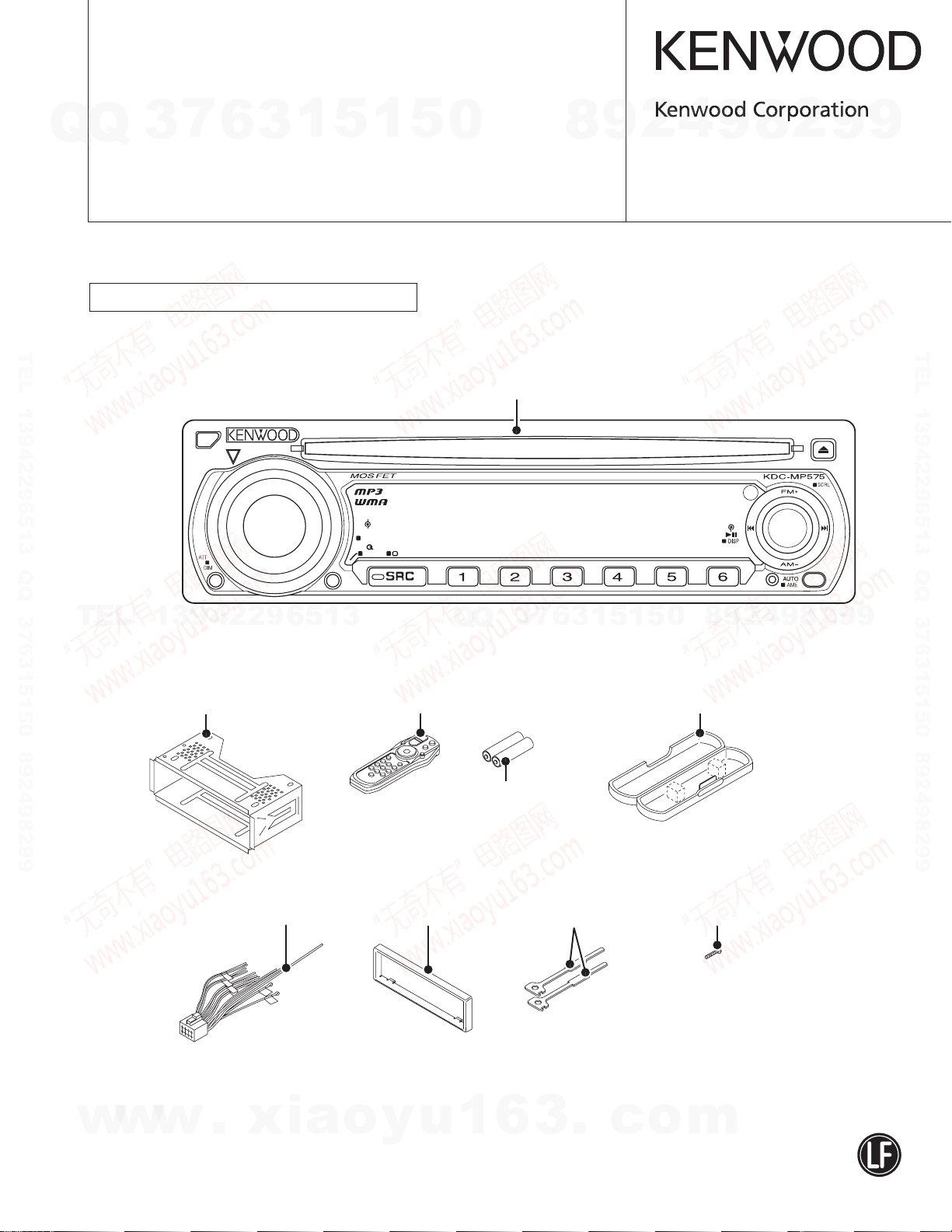
Panel assy
(A64-3690-02)
SCAN RDM REP F.SEL M.RDM
4
2
9
8
© 2005-4 CREATED IN JAPAN
B53-0281-00 (N) 0
This panel assy does not include any knobs.
For details, refer to the exploded view.
Auxiliary Input
9
8
2
9
9
TEL 13942296513 QQ 376315150 892498299
TEL
13942296513
Mounting hardware assy
(J22-0227-03)
DC cord
(E30-6123-15)
6
7
3
Q
Q
Remote controller assy (RC-517)
(A70-2069-05)
Battery
(Not supplied)
Escutcheon
(B07-3160-01)
Lever
(D10-4705-04) x2
3
1
5
1
8
0
5
Plastic cabinet
(A02-2746-01)
Screw (4x16)
(N84-4016-48)
9
9
2
8
9
4
2
9
This palstic cabinet
does not include the 2 cushions.
For details, refer to the exploded view.
w
w
w
.
xia
o
y
u
1
6
3
.
c
o
m
CKDC-MP575
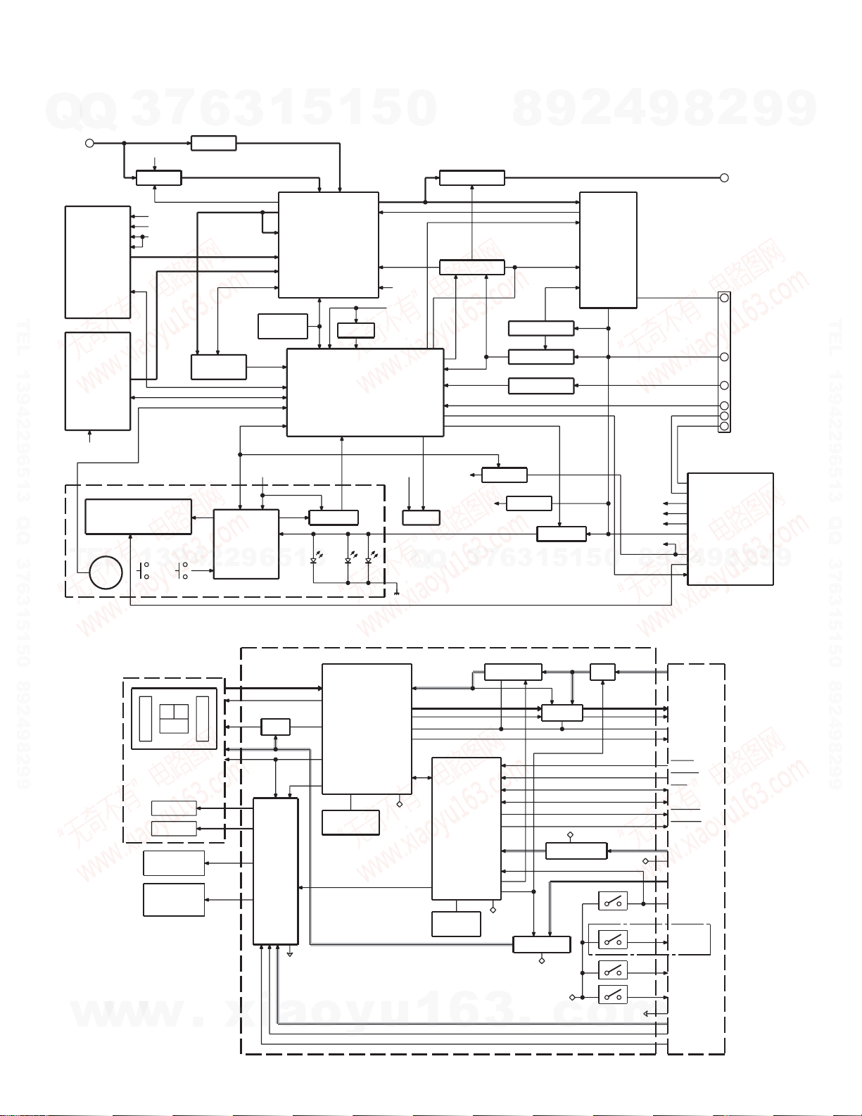
BLOCK DIAGRAM
7
Q
Q
J4
ANT
CD or MD
MECHA
AUDIO OUT
TEL 13942296513 QQ 376315150 892498299
J2
CHANGER
AUDIO OUT
BACK-UP
ED1
TEL
3
AM+B
AM AGC
SERVO
A8V
BU5V
SWITCH UNIT (X16-)
VFD
S11
13942296513
VOL
.......
Q501
6
L506
FM AGC
800mV
1200mV
RDS
DECODER
IC4
VFD DRIVER
KEY MATRIX
1
5
E-VOL
&
TUNER
SYSTEM u-COM
REMOTE
.......
KEY
ILLUMI
1
ELECTRIC UNIT (X34-)
IC10
IC8
RST IC
IC3
3
MPX OUT
MPX IN
IC11
E2PROM
IC7
PAN5V BU5V
with
5
BU5V
IC1
0
A8V
DSI
Q
Q351,352
PRE MUTE
MUTE LOGIC
PAN5
Q155
Q
SERVO
3
IC6
7
Q151
PAN5V
Q72,73
6
9
8
SURGE DET
BU DET
ACC DET
SERVO
VFD REG
5
1
3
Q51
Q52
Q53
2
IC4
IC15
1
4
POWER IC
0
5
9
SW5V
AM+B
A8V
BU5V
8
9
2
8
J6
FM (J/K Type)
FM (E Type)
AM (J/K Type)
AM (E Type)
CD/MD RECEIVER
J1
IC3
POWER SUPPLY IC
P-CON
P-ANT
SW5V
AM+B
AUDIO+B
VCC
BU5V
8
9
4
2
ILLUMI
9
PRE OUT
: 1800mV
:
1372mV
:
600mV
:
855mV
:
3600mV
:CHANGER
3600mV
SP OUT
BACK-UP
ACC
TEL MUTE
P-ANT
P-CON
9
2
9
TEL 13942296513 QQ 376315150 892498299
9
w
w
PICKUP
ACB
EF
FO COIL
TR COIL
SPINDLE
MOTOR
LOADING &
SLED
MOTOR
w
.
CD PLAYER UNIT (X32-5740-02)
IC7
RF AMP
+
SERVO
PROCESSOR
+
MP3 DECODER
APC
IC3
MOTOR
DRIVER
S.GND
xia
+
WMA DECODER
+
AAC DECODER
+
1Mbit SRAM
VREF
CLOCK
16.934MHz
o
y
D.GND
DMUTE
u
IC4
MICRO
PROCESSOR
CLOCK
16.00MHz
1
6
IC1
A3.3V REG
P-ON2
P-ON1
3
D.GND
IC6
IC2
LPF
IC5
BU3.3V REG
D3.3V REG
D.GND
D.GND
.
c
SW
D.GND
(0-01)ONLY
o
D.GND
S3
S4
S2
S1
S.GND
m
MOTHER
BOARD
A8V
L-ch
R-ch
A.GND
D.OUT
MRST
MSTOP
CLK
DATA
MUTE L
MUTE R
BU5V
D.GND
D5.0V
LOE/LIM-SW
8EJE-SW
12EJE-SW
LOS-SW
S.GND
S7.5V
LO/EJ
MOTOR
2
CKDC-MP575
COMPONENTS DESCRIPTION
7
Q
Q
● ELECTRIC UNIT (X34-3920-12)
TEL 13942296513 QQ 376315150 892498299
TEL
3
Ref. No. Application / Function Operation / Condition
IC1 SYSTEM µ-COM System control.
IC3 POWER SUPPLY DC5Vx2, 7.9Vx1, 8.1Vx1, 10.3V, P.CON, P-ANT output.
IC4 POWER IC Audio signal amplifier.
IC6 MUTE LOGIC Mute control.
IC7 RDS DECODER For other models.
IC8 RESET “L” when detection voltage goes below 3.6V.
IC10 E-VOL & TUNER E-VOL, Tuner, Stereo decode.
IC11 E2PROM Saves and writes tuner adjustment data.
IC15 VFD REGULATOR 11.3V output voltage for LED and VFD.
Q51 SERGE DET “ON” when the base goes “H”.
Q52 BU DET “ON” when the base goes “H”.
Q53 ACC DET “ON” when the base goes “H”.
Q71 SERVO+B CONTROL SW “ON” when the base goes “H”.
Q72,73 SERVO+B AVR Output voltage level : 7.5V.
Q74 IC3 CONTROL SW “ON” when the base goes “H” (Output voltage : 10.3V).
Q151 PANEL 5V SW “ON” when the base goes “L”.
Q155 DSI ILLUMI SW “ON” when the base goes “L”.
Q252 IC4 STBY SW “ON” when the base goes “L”.
Q330 Q351, 352 MUTE DRIVER “ON” when the base goes “L”.
Q351 Lch PRE MUTE SW Pre-output is muted when the base goes “H”.
Q352 Rch PRE MUTE SW Pre-output is muted when the base goes “H”.
Q501 AM RF AMP Adjusts for AM-RF gain.
13942296513
6
3
1
5
1
5
0
Q
Q
3
7
6
8
3
9
1
5
1
2
5
4
0
9
8
9
8
2
4
2
9
8
9
2
9
9
TEL 13942296513 QQ 376315150 892498299
9
● CD PLAYER UNIT (X32-5740-02)
Ref. No. Application / Function Operation / Condition
IC1 A3.3V regulator Power supply for audio 3.3V
IC2 Ope amp for low-pass filter
IC3 4ch BTL driver Driving spindle motor and loading/ejection operation
IC4 µ-com
IC5 Bu 3.3V regulator Power supply for backup 3.3V
IC6 D3.3V regulator Digital 3.3V power supply
IC7 Audio DAC built-in servo DSP MP3, WMA, and AAC compatible
IC8 Memory IC Used only for 0-02 destination
IC11 Buffer IC Level shift
Q1 A3.3V discharge circuit
Q4 Electric AMP Adjusts current to be sent to laser
Q5,6 SW 5V
Q7,8 SW 8V
w
w
D1 For electric AMP
w
.
xia
o
y
u
1
6
3
.
c
o
m
3
CKDC-MP575
COMPONENTS DESCRIPTION
7
Q
Q
● SWITCH UNIT (X16-3370-13)
Ref. No. Application / Function Operation / Condition
IC3 REMOTE SENSOR
IC4 VFD DRIVER
Q21 PAN SW5V “ON” when the base goes “H”.
TEL 13942296513 QQ 376315150 892498299
3
6
MICROCOMPUTER’S TERMINAL DESCRIPTION
3
1
5
1
5
0
8
9
2
4
9
8
2
9
9
TEL 13942296513 QQ 376315150 892498299
● SYSTEM µ-COM : IC1 on X34- (ELECTRIC UNIT)
TEL
Pin No.
1 DC ERR I DC offset detection input
2 LINE MUTE I Phone detection NAVI MUTE : Over 2.5V, TEL MUTE : Below 1V
3ROTARY CW I Rotary encoder input
4AVSS 5TUN TYPE1 I E-VOL setting switch Refer to “TUN TYPE” on the TRUTH TABLE
6TUN TYPE2 I E-VOL setting switch Refer to “TUN TYPE” on the TRUTH TABLE
7AVREF1 8 VFD DATAF I Data input from VFD driver
9 VFD DATAS O Data output to VFD driver
10 VFD CLK O Clock output to VFD driver
11 L VFD RST O Reset output to VFD driver
12 VFD CE O Chip enable output to VFD driver
13 ROTARY CCW I Rotary encoder input
14 L TDF DET I TDF panel detection TDF panel OFF : H, TDF panel ON : L
15 PWIC BEEP O Beep output
16 LX DATA S I Data from slave unit
17 LX DATA M O Data to slave unit
w
18 LX CLK I/O LX-BUS clock
13942296513
Active
(H/L)
w
Pin Name I/O Application Processing Operation
w
.
xia
o
y
u
Q
Q
1
3
6
9
8
0
5
1
5
1
3
6
7
Display OFF, Key reset, TDF panel OFF : L
Display ON, Key scan : H
3
.
c
o
m
2
4
9
8
2
9
9
4

CKDC-MP575
MICROCOMPUTER’S TERMINAL DESCRIPTION
7
Q
Q
Pin No.
TEL 13942296513 QQ 376315150 892498299
TEL
w
3
Active
(H/L)
19 NC -
20 L TUN ADJ I For adjusting IC10
21 TUN SD I Tuner search stop output H : Station exists, L : Station does not exist
22 H LX RST O Hard reset to slave unit H : Reset, L : Normal condition
23 H LX CON O Start-up request to slave unit H : Slave unit ON, L : Slave unit OFF
24 LX REQ M O Communication request to slave unit
25 AUD SDA I/O Volume + tuner I2C data input and output
26 AUD SCL I/O Volume + tuner I2C clock input and output
27 H PWIC STBY O Power IC standby output Power IC ON : H, Power IC OFF : L
28 H VOL MUTE O E-VOL mute output L : Mute OFF, Hi-Z : Mute ON
29 L PWIC MUTE O Power IC mute output Power OFF : L, Standby : L, Tel mute : L
30 TUN FANC OUT O Tuner block (inside the µ-com) check OK : L, NG : H
31 RESET2 O Mute for reset Output L
32 NC 33 VSS1 34 NC 35 L ACC DET I ACC detection ACC exists : L, ACC does not exist : H
36 L BU DET I Momentary power-down detection
37 NC 38 PS2-2 O Power supply control output
39 PS2-1 O Power supply control output
40 PS1-1 O Power supply control output
41 PS1-2 O Power supply control output
42 PS1-3 O Power supply control output
43,44 NC 45 CD MUTE I CD mute request L : Mute request
46 L CD MSTOP O CD mecha u-com stop
47 CD LOE LIM SW I CD detection (chucking switch) H : Loading is finished, L : Disc does not exist
48 CD LOEJ I/O CD motor control
49 CD MOTOR O CD motor control
50 NC 51 L CD MRST O CD mecha µ-com reset H : Normal condition, L : Reset
52 CD SCL I/O CD mecha I2C clock output
53 CD DISC12 SW I 12cm CD detection
54 CD LOS SW I CD loading detection
13942296513
w
w
6
Pin Name I/O Application Processing Operation
.
xia
3
1
5
o
1
y
5
u
0
Q
Q
1
3
6
7
3
4
2
9
8
Adjustment=H, PS1-1,2=L, PS1-3=Hi-Z,
PS2-1,2=Hi-Z, TUN DATA, CLK=Hi-Z
0
5
1
5
1
3
6
BU exists : L
BU does not exist (Momentary power-down) : H
Refer to “POWER IC CONTROL” on the TRUTH TABLE
Refer to “POWER IC CONTROL” on the TRUTH TABLE
Refer to “POWER IC CONTROL” on the TRUTH TABLE
Refer to “POWER IC CONTROL” on the TRUTH TABLE
Refer to “POWER IC CONTROL” on the TRUTH TABLE
H : mecha µ-com operates, L : mecha µ-com is stopped
Refer to “CD MECHA CONTROL OPERATION”
on the TRUTH TABLE
Refer to “CD MECHA CONTROL OPERATION”
on the TRUTH TABLE
.
c
o
9
9
8
m
2
8
4
2
9
8
9
2
9
9
TEL 13942296513 QQ 376315150 892498299
9
5
CKDC-MP575
MICROCOMPUTER’S TERMINAL DESCRIPTION
7
Q
Q
Pin No.
55 CD SDA I/O CD mecha I2C data input and output
56 OEM DISP CE I/O External display chip enable External display
57 OEM DISP CLK I/O External display clock External display
58 OEM DISP DATA I/O External display chip data External display
59 DSI O DSI control DSI ON : H, DSI OFF : L, TDF DET=H (DSI blinks)
60 L RESET I
TEL 13942296513 QQ 376315150 892498299
61 NC -
62 L PON FL O VFD power supply ON
63 KEY REQ I Communication request from VFD driver L : Key input
64 NC 65 REMOTE I Remote control input
66 LX REQ S I Communication request from slave unit
67 VSS0 68 VDD1 69 X2 70 X1 71 TEST -
TEL
72 XT2 73 XT1 74 VDD0 75 AVDD 76~78 TYPE 3~TYPE 1 I Destination switch
79 NC 80 TUN SMETER I Tuner S-meter input
3
Active
(H/L)
13942296513
6
Pin Name I/O Application Processing Operation
3
1
5
1
5
0
Q
Q
3
7
4
2
9
8
VFD ON : H, VFD OFF : L
TDF DET H (DSI blinks) : L, TDF DET L : H
8
0
5
1
5
1
3
6
9
9
8
2
4
2
9
8
9
2
9
9
TEL 13942296513 QQ 376315150 892498299
9
● TRUTH T ABLE
• TUN TYPE
General models commercially-designated as pure KENWOOD brand (Initial value)
Initial value setting
General models commercially-designated as pure KENWOOD brand (CRSC is changed)
Multi-Path Band-Path Gain=12dB, Multi-Path Charge Current=0.4µA, De-Emphasis=75µS
w
w
w
6
.
xia
o
y
u
1
6
3
.
TYPE 1 TYPE 2
LL
HL
c
o
m
CKDC-MP575
MICROCOMPUTER’S TERMINAL DESCRIPTION
7
Q
Q
• POWER SUPPLY IC (IC3) CONTROL
SEL1 (Pin No. 11)
SEL2 (Pin No. 12)
TEL 13942296513 QQ 376315150 892498299
● MECHANISM µ-COM : IC4 on X32- (CD PLAYER UNIT)
Pin No. Pin Name I/O Application
TEL
w
3
PS1-2 PS1-3 PS2-1 ILLUMI P-CON P-ANT
LLLOFF OFF OFF
LLHONOFF OFF
HLHONONOFF
HHHONONON
PS1-1 PS2-2 AUDIO SW5 AM
LLOFF OFF OFF
HLONON OFF
HHONON ON
13942296513
1NCONot used. Low-fixed
2 E2P_SCL I/O Rom correction E2P I2C clock
3~5 NC O Not used. Low-fixed
6 VDD - 5V electric potential
7 GND - GND electric potential
8,9 NC O Not used. Low-fixed
10,11 PON1,PON2 O Power ON/OFF control H : ON, L : OFF
12 LOE/LIM_SW I Down-limit SW detection L : Lim detection
13 DAC_MUTE O DAC MUTE control H : MUTE ON, L : MUTE OFF
14 DAC_RST O DAC RESET H : NORMAL, L : RESET
15 EMPH O External DAC Emphasis control
16,17 NC O Not used. Low-fixed
18 IC/Vpp - Write voltage (FLASH)
19 MUTE_L O Lch audio MUTE control L : MUTE ON, H : MUTE OFF
20 MUTE_R O Rch audio MUTE control L : MUTE ON, H : MUTE OFF
21 TYPE I DAC switching terminal
w
w
6
.
xia
3
1
5
o
1
y
5
u
0
Processing Operation
Description
7
3
Q
Q
H : Emphasis ON, Used only with DXM-6590W.
L : Emphasis OFF With DXM-6580W, open and L-fixed.
L : Normal operation,
H : In writing.
H : DSP built-in DAC used,
1
6
L : DSP built-in DAC Not used.
3
4
2
9
8
• CD MECHA CONTROL OPERATION
CD LOEJ CD MOTOR CD MECHA OPERATION
LH Load
HH Eject
Hi-Z L Stop
Hi-Z H Brake
0
5
1
5
1
3
6
Used only with DXM-6590W.
With DXM-6580W, open and L-fixed.
Used only with DXM-6590W.
With DXM-6580W, open and L-fixed.
.
c
H : DXM-6580W, L : DXM-6590W
o
9
9
8
m
Remarks
2
8
4
2
9
8
2
9
9
9
TEL 13942296513 QQ 376315150 892498299
9
* DXM-6580W : X92-5080-00, X92-5200-05, DXM-6590W : X92-5190-00
7
CKDC-MP575
MICROCOMPUTER’S TERMINAL DESCRIPTION
7
Q
Q
Pin No. Pin Name I/O Application
22 TEST_O 1 O TEST MODE O 1 (Not used.)
23 TEST_O 2 O TEST MODE O 2 (Not used.)
24 TEST_O 3 O TEST MODE O 3 (Not used.)
25 TEST_O 4 O TEST MODE O 4 (Not used.)
26 NC O Not used. Low-fixed
27 WAIT I Wait control signal detection
TEL 13942296513 QQ 376315150 892498299
28~30 NC O Not used. Low-fixed
31 RESET I Reset detection H : NORMAL, L : RESET
32 XT1 I Not used.
33 XT2 - Not used.
34 REGC 35 X2 36 X1 I
37 Vss - GND electric potential
38 VDD - 5V electric potential
39 NC O NC Output stopped in standby 3.3V driven
40 WRL I Multiplex WRITE signal 3.3V driven
41,42 NC O Not used. Low-fixed 3.3V driven
TEL
43 RD O Multiplex RD signal 3.3V driven
44 ASTB O Multiplex ASTB signal 3.3V driven
45 NC O Not used. Low-fixed 3.3V driven
46 NC O Not used. Low-fixed 3.3V driven
47~54 AD0~AD7 I/O Multiplex address/data 3.3V driven
55 BVdd - Bus interface power supply
56 BVss - Bus interface GND
57~61 AB8~AB12 I/O Multiplex data/address 3.3V driven
62~65 NC O Not used. Low-fixed 3.3V driven
66 CS O Chip select control H : OFF, L : ON 3.3V driven
67 DSP RESET O DSP reset control H : NORMAL, L : RESET 3.3V driven
68~70 NC O Not used. Low-fixed 3.3V driven
71 Avdd 72 Avss 73 Avref I A/D port reference voltage input
74 NC I Not used. Low-fixed
75 RAMSEL I
76 RZM I 0bit MUTE detection H : ≥1.7V, L : <1.7V
77 LZM I 0bit MUTE detection H : ≥1.7V, L : <1.7V
w
3
13942296513
w
w
6
.
xia
1
5
1
3
With DRAM/No DRAM switching
for different models
o
5
y
0
Processing Operation
Description
3
Q
Q
H : With DRAM, L : No DRAM
u
1
6
7
3
6
8
3
.
9
1
1
5
c
2
5
o
4
0
m
9
Remarks
9
8
8
2
4
2
9
8
9
2
9
9
TEL 13942296513 QQ 376315150 892498299
9
8
CKDC-MP575
MICROCOMPUTER’S TERMINAL DESCRIPTION
7
Q
Q
Pin No. Pin Name I/O Application
TEL 13942296513 QQ 376315150 892498299
TEL
3
78 AAC I AAC compatibility switching
79 ASEL I Audio output polarity switching
80 E2P_WR I E2PROM write switching
81 TEST_I 0 I TEST MODE I 0 (Not used.)
82 TEST_I 1 I TEST MODE I 1 (Not used.)
83 TEST_I 2 I TEST MODE I 2 (Not used.)
84 TEST_I 3 I TEST MODE I 3 (Not used.)
85 NC I Not used. Low-fixed
86 NC O Not used. Low-fixed
87 MSTOP I Standby restart interruption H : STOP release, L : STOP
88 INTSV I Interruption from servo IC H : Interruption
89~92 NC O Not used. Low-fixed
93 D-MUTE O Driver MUTE H : OFF, L : ON
94 SYS_SDA I/O System µ-com I2C data Flash write port (SI0)
95 NC O Not used. Low-fixed Flash write port (SO0)
96 SYS_SCL I/O System µ-com I2C clock Flash write port (SCK0)
97~99 NC O Not used. Low-fixed
100 E2P_SDA I/O ROM correction E2P I2C data
13942296513
6
3
1
5
1
5
0
Processing Operation
Description
H : AAC non-compatible, AAC non-compatible mode has priority
L : AAC compatible for both hardware and software.
H : Reverse output,
L : Non-reverse output
H : E2PROM WRITE,
L : NORMAL
7
3
Q
Q
6
8
3
9
1
5
1
2
5
4
0
9
8
Remarks
2
9
8
4
2
9
8
9
2
9
9
TEL 13942296513 QQ 376315150 892498299
9
w
w
w
.
xia
o
y
u
1
6
3
.
c
o
m
9
CKDC-MP575
TEST MODE
7
Q
Q
How to enter the test mode
While simultaneously press PRESET “1” ke y and PRESET “3”
key, press “RESET” button.
How to release the test mode
Press “RESET” button. (The release cannot be achieved in
the conditions of POWER OFF and ACC OFF.)
Initial conditions of the test mode
TEL 13942296513 QQ 376315150 892498299
• The source is “STANDBY”.
• The displays all lit up.
• The volume is at –10dB (The display shows “30”.)
• LOUD is “OFF”.
• CRSC is “OFF”.
• SYSTEM Q is “NATURAL”.
• BEEP is sounded at all time with the key depressed for less
than 1 second.
Special displays when all indicator lights are lighted
When “PRESET” keys are pressed while all indicators for the
STANDBY sources are lighted, the following displays will appear.
TEL
PRESET
“1” key (Display) : x x x x x x x x
PRESET
“2” key (Display) : x x x x x x x x
PRESET
“3” key time display (STANDBY source time is not counted.)
PRESET
“4” key time display
3
13942296513
•Version display (8 digits : month, date, hour, minute)
• Serial number display (8 digits)
•When pressed for less than 1 second : POWER ON
(Display) : PON x x x x x MAX 60,000 (hours)
* The display is cleared by pressing the key for more
than 2 seconds.
• When pressed for less than 1 second : CD operation
(Display) : PLY x x x x x MAX 60,000 (hours)
* The display is cleared by pressing the key for more
than 2 seconds.
6
3
1
5
1
5
0
Q
Q
PRESET
“5” key number display
PRESET
“6” key close number display
“FM” • ROM CORRECTION version display
key (Display)
“AM” • IC10 adjustment status (Refer to “ADJUSTMENT” on
key the following page.)
7
3
“ ”•Mechanism error detection status
key•Communication error → Error No. 1 → Error No. 2 →
4
2
9
8
•When pressed for less than 1 second : CD EJECT
(Display) : EJC x x x x x MAX 60,000 (times)
* The display is cleared by pressing the key for more
than 2 seconds.
• When pressed for less than 1 second : Panel open/
(Display) : PNL x x x x x MAX 600,000 (times)
* The display is cleared by pressing the key for more
than 2 seconds.
Effective : ROM _ Rxxx (x : number)
Not effective (When not able to read)
Not effective (When version is different)
(Display)
Adjustment complete : E2P _ OK _ _
Adjustment not completed : E2P _ ER _ _
5
1
3
6
Communication error : I2C _ ER _ _
* When other than “E2P _ OK _ _” , Pin No. 30 will
become “H”.
Error No. 3 → Communication error (Error No. 1 is the
most recent error.)
(Display)
Communication OK : I2C _ OK _ _
Communication error : I2C _ NG _ _
Not detected : ERR _ n – – – (n : 1~3)
Detected : ERR _ n-✳✳ (✳✳ : error code)
* The display is cleared by pressing the key for more
than 2 seconds.
1
5
0
9
8
9
2
2
8
: ROM _ R – – –
: ROM _ R✳✳✳
2
8
9
4
9
9
9
TEL 13942296513 QQ 376315150 892498299
9
10
w
w
w
.
xia
o
y
u
1
6
3
.
c
o
m
SPECIAL MODE
CKDC-MP575
7
Q
Q
● Security
•
• How to clear the programmable security code
1. While “– – – –” is being displa y ed, press “ ” for 3 seconds
TEL 13942296513 QQ 376315150 892498299
2. Input “KCAR”, using the remote controller.
3. The security is cleared and the unit enters ST ANDBY source
4. If wrong codes are input, “– – – –” will be displayed again.
3
How to enter the forced POWER ON mode
While “– – – –” is being displayed, while simultaneously
pressing “Q” key and “4” key, press “RESET” button, With
this, it is possible to turn the power on for 30 min utes only.
or more while pressing the “A UT O” key. This mak es the “– –
– –” display disappear.
Press “5” key of the remote controller twice (Input for “K”)
and press “ ” key.
Press “2” k e y of the remote controller 3 times (Input for “C”)
and press “ ” key.
Press “2” key of the remote controller once (Input for “A”)
and press “ ” key.
Press “7” key of the remote controller twice (Input for “R”)
and press “ ” key.
mode.
6
3
1
5
1
5
0
● Mechanism memory clear confirmation mode
Confirmation mode :
While depressing “ATT” key and “Q” key simultaneously,
press “RESET” button.
(Display) : MEM _ CLR _
*2 seconds after the confirmation mode boots up, Mecha-
nism memory clear as a result is displayed.
(Display) Clear status display normal completion
Release Method : Press “RESET” button.
● FM/AM channel space switching
When in the conditions of ACC ON and POWER OFF, while
depressing PRESET “1” key and PRESET “5” key simultaneously, press “SRC” key.
4
2
9
8
: CD _ O _ _ _
Clear status display abnormal completion
: CD _ X _ _ _
9
8
2
9
9
TEL 13942296513 QQ 376315150 892498299
TEL
● DC offset error detection confirmation mode
Confirmation mode :
* By pressing “AUTO” key while “DC _ ERR _ _” is being
Release Method : Press “RESET” button.
13942296513
While depressing PRESET “3” key and PRESET “6” key
simultaneously, press on the “RESET” button.
(Display) Detected : DC _ ERR _ _
Not detected : DC _ OK _ _ _
displayed, detection status is cleared. This will result in the
display of “DC _ OK _ _ _”.
Q
Q
3
7
6
3
1
5
1
5
0
8
9
2
4
9
8
2
9
9
w
w
w
.
xia
o
y
u
1
6
3
.
c
o
m
11
 Loading...