

Q
CD RECEIVER
CKDC-392V/VA
CKDC-392VD/VD A
Q
3
7
6
3
1
5
1
5
CKDC-492V/VD
SERVICE MANUAL
0
8
4
2
9
© 2004-2 CREATED IN JAPAN
B53-0145-00 (N) 0
9
8
2
9
9
MANUFACTURED BY VISTEON
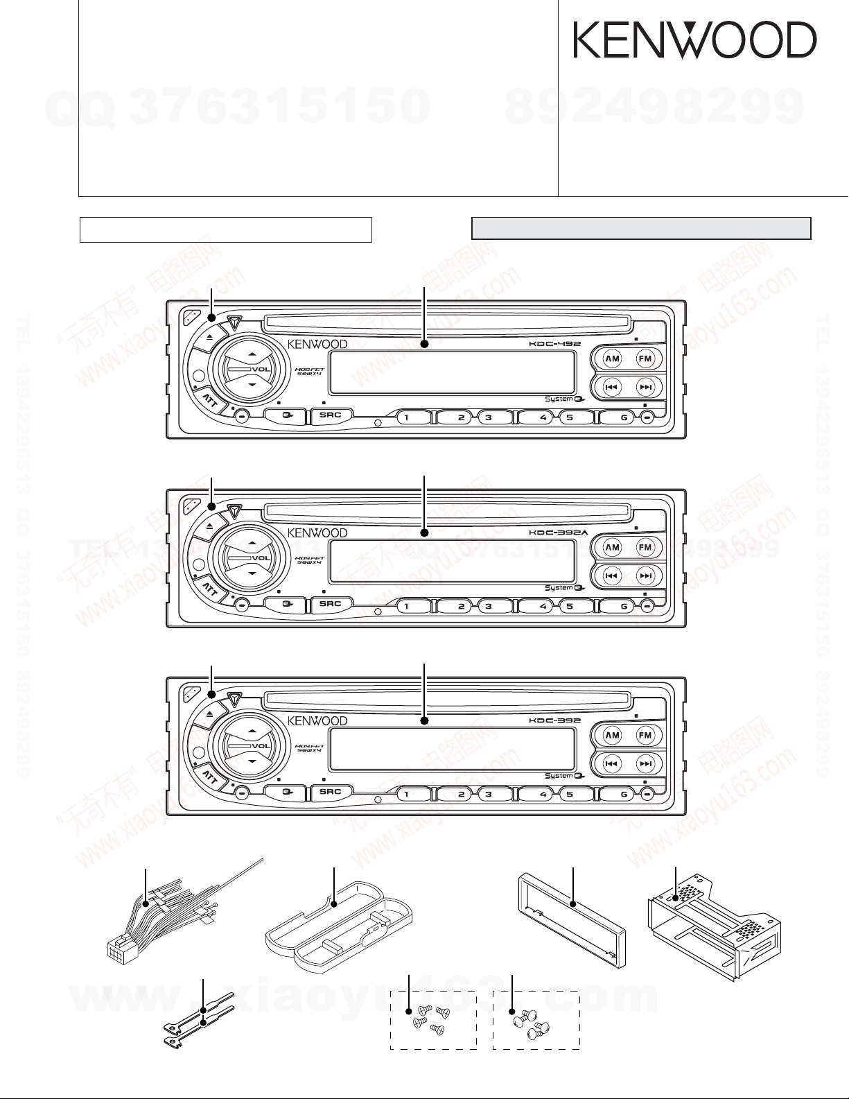
Panel
(A64-3371-01)
TEL 13942296513 QQ 376315150 892498299
D
LOU
OFF
OFF
TEL
AUD
AUTO
AME
Panel
(A64-3371-01)
13942296513
D
LOU
AUD
AUTO
AME
Front glass
CKDC-492V/VD (B10-4564-01)
SCAN
Front glass
CKDC-392VA/VAD (B10-4565-01)
7
3
Q
Q
SCAN
CD mechanism extension cord (24PIN) : W05-0934-00
CRSC
0
CLK ADJ
CRSC
8
CLK ADJ
9
2
4
9
8
2
9
9
RDM REP
1
3
6
RDM REP
5
1
5
TEL 13942296513 QQ 376315150 892498299
w
w
Panel
(A64-3371-01)
LOU
DC cord
(E30-6123-05)
Lever
(D10-4705-04) x 2
w
.
D
AUTO
AME
xia
AUD
OFF
Plastic cabinet
(A02-1491-01)
o
y
Front glass
CKDC-392V/VD (B10-4566-01)
Screw x 4
(N09-4145-05)
u
1
SCAN
6
RDM REP
Screw x 4
(N09-4149-05)
3
Escutcheon
(B07-3116-02)
.
c
o
CRSC
CLK ADJ
Mounting hardware assy
(J21-9934-03)
m
CKDC-392V/VA/VD/VDA
S1(LOS SW)
S2(12EJE SW)
(LOE & LIM SW)
S4(8EJE SW)
LPF
LPF
IC1
MECHANISM
CONTROL IC
S3
5V SW
Q2
3.3V AVR
IC2
IC3
DSP/DAC IC
CD RF/SERVO/
Q3
APC
Q4
SW
IC4
4ch BTL
DRIVER
LD
PD
C
F
AB
E
TR COIL
FO COIL
M
M
DM1
DM2
SPINDLE
MOTOR
LOADING
MOTOR
& SLED
OPTICAL PICKUP
DPU1 :
BU5V 15
DGND 14
DATA
CLK
18
19
MUTER
MUTEL 12
13
MSTOP
MRST 11
10
LOS SW 20
21
SW
1
8EJE SW 17
A8V 9
Lch 8
AGND 7
DOUT
Rch
22
6
4MOTOR
LO/EJ 5
SGND
S7.5V 3
2
NC 16
12EJE SW
MSTOP
DATA
MRST
MUTEL
MUTER
CLK
PON
SERCH
LOE&LIM
LOE & LIM
SW
PON
INTQ
SI
AO
DSP RESET
STB
SCK
DRV MUTE
SO
CNTL
RST
SI
SCK
STB
AO
INTQ
SO
MD+
SD+
TD+
FD+
LZM
RZM
ROUT
LOUT
TX
X1
4.19MHz
Z MUTE L
Z MUTE R
16.934MHz
X2
A
B
C
D
E
PRE OUT
F
LD
PD
FDIN-
BIAS
CNT
TR+
TR-
FO-
FO+
SLD+
SLD-
SPD-
SPD+
TDIN-
SPIN-
SLIN+
MUTE
LO/EJ
OPEN
OPEN
BU5V
SW5V
SW3.3V
S7.5V
VREF
2
CKDC-492V/VD
Q
TEL 13942296513 QQ 376315150 892498299
Q
CD PLAYER UNIT (X32-5490-00)
TEL
w
3
w
7
13942296513
w
6
.
3
x
i
1
a
5
1
o
y
5
u
0
Q
1
Q
6
3
7
3
8
3
6
.
1
9
5
c
1
2
o
4
0
5
m
9
2
9
8
8
4
9
2
8
2
9
9
9
TEL 13942296513 QQ 376315150 892498299
BLOCK DIAGRAM
9
1200mV
KEY MATRIX
WITH
LCD DRIVER
LCD
REMOCON
MI-COM
CD
ANT
AM AGC
FM AGC
RESET
IC
EEP-ROM
TUNER,MPX &
E-VOL.
SUPPLY IC
SW5V
SERVO
P-CON
POWER
MUTE
LOGIC
DET
ACC
BU
DET
MUTE
PRE
POWER IC
SP
ACC
UP
BACK
OUT
OUT
PRE
IC1
BU5V
IC2
SW5V
LO/S
RST
LOE/LIM
MO
LO/EJ
STOP
MUTE
8EJE
SDA
SCLK
AUDIO OUT
12EJE
Q501
Q502
AM+B
FM+B
AM AGC OUT
CD
SERVO
BU5V
A8V
TUNER OUT
BU5V
IC11
IC12
IC10
FM AGC OUT
A8V
SW2
SW1
ILLUMI
VCC
BU5V
AUDIO+B
AM+B
FM+B
BACK LIGHT
KEY ILLUMI
Q51,55
SW5V
Q50
SERVO
BU5V
FM+B
AM+B
A8V
P-CON
IC8
Q20
Q10
IC7
MUTE
Q223,224
IC4
ELECTRIC UNIT (X34- )
SWITCH UNIT (X16- )
Q
Q
3
7
6
3
1
5
1
5
0
8
9
2
4
9
8
2
9
9
TEL 13942296513 QQ 376315150 892498299
x
i
a
o
3
TEL
w
w
13942296513
w
.
y
u
1
Q
Q
6
3
7
3
1
3
6
.
1
5
c
5
o
0
m
8
9
2
4
9
8
2
9
BLOCK DIAGRAM
9
TEL 13942296513 QQ 376315150 892498299
CKDC-392V/VA/VD/VDA
CKDC-492V/VD
CKDC-392V/VA/VD/VDA
CKDC-492V/VD
COMPONENTS DESCRIPTION
7
Q
Q
● SWITCH UNIT (X16-2850-10/11/12/13)
Ref No. Application/Functions Operation/Condition/Compatibility
IC1 LCD driver LCD derive & Key input interface
IC2 Sensor Remote control sensor
Q1 Key scan detect Key scan start at base gose “L”.
● CD PLAYER UNIT (X32-5490-00)
Ref No. Application/Functions Operation/Condition/Compatibility
TEL 13942296513 QQ 376315150 892498299
IC1 Mechanism control When BU5V & MSTOP (12pin) goes “H” (IC1 is active)
IC2 SW3.3V AVR When CNTL (1pin) goes “H” (SW3.3V AVR : ON)
IC3 CD DSP & servo IC CD RF amp, Servo, DSP & DAC
IC4 BTL driver Focus, tracking coil, Sled & Spindle motor driver IC
Q2 SW SW5V SW transistor
Q3 APC Auto Power Control
Q4 SW EQ SW transistor
● ELECTRIC UNIT (X34-3350-10/11)
Ref No. Application/Functions Operation/Condition/Compatibility
IC1 System control IC System control microprocessor
IC4 Audio power IC Audio power amplifier
TEL
IC7 Power supply IC Multi AVR IC (for 5V, 8V, P-CON & P-ANT)
IC8 Muting logic IC Control for MUTE, P-ANT & RESET muting
IC10 E-VOL & tuner IC E-VOL. FM/AM tuner & stereo decoder
IC11 Reset IC When BU5V line voltage is less than 3.5V, this IC output line is “L”
IC12 E2PROM Memorized tuner adjustment data (save & load)
Q10 BU detector When the base goes “H” during BU applied (ON)
Q20 ACC detector When the base goes “H” during ACC applied (ON)
Q40 Muting driver foe Q223, 224 When the base goes “L” (Muting : ON)
Q50 SW5V When the base goes “L” (SW5V : ON)
Q51 SW Control SW for IC7
Q55 SERVO +B AVR Servo AVR (7.4V)
Q70 Surge detector When the base goes “H” (Surge detection)
Q101 DSI illumination SW When the base goes “L” (DSI illumination : ON)
Q102 Panel 5V SW When the base goes “L” (Panel 5V : ON)
Q223,224 Preout muting SW When the base goes “H” (Preout muting : ON)
Q501 AM RF amplifier When the base goes “H” (RF circuit gain is up)
Q502 FM RF amplifier When the base goes “H” (RF circuit gain is up)
3
13942296513
6
3
1
5
1
5
0
Q
Q
3
7
6
8
3
9
1
5
1
2
5
4
0
9
8
9
8
2
4
2
9
8
9
2
9
9
TEL 13942296513 QQ 376315150 892498299
9
4
w
w
w
.
xia
o
y
u
1
6
3
.
c
o
m
CKDC-392V/VA/VD/VDA
CKDC-492V/VD
MICROCOMPUTER’S TERMINAL DESCRIPTION
7
Q
Q
● SYSTEM MICROCOMPUTER : UPD780058GC555 (X34 : IC1)
Pin No. Name I/O Description Processing Operation
TEL 13942296513 QQ 376315150 892498299
TEL
w
3
1PANEL I Panel detection H : Panel detached, L : Panel attached
2 8EJE SW I
3NCONot used (out put L)
4Avss
5 L-RST O LCD driver RESET Normal H, Power off L
6 L-CE O LCD driver selection
7AVREF1 - 5V
8NC-Not used (connected to 9pin)
9 IC10-DATA I/O IC10, E2PROM data communication Non communication : H
10 IC10-CLK O IC10, E2PROM clock communication Non communication : H
11 L-DATAL I Data input from the LCD driver When panel detached : L
12 L-DATAS O Data output to the LCD driver When panel detached, output L
13942296513
13 L-CLK O Clock output to the LCD driver When panel detached, output L
14 R-DATA I Data input from the RDS Except RDS model : Output L
15 R-QUAL I Quality input from the RDS Except RDS model : Output L
16 CH-DATAC I Data input from the changer (new 5L) Except changer model : Output L
17 CH-DATAH O Data output to the changer (new 5L)
18 CH-CLK I/O Clock input/output with the Changer (new 5L)
19 CH-REQH O Request output to the changer (new 5L)
20 NC O Not used (output L)
21 AFS O Noise detection time constant switching terminal
22~24 NC O Not used (output L)
25 CH-CONT O Changer control
26 TYPE REF O 5V lines output for destination setting H : During destination reading
27 SD I Tuner SD input H : Station detected
28 NC O Not used (output L)
29 TYPE2 I Destination type selection terminal 2 Refer to destination type list.
w
w
30 TYPE1 I Destination type selection terminal 1 Refer to destination type list.
6
.
xia
3
1
5
o
1
y
5
u
0
Q
Q
1
3
6
7
3
6
4
2
9
8
H : Eject is completed
Except 8cm CD model : Always output L
H : Panel detached, L : RESET
When 7seg model, output L
H : Select (panel communication)
When panel attached, output L
Non communication : H
Pull down on X34 unit, Pull up on X16 unit
8
0
5
1
5
1
3
When non communication, last data keeping
Except changer model : Output L
Check the old and new
Except changer model : Output L
L : Requset
Except changer model : Output L
H : Normal, L : FM/AM seek and AF search
(When tuner SRC auto zero, L)
H : Changer on, L : Changer off
Except changer model : Output L
.
c
o
m
9
9
8
2
4
2
9
8
9
2
9
9
TEL 13942296513 QQ 376315150 892498299
9
5
CKDC-392V/VA/VD/VDA
CKDC-492V/VD
MICROCOMPUTER’S TERMINAL DESCRIPTION
7
Q
Q
Pin No. Name I/O Description Processing Operation
31 TYPE0 I Destination type selection terminal 0 Refer to destination type list.
32 TUNER-TYPE1 I Destination available/genuine model rool off H : Genuine model 1, L : Available model
33 Vss1 - GND
34 TUNER-TYPE0 I Destination available/genuine model noise cancel H : Genuine model 0, L : Available model
35 MUTE O Mute (E.Vol, Preset) control
36 M-DATA I/O Data input/output with the CD mechanism Non communication : H
TEL 13942296513 QQ 376315150 892498299
37 M-CLK O Clock output to the CD mechanism Non communication : H
38 ADJ O Tuner lines adjustment PS1-0, 1=L PS1-2, 2-0, 1=Hi-z
39 P-MUTE O Power IC mute control
40 SVR O Power IC servo control
41 P-STBY O Power IC standby control H : Power IC ON, L : Power IC OFF
42 SW5V O SW 5V control
43 B.U-DET I Back up detection terminal H : Power down, L : B.U. on
TEL
44 ACC-DET I ACC detection terminal H : ACC OFF, L : ACC ON
3
13942296513
6
3
1
5
1
5
0
Q
Q
3
7
4
2
9
8
H : Mute on, L : Mute off
Power off after that 15 second L
When adjustment = H
IC10-DATA, CLK=Hi-z
H : Mute off, L : Mute on
Power off after that 15 second H
H : When momentary power down detected
L : Nomal
H : SW5V OFF, L : SW5V ON
Power off after that 10 second H
0
5
1
5
1
3
6
9
8
9
2
8
4
2
9
8
9
2
9
9
TEL 13942296513 QQ 376315150 892498299
9
45 PS1-0 O
46 PS1-1 O
47 PS1-2 O Power supply IC SW1 control 2 P-ANT
48 PS2-0 O
49 PS2-1 O
50 BEEP O BEEP signal output
51 DSI O DSI control
52 NC O Not used (out put L)
w
w
53 NC O Not used (out put L)
w
.
Power supply IC SW1 control 0
Audio 8V, P-CON
Power supply IC SW1 control 1
Audio 8V, P-CON
Power supply IC SW2 control 0
ILLUMI, FM, AM
Power supply IC SW2 control 1
ILLUMI, FM, AM
xia
o
y
u
1
6
3
BA4911 SW1
PS1-2 PS1-1 PS1-0 A8V P-CON P-ANT
LLL STANDBY
LL (H) H (L) ON OFF OFF
LHHONONOFF
HHHONON ON
BA4911 SW2
PS2-1 PS2-0
LL STANDBY
L (H) H (L) ON ON OFF
HHONOFF ON
H : Light on, L : Light off
When panel attached, output L
When panel detached, flashing at the panel (H/L)
FIX model is output L
.
c
o
Power supply IC output
Power supply IC output
ILLUMI
FM AM
m
6
CKDC-392V/VA/VD/VDA
CKDC-492V/VD
MICROCOMPUTER’S TERMINAL DESCRIPTION
7
Q
Q
Pin No. Name I/O Description Processing Operation
TEL 13942296513 QQ 376315150 892498299
TEL
3
54 LOE/LIM SW I CD mechanism down&limit detection H : Chucking detection, L : Normal
55 MO SW O CD mechanism loading motor control output H : Loading, Eject, Break, L : Play
56 LO/EJ I/O CD mechanism loading/Eject switching terminal H : Eject, L : Loading
57 M-STOP O Stop output to the CD mechanism H : Play, L : Stop
58 M-RST O Reset output to the CD mechanism H : Normal, L : CD mechanism reset
59 M-MUTE I Mute input from the CD mechanism H : Mute off, L : Mute on
60 RESET Reset input from the System microcomputer
61 REMO I Remote control input
62 R-CLK I RDS clock input Except RDS model : Output L
63 CH-REQC I Request input from the changer (new 5L) L : Request
64 LOS SW I CD mechanism loading’s switch detected
65 KEY-REQ I
66 12EJE SW I 12cm disc detected L : 12cm disc
67 Vss0 - GND
68 VDD1 - VDD
13942296513
69 X2 - MAIN X’tal oscillating circuit 4.19MHz X’tal connection
70 X1 - MAIN X’tal oscillating circuit 4.19MHz X’tal connection
71 IC - TEST
72 XT2 - Not used OPEN
73 XT1 74 VDD0 - VDD Connected to VDD
75 AVREF0
76 S-METER I S-meter input
77 NOISE I FM noise detection input
78 PHONE I 2 way mute 1.0V or less : TEL MUTE
79 NC O Not used (out put L)
80 AVCONT O A/D converter standard voltage control output
6
1
5
1
3
Key input detected H : Key no input
(11pin L connected to the DATA L) L : Key input (edge key data reading start)
A/D converter reference voltage control output,
connection to the 80pin AVCONT
5
0
Q
Q
3
7
6
4
2
9
8
H : Changer detection
Except Changer model : Output L
H : No disc
L : Disk in (Loading Start)
0
5
1
5
1
3
2.5V or greater : NAVI MUTE
Except phone mute model : Output L
H : During A/D converter active
same timing with PON
9
8
9
8
2
4
2
9
8
9
2
9
9
TEL 13942296513 QQ 376315150 892498299
9
w
w
w
.
xia
o
y
u
1
6
3
.
c
o
m
7
CKDC-392V/VA/VD/VDA
CKDC-492V/VD
MICROCOMPUTER’S TERMINAL DESCRIPTION
7
Q
Q
● CD MECHANISM CONTROL IC : 789166YGB-A513 (X32 : IC1)
Pin No. Name I/O Description Processing Operation
1~6 NC I NC GND
7 ZMUTE_L I 0 bit MUTE detect (Lch)
8 ZMUTE_R I 0 bit MUTE detect (Rch)
9AVss - DGND
TEL 13942296513 QQ 376315150 892498299
10 /MUTE_L O Lch Audio mute control L : MUTE ON, H : MUTE OFF
11 /MUTE_R O Rch Audio mute control L : MUTE ON, H : MUTE OFF
12 /MSTOP I Interruption for stand-by L : STOP, H : Release for STOP mode
13 INTQ I Interruption for DSP IC H : Interruption
14 /FOGUP I Interruption for focus gain up L : Fo GAIN UP, H : NORMAL
15 PON O Power ON/OFF control H : ON, L : OFF
16 /SCK O (for DSP) serial data clock output
17 Vdd1 - BU5V
18 SO O (for DSP) serial data output
19 SI I (for DSP) serial data input
20 /CLK I/O (for system control) I2C clock
21 DATA I/O (for system control) I2C data
TEL
22 Vpp - (FLASH saving terminal)
23 XT2 - NC OPEN
24 XT1 I NC GND
25 /MRESET I Reset detect L : RESET, H : NORMAL
26 X2 - System clock 4.19MHz
27 X1 I System clock 4.19MHz
28 Vss0 - DGND
29 Vdd0 - BU5V
30 LOE&LIM_SW I Loading end & limit SW detect L : Inside detect, H : Outside
31 DRV_MUTE O Driver muting L : MUTE ON, H : MUTE OFF
32,33 NC O NC OPEN
34 /SERCH O Condition of serch state L : Search, H : NORMAL
35 /STB O Data strobe signal output
36 A0 O Command & parameter signal output
37 Vss1 - DGND
38 /DSP_RESET O DSP reset control L : RESET, H : NORMAL
39~41 NC O NC OPEN
42 /PON O Power ON/OFF control L : ON, H : OFF
43 Avdd - BU5V
44 Avref - BU5V
w
3
13942296513
w
w
6
.
xia
3
1
5
o
1
y
5
u
0
Q
Q
1
3
6
7
3
4
2
9
8
Less than 54h : NORMAL,
More than 54h : ZMUTE detect
Less than 54h : NORMAL,
More than 54h : ZMUTE detect
0
5
1
5
1
3
6
.
c
o
9
9
8
m
8
2
4
2
9
8
9
2
9
9
TEL 13942296513 QQ 376315150 892498299
9
8

TEST MODE
CKDC-392V/VA/VD/VDA
CKDC-492V/VD
7
Q
Q
1. How to enter test mode
While holding the FM key and preset 6 key and reset the unit.
All display segments light up when the test mode is entered.
2. How to exit from test mode
Reset the unit.
Turning ACC off, power off, momentary power down or panel
detaching does not terminate the test mode.
3. Test mode specifications of CD receiver
TEL 13942296513 QQ 376315150 892498299
• Pressing the Track Up key skip to tracks in the following se-
• Pressing the Track Down key skip to the track immediately
• Pressing Preset 1 key skip to track No. 28.
•Forced ejection is not provided.
4. Audio functions
• Pressing the AUDIO key or the “*” key on the remote con-
• In the Audio adjustment mode, the Seek Up/Down keys on
TEL
• The volume is -10dB (which is displayed as “30”).
• LOUDNESS is OFF.
• The Bass/Treble Up/Down and Balance/Fader Up/Down
5. Menu mode (for 14segment model)
• Pressing the CLK or the DNPP key on the remote controller
• In the Menu mode, the Seek Up/Down keys on the remote
• With the models incorporating RDS , the first operation in the
6. Version and operating hours display
• The following table shows the key operations and resulting
w
3
quence:
No.9 → No.15 → No.10 → No.11 → No.12 → No.13 → No.14
→ No.9 (repeats the cycle)
before the track being played.
troller initiates the Audio adjustment mode.
the remote controller can only be pressed shortly. (They cannot be held depressed.)
buttons function as full-boost/full-cut and full-front/full-rear
respectively.
initiates the Menu mode.
controller can only be pressed shortly. (They cannot be held
depressed.)
menu becomes local seek.
display information.
13942296513
Key Operation Display
Pressing Preset 1 Version (Date and time display)
Pressing Preset 2 All display segments light up
Pressing Preset 3 CD operating hours
Pressing Preset 4 E2PROM (Adjustment data for IC10)
w
w
Pressing Preset 5 CD ejection count
Pressing Preset 6 Number of times adjustment for IC10
6
.
xia
3
1
5
o
1
y
5
u
0
Q
Q
1
• Holding Preset 3 while the oper ating hour information is displayed clears it.
• Holding Preset 5 while the ejection count information is displayed clears it.
Adjustment Mode
• Adjustable items
1 : Stereo Decoder Sub address : 9
2 : Configuration Sub address : D
3 : Stereo decoder Adjustment Sub address : E
4 : Hi-Cut Sub address : C
5 : Field strength control Sub address : B
• Default values
If they are not written in the EEPROM, the default values
specified are set in IC10.
Adjustment procedure
1. Enter the IC10 Adjustment mode by resetting the unit while
holding preset 3 key + preset 6 key.
2. Select the TUNER source by pressing SRC.
3. When the adjustment mode is entered, the display shows
2-digit hex number.
4. When preset 1~5 is recalled, the setting values correspond-
7
3
ing to the pressed number are displayed. (The displayed
values are those in the RAM.)
5. Vary each setting value using
6. Store the values in the corresponding preset number.
7. The settings can be performed individually for each item.
(It is not required to store all the values together.)
8. After storing the values, reset the unit to exit from the adjustment mode. The v alues set in the EEPROM will be read
during the resetting.
9. When the band is switched, there may be cases in which
the preset number being displayed does not coincide with
the stored setting value. To check this, be sure to recall the
preset number after you switch the band.
Notes
1. The items that are not stored will be set to the default values.
2. Once a value is stored in memory, the value will alw ays be
used later.
(It is not allowed to modify the setting values by switching
the destination type.)
6
3
6
8
3
.
9
1
1
5
c
2
5
o
4
0
m
9
9
8
and key.
8
2
4
2
9
8
9
2
9
9
TEL 13942296513 QQ 376315150 892498299
9
9
A B C D E
D
4
R169
7
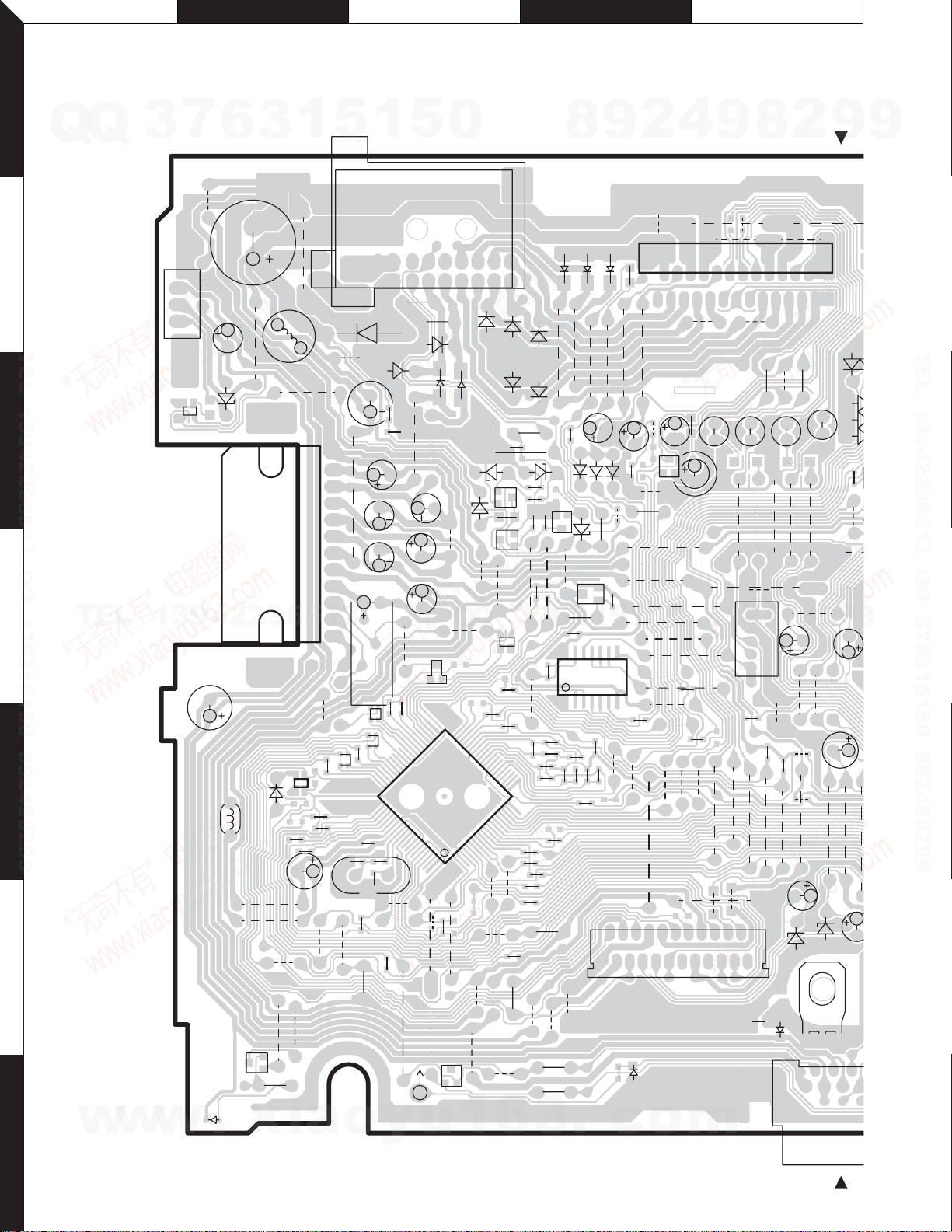
CKDC-392V/VA/VD/VDA
CKDC-492V/VD
1
2
TEL 13942296513 QQ 376315150 892498299
3
4
5
6
7
PC BOARD (FOIL SIDE VIEW)
Q
TEL
w
Q
w
7
3
Q55
EB
EBE
Q51
W137
W136
R57
6
C1
C63
D51
13942296513
C56
L101
Q101
D102
w
.
xia
3
W135
IC7
D101
C101
W129
W130
EB
R101
W121
W134
1
W122
IC11
34
R128
R129
R130
W131
W133
L2
12
R126
J2
L1
W125
W104
C103
W128
5
D1
W175
112
W124
W109
CP1
R125
CP3
R127
R414
X1
C104
W127
o
C50
C52
C54
C102
R106
1
C58
C57
R122
60
61
C105
W120
R143
5
R28
W119
C55
W103
R69
WH2
R25
D13
W114
C51
C53
D50
41
IC1
80
W578
W116
W112
u
0
D12
W410
D70
D10
W115
W113
Q
W101
R67
R108
40
1
R133
C106
W118
Q102
EB
1
D263
D11
R20
Q70
Q10
W111
Q
W110
W107
W102
R117
W98
W106
W404
2
1
D265
C30
R32
R73
B
E
R10
EB
W108
3
BEE
Q53
R264
R255
R115
21
20
W97
W105
R142
R145
6
ELECTRIC UNIT X34-3350-10/11 (J74-1465-52)
16
15
D14
R71
R72
R68
CP2
R131
W138
R123
W117
y
D266
R30
R31
W100
W96
R113
W99
D261
W93
D262
D30
R22
R11
C21
R23
W95
6
7
R119
R114
R111
R140
R139
R104
R103
R105
R102
R132
R141
W94
R163
R172
3
9
8
D264
D268
W90
W89
C257
R257
D251
D253
BE
Q20
D20
Q50
W92
R12
BE
R50
1
3
C40
14 8
IC8
1
R112
R136
R137
R135
R110
R138
R121
R107
W91
.
4
2
W81
24 2
TH1
D267
25 1
W88
W86
W84
C258
W409/R260
Q251
R261
R263
W80
D252
R259
W158
W70
R21
W74
W65
W68
R51
W72
W71
0
5
1
5
W66
W77
W63
W61
7
R258
R174
W87
W85
W82
CN1
22 2
21
R176
D111
c
o
W55
W67
C255
EB
C256
W73
C404
W76
R415
W78
W79
W53
R144
m
R256
W75
9
W58
C252
W558
8
W64
W165
9
WH1
R413
W62
2
8
R251/W405
R254/W406
W44
IC4
W52
W50
R252/W407
C253
W161
W60
W160
2
R201
W157
1
C254
W162
W51
W48
W57
W559
8
9
4
15
W566
W174
W532
R118
R116
W59
W54
W49
W47
C205
D201
D110
C142
J3
R253/W408
W45
2
C223
W565
C565
W531
W43
P1
2
1
9
W37
W156
C251
D409
R412
W25
W55
9
C224
W564
W42
C20
D202
D407
9
W417
W40
D
9
TEL 13942296513 QQ 376315150 892498299
10
 Loading...