

Page 1

Model 7072-HV
High Voltage Semiconductor Matrix Card
Instruction Manual
A GREATER MEASURE OF CONFIDENCE
Test Equipment Depot - 800.517.8431 - 99 Washington Street Melrose, MA 02176 - TestEquipmentDepot.com
Page 2

W ARRANTY
Keithley Instruments, Inc. warrants this product to be free from defects in material and workmanship for a period of 1 year
from date of shipment.
Keithley Instruments, Inc. warrants the following items for 90 days from the date of shipment: probes, cables, rechargeable
batteries, diskettes, and documentation.
During the warranty period, we will, at our option, either repair or replace any product that proves to be defective.
To exercise this warranty, write or call your local Keithley representative, or contact Keithley headquarters in Cleveland, Ohio.
You will be given prompt assistance and return instructions. Send the product, transportation prepaid, to the indicated service
facility. Repairs will be made and the product returned, transportation prepaid. Repaired or replaced products are warranted for
the balance of the original warranty period, or at least 90 days.
LIMIT A TION OF W
ARRANTY
This warranty does not apply to defects resulting from product modification without Keithley’s express written consent, or
misuse of any product or part. This warranty also does not apply to fuses, software, non-rechargeable batteries, damage from
battery leakage, or problems arising from normal wear or failure to follow instructions.
THIS WARRANTY IS IN LIEU OF ALL OTHER WARRANTIES, EXPRESSED OR IMPLIED, INCLUDING ANY
IMPLIED WARRANTY OF MERCHANTABILITY OR FITNESS FOR A PARTICULAR USE. THE REMEDIES PROVIDED HEREIN ARE BUYER’S SOLE AND EXCLUSIVE REMEDIES.
NEITHER KEITHLEY INSTRUMENTS, INC. NOR ANY OF ITS EMPLOYEES SHALL BE LIABLE FOR ANY DIRECT,
INDIRECT, SPECIAL, INCIDENTAL OR CONSEQUENTIAL DAMAGES ARISING OUT OF THE USE OF ITS
INSTRUMENTS AND SOFTWARE EVEN IF KEITHLEY INSTRUMENTS, INC., HAS BEEN ADVISED IN ADVANCE
OF THE POSSIBILITY OF SUCH DAMAGES. SUCH EXCLUDED DAMAGES SHALL INCLUDE, BUT ARE NOT LIMITED TO: COSTS OF REMOVAL AND INSTALLATION, LOSSES SUSTAINED AS THE RESULT OF INJURY TO ANY
PERSON, OR DAMAGE TO PROPERTY.
Keithley Instruments, Inc.
Sales Offices BELGIUM: Bergensesteenweg 709 • B-1600 Sint-Pieters-Leeuw • 02-363 00 40 • Fax: 02/363 00 64
CHINA: Yuan Chen Xin Building, Room 705 • 12 Yumin Road, Dewai, Madian • Beijing 100029 • 8610-6202-2886 • Fax: 8610-6202-2892
FINLAND: Tietäjäntie 2 • 02130 Espoo • Phone: 09-54 75 08 10 • Fax: 09-25 10 51 00
FRANCE: 3, allée des Garays • 91127 Palaiseau Cédex • 01-64 53 20 20 • Fax: 01-60 11 77 26
GERMANY: Landsberger Strasse 65 • 82110 Germering • 089/84 93 07-40 • Fax: 089/84 93 07-34
GREAT BRITAIN: Unit 2 Commerce Park, Brunel Road • Theale • Berkshire RG7 4AB • 0118 929 7500 • Fax: 0118 929 7519
INDIA: Flat 2B, Willocrissa • 14, Rest House Crescent • Bangalore 560 001 • 91-80-509-1320/21 • Fax: 91-80-509-1322
ITALY: Viale San Gimignano, 38 • 20146 Milano • 02-48 39 16 01 • Fax: 02-48 30 22 74
KOREA: FL., URI Building • 2-14 Yangjae-Dong • Seocho-Gu, Seoul 137-130 • 82-2-574-7778 • Fax: 82-2-574-7838
NETHERLANDS: Postbus 559 • 4200 AN Gorinchem • 0183-635333 • Fax: 0183-630821
SWEDEN: c/o Regus Business Centre • Frosundaviks Allé 15, 4tr • 169 70 Solna • 08-509 04 679 • Fax: 08-655 26 10
SWITZERLAND: Kriesbachstrasse 4 • 8600 Dübendorf • 01-821 94 44 • Fax: 01-820 30 81
TAIWAN: 1FL., 85 Po Ai Street • Hsinchu, Taiwan, R.O.C. • 886-3-572-9077• Fax: 886-3-572-9031
© Copyright 2001 Keithley Instruments, Inc.
Printed in the U.S.A.
11/01
Page 3

Model 7072-HV High V oltage Semiconductor Matrix Card
Instruction Manual
©1990, Keithley Instruments, Inc.
All rights reserved.
Cleveland, Ohio, U.S.A.
Second Printing, January 2002
Document Number: 7072-HV-901-01 Rev. B
Page 4

Manual Print History
The print history shown below lists the printing dates of all Revisions and Addenda created for this manual. The
Revision Level letter increases alphabetically as the manual undergoes subsequent updates. Addenda, which are
released between Revisions, contain important change information that the user should incorporate immediately into
the manual. Addenda are numbered sequentially. When a new Revision is created, all Addenda associated with the
previous Revision of the manual are incorporated into the new Revision of the manual. Each new Revision includes
a revised copy of this print history page.
Revision A (Document Number 7072-901-01) ............................................. February 1988
Revision B (Document Number 7072-901-01) ................................................... April 1988
Addendum B (Document Number 7072-901-02)................................................ April 1988
Addendum B (Document Number 7072-901-03).......................................... February 1996
Revision C (Document Number 7072-901-01) ................................................... April 2000
All Keithley product names are trademarks or registered trademarks of Keithley Instruments, Inc.
Other brand and product names are trademarks or registered trademarks of their respective holders.
Page 5

SAFETY PRECAUTIONS
The following safety precautions should be observed before using the Model 707%HV and the associated instruments.
This matrix card is intended for use by qualified personnel who recognize shock hazards and are familiar with the safety
precautions required to avoid possible injury. Read over this manual carefully before using the matrix card.
Exercise extreme caution when a shock hazard is present at the test circuit. User-supplied lethal voltages may be present
on the card connector jacks. The American National Standards Institute (ANSI) states that a shock hazard exists when
voltage levels greater than 30V RMS or 42.4V peak are present. A good safety practice is to expect that hazardous voltage
is present in any unknown circuit before measuring.
Do not exceed 13OOV between signal or guard and earth ground on Rows A and B.
Do not exceed ZOOV between any two pins or between any pin and earth ground on Rows C through H.
Inspect the connecting cables and test leads for possible wear, cracks, or breaks before each use.
For maximum safety, do not touch the test cables or any instruments while power is applied to the circuit under test.
Turn off the power and discharge any capacitors before connecting or disconnecting cables from the matrix card.
Do not touch any object which could provide a current path to the common side of the circuit under test or power line
(earth) ground. Always make measurements with dry hands while standing on a dry, insulated surface capable of with-
standing the voltage being measured.
Do not exceed the maximum allowable input of the matrix card, as defined in the specifications and operation section of
this manual.
Instrumentation and accessories should not be connected to humans.
Page 6

Safety Precautions
The following safety precautions should be observed before using
this product and any associated instrumentation. Although some instruments and accessories would normally be used with non-hazardous voltages, there are situations where hazardous conditions
may be present.
This product is intended for use by qualified personnel who recognize shock hazards and are familiar with the safety precautions required to avoid possible injury. Read and follow all installation,
operation, and maintenance information carefully before using the
product. Refer to the manual for complete product specifications
If the product is used in a manner not specified, the protection provided by the product may be impaired.
The types of product users are:
Responsible body is the individual or group responsible for the use
and maintenance of equipment, for ensuring that the equipment is
operated within its specif cations and operating limits, and for ensuring that operators are adequately trained.
Operators use the product for its intended function. They must be
trained in electrical safety procedures and proper use of the instrument. They must be protected from electric shock and contact with
hazardous live circuits.
Maintenance personnel perform routine procedures on the product
to keep it operating properly, for example, setting the line voltage
or replacing consumable materials. Maintenance procedures are described in the manual. The procedures explicitly state if the operator
may perform them. Otherwise, they should be performed only by
service personnel.
Service personnel are trained to work on live circuits, and perform
safe installations and repairs of products. Only properly trained service personnel may perform installation and service procedures.
Keithley products are designed for use with electrical signals that
are rated Installation Category I and Installation Category II, as described in the International Electrotechnical Commission (IEC)
Standard IEC 60664. Most measurement, control, and data I/O signals are Installation Category I and must not be directly connected
to mains voltage or to voltage sources with high transient over-voltages. Installation Category II connections require protection for
high transient over-voltages often associated with local AC mains
connections. Assume all measurement, control, and data I/O connections are for connection to Category I sources unless otherwise
marked or described in the Manual.
Exercise extreme caution when a shock hazard is present. Lethal
voltage may be present on cable connector jacks or test f xtures. The
American National Standards Institute (ANSI) states that a shock
hazard exists when voltage levels greater than 30V RMS, 42.4V
peak, or 60VDC are present.
that hazardous voltage is present in any unknown circuit before
measuring.
A good safety practice is to expect
Operators of this product must be protected from electric shock at
all times. The responsible body must ensure that operators are prevented access and/or insulated from every connection point. In
some cases, connections must be exposed to potential human contact. Product operators in these circumstances must be trained to
protect themselves from the risk of electric shock. If the circuit is
capable of operating at or above 1000 volts,
the circuit may be exposed.
Do not connect switching cards directly to unlimited power circuits.
They are intended to be used with impedance limited sources.
NEVER connect switching cards directly to AC mains. When connecting sources to switching cards, install protective devices to limit fault current and voltage to the card.
Before operating an instrument, make sure the line cord is connected to a properly grounded power receptacle. Inspect the connecting
cables, test leads, and jumpers for possible wear, cracks, or breaks
before each use.
When installing equipment where access to the main power cord is
restricted, such as rack mounting, a separate main input power disconnect device must be provided, in close proximity to the equipment and within easy reach of the operator.
For maximum safety, do not touch the product, test cables, or any
other instruments while power is applied to the circuit under test.
ALWAYS remove power from the entire test system and discharge
any capacitors before: connecting or disconnecting cables or jumpers, installing or removing switching cards, or making internal
changes, such as installing or removing jumpers.
Do not touch any object that could provide a current path to the common side of the circuit under test or power line (earth) ground. Always
make measurements with dry hands while standing on a dry, insulated
surface capable of withstanding the voltage being measured.
The instrument and accessories must be used in accordance with its
specif cations and operating instructions or the safety of the equipment may be impaired.
Do not exceed the maximum signal levels of the instruments and accessories, as def ned in the specif cations and operating information, and as shown on the instrument or test f xture panels, or
switching card.
When fuses are used in a product, replace with same type and rating
for continued protection against f re hazard.
Chassis connections must only be used as shield connections for
measuring circuits, NOT as safety earth ground connections.
If you are using a test f xture, keep the lid closed while power is applied to the device under test. Safe operation requires the use of a
lid interlock.
no conductive part of
Page 7

If a screw is present, connect it to safety earth ground using the
wire recommended in the user documentation.
!
The symbol on an instrument indicates that the user should refer to the operating instructions located in the manual.
The symbol on an instrument shows that it can source or measure 1000 volts or more, including the combined effect of normal
and common mode voltages. Use standard safety precautions to
avoid personal contact with these voltages.
The
WARNING heading in a manual explains dangers that might
result in personal injury or death. Always read the associated information very carefully before performing the indicated procedure.
The
CAUTION heading in a manual explains hazards that could
damage the instrument. Such damage may invalidate the warranty.
Instrumentation and accessories shall not be connected to humans.
Before performing any maintenance, disconnect the line cord and
all test cables.
To maintain protection from electric shock and f re, replacement
components in mains circuits, including the power transformer, test
leads, and input jacks, must be purchased from Keithley Instruments. Standard fuses, with applicable national safety approvals,
may be used if the rating and type are the same. Other components
that are not safety related may be purchased from other suppliers as
long as they are equivalent to the original component. (Note that selected parts should be purchased only through Keithley Instruments
to maintain accuracy and functionality of the product.) If you are
unsure about the applicability of a replacement component, call a
Keithley Instruments off ce for information.
To clean an instrument, use a damp cloth or mild, water based
cleaner. Clean the exterior of the instrument only. Do not apply
cleaner directly to the instrument or allow liquids to enter or spill
on the instrument. Products that consist of a circuit board with no
case or chassis (e.g., data acquisition board for installation into a
computer) should never require cleaning if handled according to instructions. If the board becomes contaminated and operation is affected, the board should be returned to the factory for proper
cleaning/servicing.
11/01
Page 8

MODEL 7072-HV
High Voltage
Semiconductor Matrix Card
ROWS:
CROSSPOINT
CONFIGURATION:
OFFSET CURRENT:
PATH ISOLATION:
Resistance:
Capacitance bvxninal):
CROSSTALK: 1 MHz, 5oO load @picaI):
3dB BANDWIDTH @picaI), 500 load:
RELAY DRWE CURRENT
(per cmsspoint):
MAXIMUM SIGNAL LEVEL
Maximum between any 2 pins or chassis:
Maximum between Signal and Guard:
1A carry/0SA switched,
1OVA peak (resistive load)
CONTACT POTENTIAL (Signal to Guard):
MATRIX CONFIGURATION: 8 rows by I2
columns.
CONNECTOR TYPE: Three-lug triaxial
(Signal, Guard, Chassis).
CONTACT LIFE:
Cold Switching: IO’closures.
At Maximum Signal Level: 105 closures.
PATH RESISTANCE (per conductor): <IO
initial, <3.5Q at end of contact life.
RELAY SE’ITLING TIME <15ms.
Law Current General Purpose
(A-B) (C-F) (G-H)
2-p& Form A
4 pA
>1013 0
0.4 pF
<A0 dB
4MHZ
40m.4
1300”
2oov
<5o!lv
INSERTION LOSS UMHz, 50O source, 5OQ
load): O.ldB typical.
ENVIRONMENT:
OFFSETCURRENTandPATHISOLATION
Specificaticmc 23°C ~60% R.H.
Operating: 0’ to 5O”C, up to 35°C at 70% RH.
Storage: -25’ to +65*C.
ACCESSORY SUPPLIED: Instrnction manual.
Specifications subject to change without notice.
2-p& Form A I-pole Form A,
~20 pA
>lP R
1 PF
<A0 dB <-50 dB
8MHz 5MHZ
6Om.4
200”
2oov
<2opv
c-v
Common Guard
<20 pA
>10’2 n
0.6 pF
80 mA
2oov
2oov
<2ojlv
Page 9

Contains information on Model 707%HV features, specifi-
cations, and accessories.
Details installation of the Model 70724-N Semiconductor
Matrix Card within the Model 707 Switching Matrix, covers card connections, and also discusses measurement
considerations.
Gives four typical applications for the Model 707.2~HV, in-
cluding combined quasistatic and high-frequency CV
measurements, semiconductor switching matrix, van der
Pauw resistivity measurements, and semiconductor parameter analysis.
SECTION 1
General Information
SECTION 2
Operation
SECTION 3
Applications
Contains performance verification procedures, troubleshooting information and principles of operation for the
matrix card.
Lists replacement parts, and also includes component layout and schematic drawings for the Model 707%HV.
SECTION 4
Service Information
SECTION 5
Replaceable Parts
Page 10

Table of Contents
SECTION 1 — General Information
1.1 INTRODUCTION. . . . . . . . . . . . . . . . . . . . . . . . . . . . . . . . . . . . . . . . . . . . . . . . . . . . . . . . . . . . . . . . . . . . . . . . . . 1-1
1.2 FEATURES. . . . . . . . . . . . . . . . . . . . . . . . . . . . . . . . . . . . . . . . . . . . . . . . . . . . . . . . . . . . . . . . . . . . . . . . . . . . . . . . 1-1
1.3 WARRANTY INFORMATION. . . . . . . . . . . . . . . . . . . . . . . . . . . . . . . . . . . . . . . . . . . . . . . . . . . . . . . . . . . . . . . 1-1
1.4 MANUAL ADDENDA . . . . . . . . . . . . . . . . . . . . . . . . . . . . . . . . . . . . . . . . . . . . . . . . . . . . . . . . . . . . . . . . . . . . . 1-1
1.5 SAFETY SYMBOLS AND TERMS . . . . . . . . . . . . . . . . . . . . . . . . . . . . . . . . . . . . . . . . . . . . . . . . . . . . . . . . . . . . 1-1
1.6 SPECIFICATIONS . . . . . . . . . . . . . . . . . . . . . . . . . . . . . . . . . . . . . . . . . . . . . . . . . . . . . . . . . . . . . . . . . . . . . . . . . 1-2
1.7 UNPACKING AND INSPECTION . . . . . . . . . . . . . . . . . . . . . . . . . . . . . . . . . . . . . . . . . . . . . . . . . . . . . . . . . . . 1-2
1.7.1 Inspect for Damage . . . . . . . . . . . . . . . . . . . . . . . . . . . . . . . . . . . . . . . . . . . . . . . . . . . . . . . . . . . . . . . . . . . . . . 1-2
1.7.2 Shipment Contents. . . . . . . . . . . . . . . . . . . . . . . . . . . . . . . . . . . . . . . . . . . . . . . . . . . . . . . . . . . . . . . . . . . . . . . 1-2
1.7.3 Instruction Manual. . . . . . . . . . . . . . . . . . . . . . . . . . . . . . . . . . . . . . . . . . . . . . . . . . . . . . . . . . . . . . . . . . . . . . . 1-2
1.8 REPACKING FOR SHIPMENT . . . . . . . . . . . . . . . . . . . . . . . . . . . . . . . . . . . . . . . . . . . . . . . . . . . . . . . . . . . . . . 1-2
1.9 OPTIONAL ACCESSORIES . . . . . . . . . . . . . . . . . . . . . . . . . . . . . . . . . . . . . . . . . . . . . . . . . . . . . . . . . . . . . . . . . 1-2
1.10 COAXIAL JUMPER ACCESS . . . . . . . . . . . . . . . . . . . . . . . . . . . . . . . . . . . . . . . . . . . . . . . . . . . . . . . . . . . . . . . . 1-2
SECTION 2 — Operation
2.1 INTRODUCTION. . . . . . . . . . . . . . . . . . . . . . . . . . . . . . . . . . . . . . . . . . . . . . . . . . . . . . . . . . . . . . . . . . . . . . . . . . 2-1
2.2 HANDLING PRECAUTIONS . . . . . . . . . . . . . . . . . . . . . . . . . . . . . . . . . . . . . . . . . . . . . . . . . . . . . . . . . . . . . . . 2-1
2.3 ENVIRONMENTAL CONSIDERATIONS . . . . . . . . . . . . . . . . . . . . . . . . . . . . . . . . . . . . . . . . . . . . . . . . . . . . 2-1
2.4 CARD INSTALLATION AND REMOVAL. . . . . . . . . . . . . . . . . . . . . . . . . . . . . . . . . . . . . . . . . . . . . . . . . . . . . 2-1
2.5 CONNECTIONS. . . . . . . . . . . . . . . . . . . . . . . . . . . . . . . . . . . . . . . . . . . . . . . . . . . . . . . . . . . . . . . . . . . . . . . . . . . 2-3
2.5.1 Card Connectors. . . . . . . . . . . . . . . . . . . . . . . . . . . . . . . . . . . . . . . . . . . . . . . . . . . . . . . . . . . . . . . . . . . . . . . . . 2-3
2.5.2 Recommended Cables and Adapters . . . . . . . . . . . . . . . . . . . . . . . . . . . . . . . . . . . . . . . . . . . . . . . . . . . . . . . 2-3
2.5.3 Triaxial to Banana Plug Adapter Preparation. . . . . . . . . . . . . . . . . . . . . . . . . . . . . . . . . . . . . . . . . . . . . . . . . 2-4
2.5.4 General Instrument Connections . . . . . . . . . . . . . . . . . . . . . . . . . . . . . . . . . . . . . . . . . . . . . . . . . . . . . . . . . . . 2-5
2.5.5 Keithley Instrument Connections . . . . . . . . . . . . . . . . . . . . . . . . . . . . . . . . . . . . . . . . . . . . . . . . . . . . . . . . . . 2-11
2.5.6 Typical Test Fixture Connections . . . . . . . . . . . . . . . . . . . . . . . . . . . . . . . . . . . . . . . . . . . . . . . . . . . . . . . . . . . 2-14
2.6 MATRIX CONFIGURATION . . . . . . . . . . . . . . . . . . . . . . . . . . . . . . . . . . . . . . . . . . . . . . . . . . . . . . . . . . . . . . . . 2-17
2.6.1 Switching Matrix . . . . . . . . . . . . . . . . . . . . . . . . . . . . . . . . . . . . . . . . . . . . . . . . . . . . . . . . . . . . . . . . . . . . . . . . 2-17
2.6.2 Row and Column Isolators . . . . . . . . . . . . . . . . . . . . . . . . . . . . . . . . . . . . . . . . . . . . . . . . . . . . . . . . . . . . . . . . 2-18
2.6.3 Pathway Considerations . . . . . . . . . . . . . . . . . . . . . . . . . . . . . . . . . . . . . . . . . . . . . . . . . . . . . . . . . . . . . . . . . . 2-18
2.6.4 Internal Matrix Expansion. . . . . . . . . . . . . . . . . . . . . . . . . . . . . . . . . . . . . . . . . . . . . . . . . . . . . . . . . . . . . . . . . 2-19
2.6.5 External Matrix Expansion . . . . . . . . . . . . . . . . . . . . . . . . . . . . . . . . . . . . . . . . . . . . . . . . . . . . . . . . . . . . . . . . 2-20
2.7 MEASUREMENT CONSIDERATIONS . . . . . . . . . . . . . . . . . . . . . . . . . . . . . . . . . . . . . . . . . . . . . . . . . . . . . . . 2-23
2.7.1 Magnetic Fields. . . . . . . . . . . . . . . . . . . . . . . . . . . . . . . . . . . . . . . . . . . . . . . . . . . . . . . . . . . . . . . . . . . . . . . . . . 2-23
2.7.2 Electromagnetic Interference (EMI). . . . . . . . . . . . . . . . . . . . . . . . . . . . . . . . . . . . . . . . . . . . . . . . . . . . . . . . . 2-23
2.7.3 Ground Loops . . . . . . . . . . . . . . . . . . . . . . . . . . . . . . . . . . . . . . . . . . . . . . . . . . . . . . . . . . . . . . . . . . . . . . . . . . . 2-24
2.7.4 Keeping Connectors Clean . . . . . . . . . . . . . . . . . . . . . . . . . . . . . . . . . . . . . . . . . . . . . . . . . . . . . . . . . . . . . . . . 2-24
2.7.5 Noise Currents Caused by Cable Flexing . . . . . . . . . . . . . . . . . . . . . . . . . . . . . . . . . . . . . . . . . . . . . . . . . . . . 2-24
2.7.6 Shielding . . . . . . . . . . . . . . . . . . . . . . . . . . . . . . . . . . . . . . . . . . . . . . . . . . . . . . . . . . . . . . . . . . . . . . . . . . . . . . . 2-24
2.7.7 Guarding . . . . . . . . . . . . . . . . . . . . . . . . . . . . . . . . . . . . . . . . . . . . . . . . . . . . . . . . . . . . . . . . . . . . . . . . . . . . . . . 2-25
2.7.8 Matrix Expansion Effects on Card SpeciÞcations . . . . . . . . . . . . . . . . . . . . . . . . . . . . . . . . . . . . . . . . . . . . . 2-27
Page 11

SECTION 3
- Applications
3.1
3.2
3.2.1
3.2.2
3.2.3
3.2.4
3.2.5
3.3
3.3.1
3.3.2
3.4
3.4.1
3.4.2
3.4.3
3.5
3.5.1
3.5.2
3.6
3.6.1
3.6.2
3.6.3
3.6.4
INTRODUCTION .........................
CV MEASUREMENTS .....................
Stand Alone System Configuration ..........
Computerized System Configuration
Optimizing CV Measurement Accuracy
Basic CV Test Procedure ..................
Typical CV Curves ......................
SJ?MICONDUCTOR TEST MATRIX ...........
system Conf&uration ....................
Testing Common-Source Characteristic of FETs
REs1sTMTY MEASUREMENTS .............
Test Configuration
Test Procedure .........................
Resistivity CaIculations ...................
Semiconductor IV Characterization ............
TestConfiguration ......................
CableConnections ......................
SEMICONDUCTOR PARAMETER ANALYSIS
system Configuration ....................
CableConnections ......................
SPA Measurement Considerations ..........
Typical Test Procedure ...................
......................
........
......
...
...................
...................
...................
...................
...................
...................
...................
...................
...................
...................
...................
...................
...................
...................
...................
...................
...................
....................
...................
...................
...................
3-l
3-1
3-l
3-1
3-4
3-4
3-4
3-6
3-6
3-7
3-8
3-9
3-10
3-12
3-12
3-12
3-12
3-12
3-14
3-15
3-15
3-15
SECTION 4
4.1
4.2
4.3
4.3.1
4.3.2
4.3.3
4.3.4
4.3.5
4.3.6
4.4
4.5
4.5.1
4.5.2
4.5.3
4.6
4.6.1
4.6.2
4.6.3
4.6.4
4.6.5
INTRODUCTTON ...............................
HANDLING AND CLEANING PRECAUTIONS
PERFORMANCE VERIFICATION ..................
EnvironmentalConditions ......................
Recommended Test Equipment ...................
RelayTesting ................................
Offset Current Verification ......................
PathIsolationVt?rification .......................
Path Resistance Verification .....................
SPECIAL HANDLING OF STATIC- SENSITIVE DEVICES
TROUBLESHOOTING ...........................
Recommended Equipment ......................
Using the Extender Card ........................
Troubleshooting Procedure ......................
PRINCIPLES OF OPERATION .....................
Block Diagram ...............................
IDDataCircuits ..............................
RelayControl ................................
Power-on Safeguard ...........................
Isolator Relays ...............................
- Service Information
.......
.................
.................
.................
.................
.................
.................
.................
.................
.................
.................
.................
.................
.................
.................
.................
.................
.................
.................
.................
.................
4-l
4-1
4-1
4-l
4-l
4-1
4-3
4-5
4-7
4-9
4-9
4-9
4-Y
4-9
4-11
4-11
4-l 1
4-12
4-12
4-12
Page 12

SECTION
5 - Replaceable Parts
5.1
5.2
5.3
5.4
5.5 COMPONENT LAYOUT AND SCHEMATIC DIAGRAM
INTnODUCTION.............................................................. 5-l
PARTSLIST . . . . . . . . . . ..___..__......__...........__..........................
ORDERING INFORMATION .
FACTORYSERVICE................................................,........... 5-l
5-l
5-1
5-l
Page 13

List of Illustrations
SECTION
Figure 2-l
Figure 2-2
Figure 2-3
Figure 2-4
Figure 2-5
Figure 2-6
Figure 2-7
Figure 2-8
Figure 2-9
Figure 2-10
Figure 2-11
Figure 2-12
Figure 2-13
Figure 2-14
Figure 2-15
Figure 2-16
Figure 2-17
Figure 2-18
Figure 2-19
Figure 2-20
Figure 2-21
Figure 2-22
Figure 2-23
Figure 2-24
2 - Operation
Model7072-HVInstalIation
CardConnectors
Triax Connector Configuration
Triaxial Cable Preparation
General Inshument Connections
Model 617 Electrometer Connections
Model196DMMConnections
Model 230 Voltage Source Connections
Model 590 CV Analyzer Connections
Model 220 Current Source Connections
Typical Test Fixture Connections
Equivalent Circuit of Test Fixture Connections .
Model 7072.HV Matrix Organization
CoMectingThreeCardsforSx36Mahix
Jumper Connector Locations
Three Cards in Daisy Chain Configuration
l6x36MatrixConstmctedbyExtemalJumpering
Using Triax Tee Adapters to Daisy Chain Cards
Power Line Ground Loops
Eliminating Ground Loops
Shielding Example ................
Dual Shield Test Fixture
Guarded Circuit ..................
Typical Guarded Signal Connections
..................................................
.........................................
.......................................
...........................................
......................................
...................................
........................................
.................................
..................................
.................................
.....................................
..................................
...............................
.........................................
..............................
..........................
..........
..........
............
...
.........................
.
...........
...........
2-2
2-3
2-4
2-5
26
2-11
2-12
2-13
2-14
2-15
2-16
2-16
2-17
Z-19
2-19
2-20
2-21
2-22
2-24
2-24
2-25
2-26
2-26
2-27
SECTION
Figure 3-1
Figure 3-2
Figure 3-3
Figure 3-4
Figure 3-5
Figure 3-6
Figure 3-7
Figure 3-8
Figure 3-9
Figure 3-10
Figure 3-11
Figure 3-12
Figure 3-13
Figure 3-14
3 - Applications
Stand Alone CV System Configuration
Computerized CV System Configuration
Typical Quasistatic CV Curve Generated by Model 595
Typical High-frequency CV Curve Generated by Model 590
SemiconductorTestMatrix..
System Configuration for Measuring Common-Emitter Characteristics
Typical Common-Source FET IV Characteristics
Resistivity Test Configuration
Resistivity Measurement Conventions
Multi Unit Test System Using Models 236 and 237 Source Measure Units
Semiconductor Parameter Analysis Switching System
SPAConnections ................................................
System Configuration for JFET Test
TypicalJFETPlot ................................................
.......................................
.......................................
................................
..............................
....................
................
.........................
................................
.....................
...................................
........
.......
3-2
3-3
3-5
3-6
3-7
.
3-8
3-a
3-9
3-11
3-13
3-14
3-16
3-17
3-18
Page 14

SECTION 4
- Service Information
Figure 4-1
Figure 4-2
Figure 4-3
Figure 4-4
Figure 4-5
Figure 46
Figure 4-7
Figure 4-8
Figure 4-Y
Test Cable Preparation
Connecting the Test Cable to the Model 7072.HV
Offset Verification Test Connections
Connections for Path Isolation Verification
Triaxial Cable Preparation
Connections for path Res@tance Verification
Shorting Measurement Paths Using Triax Tee Adapter
IDDataTig
Model 7072~HV Block Diagram
....................................
..........
............................
., ...................
..........
....................
...............
..............
........................
......
4-2
4-3
4-4
4-5
4-6
4-7
4-8
4-10
4-11
Page 15

List of Tables
SECTION 2
Table 2-l
Table 2-2
Table 2-3
SECTION 3
Table 3-l CV Test Crosspoint Summary .
Table 3-2
Table 3-3
SECTION
Table 4-1
Table 42
Table 4-3
- Operation
Recommended Cables and Adapters ...........
Parts for Special Triaxial Cable ...............
Column Numbering by Slot and Unit ..........
- Applications
Crosspoint Summary for Resistivity Measurements
Crosspoint Summary for JFET Test
4 - Service Information
Recommended Verification Equipment
Recommended Troubleshooting Equipment
Troubleshooting Procedure L
................... 2-4
................... 24
. ................... 2-18
...................
...................
...................
................... 4-2
.................... 4-9
................... 4-10
34
3-10
3-15
Page 16

SECTION 1
General Information
1 .l INTRODUCTION
This section contains general information about the
Model 7072~HV Semiconductor Matrix Card. The Model
7072-HV is designed for flexibility in switching semiconductor test setups. Two low-current, high voltage pathways, and two C-V pathways in addition to four generalpurpose pathways allow complete system versatility.
Section 1 is arranged in the following manner:
1.2 Ff?&lI~S
1.3 warranty Information
1.4 Manual Addenda
Safety Symbols and Terms
1.5
1.6 Specifications
Unpacking and Inspection
1.7
1.8 Repacking for Shipment
1.3 WARRANTY INFORMATION
Warranty information is located on the inside front cover
of this instruction manual. Should your Model 7072~HV
require warranty service, contact the Keithley representative or authorized repair facility in your area for further
information. When returning the matrix card for repair,
be sure to fill out and include the service form at the back
of this manual in order to provide the repair facility with
the necessary information.
1.4 MANUAL ADDENDA
Any improvements or changes concerning the mati
card or manual will be explained in an addendum included with the the unit. Be sure to note these changes
and incorporate them into the manual before using or
servicing the unit.
1.5 SAFETY SYMBOLS AND TERMS
The following symbols and terms may be found on an in-
strument or used in this manual.
1.9 Optional Accessories
1.10 Coaxial Jumper Access
1.2 FEATURES
Key features of the Model 7072~HV High Voltage Semiconductor Matrix Card include:
. 8 x 12 (eight row by 12 column) switching matrix.
. Two rows (A and B) with low offset current for low-
current, high voltage measurements.
. Two dedicated rows (G and H) for CV measurements.
l
Three-lug hiax connectors for all row and columns allow guarding of each signal pathway to minimize the
effects of stray capacitance, leakage current, and leakage resista&. -
l
Model 7072~HV cards can be connected together to ex-
pand the number of columns in the matrix.
The A
user should refer to the operating instructions located in
the instruction manual.
The t symbol
may be present on the terminal(s). Use standard safety
precautions to avoid personal contact with these volt-
ages.
The WARNING heading used in this manual explains
dangers that might result in personal injury or death. Always read the associated information very carefully before performing the indicated procedure.
The CAUTION heading used in this manual explains
hazards that could damage the matrix card. Such damage
may invalidate the warranty.
symbol on an instrument indicates that the
on an instrument shows that high voltage
l-1
Page 17

SECTION 1
General Information
1.6 SPECIFICATIONS
Model 7072~HV specifications may be found at the front
of this manual. These specifications are exclusive of the
matriv mainframe specifi~tiom,
Model 707 Instruction Manual.
which are located in the
1.7 UNPACKING AND INSPECTION
1.7.1
Upon receiving the Model 7072~HV, carefully unpack it
from its shipping cation and inspect the card for any obvious signs of physical damage. Report any such damage
to the shipping agent immediately. Save the original
packing carton for possible future reshipment.
1.7.2
The following items are included with every Model
7072~HV order:
l Model 7072-HV Semiconductor Ma&ix Card.
. Model 7072~HV Instruction Manual.
l Coaxial jumper cables (4) for matrix expansion.
. Additional Accessories as ordered.
Inspection for Damage
Shipment Contents
1.7.3 Instruction Manual
1.6 REPACKING FOR SHIPMENT
Should it become necessary to return the Model 7072~HV
for repair, carefully pack the card in its original packing
carton or the equivalent, and include the following information:
. Advise as to the warranty status of the mati card.
. Write ATTENTION REPAIR DEPARTMENT on the
shipping label.
l Fii out and include the service form located at the back
of this manual.
1.9 OPTIONAL ACCESSORIES
Model 707%TBC 3-Lug Female Triax Bulkhead Connector with Cap-The Model 707%TBC can be used for applications such as test fixtures.
Model 7078-CSHP Cable Set-The Model 707%CSHP
Cable Set includes the necessary cables and adapters to
connect the Model 7072~HV to the Hewlett-Packard
Model 4145 Semiconductor Parameter Analyzer. The
Model 7078~CSHI’ includes four Model 707%TRX-10
loft. 3-lug triaxial cables, four Model 7051-10 loft. BNC
cables, and four Model 7078-TRX-BNC 3-lug triax to BNC
adapters.
The Model 7072~Hv Instruction Manual is three-hole
drilled so that it can be added to the three-ring binder of
the Model 707 Switching Matrix Instruction Manual. After removing the plastic wrapping, place the manual in
the binder after the mainframe instruction manual. Note
that a manual identification tab is included and should
precede the matrix card instruction manual.
If an additional instruction manual is required, order the
manual package, Keithley part number 7072~HV-901-00.
The manual package indudes an inshuction manual and
any perhnent addenda.
l-2
Recommended cables and adapters are summarized in
Table 2-1.
1.10 COAXIAL JUMPER ACCESS
Coaxial jumpers can be installed to expand rows A, B, G
and H of the matrix using two or more Model 7072~HV
Cards. An access door on the mainframe allows access to
these jumpers. To allow access when the Model 707 is
mounted in a rack, it is recommended that the Model
7079 Slide Rack Mount Kit be used.
Page 18

SECTION 2
Operation
2.1 INTRODUCTION
This section contains information on matrix card connec-
tions, installation and matrix programming, and is arranged as follows:
2.2 Handling Precautions: Discusses precautions that
should be taken when handling the card to avoid contamination that could degrade performance.
2.3 Environmental Considerations: Outlines environmental aspects of using the Model 7072~HV.
2.4 Card Installation and Removal: Details installation
in and removal from the Model 707 Switching Matrix
mainframe.
2.5 Connections: Discusses card connectors, cables and
adapters, and typical connections to other instnunenta-
tion.
2.6 Matrix Configuration: Discusses the switching matrix, as well as matrix expansion by connecting two or
more cards together.
2.7 Measurement Considerations: Reviews a number
of considerations when making low-level current and capacitance measurements.
ment. If contamination is suspected, clean the card as dis-
cussed in Section 4. Also, the performance verification
procedures in Section 4 can be used to test the card for
low leakage resistances that could signal contamination.
2.3 ENVIRONMENTAL CONSIDERATIONS
For rated performance, the card should be operated
within the temperature and humidity limits given in the
specifications at the front of this manual. Note that current offset and path isolation values are specified within a
lower range of limits than the general operating environment.
2.4 CARD INSTALLATION AND REMOVAL
Before making connections, the Model 7072.HV should
be installed within the Model 707 Switching Matrix, as
summarized below. Figure 2-1 shows the installation
procedure.
WARNING
Turn off the mainframe power and disconnect the line cord before installing or removing matrix cards.
2.2 HANDLING PRECAUTIONS
To maintain high impedance isolation, care should be
taken when handling the matrix card to avoid contami-
nation from such foreign materials as body oils. Such
contamination can substantially lower leakage resistances, degrading performance. The areas of the card that
are most sensitive to contamination are those associated
with the Teflon@ insulators. To avoid any possible contamination, always grasp the card by the handle or the
card edges. Do not touch board surfaces, components, or
card edge connectors.
Dirt build-up over a period of time is another possible
source of contamination. To avoid this problem, operate
the mainframe and matrix card only in a clean environ-
NOTE
The coaxial jumpers used to expand the matrix with two or more Model 7072~HV cards
are not installed before card insertion; an access door on top of the mainframe allows ac-
cess to the connectors after the card is in-
stalled.
1. Before installing the card, make sure the access door
on top of the Model 707 is fully closed and secured.
The access door contains tracks for the card slots and
must be in place to properly install the card.
2. With one hand grasping the handle, and the other
holding the bottom of the card, line up the card with
the tracks in the desired slot. Make certain that the
component side of the card is facing the fan on the
mainframe.
2-l
Page 19

SECTION 2
Operation
Figure 2-1. Model 7072.HV Installation
CAUTION
hveen the card and the mainframe. Failure to
Donot touchthecard sufacesoranycompo- properly secure this ground connection may
nerds to avoid contamination that could de- result in personal injury or death due to elecgrade card performance. tric shock.
3. Slide the card into the mainframe until it is properly
seated in the edge connectors at the back of the slot.
Once the card is properly seated, secure it to the
mainframe by finger tightening the spring-loaded
screws.
4. To remove a card, first turn off the power and disconnect the line cord from the mainframe. Disconnect all external and internal cables (internal cables
can be reached through the access door). Loosen the
mounting screws, then pull the card out of the main-
WARNING frame by the handle. When the back edge of the card
The mounting screws must be secured to en- clears the mainframe, support it by grasping the botsure a proper chassis ground connection be- tom edge near the back edge.
2-2
Page 20

SECTlON 2
Operation
2.5 CONNECTIONS
Card connectors, recommended cables and adapters, and
typical connections to test inshunents are discussed in
the following paragraphs.
2.5.1
The card connectors are shown in Figure 2-2. Each row
and column is equipped with a 3-lug female triax connector. As shown in Figure 2-3, the center conductor is SIGNAL, the inner shield is GUARD, and the outer shield, or
shell is chassis ground. Note that 3-lug connectors are
used to avoid possible damage from inadvertently attempting to connect BNC cables.
Card Connectors
CAUTION
Do not exceed 200V between any two pins on
rows C-H or SIGNAL and GUARD on rows
A and B, or 1300V between SIGNAL and
chassis ground, or GUARD and chassis
ground on rows A and 8.
ROWS
A-H
Carrying
Handle
Mounting
SCrW
-Columns
i-12
w
The Model 7072~HV has 12 columns that are labeled 1
through 12, as well as eight rows, A through H. Rows A
andBarelabeledLOWIandareintendedforlow-current
or high voltage measurements. Rows G and Hare labeled
CV and are designed for capacitance-voltage measurements. Rows C through F are general purpose rows that
can be used for ordinary voltage, current, or resistance
measurements. If a crosspoint in row A or B is closed, the
crosspoints in rows C through H of that column will nOt
be connected to rows A and B. This is to prevent high
voltage from being accidentally applied to rows C
through H.
2.5.2
Recommended Cables and
Adapters
Table 2-l summarizes the cables and adapters recom-
mended for use with the Model 7072~HV. Equivalent
user-supplied items may be substituted as long as they
are of sufficient quality (low offset current, high leakage
resistance). Using substandard cables and adapters may
degrade the integrity of the measurements made using
the matrix card. See paragraph 2.7 for a discussion of
measurement considerations.
Mounting
SCMV
Figure 2-2. Card Connectors
23
Page 21

SECTION 2
Operation
Chassis
Ground
* 2OOV Max on Caution : Do not Exceed Maximum
rows C-H Voltage Levels Shown
?aure 23.
Table 2-l. Recommended Cables and Adapters
1 Model
7078-TRX-x
237-BRE-1
237-BAN-3
237-ALG-1
6011*
237-BAN
7078~TRX-BNC
7078-TRX-GND
7078-TRX-T
237-SBT-NG
6171”
Triax Connector Confimuation
plug
3-slot male triax to alligator clips
Z-slot male triax to alligator clips
3-slot male triax to female banana
jack adapter
3slot male triax to BNC adapter,
connections to center and inner
shell
3-slot male triax to BNC adapter,
connections to center and outer
shell
3-slot male to dual 3-lug female
triax tee adapter
3-slot male to Slug female adapter, guard disconnected
3slot male triax to 2-lug female
triax adapter
2.5.3 Triaxial to Banana Plug Adapter
Preparation
For instruments that use banana jacks, a special 3-slot
triax-to-single banana plug must be prepared, as discussed below. This special cable can be prepared as outlined below using the parts listed in Table 2-2 or may be
purchased as a Model 237-BAN-3. Note that you can use
either an unterminated triax cable, or cut a dual-connec-
tor cable (7078-TRX-10) in half to construct two cables.
The steps for the procedure below are shown in Figure
2-4.
Table 2-2. Parts for Special Triaxial Cable
Keithley Part or
Model Number 1 Description
7078-TRX-3 triax cable” Unterminated 3slot triax
cable
Part #
BG-10-Z
‘One ConneCtor must be cut off
1. Using a knife, cut and strip back the outer insolation
about l-1/2 inches.
2. Remove the outer insulation, then cut away the outer
shield back as far as the insulation is stripped.
3. Carefully strip away the insulation over the inner
shield one inch, then cut the inner shield off even
with the shipped insulation.
4. Strip the inner conductor l/2 inch, then twist the
strands together.
5. Unscrew the cover from a banana plug, then slide
the cover over the center conductor of the triax cable.
6. Insert the stripped center conductor through the
hole in the body of the banana plug, then wrap the
wire around the plug body.
7. Screw on the plastic cover, and make certain the wire
is secure by gently pulling on the plug.
Red banana plug
2-4
Page 22

SECTION 2
Operation
Cut
/
u’
cut
/
/
I_ 1” ----+I
(A) Cut off insulation with knife
Cut off cuter shield.
Insulation ever
inner shield
f
(6) Strip insulation off inner shield
(C) Twist inner shield then strip inner conductor.
Twist inner shield and center conductor together,
slip on plastic ccvar.
WARNING
Do not use coaxial cables and adapters because hazardous voltage from guard sources
may be present on the cable shields.
Figure 2-5 shows the general instrument connections for
the discussions below. Note that DUT guarding or
shielding are not indicated here; see Figures 2-21 and 2-24
for shielding and guarding information. Also, 2-p&
switching for rows A-F is shown in the figures; GUARD
is not switched cm rows G and H. As shown, all figures
assume instruments are connected to rows, and the DUT
is connected to columns.
DMM Connections
General
(B), and (C). Floating connections are shown in (A), with
LO and HI routed to two separate jacks on the Model
7072~HV. The common LO connections in (B) should be
used only for non-critical applications because the performance of the GUARD pathway is not specified.
DMM connections are shown in Figure 2-5(A),
(D) Insert wire into hole and wrap around body.
(E) Screw on plastic cover.
Figure 2-4.
2.5.4
The following paragraphs discuss connecting the Model
7072~I-IV to various general dasses of instrumentation
such as DMMs, electrometers, sources, and source/
measure units. Because these configurations are generic
in nature, some modification of the connecting schemes
may be necessary for your particular instrumentation.
Also, special cables or adapters may be necessary. In all
cases, 3-lug triax cables must be used to make the ccmnec-
tions.
Triaxid Cable Preparation
General Instrument Connections
WARNING
Hazardous voltage from other guard sources
may be present on LO or the DUT if other
crosspoints are closed.
4-wire DMM connections are shown in Figure 2-50 In
this case, a total of four jacks are required; HI, LO, SENSE
HI, and SENSE LO.
Electrometer Connections
Typical electrometer connections are shown in Figure
2-5(D) through (G). The unguarded volts connections in
(D) show the HI signal path routed through one jack, and
the LO path goes through the other connector. Both
GUARD pathways are connected to electrometer LO. For
guarded voltage (E), Model 7072~HV GUARD is con-
nected to electrometer GUARD.
The connections for electrometer fast amps and resis-
tance measurements are shown in Figures 2-5(F) and (G).
These configurations are essentially the same as those
discussed above. For the case of fast amps, both GUARD
paths are connected to electrometer LO, while in the case
of guarded resistance, one GUARD path is connected to
electmmeter GUARD, and
nected to electrometer LO.
the other
GUARD path is con-
2-5
Page 23

SECTION 2
Overation
Source Connections
Voltage and current source connections are shown in Fig-
ures 2-5(H) through (J). The HI and LO paths of the vcltage source (H) are routed through two jacks, with both
card GUARD pathways connected to voltage source LO.
For the unguarded current source connections (I), card
GUARD is again connected to source LO, with source HI
and LO routed through two pathways. In the case of the
guarded current source in 0, card GUARD of the Hl signal path is connected to souxe GUARD, and the other
GUARD path is connected to sauce LO.
ROWS
Source/Measure Unit Connections
Figure 2-50) shows typical connections for a source/
measure unit (SMW. In this instance, a remote-sensing
type of a SMU is shown, requiring a total of four signal
pathways to the DUT. For critical measurements, both
source and sense HI pathways would be guarded as
shown, with two of the four card GUARD pathways connected to SMU GUARD terminals. As with other instmment connections, the LO card GUARD pathways are
connected to SMU LO terminals.
COLUMNS
Fipre 2-5.
A.) DMM Floating
ROW COLUMN
Warning : Hazardous voltage from guard
sources may be present on LO.
S.) DMM Common LO
General Instrument Connections (A-B)
L-----l
707.2.HV
707%HV
DUT
Note : Use this configuration only for
noncritical measurements.
2-6
Page 24

SECTION 2
Operation
C.) DMM 4.Wire
ROWS
COLUMNS
L-----l
7072.HV
General
Instrument
Electrometer
D.) Electrometer, Unguarded Volts
Connections (C-D)
ROWS
COLUMNS
L----A
7072.HV
2-7
Page 25

SECTION 2
Otleration
ROWS
Electrometer
E.) Electrometer, Guarded Volts
ROWS
_---__
r----i
COLUMNS
DUT
707%HV
COLUMNS
I
Electrometer
F.) Electrometer. Fast Current
i
G.) Electrometer. Resistance (Guarded)
GlWd
Electrometer
I
HI
LO
ROWS
7072.HV
r---_~
7072.HV
COLUMNS
DUl
General Instrument Connections (E-G)
243
Page 26

SECTION 2
Operation
H.) Voltage Source
ROWS
ROWS COLUMNS
r-----7
L----A
7072.HV
COLUMNS
I.) Current Source, Unguarded
ROWS
J.) Current Source. Guarded
L-----l
7072.HV
_ - - - - -
L----A
707BHV
COLUMNS
DUT
2-9
Page 27

SECl7ON 2
Operation
H
Force C”*n
IorV
r-
sense -..-.-
Vorl
Source/Measure
ROWS COLUMNS
K.) Source/Measure Unit
Notes : 1.) DUT shielding/guarding not shown. See figures Z-21 and2.24
~enerai Instrument Connections (K)
-7-J. AZ-+-
L-----l
7072-H”
2.) Z-Pole switching for rows A-F shown. GUARD is not witched
on rows G and H.
2-10
Page 28

SECTION 2
Operation
2.5.5
Keithley Instrument Connections
The following paragraphs outline connecting typical
Keithley instruments to the Model 7072~HV Semiconductor Matrix Card. Other similar instruments can be
connected using the same cabling as long as their input/
output configurations are the same. Instrument connections covered include:
. Model 617 Electrometer/Source
. Model 196 DMM
. Model 230 I’rogrammable Voltage Source
. Model 220 Programmable Current Source
. Model 590 CV Analyzer
. Model 236/237/238 Source Measure Unit
Model 617 Electrometer Connections
ConnectionsfortheModel617Electrometerareshownin
Figure 2-6. The electrometer INPUT should be connected
only to rows A and B for currents less than 2nA; otherwise, current offset will affect measurement accuracy.
1. Connect one end of a Model 7078-TIW-3 or -10 3-lug
triaxial cable to rcw A of the Model 7072-HV.
2. Connect the other end of the triax cable to the Model
617 INPUT connector using a Model 6172 adapter.
3. Connect the trlax end of a prepared triax/banana cable to row B of the Model 7072XV.
4.
Connect the banana plug end of the triax/banana cable to the COM terminal of the Model 617. The shorting link between COM and chassis ground should be
removed for this application.
5.
Place the GUARD switch in the OFF position.
6. To connect the voltage source to the Model 7072~HV,
connect the V-SOURCE HI and LO connectors of the
Model 617 to the desired row connectors on the matrix card. Figure 2-6 shows connections to rows C
and D.
I
Guard off --._I
Voltage Source 1
Connection
Model 617
t
Triax/Sanana Cables
(See Figure 2 - 4)
Figure 2-6. Model 617 Electrometer Connections
7078 - TRX Triax
@I
A
7072.HV Matrix Card
Page 29

SECllON 2
Operation
Model 196 DMM Connections
Cquwct the Model 196 or other similar DMM to the matrix card using the general configuration shown in Figure
2-7. The VOLTS OHMS HI and LO terminals should be
connected to the desired rows using the prepared triax/
banana cables discussed above. For 4-wire ohms measurements, the OHMS SENSE HI and LO terminals
should be connected to two additional rows using the
same type of cables.
NOTE
For low-level voltage measurements, connect
the inner shield of the HI cable to VOLT
OHMS LO to minimize noise.
Model 230 Voltage Source Connections
Connect the Model 230 OUTPUT and COMMON tenni-
nals to the desired rows using the prepared triax/banana
plug cables, as shown in Figure 2-8. For remote sensing
applications, the SENSE OUTPUT and SENSE COMMON connectors can be routed through two additional
rows using similar cables.
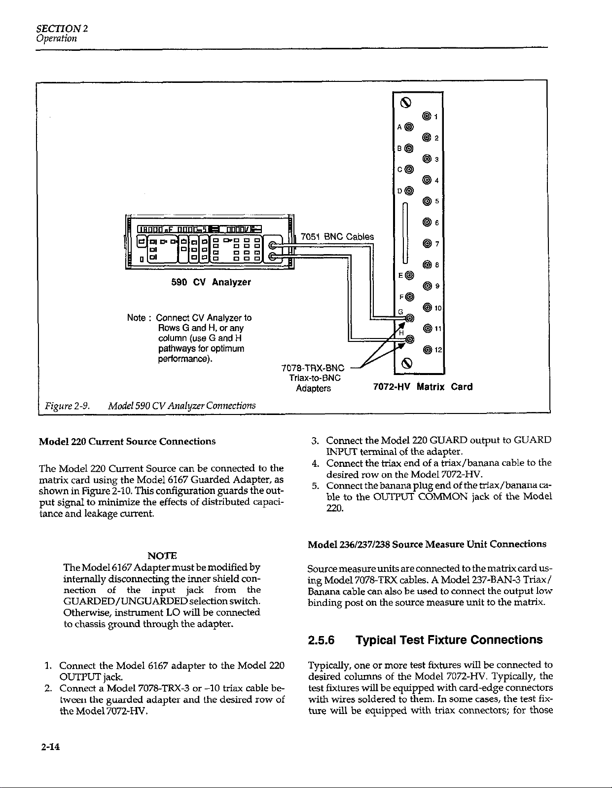
Model 590 CV Analyzer Connections
The Model 590 CV Analyzer should be connected to rows
G and H (CV rows), or any column as shown in Figure
2-9. The BNC cables that are supplied with the Model 590
can be used; however, Model 7078-TRX-BNC triax-toBNC adapters must be used at the Model 707%HV end.
‘igure 2-7.
2-12
(See Figure 2 - 1)
196 DMM
Inner Shield (Connect to LO -
for Low-Level Measurements)
7072WJ Matrix Card
Model 196 Dh4M Connections
Page 30

Common
SECTION 2
Operation
Figure 2-8.
230 Voltage Source
7072-HV Matrix Card
Model 230 Voltage Source Connections
Z-13
Page 31
SECTION 2
Operation
Note : Connect CV Analyzer to
Rows G and H, or any
column (use G and H
pathways for optimum
performance).
Figure 2-9. Model 590 CVAnalyzer Connections
Model 220 Current Source Connections
The Model 220 Current Source can be connected to the
matrix card using the Model 6167 Guarded Adapter, as
shown in Figure 2-10. This configuration guards the output signal to
minimize the effects of distributed capaci-
tance and leakage current.
NOTE
TheModel6167Adaptermust bemodified by
internally disconnecting the inner shield connection of the input jack from the
GUARDED/LJNGUARDEDselectionswitch.
Otherwise, instrument LO will be connected
to chassis ground through the adapter.
Triax-to-BNC
Adapters
7072-HV
Matrix Card
3. Connect the Model 220 GUARD output to GUARD
INPUT terminal of the adapter.
4. Connect the triax end of a triax/banana cable to the
desired row on the Model 7072~HV.
5. Connect the banana plug end of the triax/banana ca-
ble to the OUTPUT COMMON jack of the Model
220.
Model 236/237/238 Source Measure Unit Connections
Sourcemeasureunits are connected to the matrix card using Model 7078.TRX cables. A Model 237;BAN-3 Triaxl
Banana cable can also be used to connect the output low
binding post on the source measure unit to the matrix.
2.5.6
Typical Test Fixture Connections
1. Connect the Model 6167 adapter to the Model 220
OUTPUT jack.
2. Connect a Model 7078-TRX-3 or -10 triax cable between the guarded adapter and the desired row of
the Model 7072~HV.
2-14
Typically, one or more test fixtures will be connected to
desired columns of the Model 7072~HV. Typically, the
test fixtures will be equipped with card-edge connectors
with wires soldered to them. In some cases, the test fixture will be equipped with trlax connectors; for those
Page 32

Use Rows A and B when
Sourcing < 2nA
SECTION 2
OptTL?ti0Fl
II
Guarded Adapter -
Connect GUARD OU?
to GUARD
Figure 2-10. Model 220 Current Source Connections
7078.TRX Triax
IF-l
7072-HV Matrix Card
types, Keithley Model 7078-TRX-3 or -10 cables can be
used, as shown in Figure Z-11.
WARNING
Do not use BNC cables and adapters in cases
where hazardous voltages from guard
s.ource~ could be present on the BNC cable
shields.
Internally, the test fixture should be wired as shown in
the equivalent circuit of Figure Z-12. SIGNAL should be
connected to the probe or other device contact points,
while GUARD should be carried through as close to the
device as possible. If coaxial probes are to be used, connect GUARD to the probe shield if the probe shield is insulated from the fixture shield.
Usually, the chassis ground terminal of the triax connector will automatically make contact with the fixture
shield by virtue of the mounting method. However,
ground integrity should be checked to ensure continued
protection against hazardous guard voltages.
2-15
Page 33

SECTION 2
Operation
3 - Lug Female
Triax Connectors
(or run cables through strain
reliefs and connect internally)
Note : Teflon@ - insulated connectors
recommended for specified
performance.
Warning : Do not use BNC cO”“ectorS
to avoid possible shock
hazard.
3gure 2-11.
Figure Z-12.
7072-HV Matrix Card
Typical Test Fixture Connections
From
7072-HV
CWd
Equivalent Circuit of Test Fixture
Triw Cable
Co?tne~tiofts
Chassis 1
Ground L
-----
1
Wafer
--_--_--- _I
Test Fixture Chassis
2-16
Page 34

SECTION2
Operation
2.6 MATRIX CONFIGURATION
The following paragraphs discuss the switching matrix
of the Model 707’2~HV as well as how to expand the matrix by connecting two or more cards together.
2.6.1
As showninFigureZ-13, theMode170724Visorganized
as an 8 x 12 (eight row by 12 column) matrix. The rows are
labeled A through H, while the columns on the card are
numbered 1 through 12. The actual column number to
use when programming depends on the slot and unit
number, as summarized in Table 2-3. For example, card
Switching Matrix
column number 2 on a card in slot 5 of unit 1 is accessed as
matrix column 62.
Each intersecting point in the matrixis called a crosspoint
that can be individually closed or opened by programming the Model 707 mainframe. The crosspoints for rows
A through F are configured for 2-pole switching, as
shown in Figure 2-13. For these rows, SIGNAL and
GUARD are switched separately to any of the 12 columns
on the card.
The crosspoints for rows G and H use l-pole switching,
with only SIGNAL being switched. The equivalent circuit for this arrangement is also shown in Figure 2-13.
1
Figure 2-13.
Model 7072-HVMatrix Organization
Crosspoint Switching
for Rows G and H.
Columns
1 - 12
2-17
Page 35
SECTION 2
Operation
Table 2-3. Column Numbering by Slot and
Unit
Slot
1
2
3
4
5
6
1 73-84
2 85-96
3 97-108
4
5
6
1 145-156
2
3
4 181-192
5 193-204
6
1
2 229-240
3 241-252
4 253-264
5 265276
6 277288
1
2
3
4
5
6
-
2.6.2
In order to maintain the integrity of the low-current and
CV pathways, isolator relays are incorporated into each
column. These isolators are indicated as small circles on
the matrix diagram of Figure 2-13. Each relay remains
open until a crosspoint located in rows C through H is to
be closed. In this manner, the general-purpose pathways
are isolated from the more critical low-current and CV
pathways.
Row and Column Isolators
columns (l-12)
l-12
13-24
25-36
37-48
49-60
61-72
109-120
121-132
133-144
157-168
169-180
205-216
217.228
289-300
301312
313-324
325-336
337-348
349-360
The column isolator relay between rows B and C for a
given column will not close if a row A or B crosspoint in
that column is closed. This feature helps to prevent accidental application of high voltage to rows C through H.
In a similar manner, row isolator relays isolate the crosspoint relays from a given row to minimize leakage current and capacitance, and maximize path resistance. The
row isolator relay closes when any crosspoint relay associated with that row is closed.
2.6.3
As discussed previously, the eight rows on the matrix
card are designed for different purposes. Rows A and B
are designated low-current, high voltage rows, rows C
through F are general purpose rows, and rows G and H
are cv rows.
Many of the specifications for the card differ among row
types. For example, the offset current for the low-current
rows is <IpA, but the general purpose and CV rows have
a higher offset current of 20pA. Thus, A and B would be
the rows of choice for low-current measurements. The
path isolation for rows A and B is an order of magnitude
higher than that the other rows (10% vs. 10’2fL). These
two rows would be preferable for very high-impedance
measurements. Rows A and B are also used for voltage
levels up to 1300v.
In summary, the following general rules apply when
choosing which rows to use for specific measurements:
l Use rows A and B for low-current and/or high voltage
measurements.
l Use rows A, B, G, and H for low-capacitance measure-
ments.
l Rows A and B should be used where high path isola-
tion resistance is of primary concern.
l Rows C through F have the largest bandwidth, while
rows G and H have the smallest bandwidth.
For more detailed information on these factors, refer to
the Model 7072~HV Specifications located at the front of
this manual.
Pathway Considerations
2-18
Page 36

Note : Rows C - F jumpered through backplane.
ROWS A, B, G, and H require installation of coaxial jumpers (shown heavily shaded).
I
Figure 2-14. Connecting Three Cards
for
8 x 36 Matrix
SECTION 2
Operation
2.6.4
Two to six Model 7072-HV cards can be connected to-
gether within the mainframe to yield an 8 x N matrix,
where N depends on the number of cards. Figure 2-14
shows an internally expanded matrix with three cards,
resulting in an 8 x 36 (eight row by 36 column) matrix. As
s-arizedinTable2-3,the actualcolumnnumberused
when programming the unit is determined by the slot.
Rows C through F are automatically connected together
through the backplane of the mainframe. The mainframe
can be configured for two sets of three cards each by removing jumpers from the backplane of the mainframe;
see Section 3 of the Model 707 Instruction Manual for details on removing the jumpers. With the row jumpers removed, rows C through F of Model 7072~HV cards in
slots 1 through 3 are connected, and rows C through F of
Model 7072~HV cards in slots 4 through 6 are connected
together.
Because of more critical signal paths, rows A, B, G, and H
are not jumpered through the backplane. Instead, you
must install the supplied coaxial jumpers between appropriate connectors on Model 7072~HV cards (for critical
signal paths, rows can be isolated from other cards by not
installing these cables). Each card has two coaxial connectors for each row, allowing daisy chaining of card rows.
These connectors can be reached by lifting the access
door on the top of the mainframe; it is not necessary tore-
Internal Matrix Expansion
move cards to install the jumpers. Figure 2-15 shows an
edge-on view of the jumper connectors with row nunbers marked for convenience. Figure 2-16 demonstrates
how three cards can be daisy chained together using the
coaxial jumpers.
WARNING
The shells of the row jumpers are at guard
potential. To avoid a possible shock hazard,
always disconnect all cables from the row
andcolumn jacksbeforeremovingorinstalling jumpers.
2-19
Page 37

SECTION 2
Operation
Figure 2-16.
2.6.5
External jumper cables must be used to expand the num-
her of rows in the matrix, or to connect between columns
of cards installed in different mainframes. An example of
such an expanded matrix is shown in Figure Z-17. Here,
six cards are configured as a 16 x 36 matrix. Since the rows
are internally jumpered, only columns must be jumpered
externally in this config~~ration. Note that the backplane
7’hree Cards in Daisy Chain Configuration
External Matrix Expansion
jumpers must be removed to separate the cards into two
*CUPS.
Trim tee adapters (Model 7078-TIU-T) can be used to
provide daisy chain capability between the triax input
connectors. Figure Z-18 shows a typical arrangement be-
tween two Model 70724-W cards. Ideally, custom-length
biax cables should be used to avoid the cable “jungle”
that would occur with longer, standard-length cables.
Z-20
Page 38

SECTION 2
Operation
Figure 2-17.
16 x 36 Matrix Constructed by External Jumpering
2-21
Page 39

SECTION 2
Operation
Triax Tee
AdaDters
Matrix
Input/Output
Figure 2-18.
Using Trim Tee Adapters to Daisy Chain Cards
2-22
Page 40

SECTION 2
Operation
2.7 MEASUREMENT CONSIDERATIONS
Many measurements made with the Model 7072-HV concern low-level signals. Such measurements are subject to
various types of noise that can seriously affect low-level
measurement accuracy. The following paragraphs discuss possible noise sources that might affect these measurements.
2.7.1 Magnetic Fields
When a conductor cuts through magnetic lines of force, a
very small current is generated. This phenomenon will frequently cause unwanted signals to occur in the test leads of
a switching matrix system. If the conductor has sufÞcient
length, even weak magnetic Þelds like those of the earth
can create sufÞcient signals to affect low-level measurements.
Two ways to reduce these effects are: (1) reduce the
lengths of the test leads, and (2) minimize the exposed
circuit area. In extreme cases, magnetic shielding may be
required. Special metal with high permeability at low
ßux densities (such as mu metal) are effective at reducing
these effects.
Even when the conductor is stationary, magnetically
induced signals may still be a problem. Fields can be produced by various signals such as the AC power line voltage. Large inductors such as power transformers can
generate substantial mangetic Þelds, so care must be
taken to keep the switching and measuring circuits a
good distance away from these potential noise sources.
2.7.2 ELECTROMAGNETIC INTERFERENCE
(EMI)
• impulse sources as in the case of arcing in high-voltage environments
The effect on instrument performance can be considerable
if enough of the unwanted signal is present. A common
problem is the rectiÞcation by semiconductor junctions of
RF picked up by the leads.
The equipment and signal leads should be kept as far
away as possible from any EMI sources. Additional
shielding of the measuring instrument, signal leads, and
sources will often reduce EMI to an acceptable level. In extreme cases, a specially constructed screen room may be
required to sufÞciently attenuate the troublesome signal.
Many instruments incorporate internal Þltering that may
help to reduce RFI effects in some situations. In some cases,
external Þltering may also be required. Such Þltering, however, may have detrimental effects on the desired signal.
2.7.3 Ground Loops
When two or more instruments are connected together,
care must be taken to avoid unwanted signals caused by
ground loops. Ground loops usually occure when sensitive instrumentation is connected to other instrumentation with more than one signal return path such as power
line ground. As shown in Figure 2-19, the resulting
ground loop causes current to ßow through the instrument LO signal leads and then back through power line
ground. This circulating current develops a small but undesirable voltage between the LO terminals of the two instruments. This voltage will be added to the source
voltage, affecting the accuracy of the measurement.
The electromagnetic interference characteristics of the
Model 7072-HV Semiconductor Matrix Card comply with
the electromagnetic compatibility (EMC) requirements of
the European Union as denoted by the CE mark. However, it is still possible for sensitive measurements to be affected by external sources. In these instances, special
precautions may be required in the measurement setup.
Sources of EMI include:
• radio and television broadcast transmitters
• communications transmitters, including cellular
phones and handheld radios
• devices incorporating microprocessors and high
speed digital circuits
SIGNAL LEADS
INSTRUMENT 1
GROUND
CURRENT
INSTRUMENT 2
LOOP
POWER LINE GROUND
INSTRUMENT 3
Figure 2-19. Power Line Ground Loops
Figure 2-20 shows how to connect several instruments together to eliminate this type of ground loop problem.
2-23
Page 41

SECTION 2
Operation
Here, only one instrument is connected to power line
ground.
INSTRUMENT 1
‘igure Z-20.
INSTRUMENT 2
0
0 0
1 1
POWER LlNE GROUNrJ
T
Eliminating Ground Loops
INSTRUMENT
lo
1
3
Ground loops are not normally a problem with instmmats having isolated LO terminals. However, all instmmats in the test setup may not be designed in this manner. When in doubt, consult the manual for each instrument in the test setup.
2.7.5
Noise Currents Caused by Cable
Flexing
Noise currents can be generated by bending or flexing coaxialortriaxialcables. Suchcurrents, whichareknownas
triboelectxic currents, are generated by charges created
between a conductor and insulator caused by friction.
Low-noise cable can be used to minimize these effects.
Such cable has a special graphite coating under the shield
to provide lubrication and to provide a conduction path
to equalize charges.
Even low-noise cable generates some noise currents
when flexed or subjected to vibration. To miniie these
effects, keep the cables as short as possible, and do not
subject them to temperature variations that could cause
expansion or contraction. Tie down offending cables securely to avoid movement, and isolate or remove vibration sources such as motors or pumps.
2.7.6 Shielding
2.7.4 Keeping Connectors Clean
As is the case with any high-resistance device, the integrity of triaxial and other connectors can be damaged if
they are not handled properly. If the connector insulation
becomes contaminated, the insulation resistance will be
substantially reduced, affecting high-impedance measurement paths.
Oils and salts from the skin can contaminate connector
insulators, reducing their resistance. Also, contaminants
present in the air can be deposited on the insulator surface. To avoid these problems, never touch the connector
insulating material. In addition, the matrix card should
be used only in clean, dry environments to avoid contamination.
If the connector insulators should become contaminated,
either by inadvertent touching, or from air-borne deposits, they can be cleaned with a cotton swab dipped in
clean methanol. After thorough cleaning, they should be
allowed to dry for several hours in a low-humidity environment before use, or they can be dried more quicklyusing dry nitrogen.
Proper shielding of all unguarded signal paths and devices under test is important to minimize noise pickup in
virtually any switching matrix system. Otherwise, interference from such noise sources as line frequency and RF
fields can seriously corrupt a measurement.
In order for shielding to be effective, the shield surrounding the HI signal path should be connected to signal LO
(or chassis ground for instruments without isolated LO
terminals). Since most Model 7072~HV matrix applications call for separately switching LO, a separate connection from LO to the cable shield at the source or measurement end must be provided, as in the example of Figure
2-21. Here, we are using the GUARD path of the Model
7072-HV to carry the shield out to the device under test.
Needless to say, this arrangement should not be used
with guarding, as GUARD and LO should not be connected together.
WARNING
Hazardous voltage may be present if LO on
any instrument is floated above ground po-
tential.
If the device under test is to be shielded, the shield should
be connected to the LO terminal. If you are using the
GUARD connection as shield, care should be taken to in-
2-24
Page 42

SECTION 2
Operation
sulate the outer ring of the hiaxial connector mounted on
the test fixhm from the test fixture itself. Otherwise, LO
will be connected to chassis ground, possibly resulting in
a ground loop. An alternative is to use two shields, one
mounted within kind insulated from) the other. In this
case, the GUARD path would be connected to the inner
Inner Shield
CO me&d to LO
of
HI Triax
r----
shield, while the outer shield would be chassis grounded.
This arrangement is shown in Figure Z-22. Incidentally,
this configumtion is also recommended for guarded applications, with the inner shield as guard, and the outer
shield acting as a safety shield.
------
Figure 2-21.
7072TpH” (Jq5
F&m 2-22.
Shielding Example
Dual ShieZd Test Fixture
7072-HV Card
r----------i
---
l---------l
I
L - - - - - - - - - - AC Outer Shield
I
(Chassis Ground)
2-25
Page 43

SECTION 2
Operation
Inner Shield
Measuring
Instrument
L-i--J
DUT
Figure 2-23. Guarded Circuit
2.7.7
Guarding is important in high-impedance circuits where
leakage resistance and capacitance could have degrading
effects on the measurement. Guarding consists of using a
shield surroumliig a conductor that is carrying the highimpedance signal. This shield is driven by a low-impedance amplifier to maintain the shield at signal potential.
For biaxial cables, the inner shield is used as guard.
Guarding minimizes leakage resistance effects by driving the cable shield with a unity gain amplifier, as shown
in Figure 2-23. Since the amplifier has a high input impedance, it minimizes loading on the high-impedance
signal lead. Also, the low output impedance ensures that
the shield remains at signal potential, so that virhmlly no
leakage current flows through the leakage resistance, RL.
Leakage between inner and outer shields may be considerable, but that leakage is of little consequence because
that current is supplied by the buffer amplifier rather
than the signal itself.
Guarding
In a similar manner, guarding also reduces the effective
cable capacitance, resulting in much faster measurements on high-impedance circuits. Because any distributed capacitance is charged through the low impedance
of the buffer amplifier rather than by the source, settling
times are shortened considerably by guarding.
In order to use guarding effectively with the Model
707%HV, the GUARD path of the matrix card should be
connected to the guard output of the sourcing or measuring instrument. Figure 2-24 shows typical connections.
Guard should be properly carried through the inner
shield to the device under test to be completely effective.
The shielded, guarded test fixture arrangement shown in
Figure 2-22 is recommended for safety purposes (guard
voltage may be hazardous with some instruments). With
most instruments, special adapters or cables may be required to connect guard to the inner shield, and at the
same time route signal LO through a separate cable.
2-26
Page 44
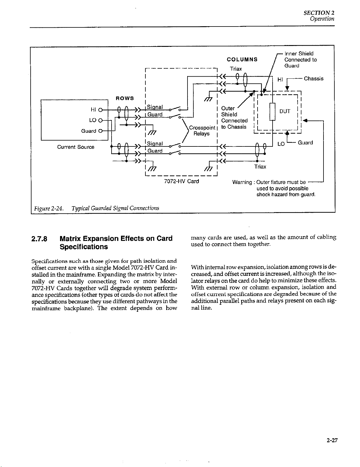
------
SECTION 2
Operation
COLUMNS
7072-HV Card
‘igure 2-24. Typical Guarded Signal Connections
2.7.8
Matrix Expansion Effects on Card
Specifications
Specifications such as those given for path isolation and
offset current are with a single Model 7072-HV Card in-
stalled in the mainframe. Expanding the matrix by internally or externally connecting two or more Model
7072~HV Cards together will degrade system performance specifications (other types of cards do not affect the
specifications because they use different pathways in the
mainframe backplane). The extent depends on how
Warning : Outer fixture must be
used to avoid possible
shock hazard from guard.
many cards are used, as well as the amount of cabling
used to connect them together.
With internal row expansion, isolation among rows is decreased, and offset current is increased, although the isolator relays on the card do help to minimize these effects.
With external row or column expansion, isolation and
offset current specifications are degraded because of the
additional parallel paths and relays present on each signal line.
2-27
Page 45

SECTION 3
Applications
3.1 INTRODUCTION
This section covers typical applications for the Model
7072~HV Semiconductor Matrix card and is organized as
follows:
3.2 CV Measurements: Outlines the test configuration
and procedure for making quasistatic and high-frequency cv measurements.
3.3 Semiconductor Test Matrix Details a semiconductor test matrix that can be used to perform a variety of different tests on semiconductors such as FETs.
3.4 Resistivity Measurements: Covers methods to
measure the resistivity of semiconductor samples using
the van der l’auw method.
3.5 Semiconductor Parameter Analysis: Discusses using the Model 7072~HV in conjunction with an HP 4145B
Semiconductor Parameter Analyzer.
3.2 CV MEASUREMENTS
The Model 707’2~HV can be used in conjunction the Keithley Model 590 CV Analyzer, and the Keithley Model 595
Quasistatic CV Meter to perform quasistatic and highfrequency CV (capacitance vs. voltage) tests on semiconductors. The resulting CV curves can be used to calculate
important semiconductor parameters such as doping
profile, band bending, and mobile ion concentration.
3.2.1
The stand alone system shown in Figure 3-l can be used
to make CV measurements without the aid of a corn-
Stand Alone System Configuration
puter. System components perform the following fmc-
tiOllS.
Model 590 CV Analyzer: Measures CV data at 1OOkHz
and 1MI-k and sends the resulting data to the plotter for
graphing.
Model 595 Quasistatic CV Meter: Measures quasistatic
CV data and sends the data to the plotter for graphing in
real time.
Model 707 Switching Matrix: Controls the semiconductor matrix card to close and open the desired crosspoints
at the proper time.
Model 7072~HV Semiconductor Matrix Card: Switches
the signal pathways to the six wafers under test.
HP-GL Plotter: Plois CV and other curves directly from
the Models 590 and 595.
3.2.2 Computerized System
Configuration
Figure 3-2 shows a computerized version of the CV matrix test system. The addition of a computer allows
greater system versatility and easier instrument control.
Also, analysis functions such as doping profile and ion
concentration canbe added to the software to expand CV
analysis capabiities.
3-l
Page 46

SECTION 3
Applications
Wafers Under
Test
6
IB
‘0
ID
IE
IF
IG
Note : Rows C-F can be used
r
for this signal path.
Model 595
Quasistatic CV Meter
-IT--
,
. ^ I
,
I
HP-GL
3-2
Page 47

Wafers Under
Test
SECTlON 3
Applications
Note : Rows C-F can be used for
this signal path.
1 2
I
I
I
L--------
3 4 5 6 7 8 9 10 11 12’
7072-HV Matrix Card
707 Switching Matrix
r
Model 595
Computer
P
I
7051
I
BNC
Cables
IEEE-488 Bus
I
0
Input
Model 590
CV Analyzer
I
I
Figure 3-2.
Note : Remove jumpers to other 7072.HV cards (if installed)
to optimize Model 595 measurement accuracy.
Computerized CV System Configuration
3-3
Page 48

SECTION 3
Applications
3.2.3 Optimizing CV Measurement
Accuracy
For accurate CV measurements, each Model 590 CV
measurement pathway must be cable corrected using the
procedure outlined in the Model 590 Instruction Manual.
The pathways to each DUT must be cable corrected separately.
Also, for best quasistatic CV results, the corrected capaci-
tance feature of the Model 595 should be used. Corrected
capacitance compensates for any leakage currents present in the cables, switching matrix, or test fixture. However, care must be taken when using corrected capaci-
tance to ensure that the device remains in equilibrium
throughout the test sweep to avoid distorting the CV
curves.
In order to minimize the effects of the switching network
on quasistatic CV measurements, cables to the Model 595
and DUT should be kept as short as possible. Also, the
low-current pathways (rows A and B) should be used
with the Model 595.
3.2.4 Basic CV Test Procedure
The fundamental CV test procedure is outlined below.
Keep in mind that this procedure does not address many
considerations and aspects of CV testing, which is fairly
complex. The procedure given is for the stand alone system in Figure 3-1. Detailed inshument operating infor-
mation may be found in the pertinent instruction manu-
als.
1. Connect the HP-GL plotter to the IEEE-488 bus connector of the Model 595 only.
2. Set up the Model 595 for the expected CV sweep.
3. Close the crosspoints necessary to connect the Model
595 to the device under test, as summarized in Table
3-l. For example, to test device #l, close Al and BZ.
4. Place the probes down on the wafer test dots.
5. Run a quasistatic sweep on the selected device and
generate a CV curve.
6. Open the crosspoints that are presently closed.
7. Set up the Model 590 for the expected CV sweep.
8. Close the crosspoints necessary to connect the Model
590 to the device under test. For example, to test device #I, close Gl and H2.
9. Run a high-frequency test sweep on the device to
store the CV data in the Model 590 buffer.
10. Disconnect the plotter from the Model 595 and connect it to the Model 590.
11. Generate a plot from the data in the Model 590
buffer.
12. Repeat steps 2 through 11 for the remaining devices,
as required.
Table 3-l. CV Test Crosspoint Summary
Closed Crosspoints
Wafer # Quasistatic 695) 1 High Frequency (590)
1
2
3
I I
4
5
6
3.2.5
Figures 3-3 and 3-4 show typical CV -es as generated
by the Models 595 and 590 respectively. The quasistatic
curve shows a fair amount of symmetry, while the the
high-frequency curve is highly asymmetrical. The asymmetrical nature of the high-frequency -e results from
the inability of the minority carriers to follow the highfrequency test signal.
Al, B2
A3,B4
A5, B6
A7,B8
A9, B10
All, 812 Gil, H12
Typical CV Curves
Gl, HZ
G3, H4
G5. H6
G7; H8
G9, HlO
3-4
Page 49

SECTION 3
Applications
+0.4E-10 +0.4E-10
Figure 3-3.
-005.00
Typical Quasistatic CV Curve Generated by Model 595
+005.00
KEITHLEY 595
3-5
Page 50

SECTION 3
Applicutions
0.90
- 4.99 - 3.99 - 2.99 - 1.99 - 0.99 0.00 1.00 1.99 2.99 3.99 4.99
Keithley 590: oo:w:1o:sno 1ooKHz x1 mer - Parallel
Figure 34.
Typical High-frequency CV Curve Generated by Model 590
3.3 SEMICONDUCTOR TEST MATRIX
Two important advantages of a matrix switching system
are the ability to connect a variety instruments to the de-
vice or devices under test, as well as the ability to connect
any instrument terminal to any device test node. The following paragraphs discuss a typical semiconductor matrix test system and how to we that system to perform a
typical test: common-source characteristic testing of a
typical JFET.
3.3.1 System Configuration
Figure 3-5 shows the configuration for a typical multi-
purpose semiconductor test matrix. Instruments in the
system perform the following functions.
Bias (Volt) X 1 Oh+00
TheDC voltage source can supply a maximum of *lOOV
at clxrents up to 2mA.
Model 230 Voltage Source: Sources DC voltages up to
3201v at a maximum current of lOOm.4.
Model 590 CV Analyzer: Adds CV sweep measurement
capability to the system.
Model 220 Current Source: Used to source currents up to
a maximum of 1OlmA with a maximum compliance voltage of 105V.
Model 617 Electrometer/Source: Measures current, and
also could be used to measure voltages up to tiOOVDC.
3-6
Model 196 DMM: Measure DC voltages in the range of
1OOnV to 300V. The Model 196 could also be used to
measure resistance in certain applications.
Page 51

Device Under Test
SECTION 3
AppIications
SGSG SGSG
------------
12 3 4 5 6 7
7072-HV
707 Switching
SGSGSGSGSG
8 9101112
Matrix
Card
Matrix
Figure 3-5. Semiconductor Test Matrix
Device Under Test: A
such devices as bipolar transistors and FETs. Additional
connections could easily be added to test more complex
devices, as required.
3.3.2
Testing Common-Source Charac-
three-terminal fixture
for testing
teristic of FETs
ThesystemshowninFigure3-5couldbeused totestava-
riety of characteristics including
Vos[om. To demonstrate a practical use for the system, we
IGSS,
IOIO~I, IG[ONI, Im and
will show how it can be used to generate common source
characteristic curves of a particular JFET.
In order to generate these curves, the instruments must
be connected to the JFET under test, as shown in Figure
3-6. The advantage of using the matrix is, of course, that it
is a simple matter of closing specific crosspoints. The
crosspoints that must be closed are also indicated on the
diagram.
3-7
Page 52

SECTION 3
Applications
o-
HI
0
LO
Model 230
Voltage Source
617
Electrometer/Source
_, .., . .
0 HI
Voltage
SOUW?
0 LO
@ = Closed Crosspoints on 7072-HV Card (Figure 3.5).
Figure 3-6. System Configuration
for
Measuring Common-Emitter Characteristics
Tonm the test,Vcsisset tospecificvalues, for example in
increments of 0.25V. At each Vcs value, the drain-source
voltage (VIE) is stepped across the desired range, and the
drain current, IO, is measured at each value of VOS. Once
all data are compiled, it is a simple matter to generate the
common-source
in Figure 3-7. If the
IV curves, an example of which is shown
system
is connected to a computer, the
test and graphing could all be done automatically.
3.4 RESISTIVITY MEASUREMENTS
TheMode17072-~HighVoltageSemiconductorMahix
card can be used in conjunction with a Model 220 Current
Source and a Model 196 DMh4 to perform resistivity
measurements on semiconductors. Such measurements
can yield such important information as doping concentration.
Figure 3-7. Typical Common-Source FET IV Charac-
teristics
3-8
Page 53

SECTION 3
Applications
3.4.1
Figure 3-8 shows the basic test configuration to make
resistivity measurements on van der Pauw samples. The
Model 220 sources current through the samples, while
the Model 196 measures the voltage developed across the
samples. The matrix card, of course, switches the signal
Test Configuration
SGSGSGSGSGSGSGSGSGSGC”“”
_---------
paths as necessary. In order to minimize sample loading,
which will reduce accuracy, the Model 196 DMM should
be used only on the 300mV or 3V ranges. Also, this configuration is not recommended for resistance measuremats above 1M due to the accuracy-degrading effects of
DMM loading.
1 2 3 4 5 6 7 8 9 101112
7072-HV Matrix Card
707 Switching Matrix
Fi,qure 3-8. Resistivity Test Confi,quration
3-9
Page 54

SECTION 3
Applications
3.4.2
InordertomakevanderPauwresistivitymeasurements,
four terminals of a sample of arbitrary shape are
ured. A current (from the Model 220) is applied to two
terminals, while the voltage is measured (by the Model
196) across the two opposite terminals, as shown in Figure 3-9. A total of eight such measurements on each sample are required, with each possible terminal and current
Test Procedure
meas-
Table 3-2. Crosspoint Summary for Resistivity Measurements
I
Voltage
VI
VZ
V3
V4
VS
V6
V7
V8
Crosspoint
Sample #l 1 Sample #2
Al 84 E3 F2
A4 Bl E3 F2
A4 83 FL2 Fl
A3 84 E2 Fl
A3 B2 El F4
A2 B3 El F4
A2 Bl E4 F3
Al B2 E4 F3
A5 B9 E7 F6 A9 812 El1 FIO l-2
A8 85 E7 F6 Al2 B9 El1 FlO
A8 87 E6 F.5 Al2 Bll El0 F9
A7 B8 E6 F5 All B12 El0 F9
A7 B6 E5 F8 All BlO E9 F12 34
A6 B7 E5 F8 A10 811 E9 F12
A6 B5 E8 F7 A10 B9 El2 Fll 4-l
A5 86 E8 I?7 A9 BlO El2 Fll l-4
L
Closed
convention. The resulting voltages are designated Vl
through V8.
In order to source cunent into and measure the voltage
across the sample, specific crosspoints must be closed.
Table 3-2 summarizes the crosspoints to close for each
voltage measurement on all three samples from the test
configuration shown in Figure 3-8.
Current Voltage
1 Sample #3
B&Well B&VeelI
2-l
2-3 4-l
3-2 41
4-3
1
3-4
3-4
l-2
l-2
2-3
2-3
3-10
Page 55

SECTION 3
Applications
Fiaure 3-9.
1“
(0
Resisti& Measurement Conventions
3-11
Page 56

SECTION 3
Applications
3.4.3
Once the eight voltage measuremenh are known, the
re+tivity can be calculated. Two values of resistivity, PA
and PB are initially computed as follows:
Whel-2:
Once PA and pi are known, the average resistivity, PAVG,
can be determined as folkxvs:
Flesistivity Calculations
1.1331 fA ts (vz+v~-vI -W
PA=
1.1331 fS tS (v6 +
pe =
PA and pi are the resistivities in R-cm
ts is the sample thickness in cm
VI through VS are the voltages measured by
the Model 196
I is the current through the sample in amperes
fA and fs are geometrical factors based on sample symmetry cf.4 = fs = 1 for perfect symmetry).
pAYG= pA+pB
I
VS
I
2
- v5 - v7)
3.5 Semiconductor IV Characterization
A source measure unit such as the Model 236 or 237 is
used to test and characterize many types of devices. One
of these is semiConductor devices. The following para-
graphs explain the basic scheme and connections used to
generate an IV curve of a bipolar or MOS transistor. Figure 3-10 shows FET devices connected in a test fixture.
3.5.1 lest Configuration
Since rows A and B of the Model 7072-I-W can be used for
low-current and high voltage source or measure applications,theyareusedtoswitchtheModel237SourceMeas-
me Unit. The Model 237 is capable of sourcing up to 1100
volts. If it will be sourcing more than 200 volts, it must be
connected to rows A and B only. The Model 236 is capable
of sourcing up to only 110 volts, so it may be connected to
any row.
At the test fixture, the drain and source leads of the FETs
are connected in a4-wire sensing configuration. This connection scheme allows the Model 237 to use remote sensing to accurately apply Vds to the FETs. The Model 236
uses local sensing and is used to supply the bias to the
gates of the FETs. Since the gates are low current, remote
sensing is not necessary.
If more DUT pins are needed, the system is easily expanded by adding more Model 7072-HV matrix cards.
Each additional card will add 12 columns to the system.
3.5.2 Cable Connections
Source Measure Unit and test fixture connections to the
matrix card are accomplished using Model 7078-TW.
These are three slot trim cables. On each Source Measure
Unit, the banana jack (5-way binding post) is used to access OUTPUT LO. This connection is made using a
Model 237-BAN. An equivalent to the Model 237-BAN-1
can be made using the information in Figure 2-4. This al-
lows OUTPUT LO to be applied to a signal pathway and
independently switched. The guard pathways of the ma-
trix cards are used exclusively to extend the driven
guards of the Source Measure Units to the DUT to elimi-
nate the effects of leakage current.
3.6 SEMICONDUCTOR PARAMETER ANALYSIS
One or more Model 7072-I-N Semiconductor Matrix
Cards can be used in conjunction with an HP4145B Semiconductor Parameter Analyzer (SPA) to provide a versatile switching system capable of complete IX characterization of semiconductors. The following paragraphs discuss system configuration, connections using the
7078-CSHP Cable Set, and SPA measurement considerations.
3-12
Page 57

SECTlON 3
Applications
GII I I I I I I I I I I
H
I I I I I I I I I I II
II I I 1 I I I I I
I’ ‘I\ ” ” ’
7072.HV
MATRIX CARD
Fkure
3-10. Multi Unit Test System Using Models 236 and 237 Source Measure Units
7072.HV
MATRIX CARD
3-13
Page 58

SECTION 3
Applications
3.6.1
Figure 3-11 shows the general configuration of the SPA
switching system. The components of the system per-
form the following htnctions:
System Configuration
SMU 1
HP 41458
Semiconductor SMU 4
Parameter
Analyzer
SMU 2
SMU 3
Vsl
vs
Vml
2
HP 4145B: Has four SMUs (Source/Measure Units), two
voltage scnmes, and two voltage measurement ports.
The unit can automatically run a variety of tests on semi-
conductors and plot data on a built-in CRT.
Test
K
.1...12
t
Fixture
13...24
25...36.
1
1
A
1...12
13...24
p
25...36
1
I
1 7
072.HV
Card
Columns
>
r
+ LEE,466 Bus
System Controller
HP9000 or IBM PC/AT
Note : Connecting cables included in 707%CSHP cable set
Page 59

SECTION 3
Applications
Model 707 Switching Matrix Controls the matrix card to
open and close signal paths as required.
Model 7072~HV Semiconductor Matrix Card: Switches
the test pathways to the deviceunder test. In this particw
lar application, three Model 707%HV cards provide
36pin test capability. A total of six cards can be installed
in a single mainframe, providing up to 72-pin capability
in one mainframe.
System Controller: Controls the SPA and switching ma-
trix with user-written software. Typical controllers for
thisappllcationareHP9000Series200 or300 (withHl-IB
interface), and IBM PC, AT or compatible computers
(equipped with an IEEE488 interface).
Test Fixture: Provides the interface between the device
under test and the matrix card. Typically, the test fixture
will be equipped with triax connectors for ease of connections.
3.6.2
Figure 3-12 shows how to connect the HP 4145B to the
Model 7072-I-W using the optional Keithley Model
707%CSHP Cable Set. The four SMU ports are to be connected with the triax cables (7078-TRX-lo), while the two
voltage source and voltage measurement ports Ws and
Vm) are to be connected using BNC cables (7051-10) and
triax-BNC adapters (7078-TRX-BNC). Typically, the SPA
will be connected to the rows, as shown in Figure 3-12.
Connections to a user-supplied test fixture should be
made using t&x cables in order to maintain path integrity and safety. BNC cables and adapters should not be
used in case hazardous potential appears on guard terrninals.
Cable Connections
Any switching system can degrade low-level signals, and
the same holds true for the system shown in Figure 3-10.
Since rows A and B on the Model 7072~HV are dedicated
lowcurrentpathways,theSMUsthatwillsourceorsense
low-level signals should be connected only to these rows.
The remaining rows can be used for less-critical signals.
Safety considerations are also a concern when connecting
instruments to a switching matrix. Therefore, it is
strongly recommended that you carefully read the HP
41458 manual before using the system.
WARNING
Hazardous voltage may be present on the
outer conductors of the connecting cables
when the HP 41458 is set up for floating
measurements.
3.6.4 Typical Test Procedure
The following paragraphs outline the procedure for using the SPA/matrix system to perform a typical test: VosIO (common-source) airves of a typical JFET. The procedure uses one of the four standard setups that are part of
the applications package supplied with the HP 4145B.
System Configuration
Figure 3-13 shows the configuration and connections for
this example. Only three of the four SMLIs are required
for the test, as indicated in the figure. A total of four FETs
can be connected to a single card, as shown on the diagram. In all cases, triax cabling should be used. The crosspoints to close to test a specific FET are summarized in
Table 3-3.
Table 3-3.
Crosspoint Summary for JFET Test
3.6.3
A complete discussion of SPA measurements is well beyond the scope of this manual. However, there are a few
points that should be kept in mind when using this arrangement. Additional measurement considerations
may be found in Section 2, paragraph 2.7 of this inshuc-
tion manual.
SPA Measurement Considerations
JmT
Tested
Crosspoints Closed*
&~urce, Gate, Drain)
I
3-15
Page 60

SECTION 3
Applications
” 7 11 , Analyzer
HP 4145 Semiconductor Parameter
,,
Triax
Cables
Triax
Cables
Cigure3-12. SPA Connections
181
7072-HV t&ix
CCWI
Triax-SNC
Adapters (Model 7078-TRX-SNC)
-I
3-16
Page 61

SECTION3
Applications
FETs Under
FETs Under
Test
Test
A A
1 1
2 2 3 3
4 4
Triax
Cables
I
7072.HV Matrix Card
i----------A
707 Switching Matrix
Figure 3-13. System Configuration for JFET Test
HP 41458 Semiconductor
Parameter Analyzer
I
I
3-17
Page 62

SECTION 3
Applications
Procedure
1. Connect the system and devices to&her. as shown
in Figure 3-131
2. Turn on the HP 41458 and allow it to go through its
boot-up routine.
- -
3. Turn on the Model 707 Switching Matrix.
4. From the HP 41458 main menu, select the channel
definition page, then choose the FET VDS-IO application.
5. Press the PAGE NEXT key, and program the scurce
parameters, as required.
6.
Press the
PAGE NEXT key, and program the re-
quired graphing parameters.
7. Press the PAGE NEXT key to display the graph format.
ID
OW
8. From the front panel of the Model 707, close the
crosspoints necessary to connect the FJZT being
tested to the SMUs (see Table 3-3).
9. Press the MEASUREMENT SINGLE key to initiate
the sweep. The SPA will generate the IO vs. VDS
curves at specified VGS values.
10. Open the crosspoints presently closed.
11. Repeat steps 8 and 9 for the remaining devices, as required.
Typical Plot
Figure 3-14 shows a typical plot made using the proce-
dure above. The device tested was a 2N4392 N-channel
JFET. For the graphs, VOS was swept from OV to 1OV in
0.W increments, and Vcs was stepped from 0 to -1025V.
Variable 1 :
VDS -Ch2
Linear sweep
Start
stop 1o.ooov
step .1ooov
Variable 2 :
VG
-ChZ
Start
stop
step
.OOOO”
.OOOO”
-1 .OOOO”
-2500”
3.500
ldiv
‘igure 3-14. Typical JFET Plot
VDS l.OOO/div (V)
constante :
“S -Chl
.OOOO”
3-18
Page 63
SECTION 3
Applications
REFERENCES
ASTM, F76-84. “Standard Method of Measuring Hall Mobility and Hall Coefficient in Extrinsic Semiconductor Single
Crystals.” Annual Bk. ASTM Stds., 1986: 10.05 155.
Coyle, G. et al Switchine Handbook. Keithley Instruments Inc., Cleveland, (1987).
Nicollian, E.H. and Brews, J.R. MOS Phvsics and Technolow. Wiley, New York (1982).
Sze, S.M. Phvsics of Semiconductor Devices, 2nd. edition. Wiley, New York (1985).
Van der Pauw, LJ. “A Method of Measuring Specific Resistivity and Hall Effects of Discs of Arbitrary Shape.” PhiliDs
Rec. Rmts.. 1958: 13 1.
O~erationandSenriceManual,Model4145ASemiconductorParameterAnalvzer.Yokogawa-Hewlett-PackardLtd,To-
kyo, Japan (1982).
3-19
Page 64

SECT
EON 4
Service In
4.1 INTRODUCTION
This section contains information necessary to service the
Model 7072~HV Semiconductor Matrix Card and is ar-
ranged as follows:
4.2 Handling and Cleaning Precautions: Discusses
handling precautions and methods to clean the card
should it become contaminated.
4.3 Performance Verification: Covers the procedures
necessary to determine if the card is operating properly.
4.4 Special Handling of Static-Sensitive Devices: Reviews precautions necessary when handling static-sensitive devices.
4.5 Troubleshooting: Presents some troubleshooting
tips for the Model 7072~HV.
4.6 Principles of Operation: Briefly discusses circuit
0pWki0*.
4.2 HANDLING AND CLEANING PRECAUTIONS
formation
board. Once the flux has been removed, swab only
the repaired area with methanol, then blow dry the
board with dry nitrogen gas.
After cleaning, the card should be placed in a 50°C
4
low-humidity environment for several hours before
use.
4.3 PERFORMANCE VERIFICATION
The following paragraphs discuss performance verification procedures for the Model 7072~HV, including relay
testing, contact resistance, contact potential, path isolation, and leakage current.
4.3.1
All verification measurements except for path isolation
and offset current should be made at an ambient temperature between 0°C and 35°C and at a relative humidity of less than 70%. Path isolation and offset current veri-
fication must be performed at an ambient temperature of
23°C and at a relative humidity of less than 60% If the matrix card has be subjected to temperature or humidity extremes, allow the card to environmentally stabilize for at
least one hour before performing any tests.
Environmental Conditions
Because of the high-impedance circuits on the Model
7072-I-N, care should be taken when handling or servicing the card to prevent possible contamination. The following precautions should be taken when servicing the
card.
1. Handle the card only by the edges and handle (do
not touch the edge connectors). Do not touch any
board surfaces or components not associated with
the repair.
2. Do not store or operate the card in an environment
where dust could settle on the circuit board. Use dry
nitrogen gas to clean dust off the board if necessary.
3. Should it become necessary to use solder on the circuit board, remove the flux from the work areas
when the repair has been completed. Use Freon@
TMS or TE or the equivalent along with clean cotton
swabs or a clean, soft brush to remove the flux. Take
care not to spread the flux to other areas of the circuit
4.3.2 Recommended Test Equipment
Table 4-l summarizes the equipment necessary to make
the performance verification tests, along with the application for each item.
4.3.3 Relay Testing
The relays on Model 7072-HV can be tested using the test
software supplied with the Model 707 Switching Matrix.
The following paragraphs discuss the test equipment
and connections. For detailed information on using the
test software, consult Section 6 of the Model 707 Instruction Manual.
Recommended Equipment
. Model 707 Switching Matrix
4-l
Page 65

SECTION 4
Service Information
Table 4-l. Recommended Verification Equipment
Qty. Description Application
1
Model 617 Electrometer
1
Model 196 6-l /2 Digit DMM
1
Model 707 Switching M&lx Au tests
1
IBM PC or HP 200 or 300 computer
4
Model 707S-TRX-10 triax cables*
2
Model 707S-TlW-3 t&x cables
1
Model 6172 2-slat male to 3-lug female triaxial adapter
3
Model 707%TRX-T triax tee adapter
5
Banana plugs (part # BG-IO-2*)
1
Relay test terminal block* Relay test
These items are used to c~nstrwt special cables; see text
l Unterminated 3slot triax cables (21, made by cutting
one TRX-7078-10
cable in half
. Relay test software (supplied with Model 707)
l IBM PC compatible or Hewlett Packard Series 200 or
300 computer
l Relay test connector (supplied with Model 707)
Offset current; path isolation
Path resistance
Relay test
Offset current; path resistance
path isolation, offset current
Offset current
Path resistance
Path isolation and resistance
Terminal Block
Connections
The test cable should be prepared using the information
shown in Figure 4-l. The center conductor of the unterminated end of one triax cable should be connected to pin
1 of the relay test connector, while the inner shield should
be connected to pin 2. The outer shield should be cut off
and be left floating at the test connector end.
The remaining triax cable should be connected as fol-
lows: connect the center conductor to pin 6, and connect
theinnershield topin5. Again,theoutershield shouldbe
left floating. Also, jumper pins 5 and 6 of the relay test
connector together.
Figure 4-2 shows how to connect the prepared test cable
to the Model 7072-I-N. Connect the first t&x cable to row
A of the card, and connect the second triax cable to row B.
Figure 4-1.
Test Cable Preparation
Also be sue to connect the test connector to the RELAY
TEST jack on the rear panel of the Model 707.
Running the Test
Follow the instructions given in the Model 707 Instruction Manual to perform the relay test. The computer will
advise you as to which relay or group of relays (if any) fail
to pass the test.
4-2
Page 66

CONWC
to
ROWS
A+8
Model -
7072.HV
Card
SECTION 2
Service Information
Triax Cables
-A
707 Switching Matrix
Figure 4-2.
Connecting the Test Cable to the Model 7072XV
4.3.4 Offset Current Verification
Recommended Equipment
l Model 707 Switching Matrix
l Model 617 Electrometer
l Model 7078-TRX-3 Triax Cable
l Model 6172 2-slot maIe to 3-lug female triaxiaf adapter
Test Connections
Figure 4-3 shows the test connections for offset current
verification. TheMode17072-HV row being tested is to be
connected to the Model 617 Electrometer input through
the triaxial cable and the triaxial adapter. Note that the
electrometer ground strap is to be removed, and the electrometer should be operated in the unguarded mode.
Procedure
NOTE
The following procedure should be performed at an ambient temperature of 23°C
and at a relative humidity of less than 60%.
1. Turn on the Model 617 power and allow it to warm
up for two hours before beginning the verification
procedure.
2. With the power off, install the Model 7072-HV in the
desired slot of the Model 707 Switching Matrix. Remove alI other cards from the instrument, and install
the slot covers.
3. After the prescribed warm up period, select the
amps function and the 2pA range on the Model 617.
Zero correct the instrument, and then select
autorsnging.
4. Connect the Model 617 to row A of the Model
7072-HV, as shown in Figure 4-3.
5. Close crosspoint Al by using the Model 707 front
panel controls.
4-3
Page 67

SECTION4
Service
Information
6172 2-Slot to
7072-t-N Matrix Card
Figure 4-3.
6. Disable zero check on the Model 617, and allow the ter from row B, and connect it to row C.
. .-_. . .
reacimg to settle.
7. Verify that the offset current reading is <IpA.
8. Enable zero check on the Model 617, and open
crosspoint Al.
9. Repeat steps 5 through 8 for crosspoints A2 through
A12. Only one crosspoint at a time should be closed.
10. Disconnect the hiax cable from row A, and connect it
instead to row B.
11. Repeat steps 5 through 8 for crosspoints Bl through
812. Only one crosspoint at a time should be closed.
12. With zero check enabled, disconnect the electrome-
Offset Verification Test Connections
13. Close crosspoint Cl by using the front panel controls
of the Model 707.
14. Disable zero check, and allow the reading to settle.
15. Verify that the offset current reading is <20pA.
16.
Enable zero check, then open the crosspoint presently closed.
17. Repeat steps 12 through 16 for rows D through H.
The electrometer should be connected to the row be-
ing tested, and only one crosspoint must be closed at
a time. The offset current for each crosspoint should
be dOpA.
4-4
Page 68

Service
SECTION 2
Information
4.35
Path Isolation Verification
Recommended Equipment
. Model 707 Switching Matrix
The procedure for verifying path isolation is discussed
below. Should the card fail any of the tests, clean it using
the procedures outlined in paragraph 4.2. If rows C
through F still fail, the problem may lie in contamination
of the mainframe backplane.
. Model 617 Electrometer
. Model 7078-TRX-3 triaxial cable
. Unterminated 3-&t triaxial cable (cut connector off
7078-TRX-3)
. Banana plug (Keitbley part #BG-10-Z)
l #16-18AWG insulated stranded wire (6 in. length)
Test Connections
NOTE
If the path isolation for specific rows is below
standards, test the associated rows or columns with the card removed from the mainframe. (Of course, it will not be possible to
Figure 4-4 shows the test connections for the path isolation tests. One row being tested is to be connected to the
Model 617 Electrometer input through a Model 6172
2slct female to 3-lug male triaxial adapter. The other row
close crosspoints with the card removed.) If is to be connected to the voltage scurce HI terminal using
rows C-F pass with the card removed but fail
with the card installed, the backplane in the
a specially prepared 3.slot triax-to-banana plug cable, the
construction of which is shown in Figure 4-5. Note that
mainframe may require cleaning. See the both the inner shield and the center conductor are to be
Model 707 Instruction Manual. connected to the banana plug as shown.
Guard off
7076-TRX-3 Triax Cable
I
r Ground Link h
/I’
User-PreDared Triax Cable
(Sed Figure 4-5)
617 Electrometer
Warning : Hazardous voltage from
the electrometer scarce
may be present on terminals.
8
~@I
A@
I II
@ll
HQ
@12
8
Fiwre 4-4. Connections for Path Isolation Verification
7072-HV Matrix Card
4-s
Page 69

SECTION 4
Service Infomation
,cut
/ /
r
/
Cut
,
L 1”LI
(A) Cut off insulation with knife.
Cut off cuter shield.
Insulation Over
Inner Shield
I-
(6) Strip insulation off Inner shield
(C) Twist inner shield then strip Inner conductor.
Twist inner shield and center conductor together,
slip on plastic cover.
(E) Screw on plastic cover.
?gure 4-5.
COM and the LO terminal of the electrometer voltage
source must be connected together as shown. Also, the
ground link between COM and chassis must be removed,
and the Model 617 guard must be turned off for current
measurements.
Trimid Cable Preparation
Procedure
WARNING
Hazardous voltage from the electrometer
voltage source will be used in the following
steps. Take care not to contact live circuits,
which could cause personal injury or death.
NOTE
The following procedure must be performed
at an ambient temperature of 23°C and at a
relative humidity of less than 60%.
1. Turn on the Model 617 and allow it to warm up for
two hours for rated accuracy.
2. With the mainframe power turned off, plug the
Model 7072-H!! into slot 1 of the mainframe. Re-
move
all
other
cards from the mainframe, and install
the slot covers.
3. After the prescribed warm up period, select the
Model 617 amps function, and enable zero check. Se-
lect the 2pA range, and zero correct the instrument.
4. Connect the Mode1617 to rows A and B of the matrix
card, as shown in Figure 4-4.
5. Program the Model 617 voltage source for a value of
+lOOV, but do not yet turn on the voltage source cutput.
6. Close crosspoints Al and 82 by using the switching
matrix front panel controls.
7. With the Model 617 in amps, enable suppress after
the reading has settled.
8. Turn on the Model 617 voltage source output, and
enable the V/I ohms function on the electrometer.
9. After the reading has settled, verify that the resis-
tance is >lOTQ (IO’Q).
10. Turn off the voltage source, and enable zero check.
Disable suppress, and select the amps
the electrometer.
11. Open crosspoints Al and B2, and close crosspoints
A3 and B4.
12. Repeat steps 7 through 11 for A3 and 84.
13. Repeat steps 7 through 12 for crosspoint pairs A5
and B6, A7 and BE, A9 and BlO, and All and B12.
14. Disconnect the electrometer from rows A and B, and
connect it instead to rows C and D.
15. Repeatsteps7through13forrowsCandD. Thepath
isolation for these rows should be >lTQ (lO?Q).
16. Repeat steps 7 through 14 for row pairs E and F, and
G and H. For each row pair, step through the
crosspoint pairs 1 and 2,3 and 4,5 and 6,7 and 8,9
and 10, and 11 and 12. The complete procedure out-
function
on
4-6
Page 70

SECTION 2
Service Information
lined in steps 7 through 11 should be repeated for
each crosspoint pair. Each resistance measurement
for rows E through H should be >lTQ (lo%&
4.3.6 Path Resistance Verification
The following paragraphs discuss the equipment, con-
nections, and procedure to check path resistance. Should
a particular pathway fail the resistance test, the relay (or
relays) for that particular crosspoint is probably defective. See the schematic diagram at the end of Section 5 to
determine which relay is defective.
Recommended Equipment
0 Model 196 DMM
. 7078-TRX-T hiax tee adapters (3)
l Unterminated 3-slot triax cables (4), made from two
7078.TRX-10 trim cables.
. Banana plugs (4), Keithley part number BG-10-Z
Connections
Figure 4-6 shows the connections for the path resistance
tests. The Model 196 is to be connected to the mw and col-
unn jacks using prepared triax/banana cables (Figure
4-5, but with inner shield and center conductor discon-
nected.) and 7078-TRX-T triax tee adapters. The special
cables can be made from two 7078-TRX-10 cables each cut
in half, or four 7078-TRX-3 cables by cutting one triax
connector off each cable.
Figure 4-6.
707%HV Matrix Card
Connections for path Resistance Verification
Page 71

SECTION 4
Service information
Procedure
1. Turn on the Model 196 DMM and allow it to warm
up for at least one hour before beginning the test.
2. With the power off, install the Model 7072~HV card
in slot 1 of the mainframe.
3. Connect the four triaxial cables to the Model 196 and
the two triax tee adapters (Figure 4-6), but do not yet
connect the adapters to the Model 7072-H!!.
4. Temporarily connect the two triax tee connectors together using a third triax tee adapter, as shown in
Figure 4-7.
5. Select the ohms function, 3OOQ range, and 6-l/2
digit resolution on the Model 196.
6. After the reading settles, enable zero on the Model
196 DMh4. Leave zero enabled for the remainder of
the tests.
7. Disconnect the two triax tee adapters from the shorting adapter, and connect the two adapters with the
cable to the row A and column 1 connectors on the
Model 7072~HV (see Figure 4-6).
8. Close crosspoint Al, and allow the reading to settle.
9. Verify that the resistance reading is <3.5Q.
10. Open the crosspoint, and disconnect the triax adapter from column 1. Connect the adapter to column 2.
11. Repeat steps 8 through 10 for columns 2 through 12.
In each case, the column adapter must be connected
to the column under test, and the crosspoint must be
closed.
12. Disconnect therowadapterfromrow A, andconnect
it instead to row B.
13. Repeat steps 8 through 10 for row B. The crosspoints
of interest here are Bl through 812. Also, the row
adapter must be connected to the row being tested.
14. Repeat steps 8 through 13 for rows C through H. In
each case, the crosspoint to close is the one corresponding to the row and column connections at that
time. In all cases, the measured resistance should be
<3.5Q.
TO
196
Figure 4-7. Shorting Measurement Paths Using Trim Tee Adapter
Page 72

SECTION 2
Service Information
4.4 SPECIAL HANDLING OF STATICSENSITIVE DEVICES
CMOS and other high-impedance devices are subject to
possible static discharge damage because of the high-impedance levels involved. When handling such devices,
use the precautions listed below.
NOTE
In order to prevent damage, assume that all
parts are static sensitive.
1.
Such devices should be transported and handled
only in containers specially designed to prevent or
dissipate
will be received in anti-static containers made of
plastic or foam. Keep these parts in their original
containers until ready for installation or use.
2.
Remove the devices from their protective containers
only at a properly-grounded work station. Also
ground yourself with an appropriate wrist strap
while working with these devices.
3.
Handle the devices only by the body; do not touch
the pins or terminals.
4.
Any printed circuit board into which the device is to
be inserted must first be grounded to thebench or table.
5.
Use only anti-static type de-soldering tools and
grounded-tip soldering irons.
static
build-up. Typically, these devices
4.5 TROUBLESHOOTING
4.5.1
Table 4-2 summarizes the recommended equipment for
general troubleshooting.
4.5.2
In order to gain access to the test points and other circuitry on the Model 7072-HV, the card must be plugged
into the Model 7070 Extender Card, which, in turn, must
be plugged into the desired slot of the mainframe. The
Model 7070 must be configured as an extender card by
placing the configuration jumper in the EXTEND position. See the documentation supplied with the Model
7070 for complete details on using the card.
4.5.3
Table 4-3 summarizes the troubleshooting procedure for
theModel7072-HVSemiconductorMatrixCard. Someof
the troubleshooting steps refer to the ID data timing diagram shown in Figure 4-8. In addition to the procedure
shown, the relay tests outlined in paragraph 4.3.3 can be
used to aid in troubleshooting. Also, refer to paragraph
4.6 for an overview of operating principles.
Recommended Equipment
Using the Extender Card
NOTE
The Model 7070 cannot be used for performing the verification tests because its presence
will affect the results.
Troubleshooting Procedure
Table 4-2. Recommended Troubleshooting Equipment
~
Keithle 7070 Allow circuit access
4-9
Page 73

SECTION 4
Service information
Table 4-3. Troubleshooting Procedure
step Item/Component
Required Condition
1 TP2
l-PI
2
3 TP3
4 TP4
Tl’5
5
TP6
6
Tp7
7
8 TP8
9 TP9
10 TPIO
+6VDC
+5vLx Logic voltage
NEXT ADDR pulses
CLR ADDR pulse
ID data pulses
STROBE pulse End of relay data sequence.
Relay data (128 bits)
CLK pulses
High on power up until first STROBE Power on safe guard.
sets low.
11 U30-U45, pins lo-18 Low with relay energized, high with
relay de-energized.
CARDSEL
CLRADDR (TP5)
l-l
comments
All voltages referenced to TP2 (digital
COIlllllOn)
Relay voltage
I’ower up only (Fig. 4-S)
Power up only (Fig. 4-8)
Power up only (Fig. 4-8)
Present when updating relays.
Present during relay data or ID data.
Relay driver outputs
NEXTADDR (TP4)
CLK (TP9)
IDDATA (TP6)
Note :
ID data sequence cccurs on power-up only.
CLRADDR pulse occur.s only once.
Figure 4-8. ID Data Timing
HI-Z
x-xxxxxxxx
D7 D6 D5 D4 D3 D2 D, DO
HI-.?
4-10
Page 74

SECTION 2
Service Information
4.6
1ne rouowmg paragrapns clxxuss 1‘1
The following paragraphs discuss the basic operating
PRINCIPLES OF OPERATION
principles for the Model 7072-HV. A SI principles for the Model 7072-HV. A schematic diagram
of the matrix card may be found in of the matrix card may be found in drawing number
7072~HV-106 (four sheets), located at th 7072~HV-106 (four sheets), located at the end of Section 5.
4.6.1
Block Diagram
Fieue4-9showsasinmlified blockdiazramof theMode
70?2-HV. Key element’s include the b&r W461, ID data
circuits (U14, U27, and U47), relay drivers (U3OJJ45) and
relays (Kl-KlZS), and power-on safe guard (U29). The
major elements are discussed below.
Address
Counter
AO-A11
ROM
DO-D7
4.6.2
ID Data Circuits
Upon power up, the card identification data information
from each card is read by the mainframe. This ID data ineludes such information as card ID, hardware settling
time for the card, and a relay configuration table, which
tells the mainframe which relays to close for a specific
crosspoint. This configuration table is necessary because
some cards (such as the Model 7072-HV) require the closing of more than one relay to close a specific crosspoint.
ID data is contained within an on-card ROM, U27. In order to read this information, the sequence below is performed upon power up. Figure 4-8 shows the general
timing of this sequence.
1. The CARDSEL line is brought low, enabling the
ROM outputs. This line remains low throughout the
ID data transmission sequence.
PX&?
to Serial
COllVWlH
TO
Mainframe
u14
U27
IDDATA
RELAYDATA
Power-On
Safeguard
u29
CLK _ >
output
Enable
u47
R&y Relays
Drivers -
wo-u45 HV
h
Column
Lock-out
Ki -K128
Columns
i-12
- A-H
ROWS
Figure 4-9.
Model 7072~HV Block Diagram
4-11
Page 75

SECTION 4
Service Information
2.
The CLRADDR line is pulsed high to clear the ad-
dress counter and set it to zero. At this point, a ROM
address of zero is selected. This
OIICE
3.
The NEXTADDR line is set low. NEXTADDR going
low increments the counter and enables parallel
loading of the parallel-to-serial converter. NEX-
TADDR is kept low long enough for the counter to
increment and the ROM outputs to stabilize. This sequence functions because the load input of the parallel-to-serial converter is level sensitive rather than
edge sensitive. The first ROM address is location 1,
not 0.
4.
The CLK line clocks the parallel-to-serial converter
to shift all eight data bits from the converter to the
mainframe via the IDDATA line.
Theprocessinsteps3and4repeatsuntilall thenecessary
ROM locations have been read. A total of 498 bytes of information are read by the mainframe during the card ID
sequence.
pulse occurs
only
4.6.3 Relay Control
The relays are controlled by serial data transmitted via
the RELAYDATA line. A total of 16 bytes for each card
are shifted in serial fashion into latches located in the 16
relay drivers, U30-U45. The serial data is fed in through
the DATA lines under control of the CLK signal. As data
overflows one register, it is fed out the Q’S line of that register to the next IC down the chain.
Once all 16 bytes have been shifted into each card in the
mainframe, the STROBE line is set high to latch the relay
information into the Q outputs of the relay drivers, and
the appropriate relays are energized (assuming the
driver outputs are enabled, as discussed below). Logic
convention is such that the corresponding relay driver
output must be low to energize the associated relay,
while the output is high when the relay is de-energized.
For example, if the Ql output of U35 is low, relay Kl will
be energized.
4.6.4 Power-on Safeguard
A power-on safeguard circuit, made up of U29 and associate components, ensures that relays do not randomly
energize upon power-up. The two AND gates, U29, make
up an R-S flip-flop. Initially, the Q output of the flip-flop
(pin 3 of U29) is set high upon power up. Since the OEN
terminals of the relay drivers U30-U45 are held high,
their outputs are disabled, and all relays remain de-energized regardless of the relay data information present at
that time.
The first STROBE pulse that comes along (in order to load
relay data) clears the R-S flip-flop, setting the OEN lines
of U30-U45 low to enable their outputs. This action allows the relays to be controlled by the transmitted relay
data information.
A hold-off period of approximately 470msec in included
in the safeguard circuit to guard against premature enabling of the relays. The time constant of the hold-off period is determined by the relative values of Rl and CZO.
4.6.5 Isolator Relays
Row and column isolator relays are necessary in addition
to the crosspoint relays in order to ensure the integrity of
low-level signal pathways (rows A, B, G, and H). Row
isolator relays include K121 through K128, while column
isolators are K25 through K36, and K85 through K96. The
necessary isolator relay(s) are closed in addition to the selected crosspoint to complete the entire pathway. For example, if crosspoint Cl0 is closed, relays K34, K46, and
K123 would be energized. If a crosspoint in rows A or B is
closed, the isolator relay in that column will not close
even if a crosspoint in rows C through H of that column is
closed. This is done to help keep high voltage off of rows
C through H.
4-12
Page 76

SECTION 5
Replaceable Parts
5.1 INTRODUCTION
This section contains a list of replaceable electrical and
mechanical parts for the Model 7072~HV, as well as a
component layout drawing and schematic diagram of the
matrix card.
5.2 PARTS LISTS
Electrical parts are listed in order of circuit designation in
Table 5-l. Table 5-2 summarizes mechanical parts.
5.3 ORDERING INFORMATION
To place an order, or to obtain information about replacement parts, contact your Keithley representative or the
factory (see the inside front cover of this manual for ad-
dresses). When ordering parts, be sure to include the following information:
1. Matrix card model number (7072~HV)
2. Card serial number
3. Part description
4. Circuit designation, if applicable
5. Keithley part number
5.4 FACTORY SERVICE
Jf the matrix card is to be returned to Keithley Instruments for repair, perform the following:
1.
Complete the service form located at the back of this
manual, and include it with the unit.
2.
Carefully pack the card in the original packing carton or the equivalent.
3.
Write ATIENTION REPAIR DEPARTMENT on the
shipping label. Note that it is not necessary to return
the matrix mainframe with the card.
5.5 COMPONENT LAYOUT AND SCHEMATIC DIAGRAM
7072-HV-100 is the component layout for the Model
7072~HV. 7072~m-106 shows a schematic diagram of the
card on four separate sheets.
5-l
Page 77

MODEL 7072-HV ELECTRICAL PARTS LIST
CIRCUIT
DESIG.
CR1
CR2
DESCRIPTION
DIODE,SILICON,lN4148 (DO-35)
DIODE,SCHOTTKY,lN5711
CR3 DIODE, SILICON, IN4006
Jl...J14
J15...JZO
JlOO...J103
J104...J107
K190...K227
K126...K189
KlOO...K125
CONN, TRIAX
CONN,TRIAX
CONN,SMB,MALE
CONN, SMB, MALE
RELAY,REED
RELAY,REED,(Dl’ST)
R!ZAY,(4I’ST)
Rl
R2
R3
R4
R5
i;...R18
KEITHLEY
PART NO.
c-314-10
C-237-.01
C-386-270P
c-64701
C-36.5.1
RF-28
RF-69
RF-38
CS-719
CS-630
‘Z-720
a-580
RL-143
RL-105
RL-104
R-76-47K
R-76.10K
R-76-1 20K
R-76-680
R-76.1lK
R-76-200
R-76.1K
TSlOO...TE149
Trl..TrlO
Wl
TERMINAL (TEFLON)
CONN,TEST POINT
STIFFENER,BOARD
TE-97-l
cs-553
IC-545
7072-HV-800
IC399
IC-536
IC-483
IC-548
IC-192
IC-444
J-16
Page 78
MODEL 7072-HV, MECHANICAL PARTS LIST
DESCRIPTION
KEITHLEY
PART NO.
CABLE CLAMP
STANDOFFS
ASSEMBLYJEAR PANEL
CABLE ASSEMBLY
CAPJ’ROTECTIVE
FASTENER
HANDLE
SHIELD.REAR
SHIELD;ROW A
SHIELD,ROW B
STANDOFF
SOCKET FOR U27
cc-334
ST-137-l
7072-302
CA-54-l
CAP-30-I
FA-154-l
HH-33-1
7071311
7072-305
7072-306
7071-310
SO-69
Page 79

M1 M2
M3
Page 80

Page 81

Page 82
Page 83

Page 84

Service Form
Model No.
Serial No. Date
Name and Telephone No.
Company
List all control settings, describe problem and check boxes that apply to problem.
Cl Intermittent
0 IEEE failure 0 Obvious problem on power-up 0 Batteries and fuses are OK
0 Front panel operational 0 All ranges or functions are bad 0 Checked all cables
Display or output (check
m Drifts 0 Unable to zero
0 Unstable 0 Will not read applied input
0 Overload
m Calibration only
0 Data required
(attach any additional sheets as necessary)
Show a block diagram of your measurement system including all instruments connected (whether power is turned on or not).
Also, describe signal source.
one)
0 Analog output follows display
0 Certificate of calibration required
0 Particular range or function bad; specify
Where is the measurement being performed? (factory, controlled laboratory, out-of-doors, etc.)
What power line voltage is used?
Relative humidity?
Any additional information. (If special modifications have been made by the user, please describe.)
Other?
Ambient temperature?
“F
Page 85

Specifications are subject to change without notice.
All Keithley trademarks and trade names are the property of Keithley Instruments, Inc. All other
trademarks and trade names are the property of their respective companies.
Keithley Instruments, Inc.
Sales Offices: BELGIUM: Bergensesteenweg 709 • B-1600 Sint-Pieters-Leeuw • 02-363 00 40 • Fax: 02/363 00 64
CHINA:
Yuan Chen Xin Building, Room 705 • 12 Yumin Road, Dewai, Madian • Beijing 100029 • 8610-6202-2886 • Fax: 8610-6202-2892
FINLAND: Tietäjäntie 2 • 02130 Espoo • Phone: 09-54 75 08 10 • Fax: 09-25 10 51 00
FRANCE: 3, allée des Garays • 91127 Palaiseau Cédex • 01-64 53 20 20 • Fax: 01-60 11 77 26
GERMANY: Landsberger Strasse 65 • 82110 Germering • 089/84 93 07-40 • Fax: 089/84 93 07-34
GREAT BRITAIN: Unit 2 Commerce Park, Brunel Road • Theale • Berkshire RG7 4AB • 0118 929 7500 • Fax: 0118 929 7519
INDIA: Flat 2B, Willocrissa • 14, Rest House Crescent • Bangalore 560 001 • 91-80-509-1320/21 • Fax: 91-80-509-1322
ITALY: Viale San Gimignano, 38 • 20146 Milano • 02-48 39 16 01 • Fax: 02-48 30 22 74
KOREA: FL., URI Building • 2-14 Yangjae-Dong • Seocho-Gu, Seoul 137-130 • 82-2-574-7778 • Fax: 82-2-574-7838
NETHERLANDS: Postbus 559 • 4200 AN Gorinchem • 0183-635333 • Fax: 0183-630821
SWEDEN: c/o Regus Business Centre • Frosundaviks Allé 15, 4tr • 169 70 Solna • 08-509 04 679 • Fax: 08-655 26 10
SWITZERLAND: Kriesbachstrasse 4 • 8600 Dübendorf • 01-821 94 44 • Fax: 01-820 30 81
TAIWAN: 1FL., 85 Po Ai Street • Hsinchu, Taiwan, R.O.C. • 886-3-572-9077• Fax: 886-3-572-9031
© Copyright 2001 Keithley Instruments, Inc.
Printed in the U.S.A.
11/01
 Loading...