

Page 1
Artisan Technology Group is your source for quality
new and certied-used/pre-owned equipment
• FAST SHIPPING AND
DELIVERY
• TENS OF THOUSANDS OF
IN-STOCK ITEMS
• EQUIPMENT DEMOS
• HUNDREDS OF
MANUFACTURERS
SUPPORTED
• LEASING/MONTHLY
RENTALS
• ITAR CERTIFIED
SECURE ASSET SOLUTIONS
SERVICE CENTER REPAIRS
Experienced engineers and technicians on staff
at our full-service, in-house repair center
Instra
Remotely inspect equipment before purchasing with
our interactive website at www.instraview.com
Contact us: (888) 88-SOURCE | sales@artisantg.com | www.artisantg.com
SM
REMOTE INSPECTION
View
WE BUY USED EQUIPMENT
Sell your excess, underutilized, and idle used equipment
We also offer credit for buy-backs and trade-ins
www.artisantg.com/WeBuyEquipment
LOOKING FOR MORE INFORMATION?
Visit us on the web at www.artisantg.com for more
information on price quotations, drivers, technical
specications, manuals, and documentation
Page 2

DAS-8 Series
User’s Guide
A GREATER MEASURE OF CONFIDENCE
Artisan Technology Group - Quality Instrumentation ... Guaranteed | (888) 88-SOURCE | www.artisantg.com
Page 3

WARRANTY
Hardware
Keithley Instruments, Inc. warrants that, for a period of one (1) year from the date of shipment (3 years for Models 2000,
2001, 2002, 2010 and 2700), the Keithley Hardware product will be free from defects in materials or workmanship. This
warranty will be honored provided the defect has not been caused by use of the Keithley Hardware not in accordance with
the instructions for the product. This warranty shall be null and void upon: (1) any modification of Keithley Hardware that
is made by other than Keithley and not approved in writing by Keithley or (2) operation of the Keithley Hardware outside
of the environmental specifications therefore.
Upon receiving notification of a defect in the Keithley Hardware during the warranty period, Keithley will, at its option,
either repair or replace such Keithley Hardware. During the first ninety days of the warranty period, Keithley will, at its
option, supply the necessary on site labor to return the product to the condition prior to the notification of a defect. Failure
to notify Keithley of a defect during the warranty shall relieve Keithley of its obligations and liabilities under this
warranty.
Other Hardware
The portion of the product that is not manufactured by Keithley (Other Hardware) shall not be covered by this warranty,
and Keithley shall have no duty of obligation to enforce any manufacturers' warranties on behalf of the customer. On those
other manufacturers’ products that Keithley purchases for resale, Keithley shall have no duty of obligation to enforce any
manufacturers’ warranties on behalf of the customer.
Software
Keithley warrants that for a period of one (1) year from date of shipment, the Keithley produced portion of the software or
firmware (Keithley Software) will conform in all material respects with the published specifications provided such Keithley
Software is used on the product for which it is intended and otherwise in accordance with the instructions therefore.
Keithley does not warrant that operation of the Keithley Software will be uninterrupted or error-free and/or that the Keithley
Software will be adequate for the customer's intended application and/or use. This warranty shall be null and void upon any
modification of the Keithley Software that is made by other than Keithley and not approved in writing by Keithley.
If Keithley receives notification of a Keithley Software nonconformity that is covered by this warranty during the warranty
period, Keithley will review the conditions described in such notice. Such notice must state the published specification(s)
to which the Keithley Software fails to conform and the manner in which the Keithley Software fails to conform to such
published specification(s) with sufficient specificity to permit Keithley to correct such nonconformity. If Keithley determines that the Keithley Software does not conform with the published specifications, Keithley will, at its option, provide
either the programming services necessary to correct such nonconformity or develop a program change to bypass such
nonconformity in the Keithley Software. Failure to notify Keithley of a nonconformity during the warranty shall relieve
Keithley of its obligations and liabilities under this warranty.
Other Software
OEM software that is not produced by Keithley (Other Software) shall not be covered by this warranty, and Keithley shall
have no duty or obligation to enforce any OEM's warranties on behalf of the customer.
Other Items
Keithley warrants the following items for 90 days from the date of shipment: probes, cables, rechargeable batteries, diskettes,
and documentation.
Items not Covered under Warranty
This warranty does not apply to fuses, non-rechargeable batteries, damage from battery leakage, or problems arising from
normal wear or failure to follow instructions.
Limitation of Warranty
This warranty does not apply to defects resulting from product modification made by Purchaser without Keithley's express
written consent, or by misuse of any product or part.
Artisan Technology Group - Quality Instrumentation ... Guaranteed | (888) 88-SOURCE | www.artisantg.com
Page 4

Disclaimer of Warranties
EXCEPT FOR THE EXPRESS WARRANTIES ABOVE KEITHLEY DISCLAIMS ALL OTHER WARRANTIES,
EXPRESS OR IMPLIED, INCLUDING WITHOUT LIMITATION, ALL IMPLIED WARRANTIES OF MERCHANTABILITY AND FITNESS FOR A PARTICULAR PURPOSE. KEITHLEY DISCLAIMS ALL WARRANTIES WITH
RESPECT TO THE OTHER HARDWARE AND OTHER SOFTWARE.
Limitation of Liability
KEITHLEY INSTRUMENTS SHALL IN NO EVENT, REGARDLESS OF CAUSE, ASSUME RESPONSIBILITY FOR
OR BE LIABLE FOR: (1) ECONOMICAL, INCIDENTAL, CONSEQUENTIAL, INDIRECT, SPECIAL, PUNITIVE OR
EXEMPLARY DAMAGES, WHETHER CLAIMED UNDER CONTRACT, TORT OR ANY OTHER LEGAL THEORY,
(2) LOSS OF OR DAMAGE TO THE CUSTOMER'S DATA OR PROGRAMMING, OR (3) PENALTIES OR PENALTY
CLAUSES OF ANY DESCRIPTION OR INDEMNIFICATION OF THE CUSTOMER OR OTHERS FOR COSTS, DAMAGES, OR EXPENSES RELATED TO THE GOODS OR SERVICES PROVIDED UNDER THIS WARRANTY.
Keithley Instruments, Inc.
Sales Offices: BELGIUM: Bergensesteenweg 709 • B-1600 Sint-Pieters-Leeuw • 02-363 00 40 • Fax: 02/363 00 64
CHINA: Yuan Chen Xin Building, Room 705 • 12 Yumin Road, Dewai, Madian • Beijing 100029 • 8610-6202-2886 • Fax: 8610-6202-2892
FINLAND: Tietäjäntie 2 • 02130 Espoo • Phone: 09-54 75 08 10 • Fax: 09-25 10 51 00
FRANCE: 3, allée des Garays • 91127 Palaiseau Cédex • 01-64 53 20 20 • Fax: 01-60 11 77 26
GERMANY: Landsberger Strasse 65 • 82110 Germering • 089/84 93 07-40 • Fax: 089/84 93 07-34
GREAT BRITAIN: Unit 2 Commerce Park, Brunel Road • Theale • Berkshire RG7 4AB • 0118 929 7500 • Fax: 0118 929 7519
INDIA: Flat 2B, Willocrissa • 14, Rest House Crescent • Bangalore 560 001 • 91-80-509-1320/21 • Fax: 91-80-509-1322
ITALY: Viale San Gimignano, 38 • 20146 Milano • 02-48 39 16 01 • Fax: 02-48 30 22 74
JAPAN: New Pier Takeshiba North Tower 13F • 11-1, Kaigan 1-chome • Minato-ku, Tokyo 105-0022 • 81-3-5733-7555 • Fax: 81-3-5733-7556
KOREA: 2FL., URI Building • 2-14 Yangjae-Dong • Seocho-Gu, Seoul 137-888 • 82-2-574-7778 • Fax: 82-2-574-7838
NETHERLANDS: Postbus 559 • 4200 AN Gorinchem • 0183-635333 • Fax: 0183-630821
SWEDEN: c/o Regus Business Centre • Frosundaviks Allé 15, 4tr • 169 70 Solna • 08-509 04 679 • Fax: 08-655 26 10
SWITZERLAND: Kriesbachstrasse 4 • 8600 Dübendorf • 01-821 94 44 • Fax: 01-820 30 81
TAIWAN: 1FL., 85 Po Ai Street • Hsinchu, Taiwan, R.O.C. • 886-3-572-9077• Fax: 886-3-572-9031
28775 Aurora Road • Cleveland, Ohio 44139 • 440-248-0400 • Fax: 440-248-6168
1-888-KEITHLEY (534-8453) • www.keithley.com
Artisan Technology Group - Quality Instrumentation ... Guaranteed | (888) 88-SOURCE | www.artisantg.com
4/02
Page 5

DAS-8 Series
User’s Guide
Revision H- June 2002
Part Number: 66160
Artisan Technology Group - Quality Instrumentation ... Guaranteed | (888) 88-SOURCE | www.artisantg.com
Page 6

The information contained in this manual is believed to be accurate and reliable. However, Keithley
Instruments, Inc., assumes no responsibility for its use; nor for any infringements or patents or other
rights of third parties that may result from its use. No license is granted by implication or otherwise
under any patent rights of Keithley Instruments, Inc.
KEITHLEY INSTRUMENTS, INC., SHALL NOT BE LIABLE FOR ANY SPECIAL, INCIDENTAL,
OR CONSEQUENTIAL DAMAGES RELATED TO THE USE OF THIS PRODUCT. THIS
PRODUCT IS NOT DESIGNED WITH COMPONENTS OF A LEVEL OF RELIABILITY THAT IS
SUITED FOR USE IN LIFE SUPPORT OR CRITICAL APPLICATIONS.
All brand and product names are trademarks or registered trademarks of their respective companies.
© Copyright Keithley Instruments, Inc., 1999, 1993.
All rights reserved. Reproduction or adaptation of any part of this documentation beyond that permitted
by Section 117 of the 1976 United States Copyright Act without permission of the Copyright owner
is unlawful.
Artisan Technology Group - Quality Instrumentation ... Guaranteed | (888) 88-SOURCE | www.artisantg.com
Page 7

S
The following safety precautions should be observed before using this product and any associated instrumentation.
Although some instruments and accessories would normally be used with non-hazardous voltages, there are situations
where hazardous conditions may be present.
This product is intended for use by qualified personnel who recognize shock hazards and are familiar with the safety
precautions required to avoid possible injury. Read and follow all installation, operation, and maintenance information
carefully before using the product. Refer to the manual for complete product specifications.
If the product is used in a manner not specified, the protection provided by the product may be impaired.
The types of product users are:
Responsible body is the individual or group responsible for the use and maintenance of equipment, for ensuring that
the equipment is operated within its specifications and operating limits, and for ensuring that operators are adequately
trained.
Operators use the product for its intended function. They must be trained in electrical safety procedures and proper use
of the instrument. They must be protected from electric shock and contact with hazardous live circuits.
Maintenance personnel perform routine procedures on the product to keep it operating properly, for example, setting
the line voltage or replacing consumable materials. Maintenance procedures are described in the manual. The procedures explicitly state if the operator may perform them. Otherwise, they should be performed only by service personnel.
Service personnel are trained to work on live circuits, and perform safe installations and repairs of products. Only
properly trained service personnel may perform installation and service procedures.
Keithley products are designed for use with electrical signals that are rated Installation Category I and Installation
Category II, as described in the International Electrotechnical Commission (IEC) Standard IEC 60664. Most measurement, control, and data I/O signals are Installation Category I and must not be directly connected to mains voltage
or to voltage sources with high transient over-voltages. Installation Category II connections require protection for high
transient over-voltages often associated with local AC mains connections. Assume all measurement, control, and data
I/O connections are for connection to Category I sources unless otherwise marked or described in the Manual.
Exercise extreme caution when a shock hazard is present. Lethal voltage may be present on cable connector jacks or
test fixtures. The American National Standards Institute (ANSI) states that a shock hazard exists when voltage levels
greater than 30V RMS, 42.4V peak, or 60VDC are present. A good safety practice is to expect that hazardous volt-
age is present in any unknown circuit before measuring.
Operators of this product must be protected from electric shock at all times. The responsible body must ensure that
operators are prevented access and/or insulated from every connection point. In some cases, connections must be exposed to potential human contact. Product operators in these circumstances must be trained to protect themselves from
the risk of electric shock. If the circuit is capable of operating at or above 1000 volts,
may be exposed.
Do not connect switching cards directly to unlimited power circuits. They are intended to be used with impedance
limited sources. NEVER connect switching cards directly to AC mains. When connecting sources to switching cards,
install protective devices to limit fault current and voltage to the card.
Before operating an instrument, make sure the line cord is connected to a properly grounded power receptacle. Inspect
the connecting cables, test leads, and jumpers for possible wear, cracks, or breaks before each use.
afety Precautions
no conductive part of the circuit
5/02
Artisan Technology Group - Quality Instrumentation ... Guaranteed | (888) 88-SOURCE | www.artisantg.com
Page 8

When installing equipment where access to the main power cord is restricted, such as rack mounting, a separate main
input power disconnect device must be provided, in close proximity to the equipment and within easy reach of the
operator.
For maximum safety, do not touch the product, test cables, or any other instruments while power is applied to the circuit under test. ALWAYS remove power from the entire test system and discharge any capacitors before: connecting
or disconnecting cables or jumpers, installing or removing switching cards, or making internal changes, such as installing or removing jumpers.
Do not touch any object that could provide a current path to the common side of the circuit under test or power line (earth)
ground. Always make measurements with dry hands while standing on a dry, insulated surface capable of withstanding the
voltage being measured.
The instrument and accessories must be used in accordance with its specifications and operating instructions or the
safety of the equipment may be impaired.
Do not exceed the maximum signal levels of the instruments and accessories, as defined in the specifications and operating information, and as shown on the instrument or test fixture panels, or switching card.
When fuses are used in a product, replace with same type and rating for continued protection against fire hazard.
Chassis connections must only be used as shield connections for measuring circuits, NOT as safety earth ground con-
nections.
If you are using a test fixture, keep the lid closed while power is applied to the device under test. Safe operation re-
quires the use of a lid interlock.
If or is present, connect it to safety earth ground using the wire recommended in the user documentation.
!
The symbol on an instrument indicates that the user should refer to the operating instructions located in the manual.
The symbol on an instrument shows that it can source or measure 1000 volts or more, including the combined
effect of normal and common mode voltages. Use standard safety precautions to avoid personal contact with these
voltages.
The
WARNING
associated information very carefully before performing the indicated procedure.
The
CAUTION
the warranty.
Instrumentation and accessories shall not be connected to humans.
Before performing any maintenance, disconnect the line cord and all test cables.
To maintain protection from electric shock and fire, replacement components in mains circuits, including the power
transformer, test leads, and input jacks, must be purchased from Keithley Instruments. Standard fuses, with applicable
national safety approvals, may be used if the rating and type are the same. Other components that are not safety related
may be purchased from other suppliers as long as they are equivalent to the original component. (Note that selected parts
should be purchased only through Keithley Instruments to maintain accuracy and functionality of the product.) If you
are unsure about the applicability of a replacement component, call a Keithley Instruments office for information.
To clean an instrument, use a damp cloth or mild, water based cleaner. Clean the exterior of the instrument only. Do
not apply cleaner directly to the instrument or allow liquids to enter or spill on the instrument. Products that consist
of a circuit board with no case or chassis (e.g., data acquisition board for installation into a computer) should never
require cleaning if handled according to instructions. If the board becomes contaminated and operation is affected,
the board should be returned to the factory for proper cleaning/servicing.
heading in a manual explains dangers that might result in personal injury or death. Always read the
heading in a manual explains hazards that could damage the instrument. Such damage may invalidate
Artisan Technology Group - Quality Instrumentation ... Guaranteed | (888) 88-SOURCE | www.artisantg.com
Page 9

Preface
The DAS-8 Series User’s Guide provides the information needed to set
up, install, and use DAS-8 Series boards.
The manual is intended for data acquisition system designers, engineers,
technicians, scientists, and other users responsible for setting up, cabling,
and wiring signals to DAS-8 Series boards. It is assumed that users are
familiar with data acquisition principles and with their particular
application.
The
DAS-8 Series User’s Guide
• Section 1 provides an overview of the features of DAS-8 Series
boards, including a description of supported software and accessories.
• Section 2 provides a more detailed description of the analog input,
digital I/O, analog output, and counter/timer I/O features of DAS-8
Series boards.
• Section 3 describes how to unpack, configure, and install DAS-8
Series boards.
• Section 4 describes how to attach accessory and expansion boards
and how to wire signals to DAS-8 Series boards.
• Section 5 describes how to use DriverLINX Analog I/O Panel and
DriverLINX Test Panel options to test functions of DAS–8
Series boards.
is organized as follows:
• Section 6 describes how to calibrate DAS-8 Series boards.
• Section 7 provides troubleshooting information.
Artisan Technology Group - Quality Instrumentation ... Guaranteed | (888) 88-SOURCE | www.artisantg.com
vii
Page 10

• Appendix A lists the specifications for DAS-8 Series boards.
• Appendix B lists the connector pin assignments.
• Appendix C provides information for programming DAS-8 Series
boards using DriverLINX.
An index completes this manual.
Throughout the manual, keep the following in mind:
• References to DAS-8 Series boards apply to the DAS-8, DAS-8/LT,
DAS-8/PGA, DAS-8/PGA-G2, and DAS-8/AO boards. When a
feature applies to a particular board, that board’s name is used.
viii
Artisan Technology Group - Quality Instrumentation ... Guaranteed | (888) 88-SOURCE | www.artisantg.com
Page 11

Table of Contents
Overview ..................................................................................................... 1-1
DAS-8 Hardware . . . . . . . . . . . . . . . . . . . . . . . . . . . 1-1
DAS-8 Software . . . . . . . . . . . . . . . . . . . . . . . . . . . . 1-3
Accessories . . . . . . . . . . . . . . . . . . . . . . . . . . . . . . . 1-5
Functional Description .............................................................................. 2-1
Analog Input Features . . . . . . . . . . . . . . . . . . . . . . . 2-2
Channel Configuration . . . . . . . . . . . . . . . . . . . 2-3
Clock . . . . . . . . . . . . . . . . . . . . . . . . . . . . . . . . . . . 2-10
Custom Clock Frequencies . . . . . . . . . . . . . . 2-10
Conversion Clock Sources (DAS-8/PGA(G2),
DAS-8/AO, and DAS-8/LT) . . . . . . . . . . . 2-11
Triggers . . . . . . . . . . . . . . . . . . . . . . . . . . . . . 2-14
Hardware Gates . . . . . . . . . . . . . . . . . . . . . . . 2-16
Data Transfer . . . . . . . . . . . . . . . . . . . . . . . . . 2-18
DAS-8/AO Analog Output Features . . . . . . . . . . . 2-18
Digital I/O Features . . . . . . . . . . . . . . . . . . . . . . . . 2-19
82C54 Counter/Timer Circuitry . . . . . . . . . . . . . . . 2-20
Interrupts . . . . . . . . . . . . . . . . . . . . . . . . . . . . . . . . 2-26
Power . . . . . . . . . . . . . . . . . . . . . . . . . . . . . . . . . . . 2-27
Setup and Installation ................................................................................ 3-1
Installation Procedure . . . . . . . . . . . . . . . . . . . . . . . 3-1
Unpacking the Board . . . . . . . . . . . . . . . . . . . . . . . . 3-2
DAS-8 Series Boards . . . . . . . . . . . . . . . . . . . . . . . . 3-3
Artisan Technology Group - Quality Instrumentation ... Guaranteed | (888) 88-SOURCE | www.artisantg.com
Page 12

Configuring the Board . . . . . . . . . . . . . . . . . . . . . . . 3-7
Setting the Base Address . . . . . . . . . . . . . . . . . 3-8
Setting the Input Configuration . . . . . . . . . . . 3-12
Setting the Interrupt Level . . . . . . . . . . . . . . . 3-13
Analog Output Voltage Range Adjustments
(DAS-8/AO Only) . . . . . . . . . . . . . . . . . . . 3-14
D/A Output Channel Update
(DAS-8/AO Only) . . . . . . . . . . . . . . . . . . . 3-16
Wait-State Setting (DAS-8/AO Only) . . . . . . 3-16
Clock Select (DAS-8/LT Only) . . . . . . . . . . . 3-16
Clock . . . . . . . . . . . . . . . . . . . . . . . . . . . . . . . . . . . 3-16
Custom Clock Frequencies . . . . . . . . . . . . . . 3-16
4–20mA Current Loops . . . . . . . . . . . . . . . . . . . . . 3-17
The Reference (DAS-8 and DAS-8/LT Only) . . . . 3-17
Interface to Transducers, Thermocouples, etc. . . . 3-18
Application Precautions . . . . . . . . . . . . . . . . . . . . . 3-20
Installing and Configuring DriverLINX for
DAS-8 Series Boards . . . . . . . . . . . . . . . . . . . 3-21
Installing the DAS-8 Series Standard
Software Package . . . . . . . . . . . . . . . . . . . . 3-22
Installing DriverLINX . . . . . . . . . . . . . . . . . . 3-24
Configuration with DriverLINX . . . . . . . . . . 3-25
Installing the Board . . . . . . . . . . . . . . . . . . . . . . . . 3-25
Configuring DriverLINX . . . . . . . . . . . . . . . . . . . . 3-26
Editing a Configuration File . . . . . . . . . . . . . . . . . 3-28
Artisan Technology Group - Quality Instrumentation ... Guaranteed | (888) 88-SOURCE | www.artisantg.com
Page 13

Cabling and Wiring ................................................................................... 4-1
Attaching Accessory and Expansion Boards . . . . . . 4-1
Attaching an STC-37 Screw
Terminal Connector . . . . . . . . . . . . . . . . . . . 4-3
Attaching an STA-08 / STA-08PGA
Screw Terminal Accessory . . . . . . . . . . . . . 4-5
Attaching an EXP-16 or EXP-16/A Expansion
Board . . . . . . . . . . . . . . . . . . . . . . . . . . . . . . 4-6
Attaching an EXP-GP Expansion Board . . . . . 4-7
Attaching an MB Series Backplane . . . . . . . . . 4-8
Connecting Multiple Expansion Boards . . . . . 4-8
Connecting Signals . . . . . . . . . . . . . . . . . . . . . . . . . 4-9
Connecting an Analog Input Signal to a
Single-Ended Input . . . . . . . . . . . . . . . . . . 4-10
Connecting an Analog Input Signal to a
Differential Input . . . . . . . . . . . . . . . . . . . . 4-11
Connecting Analog Output Signal from a
DAS-8/AO Board . . . . . . . . . . . . . . . . . . . . 4-12
Connecting Digital Signals . . . . . . . . . . . . . . 4-13
Connecting Counter/Timer I/O Signals . . . . . 4-14
Synchronizing Conversions on
Multiple Boards . . . . . . . . . . . . . . . . . . . . . 4-14
4–20mA Current Loops . . . . . . . . . . . . . . . . . . . . . 4-16
The Reference (DAS-8 and DAS-8/LT Only) . . . . 4-16
Artisan Technology Group - Quality Instrumentation ... Guaranteed | (888) 88-SOURCE | www.artisantg.com
Page 14

Calibration ................................................................................................... 5-1
Equipment Required . . . . . . . . . . . . . . . . . . . . . . . . 5-1
Potentiometers . . . . . . . . . . . . . . . . . . . . . . . . . . . . . 5-2
Troubleshooting ......................................................................................... 6-1
Problem Isolation . . . . . . . . . . . . . . . . . . . . . . . . . . . 6-2
Troubleshooting Table . . . . . . . . . . . . . . . . . . . . . . . 6-3
Technical Support . . . . . . . . . . . . . . . . . . . . . . . . . . 6-5
Specifications ............................................................................................. A-1
DAS-8 Specifications . . . . . . . . . . . . . . . . . . . A-1
DAS-8/PGA Specifications . . . . . . . . . . . . . . A-4
DAS-8/AO Specifications . . . . . . . . . . . . . . . A-5
DAS-8/LT Specifications . . . . . . . . . . . . . . . . A-8
Connector Pin Assignments ..................................................................... B-1
DriverLINX Implementation Notes ........................................................ C-1
Logical Channels . . . . . . . . . . . . . . . . . . . . . . . C-3
Analog Input Subsystem . . . . . . . . . . . . . . . . . . . . . C-3
Logical Channels . . . . . . . . . . . . . . . . . . . . . . . C-3
Analog Input Initialization . . . . . . . . . . . . . . . . C-3
External Triggering . . . . . . . . . . . . . . . . . . . . . C-4
External Clocking . . . . . . . . . . . . . . . . . . . . . . C-5
Data Coding . . . . . . . . . . . . . . . . . . . . . . . . . . . C-5
A/D Conversion Delay . . . . . . . . . . . . . . . . . . . C-6
A/D Data Lost . . . . . . . . . . . . . . . . . . . . . . . . . C-7
Analog Output Subsystem . . . . . . . . . . . . . . . . . . . . C-7
Analog Output Initialization . . . . . . . . . . . . . . C-7
External Triggering . . . . . . . . . . . . . . . . . . . . . C-7
External Clocking . . . . . . . . . . . . . . . . . . . . . . C-8
Artisan Technology Group - Quality Instrumentation ... Guaranteed | (888) 88-SOURCE | www.artisantg.com
Page 15

Data Coding . . . . . . . . . . . . . . . . . . . . . . . . . . . C-8
D/A Conversion Delay . . . . . . . . . . . . . . . . . . . C-9
D/A Data Lost . . . . . . . . . . . . . . . . . . . . . . . . . C-9
Digital Input and Output Subsystems . . . . . . . . . . C-10
Logical Channels . . . . . . . . . . . . . . . . . . . . . . C-10
Digital Input Initialization . . . . . . . . . . . . . . . C-10
Digital Output Initialization . . . . . . . . . . . . . . C-10
Digital I/O Conversion Delay . . . . . . . . . . . . C-10
Digital I/O Data Lost . . . . . . . . . . . . . . . . . . . C-10
Counter/Timer Subsystem . . . . . . . . . . . . . . . . . . . C-11
Logical Channels . . . . . . . . . . . . . . . . . . . . . . C-11
Counter/Timer Initialization . . . . . . . . . . . . . C-12
Counter/Timer Interrupt . . . . . . . . . . . . . . . . . C-12
Event Counting . . . . . . . . . . . . . . . . . . . . . . . C-12
Frequency Measurement . . . . . . . . . . . . . . . . C-13
Pulse Output . . . . . . . . . . . . . . . . . . . . . . . . . . C-14
Oneshot Pulse Output . . . . . . . . . . . . . . . . . . C-15
Time Interval Measurements . . . . . . . . . . . . . C-15
Artisan Technology Group - Quality Instrumentation ... Guaranteed | (888) 88-SOURCE | www.artisantg.com
Page 16

DAS-8 Hardware
1
Overview
The DAS-8 Series consists of the DAS-8, the DAS-8LT, the DAS-8PGA
and DAS-8PGA-G2, and the DAS-8AO for IBM PC and PC compatible
computers.The DAS-8 boards with DriverLINX software require:
• an IBM PC or compatible AT (386, or Pentium CPU) with minimum
of 2 MB of memory
• at least one CD-ROM drive, and one fixed disk drive
• MS–DOS/PCDOS 3.1 or higher
• Microsoft Windows 95/98 (
compatible with Windows NT).
• a compiler supporting Microsoft Windows development
• a mouse is highly recommended
Each member of the DAS-8 Series has the same functions with the
following differences:
•
DAS-8/LT
clock for sample timing.
— for use in a laptop or portable computer. Has 1 MHz
Note:
DAS-8 Series boards are
not
•
DAS-8/PGA and DAS-8/PGA-G2
input ranges of ±10V, ±5V, ±0.5V, ±0.05V, ±0.01V, 0 to +10V, 0 to
+1V, and 0 to +0.02V (DAS-8/PGA), or ±5V, ±2.5V, ±1.25V,
±0.625V, 0 to +5V, 0 to +2.5V, 0 to +1.25V, and 0 to +0.625V
(DAS-8/PGA/G2) and each channel is switch-selectable for
single-ended and differential inputs.
Artisan Technology Group - Quality Instrumentation ... Guaranteed | (888) 88-SOURCE | www.artisantg.com
— has software-programmable
1-1
Page 17

•
DAS-8/AO — same as DAS-8/PGA with two 12-bit analog outputs
and onboard pacer clock for sample timing.
The DAS-8 Series features an 8-channel, 12-bit successive approximation
A/D converter with sample and hold. The full scale input of each channel
is fixed at ±5V on the DAS-8and DAS-8LT and software-programmable
on the DAS-8PGA and DAS-8/AO. The A/D conversion time is typically
25µs (35µs max.). Using the DriverLINX software supplied with the
board, throughputs of up to 4ksamples per second are attainable.
An onboard 82C54 programmable counter-timer provides periodic
interrupts for the A/D sample timing. In the DAS-8, this timer obtains its
input clock directly from the computer’s ISA bus clock (usually 4.77, 6,
or 8 MHz). The DAS-8/LT, DAS-8PGA, and DAS-8/AO have an onboard
1 MHz crystal. Two additional counters on the 82C54 are available for
event counting, pulse and waveform generation, frequency, period, and
pulse width measurements.
The 7 bits of TTL digital I/O consist of one 4-bit output port and one 3-bit
input port. In addition, a precision +10.00V (±0.1V) reference voltage
output is derived from the A/D converter reference. This output can
source/sink 2mA.
A jumper-selectable external interrupt input selects any of the interrupt
levels (2 through 7) and allows interrupt routines to provide background
data acquisition or interrupt-driven control. The interrupt input can be
externally connected to the counter/timer or other trigger source.
The two 12-bit analog output channels of the DAS-8/AO are
independently switch-selectable to full-scale output ranges of ±10V, ±5 V,
±2.5V, 0 to +10V, 0 to +5V, or 4 to 20mA. Simultaneous update of both
channels is supported in DriverLINX.
1-2 Overview
Artisan Technology Group - Quality Instrumentation ... Guaranteed | (888) 88-SOURCE | www.artisantg.com
Page 18

DAS-8 Software
The following software is available for operating DAS-8 Series boards:
• DAS-8 Series standard software package — Shipped with DAS-8
Series boards. Includes DriverLINX for Microsoft Windows and
function libraries for writing application programs such as Microsoft
Visual C++; Microsoft Visual Basic; Borland Delphi; utility
programs; and language-specific example programs.
•
DriverLINX
device drivers for Windows application development includes:
— the high-performance real-time data-acquisition
•
DriverLINX API DLLs and drivers supporting the DAS-8
Series hardware.
Analog I/O Panel - A DriverLINX program that verifies the
•
installation and configuration of DriverLINX to your
DAS-8 Series board and demonstrates several virtual bench-top
instruments.
•
Learn DriverLINX - an interactive learning and demonstration
program for DriverLINX that includes a Digital Storage
Oscilloscope.
Source Code - for the sample programs.
•
DriverLINX Application Programming Interface files - for the
•
DAS-8 Series compiler.
•
DriverLINX On-line Help System - provides immediate help as
you operate DriverLINX.
•
Supplemental Documentation - on DriverLINX installation and
configuration; analog and digital I/O programming;
counter/timer programming; technical reference; and
information specific to the DAS-8 Series hardware.
Artisan Technology Group - Quality Instrumentation ... Guaranteed | (888) 88-SOURCE | www.artisantg.com
1-3
Page 19

•
DAS-8 Series utilities — The following utilities are provided as part
of both the DAS-8 Series standard software package:
DriverLINX Calibration Utility
•
DriverLINX Test Panel
•
• DAS-8 Series register I/O map — If you cannot satisfy your
application’s requirements with the available software packages and
you are an experienced programmer, you may be able to program
your DAS-8 Series board through direct register I/O instructions.
Contact the factory for more information.
Note:
Attempts to combine register-level programing of counter/timer
functions with DriverLINX programming can produce unexpected
results.
1-4 Overview
Artisan Technology Group - Quality Instrumentation ... Guaranteed | (888) 88-SOURCE | www.artisantg.com
Page 20

Accessories
The following accessories are available for use with DAS-8 Series boards:
• STC-37 screw terminal connector — For all DAS-8 Series boards,
provides 37 screw terminals that allow you to access the functions of
the board; connects directly to the DAS-8 Series board without a
cable.
•
STP37 screw terminal panel —
provides 37 screw terminals that allow you to access the functions of
the board. Requires a C1800 or S1800 cable.
For all DAS-8 Series boards,
•
STA-08 screw terminal accessory
boards only, provides screw terminals that allow you to access the
functions of the board; provides a breadboard area with power and
additional screw terminals to access the user-designed circuitry.
Requires a C1800 or S1800 cable.
•
STA-08PGA screw terminal accessory
DAS-8/PGA/G2 boards only, provides screw terminals that allow you
to access the functions of the board; provides a breadboard area with
power and additional screw terminals to access the user-designed
circuitry. Requires a C1800 or S1800 cable.
•
STA-08AO screw terminal accessory —
only, provides screw terminals that allow you to access the functions
of the board; provides a breadboard area with power and additional
screw terminals to access the user-designed circuitry. Requires a
C1800 or S1800 cable.
•
EXP-16 and EXP-16/A expansion board
multiplexer and signal-conditioning expansion boards that provide
cold junction compensation (CJC) for thermocouples and switchselectable gains ranging from 0.5 to 2000.
•
EXP-GP expansion board
expansion board; connects to RTDs, thermistors, strain gages, and
other variable resistance sensors; provides CJC for thermocouples
and switch-selectable gains of 1, 10, 100, and 1000 or 2.5, 25, 250,
and 2500.
— An 8-channel signal-conditioning
— For the DAS-8 or DAS-8/LT
— For the DAS-8/PGA and
For the DAS-8/AO board
s — Sixteen-channel
Artisan Technology Group - Quality Instrumentation ... Guaranteed | (888) 88-SOURCE | www.artisantg.com
1-5
Page 21

•
MB Series modules and backplanes — MB Series modules are
high-performance, signal-conditioning modules that measure
thermocouple, RTD, strain gage, voltage, and current inputs and are
installed in MB Series backplanes. MB Series backplanes provide
screw terminals for connecting the high-level analog I/O signals.
•
ST-SCM8 screw terminal accessory
— Allows you to connect a
DAS-8 Series board to up to four MB-02 backplanes; provides screw
terminals that allow you to access the functions of the board; provides
a breadboard area with power for the user-designed circuitry.
•
ISO-4 4-channel isolated multiplexer accessory board —
one analog input into four galvanically isolated inputs.
Expands
•
C-1800 cable
— Unshielded, 18-inch cable with a 37-pin connector
on each end; allows you to connect a DAS-8 Series board to an
STA-08, STA-08PGA, EXP-16, EXP-16/A, or EXP-GP.
•
S-1800 cable
— Shielded, 18-inch cable with a 37-pin connector on
each end; allows you to connect a DAS-8 Series board to an STA-08,
STA-08PGA, EXP-16, EXP-16/A, or EXP-GP.
•
C8-MB1 cable
— Cable with a 37-pin connector on one end and a
26-pin connector on the other end; allows you to connect a DAS-8
Series board to an MB-01 or MB-02 backplane.
•
C-2600 cable
— An 18-inch cable with a 26-pin connector at each
end; allows you to connect an STA-SCM8 screw terminal accessory
to an MB-02 backplane.
Refer to the Keithley
Data Acquisition Catalog & Reference Guide
contact your local sales office for information on obtaining these
accessories.
or
1-6 Overview
Artisan Technology Group - Quality Instrumentation ... Guaranteed | (888) 88-SOURCE | www.artisantg.com
Page 22

2
Functional Description
This chapter describes the following features of DAS-8 Series boards:
• Analog input features
• Analog output features (DAS-8/AO)
• Digital I/O features
• Counter/timer I/O features
• Interrupts
• Power
• Measuring Voltage
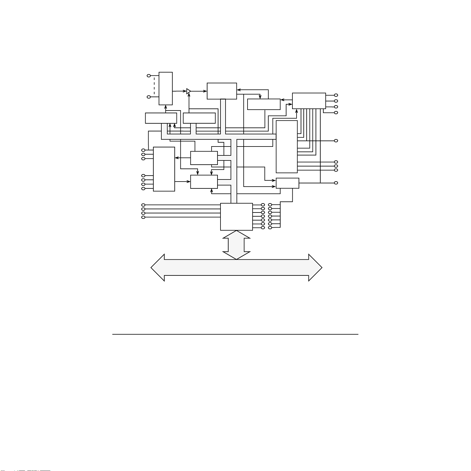
A functional block diagram of a DAS-8 Series board is shown in
Figure 2-1.
Artisan Technology Group - Quality Instrumentation ... Guaranteed | (888) 88-SOURCE | www.artisantg.com
2-1
Page 23
Analog In
8 Channels
Digital I/O
IP1
IP2
IP3
OP1
OP2
OP3
OP4
Ch 0
Ch 7
Channel Select
& Scan Logic
MUX
I/O
Buffers
Sample/Hold
Gain Control
DAS-8/PGA(G2)
Internal Data Bus
Control
Registers
Status
Registers
12 Bit A/D
with
Conversion
Control Logic
Timer/
Counter
Clk 2
Gate 2
Out 2
Clk 1
Gate 1
Out 1
Clk 0
Gate 0
Out 0
Interrupt
Control
Clock Generate
& Control Logic
Clk 1
Gate 1
Gate 2
Out 1
Out 2
Gate 0
Clk 0
Out 0
INT_IN
+5V
+12V
-12V
COM
Bus Power for
Expansion & Interface
Figure 2-1. DAS-8 Series Functional Block Diagram
Analog Input Features
DAS-8 Series boards use a 12-bit, successive approximation
analog-to-digital converter (ADC) with integral sample and hold. The
ADC provides 12-bit resolution ±1 least significant bit (LSB), providing
an effective accuracy of 11 bits. The ADC converts one sample every
25
s (25
µ
than 4 kHz (machine and software dependent).
s max.), providing an average conversion frequency of more
µ
Address
Decode &
Bus Interface
IBM PC AT Bus
Interrupt Select
Levels 2-7
(Jumper)
2-2 Functional Description
Artisan Technology Group - Quality Instrumentation ... Guaranteed | (888) 88-SOURCE | www.artisantg.com
Page 24

Channel Configuration
DAS-8 Series boards contain eight on-board analog input channels. The
following subsections describe the input configurations supported for
each channel, the gains and input ranges supported for each channel, and
the methods of specifying a channel or channels for an analog
input operation.
Input Configuration
The DAS-8 series boards contain eight analog input channels. DAS-8 and
DAS-8/LT inputs are single-ended (sharing a common low level ground)
with a fixed input range of -5.000V to +4.9976V. The DAS-8/PGA(G2)
and DAS-8/AO, on the other hand, may be configured for either
single-ended (signal measured against ground) or differential inputs (high
side of signal measured against the low side) by means of a DIP switch
located on the board.The differences between a single-ended and a
differential input configuration are described as follows:
•
Single-ended
you are measuring relatively high-level signals (greater than 1V), if
the source of the input signal is close to the board (less than two feet),
or if all input signals are referred to a common ground. This
configuration does not provide common-mode noise rejection.
•
Differential
are measuring low-level signals, if high source resistances (greater
than 100
voltage source and the host’s chassis ground. In a differential
configuration, a separate positive and negative terminal is provided
for each channel. Any common-mode noise that is picked up equally
on both inputs is rejected because the difference is zero.
You specify the input configuration by setting switches on the board. The
switches connect or disconnect the inverting side of the input signal to
low-level ground. Refer to page 3-12 for information on setting the
switches.
— A single-ended input configuration is appropriate if
— A differential input configuration is appropriate if you
) exist, or if common-mode voltages exist between the
Ω
Artisan Technology Group - Quality Instrumentation ... Guaranteed | (888) 88-SOURCE | www.artisantg.com
2-3
Page 25

Note:
On the DAS-8 and DAS-8/LT, the channels are always configured
as single-ended; all signals are referred to a single low-level ground.
If you are using EXP-16, EXP-16/A, or EXP-GP expansion boards or
MB-02 backplanes, you must configure the on-board analog input
channels associated with the expansion boards as single-ended.
Apply input voltages to the DAS-8 and DAS-8/LT between the channel
Hi and any L.L. Gnd. Wire signals enter the DAS-8/PGA(G2) and
DAS-8/AO between the Hi and Lo connection points and set switches on
the SE/DIFF DIP switch accordingly. Regardless of which board you use,
never wire signal returns to the digital common (DIG. COM.) as this is
intended as a heavy current return for power supplies and digital logic
signals, and it may differ from the low-level ground by several millivolts,
resulting in errors that are difficult to trace.
Correct use of the grounds is important to obtain consistent noise-free
measurements, because inadvertent ground loops are common when
using single ended connections. Use low-level grounds for all analog
signal returns to the DAS-8 and DAS-8/LT; they should carry signal
currents less than a few milliamps. The seven identical low-level ground
inputs are positioned in the connector so to lie between the analog
channel inputs in the flat connecting cable. This reduces undesirable
electrical noise, thus preventing crosstalk. The input current of each
channel is about 100nA at 25˚C, presenting a high input impedance to the
signal. Also, the 508A solid-state channel multiplexer used on the DAS-8
Series board is designed to withstand continuous overloads of ±32V on
each channel and transients of several hundred volts. This multiplexer has
two other desirable characteristics; a break-before-make action to prevent
shorts between channels while switching and shutting OFF all channels
when the power is off. This prevents signal-to-signal shorts when your
computer is off.
2-4 Functional Description
Artisan Technology Group - Quality Instrumentation ... Guaranteed | (888) 88-SOURCE | www.artisantg.com
Page 26
Gains and Ranges
A DAS-8 board measures analog input signals in the range of ±5V.
Each DAS-8/PGA(G2) or DAS-8/AO board contains a programmable
gain amplifier (PGA), which allows you to measure analog input signals
in one of several software-selectable unipolar and bipolar ranges. For
each channel on a DAS-8/PGA(G2) or DAS-8/AO board, you can specify
one of five bipolar and four unipolar analog input ranges.
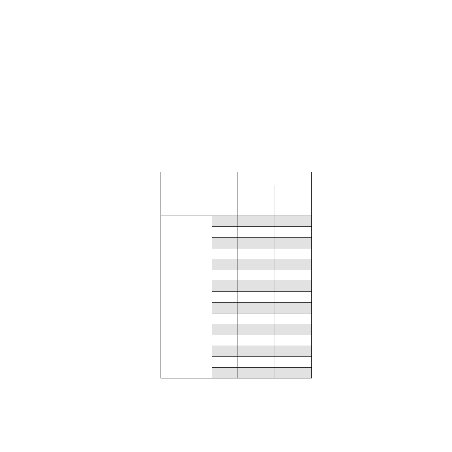
Table 2-1 lists the gains supported by DAS-8 Series boards and the analog
input voltage range for each gain.
Table 2-1. Supported Gains
Range
Board Gain
DAS-8
DAS-8/LT
DAS-8/PGA 0.5 ±10V Not available
DAS-8/PGA-G2 0.5 ±10V Not available
DAS-8/AO
1 ±5V Not available
1 ±5V 0 to 10V
10 ±500mV 0 to 1V
100 ±50mV 0 to 100mV
500 ±10mV 0 to 20mV
1 ±5V 0 to 10V
2 ±2.5V 0 to 5V
4 ±1.25V 0 to 2.5V
8 ±625mV 0 to 1.25V
0.5 ±10V 0 to 10V
Bipolar Unipolar
1 ±5V Not available
10 ±500mV 0 to 1V
100 ±50mV 0 to 100mV
500 ±10mV 0 to 20mV
Artisan Technology Group - Quality Instrumentation ... Guaranteed | (888) 88-SOURCE | www.artisantg.com
2-5
Page 27

Note:
Analog input channels on DAS-8 Series boards are provided with
protection against signals outside the specified analog input range. All
DAS-8 Series boards can tolerate voltages up to ±35V and transients of
several hundred volts without damaging the board.
When measuring signals at differential inputs, DAS-8/PGA(G2) and
DAS-8/AO boards can tolerate common-mode voltages up to ±35V and
transients of several hundred volts without damaging the board; however,
for normal operation of the board, make sure that the common-mode
voltage is no more than 12V
−
(( G / 2) x V
), where G is the gain and V
D
D
is the differential input voltage.
The DAS-8/PGA(G2) and DAS-8/AO support voltage input ranges from
±10 volts to ±0.01 volts (bipolar) and +10VDC to 0.02VDC (unipolar).
Higher voltages may be measured by the use of simple resistive dividers.
Each DAS-8/PGA(G2) or DAS-8/AO input channel can be configured for
either single-ended or differential inputs by means of Switch S2. The
DAS-8/PGA(G2) has a built-in differential amplifier to minimize errors
from Common Mode voltages. A DAS-8/PGA(G2) input channel should
be configured for single-ended (SE position of SW2 for each channel)
when attempting to measure floating signals. Grounded signals should be
read in the differential configuration to reduce common-mode error.
When using the DAS-8/PGA(G2) and DAS-8/AO with the EXP-16, all
DAS-8/PGA(G2) and DAS-8/AO channels should be set for single-ended
inputs.
The DAS-8 and DAS-8/LT provide a +10V A/D voltage reference (Vref).
It may be used for offsetting signals, but should not be heavily loaded.
The maximum available output current is 2mA. Since this reference is
shared by the A/D, any overload or shorting of the reference will affect
the scaling of the A/D.
2-6 Functional Description
Artisan Technology Group - Quality Instrumentation ... Guaranteed | (888) 88-SOURCE | www.artisantg.com
Page 28

Channel Selection
You can use DAS-8 Series boards to acquire data from a single analog
input channel or from a range of contiguous, on-board analog input
channels using automatic channel scanning. These two methods of
channel selection are described as follows:
•
•
Single channel
— You use software to specify a single channel and
initiate a conversion.
A
utomatic channel scanning
— You use software to specify the first
and last channels in a range of contiguous, on-board channels (0 to 7).
The channels are sampled in order from first to last; the hardware
automatically increments the analog input multiplexer address shortly
after the start of each conversion. When the last address is reached,
the multiplexer returns to the start address and the channels are
sampled again. For example, assume that the start channel is 4, the
stop channel is 7, and you want to acquire five samples. Your program
reads data first from channel 4, then from channels 5, 6, and 7, and
finally from channel 4 again.
Note:
An error results if the start channel number is higher than the stop
channel number.
When using automatic channel scanning, all contiguous, on-board
channels must have the same gain (analog input range).
Note:
DriverLINX allows you to acquire data from a range of
multiple channels that includes channels on expansion boards or MB
Series backplanes. The Expansion Board Configuration for Keithley
DAS-8 Series dialog in DriverLINX of the Special selection of the
Device Subsystem Page allows you to record the settings of your
analog input multiplexers and enable the expansion channels. Refer to
Appendix F: Configuration and Implementation Notes, Keithley
DAS-8 Series
manual that accompanies DriverLINX.
2-7
Artisan Technology Group - Quality Instrumentation ... Guaranteed | (888) 88-SOURCE | www.artisantg.com
Page 29

Automatic channel scanning is a hardware feature. In multi-channel
range mode, the DAS-8 Series acquires all data from a consecutive
range of analog channels.
•
The Start Channel’s gain only applies to the first channel.
•
DriverLINX uses the Stop Channel’s gain for all the other
analog channels in the range.
If the Start Channel is greater than the Stop Channel, the
•
channel sequence is [Start Channel, ..., Last Channel, 0, ...,
Stop Channel], where Last Channel is the highest numbered
channel for the DAS-8 model the application is using.
Channel Expansion
If you require additional analog input channels or signal conditioning for
transducer inputs, you can use any combination of up to eight 16-channel
EXP-16 expansion boards, eight 16-channel EXP-16/A expansion boards,
and/or eight 8-channel EXP-GP expansion boards to increase the number
of available channels to 128. You can also use up to four MB-02
backplanes to increase the number of available channels to 68. When
using the DAS-8 series boards with the EXP-16(s), the DAS-8 series
board should be configured as single-ended inputs by setting Switch S2.
In multi-channel list mode, the DAS-8 Series acquires all data from a
random list of analog channels.
The channel-gain list may contain up to 256 channels in any
•
order with any allowed gain.
•
The list may repeat the same channel with the same or different
gains.
Automatic channel scanning is a hardware feature. The functions
used to create a group of channels (sequential or non-sequential) or a
channel-gain list emulate automatic channel scanning through
software. Therefore, the maximum attainable conversion frequency is
reduced when using a group of consecutive channels or a
channel-gain list.
2-8 Functional Description
Artisan Technology Group - Quality Instrumentation ... Guaranteed | (888) 88-SOURCE | www.artisantg.com
Page 30

For the EXP-16, EXP-16/A, and EXP-GP, you attach the expansion
boards in a daisy-chain configuration using the S-1800 or C-1800 cable.
The first expansion board in the daisy chain is associated with on-board
channel 0, the next expansion board is associated with on-board channel
1, and so on. You specify the associated on-board channel by setting a
jumper on each expansion board. You can access any unused on-board
channels by attaching an STA-08 or STA-08PGA screw terminal
accessory to the last expansion board in the daisy-chain configuration.
Each EXP-16 (group of 16 channels) can operate at a different gain. In
this way a system can be configured with a variety of different channel
functions and gains, single-ended and differential.
DAS-8
Board
Note:
The PG408 DC/DC Converter option on the EXP-16 is required
for use with the DAS/AO board.
Figure 2-2 illustrates a daisy-chain configuration of two EXP-16
expansion boards, one EXP-GP expansion board, and an STA-08 screw
terminal accessory connected to a DAS-8 board.
On-board
channel 0
EXP-16
Figure 2-2. Channel Expansion
On-board
channel 1
EXP-16
On-board
channel 2
EXP-GP
On-board
channels 3 to 7
STA-08
Refer to the appropriate expansion board documentation for more
information about the EXP-16, EXP-16/A, and EXP-GP expansion
boards.
For information on attaching multiple MB-02 backplanes, refer to the
MB
Series User’s Guide.
Artisan Technology Group - Quality Instrumentation ... Guaranteed | (888) 88-SOURCE | www.artisantg.com
2-9
Page 31

Clock
The input to the counter/timers used for A/D timing varies. The
DAS-8/LT uses the PC bus clock while the DAS-8/PGA(G2) and
DAS-8/AO have an on-board 1MHz crystal oscillator. The frequency of
the PC bus may be determined automatically as described below.
Custom Clock Frequencies
For timing, the DAS-8 Series uses the clock signal on the PC I/O bus or
an on-board crystal oscillator. While the original IBM PC XT and
compatibles always had a 2.384MHz bus clock, ISA Nd EISA bus
machines have no accepted standard for PC bus clock. On many
machines, the clock frequency is one-half the CPU clock frequency, while
on others it is adjustable using motherboard jumpers or advanced BIOS
setup options. Few manufacturers provide this information in their
documentation. This frequency, however, can by measured by
DriverLINX using the 82C54 timer/counters on the DAS-8.
To measure the PC bus clock frequency, DriverLINX requires that
Counters 1 and 2 be chained together using an external jumper. To chain
the counters, connect Counter 2 Out [6] to Counter 1 IN [4] on the DAS-8
external connector.
Then, using DriverLINX, select the Counter/Timer Section in the
Configuration Dialog Box. Choosing the item “Custom clock” in the
drop-down list of the Resolution combo-box displays the Custom Clock
Frequency Dialog Box. Selecting Measure will start a 30-second
measuring interval for determination of the PC bus clock frequency. The
frequency box will update every second with the currently measured
frequency. The measuring interval may be stopped at any time using the
Stop pushbutton. The displayed frequency is added to the Resolution list
box by selecting OK, or the measurement can be abandoned by selecting
Cancel. The displayed frequency may be edited manually by selecting the
numbers in the edit box and typing a new value for the selected digits.
2-10 Functional Description
Artisan Technology Group - Quality Instrumentation ... Guaranteed | (888) 88-SOURCE | www.artisantg.com
Page 32

Conversion Clock Sources (DAS-8/PGA(G2), DAS-8/AO, and
DAS-8/LT)
The conversion clock source determines when each analog-to-digital
(A/D) conversion is initiated. DAS-8/PGA(G2),DAS-8/AO, and
DAS-8/LT boards provide the following software-selectable conversion
clock sources:
• Software — When using a software conversion clock, the host
computer issues a command to initiate a conversion. The host polls
the board to determine if the conversion is complete. When the
conversion is complete, the host reads the data from the ADC and
returns the value. If the host reads data before the conversion is
complete, the data will be invalid.
Software-initiated conversions are suitable for measuring DC
voltages; however, in applications where you must accurately control
the sampling rate (as when measuring time-varying signals), it is
recommended that you use either an internal or an external hardware
conversion clock source.
At power-up or system reset, the board assumes that conversions will
be initiated through software.
• Hardware (internal clock source) — The input to the counter/timers
used for A/D timing varies. The DAS-8 uses the PC bus clock while
the DAS-8/PGA (G2), DAS-8/AO, and DAS-8/LT have an on-board 1
MHz crystal oscillator. The frequency of the PC bus may be
determined automatically as described above.
• The internal clock source uses the on-board 82C54 counter/timer
circuitry and a crystal-controlled 1MHz time base. The 82C54
counter/timer circuitry is normally in an idle state. When you start an
analog input operation, a conversion is initiated immediately. The
82C54 is loaded with its initial count value and begins counting
down. When the 82C54 counts down to 0, another conversion is
initiated and the process repeats.
Because the 82C54 counter/timer uses a 1MHz time base, each count
represents 1
interval between conversions is 25
the time interval between conversions is 65.536ms.
µs. For example, if you load a count of 25, the time
µs; if you load a count of 65536,
2-11
Artisan Technology Group - Quality Instrumentation ... Guaranteed | (888) 88-SOURCE | www.artisantg.com
Page 33

The 82C54 contains three counter/timers: C/T0, C/T1, and C/T2. If
you are using a hardware internal clock source, the time base logic
uses C/T1 and C/T2 in either normal or cascaded mode, as follows:
– Normal Mode - A software-selectable count is loaded into C/T2
of the 82C54 counter/timer circuitry. Each time C/T2 reaches
terminal count, a conversion is initiated. The time interval
between conversions ranges from 25
– Cascaded Mode - A software-selectable count is divided between
µs to 65.536ms.
C/T2 and C/T1 of the 82C54 counter/timer circuitry. When C/T2
counts down to 0, C/T1 decrements by 1. C/T2 is reloaded with
its count value and begins counting down again. Each time C/T2
counts down to 0, C/T1 decrements by 1. Each time both C/T2
and C/T1 reach terminal count, a conversion is initiated. The time
interval between conversions ranges from 25
µs to 1.2 hours.
Refer to page 2-20 for more information about the 82C54
counter/timer circuitry.
• Hardware (external clock source) — An external clock source is
useful if you want to sample at rates not available with the 82C54
counter/timer circuitry, if you want to sample at uneven intervals, or if
you want to sample on the basis of an external event. An external
clock also allows you to synchronize conversions on multiple boards
to a common timing source.
The external clock source is an externally applied TTL-compatible
signal, which you attach to the INT_IN / XCLK pin (pin 24) of the
main I/O connector. When you start an analog input operation,
conversions are armed. At the next falling edge of the external clock
source (and at every subsequent falling edge of the external clock
source), a conversion is initiated.
Note: If you are using a hardware external clock source, you cannot
use the INT_IN / XCLK pin (pin 24) to generate interrupts.
Figure 2-3 illustrates how conversions are initiated when using an internal
and an external clock source. (Note that Figure 2-3 assumes that you are
not using a hardware trigger; refer to Figure 2-4 for an illustration of
conversions when using a hardware trigger.)
2-12 Functional Description
Artisan Technology Group - Quality Instrumentation ... Guaranteed | (888) 88-SOURCE | www.artisantg.com
Page 34

External Clock
Source
Internal Clock
Source
Conversions begin
when using an
internal clock source
Operation is started
(idle state)
Figure 2-3. Initiating Conversions
count
count
Conversions begin
when using an
external clock source
count
count
Note: The ADC acquires data at a maximum of 4kHz (one sample every
25
µs). If you are using a hardware external clock, make sure that the
clock does not initiate conversions at a faster rate than the ADC can
handle.
If you are acquiring samples from multiple channels, the maximum
sampling rate for each channel is equal to 4kHz divided by the number of
channels.
The rate at which the computer can reliably read data from the board
depends on a number of factors, including your computer, the operating
system/environment, whether you are using expansion boards, the gains
of the channels, and software issues.
2-13
Artisan Technology Group - Quality Instrumentation ... Guaranteed | (888) 88-SOURCE | www.artisantg.com
Page 35

Triggers
You can synchronize conversions on multiple DAS-8 Series boards to a
common, externally applied conversion clock. In addition, you can use a
DAS-8/PGA, DAS-8/PGA(G2), DAS-8/AO, or DAS-8/LT board as a
timing master; the output of the OUT1 pin (pin 5) on the main I/O
connector of the master board acts as an external hardware conversion
clock to any additional boards. You can use external circuitry, such as
C/T0 on the 82C54, to divide the rate of the master clock. This allows you
to synchronize conversions on the additional boards to a rate different
from that of the master board. Refer to page 4-14 for more information on
synchronizing conversions on multiple boards.
A trigger is an event that must occur before a DAS-8 Series board starts
an analog input operation. You can use one of the following trigger
sources to trigger an analog input operation:
• Software — When you start the analog input operation, conversions
begin immediately.
• Hardware — You connect a digital trigger signal to the digital input
IP1/TRIG pin (pin 25) of the main I/O connector. The trigger event
occurs when the board detects a rising edge on IP1/TRIG.
The actual point at which conversions begin depends on whether you
are using an internal or external clock source. These considerations
are described as follows:
– Internal clock source - The 82C54 counter/timer circuitry
remains idle until the trigger event occurs. When the trigger event
occurs, the board initiates the first conversion immediately.
– External clock source - Conversions are armed when the trigger
event occurs. At the next falling edge of the external clock source,
the board initiates the first conversion.
Figure 2-4 illustrates how conversions are started when using a
hardware trigger.
2-14 Functional Description
Artisan Technology Group - Quality Instrumentation ... Guaranteed | (888) 88-SOURCE | www.artisantg.com
Page 36

Hardware Trigger
External Clock
Source
Internal Clock
Source
Figure 2-4. Initiating Conversions with a Hardware Trigger
(idle state)
Trigger event occurs
count
Conversions begin
when using an
internal clock source
count
Conversions begin
when using an
external clock source
count
count
2-15
Artisan Technology Group - Quality Instrumentation ... Guaranteed | (888) 88-SOURCE | www.artisantg.com
Page 37

Hardware Gates
A hardware gate is an externally applied digital signal that determines
whether conversions occur. You connect the gate signal to the IP1/TRIG
pin (pin 25) on the main I/O connector. DAS-8 Series boards support a
positive gate only. Therefore, if the hardware gate is enabled and the
signal to IP1/TRIG is high, conversions occur; if the signal to IP1/TRIG
is low, conversions are inhibited.
Note: You cannot use the hardware gate with a hardware trigger.
However, the gate signal itself can act as a trigger. If the gate signal is low
when the software starts the analog input operation, the board waits until
the gate signal goes high before conversions begin.
When using the hardware gate, the way conversions are synchronized
depends on whether you are using a hardware external clock or a
hardware internal clock, as follows:
• External clock — The signal from the external clock continues
uninterrupted while the gate signal is low; therefore, conversions are
synchronized to the external clock.
• Internal clock — The 82C54 does not count while the gate signal is
low. Whenever the gate signal goes high, the 82C54 is loaded with its
initial count value and starts counting; therefore, conversions are
synchronized to the gate signal.
Figure 2-5 illustrates how to use the hardware gate with both an external
clock and an internal clock.
2-16 Functional Description
Artisan Technology Group - Quality Instrumentation ... Guaranteed | (888) 88-SOURCE | www.artisantg.com
Page 38

Gate Signal
Software starts
the operation
External Clock
Source
Gate is high;
conversions occur
1st conversion
(external clock)
Gate is low;
conversions inhibited
3rd conversion
(external clock)
2nd conversion
(external clock)
Internal Clock
Source
1st conversion
(internal clock)
. . . . . . . . . . . .
2nd conversion
(internal clock)
3rd conversion
(internal clock)
Figure 2-5. Hardware Gate
Note: Although DAS-8 Series boards do not provide a hardware-based
analog trigger, you can program an analog trigger through software, using
one of the analog input channels as the trigger channel. DriverLINX
provides functions for both an analog trigger and a digital trigger. Refer to
the DriverLINX Appendix F: Configuration and Implementation Notes:
Keithley DAS-8 manual for more information.
4th conversion
(internal clock)
2-17
Artisan Technology Group - Quality Instrumentation ... Guaranteed | (888) 88-SOURCE | www.artisantg.com
Page 39

Data Transfer
Because DAS-8 Series boards do not support DMA (Direct Memory
Access), data is always transferred from a DAS-8 Series board to the host
computer’s memory through an output port. Data can be transferred as
either a foreground process or a background process. If data is transferred
in the background, the end-of-conversion interrupt must be enabled so the
board can notify the host computer when new data is available. Refer to
page 2-26 for more information about interrupts. If data is transferred in
the foreground, interrupts are not required.
DAS-8/AO Analog Output Features
The DAS-8/AO is essentially a DAS-8/PGA with two DAC
(Digital-to-Analog Converter) channels.
Output data to DAC Channel 0 or 1 is written when the DAS-8/AO is
configured for normal updates. If the DACs are set for simultaneous
update, both channels are updated at the same time.
If DACs are configured for Update on Interrupt when configured for
normal update, DAC channel 0 or 1 is updated on interrupt. If the DACs
are set for simultaneous update, both DAC channels are updated on
interrupt.
2-18 Functional Description
Artisan Technology Group - Quality Instrumentation ... Guaranteed | (888) 88-SOURCE | www.artisantg.com
Page 40

Digital I/O Features
DAS-8 Series boards contain three digital input lines and four digital
output lines. The digital input lines are associated with the IP1, IP2, and
IP3 pins on the main I/O connector; the digital output lines are associated
with the OP1, OP2, OP3, and OP4 pins on the main I/O connector. Logic
1 at a pin indicates that the input/output is high (greater than 2.0V); logic
0 at a pin indicates that the input/output is low (less than 0.8V).
The digital input lines are compatible with TTL-level signals. If no signal
is connected to a digital input line, the input appears high (logic 1).
You can use the digital input and output lines for any general-purpose
task, with the following exceptions:
• If you are using an expansion board for an analog input operation, the
four digital output lines control the multiplexers on the expansion
boards to determine the expansion board channel that is acquiring
data. In this case, you cannot use the digital output lines for
general-purpose digital output operations.
• If you are using an external digital trigger or hardware gate, you must
use the IP1 pin to attach the trigger/gate signal. In this case, you
cannot use IP1 for general-purpose digital input operations.
2-19
Artisan Technology Group - Quality Instrumentation ... Guaranteed | (888) 88-SOURCE | www.artisantg.com
Page 41

82C54 Counter/Timer Circuitry
Each DAS-8 Series board contains 82C54 counter/timer circuitry; the
82C54 contains three counter/timers: C/T0, C/T1, and C/T2.
C/T0 is always available for general-purpose tasks. If you are using a
hardware internal clock source for an analog input operation, both C/T1
and C/T2 of the 82C54 counter/timer circuitry are dedicated to internal
functions and cannot be used for general-purpose tasks. If you are using a
hardware external clock source, C/T0, C/T1, and C/T2 are always
available for general-purpose tasks.
C/T0 and C/T1 have a clock input pin on the main I/O connector; all
counter/timers have a gate input pin and an output pin on the main I/O
connector. You can attach a clock source (0 to 10MHz) to the clock input
pins (CLK0 and CLK1). Pull-up resistors of 3.3k
three gate input pins (GATE0, GATE1, and GATE2). Therefore, the gates
appear enabled if no signal is attached to the gate inputs. You can use the
output pins (OUT0, OUT1, and OUT2) for pulse or frequency outputs.
You can program the 82C54 counter/timer circuitry to operate in one of
the following counter/timer modes:
Ω are provided on the
• Pulse on terminal count (Mode 0) — This mode is useful for event
counting or for programming a time delay. The software forces the
output low. On the next clock pulse after the software writes the
initial count value, the counter is loaded. When the counter reaches
zero, the output goes high and remains high until the software writes
a new count value. Note that the output does not go high until n + 1
clock pulses after the initial count is written, where n indicates the
loaded count.
A high gate input enables counting; a low gate input disables
counting. The gate input has no effect on the output. Note that an
initial count value written while the gate input is low is still loaded on
the next clock pulse.
Figure 2-6 illustrates pulse on terminal count mode.
2-20 Functional Description
Artisan Technology Group - Quality Instrumentation ... Guaranteed | (888) 88-SOURCE | www.artisantg.com
Page 42

Clock pulse
Software forces
output low
Output
Software writes initial
count value of 3
3 2 1
Figure 2-6. Pulse on Terminal Count Mode
• Programmable one-shot (Mode 1) — This mode is useful for
providing a hardware-triggered delay or one-shot pulse. The output is
initially high. A trigger loads the initial count value into the counter.
At the next clock pulse after the trigger, the output goes low and
remains low until the counter reaches zero. (The one-shot pulse is n
clock cycles in duration, where n indicates the loaded count.) After
the counter reaches zero, the output goes high and remains high until
the clock pulse after the next trigger; this makes the one-shot pulse
retriggerable.
You do not have to reload the count into the counter. The gate input
has no effect on the output. Writing a new count to the counter during
a one-shot pulse does not affect the current one-shot pulse.
Clock pulse
Output
Figure 2-7 illustrates programmable one-shot mode.
Trigger loads initial count
value of 3
3 2 1
Figure 2-7. Programmable One-Shot Mode
2-21
Artisan Technology Group - Quality Instrumentation ... Guaranteed | (888) 88-SOURCE | www.artisantg.com
Page 43

Clock pulse
• Rate generator (Mode 2) — This mode is useful for generating a
real-time clock interrupt. The output is initially high. A trigger loads
the initial count value into the counter. At the next clock pulse after
the trigger, the counter starts counting down. When the counter
reaches one, the output goes low for one clock pulse and then goes
high again. The counter is then reloaded with the initial count value
and the process repeats.
A high gate input enables counting; a low gate input disables
counting. If the gate goes low during an output pulse, the output is set
high immediately; this allows you to use the gate input to synchronize
the counter.
Writing a new count to the counter while counting does not affect the
current counting sequence. In this mode, a count of 1 is illegal.
Figure 2-8 illustrates rate generator mode.
Trigger loads initial count
value of 3
Output
3 2
Figure 2-8. Rate Generator Mode
2-22 Functional Description
1 3 2 1 2
Artisan Technology Group - Quality Instrumentation ... Guaranteed | (888) 88-SOURCE | www.artisantg.com
Page 44

Clock pulse
• Square-wave generator (Mode 3) — This mode is useful for
square-wave generation. The output is initially high. A trigger loads
the initial count value into the counter. At the next clock pulse after
the trigger, the counter starts counting down. When half the initial
count has elapsed, the output goes low for the remainder of the count.
When the total count elapses, the counter is reloaded with the initial
count value, the output goes high again, and the process repeats. If the
initial count is odd, the output is high for (n + 1) / 2 counts and low
for (n
− 1) / 2 counts, where n indicates the loaded count.
A high gate input enables counting; a low gate input disables
counting. If the gate goes low while the output is low, the output is set
high immediately. This allows you to use the gate input to
synchronize the counter.
Figure 2-9 illustrates square-wave generator mode.
Trigger loads initial count
value of 4
Output
4 3 2 1 4 3 2 1
Figure 2-9. Square-Wave Generator Mode
2-23
Artisan Technology Group - Quality Instrumentation ... Guaranteed | (888) 88-SOURCE | www.artisantg.com
Page 45

Clock pulse
• Software-triggered strobe (Mode 4) — The output is initially high.
Writing the initial count through software loads the initial count value
into the counter at the next clock pulse, but the counter does not start
counting. At the next clock pulse, the counter starts counting down.
When the counter reaches zero, the output goes low for one clock
pulse and then goes high again. Note that the output does not go low
until n + 1 clock pulses after the initial count is written, where n
indicates the loaded count.
A high gate input enables counting; a low gate input disables
counting. The gate input has no effect on the output.
Figure 2-10 illustrates software-triggered strobe mode.
Software writes initial
count value of 3
Output
Figure 2-10. Software-Triggered Strobe Mode
Software loads counter
with initial count
3 2
1
2-24 Functional Description
Artisan Technology Group - Quality Instrumentation ... Guaranteed | (888) 88-SOURCE | www.artisantg.com
Page 46

Clock pulse
• Hardware-triggered strobe (Mode 5) — The output is initially
high. A rising edge of the gate input acts as a trigger. The counter is
loaded with the initial count value on the next clock pulse after the
trigger, but the counter does not start counting. At the next clock
pulse, the counter starts counting down. When the counter reaches
zero, the output goes low for one clock pulse and then goes high
again. Note that the output does not go low until n + 1 clock pulses
after the trigger event occurs, where n indicates the loaded count.
After the trigger event occurs, the gate input has no effect on the
output. Writing a new value during counting does not affect the
counting sequence.
Figure 2-11 illustrates hardware-triggered strobe mode.
Rising edge of gate
input acts as trigger
Output
Figure 2-11. Hardware-Triggered Strobe Mode
Counter is loaded with
initial count value of 3
3 2
1
2-25
Artisan Technology Group - Quality Instrumentation ... Guaranteed | (888) 88-SOURCE | www.artisantg.com
Page 47

Refer to 82C54 documentation for information on programming the
82C54 counter/timer circuitry for general-purpose tasks. Table 2-2 lists
several companies that provide documentation for the 82C54.
Table 2-2. Sources for 82C54 Documentation
Company Address and Telephone Number
Intel Corporation Literature Sales
P.O. Box 7641
Mt. Prospect, IL 60056-7641
(800) 468-3548
Harris Semiconductor Literature Department
P.O. Box 883, MS CB1-28
Melbourne, FL 32901
(407) 724-3739
Interrupts
Newbridge
Microsystems
603 March Road
Kanata, Ontario
Canada K2K 1X3
(613) 592-0714
(800) 267-7231
DAS-8 Series boards can generate interrupts from one of the following
interrupt sources:
• External interrupt — An interrupt is generated when a rising edge
is applied to the INT_IN/XCLK pin (pin 24) on the main
I/O connector.
Note: If you are using an external interrupt, you cannot use the
INT_IN/XCLK pin (pin 24) to connect a hardware external clock
source.
• End-of-Conversion (EOC) interrupt — An interrupt is generated
when an A/D conversion is complete.
2-26 Functional Description
Artisan Technology Group - Quality Instrumentation ... Guaranteed | (888) 88-SOURCE | www.artisantg.com
Page 48

Power
The interrupt source is software-selectable. At power-up or system reset,
the board assumes that the interrupt source is an external interrupt.
You can select only one interrupt at a time. If you are using an interrupt,
you must select the interrupt level (2, 3, 4, 5, 6, or 7) using a jumper on
the board. If you are not using an interrupt, you can disable interrupts
using a jumper on the board. Refer to page 3-13 for more information.
Note: If you are acquiring data in the background, interrupts must be
enabled and the interrupt source must be an EOC interrupt.
If an interrupt condition is satisfied, an on-board flip-flop is set. If
interrupts are enabled (through both hardware and software), the board
generates an interrupt to the host, driving the selected host interrupt line
to an active state.
The analog circuitry on the DAS-8 board is powered by the ±12V of the
host computer. The DAS-8/PGA(G2) and DAS-8/AO boards contain a
DC/DC converter to provide power to the analog circuitry.
Note: Many laptop computers and other types of battery-operated
computers do not have a
−12V power supply. If your computer does not
have a −12V power supply, you need to use a DAS-8/LT board.
The host computer can provide power for EXP-16, EXP-16/A, and
EXP-GP expansion boards and MB Series backplanes; however, certain
power limitations exist. Table 2-3 lists the maximum number of
expansion boards and backplanes that the host can power.
2-27
Artisan Technology Group - Quality Instrumentation ... Guaranteed | (888) 88-SOURCE | www.artisantg.com
Page 49

Table 2-3. Expansion Board/Backplane Power Limitations
Expansion
Board/Backplane
EXP-16 4
EXP-16/A 4
EXP-GP 3
MB-01 Always use external power.
MB-02 Always use external power.
MB-03 4
MB-04 2
STA-1360 4
Maximum Number
Powered by Host
If you want to use more expansion boards or backplanes than indicated in
Table 2-3, you must connect an external power supply to the additional
expansion boards or backplanes. Refer to the appropriate expansion board
documentation for information on providing external power to EXP-16,
EXP-16/A, and EXP-GP expansion boards. Refer to the MB Series User’s
Guide for information on providing external power to MB
Series backplanes.
2-28 Functional Description
Artisan Technology Group - Quality Instrumentation ... Guaranteed | (888) 88-SOURCE | www.artisantg.com
Page 50

Setup and Installation
This chapter describes how to install the software in your computer,
unpack and inspect the board, configure the board, and install the board in
your computer. Read this chapter and all related DriverLINX
documentation before you attempt to install and use your DAS-8 Series
board.
Installation Procedure
Installing and configuring DriverLINX for the DAS-8 Series boards
requires four steps:
1. Unpack the Board and Configure the Switches and Jumpers —
Follow the instructions in this chapter to configure the DAS-8 Series
board. See Installing the Board on page 3-25.
3
2. Install DriverLINX — Follow the instructions given by the
installation program. The Read Me First instructions explain the
components and drivers you can install. See Installing and
Configuring DriverLINX for DAS-8 Series Boards on page 3-21.
3. Configure DriverLINX — See Configuration with DriverLINX on
page 3-25 for configuration options specific to the DAS-8 Series
model.
4. Install your DAS-8 hardware — Read and follow instructions in
section Installing the Board on page 3-25 of this manual.
3-1
Artisan Technology Group - Quality Instrumentation ... Guaranteed | (888) 88-SOURCE | www.artisantg.com
Page 51

Unpacking the Board
To prevent any damage to your DAS-8 Series board, perform the
following steps when unpacking the board:
1. Remove the wrapped DAS-8 Series board from its outer shipping
carton.
2. Ensure that your computer is turned OFF but grounded, then hold the
wrapped board in one hand while placing your other hand firmly on a
metal portion of the computer chassis to discharge any static
electricity.
3. Carefully remove the board from its anti-static wrapping material.
(Store the wrapping material for future use.)
4. Inspect the board for signs of damage. If any damage is apparent,
arrange to return the board to the factory; refer to Section 6 for more
information.
5. Check the remaining contents of your package against the packing
list to ensure that your order is complete. Report any missing items to
the factory immediately.
6. Once you have determined that the board is acceptable, you can
configure the board. Refer to the next section for configuration
options.
3-2 Setup and Installation
Artisan Technology Group - Quality Instrumentation ... Guaranteed | (888) 88-SOURCE | www.artisantg.com
Page 52

DAS-8 Series Boards
If you are familiar with switches and jumpers and with the items that are
configurable on DAS-8 Series boards, you can use Figure 3-1 as a quick
reference for configuring a DAS-8 board; Figure 3-2 as a quick reference
for configuring a DAS-8/LT; Figure 3-3 for configuring a DAS-8/
PGA(G2) board; Figure 3-4 for configuring a DAS-8/AO board. If you
need additional information, refer to Configuring the Board on page 3-7.
BASE ADDRESS
O
1 2 3 4 5 6 7
N
Base Address
(On = 0, Off = 1)
0000000 = 000H
0000001 = 008H
0000010 = 010H
.
.
1100000 = 300H
.
1111111 = 3F8H
IRQ
LEVEL
Switch
block S1
J2
2 3 4 5 6 7 X
Interrupt level
(X = disabled)
R1
R2
Main I/O
connector
Pin 1
Figure 3-1. DAS-8 Board
Artisan Technology Group - Quality Instrumentation ... Guaranteed | (888) 88-SOURCE | www.artisantg.com
3-3
Page 53
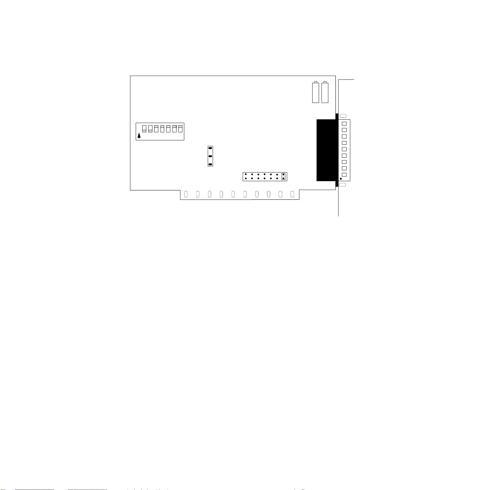
BASE ADDRESS
9 8 7 6 5 4 3
O
N
1 2 3 4 5 6 7
Switch
block S1
J3
EXT
R3
R4
INT
2 3 4 5 6 7 X
J2
Figure 3-2. DAS-8/LT Board
IRQ
LEVEL
3-4 Setup and Installation
Artisan Technology Group - Quality Instrumentation ... Guaranteed | (888) 88-SOURCE | www.artisantg.com
Page 54

R1
R2
R3
BASE ADDRESS
O
1 2 3 4 5 6 7
N
R4
Switch
block S2
IRQ
LEVEL
Switch
block S1
J2
2 3 4 5 6 7 X
O
1 2 3 4 5 6 7
N
Input Configuration
(On = single-ended,
Off = differential)
Switch 1 = Channel 0
Switch 2 = Channel 1
Switch 3 = Channel 2
Switch 4 = Channel 3
Switch 5 = Channel 4
Switch 6 = Channel 5
Switch 7 = Channel 6
Switch 8 = Channel 7
8
Main I/O
connector
Base Address
(On = 0, Off = 1)
0000000 = 000H
0000001 = 008H
0000010 = 010H
.
.
1100000 = 300H
.
1111111 = 3F8H
Pin 1
Interrupt level
(X = disabled)
Figure 3-3. DAS-8/PGA(G2) Board
Artisan Technology Group - Quality Instrumentation ... Guaranteed | (888) 88-SOURCE | www.artisantg.com
3-5
Page 55

123
S3
123
S4
IIVV
J6 CH0 J7 CH1
AMP
OUT
TP1 TP2
AMP
REF
O
1 2 3 4 5 6 7
N
Switch
block S1
8
OFF
NORM
WAIT
STATE
ON
J3
SIM
S5
BASE ADDRESS
O
1 2 3 4 5 6 7
N
Switch
block S2
J2
2 3 4 5 6 7 X
IRQ
LEVEL
Figure 3-4. DAS-8/AO Board
3-6 Setup and Installation
Artisan Technology Group - Quality Instrumentation ... Guaranteed | (888) 88-SOURCE | www.artisantg.com
Page 56

Configuring the Board
Be sure to make note of the configuration of all switches and jumpers on
the board. You will use this information to enter the correct configuration
parameters using DriverLINX. Also locate any information or notes about
the interrupt and DMA channels used by the other hardware devices in
your computer system.
You can configure the following items on DAS-8 Series boards:
• Base address (required by DriverLINX and other software packages
to perform DAS-8 Series board operations).
• Use of C/T2 on the 82C54 (cascaded or normal).
• Input range type (unipolar or bipolar) for a DAS-8/PGA(G2) or
DAS-8/AO board.
• Input configuration (single-ended or differential) for each channel on
a DAS-8/PGA(G2) or DAS-8/AO board.
• Interrupt level.
• DAS-8/AO configuration settings:
Analog output (voltage/current, range)
Output channels data output (normal/simultaneous)
Wait state (enabled or disabled)
• DAS-8/LT configuration for clock selection.
• Expansion boards used (information includes the number of
expansion boards, the gains used by channels on the expansion
boards, and the channel used as the CJC sensor).
Note: For EXP-16, EXP-16/A, and EXP-GP expansion boards, you
must also set switches on the expansion boards to specify the gains
used by channels on the expansion boards. Refer to the appropriate
expansion board documentation for information about setting the
switches.
3-7
Artisan Technology Group - Quality Instrumentation ... Guaranteed | (888) 88-SOURCE | www.artisantg.com
Page 57

Setting the Base Address
DAS-8 Series boards are shipped with a base address of 300H. If any of
the address locations between 300H and 307H are being used by another
resource in your system (including another DAS-8 Series board), you
must reconfigure the base address using the base address switch block
(labeled S1 on the DAS-8/LT board; labeled S2 on DAS-/PGA(G2) and
DAS-8/AO boards).
Note: To change the address, refer to the DriverLINX Appendix F:
Configuration and Implementation Notes — Keithley DAS-8 manual.
The base address switch block contains seven switches, labeled 1 through
7. Switch 1 corresponds to the most significant bit (MSB) of the base
address; switch 7 corresponds to the LSB of the base address. The
location of the base address switch block on the DAS-8 board is shown in
Figure 3-1; the location of the base address switch block on the DAS-8/LT
is shown in Figure 3-2; DAS-8/PGA(G2) boards is shown in Figure 3-3;
and DAS-8/AO is shown in Figure 3-4.
You place a switch in the ON position (logic 0) by sliding the switch
toward the top (numbered side) of the switch block. You place a switch in
the OFF position (logic 1) by sliding the switch toward the bottom
(unnumbered side) of the switch block.
Figure 3-5 illustrates the setting for a base address of 280H; switches 1
and 3 are in the OFF position and switches 2, 4, 5, 6, and 7 are in the ON
position.
1 2
O
N
Figure 3-5. Setting the Base Address
3-8 Setup and Installation
3 4
5 6
7
Artisan Technology Group - Quality Instrumentation ... Guaranteed | (888) 88-SOURCE | www.artisantg.com
Page 58

Table 3-1 lists I/O addresses commonly used by IBM PC/XT, AT, and
compatible computers. Determine an even boundary of eight I/O
addresses within the range of 000H to 3F8H that is not being used by
another resource in your system (including another DAS-8 Series board),
and set the switches to the appropriate base address.
Table 3-1. I/O Address Map (000H to 3FFH)
Address Range Use
000H to 00FH 8237 DMA #1
020H to 021H 8259 PIC #1
040H to 043H 8253 timer
060H to 063H 8255 PPI (XT)
060H to 064H 8742 controller (AT)
060H to 06FH 8042 keyboard controller
070H to 071H CMOS RAM and NMI mask register (AT)
080H to 08FH DMA page registers
0A0H to 0A1H 8259 PIC #2 (AT)
0A0H to 0AFH NMI mask register (XT)
0C0H to 0DFH 8237 DMA #2 (AT - word-mapped)
0F0H to 0FFH 80287 numeric processor (AT)
170H to 177H Hard disk controller #1
1F0H to 1F8H Hard disk controller #2
1F0H to 1FFH Hard disk controller (AT)
200H to 2FFH Game/control
210H to 21FH Expansion unit (XT)
238H to 23BH Bus mouse
23CH to 23FH Alternate bus mouse
278H to 27FH Parallel printer
2B0H to 2DFH EGA
2E0H to 2EFH GPIB (AT)
3-9
Artisan Technology Group - Quality Instrumentation ... Guaranteed | (888) 88-SOURCE | www.artisantg.com
Page 59

Table 3-1. I/O Address Map (000H to 3FFH) (cont.)
Address Range Use
2E8H to 2EFH Serial port
2F8H to 2FFH Serial port
300H to 31FH Prototype card
320H to 32FH Hard disk (XT)
370H to 377H Floppy disk controller #2
378H to 37FH Parallel printer
380H to 38FH SDLC
3A0H to 3AFH SDLC
3B0H to 3BBH MDA
3BCH to 3BFH Parallel printer
3C0H to 3CFH VGA EGA
3D0H to 3DFH CGA
3E8H to 3EFH Serial port
3F0H to 3F7H Floppy disk controller #1
3F8H to 3FFH Serial port
3-10 Setup and Installation
Artisan Technology Group - Quality Instrumentation ... Guaranteed | (888) 88-SOURCE | www.artisantg.com
Page 60

Notes: The Expansion Board Configuration for Keithley DAS-8 Series
dialog in DriverLINX allows you to enable the expansion channels. Make
sure that the switch settings match the settings you define in DriverLINX.
Refer to the DriverLINX Appendix F: Configuration and Implementation
Notes—Keithley DAS-8 manual.
On models DAS-8/PGA(G2) and DAS-8/AO, using a multiplexer requires
setting the associated base channel’s switch to single-ended.
The DriverLINX Analog Input subsystem has eight analog input
single-ended or differential signal connections depending on the model of
your DAS-8 series board. DriverLINX maps these signals to Logical
Channels. DriverLINX uses several of these control connections for
external clock, trigger, and gating inputs. Refer to the DriverLINX
Appendix F: Configuration and Implementation Notes—Keithley DAS-8
manual.
All DAS-8 Series boards have eight analog input channels. On
DAS-8/PGA(G2) and DAS-8/AO models, you can switch each channel to
differential or single-ended. The switch setting affects only the
connections for the channel. DriverLINX grays out this property in the
configuration dialog.
3-11
Artisan Technology Group - Quality Instrumentation ... Guaranteed | (888) 88-SOURCE | www.artisantg.com
Page 61

Setting the Input Configuration
DAS-8/PGA(G2) and DAS-8/AO boards are shipped with the input
configuration for all channels set to single-ended. If this is not appropriate
for your application, you can reconfigure the input configuration on a
channel-by-channel basis using the input configuration switch block
(labeled S2).
Note: The default input configuration in the DriverLINX configuration
file is also single-ended for all channels. Make sure that the switch
settings match the settings you establish in DriverLINX.
The input configuration switch block contains eight switches, labeled 1
through 8. Switch 1 corresponds to channel 0; switch 2 corresponds to
channel 1, and so on. The location of the input configuration switch block
on the DAS-8/PGA(G2) board is shown in Figure 3-3 and for the
DAS-8/AO is shown in Figure 3-4.
You place a switch in the ON position (single-ended) by sliding the
switch toward the top (numbered side) of the switch block. You place a
switch in the OFF position (differential) by sliding the switch toward the
bottom (unnumbered side) of the switch block.
Figure 3-6 illustrates the setting for channels 0, 5, and 7 configured as
single-ended (switches 1, 6, and 8 are in the ON position) and channels 1,
2, 3, 4, and 6 configured as differential (switches 2, 3, 4, 5, and 7 are in
the OFF position).
1 2
O
N
Figure 3-6. Setting the Input Configuration
Notes: Since DAS-8 and DAS-8/LT boards always use a single-ended
3 4
5 6
7
8
SE
DIFF
input configuration, they do not contain an input configuration switch
block.
3-12 Setup and Installation
Artisan Technology Group - Quality Instrumentation ... Guaranteed | (888) 88-SOURCE | www.artisantg.com
Page 62

Setting the Interrupt Level
DAS-8 Series boards are shipped with interrupts disabled. If you want to
use interrupts, you must set an appropriate interrupt level using jumper
block J2.
Note: DriverLINX modes specify preferred hardware data transfer
techniques: foreground or synchronous modes, background or
asynchronous modes. DriverLINX supports three modes with the
DAS-800 Series for its commands: polled mode, interrupt mode, and
other mode. Refer to the DriverLINX Appendix F: Configuration and
Implementation Notes for Keithley DAS-8 manual.
If you intend to acquire data in the background, you must enable
interrupts by setting an interrupt level.
Jumper block J2 contains seven pairs of jumper posts, labeled 2, 3, 4, 5, 6,
7, and X (disabled). You set the interrupt level by placing the supplied
jumper clip over the appropriate posts. Note that you can set only one
interrupt level at a time.
Figure 3-7 illustrates the setting for interrupt level 5; the jumper clip is
over the posts labeled 5.
IRQ
LEVEL
2 3 4 5 6 7 X
Figure 3-7. Setting the Interrupt Level
3-13
Artisan Technology Group - Quality Instrumentation ... Guaranteed | (888) 88-SOURCE | www.artisantg.com
Page 63

Table 3-2 lists interrupt levels commonly used by IBM PC and
compatible computers. Select an interrupt level that is not being used by
another resource in your system (including another DAS-8 Series board),
and set the jumper to the appropriate interrupt level. It is recommended
that you select interrupt level 3, 4, 5, or 7, if available.
Table 3-2. Interrupt Levels
Level Use
2 Reserved (XT), interrupts 8 to 15 (AT)
3 Serial port COM2 or SDLC
4 Serial port COM1 or SDLC
5 Hard disk (XT), LPT (AT)
6 Floppy disk
7 LPT
Analog Output Voltage Range Adjustments
(DAS-8/AO Only)
Switches S3 and S4 are the Analog Output Range switches for D/A1 and
D/A0, respectively. Jumpers J6 and J7 set the D/A outputs into either
Voltage Output Mode or 4-20mA Current Output Mode. Settings for
these components are as shown in Figure 3-8.
3-14 Setup and Installation
Artisan Technology Group - Quality Instrumentation ... Guaranteed | (888) 88-SOURCE | www.artisantg.com
Page 64

D/A 0
D/A 1
I
J7 CH0
I V
J7 CH0
I V
J7 CH0
I V
J7 CH0
I V
J7 CH0
I V
J7 CH0
Figure 3-8. Setting the D/A Output Switches and Jumpers
V
123
123
123
123
123
123
S4 S3
123
0 to 5 volts
S4
123
S3
0 to 10 volts
S4
123
S3
-5 to +5 volts
S4
123
S3
-10 to +10 volts
S4
123
S3
-2.5 to +2.5 volts
S4
123
S3
4 to 20 mA
IV
J6 CH1
IV
J6 CH1
IV
J6 CH1
IV
J6 CH1
IV
J6 CH1
IV
J6 CH1
3-15
Artisan Technology Group - Quality Instrumentation ... Guaranteed | (888) 88-SOURCE | www.artisantg.com
Page 65

D/A Output Channel Update (DAS-8/AO Only)
Switch S5 determines whether the two D/A outputs will be updated
independently (NORM) or simultaneously (SIM). Independent updates
are the normal mode, while simultaneous updates facilitate
synchronization. Refer to Figure 3-4.
Wait-State Setting (DAS-8/AO Only)
Jumper J3 allows the board to be set for a Wait State. A wait state may be
required when the board is used in computers whose bus speeds are
greater than 8MHz. Placing the jumper on the OFF side disables the wait
state. Refer to Figure 3-4.
Clock Select (DAS-8/LT Only)
Jumper J3 sets the board for the 1.000MHz (internal) or PC system
(external) clock. Refer to Figure 3-2.
Clock
The input to the counter/timers used for A/D timing varies. The DAS-8
uses the PC bus clock while the DAS8-PGA and DAS-8/AO have an
on-board 1MHz crystal oscillator. The frequency of the PC bus may be
determined automatically as described below.
Custom Clock Frequencies
For timing, the DAS-8 Series uses the clock signal on the PC I/O bus or
an on-board crystal oscillator. While the original IBM PC XT and
compatibles always had a 2.384MHz bus clock, ISA Nd EISA bus
machines have no accepted standard for PC bus clock. On many
machines, the clock frequency is one-half the CPU clock frequency
while, on others, it is adjustable using motherboard jumpers or advanced
BIOS setup options. Few manufacturers provide this information in their
documentation. This frequency, however, can by measured by
DriverLINX using the 82C54 timer/counters on the DAS-8.
3-16 Setup and Installation
Artisan Technology Group - Quality Instrumentation ... Guaranteed | (888) 88-SOURCE | www.artisantg.com
Page 66

To measure the PC bus clock frequency, DriverLINX requires that
Counters 1 and 2 be chained together using an external jumper. To chain
the counters, connect Counter 2 Out [6] to Counter 1 IN [4] on the DAS-8
external connector.
Then, using DriverLINX, select the Counter/Timer Section in the
Configuration Dialog Box. Choosing Custom Clock in the drop-down list
of the Resolution combo-box displays the Custom Clock Frequency
Dialog Box. Selecting Measure will start a 30-second measuring interval
for determination of the PC bus clock frequency. The frequency box will
update every second with the currently measured frequency. The
measuring interval may be stopped at any time using the Stop pushbutton.
The displayed frequency is added to the Resolution list box by selecting
OK, or the measurement can be abandoned by selecting Cancel. The
displayed frequency may be edited manually by selecting the numbers in
the edit box and typing a new value for the selected digits.
4–20mA Current Loops
Process control current-loop transducers interface easily with DAS-8 and
DAS-8/LT by adding a suitable shunt resistor across the input. Since the
maximum current is 20mA and the maximum input range of a DAS-8 is
+5V, a 250-ohm precision shunt resistor is required. The
DAS-8/PGA(G2) and DAS-8/AO default range is also ±5V, so that this
method also works here. The resistor should be of low temperaturecoefficient metal film or wirewound construction for stability with time
and temperature.
Using this interface, the 4–20mA working range of the current loop
corresponds to 1638 bits of input, a resolution of about 0.06%.
The Reference (DAS-8 and DAS-8/LT Only)
The DAS-8 and DAS-8/LT provide a +10V A/D voltage reference (Vref).
It may be used for offsetting signals, but should not be heavily loaded.
The maximum available output current is 2mA. Since this reference is
shared by the A/D, any overload or shorting of the reference will affect
the scaling of the A/D.
Artisan Technology Group - Quality Instrumentation ... Guaranteed | (888) 88-SOURCE | www.artisantg.com
3-17
Page 67

Interface to Transducers, Thermocouples, etc.
Low-level transducers such as thermocouples and strain gage bridges
(load cells, pressure/force transducers) require amplification before
applying to the high level DAS-8 series board inputs. The EXP-16
expansion multiplexer incorporates an instrumentation amplifier that can
provide stable amplification. It also includes circuitry that allows
cold-junction compensation of thermocouples. EXP-16 handles most
interfacing requirements to DC output transducers and also includes
spaces for filters, shunts, and attenuators.
For inexpensive temperature measurement in the –50 to +125 degree
Celsius range, semiconductor temperature transducers are a good choice.
The most popular types are the AD590 (Analog Devices), which behave
like a constant-current source with an output of 273µA at 0˚C and a
scaling of 1µA/˚C. The LM335 (National Semiconductor) has an output
of 2.73 volts at 0˚C and a temperature coefficient of 10mV/˚C. Both of
these devices can be powered from the +12V available from the computer
and directly interfaced to DAS-8 Series boards.
For measuring high temperatures (up to 1800˚C or more), thermocouples
are the most satisfactory solution. The base metal thermocouples, Types J,
K, T, and E have outputs around 40µV/˚C, while the platinum and
tungsten types are generally used for the highest temperature
measurement. Types S, B, and R tend to have lower outputs in the 6 to
12µV/˚C range. A further complication encountered in the use of
thermocouples is the cold-junction compensation.
Where the thermocouple wire is terminated to the copper DAS-8 Series
connections, a second thermocouple junction is formed by the two
dissimilar metals. As the temperature of this connection varies, an error is
introduced. The error can be mathematically compensated for by sensing
the connector temperature using a semiconductor sensor on another
channel and correcting the thermocouple readings using software. This is
required only at the highest levels of accuracy, since in most cases
connector temperature (usually room temperature) varies little.
3-18 Setup and Installation
Artisan Technology Group - Quality Instrumentation ... Guaranteed | (888) 88-SOURCE | www.artisantg.com
Page 68

DriverLINX has a Windows Dynamic Link Library (DLL) that you can
use to perform thermocouple linearization. This DLL exports a function
that you can use with most programming languages for converting the
voltage output of Type B, E, J, K, R, S, and T thermocouples to
temperature. The DriverLINX function, Volt2Temp, uses linear
interpolation in a lookup table to convert voltages into temperatures.
Since the lookup table data is based on a cold junction temperature of
25˚C, the input voltage needs to be corrected for the cold-junction
temperature at which the measurement was obtained with the following
formula:
Vcorr = Vx + offset + (CJCTemp – 25) slope
where Vx is the input voltage and Vcorr is the corrected voltage (both in
millivolts), CJCTemp is the measured temperature (in C˚) of the cold
junction, and slope and offset are data in the lookup table.
The Volt2Temp function assumes that the temperature values between
adjacent points in the table are linear over voltage so it can use linear
interpolation to calculate the temperature.
First, the function searches the lookup table for the nearest table voltage,
V1, which is less than or equal to the input voltage, Vx, and retrieves the
corresponding temperature value, t1. Then it retrieves the next
voltage-temperature values, V2, and t2, in the lookup table to calculate
the temperature, tx, corresponding to the corrected input voltage, Vx.
3-19
Artisan Technology Group - Quality Instrumentation ... Guaranteed | (888) 88-SOURCE | www.artisantg.com
Page 69

Application Precautions
Unavoidably, data acquisition systems are intimately tied to the computer.
Because of this, it is VERY IMPORTANT that signal inputs NOT be
mixed with AC line current. As an aid to avoiding this problem:
1. Avoid direct connections to the AC line.
2. Ensure all signal wire connections are tight and sound to avoid shorts
to high voltages.
3. Use isolation amplifiers and transformers where necessary to ensure
isolation.
There are two ground connections (DIG. COM. and L.L. GND.) on the
rear connector (DAS-8 Series boards implement the L.L. GND. only
when in the single-ended input mode). Digital common is the noisy or
“dirty” ground that is meant to carry all digital signal and heavy current
(power supply). Low level ground is the signal ground for all analog input
functions. It is only meant to carry signal currents (less than a few mA)
and is the ground reference for the A/D channels. Because of connector
contact resistance and cable resistance, there may be several millivolts
difference between these two grounds even though they are eventually
connected to each other, the computer, and power line grounds on the
DAS-8 Series board.
3-20 Setup and Installation
Artisan Technology Group - Quality Instrumentation ... Guaranteed | (888) 88-SOURCE | www.artisantg.com
Page 70

Installing and Configuring DriverLINX for
DAS-8 Series Boards
Important: As a precaution against a system crash the first time you
install and test any new hardware, you should exit all other programs and,
if you use a disk cache, disable write caching. If the system does crash
and you’re using disk compression software or a disk cache utility, as a
precaution after any crash, run the utility that checks the directory
structures.
This section describes how to install the DAS-8 Series standard software
package. The contents of these software packages are described as
follows:
• DAS-8 Series standard software package — Shipped with DAS-8
Series boards. Includes DriverLINX for Microsoft Windows and
function libraries for writing application programs such as Microsoft
Visual C++; Microsoft Visual Basic; Borland Delphi; utility
programs; and language-specific example programs.
• DriverLINX
device drivers for Windows application development includes:
– DriverLINX API DLLs and drivers supporting the DAS-8 Series
hardware
– Learn DriverLINX - an interactive learning and demonstration
program for DriverLINX that includes a Digital Storage
Oscilloscope
– Source Code - for the sample programs
– DriverLINX On-line Help System - provides immediate help as
you operate DriverLINX
– Supplemental Documentation - on DriverLINX installation and
configuration; analog and digital I/O programming; counter/timer
programming; technical reference; and information specific to the
DAS-8 Series hardware
— the high-performance real-time data-acquisition
3-21
Artisan Technology Group - Quality Instrumentation ... Guaranteed | (888) 88-SOURCE | www.artisantg.com
Page 71

Note: DAS-8 Series boards are not compatible with Windows NT or
WIN 2000.
Installing the DAS-8 Series Standard Software Package
Note: Important — Before you begin installing any hardware or software
for the DAS-8, read the DriverLINX Installation and Configuration Guide
and the DriverLINX Appendix F: Configuration and Implementation
Notes for Keithley DAS-8 manuals that are packaged with the DriverLINX
software. They are accessed from the DriverLINX CD-ROM after you
have installed Adobe Acrobat.
Before Installing DriverLINX
1. Inventory your DAS-8 board’s configuration settings.
2. Determine the resources your DAS-8 Series board requires.
3. Inventory your computer’s resources already allocated to other
installed devices.
4. Determine whether your computer has sufficient resources for your
DAS-8 board.
5. Determine whether your DAS-8 board can use your computer’s free
resources.
6. Set any jumpers/switches to configure your DAS-8 board to use your
computer’s free resources.
7. Set any other jumpers/switches to configure your DAS-8 board the
way you want.
8. Install your DAS-8 board into an appropriate free slot in
your computer.
3-22 Setup and Installation
Artisan Technology Group - Quality Instrumentation ... Guaranteed | (888) 88-SOURCE | www.artisantg.com
Page 72

Selecting the DriverLINX Components to Install
For your convenience in installing and uninstalling just the DriverLINX
components you need, the DriverLINX CD Browser will assist you in
selecting the components to install:
– Install Drivers - This required component installs only the files
you need for configuring your hardware and running third-party
data-acquisition applications that require DriverLINX.
– Install Interfaces - This optional component installs the files and
example programs that you will need to develop custom
applications for DriverLINX using C/C++, Visual Basic, Delphi,
and LabVIEW.
– Install Documentation - This optional component installs
electronic documentation for DriverLINX that you can read,
search, and print using the Adobe Acrobat Reader.
– Install Acrobat - This optional component installs the Adobe
Acrobat Reader for the DriverLINX electronic documentation.
3-23
Artisan Technology Group - Quality Instrumentation ... Guaranteed | (888) 88-SOURCE | www.artisantg.com
Page 73

Installing DriverLINX
1. Insert the DriverLINX CD-ROM into your computer’s CD-ROM
Drive.
2. Start the DriverLINX setup program. On most systems, wait a few
seconds for automatic startup. Otherwise, run the setup.exe program
from the CD-ROM.
3. The DriverLINX CD-ROM Browser Map window appears on the
screen. Click ‘Install Drivers,’ and follow the series of on-screen
instructions.
Note: To display an explanation of a menu option on the
DriverLINX CD browser map that appears next and on subsequent
setup screens, place the mouse pointer over the menu item. A star
next to a menu item means that the item was selected previously.
4. Select ‘Read Me First,’ and follow the instructions.
5. Select ‘Install Documentation.’ If you do not have Adobe Acrobat
installed on your computer, install it by selecting ‘Install Adobe
Acrobat.’
6. Open the manuals appropriate to the DAS-800 installation and read
them before installing your DAS-800 board or configuring
DriverLINX:
– DriverLINX Installation and Configuration
– Appendix F: Configuration and Implementation Notes — Keithley
DAS-8
– DriverLINX Technical Reference Manual
– DriverLINX Analog I/O Programming Guide
– DriverLINX Digital I/O Programming Guide
– DriverLINX Counter/Timer Programming Guide
– Appendix, I/O Port, Interrupt, and DMA Channel Usage
– Other manuals appropriate to your installation
3-24 Setup and Installation
Artisan Technology Group - Quality Instrumentation ... Guaranteed | (888) 88-SOURCE | www.artisantg.com
Page 74

Configuration with DriverLINX
Follow the DriverLINX on-screen instructions for installation of drivers
and interfaces. Refer to the DriverLINX Installation and Configuration
Guide and DriverLINX Appendix F: Configuration and Implementation
Notes — Keithley DAS-8 manuals.
Before you configure DriverLINX for operation with the DAS-8 Series
board, you must specify the base address, interrupt level, and input
configuration by setting switches on the board.
Installing the Board
Before installing a DAS-8 Series board in your computer, make sure that
the switches and jumpers on the board are set appropriately and that the
jumper and switch settings match the settings you configure in
DriverLINX.
Caution: Installing or removing a board with the power ON can cause
damage to your computer.
To install the board, perform the following steps:
1. Turn power to the computer and all attached equipment OFF.
2. Remove the computer chassis cover.
Select an available slot. The DAS-8 or DAS-8/LT requires a single, short
slot; the DAS-8/PGA(G2) requires a single, 1/2-slot; the DAS-8/AO
requires a full slot.
Caution: Be careful when installing a DAS-8/AO board that requires a
full slot. Some motherboards have components that extend into this space
and may cause interference.
3. Loosen and remove the screw at the top of the blank adapter plate,
then slide the plate up and out to remove.
3-25
Artisan Technology Group - Quality Instrumentation ... Guaranteed | (888) 88-SOURCE | www.artisantg.com
Page 75

4. Insert and secure the board connector in the selected slot.
5. Replace the computer chassis cover.
6. Plug in all cords and cables.
7. Turn power to the computer ON.
After you install the DAS-8 Series board in the computer, you can attach
an expansion board, if necessary, and wire the appropriate signals to the
board; refer to Section 4 for information. Before writing your application
program, you can test the functions of the DAS-8 Series board using the
DriverLINX AIO Panel or Test Panel for testing your DriverLINX
installation and configuration; verifying signal inputs to the DAS-8 Series
board; sending test signals to external devices.
Refer to the documentation provided with your computer for more
information on installing boards.
Configuring DriverLINX
After you have successfully installed the DAS-8 Series board in your
computer, start Windows to start DriverLINX. See the documentation
provided on the DriverLINX CD-ROM; especially the DriverLINX
Installation and Configuration Guide and the DriverLINX Appendix F:
Configuration and Implementation Notes:Keithley DAS-8 manuals.
Run “Learn DriverLINX” (LearnDL.exe) from the DriverLINX program
group to tell DriverLINX how you configured your DAS-8 Series board
and to verify that everything is properly installed and configured.
1. Start Windows as you normally would and select the Program
Manager window. Install DriverLINX if you have not previously
done so.
3-26 Setup and Installation
Artisan Technology Group - Quality Instrumentation ... Guaranteed | (888) 88-SOURCE | www.artisantg.com
Page 76

2. Either select the “Learn DriverLINX” icon created when you
installed DriverLINX or enter “<drive>:/DRVLNX/LEARNDL” in
the Command Line edit box. The command line edit box is activated
by selecting the Run... option. <drive> is the letter of the hard disk
drive where DriverLINX is installed.
3. Immediately after loading Learn DL, the Open DriverLINX DLL
dialog box appears. Select the name of the hardware-specific DLL
from the list for your DAS-8 board. The name is an abbreviation of
the board’s model number.
4. From the main menu bar of Learn DL, select the Device menu and
choose Select....
5. Select the Logical Device you wish to configure and then click on the
OK button (return).
6. Again select the Device menu and then choose the Configure... option
to display the Device Configuration Dialog Box.
7. From the Model list, select the model name for the DAS-8 Series
board you are configuring.
8. If the value displayed in the Address edit box is not correct, type the
correct value into the box. You may enter the address in decimal or
hexadecimal using the c-notation for hex, (that is, 768 decimal =
0x300 hexadecimal).
9. Choose the correct options for the Analog, digital, and Counter/
Timer Sections by first clicking on the appropriate radio button in the
middle of the dialog box and then completing the group of dialog
fields in the lower third of the dialog box. Be sure to click on both the
Input and Output radio buttons for the Analog and Digital groups to
see all the dialog fields.
10. After you have made all your selections, save the configuration
parameters by clicking on the OK button. This will create or update
the configuration file in the Windows directory.
3-27
Artisan Technology Group - Quality Instrumentation ... Guaranteed | (888) 88-SOURCE | www.artisantg.com
Page 77

Editing a Configuration File
The configuration file, KMBDAS8.INI, can also be created or edited
using a plain ASCII text editor, such as Notepad editor that comes with
Windows. The layout and format of the configuration file is similar to the
initialization files created by Windows and other Windows applications.
See Appendix C.
All entries in the configuration file have the following form:
[logical device number]
keyname=string
where “keyname” is the name of a field recognized by DriverLINX and
“string” is the value for that field. The case of the letters in keyname and
string is not significant.
A typical entry for logical device 0 in the configuration initialization file
follows:
The string values recognized for the Vendor and Model keynames are
[Device 0]
Vendor=Keithley
Model=DAS-8
Address=768
A/D channels=8
Min A/D volts=-5.0
Max A/D volts=5.0
IRQ=7
DMA=-1
Clock=4.15 MHz
defined in the DriverLINX API file, OEMCODES.H. Case is not
significant for matching a string value. The numeric values must all be
decimal or floating point.
3-28 Setup and Installation
Artisan Technology Group - Quality Instrumentation ... Guaranteed | (888) 88-SOURCE | www.artisantg.com
Page 78

The default address used by the DAS-8 is 768 decimal or 0x300 hex. If
you have more than one Keithley device or another peripheral card at the
same address, you will have to change the DIP switch settings for the
device address on the board.
The DAS-8 A/D channels are configured as eight single-ended or
differential analog inputs. DriverLINX does not distinguish between
single-ended and differential inputs.
The minimum and maximum analog full-scale voltages at unity gain must
be specified. For the DAS-8, the minimum and maximum voltages are
fixed at ±5 volts.
If hardware interrupts are not supported, select an IRQ value of –1,
otherwise an interrupt request level must be selected in the range of 2 to 7.
Interrupt lines can be shared so long as two devices sharing an interrupt
will not be used concurrently. A list of common hardware interrupt
assignments is shown in Table 3-2.
DMA is not used by the DAS-8 Series. This item must either have the
value -1, or the option may be deleted from the file with a text editor.
3-29
Artisan Technology Group - Quality Instrumentation ... Guaranteed | (888) 88-SOURCE | www.artisantg.com
Page 79

Cabling and Wiring
This chapter describes how to attach accessory and expansion boards to a
DAS-8 Series board, how to connect signals to a DAS-8 Series board, and
how to synchronize conversions on multiple DAS-8 Series boards.
Note: Before you make any connections to a DAS-8 Series board, make
sure that power to your computer and any accessories attached to the
DAS-8 Series board are OFF.
Attaching Accessory and Expansion Boards
4
You attach an STC-37 screw terminal connector, STA-08 or STA-08PGA
screw terminal accessory, or EXP-16, EXP-16/A, or EXP-GP expansion
board to a DAS-8 Series board through the main I/O connector, a 37-pin,
D-type connector that is labeled J2 on the board. The main I/O connector
and its pin assignments on a DAS-8 board are shown in Figure 4-1; the
main I/O connector and its pin assignments on a DAS-8/PGA(G2) board
are shown in Figure 4-2; the main I/O connector and its pin assignments
on a DAS-8/AO board are shown in Figure 4-3. Refer to Appendix B for a
more detailed description of the pins.
4-1
Artisan Technology Group - Quality Instrumentation ... Guaranteed | (888) 88-SOURCE | www.artisantg.com
Page 80

Top of Board (Rear View)
VREF Pin 19
LLGND Pin 18
LLGND Pin 17
LLGND Pin 16
LLGND Pin 15
LLGND Pin 14
LLGND Pin 13
LLGND Pin 12
DIG COM Pin 11
OP4 Pin 10
OP3 Pin 9
OP2 Pin 8
OP1 Pin 7
OUT2 Pin 6
OUT1 Pin 5
CLK1 Pin 4
OUT0 Pin 3
CLK0 Pin 2
+12V Pin 1
Pin 37 IN0
Pin 36 IN1
Pin 35 IN2
Pin 34 IN3
Pin 33 IN4
Pin 32 IN5
Pin 31 IN6
Pin 30 IN7
Pin 29 +5V
Pin 28 DIG COM
Pin 27 IP3
Pin 26 IP2
Pin 25 IP1
Pin 24 INT_IN
Pin 23 GATE2
Pin 22 GATE1
Pin 21 GATE0
Pin 20 −12V
Figure 4-1. Main I/O Connector on a DAS-8 or TAS-8/LTBoard
Top of Board (Rear View)
IN0− Pin 19
IN1− Pin 18
IN2− Pin 17
IN3− Pin 16
IN4− Pin 15
IN5− Pin 14
IN6− Pin 13
IN7− Pin 12
DIG COM Pin 11
OP4 Pin 10
OP3 Pin 9
OP2 Pin 8
OP1 Pin 7
OUT2 Pin 6
OUT1 Pin 5
CLK1 Pin 4
OUT0 Pin 3
CLK0 Pin 2
+12V Pin 1
Pin 37 IN0+
Pin 36 IN1+
Pin 35 IN2+
Pin 34 IN3+
Pin 33 IN4+
Pin 32 IN5+
Pin 31 IN6+
Pin 30 IN7+
Pin 29 +5V
Pin 28 DIG COM
Pin 27 IP3
Pin 26 IP2
Pin 25 IP1
Pin 24 INT_IN
Pin 23 GATE2
Pin 22 GATE1
Pin 21 GATE0
Pin 20 −12V
Figure 4-2. Main I/O Connector on a DAS-8/PGA(G2) Board
4-2 Cabling and Wiring
Artisan Technology Group - Quality Instrumentation ... Guaranteed | (888) 88-SOURCE | www.artisantg.com
Page 81

Top of Board (Rear View)
IN0− Pin 19
IN1− Pin 18
IN2− Pin 17
IN3− Pin 16
IN4− Pin 15
IN5− Pin 14
IN6− Pin 13
IN7− Pin 12
DIG COM Pin 11
OP4 Pin 10
OP3 Pin 9
OP2 Pin 8
OP1 Pin 7
OUT2 Pin 6
OUT1 Pin 5
CLK1 Pin 4
OUT0 Pin 3
CLK0 Pin 2
DAC1 Out Pin 1
Pin 37 IN0+
Pin 36 IN1+
Pin 35 IN2+
Pin 34 IN3+
Pin 33 IN4+
Pin 32 IN5+
Pin 31 IN6+
Pin 30 IN7+
Pin 29 +5V
Pin 28 DIG COM
Pin 27 IP3
Pin 26 IP2
Pin 25 IP1
Pin 24 INT_IN
Pin 23 GATE2
Pin 22 GATE1
Pin 21 LLGND
Pin 20 DAC0 Out
Figure 4-3. Main I/O Connector on a DAS-8/AO Board
You attach an STC-37 screw terminal connector directly to the main I/O
connector on the DAS-8 Series board. You attach an STA-08 or
STA-08PGA screw terminal accessory or an EXP-16, EXP-16/A, or
EXP-GP expansion board to the main I/O connector on the DAS-8 Series
board using either a C-1800 or S-1800 cable. The C-1800 is the
unshielded version of the cable; the S-1800 is the shielded version of the
cable.
Attaching an STC-37 Screw Terminal Connector
The screw terminals on the STC-37 screw terminal connector allow you
to connect field wiring to a DAS-8 Series board. The screw terminals are
labeled from 1 to 37 and correspond directly to the functions of the pins
on the main I/O connector on the board. For example, since pin 24 is
assigned to the external clock source, use screw terminal 24 to attach a
hardware external clock. Refer to Appendix B for a complete list of pin
assignments.
Artisan Technology Group - Quality Instrumentation ... Guaranteed | (888) 88-SOURCE | www.artisantg.com
4-3
Page 82
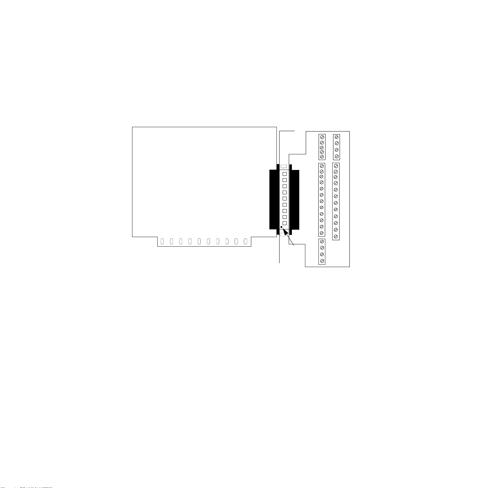
To connect an STC-37 to a DAS-8 Series board, directly attach the 37-pin
connector on the STC-37 to the main I/O connector on the DAS-8 Series
board. Figure 4-4 illustrates the connection of an STC-37 to a DAS-8
Series board.
21
17
16
DAS-8 Series Board
5
4
Pin 1
1
STC-37 Screw Terminal
Connector
Figure 4-4. Attaching an STC-37 Screw Terminal Connector
37
34
33
22
4-4 Cabling and Wiring
Artisan Technology Group - Quality Instrumentation ... Guaranteed | (888) 88-SOURCE | www.artisantg.com
Page 83

Attaching an STA-08 / STA-08PGA Screw Terminal Accessory
The screw terminals on the STA-08 screw terminal accessory allow you to
connect field wiring to a DAS-8 board; the screw terminals on the
STA-08PGA screw terminal accessory allow you to connect field wiring
to a DAS-8/PGA(G2) board. Each screw terminal is labeled with the
name of the board function to which it is connected; the screw terminals
correspond directly to the functions of the pins on the main I/O connector
on the board.
To connect an STA-08/STA-08PGA to a DAS-8 Series board, attach one
end of the S-1800 or C-1800 cable to the main I/O connector on the
DAS-8 Series board and the other end of the cable to the J1 connector on
the STA-08/STA-08PGA. Figure 4-5 illustrates the connection of an
STA-08/STA-08PGA to a DAS-8 Series board.
C-1800 / S-1800 Cable
−12 V
. . .
. . . . . . .
. . .
J1
+12 V
+5 V
. . .
. . . . . . .
. . . . . . .
. . . . . . .
DAS-8 Series Board
Pin 1
Pin 1
STA-08 / STA-08PGA
Figure 4-5. Attaching an STA-08/STA-08PGA Screw Terminal Accessory
4-5
Artisan Technology Group - Quality Instrumentation ... Guaranteed | (888) 88-SOURCE | www.artisantg.com
Page 84

Attaching an EXP-16 or EXP-16/A Expansion Board
Each EXP-16 or EXP-16/A expansion board provides up to 16 analog
input channels (labeled 0 to 15). The EXP-16 and EXP-16/A provide
three screw terminals for each channel: low-level ground (LL GND),
positive input (CHn HI), and negative input (CHn LO), where n indicates
the number of the channel.
To connect an EXP-16 or EXP-16/A to a DAS-8 Series board, attach one
end of the S-1800 or C-1800 cable to the main I/O connector on the
DAS-8 Series board and the other end of the cable to the J1 connector on
the EXP-16 or EXP-16/A. Figure 4-6 illustrates the connection of an
EXP-16 to a DAS-8 Series board.
Refer to the EXP-16 and EXP-16/A expansion board documentation for
more information about these expansion boards.
C-1800 / S-1800 Cable
DAS-8 Series Board
Pin 1
Figure 4-6. Attaching an EXP-16 or EXP-16/A Expansion Board
Pin 1
J1
J2
EXP-16
4-6 Cabling and Wiring
Artisan Technology Group - Quality Instrumentation ... Guaranteed | (888) 88-SOURCE | www.artisantg.com
Page 85

Attaching an EXP-GP Expansion Board
Each EXP-GP expansion board provides up to eight analog input
channels (labeled 0 to 7). The EXP-GP provides six screw terminals for
each channel: positive current excitation (+IEXC), positive input
(+SENSE), negative voltage excitation (
(
−IEXC), negative input (−SENSE), and positive voltage excitation (+P).
To connect an EXP-GP to a DAS-8 Series board, attach one end of the
S-1800 or C-1800 cable to the main I/O connector on the DAS-8 Series
board and the other end of the cable to the J1 connector on the EXP-GP.
Figure 4-7 illustrates the connection of an EXP-GP to a DAS-8 Series
board.
Refer to the EXP-GP expansion board documentation for more
information about this expansion board.
C-1800 / S-1800 Cable
J1
J2
−P), negative current excitation
DAS-8 Series Board
Figure 4-7. Attaching an EXP-GP Expansion Board
Pin 1
EXP-GP
Pin 1
4-7
Artisan Technology Group - Quality Instrumentation ... Guaranteed | (888) 88-SOURCE | www.artisantg.com
Page 86

Attaching an MB Series Backplane
Refer to the MB Series User’s Guide for information on connecting
DAS-8 Series boards to MB Series backplanes.
Connecting Multiple Expansion Boards
You can daisy-chain up to eight EXP-16, EXP-16/A, and/or EXP-GP
expansion boards to provide up to 128 analog input channels. You connect
the first expansion board to the DAS-8 Series board by attaching one end
of an S-1800 or C-1800 cable to the main I/O connector on the DAS-8
Series board and the other end of the cable to the J1 connector on the
expansion board. To connect additional expansion boards, attach one end
of an S-1800 or C-1800 cable to the J2 connector on the previous
expansion board and the other end of the cable to the J1 connector on the
next expansion board in the chain.
Note: Each EXP-16, EXP-16/A, or EXP-GP expansion board is
associated with an analog input channel on the DAS-8 Series board. You
specify the associated on-board channel by setting a jumper on the
expansion board. Make sure that you use a unique jumper setting for each
expansion board you are using. Refer to your expansion board
documentation for more information.
You can use the J2 connector on the last expansion board in the chain to
attach an STA-08/STA-08PGA screw terminal accessory. This allows you
to access the remaining functions of the DAS-8 Series board.
4-8 Cabling and Wiring
Artisan Technology Group - Quality Instrumentation ... Guaranteed | (888) 88-SOURCE | www.artisantg.com
Page 87

Figure 4-8 illustrates how to connect two EXP-16 expansion boards, one
EXP-GP expansion board, and an STA-08 screw terminal accessory to a
DAS-8 board.
J2
DAS-8
Board
EXP-16
Figure 4-8. Connecting Multiple Expansion Boards
Note: You can also attach up to four MB-02 backplanes to a DAS-8
Series board using an STA-SCM8 screw terminal accessory and up to
four C-2600 cables. Refer to the MB Series User’s Guide for more
information.
Connecting Signals
This section describes how to wire signals to a DAS-8 Series board.
J1
J2J1
EXP-16
J1
J2 J1
EXP-GP
STA-08
Although the illustrations in this section show a direct connection to a pin
on the main I/O connector, you will actually wire your signal to a screw
terminal on an accessory or expansion board or to a user-supplied, female
37-pin D connector. Appendix B lists the functions associated with each
pin on the main I/O connector.
The DAS-8 board contains both digital commons and low-level analog
commons. Use a digital common for all digital signal returns and power
supply returns; use a low-level analog common for all analog signal
returns.
Artisan Technology Group - Quality Instrumentation ... Guaranteed | (888) 88-SOURCE | www.artisantg.com
4-9
Page 88

The DAS-8/PGA(G2) and DAS-8/AO boards contain digital commons,
but no dedicated low-level analog commons. If you are using all eight
analog input channels and all eight channels are configured for
differential input, you must connect a bias return path to a digital
common instead of a low-level analog common. If at least one channel is
unused or configured for single-ended input, you can use the negative side
of the channel as a low-level analog common.
When wiring analog input signals, it is recommended that you terminate
all unused input channels to low-level ground; this prevents the internal
amplifier circuitry from saturating if you select an unconnected input and
ensures the accuracy of your data.
Connecting an Analog Input Signal to a Single-Ended Input
Figure 4-9 illustrates how to connect an analog input signal to
single-ended analog input channel 0 on a DAS-8 Series board.
Pin 37
Voltage
Source
+
−
Chan 0
Pin 12
LL COM
+
−
DAS-8 Board
Figure 4-9. Single-Ended Input
4-10 Cabling and Wiring
Artisan Technology Group - Quality Instrumentation ... Guaranteed | (888) 88-SOURCE | www.artisantg.com
Page 89

Connecting an Analog Input Signal to a Differential Input
For differential input configurations, you must provide a bias current
return path. If at least one channel is unused or configured for
single-ended input, use the negative side of that channel as the low-level
analog common; otherwise, use the digital common.
Figure 4-10 illustrates how to connect an analog input signal to
differential analog input channel 0 on a DAS-8PGA board for output
resistances both less than and greater than 100
channel 7 is not used, the bias current return path is connected to the
negative side of channel 7.
250 kΩ
Pin 37
Chan 0(+)
Voltage
Source
R
OUT
+
−
> 100 Ω
250 kΩ
Pin 19
Chan 0(−)
Pin 12
Chan 7(−)
Ω. Since analog input
+
−
DAS-8/PGA Board
Pin 37
Voltage
Source
R
OUT
< 100 Ω
+
Chan 0(+)
Pin 19
Chan 0(−)
−
250 kΩ
Pin 12
Chan 7(−)
+
−
DAS-8/PGA Board
Figure 4-10. Differential Input
Note: For output resistances greater than 100Ω, it is recommended that
the sum of the resistors used be at least 5,000 times greater than the
source output resistor.
4-11
Artisan Technology Group - Quality Instrumentation ... Guaranteed | (888) 88-SOURCE | www.artisantg.com
Page 90

Connecting Analog Output Signal from a DAS-8/AO Board
This section contains information needed when wiring analog output
signals from a DAS-8/AO board to your application.
Figure 4-11 illustrates how to connect a voltage output signal from a
DAS-8/AO board to your application. Figure 4-12 illustrates how to
connect a current output signal from a DAS-8.AO board to your
application.
Pin 20
DAC 0 Out
2 kΩ
0.25 Watt
Minimum
on 10V Range
Pin 21
LL GND
DAS-8/AO Board
Figure 4-11. DAS-8/AO Voltage Output
4-12 Cabling and Wiring
Artisan Technology Group - Quality Instrumentation ... Guaranteed | (888) 88-SOURCE | www.artisantg.com
Page 91

chap04_.fm Page 13 Thursday, August 22, 2002 1:37 PM
*Size resistor
so as not to
exceed 5 mA
Loop
Supply
6V to 36V
*Size resistor
so as not to
exceed 5 mA
+
−
Loop
Supply
6V to 36V
−
Load*
Pin 20
DAC 0 Out
+
−
Pin 21
LL GND
+
Pin 20
DAC 0 Out
DAS-8/AO Board
+
−
Load*
Pin 21
LL GND
DAS-8/AO Board
Figure 4-12. DAS-8/AO Current Output
Floating Load
Grounded Load
Connecting Digital Signals
You can connect the following digital signals to a DAS-8 Series board:
• Digital input signal — Connect a digital input signal to the IP1, IP2,
or IP3 pin (pin 25, 26, or 27) on the main I/O connector.
• Digital output signal — Connect a digital output signal to the OP1,
OP2, OP3, or OP4 pin (pin 7, 8, 9, or 10) on the main I/O connector.
• External conversion clock — Connect an external conversion clock
to the INT_IN pin (pin 24) on the main I/O connector.
• Hardware digital trigger or hardware gate — Connect a hardware
digital trigger or hardware gate signal to the IP1 pin (pin 25) on the
main I/O connector.
• External interrupt — Connect an external interrupt to the INT_IN
pin (pin 24) on the main I/O connector.
4-13
Artisan Technology Group - Quality Instrumentation ... Guaranteed | (888) 88-SOURCE | www.artisantg.com
Page 92

Make sure that all digital signals are TTL-level compatible. Use the
digital common as the return for all digital signals.
Caution: To prevent damage to DAS-8 Series boards, do not apply
voltages exceeding TTL maximum levels (
input pins.
−0.5V to +5.5V) to digital
Connecting Counter/Timer I/O Signals
Refer to 82C54 documentation for information on connecting counter/
timer I/O signals to the clock input pin, gate input pin, and output pin of
any available counter/timers on a DAS-8 Series board. Table 2-2 lists
several companies that provide documentation for the 82C54.
Synchronizing Conversions on Multiple Boards
You can use a hardware external clock source to synchronize conversions
on multiple DAS-8 Series boards. In addition, you can use the output of
the OUT1 pin (pin 5) on a DAS-8/PGA(G2) or DAS-8/AO board (acting
as a timing master) to synchronize conversions on additional DAS-8
Series boards.
Figure 4-13 illustrates how you can synchronize conversions on multiple
boards, using both an external clock source and a DAS-8/PGA/G2 board.
Note that in both cases, boards 1, 2, and 3 must be configured to use an
external clock.
Figure 4-14 illustrates the use of C/T0 on the 82C54 on board 1 to divide
the rate of the master clock by the programmed count. This allows you to
synchronize conversions on board 1 to a rate different from that of the
master board. Note that when you use C/T0 to divide the rate of the
master clock, C/T0 must be configured for counter/timer mode 2 (rate
generator mode). Refer to Section 2, 82C54 Counter/Timer Circuitry, or
to your 82C54 documentation for more information.
4-14 Cabling and Wiring
Artisan Technology Group - Quality Instrumentation ... Guaranteed | (888) 88-SOURCE | www.artisantg.com
Page 93

Board 1
Board 2
Board 3
External clock
Board 0
(Master)
Internal
clock
DAS-8/PGA/G2
Pin 5
OUT1
Board 1
Pin 24
INT_IN
Board 2
Pin 24
INT_IN
Pin 24
INT_IN
Board 3
Pin 24
INT_IN
Figure 4-13. Synchronizing Conversions on Multiple Boards
Pin 24
INT_IN
Pin 24
INT_IN
Board 1
C/T0 ÷ count
Board 0
(Master)
Pin 5
Internal
clock
OUT1
Figure 4-14. Dividing the Rate of the Master Clock
Pin 24
INT_IN
Pin 3 - OUT0
Pin 2
CLK0
4-15
Artisan Technology Group - Quality Instrumentation ... Guaranteed | (888) 88-SOURCE | www.artisantg.com
Page 94

4–20mA Current Loops
Process control current-loop transducers interface easily with DAS-8 and
DAS-8/LT by adding a suitable shunt resistor across the input. Since the
maximum current is 20mA and the maximum input range of a DAS-8 is
+5V, a 250-ohm precision shunt resistor is required. The DAS-8/
PGA(G2) and DAS-8/AO default range is also ±5V, so that this method
also works here. The resistor should be of low temperature-coefficient
metal film or wirewound construction for stability with time and
temperature.
Using this interface, the 4–20mA working range of the current loop
corresponds to 1638 bits of input, a resolution of about 0.06%.
The Reference (DAS-8 and DAS-8/LT Only)
The DAS-8 and DAS-8/LT provide a +10V A/D voltage reference (Vref).
It may be used for offsetting signals, but should not be heavily loaded.
The maximum available output current is 2mA. Since this reference is
shared by the A/D, any overload or shorting of the reference will affect
the scaling of the A/D.
4-16 Cabling and Wiring
Artisan Technology Group - Quality Instrumentation ... Guaranteed | (888) 88-SOURCE | www.artisantg.com
Page 95

5
Calibration
The analog input circuitry of DAS-8 Series boards is calibrated in the
factory. It is recommended that you check the calibration every six
months and recalibrate the board, if necessary.
Note:
initial calibration within an accuracy of ±0.05%. In applications where a
single gain (other than 1) is used for all channels, you can achieve better
accuracy by calibrating the board at the selected gain.
The following sections provide the information you need to calibrate
DAS-8 Series boards.
For channels using gains other than 1, the board maintains the
Equipment Required
You need the following equipment to calibrate a DAS-8 Series board:
• A digital voltmeter accurate to 6 1/2 digits on its ±10Vdc range, such
as the Keithley Model 196.
• A calibrated DC voltage source with an output voltage range of ±10V,
such as the EDC 520 from Electronic Development Corporation.
Note:
variable DC voltage source and set its output voltage level using the
voltmeter.
If a calibrated DC voltage source is not available, use a
Artisan Technology Group - Quality Instrumentation ... Guaranteed | (888) 88-SOURCE | www.artisantg.com
5-1
Page 96

• An STA-08 or STA-08PGA screw terminal accessory and C-1800
cable, or an STC-37 screw terminal connector.
Note:
equipment is of the required accuracy.
Potentiometers
DAS-8 Series boards contain potentiometers, which you must adjust
when calibrating the board. The DAS-8 board contains two
potentiometers: R1 (full scale) and R2 (offset); see Figure 5-2. The
DAS-8/LT board contains two potentiometers: R3 (full scale) and R4
(offset); see Figure 5-2.
The DAS-8/PGA(G2) boards contain four potentiometers: R1 (offset), R2
(full scale), R3 (unipolar fullscale), and R4 (unipolar offset); see Figure
5-3.
The DAS-8/AO boards contain ten potentiometers: R1 (offset), R2 (full
scale), R3 (unipolar full scale), and R4 (unipolar offset), R33 (analog
output gain adjustment for DA1) R 36 (analog output gain adjustment for
DA0), R34 (analog output zero adjustment for DA1), R37 (analog output
zero adjustment for DA0), R32 (4-20mA adjustment for DA1), and R35
(4-20mA adjustment for DA0) see Figure 5-4.
Do not attempt to calibrate a DAS-8 Series board unless your
In addition, on DAS-8/PGA(G2) and DAS-8/AO boards, you must
measure the current between two test points (TP1 and TP2) when
calibrating the board.
5-2 Calibration
Artisan Technology Group - Quality Instrumentation ... Guaranteed | (888) 88-SOURCE | www.artisantg.com
Page 97

R1 = Full scale
R2 = Offset
BASE ADDRESS
O
1 2 3 4 5 6 7
N
IRQ
LEVEL
Switch
block S1
J2
2 3 4 5 6 7 X
R1
R2
BASE ADDRESS
9 8 7 6 5 4 3
O
N
1 2 3 4 5 6 7
Figure 5-1. Potentiometers (DAS-8)
Switch
block S1
EXT
J3
INT
2 3 4 5 6 7 X
J2
Figure 5-2. Potentiometers (DAS-8/LT)
IRQ
LEVEL
R3
R3 = Full scale
R4 = Offset
R4
Artisan Technology Group - Quality Instrumentation ... Guaranteed | (888) 88-SOURCE | www.artisantg.com
5-3
Page 98

R1
R2
R4
R3
BASE ADDRESS
O
1 2 3 4 5 6 7
N
TP1 TP2
O
AMP
OUT
AMP
1 2 3 4 5 6 7
N
REF
Switch
block S2
J2
IRQ
LEVEL
2 3 4 5 6 7 X
Figure 5-3. Potentiometers [DAS-8/PGA(G2)]
8
TP1 TP2
AMP
OUT
AMP
REF
J2
2 3 4 5 6 7 X
O
1 2 3 4 5 6 7
N
Switch
block S1
IRQ
LEVEL
8
R32
OFF
R33
R34
123
J3
ON
S3
WAIT
STATE
R35
R36
NORM
123
S4
R37
IIVV
J6 CH0 J7 CH1
SIM
S5
R1
R2R3R4
BASE ADDRESS
O
1 2 3 4 5 6 7
N
Switch
block S2
Figure 5-4. Potentiometers (DAS-8/AO)
5-4 Calibration
Artisan Technology Group - Quality Instrumentation ... Guaranteed | (888) 88-SOURCE | www.artisantg.com
Page 99

6
Troubleshooting
If your DAS-8 Series board is not operating properly, use the information
in this chapter to help you isolate the problem. If the problem appears
serious enough to require technical support, refer to Technical Support on
page 6-5 for information on how to contact an applications engineer.
If you encounter a problem with a DAS-8 Series board, use the
instructions in this section to isolate the cause of the problem before
calling Keithley for technical support.
Device initialization error messages
During device initialization, DriverLINX performs a thorough test of all
possible subsystems on the DAS-8 Series board as well as the computer
interface. If DriverLINX detects any problems or unexpected responses, it
reports an error message to help isolate the problem. The device
initialization error messages fall into three basic categories:
• Device not found — Board address does not match hardware setting
or conflicts with another board. Verify the board’s address settings.
Also, don’t confuse hexadecimal with decimal addresses in the
DriverLINX Device Configure dialog box.
• Invalid IRQ level or Invalid DMA level — Selected level does not
match hardware setting, conflicts with another board’s IRQ/DMA
levels, or is dedicated to the computer’s internal functions (COM port,
disk drive controller, network adapter, etc.)
• Hardware does not match configuration — Operating mode/range
switch or jumper setting does not match selection(s) made in the
DriverLINX Device Configuration dialog box.
Artisan Technology Group - Quality Instrumentation ... Guaranteed | (888) 88-SOURCE | www.artisantg.com
6-1
Page 100

Problem Isolation
If you encounter a problem with a DAS-8 Series board, perform the
following steps to determine whether the problem is in the computer, in
the DAS-8 Series board, or in the I/O circuitry:
1. Remove power connections to the host computer.
2. Unplug the accessory connector(s) or cable(s) from the DAS-8 Series
board(s), keeping the connections intact on the accessory or
expansion board(s).
3. Remove the DAS-8 Series board(s) from the computer and visually
check for damage. If a board is obviously damaged, refer to Technical
Support on page 6-5 for information on returning the board.
4. With the DAS-8 Series board(s) out of the computer, check the
computer for proper operation. Power up the computer and perform
any necessary diagnostics.
5. When you are sure that the computer is operating properly, remove
computer power again, and install a DAS-8 Series board that you
know is functional. Do not make any I/O connections.
6. Apply computer power and check operation with the functional
DAS-8 Series board in place. This test checks the computer accessory
slot. If you are using more than one DAS-8 Series board, check the
other slots you are using.
7. If the accessory slots are functional, check the I/O hookups. Connect
the accessory and expansion boards, one at a time, and check
operation.
8. If operation is normal, the problem is in the DAS-8 Series board(s)
originally in the computer. Try the DAS-8 Series board(s) one at a
time in the computer to determine which is faulty. Use the
troubleshooting information in the next section to try to isolate the
problem.
9. If you cannot isolate the problem, refer to Technical Support on page
6-5 for instructions on getting technical support.
6-2 Troubleshooting
Artisan Technology Group - Quality Instrumentation ... Guaranteed | (888) 88-SOURCE | www.artisantg.com
 Loading...