

Page 1

Model 776 Programmable Counter/Timer
Instruction Manual
A GREATER MEASURE OF CONFIDENCE
Page 2

W ARRANTY
Keithley Instruments, Inc. warrants this product to be free from defects in material and workmanship for a period of 1 year
from date of shipment.
Keithley Instruments, Inc. warrants the following items for 90 days from the date of shipment: probes, cables, rechargeable
batteries, diskettes, and documentation.
During the warranty period, we will, at our option, either repair or replace any product that proves to be defective.
To exercise this warranty, write or call your local Keithley representative, or contact Keithley headquarters in Cleveland, Ohio.
You will be given prompt assistance and return instructions. Send the product, transportation prepaid, to the indicated service
facility . Repairs will be made and the product returned, transportation prepaid. Repaired or replaced products are warranted for
the balance of the original warranty period, or at least 90 days.
LIMIT A TION OF W ARRANTY
This warranty does not apply to defects resulting from product modification without Keithley’s express written consent, or
misuse of any product or part. This warranty also does not apply to fuses, software, non-rechargeable batteries, damage from
battery leakage, or problems arising from normal wear or failure to follow instructions.
THIS WARRANTY IS IN LIEU OF ALL OTHER WARRANTIES, EXPRESSED OR IMPLIED, INCLUDING ANY
IMPLIED WARRANTY OF MERCHANTABILITY OR FITNESS FOR A PARTICULAR USE. THE REMEDIES PROVIDED HEREIN ARE BUYER’S SOLE AND EXCLUSIVE REMEDIES.
NEITHER KEITHLEY INSTRUMENTS, INC. NOR ANY OF ITS EMPLOYEES SHALL BE LIABLE FOR ANY DIRECT,
INDIRECT, SPECIAL, INCIDENTAL OR CONSEQUENTIAL DAMAGES ARISING OUT OF THE USE OF ITS
INSTRUMENTS AND SOFTWARE EVEN IF KEITHLEY INSTRUMENTS, INC., HAS BEEN ADVISED IN ADVANCE
OF THE POSSIBILITY OF SUCH DAMAGES. SUCH EXCLUDED DAMAGES SHALL INCLUDE, BUT ARE NOT LIMITED TO: COSTS OF REMOVAL AND INSTALLATION, LOSSES SUSTAINED AS THE RESULT OF INJURY TO ANY
PERSON, OR DAMAGE TO PROPERTY.
Keithley Instruments, Inc. • 28775 Aurora Road • Cleveland, OH 44139 • 440-248-0400 • Fax: 440-248-6168 • http://www.keithle y.com
BELGIUM: Keithley Instruments B.V.
CHINA: Keithley Instruments China Y uan Chen Xin Building, Room 705 • 12 Yumin Road, Dew ai, Madian • Beijing 100029 • 8610-62022886 • Fax: 8610-62022892
FRANCE: Keithley Instruments Sarl 3, allée des Garays • 91127 Palaiseau Cedex • 01-64 53 20 20 • Fax: 01-60 11 77 26
GERMANY: Keithley Instruments GmbH Landsberger Strasse 65 • 82110 Germering • 089/84 93 07-40 • Fax: 089/84 93 07-34
GREAT BRITAIN: Keithley Instruments Ltd
INDIA: Keithley Instruments GmbH Flat 2B, WILOCRISSA • 14, Rest House Crescent • Bangalore 560 001 • 91-80-509-1320/21 • Fax: 91-80-509-1322
ITALY: Keithley Instruments s.r.l. Viale S. Gimignano, 38 • 20146 Milano • 02-48 39 16 01 • Fax: 02-48 30 22 74
NETHERLANDS: Keithley Instruments B.V. Postbus 559 • 4200 AN Gorinchem • 0183-635333 • Fax: 0183-630821
SWITZERLAND: Keithley Instruments SA Kriesbachstrasse 4 • 8600 Dübendorf • 01-821 94 44 • Fax: 01-820 30 81
TAIWAN: Keithley Instruments Taiwan 1 Fl. 85 Po Ai Street • Hsinchu, Taiwan, R.O.C. • 886-3572-9077 • Fax: 886-3572-903
Bergensesteenweg 709 • B-1600 Sint-Pieters-Leeuw • 02/363 00 40 • Fax: 02/363 00 64
The Minster • 58 Portman Road • Reading, Berkshire RG30 1EA • 0118-9 57 56 66 • Fax: 0118-9 59 64 69
9/00
Page 3

Model 776 Programmable Counter/T imer
Instruction Manual
Serial Prefix T74
©1993, Keithley Instruments, Inc.
All rights reserved.
Cleveland, Ohio, U.S.A.
Fifth Printing, April 2001
Document Number: 776-901-01 Rev. E
Page 4

Manual Print History
The print history shown below lists the printing dates of all Revisions and Addenda created for this manual. The
Revision Level letter increases alphabetically as the manual undergoes subsequent updates. Addenda, which are
released between Revisions, contain important change information that the user should incorporate immediately into
the manual. Addenda are numbered sequentially. When a new Revision is created, all Addenda associated with the
previous Revision of the manual are incorporated into the new Revision of the manual. Each new Revision includes
a revised copy of this print history page.
Addendum D (Document Number 776-901-02) ............................................ January 1999
Revision E (Document Number 776-901-01)...................................................... April 2001
All Keithley product names are trademarks or registered trademarks of Keithley Instruments, Inc.
Other brand and product names are trademarks or registered trademarks of their respective holders.
Page 5

Safety Precautions
The following safety precautions should be observed before using
this product and any associated instrumentation. Although some instruments and accessories would normally be used with non-hazardous voltages, there are situations where hazardous conditions
may be present.
This product is intended for use by qualified personnel who recognize shock hazards and are familiar with the safety precautions required to avoid possible injury. Read the operating information
carefully before using the product.
The types of product users are:
Responsible body is the individual or group responsible for the use
and maintenance of equipment, for ensuring that the equipment is
operated within its specifications and operating limits, and for ensuring that operators are adequately trained.
Operators use the product for its intended function. They must be
trained in electrical safety procedures and proper use of the instrument. They must be protected from electric shock and contact with
hazardous live circuits.
Maintenance personnel perform routine procedures on the product
to keep it operating, for example, setting the line voltage or replacing consumable materials. Maintenance procedures are described in
the manual. The procedures explicitly state if the operator may perform them. Otherwise, they should be performed only by service
personnel.
Service personnel are trained to work on live circuits, and perform
safe installations and repairs of products. Only properly trained service personnel may perform installation and service procedures.
Keithley products are designed for use with electrical signals that
are rated Installation Category I and Installation Category II, as described in the International Electrotechnical Commission (IEC)
Standard IEC 60664. Most measurement, control, and data I/O signals are Installation Category I and must not be directly connected
to mains voltage or to voltage sources with high transient over -voltages. Installation Category II connections require protection for
high transient over-voltages often associated with local AC mains
connections. The user should assume all measurement, control, and
data I/O connections are for connection to Category I sources unless otherwise marked or described in the Manual.
Exercise extreme caution when a shock hazard is present. Lethal
voltage may be present on cable connector jacks or test fixtures. The
American National Standards Institute (ANSI) states that a shock
hazard exists when voltage levels greater than 30V RMS, 42.4V
peak, or 60VDC are present.
that hazardous voltage is present in any unknown circuit before
measuring.
Users of this product must be protected from electric shock at all
times. The responsible body must ensure that users are prevented
access and/or insulated from every connection point. In some cases,
connections must be exposed to potential human contact. Product
users in these circumstances must be trained to protect themselves
from the risk of electric shock. If the circuit is capable of operating
at or above 1000 volts,
exposed.
Do not connect switching cards directly to unlimited power circuits.
They are intended to be used with impedance limited sources.
NEVER connect switching cards directly to AC mains. When connecting sources to switching cards, install protective devices to limit fault current and voltage to the card.
Before operating an instrument, make sure the line cord is connected to a properly grounded power receptacle. Inspect the connecting
cables, test leads, and jumpers for possible wear, cracks, or breaks
before each use.
When installing equipment where access to the main power cord is
restricted, such as rack mounting, a separate main input power disconnect device must be provided, in close proximity to the equipment and within easy reach of the operator.
For maximum safety, do not touch the product, test cables, or any
other instruments while power is applied to the circuit under test.
ALWAYS remove power from the entire test system and discharge
any capacitors before: connecting or disconnecting cables or jumpers, installing or removing switching cards, or making internal
changes, such as installing or removing jumpers.
Do not touch any object that could provide a current path to the common side of the circuit under test or power line (earth) ground. Always
make measurements with dry hands while standing on a dry , insulated
surface capable of withstanding the voltage being measured.
A good safety practice is to expect
no conductive part of the circuit may be
Page 6

The instrument and accessories must be used in accordance with its
specifications and operating instructions or the safety of the equipment may be impaired.
Do not exceed the maximum signal levels of the instruments and accessories, as defined in the specifications and operating information, and as shown on the instrument or test fixture panels, or
switching card.
When fuses are used in a product, replace with same type and rating
for continued protection against fire hazard.
Chassis connections must only be used as shield connections for
measuring circuits, NOT as safety earth ground connections.
If you are using a test fixture, keep the lid closed while power is applied to the device under test. Safe operation requires the use of a
lid interlock.
If a screw is present, connect it to safety earth ground using the
wire recommended in the user documentation.
!
The symbol on an instrument indicates that the user should refer to the operating instructions located in the manual.
The symbol on an instrument shows that it can source or measure 1000 volts or more, including the combined effect of normal
and common mode voltages. Use standard safety precautions to
avoid personal contact with these voltages.
The
WARNING heading in a manual explains dangers that might
result in personal injury or death. Alw ays read the associated infor mation very carefully before performing the indicated procedure.
The
CAUTION heading in a manual explains hazards that could
damage the instrument. Such damage may invalidate the warranty.
Instrumentation and accessories shall not be connected to humans.
Before performing any maintenance, disconnect the line cord and
all test cables.
To maintain protection from electric shock and fire, replacement
components in mains circuits, including the power transformer, test
leads, and input jacks, must be purchased from Keithley Instruments. Standard fuses, with applicable national safety approvals,
may be used if the rating and type are the same. Other components
that are not safety related may be purchased from other suppliers as
long as they are equivalent to the original component. (Note that selected parts should be purchased only through Keithley Instruments
to maintain accuracy and functionality of the product.) If you are
unsure about the applicability of a replacement component, call a
Keithley Instruments office for information.
To clean an instrument, use a damp cloth or mild, water based
cleaner. Clean the exterior of the instrument only. Do not apply
cleaner directly to the instrument or allow liquids to enter or spill
on the instrument. Products that consist of a circuit board with no
case or chassis (e.g., data acquisition board for installation into a
computer) should never require cleaning if handled according to instructions. If the board becomes contaminated and operation is affected, the board should be returned to the factory for proper
cleaning/servicing.
2/01
Page 7
Table of Contents
1
l-l
l-2
l-3
1-4
l-5
l-6
1-7
l-8
2
2-1
2-2 Performance Checks..
2-3
2-4
2-5
2-6
2-7
2-8
2-9
2-10
2-11
General Information
Introduction .................................................................................................................................................
Instrument and Manual Identification ...................................................................................................... 1-I
Configuration.. .............................................................................................................................................
Warranty Information .................................................................................................................................
Manual Addenda .........................................................................................................................................
Safety Symbols and Terms ........................................................................................................................
Inspection .....................................................................................................................................................
Specifications ..............................................................................................................................................
installation
Introduction .................................................................................................................................................
Power Requirements..
Grounding Requirements.. .....................................................................................................................
Installation and Mounting ..........................................................................................................................
Bench Mounting ..........................................................................................................................................
Rack Mounting.. ..........................................................................................................................................
Portable Use.. ...............................................................................................................................................
Short Term Storage.. ...................................................................................................................................
Long Term Storage or Re-packaging For Shipment ..............................................................................
Safety ............................................................................................................................................................
I-1
l-2
l-2
I -2
I-2
l-2
1-Y
2-1
.............................................................................................................................. ...2-I
.............................................................................................................................. ...2-I
.,.,2-I
2-2
2-2
2-2
2-2
2-2
2-2
2-3
3
3-l
3-2
3-2-l
Operation
Introduction
Front Panel Famlllanzatlon ...........................................................................................................................
Controls ....................................................................................................................................................
..................................................................................................................................................
1-l
3-l
3-1
Page 8
3-2-2
...........................................................................................................................................................................................................................................................
3-2-3
3-3
3-3-l
3-4
3-5
3-6
3-6-l
3-6-2
3-7
3-8
3-9
3-10
3-11
3-12
3-13
3-14
3-14-1
3-14-2
3-14-2
3-15
3-16
3-17
3-18
3-19
3-20
3-20-l
3-20-2
3-2 1
3-22
Connectors ............................................................................................................................................... 3-2
Display And Indicators .......................................................................................................................... 3-2
Rear Panel Familiarization.. ......................................................................................................................
Connectors and Terminals .....................................................................................................................
Power-up Procedure ...................................................................................................................................
Software Reset ............................................................................................................................................ 3-4
Display Messages .......................................................................................................................................
IEEE-488 Error Messages..
Error Indtcatmn
Control Selection ........................................................................................................................................
Selecting a Function ................................................................................................................................... 3-6
Selecting Gate and Delay Time
Setting Trigger Levels.. .............................................................................................................................. 3-8
Setting Input
Selecting The Number Of Displayed Digits..
Selecting Measurement Rate ..................................................................................................................... 3-10
Arming .......................................................................................................................................................... 3-l 1
Continuous Arming With the Input Signal..
Front Panel Arming ................................................................................................................................ 3-l 1
External Arming.. .................................................................................................................................... 3-l 1
Using Auto Trigger Level .......................................................................................................................... 3-12
Using V Peak A.. ......................................................................................................................................... 3-12
Using User Gate.. ........................................................................................................................................ 3-12
Using Delay ................................................................................................................................................. 3-13
Using User Delay ........................................................................................................................................ 3-13
Using Front Panel Set-ups .........................................................................................................................
Store Set-ups.. .......................................................................................................................................... 3-14
Recall Set-ups.. ........................................................................................................................................ 3-14
Using The External Reference. ................................................................................................................. 3-14
Changing The GPIB Address
Condition Controls .............................................................................................................
................................................................................................................
.........................................................................................
........................................................................................
.................................................................................................................... 3-14
3-3
3-3
3-3
3-4
:;i
3-5
3-8
3-9
3-10
3-l 1
3-14
4
4-l Introduction .................................................................................................................................................
4-2 Bus Desdription ...........................................................................................................................................
4-3
4-3-l Bus Management Lines ..........................................................................................................................
4-3-z Handshake Lines .....................................................................................................................................
4-3-3 Data Lines ................................................................................................................................................
4-4
4-5
4-6 Hardware Considerations..
4-6-l
4-6-2 Connections ............................................................................................................................................. J-5
4-7
4-8 Bus Commands ............................................................................................................................................
4-8-l
4-S-2
4-8-3 Addressed Commands ............................................................................................................................
4-8-4
4-8-5
4-9 Device-Dependent Command Programming
4-9-l Function (F) .............................................................................................................................................
IEEE-488 Programming
4-l
4-I
IEEE-488 Bus Lines ...................................................................................................................................
Interface Function Codes ...........................................................................................................................
Software Considerations.
Typical Controlled System ....................................................................................................................
Changing GPIB Address ............................................................................................................................
Uniline Commands
Universal Multiline Commands
Unaddress Commands ............................................................................................................................
Device Dependent Commands
........................................................................................................................... 4-4
........................................................................................................................ .-I-4
.............................................................................................................................. ...4-G
........................................................................................................... .4-7
.............................................................................................................
_.
....
....................................................................................
4.2
4-2
4-2
4-3
4-4
4-5
4-5
4-6
4-7
4-9
.4-9
4-9
4-9
Page 9
4-9-2
4-9-3
4-9-4
4-9-5
4-9-6
4-9-l
4-9-8
4-9-9
4-9-10
4-9-l 1
4-9-12
4-9-13
4-9-14
4-9-15
4-9-16
4-9-17
4-9-18
4-9-19
4-10
4-10-l
4-10-2
4-10-3
4-11
4-11-1
4-11-2
Channels A. B Coupling (AC. BC)
Channels A_ B Attenuator (AA, BA)
Channels A. B Filter (AF. BF)
Channels A: B Slope (AS. BS).
Channels A. B Impedance (AI. BI)
Channels A; B Trigger Level
Channels A, B Auto Trigger Level (L)
Gate Time (G, GLJ) ..................................................................................................................................
Delay Time (W, WU) .........................................................
V Peak Measurement Rate (V)
Totalize Mode (M) ..................................................................................................................................
Ratio Mode (C) ........................................................................................................................................
Displayed Digits (N) ...............................................................................................................................
Set-ups (ST. RE). .....................................................................................................................................
Triggering (T) ..........................................................................................................................................
Rate (S). ....................................................................................................................................................
Display Modes (D). .................................................................................................................................
SRQ Mode (Q) and Serial Poll
Reading From Model 776 ..........................................................................................................................
Data Control Commands (R)
Terminator
Prefix (X) ..................................................................................................................................................
Front Panel Error Messages ......................................................................................................................
ILL INS (Illegal Instruction).
ILL PAR (Illegal Parameter)
................................................................................................................................................
......................................................................................................
....................................................................................................
..............................................................................................................
.............................................................................................................
......................................................................................................
(AL.
BL)
...............................................................................................
................................................................................................
. ....................................................................
.............................................................................................................. 4-13
Status Byte Format.. .........................................................................
.................................................................................................................
................................................................................................................ 4-18
.................................................................................................................
4-11
4-12
4-12
4-12
4-12
4-12
4-12
4-12
4-12
4-13
4-13
4-13
4-13
4-l 3
4-13
4-14
4-14
4-15
4-15
4-l 6
4-17
4-l 8
4-18
5
5-l
5-2
5-3
5-4
5-5
5-6
5-7
5-8
5-9
5-9-l
5-9-2
5-9-3
5-10
5-10-l
5-10-2
5-10-3
S-10-4
5- 10-5
5-10-6
5-10-7
5-10-S
5-10-9
5-10-10
5-10-l 1
S-10-12
Maintenance and Performance Checks
Introduction .................................................................................................................................................
Line Voltage Selection ...............................................................................................................................
Fuse Replacement .......................................................................................................................................
Selecting an External Reference
Disassembly Instructions ...........................................................................................................................
Special Handling Of Static Sensitive Devices
Cleaning .......................................................................................................................................................
Repair and Replacement ............................................................................................................................
Performance Checks ...................................................................................................................................
Environmental Conditions .....................................................................................................................
Warm-up Period. ......................................................................................................................................
Recommended Test Equipment..
Performance Checks Procedure
Channels A and B Sensitivity Check
Channel C sensitivity Check
Period A. Period A Averaged Operation Check
Ratio A/B Operation
Ratio C/B Operation ...............................................................................................................................
Pulse A, T.1 A to B and Averaged Operation Check..
Phase A to B Operation Check ..............................................................................................................
Totalize B Operation Check
Auto Trigger Level A and B Operation Check
Delay Operation Check ..........................................................................................................................
User Gate Operation Check
Time Base Accuracy Check..
...............................................................................................................................
...............................................................................................................
........................................................................................
...........................................................................................................
.................................................................................................................
...................................................................................................
.................................................................................................................
.................................................................................
........................................................................
...................................................................................................................
...................................................................................
................................................................................................................... 5-l 1
.................................................................................................................
5-l
5-1
5-1
5-2
5-3
5-3
5-3
5-4
5-4
5-4
5-4
5-4
5-4
5-4
5-5
5-5
5-6
5-7
5-7
5-9
5-9
5-9
5-10
5-l 1
Page 10
6
6-l
6-2
6-3
6-3-l
6-3-2
6-3-3
6-3-4
6-3-5
6-367
6-4
6-4-l
6-4-2
6-4-3
6-4-4
6-4-S
Theory of Operation
Introduction .................................................................................................................................................
Overall Functional Description
Analog Circuitry
Input Circuits A and
Input Circuit C (option 2.4Ci).
10 MHz Standard Reference Oscillator
Reference Oscillator Circuit and TCXO (option 2.4G).
Measurement Logic Section
Power supply ...........................................................................................................................................
Digital Circuitry ..........................................................................................................................................
CPU Block Diagram
Memory Mapping ....................................................................................................................................
Address Decoding
KeyboardDisplay Interface
IEEE Interface .........................................................................................................................................
.........................................................................................................................................
B
...............................................................................................................................
...................................................................................................................................
................................................................................................................
.......................
..................................................................................................................
...................................................................................................................
. ...................................................................................................
...............................................................................................................
...............................................................................................
....................................................................
6-1
6-l
6-5
6-S
6-S
6-6
6-6
6-13
6-14
6-14
6-14
6-14
6-14
6-14
6-14
7
7-l
7-2
7-2-l
7-2-2
l-2-3
l-2-4
7-3
7-3-l
l-3-2
7-3-3
7-3-4
l-3-5
l-3-6
7-3-7
7-3-8
l-3-9
7-4
7-4-l
7-5
7-S-l
7-5-2
7-s-3
7-s-4
7-s-s
7-S-6
7-s-7
Adjustments and Troubleshooting
Introduction .................................................................................................................................................
Adjustments
Environmental Conditions.
Warm-up Period .......................................................................................................................................
Recommended Test Equipment
Adjustment Procedures
Adjustment Procedure ................................................................................................................................
Power Supply Adjustment
Trigger Level A Adjustment
Trigger Level B Adjustment
Trigger Level A Offset Adjustment
Trigger Level B Offset Adjustment
Input A xl0 High Frequency Adjustment
Input
Standard - S PPM Time Base Adjustment
TCXO.Time Base Adjustment (option 2.4G)
Troubleshooting
Recommended Test Equipment
Troubleshooting Procedure
Power Supply Checks
Digital Circuitry and Display Checks..
Standard S PPM Reference Oscillator Checks..
SO0 MHz Reference Oscillator and TCXO Checks
Trigger Level Checks
Signal Conditioning and Input Circuit Checks..
Measurement Logic
.................................................................................................................................................
....................................................................................................................
.............................................................................................................
..........................................................................................................................
.....................................................................................................................
..................................................................................................................
..................................................................................................................
......................................................................................................
......................................................................................................
...........................................................................................
B xl0 High Frequency Adjustment
..........................................................................................................................................
.............................................................................................................
.......................................................................................................................
.............................................................................................................................
.............................................................................................................................
Section Checks
............................................................................................
...........................................................................................
.....................................................................................
................................................................................................
.................................................................................
...........................................................................
.................................................................................
....................................................................................................
7-l
7-l
7-l
7-l
7-l
7-l
7-3
7-3
7-3
7-3
7-3
7-3
7-3
7-4
7-4
7-4
7-4
7-4
7-S
7-S
7-6
7-6
7-6
7-6
7-6
7-6
6
8-l
8-2 Ordering Information
8-3 Parts Description.. .......................................................................................................................................
Parts List
General .........................................................................................................................................................
.................................................................................................................................
8-l
8-1
8-1
Page 11
General Information
l-l. Introduction
This manual provides operating and maintenance infor-
matron
Counter/Timer. Section 1 is a general description of the
instrument. Section 2 and 3 obtain installation and operating instructions. IEEE programming is explained in
Section 4. Maintenance and performance checks are
provided in Section 5. The theoF of operation is described in Section 6. Section 7 oullines calibration and
troubleshooting procedures. Section 8 contains tables of
replaceable parts. Section 9 contains schematic and
component location diagrams.
Model 776 is a Fen digit microprocessor based fullyprogrammable. three-channel Universal Counrcr I
Timer. The instrument mcasurcs with a vev high resolution and precision the following paramctcrs: Frcquency A. Frequency B. Frequency C. Period A. Pulsewidth. Time interval A to B. Total counts B. Ratio A/B.
Ratio C/B. Phase A to B and Amplitude peaks. An
averaging function is available for improved resolution
in time measurement: resohes intervals of pica seconds. Various repetitive tests. no matter how complex.
are greatly simplified b>~ utiliziog any of the IO pre-programmed front panel set-up. Set-ups are stored in a
non-volatile memory and can be recalled by a simple
ke.s stroke.
for
the
Model
716
Programmable
as low as 0.01 Hz to more than 225 MHz. The reciprocal
technique is being used in low frequency mcasurcmcnts.
up to exactly 120 MHz. where the measurement tcchnique is changed to conventional measurement tcchnique. Model 776 measures frcqucncies of input signals
with minimum resolution of nine digits in one second
of gate time. With the TCXO
776l2.46. the displayed result in largely enhanced. both
in terms of stability and accuracy.
In Model 776. the lraditionally featured decade
steps of gale times. are replaced by a more flerible
variable gate time. This feature permits a choice from
500 internally pre-selected gate interwls. or an! esternal gate intcnal which is applied to a rear panel BNC
conneclor. Internal gate times range from 100 ps to IO
s. External gate expands this range to 1000 s. Trigger
leveI my be selected maounll~~ or left to bc aulomalicall? adjusted. by the instrument. to the optimum level.
thus eliminating false lriggcring on unknown signals.
NOTE
This manual provides a complclc dcscription of all fcrturcs of the 776
Series. Therefore. several of the features that are described in the following paragraphs may not be installed
in your instrument.
time
base of the Model
Model 776 utilizes a combination of two measurement techniques in order to always achieve maximum
display resolution. Some functions. such as Frequent!
measurement function. can be displayed with up to ten
digits. Such resolution can be gained from frequencies
1-2. Instrument Identification
These KeithIcy’ instmmcnts are identified by a serial
number. which is located on lhe rear panel. The lvo
most significant digits (Txs) identify instrumcnl modi-
I-I
Page 12

•
•
•
General Information
fication. If this prefix differs from that listed on the title
page of this manual, there are differences between this
manual and your instrument.
1-3. Configuration
There are two configurations available for the Model 776:
Model 776 - Two-channel 225 MHz programmable
counter/timer.
Model 776/2.4G - Same as above with 2.4 GHz Channel C and TCXO time base.
Model 776/2.4G/R - Same as above with rear panel
inputs.
1-4. Warranty Information
Warranty information is located on the inside front cover
of this instructions manual. Should your Model 776
require warranty service, contact the Keithley representative or authorized repair facility in your area for further
information. When returning the instrument for repair, be
sure to fill out and include the service form at the back of
this manual to provide the repair facility with the necessary information.
1-5. Manual Addenda
Any improvements or changes concerning the instrument
or manual will be explained in an addendum included with
the manual. Be sure to note these changes and incorporate
them into this manual.
1-6. Safety Symbols And Terms
The following symbols and terms may be found on an
instrument or used in this manual.
!
The symbol on an instrument indicates that the user
should refer to the operating instructions located in the
manual.
The WARNING heading used in this manual explains
dangers that might result in personal injury or death.
Always read the associated information very carefully
before performing the indicated procedure.
The CAUTION heading used in this manual explains
hazards that could damage the instrument. Such damage
may invalidate the warranty.
1-7. Inspection
The Model 776 was carefully inspected, both electrically
and mechanically before shipment. After unpacking all
items from the shipping carton, check for any obvious
signs of physical damage that may have occurred during
transit. (Note: There may be a protective film over the
display lens, which can be removed.) Report any damage
to the shipping agent immediately. Save the original
packing carton for possible future re-shipment. The
following items are included with every Model 776 order:
Table 1-1. Model 776 Specifications
INPUT CHARACTERISTICS
(Channel A & B)
RANGE
DC coupled
AC coupled 1 M Ω
50 Ω
SENSITIVITY (X1)
0 to 200 MHz
200 MHz to 225 MHz
5 ns Minimum Pulse Width
SIGNAL OPERATING RANGE
(X1)
(X10)
DYNAMIC RANGE (x1)
0 to 100 MHz
100 MHz to 225 MHz
Page 1-2
: 0 to 225 MHz.
: 30 Hz to 225 MHz.
: 1 MHz to 225 MHz.
: 50 mV rms sine wave.
: 75 mV rms sine wave.
: 75 mVp-p.
: -5.00 Vdc to +5.00 Vdc.
: -50.0 Vdc to +50.0 Vdc.
: 75 mV to 5 Vp-p.
: 150 mV to 2.5 Vp-p.
Page 13
Table l-l.
Model 776 Specificntions (continued)
IMPEDANCE
: 1 MQ or 50 .Q nominal shunted by less than 4.5 pF.
switchable.
LOW PASS FILTER : -3 dB NOMINAL at 100 KHz. switchable.
COUPLING
: AC or DC. switchable.
DAMAGE LEVEL (AC or DC)
(Xl)
: DC to 2 KHz - 200 V (DC + pk AC):
2 KHz to 100 KHz - lsi05 V rms Hz/Freq:
Above 100 KHz - S V rms.
(X10)
: DC to 20 KHz - 200 V (DC + pk AC):
20 KHz to 100 KHz - 4~10~ V rms Hz/Freq:
abo\:e 100 KHz - 50 V rms.
50 R
: 5 v rms
TRIGGER LEVEL CHARACTERISTICS
(Channel A and B)
MANUAL TRIGGER (auto trigger off)
(Xl)
(X10)
: -5.00 Vdc to +5.00 Vdc:
: -50.0 Vdc to i50.0 Vdc.
Setting Accuracy : Xl. * (35 mV +2% of reading): X10, + (350 mV +2% of
reading).
Resolution (X 1) : 10 mV: (X10): 100 tnV.
Preset (Xl) : 0.00 Vdc: (X10) 00.0 Vdc.
Trigger Slope
: Independent selection of positive or negative slope. switchable
AUTO TRIGGER
Frequency Range
DC Coupled : 100 Hz to 150 MHz.
AC Coupled 1 MO : 100 Hz to 150 MHz.
50 n
: 1 MHz to 150 MHz.
Auto Trigger Level Range : 150 vp-p.
Minimum Amplitude : I00 mV rms sine wave. 280 mVp-p.
ATTENUATOR
Manual
: X1 or Xl0 NOMINAL. selectable.
Auto : Attenuator is automalically enabled when in Auto Trigger
Mode.
Auto Attenuator Sensitivity : Attenuator is switched when peak input signal exceeds 5. I
VP-P.
NOTES:
1. Auto trigger is disabled in the following functions: Totalize B and Frequency C.
2. Auto trigger function requires that a repetitive signal be present at the input connector.
FREQUENCY A & FREQUENCY B
Measurement Technique : Reciprocal. below I20 MHz and in User Gate. and in Hold
operating modes: Conventional, above I20 MHz.
Measurement technique is automatically selected by the
instrument.
Range : 0.01 Hz to 225 MHz.
1-3
Page 14
General Information
Table l-l.
Model 776 Specifications (continued)
LSD(‘) Displayed
Reciprocal
Conventional
Resolution
Accuracy
FREQUENCY C
(available with Model 776/2.46)
Range
Input Impedance
Sensitivity
Dynamic Range
VSWR
Dama e Level
7
LSD(’ Displayed
Resolution
Accuracy
4
ns s freaw
gate time.
e.g min 9 digits in one second of
gate time.
l/gate time.
* LSD * (1.4 x Trig errorc2) s Frequency)
gate time
i resolution i Time Base error’3’ s Frequent)
50 MHz to 2.4 GHz.
SO .f2. AC coupled.
15 mV to 2.4 GHz.
15
mV rms to 4 V rms.
<2:1 (typically l.S:l).
AC. 5 V rms: DC. f40 V.
Same as for Frequency A & B.
Same as for Frequency A & B.
Same as for Frequency A & B.
PERIOD A, PULSE A, TIME INTERVAL A to B
Range:
LSD(‘)
Period A. Pulse A
Time Interval A to B
Displayed
Below 20 s
Above 20 s
5 ns to 2000 s.
0 ns
to
1 ns:
5 s Time s 10.” s.
Resolution
Below 20 s
Above 20 s
Accuracy
+2 LSD + start trigger error@) i stop trigger error?
; LSD.
f (Time Base errorc3)
f 1 ns * resolution.
Time Delay
Active only with Time Measurements - single. First input
transition opens the gate. Delay inhibits the consequent
transitions.
Internal
500 internal pre-programmed delay intervals can be inserted
between START and STOP of Time Interval A to B. Inputs
during delay are ignored.
Internal Range
Preset Position
External
100 ps to 100 s.
1 s.
User selectable delay intervals can be applied through rear
panel BNC connector.
External Range
100 ps
to
2000 s.
2000 s.
1 Time) i Trig level timing error
(4)
Page l-4
Page 15
General Information
Table l-l.
Model 776 Specijjcotions (continued)
TIME MEASUREMENTS AVERAGED
PERIOD A AVERAGED
&!?‘) Displayed
Resolution
Accuracy
Number of Periods Averaged
PULSE A, TIME INTERVAL
Range
Pulse A
Time Interval A to B
LSD(‘) Displayed
Resolution
Accuracy
Dead Time Stop to Start
Number of Samples Averaged
: 8 ns to 10 s
: 4 ns s Period.
gate time
: f LSD * il.4 s Trig error(‘) s Period)
It resolution + (Time Base errorc3) s Period).
A to B AVERAGED
5 ns to 10 s
-3 ns to 10 s (A and B signals must have the same
repetition rate).
4 ns/ J
3~ (1 LSD + 10 ps).
+ (Time Base Error”) x Time) zt 1 ns i!resoiution
+ Trigger Level Timing Errorc4) f (Trigger error) / fi
20 ns minimum.
N = gate time s Frequency.
e.g miu 9 digits in 1 second of gate time.
eate time
PHASE A to B AVERAGED
Range
example
Frequency Range
LSD(‘) Displayed
Resolution
Accuracy
Number of Cycles Averaged
Minimum Amplitude
TOTALIZE B
Frequency Range
Totalizing Range
Gate Modes
Infinite
Gated by A
Gated by AA
Gating Transition
Dead Time Stop to Sta#)
0 to 360” s (1 - 20 ns s Frequency A).
0 to 359.99O at 1 KHz: 0 to 180.0’ at 25 MHz.
0.1 Hz to 25 MHz. A and B signals must have the same
frequency.
4 ns s 360’ s (1 +fi)
gate time
or 0.01”. whichever is greater.
+ 1 LSD.
k resolution f (1 ns s Frequency A s 360’) *
It Trigger Level Timing
+ (Trigger error
(2) s Frequency A s 36OO)
(4) s FrequencyA x 360”) ?
Error
\iN
N = gate time s Frequency A.
100 mV rms sine wave.
0 tn 120 MHz.
0 to lOI - 1.
Totalizing on B indefinitely.
Totalizing on B between a pair of two consecutive
transitions of the opposite direction on A.
Totalizing on B between a pair of two consecutive
transitions of the same direction on A.
Positive or Negative transitions. selectable.
20 ns min from stop transition to the nest start transition.
1-5
Page 16
General Information
Table l-l.
Model
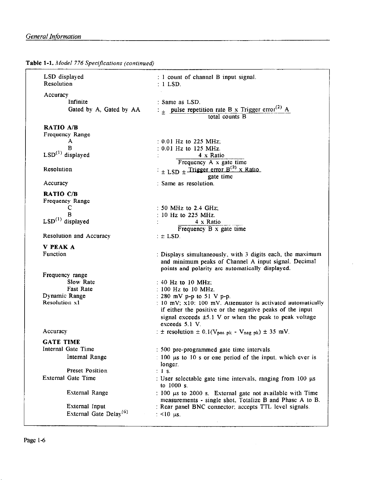
LSD displayed
Resolution
Accuracy
Infinite
Gated by A, Gated by AA
RATIO AIB
Frequency Range
A
B
LSD(‘) displayed
Resolution
Accuracy
RATIO C/B
Frequency Range
C
B
LSD(‘) displayed
Resolution and Accuracy
776
Specifications (continued)
: 1
count
of channel B input signal.
: 1 LSD.
: Same as LSD.
: * pulse repetition rate B x Trigger error(2) A
total counts B
: 0.01 Hz to 225 MHz:
: 0.01 Hz to 125 MHz.
4 x Ratio--__
Frequency A s gat;z:‘”
: + LSD ,Trieeer B x Ratio
gate time
: Same as resolution.
: SO MHz to 2.4 GHz;
: 10 Hz to 225 MHz.
4 s Ratio
Frequency B s gate time
: k LSD.
V PEAK A
Function
Frequency range
Slow Rate
Fast Rate
Dynamic Range
Resolution xl
Accuracy
GATE TIME
Internal Gate Time
Internal Range
Preset Position
External Gate Time
External Range
External Input
External Gate Delay(‘)
: Displays simultaneously. with 3 digits each, the maximum
and minimum peaks of Channel A input signal. Decimal
points and polarity are autotiaticallg displayed.
: 40 Hz to 10 MHz:
: 100 Hz to 10 MHz.
: 280 mV p-p to 51 V p-p.
: 10 mV: x10: 100 mV. Attenuator is activated automalically
if either the positive or the negative peaks of the input
signal exceeds fS.l V or when the peak to peak voltage
exceeds 5.1 V.
: + resolution i O.l(Vpas pli - Vneg & * 35 mV.
: 500 pm-programmed gate time intervals.
: 100 ps to 10 s or one period of the input. which ever is
longer.
: 1 s.
: User selectable gate time intemals. ranging from 100 ps
to 1000 5.
: 100 ps to 2000 s. External gate not available with Time
measurements - single slmt. Totalize B and Phase A to B.
Rear panel BNC connector: accepts TTL level signals.
j cl0 ps.
Page l-6
Page 17
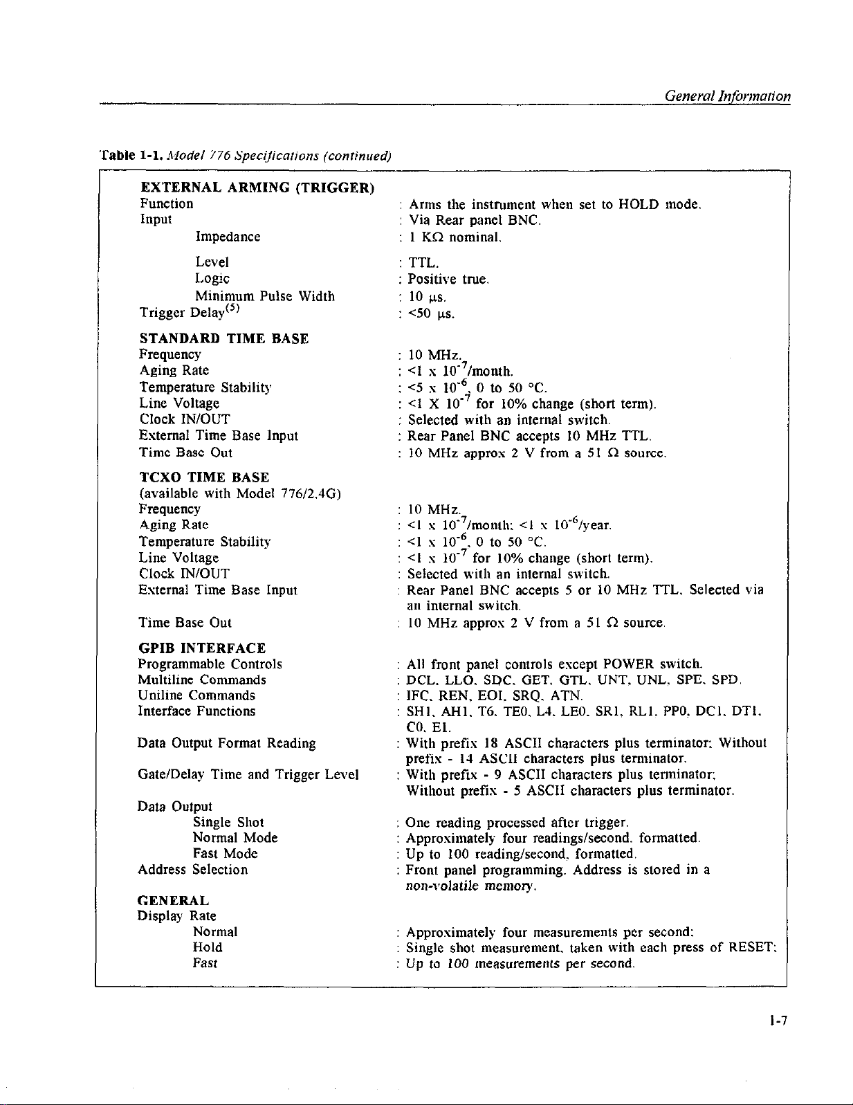
Table l-l. A,fodel 776
EXTERNAL ARMING (TRIGGER)
Function
I”PUl
Impedance
.Speci@?tions (continued)
Arms the instrument when set to HOLD mode
Via Rear panel BNC.
1 KC2 nominal.
Level
Logic
Minimum Pulse Width
Trigger Delay(‘)
STANDARD TIME BASE
Frequency
Aging Rate
Temperature Stabilit)
Line Voltage
Clock IN/OUT
External Time Base Input
Time Base Out
TCXO TIME BASE
(available with Model 776/2.46)
Frequency
Aging Rate
Temperature Stability
Line Voltage
Clock IN/OUT
External Time Base Input
Time Base Out
GPIB INTERFACE
Programmable Controls
Multiline Commands
Uniline Commands
Interface Functions
Data Output Format Reading
Gate/Delay Time and Trigger Level
Data Output
Single Shot
Normal Mode
Fast Mode
Address Selection
GENERAL
Display Rate
Normal
Hold
Fast
TTL.
Positive true
10 ps.
<SO ps.
10 MHz.
<I s IO-‘/month.
<5 s 10’6 0 to 50 “C.
<I X 10.’ for 10% change (short term).
Selected with an internal switch.
Rear Panel BNC accepts 10 MHz TTL.
10 MHz appros 2 V from a 51 0 source.
10 MHz.
<I s lO~‘/month: <I x 10e6/year.
Cl s 10‘6. 0 to 50 “C.
<I s 10“‘for 10% change (short term).
Selected with an internal switch.
Rear Panel BNC accepts 5 or 10 MHz ‘ITL. Selected via
an internal switch.
10 MHz appros 2 V from a 51 n source.
: All front panel controls except POWER switch.
: DCL. LLO. SDC. GET. GTL. UNT. UNL> SPE. SPD.
: IFC. REN. EOI. SRQ. ATN.
: SHl. AHl. T6. TEO. L4. LEO. SRI, RLI. PPO. DCI. DTI.
CO. El.
: With prefix 18 ASCII characters plus terminator: Without
prefix - 1-t ASCII characters plus terminator.
: With prefix - 9 ASCII characters plus terminator;
Without prefix - 5 ASCII characters plus terminator.
One reading processed after trigger.
Approximately four readings/second. formatted.
Up to 100 reading/second. formatted.
Front panel programming. Address is stored in a
non-volatile memory.
Approximately four measurements per second:
Single shot measurement. taken with each press of RESET:
Up to 100 measuremeals per second.
Page 18
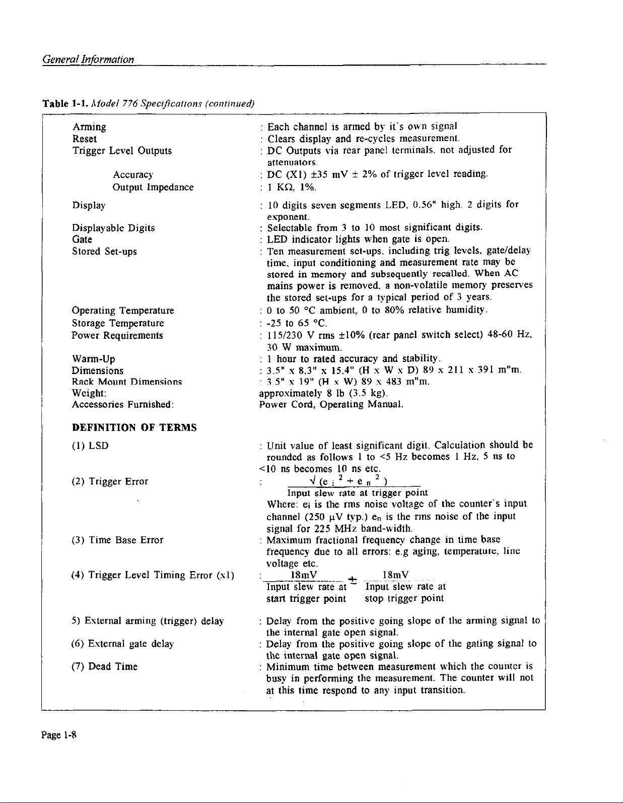
Table l-1.
Model 776 SpeciJiconons (continued)
Arming
Reset
Trigger Level Outputs
: Each channel is armed by it’s own signal
: Clears display and re-cycles measurement.
: DC Outputs via rear panel terminals. not adjusted for
attenuators.
Accuracy
: DC (Xl) *35 mV * 2% of trigger level reading.
Output Impedance : 1 KQ 1%.
Display
: 10 digits seven segtnents LED. 0.56” high. 2 digits for
exponent.
Displayable Digits : Selectable from 3 to 10 most significant digits.
Gate : LED indicator lights when gate is open.
Stored Set-ups : Ten measurement set-ups. including trig levels, gate/delay
time. input conditioning and measurement rate may be
stored in memory and subsequently recalled. When AC
mains power is removed. a non-volatile memory preserves
the stored set-ups for a typical period of 3 years.
Operating Temperature : 0 to 50 OC ambient. 0 to 80% relative humidity.
Storage Temperature
Power Requirements
: -25 to 65 “C.
: llY230 V rms &lo% (rear panel switch select) 48-60 Hz.
30 W maximum.
Warm-Up : I hour to rated accuracy and stability.
Dimensions
Rack Mount Dimensions
Weight:
Accessories Furnished:
: 3.5” s 8.3” s 15.4” (H s W s D) 89 s 211 s 391 m”m.
: 3.5” s 19” (H s W) 89 x 483 m”m.
approximately 8 lb (3.5 kg).
Power Cord, Operating Manual.
DEFINITION OF TERMS
(1) LSD : Unit value of least significant digit. Calculation should be
rounded as follows 1 to <5 Hz becomes I Hz. 5 ns to
cl0 ns becomes 10 ns etc.
(2) Trigger Error
d(ei*+On*)
Input slew rate at trigger point
Where: ei is the rms noise voltage of the counter‘s input
channel (250 pV typ.) en is the rms noise of the input
signal for 225 MHz band-width.
(3) Time Base Error
: Maximum fractional frequency change in time base
frequency due to all errors: e.g aging. temperature. line
voltage etc.
(4) Trigger Level Timing Error (xl)
:
18mV
_.~~ + ~?rnV
Input slew rate at - Input slew rate at
start trigger point stop trigger point
5) External arming (trigger) delay
: Delay from the positive going slope of the arming signal to
the internal gate open signal.
(6) External gate delay
: Delay from the positive going slope of the gating signal to
the internal gate open signal.
(7) Dead Time
: Minimum time between measurement which the counter is
busy in performing the measurement. The counter will not
at this time respond lo any input transition.
Page l-8
Page 19
l
Model 776 Programmable CounterfIimer with line
cord.
. Model 776 Instructions Manual.
If an additional manual is required, order:
. Keithley part number 776-901-00.
1-8. Specifications
Instrument specifications are listed in Table I-l. These
specifications are the performance standards or limits
against which the instrument is tested.
General Informnlion
NOTE
All specifications in the following
table apply after a warm-up period of
1 hour and at ambient temperature of
25Y f50C.
1-9
Page 20
Installation
2-1. Introduction
This section contain information and instructions necessary for the installation and shipping of the Model
776. Details are providedforpowerconnection. grounding safety requirements. installation information. and
x-packing instructions for storage or shipment.
2-2. Performance Checks
The instrument was carefully inspected for mechanical
and electrical performance before shipment from the
factory. It should be free of physical defects and in
perfect electrical order upon receipt. Check the instrument for damage in transit and perform the electrical
procedures outlined in Section 5. If there is indication
of damage or deficiency. see the warranty in this manual
and notify your local Keithley field engineering representative or the factory
CAUTION
It is recommended that the operator
be fully familiar with the specifica-
tions and all sections of this manual.
Failure to do so may compromise the
warranty and the accuracy which
Keithley has engineered into your instrument.
2-3. Power Requirements
The instrument may be operated from any one of the
following sources: a. 103.5 to 126.5 Volts (1 IS Volts
nominal) b. 207 to 253 Volts (230 Volts nominal).
The instrument operates over the power mains frcquency range of 18 to 63 Hr. Always verify that the
operating power mains voltage is the same as that specified on the rear panel voltage selector switch.
CAUTION
Failure to switch the instrument to
match the operating line voltage will
damage the instrument and may void
the warranty.
The instrument should be operated
from a power source with its neutral
at or near ground (earth potential).
The instrument is not intended for
operation from two phases of a
multi-phase ac sqstcm or across the
legs of a single-phase. three-wire ac
power system. Crest factor (ratio of
peak voltage to rms) should be typi-
cally within the range of 1.3 to I.6
at 10% of the nominal rms mains
voltage.
24. Grounding Requirements
To insure the safety of operating personnel. the U.S.
O.S.H.A. (Occupational Safety and Health) rcquirement and good engineering practice mandate that the
instrument panel and enclosure be “earth” grounded.
All Keithley instruments are provided with an Uuderwriters Laboratories (U.L. and V.D.E) listed lhrec-conductor power cable. which when plugged into an appropriate power rcceptaclc. grounds the instrument.
2-l
Page 21
The long offset pin on the male end of the power cable
carries the ground wire to the long pin of the receptacle
on the rear panel of the instrument.
CAUTION
To avoid operator shock hazard do
not exceed the power mains voltage
frequency rating which limits the
leakage current between case and
powr mains. Never expose the instrument to rain. excessive moisture,
or condensation.
2-5. Installation And Mounting
tective covering such as a plastic bag or strong krali
paper. Place power cable and other accessories with
the instrument. Store the cowred voltmeter in a clean
dry area that is not subject to extreme temperature varta&s or conditions which may cause moisture to condense on the instrument.
2-10. Long Term Storage Or
Re-Packing For Shipment
If the instrument is to be stored for a long period or
shipped. proceed as directed below. If you have any
questions ccmtact your local Keilhley field engineering
representative or the Keithlcy Scwice Department at
the factory.
The instrument is fully solid state and dissipates only
a small amonnt of power. No special cooling is required.
However. the instrument should not be operated where
the ambient temperature exceeds 50°C. when the relative humidity exceeds 80% or condensation appears
anywhere on the instrument. Avoid operating the in-
strument close to strong magnetic fields which may
be found near high power equipment such as motors.
pumps. solenoids. or high power cables. Use care when
rack mounting to locate the instrument away from
sources of excessive heat or magnetic fields. Always
leave 1 cm (1.5 inches) of ventilation space on all
sides of the instrument.
2-9. Bench Mounting
The instrument is shipped with plastic feet. tilt stand
in place and ready for use as a bench or portable in-
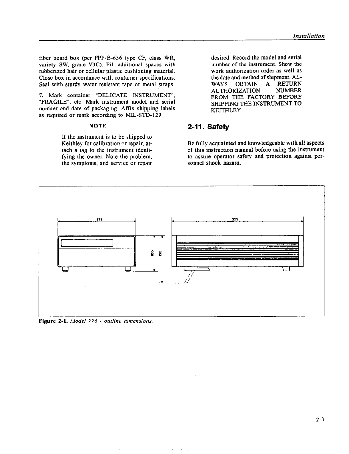
strument. See outline drawing Figure 2-l for dimen-
smns.
2-7. Rack Mounting
The instrument may be rack mounted in a standard 19
inch EIA rack. The instrument may be rack mounted
in Rack Mount Kit option Rack.
2-9. Portable Use
The instrument may be used in applications requiring
portability. A tilt stand consisting of two retractable
legs is provided with each unit.
2-9. Short Term Storage
If the instrument is to be stored for a short period of
time (less than three months). place cardboard over
the panel and cover the instrument with suitable pro-
If the original Keithley supplied packaging is to
be used proceed as follows:
1. If the original wrappings. packing material. and container have been saved. *e-pack the instrutnent and accessories originally shipped to you. If the original container is not wailablc. one may be purchased through
the Keithley Service Department at the factory.
2. Be sure the carton is well sealed with strong tape
or metal straps.
3. Mark the carton with the model number and serial
number with indelible marking. If it is to bc shipped.
show sending address and return address cm two sides
of the box: cover all previous shipping labels.
If the original container is not available. proceed
as follows:
1. Before packing the unit. place all accessories into
a plastic bag and seal the bag.
2. For extended storage or long distance shipping only.
use U.S. govermnent packing method II C and tape a
two-unit bag of desiccant (per MIL-D-3164) on the
rear cover.
3. Place a I3 cm (5 inch) by Xl cm (I2 inch) piece
of sturdy cardboard over the front panel for protection.
4. Place the counter into a plastic bag and seal the
bag.
5. Wrap the bagged instrument and accessories in one
inch thick flexible cellular plastic film cushioning material (per PPP-C-795) and place in a barrier bag (per
MIL-B-131). Extract the air from bag and heat seal.
6. Place bagged instrument and acccssorics into a 250
mm (10 inch) s 360 mm (I-I inch) s SO8 mm (20 inch)
2-2
Page 22
Installation
fiber board box (per PPP-B-636 type CF, class WR,
variety SW, grade V3C). Fill additional spaces with
rubberized hair or cellular plastic cushioning material.
Close box in accordance with container specifications.
Seal with sturdy water resistant tape or metal straps.
7. Mark container “DELICATE INSTRUMENT”,
“FRAGILE”, etc. Mark instrument model and serial
number and date of packaging. Affix shipping labels
as required or mark according to MIL-STD-129.
NOTE
If the instrument is to be shipped to
Keithley for calibration OT repair, attach a tag to the instrument identifying the owner. Note the problem,
the symptoms, and service or repair
desired. Record the mode1 and serial
number of the instrument. Show the
work authorization order as we11 as
the date and method of shipment. ALWAYS OBTAIN A RETURN
AUTHORIZATION
NUMBER
FROM THE FACTORY BEFORE
SHIPPING THE INSTRUMENT TO
KEITI-ILEY.
2-11. Safety
Be fully acquainted and knowledgeable with al1 aspects
of this instnxtion manual before using the instrument
to assure operator safety and protection against personnel shock hazard.
igure
2-l.
Model 776 - outline dimensions.
2-3
Page 23

lnstnllation
Notes
2-1
Page 24
3
Operating Instructions
3-I. introduction
Model 776 operation is divided into two general categories: basic bench operation. and IEEE-488 operation.
Basic bench operation. which is covered in this section.
consists of using the Model 776 to perform basic frequency. time. peak voltage. and phase measurements.
IEEE programming can also be used to greatly enhance
the capability of the instrument in applications such as
automatic test equipment. These aspects are covered in
details in Sections 3 and 1.
3-2. Front Panel Familiarization
The front panel layou1 of the Model 776 is shown in
Figure 3-l. The fionl panel is generally divided into
three sections: controls. conneclors. display and indicators. The following paragraphs describe the purpose of
each of these items in details.
3-2-l.
All the front panel controls escepc [POWER] are mo-
mcntarv contact switches. Many controls include an
annu&ator light to indicate the selected mode. Controls which do not have an annunciator ligh1. when
pressed. will cause an immediate reaction on the dis-
play. The con1roIs arc dbided into func1ional groups for
easier operation. Front panel controls are divided to 1he
following functional groups: Power. Mode. Funclions.
Display Modifiers. and Inpu1 Setting.
1. POWER The [POWER] witch controls the AC
power to the instrument. Pressing and releasing the
Controls
switch once turns the power on. Pressing and rclcasing
the switch a second time turns 1hc power off.
2. MODE. There are two push-buttons in the MODE
section: [CLRLCL] (clear/local). and [ZndlEXEj
(second/execute). The [2nd] push-button is used to se-
lect secondary functions. Normally. the secondary functions are marked below the push-buttons. To help distinguish between normal and secondary functions. all
secondary funclions are prin1ed in yellow. Pressing the
[2nd/EXE] push-button will cause the instrunlcnl to
display the following reading:
2nd ?
The reading is blinking indicaling lhat the counlcr is
ready for a conscqucnt press of anolhcr push-bulton
which was assigned a second function. Pressing the
[2nd/EXEj push-button again will res1ore normal op
eration. The [CLR/LCL) push-bulton when pressed.
and the instrument nas in remote operation (bu1 not in
remote lockout condition LLO). restores local operation. When
this push-bulton clears the display and arms the counter
for the next n1casurcn1cn1 cycle.
3. FUNCTION. The 1hree FUNCTION push-buttons
control the 1ype of measurcmcnt. Each push-button is
used IO select one of three functions.
FREQ. - The FREQ push-butlon places the instrument in one of three frcqucocy ntcasurcn~cnt functions:
Frequency A. Frequency B or Frequency C. Consccutive pressing of the [FREQJ push-butlon uill toggle
the
instrumen1 is in local operation. pressing
3-1
Page 25
MODE
FUNCTION
between frequency A. Frequency l3 and Frequency C
functions.
TIME - The TIME push-button sets the Model 776
up to measure one of three time
measurement
functions:
Period A. Pulse A or Time Intenxl A to B. Consecutive
pressing of the [TIME] push-button will toggle be-
tween these three functions.
RATIO -The RATIO push-button places the inslm-
ment in one of three ratio measurement functions: To-
talize B (infinite. gated by A. or gated by AA). FRQlB
(C/B or A/B). or Phase A relative to B. Consecutive
pressing of the [RATIO] push-button will toggle betwcen Totalize B. FRC$B. and Phase A to B functions.
1. DISPLAY/MODIFY. The two DISPLAY/MODIFY
push-buttons modify the display from normal frequency. time or ratio reading to another reading such as
trigger level. gate time. totalize mode. V peak mode. or
delay time.
5. INPUTS. There are 5 push-buttons at the INPUTS
section. These buttons select functions which ad.iust
input signal properties before it is applied to the actual
input. Push-buttons control attenuation. coupling.
slope. input impedance. and low pass filter to suppress
high frequency noise.
6. VERNIER. The two push-buttons in the VERN!ER
section are used as a digital potentiometer. The VERNIER operates in conjunction with the following functions: Trigger leyel. Gate time. Dela! time. Digits. Address. Totalize mode. Vpeak mode. Analog out. and
Offset. The two push-button also set these parameters
to a pm-set position.
7. SET-UPS. There are tn’o push-buttons in the SETUPS section One is used to slorc a complete front panel
set-up. The other button is used to recall a stored set-up.
3-2-2 Connectors
The connectors arc used to connect the Model 776 to the
unknown signal.
1. CHANNEL A. The CHANNEL A connector is used
\\hen making mcasurcmcnt which arc related to channel A.
2. CHANNEL B. The CHANNEL B connector is used
when making measurements which are associated with
channel B.
3. CHANNEL C. The CHANNEL C connector is used
for high frequency measurements. up lo 2.7 GHz with a
50 fi input impedance. Although this terminal is alva!~s
installed. the internal circuitq to operate this function
is optional and ma: not be installed cm your model.
NOTE
If front panel connectors are present
on a Model 776/2.4G/R unit. they are
not functional.
3-2-3. Display And Indicators
1. DISPLAY. The function of the display is to shou the
result of the processed mcaswcmcnt. The display con-
sists of a 10 digit mantissa and a single digit csponcnt.
3-2
Page 26
The exponent uses a leading minus to indicate negative
values. The sign on the exponent changes to + for zero
or positive values. The display is also used to indicate
information other than the measurement such as the gate
time or the trigger level.
2. INDICATORS. There are 30 indicators located on
the front panel. The indicators are used to point at a
selected function or signal to the user that the instrument is set to a special function like auto trigger or
remote operation.
33 Rear Panel Familiarization
Figure 3-2 shows the rear panel layout of the model 776.
3-3-l. Connectors and Terminals
1. AC RECEPTACLE. Power is applied_ through the
supplied power cord. to the 3-terminal AC receptacle.
Note that the selected power supply voltage is marked
on the rear panel above the line voltage selector switch.
2. LINE SWITCH. The LINE VOLTAGE SELECTOR
switch selects one of the primary voltage which are
marked on both sides of the switch
3. LINE FUSE. The line fuse provides protection for
the AC power line input. For information on replacing
this fuse. refer to Section 5.
4. IEEE-188 CONNECTOR. This conneclor is used
to connect the instrument to the IEEE-488 bus.
5. TRIGGER LEVEL OUTPUTS. Tbesc three lerminals are used for monitoring. by an external DMM or
oscilloscope. the DC voltage coming from channels A
and B trigger level circuits.
6.
CLOCK. This BNC connector is used to output tbe
internal clock as a reference to another instrument. The
same input may be connected to an external reference.
The function of this input/output is marked above the
connector.
7. EXTERNAL ARMING/GATE/DELAY. A BNC
connector which may receive one of three signals: arming pulse. external gate signal or external delay pulse.
This input is useful when gate or delay times other then
the internal times are required. or to take one reading
with model 776 in synchronization with other cquipment.
8. CHANNEL A, CHANNEL B, CHANNEL C (Not
shown). These connectors. only present on a Model
776/2.4GIR. are used to connect the “nil to the unknown
signal. Iffront panel connectors are present. they are not
functional.
34. Power-Up Procedure
The basic procedure of powering up the Model
described below.
716
is
Figure 3-2.
Rear Panel Cormecrors and Tenninnls.
3-3
Page 27
operating InstrmYions
1. Connect the female end of the power cord to the AC
mains receptacle on the rear panel. Connect the other
end of the power cord to a grounded AC outlet.
CAUTION
Be sure the power line voltage agrees
with the indicated value on the rear
panel of the instrument. Failure to
heed this warning may result in instrument damage.
WARNING
The instrument is equipped with a
3-wire power cord designed to be
used with grounded outlets. When the
proper connections are made. the instrument chassis is connected to the
power line ground. Failure to use a
properly grounded outlet may result
in personal shock hazard.
2. Turn on the power by pressing and releasing the
POWER switch on the front panel.
3. The instrument will then begin operation by performing a display and indicator test which takes approsimately one second. All mode and IEEE indicators will
turn on and the display will appear as follows:
4. To verify that all display segments are operating.
compare the instrument’s display with the above during
the test.
7. following the software re\-ision level. the instrument
will display the previously selected IEEE primary address which is set through front panel programming and
stored in the non-volatile memoty. For example. with
the rear panel witch set to address 25. the display will
show:
IE Adr 25
8. Following these display messages. the instrument
will go into the normal operating mode and begin displaying readings. The instrument will bc set to the
previously programmed front panel set-up.
3-5. Software Reset
One. who is not yet fully familiar with the front panel
operation of the Model 776. may find himself locked in
a “dead-end” situation where nothing operates the way
it should. The fastest way to restore the counter lo a
known condition is by resetting the instrument’s software. This can be done by pressing the [tnd/EXEJ
push-button and then pressing the [DCLl push-button
(second function to the [CLRlLCLl push-button). The
instrument will be then be set to it‘s factory selected
default. Table 3-1 summarizes these defaults.
NOTE
Software reset has no effect on any of
the front panel set-ups which were
previously stored in the mcmoty loca-
tions 0 through 9. The software reset
also has no effect on the programmed
GPIB address.
5. Following the display test. the instrument proceeds
by displaying the options installed. When no option is
installed. the instrument will display the following mes-
sage:
776
If option 2.1G (2.1 GHz C Channel input + TCXO) is
installed. the instrument will display the following rnessage:
776-2.16
6.
Once the model number and the installed options are
displayed. the instrument will perform ROM and RAM
tests. If all these tests are passed. the display will shon
the software revision level for about I second similar to
the example below:
SoFt 1.1
3-6. Display Messages
The Model 776 has several display messages associated
with basic front panel opcralion The instnuncnt has
also a few front panel indications that flag front panel
programming error. These messages are discussed in the
following. Note that the instrument has a number of
additional display messages which are associated with
IEEE-488 programming.
3-6-l. IEEE-488 Error Messages
The counter incorporates a number of display messages
which are associated with errors made through the GPIB
interface. These messages are discussed in detail in
Section 4 of this manual. However. there is one message
which should be esplaincd at this point because it may
interfere with normal front panel operation A remote
enable or a device dcpcndent command. sent to the
counter through the bus. turns on the REMOTE light
Page 28
FUNCTION
Function
Display/Modify
Gate/Delay Time I.0 s
Trigger Levels A & B 0.00 v
Coupling DC
Slope
Attenuators
Filters Off
impedance lMX2
Averaging
Auto Trigger
Delay Off
Sampling Rate
Ratio Mode A/B
V Peak A
Totalize Mode
Displayed Digits
IEEE Status Local
Note: The Model 776 and 776/2,4G/R have a default gate time of I second. The Model
776/2.4G/R has a default gate time of IOOms.
___~~~~~~DEFAULTSTATE~~.~~~~~_
Frequenn A
Normal reading
Positive going
off
Off
Off
Normal - 3 reading/s
Rate Fast
Infinite
10
1. Any two front panel push-buttons are pressed simul-
taneously except the two [VERNIER] push-buttons.
2. The instrument is in FREQ or RATIO or TIME AVG
function and the operator attempts 10 turn the delay on.
3. The instrument is in FREQ or RATIO function and
the operator attempts to turn the AVG function on.
4. The instrument is in rcmolc condition (REMOTE
LED on) and any front panel push-button except
[CLR/LCL] is pressed.
5. The [VERNIER] push-buttons were pressed and the
instrument was not in DISPLAY/MODIFY mode of
operation.
6. The instrument was in DISPLAY/MODIFY tnode of
operation and the [VERNIER fi] or [VERNIER u]
push-buttons were pressed continuously until a parameter limit was reached. Parameter limits are summarized
in Table 3-2.
2. GATE ERROR. The gate error is indicated on the
front panel by the GATE LED. This error will occur
when the counter is in FREQ or TIME AVG function
and when the signal was removed from the input connector in the middle of the measurement process or
when a radiated random noise was sensed by the input
circuitry. The GATE LED will then blink once but no
result will be registered on the display.
Table 3-1.
and enables remote operation. In this case. all front
panel push-buttons. except [LCLJ. are disabled. An
attempt to press one of these push-buttons will cause the
following message to be displayed:
This message indiiates that the inswument will ignore
any front panel programming scquencc unless the
[CLRlLCL] push-button is pressed and the REMOTE
light turns off.
Dejiiult Stntcs After Sojiivnre Reset
PrESS LcL
3-6-2. Error Indication
There are several error indications that are caused bj
either an incorrect front panel programming or insufficient input level conditioning which is otherwise required by the instrument for normal signal processing,
These indications are either visible (blinking LED) or
audible (beeper) and are described in the following.
1. AUDIBLE ALARM. The AUDIBLE ALARM will
sound when attempting an incorrect sequence of front
panel programming. This could occur under the following conditions:
3. GATE TIME ERROR. The gate time error is indicated on the front panel by the GT LED. The gate time
erroroccurs in FREQ or TIME AVG functions when the
period of the input signal is larger than the period of the
gate time. The gate error will also occur in Phase A to
B functiou when the gate time is no1 sufficient to permit
the minimum resolution of 1 degrees. When one of the
conditions above occurs. the gate time LED (GT) will
blink for a couple of times and then resume a search
routine. This sequence will rcpcat itself until a proper
signal is found or until the gale time was readjusted to
satisfy the required conditions.
4. TRIGGER LEVEL ERROR. The trigger level error
occurs when the instrument is set to AUTO TRIG or V
PEAK A modes and the input signal is either absent or
below lhe specified auto trigger limils. The trigger level
LED (either TL A or TL B) then blinks. for a couple of
times. The counter 1hen resumes a new search routine.
This sequence will repeat itself until a signal has been
found or until the auto trigger mode was turned off.
3-7. Control Selection
Selecting the various from panel operating modes is
simply a matter of pressing. once or 1wice. the appropri-
ate push-button as dcscribcd in the following paragraphs.
3-5
Page 29

Opernting Instrlrctions
FRONTPANEL
NOMENCLATURE PA&+ETF.$.
TL A Trigger Level A
TL B Trigger Level B
GT
Gate Time
DLY Delay Time
DIGITS
No of displayed digits
ADRS GPIB address
Table 3-2.
Front Panel Progrmnnring Limits
3-8. Selecting A Function
The Model 776 must be set up. for the proper measuring
function. with one of the three Function push-buttons.
There are 17 different available functions in the FUNCTION block summarized in the following. To simplify
the operating instruction for these functions. the fuuctions are divided in the following table into three operational groups.
FUNCTIONS SUMMARY
Group 1
1. FREQUENCY A
2. FREQUENCY B
3. FREQUENCY C
4. PERIOD A
5. PULSE WIDTH A
6. TIME INTERVAL A TO B
7. PHASE A RELATIVE TO I3
Group 2
8. PERIOD AVERAGED A
9. PULSE WIDTH AVERAGED A
10. TIME INTERVAL A TO B AVG
Group 3
11. TOTALIZE B (infinitely)
12. TOTALIZE B GATED BY A
13. TOTALIZE B GATED BY AA
14. RATIO A/B
15. RATIO CIB
16. V PEAK A -FAST RATE
17. V PEAK A - SLOW RATE
The letter after the function indicates the input conuector where this measurement may be performed. For
-5.00
-5.00
100 ps
100 ps
3
0
+5.00
+5.00
100 s I USER GATE
100 s / USER DELAY
10
30
example. FREQUENCY C can only be measured if the
signal is applied to the C Channel input
COIUKX~OT.
Similarly, V PEAK A can only be measured at the
Channel A input connector. Some functions require that
both Channel A and B be connected for a successful
measurement - functions like Time Interval A to B.
Ratio FRQ/B. OT Totalize B by A.
Selecting a function from the first group is described
in the following:
1. First bring the Model 776 to a known state as de-
scribed in paragraph 3-5. This is done by pressing first
the [2nd/EXE] push-button and then pressing the
(DCL] push-button. The instrument will then defaull to
a factow pre-selected state and the light next FRQ A
will illuminate: indicatiug that Frcqucucy A function is
now selected.
2. To select Frequency B press the [FREQ] push-button
once. The light next to FRQ B illuminates: indicating
that Frequency B is now selected.
3. To select Frequency C press the [FREQ] push-button
again. The light next to FRQ C illuminates: indicating
that Frequent) C is noyI’ selected. Note that this proce-
dure assumes that option 52 (2.4 GHz C Channel is
installed).
1. To select Period A press the [TIME] push-button
once. The light next to PER A illuminates: indicating
that Period A is now selected.
5. To select Pulse A press the [TIME] push-button
again. The light uest to PLS A illuminates: indicating
that Pulse A is uow selected.
6. To select Time Intenal A to B press the [TIME1
push-button again. The light next to TI A to B illuminates: indicating that Time Intenxl A to B is no\\ sc&ted.
3-6
Page 30
7. To select Phase A re1atix.e to B press the [RATIO]
push-button again. The light next to Phase A to B illuminates: indicating that Phase A to B function is now
selected.
Select
a function from the second group as
described in the following:
8. To select Period Averaged A press the [TIME] pushbutton until the light nest to PER A illuminates. Press
the [2nd] push-button and then press the AVG. pushbutton (second function to the [TIME] button). Ob-
serve that the AVG light illuminates: indicating that the
Period Averaged A function is non selected.
9. To select Pulse Averaged A press the [TIME] pushbutton until the light next to PLS A illuminates. Press
the [2nd] push-button and then press the AVG. pushbutton (second function to the TIME button). Observe
that the AVG light illuminates: indicating that the Pulse
Averaged A function is now selected.
10. To select Time Interval Averaged A to B press the
[TIME] push-button until the light next to TI A to B
illuminates. Press the ]Znd] push-button and then press
the AVG. push-button (second function to the TIME
button). Observe that the AVG light illuminates: indicating that the Time Interval Averaged A to B function
is now selected.
This reading indicates that the instrument is set to Totalize infinitely. Now press the [VERNIER UP] pushbutton once and observe that the display reading is
changed to the following:
tot bY A
This reading indicates that the instrument is now set
to Totalize at B with A serving as the gating signal.
Press the [GT] push-button again. The instrument is
now ready to perform the required function.
13. To select Totalize B by AA function repeat the
procedure as described above. Pressing the [VERNIER
fi] push-button changes the display reading as follows:
tot bY AA
This reading indicates that the instrument is no% set
to Totalize. at B input. with a pair of consecutive tran-
sitions at A. having the same direction. seming as the
gating signal. Press the [GT] push-button again The
instrument is now ready to perform the required func-
tion.
14. To select Ratio A/B press the [RATIO] push-button
again. The light nest to FRQ/B illuminates: indicating
that Ratio A/B is no!v selected.
NOTE
The averaging function. once it is selected. will automatically turn on
whenever a TIME measuring function is selected. For example. Selecting PER A averaged turns the AVG
light on. Changing the selected function to FRQ A will automatically- turn
the AVG light off. Re-selecting one of
the TIME functions will automatically turn the AVG light on.
Selecting a function from the third group requires
additional operations and is described in the following:
11. To select Totalize B press the [RATIO] push-button
once. The light next to TOT B illuminates: indicating
that Totalize B is now selected.
12. To select Totalize B by A function press the [RATIO] push-button until the light next to TOT B illuminates. The counter is now set to totalize indefinitely.
To select the Totalize B by A function press the [GT]
(gate) push-button in the DISPLAY/MODIFY group
and observe that the reading on the display is as follows:
tot InF
15. To select the Ratio C/B function press the [RATIO]
push-button until the lighl nest to FRQ/B illuminates.
The counter is now set to measure Ratio FRQIB. To
select the Ratio C/B function press the (2ndj and [FRQ
SEL] (frequency select) push-buttons in sequence and
observe that the reading on the display change to display
as follows:
A to B
This reading indicates that the instrument is set to
Ratio A/B. Now press the [VERNIER fl] push-button
once and observe that the display reading is changed to
the following:
C to B
This reading indicates that the instrument IS now set
to Ratio C/A. Press the [2nd/EXE] push-bulton again.
The instrument is now ready to perform the required
function.
16. The V Peak A function has two measurcmcnt rates:
Fast - for frequencies above IO0 Hz and Slow - for the
range of 40 Hz to 10 MHz. Note that the inslrument.
after DCL defaults to its Fast ram. Selecting the measurement rate is described later in this mauual.
3-7
Page 31
Opernting Instnrctions
3-9. Selecting Gate And Delay Time
The Model 776 may be operated in its preset gate or
delay times of one second. or with one of its 500 built-in
increments. When selecting the gate time. the instrument will increment up or down. one gate time. each
time the [fi] or [u] push-button is pressed. The present
gate time may be noted oo the display by pressing the
[GT] push-button.
The gate times may only be selected in conjunction
with frequency. time averaged. ratio FRQ/B_ and Phase
A to B functions.
The gate time may be selected as follows:
1. Select a frequency measurement function.
2. Press the [GT] push-button. Obsewe that the GT light
turns on and that the instrument displays the following
message:
1.0
This reading indicates the selected gate time in sec-
onds.
3. To change the gate time press the [VERNIER fl] or
[VERNIER 111 push-buttons. Pressing the [I?] push-but-
ton increases the value of the gate time. Conversely.
pressing the [DOWN] push-button decreases the value
of the gate time. Depressing the [l?] or [u] push-buttons
for more than 1 second. causes the instrument to increment or decrement contirwously.
4. Pressing the [fil push-button and the instrument was
at a gate time of 100 seconds forces the instrument into
a USER GATE mode. This mode requires an external
gating signal. Operating the counter with an external
gate is explained later in this section.
5. Pressing the [l?l and [u] simultaneously changes the
gate time to a preset value of 1.0 second.
6. To resume normal display operation. press the [GT]
push-button. The GT light turns off and the instrument
is now ready to perform measurements with the newly
selected gate time.
NOTE
To prevent operator error. there is an
internal audible alarm that sounds
whenever a limit is reached. (e.g low
limit of 100 ps).
The sequence of selecting the delay time is similar to
the procedure for selecting the gate time. Delay times
may only be selected and applied to single shot (non-av-
eraged) time measurement. To select a delay time value
proceed as follows:
1. Select a single shot time measurement function such
as Period. Pulse Width. or Time Interval A to B.
2. Press the IDLY] push-button. The DLY light turns on
and the instrument displays the following mcssagc:
1.0
This reading indicates the selected delay time in
seconds.
3. To change the delay time press the [VERNIER 01 or
[VERNIER u] push-buttons. Pressing the [fi] push-button increases the delay time. Conversely. pressing the
[u] push-button decreases the delay time. Depressing
the [I?] or [u] push-buttons for more than 1 second.
causes the instrument to increment or decrement con-
tinuously.
4. Pressing the [fl] push-button and the instrument was
at a delay time of 100 seconds forces the instrument into
a USER DELAY mode. This mode requires an external
delay signal. Operating the counter with an external
delay is explained later in this section.
5. Pressing the [fl] and [u] simultaneously changes the
delay time to a preset value of 1.0 seconds.
6. To resume normal display operation. press the IDLY]
push-button The DLY light turns off and the instrument
is now ready to perform measurements with the newly
selected delay time.
3-10. Setting Trigger Levels
There are two trigger level push-buttons associatedwith
each Channel A (TL A) and Channel B (TL B). The
[VERNIER fi] and [VERNIER u] push-buttons. when
operated in conjunction with TL A or TL B. set
voltage level that will trigger the instrument. To set the
trigger levels proceed as follows:
NOTE
The procedure for setting the trigger
level is identical for Channels A and
B. Trigger level A (TL A) can only be
modified when functions that are re-
lated to input A are selected. e.g. FRQ
Al TIME A to B etc. Selecting a function which involves Channel B enables access to the TL B parameter.
1. Using the procedure which is described above. set the
instrument to Frequency A function. If other front panel
the
3-8
Page 32

lights illuminate, reset the counter using the software
reset procedure which is described in paragraph 3-5.
To set input condition controls for Channel A pro-
ceed as follows:
2. Press the ]TL A] push-button. Observe that the TL A
and VOLTS indicators turn on and that the display reads
as follows:
0.00
This reading indicates the selected trigger level in
units of volts.
3. To set a positive trigger level press the [VERNIER
fi] push-button. Holding in the [I?] or [u] push-buttons
for more than I second. causes the instrument to increment or decrement continuously. To set a negati\:e trig-
ger level press the [VERNIER u] push-button until the
desired level has been reached.
NOTE
Pressing the [VERNIER fl] or [VERNIERU] push-buttons. when the lim-
its of +5.00 or -5.00 respectively have
been reached. causes
alarm to sound.
4. Simultaneously press the two [VERNIER] push-buttons and note that the display reading resets to 0.00.
5. Press the [TL A] push-button. The indicator light
turns off and the instrument returns to its previous
measurement state.
6. To set the trigger level for both Channels A and B.
select a function which involves both inputs (eg ratio
A/B. Phase A to B. time intenjal A to B or totalize B by
A). Pressing the [TL] push-button once turns the TL A
light on: indicating that the instrument displays the
trigger level for Channel A. A second consecutive press
turns the TL B light on: indicating that the instrument
displays the trigger level for Channel B. A third push
turns TL B light off. The instrument then resumes its
normal operation.
an
audible
3-11. Setting Input Conditioning
Controls
A proper set-up of the input controls ensures proper
operation of the instrument. There are five push-buttons
which control the input. These push-buttons are common to both Channels A and B.
Changing one of the input setting controls is simply
a matter of pressing the required push-button. There are
5 lights for each input channel which are associated with
each of the five controls.
1. Set the instrument to operate al one of the following
functions: FRQ A. PER A. PLS A. or V Peak A.
2. To select the required coupling mode press the [AC]
push-button. Instrument is dc coupled when the AC
light is off. When the AC light is on the instrument is
ac coupled.
3. To change the slope that the instrument will trigger
on. press the [SLOPE] push-button. The counter triggers on a positive going edge if the slope light is off. If
the slope light is on the counter triggers on a negative
going edge.
4. Attenuation is required when the inpur signal exceeds
the specified dynamic range. To attenuate the signal
press the [x10] push-button, The input signal is allenuated by a factor of 10 when the x10 light is on. When
the x10 light is off. the input signal is not attenuated.
5. In low frequency applications. where the frequency
range is below 100 KHz. it is recommended to use the
low pass filter. The low pass filter attenuales the high
frequency components which may interfere with the
required measurement. To apply a low pass filter press
the [LPF] push-button. High frequency signals are filtered when the LPF light is on. The filter is deactivate
when the LPF light is off.
6. In high frequency applications above 1 MHz. or high
slew rate signals. it is rccommcnded that the input cable
be terminated with 50 R at the counter end. To change
the input impedance from 1 Mn to 50 n press the 150
n] push-button. Input is termination with 50 0 when
the SO Cl light is on Input impedance is I MCI when the
50 0 light is off.
To set input condition controls for Channel B pro-
ceed as follows:
1. Set the instrument to operate in one of the following
functions: FRQ B or TOT B.
2. Use the same procedure as described above for Channel A.
To set input condition controls for both Channcl~ A
and B proceed as follows:
1. Set the instrument to operate in one of the following
functions: Time Interval A IO B. Ratio FRQ/B. Phase A
to B. TOT B by A. or TOT B by AA.
2. To select the AC coupling mode for Channel A. press
the
[AC]
push-button once. The AC A lighl illuminates:
3-9
Page 33

indicating that Channel A is now ac coupled. Pressing
the [AC] push-button again turns the AC A light off but
AC B light turns on: indicating that Channel A is dc
coupled and Channel B is ac coupled. Pressing the
button once more. turns both AC A and AC B light on:
indicating that both channels arc now ac coupled.
Pressing the same push-button again turns both lights
off. This now indicates that both channels are set to dc
coupling mode.
3. Use the same procedure to set the slopes. attenuation.
impedance and filtering.
processed measurement with the programmed number
of digits.
NOTE
Selecting five
instead of ten. will eliminate the five
least significant digits and will move
the entire display to the right by five
places. An example of a normal display reading. and the same display
reading with five digits of resolution
is given as follows.
digits
to be displayed.
3-12. Selecting The Number Of
Displayed Digits
A major advantage of Model 776 over similar products
is its capability to display a fixed number of digils
regardless of the frequency of the input signal. For
example. with one second of gate time. the Model 776
displays a minimum of 10 digits. This however. may
turn into a disadvantage when measuring the frequent)
of a relatively unstable signal: in which just the most
significant digits are stable and the least significant
digits are “jumping around” with no significant meaning. Model 776 permits truncation of the unstable
significant digits. while still preserving its full performance. To select the number of displayed digits proceed
as follows:
1. Press the [2nd] push-button. Observe that the instrument prompts the following message:
2nd ?
2. Press the [DIGITS] push-button (second function to
]AC A]). The instrument now displays the following:
xx diGit
Where s is the selected number of digits and could range
from 03 to IO digits.
3. Use the [VERNIER fi] to increase the number of the
displayed digits. Conversely. press the [VERNIER u]
to decrease this number.
4. Pressing the [VERNIER ft] and [VERNIER u]
simultaneously. presets ss to IO: indicating that results
will be displayed with up to IO digits of resolution. and
that no digit will be truncated.
5. To return to normal operation of the Model 776
simply press and release the [EXE] push-button (second
function to [2nd]. The instrument than displays the
least
Display reading w~ith IO digits:
1.234567890
Display reading with selected 5 digits:
1.2345
NOTE
Under certain conditions. Model 776
may display frequency reading with
less than ten digits. This may occur
when the selected gate time is smaller
than 1 .O second. In that case. the instrument overrides the programmed
pm-selected number of digits and displays only as many digits as it can.
When gate time is increased. Model
776 again limits the number of dis-
played digits to the selected value.
3-13 Selecting Measurement Rate
Model 776 offers a choice from three measurement
rates. Two measurement rates are accessible through
front panel programming - normal rate (about 3 readings
per second). and single shot (hold). A fast measurement
rate (up to IO0 reading per second) is also available but
is only accessible from the GPIB interface. The fast
measurement rate will be discussed in details in Section
4. The HOLD light determines front panel measurement
rate. When the indicator is off. the instrument is in its
normal measurement rate. When the HOLD light is on.
the instrument is set to single shot measurements. To
select the measurement raw proceed as follows:
1. Press. in sequence. the [ZndlEXE] and the [HOLD]
push-buttons (second function to IRATIO]). The
HOLD light turns on: indicating lhat the instrument is
now~ armed for a single-shot measurement cycle. Arming is explained later in this chapter.
3-10
Page 34

2. To return to normal measurement rate. press. in se-
quence.
[HOLD]
the
[2ndlEXE]
push-button and then the
push-button. The HOLD light turns off: indicating that the instrument is now ready to accept and
process readings at its normal rate.
3-14-2 Front Panel Arming
Front panel arming is performed with the
button. To use front panel arming proceed with the
following steps:
[CLR]
push-
NOTE
Measurement rate is gate time dependent. Model 176 can process 3
readings in one second when its gate
time is set to below 300 ms.
3-14 Arming
Capturing the required sequence of input signals may.
at times. create a major problem for the design engineer.
Imagine a single source that repeatedly generates bursts
of signals having various repetition rates. pulse widths.
and number of pulses. It would be next to impossible to
measure such parameters along the time axis unless the
counter is prepared for this task. Model 776 has arming
capabilities which permits such complex measurements. Do not confuse arming with Trigger. Model 776
may not be triggered. Model 776. unless armed. will not
perform the task of signal processing. Model 776 may
be armed (prepared) for the next measurement in four
ways:
1. Continuously armed by an input signal. when Model
776 is set to its normal mode of operation.
2. With front panel
ment is set to HOLD mode.
3. With an arming pulse applied to the rear panel EXT.
INPUT connector. when the instrument is in the HOLD
mode.
1. With commands given over the IEEE-488 bus as
described in Section 4. This section covers front panel
and external arming in details.
3-14-1 Continuous Arming With the
Input Signal
When no special arming mode was selected. Model 776
is armed by its input signal. This means that with no
legal input signal, the counter idles. The Gate indicator
is off until the first transition. at the input connector. is
sensed. An input signal. within the dynamic range.
initiates a measurement cycle. The gate light blinks
every time that the internal gate opens. There is no
special procedure to set the Model 776 up for continu-
ous arming. This mode is especially useful in analyzing
the contents of a burst.
[CLR]
push-button. when the instru-
1. Using the procedure described in paragraph 3-13.
select the hold mode. Obsewe that the HOLD light turns
on and that the gate light ceases from flashing: indicating that the instrument is in its one-shot measurement
mode. The display zeroes and no reading is processed
until an arming stimulus is applied.
2. To arm the instrument for a single reading. press and
release the
[CLR]
push-button. The nest transition at
the input connector will cause the gate to open. The
instrument then checks for the legality of the input
signal. processes the reading and displays the result on
the display. The display will retain the last processed
reading until cleared, re-armed. or until another function is selected.
3. To arm the instmment for a new measurement. press
the
[CLR]
push-button. Obsewe that the display zeroes
sod that a new measurement cycle is initiated.
4. To remove the instnunent from its one-shot arming
mode. turn the hold fuoctionoff by pressing in sequence
the [2nd] and
[HOLD]
push-buttons.
3-143 External Arming
External arming operates much like front panel arming
except for the arming stimulus itself. In this case the
arming stimulant is applied to the rear panel EXT. INPUT connector. The arming pulse must conform to TTL
levels. To use the external arming feature. proceed as
folloas:
1.
Using the procedure described in paragraph 3-13.
select the hold mode. Observe that the HOLD light turns
on and that the gate light ceases from flashing: indicating that the instrument is in its one-shot measurement
mode. The display zeroes and no reading is processed
until an arming stimulus is applied.
2. Connect the external arming source to the rear panel
EXT INPUT connector. The first positive going transition at the EXT INPUT connector arms the Model 776
for taking and processing the nest available signal.
Note that after each positive going transition of the
arming signal. the numeric display is set IO read zero
until the next data is processed and displayed. Model
776 ignores any transitions at the EXT INPUT
tar
when the gate is open.
connec-
3-l I
Page 35

3. To remove the instrument from its one-shot arming
mode, turn the hold function off by pressing in sequence
the [2nd] and [HOLD] push-buttons.
3-15. Using Auto Trigger Level
The auto trigger level function is extremely useful when
measuring repetitive signals having an unknown dc
component. The auto trigger is capable of finding the
peaks of the signal and then setting the trigger level
exactly at their center. In addition. The auto trigger
automatically sets the correct attenuation and adjusts
the input signal to fit within the dynamic range. The auto
trigger mode does not operate on totalize B and fre-
quency C functions. Auto trigger level function works
independently in conjunction with Channels A and B.
To set the Model 776 to operate in auto trigger mode
proceed as follow:
1. Press in sequence the
(second function to [TL A])push-buttons. Observe that
the AUTO TRIG light illuminates: indicating that the
auto trigger function is selected. When the indicator is
off. the instrument is in its normal manual trigger level
mode.
2. Apply the signal to be measured to the appropriate
input connector. After a short search sequence. the gate
opens and the measurement is processed.
3. TL A or TL B lights blink if an error was detected.
Refer to paragraph 3-6-3 for a additional error indica-
tions information.
[2nd]
and the
[AUTO
TRIG]
0.00 0.00
The three
amplitude.
digits on the left indicate the lower peak
The right three digits indicate the higher
peak amplitude. Negative values have a leading minus
sign where positive values have no sign. The minus sign
and the decimal points are automatically set by the
instrument.
2. To select the measurement rate press the
[CT]
push-
button in the DISPLAY/MODIFY group and obscrvc
that the reading on the display is as follows:
FASt
This reading indicates that the instrument is set to its
fast measuring rate.
Now
press the
[VERNIER fi]
push-
button once and obsene that the display reading is
changed to the following:
SLO
This reading indicates that the instrument is set to
measure the V Peak A with its slow measuring rate.
Press the [GT] push-button again. The instrument IS
now ready to perform the required function.
3. Press the [GT] push-button to return the counter to
normal V Peak display.
4. Press one of the FUNCTION push-buttons to select
another function. Observe that the display returns to
normal display reading and that the VOLTS light turns
off.
4. To return the Model 776 to normal trigger level mode.
press in sequence the
[2nd]
and the [AUTO TRIG]
push-buttons.
3-16. Using V Peak A
The V PEAK A function turns the Model 776 into a
versatile RF peak voltage meter where both lou and
high peaks are detected. processed and displayed. This
is especially useful in analyzing both the amplitude and
the dc component of an unknown signal. Their are two
available measurement rates for the V Peak function:
Fast for normal measurements abol-e IO0 Hz. and slow
rate for measurements of signals belox\ 100 Hz. To
select the V Peak A function proceed as follows:
1. Press in sequence the [2nd] and the
function to [FREQ]) push-buttons. Obseme that the
VOLTS light illuminates. This indicates that the instrument is now set to V Peak A measurements. The normal
display reading is transform into a two section display
like the following:
3-12
[V PK A]
(second
3-17. Using User Gate
The User Gate is useful when a gate time other than the
internal pre-determined gate times is rcquircd. The limits which must be observed are the mininwtn limit of
100 yS and the maximum limit of IOOO s. The User Gate
function is accessible in FRQ A. B and C. FRQIB. PER
AVG. PLS AVG. and TI AVG A to B operating modes.
To operate the instrument in its User Gate mode proceed
as follows:
1. Set the instrument to PRQ A. Press the
button once. 0bsen:e that the Gate light turns on, and
that the instrtunent displays the gate time.
2. Press and hold the
[VERNIER
n] push-button and
obsense that the display increments. Afler the 100 s gate
time the instrument enters the User Gate mode and
displays the following readout:
USEr GAtE
[GT]
push-
Page 36

Depressing the
[VERNIER
fi] push-button after the
usergate is displayed causes an audible alarm to sound.
3. Press the
[CT]
push-button. The Gate light turns off
and the instrument is now ready to perform measurements with an external gate time.
6. To return to normal operation depress in sequence the
[2nd] and the
]GT/DLY]
push-buttons. The DELAY
light turns off: indicating that the instrument will no
longer delay the closure of its gale.
NOTE
4. Apply an external TTL pulse to the rear panel EXT
INPUT connector. This signal now serves as the esternal gate time. The high level duration of the external
pulse determines the period of the gate time.
5. To exit the User Gate function press the
u] push-button. Pressing both the
[VERNIER
u] push-buttons presets the displayed gate
[VERNIER
[VERNIER
fi] and
time to 1 .O 5.
3-18. Using Delay
The Model 776 has a delay function which inhibits the
closure of the opened gate for a pre-determined period.
This function is very useful in burst measurements.
relay open/close time measurements where bounce time
should be eliminated, and in measurements done on a
train of pulses. The delay function is accessible in PER
A. PLS A. and Time Interval A to B. The delay time ma)
be selected using the following procedure:
1. Set the instrument to [PER
push-button in the DISPLAY/MODIFY group. Obserw
that the DLY light turns on and that the instrument
displays the delay time.
2. To change the delay time. press the
[VERNIER
u] push-buttons. Whenone ofthe ]fi] or [u]
push-buttons are depressed for more than one second.
the instrument increments or decrements continuously.
3. Depressing simultaneously the
the
[VERNIER
u] push-buttons modifies the delay time
to a preset value of 1.0 s.
4. To resume normal display. press the
ton. The DLY light turns off. When enabled. the instrument performs measurements with the newly selected
delay time.
5. To enable the delay mode. press the [2nd] push-button and then the
[GTIDLY])
push-button. Obsewe that the DELAY light
[DELAY]
illuminates. This indicates that the instrument is now set
to operate in its delay mode. The delay light turns off
automatically when another function. other than from
those specified above. is selected. Conversely. return-
ing to one of the above functions restores the delay
mode.
A].
Press the
[VERNIER fi] or
[VERNIER
IDLY]
IDLY]
fi] and
push-but-
(second function to
To prevent operator’s error. there is
an internal audible alarm that beeps
whenever a limit is reached. (e.g 100
~5 low limit).
3-19. Using User Delay
The User Delav is useful when a delay time other than
the pre-determined delay times is required. The limits
which must be observed are the minimum limit of 100
ps and the maximum limit of 10.000 s. The User Delay
function is accessible in PER A, PLS A. and Time
Interval A to B operating modes. To operate the instrument in its User Delay mode proceed as follow:
1. Set the instrument to PER A. Press the IDLY] pushbutton once. Observe that the DLY light turns on. and
that the instrument displays the delay time.
2. Press and hold the [VERNIER n] push-button and
observe that the display increments. Afler the 100 s
delay time the instrument enters the User Gate mode and
displays the following readout:
USEr dLAY
Depressing the [VERNIER I?] push-button after the
user gate is displayed causes an audible alarm to sound.
3. To resume normal display. press the [DLY] push-button. The DLY light turns off. When enabled. the inslrument performs measurcmcnts with the user delay time.
4. To enable the user delay mode depress in sequence
the [2nd] and the [DELAY] (second function to
[GT/DLY]) push-buttons. Obsewe that the DELAY
light illuminates. This indicates that the instrument is
now set to operate in its User Delay mode. The delal
light turns off automatically when another function.
other than from those specified above. is selected. Conversely. returning to one of the above functions restores
the delay mode.
5. Apply an external TTL pulse to the rear panel EXT
INPUT connector. This signal now senzs as the ester-
nal gate time. Delay is then enabled as long as this input
is kept at TTL high level. The first negative transition
to TTL low disables the delay. The delay is then dis-
abled as long as this input is kept at TTL low level.
3-13
Page 37
Operating Instructions
3-20. Using Front Panel Set-Ups
Setting up all parameters in a versatile instrument such
as the Model 776 may takes some time. The set-up time
is even longer when more than one set-up is required.
Model 776 incorporates a battev backed-up non-volatile memory that preserves stored information up to
three years. It is possible to store complete front panel
set-ups in 10 different memory locations which are built
into the instrument especially for this purpose.
3-20-l.
First modify the front panel parameters as necessav to
perform your tasks. When all parameters are set and
checked. proceed to store this set-up as follows:
1. Depress the [ST01 push button and observe that the
display is modified to indicate the following:
receive one memory location where front panel set-up
is to be stored. Set-ups may be stored in locations 0 to
9. Depressing [STOJ again cancels this function and the
instrument resumes normal operation.
2. Select one memory location from 0 to 9 and depress
the button which is marked with the selected number.
The instrument displays the following for one second:
(Where D is the selected memory location)
acknowledges the entered memom location. The instrument then resumes normiil opcraiion.
3-20-2. Recall Set-Ups
Store
This reading indicates that the instrument is ready to
This display indicates that the function generator
Set-Ups
StorE ?
(? appears flashing)
StorE D
rEcALL ?
(?
appears
This reading indicates that the instrument is ready to
recall the memory location where front panel set-up was
stored. Depressing the [RCLI button cancels this function and the instrument resumes normal operation.
2. Select one mcmo~ location from 0 to 9 so as to recall
the desired set-up. and depress the button which is
marked with the selected number. The instrument dis-
plays the following for One second:
rEcALL D
(Where D is the selected
The instrument then recalls the parameters that were
previously stored in the selected memory location and
updates front panel indicators with the recalled parameters.
flashing)
memory location)
3-22. Using An External Reference
Generally. Model 776 provides two accuracy grades for
the internal time base: stabilized clock. or an optional
temperature compensated crystal oscillator (TCXO).
The best accuracy. over the specified temperature operating range. that may be achieved with the TCXO is I
PPM. or 0.1 PPM -accuracy which will satisfy the most
demanding requirements. With special applications.
however. where such inaccuracies may become a limiling factor. an external reference ma) provide a better
solution. An EXT REF comiector is available on the rear
panel. However. before applying an esternal rcfcrcncc
signal. it is first neccssaq to open the top cover and
change a switch setting. The procedure of changing this
switch is given in Section 5 of this manual.
Turning AC Mains power off does not affect the stored
data in the RAM. Therefore. front panel set-up which
were previously recorded by the user remain presened.
To recall a front panel set-up proceed
I. Depress the [RCL] push button and observe that the
display is modified to indicate the following:
3-11
as follows:
3-23. Changing GPIB Address
GPIB address is modified using front panel programming. The non-volatile memov stores the GPIB address. Conventional address switches are not provided.
Detailed instructions how to change the GPIB address
are given in Section 4 paragraph -i-7.
Page 38

IEEE-488 Operation
1. Introduction
The IEEE-488 bus is an instrumentation data bus with
standards adopted by the IEEE (Institute of Electrical
and Electronic Engineering) in 1975 and given the
IEEE-488 designation. Model 776 conforms to this
standard - in full.
This section contains general bus information as
well as detailed programming information and is divided as follows:
1. General introductoo information pertaining to the
IEEE-488 bus may be found primarily in paragraphs 4-2
through 4-5.
2. Information necessary to connect the Model 776 to
the bus and to change the bus address is contained in
paragraphs -1-6 and 4-7.
3. Programming of the instrument with general bus
command is covered in paragraph 4-S.
4. Device-dependent command programming is described in detail in paragraph 4-9. The commands outlined in this section can be considered to be the most
important since they control virtually all instrument
functions,
5. Additional information pertaining to front panel error
messages and controller programs can be found in para-
graphs 4-11-1 and J-11-2.
4-2. Bus Description
the bus has only eight data lines which are used for both
data and most commands. Fiw bus managcmcnt lines
and three handshake lines round out the complcmcnt of
signal lines. Since the bus is of parallel design. all
devices connected to the bus have the same information
available simultaneously. Exactly what is done with the
information by each device depends on many factors.
including device capabilities.
A typical bus configuration for remote controlled
operation is shown in Figure 4-I. The typical system
will have one controller and one or more insttumcnts to
which commands are given and from which data is
received. There are three categories that describe device
operation. These include: controller: talker: listcncr.
The controller controls other devices on the bus. A
talker sends data. while a listener rcceivcs data. an
instrument. may be a talker only. a listener only. or both
a talker and listener.
Any given system can have only one controller (con-
trol may bc passed to an appropriate device through a
special command). Any number of talkers or listcncrs
map be present up to the hardnarc constraints of the bus.
The bus is limited to IS devices. but this number ma!
be reduced if higher than normal data trausfer rates arc
required or if long interconnect cables are used.
The IEEE-488 bus was designed as a parallel data trans-
fer medium to optimize data transfer without using as
excessive number of bus lines. In keeping with this goal.
Several devices may be commanded to listen at once.
but onlv one device may be a talker at any given time.
Othcr&c. communications would be scrambled much
4-l
Page 39

IEEE-488 Operation
Figure
4-1. IEEE Bus Conjiguration
like an individual is trying to select a single conversa-
tion out of a large crowd.
Before a device can talk or listen, it must be appropriately addressed. Devices are selected on the basis of
their primary address. The addressed device is sent a
talk or listen command derived from its primary address. Normally, each device on the bus has a unique
primary address so that each may be addressed individually. The bus also has another addressing mode called
secondary addressing, but not all devices use this ad-
dressing mode.
Once the device is addressed to talk or listen,
appropriate bus transactions may be initiated. For
example, if an instrument is addressed to talk, it will
usually place its data on the bus one byte at a time.
The listening device will then read this information,
and the appropriate software is then be used to channel the information to the desired location.
4-3. IEEE-488 Bus Lines
The signal lines on the IEEE-488 bus are grouped into
three general categories. The data lines handle bus
information. while the handshake and bus management lines assurc that proper data lransfcr and bus
operation takes place. Each of the bus lines is “active
low” so that approximately zero volts is a logic “one”.
The followingparagraphsdescribe the purposeofthese
lines, whichare showninFigure4-1.
4-3-l. Bus Management Lines
The bus management group is made up of five signal
lines that provide orderly transfer of data. These lines
are used to send the uniline commands described in
paragraph 4-S- 1.
1.
ATN
(Attention) - the ATN line is one of the more
important management lines. The state of the ATN line
determines whether controller information on the data
bus is to be considered data or a multiline command as
described in paragraph 4-S-2.
2.
IFC
(Interface Clear) - Setting the IFC line true (low)
causes the bus to go to a known state.
3.
REN
(Remote Enable) - Setting the REM line low
sends the REM command. This sets up instruments on
the bus for remote operation.
4.
EOI
(End Or Identify) - The EOI line is used to send
the EOI command that usually terminates a multi-byte
transfer sequence.
5.
SRQ
(Service Request) - the SRQ line
a device when it requires service from the controller.
is
set low by
4-2
Page 40

DA”
SOURCE
VALID
NAFO
I
I
I
I
,
I
DATA
TRANSFER
BEGINS
Figure
NDAC
4-2. IEEE Handshake Sequence
4-3-Z. Handshake Lines
The bus uses three handshake lines that operate in an
interlocked sequence. This method assures reliable data
transfer regardless of the transfer rate. Generally, data
transfer will occur at a rate determined by the slowest
active device on the bus.
One of the handshake lines is controlled by the
source, while the remaining two lines arc controlled by
accepting devices. The three bus handshake lines arc:
1. DAV
(Data Valid) - The source controls the state of
the DAV line.
2. NRFD
(Not Ready For Data) - the acceptor controls
the state of the NRFD line.
3.
NDAC
(Not Data Accepted) - the acceptor also con-
trols the NDAC line.
data
I
ACCEPTOR
I
I
ACCEPTOR
I
DATA
TRANSFER
ENDS
lers have time-out routines to display error messages if
the handshake sequence stops for any reason.
Once the NRFD and NDAC lines are properly set,
the source sets the DAV line low, indicating that dataon
the bus is now valid. the NRFD line then goes low; the
NDAC line goes high once all devices on the bus have
accepted the data. Each device will release the NDAC
line
at its own rate, but the NDAC line will not go high
until the slowest device has accepted the data byte.
After
the
NDAC line goes high, the source then sets
the DAV line high to indicate that the data on the bus is
no longer valid. At this point, the NDAC line returns to
its low state. Finally, the NRFD line is released by each
of the devices at their own rates, until the NRFD line
finally goes high when the slowest device is ready, and
the bus is set to repeat the sequence with the next data
byte.
The complete handshake sequence for one data byte is
shown in Figure 4-2. Once data is on the bus, the source
checks to see that NRFD is high, indicating that all
devices on the bus are ready for data. At the same time
NDAC should be low from the previous byte transfer. If
these conditions are not met, the source must then wait
until the NRFD and NDAC lines have the correct status.
If the source is controller, NRFD and NDAC must remain stable for at least 100 ns after ATN is set low:
Because of the possibility of bus hang up, some control-
The sequence just described is used to transfer both
data and multiline command. The state of the ATN line
determines whether the data bus contains data or com-
mands.
4-3-3. Data Lines
The IEEE-488 bus uses the eight data lines that allow
data to be transmitted and received in a bit-parallel,
byte-serial manner. These eight lines use the convention
4-3
Page 41

IEEE-488 Operation
DIOI through DI08 instead of the more common DO
through D7 binary terminology The data lines are bi-directional and. as with the remaining bus signal lines.
low is true.
4-4. Interface Function Codes
The interface function codes are part of the IEEE-488-
1978 standards. These codes define an instrument’s
ability to support various interface functions and should
not be confused with programming commands found
elsewhere in this manual.
Table 4-l lists the codes for the Model 776. The
numeric value following each one or two letter code
define Model 776 capability as follows:
SH (Source Handshake Function) - The ability for
the Model 776 to initiate the transfer of message/data
on the data bus provided by the SH function.
AH (Acceptor Handshake Function) -The ability for
the Model 776 to guarantee proper reception of ntes-
sage/data on the data bus provided by the AH function.
T (Talker Function) - The ability of the Model 776
to send device-dependent data over the bus (to another
device) is provided by the T function Model 776 talker
capabilities exist only after the instrument has been
addressed to talk.
L (Listen Function) - The ability of the Model 776
to receive device-dependent data over the bus (from
anther device) is provided by the L function. Listener
function capability of the Model 776 exist only after it
has been addressed to listen.
RS (Service Request Function) - The ability of the
Mode1 776 to request service from the controller is
provided by the RS function.
RL (Remote-Local Function) - The ability of the
Model 776 to be placed in remote or local modes is
provided by the RL function.
PP (parallel Poll Function) - The ability of the
Model 776 to respond to a parallel poll request from the
controller is provided by the PP function.
DC (Device Clear Function) - The ability for the
Model 776 to be cleared (initialized) is provided by the
DC function
DT (Device Trigger Function) - The ability of the
Model 776 to have its output triggered is provided by
the DT function.
C (controller Function) - The Model 776 does not
have a controller function.
TE (Extended Talker Capabilities) - The Model 776
does not have extended talker capabilities,
LE (Extended Listener Function) - The Model 776
does not have extended listener funclion
Table 4-l.
SHl
AH1
T6
IA
SRl
RLl
PP2
DC1
DTl
co
El
TEO
LEO
Model 6030 Interface Function Codes
Source Handshake Function
Acceptor Handshake Capabilities
Talker (basic talker, serial poll.
unaddressed to talk on LAG)
Listener (basic listener. unaddressed
to listen on TAG)
Service request capability
Remote/Local capability
Parallel Poll capability
Device Clear capability
Device Trigger capability
No controller capability
Open collector bus drivers
No Extended Talker capabilities
No Extended Listener capabilities
4-5. Software Considerations
The most sophisticated computer in the world would be
useless without the necessary software. This basic requirement is also true of the IEEE-488 bus. which requires the use of handler routines as described in this
paragraph.
Before a controller can be used with the IEEE-488
interface. the user must make certain that appropriate
handler software is present within the controller. With
the IBM PC computer. for esamplc. the GPIB interface
card must be used with an additional I/O ROM. which
contains the necessary handler software.
Other small computers that can be used as controllers have limited IEEE command capability. The capa-
bilities of other small computers depends on the particu-
lar interface being used. Often. little software “tricks”
are required 10 achieve the desired results.
From the preceding discussion. the message is clear:
make sure the proper software is being used with the
instrument. Often. the user may incorrectly suspect that
a hardware problem is causing fault. when it was the
software that was causing the problem all along.
4-6. HARDWARE CONSIDERATIONS
Before the instrument can bc used with the IEEE-488
bus. it must be conncctcd to the bus with a suitable
conncclor. Also. the printaT address must be yropcrly
progranmted as described in this scclion.
4-4
Page 42

4-6-l. Typical Controlled Systems
The IEEE-488 bus is a parallel interface system. As a
result. adding more device is simply
more cables to make the desired connections. Because
of this flexibility. system complexity can range from
simple to extremely complex.
The simplest possible controlled system comprises a
controller and one Model 776. The controller is used to
send commands to the instrument. which sends data
back to the controller.
The system becomes more complex when additional
instrumentation is added. Depending on programming.
all data may be routed through the controller. or it may
be transmitted directly from one instrument to another.
For very complex applications. a much larger com-
puter can be used. Tape drives or disks may then be used
to store data.
a matter
of using
4-6-2. Connections
The instrument is connected to the bus through an IEEE488 connector. This connector is designed to be stacked
to allow a number of parallel connections on one instrument.
NOTES
1. To avoid possible mechanical damage. it is recom-
mended that no more than three connectors be stacked
on any one instrument. Otherwise. the resulting strain
may cause internal damage to the connectors
2. The IEEE-488 bus is limited to a maximum of I.5
devices. including the controller. Also. the maximum
cable length is 20 meters. Failure to obsewe these limits
will probably result in erratic bus operation
Custom cables may be constructed using the information in Table 4-2. Table 4-2 also lists the contact
assignments for the various bus lines. Contacts I8
through 24 are return lines for the indicated signal lines.
and the cable shield is connected to contact 12. Each
ground line is connected to digital common in the Model
176.
CAUTION
The voltage between IEEE common
and ground must not exceed OV or
damage may result to your instrument.
Table J-2.
I DIOI
2 D102
3 D103
4 DIO4
5 EOI
6 DAV
7 NRFD
8 NDAC
9 IFC
10
11 ATN
12 SHIELD
13 D105
I4 D106
15 D107
16 DI08
17 REN
18 Gnd
19 Gnd
20 Gnd
21 Gnd
22 Gnd
23 Gnd
24 Gnd
4-7. Changing
The primav address of your instrument may bc programmed to any value between 0 and 30 as long as the
selected address is different from other devices addresses in the system This may be accomplished using
a front panel programming sequence. Note that the pri-
mary address of the instrument must agree with the
address specified in the controller’s program.
To check the present address. or to enter a nc~ one.
proceed as follows:
IEEE C’ontncf Designo~im.
Data
Data
Data
Data
Management
Handshake
Handshake
Handshake
Management
SRQ
Management
Management
Ground
Data
Data
Data
Data
Management
Ground
Ground
Ground
Ground
Ground
Ground
LOGIC Ground
GPIB Address
NOTE
The programmed primary address is
briefly displayed during the power-
up cycle of the Model 776. It is
stored in the non-volatile memory of
the instrument and is retained even
when power is turned off.
Page 43

IEEE-488 Operntion
1. Press the 2nd push-button once then press the ADR
push-button (second function to SLOPE). The display
will be modified to display the following:
1. Uniline commands: Sent by setting the associated bus
line low.
2. Multiline commands: General bus commands which
arc sent over the data lines with the ATN lint low (true).
IE Adr x
Where s may be any number from 0 to 30
3. Device-dependent commands: Special commands
that depend on dcvicc configuration: sent oycr the data
lines with ATN high (false).
2. Press the VERNIER fi or u push-buttons the select a
new GPIB primav address.
4-8-l Uniline Commands
Uniline commands are sent by setting the associated bus
3. To store the newly selected primary address depress
ENT (second function to STO). The instrument a-ill then
resume normal operation,
line to low. The ATN. IFC. and REN commands are
asserted only by the system controller. The SRQ command is sent by an external device. The EOI command
may be sent by either the controlleroran external device
depending on the direction of data transfer. The follow-
4-8. Bus Commands
While the hardware aspect of the bus is essential. the
ing is description of each command.
REN
(Remote Enable) - The rcmotc cnablc command is
interface would be essentially worthless without appro- sent to the Model 776 by lhe controller to set the instrupriate commands to control the communications be-
ment up for remote operation Generally. this should bc
tween the various instruments on the bus. This para- done before attempting to program the instrument over
graph briefly describes the purpose of the bus com- the bus. The Model 776 will indicate that it is in the
mands. which are grouped into the following three cate- remote mode by illuminating its front panel REM indi-
cator.
r
COMMAND COMMAND STATE OF COMMENTS
TYPE ATN LINE(*)
Uniline
REN
X
Set up for remote operation
EOI X Sent by setting EOI Ion
IFC
ATN
SRQ
Multiline Universal
LLO
DCL
SPE
SPD
SDC
GTL
~~.~~-. -.~.~-~GET.~
Unaddress UNL
UNT
Device- Dependent(**)
X Clears Interface
LO\\ Dcfincs data bus contents
X~ Controlled by~~external de\,icc
Lon
LO\\
Locks out front panel controls
Returns device to default conditions
Loa Enable serial polling
LOI\
Disables serial polling Addressed
Lou Returns unit to default condition
LO\%
.,,!m
Len
LO\\
High
Returns to local control
Tiggq device. for mading
Removes all listeners from bus
Removes all talkers from bus
Programs Model 60.10 for various modes.
(*I X = Don‘t Care. l**) See paragraph .l-9 for complete description
1-6
Page 44
IEEE-488 Operolion
To place the Model
776
in the remote mode. the
controller must perform the following steps:
1. Set the REN line true.
2. Address the Model
776
NOTE
to listen.
Setting REN true without addressing
will not cause the REM indicator to
turn on: however. once REN is true,
the REM light will turn on the next
time an address command is received.
EOI
(End Or Identify) - The EOI command is used
to positively identify the last byte in a multi-byte transfer sequence. This allows variable length data words to
be transmitted easily.
IFC
(Interface Clear) - The IFC command is sent to
clear the bus and set the Model
776
to a known state.
Table 4-4 summarizes the instrumeut’s state after IFC
OT DCL. Although device configurations differ. the IFC
command usually places instruments in the talk aud
listen idle states.
ATN
(Attention) - The coutroller sends ATN while
transmitting addresses or multiline commands. Device-
dependent commands are sent with the ATN line high
(false).
SRQ
(Service Request) - The SRQ command is as-
serted by an external device when it requires sen:ice
from the controller. If more thau one device is present.
a serial polling sequence. as described in paragraph
4-8-2, must be used to determine which has requested
setvice.
4-8-2. Universai multiline Commands
Universal commands are multiline commands that require no addressing. All instrumentation equipped to
implement the command will do so simultaneously
when the command is transmitted over the bus. As with
all multiline commands. the universal commands are
sent over the data liues with ATN set low:
LLO
(Local Lockout) - The LLO comtuaud is seut b)
the controller to remove the Model 776 from the local
operating mode. Once the unit receives the LLO com-
mand. all its front panel controls (except Power) will be
inoperative.
NOTE
The REN bus liue must be true before
the instrument will respond to an
LLO command.
To lock out the frout panel controls of the Model
776.
the controller must perform the following steps:
1. Set ATN true.
2. Send the LLO command to the instrument.
DCL
(Device Clear) - The DCL command may bc used
to clear the Model 776. setting it to a known stale. Note
that all devices on the bus equipped to respoud to a DCL
will do so simultaneously. When the Model
776
receives
a DCL command. it will return to the default conditions
listed in Table 4-4.
To send a DCL command the coutroller must per-
form the followiug steps:
1. Set ATN tie.
2. Place the DCL command on the bus.
SPE
(Serial Poll Enable) - The serial polling sequence
is used to obtaiu the Model
776
status byte. Usually. the
serial polliug sequence is used IO determine which of
several devices has requested service over the SRQ line.
However. the serial polling sequeuce may be used at any
time to obtaiu the status byte from the Model 776. For
more iufonnation on status byte format. refer to para-
graph 4-9-20. The serial polling sequence is conducted
as follows:
1. The controller sets the ATN line true.
2. The SPE (Serial Poll Enable) commaud is placed on
the bus by the controller.
3. The Model 776 is addressed to talk.
4. The controller sets ATN false.
5. The Model 776 then places its status byte ou lhe bus
to be read by the controller.
6. The controller then sets the ATN liue low aud places
SPD (Serial Poll Disable) ou the bus to cud the serial
polling sequence.
Steps 3 trough 5 may be rcpcated for other instru-
ments on the bus by using the correct talk address for
each instrument. ATN must be true when the talk address is trausmitted and false when the slams byte is
read.
SPD
(Serial Poll Disable) - The SPD command is sent
by the controller to remove all instnunenlatiou ou the
bus from the serial poll mode.
4-8-3. Addressed Commands
Addressed commands are multiliue commands that
must be preceded by a listen command derived from the
device’s primar) address before the iuslrumcnl will respond. Only the addressed device will respond to each
of these commands:
4-7
Page 45
IEEE-488 Operation
SDC (Selective Device Clear) - The SDC command
performs essentially the same function as the DCL comhand except that bnly the addressed device will respond. This command is useful for clearing only a selected instrument instead of all devices simultaneously.
The Model 776 will return to the default coudilious
listed in Table J-4 when responding to au SDC command.
To transmit the SDC command. the controller must
perform the following steps:
1. Set ATN true.
2. Address the Model 776 to listen.
3. Place the SDC command on the data bus.
GTL
(Go To Local) - The GTL command is used 10
remove the instrument from the remote mode of operation. Also: front panel control operation will usually be
Table 4-4.
Default Condifiom @lotus After SDC or DCLi
restored if the LLO command was previously seul. TO
send the GTL command. the controller must perform
the
following sequence:
1. Set ATN tme.
2. Address the Model 776 to lislcu.
3. Place the GTL command ou the bus
NOTE
The GTL command does not remove
the local lockout state. With the local
lockout condition previously set. the
GTL command will enable front
panel control operation until the nest
time a listeuer address command is
received. This places the Model 776
in the local lockout state again.
Function
Coupling
Attenuator
Filter
Slope
lmpedauce
Coupling
Attenuator
Filter
Slope
lmpedauce
Auto Trigger
Dela)
V Peak Rate
Totalize Mode
Ratio Mode
Displayed Digits
Rate
SRQ mask
Terminator
Display mode
Data format
Trigger level
Trigger level
Gate time
Delay time
FO
AC0
AA0
AFO
AS0
A10
BCO
BAO
BFO
BSO
BIO
LO
IO
vo
MO
co
NIO
&
zo
DO
X0
AL0
BLO
Gl
WI
Frequency A
DC coupled on channel A.
xl attenuator on channel A.
Filter off ou channel A.
Positive slope on chanuel A.
1 MR on channel A.
DC coupled on channel B.
xl atteuuator on channel B.
Filter off ou channel B.
Positive slope on channel B.
I MC> on channel B.
Manual trigger disabled.
Delay disabled.
Fas1 measurement rate.
Totalize iufiuitely.
Ratio A/B.
Set maximum displayed digits to 10.
Normal 3 readings per second.
SRQ disabled.
CR LF with EOI.
Display 1he measurement.
prefix on. no leading zeros.
OV on chauncl A.
OV on channel B.
I second gate time.
1 second delay time.
4-8
Page 46

IEEE-488 Operntion
GET (Group Execute Trigger) - The GET command is
used to trigger or arm devices to perform a specific
measurement that depends on device configuration. Although GET is considered to be an addressed command.
many devices respond to GET without being addressed.
Using the GETcommand is only one of several methods
that can be used to initiate a measurement cycle. More
detailed information on triggering can be found in Section 3 of this manual.
To send GET command over the bus. the controller must
perform the following sequence
1. Set ATN true.
2. Address the Model 776 to listen.
3. Place the GET command on the data bus.
GET can also be sent without addressing by omitting
step 2.
4-94. Unaddress Command
The two unaddress commauds are used by the controller
to simultaneously remove all talkers and listeners from
the bus. ATN is low when these multiline commands are
asserted.
UNL (Unlisten) -All listeners arc removed from the bus
at once when the UNL commands is placed on the bus.
UNT (Untalk) - The controller sends the UNT command
to clear the bus of an)- talkers.
ASCII characters (00 HEX through 20 HEX) escepl lhe
“CR” (carriage return). A command string is terminated
by an ASCII “CR” (carriage return) character (OD HEX)
which tells the instrument to cxecutc the command
string. recognized as end of command string.
If an illegal commaud or command paramelcr is
present within a command string. the instrument will:
1. Ignore the entire string.
2. Display appropriate front panel error message.
3. Se1 certain bits in its status byte.
4. Generate an SRQ if programmed to do so.
These programming aspects arc covered in tbc fol-
lowing.
NOTE
Before performing a programming
example. it is recommended that the
instrument be set to its default values
by seuding an SDC over the bus.
In order to send a device-dependent command. the
controller must perform the following sequence:
1. Set ATN true.
2. Address the Model 776 to listen
3. Set ATN false.
4. Send the command string over the data bus one byte
at a time.
NOTE
4-9-5. Device-Dependent Commands
The meaning of the device-dependent commands is determined by instrumeut configuration. Generally. these
commands are seut as one or more ASCII characters that
tell the device to perform a specific function For esample. FO is sent to the Model 776 to place the instrument
in the FREQ A mode. The IEEE-488 bus treats devicedependent commands as data in that ATN is high (false)
when the commands are transmitted.
IEEE-188 device-dependent commands are sent to
the Model 776 to control various operating conditions
such as display modify. operating mode. output and
parameter insertion. Each command is made up of an
ASCII alpha character followed by one ormore numbers
designating specific parameters. Foresample the output
waveform is programmed by send@ an ASCII “U”
followedby a number representing the output. The IEEE
bus treats device-dependent commauds as data in that
ATN is high when the commauds are transmitted.
A number of commands may be grouped together in
one string. The Model 776 will ignore all non-printable
REN must be true when attempting lo
program the Model 776.
Commands that effect the Model 776 arc listed in
Table 4-S.
4-9. Device Dependent Commands
Programming
4-9-l. Function (F)
The function command sclecc the type of mcasurcnlcnt
made by the Model 776. The 13 parameters. which arc
associated with the function command. set the instrument to measure one of these functions. The functiou
may be programmed by sending one of the following
commands:
FO=FRQA
Fl=FRQB
FZ=FRQC
F3=PERA
FJ = PLS A
FS = TI A to B
4-Y
Page 47

IEEE-188 Operation
Table
4-5. Device-Dependent Coirrnrond Sunrfmry
Function
I
Coupling
Attenuator
Filter
-.
FO
Fl
Frequency on Channel A
Frequency on Channel B
F2 Frequency on Channel C
F3
Period on Channel A
FJ Pulse on Channel A
F5
Time interval from A to B
F6 Totalize on B
F7
Ratio FRQ/B (see also Ratio Mode)
FS Phase A to B
F9 V peak A
FlO
Period average on Channel A
Fll Pulse average on Channel A
F12
AC0
AC1
BCO
Time_i~!g&from.~& ~.&!_v~!WZ~~ ~.~ ..~._
DC coupled on Channel A
AC coupled on Channel A
DC coupled on Channel B
.._. ~~~~ .,,_. ~.~_~~
g.q _ _, __.-._ AC ~o~~edon~Chalme!.B. ~~~~~~~ ~~~ ..,, ~~.~ ~~~~~ ~~~~~ .,.. ~. ~- ..,,-. ~~~~~ ~~~
AA0
AA1
BAO
XI attenuator on Channel A
X10 attenuator on Channel A
Xl attenuator on Channel B
BAI X10 attenwtg onC!lgan!lc! Ej
AFO Filter Off on Channel A
AFl
BFO
BFI
Filter On on Channel A
Filter Off on Channel B
Filter On ~011 Channel B .~. ~_~~~ .~~~ .._ ~.~~.
~-~~-~~.-.,.-~.-
Slope
Impedance
Trigger level
Auto level
4-10
AS0
ASI
Positive Slope on Channel A
Negative Slope on Channel A
BSO Positive Slope on Channel B
__, .SS! .,., ..~ ,~.. ..Yesative S!oI?e p_. Channel US .~-~
AI0 1 Ma impedance on Channel A
AI1
BIO
BII
50 n impedance on Channel A
1 Mn impedance on Channel B
m-~_son.i,3~peclance~ on_~Channel !? ~., ..~~~
AL”
BLn
LO
LI
Auto trigger level disabled
Auto trigger level enabled (mode overrides manual mode)
...~~~~~ ~.
Page 48

c
F6=TOTB
F7 = RATIO FRQIB
FE
= Phase A to B
F9 = V peak A
FlO
= PER AVG A
Fll = PLS AVG A
F12 =
TI A to B AVG
4-9-2. Channels A, 6 Coupling (AC, BC)
The coupling commands give the user control over the
input coupling of Channels A and B inputs. Coupling
may be programmed by sending one of the following
commands:
AC0
= DC coupling channel A.
J-11
Page 49

AC1 = AC coupling channel A.
BCO = DC coupling channel B.
BCl = AC coupling channel B.
4-9-3. Channels A, B Attenuator (AA, BA)
The attenuator commands give the user control over the
input attenuator mode of channels A and B. The attenu-
ator may be programmed by sending one of the follow-
ing commands:
AA0 = xl attenuator channel A.
AA1 = xl0 attenuator channel A.
BAO
= xl attenuator channel
BAI = x10 attenuator channel B.
B.
The trigger level may be programmed by sending one of
the following commands:
ALn = Trigger lewl channel A.
BLn = Trigger level channel B.
n is the trigger level in units of volts and in cnginccr-
ing format: e.g. (fD.DDiD). The sign and the csponcnt
are optional. The trigger level value may range from
-5.00 to +5.00 V in IO mV increments or from -50.0 to
+50.0 V in IOOmV incrcmenls. Selecting trigger Icvcl
wilbin the range of *S.OO V. automatically scls the
attenuator to xl. Selecting a trigger level within the
range of *SO.0 V. automatically modifies attenuator
selling to x10.
4-94. Channels A, B Filter (AF, SF)
The filter commands give the user control over the filter
at Channels A and B input. The filter may be programmed by sending one of the following commands:
AFO = filter on channel A.
AFl = filter off channel A.
BFO = filter on channel B.
BFl = filter off channel B.
4-95. Channels A, B Slope (AS, BS)
The slope selection commands give the user control
over triggering edge at channels A and B inputs. The
slope may be programmed by sending one of the following commands:
AS0 = Positive slope channel A.
AS1 = Negative slope channel A.
BSO = Positive slope channel B.
BSl = Negative slope channel B.
4-9-9. Channels A, B Impedance (Al, Bl)
The impedance selection commands give the user control over the input impedance at channels A and B
inputs. The impedance may be programmed b?; sending
one of the following commands:
AI0
= 1
MQ
impedance channel A.
AI1
= 50 R impedance channel A.
BIO = I MQ
BIl
= 50 22 impedance channel B.
impedance channel 8.
Following DCL or SDC commands. the instrument
defaults to ALO and BLO (trigger levels set to 0.00 V).
4-9-9. Channels A, B Auto trigger level (L)
The auto trigger level commands give the user control
over the auto trigger level mode. Auto-trigger mode is
automatically selected for both Channels A and B. The
aulo-trigger level mode may be programmed by sending
one of the following commands:
LO = Auto-trigger level disabled.
Ll = Auto-trigger level enabled.
4-98. Gate lime (G, GU)
The gate lime commands control the time that the gate
remains open. The gate time may be programmed by
sending command strings using the following formats:
Gnn = Internal gate time
GU = External user gate time
nn is the gate time in units of seconds and in engineering format. e.g. (D.DE+D). Sign. decimal point. sod
exponent are optiooal.
The operator has the option or selecting an external
gate time having periods other then those programmed
into the instrument. The counter may be programmed to
accepl external gate times by sending the GU command
over the bus.
Following DCL or SDC. the instrument defaults to
gate time oi one second (G I .O).
4-9-7. Channels A, B Trigger Level (AL, BL)
The trigger level commands give the user control over
the trigger threshold point at channels A and B inputs.
J-12
4-g-10. Delay Time (IV, WU)
The delay time commands control the delay in closing
the gate after the gate was open. The delay time may be
Page 50

programmed by sending commands using the following
formats:
Wnn
= Internal delay time.
WU = External user delay time.
nn is the delay time in units of and seconds in
engineering notations: e.g. (D.DE*D). Sign. decimal
points, and exponent are optional.
The operator has the option of selecting an external
delay time having periods other than those programmed
into the instrument. Model 776 may be programmed to
accept external delay times by sending the GU command over the bus.
Following DCL or SDC. the instrument defaults to
delay time of one second (W1.0).
4-9-14. Displayed Digits (N)
The displayed digits function sets the maximum number
of digits that the Model 776 will display. To program
the number of digits send the following command:
N”
Where n may have any value from 3 to IO. Upon
DCL or SDC. the instrument will be set IO NIO.
4-9-15. Set-ups (ST, RE)
The setups commands select the memory location whcrc
the actual set-up is to be stored at (ST). or recalled from
(RE). To store or recall a front panel set-up use one of
the following commands:
4-9-11. V Peak Measurement Rate (V)
The V peak measurement rate commands control the
rate of which the instrument performs its v peak measurements. Model 776 offers a choice of two measurement rates: Fast, and slow. The fast rate is normally used
when measuring amplitudes of a signal having frequencies from 100 Hz. The slow rate is used when performing measurements below IO0 Hz. The v peak measurement rate may be programmed by sending a command
using the following formats:
VO
= Fast measurement rate.
Vl = Slow measurement rate.
4-9-12. Totalize Modes (M)
Model 776 offers three gating options for its Totalizc
mode. They are: Gate is open infinitely. Gated by A. and
Gated by AA. The totalize mode commands give the
user control over the selection of one of these gating
options. The totalize mode may be programmed by
sending command strings using the following format:
MO = Totalize on B. gate open infinitely.
Ml = Totalize on B. gated by A.
MZ = Totalize on B. @ted by AA.
4-9-13. Ratio Mode (C)
The Ratio Mode commands operate in conjunction with
the F7 command (FRQ/B). These commands control the
input to be divided by the B Channel input. The ratio
mode may be programmed by sending command strings
using the following format:
CO = Ratio measurement. Crcquency A/E.
Cl = Ratio measurement. frequency C/B.
STll
REn
n designates a specific mcmo~ address. and ma!
range fro”, 0 to 9. DCL or SDC has no effccl
stored set-ups.
on
the
4-9-16. Triggering (T)
The “T” and GET commands are used to trigger the
Model 776 over the IEEE bus. Triggering command
arms the counter for a fresh measurement c!;clc. In its
continuous mode. Model 776 is always armed. while in
its hold mode (SO). a separate trigger stimulant is re-
quired lo arm for a new n~casurcment cycle. To arm the
Model 776 for a new measurement cycle use the follouing commands:
T = Addressable trigger.
GET
= Group Esecutc Trigger.
4-9-17. Rate (S)
The rate commands give the user control over the speed
that Model 776 oulpuls its processed measurements on
the bus. Model 776 may output up to 100 formatted
readings in one second. Such speed. however. requires
that either S2 or S3 rates are selected. that the programmed gate time is less than IO ms. and that unnecessary information such as prefixes. and leading spaces
are removed from the output string. Also when selecting
one of the fast rates. now that there arc frequency limits
which are associated with each rate mode. SO and S I
may be seleclcd from the front panel. SZ and SR can only
be programmed from the GPIB. The various speed rates
may be programmed using one of the following corn“lands:
J-13
Page 51

SO = Hold. One shot on T. or on GET. or on an external
arming input.
Sl = Normal. Approsimatel~ 3 reading per second.
S2 = Fast, up to 100 reading per second. 100 Hz to 120
MHz.
S3 = Fast. up to 100 reading per second. IO MHz to 225
MHz.
4-9-18. Display Modes (D)
The display command controls what parameter the
Model 776 will place on the display. The eight parameters associated with the display commands set the instrument to display the normal measurement. gate time.
delay time, trigger level A, trigger level B. number of
selected digits, analog output resolution. analog output
offset. and ratio mode. The counter may be programmed
to place one of the above parameters on the display
using the following commands:
DO = Display the normal measurement.
Dl = Display the gate time.
D2 = Display the delay time.
D3 = Display the A trigger level.
D4 = Display the B trigger level.
DS = Display the number of digits.
D6 = Display the analog output resolution.
D7 = Display the analog output offset.
D8 = Display the programmed ratio mode.
4-9-19. SRQ Mode (Q) and Serial Poll
Status Byte Format
The SRQ command controls which of a number of
conditions within the Model 776 will cause the instrument to request service from the controller with the SRQ
line command. Once the SRQ is generated. the Model
776 status,bTte can be checked. via serial pollingY to
determine if it was the Model 776 that requested service.
Other bits in the status byte could also be set depending
on certain data or error conditions. The Model 776 can
be programmed to generate SRQ under one of the following conditions.
1. If the Model 776 is ready to receive device-dependent
commands.
2. If a reading has been completed.
3. If an error condition has occurred.
bits. Table J-6 lists the commands to set the various
mask bits. while Table 4-7 lists all legal SRQ Mask
commands.
NOTE
There arc 8 legal SRQ mask com-
mands that are possible with the
Model 776. Table 4-7 lists all combi-
nations. e.g selecting 46. Model 776
will request service when one of
reading done or error occurs.
Status Byte Format:
The status byte contains informa-
tion relating to data and error conditions within the
instrument. Table 4-8 lists the mcaning of the various
bits. The status byte is obtained by using the SPE. SPD
polling sequence.
The various bits in the status byte are described below:
1. Ready:
the Model 776 receives a command and set again
Set after power-up. This bit is cleared when
wllell
the instrument have completed to decode the command
(Model 776 is ready for the next command string).
2. Reading done:
Set after completion of a measurcment cycle. The reading done bit is cleared after Model
776 was addressed to talk in RO mode.
3.
Error:
Set if an illegal command has been received
or one of gate error. gate time error. ortrigger level error
has occurred in the last measurement cycle. This bit is
cleared by reading the error status string (R7).
4.Rqs (request service):
Model 776 sets this bit if one
or more conditions for service request occur. and the
SRQ mask. for at least one of these service requesl
conditions is enabled. This bit is cleared by reading the
Status Byte using the SPE. SPD polling sequence.
NOTES
1. Once the Model 776 has generated an SRQ. its stalus
byte should be read to clear the SRQ line. Othew:isc the
instrument will continuously assert the SRQ line.
2. The Model 776 may be programmed to generate an
SRQ for more than one condition simultaneously. For
example. to set SRQ mask bits for an SRQ if an error
occurs and when the instrument is ready for the ncsl
string. the following command would be sent: QS. All
possible mask combinations are listed in Table 4-7.
SRQ Mask:
In order to facilitate SRQ programming.
the Model 776 uses an internal mask to generate the
SRQ. Whena particular mask bit is set. Model 776 seods
an SRQ when those conditions occur. Bits within the
mask can be controlled by sending the ASCII letter “Q”
followed by a decimal number to set the appropriate
4-14
3. If the instrument is programmed to generate an SRQ
when reading is done, it will generate the SRQ only once
when the reading is complctc: the SRQ may be cleared
by reading the status byte. The reading done bit in the
slatus byte may then be cleared by rcquestiog a normal
reading from the instrument (RO).
Page 52

4-10. Reading From Model 776
The Reading sequence is used to obtain from Model
776. various information strings such as measurement.
gate time, delay time or trigger level. Each information
string is made up of ASCII alpha and alphanumeric
characters. For more details on the information strings
format refer to paragraph 4-10-I.
Table 4-9 shows the general data string format for each
of the seven commands (decimal point floats).
Table 4-10 shows the interpretation for the input conditioning status. operating mode status and error status
strings (RS. R6 and R7).
NOTES
The reading sequence is conducted as follows:
1. The controller sets the ATN line true.
2. The Model 776 is addressed to talk.
3. The controller sets ATN false.
4. The instrument sends the information string over the
bus one byte at a time.
5. The controller recognizes that the string is terminated.
6. The controller sets the ATN line true.
7. The UNT (untalk) command is placed on the bus b)
the controller.
NOTE
Most controllers use the CR (Carriage Return) orLF (Line Feed) character to terminate their input sequences. but other techniques may be
used as well to recognize the end of
input sequence (for example the EOI
line is low on the bus during the
transfer of the last byte).
4-10-I Data Control commands (R)
The Data Control commands allows access to information concerning present operating conditions of the instrument. When a data control command other than RO)
is given. the Model 776 transmits the associated data
string instead of its normal data string.
it is
addressed to talk,
normal measurement data string (RO).
Model 776 will transmit its
Model 776 defaults to RO state. It is therefore not necessary to include the RO command in every reading
request.
The Model 776 Data Control commands include:
RO
= Send normal measuring data string
Rl
= Send Gate Time data status string
R2 = Send Delay Time data status string
R3 = Send Trigger Level A data status string
RJ
= Send Trigger Level B data status string
RS
= Send Input conditioning status string
R6 = Send Operating Mode Status string
R7 = Send Error Status string
The next
Note that
time
1. Data strings have fixed length of 15 ASCII characters
for the RO. RS and R6 commands without the prefix and
terminator. For all other data strings (RI through R4 and
R7). the length of the data string is 5 ASCII characters
without the prefix and terminator. If the data string is
sent with a prefix. four additional ASCII characters arc
included (refer to paragraph 4-2-3). If the data string is
sent with one or two terminators. the length of the data
string increases by one or two characters respectively.
2. All normal measurement data string information
(RO). besides the status strings (RI through R7). will be
sent only once each time a measurement has been successfully completed. This may halt the controller for the
duration of the gate or delay time. It is therefore rccommended that the status byte will bc continuously monitored and normal reading taken only after the READING DONE bit is set true.
WARNING
Model 776 updates its GPIB
huff-
ers only once at the end of a SUE-
cessful measurement cycle. If a
normal reading is requested before
the gate is closed, the bus could be
held for, at least, the duration of
the gate time. With some controllers, this delay may cause controller time-out, or even a complete
bus lockup. It is therefore recommended that the Model 776 is programmed to assert an RQS on
Reading Done (Q2). and that a normal reading is requested only if the
Reading Done bit (Bl) in the status
byte is set. The procedure of rcading the Status Byte, as well as its
interpretation, is given in pawgraph A-9-21.
3. All status string information. besides the normal data
strings. will be sent only once each time the command
is sent. Once the data string is read. the instrument will
send its normal data string (RO) the next time it is
addressed to talk. CR LF is normal tcrminatoc The
J-15
Page 53

IEEE-488 Operation
Table 4-7.
Bit Number B2 Bl
Command Error Done_
terminator may be changed
SRQ Mask Legal Co~nrnnnds
Reading
NO NO
zf
:i
Q4
::
Q7
NO NO
NO YES
NO YES
YES NO NO
YES NO YES
YES YES NO
YES YES YES
(see paragraph J-10-2). The
BO (LSB)
Ready
NO
YES
NO
YES
prefixes are listed in Table 4-9.
NOTES
1. The Error Status string will be returned only once
each time the command is sent. Once &xus is read. the
instrument will send its normal swing the next time the
instrument is addressed to talk and reading done bit is
set true.
2. To ensure that the correct status is received. the status
string should be read immediately after sending the
command. to avoid having an incorrect status transmitted.
3. The status string should not be confused with the
status byte. The status string comains a string of bytes
pertaining to the various operating modes of the instro-
mew. The status byte is a single byte hat is read wilh
the SPE. SPD command sequence and contains information on SRQ status.
4. The error status string is cleared by reading R7.
Reading this status also clears the reading done and lhe
error bits in the status byte.
4-l O-2. Terminator (2)
To allow a wide variety of controllers to be used. the
terminator can be changed by sending an appropriate
command over the bus. The default value is the commonly used carriage return, line feed (CR LF) sequence
(mode ZO). The terminalor sequence will assume this
default value after receiving a DCL or SDC.
The EOI line on the bus is usually set low by the
device during the last byte of its data transfer sequence.
In this way. the last byte is properly identified. allowing
variable length data words to be transmitted. The Model
776 will normally send EOl during the last byte of its
data string or status word. The terminator and the EOI
response from the Model 776 ma\ be sent with one of
the following commands:
ZO
= CR.LF with EOI
Zl
= CR.LF wilbout EOI
Z2
= LECR with EOI
23 = LF.CR without EOI
24 = CR with EOI
ZS
= CR without EOI
26 = LF with EOI
27
= LF without EOI
2% = No terminator with EOI
Z9
= No terminator without EOl
Table 4-8. Stntus Bvfe
Interpretation
4-16
Inferprcmtion
0
“7s
0 0
0
Reading
Error Done Ready
Page 54

Table 4-9.
Data String Formats
~-ccqmand
RO
Data String~Ponnat
(FRQA)+l.231567890E+O(TERM)
(FRQB)+l.23~S6789OE+O(TERM) for FRQ B “,eas”rc”~c”ts
(FRQC)+l.234.567890E+O(TERM) for FRQ C measurements
(PERS)+l.23456789OE+(‘IERM)
(PLSS)+l,234567890E+(TERM) for PLS A measurements
(TABS)+l.23~567890E+O(TERM)
(TOTB)+l.234567890E+O(TERM)
(ATOB)+l,234567890E+O(TERM) for Ratio A/B measurements
(CTOB)+l.234567890E+O(TERM)
(PHAS)+l,234567890E+O(TERM)
(VPKA)-O.OO -0.00 (TERM) for V PeaK A measureme”ts
(PERV)+l.23456789OE+O(TERM) for PER AVG A measurements
(PLS V)+l.23-+567890E+O(TERM) for PLS AVG measurelnents
(TABV)+I,234567890E+O(TERM) for T.1 A to B AVG measurements
RI
P.2
R3
R4
R5
R6
Rl
1.
Most co”trollers “se the CR or LF character to termi-
(GATE)lOE-O(TERM) for Gate Time
(DLAY)lOE-O(TERh4) for Delay Time
(TRGA)+O.OO(TERM) for Trig Level A
(TRGB)+O.OO(?ERM)
(STAT)OOOOOOOOOOOoOOO(TERM) Input conditioning status
(776)000001000100000(TERM)
(EROR)OOOOO(TERM) Error status
NOTES
“ate their input sequence. Using the NO TERMINATOR
mode (28 or Z9) ma); cause the controller to hang up
unless special programming is used.
2. Some controllers may require that EOI be present at
the end of transmitting.
4-103. Prefix (X)
The prefix from the data string may be suppressed “sing
this command. When the prefix is suppressed the output
~~, ~~Deuc,rM!9c ~~..-. ~~~
for FRQ A meas~rcm~nts
for PER A measurements
for T.1 A to B measurements
for TOT B measurelnents
for Ratio C/B measurements
for Phase A to B mcasuwments
for Trig Level B
Machine status
data string is four byte shorter. The X command is also
used to replace leading space character(ASCIl2() HEX)
in the data string with character 0 (ASCII 30 HEX). For
some controllers. a” attenlpl to wad a number instead of
a string, will result a reading error because of its inability to read spaces before the first significant digit. To
eliminate this problem the Model 776 should bc pro-
arammed to send the data string with leading zeros. X4
mode is an absolute necessity to reach the readiog speed
of “p to 100 readings per second (in col~junction nil11
S2 and S3). X command parameters include:
Table 4-10. ,Slntrrs IIbrci’
Command
R5
After SDC
R6
After SDC
R7
After SDC
Inlerpr~lniion
.., ..~~$tatus ~J@r$~~ormat
(STAT) F AC AA AF AS AI BC BA BF tiS Bl L 1 O(tcrm)
(STAT)00 0 0 0 0 0 0 0 0 0 0 0 0 O(CR LF)
(776) OPTI OPT2 OPT3 V M C N 0 P S Q Z D X(terml
(776) n n n
o o o IO 0 o 1 0 0 0 O(CR LF)
(EROR) IL1 ILP GATEERR TLERR 0 (CRLF)
(EROR) 0 0 0 0 0 (CR LF)
1-17
Page 55

X0 = Send data string with prefix. without leading
zeroes.
X1 = Send data string without prefix without leading
zeroes.
X2 = Send data string with prefix. with leading zeroes.
X3 = Send data string without prefix. with leading
zeroes.
X4 = Send data string without prefix. without leading
zeroes, without leading spaces.
4-11. Front Panel Error Messages
2. Set appropriate bits in the status byte and error word.
3. Generate an SRQ if programmed to do so.
4. Display an appropriate front panel mcssagc.
4-WI. ILL INS (Illegal Instruction) Error
An ILL INS error results when the Model 776 rccewx
an invalid command such as AO. This command is inva-
lid because no such letter exist in the instrumcnls pro-
gramming language.
The process of programming the Model 176 involves
the properuse of syntax. Syntax is defined as the orderly
or systematic arrangement of programming commands
or languages. The Model 776 must receive valid commands with proper syntax or it will:
1. Ignore the entire commands string in which the inva-
lid command appears.
4-11-2. ILL PAR (illegal Parameter) Error
An ILL PAR error occurs when the numeric paramelcr
associaled with a legal command lctter is invalid. For
example_ the command D 10 has an invalid oplion because the Model 776 has no display mode associated
with that number.
4-18
Page 56

5
Maintenance and
Performance Tests
5-I. Introduction
This section provides maintenance. sewice information.
and performance tests for the Model 776. the clock
multiplier and the 2.4 GHz input channel. Fuse replaccment procedure and line voltage selection arc also in-
cluded.
WARNING
The procedures described in this section are for use only by qualified
service persomlel. Do not perform
these procedures unless qualified to
do so. Many of the steps covered in
this sectibn may expose the individual to potentially lethal voltages that
could result in personal injuv or
death if normal safet? precautions
are not observed.
5-2. Line Voltage Selection
The Model 776 may be operated from either 1 IS V or
230 V nominal SO-60 Hz power sources. The instrument
was shipped from the factov set for an operating volt-
age as advised on your purchase order. To change the
line voltage. proceed as follows:
1. Using a flat-blade screwdriver. place the lint voltage
selection switch in the desired position. The voltages
are marked on the selection switch
2. Install a power line fuse consistent with the operating
\:oltagc. See paragraph S-3.
CAUTION
The correct fuse type must be used to
maintain proper mstrument protection
53. Fuse Replacement
The Model 776 has a line fuse to protect the instrument
from excessive current. This fuse may be replaced by
using the procedure dcscribcd in the folloning:
WARNING
Disconnect the instrument from the
power lint and from other equipment
before replacing the fuse.
1. Place the cod of a flat-blade screwdriver into the slot
in the LINE FUSE holder on the rear panel. Push in and
rotate the fuse carrier one quarter turn counterclock-
WARNING
Disconnect the Model 776 from the
power cord and all other sources before changing line voltage setting.
i-l
Page 57

wise. Release the pressure on the holder and let its
internal spring to push the fuse and the carrier out of the
holder.
The counters fcaturc a rear panel input/output BNC
connector designated as 10 MHz CLOCK OUT/EXT
CLOCK IN. This wnncctor sewes Iwo functions:
2. Remove the fuse and replace it with the proper type
using Table 5-1 as a guide.
CAUTION
Do not use a fuse with a rating higher
than specified or instrumem damage
may occur. If the instrumcnc persistently blows fuses. a problem may
exist within the instrument. If so. the
problem must be rectified before
continuing operation.
54. Selecting an External Frequency
Reference
The Model 776 has a 5 PPM oscillator for an internal
time base clock. The Model 77612.46 and 776/2.4G/R
have TCXO (temperature compensated cryslal oscillator) included with Channel C option.
Thcsc time bases are enough to satisfy most accurac)
requirements: however. in applications where such an
inaccuracy is a limiting factor. an external standard can
be applied to the counters. The basic accuracy of the
counters is then converted to the accuracy of the applied
frequency source.
The Model 776 accepts a 10 MHz source: the Model
7762.46 and 776/2.4G/R accepts a 5 MHz or IO MHz
SOUTCIZ
.
When an internal clock is selected. a 10 MHz signal
from the internal time base circuit is available al
this output.
.
While using the instrument wilh an external refcrewe. a signal is applied to the same connector.
The counters arc shipped set to operalc with an
internal time base. and wilh a IO MHz signal available
at the rear panel CLOCK output. To change these settings. refer to the following procedure:
WARNING
Disconnect the line cord and test
leads from the instrument before re-
moving the top cover.
1. Removc the top cowr as described in the disasscmbl)
instructions in paragraph S-S.
2. Position the shorting links as required:
A. For Models 77612.46 and 776/2,4G/R. refer to
Figure 5-l for the shorting link locations on the TCXO
board. LKl and LK2 sclcct the internal or e.xlcrnal
reference. LK3 configures the instrument for a 5 MHz
or 10 MHz external reference.
B. For a Model 776. refer to Figure S-2 for shorting
link locations on the main board. LKI (a and b). which
is located at the rear of the instrument near the poewr
transformer. selects the internal or eslernal reference.
3. Replace the top cover.
5-2
!#jl$j -oaLl
Internal
EXternal
5MHz 1OMHz
/-Locking Screw
$7
Ul
TCXO-26A 0
\
0
Page 58

5-5. Disassembly Instructions
If it is necessary to troubleshoot the ins1rument or replace a component. use the following disassembly procedure to remo\:e the top and bottom covers:
1. Remove the four screws that secure each of the top
and the bottom covers.
2. Grasp 1he top cover al the side and carefully Iif1 it off
the instrument. Similarly remove the bottom cover.
3. When replacing the covers. reverse the above procedure.
2. Remove the devices from 1hc protective containers
only at a properly grounded work slation Also ground
yourself with a suitable wrist strap.
3. Remove the dwiccs only by the body: do not touch
the pins.
4. Any printed circuil board in1o which the device is to
be inserted must also bc grounded 10 the bench or table.
5. Use only anti-static type solder sucker.
6. Use only grounded soldering irons.
7. Once the device is installed on the PC board. the
device is normally adcquatcly protected. and normal
handling rcsumc.
5-6. Special Handling of Static
Sensitive Devices
CMOS devices are designed to operate at a very high
impedance levels for low power consumption As a
result. any normal stalic charge that builds up on your
person or clothing may be sufficient to deslroy these
devices if they are not handled properly. When handling
such devices. use precautions which are described in the
following to avoid damaging them.
1. The CMOS ICs should be transported and handled
only in containers specially designed to prevent static
build-up. Typically. these parts will be received in
static-protected containers of plastic or foam. Keep
these devices in their original containers until ready for
installation.
5-7. Cleaning
Model 776 should bc cleaned as often as operating
condition require. Thoroughly clean the inside and the
outside of the instrument. Remove dust from inaccessi-
ble areas with lov pressure compressed air or j’acuum
cleaner. Use alcohol applied with a cleaning brush to
remove accumulation of din or grease from connector
contacts and component terminals.
Clean the exterior of the instmmenl and the front
panel with a mild detergent miscd with waler. applying
the solution with a sof1. lint-free cloth.
5-8. Repair and Replacement
Repair and rcplaccment of clcctrical and mechanical
parts must bc accomplished with great cam and caution
5-3
Page 59

Printed circuit boards can become warped. cracked or
burnt from excessive heat or mechanical stress. The
following repair techniques are suggested to avoid inadvertent destruction or degradation of parts and assemblies.
been subjected to conditions outside these ranges. allow
at least one additional hour for the instrument to stabilize before beginning the adjustment procedure.
5-9-2. Warm-Up Period
Use ordinary 60/40 solder and 3.5 to 40 watt pencil
type soldering iron on the circuit board. The tip of the
iron should be clean and properly tinned for best heat
transfer to the solder joint. A higher wattage soldering
iron may separate the circuit from the base material.
Keep the soldering iron in contact with the PC board for
a minimum time to avoid damage to the components or
printed conductors.
To desolder components use a commercial ” solder
sipper “. or better. solder removing SOLDER - WICK.
size 3. Always replace a componeut with its exact duplicate as specified in the parts list.
5-9. Performance Checks
The following performance checks verify proper operation of the instrument. and should normally be used :
a. As part of incoming inspection of instrument specifications;
b.
As part of troubleshooting procedure:
c. After any repair or adjustment. before returning instrument to regular service.
5-9-l. Environmental Conditions
Tests should be performed under laboratory conditions
having an ambient temperature of 25 f5 “C and a rela-
tive humidity of less than 80%. If the instrument has
Most equipment is subject to at Icast a small amount of
drift when it is first turned on. To ensure accuracy. turn
on the power to the Model 776 and allow it to warm-up
for at least 30 minutes before beginning the performance tests procedure.
5-9-3. Recommended Test Equipment
Recommended test equipment for troubleshooting. calibration and performance checking is listed in table 5-Z.
Test instruments other than those listed may be used
only if their specifications equal or exceed the required
minimal characteristics.
5-10. Performance Checks Procedure
NOTE
The Models 776 and 77612.46 have
a default gate time of I second. The
Model 776/2.4G/R
time of 10Oms. The resolution of
counter readings in the following
procedures are for a 1 second gate
time. Readings on the Model
776/2,4G/R will have one less digit.
5-10-I. Channels A and 6 Sensitivity Check
Equipment: Synthesized signal generator
Procedure:
has
a default gate
Instrument
DMM
Pulse/Function Generator
Recommended
Model
Keithley 175A
HP 8116A
Minimum Use (*)
Specifications
.I V- 100 VDC. AC rms. 0.05% P.A.T
4 s - 20 ns
Synthesized
Signal Generator
Oscilloscope
DCV Calibrator
10 MHz Standard
HP 8663A
Tektronix 2465
Fluke
Oscillatec
100 KHz - 2.560 MHz
300 MHz band width T
I v - 100 v. 0.01% A
10 MHz fl0 E-12
50 Q feedthmugh
Termination
Tek 01 I-0049-01
50 n. 2
(*) P= Performance Test. A= Adjustments, T= Tmublesbooting
Table S-2. Required Test Equipment
5-4
w. 1%
P
P.A
P.A
P.A
Page 60

1.
2.
3.
4.
5.
6.
7.
8.
9.
1.
2.
3.
1.
2.
Maintenance and Performance Tests
Figure 5-3. Channels A and B Sensitivity Test Set-up.
REAR PANEL CONNECTIONS
REF
SIGNAL GENERATOR
IN
RF
OUT
Connect the test equipment as described in Figure 5-3.
Press Model 776 push-buttons in the following
sequence [2nd] , [DCL] and then [50 Ω ] .
Set Synthesizer frequency and amplitude as given in
the following table and verify a stable counter readings as
follows:
SYNTH
FREQ
1 MHz
80 MHz
100 MHz
150 MHz
225 MHz
SIGNAL
LEVEL
50 mV
50 mV
50 mV
50 mV
50 mV
REQUIRED
READING
1.000000000 E+6
80.0000000 E+6
100.0000000 E+6
150.000000 E+6
225.000000 E+6
ALLOWED
ERROR
±2 MHz
±0.2 Hz
±0.2 Hz
±2 Hz
±2 Hz
Change synthesizer frequency setting to 10 MHz and
signal level setting to 50 mV rms.
Press [LPF] push-button and observe that the counter
does not process any more readings.
Again press [LPF] and then [x10] push-button and
observe that the Model 776 still does not process readings.
Change synthesizer amplitude level setting to 250 mV
rms.
Verify that counter reading is 10 MHz ±20 MHz.
Modify the connections in Figure 5-5 above so that
the synthesizer will now be connected to Channel B.
Select [FREQ B] .
10. Repeat the procedure above to verify Channel B sen-
sitivity.
UUT
MODEL 776
COUNTER/TIMER
C
10MHz
OUT
B
A
5-10-2. Channel C Sensitivity Check
Equipment: Synthesized signal generator
Procedure:
Connect the test equipment as described in Figure 5-4.
Press Model 776 push-buttons in the following
sequence: [2nd] , [DCL] and then [FREQ C] .
Set Synthesizer frequency and amplitude as given in
the following table and verify a stable counter readings as
follows:
SYNTH
FREQ
50 MHz
100 MHz
500 MHz
1000 MHz
2000 MHz
2400 MHz
SIGNAL
LEVEL
15 mV
15 mV
15 mV
15 mV
15 mV
15 mV
COUNTER
READING
50.0000000 E+6
100.0000000 E+6
500.000000 E+6
1.000000000 E+9
2.00000000 E+9
2.40000000 E+9
ALLOWED
ERROR
±1 LSD
±2 LSD
±1 LSD
±2 LSD
±1 LSD
±1 LSD
5-10-3. Period A, Period A Averaged
Operation Check
Equipment: Synthesized signal generator
Procedure:
Connect the test equipment as described in Figure 5-5.
Press Model 776 push-buttons in the following
sequence: [2nd] , [DCL] , [PER A] and then [50 Ω ] .
5-5
Page 61

Maintenance and Pwformance Tests
Fieure S-4.
Channel C Sensitivitv
SIGNAL GENERATOR SIGNAL GENERATOR
> >
REP REP
IN IN
0% 0%
0 0
3. Set Synthesizer frequency to 1 MHz and amplitude
level to 50 mV runs.
4. Verify a stable counter readings as follows:
1.000 E-6 kl LSD
5. Press [2nd] and then [AVG] push-buttons.
6. Set Synthesizer frequency to 125 MHz and amplitude
level to 50 mv rms.
7. Verify a stable counter readings as follows:
8.00000000 E-9 52 LSD
REAR PANEL -CONNECTIONS REAR PANEL -CONNECTIONS
UUT UUT
MODEL 776 MODEL 776
I I
COUNTER/TIMER COUNTER/TIMER OUT OUT
IOMHZ IOMHZ
5-104. Ratio A/B Operation Check
Equipment: Synthesized signal generator
Procedure:
1. Connect the test equipment as described in Figure
5-6.
2. Press Model 776 push-buttons in the following se-
quence: [2nd]. [DCL]. [FRQIBI. [AC B]. and then
[Son A&B].
3. Set Synthesizer frequency to 22.i MHz and amplitude
level to 50 mV rms.
SIGNAL OENERATOR
Figure S-S. Perimi.~~
5-6
REF
IN COUNTER I TlMER OUT
and Period..1 Averaged Test &r-up.
REAR PANEL MXlNECTlONS
“UT
MODEL 776
,-
lOM”I
Page 62
REAR PANEL
REF CONNECTION
OUT
c
SIGNAL GENERATOR
U”T
UODEL 776
COUNTER I TIMER
4. Verify a stable counter readings as follows: 3. Set Synthesizer frequency to 2000 MHz and amplitude level to 50 mV rms.
22.5000000
kl LSD
4. Verify a stable counter readings as follows:
5-105. Ratio C/B Operation Check
Equipment: Synthesized signal generator
Procedure:
1. Connect the test equipment as described in Figure
5-7.
2.
Press Model 776 push-buttons in the following se-
quence:
FrEQ
[Znd]. [DCL]. [2nd] [FRQ SEL].
C, [FRQIB]. [AC BI.
REAR PANEL
REP
CONNECTtON
OUT
c
and then [SOD
SIGNAL GENERATOR
and select
B].
ET
200.0000
+l LSD
5-108. Pulse A, T.I A to B, Pulse A AVG
and T.I. AVG Operation Check
Equipment: Pulse/Function generator
Procedure:
1. Connect the test equipment as described in Figure
5-8. It is essential that both cables to channels A and B
arc exactly equal in length.
“UT
WJOEL T76
COUNTER I TIMER
r 1
Figure 5-7.
Rntio C/B Test Set-up.
5-7
Page 63
Maintenance and Performance Tests
Firmre 5-8.
PPG.
,
Pulse A. T.I.4 to B nnd.-lvemeed Test Set-uo.
,
EfF300
OUT
0 0 0
2. Press Model 776 push-buttons in the following sequence: [2nd]. [DCL]. [PLS A] and then [5On A&B].
3. Set Pulse/function generator parameters as follows:
Output Wave form - Normal Pulse
Pulse Frequency - 18.2 KHz
Pulse Width - 20 ps
Pulse Amplitude - +2 Vp-p
4. Verify a stabkcounter readings as follows:
20.000 E-6 f.2 E-6
i
,
MODEL 776
COUNTER/TIMER
20.00000 E-6 i.2 E-6
7. Press [2nd] and then [AVG] to delete AVG function.
8. Select IT.1 A to B] and bB{ functions by pressing
the appropriate push-buttons.
9. Verify a stable counter readings as follows:
20.000 E-6 k.2 E-6
10. Press [2nd] and then
[AVGj
lo select T.I. A to B
AVG.
11. Verify a stable counter readings as follows:
5. Press [2nd] and then [AVG] to select PULSE A AVG.
20.00000 E-6 k.2 E-6
6. Verify a stable counter readings as follows:
“UT
MODEL 776
PPG.
f! ) , 1
Figure 5-9.
Phase .4 to B Test Set-up
COUNTERlTlMER
5-8
Page 64

5-10-7. Phase A to B Operation Check
Equipment: Pulse/Function generator
Procedure:
1. Connect the test equipment as described in Figure 5-9. It is
essential that both cables to channels A and B are exactly
equal in length.
2. Press Model 176 push-buttons in the following sequence:
[2nd], [DCL], [Phase A-B], [ XA] and then [SOQ A&B].
3. Set Pulse/function generator parameters as follows:
Output Wave form-Normal Pulse
Pulse Frequency - 18.2 kHz
Pulse Width - 27.5 ps
Pulse Amplitude -S? Vp-p
4. Verify a stable counter readings as follows:
180.00 zk2.00
5-10-8. Totalize B Operation Check
Equipment: Pulse/Function generator
Procedure:
1. Connect the test equipment as described in Figure 5-10.
2. Press Model
[Znd], [DCL], [TOT B], [SOQ] and then [CLR].
3. Set Pulse/function generator parameten as follows:
Output Wave form _ Pulse
Pulse Frequency - 40 MHz
Pulse Width - IO ns
776
push-buttons in the following sequence:
Pulse Amplitude - +2 Vp-p
Trigger Mode - External Burst
Burst - 1999
Trigger Slope - Positive
4. Press the pulse/function generator MANUAL triefer puahbutton. Verify a counter readings as follows:
1999
5. Again press the pulse generator MANUAL trigger pushbutton. Verify a counter readings as follows:
3998
5-10-g. Auto Trigger Level A and B Operation
Check
Equipment: Pulse/Function generator
Procedure:
1. Connect the test equipment as described in Figure 5-l I.
2. Press Model
[2nd], [DCL], [SOQ A], [2nd], [AUTO TRIG] and then [TL
Al.
3. Set Pulse/function generator parameters as follows:
Output Wave form -Normal Sinewave
Frequency - 50 kHz
Duty Cycle - 50%
Amplitude - 1 Vp-p
Offset - 4v
4. Verify that trigger level A reading is as follows:
776
push-buttons in the following sequence:
PPG.
Figure S-10.
Totolize B Test Ser-up.
OUT
“VT
MODEL 776
\
J
COUNTER I TIMER
s-9
Page 65

Figure S-1 1. iluto Trigger A
PPG.
and B 7’esr Ser-np.
“UT
MODEL ,76
,
c
COUNTER/TIMER
4.00 v ti.20 v
1. Connect the test equipment as described in Figure
s-12.
5. Modify the connections in Figure 5-11 above so that
the pulse generator will now be connected to Channel
B.
6. Press Model
776
push-buttons in the following se-
2. Press Model
quence: [2nd]. IDCL]. [PER A]. ISOf A].IZndl
[DELAY]. [2nd]. and then [AUTO TRIG].
3. Set Pulse generator parameters as follows:
776
push-buttons in the followitlg se-
quence: [Znd]. [DCL]. [FREQ B]. [SOa B], (Znd].
[AUTO TRIG] and then [TL B].
7. Repeat the procedure above to verify Channel B auto
trigger level operation.
Output Wave form - Normal Pulse
Pulse Frequcnc) - SO KHz
Hi& Lewl - +2.0 V
Loi, Lez\%l - -2.0 v
5-10-10. Delav ODeration Check
Equipment: Pulse/Function generator
Procedure: approximately I s
4. Verify a counter reading as follows:
“UT
MODEL 776
Page 66

PPG.
Maintennnce and Pe~fhmm km
REAR PANE‘ CONNECTIONS
UUT
EXT. GATE
INPUT COUNTEA/TlMER
c
MODEL 776
IOMHc
OUT
5-10-11. User Gate Operation Check
Equipment: Pulse/Function geuerator
Procedure:
1. Connect the test equipment as described in Figure
5-13.
2. Press Model 716 push-buttons in the followiug sequence: [2nd]. [DCL]. [SO0 A] and then [AC A].
3. Select the USER GATE function on the counter.
(Refer to section 3 paragraph 3-17).
4. Set Pulse/function generator frequency to 667 mHz.
and pulse width to I s.
5. Verify a stable counter reading as follow:
10.00000000 E+6 zk2
TIME BASE STANDARD
5-10-12. Time Base Accuracy Check
Equipment: IO MHz standard
Procedure:
1. Connect the test equipment as described in Figure
5-1-I
2. Press Model 776 push-buttons in the following sequence: ]2nd]. ]DCL]. ]SOn]. ]2nd] and then [AUTO
TRIG].
3. Verify a stable counter reading as follows:
10.00000000 E+6 f5OOO LSDs: or
10.00000000 E+6 ~ItlOO LSDs with option 2.4G installed:
ii!
i&EL 776
Cl
3UNTERITIMER
Page 67

hfaintenance nnd Pet@wmnce Tests
NOTES
5-12
Page 68

6
Theory of Operation
6-l. introduction
This section contains an overall functional description
of the Model 776 as well as detailed circuit analysis of
the various sections of the instrument. Information pertaining to the standard IEEE interface and the various
options are also included.
Information is arranged to provide a description of
individual functional circuit blocks. As an aid to understanding. the descriptions are keyed to accompanying
block diagrams. and simplified schematics. Detailed
schematics and component layout drawings are located
at the end of this instruction manual.
6-2. Overall hnctional Description
Model 776 is a IO digit counter with 16 different meas-
urement functions as standard. and I additional meas-
urement function as an option. The counter utilizes a
modem technique. which combines both reciprocal. and
comentional measurement techniques. hence. increas-
ing resolution in low frequency measurements. as well
as. high frequency measurements: compared to other
available counters which utilize the more conventionalfixed-gate-time technique. As an example. a conventional counter measuring I KHz with a gate time of I
second will display a resolution of 1 Hz. where Model
776 with the same gate time will always display a
minimum of nine digits of resolution.
The heart of the instrument contains two counting
registers: Nl and N2. two synchronizers. selectors. and
gates. Figures S-I and 5-2 demonstrate the intcr-connec-
tion of these four elements. The Model 776. while performing frequency measurenients. will automatically
determine which one of these configurations are to be
used. The criteria for this decision is built into the
software. However. under certain conditions the counter
can only operate using the reciprocal technique (e.g.
Frequency C. hold. and single shot frequency measure-
ments).
During frequency measurement. using the reciprocal
measurement technique (Figure S-l ). Selector I routes
the input signal (F) to clock I (CLK I ). Selector 2 routes
the reference clock signal to clock 2 (CLK 2). The gate
time (GT) is generated by the CPU. and is synchronized
to the unknown input signal (CLK I) in such a way that
the synchronized gate time I (SGT I) now has a period
with an exact integer multiple of pulses from the un-
known input signal. Counter Nl then totalizes the nutnber of input pulses during the SGT I. Synchronizer #2
generates the synchronized gate time 2 (SGT 2) from
SGT 1. SGT 2 now has a period with an exact integer
multiple of pulses from the reference clock signal.
Counter N2 totafizcs the number of rcfercncc clock
pulses (CLK 2). The CPU then computes the result to
be displayed. using the follou,ing formula:
F=N1
N2 s T ~whcre: T = the period of the
reference clock
While performing frequency measurements above
100 MHz. the inler-connection configuration is automatically changed to USC the conventional mode of operation. as shown in Figure S-2.
6-l
Page 69

Theory gf Operation
Figure 6-l.
Reciprocal Frequency~/easurement.
In this case, selector 2 routes the input signal (F) to
clock 2 (CLK 2). Selector 1 routes the reference clock
signal to clock 1 (CLK 1). The gate time (GT) which is
generated by the CPU is synchronized to clock 1 (CLK
1) in such a way that the synchronized gate time #l
(SGT 1) now has a period with an enact integer multiole
- .
of the reference clock pulses. Counter N1 then total&s
the number of the reference clock pulses during SGT 1,
Synchronizer#Z generates the synchronized gate time 2
(SGT 2) from SGT 1. SGT 2 now has a period with an
exact integer multiple of pulses from the input signal
(F). Counter N2 totalizes the number of input signal
pulses (CLK 2). The CPU then compotes the result to
be displayed, using the following formula:
. ._
F =x.-
Nl x T
where; T = the period of the reference clock (CLK)
Figure
6-2
6-2. Conventional Frequency A~easurelncnt.
Page 70

1
I I--
I
I
-I-
1
Page 71
Theory of Operation
A simplified block diagram of the complete Model 776
is given in Figure 6-3. The input signal is applied
through the input amplifiers to switching circuits which
in turn routes the signals to the correct counting circuits.
If channel C is installed, a signal from the Channel C
input terminal will pass through the channel C input
amplifier to the internal selectors. The CPU. working
under software control, then converts the signals into a
form suitable for displaying on the front panel or for the
IEEE bus.
6-3. Analog
Circuitry
The following paragraphs contain a description of the
input
circuits,
measurement logic circuits, frequency
multiplier and of the power supply. These circuits may
be found on schematic diagrams located at the end of
this manual.
6-3-l. Input Circuits A and B
NOTE
Channels A and B are identical in
terms of components and operation.
Therefore. the following description.
which reviews only Channel A circuits applies to channel B as well.
Note that letter designations for cornponents in Channel A are different
for similar components in Channel
B.
The signal which is applied to the Channel A input
terminal is preconditioned in front of the amplifier circuit by means of relays and electronic components as
follows:
Coupling:
capacitor Cl. When instrument is DC coupled, Kl con-
tacts are closed. When instrument is AC coupled. Kl
contacts are open and Cl blocks the DC components of
the input signal.
Attenuation:
resistor network R3 and R39, and capacitor network C3
and C6. When K2 shorts between contacts 1 and 7. R3
and C6 are shorted and there is no attenuation. Actuat-
ing K2 shorts between contacts 7 and 14 thereby introduces a x-10 voltage attenuation.
Filtering:
K4. Contacts on K4 are normally closed; shoning R6.
When the relay contacts open, the impedance of R16,
and the capacitance of Q2 act as a low pass filter.
Coupling is controlled by a relay Kl, and
Attenuation is controlled by relay K3,
The low pass filter is controlled by relay
Termination:
Termination is controlled by relay K2.
Relay is normally open, leaving a 1 Ma impedance
(R4+R5) in front of the input amplifier. When the relay
contacts are closed, the input impedance is shunted by
RI and R2 (5051).
Input Protection:
Front panel input conditioning
arc capable of handling signals within the specified
dynamic
range
of the Model 776. Protection of the input
circuit from over-voltage signals (up to the specified
limits) are done by R4, clipping diodes within UlO, C8,
R7. CR 2 and Q2.
Amplifier:
The amplifier comprises aband split/differential amplifier. This section consists of a high frequency amplifier - Q2, and low frequency differential
amplifier - U 10 and QS. The two bands are summed at
the junction of R12 and RlO, and then buffered by 43.
The diode network - CR5 to CR8 limit the amplitude of
the signal which is then applied to the comparator Ul2a.
Ul2a operates as a Schmidt trigger amplifier which
translates, for the following stages, the various input
wave forms to an appropriate ECL logic levels.
Trigger Level Control:
The trigger level control
circuit generates a DC voltage which is directly proportional to the required input threshold point. This voltage
is then applied through R22 to the negative input of the
differential amplifier which was previously discussed.
U7 and U6 are a serial to parallel converters which
control the D to A converter - US, U9a, U9b, and their
associated components. The output of U9b generates a
dc voltage in the range of -5 V to +5 V. This voltage is
then applied. in parallel. to the rear panel TRIGGER
LEVEL A. and through the voltage dividerR2 I and R35
to the negative input of the differential amplifier.
6-3-2. Input Circuit C
The signal which is applied to the Channel C input
terminal is AC coupled through Cl to a 6 dB attenuator
R18 through R22. and through a limiting diode network
CR 1 through CR6. to the input of the first stage ampli-
ficr U 1. The amplifier section comprises three stage
amplifiers U 1 through U3 and their associated compo-
nents. Limiting diodes, CRS through CR13, prevent
saturation of the following stages. The signal from the
U3 is routed to a divide by 128 circuit - U4. The output
from this divider is ac coupled and dc leveled by R16
and R17. and then routed through Jl to the main board
assembly.
U4 is a self oscillating circuit, that is, if no proper
signal is available at its input, the output will
at an uncontrollable frequency. To prevent this oscilla-
oscillate
6-5
Page 72

tion from reaching the counting circuit, a special com-
parator circuit is provided. This comparator detects the
magnitude of the signal at the input to the divider. Only
when the signal is within the specified limits, the output
of the divider will be gated to the rest of the circuit.
The signal at the input to U4 is dctccted by CR14.
C16, and C19. The ac signal is rectified and applied to
a comparator circuit - U5 and its associated components. The comparator then behaves just like a gate.
With an adequate signal this gate will release the output
of U4 to the subsequent circuits.
6-3-3. IQ MHz Standard Reference
Oscillator
The reference oscillator circuit contains an hybrid oscillator U57, buffers U56, and voltage regulator U55.
C124, C125, and CL.26 adjust the oscillator frequency
to a known reference. Cl24 is a coarse adjust, and C126
is a fine adjustment. LKIa/b is used for selecting be-
tween an internal reference, which is generated by U51,
and external reference frequency, which may be applied
to a rear panel BNC connector. CR35, CR36, C120. and
R192 protects the rear panel input against accidental
overloads. U56d is configured as a Schmidt trigger circuit which converts the external amplitude level to TTL
level.
6-3-4. Reference Oscillator circuit, and
TCXO (option 2.4G).
The rcfcrence oscillator circuit generates a 500 MHz
signal for the Measurement Logic Section. The accuracy
of this signal is very high and is fed from a standard 10
MHz reference oscillator as described in paragraph 6-3-
3. The repetition rate of 500 cycles in one second is
generated by a voltage controlled oscillator (VCO) circuit. The VCO is placed is a phase locked loop, and is
lock to the accuracy of the internal reference oscillator.
The accuracy of the overall circuit may be improved by
adding the TCXO. The TCXO Improves temperature
stability. as well as, long term stability of the entire
instrument. Figure 6-4 is a simplified block diagram of
the reference oscillator circuit.
The 500 MHz oscillator include 43, C23 through
C25, L2. varicap diode CR25, and their associated components. The 500 MHz output is buffered by U9, and
then simultaneously applied to J2 and to a divide by four
circuit - U3. 125 MHz from U3 isfurtherdividedby 100
by U4; the output of 1.25 MHz is then applied to the
phase comparator - U2. The output of the phase comparator is filtered, and buffered by U6, and its associated
components; its dc equivalent drives the varicap diode
which in turn controls the accuracy of the VCO oscillations. The internal 10 MHz frequency reference is dividcd by 5 by U5. The output from U5 is applied as the
phase reference to the phase comparator.
6-6
Page 73

Theory of Operation
Figure
6-5. Frequency A - Reciprocal, PeriodA Averaged, and Frequency A Conventional Signal Flow Diagram.
6-7
Page 74
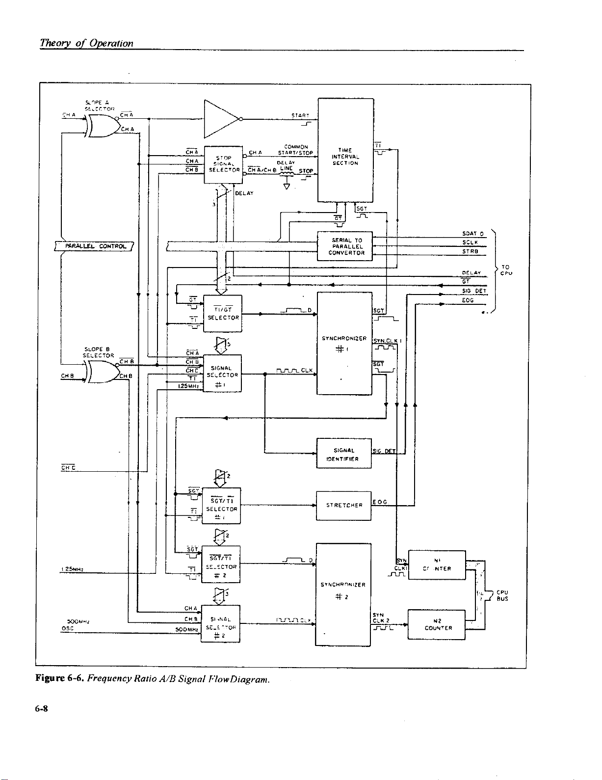
Theory of Operation
1
Figure 6-6.
6-8
Frequency Ratio A/B Signal l~‘lowDiagran~.
Page 75

Theory
of
Operation
Figure
6-l. Period A, and Time Interval A to B Signal Flow Diagram,
6-9
Page 76
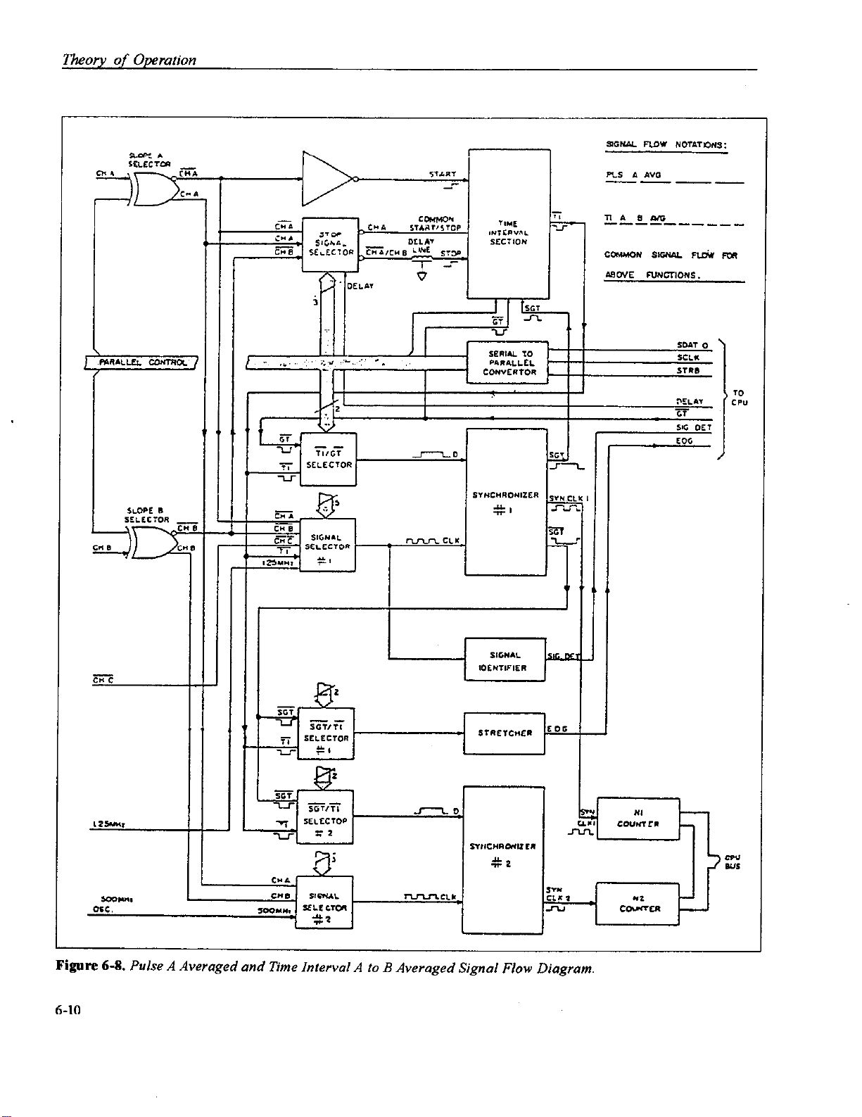
Themy of Operation
Pigure 6-8.
6-10
L-J-
Pulse A Averaged and Time Interval A to B Averaged Signal Flow Diagram
Page 77

r
.:ca‘Txa-
I==
Theory
of
Operation
Figure
6-9. Totalize B Infinite Signal Flow Diagram.
6-11
Page 78

Theory of Operation
Figure 6-10.
6-12
Totalire B By A, and Totalize B By AA Signal Flow Diagram,
Page 79

Theory of Operation
The reference oscillator also contains a phase noise
generator. During certain measurement functions, this
generator injects phase noise to the reference oscillator.
The noise generator is comprised of CR3, bias resistor
R9, and operational amplifier - U7. The noise generator
is switched in and out by an analog switch - U8 and is
controlled by 42 and its associated components.
6-3-5. Measurement Logic Section
The measurement logic section is a block which controlsvarious switching, routes the internal signals to the
correct ports. It also controls the sequence of the gate
and resets and synchronizes the main registers Nl and
N2 for the CPU. Figures 5-4 to 5-9 show the routes for
the input signal and the reference signal in every measurement function. The following is a brief explanation
of the various segments in the measurement logic section.
Control: The control circuit consists of U15, U14,
and U13. Information from the CPU is sent in a serial
form to the control ICs which in term convert the serial
information to a parallel format. The parallel outputs of
these ICs are being used to control the signal selectors,
and the signal routing to the various sections within the
measuring logic section. Qll through 413 convert the
TTL logic levels from the CPU to an appropriate voltage
levels for U15 (0 V to -5.2 V).
Signal Selector: The signal selector circuit com-
prises U19, U20, U21, U25, and U28. The function of
the signal selector is to route one of Channel A input.
Channel B input, Channel C input. or the reference
clock to the appropriate processing sections.
Time Interval Section:
circuit consists of ti dual D flip-plop U 17a/b. and gates
U18a, b and c, and Ul9b. U17a receives the start signal.
and U17b receives a stop signal. Following a reset
signal at the reset input of U17a/b, U18c simultaneously
produces a single positive pulse (TI), and its complement with a duration which is equal to the time interval
between the start, and the stop signals, regardless if the
start and stop signals are repetitive. While performing
time averaged measurements, these pulses will repeat as
long as the gate stays open.
The time interval section
approximate width of the original gate signal from the
CPU. but with a new adjusted width which is equal to
an integer number of periods of the signal being meas-
ured. This pulse is used as the #I synchronized (SGT 1)
gating signal throughout the instrument. In conventional frequency measurements, (refer to the above description), the gate time is synchronized to the reference
clock 1 (1.25 MHz). SGT 1 opens the gate U26d for the
appropriate signal to be later divided, and counted by
Nl dividing chain.
Synchronizer #2:
The
synchronizer
#2 consists of a
D flip flop U29b, gate U28d, and their associated components. During reciprocal frequency measurement,
SGT 1 signal is applied to the D input of U29b. At the
same time, the reference clock 2 (500 MHz) is applied
to the CLK input on the same IC. the output of U29b
generates a pulse SGT 2 with an approximate width of
SGT 1, but with a new adjusted width which is equal to
an integer number of periods of the reference clock 2.
In conventional frequency measurements, the gate time
is synchronized to the input signal. SGT 2 opens the gate
U28d for the appropriate signal to be later divided and
counted by N2 dividing chain.
Signal Identifier:
The signal identifier comprises
U22a. U31a, and their associated components. A signal
when present at the appropriate input terminal, is applied to the CLK input of U22a, converted to a TTL
level signal with U3 la, and then fed to a CPU port 1.1.
This port is used to flag the presence of a signal at the
input terminals. This signal is also used as the arming
signal of the counter.
Gate Identifier:
The gate identifier informs the CPU on
the state of the synchronized gate time # 1. The gate identifier
circuit also serves as a time stretcher of gate signals having
very small periods. The gate identifier consists of U26a,
U26c. U31d, R158, and C86.
Nl Counter Chain: The Nl counter chain comprises
U30b, U31a. U27a, U23a, U46a, U44, and their associated
components. U3Ob, U27a, U23a, and U46a are configured
as 7 bit binary up counter
with
its output connected to U44.
U44 is a 32 bit counter with its outputs connected to the data
bus. U31c converts the ECL logic level from U30b to Tn.
Synchronizer #l:
The synchronizer #l consists of a
D flip flop U22b. gate U26b/d, and their associated
components. During reciprocal frequency measurement, a gate signal is applied from the CPU to the D
input of U22d. and the measured signal is coupled to the
CLK input on the same IC. After a reset cycle, and
assuming that a signal is present at the appropriate input
terminal, the output of U22b generates a pulse with an
N2 Counter Chain:
The N2 counter chain comprises
U29a, U3Oa, U3lb. U27b, U23b, U46b. U45, and their
associated components. U29a, U3Oa, U27b, U23b, and
U46b are contigured as 8 bit binary up counter with its
output connected to U45. U45 is a 32 bit counter with its
outputs connected to the data bus. Ql5 and U31b convert
the ECL logic level from U29a, and U30a respectively to
T-l-L.
6-13
Page 80

Theory of Operation
6-3-6.
For the following discussions, refer to the power supply
schematic at the end of the manual. The power supply is
made up of a line fuse, power on-off switch, line voltage
selection switch, power transformer, two bridge rectifiers.
two monolithic regulators, and hvo discrete regulators
which is formed by U52, 430, 431, Q32, Q39, and their
associated
Fuse F1 is the LINE FUSE which is accessible on the rear
panel. S2 is the LINE VOLTAGE SELECT switch, which
is accessible on the rear panel, to select 115 V or 230 V
operation and Sl is the power on-off switch. CR25 is used
as a full-wave rectifier to provide a sufficient DC voltage
for the +I2 V, and -12 V regulators U50, and U51 respectivdy.
V supply. This reference is then compared to the regulated
+5 V U52b then controls through Q30 the current through
the series pass transistor - 43 1. The +5 V supply then acts
as the reference for the -5.2 V regulated supply. The operation of U52a is similar to the operation of US2b, except,
US2a operates as an inverting amplifier. CR 29, and CR30
protect the +5 Vand the -5.2 V respectively against accidental over-voltage.
Power Supply
components.
U52b receives a reference voltage of +5 V from the +I 2
6-4. Digital Circuitry
Model 776 operation is supervised by the internal CPU.
Through the CPU, the counter measurement process, the
front panel switching, display, and IEEE operation are
all performed under software control. This section
briefly describes the operation of the various sections
of the CPU, and its associated digital circuitry. A simplified block diagram is included for user reference; for
more complete circuit details refer to digital schematics
at the end of this manual.
6-4-l. CPU Block Diagram
A block diagram of the Model 776 CPU is shown in
Figure 6-3. Circuit operation centers around the CPU
unit - U39. The 803 I is an S-bit CPU capable of directly
addressing up to 64K bytes of program memory (ROM),
and up to another 64K bytes of data memory (RAM).
The CPU works with a 16 MHz clock which is divided
internally to provide a bus operation of about 1.6 MHz.
Interfacing between the CPU, and the IEEE bus is
performed by dedicated IEEE-488 bus interface IC U36. This IC performs many bus functions automatically to minimize CPU overhead. Buffering between
the 8291 IC and the IEEE bus lines is done with bus
drivers U21 and U22.
Interfacing between the CPU to the keyboard and the
display is performed by the Keyboard/Display interface
IC - U36.
64-2. Memory Mapping
The 8031 CPU is capable of directly addressing two
banks of 64k (65,536) bytes memory. One bank of memory is the program memory, and the second memory
bank is the data memory. The selection of the banks is
done internally by the CPU. Although the CPU has this
large addressing capability, only a portion of the possi-
ble memory space is actually needed.
The Model 776 uses a total of 32K of program
memory stored in the 27256 EPROM U43, and a total
of IK of data memory is stored in UIO and. The 8031
CPU uses a memory-mapped I/O scheme, additional
memory location must be allocated for the various I/O
function. All the memory-mapped II0 functions are in
the data memory space.
6-4-3. Address Decoding
The CPU has a total of 16 address lines which are used
to locate a specific memory slot. The LOW address line
(A0 to A7) are multiplexed on the address/data bus, and
the ALE (address latch enable) signal is used to separate
the LOW address from the address/data bus witch is
done by U40 address latch. Since no memory or interface element can fully decode address locations, additional address decoding must be used. U38 is l-of-8
decoder. The decoder is enabled when address lines Al5
is HIGH. Once the decoder is selected the decoding is
done by addressing lines All, A12 and A13.
6-4-4. Keyboard/Display Interface
The Keyboard/Display Interface IC US is used to control the front panel display, and to find out which one of
the buttons was pushed.
Software for the CPU is contained in an EPROM
(Erasable Programmable Read-Only Memory). U42 is a
27128 EPROM containing 16K bytes of software. Tem-
porary storage is provided by U43, RAMS (Random
Access Memory) which can store up to 2048 bytes of
information.
6-14
6-4-5. IEEE interface
The Model 776 has a built in IEEE-488 interface that
allows the instrument to be controlled through the system controller. Commands may be given over the,bus,
and data may be requested from the instrument as well.
Page 81
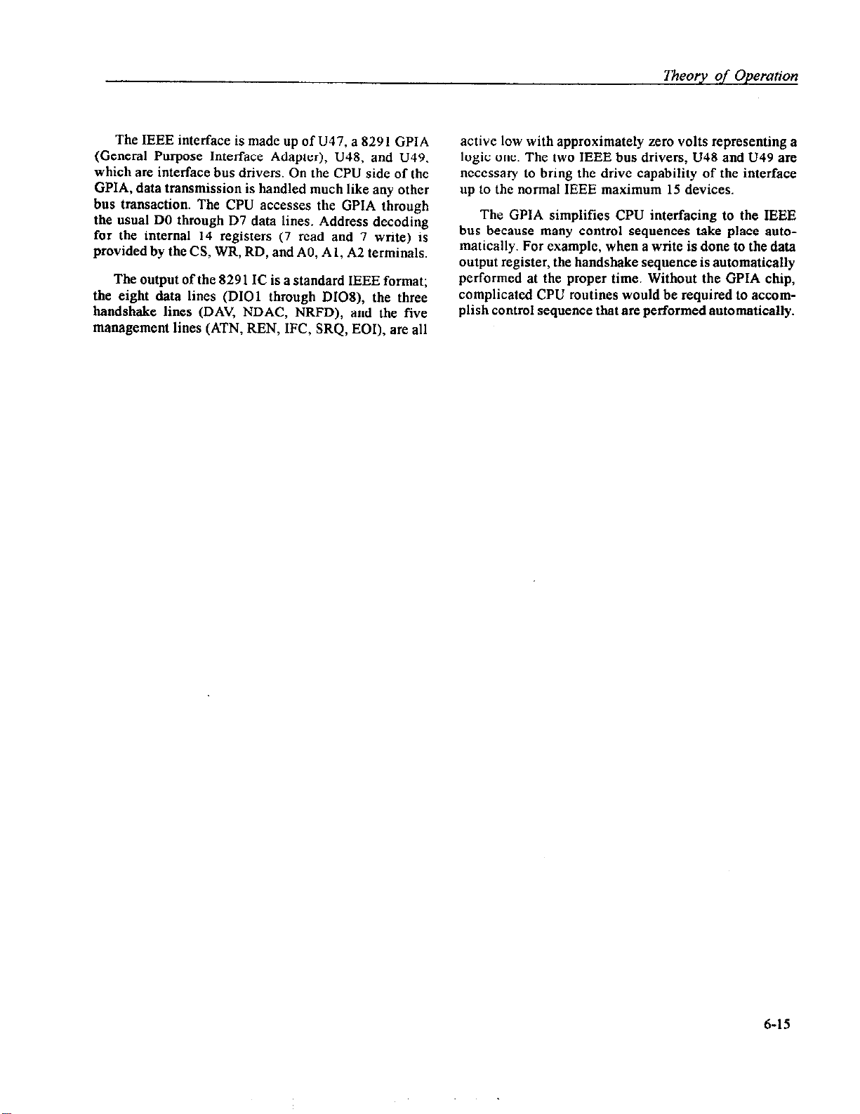
The IEEE interface is
made
up of U47, a 8291 GPIA
active low with approximately zero volts representing a
(General Purpose Interface Adapter), U48. and U49. logic enc. The two IEEE bus drivers, U48 and U49 are
which are interface bus drivers. On the CPU side of the
ncccssary to bring the drive capability of the interface
GPIA, data transmission is handled much like any other unto the normal IEEE maximum 15 devices.
bus transaction. The CPU accesses the GPIA through
the usual DO through D7 data lines. Address decoding
for the internal 14 registers (7 read and 7 write) is
provided by the CS, WR, RD, and AO, A 1, A2 terminals,
The output of the 8291 IC is a standard IEEE format;
the eight data lines (DIOl through DI08), the three
handshake lines (DAV, NDAC, NRFD), and the five
The GPIA simplifies CPU interfacing to the IEEE
bus because many control sequences take place auto-
matically. For example, when a write is done to the data
outnut reeister. the handshake seouence is automaticallv
performed at the proper time. iithout the GPIA chip,
complicated CPU routines would be required to accomplish control sequence that are performed automatically.
management lines (ATN, REN, IFC, SRQ, EOI), are all
6-15
Page 82

Theory of Operation
NOTES
6-16
Page 83

Adjustments and
Troubleshooting
7-1. Introduction
This section contains information necessary to adjust
and troubleshoot the Model 776 and the 2.1G option.
WARNING
The procedures described in this section are for use only by qualified
service personnel. Do not perform
these procedures unless qualified to
do so. Many of the steps covered in
this section may expose the individual to potentially lethal voltages that
could result in personal injury or
death if normal safety precautions
are not observed.
7-2. Adjustments
7-2-l. Environmental Conditions
Adjustments should be performed under laboratory conditions having an ambient temperature of25’15 “C. and
a relative humidity of less than 70%. If the instrument
has been subjected to conditions outside these ranges.
allow at least one additional hour for the instrument to
stabilize before beginning the adjustment procedure.
776. and allow it to warm-up for at least 30 minutes
before beginning the adjustment procedure.
7-23. Recommended Test Equipment
Recommended test equipment for calibration is listed in
Table 5-2. Test instruments other than those listed may
be used only if their specifications equal or exceed the
required cha~racteristics.
7-24. Adjustment Procedures
All adjustments are performed with the POWER switch
ON. The top cover should be removed to allow access
to test points, and adjustments. Between adjustments.
always leave top cover on the unit to keep intcmal
temperature.
WARNING
Take special care to prevent contact
with live circuits. or power line arca
which could cause electrical shock
resulting in serious injury. or death.
Use an isolated tool when making
adjustments. Use plastic or nylon
screwdriver when adjusting the time
base trimmer: other materials could
cause confusion in this adjustment.
7-2-2. Warm-Up Period
Most equipment is subject to at least a small amount of
drift when it is first turned on. To ensure long-term
calibration accuracy. turn on the power to the Model
Refer to Figure 7-1. throughout the following adjust-
ment procedures. for determining adjustment points.
Follon, the procedure in the sequence indicated because
some of the adjustments are intcrrelatcd. and dcpcndent
on the proceeding steps.
7-l
Page 84

Adjuments and Troubleshooting
Figure 7-l.
Model 776Adjus1ment Poinrs Locntion,
Page 85

Verify that Model 776 is functioning according to
the performance checks. Make sure that all results are
within. or close to. the range of the required specificalions. Othcrwisc refer to the troubleshooting procedures
given later in this section. Ccntcr all trimmers and if
necessary. remove selected components and clear the
holes to allow a selection of nc\v components.
Perform the following adjustment procedure. If an
adjustment can not be made to obtain a specific result.
refer to the troubleshooting procedures.
7-3. Adjustment Procedure
7-3-l. Power Supply Adjustment
Equipment: DMM
Procedure:
1. Set DMM to DCV measurements. Connect the DMM
between ground, and the +5 V test point.
2. AdjustR190foraDMMreadingof+5.000VilOmVdc.
7-34. Trigger Level A Offset Adjustment
Equipment: Function generator. oscilloscope
Procedure:
1. Set function generator controls as follows:
Wave form - Sine
Frequency - I KHz
Amplitude - 25 mVp-p
OffSCl - II v
Syllllllctry 50%
2. Press Model 776 push-buttons in the following scqucncc: [2ndj.
[DCL]
and then
[AC Al.
3. Connect the function generator output to tbc Channel
A input connector.
4. Set oscilloscope time base to 0. I msfdiv.
5. Connect the oscilloscope probe to U21 pin 9. Connect
the ground lead from the probe to ground.
6. Adjust R83 to obtain a square wave having a 50%
*l% duty cycle on the oscilloscope.
73-5. Trigger Level B Offset Adjustment
73-2. Trigger Level A Adjustment
Equipment: DMM. dc voltage calibrator
Procedure:
1. Set DMM to DCV measurements.
2. Set
[TL A]
to 0.00 V
3. Measure and record the voltage at Ul2 pin 8. Record this
voltage with a resolution of +tLOOl V.
4. Set
[TL A]
to 5.00 V
5. Set dc calibrator output setting to +5.000 V
6. Using a banana to BNC adapter. connect the calibrator
output to the Channel A input connector,
7. Re-connect the DMM probes to U 12 pin 8 and adjust RSO
to obtain the same voltage level as recorded in step 3.
73-3.. Trigger Level 6 Adjustment
Equipment: DMM. dc voltage calibrator
Procedure:
1. Set DMM to DCV measurements.
2. Set
ITL B]
3. Measure. and record thevoltage at U12 pin 9. Record this
voltage with a resolution of M.001 V
4. Set
[TL B]
5. Set dc calibrator output setting to +5.000 V
6. Using a banana to BNC adapter. connect the calibrator
output to the Channel B input connector.
7. Resonnect the DMM probes to U I2 pin 9. and adjust R81
to obtain the same voltage Icvol as recorded in step 3.
to 0.00 V
to
5.00 V
Equipment: Function generator. oscilloscope
Procedure:
1.
Set function generator controls as in paragraph 7-3-4.
2. Press Model 776 push-buttons in the
quence: [2nd].
[DCL]. [FRQ B]
and then
following se-
[AC Bj.
3. connect the function generator output to the Channel
B input connector.
4. Set oscilloscope time base to 0.1 ms/div.
5. Connect the oscilloscope probe to U24 pin I-I Connect,the ground lead from the probe to ground.
6. Adjust R84 to obtain a square wave haying a 50%
+l% duty cycle on the oscilloscope.
73-6. input A x10 High Frequency
Adjustment
Equipment: Function generator. oscilloscope
Procedure:
1. Set function generator controls as follows:
Wave form - Square wave
Frequency - IO KHz
Amplitude - 5 Vp-p
Offset - 0 V
Symmetry - 50%
2. Press Model 776 push-buttons in the following se-
quence: [2nd].
3. connect the function generator output to the Channel
A input connector.
[DCL]. [SO!2 A].
and then 1x10
A].
7-3
Page 86

4. Connect the oscilloscope probe to the cathode of
CR6. Connect the ground lead from the probe to ground.
5. Set oscilloscope and adjust C3 to obtain the best
square wave response having minimum overshool. and
undershoot.
7-3-7. Input B x10 High Frequency
Adjustment
Equipment: Function generator. oscilloscope
Procedure:
1. Set function generator controls as in paragraph 7-3-5.
2. Press Model 776 push-bu(tons in the following se-
quence: [Znd]. [DCL], [FRQ B]. [5On B]. and then
[xl0 B].
3. Connect the function generator output to the Channel
B input connector.
4. Connect the oscilloscope probe to the cathode of
CR14. Connect the ground lead from the probe to
ground.
5. Set oscilloscope and adjust C28 to obtain the best
square wave response having minjmum overshoot. and
undershoot.
NOTE
The Models 776 and 77612.46 have
a default gate time of 1 second. The
Model 776/2.4G/R has a default gate
time of lOOtus. The resolution of
counter readings in the following
procedures are for a I second gate
time. Readings on the Model
776/2.4G/R will have one less digit.
7-3-8. Standard - 5 PPM Time Base
Adjustment
If range can not be reached. sclcct Cl 25 (in the range of
8 - IOpF) lo bring Cl24 within range.
5. Replace the top cover. and allow the Model 776 tO
operate with the coverson foranadditional periodof lj
minutes.
6. Using a plastic mawrial screwdriver. adjust Cl26
from the rear panel to give a display reading of:
10.00000000 E+6 flOOO LSD
If range can not be reached. repcat steps 4 through 6.
7-3-9. TCXO Time Base Adjustment
(option 2.4G)
Equipment: 10 MHz Standard
Procedure:
1. The following adjustment musl be performed in a
stable temperature environment of 2.5 “C +2 “C Remove
the top cover. refer to Figure S-1. and remove the adjuslment plug at the top of the oscillator bulk. Replace the
top cover. Power-up Model 776. and allow it to operate.
for at leasl half an hour. with its covers closed.
2. Press Model 776 push-buttons in the following se-
quence: [2nd]. ]DCL]. and then ISOn
3. Connect the IO MHz standard to the Model 776
Channel A.
4. Remove the top cover. and using a plastic-tip screw-
driver. ad.just the trimming resistor on top of the TCXO
board to give a reading of:
10.00000000 E+6 irIO LSD
5. Replace the ad,justment plug and the top cover. and
allow the Model 776 to operate with the covers on for
an additional period of 15 minutes.
6. Check if frequency is still in the range. as in step 4.
If reading shifted, repeat steps 4 through 6.
A].
Equipment: IO MHz Standard
Procedure:
1. The following adjustment must be performed in a
stable temperature environment of 25 “C +2 “C Remove
the top cover. and set Cl26 to about mid-range. Replace
the top cover. Power-up Model 776. and allow it to
operate. for at least an hour. with its covers closed.
2. Press Model 776 push-buttons in the following se-
quence: [2nd]. [DCL]. and then [SO.0
3. Connect the 10 MHz standard to the Model 776
Channel A.
4. Remove the top cover. and adjust CI2-l to give a
reading of:
10.00000000 E+6 f5000 LSD
7-4
A].
7-4. Troubleshooting
The troubleshooting instructions contained in this section are intended for qualified persomiel having a basic
understanding of analog. and digital circuitry The indi-
vidual should also be experienced at using @pica1 tc~(
equipment as well as ordinary troubleshooting proce-
dures. The information presented here has been written
to assist in isolating a defeclive circuit. or circuit section: isolation of the specified component is left to the
technician
74-l. Recommended Test Equipment
The success or failure in troubleshooting a complcs
piece of cquipmcnl. like the Model 776. dcpcnds noI
Page 87

Table 7-l. Recommended Minimum Test Equipment For Troubleshooting
Adjusrmenrs and Troubleshooting
1”strume”t
DMM
Pulse/Function Generator
Signal Generator
Oscilloscope
Recommended
Model
Keithley 175A
HP 8116A 4 s - 20 ns. 15 Vp-p into 50 Q
HP 8663A 100 KHZ - 2560 MI-k
Tektronix 2465 300 MHz band width
50 ohm feed through
Termination
Tek 011-0049-01 50 R 2w. 1%
only on the skills of the technician, but also relies
heavily on accurate, reliable test equipment. Table 6-2
lists the recommended test equipment for a complete
troubleshooting and adjustment of the Model 776. However. it is also possible to troubleshoot Model 776 with
the minimum equipment which is listed in Table 7-1.
Other equipment such as logic analyzer. and in-circuit
emulatoretc, could also be helpful in difficult situation.
71-2. Power-Up Self Diagnostics
An advanced feature of the Model 776 is its self diagnosing capabilities. Upon power-up the Model 776 performs a set of tests which is described in paragraph 3-1.
If the Model 776 locks up due to ROM or RAM fail,
there is a little point in attempting to troubleshoot elsewhere unless the micro controller circuit is operating
properly.
Minimum
Specifications
.l V- 100 VDC. AC nns. .OS% basic accufac?~
7-5. Troubleshooting Procedure
7-5-l. Power Supply Checks
It is highly suggested that the first step in troubleshoot-
ing the Model 776. as well as any similar equipment,
would be
supply voltages within the instrument are not within the
required limits. troubleshooting the remaining circuits
can be vety difficult. Table 7-2 shows several checks
that can be made to the power supplies within the Model
776. In addition to the normal voltage checks. it is also
a good idea IO check the various supplies with a” oscilloscope to make sure no noise or ringing is present.
In case of a “dead short” between one of the supplies
to the common ground. it would be best to disconnect
to
check the power supply. If the various
Step Item/Component
1
S2 Line Switch
2
Fl Line Fuse
3 Jl Line Power
4
+12 v Supply
5
u50 Input
6
-12 v Supply
7
u51 Input
8
+5 v Supply
9 Input to +5 v suppl)
10
Reference to +5 V
11 -5.2 V Supply
12 Input to -5.2 v
13
+5 v Supply to osc.
14 Input to +5 v us5
Table 7-2. Power Supply Checks
Required Condition Remark8
Set to 115 V or 230 V
Continuity
See paragraph 5-2
Remove fuse to check
Plugged into live receptacle;
power on
+12 v f5%
+I5 V minimum
Positive output of CR25
-12 v lt5%
-15 V minimum
+5 v *2%
Appros. +7 V
+5 v *5%
-5.2 V i2%
Appros. -7 V
+ 5 v f5%
112 v
Negative output of CR25
Cathode of CR29
Positive output of CR28
U52b pin 5 Supply
Anode of CR30
Negative output of CR28 Supply
U57 pin 8
U55 input/+ 12 V supply
7-5
Page 88

Adiustments and Troubleshooting
In case of a “dead short” between one of the supplies
to the comtnon ground, it would be best to disconnect
the entire supply section from the remaining of the
circuitry, and then determine whether the problem is in
the power supply or in the remaining circuits. Model
776 is equipped with such quick-disconnect points.
which are located on the bottom side of the main PC
board. To access these points. it is necessary IO remove
the bottom cover. and then to remove the solder layer
from these points.
While troubleshooting the power supply section.
bear in mind that the +I2 V supply also provides the
reference voltage to the +5 V Therefore. it would be
impossible to troubleshoot the +5 V supply if the +I 2 V
supply is defective. Similarly. the +5 V supply is used
as a reference voltage to the -5.2 V supply.
74-2. Digital Circuitry and Display Checks
The most important section, to be verified after the
power supply checks, is the digital section with its
various clocks. Problems with the digital circuitry could
cause erratic operation or false display readings. Prob-
lems in the clock generator for the CPU and the digital
circuit may cause a complete malfunction of the entire
section. The CPU would not even start to generate the
control lines which makes it impossible to troubleshoot
the remaining of the circuitry. Check the various components, associated with the digital circuitry. clocks.
and the IEEE-488 interface. using the information in
Table 7-3.
7-53. Standard 5 PPM Reference
Oscillator Checks
The reference oscillator supplies a precise signal to the
500 MHz oscillator. This oscillator is integrated within
a phase locked loop. Therefore. the accuracy of this
oscillator determines the final accuracy of the 500 MHz
oscillator. Without this clock the instrument will operate erratically. Verify that a 10 MHz TTL level signal is
present at U57 pin 5. U56 pin 6. 3. and 8. and at the
CLOCK output
position.
rear
panel connector. Check LKlaib
7-54. 500 MHz reference oscillator and
TCXO Checks
The 500 MHz oscillator circuit generates an ECL signal
for the counting circuit. This generator is a free running
voltage controlled oscillator. Its final accuracy is phase
locked to the IO MHz clock refcrcncc. Problems with
the 500 MHz oscillator will definitely cause false results on the Model 776: in some cases. the counter may
display no result at all. Problems in the 500 MHz oscillator may bc identified using Table 7-1. When option 5 I
is installed. a TCXO reference replaces the standard
reference oscillator. The TCXO enhances the overall
accuracy of the insttumcnt. A malfunctioned TCXO
displays similar symptoms to an inoperative 500 MHz
oscillator. If a problem appears to be with the 500 MHz
oscillator, it is recommended that the TCXO outpul be
checked first.
7-5-5. Trigger Level Checks
The trigger level circuits control the threshold point
where the input circuit triggers. If a legal signal is
applied to the input connector. and the counter fails to
trigger. it is most likely that the fault is in one of the
trigger circuits. Problems within the trigger circuit may
be located using the checks given in Table 7-S.
74-6. Signal Conditioning And Input
Circuits Checks
Problems in these circuits could generate false results
on the Model 776. Tables 7-6 and Table 7-7 list the
checks to be made on the signal conditioning and the
input circuits respectively.
74-7. Measurement Logic Section Checks
The measuretncnt logic seclion circuitry is mainly used
as a digital traffic control to the analog signals within
the instrument. The function control circuit cheeks is
given in Table 7-8. Table 7-9 describes the remaining of
the measurement logic circuit. While performing cheeks
from Table 7-9. it is recommended to use a special high
frequency probe with very short grounding clip.
7-6
Page 89

Table
7-3. Digital Circuitr.v and Display Checks
Step Tested Circuit
1
Required Condition
Turn on power Some tests here could
Remarks
fail due to digital problems.
2
Microprocessor clock
3
Microprocessor timer 0 to +4 V 7.8 KHz square w’ave
4
Keyboard/Display clock 0 to +4 V 2.0 MHz square wave
5
IEEE Interface clock
6
Beeper clock 0 to +4 V 3.9 KHz square wave Pin 1 on U41.
7
Reset Input Turn off instrument then back on
0 to +4 V 16 MHz square wave
0 to +I V 8.0 MHz square wave
Pie 18 on U39.
Pin 14 on U39.
Pin 3 on U36.
Pin 3 on U47.
Pin 9 on U39 stays low for
about .l s and then goes high.
8 ALE Line
9
PSEN Line 0 to +4 V 190 ns negative going pulses Pin 29 on U39.
10 RD WR Lines
11 Address/Data Bus
0 to +4 V 125 ns pulses
0 to +4 V 500 ns negative going pulses Pins 16 and 17 on U39.
0 to +4 V variable pulse train
Pin 30 on U39.
Pins 21 thou 28: Pins 32 thru 39:
Pins 3 thru 10 on U39 on U42.
Depress and hold the fi Level A during the nest six tests.
This will generate serial data on the RXD lines.
12 TTL Serial Data Input
0 to +5 V variable pulse train
Pin2ofUl:Pin2ofU3:
Pin 2 of U6: and. Pin 2 of U7.
13 ECL Serial Data Input
-5.2 to 0 V variable pulse train
Pin 2 of U15: Pin 2 of U14: and.
Pin 2 of u13.
I4 TTL Serial to Parallel
Converters Clocks
0 to +5 V bursts of pulse train
Pin 4 of U37: Pin 3 of Ul:
Pin 3 of U3: Pin 3 of U6: and.
Pin 3 of U7
15 ECL Serial to Parallel
-5.2 to 0 V bursts of pulse train
Pin3 ofUl5: Pin3 ofUl4:and.
Converters Clocks Pin 3 of U13
16 TTL Serial to Parallel
Converters Strobes
0 to +5 V bursts of pulse train
Pin IS of U37: Pin 1 of Ul:
Pin 1 of U3: Pin 1 of U6: and.
Pin 1 of U7
17 ECL Serial to Parallel
Converters Strobes
-5.2 to 0 V bursts of pulse train
Pin 1 of U15: Pin 1 of Ul4; and.
Pin 1 of U13
Depress. in turn. each one of the buttons on the front panel throughout the nest test.
This test will check all buttons on the front panel as well as the interrupt line.
18 Keyboard Interrupt Line 0 to +4 V variable negative going pulses Pin4ofU36
19 LEDs Sink Lines
0 to +4 V variable pulses
Pins 10 to 16 on U35: and.
Collector of 420
7-7
Page 90
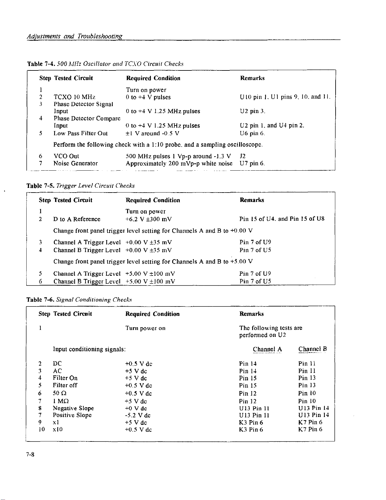
Adjustments ctnd Troubleshooting
Table 7-4.500
Step Tested Circuit Required Condition Remarks
1
2
hlHz Oscillaror and TC.\-0 Circuif Cluxks
Turn on power
TCXO IO MHz
0 to +4 V pulses
Phase Detector Signal
I 3
Input 0 to i-4 V 1.25 MHz pulses U2 pin 3.
4
Phase Detector Compare
Input 0 to +4 V 1.25 MHz pulses U2 pin 1. and U-l pin 2.
S
Low Pass Filter Out *l V around -0.5 V U6 pin 6.
Perform the following check with a I:10 probe. and a sampling osciIloscope
6
vco out 500 MHz pulses 1 Vp-p around -1.3 V 12
7
Noise Generator Approximately 200 mVp-p white noise U7 pin 6.
Table 7-5.
Trtnaer Level Circuit Checks
Step Tested Circuit Required Condition Remarks
1
2
D to A Reference +6.2 V +300 mV
Turn on power
Change front panel trigger level setting for Channels A and B to +O.OO V
3
Channel A Trigger Level +O.OO V &35 mV
4
Channel B Trigger Level +O.OO V t35 mV Pin 7 of U5
Ultl pi” 1. Ul pins 9. 10. and I I.
Pi” 15 of U4. and Pin 15 of US
Pin 7 of U9
Change front panel trigger level setting for Channels A and B to +5.00 V
5
Channel A Trigger Level +5.00 V +lOO mV Pin 7 of U9
6
Channel B Trigger Level +5,00 V +I00 mV
Table 7-6. .Si.wnl
Step Tested Circuit
Conditioning Checks
Required Condition
1 Turn power on
Input conditioning signals:
DC
AC
Filter On
Filter off
6 50 n
7 IMQ
8 Negative Slope
7 Positive Slope
9 Sl
10 xl0
+0.5 V dc
+5 V dc
+5 V
+O.S V dc
+0.5 V dc
+5 V dc
+0 V
-5.2 V dc
+5 V dc
+0.5 V dc
dc
dc
Pin 7 of U5
Remarks
The following lcsts are
performed on U2
Chamvel A
Pin 14
Pin 14
Pi” 15
Pin 15
Pin 12
Pin 12
U13 Pi” 11
U13 Pin 11
K3 Pin 6
K3 Pi” 6
Channel B
Pin 11
Pin 11
Pin 13
Pin I3
Pin IO
Pin 10
U13 Pi” I4
U13 Pin 14
K7 Pin 6
K7 Pi” 6
7-8
Page 91

Table
I-1. Input Circuits Checks
Adjustments and Troub1eshootin.g
Step Tested Cirrnit
1
:, 2
Table
Chaonel A Input Amplifier 1 MHz ,150 Vp-p sine
3
Schmidt Trigger Operation A -1.7 V to -0.8 V 1 MHz square wave
4
Channel B Input Amplifier 1 MHz ,150 Vp-p sine
5
Schmidt
7-8. Function Control Circuit Checks
Trigger Operation B -1.7 V to -0.8 V 1 MHz square wave
Rcquircd Condition
Turn on power
Remarks
Apply 1 MHz .2 Vp-p sine
Press [2nd], [DCL] to Channel A input BNC
CR6 Cathode
Pin 1 on U12
Select FREQ B function Apply I MHz .2 Vp-p sine
Channel B input BNC
CR14 Cathode
Pin 16 on Ul2
to
Page 92

Step
Tested
Circuit
Required Condition Remarks
1 Turn on power
Press
[2ndj. [DCL]. Apply 1
MHz 1 V p-p sine
10 Channel A input BNC.
2 Signal Selector #I -1.7 V to -0.7 V 1 MHz square wave
Pin 3 of LIZ.5
3 Synchronized Clock #l -1.7 V to -0.7 V 1 MHz bursts. Pin IS of U2G
Duration of burst is appros 1 s
The following are variable TTL/ECL level signals
with about 1 s burst duration - square waves.
Square wave period
4
Nl Divider Chain
2 1s
4 PS
8 PS
16 ps
32 ps
64 ps
U30b Pin 14 (ECL)
IJ31 Pin 12 (TTL)
U23 Pin 5 (TTL)
U4G Pin 11 (TTL)
U4G Pin 10 (TTL)
U46 Pin 9 (TTL)
128 ps U46 Pin S (TTL)
Signal Identifier
5
6
Gate Identifier TTL low level when gate is open. U31 Pin 13
TTL low level during measurement cycle.
U3 1 Pin 4
For the following check use a sampling oscilloscope with a 1: 10 probe
7 Synchronized Clock #2
-1.7 to -0.7 V 500 MHz bursts. Pin 15 of U28
Duration of burst is appros 1 s.
The following are variable signals with about 1 s
burst duration - square waves.
N2 Divider ‘Chain
8
9
Start/Stop Signal
10 Time Interval
11 Gate Identifier
7-10
Square wave period
ECL 4 ns
ECL 8 ns
ECL 16 ns
TTL 32 ns
TTL 64 ns
TTL 128 ns
TTL 256 ns
TTL Sl2 ns
Change panel setting to PER A,
-1.7 V to -0.7 V I KHz square wave
-1.7 V to -0.7 V 1 ms negative going
pulse for each cycle
TTL low level for 1 ms.
TTL high for about 300 ins after
gate closure
U29 Pin 3
U30 Pin 3
U27 Pin 14
U23 Pie 9
U46 Pin 3
U46 Pin 4
U46 Pin 5
U46 Pin 6
Apply 1 KHz I Vp-p square
wave to Channel A input BNC
U17 Pin 9
Ul8 Pin 15
U31 Pin 13
Page 93

8
Parts List
8-1. General
This section contains information for ordering replace-
ment parts. the replacement parts are available from the
vendors listed or from Keithley Instruments. Mechanical parts are shown separately on Figure 8-l.
8-2. Ordering Information
When ordering replacement parts. always include the
following information:
a) Instrument Model number.
b) Instrument Serial number.
c) Keithley part number.
d) Part description.
e) Circuit designation (where applicable).
Keithley will do its best to improve the instrument and
make changes in style of components and replacement
parts. Replacement parts may differ in appearance from
those found in your instrument but are always equal or
superior in performance.
8-3. Parts Description
In the following Parts List Tables. unless otherwise
noted. resistors power rating is ll4W. resistance is
given in Q and capacitance is given in pF.
Some parts in the following pans lists are marked with
an asterisk (9 These parts belong to the standard time
base circuit. These parts will not be assembled when
option 2.4G is installed.
Matched or selected components may only be bought
from the factory. Selection guides for such components
are not given anywhere in this manual.
8-l
Page 94

DWG PART
REF NUMBER
DESCRIPTION
DWG PART
REF NUMBER
DESCRIPTION
Cl
1521.04730
1500-01040
c2
c3
1550-01600
c5
1500-01040
C6
151 O-03ROO
1500-01040
c7
C6
151 o-06200
1500.01040
c9
Cl0
1500-01040
Cl1
1500-01040
1500-01030
Cl4
Cl5
1500-01040
CT6
1510-06200
Cl7 1500-01040
1500-01010
Cl6
1500-01010
Cl9
c20
1500-01040
c21
1500-01040
1560-01040
c22
C23
1540-01060
C24
1500-01040
C2S
1500471010
C26
1521.04730
C27
1500-01040
C28
1550-01 BOO
NOT USED
c29
c30
1500.01040
c31
151 O-03ROO
1500-01040
C32
c33 151 o-06200
1500-01040
c34
c35 1500-01040
C36 1500-01040
NOT USED
c37
C36 NOT USED
1500-01030
c39
c40 1500-01040
151 o-06200
c41
C42 1500-01040
c43 1500-01010
c44 1500-01010
1500-01040
c45
C46
1500.01040
c47
1540-01060
1560-01040
C48
c49
1500-01040
c50
1500-01010
c51
1500-01040
c52
1500-01040
c53
1500-01040
c54
1500-01040
c55
1500-01040
C56
1540-01060
c57
1540-01060
C58
1500-01040
c59
1540-01060
CAP POL.O47,,F 20% 260” MKT1616
CAP CER .I pF-20%+60% 60”
CAP VAR 5-I 8PF DV, 1 PSIBA
CAP CER .1 ,,F-20%+60% 5OV
CAP MICA 3 pF 10% 500V
CAP CER .I pF-20%+80% 50V
CAP MICA 62 pF 10% 500V
CAP CER .l lrF-20%+80% 50V
CAP CER .I uF-20%+60% 50V
CAP CER .I ;tF-20%+80% 6OV
CAP CER 10 “F 20% 50V
CAP CER .I uF-20%+60% 50V
CAP MICA 6i pF 10% iOOV
CAP CER .I &F-20%+80% SOV
CAP CER 100 pF 20% 50V
CAP CER 100 DF 20% 5OV
CAP CER .l &20%+60% 50V
CAP CER .I ,tF-20%+80% 50V
CAP CHIP .I pF SOV
CAP TANT 10 pF 25V
CAP CER .I ,,F-20%+80% 50V
CAP CER 100 pF 20% 50”
CAP POL.047 pF 20% 260V MKT1816
CAP CER .I pF-20%+60% 5OV
CAP VAR 5-I 6 pF DVI 1 PSI 8A
CAP CER .l )rF-20%+60% 50V
CAP MICA 3 pF 10% 500V
CAP CER .l ,&F-20%+60% 50V
CAP MICA 62 pF 10% 5OOV
CAP CER ., !tF-20%+60% 6OV
CAP CER .I PF-20%+80% 50V
CAP CER .1 uF-20%+80% 50V
CAP CER IO nF 20% SOV
CAP CER .I ,rF-20%+60% 50V
CAP MICA 62 pF 10% 500V
CAP CER .I >lF-20%+80% 5OV
CAP CER 100 pF 20% 50V
CAP CER 100 pF 20% 50V
CAP CER .I pF-20%+80% 50V
CAP CER .I ,,F-20%+80% 50V
CAP TANT 10 ,,F 25V
CAP CHIP .I k,F 5OV
CAP CER .I pF-20%+80% 50V
CAP CER 100 pF 20% 50V
CAP CER ., bF-20%+60% 50V
CAP CER .I pF-20%+60% 50V
CAP CER .I pF-20%+80% 50V
CAP CER .I fiF-20%+80% 50V
CAP CER .I pF-20%+60% 6OV
CAP TANT IO UF 25V
CAP TANT 10 ,,F 25V
CAP CER .I eF-20%+60% SOV
CAP TANT IO pF 26V
,540-o, 060
C60
C6, NOT USED
C65 1500-01040
1500-01040
C66
037 1560-01040
1560-01040
C68
C69’ 1500-01040
1500-01040
c70
c71 1500-04R70
1500-01010
C72
c73 1560-01040
c74 1500-01040
c75 1500-01040
C76 1500-01040
c77 ,560.01040
C78 1560-01040
C7S 1500-01040
1500-01040
C80
CSI 1500-01040
1500-01040
C82
CS3 1500-01040
CS4 1500-01040
C65 1500-01040
C86 1500-01030
C67 1532-01070
c90 1500-01040
C91 1500-01040
c92 1540-01050
c93 1500-01040
CS4 1500-01040
c95
C96 1500-01040
c97 1500-01040
C96
c99
Cl00
Cl01 1500-01040
Cl02
Cl03 1540-01060
Cl04 1540-01060
Cl05 ,533.01060
Cl06 1533-01080
Cl 07 1533-01070
Cl08 1533-01070
Cl09
Cl10
Cl11
Cl12 1500-01040
Cl13 1500-02210
c114
C115 1500-01030
Cl16 1532.04770
Cl 20’ 1500-01040
151 O-02200
C88
C89 1533-01080
,500-o, 040
1500.01040
1500-01040
1500-01040
1500-01040
1532-01090
1532-01090
1532.04770
1500-02210
CAP TANT 10 pF 25V
CAP CER .I pF-20%+60% 50V
CAP CER .I ,,F-20%+60% 50V
CAP CHIP .I ,,F 50V
CAP CHlP ., pF 50V
CAP CER .I pF-20%+80% 50V
CAP CER .I pF-20%+80% 5OV
CAP CER 4.7 pF 20% 5OV
CAP CER 100 pF 20% 50V
CAP CHIP .1 &rF 50V
CAP CER ., @20%+60% 5OV
CAP CER .I ,,F-20%+80% 50V
CAP CER .I ,,F-20%+80% 50V
CAP CHIP .I ,,F SOV
CAP CHIP .I k&F 50V
CAP CER .I ,rF-20%+80% 5OV
CAP CER ., pF-20%+60% 50V
CAP CER .1 ,,F-20%+80°b 50V
CAP CER ., ,d-20%+60% 50V
CAP CER .I ,rF-20%+60% 50V
CAP CER .I ,,F-20%+80% SW
CAP CER .I ,,F-20%+80% 50V
CAP CER 10 nF 20% 50V
CAP ELEC 100 ,I 16V
CAP MlCA 22 pF 20% 50V
CAP ELECTR 1000 b,F/25V
CAP CER .I ,&20%+60% 50V
CAP CER .I ,,F-20%+60% 5OV
CAP TANT 1 pF/25V
CAP CER .I ,rF-20%+80% 5OV
CAP CER .I FF-20%+80% 50V
CAP CER .1 ,,F-20%+60% 50V
CAP CER .I pF-20%+80% 5OV
CAP CER .I pF-20%+80% 50V
CAP CER .1 rrF-20%+80% 50V
CAP CER .1 ,,F-20%+60% 5OV
CAP CER .I ,,F-20%+80% 5OV
CAP CER .I rrF-20%+60% 50V
CAP CER .I ;F-20%+80% 50V
CAP TANT 10 rrF 25V
CAP TANT 10 ;tF 25V
CAP ELECTR 1000 ,,F/25V
CAP ELECTR 1000 &,F/25V
CAP ELECTR lOO~tF125V
CAP ELECTR 10O~Fl25V
CAP ELEC lO.OOO,~F 16V
CAP ELEC lO.OOOpF 16V
CAP ELECTR 470 pF/16V
CAP CER ., pF-20%+80% 50V
CAP CER 220 pF 20% 50V
CAP CER 220 pF 20% 50V
CAP CER 0.0, pF=20%+80% 50V
CAP ELECTR 470 pF/,GV
CAP CER .1 ,,F-20%+60% 5OV
8-2
Page 95
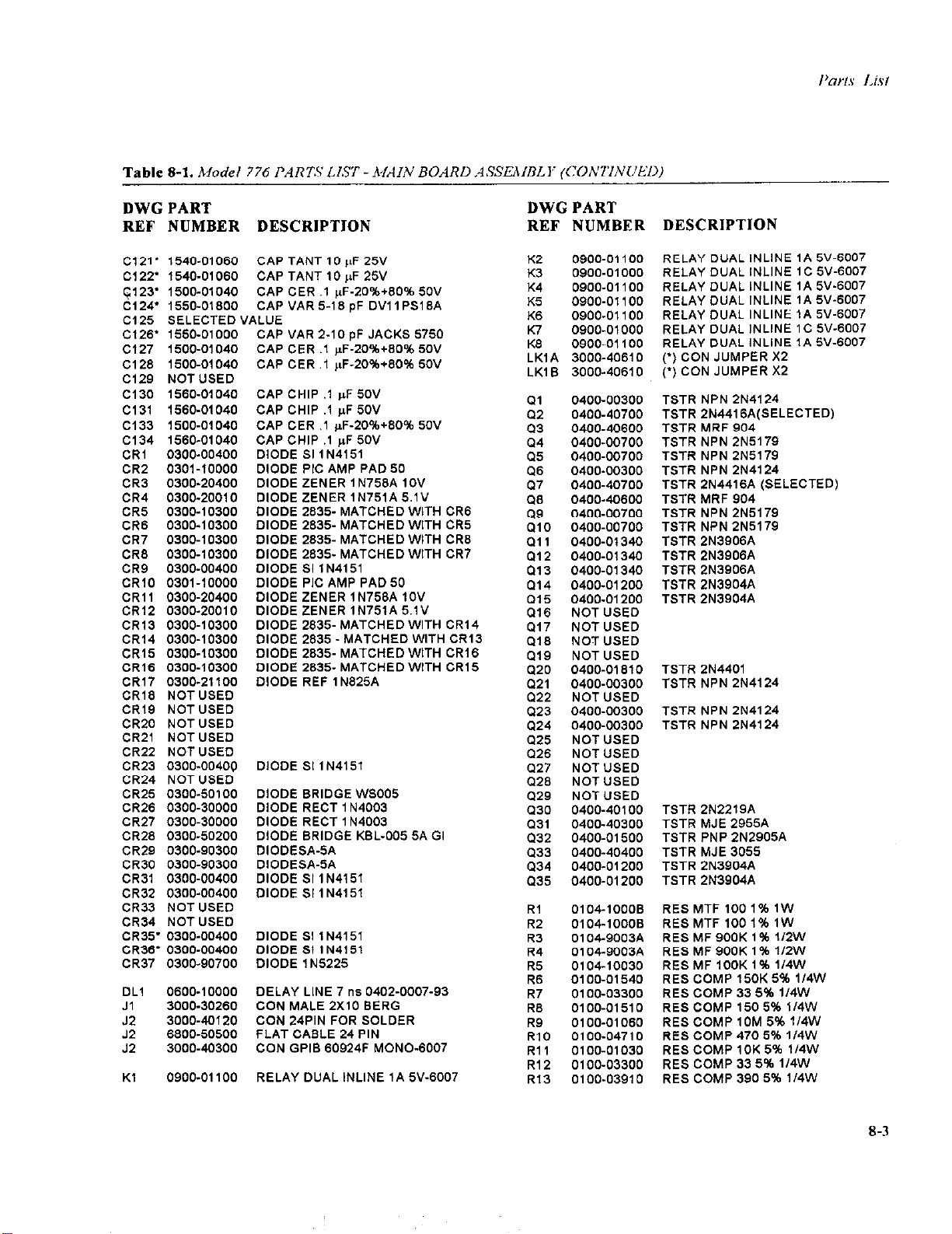
Table 8-l. h<odel 776 PARTS LIST-MAIN BOARD ..lSSi5MllLl; (CO~rTI!Vl’k’l~)
-
DWG PART
REF NUMBER DESCRIPTION
C121’ 1540-01060 CAP TANT 10 ,,F 26”
C, 22’ 1540-01060 CAP TANT 10 ,,F 25V
C123’ 1500-01040 CAP CER .I pF-20%+80% 5OV
C124’ 1550-01800 CAPVAR5-18pFDVllPS18A
Cl25 SELECTED VALUE
C126’ 1550-01000 CAP VAR 2-10 pF JACKS 5750
Cl27 1500-01040 CAP CER .1 uF-20%+60% 5OV
Cl 28 1500-01040
Cl29 NOT USED
Cl 30 1560-01040
Cl31 1560-01040
Cl33 1500-01040
Cl34 1560-01040
CR1 0300-00400
CR2 0301-10000
CR3 0300.20400
CR4 0300-20010
CR5 0300-10300
CR5
0300-10300
CR6 0300-10300 CR6 0300-10300
CR7 0300-10300 CR7 0300-10300
CR8 0300-10300 CR8 0300-10300
CR9 0300-00400 CR9 0300-00400
CR10 CR10 0301-10000 0301-10000
CR1 1 CR1 1 0300-20400 0300-20400
CR12 CR12 0300-20010 0300-20010
CR13 CR13 0300-10300 0300-10300
CR14 CR14 0300-10300 0300-10300
CR15 CR15 0300-10300 0300-10300
CR16 CR16 0300-10300 0300-10300
CR1 7 CR1 7 0300-21100 0300-21100
CR16 NOT USED
CR16 NOT USED
CR19 NOT USED CR19 NOT USED
CR20 NOT USED CR20 NOT USED
CR21 NOT USED CR21 NOT USED
CR22 NOT USED CR22 NOT USED
CR23 0300-00400 CR23 0300-00400
CR24 NOT USED CR24 NOT USED
CR26 0300.60100
CR26
0300-50100
CR26 0300-30000 CR26 0300-30000
CR27 0300-30000 CR27 0300-30000
CR26 CR26 0300-50200 0300-50200
CR29 0300-90300 CR29 0300-90300
CR30 CR30 0300-90300 0300-90300
CR31 CR31 0300-00400 0300-00400
CR32 CR32 0300-00400 0300-00400
CR33 NOT USED CR33 NOT USED
CR34 NOT USED CR34 NOT USED
CR35’ CR35’ 0300-00400 0300-00400
CR36’ CR36’ 0300-00400 0300-00400
CR37 CR37 0300-90700 0300-90700
DLl 0600-10000
Jl 3000-30260
J2 3000-40120
J2 6800.50500
3000.40300
J2
Kl 0900-01100
CAP CER .t PF-20%+60% 5ov
CAP CHIP .l ,rF SOV
CAP CHIP .I pF 50V
CAP CER .I *F-20%+80% 50V
CAP CHIP .l PF 50V
DIODE Sl lN4151
DIODE PIC AMP PAD 50
DIODE ZENER 1 N758A IOV
DIODE ZENER lN751A 5.1V
DIODE 2835-MATCHED WITH CR6
DIODE 2835-MATCHED WITH CR5
DIODE 2635-MATCHED WITH CR6
DIODE 2835-MATCHED WITH CR7
DIODE Sl lN4151
DIODE PIC AMP PAD 50
DIODE ZENER lN758A IOV
DIODE ZENER lN751A 5.1V
DIODE 2835. MATCHED WITH CR14
DIODE 2835 -MATCHED WITH CR13
DIODE 2835. MATCHED WITH CR16
DlODE 2835. MATCHED WITH CR15
DIODE REF 1 N825A
DIODE Sl lN4151
DIODE BRIDGE WSO05
DIODE RECT 1 N4003
DIODE RECT 1 N4003
DIODE BRIDGE KBL-005 5A GI
DIODESA-5A
DIODESA-5A
DIODE SI IN4151
DIODE 81 1 N4151
DIODE SI lN4151
DIODE Sl lN4151
DIODE 1 N5225
DELAY LINE 7 ns 0402-0007-93
CON MALE 2X10 BERG
CON 24PIN FOR SOLDER
FLAT CABLE 24 PIN
CON GPIB 60924F MONO-8007
RELAY DUAL INLINE IA 5V-6007
DWG PART
REF NUMBER
::
0900-01100 0900-01000
K4
0900-01100
K5
0900-01100
K6
0900-01100
K7
0900-01000
K8
0900-01100
LKlA
3000-40810
LKl B
3000-40610
01
0400-00300
Q2
0400-40700
03
0400-40600
0400-00700
:i
0400-00700
Q6
0400-00300
Q7
0400.40700
Q8
0400-40800
0400-00700
EO
0400-00700
a11
0400-01340
0400-01340
Q12
Q13
0400-01340
Q14
0400-01200
Q15
0400-01200
Q16
NOT USED
Q17
NOT USED
Q16
NOT USED
QIQ
NOT USED
Q20
0400-01810
Q21
0400-00300
Q22
NOT USED
0400-00300
Q23
Q24
0400-00300
Q25
NOT USED
Q28
NOT USED
Q27
NOT USED
Q28
NOT USED
Q29
NOT USED
Q30
0400-40100
Q31
0400-40300
Q32
0400-01500
Q33
0400-40400
Q34
0400-01200
Q35
0400-01200
Rl
0104.10008
R2
0104-10008
R3
0104.9003A
R4
0104-9003A
R5
0104-10030
R8
0100-01540
R7
0100-03300
R6
0100-01510
RQ
.-
0100-01080
RlO
0100-04710
RI 1
0100-01030
RI2
0100-03300
R13
0100-03910
DESCRJPTJON
RELAY DUAL INLINE 1A 5V-6007
RELAY DUAL INLINE 1C 5V-6007
RELAY DUAL INLINE IA 5V-6007
RELAY DUAL INLINE 1A 5V-6007
RELAY DUAL INLINt IA SV-6007
RELAY DUAL INLINE 1C 5V-6007
RELAY DUAL INLINE 1A S/-6007
(‘) CON JUMPER X2
(‘) CON JUMPER X2
TSTR NPN 2N4124
TSTR 2N4418A(SELECTED)
TSTR MRF 904
TSTR NPN 2N5179
TSTR NPN 2N5179
TSTR NPN 2N4124
TSTR 2N4415A (SELECTED)
TSTR MRF 904
TSTR NPN 2N5179
TSTR NPN 2N5179
TSTR 2N3906A
TSTR 2N3906A
TSTR 2N3906A
TSTR 2N3904A
TSTR 2N3904A
TSTR 2N4401
TSTR NPN ZN4124
TSTR NPN 2N4124
TSTR NPN 2N4124
TSTR 2N2219A
TSTR MJE 2955A
TSTR PNP 2N2905A
TSTR MJE 3055
TSTR 2N3904A
TSTR 2N3904A
RES MTF 100 1% 1W
RESMTFlOOl%lW
RES MF QOOK 1% 1/2W
RES MF QOOK 1% 1/2W
RES MF 1OOK 1% 1/4W
RES COMP 150K 5% 1/4W
RES COMP 33 5% 1/4W
RES COMP 150 5% 1/4W
RES COMP 10M 5% 114W
RES COMP 470 5% 1/4W
RES COMP 10K 5% 114W
RES COMP 33 5% 1/4W
RES COMP 390 5% 114W
8-3
Page 96

Ports Lisl
Table
8-1. Model 776 P.4RTS LIST - nlilIN BOARD ASSEMBLY /CONTINUl?D)
DWG PART
REF NUMBER
0100-01510
R14
0100-07520
R15
0100-01520
R16
010686530
RI7
0100-01810
R18
0100-02720
RlQ
0100-03920
R20
R21
0104-66610
0104-l 0030
R22
0104-28010
R23
0104-28010
R24
R2S
0104-l 0000
0104-10020
R28
0104-15020
R27
010410010
R28
0104.20020
R29
0104-10010
R30
0100-03900
R31
0100-03300
R32
01044R020
R33
R34
0104-30100
0104-11310
R35
0100-02210
R36
R37
0100-03310
0100-02220
R38
R39
0104-l 1030
R40
0104-10008
R41
0104-10008
0104-9003A
R42
0104-9003A
R43
0104-10030
R44
0100-01540
R45
0100-03300
R46
0100-01510
R47
R48
0100-01060
0100-04710
R49
R50
0100-01030
0100-03300
R51
0100-03910
R52
R53
0100-01510
R54
0100-07520
0100-01520
R55
R56
0104-66530
0100-01810
R57
0100-0270
R56
R59
0100-03920
0104-66610
R80
0104-10030
R61
0104-26010
R62
0104-26010
R63
R64
0104-10000
R65
0104-10020
R66
0104-I 5020
R67
0104-20020
R66
0104-10010
R69
0104-10010
R70
0100-03900
R7l
0100-03300
0104-4R020
R72
DESCRJPTJON
RES COMP 150 5% 114W
RES COMP 7.5K5% 1,4W
RES COMP 1.5K 6% 114W
RES MF 865K 1% 1/4W
RES COMP 180 5% 1/4W
RES COMP 2.7K 5% 1/4W
RES COMP 3.9K 5% 1/4W
RES MF 8.68K 1% 1,4W
RES MF IOOK 1% 114W
RES MF 2.8K 1% 1/4W
RES MF 2.8K 1% 1/4W
RES MF 100 1% l14W
RES MF 10K 1% 114W
RES MF 16K 1% 114W
RESMFlK1%1/4W
RES MF 20K 1% ,/4W
RESMFIK1%1,4W
RES COMP 39 5% 1/4W
RES COMP 33 5% 1/4W
RES MF 4.02 1% 1/4W
RES MF 301 1% 1/4W
RESMFl.l3K1%1/4W
RES COMP 220 5% 1/4W
RES COMP 330 5% 1,4W
RES COMP 2.2K5% l/4W
RESMTF110Kl/4Wl%
RESMTFfOOl%lW
RES MTF 100 1% 1W
RES MF QOOK 1% 1/2W
RES MF QOOK 1% 1,2W
RES MF 1OOK 1% 114W
RES COMP 150K 5% 1/4W
RES COMP 33 5% 1/4W
RES COMP 160 5% 114W
RES COMP 10M 5% 114W
RES COMP 470 5% 1,4W
RES COMP lOK5% 1/4W
RES COMP 33 5% 1/4W
RES COMP 390 5% 1,4W
RES COMP 150 6% 1/4W
RES COMP 7.5K5% 114W
RES COMP 1.5K5% 1/4W
RES MF 685K 1% 1/4W
RES COMP 180 5% 1,4W
RES COMP 2.7K6% 114W
RES COMP 3.9K 5% 1,4W
RES MF 8.66K 1% 1,4W
RES MF 1OOK 1% 1/4W
RESMF2,8Kl% 1/4W
RESMF2,6Kl%1,4W
RES MF 100 1% 1,4W
RESMF lOKl% 1/4W
RESMF 15Kl% ,,4W
RES MF 20K 1% ,,4W
RESMF lK,% 114W
RESMF lK,% ,,4W
RES COMP 39 5% 1/4W
RES COMP 33 5% 1/4W
RES MF 4.02 1% 114W
DWG PART
REF NUMBER
R73
0104-30100
R74
0104-11310
R76
0100-02210
R76
0100-03310
R77
0100-02220
R76
0104-11030
R79
0100-06210
R60
0203-02020
R81
0203-02020
R82
0203-01030
R83
0203-01030
R64
0203-02020
R85
0203-02020
R87
NOT USED
R88
NOT USED
R89
NOT USED
RQO
0100-05110
RQl
0100-01020
R92
0100-05110
R93
0100-05110
R94
0100-02410
R95 0100-05110
R96 0100-03310
R97 0100-02720
R98 0100-02220
RQQ 0100-03310
RIO0 0100-05110
RI01 0100-05110
R102 0100-06600
RI03 0100-02010
R104 0100-08800
R105 0100-05110
R106 0100.01220
R107 0100-01020
R108 0100-05110
RI09 0100-05110
RllO OlOO-05110
Rlll 0100-03310
RI 12 0100-02410
R113 0100-01010
R114 0100-05110
RI 15 0100-03310
R116 0100-07520
R117 0100-03310
Rll6 0100-05120
R119 0100-05110
R120 0100-05110
R121 0100-02720
R122 0100-05110
R123 0100-02220
R124 0100-05110
R125 0100-05110
RI26 0100-05110
R127 0100-05110
R128 0100-05110
RI29 0100-05110
RI30 0100-05110
RI31 0100-05110
R132 0100-05110
DESCRJPTJON
RES MF 301 1% 1/4W
RES MF l.l3Kl% 114W
RES COMP 220 5% lI4W
RES COMP 330 5% ll4W
RES COMP 2.2K 5% 1/4W
RESMTFllOK1/4Wl%
RES 620 1/4W5%
RES VAR 2K 3386F-l-202
RES VAR 2K 3386F-1.202
RES VAR 10K 3366F.l-103
RES VAR 10K 3386F-I-103
RES VAR 2K 3386F-l-202
RES VAR 2K 3386F.l-202
RES COMP 510 5% 1/4W
RES COMP 1 K 5% 114W
RES COMP 510 5% lI4W
RESCOMP5105% 1/4W
RES COMP 240 5% 1/4W
RES COMP 510 5% 1/4W
RES COMP 330 5% 1/4W
RES COMP 2.7K 5% 1/4W
RES COMP 2.2K 5% 1/4W
RES COMP 330 5% 1/4W
RES COMP 510 5% lI4W
RES COMP 510 5% 1/4W
RES COMP 68 5% 114W
RES COMP 200 5% 1/4W
RES COMP 86 5% 1/4W
RESCOMPBlOW 1/4W
RES COMP 1.2K5% 1/4W
RES COMP 1 K 6% 1/4W
RES COMP 510 5% 1/4W
RES COMP 510 5% 1/4W
RES COMP 510 5% 1/4W
RES COMP 330 5% ll4W
RES COMP 240 5% 1/4W
RES COMP 100 5% 114W
RES COMP 510 5% 114W
RES COMP 330 5% 1/4W
RES COMP 7.5K 5% 1/4W
RES COMP 330 5% 1/4W
RESCOMP5,1K5%1/4W
RES COMP 510 5% 114w
RES COMP 510 5% 114W
RES COMP 2.7K 5% 1/4W
RES COMP 510 5% 1/4W
RES COMP 2.2K 5% 1,4W
RES COMP 510 5% 114W
RESCOMP5105%1/4W
RES COMP 510 5% 114W
RES COMP 510 5% 114W
RES COMP 510 5% 114W
RES COMP 510 5% 1/4W
RES COMP 510 5% 1/4W
RES COMP510 5% 114W
RES COMP 510 5% 1/4W
83
Page 97

Table 8-1.
Model 776 PARTS LIST-h&UN BOARD ASSEhfBL)~ (CONTINUED)
DWG PART
REF NUMBER
R133 0100-05110
R134 0100-07520
RI35 0100-05110
RI 38 0100-07520
R137 0100-01030
RI36 0100-01020
R139 0100-02720
R140 0100-06210
R141 0100-06210
R142 0100-01030
RI43 0100-01510
RI44 0100-08210
R145 0100-02020
RI48 0100-03310
RI47 0100-01030
R148 NOT USED
RI49 NOT USED
RI50 0100-5110
R151 0100-01020
R152 NOT USED
RI53 NOT USED
RI54 0100-01020
RI55 0100-01020
RI58 0100-01030
RI 57 0100-01020
RI58 0100-03310
RI59 0100-01020
R180 0100-03310
RI 66 0100-03320
RI67 0100-01030
RI 66 0203-01010
RI89 0104-12100
RI70 0104-10010
R171 NOT USED
R172 0100-01010
R173 0100-01520
RI 74 0100-02730.
DESCRIPTION
RESCOMP5105%1,4W
RES COMP 7.6K 5% ,,4W
RES COMP 610 5% ,,4W
RES COMP 7SK5% 1/4W
RES COMP lOK5% 114W
RESCOMPlK5%1/4W
RES COMP 2.7K 5% 1,4W
RES COMP 620 5% 1,4W
RES COMP 620 5% 1/4W
RES COMP 10K 5% 114W
RES COMP 150 5% 1/4W
RES COMP 820 5% 114W
RES COMP 2K5% 114W
RES COMP 330 5% 114W
RES COMP lOK5% 114W
RES COMP 510 5% 1/4W
RES COMP 1 K 5% ,,4W
RESCOMP lK6% 114W
RESCOMPlK5%1/4W
RES COMP IOK 5% 1/4W
RESCOMPlK5%1/4W
RES COMP 330 6% 114W
RESCOMPlK5%1/4W
RES COMP 330 5% 114W
RES COMP 3.3K 5% 114W
RES COMP lOK5% 1/4W
RES VAR 100 3388F-l-101
RESMF 121 1% 1/4W
RESMFlkl%1/4W
RESCOMP 1006% ,,4W
RES COMP 1 .SK 6% 1,4W
RES COMP 27K5% 1/4W
RESCOMP lK5% 1/4W
RES COMP 120 5% 1/4W
RES COMP 4.7K5% 114W
RES MF 5.76K 1% 114W
RESCOMP lK5% 1/4W
RESCOMPl205%1/4W
RES COMP 1 K 5% 1,4W
RES MF 8.86K 1% 1/4W
RES MF 8.04K 1% 1/4W
RESMFIOK1%1/4W
RESVARlK3368F.l-102
RES COMP 220 5% 1/4W
RES COMP 220 5% ,,4W
RES COMP 1.6K 5% 1/4W
RES COMP 580 6% 1/4W
RESCOMPlK5%1/4W
RESCOMPlKB% 1,4W
RES COMP ,.6K5% l14W
DWG PART
REF NUMBER
R201 0100.02R70
R202 0100.02R70
R203 0102-03300
RN1
0109.01500
RN2
0111-01038
01 IO-01 03c CSC 05A-01.103Y 4XlOK/5 PIN
RN3
RN4
0110-05118
SPl
0900-01900 BEEPER AT-02
SW1
2000-I 0800 BWON-OFF FOR 775
0540.01100
Ul
u2
0500-l 1800
0540-01100
I
0580-00700
u5
0500-58500
0540-01100
U6
“7
0540-01100
U6
0580-00700
u9
0500-56500
IJIO
0500-53400
Ull
0500-53400
u12
0500-80500
u13
0540-01100
u14
0540-01100
u15
0540-01100
U18
0540-00830
“17
0500-45300
UIS
0500-40910
UIQ
0500-40910
u20
0500-40900
lJ21
0500-45000
u22
0500-45300
0500-12800
U23
0500-46400
U24
Ll25
0500-40900
U28
0500-40900
U27
0500-41200
U26
0500-45000
U29
0500-45300
U30
0600-46300
u31
050040920
u35
0500-I 1800
U38
0500-20700
U37
0540.00830
u3s
051 o-02700
u39
0500-21420
lJ40
051 o-03650
0520-07000
u41
U42
0500-21230 EPROM 27258
0500-q ,180 MK48202B-20 MOSTEK
u43
U44
0550-00100 32EIT BINARY COUNTER LS7081
u45
0550-00100 32BlT BINARY COUNTER LS7081
U48
u47 0500-21300
0500-21510 BUFFER FOR GPIB DS75180N
U48
u49 0500-21520
u50 0500.52200 VOLTAGE REGULATOR MC7612CP
“51 0500.52300 VOLTAGE REGULATOR MC7912CP
DESCRIPTION
RES COMP 2.7 5% ll4W
RES COMP 2.7 5% ll4W
RES COMP 33 5% 1/8W 882205
RES NET MDP-16-03.150G 15118
RES NET lOWlO MSP-IOA-Ol-103G
CSC 05A-01.511Y 4X510/5 PIN
6 BIT SHIFT REGISTOR CD40946
BUFFER 9888 (L204)
8 BIT SHIFT REGISTOR CD4094S
D-A 10 BIT CONVERTOR AD7533JN
DUAL OP AMP LM1456N
8 BIT SHIFT REGISTOR CD40948
8 BIT SHIFT REGISTOR CD40946
D-A 10 BIT CONVERTOR AD7533JN
DVAL OP AMP LM1458N
SUPER GAIN OP AMP LN306A
SUPER GAIN OP AMP LN306A
AD 9887 BD
8 BIT SHIFT REGISTOR CD40946
8 BIT SHIFT REGISTOR CD40946
8 BIT SHIFT REGISTOR CD4094B
HEX INVERTOR CD 40498
ECL FLIP-FLOP MClOH13lP
ECLOR/NOR GATE MCl0105P
ECLOR/NOR GATE MC10105P
ECL NOR MC10102P
ECL NOR MC1OH102P
ECL FLI
D-FLIPECL X0
ECL NOR MCIOlOZP
ECL NOR MC10102P
ECL FLIP-FLOP MCl013Pl
ECL NOR MClOHl02P
ECL FLIP-FLOP MClOH13lP
ECL FLIP-FLOP MCfOH131P
ECL TO TTL-TTL TRANS MCl0125P
BUFFER 9886 (L204)
KEYBOARD/DISPL.INT. P6279
HEX INVERTOR CD4049B
LOW POWER SCHOTTKY 74LS138
SINGLE CHIP MICROCOMP P6031
LOW POWER SCHOTTKY 74LS373
H-MOS-DEVIDER SN74HC4040
IOW POWER SHOTKEY 74LS393N
G.P.I.B P6291A
BUFFER FOR GPlS DS7518lN
IP-FLOP MClOH131P
FLOP 74F74
R/XNOR MClOH107P
8-5
Page 98

Table
8-1. Model 776 P;IRTS LIST - .MlI.V BOARD ASSEMBLY (COh’TIAWED)
DWG PART
REF NUMBER DESCRIPTlON
U52 0500-58500 DUAL OP AMP LMl458N
U55(‘) 0500-52000 VOLTAGE REGULATOR MC7605CP
U56(‘) 0510-02800 LOW POWER SCHOTTKY 74LS132
Table
8-2. Model 776 PARTS LIST - 500 MHz MULTIPLIER ASSEMBLI
DWG PART
REF NUMBER
Cl
1500-01040 CAP CER .I pF-20%+80% 50V
1500-01030
c2
c3
1580-01040 CAP CHIP .I pF 50V
c4
1540-01060
C5
1500-01040
C8
1500-01040 CAP CER .I ,,F-20%+80% 50V
c7
1540-01080 CAP TANT 10 pF 25V
C8
1500-01040
CQ
1500-01010
Cl0
1560-01040 CAP CHlP .l p’F 50V
Cl1
1500-01 ROO
Cl2
1580-01040
Cl3
1580-01040
Cl4
1580-01040 CAP CHIP .I ,,F 50V
Cl5
1540-01080
Cl8
1540-01080 CAP TANT 10 ;,F 25V
Cl7
1500-02030 CAP CER 20 nF 20% 50V
Cl6
1500-04720 CAP SCR 4.7 nF 20% 50V
C20
1540-01080 CAP TANT 10 pF 25V
c21
1580-01040 CAP CHIP .l ,,F 50V
c22
SELECTEDVALUE
C23
1580-02200 CAP CHIP 22 pF 50V
C24
1580-02200 CAP CHIP 22 pF 50V
C25
1580-02200 CAP CHIP 22 pF 50V
C28
* SELECTED VALUE
C27
1540-01080 CAP TANT 10 OF 25V
C26
1533-01070 CAP ELECTR iO0 @F,25V
CR1
0300-00400 DIODE SI 1 N4151
CR2
0300-00400 DIODE St 1 N4151
CR3
0300.20700 DIODE ZENER 1 N758A 6.2 V
CR4
NOT USED
CR5
0301-00200 DIODE 1N5445A
J1
3000-30250 CON MALE 2X6
J2
3000-18000 CON RF MALE JACKSON
DESCRIPTION
CAP CER 10 “F 20% 50V
CAP TANT 10 pF 25V
CAP CER .I pF-20%+80% 6OV
CAP CER .I ,,F-20%+80% 50V
CAP CER 100 DF 20% 50V
CAP CER 1 pF
CAP CHIP .1 uF 50V
CAP CHIP .I pF 50V
CAP TANT 10 nF 25V
DWG PART
REF NUMBER DESCRIPTION
U57(‘) 0600-50000
U56(‘) 0510-00110
U59(-) 0580-00900
Yl 0600-30000 CRYSTAL 18MHZ C.T.S
OSCILLATOR IOMHZ SPPM
LOW POWER SCHTTKY 74LSO2
DIGITAL TO ANALOG CONVAD8875
DWG PART
REF NUMBER DESCRIPTION
Jl
3000-30520
Ll
0800-03330
L3
4200-00000
LK1
3000-30200
LK2
3000-30200
LK3
3000-30200
R,
0100-01010
0100-01620
0100-05810
R4
0100-05810
R5
0100-05610
R8
0100-01030
R7
0100-04720
R6
0100-01220
RQ
0100-02040
RIO
0100-01020
Rll
SELECTED VALUE
R12
0100-01020
R13
0100-03330
RI4
0100-01030
RI5
0100-02220
RI8
0100-02220
RI7
0101-05810
Rl8
0113.01000
RI9
0101-02010
0510-02800
i:
0540-01800
“3
0500-57400
U4
0500-84300
“5
051 o-02400
“6
0500-57200
0500-58310
u”;
0500.90900
UQ
0400-20500
UlO
0600-90000
Llll
0500-52000
CON FEMALE 2X6-6200
COIL 3.3 fiH 1537-24
2X FERR BEAD CERAMAG24 57-1355
3 X CON BERG 75160-315 (1 PIN)
3 X CON BERG 75180-315 (1 PIN)
3 X CON BERG 75180-315 (1 PIN)
RESCOMPl005%1,4W
RES COMP 1.6K 5% 1/4W
RES COMP 580 5% 114W
RES COMP 580 5% 114W
RES COMP 580 5% 114W
RES COMP 10K6% 1,4W
RES COMP 4.7K 5% 1/4W
RES COMP 1.2K 5% 114W
RES COMP 200K 5% 1/4W
RES COMP IK 5% 1/4W
RES COMP 1 K 5% 1,4W
RES COMP 33K5% 114W
RES COMP lOK5% 114W
RES COMP 2.2K 5% 1/4W
RES COMP 2.2K 5% 114W
RES COMP 580 5% 112W
RES CHIP IO 5%
RES COMP 200 5% 1/2W
LOW POWER SCHOTTKY 74LSl32
PHASE DIDECTOR MC4044 18 PIN
PRESCALER DIVIDER:4 CA3199E
SP8829
LOW POWER SCHOTTKY 74LS93
BI-MOS OP-AMP CA3140E
OP AMP LM741 C
ANALOG SW DG211 CJ
MAR 3
TCXO 1OMHZ 1 PPM -OPTION 51
VOLTAGE REGULATOR MC7805CP
Page 99

Table
8-3. Model 776 PARTS LIST FRONT PANEL ASSEMBLEY
DWG PART
REF NUMBER DESCRIPTION
CR1 0300-00400
CR2 0300-00400 DIODE SI IN4151
CR3 0300-00400 DIODE SI 1 N4151
DSl
TO
1200-10600
DS9
DSIO 1200-10100
DSII 1200-10200
DS12
TO
DSIB 1000-00300
DSl9
TO
DS41 1000-00700
DS42 1200-10600
J4 3000-40150
Ql
TO
Q14 0400-01800 TSTR PNP2N4403
DIODE SI 1 N4151
7 SEGMENT LED DISPLAY MDSP5501
LED HDSP 7507 +/- 16020
LED HDSP 7501 7 SEG 776
MINI 3MM LED RED 5082-4460
LED RED MV 57124-16 G.I
7 SEGMENT LED DISPLAY
CON 20 PIN MALE FOR SOLDER
MDSP5501
DWG PART
REF NUMBER
RI
0100-02210
R2
0100-02210
R3
0100-02210
R4
0100-02210
RS
0100-02210
R6
0100-02210
R7
0100-02210
R8
0100-02210
R9
0100.02210
RIO
0100-02210
RI1
0100-02210
R12
0100-02210
RI3
0100-02210
RI4
0100-02210
RI5
0100-02700
RI6
0100-02200
R99
0100-02210
Sl
TO
S16
2000-61600
“1
051 o-02700
“2
051 o-02700
DESCRIPTION
RES COMP 220 5% 114W
RES COMP 220 5% 1/4W
RES COMP 220 5% 114W
RES COMP 220 5% 114W
RES COMP 220 5% 1/4W
RES COMP 220 5% 114W
RES COMP 220 5% 1/4W
RES COMP 220 5% 1/4W
RES COMP 220 5% ll4W
RES COMP 220 5% 114W
RES COMP 220 5% 114W
RES COMP 220 5% 1/4W
RES COMP 220 5% 114W
RES COMP 220 5% 1/4W
RES COMP 27 5% ll4W
RES COMP 22 5% 114W
RES COMP 220 5% 1/4W
SWC PUSH MOMENTARY
LOW POWER SCHOTTKY 74LS138
LOW POWER SCHOTTKY 74LS138
Table
8-d. Model 776 P.4RTS LIST - 2.4 GHZ I:VPlJTASSEMBLt
DWG PART
REF NUMBER DESCRIPTION
Cl
1560-01020 CAP CHIP ,001 fi 50V
1560-01020
c2
c3 1560-01020 CAP CHIP ,001 p 50V
c4 1560-01020
1560-01020
c5
C6 1560-01020
c7 1560-01020 CAP CHIP .OO, ,I SOV
C8 1560-01020
C9 1560-01020
Cl0 1560-01020
Cl1 1560-01020
Cl2 1560-01020
1560-01020
ci3
1560-01020
Cl4
Cl5 1560-01020
Cl6 1560-01000
Cl7 1560-01020
1560-01020
Cl8
Cl9 1560-02200
1560-01040
c20
1560-01040
c21
c22 1560-01040
CAP CHIP ,001 p 50V
CAP CHIP ,001 p 50V
CAP CHIP ,001 p 50V
CAP CHIP ,001 ,I 50V
CAP CHIP ,001 p 5OV
CAP CHIP ,001 $SOV
CAP CHIP ,001 p 5OV
CAP CHIP ,001 p 50V
CAP CHIP ,001 ,, 50V
CAP CHIP ,001 ,, 50V
CAP CHIP ,001 p 50V
CAP CHIP .OOl p 50V
CAP CHIP 10 pF 50V
CAP CHIP ,001 p 50V
CAP CHIP ,001 p 50V
CAP CHIP 22 pF 50V
CAP CHIP .I r,F 50V
CAP CHIP .I ,,F 50V
CAP CHIP .I pF 50V
DWG PART
REF NUMBER
CR1
0300-10300
CR2
0300-10300
CR3
0300-10300
CR4
0300-10300
CR5
0300-10300
CR6
0300-10300
CR7
0300-10300
CR8
0300-10300
CR9
0300-10300
CR10
0300-10300
CR1 1
0300-10300
CR12
0300-10300
CR13 0300-10300
CR14 0300-10300
CR15 0300-10300
J1 3000-30250
RI 0113-05100
R2
0113-05100
R3 0100-02020
R4
0100-02020
DESCRIPTION
DlODE HOT CARRIER 5062-2635
DlODE HOT CARRIER 5062-2835
DlODE HOT CARRIER 5082-2835
DlODE HOT CARRIER 5082-2835
DlODE HOT CARRIER 5082-2635
DlODE HOT CARRIER 5062-2835
DlODE HOT CARRIER 5062-2835
DlODE HOT CARRIER 5082-2835
DIODE HOT CARRIER 5062-2635
DlODE HOT CARRIER 5082-2635
DIODE HOT CARRIER 5082.2635
DlODE HOT CARRIER 5082-2635
DIODE HOT CARRIER 5062.2835
DlODE HOT CARRIER 5082-2635
DlODE HOT CARRIER 5082-2835
CON MALE 2X8
RES CHIP 51 5%
RES CHIP 51 5%
RES COMP 2K 5% 114W
RES COMP 2K 5% 1/4W
8-7
Page 100

Table
8-4. Model 776 PARTS LIST - 2.4 GHZ INPUTASSEARLY ICONTINUED)
DWG PART
REF NUMBER DESCRIPTION
R5
0100-03910
R6
0100-03910
R7
0100-03910
R8 0100-01020
R9 0100-01540
RIO
0100-01020
RI1
0100-01540
R12 0100-01020
R13 * SELECTED VALUE
RI4 0100-02250
RI5
0100-03310
RI6
0100-02710
RES COMP 390 5% 114W
RES COMP 390 5% 1/4W
RES COMP 390 5% 1,4W
RES COMP lK5% 1,4W
RES COMP 160K5% 1,4W
RESCOMPlK5%1/4W
RESCOMP150K5%1/4W
RES COMP lK5% 1/4W
RES COMP 2.2M 5% 1,4W
RES COMP 330 5% 1/4W
RES COMP 270 5% 1/4W
DWG PART
REF
NUMBER
RI7
0100-08210
RI8
0113-03010
R19
0113-03300
R20
0113-03010
R21
0113-03010
R22
0113-03010
R23
0100-01020
Ul
0400.20600
u2
0400-20600
u3
0400-20600
“4
0500-64400
U5
0500-53700
DESCRIPTION
RES COMP 620 5% 1/4W
RES CHIP 300 5% 1/8W
RES CHIP 33 6% 1/8W
RES CHIP 300 5% l/SW
RES CHIP 300 5% 1,6W
RES CHIP 300 5% l/BW
RESCOMPlK5%1/6W
MAR-7 MINI CIRCUITS
MAR-7 MINI CIRCUITS
MAR-7 MINI CIRCUITS
U.P.S. 5880 - NEC
LM393N
x-x
 Loading...