

Page 1

I
nstruction Manua
l
Model 7174A
8×12 Low Current Matrix Card
Contains Operating and Servicing Information
7174A-901-01 Rev. A / 9-98
Page 2

W ARRANTY
Keithley Instruments, Inc. warrants this product to be free from defects in material and workmanship for a period of 1 year from date of
shipment.
Keithley Instruments, Inc. warrants the following items for 90 days from the date of shipment: probes, cables, rechargeable batteries,
diskettes, and documentation.
During the warranty period, we will, at our option, either repair or replace any product that proves to be defective.
To exercise this warranty , write or call your local Keithley representative, or contact Keithle y headquarters in Cleveland, Ohio. Y ou will
be given prompt assistance and return instructions. Send the product, transportation prepaid, to the indicated service facility. Repairs
will be made and the product returned, transportation prepaid. Repaired or replaced products are warranted for the balance of the original warranty period, or at least 90 days.
LIMIT A TION OF W ARRANTY
This warranty does not apply to defects resulting from product modification without Keithley’s express written consent, or misuse of
any product or part. This warranty also does not apply to fuses, software, non-rechargeable batteries, damage from battery leakage, or
problems arising from normal wear or failure to follow instructions.
THIS WARRANTY IS IN LIEU OF ALL OTHER WARRANTIES, EXPRESSED OR IMPLIED, INCLUDING ANY IMPLIED
WARRANTY OF MERCHANTABILITY OR FITNESS FOR A PARTICULAR USE. THE REMEDIES PROVIDED HEREIN ARE
BUYER’S SOLE AND EXCLUSIVE REMEDIES.
NEITHER KEITHLEY INSTRUMENTS, INC. NOR ANY OF ITS EMPLOYEES SHALL BE LIABLE FOR ANY DIRECT, INDIRECT , SPECIAL, INCIDENTAL OR CONSEQUENTIAL DAMAGES ARISING OUT OF THE USE OF ITS INSTRUMENTS AND
SOFTWARE EVEN IF KEITHLEY INSTRUMENTS, INC., HAS BEEN ADVISED IN ADVANCE OF THE POSSIBILITY OF
SUCH DAMAGES. SUCH EXCLUDED DAMAGES SHALL INCLUDE, BUT ARE NOT LIMITED TO: COSTS OF REMOVAL
AND INSTALLATION, LOSSES SUSTAINED AS THE RESULT OF INJURY TO ANY PERSON, OR DAMAGE TO PROPERTY.
Keithley Instruments, Inc. • 28775 Aurora Road • Cleveland, OH 44139 • 440-248-0400 • Fax: 440-248-6168 • http://www.keithley.com
CHINA: Keithley Instruments China • Yuan Chen Xin Building, Room 705 • 12 Yumin Road, Dewai, Madian • Beijing 100029 • 8610-62022886 • Fax: 8610-62022892
FRANCE: Keithley Instruments SARL • BP 60 • 3 Allée des Garays • 91122 Palaiseau Cédex • 33-1-60-11-51-55 • Fax: 33-1-60-11-77-26
GERMANY: Keithley Instruments GmbH • Landsberger Strasse 65 • D-82110 Germering, Munich • 49-89-8493070 • Fax: 49-89-84930759
GREAT BRITAIN: Keithley Instruments, Ltd. • The Minster • 58 Portman Road • Reading, Berkshire, England RG3 1EA • 44-1189-596469 • Fax: 44-1189-575666
ITALY: Keithley Instruments SRL • Viale S. Gimignano 38 • 20146 Milano • 39-2-48303008 • Fax: 39-2-48302274
NETHERLANDS: Keithley Instruments BV • Avelingen West 49 • 4202 MS Gorinchem • 31-(0)183-635333 • Fax: 31-(0)183-630821
SWITZERLAND: Keithley Instruments SA • Kriesbachstrasse 4 • 8600 Dübendorf • 41-1-8219444 • Fax: 41-1-8203081
TAIWAN: Keithley Instruments Taiwan • 1FL., 85 Po Ai Street • Hsinchu, Taiwan • 886-3-572-9077 • Fax: 886-3-572-9031
Page 3

Model 7174A 8 × 12 Low Current Matrix Card
Instruction Manual
©1998, Keithley Instruments, Inc.
All rights reserved.
Cleveland, Ohio, U.S.A.
First Printing September 1998
Document Number: 7174A-901-01 Rev. A
Page 4

Manual Print History
The print history shown below lists the printing dates of all Revisions and Addenda created for this manual. The Revision
Level letter increases alphabetically as the manual undergoes subsequent updates. Addenda, which are released between Revisions, contain important change information that the user should incorporate immediately into the manual. Addenda are numbered sequentially. When a new Revision is created, all Addenda associated with the previous Revision of the manual are
incorporated into the new Revision of the manual. Each new Revision includes a revised copy of this print history page.
Revision A (Document Number 7174A-901-01)............................................................................ September 1998
All Keithley product names are trademarks or registered trademarks of Keithley Instruments, Inc.
Other brand and product names are trademarks or registered trademarks of their respective holders.
Page 5

Safety Precautions
The following safety precautions should be observed before using
this product and any associated instrumentation. Although some instruments and accessories would normally be used with non-hazardous voltages, there are situations where hazardous conditions
may be present.
This product is intended for use by qualified personnel who recognize shock hazards and are familiar with the safety precautions required to avoid possible injury. Read the operating information
carefully before using the product.
The types of product users are:
Responsible body is the individual or group responsible for the use
and maintenance of equipment, and for ensuring that operators are
adequately trained.
Operators use the product for its intended function. They must be
trained in electrical safety procedures and proper use of the instrument. They must be protected from electric shock and contact with
hazardous live circuits.
Maintenance personnel perform routine procedures on the product
to keep it operating, for example, setting the line voltage or replacing consumable materials. Maintenance procedures are described in
the manual. The procedures explicitly state if the operator may perform them. Otherwise, they should be performed only by service
personnel.
Service personnel are trained to work on live circuits, and perform
safe installations and repairs of products. Only properly trained service personnel may perform installation and service procedures.
Exercise extreme caution when a shock hazard is present. Lethal
voltage may be present on cable connector jacks or test fixtures. The
American National Standards Institute (ANSI) states that a shock
hazard exists when voltage levels greater than 30V RMS, 42.4V
peak, or 60VDC are present.
that hazardous voltage is present in any unknown circuit before
measuring.
A good safety practice is to expect
Users of this product must be protected from electric shock at all
times. The responsible body must ensure that users are prevented
access and/or insulated from every connection point. In some cases,
connections must be exposed to potential human contact. Product
users in these circumstances must be trained to protect themselves
from the risk of electric shock. If the circuit is capable of operating
at or above 1000 volts,
exposed.
As described in the International Electrotechnical Commission
(IEC) Standard IEC 664, digital multimeter measuring circuits
(e.g., Keithley Models 175A, 199, 2000, 2001, 2002, and 2010) are
Installation Category II. All other instruments’ signal terminals are
Installation Category I and must not be connected to mains.
Do not connect switching cards directly to unlimited power circuits.
They are intended to be used with impedance limited sources.
NEVER connect switching cards directly to AC mains. When connecting sources to switching cards, install protective devices to limit fault current and voltage to the card.
Before operating an instrument, make sure the line cord is connected to a properly grounded power receptacle. Inspect the connecting
cables, test leads, and jumpers for possible wear, cracks, or breaks
before each use.
For maximum safety, do not touch the product, test cables, or any
other instruments while power is applied to the circuit under test.
ALWAYS remove power from the entire test system and discharge
any capacitors before: connecting or disconnecting cables or jumpers, installing or removing switching cards, or making internal
changes, such as installing or removing jumpers.
Do not touch any object that could provide a current path to the
common side of the circuit under test or power line (earth) ground.
Always make measurements with dry hands while standing on a
dry, insulated surface capable of withstanding the voltage being
measured.
no conductive part of the circuit may be
Page 6

Do not exceed the maximum signal levels of the instruments and accessories, as defined in the specifications and operating information, and as shown on the instrument or test fixture panels, or
switching card.
When fuses are used in a product, replace with same type and rating
for continued protection against fire hazard.
Chassis connections must only be used as shield connections for
measuring circuits, NOT as safety earth ground connections.
If you are using a test fixture, keep the lid closed while power is applied to the device under test. Safe operation requires the use of a
lid interlock.
If a screw is present, connect it to safety earth ground using the
wire recommended in the user documentation.
!
The symbol on an instrument indicates that the user should refer to the operating instructions located in the manual.
The symbol on an instrument shows that it can source or measure 1000 volts or more, including the combined effect of normal
and common mode voltages. Use standard safety precautions to
avoid personal contact with these voltages.
The
WARNING heading in a manual explains dangers that might
result in personal injury or death. Alw ays read the associated infor mation very carefully before performing the indicated procedure.
Instrumentation and accessories shall not be connected to humans.
Before performing any maintenance, disconnect the line cord and
all test cables.
To maintain protection from electric shock and fire, replacement
components in mains circuits, including the power transformer, test
leads, and input jacks, must be purchased from Keithley Instruments. Standard fuses, with applicable national safety approvals,
may be used if the rating and type are the same. Other components
that are not safety related may be purchased from other suppliers as
long as they are equivalent to the original component. (Note that selected parts should be purchased only through Keithley Instruments
to maintain accuracy and functionality of the product.) If you are
unsure about the applicability of a replacement component, call a
Keithley Instruments office for information.
To clean the instrument, use a damp cloth or mild, water based
cleaner. Clean the exterior of the instrument only. Do not apply
cleaner directly to the instrument or allow liquids to enter or spill
on the instrument.
The
CAUTION heading in a manual explains hazards that could
damage the instrument. Such damage may invalidate the warranty.
Page 7
7174A 8×12 Low Current Matrix Card Specifications
MATRIX CONFIGURATION: Single 8 rows×12 columns. Expanding
the columns can be done internally by connecting the rows of
multiple 7174A cards together with coax jumpers.
CROSSPOINT CONFIGURATION: 2-pole Form A (Signal Guard).
CONNECTOR TYPE: 3-lug triax (Signal, Guard, Chassis).
MAXIMUM SIGNAL LEVEL:
Pin to Pin or Pin to Chassis: 200V. 2A carry current.
CONTACT LIFE: Cold Switching: 10
8
closures.
OFFSET CURRENT: 100fA max., 10fA typical (with 0V applied to
inputs and outputs).
ISOLATION: Path (Signal to Signal): >2×10
14
Ω, 1pF.
Common (Signal to Chassis): >1014Ω, <10pF.
SETTLING TIME: <2.5s to 400fA (all pathways) after 10V applied
(typical).
CROSSTALK (1MHz,50Ω Load): <–70dB.
INSERTION LOSS (1MHz, 50ΩLoad): <–0.2dB typical.
3dB BANDWIDTH:
(50Ω Load, 50Ω Source): 30MHz typical.
(1MΩ Load, 50Ω Source): 40MHz typical.
RELAY DRIVE CURRENT (per crosspoint): 17mA.
RELAY SETTLING TIME: <1ms.
ENVIRONMENT:
Offset Current and Path Isolation Specifications: 23°C, <60%
R.H.
Operating: 0° to 50°C, up to 35°C at 70% R.H.
Storage: –25° to +65°C.
MAXIMUM LEAKAGE:
Pin to Ground: 0.01pA/V. Pin to Pin: 0.005pA/V.
INSULATION RESISTANCE: 6.7×10
13
Ω minimum.
CAPACITANCE: (Guard Driven): Path to Ground: <10pF. Path to
Path: 1pF typical.
ACCESSORY SUPPLIED: Instruction manual and eight MCX expan-
sion cables.
ACCESSORIES AVAILABLE:
7078-TRX-TBC 3-Lug Triax to BNC Adapter
7078-TRX-T 3-Lug Triax Tee Adapter
7078-TRX-3 3-Lug Triax Cable, 0.9m (3 ft.)
7078-TRX-10 3-Lug Triax Cable, 3m (10 ft.)
7078-TBC 3-Lug Female Triax Bulkhead Connector with Cap
7078-CSHP Cable Set to Connect 7174 to HP 4145, 4155, 4156
Specifications are subject to change without notice.
Columns
HGCHGCHGCHGCHGCHGCHGCHGCHGCHGCHGCHGC
2
2
2
2
2
2
2
2
2
2
2
2
2
2
2
2
2
2
2
222
2
2
2
2
2
2
2
2
2
2
2
2
2
2
2
2
2
2
2
2
2
2
2
2
2
2
2
222
2
2
2
2
2
2
2
2
2
2
2
2
2
2
2
2
2
2
2
2
2
2
2
2
2
2
2
2
2
2
2
2
2
2
2
2
2
2
2
2
2
2
2
2
2
2
2
2
2
2
2
2
2
2
2
2
2
2
2
2
User
connections
and expansion
2
2
2
2
2
2
2
2
2
2
2
2
2
2
2
2
2
2
2
2
2
2
2
2
2
2
2
2
2
2
2
2
2
2
2
2
2
2
2
2
2
2
2
2
2
2
2
2
2
2
2
2
2
2
2
2
2
2
2
2
2
2
2
2
2
2
2
2
2
2
2
2
2
2
2
2
2
2
2
2
H
G
C
H
G
C
H
G
C
H
G
C
H
G
C
H
G
C
H
G
C
H
G
C
Rows
Page 8

Table of Contents
1 General Information
1.1 Introduction ....................................................................................................................................................... 1-1
1.2 Features ............................................................................................................................................................. 1-1
1.3 Warranty information ........................................................................................................................................ 1-1
1.4 Manual addenda ................................................................................................................................................ 1-2
1.5 Safety symbols and terms ................................................................................................................................. 1-2
1.6 Specifications .................................................................................................................................................... 1-2
1.7 Unpacking and inspection ................................................................................................................................. 1-2
1.7.1 Inspection for damage ............................................................................................................................... 1-2
1.7.2 Shipment contents ..................................................................................................................................... 1-2
1.7.3 Instruction manual ..................................................................................................................................... 1-2
1.8 Packing for shipment ........................................................................................................................................ 1-2
1.9 Optional accessories .......................................................................................................................................... 1-2
2 Operation
2.1 Introduction ....................................................................................................................................................... 2-1
2.2 Handling precautions ........................................................................................................................................ 2-1
2.3 Environmental considerations ........................................................................................................................... 2-1
2.4 Card installation and removal ........................................................................................................................... 2-2
2.5 Connections ....................................................................................................................................................... 2-2
2.5.1 Card connectors .......................................................................................................................................... 2-2
2.5.2 Recommended cables and adapters ............................................................................................................ 2-3
2.5.3 Triax banana plug adapter .......................................................................................................................... 2-4
2.5.4 General instrument connections ................................................................................................................. 2-5
2.5.5 Keithley instrument connections .............................................................................................................. 2-11
2.5.6 Typical test fixture connections ............................................................................................................... 2-17
2.6 Matrix configuration ....................................................................................................................................... 2-18
2.6.1 Switching matrix ...................................................................................................................................... 2-18
2.6.2 Path isolators ............................................................................................................................................ 2-18
2.6.3 Internal matrix expansion ......................................................................................................................... 2-21
2.7 Measurement considerations ........................................................................................................................... 2-22
2.7.1 Magnetic fields ........................................................................................................................................ 2-22
2.7.2 Electromagnetic Interference (EMI) ....................................................................................................... 2-22
2.7.3 Ground loops ........................................................................................................................................... 2-22
2.7.4 Keeping connectors clean ....................................................................................................................... 2-23
2.7.5 Noise currents caused by cable flexing ................................................................................................... 2-23
2.7.6 Shielding ................................................................................................................................................. 2-23
2.7.7 Guarding .................................................................................................................................................. 2-24
2.7.8 Matrix expansion effects on card specifications ..................................................................................... 2-24
2.8 Coaxial jumper access ..................................................................................................................................... 2-25
i
Page 9

3 Applications
3.1 Introduction ........................................................................................................................................................ 3-1
3.2 CV measurements ............................................................................................................................................... 3-1
3.2.1 Stand alone system configuration ............................................................................................................... 3-1
3.2.2 Computerized system configuration ........................................................................................................... 3-1
3.2.3 Optimizing CV measurement accuracy ...................................................................................................... 3-3
3.2.4 Basic CV test procedure ............................................................................................................................. 3-3
3.2.5 Typical CV curves ...................................................................................................................................... 3-3
3.3 Semiconductor test matrix ................................................................................................................................. 3-5
3.3.1 System configuration .................................................................................................................................. 3-5
3.3.2 Testing common-source characteristic of FETs ......................................................................................... 3-6
3.4 Resistivity measurements ................................................................................................................................... 3-7
3.4.1 Test configuration ....................................................................................................................................... 3-7
3.4.2 Test procedure ............................................................................................................................................ 3-7
3.4.3 Resistivity calculations ............................................................................................................................... 3-9
3.5 Semiconductor IV characterization .................................................................................................................... 3-9
3.5.1 Test configuration ....................................................................................................................................... 3-9
3.5.2 Cable connections ..................................................................................................................................... 3-10
4 Service Information
4.1 Introduction ........................................................................................................................................................ 4-1
4.2 Handling and cleaning precautions .................................................................................................................... 4-1
4.3 Principles of operation ........................................................................................................................................ 4-2
4.3.1 Block diagram ............................................................................................................................................ 4-2
4.3.2 ID data circuits ........................................................................................................................................... 4-2
4.3.3 Relay control .............................................................................................................................................. 4-3
4.3.4 Power-on sequence ..................................................................................................................................... 4-3
4.3.5 Isolator relays ............................................................................................................................................. 4-4
4.4 Troubleshooting .................................................................................................................................................. 4-4
4.4.1 Recommended equipment .......................................................................................................................... 4-4
4.4.2 Gaining circuit access ................................................................................................................................. 4-4
4.4.3 Troubleshooting procedure ......................................................................................................................... 4-4
4.5 Special handling of static-sensitive devices ....................................................................................................... 4-5
4.6 Performance verification .................................................................................................................................... 4-5
4.6.1 Environment conditions .............................................................................................................................. 4-5
4.6.2 Recommended test equipment .................................................................................................................... 4-5
4.6.3 Offset current verification .......................................................................................................................... 4-6
4.6.4 Path isolation verification ........................................................................................................................... 4-7
4.6.5 Path resistance verification ......................................................................................................................... 4-9
4.7 Reed pack replacement...................................................................................................................................... 4-11
5 Replaceable Parts
5.1 Introduction ........................................................................................................................................................ 5-1
5.2 Parts list .............................................................................................................................................................. 5-1
5.3 Ordering information .......................................................................................................................................... 5-1
5.4 Factory service .................................................................................................................................................... 5-1
5.5 Component layout and schematic diagram ......................................................................................................... 5-1
ii
Page 10

List of Illustrations
2 Operation
Figure 2-1 Model 7174A installation .......................................................................................................................... 2-2
Figure 2-2 Card connectors ......................................................................................................................................... 2-3
Figure 2-3 Triax connector configuration ................................................................................................................... 2-3
Figure 2-4 Triax cable preparation ............................................................................................................................. 2-4
Figure 2-5 General instrument connections ................................................................................................................ 2-6
Figure 2-6 Model 617 electrometer connections ...................................................................................................... 2-11
Figure 2-7 Model 196 DMM connections ................................................................................................................ 2-12
Figure 2-8 Model 230 voltage source connections ................................................................................................... 2-13
Figure 2-9 Model 590 CV analyzer connections ...................................................................................................... 2-14
Figure 2-10 Model 220 current source connections ................................................................................................... 2-15
Figure 2-11 Model 236/237/238 source measure unit connections ............................................................................ 2-16
Figure 2-12 Typical test fixture connections .............................................................................................................. 2-17
Figure 2-13 Equivalent circuit of test fixture connections .......................................................................................... 2-18
Figure 2-14 Matrix configuration ............................................................................................................................... 2-19
Figure 2-15 Connecting three cards for an 8 × 36 matrix ........................................................................................... 2-21
Figure 2-16 Jumper connector locations ..................................................................................................................... 2-21
Figure 2-17 Two cards in daisy chain configuration .................................................................................................. 2-22
Figure 2-18 Power line ground loops ......................................................................................................................... 2-23
Figure 2-19 Eliminating ground loops ........................................................................................................................ 2-23
Figure 2-20 Shielded and guarded .............................................................................................................................. 2-24
Figure 2-21 Guarded circuit ........................................................................................................................................ 2-24
Figure 2-22 Coaxial jumper access ............................................................................................................................. 2-25
3 Applications
Figure 3-1 Stand alone CV system configuration ........................................................................................................ 3-2
Figure 3-2 Computerized CV system configuration .................................................................................................... 3-2
Figure 3-3 Typical quasistatic CV curve generated by Model 595 ............................................................................. 3-4
Figure 3-4 Typical high-frequency CV curve generated by Model 590 ...................................................................... 3-4
Figure 3-5 Semiconductor test matrix ......................................................................................................................... 3-5
Figure 3-6 System configuration for measuring common-emitter characteristics ....................................................... 3-6
Figure 3-7 Typical common-source FET IV characteristics ........................................................................................ 3-6
Figure 3-8 Resistivity test configuration ..................................................................................................................... 3-7
Figure 3-9 Resistivity measurement conventions ........................................................................................................ 3-8
Figure 3-10 Multi-unit test system using Models 236 and 237 source measure units ................................................. 3-10
iii
Page 11

4 Service Information
Figure 4-1 Model 7174A block diagram ...................................................................................................................... 4-2
Figure 4-2 ID data timing ............................................................................................................................................. 4-3
Figure 4-3 Offset verification test connections ............................................................................................................ 4-6
Figure 4-4 Connections for path isolation verification ................................................................................................ 4-7
Figure 4-5 Triaxial cable preparation ........................................................................................................................... 4-8
Figure 4-6 Connections for path resistance verification .............................................................................................. 4-9
Figure 4-7 Shorting measurement paths using triax tee adapter ................................................................................ 4-10
Figure 4-8 Cross point relays ..................................................................................................................................... 4-12
Figure 4-9 Isolator relays ........................................................................................................................................... 4-13
iv
Page 12

List of Tables
2 Operation
Table 2-1 Recommended cables and adapters ............................................................................................................ 2-3
Table 2-2 Parts for special triaxial cable .................................................................................................................... 2-4
Table 2-3 Column numbering by slot and unit ......................................................................................................... 2-20
3 Applications
Table 3-1 CV test crosspoint summary ...................................................................................................................... 3-3
Table 3-2 Crosspoint summary for resistivity measurements .................................................................................... 3-9
4 Service Information
Table 4-1 Recommended troubleshooting equipment ................................................................................................ 4-4
Table 4-2 Troubleshooting procedure ........................................................................................................................ 4-4
Table 4-3 Recommended verification equipment ...................................................................................................... 4-5
5 Replaceable Parts
Table 5-1 Model 7174A electrical parts list ................................................................................................................5-3
Table 5-2 Model 7174A mechanical parts list ........................................................................................................... 5-4
v
Page 13

1
General Information
1.1 Introduction
This section contains general information about the Model
7174A Low Current Matrix Card. The Model 7174A Low
Current Matrix Card is designed for semiconductor research,
development, and production applications that require high
quality and performance switching I-V (current versus voltage) and C-V (capacitance versus voltage) signals. The
model 7174A is ideal for use with Keithley Model 236
Source Measure Unit for semiconductor testing and other
low current switching applications. Model 237 and Model
238 Source Measure Units can also be used below the maximum signal level (200V, 2A carry) of the Model 7174A Low
Current Matrix Card (for full specifications, refer to paragraph 1.6). The Model 7174A also can be used with Models
590 and 595 C-V instruments.
Section 1 is arranged in the following manner:
1.2 Features
1.3 Warranty information
1.4 Manual addenda
1.5 Safety symbols and terms
1.6 Specifications
1.7 Unpacking and inspection
1.8 Packing for shipment
1.9 Optional accessories
1.2 Features
Key features of the Model 7174A Low Current Matrix Card
include:
• Eight row by twelve column (8 × 12) switching matrix
configuration, with signal and guard switched at each
crosspoint
• Paths have offset currents of less than 100fA with typical offset currents of 50fA
• Maximum Leakage Currents:
Pin to Ground -- 0.01 pA/V
Pin to Pin -- 0.005 pA/V
• 3-lug Triaxial Connectors (Signal, Guard, Chassis) for
all row and columns allow guarding of each signal pathway, minimizing effects of stray capacitance, leakage
current, and leakage resistance
• Model 7174A cards can be connected together internally using the supplied SMB to SMB cables (jumpers)
to expand the number of columns in the matrix.
1.3 W arranty information
Warranty information is located on the inside front cover of
this manual. Should your Model 7174A require warranty
service, contact your Keithley representative or authorized
repair facility in your area for further information.
1-1
Page 14
General Information
1.4 Manual addenda
Any improvements or changes concerning the matrix card or
manual will be explained in an addendum included with the
unit. Be sure to note these changes and incorporate them into
the manual before using or servicing the unit.
1.5 Safety symbols and terms
The following symbols and terms may be found on an instrument or used in this manual.
!
The symbol on an instrument indicates that the user
should refer to the operating instructions located in the instruction manual.
The symbol on an instrument shows that high voltage
may be present on the terminal(s). Use standard safety precautions to avoid personal contact with these voltages.
The WARNINGS heading used in this manual explains dangers that might result in personal injury or death. Always
read the associated information very carefully before performing the indicated procedure.
1.7.2 Shipment contents
The following items are included with every Model 7174A
order:
• Model 7174A Low Current Matrix Card.
• Model 7174A Instruction Manual.
• Coaxial jumper cables Model CA-121A (8) for matrix
expansion.
• Additional accessories as ordered.
1.7.3 Instruction manual
The Model 7174A Instruction Manual is three-hole drilled so
that it can be added to the system three-ring binder. After
removing the plastic wrapping, place the manual in the
binder after the mainframe instruction manual. Note that a
manual identification tab is included and should precede the
matrix card instruction manual.
If an additional manual is required, order the manual package (Keithley part number 7174A-901-00). The manual
package includes an instruction manual and any pertinent
addenda.
The CAUTION heading used in this manual explains hazards that could damage the matrix card. Such damage may
invalidate the warranty.
1.6 Specifications
Model 7174A specifications may be found at the front of this
manual. These specifications are exclusiv e of the matrix card
file specifications, which are located in the Model 707A
Switching Matrix manual.
1.7 Unpacking and inspection
1.7.1 Inspection for damage
If you ordered the Model 7174A separately from a system,
carefully unpack it from its shipping carton and inspect the
card for any obvious signs of physical damage. Report any
such damage to the shipping agent immediately. Save the
original packing carton for possible future reshipment.
1.8 Packing for shipment
Should it become necessary to return the Model 7174A for
repair, carefully pack the card in its original packing carton
or the equivalent, and include the following information:
• Advise as to the warranty status of the matrix card.
• Write ATTENTION REPAIR DEPARTMENT on the
shipping label.
• Fill out and include the service form located at the back
of this manual.
1.9 Optional accessories
Cables
Model 7078-TRX-3 — A 0.9 m (3 ft.) triaxial cable termi-
nated at both ends with 3-slot male triax connectors. This
type of cable is also available in 10 ft. (Model 7078-TRX-10)
and 20 ft. (Model 7078-TRX-20) lengths.
Model CA-93-1 — BNC to right angle SMB (coaxial) cable.
1-2
Page 15

General Information
Model 7078-CSHP — Is a cable set containing:
Eight 10 ft. (3m) cables — Cables to connect the Model
7174A to a HP-4145 Semiconductor Parameter Analyzer.
Four BNC to triax adapters — Used with eight cables
listed above
Four 3 slot triax cables— Cable set to connect the Model
7174A to Source Measurement Units
Four BNC to BNC coax cables — Adapt the measurement
and source modules in the HP-4145 to the connectors of
the Model 7174A.
Adapters
Model 7078-TRX-TBC — A 3-lug female triax bulkhead
connector (with cap). Use this connector for custom applications and interface connections such as test fixtures.
Model 7078-TRX-T — 3-slot male to dual 3-lug female
triax tee adapter.
Model 237-BAN-3 — 3-slot male triax to male banana plug.
Model 237-ALG-2 — 3-slot male triax to alligator clips.
Model 7078-TRX-BNC — 3-slot male triax to BNC
adapter, connections to center and inner shell. For nonguarded applications, use Model 7078-TRX-GND.
Model 6171 — 3-slot male triax to 2-lug female triaxial
adapter.
Tools
Model 9172-314 — A tool designed to remove and install
internal coaxial jumpers between adjacent Model 7174A
Low Current Matrix Cards.
1-3
Page 16

2
Operation
2.1 Introduction
WARNING
The installation and operation procedures in this section are intended for use
only by qualified service personnel. Do
not perform these procedures unless
qualified to do so. Failure to recognize
and observe normal safety precautions
could result in personal injury or death.
This section contains information on matrix card connections, installation and matrix programming, and is arranged
as follows:
2.2 Handling precautions — Discusses precautions that
should be taken when handling the card to avoid contamination that could degrade performance.
2.3 Environmental considerations — Outlines environ-
mental aspects of using the Model 7174A.
2.4 Card installation and removal — Details installation
in and removal from the Model 707A Switching
Matrix.
2.7 Measurement considerations — Reviews a number
of considerations when making low-level current and
capacitance measurements.
2.8 Coaxial jumper access — Provides information on
jumper removal.
2.2 Handling precautions
To maintain high impedance isolation, care should be taken
when handling the matrix card to avoid contamination from
such foreign materials as body oils. Such contamination can
substantially lower leakage resistance, degrading performance. The areas of the card that are most sensitive to contamination are those associated with Teflon® insulators. To
avoid any possible contamination, always grasp the card by
the handle or the card edges. Do not touch board surfaces,
components, or card edge connectors.
Dirt and other particle build-up over a period of time are
other possible sources of contamination. To avoid this problem, operate the mainframe and matrix card only in a clean
environment. If contamination is suspected, clean the card as
discussed in Section 4.
2.5 Connections — Discusses card connectors, cables
and adapters, and typical connections to other
instrumentation.
2.6 Matrix configuration — Discusses the switching
matrix, as well as matrix expansion by connecting two
or more cards together.
2.3 Environmental considerations
For rated performance, the card should be operated within
the temperature and humidity limits given in the specifications at the front of this manual.
2-1
Page 17
Operation
2.4 Card installation and removal
Before making connections, the Model 7174A should be
installed within the Model 707A Switching Matrix, as summarized below. Figure 2-1 shows the installation procedure.
WARNING
T urn off the system power before installing or removing matrix cards.
NOTE
The coaxial jumpers used to expand the
matrix with two or more Model 7174A
cards can not be installed before card
insertion; an access door on top of the
mainframe allows access to the connectors
after the card is installed.
2. With one hand grasping the handle, and the other holding the bottom of the card, line up the card with the
tracks in the desired slot. Make certain that the component side of the card is facing the fan on the mainframe.
3. Slide the card into the mainframe until it is properly
seated in the edge connectors at the back of the slot.
Once the card is properly seated, secure it to the mainframe by finger tightening the spring-loaded screws.
WARNING
The mounting screws must be secured to
ensure proper chassis ground connections between the card and the mainframe. Failure to properly secure this
ground connection may result in personal injury or death due to electric
shock.
4. To remove a card, first turn off the system power. Disconnect all external and internal jumper cables (internal
cables can be reached through the access door). Loosen
the mounting screws, then pull the card out of the mainframe by the handle. When the back edge of the card
clears the mainframe, support it by grasping the bottom
edge near the back or back edge.
Model 707A
Switching Matrix
Model 7174A Low
Current Matrix Card
Figure 2-1
Model 7174A installation
1. Before installing the card, make sure the access door on
top of the Model 707A Switching Matrix is fully closed
and secured. The access door contains tracks for the card
slots and must be in place to properly install the card.
CAUTION
Do not touch the card surfaces or any
components to avoid contamination
that could degrade card performance.
2.5 Connections
Card connectors, recommended cables and adapters, and
typical connections to test instruments are discussed in the
following paragraphs.
2.5.1 Card connectors
The card connectors are shown in Figure 2-2. Each pin is
equipped with a 3-lug triax connector. As shown in Figure
2-3, the center conductor is signal, the inner shield is guard,
and the outer shield is chassis ground.
CAUTION
Do not exceed 200V between any two
pins or between any pin and chassis.
The Model 7174A has 12 columns (labeled 1 through 12)
and 8 rows (labeled A through H).
2-2
Page 18
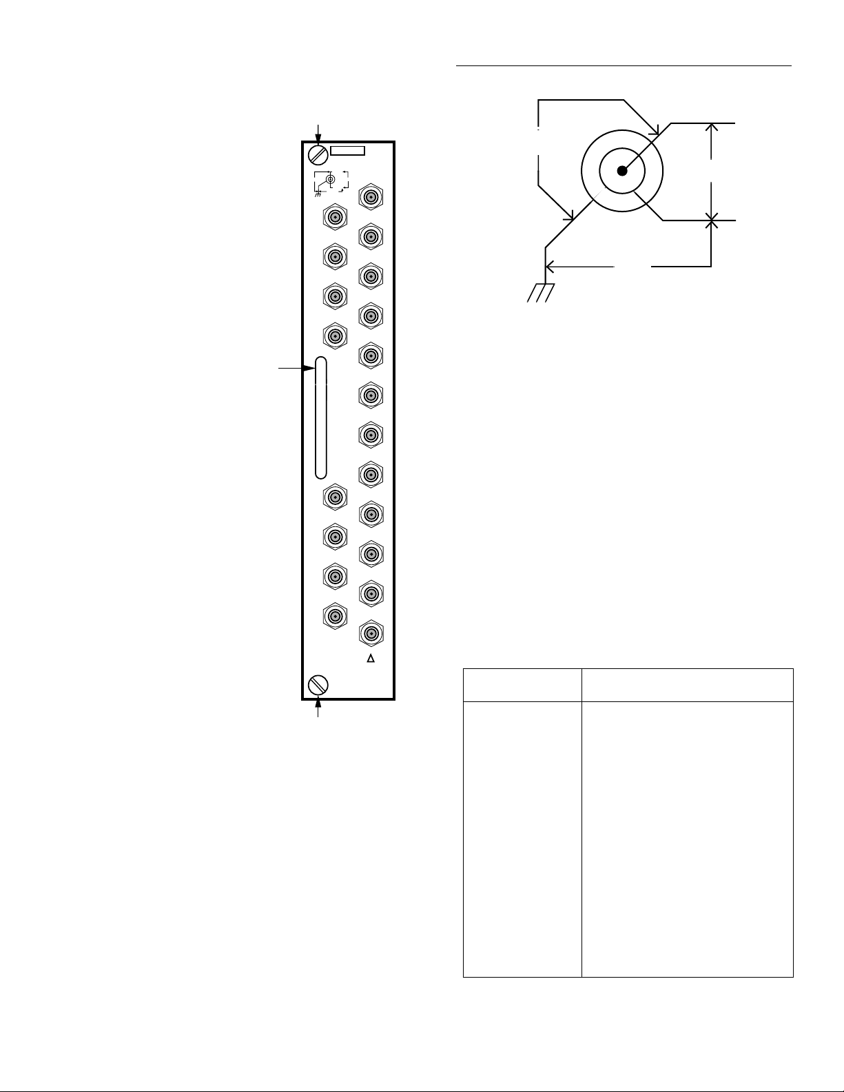
Chassis
Ground
200V
Peak
Guard
200V Peak
Signal
200V
Peak
Caution:
Do not exceed maximum
voltage levels shown.
Figure 2-3
Triax connector configuration
Operation
Mounting
Screw
KEITHLEY
7174A
8x12LOW
CURRENT MATRIX
SIGNAL
200VPK
200VPK
Carrying
Handle
B
C
D
A
200VPK
ROWS
COLUMNS
GUARD
1
2
3
4
5
6
Caution:
Remove internal row
jumpers before removing
card.
Figure 2-2
Card connectors
Mounting
Screw
E
F
10
G
11
H
12
!
WARNING:
TIGHTEN MOUNTING SCREWS
TO ENSURE PROPER
CHASSIS GROUND
MADE INU.S.A.
7
2.5.2 Recommended cables and adapters
8
Table 2-1 summarizes the cables recommended for use with
9
the Model 7174A. Equivalent user-supplied items may be
substituted as long as they are of sufficient quality (low of fset
current, high leakage resistance). Using substandard cables
and connectors may degrade the integrity of the measurements made. See paragraph 2.7 for a discussion of measurement considerations.
Table 2-1
Recommended cables and adapters
Model Description
7078-TRX-x
3-slot male triax connectors on
both ends (x=3, 10 or 20 ft.)
237-BAN-3
3-slot male triax to male banana
plug
237-ALG-2
7078-TRX-BNC
3-slot male triax to alligator clips
3-slot male triax to BNC adapter,
connections to center and inner
shell
7078-TRX-GND
3-slot male triax to BNC adapter,
connections to center and outer
shell
7078-TRX-T
3-slot male to dual 3-lug female
triax tee adapter
6171
3-slot male triax to 2-lug female
triax adapter
CA-93-1
BNC to right angle SMB cable
2-3
Page 19

Operation
2.5.3 T riax banana plug adapter
For instruments that use banana jacks, you need a triax cable
terminated with a 3-slot male triax and a single banana plug.
Use the Model 237-BAN-3 or prepare a special cable as outlined below (Special triax to banana plug cable prepara-
tion) using the parts listed in Table 2-2.
Table 2-2
Parts for special triaxial cable
Keithley part or
model number Description
7078-TRX-3 triax cable*
BG-10-2
*One connector must be cut off
Figure 2-4 shows the conductors and insulation layers of a
triaxial cable. These layers must be carefully stripped back,
cleaned thoroughly and insulated with high insulation resistance material such as Teflon to maintain the integrity of
the cable and measurement system. With the Model 237BAN-3, the center conductor of the triax is connected to the
banana plug. The inner and outer shields have no connection.
With the special cable shown in Figure 2-4, the inner shield
is shorted to the center conductor. Which cable to use
depends on your application. The length of unshielded conductor that is connected to the banana plug should be minimized to maintain signal integrity. The topic of signal
integrity is also discussed in paragraph 2.7 Measurement
considerations.
Triax cable terminated with
3-slot male triax connectors
Red banana plug
4. Strip the insulator back 1/2 inch, then twist the strands
of the conductor together as shown in Figure 2-4(C).
5. Unscrew the cover from a banana plug, then slide the
cover over the conductor.
6. Insert the stripped center conductor through the hole in
the body of the banana plug, then wrap the wire around
the plug body as shown in Figure 2-4(D).
7. Screw on the plastic cover as shown in Figure 2-4(E).
Make certain the wire is secure by gently pulling on the
plug.
Cut
1"
(A) Cut off insulation with knife.
Cut off outer shield.
Insulation Over
Inner Shields
3/4"
(B) Strip insulation off inner shield.
(C) Twist inner shield then strip inner conductor.
Twister inner shield and center conductor together,
slip on plastic cover.
Cut
Note that you can use either an unterminated triax cable, or
cut a dual-connector cable (7078-TRX-10) in half to construct two special cables.
Special triax to banana plug cable preparation
The following steps outline a procedure for installing a
banana plug on the end of a triaxial cable (with inner shield
shorted to center conductor).
1. Using a knife, cut and strip back the jacket about 1-1/2
inches.
2. Remove the outer insulation, then cut away the outer
shield as far as the insulation is stripped as shown in Figure 2-4(A).
3. Carefully strip away the insulation over the inner shield
one inch, then cut the inner shield and guard wire off
even with the stripped insulation as shown in Figure
2-4(B).
2-4
(D) Insert wires into hole and wrap around body.
(E) Screw on plastic cover.
Figure 2-4
Triax cable preparation
Page 20

Operation
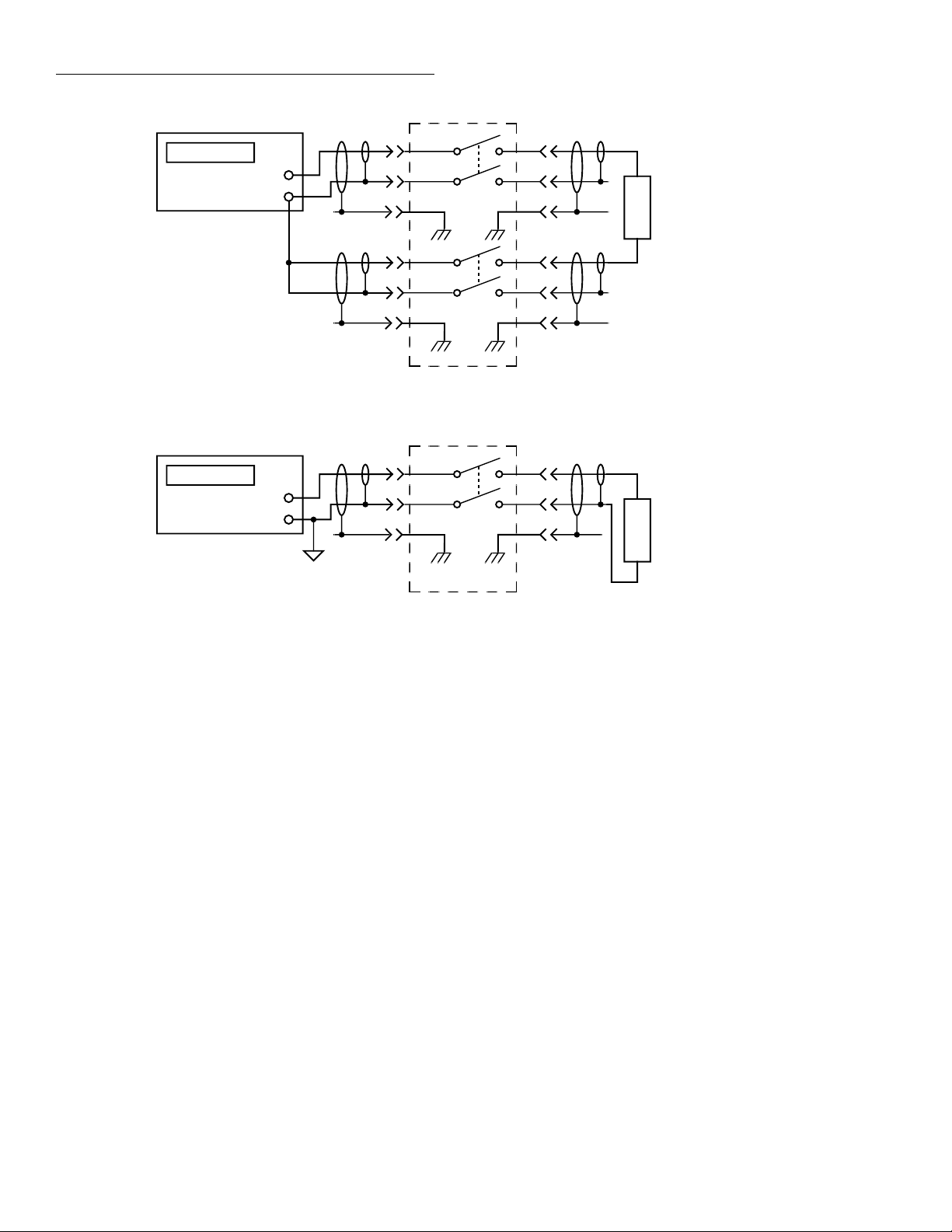
2.5.4 General instrument connections
The following paragraphs discuss connecting the Model
7174A to various general classes of instrumentation such as
DMMs, electrometers, sources, and source/measure units.
Because these configurations are generic in nature, some
modification of the connecting schemes may be necessary
for your particular instrumentation. Also, special cables or
adapters may be necessary. In all cases, 3-lug triax cables
must be used to make the connections.
WARNING
Do not use coaxial cables and adapters
because hazardous voltage from guard
sources may be present on the cable
shields.
Figure 2-5 shows the general instrument connections for the
discussions below. Note that DUT guarding or shielding are
not included here; see Figures 2-22 and 2-23 for shielding
and guarding information. As shown, all figure assume
instruments are connected to rows, and the DUT is connected to columns.
DMM connections
General DMM connections are shown in Figure 2-5 (A), (B),
and (C). Floating connections are shown in (A) with LO and
HI routed to two separate jacks on the Model 7174A. The
common LO connections in (Figure 2-5B) should be used
only for non-critical applications because the performance of
the GUARD pathway is not specified.
WARNING
Hazardous voltage from other guard
sources may be present on LO or the
DUT if other crosspoints are closed.
Electrometer connections
T ypical electrometer connections are shown in Figure 2-5(D)
through (G). The unguarded volts connections in (D) show
the HI signal path routed through one jack, and the LO path
goes through the other connector. Both GUARD pathways
are connected to electrometer LO. For guarded voltage (E),
Model 7174A GUARD is connected to electrometer
GUARD.
The connections for electrometer fast amps and resistance
measurements are shown in Figure 2-5(F) and (G). These
configurations are essentially the same as those discussed
above. For the case of fast amps, both GUARD paths are
connected to electrometer LO, while in the case of guarded
resistance, one GUARD path is connected to electrometer
GUARD, and the other GUARD path is connected to electrometer LO.
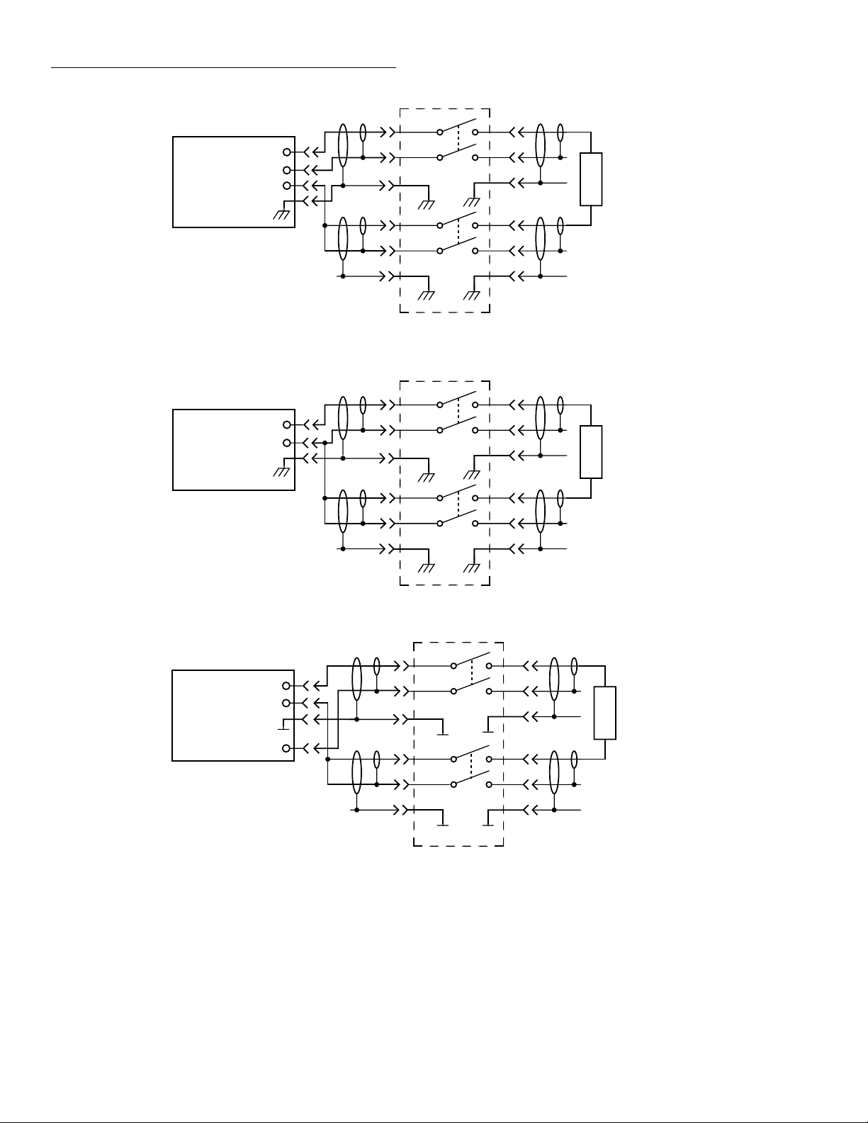
Source connections
Voltage and current source connections are shown in Figure
2-5(H) through (J). The HI and LO paths of the voltage
source (H) are routed through two jacks, with both card
GUARD pathways connected to voltage source LO. For the
unguarded current source connections (I), card GUARD is
again connected to source LO, with source HI and LO routed
through two pathways. In the case of the guarded current
source in (J), card GUARD of the HI signal path is connected
to source GUARD, and the other GUARD path is connected
to source LO.
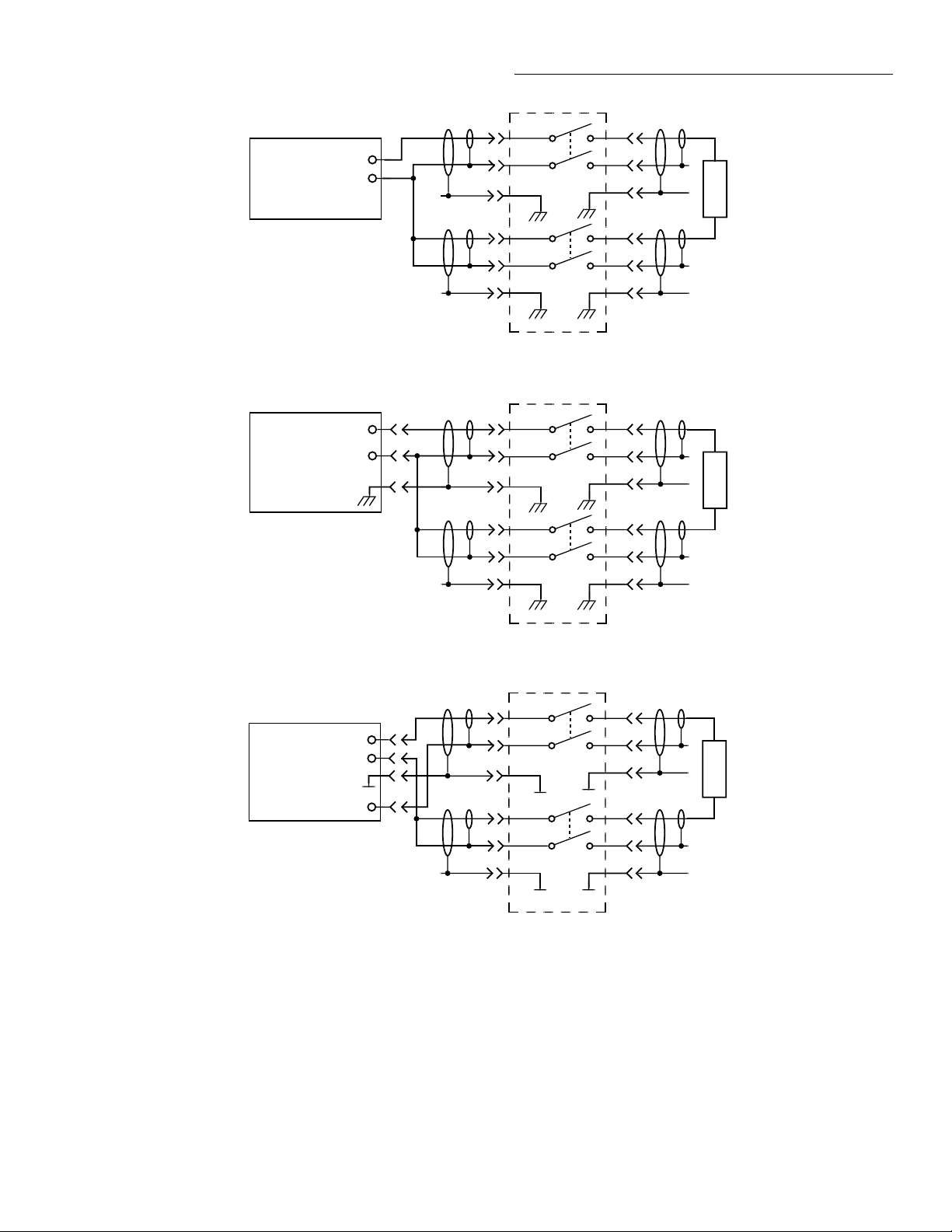
Source/measure unit connections
Figure 2-5(K) shows typical connections for a source/measure unit (SMU). In this instance, a remote-sensing type of a
SMU is shown, requiring a total of four signal pathways to
the DUT. For critical measurements, both source and sense
HI pathways would be guarded as shown, with two of the
four card GUARD pathways connected to SMU GUARD
terminals. As with other instrument connections, the LO card
GUARD pathways are connected to SMU LO terminals.
4-wire DMM connections are shown in Figure 2-5(C). In this
case, a total of four jacks are required; HI, LO, SENSE HI,
and SENSE LO.
2-5
Page 21
Operation
Rows Columns
S
ignal
HI
LO
DMM
A.) DMM Floating
Rows Columns
HI
LO
DMM
Warning:Hazardous voltage from guard
sources may be present on LO.
Guard
Signal
Guard
Signa
Guard
7174A
l
7174A
DUT
DUT
Note: Use this configuration only for
non-critical measurements.
B.) DMM Common LO
Figure 2-5
General instrument connections
2-6
Page 22
Operation
Sense HI
Sense LO
DMM
HI
LO
Rows Columns
Signal
Guard
Signal
Guard
DUT
Signal
Guard
Signal
Guard
C.) DMM 4-Wire
LO
Electrometer
D.) Electrometer, Unguarded Volts
Figure 2-5
General instrument connections (cont.)
HI
7174A
Rows Columns
Signal
Guard
DUT
Signal
Guard
7174A
2-7
Page 23
Operation
Rows Columns
Signal
HI
Guard
LO
Electrometer
E.) Electrometer, Guarded Volts
HI
LO
Electrometer
Guard
DUT
Signal
Guard
7174A
Rows Columns
Signal
Guard
DUT
Signal
Guard
F.) Electrometer,Fast Current
HI
LO
Guard
Electrometer
G.) Electrometer, Resistance (Guarded)
Figure 2-5
General instrument connections (cont.)
7174A
Signal
Guard
DUT
Signal
Guard
7174A
2-8
Page 24
ignal
S
Operation
HI
LO
Voltage
Source
H.) Voltage Source
HI
LO
Electrometer
Guard
DUT
Signal
Guard
7174A
Signal
Guard
DUT
Signal
Guard
I.) Current Source, Unguarded
Guard
Current Source
J.) Current Source, Guarded
Figure 2-5
General instrument connections (cont.)
HI
LO
7174A
Rows Columns
Signal
Guard
DUT
Signal
Guard
7174A
2-9
Page 25

Operation
Force
IorV
Sense
VorI
Source/Measure
Guard
Guard
Unit
HI
LO
HI
LO
Rows Columns
Signal
ua
G
Signal
Guard
S
ignal
uard
G
Signal
Guard
d
r
DUT
K.) Source/Measure Unit
Note: DUT shielding/guarding not shown. See Figures 2-20 and 2-21.
Figure 2-5
General instrument connections (cont.)
7174A
2-10
Page 26

Operation
2.5.5 Keithley instrument connections
The following paragraphs outline connecting typical Keithley instruments to the Model 7174A 8 × 12 Low Current
Matrix Card. Other similar instruments can be connected
using the same cabling as long as their input/output configurations are the same. Instrument connections covered
include:
• Model 617 Electrometer/Source
• Model 196 DMM
• Model 230 Programmable Voltage Source
• Model 220 Programmable Current Source
• Model 590 CV Analyzer
• Model 236/237/238 Source Measure Unit
Model 617 electrometer connections
Connections for the Model 617 Electrometer are shown in
Figure 2-6. The electrometer INPUT and COM can be con-
6172 2-slot to 3-lug
Triax Adapter
Guard off
COM
INPUT
Model 617
nected to any row. Figure 2-6 shows connections to rows A
and B.
1. Connect one end of a Model 7078-TRX- (3, 10, or 20)
3-lug triaxial cable to row A of the Model 7174A.
2. Connect the other end of the triax cable to the Model
617 INPUT connector using a Model 6172 adapter.
3. Connect the triax end of a triax/banana cable to row B of
the Model 7174A.
4. Connect the banana plug end of the triax/banana cable
to the COM terminal of the Model 617. The shorting
link between COM and chassis ground should be removed for this application.
5. Place the GUARD switch in the OFF position.
6. T o connect the v oltage source to the Model 7174A, connect the V-SOURCE HI and LO connector of the Model
617 to the desired row connectors on the matrix card.
Figure 2-6 shows connections to rows C and D.
KEITHLEY
7174A
8x12LOW
CURRENT MATRIX
SIGNAL
200VP K
COLUMNS
200VPK
GUARD
200VP K
7078 - TRX Triax
237-BAN-3 o r Special Triax
237-BAN-3
ROWS
1
A
2
B
3
C
4
D
5
L
6
7
Voltage Source
Connections
Figure 2-6
Model 617 electrometer connections
237-BAN-3 o r Special Triax
Note: See paragraph 2.5.3 and Figure
2-4 f or special triax to banana
cable.
8
E
9
F
10
G
H
!
WARNING:
TIGHTENMOUNTINGSCREWS
TOENSUREPROPER
CHAS SIS GRO UND
11
12
7174A Matrix Card
2-11
Page 27

Operation
Model 196 DMM connections
Connect the Model 196 or other similar DMM to the matrix
card using the general configuration shown in Figure 2-7.
The V OLTS OHMS HI and LO terminals should be connected to the desired rows using triax/banana cables. For 4-wire
ohms measurements, the OHMS SENSE HI and LO termi-
237-BAN-3
237-BAN-3
or Special
Triax
HI
nals should be connected to two additional rows using the
same type of cables.
NOTE
For low-level voltage measurements, connect the inner shield of the HI cable to
VOLT OHMS LO to minimize noise.
KEITHLEY
7174A
8x12LOW
CURRENT MATRIX
SIGNAL
COLUMNS
200VP K
200VPK
GUARD
200VPK
ROWS
A
B
C
D
1
2
Note
3
4
5
L
6
: See paragraph 2.5.3
and Figur
special triax to banana
2-4 for
e
cable.
196 DMM
Connect inner shield to LO for
low-levelmeasurements.
(Modify the cable of Figure 2-4.)
Figure 2-7
Model 196 DMM connections
LO
7
8
E
F
G
H
TIGHTE N MOUNTING SCR EWS
WARNING:
TOENSUREPROPER
CHASSIS GROUND
9
10
11
12
!
7174A Matrix Card
2-12
Page 28

Operation
Model 230 voltage source connections
Connect the Model 230 OUTPUT and COMMON terminal
to the desired rows using triax/banana plug cables, as shown
Common
230 C urrent Source
Note: See paragraph 2.5.3 and Figure
2-4 for special triax to banana cable.
Output
in Figure 2-8. For remote sensing applications, the SENSE
OUTPUT and SENSE COMMON connectors can be routed
through two additional rows using similar cables.
KEITHLEY
7174A
8x12LOW
CURRENT MATRIX
SIGNAL
COLUMNS
200VP K
200VP K
GUARD
200VPK
237-BAN-3 or Special Triax
237-BAN-3
ROWS
A
B
C
D
E
F
G
H
WARNING:
TIGHTENMOUNTING SCRE WS
TOE NSURE P R OPER
CHASSIS GROUND
1
2
3
4
5
6
7
8
9
10
11
12
!
Figure 2-8
Model 230 voltage source connections
7174A Matrix Card
2-13
Page 29

Operation
Model 590 CV analyzer connections
The Model 590 CV analyzer can be connected to any row or
any column as shown in Figure 2-9. The BNC cables that are
. .
590 CV Analyzer
supplied with the Model 590 can be used; however, Model
7078-TRX-BNC adapters must be used at the Model 7174A
end.
7078-TRX-BNC
Triax-to-BNC
Adapters
7051 BNC Cables
KEITHLEY
8x12LOW
CURRENT MATRIX
SIGNAL
200VPK
200VPK
GUARD
200VP K
ROWS
A
B
C
D
E
F
G
H
WARNING :
TIGHTENMOUNTINGSCREWS
TOENSUREPROPER
CHASSISGROUND
7174A
COLUMNS
!
1
2
3
4
5
6
7
8
9
10
11
12
Figure 2-9
Model 590 CV analyzer connections
7174A Matrix Card
2-14
Page 30

Operation
Model 220 current source connections
The Model 220 current source can be connected to the matrix
card using the Model 6167 Guarded Adapter, as shown in
Figure 2-10. This configuration guards the output signal to
minimize the effects of distributed capacitance and leakage
current.
NOTE
The Model 6167 adapter must be modified
by internally disconnecting the inner
shield connection of the input jack from
the GUARDED/UNGUARDED selection
switch. Otherwise, instrument LO will be
Model 6167
Guarded Adapter
connected to chassis ground through the
adapter.
1. Connect the Model 6167 adapter to the Model 220
OUTPUT jack.
2. Connect a Model 7078-TRX-(3, 10 or 20) triax cable
between the guarded adapter and the desired row of the
Model 7174A.
3. Connect the Model 220 GUARD output to GUARD
INPUT terminal of the adapter.
4. Connect the triax end of a triax/banana cable to the
desired row on the Model 7174A.
5. Connect the banana plug end of the triax/banana cable
to the OUTPUT COMMON jack of the Model 220.
KEITHLEY
7174A
8x12LOW
CURRENT MATRIX
SIGNAL
COLUMNS
200VP K
200VP K
GUARD
200VPK
7078-TRX T riax
237-BAN-3 or Special Triax
ROWS
1
A
2
B
3
C
4
D
5
6
Connect GUARD OUT
to GUARD
Note: See paragraph 2.5.3 and Figure
2-4 for special triax to banana cable.
Figure 2-10
Model 220 current source connections
220 C urrent Source
7
8
E
F
G
H
TIGHTENMOUNTING SCRE WS
WARNING:
TOE NSURE P R OPER
CHASSIS GROUND
9
10
11
12
!
7174A Matrix Card
2-15
Page 31

Operation
Model 236/237/238 source measure unit connections
Source measure units are connected to the matrix card using
Model 7078-TRX cables. A Model 237-B AN-3 triax/banana
cable can also be used to connect the output low binding post
on the source measure unit to the matrix. Figure 2-11 shows
connections for remote and local sensing applications.
LINERATING
TRIGGER
MAXOUTPUT
KEITHLEY
GUARD
!
110V
MADEIN
U.S.A.
LO
HI
HI
OUTPUT
OUTPUT
SENSE
GUARD
A. Remote Sensing
OUT IN
OUTPUT
SENSE
LO
LO
LINEVOLTAGE
200V
MAX
SELECTED
LINEF USE
SLOWBLOW
INTERLOCK
50-60Hz
1
ACONLY
100VAMAX
2
IEEE-488INTERFACE
ADDRESSENTERED VIA
FRONTPANEL PROGRAM
CAL
ENABLE
7078-TRX Triax
7078-TRX Triax
7078-TRX Triax
CAUTION
Models 237 and 238 source measure
units can only be used within the specified maximum signal levels of the Model
7174A (200V, 2A).
KEITHLEY
7174A
8x12LOW
CURRENTMATRIX
SIGNAL
200VPK
200VPK
COLUMNS
GUARD
200VPK
ROWS
1
A
2
B
3
C
4
D
5
6
7
8
E
9
F
10
G
11
H
12
WARNING:
!
TIGHTENMOUNTING SCREWS
TOENSUREPROPER
CHASSISGROUND
7174A Matrix Card
TRIGGER
OUT IN
MAXOUTPUT
KEITHLEY
GUARD
!
110V
MADEIN
U.S.A.
OUTPUT
OUTPUT
SENSE
LO
LO
LO
HI
HI
200V
MAX
OUTPUT
SENSE
GUARD
LINEVOLTAGE
SELECTED
LINEF USE
SLOWBLOW
INTERLOCK
ENABLE
B. Local Sensing
Figure 2-11
Model 236/237/238 source measure unit connections
7078-TRX Triax
237-BAN-3 or Special Triax
LINERATING
50-60Hz
1
ACONLY
100VAMAX
2
IEEE-488INTERFACE
ADDRESSENTERED VIA
FRONTPANELPROGRAM
CAL
Caution:
The models 237 and 238 Source Measure Units
can only be used within the specified maximum
signal levels of the Model 7174A (200V, 2A carry).
KEITHLEY
7174A
8x12LOW
CURRENTMATRIX
SIGNAL
COLUMNS
200VPK
200VPK
GUARD
200VPK
ROWS
1
A
2
B
3
C
4
D
5
6
7
8
E
9
F
10
G
11
H
12
!
WARNING:
TIGHTENMOUNTINGSCREWS
TOENSURE PROPER
CHASSISGROUND
7174A Matrix Card
2-16
Page 32

Operation
2.5.6 T ypical test fixture connections
Typically, one or more test fixtures will be connected to
desired columns of the Model 7174A. Typically, the test fix-
tures will be equipped with card-edge connectors with wires
soldered to them. In some cases, the test fixture will be
equipped with triax connectors; for those types, Keithley
Model 7078-TRX-(3, 10, or 20) cables can be used, as shown
in Figure 2-12.
WARNING
Do not use BNC cables and adapters in
cases where hazardous voltages from
guard sources could be present on the
BNC cable shields.
KEI THLE Y
7174A
8x12LOW
CURRENTMATRIX
SIGNAL
COLUMNS
200VP K
200VP K
GUARD
200VP
K
ROWS
A
B
C
D
1
2
3
4
5
Internally, the test fixture should be wired as shown in the
equivalent circuit of Figure 2-13. SIGNAL should be connected to the probe or other device contact points, while
GUARD should be carried through as close to the device as
possible. If coaxial probes are to be used, connect GUARD
to the probe shield if the probe shield is insulated from the
fixture shield.
Usually, the chassis ground terminal of the triax connector
will automatically make contact with the fixture shield by
virtue of the mounting method. However, ground integrity
should be checked to ensure continued protection against
hazardous guard voltages.
3 - Lug Female
Test Fixture
Triax Connectors
(or run cables through strain
reliefs and connect internally)
6
7
8
E
F
G
H
TIGHT EN MOUNTING S CR EWS
WARNING:
TOENSUREPROPER
CHAS SIS GR OUND
9
10
11
12
!
7174A Matrix Card
Figure 2-12
Typical test fixture connections
®
Note: Teflon
-insulated connectors
recommended for specified
performance.
Warning:Donot use BNC connectors
to avoid possible shock
hazard.
2-17
Page 33

Operation
Triax Cable
Signal
Probe
From
7174A
Card
Guard
Chassis
Ground
Figure 2-13
Equivalent circuit of test fixture connections
2.6 Matrix configuration
This section describes the matrix configuration of the Model
7174A. It also explains ways to expand the matrix by installing and connecting additional matrix cards in the Model
707A Switching Matrix.
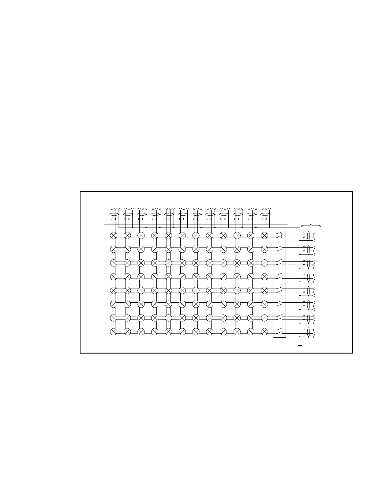
2.6.1 Switching matrix
As shown in Figure 2-14, the Model 7174A is organized as
an 8 × 12 (8 rows by 12 columns) matrix. The rows on the
card are labeled A through H while the columns are numbered 1 through 12. The actual column number to use when
programming depends on the slot and unit number (Table
2-3). For example, card column number 2 on a card in slot 5
of unit 1 is accessed as matrix column 50.
Wafer
Test Fixture Chassis
Each intersecting point in the matrix is called a crosspoint
that can be individually closed or opened by programming
the Model 707A mainframe. By closing the appropriate crosspoint, required pathways and pins may be connected. All
crosspoints are configured for 2-pole switching, as shown in
Figure 2-14. SIGNAL and GUARD are switched separately
to any of the 12 columns on the card.
2.6.2 Path isolators
The path isolator relay switches shown in Figure 2-14 serve
to isolate a given path from the rest of the matrix when no
crosspoint (relay) is closed in that pathway. This topology
minimizes leakage current and capacitance to pathways
which are active. These isolators close automatically when
any crosspoint on the path is closed and open automatically
when all crosspoints on the path are opened.
2-18
Page 34

Columns
HGC HG C HG C HGC HGC HGC HGC HG C HGC HGC HGC
Operation
HGC
User
connections
and expansion
2
2
2
2
2
2
2
2
2
2
2
2
2
2
2
2
2
2
2
2
2
2
2
2
2
2
2
2
2
2
2
2
2
2
2
2
2
2
2
2
2
2
2
2
2
2
2
2
2
2
2
2
2
2
2
2
2
2
2
2
2
2
2
2
2
2
2
2
2
2
2
2
2
2
2
2
2
2
2
Path Isolator
Relay Switch
Signal Guard
Row
2
2
2
2
2
2
2
2
2
2
2
2
2
2
2
2
2
2
2
2
2
2
2
Signal
2
2
2
2
2
2
2
2
2
2
2
2
2
2
2
2
2
2
2
2
2
2
2
2
2
2
2
Guard
2
2
2
2
2
2
2
2
2
2
2
2
2
2
2
2
2
2
2
2
2
2
2
2
2
2
2
2
2
2
2
Note: For schematic,
refer to Section 5.
2
2
2
2
2
2
2
2
2
2
2
2
2
2
2
2
2
2
2
2
2
2
2
2
2
2
2
2
2
2
2
2
H
G
C
H
G
C
H
G
C
H
G
C
H
G
C
H
G
C
H
G
C
H
G
C
Rows
Column
Figure 2-14
Matrix configuration
2-19
Page 35

Operation
Table 2-3
Column numbering by slot and unit
Unit Slot Columns (1 through 12)
1
1
2
3
4
5
6
2
1
2
3
4
5
6
1
3
2
3
4
5
6
1
4
2
3
4
5
6
1
13
25
37
49
61
73
85
97
109
121
133
145
157
169
181
193
205
217
229
241
253
265
277
2
14
26
38
50
62
74
86
98
110
122
134
146
158
170
182
194
206
218
230
242
254
266
278
3
15
27
39
51
63
75
87
99
111
123
135
147
159
171
183
195
207
219
231
243
255
267
279
4
16
28
40
52
64
76
88
100
112
124
136
148
160
172
184
196
208
220
232
244
256
268
280
5
17
29
41
53
65
77
89
101
113
125
137
149
161
173
185
197
209
221
233
245
257
269
281
6
18
30
42
54
66
78
90
102
114
126
138
150
162
174
186
198
210
222
234
2446
258
270
282
7
19
31
43
55
67
79
91
103
115
127
139
151
163
175
187
199
211
223
235
247
259
271
283
8
20
32
44
56
68
80
92
104
116
128
140
152
164
176
188
200
212
224
236
248
260
272
284
9
21
33
45
57
69
81
93
105
117
129
141
153
165
177
189
201
213
225
237
249
261
273
285
10
22
34
46
58
70
82
94
106
118
130
142
154
166
178
190
202
214
226
238
250
262
274
286
11
23
35
47
59
71
83
95
107
119
131
143
155
167
179
191
203
215
227
239
251
263
275
287
12
24
36
48
60
72
84
96
108
120
132
144
156
168
180
192
204
216
228
240
252
264
276
288
2-20
289
1
5
301
2
313
3
325
4
337
5
349
6
290
302
314
326
338
350
291
303
315
327
339
351
292
304
316
328
340
352
293
305
317
329
341
353
294
306
318
330
342
354
295
307
319
331
343
355
296
308
320
332
344
356
297
309
321
333
345
357
298
310
322
334
346
358
299
311
323
335
347
359
300
312
324
336
348
360
Page 36

Operation
2.6.3 Internal matrix expansion
Two to six Model 7174A cards can be connected together
within the mainframe to yield an 8 × N matrix, where N
depends on the number of cards. Figure 2-15 shows an internally expanded matrix with three cards, resulting in an 8 × 36
(eight row by 36 column) matrix. As summarized in Table
2-3, the actual column number used when programming the
unit is determined by the slot.
WARNING
The shells of the row jumpers are at
guard potential. To avoid a possible
shock hazard, always disconnect all
cables from the row and column jacks
before removing or installing jumpers.
Internal
9
10
Paths Jumpers
12
11
131415
Paths
1
2
3
4
5
6
7
8
123
Slot 1 Slot 2 Slot 3
8
6
4
5
7
Because of critical signal paths, rows A-H are not jumpered
through the backplane. Instead, install the supplied coaxial
jumpers between appropriate connectors on Model 7174A
cards (for more critical signal paths, rows can be isolated
from other cards by not installing these cables). Each card
has two coaxial connectors for each row, allowing daisy
chaining of card rows. These connectors can be reached by
lifting the access door on the top of the mainframe; do not
remove cards to install the jumpers. This expansion is sho wn
schematically in Figure 2-15 for cards located in slots 1, 2
and 3.
Figure 2-16 shows the location of the connectors used for
this expansion. These connectors can be reached by lifting
the access door on the top of the Model 707A Switching
Matrix. The jumpers must be installed and removed before
installing or removing a Model 7174A from the 707A
Switching Matrix. Figure 2-17 shows how two cards can be
daisy chained together using the coaxial jumpers.
Internal
Paths Jumpers
18 19
20
212223
24 25 26 27 28
29 303132 333435
16 17
36
Figure 2-15
Connecting three cards for an 8 × 36 matrix
Figure 2-16
Jumper connector locations
ABCDEFGH
Measure
(For each path)
Warning:
Guard potential is on
coaxial jumper shields.
2-21
Page 37

Operation
Figure 2-17
Two cards in daisy chain configuration
2.7 Measurement considerations
Most measurements made with the Model 7174A concern
low-level signals. Such measurements are subject to various
types of noise that can seriously affect low-level measurement accuracy. The following paragraphs discuss possible
noise sources that might affect these measurements.
keep the switching and measuring circuits a good distance
away from these potential noise sources.
2.7.2 Electromagnetic Interference (EMI)
The electromagnetic interference characteristics of the
Model 7174A comply with the electromagnetic compatibility (EMC) requirements of the European Union (EU) directives as denoted by the CE mark. However, it is still possible
for sensitive signals to be affected by external sources. In
these instances, special precautions may be required in the
test setup.
Sources of EMI include:
• Radio and TV broadcast transmitters.
• Communications transmitters, including cellular
phones and handheld radios.
• Devices incorporating microprocessors and high-speed
digital circuits.
• Impulse sources as in the case of arcing in high-voltage
environments.
The Model 7174A, signal source, measuring instrument, and
signal leads should be kept as far away as possible from any
EMI sources. Additional shielding of the card, signal leads,
sources, and measuring instruments will often reduce EMI to
an acceptable level. In extreme cases, a specially constructed
screen room may be required to sufficiently attenuate the
troublesome signal.
2.7.1 Magnetic fields
When a conductor cuts through magnetic lines of force, a
very small current is generated. This phenomenon will frequently cause unwanted signals to occur in the test leads of a
switching matrix system. If the conductor has sufficient
length, even weak magnetic fields like those of the earth can
create sufficient signals to affect low-level measurements.
Two ways to reduce these effects are: (1) reduce the lengths
of the test leads, and (2) minimize the exposed circuit area.
In extreme cases, magnetic shielding may be required. Special metals with high permeability at low flux densities (such
as mu metal) are effective at reducing these effects.
Even when the conductor is stationary, magneticallyinduced signals may still be a problem. Fields can be
produced by various signals such as the AC power line
voltage. Large inductors such as power transformers can also
generate substantial magnetic fields, so care must be taken to
2-22
Many instruments incorporate internal filtering that may
help to reduce EMI effects in some situations. In other cases,
additional external filtering may be required. Keep in mind,
however, that filtering may have detrimental effects, such as
increased settling time, on the measurement.
2.7.3 Ground loops
When two or more instruments are connected together, care
must be taken to avoid unwanted signals caused by ground
loops. Ground Loops usually occur when sensitive instrumentation is connected to other instrumentation with more
than one signal return path such as power line ground. As
shown in Figure 2-18, the resulting ground loop causes
unwanted signals to flow through the instrument LO signal
leads and then back through power line ground. This circulating current develops a small but undesirable voltage
between the LO terminals of the two instruments. This voltage will be added to the source voltage, affecting the accuracy of the measurement.
Page 38

Operation
SIGNALLEADS
INSTRUMENT 1 INSTRUMENT 2 INSTRUMENT 3
GROUND
LOOP
CURRENT
POWER LINE GROUND
Figure 2-18
Power line ground loops
Figure 2-19 shows how to connect several instruments together to eliminate this type of ground loop problem. Here,
there is only one connection to power line ground.
INSTRUMENT 1 INSTRUMENT 2 INSTRUMENT 3
these problems, never touch the connector insulating material. In addition, the matrix card should be used only in clean,
dry environments to avoid contamination.
If the connector insulators should become contaminated,
either by inadvertent touching or from air borne deposits,
they can be cleaned with a cotton swab dipped in clean methanol or an HCFC. After thorough cleaning, they should be
allowed to dry for several hours in a low-humidity environment before use, or they can be dried more quickly using dry
nitrogen.
2.7.5 Noise currents caused by cable flexing
Noise currents can be generated by bending or flexing coaxial, triaxial, or quadraxial cables. Such currents, known as
triboelectric currents, are generated by charges created
between a conductor and insulator caused by friction.
Low-noise cable can be used to minimize these effects. Such
cables have a special graphite coating under the shield to provide lubrication and to provide a conduction path to equalize
charges.
POWER LINE GROUND
Figure 2-19
Eliminating ground loops
Ground loops are not normally a problem with instruments
having isolated LO terminals. However, all instruments in
the test setup may not be designed in this manner. When in
doubt, consult the manual for each instrument in the test setup.
2.7.4 Keeping connectors clean
As is the case with any high-resistance device, the integrity
of connectors can be damaged if they are not handled properly. If the connector insulation becomes contaminated, the
insulation resistance will be substantially reduced, affecting
high-impedance measurement paths.
Oils and salts from the skin can contaminate connector insulators, reducing their resistance. Also, contaminants present
in the air can be deposited on the insulator surface. To avoid
Even low-noise cable generates some noise current when
flexed or subjected to vibration. To minimize these effects,
keep the cables as short as possible, and do not subject them
to temperature variations that could cause expansion or contraction. Tie down offending cables securely to avoid movement, and isolate or remove vibration sources such as motors
or pumps.
2.7.6 Shielding
Proper shielding of all unguarded signal paths and devices
under test is important to minimize noise pickup in virtually
any switching matrix system. Otherwise, interference from
such noise sources as line frequency and RF fields can seriously corrupt a measurement.
In order for shielding to be effective, the shield must completely surround the source, measure and guard signals. It
must also have a low impedance path to chassis ground. This
is shown pictorially in Figure 2-20. The shield also functions
as a safety shield since it is connected to chassis ground.
WARNING
Hazardous voltage may be present if LO
on any instrument is floated above
ground potential.
2-23
Page 39

Operation
To
7174A
Source
Measure
Guard
Chassis
Signal Source and Measure
(Probe or Contact Point)
Figure 2-20
Shielded and guarded
2.7.7 Guarding
Guarding is important in high-impedance circuits where
leakage resistance and capacitance could have degrading
effects on the measurement. Guarding consists of using a
shield surrounding a conductor that is carrying the high
impedance signal. This shield is driven by a low-impedance
amplifier to maintain the shield at signal potential.
Guarding minimizes leakage resistance effects by driving the
cable shield with a unity gain amplifier, as shown in Figure
2-21. Since the amplifier has a high input impedance, it minimizes loading on the high-impedance signal lead. Also, the
low output impedance ensures that the shield remains at signal potential, so that virtually no leakage current flows
through the leakage resistance, RL. Leakage between inner
and outer shields may be considerable, but that leakage is of
little consequence because that current is supplied by the
buffer amplifier rather than the signal itself.
DUT
Source or Measure
Signal
R
R
s
E
s
DUT
Figure 2-21
Guarded circuit
Inner Shield
(Guard or LO)
Outer S hield
(Chassis Ground)
Inner Shield
X1
Buffer
L
E
M
Guard
Measuring
Instrument
In a similar manner, guarding also reduces the effecti ve cable
capacitance, resulting in much faster measurements on highimpedance circuits. Because any distributed capacitance is
charged through the low impedance of the buffer amplifier
rather than by the source, settling times are shortened considerably by guarding.
In order to use guarding effectively with the Model 7174A,
the guard path of the matrix card should be connected to the
guard output of the sourcing or measuring instrument. Figure
2-20 shows typical connections. Guard should be properly
carried through the inner shield to the device under test to be
completely effective. The shielded, guarded test fixture
arrangement shown in Figure 2-20 is also recommended for
safety purposes (guard voltage may be hazardous with some
instruments).
2-24
2.7.8 Matrix expansion effects on card
specifications
Specifications such as those given for path isolation and offset current are with a single Model 7174A card installed in
the mainframe. Expanding the matrix by internally connecting two or more Model 7174A cards together will degrade
system performance specifications (other types of cards do
not affect the specifications because they use different pathways in the mainframe backplane). The extent depends on
how many cards are used, as well as the amount of cabling
used to connect them together.
With internal pathway expansion, isolation among paths is
increased, and offset current is decreased, although the isolator relays on the card do help to minimize these effects.
Page 40

2.8 Coaxial jumper access
To gain access to jumpers, lift jumper across cover (Figure
2-22).
Operation
Figure 2-22
Coaxial jumper access
2-25
Page 41

3
Applications
3.1 Introduction
This section covers typical applications for the Model 7174A
8 × 12 Low Current Matrix Card and is organized as follows:
3.2 CV measurements — Outlines the test configuration
and procedure for making quasistatic and highfrequency CV measurements.
3.3 Semiconductor test matrix — Details a semiconduc-
tor test matrix that can be used to perform a variety of
different tests on semiconductors such as FETs.
3.4 Resistivity measurements— Covers methods to mea-
sure the resistivity of semiconductor samples using the
van der Pauw method.
3.5 Semiconductor IV characterization — Covers the
basic scheme and connections used to generate an IV
curve of a bipolar or MOS transistor.
3.2 CV measurements
The Model 7174A can be used in conjunction with the
Keithley Model 590 CV Analyzer, and the Keithley Model
595 Quasistatic CV Meter to perform quasistatic and highfrequency CV (capacitance vs. voltage) test on
semiconductors. The resulting CV curves can be used to
calculate important semiconductor parameters such as
doping profile, band bending, and mobile ion concentration.
3.2.1 Stand alone system configuration
The stand alone system shown in Figure 3-1 can be used to
make CV measurements without the aid of a computer. System components perform the following functions.
Model 590 CV Analyzer: Measures CV data at 100kHz and
1MHz and sends the resulting data to the plotter for
graphing.
Model 595 Quasistatic CV Meter: Measures quasistatic CV
data and sends the data to the plotter for graphing in real
time.
Model 707A Switching Matrix: Controls the semiconductor
matrix card to close and open the desired crosspoints at the
proper time.
Model 7174A 8 × 12 Low Current Matrix Card: Switches
the signa pathways to the six devices under test.
HP-GL Plotter: Plots CV and other curves directly from the
Models 590 and 595.
3.2.2 Computerized system configuration
Figure 3-2 shows a computerized version of the CV matrix
test system. The addition of a computer allows greater system versatility and easier instrument control. Also, analysis
functions such as doping profile and ion concentration can be
added to the software to expand CV analysis capabilities.
3-1
Page 42

Applications
Devices Under
123456
A
B
C
D
E
F
G
H
7174A Matrix Card
707A Switching Matrix
Figure 3-1
Stand alone CV system configuration
Test
1112345678910 12
Triax
Cables
4801 Low-Noise Cables
S
G
S
G
7078-TRX-BNC
Triax BNC
Adapters
S
G
S
G
7051 BNC
Cables
Model 595
Quasistatic CV Meter
Meter Input
V-Source Output
IEEE-488
Bus
Output
Input
Model 590
CV Analyzer
Note:
Connect plotter to only one
instrument at a time.
HP-GL
Plotter
Devices Under
Test
123456
A
B
C
D
E
F
G
H
7174A Matrix Card
707A Switching Matrix
Triax
Cables
4801 Low-Noise Cables
S
G
S
G
7078-TRX-BNC
Triax BNC
Adapters
S
G
S
G
Model 595
Quasistatic CV Meter
Meter Input
V-Source Output
IEEE-488
Bus
Output
1112345678910 12
Input
7051 BNC
Cables
Model 590
CV Analyzer
IEEE-488 Bus
Note: Remove jumpers to other 7174A cards (if installed)
to optimize Model 595 measurement accuracy.
Computer
HP-GL
Plotter
Figure 3-2
Computerized CV system configuration
3-2
Page 43

Applications
3.2.3 Optimizing CV measurement accuracy
For accurate CV measurements, each Model 590 CV measurement pathway must be corrected using the procedure
outlined in the Model 590 Instruction Manual. The pathways
to each DUT must be cable corrected separately.
Also, for best quasistatic CV results, the corrected capacitance feature of the Model 595 should be used. Corrected
capacitance compensates for any leakage currents present in
the cables, switching matrix, or test fixture. However, care
must be taken when using corrected capacitance to ensure
that the device remains in equilibrium throughout the test
sweep to avoid distorting the CV curves.
In order to minimize the effects of the switching network on
quasistatic CV measurements, cables to the Model 595 and
DUT should be kept as short as possible.
3.2.4 Basic CV test procedure
The fundamental CV test procedure is outlined below. Keep
in mind that this procedure does not address many considerations and aspects of CV testing, which is fairly complex.
The procedure given is for the stand alone system in Figure
3-1. Detailed instrument operating information may be
found in the pertinent instruction manuals.
7. Set up the Model 590 for the expected CV sweep.
8. Close the crosspoints necessary to connect the Model
590 to the device under test. For example, to test device
#1, close G1 and H2.
9. Run a high-frequency test sweep on the device to store
the CV data in the Model 590 buffer.
10. Disconnect the plotter from the Model 595 and connect
it to the Model 590.
11. Generate a plot from the data in the Model 590 buffer.
12. Repeat steps 2 through 11 for the remaining devices, as
required.
Table 3-1
CV test crosspoint summary
Closed crosspoints
Wafer #
1
2
3
4
5
6
Quasistatic (595) High frequency (590)
A1, B2
A3, B4
A5, B6
A7, B8
A9, B10
A11, B12
G1, H2
G3, H4
G5, H6
G7, H8
G9, H10
G11, H12
1. Connect the HP-GL plotter to the IEEE-488 bus connector of the Model 595 only.
2. Set up the Model 595 for the expected CV sweep.
3. Close the crosspoints necessary to connect the Model
595 to the device under test, as summarized in Table 3-1.
For example, to test device #1, close A1 and B2.
4. Place the probes down on the wafer test dots.
5. Run a quasistatic sweep on the selected device and generate a CV curve.
6. Open the crosspoints that are presently closed.
3.2.5 T ypical CV curves
Figure 3-3 and Figure 3-4 shows typical CV curves as
generated by the Model 595 and 590 respectively. The
quasistatic curve shows a fair amount of symmetry, while the
high-frequency curve is highly asymmetrical. The
asymmetrical nature of the high-frequency curve results
from the inability of minority carries to follow the highfrequency test signal.
3-3
Page 44

Applications
+0.6E-10
+0.4E-10
-005.00
+005.00
KEITHLEY 595
Figure 3-3
Typical quasistatic CV curve generated by Model 595
1.50
1.42
1.35
9
0
-
^
0
1
1.27
X
)
d
a
r
a
1.20
F
(
e
c
n
a
t
1.12
i
c
a
p
a
C
1.05
0.97
0.90
0.82
0.75
- 4.99 - 3.99 - 2.99 - 1.99 - 0.99 0.00 1.00 1.99 2.99 3.9 9 4.99
Keithley 590: 00: 00: 10: 500 100KHz X1 Filter ------------- Para llel
Bias (Volt) X 10^+00
Figure 3-4
Typical high-frequency CV curve generated by Model 590
3-4
Page 45

1112345678910 12
A
C
B
D
E
F
G
H
G
SGS G
SGS G
SGS GSG SGSG
G
G
G
G
G
G
S
S
S
S
S
S
HI
G
LO
LO
LO
617
I Measure
HI
HI
V Source
590
CV
HI HI HI LOLOLO
220
Current
Source
196
DMM
V Measure
230
V Source
Device Under Test
Source
Gate
Drain
7174A Matrix Card
707A Switching Matrix
Figure 3-5
Semiconductor test matrix
Applications
3.3 Semiconductor test matrix
Two important advantages of a matrix switching system are
the ability to connect a variety of instruments to the device or
devices under test, as well as the ability to connect any
instrument terminal to any device test node. The following
paragraphs discuss a typical semiconductor matrix test system and how to use that system to perform a typical test:
common-source characteristic testing of a typical JFET.
3.3.1 System configuration
Figure 3-5 shows the configuration for a typical multipurpose semiconductor test matrix. Instruments in the
system perform the following functions.
Model 617 Electrometer/Source: Measures current, and
also could be used to measure voltages up to ±200VDC. The
DC voltage source can supply a maximum of ±100V at currents up to 2mA.
Model 230 Voltage Source: Sources DC voltages up to
±101V at a maximum current of 100mA.
Model 590 CV Analyzer: Adds CV sweep measurement
capability to the system.
Model 220 Current Source: Used to source currents up to a
maximum of 101mA with a maximum compliance voltage
of 105V.
Model 196 DMM: Measure DC voltages in the range of
100nV to 300V. The Model 196 could also be used to measure resistance in certain applications.
Device Under T est: A three-terminal picture for testing such
devices as bipolar transistors and FETs. Additional connections could easily be added to test more complex devices, as
required.
3-5
Page 46

Applications
617
Electrometer/Source
A12
HI
I
D
B9
Meter
(Current)
LO
D
F8 F10
HI
LO
Model 230
Voltage Source
= Closed Crosspoints on 7174A Card (Figure 3-5).
E9
E11
G
V
GS
S
Figure 3-6
System configuration for measuring common-emitter characteristics
3.3.2 T esting common-source characteristic of
FET s
The system shown in Figure 3-5 could be used to test a variety of characteristics including I
and V
DS[OFF]
. To demonstrate a practical use for the system,
we will show how it can be used to generate common source
characteristic curves of a particular JFET.
In order to generate these curves, the instrument must be
connected to the JFET under test, as shown in Figure 3-6.
The advantage of using the matrix is, of course, that it is a
simple matter of closing specific crosspoints. The crosspoints that must be closed are also indicated on the diagram.
GSS
, I
D[OFF]
, I
G[ON]
, I
DSS
,
V
DS
I
(µA)
D9
HI
Voltage
Source
LO
C11
100
90
V=0V
80
70
60
D
50
40
30
20
10
0
0 23456789
1
V(Volts)
DS
GS
V=-0.5V
GS
V=-1V
GS
10
To run the test, V
increments of 0.25V. At each V
voltage (V
DS
drain current, I
is set to specific values, for example in
GS
value, the drain-source
GS
) is stepped across the desired range, and the
, is measured at each value of V
D
. Once all
DS
data are compiled, it is a simple matter to generate the
common-source IV curves, an example of which is shown in
Figure 3-7. If the system is connected to a computer, the test
and graphing could all be done automatically.
3-6
Figure 3-7
Typical common-source FET IV characteristics
Page 47

Applications
3.4 Resistivity measurements
The Model 7174A 8 × 12 Low Current Matrix Card can be
used in conjunction with a Model 220 Current Source and a
Model 196 DMM to perform resistivity measurements on
semiconductors. Such measurements can yield such important information as doping concentration.
3.4.1 T est configuration
Figure 3-8 shows the basic test configuration to make resistivity measurements on van der Pauw samples. The Model
220 sources current through the samples, while the Model
196 measures the voltage developed across the samples. The
matrix card, of course, switches the signal paths as necessary. In order to minimize sample loading, which will reduce
accuracy, the Model 196 DMM should be used only on the
300mV or 3V ranges. Also, this configuration is not recom-
1
3
due to the
2
4
mended for resistance measurements above 1M Ω
accuracy-degrading effects of DMM loading.
1
Sample 1
4
2
3
Sample 2 Sample 3
4
3.4.2 T est procedure
In order to make van der Pauw resistivity measurements,
four terminals of a sample of arbitrary shape are measured.
A current (from the Model 220) is applied to two terminals,
while the voltage is measured (by the Model 196) across the
two opposite terminals, as shown in Figure 3-9. A total of
eight such measurements on each sample are required, with
each possible terminal and current convention. The resulting
voltages are designated V1 through V8.
In order to source current into and measure the voltage
across the sample, specific crosspoints must be closed. Table
3-2 summarizes the crosspoints to close for each voltage
measurement on all three samples from the test configuration
shown in Figure 3-8.
1
2
3
SGSG
A
B
C
D
E
F
G
H
Figure 3-8
Resistivity test configuration
SG
SGSG SGSGSG
SG SGSGSG
7174A Matrix Card
707A Switching Matrix
1112345678910 12
S
G
S
G
S
G
S
G
HI
G
LO
220 Current Source
(Sources Current through Sample)
HI
LO
196 DMM
(Measures Voltage Across Sample)
3-7
Page 48

Applications
I
12
43
V
(A)
V
3
(C) (D)
1
I
12
43
(B)
I
12
43
V
2
1
V
4
43
2
I
V
5
12
43
I
(E) (F)
1
43
I
(G) (H)
2
V
7
Figure 3-9
Resistivity measurement conventions
V
6
12
43
I
I
12
V
43
8
3-8
Page 49

Table 3-2
Crosspoint summary for resistivity measurements
Crosspoint closed
Voltage
Applications
Current
between
Voltage
betweenSample #1 Sample #2 Sample #2
V
V
V
V
V
V
V
V
A1
B4
E3
F2
A5
B9
1
A4
B1
E3
F2
2
A4
B3
3
A3
4
A3
5
A2
6
A2
7
A1
8
B4
B2
B3
B1
B2
E2
E2
E1
E1
E4
E4
F1
F1
F4
F4
F3
F3
A8
A8
A7
A7
A6
A6
A5
B5
B7
B8
B6
B7
B5
B6
E7
E7
E6
E6
E5
E5
E8
E8
3.4.3 Resistivity calculations
Once the eight voltage measurements are known, the resistivity can be calculated. Two values of resistivity, ρ
are initially computed as follows:
1.1331 fAtSV2+V4–V1–V
------------------------------------------------------------------------ -=
ρ
A
1.1331 fBtSV6+V8–V5–V
------------------------------------------------------------------------ -=
ρ
B
()
I
()
I
3
7
and ρ
A
F6
F6
F5
F5
F8
F8
F7
F7
A9
A12
A12
A11
A11
A10
A10
A9
B12
B9
B11
B12
B10
B11
B9
B10
E11
E11
E10
E10
E9
E9
E12
E12
F10
F10
F9
F9
F12
F12
F11
F11
1-2
2-1
2-3
3-2
3-4
4-3
4-1
1-4
3-4
3-4
4-1
4-1
1-2
1-2
2-3
2-3
3.5 Semiconductor IV characterization
A source measure unit such as the Model 236, 237, or 238 is
used to test and characterize many types of devices. One of
B
these is semiconductor devices. The following paragraphs
explain the basic scheme and connections used to generate
an IV curve of a bipolar or MOS transistor. Figure 3-10
shows FET devices connected in a test fixture.
3.5.1 T est configuration
Rows A and B are used to switch the Model 237 Source Measure Unit; rows C and D are used for the Model 236.
Where: ρ
and ρ
A
t
is the sample thickness in cm
S
V
1
are the resistivities in Ω -cm
B
through V
are the voltages measured by the
8
Model 196
I is the current through the sample in amperes
f
and f
are geometrical factors based on sample
B
=f
=1 for perfect symmetry).
A
B
are known, the average resistivity, ρ
B
Once ρ
A
symmetry (f
and ρ
A
can be determined as follows:
ρ
AVG
ρAρB+
------------------ -=
CAUTION
To prevent card damage, do not exceed
the 200 volt maximum rating of the
Model 7174A when switching the Model
237, which is capable of sourcing up to
1100 volts.
AVG
connected in a 4-wire sensing configuration. This connection
At the test fixture, the drain and source leads of the FETs are
,
scheme allows the Model 237 to use remote sensing to
accurately apply Vds to the FETs. The Model 236 uses local
sensing and is used to supply the bias to the gates of the
2
FETs. Since the gates are low current, remote sensing is not
necessary.
If more DUT pins are needed, the system is easily expanded
by adding more Model 7174A matrix cards. Each additional
card will add 12 columns to the system.
3-9
Page 50

Applications
3.5.2 Cable connections
Source Measure Unit and test fixture connections to the
matrix card are accomplished using Model 7078-TRX.
These are three slot triax cables. On each Source Measure
Unit, the banana jack (5-way binding post) is used to access
OUTPUT LO. This connection is made using a Model 237-
Note:
Source Measure Units
Model 237 Model 236
DUT #1
Output HI/Guard
Sense HI/Guard
Sense LO/Output LO
Output LO
Output HI/Guard
Output LO
7078-TRX
Cables
123456789101112
Rows
A
X
B
X
C
D
E
F
G
H
X
X
X
•
•
X
X
X
•
•
123456789101112
BAN-3 or the special cable constructed using the information in Figure 2-4. This allows OUTPUT LO to be applied to
a signal pathway and independently switched. The guard
pathways of the matrix cards are used exclusively to extend
the driven guards of the Source Measure Units to the DUT to
eliminate the effects of leakage current.
Do not connect guards to the
DUT or short them together. If
guarding the inner panel, only
connect one guard line to it.
Test Fixture
DUT #2
DUT #3
Inner
Panel
Warning:
Columns
Test fixture chassis
must be connected
to a safety earth
ground.
7174A
Matrix Card
=
Model 237-BAN-3 or
Triax to banana plug
Modification (see Figure 2-4)
X
=
Crosspoints closed to
apply VDS to DUT #1
•
=
Crosspoints closed to
bias gate of DUT #1
Figure 3-10
Multi unit test system using Models 236 and 237 source measure units
3-10
7174A
Matrix Card
Signal
Guard
Signal
Crosspoint Switching
for all Rows
Guard
Page 51

4
Service Information
4.1 Introduction
WARNING
The service procedures in this section
are intended for use only by qualified
service personnel. Do not perform these
procedures unless qualified to do so.
Failure to recognize and observe normal
safety precautions could result in personal injury or death.
This section contains information necessary to service the
Model 7174A Low Current Matrix Card and is arranged as
follows:
4.2 Handling and cleaning precautions — Discusses
handling precautions and methods to clean the card
should it become contaminated.
4.3 Principles of operation — Briefly discusses circuit
operation.
4.4 Troubleshooting — Presents some troubleshooting
tips for the Model 7174A.
4.5 Special handling of static-sensitive devices —
Reviews precautions necessary when handling staticsensitive devices.
4.6 Performance verification — Describes conditions
and provides references to determine if the card is operating properly.
4.7 Reed pack replacement — Provides a procedure for
replacing faulty reed packs.
4.2 Handling and cleaning precautions
Because of the high-impedance circuits on the Model
7174A, care should be taken when handling or servicing the
card to prevent possible contamination. The following precautions should be taken when servicing the card.
1. Handle the card only by the edges and handle (do not
touch the edge connectors). Do not touch any board surfaces or components not associated with the repair.
2. Do not store or operate the card in an environment
where dust could settle on the circuit board. Use dry nitrogen gas to clean dust off the board if necessary.
3. When making repairs on the circuit board, use aqua core
solder and OA-based (organic acti v ated) flux. Use warm
deionized water along with clean cotton swabs or a
clean, soft brush to remove the flux. Take care not to
spread the flux to other areas of the circuit board. Once
the flux has been removed, blow dry the board with dry
nitrogen gas.
NOTE
Removal of skin oils and other nonorganic contaminants can be done with
methanol or an HCFC.
4. After cleaning, the card should be placed in a 50°C lowhumidity environment for several hours before use.
4-1
Page 52

Service Information
4.3 Principles of operation
The following paragraphs discuss the basic operating principles for the Model 7174A. A schematic diagram of the
matrix card may be found in drawings 9174-106 (mother
board) and 9174-126 (air matrix relay board) located at the
end of Section 5.
4.3.1 Block diagram
Figure 4-1 shows a simplified block diagram of the Model
7174A. Key elements include the buf fer (U410), ID data cir cuits (U406, U408, and U410), relay drivers (U101 through
U113), relays (K101-K204), and the power-on safe guard
(U409). The major elements are discussed below.
4.3.2 ID data circuits
At power up, the card identification data information from
each card is read by the mainframe. This ID data includes
such information as card ID, hardware settling time for the
card, and a relay configuration table, which tells the mainframe which relays to close for a specific crosspoint. This
configuration table is necessary because some cards (such as
the Model 7174A) require the closing of more than one relay
to close a specific crosspoint.
ID Data is contained within an on-card ROM, U406. In order
to read this information, the sequence below is performed
upon power up. Figure 4-2 shows the general timing of this
sequence.
1. The CARDSEL line is brought low, enabling the ROM
outputs. This line remains low throughout the ID data
transmission sequence.
2. The CLRADDR line is pulsed clearing the address
counter to zero. At this point, a ROM address of zero is
selected. This pulse occurs only once.
3. The NEXTADDR line is set low. NEXTADDR going
low increments the counter and enables parallel loading
of the parallel-to-serial converter. NEXTADDR is kept
low long enough for the counter to increment and the
ROM outputs to stabilize. This sequence functions
because the load input of the parallel-to-serial converter
is level sensitive rather than edge sensitive. The first
ROM address is location 1, not 0.
4. The CLK line clocks the parallel-to-serial converter to
shift all eight data bits from the converter to the mainframe via the IDDATA line.
The process in steps 3 and 4 repeats until all the necessary
ROM locations hav e been read. A total of 498 bytes of information are read by the mainframe during the card ID
sequence.
Address
Counter
U407
CLRADDR
To
Mainframe
Figure 4-1
Model 7174A block diagram
A0-A11
NEXTADDR
Buffer
U410
ROM
U406
CARDSEL
IDDATA
RELAYDATA
STROBE
Power-On
Safeguard
U409
D0-D7
CLK
NEXTADDR
Drivers
U101-U113
Output
Enable
Converter
U408
Relay
Parallel
to Serial
Relays
K101-K204
Columns
1-12
Rows
A-H
4-2
Page 53

CARDSEL
CLRADDR
NEXTADDR
Service Information
CLK
IDDATA
HI-Z
Note: ID data sequence occurs on power-up only.
CLRADDR pulse occurs only once.
D7 D6 D5 D4 D3 D2 D1 D0
Figure 4-2
ID data timing
4.3.3 Relay control
The relays are controlled by serial data transmitted via the
RELAY DATA line. A total of 16 bytes for each card are
shifted in serial fashion into latches located in the 16 relay
drivers, (U101 through U113). The serial data is fed in
through the DATA lines under control of the CLK signal. As
data overflows one register, it is fed out the Q’s line of that
register to the next IC down the chain.
Once all 16 bytes have been shifted into each card in the
mainframe, the STROBE line is set high to latch the relay
information into the Q outputs of the relay drivers, and the
appropriate relays are energized (assuming the driver outputs
are enabled, as discussed below). Logic convention is such
that the corresponding relay driver output must be low to
energize the associated relay, while the output is high when
the relay is de-energized. For example, if the Q1 output of
U113 is low, relay K197 will be energized.
HI-Z
4.3.4 Power-on sequence
A power-on safeguard circuit, made up of U409 and associated components, ensures that relays do not randomly energize upon power-up. The tw o ANG gates, U409, make up an
R-S flip-flop. Initially, the Q output of the flip-flop (pin 3 of
U409) is set high upon power up. Since the OEN terminals
of the relay drivers (U101 through U113) are held high, their
outputs are disabled, and all relays remain de-energized
regardless of the relay data information preset at that time.
The first STROBE pulse that comes along (in order to load
relay data) clears the R-S flip-flop, setting the OEN lines of
the relay drivers low to enable their outputs. This action
allows the relays to be controlled by the transmitted relay
data information.
A hold-off period of approximately 470msec is included in
the safeguard circuit to guard against premature enabling of
the relays. The time constant of the hold-off period is determined by the relative values of R419 and C419.
4-3
Page 54

Service Information
4.3.5 Isolator relays
Row isolator relays are necessary in addition to the crosspoint relays in order to ensure the integrity of signal pathways. Path isolator relays include K198-K204. The
necessary isolator relay is closed in addition to the selected
crosspoint to complete the entire pathway. For example, if
crosspoint C10 (Row C, Column 10) is closed, relays K199
and K183 would be energized.
4.4 T roubleshooting
4.4.1 Recommended equipment
T able 4-1 summarizes the recommended equipment for general troubleshooting.
Table 4-1
Recommended troubleshooting equipment
Manufacturer
Description
5 ½ digit DMM
Oscilloscope
Extender card
and model Application
Keithley 199
TEK 2243
Keithley 7070
Measure DC voltages
View logic waveforms
Allow circuit access
4.4.2 Gaining circuit access
In order to gain access to the test points and other circuitry
on the Model 7174A, the card must be plugged into the
Model 7070 Extender Card, which, in turn, must be plugged
into the desired slot of the mainframe. The Model 7070 must
be configured as an extender card by placing the configuration jumper in the EXTEND position. See the documentation
supplied with the Model 7070 for complete details on using
the card.
NOTE
Do not use the Model 7070 for performing
verification tests because its presence will
affect the results.
4.4.3 T roubleshooting procedure
Table 4-2 summarizes the troubleshooting procedure for the
Model 7174A Low Current Matrix Card. Some of the troubleshooting steps refer to the ID data timing diagram shown
in Figure 4-2. Refer to paragraph 4.3 for an overview of oper ating principles.
Table 4-2
Troubleshooting procedure
Step Test point/component Required condition Comments
1
DGND
2
4-4
10
11
3
4
5
6
7
8
9
+6V
+5V
NXTADR
CLRADR
IDDATA
STRB
RLDAT
CLK
OE
U101-U113
pins 10-18
+6VDC
+5VDC
NEXT ADDR pulses
CLR ADDR pulse
ID data pulses
STROBE pulse
Relay data (128 bits)
CLK pulses
High on power up until first
STROBE sets low.
Low with relay energized,
high with relay de-energized.
All voltages referenced to DGND (digital
common)
Relay voltage
Logic voltage
Power up only (Fig. 4-2)
Power up only (Fig. 4-2)
Power up only (Fig. 4-2)
End of relay data sequence
Present when updating relays
Present during relay data or ID data (Fig. 4-2)
Power on safe guard
Relay driver outputs
Page 55

Service Information
4.5 Special handling of static-sensitive devices
CMOS and other high-impedance devices are subject to possible static discharge damage because of the high-impedance
levels in volved. When handling such devices, use the precautions listed below.
NOTE
In order to prevent damage, assume that all
parts are static sensitive.
1. Such devices should be transported and handled only in
containers specially designed to prevent or dissipate
static build-up. Typically , these devices will be received
in anti-static containers made of plastic or foam. Keep
these parts in their original containers until ready for installation or use.
2. Remove the devices from their protective containers
only at a properly-grounded work station. Also ground
yourself with an appropriate wrist strap while working
with these devices.
3. Handle the devices only by the body; do not touch the
pins or terminals.
4. Any printed circuit board into which the device is to be
inserted must first be grounded to the bench or table.
5. Use only anti-static type de-soldering tools and
grounded-tip soldering irons.
4.6 Performance verification
The following paragraphs discuss performance verification
procedures for the Model 7174A, including relay testing,
contact resistance, contact potential, path isolation, and leakage current.
4.6.1 Environment conditions
All verification measurements except for path isolation and
offset current should be made at an ambient temperature of
21°C-25°C and a relative humidity of less than 0% R.H. Path
isolation and offset current verification must be performed at
an ambient temperature of 23°C and a relative humidity of
less than 60% R.H. If the card has been subjected to temperatures or humidities outside of this range for even a short
time, allow it to stabilize within these ranges for at least one
hour before performing any tests.
4.6.2 Recommended test equipment
Table 4-3 summarizes the equipment necessary to make the
performance verification tests, along with the application for
each item.
Table 4-3
Recommended verification equipment
Qty. Description Application
1
Model 617 Electrometer
1
Model 196 6½ Digit DMM
1
Model 707A Switching Matrix
4
Model 7078-TRX-10 triax cables*
2
Model 7078-TRX-3 triax cables
1
Model 6172 2-slot male to 3-lug female triaxial adapter
3
Model 7078-TRX-T triax tee adapter
5
Banana plugs (part #BG-10-2*)
1
Model 263 Calibrator/Source
1
BNC to Right-angle SMB Cable (part #CA-93-1)
1
BNC to Dual Banana Adapter (Pomona part #1269)
*These items are used to construct special cables; see text and Figure 4-9.
Offset current; path isolation
Path resistance; electrometer
All tests
Offset current; path resistance
Path isolation; offset current; electrometer
Offset current; electrometer
Path resistance
Path isolation and resistance
Electrometer
Electrometer
Electrometer
4-5
Page 56

Service Information
4.6.3 Offset current verification
Recommended equipment
• Model 707A Switching Matrix
• Model 617 Electrometer
• Model 7078-TRX-3 Triax Cable
• Model 6172 2-slot male to 3-lug female triaxial adapter
Test connections
Figure 4-3 shows the test connections for offset current
verification. The Model 7174A row being tested is to be
connected to the Model 617 Electrometer input through the
triaxial cable and the triaxial adapter. Note that the
electrometer ground strap is to be removed, and the
electrometer should be operated in the unguarded mode.
Procedure
NOTE
The following procedure should be performed at an ambient temperature of 23°C
and at a relative humidity of less than
60%.
1. Turn on the Model 617 power and allow it to warm up
for two hours before beginning the verification
procedure
6172 2-Slot to
3-Lug Triax Adapter
Guard off
2. With the power off, install the Model 7174A in the
desired slot of the Model 707A Switching Matrix.
Remove all other cards from the instrument, and install
the slot covers.
3. After the prescribed warm up period, select the amps
function and the 2pA range on the Model 617. Zero correct the instrument, and then select autoranging.
4. Connect the Model 617 to row A of the Model 7174A,
as shown in Figure 4-4.
5. Close crosspoint A1 by using the Model 707A front
panel controls.
6. Disable zero check on the Model 617, and allow the
reading to settle.
7. Verify that the offset current reading is <500fA.
8. Enable zero check on the Model 617, and open crosspoint A1.
9. Repeat steps 5 through 8 for crosspoints A2 through
A12. Only one crosspoint at a time should be closed.
10. Disconnect the triax cable from row A, and connect it
instead to row B.
11. Repeat steps 5 through 8 for crosspoints B1 through
B12. Only one crosspoint at a time should be closed.
12. Connect the triax cable to each succeeding row and
repeat steps 5 through 8 for each of the row’s
crosspoints.
Connect Cable
to Row Under
Test
7078-TRX-3 Triax Cable
Ground Link
Removed
200VPK
200VPK
A
B
C
D
KEITHLEY
8x12LOW
CURRENT MATRIX
SIGNAL
200VPK
GUARD
ROWS
7174A
COLUMNS
1
2
3
4
5
617
7174A
A
Equivalent Circuit
Figure 4-3
Offset verification test connections
4-6
617 Electrometer
E
F
G
H
WARNING:
TIGHTENMOUNTING SCREWS
TOENSURE PROPER
CHASSISGROUN
Matrix Card7174A
6
7
8
9
10
11
12
!
D
Page 57

Service Information
4.6.4 Path isolation verification
The procedure for verifying path isolation is discussed below. Should the card fail any of the tests, clean it using the
procedures outlined in paragraph 4.2.
Recommended equipment
• Model 707A Switching Matrix
• Model 617 Electrometer
• Model 7078-TRX-3 Triax Cable
• Unterminated 3-slot triaxial cable (cut connector off
7078-TRX-3)
• Banana plug (Keithley part #BG-10-2)
• #16-18AWG insulated stranded wire (6 in. length)
Test connections
Figure 4-4 shows the test connections for the path isolation
tests. One row being tested is to be connected to the Model
617 Electrometer input through a Model 6172 2-slot female
6172
Adapter
Guard off
to 3-lug male triaxial adapter. The other row is to be connected to the voltage source HI terminal using a specially
prepared 3-slot triax-to-banana plug cable, the construction
of which is shown in Figure 4-5. Note that both the inner
shield and the center conductor are to be connected to the
banana plug as shown.
COM and LO terminal of the electrometer voltage source
must be connected together as shown. Also, the ground link
between COM and chassis must be removed, and the Model
617 guard must be turned off for current measurements.
Procedure
WARNING
Hazardous voltage from the electrometer voltage source will be used in the following steps. Take care not to contact
live circuits, which could cause personal
injury or death.
KEITHLEY
7174A
8x12LOW
CURRENT MATRIX
SIGNAL
200VPK
COLUMNS
200VPK
GUARD
200VPK
7078-TRX-3 Triax Cable
Ground Link
Removed
ROWS
1
A
2
B
3
C
4
D
5
617
7174A
A
F
Equivalent Circuit
Figure 4-4
Connections for path isolation verification
Row A
Row B
617 Electrometer
User-Prepared Triax Cable
(See Figure 4-5)
Warning: Hazardous voltage from
the electrometer source
may be present on terminals.
6
7
8
E
9
F
10
G
11
H
!
WARNING:
TIGHTENM OUNTINGSCREWS
TOENSURE PROPER
CHASSISGROUND
12
7174A Matrix Card
4-7
Page 58

Service Information
Cut
(A) Cut off insulation with knife.
Cut off outer shield.
Insulation Over
Inner Shields
3/4"
(B) Strip insulation off inner shield.
(C) Twist inner shield then strip inner conductor.
Twister inner shield and center conductor together,
slip on plastic cover.
(D) Insert wires into hole and wrap around body.
(E) Screw on plastic cover.
Figure 4-5
Triaxial cable preparation
NOTE
The following procedure must be performed at an ambient temperature of 23°C
and at a relative humidity of less than
60%.
Cut
1. Turn on the Model 617 and allow it to warm up for two
hours for rated accuracy.
2. With the mainframe power turned off, plug the Model
1"
7174A into slot 1 of the mainframe. Remove all other
cards from the mainframe, and install the slot covers.
3. After the prescribed warm up period, select the Model
617 amps function, and enable zero check. Select the
2pA range, and zero correct the instrument.
4. Connect the Model 617 to rows A and B of the matrix
card, as shown in Figure 4-4.
5. Program the Model 617 voltage source for a value of
+100V, but do not yet turn on the voltage source output.
6. Close crosspoints A1 and B2 by using the switching matrix front panel controls.
7. With the Model 617 in amps, enable suppress after the
reading has settled.
8. Turn on the Model 617 voltage source output, and enable the V/I ohms function on the electrometer.
9. After the reading has settled, verify that the resistance is
>67T Ω (6.7 × 10
13
Ω ).
10. Turn off the voltage source, and enable zero check.
Disable suppress, and select the amps function on the
electrometer.
11. Open crosspoints A1 and B2, and close crosspoints A3
and B4.
12. Repeat steps 7 through 11 for A3 and B4.
13. Repeat steps 7 through 12 for crosspoint pairs A5 and
B6, A7 and B8, A9 and B10, and A11 and B12.
14. Disconnect the electrometer from rows A and B, and
connect it instead to rows C and D.
15. Repeat steps 7 through 13 for rows C and D. The path
isolation for these rows should be 67T Ω (6.7 × 10
3
Ω ).
16. Repeat steps 7 through 14 for row pairs E and F, and G
and H. For each row pair, step through the crosspoint
pairs 1 and 2, 3 and 4, 5 and 6, 7 and 8, 9 and 10, and 11
and 12. The complete procedure outlined in steps 7
through 11 should be repeated for each crosspoint pair.
Each resistance measurement for rows E through H
should be 67T Ω (6.7 × 10
13
Ω ).
4-8
Page 59

Service Information
4.6.5 Path resistance verification
The following paragraphs discuss the equipment, connections, and procedure to check path resistance. Should a particular pathway fail the resistance test, the relay (or relays)
for that particular crosspoint is probably defective. See the
schematic diagram at the end of Section 5 to determine
which relay is defective.
NOTE
The following procedure verifies the resistance of the HI signal path. To verify the
resistance of the GUARD path, modify the
cable of Figure 4-5 to connect the inner
shield to the banana plug and have no connection to the triax center conductor.
Recommended equipment
• Model 196 DMM
• 7078-TRX-T triax tee adapters (3)
• 237-BAN-3 triax to banana cables (4)
Connections
Figure 4-6 shows the connections for the path resistance
tests. The Model 196 is to be connected to the row and column jacks using Model 237-BAN-3 triax/banana cables.
These cables differ from the one in Figure 4-5 in that the
inner shield and center conductor are not connected together.
7078-TRX-T
Triax Tee Adapters
237-BAN-3
Triax/Banana
196 DMM
Triax
Figure 4-6
Connections for path resistance verification
7174A
KEITHLEY
8x12LOW
CURRENT MATRIX
SIGNAL
COLUMNS
200VPK
200VPK
GUARD
200VPK
ROWS
B
C
D
E
F
G
H
!
WARNING:
TIGHTENM OUNTINGSCREWS
TOENSURE PROPER
CHASSISGROUND
7174A Matrix Card
4-9
Page 60

Service Information
Procedure
1. Turn on the Model 196 DMM and allow it to warm up
for at least one hour before beginning the test.
2. With the po wer off, install the Model 7174A card in slot
1 of the mainframe.
3. Connect the four triaxial cables to the Model 196 and
the two triax tee adapters (Figure 4-6), but do not yet
connect the adapters to the Model 7174A.
4. Temporarily connect the two triax tee connectors together using a third triax tee adapter, as shown in Figure
4-7.
5. Select the ohms function, 300 Ω range, and 6 ½ digit resolution on the Model 196.
6. After the reading settles, enable zero on the Model 196
DMM. Leave zero enabled for the remainder of the tests.
7. Disconnect the two triax tee adapters from the shorting
adapter, and connect the two adapters with the cable to
To
196
the row A and column 1 connectors on the Model 7174A
(see Figure 4-6).
8. Close crosspoint A1, and allow the reading to settle.
9. Verify that the resistance reading is <1.5 Ω
.
10. Open the crosspoint, and disconnect the triax adapter
from column 1. Connect the adapter to column 2.
11. Repeat steps 8 through 10 for columns 2 through 12. In
each case, the column adapter must be connected to the
column under test, and the crosspoint must be closed.
12. Disconnect the row adapter from row A, and connect it
instead to row B.
13. Repeat steps 8 through 10 for row B. The crosspoints of
interest here are B1 through B12. Also, the row adapter
must be connected to the row being tested.
14. Repeat steps 8 through 13 for rows C through H. In each
case, the crosspoint to close is the one corresponding to
the row and column connections at that time. In all
cases, the measured resistance should be <1.5 Ω
.
To
196
Figure 4-7
Shorting measurement paths using triax tee adapter
4-10
Triax Tee
Adapters
Page 61

Service Information
4.7 Reed pack replacement
If after performing troubleshooting or verification, a reed
switch is thought to be faulty , it should be replaced. Note that
reeds can only be replaced as a pack of three. The part number for a reed pack is RL-179. A reed pack maintenance kit,
part number 9174-MK is also suggested.
Cross point relay
Use the following procedure and Figure 4-8 to replace cross
point relay reed packs.
NOTE
Repairs should only be done from the
component side of the board.
1. Remove the card and place on an anti-static surface.
2. Put on the gloves that came in the maintenance kit.
3. Carefully pry off the cover of the guard enclosure of the
crossbar that includes the suspect reed. Take care not to
break the wire that connects the cover to the front panel.
4. Carefully pry off the cross point interconnect board.
Take care not to break the wires that connect the interconnect board to the front panel.
5. Using clean needle-noise pliers, carefully remove the
reed pack in question.
6. Inspect the relay coil. If there is any debris or
contamination, clean with methanol and blow out with
dry nitrogen.
NOTE
When inserting reed pack, make sure long
leads are inserted into relay coil (bobbin).
7. Using the reed pack insertion tool from the maintenance
kit, install the new reed pack into bobbin making sure
the long leads align with the holes at the base of the relay
coil (bobbin).
8. Reinstall any reed packs that may have been removed
when the cross point interconnect board was removed.
9. Reinstall the cross point interconnect board. Be sure that
it is properly seated.
10. Reinstall the guard enclosure cover.
11. Allow the card to stabilize for one hour.
12. Retest the card to verify operation and specifications.
Isolator relay
Use the following procedure and Figure 4-9 to replace isolator relay reed packs.
NOTE
Repairs should only be done from the
component side of the board.
1. Remove the card and place on an anti-static surface.
2. Put on the gloves that came in the maintenance kit.
3. Carefully pry off the cover of the guard enclosure. Take
care not to break wires connecting the relay to the pathway interconnect board.
4. Using clean needle nose pliers, carefully disconnect the
three wires that attach to the reed pack, taking note of
the locations for each.
5. Remove the reed pack in question.
6. Inspect the reed pack socket. If there is any debris or
contamination, clean with methanol and blow out with
dry nitrogen.
NOTE
When inserting reed pack, make sure long
leads are inserted into relay coil (bobbin).
7. Using the reed pack insertion tool from the maintenance
kit, install the new reed pack into bobbin making sure
the long leads align with the holes at the base of the relay
coil (bobbin).
8. Reconnect the wires to the top of the reed pack.
9. Reinstall the guard enclosure cover.
10. Allow the card to stabilize for one hour.
11. Retest the card to verify operations and specifications.
4-11
Page 62

Service Information
Isolator
Relays (8)
N
ote
When inserting reed
:
pack, make sure long
leads are inserted into
bobbin.
Figure 4-8
Cross point relays
Clear
Triax
Connector
Yellow
TP1
Cross point
Relays (12 sets)
Bobbin
Cross point
Interconnect
Board
Cover
Crosspoint
Relay
Reed Pack
4-12
Page 63

Pathway Interconnect Board
Service Information
Isolator
Relays (8)
Clear
Red
Bobbin
Isolator
Relay
Reed Pack
Note:
When inserting reed
pack, make sure long
leads are inserted into
bobbin.
Black
Red
Black
Yellow
Yellow
Clear
Figure 4-9
Isolator relays
Cross point
Relays (12 sets)
4-13
Page 64

5
Replaceable Parts
5.1 Introduction
This section contains a list of replaceable electrical and
mechanical parts for the Model 7174A, as well as a component layout drawing and schematic diagram of the matrix
card.
5.2 Parts list
Electrical parts are listed in order of circuit designation in
Table 5-1. Table 5-2 summarizes mechanical parts.
5.3 Ordering information
To place an order, or to obtain information about replacement parts, contact your Keithley representative or the factory (see the front of this manual for addresses). When
ordering parts, be sure to include the following information:
1. Matrix card model number 7174A.
2. Card serial number
3. Part description
4. Circuit designation, if applicable
5. Keithley part number
5.4 Factory service
If the matrix card is to be returned to Keithley Instruments
for repair, perform the following:
1. Call the Repair Department at 1-800-552-1115 for a
Return Authorization (RMA) number.
2. Complete the service form located at the back of this
manual, and include it with the unit.
3. Carefully pack the card in the original packing carton or
the equivalent.
4. Write ATTENTION REPAIR DEPARTMENT and the
RMA number on the shipping label. Note that it is not
necessary to return the matrix mainframe with the card.
5.5 Component layout and schematic diagram
Mother board
• Component layout — 9174-100
• Schematic — 9174-106
Relay board
• Component layout — 9174-120
• Schematic — 9174-126 (sheets 1 and 4 only)
Pathway interconnect board
• Component layout — 7174-160
• Schematic — 7174-166
5-1
Page 65

Table 5-1
Model 7174A electrical parts list
Circuit Desig. Description Keithley Part No.
Replaceable Parts
C101-113
C415-418, 421
C413
C414, 425
C419
C420, 423
C422, 424
CR403
CR402
J1001
J1001-1003
K101-204
K101-204
R101-128
R417, 418
R419
R420
R421
R422
R423
CAP, .1µF, 20%, 50V, CERAMIC
CAP, .1µF, 20%, 50V, CERAMIC
CAP, .01µF, 10%, 1000V, CERAMIC
CAP, 10µF, -20+100%, 25V, ALUM ELEC
CAP, 47µF, 10%, 16V, ALUM ELEC
CAP, .01µF, 20%, 50V, CERAMIC
CAP, 270pF, 20%, 100V, CERAMIC/FERRITE
DIODE, SILICON, IN4148 (DO-35)
DIODE, SCHOTTKY, IN5711
CONNECTOR
CONNECTOR, MALE
REED PACK 3 FORM, DUAL GUARDED
RELAY, AIR MATRIX BOBBIN
RES, 22M, 5%, 1/4W, COMPOSITION OR FILM
RES, 10K, 5%, 1/4W, COMPOSITION OR FILM
RES, 47K, 5%, 1/4W, COMPOSITION OR FILM
RES, 200, 5%, 1/4W, COMPOSITION OR FILM
RES, 680, 5%, 1/4W, COMPOSITION OR FILM
RES, 120K, 5%, 1/4W, COMPOSITION OR FILM
RES, 11K, 5%, 1/4W, COMPOSITION OR FILM
C-365-.1
C-365-.1
C-64-.01
C-314-10
C-321-47
C-237-.01
C-386-270P
RF-28
RF-69
CS-598
CS-389-2
RL-179
RL-177
R-76-22M
R-76-10K
R-76-47K
R-76-200
R-76-680
R-76-120K
R-76-11K
U101-113
U406
U407
U408
U409
U410
W401
*Order present firmware revision level.
IC, 8-BIT SERIAL-IN LATCH DRIVER, 5841A
PROGRAM
IC, 12 STAGE BINARY COUNTER, 74HCT4040
IC, 8-BIT PARALLEL TO SERIAL, 74HCT165
IC, QUAD 2 INPUT NAND, 74HCT00
IC, OCTAL BUFFER/LINE DRIVER, 74HC244
STIFFENER, BOARD
IC-536
7174-800A02*
IC-545
IC-548
IC-399
IC-489
J-16
5-3
Page 66

Replaceable Parts
Table 5-2
Model 7174A mechanical parts list
Description Keithley Part No.
#4-40X1/4 PHILLIPS PAN HD SEMS SCREW (9174-162 BOARD TO BRACKETS)
#6-32X3/8LG. PHIL FLAT HD SCR (HANDLE MTG)
#6-32X5/16PHIL PAN HED SEMS SCR (R. PANEL TO MB; BRKT TO BD)
#6-32 PEM NUT
8 POS INTERCONNECT
13 POS INTERCONNECT
BRACKET
BRACKET
CABLE
CABLE ASSEMBLY, 16 CONDUCTOR
CAP, PROTECTIVE
CONN, TEST POINT (DONE,IDDATA,NXTADR,OR,P,/F,RDAT,STRB)
CONN, TEST POINT (+5V, +VTH, -VTH,AGND,CLK,CLRADR,DGND)
CONNECTOR (ON SC-120-4)
FASTENER
FEMALE, BULKHEAD MOUNT RECEPTACLE
GROUND CLIP
GUARD TUBE, BASE
GUARD TUBE, LID
GUARD TUBE, BASE
GUARD TUBE, LID
GUARD TUBE, BASE
GUARD TUBE, LID
HANDLE
LOCKNUT (REL BD TO FASTENERS, BRKT TO BD)
LUG (ON SC-83, SC-120-4)
LUG (ON SC-120-4)
REAR PANEL ASSEMBLY
SOCKET (SOLDERED ON SC-83 AND SC-120-4)
SOCKET, I.C. 28 PIN (FOR U406)
SPACER, LID
STRIP TERMINAL (FOR SC-111)
SUPPORT
TEFLON TWISTED PAIR SHLD
TERMINAL, BIFURCATED (TEFLON)
TEST PIN
TRIAX CONNECTOR (FOR SC-111
WIRE, SINGLE CONDUCTOR
4-40X1/4PPHSEM
6-32X3/8PFH
6-32X5/16PPHSEM
FA-135
9174-315B
9174-314B
9174-307A
9174-308A
CA-121A
CA-27-13C
CAP-30-1
CS-553
CS-553
CS-236
FA-257-1
CS-824
9174-313A
9174-301A
9174-302A
9174-303A
9174-304A
9174-305A
9174-306A
HH-33-1
FA-226-1
LU-108-2
LU-108-2
7174A-301A
SO-144
SO-69
9174-316A
CS-812
9174-309A
SC-83
TE-119
TE-108
CS-827
SC-120-4
5-4
Page 67

M1
Page 68

Page 69

Page 70

Page 71

Page 72

Page 73

Page 74

Index
A
Applications 3-1
B
Basic CV test procedure 3-3
Block diagram 4-2
C
Cable connections 3-10
Card connectors 2-2
Card installation and removal 2-2
Coaxial jumper access 2-25
Component layout and schematic diagram
5-1
Computerized system configuration 3-1
Connections 2-2
CV measurements 3-1
E
Electromagnetic Interference (EMI) 2-22
Environment conditions 4-5
Environmental considerations 2-1
F
Factory service 5-1
Features 1-1
G
Gaining circuit access 4-4
General information 1-1
General instrument connections 2-5
Ground loops 2-22
Guarding 2-24
H
Handling and cleaning precautions 4-1
Handling precautions 2-1
I
ID data circuits 4-2
Inspection for damage 1-2
Instruction manual 1-2
Internal matrix expansion 2-21
Introduction 1-1, 2-1, 3-1, 4-1, 5-1
Isolator relays 4-4
K
Keeping connectors clean 2-23
Keithley instrument connections 2-11
M
Magnetic fields 2-22
Manual addenda 1-2
Matrix configuration 2-18
Matrix expansion effects on card specifica-
tions 2-24
Measurement considerations 2-22
N
Noise currents caused by cable flexing
2-23
O
Offset current verification 4-6
Operation 2-1
Optimizing CV measurement accuracy
3-3
Optional accessories 1-2
Ordering information 5-1
P
Packing for shipment 1-2
Parts list 5-1
Path isolation verification 4-7
Path isolators 2-18
Path resistance verification 4-9
Performance verification 4-5
Power-on sequence 4-3
Principles of operation 4-2
R
Recommended cables and adapters 2-3
Recommended equipment 4-4
Recommended test equipment 4-5
Reed pack replacement 4-11
Relay control 4-3
Replaceable parts 5-1
Resistivity calculations 3-9
Resistivity measurements 3-7
S
Safety symbols and terms 1-2
Semiconductor IV characterization 3-9
Semiconductor test matrix 3-5
Service information 4-1
Shielding 2-23
Shipment contents 1-2
Special handling of static-sensitive devices
4-5
Specifications 1-2
Stand alone system configuration 3-1
Switching matrix 2-18
System configuration 3-5
T
Test configuration 3-7, 3-9
Test procedure 3-7
Testing common-source characteristic of
FETs 3-6
Triax banana plug adapter 2-4
i-1
Page 75

Troubleshooting 4-4
Troubleshooting procedure 4-4
Typical CV curves 3-3
Typical test fixture connections 2-17
U
Unpacking and inspection 1-2
W
Warranty information 1-1
i-2
Page 76

Service Form
Model No. Serial No. Date
Name and Telephone No.
Company
List all control settings, describe problem and check boxes that apply to problem.
Intermittent
❏
❏
IEEE failure
Front panel operational
❏
Display or output (check one)
Drifts
❏
Unstable
❏
❏
Overload
❏
Calibration only
Data required
❏
(attach any additional sheets as necessary)
Show a block diagram of your measurement system including all instruments connected (whether power is turned on or not).
Also, describe signal source.
Analog output follows display
❏
❏
Obvious problem on power-up
All ranges or functions are bad
❏
Unable to zero
❏
Will not read applied input
❏
❏
Certificate of calibration required
Particular range or function bad; specify
❏
❏
Batteries and fuses are OK
Checked all cables
❏
Where is the measurement being performed? (factory, controlled laboratory, out-of-doors, etc.)
What power line voltage is used? Ambient temperature? °F
Relative humidity? Other?
Any additional information. (If special modifications have been made by the user, please describe.)
Be sure to include your name and phone number on this service form
.
Page 77

Keithley Instruments, Inc.
28775 Aurora Road
Cleveland, Ohio 44139
Printed in the U.S.A.
 Loading...