

Page 1
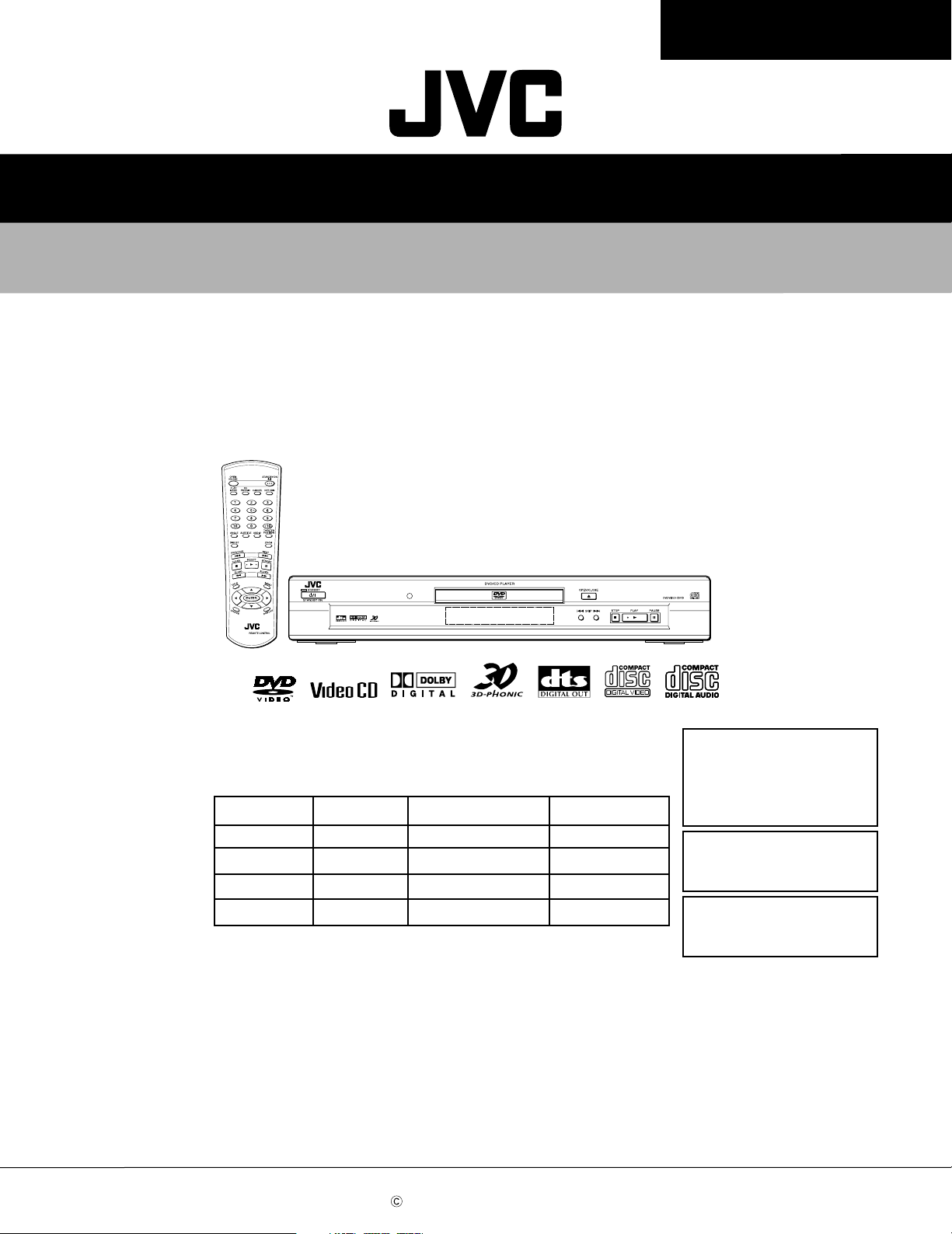
XV-S40BK/XV-S42SL
XV-S45GD/XV-S30BK
SERVICE MANUAL
DVD VIDEO PLAYER
XV-S40BK / XV-S42SL
XV-S45GD / XV-S30BK
˚
Each difference point
Model
XV-S40BK
XV-S42SL
XV-S45GD
XV-S30BK
Body color
Black
Silver
Gold
Black
Optical digital out
Contents
Safety precautions ------------------------ 1-2
Preventing static electricity ------------- 1-3
Importance admistering
point on the safety ------------ 1-4
Area Suffix
(XV-S40BK/XV-S30BK)
J ------------- U.S.A.
AV Compulink
O
O
O
X
Precautions for service ----------------- 1-5
Disassembly method -------------------- 1-6
Adjustment method ---------------------- 1-15
Description of major ICs ---------------- 1-21
O
O
O
X
C ---------- Canada
Area Suffix (XV-S42SL)
C ---------- Canada
Area Suffix (XV-S45GD)
J ------------- U.S.A.
This service manual is printed on 100% recycled paper.
COPYRIGHT 2001 VICTOR COMPANY OF JAPAN, LTD.
No.A0003
Feb. 2001
Page 2
XV-S40BK/XV-S42SL/XV-S45GD/XV-S30BK
Safety Precautions
1. This design of this product contains special hardware and many circuits and components specially
for safety purposes. For continued protection, no changes should be made to the original design
unless authorized in writing by the manufacturer. Replacement parts must be identical to those
used in the original circuits. Services should be performed by qualified personnel only.
2. Alterations of the design or circuitry of the product should not be made. Any design alterations of
the product should not be made. Any design alterations or additions will void the warranty
and will further relieve the manufacture of responsibility for personal injury or property damage
resulting therefrom.
3. Many electrical and mechanical parts in the products have special safety-related characteristics.
These characteristics are often not evident from visual inspection nor can the protection afforded
by them necessarily be obtained by using replacement components rated for higher voltage,
wattage, etc. Replacement parts which have these special safety characteristics are identified in
the Parts List of Service Manual. Electrical components having such features are identified by
shading on the schematics and by ( ) on the Parts List in the Service Manual. The use of a
substitute replacement which does not have the same safety characteristics as the recommended
replacement parts shown in the Parts List of Service Manual may create shock, fire, or other
hazards.
4. The leads in the products are routed and dressed with ties, clamps, tubings, barriers and the
like to be separated from live parts, high temperature parts, moving parts and/or sharp edges
for the prevention of electric shock and fire hazard. When service is required, the original lead
routing and dress should be observed, and it should be confirmed that they have been returned
to normal, after reassembling.
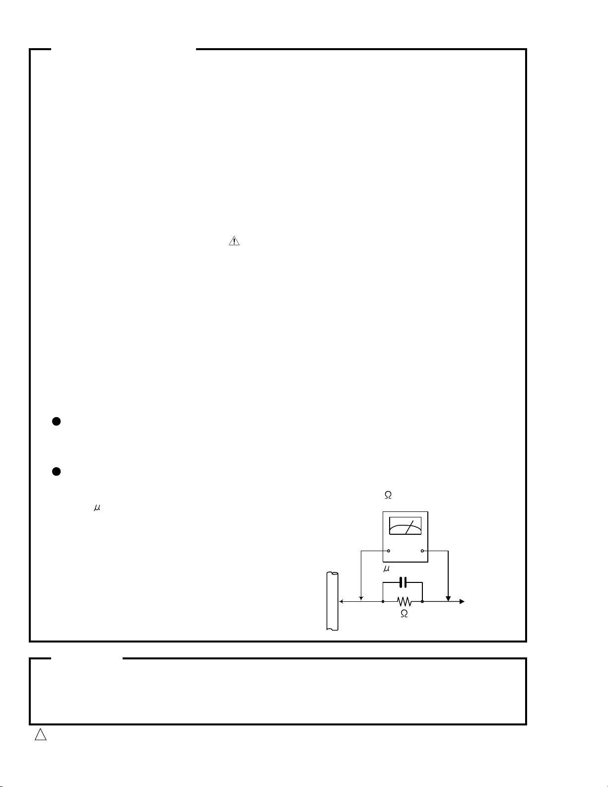
5. Leakage current check (Electrical shock hazard testing)
After reassembling the product, always perform an isolation check on the exposed metal parts of
the product (antenna terminals, knobs, metal cabinet, screw heads, headphone jack, control
shafts, etc.) to be sure the product is safe to operate without danger of electrical shock.
Do not use a line isolation transformer during this check.
Plug the AC line cord directly into the AC outlet. Using a "Leakage Current Tester", measure
the leakage current from each exposed metal parts of the cabinet , particularly any exposed
metal part having a return path to the chassis, to a known good earth ground. Any leakage
current must not exceed 0.5mA AC (r.m.s.)
Alternate check method
Plug the AC line cord directly into the AC outlet. Use an AC voltmeter having, 1,000 ohms
per volt or more sensitivity in the following manner. Connect a 1,500 10W resistor paralleled by
a 0.15 F AC-type capacitor between an exposed
metal part and a known good earth ground.
Measure the AC voltage across the resistor with the
AC voltmeter.
Move the resistor connection to each exposed
metal part, particularly any exposed metal part
having a return path to the chassis, and measure
the AC voltage across the resistor. Now, reverse
the plug in the AC outlet and repeat each
measurement. voltage measured Any must not
exceed 0.75 V AC (r.m.s.). This corresponds to 0.5
0.15 F AC TYPE
1500 10W
Good earth ground
AC VOLTMETER
(Having 1000
ohms/volts,
or more sensitivity)
Place this
probe on
each exposed
metal part.
Warning
1. This equipment has been designed and manufactured to meet international safety standards.
2. It is the legal responsibility of the repairer to ensure that these safety standards are maintained.
3. Repairs must be made in accordance with the relevant safety standards.
4. It is essential that safety critical components are replaced by approved parts.
5. If mains voltage selector is provided, check setting for local voltage.
Burrs formed during molding may be left over on some parts of the chassis. Therefore,
pay attention to such burrs in the case of preforming repair of this system.
1-2
CAUTION
!
Page 3
XV-S40BK/XV-S42SL/XV-S45GD/XV-S30BK
Preventing static electricity
Electrostatic discharge (ESD), which occurs when static electricity stored in the body, fabric, etc. is discharged,
can destroy the laser diode in the traverse unit (optical pickup). Take care to prevent this when performing repairs.
1.1. Grounding to prevent damage by static electricity
Static electricity in the work area can destroy the optical pickup (laser diode) in devices such as DVD players.
Be careful to use proper grounding in the area where repairs are being performed.
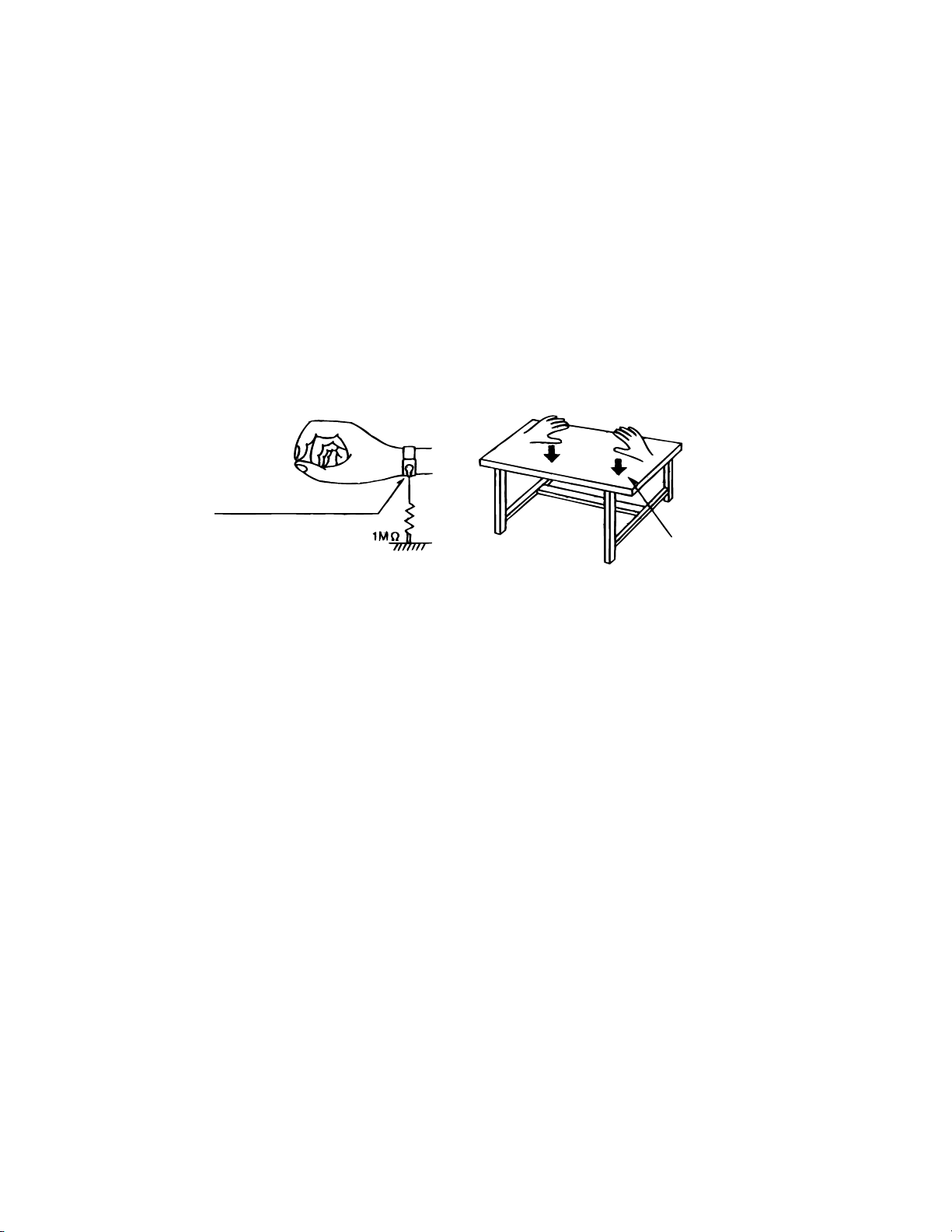
1.1.1. Ground the workbench
1. Ground the workbench by laying conductive material (such as a conductive sheet) or an iron plate over
it before placing the traverse unit (optical pickup) on it.
1.1.2. Ground yourself
1. Use an anti-static wrist strap to release any static electricity built up in your body.
(caption)
Anti-static wrist strap
Conductive material
(conductive sheet) or iron plate
1.1.3. Handling the optical pickup
1. In order to maintain quality during transport and before installation, both sides of the laser diode on the
replacement optical pickup are shorted. After replacement, return the shorted parts to their original condition.
(Refer to the text.)
2. Do not use a tester to check the condition of the laser diode in the optical pickup. The tester's internal power
source can easily destroy the laser diode.
1.2. Handling the traverse unit (optical pickup)
1. Do not subject the traverse unit (optical pickup) to strong shocks, as it is a sensitive, complex unit.
2. Cut off the shorted part of the flexible cable using nippers, etc. after replacing the optical pickup. For specific
details, refer to the replacement procedure in the text. Remove the anti-static pin when replacing the traverse
unit. Be careful not to take too long a time when attaching it to the connector.
3. Handle the flexible cable carefully as it may break when subjected to strong force.
4. It is not possible to adjust the semi-fixed resistor that adjusts the laser power. Do not turn it
1-3
Page 4
XV-S40BK/XV-S42SL/XV-S45GD/XV-S30BK
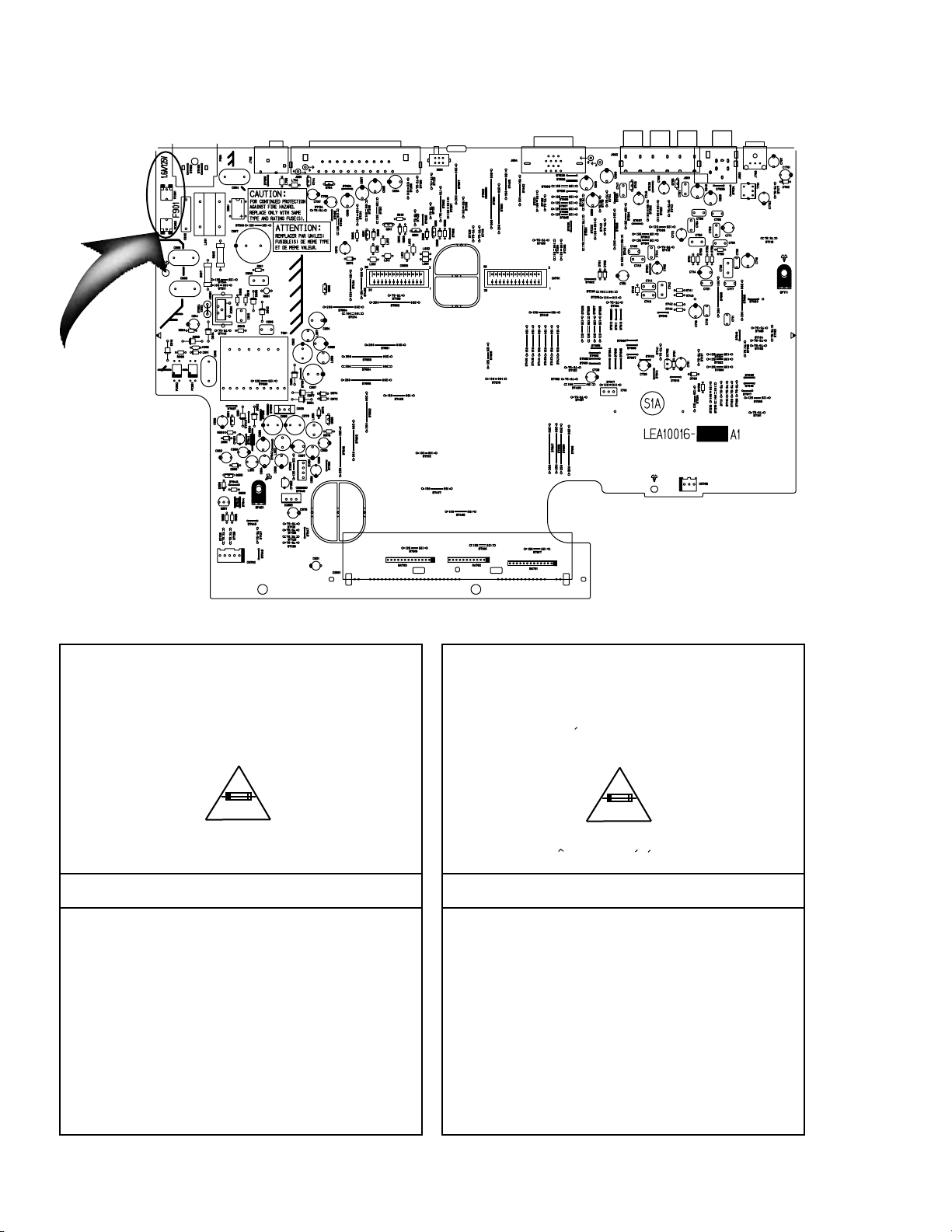
Importance Admistering point on the Safety
Full Fuse Replacement Marking
Graphic symbol mark
(This symbol means fast blow type fuse.)
should be read as follows ;
FUSE CAUTION
FOR CONTINUED PROTECTION AGAINST RISK
OF FIRE, REPLACE ONLY WITH SAME TYPE
AND RATING OF FUSES ;
F901 : 1.6 A / 125 V
Marquage Pour Le Remplacement
Complet De Fusible
Le symbole graphique (Ce symbole signifie
fusible de type a fusion rapide.)
doit etre interprete comme suit ;
PRECAUTIONS SUR LES FUSIBLES
POUR UNE PROTECTION CONTINUE CONTRE
DES RISQUES D'INCENDIE, REMPLACER
SEULEMENT PAR UN FUSIBLE DU MEME TYPE ;
F901 : 1.6 A / 125 V
1-4
Page 5
XV-S40BK/XV-S42SL/XV-S45GD/XV-S30BK
Precautions for Service
Handling of Traverse Unit and Laser Pickup
1. Do not touch any peripheral element of the pickup or the actuator.
2. The traverse unit and the pickup are precision devices and therefore must not be subjected to
strong shock.
3. Do not use a tester to examine the laser diode. (The diode can easily be destroyed by the
internal power supply of the tester.)
4. To replace the traverse unit, pull out the metal short pin for protection from charging.
5. When replacing the pickup, after mounting a new pickup, remove the solder on the short land
which is provided at the center of the flexible wire to open the circuit.
6. Half-fixed resistors for laser power adjustment are adjusted in pairs at shipment to match the
characteristics of the optical block.
Do not change the setting of these half-fixed resistors for laser power adjustment.
Destruction of Traverse Unit and Laser Pickup by Static Electricity
Laser diodes are easily destroyed by static electricity charged on clothing
or the human body. Before repairing peripheral elements of the traverse
unit or pickup, be sure to take the following electrostatic protection:
1. Wear an antistatic wrist wrap.
2. With a conductive sheet or a steel plate on the workbench on which
the traverse unit or the pick up is to be repaired, ground the sheet
or the plate.
3. After removing the flexible wire from the connector (CN101),
short-circuit the flexible wire by the metal clip.
4. Short-circuit the laser diode by soldering the land which is provided
at the center of the flexible wire for the pickup.
After completing the repair, remove the solder
to open the circuit.
Please refer to "Fig.4" of "Disassembly
method" for details.
Short circuit
Servo control
board
1-5
Page 6
XV-S40BK/XV-S42SL/XV-S45GD/XV-S30BK
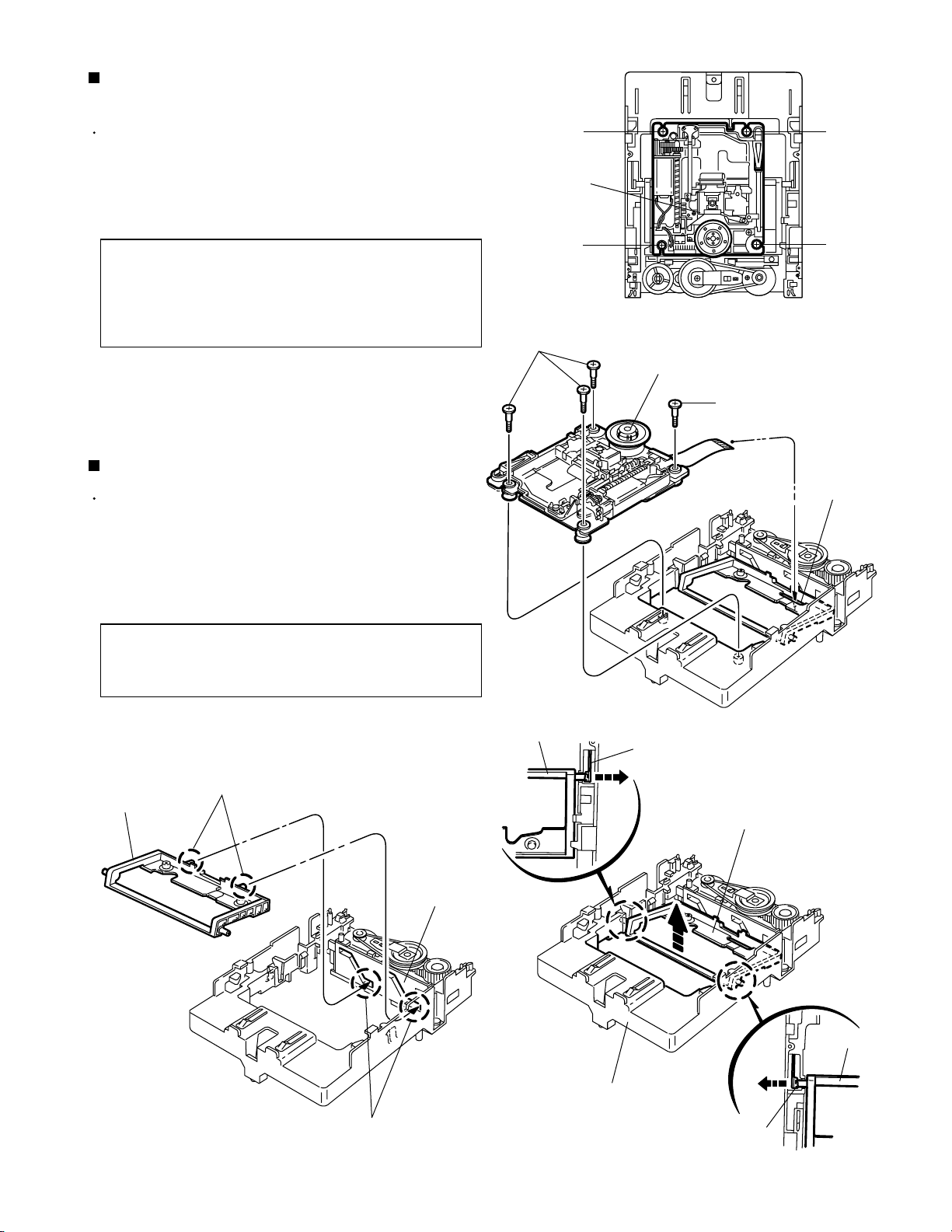
Disassembly method
<Main body>
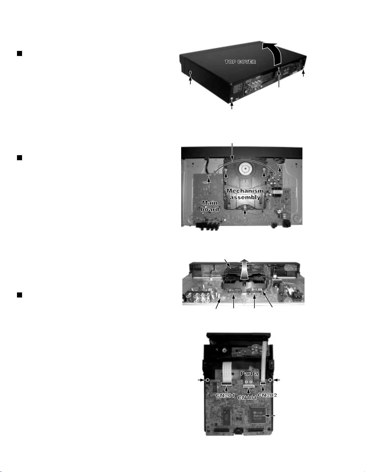
Removing the top cover (see Fig.1)
1.Remove the two screws A attaching the top cover
on both sides of the body.
2.Remove the three screws B attaching the top cover
on the back of the body.
A x 2
B
B
3.Remove the top cover from the body by lifting the
rear part of the top cover.
ATTENTION: Do not break the front panel tab
fitted to the top cover.
Removing the mechanism assembly
(see Fig.2,3)
* Prior to performing the following procedure, remove
the top cover.
* There is no need to remove the front panel assembly.
1.Remove the three screws C attaching the mechanism
assembly on the bottom chassis.
2.The servo control board is removed from the connector
CN961 and CN701 connected with the main board
respectively.
3.Remove the mechanism assembly by lifting the rear part
of the mechanism assembly.
*Please remove lug wire when you do not remove
the mechanism assembly easily.
CN703
Mechanism
assembly
B
Lug wire
C
Fig.2
Fig.1
CN702
C
C
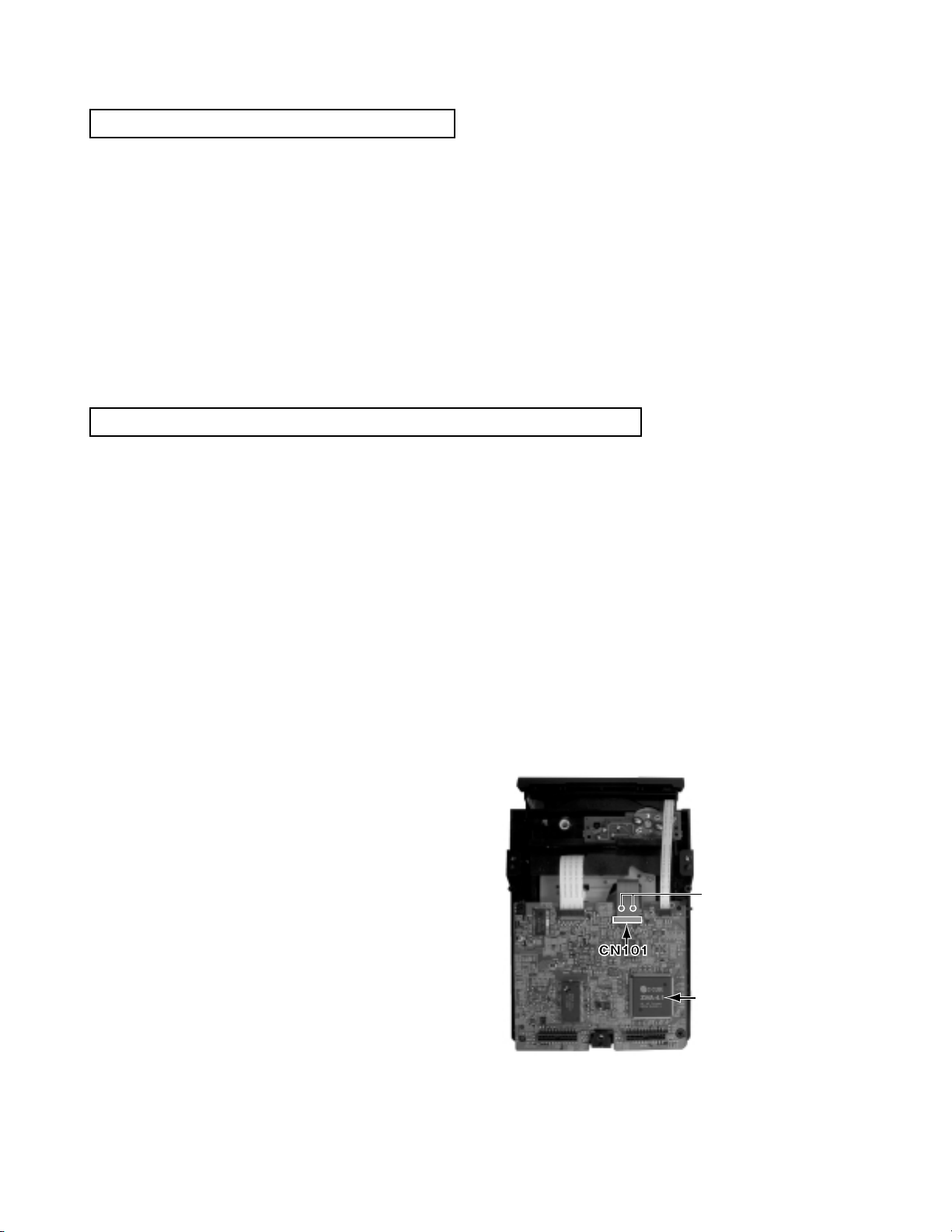
Removing the servo control board
(see Fig.4)
* Prior to performing the following procedure, remove
the top cover and mechanism assembly.
1.Disconnect the card wire from connector CN201 and
CN202 on the servo control board respectively.
2.Disconnect the flexible wire from connector CN101
on the servo control board from pick-up.
ATTENTION
At this time, please extract the wire after short-circuited
of two places on the wire in part a with solder.
Please remove the solder two places of part a after
connecting the wire with CN101 when reassembling.
3.Two places in hook b are removed, the servo control board
is lifted, and it is removed.
1-6
Main board
Hook b
CN701 CN961
Fig.3
Fig.4
Servo control
board
Hook b
Servo control
board
Page 7
Removing the rear panel (see Fig.5)
XV-S40BK/XV-S42SL/XV-S45GD/XV-S30BK
*Prior to performing the following procedure, remove
the top cover.
1.Remove the six screws D attaching the rear panel
on the back of the body.
Removing the front panel assembly
(see Fig.6,7)
* Prior to performing the following procedure, remove
the top cover.
* There is no need to remove the mechanism assembly.
1.Remove the one screw E attaching the front panel
assembly on the bottom chassis.
2.Disconnect the wire from CN702 and CN703 on the
main board respectively.
3.Hook c and d are removed respectively, and the front
panel assembly is removed.
Removing the main board (see Fig.8)
D
Front panel
assembly
Hook d
Hook c
Rear panel
D
Fig.5
E
D
Hook d
Fig.6
* Prior to performing the following procedure, remove
the top cover, mechanism assembly and rear panel.
1.Disconnect the wire from CN702 and CN703 on the
main board respectively.
2.Remove the four screws F attaching the main board
on the bottom chassis.
CN702
CN703
Fig.7
F
CN703
F
F
CN702
Fig.8
F
1-7
Page 8
XV-S40BK/XV-S42SL/XV-S45GD/XV-S30BK
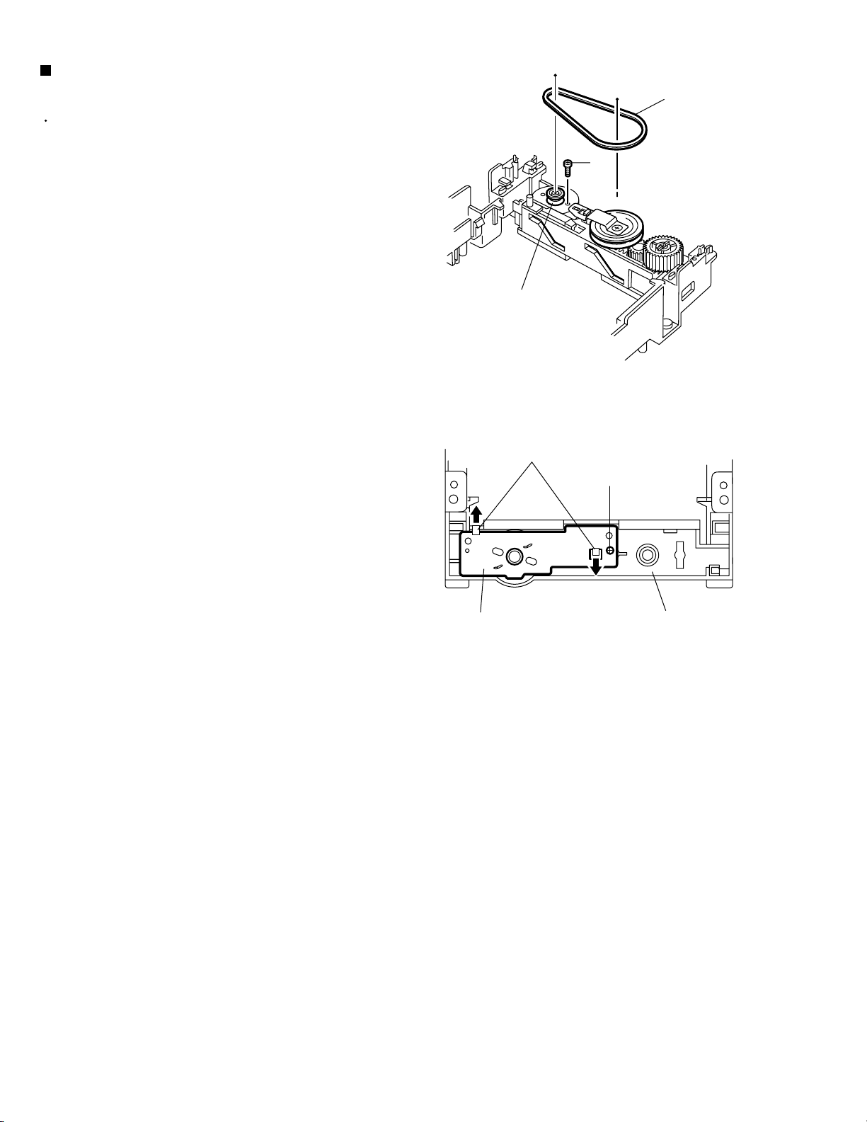
<Loading assembly section>
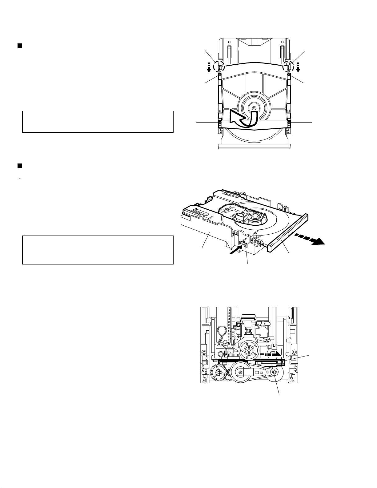
Removing the clamper assembly
(See Fig.1)
1.
Remove the four screws A attaching the clamper
assembly.
2.
Move the clamper in the direction of the arrow to
release the two joints a on both sides.
ATTENTION:
When reattaching, fit the clamper to
the two joints a.
Removing the tray (See Fig.2 and 3)
Prior to performing the following procedure, remove
the clamper assembly.
1.
Push b of the slide cam into the slot on the left side
of the loading base until it stops.
2.
Draw out the tray toward the front.
Joint a
A
Joint a
A
AA
Fig.1
ATTENTION:
Before reattaching the tray, slide the
part c of the slide cam to the right as
shown in Fig.3.
Clamper base
Push
Tray
b
Fig.2
Par t c
Slide cam
Fig.3
1-8
Page 9
Removing the traverse mechanism
assembly (See Fig.4 and 5)
XV-S40BK/XV-S42SL/XV-S45GD/XV-S30BK
Prior to performing the following procedure, remove
the clamper assembly and the tray.
1.
Remove the four screws B attaching the traverse
mechanism assembly.
ATTENTION:
Before reattaching the traverse
mechanism assembly, pass the card
wire extending from the spindle motor
board through the notch d of the
elevator.
Removing the elevator (See Fig.6 and 7)
Prior to performing the following procedure, remove
the clamper assembly, the tray and the traverse
mechanism assembly.
1.
Extend each bar e inside of the loading base
outward and detach the elevator shaft.
B
Traverse mechanism
assembly
B
B
BB
BB
Fig.4
Traverse mechanism assembly
BB
Elevator
Notch d
ATTENTION:
Elevator
When reattaching, first fit the two
shafts on the front of the elevator to
the slots f of the slide cam.
Shafts
Slide cam
Elevator
Fig.5
e
Elevator
Elevator
Loading base
Slots f
e
Fig.6Fig.7
1-9
Page 10
XV-S40BK/XV-S42SL/XV-S45GD/XV-S30BK
Removing the motor assembly
(See Fig.8 and 9)
Prior to performing the following procedure, remove
the clamper assembly, the tray, the traverse
mechanism assembly and the elevator.
1.
Remove the belt from the pulley.
2.
Remove the screw C attaching the motor assembly.
3.
Turn over the body and remove the screw D
attaching the motor assembly.
4.
Release the two tabs g retaining the motor board.
Belt
C
Motor assembly
Fig.8
Tabs g
Motor assembly
D
Loading base
Fig.9
1-10
Page 11
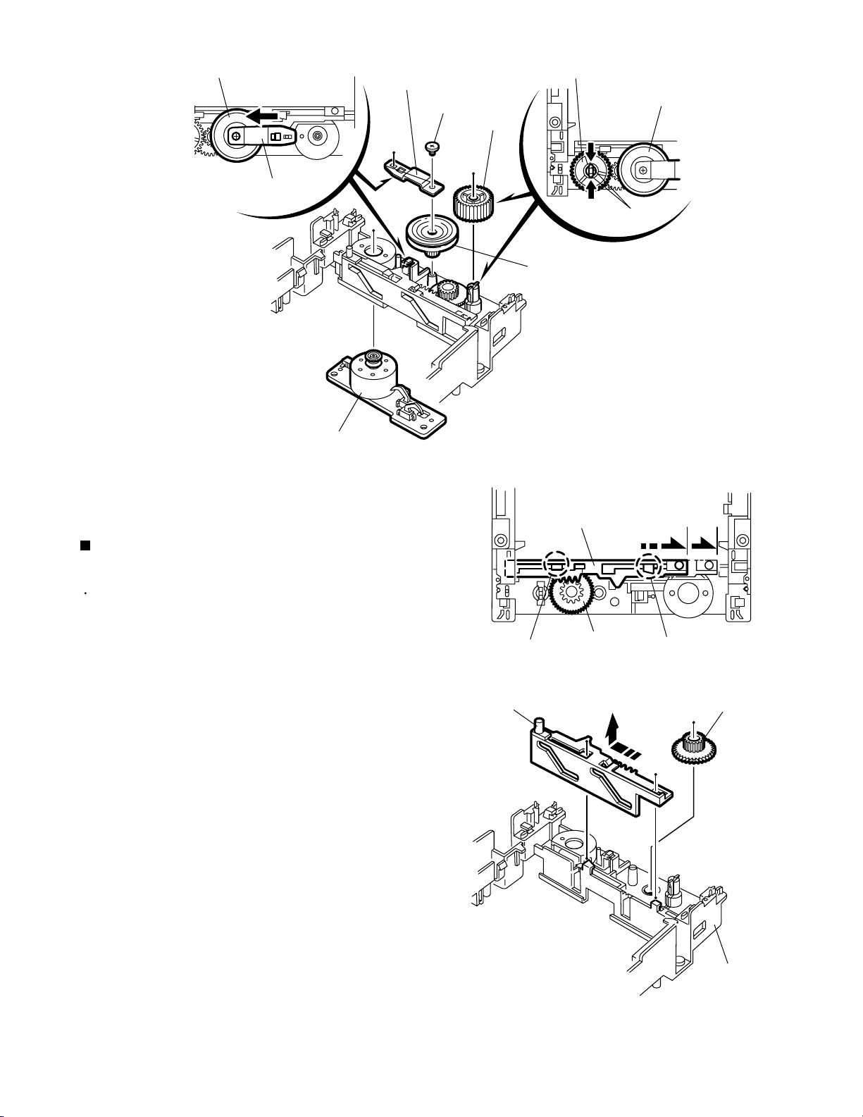
XV-S40BK/XV-S42SL/XV-S45GD/XV-S30BK
Pulley gear
Pulley gear bracket
Motor assembly
Pulley gear bracket
E
Idle gear
Fig.10
Idle gear
Pulley gear
Tads h
Pulley gear
Removing the Idle gear / pulley gear /
middle gear / slide cam (See Fig.10 to 12)
Prior to performing the following procedure, remove
the clamper assembly, the tray, the traverse
mechanism assembly, the elevator and the motor
assembly.
1.
Press the two tabs h inward and pull out the idle
gear.
2.
Remove the screw E attaching the pulley gear
bracket. Slide the pulley gear bracket in the direction
of the arrow and pull out the pulley gear.
3.
Slide the slide cam in the direction of the arrow to
release the two joints i and remove upward.
4.
Remove the middle gear.
Slide cam
Joint i
Slide cam
Middle gear
Joint i
Fig.11
Middle gear
Fig.12
Loading base
1-11
Page 12
XV-S40BK/XV-S42SL/XV-S45GD/XV-S30BK
<Traverse mechanism assembly section>
Removing the feed motor assembly
(See Fig.13)
1.
Unsolder the two soldering j on the spindle motor
board.
2.
Remove the two screws F attaching the feed motor
assembly.
Removing the feed motor
(See Fig.13 to 15)
Prior to performing the following procedure, remove
the feed motor assembly.
1.
Remove the screw G attaching the thrust spring.
Feed motor assembly
F
F
Notch k
Soldering j
Spindle motor board
Pickup
Spindle motor
Fig.13
Feed gear (M)
Thrust spring
ATTENTION:
2.
Remove the feed gear (M).
3.
Pull out the feed gear (E) and the lead screw.
4.
Remove the two screws H attaching the feed motor.
ATTENTION:
When reattaching the thrust spring,
make sure that the thrust spring
presses the feed gear (M) and the feed
gear (E) reasonably.
When reattaching, pass the two cables
extending from the feed motor through
the notch k of the feed holder as
shown in Fig.13.
G
Lead screw
Feed gear (E)
Fig.14
Feed motor
1-12
Feed holder
H
Fig.15
Page 13

XV-S40BK/XV-S42SL/XV-S45GD/XV-S30BK
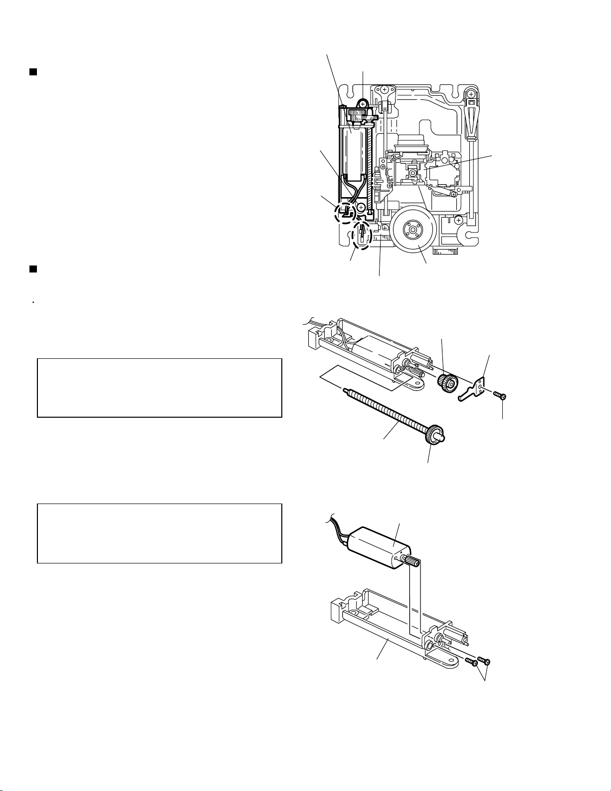
Removing the pickup (See Fig.16 and 17)
1.
Remove the screw I attaching the T spring (S) and
the shaft holder. Remove also the plate.
ATTENTION:
2.
Pull out the part l of the shaft upward. Move the part
m in the direction of the arrow and detach from the
spindle base.
3.
Disengage the joint n of the pickup and the shaft in
the direction of the arrow.
4.
Pull out the shaft from the pickup.
5.
Remove the two screws J attaching the actuator.
6.
Disengage the joint of the actuator and the lead
spring. Pull out the lead spring.
When reattaching, make sure that the
T spring (S) presses the shaft.
Shaft holder
I
Plate
T spring (S)
Lead spring
Pickup
Joint n
Part m
Part l
Fig.16
Actuator
J
Actuator
Lead spring
Shaft
Spring
The spring must be under the shaft when you
install pick-up.
Removing the shaft holder / shaft
(See Fig.18)
1.
Remove the screw K attaching the shaft holder.
2.
Remove the shaft.
Pick-up
Pickup
K
Shaft
Fig.17
Shaft
Shaft holder
Fig.18
1-13
Page 14

XV-S40BK/XV-S42SL/XV-S45GD/XV-S30BK
Removing the spindle motor assembly
(See Fig.19 to 21)
1.
Remove the three screws L attaching the spindle
motor on the bottom of the mechanism base.
ATTENTION:
2.
Remove the three screws M attaching the spindle
base.
When reattaching, pass the card wire
extending from the spindle motor
board through the notch of the spindle
base.
L
L
Spindle motor assembly
Spindle motor
Fig.19
Spindle base
M
L
Fig.20
M
Spindle base
Mechanism base
Fig.21
1-14
Page 15

XV-S40BK/XV-S42SL/XV-S45GD/XV-S30BK
Adjustment method
(1) Initialization method
If microprocessor (IC401,IC402,IC403) or pick-up is replaces, initialize the
DVD player in the following matter
1)Take out the disc and close the tray.
2)Unplug the power plug.
3)Insert power plug into outlet while pressing both PLAY button and OPEN/CLOSE button.
4)FL Display indicate "TEST " . :Version, :Region code
5)Press 3D-PHONIC key button of remote controller. and EEPROM initialize start.
6)When indicate "DTS" on the display, initialize finishes.
7)The power is turned OFF, and Unplug the power plug.
(2) Display of "Laser current value" and "Jitter value"
"Laser current value" and "Jitter value" are displayed on the FL display by the undermentioned
method. Please refer to the failure diagnosis.
1)Take out the disc and close the tray.
2)Unplug the power plug.
3)Insert power plug into outlet while pressing both PLAY button and OPEN/CLOSE button.
4)FL Display indicate "TEST " . :Version, :Region code
5)Press the "OPEN/CLOSE" button to move the tray outward.
Put the test disc (VT-501) on the tray and press "OPEN/CLOSE" button.
The tray should move inward (Note:Don't push to close the tray directly by hand etc.)
6)Press the "PLAY" button.
7)The laser current value and the jitter value is displayed on the FL indicator as follows.
FL Display
* The test mode is canceled when
0 0 4 0 3 9 7 8
Laser current value Jitter value
the power is turned off.
For Laser current value
The laser current value becomes 40mA for the above-mentioned.
Becomes a test mode by doing above-mentioned procedure 1) - 4). Afterwards, the laser current value can
be switched by pushing the key to remote control without turning on the disk.
Remote control "4" key --- Laser of CD
Remote control "5" key --- Laser of DVD
If the laser current value is 64mA or less, it is roughly good. There is a possibility to which pick-up is
deteriorated, and exchange pick-up, please when there are 65mA or more laser current value.
*Returns to a usual test mode by the
thing to push the stop button of
remote control.
1-15
Page 16

XV-S40BK/XV-S42SL/XV-S45GD/XV-S30BK
For Jitter value
The jitter value is displayed by the hexadecimal number and refer to the conversion table of following,please.
If the indication value is 11% or less, it can be judged by this simple checking method that the signal
read precision of the set is satisfactory.
Before using the TEST disc VT-501, careful check it if there is neither damage nor dirt on the read surface.
OPEN
STANDBY/ON
/CLOSE
3D
PLAY
PHONIC
MODE
123
4
7
SUBTITLEANGLE AUDIO
DIGEST
S
U
IO
V
E
R
P
R
A
E
L
C
–
W
O
L
S
E
L
T
I
T
C
H
O
I
C
E
RM-SXVB40A REMOTE CONTROL
CANCEL
56
89
0+1010
SELECT
S
ENTER
RETURN
THEATER
POSITION
ZOOM
N
E
X
T
S
T
R
O
B
E
L
O
W
+
M
E
N
U
Y
A
L
P
S
I
D
3D PHONIC
BUTTON
5 BUTTON
(LASER OF DVD)
4 BUTTON
(LASER OF CD)
POWER BUTTON
STANDBY
STANDBY ON
DOLBY
D I G I T A L
DTS display part
FL Display
DVD/CD PLAYER
OPEN/CLOSE
BUTTON
PLAY BUTTON
OPEN/CLOSE
SKIP
DVD/VIDEO CD/CD
PAUSEPLAYSTOP
Jitter value
FL display FL display
3818
3828
3838
3848
3858
3868
3878
3888
3898
38A8
38b8
38c8
38d8
38E8
38F8
3918
3928
3938
3948
3958
3968
3978
3988
Conversion
value(&)
4.7
4.8
4.9
5.1
5.2
5.3
5.4
5.5
5.7
5.8
5.9
6.0
6.1
6.3
6.4
6.6
6.7
6.9
7.0
7.1
7.2
7.3
7.5
3998
39A8
39B8
39C8
39D8
39E8
39F8
3A18
3A28
3A38
3A48
3A58
3A68
3A78
3A88
3A98
3AA8
3AB8
3AC8
3AD8
3AE8
3AF8
Conversion
value(&)
7.6
7.7
7.8
7.9
8.1
8.2
8.3
8.5
8.7
8.8
8.9
9.0
9.1
9.3
9.4
9.5
9.6
9.7
9.9
10.0
10.1
10.2
FL display FL display
3B18
3B28
3B38
3B48
3B58
3B68
3B78
3B88
3B98
3BA8
3BB8
3BC8
3BD8
3BE8
3BF8
3C18
3C28
3C38
3C48
3C58
3C68
3C78
3C88
Conversion
value(&)
10.5
10.6
10.7
10.8
10.9
11.1
11.2
11.3
11.4
11.5
11.7
11.8
11.9
12.0
12.1
12.4
12.5
12.7
12.7
12.9
13.0
13.1
13.2
3C98
3CA8
3CB8
3CC8
3CD8
3CE8
3CF8
3D18
3D28
3D38
3D48
3D58
3D68
3D78
3D88
3D98
3DA8
3DB8
3DC8
3DD8
3DE8
3DF8
Conversion
value(&)
13.3
13.5
13.6
13.7
13.8
13.9
14.1
14.3
14.4
14.5
14.7
14.8
14.9
15.0
15.1
15.3
15.4
15.5
15.6
15.7
15.9
16.0
1-16
Page 17

Troubleshooting
Servo volume
Press OPEN
/CLOSE key
XV-S40BK/XV-S42SL/XV-S45GD/XV-S30BK
Is tray
operation
Confirmation of tray drive circuit
N
and circuit in surrounding
correct?
Y
Is the traverse moving
along the innermost
N
perimeter for SW detection?
Y
"NO DISC" message appears
Y
immediately after vertical
movement of the pick-up lens
N
The state that DISC does not rotate continues for
several seconds, and becomes NO DISC or an
error display afterwards.
The rotation of DISC becomes high-speed and
abnormal, and becomes NO DISC or an error
display afterwards.
N
Is focus retraction OK?
FE
OFF
Even when it retracts
correctly, if it is out of focus
and makes repeated retries
with a clicking sound, it is
in error.
ON
See "(4) Focus ON error"
N
in "Check points for
individual errors"
Y
Is tracking retraction OK?
See "(3) Traverse movement error"
in "Check points for individual errors"
See "(2) Disk detection, distinction error"
in "Check points for individual errors"
Y
See "(1) Spindle startup error"
in "Check points for individual errors"
Is the inter-layer jump OK?
FE
LO LI
A
Two layers of DVD only.
N
(8) Inter-layer
jump error
Y
TE
OFF
If TE waveform reappears
or fails to converge after the
TE retraction, it is in error.
ON
Y
Is the spindle servo
locked correctly?
Is the RF OUT waveform
locked correctly?
Y
A
See "(5) Tracking ON error"
N
in "Check points for
individual errors"
See "(6) Spindle CLV error"
N
in "Check points for
individual errors"
Has the disc information
been collected?
Stop will result
Y
Is playback
N
possible?
Y
OK !
N
(7) Address read
error
Check (9),(10),(11), and
(12) items in "Check points
for individual errors"
1-17
Page 18

XV-S40BK/XV-S42SL/XV-S45GD/XV-S30BK
Check points for each error
(1) Spindle start error
1.Defective spindle motor
*Are there several ohms resistance between each pin of CN201 "5-6","6-7","5-7"?
(The power supply is turned off and measured.)
*Is the sign wave of about 100mVp-p in the voltage had from each terminal?
[ CN201"9"(H1-),"10"(H1+),"11"(H2-),"12"(H2+),"13"(H3-),"14"(H3+) ]
2.Defective spindle motor driver (IC251)
*Has motor drive voltage of a sine wave or a rectangular wave gone out to each terminal(SM1~3)
of CN201"5,6,7" and IC251"2,4,7"?
*Is FG pulse output from the terminal of IC251"24"(FG) according to the rotation of the motor?
*Is it "L(about 0.9V)" while terminal of IC251"15"(VH) is rotating the motor?
3.Has the control signal come from servo IC or the microcomputer?
*Is it "L" while the terminal of IC251"16"(SBRK) is operating?
Is it "H" while the terminal of IC251"23"(/SPMUTE) is operating?
*Is the control signal input to the terminal of IC251"22"(EC)?
(changes from VHALF voltage while the motor is working.)
*Is the VHALF voltage input to the terminal of IC251"21"(ECR)?
4.Is the FG signal input to the servo IC?
*Is FG pulse input to the terminal of IC201"53"(FG) according to the rotation of the motor?
(2) Disc Detection, Distinction error (no disc, no RFENV)
* Laser is defective.
* Front End Processor is defective (IC101).
* APC circuit is defective. --- Q101,Q102.
* Pattern is defective. --- Lines for CN101 - All patterns which relate to pick-up and patterns between IC101
* Servo IC is defective (IC201).
* IC101 --- For signal from IC101 to IC201, is signal output from IC101 "20" (ASOUT) and
IC101 "41"(RFENV) and IC101 "22" (FEOUT)?
1-18
Page 19

(3) Traverse movement NG
1.Defective traverse driver
*Has the voltage come between terminal of CN101 "1" and "2" ?
2.Defective BTL driver (IC271)
*Has the motor drive voltage gone out to IC271"17" or "18"?
3.Has the control signal come from servo IC or the microcomputer?
*Is it "H" while the terminal of IC271"9"(STBY1) ?
*TRSDRV Is the signal input?
4.TRVSW is the signal input from microcomputer?
(4) Focus ON NG
* Is FE output ? --- Pattern, IC101
* Is FODRV signal sent ? (R279) --- Pattern, IC201
* Is driving voltage sent ?
IC271 "13", "14" --- If NG, pattern, driver, mechanical unit .
* Mechanical unit is defective.
(5) Tracking ON NG
XV-S40BK/XV-S42SL/XV-S45GD/XV-S30BK
* When the tracking loop cannot be drawn in, TE shape of waves does not settle.
* Mechanical unit is defective.
Because the self adjustment cannot be normally adjusted, the thing which cannot be normally
drawn in is thought.
* Periphery of driver (IC271)
Constant or IC it self is defective.
* Servo IC (IC201)
When improperly adjusted due to defective IC.
(6) Spindle CLV NG
* IC101 -- "35"(RF OUT), "30"(RF-), "31(RF+).
* Does not the input or the output of driver's spindle signal do the grip?
* Has the tracking been turned on?
* Spindle motor and driver is defective.
* Additionally, "IC101 and IC201" and "Mechanism is defective(jitter)", etc. are thought.
(7) Address read NG
* Besides, the undermentioned cause is thought though specific of the cause is difficult because various
factors are thought.
Mechanism is defective. (jitter)
IC201, IC301, IC401.
The disc is dirty or the wound has adhered.
(8) Between layers jump NG (double-layer disc only)
Mechanism defective
Defect of driver's IC(IC271)
Defect of servo control IC(IC201)
1-19
Page 20

XV-S40BK/XV-S42SL/XV-S45GD/XV-S30BK
(9) Neither picture nor sound is output
1.It is not possible to search
*Has the tracking been turned on?
"(5) Tracking ON error" in "Check points for individual errors"
*To
*Is the feed operation normal?
To "(3) traverse movement NG" in "Check points for individual errors" when it is not normal.
Are not there caught of the feeding mechanism etc?
(10) Picture is distorted or abnormal sound occurs at intervals of several seconds.
Is the feed operation normal?
Are not there caught of the feeding mechanism etc?
(11) Others
The image is sometimes blocked, and the image stops.
The image is blocked when going to outer though it is
normal in surroundings in the disk and the stopping
symptom increases.
when the tracking is not normal.
There is a possibility with bad jitter
value for such a symptom.
(12) CD During normal playback operation
a) Is TOC reading normal?
Displays total time
for CD-DA.
Shifts to double-speed
mode for V-CD.
YES
NO
b)Playback possible?
*--:-- is displayed during FL search.
According to [It is not possible to search ] for DVD(9), check the feed
and tracking systems.
*No sound is output although the time is displayed.(CA-DA)
DAC, etc, other than servo.
*The passage of time is not stable, or picture is abnormal.(V-CD)
*The wound of the disc and dirt are confirmed.
1-20
Page 21

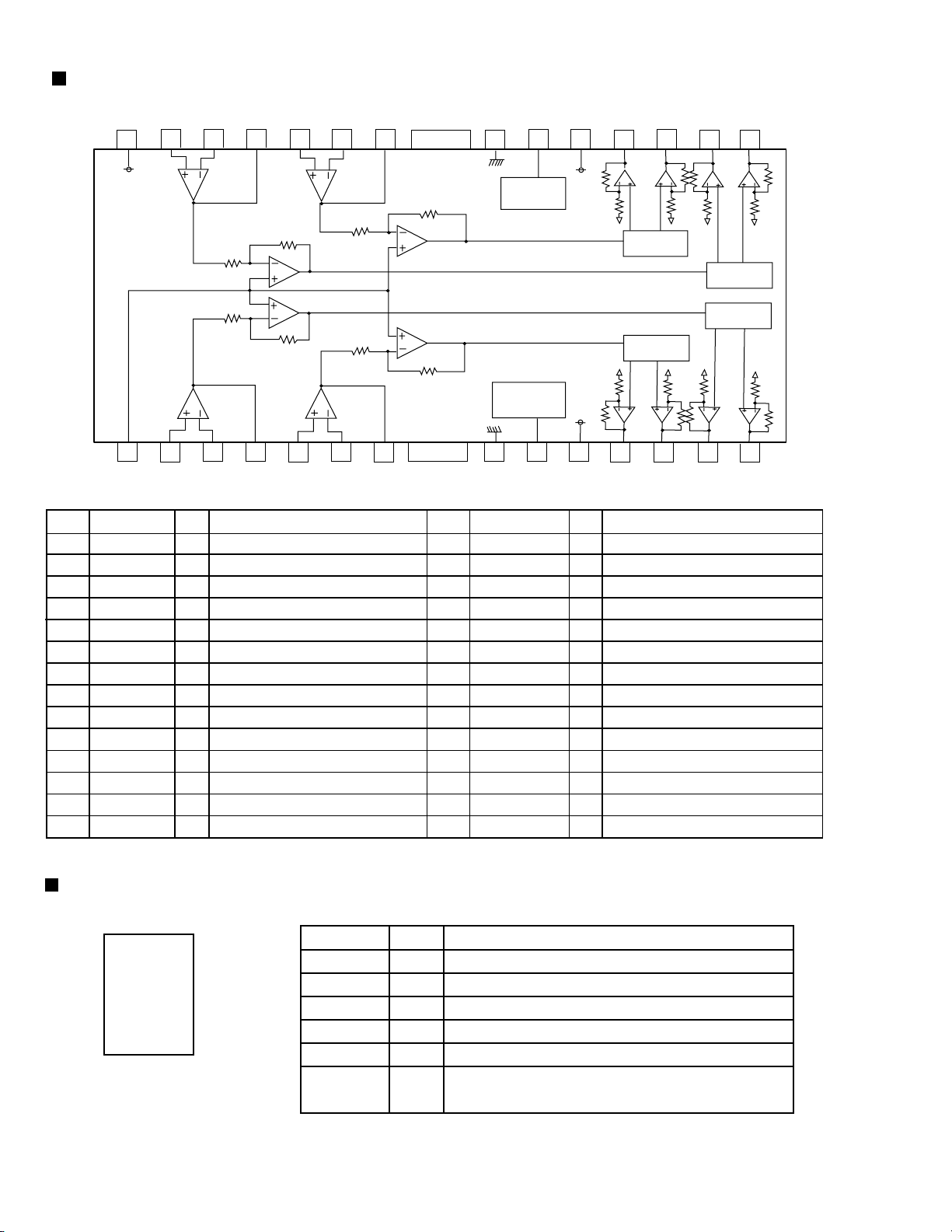
Description of major ICs
AN8702FH(IC101):Frontend processor
1.Pin layout
HDTYPE
646362616059585756555453525150
VIN12
VIN11
GND1
VIN4
VIN3
VIN2
VIN1
VREF1
VCC1
VIN10
VIN9
XV-S40BK/XV-S42SL/XV-S45GD/XV-S30BK
VIN8
VIN7
VIN6
VIN5
49
2.Pin function
Pin No.
Symbol
1
PC1
2
PC01
3
PC2
4
PC02
5
TGBAL
6
TBAL
7
FBAL
8
POFLT
9
DTRD
10
IDGT
11
STANDBY
12
SEN
13
SCK
14
STDI
15
RSEL
16
JLINE
17
TEN
18
TEOUT
19
ASN
20
ASOUT
21
FEN
22
FEOUT
23
VSS
24
25
26
27
28
29
30
31
32
33
TG
VDD
GND2
VREF2
VCC2
VHALF
DFLTON
DFLTOP
DSFLT
GND3
1
PC1
2
PC01
PC2
3
PC02
4
TGBAL
5
TBAL
6
FBAL
7
POFLT
8
DTRD
9
IDGT
SEN
SCK
STDI
RSEL
JLINE
10
11
12
13
14
15
16
171819202122232425262728293031
TEN
TEOUT
STANDBY
I/O Description
Tangential phase balance control terminal
I
I
Tracking balance control terminal
I
Focus balance control terminal
O
Track detection threshold level terminal
I
Data slice part data read signal input terminal
(For RAM)
I
Data slice part address part gate signal input
terminal( For RAM)
I
Standby mode control terminal
I
SEN(Serial data input terminal)
I
SCK(Serial data input terminal)
I
STDI(Serial data input terminal)
O
Tracking error signal output terminal
I
Focus error output amplifier reversing input terminal
O
Focus error signal output terminal
-
Connect to GND
O
Tangential phase error signal output terminal
-
Power supply terminal 3V
-
Connect to GND
O
VREF2 voltage output terminal
-
Power supply terminal 5V
O
VHALF voltage output terminal
-
Connect to GND
AN8702FH
FEN
ASN
FEOUT
ASOUT
VSS
48
RFINN
RFINP
47
TESTSG
46
AGCO
45
AGCG
44
PEAK
43
BOTTOM
42
RFENV
41
BDO
40
OFTR
39
DCRF
38
RFC
37
VCC3
36
RFOUT
35
RFDIFO
34
GND3
33
32
TG
VDD
VCC2
GND2
VREF2
Pin No.
Symbol I/O Description
34
RFDIFO
35
RFOUT
36
37
38
39
40
41
RFENV
42
BOTTOM
43
44
AGCG
45
AGCO
46
TESTSG
47
RFINP
48
RFINN
49
50
51
52
53
54
55
56
VREF1
57
58
59
60
61
62
63
64
HDTYPE
VHALF
VCC3
RFC
DCRF
OFTR
BDO
PEAK
VIN5
VIN6
VIN7
VIN8
VIN9
VIN10
VCC1
VIN1
VIN2
VIN3
VIN4
GND1
VIN11
VIN12
DSFLT
DFLTOP
DFLTON
Power supply terminal 5V
-
All addition amplifier capacitor terminal
O
OFTR output terminal
O
RF envelope output terminal
O
Bottom envelope detection filter terminal
O
Peak envelope detection filter terminal
O
AGC amplifier gain control terminal
O
TEST signal input terminal
I
RF signal positive input terminal
I
RF signal negative input terminal
I
Focus input of external division into two terminal
I
Focus input of external division into two terminal
I
I
I
I
I
Power supply terminal 5V
-
VREF1 voltage output terminal
O
External division into four (DVD/CD) RF input
I
terminal1
External division into four (DVD/CD) RF input
I
terminal2
External division into four (DVD/CD) RF input
I
terminal3
External division into four (DVD/CD) RF input
I
terminal4
Connect to GND
I
I
1-21
Page 22
XV-S40BK/XV-S42SL/XV-S45GD/XV-S30BK
BA5983FM-X (IC271) : 4CH DRIVER
1.Block Diagram
27
26
28
Vcc
10k
25
20k
24
23 22
10k
20k
21
STAND BY
CH4
20
Vcc
19
10k
10k
18
Level Shift
17 16
10k
10k
10k
10k
15
10k
10k
Level Shift
10k
10k
1
2
3
5
4
10k
10k
6
7
2.Pin Function
Pin No. Pin No.
10
11
12
13
14
Symbol Symbol
1
BIAS IN
2
OPIN1(+)
3
OPIN1(-)
4
OPOUT1
5
OPIN2(+)
6
OPIN2(-)
7
OPOUT2
8
9
GND
STBY1
PowVcc1
VO2(-)
VO2(+)
VO1(-)
VO1(+)
I/O I/O
Input for Bias-amplifier
I
Non inverting input for CH1 OP-AMP
I
Inverting input for CH1 OP-AMP
I
Output for CH1 OP-AMP
O
Non inverting input for CH2 OP-AMP
I
Inverting input for CH2 OP-AMP
I
Output for CH2 OP-AMP
O
Substrate ground
-
Input for CH1/2/3 stand by control
I
Vcc for CH1/2 power block
-
Inverted output of CH2
O
Non inverted output of CH2
O
Inverted output of CH1
O
Non inverted output of CH1
O
Function
15
16
17
18
19
20
21
22
23
24
25
26
27
28
STAND BY
CH1/2/3
89
VO4(+)
VO4(-)
VO3(+)
VO3(-)
PowVcc2
STBY2
GND
OPOUT3
OPIN3(-)
OPIN3(+)
OPOUT4
OPIN4(-)
OPIN4(+)
PreVcc
Level Shift
Level Shift
12
10k
10k
10k
10k
13
Function
10k
Vcc
10k
11
10
O
Non inverted output of CH4
O
Inverted output of CH4
O
Non inverted output of CH3
O
Inverted output of CH3
-
Vcc for CH3/4 power block
I
Input for Ch4 stand by control
-
Substrate ground
O
Output for CH3 OP-AMP
I
Inverting input for CH3 OP-AMP
I
Non inverting input for CH3 OP-AMP
O
Output for CH4 OP-AMP
I
Inverting input for CH4 OP-AMP
I
Non inverting input for CH4 OP-AMP
-
Vcc for pre block
10k
10k
14
BR93LC66F-X(IC403):EEPROM
1.Terminal layout
NC
VCC
CS
SK
1
2
3
4
8
NC
7
GND
6
DO
5
DI
1-22
2.Pin Functions
Symbol
VCC
GND
CS
SK
DI
DO
I/O
-
-
I
I
I
O
Function
Power supply
Connect to GND
Chip select input
Serial clock input
Start bit,OP-code,address,serial data input
Serial data output,
Internal state display output of READY/BUSY
Page 23
KM416S1120DT-G8(IC504,IC505):DRAM
1.Terminal Layout
VSS
DQ15
DQ14
VSSQ
DQ13
DQ12
VDDQ
DQ11
DQ10
VSSQ
DQ9
DQ8
VDDQNCUDQM
CLK
CKENCA9A8A7A6A5A4VSS
50494847464544434241403938373635343332313029282726
XV-S40BK/XV-S42SL/XV-S45GD/XV-S30BK
123456789
DQ0
DQ1
DQ2
VSSQ
DQ3
VDD
2.Block Diagram
CLK
ADO
LCKE
101112131415161718192021222324
DQ4
VDDQ
DQ5
DQ6
VSSQ
DQ7
VDDQ
LDQM
WE
CAS
RAS
Bank Select
Refresh Counter
Row Buffer
Address Register
LCBR
LRAS
LRAS LCBR LWE LCAS
CS
A0A1A2
A11
A10
Timing register
25
A3
VDD
Row Decoder
Col.Buffer
Data input register
512K x 16
512K x 16
Column decoder
Latency & burst length
Programming register
LWCBR
Sense AMP
I/O Control
LWE
LDQM
Output Buffer
DQI
LDQM
CLK CKE CS RAS CAS WE L(U)DQM
3.Pin Function
Pin No. Symbol Function Pin No. Symbol Function
To Ground
Address
Address
Address
Address
Address
Address
Non Connection
Clock Enable
System Clock
Data Input/Mask Output
Non Connection
Power Supply
Data Input/Output
Data Input/Output
To Ground
Data Input/Output
Data Input/Output
Power Supply
Data Input/Output
Data Input/Output
To Ground
Data Input/Output
Data Input/Output
To Ground
10
11
12
13
14
15
16
17
18
19
20
21
22
23
24
25
1
VDD
2
DQ0
3
DQ1
4
VSSQ
5
DQ2
6
DQ3
7
VDDQ
8
DQ4
9
DQ5
VSSQ
DQ6
DQ7
VDDQ
LDQM
WE
CAS
RAS
CS
A11
A10
VDD
Power Supply
Data Input/Output
Data Input/Output
To Ground
Data Input/Output
Data Input/Output
Power Supply
Data Input/Output
Data Input/Output
To Ground
Data Input/Output
Data Input/Output
Power Supply
Data Input/Mask Output
Write Enable
Column Address Strobe
Raw Address Strobe
Chip Select
Address
Address
Address
A0
Address
A1
Address
A2
Address
A3
Power Supply
26
27
28
29
30
31
32
33
34
35
36
37
38
39
40
41
42
43
44
45
46
47
48
49
50
VSS
A4
A5
A6
A7
A8
A9
NC
CKE
CLK
UDOM
NC
VDDQ
DQ8
DQ9
VSSQ
DQ10
DQ11
VDDQ
DQ12
DQ13
VSSQ
DQ14
DQ15
VSS
1-23
Page 24

XV-S40BK/XV-S42SL/XV-S45GD/XV-S30BK
MN101C35DGD(IC701):System controller
Pin function
Pin No.
1
2
3
4~7
8
9
10
11
12
13
14
15
16
17
18
19
20
21
22
23
24
25
26
27
28
29
30
31
32
33
34
35
36
37
38
39
40
41
42
43
44
45
46
47
48
49~51
52~64
65~88
89~99
100
Symbol
D DATA
DCLK
DACOCS
DI/DO/CS/SK
VDD
OSC2
OSC1
VSS
XI
XO
MMOD
VREF-
POWER SW
NTSEL
RGB/YC SW
S/COMPO
AIN0
AIN2
TEST0
TEST1
VREF+
RGBSEL
RESET
AVCO
AVCI
POWERON
TCLOSE
YOPEN
/LMMUTE
SWOPEN
SWUPDN
REMO
NC
REQ
NC
S2UDT
U2SDT
SCLK
BUSY
CPURST
NC
VS3
VS1
MUTE
STANDBYIND
NC
1G~13G
S1~S24
NC
VPP
I/O
O
O
O
-
-
O
I
-
-
-
-
I
I
-
I
I
-
-
-
O
I
O
I
O
O
O
O
I
I
I
-
I
-
O
I
O
O
O
O
O
O
O
O
O
-
-
DAC control data
DAC control clock
DAC control chip select
Non connect
Power supply +B 5V
Oscillation terminal 8MHz
Oscillation terminal 8MHz
Connect to ground
Unused, Connect with ground
Unused
Connect to ground
Connect to ground
Key input (power)
NTSC/PAL switch input
Un used
Un used
Key input (S831~S835)
Key input (open/close)
Un used
Un used
Power supply +B 5V
RGB select control (H:RGB L:other)
Reset input
AV COMPULINK output
AV COMPULINK input
Power ON output
Tray close control output
Tray open control output
Tray muting output (L:muting)
Detection switch of tray open/close (L:open/close)
Detection switch of traverse mechanism up/down (H:UP L:DOWN)
Remote control interruption
Non connect
Communication between unit microcomputers request
Non connect
Communication between unit microcomputers DATA output
Communication between unit microcomputers DATA input
Communication between unit microcomputers CLK
Communication between unit microcomputers BUSY
Unit microcomputers reset
Non connect
S3 control (H:standby L:power ON)
S1 control
Muting output
LED control signal output (standby)
Non connect
FL grid control signal output
FL segment control signal output
Non connect
-VDISP (apply -35V)
Description
1-24
Page 25

MN102L25GGE1(IC401):Unit CPU
Pin function
Pin No. Pin No.
Symbol Symbol
1
WAIT
2
3
4
5
6
7
8
9
10
11
12
13
14
15
16
17
18
19
20
21
22
23
24
25
26
27
28
29
30
31
32
33
34
35
36
37
38
39
40
41
42
43
44
45
46
47
48
49
50
RE
SPMUTE
WEN
CS1
CS2
CS3
DRVMUTE
SPKICK
LSIRST
WORD
A0
A1
A2
A3
VDD
SYSCLK
VSS
XI
XO
VDD
OSCI
OSCO
MODE
A4
A5
A6
A7
A8
A9
A10
A11
VDD
A12
A13
A14
A15
A16
A17
A18
A19
VSS
A20
TXSEL
HAGUP
-
-
HMFON
TRVSW
I/O I/O
Micon wait signal input
I
Read enable
O
Spindle muting output to IC251
O
Write enable
O
Non connect
Chip select for ODC
O
Chip select for ZIVA
O
Chip select for outer ROM
O
Driver mute
O
Spin kick (Non connect)
O
LSI reset
O
Bus selection input
O
Address bus 0 for CPU
O
Address bus 1 for CPU
O
Address bus 2 for CPU
O
Address bus 3 for CPU
O
Power supply
System clock signal output
O
Ground
Not use (Connect to vss)
Non connect
Power supply
Clock signal input(13.5MHz)
I
Clock signal output(13.5MHz)
O
CPU Mode selection input
I
Address bus 4 for CPU
O
Address bus 5 for CPU
O
Address bus 6 for CPU
O
Address bus 7 for CPU
O
Address bus 8 for CPU
O
Address bus 9 for CPU
O
Address bus 10 for CPU
O
Address bus 11 for CPU
O
Power supply
Address bus 12 for CPU
O
Address bus 13 for CPU
O
Address bus 14 for CPU
O
Address bus 15 for CPU
O
Address bus 16 for CPU
O
Address bus 17 for CPU
O
Address bus 18 for CPU
O
Address bus 19 for CPU
O
Ground
Address bus 20 for CPU
O
TX Select
O
O
Non connect
Non connect
-
Detection switch of traverse
I
inside
Function
51
52
53
54
55
56
57
58
59
60
61
62
63
64
65
66
67
68
69
70
71
72
73
74
75
76
77
78
79
80
81
82
83
84
85
86
87
88
89
90
91
92
93
94
95
96
97
98
99
100
XV-S40BK/XV-S42SL/XV-S45GD/XV-S30BK
Function
-
-
ADSCEN
VDD
FEPEN
SLEEP
BUSY
REQ
CIRCEN
-
VSS
EPCS
EPSK
DPDI
EPDO
VDD
SCLKO
S2UDT
U2SDT
CPSCK
SDIN
SDOUT
-
-
NMI
ADSCIRQ
ODCIRQ
DECIRQ
WAKEUP
ODCIRQ2
ADSEP
RST
VDD
TEST1
TEST2
TEST3
TEST4
TEST5
TEST6
TEST7
TEST8
VSS
D0
D1
D2
D3
D4
D5
D6
D7
-
Serial enable signal for ADSC
O
Power supply
Serial enable signal for FEP
O
Standby signal for FEP
O
Communication busy
I
Communication Request
O
CIRC command select
O
Non connect
Ground
EEPROM chip select
O
EEPROM clock
O
EEPROM data input
I
EEPROM data output
O
Power supply
Communication clock
I
Communication input data
I
Communication output data
O
Clock for ADSC serial
O
ADSC serial data input
I
ADSC serial data output
O
Not use
Not use
Not use
Interrupt input of ADSC
I
Interrupt input of ODC
I
Interrupt input of ZIVA
I
Not use
O
Interruption of system control
I
Address data selection input
I
Reset input
I
Power supply
Test signal 1 input
I
Test signal 2 input
I
Test signal 3 input
I
Test signal 4 input
I
Test signal 5 input
I
Test signal 6 input
I
Test signal 7 input
I
Test signal 8 input
I
Ground
Data bus 0 of CPU
I/O
Data bus 1 of CPU
I/O
Data bus 2 of CPU
I/O
Data bus 3 of CPU
I/O
Data bus 4 of CPU
I/O
Data bus 5 of CPU
I/O
Data bus 6 of CPU
I/O
Data bus 7 of CPU
I/O
1-25
Page 26
XV-S40BK/XV-S42SL/XV-S45GD/XV-S30BK
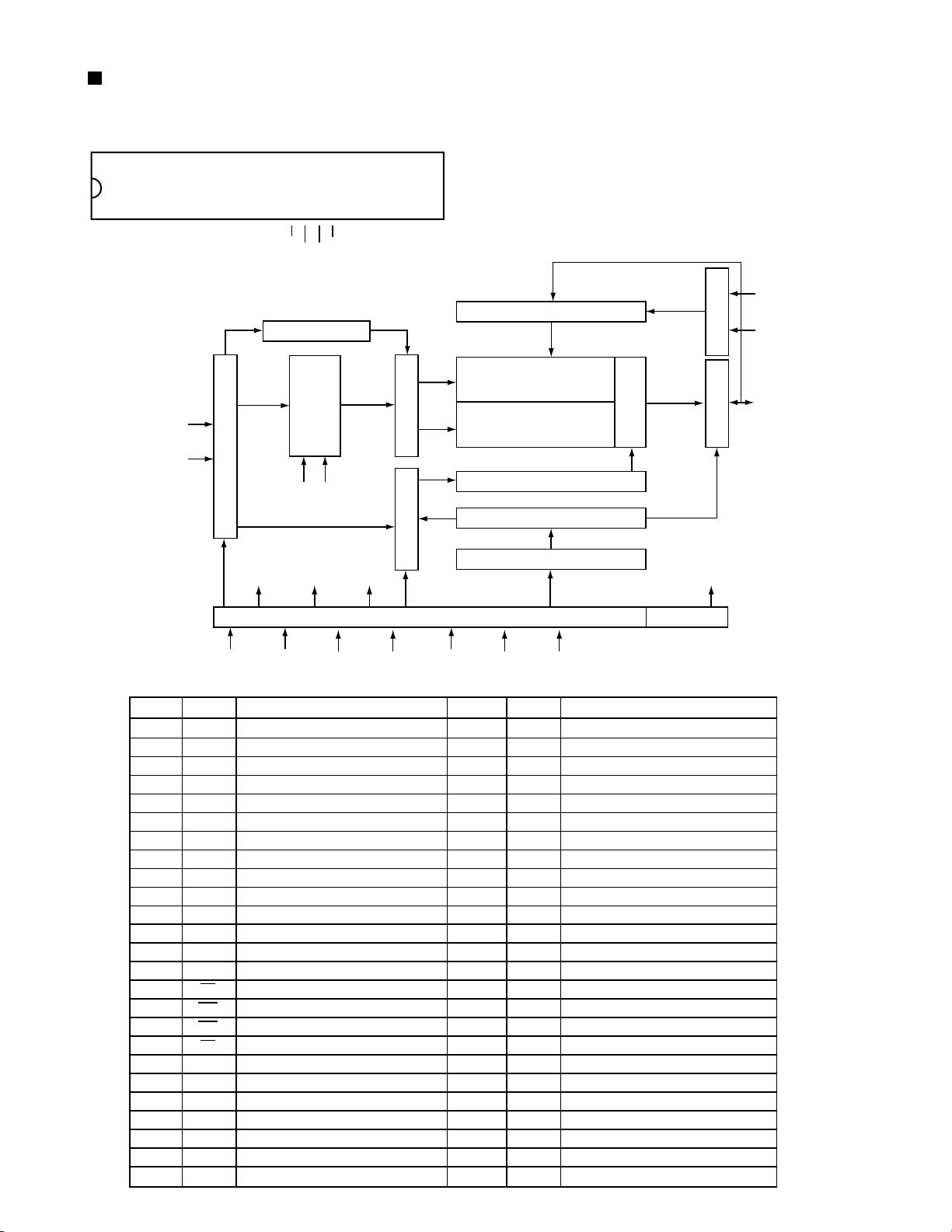
MN103S13BDA(IC301):Optical disc controller
1.Pin layout
DMARQ
NIOWR
VSS
NIORD
IORDY
NDMACK
VDD
INTRQ
NIOCS16
DA1
VSS
NPDIAG
144
143
142
141
140
139
138
137
136
135
134
HDD15
HDD0
HDD14
VDD
HDD1
HDD13
HDD2
VSS
HDD12
VDD
HDD3
HDD11
HDD4
HDD10
VDD
HDD5
HDD9
VSS
HDD6
HDD8
HDD7
VDDH
NRESET
MASTER
NINT0
NINT1
WAITDOC
NMRST
DASPST
VDD
OSCO2
OSCI2
UATASEL
VSS
PVSSDRAM
PVDDDRAM
1
2
3
4
5
6
7
8
9
10
11
12
13
14
15
16
17
18
19
20
21
22
23
24
25
26
27
28
29
30
31
32
33
34
35
36
3738394041424344454647484950515253545556575859606162636465666768697071
133
MN103S13BDA
DA0
132
DA2
131
VDD
NCS1FX
130
129
NCS3FX
NDASP
NTRYCL
128
127
126
VDD
125
NEJECT
VSS
MONI0
124
123
122
MONI1
MONI2
121
120
MONI3
SDATA
119
118
SCLOCK
VDD
DAT0
117
116
115
DAT1
114
DAT2
113
DAT3
112
CHCK40
NCLDCK
SUBC
111
110
109
108
107
106
105
104
103
102
101
100
99
98
97
96
95
94
93
92
91
90
89
88
87
86
85
84
83
82
81
80
79
78
77
76
75
74
73
72
SBCK
VSS
P0
P1
PVDD
PVSS
VDD
OSCO1
OSCI1
VSS
LRCK
BLKCK
IPFLAG
DACCLK
DACLRCK
DA C DATA
NTRON
LG
JMPINH
IDHOLD
SBCK/PLLOK
CLKOUT2
VDD
NRST
MMOD
VSS
CPDET1
CPDET2
BDO
IDGT
DTRD
TEHLD
VDD
CLKOUT1
CPUDT0
CPUDT1
2.Block diagram
DVD-ROM
Formatter
CGEN
MODE
CPUADR17
CPUADR16
VSS
CPUADR15
CPUADR14
CPUADR13
CD-PRE
Instruction
memory
(40KB)
DATA
MEMORY
(6KB)
VDD
CPUADR9
CPUADR8
CPUADR11
CPUADR10
CPUADR7
CPUADR12
Formatter
General purpose IO bus
CPUADR6
CPUADR5
CPUADR4
CPUADR3
CPUADR2
i /t
High speed IO bus
32 bit
CPU core
GCAL
CPUADR1
VSS
CPUADR0
ECC
NCS
NWR
NRD
VDD
CPUDT7
CPUDT6
PVPPDRAM
DRAMC
CPUDT5
CPUDT4
PVSSDRAM
PVDDDRAM
PTESTDRAM
Host i / f
MPEG i / t
DMA
BCU
VSS
CPUDT3
CPUDT2
ATAPI
4Mbit
DRAM
1-26
WDT
16 bit
timer x 2
SYSTEM
i / f
INTC
Page 27
3.Pin function (1/3)
XV-S40BK/XV-S42SL/XV-S45GD/XV-S30BK
Pin No.
1
2
3
4
5
6
7
8
9
10
11
12
13
14
15
16
17
18
19
20
21
22
23
24
25
26
27
28
29
30
31
32
33
34
35
36
37
38
39
40
41
42
43
44
45
46
47
48
49
50
Symbol
HDD15
HDD0
HDD14
VDD
HDD1
HDD13
HDD2
VSS
HDD12
VDD
HDD3
HDD11
HDD4
HDD10
VDD
HDD5
HDD9
VSS
HDD6
HDD8
HDD7
VDDH
NRESET
MASTER
NINT0
NINT1
WAITDOC
NMRST
DASPST
VDD
OSCO2
OSCI2
UATASEL
VSS
PVSSDRAM
PVDDDRAM
CPUADR17
CPUADR16
VSS
CPUADR15
CPUADR14
CPUADR13
CPUADR12
VDD
CPUADR11
CPUADR10
CPUADR9
CPUADR8
CPUADR7
CPUADR6
I/O
I/O
I/O
I/O
I/O
I/O
I/O
I/O
I/O
I/O
I/O
I/O
I/O
I/O
I/O
I/O
I/O
I
I/O
O
O
O
O
I
-
O
I
I
-
I
I
-
I
I
I
I
-
I
I
I
I
I
I
Description
ATAPI Data
ATAPI Data
ATAPI Data
Power supply 3V
ATAPI Data
ATAPI Data
ATAPI Data
Connect to GND
ATAPI Data
Power supply 2.7V
ATAPI Data
ATAPI Data
ATAPI Data
ATAPI Data
Power supply 3V
ATAPI Data
ATAPI Data
Connect to GND
ATAPI Data
ATAPI Data
ATAPI Data
ATAPI Reset input
ATAPI Master/slave select
Interruption of system control 0
Interruption of system control 1
Wait control of system control
Reset of system control (Connect to TP302)
Setting of initial value of DASP signal
Power supply 3V
Non connect
Non connect
Connect to VSS
Connect to GND
Connect to VSS
Connect to VDD(2.7V)
System control address
System control address
Connect to GND
System control address
System control address
System control address
System control address
Power supply 2.7V
System control address
System control address
System control address
System control address
System control address
System control address
1-27
Page 28

XV-S40BK/XV-S42SL/XV-S45GD/XV-S30BK
3.Pin function (2/3)
Pin No.
51
52
53
54
55
56
57
58
59
60
61
62
63
64
65
66
67
68
69
70
71
72
73
74
75
76
77
78
79
80
81
82
83
84
85
86
87
88
89
90
91
92
93
94
95
96
97
98
99
100
Symbol
CPUADR5
CPUADR4
CPUADR3
CPUADR2
CPUADR1
VSS
CPUADR0
NCS
NWR
NRD
VDD
CPUDT7
CPUDT6
PVPPDRAM
PTESTDRAM
PVDDDRAM
PVSSDRAM
CPUDT5
CPUDT4
CPUDT3
VSS
CPUDT2
CPUDT1
CPUDT0
CLKOUT1
VDD
TEHLD
DTRD
IDGT
BDO
CPDET2
CPDET1
VSS
MMOD
NRST
VDD
CLKOUT2
SBCK/PLLOK
IDOHOLD
JMPINH
LG
NTRON
DAC DATA
DACLRCK
DACCLK
IPFLAG
BLKCK
LRCK
VSS
OSCI1
I/O
I
I
I
I
I
I
I
I
I
I/O
I/O
O
I
I/O
I/O
I/O
I/O
I/O
I/O
O
-
O
O
O
I
I
I
-
I
I
-
O
O
O
O
O
I
O
O
I
I
I
I
-
I
Description
System control address
System control address
System control address
System control address
System control address
Connect to GND
System control address
System control chip select
Writing system control
Reading system control
Power supply 3V
System control data
System control data
Connect to VSS
Connect to VSS
Connect to VDD(2.7V)
Connect to VSS
System control data
System control data
System control data
Connect to GND
System control data
System control data
System control data
Clock signal output (16.9/11.2/8.45MHz)
Power supply 3V
Mirror gate (Connect to TP141)
Data frequency control switch (Connect to TP304)
CAPA switch
RF Dropout/BCA data
Outer capacity detection
Inner capacity detection
Connect to GND
Connect to VSS
System reset
Power supply 3V
Clock 16.9MHz
Flame mark detection
ID gate for tracking holding
Jump prohibition
Land/group switch
Tracking ON
Serial data output (Connect to TP148)
Identification signal of L and R (Connect to TP149)
Clock for serial data output
Input of IP flag
Sub code/block/input clock
Identification signal of L and R (Connect to VSS)
Connect to GND
Oscillation input terminal 16.9MHz
1-28
Page 29
3.Pin function (3/3)
XV-S40BK/XV-S42SL/XV-S45GD/XV-S30BK
Pin No.
101
102
103
104
105
106
107
108
109
110
111
112
113
114
115
116
117
118
119
120
121
122
123
124
125
126
127
128
129
130
131
132
133
134
135
136
137
138
139
140
141
142
143
144
Symbol
OSCO1
VDD
PVSS
PVDD
P1
P0
VSS
SBCK
SUBC
NCLDCK
CHCK40
DAT3
DAT2
DAT1
DAT0
VDD
SCLOCK
S DATA
MONI3
MONI2
MONI1
MONI0
VSS
NEJECT
VDD
NTRYCL
NDASP
NCS3FX
NCS1FX
VDD
DA2
DA0
NPDIAG
VSS
DA1
NIOCS16
INTRQ
VDD
NDMACK
IORDY
NIORD
VSS
NIOWR
DMARQ
I/O
O
-
-
I/O
I/O
-
O
I/O
I/O
O
O
O
O
-
-
I/O
I/O
I/O
I/O
I/O
O
O
-
O
I/O
O
Description
Oscillation output terminal 16.9MHz
Power supply 3V
Connect to GND
Power supply 3V
Terminal master polarity switch input
CIRC-RAM,OVER/UNDER Interruption
Connect to GND
Clock output for sub code,serial input
Sub code,serial input
I
Sub code,flame clock input
I
Clock is read to DAT3~0 (Output of division frequency from ADSC)
I
Data is read from disc (Going side by side output from ADSC)
I
Data is read from disc (Going side by side output from ADSC)
I
Data is read from disc (Going side by side output from ADSC)
I
Data is read from disc (Going side by side output from ADSC)
I
Power supply 3V
Debug serial clock (270 ohm pull up)
Debug serial data (270 ohm pull up)
Internal good title monitor (Connect to TP150)
Internal good title monitor (Connect to TP151)
Internal good title monitor (Connect to TP152)
Internal good title monitor (Connect to TP153)
Connect to GND
Eject detection
I
Power supply 2.7V
Non connect (Tray close detection)
I
ATAPI drive active / slave connect I/O
Non connect (ATAPI host chip select)
I
Non connect (ATAPI host chip select)
I
Power supply 3V
ATAPI host address
Non connect (ATAPI host address)
ATAPI Slave master diagnosis input
Connect to GND
Non connect (ATAPI host address)
Output of selection of width of ATAPI host data bus
ATAPI Host interruption output
Power supply 3V
Non connect (ATAPI Host DMA characteristic)
I
ATAPI Host ready output (Connect to TP157)
Non connect (ATAPI host read)
I
Connect to GND
ATAPI Host write
ATAPI Host DMA request (Connect to TP159)
1-29
Page 30

XV-S40BK/XV-S42SL/XV-S45GD/XV-S30BK
MN67706ZY (IC201) : Auto digital servo controller
1.Terminal Layout
33VDD
33VSS
TEST
MINTEST
NCLDCK/JUMP
SUBC
IPFLAG
DACCLK
NTRON
DACDATA/LG
DACLRCK/JMPINH
IDHOLD
SBCK/PLLOK
BLKCK/CPDET1
LRCK/CPDET2
IDGT/TEMUTE
75747372717069686766656463626160595857565554535251
CHCK40
DAT3
DAT2
DAT1
DAT0
33VSS
33VDD
XRESET
ENS
ENC
CPUIRQ
CPUCLK
CPUDTIN
CPUDTOUT
MONA
MONB
MONC
25VSS
25VDD
LDCUR(AD6)
TDOFS(AD5)
TG(AD4)
RFENV(AD3)
NC
TX
76
77
78
79
80
81
82
83
84
85
86
87
88
89
90
91
92
93
94
95
96
97
98
99
100
123456789
MN67706ZY
101112131415161718192021222324
DTRD
25VDD
25VSS
TILTN
TILT
TILTPFGSPDRV
TRSDRV
50
49
48
47
46
45
44
43
42
41
40
39
38
37
36
35
34
33
32
31
30
29
28
27
26
25
TSTSG
BDO
SYSCLK
OFTR
33VDD
33VSS
FBAL
TBAL
TGBAL
AVSS
ROUT
LOUT
AVDD
JLINE
DBALO
VCOF
TRCRS
CMPIN
LPFOUT
LPFIN
AVSS
HPFOUT
HPFIN
AVDD
VFOSHORT
ARF
TE(AD1)
FE(AD0)
AS(AD2)
AVSS
AVDD
TRDRV(DA0)
FODRV(DA1)
NARF
IREF1
IREF2
DSLF1
DSLF2
AVDD
VHALF
PLPG
2.Pin Functions (1/3)
Pin No. Symbol I/O Function
10
11
12
13
14
15
16
17
18
19
20
21
22
23
24
25
1
2
3
4
5
6
7
8
9
AS(AD2)
TE(AD1)
FE(AD0)
AVDD
FODRV(DA1)
TRDRV(DA0)
AVSS
ARF
NARF
IREF1
IREF2
DSLF1
DSLF2
AVDD
VHALF
PLPG
PLFG
VREFH
RVI
AVSS
PLFLT1
PLFLT2
JITOUT
RFDIF
CSLFL1
I
I
I
O
O
-
I
I
I
I
I/O
I/O
-
I
-
-
I
I/O
O
O
I/O
I
I/O
AS : Full adder signal(FEP)
Phase difference/3 beam tracking error(FEP)
Focus error(FEP)
Apply 3.3V(For analog circuit)
Focus drive(DRVIC)
Tracking drive(DRVIC)
Ground(For analog circuit)
Equivalence RF+(FEP)
Equivalence RF-(FEP)
Reference current1(For DBAL)
Reference current2(For DBAL)
Connect to capacitor1 for DSL
Connect to capacitor2 for DSL
Apply 3.3V(For analog circuit)
Reference voltage 1.65+-0.1V(FEP)
Not use(PLL phase gain setting resistor terminal)
Not use(PLL frequency gain setting resistor terminal)
Reference voltage 2.2V+-0.1V(FEP)
Connect to resistor for VREFH reference current source
Ground(For analog circuit)
Connect to capacitor1 for PLL
Connect to capacitor2 for PLL
Output for jitter signal monitor
Not use
Pull-up to VHALF
PLFG
VREFH
RVI
AVSS
PLFLT1
JITOUT
PLFLT2
RFDIF
CSLFL1
1-30
Page 31
2.Pin function (2/3)
Pin No. Symbol I/O Function
26
27
28
29
30
31
32
33
34
35
36
37
38
39
40
41
42
43
44
45
46
47
48
49
50
51
52
53
54
55
56
57
58
59
60
61
62
63
64
65
66
67
68
69
70
71
72
73
74
75
76
77
78
79
80
VFOSHORT
AVDD
HPFIN
HPFOUT
AVSS
LPFIN
LPFOUT
CMPIN
TRCRS
VCOF
DBALO
JLINE
AVDD
LOUT
ROUT
AVSS
TGBAL
TBAL
FBAL
33VSS
33VDD
OFTR
SYSCLK
BDO
TSTSG
TRSDRV
SPDRV
FG
TILTP
TILT
TILTN
25VSS
25VDD
DTRD
IDGT/TEMUTE
LRCK/CPDET2
BLKCK/CPDET1
SBCK/PLLOK
IDHOLD
DACLRCK/JMPINH
DACDATA/LG
NTRON
DACCLK
IPFLAG
SUBC
NCLDCK/JUMP
MINTEST
TEST
33VSS
33VDD
CHCK40
DAT3
DAT2
DAT1
DAT0
O
O
O
I/O
O
O
O
O
O
O
O
O
O
O
O
O
O
O
O
O
O
O
O
O
O
O
O
O
O
VFO short output
-
Apply 3.3V(For analog circuit)
I
Pull-up to VHALF
Connect to TP208
-
Ground(For analog circuit)
I
Pull-up to VHALF
Not use
I
Connect to TP210
I
Input signal for track cross formation
JFVCO control voltage
DSL balance adjust output
J-line setting output(FEP)
-
Apply 3.3V(For analog circuit)
Connect to TP203 (Analog audio left output)
Connect to TP204 (Analog audio right output)
-
Ground(For analog circuit)
Tangential balance adjust(FEP)
Tracking balance adjust(FEP)
Focus balance adjust(FEP)
-
Ground(For I/O)
-
Apply 3.3V(For I/O)
I
Off track signal
I
16.9344MHz system clock input(ODC)
I
Drop out(FEP)
Calibration signal(FEP)
Traverse drive(DRVIC)
Spindle drive output(DRVIC)
I
FG signal input (Spindle motor driver)
Connect to TP205
Connect to TP206
Connect to TP207
-
Ground(For internal core)
-
Apply 2.5V(For internal core)
I
Data read control signal(ODC)
I
Pull-down to Ground
LR channel data strobe(ODC)/
CD sub code synchronous signal(ODC)/
I
CD sub code data shift clock(ODC)/PLL pull-in OK signal input
I
Pull-down to Ground
I
1bit DAC-LR channel data strobe(ODC)/
I
CD 1bit DAC channel data(ODC)
L : Tracking ON(ODC)
1bit DAC channel data shift clock(ODC)
CIRC error flag(ODC)
CD sub code(ODC)
CD sub code data frame clock(ODC)/DVD JUMP signal(ODC)
I
Pull-down to Ground(For MINTEST)
I
Pull-down to Ground(For TEST)
-
Ground(For I/O)
-
Apply 3.3V(For I/O)
Clock for SRDATA(ODC)
SRDATA3(ODC)
SRDATA2(ODC)
SRDATA1(ODC)
SRDATA0(ODC)
XV-S40BK/XV-S42SL/XV-S45GD/XV-S30BK
1-31
Page 32

XV-S40BK/XV-S42SL/XV-S45GD/XV-S30BK
2.Pin function (3/3)
Pin No. Symbol I/O Function
-
81
82
83
84
85
86
87
88
89
90
91
92
93
94
95
96
97
98
99
100
33VSS
33VDD
TX
XRESET
ENS
ENC
CPUIRQ
CPUCLK
CPUDTIN
CPUDTOUT
MONA
MONB
MONC
NC
25VSS
25VDD
LDCUR(AD6)
TDOFS(AD5)
TG(AD4)
RFENV(AD3)
O
O
O
O
O
O
O
Ground(For I/O)
-
Apply 3.3V(For I/O)
Digital audio interface
I
Reset input (System control)
I
Servo DSC serial I/F chip select (System control)
I
CIRC serial I/F chip select (System control)
Interrupt request (System control)
I
Syscon serial I/F clock (System control)
I
Syscon serial I/F data input (System control)
Syscon serial I/F data output (System control)
Connect to TP226 (Monitor terminal A)
Connect to TP225 (Monitor terminal A)
Connect to TP224 (Monitor terminal A)
Connect to TP211
-
Ground(For internal core)
-
Apply 2.5V(For internal core)
I
I
I
Tangential phase difference(FEP)
I
RF envelope input(FEP)
NJM4580M-X(IC741,IC751):Dual OP amplifier
Block diagram
V+ B OUT B -IN B +IN
8765
B
A
1234
V-A +INA -INA OUT
TC74VHC00FT-X(IC322,IC503) : Write timing control
1.Terminal layout / Block diagram
Vcc 4B 4A 4Y 3B 3A 3Y
14 13
12
11 10 9 8
1-32
2
1
6
543
7
1A 1B 1Y 2A 2B 2Y GND
Page 33

ZIVA-4.1-PA2(IC501):Back end - Digital decoder
1.Terminal layout
~
208 157
1
~
156
~
XV-S40BK/XV-S42SL/XV-S45GD/XV-S30BK
52
~
53 104
2.Pin function (1/5)
Pin No.
1
2
3
4
5
6
7
8
9
10
11
12
13
14
15
16
17
18
19
20
21
22
23
24
25
26
27
28
29
30
31
32
33
34
35
36
Symbol
RD
R/W
VDD
WAIT
RESET
VSS
VDD
INT
NC
NC
NC
NC
VDD
VSS
NC
NC
NC
NC
VSS
VDD
V DATA 0
V DATA 1
V DATA 2
V DATA 3
V DATA 4
V DATA 5
V DATA 6
V DATA 7
VSYNC
HSYNC
VSS
VDD
NC
NC
NC
VDD
105
I/O
O
O
O
O
O
O
O
O
O
O
I/O
I/O
Description
Read strobe input
I
Read/write strobe input
I
Power supply terminal 3.3V
Transfer not complete / data acknowledge.
Active LOW to indicate host initiated transfer is complete.
Active LOW : reset signal input
I
Connect to ground
Power supply terminal 3.3V
Host interrupt signal output
Non connect
Non connect
Non connect
Non connect
Power supply terminal 2.5V
Connect to ground
Non connect
Non connect
Non connect
Non connect
Connect to ground
Power supply 3.3V
Video data bus output. Byte serial CbYCrY data synchronous with VCLK.
Video data bus output. Byte serial CbYCrY data synchronous with VCLK.
Video data bus output. Byte serial CbYCrY data synchronous with VCLK.
Video data bus output. Byte serial CbYCrY data synchronous with VCLK.
Video data bus output. Byte serial CbYCrY data synchronous with VCLK.
Video data bus output. Byte serial CbYCrY data synchronous with VCLK.
Video data bus output. Byte serial CbYCrY data synchronous with VCLK.
Video data bus output. Byte serial CbYCrY data synchronous with VCLK.
Vertical sync. Bi-directional, the decoder output the top border of a new
field on the first HSYNC after the falling edge of VSYNC.
Horizontal sync. The decoder begins outputting pixel data for a new
horizontal line after the falling (active) edge of HSYNC.
Connect to ground
Power supply terminal 3.3V
Non connect
Non connect
Non connect
Power supply terminal 2.5V
-
1-33
Page 34

XV-S40BK/XV-S42SL/XV-S45GD/XV-S30BK
2.Pin function (2/5)
Pin No.
37
38
39
40
41
42
43
44
45
46
47
48
49
50
51
52
53
54
55
56
57
58
59
60
61
62
63
64
65
66
67
68
69
70
71
72
73
74
75
76
77
78
79
80
81
82
83
84
Symbol
VSS
NC
NC
NC
NC
NC
PIO0
VSS
VDD
PIO1
PIO2
PIO3
PIO4
PIO5
PIO6
PIO7
M DATA 0
M DATA 1
VDD
VSS
M DATA 2
M DATA 3
M DATA 4
M DATA 5
M DATA 6
M DATA 7
MDATA15
VDD
VSS
MDATA14
VDD
VSS
MDATA13
MDATA12
MDATA11
MDATA10
M DATA 9
VDD
VSS
M DATA 8
LDQM
SD-CLK
CLKSEL
MADDR9
MADDR8
VDD
VSS
MADDR7
I/O
Connect to ground
Non connect
Non connect
Non connect
Non connect
Non connect
Programmable I/O terminal
I/O
Connect to ground
Power supply terminal 3.3V
Programmable I/O terminal
I/O
Programmable I/O terminal
I/O
Programmable I/O terminal
I/O
Programmable I/O terminal
I/O
Programmable I/O terminal
I/O
Programmable I/O terminal
I/O
Programmable I/O terminal
I/O
SDRAM data
I/O
SDRAM data
I/O
Power supply terminal 3.3V
Connect to ground
SDRAM data
I/O
SDRAM data
I/O
SDRAM data
I/O
SDRAM data
I/O
SDRAM data
I/O
SDRAM data
I/O
SDRAM data
I/O
Power supply terminal 3.3V
Connect to ground
SDRAM data
I/O
Power supply terminal 2.5
Connect to ground
SDRAM data
I/O
SDRAM data
I/O
SDRAM data
I/O
SDRAM data
I/O
SDRAM data
I/O
Power supply terminal 3.3V
Connect to ground
SDRAM data
I/O
SDRAM Lower or upper mask
O
SDRAM Clock
O
Selects SYSCLK or VCLK as clock source. Normal operation is to tie HIGH.
I
SDRAM address
O
SDRAM address
O
Power supply terminal 3.3V
Connect to ground
SDRAM address
O
Description
1-34
Page 35

2.Pin function (3/5)
XV-S40BK/XV-S42SL/XV-S45GD/XV-S30BK
Pin No.
85
86
87
88
89
90
91
92
93
94
95
96
97
98
99
100
101
102
103
104
105
106
107
108
109
110
111
112
113
114
115
116
117
118
119
120
121
122
123
124
125
126
127
128
Symbol
MADDR6
MADDR5
VDD
VSS
MADDR4
MWE
SD-CAS
VDD
VSS
SD-RAS
SD-CS0
SD-CS1/MADDR11
SD-BS
MADDR10
MADDR0
VDD
VSS
MADDR1
MADDR2
MADDR3
RESERVED
NC
NC
RESERVED
NC
RESERVED
RESERVED
RESERVED
DAI-LRCK
DAI-BCK
VDD
VSS
DAI-DATA
DA-DATA3
DA-DATA2
DA-DATA1
DA-DATA0
DA-LRCK
VDD
VSS
DA-XCK
DA-BCK
DA-IEC
VDD
I/O
SDRAM address
O
SDRAM address
O
Power supply terminal 2.5V
Connect to ground
SDRAM address
O
SDRAM write enable
O
Active LOW SDRAM column address
O
Power supply terminal 3.3V
Connect to ground
Active LOW SDRAM row address
O
Active LOW SDRAM chip select 0
O
Active LOW SDRAM chip select 1 or use as MADDR11 for larger SDRAM
O
SDRAM bank select
O
SDRAM address
O
SDRAM address
O
Power supply terminal 3.3V
Connect to ground
SDRAM address
O
SDRAM address
O
SDRAM address
O
Tie to VSS or VDD_3.3 as specified in table1
I
Non connect
Non connect
Tie to VSS or VDD_3.3 as specified in table1
I
Non connect
Tie to VSS or VDD_3.3 as specified in table1
I
Tie to VSS or VDD_3.3 as specified in table1
I
Tie to VSS or VDD_3.3 as specified in table1
I
PCM left/right clock
I
PCM input bit clock
I
Power supply 3.3V
Connect to ground
PCM data input
I
PCM data output. Eight channels. Serial audio samples relative to
O
DA_BCK and DA_LRCK
PCM data output. Eight channels. Serial audio samples relative to
O
DA_BCK and DA_LRCK
PCM data output. Eight channels. Serial audio samples relative to
O
DA_BCK and DA_LRCK
PCM data output. Eight channels. Serial audio samples relative to
O
DA_BCK and DA_LRCK
PCM left clock. Identifies the channel for each sample
O
Power supply terminal 3.3V
Connect to ground
Audio external frequency clock input or output
I/O
PCM bit clock output
O
PCM data out in IEC-958 format or compressed data out in IEC-1937 format
O
Power supply terminal 2.5V
-
Description
1-35
Page 36
XV-S40BK/XV-S42SL/XV-S45GD/XV-S30BK
2.Pin function (4/5)
Pin No.
129
130
131
132
133
134
135
136
137
138
139
140
141
142
143
144
145
146
147
148
149
150
151
152
153
154
155
156
157
158
159
160
161
162
163
164
165
166
167
168
169
Symbol
VSS
NC
VSS_DAC
VSS_VIDEO
CVBS
VDD_DAC
VDD_VIDEO
NC
VSS_DAC
VSS_VIDEO
CVBS/G/Y
VDD_DAC
VDD_VIDEO
NC
VSS_DAC
VSS_VIDEO
Y/B/U
VDD_DAC
VDD_VIDEO
NC
VSS_DAC
VSS_VIDEO
C/R/V
VDD_DAC
VDD_VIDEO
VSS_RREF
RREF
VDD_RREF
A_VSS
SYSCLK
VCLK
A_VDD
DVD-DATA0/CD-DATA
DVD-DATA1/CD-LRC
DVD-DATA2/CD-BCK
DVD-DATA3/CD-C2PO
DVD-DATA4/CDGSDATA
VSS
VDD
DVD-DATA5/CDG-VFSY
DVD-DATA6/CDG-SOS1
I/O
Connect to ground
Non connect
Connect to ground for analog video DAC
Connect to ground for analog video
DAC video output format : CVBS. Macrovision encoded
O
Power supply terminal for analog video DAC
Power supply terminal for analog video
Non connect
Connect to ground for analog video DAC
Connect to ground for analog video
DAC video output format. Macrovision encoded
O
Power supply terminal for analog video DAC
Power supply terminal for analog video
Non connect
Connect to ground for analog video DAC
Connect to ground for analog video
DAC video output format. Macrovision encoded
O
Power supply terminal for analog video DAC
Power supply terminal for analog video
Non connect
Connect to ground for analog video DAC
Connect to ground for analog video
DAC video output format. Macrovision encoded
O
Power supply terminal for analog video DAC
Power supply terminal for analog video
Connect to ground for analog video
Reference resistor. Connecting to pin 154
O
Power supply terminal for analog video 3.3V
Power supply terminal for analog PLL 3.3V
Optical system clock. Tie to A_VDD through a 1K ohm resistor
I
System clock input
I
Power supply terminal for analog PLL 3.3V
Serial CD data. This pin is shared with DVD compressed data DVD-DATA0
I
Programmable polarity 16-bit word synchronization to the decoder.
I
Description
This pin is shared with DVD compressed data DVD-DATA1
CD bit clock. Decoder accept multiple BCK rates. This pin is shared with
I
DVD compressed DVD-DATA2
Asserted HIGH indicates a corrupted byte. This pin is shared with DVD
I
compressed data DVD-DATA3
DVD parallel compressed data from DVD DSP. or CD-G data indicating
I
serial subcode data input
Connect to ground
Power supply terminal 3.3V
DVD parallel compressed data from DVD DSP. or CD-G frame sync
I
indicating frame-start or composite synchronization input.
DVD parallel compressed data from DVD DSP. or CD-G block sync
I
indicating block-start synchronization input
1-36
Page 37

2.Pin function (5/5)
Pin No.
170
171
172
173
174
175
176
177
178
179
180
181
182
183
184
185
186
187
188
189
190
191
192
193
194
195
196
197
198
199
200
201
202
203
204
205
206
207
208
Symbol
DVD-DATA7/CDG-SCLK
VDACK
VREQUEST
VSTROBE
ERROR
VDD
RESERVED
VDD
VSS
NC
RESERVED
NC
HADDR0
HADDR1
HADDR2
RESERVED
RESERVED
RESERVED
VSS
VDD
RESERVED
VSS
VDD
RESERVED
RESERVED
RESERVED
RESERVED
H DATA 7
VSS
H DATA 6
H DATA 5
H DATA 4
H DATA 3
H DATA 2
VDD
VSS
H DATA 1
H DATA 0
CS
XV-S40BK/XV-S42SL/XV-S45GD/XV-S30BK
I/O
DVD parallel compressed data from DVD DSP. or CD-G clock indicating
I
sub code data clock input or output
In synchronous mode, bitstream data acknowledge. Asserted when DVD
I
data is valid.Polarity is programmable
Bitstream request
O
Bitstream strobe
I
Error in input data
I
Power supply terminal 3.3V
Tie to VSS or VDD_3.3 as specified in table 1
I
Power supply terminal 3.3V
Connect to ground
Non connect
Tie to VSS or VDD_3.3 as specified in table 1
I
Non connect
-
Host addressbus. 3-bit address bus selects one of eight host interface registers
I
Host addressbus. 3-bit address bus selects one of eight host interface registers
I
Host addressbus. 3-bit address bus selects one of eight host interface registers
I
Tie to VSS or VDD_3.3 as specified in table 1
I
Tie to VSS or VDD_3.3 as specified in table 1
I
Tie to VSS or VDD_3.3 as specified in table 1
I
Connect to ground
Power supply terminal 2.5V
Tie to VSS or VDD_3.3 as specified in table 1
I
Connect to ground
Power supply terminal 3.3V
Tie to VSS or VDD_3.3 as specified in table 1
I
Tie to VSS or VDD_3.3 as specified in table 1
I
Tie to VSS or VDD_3.3 as specified in table 1
I
Tie to VSS or VDD_3.3 as specified in table 1
I
The 8-bit bi-derectional host data through which the host writes data to
I/O
the decoder code.
Connect to ground
The 8-bit bi-derectional host data through which the host writes data to
I/O
the decoder code.
The 8-bit bi-derectional host data through which the host writes data to
I/O
the decoder code.
The 8-bit bi-derectional host data through which the host writes data to
I/O
the decoder code.
The 8-bit bi-derectional host data through which the host writes data to
I/O
the decoder code.
The 8-bit bi-derectional host data through which the host writes data to
I/O
the decoder code.
Power supply terminal 3.3V
Connect to ground
The 8-bit bi-derectional host data through which the host writes data to
I/O
the decoder code.
The 8-bit bi-derectional host data through which the host writes data to
I/O
the decoder code.
Host chip select input
I
Description
1-37
Page 38

XV-S40BK/XV-S42SL
XV-S45GD/XV-S30BK
VICTOR COMPANY OF JAPAN, LIMITED
OPTICAL DISC BUSINESS DIV. PERSONAL & MOBILE NETWORK BUSINESS UNIT
AV & MULTIMEDIA COMPANY 1644, Shimotsuruma, Yamato, Kanagawa 242-8514, Japan
No.A0003
Printed in Japan
200102(S)
 Loading...