

Page 1
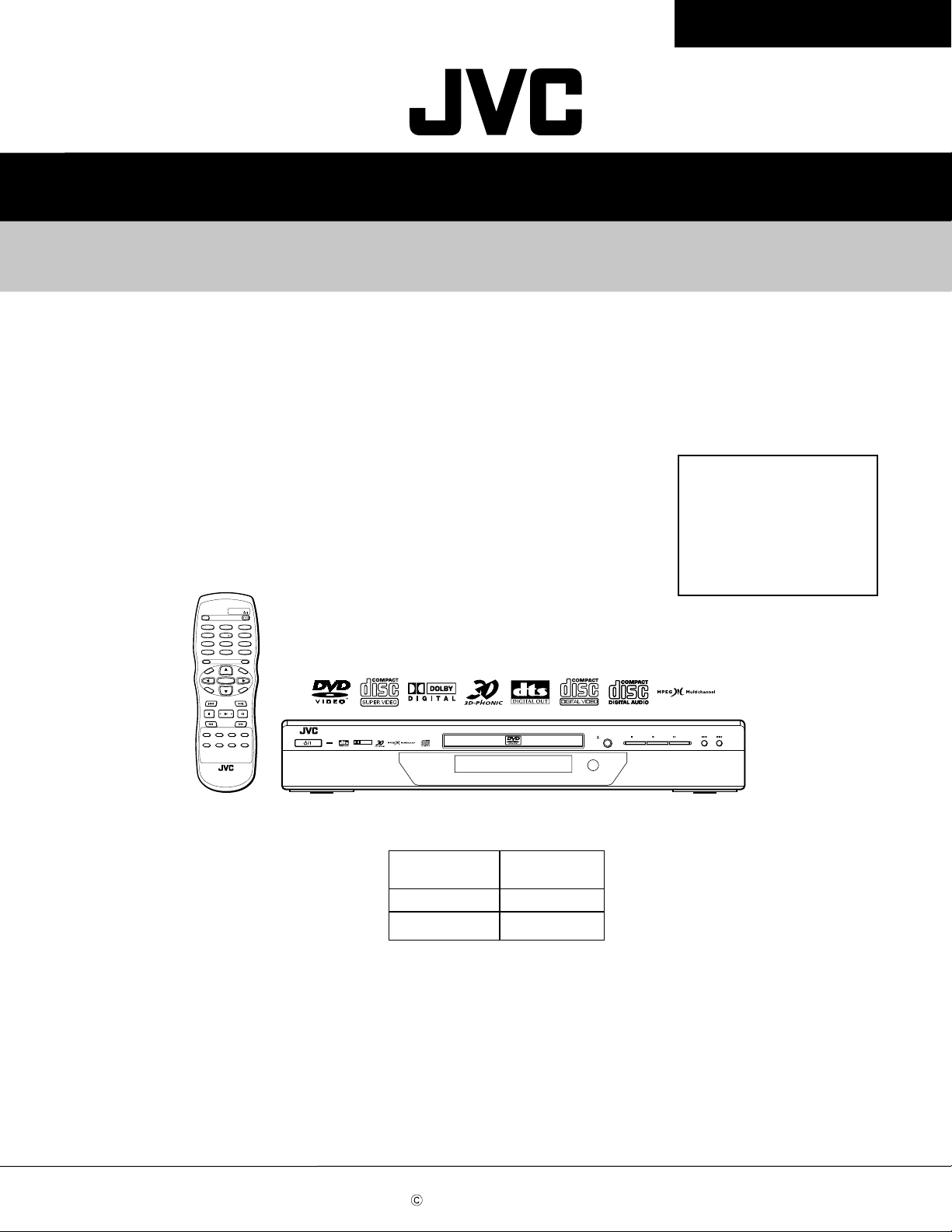
XV-S300BK/XV-S302SL
SERVICE MANUAL
DVD VIDEO PLAYER
XV-S300BK / XV-S302SL
Area Suffix
B --------------------------- U.K.
E ----- Continental europe
EN ------ Northern europe
EV ------- Eastern Europe
EE -- Russian Federation
STANDBY/ON
OPEN/
CLOSE
123
456
789
10 0+10
RETURN
CANCEL
U
M
N
E
E
N
M
U
P
O
T
ENTER
C
H
PHONIC
O
I
C
E
NEXT
PREVIOUS
CLEAR SELECT STROBE
SLOW-SLOW
PLAY
SUB TITLE
AUDIO
MODE
3D
DIGEST ANGLE ZOOM
RM-SXV001A
REMOTE CONTROL
THEATER
POSITION
Y
A
L
P
S
I
D
+
STANDBY
DOLBY
STANDBY/ON
D I G I T A L
DVD/SUPER VCD/VCD/CD PLAYER
Each difference point
Model Body color
XV-S300BK
XV-S302SL
Contents
Safety precautions ------------------------ 1-2
Preventing static electricity ------------- 1-3
Precautions for service ------------------ 1-4
Important for laser products ------------ 1-5
Disassembly method --------------------- 1-6
SKIP
OPEN/CLOSE
PAUSEPLAYSTOP
Black
Silver
Adjustment method ----------------------- 1-15
Attention when pick-up is exchanged - 1-19
Comfirm method of operation ---------- 1-20
Troubleshooting --------------------------- 1-21
Description of major ICs ----------------- 1-25
This service manual is printed on 100% recycled paper.
COPYRIGHT 2002 VICTOR COMPANY OF JAPAN, LTD.
No.A0029
Apr. 2002
Page 2
XV-S300BK/XV-S302SL
1. This design of this product contains special hardware and many circuits and components specially for safety
purposes. For continued protection, no changes should be made to the original design unless authorized in
writing by the manufacturer. Replacement parts must be identical to those used in the original circuits. Services
should be performed by qualified personnel only.
2. Alterations of the design or circuitry of the product should not be made. Any design alterations of the product
should not be made. Any design alterations or additions will void the manufacturers warranty and will further
relieve the manufacture of responsibility for personal injury or property damage resulting therefrom.
3. Many electrical and mechanical parts in the products have special safety-related characteristics. These
characteristics are often not evident from visual inspection nor can the protection afforded by them necessarily
be obtained by using replacement components rated for higher voltage, wattage, etc. Replacement parts which
have these special safety characteristics are identified in the Parts List of Service Manual. Electrical
components having such features are identified by shading on the schematics and by ( ) on the Parts List in
the Service Manual. The use of a substitute replacement which does not have the same safety characteristics
as the recommended replacement parts shown in the Parts List of Service Manual may create shock, fire, or
other hazards.
4. The leads in the products are routed and dressed with ties, clamps, tubings, barriers and the like to be
separated from live parts, high temperature parts, moving parts and/or sharp edges for the prevention of
electric shock and fire hazard. When service is required, the original lead routing and dress should be
observed, and it should be confirmed that they have been returned to normal, after reassembling.
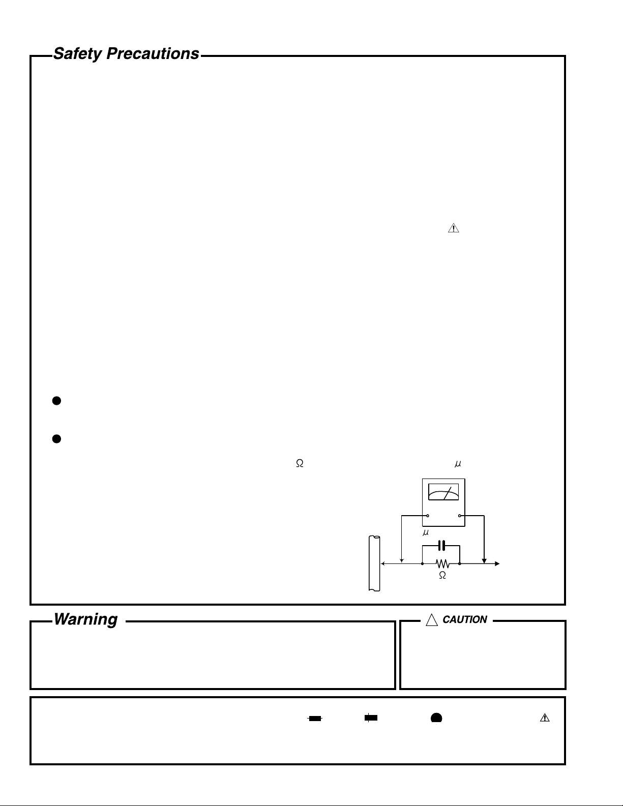
5. Leakage current check (Electrical shock hazard testing)
After reassembling the product, always perform an isolation check on the exposed metal parts of the product
(antenna terminals, knobs, metal cabinet, screw heads, headphone jack, control shafts, etc.) to be sure the
product is safe to operate without danger of electrical shock.
Do not use a line isolation transformer during this check.
Plug the AC line cord directly into the AC outlet. Using a "Leakage Current Tester", measure the leakage
current from each exposed metal parts of the cabinet, particularly any exposed metal part having a return
path to the chassis, to a known good earth ground. Any leakage current must not exceed 0.5mA AC (r.m.s.).
Alternate check method
Plug the AC line cord directly into the AC outlet. Use an AC voltmeter having, 1,000 ohms per volt or more
sensitivity in the following manner. Connect a 1,500 10W resistor paralleled by a 0.15 F AC-type capacitor
between an exposed metal part and a known good earth ground.
Measure the AC voltage across the resistor with the AC
voltmeter.
Move the resistor connection to each exposed metal part,
particularly any exposed metal part having a return path to
the chassis, and measure the AC voltage across the resistor.
Now, reverse the plug in the AC outlet and repeat each
measurement. Voltage measured any must not exceed 0.75 V
AC (r.m.s.). This corresponds to 0.5 mA AC (r.m.s.).
0.15 F AC TYPE
1500 10W
Good earth ground
AC VOLTMETER
(Having 1000
ohms/volts,
or more sensitivity)
Place this
probe on
each exposed
metal part.
!
1. This equipment has been designed and manufactured to meet international safety standards.
2. It is the legal responsibility of the repairer to ensure that these safety standards are maintained.
3. Repairs must be made in accordance with the relevant safety standards.
4. It is essential that safety critical components are replaced by approved parts.
5. If mains voltage selector is provided, check setting for local voltage.
Burrs formed during molding may
be left over on some parts of the
chassis. Therefore, pay attention to
such burrs in the case of
preforming repair of this system.
In regard with component parts appearing on the silk-screen printed side (parts side) of the PWB diagrams, the
parts that are printed over with black such as the resistor ( ), diode ( ) and ICP ( ) or identified by the " "
mark nearby are critical for safety.
When replacing them, be sure to use the parts of the same type and rating as specified by the manufacturer.
(Except the J and C version)
1-2
Page 3
XV-S300BK/XV-S302SL
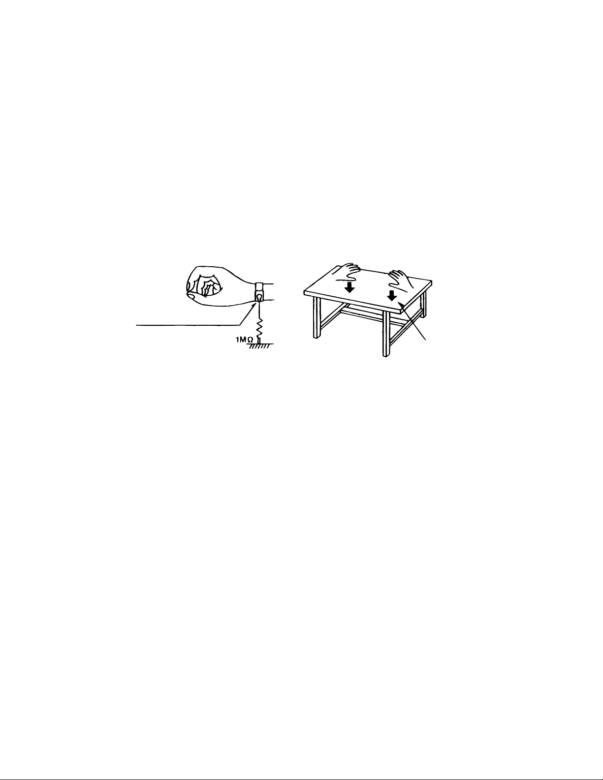
Preventing static electricity
Electrostatic discharge (ESD), which occurs when static electricity stored in the body, fabric, etc. is discharged,
can destroy the laser diode in the traverse unit (optical pickup). Take care to prevent this when performing repairs.
1.1. Grounding to prevent damage by static electricity
Static electricity in the work area can destroy the optical pickup (laser diode) in devices such as DVD players.
Be careful to use proper grounding in the area where repairs are being performed.
1.1.1. Ground the workbench
1. Ground the workbench by laying conductive material (such as a conductive sheet) or an iron plate over
it before placing the traverse unit (optical pickup) on it.
1.1.2. Ground yourself
1. Use an anti-static wrist strap to release any static electricity built up in your body.
(caption)
Anti-static wrist strap
Conductive material
(conductive sheet) or iron plate
1.1.3. Handling the optical pickup
1. In order to maintain quality during transport and before installation, both sides of the laser diode on the
replacement optical pickup are shorted. After replacement, return the shorted parts to their original condition.
(Refer to the text.)
2. Do not use a tester to check the condition of the laser diode in the optical pickup. The tester's internal power
source can easily destroy the laser diode.
1.2. Handling the traverse unit (optical pickup)
1. Do not subject the traverse unit (optical pickup) to strong shocks, as it is a sensitive, complex unit.
2. Cut off the shorted part of the flexible cable using nippers, etc. after replacing the optical pickup. For specific
details, refer to the replacement procedure in the text. Remove the anti-static pin when replacing the traverse
unit. Be careful not to take too long a time when attaching it to the connector.
3. Handle the flexible cable carefully as it may break when subjected to strong force.
4. It is not possible to adjust the semi-fixed resistor that adjusts the laser power. Do not turn it
1-3
Page 4
XV-S300BK/XV-S302SL
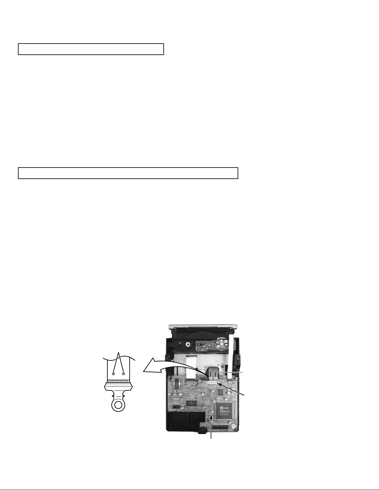
Precautions for service
Handling of Traverse Unit and Laser Pickup
1. Do not touch any peripheral element of the pickup or the actuator.
2. The traverse unit and the pickup are precision devices and therefore must not be subjected to strong shock.
3. Do not use a tester to examine the laser diode. (The diode can easily be destroyed by the internal power
supply of the tester.)
4. To replace the traverse unit, pull out the metal short pin for protection from charging.
5. When replacing the pickup, after mounting a new pickup, remove the solder on the short land which is
provided at the center of the flexible wire to open the circuit.
6. Half-fixed resistors for laser power adjustment are adjusted in pairs at shipment to match the characteristics
of the optical block.
Do not change the setting of these half-fixed resistors for laser power adjustment.
Destruction of Traverse Unit and Laser Pickup by Static Electricity
Laser diodes are easily destroyed by static electricity charged on clothing
or the human body. Before repairing peripheral elements of the traverse
unit or pickup, be sure to take the following electrostatic protection:
1. Wear an antistatic wrist wrap.
2. With a conductive sheet or a steel plate on the workbench on which the traverse unit or the pick up is to be
repaired, ground the sheet or the plate.
3. After removing the flexible wire from the connector (CN101), short-circuit the flexible wire by the metal clip.
4. Short-circuit the laser diode by soldering the land which is provided at the center of the flexible wire for the
pickup. After completing the repair, remove the solder to open the circuit.
Please refer to "Fig.4" of "Disassembly
method" for details.
Short circuit
Short circuit
CN101
1-4
Servo control
board
Page 5
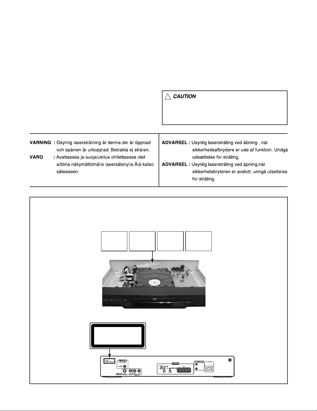
Important for laser products
XV-S300BK/XV-S302SL
1.CLASS 1 LASER PRODUCT
2.DANGER : Invisible laser radiation when open and inter
lock failed or defeated. Avoid direct exposure to beam.
3.CAUTION : There are no serviceable parts inside the
Laser Unit. Do not disassemble the Laser Unit. Replace
the complete Laser Unit if it malfunctions.
4.CAUTION : The compact disc player uses invisible laser
radiation and is equipped with safety switches which
prevent emission of radiation when the drawer is open and
the safety interlocks have failed or are de
feated. It is dangerous to defeat the safety switches.
5.CAUTION : If safety switches malfunction, the laser is able
to function.
6.CAUTION : Use of controls, adjustments or performance of
procedures other than those specified herein may result in
hazardous radiation exposure.
!
Please use enough caution not to
see the beam directly or touch it
in case of an adjustment or operation
check.
REPRODUCTION AND POSITION OF LABEL and PRINT
WARNING LABEL and PRINT
CAUTION: Invisible laser
radiation when open and
interlock failed or defeated.
AVOID DIRECT EXPOSURE
TO BEAM. (e)
VARNING: Osynlig laserstrålning när denna del är
öppnad och spärren är
urkopplad. Betrakta ej
strålen. (s)
CLASS 1
LASER PRODUCT
ADVARSEL: Usynlig laser-
stråling ved åbning, når
sikkerhedsafbrydere er ude
af funktion. Undgå udsættelse for stråling (d)
VARO: Avattaessa ja suojalukitus ohitettaessa olet
alttiina näkymättömälle
lasersäteilylle. Älä katso
säteeseen. (f)
1-5
Page 6
XV-S300BK/XV-S302SL
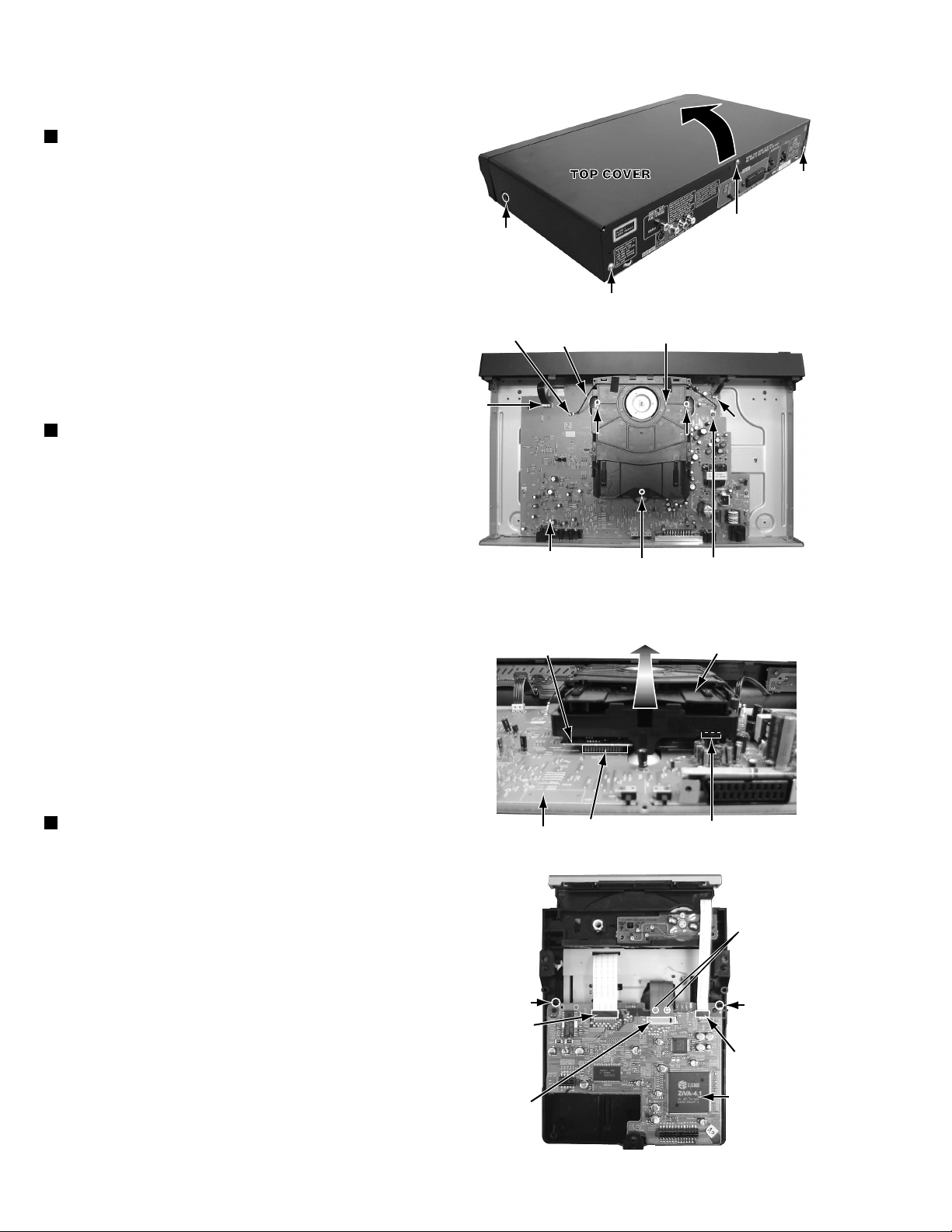
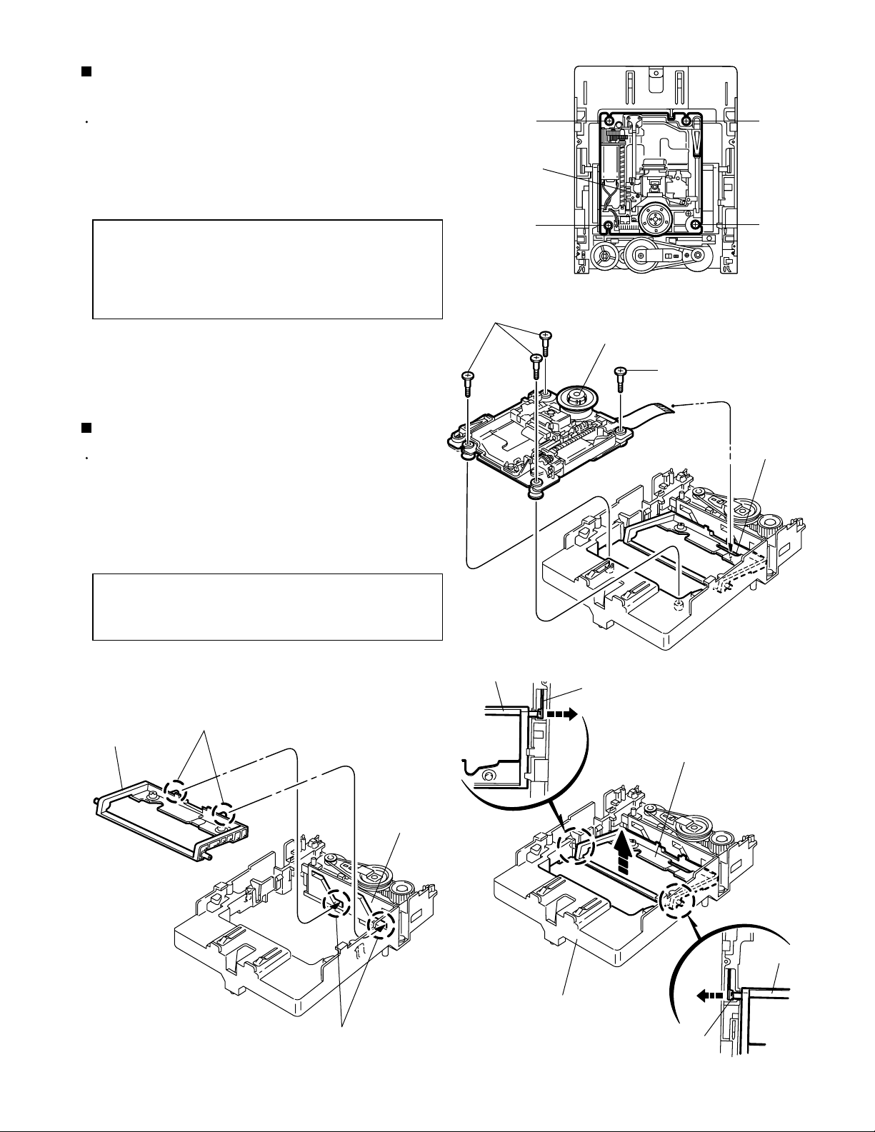
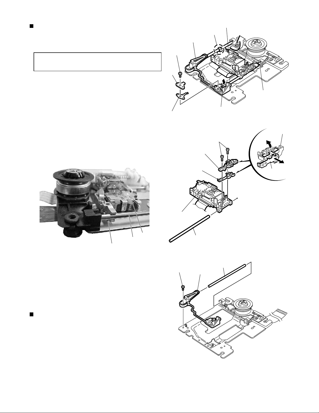
Disassembly method
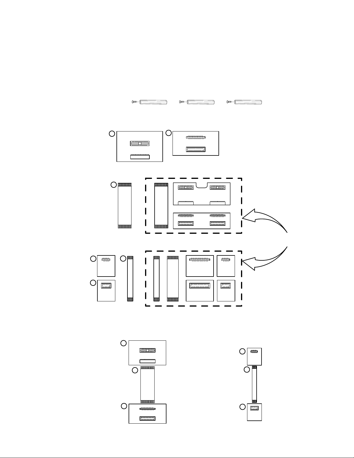
<Main body>
Removing the top cover (see Fig.1)
1.
Remove the two screws A attaching the top cover on
both sides of the body.
2.
Remove the three screws B attaching the top cover
on the back of the body.
3.
Remove the top cover from the body by lifting the
rear part of the top cover.
ATTENTION: Do not break the front panel tab
fitted to the top cover.
Removing the mechanism assembly
(see Fig.2,3)
Prior to performing the following procedure, remove
*
the top cover.
There is no need to remove the front panel assembly.
*
Remove the three screws C attaching the mechanism
1.
assembly on the bottom chassis.
Remove the two screws D attaching the lug wire and
2.
main board on the main board.
The servo control board is removed from the
3.
connector CN961 and CN701 connected with the main
board respectively.
CN702
A x 2
D
Lug wire
Main board
Servo control board
Fig.1
B
Mechanism assembly
C
Fig.2
C
C
D
Mechanism
assembly
B
B
CN703
Remove the mechanism assembly by lifting the rear
4.
part of the mechanism assembly.
Removing the servo control board (see Fig.4)
Prior to performing the following procedure, remove
*
the top cover and mechanism assembly.
Disconnect the card wire from connector CN201 and
1.
CN202 on the servo control board respectively.
Disconnect the flexible wire from connector CN101 on
2.
the servo control board from pick-up.
< ATTENTION >
At this time, please extract the wire after short-circuited
of two places on the wire in part a with solder.
Please remove the solder two places of part a after
connecting the wire with CN101 when reassembling.
Two places in hook b are removed, the servo control
3.
board is lifted, and it is removed.
Main board
Hook b
CN201
CN101
CN701
Fig.3
Fig.4
CN961
Part a
Hook b
CN202
Servo control
board
1-6
Page 7
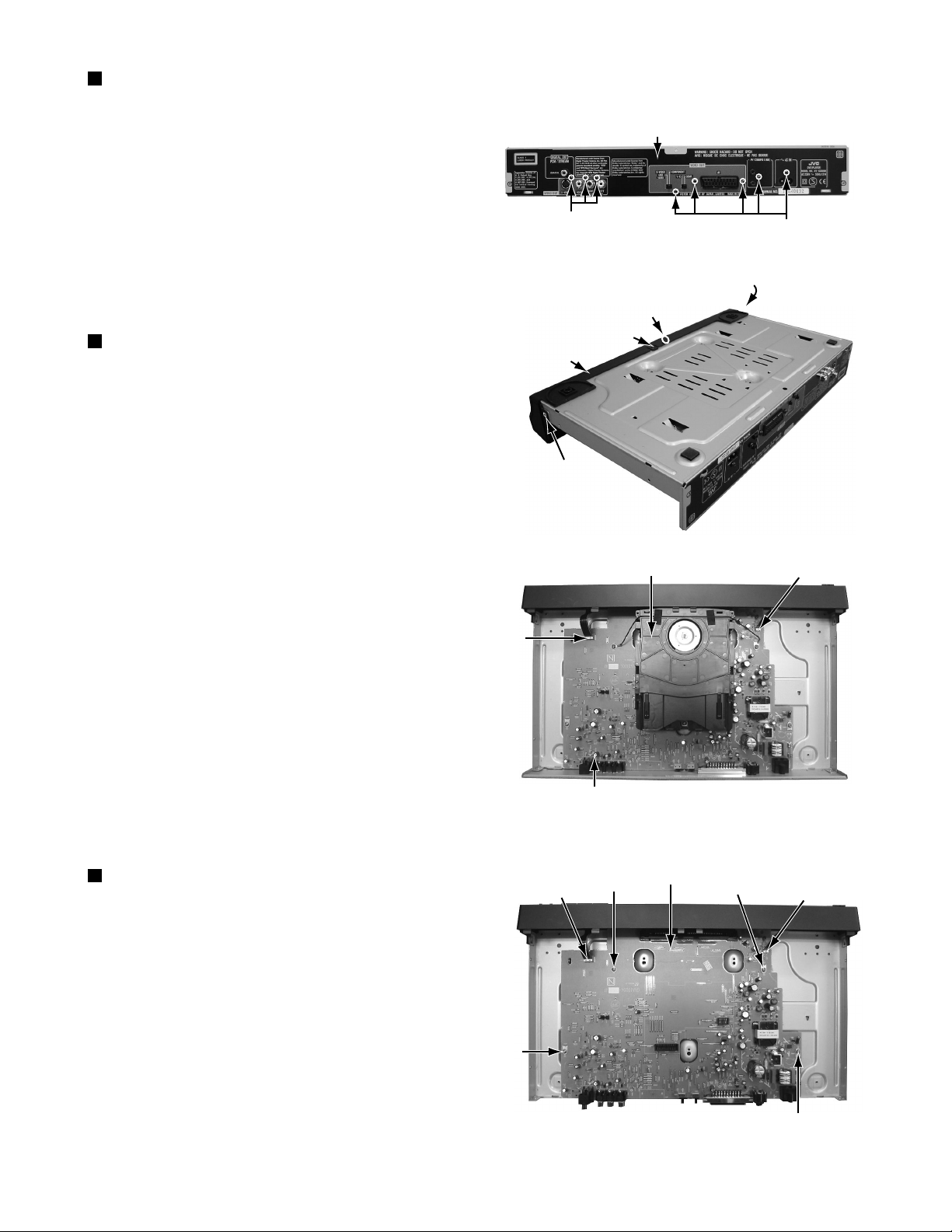
Removing the rear panel (see Fig.5)
XV-S300BK/XV-S302SL
*Prior to performing the following procedure, remove
the top cover.
1.Remove the eight screws E attaching the rear panel
on the back of the body.
Removing the front panel assembly
(see Fig.6,7)
* Prior to performing the following procedure, remove
the top cover.
* There is no need to remove the mechanism assembly.
1.Remove the one screw F attaching the front panel
assembly on the bottom chassis.
2.Disconnect the wire from CN702 and CN703 on the
main board respectively.
3.Hook c and d are removed respectively, and the front
panel assembly is removed.
Front panel
assembly
Hook d
Rear panel
E
Fig.5
F
Hook c
Mechanism assembly
E
Hook d
Fig.6
CN703
Removing the main board (see Fig.8)
* Prior to performing the following procedure, remove
the top cover, mechanism assembly and rear panel.
1.Disconnect the wire from CN702 and CN703 on the
main board respectively.
2.Remove the four screws G attaching the main board
on the bottom chassis.
CN702
G
Main board
CN702
Main board
G
Fig.7
G
CN703
Fig.8
G
1-7
Page 8
XV-S300BK/XV-S302SL
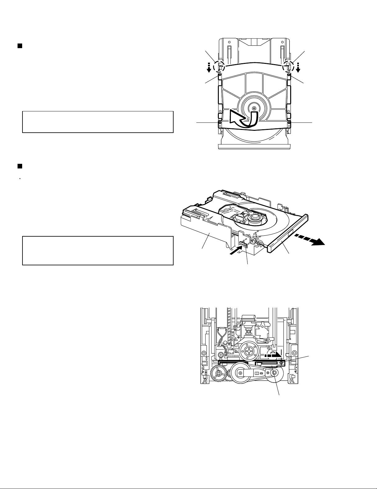
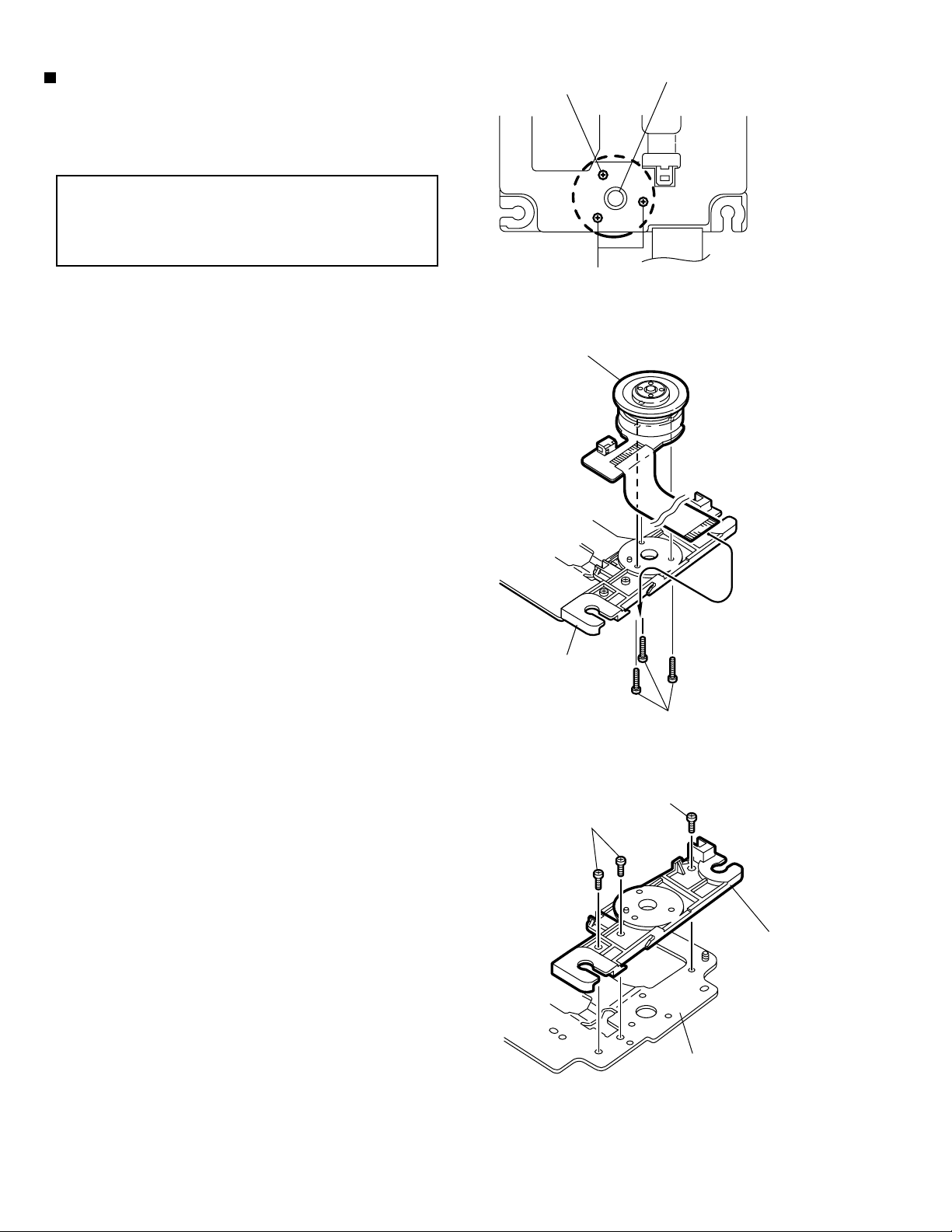
<Loading assembly section>
Removing the clamper assembly
(See Fig.1)
1.
Remove the four screws A attaching the clamper
assembly.
2.
Move the clamper in the direction of the arrow to
release the two joints a on both sides.
ATTENTION:
When reattaching, fit the clamper to
the two joints a.
Removing the tray (See Fig.2 and 3)
Prior to performing the following procedure, remove
the clamper assembly.
1.
Push b of the slide cam into the slot on the left side
of the loading base until it stops.
2.
Draw out the tray toward the front.
Joint a
A
Joint a
A
AA
Fig.1
ATTENTION:
Before reattaching the tray, slide the
part c of the slide cam to the right as
shown in Fig.3.
Clamper base
Push
Tray
b
Fig.2
Part c
Slide cam
Fig.3
1-8
Page 9
Removing the traverse mechanism
assembly (See Fig.4 and 5)
XV-S300BK/XV-S302SL
Prior to performing the following procedure, remove
the clamper assembly and the tray.
1.
Remove the four screws B attaching the traverse
mechanism assembly.
ATTENTION:
Before reattaching the traverse
mechanism assembly, pass the card
wire extending from the spindle motor
board through the notch d of the
elevator.
Removing the elevator (See Fig.6 and 7)
Prior to performing the following procedure, remove
the clamper assembly, the tray and the traverse
mechanism assembly.
1.
Extend each bar e inside of the loading base
outward and detach the elevator shaft.
B
Traverse mechanism
assembly
B
B
BB
BB
Fig.4
Traverse mechanism assembly
BB
Elevator
Notch d
ATTENTION:
Elevator
When reattaching, first fit the two
shafts on the front of the elevator to
the slots f of the slide cam.
Shafts
Slide cam
Elevator
Fig.5
e
Elevator
Elevator
Loading base
Slots f
e
Fig.6Fig.7
1-9
Page 10
XV-S300BK/XV-S302SL
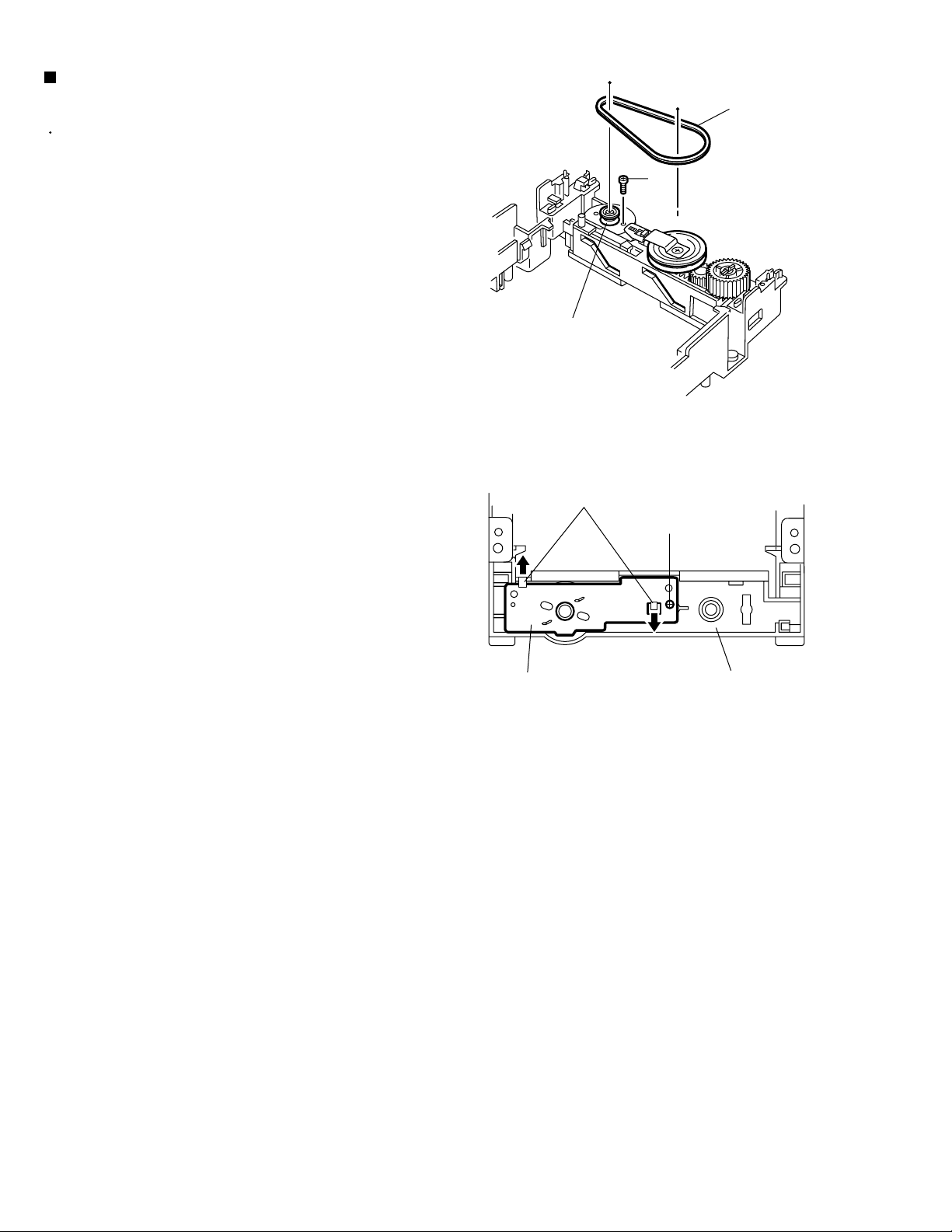
Removing the motor assembly
(See Fig.8 and 9)
Prior to performing the following procedure, remove
the clamper assembly, the tray, the traverse
mechanism assembly and the elevator.
1.
Remove the belt from the pulley.
2.
Remove the screw C attaching the motor assembly.
3.
Turn over the body and remove the screw D
attaching the motor assembly.
4.
Release the two tabs g retaining the motor board.
Belt
C
Motor assembly
Fig.8
Tabs g
Motor assembly
D
Loading base
Fig.9
1-10
Page 11
XV-S300BK/XV-S302SL
Pulley gear
Pulley gear bracket
Motor assembly
Pulley gear bracket
E
Idle gear
Fig.10
Idle gear
Pulley gear
Tads h
Pulley gear
Removing the Idle gear / pulley gear /
middle gear / slide cam (See Fig.10 to 12)
Prior to performing the following procedure, remove
the clamper assembly, the tray, the traverse
mechanism assembly, the elevator and the motor
assembly.
1.
Press the two tabs h inward and pull out the idle
gear.
2.
Remove the screw E attaching the pulley gear
bracket. Slide the pulley gear bracket in the direction
of the arrow and pull out the pulley gear.
3.
Slide the slide cam in the direction of the arrow to
release the two joints i and remove upward.
4.
Remove the middle gear.
Slide cam
Joint i
Slide cam
Middle gear
Joint i
Fig.11
Middle gear
Fig.12
Loading base
1-11
Page 12
XV-S300BK/XV-S302SL
<Traverse mechanism assembly section>
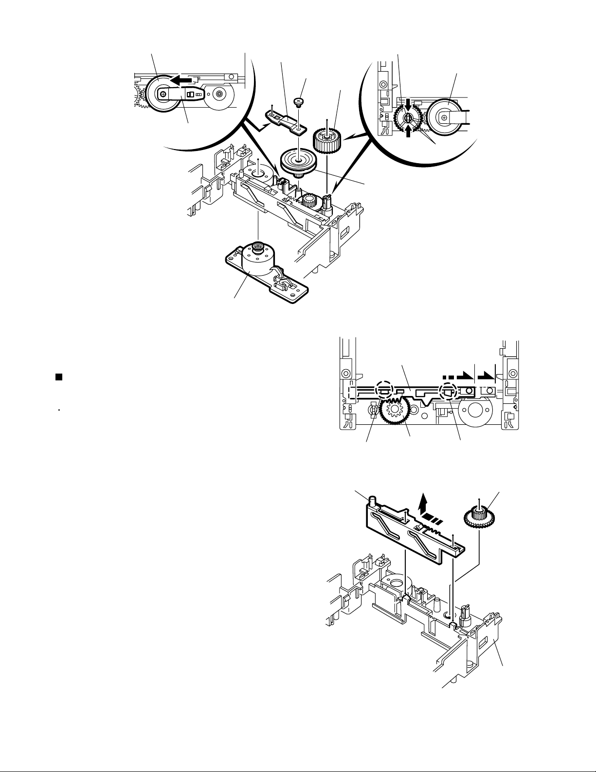
Removing the feed motor assembly
(See Fig.13)
1.
Unsolder the two soldering j on the spindle motor
board.
2.
Remove the two screws F attaching the feed motor
assembly.
Removing the feed motor
(See Fig.13 to 15)
Prior to performing the following procedure, remove
the feed motor assembly.
1.
Remove the screw G attaching the thrust spring.
Feed motor assembly
F
F
Notch k
Soldering j
Spindle motor board
Pickup
Spindle motor
Fig.13
Feed gear (M)
Thrust spring
ATTENTION:
2.
Remove the feed gear (M).
3.
Pull out the feed gear (E) and the lead screw.
4.
Remove the two screws H attaching the feed motor.
ATTENTION:
When reattaching the thrust spring,
make sure that the thrust spring
presses the feed gear (M) and the feed
gear (E) reasonably.
When reattaching, pass the two cables
extending from the feed motor through
the notch k of the feed holder as
shown in Fig.13.
G
Lead screw
Feed gear (E)
Fig.14
Feed motor
1-12
Feed holder
H
Fig.15
Page 13
XV-S300BK/XV-S302SL
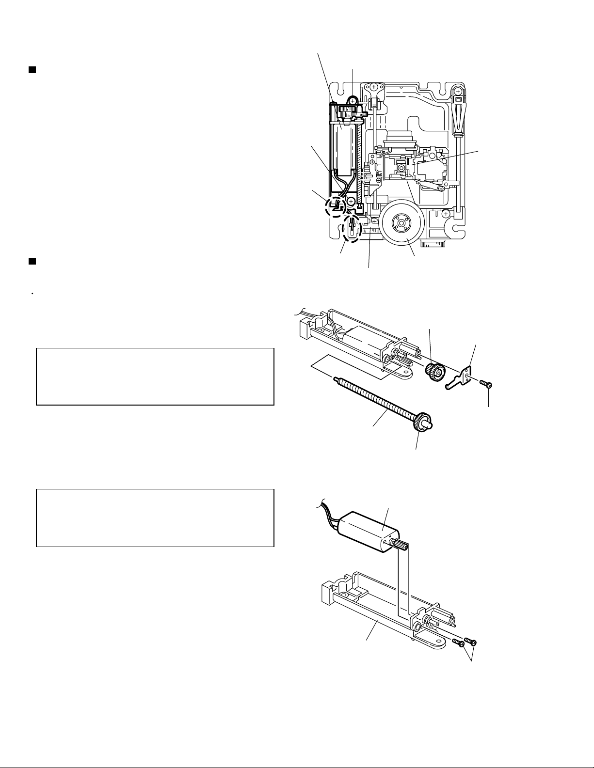
Removing the pickup (See Fig.16 and 17)
1.
Remove the screw I attaching the T spring (S) and
the shaft holder. Remove also the plate.
ATTENTION:
2.
Pull out the part l of the shaft upward. Move the part
m in the direction of the arrow and detach from the
spindle base.
3.
Disengage the joint n of the pickup and the shaft in
the direction of the arrow.
4.
Pull out the shaft from the pickup.
5.
Remove the two screws J attaching the actuator.
6.
Disengage the joint of the actuator and the lead
spring. Pull out the lead spring.
When reattaching, make sure that the
T spring (S) presses the shaft.
Shaft holder
I
Plate
T spring (S)
Lead spring
Pickup
Joint n
Part m
Part l
Fig.16
Actuator
J
Actuator
Lead spring
Shaft
Spring
The spring must be under the shaft when you
install pick-up.
Removing the shaft holder / shaft
(See Fig.18)
1.
Remove the screw K attaching the shaft holder.
2.
Remove the shaft.
Pick-up
Pickup
K
Shaft
Fig.17
Shaft
Shaft holder
Fig.18
1-13
Page 14
XV-S300BK/XV-S302SL
Removing the spindle motor assembly
(See Fig.19 to 21)
1.
Remove the three screws L attaching the spindle
motor on the bottom of the mechanism base.
ATTENTION:
2.
Remove the three screws M attaching the spindle
base.
When reattaching, pass the card wire
extending from the spindle motor
board through the notch of the spindle
base.
L
L
Spindle motor assembly
Spindle motor
Fig.19
Spindle base
L
Fig.20
M
M
Spindle base
Mechanism base
Fig.21
1-14
Page 15
XV-S300BK/XV-S302SL
Adjustment method
(1) Initialization method
If microprocessor (IC401,IC402,IC451,IC504) or pick-up is replaces, initialize the
DVD player in the following matter
1)Take out the disc and close the tray.
2)Unplug the power plug.
3)Insert power plug into outlet while pressing both "PLAY" button and "OPEN/CLOSE" button.
4)FL Display indicate "TEST " . :Version, :Region code
5)Press "3D-PHONIC" button of remote controller. and EEPROM initialize start.
6)When indicate "DTS" on the display, initialize finishes.
7)The power is turned OFF, and Unplug the power plug.
(2) Display of "Laser current value" and "Jitter value"
"Laser current value" and "Jitter value" are displayed on the FL display by the undermentioned
method. Please refer to the failure diagnosis.
1)Take out the disc and close the tray.
2)Unplug the power plug.
3)Insert power plug into outlet while pressing both "PLAY" button and "OPEN/CLOSE" button.
4)FL Display indicate "TEST " . :Version, :Region code
5)Press the "OPEN/CLOSE" button to move the tray outward.
Put the test disc (VT-501) on the tray and press "OPEN/CLOSE" button.
The tray should move inward (Note:Don't push to close the tray directly by hand etc.)
6)Press the "PLAY" button.
7)After a few seconds, The laser current value and the jitter value is displayed on the FL indicator as follows.
FL Display
* The test mode is canceled when
0 0 3 5 1 8 B 6
the power is turned off.
Laser current value Jitter value
For Laser current value
The laser current value becomes 35mA for the above-mentioned.
Becomes a test mode by doing above-mentioned procedure 1) - 4). Afterwards, the laser current value can
be switched by pushing the button to remote controller without turning on the disk.
Remote control "4" button --- Laser of CD
Remote control "5" button --- Laser of DVD
It can be judged it is simply good if the displayed current value of the laser is smaller than
that of the undermentioned value.
Moreover, there must be a deteriorated possibility and the pick-up must exchange the pick-up more
than the undermentioned value.
Laser current value of CD ------ 49 mA or less
Laser current value of DVD ---- 64 mA or less
STANDBY/ON
OPEN/
CLOSE
123
456
789
10 0+10
RETURN
U
N
E
M
P
O
T
ENTER
C
H
O
I
C
E
PREVIOUS
CLEAR SELECT STROBE
SLOW-SLOW
PLAY
SUB TITLE
AUDIO
MODE
3D
PHONIC
DIGEST ANGLE ZOOM
RM-SXV001A
REMOTE CONTROL
CANCEL
M
E
N
U
Y
A
L
P
S
I
D
NEXT
+
THEATER
POSITION
5 Button
(Laser of DVD)
4 Button
(Laser of CD)
3D PHONIC
Button (Initialize start)
POWER Button
*Returns to a usual test mode by the
thing to push the "STOP" button of
remote controller.
DTS Display part
(Initialize complete)
FL Display
STANDBY/ON
STANDBY
DOLBY
D I G I T A L
DVD/SUPER VCD/VCD/CD PLAYER
OPEN/CLOSE
Button(Test mode)
(Test mode & display of jitter)
OPEN/CLOSE
PLAY Button
SKIP
PAUSEPLAYSTOP
1-15
Page 16
XV-S300BK/XV-S302SL
For Jitter value
The jitter value is displayed on the FL display referring to the previous page.
The jitter value is displayed by the hexadecimal number.
In the following cases, please "Flap adjustment of the pick-up guide shaft" referring to the following page.
Before using the TEST disc VT-501, careful check it if there is neither damage nor dirt on the read surface.
< In the following cases, please adjustment >
* When you exchange the pick-up
* When you exchange the spindle motor
* When the reading accuracy of the signal is bad (There is a block noise in the screen etc..)
STANDBY/ON
OPEN/
CLOSE
123
456
789
10 0+10
RETURN
U
N
E
M
P
O
T
ENTER
C
H
O
I
C
E
PREVIOUS
CLEAR SELECT STROBE
SLOW-SLOW
PLAY
SUB TITLE
AUDIO
MODE
3D
PHONIC
DIGEST ANGLE ZOOM
RM-SXV001A
REMOTE CONTROL
(Laser of DVD)
CANCEL
M
E
N
U
A
L
P
S
I
D
NEXT
+
THEATER
POSITION
(Laser of CD)
Y
3D PHONIC
Button (Initialize start)
5 Button
4 Button
DTS Display part
(Initialize complete)
POWER Button
STANDBY
STANDBY/ON
D I G I T A L
OPEN/CLOSE
Button(Test mode)
FL Display
DOLBY
DVD/SUPER VCD/VCD/CD PLAYER
OPEN/CLOSE
PLAY Button
(Test mode & display of jitter)
SKIP
PAUSEPLAYSTOP
1-16
Page 17
(3) Flap adjustment of the pick-up guide shaft
<Tool list for adjustment>
* Hex wrench for adjustment
Off-the-shelf (1.3mm)
* Test disc
VT-501 or VT-502
* Stud (four pieces set)
Parts No. : JIGXVS40 (One is not used though there are four. )
* Assistance board and extension cord
Parts No. : EXTXVS40MK2CB
1
EXTXVS40MK2CB-1 MAIN CONNECT
Parts No. : EXTXVS40CB
3
2
EXTXVS40MK2CB-2 CONTROL CONNECT
XV-S40
MAIN CONNECT
XV-S300BK/XV-S302SL
Parts No. : EXTXV521CB
<Connection diagram>
4
5
XV-521 CN601
MAIN CONNECT
XV-521 CN503
6
CONT CONNECT
To CN701 of main board
EXTXVS40MK2CB-1 MAIN CONNECT
1
3
XV-S40 CONTROL CONNECT
CN701 XV-521
XV-521 CN502
CONT CONNECT
MAIN CONNECT
MAIN CONNECT
CN706 XV-521
CN501 XV-521
CONT CONNECT
To CN961 of main board
4
MAIN CONNECT
6
These parts are not used.
XV-521 CN601
2
EXTXVS40MK2CB-2 CONTROL CONNECT
To CN503 of servo control board
5
CONT CONNECT
XV-521 CN503
To CN502 of servo control board
1-17
Page 18
XV-S300BK/XV-S302SL
<Adjustment preparation>
1.The mechanism assembly is made in the state from the main body from which is detached referring to the
disassembly method.
2.Three studs are installed in the mechanism assembly respectively.
3.The servo control board is removed from the mechanism assembly, and puts into the state set up as shown
in figure. (Each wire connected by the servo control board this time leaves the connection maintained.)
Between shaft and hook of mechanism assembly of figure Board is put.
4.The extension cord is inserted in the connector of the assistance board respectively.
The main board is connected with the servo control board as shown in figure.
Mechanism
assembly
Extension
cord
Stud
Main board
Servo control board
Assistance
board
Extension
cord
Shaft & hook
Stud
Assistance
board
Assistance
board
Extension
cord
Shaft & hook
Assistance
board
Servo control board
Extension
cord
Assistance
board
<Adjustment>
1.Puts into the state to display the jitter value on the FL display referring to "Display of the jitter value".
2.The adjustment screw under the traverse mechanism is turned with hex wrench, and matches so that the
jitter value displayed on the FL display may become "maximum" value.
1-18
Adjustment screw a Adjustment screw b
Adjustment
screw c
<POINT>
1.Turns in the forward or the opposite direction,
and makes to the position where the jitter value
is good the half rotation of adjustment screw a
and b(180 degrees) respectively.
2.Afterwards, adjustment screw b and c are turned
in the same way, and makes to the best position.
Page 19
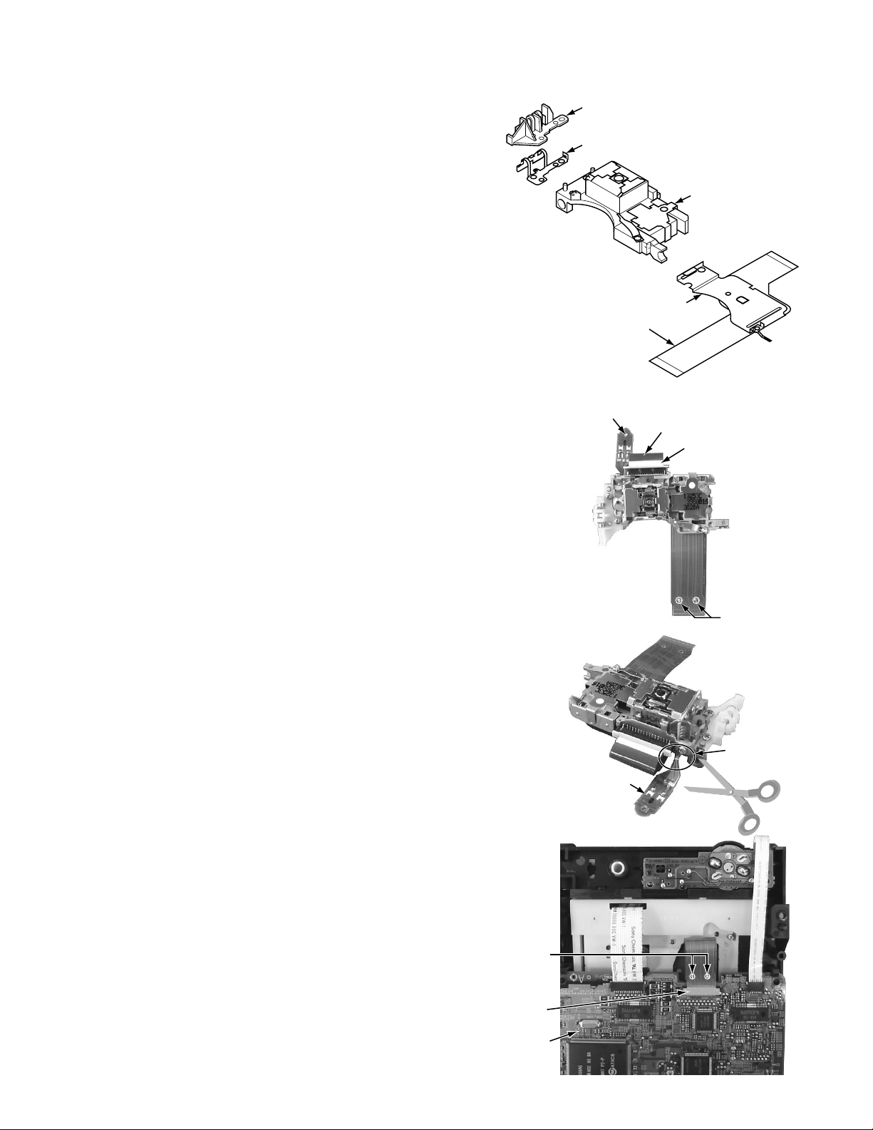
Attention when pick-up is exchanged
1.Flexible wire, pick-up spring, switch actuator,
and lead spring are removed from an old pick-up
(broken the one).
XV-S300BK/XV-S302SL
Switch actuator
Lead spring
< Guide >
Flexible wire, pick-up spring and switch actuator,
lead spring are removed without each decomposing
while assembled.
2.The above-mentioned parts are installed in a new
pick-up (non-defective article).
3.A flexible wire is inserted in the connector which has
taken side with the pick-up, and solder is put up to short
land part "a" two places on a flexible wire.
4.The electrostatic breakdown protection circuit attached
to the pick-up is cut.
< ATTENTION >
Please cut the electrostatic breakdown protection circuit
attached to the pick-up after solder is put up to two places
on a flexible wire short land part "a" of the insertion of a
flexible wire this time in the connector without fail.
The procedure might be mistaken and if solder has not
surely adhered to two places on a flexible wire short land
part "a", the laser diode in the pick-up be destroyed again.
Pick-up
Pick-up spring
Flexible wire
Electrostatic breakdown
protection circuit
Flexible wire
Connector
5.The pick-up is installed in the traverse mechanism.
6.A flexible wire is connected with connector CN101 on the
servo control board by installing the traverse mechanism
in the loading mechanism.
7.Solder in two places on a flexible wire in part "a" is
removed.
< ATTENTION >
Please remove solder in two places in part "a" after
connecting a flexible wire with connector CN101 on
the servo control board without fail this time.
When the procedure is mistaken, the laser diode in
the pick-up might be destroyed.
Please remove solder in two places in part "a" surely.
Short land
part "a"
Cutting part
Electrostatic breakdown
protection circuit
Short land
part "a"
CN101
Servo control
board
1-19
Page 20

XV-S300BK/XV-S302SL
Confirm method of operation
Please confirm the operation of the undermentioned item after doing the repair and
the upgrade of the firmware.
The EEPROM is initialized.
Refer to the initialization method.
Opening picture check (Power ON)
It should be display "JVC"
Muting working
The noise must not be had to the performance beginning when you
push "PLAY" button or at ON/STANDBY.
FL Display
The mark and the logo, etc. displayed by each operation must be displayed correctly.
FL Display should light correctly without any unevenness.
All Function button
All function buttons should worked correctly with moderate click feeling.
Open and close movement of tray
When press OPEN/CLOSE button the tray should move smoothly without any noise.
Remote controller unit working
Check the correctly operation in use of remote controller unit.
Reading of TOC
Be not long in the malfunction.
Search
Both forward-searches and backward-searches should be able to be done.
Do not stop be searching or after the search.
Skip
Both forward-skip and backward-skip should be able to be done.
Do not stop be after the skip.
Playback
Do not find abnormality etc. of tone quality and the picture quality.
Most outside TITLE playback check
Play VT-501 TITLE 59 CHAPTER 1 , check normal playback.
1-20
Page 21
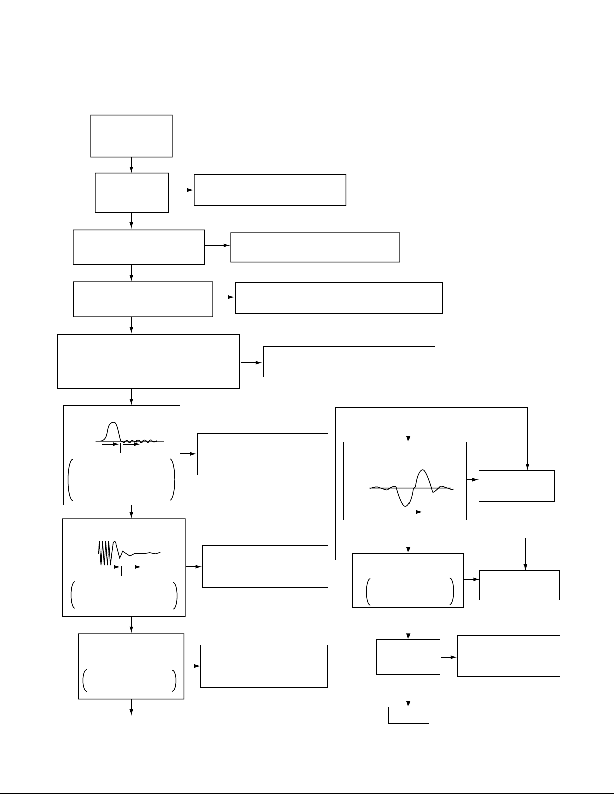
Troubleshooting
Servo volume
Press OPEN
/CLOSE key
XV-S300BK/XV-S302SL
Is tray
operation
Confirmation of tray drive circuit
N
and circuit in surrounding
correct?
Y
Is the traverse moving
along the innermost
N
perimeter for SW detection?
Y
"NO DISC" message appears
Y
immediately after vertical
movement of the pick-up lens
N
The state that DISC does not rotate continues for
several seconds, and becomes NO DISC or an
error display afterwards.
The rotation of DISC becomes high-speed and
abnormal, and becomes NO DISC or an error
display afterwards.
N
Is focus retraction OK?
FE
OFF
Even when it retracts
correctly, if it is out of focus
and makes repeated retries
with a clicking sound, it is
in error.
ON
See "(4) Focus ON error"
N
in "Check points for
individual errors"
Y
Is tracking retraction OK?
See "(3) Traverse movement error"
in "Check points for individual errors"
See "(2) Disk detection, distinction error"
in "Check points for individual errors"
Y
See "(1) Spindle startup error"
in "Check points for individual errors"
Is the inter-layer jump OK?
FE
LO LI
A
Two layers of DVD only.
N
(8) Inter-layer
jump error
Y
TE
OFF
If TE waveform reappears
or fails to converge after the
TE retraction, it is in error.
ON
Y
Is the spindle servo
locked correctly?
Is the RF OUT waveform
locked correctly?
Y
A
See "(5) Tracking ON error"
N
in "Check points for
individual errors"
See "(6) Spindle CLV error"
N
in "Check points for
individual errors"
Has the disc information
been collected?
Stop will result
Y
Is playback
N
possible?
Y
OK !
N
(7) Address read
error
Check (9),(10),(11), and
(12) items in "Check points
for individual errors"
1-21
Page 22

XV-S300BK/XV-S302SL
Check points for each error
(1) Spindle start error
1.Defective spindle motor
*Are there several ohms resistance between each pin of CN201 "5-6","6-7","5-7"?
(The power supply is turned off and measured.)
*Is the sign wave of about 100mVp-p in the voltage had from each terminal?
[ CN201"9"(H1-),"10"(H1+),"11"(H2-),"12"(H2+),"13"(H3-),"14"(H3+) ]
2.Defective spindle motor driver (IC251)
*Has motor drive voltage of a sine wave or a rectangular wave gone out to each terminal(SM1~3)
of CN201"5,6,7" and IC251"2,4,7"?
*Is FG pulse output from the terminal of IC251"24"(FG) according to the rotation of the motor?
*Is it "L(about 0.9V)" while terminal of IC251"15"(VH) is rotating the motor?
3.Has the control signal come from servo IC or the microcomputer?
*Is it "L" while the terminal of IC251"18"(SBRK) is operating?
Is it "H" while the terminal of IC251"23"(/SPMUTE) is operating?
*Is the control signal input to the terminal of IC251"22"(EC)?
(changes from VHALF voltage while the motor is working.)
*Is the VHALF voltage input to the terminal of IC251"21"(ECR)?
4.Is the FG signal input to the servo IC?
*Is FG pulse input to the terminal of IC301"69"(FG) according to the rotation of the motor?
(2) Disc Detection, Distinction error (no disc, no RFENV)
* Laser is defective.
* Front End Processor is defective (IC101).
* APC circuit is defective. --- Q101,Q102.
* Pattern is defective. --- Lines for CN101 - All patterns which relate to pick-up and patterns between IC101
* IC101 --- For signal from IC101 to IC301, is signal output from IC101 "20" (ASOUT) and
IC101 "41"(RFENV) and IC101 "22" (FEOUT)?
1-22
Page 23

(3) Traverse movement NG
1.Defective traverse driver
*Has the voltage come between terminal of CN101 "1" and "2" ?
2.Defective BTL driver (IC201)
*Has the motor drive voltage gone out to IC201"17" or "18"?
3.Has the control signal come from servo IC or the microcomputer?
*Is it "H" while the terminal of IC201"9"(STBY1) ?
*TRSDRV Is the signal input? (IC301 "67")
4.TRVSW is the signal input from microcomputer? (IC401 "46")
(4) Focus ON NG
* Is FE output ? --- Pattern, IC101
* Is FODRV signal sent ? (R209) --- Pattern, IC301 "115"
* Is driving voltage sent ?
IC201 "13", "14" --- If NG, pattern, driver, mechanical unit .
* Mechanical unit is defective.
(5) Tracking ON NG
XV-S300BK/XV-S302SL
* When the tracking loop cannot be drawn in, TE shape of waves does not settle.
* Mechanical unit is defective.
Because the self adjustment cannot be normally adjusted, the thing which cannot be normally
drawn in is thought.
* Periphery of driver (IC201)
Constant or IC it self is defective.
* Servo IC (IC301)
When improperly adjusted due to defective IC.
(6) Spindle CLV NG
* IC101 -- "35"(RF OUT), "30"(ARF-), "31(ARF+).
* Does not the input or the output of driver's spindle signal do the grip?
* Has the tracking been turned on?
* Spindle motor and driver is defective.
* Additionally, "IC101 and IC301" and "Mechanism is defective(jitter)", etc. are thought.
(7) Address read NG
* Besides, the undermentioned cause is thought though specific of the cause is difficult because various
factors are thought.
Mechanism is defective. (jitter)
IC301, IC401.
The disc is dirty or the wound has adhered.
(8) Between layers jump NG (double-layer disc only)
Mechanism defective
Defect of driver's IC(IC201)
Defect of servo control IC(IC301)
1-23
Page 24

XV-S300BK/XV-S302SL
(9) Neither picture nor sound is output
1.It is not possible to search
*Has the tracking been turned on?
"(5) Tracking ON NG" in "Check points for each error"
*To
*Is the feed operation normal?
To "(3) traverse movement NG" in "Check points for each error" when it is not normal.
Are not there caught of the feeding mechanism etc?
(10) Picture is distorted or abnormal sound occurs at intervals of several seconds.
Is the feed operation normal?
Are not there caught of the feeding mechanism etc?
(11) Others
The image is sometimes blocked, and the image stops.
The image is blocked when going to outer though it is
normal in surroundings in the disk and the stopping
symptom increases.
when the tracking is not normal.
There is a possibility with bad jitter
value for such a symptom.
(12) CD During normal playback operation
a) Is TOC reading normal?
Displays total time
for CD-DA.
Shifts to double-speed
mode for V-CD.
YES
b)Playback possible?
NO
*--:-- is displayed during FL search.
According to [It is not possible to search ] for DVD(9), check the feed
and tracking systems.
*No sound is output although the time is displayed.(CA-DA)
DAC, etc, other than servo.
*The passage of time is not stable, or picture is abnormal.(V-CD)
*The wound of the disc and dirt are confirmed.
1-24
Page 25

Description of major ICs
74VHC00MTC-X (IC455,IC503) : 2-input nand gate
1.Pin layout 2.Truth table
XV-S300BK/XV-S302SL
1A
1B
1Y
2A
2B
2Y
GND
1
2
3
4
5
6
7
14
13
12
11
10
9
8
VCC
4A
4B
4Y
3A
3B
3Y
(TOP VIEW)
74VHC74MTC-X (IC454) : ZIVA Wait
1.Terminal layout
CLR1
D1
CK1
PR1
Q1
Q1
GND
1
2
3
4
CK1 D1
PR1CLR1
Q1 Q1
5
6
7
CK2D2
PR2CLR2
Q2 Q2
14
13
12
11
10
9
8
Vcc
CLR2
D2
CK2
PR2
Q2
Q2
2.Trouth table
Input Output
CLR
PR
L
H
H
L
L
L
H
H
H
H
H
H
A
L
L
H
H
L : High impedance
D
CK
X
X
X
X
X
X
L
H
X
Q
L
H
H(Note 1)
L
H
Qn
B
L
H
L
H
Y
H
H
H
L
Function
Q
H
L
Clear
Preset
H(Note 1)
H
L
Qn
No change
3.Pin function
Pin No.
1
2
3
4
5
6
7
Symbol I/O Description
CLR1
D1
CK1
PR1
Q1
Q1
GND
Direct clear input 1
I
Data input 1
I
Clock pulse input 1
I
Direct preset input 1
I
Output
O
Output
O
Connect to ground
-
Pin No.
8
9
10
11
12
13
14
Symbol I/O Description
Q2
Q2
PR2
CK2
D2
CLR2
VCC
Output
O
Output
O
Direct preset input 2
I
Click pulse input 2
I
Data input 2
I
Clock clear input 2
I
Power supply
-
1-25
Page 26

XV-S300BK/XV-S302SL
74VHCT08ASJ-X (IC704) : 2-input AND gate
1.Pin layout 2.Truth table
1G
1A
1Y
2G
2A
2Y
GND
1
2
3
14
13
12
VCC
4G
4A
L
L
H
H
G
4
5
6
7
11
10
9
8
4Y
3G
3A
3Y
Y
A
Z
L
Z
H
Z
L
L
H
MM1565AF-X (IC951) / MM1563DF-X (IC953) : 500mA Regulator
1.Block diagram
Vin
Cont
Bias
Thermal
shutdown
Driver
Current
limiter
Vo
Reference
2.Pin function
Pin No. Symbol Function
GND
1
2
3
4
5
6
7
Vout
NC
GND
Cn
Cout
Sub
Vin
Cn
Output terminal
Non connect
Connect to ground
Noise decrease terminal
Control terminal
Substrate (Connect to ground)
Input terminal
1-26
Page 27

AN8703FH-V (IC101) : Frontend processor
1.Pin layout
64 49
XV-S300BK/XV-S302SL
1
16
17 32
2.Pin function
Pin No.
1
2
3
4
5
6
7
8
9
10
11
12
13
14
15
16
17
18
19
20
21
22
23
24
25
26
27
28
29
30
31
32
33
Symbol
LPC1
LPC01
LPC2
LPC02
VFOSHORT
TBAL
FBAL
POFLT
DTRD
IDGT
STANDBY
SEN
SCK
STDI
RSCL
JLINE
TEN
TEOUT
AGCBAL
ASOUT
FEN
FEOUT
AGCOFST
MON
AGCLVL
GND2
VREF2
VCC2
VHALF
DFLTON
DFLTOP
DCFLT
GND3
48
33
I/O Description
Laser input terminal (DVD)
I
Laser drive signal output terminal (DVD)
O
Laser input terminal (CD)
I
Laser drive signal output terminal (CD)
O
VFOSHORT control terminal
I
Tracking balance control terminal
I
Focus balance control terminal
I
Track detection threshold level terminal
O
Data slice part data read signal input terminal
I
(For RAM)
Data slice part address part gate signal input
I
terminal( For RAM)
Standby mode control terminal
I
SEN(Serial data input terminal)
I
SCK(Serial data input terminal)
I
STDI(Serial data input terminal)
I
Standard electric current terminal
I
Electric current setting terminal of JLine
I
Reversing input terminal of tracking error output AMP.
I
Tracking error signal output terminal
O
Offset adjusting terminal 1
I
Full adder signal output terminal
O
Focus error output amplifier reversing input terminal
I
Focus error signal output terminal
O
Offset adjusting terminal 2
I
Non connect
-
Output amplitude adjustment for DRC
O
Connect to GND
-
VREF2 voltage output terminal
O
Power supply terminal 5V
-
VHALF voltage output terminal
O
Reversing output terminal of filter AMP.
O
Filter AMP. output terminal
O
Capacity connection terminal for filter output
I
Connect to GND
-
Pin No.
Symbol I/O Description
Non connect
34
35
36
37
38
39
40
41
42
43
44
45
46
47
48
49
50
51
52
53
54
55
56
57
58
59
60
61
62
63
64
RFDIFO
RFOUT
VCC3
RFC
DCRF
OFTR
BDO
RFENV
BOTTOM
PEAK
AGCG
AGCO
TESTSG
RFINP
RFINN
VIN5
VIN6
VIN7
VIN8
VIN9
VIN10
VCC1
VREF1
VIN1
VIN2
VIN3
VIN4
GND1
VIN11
VIN12
HDTYPE
-
Connect to TP103
-
Power supply terminal 3.3V
-
Filter for RF delay correction AMP.
O
All addition amplifier capacitor terminal
O
OFTR output terminal
O
BDO output terminal
O
RF envelope output terminal
O
Bottom envelope detection filter terminal
O
Peak envelope detection filter terminal
O
AGC amplifier gain control terminal
O
AGC amplifier level control terminal
O
TEST signal input terminal
I
RF signal positive input terminal
I
RF signal negative input terminal
I
Internal four-partition (CD) RF input 1
I
Internal four-partition (CD) RF input 2
I
Internal four-partition (CD) RF input 3
-
Internal four-partition (CD) RF input 4
-
External two-partition (DVD) RF input 2
I
External two-partition (DVD) RF input 1
I
Power supply terminal 5V
-
VREF1 voltage output terminal
O
Internal four-partition (DVD) RF input 1
I
Internal four-partition (DVD) RF input 2
I
Internal four-partition (DVD) RF input 3
I
Internal four-partition (DVD) RF input 4
I
Connect to GND
-
3 beam sub input terminal 2 (CD)
I
3 beam sub input terminal 1 (CD)
I
HD Type selection
O
1-27
Page 28

XV-S300BK/XV-S302SL
BA5983FM-X (IC201) : 4CH Driver
1.Block diagram
27
26
28
Vcc
25
10k
20k
23 22 30
24
10k
20k
21
STAND BY
CH4
20
Vcc
19
10k
10k
18
Level Shift
17 16
10k
10k
10k
10k
15
10k
10k
Level Shift
10k
10k
1
2
3
5
4
10k
10k
STAND BY
CH1/2/3
6
729 891011121314
Vcc
10k
10k
Level Shift
10k
10k
10k
10k
2.Pin function
Pin No. Pin No.Symbol SymbolI/O I/ODescription Description
10
11
12
13
14
15
1
2
3
4
5
6
7
8
9
BIAS IN
OPIN1(+)
OPIN1(-)
OPOUT1
OPIN2(+)
OPIN2(-)
OPOUT2
GND
STBY1
PowVcc1
VO2(-)
VO2(+)
VO1(-)
VO1(+)
VO4(+)
Input for Bias-amplifier
I
Non inverting input for CH1 OP-AMP
I
Inverting input for CH1 OP-AMP
I
Output for CH1 OP-AMP
O
Non inverting input for CH2 OP-AMP
I
Inverting input for CH2 OP-AMP
I
Output for CH2 OP-AMP
O
Substrate ground
Input for CH1/2/3 stand by control
I
Vcc for CH1/2 power block
Inverted output of CH2
O
Non inverted output of CH2
O
Inverted output of CH1
O
Non inverted output of CH1
O
Non inverted output of CH4
O
16
17
18
19
20
21
22
23
24
25
26
27
28
29
30
VO4(-)
VO3(+)
VO3(-)
PowVcc2
STBY2
GND
OPOUT3
OPIN3(-)
OPIN3(+)
OPOUT4
OPIN4(-)
OPIN4(+)
PreVcc
O
Inverted output of CH4
O
Non inverted output of CH3
O
Inverted output of CH3
-
Vcc for CH3/4 power block
I
Input for Ch4 stand by control
-
Substrate ground
O
Output for CH3 OP-AMP
I
Inverting input for CH3 OP-AMP
I
Non inverting input for CH3 OP-AMP
O
Output for CH4 OP-AMP
I
Inverting input for CH4 OP-AMP
I
Non inverting input for CH4 OP-AMP
-
Vcc for pre block
-
Connect to ground
-
Connect to ground
Level Shift
10k
10k
CY24203SC-X (IC571) : MPEG / Audio clock generator with VCXO
1.Pin layout 2.Pin function
Pin No. DescriptionSymbol
1-28
XIN
VDD
VCXO
VSS
1
2
3
4
8
XOUT
7
27M
6
13.5M
5
16.9344M
1
2
3
4
5
6
7
8
XIN
VDD
VCXO
VSS
16.9344M
13.5
27M
XOUT
Reference crystal input
Power supply
Input analog control for VCXO
Connect to ground
16.9344 MHz clock output
13.5 MHz clock output
27 MHz clock output
Reference crystal output
Page 29

BA6664FM-X(IC251):Spindle motor driver
1.Pin layout
1
NC
A3
NC
A2
NC
NC
A1
29
GND
H1+
10
H1-
11
H2+
12
H2-
13
H3+
14
H3-
2.Pin function
28
2
3
4
5
6
7
8
9
RNF
27
VM
26
GSW
25
VCC
24
FG
23
PS
22
EC
30
21
ECR
20
FR
19
FG2
18
SB
17
CNF
16
BR
15
VH
XV-S300BK/XV-S302SL
Pin No.
1
2
3
4
5
6
7
8
9
10
11
12
13
14
15
16
17
18
19
20
21
22
23
24
25
26
27
28
29
30
Symbol
NC
A3
NC
A2
NC
NC
A1
GND
H1+
H1-
H2+
H2-
H3+
H3-
VH
BR
CNF
SB
FG2
FR
ECR
EC
PS
FG
VCC
GSW
VM
RNF
I/O
-
O
-
O
-
-
O
I
I
I
I
I
I
I
-
-
O
-
I
I
O
O
-
O
-
O
-
-
Description
Non connect
Output 3 for spindle motor
Non connect
Output 2 for spindle motor
Non connect
Non connect
Output 1 for spindle motor
Connect to ground
Positive input for hall input AMP 1
Negative input for hall input AMP 2
Positive input for hall input AMP 2
Negative input for hall input AMP 2
Positive input for hall input AMP 3
Negative input for hall input AMP 3
Hall bias terminal
Non connect
Capacitor connection pin for phase compensation
Short brake terminal
Non connect
Non connect
Torque control standard voltage input terminal
Torque control voltage input terminal
Start/stop switch (power save terminal)
FG signal output terminal
Power supply for signal division
Gain switch
Power supply for driver division
Resistance connection pin for output current sense
Connect to ground
Connect to ground
1-29
Page 30

XV-S300BK/XV-S302SL
K3N5V1000F-J004 (IC402) :EPROM
1.Pin layout
WP
A20A9A10
A11
A12
A13
A14
A15
A16
A17
BYTE
VssA0D7
D14D6D13D5D12D4Vcc
444342414039383736353433323130292827262524
123456789
WE
A19
2.Block diagram
A8A7A6A5A4A3A2
A18
A0
A1
A2
A3
A4
A5
A6
A7
A8
A9
A10
A11
A12
A13
A14
A15
A16
A17
A18
A19
A20
Address Buffer
10111213141516171819202122
A1
CE
Vss
D0D8D1D9D2
OE
D10D3D11
x 8 / x 16 Output select
CE
CE
OE
OE
Memory Cell Matrix
1,048,576 x 16-Bit or 2,097,152 x 8-Bit
Row Decoder
Column Decoder
D0
D1
23
BYTE
Multiplexer
Output Buffer
D12
D11
D13
When the mode of IC outputs
eight bits, these pins are in the
state of high impedance.
D14D2D3D4D5D6D7D8D9D10
3.Pin functions
1-30
Symbol
A0 - A20
D0 - D14
CE
OE
BYTE
Vcc
Vss
WE
WP
Function
Address Input
Data Output
Chip Enable
Output Enable
Mode Switch
Power Supply
GND
Write enable
Connect to ground
Page 31

K4S641632F-TC75 (IC504) :CMOS SDRAM
1.Pin layout
XV-S300BK/XV-S302SL
VSS
545352515049484746454443424140393837363534333231302928
123456789
2.Block diagram
CLK
ADD
SSQ
DQ15
V
DQ14
Q
Vcc
DQ1
DQ0
Vcc
Address register
DQ13
DQ2
VccQDQ12
SSQ
V
SSQ
DQ11
V
DQ10
DQ9
VccQDQ8
VSSN.C
UDQM
CLK
CKENCA11A9A8A7A6A5A4
1011121314151617181920212223242526
DQ3
DQ4
Q
Vcc
DQ5
DQ6
SSQ
V
DQ7
Vcc
LDQM
WE
CAS
RAS
CS
Bank select
Refresh counter
Row buffer
LCBR
LRAS
Row decoder
Col. buffer
A0A1A2
BS0
BS1
A10/AP
Data input register
Column decoder
SS
V
27
A3
Vcc
1M x 16
1M x 16
1M x 16
1M x 16
I/O Control Output buffer
LWE
LDQM
Sense AMP.
DQI
3.Pin functions
Latency & Burst length
LCKE
Programming register
LRAS LCBR LWE LCAS
Timing register
CLK CKE CS RAS CAS WE L(U)DQM
Symbol
CLK
CS
CKE
A0~A11
BS0,1
RAS
CAS
WE
LDQM
DQ0~15
Vcc/Vss
Vccq/Vssq
N.C
System clock
Chip select
Clock enable
address
Bank address strobe
Row address strobe
column address strobe
Write enable
Data input/output mask
Data input/output
Power supply/ground
Data output power/ground
Non connect
Description
LWCBR
LDQM
1-31
Page 32

XV-S300BK/XV-S302SL
MN101C35DLD (IC701) : System controller
Pin function
Pin No.
1
2
3
4
5
6,7
8
9
10
11
12
13
14
15
16
17
18
19
20
21
22,23
24
25
26
27
28
29
30
31
32
33
34
35
36
37
38
39
40
41
42
43
44
45
46
47
48
49~51
52~64
65~88
89~99
100
Symbol
D DATA
DACOCS
DCLK
MUTE1
VIDEO SW
MODE 1,2
VDD
OSC2
OSC1
VSS
XI
XO
MMOD
VREF-
POWER SW
NTSEL
RGB/YC SW
S/COMPO
AIN0
AIN1
TEST0,1
VREF+
RGBSEL
RESET
AVCO
AVCI
POWERON
TCLOSE
TOPEN
/LMMUTE
SWOPEN
SWUPDN
REMO
NC
REQ
NC
S2UDT
U2SDT
SCLK
BUSY
CPURST
NC
VS3
VS1
MUTE
STANDBYIND
NC
13G~1G
S24~S1
NC
VPP
I/O
O
O
O
O
I
O
-
O
I
-
-
-
-
I
I
I
I
I
I
-
-
O
I
O
I
O
O
O
O
I
I
I
-
I
-
O
I
O
O
O
O
O
O
O
O
O
-
-
DAC control data
DAC control chip select
DAC control clock
Muting signal to IC601
Component / S-Video switch input
Output mode switch
Power supply +B 5V
Oscillation terminal 8MHz
Oscillation terminal 8MHz
Connect to ground
Unused, Connect with ground
Non connect
Connect to ground
Connect to ground
Key input (power)
NTSC/PAL switch input
RGB/YC Switch input
S/COMPONENT Switch input
Key input (S831~S835)
Key input (S821:open/close)
Not used
Power supply +B 5V
RGB select control (H:RGB L:other)
Reset input
AV COMPULINK output
AV COMPULINK input
Power ON output
Tray close control output
Tray open control output
Tray muting output (L:muting)
Detection switch of tray open/close (L:open/close)
Detection switch of traverse mechanism up/down (H:UP L:DOWN)
Remote control interruption
Non connect
Communication between unit microcomputers request
Non connect
Communication between unit microcomputers DATA output
Communication between unit microcomputers DATA input
Communication between unit microcomputers CLK
Communication between unit microcomputers BUSY
Unit microcomputers reset
Non connect (Connect to ground)
S3 control (Function identification)
S1 control (Function identification)
Muting output
LED control signal output (D801:standby)
Non connect
FL grid control signal output
FL segment control signal output
Non connect
-VDISP (apply -35V)
Description
1-32
Page 33

MN102L62GLH1 (IC401) : Unit CPU
Pin function
Pin No. Pin No.
Symbol SymbolI/O I/OFunction Function
1
2
3
4
5
6
7
8
9
10
11
12
13
14
15
16
17
18
19
20
21
22
23
24
25
26
27
28
29
30
31
32
33
34
35
36
37
38
39
40
41
42
43
44
45
46
47
48
49
50
WAIT
RE
SPMUTE
WEN
HDTYPE
CS1
CS2
CS3
DRVMUTE
SBRK
LSIRST
WORD
A0
A1
A2
A3
VDD
SYSCLK
VSS
XI
XO
VDD
OSCI
OSCO
MODE
A4
A5
A6
A7
A8
A9
A10
A11
VDD
A12
A13
A14
A15
A16
A17
A18
A19
VSS
A20
TXSEL
TRVSW
HUGUP
HFMON
HAGUP
-
Micon wait signal input
I
Read enable
O
Spindle muting output to IC251
O
Write enable
O
HD Type selection
O
Chip select for ODC
O
Chip select for ZIVA
O
Chip select for outer ROM
O
Driver mute
O
Short brake terminal
O
LSI reset
O
Bus selection input
I
Address bus 0 for CPU
O
Address bus 1 for CPU
O
Address bus 2 for CPU
O
Address bus 3 for CPU
O
Power supply
Non connect
Ground
Not use (Connect to vss)
Non connect
Power supply
Clock signal input(13.5MHz)
I
Clock signal output(13.5MHz)
O
CPU Mode selection input
I
Address bus 4 for CPU
O
Address bus 5 for CPU
O
Address bus 6 for CPU
O
Address bus 7 for CPU
O
Address bus 8 for CPU
O
Address bus 9 for CPU
O
Address bus 10 for CPU
O
Address bus 11 for CPU
O
Power supply
Address bus 12 for CPU
O
Address bus 13 for CPU
O
Address bus 14 for CPU
O
Address bus 15 for CPU
O
Address bus 16 for CPU
O
Address bus 17 for CPU
O
Address bus 18 for CPU
O
Address bus 19 for CPU
O
Ground
Address bus 20 for CPU
O
TX Select
O
Detection switch of traverse
I
inside
Connect to TP408
HFM Control output to Q103
O
Connect to pick-up
O
Connect to TP407
-
51
52
53
54
55
56
57
58
59
60
61
62
63
64
65
66
67
68
69
70
71
72
73
74
75
76
77
78
79
80
81
82
83
84
85
86
87
88
89
90
91
92
93
94
95
96
97
98
99
100
-
-
P85/TM5IO
VDD
-
FEPEN
SLEEP
-
BUSY
REQ
VSS
EPCS
EPSK
EPDI
EPDO
VDD
SCLKO
S2UDT
U2SDT
CPSCK
P74/SBI1
SDOUT
-
-
NMI
ADSCIRQ
ODCIRQ
DECIRQ
CSSIRQ
ODCIRQ2
ADSEP
RST
VDD
TEST1
TEST2
TEST3
TEST4
TEST5
TEST6
TEST7
TEST8
VSS
D0
D1
D2
D3
D4
D5
D6
D7
XV-S300BK/XV-S302SL
Connect to TP406
Connect to TP405
Connect to TP404
Power supply
Connect to TP403
Serial enable signal for FEP
O
Standby signal for FEP
O
Connect to TP402
Communication busy
I
Communication request
O
Ground
EEPROM chip select
O
EEPROM clock
O
EEPROM data input
I
EEPROM data output
O
Power supply
Communication clock
O
Communication input data
I
Communication output data
O
Clock for ADSC serial
O
Not use (Pull down)
I
ADSC serial data output
O
Not use (Pull up)
I
Not use (Pull up)
I
NMI Terminal
I
Interrupt input of ADSC
I
Interrupt input of ODC
I
Interrupt input of ZIVA
I
Not use (Pull down)
I
Interruption of system control
I
Address data selection input
I
Reset input
I
Power supply
Test signal 1 input
I
Test signal 2 input
I
Test signal 3 input
I
Test signal 4 input
I
Test signal 5 input
I
Test signal 6 input
I
Test signal 7 input
I
Test signal 8 input
I
Ground
Data bus 0 of CPU
I/O
Data bus 1 of CPU
I/O
Data bus 2 of CPU
I/O
Data bus 3 of CPU
I/O
Data bus 4 of CPU
I/O
Data bus 5 of CPU
I/O
Data bus 6 of CPU
I/O
Data bus 7 of CPU
I/O
1-33
Page 34

XV-S300BK/XV-S302SL
MN103S28EGA (IC301) : Super optical disc controller
1.Terminal layout
176 133
1
132
44
45 88
2.Block diagram
(core 1 I/O)
89
Analog
Servo I/O
Servo core
(core 2)
RAM
DVD-ROM
Formatter
CGEN
MODE
CD-PRE
Instruction
memory
(40KB)
Data
memory
(6KB)
General purpose IO bus
DMA
I/F
High speed IO bus
CPU core
32 bit
ECC
Host I/F
MPEG I/F
DMA
BCU
DRAMC
ATAPI
2Mbit
DRAM
3.Pin function (1/4)
Pin No.
1,2
3
4
5
6
7
8
9~17
18
19
20
21
22~30
31
32
33
34
35
CPUADR17~9
DRAMVDD18
CPUADR8~0
DRAMVDD3
CIRC
Symbol
NINT0,1
VDD3
VSS
NINT2
WAITDOC
NMPST
DASPST
VDD18
VSS
DRAMVSS
VDD3
VSS
NCS
NWR
I/O
O
-
O
O
O
I
I
-
-
-
-
I
-
-
-
I
I
WDT
16 bit
timer x 2
SYSTEM
Interruption of system control 0,1
Power supply terminal for I/O(3.3V)
Connect to ground
Interruption of system control 2
Wait control of system control
Reset of system control (Non connect)
Setting of initial value of DASP signal
System control address
Power supply terminal for I/O (1.8V)
Connect to ground
Power supply terminal for DRAM (1.8V)
Connect to ground for DRAM
System control address
Power supply terminal for I/O (3.3V)
Connect to ground
Power supply terminal for DRAM (3.3V)
System control chip select
Writing system control
I/F
INTC
Description
1-34
Page 35

3.Pin function (MN103S28EGA : 2/4)
XV-S300BK/XV-S302SL
Pin No.
36
37~44
45
46
47
48
49
50
51
52
53~56
57
58
59
60
61~64
65
66
67
68
69
70
71
72
73
74
75
76
77
78
79
80
81
82
83
84
85
86
87
88
89
90
91
92
93
94
95
96
97
98
99
100
Symbol
NRD
CPUDT7~0
CLKOUT1
MMOD
NRST
MSTPOL
SCLOCK
S DATA
OFTR
BDO
PWM1~4
VDD3
DRAMVDD18
DRAMVSS
VSS
PWM5~8
TBAL
FBAL
TRSDRV
SPDRV
FG
TILTP
TILT
TILTN
TX
DTRD
IDGT
VDD18
VSS
VDD3
OSCI1
OSCO1
VSS
TSTSG
VFOSHORT
JLINE
AVSSD
ROUT
LOUT
AVDD
VCOF
TRCRS
CMPIN
LPFOUT
LPFIN
AVSS
HPFOUT
FPFIN
CSLFLT
RFDIF
AVDDC
PLFLT2
I/O
I
I/O
I
I
I
-
I
I
-
-
-
-
-
-
O
O
O
O
I
-
-
-
O
-
-
-
-
I
O
-
O
O
O
-
-
-
I
I
-
I
-
I
I
-
I
Description
Read signal input from system controller
System control data
Non connect
Test mode switch signal
System reset
Master terminal polarity switch input
Non connect
Non connect
Off track signal input
Drop out signal input
Non connect
Power supply terminal for I/O (3.3V)
Power supply terminal for DRAM (1.8V)
Connect to ground for DRAM
Connect to ground
Non connect
Tracking balance adjustment output
Focus balance adjustment output
Traverse drive output
Spindle drive output
Motor FG input
Non connect
Non connect
Non connect
Digital output signal
Non connect
Non connect
Power supply terminal for I/O (1.8V)
Connect to ground
Power supply terminal for I/O (3.3V)
Oscillation input 16.9MHz
Oscillation output 16.9MHz
Connect to ground
Calibration signal
VFO short output
J-line setting output
Connect to ground for analog circuit
Non connect
Non connect
Power supply terminal for analog circuit (3.3V)
JFVCO control voltage
Input signal for track cross formation
Non connect
Non connect
Pull-up to VHALF
Connect to ground for analog circuit
Non connect
HPF input
Pull-up to VHALF
Non connect
Power supply terminal for analog circuit (3.3V)
Connect to capacitor 2 for PLL
1-35
Page 36

XV-S300BK/XV-S302SL
3.Pin function (MN103S28EGA : 3/4)
Pin No.
101
102
103
104
105
106
107,108
109
110
111
112
113
114
115
116
117
118
119
120
121
122
123
124
125
126
127
128
129
130
131
132
133
134
135
136,137
138
139
140
141
142
143
144
145
146
147
148
149
150
151
152
153
154
Symbol
PLFLT1
AVSS
RVI
VREFH
PLPG
VHALF
DSLF2,1
AVDD
NARF
ARF
JITOUT
AVSS
DAC0
DAC1
AVDD
AD0
AD1
AD2
AD3
AD4
AD5
AD6
TECAPA
VDD3
VSS
MONI0
MONI1
MONI2
MONI3
NEJECT
NTRYCTL
NDASP
NCS3FX
NCS1FX
DA2
NPDIAG
DA1
NIOCS16
INTRQ
NDMACK
VDD3
VSS
IORDY
NIORD
NIOWR
DMARQ
HDD15
HDD0
HDD14
VDD18
PO
UATASEL
I/O
-
-
-
O
O
O
-
-
-
-
-
-
-
-
I/O
I/O
I/O
I/O
I/O
I/O
O
-
-
-
I/O
-
-
I/O
I/O
I/O
-
Description
Connect to capacitor 1 for PLL
I
Connect to ground for analog circuit
Connect to resistor for VREF reference current source
I
Reference voltage input (2.2V)
I
Non connect
Reference voltage input (1.65V)
I
Connect to capacitor 2,1 for DSL
I
Power supply terminal for analog circuit (3.3V)
Equivalence RF-
I
Equivalence RF+
I
Output for jitter signal monitor
Connect to ground for analog circuit
Tracking drive output
Focus drive output
Power supply terminal for analog circuit (3.3V)
I
Focus error input
I
Phase difference/3 beams tracking error
I
AS : Full adder signal
I
RF envelope input
I
DVD laser current control terminal
I
I
CD laser current control terminal
Non connect
Power supply terminal for I/O (3.3V)
Connect to ground
Connect to TP306
Connect to TP307
Connect to TP308
Connect to TP309
Eject detection
Tray close detection
ATAPI drive active / slave connect I/O
I
ATAPI host chip select
I
ATAPI host chip select
ATAPI host address 2,0
ATAPI slave master diagnosis input
ATAPI host address 1
Non connect
ATAPI host interruption output
I
ATAPI host DMA characteristic
Power supply terminal I/O (3.3V)
Connect to ground
NOn connect
ATAPI host read
Non connect
Non connect
ATAPI host data 15
ATAPI host data 0
ATAPI host data 14
Power supply terminal for I/O (1.8V)
I
Connect to ground
I
Connect to ground
1-36
Page 37

3.Pin function (MN103S28EGA : 4/4)
XV-S300BK/XV-S302SL
Pin No.
155
156
157
158
159
160
161
162
163
164
165
166
167
168
169
170
171~173
174
175
176
Symbol
VSS
VDD3
HDD1
HDD13
HDD2
HDD12
HDD3
VDD3
VSS
HDD11
HDD4
HDD10
HDD5
HDD9
VDD3
VSS
HDD6~8
VDDH
NRESET
MASTER
I/O
I/O
I/O
I/O
I/O
I/O
I/O
I/O
I/O
I/O
I/O
I/O
-
Connect to ground
-
Power supply terminal for I/O (3.3V)
ATAPI host data 1
ATAPI host data 13
ATAPI host data 2
ATAPI host data 12
ATAPI host data 3
-
Power supply terminal for I/O (3.3V)
-
Connect to ground
ATAPI host data 11
ATAPI host data 4
ATAPI host data 10
ATAPI host data 5
ATAPI host data 9
Power supply terminal for I/O (3.3V)
Connect to ground
ATAPI host data 6~8
Reference power supply for ATAPI (5.0V)
ATAPI host reset input
I
ATAPI master / slave select
I
Description
S-93C66AFJ-X (IC451) : EEPROM
1.Pin layout
1
PE
CS
SK
2
3
4
VCC
1.Block diagram
DI
8
NC
7
GND
6
DO
5
DI
Memory
array
Data resister
2.Pin function
Pin No. DescriptionSymbol
1
2
3
4
5
6
7
8
PE
VCC
CS
SK
DI
DO
GND
NC
Address
decoder
Buffer output
I/O
-
I
I
I
O
-
-
Non connect
Power supply terminal
Chip select input
Serial clock input
Serial data input
Serial data output
Connect to ground
Non connect
Vcc
GND
DO
CS
SK
Mode decode
logitech
Clock generation
circuit
1-37
Page 38

XV-S300BK/XV-S302SL
1.Terminal layout
1
M5
DIN
LRCK
BCK
M3
DVDD2
CKO
DVSS2
M2
M1
OUT1C
AVDD1
OUT1D
AVSS1
2. Pin function
10
11
12
13
14
28
2
27
3
26
4
25
5
24
6
23
7
22
8
21
9
20
19
18
17
16
15
MN35505-X (IC703) : DAC
M6
M4
M8
M7
DVDD1
VCOF
XIN
XOUT
DVSS1
M9
OUT2C
AVDD2
OUT2D
AVSS2
Pin No.
1
2
3
4
5
6
7
8
9
10
11
12
13
14
15
16
17
18
19
20
21
22
23
24
25
26
27
28
M5
DIN
LRCK
BCK
M3
DVDD2
CKO
DVSS2
M2
M1
OUT1C
AVDD1
OUT1D
AVSS1
AVSS2
OUT2D
AVDD2
OUT2C
M9
DVSS1
XOUT
XIN
VCOF
DVDD1
M7
M8
M4
M6
I/OSymbol Description
I
I
I
I
I
-
-
I
I
O
-
O
-
-
O
-
O
I
-
-
I
-
-
I
I
Control signal for DAC
Digital data input
L and R clock for DAC
Bit clock for DAC
Control signal for DAC
Power supply terminal
Non connect
Connect to ground
Control signal for DAC
Control signal for DAC
Analog output 1
Power supply terminal
Analog output 1
Connect to ground
Connect to ground
Analog output 2
Power supply terminal
Analog output 2
Control signal for DAC
Connect to ground
Non connect
Non connect
VCO Frequency
Power supply D+5V
Connect to ground
Connect to ground
Control signal for DAC
Clock for control signal
1-38
Page 39

STR-G6551-F8 (IC901) : Switch regulator
VIN
4
XV-S300BK/XV-S302SL
1
D
START
REG
T. S. D
O.V.P
LATCH
O.S.C
Comp.2
Vth(2)
DRIVE
Comp.1
2
S
Vth(1)
5
O.C.P/F.B
3
GND
1-39
Page 40

XV-S300BK/XV-S302SL
ZIVA-4.1-PB0 (IC501) : Back end - Digital decoder
1.Terminal layout
~
208 157
1
~
156
~
52
~
53 104
2.Pin function (1/5)
Pin No.
1
2
3
4
5
6
7
8
9
10
11
12
13
14
15
16
17
18
19
20
21
22
23
24
25
26
27
28
29
30
31
32
33
34
35
36
Symbol
RD
R/W
VDD_3.3
WAIT
RESET
VSS
VDD_3.3
INT
NC
NC
NC
NC
VDD_2.5
VSS
NC
NC
NC
NC
VSS
VDD_3.3
V DATA 0
V DATA 1
V DATA 2
V DATA 3
V DATA 4
V DATA 5
V DATA 6
V DATA 7
VSYNC
HSYNC
VSS
VDD_3.3
NC
NC
NC
VDD_2.5
105
I/O
I
I
-
O
I
-
-
O
-
-
-
-
-
-
-
-
-
-
-
O
O
O
O
O
O
O
O
I/O
I/O
-
-
-
-
-
-
Description
Read strobe input
Read/write strobe input
Power supply terminal 3.3V
Transfer not complete / data acknowledge.
Active LOW to indicate host initiated transfer is complete.
Active LOW : reset signal input
Connect to ground
Power supply terminal 3.3V
Host interrupt signal output
Non connect
Non connect
Non connect
Non connect
Power supply terminal 2.5V
Connect to ground
Non connect
Non connect
Non connect
Non connect
Connect to ground
Power supply 3.3V
Video data bus output. Byte serial CbYCrY data synchronous with VCLK.
Video data bus output. Byte serial CbYCrY data synchronous with VCLK.
Video data bus output. Byte serial CbYCrY data synchronous with VCLK.
Video data bus output. Byte serial CbYCrY data synchronous with VCLK.
Video data bus output. Byte serial CbYCrY data synchronous with VCLK.
Video data bus output. Byte serial CbYCrY data synchronous with VCLK.
Video data bus output. Byte serial CbYCrY data synchronous with VCLK.
Video data bus output. Byte serial CbYCrY data synchronous with VCLK.
Vertical sync. Bi-directional, the decoder output the top border of a new
field on the first HSYNC after the falling edge of VSYNC.
Horizontal sync. The decoder begins outputting pixel data for a new
horizontal line after the falling (active) edge of HSYNC.
Connect to ground
Power supply terminal 3.3V
Non connect
Non connect
Non connect
Power supply terminal 2.5V
1-40
Page 41

2.Pin function (ZIVA-4.1-PB0 : 2/5)
XV-S300BK/XV-S302SL
Pin No.
37
38
39
40
41
42
43
44
45
46
47
48
49
50
51
52
53
54
55
56
57
58
59
60
61
62
63
64
65
66
67
68
69
70
71
72
73
74
75
76
77
78
79
80
81
82
83
84
Symbol
VSS
NC
NC
NC
NC
NC
PIO0
VSS
VDD_3.3
PIO1
PIO2
PIO3
PIO4
PIO5
PIO6
PIO7
M DATA 0
M DATA 1
VDD_3.3
VSS
M DATA 2
M DATA 3
M DATA 4
M DATA 5
M DATA 6
M DATA 7
MDATA15
VDD_3.3
VSS
MDATA14
VDD_2.5
VSS
MDATA13
MDATA12
MDATA11
MDATA10
M DATA 9
VDD_3.3
VSS
M DATA 8
LDQM
SD-CLK
CLKSEL
MADDR9
MADDR8
VDD_3.3
VSS
MADDR7
I/O
Connect to ground
Non connect
Non connect
Non connect
Non connect
Non connect
Programmable I/O terminal
I/O
Connect to ground
Power supply terminal 3.3V
Programmable I/O terminal
I/O
Programmable I/O terminal
I/O
Programmable I/O terminal
I/O
Programmable I/O terminal
I/O
Programmable I/O terminal
I/O
Programmable I/O terminal
I/O
Programmable I/O terminal
I/O
SDRAM data
I/O
SDRAM data
I/O
Power supply terminal 3.3V
Connect to ground
SDRAM data
I/O
SDRAM data
I/O
SDRAM data
I/O
SDRAM data
I/O
SDRAM data
I/O
SDRAM data
I/O
SDRAM data
I/O
Power supply terminal 3.3V
Connect to ground
SDRAM data
I/O
Power supply terminal 2.5
Connect to ground
SDRAM data
I/O
SDRAM data
I/O
SDRAM data
I/O
SDRAM data
I/O
SDRAM data
I/O
Power supply terminal 3.3V
Connect to ground
SDRAM data
I/O
SDRAM Lower or upper mask
O
SDRAM Clock
O
Selects SYSCLK or VCLK as clock source. Normal operation is to tie HIGH.
I
SDRAM address
O
SDRAM address
O
Power supply terminal 3.3V
Connect to ground
SDRAM address
O
Description
1-41
Page 42

XV-S300BK/XV-S302SL
2.Pin function (ZIVA-4.1-PB0 : 3/5)
Pin No.
85
86
87
88
89
90
91
92
93
94
95
96
97
98
99
100
101
102
103
104
105
106
107
108
109
110
111
112
113
114
115
116
117
118
119
120
121
122
123
124
125
126
127
128
Symbol
MADDR6
MADDR5
VDD_2.5
VSS
MADDR4
MWE
SD-CAS
VDD_3.3
VSS
SD-RAS
SD-CS0
SD-CS1/MADDR11
SD-BS
MADDR10
MADDR0
VDD_3.3
VSS
MADDR1
MADDR2
MADDR3
RESERVED
NC
NC
RESERVED
NC
RESERVED
RESERVED
RESERVED
DAI-LRCK
DAI-BCK
VDD_3.3
VSS
DAI-DATA
DA-DATA3
DA-DATA2
DA-DATA1
DA-DATA0
DA-LRCK
VDD_3.3
VSS
DA-XCK
DA-BCK
DA-IEC
VDD_2.5
I/O
SDRAM address
O
SDRAM address
O
Power supply terminal 2.5V
Connect to ground
SDRAM address
O
SDRAM write enable
O
Active LOW SDRAM column address
O
Power supply terminal 3.3V
Connect to ground
Active LOW SDRAM row address
O
Active LOW SDRAM chip select 0
O
Active LOW SDRAM chip select 1 or use as MADDR11 for larger SDRAM
O
SDRAM bank select
O
SDRAM address
O
SDRAM address
O
Power supply terminal 3.3V
Connect to ground
SDRAM address
O
SDRAM address
O
SDRAM address
O
Tie to VSS or VDD_3.3 as specified in table 1
I
Non connect
Non connect
Tie to VSS or VDD_3.3 as specified in table 1
I
Non connect
Tie to VSS or VDD_3.3 as specified in table 1
I
Tie to VSS or VDD_3.3 as specified in table 1
I
Tie to VSS or VDD_3.3 as specified in table 1
I
PCM left/right clock
I
PCM input bit clock
I
Power supply 3.3V
Connect to ground
PCM data input
I
PCM data output. Eight channels. Serial audio samples relative to
O
DA_BCK and DA_LRCK
PCM data output. Eight channels. Serial audio samples relative to
O
DA_BCK and DA_LRCK
PCM data output. Eight channels. Serial audio samples relative to
O
DA_BCK and DA_LRCK
PCM data output. Eight channels. Serial audio samples relative to
O
DA_BCK and DA_LRCK
PCM left clock. Identifies the channel for each sample
O
Power supply terminal 3.3V
Connect to ground
Audio external frequency clock input or output
I/O
PCM bit clock output
O
PCM data out in IEC-958 format or compressed data out in IEC-1937 format
O
Power supply terminal 2.5V
-
Description
1-42
Page 43

2.Pin function (ZIVA-4.1-PB0 : 4/5)
XV-S300BK/XV-S302SL
Pin No.
129
130
131
132
133
134
135
136
137
138
139
140
141
142
143
144
145
146
147
148
149
150
151
152
153
154
155
156
157
158
159
160
161
162
163
164
165
166
167
168
169
Symbol
VSS
NC
VSS_DAC
VSS_VIDEO
CVBS
VDD_DAC
VDD_VIDEO
NC
VSS_DAC
VSS_VIDEO
CVBS/G/Y
VDD_DAC
VDD_VIDEO
NC
VSS_DAC
VSS_VIDEO
Y/B/U
VDD_DAC
VDD_VIDEO
NC
VSS_DAC
VSS_VIDEO
C/R/V
VDD_DAC
VDD_VIDEO
VSS_RREF
RREF
VDD_RREF
A_VSS
SYSCLK
VCLK
A_VDD
DVD-DATA0/CD-DATA
DVD-DATA1
/CD-LRCK
DVD-DATA2/CD-BCK
DVD-DATA3/CD-C2PO
DVD-DATA4/CDGSDATA
VSS
VDD_3.3
DVD-DATA5/CDG-VFSY
DVD-DATA6/CDG-SOS1
I/O
Connect to ground
Non connect
Connect to ground for analog video DAC
Connect to ground for analog video
DAC video output format : CVBS. Macrovision encoded
O
Power supply terminal for analog video DAC
Power supply terminal for analog video
Non connect
Connect to ground for analog video DAC
Connect to ground for analog video
DAC video output format. Macrovision encoded
O
Power supply terminal for analog video DAC
Power supply terminal for analog video
Non connect
Connect to ground for analog video DAC
Connect to ground for analog video
DAC video output format. Macrovision encoded
O
Power supply terminal for analog video DAC
Power supply terminal for analog video
Non connect
Connect to ground for analog video DAC
Connect to ground for analog video
DAC video output format. Macrovision encoded
O
Power supply terminal for analog video DAC
Power supply terminal for analog video
Connect to ground for analog video
Reference resistor. Connecting to pin 154
O
Power supply terminal for analog video 3.3V
Power supply terminal for analog PLL 3.3V
Optical system clock. Tie to A_VDD through a 1K ohm resistor
I
System clock input
I
Power supply terminal for analog PLL 3.3V
Serial CD data. This pin is shared with DVD compressed data DVD-DATA0
I
Programmable polarity 16-bit word synchronization to the decoder.
I
Description
This pin is shared with DVD compressed data DVD-DATA1
CD bit clock. Decoder accept multiple BCK rates. This pin is shared with
I
DVD compressed DVD-DATA2
Asserted HIGH indicates a corrupted byte. This pin is shared with DVD
I
compressed data DVD-DATA3
DVD parallel compressed data from DVD DSP. or CD-G data indicating
I
serial sub code data input
Connect to ground
Power supply terminal 3.3V
DVD parallel compressed data from DVD DSP. or CD-G frame sync
I
indicating frame-start or composite synchronization input.
DVD parallel compressed data from DVD DSP. or CD-G block sync
I
indicating block-start synchronization input
1-43
Page 44

XV-S300BK/XV-S302SL
2.Pin function (ZIVA-4.1-PB0 : 5/5)
Pin No.
170
171
172
173
174
175
176
177
178
179
180
181
182
183
184
185
186
187
188
189
190
191
192
193
194
195
196
197
198
199
200
201
202
203
204
205
206
207
208
Symbol
DVD-DATA7/CDG-SCLK
VDACK
VREQUEST
VSTROBE
ERROR
VDD_3.3
RESERVED
VDD_3.3
VSS
NC
RESERVED
NC
HADDR0
HADDR1
HADDR2
RESERVED
RESERVED
RESERVED
VSS
VDD_2.5
RESERVED
VSS
VDD_3.3
RESERVED
RESERVED
RESERVED
RESERVED
H DATA 7
VSS
H DATA 6
H DATA 5
H DATA 4
H DATA 3
H DATA 2
VDD_3.3
VSS
H DATA 1
H DATA 0
CS
I/O
DVD parallel compressed data from DVD DSP. or CD-G clock indicating
I
Description
sub code data clock input or output
In synchronous mode, bit stream data acknowledge. Asserted when DVD
I
data is valid. Polarity is programmable
Bit stream request
O
Bit stream strobe
I
Error in input data
I
Power supply terminal 3.3V
Tie to VSS or VDD_3.3 as specified in table 1
I
Power supply terminal 3.3V
Connect to ground
Non connect
Tie to VSS or VDD_3.3 as specified in table 1
I
Non connect
-
Host address bus. 3-bit address bus selects one of eight host interface registers
I
Host address bus. 3-bit address bus selects one of eight host interface registers
I
Host address bus. 3-bit address bus selects one of eight host interface registers
I
Tie to VSS or VDD_3.3 as specified in table 1
I
Tie to VSS or VDD_3.3 as specified in table 1
I
Tie to VSS or VDD_3.3 as specified in table 1
I
Connect to ground
Power supply terminal 2.5V
Tie to VSS or VDD_3.3 as specified in table 1
I
Connect to ground
Power supply terminal 3.3V
Tie to VSS or VDD_3.3 as specified in table 1
I
Tie to VSS or VDD_3.3 as specified in table 1
I
Tie to VSS or VDD_3.3 as specified in table 1
I
Tie to VSS or VDD_3.3 as specified in table 1
I
The 8-bit bi-derectional host data through which the host writes data to
I/O
the decoder code.
Connect to ground
The 8-bit bi-derectional host data through which the host writes data to
I/O
the decoder code.
The 8-bit bi-derectional host data through which the host writes data to
I/O
the decoder code.
The 8-bit bi-derectional host data through which the host writes data to
I/O
the decoder code.
The 8-bit bi-derectional host data through which the host writes data to
I/O
the decoder code.
The 8-bit bi-derectional host data through which the host writes data to
I/O
the decoder code.
Power supply terminal 3.3V
Connect to ground
The 8-bit bi-derectional host data through which the host writes data to
I/O
the decoder code.
The 8-bit bi-derectional host data through which the host writes data to
I/O
the decoder code.
Host chip select input
I
1-44
Page 45

XV-S300BK/XV-S302SL
VICTOR COMPANY OF JAPAN, LIMITED
PERSONAL & MOBILE NETWORK BUSINESS UNIT
1644, Shimotsuruma, Yamato, Kanagawa 242-8514, Japan
No.A0029
Printed in Japan
200204(O)
Page 46

XV-S300BK/XV-S302SL
In regard with component parts appearing on the silk-screen printed side (parts side) of
the PWB diagrams, the parts that are printed over with black such as the resistor ( ),
diode ( ) and ICP ( ) or identified by the " " mark nearby are critical for safety.
When replacing them, be sure to use the parts of the same type and rating as specified
by the manufacturer. (Except the JC version)
2-1
Page 47

XV-S300BK/XV-S302SL
Block diagrams
DVD Servo control & AV decoder section (SHEET 5,6)
TO CN701
C/R/V
Y/B/U
SHEET 4
CVBS/G/Y
CVBS
TO CN961
SHEET 1
CN502 CN503
TX
V+5V
DA_DATA1
IC503
DA-IEC
IC504
16M SDRAM
STD0~7
SODC
IC301
(Super optical disc controller)
BDO OFTR
TBAL TE RFENV
FBAL FE AS
ARF+ ARF-
TESTSG JLINE
FEPEN CPSCK SDOUT SLEEP
TDOFS FODRV
/WR
TRDRV TRSDRV
/RD
IC501
AV DECODER
/WR
/RD
OSCI1
27MHz
FG SPDRV
OSCI/O
IC571
WAITDEC
ODCIRQ
ADSCIRQ
ODCIRQ2
MOTOR
DRIVER
SPINDLE
WAITODC
IC251
IC454
IC455
ZIVA WAIT
WAIT
IC401
Unit CPU
SBRK SPMUTE
U2SDT S2UDT
SCLKO REQ
BUSY CPURST
DECIRQ
EPDO
EPDI
EPSK
EPCS
IC451
EPROM
CPUD0~7 CPUA0~2
CPUD0~7 CPUA0~17
CPUD0~7
CPUA0~20
16M ROM
LSIRST
IC402
2-2
FEP
IC101
(Front end processor)
T1CD T2CD F1CD F2CD
CN101
TR TC TD TA F2DVD F1DVD
FROM
T+ T-
Pick-up
4CH Driver
F+ F-
IC201
FM+
DRVMUTE
FM-
LM-
VH
SM1~3
H1+~H3+
H1-~H3-
LM+
CN201 CN202
FROM
assembly
Spindle motor
FROM
Loading
assembly
mechanism
LMMUTE
TCLOSE
TOPEN
SWOPEN SWUPDN
Page 48

System control & audio output section (SHEET 4)
RESET
TO FW801
SHEET 2
POWERSW STANDBYIND
CN703CN702CN701
IC702
RESET
AVCO AVCI
AV Compulink
Q709
XV-S300BK/XV-S302SL
J702
AV COMPULINK
TO FW802
SHEET 2
TO SHEET 2
TO SHEET 3
TO CN503
SHEET 6
AIN0 AIN1 REMO
MUTE1
S1~S24
1G~13G
MODE1
MODE2
C/R/V
Y/B/U
CVBS/G/Y
CVBS
DA_DATA1
TX
CONTROLLER
U2SDT
CPURST
SCLOCK
S2UDT
BUSY
REQ
TOPEN
TCLOSE
LMMUTE
SWOPEN
SWUPDN
SYSTEM
IC701
OSC1,2
DAC
CONTROL
OUT1C
OUT1D
DAC
IC703
OUT2C
OUT2D
RGBSEL VIDEOSW
OSC
X701(8MHz)
IC741,IC751
D3.3V
LPF
MUTE
IC704
Q743,Q753
Q744, Q754
D791,D792
AUDIO_R
AUDIO_L
P.MUTE
MUTE
Q791
DOUT
B5V
+12V
-12V
R ch
L ch
TO SHEET 1
TO SHEET 3
ANALOG
AUDIO OUT
COAXIAL
DIGITAL OUT
FL Display & Operation switch section (SHEET 2)
S1~S24
TO SHEET 4
TO SHEET 1
1G~13G
B5V F- F+
FL DISPLAY
DI801
REMO
REMOTE
CONTROL
IC801
TO CN702 SHEET 4
FW802
AIN1 AIN0
OPEN/CLOSE
SWITCH
S821
TO CN703 SHEET 4
POWERSW
OPERATION
SWITCH
S831~S835
FW801
POWER
SWITCH
S801
STANDBYIND
STANDBY
INDICATOR
D801
2-3
Page 49

XV-S300BK/XV-S302SL
DC Regulator section (SHEET 1)
TO SHEET 2
F+F--VDISP
Q951,Q952
FL ON/OFF
B3.3V
IC953
B3.3V REG.
TO CN502
SHEET 6
S5V
D5V
CN961
IC951
D5V REG.
M9V
S3V
IC952
D3.3V REG.
TO SHEET 4
D3V
D5V
B3.3V
D.P.ON
+12V
P.MUTE
-12V
D951
AC-DC
C960
AC-DC
D901
AC-DC
LINE FILTER
D952
C963,C964
L901
L951
L952
D953
AC-DC
C965,C966
T901
TRANSFORMER
D904
C914
AC-DC
IC901
SWITCHING
REGULATOR
D954
AC-DC
L955
C979,C997
D931
AC-DC
MUTE
DETECTION
L930
C934,C935
PC901
FEED BACK
Q966
D956
AC-DC
Q991
L957
AC-DC
C982,C984
L959
D957
C987,C989
2-4
AC IN
Page 50

Audio & Video signal output section (SHEET 3)
XV-S300BK/XV-S302SL
TO SHEET 4
MODE1,2 MUTE1
C/R/V
Y/B/U
CVBS/Y/G
DOUT
L ch
R ch
RGBSEL
CVBS
AUDIO_L
AUDIO_R
COMPONENT / S-VIDEO
LPF
L631, L632
VIDEO SIGNAL
CONTROLLER
IC601
Q969 Q967
Q631
C/Pr/R
Y/Pb/B
CVBS/Y/G
L1701, K709
C
Y
S692
J602
S-VIDEO OUT
COAXIAL
DIGITAL OUT
R/C
B
J691
G
L
R
BLANKING
Y/COMPOSITE
S691
Y/C COMPOSITE/RGB
COMPOSITE
VIDEO OUT
L
AUDIO OUT
R
J601
S-VIDEO
and
VIDEO
RGB
2-5
Page 51

Standard schematic diagrams
Power supply section
XV-S300BK/XV-S302SL XV-S300BK/XV-S302SL
T901
EP952
C904
L901
C902
C905
QQR1105-001
C918
0.068/AC250V
IC901
STR-G6551-F8
F901
6
P901
QMF51U1-1R6-J8
3.3M
R910
D901
S1WB/A/60-4101
R905
C908
0.0033/1K
C907
C913
220P/1K
68k
R907
0.47
R901
68K
D908
F1T4-T2
D903
F1T4-T2
D904
F1T4-T2
100P/1K
C909
R903
10
QQS0149-001
D951
D952
F1T4-T2
F1T4-T2
5
K902
R906
C915
470P
C914
680
39/25
390
PC901
PC123Y02
R900
F1T4-T2
D555
CP951
ICP-N10-T
C960 C961
82/10 0.1
R954
10
39/50
C963
D931
21DQ04-T3
D953
F1T4-T2
560/10
C965
1000/10
C934
C930
0.1
L952
22
22
L930
C935
470/10
C966
470/10
C962
4
100P
C992
1/50
R970
39
D991
HZS3CLL-T2
680
R961
R963R965
15010K
L955
F1T4-T2
D954
C979
820/16
220/16
22
C997
KRC103S-X
R908
3.3K
C555
Q991
KTC3199/Y/-T
3
R960
39
MTZJ4.7B-T2
22/50
C967
1
0.1
C970
Q966
R955
22k
KTD863/Y/-T
D960
Q951
Q952
KRA104S-X
IC951
MM1565AF-X
IC952
SI-3033LSA-X
IC953
MM1563DF-X
1
C976
C981
0.1
R953
10K
C936
R956
R952
10k
C968C969
1220/10
NI
1
C978
C977
100/10
C932
470P
C973
470/10
C938
470P
8.2
F+
F-
-VDISP
B3.3V
L1
QQL231K-100Y
L2
QQL231K-100Y
C16
100/6.3
C917
100/6.3
TO SHEET 2
EP951
0.1
S.GND
M9V
D5V
S5V
D3V
S3V
C17
TO CN502
SHEET 6
CN961
QGB2027M8-10
R975
4.7k
D.P.ON
12V
2
Parts are safety assurance parts.
When replacing those parts make
sure to use the specified one.
D956
F1T4-T2
180/25
D957
F1T4-T2
1
C982
L957
10
C984
100/25
C989C987
100/25180/25
L959
10
0.1/25
C940
0.1/25
C939
2SC2060/QR/-T
R1
91
Q1
C13
0.1/16
D1
HZU2.4B-X
C12
0.1/16
100/6.3
100/6.3
C14
100/6.3
C11
-12V
D1.8V
P.MUTE
C15
D.GND
TO SHEET 4
XV-S300BK/S302SL SHEET 1
BC
DE
F
G
HA
I
2-6
Page 52

XV-S300BK/XV-S302SL
FL Display & operation switch section
TO CN702
SHEET 4
TO CN703
SHEET 4
6
FW801
QUM123-11DGZ4
R801
IC801
GP1UD271XK
180
FW802
QUM125-09DGZ4
5
4
S801
QSW0651-001Z
SLR-342VC-T
D801
C802
47/10
S821
C801
0.1
S831
S832
S833
S834
S835
R845R847 R846R848
4301.1K 6802.2K
3
B5V
S2S3S4
S5S1S7
S6
S8
TO SHEET 1
TO SHEET 4
2
S1-S24.1G-13G
F-
F+
S9
S13
S11
S12
S10
S17
S18
S15
S14
S19
S16
S21
S22
S24
S23
S20
2G3G4G5G7G8G9G
1G
6G
10G
11G
12G
13G
4.7/50
C821
1
XV-S300BK/S302SL SHEET 2
BC
DE
F
G
HA
I
2-7
Page 53

XV-S300BK/XV-S302SL XV-S300BK/XV-S302SL
Audio / video signal output section
J604
QNZ0499-001
R662
10k
R663
10k
R665
6
IC601
MM1566BFBE-W
C660
C658
220/16
5
TO SHEET 4
C/R/V
Y/B/U
CVBS/G/Y
CVBS
MUTE1
MODE1
MODE2
220/16
C985
C666
270P
C667
0.1
C650
1U/50V
36
R651
C651
1U/50V
C652
C664
1U/50V
270P
C668
270P
C653
36
36
R652
R653
0.1
22/16
C663
0.1
C665
C661
470/6.3
C657
100/6.3
C656
22/16
C655
100/6.3
C654
22/16
0.1
C662
0.1
Q694
KRC102S-X
R609
75
R619
75
R659
75
470/16
C649
R649
82
4
560
R636
L632L631
R631
R632
C631
150
0
D5V
DOUT
3
COMPONENT/SVIDEO
AUDIO_L
K605
NQR0227-004X
270P
5.65.6
100P
220p
C633
C634
R635
220
Q631
KTA1267/G/-T
150
0
R633
R634
D639
1SS133-T2
0
R1776
D640
K604
NQR0227-004X
1SS133-T2
0.68UH
C1703
L1701
150p
82
R1773
R1723
DTA114WKA-X
D641
10
Q693
1SS133-T2
NQR0227-004X
NQR0227-004X
C639
0.1/16
K709
K708
R664
9.1k2.2k
J601
R629
75
R639
75
10K
R660R661
2.2K
C1704
330P
C1772
0.1
AUDIO_R
R1731
1k
Q691
KRC102S-X
R686
150
C686C685
470P470P
R696
0
R697
150
R685
Q692
KRC102S-X
1k
100k
R698
470/6.3
C694
Q696
KRA102S-X
R682
NI
TO SHEET 4
Rch
Lch
VS3
2
VS1
+12V
NTSC/PAL
RGBSEL
R1732
10
S692
QSW0454-001
B5530
B5531
S691
QSW0454-001
C691
100p
1
R688
75
Q697
KRC102S-X
R687
75
R695
R694
R681
300
R699
300
J691
QNZ0516-001
75
75
Video signal
Audio signal
XV-S300BK/S302SL SHEET 3
BC
DE
F
G
HA
I
2-8
Page 54

System control & audio signal DAC section
XV-S300BK/XV-S302SL
EP711
6
TO CN503
SHEET 6
CN701
C/R/V
Y/B/U
CVBS/G/Y
CVBS
V.DGN
MUTE1
MODE1
MODE2
QGB2027M8-26
5
TO SHEET 3
4
QGD2501C1-05Z
CN702
AIN0
AIN1
TO FW802
SHEET 2
DGND
REMO
3
QGD2501C1-03Z
CN703
TO FW801
SHEET 2
2
TO SHEET 2
S1-S24.1G-13G
D5V
D3V
D.P.ON
B3.3V
REQ
BUSY
S2UDT
SCLOCK
CPURST
U2SDT
TCLOSE
/LMMUTE
C704
TOPEN
100P
R1713
SW0PEN
SWUPDN
100
DA_BCK
DA_LRCK
DA-DATA1
IC703
MN35505-X
33K
R786
R766
27K
R776
27K
NQR0227-004X
NQR0227-004X
R797
47K
C797
0.0015
C746
22/25
R765
560
C756
22/25
R775
560
C737
R780
22/25
C738
22/25
R790
K706
270
R20
K705
K703
NQR0227-004X
DA_LRCK
DA_BCK
C715
NI
AVCI
TCLOSE
TOPEN
R721
R723
R724
R725
1000/6.3
C716
/LMMUTE
R25
C722
470
10
SWOPEN
470
470
470
SWUPDN
IC701
REQ
S3
S1
U2SDT
S2UDT
S4S5S6S7S8S9S10
0
R1775
BUSY
SCLKO
CPURST
K701
DDATA
K710
QQR1183-001Z
10k
R709
1SS133-T2
D701
470
R1717
D709
1SS133-T2
Q709
KRC107S-X
330P
C709
R1729
2.2k
IC-PST9127-T
IC702
1K
R701
C701
1/50
QAX0667-001Z
4.7k
R702
R704
1K
X701
AVCOS2AVCI
R1714
R795
R1726
R1728
DDATE
DAC0CS
DCLK
R1750
R1751
R703
1M
C728
100/10
0
R789
4.7K
NI
NI
R788
2.2k
0.1
C702
1K4.7K
R1752
10K
C706
0.1
10k
0
R1727
R1715
1K
R1710
R1709
1K4.7K
R1725
1k
1k
R1704
R1707
2.2k
2.2k
R1708
0.1
C705
C729
NI
DA-DATA1
10
R711
C711
1.5
K704
NQR0227-004X
-VDISP
R1730
4.7K
AVCO
100P
NQR0227-004X
10
C724
R717
100P
R731
3.3k
C717
C731
0.01
1.5
RA703
NI
S11
S12
S13
C730
C721
C714
1000/6.3
R713R715
DCLK
R728
470
DAC0CS
R729
470
C718
470/6.3
0.22
NI
2222
K713
S14
S15
S16
S17
S18
S19
S20
S21
S22
S23
S24
1G
2G
3G
4G
5G
6G
7G
8G
9G
10G
11G
12G
13G
RA702
NI
RA701
NI
R742
R743
27k
27k
R741
R740
R763
R744
3.6k
3.6k
R752
R753
27k
27k
R751
R750
R773
R754
3.6k
3.6k
R745
18k
18k
1000p
C740
18k
18k
1000p
C750
18K
R746
C741
3.3k
220p
R748 R761
1.1k 1.1k
IC741
NJM4565M-W
0.033
3.6K
C742
R747
R755
18K
R756
C751
220p
3.3k
R758 R771
1.1k 1.1k
IC751
NJM4565M-W
0.033
3.6K
C752
R757
C745
0.01
R762
C744
680p
680
C749
R764
NI
18K
IC751
NJM4565M-W
C755
0.01
R772
C754
680p
680
C739
NI
IC741
NJM4565M-W
R774
18K
R782
220
R783
220
100/16
100/16
C761
C762
R792
220
R793
220
100/16
100/16
C771
C772
L710
NI
C713
NI
Q791
KRA102S-X 1SS133-T2
D791
D792
C747
2200p
Q743
2SD2144S/VW/-T
QQR1183-001Z
C757
2200p
Q753
2SD2144S/VW/-T
Q744
2SD2144S/VW/-T
R781
R791
2SD2144S/VW/-T
Q754
470
R1722
C1750
0.1/16
C1701
47/25
R1772
R705
R706
100K
R707
NI
NI
C708
1SS133-T2
R767
100
R768
10K
K711
R777
100
R778
10K
R769
10k
R779
10k
470
R1721
330
2.2
C707 C736
100/6.3 0.1
C20
R1724
NI
L709R708
2.2100
100
IC704
74VHCT08ASJ-X
100p
C21
AUDIO_L
A.GND
AUDIO_R
COMPONENT/SVIDEO
C1702
4.7/25
NTSC/PAL
QNS0089-001
Rch
Lch
VS1
VS3
+12V
DGND
DOUT
RGBSEL
J703
GP1FA550TZ
J702
TO SHEET 3
TO SHEET 1
1
-12v
D1.8V
P.MUTE
BC
Video signal
Audio signal
DE
XV-S300BK/S302SL SHEET 4
F
G
HA
I
2-9
Page 55

6
5
4
3
2
1
DVD Servo control section
TP10
TP11
TP12
TP13
TP15
TP16
TP21
TP22
TP23
TP25
TP27
TP28
CN101
To
pick-up
To spindle
motor
assembly
To loading
mechanism
assembly
QGF0522F1-30W
CN201
QGF1016F2-15W
CN202
QGF1016F2-06W
K101
TP9
TP7
TP6
TP5
TP4
TP3
TP2
TP45
TP44
TP43
TP42
TP41
TP40
TP39
TP31
TP32
TP33
TP34
TP35
TP36
TP37
SWOPEN
SWUPDN
TP49
TP50
TP46
TP47
TP48
R114
R115
0
R117
0
NQR0007-002X
TP1
TRVSW
TP38
LM+
LM-
TP30
T2CD
F2CD
T1CD
F1CD
0
C142
TB
TC
TD
TA
R116
0
F2DVD
F1DVD
RF-
C143
C146
0.1/16
RF+
T-
C138
1/16
FF+
T+
D101
RB521S-30
C139
1/16
VH
H3+
H3H2+
H2H1+
H1-
R201
47
SM3
SM2
SM1
FMFM+
C141
0.1/16
0.1/16
TP20
TP19
TP18
TP17
0.1/16
HAGUP
TP29
TP26
TP14
22K
R103
33K
R101
Q101
KTA1001/Y/-X
C102
NI
27
2.2
R119
R104
R102
C105
47/6.3 47/6.3
R110
DVDLDCUR
XV-S300BK/XV-S302SL XV-S300BK/XV-S302SL
STD7
STD6
STD5
STD4
STD3
STD2
STD1
STD0
STEN
ODCIRQ2
ODCIRQ
ADSCIRQ
CPUA17
CPUA16
CPUA15
CPUA14
CPUA13
CPUA12
CPUA11
CPUA10
CPUA9
CPUA8
CPUA7
CPUA6
CPUA5
CPUA4
CPUA3
CPUA2
CPUA1
CPUA0
SODCCS
/WR
/RD
CPUD7
CPUD6
CPUD5
CPUD4
CPUD3
CPUD2
CPUD1
CPUD0
/RD
/WR
SODCCS
CPUA0
CPUA1
CPUA2
CPUA3
CK135
K304
LSIRST
D5V
F1CD
F1DVD
F2DVD
TB
TC
TD
T2CD
T1CD
10K
8.2K
R113
R112
C144
0.01/16
C145
NI
R130
24K
R111
IC201
BA5983FM-X
H3-
H3+
C257
C256
1.8K
IC101
AN8703FH-V
C124
47P
C125
270P
TP105TP104
FE
TE
AS
R203
0
C205
R213
10K
C211
0.022
H2-
H2+
0.1/16
C258
SBRK
R204
27K
C206
NI120P
R205
27K
R207R206
30K30K
R219
18K
R220
18K
R221
6.8K
R211
2.4k
R212
10k
C210
NI
R214
10K
C212
0.01/16
H1-
H1+
SM1
0.1/16
0.1/16
C259
IC251
BA6664FM-X
R259
10K
0
R258
/SPMUTE
HDTYPE
TP24
R106
27K
TBAL
FBAL
R107
27K
KTA1001/Y/-X
2.2
R120
M9V
MGND
Q103
DTA144EE-X
C201
22/6.3
C203
0.1/16
JLINE
D5V
R202
DGND
SLEEP
FEPEN
CPSCK
SDOUT
R108 R109
6.8K 1K
C109
/HFMON
F-F+T+
1
C213 C214
NI NI
LM+
M9V
MGND DGND
0.15/16
LM-
D5V
220P
C110
T-
C204
0.1/16
C217
0.1/16
FM+
FM-
VH
R256
47
0.1/16
Q102
C103
NI
27
R105
22K
C106
S5V
33K
CDLDCUR
F2CD
TA
0.1/16
0.1/16
C111
C112
C129
C128
0.1/16
0.0047
0.1/16
C126
C127
0.1/16
ARF-
ARF+
D201
NI
TDOFS
R208
TRDRV
22K
R209
FODRV
22K
NI
C209
C208
390P
C207
390P
/DRVMUTE
R210
2.4k
R223
R222
9.1k
10k
C218
1
R216
9.1k
R215
TRSDRV
10K
1
C216
SM3
SM2
0.1/16
C260
0.1/16
C261
0.1/16
C262
C263
0.1/16
FG
R251
0.47
20k
0
R254
R253
R252
C264
2.2
C252
C255
0.022/16
0.01/16
C251
0.1/1633/10
C253
0.1/16
R255
SPDRV
10K
C113
22/6.3
C115
0.1/16
C116
R124
NI
0.1/16
TESTSG
C117
C118
0.047/16
C119
0.027/16
560P
1M
R125
RFENV
R126
1M
C120
BDO
560P
OFTR
0.1/16
C121
C122
R127
2.2K
12P
C123
0.1/16
TP103
S5V
S3V
TP101
47/6.3
47/4
C137
C135
TP102
TOPEN
TCLOSE
/LMMUTE
1
1
R128
R129
SGND
D3V
IC455
C454
0.1/16
DGND
R453
1k
IC454
74VHC74MTC-X
74VHC00MTC-X
D3V
WAITDEC
0.1/16
C453
DGND
R341
5.6K
C347
0.1/16
C346
0.1/16
C345
0.1/16
C344
0.1/16
C343
0.1/16
CSROM
CSDEC
HDTYPE
R413
0.1/160.1/16
C403C404
4.7K
NI
R416
/SPMUTE
SBRK
/DRVMUTE
C348
0.1/16
10K
R340
47K
47K
R302
R301
TP303
OFTR
BDO
CPUD4
CPUD5
CPUD6
CPUD7
R411R412
4.7KNI
4.7K
NI
R415
R414
CPUA4
CPUA5
CPUA6
CPUA7
CPUD3
CPUA8
0.1/16
C301
47K
47K
47K
R306
R305
R304
R303
0.1/16
C341
C342
0.1/16
R338
CPUD0
CPUA11
*
R410
CPUA12
R408
R409
MN102L62GLH
CPUA13
CPUA14
4.7K
R339
4.7K
C340
0.1/16
C339
0.1/16
R406
R407
IC401
CPUA15
CPUA16
C405
0.1/16
TP304
CPUD1
CPUD2
CPUA9
CPUA10
47K
R405
CPUA17
R307
CPUA18
47K
27K
R337
TBAL
TP401
0.1/16
*******
R403
R404
CPUA19
C302
0.1/16
IC301
MN103S28EGA
27K
R336
FBAL
TRSDRV
C402
CPUA20
0.1/16
C303
0
R308
SPDRV
R402
FG
ODCIRQ2
4.7K
TP408
TRVSW
NI
R310
47K
R309
C338
0.1/16
TP305
DECIRQ
ODCIRQ
ADSCIRQ
R427
0
R425
NI
R428
4.7K
11146
11146
TP407
HAGUP
/HFMON
STCLK
STVALID
NI
NI
R311
0.1/16
C337
CK169
CPURST
R424
4.7K
R423
4.7K
4.7K
R422
R421
0
U2SDT
S2UDT
SCLKO
C407
0.1/16
REQ
BUSY
11146
11146
11146
11146
11146
R316
R314
R312
R315
47K
47K
R317
R313
R318
NI
R319
47K
TP309
TP308
TP307
TP306
C310
0.1/16
C311
C312
560P
R320
0
560P
R321
47K
C313
R322
560P
0
C314
R323
330P
47K
C315
R324
470P
C316
270P
C317
120P
C318
0.1/16
C324
C350
0.1/16
C328
0.1/16
R332
1K
C332
1/16
1k
R334
R333
6.8K
C333
0.1/16
C334
0.15
JLINE
TESTSG
SDOUT
CPSCK
EPDO
EPDI
EPSK
EPCS
TP402
SLEEP
C406
FEPEN
0.1/16
TP403
TP404
TP405
TP406
47K
R325
12K
R326
47K
TP301
TP302
C319
0.001
C320
0.001
C321
0.001
C322
0.0056
R327
1M
0.1/16
C323
0.001
C349
0.1/16
R328
15K
C325
47P
C351
C326
NI
0.018/16
C327
0.001
47K
R329
R330
47K
R331
47K
C329
0.01/16
C330
0.1/16
C331
0.01/16
K401
C401
47/4
DGND
0.1/16
EPCS
EPSK
ADSCTX
TXSEL
NI
NI
NI
C308
100/4
CDLDCUR
TDOFS
DVDLDCUR
RFENV
AS
TE
FE
ARF+
ARF-
TE
D3V
IC451
S-93C66AFJ-X
C450
FODRV
TRDRV
K301
S3V
K302
D3V
K303
D1.8V
C304
C306
100/4
100/4
DGND
SGND
TO
SHEET 6
EPDO
EPDI
TO
SHEET 6
BC
DE
2-10
Digital data signal
F
G
XV-S300BK/S302SL SHEET 5
HA
I
Page 56

XV-S300BK/XV-S302SL
AV Decoder section
Z3V
K571
NQR0007-002X
22/6.3
CSDEC
/RD
/WR
NQR0007-002X
K506
R501
1k
R502
4.7k
C571
DGND
C533
K501
0.1/16
C530
C531
0.1/16
100/4
C556
100/4
C557
0.1/16
C501
0.1/16
C502
0.1/16
C503
0.1/16
C504
0.1/16
C505
0.1/16
C506
0.1/16
C507
0.1/16
DGND
6
Z3V
D501
5
TO SHEET 5
CSROM
4
IC504
K4S641632E-TC75
3
R432
CPUA19
CPUA18
CPUA8
CPUA7
CPUA6
CPUA5
CPUA4
CPUA3
CPUA2
CPUA1
/RD
CPUD0
CPUD1
CPUD2
2
CPUD3
R431
4.7k
K402
D3V
NQR0007-002X
4.7k
CPUA20
CPUA9
CPUA10
CPUA11
CPUA12
CPUA13
CPUA14
CPUA15
CPUA16
CPUA17
CPUA0
CPUD7
CPUD6
CPUD5
CPUD4
C411
0.1/16
IC402
DGND
MD0
MD1
MD2
MD3
MD4
MD5
MD6
MD7
LDQM
/MWE
SD_CAS
SD_RAS
SD-CS0
BS1
MA10
MA0
MA1
MA2
MA3
K504
NQR0201-001X
C540
47/4
C541
0.1/16
LDQM
SD_CLK
MA11
MA9
MA8
MA7
MA6
MA5
MA4
DGND
1SR154-400-X
NQR0007-002X
WAITDEC
LSIRST
DECIRQ
MD15
MD14
MD13
MD12
MD11
MD10
MD9
MD8
R573
CK169
DGND
0
R572
CK135
K502
NQR0007-002X
MD0
0
CPUD0
MD1
47
R577
R575
C573
0.1/16
R574
NI
C577
NI
C534
100/4
CPUD2
CPUD1
C547
0.1/16
C508
0.1/16
MD3
MD2
CPUD3
MD4
10k
C578
CPUD4
MD5
C572
X571
NAX0550-001X
NI
C535
CPUD6
CPUD5
MD7
MD6
IC571
CY24203SC-X
10k
R576
0.1/16
R571
33
C536
0.01/16
0.1/16
STD3
STD4
STD5
STD6
STD7
STEN
STCLK
33
33
0
0
STVALID
CPUA0
CPUA1
CPUD7
C544
C510
C509
0.1/16
0.1/16
MD13
MD14
MD15
CPUA2
0.1/16
C529
0.1/16
0.1/16
C511
MD9
MD10
MD11
MD12
IC501
ZIVA-4.1-PB0
0.1/16
MD8
33
R504
LDQM
NQR0269-001X
K505
SD_CLK
C528
0.1/16
C512
R511
R513
MA9
MA8
0
R536
R537
R538
R539
R540
R543
R542
R541
C527
R545
0.1/16
33
R515
R519
R517
MA7
MA6
MA5
C526
4.7k
C513
0.1/16
C514
0.1/16
0.1/16
33
33
33
33
33333333333333
33
R521
R509
R506
R507
R508
R510
R512
/MWE
MA11
SD_CAS
SD_RAS
SD-CS0
BS1
MA4
TP505
M9V
D5V
S5V
Z3V
D3V
S3V
STD2
STD1
STD0
33
3333333333
R533
R534
R535
R532
C515
0.1/16
333333
R514
R516
R520
R518
MA10
MA0
MA1
MA2
R552
0
1k
C525
R546
R528
0.1/16
180
1k
C566
0.1/16
C567
C/R/V
47/4
R551
C524C522C520
0.1/160.1/160.1/16
Y/B/U
VGND
CVBS/G/Y
CVBS
DECTX
C518
0.1/16
DA_BCK
180
R529
C517
0.1/16
180
R527
DA_LRCK
R524
180
DA_DATA1
R525
NI
DA_DATA2
R526
NI
DA_DATA3
C516
ADSCTX
0.1/16
TXSEL
R547
2.2K
33
R522
MA3
0
DGND
R558
NI
Z3V
C539
0.1/16
74VHC00MTC
IC503
R548
3.3K
DGND
TOPEN
TX
/LMMUTE
TCLOSE
U2SDT
CPURST
SCLKO
S2UDT
BUSY
REQ
SWUPDN
SWOPEN
C/R/V
DA_DATA3
Y/B/U
DA_DATA2
CVBS/G/Y
DA_DATA1
CVBS
DA_LRCK
DA_BCK
TP91
C7
DGND
C1
C2
C3
C4
C5
NQR0007-002X
K580
NI
TP92
C9
C8
0.1/16
0.1/16
0.1/16
0.1/16
0.1/16
K561
D1.8V
K566
NI
K564
NI
K565
NQR0007-002X
K563
NQR0007-002X
K562
NQR0007-002X
TP93
NININI
SGND
MGND
C10
DGND
R555
0
K579
NQR0007-002X
K578
NQR0007-002X
K577
NQR0007-002X
K575
NQR0007-002X
TP80
TP82
TP84
TP86
TP83
TP81
TP85
TP87
TO CN961
SHEET 1
SGND
TP52
TP55
TP56
TP59
TP63
TP51
TP54
TP57
TP60
TP58
TP74
TP65
TP66
CN502
QGB2027L1-10X
TP70
TP53
TP62
TP64
TP61
C6
0.1/16
CN503
QGB2027L1-26X
TO CN701
TP72
TP73
TP67
TP68
SHEET 4
TP71
TP69
DGND
Digital data signal
Video signal
Audio signal
1
TO SHEET 5
XV-S300BK/S302SL SHEET 6
BC
DE
F
G
HA
I
2-11
Page 57

Printed circuit boards
Main board
P901
B7053
B7052
6
5
4
3
2
C992
Q991
FC901
FC902
EP952
D991
C902
PC901
C555
R960
C905
S835
S835
S832
S832
S834
S834
S831
S831
D904
R908
B7054
R903
L901
R906
K902
C914
R904
D951
CP951
L952
FW802
FW802
XV-S300BK/XV-S302SL XV-S300BK/XV-S302SL
C771
K710
B7020
B7104
B7103
T701
B7105
C718
B7018
C1702
B7118
J703
C1750
B5157
B7117
B7102
EP711
C707
C1701
D702
B7951
B5251
B7801
B7403
CN701
J604
C609
B7127
B7402
B5503
B5713
B5504
B7416
B5505
B7415
B7221
B5152
B7309
B5506
B7414
B7136
B5104
B7023
B7413
B7807
B7133
B7409
B7135
R1732
B7412
B7808
B7029
B7030
B7031
B7308
B7307
B7306
B7305
B5205
B7411
B7809
B5517
B7132
B5159
B7810
B7204
B7203
B5101
B5105
B7003
B7002
B7001
B7106
B7116
B5115
B7325
C728
B7044
B7501
B7022
C619
B7326
B7046
C659
B7056
B7222
B7327
B7137
B7045
D791
B7328
B7142
B7219
B7115
B7218
B7217
D792
B7114
B7004
B7606
B7012
B7005
J601
B7025
B7011
B7006
X701
C747
B7304
B7010
B7401
Q743
B7007
C761
C746
C745
B7057
C749
B7302
B7301
R745
B7009
C729
B5541
B7008
B7013
B7202
C741
C740
K712
B7021
B7028
B7201
B7303
C744
B7016
B7141
K711
B7014
B5540
B7113
C756
C762
B7112
C742
IC702
K713
R740
B7015
R742
D701
C772
Q753
R753
R751
C701
B5511
R743
R741
C752
D709
D641
C757
B7324
B7033
C754
C716
B7107
C649
C739
R1730
C721
R750
R755
B5536
B5707
B7026
B7042
C755
R752
C714
C715
B7321
B7322
B7330
B5708
B5704
B5703
C629
B7111
B7605
C730
C711
C750
C717
B5514
B5109
C751
B5108
J602
B7024
L1701
D640
C731
B7608
B7019
B7101
B7055
B7017
B5718
B5705
B5706
B5106
J702
C904
R910
D901
C918
HS901
D555
T901
D952
R954
C965
B7329
B5117
C960
C966
R907
IC901
D931
R905
B7211
C913
B7320
B7313
D903
D908
B5508
R911
C934
C908
D953
CP952
B5537
C969
B7110
L930
C979
C935
C987
D933
D957
L709
B5120
C973
C909
D954
J691
L710
C697
B5535
B7312
L957
B7034
B5156
CN961
B5151
B5502
C654
B5515
C655
B5202
C696
C14
B5509
B5513
B5154
B5501
C11
B5203
B5715
B7210
B5534
C656
C652
B5301
B7602
C694
B7208
B5532
C695
B5533
B7601
B5102
B7049
C661
C651
C16
B5709
B7406
C660
C650
B7802
B5103
B7037
B7122
L631
B5155
B7311
B7209
C657
B7035
B5114
B7125
C13
C12
Q1
L2
B5302
B7803
B5116
R901
B5119
B5539
C907
D956
B7214
C737
B5712
B5721
B7124
Q744
C997
Q754
C738
B7036
R1731
C653
C982
C984
B5711
C989
L959
C15
L1
B5710
C17
B5206
L955
B5701
B7806
B7139
Q631
B7410
B7212
L632
B7407
B5507
B7123
D639
R636
S691
B7502
B7207
B7607
B7206
C985
B5530
B7120
B5201
,B7119
B7032
S692
B5531
B5110
B5111
B5112
B5113
B7213
CN703
EP951
L951
B7038
S833
S833
C802
C802
S821
S821
1
IC801
IC801
BC
B7051
R953
B7041
Q951
D950
C963
C964
R956
B7039
R980
Q953
B7130
B7128
B7040
B7043
C978
B7048
C962
D960
C821
DI801
B7408
B7314
B7318
RA703
B7315
RA702
B7603
B7316
DE
RA701
B7405
B7317
F
G
B7126
FW801
FW801
CN702
S801
S801
D801
D801
HA
I
2-12
Page 58

Servo control board
XV-S300BK/XV-S302SL
Forward side Reverse side
IC201
6
C333
C334
K301
R422
R128
R129
R333
K302
TP408
TP407
TP404
TP405TP406
C119
TP403
C256
R256
R220
R205
C206
C207
C351
R327
C315
R410
R408
R406
R404
C144
R130
R102
R101
R301
R110
C348
R423R424
R421
R105
R104
C213C214
R340
R409
R407
R405
R403
R428
R341
C111
C112
C208
R219
R206R207
C138
D201
C205
C204
C326
C325
R328
C323
C322
R317
R112 R113
C145
C319
C317
C316
C314
C313
C312
C311
5
R204
R203
C209
4
3
C141
R114
C142
R115
C143
C146
C139
D101
Q103
2
C103
Q101Q102
R103
1
C102
R334
TP402
C566
C524C525
C126
C120
C203
R222
R210
R211
R221
R213
R528
R546
C123
R126
C210 C211
C338
C533
R516
R520
R212
C216
R214
C339
R336
K502
C522
C520
C518
R512
C218
C212
R339
C536
C535
R552
C526
C516
R509
R223
R507
R216
R338
R337
C517
R521
C340
R513
R517
C450
R522
C1
C3
C5
IC451
R518
IC401
R510
R514
R508
R506
C2
C4
IC301
R519
C344 C345 C346 C347
R515
C343
K304
R511
K505
R504
IC455
IC504
C510
C453
C509
IC454
R453
R547
C508
IC503
C507
C501
C502
C503
C504
C541
C505 C506
R548
K566
K564
K565
K563
K562
TP505
R573
R572
R571
K561
C527
C528
R551
C572
R575
C6
C529
C573
IC571
R577
K580
R555
K579
K578
K577
K575
R576
C544
C547
C578
R574
C577
X571
TP64
TP61
TP53
TP54
TP51
TP57
TP59
TP74
TP58
TP60
TP73
TP72
TP70
TP62
TP56
TP55
TP52
TP63
TP65
TP66
TP67
CN503
TP68
TP69
TP71
C10
C7
TP91
C539
R558
K501
R501
R502
C530
C531
K504
C540
D501
IC501
C556
C454
C511
K506
C557
C512
C571
K571
C513
R427
C514
TP80
TP82
TP84
C402
K303
C401
R425
TP401
C308
R402
CN502
IC402
R432
K401
TP92
C8
K402
C411
R545
R542
C515
TP93
C9
C342
R411
R412
R413
R541
R543
TP81
TP83
TP85
TP86
TP87
C341
R538
R540
R539
R431
C403
R536
R537
C406C407
TP303TP304
R215
C301
R416
C404
R534
R533
R535
R529
R527
R524
R525
R526
R255
R532
C124C125
TP104TP105
C127
C128
TP101
C129
TP305
R331
C349
R208
R209
C302
R414 R415
C534
C567
C337
R329
R330
C350
TP302
TP301
C303
C405
C252
C201
C304
C331
C330
TP307
TP306
TP308
TP309
C109
R108
R109
TP103
TP102
R111
C110
R332
C310
R107
C135
C137
C332
C328
C327
C324
C318
TP27 TP28
TP25
TP22
C306
R106
R251
C217
R202
C329
C321
C320
R326
R325
R324
R323
R322
R321
R320
R318
TP21
TP19TP20
TP12 TP13
R252
R201
R319
C113
TP17
TP10TP11
C106
C105
C251
R253
C253
C261
C262
TP31
TP32
TP33
TP34
TP35
TP36
TP37
TP38
TP39
TP40
TP41
TP42
TP43
TP16
TP29
TP14 TP15
TP26
R116
TP7
R117
TP5
IC101
TP9
C115
C116
C122
R120
R119
C264
TP44
TP18
K101
R127
C255
C260
TP45
C121
R254
C263
TP1
TP3
TP4
C118
R125
TP48
TP50
TP49
R258
TP30
TP46
TP24
C117
CN202
R259
TP47
R124
IC251
C257C258C259
CN201
TP2
TP23
CN101
TP6
BC
DE
F
G
HA
I
2-13
Page 59

XV-S300BK/XV-S302SL
6
Loading motor board
5
S2
S1
4
3
2
2-14
1
ABCDE
Page 60

XV-S300BK/XV-S302SL
PARTS LIST
[XV-S300BK/XV-S302SL]
* All printed circuit boards and its assemblies are not available as service parts.
- Contents -
Area Suffix
B --------------------------- U.K.
E ----- Continental europe
EN ------ Northern europe
EV ------- Eastern Europe
EE -- Russian Federation
Exploded view of general assembly and parts list
DVD Traverse mechanism assembly and parts list
DVD Loading mechanism assembly and parts list
Electrical parts list
Packing materials and accessories parts list
3-2
3-5
3-7
3-9
3-15
3-1
Page 61

XV-S300BK/XV-S302SL
Exploded view of general assembly and parts list
Block No. M M M1
28
BACK SIDE
28
33
33
24
25
32
30
31
29
33
33
22
41
18
D
19
19
19
C
18
41
18
23
17
41
19
18
23
Grease
UD-24H2R
23
24
27
1
2
BACK SIDE
6
5
20
16
34
27
G
21
16
7
A
11
Main
Board
A
10
E
12
B
42
15
13
D
B
G
F
16
35
36
39
37
40
F
3-2
4
E
14
C
14
Page 62

XV-S300BK/XV-S302SL
Parts list (General assembly)
Item
A
1 GN10017-006A FRONT PANEL 1,2,3,4,51
2 GN40006-001A JVC MARK 1,2,3,4,51
4 GN20009-001A WINDOW SCREEN 1
5 LE30900-001A INDICATOR 1
6 GN20011-001A PUSH BUTTON 1,2,3,4,51
7 QYSBSF2608Z T.SCREW 2
10 GN20012-001A PUSH BUTTON
11 QYSBSF2608Z T.SCREW 3
12 QYSDSG3008M SCREW 1,2,3,4,51
13 GN10016-001A CHASSIS BASE 1
14 E75896-001 FELT SPACER 2
15 LE40768-003A PROTECT SHEET 1
16 QYSBSGG3008E T.SCREW 4
17 --------- TRAVERSE MECHANISM 1
18 LV41659-201A INSULATOR 4
19 LV41424-001A SPECIAL SCREW 4
20 --------- LOADING MECHANISM 1
21 QMF51E2-1R6-J1 FUSE 1
A
22 LE20541-001A/S/ METAL COVER 1,2,3,4,51
23 QYSBSGG3008E T.SCREW 3
24 E406308-003 SPECIAL SCREW 1,2,3,4,52
25 GN20013-001A FITTING 1,2,3,4,51
27 LV10455-002A TRAY 1
28 LV20913-002A CLAMPER BASE 1
29 LV32417-001A CLAMPER 1
30 LV42089-002A YOKE 1
31 LV42930-003A MAGNET 1,2,3,5,8,101
32 LV41741-001A SPECIAL SCREW 1
33 QYSBSF2008Z SCREW 4
34 QYSBSGY3008M SPECIAL SCREW 1
35 QYSBSGY3008M SPECIAL SCREW 1
36 QYSBSGY3008M SPECIAL SCREW 2
37 QYSBSGY3008M SPECIAL SCREW 3
39 QYSBSGY3008M SPECIAL SCREW
Parts number Parts name Area
GN10017-002A FRONT PANEL 6,7,8,9,101
GN40006-002A JVC MARK 6,7,8,9,101
GN20011-002A PUSH BUTTON 6,7,8,9,101
GN20012-002A 6,7,8,9,101
QYSDSG3008N T.SCREW 6,7,8,9,101
LE20541-002A/S/ METAL COVER 6,7,8,9,101
E406308-004 SPECIAL SCREW 6,7,8,9,102
GN20013-002A FITTING 6,7,8,9,101
LV41118-003A MAGNET 4,6,7,91
PUSH BUTTON
Q'ty
Description
See 3-5 page
See 3-7 page
AC INLET
COMPU LINK
VIDEO OUT
A/V OUT
REAR + CHASSIS
1
Block No. M1MM
1,2,3,4,51
Explanation of area column
1 =XV-S300BK ver. B
2 =XV-S300BK ver. E
3 =XV-S300BK ver. EE
4 =XV-S300BK ver. EN
5 =XV-S300BK ver. EV
6 =XV-S302SL ver. B
7 =XV-S302SL ver. E
8 =XV-S302SL ver. EE
9 =XV-S302SL ver. EN
10 =XV-S302SL ver. EV
3-3
Page 63

XV-S300BK/XV-S302SL
Parts list (General assembly)
Item
A
40 GN20018-050A REAR PANEL 1,2,4,51
41 QYSBSG3010E T.SCREW 3
42 LE20540-002A FL HOLDER 1
Parts number Parts name Area
GN20018-053A REAR PANEL 6,7,9,101
GN20018-051A REAR PANEL 31
GN20018-054A REAR PANEL 81
Q'ty
Explanation of area column
1 =XV-S300BK ver. B
2 =XV-S300BK ver. E
3 =XV-S300BK ver. EE
4 =XV-S300BK ver. EN
5 =XV-S300BK ver. EV
Description
Block No. M1MM
6 =XV-S302SL ver. B
7 =XV-S302SL ver. E
8 =XV-S302SL ver. EE
9 =XV-S302SL ver. EN
10 =XV-S302SL ver. EV
3-4
Page 64

XV-S300BK/XV-S302SL
DVD Traverse mechanism assembly and parts list
Grease
EBS0006-013B
PG-641
CFD-4007ZY2
Block No. M M M2
26
25
21
21
19
28
3
3
2
20
18
16
22
3
16
24
15
17
14
12.0mm 0.2mm
0.2
65.2mm mm
0
5
27
23
13
13
6
4
7
1
10
7
8
9
12
11
29
29
30
30
30
29
3-5
Page 65

XV-S300BK/XV-S302SL
Parts list (DVD Traverse mechanism assembly)
Item
A
1 LE20520-002A MECHA BASE 1
2 LE20516-001A SPINDLE BASE 1
3 QYSDST2605M TAPPING SCREW 3
4 LE30909-001A HOLDER 1
5 QAR0165-001 FEED MOTOR 1
6 LV41510-001A FEED GEAR 1
7 QYSPSPU2040M SCREW 2
8 LV41512-001A FEED GEAR 1
9 LV41517-003A LEAD SCREW 1
10 LV41511-002A FEED GEAR 1
11 LE40742-001A TORSION SPRING 1
12 QYSDSF2005Z SCREW 1
13 QYSDST2605M TAPPING SCREW 2
14 LE20517-001A HOLDER 1
15 LE40744-001A SPRING 1
16 LV41121-002A SLIDE SHAFT 2
17 QYSDST2605M TAPPING SCREW 1
18 QAL0342-001 OPTICAL PICK-UP 1
19 LE20519-001A ACTUATOR 1
20 LE30886-001A SPRING 1
21 QYSPSFU1740Z SCREW 2
22 LE30888-003A SPRING 1
23 QYSPSGU1430Z SCREW 1
24 LE40743-001A SPRING 1
25 LE40774-001A PLATE 1
26 QYSDST2606Z SCREW 1
27 QAL0284-001 F.P.C.WIRE ASSY 1
28 QAR0162-001 SPINDLE MOTOR 1
29 QYSPSPU1760Z SCREW 3
30 QYYASPF2608N SCREW 3
Parts number Parts name Area
Q'ty
Block No. M2MM
Description
3-6
Page 66

XV-S300BK/XV-S302SL
DVD Loading mechanism assembly and parts list
Block No. M M M3
Grease
UD-24H2
EM-30L
CFD-4007ZY2
13
10
9
8
3
A
12
11
7
6
4
1
3
2
2
6.85mm 0.1mm
5
14
A
3-7
Page 67

XV-S300BK/XV-S302SL
Parts list (DVD Loading mechanism assembly)
Item
A
1 LV10454-007A LOADING BASE 1
2 QAR0164-001 MOTOR 1
3 LV42087-001A MOTOR PULLEY 1
4 QYSPSPU1730Z SCREW 1
5 VKZ4777-003 MINI SCREW 1
6 LV42209-001A BELT 1
7 LV42084-002A PULLEY GEAR 1
8 LV42085-002A MIDDLE GEAR 1
9 LV42086-001A IDLE GEAR 1
10 LV32514-002A SLIDE CAM 1
11 LV42348-001A GEAR BRACKET 1
12 VKZ4777-003 MINI SCREW 1
13 LV20912-002A ELEVATOR 1
14 QUQK10-0610AJ FFC WIRE 1
Electrical parts list (Loading motor board)
Item
A
CN 1
QGF1016F3-06
QSW0910-002
S 1
QSW0910-002
S 2
Parts number Parts name Area
Block No. 03
Parts number Parts name Area
CONNECTOR
SWITCH
SWITCH
Remarks
Q'ty
Block No. M3MM
Description
3-8
Page 68

XV-S300BK/XV-S302SL
Electrical parts list (Main board)
Item
A
BK801 LE20539-001A FL HOLDER
C 11 QCBB1HK-104Y C CAPACITOR .10MF 10% 50V
C 12 QCBB1HK-104Y C CAPACITOR .10MF 10% 50V
C 13 QETN0JM-107Z E CAPACITOR 100MF 20% 6.3V
C 14 QETN0JM-107Z E CAPACITOR 100MF 20% 6.3V
C 15 QETN0JM-107Z E CAPACITOR 100MF 20% 6.3V
C 16 QETN0JM-107Z E CAPACITOR 100MF 20% 6.3V
C 17 QETN0JM-107Z E CAPACITOR 100MF 20% 6.3V
C 21 NCS31HJ-101X C.CAPA. C.M
C 555 QCBB1HK-101Y C CAPACITOR 100PF 10% 50V
C 631 NCS31HJ-271X C CAPACITOR
C 633 NCS31HJ-221X C.CAPA. C.M
C 634 NCS31HJ-101X C.CAPA. C.M
C 639 NCB31CK-104X C CAPACITOR
C 649 QETN0JM-477Z E CAPACITOR 470MF 20% 6.3V
C 650 QETN1HM-105Z E CAPACITOR 1.0MF 20% 50V
C 651 QETN1HM-105Z E CAPACITOR 1.0MF 20% 50V
C 652 QETN1HM-105Z E CAPACITOR 1.0MF 20% 50V
C 653 QETN1CM-226Z E CAPACITOR 22MF 20% 16V
C 654 QETN1CM-226Z E CAPACITOR 22MF 20% 16V
C 655 QETN0JM-107Z E CAPACITOR 100MF 20% 6.3V
C 656 QETN1CM-226Z E CAPACITOR 22MF 20% 16V
C 657 QETN0JM-107Z E CAPACITOR 100MF 20% 6.3V
C 658 NCB31CK-104X C CAPACITOR
C 660 QETN1CM-227Z E CAPACITOR 220MF 20% 16V
C 661 QETN0JM-477Z E CAPACITOR 470MF 20% 6.3V
C 662 NCB31CK-104X C CAPACITOR
C 663 NCB31CK-104X C CAPACITOR
C 664 NCB31CK-104X C CAPACITOR
C 665 NCB31CK-104X C CAPACITOR
C 666 NCS31HJ-271X C CAPACITOR
C 667 NCS31HJ-271X C CAPACITOR
C 668 NCS31HJ-271X C CAPACITOR
C 685 NCS31HJ-471X C CAPACITOR
C 686 NCS31HJ-471X C CAPACITOR
C 694 QETN0JM-477Z E CAPACITOR 470MF 20% 6.3V
C 701 QETN1HM-105Z E CAPACITOR 1.0MF 20% 50V
C 702 NCB31CK-104X C CAPACITOR
C 704 NCS31HJ-101X C.CAPA. C.M
C 705 NCB31CK-104X C CAPACITOR
C 706 NCB31CK-104X C CAPACITOR
C 709 NCS31HJ-331X C.CAPA. C.M
C 711 QCZ0202-155Z ML C CAPA I/M 1.5MF
C 714 QETN0JM-108Z E CAPACITOR 1000MF 20% 6.3V
C 716 QETN0JM-108Z E CAPACITOR 1000MF 20% 6.3V
C 717 QCZ0202-155Z ML C CAPA I/M 1.5MF
C 718 QETN0JM-227Z E CAPACITOR 220MF 20% 6.3V
C 722 NCS31HJ-101X C.CAPA. C.M
C 724 NCS31HJ-101X C.CAPA. C.M
C 728 QETN1AM-107Z E CAPACITOR 100MF 20% 10V
C 730 QFV21HJ-224Z MF CAPACITOR .22MF 5% 50V
C 731 QFN31HJ-103Z M CAPACITOR .010MF 5% 50V
C 737 QETN1EM-226Z E CAPACITOR 22MF 20% 25V
C 738 QETN1EM-226Z E CAPACITOR 22MF 20% 25V
C 740 QFN31HJ-102Z M CAPACITOR 1000PF 5% 50V
C 741 QFN31HJ-221Z M CAPACITOR 220PF 5% 50V
C 742 QFN31HJ-332Z M CAPACITOR 3300PF 5% 50V
C 744 QFN31HJ-681Z M CAPACITOR 680PF 5% 50V
C 745 QFN31HJ-103Z M CAPACITOR .010MF 5% 50V
C 746 QETN1EM-226Z E CAPACITOR 22MF 20% 25V
C 747 QFN31HJ-222Z M CAPACITOR 2200PF 5% 50V
C 750 QFN31HJ-102Z M CAPACITOR 1000PF 5% 50V
C 751 QFN31HJ-221Z M CAPACITOR 220PF 5% 50V
C 752 QFN31HJ-332Z M CAPACITOR 3300PF 5% 50V
Parts number Parts name Area
Remarks
Explanation of area column
1 =XV-S300BK ver. B
2 =XV-S300BK ver. E
3 =XV-S300BK ver. EE
Block No. 01
Item
A
C 754 QFN31HJ-681Z M CAPACITOR 680PF 5% 50V
C 755 QFN31HJ-103Z M CAPACITOR .010MF 5% 50V
C 756 QETN1EM-226Z E CAPACITOR 22MF 20% 25V
C 757 QFN31HJ-222Z M CAPACITOR 2200PF 5% 50V
C 761 QETN1CM-107Z E CAPACITOR 100MF 20% 16V
C 762 QETN1CM-107Z E CAPACITOR 100MF 20% 16V
C 771 QETN1CM-107Z E CAPACITOR 100MF 20% 16V
C 772 QETN1CM-107Z E CAPACITOR 100MF 20% 16V
C 797 NCB31HK-152X C CAPACITOR
C 801 NCB31CK-104X C CAPACITOR
C 802 QEKC1AM-476Z E CAPACITOR 47MF 20% 10V
C 821 QEKC1HM-475Z E CAPACITOR 4.7MF 20% 50V
C 902 QFZ9075-104 M CAPACITOR
A
C 904 QCZ9079-102 C CAPACITOR 1000PF
C 905 QCZ9079-102 C CAPACITOR 1000PF
C 907 QEZ0374-826 E CAPACITOR
A
C 908 QCZ0136-332Z C CAPACITOR 3300PF
C 909 QCZ0136-101Z C CAPACITOR 100PF
C 910 QRZ9044-335 F RESISTOR 53.3M 1/0W
C 913 QCZ0136-221Z C CAPACITOR 220PF
C 914 QEMX1EM-396Z E CAPACITOR OR USE PARTS
C 915 NCB31HK-471X C CAPACITOR
C 917 NCB31CK-104X C CAPACITOR
C 918 QFZ9075-683 M CAPACITOR .068MF
C 930 NCB31HK-103X C CAPACITOR
C 932 NCB31HK-471X C CAPACITOR
C 934 QEZ0528-108 E CAPACITOR 1000MF
C 935 QETN1AM-477Z E CAPACITOR 470MF 20% 10V
C 938 NCB31HK-471X C CAPACITOR
C 939 NCB31EK-104X C CAPACITOR
C 940 NCB31EK-104X C CAPACITOR
C 960 QEMX1AM-826Z E CAPACITOR OR USE PARTS
C 961 NCB31CK-104X C CAPACITOR
C 962 QETN1HM-226Z E CAPACITOR 22MF 20% 50V
C 963 QEMX1HM-396Z E CAPACITOR OR USE PARTS
C 965 QEZ0586-567 E CAPACITOR OR USE PARTS
C 966 QETN1AM-477Z E CAPACITOR 470MF 20% 10V
C 967 NCB21CK-105X C CAPACITOR
C 968 NCB21CK-105X C CAPACITOR
C 969 QETN1AM-227Z E CAPACITOR 220MF 20% 10V
C 970 NCB31CK-104X C CAPACITOR
C 973 QETN1AM-477Z E CAPACITOR 470MF 20% 10V
C 976 NCB21CK-105X C CAPACITOR
C 977 NCB21CK-105X C CAPACITOR
C 978 QETN1AM-107Z E CAPACITOR 100MF 20% 10V
C 979 QEMW1CM-827 E CAPACITOR OR USE PARTS
C 981 NCB31CK-104X C CAPACITOR
C 982 QEMX1EM-187Z E CAPACITOR
C 984 QETN1EM-107Z E CAPACITOR 100MF 20% 25V
C 985 QETN1CM-227Z E CAPACITOR 220MF 20% 16V
C 987 QEMX1EM-187Z E CAPACITOR OR USE PARTS
C 989 QETN1EM-107Z E CAPACITOR 100MF 20% 25V
C 992 QETN1HM-105Z E CAPACITOR 1.0MF 20% 50V
C 997 QETN1CM-227Z E CAPACITOR 220MF 20% 16V
C1701 QETN1EM-476Z E CAPACITOR 47MF 20% 25V
C1702 QETN1EM-475Z E CAPACITOR 4.7MF 20% 25V
C1703 NCS31HJ-151X C CAPACITOR
C1704 NCS31HJ-331X C.CAPA. C.M
C1750 QCBB1HK-104Y C CAPACITOR .10MF 10% 50V
C1772 NCB31CK-104X C CAPACITOR
CN701 QGB2027M8-26 CONNECTOR
CN702 QGD2501C1-05Z SOCKET I.M
4 =XV-S300BK ver. EN
5 =XV-S300BK ver. EV
Parts number Parts name Area
QEMW1EM-187 E CAPACITOR 4,6,7,9OR USE PARTS
6 =XV-S302SL ver. B
7 =XV-S302SL ver. E
8 =XV-S302SL ver. EE
Remarks
.10MF
82MF
OR USE PARTS
9 =XV-S302SL ver. EN
10 =XV-S302SL ver. EV
1,2,3,5,8,10
3-9
Page 69

XV-S300BK/XV-S302SL
Electrical parts list (Main board)
Item
A
CN703 QGD2501C1-03Z SOCKET
CN961 QGB2027M8-10 CONNECTOR
CP951 ICP-N10-T ICP
A
D 1 HZU2.4B-X MG.RES C.M
D 555 F1T4-T2 FR DIODE
D 639 1SS133-T2 SI DIODE IM
D 701 1SS133-T2 SI DIODE IM
D 709 1SS133-T2 SI DIODE IM
D 791 1SS133-T2 SI DIODE IM
D 792 1SS133-T2 SI DIODE IM
D 801 SLR-342VC-T LED STANDBY
D 901 S1WB/A/60-4101 BRIDGE DIODE
A
D 903 F1T4-T2 FR DIODE
A
D 904 F1T4-T2 FR DIODE
A
D 908 F1T4-T2 FR DIODE
A
D 931 21DQ04-T3
D 951 F1T4-T2 FR DIODE
A
D 952 F1T4-T2 FR DIODE
A
D 953 F1T4-T2 FR DIODE
A
D 954 F1T4-T2 FR DIODE
A
D 956 F1T4-T2 FR DIODE
A
D 957 F1T4-T2 FR DIODE
A
D 960 MTZJ4.7B-T2 Z DIODE I M
D 991 HZS3CLL-T2 Z DIODE
DI801 QLF0103-002 FL TUBE
EP711 QNZ0136-001Z EARTH PLATE
EP951 QNZ0136-001Z EARTH PLATE
EP952 QNZ0136-001Z EARTH PLATE
FC901 QNG0003-001Z FUSE CLIP
FC902 QNG0003-001Z FUSE CLIP
FL901 LV41385-010A FUSE LABEL 1,3,5,8,10
HS901 E70306-002 HEAT SINK
IC601 MM1566BF-X IC(VIDEO) 1,3,5,8,10
IC701 MN101C35DLD IC SYSTEM MICOM
IC702 IC-PST9127-T
IC703 MN35505-X IC C M
IC704 74VHCT08ASJ-X IC
IC741 NJM4565M-W IC
IC751 NJM4565M-W IC
IC801 GP1UD271XK RM RECIVER
IC901 STR-G6551-F8 IC
A
IC951 MM1565AF-X IC
IC952 SI-3033LSA-X IC
IC953 MM1563DF-X IC
A
J 601 NZZ000000000734
J 602 NZZ000000000732
J 691 QNZ0516-001 RGB CONNECTOR
J 702 QNS0089-001 3.5 JACK
K 605 NQR0227-004X FERRITE BEADS
K 701 NQR0227-004X FERRITE BEADS
K 703 NQR0201-018X INDUCTOR
K 704 NQR0201-018X INDUCTOR
K 705 NQR0201-018X INDUCTOR
K 706 NQR0201-018X INDUCTOR
K 708 NQR0227-004X FERRITE BEADS
K 709 NQR0227-004X FERRITE BEADS
K 718 QQR1183-001Z FERRITE BEADS 2
K 902 QQR1183-001Z FERRITE BEADS
L 1 QQL231K-100Y INDUCTOR
L 2 QQL231K-100Y INDUCTOR
L 631 QQL231K-5R6Y INDUCTOR
Parts number Parts name Area
FR DIODE
QLF0103-001 FL TUBE 4,6,7,9
MM1566BFBE-W IC(VIDEO) 2,4,6,7,9
IC I.M
PIN JACK
S&DIGI JACK
NRSA63J-331X MG RESISTOR 2
Block No. 01
Remarks
AV COMPULINK
Explanation of area column
1 =XV-S300BK ver. B
2 =XV-S300BK ver. E
3 =XV-S300BK ver. EE
1,2,3,5,8,10
1,3,4,5,6,10
Item
A
L 632 QQL231K-5R6Y INDUCTOR
L 709 QQL231K-2R2Y INDUCTOR
L 901 QQR1194-001 LINE FILTER
A
L 930 QQL26AK-220Z INDUCTOR
L 952 QQL26AK-220Z INDUCTOR
L 955 QQL26AK-220Z INDUCTOR
L 957 QQL244K-100Z INDUCTOR
L 959 QQL244K-100Z INDUCTOR
L1701 QQL231K-R68Y INDUCTOR I.M
P 901 QNC0091-001 AC INLET
PC901 PC123Y02 IC(PHOTO COUPLE
Q 1 2SC2060/QR/-T TRANSISTOR
Q 631 KTA1267/G/-T TR I/M
Q 691 KRC102S-X DIGITAL.TR
Q 692 KRC102S-X DIGITAL.TR
Q 696 KRA102S-X DIGITAL.TR
Q 697 KRC102S-X DIGITAL.TR
Q 709 KRC107S-X DIGITAL.TR
Q 743 2SD2144S/VW/-T TRANSISTOR AMUTE1
Q 744 2SD2144S/VW/-T TRANSISTOR
Q 753 2SD2144S/VW/-T TRANSISTOR AMUTE1
Q 754 2SD2144S/VW/-T TRANSISTOR
Q 791 KRA102S-X DIGITAL.TR
Q 951 KTD863/Y/-T TRANSISTOR
Q 952 KRA104S-X DIGITAL.TR
Q 966 KRC103S-X
Q 991 KTC3199/Y/-T TR I/M
R 1 NRSA63J-910X MG RESISTOR
R 20 NRSA63J-271X MG RESISTOR
R 25 NRSA63J-100X MG RESISTOR
R 629 NRSA63J-750X MG RESISTOR
R 631 NRSA63J-151X MG RESISTOR
R 632 NRSA63J-0R0X MG RESISTOR
R 633 NRSA63J-151X MG RESISTOR
R 634 NRSA63J-0R0X MG RESISTOR
R 635 NRSA63J-221X MG RESISTOR
R 636 QRE141J-561Y C RESISTOR 560 5% 1/4W
R 639 NRSA63J-750X MG RESISTOR
R 649 NRSA63J-820X MG RESISTOR
R 651 NRSA63J-360X C RESISTOR
R 652 NRSA63J-360X C RESISTOR
R 653 NRSA63J-360X C RESISTOR
R 681 NRSA63J-301X MG RESISTOR
R 685 NRSA63J-151X MG RESISTOR
R 686 NRSA63J-151X MG RESISTOR
R 687 NRSA63J-750X MG RESISTOR
R 688 NRSA63J-750X MG RESISTOR
R 694 NRSA63J-680X MG RESISTOR
R 695 NRSA63J-750X MG RESISTOR
R 696 NRSA63J-0R0X MG RESISTOR
R 697 NRSA63J-102X MG RESISTOR
R 698 NRSA63J-104X MG RESISTOR
R 699 NRSA63J-301X MG RESISTOR
R 701 NRSA63J-102X MG RESISTOR
R 702 NRSA63J-472X MG RESISTOR
R 703 NRSA63J-105X MG RESISTOR
R 704 NRSA63J-102X MG RESISTOR
R 706 NRSA63J-104X MG RESISTOR
R 708 NRSA63J-101X MG RESISTOR
R 709 NRSA63J-103X MG RESISTOR
R 711 NRSA63J-100X MG RESISTOR
R 713 NRSA63J-470X MG RESISTOR
R 715 NRSA63J-470X MG RESISTOR
4 =XV-S300BK ver. EN
5 =XV-S300BK ver. EV
Parts number Parts name Area
TR I/M
6 =XV-S302SL ver. B
7 =XV-S302SL ver. E
8 =XV-S302SL ver. EE
Remarks
9 =XV-S302SL ver. EN
10 =XV-S302SL ver. EV
3-10
Page 70

XV-S300BK/XV-S302SL
Electrical parts list (Main board)
Item
A
R 717 NRSA63J-220X MG RESISTOR
R 721 NRSA63J-471X MG RESISTOR
R 723 NRSA63J-471X MG RESISTOR
R 724 NRSA63J-471X MG RESISTOR
R 725 NRSA63J-471X MG RESISTOR
R 728 NRSA63J-471X MG RESISTOR
R 729 NRSA63J-471X MG RESISTOR
R 731 NRSA63J-332X MG RESISTOR
R 740 QRE141J-273Y C RESISTOR 27K 5% 1/4W
R 741 QRE141J-273Y C RESISTOR 27K 5% 1/4W
R 742 QRE141J-183Y C RESISTOR 18K 5% 1/4W
R 743 QRE141J-183Y C RESISTOR 18K 5% 1/4W
R 744 NRSA63J-362X MG RESISTOR
R 745 QRE141J-183Y C RESISTOR 18K 5% 1/4W
R 746 NRSA63J-332X MG RESISTOR
R 747 NRSA63J-362X MG RESISTOR
R 748 NRSA63J-112X MG RESISTOR
R 750 QRE141J-273Y C RESISTOR 27K 5% 1/4W
R 751 QRE141J-273Y C RESISTOR 27K 5% 1/4W
R 752 QRE141J-183Y C RESISTOR 18K 5% 1/4W
R 753 QRE141J-183Y C RESISTOR 18K 5% 1/4W
R 754 NRSA63J-362X MG RESISTOR
R 755 QRE141J-183Y C RESISTOR 18K 5% 1/4W
R 756 NRSA63J-332X MG RESISTOR
R 757 NRSA63J-362X MG RESISTOR
R 758 NRSA63J-112X MG RESISTOR
R 761 NRSA63J-112X MG RESISTOR
R 762 NRSA63J-681X MG RESISTOR
R 763 NRSA63J-362X MG RESISTOR
R 764 NRSA63J-183X MG RESISTOR
R 765 NRSA63J-561X MG RESISTOR
R 766 NRSA63J-273X MG RESISTOR
R 767 NRSA63J-101X MG RESISTOR
R 768 NRSA63J-103X MG RESISTOR
R 769 NRSA63J-103X MG RESISTOR
R 771 NRSA63J-112X MG RESISTOR
R 772 NRSA63J-681X MG RESISTOR
R 773 NRSA63J-362X MG RESISTOR
R 774 NRSA63J-183X MG RESISTOR
R 775 NRSA63J-561X MG RESISTOR
R 776 NRSA63J-273X MG RESISTOR
R 777 NRSA63J-101X MG RESISTOR
R 778 NRSA63J-103X MG RESISTOR
R 779 NRSA63J-103X MG RESISTOR
R 780 NRSA63J-561X MG RESISTOR
R 781 NRSA63J-562X MG RESISTOR
R 782 NRSA63J-221X MG RESISTOR
R 783 NRSA63J-221X MG RESISTOR
R 786 NRSA63J-333X MG RESISTOR
R 789 NRSA63J-0R0X MG RESISTOR
R 790 NRSA63J-561X MG RESISTOR
R 791 NRSA63J-562X MG RESISTOR
R 792 NRSA63J-221X MG RESISTOR
R 793 NRSA63J-221X MG RESISTOR
R 795 NRSA63J-472X MG RESISTOR
R 797 NRSA63J-473X MG RESISTOR
R 801 NRSA63J-181X MG RESISTOR
R 845 NRSA63J-431X MG RESISTOR
R 846 NRSA63J-681X MG RESISTOR
R 847 NRSA63J-112X MG RESISTOR
R 848 NRSA63J-222X MG RESISTOR
R 900 NRSA63J-391X MG RESISTOR
R 901 QRL01DJ-683X OMF RESISTOR 68K 5% 1/1W
R 903 QRE141J-100Y C RESISTOR 10 5% 1/4W
Parts number Parts name Area
Block No. 01
Remarks
Item
A
R 905 QRL027J-683 UNF OMF RESISTOR 68K 5% 1/2W
R 906 QRE141J-681Y C RESISTOR 680 5% 1/4W
R 907 QRT022J-R47 OMF RESISTOR 5% 1/2W
R 908 QRE141J-332Y C RESISTOR 3.3K 5% 1/4W
R 910 QRZ9044-335 F RESISTOR
R 952 NRSA63J-103X MG RESISTOR
R 953 QRE141J-103Y C RESISTOR 10K 5% 1/4W
R 954 QRZ9005-100X F RESISTOR
A
R 955 NRSA63J-223X MG RESISTOR
R 956 QRE141J-8R2Y C RESISTOR 8.2 5% 1/4W
R 960 QRE141J-390Y C RESISTOR 39 5% 1/4W
R 961 NRSA63J-681X MG RESISTOR
R 963 NRSA63J-151X MG RESISTOR
R 965 NRSA63J-103X MG RESISTOR
R 970 NRSA63J-390X MG RESISTOR
R 975 NRSA63J-472X MG RESISTOR
R1704 NRSA63J-102X MG RESISTOR
R1707 NRSA63J-222X MG RESISTOR
R1708 NRSA63J-222X MG RESISTOR
R1709 NRSA63J-102X MG RESISTOR
R1710 NRSA63J-102X MG RESISTOR
R1713 NRSA63J-101X MG RESISTOR
R1714 NRSA63J-472X MG RESISTOR
R1717 NRSA63J-471X MG RESISTOR
R1721 NRSA63J-471X MG RESISTOR
R1722 NRSA63J-471X MG RESISTOR
R1723 NRSA63J-100X MG RESISTOR
R1724 NRSA63J-101X MG RESISTOR TO C708
R1725 NRSA63J-102X MG RESISTOR
R1727 NRSA63J-0R0X MG RESISTOR
R1728 NRSA63J-222X MG RESISTOR
R1729 NRSA63J-222X MG RESISTOR
R1730 QRE141J-472Y C RESISTOR 4.7K 5% 1/4W
R1731 QRE141J-102Y C RESISTOR 1.0K 5% 1/4W
R1732 QRE141J-100Y C RESISTOR 10 5% 1/4W
R1750 NRSA63J-102X MG RESISTOR
R1751 NRSA63J-472X MG RESISTOR
R1752 NRSA63J-103X MG RESISTOR
R1772 NRSA63J-331X MG RESISTOR
R1773 NRSA63J-820X MG RESISTOR
R1775 NRSA63J-0R0X MG RESISTOR
R1776 NRSA63J-0R0X MG RESISTOR
S 691 QSW0454-001 SWITCH
S 692 QSW0454-001 SWITCH
S 801 QSW0651-001Z TACT SWITCH
S 821 QSW0651-001Z TACT SWITCH
S 831 QSW0651-001Z TACT SWITCH
S 832 QSW0651-001Z TACT SWITCH
S 833 QSW0651-001Z TACT SWITCH
S 834 QSW0651-001Z TACT SWITCH
S 835 QSW0651-001Z TACT SWITCH
T 901 QQS0149-001 SW TRANSF
A
X 701 QAX0667-001Z RESONATOR I.M
Parts number Parts name Area
3.3M 1/0W
10 1/0W
NRSA63J-0R0X MG RESISTOR 2
Explanation of area column
1 =XV-S300BK ver. B
2 =XV-S300BK ver. E
3 =XV-S300BK ver. EE
4 =XV-S300BK ver. EN
5 =XV-S300BK ver. EV
Remarks
1,2,3,4,6,10
1,3,4,5,6,10
6 =XV-S302SL ver. B
7 =XV-S302SL ver. E
8 =XV-S302SL ver. EE
9 =XV-S302SL ver. EN
10 =XV-S302SL ver. EV
3-11
Page 71

XV-S300BK/XV-S302SL
Electrical parts list (Servo control board)
Item
A
C 1 NCB31CK-104X C CAPACITOR
C 2 NCB31CK-104X C CAPACITOR
C 3 NCB31CK-104X C CAPACITOR
C 4 NCB31CK-104X C CAPACITOR
C 5 NCB31CK-104X C CAPACITOR
C 6 NCB31CK-104X C CAPACITOR
C 105 NEA70JM-476X E.CAPACITOR
C 106 NEA70JM-476X E.CAPACITOR
C 109 NCB21CK-154X C.CAPA. C.M
C 110 NCS31HJ-221X C.CAPA. C.M
C 111 NCB31CK-104X C CAPACITOR
C 112 NCB31CK-104X C CAPACITOR
C 113 NEA70JM-226X E CAPACITOR
C 115 NCB31CK-104X C CAPACITOR
C 116 NCB31CK-104X C CAPACITOR
C 117 NCB31CK-473X C CAPACITOR
C 118 NCB31CK-273X C CAPACITOR
C 119 NCB31HK-561X C CAPACITOR
C 120 NCB31HK-561X C CAPACITOR
C 121 NCB31CK-104X C CAPACITOR
C 122 NCS31HJ-120X C.CAPA. C.M
C 123 NCB31CK-104X C CAPACITOR
C 124 NCS31HJ-470X C.CAPA. C.M
C 125 NCB31HK-271X C CAPACITOR
C 126 NCB31CK-104X C CAPACITOR
C 127 NCB31CK-104X C CAPACITOR
C 128 NCB31CK-104X C CAPACITOR
C 129 NCB31HK-472X C CAPACITOR
C 135 NEA70JM-476X E.CAPACITOR
C 137 NEA70GM-476X E.CAPA. C.M.
C 138 NCB21CK-105X C CAPACITOR
C 139 NCB21CK-105X C CAPACITOR
C 141 NCB31CK-104X C CAPACITOR
C 142 NCB31CK-104X C CAPACITOR
C 143 NCB31CK-104X C CAPACITOR
C 144 NCB31CK-103X C CAPACITOR
C 146 NCB31CK-104X C CAPACITOR
C 201 NEA70JM-226X E CAPACITOR
C 203 NCB31CK-104X C CAPACITOR
C 204 NCB31CK-104X C CAPACITOR
C 205 NCB31HK-121X C CAPACITOR
C 207 NCB31HK-391X C CAPACITOR
C 208 NCB31HK-391X C CAPACITOR
C 211 NCB31HK-223X C CAPACITOR
C 212 NCB31CK-103X C CAPACITOR
C 216 NCB30JK-105X C CAPACITOR
C 217 NCB31CK-104X C CAPACITOR
C 218 NCB30JK-105X C CAPACITOR
C 251 NCB31CK-104X C CAPACITOR
C 252 NEA71AM-336X E CAPACITOR
C 253 NCB31CK-104X C CAPACITOR
C 255 NCB31CK-223X C CAPACITOR
C 256 NCB31CK-104X C CAPACITOR
C 257 NCB31CK-104X C CAPACITOR
C 258 NCB31CK-104X C CAPACITOR
C 259 NCB31CK-104X C CAPACITOR
C 260 NCB31CK-104X C CAPACITOR
C 261 NCB31CK-104X C CAPACITOR
C 262 NCB31CK-104X C CAPACITOR
C 263 NCB31CK-104X C CAPACITOR
C 264 NCB31CK-103X C CAPACITOR
C 301 NCB31CK-104X C CAPACITOR
C 302 NCB31CK-104X C CAPACITOR
C 303 NCB31CK-104X C CAPACITOR
C 304 NEA70GM-107X E CAPACITOR
C 306 NEA70GM-107X E CAPACITOR
Parts number Parts name Area
Block No. 02
Remarks
Item
A
C 308 NEA70GM-107X E CAPACITOR
C 310 NCB31CK-104X C CAPACITOR
C 311 NCB31HK-561X C CAPACITOR
C 312 NCB31HK-561X C CAPACITOR
C 313 NCB31HK-561X C CAPACITOR
C 314 NCB31HK-331X C CAPACITOR
C 315 NCB31HK-471X C CAPACITOR
C 316 NCB31HK-271X C CAPACITOR
C 317 NCS31HJ-121X C CAPACITOR
C 318 NCB31CK-104X C CAPACITOR
C 319 NCB31HK-102X C CAPACITOR
C 320 NCB31HK-102X C CAPACITOR
C 321 NCB31HK-102X C CAPACITOR
C 322 NCB31HK-562X C CAPACITOR
C 323 NCB31HK-102X C CAPACITOR
C 324 NCB31CK-104X C CAPACITOR
C 325 NCS31HJ-470X C.CAPA. C.M
C 326 NCB31CK-183X C CAPACITOR
C 327 NCB31HK-102X C CAPACITOR
C 328 NCB31CK-104X C CAPACITOR
C 329 NCB31CK-103X C CAPACITOR
C 330 NCB31CK-104X C CAPACITOR
C 331 NCB31CK-103X C CAPACITOR
C 332 NCB21CK-105X C CAPACITOR
C 333 NCB31AK-154X C CAPACITOR
C 334 NCB31CK-104X C CAPACITOR
C 337 NCB31CK-104X C CAPACITOR
C 338 NCB31CK-104X C CAPACITOR
C 339 NCB31CK-104X C CAPACITOR
C 340 NCB31CK-104X C CAPACITOR
C 341 NCB31CK-104X C CAPACITOR
C 342 NCB31CK-104X C CAPACITOR
C 343 NCB31CK-104X C CAPACITOR
C 344 NCB31CK-104X C CAPACITOR
C 345 NCB31CK-104X C CAPACITOR
C 346 NCB31CK-104X C CAPACITOR
C 347 NCB31CK-104X C CAPACITOR
C 348 NCB31CK-104X C CAPACITOR
C 349 NCB31CK-104X C CAPACITOR
C 350 NCB31CK-104X C CAPACITOR
C 401 NEA70GM-476X E.CAPA. C.M.
C 402 NCB31CK-104X C CAPACITOR
C 403 NCB31CK-104X C CAPACITOR
C 404 NCB31CK-104X C CAPACITOR
C 405 NCB31CK-104X C CAPACITOR
C 406 NCB31CK-104X C CAPACITOR
C 407 NCB31CK-104X C CAPACITOR
C 411 NCB31CK-104X C CAPACITOR
C 450 NCB31CK-104X C CAPACITOR
C 453 NCB31CK-104X C CAPACITOR
C 454 NCB31CK-104X C CAPACITOR
C 501 NCB31CK-104X C CAPACITOR
C 502 NCB31CK-104X C CAPACITOR
C 503 NCB31CK-104X C CAPACITOR
C 504 NCB31CK-104X C CAPACITOR
C 505 NCB31CK-104X C CAPACITOR
C 506 NCB31CK-104X C CAPACITOR
C 507 NCB31CK-104X C CAPACITOR
C 508 NCB31CK-104X C CAPACITOR
C 509 NCB31CK-104X C CAPACITOR
C 510 NCB31CK-104X C CAPACITOR
C 511 NCB31CK-104X C CAPACITOR
C 512 NCB31CK-104X C CAPACITOR
C 513 NCB31CK-104X C CAPACITOR
C 514 NCB31CK-104X C CAPACITOR
C 515 NCB31CK-104X C CAPACITOR
Parts number Parts name Area
Remarks
3-12
Page 72

Electrical parts list (Servo control board)
Item
A
C 516 NCB31CK-104X C CAPACITOR
C 517 NCB31CK-104X C CAPACITOR
C 518 NCB31CK-104X C CAPACITOR
C 520 NCB31CK-104X C CAPACITOR
C 522 NCB31CK-104X C CAPACITOR
C 524 NCB31CK-104X C CAPACITOR
C 525 NCB31CK-104X C CAPACITOR
C 526 NCB31CK-104X C CAPACITOR
C 527 NCB31CK-104X C CAPACITOR
C 528 NCB31CK-104X C CAPACITOR
C 529 NCB31CK-104X C CAPACITOR
C 530 NEA70GM-107X E CAPACITOR
C 531 NCB31CK-104X C CAPACITOR
C 533 NCB31CK-104X C CAPACITOR
C 534 NEA70GM-107X E CAPACITOR
C 535 NCB31CK-104X C CAPACITOR
C 536 NCB31CK-103X C CAPACITOR
C 539 NCB31CK-104X C CAPACITOR
C 540 NEA70GM-476X E.CAPA. C.M.
C 541 NCB31CK-104X C CAPACITOR
C 544 NCB31CK-104X C CAPACITOR
C 547 NCB31CK-104X C CAPACITOR
C 556 NEA70GM-107X E CAPACITOR
C 566 NCB31CK-104X C CAPACITOR
C 567 NEA70GM-476X E.CAPA. C.M.
C 571 NEA70JM-226X E CAPACITOR
C 572 NCB31CK-104X C CAPACITOR
C 573 NCB31CK-104X C CAPACITOR
CN101 QGF0522F1-30W FFC CONNECTOR PU
CN201 QGF1016F2-15W CONNECTOR PU
CN202 QGF1016F2-06W CONNECTOR PU
CN502 QGB2027L1-10X CONNECTOR SYSTEM
CN503 QGB2027L1-26X CONNECTOR SYSTEM
D 101 RB521S-30 MG RESISTOR
D 501 1SR154-400-X DIODE
FW801 QUM123-11DGZ4 PARA RIBON WIRE TO CN703
FW802 QUM125-09DGZ4 PARA RIBON WIRE TO CN702
IC101 AN8703FH-V IC
IC201 BA5983FM-X IC
IC251 BA6664FM-X LSI
IC301 MN103S28EGA IC
IC401 MN102L62GLH1 IC 1,3,5,8,10
IC402 K3N5V1000F-J004 1,3,5,8,10
IC451 S-93C66AFJ-X IC
IC454 74VHC74MTC-X IC
IC455 74VHC00MTC-X IC
IC501 ZIVA-4.1-PB0 IC
IC503 74VHC00MTC-X IC
IC504 K4S641632F-TC75 IC
IC571 CY24203SC-X IC
K 101 NQR0007-002X FERRITE BEADS
K 301 NQR0007-002X FERRITE BEADS
K 302 NQR0007-002X FERRITE BEADS
K 303 NQR0007-002X FERRITE BEADS
K 304 NQR0007-002X FERRITE BEADS
K 401 NQR0007-002X FERRITE BEADS
K 402 NQR0007-002X FERRITE BEADS
K 501 NQR0007-002X FERRITE BEADS
K 502 NQR0007-002X FERRITE BEADS
K 504 NQR0201-001X FERRITE BEADS
K 505 NQR0269-001X F.BEADS C.M
K 506 NQR0007-002X FERRITE BEADS
Parts number Parts name Area
MN102L62GLH IC 2,4,6,7,9
IC
K3N5V1000F-J001 2,4,6,7,9
IC
Block No. 02
Remarks
ATTENTION
ATTENTION
ATTENTION
ATTENTION
ATTENTION
Please exchange "IC401" and "IC402" absolutely
by the pair.
Item
A
K 561 NQR0007-002X FERRITE BEADS
K 562 NQR0007-002X FERRITE BEADS
K 563 NQR0007-002X FERRITE BEADS
K 565 NQR0007-002X FERRITE BEADS
K 571 NQR0007-002X FERRITE BEADS
K 575 NQR0007-002X FERRITE BEADS
K 577 NQR0007-002X FERRITE BEADS
K 578 NQR0007-002X FERRITE BEADS
K 579 NQR0007-002X FERRITE BEADS
Q 101 KTA1001/Y/-X TRANSISTOR
Q 102 KTA1001/Y/-X TRANSISTOR
Q 103 DTA144EE-X DIGI TRANSISTOR
R 101 NRSA63J-333X MG RESISTOR
R 102 NRSA63J-223X MG RESISTOR
R 103 NRSA63J-223X MG RESISTOR
R 104 NRS125J-270X MG RESISTOR
R 105 NRS125J-270X MG RESISTOR
R 106 NRSA63J-273X MG RESISTOR
R 107 NRSA63J-273X MG RESISTOR
R 108 NRSA63J-682X MG RESISTOR
R 109 NRSA63J-102X MG RESISTOR
R 110 NRSA63J-333X MG RESISTOR
R 111 NRVA63D-243X RES. C.M
R 112 NRSA63J-822X MG RESISTOR
R 113 NRSA63J-103X MG RESISTOR
R 114 NRSA63J-0R0X MG RESISTOR
R 115 NRSA63J-0R0X MG RESISTOR
R 116 NRSA63J-0R0X MG RESISTOR
R 117 NRSA63J-0R0X MG RESISTOR
R 119 NRSA63J-2R2X MG RESISTOR
R 120 NRSA63J-2R2X MG RESISTOR
R 125 NRSA63J-105X MG RESISTOR
R 126 NRSA63J-105X MG RESISTOR
R 127 NRSA63J-222X MG RESISTOR
R 128 NRS125J-1R0X MG RESISTOR
R 129 NRS125J-1R0X MG RESISTOR
R 130 NRSA63J-182X MG RESISTOR
R 201 NRSA63J-470X MG RESISTOR
R 202 NRS125J-1R0X MG RESISTOR
R 203 NRSA63J-0R0X MG RESISTOR
R 204 NRSA63J-273X MG RESISTOR
R 205 NRSA63J-273X MG RESISTOR
R 206 NRSA63J-303X MG RESISTOR
R 207 NRSA63J-303X MG RESISTOR
R 208 NRSA63J-223X MG RESISTOR
R 209 NRSA63J-223X MG RESISTOR
R 210 NRSA63J-242X MG RESISTOR
R 211 NRSA63J-242X MG RESISTOR
R 212 NRSA63J-103X MG RESISTOR
R 213 NRSA63J-103X MG RESISTOR
R 214 NRSA63J-103X MG RESISTOR
R 215 NRSA63J-103X MG RESISTOR
R 216 NRSA63J-912X MG RESISTOR
R 219 NRSA63J-183X MG RESISTOR
R 220 NRSA63J-183X MG RESISTOR
R 221 NRSA63J-682X MG RESISTOR
R 222 NRSA63J-103X MG RESISTOR
R 223 NRSA63J-912X MG RESISTOR
R 251 NRS125J-R47X MG RESISTOR
R 252 NRSA63J-2R2X MG RESISTOR
R 253 NRSA63J-0R0X MG RESISTOR
R 254 NRSA63J-203X MG RESISTOR
R 255 NRSA63J-103X MG RESISTOR
R 256 NRSA63J-470X MG RESISTOR
Parts number Parts name Area
Explanation of area column
1 =XV-S300BK ver. B
2 =XV-S300BK ver. E
3 =XV-S300BK ver. EE
4 =XV-S300BK ver. EN
5 =XV-S300BK ver. EV
6 =XV-S302SL ver. B
7 =XV-S302SL ver. E
8 =XV-S302SL ver. EE
XV-S300BK/XV-S302SL
Remarks
9 =XV-S302SL ver. EN
10 =XV-S302SL ver. EV
3-13
Page 73

XV-S300BK/XV-S302SL
Electrical parts list (Servo control board)
Item
A
R 258 NRSA63J-0R0X MG RESISTOR
R 259 NRSA63J-103X MG RESISTOR
R 301 NRSA63J-473X MG RESISTOR
R 302 NRSA63J-473X MG RESISTOR
R 303 NRSA63J-473X MG RESISTOR
R 304 NRSA63J-473X MG RESISTOR
R 305 NRSA63J-473X MG RESISTOR
R 306 NRSA63J-473X MG RESISTOR
R 307 NRSA63J-473X MG RESISTOR
R 308 NRSA63J-0R0X MG RESISTOR
R 309 NRSA63J-473X MG RESISTOR
R 313 NRSA63J-473X MG RESISTOR
R 317 NRSA63J-473X MG RESISTOR
R 319 NRSA63J-473X MG RESISTOR
R 320 NRSA63J-0R0X MG RESISTOR
R 321 NRSA63J-473X MG RESISTOR
R 322 NRSA63J-0R0X MG RESISTOR
R 323 NRSA63J-473X MG RESISTOR
R 324 NRSA63J-473X MG RESISTOR
R 325 NRSA63J-123X MG RESISTOR
R 326 NRSA63J-473X MG RESISTOR
R 327 NRSA63J-105X MG RESISTOR
R 328 NRSA63J-153X MG RESISTOR
R 329 NRSA63J-473X MG RESISTOR
R 330 NRSA63J-473X MG RESISTOR
R 331 NRSA63J-473X MG RESISTOR
R 332 NRSA63J-102X MG RESISTOR
R 333 NRSA63J-682X MG RESISTOR
R 334 NRSA63J-102X MG RESISTOR
R 336 NRSA63J-273X MG RESISTOR
R 337 NRSA63J-273X MG RESISTOR
R 338 NRSA63J-472X MG RESISTOR
R 339 NRSA63J-472X MG RESISTOR
R 340 NRSA63J-103X MG RESISTOR
R 341 NRSA63J-562X MG RESISTOR
R 402 NRSA63J-472X MG RESISTOR
R 403 NRSA63J-0R0X MG RESISTOR 3,8
R 404 NRSA63J-0R0X MG RESISTOR 3,8
R 405 NRSA63J-0R0X MG RESISTOR
R 406 NRSA63J-0R0X MG RESISTOR
R 411 NRSA63J-472X MG RESISTOR
R 413 NRSA63J-472X MG RESISTOR
R 414 NRSA63J-472X MG RESISTOR
R 421 NRSA63J-0R0X MG RESISTOR
R 422 NRSA63J-472X MG RESISTOR
R 423 NRSA63J-472X MG RESISTOR
R 424 NRSA63J-472X MG RESISTOR
R 427 NRSA63J-0R0X MG RESISTOR
R 428 NRSA63J-472X MG RESISTOR
R 431 NRSA63J-472X MG RESISTOR
R 432 NRSA63J-472X MG RESISTOR
R 453 NRSA63J-102X MG RESISTOR
R 501 NRSA63J-102X MG RESISTOR
R 502 NRSA63J-472X MG RESISTOR
R 504 NRSA63J-330X MG RESISTOR
R 506 NRSA63J-330X MG RESISTOR
R 507 NRSA63J-330X MG RESISTOR
R 508 NRSA63J-330X MG RESISTOR
R 509 NRSA63J-330X MG RESISTOR
R 510 NRSA63J-330X MG RESISTOR
R 511 NRSA63J-330X MG RESISTOR
R 512 NRSA63J-330X MG RESISTOR
R 513 NRSA63J-330X MG RESISTOR
R 514 NRSA63J-330X MG RESISTOR
Parts number Parts name Area
Block No. 02
Remarks
1,2,4,5,6,10
Item
A
R 515 NRSA63J-330X MG RESISTOR
R 516 NRSA63J-330X MG RESISTOR
R 517 NRSA63J-330X MG RESISTOR
R 518 NRSA63J-330X MG RESISTOR
R 519 NRSA63J-330X MG RESISTOR
R 520 NRSA63J-330X MG RESISTOR
R 521 NRSA63J-330X MG RESISTOR
R 522 NRSA63J-330X MG RESISTOR
R 524 NRSA63J-181X MG RESISTOR
R 527 NRSA63J-181X MG RESISTOR
R 528 NRSA63J-102X MG RESISTOR
R 529 NRSA63J-181X MG RESISTOR
R 532 NRSA63J-102X MG RESISTOR
R 533 NRSA63J-330X MG RESISTOR
R 534 NRSA63J-330X MG RESISTOR
R 535 NRSA63J-330X MG RESISTOR
R 536 NRSA63J-330X MG RESISTOR
R 537 NRSA63J-330X MG RESISTOR
R 538 NRSA63J-330X MG RESISTOR
R 539 NRSA63J-330X MG RESISTOR
R 540 NRSA63J-330X MG RESISTOR
R 541 NRSA63J-0R0X MG RESISTOR
R 542 NRSA63J-0R0X MG RESISTOR
R 543 NRSA63J-0R0X MG RESISTOR
R 545 NRSA63J-472X MG RESISTOR
R 546 NRSA63J-181X MG RESISTOR
R 547 NRSA63J-222X MG RESISTOR
R 548 NRSA63J-332X MG RESISTOR
R 551 NRSA63J-0R0X MG RESISTOR 2,4,6,7,9
R 552 NRSA63J-0R0X MG RESISTOR
R 555 NRSA02J-0R0X MG RESISTOR
R 571 NRSA63J-330X MG RESISTOR
R 572 NRSA63J-0R0X MG RESISTOR
R 573 NRSA63J-0R0X MG RESISTOR
R 575 NRSA63J-103X MG RESISTOR
R 576 NRSA63J-103X MG RESISTOR
R 577 NRSA63J-470X MG RESISTOR
X 571 NAX0550-001X CRYSTAL
Parts number Parts name Area
Remarks
Explanation of area column
1 =XV-S300BK ver. B
2 =XV-S300BK ver. E
3 =XV-S300BK ver. EE
4 =XV-S300BK ver. EN
5 =XV-S300BK ver. EV
6 =XV-S302SL ver. B
7 =XV-S302SL ver. E
8 =XV-S302SL ver. EE
9 =XV-S302SL ver. EN
10 =XV-S302SL ver. EV
3-14
Page 74

Packing materials and accessories parts list
XV-S300BK/XV-S302SL
Block No. M4MM
Block No. M5MM
P3
P1
Accessories
A2
Except XV-S300BKB
XV-S302SLB
A10
A2
XV-S300BKB
XV-S302SLB only
P5
P4
P2
A7
3-15
Page 75

XV-S300BK/XV-S302SL
Packing list
Item
A
P 1 QPC06005515P POLY BAG 1
P 2 GN10021-001A PACKING CASE 11
P 3 GN20016-001A PACKING PAD(L) 1
P 4 GN20017-001A PACKING PAD(R) 1
P 5 GN30046-001A SHEET ASSY 1,61
Parts number Parts name Area
GN10020-003A PACKING CASE 7,9,101
GN10020-001A PACKING CASE 2,4,51
GN10020-012A PACKING CASE 31
GN10021-002A PACKING CASE 61
GN10020-007A PACKING CASE 81
Q'ty
Description
Accessories list
Item
A
A 1 GNT0013-006A INST BOOK 1,61
A 2 QMPP060-183-JD POWER CORD 1,6
A
A
A 3 BT-54008-2 WARRANTY CARD 1,2,4,6,7,91
A 4 VNA3000-204 REGIST.CARD 1,61
A 6 QAM0328-001 AV CORD 3P 1
A 7 RM-SXV001A REMOCON UNIT 1
A 8 --------- BATTERY 2
A 9 QPC02504015P POLY BAG 1
A 10 QPC02503510P POLY BAG 1,61
Parts number Parts name Area
GNT0013-009A INST BOOK 5,101
GNT0013-007A INST BOOK 2,71
GNT0013-010A INST BOOK 3,81
GNT0013-017A INST BOOK 4,91
GNT0013-008A INST BOOK 4,91
QMPL150-183-JC POWER CORD 2,3,4,5,7,8,9,10
BT-54012-2 WARRANTY CARD 3,81
Q'ty
1
1
Description
Block No. M4MM
Block No. M5MM
3-16
Explanation of area column
1 =XV-S300BK ver. B
2 =XV-S300BK ver. E
3 =XV-S300BK ver. EE
4 =XV-S300BK ver. EN
5 =XV-S300BK ver. EV
6 =XV-S302SL ver. B
7 =XV-S302SL ver. E
8 =XV-S302SL ver. EE
9 =XV-S302SL ver. EN
10 =XV-S302SL ver. EV
 Loading...