

Page 1
A0036200209
XV-NA7SL
SERVICE MANUAL
DVD AUDIO/VIDEO PLAYER
XV-NA7SL
TABLE OF CONTENTS
1 Important Safety Precautions . . . . . . . . . . . . . . . . . . . . . . . . . . . . . . . . . . . . . . . . . . . . . . . . . . . . . . . . . . . . . 3
2 Disassembly method . . . . . . . . . . . . . . . . . . . . . . . . . . . . . . . . . . . . . . . . . . . . . . . . . . . . . . . . . . . . . . . . . . . . 7
3 Mechanism . . . . . . . . . . . . . . . . . . . . . . . . . . . . . . . . . . . . . . . . . . . . . . . . . . . . . . . . . . . . . . . . . . . . . . . . . . . 11
4 Adjustment method . . . . . . . . . . . . . . . . . . . . . . . . . . . . . . . . . . . . . . . . . . . . . . . . . . . . . . . . . . . . . . . . . . . . 18
5 Description of major ICs . . . . . . . . . . . . . . . . . . . . . . . . . . . . . . . . . . . . . . . . . . . . . . . . . . . . . . . . . . . . . . . . 27
6 Glossary of term and abbreviations(for AV Decoder section). . . . . . . . . . . . . . . . . . . . . . . . . . . . . . . . . . 48
COPYRIGHT © 2002 VICTOR COMPANY OF JAPAN, LTD.
No.A0036
2002/10
Page 2
SECTION 1
Important Safety Precautions
1.1 Safety Precautions
(1) This design of this product contains special hardware and
many circuits and components specially for safety purposes.
For continued protection, no changes should be made to the
original design unless authorized in writing by the
manufacturer. Replacement parts must be identical to
those used in the original circuits. Services should be
performed by qualified personnel only.
(2) Alterations of the design or circuitry of the product should
not be made. Any design alterations of the product should
not be made. Any design alterations or additions will vo id
the manufacturers warranty and will further relieve the
manufacture of responsibility for personal injury or property
damage resulting therefrom.
(3) Many electrical and mechanical parts in the products have
special safety-related characteristics. These characteristics are often not evident from visual inspection nor can the
protection afforded by them necessarily be obtained by
using replacement components rated for higher voltage,
wattage, etc. Replacement parts which have these specia l
safety characteristics are identified in the Parts List of Service
Manual. Electrical components having such featur es ar e
identified by shading on the schematics and by ( )
on the Parts List in the Service Manual. The use of a substitute replacement which does not have the same safety
characteristics as the recommended replacement parts
shown in the Parts List of Service Manual may create
shock, fire, or other hazards.
(4) The leads in the products are routed and dressed with ties,
clamps, tubings, barriers and the like to be separated from
live parts, high temperature parts, moving parts and/or
sharp edges for the prevention of electric shock and fire
hazard. When service is required, the original lead routing
and dress should be observed, and it should be confirmed
that they have been returned to normal, after reassembling.
(5) Leakage shock hazard testing)
After reassembling the product, always perform an isolation
check on the exposed metal parts of the product (antenna
terminals, knobs, metal cabinet, screw heads, headphone
jack, control shafts, etc.) to be sure the product is safe to
operate without danger of electrical shock.
Do not use a line isolation transformer during this check.
• Plug the AC line cord directly into the AC outlet. Using a
"Leakage Current Tester", measure the leakage current
from each exposed metal parts of the cabinet, particularly any exposed metal part having a return path to the
chassis, to a known good earth ground. Any leakage
current must not exceed 0.5mA AC (r.m.s.).
• Alternate check method
Plug the AC line cord direct ly into the AC outle t. Use a n AC
voltmeter having, 1,000 ohms per volt or more sensitivity in
the following manner. Connect a 1,500 ohm 10W resistor
paralleled by a 0.15 µF AC-type capacitor between an
exposed metal part and a known good earth ground.
Measure the AC voltage across the resistor with the AC
XV-NA7SL
voltmeter.
Move the resistor connection to each exposed metal part,
particularly any exposed metal part having a return path to
the chassis, and measure the AC voltage across the
resistor. Now, reverse the plug in the AC outlet and repeat
each measurement. Voltage measured any must not
exceed 0.75 V AC (r.m.s.). This corresponds to 0.5 mA AC
(r.m.s.).
1.2 Warning
(1) This equipment has been designed and manufactured to
meet international safety standards.
(2) It is the legal responsibility of the repairer to ensure that
these safety standards are maintained.
(3) Repairs must be made in accordance with the relevant
safety standards.
(4) It is essential that safety critical components are replaced
by approved parts.
(5) If mains voltage selector is provided, check setting for lo-
cal voltage.
1.3 Caution
Burrs formed during molding may be left over on some
parts of the chassis.
Therefore, pay attention to such burrs in the case of preforming repair of this system.
1.4 Critical parts for safety
In regard with component parts appearing on the silk-screen
printed side (parts side) of the PWB diagrams, the parts that are
printed over with black such as the resistor ( ), diode ( )
and ICP ( ) or identified by the " " ma rk nearby are critical
for safety.
When replacing them, be sure to use the parts of the same type
and rating as specified by the manufacturer. (Except the JC version)
3
Page 3
XV-NA7SL
1.5 Preventing static electricity
Electrostatic discharge (ESD), which occurs when static electricity stored in the body, fabric, etc. is discharged,
can destroy the laser diode in the traverse unit (optical pickup). Take care to prevent this when performing repairs.
1.5.1 Grounding to prevent damage by static electricity
Static electricity in the work area can destroy the optical pickup (laser dio de) in devices such as DVD players.
Be careful to use proper grounding in the area where repairs are being performed.
(1) Ground the workbench
Ground the workbench by laying conductive material (such as a conductive sheet) or an iron pl ate over it before placing the
traverse unit (optical pickup) on it.
(2) Ground yourself
Use an anti-static wrist strap to release any static electricity built up in your body.
(3) Handling the optical pickup
• In order to maintain quality during transport and before installation, both sides of the laser diode on the replacement optical
pickup are shorted. After replacement, return the shorted parts to their original condition.
(Refer to the text.)
• Do not use a tester to check the condition of the laser diode in the optical pickup. The tester's i nternal power source can
easily destroy the laser diode.
1.6 Handling the traverse unit (optical pickup)
(1) Do not subject the traverse unit (optical pickup) to strong shocks, as it is a sensitive, complex unit.
(2) Cut off the shorted part of the flexible cable using nippers, etc. after replacing the optical picku p. For specific details, refer to the
replacement procedure in the text. Remove the anti-static pin when replacing the traverse unit. Be careful not to take too
long a time when attaching it to the connector.
(3) Handle the flexible cable carefully as it may break when subjected to strong force.
(4)I t is not possible to adjust the semi-fixed resistor that adjusts the laser power. Do not turn it.
4
Page 4
1.7 Important for laser products
(1) CLASS 1 LASER PRODUCT
(2) DANGER : Invisible laser radiation when open and inter
lock failed or defeated. Avoid direct exposure to beam.
(3) CAUTION : There are no serviceable parts inside the
Laser Unit. Do not disassemble the Laser Unit. Replace
the complete Laser Unit if it malfunctions.
(4) CAUTION : The compact disc player uses invisible laser
radiation and is equipped with safety switches which
prevent emission of radiation when the drawer is open and
the safety interlocks have failed or are de feated.
It is dangerous to defeat the safety switches.
VARNING
Osynlig laserstrålning är denna del är öppnasd och spårre n är
urkopplad. Betrakta ej strålen.
VARO
Avattaessa ja suojalulitus ohitettaessa olet alttiina näkymättömälle lasersateilylle. Älä katso säteeseen.
XV-NA7SL
(5) CAUTION : If safety switches malfunction, the laser is able
to function.
(6) CAUTION : Use of controls, adjustments or performance
of procedures other than those specified herein may result
in hazardous radiation exposure.
CAUTION
Please use enough caution not to see the beam dir ectly
or touch it in case of anadjustment or operation check.
ADVARSEL
Usynlig laserstrling ved åbning, når sikkerhedsafbrydere er
ude af funktion. Undgå udsasttelse for stråling.
ADVARSEL
Usynlig laserstråling ved åpning, når sikkerhetsbryteren er
avslott. unngå utsettelse for stråling.
5
Page 5
XV-NA7SL
1.8 Precautions for Service
1.8.1 Handling of Traverse Unit and Laser Pickup
(1) Do not touch any peripheral element of the pickup or the actuator.
(2) The traverse unit and the pickup are precision devices and therefore must not be subjected to strong shock.
(3) Do not use a tester to examine the laser diode. (The diode can easily be destroyed by the internal power supply of the tester.)
(4) To replace the traverse unit, pull out the metal short pin for protection from charging.
(5) When replacing the pickup, after mounting a new pickup, remove the solder on the short land which is provided at the center
of the flexible wire to open the circuit.
(6) Half-fixed resistors for laser power adjustment are adjusted in pairs at shipment to match the characteristics of the optical block.
Do not change the setting of these half-fixed resistors for laser power adjustment.
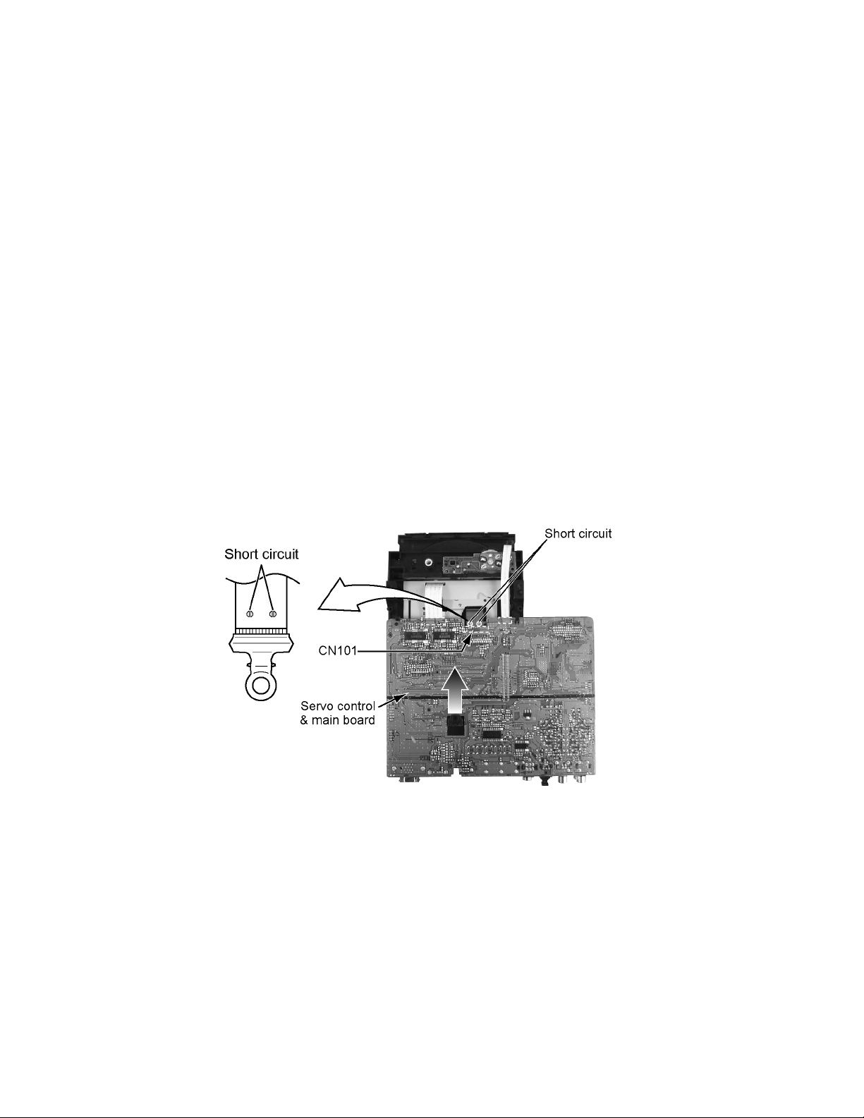
1.8.2 Destruction of Traverse Unit and Laser Pickup by Static Electricity
Laser diodes are easily destroyed by static electricity charged on clothing
or the human body. Before repairing peripheral elements of the traverse unit or pickup, be sure to take the following electrostatic
protection:
(1) Wear an antistatic wrist wrap.
(2) With a conductive sheet or a steel plate on the workbench on whi ch the traverse unit or th e pick up is to be repaired, ground
the sheet or the plate.
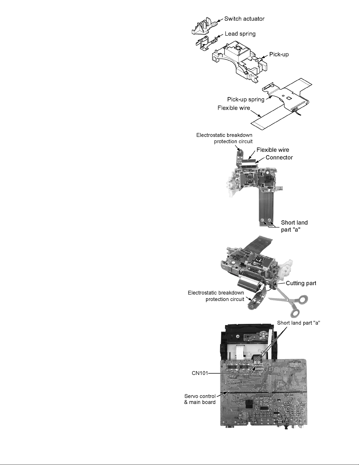
(3) After removing the flexible wire from the connector (CN101), short-circuit the flexible wire by the metal clip.
(4) Short-circuit the laser diode by soldering the land which is provided at the center of the flexible wire for the pickup.
After completing the repair, remove the solder to open the circuit.
Please refer to "Fig.8" of "Disassembly method" for details.
6
Page 6
SECTION 2
Disassembly method
There is a part different from the photograph a ccording to the
model and the destination though explains this disassembly
method by using version for europe.
2.1 Main body section
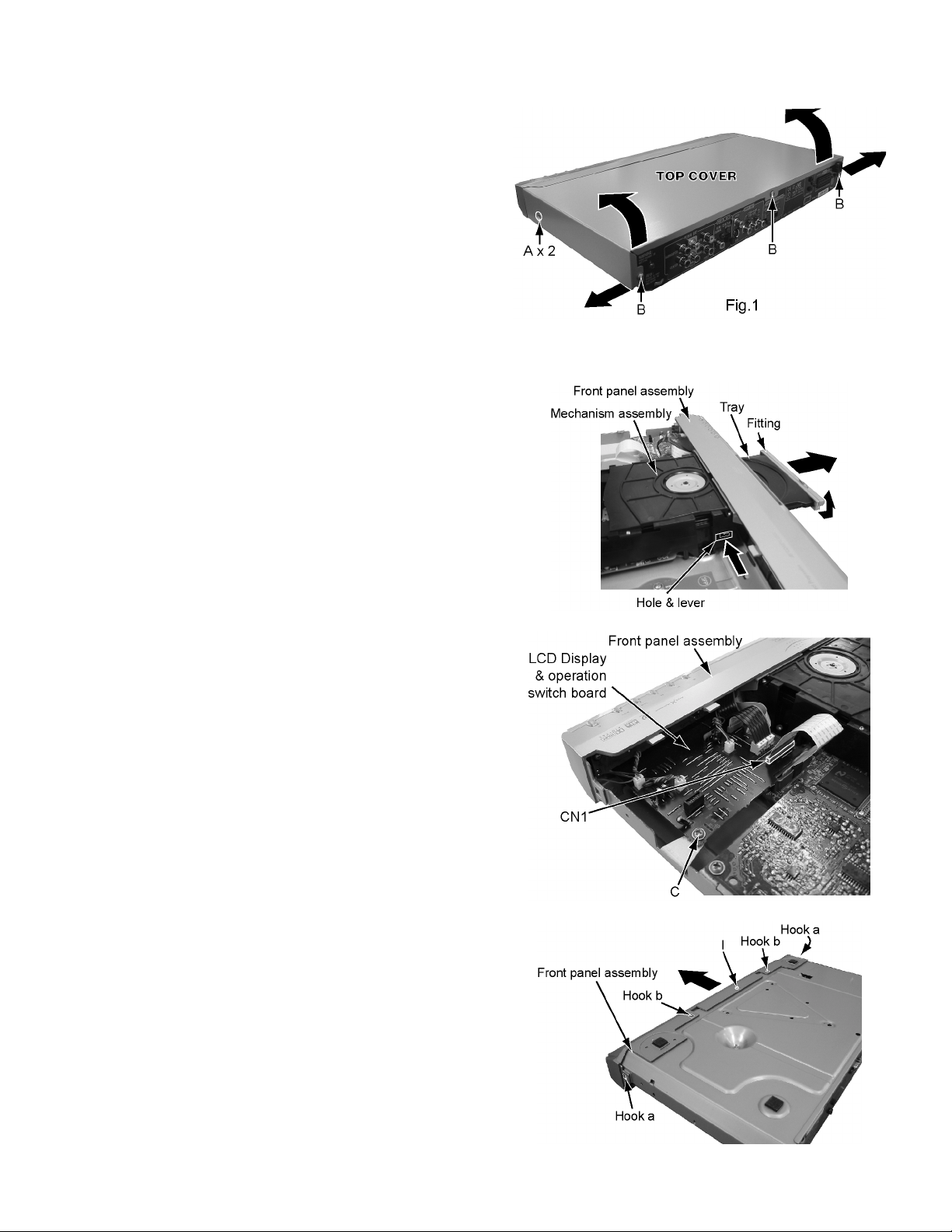
2.1.1 How to remove a top cover
(See Figure 1)
(1) Screw A attaches a top cover to the main part. Remove
the two screws A from the both sides of the main part.
(2) Screw B attaches the top cover to the main part. Remove
the three screws B from the rear side of the main part.
(3) Raise the both sides and lower pa rt of the rear of the top
cover, with opening them slightly in an outward direction.
And the top cover will be removed.
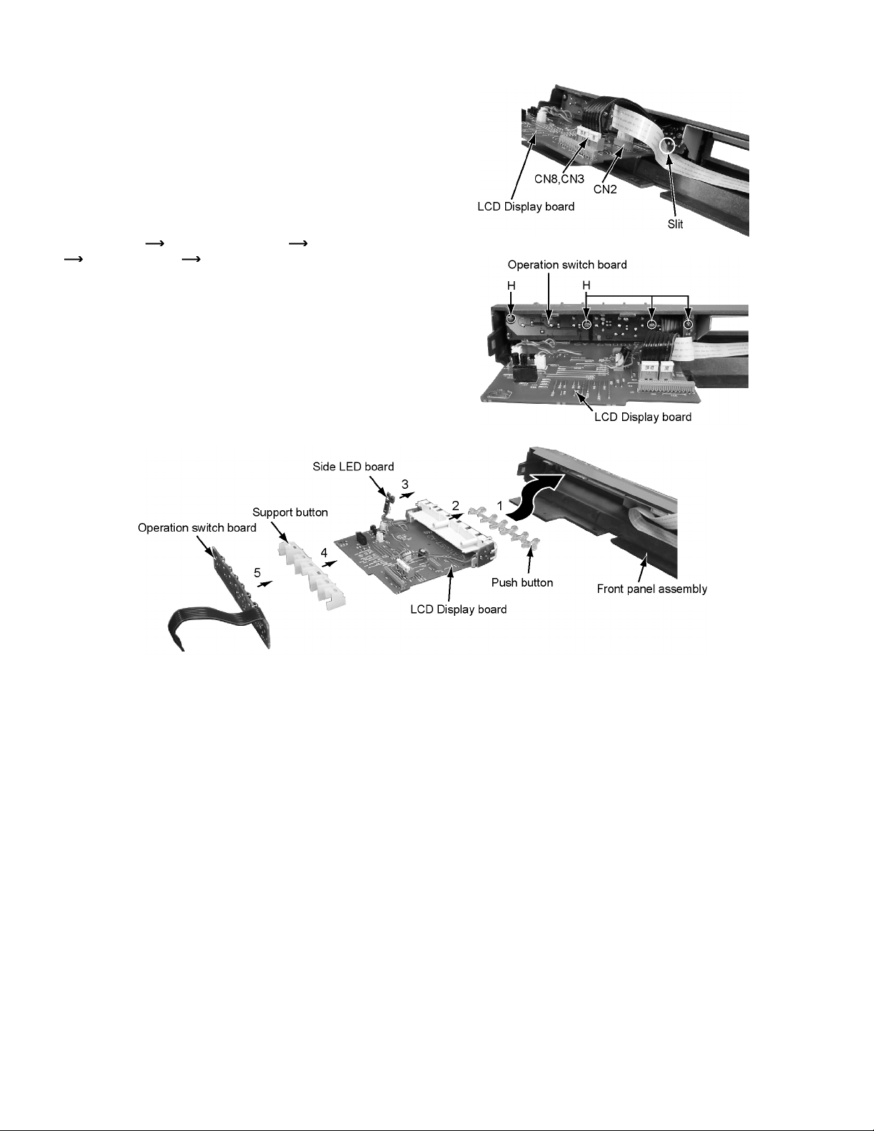
2.1.2 How to remove a front panel assembly
(See Figure 2, 3, and 4.)
• Please remove a top cover before removing a front panel as-
sembly.
• Front panel assembly can be removed without removing
mechanism assembly.
(1) Insert a kind of screwdriver in a hole located in the left side
of mechanism assembly, and push a lever until it cannot
be inserted any further.
(2) And then, a tray will come out. Remove the tray in an up-
per direction, with slightly opening the lower part of fitting
in an outward direction.
(3) Screw C attaches LCD display & operation switch board to
the main part. Remove the screw C.
(4) Extract a card wire from connector CN1 on LCD display &
operation switch board.
(5) Remove I screw that attach the front panel assembly to the
main part.
(6) Remove two hook "a"s and two "b"s. Remove front panel
assembly in a front direction.
XV-NA7SL
Fig.1
Fig.2
Fig.3
Fig.4
7
Page 7
XV-NA7SL
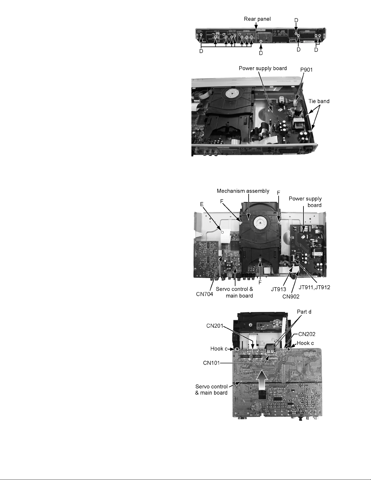
2.1.3 How to remove a rear panel
(See Figure 5 and 6)
• Please remove a top cover before removing a rear panel.
(1) Screw D attaches a rear panel to the main part. Remove
the thierteen screws D.
(2) Extract a power cord from socket P901 on a power supply
board.
(3) Remove two tie bands.
2.1.4 How to remove a mechanism assembly
& servo control board
(See Figure 7 and 8)
• Please remove a top cover, a front panel assembly, and a rear
panel before removing a mechanism assembly & servo control board.
(1) Extract flat wire from connector JT911, JT912, and JT913
on a power supply board.
(2) Extract card wire from connector CN902 and CN704 on a
power supply board and servo control & main board .
(3) Screw E attaches servo control & main board to the main
part. Remove one screw E.
(4) Screw F attaches a mechanism assembly. Remove three
screws F.
(5) Remove two hook "c"s. And then, remove servo control &
main board with sliding it in a front direction.
(6) Two card wires are connected to servo control & main
board. Extract this card wire from CN201 and CN202 respectively.
(7) A wire is connected to servo control & main board from a
pickup. Extract it from CN101.
ATTENTION:
At this time, please extract the wire after short-circuited of two places on the wire in part d with solder.
Please remove the solder two places of part d after
connecting the wire with CN101 when reassembling.
Fig.5
Fig.6
Fig.7
Fig.8
8
Page 8
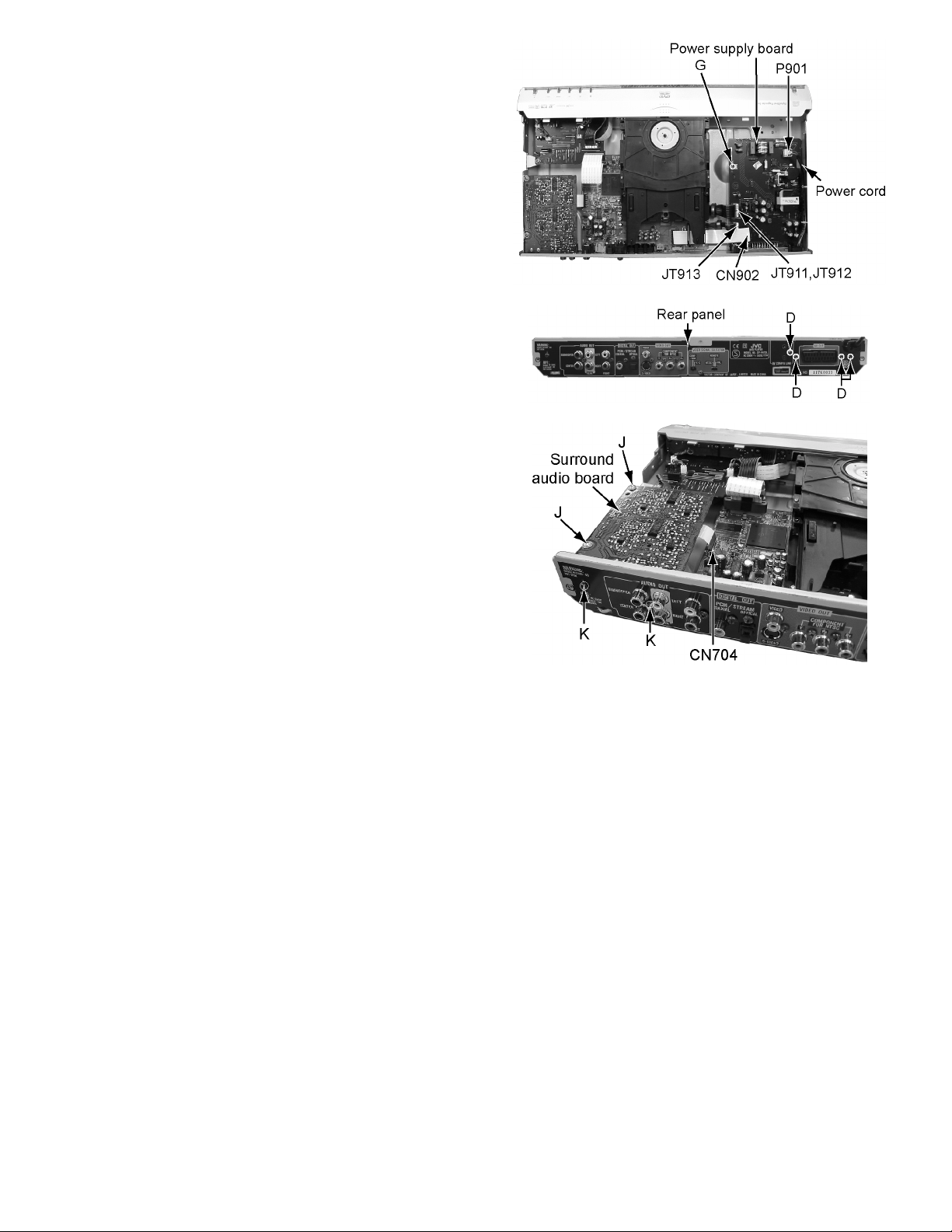
2.1.5 How to remove a power supply board
(See Figure 9 and 5)
• Please remove a top cover before removing a power supply
board.
(1) Extract flat wire from connector JT911, JT912, and JT913
on a power supply board.
(2) Extract card wire from connector CN902 on apower supply
board.
(3) Extract power supply cord from socket P901 on a power
supply board.
(4) Remove one screw G that attaches a power supply board
and four screws D that attaches a power supply board
from the rear side.
2.1.6 How to remove a surround audio board
(See Figure 10)
• Please remove a top cover before removing a surround audio
board.
(1) Extract card wire from connector CN704 on a servo control
& main board.
(2) Remove two screws J that attaches a surround audio
board and two screws K that attaches a surround aud io
board from the rear side.
XV-NA7SL
Fig.9
Fig.5
Fig.10
9
Page 9
XV-NA7SL
2.1.7 How to remove LCD display & operation switch
board
(See Figure 11, 12, and 13)
• Please remove a top cover and a front panel assembly before
removing LCD display & operation switch board.
(1) Extract card wire and flat wire from connector CN2, CN 3,
and CN8 on LCD display board.
(2) Remove four screws H that attach an operation switch
board, and then operation switch board.
(3) Remove support button, LCD display board, and push but-
ton in this order.
• When the main part is assembled, parts must be assem-
bled in the following order:
Push button LCD display board Side LED board
Support button Operation switch board.
• After the operation switch board is attached to its place,
let a card wire through a slit on the operation switch
board, and then insert it in CN2. (See Figure 11.)
Fig.11
Fig.13
Fig.12
10
Page 10
SECTION 3
Mechanism
3.1 Loading assembly section
3.1.1 Removing the clamper assembly
(See Fig.1)
(1) Remove the four screws A attaching the clamper assembly.
(2) Move the clamper in the direction of the arrow to release
the two joints a on both sides.
ATTENTION:
When reattaching, fit the clamper to the two joints a.
3.1.2 Removing the tray
(See Fig2. and 3)
Note:
• Prior to performing the following procedure, remove the
clamper assembly.
(1) Push b of the slide cam into the slot on the left side of the
loading base until it stops.
(2) Draw out the tray toward the front.
ATTENTION:
Before reattaching the tray, slide the part c of the
slide cam to the right as shown in Fig.3.
XV-NA7SL
Fig.1
Fig.2
Fig.3
11
Page 11
XV-NA7SL
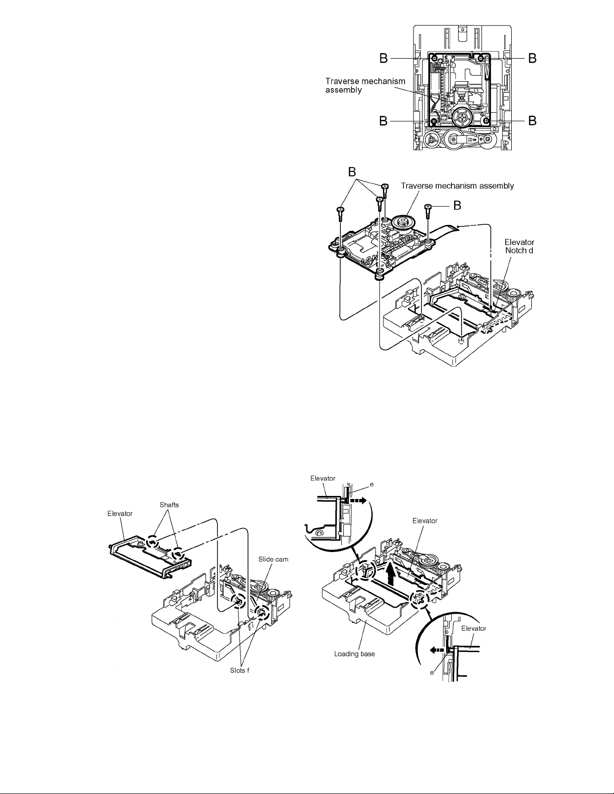
3.1.3 Removing the traverse mechanism assembly
(See Fig.4 and 5)
Note:
• Prior to performing the following procedure, remove the
clamper assembly and the tray.
(1) Remove the four screws B attaching the traverse mechanism
assembly.
ATTENTION:
Before reattaching the traverse mechanism assem bly, pass the card wire extending from the spind le
motor board through the notch d of the elevator.
Fig.4
Fig.5
3.1.4 Removing the elevator
(See Fig.6)
Note:
• Prior to performing the following procedure, remove the clamper assembly, the tray and the traverse mechanism assembly.
(1) Extend each bar e inside of the loading base outward and detach the elevator shaft.
ATTENTION:
When reattaching, first fit the two shafts on the front of the elevator to the slots f of the slide cam.
12
Fig.6
Page 12
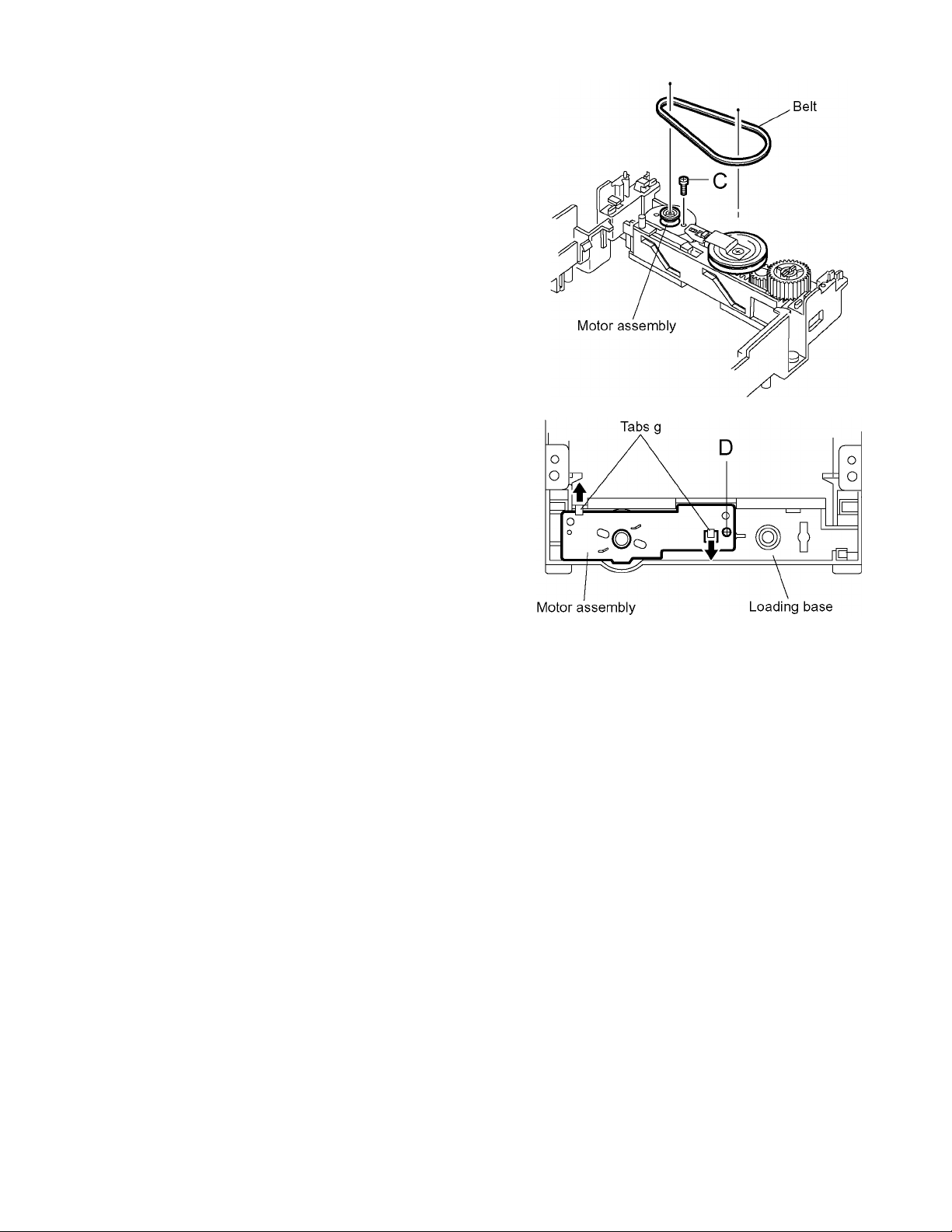
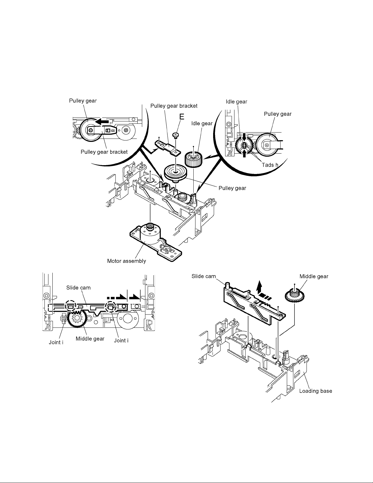
3.1.5 Removing the motor assembly
(See Fig.7 and 8)
Note:
• Prior to performing the following procedure, remove the
clamper assembly, the tray.the traverse mechanism assembly and the elevator.
(1) Remove the belt from the pulley.
(2) Remove the screw C attaching the motor assembly.
(3) Turn over the body and remove the screw D attaching the
motor assembly.
(4) Release the two tabs g retaining the motor board.
XV-NA7SL
Fig.7
Fig.8
13
Page 13
XV-NA7SL
3.1.6 Removing the Idle gear/pully gear/middle gear/s litecam
(See Fig.9 to 11)
Note:
• Prior to performing the followong procedure,remove the clamper assembly,the tray,the traverse mechanism assembly,the
elevator and the motor assembly.
(1) Press the two tabs h inward and pull out idle gear.
(2) Remove the screw E attaching the pulley gear bracket.
Slide t h e p u l l ey gear br a c k et in the d i r ection of the arrow and pull out the pulley gear.
(3) Slide the side cam in the direction of the arrow to release the two joints i and remove upward.
(4) Remove the middle gear.
Fig.10
Fig.9
Fig.11
14
Page 14
3.2 Traverse mechanism assembly section
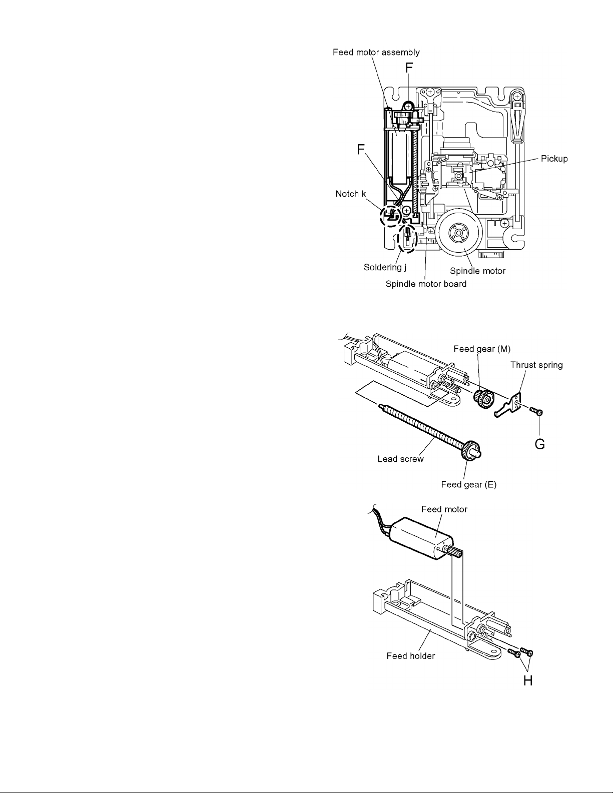
3.2.1 Removing the feed motor assembly
(See Fig.12)
(1) Unsolder the two soldering j on the spindle motor board.
(2) Remove the four screws F attaching the feed moto r as-
sembly.
3.2.2 Removing the feed motor
(See Fig.12 to 14)
Note:
• Prior to performing the following procedure, remove the
feed motor assembly.
XV-NA7SL
Fig.12
(1) Remove the screw G attaching the thrust spring.
ATTENTION:
When reattaching the thrust spring, make sure that
the thrust spring presses the feed gear (M) and the
feed gear (E) reasonably.
(2) Remove the feed gear (M).
(3) Pull out the feed gear (E) and the lead screw.
(4) Remove the two screws H attaching the feed motor.
ATTENTION:
When reattaching, pass the two cables extending
from the feed motor through the notch k of the feed
holder as shown in Fig13.
Fig.13
Fig.14
15
Page 15
XV-NA7SL
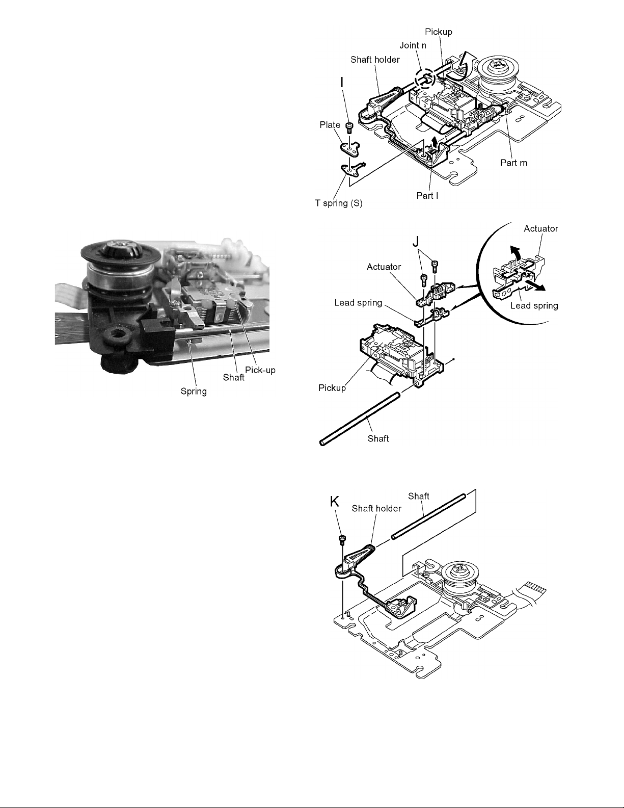
3.2.3 Removing the pickup
(See Fig.16 and 18)
(1) Remove the screw I attaching the T spring (S) and the
shaft holder. Remove also the plate.
ATTENTION:
When reattaching,make sure that the T spring (S)
presses the shaft.
(2) Pull out the part l of the shaft upward. Move the part m in
the direction of the arrow and detach from the spindle
base.
(3) Disengage the joint n of the pickup and the shaft in the
direction of the arrow.
(4) Pull out the shaft from the pickup.
(5) Remove the two screws J attaching the actuator.
(6) Disengage the joint of the actuator and the lead spring.
Pull out the lead spring.
Fig.16
Fig.15
The spring must be under the shaft when you
install pick-up.
3.2.4 Removing the shaft holder / shaft
(See Fig.18)
(1) Remove the screw K attaching the shaft holder.
(2) Remove the shaft.
Fig.17
Fig.18
16
Page 16
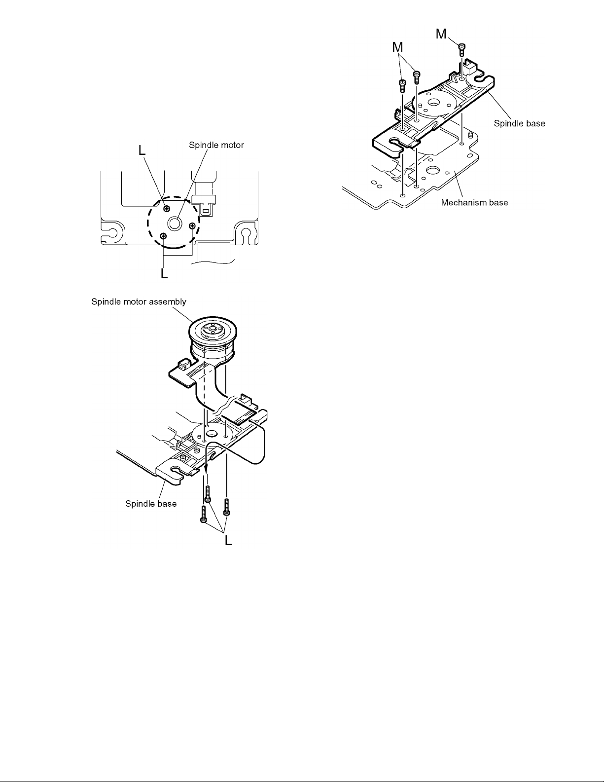
3.2.5 Removing the spindle motor assembly
(See Fig.19 to 21)
(1) Remove the three screws L attaching the spindle motor on
the bottom of the mechanism base.
ATTENTION:
When reattaching, pass the card wire extending
from the spindle motor board through the notch of
the spindle base.
(2) Remove the three screws M attaching the spindle base.
Fig.19
XV-NA7SL
Fig.21
Fig.20
17
Page 17
XV-NA7SL
SECTION 4
Adjustment method
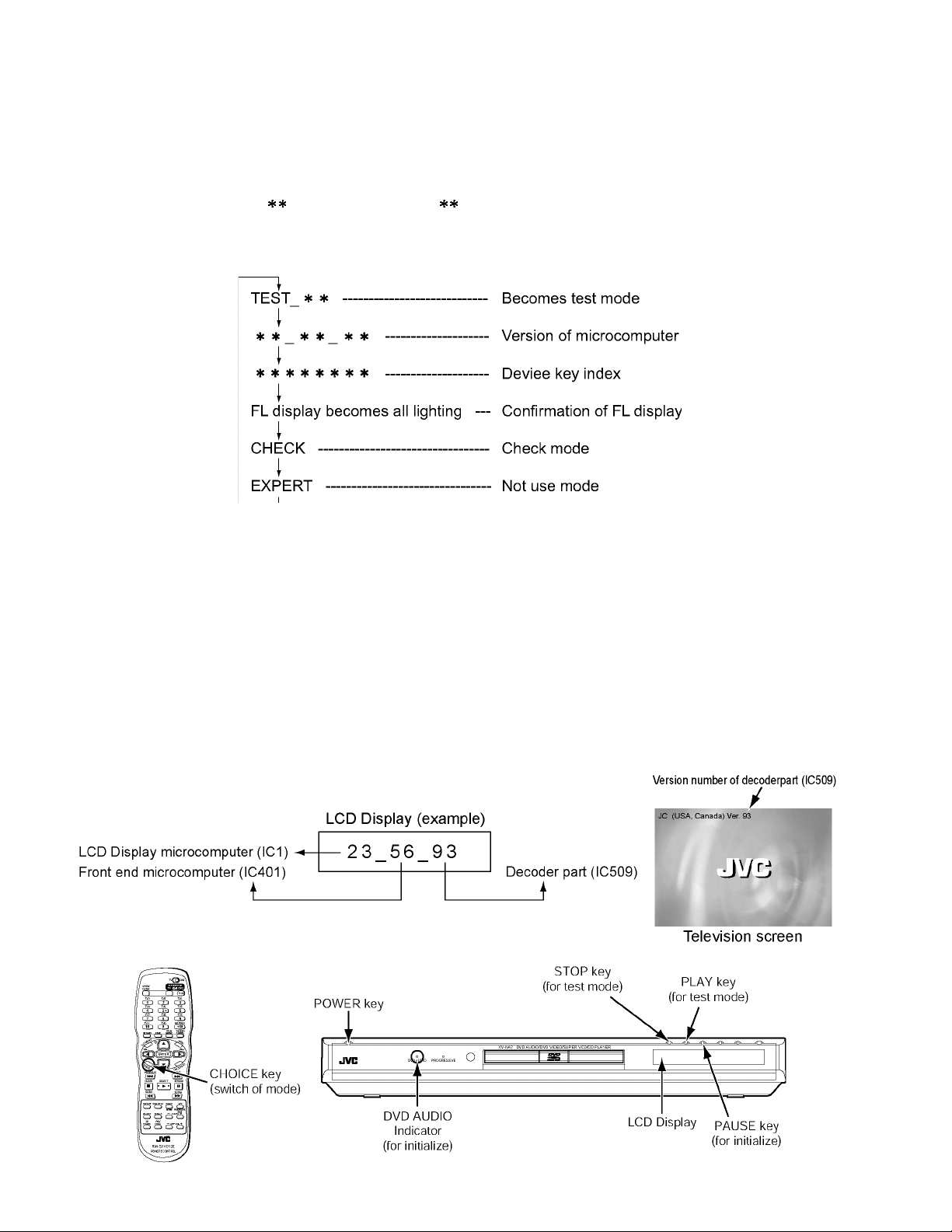
4.1 Test mode setting method
(1) Take out the disc and close the tray.
(2) Unplug the power plug.
(3) Insert power plug into outlet while pressing both "PLAY" key and "STOP" key of the main body.
(4) The player displays " TEST_ " on the LCD display. " " means the player version.
(5) When the power supply is turned off, test mode is released.
The mode changes as follows whenever the "CHOICE" key of remote controller is pushed in test mode.
4.2 Initialization method
Please initialize according to the following procedures when microprocessor or pick-up is exchanged and when the
up-grade is done.
(1) Makes to test mode.
(2) "PAUSE" key of the main body is pushed.
(3) When the DVD AUDIO indicator lights blue, it is initialization completion.
4.3 Method of displaying version of microcomputer
(1) Makes to test mode and initializes
(2) When "CHOICE" key of remote controller is pushed once, the figure is displayed on the LCD display as follows.
* Version number of decoder is displayed on the television screen.
* Last two digits are displayed on the FL display for the treble version number.
18
Page 18
XV-NA7SL
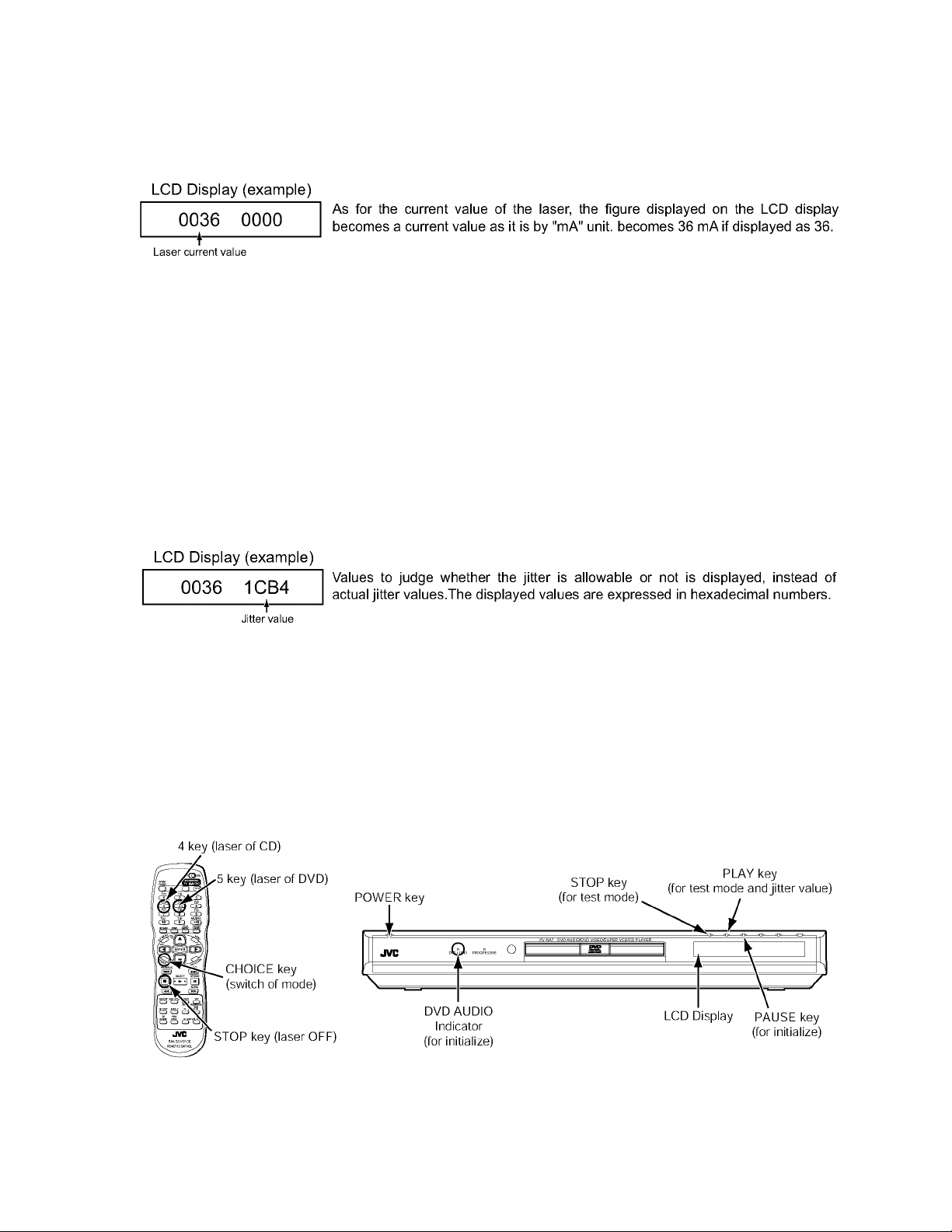
4.4 Display of current value of laser
(1) Makes to test mode and initializes.
(2) When "CHOICE" key of remote controller is pushed four times, It is displayed on the LCD display, "CHECK".
(3) Afterwards, the laser current value can be switched by pushing the key to remote controller without turning on the disc.
Remote controller "4" key --- Laser of CD
Remote controller "5" key --- Laser of DVD
(4) The laser output stops if the "STOP" key to remote controller is pushed.
It can be judged it is simply good if the displayed current value of the laser is smaller than that of the undermentioned value.
Moreover, there must be a deteriorated possibility and the pick-up must exch ange the pick-up more than the undermentioned value.
Laser current value of CD ------ 49 mA or less
Laser current value of DVD ---- 64 mA or less
4.5 Display of jitter value
(1) Makes to test mode and initializes.
(2) When "CHOICE" key of remote controller is pushed four times, It is displayed on the LCD display, "CHECK".
(3) The test disk (VT-501) is inserted, and the "PLAY" key to the main body is pushed.
(4) After a few seconds, the jitter value is displayed on the LCD display as follows.
In the following cases, please "Flap adjustment of the pick-up guide shaft" referring to the following page.
Before using the TEST disc VT-501, careful check it if there is neither damage nor dirt on the read surface.
< In the following cases, please adjustment >
• When you exchange the pick-up
• When you exchange the spindle motor
• When the reading accuracy of the signal is bad (There is a block noise in the scr een etc..)
19
Page 19
XV-NA7SL
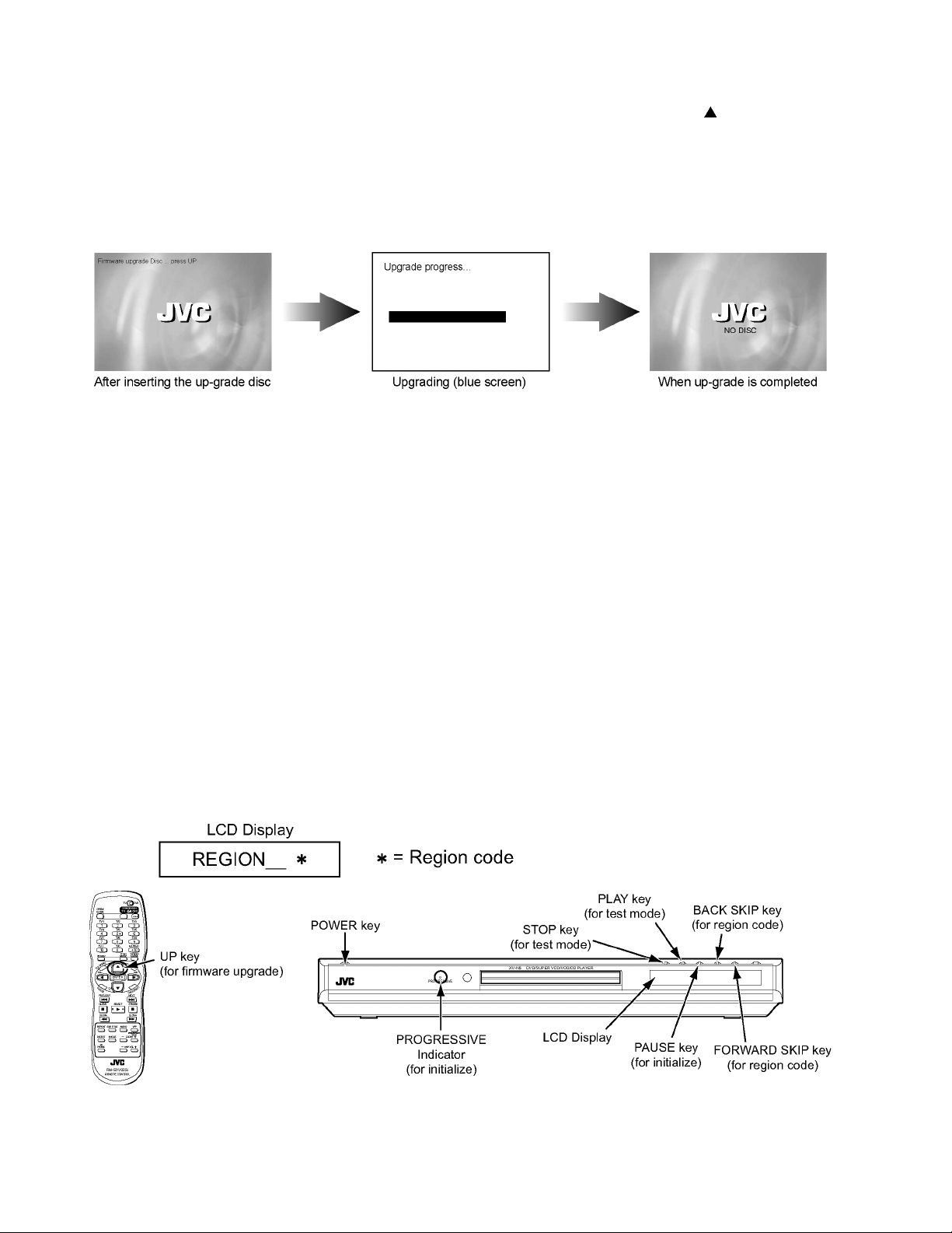
4.6 Upgrading of firmware
(1) The power supply is turned on pushing the "POWER" key.
(2) The up-grade disc is inserted.
(3) When LCD display of the main body changes from "READING" into "UPGRADE", cursor "UP" key ( ) of remote controller
is pushed.
(4) The up-grade starts if the entire screen becomes blue and it is displayed, "Upgrade progress".
(5) The tray opens automatically, the up-grade disc is removed.
(6) The up-grade ends if the tray closes automatically, and the screen returns to the normal screen.
(7) Please confirm the version of the microcomputer after makes to test mode and initializes.
The disc for the up-grade is usually one piece. The disc becomes two pieces according to the version. In that case, please
note the undermentioned content.
*The up-grade is done by using the STEP1 disc according to "(1)" and "(4)" of the above-mentioned procedure.
*The tray opens automatically after a few seconds and exchange for the disc of STEP2, please.
*The tray closes automatically. There is only about five second time that the tray opens this time,and replace the disc quickly between
those, please.
ATTENTION:
• When the tray shuts with the STEP1 disc left for the tray
The up-grade starts again and exchange for the STEP2 disc, please when the tray opens automatically.
• When the tray closes with there no disc in the tray
Because the tray opens automatically, the disc of STEP2 is put on the tray.
The power supply is turned off once pushing the "POWER" key.
The up-grade starts when the "POWER" key is pushed afterwards.
* After the up-grade ends, the STEP2 disc is removed because the tray opens automatically.
* Afterwards, it is the same as (6),(7) of the above-mentioned procedures.
4.7 Display of region code
(1) Makes to the stand-by state.
(2) The "POWER" key is pushed while pushing the "BACK SKIP" key and the "FORWARD SKIP" key to the main body.
(3) Region code is displayed on the LCD display as follows.
20
Page 20
XV-NA7SL
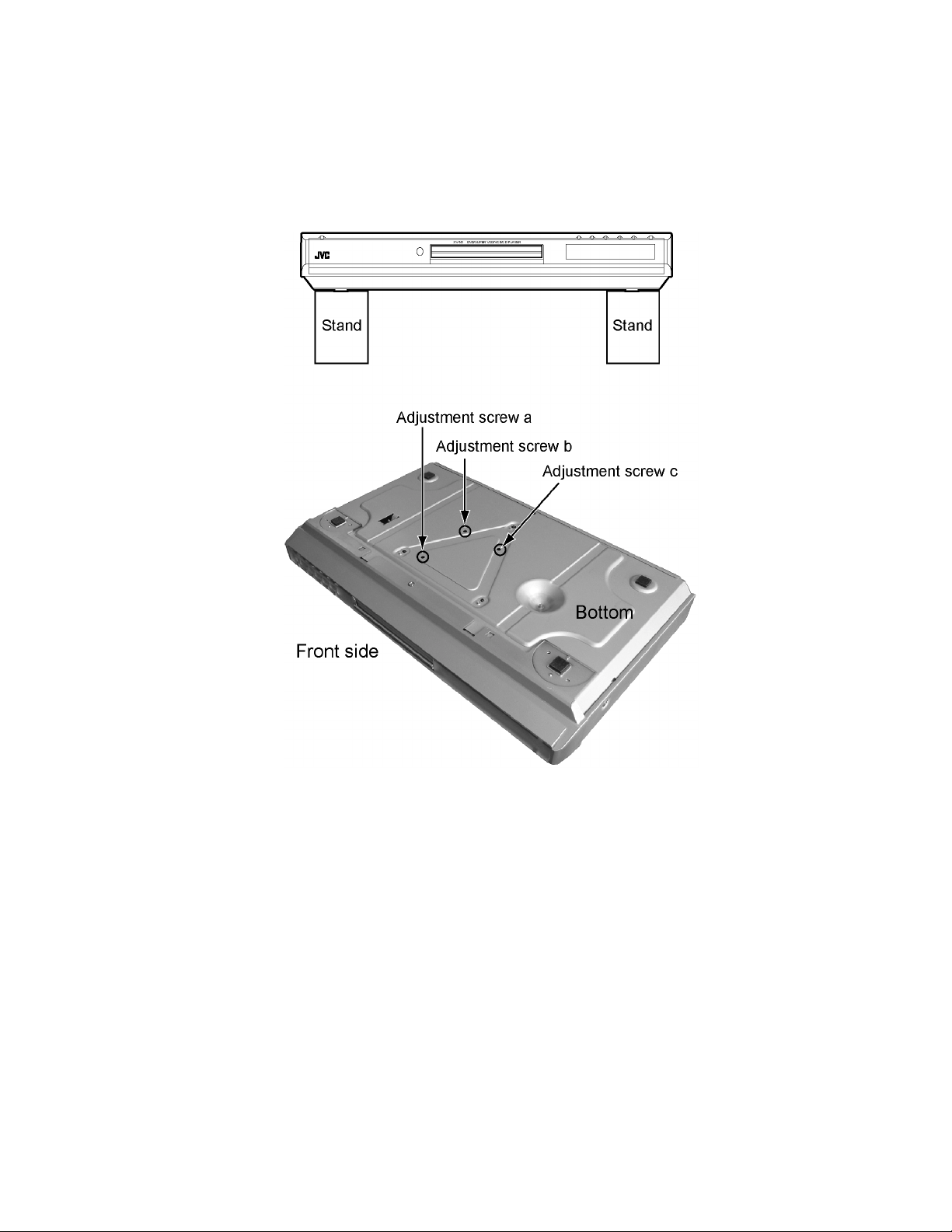
4.8 Flap adjustment of the pick-up guide shaft
4.8.1 Tool list for adjustment
Hex wrench for adjustment : Off-the-shelf (1.3mm)
Test disc : VT-501 or VT-502
Stand of about 150mm in height : 2 pcs
(1) Puts into the state to display the jitter value on the LCD display referring to "3.5 Display of the jitter value".
(2) A hex-head wrench is inserted in the hole three places for the adjustment in the main body bottom, and the adjustment screw
is turned, and matches so that the jitter value displayed on the LCD display mey become maximum value.
ATTENTION:
As this value is bigger, the jitter is more allowable in this model.
POINT:
(1) Turns in the forward or the opposite direction, and makes to the position where the jitter value is good the half rotation of
adjustment screw a and b(180 degrees) respectively.
(2) Afterwards, adjustment screw b and c are turned in the same way, and makes to the best position.
21
Page 21
XV-NA7SL
4.9 Attention when pick-up is exchanged
(1) Flexible wire, pick-up spring, switch actuator, and lead
spring are removed from an old pick-up (broken the one).
Guide:
Flexible wire, pick-up spring and switch actuator,lead
spring are removed without each decomposing while
assembled.
(2) The above-mentioned parts are installed in a new pick-up
(non-defective article).
(3) A flexible wire is inserted in the connector which has taken
side with the pick-up, and solder is put up to short land part
"a" two places on a flexible wire.
(4) The electrostatic breakdown protection circuit attached to
the pick-up is cut.
ATTENTION:
Please cut the electrostatic breakdown protection
circuit attached to the pick-up after solder is put up
to two places on a flexible wire short land part "a" of
the insertion of a flexible wire this time in the connector without fail.
The procedure might be mistaken and if solder has
not surely adhered to two places on a flexible wire
short land part "a", the laser diode in the pick-up be
destroyed again.
(5) The pick-up is installed in the traverse mechanism.
(6) A flexible wire is connected with connector CN101 on the
servo control board by installing the traverse mechanism
in the loading mechanism.
(7) Solder in two places on a flexible wire in part "a" is re-
moved.
ATTENTION :
Please remove solder in two places in part "a" after
connecting a flexible wire with connector CN101 on
the servo control board without fail this time.
When the procedure is mistaken, the laser diode in
the pick-up might be destroyed.
Please remove solder in two places in part "a" surely.
22
Page 22

XV-NA7SL
4.10 Confirm method of operation
Please confirm the operation of the undermentioned item after doing the repair and the upgrade of the firmware.
The EEPROM is initialized. Refer to the initialization method.
Opening picture check (Power ON) It should be display "JVC"
Muting working The noise must not be had to the performance beginning when you push "PLAY" button or
at ON/STANDBY.
FL Display The mark and the logo, etc. displayed by each operation must be displayed correctly.
FL Display should light correctly without any unevenness.
All Function button All function buttons should worked correctly with moderate click feeling.
Open and close movement of tray When press OPEN/CLOSE button the tray should move smoothly without any noise.
Remote controller unit working Check the correctly operation in use of remote controller unit.
Reading of TOC Be not long in the malfunction.
Search Both forward-searches and backward-searches should be able to be done.
Do not stop be searching or after the search.
Skip Both forward-skip and backward-skip should be able to be done.
Do not stop be after the skip.
Playback Do not find abnormality etc. of tone quality and the picture quality.
Most outside TITLE playback check Play VT-501 TITLE 59 CHAPTER 1 , check normal playback.
23
Page 23
XV-NA7SL
4.11Troubleshooting
4.11.1 Servo volume
24
Fig.1
Page 24

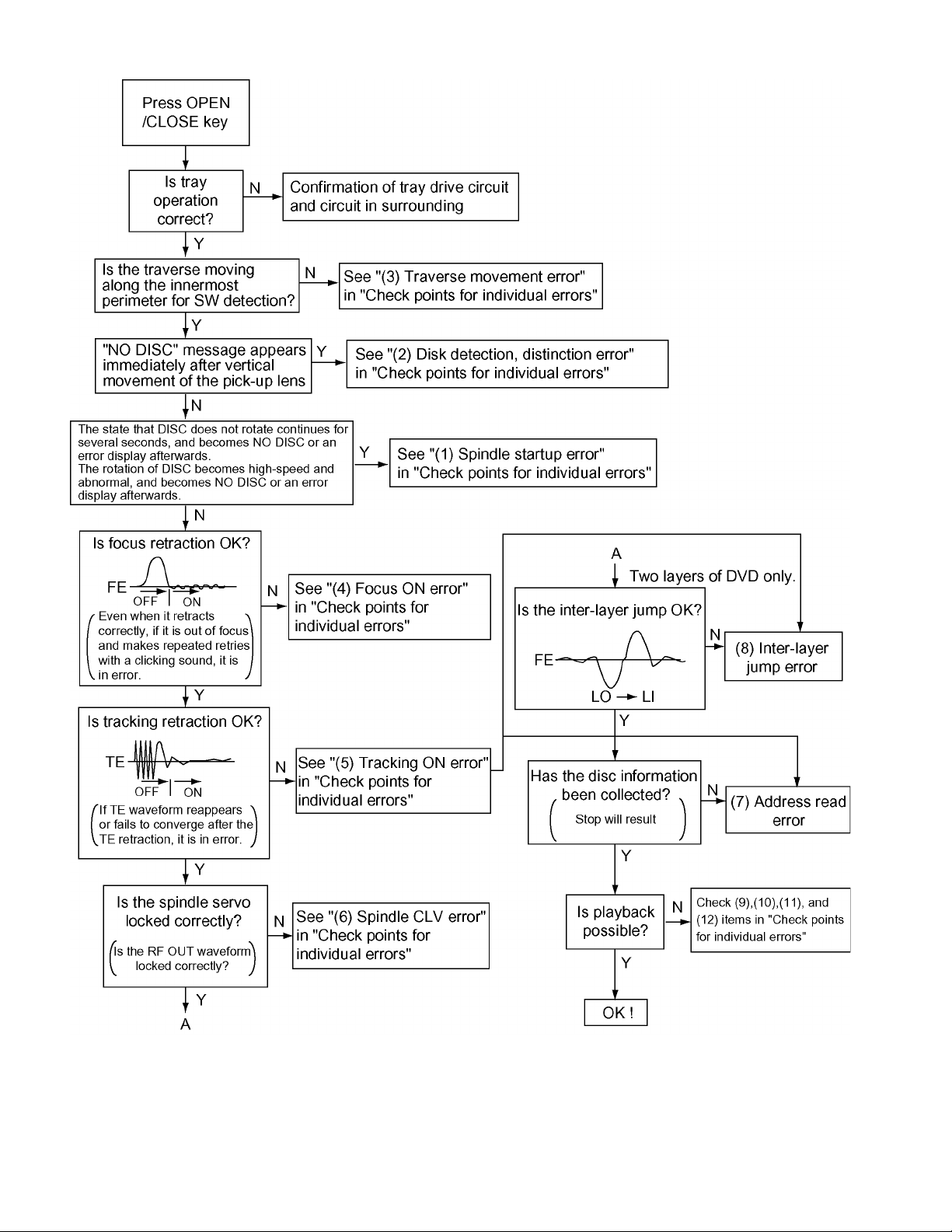
4.12Check points for each error
4.12.1 Spindle start error
(1) Defective spindle motor
• Are there several ohms resistance between each pin of CN201 "5-6","6-7","5-7"?
(The power supply is turned off and measured.)
• Is the sign wave of about 100mVp-p in the voltage had from each terminal?
[ CN201"9"(H1-),"10"(H1+),"11"(H2-),"12"(H2+),"13"(H3-),"14"(H3+) ]
(2) Defective spindle motor driver (IC251)
• Has motor drive voltage of a sine wave or a rectangular wave gone out to each terminal(SM1~3)
of CN201"5,6,7" and IC251"2,4,7"?
• Is FG pulse output from the terminal of IC251"24"(FG) according to the rotation of the motor?
• Is it "L(about 0.9V)" while terminal of IC251"15"(VH) is rotating the motor?
(3) Has the control signal come from servo IC or the microcomputer?
• Is it "L" while the terminal of IC251"18"(SBRK) is operating?
Is it "H" while the terminal of IC251"23"(/SPMUTE) is operating?
• Is the control signal input to the terminal of IC251"22"(EC)?
(changes from VHALF voltage while the motor is working.)
• Is the VHALF voltage input to the terminal of IC251"21"(ECR)?
(4) Is the FG signal input to the servo IC?
• Is FG pulse input to the terminal of IC301"69"(FG) according to the rotation of the motor?
4.12.2 Disc Detection, Distinction error (no disc, no RFENV)
• Laser is defective.
• Front End Processor is defective (IC101).
• APC circuit is defective. --- Q101,Q102.
• Pattern is defective. --- Lines for CN101 - All patterns which relate to pick-up and patterns between IC101
• IC101 --- For signal from IC101 to IC301, is signal output from IC101 "20" (ASOUT) and IC101 "41"(RFENV) and IC101 "22"
(FEOUT)?
4.12.3 Traverse movement NG
(1) Defective traverse driver
• Has the voltage come between terminal of CN101 "1" and "2" ?
(2) Defective BTL driver (IC201)
• Has the motor drive voltage gone out to IC201"17" or "18"?
(3) Has the control signal come from servo IC or the microcomputer?
• Is it "H" while the terminal of IC201"9"(STBY1) ?
• TRSDRV Is the signal input? (IC301 "67")
(4) TRVSW is the signal input from microcomputer? (IC401 "50")
4.12.4 Focus ON NG
• Is FE output ? --- Pattern, IC101
• Is FODRV signal sent ? (R209) --- Pattern, IC301 "115"
• Is driving voltage sent ?
• IC201 "13", "14" --- If NG, pattern, driver, mechanical unit .
• Mechanical unit is defective.
4.12.5 Tracking ON NG
• When the tracking loop cannot be drawn in, TE shape of waves does not settle.
• Mechanical unit is defective.
Because the self adjustment cannot be normally adjusted, the thing which cannot be normally drawn in is thought.
• Periphery of driver (IC201)
Constant or IC it self is defective.
• Servo IC (IC301)
When improperly adjusted due to defective IC.
XV-NA7SL
25
Page 25

XV-NA7SL
4.12.6 Spindle CLV NG
• IC101 -- "35"(RF OUT), "30"(ARF-), "31(ARF+).
• Does not the input or the output of driver's spindle signal do the grip?
• Has the tracking been turned on?
• Spindle motor and driver is defective.
• Additionally, "IC101 and IC301" and "Mechanism is defective(jitter)", etc. are thought.
4.12.7 Address read NG
• Besides, the undermentioned cause is thought though specific of the cause is difficult because various factors are thought.
Mechanism is defective. (jitter)
IC301, IC401.
The disc is dirty or the wound has adhered.
4.12.8 Between layers jump NG (double- layer disc only)
Mechanism defective
Defect of driver's IC(IC201)
Defect of servo control IC(IC301)
4.12.9 Neither picture nor sound is output
(1) It is not possible search
• Has the tracking been turned on?
• To "(5) Tracking ON NG" in "Check points for each error" when the tracking is not normal.
• Is the feed operation normal?
To "(3) traverse movement NG" in "Check points for each error" when it is not normal.
Are not there caught of the feeding mechanism etc?
4.12.10 Picture is distorted or abnormal sound occurs at intervals of several seconds.
Is the feed operation normal?
Are not there caught of the feeding mechanism etc?
4.12.11 Others
• The image is sometimes blocked, and the image stops.
• The image is blocked when going to outer though it is normal in suroundings in the disk and the stopping sympton increases.
There is a possibility with bad jitter value for such a symptom.
4.12.12 CD During normal playback operation
(1) Is TOC reading normal?
• Displays total time for CD-DA.
• Shifts to double-speed mode for V-CD
(2) Is playback afterwards possible?
(3) When can not do a normal playback
• --:-- is displayed during FL search.
According to [It is not possible to search ] for DVD(9), check the feed and tracking systems.
• No sound is output although the time is displayed.(CA-DA)
DAC, etc, other than servo.
• The passage of time is not stable, or picture is abnormal.(V-CD)
• The wound of the disc and dirt are confirmed.
26
Page 26
SECTION 5
Description of major ICs
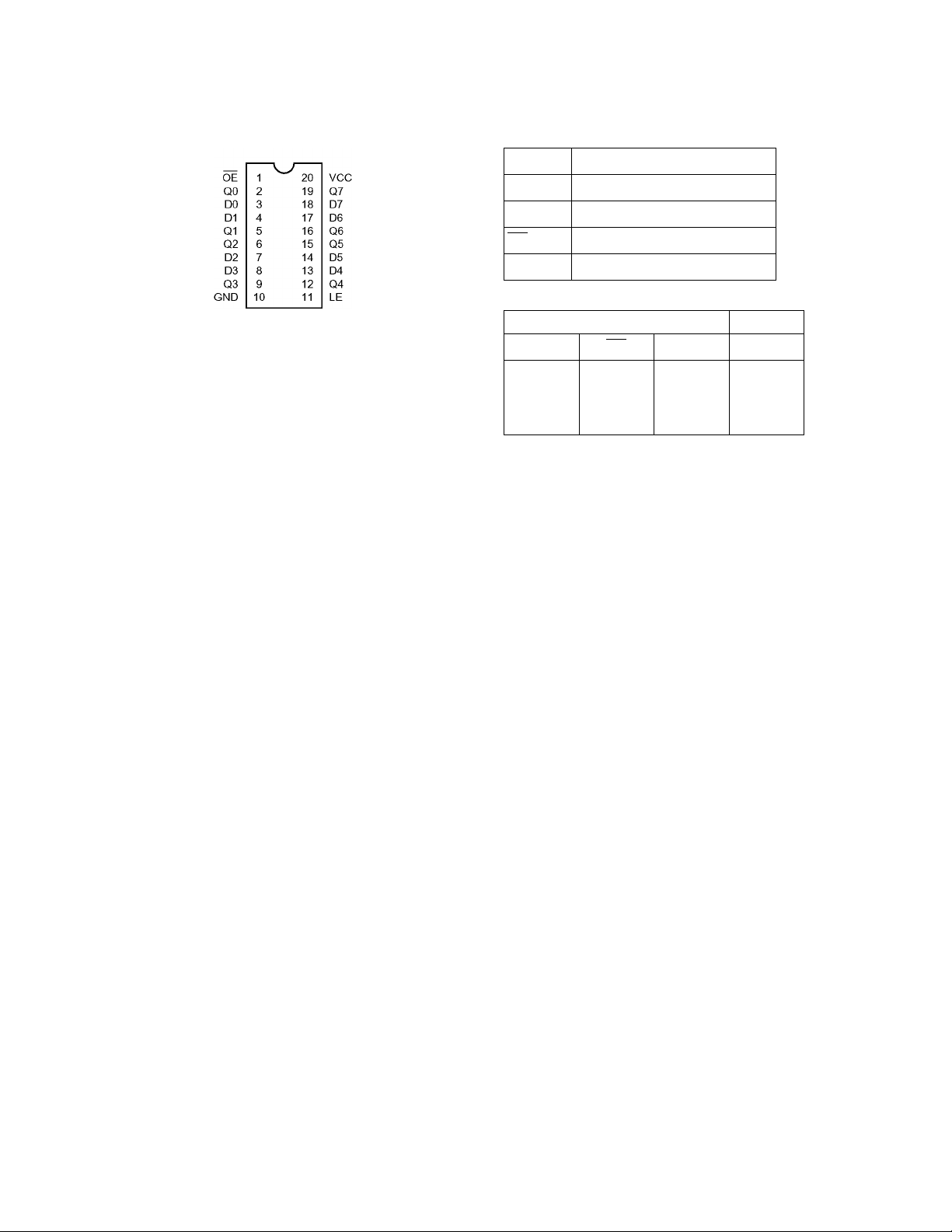
5.1 74LCX373MTC-X(IC512,IC513)
• Pin layout • Pin function
Symbol
D0~D7
LE
OE
Q0~Q7
• Truth table
H = HIGH Voltage level
L = LOW Voltage level
Z = High impedance
X = Immaterial
Q0 = Previous Q0 before HIGH to LOW transition of latch enable
Description
Data inputs
Latch enable input
Output enable input
3-State latch outputs
LE
X
H
H
L
INPUTS OUTPUTS
OE
H
L
L
L
Dn Qn
X
L
H
X
Z
L
H
Q0
XV-NA7SL
27
Page 27
XV-NA7SL
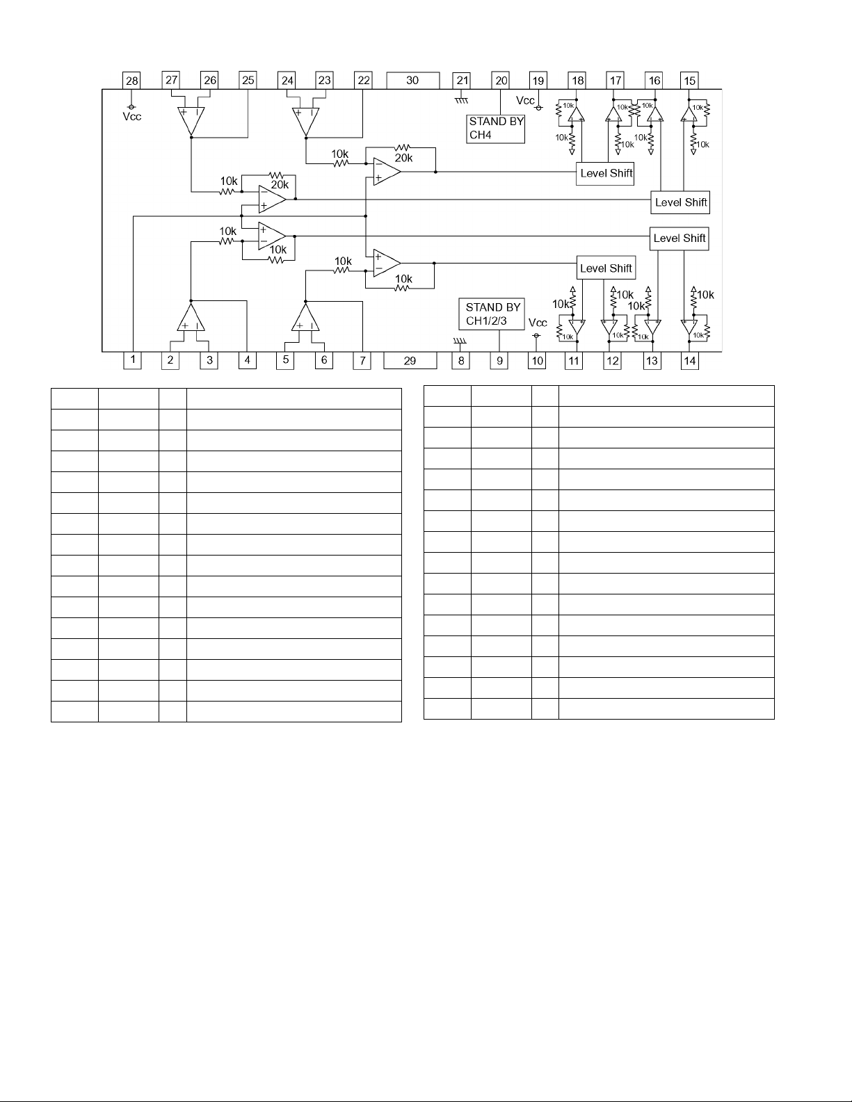
5.2 BA5983FM-X (IC201) : 4CH Driver
• Block diagram
• Pin function
Pin No. Symbol I/O Description
1 BIAS IN I Input for Bias-amplifier
2 OPIN1(+) I Non inverting input for CH1 OP-AMP
3 OPIN1(-) I Inverting input for CH1 OP-AMP
4 OPOUT1 O Output for CH1 OP-AMP
5 OPIN2(+) I Non inverting input for CH2 OP-AMP
6 OPIN2(-) I Inverting input for CH2 OP-AMP
7 OPOUT2 O Output for CH2 OP-AMP
8 GND - Substrate ground
9 STBY1 I Input for CH1/2/3 stand by control
10 PowVcc1 - Vcc for CH1/2 power block
11 VO2(-) O Inverted output of CH2
12 VO2(+) O Non inverted output of CH2
13 VO1(-) O Inverted output of CH1
14 VO1(+) O Non inverted output of CH1
15 VO4(+) O Non inverted output of CH4
Pin No. Symbol I/O Description
16 VO4(-) O Inverted output of CH4
17 VO3(+) O Non inverted output of CH3
18 VO3(-) O Inverted output of CH3
19 PowVcc2 - Vcc for CH3/4 power block
20 STBY2 I Input for Ch4 stand by contro l
21 GND - Substrate ground
22 OPOUT3 O Output for CH3 OP-AMP
23 OPIN3(-) I Inverting input for CH3 OP-AMP
24 OPIN3(+) I Non inverting input for CH3 OP-AMP
25 OPOUT4 O Output for CH4 OP-AMP
26 OPIN4(-) I Inverting input for CH4 OP-AMP
27 OPIN4(+) I Non inverting input for CH4 OP-AMP
28 PreVcc - Vcc for pre block
29 - Connect to ground
30 - Connect to ground
28
Page 28

5.3 AN8703FH-V (IC101) : Frontend processor
• Pin layout
• Pin function
Pin No.
10 IDGT I Data slice part address part gate signal
11 STANDBY I Standby mode control terminal
12 SEN I SEN(Serial data input terminal)
13 SCK I SCK(Serial data input terminal)
14 STDI I STDI(Serial data input terminal)
15 RSCL I Standard electric current terminal
16 JLINE I Electric current setting terminal of JLi ne
17 TEN I Reversing input te rminal of tracking error
18 TEOUT O Tracking error signal output terminal
19 AGCBAL I Offset adjusting terminal 1
20 ASOUT O Full adder signal output terminal
21 FEN I Focus error output amplif ier reversing in-
22 FEOUT O Focus error signal output terminal
23 AGCOFST I Offset adjusting terminal 2
24 MON - Non connect
25 AGCLVL O Output amplitude adjustme nt for DRC
26 GND2 - Connect to GND
27 VREF2 O VREF2 voltage output terminal
28 VCC2 - Power supply terminal 5V
29 VHALF O VHALF voltage output terminal
30 DFLTON O Reversing output terminal of filter AMP.
31 DFLTOP O Filter AMP. output terminal
32 DCFLT I Capacity connection terminal for filter
Symbol I/O Description
1 LPC1 I Laser input terminal (DVD)
2 LPC01 O Laser drive signal output terminal (DVD)
3 LPC2 I Laser input terminal (CD)
4 LPC02 O Laser drive signal output terminal (CD)
5
VFOSHORT
6 TBAL I Tracking balance control terminal
7 FBAL I Focus balance control terminal
8 POFLT O Track detection threshold level terminal
9 DTRD I Data slice part data read s ignal in put ter-
I VFOSHORT control terminal
minal(For RAM)
input terminal( For RAM)
output AMP.
put terminal
output
XV-NA7SL
Pin No.
33 GND3 - Connect to GND
34 RFDIFO - Non connect
35 RFOUT - Connect to TP103
36 VCC3 - Power supply terminal 3.3V
37 RFC O Filter for RF delay correction AMP.
38 DCRF O All addition amplifier capacitor terminal
39 OFTR O OFTR output terminal
40 BDO O BDO output terminal
41 RFENV O RF envelope output terminal
42 BOTTOM O Bottom envelope detection filter terminal
43 PEAK O Peak envelope detection filter terminal
44 AGCG O AGC amplifier gain control terminal
45 AGCO O AGC amplifier level control terminal
46 TESTSG I TEST signal input terminal
47 RFINP I RF signal positive input terminal
48 RFINN I RF signal negative input terminal
49 VIN5 I Internal four-partition (CD) RF input 1
50 VIN6 I Internal four-partition (CD) RF input 2
51 VIN7 - Internal four-partition (CD) RF input 3
52 VIN8 - Internal four-partition (CD) RF input 4
53 VIN9 I External two-partition (DVD) RF input 2
54 VIN10 I External two-partition (DVD) RF input 1
55 VCC1 - Power supply terminal 5V
56 VREF1 O VREF1 voltage output terminal
57 VIN1 I Internal four-partition (DVD) RF input 1
58 VIN2 I Internal four-partition (DVD) RF input 2
59 VIN3 I Internal four-partition (DVD) RF input 3
60 VIN4 I Internal four-partition (DVD) RF input 4
61 GND1 - Connect to GND
62 VIN11 I 3 beam sub input terminal 2 (CD)
63 VIN12 I 3 beam sub input terminal 1 (CD)
64 HDTYPE O HD Type selection
Symbol I/O Description
29
Page 29
XV-NA7SL
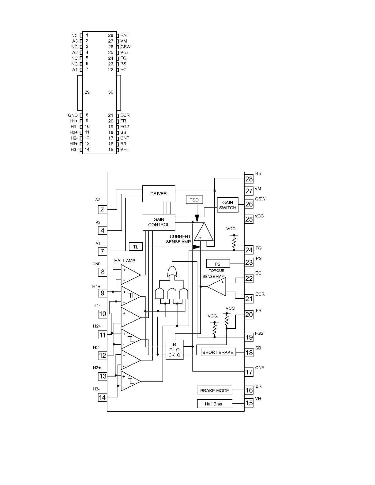
5.4 BA6664FM-X (IC251) : 3Phase Motor Driver
• Pin layout
• Block diagram
30
Page 30
• Pin function (BA6664FM-X)
Pin No. Symbol I/O Description
1 NC - Non connect
2 A3 O Output 3 for spindle motor
3 NC - Non connect
4 A2 O Output 2 for spindle motor
5 NC - Non connect
6 NC - Non connect
7 A1 O Output 1 for spindle motor
8 GND - Connect to ground
9 H1+ I Positive input for hall input AMP 1
10 H1- I Negative input for hall input AMP 1
11 H2+ I Positive input for hall input AMP 2
12 H2- I Negative input for hall input AMP 2
13 H3+ I Positive input for hall input AMP 3
14 H3- I Negative input for hall input AMP 3
15 VH I Hall bias terminal
16 BR - Non connect
17 CNF - Capacitor connection pin for phase compensation
18 SB I Short brake terminal
19 FG2 - Non connect
20 FR - Non connect
21 ECR I Torque control standard voltage input terminal
22 EC I Torque control voltage input terminal
23 PS O Start/stop switch (power save terminal)
24 FG O FG signal output terminal
25 VCC - Power supply for signal division
26 GSW O Gain switch
27 VM - Power supply for driver division
28 RNF O Resistance connection pin for output current sense
29 - Connect to ground
30 - Connect to ground
XV-NA7SL
31
Page 31

XV-NA7SL
5.5 K4S643232E-TC60(IC505):DRAM
• Block diagram
• Pin function
Symbol Description
CLK System clock signal input
CS Chip select input
CKE Clo ck enable
A0~A10 Address
BA0,1 Bank select address
RAS Row address strobe
CAS Column address strobe
WE Write enable
DQM0~3 Data input/output mask
DQ0~31 Data input/output
VDD Power supply terminal
VSS Connect to ground
VDDQ Power supply terminal
VSSQ Connect to ground
NC Non connect
32
Page 32

5.6 MN101C57DLR(IC1):System controller
• Pin function
Pin No. Symbol I/O Description
1 VLC1 - LCD Power supply terminal 1 (B5V)
2 VLC2 - LCD Power supply terminal 2 (B5V divide voltage)
3 VLC3 - LCD Power supply terminal 3 (B5V divide voltage)
4,5 NC - Non connect
6 P.ON O Indicator control signal output for STANDBY
7 PRORED O Indicator control signal output for PROGRESSIVE (red)
8 PROGRN O Indicator control signal output for PROGRESSIVE (green)
9 DVDAUDIO O Indicator control signal output for DVD AUDIO
10 N5/NA7 O Indicator control signal output for PLAY
11 VSS - Connect to ground
12,13 OSC1,2 I/O System clock signal oscillation terminal
14 MMOD I Memory enhancing switching
15 XI - Conne ct to ground
16 XO - Non connect
17 VDD - Power supply terminal (B5V)
18 NRST I Reset input
19 VDD - Power supply terminal (B5V)
20 TXD O Serial transmission data output
21 RXD I Serial receive data input
22 SCK I Serial communication clock input
23 INT O Serial transmission interrupt output
24 CLP O RGB/CMP switching signal output
25 AVCO O AV Compulink output terminal
26 AVCI I AV Compulink input terminal
27 BL O LCD Back lamp drive signal output
28 TCLOSE O Tray open signal output
29 TOPEN O Tray close signal output
30 LMMUTE O 4 ch driver MUTE signal output L:MUTE
31 DISCSET I Disc catch status input H:SET
32 DISCSTP I Di sc stop status input H:STOP
33 SWOPEN I Tray open status input H:OPEN L:CLOSE
34 SWUPDN I Tray close status input L:OPEN H:CLOSE
35 REMO I Remote control signal input
36 RGB I RGB/ S video switch signal input
37 CS I Serial receive chip select input
38 POWERSW I Power button input
39 VDD - Power supply terminal (B5V)
40 VREF+ - Power supply terminal (B5V)
41 KEYI0 I Key control signal input 0
42 KEYI1 I Key control signal input 1
43 NTB I NTSC/PAL switch signal input
44 PROINT I INT/PROG switch signal input
45 MUTE O Audio muting output
46 INT/PROG O INT/PROG switch signal output
47 EMODEL O Indicator control signal output for PAUSE
48 CPURST O LSI Reset output
49 VREF- - Connect to ground
50~96 SEG46~0 O LCD Segment control signal output 46~0
97~100 COM0~3 O LCD Common signal output 0~3
XV-NA7SL
33
Page 33

XV-NA7SL
5.7 MM1565AF-X (IC951) : 500mA Regulator
• Block diagram
• Pin function
Pin No. Symbol Function
1 Vout Output terminal
2 NC Non connect
3 GND Connect to ground
4 Cn Noise decrease terminal
5 Cout Control terminal
6 Sub Substrate (Connect to ground)
7 Vin Input terminal
34
Page 34

5.8 MN102L62GLF3 (IC401) : Unit CPU
• Pin function
Pin No. Symbol I/O Function
1 WAIT I Micon wait signal input
2 RE O Read enable
3 SPMUTE O Spindle muting output to IC251
4 WEN O Write enable
5 LMMUTE - Non connect
6 CS1 O Chip select for ODC
7 CS2 - Non connect
8 HDTYPE O HD Type selection
9 DRVMUTE O Driver mute
10 SBRK O Short brake terminal
11 LSIRST O LSI reset
12 WORD I Bus selection input
13 A0 O Address bus 0 for CPU
14 A1 O Address bus 1 for CPU
15 A2 O Address bus 2 for CPU
16 A3 O Address bus 3 for CPU
17 VDD - Power supply
18 SYSCLK - Non connect
19 VSS - Ground
20 XI - Not use (Connect to vss)
21 XO - Non connect
22 VDD - Power supply
23 OSCI I Clock signal input(13.5MHz)
24 OSCO O Clock signal output(13.5MHz)
25 MODE I CPU Mode selection input
26 A4 O Address bus 4 for CPU
27 A5 O Address bus 5 for CPU
28 A6 O Address bus 6 for CPU
29 A7 O Address bus 7 for CPU
30 A8 O Address bus 8 for CPU
31 A9 O Address bus 9 for CPU
32 A10 O Address bus 10 for CPU
33 A11 O Address bus 11 for CPU
34 VDD - Power supply
35 A12 O Address bus 12 for CPU
36 A13 O Address bus 13 for CPU
37 A14 O Address bus 14 for CPU
38 A15 O Address bus 15 for CPU
39 A16 O Address bus 16 for CPU
40 A17 O Address bus 17 for CPU
41 A18 - Non connect
42 A19 - Non connect
43 VSS - Ground
44 A20 - Non connect
45 DISCSTP O Mechanism state signal output
46 HUGUP O Connect to pick-up
47 TCLOSE - Non connect
48 WOBBLEF1L
49 HFMON O HFM Control output to Q103
50 TRVSW I Detection switch of traverse in-
side
XV-NA7SL
Pin No. Symbol I/O Function
51 SWUPDN - Non connect
52 MECHA_H/V - Connect to ground
53 DISCSET I Mechanism state signal input
54 VDD - Power supply
55 FEPEN O Serial enable signal for FEP
56 SLEEP O Standby signal for FEP
57 BUSY - Non connect
58 REQ O Communication request
59 - - Connect to TP405
60 - - Non connect
61 VSS - Ground
62 EPCS O EEPROM chip select
63 EPSK O EEPROM clock
64 EPDI I EEPROM data input
65 EPDO O EEPROM data output
66 VDD - Power supply
67 SCLKO O Communication clock
68 S2UDT I Communication input data
69 U2SDT O Communication output data
70 CPSCK O Clock for ADSC serial
71 P74/SBI1 I Not use (Pull down)
72 SDOUT O ADSC serial data output
73 - I Not use (Pull up)
74 - I Not use (Pull up)
75 NMI I NMI Terminal
76 ADSCIRQ I Interrupt input of ADSC
77 ODCIRQ I Interrupt input of ODC
78 DECIRQ I Interrupt input of ZIVA
79 CSSIRQ I Not use (Pull down)
80 ODCIRQ2 I Interruption of system control
81 ADSEP I Address data selection input
82 RST I Reset input
83 VDD - Power supply
84 TEST1 I Test signal 1 input
85 TEST2 I Test signal 2 input
86 TEST3 I Test signal 3 input
87 TEST4 I Test signal 4 input
88 TEST5 I Test signal 5 input
89 TEST6 I Test signal 6 input
90 TEST7 I Test signal 7 input
91 TEST8 I Test signal 8 input
92 VSS - Ground
93 D0 I/O Data bus 0 of CPU
94 D1 I/O Data bus 1 of CPU
95 D2 I/O Data bus 2 of CPU
96 D3 I/O Data bus 3 of CPU
97 D4 I/O Data bus 4 of CPU
98 D5 I/O Data bus 5 of CPU
99 D6 I/O Data bus 6 of CPU
100 D7 I/O Data bus 7 of CPU
35
Page 35

XV-NA7SL
5.9 MN103S26EGA (IC301) : Super optical disc controller
• Terminal layout
• Block diagram
36
Page 36

• Pin function
Pin No. Symbol I/O Description
1,2 NINT0,1 O Interruption of system control 0,1
3 VDD3 - Power supply terminal for I/O(3.3V)
4 VSS - Connect to ground
5 NINT2 O Interruption of system control 2
6 WAITDOC O Wait control of system control
7 NMPST O Reset of system control (Non connect)
8 DASPST I Setting of initial value of DASP signal
9~17 CPUADR17~9 I System control address
18 VDD18 - Power supply terminal for I/O (1.8V)
19 VSS - Connect to ground
20 DRAMVDD18 - Power supply terminal for DRAM (1.8V)
21 DRAMVSS - Connect to ground for DRAM
22~30 CPUADR8~0 I System control address
31 VDD3 - Power supply terminal for I/O (3.3V)
32 VSS - Connect to ground
33 DRAMVDD3 - Power supply terminal for DRAM (3.3V)
34 NCS I System control chip select
35 NWR I Writing system control
36 NRD I Read signal input from system controller
37~44 CPUDT7~0 I/O System control data
45 CLKOUT1 - Non connect
46 MMOD I Test mode switch signal
47 NRST I System reset
48 MSTPOL I Master terminal polarity switch input
49 SCLOCK - Non connect
50 SDATA - Non connect
51 OFTR I Off track signal input
52 BDO I Drop out signal input
53~56 PWM1~4 - Non connect
57 VDD3 - Power supply terminal for I/O (3.3V)
58 DRAMVDD18 - Power supply terminal for DRAM (1.8V)
59 DRAMVSS - Connect to ground for DRAM
60 VSS - Connect to ground
61~64 PWM5~8 - Non connect
65 TBAL O Tracking balance adjustment output
66 FBAL O Focus balance adjustment output
67 TRSDRV O Traverse drive output
68 SPDRV O Spindle drive output
69 FG I Motor FG input
70 TILTP - Non connect
71 TILT - Non connect
72 TILTN - Non connect
73 TX O Digital output signal
74 DTRD - Non connect
75 IDGT - Non connect
76 VDD18 - Power supply terminal for I/O (1.8V)
77 VSS - Connect to ground
XV-NA7SL
37
Page 37

XV-NA7SL
Pin No. Symbol I/O Description
78 VDD3 - Power supply terminal for I/O (3.3V)
79 OSCI1 I Oscillation input 16.9MHz
80 OSCO1 O Oscillation output 16.9MHz
81 VSS - Connect to ground
82 TSTSG O Calibration signal
83 VFOSHORT O VFO short output
84 JLINE O J-line settin g ou tput
85 AVSSD - Connect to ground for analog circuit
86 ROUT - Non connect
87 LOUT - Non connect
88 AVDD - Power supply terminal for analog circuit (3.3V)
89 VCOF I JFVCO control voltage
90 TRCRS I Input signal for track cross formation
91 CMPIN - Non connect
92 LPFOUT - Non connect
93 LPFIN I Pull-up to VHALF
94 AVSS - Connect to ground for analog circuit
95 HPFOUT - Non connect
96 FPFIN I HPF input
97 CSLFLT I Pull-up to VHALF
98 RFDIF - Non connect
99 AVDDC - Power supply terminal for analog circuit (3.3V)
100 PLFLT2 I Connect to capacitor 2 for PLL
101 PLFLT1 I Connect to capacitor 1 for PLL
102 AVSS - Connect to ground for analog circuit
103 RVI I Connect to resistor for VREF reference current source
104 VREFH I Reference voltage input (2.2V)
105 PLPG - Non connect
106 VHALF I Reference voltage input (1.65V)
107,108 DSLF2,1 I Connect to capacitor 2,1 for DSL
109 AVDD - Power supply terminal for analog circuit (3.3V)
110 NARF I Equivalence RF111 ARF I Equivalence RF+
112 JITOUT O Output for jitter signal monitor
113 AVSS - Connect to ground for analog circuit
114 DAC0 O Tracking drive output
115 DAC1 O Focus drive output
116 AVDD - Power supply terminal for analog circuit (3.3V)
117 AD0 I Focus error input
118 AD1 I Phase difference/3 beams tracking error
119 AD2 I AS : Full adder signal
120 AD3 I RF envelope input
121 AD4 I DVD laser current control terminal
122 AD5 I
123 AD6 I CD laser current control terminal
124 TECAPA - Non connect
125 VDD3 - Power supply terminal for I/O (3.3V)
126 VSS - Connect to ground
38
Page 38

Pin No. Symbol I/O Description
127 MONI0 - Connect to TP306
128 MONI1 - Connect to TP307
129 MONI2 - Connect to TP308
130 MONI3 - Connect to TP309
131 NEJECT I/O Eject detection
132 NTRYCTL I/O Tray close detection
133 NDASP I/O ATAPI drive active / slave connect I/O
134 NCS3FX I ATAPI host chip select
135 NCS1FX I ATAPI host chip select
136,137 DA2,0 I/O ATAPI host address 2,0
138 NPDIAG I/O ATAPI slave master diagnosis input
139 DA1 I/O ATAPI host address 1
140 NIOCS16 - Non connect
141 INTRQ O ATAPI host interruption output
142 NDMACK I ATAPI host DMA characteristic
143 VDD3 - Power supply terminal I/O (3.3V)
144 VSS - Connect to ground
145 IORDY - Non connect
146 NIORD I/O ATAPI host read
147 NIOWR - Non connect
148 DMARQ - Non connect
149 HDD15 I/O ATAPI host data 15
150 HDD0 I/O ATAPI host data 0
151 HDD14 I/O ATAPI host data 14
152 VDD18 - Power supply terminal for I/O (1.8V)
153 PO I Connect to ground
154 UATASEL I Connect to ground
155 VSS - Connect to ground
156 VDD3 - Power supply terminal for I/O (3.3V)
157 HDD1 I/O ATAPI host data 1
158 HDD13 I/O ATAPI host data 13
159 HDD2 I/O ATAPI host data 2
160 HDD12 I/O ATAPI host data 12
161 HDD3 I/O ATAPI host data 3
162 VDD3 - Power supply terminal for I/O (3.3V)
163 VSS - Connect to ground
164 HDD11 I/O ATAPI host data 11
165 HDD4 I/O ATAPI host data 4
166 HDD10 I/O ATAPI host data 10
167 HDD5 I/O ATAPI host data 5
168 HDD9 I/O ATAPI host data 9
169 VDD3 - Power supply terminal for I/O (3.3V)
170 VSS - Connect to ground
171~173 HDD6~8 I/O ATAPI host data 6~8
174 VDDH - Reference power supply for ATAPI (5.0V)
175 NRESET I ATAPI host reset input
176 MASTER I ATAPI master / slave select
XV-NA7SL
39
Page 39

XV-NA7SL
5.10 MN35505-X (IC703,IC411,IC412) : DAC
• Terminal layout
• Pin function
Pin No. Symbol I/O Description
1 M5 I Control signal for DAC
2 DIN I Digital data input
3 LRCK I L and R clock for DAC
4 BCK I Bit clock for DAC
5 M3 I Control signal for DAC
6 DVDD2 - Power supply terminal
7 CKO - Non connect
8 DVSS2 - Connect to ground
9 M2 I Control signal for DAC
10 M1 I Control signal for DAC
11 OUT1C O Analog output 1
12 AVDD1 - Power supply terminal
13 OUT1D O Analog output 1
14 AVSS1 - Connect to ground
15 AVSS2 - Connect to ground
16 OUT2D O Analog output 2
17 AVDD2 - Power supply terminal
18 OUT2C O Analog output 2
19 M9 I Control signal for DAC
20 DVSS1 - Connect to ground
21 XOUT - Non connect
22 XIN - Non connect
23 VCOF I VCO Frequency
24 DVDD1 - Power supply D+5V
25 M7 - Connect to ground
26 M8 - Connect to ground
27 M4 I Control signal for DAC
28 M6 I Clock for control signal
40
Page 40

5.11NDV8611VWA(IC501):AV Decoder
• Pin layout
• Block diagram
XV-NA7SL
• Pin function
Pin No. Symbol I/O Description
1 VDDio - Power supply terminal 3.3V
2,3 MD10,11 I/O SDRAM Data bu s terminal
4 VDD - Power supply terminal 1.8V
5 MD12 I/O SDRAM Data bus terminal
6 VSSio - Connect to ground
7~9 MD13~15 I/O SDRAM Data bus terminal
10 VDDio - Power supply terminal 3.3V
11 DQM1 O SDRAM Data byte enable
12,13 MA9,8 O SDRAM Address bus terminal
14 VSSio - Connect to ground
15,16 MA7,6 O SDRAM Address bus terminal
17 VSS - Connect to ground
18 MA5 O SDRAM Address bus terminal
19 VDDio - Power supply terminal 3.3V
20,21 MA4,3 O SDRAM Address bus terminal
22 MCLK O SDRAM Clock output
23 VSSio - Connect to ground
24 CKE O SDRAM Clock enable output
25,26 MA2,1 O SDRAM Address bus terminal
27 VDDio - Power supply terminal 3.3V
28 MA0 O SDRAM Address bus terminal
29 MA10 O SDRAM Address bus terminal
30 MA11 - Non connect
41
Page 41

XV-NA7SL
Pin No. Symbol I/O Description
31 VSSio - Connect to ground
32,33 MA12,13 O SDRAM Address bus, reserved for terminal compatibility with 64Mb SDRAM
34 VDD - Power supply terminal 1.8V
35 CS0 O SDRAM Primary bank chip select
36 VDDio - Power supply terminal 3.3V
37 RAS O SDRAM Command bit
38 CAS O SDRAM Command bit
39 WE O SDRAM Command bit
40 VSSio - Connect to ground
41 DQM0 O SDRAM Data byte enable
42 DQM2 O SDRAM Data byte enable
43 MD16 I/O SDRAM Data bus terminal
44 VDDio - Power supply terminal 3.3V
45,46 MD17,18 I/O SDRAM Data bus terminal
47 VSS - Connect to ground
48 MD19 I/O SDRAM Data bus terminal
49 VSSio - Connect to ground
50~52 MD20~22 I/O SDRAM Data bus terminal
53 VDDio - Power supply terminal 3.3V
54~56 MD23~25 I/O SDRAM Data bus terminal
57 VSSio - Connect to ground
58~61 MD26~29 I/O SDRAM Data bus terminal
62 VDDio - Power supply terminal 3.3V
63,64 MD30,31 I/O SDRAM Data bus terminal
65 DQM3 O SDRAM Data byte enable
66 CS1 O SDRAM Extension bank chip select
67 VSSD - Connect to ground
68 SPDIF O S/PDIF Digital audio output terminal
69 VSSio - Connect to ground
70 AIN I Digital audio input for digital micro; can be used as GPIO
71 AOUT3 O Serial audio output data to audio DAC for left and right channels for down-mix
72 AOUT2 O Serial audio output data to audio DAC for surround left and right channels
73 AOUT1 O Serial audio output data to audio DAC for center and LFE channels
74 AOUT0 O Serial audio output data to audio DAC for left and right channels
75 VDDio - Power supply terminal 3.3V
76 PCMCLK O Audio DAC PCM sampling clock frequency, common clock for DACs and ADC
77 VDD - Power supply terminal 1.8V
78 ACLK O Audio interface se rial data clock, common clock for DACs and AD converter
79 LRCLK O Left / right channel clock, common clock for DACs and ADC
80 SRST O Active low RESET signal for peripheral reset
81 RSTP I RESET_Power : from system, used to reset frequency synthesizer and re st
of chip
82 VSSio - Connect to ground
83 RXD1 I UART1 Serial data input from external serial device, used for IR receiver
84 SSPIN1 I/O SSP1 Data in or 16X clock for USART function in UART1
85 VSS - Connect to ground
86 SSPOUT1 I/O SSP1 Data out or UART1 data-terminal-ready signal
87 SSPCLK1 I/O SSP1 Clock or UART1 clear-to -send signal
88 SSPCLK0 I/O SSP0 Clock or request-to-send function in UART1
89 VDD - Power supply terminal 1.8V
90 SSPIN0 I/O SSP0 Data in or 16X clock for USART function in UART0
91 VDDio - Power supply terminal 3.3V
42
Page 42
XV-NA7SL
Pin No. Symbol I/O Description
92 SSPOUT0 I/O SSP0 Data out or UART0 data-terminal-ready signal
93 TXD0 I/O UART0 Serial data output to an external serial device
94 RXD0 I UART0 Serial data input from external serial device
95 CTS0 I/O UART0 Clear-to-send signal
96 RTS0 I/O UART0 Request-to-send signal
97 VSSio - Connect to ground
98 CXI I Crystal input terminal for on-chip oscillator or system input clock
99 CXO O Crystal output terminal for on-chip oscillator
100 OSCVSS - Connect to groun d for oscillator
101 OSCVDD - Po wer supply terminal for oscillator 1.8V
102 MVCKVDD - Power supply terminal for main and video clock PLL 3.3V
103 SCEN I Scan chain test enable
104 MVCKVSS - Connect to ground for main and video clock PLL
105 ACLKVSS - Connect to ground for audio clock PLL
106 SCMD I Scan chain test mode
107 ACLKVDD - Po wer supply terminal for audio clock PLL 3.3V
108 VDDDAK - Power supply terminal for DAC digital 1.8V
109 VSSDAC - Connect to ground for DAC digital
110 Cr/R O Video signal output (Cr output : composite/componen t Red output)
111 IOM O Cascaded DAC differential output used to dump current into external resistor for power
112 C/Cb/B O Video signal output (Chrominance output for NTSC/PAL S-Video
113 VAA3 - Cb output for component Blue output)
114 Y/G O Power supply terminal for DAC analog 3.3V
115 VSSA - Video signal output (Luminance for S-Video and component Green output)
116 VREF - Connect to ground for DAC analog
117 VAA - Non connect
118 CVBS/C O Video signal output (Composite video Chrominance output for S-Video)
119 RSET O Current setting resistor of output DACs
120 COMP O Compensation capacitor connection
121 VSS - Connect to ground
122 VCLK - Non connect
123 VSYNC - Non connect
124 HSYNC - Non connect
125 V DDio - Power supply terminal 3.3V
126~131 VI07~02 - Non connect
132 VSSio - Connect to ground
133,134 VI01,00 - Non connect
135 VDD - Power supply terminal 1.8V
136~139 AD31~28 I/O Multiplexed addre ss / data bus terminal
140 VDDio - Power supply terminal
141~144 AD27~24 I/O Multiplexed addre ss / data bus terminal
145 PWE3 I/O Byte write enable for FLASH,EEPROM,SRAM or peripherals terminal
146 AD23 I/O Multiplexed address / data bus terminal
147 VSSio - Connect to ground
148~153 AD22~17 I/O Multiplexed addre ss / data bus terminal
154 V DDio - Power supply terminal 3.3V
155 AD16 I/O Multiplexed address / data bus terminal
156 PWE2 I/O Byte write enable for FLASH,EEPROM,SRAM or peripherals terminal
157,158 AD15,14 I/O Multiple xed address / data bus terminal
159 VDD - Power supply terminal 1.8V
160 SCLK O External bus clock used for programmable host peripherals
43
Page 43

XV-NA7SL
Pin No. Symbol I/O Description
161 ACK I/O Programmable WAIT/ACK/RDY control
162 VSSio - Connect to ground
163~168 AD13~8 I/O Multiplexed address / data bus terminal
169 VDDio - Power supply terminal 3.3V
170 PWE1 I/O Byte write enable for FLASH,EEPROM,SRAM or peripherals terminal
171 VSS - Connect to ground
172~176 AD7~3 I/O Multiplexed address / data bus terminal
177 VSSio - Connect to ground
178~180 AD2~0 I/O Multiplexed address / data bus terminal
181 VDDio - Power supply terminal 3.3V
182 PWE0 I/O Byte write enable for FLASH,EEPROM,SRAM or peripherals terminal
183 ALE I/O Address latch enable
184~187 LA0~3 I/O Latched address 0~3
188 VSSio - Connect to ground
189 RD I/O Read terminal
190 LHLDA O Bus hold acknowledge in slave mode
191 LHLD I Bus hold request from external master in slave mode
192 VDD - Power supply terminal 1.8V
193 PCS0 O Peripheral chip select 0, generally used for enabling the program store
ROM/FLASH
194,195 XI01,02 I/O Programmable general purpose external input/output
196 VDDio - Power supply terminal 3.3V
197~200 XI03~06 I/O Programmable general purpose external input/output
201 VSS - Connect to ground
202,203 XI07,08 I/O Programmable general purpose external input/output
204 VSSio - Connect to ground
205 XI09 I/O Programmable general purpose external input/output
206~209 XID10~13 I/O Programmable general purpose external input/output
210 VDDio - Power supply terminal 3.3V
211 XID14 I/O Programmable general purpose external input/output
212 VDD - Power supply terminal 1.8V
213 DSYNC I DVD Parallel mode sector sync
214 DREQ O DVD Parallel mode data request
215 DCLK I Data sampling clock
216 DSTB I Parallel mode data valid, serial mode left/right clock
217 DVD0 I DVD Drive parallel data port
218 VSSio - Connect to ground
219~223 DVD1~5 I DVD Drive parallel data port
224 VDDio - Power supply terminal 3.3V
225,226 DVD6,7 I DVD Drive parallel data port
227 MD0 I/O SDRAM Data bus terminal
228 VSSio - Connect to ground
229 MD1 I/O SDRAM Data bus terminal
230 VSS - Connect to ground
231,232 MD2,3 I/O SDRAM Data bus terminal
233 VDDio - Power supply terminal 3.3V
234~236 MD4~6 I/O SDRAM Data bus terminal
237 VSSio - Connect to ground
238~240 MD7~9 I/O SDRAM Data bus terminal
44
Page 44

5.12 S-93C66AFJ-X (IC451, IC510) : EEPROM
• Pin layout • Pin function
Pin No. Symbol I/O Description
1 PE - Non connect
2 VCC - Power supply terminal
3 CS I Chip select input
4 SK I Serial clock input
5 DI I Serial data input
6 DO O Serial data output
7 GND - Connect to ground
8 NC - Non connect
• Block diagram
XV-NA7SL
45
Page 45

XV-NA7SL
5.13 SST39VF160-7CEK (IC509) : 16M EEPROM
• Pin layout
• Block diagram
• Pin function
Symbol Pin name Function
A19~A0 Address Inputs To provide memory addresses. During sector erase A19~A11 address lines will
select the sector. During block erase A19~A15 address lines will select the block.
DQ15~DQ0 Data Input/Output To output data during r ead cycles and receive input data during write cycles. Data
is internally latched during a write cycle. The outputs are in tri-state when /OE or
/CE is high.
/CE Chip Enable To activate the device when /CE is low.
/OE Output Enable To gate the data output buffers.
/WE Write Enable To control the write operations.
VCC Power Supply To provide 3-volt supply ( 2.7V-3.6V ).
Vss Ground
NC No Connection
46
Page 46

5.14 STR-G6551-F8 (IC901) : Switch regulator
• Block diagram
• Pin function
Pin No. Symbol Description Function
1 D Drain terminal MOS FET drain
2 S Source terminal MOS FET source
3 GND Ground terminal Ground
4 Vin Power supply terminal Input of power supply for control circuit
5 O.C.P/F.B Over current / Feedback terminal Input of over current detection signal and constant voltage
control signal
XV-NA7SL
5.15 TC74HC08AF-X(IC704) : 2-input and gate
• Pin layout • Truth table
ABY
LLL
LHL
HLL
HHH
47
Page 47

XV-NA7SL
SECTION 6
Glossary of term and abbreviations(for AV Decoder section)
3D 3-dimension
A/V 1)audio/video 2)audio/visual
ac alternating current
ACLK audio serial-data (bit) clock
AD multiplexe d address / data bus
ADC analog-to-digital converter
AIN digital audio input
ALE address latch enable
ANSI/SMPTE American National Standards Institute / Society of Motion Pictures and Television Engineers
AOP Audio Output Processor
AXCLK test-mode audio-PLL clock output
baud unit of signaling speed equal to one code element per second
Cb blue color difference component ( in accordance with the CCIR 601 spec ifications)
CCIR Consultative Committee on International Radio
CD comp act disc
CD-DA compact disc-digital audio
CMOS Complementary Metal Oxide Semiconductor
CPU Central Processing Unit
Cr red color difference component ( in accordance with the CCIR 601 specifications)
CSS Content Scrambling System
CTS Clear To Send
CVBS Composite Video Blank and Sync
DAC Digital-to-Analog Converter
dc direct current
DEMUX DEMUX Engine
DSP Digital Signal Processing
DTS Digital Theater System
DVD Digital Versatile Disc
EAV End Active Video
EAV/SAV End Active Video / Start Active Video
EEI Enable Error Interrupt
EEPROM Electrically Erasable Programmable Read-Only Memory
FS FIFO Status
GPIO General Purpose Input/Output
HDCD High Definition Compatible Digital
HDTV High-Definition television
HSYNC Horizontal sync
I/O Input/Output
IEC International Electrotechnical Commission
IOM Current (I) Output Minus ( complementary shared current path to Video DAC current paths)
IR infrared
ITU International Telecommunications Union
LA Latched Address Bus
LCLK oscillator clock ( derived from internal crystal oscillator )
Lfe Low-frequency effect
LRCLK Left/Right clock
LSB Least Significant Bit
Mb Megabit
MB Megabyte
MCLK primary or master clock
MHz Megahertz
MIPS Million Instructions Per Second
MmCPU Mediamatics CPU (synonym for internal RISC CPU)
MP3 Moving Picture Experts Group Layer-3 Audio (audio file format / extension)
MPEG1 audio A digital audio forma t mainly used in vid eo CDs. It is based on the moving picture expe rt group(MPEG1) format,
MPEG2 audio A digital audio format mainly used in Europe and Australia. It p rovides high qu ality, multi-channel audio of up to
NOP No Operation
NTSC 1)National Television System Committee 2)Worldwide video standard in North Ame r ica and Japan
NTSC-M Version of NTSC used in certain parts of the world (Brazil)
OSD On-screen display
PAL Phase alteration by line
PCM Pulse Code Modulation
PCMCLK PCM audio-data over-sampling clock
PCS 1)Picture Control and Size 2)Perpheral Chip Select
PLL Phase Lock Loop
PQFP Plastic Quad Flat Pack (Package)
PWM Pulse Width Modulator
r/w Read/Write acce ss
RAM Random Access Memory
RGB Red-Green-Blue (color model)
RISC Reduced Instruction Set Computer
ROM Read-Only Memory
RXD Receive signal
a data compression technology.
eight channels in the same was as Dolby Digital and DTS. It is based on the MPEG2 format, a data compression
technology more improved than MPEG1
48
Page 48

XV-NA7SL
RW Readable / Write able
SAV Start Active Video
SCART Syndicat des Constructeurs d'Appareils Radiorecepteurs et Televiseurs ( connector used in Europe to connect
SCLK Secondary or slave clock
SDRAM Synchro nous Dynamic Random Access Memory
S/PDIF Sony / Philips Digital Interface
S/PDIFCLK clock associated with the S/PDIF output
SRAM Static Random Access Memory
SSP Synchronous Serial Port
TXD transmit signal
UART Universal Asynchronous Receiver-transmitter
USART Universal Synchronous / Asynchronous Receiver / Transmitter
VGA Video Graphics Array
VIO Video Input / Output
VREF Voltage REFerence
Vref Vertical reference
VSSA quiet analog ground
VSYNC Vertical sync
XBUS External peripheral bus
XIO External Input / Output
Y Luminance component (in accordance with the CCIR 601 specifications)
YCbCr Luminance component, blue color difference component, red color difference component(in accordance with the
many kinds of audiovisual equipment)
CCIR 601 specifications)
49
Page 49

XV-NA7SL
VICTOR COMPANY OF JAPAN, LIMITED
PERSONAL & MOBILE NETWORK BUSINESS UNIT.
1644, Shimotsuruma, Yamato, Kanagawa 242-8514, Japan
(No.A0036)
Printed in Japan
2002/10
Page 50

XV-NA7SL
In regard with component parts appearing on the silk-screen printed side (parts side) of
the PWB diagrams, the parts that are printed over with black such as the resistor ( ),
diode ( ) and ICP ( ) or identified by the " " mark nearby are critical for safety.
When replacing them, be sure to use the parts of the same type and rating as specified
by the manufacturer. (Except the JC version)
2-1
Page 51

XV-NA7SL
Block diagrams
DVD Servo control & AV decoder section (SHEET 1,2,3)
TO SHEET 5
TO SHEET 4
TO CN1
SHEET 6
CN511
TO JT911,JT912
SHEET 7
FW901
TO JT913
FW903
SHEET 7
IC505
SDRAM
IC509
AD0~15
Flash ROM
LADD4~19
27MHz
PWE0
LA0~3
IC512
X571
AD8~19
IC513
MUTE
AOUT0~2 SPDIF
CXI/O
IC501
AV Decoder
STD0~7
IC301
SODC
WAIT
(Super optical disc controller)
YOUT
/WR
/RD
COUT
CbOUT
CrOUT
DECIRQ
CPUD0~7
CPUA0~17
ADSCIRQ
S1OUT
SSPIN0
SSPOUT0
ODCIRQ
ODCIRQ2
INT/PROG
REQ
SRST
SSPCLK0
LSIRST
CLP
CPURST
IC451
EPROM
EPDO EPDI
EPSK EPCS
P. O N
AVCOMP
TCLOSE TOPEN LMMUTE
M9V
D3.3V/S3.3V
D5V/S5V/M5V
+12V
-12V
BDO OFTR
TBAL TE RFENV
FBAL FE TG AS
ARF+ ARF-
TESTSG JLINE
FEPEN CPSCK SDOUT SLEEP
FEP
IC101
TDOFS FODRV
IC201
4CH Driver
(Frontend prosessor)
T1CD T2CD F1CD F2CD
TR TC TD TA F2DVD F1DVD
T+ T-
F+ F-
CN101
FROM
Traverse
mechanism
(Pick-up unit)
FG
SPDRV
IC251
Spindle
IC401
Unit CPU
motor driver
SBRK SPMUTE
OSCI/O
DRVMUTE
TRVSW
VH
SM1~3
H1+~H3+
TRDRV TRSDRV
FM-
FM+
H1-~H3-
LM+
LM-
X401
13.5MHz
SWOPEN SWUPDN
CN201 CN202
FROM
Traverse
assembly)
mechanism
(Spindle motor
FROM
Loading
mechanism
2-2
Page 52

Video signal output section (SHEET 4) For Asia
XV-NA7SL
TO SHEET 2
TO SHEET 3
COUT
YOU T
CbOUT
CrOUT
CYin
Cbin
CLP
NTB
PRO/INT
Cin
Vin
Yin
Crin
IC801
Cout
Vou t
Yo u t
CYout
Cbout
Crout
Video signal output section (SHEET 4) For Europe
TO SHEET 2
COUT
YOU T
Cin
Vin
Yin
CYin
IC801
Cout
Vou t
Yo u t
CYout
J802
S-VIDEO OUT
Composite OUT
Y
Cb
Component OUT
Cr
J801
S801
PAL NTSC
INT
S802
REMO
PROG
J802
S-VIDEO OUT
Composite OUT
CV/Y
G
CbOUT
CrOUT
TO SHEET 5
TO SHEET 3
Cbin
Crin
LCH RCH MUTE2
CLP
NTB
PRO/INT
Cbout
Crout
B
R/C
TO CN902
SHEET 7
CN801
J801
Y
Component OUT
Cb
Cr
S801
RGB
/COMPOSITE Y/C
NTSC
S802
REMO
PA L
2-3
Page 53

XV-NA7SL
DAC & Audio signal output section (SHEET 5)
TO
SHEET 3
TO CN401
SHEET 8
TO
SHEET 4
CN704
LCH RCH
MUTE2
MUTE3
AOUT0 BCK
DCLK LRCK
DAC0SC DDATA
MUTE2
Front audio
DAC
IC703
OUT1C
OUT1D
OUT2C
OUT2D
LPF
IC741,IC751
MUTE LMMUTE
Q705,Q791
Q743
Q753
MUTE
Front analog
audio OUT
J700
TO
SHEET 3
Surround audio section (SHEET 8)
REAR
AUDIO DAC
IC411
CENTER/
SUB WOOFER
AUDIO DAC
IC412
TO CN704
SHEET 5
CN401
AOUT2
BCK
LRCK
D DATA
AOUT1
BCK
LRCK
D DATA
SPDIF
OUT1C
OUT1D
OUT2C
OUT2D
OUT1C
OUT1D
OUT2C
OUT2D
IC704
LPF
IC812,IC811
LPF
IC821,IC822
MUTE2
MUTE2
MUTE
Q401,Q402
MUTE
Q403,Q404
Coaxial digital
OUT
J701
Optical digital
OUT
J703
J401
REAR
ANALOG
AUDIO OUT
CENTER
SUB WOOFER
ANALOG
AUDIO OUT
2-4
Page 54

System control & LCD display section (SHEET 6)
XV-NA7SL
Standby LED
D2
Remote control
IC3
Power switch
S1
Illumination
light 1
D4
Progressive LED
Q6~Q9
D3
DVD AUDIO LED
D5,Q5
Operation switch
S2~S7
STANDBYIND
REMO
POWERSW
EL1IND
PRORED
PROGRN
DVDAUD IO
CN7
FW3
Q2
CN2
KEYI0 KEYI1
CN3
P. O N
System
controller
IC2
BL
P. O N
AVCOMP P.ON INT/PROG CPURST
MUTE CLP TCLOSE TOPEN
SWUPDN SWOPEN LMMUTE
OSC1,2
NRST
SEG46~0
Q4,Q13
Illumination
OSC
X1
Reset
IC2
COM0~3
CN6 CN5 CN4
CN11 CN10 CN9
light 2
D11
LCD Display
DI1
Back
light 2
D10
Back
light 1
D9
TO CN511
CN1
SHEET 3
Power supply section (SHEET 7)
SCART Terminal
J902
Q910
AC IN
Line filter
L901
Switching
regulator
IC901
FEED BACK
Q911
AC-DC
PC901
LCH,RCH,MUTE2
AC-DC
D901
D904
C914
Q991
TO CN801 SHEET 4
R/C,G,B,CV/Y
Power
transformer
T901
CN902
AC-DC
D956
C982,C984
L957
AC-DC
D957
C987,C989
L959
AC-DC
D908
C965,C966
L952
AC-DC
D954
C979,C980
L955
AC-DC
D981
C975,C976
L960
D5V REG.
3.3V REG.
IC952
AVCOMP
IC951
J901
AV
COMPULINK
-12V
+12V
TO FW903
SHEET 3
D5V
JT911,JT912JT913
M9V
D3.3V
P. O N
B3.3V
TO FW901
SHEET 3
D998
C978
2-5
Page 55

XV-NA7SL
< MEMO >
2-6
Page 56

XV-NA7SL
Standard schematic diagrams
Servo control section
TP10
TP11
TP12
TP13
TP15
TP16
TP21
TP22
TP23
TP25
TP27
TP28
CN101
pick-up unit
To
To spindle
motor
assembly
To loading
mechanism
assembly
QGF0523F1-30W
CN201
QGF1037F1-15W
CN202
QGF1037F1-06W
R114
R115
R116
R117
K101
NQR0007-002X
TP9
TP7
TP6
TP5
TP4
TP3
TP2
TP1
TP45
TP44
TP43
TP42
TP41
TP40
TP39
TP31
TP32
TP33
TP34
TP35
TP36
TP37
TP38
TP46
TP47
TP48
TP49
TP50
TP30
TP29
F2CD
D101
VH
H3+
H3-
H2+
H2-
H1+
H1-
SM3
SM2
SM1
FM-
FM+
LM+
LM-
C138
RB521S-30
0.1/16
TP26
C141
0.1/16
C142
0.1/16
TP20
TP19
TP18
TP17
TP14
C143
0.1/16
C146
0.1/16
Q101
KTA1001/Y/-X
C102
NI
0.1/16
C139
27
2.2
R119
R104
22K
R102
C105
22K
47/6.3 47/6.3
R103
33K
4.7k
R121
R201
47
33K
R101
R110
DVDLDCUR
R218R217
NI
C215
T1CD
F1CD
0
TB
TC
TD
TA
0
0
F2DVD
F1DVD
RF-
RF+
0
T-
F-
F+
T+
TRVSW
SWOPEN
SWUPDN
HDTYPET2CD
TP24
R106
27K
TBAL
FBAL
R107
27K
SLEEP
FEPEN
CPSCK
SDOUT
Q102
KTA1001/Y/-X
R108 R109
JLINE
C103
NI
27
R105
C106
S5V
CDLDCUR
NINI
D202
NI
2.2K 1.8K
2.2
R120
M9V
C203
0.1/16
MGND
VH
HAGUP
M5V
R202
C201
22/6.3
DGND
C109
0.1/16
DTA144EE-X
F-F+T+
1
C213 C214
NI NI
LM+
LM-
H2-
H3-
H3+
0.1/16
C257
Q103
T-
FM+
FM-
H2+
H1-
0.1/16
C258
D5V
K301
K302
K303
R816
2SA1774/R/-X
R801
8.2K
R810
1.5K
C804
680p
12P
C807
82
C809
0.012
0.0027
Q802
Q805
2SC4617/R/-X
Q806
2SC4617/R/-X
C810
Q803
2SC4617/R/-X
Q804
2SC4617/R/-X
C806
150p
56P
C805
DTC114EE-X
D3.3V D1.8VS3.3V
Q808
2SC4617/R/-X
R808
1K
R811
10K
R812
10K
R813
10K
Q807
R814
10K
NQR0007-002X
NQR0007-002X
NQR0007-002X
TO SHEET 2
1K
R818
TB
TA
TC
TD
T1CD
T2CD
10K
8.2K
R113
R112
C144
0.01/16
C145
NI
R130
24K
220P
C110
R111
47P
C124
TE
/HFMON
C205
120P
R206
30K
C204
0.1/16
R219
IC201
BA5983FM-X
C217
0.1/16
R213
10K
C211
0.022
SM1
IC251
BA6664FM-X
SM2
H1+
0.1/16
C259
0.1/16
C111
1.8K
IC101
AN8703FH-V
C125
270P
TP105TP104
FE
AS
R203
0
R204
C206
27K
NI
R205
27K
R207
47K
18K
24K
R220
R221
6.8K
R222
10K
R211
2.4K
R212
10K
C210
NI
R214
10K
C216
C212
0.01/16
SM3
0.1/16
C260
C261
0.1/16
C262
0.1/16
F1CD
F2CD
F1DVD
F2DVD
0.1/16
C112
C115
0.1/16
C116
0.1/16
C118
R127 C122
2.2K
TP101
0.1/16
0.1/16
0.1/16
C129
C126
390P
C207
1
C263
0.1/16
0.0047
C127
C128
ARF-
ARF+
NI
D201
TDOFS
R208
TRDRV
22K
R209
FODRV
22K
/DRVMUTE
NI
390P
C208
C209
R210
2.4K
R223
9.1K
C218
1
R216
9.1k
R215
TRSDRV
10K
TP311
C113
22/6.3
ODCIRQ2
ODCIRQ
RF-
R124
NI
RF+
TESTSG
C117
0.047/16
C119
560P0.027/16
R125
1M
RFENV
BDO
OFTR
TP103
1M
R126
560P
C120
0.1/16
C121
12P
C123
0.1/16
S3.3V
1
R128
1
47/4
47/6.3
C135
R129
C137
S5V
SGND
TP102
CPUA0
CPUA1
CPUA2
CPUA3
ADSCIRQ
CPUA17
CPUA16
CPUA15
CPUA14
CPUA13
CPUA12
CPUA11
CPUA10
CPUA9
CPUA8
CPUA7
CPUA6
CPUA5
CPUA4
CPUA3
CPUA2
CPUA1
CPUA0
SODCCS
/WR
/RD
CPUD7
CPUD6
CPUD5
CPUD4
CPUD3
CPUD2
CPUD1
CPUD0
/RD
/WR
SODCCS
LSIRST
R350
0
X401
NAX0543-001X
K304
STEN
NQR0007-002X
R341
5.6K
10K
R301
R340
C347
0.1/16
C346
0.1/16
C345
0.1/16
C344
0.1/16
C343
0.1/16
C360
NI
DGND
HDTYPE
WAITDEC
R411R412
4.7KNI
R413
4.7K
CK135
R416
NI
0.1/160.1/16
C403C404
STD2
STD1
STD0
C348
0.1/16
47K
47K
47K
TP303
R304
R303
R302
TP304
OFTR
BDO
CPUD2
CPUD3
CPUD4
CPUD5
CPUD6
CPUD7
C342
CPUD1
STD5
STD4
STD3
0.1/16
C301
47K
47K
47K
47K
0.1/16
CPUD0
R305
0.1/16
C341
0.1/16
NI
R409
R410
MN102L62GLF
R307
R306
R338
4.7K
R339
4.7K
27K
R337
C340
C339
0.1/16
TBAL
R405
R406
R407
R408
IC401
C303
C302
0.1/16
R308
IC301
MN103S26EGA
27K
R336
TRSDRV
FBAL
TP401
C402
0.1/16
NININININININI
R403
R404
SPDRV
STD7
STD6
AVRTM
NI
0.1/16
0
R310
47K
R309
C338
0.1/16
CK169
TP305
NAX0542-001X
ODCIRQ2
4.7K
DECIRQ
ODCIRQ
ADSCIRQ
X301
R425
NI
R428
4.7K
FG
R402
STCLK
STVALID
C304
C306
NI
R311
0.1/16
C337
R320
1M
R427
1K
R424
R423
R422
R421
C407
0.1/16
TP405
C406
0.1/16
47K
NI
R317
R316
R315
R314
R313
R312
NI
R318
R319
47K
TP309
TP308
TP307
TP306
C310
C311
0.1/16
560P
R321
C312
560P
C313
560P
C314
R323
330P
C315
R324
470P
C316
R325
270P
C317
R326
120P
TP301
C318
0.1/16
TP302
C319
0.001
C320
0.001
C321
0.001
C322
0.0056
R327
1M
C324
0.1/16
C323
0.001
C349
0.1/16
C350
R328
15K
0.1/16
C325
47P
C351
C326
NI
0.018/16
C327
0.001
47K
R329
R330
47K
R331
47K
C329
0.01/16
C328
0.1/16
R332
C330
1K 0.1/16
C331
C332
1/16
1K
18K
R334
R333
C333
0.1/16
C334
0.1/16
TESTSG
JLINE
SRST
4.7K
4.7K
4.7K
0
SSPIN0
SSPOUT0
SSPCLK0
SDOUT
CPSCK
EPDO
EPDI
EPSK
EPCS
REQ
SLEEP
FEPEN
0.01/16
NININI
47K
C308
100/4
100/4
100/4
DGND
SGND
CDLDCUR
47K
47K
47K
12K
47K
0.1/16
TDOFS
DVDLDCUR
RFENV
AS
TE
FE
FODRV
TRDRVRFDIFO
TP312
ARF+
ARF-
TP313
TE
D3.3V
K401
C401
NQR0007-002X
47/4
DGND
IC451
S-93C66AFJ-X
C450
EPCS
EPSK
C920
0.1
820820
R815
SGND
Q801
2SC4617/R/-X
RFDIFO
R806
1K
R817
68P
C801
SGND
C802
R807
1.5K
68P
12P
C803
R802
15K
R809
12K
R803
1.2K
R804
820
2.4K
R805
C808
120P
EPDO
EPDI
R256
47
M9V
D5V
MGND
10K
R259
C256
0.1/16
SBRK
TP310
R251
0.47
0
0
20K
R258
R254
R253
R252
2.2
C251
C252
0.1/16
33/10
C253
0.1/16
R255
10K
/SPMUTE
C255
0.015/16
DGND
FG
C264
0.01/16
4.7K
NI
R414
R415
CPUA4
CPUA5
CPUA6
CPUA7
CPUA8
CPUA9
CPUA10
CPUA11
CPUA12
CPUA13
CPUA14
0.1/16
CPUA15
C405
CPUA16
CPUA17
HAGUP
/HFMON
R224
10K
TO SHEET 3
TOPEN
SPDRV
TCLOSE
/LMMUTE
/SPMUTE
SBRK
/DRVMUTE
DISCSTP3V
TRVSW
DISCSET3V
Digital data signal
SHEET 1
2-7
Page 57

XV-NA7SL
AV Decoder section
TO SHEET 1
IC506
K4S641632F-TC75
D3.3V
R998
R995
D3.3VD1.8V
C521
0.1
K502K503
K504
NQR0007-002X
NQR0007-002X
NQR0007-002X
STD7
C524
D3.3V
K501
NQR0007-002X
IC505
W986432DH-7
C501
0.1/16
10
R1570
MD0
R1571
MD1
10
R1502
MD2
10
R1503
MD3
10
R1504
MD4
10
R1505
MD5
10
R1506
MD6
10
R1507
MD7
10
R1532
DQM0
10
R1533
WE-
10
R1534
CAS-
10
R1535
RAS-
10
R1536
CS0-
10
R1562
MA12
10
R1561
MA13
10
R1560
MA10
10
R1550
MA0
10
R1551
MA1
10
R1552
MA2
10
R1537
DQM3
10
R1524
MD24
10
R1525
MD25
10
R1526
MD26
10
R1527
MD27
10
R1528
MD28
10
R1529
MD29
10
R1530
MD30
10
R1531
MD31
10
D3.3V
LM1117MP1.8-X
C550
C549
0.1/16
47/4
DGND
C511
47/4
MD8
10
MD9
10
MD10
10
MD11
10
MD12
10
MD13
10
MD14
10
MD15
10
DQM1
10
R1538
10
CKE
10
MA9
10
MA8
10
MA7
10
MA6
10
MA5
10
MA4
10
MA3
10
DQM2
10
MD16
10
MD17
10
MD18
10
MD19
10
MD20
10
MD21
10
MD22
10
MD23
10
IC511
D1.8V
C557
0.1/16
C573
220/4
R859
0
R861
0
R866
0
R836
0
R847
0
C865
0.01
MD10
MD11
MD12
R1508
MD13
R1509
MD14
R1510
MD15
R1511
DQM1
R1512
MA9
MA8
R1513
R1514
MA7
MA6
R1515
MA5
R1541
MA4
MA3
R1539
CKE
R1559
MA2
R1558
MA1
R1557
R1556
MA0
R1555
MA10
R1554
MA11
R1553
R1540
MA12
MA13
R1516
CS0-
R1517
RAS-
R1518
CAS-
WE-
R1519
R1520
DQM0
DQM2
R1521
MD16
R1522
MD17
R1523
MD18
MD19
MD20
MD21
MD22
MD23
MD24
MD25
MD26
MD27
MD28
47/4
C512
C514
C515
C516
C517
C518
C519
C520
C523
C529
C527
47/4
C528
MD8
MD7
MD6
MD5
MD4
MD9
0.1/16
0.1/16
0.1/16
0.1/16
0.1/16
0.1/16
0.1/16
0.1/16
0.1/16
0.1/16
MD29
MD3
100
R583
MD30
MD31
DQM3
SPDIF
STD6
0.1/16
MD1
MD0
MD2
C532
C531
0.1/16
150
150
150
R580
R579
R578
192k
AOUT0
AOUT1
AOUT2
SRST
STD5
STD4
STD3
STD2
STD1
STD0
STCLK
STVALID
C533
0.1/16
0.01
0.1/16
C551
TP878
150
150
R576
R575
TP860
TP861
TP862
BCK
LRCLK
C506
15P
R503
NI
X571
NAX0513-001X
SSPIN1
SSPOUT1
C507
STEN
SSPCLK1
18P
AVRTM
SSPCLK0
R501
47
BUSY
SWMUTE
TP913
TP912
REQ
R541
DECIRQ
0
0
R739
R740
C534
C547
0.1/16
0.1/16
IC501
C545
0.1/16
C535
0.1/16
TP865
TP866
TP863
TP864
SSPOUT0
SSPIN0
NI
FLINT
DACDENA
0
470000470
0
R997
R543
R544
R545
TP911
S1OUT
LRMUTE
C540
0.1/16
C582
47/4
R546
0
X6
0
R996
R547
K507
D3.3V
NQR0007-002X
D1.8V
DAC2CS
R548
C571
47/4
DAC1CS
470
R549
1.6K
R574
C541
K508
RCK
DAC0CS
LA0
470
R551
R550
C548
0.1/16
1.6K
R573
C543
0.1/16
C601
47/4
NQR0007-002X
FLCS3V
000
R552
0.1/16
K509
NQR0007-002X
D3.3V
D1.8V
PCS0
0
R553
LHLD
C536
0.1/16
CrOUT
C544
0.1/16
C602
47/4
K510
NQR0007-002X
LHLDA
C539
CbOUT
TO SHEET 3
LA3
LA2
LA1
R505
NI
R506
NI
R507
NI
R508
NI
0.1/16
PWE1
C993
0.1/16
C994
0.1/16
C995
0.1/16
PWE3
C996
0.1/16
C997
0.1/16
TP867
TP868
TP870
TP871
TP872
TP873
TP874
C998
0.1/16
TP875
TP876
TP877
C542
0.1/16
R738
0
R565
6.8k
R589
R566
1.3K
R567
120
R568
R569
R570
R571
R572
75
COUT
YOUT
C572
0.1/16
C580
47/4
C578
0.1/16
C581
D1.8VD3.3V
220/4
K513
NQR0007-002X
10
L501
1.5K
75
75
10
NI
VI02
CPURST
RD-
ALE
PWE0
AD0
AD1
R584
3.3K
R991
22
TP869
AD2
AD3
AD4
AD5
AD6
AD7
AD8
AD9
AD10
AD11
AD12
AD13
ACK
SCLK
AD14
AD15
PWE2
AD16
AD17
AD18
AD19
AD20
AD21
AD22
AD23
AD24
AD25
AD26
AD27
AD28
AD29
AD30
AD31
TO SHEET 3
K557
NQR0007-002X
K556
NQR0007-002X
NQR0007-002X
NQR0007-002X
K558
K559
TO SHEET 4
TO SHEET 3
Digital data signal
Video signal
Audio signal
SHEET 2
2-8
Page 58

XV-NA7SL
Flash ROM section
TO SHEET 2
TO SHEET 2
AD30
AD28
AD26
AD24
AD23
AD22
AD21
AD19
AD17
AD16
AD15
AD14
AD13
AD12
AD11
AD10
AD8
AD7
AD6
AD5
AD3
AD1
PWE0
LA0
LA2
RD-
LHLD
DAC0CS
DAC2CS
RGB
FLINT
SWMUTE
SW501
D5V
SRST
D5VD3.3V
DGND
D3.3V
IC512
DGND
74LCX373MTC-X
IC513
74LCX373MTC-X
LADD19
LADD18
LADD17
LADD7
LADD15
LADD14
LADD13
LADD12
AD19
AD18
AD17
AD7
ALE
AD15
AD14
AD13
AD12
ALE
R604
NI
C554
0.1/16
LADD6
AD15
AD6
AD7
AD5
AD14
LADD5
AD6
LADD4
AD13
AD4
AD5
AD16
AD12
LADD16
AD4
AD11
AD3
AD10
AD2
AD9
LADD11
AD1
AD8
AD11
AD0
AD10
LADD10
RD-
LADD9
AD9
FCS-
AD8
LA0
LADD8
LADD16
LADD15
LADD14
LADD13
CN501
NI
NI
NI
C620
C621
NI
R502
NI
0
R655
FCS-
PCS0
LHLDA
FLCS3V
DAC1CS
DACDENA
AD31
AD29
AD27
AD25
PWE3
AD20
AD18
PWE2
SCLK
ACK
AD9
PWE1
AD4
AD2
AD0
ALE
LA1
LA3
PCS0
X6
NTB
LADD12
LADD11
LADD10
LADD9
LADD8
LADD19
PWE0
ACK
LADD18
LADD17
LADD7
LADD6
LADD5
LADD4
LA3
LA2
LA1
IC509
SST39VF160-9CEK
R601
NI
R602
NI
D3.3V
K519
NQR0007-002X
C992
0.1/16
C569
0.1/16
S1OUT
SWUPDN
SWOPEN
/LMMUTE
TCLOSE
TOPEN
SSPIN1A
SSPOUT1
SSPCLK1B
FLINT
FLCS3V
CPURST
DISCSET
DISCSTP3V
0.1
DGND
0.1
SGND
0.1
MGND
C504
100/10
C593
S5V
L503
1
C505
C594
100/10
M5V
R511
0
C508
100/10
C595 C592
D3.3V
0.1
0.1
0.1
C500
C590
100/10
S3.3V
L502
1
R510
C502
C591
100/10
M9V
C503
100/10
NQR0007-002X
K582
NQR0007-002X
K563
NQR0007-002X
K561
NQR0007-002X
K515
NQR0007-002X
K518
NQR0007-002X
K586
NQR0007-002X
K579
NQR0007-002X
K560
0
P.ON
AVCOMP
+12V
NTB
RGB
MUTE
CLP
INT/PROG
PROINT
AVCOMP
P.ON
EP701
C579
QNZ0136-001Z
NI
-12V
FW901
QUM108-14DGZ4
TO JT911,JT912
SHEET 7
QUM104-16DGZ4
TO JT913
SHEET 7
FW903
AGND
INT/PROG
CLP
RGB
NTB
TO SHEET 4
S1OUT
PROINT
CN511
QGF1016C1-27
TO CN1
SHEET 6
TO SHEET 2
TO SHEET 1
DGND
SSPOUT1
SSPCLK1
TP848
DGND
D3.3V
K520
NQR0007-002X
C619
0.1/16
IC523
NC7SZ125P5-X
10K
R521
SSPIN1A
BUSY
SSPIN1
DACDENA
DDATA
DCLK
IC522
74LCX32MTC-X
SSPCLK1B
DISCSET3V
DISCSET
IC510
S-93C66AFJ-X
R512
3.3K
RCK
DGND
LRMUTE
DDATA
BCK
DCLK
LRCLK
DAC0CS
AOUT0
DAC1CS
AOUT1
DAC2CS
AOUT2
192k
SPDIF
VI02
NQR0007-002X
K573
K567
NQR0007-002X
NQR0007-002X
K577
NQR0007-002X
K569
NQR0007-002X
K575
NQR0007-002X
K571
NQR0007-002X
K576
NQR0007-002X
K570
NQR0007-002X
K572
NQR0007-002X
K574
NQR0007-002X
K564
NQR0007-002X
K566
TO SHEET 5
Audio signal
SHEET 3
2-9
Page 59

XV-NA7SL
4
Video signal output section
D5V
K801
NQR0007-002X
NQR0007-002X
R842
R823
R819 R820
2.2K 2.2K
KRC102S-X
K802
Q822
KRC102S-X
R821
9.1K
Q821
R822
9.1K
C820
NI
75
R824
75
R825
75
10K
J800
QNZ0499-001
TO SHEET 2
C851
100/10
IC801
0
R870
R871
1K
L802
NQR0460-001X
0
R873
R874
1K
L801
NQR0429-001X
0
R876
R877
1K
L803
NQR0460-001X
0
R879
R880
1K
L804
NQR0460-001X
R872
75
C839
NI
R882
R883
C840
NI
R875
75
R878
75
R881
75
C838
NI
0
C837
NI
C833
0.01
R890
0
0
R851
22k
R888
C834
0.1
NI0
R830R831
0
C835
0.1
C836
0.01
C817
22/10
C818
1
C831
1
R852
22k
C832
1
MM1568AJ-X
C853
0.1
C811
0.1
C856
220/6.3
C814
22/25
C858
220/6.3
C812
22/25
C860
220/6.3
22/10
C819
C813
220/6.3
22/10
C859
C815
220/6.3
C816
22/10
0
R887
R854
0
R884
NI
Q827
DTC114EK-X
R885
4.7K
R834
10K
Q825
DTA114EK-X
R800
75
R828
75
R829
75
R838
75
R839
75
R843
75
R826
R827
R863
2.2K
R844
R862
3.3K
R858
0
1k
J802
J801
NI
0
S801
QSW0454-001
S802
QSW0986-001
TO SHEET 3
TO SHEET 5
2-10
INT/PROG
CLP
RGB
S1OUT
MUTE3
MUTE2
LCH
AGND
RCH
PROINT
R845
0
R846
0
R850
0
R853
0
NTB
R837
0
0
R832
R833
0
R857
R856
1K1K
Q826
DTC114EK-X
R855
100K
CN801
QGF1016C1-15
TO CN902
SHEET 7
Video signal
Audio signal
SHEET
Page 60

DAC & audio signal output section
D5V
MUTE
LRMUTE
TO
SHEET 3
R711
K701
10
NQR0007-002X
K703
NQR0007-002X
DGND
R705
K711
+12V
NI
R729
470
R728
470
NQR0007-002X
-12V
XV-NA7SL
R795
47K
47K
R794
R756
3.3k
R1500
18k
R746
3.3k
NJM5532L
R754
3.6K
R703
10k
R701
10k
R744
3.6K
IC751
NJM5532L
IC741
R1501
C745
C741
R748
C742
R747
3.6K
R757
3.6k
C752
C751
Q756
2SC3576-JVC-T
Q755
2SC3576-JVC-T
R758
0.01
C761
R782
220
R761
IC741
NJM5532L
C743
2700p
1M
R702
C744
C762
C772
R700
C754
1M
C753
R771
2700p
0.01
IC751
NJM5532L
C771
C755
R762
C748
R783
220
R764
18K
220
R774
18k
C749
R772
R792 R793
220
R796
10k
Q704
KRC109S-X
C746
MUTE3RCH
R765
560
R766
27K
R776
27k
LCH
C756
R775
560
R742
R726
22
0.001
-12V
C700
220/10
C710
R731
3.3k
C730
0.22
C731
0.01
C717
1.5
IC703
MN35505-X
470
470
470
470
R723
R721
10
R712
R724
R725
C711
1.5
K704
NQR0007-002X
C714
470/10
C716
R704
0
K710
NQR0007-002X
470/10
R713
47
AGND
R715
47
R780
18k
R743
18k
27K
R781
27K
Q706
KRA102S-X
27k
R751
27k
R750
C740
R773
3.6K
C701
R798
47k
0.0015
R763
3.6k
C750
R753
18k
R752
18k 18k
R789
C747
C757
100K
Q828
KRA121S-X
Q705
KRA102S-X
Q791
2SC2412K/RS/-X
Q743
2SC3576-JVC-T
Q753
2SC3576-JVC-T
R767
100
R768
10K
J700
R779
0
C797
1500p
0
R778
10k
R777
100
R797
47k
NI
R784
R785
TO CN401
SHEET 8
TO
SHEET 4
CN704
QGF1016C2-17W
MUTE3
LCH
RCH
D3.3V
K706
NQR0227-004X
R520
R1721
MUTE2
R1730
L1701
1
C1702
R1722
0
R519
0
10
C1701
47/25
IC704
TC74HC08AF-X
K705
NQR0227-004X
300
R1725
300 82
R706
100K
4.7/25
100/10
R1727
C707
C1703
150P
C735
10
C1704
330p
J703
GP1FA351TZ
C1706
0.1
10
K1701
R1728
NQR0227-004X
0.1
J701
QNN0347-001
Audio signal
SHEET 5
2-11
Page 61

XV-NA7SL
System control & LCD display section
DI1
QLD0239-001
330
R26
330
R25
SPR-325MVW/L/-T
0
R22
Q8
KRA102S-X
Q6
KRC107S-X
S1
QSW0651-001Z
SEG1
SEG0
COM0
COM1
COM2
CN7
QGF1016F3-13
IC3
C9
47/10
C10
C17
GP1UD271XK
1
0.022
GND
CN2
QGF1016C1-13
KRA103S-X
Q2
C14
0.1
IC2
XC61FN2712M-X
R3
4.7K
R2
C3
0.1
D1
1SS355-X
KRC107S-X
Q1
C1
AVCO
330P
1K
0.01
C2
QAX0667-001Z
X1
R53
0
R1
4.7k
AVCI
C6
0.1
R9
10K
COM3
C15
0.1
C4
0.1
C5
0.1
R52
0
R46
R15
R16R17
C11
220/6.3
SEG2
SEG3
SEG4
SEG5
SEG6
SEG7
SEG8
SEG9
SEG10
SEG11
SEG12
SEG13
SEG14
SEG15
SEG16
SEG17
SEG18
SEG19
SEG20
SEG21
SEG22
SEG23
SEG24
SEG25
SEG26
SEG27
SEG28
SEG29
SEG30
SEG31
SEG32
SEG33
SEG34
SEG35
SEG36
SEG37
SEG38
SEG39
SEG40
SEG41
SEG42
SEG43
SEG44
SEG45
SEG46
CN1
QGF1016C1-27
D5V
B3.3V
SWUPDN
SEG2
SEG3
SEG4
SEG5
SEG6
SEG7
SEG8
SEG9
SEG10
SEG11
SEG12
SEG13
SEG14
SEG15
SEG16
SEG17
SEG18
SEG19
SEG1
SEG0
COM0
COM1
COM2
COM3
4.7K
10K
10K
10K
IC1
MN101C57DLR
SEG20
SEG21
SEG22
SEG23
SEG24
SEG25
SEG26
SEG27
SEG28
SEG29
SEG30
SEG31
SEG32
SEG33
SEG34
SEG35
SEG36
SEG37
SEG38
SEG39
SEG40
SEG41
SEG42
SEG43
SEG44
SEG45
SWOPEN
/LMMUTE
TCLOSE
TOPEN
NTB
RGB
TXD
RXD
SCK
INT
CS
CPURST
M9V
MUTE
CLP
INT/PROG
PROINT
AVCOMP
P.ON
DISCSET
DISCSTP
TO CN511
SHEET 3
75
150
R24
R23
R47
D2
330
SPR-39MVWF
KRC107S-X
Q9
KRA102S-X
75
R38
Q7
D5
Q5
KRC107S-X
SELU2E10C
D3
D4
SELU2E10C
SEG46
2.2K
R6
100K
R14
2.2K
FW3
S4
R27
0SELU2E10C
S5
R28
S6
S2
S3
S7
R31
D6
2.2k 2.2K
27
R33
R32
1.8k
1ss355-x
D15
R29R30
430
680
Q10
2SC1740/RS/-T
D9
NSPW300BS/BRS/
D10
NSPW300BS/BRS/
D11
QUM107-10DGZ4
CN9
QJK018-021202
CN10
QJK018-021202
CN11
QJK018-021202
CN3
CN8
QGD2501C1-04Z
CN4
QGA2001C1-02
CN5
QGA2001C1-02
CN6
QGA2001C1-02
QGD2501C1-03Z
R21
0
R36
2.2K
R37
2.2K
Q4
2SC1740S/RS/-T
R18
R35
10/16
27
C13
27
Q13
2SC1740S/RS/-T
D12
1SS355-X
C8
R40
1.8k
1.8k
R41
10/16
1SS355-X
D13
2.2K
R5
R4
10K
NI
R7
R8
R56
R19
3.9K
3.9K
R42
3.9K
C16
10/16
1M
R34
C12
0.1
10K
R13
1K
1.5K
10K
R12
R10
R11
R44
0
1K
0
R51
R50
R20
3.3K
C7
NI
NI
2-12
SELU2E10C
SHEET 6
Page 62

XV-NA7SL
Power supply section
D957
F1T4-T2
180/25
BK901
R951
75
R909
150
R952
75
R953
C910
22/25
R914
C911
22/25
Q910
R912
2SC3576-JVC-T
560
R910
10K
R915
10K
R913
Q911
560
2SC3576-JVC-T
5.6k
R916
150
R917
150
R911
5.6k
75
R954
75
0
R958
J902
QNZ0516-001
TO CN801
SHEET 4
!
L959
10
C987
470/16
C989
CN902
QGF1205C1-15
QNZ0136-001Z
QGA7901C1-02
EP901
180/25
C982
!
D956
F1T4-T2
!
D954
F1T4-T2
B2
C905
!
0.001
L901
FC902
!
QQR1194-001
!
C902
0.1
R920
!
C921
0.001
!
!
FC901
P901
QNG0003-001Z
C903
!
0.1
3.3M
IC901
STR-G6551R-F8
!
D901
S1WB/A/60-4101
!
K902
D905
F1T4-T2
R908
3.3k
!
R901
68k
!
D902
C909
SARS01-T2
NI
R921
47
!
R907
0.47
R906
680
C915
470p
C914
39/25
PC123Y02
PC901
!
F1T4-T2
!
KTC3199/Y/-T
D904
Q991
C922
0.0033
C907
!
QEZ0522-127
C999
NI
R905
68K
C913
100P
QQR1183-001Z
!
T901
QQS0159-001
R903
!
C981
C991
1
100p
R902
39
R960
39
R961
680
HZ3CLL-T2
D991
R964
100K
R969
270
150
R962
1000/10 220/10
C979 C980
!
D908
EK16-F1
C965
1000/10
!
D981
RK34-LFB2
470/16
C984
L957
10
L955
QQR1291-001Z
IC951
MM1565AF-X
L952
QQR1291-001Z
C966 C983 C968C969
470/10 1 1
IC952
PQ3RD23
L960
QQR1291-001Z
C990
C975
1000/10
470/6.3
0.33
C976
C985
C986
220/6.3
0.33
D998
11ES2-T4
L909R918
2.2100
R919
NI
L910
NI
C972
470p
K906
QQR1183-001Z
K904
QQR1183-001Z
C928
K905
QQR1183-001Z
NI
NI
R992
R991
J901
QNS0089-001
J901
100
R924
0.022
QGD2501C1-04Z
TO FW903
SHEET 3
JT913
C953
NI
QGD2501C1-04Z
JT911
TO FW901
SHEET 3
220/6.3
220/6.3
B303
C978
JT912
QGD2501C1-04Z
Video signal
Audio signal
Parts are safety assurance parts.
When replacing those parts make
sure to use the specified one.
SHEET 7
2-13
Page 63

XV-NA7SL
Surround audio section
NQR0007-002X
K413
NQR0007-002X
K411
10
R365
NQR0007-002X
BK811
C429
220/6.3
R361
22
R367
470
K415
R363
3.3k
R369
470
C441
0.01
C432
0.22
C431
0.01
C434
470/6.3
R470
47
K417
NQR0007-002X
C430
1.5
R432
18K
R434
18K
30K
R442
R440
30K
C412
R444
2.7K
1200P
R438
1.6K
NJM4580L
R446
2.7K
IC812
R436
36k
C416
120P
R450
750
C414
4700P
R448
3.6K
C418
0.012
NJM4580L
R452
750
IC812
C420
1000P
100/16
C428
100/16
C426
R468
220
R454
1K
R466 R456
220 18K
C422
1000P
C424
47/25
R460
560
C1426
2200p
R458
27K
R462
100
Q402
2SD2144S/VW/-T
R464
10K
CN401
TO CN704
SHEET 5
QGF1016C1-17
DDATA
AOUT2
LRCK
BCK
DAC2CS
DCLK
D.GND
AOUT1
DAC1CS
MUTE2
DAC1CS
DCLK
R366
10
DAC2CS
NQ70007-002X
K414
NQR0007-002X
K416
NQR0007-002X
DCLK
K412
IC411
MN35505
C1467
220/6.3
22
R368
470
R455
C427
IC822
NJM4580L
NJM4580L
IC811
C468
100/16
100/16
C466
100/16
100/16
C425
R358
220
220
R356
R443 R445 R447
C433
470/6.3
R469
C474
470/6.3
47
K421
R360
47
K418
NQR0007-002X
470
470
470
470
R371
R373
DDATA
AOUT2
R362
R370
C442
0.01
10
R389
R377
R375
C435
1.5
NQR0007-002X
BCK
LRCK
R364
3.3k
C1468
0.22
C469
0.01
470
C470
1.5
2.7K 2.7K 3.6K
C411
30K
R441
R433
R439
18K
30K
+12V
R472
18K
R474
18K
R480
30K
R482
30K
R484
2.7K
1200P
C452
NJM4580L
1200P
IC822
IC811
NJM4580L
R437
1.6K
R478
1.6K
R486
2.7K
C413
4700P
R435R431
36K18K
R476
36k
C456
120P
R488
3.6K
C454
4700P
R449
750
C415
120P
R490
750
C419
1000P
R451
750
C417
0.012
C458
0.012
R492
750
C460
1000P
18K
220220
R465R467
27K
R457
C1425
2200p
R459
560
-12V
R350
560
2200p2200p
C1466
C462
1000P
R494
R453
1K
C421
1000P
C423
47/25
C464
47/25
1K
R498
27K
R496
18K
2SD2144S/VW/-T
R352
Q404
2SD2144S/VW/-T
100
C409
1500P
Q401
R463
10K
R461
100
MUTE2
K419K420
NQR0007-002X
R354
10K
NQR0007-002X
J401
2-14
IC412
MN35505
470
R372
DDATA
470
R374
AOUT1
470
R376
LRCK
220
R355
C467
R483 R487
C473
470/6.3
K422
NQR0007-002X
R359
10
10
R390
470
R378
C475
1.5
BCK
2.7K 3.6K
30K
R481
30K
R473
R479
18K
R471 R475
18K 36K
R485
2.7K
C453
4700P
C451
1200P
NJM4580L
R477
1.6K
IC821
120P
C455
R489 R491
750 750
0.012
100/16
C459
1000P
IC821
NJM4580L
C465
C457
100/16
R495
18K
C461
1000P
R493
1K
R357
220
R497
27K
R499
C463
560
47/25
C1465
Q403
2SD2144S/VW/-T
R351
100
R353
10K
MUTE2
C410
1500P
Audio signal
SHEET 8
Page 64

Printed circuit boards
Servo control & output terminal board (Forward side)
XV-NA7SL
K573
K520
R503
C541
R575
K569
R746
C748
R1730
C707
K576
R546
R548
X571
C571
L501
R1723
L1701
K702
C619
K572
C548
R550
R501
R1500
Q756
K577
C540
C507
C544
C581
R506
C536
IC501
C573
C1702
R519
J802
R512
K507
C557
R520
IC522
K581
R508
K509
K575
R552
R505
R584
C993
R991
C994
C995
C542
C543
C572
K513
C578
K580
R521
IC523
R551
R507
C996
C582
C602
C539
C580
S
B
R553
C997
C998
K505
K506
C601
A
R580
R583
C550
C549
C1701
R869
R864
6
CN202
A1
LEA10056-
C535
R738
R578
R579
C531
C532
C551
R849
R859
R860
C851
R861
R1525
R1551
R1560
R1562
R1533
R1535
R1537
R1507
R1503
R1505
R1571
R1527
R1529
R1531
R1550
R1552
R1526
R1528
R1524
R1530
27
3
C501
IC505
R1519
R1521
R1523
R1522
R1520
2
CN704
16
2
K701
C750
R1501
Q755
1 1
C511
R1518
R756
C753
C755
K501
1
R711
C751
C749
J700
26
R1517
17
R752
R753
C716
C756
R1554
R1540
R1553
R1516
C711
CN511
R1556
R1557
R1555
R721
R723
R724
R725
R712
R772
R1512
R1513
R1515
R1539
R1558
R1559
Q704
C757
R1541
R789
R796
Q705
R1561
R1510
IC751
Q753
R1534
R1536
C524
C519
R1514
R705
C752
R1532
R1506
K503
R1570
C512
C515
C516
R1538
C517
C518
IC506
C520
R1508
C523
R1511
R1509
C527
K504
R795
K710
C771
R1502
R1504
C514
Q791
C762
C772
C754
C744
C761
J701
A
K571
C743
R543
C533
C700
C717
R762
R995
R545
R547
C731
R742
R743
C714
C746
IC510
R998
R549
C534
C547
C741
C745
J703
R996
R997
R541
R544
C730
C740
C506
R576
K567
K510
K508
1
2
C521
K502
C528
C529
A
K566
R794
K564
K574
K570
K711
R729
R728
R731
C710
IC703
R704
C742
IC741
C747
Q743
S1E
1
30
R121
C545
C554
R604
IC512
R119
R101
R103
IC509
C992
K519
C102
C105
IC513
C145
C113
C144
C106
R129
LEB10056-001EI1
L802 L803
L801
C814
C856 C858
C812
C860
C819
R888
C859
C813
C817
CN101
R110
L804
R104
R120
R102
R105
C569
C135
C816
C815
C D
1
C115
C112
C111
R112
C103
R601 R602
R124
C116
R130
Q102
C117
C118
R113
Q101
C137
R125
C119
R106
R116
C123
C120
R107
D101
R126
IC101
C139
C138
K303
EP701
R111
C110
C109
Q103
C308
K302
R308
R307
R305
R128
C122
C128
C127
R109
C306
C129
C124
R108
R310
R309
C303
R304
X401
15 1
C121
C126
C125
TP104
C579
15
R127
TP105
R316
R313
R301
C348
K304
C405
IC451
FE
TE
R318
R311
C404
R224
C450
C201
R317
R315
R314
R312
C302
R306
R341
C403
R416
14
CN201
C301
R340
R303
R302
R412
R411
IC401
FODRV
TP301
R209
C310
R319
R413
C406
R202
IC301
C360
K401
1
C252
TRDRV
TP302
R208
C318
C311
C407
C401
C346
R421
C324
R422
C251
C349
R328
R409
R408
R407
R405
R403
R423
R424
C805
C328
C345
R428
HEAT PROOF FLUX
CN801
2
S801
S802
J800 J801
WC801
R813
Q805
C344
R410
C402
R819
R822
R804
R805
C808
C807
R425
R427
Q822
Q807
C343
R406
C504
R404
R402
C804
R803
C803
R510
C806
Q804
R809
R810
C592
R825
R812
Q803
R802
R330
UL
R824
C337
C338
C809
R801
Q808
R808
Q802
R811
R807
C802
C330
C331
R332
C332
C329
R320
R337
C340
R255
R215
R339
R338
C341
C342
C505
C594
R511
C508
C595
C503
MARK
Q821
R823
R842
R806
C810
C339
C591
L502
C593
2
R820
R816
Q801
X301
R336
C500
C590
L503
R821
R815
K301
1
FW903
C865
3
C920
Q806
R818
R814
C304
8
1
4
R866
C502
C801
R817
FW901
2-15
Page 65

XV-NA7SL
Servo control & output terminal board (Reverse side)
TP310
TP45
TP305
TP41
TP43
IC251
R256
C334
TP311
TP44
C257
C256
C333
C258
R331
R333
R334
TP42
R259
TP303
C259
R329
TP304
TP39
TP40
C327
C326
TP35
C255
C350
C322
C351
C323
C325
C263
C260
R258
C321
TP313
R327
C319
C264
R254
C317
R350
C261
C320
R326
C316
C253
R252
R253
TP312
TP306
R324
R325
C315
C262
TP36
TP37
TP307
C314
TP38
C213
R251
TP308
C313
C347
TP4
TP2
R201
TP3
IC201
TP33
C214
TP309
R323
C312
C204
TP1
TP31
R321
D201
TP32
C217
TP34
C209
R203
C211
R214
R213
C212
R206
R221
R212
C216
C205
R204
C210
R216
R211
R223
C218
C206
R207
C208
R222
R220
R210
C203
TP103
R205
TP5
TP101
TP6
K101
C207
TP9
TP7
TP10
TP11
R219
TP12
TP13
D202
R218
TP14
TP17
TP15
R217
C215
TP18
TP16
TP19
R114
C146
TP20
TP21
TP22
TP23
TP24
C142
TP102
TP26
C143
R115
C141
R117
TP25
TP27
TP28
TP30
TP29
TP46
TP47
R655
R502
TP48
TP49
TP50
SW501
CN501
TP869
TP871
TP873
TP875
TP877
TP867
TP870
TP872
TP874
TP876
C620
TP868
TP911
TP912
R739
TP863
TP864
TP913
TP866
TP865
R740
TP862
TP861
K560
R565
R566
TP860
TP525
R574
R589
R573
R567
R568
K556
K557
TP878
TP526
R569
R570
K558
K559
TP524
R571 R572
TP522
TP519
TP521
TP523
TP848
TP520
TP514
TP516
TP518
TP517
TP515
K582
K515
K563
K561
TP512
TP513
K518
TP510
K586
TP511
TP509
TP508
TP507
TP505 TP506
TP502
TP504
K579
TP503
TP700
TP702
TP704
TP707
TP501
TP500
TP701
TP705
TP706
TP703
FW903
R867
FW901
R868
J800
TP401
Q826
S802
TP405
Q828
R856
R415
R855
R845
TP805
TP804
TP803
R846 R850
TP802
R414
TP809
TP807
R857
TP801
R863
TP810
TP808
TP800
S801
R797
TP806
R853
R858
R862
R844
Q827
K802
R885
R833
R826
R881
C837
C816
C815
R832
R837
R827
L804
R852
C832
R880
C818
C831
C836
C817
Q825
R879
C838
C859
C813
R877
L803
R800
R876
R878
C819
C860
R874
R883
R873
L801
R882
IC801
C812
C858
R875
C851
C811
R828
C840
C853
C814
C856
R829
J801
R871
R870
L802
R851
R872
R830
K801
C621
R835
R887
R884
R841
R847
R848
C1701
R834
R836
R840
R831
C835
R854
R890
C833
C834
R838
R1725
R1721
R839
C1702
R1722
IC704
R843
J802
Q706
R1727
K706
IC511
C1703
R1728
C730
R703
L1701
K705
C700
C740
R1500
R702
C707
J703
R746
C745
K1701
R764
C735
C731
R742
R743
C743
R784
R748
C748
R782
C746
R766
C714
R713
R761
R706
C717
C741
R762
R765
R768
R785
R726
K704
R773
C742
C762
C744
C761
Q743
C747
R767
C1706
K703
R780
R781
R783
R754
R757
Q753
R747
R750 R751
R744
C752
C772
R793
C754
C771
R792
C757
C1704
C711
C797
R753
R715
R779
R752
J700 J701
TP708
TP710
C716
R763
R771
R772
R775
C755
R777
TP712
C749
C756
R778
C750
C751
R756
R758
C753
R700
R774
R776
TP711
R1501
Q755
TP709
R701
C701
R798
2-16
Page 66

System control & power supply board
FC901
P901
FC902
C902
L901
R920
C903
C921
C905
D6
XV-NA7SL
R31
FW3
R33
R901
C922
C909
BK901
C982
C984
D956
L957
C907
C989
D902
D957
C987
T901
C913
R921
R903
L959
IC901
R958
C999
D954
R917
C915
D904
R907
R908
D908
R916
D901
HS901
D981
R915
R910
R954
R913
R911
K902
C914
R906
D905
Q910
Q911
R914
J902
L960
L952
L955
R905
C975
C979
R912
R960
R963
C965
R902
R962
R961
R964
PC901
D991
C991
C980
C910
Q991
C976
C966
C911
R951 R952 R953
D4
R22
C990
IC952
K904
R969
K905
C981
C986
D998
CN902
C968
C969
C985
K906
R909
D2
R23
C983
C978
R918
L909
R24
EP901
IC951
JT911
C952
J901
C972
C923
R47
JT912
R992
R991
JT913
C928
R924
S1
R919
L910
D14
R41
Q13
CN6
R56
R42
C13
D13
R35
C7
C16
R40
R34
D12
C8
R50
R19
EP1
R20
CN12
Q4
R12
R18
R11
CN5
R51
CN7
R44
R10
R13
C12
R14
R32
R6
CN1
CN8
R8
R5
R7
R4
IC1
DI1
D9
CN9
Q5
R9
R43
CN10
Q7
Q6
C6
R38
D10
Q9
Q8
C11
X1
D5
CN4
R2
R21
R52
R53
R17
C5
R16
C4
R15
C15
D11
CN11
C10
R26
R25
D3
CN3
R3
Q2
R46
C9
C17
R37
R36
C3
IC2
C2
CN2
C14
R1
D1
Q1
C1
IC3
S3
D15
Q10
S4
R27
S5
S6
S7
S2
R28
R30
R29
2-17
Page 67

XV-NA7SL
Loading motor board
Surround audio board
CN401
R367
R371
R375
R372
R374
R495
R455
R453
C417
R493
S1
C414
C428
K418
C468
C463
R499
K417
R466
C454
R464
R462
C441
C434
R448
R480
C474
R356
C466
R497
R353
R461
K419
K415
R369
R373
R435
R377
R437
C419
C415
IC811
C421
R451
K414
C475
R390
R366
R475
R477
R376
C459
C455 C456
IC821
C461
R491
C457
BK811
R431
C411
R378
C451
R433
R467
R473
R489
R357
R365
R441
R481
C424
C423
K413
R449
C425
K416
R479
R487
R355
C465
R458
R457
C435
R439
R447
R465
R471
C467
R389
C433
C473
R460
R459
R443
R445
C413
C427
R368
R370
C442
R359
R483
R485
C453
C1426
Q402
C1425
IC411
K421
R469
IC412
K422
Q401
R463
R442
R468
C470
R482
R488
C410
C430
R432
R440
C426
C469
R363
R472
R358
C1465
Q403
R351
C431
R434
R450
R474
K420
R364
IC822
J401
C429
C412
C416
IC812
K412
C452
R490
C409
K411
R438
C1468
R478
C1466
R436
C422
R362
C462
R492
Q404
R352
C432
R452
C1467
R361
R476
C460
C458
R498
R354
R470
R446
R456
R454
C420
C418
R360
R486
R494
C464
R350
S2
R444
R484
R496
2-18
Page 68
XV-NA7SL
PARTS LIST
[XV-NA7SL]
* All printed circuit boards and its assemblies are not available as service parts.
A ------ Australia
B ------ U.K.
E ------ Continental Europe
EN ---- Northern Europe
US ---- Singapore
UW --- Brazil, Mexico, Peru
- Contents -
Exploded view of general assembly and parts list
DVD Traverse mechanism assembly and parts list
DVD Loading mechanism assembly and parts list
Electrical parts list
Packing materials and accessories parts list
Area Suffix
3-2
3-5
3-7
3-9
3-20
3-1
Page 69

XV-NA7SL
Exploded view of general assembly and parts list
Block No.
MMM1
35
BACK SIDE
34
BACK SIDE
8
2
61
63
40
44
9
31
57
D
32
J
27
32
H
G
41
28
F
M
B
ain
oard
B
9
9
60
40
40
35
64
34
17
13
12
1
14
10
67
6
5
4
A
3
39
37
40
38
36
65
68
C
B
7
19
D
8
2
18
32
24
E
31
G
J
31
15
62
44
H
30
42
43
F
32
59
C
23
31
33
62
66
58
22
25
63
54
26
29
Grease
JVS-1003
62
16
52
53
51
50
46
K
K
47
49
48
55
56
36
3-2
A
20
E
20
Page 70

XV-NA7SL
Parts list (General assembly) 1/2
Item
A
1 LE10272-006A
2 E75896-001
3 LE20638-014A WINDOW SCREEN 1
4 LE20639-004A
5 QYSBSF2608Z
6 LE20640-002A PUSH BUTTON 1
7 LE20641-001A
8 LE31030-002A
9 QYSBSF2608Z
10 LE20646-001A
11 LE20662-001A
12 QYSBSF2608Z
13 QYSDSG3008N T.SCREW 1
14 QUQ110-1336AJ
15 QUQ110-2711AJ
16 QUQ412-1514CJ
17 E3400-431
18 LE10273-002A
19 LE30001-033A
20 E75896-001 FELT SPACER 2
21 QUQ810-1713AJ
22 QQR1349-001
23 QQR1350-001
24 QQR1351-001
25 LV30225-090A
26 QYSBSGG3008E
27 QYSBSGG3008E T.SCREW 1
28 QYSBSGG3008E
29 QYSBSGG3008E
30 -------------------- DVD TRAVERSE ME 1
31 LV41659-201A
32 LV41424-001A
33 --------------------
34 LV10582-001A
35 LV20913-002A
36 LV32417-001A
37 LV42089-002A YOKE 1
38 LV42930-003A
39 LV41741-001A
40 QYSBSF2008Z
41 QUQ110-0610AJ
42 QYSBST3010E
43 LE40874-002A
44 QYSBST3008E T.SCREW 2
45 LE20647-025A
Parts number Parts name Area
FRONT PANEL
LE10272-005A
LE20647-022A
LE20647-023A
FRONT PANEL
FELT SPACER
PUSH BUTTON
T.SCREW
PUSH BUTTON
LED LENS
T.SCREW
BKT
INDICATOR
T.SCREW
FFC WIRE
FFC WIRE
FFC WIRE
SPACER
CHASSIS BASE
SPACER
FFC WIRE
FERRITE CORE
FERRITE CORE
FERRITE CORE
SPACER
T.SCREW
T.SCREW
T.SCREW
INSULATOR
SPECIAL SCREW
1DISC LAODING B
TRAY LONG TYPE
CLAMPER BASE
CLAMPER
MAGNET
SPECIAL SCREW
SCREW
FFC WIRE
T.SCREW
THRUST SPRING
REAR PANEL
REAR PANEL
REAR PANEL
Q'ty
Block No. M1MM
Description
1
1
2
1
2
1
2
4
1
1
2
1
1
1
1
1
1
1
1
1
1
1
1
1
2
4
4
1
1
1
1
1
1
4
1
1
1
1
1
1
A,US,UW
B,E,EN
B,E,EN
A
B,E,EN
US
3-3
Page 71

XV-NA7SL
Parts list (General assembly) 2/2
Item
A
45 LE20647-024A
46 QYSBSGY3008M
47 QYSBSGY3008M
48 QYSBSGY3008M SPECIAL SCREW 1
49 QYSBSGY3008M
50 QYSBSGY3008M
51 QYSBSGY3008M SPECIAL SCREW 2
52 QYSBSGY3008M
53 QYSBSGY3008M
54 QYSBSGY3008M
55 QYSBSGY3008M
56 QYSBSGY3008M
57 QMF51E2-1R6-J1
A
58 QHS3771-108 CORD STOPPER 1
A
59 QMPG070-244-JC
A
A
A
60 QZW0004-001
61 LE20645-001A
62 QYSBSGG3008E
63 QYSDSG3008N T.SCREW 2
64 LE31040-001A
65 LE20663-001A
66 LV41843-001A
67 LE31028-001A
68
Parts number Parts name Area
REAR PANEL
SPECIAL SCREW
SPECIAL SCREW
SPECIAL SCREW
SPECIAL SCREW
SPECIAL SCREW
SPECIAL SCREW
SPECIAL SCREW
SPECIAL SCREW
SPECIAL SCREW
FUSE
POWER CORD
QMPN160-200-JD
QMPK190-200-JC
QYSBSE3008Z SCREW
POWER CORD
POWER CORD
WIRE CLAMP
METAL COVER
T.SCREW
ORNAMENT
FITTING BASE
LASER CAUTION
LCD LENS
Q'ty
Block No. M1MM
Description
1
1
1
1
1
2
1
1
1
1
1
1
1
1
2
1
3
1
1
1
1
1
UW
B,E,EN
A
B
E,EN,US,UW
3-4
Page 72

DVD Traverse mechanism assembly and parts list
XV-NA7SL
Grease
EBS0006-013B
PG-641
CFD-4007ZY2
Block No. M M M2
26
25
21
21
19
28
3
3
2
20
18
16
22
3
16
24
15
17
14
12.0mm 0.2mm
0.2
65.2mm mm
0
5
27
23
13
13
6
4
7
1
10
7
8
9
12
11
29
29
30
30
30
29
3-5
Page 73

XV-NA7SL
Parts list (DVD Traverse mechanism assembly)
Item
A
1 LE20520-002A MECHA BASE 1
2 LE20516-001A SPINDLE BASE 1
3 QYSDST2605M TAPPING SCREW 3
4 LE30909-001A HOLDER 1
5 QAR0165-001 FEED MOTOR 1
6 LV41510-001A FEED GEAR 1
7 QYSPSPU2040M SCREW 2
8 LV41512-001A FEED GEAR 1
9 LV41517-003A LEAD SCREW 1
10 LV41511-002A FEED GEAR 1
11 LE40742-001A TORSION SPRING 1
12 QYSDSF2005Z SCREW 1
13 QYSDST2605M TAPPING SCREW 2
14 LE20517-001A HOLDER 1
15 LE40744-001A SPRING 1
16 LV41121-002A SLIDE SHAFT 2
17 QYSDST2605M TAPPING SCREW 1
18 QAL0342-001 OPTICAL PICK-UP 1
19 LE20519-001A ACTUATOR 1
20 LE30886-001A SPRING 1
21 QYSPSFU1740Z SCREW 2
22 LE30888-003A SPRING 1
23 QYSPSGU1430Z SCREW 1
24 LE40743-001A SPRING 1
25 LE40774-001A PLATE 1
26 QYSDST2606Z SCREW 1
27 QAL0284-001 F.P.C.WIRE ASSY 1
28 QAR0162-001 SPINDLE MOTOR 1
29 QYSPSPU1760Z SCREW 3
30 QYYASPF2608N SCREW 3
Parts number Parts name Area
Q'ty
Block No. M2MM
Description
3-6
Page 74

DVD Loading mechanism assembly and parts list
Block No. M M M3
Grease
UD-24H2
EM-30L
CFD-4007ZY2
XV-NA7SL
To G of Servo control & A/V output terminal board.
9
8
13
10
12
11
7
6
4
1
3
2
6.85mm 0.1mm
To F of Servo control & A/V output terminal board.
5
14
3
2
3-7
Page 75

XV-NA7SL
Parts list (DVD Loading mechanism assembly)
Item
A
1 LV10454-007A LOADING BASE 1
2 QAR0164-001 MOTOR 1
3 LV42087-001A MOTOR PULLEY 1
4 QYSPSPU1730Z SCREW 1
5 VKZ4777-003 MINI SCREW 1
6 LV42209-001A BELT 1
7 LV42084-002A PULLEY GEAR 1
8 LV42085-002A MIDDLE GEAR 1
9 LV42086-001A IDLE GEAR 1
10 LV32514-002A SLIDE CAM 1
11 LV42348-001A GEAR BRACKET 1
12 VKZ4777-003 MINI SCREW 1
13 LV20912-002A ELEVATOR 1
14 QUQ110-0610AJ FFC WIRE 1
Electrical parts list (Loading motor board)
Item
A
CN 1
Parts number Parts name Area
QGF1016F3-06
QSW0910-002
S 1
QSW0910-002
S 2
Parts number Parts name Area
Remarks
CONNECTOR
SWITCH
SWITCH
Block No. 04
Q'ty
Block No. M3MM
Description
3-8
Page 76

XV-NA7SL
r
r
Electrical parts list (Servo control board)
Item
A
C 105 NEA70JM-476X E.CAPACITOR
C 106 NEA70JM-476X E.CAPACITOR
C 109 NCB31CK-104X C CAPACITOR
C 110 NCS31HJ-221X C.CAPA. C.M
C 111 NCB31CK-104X C CAPACITOR
C 112 NCB31CK-104X C CAPACITOR
C 113 NEA70JM-226X E CAPACITOR
C 115 NCB31CK-104X C CAPACITOR
C 116 NCB31CK-104X C CAPACITOR
C 117 NCB31CK-473X C CAPACITOR
C 118 NCB31CK-273X C CAPACITOR
C 119 NCB31HK-561X C CAPACITOR
C 120 NCB31HK-561X C CAPACITOR
C 121 NCB31CK-104X C CAPACITOR
C 122 NCS31HJ-120X C.CAPA. C.M
C 123 NCB31CK-104X C CAPACITOR
C 124 NCS31HJ-470X C.CAPA. C.M
C 125 NCB31HK-271X C CAPACITOR
C 126 NCB31CK-104X C CAPACITOR
C 127 NCB31CK-104X C CAPACITOR
C 128 NCB31CK-104X C CAPACITOR
C 129 NCB31HK-472X C CAPACITOR
C 135 NEA70JM-476X E.CAPACITOR
C 137 NEA70GM-476X E.CAPA. C.M.
C 138 NCB31CK-104X C CAPACITOR
C 139 NCB31CK-104X C CAPACITOR
C 141 NCB31CK-104X C CAPACITOR
C 142 NCB31CK-104X C CAPACITOR
C 143 NCB31CK-104X C CAPACITOR
C 144 NCB31CK-103X C CAPACITOR
C 146 NCB31CK-104X C CAPACITOR
C 201 NEA70JM-226X E CAPACITOR
C 203 NCB31CK-104X C CAPACITOR
C 204 NCB31CK-104X C CAPACITOR
C 205 NCS31HJ-121X C CAPACITOR
C 207 NCB31HK-391X C CAPACITOR
C 208 NCB31HK-391X C CAPACITOR
C 211 NCB31HK-223X C CAPACITOR
C 212 NCB31CK-103X C CAPACITOR
C 216 NCB30JK-105X C CAPACITOR
C 217 NCB31CK-104X C CAPACITOR
C 218 NCB30JK-105X C CAPACITOR
C 251 NCB31CK-104X C CAPACITOR
C 252 NEA71AM-336X E CAPACITOR
C 253 NCB31CK-104X C CAPACITOR
C 255 NCB31CK-153X C CAPACITOR
C 256 NCB31CK-104X C CAPACITOR
C 257 NCB31CK-104X C CAPACITOR
C 258 NCB31CK-104X C CAPACITOR
C 259 NCB31CK-104X C CAPACITOR
C 260 NCB31CK-104X C CAPACITOR
C 261 NCB31CK-104X C CAPACITOR
C 262 NCB31CK-104X C CAPACITOR
C 263 NCB31CK-104X C CAPACITOR
C 264 NCB31CK-103X C CAPACITOR
C 301 NCB31CK-104X C CAPACITOR
C 302 NCB31CK-104X C CAPACITOR
C 303 NCB31CK-104X C CAPACITOR
C 304 NEA70GM-107X E CAPACITOR
C 306 NEA70GM-107X E CAPACITOR
C 308 NEA70GM-107X E CAPACITOR
C 310 NCB31CK-104X C CAPACITOR
C 311 NCB31HK-561X C CAPACITOR
C 312 NCB31HK-561X C CAPACITOR
C 313 NCB31HK-561X C CAPACITOR
C 314 NCB31HK-331X C CAPACITOR
Parts numbe
Parts name Area
Block No. 01
Remarks
Item
A
C 315 NCB31HK-471X C CAPACITOR
C 316 NCB31HK-271X C CAPACITOR
C 317 NCS31HJ-121X C CAPACITOR
C 318 NCB31CK-104X C CAPACITOR
C 319 NCB31HK-102X C CAPACITOR
C 320 NCB31HK-102X C CAPACITOR
C 321 NCB31HK-102X C CAPACITOR
C 322 NCB31HK-562X C CAPACITOR
C 323 NCB31HK-102X C CAPACITOR
C 324 NCB31CK-104X C CAPACITOR
C 325 NCS31HJ-470X C.CAPA. C.M
C 326 NCB31CK-183X C CAPACITOR
C 327 NCB31CK-102X C.CAPA. C.M
C 328 NCB31CK-104X C CAPACITOR
C 329 NCB31CK-103X C CAPACITOR
C 330 NCB31CK-104X C CAPACITOR
C 331 NCB31CK-103X C CAPACITOR
C 332 NCB21CK-105X C CAPACITOR
C 333 NCB31CK-104X C CAPACITOR
C 334 NCB31CK-104X C CAPACITOR
C 337 NCB31CK-104X C CAPACITOR
C 338 NCB31CK-104X C CAPACITOR
C 339 NCB31CK-104X C CAPACITOR
C 340 NCB31CK-104X C CAPACITOR
C 341 NCB31CK-104X C CAPACITOR
C 342 NCB31CK-104X C CAPACITOR
C 343 NCB31CK-104X C CAPACITOR
C 344 NCB31CK-104X C CAPACITOR
C 345 NCB31CK-104X C CAPACITOR
C 346 NCB31CK-104X C CAPACITOR
C 347 NCB31CK-104X C CAPACITOR
C 348 NCB31CK-104X C CAPACITOR
C 349 NCB31CK-104X C CAPACITOR
C 350 NCB31CK-104X C CAPACITOR
C 401 NEA70GM-476X E.CAPA. C.M.
C 402 NCB31CK-104X C CAPACITOR
C 403 NCB31CK-104X C CAPACITOR
C 404 NCB31CK-104X C CAPACITOR
C 405 NCB31CK-104X C CAPACITOR
C 406 NCB31CK-104X C CAPACITOR
C 407 NCB31CK-104X C CAPACITOR
C 450 NCB31CK-104X C CAPACITOR
C 500 NEA70JM-476X E.CAPACITOR
C 501 NCB31CK-104X C CAPACITOR
C 502 NEA70JM-476X E.CAPACITOR
C 503 NEA71AM-336X E CAPACITOR
C 504 NEA70JM-476X E.CAPACITOR
C 505 NEA70JM-476X E.CAPACITOR
C 506 NDC31HJ-150X C CAPACITOR
C 507 NDC31HJ-180X C.CAPACITOR
C 508 NEA70JM-476X E.CAPACITOR
C 511 NEA70GM-476X E.CAPA. C.M.
C 512 NCB31CK-104X C CAPACITOR
C 514 NCB31CK-104X C CAPACITOR
C 515 NCB31CK-104X C CAPACITOR
C 516 NCB31CK-104X C CAPACITOR
C 517 NCB31CK-104X C CAPACITOR
C 518 NCB31CK-104X C CAPACITOR
C 519 NCB31CK-104X C CAPACITOR
C 520 NCB31CK-104X C CAPACITOR
C 521 NCB31CK-104X C CAPACITOR
C 523 NCB31CK-104X C CAPACITOR
C 524 NEA70GM-476X E.CAPA. C.M.
C 527 NEA70GM-476X E.CAPA. C.M.
C 528 NCB31CK-104X C CAPACITOR
C 529 NCB31CK-104X C CAPACITOR
Parts numbe
Parts name Area
Remarks
3-9
Page 77

XV-NA7SL
r
r
Electrical parts list (Servo control board)
A
Item
Parts numbe
C 531 NCB31CK-104X C CAPACITOR
C 532 NCB31CK-104X C CAPACITOR
C 533 NCB31CK-104X C CAPACITOR
C 534 NCB31CK-104X C CAPACITOR
C 535 NCB31CK-104X C CAPACITOR
C 536 NCB31CK-104X C CAPACITOR
C 539 NCB31CK-104X C CAPACITOR
C 540 NCB31CK-104X C CAPACITOR
C 541 NCB31CK-104X C CAPACITOR
C 542 NCB31CK-104X C CAPACITOR
C 543 NCB31CK-104X C CAPACITOR
C 544 NCB31CK-104X C CAPACITOR
C 545 NCB31CK-104X C CAPACITOR
C 547 NCB31CK-104X C CAPACITOR
C 548 NCB31CK-104X C CAPACITOR
C 549 NEA70GM-476X E CAPACITOR
C 550 NCB31CK-104X C CAPACITOR
C 551 NCB31CK-103X C CAPACITOR
C 554 NCB31CK-104X C CAPACITOR
C 557 NCB31CK-104X C CAPACITOR
C 569 NCB31CK-104X C CAPACITOR
C 571 NEA70GM-476X E CAPACITOR
C 572 NCB31CK-104X C CAPACITOR
C 573 NEA70GM-227X E CAPACITOR
C 578 NCB31CK-104X C CAPACITOR
C 580 NEA70GM-476X E CAPACITOR
C 581 NEA70GM-227X E CAPACITOR
C 582 NEA70GM-476X E CAPACITOR
C 590 NCB31CK-104X C CAPACITOR
C 591 NCB31CK-104X C CAPACITOR
C 592 NCB31CK-104X C CAPACITOR
C 593 NCB31CK-104X C CAPACITOR
C 594 NCB31CK-104X C CAPACITOR
C 595 NCB31CK-104X C CAPACITOR
C 601 NEA70GM-476X E CAPACITOR
C 602 NEA70GM-476X E CAPACITOR
C 619 NCB31CK-104X C CAPACITOR
C 700 QEXT0JM-157Z E CAPACITOR 150MF 20% 6.3V
C 701 NCB31HK-152X C CAPACITOR
C 705 NCB31CK-104X C CAPACITOR
C 707 QETN1AM-107Z E CAPACITOR
C 710 NCS31HJ-102X C CAPACITOR
C 711 QCZ0202-155Z ML C CAPACITOR
C 714 QTE1A28-477Z E CAPACITOR
C 716 QTE1A28-477Z E CAPACITOR
C 717 QCZ0202-155Z ML C CAPACITOR
C 730 QFV21HJ-224Z MF CAPACITOR .22MF 5% 50V
C 731 QFLC1HJ-103Z M CAPACITOR .010MF 5% 50V
C 735 NCB31CK-104X C CAPACITOR
C 740 QFLC1HJ-561Z M CAPACITOR
C 741 QFP31HJ-121Z PP CAPACITOR
C 742 QFLC1HJ-182Z M CAPACITOR
C 743 QFLC1HJ-272Z M CAPACITOR
C 744 QFLC1HJ-561Z M CAPACITOR
C 745 QFLC1HJ-103Z M CAPACITOR
C 746 QTE1A48-476Z E CAPACITOR
C 747 QFLC1HJ-182Z M CAPACITOR 1800PF 5% 50V
C 748 QFLC1HJ-561Z M CAPACITOR 560PF 5% 50V
C 749 QFLC1HJ-561Z M CAPACITOR 560PF 5% 50V
C 750 QFLC1HJ-561Z M CAPACITOR
C 751 QFP31HJ-121Z PP CAPACITOR
C 752 QFLC1HJ-182Z M CAPACITOR
C 753 QFLC1HJ-272Z M CAPACITOR
C 754 QFLC1HJ-561Z M CAPACITOR
C 755 QFLC1HJ-103Z M CAPACITOR
C 756 QTE1A48-476Z E CAPACITOR
Parts name Area
Block No. 01
100MF 20% 10V
1.5MF
1.5MF
560PF 5% 50V
120PF 5% 50V
1800PF 5% 50V
2700PF 5% 50V
560PF 5% 50V
.010MF 5% 50V
560PF 5% 50V
120PF 5% 50V
1800PF 5% 50V
2700PF 5% 50V
560PF 5% 50V
.010MF 5% 50V
Remarks
A
Item
Parts numbe
C 757 QFLC1HJ-182Z M CAPACITOR 1800PF 5% 50V
C 761 QTE1C28-107Z E CAPACITOR
C 762 QTE1C28-107Z E CAPACITOR
C 771 QTE1C28-107Z E CAPACITOR
C 772 QTE1C28-107Z E CAPACITOR
C 797 NCB31HK-152X C CAPACITOR
C 801 NCS31HJ-680X C CAPACITOR
C 802 NCS31HJ-680X C CAPACITOR
C 803 NCS31HJ-120X C CAPACITOR C
C 804 NCS31HJ-681X C CAPACITOR C
C 805 NCS31HJ-560X C CAPACITOR C
C 806 NCS31HJ-151X C CAPACITOR
C 807 NCS31HJ-120X C CAPACITOR
C 808 NCS31HJ-121X C CAPACITOR
C 809 NCB31HK-272X C CAPACITOR
C 810 NCB31HK-123X C CAPACITOR
C 811 NCB31CK-104X C CAPACITOR
C 812 QETN1EM-226Z E CAPACITOR 22MF 20% 25V
C 813 QETN0JM-227Z E CAPACITOR 220MF 20% 6.3V
C 814 QETN1EM-226Z E CAPACITOR 22MF 20% 25V
C 815 QETN0JM-227Z E CAPACITOR 220MF 20% 6.3V
C 816 QETN1AM-226Z E CAPACITOR
C 817 QETN1AM-226Z E CAPACITOR
C 818 NCB21CK-105X C CAPACITOR
C 819 QETN1AM-226Z E CAPACITOR
C 831 NCB21CK-105X C CAPACITOR
C 832 NCB21CK-105X C CAPACITOR
C 833 NCB31HK-103X C CAPACITOR
C 834 NCB31CK-104X C CAPACITOR
C 835 NCB31CK-104X C CAPACITOR
C 836 NCB31CK-103X C CAPACITOR
C 851 QETN1AM-107Z E CAPACITOR
C 853 NCB31CK-104X C CAPACITOR
C 856 QETN0JM-227Z E CAPACITOR
C 858 QETN0JM-227Z E CAPACITOR
C 859 QETN1AM-226Z E CAPACITOR
C 860 QETN0JM-227Z E CAPACITOR 220MF 20% 6.3V
C 865 NCB31CK-103X C CAPACITOR
C 992 NCB31CK-104X C CAPACITOR
C 993 NCB31CK-104X C CAPACITOR
C 994 NCB31CK-104X C CAPACITOR
C 995 NCB31CK-104X C CAPACITOR
C 996 NCB31CK-104X C CAPACITOR
C 997 NCB31CK-104X C CAPACITOR
C 998 NCB31CK-104X C CAPACITOR
C1701 QETN1EM-476Z E CAPACITOR
C1702 QETN1EM-475Z E CAPACITOR 4.7MF 20% 25V
C1703 NCS31HJ-151X C CAPACITOR
C1704 NCS31HJ-331X C CAPACITOR
C1706 NCB31CK-104X C CAPACITOR
CN101 QGF0523F1-30W FFC/FPC CONNE
CN201 QGF1037F1-15W CONNECTOR
CN202 QGF1037F1-06W W TO B CONNE
CN511 QGF1016C1-27 CONNECTOR
CN704 QGF1016C2-17W CONNECTOR
CN801 QGF1205C1-15 CONNECTOR B,E,ENE
D 101 RB521S-30 MG RESISTOR
FW901 QUM138-08DGZ4 PARA RIBON WI RE
FW903 QUM134-08DGZ4 PARA RIBON WI RE
IC101 AN8703FH-V IC
IC201 BA5983FM-X IC
IC251 BA6664FM-X LSI
IC301 MN103S26EGA IC
IC401 MN102L62GLF3 IC
IC451 S-93C66AFJ-X IC
IC501 NDV8611VWA IC
Parts name Area
C
C
C
C
C
C
C
22MF 20% 10V
22MF 20% 10V
22MF 20% 10V
100MF 20% 10V
220MF 20% 6.3V
220MF 20% 6.3V
22MF 20% 10V
47MF 20% 25V
PU
SP&STP
LOADER
REAR/CNTR/SW
Remarks
3-10
Page 78

XV-NA7SL
r
Y
Y
Y
r
Electrical parts list (Servo control board)
A
Item
Parts numbe
IC505 K4S643232E-TC60 IC
IC509 SST39VF160-9CEK IC (FLASH)
IC510 S-93C66AFJ-X IC
IC511 LM1117MP1.8-X IC
IC512 74LCX373MTC-X IC(DIGITAL)
IC513 74LCX373MTC-X IC(DIGITAL)
IC522 74LCX32MTC-X IC(DIGITAL)
IC523 NC7SZ125P5-X IC(DIGITAL)
IC703 MN35505-X IC C M
IC704 TC74HC08AF-X IC
IC741 NJM5532L IC
IC751 NJM5532L IC
IC801 MM1568CJ-X IC
J 700 QNN0513-001 PIN JACK
J 701 QNN0458-001 PIN JACK
J 703 GP1FA351TZ OPT TRANSMITTER
J 801 QNN0395-001 PIN JACK
J 802 QNN0454-001 PIN JACK S/COMP. ALL
K 101 NQR0007-002X FERRITE BEADS
K 301 NQR0007-002X FERRITE BEADS
K 302 NQR0007-002X FERRITE BEADS
K 303 NQR0007-002X FERRITE BEADS
K 304 NQR0007-002X FERRITE BEADS
K 401 NQR0007-002X FERRITE BEADS
K 501 NQR0007-002X FERRITE BEADS
K 502 NRSA02J-0R0X MG RESISTOR
K 503 NRSA02J-0R0X MG RESISTOR
K 504 NQR0007-002X FERRITE BEADS
K 507 NQR0007-002X FERRITE BEADS
K 508 NQR0007-002X FERRITE BEADS
K 509 NQR0007-002X FERRITE BEADS
K 510 NQR0007-002X FERRITE BEADS
K 513 NQR0007-002X FERRITE BEADS
K 515 NQR0007-002X FERRITE BEADS
K 518 NQR0007-002X FERRITE BEADS
K 519 NQR0007-002X FERRITE BEADS
K 520 NQR0007-002X FERRITE BEADS
K 556 NQR0007-002X FERRITE BEADS
K 557 NQR0007-002X FERRITE BEADS
K 558 NQR0007-002X FERRITE BEADS
K 559 NQR0007-002X FERRITE BEADS
K 560 NQR0007-002X FERRITE BEADS
K 561 NQR0007-002X FERRITE BEADS
K 563 NQR0007-002X FERRITE BEADS
K 564 NQR0007-002X FERRITE BEADS
K 566 NQR0007-002X FERRITE BEADS
K 567 NQR0007-002X FERRITE BEADS
K 569 NQR0007-002X FERRITE BEADS
K 570 NQR0007-002X FERRITE BEADS
K 571 NQR0007-002X FERRITE BEADS
K 572 NQR0007-002X FERRITE BEADS
K 573 NQR0007-002X FERRITE BEADS
K 574 NQR0007-002X FERRITE BEADS
K 575 NQR0007-002X FERRITE BEADS
K 576 NQR0007-002X FERRITE BEADS
K 577 NQR0007-002X FERRITE BEADS
K 579 NQR0007-002X FERRITE BEADS
K 582 NQR0007-002X FERRITE BEADS
K 586 NQR0007-002X FERRITE BEADS
K 701 NQR0007-002X FERRITE BEADS
K 702 NQR0007-002X FERRITE BEADS
K 703 NQR0007-002X FERRITE BEADS
K 704 NQR0007-002X FERRITE BEADS
K 705 NQR0227-004X FERRITE BEADS
K 706 NQR0227-004X FERRITE BEADS
K 711 NQR0007-002X FERRITE BEADS
Parts name Area
FRONT L/R
COAXIAL
OPT DIGITAL OUT
COMPONENT ALL
Block No. 01
Remarks
A
Item
Parts numbe
K 801 NQR0007-002X FERRITE BEADS
K 802 NQR0007-002X FERRITE BEADS
K1701 NQR0227-004X FERRITE BEADS
L 501 NQL044K-100X INDUCTOR
L 502 NQL044K-100X INDUCTOR
L 503 NQL044K-100X INDUCTOR
L 801 QQR1089-001 LPF
L 802 QQR1088-001 LPF
L 803 QQR1088-001 LPF
L 804 QQR1088-001 LPF
L1701 QQL231K-1R0Y INDUCTOR
Q 101 KTA1001/Y/-X TRANSISTOR
Q 102 KTA1001/Y/-X TRANSISTOR
Q 103 DTA144EE-X DIGI TRANSISTOR
Q 704 KRC109S-X TRANSISTOR
Q 705 KRA102S-X DIGITAL.TR
Q 706 KRA102S-X DIGITAL.TR
Q 743 2SC3576-JVC-T TRANSISTOR I/M LR MUTE
Q 753 2SC3576-JVC-T TRANSISTOR I/M LR MUTE
Q 755 2SC3576-JVC-T TRANSISTOR I/M NA7 ONL
Q 756 2SC3576-JVC-T TRANSISTOR I/M NA7 ONL
Q 791 2SC2412K/RS/-X CHIP TRANSISTOR
Q 801 2SC4617/R/-X TRANSISTOR
Q 802 2SA1774/R/-X TRANSISTOR
Q 803 2SC4617/R/-X TRANSISTOR
Q 804 2SC4617/R/-X TRANSISTOR
Q 805 2SC4617/R/-X TRANSISTOR
Q 806 2SC4617/R/-X TRANSISTOR C
Q 807 DTC114EE-X RANSISTOR C
Q 808 2SC4617/R/-X TRANSISTOR C
Q 821 KRC102S-X DIGITAL.TR
Q 822 KRC102S-X DIGITAL.TR
Q 825 DTA114EK-X TRANSISTOR
Q 826 DTC114EKA-X TRANSISTOR
Q 828 KRA121S-X DIGITAL.TR
R 101 NRSA63J-333X MG RESISTOR
R 102 NRSA63J-223X MG RESISTOR
R 103 NRSA63J-223X MG RESISTOR
R 104 NRS125J-270X MG RESISTOR
R 105 NRS125J-270X MG RESISTOR
R 106 NRSA63J-273X MG RESISTOR
R 107 NRSA63J-273X MG RESISTOR
R 108 NRSA63J-222X MG RESISTOR
R 109 NRSA63J-182X MG RESISTOR
R 110 NRSA63J-333X MG RESISTOR
R 111 NRVA63D-243X RES. C.M
R 112 NRSA63J-822X MG RESISTOR
R 113 NRSA63J-103X MG RESISTOR
R 114 NRSA63J-0R0X MG RESISTOR
R 115 NRSA63J-0R0X MG RESISTOR
R 116 NRSA63J-0R0X MG RESISTOR
R 117 NRSA63J-0R0X MG RESISTOR
R 119 NRSA63J-2R2X MG RESISTOR
R 120 NRSA63J-2R2X MG RESISTOR
R 121 NRSA63J-472X MG RESISTOR
R 125 NRSA63J-105X MG RESISTOR
R 126 NRSA63J-105X MG RESISTOR
R 127 NRSA63J-222X MG RESISTOR
R 128 NRS125J-1R0X MG RESISTOR
R 129 NRS125J-1R0X MG RESISTOR
R 130 NRSA63J-182X MG RESISTOR
R 201 NRSA63J-470X MG RESISTOR
R 202 NRS125J-1R0X MG RESISTOR
R 203 NRSA63J-0R0X MG RESISTOR
R 204 NRSA63J-273X MG RESISTOR
R 205 NRSA63J-273X MG RESISTOR
Parts name Area
Remarks
NA7 ONL
C
C
C
C
D
D
E
E
E
A,US,UW
A,US,UW
B,E,EN
B,E,EN
B,E,EN
3-11
Page 79

XV-NA7SL
r
r
Electrical parts list (Servo control board)
Item
A
R 206 NRSA63J-303X MG RESISTOR
R 207 NRSA63J-473X MG RESISTOR
R 208 NRSA63J-223X MG RESISTOR
R 209 NRSA63J-223X MG RESISTOR
R 210 NRSA63J-242X MG RESISTOR
R 211 NRSA63J-242X MG RESISTOR
R 212 NRSA63J-103X MG RESISTOR
R 213 NRSA63J-103X MG RESISTOR
R 214 NRSA63J-103X MG RESISTOR
R 215 NRSA63J-103X MG RESISTOR
R 216 NRSA63J-912X MG RESISTOR
R 219 NRSA63J-183X MG RESISTOR
R 220 NRSA63J-243X MG RESISTOR
R 221 NRSA63J-682X MG RESISTOR
R 222 NRSA63J-103X MG RESISTOR
R 223 NRSA63J-912X MG RESISTOR
R 224 NRSA63J-103X MG RESISTOR
R 251 NRS125J-R47X MG RESISTOR
R 252 NRSA63J-2R2X MG RESISTOR
R 253 NRSA63J-0R0X MG RESISTOR
R 254 NRSA63J-203X MG RESISTOR
R 255 NRSA63J-103X MG RESISTOR
R 256 NRSA63J-470X MG RESISTOR
R 258 NRSA63J-0R0X MG RESISTOR
R 259 NRSA63J-103X MG RESISTOR
R 301 NRSA63J-473X MG RESISTOR
R 302 NRSA63J-473X MG RESISTOR
R 303 NRSA63J-473X MG RESISTOR
R 304 NRSA63J-473X MG RESISTOR
R 305 NRSA63J-473X MG RESISTOR
R 306 NRSA63J-473X MG RESISTOR
R 307 NRSA63J-473X MG RESISTOR
R 308 NRSA63J-0R0X MG RESISTOR
R 309 NRSA63J-473X MG RESISTOR
R 313 NRSA63J-473X MG RESISTOR
R 317 NRSA63J-473X MG RESISTOR
R 319 NRSA63J-473X MG RESISTOR
R 320 NRSA63J-105X MG RESISTOR C
R 321 NRSA63J-473X MG RESISTOR
R 323 NRSA63J-473X MG RESISTOR
R 324 NRSA63J-473X MG RESISTOR
R 325 NRSA63J-123X MG RESISTOR
R 326 NRSA63J-473X MG RESISTOR
R 327 NRSA63J-105X MG RESISTOR
R 328 NRSA63J-183X MG RESISTOR
R 329 NRSA63J-473X MG RESISTOR
R 332 NRSA63J-102X MG RESISTOR
R 333 NRSA63J-183X MG RESISTOR
R 334 NRSA63J-102X MG RESISTOR
R 336 NRSA63J-273X MG RESISTOR
R 337 NRSA63J-273X MG RESISTOR
R 338 NRSA63J-472X MG RESISTOR
R 339 NRSA63J-472X MG RESISTOR
R 340 NRSA63J-103X MG RESISTOR
R 341 NRSA63J-562X MG RESISTOR
R 350 NRSA63J-0R0X MG RESISTOR
R 402 NRSA63J-472X MG RESISTOR
R 403 NRSA63J-0R0X MG RESISTOR C
R 405 NRSA63J-0R0X MG RESISTOR C
R 411 NRSA63J-472X MG RESISTOR
R 413 NRSA63J-472X MG RESISTOR
R 414 NRSA63J-472X MG RESISTOR
R 421 NRSA63J-0R0X MG RESISTOR
R 422 NRSA63J-472X MG RESISTOR
R 423 NRSA63J-472X MG RESISTOR
R 424 NRSA63J-472X MG RESISTOR
Parts numbe
Parts name Area
Block No. 01
Remarks
Item
A
R 427 NRSA63J-102X MG RESISTOR
R 428 NRSA63J-472X MG RESISTOR
R 501 NRSA63J-470X MG RESISTOR
R 510 NRSA63J-0R0X MG RESISTOR
R 511 NRSA63J-0R0X MG RESISTOR
R 512 NRSA63J-332X MG RESISTOR
R 519 NRSA63J-0R0X MG RESISTOR
R 520 NRSA63J-0R0X MG RESISTOR
R 521 NRSA63J-103X MG RESISTOR
R 541 NRSA63J-0R0X MG RESISTOR
R 543 NRSA63J-0R0X MG RESISTOR
R 544 NRSA63J-471X MG RESISTOR
R 545 NRSA63J-0R0X MG RESISTOR
R 546 NRSA63J-0R0X MG RESISTOR
R 547 NRSA63J-0R0X MG RESISTOR
R 548 NRSA63J-471X MG RESISTOR
R 549 NRSA63J-471X MG RESISTOR
R 550 NRSA63J-471X MG RESISTOR
R 551 NRSA63J-0R0X MG RESISTOR
R 552 NRSA63J-0R0X MG RESISTOR
R 553 NRSA63J-0R0X MG RESISTOR
R 565 NRVA63D-622X CMF RESISTOR
R 566 NRVA63D-132X MG RESISTOR
R 567 NRVA63D-750X RES. C.M
R 568 NRVA63D-750X RES. C.M
R 569 NRVA63D-750X RES. C.M
R 570 NRSA63J-100X MG RESISTOR
R 572 NRVA63D-750X RES. C.M
R 573 NRSA63J-162X MG RESISTOR
R 574 NRSA63J-162X MG RESISTOR
R 575 NRSA63J-151X MG RESISTOR
R 576 NRSA63J-151X MG RESISTOR
R 578 NRSA63J-151X MG RESISTOR
R 579 NRSA63J-151X MG RESISTOR
R 580 NRSA63J-151X MG RESISTOR
R 583 NRSA63J-101X MG RESISTOR
R 584 NRSA63J-332X MG RESISTOR
R 589 NRSA63J-0R0X MG RESISTOR
R 655 NRSA63J-0R0X MG RESISTOR
R 700 NRSA63J-105X MG RESISTOR
R 701 NRSA63J-103X MG RESISTOR
R 702 NRSA63J-105X MG RESISTOR
R 703 NRSA63J-103X MG RESISTOR
R 704 NRSA63J-0R0X MG RESISTOR
R 706 NRSA63J-104X MG RESISTOR
R 711 NRSA63J-100X MG RESISTOR
R 712 NRSA63J-100X MG RESISTOR
R 713 NRSA63J-470X MG RESISTOR
R 715 NRSA63J-470X MG RESISTOR
R 721 NRSA63J-471X MG RESISTOR
R 723 NRSA63J-471X MG RESISTOR
R 724 NRSA63J-471X MG RESISTOR
R 725 NRSA63J-471X MG RESISTOR
R 726 NRSA63J-220X MG RESISTOR
R 728 NRSA63J-471X MG RESISTOR
R 729 NRSA63J-471X MG RESISTOR
R 731 NRSA63J-332X MG RESISTOR
R 738 NRSA63J-152X MG RESISTOR
R 739 NRSA63J-0R0X MG RESISTOR
R 740 NRSA63J-0R0X MG RESISTOR
R 742 QRA14CF-1802Y MF RESISTOR
R 743 QRA14CF-1802Y MF RESISTOR
R 744 NRSA63J-362X MG RESISTOR
R 746 QRA14CF-3301Y MF RESISTOR
R 747 NRSA63J-362X MG RESISTOR
R 748 NRSA63J-621X MG RESISTOR
Parts numbe
Parts name Area
Remarks
B,E,EN
A,US,UW
18 1/4W
18 1/4W
33 1/4W
3-12
Page 80

XV-NA7SL
r
r
Electrical parts list (Servo control board)
A
Item
Parts numbe
R 750 NRSA63J-273X MG RESISTOR
R 751 NRSA63J-273X MG RESISTOR
R 752 QRA14CF-1802Y MF RESISTOR
R 753 QRA14CF-1802Y MF RESISTOR
R 754 NRSA63J-362X MG RESISTOR
R 756 QRA14CF-3301Y MF RESISTOR
R 757 NRSA63J-362X MG RESISTOR
R 758 NRSA63J-621X MG RESISTOR
R 761 NRSA63J-621X MG RESISTOR
R 762 QRE141J-821Y C RESISTOR 820 5% 1/4W
R 763 NRSA63J-362X MG RESISTOR
R 764 NRSA63J-183X MG RESISTOR
R 765 NRSA63J-561X MG RESISTOR
R 766 NRSA63J-273X MG RESISTOR
R 767 NRSA63J-101X MG RESISTOR
R 768 NRSA63J-103X MG RESISTOR
R 771 NRSA63J-621X MG RESISTOR
R 772 QRE141J-821Y C RESISTOR 820 5% 1/4W
R 773 NRSA63J-362X MG RESISTOR
R 774 NRSA63J-183X MG RESISTOR
R 775 NRSA63J-561X MG RESISTOR
R 776 NRSA63J-273X MG RESISTOR
R 777 NRSA63J-101X MG RESISTOR
R 778 NRSA63J-103X MG RESISTOR
R 779 NRSA63J-0R0X MG RESISTOR
R 780 NRSA63J-273X MG RESISTOR
R 781 NRSA63J-273X MG RESISTOR
R 782 NRSA63J-221X MG RESISTOR
R 783 NRSA63J-221X MG RESISTOR
R 785 NRSA63J-0R0X MG RESISTOR
R 789 NRSA63J-104X MG RESISTOR
R 792 NRSA63J-221X MG RESISTOR
R 793 NRSA63J-221X MG RESISTOR
R 794 NRSA63J-473X MG RESISTOR
R 795 NRSA63J-473X MG RESISTOR
R 796 NRSA63J-103X MG RESISTOR
R 797 NRSA63J-473X MG RESISTOR
R 798 NRSA63J-473X MG RESISTOR
R 800 NRSA63J-750X MG RESISTOR
R 801 NRSA63J-822X MG RESISTOR C
R 802 NRSA63J-153X MG RESISTOR
R 803 NRSA63J-122X MG RESISTOR
R 804 NRSA63J-821X MG RESISTOR
R 805 NRSA63J-242X MG RESISTOR
R 806 NRSA63J-821X MG RESISTOR
R 807 NRSA63J-152X MG RESISTOR
R 808 NRSA63J-102X MG RESISTOR C
R 809 NRSA63J-123X MG RESISTOR C
R 810 NRSA63J-152X MG RESISTOR C
R 811 NRSA63J-103X MG RESISTOR
R 812 NRSA63J-103X MG RESISTOR
R 813 NRSA63J-103X MG RESISTOR
R 814 NRSA63J-103X MG RESISTOR
R 815 NRSA63J-821X MG RESISTOR
R 816 NRSA63J-820X MG RESISTOR
R 817 NRSA63J-102X MG RESISTOR C
R 818 NRSA63J-102X MG RESISTOR C
R 825 NRSA63J-750X MG RESISTOR A,US,UWD
R 827 NRSA63J-0R0X MG RESISTOR
R 828 NRSA63J-750X MG RESISTOR
R 829 NRSA63J-750X MG RESISTOR
R 831 NRSA63J-0R0X MG RESISTOR
R 832 NRSA63J-0R0X MG RESISTOR
R 833 NRSA63J-0R0X MG RESISTOR
R 836 NRSA63J-0R0X MG RESISTOR
R 837 NRSA63J-0R0X MG RESISTOR A,US,UWU
Parts name Area
18 1/4W
18 1/4W
33 1/4W
C
C
C
C
C
C
C
C
C
C
C
C
E
U
Block No. 01
Remarks
A,US,UW
B,E,EN
A,US,UW
A
Item
Parts numbe
R 838 NRSA63J-750X MG RESISTOR
R 839 NRSA63J-750X MG RESISTOR
R 843 NRSA63J-750X MG RESISTOR
R 844 NRSA63J-222X MG RESISTOR
R 845 NRSA63J-0R0X MG RESISTOR
R 846 NRSA63J-0R0X MG RESISTOR
R 847 NRSA63J-0R0X MG RESISTOR
R 850 NRSA63J-0R0X MG RESISTOR
R 851 NRSA63J-223X MG RESISTOR
R 852 NRSA63J-223X MG RESISTOR
R 853 NRSA63J-0R0X MG RESISTOR B,E,ENE
R 854 NRSA63J-0R0X MG RESISTOR
R 855 NRSA63J-104X MG RESISTOR
R 856 NRSA63J-102X MG RESISTOR
R 857 NRSA63J-102X MG RESISTOR
R 858 NRSA63J-0R0X MG RESISTOR
R 859 NRSA63J-0R0X MG RESISTOR
R 861 NRSA63J-0R0X MG RESISTOR
R 862 NRSA63J-332X MG RESISTOR B,E,ENE
R 863 NRSA63J-102X MG RESISTOR E/U
R 866 NRSA63J-0R0X MG RESISTOR
R 872 NRSA63J-820X MG RESISTOR
R 874 NRSA63J-102X MG RESISTOR
R 875 NRSA63J-750X MG RESISTOR
R 877 NRSA63J-102X MG RESISTOR
R 878 NRSA63J-750X MG RESISTOR
R 880 NRSA63J-102X MG RESISTOR
R 881 NRSA63J-750X MG RESISTOR
R 882 NRSA63J-0R0X MG RESISTOR B,E,EN E
R 883 NRSA63J-0R0X MG RESISTOR A,US,UW D/U
R 884 NRSA63J-0R0X MG RESISTOR
R 887 NRSA63J-0R0X MG RESISTOR
R 888 NRSA63J-0R0X MG RESISTOR
R 890 NRSA63J-0R0X MG RESISTOR
R 991 NRSA63J-220X MG RESISTOR
R 996 NRSA63J-0R0X MG RESISTOR
R 997 NRSA63J-0R0X MG RESISTOR
R 998 NRSA63J-0R0X MG RESISTOR B,E,EN
R1500 QRA14CF-1802Y MF RESISTOR 18 1/4W
R1501 QRA14CF-1802Y MF RESISTOR 18 1/4W
R1502 NRSA63J-100X MG RESISTOR
R1503 NRSA63J-100X MG RESISTOR
R1504 NRSA63J-100X MG RESISTOR
R1505 NRSA63J-100X MG RESISTOR
R1506 NRSA63J-100X MG RESISTOR
R1507 NRSA63J-100X MG RESISTOR
R1508 NRSA63J-100X MG RESISTOR
R1509 NRSA63J-100X MG RESISTOR
R1510 NRSA63J-100X MG RESISTOR
R1511 NRSA63J-100X MG RESISTOR
R1512 NRSA63J-100X MG RESISTOR
R1513 NRSA63J-100X MG RESISTOR
R1514 NRSA63J-100X MG RESISTOR
R1515 NRSA63J-100X MG RESISTOR
R1516 NRSA63J-100X MG RESISTOR
R1517 NRSA63J-100X MG RESISTOR
R1518 NRSA63J-100X MG RESISTOR
R1519 NRSA63J-100X MG RESISTOR
R1520 NRSA63J-100X MG RESISTOR
R1521 NRSA63J-100X MG RESISTOR
R1522 NRSA63J-100X MG RESISTOR
R1523 NRSA63J-100X MG RESISTOR
R1524 NRSA63J-100X MG RESISTOR
R1525 NRSA63J-100X MG RESISTOR
R1526 NRSA63J-100X MG RESISTOR
R1527 NRSA63J-100X MG RESISTOR
Parts name Area
Remarks
E
E
E
E
E
E
E
E
E
D/U
E
D/U
B,E,EN
B,E,EN
B,E,EN
B,E,EN
B,E,EN
B,E,EN
B,E,EN
B,E,EN
B,E,EN
A,US,UW
B,E,EN
A,US,UW
A,US,UW
3-13
Page 81

XV-NA7SL
r
Electrical parts list (Servo control board)
A
Item
Parts numbe
R1528 NRSA63J-100X MG RESISTOR
R1529 NRSA63J-100X MG RESISTOR
R1530 NRSA63J-100X MG RESISTOR
R1531 NRSA63J-100X MG RESISTOR
R1532 NRSA63J-100X MG RESISTOR
R1533 NRSA63J-100X MG RESISTOR
R1534 NRSA63J-100X MG RESISTOR
R1535 NRSA63J-100X MG RESISTOR
R1536 NRSA63J-100X MG RESISTOR
R1537 NRSA63J-100X MG RESISTOR
R1538 NRSA63J-100X MG RESISTOR
R1539 NRSA63J-100X MG RESISTOR
R1540 NRSA63J-100X MG RESISTOR
R1541 NRSA63J-100X MG RESISTOR
R1550 NRSA63J-100X MG RESISTOR
R1551 NRSA63J-100X MG RESISTOR
R1552 NRSA63J-100X MG RESISTOR
R1553 NRSA63J-100X MG RESISTOR
R1554 NRSA63J-100X MG RESISTOR
R1555 NRSA63J-100X MG RESISTOR
R1556 NRSA63J-100X MG RESISTOR
R1557 NRSA63J-100X MG RESISTOR
R1558 NRSA63J-100X MG RESISTOR
R1559 NRSA63J-100X MG RESISTOR
R1560 NRSA63J-100X MG RESISTOR
R1561 NRSA63J-100X MG RESISTOR
R1562 NRSA63J-100X MG RESISTOR
R1570 NRSA63J-100X MG RESISTOR
R1571 NRSA63J-100X MG RESISTOR
R1721 NRSA63J-100X MG RESISTOR
R1722 NRSA63J-301X MG RESISTOR
R1725 NRSA63J-301X MG RESISTOR
R1727 NRSA63J-820X MG RESISTOR
R1728 NRSA63J-100X MG RESISTOR
R1730 NRSA63J-100X MG RESISTOR
S 801 QSW0454-001 SWITCH
S 802 QSW0986-001 SLIDE SWITCH PRG/INT/RM U
WC801 QZW0038-001 WIRE CLAMP B,E,EN
X 301 NAX0542-001X C RESONATOR
X 401 NAX0543-001X C RESONATOR
X 571 NAX0513-001X CRYSTAL
Parts name Area
Block No. 01
Remarks
PAL/NT U
3-14
Page 82

XV-NA7SL
r
Y
Y
Y
r
Electrical parts list (Main board)
A
Item
Parts numbe
BK901 E409182-001SM GRAND TERMINAL
C 1 NCS31HJ-331X C RESISTOR
C 2 NCB31CK-103X C CAPACITOR
C 3 NCB31CK-104X C CAPACITOR
C 4 NCB31CK-104X C CAPACITOR
C 5 NCB31CK-104X C CAPACITOR
C 6 NCB31CK-104X C CAPACITOR
C 8 QEKC1CM-106Z E CAPACITOR
C 9 QEKC1AM-476Z E CAPACITOR 47MF 20% 10V
C 10 NCB21CK-105X C CAPACITOR
C 11 QEKC0JM-227Z E CAPACITOR 220MF 20% 6.3V
C 12 NCB31CK-104X C CAPACITOR
C 13 QEKC1CM-106Z E CAPACITOR
C 14 NCB31CK-104X C CAPACITOR
C 15 NCB31CK-104X C CAPACITOR
C 16 QEKC1CM-106Z E CAPACITOR
C 17 NCB31CK-223X C CAPACITOR
A
C 902 QFZ9075-104 M CAPACITOR
A
C 903 QFZ9075-104 M CAPACITOR
A
C 905 QCZ9079-102 C CAPACITOR
A
C 907 QEZ0590-686 E CAPACITOR
C 910 QETN1EM-226Z E CAPACITOR
C 911 QETN1EM-226Z E CAPACITOR
C 913 QCZ0136-101Z C CAPACITOR
C 914 QEZ0532-396Z E CAPACITOR
C 915 NCB31HK-471X C CAPACITOR
A
C 921 QCZ9079-102 C CAPACITOR
C 922 QCZ0136-332Z C CAPACITOR 3300PF
C 928 NCB31CK-223X C CAPACITOR C
C 965 QEZ0528-108 E CAPACITOR 1000MF
C 966 QETN1AM-477Z E CAPACITOR
C 968 NCB21CK-105X C CAPACITOR
C 969 QETN0JM-227Z E CAPACITOR
C 972 NCS31HJ-471X C CAPACITOR
C 975 QEZ0528-108 E CAPACITOR
C 976 QETN0JM-477Z E CAPACITOR
C 978 QETN0JM-227Z E CAPACITOR 220MF 20% 6.3V
C 979 QEZ0528-108 E CAPACITOR 1000MF
C 980 QETN1AM-227Z E CAPACITOR 220MF 20% 10V
C 981 NCB21CK-105X C CAPACITOR
C 982 QEZ0532-187Z E CAPACITOR
C 983 NCB21CK-105X C CAPACITOR
C 984 QETN1CM-477Z E CAPACITOR
C 985 QETN0JM-227Z E CAPACITOR
C 986 NCB21CK-334X C RESISTOR
C 987 QEZ0532-187Z E CAPACITOR
C 989 QETN1CM-477Z E CAPACITOR -12V
C 990 NCB21CK-334X C RESISTOR
C 991 NCS31HJ-101X C RESISTOR
CN 1 QGF1016C1-27 CONNECTOR
CN 2 QGF1016C1-13 CONNECTOR
CN 3 QGD2501C1-03Z SOCKET
CN 4 QGA2001C1-02 2P PLUG ASSY
CN 5 QGA2001C1-02 2P PLUG ASSY
CN 6 QGA2001C1-02 2P PLUG ASSY
CN 7 QGF1016F3-13 CONNECTOR
CN 8 QGD2504C1-04Z SOCKET I.M
CN 9 QJK018-021202 SIN CR C-B WIRE
CN 10 QJK018-021202 SIN CR C-B WIRE
CN 11 QJK018-021202 SIN CR C-B WIRE
CN902 QGF1205C1-15 CONNECTOR
D 1 1SS355-X DIODE C.M
D 2 SPR-39MVWF LED
D 3 SPR-325MVW/L/-T LED
D 4 SELU2E10C LED
D 5 SELU2E10C LED DVD AUDIO
Parts name Area
Block No. 02
10MF 20% 16V
10MF 20% 16V
10MF 20% 16V
.10MF
.10MF
1000PF
U/A
E
E
100PF
39MF
1000PF
470MF 20% 10V
220MF 20% 6.3V
1000MF
470MF 20% 6.3V
+12V
+12V
220MF 20% 6.3V
-12V
PERICONE E
PROGRESSIVE
STANDB
EDGE LIGHT
Remarks
B,E,EN
B,E,EN
B,E,EN
A
Item
Parts numbe
D 6 SELU2E10C LED TRA
D 9 NSPW300BS/BRS/ LED BACK LIGHT
D 10 NSPW300BS/BRS/ LED
D 11 SELU2E10C LED
D 12 1SS355-X DIODE
D 13 1SS355-X DIODE
D 15 1SS355-X DIODE
A
D 901 S1WB/A/60-4101 BRIDGE DIODE
A
D 902 SARS01-T2 FR DIODE
A
D 904 F1T4-T2 FR DIODE
D 905 F1T4-T2 FR DIODE
A
D 908 EK16-F1 FR DIODE(FOMING
A
D 954 F1T4-T2 FR DIODE
A
D 956 F1T4-T2 FR DIODE
A
D 957 F1T4-T2 FR DIODE
A
D 981 RK34-LFB2 SB DIODE
D 991 HZS3CLL-T2 Z DIODE
D 998 11ES2-T4 DIODE I.M
DI 1 QLD0239-001 LCD MODULE
EP901 QNZ0136-001Z EARTH PLATE PRIMAR
FC901 QNG0003-001Z FUSE CLIP
FC902 QNG0003-001Z FUSE CLIP
FW 3 QUM137-10DGZ4 PARA RIBON WIRE
HL 1 LE20644-001A LCD HOLDER
HL 2 LE31029-001A LED HOLDER
HS901 E70306-006 HEAT SINK
IC 1 MN101C57DLR IC
IC 2 XC61FN2712M-X IC
IC 3 GP1UD271XK RM RECIVER
IC901 STR-G6551R-F8 IC(HYBRID)
A
IC951 MM1565AF-X IC
IC952 PQ3RD23 IC
J 901 QNS0089-001 3.5 JACK
J 902 QNZ0516-001 RGB CONNECTOR
JT911 QGD2501C1-04Z SOCKET
JT912 QGD2504C1-04Z SOCKET
JT913 QGD2504C1-04Z SOCKET FW903
K 902 QQR1183-001Z FERRITE BEADS
K 904 QQR1183-001Z FERRITE BEADS
K 905 QQR1183-001Z FERRITE BEADS
K 906 QQR1183-001Z FERRITE BEADS
A
L 901 QQR1105-001 LINE FILTER
L 909 QQL231K-2R2Y INDUCTOR
L 952 QQR1291-001Z CHOKE COIL
L 955 QQR1291-001Z CHOKE COIL
L 957 QQL244K-100Z INDUCTOR
L 959 QQL244K-100Z INDUCTOR
L 960 QQR1291-001Z CHOKE COIL
P 901 QGA7901C1-02 CONNECTOR
A
PC901 PC123Y02 IC(PHOTO COUPLE
Q 1 KRC107S-X DIGITAL.TR
Q 2 KRA103S-X DIGITAL.TR
Q 4 2SC1740S/RS/-T TRANSISTOR
Q 5 KRC107S-X DIGITAL.TR
Q 6 KRC107S-X DIGITAL.TR
Q 7 KRC107S-X DIGITAL.TR
Q 8 KRA102S-X DIGITAL.TR
Q 9 KRA102S-X DIGITAL.TR
Q 10 2SC1740S/RS/-T TRANSISTOR
Q 13 2SC1740S/RS/-T TRANSISTOR
Q 910 2SC3576-JVC-T TRANSISTOR
Q 911 2SC3576-JVC-T TRANSISTOR
Q 991 KTC3199/Y/-T TRANSISTOR
R 1 NRSA63J-472X MG RESISTOR
R 2 NRSA63J-102X MG RESISTOR
R 3 NRSA63J-472X MG RESISTOR
Parts name Area
BACK LIGHT
EDGE LIGHT
SYSCOM MASK
AV COMPULINK
PERICONE E
FW901
FW901
E MUTE
E MUTE
Remarks
B,E,EN
B,E,EN
B,E,EN
3-15
Page 83

XV-NA7SL
r
Y
r
A
Electrical parts list (Main board)
A
Item
Parts numbe
R 4 NRSA63J-222X MG RESISTOR
R 5 NRSA63J-222X MG RESISTOR
R 6 NRSA63J-104X MG RESISTOR
R 7 NRSA63J-103X MG RESISTOR
R 9 NRSA63J-103X MG RESISTOR
R 10 NRSA63J-103X MG RESISTOR
R 11 NRSA63J-152X MG RESISTOR
R 12 NRSA63J-102X MG RESISTOR
R 13 NRSA63J-103X MG RESISTOR
R 14 NRSA63J-222X MG RESISTOR
R 15 NRSA63J-103X MG RESISTOR
R 16 NRSA63J-103X MG RESISTOR
R 17 NRSA63J-103X MG RESISTOR
R 18 NRSA63J-270X MG RESISTOR
R 19 NRSA63J-392X MG RESISTOR
R 20 NRSA63J-332X MG RESISTOR
R 21 NRSA63J-0R0X MG RESISTOR
R 22 NRSA63J-0R0X MG RESISTOR
R 23 NRSA63J-151X MG RESISTOR
R 24 NRSA63J-750X MG RESISTOR
R 25 NRSA63J-331X MG RESISTOR
R 26 NRSA63J-331X MG RESISTOR
R 27 NRSA63J-222X MG RESISTOR
R 28 NRSA63J-222X MG RESISTOR
R 29 NRSA63J-431X MG RESISTOR
R 30 NRSA63J-681X MG RESISTOR
R 31 NRSA63J-0R0X MG RESISTOR
R 32 NRSA63J-182X MG RESISTOR
R 33 NRSA63J-270X MG RESISTOR
R 34 NRSA63J-105X MG RESISTOR
R 35 NRSA63J-270X MG RESISTOR
R 36 NRSA63J-222X MG RESISTOR
R 37 NRSA63J-222X MG RESISTOR
R 38 NRSA63J-750X MG RESISTOR
R 40 NRSA63J-182X MG RESISTOR
R 41 NRSA63J-182X MG RESISTOR
R 42 NRSA63J-392X MG RESISTOR
R 43 NRSA63J-103X MG RESISTOR
R 44 NRSA63J-102X MG RESISTOR D/E
R 46 NRSA63J-472X MG RESISTOR
R 50 NRSA63J-0R0X MG RESISTOR
R 51 NRSA63J-0R0X MG RESISTOR
R 53 NRSA63J-0R0X MG RESISTOR
R 56 NRSA63J-392X MG RESISTOR
R 901 QRL01DJ-683X OMF RESISTOR
A
R 902 NRSA63J-390X MG RESISTOR
R 903 QRE141J-560Y C RESISTOR 56 5% 1/4W
A
R 905 QRL027J-683 OMF RESISTOR 68K 5% 1/2W
R 906 QRE141J-681Y C RESISTOR 680 5% 1/4W
R 907 QRT022J-R47 OMF RESISTOR
A
R 908 QRE141J-332Y C RESISTOR
R 909 QRE141J-151Y C RESISTOR
R 910 NRSA63J-562X MG RESISTOR
R 911 NRSA63J-562X MG RESISTOR
R 912 NRSA63J-561X MG RESISTOR
R 913 NRSA63J-561X MG RESISTOR B,E,ENE MUTE
R 914 NRSA63J-103X MG RESISTOR B,E,ENE MUTE
R 915 NRSA63J-103X MG RESISTOR B,E,ENE MUTE
R 916 NRSA63J-151X MG RESISTOR B,E,ENE MUTE
R 917 NRSA63J-151X MG RESISTOR
R 918 NRSA63J-101X MG RESISTOR
R 920 QRZ9037-335 F RESISTOR
R 921 QRL01DJ-470X OMF RESISTOR
A
R 924 NRSA63J-101X MG RESISTOR
R 951 NRSA63J-750X MG RESISTOR
R 952 NRSA63J-750X MG RESISTOR B,E,ENE
Parts name Area
U
D
U
68K 5% 1/1W
5% 1/2W
3.3K 5% 1/4W
E
E MUTE
E MUTE
E MUTE
E MUTE
3.3M 1/0W
47 5% 1/1W
E
Block No. 02
Remarks
A,US,UW
A,US,UW
B,E,EN
A,US,UW
B,E,EN
B,E,EN
B,E,EN
B,E,EN
B,E,EN
B,E,EN
A
Item
Parts numbe
R 953 NRSA63J-750X MG RESISTOR B,E,ENE
R 954 NRSA63J-750X MG RESISTOR B,E,EN
R 958 NRSA63J-0R0X MG RESISTOR
R 960 NRSA63J-390X MG RESISTOR
R 961 NRSA63J-681X MG RESISTOR
R 962 NRSA63J-151X MG RESISTOR
R 964 NRSA63J-104X MG RESISTOR
R 969 NRSA63J-271X MG RESISTOR
S 1 QSW0651-001Z TACT SWITCH POWER SW
S 2 QSW0651-001Z TACT SWITCH OPEN/CLOSE
S 3 QSW0651-001Z TACT SWITCH STOP
S 4 QSW0651-001Z TACT SWITCH
S 5 QSW0651-001Z TACT SWITCH
S 6 QSW0651-001Z TACT SWITCH
S 7 QSW0651-001Z TACT SWITCH
A
T 901 QQS0159-001 SW TRANSF
X 1 QAX0667-001Z RESONATOR I.M
Parts name
Remarks
PLA
PAUSE
BW SKIP
FW SKIP
rea
3-16
Page 84

XV-NA7SL
r
r
Electrical parts list (Surround audio board)
A
Item
Parts numbe
BK811 E409182-001SM GRAND TERMINAL
C 409 NCB31HK-152X C CAPACITOR
C 410 NCB31HK-152X C CAPACITOR
C 411 QFLC1HJ-122Z M CAPACITOR
C 412 QFLC1HJ-122Z M CAPACITOR
C 413 QFLC1HJ-472Z M CAPACITOR
C 414 QFLC1HJ-472Z M CAPACITOR
C 415 QFLC1HJ-121Z M CAPACITOR
C 416 QFLC1HJ-121Z M CAPACITOR 120PF 5% 50V
C 417 QFLC1HJ-123Z M CAPACITOR .012MF 5% 50V
C 418 QFLC1HJ-123Z M CAPACITOR .012MF 5% 50V
C 419 QFLC1HJ-102Z M CAPACITOR
C 420 QFLC1HJ-102Z M CAPACITOR
C 421 QFLC1HJ-102Z M CAPACITOR
C 422 QFLC1HJ-102Z M CAPACITOR
C 423 QTE1A48-476Z E CAPACITOR
C 424 QTE1A48-476Z E CAPACITOR
C 425 QTE1C28-107Z E CAPACITOR
C 426 QTE1C28-107Z E CAPACITOR
C 427 QTE1C28-107Z E CAPACITOR
C 428 QTE1C28-107Z E CAPACITOR
C 429 QTE0J28-227Z E CAPACITOR
C 430 NCB21AK-105X C CAPACITOR
C 431 QFLC1HJ-103Z M CAPACITOR
C 432 QFVJ1HJ-224Z MF CAPACITOR
C 433 QTE0J28-477Z E CAPACITOR
C 434 QTE0J28-477Z E CAPACITOR
C 435 NCB21AK-105X C CAPACITOR
C 441 NCB31HK-102X C CAPACITOR
C 442 NCB31HK-102X C CAPACITOR
C 451 QFLC1HJ-122Z M CAPACITOR
C 452 QFLC1HJ-122Z M CAPACITOR
C 453 QFLC1HJ-472Z M CAPACITOR
C 454 QFLC1HJ-472Z M CAPACITOR
C 455 QFLC1HJ-121Z M CAPACITOR
C 456 QFLC1HJ-121Z M CAPACITOR
C 457 QFLC1HJ-123Z M CAPACITOR .012MF 5% 50V
C 458 QFLC1HJ-123Z M CAPACITOR .012MF 5% 50V
C 459 QFLC1HJ-102Z M CAPACITOR 1000PF 5% 50V
C 460 QFLC1HJ-102Z M CAPACITOR 1000PF 5% 50V
C 461 QFLC1HJ-102Z M CAPACITOR
C 462 QFLC1HJ-102Z M CAPACITOR
C 463 QTE1A48-476Z E CAPACITOR
C 464 QTE1A48-476Z E CAPACITOR
C 465 QTE1C28-107Z E CAPACITOR
C 466 QTE1C28-107Z E CAPACITOR
C 467 QTE1C28-107Z E CAPACITOR
C 468 QTE1C28-107Z E CAPACITOR
C 469 QFLC1HJ-103Z M CAPACITOR .010MF 5% 50V
C 470 NCB21AK-105X C CAPACITOR
C 473 QTE0J28-477Z E CAPACITOR
C 474 QTE0J28-477Z E CAPACITOR
C 475 NCB21AK-105X C CAPACITOR
C1425 QFLC1HJ-222Z M CAPACITOR
C1426 QFLC1HJ-222Z M CAPACITOR
C1465 QFLC1HJ-222Z M CAPACITOR 2200PF 5% 50V
C1466 QFLC1HJ-222Z M CAPACITOR 2200PF 5% 50V
C1467 QTE0J28-227Z E CAPACITOR
C1468 QFVJ1HJ-224Z MF CAPACITOR .22MF 5% 50V
CN401 QGF1016C1-17 CONNECTOR
IC411 MN35505-X IC
IC412 MN35505-X IC
IC811 NJM4580M-X IC
IC812 NJM4580M-X IC
IC821 NJM4580M-X IC
IC822 NJM4580M-X IC
Parts name Area
1200PF 5% 50V
1200PF 5% 50V
4700PF 5% 50V
4700PF 5% 50V
120PF 5% 50V
1000PF 5% 50V
1000PF 5% 50V
1000PF 5% 50V
1000PF 5% 50V
.010MF 5% 50V
.22MF 5% 50V
1200PF 5% 50V
1200PF 5% 50V
4700PF 5% 50V
4700PF 5% 50V
120PF 5% 50V
120PF 5% 50V
1000PF 5% 50V
1000PF 5% 50V
2200PF 5% 50V
2200PF 5% 50V
Block No. 03
Remarks
A
Item
Parts numbe
J 401 QNN0514-001 PIN JACK
K 411 NQR0007-002X FERRITE BEADS
K 412 NQR0007-002X FERRITE BEADS
K 413 NQR0007-002X FERRITE BEADS
K 414 NQR0007-002X FERRITE BEADS
K 415 NQR0007-002X FERRITE BEADS
K 416 NQR0007-002X FERRITE BEADS
K 417 NRSA63J-0R0X MG RESISTOR
K 418 NRSA63J-0R0X MG RESISTOR
K 419 NRSA63J-0R0X MG RESISTOR
K 420 NRSA63J-0R0X MG RESISTOR
K 421 NQR0007-002X FERRITE BEADS
K 422 NQR0007-002X FERRITE BEADS
Q 401 2SD2144S/VW/-T TRANSISTOR
Q 402 2SD2144S/VW/-T TRANSISTOR
Q 403 2SC3576-JVC-T TRANSISTOR
Q 404 2SC3576-JVC-T TRANSISTOR
R 350 NRSA63J-561X MG RESISTOR
R 351 NRSA63J-101X MG RESISTOR
R 352 NRSA63J-101X MG RESISTOR
R 353 NRSA63J-103X MG RESISTOR
R 354 NRSA63J-103X MG RESISTOR
R 355 NRSA63J-221X MG RESISTOR
R 356 NRSA63J-221X MG RESISTOR
R 357 NRSA63J-221X MG RESISTOR
R 358 NRSA63J-221X MG RESISTOR
R 359 NRSA63J-470X MG RESISTOR
R 360 NRSA63J-470X MG RESISTOR
R 361 NRSA63J-220X MG RESISTOR
R 362 NRSA63J-470X MG RESISTOR
R 363 NRSA63J-332X MG RESISTOR
R 364 NRSA63J-332X MG RESISTOR
R 365 NRSA63J-100X MG RESISTOR
R 366 NRSA63J-100X MG RESISTOR
R 367 NRSA63J-471X MG RESISTOR
R 368 NRSA63J-471X MG RESISTOR
R 369 NRSA63J-471X MG RESISTOR
R 370 NRSA63J-471X MG RESISTOR
R 371 NRSA63J-471X MG RESISTOR
R 372 NRSA63J-471X MG RESISTOR
R 373 NRSA63J-470X MG RESISTOR
R 374 NRSA63J-471X MG RESISTOR
R 375 NRSA63J-470X MG RESISTOR
R 376 NRSA63J-471X MG RESISTOR
R 377 NRSA63J-470X MG RESISTOR
R 378 NRSA63J-471X MG RESISTOR
R 389 NRSA63J-100X MG RESISTOR
R 390 NRSA63J-100X MG RESISTOR
R 431 QRA14CF-1802Y MF CAPACITOR 18 1/4W
R 432 QRA14CF-1802Y MF CAPACITOR
R 433 QRA14CF-1802Y MF CAPACITOR
R 434 QRA14CF-1802Y MF CAPACITOR
R 435 QRA14CF-3602Y MF CAPACITOR
R 436 QRA14CF-3602Y MF CAPACITOR
R 437 QRA14CF-1601Y MF CAPACITOR
R 438 QRA14CF-1601Y MF CAPACITOR 16 1/4W
R 439 NRSA63J-303X MG RESISTOR
R 440 NRSA63J-303X MG RESISTOR
R 441 NRSA63J-303X MG RESISTOR
R 442 NRSA63J-303X MG RESISTOR
R 443 NRSA63J-272X MG RESISTOR
R 444 NRSA63J-272X MG RESISTOR
R 445 NRSA63J-272X MG RESISTOR
R 446 NRSA63J-272X MG RESISTOR
R 447 NRSA63J-362X MG RESISTOR
R 448 NRSA63J-362X MG RESISTOR
Parts name Area
Remarks
18 1/4W
18 1/4W
18 1/4W
36 1/4W
36 1/4W
16 1/4W
3-17
Page 85

XV-NA7SL
r
Electrical parts list (Surround audio board)
A
Item
Parts numbe
R 449 NRSA63J-751X MG RESISTOR
R 450 NRSA63J-751X MG RESISTOR
R 451 NRSA63J-751X MG RESISTOR
R 452 NRSA63J-751X MG RESISTOR
R 453 QRE141J-102Y C RESISTOR
R 454 QRE141J-102Y C RESISTOR
R 455 NRSA63J-183X MG RESISTOR
R 456 NRSA63J-183X MG RESISTOR
R 457 NRSA63J-273X MG RESISTOR
R 458 NRSA63J-273X MG RESISTOR
R 459 NRSA63J-561X MG RESISTOR
R 460 NRSA63J-561X MG RESISTOR
R 461 NRSA63J-101X MG RESISTOR
R 462 NRSA63J-101X MG RESISTOR
R 463 NRSA63J-103X MG RESISTOR
R 464 NRSA63J-103X MG RESISTOR
R 465 NRSA63J-221X MG RESISTOR
R 466 NRSA63J-221X MG RESISTOR
R 467 NRSA63J-221X MG RESISTOR
R 468 NRSA63J-221X MG RESISTOR
R 469 NRSA63J-470X MG RESISTOR
R 470 NRSA63J-470X MG RESISTOR
R 471 QRA14CF-1802Y MF RESISTOR
R 472 QRA14CF-1802Y MF RESISTOR
R 473 QRA14CF-1802Y MF RESISTOR
R 474 QRA14CF-1802Y MF RESISTOR
R 475 QRA14CF-3602Y MF RESISTOR
R 476 QRA14CF-3602Y MF RESISTOR 36 1/4W
R 477 QRA14CF-1601Y MF RESISTOR 16 1/4W
R 478 QRA14CF-1601Y MF RESISTOR 16 1/4W
R 479 NRSA63J-303X MG RESISTOR
R 480 NRSA63J-303X MG RESISTOR
R 481 NRSA63J-303X MG RESISTOR
R 482 NRSA63J-303X MG RESISTOR
R 483 NRSA63J-272X MG RESISTOR
R 484 NRSA63J-272X MG RESISTOR
R 485 NRSA63J-272X MG RESISTOR
R 486 NRSA63J-272X MG RESISTOR
R 487 NRSA63J-362X MG RESISTOR
R 488 NRSA63J-362X MG RESISTOR
R 489 NRSA63J-751X MG RESISTOR
R 490 NRSA63J-751X MG RESISTOR
R 491 NRSA63J-751X MG RESISTOR
R 492 NRSA63J-751X MG RESISTOR
R 493 QRE141J-102Y C RESISTOR
R 494 QRE141J-102Y C RESISTOR
R 495 NRSA63J-183X MG RESISTOR
R 496 NRSA63J-183X MG RESISTOR
R 497 NRSA63J-273X MG RESISTOR
R 498 NRSA63J-273X MG RESISTOR
R 499 NRSA63J-561X MG RESISTOR
Parts name Area
Block No. 03
Remarks
1.0K 5% 1/4W
1.0K 5% 1/4W
18 1/4W
18 1/4W
18 1/4W
18 1/4W
36 1/4W
1.0K 5% 1/4W
1.0K 5% 1/4W
3-18
Page 86

< MEMO >
XV-NA7SL
3-19
Page 87

XV-NA7SL
Packing materials and accessories parts list
A12
A1
A12
A3,A6,A7,A11
Block No. M4MM
Block No. M5MM
EXCEPT EN
EN ONLY
P2
P5
A12
A1~ A11
P4
A13
P3
3-20
P1
Page 88

XV-NA7SL
Packing parts list
Item
A
P 1 LE31032-017A
P 2 LE20648-001A
P 3 LE20649-001A PACKING PAD(R) 1
P 4 LE30920-003A
P 5 QPC06005515P
Parts number Parts name Area
PACKING CASE
LE31032-014A
LE31032-022A
LE31032-015A PACKING CASE US1
LE31032-016A
PACKING CASE
PACKING CASE
PACKING CASE
PACKING PAD(L)
SHEET ASSY
POLY BAG
Accessories parts list
Item
A
A 1 LET0212-010A
A 2
A
A 3
A 4 BT-56002-2
A 5 VNA3000-204
A 6 QAM0328-001
A 7 EWP302-011W
A 8 QAM0005-002
A 9 QAM0326-001
A 10 RM-SXV013U
A 11 -------------------
A 12 QPC02504015P
A 13 LE40912-001A
Parts number Parts name Area
INST BOOK
LET0212-004A
LET0212-005A
LET0212-007A INST BOOK EN1
LET0212-006A
LET0204-012A INST BOOK US1
LET0212-015A
QAM0112-001
BT-56001-2
BT-54008-4
RM-SXV012E
QPC02504015P
INST BOOK
INST BOOK
INST BOOK
INST BOOK
AC PLUG ADAPTER
WARRANTY CARD
WARRANTY CARD
SVC CENTER LIST
REGIST.CARD
AV CORD 3P
SIGNAL CORD
S-VIDEO CORD
1P PLUG CORD(JE
REMOCON UNIT
REMOCON UNIT
BATTERY
POLY BAG
POLY BAG
CAUTION SHEET
Q'ty
1
1
1
1
LEFT
1
RIGHT
1
FOR SET
1
Q'ty
1
English
1
English
German,French,Dutch
1
Swedish,Finnish,Danish
German,French,Spanish,Italian
1
English,Chinese(Beujing)
1
English,Spanish,Porutguese
1
1
1
1
1
1
2
1
1
1
1
FOR EXP.
2
FOR ACC,INST
1
FOR ACC,INST
2
1
Description
Description
Block No. M4MM
A
B
E,EN
UW
A,B
Block No. M5MM
A
B
E
EN
UW
US,UW
A
B,E,EN
A
B
A,US,UW
A,US,UW
A,US,UW
B,E,EN
A,B,E,US,UW
EN
B,E,EN
3-21
 Loading...