

Page 1
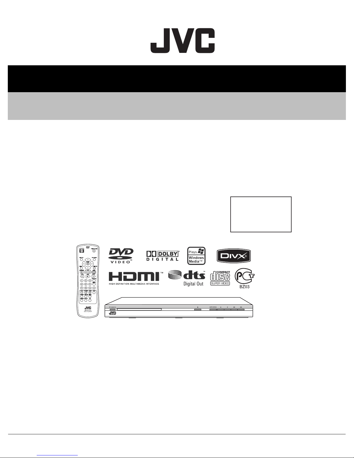
SERVICE MANUAL
DVD PLAYER
YD11920074SERVICE MANUAL
XV-N650BEU,XV-N650BEY,XV-N650BEK,
XV-N650BER,XV-N652SEU,XV-N652SEY,
XV-N652SEZ,XV-N652SEK,XV-N652SER
Area Suffix
EK ------------------------ U.K.
EU -------- Western Europe
EY -------- Northern Europe
EZ --------- Eastern Europe
ER ---- Russian Federation
COPYRIGHT © 2007 Victor Company of Japan, Limited
1 PRECAUTION. . . . . . . . . . . . . . . . . . . . . . . . . . . . . . . . . . . . . . . . . . . . . . . . . . . . . . . . . . . . . . . . . . . . . . . . . 1-3
2 SPECIFIC SERVICE INSTRUCTIONS . . . . . . . . . . . . . . . . . . . . . . . . . . . . . . . . . . . . . . . . . . . . . . . . . . . . . . 1-6
3 DISASSEMBLY . . . . . . . . . . . . . . . . . . . . . . . . . . . . . . . . . . . . . . . . . . . . . . . . . . . . . . . . . . . . . . . . . . . . . . . 1-7
4 ADJUSTMENT . . . . . . . . . . . . . . . . . . . . . . . . . . . . . . . . . . . . . . . . . . . . . . . . . . . . . . . . . . . . . . . . . . . . . . . 1-13
5 TROUBLESHOOTING . . . . . . . . . . . . . . . . . . . . . . . . . . . . . . . . . . . . . . . . . . . . . . . . . . . . . . . . . . . . . . . . . 1-14
COPYRIGHT © 2007 Victor Company of Japan, Limited
Only ver. ER
XV-N650BEU,XV-N650BEY,XV-N650BEK,XV-N650BER,
XV-N652SEU,XV-N652SEY,XV-N652SEZ,XV-N652SEK,XV-N652SER [D7P3]
TABLE OF CONTENTS
No.YD119
2007/4
Page 2
SPECIFICATION
XV-N650BEU,XV-N650BEY,XV-N650BEK,XV-N650BER,XV-N652SEU,XV-N652SEY,XV-N652SEZ,XV-N652SEK,XV-N652SER
General
Power requirements AC 220-240 V, 50/60 Hz
Power consumption 8 W
Dimensions (Approx.) 430 × 35 × 201 mm (17 × 1.4 × 7.9 inches) (W × H × D) without foot
Net weight (Approx.) 1.6 kg (3.5 lbs)
Operating temperature 5 °C to 35 °C (41 °F to 95 °F)
Operating humidity 5 % to 90 %
Outputs
VIDEO OUT 1.0 V (p-p), 75 Ω, sync negative, RCA jack × 1 / SCART (TO TV)
COMPONENT VIDEO OUT (Y) 1.0 V (p-p), 75 Ω,negative sync, RCA jack × 1
(Pb)/(Pr) 0.7 V (p-p), 75 Ω, RCA jack × 2
AUDIO OUT 2.0 Vrms (1 KHz, 0 dB), 600 Ω, RCA jack (L, R) × 1 / SCART (TO TV)
DIGITAL OUT (COAXIAL) 0.5 V (p-p), 75 Ω, RCA jack × 1
DIGITAL OUT (OPTICAL) 3 V (p-p), Optical jack × 1
System
Laser Power For DVD Wavelength : 653 to 663 nm
Output : 1.0 mW
For CD Wavelength : 770 to 810 nm
Output : 0.4 mW
Signal system PAL/NTSC
Frequency response DVD (PCM 96 kHz): 8 Hz to 44 kHz
DVD (PCM 48 kHz): 8 Hz to 22 kHz
CD: 8 Hz to 20 kHz
Signal-to-noise ratio More than 90 dB (ANALOG OUT connectors only)
Harmonic distortion Less than 0.02%
Dynamic range More than 95 dB (DVD/CD)
Accessories
Video cable (1), Audio cable (1), Remote control (1), Batteries (2)
Note:
Design and specifications are subject to change without prior notice.
1-2 (No.YD119)
Page 3
SECTION 1
PRECAUTION
1.1 Safety Precautions
(1) This design of this product contains special hardware and
many circuits and components specially for safety purposes. For continued protection, no changes should be made
to the original design unless authorized in writing by the
manufacturer. Replacement parts must be identical to
those used in the original circuits. Services should be performed by qualified personnel only.
(2) Alterations of the design or circuitry of the product should
not be made. Any design alterations of the product should
not be made. Any design alterations or additions will void
the manufacturers warranty and will further relieve the
manufacture of responsibility for personal injury or property
damage resulting therefrom.
(3) Many electrical and mechanical parts in the products have
special safety-related characteristics. These characteristics are often not evident from visual inspection nor can the
protection afforded by them necessarily be obtained by using replacement components rated for higher voltage, wattage, etc. Replacement parts which have these special
safety characteristics are identified in the Parts List of Service Manual. Electrical components having such features
are identified by shading on the schematics and by ( ) on
the Parts List in the Service Manual. The use of a substitute
replacement which does not have the same safety characteristics as the recommended replacement parts shown in
the Parts List of Service Manual may create shock, fire, or
other hazards.
(4) The leads in the products are routed and dressed with ties,
clamps, tubings, barriers and the like to be separated from
live parts, high temperature parts, moving parts and/or
sharp edges for the prevention of electric shock and fire
hazard. When service is required, the original lead routing
and dress should be observed, and it should be confirmed
that they have been returned to normal, after reassembling.
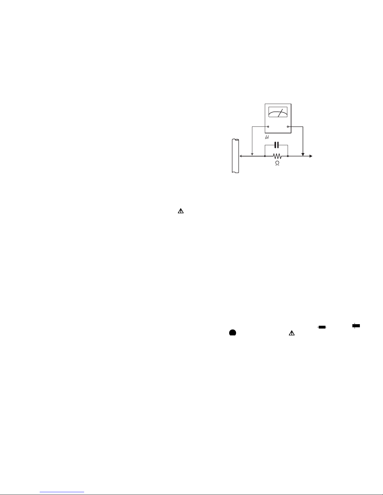
(5) Leakage shock hazard testing)
After reassembling the product, always perform an isolation check on the exposed metal parts of the product (antenna terminals, knobs, metal cabinet, screw heads,
headphone jack, control shafts, etc.) to be sure the product
is safe to operate without danger of electrical shock.Do not
use a line isolation transformer during this check.
• Plug the AC line cord directly into the AC outlet. Using a
"Leakage Current Tester", measure the leakage current
from each exposed metal parts of the cabinet, particularly any exposed metal part having a return path to the
chassis, to a known good earth ground. Any leakage current must not exceed 0.5mA AC (r.m.s.).
• Alternate check method
Plug the AC line cord directly into the AC outlet. Use an
AC voltmeter having, 1,000 ohms per volt or more sensitivity in the following manner. Connect a 1,500 ohm 10W
resistor paralleled by a 0.15 F AC-type capacitor between an exposed metal part and a known good earth
ground.
Measure the AC voltage across the resistor with the AC
voltmeter.
Move the resistor connection to each exposed metal
part, particularly any exposed metal part having a return
path to the chassis, and measure the AC voltage across
the resistor. Now, reverse the plug in the AC outlet and
repeat each measurement. Voltage measured any must
not exceed 0.75 V AC (r.m.s.). This corresponds to 0.5
mA AC (r.m.s.).
AC VOLTMETER
(Having 1000
ohms/volts,
or more sensitivity)
0.15 F AC TYPE
Place this
probe on
1500 10W
Good earth ground
1.2 Warning
(1) This equipment has been designed and manufactured to
meet international safety standards.
(2) It is the legal responsibility of the repairer to ensure that
these safety standards are maintained.
(3) Repairs must be made in accordance with the relevant
safety standards.
(4) It is essential that safety critical components are replaced
by approved parts.
(5) If mains voltage selector is provided, check setting for local
voltage.
1.3 Caution
Burrs formed during molding may be left over on some parts
of the chassis.
Therefore, pay attention to such burrs in the case of preforming repair of this system.
1.4 Critical parts for safety
In regard with component parts appearing on the silk-screen
printed side (parts side) of the PWB diagrams, the parts that are
printed over with black such as the resistor ( ), diode ( )
and ICP ( ) or identified by the " " mark nearby are critical for
safety. When replacing them, be sure to use the parts of the
same type and rating as specified by the manufacturer. (Except
the JC version)
each exposed
metal part.
(No.YD119)1-3
Page 4
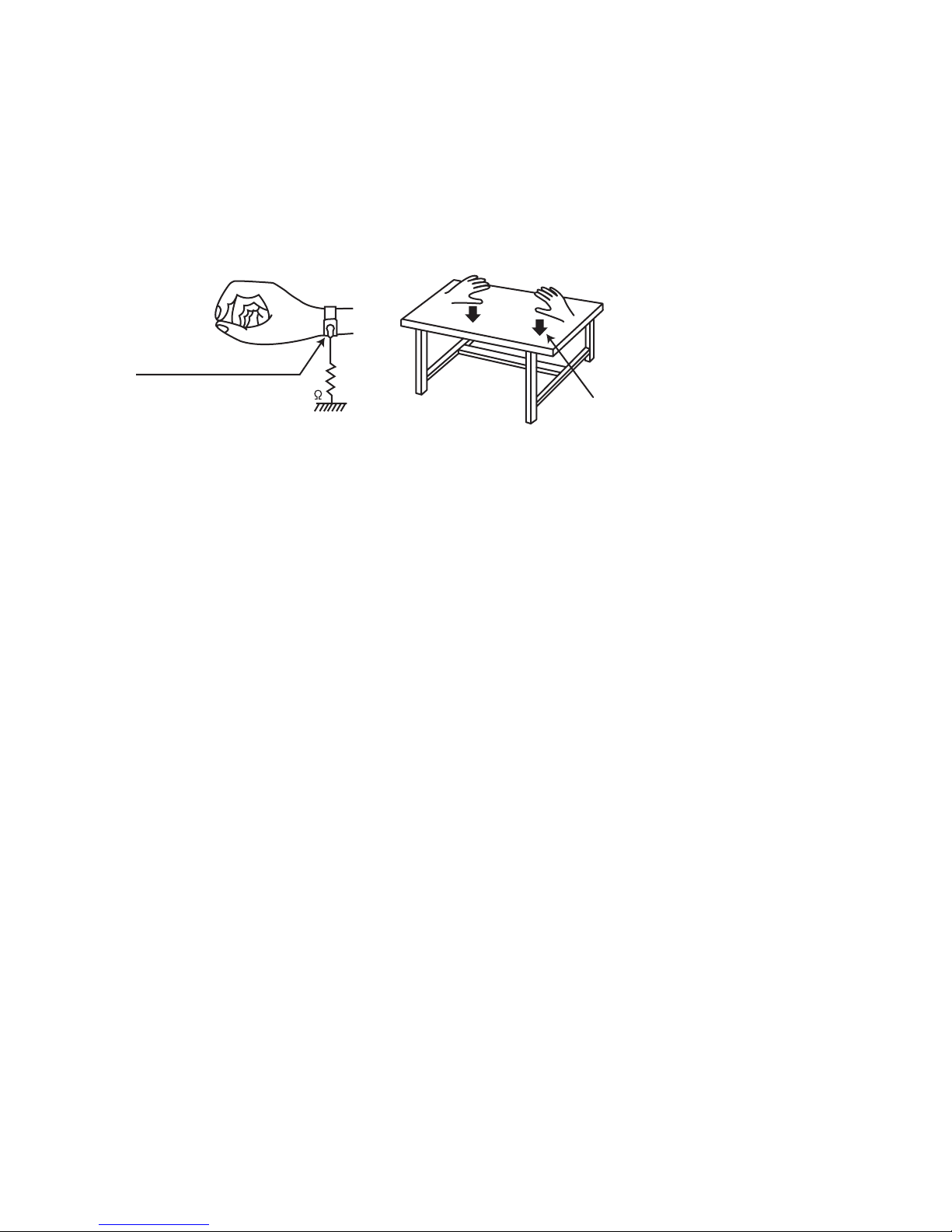
1.5 Preventing static electricity
Electrostatic discharge (ESD), which occurs when static electricity stored in the body, fabric, etc. is discharged, can destroy the laser
diode in the traverse unit (optical pickup). Take care to prevent this when performing repairs.
1.5.1 Grounding to prevent damage by static electricity
Static electricity in the work area can destroy the optical pickup (laser diode) in devices such as DVD players.
Be careful to use proper grounding in the area where repairs are being performed.
(1) Ground the workbench
Ground the workbench by laying conductive material (such as a conductive sheet) or an iron plate over it before placing the
traverse unit (optical pickup) on it.
(2) Ground yourself
Use an anti-static wrist strap to release any static electricity built up in your body.
(caption)
Anti-static wrist strap
1M
Conductive material
(conductive sheet) or iron palate
(3) Handling the optical pickup
• In order to maintain quality during transport and before installation, both sides of the laser diode on the replacement optical
pickup are shorted. After replacement, return the shorted parts to their original condition.
(Refer to the text.)
• Do not use a tester to check the condition of the laser diode in the optical pickup. The tester's internal power source can easily
destroy the laser diode.
1.6 Handling the traverse unit (optical pickup)
(1) Do not subject the traverse unit (optical pickup) to strong shocks, as it is a sensitive, complex unit.
(2) Cut off the shorted part of the flexible cable using nippers, etc. after replacing the optical pickup. For specific details, refer to the
replacement procedure in the text. Remove the anti-static pin when replacing the traverse unit. Be careful not to take too long
a time when attaching it to the connector.
(3) Handle the flexible cable carefully as it may break when subjected to strong force.
(4) I t is not possible to adjust the semi-fixed resistor that adjusts the laser power. Do not turn it.
1.7 Precautions of the safe use of battery
• Store the battery in a place where children cannot reach.If a child accidentally swallows the battery, consult a doctorimmediately.
• Do not recharge, short, disassemble or heat the battery or dispose of it in a fire.
Doing any of these things may cause the battery to give off heat, crack, or start a fire.
• Do not leave the battery with other metallic materials.Doing this may cause the battery to give off heat, crack, or start a fire.
• When throwing away or saving the battery, wrap it in tape and insulate; otherwise, the battery may start to give off heat, crack, or
start a fire.
• Do not poke the battery with tweezers or similar tools.Doing this may cause the battery to give off heat, crack, or start a fire.
• Dispose of batteries in the proper manner, according to federal, state, and local regulations.
1-4 (No.YD119)
Page 5
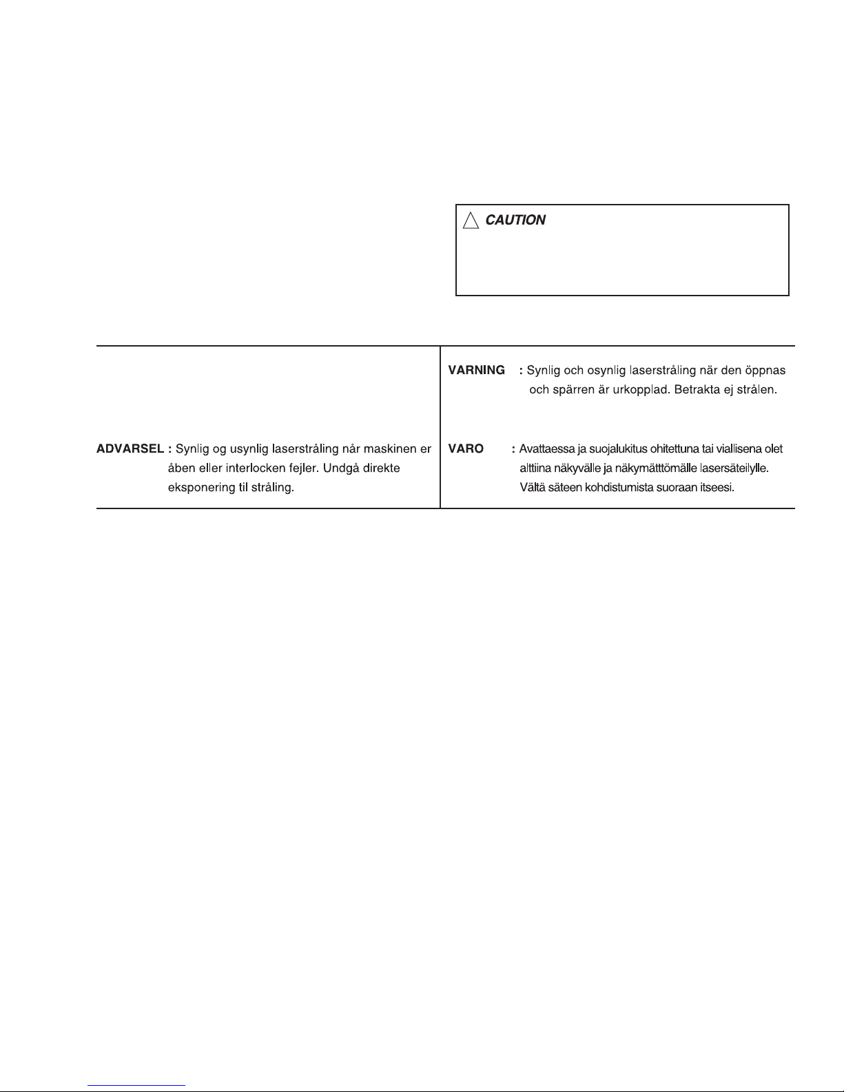
1.8 Important for laser products
!
1.CLASS 1 LASER PRODUCT
2.CAUTION : VISIBLE AND/OR INVISIBLE CLASS 1M
LASER RADIATION WHEN OPEN.
DO NOT STARE INTO BEAM OR VIEW DIRECTLY WITH
OPTICAL INSTRUMENTS.
3.CAUTION : There are no serviceable parts inside the
Laser Unit. Do not disassemble the Laser Unit. Replace
the complete Laser Unit if it malfunctions.
4.CAUTION : The laser products uses visible and / or
invisible laser radiation and is equipped with safety
switches which prevent emission of radiation when the
drawer is open and the safety interlocks have failed or are
defeated. It is dangerous to defeat the safety switches.
CAUTION : VISIBLE AND/OR INVISIBLE CLASS 1M
LASER RADIATION WHEN OPEN.
DO NOT STARE INTO BEAM OR VIEW
DIRECTLY WITH OPTICAL INSTRUMENTS.
5.CAUTION : If safety switches malfunction, the laser is able
to function.
6.CAUTION : Use of controls, adjustments or performance of
procedures other than those specified here in may result in
hazardous radiation exposure.
Please use enough caution not to
see the beam directly or touch it
in case of an adjustment or operation
check.
(No.YD119)1-5
Page 6
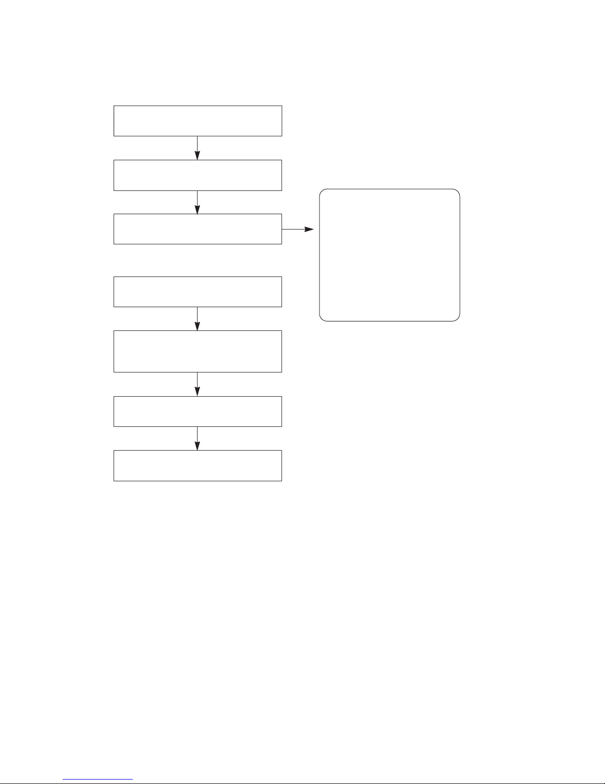
SPECIFIC SERVICE INSTRUCTIONS
2.1 SERVICE INFORMATION FOR EEPROM
POWER ON
SECTION 2
DVD LOGO Status (NO Disk status)
Remotecontrol
Pause key-->1-->4-->7-->2 in order.
Press number 0~8, Press charater
A~F (1~6 for a while)
Use arrow key (F D G E) to move
to approprite position and make
changes
Press pause key once
DETECT NEW EEPROM
(OPTION EDIT SCREEN)
MODEL : XV-N650B/XV-N652S
NAME HEX
OPT 1 00
OPT 2 00
OPT 3 00
OPT 4 00
OPT 5 00
OPT 6 00
OPT 7 00
OPT 8 00
Change will be applied when power
OFF-->ON.
1-6 (No.YD119)
Page 7
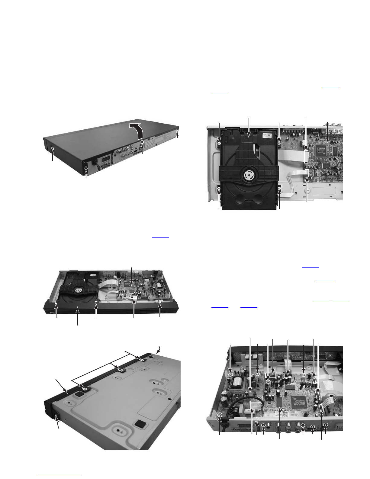
SECTION 3
TOP COVER
DISASSEMBLY
3.1 Main body section
3.1.1 Removing the top cover (See figure 1)
(1) Remove the two screws A attaching the top cover on both
sides of the main body.
(2) Remove the three screws B attaching the top cover on the
back of the main body.
(3) Raise the both sides and lower part of the rear of the top
cover, with opening them slightly in an outward direction.
And the top cover will be removed.
TOP COVER
TOP COVER
3.1.3 Removing the mechanism assembly (See figure 4)
• Prior to performing the following procedure, remove the top
cover and front panel assembly.
(1) Disconnect the card wire from connectors CN201
on the main board.
CN202
(2) Remove the four screws C attaching the mechanism as-
sembly.
Mechanism assembly
C
B
C
CN201
Main board
and
CN604
B
on the
Hook a
Hook a
A x 2
B
Fig.1
3.1.2 Removing the front panel assembly (See figure 2, figure 3)
• Prior to performing the following procedure, remove the top
cover.
(1) Disconnect the card wire from connector CN604
main board.
(2) Remove the eight hooks a, and then remove the front panel
assembly.
Main board
Hook a
Front panel assembly
Hook a
Fig.2
Hook a
CN202
CC
Fig.4
3.1.4 Removing the regulator board and main board (See
figure 5)
• Prior to performing the following procedure, remove the top
cover.
CN202
E
on the main
on the
, CN201,
CN201
(1) Disconnect the wire from connector CN603
board.
(2) Disconnect the power cord from connector PW101
regulator board.
(3) Remove the four screws D attaching the regulator board.
(4) Disconnect the card wire from connectors CN701
and CN604 on the main board.
CN202
(5) Remove the two screws E attaching the main board.
(6) Remove the three screws F and one screw G attaching the
main board with rear panel.
Regulator board
D
D
CN603
E
CN604
Front panel
assembly
Hook a
Fig.3
PW101
D
F
D
Main board
Fig.5
F G F
CN701
(No.YD119)1-7
Page 8
3.1.5 Removing the SCART terminal board (See figure 6)
• Prior to performing the following procedure, remove the top
cover, front panel assembly and mechanism assembly
(1) Disconnect the card wire from connector P3701 on the
SCART board.
(2) Remove the one screw H and one screw I attaching the
SCART terminal board.
SCART board
H
Fig.6
P3701
I
1-8 (No.YD119)
Page 9

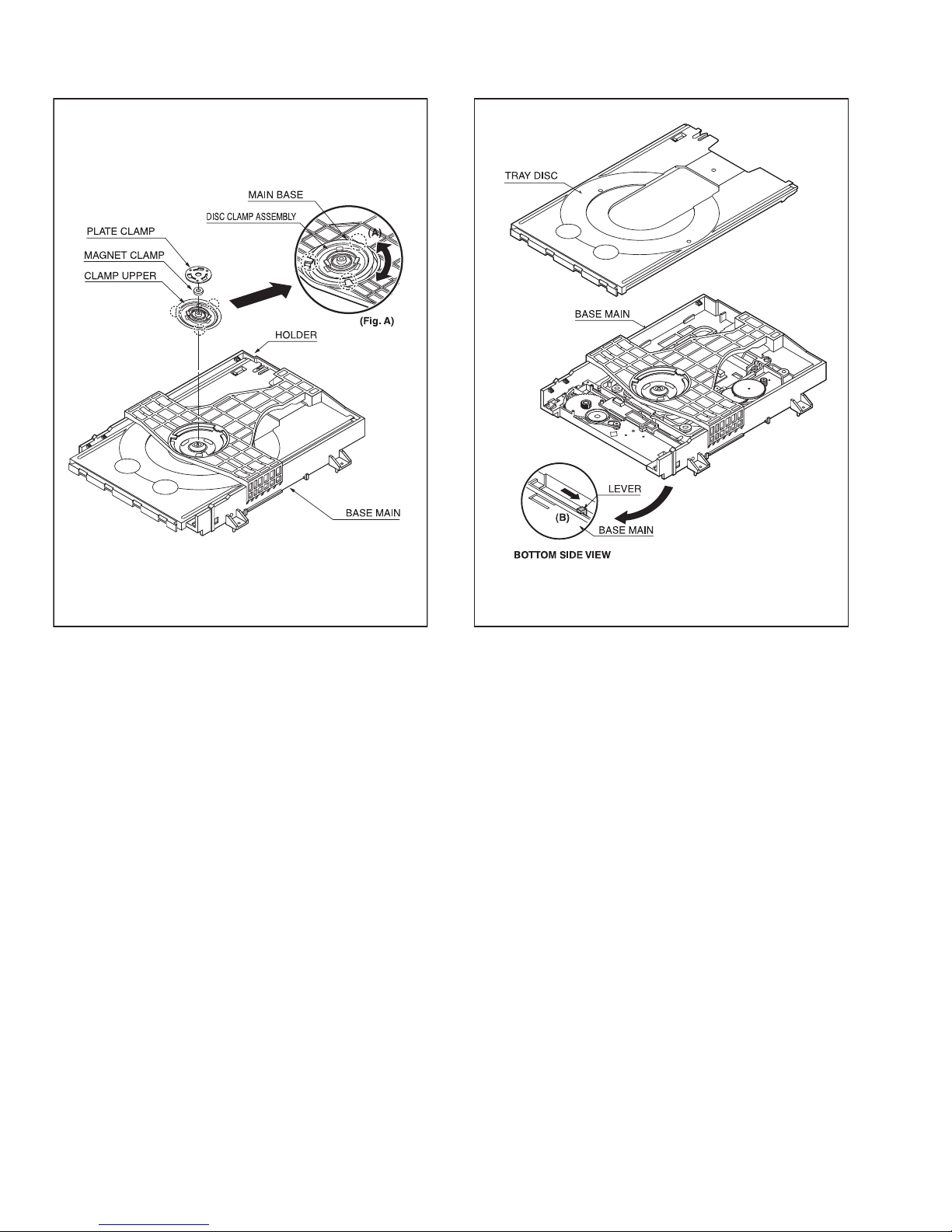
3.2 DVD MECHANISM PARTS LOCATION
• TOP VIEW (WITH TRAY)
• TOP VIEW (WITHOUT TRAY)
Procedure
Starting No.
Parts Fixing Type
Disass
embly
Fig-
ure
1 Main Base 4-1
12
Clamp Assembly Disc
4-1
1, 2 3 Plate Clamp 4-1
1, 2, 3 4 Magnet Clamp 4-1
1, 2, 3, 4 5 Clamp Upper 4-1
1 6 Tray Disc 4-2
1, 6 7
Base Assembly
Sled
4-3
4 Screws,
1, 2, 6 8 Gear Feed
1 Connector
4-3
1 Locking Tabs
1, 2, 6, 8 9 Gear Middle
1, 2, 6, 8,9 10 Gear Rack 1 Screw 4-3
1, 2, 7 11 Rubber Rear 4-3
1, 2, 7 12
Frame Assembly Up/Down
1 Screw Bottom 4-4
1, 2 13 Belt Loading 1 Locking Tab 4-4
1, 2 ,13 14 Gear Pulley 4-4
1, 2, 13, 14 15 Gear Loading 1 Locking Tab 4-4
1, 2, 7, 12,
13, 14
1, 2, 13 17
1,2,7,12,13,
14,15,16,17
16 Guide Up/Down 4-4
PWB Assembly
Loading
1 Locking Tab
1 Hook
2 Screw
Bottom 4-4
18 Base Main 2 Locking Tabs 4-4
• BOTTOM VIEW
Note
When reassembling, perform the procedure in reverse order.
The “Bottom” on Disassembly column of above Table indicates
the part should be disassembled at the Bottom side.
(No.YD119)1-9
Page 10
3.3 DVD MECHANISM DISASSEMBLY
Fig.4-1
3.3.1 MAIN BASE (FIG. 4-1)
3.3.1.1 Clamp Assembly Disc
(1) Place the Clamp Assembly Disc as Fig. (A)
(2) Lift up the Clamp Assembly Disc in direction of arrow(A).
(3) Separate the Clamp Assembly Disc from the Holder
Clamp.
3.3.1.1.1 Plate Clamp
(1) Turn the Plate Clamp to counterclockwise direction and
then lift up the Plate Clamp.
3.3.1.1.2 Magnet Clamp
3.3.1.1.3 Clamp Upper
Fig.4-2
3.3.2 TRAY DISC (FIG. 4-2)
(1) Insert and push a Driver in the emergency eject hole(A) at
the right side, or put the Driver on the Lever(B) of the Gear
Emergency and pull the Lever(B) in direction of arrow so
that the Tray Disc is ejected about 15~20mm.
(2) Pull the Tray Disc until it is separated from the Base Main
completely.
1-10 (No.YD119)
Page 11
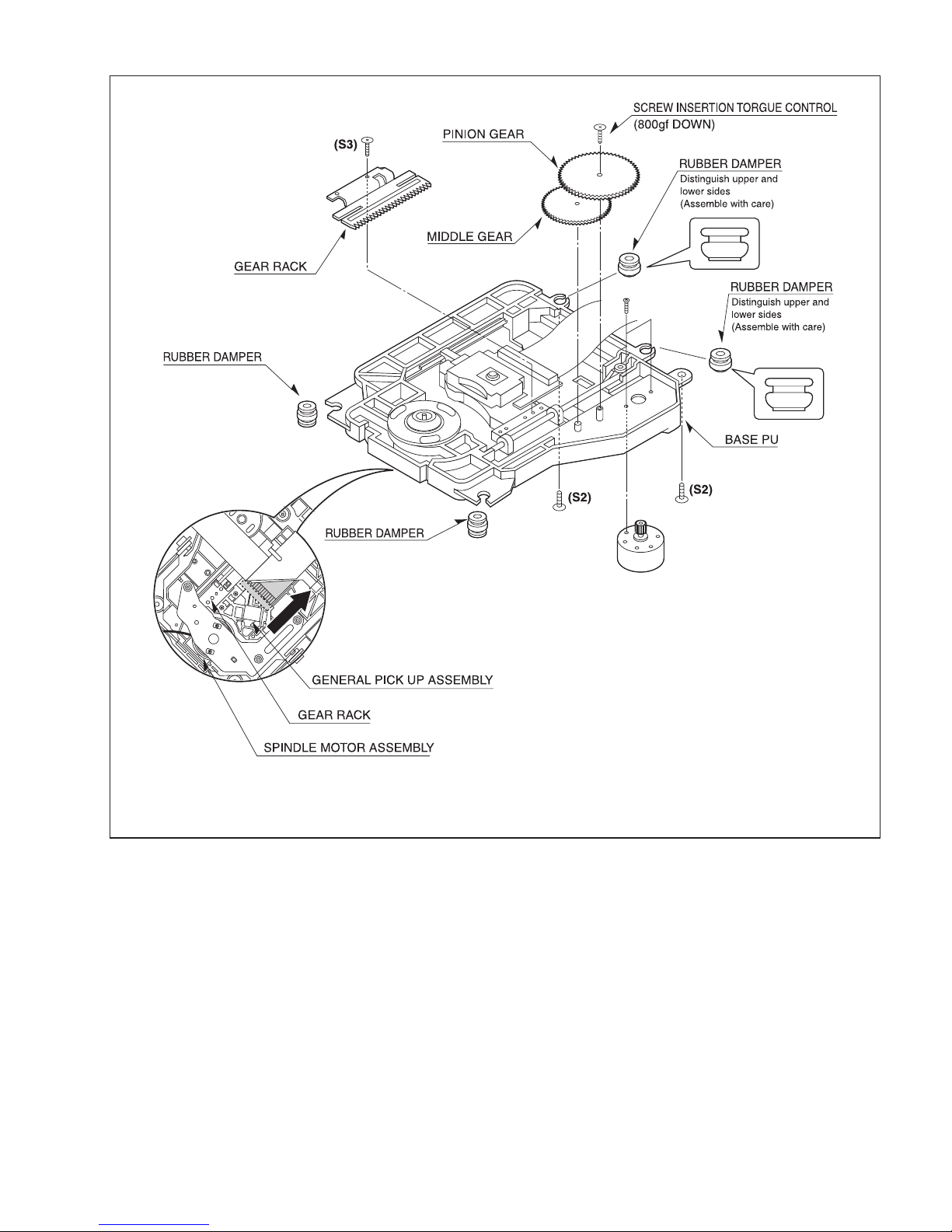
3.3.3 BASE ASSEMBLY SLED (FIG. 4-3)
(1) Release 4 Screw (S2).
(2) Disconnect the FFC Connector (C1)
3.3.3.1 Gear Feed
3.3.3.2 Gear Middle
Fig.4-3
3.3.3.3 Gear Rack
(1) Release the Scerw (S3)
3.3.4 RUBBER REAR (FIG. 4-3)
(No.YD119)1-11
Page 12
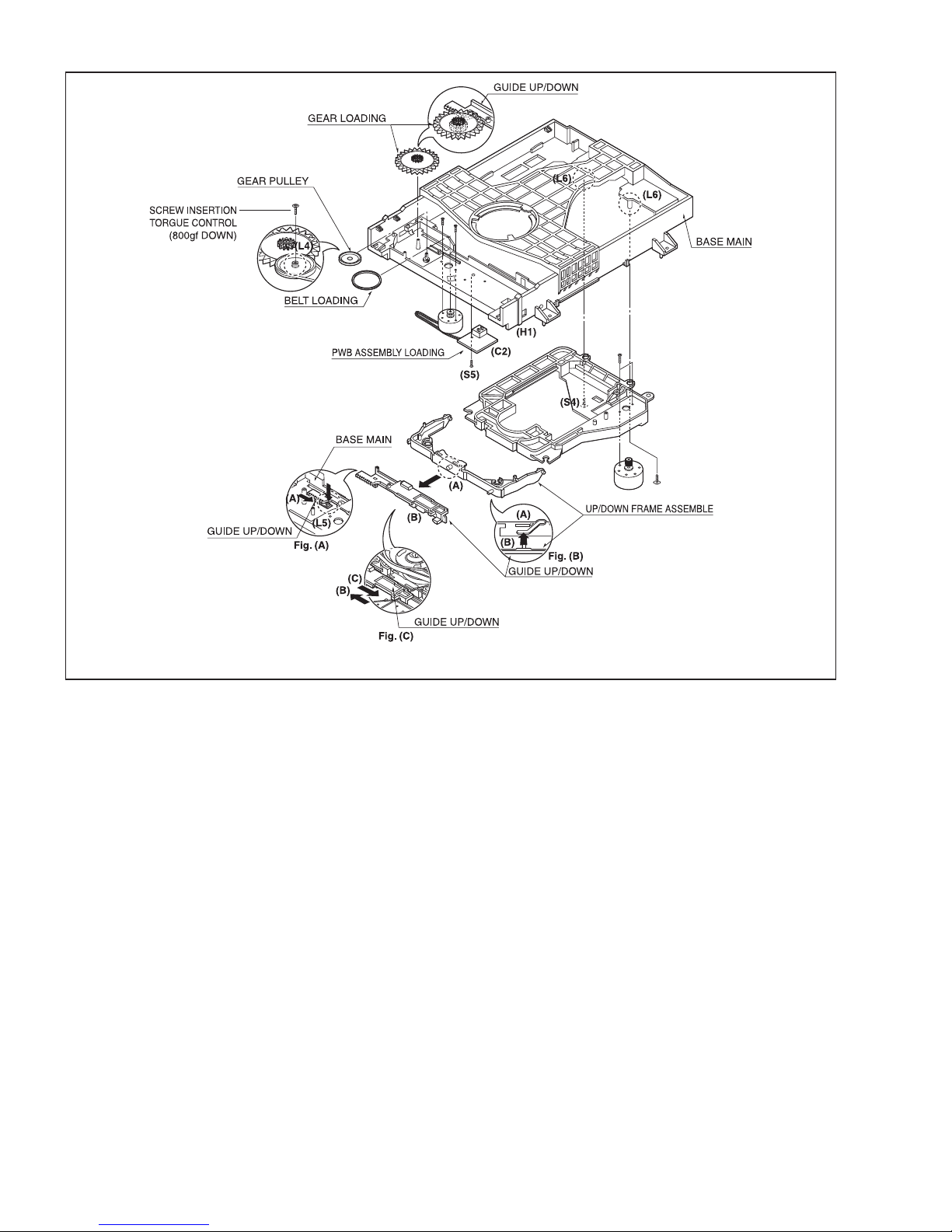
3.3.5 FRAME ASSEMBLY UP/DOWN (FIG. 4-4)
Note
Put the Base Main face down (Bottom Side)
(1) Release the screw (S4)
(2) Unlock the Locking Tab (L3) in direction of arrow and then
lift up the Frame Assembly Up/Down to separate it from the
Base Main.
Note
• When reassembling move the Guide Up/Down in direction of
arrow(C) until it is positioned as Fig.(C).
• When reassembling insert (A) portion of the Frame Assem-
bly Up/Down in the (B) portion of the Guide Up/Down as
Fig.(B)
3.3.6 BELT LOADING(FIG. 4-4)
Note
Put the Base Main on original position(Top Side)
3.3.7 GEAR PULLEY (FIG. 4-4)
(1) Unlock the Locking Tab(L4) in direction of arrow(B) and
then separate the Gear Pulley from the Base Main
Fig.4-4
3.3.8 GEAR LOADING (FIG. 4-4)
3.3.9 GUIDE UP/DOWN (FIG. 4-4)
(1) Move the Guide Up/Down in direction of arrow(A) as
Fig.(A)
(2) Push the Locking Tab(L5) down and then lift up the Guide
Up/Down to separate it from the Base Main.
Note
When reassembling place the Guide Up/Down as Fig.(C) and
move it in direction arrow(B) until it is locked by the Locking
Tab(L5). And confirm the Guide Up/Down as Fig.(A)
3.3.10 PWB ASSEMBLY LOADING (FIG. 4-4)
Note
Put the Base Main face down(Bottom Side)
(1) Release 1 Screws(S5)
(2) Unlock the Loading Motor (C2) from the Hook (H1) on the
Base Main.
(3) Unlock 2 Locking Tabs(L6) and separate the PWB Assem-
bly Loading from the Base Main.
3.3.11 BASE MAIN (FIG. 4-4)
1-12 (No.YD119)
Page 13
SECTION 4
ADJUSTMENT
4.1 The version of the firmware is confirmed
(1) The power supply is turned ON.
(2) Press the "SETUP" button of the remote control unit to select "16:9" in "Display Mode".
TV Aspect
Display Mode
TV Output Select
4:3
16:9
Prev. Move Enter
(3) Press the buttons of the remote control unit in the following order.
"1"→"3"→"9"→"7"→"1"→"3"→"9"→"ENTER"
(4) When the TV display changes as shown as below, check the firmware version.
SYSTEM INFORMATION
MODEL : JVC_DV_JV070D202230BZIH
CHIP I.D : VADDIS_888
Firmware version
of main body
SERVO VER. : 40.52
MICOM VER. : V1.372
Check Sum : B6B3
PROM OPTION 55 53 00 d3 03 55 f4 00
Factory Reset..Done.
(5) Press the "ENTER" button of the remote control unit to display the initial screen.
4.2 Updating the firmware
• Firmware update disc supports CD-R media.
• When firmware update is necessary, information is available from the web site of DIGITAL VIDEO STORAGE, CS group.
4.2.1 Creating an update disc
Please check the details of the update disc creation method with JS-NET.
(1) Down load the update file from JS-NET.
(2) Write the update file into CD-R. Pay attention in the following points when writing the update disc.
• Make sure to write in "Disc at Once".
• Set the file compatibility to "JOLIET format".
If the writing method is not correct, the update results in an error.
4.2.2 Update procedure
(1) Turn the power of the main unit ON, and insert the update disc.
(2) The TV screen shows the display as shown as below after a while, select "Start" and then press "ENTER" with the remote control
unit.
Firmware upgrade
Cancel Start
(3) When "Erase and Program Do Not Power Off" is displayed on the TV screen and the tray opens in a few seconds, remove the
update disc.
(4) Wait for about three minutes.
(5) When the firmware updating is completed, the tray closes automatically and the power is turned OFF.
(6) Turn the power ON, and then check the firmware version.
(No.YD119)1-13
Page 14
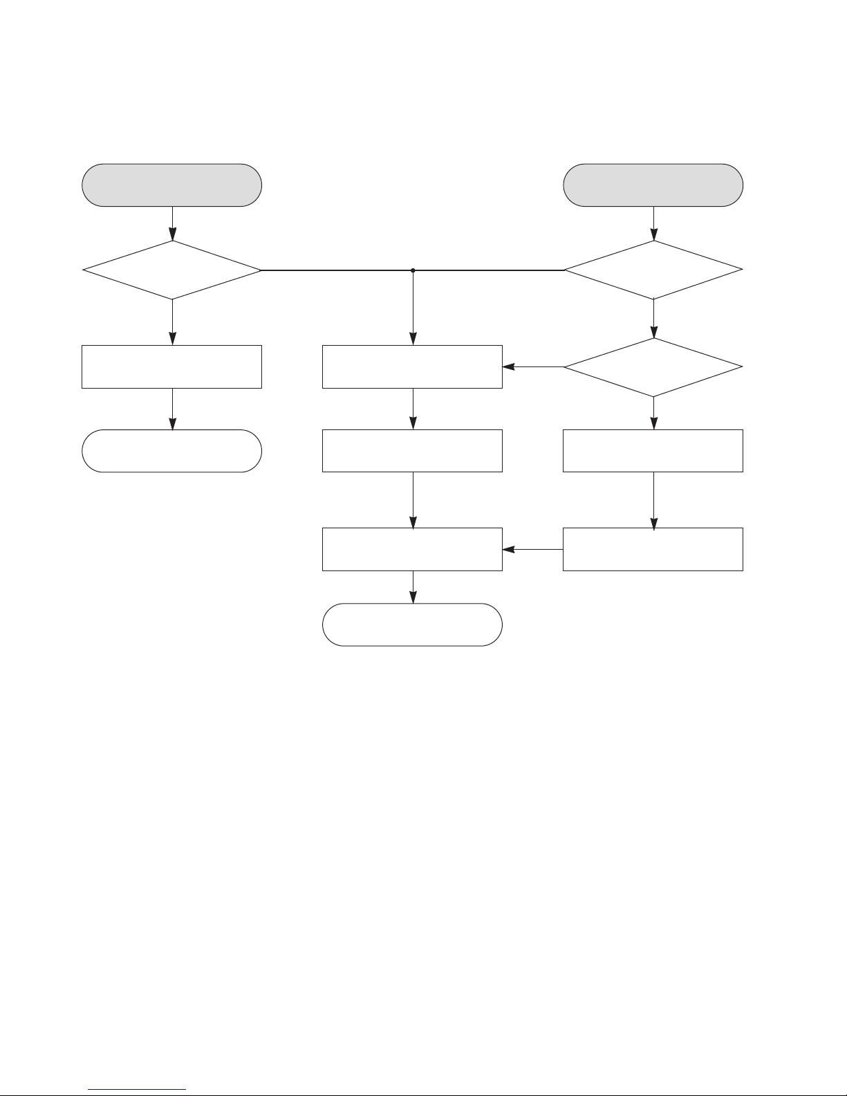
TROUBLESHOOTING
5.1 ELECTRICAL TROUBLESHOOTING GUIDE
5.1.1 POWER CHECK FLOW
SECTION 5
A. B.
No 5V No 3.3VA
Is 3.3VA
NO
NO
section working?
YES
Is 5.6V present at
collector of Q126?
YES
No 3.3VA
NO
Replace Q126. Check FR101 Replace Q121.
Is there a DC voltage at
NO
cathode of D105 or D107?
Is 3.3VA
section working?
YES
Is 3.3V
present at emitter
of Q121?
YES
YES
Check D105/D106/D107/
D108 and replace.
YES
Replace IC101.
1-14 (No.YD119)
Page 15
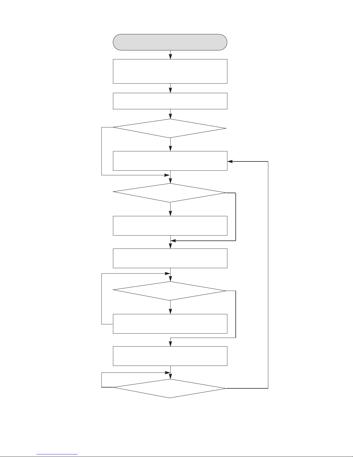
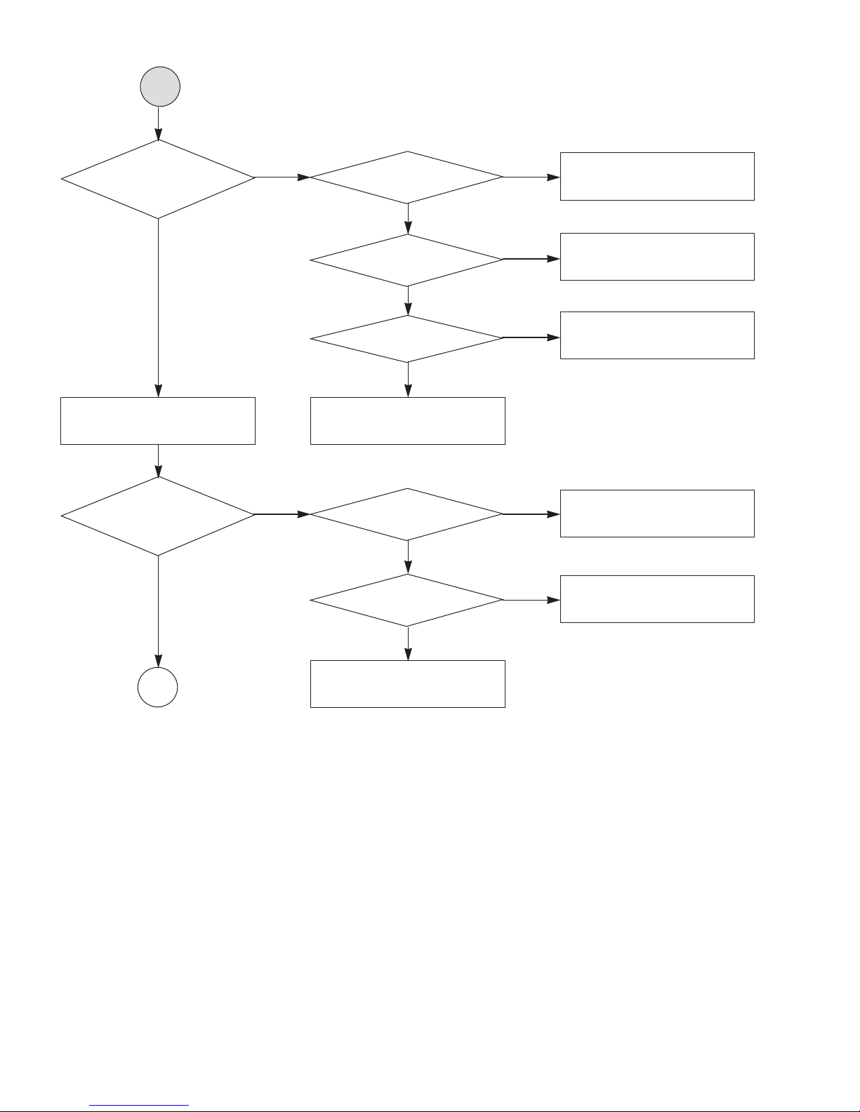
5.1.2 SYSTEM OPERATION FLOW
Power on
1. 186 CPU initializes SERVO, DSP &
RISC registers
2. Write RISC code to SDRAM
3. Reset RISC
Show LOGO
YES
Tray closed?
NO
Tray close to closed position
SLED at inner side?
NO
SLED moves to inner position
1. Judge whether have disc and disc type
2. Jump to related disc reading procedure
Recieve
OPEN/CLOSE key?
YES
YES
1. Execute pressed key & IR key
2. System operation routine loop
1. Stop playback & open tray
2. Display tray open message & LOGO
NO
NO
YES
Receive CLOSE key?
(No.YD119)1-15
Page 16
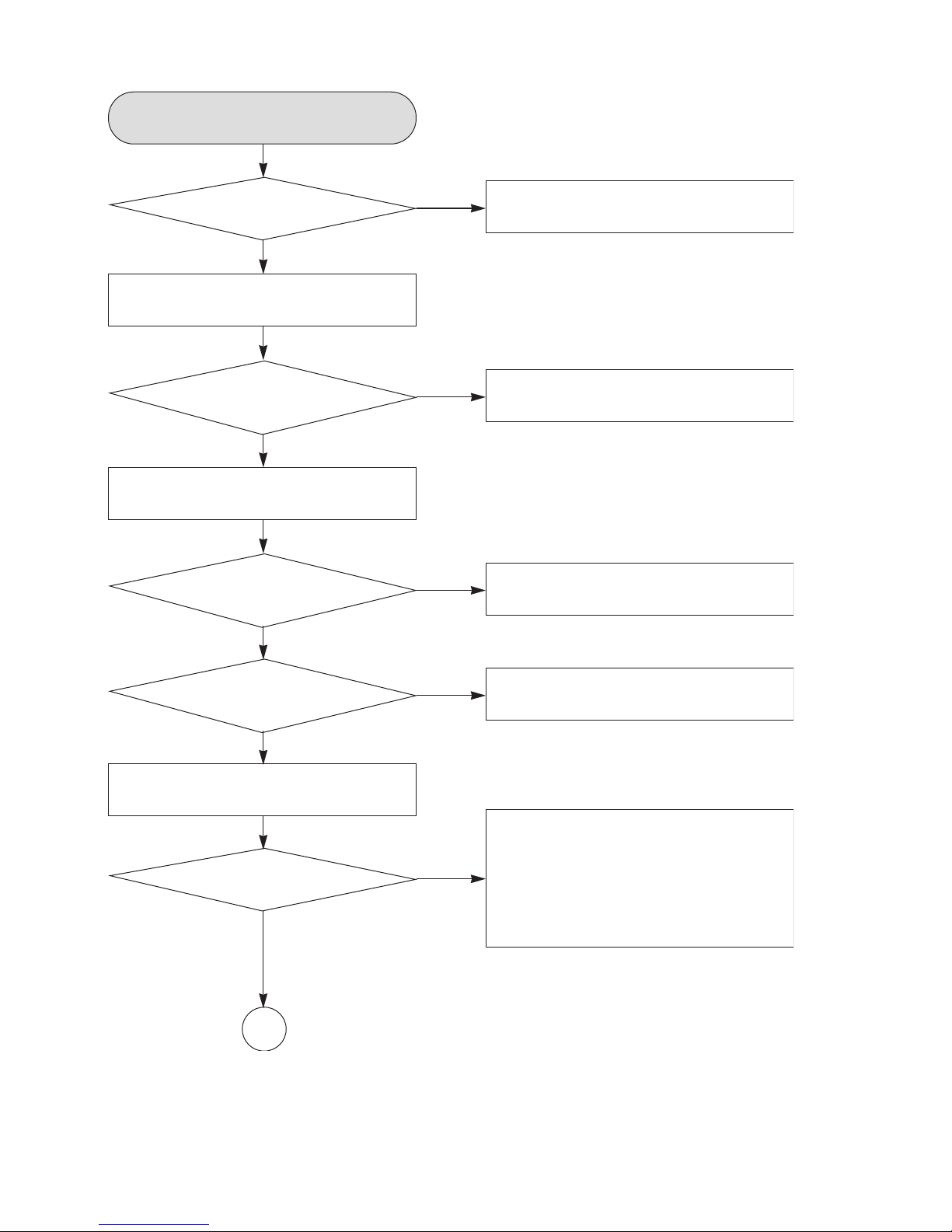
5.1.3 SYSTEM TEST FLOW
TEST
Check the AC
Voltage power PCBA (110V or
220V)
YES
Switch on the power PCBA
Is the DC
voltage outputs OK?
(5V, 3.3V, 12V, 5.6V
MOTOR)
YES
Make sure the main PCBA don't
short on VCC and switch it on.
YES
Is 3.3V
outputs normal on main
PCBA?
YES
NO
NO
NO
Replace power PCBA or AC transformer.
Repair or replace power PCBA
Check the regulators or related diodes.
Is 1.8V voltage
normal for ZORAN IC
YES
Connect to PC RS232 cable and
update the FLASH memory code.
Update FLASH
successfully?
YES
A
NO
NO
1. Check Q203.
2. Check D201.
3. Check IC102.
1. Check 27MHz system clock.
2. Check system reset circuit.
3. Check FLASH R/W enable signal PRD,
RWR.
4. Check RS232 SIGNALS.
5. Check FLASH memory related circuit.
1-16 (No.YD119)
Page 17
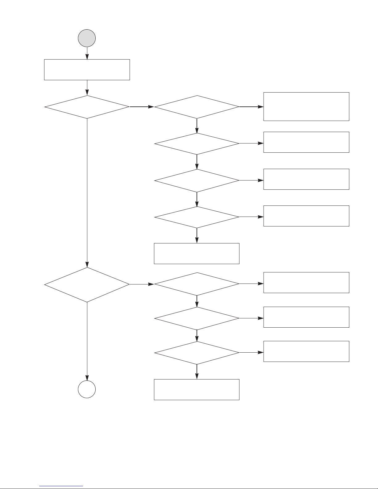
A
RESET or power on.
Show LOGO?
YES
NO NO
Flash
memory operates
properly?
YES
SDRAM
NO
works properly?
YES
ZR36888
NO
VIDEO outputs
properly?
YES
Have TV
NO
signal output?
YES
Check AV cable
connection to TV set.
Check connection lines
between FLASH & ZR36888
and the FLASH access time
whether is suitable or not.
Check connection lines
between SDRAM & ZR36888
and the SDRAM is damaged.
Check the related circuit of
ZR36888
Check the filtering and amp
circuit of TV signal.
move inside when it is not
Does tray
at closed position?
YES
B
NO
Normal
OUTSW & INSW
signals?
YES
Normal
OPEN & CLOSE
signal?
YES
Normal
LOAD+ & LOAD
signal?
YES
Check the cable
connection between main
PCBA and loader.
NO
NO
NO
Check the load OPEN &
CLOSE switch
Check the tray control IO
pins on ZR36888 & AM5869S
Check the tray control
amplifying circuit on motor
driver.
(No.YD119)1-17
Page 18
B
Does the
SLED move
to inner side when it is at
outer position?
YES
Do not put in disc and
tray close.
Optical Lens has
movements for searching
Focus?
Motor
driver MUTE pin
is high?
YES
Is SLED_S
DC Level higher than
1.65V?
YES
SLED+
and SLED- output
properly?
YES
Check the cable connection
with MECHA.
Proper
FOCUS_S outputs to
motor driver?
YES
NONO
NO
NO
NONO
Check the connection line of
MUTE signal.
Check the related circuit of
FMSO.
Check the amp circuit on
motor driver.
Check FOCUS_S connection
on ZR36888 and motor driver.
C
YES
Proper
FACT+ & FAC
toutputs?
YES
Check cable connect on
with pick-up head.
NO
Check the amp circuit on
motor driver.
1-18 (No.YD119)
Page 19

C
Laser
turns on when reading
disc?
YES
Put disc in?
YES
Disc ID is correct?
NO NO
LD_DVD or
LD_CD output
properly?
YES
Collector
NO
voltage of power transistor
is OK?
YES
Check cable connection
between transistor output
and pick-up head.
NO
Laser off
NO
Proper RF signal
NO
on ZR36888?
YES
Check the laser power circuit
on ZR36888 and connecting
to power transistor.
Check the related circuit on
laser power transistor
Check the related circuit
on ZR36888 RFL signal.
YES
Does
spindle rotate?
YES
D
Check LD_DVD &
LD_CD signal
NO NO
SPINDLE_S signal on
Proper
ZR36888
YES
SP+ & SP- output
NO
properly?
YES
Check the cable connection
between spindle and main
PCBA.
Check SPINDLE_S related
circuit on ZR36888.
Check the spindle control
amp circuit of motor driver.
(No.YD119)1-19
Page 20

D
Focus on OK?
YES
Track on OK?
YES
NO NO
signals on A, B, C, D of
Proper
ZR36888
YES
Check FE signal
NO
on ZR36888
YES
Check FOCUS_S signal
on ZR36888
NO NO
Normal
TE signal on
ZR36888?
YES
Properly
NO
TRACK_S signal on
ZR36888?
YES
TACT+ & TACT-
NO
output properly?
Check connections between
ZR36888 and pick-up head.
Check the FOCUS_S
connection on ZR36888
and motor driver.
Check the related
circuit on ZR36888
Check the TRACK_S
connection on ZR36888
and motor driver.
Check the tracking control
amp circuit on motor
driver.
Disc is play?
YES
E
NO
YES
Check cable connection on
pick-up head.
Check RF signal waveform.
1-20 (No.YD119)
Page 21

E
Normal
audio output when disc
playback?
YES
Normal
IR.VFD & Front panel
key functions?
YES
NO
Audio DAC
received correct data
NO
stream?
YES
Normal
NO
audio DAC out?
YES
Check audio filter,
amplify, mute circuit.
Commu-
NO NO
nications between
IR.VFD Front panel key
& ZR36888 is
normally?
YES
Check connection between
ZR36888 & audio DAC.
Check the related
circuit of Audio DAC.
Check communication lines
on ZR36888
TEST END
Check the cable connection
on front panel.
(No.YD119)1-21
Page 22

5.2 DETAILS AND WAVEFORMS ON SYSTEM TEST AND DEBUGGING
5.2.1 SYSTEM 27MHz CLOCK, RESET, FLASH R/W SIGNAL
1) ZR36888 main clock is at 27MHz (X601)
3.1V, 27MHz
Fig.1-1
2) ZR36888 reset is low active.
3.3VA
PWR_CTL
RESET
Fig.1-2
3.3VA
RESET
PWR_CTL
1-22 (No.YD119)
Page 23

5.2.2 SDRAM CLOCK
1) SDRAM clock is at 143MHz
CLK=143MHz, Vp-p=3.3V
1
5.2.3 TRAY OPEN/CLOSE SIGNAL
1) Tray open/close waveform
1
IC603 38PIN
Fig.2-1
OPEN
1
1
2
2
3
4
OPEN CLOSE
CLOSE
LM-
LM+
Fig.3-1
3
4
IC201
(No.YD119)1-23
Page 24

2) Tray open waveform
OPEN
CLOSE
LM-
3) Tray close waveform
Fig.3-2
LM+
OPEN
CLOSE
LM-
LM+
OPEN
CLOSE
LM+
LM-
Fig.3-3
1-24 (No.YD119)
Page 25

5.2.4 SLED CONTROL RELATED SIGNAL (NO DISC CONDITION)
SLED_S
1
DRVSB
2
SLED+
3
SLED-
4
Fig.4-1
5.2.5 LENS CONTROL RELATED SIGNAL (NO DISC CONDITION)
FOCUS_S
1
FOCUS+
1
2
3
4
1
2
FOCUS-
3
2
3
Fig.5-1
(No.YD119)1-25
Page 26

5.2.6 LASER POWER CONTROL RELATED SIGNAL (NO DISC CONDITION)
VR_CD
DVD_LD
CD_LD
Fig.6-1
5.2.7 DISC TYPE JUDGEMENT WAVEFORM
FACT+
1
FE
SBAD
Fig.7-1(DVD)
1
1-26 (No.YD119)
Page 27

2
Fig.7-2(DVD)
FACT+
FE
SBAD
2
FACT+
FE
Fig.7-3(CD)
SBAD
2
2
Fig.7-4(CD)
FACT+
FE
SBAD
(No.YD119)1-27
Page 28

5.2.8 FOCUS ON WAVEFORM
1
2
3
Fig.8-1(DVD)
1
FE
FOCUS
FACT+
FACT-
3
2
4
FE
4
FOCUS
5
FACT+
6
FACT-
6
5
Fig.8-2(CD)
1-28 (No.YD119)
Page 29

5.2.9 SPINDLE CONTROL WAVEFORM (NO DISC CONDITION)
1
SPINDLE_S
1
SP+
2
SP-
3
2
3
IC201
Fig.9-1(DVD)
(No.YD119)1-29
Page 30

5.2.10 TRACKING CONTROL RELATED SIGNAL (SYSTEM CHECKING)
TE
1
TRACK_S
1
2
TACT+
3
TACT-
Fig.10-1(DVD)
TE
1
TRACK_S
2
3
2
TACT+
3
TACT-
Fig.10-2(CD)
1-30 (No.YD119)
Page 31

5.2.11 RF WAVEFORM
1
Fig.11-1
5.2.12 ZR36888 AUDIO OPTICAL AND COAXIAL OUTPUT (SPDIF)
1
JIG202 & CN201 2PIN
1
1
R644 & IC601 126PIN
Fig.12-1
(No.YD119)1-31
Page 32

5.2.13 ZR36888 VIDEO OUTPUT WAVEFORM
1) Full colorbar signal (CVBS)
2
1
2) Y
2
JK701 2PIN
Fig.13-1
1
JK701 13PIN
Fig.13-2
1-32 (No.YD119)
Page 33

3) C
K
3
JK701 14PIN
Fig.13-3
5.2.14 AUDIO OUTPUT FROM AUDIO DAC
1) AUDIO L/R
1kHz 0dB
3
1
1
2
2) Audio Related Signal
2
JK701 5, 8PIN
Fig.14-1
AOUT0
ABCK
ALRCL
Fig.14-2
(No.YD119)1-33
Page 34

Victor company of Japan, Limited
DIGITAL VIDEO STORAGE CATEGORY 12, 3-chome, Moriya-cho, Kanagawa-ku, Yokohama-city, Kanagawa-prefecture, 221-8528, Japan
(No.YD119)
Printed in Japan
VPT
Page 35

SCHEMATIC DIAGRAMS
DVD PLAYER
XV-N650BEU,XV-N650BEY,XV-N650BEK,
XV-N650BER,XV-N652SEU,XV-N652SEY,
XV-N652SEZ,XV-N652SEK,XV-N652SER
CD-ROM No.SML200704
Area Suffix
EK ------------------------ U.K.
EU -------- Western Europe
EY -------- Northern Europe
EZ --------- Eastern Europe
ER ---- Russian Federation
Only ver. ER
XV-N650BEU,XV-N650BEY,XV-N650BEK,XV-N650BER,
XV-N652SEU,XV-N652SEY,XV-N652SEZ,XV-N652SEK,XV-N652SER [D7P3]
COPYRIGHT 2007 Victor Company of Japan, Limited
No.YD119SCH
2007/4
Page 36

Page 37

!
CHARTS AND DIAGRAMS
NOTES OF SCHEMATIC DIAGRAM
Safety precautions
The Components indentified by the symbol are
critical for safety. For continued safety, replace safety
critical components only with manufacturer's recommended parts.
1. Units of components on the schematic diagram
Unless otherwise specified.
1) All resistance values are in ohm. 1/6 W, 1/8 W (refer to
parts list).
Chip resistors are 1/16 W.
K: KΩ(1000Ω), M: MΩ (1000KΩ)
2) All capacitance values are in µF, (P: PF).
3) All inductance values are in µH, (m: mH).
4) All diodes are 1SS133, MA165 or 1N4148M (refer to parts
list).
2. Indications of control voltage
AUX : Active at high.
AUX or AUX(L) : Active at low.
3. Interpreting Connector indications
Note: If the voltages are not indicated on the schematic
diagram, refer to the voltage charts.
123
2.5
(5.0)
1.8
PB and REC modes
(Voltage of PB and REC modes
are the same)
PB mode
REC mode
4. Voltage measurement
1) Regulator (DC/DC CONV) circuits
REC : Colour bar signal.
PB : Alignment tape (Colour bar).
— : Unmeasurable or unnecessary to measure.
2) Indication on schematic diagram
Voltage indications for REC and PB mode on the schematic diagram are as shown below.
6. Indication of the parts for adjustments
The parts for the adjustments are surrounded with the circle
as shown below.
7. Indication of the parts not mounted on the circuit board
“OPEN” is indicated by the parts not mounted on the circuit
board.
R216
OPEN
1
2
3
1
2
3
1
2
3
1
4
2
3
Removable connector
Wire soldered directly on board
Non-removable Board connector
Board to Board
Connected pattern on board
The arrows indicate signal path
Note: The Parts Number, value and rated voltage etc. in
the Schematic Diagram are for references only.
When replacing the parts, refer to the Parts List.
CIRCUIT BOARD NOTES
1. Foil and Component sides
1) Foil side (B side) :
Parts on the foil side seen from foil face (pattern face)
are indicated.
2) Component side (A side) :
Parts on the component side seen from component face
(parts face) indicated.
2. Parts location guides
Parts location are indicated by guide scale on the circuit board.
Parts location are indicated by guide scale on the circuit board.
LOCATION
REF No.
IC101 B C 6 A
IC
Category : IC
Horizontal “A” zone
Vertical “6” zone
B : Foil side
(A : Component side)
C : Chip component
D : Discrete component)
2-1 2-2
Page 38

A
1
2
3
4
5
BCDEFG
Block diagrams
M
M
DISC
SPINDLE
MOTOR
LOADING
MOTOR
DECK MECHA NISM
DVD : A,B,C,D,RF
CD : A,B,C,D,E,F,RF
PICK
UP
B/Pb
IC604
MX29LV160TTC
16/32BIT
FLASH RO
M
MEMAD[0:19]
FLASHCS-
MEMWR-
MEMR
D-
RAMDAT[00:
15]
CVBS
R/Pr G/Y
TV_DAC[0:3]
Y
C
IC605
S524C80D80
EEPROM
LOAD[+,-]
FACT[+,-]
TACT[+,-]
SP [+,-]
SLED
(FEEDING)
MOTO
R
SLED[+,-]
M
V33DA
V33A
V18A/V33A
IC701
MM1692XVBE
VIDEO BUFFE
R
ASPDIF
COAXIAL
CD_LD,DVD_LD,V
C
5.6VA
INSW,OUTSW
MEMDA[0:15]
I2CCLK/MC
IC603
ESMT_M12L64164A
4M/16BIT
SDRAM
V33A
RAMAD[00:11]
RAMCKE
PCLK
RAMBA
RAMCS1
RAMDQM
RAMWE
RAMCAS
RAMRA
S
I2CDAT
/MD
IC601
ZORAN ZR36888
RF+DSP MPEG IC
5V
YC_MIX
OPEN,CLOSE,SLED_S,SPINDLE_S,FOCUS_S,TRACK_S
CD_DVD, VR_CD,VR_DV
D
CD_DVD
CN601
CN602
Dow nload
I/F
DUPTR0
IC201
AM5869S
Motor Dri v
e
DRVSB
PICKSEL
KEY Input
5V
12V
27MHz
RC901
R/C
IC901
ETK6203
LED DRIVER
IR
POWER
BOARD
POWCTL_H
3.3V
3.3VA
DIG901
LED Cloc
k
5V
Din
Dout
CLK STB
3
Power
Key
Power
On
AC 90V~240V
50HZ/60H
z
5.6VA
3.3VA
RESET
SPDL_SENS+ ,1.8VA
DUPTD0
12V
AL
AR
IC703
Audi o Op-amp
AZ45
80M
AL
AR
JK705
HDMI
Jack
HDMI5V
CN610
USB_DN
USB_
DP
To USB2.0
Boar
d
Optical
Optio
n
Over all
IC606
KIA7027
RESET IC
2-3 2-4
Page 39

A
1
2
3
4
5
BCD EFG
8V
3.3V
FILTER
SWIT
CHING IC
TRANS
FEED B.
3.3VA
RECTIFIE
R(5.6V)
RECTIFIE
R(9.5V)
LPF
RECTIFIE
R(14V)
LPF
12V
PWR CT
L
5V
5.6V(M)
/ 5.6VA
RECTIFIE
R(3.4V)
LPF
AC100~240V
RECTIFIER
REG.
T/ W
Power regulator (SMPS) section MPEG & Memory (ZR36888) section
IC605
EEPRO
M
IC604
FLASH MEMORY
(16 M )
VIDEO
In
In
terf
terf
ace
AUD
AUD
IO
In
In
terface
IC901
IC901
LED
D
DRI
DRI
VE IC
IC
IC603
SDRAM
64M
RAMAD[00:11] ,RAMCKE
PCLK ,RAMBA,RAMCS1
RAMDQM ,RAMWE
RAMCAS
RAMRAS
RAMDAT
[00:15]
X60
X60
1
27MH
27MH
z
C_Y,S_Y
SY_Pr_OUT,Y_OUT,SC_Pb_out
RGB_SEL,16_9_H
AMCLK,ALRCK,ABCK
D_MUTE
AOUT0.ML
I2CCLK/MC, I2CDAT/MD
ASPDIF
FLASHCSMEMWRMEMRD
MEMAD[0:19]
MEMD
A[0:15]
DIN ,DO
UT
CLK,
STB
IC606
RESET
IC
RESET
I2CCLK/MC
I2CDA
T/MD
JK705
HDMI
JA
CK
TX0+,TX0-,TX1+,TX1TX2+,TX2-,
TXC+TXC-
CN610
USB_DN
USB_DP
To USB2.0
Board
IC601 (MPEG + DSP + RF)
ZR36888
2-5 2-6
Page 40

A
1
2
3
4
5
BCDEFG
IC201
AM5869S
Motor Driver
DVD: A,B,C,D, RFO
CD: A,B,C,D, E, F,RF
O
SP+, SP
-
M/D
PICK
UP
X601
IC601
ZR36888
DVDPLAYER
ONE CHIPP
OPEN,CLOSE,SLED_S,SPINDLE_S,
FOCUS_S,TRACK_S, DRVSB
SPDL_SENS+ ,1.8
VA
FACT+, FACT-
TACT+, TACT-
SLED+, SL
ED-
LOAD+, LOAD-
27MHz
X-TA
L
CD_LD,DVD_LD
CD_DVD
ALPC
V20, PICKSEL
TRIN,TROUT
IC603
4M x 16bit
SDRAM
RAMADD[0:11]
RAMDQM,
RAMCKE
PCLK,RAMBA
RAMCS1,RAMWE
RAMCAS,RAMRAS
RAMDAT[0:15]
FLASH
ROM
MEMWR,MEMRD
MEMC
S
MEMDA[0:15
]
MEMAD[0:19]
EEP
ROM
I2CCLK
I2CDAT
RS232C
DUPTD0
DU
PTR0
VR_DVD,VR_CD
Servo control (ZR36888) section Video & Audio section
IC701
VIDEO 6dB
Amp
IC672 (OP Amp)
LPF&Buffer
CVBS
COMPONENT (R.G.B) / (Y.Pb.Pr )
SUPER VIDEO (Y/C)
(SY_Pr_OUT,Y_OUT,SC_Pb_OUT)
(C_Y/S_Y)
AR
A/V
JACK
AUDIO" L"
AUDIO "R"
AL
MPEG
MPEG
2-7 2-8
Page 41

A
1
2
3
4
5
BCD EFG
No Power
D105~D108 are Defective
12V No Power
Q123 is Defective
5V No Power
Q126 is Defective
Switching Error
IC102, IC103 are Defective
No Power
FR101 is Defective
Switching Error
IC101 is Defective
3.3V No Power
Q121 is Defective
WHEN SERVICING THIS CHASSIS, UNDER NO
CIRCUMSTANCES SHOULD THE ORIGINAL DESIGN
BE MODIFIED OR ALTERED WITHOUT PERMISSION
FROM THE JVC. ALL COMPONENTS SHOULD BE
REPLACED ONLYWITH TYPES IDENTICAL TO THOSE
IN THE ORIGINAL CIRCUIT. SPECIAL COMPONENTS
ARE SHADED ON THE SCHEMATIC FOR EASY
IDENTIFICATION. THIS CIRCUIT DIAGRAM MAY
OCCASIONALLYDIFFER FROM THE ACTUAL CIRCUIT
USED. THIS WAY, IMPLEMENTATION OF THE LATEST
SAFETY AND PERFORMANCE IMPROVEMENT
CHANGES INTO THE SET IS NOT DELAYED UNTIL
THE NEW SERVICE LITERATURE IS PRINTED.
1. Shaded( ) parts are critical for safety. Replace only
with specified part number.
2. Voltages are DC-measured with a digital voltmeter
during Play mode.
IMPORTANT SAFETY NOTE :
Standard schematic diagrams
Power (SMPS) section
SHEET 1
2-9 2-10
Page 42

A
1
2
3
4
5
BCDEFG
System (MPEG) section
SHEET 2
2-11 2-12
Page 43

A
1
2
3
4
5
BCD EFG
Servo control section
SHEET 3
2-13 2-14
Page 44

A
1
2
3
4
5
BCDEFG
AV/Jack section
SHEET 4
2-15 2-16
Page 45

A
1
2
3
4
5
BCD EFG
Timer/Key control section
SHEET 5
2-17 2-18
Page 46

CONDENSER AND TR VOLTAGE CHECK
PIN STOP PLAY
IC201
1 1.67 1.67
2 1.88 1.89
3 1.28 1.28
4 1.71 1.72
5 1.28 1.29
6 0.01 0.01
7 0.01 0.01
8 5.24 5.25
9 0.01 0.01
10 0.02 0.02
11 2.62 2.67
12 2.53 2.61
13 2.72 2.72
14 2.39 2.38
15 2.6 2.6
16 2.59 2.56
17 3.44 3.44
18 1.58 1.57
19 5.24 5.24
20 1.1 1.1
21 5.24 5.24
22 0.01 0.01
23 1.7 2.05
24 0.43 0.4
25 2.9 2.86
26 1.7 1.7
27 1.7 1.7
28 3.26 3.26
IC601
1 0.01 1.7
2 3.29 3.26
3 3.29 3.27
4 0.08 0.4
5 0.05 0.4
6 0.05 0.3
7 1.72 1.9
8 1.72 0.8
9 2.78 0.5
10 1.72 0.7
11 0.01 1.6
12 3.25 3.25
13 3.44 3.28
14 0.01 2.1
15 3.43 3.1
16 1.71 2.7
17 3.31 3.1
18 1.7 2.2
19 0.7 1
20 0.01 0.01
21 3.39 3.24
22 2.6 2.9
23 3.39 3.25
24 2.4 2.5
25 1.86 1.9
26 1.1 1.63
27 2.5 1.08
28 0.01 0.01
29 0.01 0.01
30 3.24 3.24
PIN STOP PLAY
31 0.01 0.05
32 0.01 0.01
33 2.7 3.2
34 1.82 1.82
35 0.4 1.13
36 1.7 1.5
37 2 2.5
38 1.7 3.9
39 0.01 1.2
40 1.7 1.5
41 3.4 3.28
42 0.01 1.5
43 1.71 2.7
44 1.82 3.19
45 1.69 1.6
46 1.7 1.5
47 3.41 3.28
48 1.68 3.04
49 1.68 3.03
50 3.24 3.24
51 3.39 3.27
52 3.39 3.29
53 1.63 1
54 0.13 0.5
55 0.13 1.26
56 0.12 0.5
57 1.64 1
58 3.39 3.28
59 0.12 0.4
60 3.24 3.24
61 3.24 3.24
62 0.01 0.01
63 0.01 0.4
64 1.85 1.8
65 3.24 3.24
66 0.01 0.01
67 0.03 0.34
68 3.39 3.28
69 0.01 0.01
70 3.36 3.22
71 0.09 0.37
72 0.01 0.01
73 0.01 3.23
74 3.37 3.25
75 3.38 3.28
76 3.39 3.28
77 3.38 3.17
78 0.01 0.02
79 0.01 0.01
80 1.6 1.49
81 1.78 1.78
82 1.59 1.91
83 0.01 0.01
84 1.4 1.25
85 1.8 1.5
86 1.6 1
87 3.39 3.28
88 1.6 1.3
89 1.8 2
90 1.7 1.5
91 0.01 0.01
PIN STOP PLAY
92 1.61 1.89
93 0.01 1.8
94 1.29 1.99
95 0.01 0.01
96 1.69 2.2
97 3.39 3.28
98 1.69 1.85
99 1.78 1.3
100 1.58 1.52
101 0.01 0.01
102 1.61 1.81
103 1.61 1.9
104 1.61 1.7
105 3.39 3.28
106 0.01 0.01
107 0.01 0.01
108 0.01 0.01
109 0.01 0.01
110 1.68 1.61
111 0.02 0.01
112 0.02 0.01
113 0.01 1.07
114 0.01 0.01
115 1.69 1.64
116 1.69 1.61
117 0.01 0.01
118 1.69 1.5
119 3.39 3.25
120 0.01 0.01
121 0.01 0.01
122 0.01 0.01
123 0.01 0.01
124 1.7 1.64
125 3.39 3.28
126 0.01 0.01
127 0.07 3.25
128 0.01 0.01
129 0.01 0.01
130 0.01 0.01
131 1.85 2.35
132 3.37 0.04
133 3.38 3.21
134 3.38 3.21
135 3.03 0.01
136 0.03 0.01
137 0.01 3.26
138 3.39 3.25
139 0.01 0.01
140 0.01 0.01
141 3.29 3.35
142 1.89 2.32
143 1.66 2.6
144 1.66 2.26
145 0.01 0.01
146 0.01 0.01
147 0.75 1.23
148 0.01 0.01
149 3.37 3.21
150 0.98 1.32
151 0.98 1.31
152 3.39 3.26
PIN STOP PLAY
153 1.28 1.62
154 1.28 1.65
155 0.01 0.01
156 0.01 0.01
157 1.65 1.31
158 1.65 1.31
159 3.25 3.36
160 2.64 3.21
161 3.25 3.2
162 2.64 3.21
163 3.25 3.21
164 2.64 3.2
165 0.01 0.01
166 2.64 3.14
167 1.88 2.15
168 0.01 0.01
169 2.64 2.1
170 1.88 2.3
171 2.01 2.3
172 1.8 2.2
173 1.74 2.3
174 1.71 1.69
175 0.11 1.68
176 0.1 0.16
177 3.15 0.36
178 3.15 3.2
179 3.13 3.25
180 0.01 0.01
181 0.01 0.01
182 10.8 2.3
183 0.01 3.25
184 0.01 0.01
185 0.01 0.2
186 3.29 3.26
187 3.28 3.26
188 0.01 0.02
189 0.01 0.01
190 0.1 1.3
191 1.2 3.26
192 3.3 0.01
193 0.01 0.01
194 0.01 0.01
195 1.7 1.36
196 1.8 0.01
197 0.01 2.41
198 1.4 3.26
199 3.3 0.01
200 0.01 0.01
201 0.01 1.36
202 1.51 2.9
203 3.9 3.26
204 3.3 3.25
205 0.01 3.28
206 3.24 3.28
207 3.25 3.27
208 3.24 0.39
209 3.25 3.2
210 2.64 3.21
211 3.25 3.21
212 2.64 3.2
213 0.01 0.01
PIN STOP PLAY
214 2.64 3.14
215 1.88 2.15
216 0.01 0.01
217 2.64 2.1
218 1.88 2.3
219 2.01 2.3
220 1.8 2.2
221 1.74 2.3
222 1.71 1.69
223 0.11 1.68
224 0.1 0.16
225 3.15 0.36
226 3.15 3.2
227 3.13 3.25
228 0.01 0.01
229 0.01 0.01
230 10.8 2.3
231 0.01 3.25
232 0.01 0.01
233 0.01 0.2
234 3.29 3.26
235 3.28 3.26
236 0.01 0.02
237 0.01 0.01
238 0.1 1.3
239 1.2 3.26
240 3.3 0.01
241 0.01 0.01
242 0.01 0.01
243 1.7 1.36
244 1.8 0.01
245 0.01 2.41
246 1.4 3.26
247 3.3 0.01
248 0.01 0.01
249 0.01 1.36
250 1.51 2.9
251 3.9 3.26
252 3.3 3.25
253 0.01 3.28
254 3.24 3.28
255 3.25 3.27
256 3.24 0.39
IC603
1 3.37 3.38
2 1.67 2.25
3 3.37 3.37
4 1.73 1.77
5 1.8 1.63
6 0.01 0.01
7 1.71 2.2
8 1.6 2.23
9 3.38 3.37
10 3.38 2.07
11 1.97 1.03
12 0.01 0.01
13 0.16 1.05
14 3.38 3.37
15 0.01 0.01
16 3.36 3.25
17 3.36 3.29
PIN STOP PLAY
18 3.34 3.18
19 3.34 3.31
20 0.19 0.39
21 3.34 3.13
22 1.2 2.05
23 0.15 0.39
24 0.14 0.56
25 0.38 0.34
26 0.3 0.49
27 0.34 0.45
28 0.01 0.01
29 1.93 0.33
30 1.94 0.24
31 0.15 1.58
32 0.17 0.08
33 0.04 0.19
34 0.27 3.15
35 0.27 2.56
36 0.29 3.56
37 3.38 3.37
38 1.78 1.77
39 0.01 0.08
40 0.04 0.08
41 0.04 0.01
42 1.9 1.39
43 3.37 3.37
44 1.64 1.8
45 1.7 1.37
46 0.04 0.01
47 1.68 1.53
48 0.02 1.99
49 3.38 1.68
50 1.89 0.25
51 0.81 1.48
52 0.01 0.47
53 1.35 1.26
54 0.01 0.01
IC604
1 0.4 0.36
2 1.28 0.35
3 1.22 1.67
4 1.63 1.36
5 1.05 0.35
6 1.54 0.33
7 1.06 1.36
8 2.33 2.28
9 0.02 0.34
10 0.07 0.31
11 3.37 3.37
12 4.91 4.91
13 3.37 3.38
14 3.37 3.38
15 1.05 0.31
16 0.07 1.58
17 1.06 2.76
18 2.63 1.2
19 1.46 3.37
20 1.54 3.38
21 0.01 3.37
22 0.01 3.38
23 0.07 3.34
PIN STOP PLAY
24 3.33 3.34
25 0.01 3.38
26 3.37 0.01
27 0.01 3.38
28 3.37 0.02
29 0.01 0.01
30 0.34 0.01
31 0.33 0.01
32 2.86 2.9
33 2.86 0.02
34 0.01 1.78
35 0.01 1.88
36 0.02 3.38
37 3.37 1.96
38 2.87 1.92
39 2.95 1.89
40 0.01 0.26
41 0.02 1.92
42 0.01 1.96
43 2.95 1.95
44 2.88 1.94
45 2.88 0.01
46 0.01 3.38
47 3.37 3.37
48 0.01 3.09
IC605
1 0.01 0.01
2 0.01 0.01
3 0.01 0.01
4 0.01 0.01
5 0.12 0.4
6 3.35 3.35
7 0.01 0.01
8 3.35 3.35
IC701
100
2 2.29 2.29
3 2.43 2.43
4 1.9 1.9
5 4.85 4.85
6 1.9 1.9
700
8 2.29 2.29
9 2.28 2.28
10 0 0
11 2.23 2.23
12 2.26 2.26
13 2.09 2.09
14 2.05 2.05
15 2.07 2.07
16 2.23 2.23
IC703
1 5.89 5.89
2 3.08 3.2
3 3.08 3.19
4 0.01 0.01
5 3.08 3.22
6 3.08 3.22
7 5.9 5.9
8 11.79 11.79
CONDENSER
PLAY
+
-
C6E6 3.27 0.00
C223 3.26 0.00
C686 4.87 0.00
C214 5.8 0.00
C201 4.90 0.00
C217 1.82 0.00
C208 3.26 2.37
C209 3.25 3.12
C6A4 3.26 0.00
C6F7 3.26 0.00
C6J1 3.25 0.00
C6A2 3.25 0.00
C6A7 1.81 0.00
C6E2 3.24 0.00
C6E3 3.24 0.00
C6A5 1.79 0.00
C7E4 4.92 0.00
C7E2 4.93 0.00
C7E9 5.62 0.00
C727 2.45 0.00
C6E1 3.26 0.00
C6C9 3.25 0.00
C6A1 1.81 0.00
C6E4 1.79 0.00
C6E5 3.26 0.00
C6A6 3.26 0.00
C741 4.92 0.00
C6E7 3.25 0.00
C6E8 3.25 0.00
C7F3 11.92 0.00
C787 4.91 0.00
TR
PLAY
EC B
Q601 0.00 0.00 0.00
Q602 0.00 0.00 0.66
Q603 0.00 4.46 0.00
Q701 0.00 0.00 0.00
Q702 0.00 0.00 0.00
Q703 3.26 3.27 0.00
Q709 0.09 0.00 11.89
Q711 0.08 0.00 0.00
Q712 0.08 0.00 0.00
Q713 0.08 0.00 0.00
Q714 0.09 0.00 11.89
Voltage chart
2-19 2-20
Page 47

A
1
2
3
4
5
BCD EFG
(Top view) (Bottom view)
Printed circuit boards
Main board <01>
2-21 2-22
Page 48

A
1
2
3
4
5
BCDEFG
(Top view)
(Bottom view)
Timer board <01>
Power regulator board <01>
Warning
Parts that are shaded are critical
with respect to risk of fire or
electrical shock.
NOTE)
2-23 2-24
Page 49

SCART board <01>
(Top view) (Bottom view)
5
4
Key board <01>
(Top view) (Bottom view)
3
2
1
A
BCD
2-25
Page 50

Victor Company of Japan, Limited
DIGITAL VIDEO STORAGE CATEGORY 12, 3-chome, Moriya-cho, kanagawa-ku, Yokohama, kanagawa-prefecture, 221-8528, Japan
No.YD119SCH
Printed in Japan
VPT
Page 51

PARTS LIST
g
[XV-N650BEU,XV-N650BEY,XV-N650BEK,
XV-N650BER,XV-N652SEU,XV-N652SEY,
XV-N652SEZ,XV-N652SEK,XV-N652SER]
* SAFETY PRECAUTION
Parts identified by the symbol are critical for safety. Replace only with
specified part numbers.
* BEWARE OF BOGUS PARTS
Parts that do not meet specifications may cause trouble in regard to safety and
performance. We recommend that genuine JVC parts be used.
* (x_) in a description column shows the number of the used part.
Area Suffix
EK ------------------------ U.K.
EU -------- Western Europe
EY -------- Northern Europe
EZ --------- Eastern Europe
ER ---- Russian Federation
- Contents -
Exploded view of general assembly and parts list
DVD mechanism assembly and parts list
Electrical parts list
Packin
materials and accessories parts list
3-2
3-4
3-6
3-10
(No.YD119)3-1
Page 52

Exploded view of general assembly and parts list
Block No. M1MM
460
283
KEY
A43
452
CN903
452
TIMER
462
C
SCART
CABLE1
460
B
D
462
B
C
452
MAIN
D
P101
250
462
460
A
SMPS
3-2(No.YD119)
261
262
261
462
467
320
A
300
465
A44
261
Page 53

General assembly
Block No. [M][1][M][M]
Symbol No. Part No. Part Name Description Local
250 LG-MBN32047505 TOP COVER 650EK,650ER,650EU,650EY
250 LG-MBN32047501 TOP COVER 652EK,652ER,652EU,652EY,652EZ
261 LG-MCQ32325001 Damper (x4)
262 LG-MAZ32047801 Bracket
283 LG-MCV36525102 TRAY FITTING 650EK,650ER,650EU,650EY
283 LG-MCV36525101 TRAY FITTING 652EK,652ER,652EU,652EY,652EZ
300 LG-6410RBHV06A Power Cord 650EK,652EK
300 LG-6410RCHP04A Power Cord
320 LG-MGC36642008 Rear Panel
452 LG-1SZZR-0098A Screw (x5)
460 LG-1SZZR-0098H Screw (x5) 650EK,650ER,650EU,650EY
460 LG-1SZZR-0098G Screw
462 LG-1SZZR-0098J Screw (x13)
465 LG-1SZZR-0097K Screw (x2)
467 LG-1SZZR-0097N Screw
A43 LG-AAX33298905 FRONT PANEL ASSEMBLY 650EK,650ER,650EU,650EY
A43 LG-AAX33298906 FRONT PANEL ASSEMBLY 652EK,652ER,652EU,652EY,652EZ
A44 LG-ADV32453308 Frame Assembly
CABLE1 LG-EAD35665201 Cable FFC
CN903 LG-561-712B Connector Wafer
P101 LG-6631R-E078Q Harness Single
(x5)
650ER,650EU,650EY,652ER,652EU,652EY,652EZ
652EK,652ER,652EU,652EY,652EZ
(No.YD119)3-3
Page 54

DVD mechanism assembly and parts list
A02
439
018
013
014
017
435
Block No. M2MM
A01
012
026
015
019
015B
015A
A03
012
440
036
024
025
016
012A
432
030
010
439
431
435
012A
021
3-4(No.YD119)
430
Page 55

DVD mechanism
Symbol No. Part No. Part Name Description Local
010 LG-EAD34861101 Cable FFC
012 LG-5040R-0083A Damper (x2)
012A LG-5040R-0110A Damper (x2)
013 LG-4400R-0010A Belt
014 LG-4470R-0154A Gear
015 LG-4681R-A015A Motor Unclassified
015A LG-EAU36590901 Motor DC
015B LG-4560R-0008A Pulley
016 LG-EBR34880101 PCB Assembly
017 LG-4470R-0176A Gear
018 LG-MEA32088501 Guide
019 LG-3210R-M007A Frame
021 LG-4681R-B009C Motor Unclassified
024 LG-4470R-0179A Gear
025 LG-4470R-0178A Gear
026 LG-MJS31956301 Tray
030 LG-4470R-0180A Gear
036 LG-4370R-0136A Shaft
430 LG-1SZZR-0064B Screw Customized (x2)
431 LG-1SZZR-0062A Screw Customized
432 LG-1SZZR-0072A Screw Customized
435 LG-1SZZR-0011A Screw Customized (x4)
439 LG-1SZZR-0075A Screw Customized
440 LG-1SZZH-1007B Screw Customized
A01 LG-4861R-0016B Clamp Assembly
A02 LG-AAN31507711 Base Assembly
A03 LG-AAN31507801 Base Assembly
Block No. [M][2][M][M]
(No.YD119)3-5
Page 56

Electrical parts list
Symbol No.
Part No. Part Name Description Local
Board assembly
Block No. [0][1]
Symbol No.
A42 LG-EBR35956911 Key
A46 LG-EBR36524619
A46 LG-EBR36524617
A46 LG-EBR36524618
A47 LG-EBR32134221
A48 LG-EBR35865311
A49 LG-EBR35945311 Timer
PW101 LG-6630V90108A Connector Wafer
IC101 LG-EAN34789801 IC PWM Controller
IC102 LG-6500RDB011B Sensor Position
IC103
IC201 LG-0ILNR00091A IC Motor Driver
IC601 LG-0ILNR00177A IC Video Processors
IC603
IC605
IC606 LG-0IKE702700B IC Reset
IC701 LG-0ILNR00048A IC Display Driver
IC703 LG-0ILNRAU017A IC OP Amplifier
IC901 LG-0IPRPPY005A Driver IC
IC604A LG-SAA30638623 S/W System Program
IC604A LG-SAA30638621 S/W System Program
IC604A LG-SAA30638622 S/W System Program
Q121 LG-0TR127709AB TR Bipolar
Q122 LG-0TR319809AC Transistor Assembly
Q123 LG-0TR320309AA TR Bipolar
Q124 LG-0TR220309AF TR Bipolar
Q126 LG-0TR320309AA TR Bipolar
Q201 LG-0TRAU80008A TR Bipolar
Q202 LG-0TRAU80008A TR Bipolar
Q203 LG-0TRKE80068A TR Bipolar
Q301 LG-0TR120309AE TR Bipolar
Q601 LG-0TR390409DA TR Bipolar
Q602 LG-0TR390409DA TR Bipolar
Q603 LG-0TR390409DA TR Bipolar
Q701 LG-0TRAU80008A TR Bipolar
Q705 LG-0TRAU80017A TR Bipolar
Q706 LG-0TRAU80017A TR Bipolar
Q708 LG-0TRAU80017A TR Bipolar
Q711 LG-0TRAU80017A TR Bipolar
Q712 LG-0TRAU80017A TR Bipolar
Q713 LG-0TRAU80017A TR Bipolar
Q714 LG-0TRAU80017A TR Bipolar
Q715 LG-0TFPH80002A FET
Q716 LG-0TFPH80002A FET
D101 LG-0DRRE00163A Diode Rectifier
D104 LG-0DR104009BA Diode Rectifier
D105 LG-0DRRE00203A Diode Rectifier
D106 LG-0DRRE00203A Diode Rectifier
D107 LG-0DRRE00203A Diode Rectifier
D108 LG-0DRRE00203A Diode Rectifier
D121 LG-0DR158220AA Diode Schottky
D123
D125 LG-0DR104009BA Diode Rectifier
D151 LG-0DS141489BB Diode Switching
D201 LG-0DRRE00159A Diode Rectifier
D700 LG-0DD181009AA Diode Switching
C101 LG-624-088F Capacitor Film DIP
C103 LG-0CZZR00011B Capacitor Unclassified
C104 LG-0CZZR00011B Capacitor Unclassified
C105 LG-0CQ1031Y519 Capacitor Film DIP
C106 LG-624-087S Capacitor Unclassified 47PF D 1KV 10% TR B(Y5P)
C108 LG-0CN1040K948
C109 LG-624-085D Capacitor AL Radial
C111 LG-0CG2220U630
C113 LG-0CQ1521N409 Capacitor Film DIP
C114 LG-0CQ4721N409 Capacitor Film DIP
C121 LG-0CE108BD630 Capacitor AL Radial
C122 LG-0CE3376D638 Capacitor AL Radial
Part No. Part Name Description Local
board
LG-0IPMGUC004B
LG-0IMMREB004E
LG-0IMMRSS038A
LG-0DSTW00070A
Main board
Main board
Main board
SMPS board assembly
SCART board assembly
IC LDO Voltage Regulator TL431 MAX12V 3.3V - TO92 TP 3P
IC SDRAM
IC EEPROM
Diode Rectifier
Capacitor Ceramic Axial
Capacitor Ceramic Radial
assembly
assembly
assembly
assembly
board assembly
07 DVD-P JVC Key IN
650EK,650EU,652EK,652EU
650ER,652ER
650EY,652EY,652EZ
DV200'S PAL SMPS IN MOTHER P/N
DV200'S ZORAN 888 SCART PCB AS
07 DVD-P JVC Timer IN
JE202-2L-03 2P 3.96MM 1R ANGLE
STR-A6259H 12.9V TO 15.7V 10V
K1010B 5V DIP BK 4PIN PHOTOCOU
AM5869S 4.3TO13.2V 3.1TO3.5V 1
ZR36888HLCG 1.8VTO3.3V 0VTO0V
M12L64164A-7TG 64MBIT 1MX16BIT
S524C80D80-SCB1 8KBIT 1KX8BIT
KIA7027P ST RESET IC TO-92 - MM1692XVBE 7V 2.4V 1W TSOP R/T
S4580 +-2TO+-18V 3mV 0.0005% PT6963 PTC 32PIN SO R/TP LED D
650EK,650EU,652EK,652EU
650ER,652ER
650EY,652EY,652EZ
STB1277LY-AT PNP -5V -30V -30V
KTC3198 KTC3198 TP KEC - - -BL
KTC3203 NPN 5V 35V 30V 800MA 1
SRA2203 PNP -40V - -50V -0.1A
KTC3203 NPN 5V 35V 30V 800MA 1
2SA1980SY PNP -5V -50V -50V -0
2SA1980SY PNP -5V -50V -50V -0
KTA1531T-Y PNP -5V -30V -20V SRC1203 NPN 40V - 50V 100MA 50
2N3904S NPN 6V 60V 40V 200MA 5
2N3904S NPN 6V 60V 40V 200MA 5
2N3904S NPN 6V 60V 40V 200MA 5
2SA1980SY PNP -5V -50V -50V -0
2SC5343SG NPN 5V 60V 50V 150MA
2SC5343SG NPN 5V 60V 50V 150MA
2SC5343SG NPN 5V 60V 50V 150MA
2SC5343SG NPN 5V 60V 50V 150MA
2SC5343SG NPN 5V 60V 50V 150MA
2SC5343SG NPN 5V 60V 50V 150MA
2SC5343SG NPN 5V 60V 50V 150MA
2N7002 N-CHANNEL DMOSFET 60V +
2N7002 N-CHANNEL DMOSFET 60V +
1F7 1KV 1.3V 5UA 25A 500NSEC R
RL104F 400V 1.3V 5UA 30A 150NS
1A7 600V 1.1V 5UA 25A - R1 TP
1A7 600V 1.1V 5UA 25A - R1 TP
1A7 600V 1.1V 5UA 25A - R1 TP
1A7 600V 1.1V 5UA 25A - R1 TP
1N5822 950MV 40V 3A 1NSEC 250p
HER202-TSC 100V 1V 5UA 60A 50N
RL104F 400V 1.3V 5UA 30A 150NS
1N4148(26MM) 1V 100V 150MA 500
RL1N4004 400V 1.1V 5UA 30A 1NS
KDS181-T1(A3) 1.2V 85V 300MA 2
435D 275V 104 K 100nF 10% 275V
SAMYOUNG SAMWHA G-LUXON E-CAP
SAMYOUNG SAMWHA G-LUXON E-CAP
230S 2J 103 K 10nF 10% 630V MP
CH UP050 F104Z-A-B Z 100nF -20
KME5.0TP50VB47M 47uF 20% 50V 1
SDE2G222M12BW1 2200pF 20% 400V
HPE 2A 152J TP 1.5nF 5% 100V P
310M 2A 472 J 4.7nF 5% 100V PE
RUS1A102MIS 1000uF 20% 10V 626
SMS5.0TP10VB330M 330uF 20% 10V
C123 LG-0CE108EF630 Capacitor AL Radial
C124 LG-0CE3376D638 Capacitor AL Radial
C126 LG-624-085D Capacitor AL Radial
C128 LG-0CQ1042K409 Capacitor Film DIP
C153 LG-0CE4754K638 Capacitor AL Radial
C154 QETC1HM-105Z E CAPACITOR
C155 LG-0CE1076F638 Capacitor AL Radial
C156 LG-0CN223AK948
C157 LG-0CN223AK948
C201 QET61CM-107Z E CAPACITOR
C202 LG-0CH1104K942
C204 LG-0CH1104K942
C205 LG-0CH1104K942
C206 LG-0CH1104K942
C207 LG-0CH1104K942
C208 LG-0CE2274C638 Capacitor AL Radial
C209 LG-0CE4764C638 Capacitor AL Radial
C210 LG-0CH1104K942
C211 LG-0CH4330K412
C213 LG-0CH1104K942
C214 LG-0CE4774F638 Capacitor AL Radial
C216 NDC31HJ-101X C CAPACITOR
C217 QET61CM-107Z E CAPACITOR
C219 LG-0CH1104K942
C220 LG-0CH1104K942
C223 LG-0CE4764C638 Capacitor AL Radial
C224 LG-0CH1103K562
C227 LG-0CE2274F638 Capacitor AL Radial
C228 LG-0CH1104K942
C229 LG-0CH4330K412
C230 LG-0CH4330K412
C231 LG-0CH4330K412
C232 LG-0CH4330K412
C233 LG-0CH4330K412
C234 LG-0CH4330K412
C305 LG-0CE477CC618 Capacitor AL Radial
C306 LG-0CE477CC618 Capacitor AL Radial
C307 LG-0CE477CC618 Capacitor AL Radial
C602 LG-0CH1273F562
C603 LG-0CH4330K412
C604 LG-0CH1102K562
C605 LG-0CH1103K562
C606 LG-0CH1103K562
C607 LG-0CH1103K562
C608 LG-0CH1104K942
C610 LG-0CH1102K562
C611 LG-0CH1104K942
C613 LG-0CH1104K942
C615 LG-0CH1104K942
C617 LG-0CH1104K942
C618 LG-0CH1105D942
C619 LG-0CH4150K412
C622 NDC31HJ-180X C CAPACITOR
C623 LG-0CH1103K562
C624 LG-0CH1104K942
C625 LG-0CH1103K562
C626 LG-0CH1101F642
C627 LG-0CH1103K562
C628 LG-0CH1103K562
C629 LG-0CH1103K562
C630 LG-0CH1103K562
C632 LG-0CH1103K562
C633 LG-0CH1103K562
C634 LG-0CH1103K562
C635 LG-0CH1103K562
C637 LG-0CH1103K562
C638 LG-0CH1103K562
C639 LG-0CH1103K562
C640 LG-0CH1103K562
C641 LG-0CH1102K562
C643 LG-0CH1103K562
C644 LG-0CH1104K942
C645 LG-0CH1103K562
C646 LG-0CH1105D942
C647 LG-0CH1102K562
C648 LG-0CH1103K562
C649 LG-0CH1103K562
C652 LG-0CH1101F642
Capacitor Ceramic Axial
Capacitor Ceramic Axial
Capacitor Ceramic Chip
Capacitor Ceramic Chip
Capacitor Ceramic Chip
Capacitor Ceramic Chip
Capacitor Ceramic Chip
Capacitor Ceramic Chip
Capacitor Ceramic Chip
Capacitor Ceramic Chip
Capacitor Ceramic Chip
Capacitor Ceramic Chip
Capacitor Ceramic Chip
Capacitor Ceramic Chip
Capacitor Ceramic Chip
Capacitor Ceramic Chip
Capacitor Ceramic Chip
Capacitor Ceramic Chip
Capacitor Ceramic Chip
Capacitor Ceramic Chip
Capacitor Ceramic Chip
Capacitor Ceramic Chip
Capacitor Ceramic Chip
Capacitor Ceramic Chip
Capacitor Ceramic Chip
Capacitor Ceramic Chip
Capacitor Ceramic Chip
Capacitor Ceramic Chip
Capacitor Ceramic Chip
Capacitor Ceramic Chip
Capacitor Ceramic Chip
Capacitor Ceramic Chip
Capacitor Ceramic Chip
Capacitor Ceramic Chip
Capacitor Ceramic Chip
Capacitor Ceramic Chip
Capacitor Ceramic Chip
Capacitor Ceramic Chip
Capacitor Ceramic Chip
Capacitor Ceramic Chip
Capacitor Ceramic Chip
Capacitor Ceramic Chip
Capacitor Ceramic Chip
Capacitor Ceramic Chip
Capacitor Ceramic Chip
Capacitor Ceramic Chip
Capacitor Ceramic Chip
Capacitor Ceramic Chip
Capacitor Ceramic Chip
Capacitor Ceramic Chip
Capacitor Ceramic Chip
Capacitor Ceramic Chip
Capacitor Ceramic Chip
Capacitor Ceramic Chip
Capacitor Ceramic Chip
Capacitor Ceramic Chip
Capacitor Ceramic Chip
Capacitor Ceramic Chip
Capacitor Ceramic Chip
KMG5.0MC16VB1000M 1000uF 20% 1
SMS5.0TP10VB330M 330uF 20% 10V
KME5.0TP50VB47M 47uF 20% 50V 1
310M 1H 104 J 100nF 5% 50V PE
ESS475M050T1A5B07G 4.7uF 20% 5
ESS105M050T1A5B07G 1uF 20% 50V
SMS5.0TP16VB100M 100uF 20% 16V
CH UP050 F223Z-A-B Z 22nF -20T
CH UP050 F223Z-A-B Z 22nF -20T
SRA5.0TP16VB100M 100uF 20% 16V
0603F104Z500CT 100nF -20TO+80%
0603F104Z500CT 100nF -20TO+80%
0603F104Z500CT 100nF -20TO+80%
0603F104Z500CT 100nF -20TO+80%
0603F104Z500CT 100nF -20TO+80%
ESS227M6R3T1A5E07G 220uF 20% 6
ESS476M6R3T1A5C07G 47uF 20% 6.
0603F104Z500CT 100nF -20TO+80%
0603N330J500LT 33pF 5% 50V C0G
0603F104Z500CT 100nF -20TO+80%
SHL5.0TP16VB470M 470uF 20% 16V
0603N101J500LT 100pF 5% 50V C0
SRA5.0TP16VB100M 100uF 20% 16V
0603F104Z500CT 100nF -20TO+80%
0603F104Z500CT 100nF -20TO+80%
ESS476M6R3T1A5C07G 47uF 20% 6.
0603B103K500CT 10nF 10% 50V X7
SRA5.0TP16VM220M 220uF 20% 16V
0603F104Z500CT 100nF -20TO+80%
0603N330J500LT 33pF 5% 50V C0G
0603N330J500LT 33pF 5% 50V C0G
0603N330J500LT 33pF 5% 50V C0G
0603N330J500LT 33pF 5% 50V C0G
0603N330J500LT 33pF 5% 50V C0G
0603N330J500LT 33pF 5% 50V C0G
SMS5.0TP6.3VB470M 470uF 20% 6.
SMS5.0TP6.3VB470M 470uF 20% 6.
SMS5.0TP6.3VB470M 470uF 20% 6.
0603B273K160CT 27nF 10% 16V X7
0603N330J500LT 33pF 5% 50V C0G
0603B102K500CT 1nF 10% 50V X7R
0603B103K500CT 10nF 10% 50V X7
0603B103K500CT 10nF 10% 50V X7
0603B103K500CT 10nF 10% 50V X7
0603F104Z500CT 100nF -20TO+80%
0603B102K500CT 1nF 10% 50V X7R
0603F104Z500CT 100nF -20TO+80%
0603F104Z500CT 100nF -20TO+80%
0603F104Z500CT 100nF -20TO+80%
0603F104Z500CT 100nF -20TO+80%
0603F105Z100CT 1uF -20TO+80% 1
0603N150J500LT 15pF 5% 50V C0G
0603N180J500LT 18pF 5% 50V C0G
0603B103K500CT 10nF 10% 50V X7
0603F104Z500CT 100nF -20TO+80%
0603B103K500CT 10nF 10% 50V X7
C1608COG1C500MT 100pF 20% 16V
0603B103K500CT 10nF 10% 50V X7
0603B103K500CT 10nF 10% 50V X7
0603B103K500CT 10nF 10% 50V X7
0603B103K500CT 10nF 10% 50V X7
0603B103K500CT 10nF 10% 50V X7
0603B103K500CT 10nF 10% 50V X7
0603B103K500CT 10nF 10% 50V X7
0603B103K500CT 10nF 10% 50V X7
0603B103K500CT 10nF 10% 50V X7
0603B103K500CT 10nF 10% 50V X7
0603B103K500CT 10nF 10% 50V X7
0603B103K500CT 10nF 10% 50V X7
0603B102K500CT 1nF 10% 50V X7R
0603B103K500CT 10nF 10% 50V X7
0603F104Z500CT 100nF -20TO+80%
0603B103K500CT 10nF 10% 50V X7
0603F105Z100CT 1uF -20TO+80% 1
0603B102K500CT 1nF 10% 50V X7R
0603B103K500CT 10nF 10% 50V X7
0603B103K500CT 10nF 10% 50V X7
C1608COG1C500MT 100pF 20% 16V
3-6(No.YD119)
Page 57

Symbol No.
Part No. Part Name Description Local
Symbol No.
Part No. Part Name Description Local
C657 LG-0CH1103K562
C658 LG-0CH1104K942
C659 LG-0CH1104K942
C660 LG-0CH1104K942
C664 LG-0CH1104K942
C667 LG-0CH1103K562
C668 LG-0CH1103K562
C669 LG-0CH1103K562
C670 LG-0CH1103K562
C671 LG-0CH1103K562
C672 LG-0CH1105D942
C674 LG-0CH1102K562
C675 LG-0CH1223F512
C676 LG-0CH4330K412
C677 LG-0CH4330K412
C678 LG-0CH1103K562
C679 LG-0CH1103K562
C680 LG-0CH1103K562
C681 LG-0CH1103K562
C683 LG-0CH1103K562
C684 LG-0CH1103K562
C686 LG-0CE4775C638 Capacitor AL Radial
C687 NDC31HJ-221X C CAPACITOR
C688 NDC31HJ-221X C CAPACITOR
C689 NDC31HJ-221X C CAPACITOR
C690 NDC31HJ-221X C CAPACITOR
C691 NDC31HJ-221X C CAPACITOR
C693 LG-0CH4330K412
C694 LG-0CH4330K412
C6A1 LG-0CE2274F638 Capacitor AL Radial
C6A2 QET61CM-107Z E CAPACITOR
C6A5 QET61CM-107Z E CAPACITOR
C6A6 LG-0CE2274F638 Capacitor AL Radial
C6A7 LG-0CE2274F638 Capacitor AL Radial
C6C9 LG-0CE4775C638 Capacitor AL Radial
C6E1 LG-0CE2274C638 Capacitor AL Radial
C6E2 QET61CM-107Z E CAPACITOR
C6E3 QET61CM-107Z E CAPACITOR
C6E4 QET61CM-476 E CAPACITOR
C6E6 LG-0CE4775F638 Capacitor AL Radial
C6E7 LG-0CE3363F638 Capacitor AL Radial
C6E8 QET61CM-106Z E CAPACITOR
C6F1 LG-0CH1104K942
C6F2 LG-0CH1104K942
C6F3 LG-0CH1104K942
C6F4 LG-0CH1104K942
C6F5 LG-0CH1104K942
C6F6 LG-0CH1104K942
C6F7 LG-0CE2274C638 Capacitor AL Radial
C6J1 QET61CM-106Z E CAPACITOR
C6L1 LG-0CH1102K562
C706 LG-0CH1102K562
C707 LG-0CH1102K562
C710 LG-0CH1471K512
C711 LG-0CH1104K942
C712 LG-0CH1104K942
C713 LG-0CH4220K412
C715 NDC31HJ-270X C CAPACITOR
C727 QET61CM-226 E CAPACITOR
C728 LG-0CH4470K442
C733 LG-0CH1104K942
C734 LG-0CH1471K512
C735 LG-0CH4470K442
C736 LG-0CH1104K942
C737 LG-0CH4181K412
C738 LG-0CH4181K412
C739 LG-0CH1104K942
C741 LG-0CE4764C638 Capacitor AL Radial
C742 LG-0CH1104K942
C776 LG-0CH1105F942
C777 LG-0CH1105F942
C780 LG-0CH1105F942
C781 LG-0CH1105F942
C787 QET61CM-107Z E CAPACITOR
C789 LG-0CH1104K942
C7E2 QET61CM-226 E CAPACITOR
C7E4 QET61CM-476 E CAPACITOR
C7E9 QET61CM-107Z E CAPACITOR
Capacitor Ceramic Chip
Capacitor Ceramic Chip
Capacitor Ceramic Chip
Capacitor Ceramic Chip
Capacitor Ceramic Chip
Capacitor Ceramic Chip
Capacitor Ceramic Chip
Capacitor Ceramic Chip
Capacitor Ceramic Chip
Capacitor Ceramic Chip
Capacitor Ceramic Chip
Capacitor Ceramic Chip
Capacitor Ceramic Chip
Capacitor Ceramic Chip
Capacitor Ceramic Chip
Capacitor Ceramic Chip
Capacitor Ceramic Chip
Capacitor Ceramic Chip
Capacitor Ceramic Chip
Capacitor Ceramic Chip
Capacitor Ceramic Chip
Capacitor Ceramic Chip
Capacitor Ceramic Chip
Capacitor Ceramic Chip
Capacitor Ceramic Chip
Capacitor Ceramic Chip
Capacitor Ceramic Chip
Capacitor Ceramic Chip
Capacitor Ceramic Chip
Capacitor Ceramic Chip
Capacitor Ceramic Chip
Capacitor Ceramic Chip
Capacitor Ceramic Chip
Capacitor Ceramic Chip
Capacitor Ceramic Chip
Capacitor Ceramic Chip
Capacitor Ceramic Chip
Capacitor Ceramic Chip
Capacitor Ceramic Chip
Capacitor Ceramic Chip
Capacitor Ceramic Chip
Capacitor Ceramic Chip
Capacitor Ceramic Chip
Capacitor Ceramic Chip
Capacitor Ceramic Chip
Capacitor Ceramic Chip
Capacitor Ceramic Chip
Capacitor Ceramic Chip
Capacitor Ceramic Chip
Capacitor Ceramic Chip
0603B103K500CT 10nF 10% 50V X7
0603F104Z500CT 100nF -20TO+80%
0603F104Z500CT 100nF -20TO+80%
0603F104Z500CT 100nF -20TO+80%
0603F104Z500CT 100nF -20TO+80%
0603B103K500CT 10nF 10% 50V X7
0603B103K500CT 10nF 10% 50V X7
0603B103K500CT 10nF 10% 50V X7
0603B103K500CT 10nF 10% 50V X7
0603B103K500CT 10nF 10% 50V X7
0603F105Z100CT 1uF -20TO+80% 1
0603B102K500CT 1nF 10% 50V X7R
0603B223K160CT 22nF 10% 16V X7
0603N330J500LT 33pF 5% 50V C0G
0603N330J500LT 33pF 5% 50V C0G
0603B103K500CT 10nF 10% 50V X7
0603B103K500CT 10nF 10% 50V X7
0603B103K500CT 10nF 10% 50V X7
0603B103K500CT 10nF 10% 50V X7
0603B103K500CT 10nF 10% 50V X7
0603B103K500CT 10nF 10% 50V X7
470UF SR SV 6.3V 20% FM5 TP 5
0603N221J500LT 220pF 5% 50V C0
0603N221J500LT 220pF 5% 50V C0
0603N221J500LT 220pF 5% 50V C0
0603N221J500LT 220pF 5% 50V C0
0603N221J500LT 220pF 5% 50V C0
0603N330J500LT 33pF 5% 50V C0G
0603N330J500LT 33pF 5% 50V C0G
SRA5.0TP16VM220M 220uF 20% 16V
SRA5.0TP16VB100M 100uF 20% 16V
SRA5.0TP16VB100M 100uF 20% 16V
SRA5.0TP16VM220M 220uF 20% 16V
SRA5.0TP16VM220M 220uF 20% 16V
470UF SR SV 6.3V 20% FM5 TP 5
ESS227M6R3T1A5E07G 220uF 20% 6
SRA5.0TP16VB100M 100uF 20% 16V
SRA5.0TP16VB100M 100uF 20% 16V
ESS476M016T1A5C07G 47uF 20% 16
SHL5.0TP16VB470M. 470uF 20% 16
SRE5.0TP16VB33M 33uF 20% 16V 4
ESS106M016T1A5B07G 10uF 20% 16
0603F104Z500CT 100nF -20TO+80%
0603F104Z500CT 100nF -20TO+80%
0603F104Z500CT 100nF -20TO+80%
0603F104Z500CT 100nF -20TO+80%
0603F104Z500CT 100nF -20TO+80%
0603F104Z500CT 100nF -20TO+80%
ESS227M6R3T1A5E07G 220uF 20% 6
ESS106M016T1A5B07G 10uF 20% 16
0603B102K500CT 1nF 10% 50V X7R
0603B102K500CT 1nF 10% 50V X7R
0603B102K500CT 1nF 10% 50V X7R
0603B471K500CT 470pF 10% 50V Y
0603F104Z500CT 100nF -20TO+80%
0603F104Z500CT 100nF -20TO+80%
0603N220J500LT 22pF 5% 50V C0G
0603N270J500LT 27pF 5% 50V C0G
ESS226M016T1A5B07G 22uF 20% 16
C1608R2H1H470JT 47pF 5% 50V R2
0603F104Z500CT 100nF -20TO+80%
0603B471K500CT 470pF 10% 50V Y
C1608R2H1H470JT 47pF 5% 50V R2
0603F104Z500CT 100nF -20TO+80%
C1608C0G1H181JT 180pF 5% 50V C
C1608C0G1H181JT 180pF 5% 50V C
0603F104Z500CT 100nF -20TO+80%
ESS476M6R3T1A5C07G 47uF 20% 6.
0603F104Z500CT 100nF -20TO+80%
0603F105Z160CT 1uF -20TO+80% 1
0603F105Z160CT 1uF -20TO+80% 1
0603F105Z160CT 1uF -20TO+80% 1
0603F105Z160CT 1uF -20TO+80% 1
SRA5.0TP16VB100M 100uF 20% 16V
0603F104Z500CT 100nF -20TO+80%
ESS226M016T1A5B07G 22uF 20% 16
ESS476M016T1A5C07G 47uF 20% 16
SRA5.0TP16VB100M 100uF 20% 16V
C7F3 QET61CM-107Z E CAPACITOR
C7F4 QET61CM-476 E CAPACITOR
C901 LG-0CN1040K948
C902 LG-0CN1510K518
C903 LG-0CN1510K518
C904 LG-0CN1510K518
C905 LG-0CN1510K518
C906 LG-0CE2274C638 Capacitor AL Radial
C907 LG-0CN1020K518
C908 LG-0CE4764C638 Capacitor AL Radial
C909 LG-0CN1040K948
R102 LG-0RS0101K619
R103 LG-0RS5602K619
R105 LG-0RD0392F608 Resistor Carbon Film
R121 QRE141J-102Y C RESISTOR
R122 LG-0RD1200F608 Resistor Carbon Film
R123 LG-0RD4702F608 Resistor Carbon Film
R124 LG-0RD1800F608 Resistor Carbon Film
R125 QRD161J-222Y C RESISTOR
R126 QRE141J-102Y C RESISTOR
R127 LG-0RN1001F408 Resistor Metal Film
R128 LG-0RN3001F408 Resistor Metal Film
R130 LG-0RD1002F608 Resistor Carbon Film
R140 QRD161J-221 C RESISTOR
R143 QRD161J-221 C RESISTOR
R144 QRE141J-102Y C RESISTOR
R145 QRE141J-102Y C RESISTOR
R151 QRD161J-104Y C RESISTOR
R152 LG-0RD2202F608 Resistor Carbon Film
R201 LG-0RH4700C422 Resistor Chip
R202 LG-0RH1001C422 Resistor Chip
R203 LG-0RH3302C622 Resistor Chip
R204 LG-0RH0332C622 Resistor Chip
R206 LG-0RH6201C622 Resistor Chip
R208 NRSA63J-472X MG RESISTOR
R209 NRSA6AD-272W MG RESISTOR
R211 NRSA63J-103X MG RESISTOR
R212 NRSA63J-0R0X MG RESISTOR
R213 NRSA63J-223X MG RESISTOR
R216 NRSA63J-221X MG RESISTOR
R217 LG-0RH0331C622 Resistor Chip
R218 NRSA63J-221X MG RESISTOR
R219 LG-0RH0471C622 Resistor Chip
R220 NRSA63J-472X MG RESISTOR
R221 NRSA63J-472X MG RESISTOR
R222 NRSA63J-102X MG RESISTOR
R224 NRSA63J-563X MG RESISTOR
R229 LG-0RH1000C422 Resistor Chip
R230 LG-0RH1000C422 Resistor Chip
R250 NRSA63J-0R0X MG RESISTOR
R301 QRD161J-221 C RESISTOR
R302 QRD161J-221 C RESISTOR
R303 QRD161J-104Y C RESISTOR
R304 QRD161J-104Y C RESISTOR
R305 LG-0RD0752F608 Resistor Carbon Film
R306 QRD161J-104Y C RESISTOR
R307 QRE141J-102Y C RESISTOR
R308 QRE141J-102Y C RESISTOR
R601 NRSA6AD-393W MG RESISTOR
R602 NRSA63J-153X MG RESISTOR
R603 NRSA63J-472X MG RESISTOR
R604 LG-0RH4302C622 Resistor Chip
R605 LG-0RH2002C422 Resistor Chip
R606 NRSA63J-0R0X MG RESISTOR
R608 LG-0RH0752C422 Resistor Chip
R609 LG-0RH0752C422 Resistor Chip
R610 LG-0RH0752C422 Resistor Chip
R611 LG-0RH0752C422 Resistor Chip
R612 LG-0RH0752C422 Resistor Chip
R613 LG-0RJ3920C477 Resistor Chip
R615 LG-0RH0332C622 Resistor Chip
R616 LG-0RH0332C622 Resistor Chip
R619 LG-0RH0332C622 Resistor Chip
R620 NRSA63J-0R0X MG RESISTOR
R621 NRSA63J-222X MG RESISTOR
R622 NRSA63J-153X MG RESISTOR
R623 NRSA63J-153X MG RESISTOR
Capacitor Ceramic Axial
Capacitor Ceramic Axial
Capacitor Ceramic Axial
Capacitor Ceramic Axial
Capacitor Ceramic Axial
Capacitor Ceramic Axial
Capacitor Ceramic Axial
Resistor Metal Oxide Film
Resistor Metal Oxide Film
SRA5.0TP16VB100M 100uF 20% 16V
ESS476M016T1A5C07G 47uF 20% 16
CH UP050 F104Z-A-B Z 100nF -20
RH UP050 B151K-A-B 150pF 10% 5
RH UP050 B151K-A-B 150pF 10% 5
RH UP050 B151K-A-B 150pF 10% 5
RH UP050 B151K-A-B 150pF 10% 5
ESS227M6R3T1A5E07G 220uF 20% 6
RH UP050 B102K-A-B 1nF 10% 50V
ESS476M6R3T1A5C07G 47uF 20% 6.
CH UP050 F104Z-A-B Z 100nF -20
RSD02R1J1R00 1Ω 5% 2W 12.0X4
SML02R0J56K0 56KΩ 5% 2W 8.6X
RD-96S1J39R0 39Ω 5% 1/6W 3.2
RD-96S1J1K00 1KΩ 5% 1/6W 3.2
RD-96S1J120R 120Ω 5% 1/6W 3.
RD-96S1J47K0 47KΩ 5% 1/6W 3.
RD-96S1J180R 180Ω 5% 1/6W 3.
RD-96S1J2K20 2.2KΩ 5% 1/6W 3
RD-96S1J1K00 1KΩ 5% 1/6W 3.2
RN-96S1F1K00 1KΩ 1% 1/6W 3.2
RN-96S1F3K00 3KΩ 1% 1/6W 3.2
RD-96S1J10K0 10KΩ 5% 1/6W 3.
RD-96S1J220R 220Ω 5% 1/6W 3.
RD-96S1J220R 220Ω 5% 1/6W 3.
RD-96S1J1K00 1KΩ 5% 1/6W 3.2
RD-96S1J1K00 1KΩ 5% 1/6W 3.2
RD-96S1J100K 100KΩ 5% 1/6W 3
RD-96S1J22K0 22KΩ 5% 1/6W 3.
MCR03EZPF4700 470Ω 1% 1/10W
MCR03EZPF102 1KΩ 1% 1/10W 16
MCR03EZPJ333 33KΩ 5% 1/10W 1
MCR03EZPJ330 33Ω 5% 1/10W 16
MCR03EZPJ622 6.2KΩ 5% 1/10W
MCR03EZPJ472 4.7KΩ 5% 1/10W
MCR03EZPJ272 2.7KΩ 5% 1/10W
MCR03EZPJ103 10KΩ 5% 1/10W 1
MCR03EZPJ000 0Ω 5% 1/10W 160
MCR03EZPJ223 22KΩ 5% 1/10W 1
MCR03EZPJ221 220Ω 5% 1/10W 1
MCR03EZPJ3R3 3.3Ω 5% 1/10W 1
MCR03EZPJ221 220Ω 5% 1/10W 1
MCR03EZPJ4R7 4.7Ω 5% 1/10W 1
MCR03EZPJ472 4.7KΩ 5% 1/10W
MCR03EZPJ472 4.7KΩ 5% 1/10W
MCR03EZPJ102 1KΩ 5% 1/10W 16
MCR03EZPJ563 56KΩ 5% 1/10W 1
MCR03EZPF101 100Ω 1% 1/10W 1
MCR03EZPF101 100Ω 1% 1/10W 1
MCR03EZPJ000 0Ω 5% 1/10W 160
RD-96S1J220R 220Ω 5% 1/6W 3.
RD-96S1J220R 220Ω 5% 1/6W 3.
RD-96S1J100K 100KΩ 5% 1/6W 3
RD-96S1J100K 100KΩ 5% 1/6W 3
RD-96S1J75R0 75Ω 5% 1/6W 3.2
RD-96S1J100K 100KΩ 5% 1/6W 3
RD-96S1J1K00 1KΩ 5% 1/6W 3.2
RD-96S1J1K00 1KΩ 5% 1/6W 3.2
MCR03EZPJ393 39KΩ 5% 1/10W 1
MCR03EZPJ153 15KΩ 5% 1/10W 1
MCR03EZPJ472 4.7KΩ 5% 1/10W
MCR03EZPJ433 43KΩ 5% 1/10W 1
MCR03EZPF203 20KΩ 1% 1/10W 1
MCR03EZPJ000 0Ω 5% 1/10W 160
MCR03EZPF750 75Ω 1% 1/10W 16
MCR03EZPF750 75Ω 1% 1/10W 16
MCR03EZPF750 75Ω 1% 1/10W 16
MCR03EZPF750 75Ω 1% 1/10W 16
MCR03EZPF750 75Ω 1% 1/10W 16
MCR03EZPF3920 392Ω 1% 1/10W
MCR03EZPJ330 33Ω 5% 1/10W 16
MCR03EZPJ330 33Ω 5% 1/10W 16
MCR03EZPJ330 33Ω 5% 1/10W 16
MCR03EZPJ000 0Ω 5% 1/10W 160
MCR03EZPJ222 2.2KΩ 5% 1/10W
MCR03EZPJ153 15KΩ 5% 1/10W 1
MCR03EZPJ153 15KΩ 5% 1/10W 1
(No.YD119)3-7
Page 58

Symbol No.
Part No. Part Name Description Local
Symbol No.
Part No. Part Name Description Local
R624 NRSA63J-101X MG RESISTOR
R625 LG-0RH0332C622 Resistor Chip
R629 NRSA63J-101X MG RESISTOR
R631 LG-0RJ4300C477 Resistor Chip
R634 NRSA63J-0R0X MG RESISTOR
R636 NRSA63J-0R0X MG RESISTOR
R638 NRSA63J-472X MG RESISTOR
R639 NRSA63J-472X MG RESISTOR
R640 NRSA63J-472X MG RESISTOR
R644 LG-0RH0332C622 Resistor Chip
R645 NRSA63J-0R0X MG RESISTOR
R646 NRSA63J-0R0X MG RESISTOR
R651 LG-0RH3302C622 Resistor Chip
R682 NRSA63J-472X MG RESISTOR
R683 NRSA63J-471X MG RESISTOR
R684 NRSA63J-332X MG RESISTOR
R685 NRSA63J-332X MG RESISTOR
R686 NRSA63J-332X MG RESISTOR
R687 NRSA63J-472X MG RESISTOR
R690 LG-0RH0752C422 Resistor Chip
R691 NRSA63J-104X MG RESISTOR
R692 NRSA63J-750X MG RESISTOR
R693 LG-0RH0332C622 Resistor Chip
R698 NRSA63J-103X MG RESISTOR
R6A1 NRSA63J-104X MG RESISTOR
R6A3 NRSA63J-332X MG RESISTOR
R6A4 NRSA63J-221X MG RESISTOR
R6A5 NRSA63J-221X MG RESISTOR
R6A6 NRSA63J-221X MG RESISTOR
R6A7 NRSA63J-221X MG RESISTOR
R6A8 NRSA63J-221X MG RESISTOR
R6A9 NRSA63J-221X MG RESISTOR
R703 NRSA63J-102X MG RESISTOR
R711 NRSA63J-102X MG RESISTOR
R712 NRSA63J-102X MG RESISTOR
R715 NRSA63J-102X MG RESISTOR
R716 NRSA63J-102X MG RESISTOR
R717 NRSA6AD-473W MG RESISTOR
R718 NRSA6AD-473W MG RESISTOR
R719 NRSA63J-222X MG RESISTOR
R720 NRSA6AD-270W MG RESISTOR
R721 NRSA6AD-272W MG RESISTOR
R722 NRSA63J-223X MG RESISTOR
R723 NRSA6AD-473W MG RESISTOR
R726 NRSA6AD-473W MG RESISTOR
R727 NRSA63J-472X MG RESISTOR
R728 NRSA63J-472X MG RESISTOR
R729 NRSA6AD-473W MG RESISTOR
R730 NRSA6AD-473W MG RESISTOR
R732 LG-0RH0752C422 Resistor Chip
R736 LG-0RH0752C422 Resistor Chip
R737 NRSA63J-223X MG RESISTOR
R738 LG-0RH0222C622 Resistor Chip
R739 NRSA63J-222X MG RESISTOR
R744 NRSA63J-104X MG RESISTOR
R745 NRSA63J-104X MG RESISTOR
R746 NRSA6AD-473W MG RESISTOR
R747 NRSA6AD-473W MG RESISTOR
R753 LG-0RH0682C622 Resistor Chip
R755 LG-0RH0222C622 Resistor Chip
R757 LG-0RH0752C422 Resistor Chip
R758 LG-0RH0752C422 Resistor Chip
R759 NRSA63J-102X MG RESISTOR
R761 LG-0RH0222C622 Resistor Chip
R765 LG-0RH0752C422 Resistor Chip
R768 LG-0RH0752C422 Resistor Chip
R770 LG-0RH0752C422 Resistor Chip
R771 LG-0RH0752C422 Resistor Chip
R772 LG-0RH0752C422 Resistor Chip
R773 LG-0RH0752C422 Resistor Chip
R774 LG-0RH0752C422 Resistor Chip
R775 LG-0RH0752C422 Resistor Chip
R779 NRSA63J-561X MG RESISTOR
R781 LG-0RH0562C622 Resistor Chip
R782 LG-0RH0562C622 Resistor Chip
R783 NRSA63J-222X MG RESISTOR
R784 NRSA63J-222X MG RESISTOR
R785 NRSA63J-103X MG RESISTOR
MCR03EZPJ101 100Ω 5% 1/10W 1
MCR03EZPJ330 33Ω 5% 1/10W 16
MCR03EZPJ101 100Ω 5% 1/10W 1
MCR03EZPF431 430Ω 1% 1/10W 1
MCR03EZPJ000 0Ω 5% 1/10W 160
MCR03EZPJ000 0Ω 5% 1/10W 160
MCR03EZPJ472 4.7KΩ 5% 1/10W
MCR03EZPJ472 4.7KΩ 5% 1/10W
MCR03EZPJ472 4.7KΩ 5% 1/10W
MCR03EZPJ330 33Ω 5% 1/10W 16
MCR03EZPJ000 0Ω 5% 1/10W 160
MCR03EZPJ000 0Ω 5% 1/10W 160
MCR03EZPJ333 33KΩ 5% 1/10W 1
MCR03EZPJ472 4.7KΩ 5% 1/10W
MCR03EZPJ471 470Ω 5% 1/10W 1
MCR03EZPJ332 3.3KΩ 5% 1/10W
MCR03EZPJ332 3.3KΩ 5% 1/10W
MCR03EZPJ332 3.3KΩ 5% 1/10W
MCR03EZPJ472 4.7KΩ 5% 1/10W
MCR03EZPF750 75Ω 1% 1/10W 16
MCR03EZPJ104 100KΩ 5% 1/10W
MCR03EZPJ750 75Ω 5% 1/10W 16
MCR03EZPJ330 33Ω 5% 1/10W 16
MCR03EZPJ103 10KΩ 5% 1/10W 1
MCR03EZPJ104 100KΩ 5% 1/10W
MCR03EZPJ332 3.3KΩ 5% 1/10W
MCR03EZPJ221 220Ω 5% 1/10W 1
MCR03EZPJ221 220Ω 5% 1/10W 1
MCR03EZPJ221 220Ω 5% 1/10W 1
MCR03EZPJ221 220Ω 5% 1/10W 1
MCR03EZPJ221 220Ω 5% 1/10W 1
MCR03EZPJ221 220Ω 5% 1/10W 1
MCR03EZPJ102 1KΩ 5% 1/10W 16
MCR03EZPJ102 1KΩ 5% 1/10W 16
MCR03EZPJ102 1KΩ 5% 1/10W 16
MCR03EZPJ102 1KΩ 5% 1/10W 16
MCR03EZPJ102 1KΩ 5% 1/10W 16
MCR03EZPJ473 47KΩ 5% 1/10W 1
MCR03EZPJ473 47KΩ 5% 1/10W 1
MCR03EZPJ222 2.2KΩ 5% 1/10W
MCR03EZPJ271 270Ω 5% 1/10W 1
MCR03EZPJ272 2.7KΩ 5% 1/10W
MCR03EZPJ223 22KΩ 5% 1/10W 1
MCR03EZPJ473 47KΩ 5% 1/10W 1
MCR03EZPJ473 47KΩ 5% 1/10W 1
MCR03EZPJ472 4.7KΩ 5% 1/10W
MCR03EZPJ472 4.7KΩ 5% 1/10W
MCR03EZPJ473 47KΩ 5% 1/10W 1
MCR03EZPJ473 47KΩ 5% 1/10W 1
MCR03EZPF750 75Ω 1% 1/10W 16
MCR03EZPF750 75Ω 1% 1/10W 16
MCR03EZPJ223 22KΩ 5% 1/10W 1
MCR03EZPJ220 22Ω 5% 1/10W 16
MCR03EZPJ222 2.2KΩ 5% 1/10W
MCR03EZPJ104 100KΩ 5% 1/10W
MCR03EZPJ104 100KΩ 5% 1/10W
MCR03EZPJ473 47KΩ 5% 1/10W 1
MCR03EZPJ473 47KΩ 5% 1/10W 1
MCR03EZPJ680 68Ω 5% 1/10W 16
MCR03EZPJ220 22Ω 5% 1/10W 16
MCR03EZPF750 75Ω 1% 1/10W 16
MCR03EZPF750 75Ω 1% 1/10W 16
MCR03EZPJ102 1KΩ 5% 1/10W 16
MCR03EZPJ220 22Ω 5% 1/10W 16
MCR03EZPF750 75Ω 1% 1/10W 16
MCR03EZPF750 75Ω 1% 1/10W 16
MCR03EZPF750 75Ω 1% 1/10W 16
MCR03EZPF750 75Ω 1% 1/10W 16
MCR03EZPF750 75Ω 1% 1/10W 16
MCR03EZPF750 75Ω 1% 1/10W 16
MCR03EZPF750 75Ω 1% 1/10W 16
MCR03EZPF750 75Ω 1% 1/10W 16
MCR03EZPJ561 560Ω 5% 1/10W 1
MCR03EZPJ560 56Ω 5% 1/10W 16
MCR03EZPJ560 56Ω 5% 1/10W 16
MCR03EZPJ222 2.2KΩ 5% 1/10W
MCR03EZPJ222 2.2KΩ 5% 1/10W
MCR03EZPJ103 10KΩ 5% 1/10W 1
R786 NRSA63J-102X MG RESISTOR
R787 NRSA63J-103X MG RESISTOR
R901 QRD161J-472Y C RESISTOR
R902 LG-874-000T Wire Jump
R903 QRD161J-472Y C RESISTOR
R904 QRE141J-331Y C RESISTOR
R905 LG-0RD5102F608 Resistor Carbon Film
R908 LG-0RD0471F608 Resistor Carbon Film
RA701 LG-0RRZVTA0011 Resistor Array
RA702 LG-0RRZVTA0011 Resistor Array
L101 LG-EAM34728301 Filter Line Noise
L121 LG-633-088G Coil Choke
L122 LG-633-088G Coil Choke
L202 LG-6200HJC102A Filter Bead
L203 LG-6200HJC102A Filter Bead
L205 LG-6200HJC102A Filter Bead
L206 LG-6200HJC102A Filter Bead
L301 LG-0LR0102J025
L302 LG-0LR0102J025
L601 LG-6200HJC102A Filter Bead
L602 LG-6200HJC102A Filter Bead
L603 LG-6200HJC102A Filter Bead
L604 LG-6200HJC102A Filter Bead
L605 LG-6200HJC102A Filter Bead
L607 LG-6200HJC102A Filter Bead
L608 LG-6200HJC102A Filter Bead
L610 LG-6200HJC102A Filter Bead
L612 LG-0LC11608C01 Filter Bead
L613 LG-6200HJC102A Filter Bead
L614 LG-6200HJC102A Filter Bead
L615 LG-6200HJC102A Filter Bead
L637 LG-0LC11608D01 Filter Bead
L670 LG-6200RJC003A Filter Bead
L671 LG-6200RJC003A Filter Bead
L6A5 LG-6200HJC102A Filter Bead
L6A8 LG-6200HJC102A Filter Bead
L6A9 LG-6200HJC102A Filter Bead
L6B3 LG-6200HJC102A Filter Bead
L6B5 LG-6200HJC102A Filter Bead
L6B6 LG-6200HJC102A Filter Bead
L702 LG-6200HJC102A Filter Bead
L716 LG-0LCCE00004E
L717 LG-0LCCE00004E
L718 LG-6200HJC102A Filter Bead
L727 LG-0LCCE00004L
L728 LG-0LCCE00004L
L729 LG-0LCCE00004L
T101
BC101 LG-636-004C Filter Bead
BC301 LG-636-004C Filter Bead
CN201 LG-6630XE00123
CN202 LG-6630XE00109
CN603 LG-561-711J Connector Wafer
CN604 LG-6630R-FB10L
CN701 LG-6630XE00112
CN901 LG-6630R-FB10L
CN902 LG-6631R-E061H Harness Single
DG901 LG-6301R2U017Q LED Assembly
F301 LG-0LA0101K018
F302 LG-0LA0101K018
F303 LG-0LA0101K018
F701 LG-6200J000039 Filter Line Noise
F702 LG-6200J000039 Filter Line Noise
F703 LG-6200J000039 Filter Line Noise
F704 LG-6200J000039 Filter Line Noise
FR101 LG-0RM0221K634 Resistor Cement
JK301 LG-6612M00003B Jack Scart
JK701 LG-6612J00044E Jack RCA
JK703 LG-6612K00003D Jack Fiber Optic
JK705 LG-6630R-SY08W Connector I/O
P3701 LG-6630R-FB10L
RC901 LG-6712R1238HA Receiver Module
SW901 LG-6600R000036 Switch Tact
SW902 LG-556-219B Switch Tact
SW904 LG-556-219B Switch Tact
SW905 LG-556-219B Switch Tact
LG-6170RNGW05S
Inductor Wire Wound Radial
Inductor Wire Wound Radial
Inductor Multilayer Chip
Inductor Multilayer Chip
Inductor Multilayer Chip
Inductor Multilayer Chip
Inductor Multilayer Chip
Transformer Switching
Connector FFC/FPC/PIC
Connector FFC/FPC/PIC 04-6232-009-010-000 9P 1.00MM
Connector FFC/FPC/PIC
Connector FFC/FPC/PIC
Connector FFC/FPC/PIC
Inductor Wire Wound Axial LAL02TA1R0K 1UH 10% - 270MA 0.
Inductor Wire Wound Axial LAL02TA1R0K 1UH 10% - 270MA 0.
Inductor Wire Wound Axial LAL02TA1R0K 1UH 10% - 270MA 0.
Connector FFC/FPC/PIC
MCR03EZPJ102 1KΩ 5% 1/10W 16
MCR03EZPJ103 10KΩ 5% 1/10W 1
RD-96S1J4K70 4.7KΩ 5% 1/6W 3
650ER,652ER
RD-96S1J4K70 4.7KΩ 5% 1/6W 3
RD-96S1J330R 330Ω 5% 1/6W 3.
RD-96S1J51K0 51KΩ 5% 1/6W 3.
RD-96S1J4R70 4.7Ω 5% 1/6W 3.
RCA86TRJ10R0 10Ω 5% 1/16W 4
RCA86TRJ10R0 10Ω 5% 1/16W 4
LFU1116H2-01300 35MH 19X18X16M
22KS 22uH - - 8X17MM LEAD - K
22KS 22uH - - 8X17MM LEAD - K
HB-1M2012-102JT 1000Ω 2X1.25
HB-1M2012-102JT 1000Ω 2X1.25
HB-1M2012-102JT 1000Ω 2X1.25
HB-1M2012-102JT 1000Ω 2X1.25
EL0405RA-100J-3 10UH 5% - 353M
EL0405RA-100J-3 10UH 5% - 353M
HB-1M2012-102JT 1000Ω 2X1.25
HB-1M2012-102JT 1000Ω 2X1.25
HB-1M2012-102JT 1000Ω 2X1.25
HB-1M2012-102JT 1000Ω 2X1.25
HB-1M2012-102JT 1000Ω 2X1.25
HB-1M2012-102JT 1000Ω 2X1.25
HB-1M2012-102JT 1000Ω 2X1.25
HB-1M2012-102JT 1000Ω 2X1.25
HB-1M1608-102JT 1000Ω 1.6X0.
HB-1M2012-102JT 1000Ω 2X1.25
HB-1M2012-102JT 1000Ω 2X1.25
HB-1M2012-102JT 1000Ω 2X1.25
HB-1M1608-121JT 120Ω 1.6X0.8
HB-1S1608-121JT 120Ω 1.6X0.8
HB-1S1608-121JT 120Ω 1.6X0.8
HB-1M2012-102JT 1000Ω 2X1.25
HB-1M2012-102JT 1000Ω 2X1.25
HB-1M2012-102JT 1000Ω 2X1.25
HB-1M2012-102JT 1000Ω 2X1.25
HB-1M2012-102JT 1000Ω 2X1.25
HB-1M2012-102JT 1000Ω 2X1.25
HB-1M2012-102JT 1000Ω 2X1.25
FI-C2012-103KJT 10UH 10% - 25M
FI-C2012-103KJT 10UH 10% - 25M
HB-1M2012-102JT 1000Ω 2X1.25
Fl-B2012-102KJT 1UH 10% 50V 10
Fl-B2012-102KJT 1UH 10% 50V 10
Fl-B2012-102KJT 1UH 10% 50V 10
6170RNGW05S EE2532S 4Ω 2.5mH
BFS3550R2FD8 70Ω 9X3.5X7.5MM
BFS3550R2FD8 70Ω 9X3.5X7.5MM
04-6232-023-010-000 23P 1.00MM
GIL-S-10P-S2T2-EF 10P 2.00MM 1
00-6232-012-006-800 12P 1.00MM
JE500-B1.0-T12 12P 1.00MM FFC
00-6232-012-006-800 12P 1.00MM
UL1061 AWG26 GIL-S-02 9073-02
GYXS-2511CG LED CLOCK BRIGHT L
ACM2012H-900-2P - 2X1.2X1.2MM
ACM2012H-900-2P - 2X1.2X1.2MM
ACM2012H-900-2P - 2X1.2X1.2MM
ACM2012H-900-2P - 2X1.2X1.2MM
RWR02V-J2R20 2.2Ω 5% 2W 27X1
RGB-16B 21P 21P/1C 3.81MM ANGL
RCA-702A-1 15MM 2RX4C ANGLE TR
JST1164 3P TX 2.54MM ANGLE 13.
HMR48-AK521A 19P 0.50MM ANGLE
00-6232-012-006-800 12P 1.00MM
AT138ARF1(346HF6N2-B) 2.7TO6V
EVQ22505R 1C1P 15VDC 0.02A VER
THVV502GAA 1C1P 12VDC 0.05A HO
THVV502GAA 1C1P 12VDC 0.05A HO
THVV502GAA 1C1P 12VDC 0.05A HO
3-8(No.YD119)
Page 59

Symbol No.
Part No. Part Name Description Local
SW906 LG-556-219B Switch Tact
SW907 LG-556-219B Switch Tact
SW908 LG-556-219B Switch Tact
V101 LG-656-004C Varistor
X601 LG-6212AA2271F Crystal
ZD101 LG-0DZ330009CA Diode Zener
ZD102 LG-0DZ100009AA Diode Zener
ZD151 LG-0DZ130009AA Diode Zener
ZD152 LG-0DZ560009CA Diode Zener
THVV502GAA 1C1P 12VDC 0.05A HO
THVV502GAA 1C1P 12VDC 0.05A HO
THVV502GAA 1C1P 12VDC 0.05A HO
650ER,652ER
HC-49/S 27MHZ 20PPM (KITELCO 1
MTZJT-7733B 33V 30.32TO31.88V
MTZJT-7710B 10V 9.41TO9.9V 30O
MTZJT-7713A 13V 12.11TO12.75V
MTZJT-775.6B 5.6V 5.45TO5.73V
(No.YD119)3-9
Page 60

Packing materials and accessories parts list
Block No. M3MM
811 PLUG ASS'Y 1WAY(YELLOW)
812 PLUG ASS'Y 2WAY
Packing and accessories
Symbol No. Part No. Part Name Description Local
801 LG-AFN32666504 INST BOOK 650EK,652EK
801 LG-AFN32666507 INST BOOK 650ER,652ER
801 LG-AFN32666505 INST BOOK 650EU,652EU
801 LG-AFN32666510 INST BOOK 650EY,652EY
801 LG-AFN32666506 INST BOOK 652EZ
802 LG-MAY38135842 PACKING CASE 650EK,650EU,650EY
802 LG-MAY38135843 PACKING CASE 650ER
802 LG-MAY38135845 PACKING CASE 652EK,652EU,652EY,652EZ
802 LG-MAY38135846 PACKING CASE 652ER
803 LG-MFZ33010801 PACKING PAD (x2)
804 ------------ PACKING SHEET
808 ------------ Battery
811 LG-6850R-PAA2F Cable Assembly RCA PLUG RCA PLUG 1.2M 1P YELL
812 LG-6850R-PBA2H Cable Assembly RCA PLUG RCA PLUG 1.2M 2P RED/
900 LG-AKB32722901 Remote Controller Assembly
3-10(No.YD119)
Block No. [M][3][M][M]
 Loading...