

Page 1
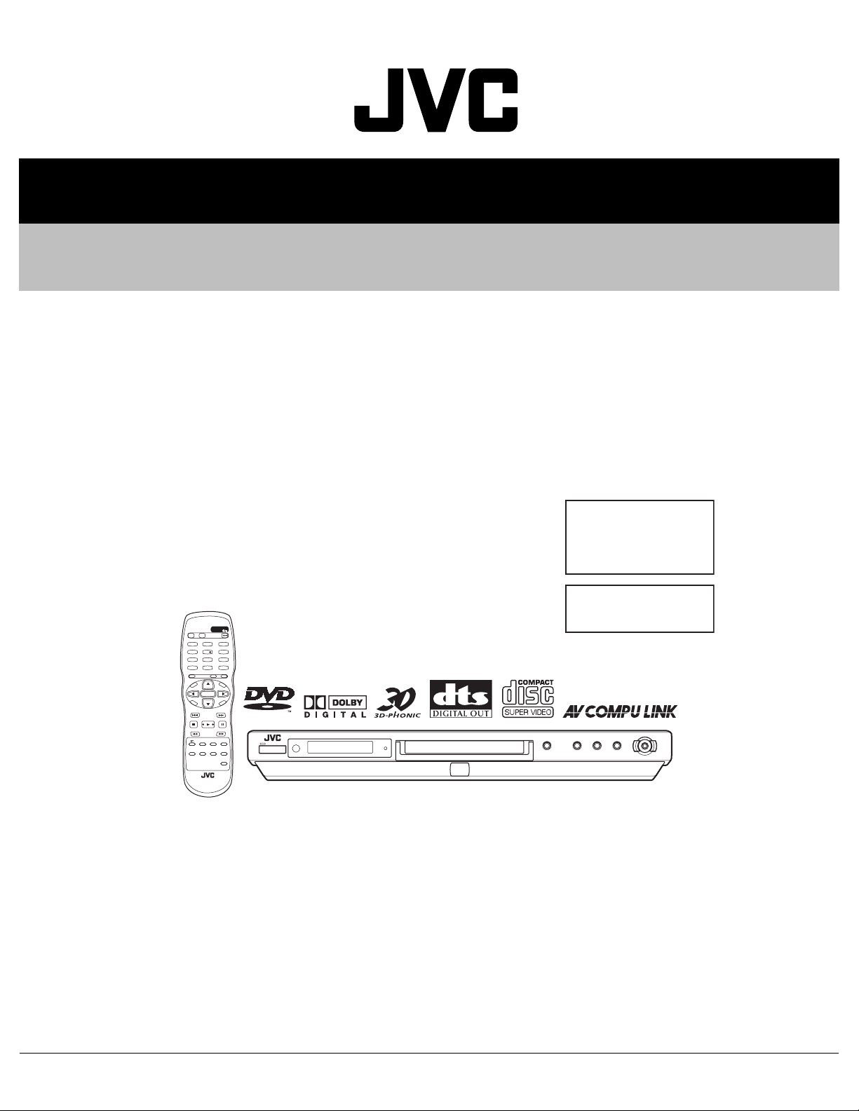
SERVICE MANUAL
DVD VIDEO PLAYER
XA00320035
XV-N40BK[MK2],
XV-N44SL[MK2],
XV-N4SL[MK2]
Area Suffix
(XV-N40BK,XV-N44SL)
J -------------------------- U.S.A.
C --------------------- Canada
Area Suffix (XV-N4SL)
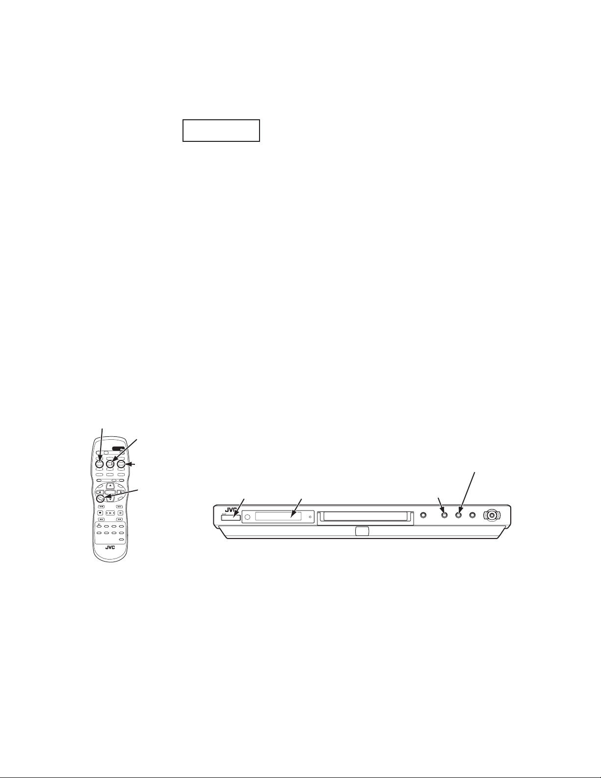
STANDBY/ON
OPEN/
CLOSE
DISPLAY
1
3
2
4
6
5
7
9
8
010 +10
TITLE/
CANCEL
GROUPRETURN
U
M
N
E
E
N
M
U
P
O
T
ENTER
C
N
H
E
O
E
R
I
C
C
E
S
N
O
NEXTPREVIOUS
SELECTCLEAR
-
SLOW
3D
PHONIC
SUB TITLE
ANGLE
VIDEO
SLOW+
VFP
REPEAT
PROGRESSIVE
SCAN
ZOOM
AUDIO
DIMMER
C --------------------- Canada
This illustration is XV-N40BK for U.S.A
This service manual is a service manual of the model which
changes a part of specification of the above-mentioned model
which has already been put on the market.
Please refer to the following page for details.
TABLE OF CONTENTS
1 Important Safety Precautions . . . . . . . . . . . . . . . . . . . . . . . . . . . . . . . . . . . . . . . . . . . . . . . . . . . . . . . . . . . 1-4
2 Disassembly method . . . . . . . . . . . . . . . . . . . . . . . . . . . . . . . . . . . . . . . . . . . . . . . . . . . . . . . . . . . . . . . . . . 1-8
3 Adjustment. . . . . . . . . . . . . . . . . . . . . . . . . . . . . . . . . . . . . . . . . . . . . . . . . . . . . . . . . . . . . . . . . . . . . . . . . . 1-15
4 Description of major ICs. . . . . . . . . . . . . . . . . . . . . . . . . . . . . . . . . . . . . . . . . . . . . . . . . . . . . . . . . . . . . . . 1-24
COPYRIGHT © 2003 VICTOR COMPANY OF JAPAN, LIMITED.
No.XA003
2003/5
Page 2
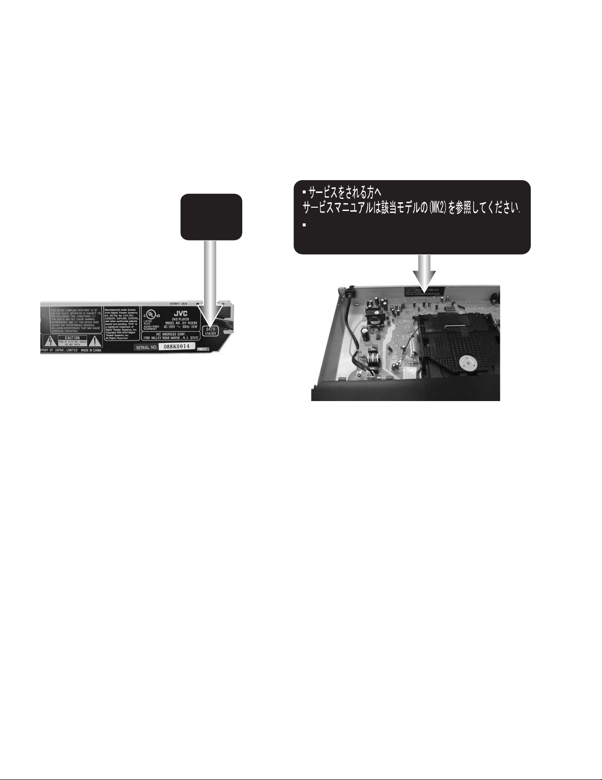
For this service manual
This service manual is a service manual of the model which changes a part of specification of the above-mentioned model
which has already been put on the market.
<When the label in figure is pasted in the main body>
The specification is different from what the label of the same model does not paste because of the specification improvement,
and refer to this service manual, please. Please already refer to the issued service manual when the label is not pasted.
* Please refer to this service manual for the model to which this label is pasted.
* Please refer to the service manual which has already been issued for the
model to which this label is not pasted.
(one that there is no description named [MK2] in cover of service manual. )
0478
The surface of a rear panel
inside
or
Used only service dealer
Please refer to service manual of an applicable model [MK2]
GN30080-001A
1-2 (No.XA003)
Page 3
SPECIFICATION
General
Readable discs DVD VIDEO, DVD-R (Video format), DVDRW (Video format), +RW (Video format), SVCD, Video CD,
Audio CD (CD-DA), MP3 format, JPEG, CD-R/RW (CD-DA, SVCD, Video CD, MP3 format, JPEG)
Video format NTSC, 480i (Interlaced scan)/480p (Progressive scan) selectable
Other
Power requirements AC 120 V, 60 Hz
Power consumption 10 W (POWER ON) 0.7 W (STANDBY mode)
Mass 2.1 kg (4.7 lbs)
Dimensions (W x H x D) 435mm x 53mm x 248.4mm (17-3/16 inch x 2-1/8 inc x 9-13/16 inch)
Video outputs
COMPONENT (pin jacks) Y Output: 1.0 Vp-p (75 Ω)
Pb/Pr Output: 0.7Vp-p (75 Ω)
VIDEO OUT (pin jack) 1.0 Vp-p (75 Ω)
S-VIDEO OUT (S jack) Y Output: 1.0 Vp-p (75 Ω)
C Output: 286 mVp-p (75 Ω)
Horizontal resolution 500 lines or more
Audio outputs
ANALOG OUT (pin jack) 2.0 Vrms (10 kΩ)
DIGITAL OUT (COAXIAL) 0.5 Vp-p (75 Ω termination)
DIGITAL OUT (OPTICAL) -21 dBm to -15 dBm (peak)
Audio characteristics
Frequency response CD (sampling frequency 44.1 kHz):2 Hz to 20 kHz
DVD (sampling frequency 48 kHz):2 Hz to 22 kHz
(4 Hz to 20 kHz for DTS and Dolby Digital bitstream signals)
DVD (sampling frequency 96 kHz):2 Hz to 44 kHz
Dynamic range 16 bit: More than 98 dB
20 bit: More than 100 dB
24 bit: More than 100 dB
Wow and flutter Unmeasurable (less than + 0.002%)
Total harmonic distortion less than 0.006%
• Specifications and appearance are subject to change without prior notice.
• Manufactured under license from Dolby Laboratories. "Dolby" and the double-D symbol are trademarkes of Dolby Laboratories.
• Manufactured under license from Digital Theater Systems, Inc. "DTS" and "DTS Digital Surround" are registered trademarks of Digital Theater Systems, Inc.
Digital output signal chart
Disc type Output
PCM ONLY DOLBY DIGITAL/PCM STREAM/PCM
DVD with 48/44.1 kHz,
16/20/24 bit linear PCM
DVD with 96 kHz,
16/22/24 bit linear PCM
DVD with DTS No output DTS bitstream
DVD with Dolby Digital 48 kHz, 16 bit, stereo linear PCM Dolby Digital bitstream
DVD with MPEG
Multichannel
SVCD/Video CD/Audio CD 44.1 kHz, 16 bit, stereo linear PCM
Audio CD with DTS No output DTS bitstream
CD-R/RW with MP3 Linear PCM
48 kHz, 16 bit, stereo linear PCM MPEG bitstream
48/44.1 kHz, 16 bit, stereo linear PCM
48kHz, 16 bit, stereo linear PCM (Down sampling)
(No.XA003)1-3
Page 4
SECTION 1
Important Safety Precautions
1.1 Safety Precautions
(1) This design of this product contains special hardware and
many circuits and components specially for safety purposes. For continued protection, no changes should be made
to the original design unless authorized in writing by the
manufacturer. Replacement parts must be identical to
those used in the original circuits. Services should be performed by qualified personnel only.
(2) Alterations of the design or circuitry of the product should
not be made. Any design alterations of the product should
not be made. Any design alterations or additions will void
the manufacturers warranty and will further relieve the
manufacture of responsibility for personal injury or property
damage resulting therefrom.
(3) Many electrical and mechanical parts in the products have
special safety-related characteristics. These characteristics are often not evident from visual inspection nor can the
protection afforded by them necessarily be obtained by using replacement components rated for higher voltage, wattage, etc. Replacement parts which have these special
safety characteristics are identified in the Parts List of Service Manual. Electrical components having such features
are identified by shading on the schematics and by ( ) on
the Parts List in the Service Manual. The use of a substitute
replacement which does not have the same safety characteristics as the recommended replacement parts shown in
the Parts List of Service Manual may create shock, fire, or
other hazards.
(4) The leads in the products are routed and dressed with ties,
clamps, tubings, barriers and the like to be separated from
live parts, high temperature parts, moving parts and/or
sharp edges for the prevention of electric shock and fire
hazard. When service is required, the original lead routing
and dress should be observed, and it should be confirmed
that they have been returned to normal, after reassembling.
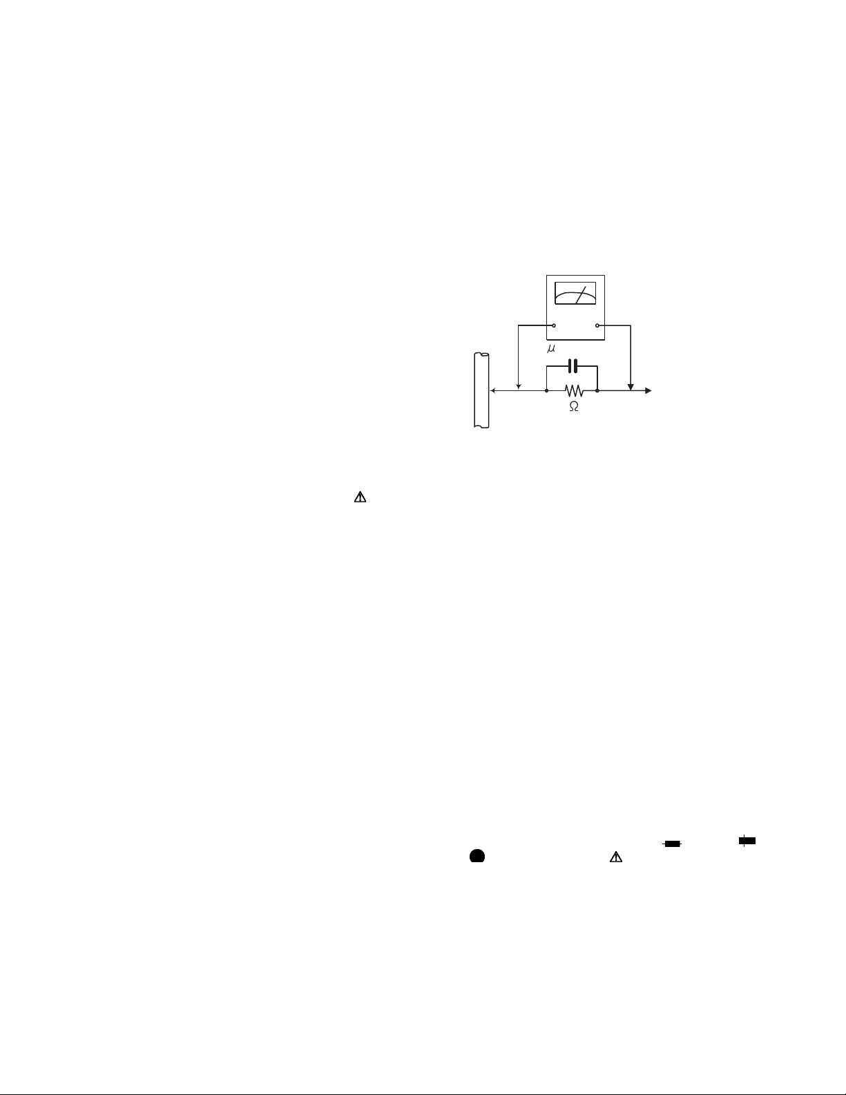
(5) Leakage shock hazard testing
After reassembling the product, always perform an isolation check on the exposed metal parts of the product (antenna terminals, knobs, metal cabinet, screw heads,
headphone jack, control shafts, etc.) to be sure the product
is safe to operate without danger of electrical shock.Do not
use a line isolation transformer during this check.
• Plug the AC line cord directly into the AC outlet. Using a
"Leakage Current Tester", measure the leakage current
from each exposed metal parts of the cabinet, particularly any exposed metal part having a return path to the
chassis, to a known good earth ground. Any leakage current must not exceed 0.5mA AC (r.m.s.).
• Alternate check method
Plug the AC line cord directly into the AC outlet. Use an
AC voltmeter having, 1,000Ω per volt or more sensitivity
in the following manner. Connect a 1,500Ω 10W resistor
paralleled by a 0.15µF AC-type capacitor between an ex-
posed metal part and a known good earth ground.
Measure the AC voltage across the resistor with the AC
voltmeter.
Move the resistor connection to each exposed metal
part, particularly any exposed metal part having a return
path to the chassis, and measure the AC voltage across
the resistor. Now, reverse the plug in the AC outlet and
repeat each measurement. Voltage measured any must
not exceed 0.75 V AC (r.m.s.). This corresponds to 0.5µ
mA AC (r.m.s.).
AC VOLTMETER
(Having 1000
ohms/volts,
or more sensitivity)
0.15 F AC TYPE
Place this
probe on
1500 10W
Good earth ground
1.2 Warning
(1) This equipment has been designed and manufactured to
meet international safety standards.
(2) It is the legal responsibility of the repairer to ensure that
these safety standards are maintained.
(3) Repairs must be made in accordance with the relevant
safety standards.
(4) It is essential that safety critical components are replaced
by approved parts.
(5) If mains voltage selector is provided, check setting for local
voltage.
1.3 Caution
Burrs formed during molding may be left over on some parts
of the chassis.
Therefore, pay attention to such burrs in the case of preforming repair of this system.
1.4 Critical parts for safety
In regard with component parts appearing on the silk-screen
printed side (parts side) of the PWB diagrams, the parts that are
printed over with black such as the resistor ( ), diode ( )
and ICP ( ) or identified by the " " mark nearby are critical
for safety. When replacing them, be sure to use the parts of the
same type and rating as specified by the manufacturer.
(This regulation dose not Except the J and C version)
each exposed
metal part.
1-4 (No.XA003)
Page 5
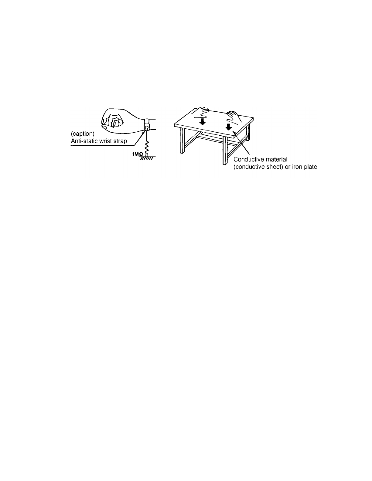
1.5 Preventing static electricity
Electrostatic discharge (ESD), which occurs when static electricity stored in the body, fabric, etc. is discharged, can destroy the laser
diode in the traverse unit (optical pickup). Take care to prevent this when performing repairs.
1.5.1 Grounding to prevent damage by static electricity
Static electricity in the work area can destroy the optical pickup (laser diode) in devices such as DVD players.
Be careful to use proper grounding in the area where repairs are being performed.
(1) Ground the workbench
Ground the workbench by laying conductive material (such as a conductive sheet) or an iron plate over it before placing the
traverse unit (optical pickup) on it.
(2) Ground yourself
Use an anti-static wrist strap to release any static electricity built up in your body.
(3) Handling the optical pickup
• In order to maintain quality during transport and before installation, both sides of the laser diode on the replacement optical
pickup are shorted. After replacement, return the shorted parts to their original condition.
(Refer to the text.)
• Do not use a tester to check the condition of the laser diode in the optical pickup. The tester's internal power source can easily
destroy the laser diode.
1.6 Handling the traverse unit (optical pickup)
(1) Do not subject the traverse unit (optical pickup) to strong shocks, as it is a sensitive, complex unit.
(2) Cut off the shorted part of the flexible cable using nippers, etc. after replacing the optical pickup. For specific details, refer to the
replacement procedure in the text. Remove the anti-static pin when replacing the traverse unit. Be careful not to take too long
a time when attaching it to the connector.
(3) Handle the flexible cable carefully as it may break when subjected to strong force.
(4) I t is not possible to adjust the semi-fixed resistor that adjusts the laser power. Do not turn it.
1.7 Precautions of the safe use of battery (Only XV-N4SL)
• Store the battery in a place where children cannot reach.If a child accidentally swallows the battery, consult a doctorimmediately.
• Do not recharge, short, disassemble or heat the battery or dispose of it in a fire.
Doing any of these things may cause the battery to give off heat, crack, or start a fire.
• Do not leave the battery with other metallic materials.Doing this may cause the battery to give off heat, crack, or start a fire.
• When throwing away or saving the battery, wrap it in tape and insulate; otherwise, the battery may start to give off heat, crack, or
start a fire.
• Do not poke the battery with tweezers or similar tools.Doing this may cause the battery to give off heat, crack, or start a fire.
• Dispose of batteries in the proper manner, according to federal, state, and local regulations.
(No.XA003)1-5
Page 6
1.8 Importance admistering point on the safety
J702
EP953
C966
C965
C964
L953
C963
D957
D956
T901
C908
C906
R901
C907
B234
R910
C904
C918
C905
L901
C902
EP951
P901
L955
C967
L954
D954
D903
D901
B631
C988
C958
D953
D955
R912
D902
C914
R915
C913
IC901
FC901
L951
C952
D951
R903
D904
R906
C955
B141
D952
PC901
R913
R954
C950
C970
CP951
B137
IC952
B34
Q951
R953
R951
B116
B135
B303
B37
B133
B134
C701
B38
B39
B132
B40
B202
B205
B231
B233
B105
C802
C808
B45
B107
FC902
B4
L710
L709
L952
B331
C953
R969
C951
B236
B403
B136
B271
B347
D701
X701
C706
B142
B143
B170
B2
B203
B102
B16
K811
C959
B140
B852
B871
B874
B872
B166
B237
EP952
CN904
B36
B103
B101
D702
K814
K812
CN901
K813
K810
S901
B273
B873
B772
B771
C973
C957
B601
Q953
B32
B601
B332
R966
B272
B139
B138
B532
C977
L959
S902
C975
C976
L957
B15
B533
L956
B276
B333
C974
CN902
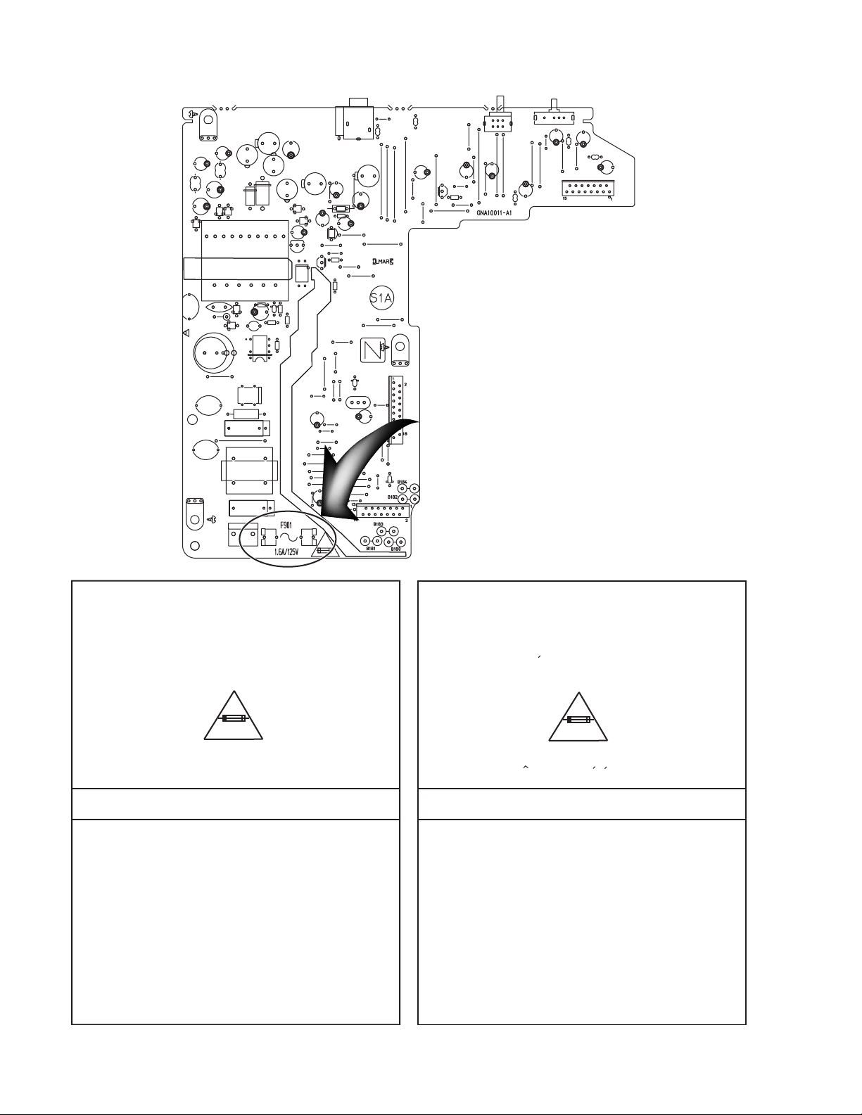
Full Fuse Replacement Marking
Graphic symbol mark
(This symbol means fast blow type fuse.)
should be read as follows ;
FUSE CAUTION
FOR CONTINUED PROTECTION AGAINST RISK
OF FIRE, REPLACE ONLY WITH SAME TYPE
AND RATING OF FUSES ;
F901 : 1.6 A / 125 V F901 : 1.6 A / 125 V
Marquage Pour Le Remplacement
Complet De Fusible
Le symbole graphique (Ce symbole signifie
fusible de type a fusion rapide.)
doit etre interprete comme suit ;
PRECAUTIONS SUR LES FUSIBLES
POUR UNE PROTECTION CONTINUE CONTRE
DES RISQUES D'INCENDIE, REMPLACER
SEULEMENT PAR UN FUSIBLE DU MEME TYPE ;
1-6 (No.XA003)
Page 7
1.9 Precautions for Service
1.9.1 Handling of Traverse Unit and Laser Pickup
(1) Do not touch any peripheral element of the pickup or the actuator.
(2) The traverse unit and the pickup are precision devices and therefore must not be subjected to strong shock.
(3) Do not use a tester to examine the laser diode. (The diode can easily be destroyed by the internal power supply of the tester.)
(4) To replace the traverse unit, pull out the metal short pin for protection from charging.
(5) When replacing the pickup, after mounting a new pickup, remove the solder on the short land which is provided at the center of
the flexible wire to open the circuit.
(6) Half-fixed resistors for laser power adjustment are adjusted in pairs at shipment to match the characteristics of the optical block.
Do not change the setting of these half-fixed resistors for laser power adjustment.
1.9.2 Destruction of Traverse Unit and Laser Pickup by Static Electricity
Laser diodes are easily destroyed by static electricity charged on clothingor the human body. Before repairing peripheral elements of
the traverse unit or pickup, be sure to take the following electrostatic protection:
(1) Wear an antistatic wrist wrap.
(2) With a conductive sheet or a steel plate on the workbench on which the traverse unit or the pick up is to be repaired, ground the
sheet or the plate.
(3) It solders to two short circuit sections on the substrate of a pick-up.
(4) After removing the flexible wire from the connector (CN101), short-circuit the flexible wire by the metal clip.
(5) Short-circuit the laser diode by soldering the land which is provided at the center of the flexible wire for the pickup.
After completing the repair, remove the solder to open the circuit.
Pick-up
Short circuit
* Please refer to the disassembly method for details.
CN101
Servo control board
(No.XA003)1-7
Page 8
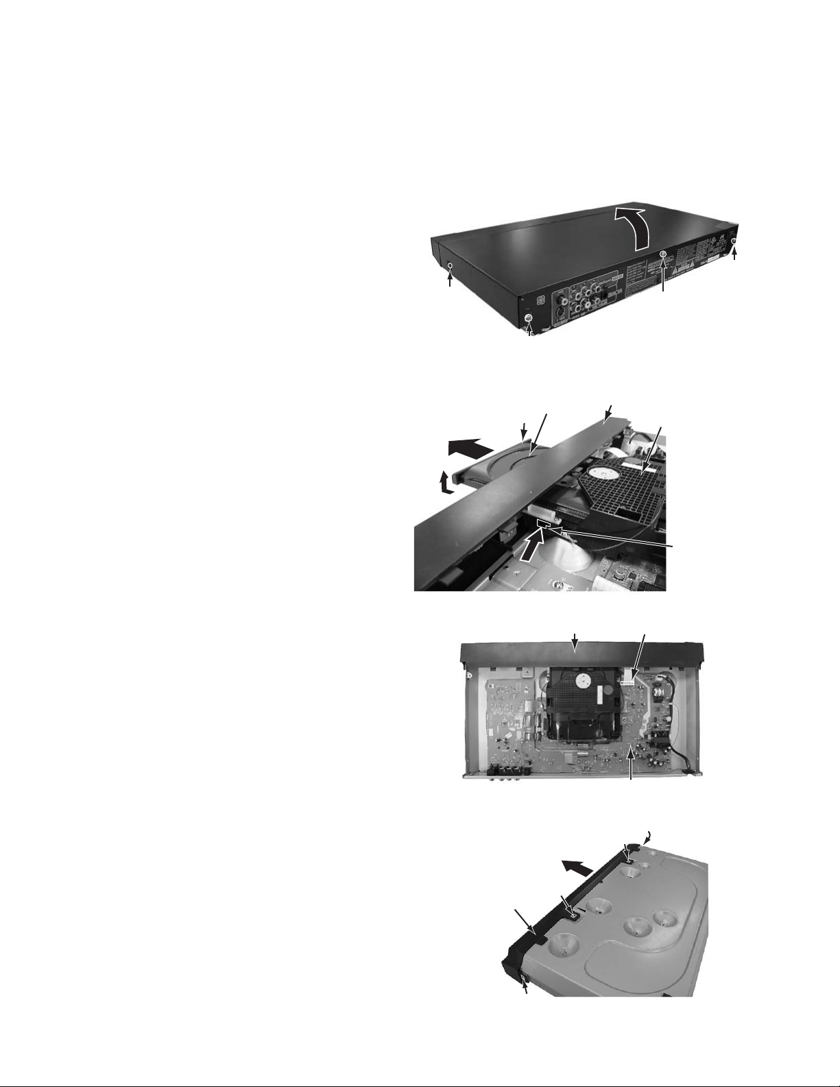
SECTION 2
TOP COVER
r
Push
Disassembly method
There is a part different from the photograph according to the model and the destination though explains this disassembly method
by using XV-N30BK for U.S.A.
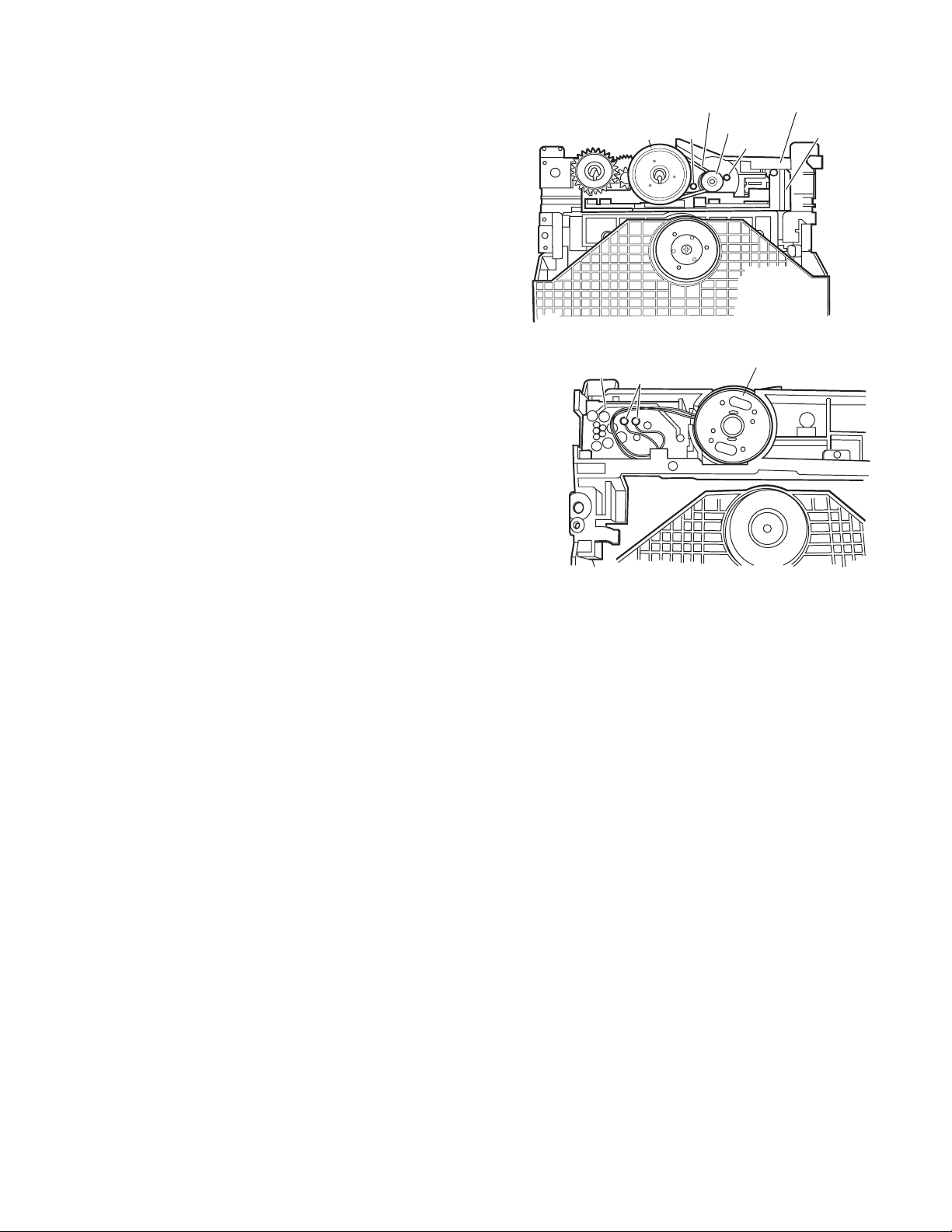
2.1 Main body section
2.1.1 Removing the top cover (See Figure 1)
(1) Remove the two screws A attaching the top cover on both
sides of the main body.
(2) Remove the three screws B attaching the top cover on the
back of the main body.
(3) Raise the both sides and lower part of the rear of the top
cover, with opening them slightly in an outward direction.
And the top cover will be removed.
2.1.2 Removing the front panel assembly (See Figure 2, Figure 3, Figure 4)
• Prior to performing the following procedure, remove the top
cover.
• There is no need to remove the mechanism assembly.
(1) Insert a kind of screwdriver in a hole located in the right
side of mechanism assembly, and push a lever until it cannot be inserted any further.
(2) And then, a tray will come out. Remove the tray in an upper
direction, with slightly opening the lower part of fitting in an
outward direction.
(3) Disconnect the card wire from connector CN901 on the
power supply board.
(4) Hook a and b are removed respectively, and the front panel
assembly is removed.
A
x
2
Fitting
B
Push
TOP COVER
TOP COVER
Fig.1
Tray
B
Front panel assembly
Mechanism assembly
Hole and leve
B
1-8 (No.XA003)
Fig.2
Front panel assembly
Power supply board
Fig.3
Hook b
Front panel
assembly
Hook b
Hook a
Fig.4
CN901
Hook a
Page 9
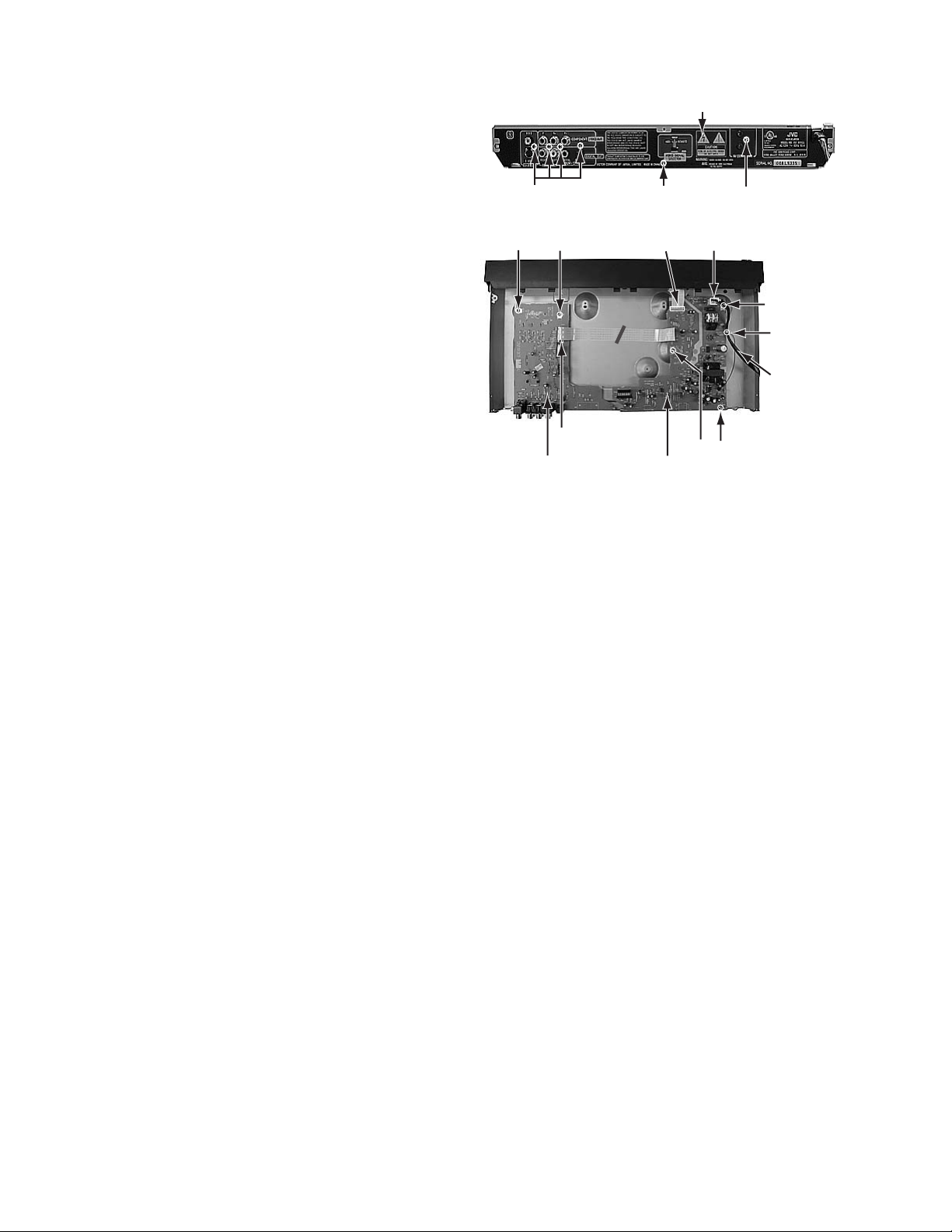
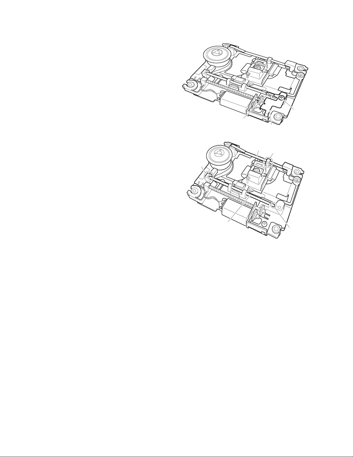
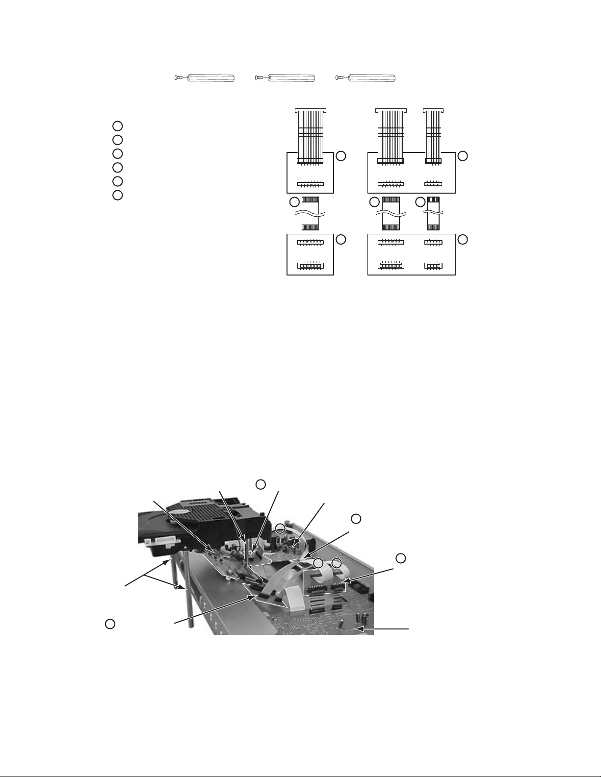
2.1.3 Removing the mechanism assembly (See Figure 2, Figure 5)
• Prior to performing the following procedure, remove the top
cover.
• There is no need to remove the front panel assembly.
(1) Insert a kind of screwdriver in a hole located in the right
side of mechanism assembly, and push a lever until it cannot be inserted any further.
(2) And then, a tray will come out. Remove the tray in an upper
direction, with slightly opening the lower part of fitting in an
outward direction.
(3) Remove the three screws C attaching the mechanism as-
sembly.
(4) Disconnect the wire from connector CN501,CN502,CN503
on the servo control board respectively.
(5) Remove the mechanism assembly by lifting the rear part of
the mechanism assembly.
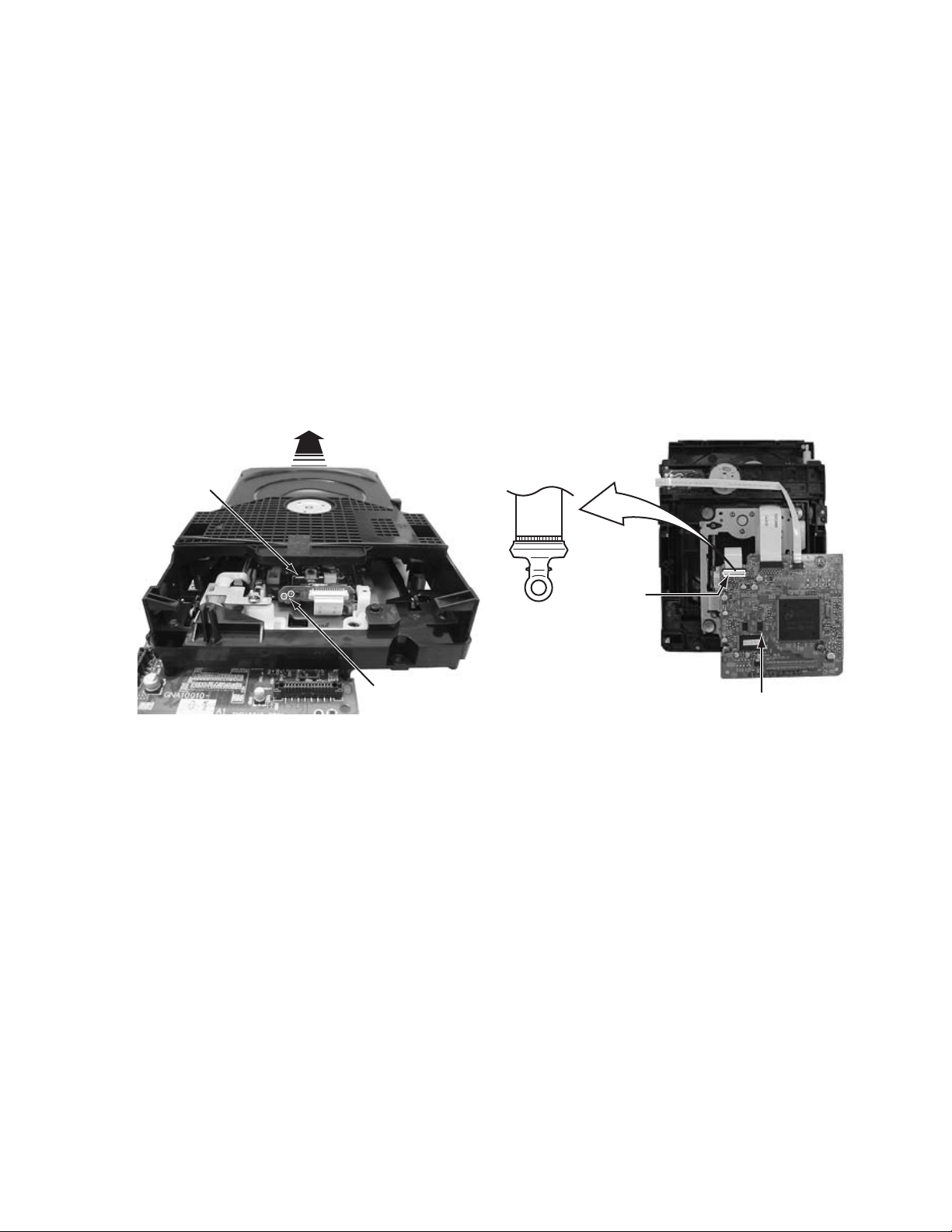
2.1.4 Removing the servo control board (See Figure 6, Figure 7)
• Prior to performing the following procedure, remove the mechanism assembly.
(1) A tray is made to slide ahead.
(2) A gear 1 is turned counterclockwise. Then, a pick-up unit
moves back.
(3) It solders to two c sections on the pick-up unit.
(4) Remove the three screws D attaching the servo control
board.
(5) Disconnect the card wire from connector CN201,CN202 on
the servo control board.
(6) Disconnect the flexible wire from connector CN101 on the
servo control board from pick-up unit.
ATTENTION:
Please extract the wire after short-circuited of two places
on the wire in part c with solder. Please remove the solder two places of part c after connecting the wire with
CN101 when reassembling.
CAUTION:
Be sure to solder the short land sections “c” on the pickup unit before disconnecting the card wire from connector CN101 on the DVD servo control board.
If the card wire is disconnected without attaching solder,
the pick-up unit may be destroyed by static electricity.
CN502
CN503
Gear1
Pick-up
Mechanism assembly
C
CN501
Fig.5
Fig.6
C
C
Part c
CN202
CN201
CN101
D
Servo control board
Fig.7
D
D
(No.XA003)1-9
Page 10
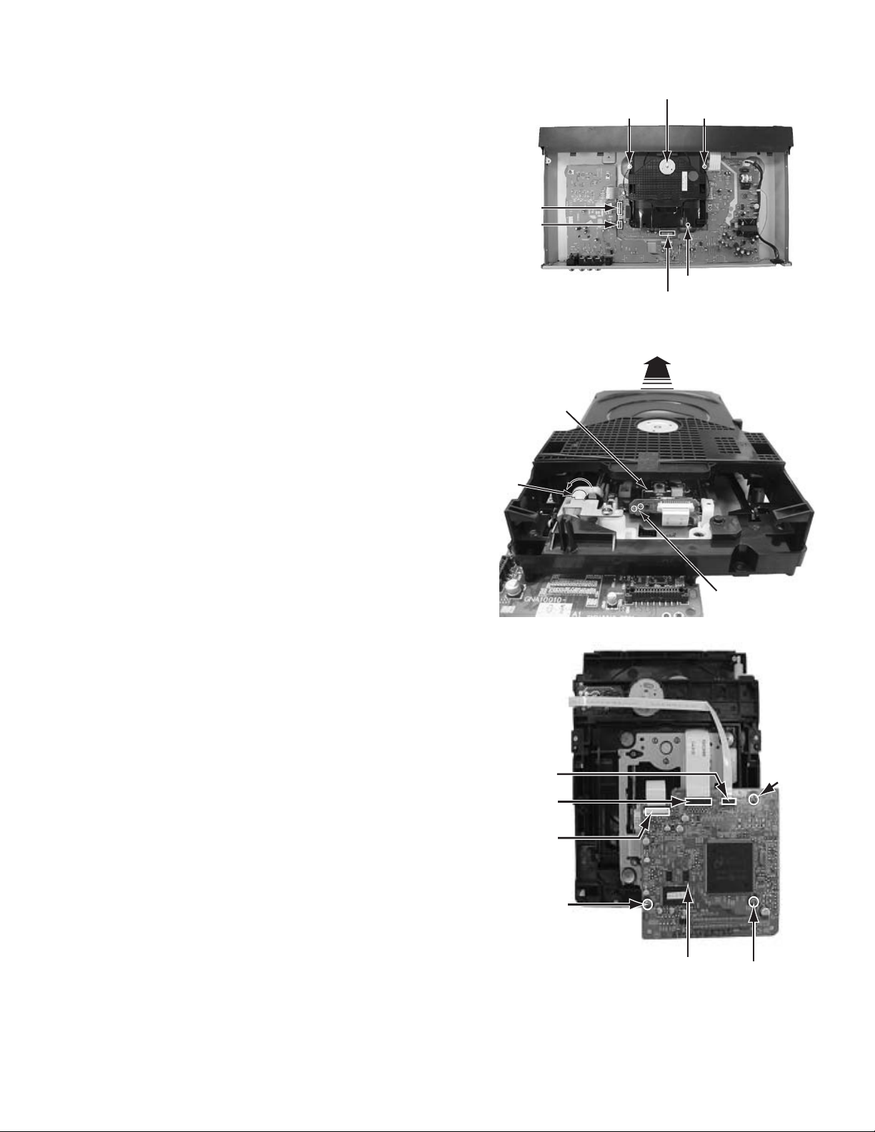
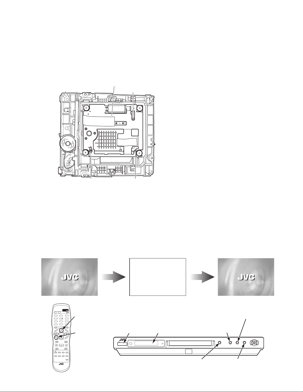
2.1.5 Removing the rear panel (See Figure 8, Figure 9)
• Prior to performing the following procedure, remove the top
cover.
(1) Remove the six screws E attaching the rear panel.
(2) Disconnect the power cord from connector P901 on the
power supply board
(3) Remove tie band.
Rear panel
E
E E
Fig.8
G G
CN702
2.1.6 Removing the output terminal board and power supply board. (See Figure 9)
• Prior to performing the following procedure, remove the top
cover/mechanism assembly/rear panel.
(1) Remove the two screws G attaching the output terminal
board.
(2) Disconnect the card wire from connector CN702 on the
output terminal board.
(3) Remove the three screws H attaching the power supply
board.
(4) Disconnect the card wire from connector CN901 on the
power supply board.
CN901 P901
H
Power supply boardOutput terminal board
Fig.9
H
Tie band
Power cord
H
1-10 (No.XA003)
Page 11
2.2 Loading mechanism assembly
Projection of the tray
2.2.1 Removing the tray (See Figure 1, Figure 2, Figure 3, Figure 4, Figure 5, Figure 6)
(1) Push a of the slide cam on the hole in the right side of the
loading base by using a driver until it stops. (See Figure 1.)
(2) The tray comes out. Pull the tray in a front direction until it
stops.
(3) Remove the two screws A attaching the slide bracket. (See
Figure 2.)
(4) Tilt the tray in a direction of the arrow around the point in
the left rear part of the tray. (See Figure 3.)
(5) The rail of the tray is removed from b of the loading base.
Then, remove the tray upward. (See Figure 4.)
Attaching the tray:
Engage c of the loading base to the projection of the tray while
tilting the tray to the left. Turn the tray in a direction of the arrow, and attach the slide bracket. (See Figure 5.)
Note:
Prior to the procedure above, move the slide cam in a direction
of the arrow so that d of the slide cam can be inserted in e of
the tray. (See Figure 6.)
Tray
The point in the left rear part
Tray
Fig.3
Push
Slide cam part a
Slide bracket
A
Fig.1
Fig.2
A
Loading base
Tray
Loading base part b
Rail of the tray
Fig.4
Projection of the tray
Loading base part c
Fig.5
Part e
Part d
Slide cam
Fig.6
(No.XA003)1-11
Page 12
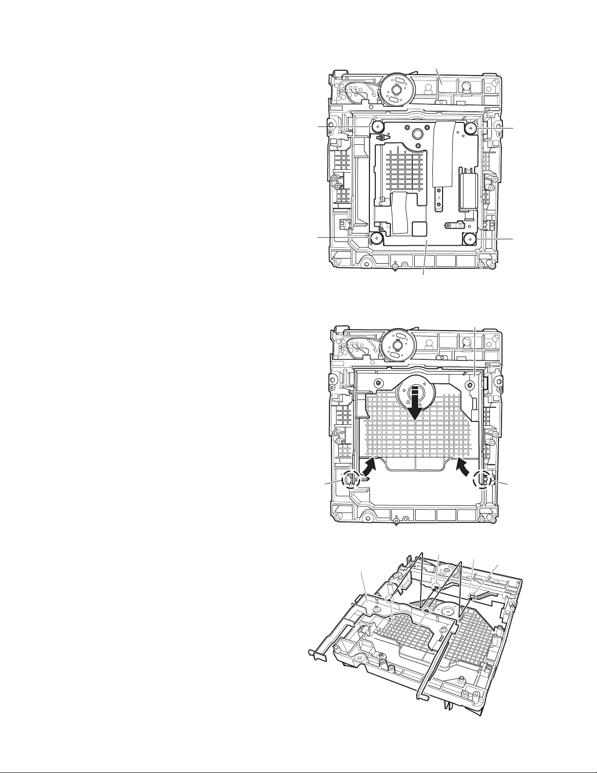
2.2.2 Removing the traverse mechanism assembly (See Figure 7)
f
Shaft
Reverse the loading mechanism assembly. Remove the four
screws B attaching the traverse mechanism assembly. Remove
the traverse mechanism assembly upward.
Loading mechanism assembly
2.2.3 Removing the elevator (See Figure 8 and Figure 9)
• Prior to the following procedure, remove the traverse mechanism assembly.
(1) Remove the two arms of the elevator from the two parts f
by moving the arms in a direction of the arrow.
(2) Pull out the elevator in a rear direction.
Attaching the elevator:
Engage the two holes g to the two shafts on the front part of
the elevator. And then, attach the elevator.
B
B
B
B
Traverse mechanism assembly
Fig.7
Elevator
1-12 (No.XA003)
Part f
Fig.8
g
Slide cam
Elevator
Shaft
Fig.9
Part
g
Page 13
2.2.4 Removing the loading motor (See Figure 10 and Figure 11)
• Prior to the following procedure, remove the tray, the traverse
mechanism assembly, and the elevator.
(1) Remove the belt from the pulley.
(2) Remove two screws C attaching the loading motor.
(3) Remove two solders h on the switch board.
Pulley
Belt
C
Fig.10
Pulley
C
Loading base
Slide cam
Switch board
Loading motor
Part h
Fig.11
(No.XA003)1-13
Page 14
2.3 Traverse mechanism assembly
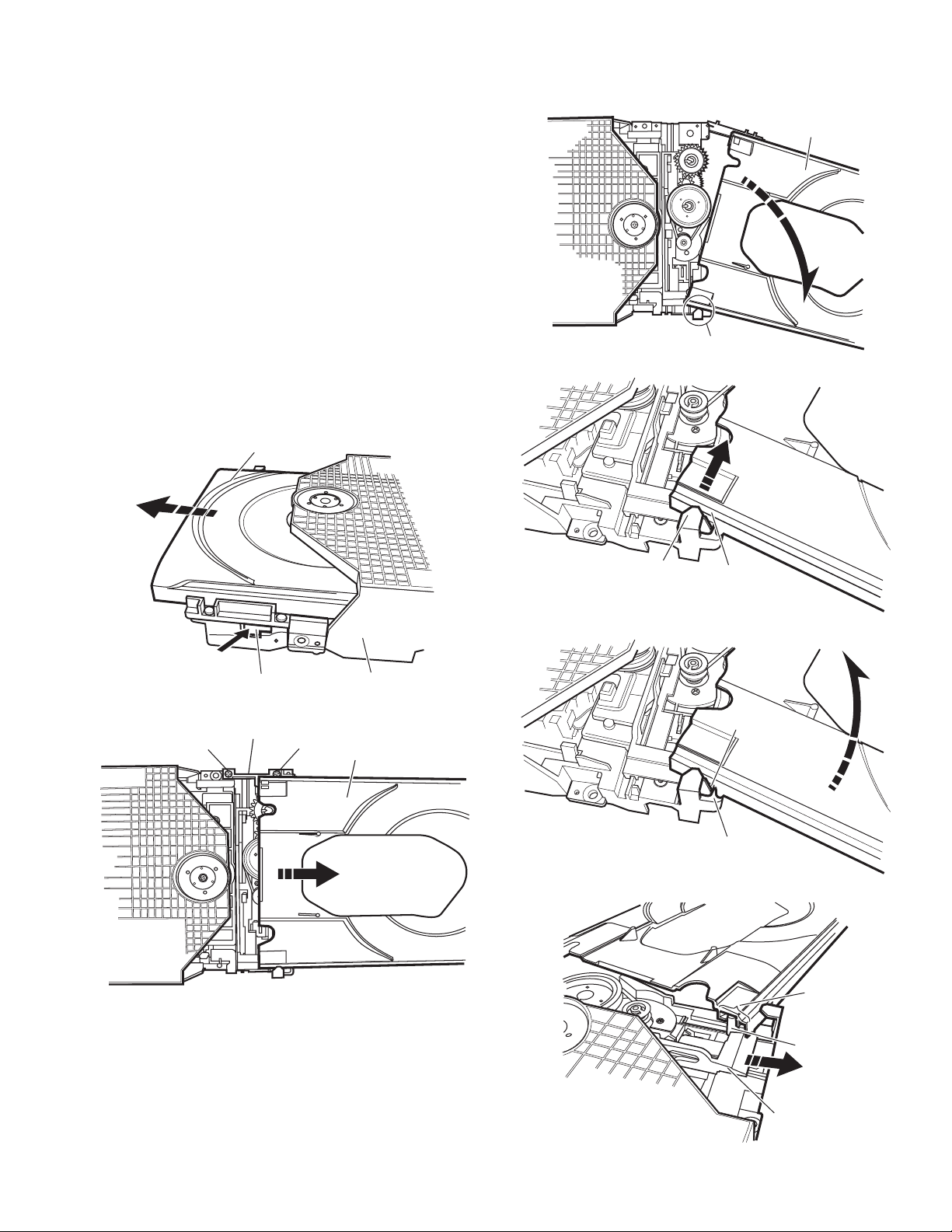
2.3.1 Removing the pickup (See Figure 12, Figure 13)
• Prior to the following procedure, remove the traverse mechanism assembly.
(1) Remove one screw D attaching the plate.
(2) Remove the plate and the leaf spring.
(3) Lift i of the shaft 1, and pull out the shaft 1 from j.
(4) Remove k of the pickup from the shaft 2.
Attaching the pickup:
(1) Engage k of the pickup to the shaft 2.
(2) Insert the shaft 1 in j, and attach the shaft 1 to i.
(3) Attach the leaf spring, and then attach the plate. Fix the
leaf spring and the plate by using the screw D.
D
Leaf spring
Plate
Fig.12
Part j
Shaft 2
Part k
Shaft 1
Part i
Fig.13
1-14 (No.XA003)
Page 15
SECTION 3
Adjustment
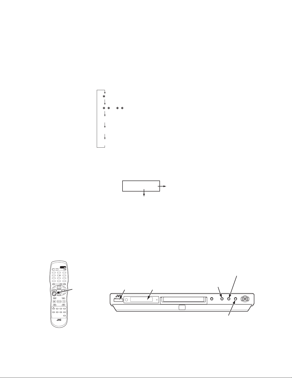
3.1 Test mode setting method
(1) Unplug the power plug.
(2) Insert power plug into outlet while pressing both "PLAY" key and "STOP" key of the main body.
(3) The FL display shows "∗0", and the main body turns to test mode. "∗" means the destination, and "0" means parameter adjust-
ment status.
(4) To release test mode, press "POWER" key of the main body.
NOTE:
Each pressing of "CHOICE" key of the remote controller in test mode changes the mode as follows.
0 ------------------------------
_ ----------------------
Becames test mode
Version of firmware
FL Display becames all lighting
CK --------------------------------
EP -------------------------------
3.2 Method of displaying version of firmware
(1) Set the main body at test mode.
(2) Press "CHOICE" key of the remote controller once. Then, version number and alphabetical letter of the system controller and
the back end are displayed in the FL display as follows:
Check mode
Not used
FL Display (Example)
19_16
System controller
3.3 Initialization method
Please initialize according to the following procedures in the following case:
• Just after you upgrade the firmware.
• After you confirm the symptoms that a customer points out. First Initialize, and then confirm whether the symptoms are improved or
not.
• After servicing, before returning the main body to a customer. (Initialized main body should be returned to a customer.)
(1) Set the main body at test mode.
(2) Press "PAUSE" key of the main body.
(3) When initialization is completed, the FL display changes from "∗0" to "∗00".(The left "0" of "00" is not always "0". It shows pa-
rameter adjustment status.)
Back end
STANDBY/ON
OPEN/
CLOSE
DISPLAY
3
1
2
6
4
5
9
7
8
010 +10
TITLE/
CANCEL
GROUPRETURN
U
M
N
E
E
N
M
U
P
O
T
ENTER
C
H
O
I
C
E
SELECTCLEAR
-
SLOW
3D
PHONIC
SUB TITLE
ANGLE
N
E
E
R
C
S
N
O
NEXTPREVIOUS
SLOW+
VFP
REPEAT
PROGRESSIVE
SCAN
ZOOM
AUDIO
DIMMER
CHOICE key
(switch of mode)
POWER key
FL Display
STOP key
(for test mode)
PLAY key
(for test mode)
PAUSE key
(for initialize)
(No.XA003)1-15
Page 16
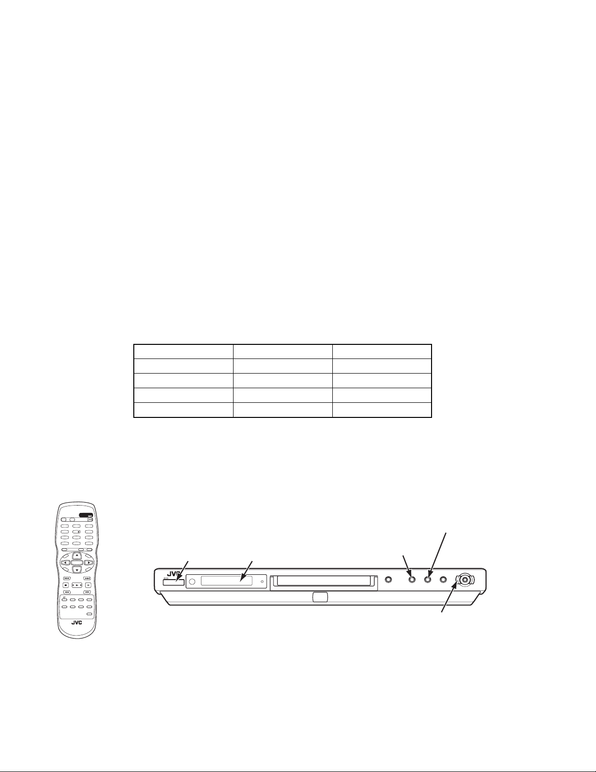
3.4 All-initialization method
Please perform all-initialization according to the following procedures in the following case:
• Just after you exchange the pick-up.
• Just after you exchange the spindle motor.
• Just after you exchange the traverse mechanism base.
NOTE:
Please perform all-initialization when you exchange the parts above and also when you remove the parts above.
• Just after the flap adjustment of the pick-up guide shaft
(1) Set the main body at test mode.
(2) Press and hold "BACKWARD SKIP" key of the main body for more than 2 seconds.
(3) When all-initialization is completed, the FL display changes from "∗0" to "∗33".
NOTE:
After all-initialization, be sure to perform optimization adjustment of Front End parameter.
3.5 Optimization adjustment of Front End parameter
Adjustment to optimize Front End parameter must be performed in each mechanism assembly of this model for high-speed starting.Please perform optimization according to the following procedures just after all-initialization is completed and when FL display
shows anything except "∗0" (For example when FL display shows "∗1", "∗2", and "∗3") at test mode.
(1) Press "POWER" key of the main body to turn the main body on (not to set the main body at test mode).
(2) Insert the test disc VT-501 or commercial dual-layer DVD software.
(3) Remove the disc when the FL display changes from "READ" to disc information.
(4) Perform the same procedures as in (2) and (3) above by using the test disc CTS-1000 or commercial CD-DA software.
(5) Set the main body at test mode, and check that the FL display shows "∗0".
NOTE:
Status of this adjustment can be judged by the number displayed at test mode as follows:
DVD adjustment CD adjustment FL display at test mode
Adjusted Adjusted ∗0
Not adjusted Adjusted ∗1
Adjusted Not adjusted ∗2
Not adjusted Not adjusted ∗3
NOTE:
As for a disc used for adjustment,
• Disc should be mounted. ("Mounting" means to display "READ" after the disc is inserted and then display the disc information.) Disc need not be played.
• If you do not have test disc either VT-501 (DVD) or CTS-1000 (CD-DA), use a commercial disc (for DVD, dual-layer software) after seeing and checking that the disc is neither curved nor foreseen that it may shake at the time of playback.If you
use a disc with bad features, starting time may be slow or disc may not be read.
STANDBY/ON
OPEN/
CLOSE
DISPLAY
3
1
2
6
4
5
9
7
8
010 +10
TITLE/
CANCEL
GROUPRETURN
U
M
N
E
E
N
M
U
P
O
T
ENTER
C
H
O
I
SLOW
ANGLE
N
E
E
R
C
C
E
S
N
O
NEXTPREVIOUS
SELECTCLEAR
-
SLOW+
3D
VFP
REPEAT
PHONIC
PROGRESSIVE
SCAN
SUB TITLE
ZOOM
AUDIO
DIMMER
POWER key
FL Display
STOP key
(for test mode)
PLAY key
(for test mode)
BACKWARD SKIP key
(for All initialize : It pushes 2 seconds or more.)
1-16 (No.XA003)
Page 17
3.6 Display of current value of laser
(1) Set the main body at test mode.
(2) Press "CHOICE" key of the remote controller three times. Then, FL display is displayed "CK".
(3) The laser current value can be switched between the value of CD and that of DVD by pressing the following key of the remote
controller.
FL Display (Example)
2530
The number shown in the FL display shows mA of current value of laser.
The first two numbers ("25" in "2530") shows current value of laser at the time of adjustment after the latest all-initialization, 25mA
in this example.
The last two numbers ("30" in "2530") shows the present current value of laser, 30mA in this example.
The first two numbers ("25" in "2530") usually shows current value of laser at the time of shipment, so you can see how the product has been deteriorated by comparing the first two numbers ("25" in "2530") and the last two numbers ("30" in "2530").
CD and DVD:
The laser current value of 80 mA or less is normal.The laser current value of over 81 mA is not normal. Laser diode of the
pickup has been deteriorated.
To return to test mode, press "STOP" key of the main body.
3.7 Flap adjustment of the pick-up guide shaft
Please perform flap adjustment of the pick-up guide shaft in the following case:
• Just after you exchange the pick-up.
• Just after you exchange the spindle motor.
• Just after you exchange the traverse mechanis m ba se .
NOTE:
Please perform flap adjustment of the pick-up guide shaft when you exchange the parts above and also w hen you remove the
parts above.
• When the reading accuracy of the signal is bad (The re is a block noise in the screen, Screen stops in the outer circumference of a
disc, etc.)
4 key (laser of CD)
5 key (laser of DVD)
STANDBY/ON
OPEN/
DISPLAY
CLOSE
3
1
2
6
4
5
6 key
9
7
8
010 +10
(display of jitter value)
TITLE/
CANCEL
GROUPRETURN
U
M
N
E
E
N
M
U
P
O
T
ENTER
C
H
O
I
C
E
SELECTCLEAR
SLOW
-
3D
PHONIC
SUB TITLE
ANGLE
N
E
E
R
C
S
N
O
NEXTPREVIOUS
SLOW+
VFP
REPEAT
PROGRESSIVE
SCAN
ZOOM
AUDIO
DIMMER
CHOICE key
(switch of mode)
POWER key
Remote controller "4" key --- Laser of CD
Remote controller "5" key --- Laser of DVD
(for test mode and jitter value)
STOP key
FL Display
(for test mode)
PLAY key
(No.XA003)1-17
Page 18
3.7.1 Tool for adjustment
*Stud: One set (four studs), Part number: JIGXVS40 (Note: One of the four studs is not used here.)
* Relay board and extension cord (One set) --- Parts number : EXTXVN30CB
-- Items --
1
Relay board 1 : EXTXVN30CB-1
2
Relay board 2 : EXTXVN30CB-2
3
Relay board 3 : EXTXVN30CB-3
4
Relay board 4 : EXTXVN30CB-4
5
Card wire : 15 pins 15 cm 2 pcs
6
Card wire : 9 pins 15 cm 1 pcs
5 5 6
3
1
4
2
*The phillips screwdriver for adjustment --- goods on the market
*Test disc ---- Parts number : VT-501
3.7.2 Preparation for adjustment
(1) A mechanism assembly is removed with reference to the disassembly method of a service manual.
(2) When the card wire which has connected the power supply board and the output terminal board is extracted at this time, please
connect again.
(3) Three stud is attached in a mechanism assembly, respectively.
(4) Remove the servo control board attached the mechanism assembly.
(If you disconnect the wires connected to the servo control board, connect them again.)
(5) The relay board 2 is connected to the connectors CN601 and CN701 on the output terminal board.
(6) The relay board 4 is connected to the connectors CN902 on the power supply board.
(7) The relay board 1 is connected to the connectors CN502 and CN503 on the servo control board.
(8) The relay board 3 is connected to the connectors CN501 on the servo control board.
(9) Between relay boards, an extension code is inserted, respectively and it connects.
(Be careful of direction of a card wire at this time.)
3
Servo control board
Stud
Relay board 3
55
Power supply board
4
Relay board 4
1-18 (No.XA003)
Stud
1
Relay board 1
55 66
2
Relay board 2
Output terminal
board
Page 19
3.7.3 Adjustment
A
(1) Set the main body at test mode.
(2) Press the "CHOICE" key of the remote controller three times, and the FL display is displayed "CK".
(3) Insert a test disc (VT-501), and press the "PLAY" key of the main body.
(4) After a few seconds, press the numeric key "6" of the remote controller. Then, the FL display is displays a jitter value.
(5) Turn the adjustment screws on the underside of the traverse mechanism with phillips screw driver until the maximum jitter value
is displayed on the FL display. (In this model, a bigger jitter value means a better result.)
NOTE:
• Reference values to judge whether the jitter is allowable or not are displayed, instead of actual jitter values.
• Please be sure to perform "all-initialization" and "optimization adjustment of front end parameter" after adjusting.
Traverse mechanism assembly
Loading mechanism assembly
Screw c
POINT:
Turn the adjustment screws a and b to the
same angle in the right direction. And turn
the adjustment screws a and b to the
same angle in the left direction. Then, turn
the screws a and b in either the right or
the left direction to increase the number of
jitter. Don't turn the adjustment screw c.
Screw a
Screw b
3.8 Upgrading of firmware
The latest firmware for upgrading is updated in "Optical disc CSG" page in JS-net.At the time of service, compare the version of the
product and the latest version, and upgrade the old version into the latest version.
(1) Press "POWER" key of the main body to turn the main body on
(2) Insert the upgrade disc.
(3) When FL display of the main body changes from "READ" to "UP", press "cursor UP" key () of the remote controller.
(4) The entire screen becomes blue, and upgrading starts.
(5) The tray opens automatically. Remove the upgrade disc.
(6) The screen returns to the normal screen. Then, press "POWER" key of the main body. When the stand-by indicator is lighted,
upgrading is completed.
(7) Set the main body at test mode, and perform initialization. Then, confirm the version of the firmware.
Firmware upgrade Disc ... press UP
fter inserting the up-grade disc
STANDBY/ON
OPEN/
DISPLAY
CLOSE
1
4
7
U
N
E
M
P
O
T
ENTER
C
H
O
I
C
E
SELECTCLEAR
SLOW
-
3D
PHONIC
SUB TITLE
ANGLE
UP key
(for firmware upgrade)
3
2
6
5
9
8
010 +10
TITLE/
CANCEL
GROUPRETURN
M
E
N
U
CHOICE key
N
E
E
R
C
S
(switch of mode)
N
O
NEXTPREVIOUS
SLOW+
VFP
REPEAT
PROGRESSIVE
SCAN
ZOOM
AUDIO
DIMMER
Upgrade application initializing...
While upgrading (blue screen)
POWER key
FL Display
STOP key
(for test mode)
OPEN/CLOSE key
NO DISC
When up-grade is completed
PLAY key
(for test mode)
PAUSE key
(for initialize)
(No.XA003)1-19
Page 20

3.9 Confirm method of operation
Please confirm the operation of the undermentioned item after doing the repair and the upgrade of the firmware.
Initialize Refer to the initialization method.
All-initialize Refer to the All-initialization method.
Parameter adjustment status Set the main body at test mode, and check that the FL display shows "∗0".
Opening picture check (Power ON) It should be display "JVC"
Muting working The noise must not be had to the performance beginning when you push "PLAY" button or
at ON/STANDBY.
FL Display The mark and the logo, etc. displayed by each operation must be displayed correctly.
FL Display should light correctly without any unevenness.
All Function button All function buttons should worked correctly with moderate click feeling.
Open and close movement of tray When press OPEN/CLOSE button the tray should move smoothly without any noise.
Remote controller unit working Check the correctly operation in use of remote controller unit.
Reading of TOC Be not long in the malfunction.
Search Both forward-searches and backward-searches should be able to be done.
Do not stop be searching or after the search.
Skip Both forward-skip and backward-skip should be able to be done.
Do not stop be after the skip.
Playback Do not find abnormality etc. of tone quality and the picture quality.
Most outside TITLE playback check Play VT-501 TITLE 59 CHAPTER 1, check normal playback.
1-20 (No.XA003)
Page 21
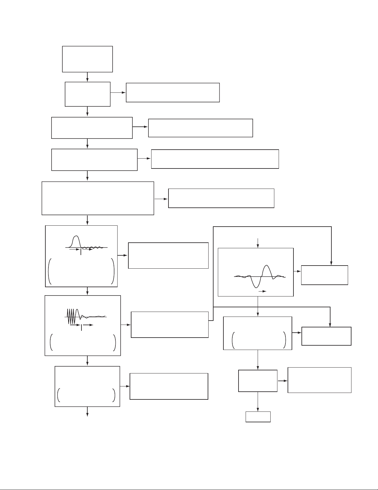
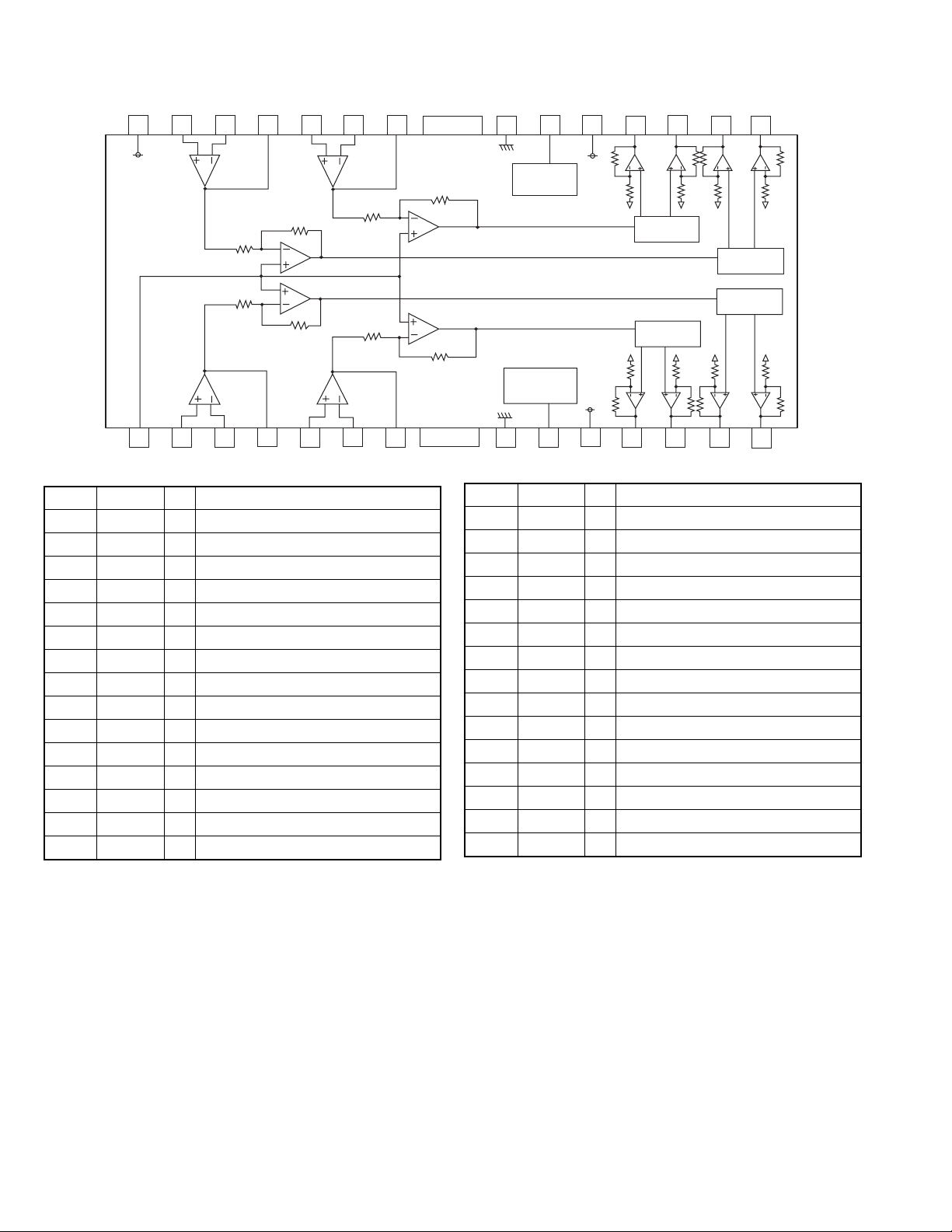
3.10 Troubleshooting
3.10.1 Servo volume
Press OPEN
/CLOSE key
Is tray
operation
Confirmation of tray drive circuit
N
and circuit in surrounding
correct?
Y
Is the traverse moving
along the innermost
N
perimeter for SW detection?
Y
"NO DISC" message appears
Y
immediately after vertical
movement of the pick-up lens
N
The state that DISC does not rotate continues for
several seconds, and becomes NO DISC or an
error display afterwards.
The rotation of DISC becomes high-speed and
abnormal, and becomes NO DISC or an error
display afterwards.
N
Is focus retraction OK?
FE
OFF
Even when it retracts
correctly, if it is out of focus
and makes repeated retries
with a clicking sound, it is
in error.
ON
See "(4) Focus ON error"
N
in "Check points for
individual errors"
Y
Is tracking retraction OK?
See "(3) Traverse movement error"
in "Check points for individual errors"
See "(2) Disk detection, distinction error"
in "Check points for individual errors"
Y
See "(1) Spindle startup error"
in "Check points for individual errors"
Is the inter-layer jump OK?
FE
LO LI
A
Two layers of DVD only.
N
(8) Inter-layer
jump error
Y
TE
OFF
If TE waveform reappears
or fails to converge after the
TE retraction, it is in error.
ON
Y
Is the spindle servo
locked correctly?
Is the RF OUT waveform
locked correctly?
Y
A
See "(5) Tracking ON error"
N
in "Check points for
individual errors"
See "(6) Spindle CLV error"
N
in "Check points for
individual errors"
Fig.1
Has the disc information
been collected?
Stop will result
Y
Is playback
N
possible?
Y
OK !
N
(7) Address read
error
Check (9),(10),(11), and
(12) items in "Check points
for individual errors"
(No.XA003)1-21
Page 22

3.11 Check points for each error
3.11.1 Spindle start error
(1) Defective spindle motor
• Are there several ohms resistance between each pin of CN201 "1-2","2-3","1-3"?
(The power supply is turned off and measured.)
• Is the sign wave of about 100mVp-p in the voltage had from each terminal?
[ CN201"10"(H1+),"11"(H1-),"7"(H2+),"8"(H2-),"5"(H3+),"6"(H3-) ]
(2) Defective spindle motor driver (IC251)
• Has motor drive voltage of a sine wave or a rectangular wave gone out to each terminal(SM1~3)
of CN201"1,2,3" and IC251"2,4,7"?
• Is FG pulse output from the terminal of IC251"24"(FG) according to the rotation of the motor?
• Is it "L(about 0.9V)" while terminal of IC251"15"(VH) is rotating the motor?
(3) Has the control signal come from servo IC or the microcomputer?
• Is it "L" while the terminal of IC251"18"(SBRK) is operating?
Is it "H" while the terminal of IC251"23"(/SPMUTE) is operating?
• Is the control signal input to the terminal of IC251"22"(EC)?
(changes from VHALF voltage while the motor is working.)
• Is the VHALF voltage input to the terminal of IC251"21"(ECR)?
(4) Is the FG signal input to the servo IC?
• Is FG pulse input to the terminal of IC301"69"(FG) according to the rotation of the motor?
3.11.2 Disc Detection, Distinction error (no disc, no RFENV)
• Laser is defective.
• Front End Processor is defective (IC101).
• APC circuit is defective. --- Q101,Q102.
• Pattern is defective. --- Lines for CN101 - All patterns which relate to pick-up and patterns between IC101
• IC101 --- For signal from IC101 to IC301, is signal output from IC101 "20" (ASOUT) and IC101 "41"(RFENV) and IC101 "22"
(FEOUT)?
3.11.3 Traverse movement NG
(1) Defective traverse driver
• Has the voltage come between terminal of CN101 "2" and "4" ?
(2) Defective BTL driver (IC201)
• Has the motor drive voltage gone out to IC201"17" or "18"?
(3) Has the control signal come from servo IC or the microcomputer?
• Is it "H" while the terminal of IC201"9"(STBY1) ?
• TRSDRV Is the signal input? (IC301 "67")
(4) TRVSW is the signal input from microcomputer? (IC301 "56")
3.11.4 Focus ON NG
• Is FE output ? --- Pattern, IC101
• Is FODRV signal sent ? (R209) --- Pattern, IC301 "115"
• Is driving voltage sent ?IC201 "13", "14" --- If NG, pattern, driver, mechanical unit .
• Mechanical unit is defective.
3.11.5 Tracking ON NG
• When the tracking loop cannot be drawn in, TE shape of waves does not settle.
• Mechanical unit is defective.
Because the self adjustment cannot be normally adjusted, the thing which cannot be normally drawn in is thought.
• Periphery of driver (IC201)
Constant or IC it self is defective.
• Servo IC (IC301)
When improperly adjusted due to defective IC.
1-22 (No.XA003)
Page 23

3.11.6 Spindle CLV NG
• IC101 -- "30"(ARF-), "31(ARF+).
• Does not the input or the output of driver's spindle signal do the grip?
• Has the tracking been turned on?
• Spindle motor and driver is defective.
• Additionally, "IC101 and IC301" and "Mechanism is defective(jitter)", etc. are thought.
3.11.7 Address read NG
• Besides, the undermentioned cause is thought though specific of the cause is difficult because various factors are thought.
Mechanism is defective. (jitter)
IC301
The disc is dirty or the wound has adhered.
3.11.8 Between layers jump NG (double-layer disc only)
Mechanism defective
Defect of driver's IC(IC201)
Defect of servo control IC(IC301)
3.11.9 Neither picture nor sound is output
(1) It is not possible search
• Has the tracking been turned on?
• To " Tracking ON NG" in "Check points for each error" when the tracking is not normal.
• Is the feed operation normal?
To " traverse movement NG" in "Check points for each error" when it is not normal.Are not there caught of the feeding mechanism etc?
3.11.10 Picture is distorted or abnormal sound occurs at intervals of several seconds.
Is the feed operation normal?
Are not there caught of the feeding mechanism etc?
3.11.11Others
• The image is sometimes blocked, and the image stops.
• The image is blocked when going to outer though it is normal in suroundings in the disk and the stopping sympton increases.
There is a possibility with bad jitter value for such a symptom.
3.11.12CD During normal playback operation
(1) Is TOC reading normal?
• Displays total time for CD-DA.
• Shifts to double-speed mode for V-CD
(2) Is playback afterwards possible?
(3) When can not do a normal playback
• --:-- is displayed during FL search.
According to [It is not possible to search ] for DVD, check the feed and tracking systems.
• No sound is output although the time is displayed.(CA-DA)
DAC, etc, other than servo.
• The passage of time is not stable, or picture is abnormal.(V-CD)
• The wound of the disc and dirt are confirmed.
(No.XA003)1-23
Page 24
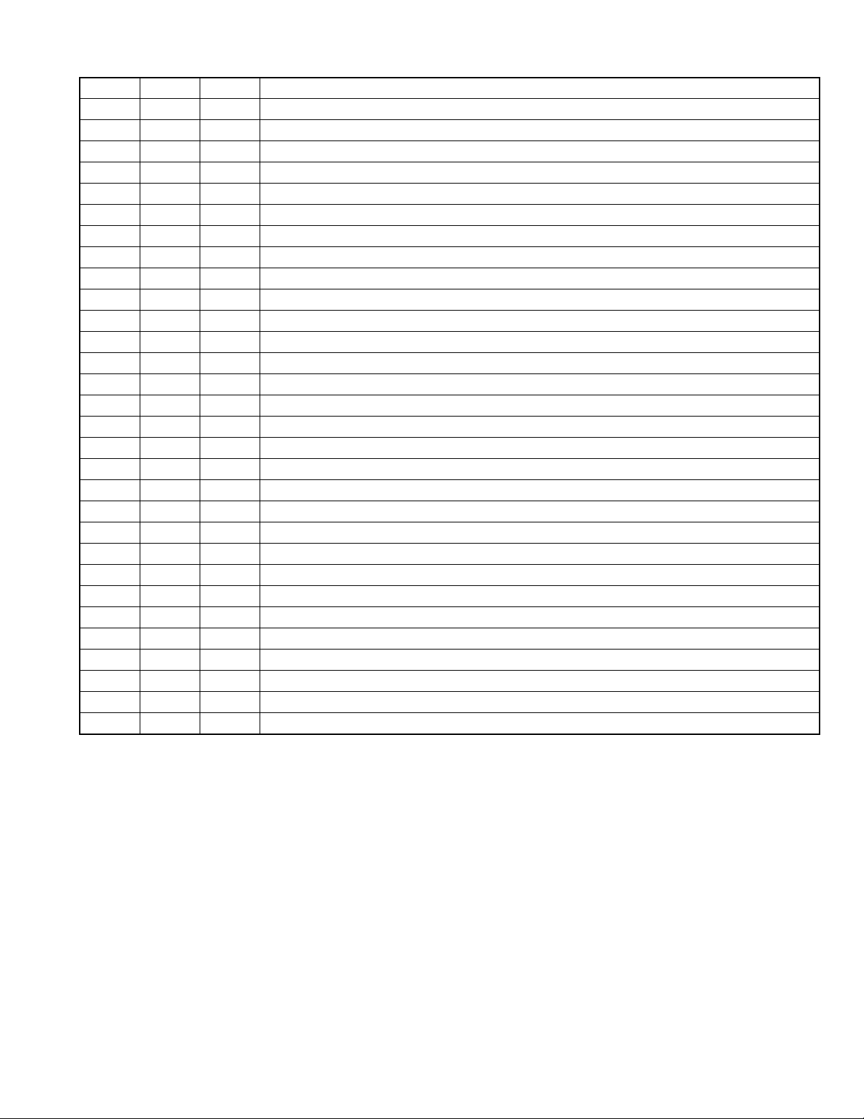
Description of major ICs
4.1 AN8703FH-V (IC101) : Frontend processor
• Pin layout
48 33~
• Block diagram
AGOFST
AGCBAL
DFLTOP
AGCLVL
DCFLT
DCFLT
RFENV
BOTTOM
PEAK
49
~
64
116
23
19
30
31
25
32
41
42
43
32
17
~
Level
Cont.
+-
+-
HOLD EQ
+-+-
~
UDO
40 39 45 44 29 27 56 36 36 28 55 26 61
Level
Cont.
Vol. Adg
VGA
OFTR
Det.
BDO
Det.
SECTION 4
OFTR
AGCO
AGCG
AGC Cont.
Boost
Cont.
FC
Cont.
VHALP
VREF2
VREF1
VCC3
VCC2
VCC1
GND3
REG SIF
GND2
GND1
LPC AMP
+-
9
10
11
12
13
14
64
HDTYPE
1
LPC1
2
LPCO1
LPC2
3
LPCO2
4
18
TEOUT
DTRD
IDGT
STANBY
SEN
SCK
STDI
1-24 (No.XA003)
RFINP
RFINN
TESTSG
VFOSHORT
DCRF
RFOUT
RFC
FEOUT
FEN
FBAL
ASOUT
47
48
46
38
35
37
22
21
20
TEN
+-
S-line
J-line
17
6
8
24
34
15
16
TBAL
POFLT
MON
RFDIFO
RSCL
JLINE
+-
+-
5
+-
7
FBAL
+-
49 50 51 52 53 54 62
VIN5
VIN6
VIN7
+-
SW
ADD ADD ADD
VIN8
VIN9
VIN10
AMP
Differential
Phase
TBAL
Det.
EQ EQ EQ EQ
63 57 58 59 60
VIN1
VIN11
VIN12
TBAL
VIN2
VIN3
VIN4
Micro
Det.
ADD
+-
ADD
Page 25

• Pin function
Pin No. Symbol Function
1 LPC1 Laser pin input (DVD head)
2 LPCO1 Laser drive output (DVD head)
3 LPC2 Laser in input (CD head)
4 LPCO2 Laser drive output (CD head)
5 VFOSHORT VFOSHORT control
6 TBAL Tracking balance control
7 FBAL Focus balance control
8 POFLT Track detection threshold level
9 DTRD Data slice data read signal input (for RAM)
10 IDGT Data slice address gate signal input (for RAM)
11 STANBY Standby mode control
12 SEN SEN (serial data input)
13 SCK SCK(serial data input)
14 STDI STDI(serial data I/O)
15 RSCL Reference current setting
16 JLINE J-line vurrent setting
17 TEN Tracking error amplifier inverted input
18 TEOUT Tracking error signal output
19 AGCBAL Offset adjustment for DRC-1
20 ASOUT Full addition signal output
21 FEN Focus error amplifier inverted input
22 FEOUT Focus error signal output
23 AGCOFST Offeset adjustment for DRC-2
24 MON Monitor
25 AGCLVL Output amplitude adjustment for DRC
26 GND2 Ground 2
27 VREF2 VREF2 voltage output
28 VCC2 Power supply 2 (5V)
29 VHALF VHALF voltage output
30 DFLTON Filter amplifier inverted output
31 DFLTOP Filter amplifier positive output
32 DCFLT Filter output capacitance connection
33 GND3 Groud 3
34 RFDIFO Raidal differntial output
35 RFOUT RF full-addition amplifier output
36 VCC3 Power supply 3 (3.3V)
37 RFC Filter for RF-group delay correction amplifier
38 DCRF DC-cut filter for RF full-addition amplifier
39 OFTR OFTR output
40 BDO BDO output
41 RFENV RF envelope output
42 BOTTOM Bottom envelope detection filter
43 PEAK Peak envelope detection filter
44 AGCG AGC amplifier again control
45 AGCO AGC amplifier level control
(No.XA003)1-25
Page 26
Pin No. Symbol Function
46 TESTSG TEST signal input
47 REFINP RF signal positive input
48 RFINN RE signal inverterd input
49 VIN5 Internal four-partition (CD) RF input 1
50 VIN6 Internal four-partition (CD) RF input 2
51 VIN7 Internal four-partition (CD) RF input 3
52 VIN8 Internal four-partition (CD) RF input 4
53 VIN9 Internal four-partition (DVD) RF input 2
54 VIN10 Internal four-partition (DVD) RF input 1
55 VCC1 Power supply 1 (5V)
56 VREF1 VREF1 voltage output
57 VIN1 Internal four-partition (DVD) RF input 1
58 VIN2 Internal four-partition (DVD) RF input 2
59 VIN3 Internal four-partition (DVD) RF input 3
60 VIN4 Internal four-partition (DVD) RF input 4
61 GND1 Groud 1
62 VIN11 3-deam sub (CD) input 2
63 VIN12 3-deam sub (CD) input 1
64 HDTYPE HD type selection
4.2 74LCX373MTC-X (IC512,IC513) : Octal D-type latch
• Pin layout
1OE
2Q0
3D0
4D1
5Q1
6Q2
7
8D3
9Q3
10GND
20
19
18
17
16
15
14D2
13
12
11
VCC
Q7
D7
D6
Q6
Q5
D5
D4
Q4
LE
(TOP VIEW)
• Pin function
Symbol Description
D0~D7 Data inputs
LE Latch enable input
OE Output enable input
Q0~Q7 3-State latch outputs
• Truth table
INPUTS OUTPUT
LE OE Dn Qn
XHXZ
HLLL
HLHH
LLXQ0
H = HIGH Voltage levelL = LOW Voltage levelZ = High impedanceX = ImmaterialQ0 = Previous Q0 before HIGH to LOW
transition of latch enable
• Block diagram
D0
D1
D2
D3
D4
D5
D6
D7
18
D
D
Q
L
16
Q6
OE
3
4
7
8
13
14
D
D
D
D
D
Q
Q
Q
L
L
11
LE
1
2
Q0
L
5
Q1
Q
L
L
6
9
Q2
Q3
17
D
Q
Q
L
12
15
Q4
Q5
Q
L
19
Q7
1-26 (No.XA003)
Page 27
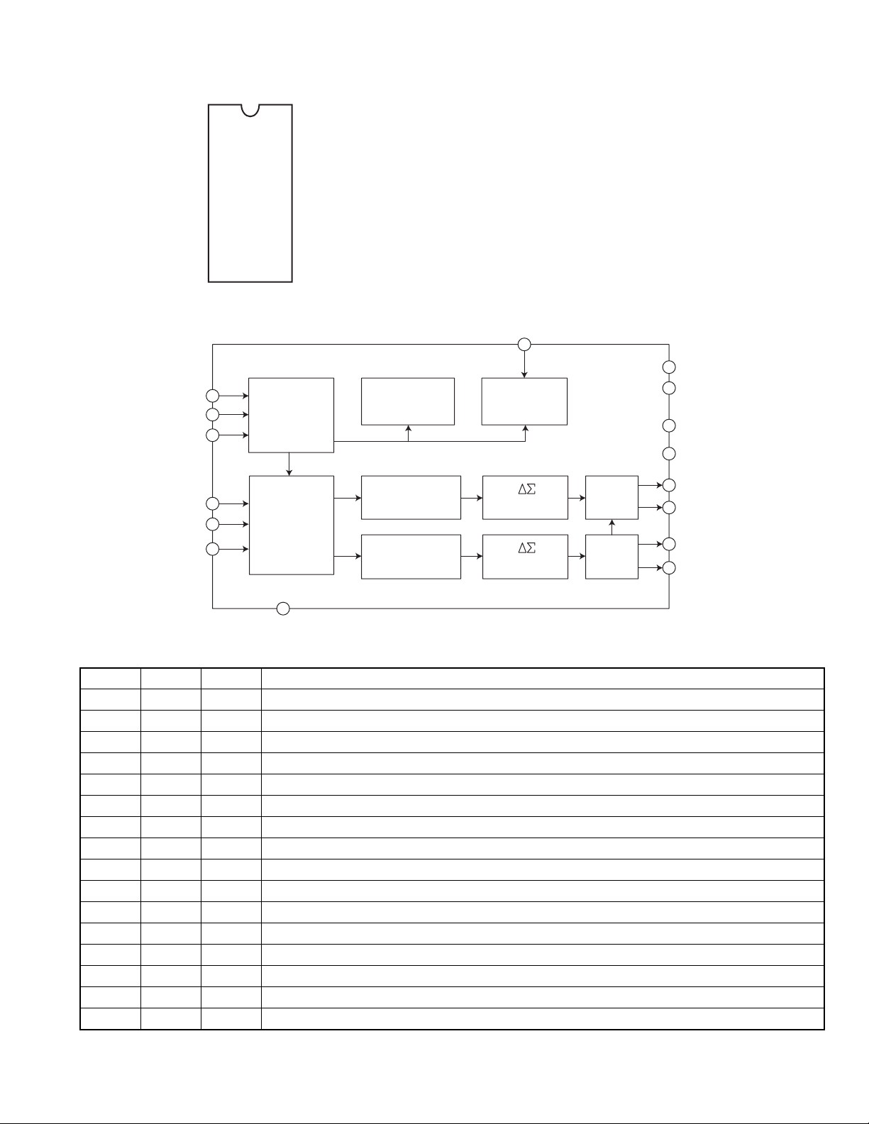
4.3 AK4381VT-X (IC402) : 2ch DAC
•Pin layout
• Block diagram
MCLK
BICK
SDTI
LRCK
PDN
CSN
CCLK
CDTI
CSN
CCLK
CDTI
LRCK
BICK
SDTI
1
2
3
4
5
6
7
8
16
15
14
13
12
11
10
9
DZFL
DZFR
VDD
VSS
AOUTL+
AOUTLAOUTR+
AOUTR-
MCLK
VDD
VSS
DZFL
uP
Interface
De-emphasis
Control
Clock
Divider
DZFR
AOUTL+
AOUTL-
Audio
8X
Interpolator
Modulator
SCF
Data
Interface
8X
Interpolator
Modulator
SCF
AOUTR+
AOUTR-
PDN
• Pin functions
Pin No. Symbol I/O Description
1 MCLK I Master clock input terminal
2 BICK I Audio serial data clock terminal
3 SDTI I Audio serial data input terminal
4 LRCK I L/R Clock terminal
5 PDN I Power down mode terminal
6 CSN I Chip select
7 CCLK I Control data input terminal
8 CDTI I Control data input terminal
9 AOUTR- O Rch negative analog output terminal
10 AOUTR+ O Rch positive analog output terminal
11 AOUTL- O Lch negative analog output terminal
12 AOUTL+ O Lch positive analog output terminal
13 VSS - Connect to ground
14 VDD - Power supply terminal
15 DZFR O Rch data zero input detection terminal
16 DZFL O Lch data zero input detection terminal
(No.XA003)1-27
Page 28
4.4 BA6664FM-X (IC251) : Spindle motor driver
• Pin layout
NC
A3
NC
A2
NC
NC
A1
GND
H1+
H1-
H2+
H2-
H3+
H3-
1
2
3
4
5
6
7
29 30
8
9
10
11
12
13
14
RNF
28
VM
27
GSW
26
Vcc
25
FG
24
PS
23
EC
22
ECR
21
FR
20
FG2
19
SB
18
CNF
17
BR
16
VH-
15
• Block diagram
A3
2
A2
4
A1
TL
7
8
9
10
11
12
13
HALL AMP
+
-
+
-
+
-
+
-
+
-
+
-
GND
H1+
H1-
H2+
H2-
H3+
H3-
14
DRIVER
GAIN
CONTROL
CURRENT
SENSE AMP
R
D Q
CK Q
TSD
+ -
SENSE AMP
SHORT BRAKE
BRAKE MODE
PS
TOROUE
VCC
Hall Bias
GAIN
SWITCH
VCC
+
-
VCC
28
27
26
25
24
23
22
21
20
19
18
17
16
15
R
NF
VM
GSW
VCC
FG
PS
EC
ECR
FR
FG2
SB
CNF
BR
VH
1-28 (No.XA003)
Page 29
• Pin function (BA6664FM-X)
Pin No. Symbol I/O Description
1 NC - Non connect
2 A3 O Output 3 for spindle motor
3 NC - Non connect
4 A2 O Output 2 for spindle motor
5 NC - Non connect
6 NC - Non connect
7 A1 O Output 1 for spindle motor
8 GND - Connect to ground
9 H1+ I Positive input for hall input AMP 1
10 H1- I Negative input for hall input AMP 1
11 H2+ I Positive input for hall input AMP 2
12 H2- I Negative input for hall input AMP 2
13 H3+ I Positive input for hall input AMP 3
14 H3- I Negative input for hall input AMP 3
15 VH I Hall bias terminal
16 BR - Non connect
17 CNF - Capacitor connection pin for phase compensation
18 SB I Short brake terminal
19 FG2 - Non connect
20 FR - Non connect
21 ECR I Torque control standard voltage input terminal
22 EC I Torque control voltage input terminal
23 PS O Start/stop switch (power save terminal)
24 FG O FG signal output terminal
25 VCC - Power supply for signal division
26 GSW O Gain switch
27 VM - Power supply for driver division
28 RNF O Resistance connection pin for output current sense
29 - Connect to ground
30 - Connect to ground
(No.XA003)1-29
Page 30
4.5 BA5983FM-X (IC201) : 4-channel driver
• Block diagram
27
26
25
28
Vcc
10k
24
20k
23 22 30
10k
20k
21
STAND BY
CH4
20
Vcc
19
18
10k
10k
17 16
10k
Level Shift
10k
10k
10k
15
10k
10k
Level Shift
10k
10k
1
2
3
5
4
10k
6
• Pin function
Pin No. Symbol I/O Description
1 BIAS IN I Input for Bias-amplifier
2 OPIN1(+) I Non inverting input for CH1 OP-AMP
3 OPIN1(-) I Inverting input for CH1 OP-AMP
4 OPOUT1 O Output for CH1 OP-AMP
5 OPIN2(+) I Non inverting input for CH2 OP-AMP
6 OPIN2(-) I Inverting input for CH2 OP-AMP
7 OPOUT2 O Output for CH2 OP-AMP
8 GND - Substrate ground
9 STBY1 I Input for CH1/2/3 stand by control
10 PowVcc1 - Vcc for CH1/2 power block
11 VO2(-) O Inverted output of CH2
12 VO2(+) O Non inverted output of CH2
13 VO1(-) O Inverted output of CH1
14 VO1(+) O Non inverted output of CH1
15 VO4(+) O Non inverted output of CH4
Level Shift
10k
10k
Level Shift
10k
10k
10k
10k
10k
10k
10k
STAND BY
CH1/2/3
729 891011121314
Vcc
Pin No. Symbol I/O Description
16 VO4(-) O Inverted output of CH4
17 VO3(+) O Non inverted output of CH3
18 VO3(-) O Inverted output of CH3
19 PowVcc2 - Vcc for CH3/4 power block
20 STBY2 I Input for Ch4 stand by control
21 GND - Substrate ground
22 OPOUT3 O Output for CH3 OP-AMP
23 OPIN3(-) I Inverting input for CH3 OP-AMP
24 OPIN3(+) I Non inverting input for CH3 OP-AMP
25 OPOUT4 O Output for CH4 OP-AMP
26 OPIN4(-) I Inverting input for CH4 OP-AMP
27 OPIN4(+) I Non inverting input for CH4 OP-AMP
28 PreVcc - Vcc for pre block
29 - Connect to ground
30 - Connect to ground
1-30 (No.XA003)
Page 31
4.6 SST39VF160-9DD (IC509) : 16M EEPROM
A
•Pin layout
• Block diagram
A15
A14
A13
A12
A11
A10
A9
A8
A19
NC
/WE
/RST
NC
NC
R/B
A18
A17
A7
A6
A5
A4
A3
A2
A1
19~A0
10
11
12
13
14
15
16
17
18
19
20
21
22
23
24
1
2
3
4
5
6
7
8
9
48
A16
47
/BYTE
46
Vss
45
D15
44
D7
43
D14
42
D6
41
D13
40
D5
39
D12
38
D4
37
VCC
36
D11
35
D3
34
D10
33
D2
32
D9
31
D1
30
D8
29
D0
28
/OE
27
Vss
26
/CE
25
A0
16,777,216Bit
X-Decoder
EEPROM
Cell Array
Address Buffer & Latches
Y-Decoder
/CE
/OE
Control Logic
I/O Buffers & Data Latches
/WE
DQ15~DQ0
• Pin function
Symbol Pin name Function
A19~A0 Address Inputs To provide memory addresses. During sector erase A19~A11 address lines will select the
sector. During block erase A19~A15 address lines will select the block.
DQ15~DQ0 Data Input/Output To output data during read cycles and receive input data during write cycles. Data is
internally latched during a write cycle. The outputs are in tri-state when /OE or /CE is high.
/CE Chip Enable To activate the device when /CE is low.
/OE Output Enable To gate the data output buffers.
/WE Write Enable To control the write operations.
VCC Power Supply To provide 3-volt supply ( 2.7V-3.6V ).
Vss Ground Connect to ground
NC No Connection
(No.XA003)1-31
Page 32
4.7 JCE8045 (IC501) : AV Decoder
• Pin layout
240 181
1
180
• Block diagram
digital audio
serial
peripherals
DVD data
60
61 120
Serial
controller
121
audio DAC
processor
port
digital audio
Audio
output
DVD
A/V
+
CSS
Audio
DSP
Demux
engine
MPEG
Video
decoder
SDRAM
controller
Video I/O port
Video
output
processor
RISC
uProcessor
+ cache
NTSC
PAL
SCART
encoder
XBUS
controller
Video
XBUS
SDRAM
• Pin function
Pin No. Symbol I/O Description
1 VDDio - Power supply terminal 3.3V
2,3 MD10,11 I/O SDRAM Data bus terminal
4 VDD - Power supply terminal 1.8V
5 MD12 I/O SDRAM Data bus terminal
6 VSSio - Connect to ground
7~9 MD13~15 I/O SDRAM Data bus terminal
10 VDDio - Power supply terminal 3.3V
11 DQM1 O SDRAM Data byte enable
12,13 MA9,8 O SDRAM Address bus terminal
14 VSSio - Connect to ground
15,16 MA7,6 O SDRAM Address bus terminal
17 VSS - Connect to ground
18 MA5 O SDRAM Address bus terminal
19 VDDio - Power supply terminal 3.3V
20,21 MA4,3 O SDRAM Address bus terminal
22 MCLK O SDRAM Clock output
23 VSSio - Connect to ground
24 CKE O SDRAM Clock enable output
1-32 (No.XA003)
Page 33

Pin No. Symbol I/O Description
25,26 MA2,1 O SDRAM Address bus terminal
27 VDDio - Power supply terminal 3.3V
28 MA0 O SDRAM Address bus terminal
29 MA10 O SDRAM Address bus terminal
30 MA11 - Non connect
31 VSSio - Connect to ground
32,33 MA12,13 O SDRAM Address bus, reserved for terminal compatibility with 64Mb SDRAM
34 VDD - Power supply terminal 1.8V
35 CS0 O SDRAM Primary bank chip select
36 VDDio - Power supply terminal 3.3V
37 RAS O SDRAM Command bit
38 CAS O SDRAM Command bit
39 WE O SDRAM Command bit
40 VSSio - Connect to ground
41 DQM0 O SDRAM Data byte enable
42 DQM2 O SDRAM Data byte enable
43 MD16 I/O SDRAM Data bus terminal
44 VDDio - Power supply terminal 3.3V
45,46 MD17,18 I/O SDRAM Data bus terminal
47 VSS - Connect to ground
48 MD19 I/O SDRAM Data bus terminal
49 VSSio - Connect to ground
50~52 MD20~22 I/O SDRAM Data bus terminal
53 VDDio - Power supply terminal 3.3V
54~56 MD23~25 I/O SDRAM Data bus terminal
57 VSSio - Connect to ground
58~61 MD26~29 I/O SDRAM Data bus terminal
62 VDDio - Power supply terminal 3.3V
63,64 MD30,31 I/O SDRAM Data bus terminal
65 DQM3 O SDRAM Data byte enable
66 CS1 O SDRAM Extension bank chip select
67 VSSD - Connect to ground
68 SPDIF O S/PDIF Digital audio output terminal
69 VSSio - Connect to ground
70 ADC I Digital audio input for digital micro; can be used as GPIO
71 AOUT3 O Serial audio output data to audio DAC for left and right channels for down-mix
72 AOUT2 O Serial audio output data to audio DAC for surround left and right channels
73 AOUT1 O Serial audio output data to audio DAC for center and LFE channels
74 AOUT0 O Serial audio output data to audio DAC for left and right channels
75 VDDio - Power supply terminal 3.3V
76 PCMCLK O Audio DAC PCM sampling clock frequency, common clock for DACs and ADC
77 VDD - Power supply terminal 1.8V
78 ACLK O Audio interface serial data clock, common clock for DACs and AD converter
79 LRCLK O Left / right channel clock, common clock for DACs and ADC
80 SRST O Active low RESET signal for peripheral reset
81 RSTP I RESET_Power : from system, used to reset frequency synthesizer and rest of chip
(No.XA003)1-33
Page 34

Pin No. Symbol I/O Description
82 VSSio - Connect to ground
83 RXD1 I UART1 Serial data input from external serial device, used for IR receiver
84 SSPIN1 I/O SSP1 Data in or 16X clock for USART function in UART1
85 VSS - Connect to ground
86 SSPOUT1 I/O SSP1 Data out or UART1 data-terminal-ready signal
87 SSPCLK1 I/O SSP1 Clock or UART1 clear-to -send signal
88 SSPCLK0 I/O SSP0 Clock or request-to-send function in UART1
89 VDD - Power supply terminal 1.8V
90 SSPIN0 I/O SSP0 Data in or 16X clock for USART function in UART0
91 VDDio - Power supply terminal 3.3V
92 SSPOUT0 I/O SSP0 Data out or UART0 data-terminal-ready signal
93 TXD0 I/O UART0 Serial data output to an external serial device
94 RXD0 I UART0 Serial data input from external serial device
95 CTS0 I/O UART0 Clear-to-send signal
96 RTS0 I/O UART0 Request-to-send signal
97 VSSio - Connect to ground
98 CXI I Crystal input terminal for on-chip oscillator or system input clock
99 CXO O Crystal output terminal for on-chip oscillator
100 OSCVSS - Connect to ground for oscillator
101 OSCVDD - Power supply terminal for oscillator 1.8V
102 MVCKVDD - Power supply terminal for main and video clock PLL 3.3V
103 SCEN I Scan chain test enable
104 MVCKVSS - Connect to ground for main and video clock PLL
105 ACLKVSS - Connect to ground for audio clock PLL
106 SCMD I Scan chain test mode
107 ACLKVDD - Power supply terminal for audio clock PLL 3.3V
108 VDDDAK - Power supply terminal for DAC digital 1.8V
109 VSSDAC - Connect to ground for DAC digital
110 Cr/R O Video signal output (Cr output : composite/component Red output)
111 IOM O Cascaded DAC differential output used to dump current into external resistor for power
112 C/Cb/B O Video signal output (Chrominance output for NTSC/PAL S-Video Cb output for component Blue output)
113 VAA3 - Power supply terminal for DAC analog 3.3V
114 Y/G O Video signal output (Luminance for S-Video and component Green output)
115 VSSA - Connect to ground for DAC analog
116 VREF - Non connect
117 VAA -
118 CVBS/C O Video signal output (Composite video Chrominance output for S-Video)
119 RSET O Current setting resistor of output DACs
120 COMP O Compensation capacitor connection
121 VSS - Connect to ground
122 VCLK - Non connect
123 DISCSTP - Non connect
124 DISCSET - Non connect
125 VDDio - Power supply terminal 3.3V
126 SLEEP - Non connect
127 TRVSW - Non connect
1-34 (No.XA003)
Page 35

Pin No. Symbol I/O Description
128 /HFMON - Non connect
129 SBAK - Non connect
130 HAGUP - Non connect
131 VI02 - Non connect
132 VSSio - Connect to ground
133 /DRVMUTE - Non connect
134 /SPMUTE - Non connect
135 VDD - Power supply terminal 1.8V
136~139 AD31~28 I/O Multiplexed address / data bus terminal
140 VDDio - Power supply terminal
141~144 AD27~24 I/O Multiplexed address / data bus terminal
145 PWE3 I/O Byte write enable for FLASH,EEPROM,SRAM or peripherals terminal
146 AD23 I/O Multiplexed address / data bus terminal
147 VSSio - Connect to ground
148~153 AD22~17 I/O Multiplexed address / data bus terminal
154 VDDio - Power supply terminal 3.3V
155 AD16 I/O Multiplexed address / data bus terminal
156 PWE2 I/O Byte write enable for FLASH,EEPROM,SRAM or peripherals terminal
157158 AD15,14 I/O Multiplexed address / data bus terminal
159 VDD - Power supply terminal 1.8V
160 SCLK O External bus clock used for programmable host peripherals
161 ACK I/O Programmable WAIT/ACK/RDY control
162 VSSio - Connect to ground
163~168 AD13~8 I/O Multiplexed address / data bus terminal
169 VDDio - Power supply terminal 3.3V
170 PWE1 I/O Byte write enable for FLASH,EEPROM,SRAM or peripherals terminal
171 VSS - Connect to ground
172~176 AD7~3 I/O Multiplexed address / data bus terminal
177 VSSio - Connect to ground
178~180 AD2~0 I/O Multiplexed address / data bus terminal
181 VDDio - Power supply terminal 3.3V
182 PWE0 I/O Byte write enable for FLASH,EEPROM,SRAM or peripherals terminal
183 ALE I/O Address latch enable
184~187 LA0~3 I/O Latched address 0~3
188 VSSio - Connect to ground
189 RD I/O Read terminal
190 LHLDA O Bus hold acknowledge in slave mode
191 LHLD I Bus hold request from external master in slave mode
192 VDD - Power supply terminal 1.8V
193 PCS0 O Peripheral chip select 0, generally used for enabling the program store ROM/FLASH
194195 XI01,02 I/O Programmable general purpose external input/output
196 VDDio - Power supply terminal 3.3V
197~200 XI03~06 I/O Programmable general purpose external input/output
201 VSS - Connect to ground
202 SODCCS I SODC Chip select
203 ADSCIRQ I Interrupt input
(No.XA003)1-35
Page 36

Pin No. Symbol I/O Description
204 VSSio - Connect to ground
205 XI09 I/O Programmable general purpose external input/output
206~208 XID10~12 I/O Programmable general purpose external input/output
209 ODCIRQ I Interrupt input
210 VDDio - Power supply terminal 3.3V
211 ODCIRQ2 I Interrupt input
212 VDD - Power supply terminal 1.8V
213 DSYNC I DVD Parallel mode sector sync
214 ODCIRQ2 I Interrupt input
215 DCLK I Data sampling clock
216 DSTB I Parallel mode data valid, serial mode left/right clock
217 DVD0 I DVD Drive parallel data port
218 VSSio - Connect to ground
219~223 DVD1~5 I DVD Drive parallel data port
224 VDDio - Power supply terminal 3.3V
225226 DVD6,7 I DVD Drive parallel data port
227 MD0 I/O SDRAM Data bus terminal
228 VSSio - Connect to ground
229 MD1 I/O SDRAM Data bus terminal
230 VSS - Connect to ground
231232 MD2,3 I/O SDRAM Data bus terminal
233 VDDio - Power supply terminal 3.3V
234~236 MD4~6 I/O SDRAM Data bus terminal
237 VSSio - Connect to ground
238~240 MD7~9 I/O SDRAM Data bus terminal
1-36 (No.XA003)
Page 37
4.8 UPD789074MC-025 (IC701) : System controller
•Pin layout
INT
S/COMP
VPP
RESET
X2
X1
VSS
VDD
TCLOSE
TOPEN
AVCI
REMO
SWCLOSE
SWOPEN
RXD
1
2
3
4
5
6
7
8
9
10
11
12
13
14
15
PROG
30
FASTPLAY
29
PROGRN
28
PRORED
27
LMUTE
26
AVCO
25
P.ON/STANDB
24
CPURST
23
MUTE
22
FLDIN
21
FLDOUT
20
FLCLK
19
FLSTB
18
INTP
17
TXD
16
• Pin function
Pin No. Symbol I/O Description
1 INT I INT/PROG Change signal input terminal H:Interlace
2 S/COMP I S(L)/COMPORNENT(H) output switching signal input
3 VPP - The power supply for on board to writing
4 RESET I Reset input (L:reset)
5 X2 - Clock (5MHz)
6 X1 - Clock (5MHz)
7 VSS - Connect to ground
8 VDD - Power supply terminal +3.3V
9 TCLOSE O PWM signal output for tray close
10 TOPEN O PWM signal output for tray open
11 AVCI I AV Compulink control data input
12 REMO I Remote control signal input
13 SWCLOSE I Tray switch signal input 1 L:Full open L:Movement H:Full close
14 SWOPEN I Tray switch signal input 2 L:Full open H:Movement H:Full close
15 RXD I Decoder serial communication data input
16 TXD O Decoder serial communication data output
17 INTP O Decoder serial communication interruption signal output
18 FLSTB O FL Driver strobe output
19 FLCLK O FL Driver clock output
20 FLDOUT I Data input from FL Driver
21 FLDIN O Data output to FL Driver
22 MUTE O Audio muting output H:muting
23 CPURST O LSI Reset output L:reset
24 P.ON/STANDB O Power ON output
25 AVCO O AV Compulink control data output
26 LMUTE O Motor driver muting output H:mute
27 PRORED I Progressive LED control signal output (RED)
28 PROGRN I Progressive LED control signal output (GREEN)
29 FASTPLAY O Quick playback LED (green) signal output
30 PROG I INT/PROG Change signal input terminal H:Progressive
(No.XA003)1-37
Page 38
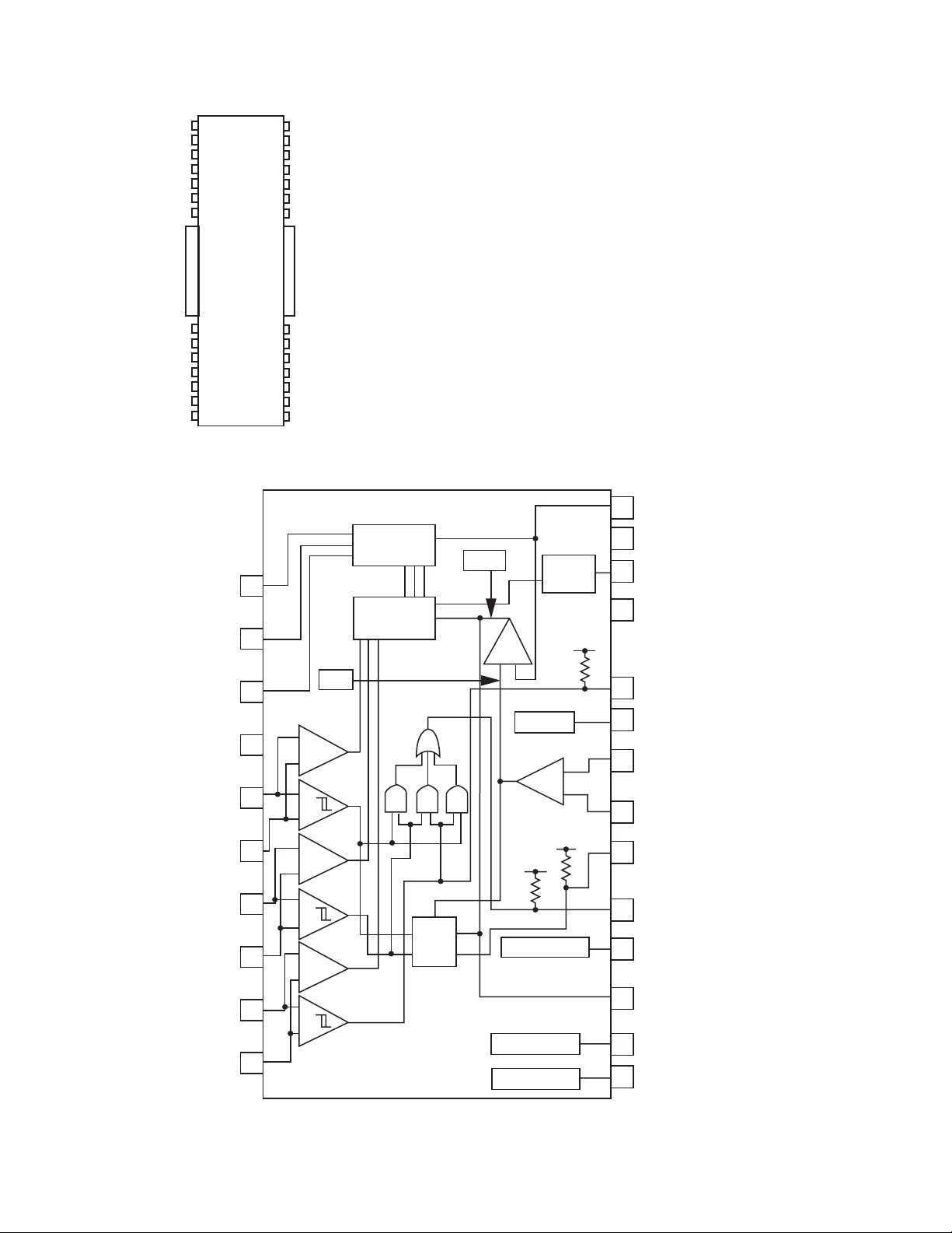
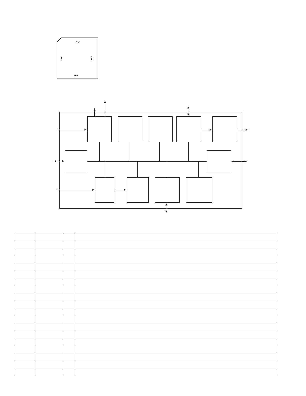
4.9 MN103S26EDC-H (IC301) : Super optical disc controller
• Terminal layout
176 133
1
132
• Block diagram
44
45 88
Analog
Servo I/O
(core 1 I/O)
Servo core
(core 2)
RAM
89
DVD-ROM
Formatter
CGEN
MODE
CD-PRE
Instruction
memory
(40KB)
Data
memory
(6KB)
General purpose IO bus
DMA
I/F
High speed IO bus
32 bit
CPU core
ECC
Host I/F
MPEG I/F
DMA
BCU
DRAMC
ATAPI
2Mbit
DRAM
CIRC
WDT
16 bit
timer x 2
SYSTEM
I/F
• Pin function
Pin No. Symbol I/O Description
1,2 NINT0,1 O Interruption of system control 0,1
3 VDD3 - Power supply terminal for I/O(3.3V)
4 VSS - Connect to ground
5 NINT2 O Interruption of system control 2
6 WAITDOC O Wait control of system control
7 NMPST O Reset of system control (Non connect)
8 DASPST I Setting of initial value of DASP signal
9~17 CPUADR17~9 I System control address
18 VDD18 - Power supply terminal for I/O (1.8V)
19 VSS - Connect to ground
20 DRAMVDD18 - Power supply terminal for DRAM (1.8V)
21 DRAMVSS - Connect to ground for DRAM
22~30 CPUADR8~0 I System control address
31 VDD3 - Power supply terminal for I/O (3.3V)
32 VSS - Connect to ground
33 DRAMVDD3 - Power supply terminal for DRAM (3.3V)
INTC
1-38 (No.XA003)
Page 39

Pin No. Symbol I/O Description
34 NCS I System control chip select
35 NWR I Writing system control
36 NRD I Read signal input from system controller
37~44 CPUDT7~0 I/O System control data
45 CLKOUT1 - Non connect
46 MMOD I Test mode switch signal
47 NRST I System reset
48 MSTPOL I Master terminal polarity switch input
49 SCLOCK - Non connect
50 SDATA - Non connect
51 OFTR I Off track signal input
52 BDO I Drop out signal input
53 SDOUT I/O Serial data input/output terminal
54 CPSCK O Clock output for serial data
55 FEPEN O Front end processor serial enable signal output
56 PWM4 I Traverse mechanism inner circumference detect switch
57 VDD3 - Power supply terminal for I/O (3.3V)
58 DRAMVDD18 - Power supply terminal for DRAM (1.8V)
59 DRAMVSS - Connect to ground for DRAM
60 VSS - Connect to ground
61 WOBBLEFIL - Non connect
62 PWM6 O Connect to pick up unit
63 PWM7 O Short brake terminal
64 PWM8 - Non connect
65 TBAL O Tracking balance adjustment output
66 FBAL O Focus balance adjustment output
67 TRSDRV O Traverse drive output
68 SPDRV O Spindle drive output
69 FG I Motor FG input
70 TILTP - Non connect
71 TILT - Non connect
72 TILTN - Non connect
73 TX O Digital output signal
74 DTRD - Non connect
75 IDGT - Non connect
76 VDD18 - Power supply terminal for I/O (1.8V)
77 VSS - Connect to ground
78 VDD3 - Power supply terminal for I/O (3.3V)
79 OSCI1 I Oscillation input 16.9MHz
80 OSCO1 O Oscillation output 16.9MHz
81 VSS - Connect to ground
82 TSTSG O Calibration signal
83 VFOSHORT O VFO short output
84 JLINE O J-line setting output
85 AVSS - Connect to ground for analog circuit
86 ROUT - Non connect
(No.XA003)1-39
Page 40

Pin No. Symbol I/O Description
87 LOUT - Non connect
88 AVDD - Power supply terminal for analog circuit (3.3V)
89 VCOF I JFVCO control voltage
90 TRCRS I Input signal for track cross formation
91 CMPIN - Non connect
92 LPFOUT - Non connect
93 LPFIN I Pull-up to VHALF
94 AVSS - Connect to ground for analog circuit
95 HPFOUT - Non connect
96 HPFIN I HPF input
97 CSLFLT I Pull-up to VHALF
98 RFDIF - Non connect
99 AVDD - Power supply terminal for analog circuit (3.3V)
100 PLFLT2 I Connect to capacitor 2 for PLL
101 PLFLT1 I Connect to capacitor 1 for PLL
102 AVSS - Connect to ground for analog circuit
103 RVI I Connect to resistor for VREF reference current source
104 VREFH I Reference voltage input (2.2V)
105 PLPG - Non connect
106 VHALF I Reference voltage input (1.65V)
107,108 DSLF2,1 I Connect to capacitor 2,1 for DSL
109 AVDD - Power supply terminal for analog circuit (3.3V)
110 NARF I Equivalence RF-
111 ARF I Equivalence RF+
112 JITOUT O Output for jitter signal monitor
113 AVSS - Connect to ground for analog circuit
114 DAC0 O Tracking drive output
115 DAC1 O Focus drive output
116 AVDD - Power supply terminal for analog circuit (3.3V)
117 AD0 I Focus error input
118 AD1 I Phase difference/3 beams tracking error
119 AD2 I AS : Full adder signal
120 AD3 I RF envelope input
121 AD4 I DVD laser current control terminal
122 AD5 I
123 AD6 I CD laser current control terminal
124 TECAPA - Non connect
125 VDD3 - Power supply terminal for I/O (3.3V)
126 VSS - Connect to ground
127 MONI0 - Connect to TP306
128 MONI1 - Connect to TP307
129 MONI2 - Connect to TP308
130 MONI3 - Connect to TP309
131 NEJECT I/O Eject detection
132 NTRYCTL I/O Tray close detection
133 NDASP I/O ATAPI drive active / slave connect I/O
1-40 (No.XA003)
Page 41

Pin No. Symbol I/O Description
134 NCS3FX I ATAPI host chip select
135 NCS1FX I ATAPI host chip select
136 DA2 O Data sampling clock output
137 DA0 I/O ATAPI host address 0
138 NPDIAG I/O ATAPI slave master diagnosis input
139 DA1 I/O ATAPI host address 1
140 NIOCS16 - Non connect
141 INTRQ O ATAPI host interruption output
142 NDMACK I ATAPI host DMA characteristic
143 VDD3 - Power supply terminal I/O (3.3V)
144 VSS - Connect to ground
145 IORDY - NOn connect
146 NIORD I/O ATAPI host read
147 NIOWR - Non connect
148 DMARQ - Non connect
149 HDD15 I/O ATAPI host data 15
150 HDD0 I/O ATAPI host data 0
151 HDD14 I/O ATAPI host data 14
152 VDD18 - Power supply terminal for I/O (1.8V)
153 PO I Connect to ground
154 UATASEL I Connect to ground
155 VSS - Connect to ground
156 VDD3 - Power supply terminal for I/O (3.3V)
157 HDD1 I/O ATAPI host data 1
158 HDD13 I/O ATAPI host data 13
159 HDD2 I/O ATAPI host data 2
160 HDD12 I/O ATAPI host data 12
161 HDD3 I/O ATAPI host data 3
162 VDD3 - Power supply terminal for I/O (3.3V)
163 VSS - Connect to ground
164 HDD11 I/O ATAPI host data 11
165 HDD4 I/O ATAPI host data 4
166 HDD10 I/O ATAPI host data 10
167 HDD5 I/O ATAPI host data 5
168 HDD9 I/O ATAPI host data 9
169 VDD3 - Power supply terminal for I/O (3.3V)
170 VSS - Connect to ground
171~173 HDD6~8 I/O ATAPI host data 6~8
174 VDDH - Reference power supply for ATAPI (5.0V)
175 NRESET I ATAPI host reset input
176 MASTER I ATAPI master / slave select
(No.XA003)1-41
Page 42
4.10 W986432DH-7 (IC505) : 32 Bits SDRAM
• Pin layout
86
85
84
83
82
81
80
50
49
48
47
46
45
44
1
2
3
4
5
6
7
37
38
39
40
41
42
43
• Pin function
Pin No. I/O Symbol Function
1 - Vcc Power for input buffers and logic circuit inside DRAM. (+3.3V)
2 I/O DQ0 Multiplexed pins for data out put and input.
3 I/O VccQ Separated power from VCC, to improve DQ noise immunity. (+3.3V)
4-5 I/O DQ1~DQ2 Multiplexed pins for data out put and input.
6 I/O VssQ Separated power from VSS, to improve DQ noise immunity.
7-8 I/O DQ3~DQ4 Multiplexed pins for data out put and input.
9 I/O VccQ Separated power from VCC, to improve DQ noise immunity.
10~11 I/O DQ5~DQ6 Multiplexed pins for data out put and input.
12 I/O VssQ Separated power from VSS, to improve DQ noise immunity.
13 I/O DQ7 Multiplexed pins for data out put and input.
14 - NC No connection
15 - Vcc Power for input buffers and logic circuit inside DRAM. (+3.3V)
16 I/O DQM0 The output buffer is placed at Hi-Z (with latency of 2) when DQM is sampled high in read cycle.
In write cycle sampling DQM high will block the write operation with zero latency.
17 - WE
Referred to RAS
18 - CAS Referred to RAS
19 - RAS Command input. When sampled at the rising edge of the clock RAS ,CAS and WE define the
operation to be executed.
20 - CS
Disable or enable the command decoder. When command decoder is disabled ,new command
is ignored and previous operation continues.
21 - NC No connection
22-23 -
-
BS0
BS1
Select bank to activate dining row address latch time, or bank to read / write during address
latch time,
or bank to read / write during address latch time.
24-27 - A0~A10 Multiplexed pins for row and column address. Row address: A0-A10. Column address:A0-
A7.A10 is sampled during a recharge command to determine if all banks are to be recharged
or bank selected by BS0, BS1.
28 I/O DQM2 The output buffer is placed at Hi-Z (with latency of 2) when DQM is sampled high in read cycle.
In write cycle, sampling DQM high will block the write operation with zero latency.
29 - Vcc Power for input buffers and logic circuit inside DRAM. (+3.3V)
30 - NC No connection
31 I/O DQ16 Multiplexed pins for data out put and input.
32 I/O VssQ Separated power from VSS, to improve DQ noise immunity.
33-34 I/O DQ17~18 Multiplexed pins for data out put and input.
35 I/O VssQ Separated power from VCC, to improve DQ noise immunity.
36-37 I/O DQ19~20 Multiplexed pins for data out put and input.
38 I/O VssQ Separated power from VSS, to improve DQ noise immunity.
1-42 (No.XA003)
Page 43

Pin No. I/O Symbol Function
39-40 I/O DQ21~22 Multiplexed pins for data out put and input.
41 - VccQ Separated power from VCC, to improve DQ noise immunity. (+3.3V)
42 I/O DQ23 Multiplexed pins for data out put and input.
43 - Vcc Power for input buffers and logic circuit inside DRAM. (+3.3V)
44 - Vss Ground for input buffers and logic circuit inside DRAM.
45 I/O DQ24 Multiplexed pins for data out put and input.
46 I/O VssQ Separated power from VSS, to improve DQ noise immunity.
47-48 I/O DQ25~26 Multiplexed pins for data out put and input.
49 - VccQ Separated power from VCC, to im prove DQ noise immunity. (+3.3V)
50-51 I/O DQ27~28 Multiplexed pins for data out put and input.
52 I/O VssQ Separated power from VSS, to improve DQ noise immunity.
53-54 I/O DQ29~30 Multiplexed pins for data out put and input.
55 - VccQ Separated power from VCC, to improve DQ noise immunity. (+3.3V)
56 I/O DQ31 Multiplexed pins for data out put and input.
57 - NC No connection
58 - Vss Ground for input buffers and logic circuit inside DRAM.
59 I/O DQM3 The output buffer is placed at Hi-Z (with latency of 2) when DQM is sampled high in read cycle.
In write cycle sampling DQM high will block the write operation with zero latency.
60-66 - A3~A9 Multiplexed pins for row and column address. Row address: Ao-A10. Column address:A0-
A7.A10 is sampled during a recharge command to determine if all banks are to be recharged
or bank selected by BS0, BS1.
67 - CKE CKE controls the clock activation and deactivation. When CKE is low, Power Down rising edge
of clock.
68 I CLK System clock used to sample inputs on the rising edge of clock.
69-70 - NC No connection
71 I/O DQM1 The output buffer is placed at Hi-Z (with latency of 2) when DQM is sampled high in read cycle.
In write cycle, sampling DQM high will block the write operation with zero latency.
72 - Vss Ground for input buffers and logic circuit inside DRAM.
73 I/O NC No connection
74 I/O DQ8 Multiplexed pins for data out put and input.
75 I/O VccQ Separated power from VCC, to improve DQ noise immunity. (+3.3V)
76-77 I/O DQ9~10 Multiplexed pins for data out put and input.
78 I/O VssQ Separated power from VSS, to improve DQ noise immunity.
79-80 I/O DQ11~12 Multiplexed pins for data out put and input.
81 I/O VccQ Separated power from VCC, to improve DQ noise immunity. (+3.3V)
82-83 I/O DQ13~14 Multiplexed pins for data out put and input.
84 I/O VssQ Separated power from VSS, to improve DQ noise immunity.
85 I/O DQ15 Multiplexed pins for data out put and input.
86 - Vss Ground for input buffers and logic circuit inside DRAM.
(No.XA003)1-43
Page 44
• Block diagram
CLK
CKE
CS
RAS
CAS
WE
A10
A0
A9
BS0
BS1
Clock
buffer
Command
buffer
Address
buffer
Control
signal
generator
Mode
register
Column decoder
Cell array
bank #0
Row decoder
Sense amplifier
Column decoder
Cell array
bank #1
Row decoder
Sense amplifier
Refresh
counter
Column
counter
NOTE:
The cell array configuration is 2048 * 256 * 32
Column decoder
Cell array
bank #2
Row decoder
Sense amplifier
Data control
circuit
DQ
buffer
Column decoder
Cell array
bank #3
Row decoder
Sense amplifier
DQ1
DQ31
DQM0~3
1-44 (No.XA003)
Page 45

(No.XA003)1-45
Page 46

VICTOR COMPANY OF JAPAN, LIMITED
AV & MULTIMEDIA COMPANY OPTICAL DISC CATEGORY 1644, Shimotsuruma, Yamato, Kanagawa 242-8514, Japan
(No.XA003)
Printed in Japan
WPC
Page 47
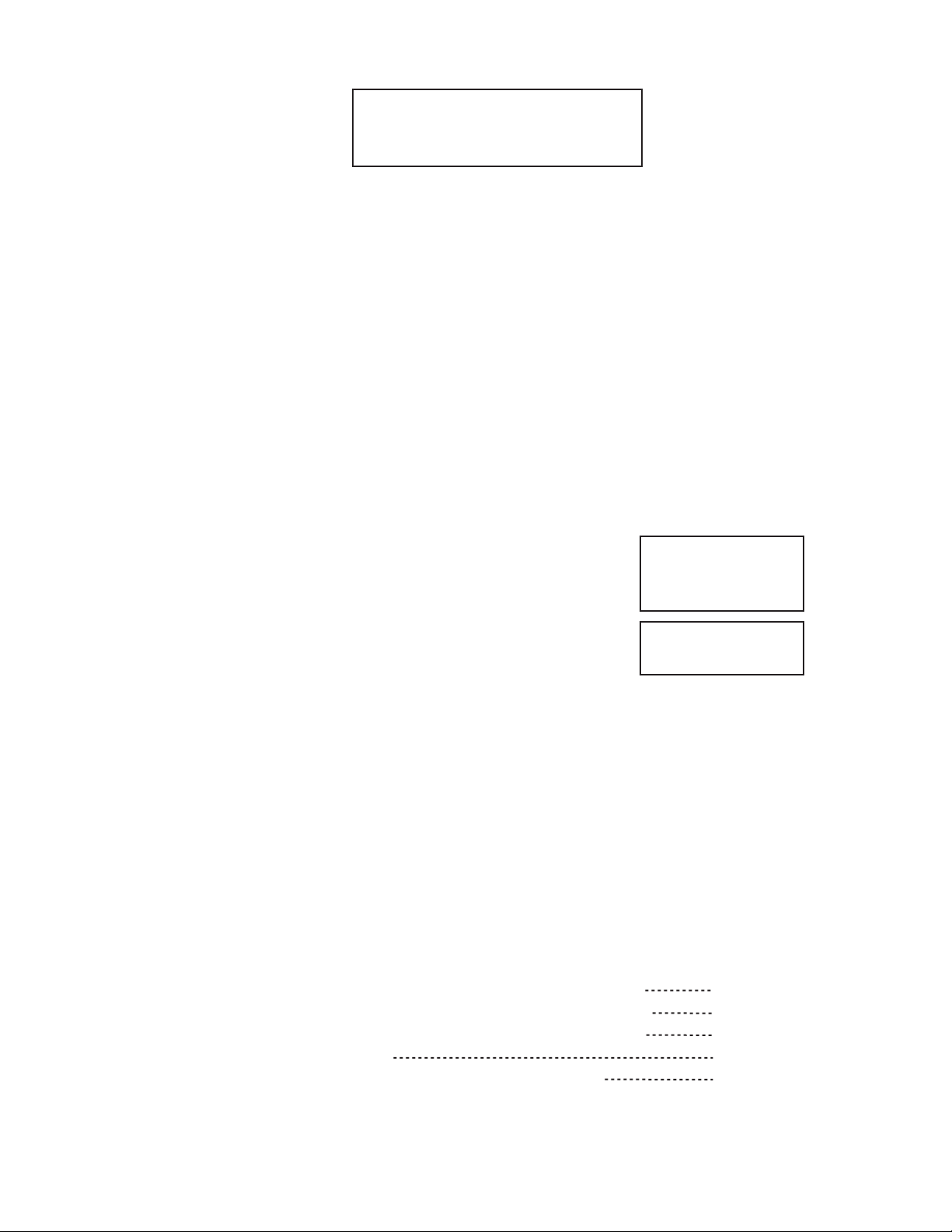
XV-N40BK,XV-N44SL,XV-N4SL
PARTS LIST
[XV-N40BK,XV-N44SL,XV-N4SL]
[MK2]
* All printed circuit boards and its assemblies are not available as service parts.
* (x_) in a description column shows the number of the used part.
- Contents -
Exploded view of general assembly and parts list
DVD Traverse mechanism assembly and parts list
DVD Loading mechanism assembly and parts list
Electrical parts list
Packing materials and accessories parts list
Area Suffix
(XV-N40BK,XV-N44SL)
J -------------------------- U.S.A.
C --------------------- Canada
Area Suffix (XV-N4SL)
C --------------------- Canada
3-2
3-4
3-6
3-8
3-12
(No.XA003)3-1
Page 48
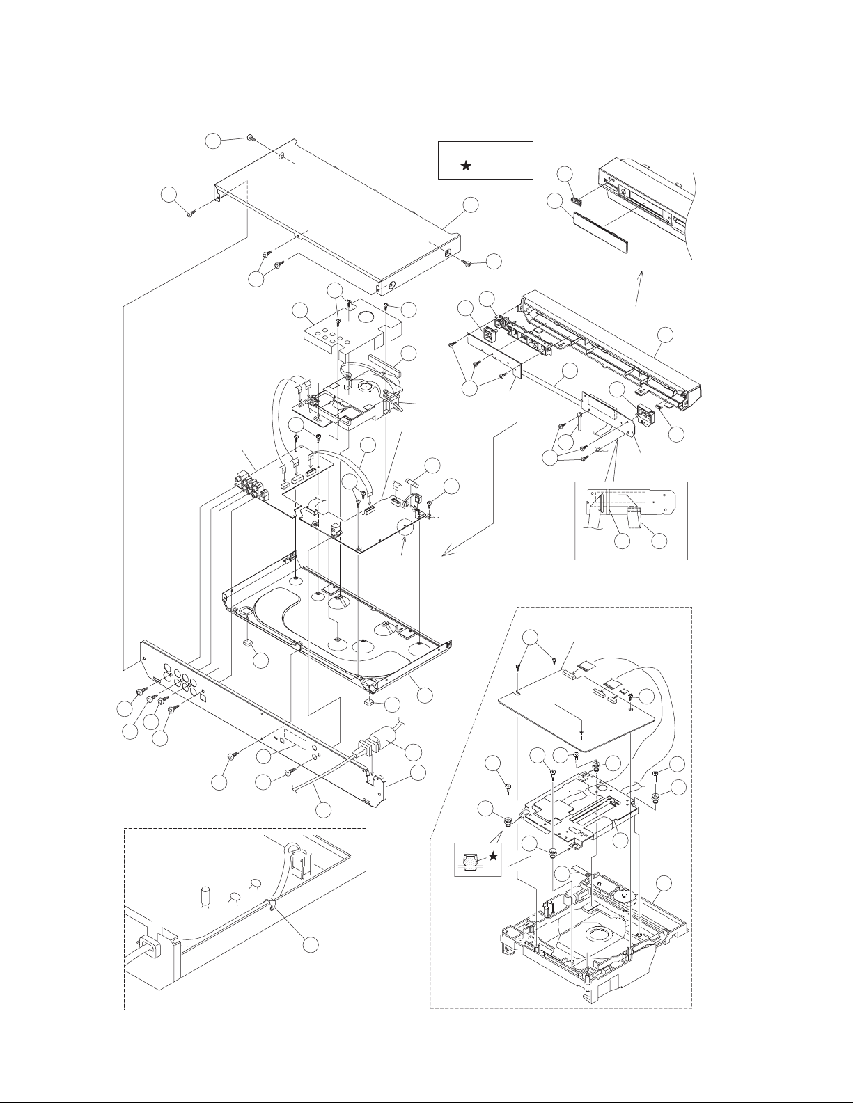
XV-N40BK,XV-N44SL,XV-N4SL
Exploded view of general assembly and parts list
Block No.M1MM
37
38
Audio/Video
output board
37
15
44
Grease
JVS-1003
36
38
23
23
39
b
"B"
Power supply &
system control
e
c
"A"
board
32
40
15
b
15
7
8
9
Operation
switch board
2
3
BACK
SIDE
1
42
4
e
11
6
display board
10
5
FL
41
27
28
"A"
29
26
25
13
43
31
34
33
13
c
45
24
12
17
19
"B" BACK SIDE
19
d
22
Servo
control board
a
a
21
19
17
17
d
21
19
17
16
20
3-2(No.XA003)
Page 49

XV-N40BK,XV-N44SL,XV-N4SL
General assembly
Block No. [M][1][M][M]
Symbol No. Part No. Part Name Description Local
1 GN10037-007A FRONT PANEL 40C,40J
1 GN10037-011A FRONT PANEL 44C,44J
1 GN10037-012A FRONT PANEL 4C
2 GN40020-001A JVC MARK 40C,40J
2 GN40020-002A JVC MARK 44C,44J,4C
3 GN20041-002A WINDOW SCREEN
4 GN20040-003A PUSH BUTTON POWER 40C,40J
4 GN20040-002A PUSH BUTTON POWER 44C,44J,4C
5 GN30049-001A INDICATOR
6 QYSDSF2608Z SCREW POWER SW.CB.(x3)
7 GN20043-005A PUSH BUTTON PLAY 40C,40J
7 GN20043-002A PUSH BUTTON PLAY 44C,44J,4C
8 GN20044-002A PUSH BUTTON SEARCH
9 QYSDSF2608Z SCREW PLAY SW.CB.(x3)
10 GN30006-012A SPACER
11 VKZ4001-110 WIRE HOLDER
12 GN10038-002A CHASSIS BASE 40C,40J
12 GN10038-001A CHASSIS BASE 44C,44J,4C
13 E75896-002 FELT SPACER (x2)
15 QYSBSG3008Z TAPPING SCREW MAIN CB+CHASSIS(x5)
16 ------------ TRAVERSE MECHANISM
17 LE40900-003A INSULATOR (x4)
19 LE40901-001A SPECIAL SCREW FOR INSULATOR(x4)
20 ------------ LOADING MECHANISM
21 QYSDSF2608Z SCREW FOR CLAMPER BAS(x3)
22 QUQ210-0518BJ FFC WIRE
23 QYSBSG3008Z TAPPING SCREW MECHA+CHASSIS(x3)
24 GN20047-023A REAR PANEL 40C,40J
24 GN20047-038A REAR PANEL 44C,44J
24 GN20047-051A REAR PANEL 4C
25 QYSBSGY3008M SPECIAL SCREW REAR+CHASSIS
26 QYSBSGY3008M SPECIAL SCREW OPT OUT 40C,40J,44C,44J
27 QYSBSGY3008M SPECIAL SCREW COAXIAL
28 QYSBSGY3008M SPECIAL SCREW AUDIO OUT
29 QYSBSGY3008M SPECIAL SCREW VIDEO OUT
31 QYSBSGY3008M SPECIAL SCREW COMPU LINK
32 QMF51U1-1R6-J8 FUSE 1.6A AC125V
33 QMPD450-200-JN POWER CORD(US/CA) 2m BLACK
34 QZW0004-001 WIRE CLAMP
36 GN20046-001A/S/ METAL COVER 40C,40J
36 GN20046-002A/S/ METAL COVER 44C,44J,4C
37 QYSBSGG3008E TAPPING SCREW METAL REAR(x3)
38 QYSDSG3008M SCREW METAL SIDE(x2) 40C,40J
38 QYSDSG3008N TAPPING SCREW METAL SIDE(x2) 44C,44J,4C
39 GN20042-002A FITTING 40C,40J
39 GN20042-005A FITTING 44C,44J,4C
40 QUQ412-1923BJ FFC WIRE
41 QUQ412-1417BJ FFC WIRE
42 QUQ412-0817AJ FFC WIRE
43 GN30080-001A SERVICE LABEL
44 GN30081-002A SHIELD
45 QQR0491-001 FERRITE CORE
<Local area>
XV-N40BK J:40J C:40C
XV-N44SL J:44J C:44C XV-N4SL C:4C
(No.XA003)3-3
Page 50
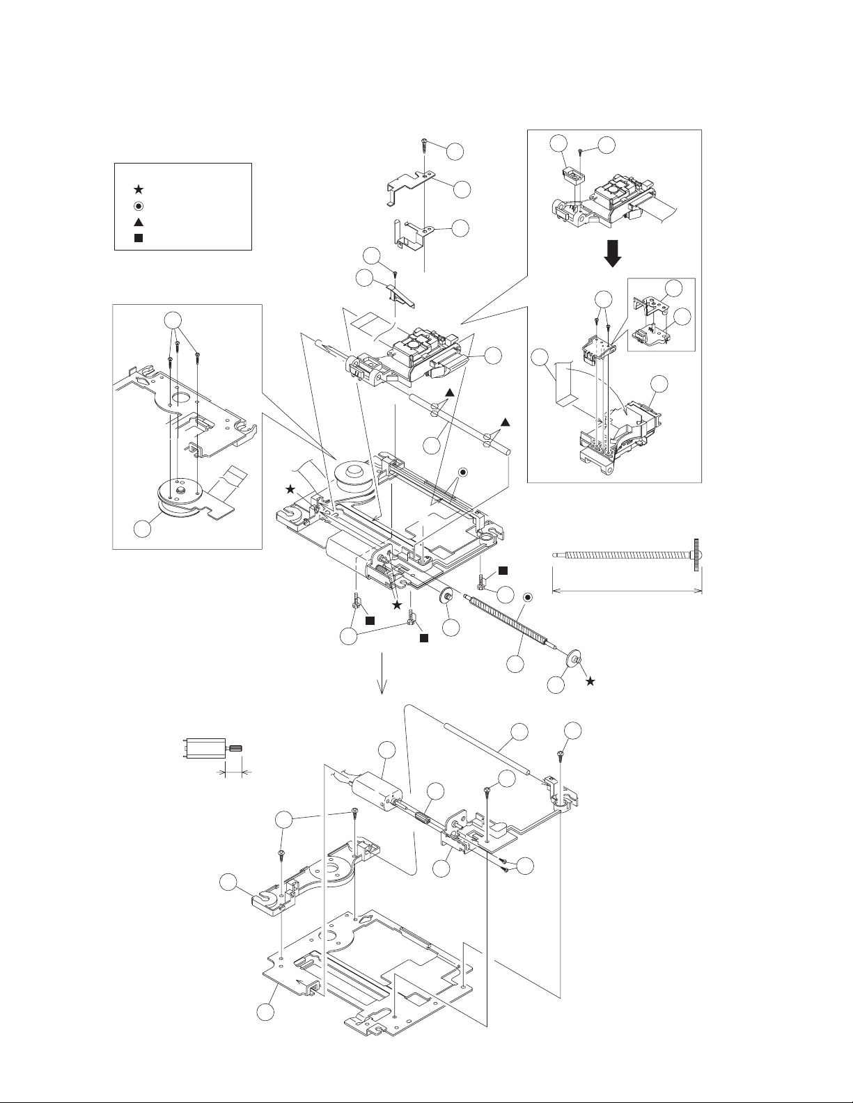
XV-N40BK,XV-N44SL,XV-N4SL
DVD Traverse mechanism assembly and parts list
Grease
=JVG-31N
=CFD-4007ZY2
=PG-641
=1401C
< BACK SIDE >
27
EXL-V10-1C
25
24
23
6
5
A
16
Block No.M2MM
17
15
14
13
26
28
29
19
A
22
8
28
21
18
12
+
63.3mm
20
4
11
0.1mm
-
3-4(No.XA003)
10.5mm
+
-
2
0.1mm
1
9
3
7
11
10
Page 51

XV-N40BK,XV-N44SL,XV-N4SL
DVD Traverse mechanism
Symbol No. Part No. Part Name Description Local
1 LE20697-002A MECHA BASE
2 LE20699-001A SPINDLE BASE
3 QYSDST2604M TAPPING SCREW 2.6mm x 4mm(x2)
4 LE40931-001A SHAFT
5 LV33991-001A ADJUST SPRING
6 QYSPSFU2040M TAPPING SCREW M2 x 4mm
7 LE20698-001A FEED HOLDER
8 QAR0215-001 FEED MOTOR
9 LV41510-001A FEED GEAR T
10 QYSPSPU2040M TAPPING SCREW M2 x 4mm(x2)
11 QYSDST2604M TAPPING SCREW 2.6mm x 4mm(x2)
12 QAL0478-001 PICK UP
13 LE20700-001A SW ACTUATOR
14 LE31067-002A LEAD SPRING
15 QYSPSFU1740Z TAPPING SCREW M1.7 x 4mm(x2)
16 LE40929-001A SW.LEVER
17 QYSPSFU1740Z TAPPING SCREW M1.7 x 4mm
18 QUQ105-2409AC FFC
19 LE40931-001A SHAFT
20 LE40855-001A FEED GEAR E
21 LE40918-001A LEAD SCREW
22 LE40930-001A FEED GEAR M
23 LE40928-001A THURUST SPRING
24 LE40927-001A PLATE
25 QYSDST2614Z TAPPING SCREW M2.6 x 14mm
26 QAR0284-001 SPINDLE MOTOR
26 QAR0285-001 SPINDLE MOTOR
27 QYSPSPU1740Z TAPPING SCREW M1.7 x 4mm(x3)
28 LE40858-002A SPECIAL SCREW (x3)
29 QQR1426-001C FERRITE CORE
Block No. [M][2][M][M]
(No.XA003)3-5
Page 52
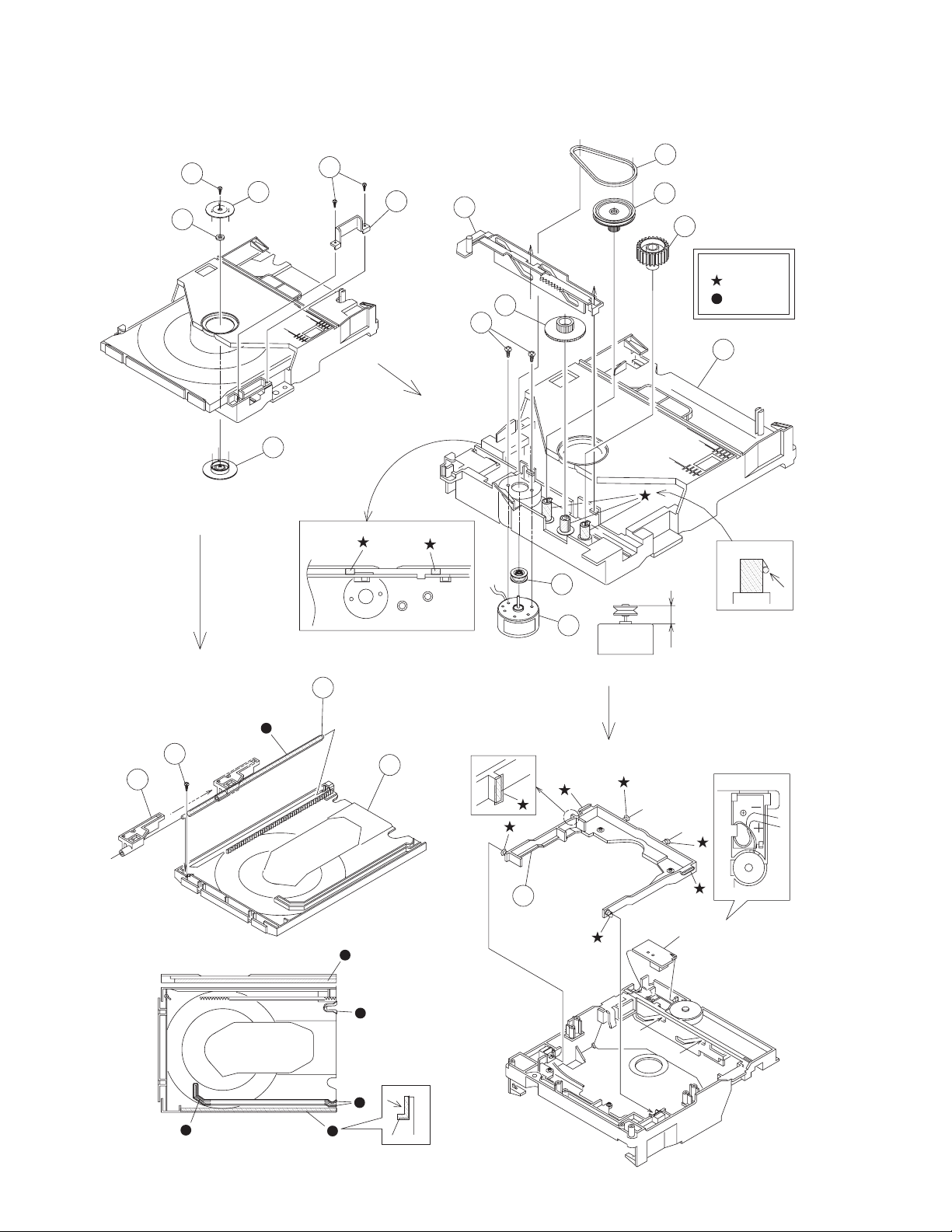
XV-N40BK,XV-N44SL,XV-N4SL
DVD Loading mechanism assembly and parts list
22
ELM-J2-1C
5
4
13
18
20
14
19
17
Block No.M3MM
16
3
21
Grease
JVG-31N
JVS-1003
1
(All circumferenced)
10
8
12
0.10mm
-
+
11
7.95mm
9
BACK SIDE
7
a
b
6
switch board
a
b
3-6(No.XA003)
Page 53

XV-N40BK,XV-N44SL,XV-N4SL
DVD Loading mechanism
Symbol No. Part No. Part Name Description Local
1 LE10275-002A LOADER BASE
3 LE31043-001A PULLEY GEAR
4 LE31042-001A MIDDLE GEAR
5 LE20665-001A SLIDE CAM
6 LE20666-001A ELEVATOR
7 LE10276-002A TRAY
8 LE31045-001A BUSHING
9 LE40898-001A SHAFT
10 QYSSSF2008Z TAP SCREW M2 x 8mm
11 QAR0197-001 MOTOR
12 LV42087-002A MOTOR PULLEY
13 QYSPSPU1730Z SCREW FOR MOTOR(x2)
14 QYSDSF2008Z TAP SCREW M2 x 8mm(x2)
16 LE40897-001A BELT
17 LE31046-001A CLAMPER
18 LV42930-003A MAGNET
18 or LV41118-003A MAGNET
19 LE40899-001A YOKE
20 LE40906-001A SPECIAL SCREW
21 LE31044-001A IDLE GEAR
22 LE40937-001A LEAF SPRING
Block No. [M][3][M][M]
(No.XA003)3-7
Page 54

XV-N40BK,XV-N44SL,XV-N4SL
Electrical parts list
Servo control board
Block No. [0][1]
Symbol No.
IC101 AN8703FH-V IC Frontend processor for DVD
IC201 BA5983FM-X IC 4-channel driver
IC251 BA6664FM-X IC Motor driver
IC301 MN103S26EDC-H IC
IC402 AK4381VT-X IC 2ch DAC
IC501 JCE8045 IC
IC505 or HY57643220CT55 IC 44J
IC505 or W986432DH-7 IC Bits SDRAM
IC505 HY57643220CT55 IC
IC509
IC509
IC511 LM1117MP1.8-X IC Regulator
IC512 74LCX373MTC-X IC(DIGITAL) Octal D-type latch
IC513 74LCX373MTC-X IC(DIGITAL) Octal D-type latch
Q101 2SB1424/QR/-W TRANSISTOR
Q102 2SB1424/QR/-W TRANSISTOR
Q103 DTA144EE-X DIGI TRANSISTOR
Q801 UN2111-X TRANSISTOR 4C
Q802 UN2111-X TRANSISTOR 4C
D101 RB521S-30-X SB DIODE
D301 RB521S-30-X SB DIODE
C105 NEA70JM-476X E CAPACITOR 47uF 6.3V M
C106 NEA70JM-476X E CAPACITOR 47uF 6.3V M
C109 NCB31CK-104X C CAPACITOR 0.1uF 16V K
C110 NCS31HJ-221X C CAPACITOR 220pF 50V J
C111 NCF31CZ-104X C CAPACITOR 0.1uF 16V Z
C112 NCF31CZ-104X C CAPACITOR 0.1uF 16V Z
C116 NCB31CK-104X C CAPACITOR 0.1uF 16V K
C117 NCB31CK-473X C CAPACITOR 0.047uF 16V K
C118 NCB31CK-273X C CAPACITOR 0.027uF 16V K
C119 NCB31HK-561X C CAPACITOR 560pF 50V K
C120 NCB31HK-561X C CAPACITOR 560pF 50V K
C121 NCB31CK-104X C CAPACITOR 0.1uF 16V K
C122 NCS31HJ-120X C CAPACITOR 12pF 50V J
C123 NCF31CZ-104X C CAPACITOR 0.1uF 16V Z
C124 NCS31HJ-470X C CAPACITOR 47pF 50V J
C125 NCB31HK-271X C CAPACITOR 270pF 50V K
C126 NCF31CZ-104X C CAPACITOR 0.1uF 16V Z
C127 NCF31CZ-104X C CAPACITOR 0.1uF 16V Z
C128 NCF31CZ-104X C CAPACITOR 0.1uF 16V Z
C129 NCB31HK-472X C CAPACITOR 4700pF 50V K
C135 NEA70JM-476X E CAPACITOR 47uF 6.3V M
C137 NEA70GM-476X E CAPACITOR 47uF 4V M
C138 NCF31CZ-104X C CAPACITOR 0.1uF 16V Z
C141 NCF31CZ-104X C CAPACITOR 0.1uF 16V Z
C142 NCF31CZ-104X C CAPACITOR 0.1uF 16V Z
C144 NCB31CK-103X C CAPACITOR 0.01uF 16V K
C204 NCF31CZ-104X C CAPACITOR 0.1uF 16V Z
C205 NCS31HJ-121X C CAPACITOR 120pF 50V J
C207 NCB31HK-391X C CAPACITOR 390pF 50V K
C208 NCB31HK-391X C CAPACITOR 390pF 50V K
C211 NCB31HK-223X C CAPACITOR 0.022uF 50V K
C212 NCB31CK-103X C CAPACITOR 0.01uF 16V K
C216 NCB30JK-105X C CAPACITOR 1uF 6.3V K
C217 NCF31CZ-104X C CAPACITOR 0.1uF 16V Z
C218 NCB30JK-105X C CAPACITOR 1uF 6.3V K
C251 NCF31CZ-104X C CAPACITOR 0.1uF 16V Z
C253 NCF31CZ-104X C CAPACITOR 0.1uF 16V Z
C255 NCB31CK-153X C CAPACITOR 0.015uF 16V K
C256 NCB31CK-104X C CAPACITOR 0.1uF 16V K
C257 NCF31CZ-104X C CAPACITOR 0.1uF 16V Z
C258 NCF31CZ-104X C CAPACITOR 0.1uF 16V Z
C259 NCF31CZ-104X C CAPACITOR 0.1uF 16V Z
C260 NCF31CZ-104X C CAPACITOR 0.1uF 16V Z
C261 NCF31CZ-104X C CAPACITOR 0.1uF 16V Z
C262 NCF31CZ-104X C CAPACITOR 0.1uF 16V Z
C263 NCF31CZ-104X C CAPACITOR 0.1uF 16V Z
C264 NCB31CK-103X C CAPACITOR 0.01uF 16V K
3-8(No.XA003)
Part No. Part Name Description Local
SST39VF160H0891
SST39VF160H0961
IC
IC only XV-N4SL
40C,40J,44C,
4C
except XV-N4SL
Symbol No.
C301 NCF31CZ-104X C CAPACITOR 0.1uF 16V Z
C302 NCF31CZ-104X C CAPACITOR 0.1uF 16V Z
C303 NCF31CZ-104X C CAPACITOR 0.1uF 16V Z
C304 NEA70GM-476X E CAPACITOR 47uF 4V M
C306 NEA70GM-476X E CAPACITOR 47uF 4V M
C308 NEA70GM-476X E CAPACITOR 47uF 4V M
C310 NCF31CZ-104X C CAPACITOR 0.1uF 16V Z
C311 NCB31HK-561X C CAPACITOR 560pF 50V K
C312 NCB31HK-561X C CAPACITOR 560pF 50V K
C313 NCB31HK-561X C CAPACITOR 560pF 50V K
C314 NCB31HK-331X C CAPACITOR 330pF 50V K
C315 NCB31HK-471X C CAPACITOR 470pF 50V K
C316 NCB31HK-271X C CAPACITOR 270pF 50V K
C317 NCS31HJ-121X C CAPACITOR 120pF 50V J
C318 NCF31CZ-104X C CAPACITOR 0.1uF 16V Z
C319 NCB31HK-102X C CAPACITOR 1000pF 50V K
C320 NCB31HK-102X C CAPACITOR 1000pF 50V K
C321 NCB31HK-102X C CAPACITOR 1000pF 50V K
C322 NCB31HK-562X C CAPACITOR 5600pF 50V K
C323 NCB31HK-102X C CAPACITOR 1000pF 50V K
C324 NCF31CZ-104X C CAPACITOR 0.1uF 16V Z
C325 NCS31HJ-470X C CAPACITOR 47pF 50V J
C326 NCB31CK-183X C CAPACITOR 0.018uF 16V K
C327 NCB31HK-102X C CAPACITOR 1000pF 50V K
C328 NCF31CZ-104X C CAPACITOR 0.1uF 16V Z
C329 NCB31CK-103X C CAPACITOR 0.01uF 16V K
C330 NCB31CK-104X C CAPACITOR 0.1uF 16V K
C331 NCB31CK-103X C CAPACITOR 0.01uF 16V K
C332 NCF31CZ-104X C CAPACITOR 0.1uF 16V Z
C333 NCB31CK-104X C CAPACITOR 0.1uF 16V K
C334 NCB31CK-104X C CAPACITOR 0.1uF 16V K
C337 NCF31CZ-104X C CAPACITOR 0.1uF 16V Z
C338 NCF31CZ-104X C CAPACITOR 0.1uF 16V Z
C339 NCB31CK-104X C CAPACITOR 0.1uF 16V K
C340 NCB31CK-104X C CAPACITOR 0.1uF 16V K
C341 NCF31CZ-104X C CAPACITOR 0.1uF 16V Z
C343 NCF31CZ-104X C CAPACITOR 0.1uF 16V Z
C345 NCF31CZ-104X C CAPACITOR 0.1uF 16V Z
C346 NCF31CZ-104X C CAPACITOR 0.1uF 16V Z
C347 NCF31CZ-104X C CAPACITOR 0.1uF 16V Z
C348 NCB31CK-104X C CAPACITOR 0.1uF 16V K
C349 NCF31CZ-104X C CAPACITOR 0.1uF 16V Z
C350 NCF31CZ-104X C CAPACITOR 0.1uF 16V Z
C360 NEA70GM-476X E CAPACITOR 47uF 4V M
C400 NCB31HK-102X C CAPACITOR 1000pF 50V K
C407 NCF31CZ-104X C CAPACITOR 0.1uF 16V Z
C408 NEA70JM-227X E CAPACITOR 220uF 6.3V M
C409 NEA70JM-227X E CAPACITOR 220uF 6.3V M
C501 NCF31CZ-104X C CAPACITOR 0.1uF 16V Z
C506 NDC31HJ-150X C CAPACITOR 15pF 50V J
C507 NDC31HJ-180X C CAPACITOR 18pF 50V J
C512 NCF31CZ-104X C CAPACITOR 0.1uF 16V Z
C517 NCF31CZ-104X C CAPACITOR 0.1uF 16V Z
C518 NCF31CZ-104X C CAPACITOR 0.1uF 16V Z
C519 NCF31CZ-104X C CAPACITOR 0.1uF 16V Z
C521 NCF31CZ-104X C CAPACITOR 0.1uF 16V Z
C523 NCF31CZ-104X C CAPACITOR 0.1uF 16V Z
C524 NEA70GM-476X E CAPACITOR 47uF 4V M
C527 NEA70GM-476X E CAPACITOR 47uF 4V M
C531 NCF31CZ-104X C CAPACITOR 0.1uF 16V Z
C532 NCF31CZ-104X C CAPACITOR 0.1uF 16V Z
C533 NCF31CZ-104X C CAPACITOR 0.1uF 16V Z
C534 NCF31CZ-104X C CAPACITOR 0.1uF 16V Z
C540 NCF31CZ-104X C CAPACITOR 0.1uF 16V Z
C541 NCF31CZ-104X C CAPACITOR 0.1uF 16V Z
C542 NCB31CK-104X C CAPACITOR 0.1uF 16V K
C543 NCF31CZ-104X C CAPACITOR 0.1uF 16V Z
C544 NCF31CZ-104X C CAPACITOR 0.1uF 16V Z
C545 NCF31CZ-104X C CAPACITOR 0.1uF 16V Z
C548 NCF31CZ-104X C CAPACITOR 0.1uF 16V Z
C549 NEA70GM-476X E CAPACITOR 47uF 4V M
C550 NCF31CZ-104X C CAPACITOR 0.1uF 16V Z
C551 NCB31CK-103X C CAPACITOR 0.01uF 16V K
C554 NCF31CZ-104X C CAPACITOR 0.1uF 16V Z
Part No. Part Name Description Local
<Local area>
XV-N40BK J:40J C:40C
XV-N44SL J:44J C:44C XV-N4SL C:4C
Page 55

Symbol No.
Part No. Part Name Description Local
Symbol No.
XV-N40BK,XV-N44SL,XV-N4SL
Part No. Part Name Description Local
C557 NCF31CZ-104X C CAPACITOR 0.1uF 16V Z
C558 NCF31CZ-104X C CAPACITOR 0.1uF 16V Z
C562 NCF31CZ-104X C CAPACITOR 0.1uF 16V Z
C566 NCF31CZ-104X C CAPACITOR 0.1uF 16V Z
C569 NCF31CZ-104X C CAPACITOR 0.1uF 16V Z
C572 NCF31CZ-104X C CAPACITOR 0.1uF 16V Z
C573 NEA70GM-476X E CAPACITOR 47uF 4V M
C578 NCF31CZ-104X C CAPACITOR 0.1uF 16V Z
C581 NEA70GM-227X E CAPACITOR 220uF 4V M
R101 NRSA63J-333X MG RESISTOR 33kΩ 1/16W J
R102 NRSA63J-223X MG RESISTOR 22kΩ 1/16W J
R103 NRSA63J-223X MG RESISTOR 22kΩ 1/16W J
R104 NRS125J-270X MG RESISTOR 27Ω 1/2W J
R105 NRS125J-270X MG RESISTOR 27Ω 1/2W J
R106 NRSA63J-273X MG RESISTOR 27kΩ 1/16W J
R107 NRSA63J-273X MG RESISTOR 27kΩ 1/16W J
R108 NRSA63J-222X MG RESISTOR 2.2kΩ 1/16W J
R109 NRSA63J-182X MG RESISTOR 1.8kΩ 1/16W J
R110 NRSA63J-333X MG RESISTOR 33kΩ 1/16W J
R111 NRVA63D-243X CMF RESISTOR 24k
R112 NRSA63J-822X MG RESISTOR 8.2k
R113 NRSA63J-103X MG RESISTOR 10kΩ 1/16W J
R115 NRSA63J-0R0X MG RESISTOR 0Ω 1/16W J
R116 NRSA63J-101X MG RESISTOR 100Ω 1/16W J
R117 NRSA63J-101X MG RESISTOR 100Ω 1/16W J
R119 NRSA63J-2R2X MG RESISTOR 2.2Ω 1/16W J
R120 NRSA63J-2R2X MG RESISTOR 2.2Ω 1/16W J
R125 NRSA63J-105X MG RESISTOR 1MΩ 1/16W J
R126 NRSA63J-105X MG RESISTOR 1MΩ 1/16W J
R127 NRSA63J-222X MG RESISTOR 2.2kΩ 1/16W J
R128 NRS125J-1R0X MG RESISTOR 1Ω 1/2W J
R129 NRS125J-1R0X MG RESISTOR 1Ω 1/2W J
R130 NRSA63J-182X MG RESISTOR 1.8kΩ 1/16W J
R201 NRSA63J-470X MG RESISTOR 47Ω 1/16W J
R202 NRS125J-1R0X MG RESISTOR 1Ω 1/2W J
R204 NRSA63J-273X MG RESISTOR 27kΩ 1/16W J
R205 NRSA63J-273X MG RESISTOR 27kΩ 1/16W J
R206 NRSA63J-303X MG RESISTOR 30kΩ 1/16W J
R207 NRSA63J-473X MG RESISTOR 47kΩ 1/16W J
R208 NRSA63J-223X MG RESISTOR 22kΩ 1/16W J
R209 NRSA63J-223X MG RESISTOR 22kΩ 1/16W J
R210 NRSA63J-392X MG RESISTOR 3.9kΩ 1/16W J
R211 NRSA63J-392X MG RESISTOR 3.9kΩ 1/16W J
R212 NRSA63J-103X MG RESISTOR 10kΩ 1/16W J
R213 NRSA63J-103X MG RESISTOR 10kΩ 1/16W J
R214 NRSA63J-103X MG RESISTOR 10kΩ 1/16W J
R215 NRSA63J-103X MG RESISTOR 10kΩ 1/16W J
R216 NRSA63J-912X MG RESISTOR 9.1kΩ 1/16W J
R219 NRSA63J-183X MG RESISTOR 18k
R220 NRSA63J-243X MG RESISTOR 24kΩ 1/16W J
R221 NRSA63J-682X MG RESISTOR 6.8k
R222 NRSA63J-103X MG RESISTOR 10k
R223 NRSA63J-912X MG RESISTOR 9.1kΩ 1/16W J
R230 NRSA63J-332X MG RESISTOR 3.3k
R251 NRS125J-R47X MG RESISTOR 0.47
R252 NRSA63J-2R2X MG RESISTOR 2.2Ω 1/16W J
R254 NRSA63J-203X MG RESISTOR 20k
R255 NRSA63J-103X MG RESISTOR 10kΩ 1/16W J
R256 NRSA63J-470X MG RESISTOR 47
R259 NRSA63J-103X MG RESISTOR 10k
R280 NRSA63J-332X MG RESISTOR 3.3kΩ 1/16W J
R301 NRSA63J-473X MG RESISTOR 47k
R302 NRSA63J-473X MG RESISTOR 47k
R303 NRSA63J-473X MG RESISTOR 47kΩ 1/16W J
R304 NRSA63J-473X MG RESISTOR 47k
R305 NRSA63J-473X MG RESISTOR 47k
R306 NRSA63J-473X MG RESISTOR 47k
R307 NRSA63J-473X MG RESISTOR 47k
R308 NRSA63J-0R0X MG RESISTOR 0Ω 1/16W J
R309 NRSA63J-473X MG RESISTOR 47k
R313 NRSA63J-473X MG RESISTOR 47k
R317 NRSA63J-473X MG RESISTOR 47kΩ 1/16W J
R320 NRSA63J-105X MG RESISTOR 1M
R321 NRSA63J-473X MG RESISTOR 47k
R323 NRSA63J-473X MG RESISTOR 47kΩ 1/16W J
R324 NRSA63J-473X MG RESISTOR 47k
R325 NRSA63J-123X MG RESISTOR 12k
<Local area>
XV-N40BK J:40J C:40C
XV-N44SL J:44J C:44C XV-N4SL C:4C
Ω
1/16W D
Ω
1/16W J
Ω
1/16W J
Ω
1/16W J
Ω
1/16W J
Ω
1/16W J
Ω
1/2W J
Ω
1/16W J
Ω
1/16W J
Ω
1/16W J
Ω
1/16W J
Ω
1/16W J
Ω
1/16W J
Ω
1/16W J
Ω
1/16W J
Ω
1/16W J
Ω
1/16W J
Ω
1/16W J
Ω
1/16W J
Ω
1/16W J
Ω
1/16W J
Ω
1/16W J
R326 NRSA63J-473X MG RESISTOR 47kΩ 1/16W J
R327 NRSA63J-105X MG RESISTOR 1MΩ 1/16W J
R328 NRSA63J-153X MG RESISTOR 15kΩ 1/16W J
R329 NRSA63J-473X MG RESISTOR 47kΩ 1/16W J
R330 NRSA63J-473X MG RESISTOR 47kΩ 1/16W J
R331 NRSA63J-473X MG RESISTOR 47k
R332 NRSA63J-102X MG RESISTOR 1k
R333 NRSA63J-183X MG RESISTOR 18kΩ 1/16W J
R334 NRSA63J-102X MG RESISTOR 1kΩ 1/16W J
R336 NRSA63J-273X MG RESISTOR 27kΩ 1/16W J
R337 NRSA63J-273X MG RESISTOR 27kΩ 1/16W J
R338 NRSA63J-472X MG RESISTOR 4.7kΩ 1/16W J
R339 NRSA63J-472X MG RESISTOR 4.7kΩ 1/16W J
R340 NRSA63J-103X MG RESISTOR 10kΩ 1/16W J
R341 NRSA63J-562X MG RESISTOR 5.6kΩ 1/16W J
R342 NRSA63J-0R0X MG RESISTOR 0Ω 1/16W J
R343 NRSA63J-103X MG RESISTOR 10kΩ 1/16W J
R344 NRSA63J-103X MG RESISTOR 10kΩ 1/16W J
R345 NRSA63J-681X MG RESISTOR 680Ω 1/16W J
R403 NRSA63J-100X MG RESISTOR 10Ω 1/16W J
R404 NRSA63J-332X MG RESISTOR 3.3k
R501 NRSA63J-470X MG RESISTOR 47
R513 NRSA63J-0R0X MG RESISTOR 0Ω 1/16W J
R514 NRSA63J-220X MG RESISTOR 22Ω 1/16W J
R515 NRSA63J-331X MG RESISTOR 330Ω 1/16W J
R519 NRSA63J-103X MG RESISTOR 10kΩ 1/16W J
R520 NRSA63J-0R0X MG RESISTOR 0Ω 1/16W J
R521 NRSA63J-0R0X MG RESISTOR 0Ω 1/16W J
R522 NRSA63J-0R0X MG RESISTOR 0Ω 1/16W J
R523 NRSA63J-0R0X MG RESISTOR 0Ω 1/16W J
R525 NRSA63J-0R0X MG RESISTOR 0Ω 1/16W J
R550 NRSA63J-471X MG RESISTOR 470Ω 1/16W J
R565 NRSA63J-103X MG RESISTOR 10kΩ 1/16W J
R566 NRVA63D-122X CMF RESISTOR 1.2kΩ 1/16W D
R567 NRSA63J-750X MG RESISTOR 75Ω 1/16W J
R568 NRSA63J-750X MG RESISTOR 75Ω 1/16W J
R569 NRSA63J-750X MG RESISTOR 75Ω 1/16W J
R570 NRSA63J-100X MG RESISTOR 10Ω 1/16W J
R572 NRSA63J-750X MG RESISTOR 75Ω 1/16W J
R573 NRSA63J-162X MG RESISTOR 1.6kΩ 1/16W J
R574 NRSA63J-162X MG RESISTOR 1.6kΩ 1/16W J
R575 NRSA63J-151X MG RESISTOR 150Ω 1/16W J
R576 NRSA63J-151X MG RESISTOR 150Ω 1/16W J
R578 NRSA63J-151X MG RESISTOR 150Ω 1/16W J
R583 NRSA63J-101X MG RESISTOR 100Ω 1/16W J
R584 NRSA63J-332X MG RESISTOR 3.3kΩ 1/16W J
R589 NRSA63J-0R0X MG RESISTOR 0Ω 1/16W J
L501 NQL044K-100X COIL 10uH K
CN101 QGF0523F1-24W CONNECTOR FFC/FPC (1-24)
CN201 QGF1016F2-15W CONNECTOR FFC/FPC (1-15)
CN202 QGF1016F2-05W CONNECTOR FFC/FPC (1-5)
CN501 QGB1231L2-15W CONNECTOR B-B (1-15)
CN502 QGB1231L2-15W CONNECTOR B-B (1-15)
CN503 QGB1231L2-09W CONNECTOR B-B (1-9)
K101 NQR0007-002X FERRITE BEADS
K556 NQR0007-002X FERRITE BEADS
K557 NQR0007-002X FERRITE BEADS
K558 NQR0007-002X FERRITE BEADS
K559 NQR0007-002X FERRITE BEADS
K560 NQR0007-002X FERRITE BEADS
X301 NAX0566-001X C RESONATOR 16.934MHz
X571 NAX0550-001X CRYSTAL 27.000MHz
Ω
1/16W J
Ω
1/16W J
Ω
1/16W J
Ω
1/16W J
(No.XA003)3-9
Page 56

XV-N40BK,XV-N44SL,XV-N4SL
Main board
Block No. [0][2]
Symbol No.
IC701
IC702 IC-PST3527N-X IC
IC704 74VHCT08ASJ-X IC 2-input AND gate
IC751 NJM14558M-W IC
IC801 PT6315-S IC
IC802 RPM7238-H9 IR DETECT UINT
IC901 MIP2C40MP IC
IC951 MM1565AF-X IC Regulator
IC952 TL431/A/-T IC
Q701 KRC107S-X DIGI TRANSISTOR
Q751 2SC3576-JVC-T TRANSISTOR
Q752 2SC3576-JVC-T TRANSISTOR
Q755 UN221E-X TRANSTSTOR
Q756 UN2111-X TRANSISTOR
Q757 2SD601A-X TRANSISTOR
Q801 KRA102S-X DIGI TRANSISTOR
Q802 KRA102S-X DIGI TRANSISTOR
Q951 2SC3576-JVC-T TRANSISTOR
Q952 UN2113-X TRANSISTOR
Q953 2SD2264/R/-T TRANSISTOR
D701 1SS133-T2 DIODE
D801 SLR-342VC-T LED
D802
D803 1SS133-T2 DIODE
D804 1SS133-T2 DIODE
D805 1SS133-T2 DIODE
D806 1SS133-T2 DIODE
D810 SLR-342MC-T LED
D901 DI106 BRIDGE DIODE
D902 1F4-T2 FR DIODE
D903 1F4-T2 FR DIODE
D904 1SS244-T2 SI DIODE
D951 1F4-T2 FR DIODE
D952 1F4-T2 FR DIODE
D953 UF304G-F82 FR DIOAE
D954 1F4-T2 FR DIODE
D955 PS154R-F83 DIODE
D956 1F4-T2 FR DIODE
D957 1F4-T2 FR DIODE
PC901 PC123Y22 PHOTO COUPLER
C602 NCS31HJ-221X C CAPACITOR 220pF 50V J
C603 NCS31HJ-331X C CAPACITOR 330pF 50V J
C604 NCS31HJ-220X C CAPACITOR 22pF 50V J
C612 NCS31HJ-101X C CAPACITOR 100pF 50V J
C613 NCS31HJ-151X C CAPACITOR 150pF 50V J
C614 NCS31HJ-220X C CAPACITOR 22pF 50V J
C622 NCS31HJ-101X C CAPACITOR 100pF 50V J
C623 NCS31HJ-151X C CAPACITOR 150pF 50V J
C624 NCS31HJ-220X C CAPACITOR 22pF 50V J
C632 NCS31HJ-101X C CAPACITOR 100pF 50V J
C633 NCS31HJ-151X C CAPACITOR 150pF 50V J
C634 NCS31HJ-220X C CAPACITOR 22pF 50V J
C639 NCB31CK-104X C CAPACITOR 0.1uF 16V K
C683 NCS31HJ-331X C CAPACITOR 330pF 50V J
C685 NCB31HK-221X C CAPACITOR 220pF 50V K
C686 NCB31HK-221X C CAPACITOR 220pF 50V K
C701 QETN0JM-107Z E CAPACITOR 100uF 6.3V M
C702 NCB31CK-104X C CAPACITOR 0.1uF 16V K
C703 NCB31CK-103X C CAPACITOR 0.01uF 16V K
C704 NCB31CK-104X C CAPACITOR 0.1uF 16V K
C705 NCS31HJ-331X C CAPACITOR 330pF 50V J
C706 QETN0JM-107Z E CAPACITOR 100uF 6.3V M
C707 NCS31HJ-101X C CAPACITOR 100pF 50V J
C714 NCB31CK-104X C CAPACITOR 0.1uF 16V K
C751 NCB31CK-332X C CAPACITOR 3300pF 16V K
C752 NCB31CK-332X C CAPACITOR 3300pF 16V K
C753 NCS31HJ-471X C CAPACITOR 470pF 50V J
C754 NCS31HJ-471X C CAPACITOR 470pF 50V J
3-10(No.XA003)
Part No. Part Name Description Local
UPD789074MC-025
SPR-325MVW/L/-T
IC
LED GREEN-RED
40C,40J,44C,
44J
40C,40J,44C,
44J
Symbol No.
C755 NCS31HJ-471X C CAPACITOR 470pF 50V J
C756 NCS31HJ-471X C CAPACITOR 470pF 50V J
C757 QETN1EM-226Z E CAPACITOR 22uF 25V M
C758 QETN1EM-226Z E CAPACITOR 22uF 25V M
C759 NCB31HK-222X C CAPACITOR 2200pF 50V K
C760 NCB31HK-222X C CAPACITOR 2200pF 50V K
C763 NCB31HK-152X C CAPACITOR 1500pF 50V K
C764 QETN1CM-107Z E CAPACITOR 100uF 16V M
C765 QETN1CM-107Z E CAPACITOR 100uF 16V M
C791 QETN1EM-475Z E CAPACITOR 4.7uF 25V M
C793 QETN1AM-107Z E CAPACITOR 100uF 10V M
C794 NCB31CK-104X C CAPACITOR 0.1uF 16V K
C795 QETN1EM-476Z E CAPACITOR 47uF 25V M
C797 NDC31HJ-151X C CAPACITOR 150pF 50V J
C798 NCB31CK-104X C CAPACITOR 0.1uF 16V K
C801 QER60JM-106Z E CAPACITOR 10uF 6.3V M
C802 QETN1HM-475Z E CAPACITOR 4.7uF 50V M
C803 NCB31CK-104X C CAPACITOR 0.1uF 16V K
C804 QER60JM-476Z E CAPACITOR 47uF 6.3V M
C805 NCB31CK-104X C CAPACITOR 0.1uF 16V K
C808 QETN1HM-475Z E CAPACITOR 4.7uF 50V M
C809 QEKC1HM-476Z E CAPACITOR 47uF 50V M
C810 NCB31HK-102X C CAPACITOR 1000pF 50V K
C811 NCB31CK-104X C CAPACITOR 0.1uF 16V K
C902 QFZ9073-473 MM CAPACITOR 0.047uF AC250V M
C905 QCZ9079-102 C CAPACITOR 1000pF AC250V M
C906 QCZ9079-102 C CAPACITOR 1000pF AC250V M
C907 QETM2DM-476 E CAPACITOR 47uF 200V M
C908 QCZ0136-332Z C CAPACITOR 3300pF 1kV K
C913 QCZ0136-101Z C CAPACITOR 100pF 1kV K
C914 QEZ0598-226Z E CAPACITOR 22uF
C915 NCB31CK-104X C CAPACITOR 0.1uF 16V K
C918 QFZ9073-473 MM CAPACITOR 0.047uF AC250V M
C950 QEZ0592-107Z E CAPACITOR 100uF
C951 QETN1EM-226Z E CAPACITOR 22uF 25V M
C952 QEZ0592-108Z E CAPACITOR 1000uF
C953 QETN1HM-226Z E CAPACITOR 22uF 50V M
C954 NCB31CK-104X C CAPACITOR 0.1uF 16V K
C955 QETN0JM-107Z E CAPACITOR 100uF 6.3V M
C956 NCB31CK-104X C CAPACITOR 0.1uF 16V K
C957 QETN0JM-107Z E CAPACITOR 100uF 6.3V M
C958 QEZ0529-477Z E CAPACITOR 470uF 10V M
C959 QETN1AM-107Z E CAPACITOR 100uF 10V M
C960 NCF31AZ-105X C CAPACITOR 1uF 10V Z
C963 QEZ0594-107Z E CAPACITOR 100uF
C964 QEZ0594-107Z E CAPACITOR 100uF
C965 QETN1CM-107Z E CAPACITOR 100uF 16V M
C966 QETN1CM-107Z E CAPACITOR 100uF 16V M
C967 QEZ0594-337Z E CAPACITOR 330uF
C969 NCF31AZ-333X C CAPACITOR 0.033uF 10V Z
C971 NCS31HJ-471X C CAPACITOR 470pF 50V J
C972 NCB30JK-105X C CAPACITOR 1uF 6.3V K
C973 QETN0JM-107Z E CAPACITOR 100uF 6.3V M
C974 QETN1EM-476Z E CAPACITOR 47uF 25V M
C975 QETN0JM-107Z E CAPACITOR 100uF 6.3V M
C976 QETN1EM-476Z E CAPACITOR 47uF 25V M
C977 QETN1EM-476Z E CAPACITOR 47uF 25V M
C982 NCB31CK-104X C CAPACITOR 0.1uF 16V K
C983 NCB31CK-104X C CAPACITOR 0.1uF 16V K
C984 NCB31CK-104X C CAPACITOR 0.1uF 16V K
C988 QETN1CM-107Z E CAPACITOR 100uF 16V M
R2 NRSA63J-0R0X MG RESISTOR 0
R682 NRSA63J-100X MG RESISTOR 10
R683 NRSA63J-100X MG RESISTOR 10Ω 1/16W J
R701 NRSA63J-103X MG RESISTOR 10kΩ 1/16W J
R702 NRSA63J-103X MG RESISTOR 10kΩ 1/16W J
R703 NRSA63J-103X MG RESISTOR 10k
R705 NRSA63J-103X MG RESISTOR 10k
R706 NRSA63J-102X MG RESISTOR 1kΩ 1/16W J
R707 NRSA63J-103X MG RESISTOR 10k
R708 NRSA63J-472X MG RESISTOR 4.7k
R711 NRSA63J-103X MG RESISTOR 10kΩ 1/16W J
R712 NRSA63J-103X MG RESISTOR 10k
R713 NRSA63J-101X MG RESISTOR 100
R715 NRSA63J-101X MG RESISTOR 100Ω 1/16W J
Part No. Part Name Description Local
Ω
1/16W J
Ω
1/16W J
Ω
1/16W J
Ω
1/16W J
Ω
1/16W J
Ω
1/16W J
Ω
1/16W J
Ω
1/16W J
<Local area>
XV-N40BK J:40J C:40C
XV-N44SL J:44J C:44C XV-N4SL C:4C
40C,40J,44C,
44J
40C,40J,44C,
44J
Page 57

Symbol No.
Part No. Part Name Description Local
Symbol No.
XV-N40BK,XV-N44SL,XV-N4SL
Part No. Part Name Description Local
R751 NRSA63J-392X MG RESISTOR 3.9kΩ 1/16W J
R752 NRSA63J-392X MG RESISTOR 3.9kΩ 1/16W J
R755 NRSA63J-392X MG RESISTOR 3.9kΩ 1/16W J
R756 NRSA63J-392X MG RESISTOR 3.9kΩ 1/16W J
R759 NRSA63J-472X MG RESISTOR 4.7kΩ 1/16W J
R760 NRSA63J-472X MG RESISTOR 4.7k
R761 NRSA63J-201X MG RESISTOR 200
R762 NRSA63J-201X MG RESISTOR 200Ω 1/16W J
R763 NRSA63J-201X MG RESISTOR 200Ω 1/16W J
R764 NRSA63J-201X MG RESISTOR 200Ω 1/16W J
R765 NRSA63J-472X MG RESISTOR 4.7kΩ 1/16W J
R766 NRSA63J-472X MG RESISTOR 4.7kΩ 1/16W J
R767 NRSA63J-561X MG RESISTOR 560Ω 1/16W J
R768 NRSA63J-561X MG RESISTOR 560Ω 1/16W J
R769 NRSA63J-273X MG RESISTOR 27kΩ 1/16W J
R770 NRSA63J-273X MG RESISTOR 27kΩ 1/16W J
R771 NRSA63J-103X MG RESISTOR 10kΩ 1/16W J
R772 NRSA63J-103X MG RESISTOR 10kΩ 1/16W J
R773 NRSA63J-101X MG RESISTOR 100Ω 1/16W J
R774 NRSA63J-101X MG RESISTOR 100Ω 1/16W J
R782 NRSA63J-473X MG RESISTOR 47k
R783 NRSA63J-221X MG RESISTOR 220
R784 NRSA63J-221X MG RESISTOR 220Ω 1/16W J
R785 NRSA63J-473X MG RESISTOR 47kΩ 1/16W J
R786 NRSA63J-103X MG RESISTOR 10kΩ 1/16W J
R787 NRSA63J-104X MG RESISTOR 100kΩ 1/16W J
R788 NRSA63J-473X MG RESISTOR 47kΩ 1/16W J
R790 NRSA63J-100X MG RESISTOR 10Ω 1/16W J
R791 NRSA63J-301X MG RESISTOR 300Ω 1/16W J
R792 NRSA63J-301X MG RESISTOR 300Ω 1/16W J
R794 NRSA63J-820X MG RESISTOR 82Ω 1/16W J
R802 NRSA63J-181X MG RESISTOR 180Ω 1/16W J
R804 NRSA63J-104X MG RESISTOR 100kΩ 1/16W J
R807 NRSA63J-103X MG RESISTOR 10kΩ 1/16W J
R808 NRSA63J-103X MG RESISTOR 10kΩ 1/16W J
R809 NRSA63J-103X MG RESISTOR 10kΩ 1/16W J
R810 NRSA63J-151X MG RESISTOR 150Ω 1/16W J
R811 NRSA63J-0R0X MG RESISTOR 0Ω 1/16W J
R812 NRSA63J-0R0X MG RESISTOR 0Ω 1/16W J
R813 NRSA63J-820X MG RESISTOR 82Ω 1/16W J
R814 NRSA63J-221X MG RESISTOR 220Ω 1/16W J
R901 QRL01DJ-683X OMF RESISTOR 68kΩ 1W J
R903 QRE141J-181Y C RESISTOR 180Ω 1/4W J
R906 QRE141J-274Y C RESISTOR 270kΩ 1/4W J
R912 QRE141J-103Y C RESISTOR 10kΩ 1/4W J
R913 QRE141J-103Y C RESISTOR 10kΩ 1/4W J
R915 QRE141J-103Y C RESISTOR 10kΩ 1/4W J
R951 QRE141J-100Y C RESISTOR 10Ω 1/4W J
R952 NRSA63J-103X MG RESISTOR 10kΩ 1/16W J
R953 QRE141J-103Y C RESISTOR 10k
R954 QRZ9005-100X F.RESISTOR 10
R955 NRSA63J-223X MG RESISTOR 22kΩ 1/16W J
R956 NRSA63J-103X MG RESISTOR 10k
R957 NRSA63J-0R0X MG RESISTOR 0Ω 1/16W J
R960 NRSA63J-471X MG RESISTOR 470
R961 NRSA63J-472X MG RESISTOR 4.7k
R962 NRSA63F-392X MG RESISTOR 3.9kΩ 1/16W F
R964 NRSA63F-103X MG RESISTOR 10k
R966 QRE141J-470Y C RESISTOR 47Ω 1/4W J
R967 NRSA63J-103X MG RESISTOR 10k
R968 NRSA63J-102X MG RESISTOR 1k
R969 QRE141J-271Y C RESISTOR 270Ω 1/4W J
L601 QQL231K-2R2Y COIL 2.2uH K
L611 QQL231K-1R0Y COIL 1uH K
L612 QQL231K-1R0Y COIL 1uH K
L613 QQL231K-1R0Y COIL 1uH K
L681 QQL231K-1R0Y COIL 1uH K
L709 QQL231K-2R2Y COIL 2.2uH K
L901 QQR0816-001 LINE FILTER
L951 QQR1291-001Z CHOKE COIL
L952 QQR1291-001Z CHOKE COIL
L953 QQL531J-220Y COIL 22uH J
L954 QQL531J-220Y COIL 22uH J
L955 QQR1291-001Z CHOKE COIL
L956 QQL531J-220Y COIL 22uH J
L957 QQL231K-220Y COIL 22uH K
L959 QQL231K-220Y COIL 22uH K
<Local area>
XV-N40BK J:40J C:40C
XV-N44SL J:44J C:44C XV-N4SL C:4C
Ω
1/16W J
Ω
1/16W J
Ω
1/16W J
Ω
1/16W J
Ω
1/4W J
Ω
Ω
1/16W J
Ω
1/16W J
Ω
1/16W J
Ω
1/16W F
Ω
1/16W J
Ω
1/16W J
T901 QQS0197-001 SW TRANSF
BK801 GN30053-001A VFD HOLDER
CN601 QGB1231M1-15 CONNECTOR B-B (1-15)
CN701 QGB1231M1-09 CONNECTOR B-B (1-9)
CN702 QGF1201C3-19 CONNECTOR FFC/FPC (1-19)
CN801 QGF1201F3-14 CONNECTOR FFC/FPC (1-14)
CN802 QGF1201F3-08 CONNECTOR FFC/FPC (1-8)
CN803 QGF1201F3-08 CONNECTOR FFC/FPC (1-8)
CN901 QGF1201C3-14 CONNECTOR FFC/FPC (1-14)
CN902 QGB1231M1-15 CONNECTOR B-B (1-15)
CN904 QGF1201C3-19 CONNECTOR FFC/FPC (1-19)
CP951 ICP-N10-T IC PROTECTOR 400mA
DI801 QLF0112-001 FL TUBE
DI801 or QLF0122-001 FL TUBE
EP951 QNZ0136-001Z EARTH PLATE
EP952 QNZ0136-001Z EARTH PLATE
EP953 QNZ0136-001Z EARTH PLATE
FC901 QNG0003-001Z FUSE CLIP
FC902 QNG0003-001Z FUSE CLIP
J601 QNN0590-001 PIN JACK
J602 QNN0564-001 PIN JACK
J702 QNS0221-001 3.5 JACK
J703 GP1FA352TZ OPT TRANSMITTER
K682 NQR0227-004X FERRITE BEADS
K792 NQR0227-004X FERRITE BEADS
K815 NRSA63J-0R0X MG RESISTOR 0Ω 1/16W J
K816 NRSA63J-0R0X MG RESISTOR 0Ω 1/16W J
K817 NRSA63J-0R0X MG RESISTOR 0Ω 1/16W J
K818 NRSA63J-0R0X MG RESISTOR 0Ω 1/16W J
K819 NRSA63J-0R0X MG RESISTOR 0Ω 1/16W J
K820 NRSA63J-0R0X MG RESISTOR 0Ω 1/16W J
K821 NRSA63J-0R0X MG RESISTOR 0Ω 1/16W J
K822 NRSA63J-0R0X MG RESISTOR 0Ω 1/16W J
K823 NRSA63J-0R0X MG RESISTOR 0Ω 1/16W J
P901 QGA7901C1-02 CONNECTOR W-B (1-2)
S801 QSW0651-001Z TACT SWITCH
S802 QSW0651-001Z TACT SWITCH
S803 QSW0651-001Z TACT SWITCH
S804 QSW0651-001Z TACT SWITCH
S805 QSW0651-001Z TACT SWITCH
S806 QSW0651-001Z TACT SWITCH
S807 QSW0651-001Z TACT SWITCH
S808 QSW0651-001Z TACT SWITCH
S902 QSW0986-001 SLIDE SWITCH
X701 QAX0756-001Z C RESONATOR 4.915MHz
OT1 GN30006-007A VFD SPACER
Switch board
Block No. [0][3]
Symbol No.
CN1 QGF1016F3-05 CONNECTOR FFC/FPC (1-5)
S1 QSW1007-001
Part No. Part Name Description Local
DETECT SWITCH
DET SW
40C,40J,44C,
44J
(No.XA003)3-11
Page 58
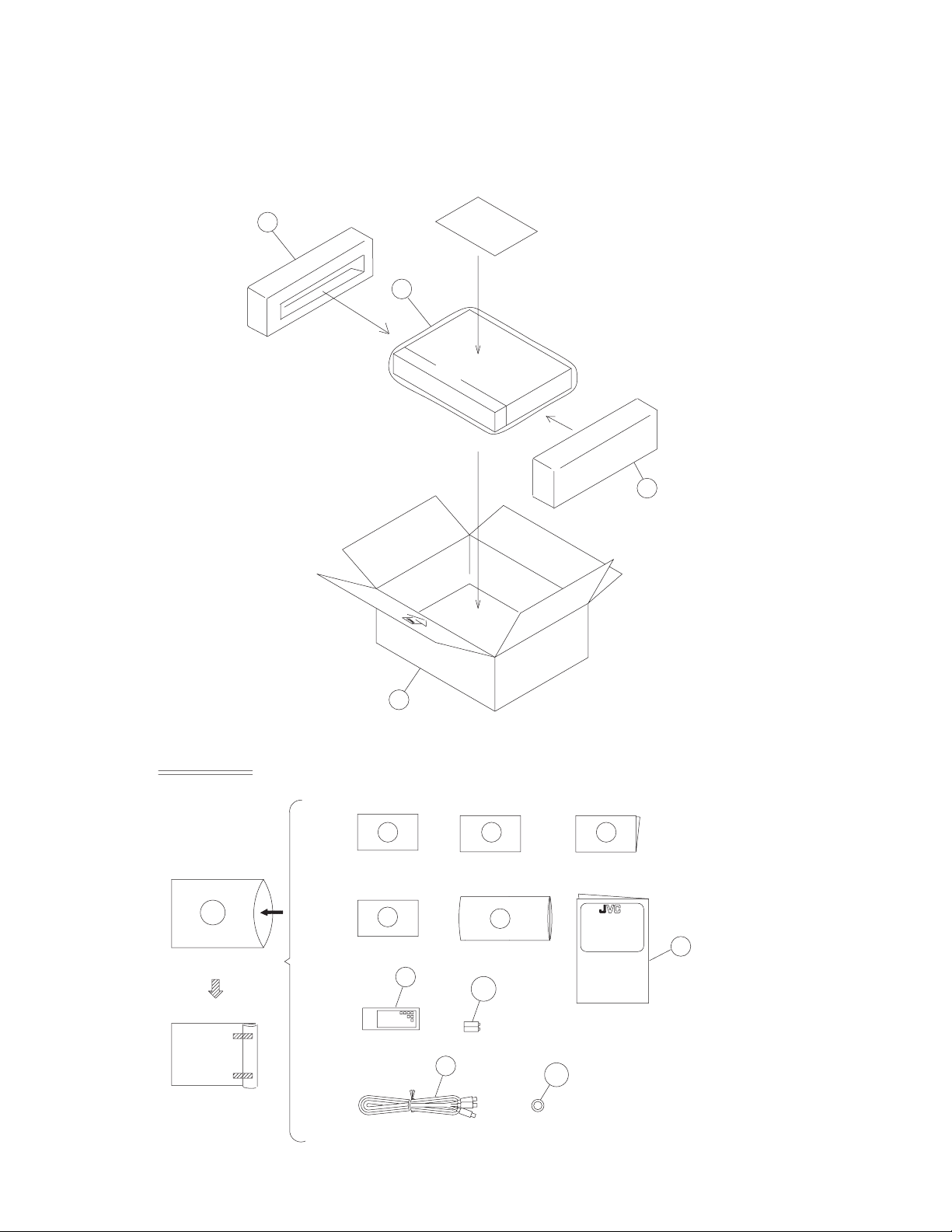
XV-N40BK,XV-N44SL,XV-N4SL
Packing materials and accessories parts list
INST BOOK SA
P3
P1
FRONT
Block No.M4MM
INST BOOK SA
A10
A2
A1
P2
A4
P4
A5
Important
A6
3-12(No.XA003)
A8
A7
A3
A9
except
XV-N4SL
A9
only XV-N4SL
Page 59

XV-N40BK,XV-N44SL,XV-N4SL
Packing and accessories
Block No. [M][4][M][M]
Symbol No. Part No. Part Name Description Local
A 1 LE40932-002A INSERT SHEET
A 2 GNT0027-002C INST BOOK English French 40C,44C
A 2 GNT0027-001C INST BOOK English 40J,44J
A 2 GNT0033-001A INST BOOK English 4C
A 3 BT-52006-1 WARRANTY CARD 40C,44C,4C
A 4 BT-20071B SVC CENTER LIST 40C,44C,4C
A 5 BT-51028-2 J=REGIST CARD 40J,44J
A 6 YU20333 SAFETY INST. 40J,44J
A 7 QAM0328-001 AV CORD 3P
A 8 RM-SXV037J REMOCON UNIT 40C,40J,44C,44J
A 8 RM-SXV053J REMOCON UNIT 4C
A 9 ------------ BATTERY (x2) 40C,40J,44C,44J
A 9 ------------ BATTERY CR2032/1FE 3V 225mAh 4C
A10 QPC02504015P POLY BAG FOR ACC INST
P 1 QPC06005515P POLY BAG FOR SET
P 2 GN10039-004A PACKING CASE 40C,40J
P 2 GN10039-005A PACKING CASE 44C,44J
P 2 GN10039-007A PACKING CASE 4C
P 3 GN20048-001A PACKING PAD(L) LEFT
P 4 GN20049-001A PACKING PAD(R) RIGHT
<Local area>
XV-N40BK J:40J C:40C
XV-N44SL J:44J C:44C XV-N4SL C:4C
(No.XA003)3-13
Page 60
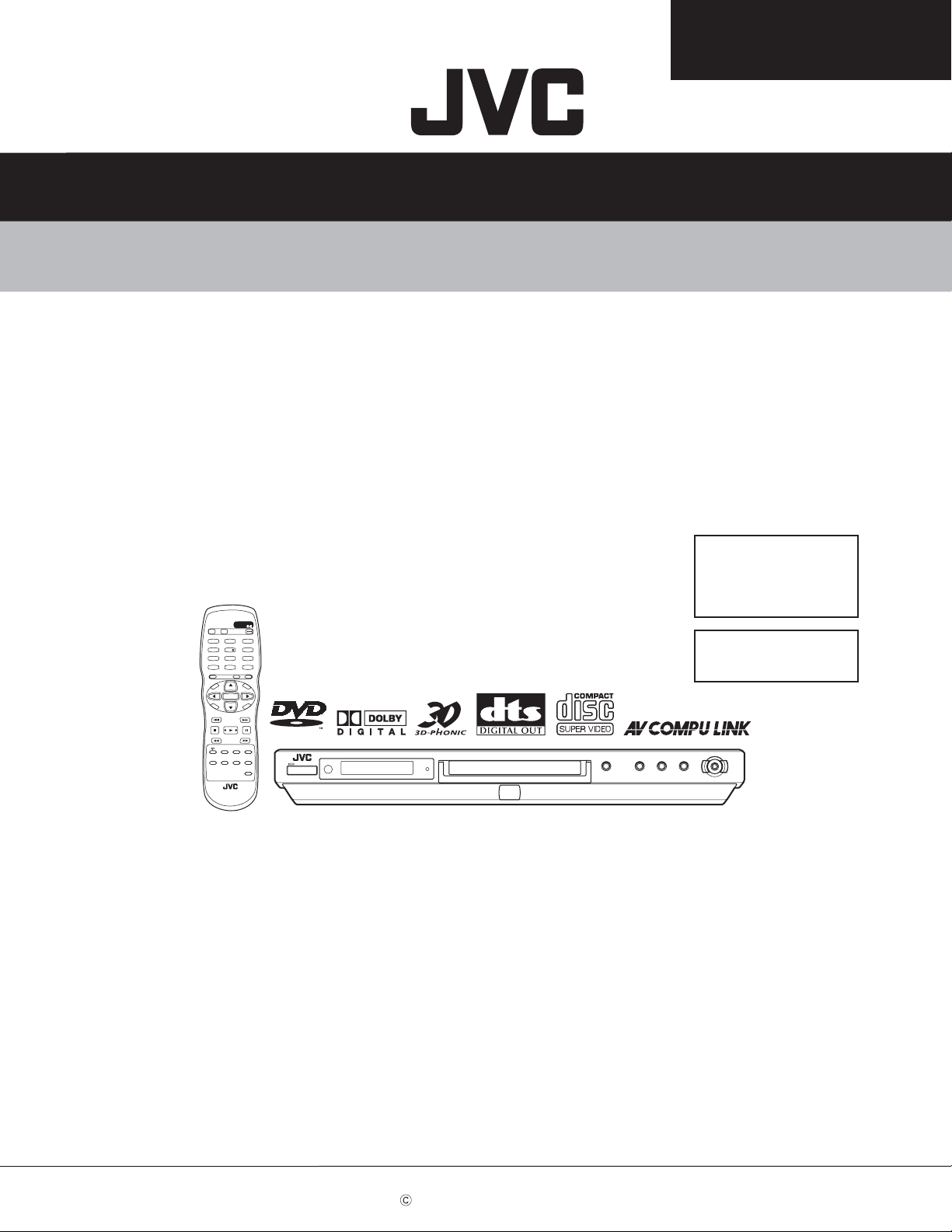
XV-N40BK,XV-N44SL,
XV-N4SL
SCHEMATIC DIAGRAMS
DVD VIDEO PLAYER
XV-N40BK[MK2],
XV-N44SL[MK2],
XV-N4SL[MK2]
CD-ROM No.SML200306
(XV-N40BK,XV-N44SL)
J -------------------------- U.S.A.
C --------------------- Canada
STANDBY/ON
OPEN/
DISPLAY
CLOSE
1
3
2
4
6
5
7
9
8
010 +10
TITLE/
CANCEL
GROUPRETURN
U
M
N
E
E
N
M
U
P
O
T
ENTER
C
N
H
E
O
E
R
I
C
C
E
S
N
O
NEXTPREVIOUS
SELECTCLEAR
-
SLOW
3D
PHONIC
SUB TITLE
ANGLE
VIDEO
SLOW+
VFP
REPEAT
PROGRESSIVE
SCAN
ZOOM
AUDIO
DIMMER
Area Suffix (XV-N4SL)
C --------------------- Canada
This service manual is a service manual of the model which
changes a part of specification of the above-mentioned model
which has already been put on the market.
Please refer to the following page for details.
Area Suffix
Contents
Safety precaution ------------------------ 2-2
For this service manual ---------------- 2-2
Block diagrams --------------------------- 2-3
Standard schematic diagrams -------- 2-6
Printed circuit boards -------------------- 2-20
COPYRIGHT 2003 VICTOR COMPANY OF JAPAN, LIMITED.
No.XA003SCH
2003/06
Page 61
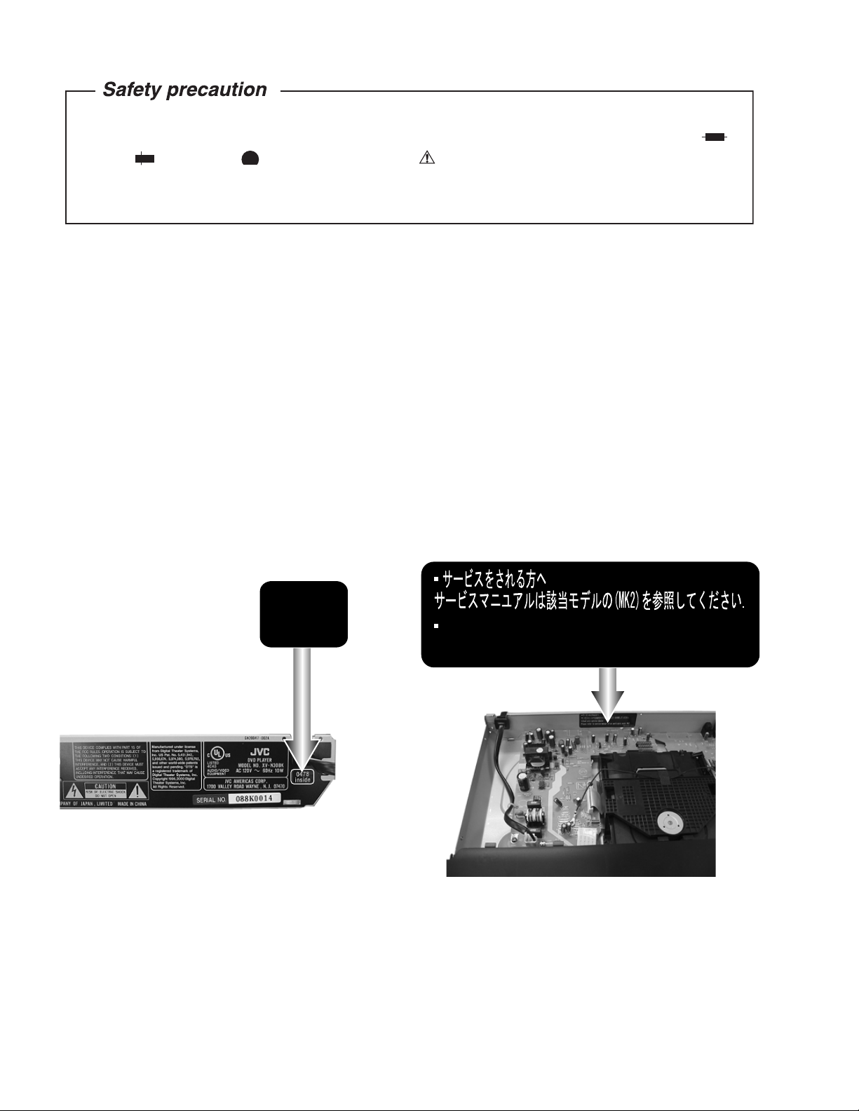
XV-N40BK,XV-N44SL/XV-N4SL
In regard with component parts appearing on the silk-screen pr inted side (par ts side) of
the PWB diagrams, the parts that are printed over with black such as the resistor ( ),
diode ( ) and ICP ( ) or identified by the " " mark nearby are critical for safety.
When replacing them, be sure to use the parts of the same type and rating as specified
by the manufacturer. (Except the JC version)
For this service manual
This service manual is a service manual of the model which changes a part of
specification of the above-mentioned model which has already been put on the market.
< When the label in figure is pasted in the main body >
The specification is different from what the label of the same model does not paste because
of the specification improvement, and refer to this service manual, please.
Please already refer to the issued service manual when the label is not pasted.
* Please refer to this service manual for the model to which this label is pasted.
* Please refer to the service manual which has already been issued for the
model to which this label is not pasted.
(one that there is no description named [MK2] in cover of service manual. )
The surface of a rear panel
0478
inside
or
Used only service dealer
Please refer to service manual of an applicable model [MK2]
GN30080-001A
2-2
Page 62
Block diagrams
Power supply & system controller section (SHEET 1)
XV-N40BK,XV-N44SL/XV-N4SL
TO CN801
SHEET 2
FL ON/OFF
D951
AC-DC
F-
F+
CN901
Q951,Q952
C950
-VDISP
B3.3V
AC-DC
D952
C951,C953
D5V
S5V
IC951
D5V REG.
D955
AC-DC
C958,C959
M5V
A5V
CN902
L952
AC-DC
M9V
D954
D3V
S3V
TO CN501
L955
C967,C988
SHEET 7
Q953
3.3V REG.
D953
AC-DC
C952,C955
L951
TO CN702
SHEET 3
AC-DC
+12V
CN904
AC-DC
D956,L953
C963,C965
-12V
D957,L954
C964,C966
S902
Interlace
J702
Progressive
PROG INT
AVCI AVCO
AV Compulink
Except ver.J/C
D901
AC-DC
L901
Line filter
AC IN
Power
T901
transformer
AC-DC
regulator
Switching
D904
C914
IC901
FEED BACK
PC901
IC702
RESET
FASTPLAY REMO DIN DOUT PON/STB PROGRN PRORED
TCLOSE TOPEN SWUPDN SWOPEN RXD TXD INTP CPURST LMMUTE
IC701
System controller
X1
X2
X701
5MHz
2-3
Page 63
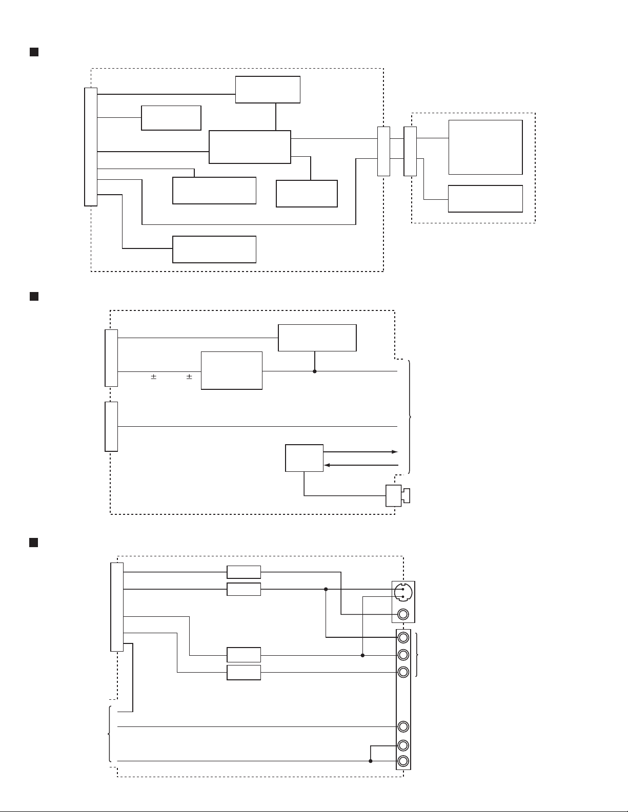
XV-N40BK,XV-N44SL/XV-N4SL
FL Display section (SHEET 2)
F+ F-
STANDBY
Standby LED
D801
TO CN901
SHEET 1
-VDISP DOUT DIN CLK
CN801
REMO
FL Display driver
Remote controller
IC802
FAST PLAY
PROGRN
PRORED
Progressive LED
Q801,Q802,D802
Audio amplifier section (SHEET 3)
AMUTE
TO CN503
SHEET 7
CN701
AOUTL AOUTR
OP.AMP
IC751
FL Display
DI801
IC801
GRI~GR7
SGI~SG9
S1
K2
Power switch
S801
MUTE
Q755,Q756,Q757
AUDIO-L/R
CN802
S1~S7
CN803
Operation
switch
S802,S803
S804,S805
S806,S807,S808
Quick play LED
D810
TO CN904
SHEET 1
CN702
TOPEN LMMUTE TCLOSE CPURST INTP TXD RXD
SWUPDN SWOPEN
IC704
TX
Audio/Video signal output terminal section (SHEET 4)
TO CN502
SHEET 7
TO SHEET 3
CN601
TX
TOPEN
TCLOSE
LMMUTE
CPURST
INTP
TXD
RXD
SWUPDN
SWOPEN
COUT
YOUT
CbOUT
CrOUT
L601
L611
L612
L613
DOUT
AUDIO-L/R
DOUT
Y
Pb
Pr
TO SHEET 4
J703
Optical digital output
J602
S-VIDEO output
Composite video output
J601
Component video
output
Coaxial digital
audio output
Front analog
audio output
2-4
Page 64
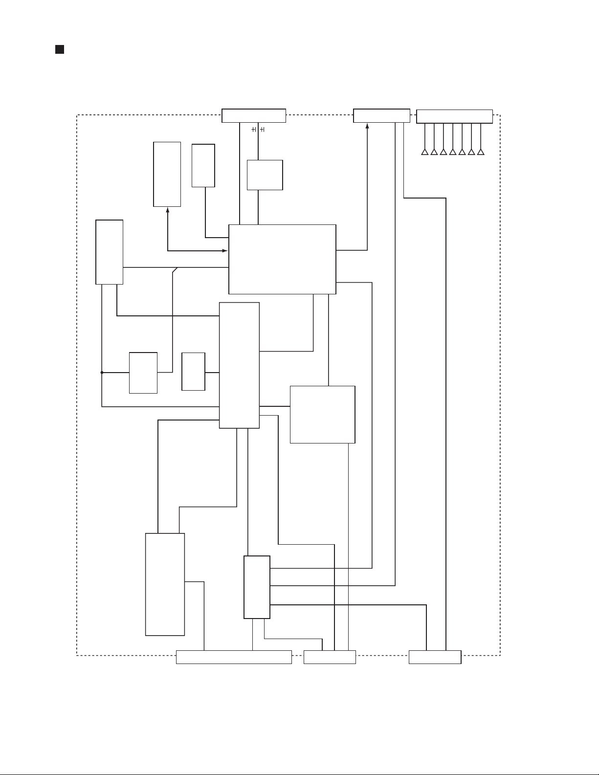
DVD Servo control & AV decoder section (SHEET 5,6,7)
TO CN701
SHEET 3
AOUTL
AOUTR
X571
IC505
SDRAM
27MHz
CXI/O
DA
IC402
S1OUT AMUTE
converter
PCMCLK
BCK
AOUT0
LRCLK
DACDENA
DAC0CS
SSPCLK1
SSPOUT1
YOUT COUT CbOUT CrOUT
TXD RXD TX INTP CPURST
CN502CN503
XV-N40BK,XV-N44SL/XV-N4SL
TO CN601
SHEET 4
CN501
S3.3V
D3.3V
TO CN902
SHEET 1
S5V
A5V
D5V
M5V
M9V
IC509
Flash ROM
LADD4~19
PWE0
LA0~3
AD0~15
LA0~LA3
AD0~AD3
AD8~19
OSC I1/O1
IC512
IC513
FEPEN CPSCK SDOUT SLEEP
X301
16.9MHz
BDO OFTR
TBAL TE RFENV
FBAL FE AS
Decoder
AV
)
STD0~7
ADSCIRQ
ODCIRQ
IC301
SODC
FG
SPDRV
SBRK
Super optical disc controller
(
ARF+ ARF-
TESTSG JLINE
FODRV
TRDRV TRSDRV
TRVSW
IC501
ODCIRQ2
LSIRST
SODCCS
IC251
Spindle
motor driver
SPMUTE
VH SM1~3
TCLOSE TOPEN LMMUTE
DRVMUTE
H1+~H3+ H1-~H3-
FEP
IC101
(Front end processor)
A B C D E F RF
CN101
FROM
T+ T-
Pick-up
4CH Driver
F+ F-
Unit
IC201
FM+
FM-
CN201 CN202
FROM
assembly
Spindle motor
LM+
LM-
FROM
SWOPEN SWUPDN
assembly
Loading motor
2-5
Page 65
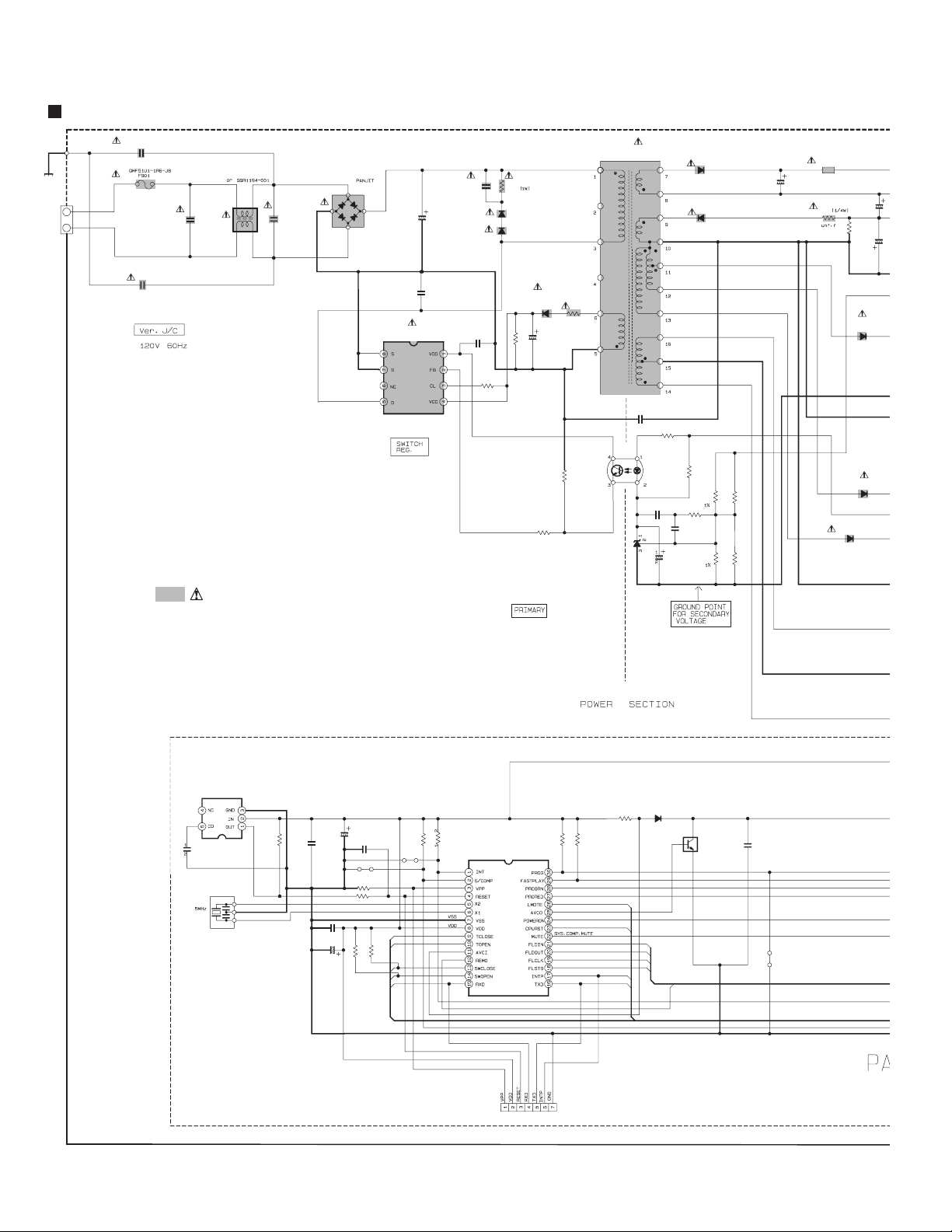
XV-N40BK,XV-N44SL/XV-N4SL
C
0
2
Standard schematic diagrams
Power supply & system controller section
QNZ0136-001Z
EP951
1
1
P901
1
QGA7901C1-02
C905
0.001/AC250V
1
2
1
1
FC902
FC901
QNG0003-001ZNIQNG0003-001Z
1
2
NI
C904
L901
1
22
C902
0.074/AC250V
QQR0816-001
1
2
34
C918
1
2
0.074/AC250V
D901
DI106
2
Parts are safety assurance parts.
When replacing those parts make
sure to use the specified one.
1
4
3
100P/1K
C913
IC901
MIP2C40MP
1
2
1
2
C907
47U/200
0.0033/1K
C908
C915
1
0.1
12
T901
QQS0197-001
1
R901
68K
2
12
2
D903
1F4-T2
1
2
D902
1F4-T2
1
D904
R903
1SS244-T2
150
1
2
12
1
C914
22/35
9.1K
2
R912
2
12
R906
270k
C906
QCZ9079-102
1
2
PC901
PC123Y22
R915
10K
12
R913
12
10K
IC952
TL431/A/-T
R960
470
12
C969
0.033
1
1
2
D951
1F4-T2
1
2
D952
1F4-T2
R968
1K
12
R962 R963
3.9k
R961
12
2
4.7k
C961
1
NI
2
C970
R964
10k NI
NI
12
12
R965
12
12
100/6.3
C950
CP951
ICP-N10-T
12
1
2
R954
10
12
1F4-T2
R955
12
UF304G-F82
D954
1
C951
22/25
22K
D953
1
D955
1
PS154R-F83
2
1
2
2
2
1
2
C95
470/1
2
2-6
C714
0.1
IC702
IC-PST3527N-X
X701
QAX0756-001Z
21
3
D701
R703
1SS133-T2
10K
1
2
R701
1
C701
C702
0.1
12
100/6.3
C703
2
1
2
0.01
1
B39
12
R705
10K
1K
1
2
C704
0.1
1
2
R711
12
C706
100/6.3
R704
4.7K
R708
10K
4.7K
R707
10K
12
B38
12
NI
S/COMP
VPP
RESET
X2
X1
TCLOSE
TOPEN
AVCI
REMO
SWUPON
SWOPEN
RXD
2
NI
12
12
R706
12
10K
R712
IC701
UPD789074MC-025
INT
10K
FASTPLAY
PROGRN
PRORED
/LMMUTE
PON/STB
R702
10K
12
PROG
AVCO
CPURST
DIN
DOUT
CLK
STB
INTP
TXD
P704
QGF1016C1-07
12
12
1
2
KRC107S-X
3
C705
1
Q701
330P
2
12
B40
NI
Page 66
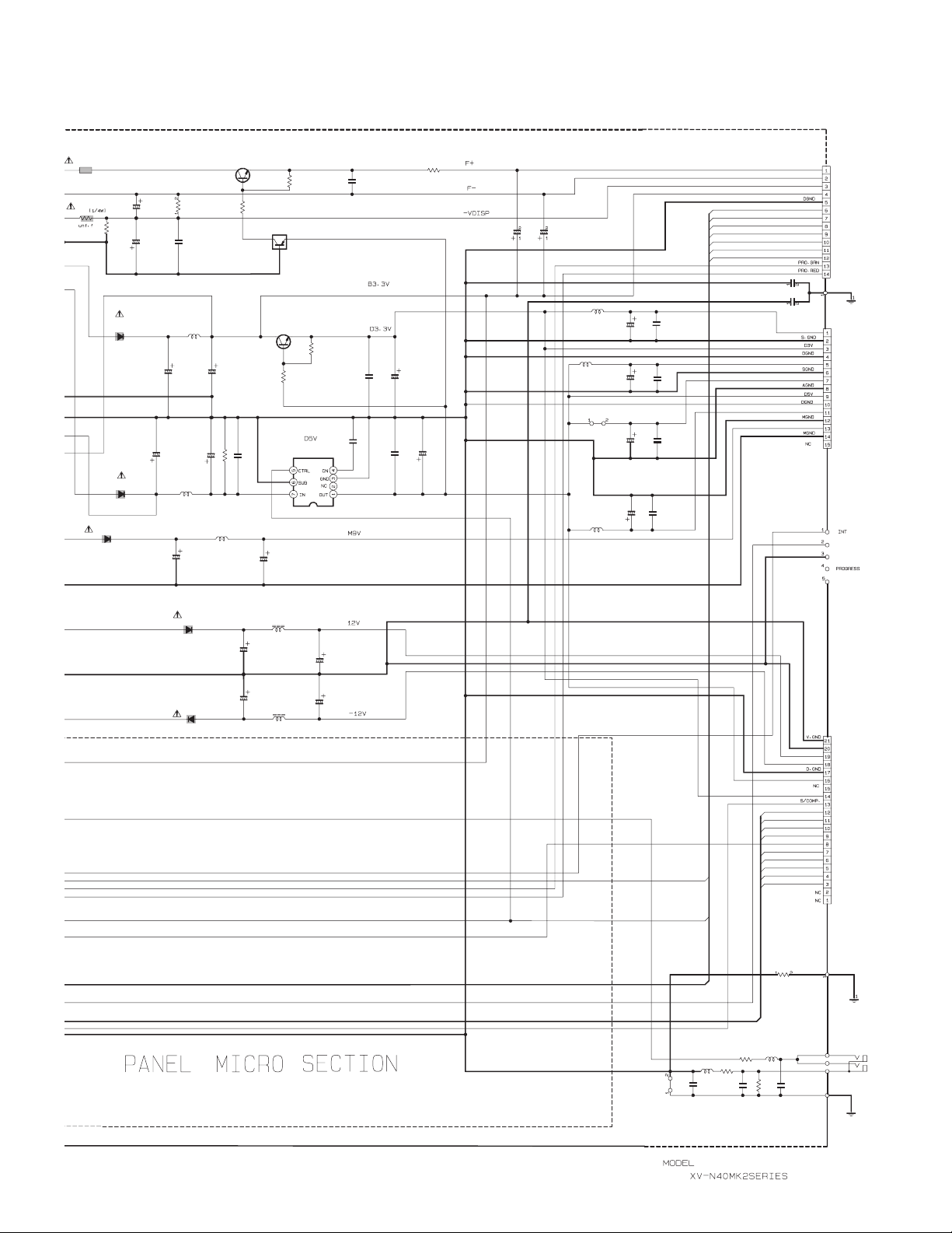
XV-N40BK,XV-N44SL/XV-N4SL
CP951
ICP-N10-T
12
R954
10
12
1F4-T2
12
UF304G-F82
D954
1
1
C951
22/25
2
R955
22K
2
22/35
1
D953
1
2
C958
470/10 100/10
D955
1
2
PS154R-F83
2
Q951
2SC3576-JVC-T
123
R969
270
1
C953
C954
0.1
2
L951
22
12
1
C952
1000/6.3
2
2
C959
1
L952
22
12
1
C967
2
330/16
1
C955
100/6.3
2
2
1
L955
22
12
R956
10K
C960
1
2
12
12
1.0
R953
10K
Q952
KRA104S-X
1
2
123
R966
47
C988
100/16
Q953
2SD2264-T
123
12
R952
10k
12
MM1565AF-X
12
IC951
1
0.1
2
C982
R967
10K
1
C956
0.1
212
C971
1
470P
C972
2
1.0
R951
12
12
C808
4.7/50
C957
100/6.3
C973
100/6.3
1
2
2
1
4.7/50
C802
12
L956
22
12
L957
22
B15
L959
22
12
121
C974
47/25
C976
1
47/25
2
C975
1
100/6.3
212
C977 C981
47/25 NI
C978
NI
2
1
C979
NI
2
C980
NI
1
2
2
1
C983
C984
0.1
0.1
F+
F-
-VDISP
B3.3V
REMO
DOUT
DIN
CLK
STB
PON/STB
FASTPLAY
S3V
S5V
A5V
M5V
M9V
CN901
QGF1201C3-14
TO CN801
SHEET 2
EP952
QNZ0136-001Z
CN902
QGB1231M1-15
TO CN501
SHEET 7
S902
QSW0986-001
1F4-T2
1F4-T2
D956
1
2
C963
100/16
C964
100/16
D957
1
2
L953
22
12
1
2
1
2
L954
22
12
1
C965
2
100/16
1
C966
100/16
2
A.GND
12V
-12V
CN904
D5V
QGF1016C1-19
D3.3V
INTP
TO CN702
SWUPON
TXD
SHEET 3
SWOPEN
SYS.COMP.MUTE
RXD
CPURST
TOPEN
/LMMUTE
TCLOSE
R957
0
L709
R713
2.2
100
12
12
R714L710
12
B4
C708
C713
2
NI
NI
12
NINI
1
C707
100p
1
1
R715
100
2
2
12
1
2
3
1
EP953
J702
QNS0221-001
QNZ0136-001Z
SHEET 1
2-7
Page 67
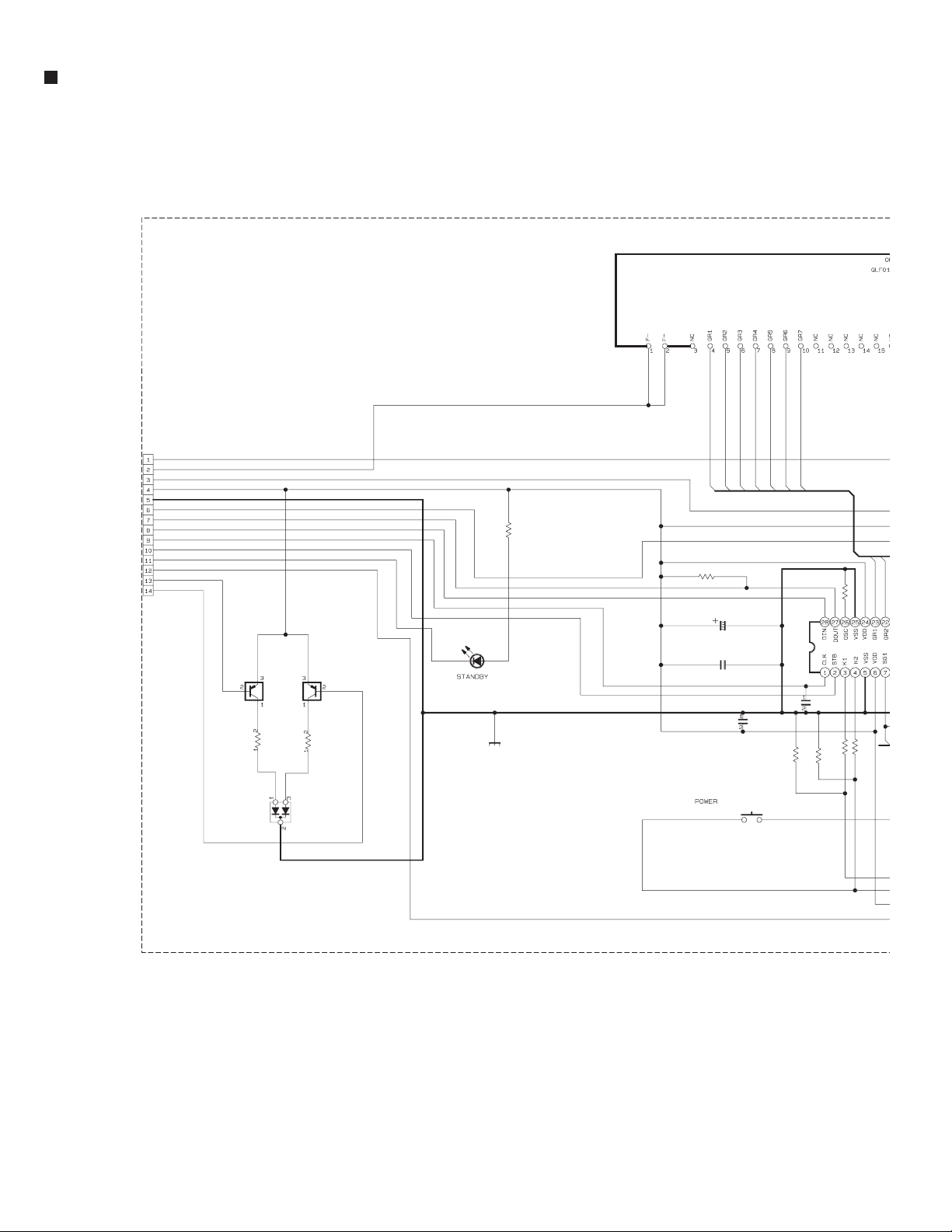
XV-N40BK,XV-N44SL/XV-N4SL
8
GR3
SG2
FL Display section
F+
F-
-VDISP
CN801
QGF1201F3-14
TO CN901
SHEET 1
B3.3V
DGND
REMO
DOUT
DIN
CLK
STB
STANDBY
FASTPLAY
PROGRN
PRORED
Q801
KRA102S-X
R813
82
Q802
KRA102S-X
R814
220
D801
SLR-342VC-T
R802
180
12
R807
10K
GR1
10/6.3V
C801
C805
0.1
GR2
GR3
GR4
0.1
C811
GR5
GR6
R808
GR7
IC801
PT6315-S
10k
R809
1000P
C810
DI
QLF01
100K
R804
GR1
GR2
SG1
0
0
R812
R811
10k
2-8
D802
SPR-325MVW/L/-T
S801
1
QSW0651-001Z
Page 68
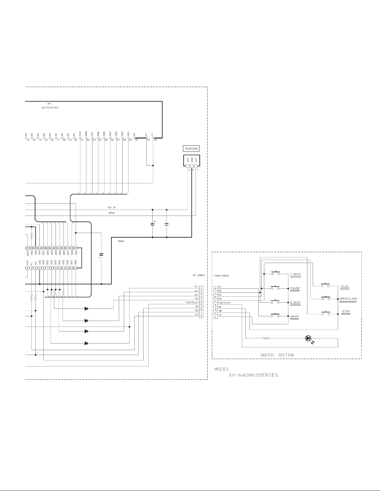
DI801
QLF0122-001
XV-N40BK,XV-N44SL/XV-N4SL
SG2
SG9
SG8
SG7
SG6
SG5
SG1
SG4
SG3
IC802
RPM7238-H9
R811
R804
0
100K
R812
C804
47/6.3
GR1
GR2
GR3
GR4
GR5
GR6
GR7
SG9
C809
47/50
SG1
SG2
SG3
SG4
SG5
SG6
SG7
SG8
0
D803
1SS133-T2
D804
1SS133-T2
D805
1SS133-T2
D806
1SS133-T2
C803
0.1
CN802
QGF1201F3-08
CN803
QGF1201F3-08
S805
QSW0651-001Z
S806
QSW0651-001Z
S807
QSW0651-001Z
S808
QSW0651-001Z
R810
150
SLR-342MC-T
D810
S802
12
QSW0651-001Z
S803
12
QSW0651-001Z
S804
12
QSW0651-001Z
SHEET 2
2-9
Page 69
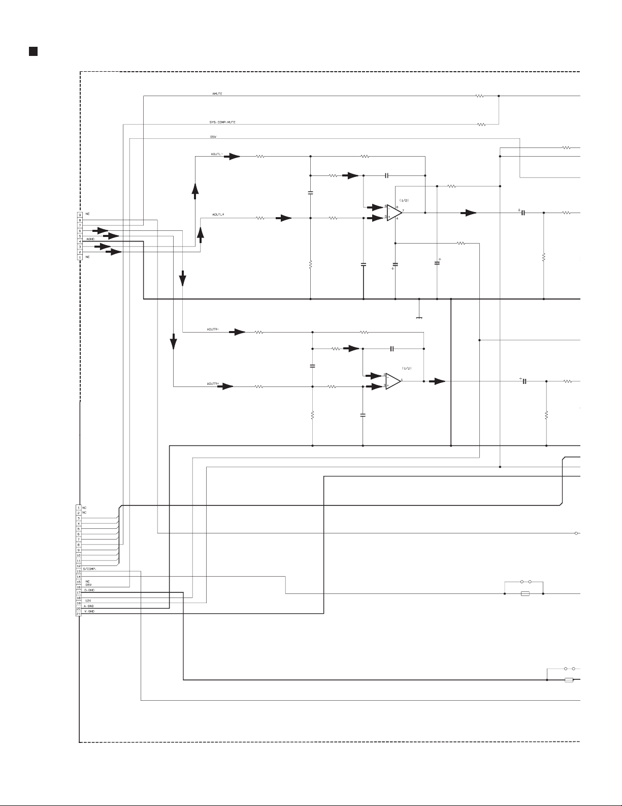
XV-N40BK,XV-N44SL/XV-N4SL
5
6
6
2
2
0
Audio amplifier section
CN701
QGB1231M1-09
TO CN503
SHEET 7
DOUTCNT
AMUTE
R751
R755
3.9k
R782
47K
R788
47K
R786
3.9k
R761
200
C751
0.0033
R763
200
R765
4.7k
R759
4.7k
IC751
HA17558F-X
C755
470p
C753
470p
C764
100/16
C765
100/16
R783
220
R784
220
C757
22/25
R769
27k
10K
R767
560
C7
0.00
CN702
QGF1016C1-19
TO CN904
SHEET 1
TCLOSE
/LMMUTE
TOPEN
CPURST
RXD
SYS.COMP.MUTE
SWOPEN
TXD
SWUPON
INTP
D3.3V
-12V
R752
R756
R762
R760
4.7k
200
IC751
HA17558F-X
C756
470p
3.9k
C752
0.0033
R764
2003.9k
R766
4.7k
C754
470p
GND
C758
22/25
K791
NI
R768
560
R770
27k
B89
C7
0.00
B
2-10
NQR0227-0
B52
NI
K792
Page 70
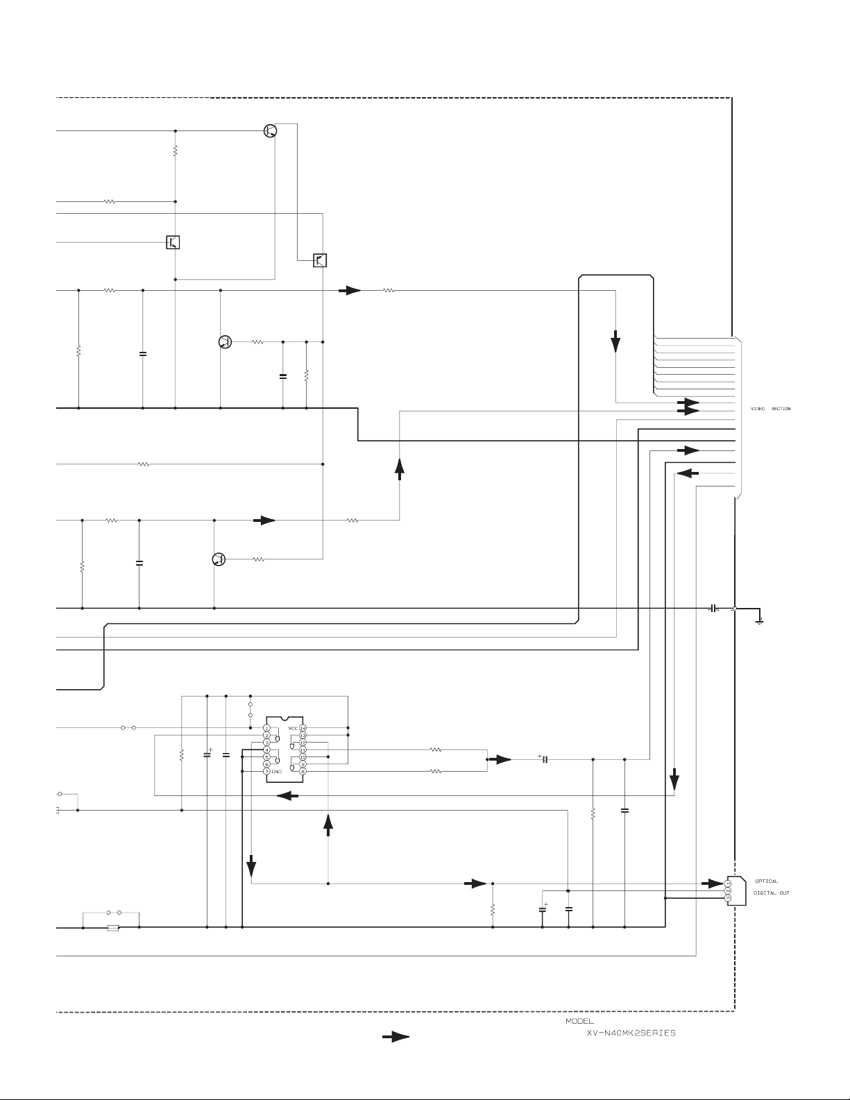
XV-N40BK,XV-N44SL/XV-N4SL
5
5
Q757
2SC2412K/RS/-X
R787
100K
R786
10K
Q755
KRC109S-X
7
R767
560
Q756
KRA102S-X
R773
100
C795
C796
NI
B148
R771
10k
R772
10k
0.0015
C763
IC704
74VHCT08ASJ-X
R781
NI
R774
100
R791
300
12
R792
300
12
C791
4.7/25
R794
82
C797
150P
R769
27k
8
R770
27k
9
1
R768
C759
0.0022
R785
47K
560
C760
0.0022
B60
NI
2SC3576-JVC-T
Q752
2SC3576-JVC-T
R790
10
Q751
47/25
TOPEN
/LUMMTE
TCLOSE
CPURST
INTP
RXD
TXD
SWUPON
SWOPEN
AUDIO-L
AUDIO-R
V.GND
A.GND
DOUT
DGND
TX
NI
TO SHEET 4
EP751C777
NI
B52
NI
K792
NQR0227-004X
R793
NI
Audio signal
C793
100/10 0.1
C794
J703
GP1FA352TZ
SHEET 3
2-11
Page 71
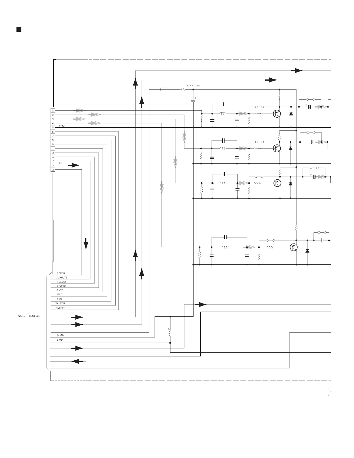
XV-N40BK,XV-N44SL/XV-N4SL
Audio / Video signal output terminal section
CN601
QGB1231M1-15
TO CN502
SHEET 7
C/Cv/Y
Y/G/Cv
Cb/B/Cv
Cr/R/C
SWOPEN
SWUPON
RXD
TXD
INTP
CPURST
TCLOSE
/LMMUTE
TOPEN
K601
R601
1
12
NI
NI
C601
NI
NI
R602
NI
R612
NI
R622
R632
C604
22P
L601
2.2UH
C603
C602
330P
220P
C614
22P
L611
1uH
C613
C612
150P
100P
C624
22P
L612
1uH
C623
150P
C622
100P
C634
22P
L613
1uH
C633
NI
150P
C632
100P
R603
R613
R623
B85
R604
NI
NI
B84
R614
NI
NI
B75
R624
NI
NI
R633
NI
R605R615
1212
3
2
2
Q601
NI
Q611
NI
Q621
NI
B82
R634
NI
NI
2
2
NI
1
D601
1
NI
3
2
1
D611
1
NI
R625
12
3
2
NI NI
D621
1
1
2
Q631
NI
R635
NI
B903
C650
12
3
NI
1
D631
NI
B902
C651
NI
B901
C652
NI
B900
C653
NI
TO SHEET 3
2-12
AUDIO-L
AUDIO-R
12V
DOUT
DGND
TX
S/COMP.
R2
0
Page 72
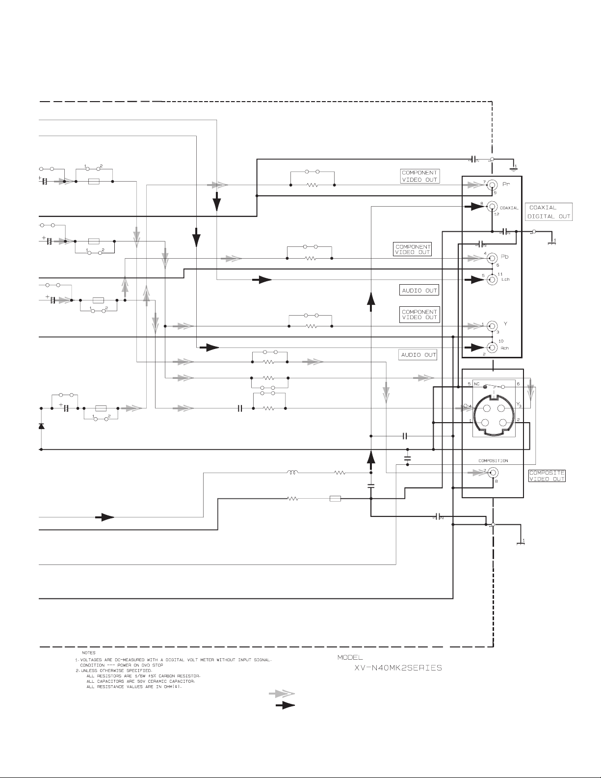
B903
C650
XV-N40BK,XV-N44SL/XV-N4SL
C666
EP651
NI
B77
K602
NI
NI
B51
R626
NI
NI
B902
C651
NI
B901
C652
C686
220p
220p
C685
J601
@QNN0565-001
J602
QNN0564-001
S-VIDEO
OUT
K603
NI
B53
L681
1U
R682
R616
NI
B54
R606
NI
C682
NI
1
2
C640
R683
10
C683
K682
10
NQR0227-004X
330P
NI
C798
0.1
B76
NI
B900
C653
K604
NI
B88
B57
R636
NI
R637
NI
B62
R639
B58
NI
K605
NI
NI
B73
C639
0.1/16
Video signal
Audio signal
SHEET 4
2-13
Page 73
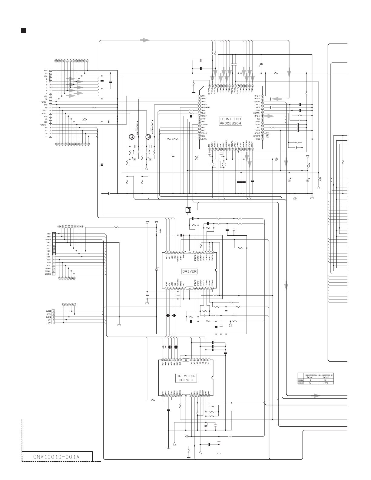
XV-N40BK,XV-N44SL/XV-N4SL
10K
C
C
7
6
5
4
3
2
0
Servo control section
TP125
TP126
TP127
TP128
TP129
TP130
TP111
TP112
TP107
TP108
TP109
R117
1
K101
111111111
TP116
TP117
TP118
TP119
TP120
TP121
TP33
TP34
TP45
TP42
TP40
TP39
1
1111
1111111
TP35
TP36
TP37
TP38
TP47
TP48
TP49
TP50
11
1
TP110
TP41
TP122
TP123
RF
R116
12
100
NQR0007-002X
12
F+
FT+
T-
111
TP124
E
F
D
A
B
C
100
TRVSW
SWUPDN
SWOPEN
LM+
LM-
1
1
0.1
2
C142
2
C141
0.1
C138
1
2
D101
1
RB521S-30-X
1
2
C139
NI
12
FM+
FM-
H1H1+
VC+
H2-
H2+
H3H3+
VH
SM2
SM1
SM3
/LMMUTE
TO Pick-up
unit
CN101
QGF0523F1-24W
TO Spindle motor
assembly
CN201
QGF1016F2-15W
TO Loading motor
assembly
CN202
QGF1016F2-05W
111111 11111 1
1
TP113
TP114
TP115
TP31
TP32
1
11
TP44
TP43
TP46
11
1
TP311
R210
3.9K
0.1/16
0.1/16
1
1
2
2
C111
C112
0.1/16
12121
C126
R209
12
1
2
C208
12
R223
9.1K
R216
12
9.1K
R215
1212
10K
CBA
D
2
C113
1
NI
R114
NI
12
0
R115
C121
C122
C123
R126
C120
0.047/16
C119
R125
R124
1
1
1
12
560P
1
C135
47/6.3
1
TP102
12
C117
1
2
560P
1
2
1M
NI
0.1/16
2
2
0.1/16
2
1M
2
S3.3V
R128
1
C137
47/4
2
1
1
12
SGND
1
12
1
R129
1
S5V
R343
12
OD
OD
ADS
ACK
T
LADD1
LADD1
LADD1
LADD1
LADD1
LADD1
LADD11
LADD1
LADD9
LADD8
LADD7
LADD6
LADD5
LADD4
LA3
LA2
LA1
LA0
SODCCS
PWE0
RDAD7
AD6
AD5
AD4
AD3
AD2
AD1
AD0
0.1/16
RF
C116
1
2
TESTSG
0.027/16
C118
1
2
RFENV
BDO
OFTR
2.2K 12P
R127
TP103
1
TP106
1
TP101
1
1
0.1/16
0.1/16
2
C129
0.0047
2
C127
C128
ARF-
ARF+
TRDRV
22K
390P
R230
3.3K
FODRV
/DRVMUTE
TCLOSE
TOPEN
TRSDRV
1
2
F
E
DAB
C
8.2K
10K
C144
0.01/16
R112
R113
1
2
C145
NI
1
2
1.8K
R130
1
24K
R111
2
/HFMON
12
18K
R219
R211
12
3.9K
1
C210
NI
SM2
C124
TP104
C206
NI
1
R207
12
47K
2
R214
10K
SM3
12
IC101
AN8703FH-V
121
47P
C125
2
270P
TP105
12
12
AS
FE
TE
R204 R208
12 12
27K 22K
R205
12
2
27K
1
390P
C207
2
24K
12
R220
R221
12
6.8K
12
R222
12 12
10K
1
C218
2
R212
12
10K
1
1
1
2
C216
2
C212
0.01/16
0.1/16
C260
1
2
0.1/16
C261
1
2
0.1/16
C262
1
2
2
C263
0.1/16
1
0.1
TBAL
FBAL
FEPEN
CPSCK
SDOUT
Q102
2SB1424/R/-W
Q101
2SB1424/R/-W
1
1
2
2
R108 R109
JLINE
3
3
C102
NI
1
2
2.2
27
R119
R105
R104
12
12
12
22K
R102
1
2
12
C105
47/6.3 47/6.3
22K
R103
12
R101
12
R201
47
DGND
33K
DVDLDCUR
S5V
33K
R110
12
NI
C203
MGND
1
M9V
1
2
VH
CDLDCUR
1
1
C103
NI
1
27
1
C106
2
R120
12
2
M5V
R202
1
NI
2
C201
2.2
1
12
1212
2.2K 1.8K
C109
F-
1
C213 C214
121
NI NI
LM+
LM-
H2-
H3-
H3+
12121
0.1/16
C257
1
2
0.1/16
FM+
H2+
C258
DTA144EE-X
T-T+F+
C204
0.1/16
1
2
C217
2
FM-
H1-
H1+
2
0.1/16
0.1/16
C259
0.1/16
Q103
1
R106
R107
C110
3
1
2
IC201
BA5983FM-X
R131
NI
12
SGND
27K
27K
220P
SLEEP
2
C205
120P
1
R206
12
30K
R213
10K
12
1
2
C211
0.022
SM1
2-14
R256
12
47
0.1/16
C256
MGND
IC251
BA6664FM-X
SBRK
12
10K
R259
1
2
1
TP310
1
M9V
1
R280
3.3K
12
DGND
1
R254
/SPMUTE
20K
12
C252
1
D5V
1
NI
2
12
12
C253
0.1/16
2
R251
0.47
R252
2.2
1
DGND
1
C264
0.01/16
2
1
2
C251
0.1/16
R255
10K
12
2
C255
0.015/16
1
1
FG
SPDRV
Page 74
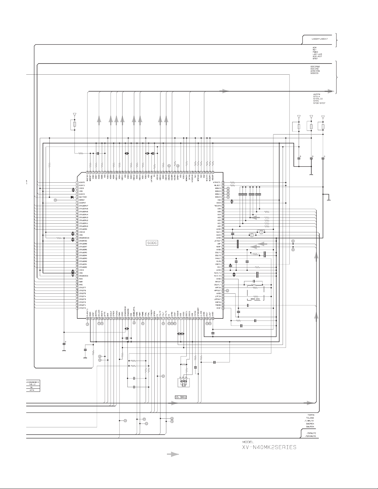
XV-N40BK,XV-N44SL/XV-N4SL
TO
SHEET 7
TO
SHEET 6
STD7
STD5
STD4
STD3
STD2
STD1
STD0
STEN
STD6
AVRTM
STVALID
STCLK
PWE0
RDAD7
AD6
AD5
AD4
AD3
AD2
AD1
AD0
SODCCS
12
ODCIRQ2
ODCIRQ
ADSCIRQ
ACK
LADD17
LADD16
LADD15
LADD14
LADD13
LADD12
LADD11
LADD10
LADD9
LADD8
LADD7
LADD6
LADD5
LADD4
LA3
LA2
LA1
LA0
10K
R343
TP331
12
RB521S-30-X
1
R350
NI
DGND
D5V
1
12
NI
K304
R341
12
C347
1
0.1/16
2
D301
1
2
C346
1
0.1/16
2
C345
1
0.1
2
C344
1
NI
1
2
C343
2
0.1/16
1
C360
NI
2
1
1
5.6K
C352
NI
DGND
2
C348
0.1/16
47K
47K
10K
R302
R301
R340
12
12
12
111 1
TP316
TP315
TP314
1
2
0
R342
TP303
12
11
1
TP304
SRST
OFTR
1
2
0.1/16
C301
47K
47K
47K
R305
R304
R303
12
12
12
0.1NI
C341
1
2
C342
1
2
10K
R344
R338
12
4.7K
12
R339
4.7K
12
1
C340
0.1/16
1
C339
0.1/16
BDO
SDOUT
CPSCK
FEPEN
TP317
1
TRVSW
121
2
C303
C302
0.1/16
0.1/16
0
47K
47K
R307
R306
12
12
R308
12
IC301
MN103S26EGB-H
1111
TP332
TP320
27K
27K
R337
R336
12
12
2
2
FBAL
TBAL
TRSDRV
SPDRV
FG
TP318
1
TP319
1
HAGUP
SBRK
1
TP305
/HFMON
R309
47K
12
1
TP322
SLEEP
TP330
TP324
1
1
TP325
NI
R310
TP321
TP323
TP326
C338
TP329
11
121
2
0.1/16
R320
12
1M
X301
NAX0566-001X
NI
R311
C337
0.1/16
R345
12
680
47K
NI
R313
R312
1K
R334
12
1
0.1/16
C334
TESTSG
R314
11
18K
R333
12
JLINE
NININI
47K
R317
R316
R315
NI
R318
NI
R319
TP309
11
TP308
120P
270P
470P
330P
560P
560P
C328
0.1/16
C316
C329
C331
2
0.01/16
TP302
560P
C315
C314
C313
C312
C311
47K
R321
47K
R323
47K
R324
12K
R325
47K
R326
TP301
12
12
C322
0.0056
R327
1
2
12
1
2
1M
C323
1
0.001
C324
0.1/16
2
15K
R328
47P
C325
0.018/16
C326
1
2
C327
0.001
1
2
47K
R329
47K
R330
R331
47K
0.01/16
1
2
C330
1
2
TP327
TP328
0.1/16
TP307
11
TP306
C317
1
2
C310
0.1/16
C318
1
0.1/16
2
0.001
C319
1
2
0.001
C320
1
2
0.001
C321
1
2
1
C349
C350
0.1/16 0.1/16
2
1
2
1
NI
C351
2
TP333
1
1
2
R332
12
1K 0.1/16
1
C332
0.1
2
1
2
C333
1
TP312
TP313
1
1
NI
K303
12
1
2
C308
47/4
D3.3VD1.8V
K302
12
1
2
CDLDCUR
OFTR
DVDLDCUR
RFENV
FODRV
TRDRV
ARF+
ARF-
11
NI
C306
47/4
DGND
AS
TE
FE
TE
S3.3V
1
NI
K301
12
1
2
C304
47/4
SGND
TO
SHEET 7
TO
SHEET 6
Digital data signal
SHEET 5
2-15
Page 75
XV-N40BK,XV-N44SL/XV-N4SL
TP878
AV Decoder section
TO SHEET 5
TO SHEET 5
CPURST
SRST
LC502
NI
12
3
NI
K502
12
C521
0.1
1
2
1
2
C524 C527
47/4 47/4
D3.3VD1.8V
11
12
NI
K504
1
LC504
NI
3
12
2
STD2
STD3
STD4
STD5
STD6
STD7
2
1
NI
C528
2
1
C533
0.1/16
D3.3V
1
LC501
NI
3
K501
NI
12
12
IC505
C501
0.1/16
1
2
MD0
MD1
MD2
MD3
MD4
MD5
MD6
MD7
DQM0
WECASRASCS0-
MA12
MA13
MA10
MA0
MA1
MA2
MD24
MD25
MD26
MD27
MD28
MD29
MD30 MD22
MD31
W986432DH-7
1
C511
NI
2
MD23
MD10
MD11
MD12
MD13
MD14
MD15
DQM1
MCLK
DQM2DQM3
MD16
MD17
MD18
MD19
MD20
MD21
MD9
MD8
0.1/16
MD10
MD11
MD12
MD13
MD14
MD15
DQM1
MA9
MA8
MA7
MD8
MD9
CKE
MA9
MA8
MA7
MA6
MA5
MA4
MA3
MA6
MA5
MA4
MA3
CKE
MA2
MA1
MA0
MA10
MA12
MA13
CS0-
RASCASWE-
DQM0
DQM2
MD16
MD17
MD18
MD19
MD20
MD21
MD22
MD23
MD24
MD25
MD26
MD27
MD28
C512
NI
C514
NI
C515
NI
C516
0.1/16
C517
1
TP810
0.1/16
C518
0.1/16
C519
NI
C520
0.1/16
C523
NI
C529
MD3
MD2
MD0
MD1
MD4
MD5
MD6
MD7
2-16
1
DGND
D3.3V
IC511
LM1117MP1.8-X
1
1
1
2
C549
47/4
1
2
C550
0.1/16
2
D1.8V
1
C557
2
0.1/16
C573
47/4
MD29
MD30
MD31
DQM3
1
TP885
100
R583
12
AIN
TX
1
TP883
TP884
121
2
C532
C531
111
TP811
TP812
150
R578
1
AOUT0
0.1/16
12
PCMCLK
0.1/16
150
R576
BCK
1
150
12
R575
TP861
TP862
TP882
LRCLK
Page 76
XV-N40BK,XV-N44SL/XV-N4SL
1
TO SHEET 5
DOUTCNT
ODCIRQ
ODCIRQ2
TP912
11
TP913
STEN
STD0
STD1
STD2
STD3
STD4
STD5
STD6
STD7
2
1
C533
0.1/16
MD0
MD1
STVALID
STCLK
AVRTM
121
C534
0.1/16
2
C547
IC501
JCE8045
NI
TP533
1
470
12
R550
2
1
C548
/DRVMUTE
/SPMUTE
0.1/16
TP532
1
TP531
1
TP530
1
TP529
111
TP528
TP527
LA0
LA3
LA2
PCS0
2
1
C536
LA1
LHLD
LHLDA
2
1
NI
NI
C539
R505
12
R506
12
R507
R508
NI
NI
NI
12
NI
12
C558
C559
C560
C561
TP867
TP868
TP869
1
TP870
1111
TP871
TP872
11
TP873
1
TP874
1
TP875
1
TP876
1
TP877
C562
C563
0.1/16
NI
NI
NI
0.1/16
NI
R584
12
3.3K
12
R514
22
PWE0
PWE1
AD10
AD11
AD12
AD13
SCLK
AD14
AD15
PWE2
AD16
AD17
AD18
AD19
AD20
AD21
AD22
AD23
PWE3
AD24
AD25
AD26
AD27
AD28
AD29
AD30
AD31
RDALE
AD0
AD1
AD2
AD3
AD4
AD5
AD6
AD7
AD8
AD9
ACK
X6
INTP
DAC2CS
SODCCS
DAC1CS
DAC0CS
ADSCIRQ
DACDENA
TO SHEET 7
TO SHEET 7
121
2
C532
C531
11
0.1/16
TP884
TP811
TP812
150
12
R578
1
P883
AOUT0
PCMCLK
1
TP860
1
0.1/16
TP878
150
150
12
R576
R575
11
TP861
TP862 TP866
1
TP882
ADCENA
LRCLK
BCK
2
C506
1
SSPOUT1
SSPCLK1
R503
12
NI
1
X571
NAX0550-001X
15P
121
2
NI
C545
C535
NI
NI
12
R585
R586
111
TP838
TP839
TP865
TP863
TP864
2
2
18P
C507
1
0.1/16
NI
12
12
R587
TP840
1
11
1
TXD
R501
12
47
2
1
C542
0.1/16
C544
0.1/16
CrOUT
1
C564
NI
1
NI
2
2
CbOUT
L501
12
1
D3.3V
YOUT
10
1
TP881
0
R589
12
12
1
D1.8V
COUT
R565
R566
R567
NI
K513
1.6K
1.6K
12
12
R574
R573
AMUTE
S1OUT
RXD
C540
0.1/16
1
2
C582
NI
1
2
NI
K507
12
12
1
D3.3V
1
D1.8V
C543
C541
0.1/16
1
2
1
2
1
2
1
2
C571
C565
NI
NI
NI 0.1/16
NI
K509
K508
K510
12
12
1
D3.3V
1
D1.8V
NI
R512
12
10K
R513
1.2K
1k
R568
R569
R570
R571
1k
R572
1
2
C572
0.1/16
1
2
C580
NI
1
C578
0.1/16
1
C581
220/4
0
12
1k
1k
10
NI
VGND
2
2
Digital data signal
Video signal
TO SHEET 7
Audio signal
SHEET 6
2-17
Page 77
XV-N40BK,XV-N44SL/XV-N4SL
0
P
X
8
Flash ROM section
TO SHEET 6
TO SHEET 5
AD30
AD28
AD26
AD24
AD23
AD22
AD21
AD19
AD17
AD16
AD15
AD14
AD13
AD12
AD11
AD10
AD8
AD7
AD6
AD5
AD3
AD1
PWE0
LA0
LA2
RD-
LHLD
DAC0CS
DAC2CS
SODCCS
INTP
DOUTCNT
SW501
NI
TO SHEET 6
TO SHEET 5
R502
NI
12
FCS-
PCS0
R520
0
12
CN504
CPURST
IC509
R516
12
NI
R517
NI
12
SST39VF160-7CEK
R518
NI
DGND
1
1
C400
0.001
2
1
AGND
LADD15
LADD14
LADD13
LADD12
DACDENA
DAC0CS
LADD11
LADD10
LADD9
LADD8
LADD19
PWE0
ACK
LADD18
LADD17
LADD7
LADD6
LADD5
LADD4
LA3
LA2
LA1
NI
SRST
AD31
AD29
AD27
AD25
PWE3
AD20
AD18
PWE2
SCLK
ACK
AD9
PWE1
AD4
AD2
AD0
ALE
LA1
LA3
LHLDA
PCS0
/SPMUTE
DAC1CS
X6
ADSCIRQ
DACDENA
DGND
12
R519
12
10K
2
C554
0.1/16
1
LADD16
AD15
AD14
AD13
AD12
AD11
AD10
FCS-
R404
3.3K
12
1
AGND
LADD6
AD6
AD7
AD5
LADD5
AD6
LADD4
AD4
AD5
AD16
LADD16
AD4
AD3
AD2
AD9
LADD11
AD1
AD8
AD11
AD0
AD10
LADD10
RD-
LADD9
AD9
AD8
LA0
LADD8
AIN
LRCLK
PCMCLK
BCK
ADCENA
R405
NI
12
1
AGND
PCMCLK
BCK
AOUT0
LRCLK
SSPCLK1
SSPOUT1
IC512
74LVC373A
IC513
74LVC373A
1
DGND
IC401
AK5355VT-
IC4
AK43
2-18
TO SHEET 6
TO SHEET 5
Page 78
XV-N40BK,XV-N44SL/XV-N4SL
N
0
U
TP501
TP502
TP503
TP504
TP505
TP506
M9V
1
SGND
1
DGND
R521
R522
R523
DGND
C510
NI
MGND
R509
NI
12
R510
NI
R511
NI
12
0
0
0
1
C551
0.01
2
1
C509
1
2
1
D3.3V
1
K519
NI
1
AGND
12
C552
NI
1
2
C553
SGND
SGND
TXD
RXD
TX
COUT
YOUT
CbOUT
CrOUT
VGND
NI
1
2
C555
NI
1
2
DGND
1
1
C556
C567
C568
NI
1
NI
1
NI
1
SWOPEN
SWUPDN
TCLOSE
/LMMUTE
TOPEN
1
2
2
2
AGND
11
1
2
C566
0.1/16
1
2
C569
0.1/16
1
S3.3V
1
12
L401
10u
R401
12
1
C405
0.001
2
1
AGND
R402
10
12
470
1
C406
NI
2
SGND
ADCDIN
INTP
CPURST
D401
NI
1
2
1
1
2
0.1
2
NI
47/4
C403
C404
2
D402
1
IC512
74LVC373APW-X
LADD19
AD19
AD18
LADD18
LADD17
AD17
AD7
LADD7
ALE
LADD15
AD15
AD14
LADD14
LADD13
AD13
AD12
LADD12
ALE
IC513
74LVC373APW-X
DGND
IC401
AK5355VT-X
LK
A
R405
NI
12
AGND
TP401
1
1
1
0.1
47/4
C401
C402
2
2
1
NI
2
MGND
R515
12
D5V S5V
1
C505
NI
2
DGND
DGND
1
330
A5V
1111
1
C504
NI
2
0
R525
AGND
1
VGND
VGND
VGND
VGND
K556
K557
K558
K559
C502
1
C503
NI
2
12
SGND
1
LC559
NI
12
3
1
LC558
NI
12
3
1
LC557
NI
12
3
1
LC556
NI
12
3
1
NQR0007-002X
NQR0007-002X
NQR0007-002X
NQR0007-002X
K560
NI
DGND
S3.3VD3.3VM5V
C508
NI
1
2
111
SGND
NQR0007-002X
111
1
2
TP507
1111111
TO CN902
SHEET 1
1111111
CN501
1
TP512
TP513
TP514
TP526
TP525
TP515
TP516
TP517
111211111111
TP511
TP524
TP510
TP523
TP509
TP522
TP508
TP521
QGB1231L2-15W
TO CN601
SHEET 4
CN502
QGB1231L2-15W
1
11111
TP520
TP519
TP518
TP534
TP535
TP536
A5V
IC402
LK
K1
T1
AK4381VT-X
1
10
R403
12
TP402
11
TP403
1
C407
2
0.1
1
C409
1
C408
220/6.3
2
220/6.3
2
AGND
AOUTL+
AOUTLAOUTR+
AOUTR-
ADCDIN
AOUTL+
AOUTL-
AOUTR+
AOUTR-
DOUTCNT
S1OUT
AMUTE
TP548
TP547
TP546
TP549
TP545
TP544
TP543
TP542
AGND
R524
NI
12
1
TP541
111111111
CN503
QGB1231L2-09W
TO CN701
SHEET 3
Video signal
Audio signal
SHEET 7
2-19
Page 79
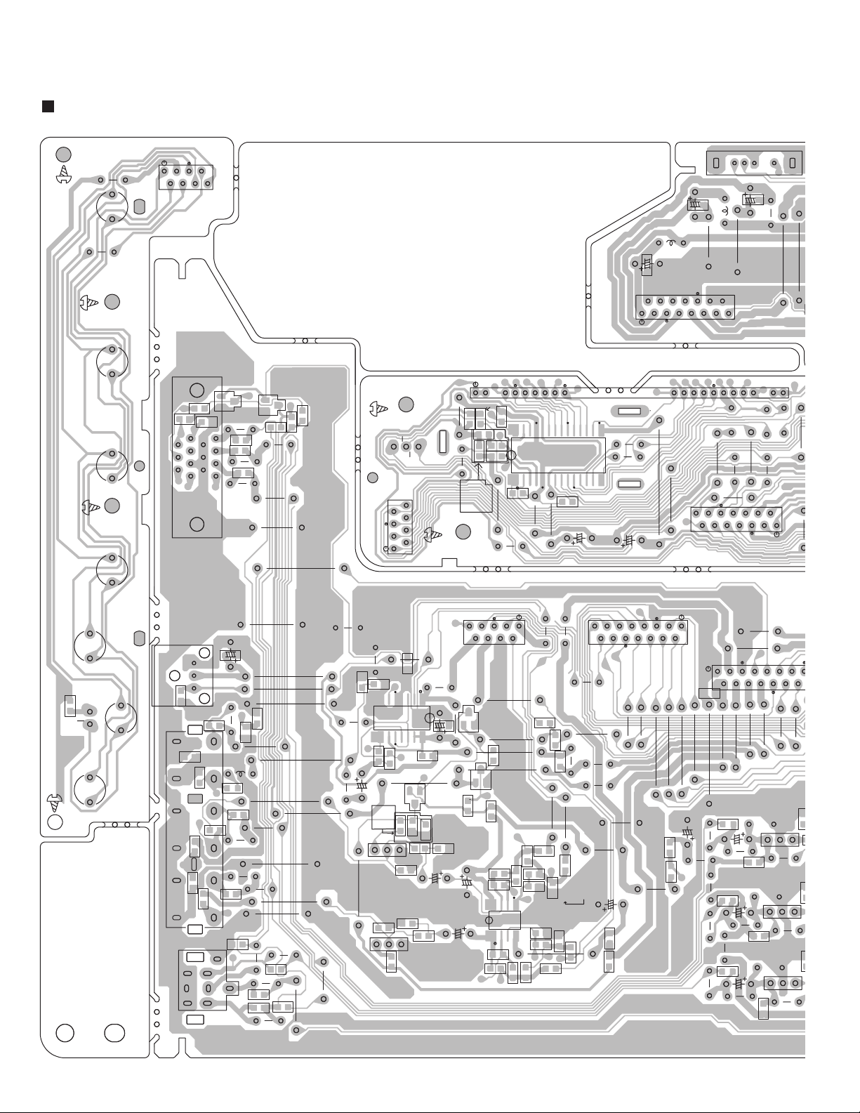
XV-N40BK,XV-N44SL/XV-N4SL
C
R633
R
Printed circuit boards
Main board
S802 S803 S804
S806
R663
CN803
R664
J604
R662
R665
Q661
R666
R667
Q635
R640
R638
R661
CN802
D802
DI801
C805
R809
R808
R812
R811
R807
R804
C810
C811
C801
IC801
CN902
C809
C978
C979
L956
C974
C976
CN801
D804
L957
D805
C975
C980
S902
C981
D803
S807
R810
S805
D810
S808
J601
J703
R793
C798
R773
C685
C686
C683
R774
C640
J602
R626
R606
C793
R639
L681
C794
R683
R636
K682
R616
R682
R637
C639
IC704
Q752
C797
R792
C791
Q751
C760
R791
R771
R772
R781
C759
R794
C763
Q756
R770
K792
R767
R790
C757
R768
CN701
C796
R769
C795
IC751
C758
R786
C765
R760
C754
Q757
R783
C753
R759
R787
Q755
R782
R761
R762
R751
C751
C756
R764
C752
R763
C755
R752
R788
K791
R765
R766
R755
R756
C764
R784
R785
R601
K601
CN601
R2
C601
K605
K604
C653
K603
R635
C652
R625
C651
D631
D621
D611
R615
Q631
R623
Q621
R613
Q611
2-20
Page 80
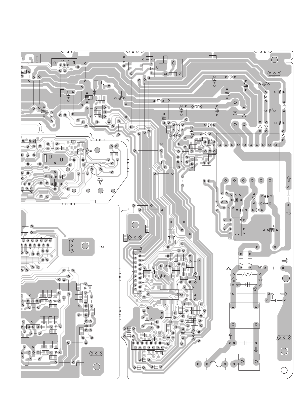
C975
C980
5
S902
C981
D803
C977
C804
L959
C956
IC802
R813
C803
C957
Q801
R814
S901
Q802
IC951
C973
R966
R967
C972
S801
C960
C971
Q953
D801
R956
C959
D806
L710
R802
R714
R713
L709
C713
Q952
L952
C953
C954
R715
C951
C708
C707
R954
R969
CP951
C955
R962
R963
R953
C982
R951
J702
C950
R964
Q951
XV-N40BK,XV-N44SL/XV-N4SL
L951
R961
R952
D951
C961
R965
PC901
C952
D952
C969
R957
R960
R913
C988
R903
C970
IC952
R968
C958
D904
R915
L955
D953
C914
C967
R912
C913
EP953
D955
D954
D902
D957
D903
C966
C965
L954
L953
C964
C963
D956
T901
C906
C908
R901
D631
635
R625
D621
D611
R615
Q621
Q611
Q631
R634
R623
R613
R633
R624
R614
C632
C622
C612
C633
C623
C613
CN702
R632
L613
C634
C624
R612
C614
C777
R622
L612
L611
C602
R603
C603
D601
C666
K602
EP751
R602
Q601
C650
L601
C604
R604
R605
EP651
C983
R955
K812
EP952
D702
K814
CN904
K815
K810
K816
K818
K813
C984
R711
R712
C715
K817
K811
C704
C706
K820
C705
D701
K823
X701
K819
R706
C703
IC701
CN901
Q701
R705
R703
R707
B107
R704
K822
C802
IC702
K821
C808
C714
R708
C701
C702
R701
R709
FC902
R710
R702
R906
C915
FC901
IC901
D901
L901
C902
C907
C904
R910
C918
C905
EP951
P901
2-21
Page 81
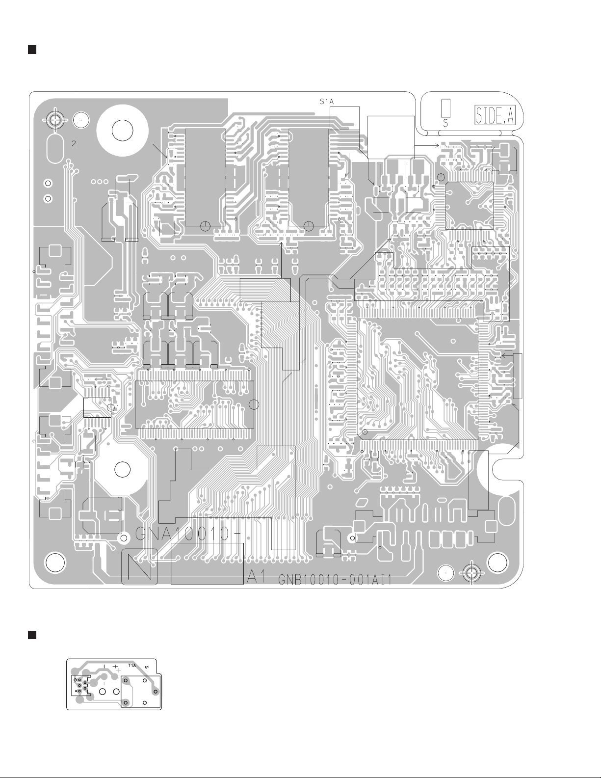
XV-N40BK,XV-N44SL/XV-N4SL
Servo control board
Forward side
CN503
CN502
R404
C400
IC402
D402
C556
C581
R573
R405
R575
L401
C407
C408
C567
C568
C578
R570
R574
C532
C531
C529
R403
L501
R571
C540
C535
C582
C545
R576
R578
IC505
R280
C253
C264
C563
C524
K507
C571
R259
R255
C255
R254
C251
R251
LC502
C521
R256
C256
K502
C310
R318
R319
IC251
R252
K504
LC504
C311
C313
R321
R323
C314
C312
C263
C527
R324
R325
C315
C316
C260
C541
R326
C319 C320
C317
C559
C560
K501
K508
R550
C511
C321
C322 C323
R327
C257 C258
C259
C261
C262
R514
R215
LC501
C501
R328
C349 C350
C325
C214
C203
C211
R211
C210
R212 R213
C216
C558
R214
C212
C126
R329
C326
C351
C327
C213
R584
R216
R222
R102
R103
R101
R110
C127
C128
R330 R331
C329
R332
C333
C539
R210
R221
R106
R107
R111
C109
R115
C129
C330 C331
C334
R333
R334
IC201
R223
C110
R108 R109
C302
R307
R302
C218
R312
R314 R315
R313
C303
R308
R305
C301
R304
R301
C348
C549
R219
R220
R316
R317
R309
R306
R303
R340
C554
CN501
R119
C102
C204
C208
R310
R311
R341
C550
R120
C103
R230
R206 R207
C207
R204
R208
C347
K304
R112
R131
C205
C206
R104
R205
R209
R343
C502
C145
C144
R113
R130
Q101
D301
C142
C111 C112
R350
C346
C141
C345
Q102
R105
C552
C553
IC101
C124
C344
R510
C555
C343
R509
R511
C125
IC301
R336
R339
R337
R338
C341
C342
C113
C339
C340
R344
R114
R127
C122
R345
R320
C337
R342
C352
C118
X301
Loading motor board
2-22
Page 82
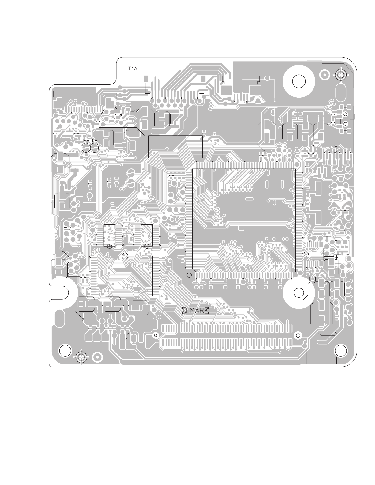
CN101
TP106
TP103
K301
C304
TP325
TP324
TP322
TP321
TP332
TP304
C360
TP512
TP514
TP101
TP102
TP318
TP317
TP315
TP314
TP506
TP508
TP510
C510
C135
C332
TP326
TP320
TP316
TP502
TP504
C505
C509
TP313
R129
TP328
TP327
TP303
R517
C306
R525
C504
TP118
TP105
TP312
TP333
TP323
TP319
C566
R516
K302
TP513
R116
C137
TP104
C328
TP305
TP511
TP115
C119
R125
C324
C338
C308
TP509
TP121
TP123
TP117
R128
C120
C123
IC512
C503
TP507
TP505
TP122
TP124
TP116
R117
R126
C121
C318
K519
K303
C508
K101
TP120
R124
C117
TP302
TP301
TP306
TP307
C569
TP501
C138
C139
D101
Q103
TP119
C105
C106
C116
TP308
TP330
IC511
TP111
TP110
TP112
TP309
TP529
TP530
TP533
TP329
C573
TP503
C201
TP528
TP527
TP531
TP532
TP913
R518
IC509
TP331
C557
Reverse side
TP37
R201
R202
TP125
TP130
TP107 TP108 TP109
TP126
TP129
TP127
TP128
R505
R506
R507
R508
C536
C548
TP912
C534
C547
C533
IC513
C528
R519
TP33
TP36
TP35
TP114
TP113
C512
TP31
TP43
TP38
IC501
C514
CN201
TP32
TP41
TP42
TP44
C217
TP311
TP47
TP45
TP39
TP870
TP869
TP867
TP868
C515
C516
TP46
TP40
TP34
CN202
TP873
TP871
TP872
C517
XV-N40BK,XV-N44SL/XV-N4SL
R522
TP49
C561
TP874
TP875
TP876
TP877
TP810
C518
C252
C562
C520
C519
CN504
TP50
TP48
C542
R565
TP310
C523
C572
R566
C565
C401
R512
R513
K509
TP881
C403
D401
TP548
C543
C544
C564
R589
TP860
TP885
R402
C402
R521
R523
K510
LC559
R572
K559
C507
R501
R503
C506
X571
IC401
C409
TP882
TP812
TP811
TP884
R515
K513
TP862
C404
TP883
C551
R568 R569
LC557 LC558
K557 K558
C580
TP522
TP524
TP865
TP534
C406
TP861
TP838
R585
R520
TP526
TP516
TP536
TP878
TP519
R583
TP839
R586
R502
R567
LC556
K556
TP525
TP866
K560
TP863
C405
R524
TP840
R587
TP515
TP403
TP542
TP546
TP544
TP401
R401
SW501
TP521
TP523
TP517 TP518
TP520
TP535
TP864
TP541
TP402
TP543
TP545
TP547
TP549
2-23
Page 83

XV-N40BK,XV-N44SL,
XV-N4SL
VICTOR COMPANY OF JAPAN, LIMITED
AV & MULTIMEDIA COMPANY OPTICAL DISC CATEGORY 1644, Shimotsuruma, Yamato, Kanagawa 242-8514, Japan
No.XA003SCH
Printed in japan
200306
 Loading...