JVC XV-N320B, XV-N322S Diagram

SCHEMATIC DIAGRAMS
DVD PLAYER
XV-N320B,XV-N322S
CD-ROM No.SML200503
Area Suffix
EK ------------------------ U.K.
EU -------- Western Europe
EY -------- Northern Europe
EZ --------- Eastern Europe
ER ---- Russian Federation
STANDBY/ON
OPEN/
CLOSE
+
SLOW
DISPLAYON SCREEN
T
O
T
P
H
U
M
B
N
A
IL
L
ENTER
S
NEXTPREVIOUS
SELECT
CLEAR
123
456
789
0
SOUND
VFP
EFFECT
I/P
SUBTITLEANGLE
AUDIO
ZOOM
/
IS
T
E
T
U
P
®
VIDEO
M
E
N
U
M
E
N
U
CANCEL RETURN
TITLE/
GROUP DIMMER
SLIDE EFFECT
XV-N320BEKC,XV-N320BEUC,XV-N320BEYC,XV-N320BEZC,XV-N320BERC
XV-N322SEKC,XV-N322SEUC,XV-N322SEYC,XV-N322SEZC,XV-N322SERC
COPYRIGHT 2005 Victor Company of Japan, Limited
No.YD056SCH
2005/3


CHARTS AND DIAGRAMS
NOTES OF SCHEMATIC DIAGRAM
Safety precautions
The Components indentified by the symbol are
critical for safety. For continued safety, replace safety
critical components only with manufacturer's recommended parts.
1. Units of components on the schematic diagram
Unless otherwise specified.
1) All resistance values are in ohm. 1/6 W, 1/8 W (refer to
parts list).
Chip resistors are 1/16 W.
K: KΩ(1000Ω), M: MΩ (1000KΩ)
2) All capacitance values are in µF, (P: PF).
3) All inductance values are in µH, (m: mH).
4) All diodes are 1SS133, MA165 or 1N4148M (refer to parts
list).
Note: The Parts Number, value and rated voltage etc. in
the Schematic Diagram are for references only.
When replacing the parts, refer to the Parts List.
2. Indications of control voltage
AUX : Active at high.
AUX or AUX(L) : Active at low.
!
4. Voltage measurement
1) Regulator (DC/DC CONV) circuits
REC : Colour bar signal.
PB : Alignment tape (Colour bar).
— : Unmeasurable or unnecessary to measure.
2) Indication on schematic diagram
Voltage indications for REC and PB mode on the schematic diagram are as shown below.
REC mode
12 3
2.5
(5.0)
PB mode
1.8
PB and REC modes
(Voltage of PB and REC modes
are the same)
Note: If the voltages are not indicated on the schematic
diagram, refer to the voltage charts.
6. Indication of the parts for adjustments
The parts for the adjustments are surrounded with the circle
as shown below.
3. Interpreting Connector indications
1
2
Removable connector
3
1
2
Wire soldered directly on board
3
1
Non-removable Board connector
2
3
1
2
4
Board to Board
3
Connected pattern on board
The arrows indicate signal path
Note: For the destination of each signal and further line
connections that are cut off from the diagram,
refer to "BOARD INTERCONNECTIONS"
7. Indication of the parts not mounted on the circuit board
“OPEN” is indicated by the parts not mounted on the circuit
board.
R216
OPEN
2-1 2-2

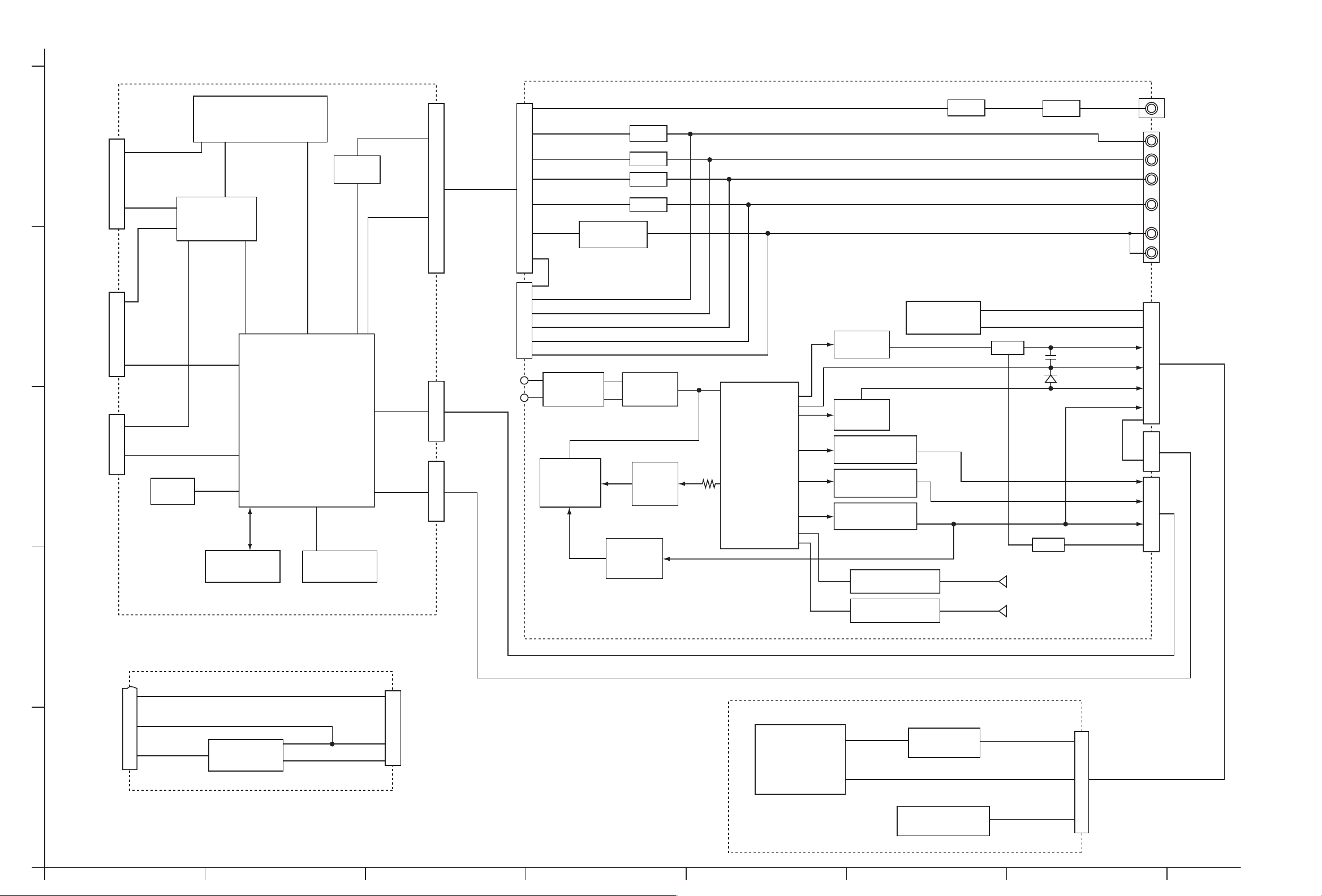
Block diagram
5
4
Spindle motor
Loading motor
3
2
FROM
Pick-up
Unit
FROM
assembly
FROM
assembly
A B C D E F RF
CN101
CDPD DVDPD
T+ TF+ F-
WOUT
VOUT
UOUT
COM
FM+
FM-
CN201 CN202
TRVSW
CLOSESW OPENSW
LM+
LM-
X301
FEP
(Front end processor)
IC101
SVREF
4CH Driver
IC201
FODRV
TRDRV
TRSDRV
OPEN
FG SPDRV
RPBC
AMPSTBY
(
Super optical disc controller
VID_XO
VID_XI
64M SDRAM
IC302
DFCT
BSUM
FE CE
MINTR
SCLK
S DATA
SDEN
INB IN
TE
SODC
and
AV Decoder
IC301
LA0 to LA20
LWRL LOE
LCS3 LD0 to LD7
Flash ROM
AOUTL+ AOUTR+
2CH DAC
IC403
SPDIF
AOUTLAOUTRYOUT
Cb/Pb
Cr/Pr
C/Cv/Y
S1(FUNCTION)
BLANKING
RGB(VIDEOSW)
)
IC303
STBY
REMO
FLDIN
CLK
STB
CN302
CN301
CN303
TO CN702
SHEET 3
AC IN
CN905
AOUTL+/AOUTR+/-
CN904
PbOUT
PrOUT
C/Cv/Y
BLANKING
FUNCTION
VIDEOSW
Line filter
L901
Switching
regulator
IC901
Y
OP.Amplifier
IC701
FEED BACK
PC901
L706
L730
L709
L701
Y/G
Pb/B
Pr/R
Cv/Y
LCH RCH
AC-DC
D903
AC-DC
D906
C909
Powe r
transformer
T901
AC-DC
D951,C950
AC-DC
D952,C982
AC-DC
D955,C954,L952
AC-DC
D954,C955,L953
AC-DC
D953,C983,L951
AC-DC
D956,L954,C957,C985
AC-DC
D957,L955,C956,C966
SPDIF
Operation switch
S501 to S508
IC704
-12V
+12V
Q951
Q952
L707
SG1 to SG4
AUDIOL/R
K1,K2
-VDISP
B3.3V
REMO
FLDIN
CLK
STB
B5.7V
M9V
B3.3V
STBY
F+
J602
Coaxial digital
output
J601
Y
Pb
Pr
F-
Component
video output
Composite
video output
Analog
audio output
CN901CN902CN903
1
Scart terminal
LCH RCH Pr/R Pb/B FUNCTION BLANKING
J702
2IN-1OUT SW
Y/COMPOSITE
IC703
A
CN702
G
Y/G
Cv/Y VIDEOSW
BCDEFG
TO CN904
SHEET 2
FL Display driver
IC501
2-3 2-4
GR1 to GR7
SG1 to SG9
K1 K2 SG1 to SG4 -VDISP STB FLDIN CLK
FL Display
DI501
Remote controller
IC502
F+ F-
CN501
REMO
 Loading...