

Page 1
SERVICE MANUAL
BLU-RAY DISC PLAYER
MB706<Rev.002>20097SERVICE MANUAL
XV-BP1J, XV-BP1C, XV-BP1B,
XV-BP1E, XV-BP1EN, XV-BP1EV,
XV-BP1EE, XV-BP1US,
XV-BP1UX, XV-BP1UJ
(Except J,C,UJ)
COPYRIGHT © 2009 Victor Company of Japan, Limited
Lead free solder used in the board (material : Sn-Ag-Cu, melting point : 219 Centigrade)
TABLE OF CONTENTS
1 PRECAUTION. . . . . . . . . . . . . . . . . . . . . . . . . . . . . . . . . . . . . . . . . . . . . . . . . . . . . . . . . . . . . . . . . . . . . . . . . 1-5
2 SPECIFIC SERVICE INSTRUCTIONS . . . . . . . . . . . . . . . . . . . . . . . . . . . . . . . . . . . . . . . . . . . . . . . . . . . . . . 1-9
3 DISASSEMBLY . . . . . . . . . . . . . . . . . . . . . . . . . . . . . . . . . . . . . . . . . . . . . . . . . . . . . . . . . . . . . . . . . . . . . . 1-10
4 ADJUSTMENT . . . . . . . . . . . . . . . . . . . . . . . . . . . . . . . . . . . . . . . . . . . . . . . . . . . . . . . . . . . . . . . . . . . . . . . 1-11
5 TROUBLESHOOTING . . . . . . . . . . . . . . . . . . . . . . . . . . . . . . . . . . . . . . . . . . . . . . . . . . . . . . . . . . . . . . . . . 1-12
COPYRIGHT © 2009 Victor Company of Japan, Limited
No.MB706<Rev.002>
2009/7
Page 2
SPECIFICATION
For Northern America
General
Power requirements AC 120 V~, 60 Hz
Power consumption 18W
Dimensions (W × H × D) Approx. 16.9 x 2.1 x 9.7 inches (430 x 54 x 245 mm) without foot
Net Weight (Approx.) 6.2 lbs (2.8 kg)
Operating temperature 41 °F to 95 °F (5 °C to 35 °C)
Operating humidity 5 % to 90 %
Outputs
VIDEO OUT 1.0 V (p-p), 75 Ω, sync negative, RCA jack × 1
COMPONENT VIDEO OUT (Y) 1.0 V (p-p), 75 Ω, sync negative, RCA jack × 1
(Pb)/(Pr) 0.7 V (p-p), 75 Ω, RCA jack × 2
HDMI OUT (video/audio) 19 pin (HDMI standard, Type A)
ANALOG AUDIO OUT 2.0 Vrms (1 kHz, 0 dB), 600 Ω, RCA jack (L, R) × 1
DIGITAL OUT (COAXIAL) 0.5 V (p-p), 75 Ω, RCA jack × 1
DIGITAL OUT (OPTICAL) 3 V (p-p), Optical jack × 1
System
Laser Semiconductor laser, wavelength: 405nm / 650 nm
Signal system Standard NTSC Color TV system
Frequency response 20 Hz to 20 kHz (48 kHz, 96 kHz, 192 kHz sampling)
Signal-to-noise ratio More than 100 dB (ANALOG OUT connectors only)
Harmonic distortion Less than 0.008%
Dynamic range More than 95 dB
LAN port Ethernet jack × 1, 10BASE-T/100BASE-TX
Design and specifications are subject to change without prior notice.
1-2 (No.MB706<Rev.002>)
Page 3
For Europe
General
Power requirements AC 220-240 V ~, 50/60 Hz
Power consumption 18W
Dimensions (W × H × D) Approx. 430 × 54 × 245 mm without foot
Net Weight (Approx.) 2.8 kg
Operating temperature 5 °C to 35 °C
Operating humidity 5 % to 90 %
Outputs
VIDEO OUT 1.0 V (p-p), 75 Ω, sync negative, RCA jack × 1
COMPONENT VIDEO OUT (Y) 1.0 V (p-p), 75 Ω, sync negative, RCA jack × 1
(Pb)/(Pr) 0.7 V (p-p), 75 Ω, RCA jack × 2
HDMI OUT (video/audio) 19 pin (HDMI standard, Type A)
ANALOGUE AUDIO OUT 2.0 Vrms (1 kHz, 0 dB), 600 Ω, RCA jack (L, R) × 1
DIGITAL OUT (COAXIAL) 0.5 V (p-p), 75 Ω, RCA jack × 1
DIGITAL OUT (OPTICAL) 3 V (p-p), Optical jack × 1
System
Laser Semiconductor laser, wavelength: 405nm / 650 nm
Signal system Standard PAL/NTSC Colour TV system
Frequency response 20 Hz to 20 kHz (48 kHz, 96 kHz, 192 kHz sampling)
Signal-to-noise ratio More than 100 dB (ANALOGUE OUT connectors only)
Harmonic distortion Less than 0.008%
Dynamic range More than 95 dB
LAN port Ethernet jack × 1, 10BASE-T/100BASE-TX
Bus power supply DC 5 V 500 mA
Design and specifications are subject to change without prior notice.
(No.MB706<Rev.002>)1-3
Page 4
For Asia
General
Power requirements AC 110-240 V ~, 50/60 Hz
Power consumption 18W
Dimensions (W × H × D) Approx. 430 × 54 × 245 mm without foot
Net Weight (Approx.) 2.8 kg
Operating temperature 5 °C to 35 °C
Operating humidity 5 % to 90 %
Outputs
VIDEO OUT 1.0 V (p-p), 75 Ω, sync negative, RCA jack × 1
COMPONENT VIDEO OUT (Y) 1.0 V (p-p), 75 Ω, sync negative, RCA jack × 1
(Pb)/(Pr) 0.7 V (p-p), 75 Ω, RCA jack × 2
HDMI OUT (video/audio) 19 pin (HDMI standard, Type A)
ANALOGUE AUDIO OUT 2.0 Vrms (1 kHz, 0 dB), 600 Ω, RCA jack (L, R) × 1
DIGITAL OUT (COAXIAL) 0.5 V (p-p), 75 Ω, RCA jack × 1
DIGITAL OUT (OPTICAL) 3 V (p-p), Optical jack × 1
System
Laser Semiconductor laser, wavelength: 405nm / 650 nm
Signal system Standard PAL/NTSC Colour TV system
Frequency response 20 Hz to 20 kHz (48 kHz, 96 kHz, 192 kHz sampling)
Signal-to-noise ratio More than 100 dB (ANALOGUE OUT connectors only)
Harmonic distortion Less than 0.008%
Dynamic range More than 95 dB
LAN port Ethernet jack × 1, 10BASE-T/100BASE-TX
Bus power supply DC 5 V 500 mA
Design and specifications are subject to change without prior notice.
1-4 (No.MB706<Rev.002>)
Page 5
SECTION 1
PRECAUTION
1.1 Safety Precautions
(1) This design of this product contains special hardware and
many circuits and components specially for safety purposes. For continued protection, no changes should be made
to the original design unless authorized in writing by the
manufacturer. Replacement parts must be identical to
those used in the original circuits. Services should be performed by qualified personnel only.
(2) Alterations of the design or circuitry of the product should
not be made. Any design alterations of the product should
not be made. Any design alterations or additions will void
the manufacturers warranty and will further relieve the
manufacture of responsibility for personal injury or property
damage resulting therefrom.
(3) Many electrical and mechanical parts in the products have
special safety-related characteristics. These characteristics are often not evident from visual inspection nor can the
protection afforded by them necessarily be obtained by using replacement components rated for higher voltage, wattage, etc. Replacement parts which have these special
safety characteristics are identified in the Parts List of Service Manual. Electrical components having such features
are identified by shading on the schematics and by ( ) on
the Parts List in the Service Manual. The use of a substitute
replacement which does not have the same safety characteristics as the recommended replacement parts shown in
the Parts List of Service Manual may create shock, fire, or
other hazards.
(4) The leads in the products are routed and dressed with ties,
clamps, tubings, barriers and the like to be separated from
live parts, high temperature parts, moving parts and/or
sharp edges for the prevention of electric shock and fire
hazard. When service is required, the original lead routing
and dress should be observed, and it should be confirmed
that they have been returned to normal, after reassembling.
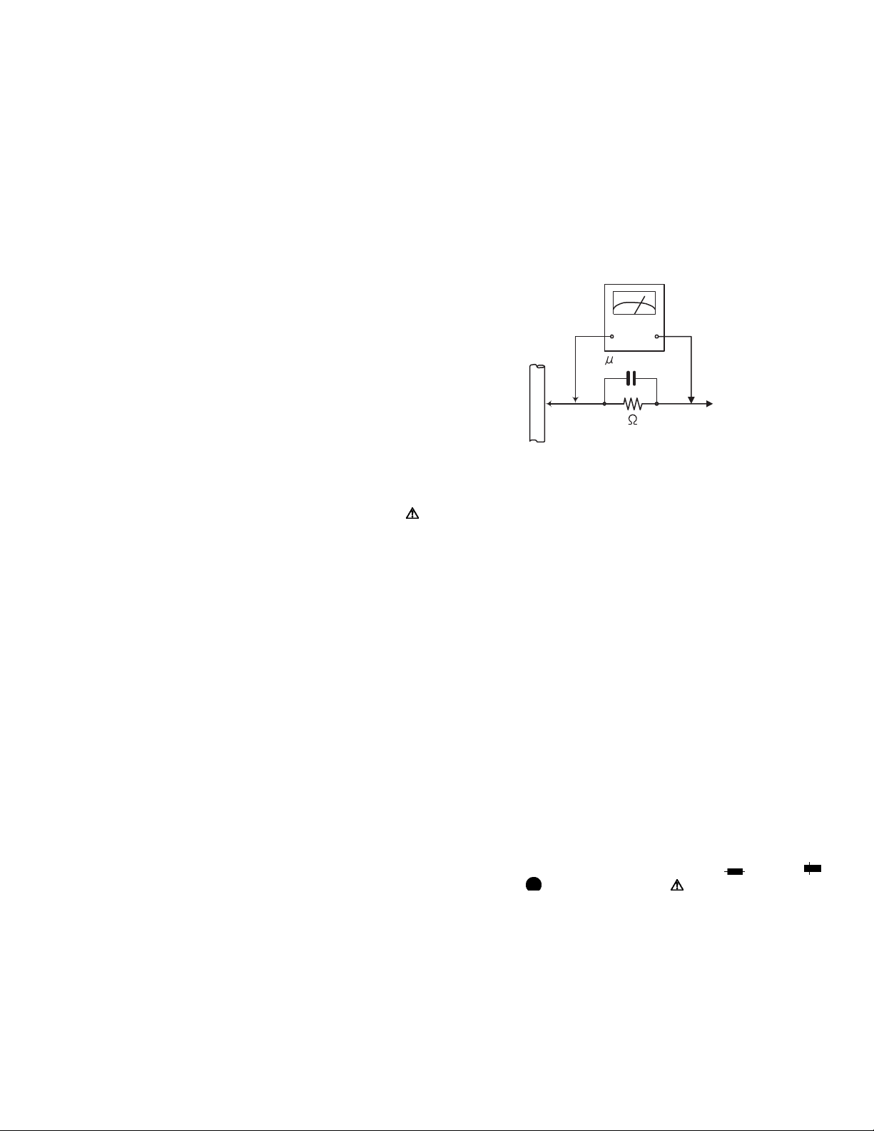
(5) Leakage shock hazard testing
After reassembling the product, always perform an isolation check on the exposed metal parts of the product (antenna terminals, knobs, metal cabinet, screw heads,
headphone jack, control shafts, etc.) to be sure the product
is safe to operate without danger of electrical shock.Do not
use a line isolation transformer during this check.
• Plug the AC line cord directly into the AC outlet. Using a
"Leakage Current Tester", measure the leakage current
from each exposed metal parts of the cabinet, particularly any exposed metal part having a return path to the
chassis, to a known good earth ground. Any leakage current must not exceed 0.5mA AC (r.m.s.).
• Alternate check method
Plug the AC line cord directly into the AC outlet. Use an
AC voltmeter having, 1,000Ω per volt or more sensitivity
in the following manner. Connect a 1,500Ω 10W resistor
paralleled by a 0.15µF AC-type capacitor between an ex-
posed metal part and a known good earth ground.
Measure the AC voltage across the resistor with the AC
voltmeter.
Move the resistor connection to each exposed metal
part, particularly any exposed metal part having a return
path to the chassis, and measure the AC voltage across
the resistor. Now, reverse the plug in the AC outlet and
repeat each measurement. Voltage measured any must
not exceed 0.75 V AC (r.m.s.). This corresponds to 0.5
mA AC (r.m.s.).
AC VOLTMETER
(Having 1000
ohms/volts,
or more sensitivity)
0.15 F AC TYPE
Place this
probe on
1500 10W
Good earth ground
1.2 Warning
(1) This equipment has been designed and manufactured to
meet international safety standards.
(2) It is the legal responsibility of the repairer to ensure that
these safety standards are maintained.
(3) Repairs must be made in accordance with the relevant
safety standards.
(4) It is essential that safety critical components are replaced
by approved parts.
(5) If mains voltage selector is provided, check setting for local
voltage.
1.3 Caution
Burrs formed during molding may be left over on some parts
of the chassis.
Therefore, pay attention to such burrs in the case of preforming repair of this system.
1.4 Critical parts for safety
In regard with component parts appearing on the silk-screen
printed side (parts side) of the PWB diagrams, the parts that are
printed over with black such as the resistor ( ), diode ( )
and ICP ( ) or identified by the " " mark nearby are critical
for safety. When replacing them, be sure to use the parts of the
same type and rating as specified by the manufacturer.
(This regulation dose not Except the J and C version)
each exposed
metal part.
(No.MB706<Rev.002>)1-5
Page 6
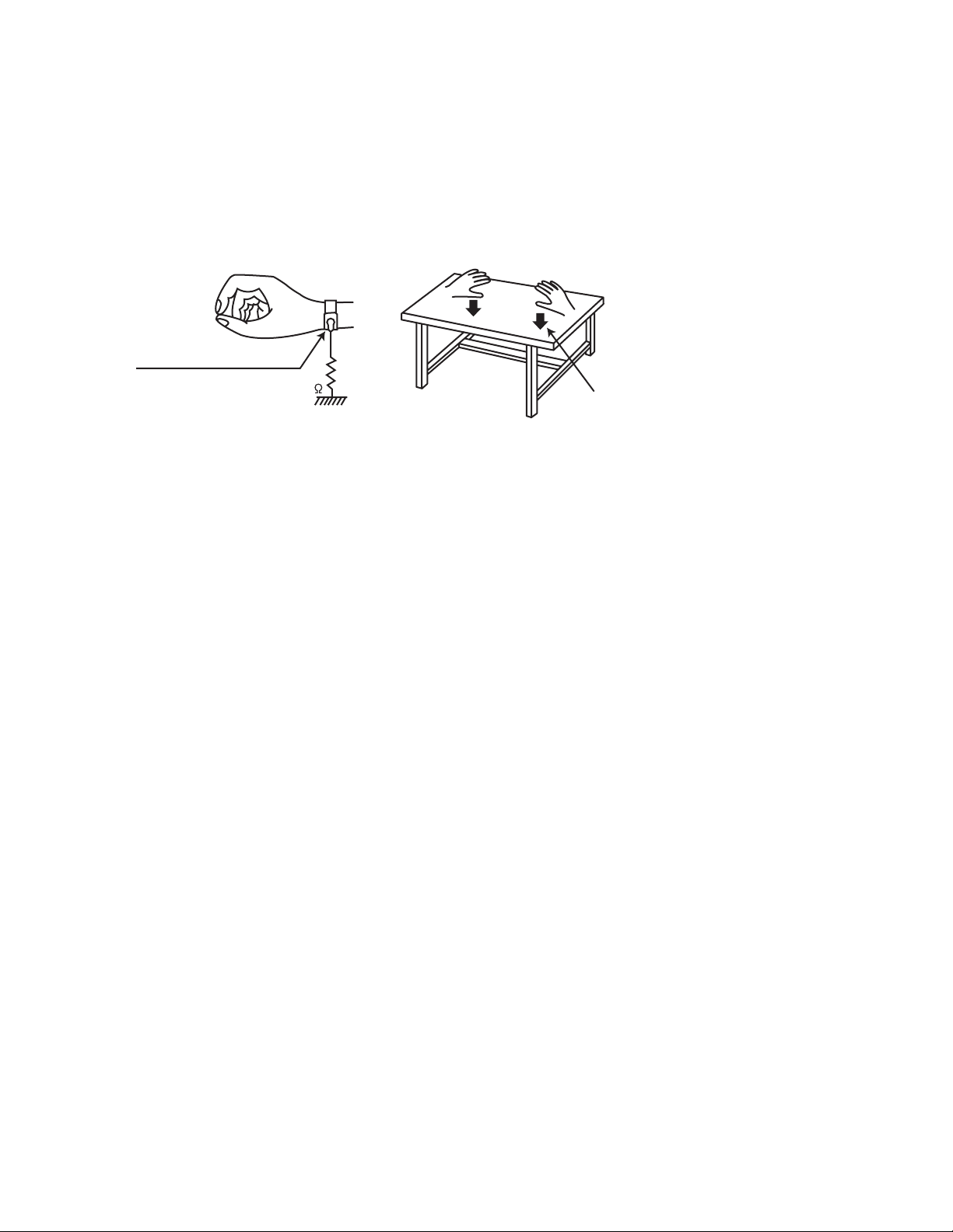
1.5 Preventing static electricity
Electrostatic discharge (ESD), which occurs when static electricity stored in the body, fabric, etc. is discharged, can destroy the laser
diode in the traverse unit (optical pickup). Take care to prevent this when performing repairs.
1.5.1 Grounding to prevent damage by static electricity
Static electricity in the work area can destroy the optical pickup (laser diode) in devices such as laser products.
Be careful to use proper grounding in the area where repairs are being performed.
(1) Ground the workbench
Ground the workbench by laying conductive material (such as a conductive sheet) or an iron plate over it before placing the
traverse unit (optical pickup) on it.
(2) Ground yourself
Use an anti-static wrist strap to release any static electricity built up in your body.
(caption)
Anti-static wrist strap
1M
Conductive material
(conductive sheet) or iron palate
(3) Handling the optical pickup
• In order to maintain quality during transport and before installation, both sides of the laser diode on the replacement optical
pickup are shorted. After replacement, return the shorted parts to their original condition.
(Refer to the text.)
• Do not use a tester to check the condition of the laser diode in the optical pickup. The tester's internal power source can easily
destroy the laser diode.
1-6 (No.MB706<Rev.002>)
Page 7
1.6 Importance administering point on the safety
loader
W104
R145
8.P-CON
L127
7.5V
C122
R146
audio
6.GND
3.GND
2.3.3V
1.3.3V
5.12V
4.12V
C151
C154
IC153
78R33
J101
R153
IC151
78R12
C121
SB360
D133
D122
SB360
C125
D126
IC103
R143
C143
16.FD(+)
15.FD(-)
W119
W103
R157
W105
R154
R155
R156
R181
R191
W113
W107
W108
C152
W115
IC152
378R05
(278R05)
R131
R152
R151
C133
R150
R122
6.2B (2.7B)
ZD121
W109
W114
W110
C126
9.GND
14.-29VA
13.GND
12.5.3VA
11.5.3VA
10.GND
W117
W102
IC154
278R12
W106
C131
L123
C124
R121
D131
R144
P101
C153
C132
W116
L124
C123
D123
SB360
W182
D121
HER303
D132
W112
B5A60VI
D124
10A06
(B5A60VI)
D125
R141
W183
W111
D130
R142
C103
C111
W101
IC102
R105
D102
T101
C107
R101
R104
C105
C106
D101
BC101
C109
BD101
W118
C115
V101
IC101
R100
R109
C101
C104
33B
ZD101
10B
ZD103
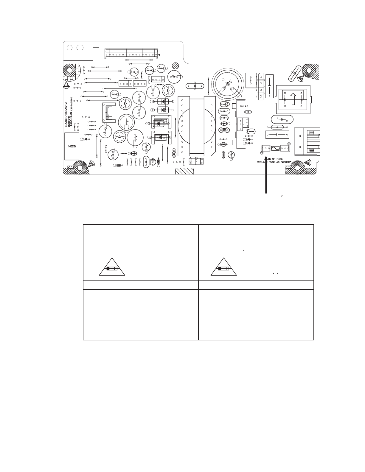
FH102
C102
F101
T1.6AL 250V
C110
L102
PW101
FH101
fast blow type / type a fusion rapide
Full Fuse Replacement Marking
Graphic symbol mark
(This symbol means fast blow type fuse.)
should be read as follows ;
FUSE CAUTION
FOR CONTINUED PROTECTION AGAINST RISK
OF FIRE, REPLACE ONLY WITH SAME TYPE
AND RATING OF FUSES ;
F901 : 3.5A 125V F901 : 3.5A 125V
Marquage Pour Le Remplacement
Complet De Fusible
Le symbole graphique (Ce symbole signifie
fusible de type a fusion rapide.)
^
doit etre interprete comme suit ;
PRECAUTIONS SUR LES FUSIBLES
POUR UNE PROTECTION CONTINUE CONTRE
DES RISQUES D'INCENDIE, REMPLACER
SEULEMENT PAR UN FUSIBLE DU MEME TYPE ;
(No.MB706<Rev.002>)1-7
Page 8
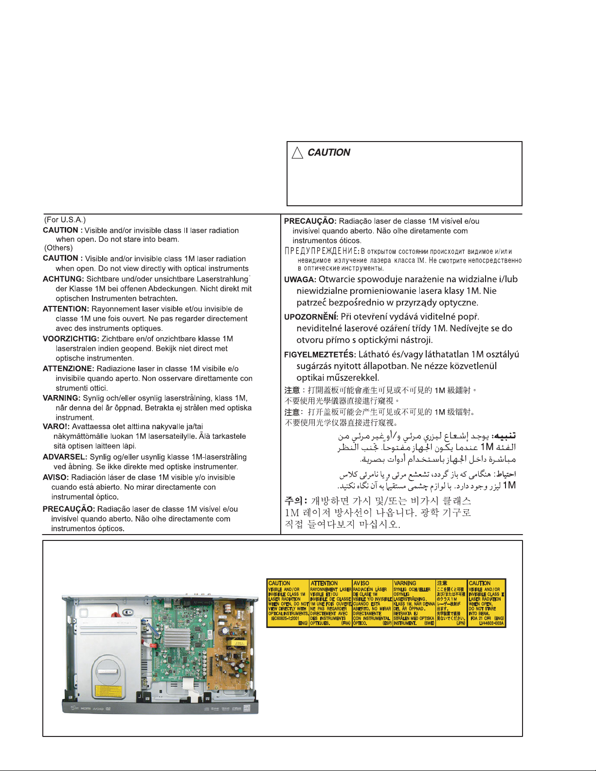
1.7 Important for laser products
1.CLASS 1 LASER PRODUCT
2.CAUTION :
(For U.S.A.) Visible and/or invisible class II laser radiation
when open. Do not stare into beam.
(Others) Visible and/or invisible class 1M laser radiation
when open. Do not view directly with optical instruments.
3.CAUTION : Visible and/or invisible laser radiation when
open and inter lock failed or defeated. Avoid direct
exposure to beam.
4.CAUTION : This laser product uses visible and/or invisible
laser radiation and is equipped with safety switches which
prevent emission of radiation when the drawer is open and
the safety interlocks have failed or are defeated. It is
dangerous to defeat the safety switches.
5.CAUTION : If safety switches malfunction, the laser is able
to function.
6.CAUTION : Use of controls, adjustments or performance of
procedures other than those specified here in may result in
hazardous radiation exposure.
!
Please use enough caution not to
see the beam directly or touch it
in case of an adjustment or operation
check.
REPRODUCTION AND POSITION OF LABELS and PRINT
WARNING LABEL and PRINT
1-8 (No.MB706<Rev.002>)
Page 9

SECTION 2
SPECIFIC SERVICE INSTRUCTIONS
This service manual does not describe SPECIFIC SERVICE INSTRUCTIONS.
(No.MB706<Rev.002>)1-9
Page 10
SECTION 3
DISASSEMBLY
3.1 Main body
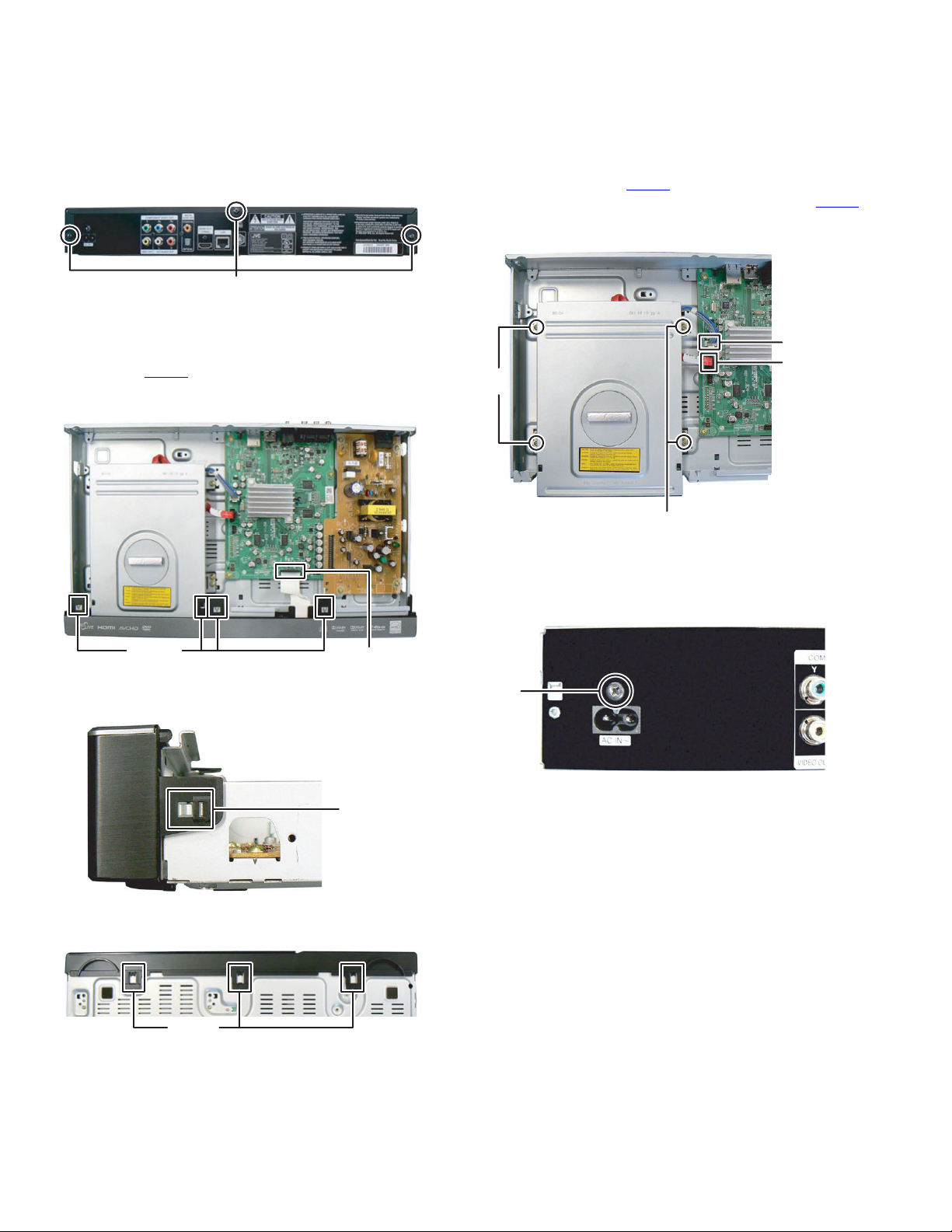
3.1.1 Removing the Top cover (See Fig.1)
(1) Remove the three screws A attaching the Top cover.
A
Fig.1
3.1.2 Removing the Front panel (See Fig.2 to 4)
(1) Disconnect the card wire from Front panel connected to
connector CN202
(2) Disengage four hooks a engaged top side of the Front pan-
el. (See Fig.2)
of the Main board. (See Fig.2)
3.2 Removing the Blu-ray drive unit (See Fig.5)
(1) Disconnect the connector wire from Blu-ray drive unit con-
nected to connector CN801
(2) Disconnect the FFC cable connected to connector CN802
of the Main board.
(3) Remove the four screws B attaching the Blu-ray drive unit.
of the Main board.
CN801
CN802
B
B
Fig.5
3.3 Removing the SMPS board (See Fig.6, 7)
(1) Remove the one screw C attaching the AC jack. (See
Fig.6)
hook a
Fig.2
(3) Disengage two hooks b engaged both side of the Front
panel. (See Fig.3)
Fig.3
(4) Disengage three hooks c engaged bottom side of the Front
panel. (See Fig.4)
hook
c
Fig.4
CN202
hook b
C
Fig.6
1-10 (No.MB706<Rev.002>)
Page 11
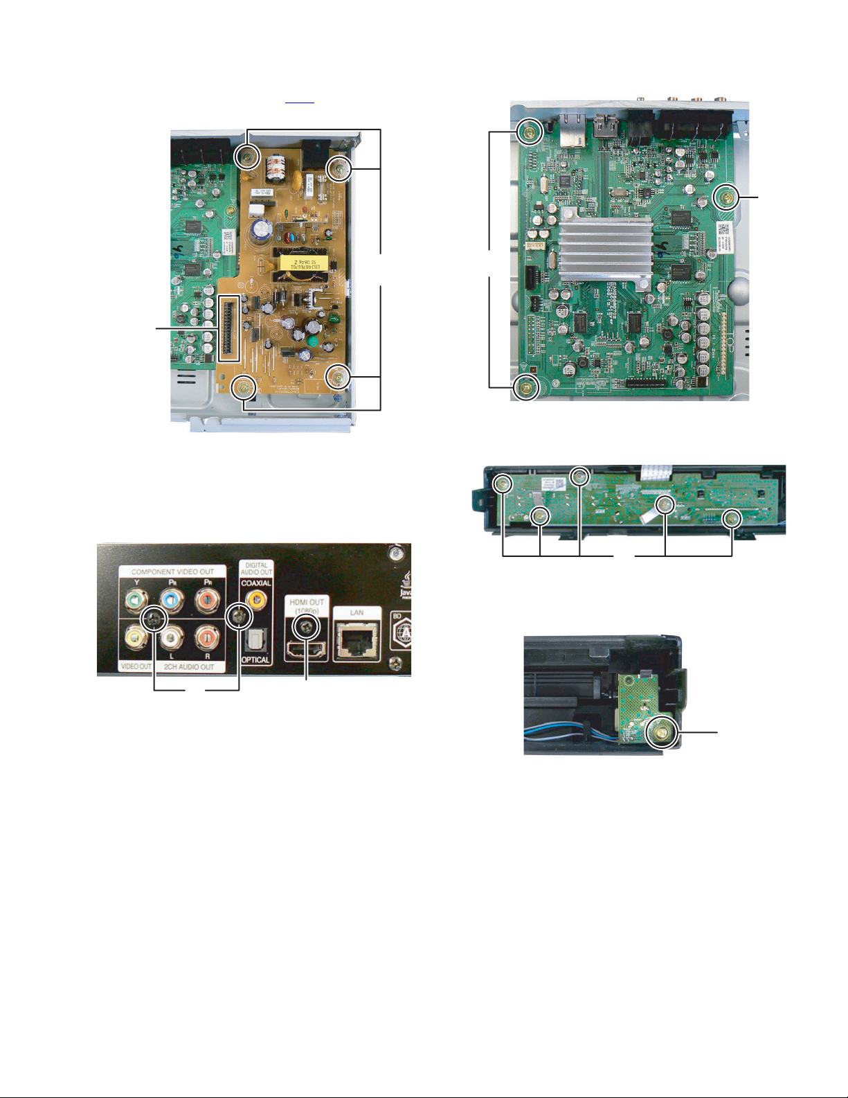
(2) Remove the four screws D attaching the SMPS board.
(See Fig.7)
(3) Disconnect the B-B connector P101
from Main board. (See Fig.7)
of the SMPS board
(3) Remove the three screws G attaching the Main board.
(See Fig.9)
G
D
P101
Fig.7
3.4 Removing the Main board (See Fig.8, 9)
(1) Remove the two screws E attaching the RCA jacks. (See
Fig.8)
(2) Remove the one screw F attaching the HDMI jack. (See
Fig.8)
G
Fig.9
3.5 Removing the Timer board (See Fig.10)
(1) Remove the five screws H attaching the Timer board.
H
Fig.10
3.6 Removing the Key board (See Fig.11)
(1) Remove the one screw J attaching the Key board.
EF
Fig.8
Fig.11
SECTION 4
ADJUSTMENT
This service manual does not describe ADJUSTMENT.
J
(No.MB706<Rev.002>)1-11
Page 12
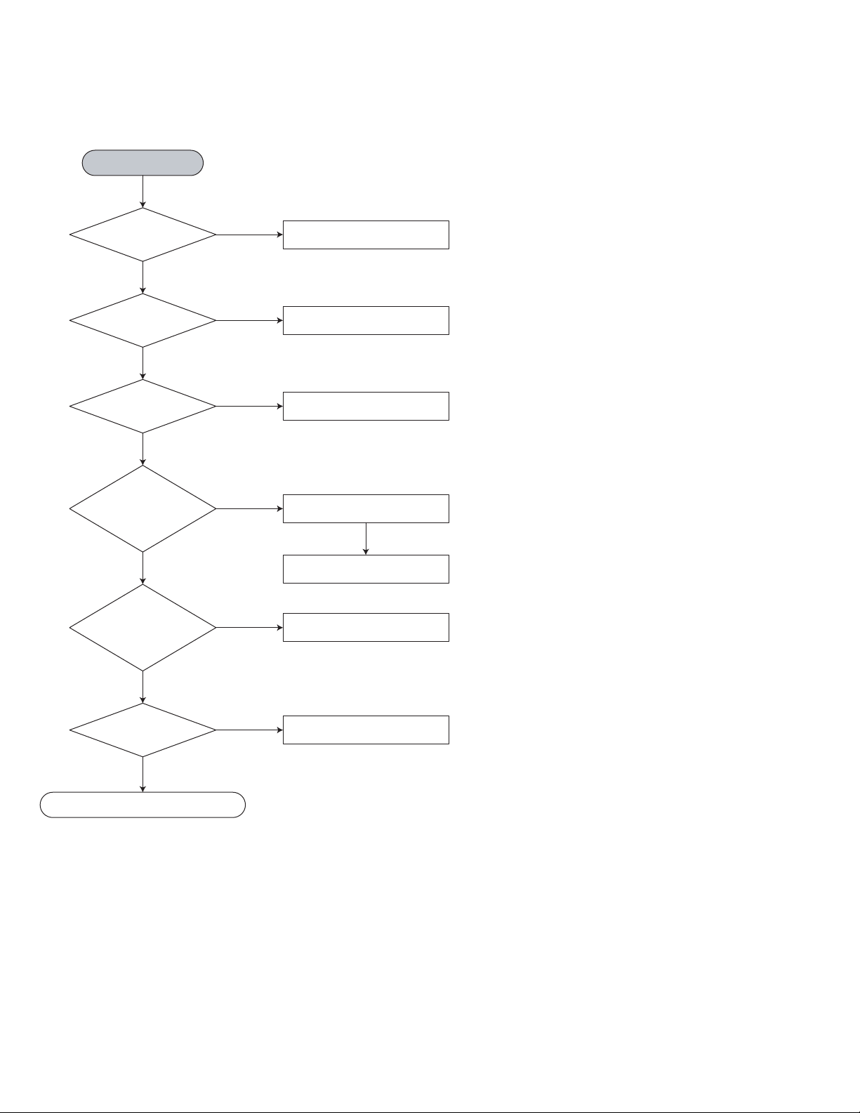
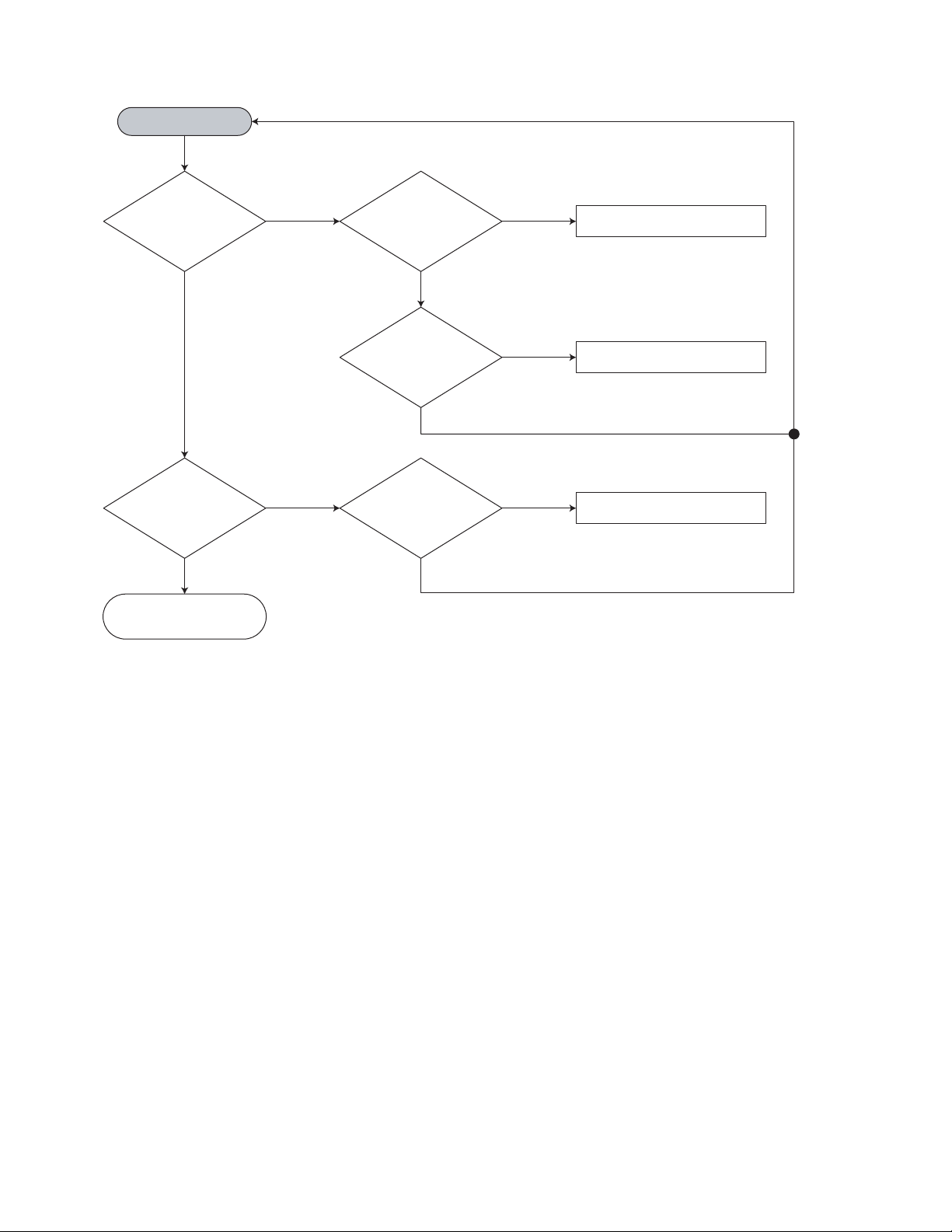
5.1 Power supply (SMPS)
No 5.3VA
SECTION 5
TROUBLESHOOTING
Is the
F101 normal?
YES
Is BD101 normal? Replace BD101
YES
Is R101 normal? Replace R101
YES
Is VCC
(13~27V) supplied to
IC101 Pin4?
YES
Is there about
2.5V at the IC103
Pin1?
NO
NO
NO
NO
NO
Replace F101 (same fuse)
Is D102 normal?
YES
Check or replace the D102
Replace IC103
YES
Is the IC102
normal?
YES
Power Line or Main PCB is short
1-12 (No.MB706<Rev.002>)
NO
Replace IC102
Page 13
No 3.3VA
No 5VA
YES
Is the Vcc
(3.8V) supplied to
IC153 Pin1?
YES
Is the IC153
Pin4 "H"?
YES
Check or Replace
the IC153
No 12V_A
YES
Is the Vcc
(13.5V) supplied to
IC151 Pin1?
NO
NO
NO
Check or Replace
the D123
Check the DVD CTL
"H" signal from u-com
Check or Replace
the D121
YES
Is the Vcc
(5.5V) supplied to
D132 anode?
YES
Is the IC152
Pin4 "H"?
YES
Check or Replace
the IC152
No 12V_L
YES
Is the Vcc
(13.5V) supplied to
IC154 Pin1?
NO
NO
NO
Check or Replace
the D132
Check the DVD CTL
"H" signal from u-com
Check or Replace
the D121
YES
Is the IC151
Pin4 "H"?
YES
Check or Replace
the IC151
NO
Check the DVD CTL
"H" signal from u-com
YES
Is the IC154
Pin4 "H"?
YES
Check or Replace
the IC154
NO
Check the DVD CTL
"H" signal from u-com
(No.MB706<Rev.002>)1-13
Page 14
5.2 Power ON
POWER on
"HELLO
PLEASE WAIT"
Display on VFD
OK?
YES
"JVC LOGO"
display on monitor
OK?
YES
Normal TV
function OK
NO
NO
Front I/F
cable connection
OK?
YES
VFD power
cable connection
OK?
YES
Display
cable connection
OK?
YES
NO
NO
NO
Front I/F cable connect
VFD power cable connect
Proper display cable connect
1-14 (No.MB706<Rev.002>)
Page 15

5.3 SYSTEM PART
POWER on
"HELLO
PLEASE WAIT"
Display on VFD
OK?
YES
NO
CN501, Pin18:
+5.3VA, Pin3: -29VA,
Pin17: -27V, Pin13:
-24V?
YES
X501 10MHz
OK?
YES
R516
About 625kHz Serial
Clock OK?
YES
R523
About 500kHz
OK?
YES
DIG501 Change
NO
NO
NO
NO
Check SMPS
X501 Change
IC501 Change
IC502 Change
Timer board
"READING"
display on VFD
OK?
YES
System part OK
NO
CN701, Pin5:
12V, Pin7: 5V,
Pin2: 2.2V, Pin11:
5.3VA?
YES
CA207: 5.3VA
CA210: 1.2V
CA211: 5V
YES
X301: 27MHz
OK?
YES
X302: 25MHz
OK?
YES
Check IC301
NO
NO
NO
NO
Check SMPS
IC202, IC203, IC204 Change
X301 Change
X102 Change
Main board
(No.MB706<Rev.002>)1-15
Page 16

5.4 COMPONENT (Y,Pb,Pr) VIDEO OUT
Component video no display
L906 +3.3V
OK?
YES
C913, C914, C915
Signal OK?
YES
R923, R924, R925
Signal OK?
YES
JK904
Soldering OK?
YES
Component Video OK
NO
NO
NO
NO
Re-soldering
Re-soldering
Re-soldering
Re-soldering
5.5 CVBS VIDEO OUT
CVBS video no display
C910
Video signal input
OK?
YES
C913
Video signal output
OK?
YES
JK904
Soldering OK?
YES
Component Video OK
NO
NO
NO
IC301 Check
IC901 Check
Re-soldering
1-16 (No.MB706<Rev.002>)
Page 17

5.6 AUDIO (S/PDIF, OPTICAL)
No Audio
C917
Digital Audio
output OK?
YES
JK903 Red
Lighting OK?
YES
S/PDIF, OPTICAL
audio out OK
NO
NO
IC301 Check
JK903 (Pin2)
+5.0V OK?
JK903 Re-soldering
NO
IC204 Check
(No.MB706<Rev.002>)1-17
Page 18

5.7 AUDIO (ANALOG)
No Audio
IC603 (Pin8)
12V AUDIO
OK?
YES
Q905 (Pin2)
LOW?
YES
IC903
Pin 6, 7, 8, I2S
Output OK?
YES
IC903 Pin 14, 15
audio output before
Amp OK?
YES
NO
NO
NO
NO
CN201 (Pin4)
12V AUDIO
OK?
R947 Re-soldering
Q902 Re-soldering
IC301 Check
IC903 Check
NO
Check SMPS
CA907, CA908
audio output
OK?
YES
R949, R950
JK904 (Pin2, 5)
soldering OK?
YES
Audio Output OK
NO
NO
IC904 Check
Re-soldering
1-18 (No.MB706<Rev.002>)
Page 19

5.8 HDMI
No A/V
JK902
Soldering OK?
YES
JK902 Pin 18
VCC +5V OK?
YES
JK902 Pin 19
+2.0V < Voltage < +5.3V
OK?
YES
JK902 Pin 15, 16
(SCL, SDA)
OK?
YES
NO
NO
NO
NO
Re-soldering
L902
soldering OK?
IC204 Pin 4 Check
TV hot plug detect signal
check (from IC301)
Check HDMI Voltage
Level Shifter
NO
Re-soldering
HDMI out OK
(No.MB706<Rev.002>)1-19
Page 20

Victor Company of Japan, Limited
Audio/Video Systems Division 10-1,1chome,Ohwatari-machi,Maebashi-city,371-8543,Japan
(No.MB706<Rev.002>)
Printed in Japan
VSE
Page 21

SCHEMATIC DIAGRAMS
Blu-ray Disc Player
XV-BP1J,XV-BP1C,XV-BP1B,
XV-BP1E,XV-BP1EN,XV-BP1EV,
XV-BP1EE,XV-BP1US,XV-BP1UX,
XV-BP1UJ
DVD-ROM No.SML2009Q1
Lead free solder used in the board (material : Sn-Ag-Cu, melting point : 219 Centigrade)
Contents
Block diagrams
Standard schematic diagrams
Printed circuit boards
COPYRIGHT 2009 Victor Company of Japan, Limited.
(Except J,C,UJ)
2-1
2-2
2-11 to 12
No.MB706SCH<Rev.002>
2009/7
Page 22

In regard with component parts appearing on the silk-screen printed side (parts side) of the PWB diagrams, the
parts that are printed over with black such as the resistor ( ), diode ( ) and ICP ( ) or identified by the " "
mark nearby are critical for safety.
Page 23

Block diagram
IC601
1.8V DCDC
IC701
1Gbit DDR2 SDRAM
IC702
1Gbit DDR2 SDRAM
512Gbit DDR2SDRAM
512Gbit DDR2SDRAM
IC703
IC704
27MHz 25MHz
SATA 1.1V DCDC
1.2V LDO
IC804
FAST ETHERNET
PHYCEIVER
IC301
2HD Decode
400MHz ARM11x2
200MHz Audio DSPx2
HDMI 1.3
Ethernet MAC
5V LDO
JK603
HDMI
JK901
Ethernet
Optical
coaxial
Debug
UART1
Front Panel
UART0
USB 2.0
IC801
Puer NAND
IC803
S_FLASH
IC903
Audio DAC
IC904
Dual Op Amp.
IC901
3ch SDTV
Video amp
IC902
3ch HDTV
Video amp
JK904
Audio L/R
CVBS
YPbPr
2-1
Page 24

Standard schematic diagrams
r
SMPS CIRCUIT DIAGRAM
BD101
GBL206
100nF /250VA
L102
25mH
100nF/250VA
4
C102
1
2
1
3
2
4
4
3
R100
1.5M/0.5W
C101
V101
PW101
1
2
BR
BL
(BK)
(WH)
2
2
1
2
1
3
FH02
FH01
F 10 1
T1.6AL /250V
R101
2.7/2W
1
C103
100u/450V
1
D
STR-W6251
S/OCP FM GND
3
R109
0.33 /2W
C110
1000pF/250AV
C111
1000pF/250VA
BEAD
BC101
IC101
7
C115
4
VCC
5
4.7nF
R104
56K/2W
D101
1N17
6
FB
1.5nF
C107
C106
UZ-10BSB
UZ-33BSB
ZD103
C105
0.01u/630V
68pF/1KV
D102
RL104F
C109
47nF/50V
ZD101
R105
39
HOT
T101EER3530
2
3
4
5
6
7
8
9
10
100nF
C104
CIRCUIT
FD (+)
22
21
FD (-)
-29VA
20
19
GND
18
5. 3VA
GND
17
16
5.5VA(LOADER)
13VA(LODER, AUDIO)
15
14
GND
3. 8VA 1A
13
12
GND
IC102
LTV-817B
4
3
D126
RL104F
D125
RL104F
D122
SB360
10A60V
D124
D133
SB360
B5A60V1
D132
D121
UF5402(HER303)
D123
SB360
1
2
IMPORTANT SAFETY
WHEN SERVICING THIS CHASSIS, UNDER NO
CIRCUMSTANCES SHOULD THE ORIGINAL
DESIGN BE MODIFIED OR ALTERED WITHOUT
PERMISSION FROM THE JVC. ALL COMPONENTS
SHOULD BE REPLACED ONLY WITH TYPES
IDENTICAL TO THOSE IN THE ORIGINAL CIRCUIT
SPECIAL COMPONENTS ARE SHADED ON THE
R121
0.2
C126
220uF/16V
R131
82K
C125
47uF/ 50V
C133
L123
22uH
L127
22uH
22uH
L124
D130
1SS133
1000uF/ 10V
D131
1SS133
3.3K
R145
0.01
OPTION
R141
220
R142
2.2K
IC103
KA431AZ
C143
0.1u
C124
2200uF/ 16V
(105DEG)
C122
2200uF/ 16V
(105DEG)
C121
1000uF/ 25V
(105DEG)
C123
2200uF/ 10V
(105DEG)
R143
1K
R144
4.7K
0.01
R146
820
SCHEMATIC FOR EASY IDENTIFICATION. THIS
CIRCUIT DIAGRAM MAY OCCASIONALLY DIFFER
FROM THE ACTUAL CIRCUIT USED. THIS WAY,
IMPLEMENT ATION OF THE LATEST SAFETY
AND PERFORMANCE IMPROVEMENT CHANGES
INTO THE SET IS NOT DELAYED UNTIL THE NEW
SERVICE LITERATURE IS PRINTED.
R181
15
R191
15
ZD121
UZ-6.2B
R122
100K
R150
1.2K
C131
470uF/ 25V
C132
1000uF/ 10V
R151
1.2K
R152
OPTION with Heatsink
OPEN
1
1
1
278R12
1
4
IC152
378R05
3
4
IC154
3
4
IC151
78R12
3
4
IC153
78R33
3
2
2
J101
2
2
2
1
R156
4.7K
C152
100uF/16V
R154
4.7K
C154
100uF/16V
R155
4.7K
C151
100uF/16V
R153
4.7K
C153
100uF/16V
NOTE:
1. Shaded
( )
psrts are critical for safety. Replace only
with specified part number
2. Voltages are DC-measured with a digital voltmete
during Play mode.
9
4
FD(+)
FD(-)
-29VA
GND
5.3VA
5.3VA
GND
GND
P_CON
5V LODER
GND
12V LOADER
12V AUDIO
GND
3.3V
3.3V
P101
R157
10K
16
15
14
13
12
11
10
8
7
6
5
3
2
1
NOTES)
Symbol denotes AC ground.
Symbol denotes DC chassis ground.
Warning
NOTES)
Parts that are shaded are critical
With respect to risk of fire or
electrical shock.
120V
110 240V
2-2
C103
150uF/250V
100uF/450V
BD300
BD400
L102
04150ST
145E
(145L)
(145G)
D132
5A60VI
(H/S)
D133
D124
D122
10A60
X
(H/S)
SB360
X
X
SB360
IC152
C122
378B05
2200uF
X
(H/S)
1000uF
278R05
IC151
78R12
ZD121
J101
X
6.2B
2.7B
0
X
Page 25

POWER/TIMER/USB CIRCUIT DIAGRAM
1uF
0.1uF
0.1uF
0.1uF
C201
C202
C203
C204
FROM SMPS
CN201
3.3V
3.3V
GND
12V_AUDIO
12V_LOADER
GND
5V_LOADER
P_CON
GND
GND
5.3VA
5.3VA
GND
-29VA
FD-
FD+
FRONT TIMER I/F
GND
USB_P
USB_N
GND
PWR_CTRL_5.3VA
5.3VA
FD-
GND
RXO
TXO
FD+
GND
CEC
INST_OPEN
PWR_CTRL
D3
D2
D1
RESET#
A_MUTE
-29VA
5V
5V
CN202
1
2
3
4
5
6
7
8
9
10
11
12
13
GND
14
15
16
C217
0.1uF
TP219
23
TP218
22
TP217
21
20
TP216
19
TP215
18
TP214
17
16
TP213
15
TP212
14
TP211
13
12
TP210
11
TP209
10
TP208
9
TP207
8
TP206
7
TP205
6
TP204
5
TP203
4
TP202
3
TP201
2
1
GND
C255
FD+
C218
0.1uF
GND
R214 0
R215 0
C244
2pF
FD-
FD+
R219
R299 2.2K
-29VA
HB_102(2)
10uF(2012)
5:14
PWR_CTRL
FD-
GND GND
C245
2pF
C254
(N.C)
0
L205
C219
0.1uF
V201
5.3VA
NC
C252
C251
C253
-29VA
5V
NC
V202
(N.C)
(N.C)
(N.C)
1uF
C205
0.1uF
C206
+
GND
12V_AUDIO
0.1uF
0.1uF
C207
C208
GND
1uF
C209
1uF
C213
1uF
0.1uF
0.1uF
C220
C221
C222
USB_P
USB_N
PWR_CTRL_5.3VA
T_RX
T_TX
HDMI_CEC
A_MUTE
PWR_CTRL
INST_OPEN
D2_CTL2
D2_CTL3
RESET
D2_CTL1
CA201
330uF/16V
+
CA202
330uF/16V
0.1uF
0.1uF
C210
C211
0.1uF
C214
0.1uF
C223
3.3V
12V_LOADER
0.1uF
CA203
330uF/16V
C212
GND
5V_LOADER
0.1uF
0.1uF
++
CA204
330uF/16V
C215
C216
GND
5.3VA
+
+
CA206
330uF/16V
CA205
330uF/16V
GND
*USB Design & Layout Guide*
1.USB Data DP/DN must be routed as100ohm differential pairs.
2.Match Trace length of DP/DN
3.Trace spacing is same as trace width.
4.Route differential pairs above gnd plane and gnd plane are not split under differential pairs.
5.Avoid via aspossible as you can.
6.Trace spacing between DP/DN and other traces must be more than 5 times of DP/DN trace width.
7.Consider current upto 500mA.
8.Consider abrupt USB power short.
9.USB RREF resistor (R114) must be place close to BCM7440.
T_RX
T_TX
RESET
R202
10(2012)
C224
0.1u(2012)
GND
3.3V
D
S
G
Q202
N.C(2SK3018-T106)
3.3V
D
S
G
Q203
2SK3018-T106
R223
N.C(10K)
D202
N.C(RB501V-40)
D
22
R225
Q201
N.C(2SK3018-T106)
C225
R220 150
G
0.1u(2012)
R228
N.C(10K)
N.C(150)
10K
R229
3.3V5.3VA
S
R221
R218
150
IC201
G5627
1
VCC
2
REF
3
GND
4
PGND
FB
MAX. : 3A (max:2.4A)
TEMP. RANGE : -40~85
TIMER CIRCUIT
TIMER_RX
C249
120pF
GND
TIMER_TX
C248
120pF
GND
RESET CIRCUIT
R224
N.C(10K)
R226
6.2K
10K
R227
GND
HB_102(2)
VIN
LX
EN
L201
GND
5.3VA
8
7
6
5
RESET#
C226
10uF(2012)
C227
10uF(2012)
R204
2K
N.C
R203
GND
GND
C228
20K_1%(2012)
OPEN
R207
3.3V
100UF/6.3V
PWR_CTRL_5.3VA
L202
10uH
R206
GND
CA209
5V
1.1V
C229
C230
10uF(2012)
10uF(2012)
R205
7.5K_1%
GND GND
*Msut be placed Inductor L202
390(2012)
*Must be placed sama plane as L202
IC203
TJ3965S-1.2V-3L
VIN
OUT
GND
1 2 3
C240
0.1uF
GND
IC205
VIN
GND
1 2 3
GND
+
GND
C246
NC
GND GND
C241
0.1uF
OUT
C247
0.1uF
CA207
100uF/16V
5.3VA
+
GND
HH_102(2)
PWR_CTRL_5.3VA
1.2V
CA210
220UF/6.3V
2.5V
GND
C231
22uF
1
L204
2
3
4
C232
0.1uF
GND
100K
R209
GND
+
CA212
100UF/16V
GND
OPTION (EFUSE CIRCUIT)
[5.6VA TO 1.8V]
AOZ1021 (max 3A@1.8V. max : 2A)
IC202
AOZ1021
PGND
VIN
AGND
FB
C234
102
C233
OPEN
C235
OPEN
5.3VA
PWR_CTRL
C243
0.1uF
1 2 34 5
8
LX
7
LX
6
EN
5
COMP
R210
15K
IC204
TJ3965RS-5.0V-5L
EN
VIN
GND
GND
VOUT
BZX84-C6V8
C237
C238
10uF(2012)
C236
GND
OPEN
GND
+
10uF(2012)
5V
CA211
220UF/16V
L203
10uH
R212
27K_1%
R217
1.5K_1%
R211
20K_1%
*Msut be placed Inductor L203
*Must be placed sama plane as L203
SENSE
R231
N.C(6.2K_1%)
R232
N.C(390)
R230
0(20K_1%)
ZD201
C242
0.1uF
C239
1.8V
N.C(0.1UF)
BD370
R230 : 0 ohm
R231.2 : N.C
BD360
R230 : 20K ohm_1%
R231 : 6.2K ohm_1%
R232 : 390 ohm
2-3
Page 26

MPEG4-1 CIRCUIT DIAGRAM
3.3V
HB2012_1000
HB2012_1000
HB2012_1000
HB2012_1000
HB2012_1000
HB2012_1000
HB2012_1000
HB2012_1000
HB2012_1000
HB2012_1000
HB2012_1000
HB2012_1000
HB2012_1000
HB2012_1000
1.2V
L301
L302
L303
L304
L305
L306
L307
L308
L309
L310
L311
C391
GND
C390
RESET#
L312
L313
L314
RTC OPTION
3.3V
4.7uF
C302
4.7uF
C303
4.7uF
C304
4.7uF
4.7uF
C306
4.7uF
C307
4.7uF
C308
4.7uF
C309
4.7uF
C310
4.7uF
C311
4.7uF
15pF
15pF
C312
4.7uF
C313
4.7uF
C314
4.7uF
L315
HB2012_1000
C330
0.1uF
GND
C301
C305
TP301
TP302
TP303
TP304
X301
27MHZ
GND
C317
0.1uF
C318
0.1uF
C319
0.1uF
C320
0.1uF
0.1uF
0.1uF
C323
0.1uF
0.1uF
C325
0.1uF
C326
0.1uF
C327
0.1uF
C328
0.1uF
C315
0.1uF
C316
0.1uF
C321
C322
C324
C329
0.1uF
100K
R334
R301
R303
R304
R305
R308
R309
C331
C332
R310
1.5K_(1%)
R302
R307
TP362
TP316
TP370
TP309
TP310
TP312
TP313
TP314
TP315
0/NC
4.7uF
0.1uF
0.1uF
C333
R313
TP359
TP317
TP318
TP360
TP361
10K
10K
22
22
22
R342
0
0/NC
2.2K
GND
L316
HB2012_1000
0.1uF
C334
GND
A_MCLK
A_BCK
A_LRCK
A_DATA2_R
A_DATA4
ASPDIF
AMUTE
EFVDDQ_CTL
PR
PB
Y
CVBS_I
NAND_CEN2
1.2V
HB2012_1000
4.7uF
C335
GND
TXC+
TXC-
TX0+
TX0-
TX1+
TX1-
TX2+
TX2-
HPD
H_SDA
H_SCL
1k_1%
GND
SACD OPTION
1.1V
0.1uF
0.1uF
0.1uF
CA302
470UF/6.3V
1.1V
CA306
0.1uF
0.1uF
0.1uF
0.1uF
0.1uF
0.1uF
0.1uF
0.1uF
0.1uF
CA303
470UF/6.3V
K11
K12
K15
K16
L10
L11
L13
L14
L16
L17
M10
M17
N11
N16
P11
P16
R10
R17
T10
T11
T13
T14
T16
T17
U11
U12
U15
U16
AA5
AB4
AB5
AC3
AC4
AD2
AD3
AE2
220uF/6.3V
D8
E20
E21
E9
F4
G5
Y5
AC5
AD6
AA4
AB3
0.1uF
C351
CA301
L326
CA304
220uF/6.3V
33UF/6.3V
C375
C376
C377
C378
C379
C380
C381
C382
C383
GND
R311
10K
R312
3.3V
TP321
TP322
TP323
TP324
TP325
TP326
TP327
TP328
TP329
TP330
TP331
TP332
TP333
TP334
TP335
TP336
TP337
TP338
TP339
TP340
TP341
TP342
TP343
TP344
TP345
10K
B23
SFCS
A23
SFCK
C22
SFDI
D21
SFDO
B22
SFCS2
A25
NFCEN
A26
NFREN
A24
NFWEN
C24
NFRBN
B24
NFALE
C23
NFCLE
D22
NFD0
B25
NFD1
B26
NFD2
D23
NFD3
E22
NFD4
C25
NFD5
C26
NFD6
D24
NFD7
E4
PMCD1N
D3
PMD7
D2
PMA7
D1
PMA4
E3
PMCE1N
E1
PMVS1N
E2
PMOEN
F3
PMWRN
F2
PMWEN
G3
PMRDY
G2
PMVS2N
G1
PMWAITN
H1
PMREGN
F5
PMA6
G4
PMCE2N
H5
PMRDN
H3
PMRST
H4
PMBVD2
H2
PMBVD1
A2
SD2CLK
A1
SD2CMD
B2
SD2D0
B1
SD2D1
C2
SD2D2
C1
SD2D3
AA2
UATXD
Y3
UARXD
AA1
TDO
AC1
TRST#
AB2
TDI
AA3
TMS
Y4
TCK
AB1
RTCK
GND
SF_CS
SF_CK
SF_DI
SF_DO
TIMER_TX
NF_CEN
NF_REN
NF_WEN
NF_EBN
NF_ALE
NF_CLE
NF_D0
NF_D1
NF_D2
NF_D3
NF_D4
NF_D5
NF_D6
NF_D7
3.3V
L317
C394
0.1uF
S
D
GND
G
Si2302ADS N Ch
5V
N.C(0.1uF)
Q301
C395
UATXD
UARXD
TTDO
TTRST#
TTDI
TTMS
TTCK
TRTCK
RESET OPTION'
IC301
MT8520
AVDD12_STX1
AVDD12_SRX1
AVSS12_ST1
AVSS12_ST1
SRXP_1
SRXN_1
STXN_1
STXP_1
AVDD12_SRX2
AVDD12_STX2
AVSS12_ST2
AVSS12_ST2
SRXP_2
SRXN_2
STXN_2
STXP_2
AVDD33_ST
AVDD12_ST
AVDD33_XTAL25M
AVSS33_XTAL25M
XTAL25M0
XTAL25MI
SVCTST
RREF
VSTB
VD ATA
VCLK
LCDRD
1.2V
L319
0.1uF
C341
TP352
TP353
TP354
12.1K(1%)
HB2012_1000
L320
HB2012_1000
C339
0.1uF
GND
SATA_RX+
SATA_RX-
SATA_TXSATA_TX+
1.2V
HB2012_1000
L321
HB2012_1000
L322
3.3V
HB2012_1000
HB2012_1000
C346
0.1uF
GND
HB2012_1000
C374
X302
25MHZ
C373
3.3V
R347
4.7K
20pF
20pF
1.2V
3.3V
CA308
220uF/6.3V
3.3V
HB2012_1000
GND
EFPWRQ33
RESER_P
EFPWQ
C343
2.2uF
L323
L324
L325
C348
2.2uF
R317
100K
GND
TP363
TP364
TP365
TP366
K3
J3
C338
0.1uF
J4
K4
J1
J2
K1
K2
L3
M3
0.1uF
L4
C340
M5
TP346
L1
L2
TP347
TP348
M1
TP349
M2
C342
0.1uF
N5
M4
C345
C344
0.1uF
2.2uF
N2
P3
C347
0.1uF
GND
R316
10
P1
P2
N3
R318
N4
AE4
AD5
AE5
AF5
AF2
IR
C353
C352
VCCK
VCCK
VCCK
VCCK
VCCK
VCCK
VCCK
VCCK
VCCK
VCCK
VCCK
VCCK
VCCK
VCCK
VCCK
VCCK
VCCK
VCCK
VCCK
VCCK
VCCK
VCCK
VCCK
VCCK
VCCK
VCCK
VCCK
VCCK
VCCK
VCCK
VCCK
VCCK
VCCK
VCCK
VCCK
VCCK
DVCC3I0-2
DVCC3I0-3
DVCC3I0-3
DVCC3I0-2
DVCC3I0-2
DVCC3I0-2
DVCC3I0-1
DVCC3I0-1
DVCC3I0-1
EFPWRQ-U
EFPWRQ-T
C354
0.1uF
C355
0.1uF
C356
0.01uF
C357
0.01uF
C358
0.1uF
C359
0.01uF
0.01uF
C360
C361
IC301
MT8520
0.1uF
C362
0.01uF
C363
0.1uF
C364
0.1uF
C365
0.1uF
0.01uF
0.01uF
C368
C367
C366
ETMDIO
ETMDC
ETTXEN
ETTXER
ETTXCLK
ETTXD0
ETTXD1
ETTXD2
ETTXD3
ETRXCLK
ETRXD0
ETRXD1
ETRXD2
ETRXD3
ETRXDV
ETRXER
ETCOL
ETCRS
AVDD33_USB
AVSS33_USB
AVDD12_USB
AVSS12_USB
USB_XTALO
USB_XTALI
USB_DPO
USB_DMO
USB_DP1
USB_DM1
USB_VRT
GPI00
GPI01
GPI02
GPI03
GPI010
GPI011
GPI014
SCL
SDA
C369
0.1uF
0.1uF
C370
AE3
AD4
AF3
AF4
AE1
AF1
G20
AC2
AD1
0.1uF
0.01uF
0.1uF
C392
C393
C371
GND
B7
E8
A3
D7
D5
B4
A4
C4
B3
E6
B5
A5
E7
D6
C5
C6
C3
B6
V4
U5
U4
T5
V1
V2
U2
U3
W2
W1
V3
C384
0.1uF
ETMDIO
ETMDC
ETTXEN
TP355
ETTXCLK
ETTXD0
ETTXD1
ETTXD2
ETTXD3
ETRXCLK
ETRXD0
ETRXD1
ETRXD2
ETRXD3
ETRXDV
ETRXER
ETCOL
ETCRS
L327
C385
4.7uF
L328
C386
C387
0.1uF
4.7uF
GND
TP375
TP376
USB_P
USB_N
TP356
TP357
5.1K(1%)
R320
TP371
TP374
TP373
TP368
TP369
33
R321
33
R322
HB2012_1000
HB2012_1000
GND
ML
TIMER_RX
SCL_MC
SCL_MD
3.3V
1.2V
IC301
MT8520
B17
AVDD33_APLL
E16
AVSS33_APLL
A18
AVDD33_VDPLL
D17
AVSS33_VDPLL
B18
AVDD33_ARMPLL
E17
AVSS33_ARMPLL
C18
AVDD33_VDACR
E18
AVSS33_VDACR
D18
AVDD33_VDACY
D19
AVSS33_VDACY
C17
AVDD33_SYSPLL2
D16
AVSS33_SYSPLL2
C19
AVDD33_VDACBG
D20
AVSS33_VDACBG
AC26
AVDD33_DMPLL
AC25
AVSS33_DMPLL
D14
AVDD12_SYSPLL
E14
AVSS12_SYSPLL
A17
AVDD33_XTAL
C15
AVSS33_XTAL
AB24
AVDD33_DMXTAL
AA23
AVSS33_DMXTAL
AB25
DMXTALI
AB26
DMXTAL0
B16
XTALI
A16
XTAL0
C16
TXP
D15
TXN
W5
RESET#
R3
AVDD33_SACD
P4
AVSS33_
R4
T4
R5
P5
W4
V5
W3
Y1
Y2
A22
GND
SACD
AVDD12_ADCD
AVSS12_ADCD
AVDD12_ADC
AVSS12_ADC
AVDD10_RTC
AVSS_RTC
RTCRBIAS
XI_RTC
XO_RTC
DACVREF
AOSDATA0
AOSDATA1
AOSDATA2
AOSDATA3
AOSDATA4
AOSDATA5
AVDD10_HDMI
AVDD33_HDMI
AVDD33_HDMI
AVSS_HDMI
AVSS_HDMI
AVSS_HDMI
NS_CKIN_33
AOMCLK
AOBCK
AOLRCK
SPDIF
MCIN
AMUTE
IOR
IOB
IOG
IOX
IOC
IOY
FS
PWM0
CLK_P
CLK_M
CHO_P
CHO_M
CH1_P
CH1_M
CH2_P
CH2_M
HTPLG
CEC
HDMISD
HDMISCK
EXT_CAP
EXT_RES
NS_TSTP
NS_TSTN
NS_RFIP
NS_RFIN
A10
B10
D10
E10
B19
B20
A20
C20
A21
B21
C21
E19
C12
C13
C14
C11
D12
D13
A14
B14
A13
B13
A12
B12
A11
B11
E12
D11
C10
E11
A15
B15
C9
B9
B8
A8
D9
C8
A7
C7
T3
T1
T2
R2
R1
4.7uF
C372
2
GND
VCC
GND
OUT
IC302
R348
N.C(10K)
1
3
R346
CA307
22uF/6.3V(N.C)
GND
N.C(0)
RESET#
2-4
Page 27

MPEG4-2 CIRCUIT DIAGRAM
1.8V
DDR2_VREF
0.1uF
0.1uF
C629
C630
GND
R601
75(1%)
R602
75(1%)
R605
R603
R608
R606
;3:B4
DDR2_A_RA[0-13]
0
0
0
0
DDR2_A_DQ[0-31]
1.8V
1uF
220uF/6.3V
220uF/6.3V
CA601
GND
DDR2_VREF
220uF/6.3V
N.C (220uF/6.3V)
CA604
CA603
DDR2_0V9
C623
0.1uF
CA605
C601
CA606
0.1uF
0.1uF
C603
C602
C624
220uF/6.3V
0.1uF
0.1uF
C604
0.1uF
C605
CA607
220uF/6.3V
GND
0.1uF
C606
1
2
3
4
0.1uF
C607
0.1uF
C608
NC
GND
VSENSE
VREF
0.1uF
C609
IC601
G2995P1X
0.1uF
C610
0.1uF
C611
VTT
PVIN
AVIN
VDDQ
0.1uF
C612
3.3V
0.1uF
C613
8
7
6
5
0.1uF
C614
R615
N.0(0)
R616
0.1uF
C615
0.1uF
C616
0
CA608
220uF/6.3V
GND
0.1uF
C617
0.1uF
C618
0.1uF
C625
0.1uF
C619
0.1uF
C631
0.1uF
C620
0.1uF
C621
C632
0.1uF
C622
0.1uF
DDR2 SDRAM LAYOUT GUIDE
1) a. DQS pairs will eventually have length matching rule to their respective byte lane data
b. CK pairs will eventually have length matching rule to address lines
2) The decaps and VREF resistors and caps should be laid out near the associated balls.For 7440 they should be
backside in the depopulated ring. VREF is the most senstive net ( in terms of isolation ) to route.
3) use top and bottom layers only.
4) Lay out escape plan per attached sketch
5) Complete the layout of the wires in the following order. Keeping signals on their layer as much as possible:
CK pairs
DQS diff pairs
DQ and DM
remaining signals
6) Signals can be freely substituted within the follwing groups: [RS] if this is done, the schematic should be updated to mach
DQ[7:0] DQ[15:8] DQ[23:16] DQ[31:24]
7) Diff pairs should be routed together 4 mil etch 4 mil spacing
8) Signals should be routed 4 mil etch 4 mil space min, 8 mil spacing mostly.
9) Keep data lines separate from address lines, to avoid x-talk between the two
10) Prepare wire length report and schedule a review
11) LENGTH RULE: Data bits DDA2_n_DATA[31:0] <=1.5
12) Keep decoupling caps on back side out from beneath backing plate.
13) Route clocks as differential pairs - Match differential impedance
60 ohm to plane.
120 ohm on pair
DDR2_D_CLK0
R604
100_1%
DDR2_D_CLK0#
DDR2_D_CLK1
R607
100_1%
DDR2_D_CLK1#
DDR2_A_0DT
0.1uF
C633
1.8V
CA609
330uF/6.3V
IC301
MT8520
V21
BDQ0
W23
BDQ1
AA25
BDQ2
W22
BDQ3
Y22
BDQ4
Y24
BDQ5
W21
BDQ6
U20
BDQ7
T23
BDQ8
U25
BDQ9
T22
BDQ10
U22
B
DQ11
V25
B
DQ12
U26
B
DQ13
T21
B
DQ14
U24
B
DQ15
K21
B
DQ16
K23
B
DQ17
K22
B
DQ18
K24
B
DQ19
J25
B
DQ20
J21
B
DQ21
H24
B
DQ22
J23
B
DQ23
G22
B
DQ24
H22
B
DQ25
G21
B
DQ26
E26
BDQ27
F25
BDQ28
F23
BDQ29
E25
BDQ30
E24
B
DQ31
W24
D4
DVSS
E5
DVSS
E23
DVSS
F21
DVSS
F22
DVSS
F24
DVSS
K10
DVSS
K13
DVSS
K14
DVSS
K17
DVSS
L12
DVSS
L15
DVSS
L21
DVSS
L23
DVSS
M11
DVSS
M12
DVSS
M13
DVSS
M14
DVSS
M15
DVSS
M16
DVSS
M22
DVSS
M24
DVSS
N10
DVSS
N12
DVSS
N13
DVSS
N14
DVSS
N15
DVSS
N17
DVSS
P10
DVSS
P12
DVSS
P13
DVSS
P14
DVSS
P15
DVSS
P17
DVSS
R11
DVSS
R12
DVSS
R13
DVSS
R14
DVSS
R15
DVSS
R16
DVSS
T12
DVSS
T15
DVSS
U10
DVSS
U13
DVSS
U14
DVSS
U17
DVSS
DVSS
U23
DVSS
V22
DVSS
V24
DVSS
AA11
DVSS
AA17
DVSS
AA21
DVSS
AB6
DVSS
AB12
DVSS
AB18
DVSS
AB22
DVSS
AC6
DVSS
AC11
DVSS
AC17
DVSS
AC23
DVSS
AD12
DVSS
AD18
DVSS
AD24
DVSS
GND
BDQM0
BDQM1
BDQM2
BDQM3
B
DQS0
B
DQSB0
BDQS1
BDQSB1
BDQS2
BDQSB2
B
DQS3
BDQSB3
B
BA0
B
BA1
BBA2
B
CAS#
B
CKE
BRAS#
BRCS#
BRWE#
BRA0
BRA1
BRA2
BRA3
BRA4
BRA5
BRA6
BRA7
BRA8
BRA9
BRA10
BRA11
BRA12
BRA13
B
RCLK
B
RCLKB
B
RCLK1
B
RCLKB1
B
0DT
VDD_BRVREF
V23
G26
G23
Y25
Y26
W26
W25
H25
H26
G25
G24
L24
M23
L25
P20
K25
T24
R23
K26
P26
N26
P22
L26
R25
M25
M24
M21
P25
N23
N25
N21
N22
P24
T25
T26
D25
D26
R21
L22
DDR2_B_DQ[0]
DDR2_B_DQ[1]
DDR2_B_DQ[2]
DDR2_B_DQ[3]
DDR2_B_DQ[4]
DDR2_B_DQ[5]
DDR2_B_DQ[6]
DDR2_B_DQ[7]
DDR2_B_DQ[8]
DDR2_B_DQ[9]
DDR2_B_DQ[10]
DDR2_B_DQ[11]
DDR2_B_DQ[12]
DDR2_B_DQ[13]
DDR2_B_DQ[14]
DDR2_B_DQ[15]
DDR2_B_DQ[16]
DDR2_B_DQ[17]
DDR2_B_DQ[18]
DDR2_B_DQ[19]
DDR2_B_DQ[20]
DDR2_B_DQ[21]
DDR2_B_DQ[22]
DDR2_B_DQ[23]
DDR2_B_DQ[24]
DDR2_B_DQ[25]
DDR2_B_DQ[26]
DDR2_BDQ[27]
DDR2_B_DQ[28]
DDR2_B_DQ[29]
DDR2_B_DQ[30]
DDR2_B_DQ[31]
DDR2_B_DQM[0]
DDR2_B_DQM[1]
DDR2_B_DQM[2]
DDR2_B_DQM[3]
DDR2_B_DQS0
DDR2_B_DQS0#
DDR2_B_DQS1
DDR2_B_DQS1#
DDR2_B_DQS2
DDR2_B_DQS2#
DDR2_B_DQS3
DDR2_B_DQS3#
DDR2_B_BA[0]
DDR2_B_BA[1]
DDR2_B_BA[2]
DDR2_B_CAS#
DDR2_B_CKE
DDR2_B_RAS#
DDR2_B_CS#
DDR2_B_WE#
DDR2_B_RA[0]
DDR2_B_RA[1]
DDR2_B_RA[2]
DDR2_B_RA[3]
DDR2_B_RA[4]
DDR2_B_RA[5]
DDR2_B_RA[6]
DDR2_B_RA[7]
DDR2_B_RA[8]
DDR2_B_RA[9]
DDR2_B_RA[10]
DDR2_B_RA[11]
DDR2_B_RA[12]
DDR2_B_RA[13]
DDR2_B_CLK0
B
_CLK0#
DDR2_
B
DDR2_
B
DDR2_
DDR2_B_0DT
DDR2_
VREF
0.1uF
C628
GND
IC301
MT8520
H21
VCC18I0
H23
VCC18I0
J22
VCC18I0
J24
VCC18I0
P21
VCC18I0
P23
VCC18I0
R22
VCC18I0
R24
VCC18I0
Y21
VCC18I0
Y23
VCC18I0
AA8
VCC18I0
AA14
VCC18I0
AA20
VCC18I0
AA22
VCC18I0
AA24
VCC18I0
AB9
VCC18I0
AB15
VCC18I0
AB21
VCC18I0
AB23
VCC18I0
AC8
VCC18I0
AC14
VCC18I0
AC20
VCC18I0
AC22
VCC18I0
AC24
VCC18I0
AD9
VCC18I0
AD15
VCC18I0
AD21
VCC18I0
AD23
VCC18I0
AD25
VCC18I0
AE24
VCC18I0
AE25
VCC18I0
AE26
VCC18I0
AF25
VCC18I0
AA16
VDD_ARVREF
AB16
VDD_ARVREF
1.8V
AF24
REXTUP
AD26
REXTDN
GND
ARCLKB1
ADQ0
ADQ1
ADQ2
ADQ3
ADQ4
ADQ5
ADQ6
ADQ7
ADQ8
ADQ9
ADQ10
ADQ11
ADQ12
ADQ13
ADQ14
ADQ15
ADQ16
ADQ17
ADQ18
ADQ19
ADQ20
ADQ21
ADQ22
ADQ23
ADQ24
ADQ25
ADQ26
ADQ27
ADQ28
ADQ29
ADQ30
ADQ31
ADQM0
ADQM1
ADQM2
ADQM3
ADQS0
ADQSB0
ADQS1
ADQSB1
ADQS2
ADQSB2
ADQS3
ADQSB3
ABA0
ABA1
ABA2
ARAS#
ACAS#
ACKE
ARCS#
ARWE#
ARA0
ARA1
ARA2
ARA3
ARA4
ARA5
ARA6
ARA7
ARA8
ARA9
ARA10
ARA11
ARA12
ARA13
ARCLK
ARCLKB
ARCLK1
A0DT
AC7
AB8
AD7
AB7
AA7
AA9
Y8
AE6
AF10
AB11
AA10
AE9
AD8
AE10
AC10
AD10
AE17
AE18
AC18
AF17
AB17
AA18
AD17
AD19
AD22
AB20
AF22
AD20
AB19
AE22
AC21
AE21
AC9
AB10
AC19
AA19
AE7
AF7
AF8
AE8
AE19
AF19
AF20
AE20
AE16
AD16
AC15
AC12
AE12
AC16
Y11
AA15
AC13
AA13
AB13
AF16
AA12
AE15
AF13
AE14
AD13
AD14
AB14
AF14
Y14
AE13
AE11
AF11
AE23
AF23
AD11
DDR2_A_DQ[0]
DDR2_A_DQ[1]
DDR2_A_DQ[2]
DDR2_A_DQ[3]
DDR2_A_DQ[4]
DDR2_A_DQ[5]
DDR2_A_DQ[6]
DDR2_A_DQ[7]
DDR2_A_DQ[8]
DDR2_A_DQ[9]
DDR2_A_DQ[10]
DDR2_A_DQ[11]
DDR2_A_DQ[12]
DDR2_A_DQ[13]
DDR2_A_DQ[14]
DDR2_A_DQ[15]
DDR2_A_DQ[16]
DDR2_A_DQ[17]
DDR2_A_DQ[18]
DDR2_A_DQ[19]
DDR2_A_DQ[20]
DDR2_A_DQ[21]
DDR2_A_DQ[22]
DDR2_A_DQ[23]
DDR2_A_DQ[24]
DDR2_A_DQ[25]
DDR2_A_DQ[26]
DDR2_A_DQ[27]
DDR2_A_DQ[28]
DDR2_A_DQ[29]
DDR2_A_DQ[30]
DDR2_A_DQ[31]
DDR2_A_DQM[0]
DDR2_A_DQM[1]
DDR2_A_DQM[2]
DDR2_A_DQM[3]
DDR2_A_DQS0
DDR2_A_DQS0#
DDR2_A_DQS1
DDR2_A_DQS1#
DDR2_A_DQS2
DDR2_A_DQS2#
DDR2_A_DQS3
DDR2_A_DQS3#
DDR2_A_BA[0]
DDR2_A_BA[1]
DDR2_A_BA[2]
DDR2_A_RAS#
DDR2_A_CAS#
DDR2_A_CKE
DDR2_A_CS#
DDR2_A_WE#
DDR2_A_RA[0]
DDR2_A_RA[1]
DDR2_A_RA[2]
DDR2_A_RA[3]
DDR2_A_RA[4]
DDR2_A_RA[5]
DDR2_A_RA[6]
DDR2_A_RA[7]
DDR2_A_RA[8]
DDR2_A_RA[9]
DDR2_A_RA[10]
DDR2_A_RA[11]
DDR2_A_RA[12]
DDR2_A_RA[13]
DDR2_A_CLK0
DDR2_A_CLK0#
DDR2_A_CLK1
DDR2_A_CLK1#
_CLK1
_CLK1#
R611
R609
R614
R612
;3:B4
0
100_1%
0
0
100_1%
0
DDR2_A_DQ[0-31]
DDR2_B_RA[0-13]
R610
R613
DDR2_D_CLK2
D
_CLK2#
DDR2_
DDR2_D_CLK3
DDR2_D_CLK3#
2-5
Page 28

KEY CIRCUIT DIAGRAM
2
SW401
LED401
1
2
3
PN401
STBY_LED
PWR_KEY
DGND
Power
1
GND
GND
2-6
Page 29

TIMER CIRCUIT DIAGRAM
RESET
5.3VA
CN502
USB_VCC
USB_D-
USB_D+
GND
GND
GND
5V
1
2
3
4
5
6
7
8
9
10
11
12
13
14
15
16
17
18
19
20
21
22
23
GND
USB
1
2
3
4
5
6
GND
C514
0.1uF
GND
CN501
5V
5V
-29VA
D1
RESET
D3
D2
INST_OPEN
PWR_CTRL
A_MUTE
HDMI_CEC
GND
FD+
Timer Tx
Timer Rx
GND
FD-
5.3VA
PWR_CTRL _5.3V
GND
USB_N
USB_P
GND
R568
R563
5.3VA
FLASH D/L
TXD
VDD
CLK
GND
PVX01
1
5.3VA
R551
0(N.C)
-29VA
CEC
FD+
TX0
RX0
FD-
1K
D1
D3
D2
X2
X1
C527
100nF(N.C)
GND
GND
BZX84-C6V8
X2
X1
GND
5.3VA
ZD504
BZX84-C6V8
100nF
ZD501
R554
C524
R503
0
100nF
C501
GND
10K
CE502
22uF/16V
C525
1uF
F/W HW Option
BD400 GND
BD300 Open
C504
C503
100nF
100nF
5.3VA
R552
330
GND
IC504
KTA7042AT
3
GND
C505
18pF
X501
10MHz
C506
18pF
OUT
R539
1
VCC
RESET#
INST_OPEN
PWR_CTRL
A_MUTE
P_CON_5.3V
4
1
R507
1M
2
3
2
GND
0
0
GND
GND
10
11
C502
12
1uF
13
14
GND
IC506
2SC5344Y
C
ZD503
BZX84-C3V6
15
16
B
GND
JIG502
JIG501
GND
64
63
PAL
1
NC
NT/PAL OPT
2
Self program Mode
3
NC
4
NC
5
NC
6
RESET
7
XT2(32.768Khz)
8
XT1(32.768Khz)
9
DownLoad(10K Pulldown)
X2(10.0Mhz)
X1(10.0Mhz)
REGC
VSS
EVSS
VDD
EVDD
IIC_CLK
17
18
3.3VA
E
C532
1uF
GND
RESET
2
3
4
JIG503
X2
RESET#
62
61
OPTION_RTN1
HOST_RESET_L
HOST_ENA_L(H)
IIC_DATA
NC
20
19
R567
0
C526
1uF
CEC
RXD
FLMD0
6
5
7
JIG505
JIG504
JIG506
58
60
59
HOST_CLK_IN
HOST_DATA_IN
HOST_DATA_OUT
IC501
uPD78F0535GK
- PIN 10- 11 : 9.8304MHz
CEC_TX
CEC_RX
NC
NC
23
22
21
5.3VA
R509
100K
D501
RB501V-40
D
G
IC505
2SK3018-T106
PORT
8
JIG507
TX0
GND
57
55
56
NC
DIG_LINK_TV_H
A_MUTE
NC
24
26
25
A_MUTE
3.3VA
S
R555
RX0
ZD502
BZX84-C6V8
54
53
52
NC
NC
NC
INSTANT_OPEN
3.3V POWER_CTL_H
DIMMER_RESET
28
29
27
0
R560
INST_OPEN
P_CON_5.3V
PWR_CTRL
27K
R553
D502
RB501V-40
C528
0
1500pF(N.C)
GND
Tx Rx Level Shifter
C530
100pF
GND
KEY_RTN_0
100
R524
49
50
51
NC
NC
KEY_RTN1
48
KEY_RTNO
AVSS
47
AVRE F
46
FLD_CLK
45
FLD_DATA_IN
44
FLD_DATA_OUT
FLD_ENA_L
REMOCON_IN
NC
32
31
43
42
41
40
NC
39
NC
38
37
D3
36
D2
35
D1
34
NC
33
NC
NC
10K
10K
R540
R541
GND
GND
D2
D1
D3
FLASH_DOWNLOAD
FLASH_DOWNLOAD
PWR_CTL_H
NC
30
CEC
R543
100
R547
100
R548
100
C531
100pF
GND
GND
5.3VA
5.3VA
GND
GND
5.3VA
GND
GND
R542
10K
R544
7.5K
R549
10K
R550
7.5K
C511
1uF
R545
10K
R546
7.5K
R558
10K
R517
10K
R536
5.3VA
1K
R512
100
5.3VA
5.3VA
R535
DIG501
HNS-06SC41
FD+ option
4G
2G
6G
5G
3G
NC
P1
F+
F+
2
R537
1
22
22
R538
C521
100nF
GND
GND
Q501
RC501
3
GND
2
VCC
1
OUT
RCU
Receiver
R513
330
CE503
47uF/16V
GND
C3205
R516
1K
R515
1K
R514
1K
5.3VA
L502
HB-1M2012-102JT
C517
10nF
GND
R564
33K
Q502
C
KRA103S
B
E
PWR_CTRL
FLD_DATA_OUT
BD_LED_CTRL
HD_LED_CTRL
GND
FLD_CLK
FLD_ENA_L
R565
0
C533
0.1uF
FD-
PO1
PO2
PO3
PO4
PO5
PO6
PO7
PO8
PO9
FD+
KEY_RTN_0
C529
0.1uF
CE501
R559
22uF/16V
10K
GND
GND
C510
GND
100nF
1K
P4
P5
P2
P3
10
8
7
9
6
5
P05
P04
P06
P03
P02
P01
VSS
12
VDD
13
SG1/KS1
14
SG2/KS2
15
SG3/KS3
16
SG4/KS4
17
SG5/KS5
18
SG6/KS6
19
SG7/KS7
20
SG8/KS8
21
SG9/KS9
22
SUB_KEY
P6
11
P07
K2
SG10/KS10
P10
P7
12
P08
11
K1
SG11/KS11
23
P11
P8
P9
14
13
P10
P09
FLD_CLK
FLD_ENA_L
10
9
CLK
STB
IC502
PT6315
SG12/KS12
SG13/KS13
24
25
13
P12
P
P10
15
P11
FLD_DATA_OUT
8
DIN
SG14/KS14
26
14
P
P11
16
P12
7
DOUT
SG15/KS15
27
15
P
P12
P13
6
OSC
SG24/GR5
SG23/GR6
SG22/GR7
SG21/GR8
SG20/GR9
SG16/KS16
28
KEY
2
SW501
Play/Pause
1
GND
R525
680
R526
820
2
SW502
Power ON/OFF
1
2
SW503
OPEN/CLOSE
1
R527
1.2K
1G
P13
P14
P15
23
24
21
17
18
20
19
G01
P14
P15
2
4
1
3
5
LED2
LED1
LED3
LED4
VSS
VDD
GR1
GR2
GR3
GR4
VEE
SG18/GR11
SG19/GR10
SG17/GR12
29
31
32
33
30
-29VA
22
G02
G03
HD_LED_CTRL
25
G05
G04
R523
56K
44
43
42
41
40
39
38
37
36
35
34
BD_LED_CTRL
26
G06
SUB_KEY
F-
30
29
C520
100nF
GND
FD-
GND
5.3VA
L503
HB-1M2012-102JT
CE504
47uF/16V
C519
22nF
F-
GO1
GO2
GO3
GO4
GO5
GO6
GND
From I/O_BRD to LED_BRD
CN503
1
SUB_KEY
2
GND
BD_LED_CTRL
3
HD_LED_CTRL
5V
GND
4
5
5V
SMD 5PIN 1MM
2-7
Page 30

DDR2-SDRAM CIRCUIT DIAGRAM
1.8V
1.8V
3:C5:B4
1uF
220uF/6.3V
0.1uF
0.1uF
C743
C742
C741
CA703
GND
1.8V
A1
VDD
F1
VDD
J9
VDD
M9
VDD
R1
VDD
A9
C1
C3
C7
C9
F9
G1
G3
G7
G9
J1
J2
K9
0DT
R9
R1
D9
D1
D3
D7
C2
DQ9
C8
DQ
8
F9
DQ
7
F1
DQ
6
H9
DQ
5
H1
DQ
4
H3
DQ
3
H7
DQ
2
G2
DQ
1
G8
DQ
0
B7
A8
F7
F8
A2
NC
F2
NC
DDR2_B_DQS1
DDR2_B_DQS1#
DDR2_B_DQS0
DDR2_B_DQS0#
0.1uF
0.1uF
0.1uF
0.1uF
C747
C746
C744
C745
Place as close as possible
in VDDL pin
DDR2_VREF
N.C
C757
GND
DDR2_B_ODT
0.1uF
C748
0.1uF
C749
0.1uF
C740
0.1uF
C751
0.1uF
C752
0.1uF
0.1uF
C753
C754
DDR2_B_DQ[15]
DDR2_B_DQ[14]
DDR2_B_DQ[13]
DDR2_B_DQ[12]
DDR2_B_DQ[11]
DDR2_B_DQ[10]
DDR2_B_DQ[9]
DDR2_B_DQ[8]
DDR2_B_DQ[7]
DDR2_B_DQ[3]
DDR2_B_DQ[5]
DDR2_B_DQ[6]
DDR2_B_DQ[1]
DDR2_B_DQ[2]
DDR2_B_DQ[4]
DDR2_B_DQ[0]
C755
0.1uF
C756
0.1uF
;3:B4
DDR2_B_DQ[0-31]
DDR2_A_RA[0-13]
DDR2_A_RA[13]
DDR2_A_RA[12]
DDR2_A_RA[11]
DDR2_A_RA[10]
DDR2_A_RA[9]
DDR2_A_RA[8]
DDR2_A_RA[7]
DDR2_A_RA[6]
DDR2_A_RA[5]
DDR2_A_RA[4]
DDR2_A_RA[3]
DDR2_A_RA[2]
DDR2_A_RA[1]
DDR2_A_RA[0]
DDR2_A_BA[2]
DDR2_A_BA[1]
DDR2_A_BA[0]
DDR2_D_CLK0
DDR2_D_CLK0#
DDR2_A_CKE
DDR2_A_CS#
DDR2_A_RAS#
DDR2_A_CAS#
DDR2_A_WE#
DDR2_A_DQM[1]
DDR2_A_DQM[0]
1uF
R7
NC[A15]
R3
NC[A14]
R8
A13
R2
A12
P7
A11
M2
A10/AP
P3
A9
P8
A8
P2
A7
N7
A6
N3
A5
N8
A4
N2
A3
M7
A2
M3
A1
M8
A0
L1
BA2/NC
L3
BA1
L2
BA0
J8
CK
K8
nCK
K2
CKE
L8
nCS
K7
nRAS
L7
nCAS
K3
nWE
B3
UDM
F3
LDM
A3
VSS
E3
VSS
J3
VSS
N1
VSS
P9
VSS
A7
VSSQ
B2
VSSQ
B8
VSSQ
D2
VSSQ
D8
VSSQ
F2
VSSQ
F8
VSSQ
H2
VSSQ
H8
VSSQ
E7
VSSQ
J7
VSSDL
IC701
HYB18TC1G160C2F-2.5(6-6-6)
VDD
VDD
VDD
VDD
VDD
VDDQ
VDDQ
VDDQ
VDDQ
VDDQ
VDDQ
VDDQ
VDDQ
VDDQ
VDDQ
VDDL
VREF
0DT
DQ15
DQ14
DQ13
DQ12
DQ11
DQ10
DQ9
DQ
DQ
DQ
DQ
DQ
DQ
DQ
DQ
DQ
UDQS
nUDQS
LQDS
nLQDS
220uF/6.3V
0.1uF
0.1uF
C701
C703
C702
CA701
GND
1.8V
A1
F1
J9
M9
R1
A9
C1
C3
C7
C9
F9
G1
G3
G7
G9
J1
J2
K9
R9
R1
D9
D1
D3
D7
C2
C8
8
F9
7
F1
6
H9
5
H1
4
H3
3
H7
2
G2
1
G8
0
B7
A8
F7
F8
A2
NC
F2
NC
DDR2_A_DQS1
DDR2_A_DQS1#
DDR2_A_DQS0
DDR2_A_DQS0#
0.1uF
0.1uF
0.1uF
0.1uF
0.1uF
0.1uF
C708
C707
C709
C706
C704
C705
Place as close as possible
in VDDL pin
Place C717,c737,C757,C799
on each VREF ball as close as possible
DDR2_VREF
C717
N.C
DDR2_A_ODT
GND
GND
0.1uF
C710
0.1uF
C711
0.1uF
C712
0.1uF
C713
0.1uF
0.1uF
0.1uF
C716
C714
C715
DDR2_A_DQ[15]
DDR2_A_DQ[14]
DDR2_A_DQ[13]
DDR2_A_DQ[12]
DDR2_A_DQ[9]
DDR2_A_DQ[10]
DDR2_A_DQ[11]
DDR2_A_DQ[8]
DDR2_A_DQ[2]
DDR2_A_DQ[6]
DDR2_A_DQ[5]
DDR2_A_DQ[3]
DDR2_A_DQ[1]
DDR2_A_DQ[7]
DDR2_A_DQ[4]
DDR2_A_DQ[0]
;3:G6
DDR2_A_DQ[0-31]
DDR2_B_RA[0-13]
DDR2_B_RA[13]
DDR2_B_RA[12]
DDR2_B_RA[11]
DDR2_B_RA[10]
DDR2_B_RA[9]
DDR2_B_RA[8]
DDR2_B_RA[7]
DDR2_B_RA[6]
DDR2_B_RA[5]
DDR2_B_RA[4]
DDR2_B_RA[3]
DDR2_B_RA[2]
DDR2_B_RA[1]
DDR2_B_RA[0]
DDR2_B_BA[2]
DDR2_B_BA[1]
DDR2_B_RA[0]
DDR2_D_CLK2
DDR2_B_CLK2#
DDR2_B_CKE
DDR2_B_CS#
DDR2_B_RAS#
DDR2_B_CAS#
DDR2_B_WE#
DDR2_B_DQM[1]
DDR2_B_DQM[0]
IC703
HYB18TC512160B2F-2.5(6-6-6)
R7
NC
R3
NC
R8
NC
R2
A12
P7
A11
M2
A10/AP
P3
A9
P8
A8
P2
A7
N7
A6
N3
A5
N8
A4
N2
A3
M7
A2
M3
A1
M8
A0
L1
NC
L3
BA1
L2
BA0
J8
CK
K8
CK
K2
CKE
L8
CS
K7
RAS
L7
CAS
K3
WE
B3
UDM
F3
LDM
A3
VSS
E3
VSS
J3
VSS
N1
VSS
P9
VSS
A7
VSSQ
B2
VSSQ
B8
VSSQ
D2
VSSQ
D8
VSSQ
F2
VSSQ
F8
VSSQ
H2
VSSQ
H8
VSSQ
E7
VSSQ
J7
VSSDL
VDDQ
VDDQ
VDDQ
VDDQ
VDDQ
VDDQ
VDDQ
VDDQ
VDDQ
VDDQ
VDDL
VREF
DQ15
DQ14
DQ13
DQ12
DQ11
DQ10
UDQS
UDQS
LQDS
LQDS
GND
1.8V
1.8V
1uF
220uF/6.3V
0.1uF
1uF
220uF/6.3V
0.1uF
0.1uF
C721
C723
C722
VDD
VDD
VDD
VDD
VDD
VDDQ
VDDQ
VDDQ
VDDQ
VDDQ
VDDQ
VDDQ
VDDQ
VDDQ
VDDQ
VDDL
VREF
0DT
DQ15
DQ14
DQ13
DQ12
DQ11
DQ10
DQ9
DQ
DQ
DQ
DQ
DQ
DQ
DQ
DQ
DQ
UDQS
nUDQS
LQDS
nLQDS
CA702
GND
1.8V
A1
F1
J9
M9
R1
A9
C1
C3
C7
C9
F9
G1
G3
G7
G9
J1
J2
K9
R9
R1
D9
D1
D3
D7
C2
C8
8
F9
7
F1
6
H9
5
H1
4
H3
3
H7
2
G2
1
G8
0
B7
A8
F7
F8
A2
NC
F2
NC
DDR2_A_DQS3
DDR2_A_DQS3#
DDR2_A_DQS2
DDR2_A_DQS2#
IC702
HYB18TC1G160C2F-2.5(6-6-6)
R7
NC[A15]
R3
DDR2_A_RA[13]
DDR2_A_RA[12]
DDR2_A_RA[11]
DDR2_A_RA[10]
DDR2_A_RA[9]
DDR2_A_RA[8]
DDR2_A_RA[7]
DDR2_A_RA[6]
DDR2_A_RA[5]
DDR2_A_RA[4]
DDR2_A_RA[3]
DDR2_A_RA[2]
DDR2_A_RA[1]
DDR2_A_RA[0]
DDR2_A_BA[2]
DDR2_A_BA[1]
DDR2_A_BA[0]
DDR2_D_CLK1
DDR2_0V9
RA701
0.1uF
C777
0.1uF
C778
0.1uF
C779
0.1uF
C780
0.1uF
C781
0.1uF
C798
0.1uF
C782
0.1uF
C783
0.1uF
C784
0.1uF
C785
0.1uF
C786
GND
DDR2_A_RA[2]
56
8
7
DDR2_A_RA[6]
DDR2_A_RA[9]
46
35
DDR2_A_RA[11]
2
1
RA702
DDR2_A_RA[7]
56
8
7
DDR2_A_BA[2]
DDR2_A_RA[5]
46
35
DDR2_A_BA[1]
2
1
RA703
DDR2_A_RA[1]
56
8
7
DDR2_A_RA[10]
DDR2_A_RA[12]
46
35
DDR2_A_WE#
2
1
RA704
DDR2_A_BA[0]
56
8
7
DDR2_A_RA[3]
DDR2_A_CKE
46
35
DDR2_A_RA[0]
2
1
RA705
DDR2_A_CAS#
56
8
7
DDR2_A_RA[8]
DDR2_A_RA[13]
46
35
DDR2_A_RA[4]
2
1
RA706
56
2
1
DDR2_A_ODT
4
3
DDR2_A_RAS#
6
5
DDR2_A_CS#
7
8
DDR2_D_CLK1#
DDR2_A_CKE
DDR2_A_CS#
DDR2_A_RAS#
DDR2_A_CAS#
DDR2_A_WE#
DDR2_A_DQM[3]
DDR2_A_DQM[2]
GND
NC[A14]
R8
A13
R2
A12
P7
A11
M2
A10/AP
P3
A9
P8
A8
P2
A7
N7
A6
N3
A5
N8
A4
N2
A3
M7
A2
M3
A1
M8
A0
L1
BA2/NC
L3
BA1
L2
BA0
J8
CK
K8
nCK
K2
CKE
L8
nCS
K7
nRAS
L7
nCAS
K3
nWE
B3
UDM
F3
LDM
A3
VSS
E3
VSS
J3
VSS
N1
VSS
P9
VSS
A7
VSSQ
B2
VSSQ
B8
VSSQ
D2
VSSQ
D8
VSSQ
F2
VSSQ
F8
VSSQ
H2
VSSQ
H8
VSSQ
E7
VSSQ
J7
VSSDL
0.1uF
0.1uF
0.1uF
0.1uF
C727
C724
C726
C725
Place as close as possible
in VDDL pin
DDR2_VREF
C737
N.C
DDR2_A_ODT
0.1uF
C728
GND
0.1uF
C729
0.1uF
C730
0.1uF
C731
0.1uF
C732
0.1uF
0.1uF
C733
C734
DDR2_A_DQ[31]
DDR2_A_DQ[30]
DDR2_A_DQ[29]
DDR2_A_DQ[28]
DDR2_A_DQ[25]
DDR2_A_DQ[24]
DDR2_A_DQ[27]
DDR2_A_DQ[26]
DDR2_A_DQ[23]
DDR2_A_DQ[17]
DDR2_A_DQ[18]
DDR2_A_DQ[20]
DDR2_A_DQ[19]
DDR2_A_DQ[21]
DDR2_A_DQ[22]
DDR2_A_DQ[16]
0.1uF
C735
0.1uF
C736
IC704
HYB18TC512160B2F-2.5(6-6-6)
A1
VDD
F1
VDDQ
VDDQ
VDDQ
VDDQ
VDDQ
VDDQ
VDDQ
VDDQ
VDDQ
VDDQ
VDDL
VREF
DQ15
DQ14
DQ13
DQ12
DQ11
DQ10
UDQS
UDQS
LQDS
LQDS
VDD
J9
VDD
M9
VDD
R1
VDD
A9
C1
C3
C7
C9
F9
G1
G3
G7
G9
J1
J2
K9
0DT
R9
R1
D9
D1
D3
D7
C2
DQ9
C8
DQ
8
F9
DQ
7
F1
DQ
6
H9
DQ
5
H1
DQ
4
H3
DQ
3
H7
DQ
2
G2
DQ
1
G8
DQ
0
B7
A8
F7
F8
A2
NC
F2
NC
R7
NC
R3
DDR2_B_RA[13]
DDR2_B_RA[12]
DDR2_B_RA[11]
DDR2_B_RA[10]
DDR2_B_RA[9]
DDR2_B_RA[8]
DDR2_B_RA[7]
DDR2_B_RA[6]
DDR2_B_RA[5]
DDR2_B_RA[4]
DDR2_B_RA[3]
DDR2_B_RA[2]
DDR2_B_RA[1]
DDR2_B_RA[0]
DDR2_B_BA[2]
DDR2_A_BA[1]
DDR2_A_BA[0]
DDR2_D_CLK3
DDR2_0V9
0.1uF
C787
0.1uF
C788
0.1uF
C789
0.1uF
C790
0.1uF
C791
0.1uF
C792
0.1uF
C793
0.1uF
C794
0.1uF
C795
0.1uF
C796
0.1uF
C797
GND
RA707
DDR2_B_0DT
56
8
7
DDR2_B_RA[2]
DDR2_B_RA[13]
46
35
DDR2_B_RA[8]
2
1
RA708
DDR2_B_RA[1]
56
8
7
DDR2_B_RA[10]
DDR2_B_BA[1]
46
35
DDR2_B_RA[5]
2
1
RA709
56
DDR2_B_BA[0]
8
7
DDR2_B_RA[3]
DDR2_B_BA[2]
46
35
DDR2_B_RA[11]
2
1
RA710
DDR2_B_RA[0]
56
8
7
DDR2_B_CAS#
DDR2_B_RA[9]
46
35
DDR2_B_RA[6]
2
1
RA711
DDR2_B_RA[12]
56
8
7
DDR2_B_RA[7]
DDR2_B_WE#
46
35
DDR2_B_CKE
2
1
RA712
DDR2_B_CS#
56
2
1
DDR2_B_RA[4]
4
3
DDR2_B_RAS#
6
5
7
8
DDR2_D_CLK3#
B
_CKE
DDR2_
B
_CS#
DDR2_
DDR2_A_RAS#
B
_CAS#
DDR2_
DDR2_
B
_WE#
DDR2_B_DQM[3]
B
_DQM[2]
DDR2_
GND
NC
R8
NC
R2
A12
P7
A11
M2
A10/AP
P3
A9
P8
A8
P2
A7
N7
A6
N3
A5
N8
A4
N2
A3
M7
A2
M3
A1
M8
A0
L1
NC
L3
BA1
L2
BA0
J8
CK
K8
CK
K2
CKE
L8
CS
K7
RAS
L7
CAS
K3
WE
B3
UDM
F3
LDM
A3
VSS
E3
VSS
J3
VSS
N1
VSS
P9
VSS
A7
VSSQ
B2
VSSQ
B8
VSSQ
D2
VSSQ
D8
VSSQ
F2
VSSQ
F8
VSSQ
H2
VSSQ
H8
VSSQ
E7
VSSQ
J7
VSSDL
0.1uF
C761
C763
C762
CA704
GND
1.8V
DDR2_B_DQS3
DDR2_B_DQS3#
DDR2_B_DQS2
DDR2_B_DQS2#
0.1uF
0.1uF
0.1uF
0.1uF
C767
C764
C766
C765
Place as close as possible
in VDDL pin
DDR2_VREF
C799
DDR2_B_ODT
0.1uF
C768
0.1uF
C769
N.C
0.1uF
C770
GND
0.1uF
C771
0.1uF
C772
0.1uF
0.1uF
C774
C773
DDR2_B_DQ[31]
DDR2_B_DQ[30]
DDR2_B_DQ[29]
DDR2_B_DQ[28]
DDR2_B_DQ[27]
DDR2_B_DQ[26]
DDR2_B_DQ[25]
DDR2_B_DQ[24]
DDR2_B_DQ[21]
DDR2_B_DQ[22]
DDR2_B_DQ[16]
DDR2_B_DQ[17]
DDR2_B_DQ[19]
DDR2_B_DQ[23]
DDR2_B_DQ[20]
DDR2_B_DQ[18]
0.1uF
C775
0.1uF
C776
2-8
Page 31

NAND/FLASH/ETHERNET CIRCUIT DIAGRAM
Pure NAND : 128MB (nCS0)
IC801
HY27UF082G2A-TPCB
29
R817
5.1K
GND
3.3V
5.1K/NC
R821
5.1K(N.C)
R826
5.1K/NC
GND
C815
0.1uF
R822
I/00
30
I/01
31
I/02
32
I/03
41
I/04
42
I/05
43
I/06
44
I/07
19
WP
16
CLE
ALE
17
15
NC
14
NC
10
NC
9
CE
8
RE
18
WE
4
NC
5
NC
6
NC
7
R/B
38
NC
LAN_TX+
LAN_TX-
GND
33
34
36
35
32
AGND
TPTX-
TPTX+
AVDD33
37
ANE
GND
38
DUPLEX
39
SPEED
40
RPTR
41
LDPS
5.1K
42
RESETR
43
ISOLATE
44
MII/SNIB
45
DGND
46
X1
47
GND
X2
48
DVDD33
R802
GND
10K/NC
R886
3.3V
R801
5.1K
COL
1
0
ETCOL
RTL821CP
TXD3
TXD2
TXEN
4
2
3
5
0
0
0
R830
R829
R832
R831
ETTXD3
ETTXD2
ETTXEN
Hardware
Con figuration
1. This
configuration
Enable : Auto
Disable :
2. There
seven configuretion pins could
to Vdd or
RESET_P
RESET#
NF_CLE
NF_ALE
NAND_CEN2
NF_CEN
NF_REN
NF_WEN
NF_EBN
network:
shows
negotiation, Full duplex,
Link Down Power Saving, MII interface
Isolate, Repeater mode
GND
directly.
be connected
C816
20pF
have to check about
R898
R887
10K
N.C(0)
N.C(0.1uF)
100Mbps,
C834
GND
X801
25MHZ
GND
crystal
NF_D0
NF_D1
NF_D2
NF_D3
NF_D4
NF_D5
NF_D6
NF_D7
TP801
10K
R800
GND
R882
0/NC
R803
0/NC
GND
L801
HB2012_1000
GND
3.3V
R808
5.1K
R819
R820
5.1K
R823
5.1K
R824
5.1K
R825
GND
5.1K
GND
20pF
and
3.3V
C818
0.1uF
load cap
C817
37
VCC
VCC
12
C801
0.1uF
36
VSS
VSS
13
48
NC
NC
47
46
NC
NC
45
40
NC
39
NC
35
NC
34
NC
33
NC
28
NC
27
NC
26
NC
25
NC
24
NC
23
NC
22
NC
21
NC
20
NC
NC
11
NC
NC
NC
LAN_RX+
LAN_RX-
PWFEOUT
R850
2K(1%)
30
31
TPRX-
TPRX+
PWFBOUT
IC804
TXC
TXD1
TXD0
7
6
0
0
0
R834
R833
ETTXD1
ETTXD0
ETTXCLK
3
2
1
Close to Pin 32
CA804
22uF/6.3V
GND
GND
28
29
27
AGND
RESET
LED4/PHYAD4
LED3/PHYAD3
LED0/PHYAD0
PWFBIN
9
8
10
5.1K
0.1uF
C821
R877
GND
3.3V
Close to Pin 8
3.3V
C802
0.1uF
GND
HB2012_1000
26
NC
MDIO
DVDD33
LED1/PHYAD1
DGND
11
GND
5.1K
R878
100uF/6.3V
CA803
10K
4.7K
R804
L802
C822
0.1uF
GND
R846
R847
25
MDC
RXER/FXEN
CRS
RXDV
RXD0
RXD1
RXD2
RXD3
DGND
RXC
LED2/PHYAD2
12
5.1K
R879
R805
GND
10K
R806
33
33
*SATA Design & Layout Guide*
1.SATA Data DP/DN must be routed as 100ohm differential pairs.
2.Match Trace length of DP/DN
3.Trace spacing is same as trace width.
differential pairs avobe gnd plane and gnd plane are not split under differential pairs.
4.Route
5. Avoid via
aspossible as you can.
6. Teace
spacing between Dp/DN and other trades must be more than 5 times of DP/DN trase width.
7. SATA Xstal(X102) must be plane close to BCM7440.
8. Trace Length must be less than 100mm.
ac-coupling capacitor(C405,411,402,419) close to connector
9. Place
*TRACE LENGTH MUST BE LESS THAN 100mm
C807
0.1uF
GND
5V_LOADER
CA807
100uF/16V
I4
GND
12V_LOADER
C806
0.1uF
GND
CA801
100uF/16V
GND
INST_OPEN
R885
CN801
INST_OPEN
1
TP802
2
12V_LOADER
TP803
3
GND
GND
4
TP804
5V_LOADER
5
TP805
1K
GND
EEPROM OPTION
C803
0.1uF
IC802
S24CS08A
1
NC
2
NC
3
NC
4
GND
GND
3.3V
R848
R849
1.5K
1.5K(N.C)
ETMDIO
ETMDC
5.1K
R843
ETRXER
ETCRS
ETRXDV
ETRXD0
ETRXD1
ETRXD2
ETRXD3
ETRXCLK
5.1K
R844
24
23
22
21
20
19
18
17
16
15
14
13
R881
5.1K
R880
5.1K
R838
R845
R842
R841
R840
R839
R837
0
0
0
0
0
0
0
R836
3.3V
C823
0.1uF
GND
3.3V
3.3V
R807
R808
4.7K
8
VCC
7
WP
6
R851
SCL
5
R852
SDA
GND
D5
D5
D5
D5
D5
D5
4.7K
33
33
SCL_MC
SDA_MD
SF_CS
SF_DI
R892
R893
N.C
EFVDDQ_CTL
Serial Flash
R809
10K
1K
TP814
TP815
TP816
C829
C830
N.C
N.C
GND
EFUSE
OPTION
TP813
R897
NC
R860
NC
5V
R894
10K(NC)
1
2
3
4
GND
IC803
MX25L1605AM2C-15G
VCC
CS#
HOLD#
S0
SCK
W#
SI
GND
3.3V
R859
2
3
NC
1
Q801
NC
2.5V
2
3
Q802
1
NC
C827
0.1uF
GND
R861
R863
C828
0.1uF
TP809
8
TP810
7
TP811
6
TP812
5
C832
C833
N.C
N.C
NC
R862
100
GND
100
EFUSE Circuit
EFPWRQ33
EFPWRQ
R810
C804
N.C
3.3V
10K
GND
TTRST#
TTDI
TTMS
TTCK
TRTCK
TTDO
RESET#
L804
HB2012_1000
C805
0.1uF
R864
SF_CK
SF_D0
ETTXD1
AMUTE
A_DATA2_R
A_DATA4
ETTXD3
3.3V
R866
10K
N.C(0)
R867
10K
10K
R868
10K
R865
N.C(10K)
R872
10K
R873
JIG Connector
Have
LODER SATA
*IMPEDANDCE MATCHING IS REQUIRED : 100 OHM (AT EACH DIFFERENTIAL LINE)
C808
SATA_TX+
SATA_TX-
SATA_RX+
SATA_RX-
C809
C810
C811
0.01uF
0.01uF
0.01uF
0.01uF
INTERFACE
1
TP818
2
TP819
3
4
TP820
5
TP821
6
TP822
7
GND
RS232 Ports
3.3V
R815
R816
10K
10K
TP806
1
1
3
5
7
9
C814
0.1uF
R811
R812
R813
R814
R835
TVTRFE
TTRST#
TTDI
TTMS
TTCK
TRTCK
TTD0
RESET#
TDBGRQ
DBGACK
GND
1K(N.C)
N.C(
JIG802
TP807
2
TP808
TP817
10K
10K
10K
10K)
3.3V
GND
GND
GND
GND
GND
GND
GND
GND
GND
UARXD
3
4
ETTXD1 : 0=>Default, 1=>2nd RISC ICE enable
AMUTE : 0=>Default, 1=>Main RISC ICE enable
A_DATA_R: 0=>DRAM Boot, 1=>FLASH Boot
A_DATA4 : 0=>Default, 1=>RTC Strapping
ETTXD3 : 0=>Default, '1=>SLC,MLC
GND
2
4
6
8
10
12
14
16
18
20
GND
UATXD
UARXD
3.3V
R896
R899
N.C(10K)
R869
N.C(10K)
R874
R895
10K
1K
10K
R870
R871
N.C(10K)
11
13
15
17
19
10K
10K
10K
R875
R876
to find this connector.
CN802
DGND
SATA_TXP1
SATA_TXN1
DGND
SATA_RXN1
SATA_RXP1
DGND
CN805
GND
UATXD
3.3V
2-9
Page 32

AV/HDMI CIRCUIT DIAGRAM
A
*IMPEDANCE MATCH ING IS REQUIRED : 100 OHM ( AT EACH DIFFERENTIAL LINE)
*Ethernet Design & Layout Guide*
1.Eth Data DP/DN must be routed as 100ohm differential pairs.
2.Match Trace length of DP/DN
3.Trace spacing is same as trace width.
4.Route differential pairs above gnd plane and gnd plane are not split under differential pairs.
5.Avoid via aspossible as you can.
6.Trace spacing between DP/DN and other trances must be more than 5 times of DP/DN trace width.
7. EPHY_RDAC resistor(R102) must be place close to BCM7440.
GND
GND
R902
49.9(1%)
R904
49.9(1%)
CVBS_I
ETHERNET
R905
0
R954
150_1%
1
2
3
4
5
6
7
8
9
10
GND
0.1uF
C910
GND
LAN_TX+
LAN_TX-
PWFEOUT
LAN_RX+
LAN_RX-
Jk901(RD1-105BAG1A)
involved transmitter filter & Receiver filterEthernet Jack Module
R901
49.9(1%)
C901
0.1uF
C902
0.1uF
GND
R903
49.9(1%)
C903
0.1uF
2:C3
At each
differential pair
trace impedance must be
100 ohm.
*HDMI Design & Layout Guide*
1.HDMI differential pair signals must be routed as 100ohm differential pairs.
2.Match Trace length of
3.Trace spacing is same as trace width within pair signals.
4.Route differential pairs above gnd plane and gnd plane are not split under differential pairs.
5.Avoid via aspossible as you can.
6.Trace spacing between DP/DN and other trances must be more than 5 times of DP/DN trace width.
7. Trace Length must be less than 100mm.
H_SCL
H_SDA
3.3V
0.1uF
C937
GND
R910
R907
10K
10K
Place R908,R909 and C686 on the top of PCB
Maximum capacitance of DDC line is 50pF.
Maximum CEC line leakage current in off (unpowered) state : 1.8uA
R919
NC(3M)
0.1uF
C913
0.1uF
C914
0.1uF
C915
JK901
TD+
TDTCT
NC
NC
NC
RD+
RD-
GND
GND
GND
TOP VIEW
9
1
IN_CH1
2
IN_CH2
3
IN_CH3
4
VS+
2
1
IC901
THS7314
6
4
3
5
OUT_CH1
OUT_CH2
OUT_CH3
GND
7
C911
0.1uF
GND
K4
75_1%
R913
8
7
6
5
GND
CVBS
PR
PB
Y
R915
150_1%
GND
R914
150_1%
GND GND
R916
150_1%
Termination Resistor are placed close to Video Filter
HDMI
Q907
2SK3018
Q908
2SK3018
R921
3M
differential pairs.
Level Shifter
3
2
1
1
2
3
R922
3M
R908
2K
CA913
100UF/6.3V
HDMI
HPD
C907
D901
N.C
GND
TP907
C916
27pF
GND
R928
100
C918
100pF
2.2uF(N.C)
GND
R929
75
100pF
C919
GND
GND
D904
NC
12V
7V
12V
7V
R962
110
GND
HDMI_SDA
HDMI_SCL
have to change component symbol
GND
HPD
19
VCC +5V
18
GND
17
SDA
16
SCL
15
14
NC
13
CEC
12
TX-CLK
11
TX-SHD
10
TX-CLK+
9
TXO
8
TXO_SHD
7
TX0+
6
TX1
5
TX1_SHD
TX1+
4
3
TX2
2
TX2_SHD
TX2+
1
JK902
5V
R927
22
CA914
10uF/16V
C936
0.1uF
23
1
A
B
JK903
GND
5V
R900
0
ASPDIF
4.7*4N
RN901
HDMI_CEC
1
2
3
4
1
2
3
4
5V
R909
2K
V901
N.C
GND
C935
0.1uF
GND
IC902
THS7316
1
IN_CH1
2
IN_CH2
3
IN_CH3
4
VS+
V902
N.C
L906
HB2012_1000
OUT_CH1
OUT_CH2
OUT_CH3
GND
HDMI_SCL
HDMI_SDA
3.3V
0
TX1TX1+
TX2TX2+
TXCTXC+
TX0TX0+
8
7
6
5
8
7
6
5
4.7*4N
RN902
R958
8
7
6
5
GND
R923
R924
R925
75_1%
75_1%
75_1%
COMP_PR
COMP_PB
COMP_Y
L902
HB2012_1000
C934
0.1uF
OPTICAL/COAXIAL OUT
R926
100
C917
0.1uF
5.3VA
Q902
2SA1037K
220
ML
SCL_MC
SDA_MD
A_MCLK
_DATA4
A_BCK
A_LRCK
R971
N.C(4.7K)
3.3V
R972
N.C(4.7K)
A_MUTE
R973
N.C(4.7K)
Q903
KRA103S
R969
1K
R933
1K
R931
10K
R930
GND
R970
1K
KRA103S
Q904
IC903
1
2
3
4
5
6
7
8
PCM1780
ZEROL/NA
MS
MC
MD
SCK
DATA
BCK
LRCK
ZEROR/ZEROA
VOUTL
VOUTR
VCOM
AGND
VCC
NC
NC
GND
22
D905
DAP202K
16
15
14
13
12
11
10
9
R936
R937
1K
CA905
10uF/16V
C920
0.1uF
GND
5V
L905
HB
CA906
10uF/16V
Q905
KTC3875S
CA907
GND
22uF/16V
CA908
22uF/16V
R955
Q906
KTC3875S
R938
8.2.K
8.2.K
GND
12V_AUDIO
R942
5.6K
R943
4.7K
GND
C921
680pF
R944
1K
CA911
220uF/16V
C925
680pF
R939
12K
R940
5.1K
C922
R941
330
100pF
4
3
2
GND
GND
R945
5.1K
R946
12K
GND
1
A
IC904
NJM4580M
B
5
6
C924
100pF
12V_AUDIO
7
8
R947
10
CA912
220uF/16V
GND
R948
330
C923
680pF
CA909
220uF/16V
GND
C926
680uF
GND
1K
R950
R949
CA910
220uF/16V
220
R952
100K
AUDIO_R
K4
AUDIO_L
R951
100K
GND
12
GND
11
GND
10
COMP_Pr
9
GND
8
COMP_Pb
7
GND
6
COMP_Y
5
GND
4
GND
3
D2_CTL3
2
D2_CTL2
1
D2_CTL1
CN907
D2_CTL3
D2_CTL2
D2_CTL1
R963
R964
R965
R976
R975
R974
10K
10K
10K
75_1%
75_1%
75_1%
TP908
TP909
TP910
TP911
TP912
TP913
GND
*Audio & Video Singnal Layout Guide*
1. Component & CVBS signal traces must be routed using signal to signal spacing is more than 0.25mm.
2. Place R101,R107,VDAC_BIAS resistors close to 7440
3. Audio ciock signals are might be needed damping resistors and damping resistors are placed close to 7440
-SCK,BCK,LRCK
COMPONENT, CVBS , 2CH AUDIO
COMP_Y
CVBS
COMP_PB
AUDIO_L
COMP_PR
AUDIO_R
D906
NC
have to change component symbol
12V
12V
7V
7V
GND
9
8
7
6
5
4
3
2
1
JK904
GND
2-10
Page 33

Printed circuit boards
Main board (forward side)
( Lead free solder used in the board (material : Sn-Ag-Cu, melting point : 219 Centigrade) )
Main board (reverse side)
( Lead free solder used in the board (material : Sn-Ag-Cu, melting point : 219 Centigrade) )
R963
CA801
R885
CA209
JIG802
CN907
R964
IC203
R965
CN805
CN907
1. D2 CTL1
2. D2 CTL2
3. D2 CTL3
4. GND
5. COMP Y
6. GND
7. COMP Pb
8. GND
9. COMP Pr
10. GND
CN801
CN802
C834
R876
R875
R872
R871
R867
R866
R865
R873
R864
R868
R869
R898
R874
R870
X801
C811
C810
C809
C808
3. UATXD
4. GND
R819
R820
R821
R823
R887
C816
C817
25MHz
CA210
CA318
CA802
X302
25MHz
1. 3.3VSTB
2. UARXD
CN805
CA307
R348
R824
R886
CA306
C329
R346
IC205
R818 R817
C901
R901
R902
L801
C815
R830
R829
R831
C241
TP343
TP324
TP329
TP333TP339
C374
TP352
TP353
C373
R321
R851
R852
L907
JK901
CA804
IC804
R834
R833
R832
C346
TP342 TP341TP340
TP323 TP345TP344
TP327 TP326TP325
TP332TP331
TP354
TP347
TP346
TP348
TP361
R317
R316
TP375
TP360
TP357
TP368
TP369
R322
TP374
TP363
TP373
CA304
CA303
CA301
C716
C715
C701
C247
CA302
R904
R905
C903
TP376
TP356
IC701
CA701
L202
23. GND
22. USB-P
R903
R842
R836
R840
R838
R307
R302
R304
TP349
TP359
TP366
TP371
R347
C230
19. PWRCTRL 5.3VA
20. GND
21. USB-N
R846
R847
R845
18. 5.3VA
R837
R839
R841
TP309
TP310
C229
16. GND
17. FD-
TP313
R203
IC201
C226
14. TX0
15. RX0
JK902
R814
R604
C785
C784
C227
12. GND
13. FD+
R813
R896
R303
R342
R305
R603
R605
RA706
C786
RA705
C778
C777
R204
8. INST-OPEN
9. PWR-CTRL
10. A-MUTE
11. CEC
RN902 RN901
RA701
L201
R202
2. 5V
3. -29VA
4. D2-CTL1
6. D2-CTL3
7. D2-CTL2
5. RESET
R908
Q907
27MHz
RA702
1. 5V
V902V901
R900
R907
R977
D907
R971
R972
R973
C390
C324
RA704
C780
R207
C225
C224
R206
C228
C244 C245
V201 V202
C315
C779
C316
RA703
C783
R910
X301
R334
C782
C937
C798
Q908
C781
R215
R214
D901
C737
R909
C317
C330
R608
C934
C907
C391
TP314
R606
JK903
R933
IC702
CA607
CA914
L902
Q903
R969
C833
TP315
IC301
CN202
R927
C832
L804
R309
TP301
R970
TP302
C249
R220
R221
R228
Q202
R810
C804
C830
Q906
D904
L905
CA603
IC903
R892
R893
CA702
C248
R218
R229
Q203
R962
R609
R611
R612
R614
C919
IC803
C829
R607
C920
R224
R226
R227
C721
C736
Q904
8
C911
CN201
1. 3.3V
2. 3.3V
3. GND
4. 12V AUDIO
5. 12V LODER
6. GND
7. 5V LODER
8. P CON
9. GND
10. GND
11. 5.3VA
12. 5.3VA
13. GND
14. -29VA
15. FD-
16. FD+
CN201
CVBS
9
Y
R954
R923
R924
R945
R940
C761
IC704
RA711
RA709
RA708
RA710
R616
IC204
C925
R955
R938R939
IC601
CA202
CA204 CA205
CA206
IC904
RA707
CA201
CA203
C913
IC902
CA703
CA704
R925
CA913
C914
C741
C753
C754
C915
CA606
R913
IC901
C910
CN201
1. 3.3V
2. 3.3V
3. GND
4. 12V-AUDIO
5. 12V-LOADER
6. GND
7. 5V-LOADER
8. P-CON
9. GND
10. GND
11. 5.3VA
12. 5.3VA
13. GND
14. -29VA
15. FD-
16. FD+
CN201
C219
C218
C217
C917
R950
R926
R952
C916
R928
R929
C918
R951
Q905
R949
CA905
CA906
R809
R894
CA605
C611
C601
CA604
C612
C239
C238
C237
C231
Q201
R225
C255
D202
R223
JK904
CA912
R946
CA909
C924
CA910
CA911
C922 C921
CA907
CA908
CA803
R613
C796
C795
C791
C792
C789
C790
C793
C794
C787
C788
RA712
C797
R610
IC703
C624
IC202
C232
CA212
C233
R210
C234
R615
CA608
CA609
CA207
C243
C242
R230
CA601
L203
L204
ZD201
L205
CA211
C935
L906
R958
C208
C216
C220
C207
C222
C215
C206
C214
C221
R975
R974
R919
R915
C205
C201
C213
C223
C799
R921
R914
C204
C209
C203
C210
C202
R922
R916
C211
C212
R232
5
L
6
PB
R947
R942
R944
R943
R800
R804
IP801
R805
R806
C802
C771
C772
C762
C774
C756
C745
C741
C752
C757
C623
C632
C631
C633
R231
R882
R948
C926
C770
C767
C769
C751
C775
R211
R217
C236
R212
C748
C765
C763
C625
C923
R941
C744
C768
C742
C750
C749
JK904
C776
C766
C743
C746
TP201
TP202
C755
IC801
C764
C235
R209
C773
23
TP203
TP204
PR R
TP211
D906
C253
TP205
R299
C251
TP208
R976
C252
TP907
R936
TP813
C730
TP206
TP209
R219
D905
TP815
C733
R803
TP207
TP214
R937
C734
TP212
JK903
C801
C735
TP210
C725C731
TP213
C936
TP811
TP814
TP219
L303
C311
L311
R931
R930
TP816
TP810
TP809
L310
L306
L302
L307
L308
C729
C724
C254
TP215
L305
C726
C727
C805
L304
C308
TP216
Q902
C614
C621
C722
C728
C325
R602
C322
R601
C732
TP812
R311
R312
R308
C360C351C367C359 C377
C723
C610
C609
C303
C307
C321
C356
C622
C602
C615
C628
C604
C358
C608
TP217
C376
C603
TP218
C606
L301
C302
C319
C607
C301
C305
C304
TP303
C369
C620
C393C392 C371
R205
C310
C629
C323
C306
C318
C630
C320
C332
C364
C613
C309
C362
C619
C363
C395
C353
C355
TP312
TP362
TP304
C357
C368
C352
C618
C335
R310
C617
R313
C333
C394
C334
JK902
TP316
R301
C616
Q301
L309
C331
C354C605
L317
L316
TP322 TP321 TP334
TP328
TP336
TP370
TP355
C382
C380
C381
C383
C338
C339
C366C361
C341
C344
C327
C328
C342
C326
C386
C384
R320
C375
C379
C378
C365
TP365
C370
TP364
Q801
C712
C711
C704
TP335
TP337
C828
R862
R899
R812
R861
R318
TP317
C710
C709
R897
TP330
TP338
R859
C705
R881
C823
R849
R848
R844
R843
TP318
C312
C387
C385
C703
C340
C347
C707
L320
R863
C713
C708
R880
C872
Q802
C717
C343
C348
L319
L321
R860
C714
C702
L802
R877
R879
C706
R808
C821
R878
R850
JK901
TP909
TP908
TP910
TP817
TP808
TP807
IC302
TP822
TP806
TP819
TP818
R815
TP804
R816
C807
JIG802
C240
C814
TP803
TP911
TP912
TP913
TP802
TP821
TP820
C806
CN801
TP805
C822
C902
R822
R826
R825
C818
R802
R801
R811
R835
R895
L322
L324
C345
L323
L325
CN801
L313
C313C314
1. INST OPEN
2. 12V LOADER
3. GND
L314
4. GND
5. 5V LOADER
L312
L328
L327
L315
R807
C803
IC802
L326
C372
JIG802
1. TVTRFE
2. 3.3V
3. TTRST#
4. GND
5. TTDI
6. GND
7. TTMS
8. GND
9. TTCK
10. GND
11. TRTCK
12. GND
13. TTDO
14. GND
15. RESET#
16. GND
C246
17. TDBGRQ
18. GND
19. DBGACK
20. GND
Key board
( Lead free solder used in the board (material : Sn-Ag-Cu, melting point : 219 Centigrade) )
( reverse side )
LED401
EAX60509401
FRONT KEY
2009.01.23
SW401
PN401
2.PWR KEY
3.GND
1.STBY LED
EAX60509401
FRONT KEY
2009.01.23
SW401
PN401
( forward side )
LED401
RED
2-11
Page 34

SMPS board
( Lead free solder used in the board (material : Sn-Ag-Cu, melting point : 219 Centigrade) )
Timer board
( Lead free solder used in the board (material : Sn-Ag-Cu, melting point : 219 Centigrade) )
CN503
1.STBY LED
2.PWR KEY
3.GND
CN503
R565
Q501
C517
IC502
LED501
BLUE
ZD503
CN501
23.GND
22.USB P
21.USB N
20.GND
19.PWR CTRL 5.3V
18. 5.3VA
17.FD-
16.GND
15.TIMER RX
14.TIMER TX
13.FD+
12.GND
11.HDMI-CEC
10.A MUTE
9.PWR CTRL
8.INST OPEN
7.D2
6.D3
5.RESET
4.D1
3. -29VA
2. 5V
1. 5V
PVX01
C530
R537
R538
C521
C534
1.GND
2.VDD
3.CLK
4.RESET
5.TXD
6.RXD
7.FLMD0
8.PORT
R545
C520
L502
R552
R576
DIG501
C527
R551
R554
R539
IC504
R524
ZD504
C506
10NHZ
ZD501
X501
C502
C504
C503
PVX01
R567
R560
R541
R540
R543
R544
R542
R549
R550
R547
R548
R564
Q502
CE503
R513
L504
CE504
C519
R501
SW505
R598
D501
IC505
R553
C526
R509
1
D502
6.GND
R597
R525
5.GND
4.GND
C528
IC506
1.USB VCC
2.USB D-
3.USB D+
R527
CN502
R555
SW501
SW506
CN502
R526
C514
C525
C532
C505
R507
R503
C501
C510
R515
R536
R514
IC501
R546
L503
R512
SW502
SW503
R516
ZD502
R535
R524
RC501
R523
R575
LED502
LED503
BLUE
LED504
BLUE
R570
LED505
BLUE BLUE BLUE
R571
LED506
Q503
LED507
C511
R517
R558
R559
C530
C531
R563
C535
C529
CN501
CN501
1. 5V
2. 5V
3. GND
4. USB-N
5. USB-P
6. GND
R568
R569
R572
R574
R573
7. FD(+)
8. FD(-)
9. -29VA
10.GND
11.RESET#
12.D2 CTL1
13.D2 CTL2
14.D2 CTL3
15.A-MUTE
16.INST-OPEN
17.PWR-CTRL
18.PWR-CTRL-5.3V
19.HDMI-CEC
20.GND
21.5.3VA
22.TIMER-RX
23.TIMER-TX
RC501
CN501
LED502
SW505
LED503
IC506
SW501
LED504
SW506
LED505
SW502
LED506
SW503
LED507
DEG501
JIG502
JIG503
JIG504
JIG505
JIG506
JIG507
CE503
CN502
CE504
CN503
1. STBY LED
2. PWR KEY
3. GND
JIG501
PVX01
Q501
LED501
loader
R146
C121
C131
7.5V
7.5V
C122
R146
6.GND
C154
J101
IC151
D126
R143
R143
D133
IC151
5.12V
6.GND
78R12
C121
C125
5.12V
D122
J101
audio
4.12V
D133
C143
C143
R153
4. 12V
audio
3.GND
R153
SB360
D122
C151
3.GND
2.3.3V
SB360
C125
IC103
2.3.3V
1.3.3V
C151
IC153
78R33
IC103
C123
1.3.3V
D130
IC153
C123
D130
D124
D132
W116
C153
W183
D121
D123
P101
C153
C103
C132
C111
( forward side )
C110
W181
T101
IC102
W101
IC102
T101
D102
R105
BC101
R101
C102
R104
C105
C106
D101BC101
C104
R105
D102
C107
C109
C107
C109
D101
C106
C105
R104
W118
W118
IC101
10B
IC101
ZD103
BD101
C115
V101
R100
R109
C101
33B
ZD101
FH102
F101
T1.6AL 250V
F101
T1.6AL 250V
C104
FH02
ZD103
ZD101
R109
FH01
C101
R100
FH101
L102
PW101
PW101
W180
W180
V101
C115
BD101
L102
C102
W116
L124
D123
SB360
W182
D121
HER303
D132
W112
B5A60VI
D124
10A06
(B5A60VI)
D125
R141
W183
W111
W111
D125
W182
R142
R141
R142
W112
W101
L124
C132
C111
C103
R101
W181
C110
( reverse side )
9.GND
16.FD(+)
15.FD(-)
14.-29VA
13.GND
W119
6.2B (2.7B)
R131
W107
378R05
R131
R122
W109
W108
IC152
(278R05)
W109
W103
W105
W113
C133
W110
W110
C133
IC154
278R12
W106
C152
W115
L123
W114
C126
D131
C126
W114
L123
R157
R154
R155
R156
R152
R181
R191
R151
R150
ZD121
ZD121
R122
R150
R151
R152
R181
R191
8.P-CON
12.5.3VA
11.5.3VA
10.GND
W117
W102
W104
C131
L127
C124
R121
D131
R144
R145
R145
R144
R121
D126
C124
C122
IC152
L127
R156
R155
R154
W115
W108
W107
W113
W105
C152
W106
IC154
W104
W103
R157
W119
P101
13.GND
14.-29VA
15.FD(-)
16.FD(+)
C154
W102
W117
10.GND
11.5.3VA
12.5.3VA
9.GND
8.P-CON
loader
2-12
( forward side )
( reverse side )
Page 35

< MEMO >
Page 36

Victor Company of Japan, Limited
(No.MB706SCH<Rev.001>)
Audio/Video Systems Division 10-1,1chome,Ohwatari-machi,Maebashi-city,371-8543,Japan
(No.MB706SCH<Rev.001>)
Printed in Japan
VSE
Page 37

PARTS LIST
XV-BP1J, XV-BP1C, XV-BP1B, XV-BP1E,
XV-BP1EN, XV-BP1EV, XV-BP1EE, XV-BP1US,
XV-BP1UX, XV-BP1UJ
MODEL MARK
AXV-BP1J
DXV-BP1E EXV-BP1EN FXV-BP1EV
GXV-BP1EE HXV-BP1US IXV-BP1UX
JXV-BP1UJ
* All printed circuit boards and its assemblies are not available as service parts.
MODEL MARK
BXV-BP1C
MODEL MARK
- Contents -
Exploded view of general assembly and parts list (Block No.M1)
Electrical parts list (Block No.01~02)
Packing materials and accessories parts list (Block No.M3)
CXV-BP1B
3- 2
3- 5
3- 8
MB706PAR<Rev.002>
3-1
Page 38

Exploded view of general assembly and parts list
Block No.
5
5
M MM1
8
B
5
16
17
Key
board
19
15
21
7
c
10
c
B
5
9
Main
board
22
a
a
5
5
15
15
5
20
15
20
15
Timer
board
3-2
18
12
Page 39

3
5
10
c
B
1
Main
board
a
5
5
5
SMPS
board
5
11
6
12
4
12
14
13
12
The parts without symbol number are not service.
3-3
Page 40

General Assembly
Symbol No. Part No. Part Name Description Local
1 LG-MBN42965401 TOP COVER A,B,C,D,E,F,G,H,J
1 LG-MBN42965402 TOP COVER I
3 LG-1SZZR-0098H SCREW 3MM 8MM(x3)
4 LG-1SZZR-0097N SCREW 3MM 8MM(x3)
5 LG-1SZZR-0098J SCREW 3MM 6.5MM(x12)
6 LG-353-022S SCREW 3MM 6MM
7 LG-EAD56862801 HARNESS 5P
8 LG-EAD55660703 FFC CABLE SATA DATA-200MM
9 LG-EAZ54850411 BD MECHA ASSY
10 LG-EBR60310112 MAIN BOARD ASSY A,J
10 LG-EBR60310133 MAIN BOARD ASSY B
10 LG-EBR60310135 MAIN BOARD ASSY C
10 LG-EBR60310134 MAIN BOARD ASSY D
10 LG-EBR60310136 MAIN BOARD ASSY E
10 LG-EBR60310137 MAIN BOARD ASSY F
10 LG-EBR60310145 MAIN BOARD ASSY G
10 LG-EBR60310138 MAIN BOARD ASSY H
10 LG-EBR60310139 MAIN BOARD ASSY I
11 LG-1SZZR-0097N SCREW 3MM 8MM
12 LG-MCQ32325001 DAMPER (x4)
13 LG-MBS42965001 FRAME CHASSIS
14 LG-MGC42965115 REAR PANEL A
14 LG-MGC42965125 REAR PANEL B
14 LG-MGC42965117 REAR PANEL C,D,E,F,I
14 LG-MGC42965118 REAR PANEL G
14 LG-MGC42965116 REAR PANEL H,J
15 LG-1SZZR-0098A SCREW 3MM 10MM(x6)
16 LG-AGL71922609 FRONT PANEL ASSY A,B,J
16 LG-AGL71922604 FRONT PANEL ASSY C,D,E,F,G,H,I
17 LG-MJS60885201 TRAY FITTING
18 LG-MCK60886901 USB COVER
19 LG-4970R-0146D SPRING
20 LG-3300RCH001B PLATE (x2)
21 LG-EAD35219505 HARNESS 3P
22 LG-EAD50273002 FFC WIRE 23P
Block No. [M][1][M][M]
3-4
Page 41

Electrical parts list
SMPS board
Block No. [0][1]
Symbol No.
PW101 LG-EAG35192701 POWER SOCKET 2P
IC101 LG-0IPMG78398A PWM IC STR-W6251
IC102 PZ0ILI817000B POSITION SENSOR LTV-817B
IC102 or LG-6500RDB010A POSITION SENSOR PC123YN2
IC103 LG-0IPMGUC004B REGULATOR IC TL431K-T92-B
IC103 or LG-0IKE431000A REGULATOR IC KIA431
IC103 or LG-0ISS431000A REGULATOR IC KA431AZ
IC152 LG-EAN44022001 REGULATOR IC A278R05PI
IC152 or LG-0IPMGKE047A REGULATOR IC KIA278R05PI-CU
IC153 LG-EAN43506901 REGULATOR IC A78R33PIC
IC153 or LG-0IPMGKE006B REGULATOR IC KIA78R33PI
IC153 or LG-0IPMGGM002A REGULATOR IC G9133
IC154 LG-0IPMGKE048A REGULATOR IC KIA278R12PI-CU
D101 LG-0DRRE00163A RECTIFIER DIODE 1KV 1.3V 5UA 25A
D102 LG-0DR104009BA RECTIFIER DIODE 400V 1.3V 5UA 30A
D102 or LG-0DRGF00239A RECTIFIER DIODE 400V 1.3V 5UA 30A
D121 LG-EAH31951401 SW DIODE 1.7V 200V 3A 150A
D121 or LG-0DSDI00110A RECTIFIER DIODE 200V 1V 5UA 150A
D123 LG-0DSDI00090A SCHOTTKY DIODE 740MV 60V 3A
D123 or LG-0DSTW00030A SCHOTTKY DIODE 700MV 60V 3A
D124 LG-0DSNH00020C SW DIODE
D124 or LG-0DSKE00141A SCHOTTKY DIODE 550MV 60V 5A
D125 LG-0DR104009BA RECTIFIER DIODE 400V 1.3V 5UA 30A
D125 or LG-0DRGF00239A RECTIFIER DIODE 400V 1.3V 5UA 30A
D126 LG-0DR104009BA RECTIFIER DIODE 400V 1.3V 5UA 30A
D126 or LG-0DRGF00239A RECTIFIER DIODE 400V 1.3V 5UA 30A
D130 1SS133-T2 SI DIODE 1SS133 1.2V 90V
D131 1SS133-T2 SI DIODE 1SS133 1.2V 90V
D132 LG-0DSNH00020B SW DIODE 60V 5V 7.85A
D132 or LG-0DSKE00141B SCHOTTKY DIODE 550MV 60V 5A
C101 LG-624-088L FILM CAPACITOR
C101 or LG-624-088F FILM CAPACITOR 100NF 10% 275V
C101 or LG-624-088S BOX CAPACITOR
C101 or LG-EAE39104801 FILM CAPACITOR
C102 LG-624-088L FILM CAPACITOR
C102 or LG-624-088F FILM CAPACITOR 100NF 10% 275V
C102 or LG-624-088S BOX CAPACITOR
C102 or LG-EAE39104801 FILM CAPACITOR
C103 LG-0CE1076R610 AL CAPACITOR 100UF 20% 250V A,B
C103 LG-0CE686CV610 AL CAPACITOR 68uF 20% 450V C,D,E,F
C103 LG-EAE60770601 AL CAPACITOR 68uF G
C103 LG-0CZZR00033A AL CAPACITOR 100uF 450V 20% H,I,J
C104 LG-0CN1040K948 C CAPACITOR 100NF
C105 LG-0CQ1031Y519 FILM CAPACITOR 10NF 10% 630V
C106 LG-624-087G C CAPACITOR 68PF/1KV SMPS
C107 LG-0CQ2221N409 FILM CAPACITOR 2.2NF 5% 100V
C109 LG-624-085D AL CAPACITOR 47UF 20% 50V
C110 LG-EAE42617701 C CAPACITOR 1000PF
C110 or LG-0CG1020U630 C CAPACITOR 1000PF D 400V
C111 LG-EAE42617701 C CAPACITOR 1000PF
C111 or LG-0CG1020U630 C CAPACITOR 1000PF D 400V
C115 LG-0CQ4721N409 FILM CAPACITOR 4.7NF
C121 LG-0CE108EH610 AL CAPACITOR 1000UF 20%
C122 LG-0CE108BF630 AL CAPACITOR 1000UF 20%
C123 LG-0CE108BF630 AL CAPACITOR 1000UF 20%
C124 LG-EAE34802401 AL CAPACITOR 2200UF 20% 16V
C125 LG-624-085D AL CAPACITOR 47UF 20% 50V
C126 LG-0CE2276F638 AL CAPACITOR 220UF 20% 16V
C133 LG-624-082H AL CAPACITOR 1000UF 20%
C143 LG-0CQ1042K409 FILM CAPACITOR 100NF 5% 50V
C151 QET61CM-107Z E CAPACITOR 100uF 16V M
C152 QET61CM-107Z E CAPACITOR 100uF 16V M
C153 QET61CM-107Z E CAPACITOR 100uF 16V M
C154 QET61CM-107Z E CAPACITOR 100uF 16V M
R100 QRE121J-155Y C RESISTOR 1.5M
R101 LG-614-007A CEMENT RES 2.7
Part No. Part Name Description Local
400MA 600MA 4N
400MA 600MA 4N
Ω
1/2W J
Ω
5% 2W
Symbol No.
R104 LG-0RS5602K619 METAL FILM RES 56KΩ 5% 2W
R105 LG-0RD0222F608 CARBON FILM RES 22
R109 LG-0RS0330K618 METAL FILM RES 0.33
R121 LG-0RF0200F708 FUSE RESISTOR 0.2Ω 10% 1/6W
R122 QRD161J-104Y C RESISTOR 100k
R131 LG-0RD8202F608 CARBON FILM RES 82K
R141 QRD161J-221 C RESISTOR 220
R142 QRD161J-222Y C RESISTOR 2.2k
R143 QRE141J-102Y C RESISTOR 1k
R144 LG-0RN4701F408 METAL FILM RES 4.7K
R145 LG-0RN3301F408 METAL FILM RES 3.3K
R146 LG-0RD8200F608 CARBON FILM RES 820
R153 QRD161J-472Y C RESISTOR 4.7k
R154 QRD161J-472Y C RESISTOR 4.7k
R156 QRD161J-472Y C RESISTOR 4.7k
R157 LG-0RD1002F608 CARBON FILM RES 10K
R181 LG-0RD0152F608 CARBON FILM RES 15
R191 LG-0RD0152F608 CARBON FILM RES 15
L102 LG-616-145G FILTER
L102 or LG-616-145E NOISE FILTER 22MH
L123 LG-6140RCC003H RF COIL 22UH 5V 0A
T101 LG-EBJ48766701 SW TRANSFORMER
BC101 LG-EAM56488801 BEAD FILTER
BC101 or LG-636-004C BEAD FILTER 70
BD101 LG-EAH31952001 BRIDGE DIODE 600V 1V 500UA 60A
BD101 or LG-0DRDI00201A BRIDGE DIODE 600V 1.05V 500UA
F101 LG-0FS1601B51D FUSE 250V 1.6A
FH01 LG-586-008B HOLDER
FH02 LG-586-008B HOLDER
P101 LG-6630R-BF03P B TO B CONN 16P
V101 LG-EAF38754501 VARISTOR 680V 10% 500PF
V101 or LG-EAF43134201 VARISTOR 680V 10% 250PF
V101 or LG-EAF43134701 VARISTOR 680V 10% 230F A,B,I,J
ZD101 LG-0DZ330009CA Z DIODE 33V
ZD103 LG-0DZ100009AA Z DIODE 10V
ZD103 or LG-0DZ102609AB Z DIODE 10V
ZD121 LG-0DZ270009BD Z DIODE 2.7V
Part No. Part Name Description Local
Ω
5% 1/6W
Ω
5% 2W
Ω
1/6W J
Ω
5% 1/6W
Ω
1/6W J
Ω
1/6W J
Ω
1/4W J
Ω
1% 1/6W
Ω
1% 1/6W
Ω
5% 1/6W
Ω
1/6W J
Ω
1/6W J
Ω
1/6W J
Ω
5% 1/6W
Ω
5% 1/6W
Ω
5% 1/6W
Ω
2A
Front board
Block No. [0][2]
Symbol No.
IC501 LG-EAN33391102 MICON UPD78F0535GK(S)-
IC501 or LG-EAN33391101 MICON UPD78F0535GK-UET
IC502 LG-0IPRPPY002A DISP DRIVE IC PTC6315
IC505 LG-0TRRH80042A FET 2SK3018-T106
IC506 LG-0TR534409AA BIPOLAR TR 2SC5344Y
Q501 LG-0TR320509AB TRANSISTOR KTC3205-
Q502 LG-0TR103009AC BIPOLAR TR KRA103S-T1
Q503 LG-0TR150509AD BIPOLAR TR KTA1505S-Y
D501 LG-0DRRM00138A SCHOTTKY DIODE 550MV 45V 100MA
D502 LG-0DRRM00138A SCHOTTKY DIODE 550MV 45V 100MA
C501 LG-0CH1104K512 C CAPACITOR 100NF 10% 16V
C502 LG-0CH1105F942 C CAPACITOR 1UF
C503 LG-0CH1104K512 C CAPACITOR 100NF 10% 16V
C504 LG-0CH1104K512 C CAPACITOR 100NF 10% 16V
C505 NDC31HJ-180X C CAPACITOR 18pF 50V J
C506 NDC31HJ-180X C CAPACITOR 18pF 50V J
C510 LG-0CH1104K512 C CAPACITOR 100NF 10% 16V
C511 LG-0CH1105F942 C CAPACITOR 1UF
C514 LG-0CH1104K512 C CAPACITOR 100NF 10% 16V
C517 LG-0CH1103K562 C CAPACITOR 10NF 10% 50V
C519 LG-0CH1223K942 C CAPACITOR 22NF
Part No. Part Name Description Local
UET-A
Y(KTC2236A)
KTC3205-TP
3-5
Page 42

Symbol No.
Part No. Part Name Description Local
Symbol No.
Part No. Part Name Description Local
C520 LG-0CK104CKG6A C CAPACITOR 100NF 10% 50V
C521 LG-0CK104CKG6A C CAPACITOR 100NF 10% 50V
C525 LG-0CH1105F942 C CAPACITOR 1UF
C526 LG-0CH1105F942 C CAPACITOR 1UF
C527 LG-0CH1104K512 C CAPACITOR 100NF 10% 16V
C529 LG-0CH1104K512 C CAPACITOR 100NF 10% 16V
C530 NDC31HJ-101X C CAPACITOR 100pF 50V J
C531 NDC31HJ-101X C CAPACITOR 100pF 50V J
C532 LG-0CH1105F942 C CAPACITOR 1UF
C533 LG-0CK104CKG6A C CAPACITOR 100NF 10% 50V
C535 LG-0CK106DD64A C CAPACITOR 10UF 20% 10V
Ω
R501 LG-0RH0000D622 RESISTOR 0
R503 NRSA63J-103X MG RESISTOR 10k
R507 NRSA63J-105X MG RESISTOR 1M
R509 NRSA63J-104X MG RESISTOR 100k
R512 NRSA63J-101X MG RESISTOR 100
R513 NRSA63J-331X MG RESISTOR 330
R514 NRSA63J-102X MG RESISTOR 1k
R515 NRSA63J-102X MG RESISTOR 1k
R516 NRSA63J-102X MG RESISTOR 1k
R517 NRSA63J-103X MG RESISTOR 10k
R523 NRSA63J-563X MG RESISTOR 56k
R524 NRSA63J-101X MG RESISTOR 100
R525 NRSA63J-681X MG RESISTOR 680
R526 NRSA6AD-821W MG RESISTOR 820
R527 NRSA63J-122X MG RESISTOR 1.2k
R535 NRSA63J-102X MG RESISTOR 1k
R536 NRSA63J-102X MG RESISTOR 1k
R537 LG-0RH0222C622 RESISTOR 22
R538 LG-0RH0222C622 RESISTOR 22
R540 NRSA63J-103X MG RESISTOR 10k
R541 NRSA63J-103X MG RESISTOR 10k
R542 NRSA63J-103X MG RESISTOR 10k
R543 NRSA63J-101X MG RESISTOR 100
R544 NRSA63J-752X MG RESISTOR 7.5k
R545 NRSA63J-103X MG RESISTOR 10k
R546 NRSA63J-752X MG RESISTOR 7.5k
R547 NRSA63J-101X MG RESISTOR 100
R548 NRSA63J-101X MG RESISTOR 100
R549 NRSA63J-103X MG RESISTOR 10k
R550 NRSA63J-752X MG RESISTOR 7.5k
R551 NRSA63J-472X MG RESISTOR 4.7k
R552 NRSA63J-331X MG RESISTOR 330
R553 NRSA6AD-273W MG RESISTOR 27k
R555 NRSA63J-0R0X MG RESISTOR 0
R558 NRSA63J-103X MG RESISTOR 10k
R559 NRSA63J-103X MG RESISTOR 10k
R560 NRSA63J-0R0X MG RESISTOR 0
R563 NRSA63J-0R0X MG RESISTOR 0
R564 LG-0RH3302C622 RESISTOR 33K
R565 NRSA63J-0R0X MG RESISTOR 0
R567 NRSA63J-0R0X MG RESISTOR 0
R568 LG-0RH1000C422 RESISTOR 100
R569 LG-0RH1000C422 RESISTOR 100
R570 LG-0RH1000C422 RESISTOR 100
R571 LG-0RH1000C422 RESISTOR 100
R572 LG-0RH1000C422 RESISTOR 100
R573 LG-0RH1000C422 RESISTOR 100
R574 NRSA63J-472X MG RESISTOR 4.7k
R575 LG-0RH1800C622 RESISTOR 180
R576 LG-0RH1800C622 RESISTOR 180
R597 NRSA63J-222X MG RESISTOR 2.2k
R598 NRSA63J-152X MG RESISTOR 1.5k
L502 LG-6200HJC102A BEAD FILTER 1000
L503 LG-6200HJC102A BEAD FILTER 1000
L504 LG-6200HJC102A BEAD FILTER 1000
5% 1/8W
Ω
1/16W J
Ω
1/16W J
Ω
1/16W J
Ω
1/16W J
Ω
1/16W J
Ω
1/16W J
Ω
1/16W J
Ω
1/16W J
Ω
1/16W J
Ω
1/16W J
Ω
1/16W J
Ω
1/16W J
Ω
1/16W D
Ω
1/16W J
Ω
1/16W J
Ω
1/16W J
Ω
5% 1/10W
Ω
5% 1/10W
Ω
1/16W J
Ω
1/16W J
Ω
1/16W J
Ω
1/16W J
Ω
1/16W J
Ω
1/16W J
Ω
1/16W J
Ω
1/16W J
Ω
1/16W J
Ω
1/16W J
Ω
1/16W J
Ω
1/16W J
Ω
1/16W J
Ω
1/16W D
Ω
1/10W J
Ω
1/16W J
Ω
1/16W J
Ω
1/10W J
Ω
1/10W J
Ω
5% 1/10W
Ω
1/10W J
Ω
1/10W J
Ω
1% 1/10W
Ω
1% 1/10W
Ω
1% 1/10W
Ω
1% 1/10W
Ω
1% 1/10W
Ω
1% 1/10W
Ω
1/16W J
Ω
5% 1/10W
Ω
5% 1/10W
Ω
1/16W J
Ω
1/16W J
Ω
Ω
Ω
LED503 LG-EAV42536401 LED
LED504 LG-EAV42536401 LED
LED505 LG-EAV42536401 LED
LED506 LG-EAV42536401 LED
LED507 LG-EAV42536401 LED
RC501 LG-EAV41920401 MODULE RECEIVER AT138ARF1
SW401 LG-556-219B TACT SWITCH
SW501 LG-556-219B TACT SWITCH
SW502 LG-556-219B TACT SWITCH
SW503 LG-556-219B TACT SWITCH
SW505 LG-556-219B TACT SWITCH
SW506 LG-556-219B TACT SWITCH
X501 LG-EAW32265901 CRYSTAL 10MHZ
ZD501 LG-0DZPH00118A Z DIODE 6.8V +-5% 15
ZD502 LG-0DZPH00118A Z DIODE 6.8V +-5% 15
ZD503 LG-0DZPH00079A Z DIODE 3.6V +-5% 90
ZD504 LG-0DZPH00118A Z DIODE 6.8V +-5% 15
Ω
Ω
Ω
Ω
CE503 LG-0CE4763F638 AL CAPACITOR 47UF 20% 16V
CE504 LG-0CE4763F638 AL CAPACITOR 47UF 20% 16V
CN501 LG-6630R-FB05W FFC/FPC/PIC CON 23P
CN502 LG-EAG43125201 USB CONNECTOR
CN503 LG-561-711C CONNECTOR 3P
DIG501 LG-EAJ49965601 VFD
LED401 LG-0DLAU0239AA LED
LED501 LG-EAV60667201 LED
LED502 LG-EAV42536401 LED
3-6
Page 43

<MEMO>
3-7
Page 44

Packing materials and accessories parts list
No additional / supplemental order of WARRANTY CARDs are available.
C,UJ
A3
A2
A7
A4
A5
Block No.
M MM3
A1
P2 1/2
A6
P3
P2 2/2
P1
3-8
The parts without symbol number are not service.
Page 45

Packing and Accessories
Block No. [M][3][M][M]
Symbol No. Part No. Part Name Description Local
A 1 LG-AFN72974901 INST ASSY A
A 1 LG-AFN72974903 INST ASSY B
A 1 LG-AFN72974904 INST ASSY C
A 1 LG-AFN72974905 INST ASSY D
A 1 LG-AFN72974907 INST ASSY E
A 1 LG-AFN72974906 INST ASSY F
A 1 LG-AFN72974908 INST ASSY G
A 1 LG-AFN72974909 INST ASSY H
A 1 LG-AFN72974910 INST ASSY I
A 1 LG-AFN72974902 INST ASSY J
A 2 LG-AKB72909101 REMOCON UNIT A,B,J
A 2 LG-AKB72909001 REMOCON UNIT C,D,E,F,G
A 2 LG-AKB72910501 REMOCON UNIT H,I
A 3 ------------ BATTERY 1.5V(x2)
A 4 LG-6850R-PAA8F RCA CABLE A,B,J
A 4 LG-6850R-PAA2F RCA CABLE 1P C,D,E,F,G,H,I
A 5 LG-6850R-PBA8H RCA CABLE A,B,J
A 5 LG-6850R-PBA2H RCA CABLE 1.2M 2P C,D,E,F,G,H,I
! A 6 LG-6410RGHV01A POWER CORD A,B
! A 6 LG-EAD36124401 POWER CORD C
! A 6 LG-6410RCDV01A POWER CORD D,E,F,G,H,I,J
! A 7 LG-6634A00007A AC PLUG B,J
P 1 LG-MAY61954831 CARTON A,B,J
P 1 LG-MAY61954834 CARTON C,D,E,F
P 1 LG-MAY61954835 CARTON G
P 1 LG-MAY61954836 CARTON H
P 1 LG-MAY61954837 CARTON I
P 2 LG-MFZ47272602 CUSHION
P 3 LG-3880SCS001E POLY BAG
3-9
 Loading...