

Page 1
SERVICE MANUAL
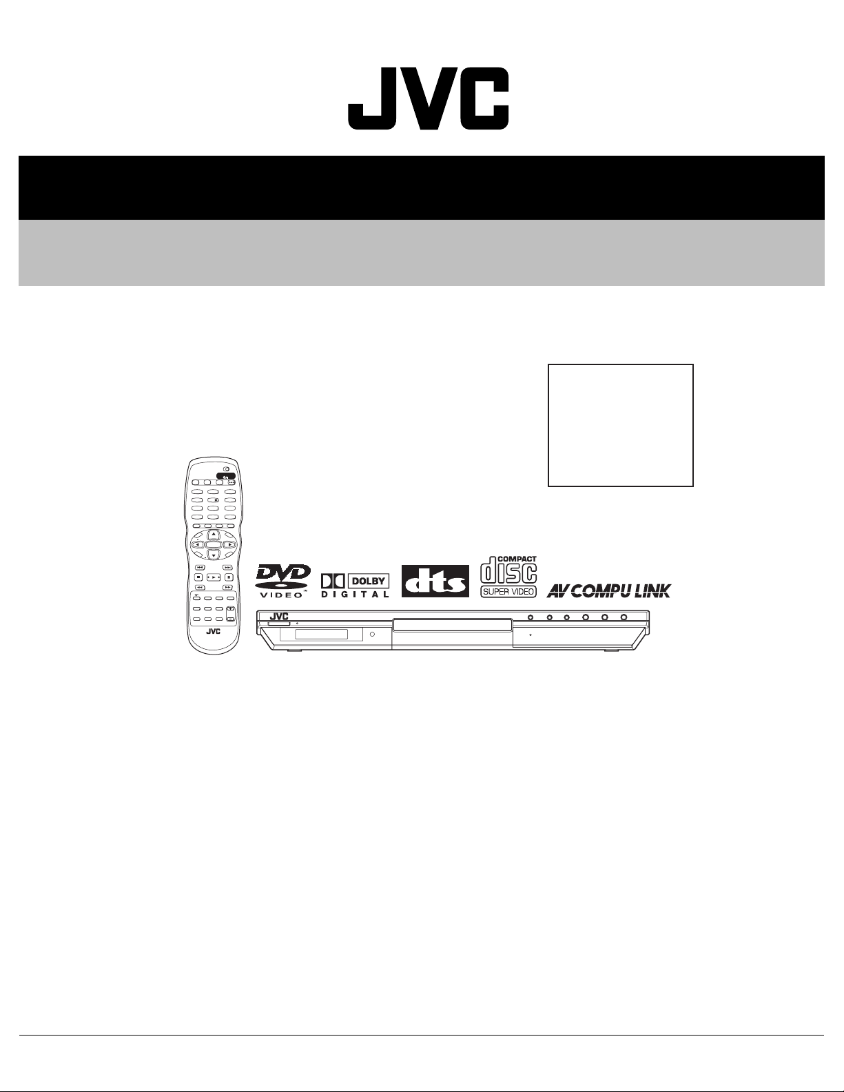
DVD PLAYER / MEMORY CARD READER
XA00420038
XV-NP1SL
Area Suffix
B ------------------------- U.K.
TV DVD
STANDBY/ON
OPEN/
DVD/
TV DVD
CLOSE
CARD
TV1 TV2 TV3
213
TV4 TV5 TV6
546
TV7 TV8 TV9
879
TV-/-- TV0 MUTING
010 +10
TITLE/
THUMBNAIL
GROUP
/LIST
U
N
E
CH
M
+
P
O
T
VOL VOL+
ENTER
C
CH
H
O
I
C
E
SELECTCLEAR
-
SLOW
SOUND
EFFECT
SUB TITLE
ANGLE
AUDIO
SLIDE
REPEAT
DIMMER
EFFECT
TV/VIDEO
CANCELRETURN
N
O
NEXTPREVIOUS
SLOW+
PROGRESSIVE
C -------------------- Canada
J ------------------------ U.S.A.
E ------- Continental Europe
EE ----- Russian Federation
EN -------- Northern Europe
EV ---------- Eastern Europe
UJ ------------- U.S.A Military
M
E
N
U
N
E
E
R
C
S
VFPZOOM
SCAN
AMP
VOL
TABLE OF CONTENTS
1 PRECAUTION. . . . . . . . . . . . . . . . . . . . . . . . . . . . . . . . . . . . . . . . . . . . . . . . . . . . . . . . . . . . . . . . . . . . . . . . . 1-3
2 SPECIFIC SERVICE INSTRUCTIONS. . . . . . . . . . . . . . . . . . . . . . . . . . . . . . . . . . . . . . . . . . . . . . . . . . . . . . 1-8
3 DISASSEMBLY . . . . . . . . . . . . . . . . . . . . . . . . . . . . . . . . . . . . . . . . . . . . . . . . . . . . . . . . . . . . . . . . . . . . . . . 1-9
4 ADJUSTMENT . . . . . . . . . . . . . . . . . . . . . . . . . . . . . . . . . . . . . . . . . . . . . . . . . . . . . . . . . . . . . . . . . . . . . . . 1-16
5 TROUBLE SHOOTING. . . . . . . . . . . . . . . . . . . . . . . . . . . . . . . . . . . . . . . . . . . . . . . . . . . . . . . . . . . . . . . . . 1-23
COPYRIGHT © 2003 VICTOR COMPANY OF JAPAN, LIMITED
No.XA004
2003/9
Page 2
SPECIFICATION
General Readable discs DVD VIDEO, DVD-R (Video format), DVD-RW (Video format), SVCD, Video CD,
Audio CD (CD-DA), CD-R/RW (CD-DA, SVCD, Video CD, MP3/WMA format,
JPEG, MPEG-4)
Readable cards SD card, Multi Media Card, Smart Media, Compact Flash, Memory Stick
(MP3/WMA format, JPEG, MPEG-4)
Video format NTSC, 480i (Interlaced scan) / 480p (Progressive scan) selectable
Other Power requirements AC 120 V, 60 Hz
Power consumption 12 W (POWER ON), 2.7 W (STANDBYmode)
Mass 2.1 kg (4.7 lbs)
Dimensions (W xH x D) 435 mm x 48 mm x 270.5 mm (17-3/16 inch x 1-15/16 inch x 10-11/16 inch)
Video outputs COMPONENT (pin jacks) Y Output: 1.0 Vp-p (75 ohm)
PB/PR Output: 0.7 Vp-p (75 ohm)
VIDEO OUT (pin jack) 1.0 Vp-p (75 ohm)
S-VIDEO OUT (S jack) Y Output: 1.0 Vp-p (75 ohm)
C Output: 286 mVp-p (75 ohm)
Horizontal resolution 500 lines or more
Audio outputs ANALOG OUT (pin jack) 2.0 Vrms (10 kohm)
DIGITAL OUT (COAXIAL) 0.5 Vp-p (75 ohm termination)
DIGITAL OUT (OPTICAL) -21 dBm to -15 dBm (peak)
Audio characteristics Frequency response CD (sampling frequency 44.1 kHz):2 Hz to 20 kHz
DVD (sampling frequency 48 kHz):2 Hz to 22 kHz (4 Hz to 20 kHz for DTS and
Dolby Digital bitstream signals)
DVD (sampling frequency 96 kHz):2 Hz to 44 kHz
Dynamic range 16 bit: More than 98 dB
20/24 bit: More than 100 dB
Wow and flutter Unmeasurable (less than + 0.002%)
Total harmonic distortion less than 0.006%
• Specifications and appearance are subject to change without prior notice.
• Manufactured under license from Dolby Laboratories. “Dolby” and the doubl e-D symbol are trademark of Dolby Laboratories.
• “DTS” and “DTS Digital Out” are trademarks of Digital Theater Systems, Inc.
1-2 (No.XA004)
Page 3
SECTION 1
Good earth ground
d
AC VOLTMETER
PRECAUTION
1.1 Safety Precautions
(1) This design of th is product contains special hardware and
many circuits and components specially for safety purposes. For continued protection, no changes should be made
to the original design unless authorized in writing by the
manufacturer. Replacement parts must be identical to
those used in the original circuits. Services should be performed by qualified personnel only.
(2) Alterations of the design or circuitry of the product should
not be made. Any design alterations of the product should
not be made. Any design alterations or additions will void
the manufacturers warranty and will further relieve the
manufacture of responsibility for personal injury or property
damage resulting therefrom.
(3) Many electrical and mechanical parts in the products have
special safety-related characteristics. These characteristics are often not evident from visual inspection nor can the
protection afforded by them necessarily be obtained by using replacement components rated for higher voltage, wattage, etc. Replacement parts which have these special
safety characteristics are identified in the Parts List of Service Manual. Electrical components having such features
are identified by shading on the schematics and by ( ) on
the Parts List in the Service Manual. The use of a substitute
replacement which does not have the same safety characteristics as the recommended replacement parts shown in
the Parts List of Service Manual may create shock, fire, or
other hazards.
(4) The leads in the products are routed and dressed with ties,
clamps, tubings, barriers and the like to be separated from
live parts, high temperature parts, moving parts and/or
sharp edges for the prevention of electric shock and fire
hazard. When service is required, the original lead routing
and dress should be observed, and it should be confirmed
that they have been returned to normal, after reassembling.
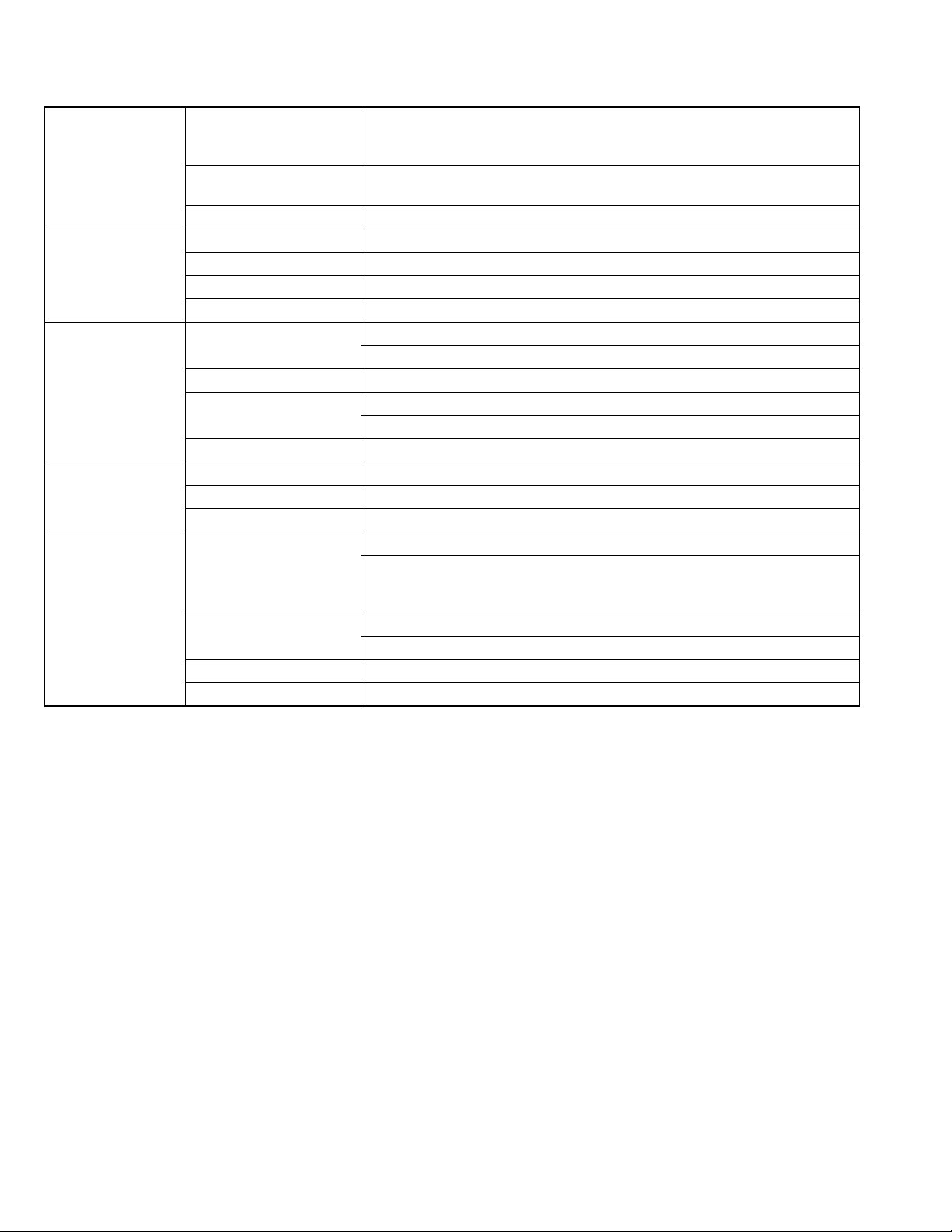
(5) Leakage shock hazard testing
After reassembling the product, always perform an isolation check on the exposed metal parts of the product (antenna terminals, knobs, metal cabinet, screw heads,
headphone jack, control shafts, etc.) to be sure the product
is safe to operate without danger of electrical shock.Do not
use a line isolation transformer during this check.
• Plug the AC line cord directly into the AC outlet. Using a
"Leakage Current Tester", measure the leakage current
from each exposed metal parts of the cabinet, particularly any exposed metal part having a return path to the
chassis, to a known good earth ground. Any leakage current must not exceed 0.5mA AC (r.m.s.).
• Alternate check method
Plug the AC line cord directly into the AC outlet. Use an
AC voltmeter having, 1,000Ω per volt or more sensitivity
in the following manner. Connect a 1,500Ω 10W resistor
paralleled by a 0.15µF AC-type capacitor between an exposed metal part and a known good earth ground.
Measure the AC voltage across the resistor with the AC
voltmeter.
Move the resistor connection to each exposed metal
part, particularly any exposed metal part having a return
path to the chassis, and measure the AC voltage across
the resistor. Now, reverse the plug in the AC outlet and
repeat each measurement. Voltage measured any must
not exceed 0.75 V AC (r.m.s.). This corresponds to 0.5
mA AC (r.m.s.).
(Having 1000
ohms/volts,
or more sensitivity)
0.15 F AC TYPE
Place this
probe on
1500 10W
1.2 Warning
(1) This equipment has been designed and manufactured to
meet international safety standards.
(2) It is the legal resp onsibility of the repairer to ensure that
these safety standards are maintained.
(3) Repairs must be made in accordance with the relevant
safety standards.
(4) It is essential that safety critical compone nts are replaced
by approved parts.
(5) If mains voltage selector is provided, check setting for local
voltage.
1.3 Caution Burrs formed during molding may be left over on some parts
of the chassis.
Therefore, pay attention to such burrs in the case of preforming repair of this system.
1.4 Critical parts for safety
In regard with component parts appearing on the silk-screen
printed side (parts side) of the PWB diagrams, the parts that are
printed over with black such as the resistor ( ), diode ( )
and ICP ( ) or identified by the " " mark nearby are critical
for safety. When replacing them, be sure to use the parts of the
same type and rating as specified by the manufacturer.
(This regulation dose not Except the J and C version)
each expose
metal part.
(No.XA004)1-3
Page 4
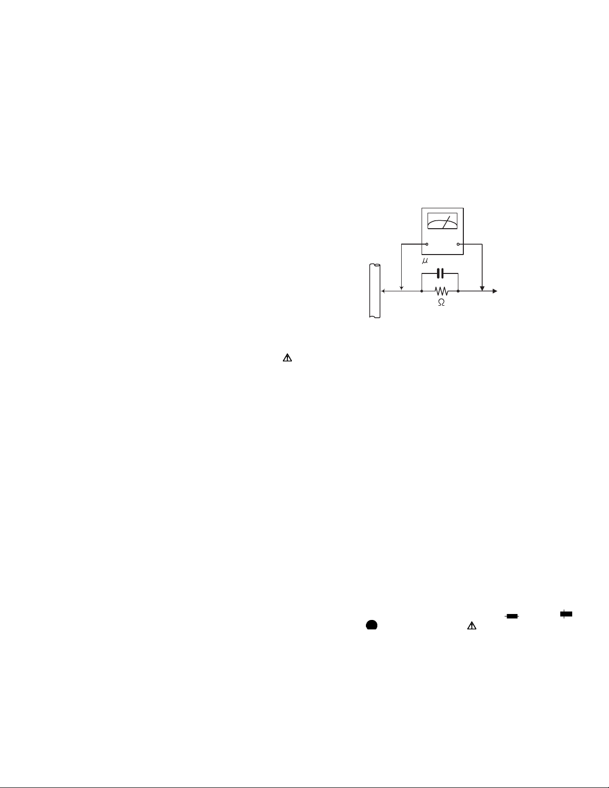
1.5 Preventing static electricity
Electrostatic discharge (ESD), which occurs when static electricity stored in the body, fabric, etc. is discharged, can destroy the laser
diode in the traverse unit (optical pickup). Take care to prevent this when performing repairs.
1.5.1 Grounding to prevent damage by static electricity
Static electricity in the work area can destroy the optical pickup (laser diode) in devices such as DVD players.
Be careful to use proper grounding in the area where repairs are being performed.
(1) Ground the workbench
Ground the workbench by laying conductive material (such as a conductive sh eet) or an iron plate over it before placing the
traverse unit (optical pickup) on it.
(2) Ground yourself
Use an anti-static wrist strap to release any static electricity built up in your body.
(caption)
Anti-static wrist strap
1M
Conductive material
(conductive sheet) or iron palate
(3) Handling the optical pickup
• In order to maintain quality during transport and before instal lation, both sides of the laser di ode on the replacement optica l
pickup are shorted. After replacement, return the shorted parts to their original condition.
(Refer to the text.)
• Do not use a tester to check the condition of the laser diode in the optical pickup. The tester's internal power source can easily
destroy the laser diode.
1.6 Handling the traverse unit (optical pickup)
(1) Do not subject the traverse unit (optical pickup) to strong shocks, as it is a sensitive, complex unit.
(2) Cut off the shorted part of the flexible cable using nippers, etc. after replacing the optical pickup. For specific details, refer to the
replacement procedure in the text. Remove the anti-static pin when replacing the traverse unit. Be careful not to take too long
a time when attaching it to the connector.
(3) Handle the flexible cable carefully as it may break when subjected to strong force.
(4) It is not possible to adjust the semi-fixed resistor that adjusts the laser power. Do not turn it.
1-4 (No.XA004)
Page 5
1.7 Importance adminis t ering point on the safety
B4
EP951
CN901
C951
D960
R951
C808
C802
Q951
B110
B202
B111
B931
B56
EP952
P901
B205
B908
C904 C905
B402
R910
C918
FC901 FC902
L901
C902
L953
C963
B19
D956
B6
C908
C907
R901
B104
D901
D903
D902
IC901
C913
R912
C914
R913
R906
D904
R915
R903
PC901
B912
D951
C906
C950
CP951
IC952
C970
B911
B910
C965
C966
L954
C964
D957
D954
D955
C958
D953
C952
T901
C953
R954
D952
B301
B107
B101
B403
B907
B906
B905
B904
B903
B909
CN904
B913
WC802
EP953
B55
R966
L955
C967
L952
L951
C955
B801
B802
B901
B804
B902
B914
B917
B935
B108
B203
C957
Q953
B204
CN902 CN903
C988
B207
B404
B923
B921
C959
C762
C761
B916
B915
B934
CN651
B918
B919
B922
C973
B1
B2
J702
L709
L710
S902
B924
B925
B3
S901
Q754
B201
Q753
J603
B929
B926
B927
J681
EP910
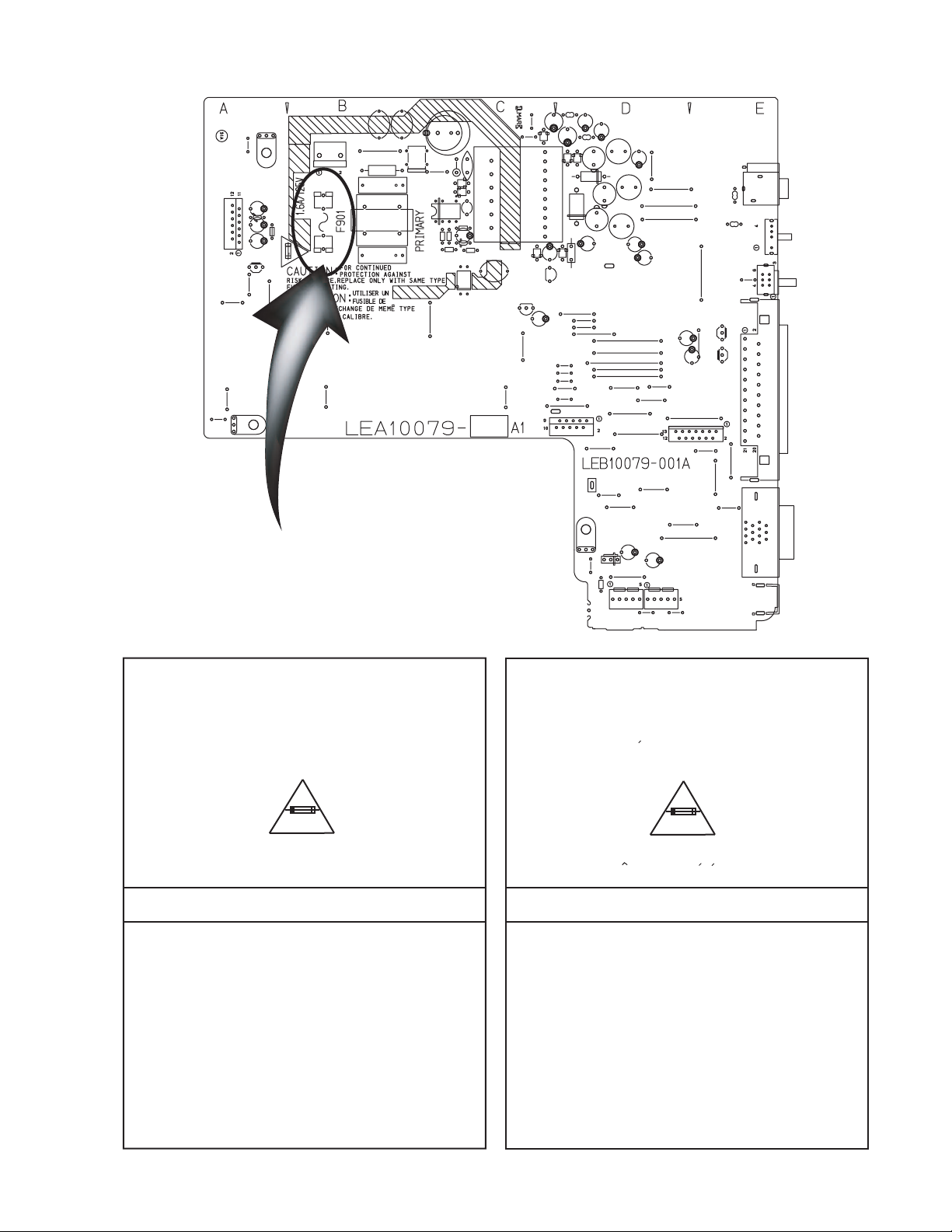
Full Fuse Replacement Marking
Graphic symbol mark
(This symbol means fast blow type fuse.)
should be read as follows ;
FUSE CAUTION
FOR CONTINUED PROTECTION AGAINST RISK
OF FIRE, REPLACE ONLY WITH SAME TYPE
AND RATING OF FUSES ;
F901 : 1.6 A / 125 V F901 : 1.6 A / 125 V
Marquage Pour Le Remplacement
Complet De Fusible
Le symbole graphique (Ce symbole signifie
fusible de type a fusion rapide.)
doit etre interprete comme suit ;
PRECAUTIONS SUR LES FUSIBLES
POUR UNE PROTECTION CONTINUE CONTRE
DES RISQUES D'INCENDIE, REMPLACER
SEULEMENT PAR UN FUSIBLE DU MEME TYPE ;
(No.XA004)1-5
Page 6
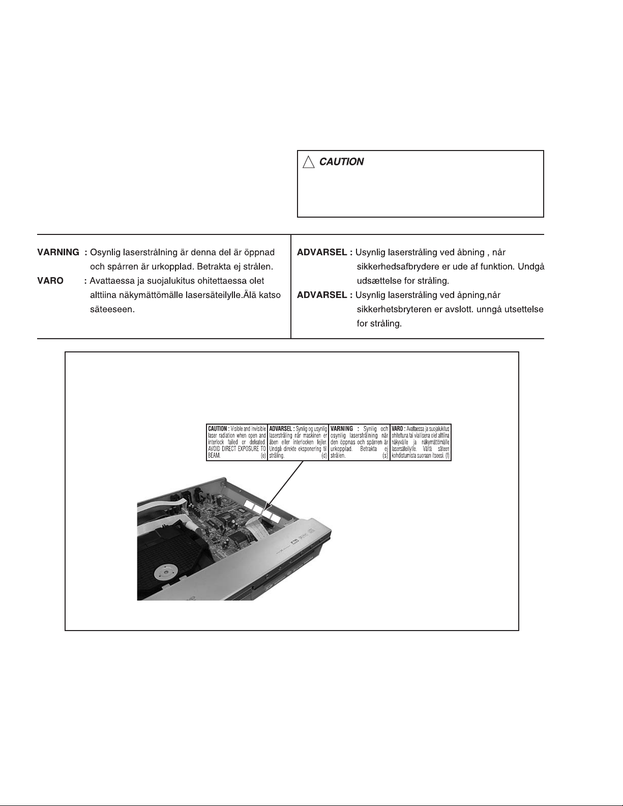
1.8 Important for laser products
1.CLASS 1 LASER PRODUCT
2.DANGER : Invisible laser radiation when open and inter
lock failed or defeated. Avoid direct exposure to beam.
3.CAUTION : There are no serviceable parts inside the
Laser Unit. Do not disassemble the Laser Unit. Replace
the complete Laser Unit if it malfunctions.
4.CAUTION : The compact disc player uses invisible laser
radiation and is equipped with safety switches which
prevent emission of radiation when the drawer is open and
the safety interlocks have failed or are de
feated. It is dangerous to defeat the safety switches.
REPRODUCTION AND POSITION OF LABEL
5.CAUTION : If safety switches malfunction, the laser is able
to function.
6.CAUTION : Use of controls, adjustments or performance of
procedures other than those specified herein may result in
hazardous radiation exposure.
!
Please use enough caution not to
see the beam directly or touch it
in case of an adjustment or operation
check.
WARNING LABEL
CAUTION:
radiation
Invisible
interlock faile
when open and
AVOID DIRECT EXPOSURE
laser
d o
TO BEAM.
r defeated.
VARNING:
strålning n
O
synlig laser-
(e)
öppnad och sp
är denna del
urkopplad. Betrakta
strålen.
ärren
(s)
The inside of a chassis base
ADVARSEL:
är
str
är
åling ved
Us
sikkerhedsafbryd
ynlig
ej
laser-
åbning, n
af funktion.
telse for str
ere er
VARO:
å
r
Undg
ude
Avattaessa
jalukitus
åling
å ud
sæt-
alttiin
ohitettaessa
(d)
ja suo-
a n
lasers
äkymätt
äteilylle.
s
äteeseen.
olet
ömä
Ä
lle
lä
katso
(f)
1-6 (No.XA004)
Page 7
1.9 Precautions for Service
1.9.1 Handling of Traverse Unit and Laser Pickup
(1) Do not touch any peripheral element of the pickup or the actuator.
(2) The traverse unit and the pickup are precision devices and therefore must not be subjected to strong shock.
(3) Do not use a tester to examine the laser diode. (The diode can easily be destroyed by the internal power supply of the tester.)
(4) To replace the traverse unit, pull out the metal short pin for protection from charging.
(5) When replacing the pickup, after mounting a new pickup, remove the solder on the short land which is provided at the center of
the flexible wire to open the circuit.
(6) Half-fixed resistors for laser power adjustment are adjusted in pairs at shipment to match the characteristics of the optical block.
Do not change the setting of these half-fixed resistors for laser power adjustment.
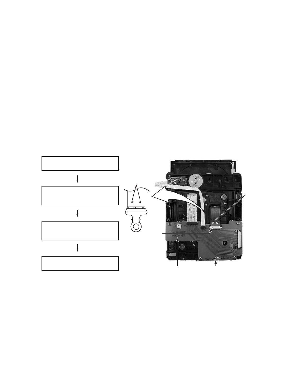
1.9.2 Destruction of Traverse Unit and Laser Pickup by Static Electricity
Laser diodes are easily destroyed by static electricity charged on clothingor the human body. Before repairing peripheral elements of
the traverse unit or pickup, be sure to take the following electrostatic protection:
(1) Wear an antistatic wrist wrap.
(2) With a conductive sheet or a steel plate on the workbench on which the traverse unit or the pick up is to be repaired, ground the
sheet or the plate.
(3) Please be sure to make the switch of a relay board into the "SHORT" side before drawing out a wire from the connector CN101
on a servo control board,when taking out a mechanism assemb ly from a main body.And please be sure to make a switch into
the "OPEN" side after connecting a wire to CN101, when it mounts a mechanism assembly in a main body.
(4) After removing the flexible wire from the connector (CN1), short-circuit the flexible wire by the metal clip.
(5) Short-circuit the laser diode by soldering the land which is provided at the center of the flexible wire for the pickup.
After completing the repair, remove the solder to open the circuit.
The procedure for protecting a pickup
The switch on a relay board is
changed from "OPEN" to "SHORT."
Short circuit
A wire is extracted from the
connector CN101 on a servo control
board.
It solders to the short circuit part on a
flexible wire, and it is made to shortcircuit.
A flexible wire is extracted from the
connector CN1 on a relay board.
In case you assemble, please do all work conversely.
CN1
Relay board
Short circuit
Switch
(No.XA004)1-7
Page 8

SECTION 2
SPECIFIC SERVICE INSTRUCTIONS
This service manual does not describe SPECIFIC SERVICE INSTRUCTIONS.
1-8 (No.XA004)
Page 9
SECTION 3
B
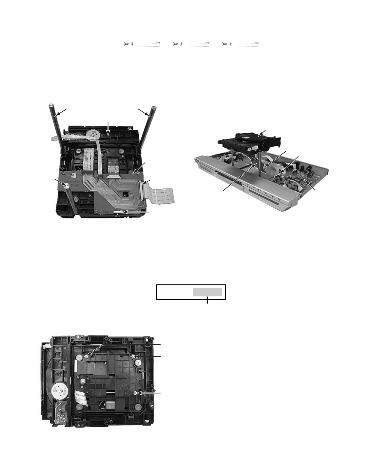
TOP COVER
Front panel assembly
ly
Push
Hook a
F
a
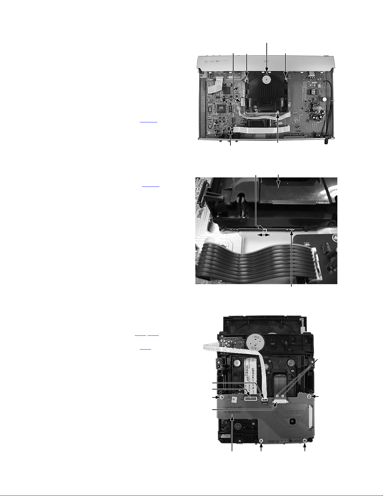
DISASSEMBLY
There is a part different from the photograph according to the model and the destination though explains this disassembly method by
using XV-NP1SL for europe.
3.1 Main body section
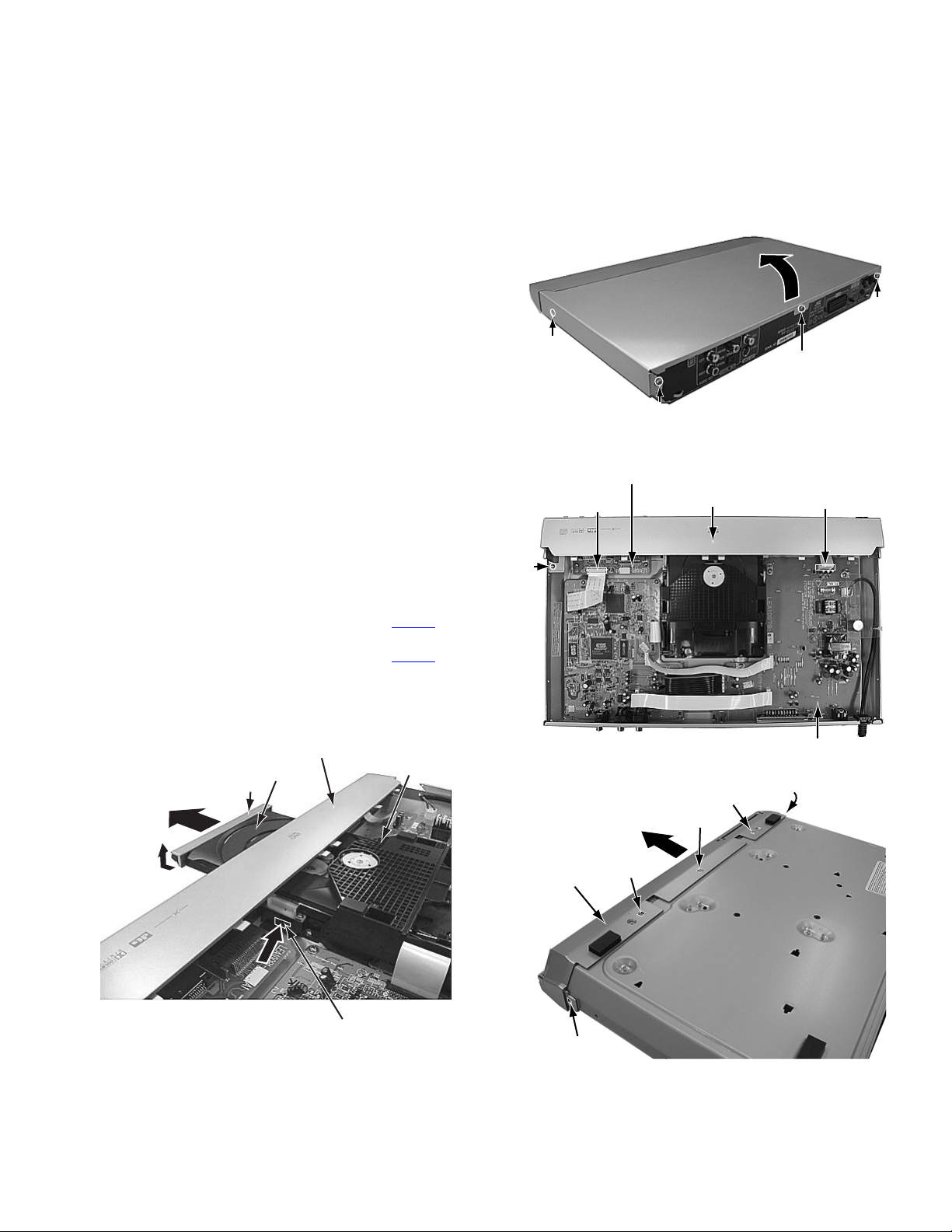
3.1.1 Removing the top cover (See Figure 1)
(1) Remove the two screws A attaching the top cover on both
sides of the main body.
(2) Remove the three screws B attaching the top cover on the
back of the main body.
(3) Raise the both sides and lower part of the rear of the top
cover, with opening them slightly in an outward direction.
And the top cover will be removed.
3.1.2 Removing the front panel assembly (See Figure 2, Figure 3, Figure 4)
• Prior to performing the following procedure, remove the top
cover.
• There is no need to remove the mechanism assembly.
(1) Insert a kind of screwdriver in a hole located in the righ t
side of mechanism assembly, and push a lever until it cannot be inserted any further.
(2) And then, a tray will come out. Remove the tray in an upper
direction, with slightly opening the lower part of fitting in an
outward direction.
(3) Disconnect the card wire from connector CN901
power supply board.
(4) Disconnect hte card wire from connector CN831
memory card reader board.
(5) Remove the one screw C attaching the bracket.
(6) Hook a and b are removed respectively, and the front panel
assembly is removed.
Mechanism assemb
Fitting
Tray
on the
on the
A
x 2
Memory card reader board
CN831
C
TOP COVER
TOP COVER
B
Fig.1
Front panel assembly
Power supply board
Fig.3
Hook b
Hook b
B
CN901
ront panel
ssembly
Push
Hole and lever
Fig.2
Hook b
Hook a
Fig.4
(No.XA004)1-9
Page 10
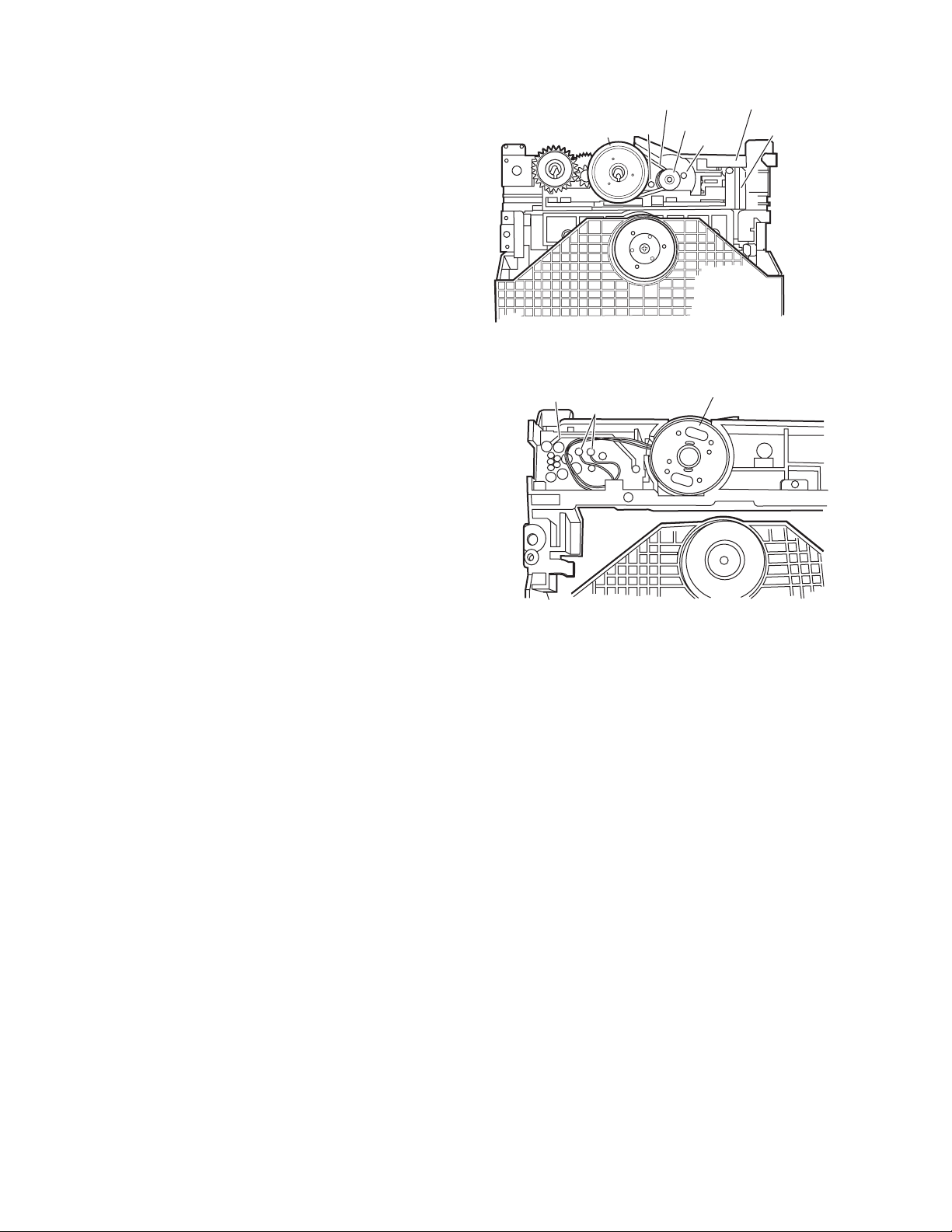
3.1.3 Removing the mechanism assembly (See Figure 2, Figure 5, Figure 6)
OPENSHORT
• Prior to performing the following procedure, remove the top
cover.
• There is no need to remove the front panel assembly.
(1) Insert a kind of screwdriver in a hole located in the right
side of mechanism assembly, and push a lever until it cannot be inserted any further. (See Figure 2)
(2) And then, a tray will come out. Remove the tray in an upper
direction, with slightly opening the lower part of fitting in an
outward direction. (See Figure 2)
(3) Remove the three screws D attaching the mechanism as-
sembly.
(4) The switch on a relay board is made into the “SHORT” side.
(5) Disconnect the card wire from connector CN101
on the
servo control and signal output terminal board.
(6) Remove the mechanism assembly by lifting the rear part of
the mechanism assembly.
ATTENTION:
Please be sure to make the switch on a relay board into a
Servo control and signal
output terminal board
“SHORT” side before disconnect a card wire from the connector CN101 on servo control and signal output terminal board.
Moreover, please be sure to make a switch into the “OPEN”
side after inserting a card wire in a connector CN101
at the
time of an assembly.
There is a possiblity of destroying the laser diode of a pick-up
unit with static electricity.
Mechanism assembly
CN101
D
Switch
D
D
Fig.5
Mechanism assembly
3.1.4 Removing the relay board (See Figure 7)
• Prior to performing the following procedure, remove the mechanism assembly.
(1) Remove the four screws E attaching the relay board.
(2) Disconnect the card wire from connector CN2
,CN3 on the
relay board respectively.
(3) Disconnect the flexible wire from connector CN1
on the re-
lay board from pick-up unit.
ATTENTION:
At this time, please extract the wire after short-circuited
of two places on the wire in part c with solder. Please remove the solder two places of part c after connecting the
wire with CN1 when reassembling.
There is a possibility of destroying the laser diode of a
pick-up unit with static electricity.
CN2
CN3
CN1
SHORT OPEN
OPEN
Relay board
Fig.6
Part c
E
E
1-10 (No.XA004)
Relay board
EE
Fig.7
Page 11
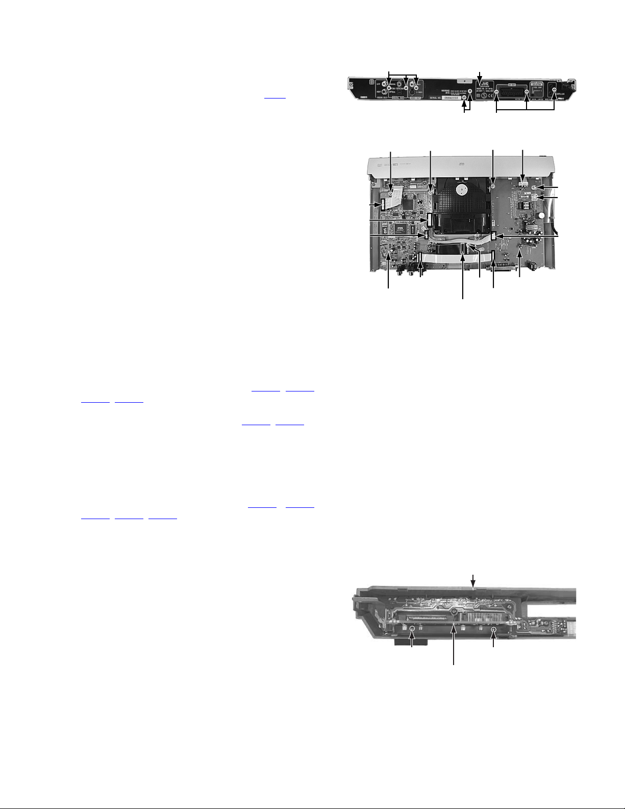
3.1.5 Removing the rear panel (See Figure 8, Figure 9)
4
output terminal board
CN901
C
C
C
Front panel assembly
• Prior to performing the following procedure, remove the top
cover.
F
(1) Remove the eight screws F attaching the rear panel.
(2) Disconnect the power cord from connector P901
on the
power supply board
(3) Remove tie band.
G
N503
N101
N401
CN631
Servo control and signal
3.1.6 Removing the servo control and signal output terminal board. (See Figure 9)
• Prior to performing the following procedure, remove the top
cover/rear panel.
(1) Remove the two screws G attaching the servo control a nd
signal output terminal board.
(2) Disconnect the card wire from connector CN101
, CN401,
CN631, CN503 on the servo control and signal ou tput ter-
minal board.
(3) Disconnect the flat wire from connector CN902
, CN903 on
the power supply board.
3.1.7 Removing the power supply board. (See Figure 9)
• Prior to performing the following procedure, remove the top
cover/rear panel.
(1) Remove the three screws H attaching the p ower supply
board.
(2) Disconnect the wire from connector CN901
CN903
, CN904, CN651 on the power supply board.
, CN902,
(3) Disconnect the socket wire from socket P901 on the power
supply board.
3.1.8 Removing the memory card reader board. (See Figure 10)
• Prior to performing the following prcedure, remove the front
panel assembly.
(1) Remove the two screws I attaching the bracket.
G
Rear panel
F
F
Fig.8
H
Power supply board
H
CN651
CN902,CN903
Fig.9
H
P901
CN90
II
Memory card reader board
Fig.10
(No.XA004)1-11
Page 12
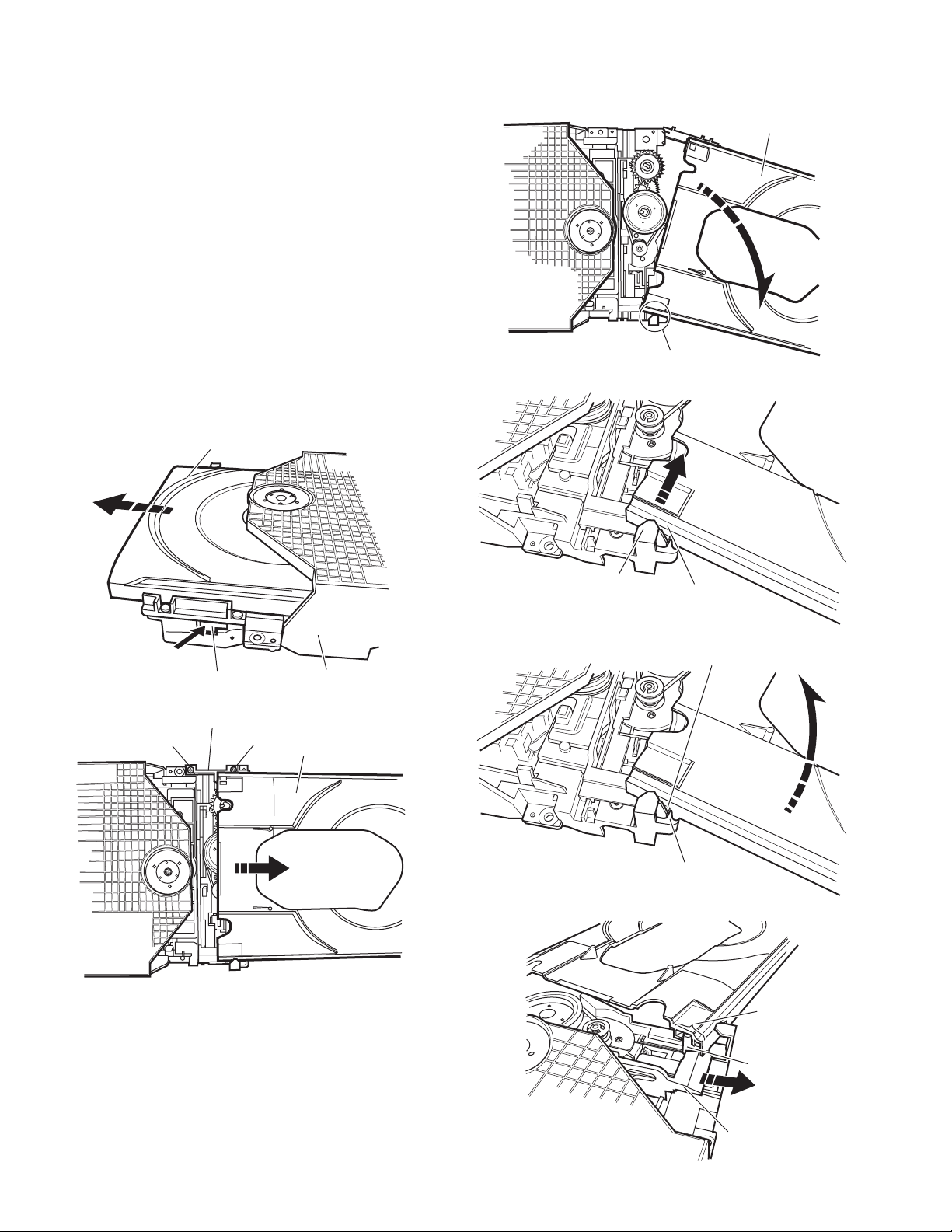
3.2 Loading mechanism assembly
3.2.1 Removing the tray (See Figure 1, Figure 2, Figure 3, Figure 4, Figure 5, Figure 6)
(1) Push a of the slide ca m on the ho le in the right side of the
loading base by using a driver until it stops. (See Figure 1.)
(2) The tray comes out. Pull the tray in a front direction until it
stops.
(3) Remove the two screws A attaching the slide bracket. (See
Figure 2.)
(4) Tilt the tray in a directi on of the arrow around the point in
the left rear part of the tray. (See Figure 3.)
(5) The rail of the tray is removed from b of the loading base.
Then, remove the tray upward. (See Figure 4.)
Attaching the tray:
Engage c of the loading base to the projection of the tray while
tilting the tray to the left. Turn the tray in a direction of the arrow, and attach the slide bracket. (See Figure 5.)
Note:
Prior to the procedure above, move the slide cam in a direction
of the arrow so that d of the slide cam can be inserted in e of
the tray. (See Figure 6.)
Tray
The point in the left rear part
Tray
Fig.3
Push
Slide cam part a
Slide bracket
A
Fig.1
Fig.2
A
Loading base
Tray
Loading base part b
Rail of the tray
Fig.4
Projection of the tray
Loading base part c
Fig.5
Par t e
1-12 (No.XA004)
Par t d
Slide cam
Fig.6
Page 13
3.2.2 Removing the traverse mechanism assembly (See Figure 7)
Shaft
Reverse the loading mechanism assembly. Remove the four
screws B attaching the traverse mechanism assembly. Remove
the traverse mechanism assembly upward.
Loading mechanism
B
assembly
B
3.2.3 Removing the elevator (See Figure 8 and Figure 9)
• Prior to the following procedure, remove the traverse mechanism assembly.
(1) Remove the two arms of the el evator from the two parts f
by moving the arms in a direction of the arrow.
(2) Pull out the elevator in a rear direction.
Attaching the elevator:
Engage the two holes g to the two shafts on the front part of
the elevator. And then, attach the elevator.
Elevator
B
Elevator
Traverse mechanism
assembly
Fig.7
g
Shaft
Shaft
Fig.9
B
Slide cam
g
Par t f
Par t f
Fig.8
(No.XA004)1-13
Page 14
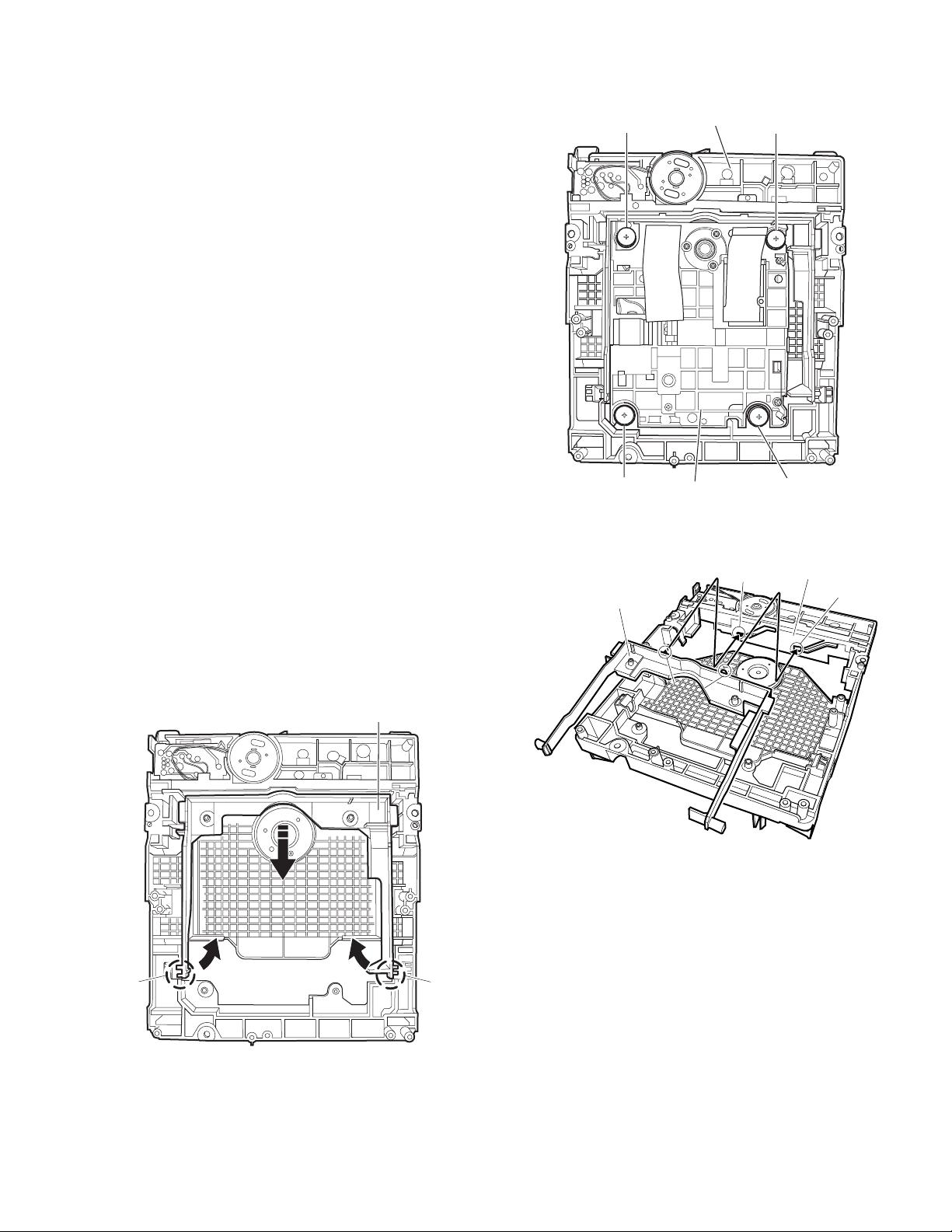
3.2.4 Removing the loading motor (See F ig ure 10 and Figure 11)
• Prior to the following procedure, remove the tray, the traverse
mechanism assembly, and the elevator.
(1) Remove the belt from the pulley.
(2) Remove two screws C attaching the loading motor.
(3) Remove two solders h on the switch board.
Pulley
Belt
㧯
Fig.10
Loading base
Pulley
㧯
Slide cam
Switch board
Loading motor
Part h
Fig.11
1-14 (No.XA004)
Page 15

3.3 Traverse mechanism assembly
3.3.1 Removing the pickup (See Figure 12, Figure 13, and Figur e 14)
• Prior to the following procedure, remove the traverse mechanism assembly.
(1) Remove one screw D attaching the plate.
(2) Remove the plate and the leaf spring.
(3) Lift i of the shaft 1, and pull out the shaft 1 from j.
(4) Remove k of the pickup from the shaft 2.
Attaching the pickup:
(1) Engage k of the pickup to the shaft 2.
Note:
As Figure 14 shows, the spring must come under the
shaft 2.
(2) Insert the shaft 1 in j, and attach the shaft 1 to i.
(3) Attach the leaf sp ring, and then atta ch the plate. Fi x the
leaf spring and the plate by using the screw D.
Pick-up
Plate
D
Leaf spring
Fig.12
Par t j
Shaft 1
Par t k
Par t i
Shaft 2
Fig.13
Spring
Shaft 2
Fig.14
(No.XA004)1-15
Page 16
SECTION 4
ADJUSTMENT
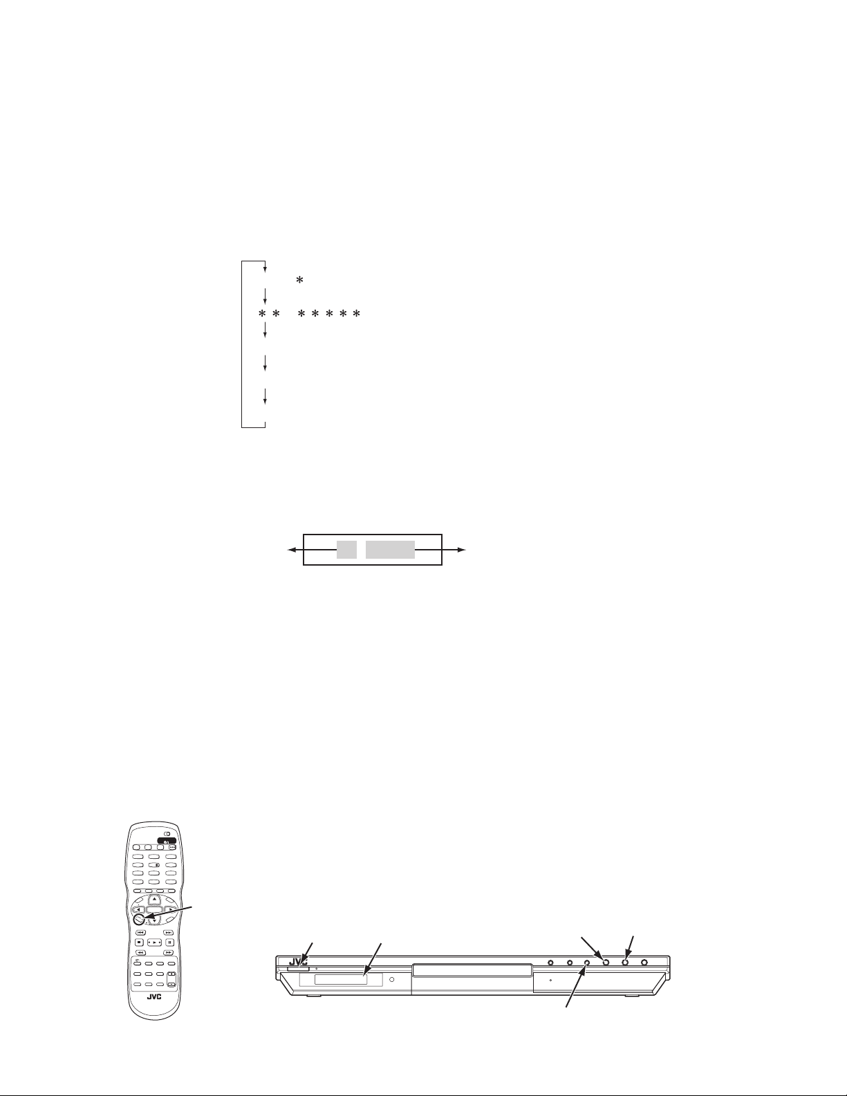
4.1 Test mode setting method
(1) Unplug the power plug.
(2) Insert power plug into outlet while pressing both "PLAY" key and "STOP" key of the main body.
(3) The FL display shows "∗0", and the main body turns to test mode. "∗" means the destination, and "0" means parameter adjust-
ment status.
(4) To release test mode, press "POWER" key of the main body.
NOTE:
Each pressing of "CHOICE" key of the remote controller in test mode changes the mode as follows.
TEST 0 ----------------------
_ -------------
Becames test mode
Version of firmware
FL Display becames all lighting
CHECK -------------------------
EXPERT -----------------------
4.2 Method of displaying version of firmware
(1) Set the main body at test mode.
(2) Press "CHOICE" key of the remote controller once. Then, versio n number and alphabe tical letter of the system controller and
the back end are displayed in the FL display as follows:
Check mode
Not used
FL Display (Example)
Frontend
09_12001
4.3 Initialization method
Please initialize according to the following procedures in the following case:
• Just after you upgrade the firmware.
• After you confirm the symptoms that a customer points out. First Initialize, and then confirm whether the symptoms are improved or
not.
• After servicing, before returning the main body to a customer. (Initialized main body should be returned to a customer.)
(1) Set the main body at test mode.
(2) Press "FORWARD SKIP" key of the main body.
(3) When initialization is completed, the FL display changes from "∗0" to "∗00"
(The left "0" of "00" is not always "0". It shows parameter adjustment status.)
(4) Please be sure to check that turned OFF the power supply and the standby indicator has lit up red. Pl ease check that turn ON
a power supply after that and the screen has become the blue back, and turn OFF a power supply.
ATTENTION:
It is displayed as "∗33" by the bug.
As soon as a firmware is corrected, it shows information by "service bulletin".
Backend
(exp. ver 1.20.0.1)
1-16 (No.XA004)
TV DVD
STANDBY/ON
OPEN/
DVD/
TV DVD
CLOSE
CARD
TV1 TV2 TV3
213
TV4 TV5 TV6
546
TV7 TV8 TV9
879
TV-/-- TV0 MUTING
010 +10
TITLE/
THUMBNAIL
GROUP
/LIST
U
N
E
CH
M
+
P
O
T
VOL VOL+
ENTER
C
CH
H
O
I
C
E
SELECTCLEAR
SLOW
-
SOUND
EFFECT
SUB TITLE
ANGLE
AUDIO
SLIDE
REPEAT
DIMMER
EFFECT
TV/VIDEO
CANCELRETURN
M
E
N
U
CHOICE key
N
E
E
R
C
(change of mode)
S
N
O
NEXTPREVIOUS
SLOW+
VFPZOOM
PROGRESSIVE
SCAN
AMP
VOL
POWER key
FL Display
STOP key
(for test mode)
FORWARD SKIP key
(for initialize)
PLAY key
(for test mode)
Page 17
4.4 All-initialization method
Please perform all-initialization according to the following procedures in the following case:
• Just after you exchange the pick-up.
• Just after you exchange the spindle motor.
• Just after you exchange the traverse mechan i s m ba se .
NOTE:
Please perform all-initialization when you exchange the parts above and also when you remove the parts above.
• Just after the flap adjustment of the pick-up guide shaft
(1) Set the main body at test mode.
(2) Press and hold "BACKWARD SKIP" key of the main body for more than 2 seconds.
(3) When all-initialization is completed, the FL display changes from "∗0" to "∗33".
(4) Please be sure to check that turned OFF the power supply a nd th e stan dby indicator h as lit up red. Please ch eck tha t tu rn ON
a power supply after that and the screen has become the blue back, and turn OFF a power supply.
NOTE:
After all-initialization, be sure to perform optimization adjustment of Front End parameter.
4.5 Optimization adjustment of Front End parameter
Adjustment to optimize Front End parameter must be performed in each mechanism assemb ly of this model for high-speed starting.Please perform optimization according to the following p rocedures just after all-initialization i s completed and when FL display
shows anything except "∗0" (For example when FL display shows "∗1", "∗2", and "∗3") at test mode.
(1) Press "POWER" key of the main body to turn the main body on (not to set the main body at test mode).
(2) Insert the test disc VT-501 or commercial dual-layer DVD software.
(3) Remove the disc when the FL display changes from "READING" to disc information.
(4) Perform the same procedures as in (2) and (3) above by using the test disc CTS-1000 or commercial CD-DA softw are.
(5) Set the main body at test mode, and check that the FL display shows "∗0".
NOTE:
Status of this adjustment can be judged by the number displayed at test mode as follows:
DVD adjustment CD adjustment FL display at test mode
Adjusted Adjusted ∗0
Not adjusted Adjusted ∗1
Adjusted Not adjusted ∗2
Not adjusted Not adjusted ∗3
ATTENTION:
Status is not normally displayed by the bug of a micro computer.
As soon as a firmware is corrected, it shows information by "service bulletin".
NOTE:
As for a disc used for adjustment,
• Disc should be mounted. ("Mounting" means to display "READING" after the disc is inserted and then display the disc information.) Disc need not be played.
• If you do not have test disc either VT-501 (DVD) or CTS-1000 (CD-DA), use a commercial disc (for DVD, dual-layer software) after seeing and checking that the di sc is neithe r curved nor foreseen that it may shake at the time of playback.If you
use a disc with bad features, starting time may be slow or disc may not be read.
TV DVD
STANDBY/ON
OPEN/
DVD/
TV DVD
CLOSE
CARD
TV1 TV2 TV3
213
TV4 TV5 TV6
546
TV7 TV8 TV9
879
TV-/-- TV0 MUTING
010 +10
TITLE/
TV/VIDEO
THUMBNAIL
GROUP
CANCELRETURN
/LIST
U
M
N
E
E
CH
N
M
U
+
P
O
T
VOL VOL+
ENTER
C
H
O
ANGLE
REPEAT
N
CH
E
E
R
I
C
C
E
S
N
O
NEXTPREVIOUS
SELECTCLEAR
SLOW
-
SLOW+
SOUND
VFPZOOM
EFFECT
PROGRESSIVE
SCAN
SUB TITLE
AUDIO
AMP
SLIDE
VOL
DIMMER
EFFECT
POWER key
FL Display
STOP key
(for test mode)
PLAY key
(for test mode)
(for all-initialize : It pushes 2 seconds or more.)
BACKWARD SKIP key
(No.XA004)1-17
Page 18
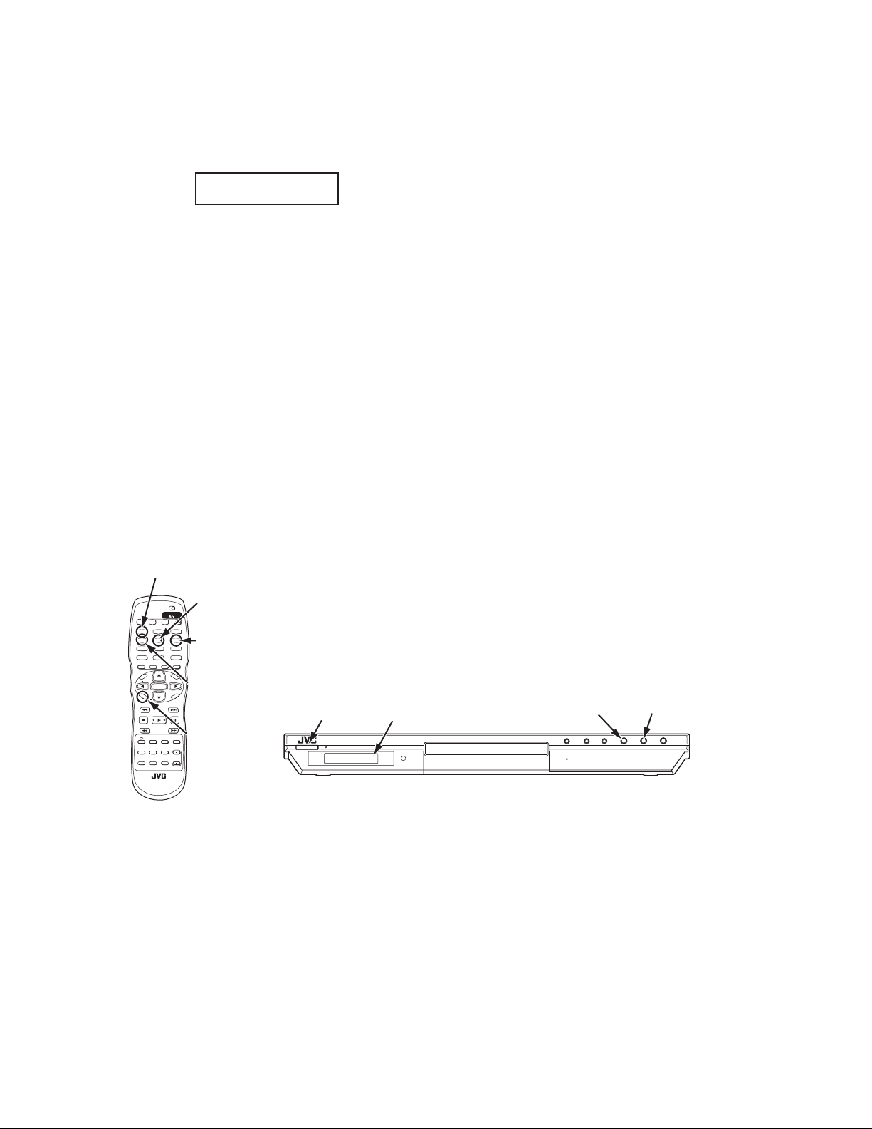
4.6 Display of current value of laser
(1) Set the main body at test mode.
(2) Press "CHOICE" key of the remote controller three times. T hen, FL display is displayed "CHECK".
(3) The laser current value can be switched between th e value of CD and that of DVD by pressing the following key of the re mote
controller.
FL Display (Example)
0030_0000
The number shown in the FL display shows mA of current value of laser.
In the case of the above-mentioned example, the laser current value of 30mA is expressed.
CD:
The laser current value of 49 mA or less is normal.The laser current value of over 50 mA is not normal . Laser diode of the
pickup has been deteriorated.
DVD:
The laser current value of 64 mA or less is normal.The laser current value of over 65 mA is not normal . Laser diode of the
pickup has been deteriorated.
To return to test mode, press "STOP" key of the main body.
4.7 Flap adjustment of the pick-up guide shaft
Please perform flap adjustment of the pick-up guide shaft in the following case:
• Just after you exchange the pick-up.
• Just after you exchange the spindle motor.
• Just after you exchange the traverse mechanism base.
NOTE:
Please perform flap adjustment of the pick-up guide shaft when you exchange the parts above and also when you remove the
parts above.
• When the reading accuracy of the signal is bad (There is a block noise in the screen, Screen stops in the outer circumference of a
disc, etc.)
1 key (automatic adjustment)
5 key (laser of DVD)
TV DVD
STANDBY/ON
OPEN/
DVD/
TV DVD
CLOSE
CARD
TV1 TV2 TV3
213
TV4 TV5 TV6
546
TV7 TV8 TV9
TV-/-- TV0 MUTING
THUMBNAIL
/LIST
U
N
E
CH
M
+
P
O
T
VOL VOL+
ENTER
C
CH
H
O
I
C
E
SELECTCLEAR
SLOW
-
SOUND
EFFECT
SUB TITLE
ANGLE
SLIDE
REPEAT
EFFECT
6 key
879
(display of jitter value)
010 +10
TITLE/
TV/VIDEO
GROUP
CANCELRETURN
M
E
N
U
4 key (laser of CD)
N
E
E
R
C
S
N
O
NEXTPREVIOUS
SLOW+
VFPZOOM
CHOICE key
PROGRESSIVE
SCAN
AUDIO
(change of mode)
AMP
VOL
DIMMER
POWER key
Remote controller "4" key --- Laser of CD
Remote controller "5" key --- Laser of DVD
STOP key
FL Display
(for test mode)
PLAY key
(for test mode)
1-18 (No.XA004)
Page 19
4.7.1 Tool for adjustment
S
OPEN SHORT
&
d
a
b
c
*Stud: One set (four studs), Part number: JIGXVS40 (Note: One of the four studs is not used here.)
4.7.2 Preparation for adjustment
(1) See the disassembly procedure , and remove the Mechanism assembly from the main body.
(2) Remove the relay board attached to the mechanism assembly.(If you disconne ct the wires con nected to th e Relay board, con-
nect them again.)
(3) Attach the three studs to the Mechanism asse mbly.
(4) Put the Mechanism assembly in the center of the main body, and connect the 50 pin wire from the connector CN4 on theRelay
board to the connector CN101 on the Servo control & signal output terminal board.
Stud
Stud
Mechanism
assembly
Mechanism assembly
CN4
CN101
Relay board
tud
OPEN SHORT
OPEN SHORT
CN4
Switch
Relay board
Servo control
signal output
terminal boar
4.7.3 Adjustment
(1) Set the unit to test mode.
(2) Press the "CHOICE" key of the remote controller three times, and the FL display is displayed "CHECK".
(3) Insert a test disc (VT-501), and press the numeric key "1" of the remote controller for automatic adjustment.
(4) After a few seconds, press the numeric key "6" of the remote controller. Then, the FL display displays a jitter value.
(5) Turn the adjustment screws on the underside of the traverse mechanism with phillips screw driver until the maximum jitter value
is displayed on the FL display. (In this model, a bigger jitter value means a better result.)
FL Display (Example)
0 0 3 2 _ 3 E D 0
Jitter value
NOTE:
During operation, the switch on the Relay board should be switched to "OPEN".Reference values to judge whether the jitter is allowable or not are displayed, instead of actual jitter values.
POINT:
Screw
Screw
Screw
Turn the adjustment screws a and b to the sa me angle in the
right direction. And turn the adjustment screws a and b to the
same angle in the left direction. Then, turn the screws a and b
in either the right or the left direction to increase the number of
jitter. Don't turn the adjustment screw c.
(No.XA004)1-19
Page 20
4.8 Upgrading of firmware
The latest firmware for upgrading is updated in "Optical disc CSG" page in JS-net.At the time of service, co mpare the version of th e
product and the latest version, and upgrade the old version into the latest version.
4.8.1 Distribution method
(1) Compressed file is distributed through JS-NET.
(2) Download the version of the destination of the model, and self-extract the file.
(3) "bank30.rom" file is made.
(4) Write "bank30.rom" file in the root of CD-R/RW. (Folders such as jvc_dvd are not necessary.)
4.8.2 UPGRADE method
(1) Prepare UPGRADE disc with "bank30.rom" file written in its root.
(2) While keeping the main body in POWER ON mode, insert the disc.
(3) Disc starts to be played automatically, and UPGRADE will proceed, according to the following indication.
TV screen "NOW READING" → "READING" in upper left → "WRITE" in upper left
FL indicator "READING" → "READING" → "READING"
(4) When UPGRADE finishes, the main body changes from the POWER ON mode to STANDBY mode.
(5) Press the OPEN/CLOSE button, and open the tray to eject the disc.
(6) Set the main body at test mode, and perfo rm initialization. Then, confirm the version of the firmware.
Time necessary for UPGRADE Approx. 3 minutes
NOTE:
After UPGRADE finishes, disc automatically starts to be played and UPGRADE starts again if the main body in the STANDBY mode
is turned on. So, be sure to press the OPEN/CLOSE button in the STANDBY mode without pressing the POWER button, and eject
the tray.
NOTE:
The screen is displayed in blue when the disc is ejected.
After that, if the main body in POWER-OFF mode is turned on, the screen returns to a normal screen.
4.8.3 When UPGRADE is not performed properly
Keys entries are not accepted during UPGRADE, but UPGRADE stops when AC plug is pulled out.
Data in Flash-ROM are collapsed, but the main body can be turned on thanks to Fail Safe function. The main body returns to the normal state after UPGRADE disc is read again.
• When UPGRADE stops because AC plug is pulled out mistakenly.
(1) When the AC plug is put into a wall socket, the main body is auto matically turned on.
(2) Disc inserted in the tray automatically starts to be played, and UPGRADE starts.
TV screen remains black (No output).
FL indication "LOAD" → "READ" → "WRITE"
(3) When UPGRADE finishes, the main body changes from the POWER ON mode to STANDBY mode.
(4) Press the OPEN/CLOSE button without pressing the POWER button. Open the tray and eject the disc.
1-20 (No.XA004)
TV DVD
STANDBY/ON
OPEN/
DVD/
TV DVD
CLOSE
CARD
TV1 TV2 TV3
213
TV4 TV5 TV6
546
TV7 TV8 TV9
879
TV-/-- TV0 MUTING
010 +10
TITLE/
THUMBNAIL
GROUP
/LIST
U
N
E
CH
M
+
P
O
T
VOL VOL+
ENTER
C
CH
H
O
I
C
E
SELECTCLEAR
SLOW
-
SOUND
EFFECT
SUB TITLE
ANGLE
AUDIO
SLIDE
REPEAT
DIMMER
EFFECT
TV/VIDEO
CANCELRETURN
N
O
NEXTPREVIOUS
SLOW+
PROGRESSIVE
M
E
N
U
N
E
E
R
C
S
POWER key
VFPZOOM
SCAN
AMP
VOL
FL Display
Standby indicator
OPEN/CLOSE key
STOP key
(for test mode)
FORWARD SKIP key
PLAY key
(for test mode)
(for initialize)
Page 21
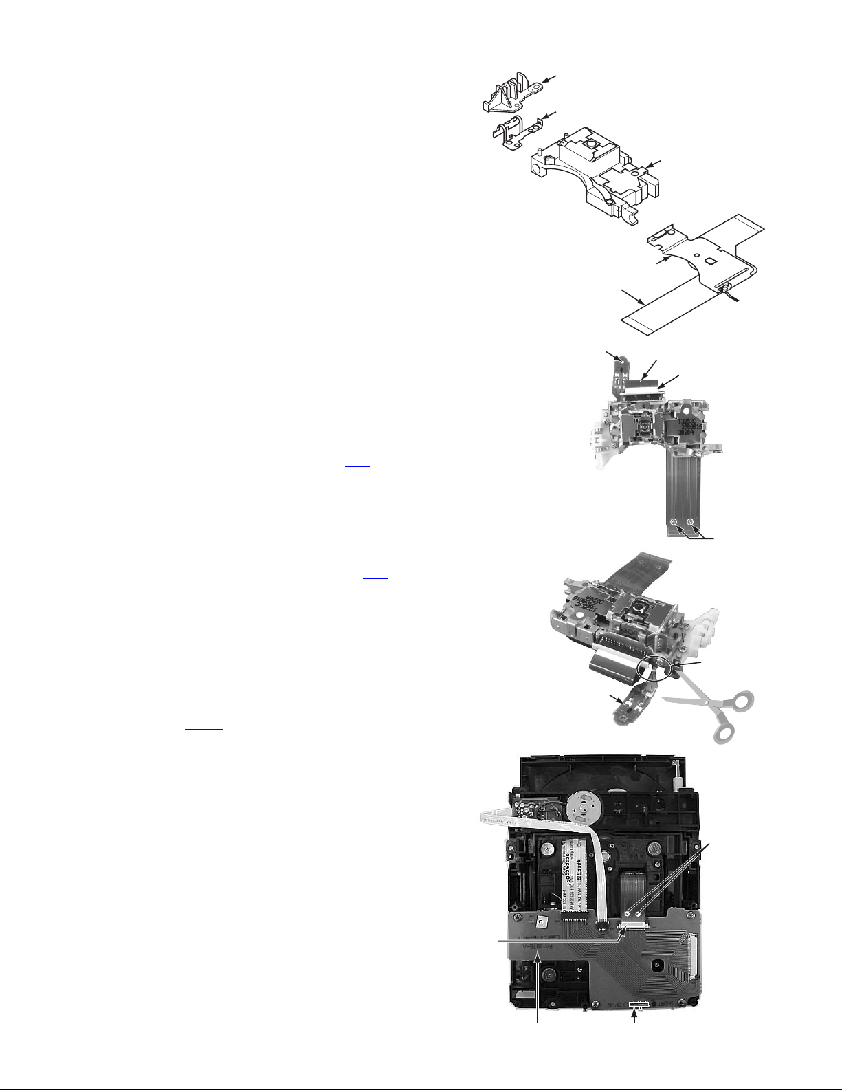
4.9 Attention when pick-up is exchanged
(1) Flexible wire, pick-up spring, switch actuator, and lead
spring are removed from an old pick-up (broken the one).
Guide:
Flexible wire, pick-up spring and switch actuator,lead
spring are removed without each decomposing while assembled.
(2) The above-mentioned parts are instal led in a new pick-up
(non-defective article).
(3) A flexible wire is inserted in the connector which has taken
side with the pick-up, and solder is put up to short land part
"a" two places on a flexible wire.
(4) The electrostatic breakdown protection circuit attached to
the pick-up is cut.
ATTENTION:
Please cut the electrostatic breakdown protection
circuit attached to the pick-up after solder is put up
to two places on a flexible wire short land part "a" of
the insertion of a flexible wire this time in the connector without fail.
The procedure might be mistaken and if solder has
not surely adhered to two places on a flexible wire
short land part "a", the laser diode in the pick-up be
destroyed again.
(5) The pick-up is installed in the traverse mechani sm.
(6) A flexible wire is connected with connector CN1
lay board by installing the traverse mechanism in the loading mechanism.
(7) Solder in two places on a flexible wire in part "a" is re-
moved.
ATTENTION :
Please remove solder in two places in part "a" after
connecting a flexible wire with connector CN1
relay board without fail this time.
When the procedure is mistaken, the laser diode in
the pick-up might be destroyed.
Please remove solder in two places in part "a" surely.
Please make the switch on a relay board into the
"SHORT" side beforehand.
After mounting a mechanism assembly in a main
part, please make a switch into the "OPEN" side after
connecting the card wire from a relay board to the
connector CN101
terminal board.
on a servo control & signal output
on the re-
on the
Switch actuator
Lead spring
Pick-up spring
Flexible wire
Electrostatic breakdown
protection circuit
Electrostatic breakdown
protection circuit
Pick-up
Flexible wire
Connector
Short land
part "a"
Cutting part
CN1
Relay board
Short land
part "a"
Switch
(No.XA004)1-21
Page 22

4.10 Confirm method of operation Please confirm the operation of the undermentioned item after doing the repair and the upgrade of the firmware.
Initialize Refer to the initialization method.
All-initialize Refer to the All-initialization method.
Parameter adjustment status Set the main body at test mode, and check that the FL display shows "0".
Opening picture check (Power ON) It should be display "JVC"
Muting working The noise must not be had to the performance beginning when you push "PLAY" button or
at ON/STANDBY.
FL Display The mark and the logo, etc. displayed by each operation must be displayed correctly.
FL Display should light correctly without any unevenness.
All Function button All function buttons should worked correctly with moderate click feeling.
Open and close movement of tray When press OPEN/CLOSE button the tray should move smoothly without any noise.
Remote controller unit working Check the correctly operation in use of remote controller unit.
Reading of TOC Be not long in the malfunction.
Search Both forward-searches and backward-searches should be able to be done.
Do not stop be searching or after the search.
Skip Both forward-skip and backward-skip should be able to be done.
Do not stop be after the skip.
Playback Do not find abnormality etc. of tone quality and the picture quality.
Most outside TITLE playback check Play VT-501 TITLE 59 CHAPTER 1 , check normal playback.
1-22 (No.XA004)
Page 23
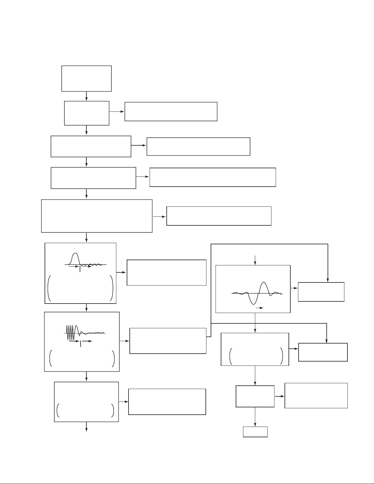
5.1 Servo volume
Press OPEN
/CLOSE key
SECTION 5
TROUBLE SHOOTING
Is tray
operation
Confirmation of tray drive circuit
N
and circuit in surrounding
correct?
Y
Is the traverse moving
along the innermost
N
perimeter for SW detection?
Y
"NO DISC" message appears
Y
immediately after vertical
movement of the pick-up lens
N
The state that DISC does not rotate continues for
several seconds, and becomes NO DISC or an
error display afterwards.
The rotation of DISC becomes high-speed and
abnormal, and becomes NO DISC or an error
display afterwards.
N
Is focus retraction OK?
FE
OFF
Even when it retracts
correctly, if it is out of focus
and makes repeated retries
with a clicking sound, it is
in error.
ON
See "(4) Focus ON error"
N
in "Check points for
individual errors"
Y
Is tracking retraction OK?
See "(3) Traverse movement error"
in "Check points for individual errors"
See "(2) Disk detection, distinction error"
in "Check points for individual errors"
Y
See "(1) Spindle startup error"
in "Check points for individual errors"
Is the inter-layer jump OK?
FE
LO LI
A
Two layers of DVD only.
N
(8) Inter-layer
jump error
Y
TE
OFF
If TE waveform reappears
or fails to converge after the
TE retraction, it is in error.
ON
Y
Is the spindle servo
locked correctly?
Is the RF OUT waveform
locked correctly?
Y
A
See "(5) Tracking ON error"
N
in "Check points for
individual errors"
See "(6) Spindle CLV error"
N
in "Check points for
individual errors"
Fig.1
Has the disc information
been collected?
Stop will result
Y
Is playback
N
possible?
Y
OK !
N
(7) Address read
error
Check (9),(10),(11), and
(12) items in "Check points
for individual errors"
(No.XA004)1-23
Page 24

5.2 Check points for each error
5.2.1 Spindle start error
(1) Defective spindle motor
• Are there several ohms resistance between each pin of CN101
(The power supply is turned off and measured.)
• Is the sign wave of about 100mVp-p in the voltage had from each terminal?
[ CN101
(2) Defective spindle motor driver (IC251)
• Has motor drive voltage of a sine wave or a rectangular wave gone out to each terminal(SM1~3)
of CN101
• Is FG pulse output from the terminal of IC251"24"(FG) according to the rotation of the motor?
• Is it "L(about 0.9V)" while terminal of IC251
(3) Has the control signal come from servo IC or the microcomputer?
• Is it "L" while the terminal of IC251
Is it "H" while the terminal of IC251
• Is the control signal input to the terminal of IC251"22"(EC)?
(changes from VHALF voltage while the motor is working.)
• Is the VHALF voltage input to the terminal of IC251
(4) Is the FG signal input to the servo IC?
• Is FG pulse input to the terminal of IC301
5.2.2 Disc Detection, Distinction error (no disc, no RFENV)
• Laser is defective.
• Front End Processor is defective (IC101).
• APC circuit is defective. --- Q101
• Pattern is defective. --- Lines for CN101 - All patterns which relate to pick-up and patterns between IC101
• IC101 --- For signal from IC101 to IC301, is signal output from IC101 "21" (ASOUT) and IC101 "36"(RFENV) and IC101 "20"
(FEOUT)?
"9"(H1+),"10"(H1-),"11"(H2+),"12"(H2-),"13"(H3+),"14"(H3-) ]
"5,6,7" and IC251"2,4,7"?
"15"(VH) is rotating the motor?
"18"(SBRK) is operating?
"23"(/SPMUTE) is operating?
"21"(ECR)?
"69"(FG) according to the rotation of the motor?
,Q102.
"5-6","6-7","5-7"?
5.2.3 Traverse movement NG
(1) Defective traverse driver
• Has the voltage come between terminal of CN101
(2) Defective BTL driver (IC201
• Has the motor drive voltage gone out to IC201"17" or "18"?
(3) Has the control signal come from servo IC or the microcomputer?
• Is it "H" while the terminal of IC201
• TRSDRV Is the signal input? (IC301
(4) TRVSW is the signal input from microcomputer? (IC305
5.2.4 Focus ON NG
• Is FE output ? --- Pattern, IC101
• Is FODRV signal sent ? (R209) --- Pattern, IC301 "115"
• Is driving voltage sent ?IC201
• Mechanical unit is defective.
5.2.5 Tracking ON NG
• When the tracking loop cannot be drawn in, TE shape of waves does not settle.
• Mechanical unit is defective.
Because the self adjustment cannot be normally adjusted, the thing which cannot be normally drawn in is thought.
• Periphery of driver (IC201
Constant or IC it self is defective.
• Servo IC (IC301
When improperly adjusted due to defective IC.
)
)
"9"(STBY1) ?
"67")
"13", "14" --- If NG, pattern, driver, mechanical un i t .
)
"49" and "50" ?
"50")
1-24 (No.XA004)
Page 25

5.2.6 Spindle CLV NG
• IC101
• Does not the input or the output of driver's spindle signal do the grip?
• Has the tracking been turned on?
• Spindle motor and driver is defective.
• Additionally, "IC101
5.2.7 Address read NG
• Besides, the undermentioned cause is thought though specific of the cause is difficult because various factors are thought.
• Mechanism is defective. (jitter)
•IC301
5.2.8 Between layers jump NG (double-layer disc only)
5.2.9 Neither picture nor sound is output
(1) It is not possible search
• Has the tracking been turned on?
• To "(5) Tracking ON NG" in "Check points for each error" when the tracking is not normal.
• Is the feed operation normal?
5.2.10 Picture is distorted or abnormal sound occurs at intervals of several seconds.
-- "27"(ARF-), "26(ARF+).
and IC301" and "Mechanism is defective(jitter)", etc. are thought.
The disc is dirty or the wound has adhered.
Mechanism defective
Defect of driver's IC(IC201
Defect of servo control IC(IC301)
To "(3) traverse movement NG" in " Check points for each error" when it is not normal.Are not there caught of the feeding mechanism etc?
Is the feed operation normal?
Are not there caught of the feeding mechanism etc?
)
5.2.11 Others
• The image is sometimes blocked, and the image stops.
• The image is blocked when going to outer though it is normal in suroundings in the disk and the stopping sympton increases.
There is a possibility with bad jitter value for such a symptom.
5.2.12 CD During normal playback operation
(1) Is TOC reading normal?
• Displays total time for CD-DA.
• Shifts to double-speed mode for V-CD
(2) Is playback afterwards possible?
(3) When can not do a normal playback
• --:-- is displayed during FL search.
According to [It is not possible to search ] for DVD(9), check the feed and tracking systems.
• No sound is output although the time is displayed.(CA-DA)
DAC, etc, other than servo.
• The passage of time is not stable, or picture is abnormal.(V-CD)
• The wound of the disc and dirt are confirmed.
(No.XA004)1-25
Page 26

VICTOR COMPANY OF JAPAN, LIMITED
AV & MULTIMEDIA COMPANY OPTICAL DISC CATEGORY 1644, Shimotsuruma, Yamato, Kanagawa 242-8514, Japan
(No.XA004)
Printed in Japan
WPC
Page 27

SCHEMATIC DIAGRAMS
DVD PLAYER / MEMORY CARD READER
XV-NP1SL
CD-ROM No.SML200309
Area Suffix
J -------------------------- U.S.A.
C --------------------- Canada
UJ ------------- U.S.A Militaly
B -------------------------- U.K.
E ------ Continental Europe
STANDBY/ON
OPEN/
DVD/
TV DVD
CLOSE
CARD
TV1 TV2 TV3
213
TV4 TV5 TV6
546
TV7 TV8 TV9
879
TV-/-- TV0 MUTING
010 +10
TITLE/
THUMBNAIL
GROUP
/LIST
U
N
E
CH
M
+
P
O
T
VOL VOL+
ENTER
C
CH
H
O
I
C
E
SELECTCLEAR
-
SLOW
SOUND
EFFECT
SUB TITLE
ANGLE
AUDIO
SLIDE
REPEAT
DIMMER
EFFECT
TV DVD
TV/VIDEO
CANCELRETURN
M
S
N
O
NEXTPREVIOUS
SLOW+
VFPZOOM
PROGRESSIVE
SCAN
AMP
VOL
E
N
U
N
E
E
R
C
EN ------- Northern Europe
EV --------- Eastern Europe
EE ---- Russian Federation
Contents
Safety precaution ------------------------ 2-2
Block diagrams --------------------------- 2-3
Standard schematic diagrams -------- 2-8
Printed circuit boards -------------------- 2-26
COPYRIGHT 2003 VICTOR COMPANY OF JAPAN, LIMITED.
No.XA004SCH
2003/09
Page 28

In regard with component parts appearing on the silk-screen pr inted side (par ts side) of
the PWB diagrams, the parts that are printed over with black such as the resistor ( ),
diode ( ) and ICP ( ) or identified by the " " mark nearby are critical for safety.
When replacing them, be sure to use the parts of the same type and rating as specified
by the manufacturer. (Except the JC version)
2-2 (No.XA004SCH)
Page 29

Block diagrams
FL Display & Operation switch section (SHEET 1)
FL Display
DI801
G1-G11
P1-P17
FL Display driver
IC801
PRORED
PROGRN
D823
DVD/CARD LED
FLOFF
Power switch
S801
TO CN901
SHEET 2
F+ F-
STANDBY
CN801
-VDISP VFDIO VFDCLK VFDCS
Standby LED
D825
REMO
Remote controller
IC802
PROGRESSIVE LED
K1
K2
CN802
CN852
DVD/CARD LED
D822
Operation switch
S805,S806,S807
ILLUMINATION LED
D828,Q826
K2
Operation switch
S802,S803,S804,S808
Relay board section (SHEET 9)
FROM
Pick-up
Unit
FROM
Loading motor
assembly
FROM
Spindle motor
assembly
CN2 CN3CN1
T1CD T2CD F1CD F2CD RF+ RF- TB TC TD TA F2DVD F1DVD
LM+ LM- SWOPEN SWUPDN
FM+ FM- TRVSW VH SM1 SM2 SM3 H1+ H2+ H3+ H1- H2- H3-
CN4
TO CN101
SHEET 3
(No.XA004SCH) 2-3
Page 30

Power supply section (SHEET 2)
TO CN801
SHEET 1
CN901
F-
F+
Q951,Q952
FL ON/OFF
B3.3V
-VDISP
REMO
STANDBY
VFDIO
5V
VFDCS
VFDCLK
D5V REG.
CN902,CN903
B3.3V
STANDBY
IC951
TO FW401
SHEET 5
M9V
+12V
D3.3V
-12V
3.3V REG.
Q953
TO CN401
CN904
480I
SHEET 5
S902
PROINT
SWREMO
480P
REMOTE
J702
AV Compulink
COMPULINK
AC-DC
D951
C950
AC-DC
Line filter
D901
L901
AC-DC
D952
AC-DC
C951,C953
Power
L952
D955
C958,C959
T901
transformer
AC-DC
Switching
D954
AC-DC
D904
C914
IC901
regulator
L955
AC-DC
C967,C988
L951
D953
C952,C955
CN651
PC901
FEED BACK
Y/COMPOSITE
GBR/C
AC-DC
D956,L953,C963,C965
AUDIOL/R
FUNCSW
J603
AC-DC
BLANKING
D957,L954,C964,C966
NTSCPAL
AC IN
2-4 (No.XA004SCH)
SHEET 7
TO CN631
SCART
Terminal
(only Europe)
S901
Y/C
COMP/RGB
Page 31

DVD Servo control & AV decoder section (SHEET 3,4,5)
TO SHEET 6
AOUTL
AOUTR
DA
IC402
converter
MCLK
TBCK
Decoder
AV
TSDO
TWS
IC501
SPDIF AMUTE
XI
XO
OSC
IC505
X571
DAC_V
IC502
SDRAM
IC408
IC405
Flash ROM
)
DAC_Y
DAC_C
DAC_U
TO SHEET 7
S1OUT INT_PROG CLP
TO CN831
SHEET 8
CN503
HD14 HD15
IDEHRD IDEHWR IDEHD0-13
CN401
COMPULINK REMO VFDIO VFDCLK VFDCS STANDBY
TO CN904
SHEET 2
PAL_NTSC SWREMO PROINT
OSC I1/O1
X301
16.9MHz
BDO OFTR
TBAL TE RFENV
FBAL FE AS
ARF+ ARF-
FEPEN CPSCK SDOUT SLEEP
SODC
Super optical disc controller
(
TESTSG JLINE
CDLDCUR DVDLDCUR
LPC01
LPC02
Q101,Q102
FEP
IC101
(Front end processor)
LPC1 LPC2
IC301
13.5MHz
FODRV
TRDRV
T1CD T2CD F1CD
F2CD RF+ RF-
X302
TRSDRV
TB TC TD T A F2DVD
F1DVD
OSCI
OSCO
T+ T-
DRVMUTE
IC201
4CH Driver
F+ F-
DISCSET
DISCSTP
IC305
UNIT CPU
IC306
EEPROM
CN101
FG
SBRK
SPMUTE
LM+ LM-
FM+ FM-
SPDRV
Spindle
motor driver
TRVSW
VH SM1 SM2 SM3
IC410
IC409
IC251
H1+ H2+ H3+ H1- H2- H3-
TCLOSE TOPEN LMMUTE
SWOPEN SWUPDN
TO CN4
SHEET 1
(No.XA004SCH) 2-5
Page 32

Audio signal output terminal section (SHEET 6)
AMUTE
MUTE
Q751,Q752,Q755,Q756,Q757,Q758
OP. AMP
AOUTL AOUTR
IC751
TO SHEET 5
SPDIF
IC704
Video signal control & output terminal section (SHEET 7)
TO SHEET 5
TO SHEET 6
Cin
Cbin
Yin
Crin
CLP
S1OUT
CVBSin
CYin
Video
driver
IC601
VMUTE LCH RCH
Cout
Cbout
Yout
CYout
Y/COMPOSITE
S1
FUNCTION
Y
Pb
Pr
G
B
R/C
AUDIO-L/R
J700
Front analog
audio output
VMUTE
LCH RCH
TO SHEET 7
J602
S-VIDEO output
Composite video output
J605
Component video
output
CN631
TO CN651
SHEET 2
Coaxial digital
audio output
Optical digital output
J704
Memory card reader section (SHEET 8)
IDEHD0~15 HIRQ IDEHWR IDEHRD HIOCS16 HA0~2 HCS1
SD_EN MS_EN SM_MUX
CN831
TO CN503
SHEET 4
2-6 (No.XA004SCH)
LD8~15
LOE LCS2 WRHL
HCS3
IC831 IC832 IC833 IC834
HA0~2 IDEHRD IDEHWR IDEHD0~3 IDEHD8~15
SM_CE MS_SDIO SD_CMD
MS_BS
MS_SCLK SD_CLK
SD_WP MS_INS
SM_RB SM_CD SM_WRD
CF_CD
SMART MEDIA
CN832
MEMORY STICK
SD
MMC
CONNECTOR
CN833
COMPACT FLASH CARD
CONNECTOR
Page 33

<< MEMO >>
(No.XA004SCH) 2-7
Page 34

Standard schematic diagrams
FL Display & operation switch section
DI801
QLF0118-001
TO CN901
SHEET 2
CN801
QGF1205C1-12
F+
-VDISP
B3.3V
DGND
REMO
VFDIO
VFDCLK
VFDCS
STANDBY
G1
R804
100K
C801
NI
G11
G10G9G8G7G6G5G4G3G2
G1
G2
0.001
C810
P1
P2
2-8 (No.XA004SCH)
R825
D823
SPR-325MVW/L/-T
C805
0.1
100
100
R824
DGND
D825
SPR-325MVW/L/-T
KRA102S-X
Q823
R823
150
R802
150
10K
10K
R808
R809
10K
R812
10K
R811
Page 35

P13
P14
P15
P16
P17
G1G2G3G4G5G6G7G8G9
IC801
PT6315
P1
P2
P12
P11
P10
P9P8P7P6P5P4P3
P1P2P3P4P5P6P7P8P9
G10
G11
P17
P16
P15
P14
P13
P12
P11
P10
IC802
GP1UE271XK
D822
SLR-342MC-T
D807
D803
D804
D805
D806
S801
QSW0651-001Z
1SS133-T2
1SS133-T2
1SS133-T2
1SS133-T2
1SS133-T2
150
C809
0.01
C804
4.7/50
C803
0.1
CN852
QGF1201F3-11
CN802
QGF1201F3-11
R826
S805
QSW0651-001Z
S806
QSW0651-001Z
S807
QSW0651-001Z
D828
204-10SUBC/A4UV
R827
240
Q826
KRC107S-X
S808
QSW0651-001Z
S802
QSW0651-001Z
S803
QSW0651-001Z
S804
QSW0651-001Z
SHEET 1
(No.XA004SCH) 2-9
Page 36

2
Power supply section
EP951
P901
QGA7901C1-02
QNZ0136-001Z
QNG0003-001Z
FC901
0.001/AC250V
FC902
QNG0003-001Z
0.068/AC250V
C904
C902
L901
QQR0816-001
!
C918
0.068/AC250V
T901
QQS0197-001
D951
1F4-T2
1F4-T2
D952
R901
C908
1F4-T2
1F4-T2
68K
D903
D902
D901
DI106
R910
3.3M
0.0033/1K
C907
100/6.3
C950
CP951
ICP-N10-T
R954
10
C951
22/25
C
2
C905
NI
IC901
MIP2C40MP
C913
100P/1K
D904
R903
1SS244-T2
C915
0.1
R912
*
R906
270K
220
C914
22/35
R915
10K
PC901
PC123Y22
R913
10K
IC952
TL431/A/-T
R960
470
C970
C906
0.001/AC250V
R968
1K
C969
0.22
NI
B6
NI
R962
R963
3.9K
NI
R961
10K
C961
NI
R965
220K
R964
10K
!
D953
UF304G-F82
!
D955
PS154R-F83
D954
!
1F4-T2
2-10 (No.XA004SCH)
Page 37

CP951
ICP-N10-T
R954
10
CN901
Q951
2SC3576-JVC-T
R952
C951
22/25
!
D953
UF304G-F82
!
D955
PS154R-F83
D954
!
1F4-T2
D960
MTZJ2.0B-T2
C954
C953
0.1
22/35
L951
22
C952
C955
100/6.3
C959
100/10
L955
22
C958
470/10
C967
330/16
L952
22
1000/6.3
10K
R953
10K
Q952
KRA104S-X
Q953
2SD2264/R/-T
R956
C960
10K
1.0
C988
100/16
C982
0.1
R955
22K
R967
10K
R966 C956 C957
47 0.1
IC951
MM1565AF-X
R951
0
C802
C808
4.7/50
4.7/50
100/6.3
C971
470P
C972
C973
1.0
100/6.3
STANDBY
PAL_NTSC
PROINT
QGF1201C3-12
F-
-VDISP
D3.3V
M9V
-12V
12V
5V
EP952
QNZ0136-001Z
EP953
QNZ0136-001Z
CN902
QGD2504C1-05Z
CN903
QGD2504C1-05Z
EP951
QNZ0136-001Z
S901
QSW0454-001
NTB2
TO CN801
SHEET 1
TO FW401
SHEET 5
REMO
VFDIO
VFDCLK
VFDCS
STANDBY
C993
NI
B56
B55
B4
C991
NI
B19
NI
C992
1F4-T2
D956
D957
1F4-T2
100/16
100/16
L953
22
C963
C964
L954
22
C965
100/16
C966
100/16
TO CN631
SHEET 7
RCH
AGND
B
FUNCSW
G
CV_Y
CN651
QGF1201C3-13
L709
R713
2.2
100
R714L710
NINI
Q754
2SC3576-JVC-T
2SC3576-JVC-T
C708
NI
R780
10K
R779
10K
Q753
5V
C713
NI
R776
C762
560
22/25
1.1K1.1K
R778R777
C761
R775
22/25
560
R652
R654
R658
R659
Q696
KRA102S-X
C707
100p
R715
100
R651
C654
R653
470P
C655
470P
0
0
0
150
R670
0
1.8K
R671
R681
10K
150
150
REMO
VFDCS
VFDCLK
VFDIO
STANDBY
DGND
S902
TO CN401
SHEET 5
CN904
QGF1201C3-10
J702
QNS0221-001
J702
J603
QNZ0516-001
Parts are safety assurance parts.
When replacing those parts make
sure to use the specified one.
J681
QNZ0636-001
EP910
E409182-001SM
SHEET 2
(No.XA004SCH) 2-11
Page 38

C
R
N
Servo control section
TP148
TP130
TP142
TP129
TP143
TP128
TP144
TP127
TP145
TP126
TP146
TP125
TP147
TP124
TO CN4
SHEET 9
CN101
QGF0529C1-50W
TP136
TP135
TP137
TP134
TP138
TP133
TP139
TP132
TP140
TP141
TP131
TP123
TP149
TP122
TP150
TP121
TP151
TP120
TP152
TP153
SWOPEN
SWUPDN
F2DVD
F1DVD
TP119
TP154
TRVSW
DGND
T2CD
F2CD
T1CD
F1CD
RFRF+
TP118
TBTCTD
TA
T2CD
T1CD
0.001
10K
8.2K
C130
R113
C144
C145
FM+
FM-
SM1
SM2
SM3
VH
H1+
H1H2+
H2H3+
H3VC+
LMLM+
TB
TC
TD
TA
TFF+
T+
TP117
TP27
TP24
C141
0.1/16
C142
0.1/16
C143
TP115
K101
NQR0007-002X
TP114
0.1/16
0.1
C138
C146
0.1/16
TP116
R104
R201
TP113
C102
R103
47
Q101
KTA1001/Y/-X
NI
27
C105
22K
33K
R101
R121
TP111
TP112
R119
47/25
DVDLDCUR
4.7K
M5V
TP110
NI
C201
TP25
2.2
22K
R102
33K
R110
HAGUP
1
R202
R105
S5V
Q102
KTA1001/Y/-X
C103
NI
27
C106
47/25
CDLDCUR
RB521S-30-X
FBAL
R106
R107
TBAL
FEPEN
CPSCK
SDOUT
C111
4700P
2.2
R120
D101
C205
120P
NI
C139
SGND
C204
0.1/16
IC201
BA5983FM-X
R112
0.01
R108
1.8K
NI
27K
27K
TP104
C110
100P
TE
OFTR
R204
C206
27K
NI
R206
30K
R205
27K
R207
47K
18K
24K
R219
R220
0.001
0.001
C132
C131
AN8708FHK
BDO
0.001
C133
IC101
R111
F2DVD
F1DVD
0.1
C126
12K
TP105
AS
FE
Q103
DTA144EE-X
390P
DGND
F2CD
F1CD
0.1
C112
0.1
2200P
390P
C128
C124
C125
/HFMON
R208
22K
R209
22K
C208C207
390P
R230
3.3K
NI
C113
R125
1M
RFENV
C121
0.1
C115
0.1
C116
0.1
TESTSG
ARF-
ARF+
TP101
1
0.1
C127
C135
R129
47/25
TP102
S5V
TRDRV
FODRV
/DRVMUTE
C119
560P
RFRF+
TP107
C134
0.22
C136
0.1
0.001
C140
S3.3V
0.1
C511
DGND
1
R128
C137
47/25
SGND
SODCCS
PWE0
RDCPUD7
CPUD6
CPUD5
CPUD4
CPUD3
CPUD2
CPUD1
CPUD0
ODCIRQ2
ODCIRQ
0.1/16
ADSCIRQ
WAITDEC
TP331
CPUA17
CPUA16
CPUA16
CPUA14
CPUA13
CPUA12
CPUA11
CPUA10
CPUA9
R350
CPUA8
CPUA7
CPUA6
CPUA5
CPUA4
CPUA3
CPUA2
CPUA1
CPUA0
C373
0.1
C347
0.1/16
NI
100P
C343
0.1/16
DGND
/LMMUTE
MGND
M9V
NI
0.1
C203
C401
C217
C213 C214
NI NI
LM+
LM-
FM+
FM-
VH
R256
47
0.1/16
H3-
C256
MGND
0.1/16
H2-
H3+
C257
0.1/16
R211
3.9K
R213
10K
C210
NI
R214
C211
0.022
H2+
C258
0.1/16
M9V
10K
SM1
H1-
H1+
C259
0.1/16
IC251
BA6664FM-X
R259
10K
R254
TP310
D5V
R280
3.3K
DGND
0.01/16
1
1
C216
C218
C212
R221
6.8K
R210
3.9K
R222
10K
R212
10K
SM2
SM3
C260
C261
C262
R251
0.47
20K
R252
2.2
C252
NI
C253
0.1/16
C255
0.015/16
DGND
0.1/16
0.1/16
0.1/16
TP311
C251
0.1/16
R223
TCLOSE
9.1K
R216
C263
0.1/16
R255
10K
TOPEN
9.1K
R215
TRSDRV
10K
WAITDEC
RD-
PWE0
SODCCS
LSIRST
CPUA0
CPUA1
CPUA2
CPUA3
X302
NAX0543-001X
C264
0.01/16
SBRK
SPDRV
/SPMUTE
/DRVMUTE
SBRK
FG
2-12 (No.XA004SCH)
/SPMUTE
Page 39

D1.8V
D
D5V
STEN
C373
ODCIRQ2
ODCIRQ
C347
0.1/16
ADSCIRQ
WAITDEC
TP331
CPUA17
CPUA16
CPUA16
CPUA14
CPUA13
CPUA12
CPUA11
CPUA10
CPUA9
0.1/16
R350
NI
CPUA8
CPUA7
CPUA6
CPUA5
CPUA4
CPUA3
CPUA2
CPUA1
CPUA0
100P
C343
0.1/16
CCS
0
D7
D6
D5
D4
D3
D2
D1
D0
DGND
EC
02
43-001X
NI
0.1
0.1
K304
C372
R341
5.6K
C346
C345
0.1
C344
C360
47/25
R351 R352
NI 4.7K
R353
4.7K
R354
NI
C352
100P
C353
0.1/16
10K
R301
R340
TP314
NI
C365
TP303
TP304
LSIRST
R355
4.7K
STD2
STD1
STD0
C348
0.1/16
47K
47K
47K
TP315
R304
R303
R302
TP316
OFTR
BDO
CPUD7
CPUD6
CPUD5
CPUD4
R356
NI
CPUA6
CPUA4
CPUA7
CPUA5
STD3
47K
CPUD3
CPUA8
C341
0.1
C342
100P
CPUD2
CPUA9
C301
CPUD1
CPUA10
0.1/16
R305
0.1/16
0.1/16
CPUD0
CPUA11
STD4
47K
R306
TP332
R338
4.7K
R339
4.7K
C340
C339
R366
CPUA12
STD5
47K
47K
R307
MN103S26EGB-H
TP320
27K
R337
TBAL
R367
R368
R369
NININININININI
IC305
MN102L62GLM1
CPUA15
CPUA14
CPUA13
C354
0.1/16
C302
IC301
FBAL
R370
CPUA16
0.1/16
R336
TRSDRV
R371
CPUA17
C303
R308
27K
SPDRV
STD7
STD6
AVRTM
R310
NI
0.1/16
0
TP305
FG
C357
0.1/16
R373
R372
NI
TP329
TP330
47K
R309
0.1
ODCIRQ2
R363
4.7K
DISCSTP
HAGUP
TP324
TP325
NAX0566-001X
DECIRQ
TP326
R320
X301
1M
ODCIRQ
/HFMON
C338
R322
ADSCIRQ
TRVSW
0.1
C337
0
TP334
TP322
STCLK
STVALID
R311
NI
C334
0.1/16
R364
NI
R362
4.7K
DISCSET
R317
R316
R315
R312
R314
NININI
47K
47K
NI
R313
R318
R319
TP309
TP308
TP307
TP306
C310
0.1/16
C318
0.1/16
C350
0.1/16
100P
C351
TP333
R332
1K
C331
C332
0.1
TP327
TP328
1K
18K
R334
R357
10K
TESTSG
R361
R360
R359
R358
C356
0.1/16
C355
0.1/16
JLINE
R333
C333
0.1/16
TP323
R343
4.7K
R365
0
R342
4.7K
4.7K
4.7K
0
4.7K
TP321
TP335
TP317
TP318
TP319
SDOUT
CPSCK
SSPIN
SSPOUT
SSPCLK
SLEEP
FEPEN
SWOPEN
/HRST
EPDO
EPDI
EPSK
EPCS
REQ
D3.3V
D3.3V
C380
C378
0
LC302
K302
C379
C371
C306
47/25
DGND
NI
NI
120P
270P
470P
330P
560P
C317
C316
C315
C314
C313
TP301
TP302
0.001
C319
C320
0.001
0.001
C321
C349
0.1/16
C325
C326
C327
R329
R331
C329
C328
0.1/16
C330
0.01/16
C364 C363
47/25 47/25
C324
0.1/16
R328
0.001
R330
47K
0.01/16
0.1/16
LM1117MP1.8-X
0.1/16
C358
DGND
47P
0.018/16
47K
47K
47/6.3
R327
15K
IC307
C322
0.0056
1M
C362C361
0.1/16
C521
LC305
S3.3V
C376
0
0
0.1
LC303
K303
C377
C381
C308
47/25
0.1
C304
560P
560P
C312
C311
47K
R321
R323
47K
R324
47K
R325
12K
R326
47K
C323
0.001
TP313
TP312
R335
4.7K
C335
680P
D1.8V
D3.3V
0
K305
C520
0.1
IC306
C359
BR93L66F-W-X
0.1/16
EPCS
EPSK
C452
LC301
47/25
AGND
K301
CDLDCUR
BDO
DVDLDCUR
RFENV
AS
TE
FE
FODRV
TRDRV
ARF+
ARF-
TE
SGND
EPDO
EPDI
TO SHEET 4
TO SHEET 5
SHEET 3
(No.XA004SCH) 2-13
Page 40

6
0R0
0R0
AV Decoder section
TO SHEET 5
TO SHEET 5
TO SHEET 3
TP557
TP556
NI
15P
NI
BB3.3V
K504
K501
C503
0.1
C510
0.1
DGND
4.7K
4.7K
4.7K
R547
10K
C568
0.1
0.1
C569
33
R548
33
R549
33
R550
C570
0.1
R551
0
R552
0
R553
0
R554
33
R555
33
0.1
C571
0.1
C572
0.1
C573
0.1
C574
220/6.3
C547
K502
NQR0007-001X
C530
D5V
K530
LC530
C531
/HRD
STCLK
IDEHWR
HD0
STD1
IDEHD1
HD2
STD3
IDEHD3
HD4
STD5
IDEHD5
C506
0.1
HD6
STD7
IDEHD7
HD8
SSPIN
IDEHD9
HD10
SSPCLK
IDEHD11
HD12
DECIRQ
/HRST
STEN
SEL
DB0 DB15
DB1
DB2
DB3
DB4
DB5
DB6
DB7
DQMX
/WE
/CAS
/RAS0
/CS0
BANK0
BANK1
MA10
MA0
MA1
MA2
MA3
IDEHD13
C590
0.1
C591
0.1
C592
0.1
C593
33
R501
33
R502
33
R503
33
R504
33
R505
33
R506
10
R507
10
R508
10
R509
10
R510
10
R511
0.1
IC505
FST16233MTD-X
IC502
K4S641632F-TC75
C595
B3.3V
K503
NQR0007-001X
DGND
C633
470P
C634
470P
STVALID
IDEHRD
/HWR
STD0
IDEHD0
HD1
STD2
IDEHD2
HD3
STD4
IDEHD4
HD5
C507
0.1
STD6
IDEHD6
HD7
AVRTM
IDEHD8
HD9
SSPOUT
IDEHD10
HD11
REQ
IDEHD12
HD13
LC503
C581
C585
0.1
0.1
*
R520
33
R519
10
R518
10
R517
10
R516
10
R515
10
R514
10
R513
10
R512
C582
NI
DB14
DB13
DB12
DB11
DB10
DCLK
MA11
0.1
C583
IC503
BR24L01AF-W-X
DGND
D501
1SS355-X
Q501
KRC107S-X
C501
330P
DB9
DB8
CKE
MAK
MA8
MA7
MA6
MA5
MA4
COMPULINK
STANDBY
VFDIO
REMO
VFDCS
VFDCLK
/LOE
/LCS1
/LCS2
/LCS3
LD0
LD1
LD1
LD3
LD4
LD5
LD6
LD7
LD8
LD9
LD10
LD11
LD12
LD13
LD14
LD15
/WRLL
/WRHL
LA0
LA1
LA2
LA3
R544
R545
R546
C588
C586
C587
2-14 (No.XA004SCH)
D3.3V
D5V
TP501
TP502
TP503
TP504
TP505
TP506
TP507
TP508
TP509
TP510
TP511
TP512
TP513
TP514
TP515
TP516
TP517
TP518
TP519
D1001
MTZJ3.3B-T2
TP526
C508
TP527
0.1
K507
TP528
NI
IDEHD1
IDEHWR
IDEHD3
IDEHD5
IDEHD7
IDEHD9
IDEHD11
IDEHD12
IDEHD13
IDEHD10
IDEHD8
IDEHD6
IDEHD4
IDEHD2
IDEHD0
IDEHRD
HD15
HD14
/HIRQ
CFRESET
/HIORDY
/HCS1
/HIOCS16
/HCS3
HA0
LD8
LD9
/LCS2
/LOE
LD15
LD10
LD11
LD12
LD13
LD14
/WRHL
TP529
TP530
TP531
TP532
TP533
TP535
TP536
TP537
TP538
TP539
TP540
TP550
TP551
TP552
TP553
CN503
QGF0529C1-45W
TP554
DGND
DGND
C550
C549
0.1/1
1000/6.3
HA2
HA1
TO CN831
SHEET 8
Page 41

B3.3V
DGND
C512
HA2
HA1
HA0
/HRD
/HWR
/HCS3
/HCS1
0R0
K504
LC504
C513
0R0
K501
LC501
DGND
C503
0.1
C510
0.1
47
R556
C631
0.1
/HIOCS16
47
47
47
47
47
47
47
R558
R557
R584
R562
R563
R559
R560
R561
0.1
C567
BB3.3V
7
6
4.7K
4.7K
4.7K
R547
10K
C568
0.1
0.1
C569
33
R548
33
R549
33
R550
C570
0.1
R551
0
R552
0
R553
0
R554
33
R555
33
0.1
C571
0.1
C572
0.1
C573
0.1
C574
/HIORDY
47
R564
4.7K
/HRST
HD15
HD14
HD13
HD9
HD8
HD7
HD6
HD5
HD4
HD3
HD2
HD1
/HIRQ
STEN
HD12
HD11
HD10
HD0
TO
SHEET 5
AMUTE
DAC_V
DAC_Y
DAC_C
47
47
47
47
0R0
R568
R567
R569
R566
R565
0.1
C566
4747474747
47
47
R570
R573
R572
R571
R576
R575
R574
0.1
C565
IC501
ES6028F
47474747474747
TP563
R521
R579
R582
R581
R580
R578
R577
TP561
0.1
TP562
C564
TP560
0.1
C584
TP559
TP558
LC506
R543
330
R542
1.2K
C576
0.1
C575
0.1
C578
NI
0.1
C594
0R0
K506
0.1
C563
DCLK
DQMX
/CS0
0.1
C562
DB15
DB14
DB13
DB12
0.1
C561
DB11
DB10
DB9
DB8
DB7
DB6
0.1
C560
DB5
DB4
DB3
DB2
DB1
DB0
0.1
C559
BANK1
BANK0
/RAS0
/WE
CKE
/CAS
0.1
C558
MA11
MA10
MA9
MA8
MA7
MA6
0.1
C557
MA5
MA4
MA3
MA2
MA1
MA0
DAC_U
VGND
C549
1000/6.3
220/6.3
C547
K502
NQR0007-001X
IC511
BA00BC0WFP-X
C550
0.1/16
LC502
K505
NQR0007-002X
C505
0.1
0.1
C551
C502
LA4
0.1
C552
LA5
LA9
LA8
LA7
LA6
LA10
LA11
0.1
C553
LA16
LA15
LA14
LA13
LA12
LA17
LA18
0.1
C554
NI
4.7K
NI
R532
4.7K
R531
R535
R536
LA20
LA19
/RST
4.7K
R534
0.1
C555
NI
NI
R525
R533
0
R524
0.1
C556
4.7K
R526
C504
R538
LC505
C509
NI
R537
4.7K
NI
R539
C579
0
27P
R541
X571
NAX0550-001X
100K
L515
3.3
C580
C577
0.001
22P
SPDIF
TO SHEET 5
C514
0.1
39K
R529
C548
0.1/16
R528
33K
DGND
IC506
IC-PST3527N-X
C516
0.1
TWS
R583
1K
C515
0.01
TSDO
MCLK
TBCK
BB3.3V
TO SHEET 5
SHEET 4
(No.XA004SCH) 2-15
Page 42

C
C
C
FLASH-ROM Section
TO SHEET 4
TO SHEET 3
LA20
LA16
LA15
LA14
LA13
LA12
LA11
LA10
LA9
/WRHL
/WRLL
/RST
LA19
LA18
LA8
LA7
LA6
LA5
LA4
LA3
LA2
BB3.3V
C422
*
LC405
C421
*
DGND
IC405
SST39VF160-7DD
R445
NI
R446
*
DGND
R440
*
NI
R444
R441
NI
DGND
R443
R442
LA17
LD15
0
LA0
NI
LD7
LD14
LD6
LD13
LD5
LD12
LD4
LD11
LD3
LD10
LD2
LD9
LD1
LD8
LD0
/LOE
R447
R448
LA1
NI
/LCS2
/LCS3
*
D3.3V
TO SHEET 4
TO SHEET 4
SEL
C425
C424
0.1
TP405
DAC_PDN
LD0
LD1
DAC_CSN
DAC_CCLK
LD2
LD3 LD4
DAC_CDTI
IC408
74VHC273MTC-X
DGND
TP404
TOPEN
LD8
LD9
TCLOSE
LD7
/LMMUTE INT_PROG
LD6
LD10
CFRESET
LD11 LD12
DISCSET
LD5
DGND
/LCS1
/WRLL
/WRHL
0.1
IC409
74VHC273MTC-X
C427
0.1
74LCX32MTC-X
IC411
DGND
LD15
LD14
S1OUT
LD13
/LOE
CLP
SWOPEN
LD15
SWUPDN
LD14
DISCSTP
LD13
PAL_NTSC
LD12
R421
22K
C426
0.1
R422
R423
22K
22k
B401
R424
DGND
IC410
74LCX244MTC-X
B402
NI
R425
22k
0
22K
R522
R523
22K
R427
R426
TP432
R420
R428
R429
SWREMO
LD9
PROINT
LD10
TP431
LD11
D5V
LD8
MCLK
TBCK
TSDO
TWS
DAC_P
DAC_
DAC_
DAC_
TO SHEET 4
TO SHEET 4
2-16 (No.XA004SCH)
Page 43

DGND
VGND
C446
0R0
C447
0R0
C448
0R0
DGND
C451
NI
AGND
R410
0
R411
0
R412
0
VGND
D5V
NI
C461
C462
DGND
IC460
NI
NI
NI
C460
MGND
DGND
AGND
SGND
D5V
C429
C428
0.1
100/6.3
S5V
C430
C431
0.1
100/6.3
R500
0R0
M5V
C432
0.1
100/6.3
A5V
C434
C435
100/6.3
D3.3V
L402
10
C436
C437
0.1
100/6.3
S3.3V
L403
10
DGND
L404
10
L405
10
C438
C439
0.1
100/6.3
B3.3V
C456
C455
100/6.3
0.1
M9V
C441C433
C440
0.1
100/16
12V
C442
C443
0.10.1
22/16
C445
C444
100/16
0.1
-12V
DGND
EP501
QNZ0136-001Z
0
R593
0
R592
0
R591
0
R590
QNZ0136-001Z
FW401
QUM10A-11DGZ4
EP502
TO CN902,
CN903
SHEET 2
SWREMO
PROINT
LD10
432
LD9
TP431
LD11
DAC_V
DAC_Y
DAC_C
DAC_U
VGND
S1OUT
CLP
INT_PROG
R414
COMPULINK
PROINT
SWREMO
PAL_NTSC
K411
REMO
D5V
LD8
MCLK
TBCK
TSDO
TWS
DAC_PDN
DAC_CSN
DAC_CCLK
DAC_CDTI
C407
0.1
IC402
AK4381VT-X
R407
NI
TP402
TP403
NQR0007-002X
R430
C408
C409
1000/6.3
0.1
AGND
AOUTL+
AOUTLAOUTR+
AOUTR-
VFDCS
VFDCLK
VFDIO
STANDBY
AOUTL+
AOUTL-
AOUTR+
AOUTR-
AMUTE
SPDIF SPDIF2
NQR0007-002X
K412
NQR0007-002X
NQR0007-002X
K413
NQR0007-002X
K414
NQR0007-002X
K415
75
75
75
75
R416
R417
R415
TP424
TP423
TP422
TP421
TP420
TP425
TP426
TP427
TP428
DGND
TP413
TP414
TP415
TP417
TP418
R434
100
TP411
TP429
CN401
QGF1205C1-10
TO SHEET 7
TO CN904
SHEET 2
TO SHEET 6
SHEET 5
(No.XA004SCH) 2-17
Page 44

X
Audio signal output terminal section
R751 R753 R759
2K 2.2K
R755
2K 2.2K
AMUTE
AOUTL-
AOUTL+
TO SHEET 5
AOUTRAOUTR+
SPDIF2
R782
47K
4.7K
R761
200
C751
0.0033
R757
R763
200
R765
4.7K
C753
470p
IC751
HA17558AF-X
C755 C764
470p 22/
C765
22/
220
R784
R752 R754
2K
R756
2.2K
AGND
R760
4.7K
R762
200
C752
0.0033
R764R758
2002.2K2K
R766
4.7K
C754
470p
IC751
HA17558AF-X
C756
470p
R783
220
-12V
D3.3V
12V
K791
NQR0227-004
2-18 (No.XA004SCH)
DGND
K792
0R0
Page 45

Q756
Q757
2SC2412K/RS/-X
R787
100K
R786
10K
D5V
Q755
KRC109S-X
Q758
KRA121S-X
KRA102S-X
C757
22/25
C758
22/25
R783
220
R767
560
R771
R769
27K
R770
27K
C759
0.0022
R785
47K
R768
560
C760
0.0022
Q751
2SC3576-JVC-T
Q752
2SC3576-JVC-T
10K
R781
C763
0.0015
R772
10K
NI
R773
100
AUDIO_L
AGND
AUDIO_R
J700
QNN0575-001
VMUTE
R774
100
LCH
RCH
MUTE2
TO SHEET 7
12V
IC704
74VHCT08ASJ-X
R791
K791
NQR0227-004X
R790
10
NI
47/25
0
R685
C796
C795
300
R792
300
C791
4.7/25
L681
R683
10
R794
82
0.68
C797
150P
R682
10
NQR0227-004X
C682
330p
K682
C1706
0.1
AGND
J704
R793
NI
K792
0R0
GND
C793
100/6.3 0.1
C794
SHEET 6
(No.XA004SCH) 2-19
Page 46

C
2
Video signal control & output terminal section
D5V
DAC_V
DAC_Y
DAC_C
TO SHEET 5
DAC_U
VGND
INT_PROG
S1OUT
CLP
K601
NQR0227-004X
K401
*
R601
68
K402
*
R603
C604
75
K403
*
**
R605R607
K404
*
B601
*
NI
C602
NI
NININI
C608
B607
*
*
R623
R622
*
R621
B602
*
Q602
*
R618
*
2
2-20 (No.XA004SCH)
TO
SHEET 6
VMUTE
RCH
AGND
LCH
MUTE2
C610
Page 47

NQR0227-004X
*
R622
R621
*
IC601
MM1623XF-X
C603
*
C621
*
*
R623
YCMIX
*
C605
B602
0.1
C606 C615
C622
*
C607
1
C609
1
C616
1000/6.3
1000/6.3
1000/6.3
1000/6.3
1000/6.3
*
R615
Q601
*
C601
100/10
C618
0.1
C617
*
NININI
C641C647C643C645C646
C614
C613
NI
C612
NI
R608
*
*
R617
R625
R628
*
R626
*
*
B606
R616
*
R611
75
R612
75
R613
75
**
B603B604
R624
NI
*
*
R627
R609
75
R610
75
R614
75
*
R643
*
R641
*
R642
C644
NI
C640
NI
*
B605
J605
J602
*22/25
C642
NI
R655
1k
KRC102S-X
R697
1k
Q691
R657
100k
CN631
QGF1201C3-13
TO CN651
SHEET 2
SHEET 7
(No.XA004SCH) 2-21
Page 48

C845
Memory card reader section
CN831
D3.3V
D5V
IDEHWR
IDEHD1
IDEHD3
IDEHD5
IDEHD7
IDEHD9
IDEHD11
IDEHD13
IDEHD12
IDEHD10
IDEHD8
IDEHD6
IDEHD4
IDEHD2
IDEHD0
TO CN503
SHEET 4
IDEHRD
IDEHD14
IDEHD15
HIRQ
CFRST
HIORDY
HIOCS16
HCS1
HCS3
HA0
HA1
HA2
LCS2
LOE
LD8
LD9
LD10
LD11
LD12
LD13
LD14
LD15
WRHL
DGND
C850
15P
15P
100P
22/6.3
C851
R855
0R0
Q831 Q832
KTA1504/YG/-X KTA1504/YG/-X
10K
0.1
C840
C836
0.1
IC831
0.1
IDEHD5
MS_EN
R847
PWRCTL1
FST3125MTC-X
SM_MUXIDEHD4
270
C841
CF_VCC
0.1
C842
R891
22/6.3
IC832
74LCX02MTC-X
R843
2.2K
R863
10K 10K
C843
R856
0R0
R850R848
10K
0.1
R849
C837
22/6.3
C844
270
0.1
2-22 (No.XA004SCH)
C880
C1001
C882
CN832
NNZ0090-001
IDEHD11
IDEHD13
IDEHD12
IDEHD15
IDEHD14
HCS1
SD_CMD
MS_SDIO
R864
5.1K
SM_CE
HCS3
HIRQ
IDEHWR
IDEHRD
IDEHD7
IDEHD6
IDEHD5
IDEHD4
IDEHD3
CF_CD
IDEHD9
IDEHD8
HA0
HA1
HA2
HIOCS16
IDEHD10
R831
HIORDY
CFRST
C831
C860
NI
R862
1K
NI
IDEHD0
IDEHD1
IDEHD2
Page 49

R879
HIORDY
R880
CHASS D GND0.1
C870
0
NI
Q832
KTA1504/YG/-X
R850
10K
0.1
R856
0R0
R849
C837
R857
0R0
R852
10K
MS_INS
SM_WPD
LD8
LD9
LD10
SM_CD
LD11
Q833
KTA1504/YG/-X
22/6.3
0.1
C848
C847
R851
270
PWRCTL2
C839C838
MS_BS
R844
MS_SCLK
R845 R846
10
10K
R893
0.10.1
LD8
10
LD9
LD10
LD11
IC834
74VHC273MTC-X
SD_EN
PWRCTL2
LD15
LD14
PWRCTL1
SD_CLK
LD13
10
LD12
SM_VCC
22/6.3
0.1
10K
R892
C845
C844
270
LOE
LCS2
WRHL
CF_CD
LD15
SD_CD
LD14
SD_WP
LD13
SM_RB
LD12
0.1
IC833
74LCX244MTC-X
R861
0.1
C846
10K
C860
10K
10K
330
R874
SD_CLK
R839
330
R875
IDEHD0
10K
R840
330
R876
IDEHD1
SD_CD
R877
R841
NI
R842
0
0.1
C835
R878
330
SD_WP
10K
10K
10K
R837
R836
R838
330
330
R871
IDEHD2
R872
IDEHD3
330
R873
SD_CMD
10K
R832
0.1
0.1
C832
C831
IDEHD2
IDEHD1
IDEHD0
NI
C833
0.1
SM_CE
HA0
IDEHRD
HA1
SM_RB
IDEHWR
HA2
IDEHD8
IDEHD15
IDEHD9
IDEHD14
IDEHD10
IDEHD13
IDEHD11
IDEHD12
R833
SM_CD
10K
R834
SM_WPD
NI
0.1
C834
MS_BS
R860
MS_SDIO
10K
R835
MS_INS
10K
MS_SCLK
CN833
NNZ0092-001
SHEET 8
(No.XA004SCH) 2-23
Page 50

Relay board section
TO CN101
SHEET 3
2-24 (No.XA004SCH)
QGF0522F1-50W
NSW0127-001X
CN4
SW1
To pick-up unit
Page 51

unit
CN1
QGF0522F1-30W
CN2 CN3
QGF1016F2-05W
To Loading
motor
assembly
QGF1016F2-15W
To Spindle
motor
assembly
SHEET 9
(No.XA004SCH) 2-25
Page 52

9
C
5
R
Printed circuit boards
Power supply and FL display board
L955
C965
C966
Switch board
J603
S902
J702
S901
R670
R715
C708
C922 C923
L710
R651
R653
Q753
R658
R671
C707
R654
R659
R652
C654 C655
C713
L709
R714
R713
Q754
Q696
R780
R779
R777 R778
R775 R776
CN651
C762
C761
C959
C955
L952
C988
L951
C967
D95
C958
C952
C
C920
Relay board
CN4
CN1
2-26 (No.XA004SCH)
SW1
CN2
CN3
J681
R681
EP910
R682
R683
B928
C924
C925
R956
C960
CN903
C926
C973
R826
W802
C971 C972
C927
D822
C956
CN902
C957
R967
WC802
IC951
EP953
Q953
R966
S806
S808
Page 53

C959
C955
L952
C988
L951
L955
C966
C952
C967
D955
C958
C953
C954
R955
C965
L954
D954
D953
L953
R954
C963
C964
D957
R965
T901
D952
R963
R964
D956
R962
C970
C950
C992
CP951
C961
R961
D951
IC952
C969
R968
R960
C906
C914
D904
C913
R903
R912
C908
R915
C907
R901
D903
D902
PC901
R906
D901
C915
R913
IC901
C905
R910
C918
C902
C904
L901
P901
FC901 FC902
B932
D960
R951
EP951
C982
R952
C921
C808
C802
Q951
C951
Q952
B933
CN901
R925
R924
R921
R922
R923
R953
R956
C960
CN903
C926
C973
R826
C971 C972
C927
D822
C956
CN902
C957
R967
IC951
S806
Q953
C920
WC802
EP953
R966
C929
CN904
S802
CN802
R825
R824
B815
B814
D823
IC802
W801
S804
C803
D803
R804
D807
R808
R809
R811
R812
D806
D805
S805
D804
C804
S807
R823
DI801
IC801
B812
C810
S803
C809
CN801
D825
R802
Q823
C928
EP952
C805
S801
W802
S808
B46
D828
CN852
R827
Q826
(No.XA004SCH) 2-27
Page 54

2
Servo control & signal output terminal board (Forward side)
C760
R772
R768
R770
Q752
R774
R773
C682
K682
C1706
C758
C759
Q751
R771
R682
J605 J700
C764 C765
L681
R620
C763
C794
J704
R683
R794
C797
J602
C616
C615
C643
C614
C645
C613
C612
Q756
R781
C793
C641
B404
R767
IC704
C754
R760
R759
C753
R769
C757
Q757
R791
R792
C791
CN631
R641
R762
R761
R642
R766
R765
R685
C795
K791
B605
C646
C756
C755
C796
R790
R616
R615
R643
C442
C462
R764
R763
R786
R655
R787
R782
R697
R657
C443
C460
C461
R757
Q758
R785
Q601
C445
C751 C752
C601
C435
L404
C444
C440
B403
C455
IC460
R754
R758
R753
C449
R523
Q691
R618
C434
R755 R756
R751 R752
R425
R522
R420
K601
C425
R429
R427
Q755
R426
C441
C452
C407
C408
R430
IC409
K792
B602
FW401
R428
C426
C409
B402
Q602
R424
C606
C428
L402
L403
C433
IC410
L405
B401
R421
C429
C450
IC402
C451
R423
C427
R422
C432
B405
B406
C439
L515
C430
IC408
C424
R537
R511
C431
C437
C436
C438
R445
R446
K501
IC506
IC411
C580
C579
R510
C514
C516
R538
X571
R508
R509
R506
R507
C551
C552
C553
C515
R583
R532
R531
C554
R535
R536
C555
R534
R533
C556
R434
R505
IC405
R539
C585
R503
R504
IC501
R541
R501
R502
CN401
C504
K503
C581
C557
K505
R512
B302
C574
R514
R513
C573
C558
R515
R516
R517
R518
C572
R519
C582
K415
C559
K414
C560
IC50
C372
2-28 (No.XA004SCH)
Page 55

0
02
427
B405
B406
L515
C430
IC408
C424
R537
C431
R446
C580
R510
R511
R445
K501
C514
IC506
C516
R538
IC411
C579
R508
R509
X571
R506
R507
C551
C552
C553
C515
R583
R532
R531
C554
R535
R536
C555
R534
R533
C556
R434
R505
IC405
R539
C585
R503
R504
IC501
R541
R501
R502
CN401
C504
K505
K503
C581
C557
R512
B302
C574
R514
R513
C573
C558
R515
R516
R517
R518
C572
R519
C582
K415
C559
K414
C560
IC502
C372
C503
K413
C561
B501
K412
R441
R440
R442
C562
C563
K411
R443
R444
C421
R448
R447
C505
R528
R520
R333
C333
C136
C134
D101
C116
C115
C121
R125
C119
IC503
R561
R529
C334
R334
R335
C127
C140
C257 C258 C259
R558
R560
R559
R562
R563
C567
C566
C565
C332
R332
C331
C330
R557
K502
C329
C335
CN101
C583
C547
C548
IC511
C252
R129
C142
C549
C304
C146
R584
R564
R565
R567
R569
R573
R575
R577
C550
C564
C135
C141
R578
R579
R580
R581
R521
R582
K506
R542
R543
C584
C575
C576
C578
C143
C507
R566
R568
R574
R576
C139
C138
R570
R571
R572
Q103
K101
C501
IC505
K301
C137
C124
C125
Q501
R553
C571
C340
R337
R336
C339
C128
TP105
IC101
D501
R551
R552
C570
X301
C113
R550
R547
C569
C360
C112
C126
R545
R546
R549
R556
C568
R365
C506
C342
C341
R338
R339
C337
C338
C365
R111
C132
C133
R544
R343
R362
R363
C357
R364
R373
R372
R371
R370
R369
R368
R367
R366
R322
R107
R106
C131
R113
IC301
R320
TP104
C111
R108
C130
C144
C145
CN503
K305
R351
R353
Q102
Q101
R112
R360
R361
C358
IC305
C352
R352
C344
C110
R119
C102
R102
R120 R121
C103
R103
C201
R358
R359
R110
R105
R101
C356
R342
C343
R104
IC306
C345
C346
R350
X302
R331
C349
R330
R329
R230
C106
C105
C328
C327
C520
C359
C355
R354
C353
TP301
TP302
C326
C325
C351
C319
C322
K507
C354
R356
C347
K304
C323
R328
R357
R355
C324
R327
R341
R340
R301
R302
C310
R303
R304
C301
R305
R307
R308
C303
R309
R310
C302
R312
R314
R315
R317
C317
C318
C320
C321
C363
C348
R306
R311
R313
R316
R326
C315
C316
R325
K303
R321
R324
C313
C314
R593
EP502
R591
IC307
K302
C312
R319
C311
R323
EP501
R590
C361 C362
C364
C371
C306 C308
R318
R592
C439
C437
C436
C438
(No.XA004SCH) 2-29
Page 56

K
TP425
Servo control & signal output terminal board (Reverse side)
TP511
TP513
TP151
TP554
EP502
C508
TP504
TP565
TP566
TP501
TP503
TP502
TP509
TP505
TP506
TP510
TP507 TP508
TP514
TP517
TP516
TP512
TP515
TP518
TP519
TP526
TP540
TP551
TP528
TP538
TP532
TP536
TP530
TP537
TP531
TP553
TP539
TP552
TP529
TP550
TP527
TP535
TP533
C586
C216
R216
R212
C203
R220
R209
EP501
R223
C218
R222
R210
C210
R211
R207
C206
R206
R219
TP137
C205
R204
C364
C308
C306
R215
C212
R214
C211
R213
R221
R205
C363
C207
TP308
TP309
TP24
C217
TP331
TP329
TP304
TP311
TP306
TP307
C214
C208
TP319
TP335
TP330
C106
C105
IC201
R208
TP318
TP312
TP317
TP326
TP324
TP313
TP323
TP320
C350
C213
C204
TP334
TP314
TP333
TP102
TP25
C201
C358
TP321
TP322
TP327
TP315
TP303
TP332
TP328
C151
R202
TP316
TP101
TP325
TP305
R128
TP120
C113
C137
C373
C360
TP107
TP110
TP112
TP111
TP116
TP115
TP113
C304
TP118
TP119
TP114
C270
C135
TP121
TP126
TP122 TP123
C511
C252
TP127
TP132
C549
C547
R252
TP125
TP128
TP130
TP27
TP124
TP420
C253
R251
C251
TP117
TP129
TP131
TP134
TP135
TP138
TP133
TP557
R412
TP149
TP141
TP136
R201
R548
C631
TP145
TP148
TP143
TP139
TP146
TP556
C510
R280
C264
R254
TP142
TP140
B502
C632
TP144
R555
C255
R255
TP150
TP147
TP153
TP152
TP154
R554
R631
C634
C262
C587
R259
C261
C260
C633
C256
C263
C588
R256
C401
IC251
R525
R417
R416
CN401
TP410
R603
TP424
TP426
2-30 (No.XA004SCH)
Page 57

TP
e)
TP535
TP533
C586
B505
B504
B503
C461
C754
TP403
TP404
TP423
C577
C607
TP402
C622
C429
L402
L403
R407
TP418
R621
C605
TP414
TP417
TP432
TP431
TP422
TP415
TP421
C606
R622
C435
L404
C408
TP412
TP419
C621
C617
C445
TP413
C601
R608
C752
C751
R783
C603
R411
C447
C618
C756
C755
C795
R784
R617
IC751
C753
CN631
B606
C616
C615
C614
C791
C647
C757
R628
C759
L681
R614
R626
R625
R613
Q751
C793
R627
C764
C765
C642
R624
C640
J602
R609
J605 J700
Q752
C644
C758
C760
R793
J704
TP556
TP557
R548
TP420
C511
C549
C547
C304
C252
C270
R252
C135
TP125
TP128
121
TP127
TP126
TP122 TP123
TP132
TP130
TP27
TP124
C253
R251
C251
TP117
TP129
TP134
TP135
TP138
TP133
R412
TP149
TP131
TP141
TP136
R201
C631
TP145
TP148
TP143
TP139
TP146
C510
B502
R280
C264
R254
TP142
TP140
R555
C632
C255
R255
TP150
TP147
TP153
TP152
TP154
TP144
R554
C634
C262
C587
R631
R259
C261
C260
C633
C256
C263
C588
R256
C401
IC251
R525
R416
CN401
R417
R603
TP424
R601
TP410
K402
TP426
TP425
R526
TP411
TP564
K401
TP427
B601
C604
TP429
R524
C602
TP409
TP428
B607
C448
L515
R623
TP408
TP407
R414 R415
K403
R605 R607
K404
C431
C437
TP405
C609
IC601
C608
C610
C439
L405
C433
C455
FW401
C441
C456
C443
C446
R410
C613
C612
B604
R610
B603
R612
R611
(No.XA004SCH) 2-31
Page 58

R
2
Memory card reader board
Forward side
CN833
C870
R880
R855
R879
R847
C840
R848
R846
C882
C842
R891
Q831
C880
C831
C839
R844
C832
R862
C860
IC834
R845
R831
R863
C837
IC832
C841
C838
R861
IC833
Reverse side
C851
R833
C843
R850
R849
Q832
R856
R864
R843
IC831
C836
C850
C845
R835
R877
R89
2-32 (No.XA004SCH)
Page 59

Forward side
CN833
CN831
CN832
C870
R880
R855
R879
R847
C840
R848
R846
C882
C842
R891
Q831
C839
C880
C831
R844
C832
R862
C860
IC834
R845
R831
R863
C837
IC832
C841
C838
R861
IC833
Reverse side
C851
R833
C843
R850
R849
Q832
R856
R864
R843
IC831
C836
C850
C845
R835
R877
R892
R834
C844
C846
R851
R852
R841
R872
R832
Q833
R857
R836
R838
R873
R875
C848
R871
C835
R860
C847
C834
R893
R837
C833
R874
R839
R881
R882
R876
R878
R840
R842
(No.XA004SCH) 2-33
Page 60

VICTOR COMPANY OF JAPAN, LIMITED
AV & MULTIMEDIA COMPANY OPTICAL DISC CATEGORY 1644, Shimotsuruma, Yamato, Kanagawa 242-8514, Japan
No.XA004SCH
Page 61

PARTS LIST
[XV-NP1SL]
* All printed circuit boards and its assemblies are not available as service parts.
* (x_) in a description column shows the number of the used part.
Area Suffix
J -------------------------- U.S.A.
C --------------------- Canada
UJ ------------ U.S.A Militaly
B -------------------------- U.K.
E ------ Continental Europe
EN ------- Northern Europe
EV --------- Eastern Europe
EE ---- Russian Federation
- Contents -
Exploded view of general assembly and parts list
DVD Traverse mechanism assembly and parts list
DVD Changer mechanism assembly and parts list
Electrical parts list
Packing materials and accessories parts list
3-2
3-4
3-6
3-8
3-14
(No.XA004)3-1
Page 62

Exploded view of general assembly and parts list
62
24
59
57
58
22
a
27
20
b
21
14
11
10
Memory card
reader board
Operation
switch board
13
Block No.M1MM
a
b
12
6
26
13
66
9
8
25
7
9
FL display board
Servo control&
signal output
terminal board
29
47
46
48
2
1
BACK
SIDE
d
41
Relay board
38
19
18
3
4
5
19
16
15
17
60
61
"B" BACK SIDE
42
g
h
i
41
34
38
F
35
36
h
i
c
38
36
58
40
43
D
63
65
50
45
51
32
e
c
E
44
64
C
31
D
C
43
33
f
"B"
53
"A"
29
f
54
59
3
23
E
e
d
31
Power supply
board
30
28
3-2(No.XA004)
52
49
"A"
56
55
37
g
39
F
Page 63

General assembly
Block No. [M][1][M][M]
Symbol No. Part No. Part Name Description Local
1 LE10284-006A FRONT PANEL only Europe
1 LE10284-005A FRONT PANEL C,J,UJ
2 GN40020-002A JVC MARK
3 LE40935-001A FELT SPACER (x2)
4 GN20054-004A ORNAMENT(L)
5 LE20703-007A W.SCREEN(L) only Europe
5 LE20703-006A W.SCREEN(L) C,J,UJ
6 GN30059-004A FL SCREEN
7 GN20058-005A PUSH BUTTON SL POWER
8 GN30057-001A INDICATOR
9 QYSBSF2608Z TAPPING SCREW POWER SW.CB.(x3)
10 GN20059-004A PUSH BUTTON SL PLAY
11 LE31068-001A PUSH BUTTON CARD/DVD
12 LE31073-002A LED COVER
13 QYSBSF2608Z TAPPING SCREW PLAY SW.CB.(x5)
14 LE31071-001A SPRING
15 LE20706-001A DOOR BASE
16 LE20705-001A ORNAMENT(R)
17 LE20704-002A W.SCREEN(D)
18 LE31069-007A LENS only Europe
18 LE31069-009A LENS C,J,UJ
19 QYSSSF2008N TAP SCREW FOR ORNAMENT(x2)
20 LE20707-002A C.B HOLDER C,J,UJ
20 LE20707-003A C.B HOLDER only Europe
21 QYSBSF2608Z TAPPING SCREW F.P+C.B HOLDER(x2)
22 QYSBSG3008Z TAPPING SCREW C.B+C.B HOLDER(x2)
23 QYSBSG3008Z TAPPING SCREW CHASSIS+C.B HOL
24 LE40962-001A SHEET
25 QUQ412-1210CJ FFC WIRE FRONT+SYSTEMEM
26 QUQ110-1112AJ FFC WIRE FRONT+KEY
27 QUQ605-4511AF FFC WIRE SLOT+MAIN
28 GN10045-003A CHASSIS BASE
29 LE40935-001A FELT SPACER (x2)
30 GN40037-001A PROTECT SHEET
31 QYSBSGG3008E TAPPING SCREW POWERCB+CHASSIS(x3)
32 QYSBSGG3008E TAPPING SCREW MAIN CB+CHASSIS(x2)
33 QUQ412-1020CJ FFC WIRE POWER+MAIN
34 QUQ605-5008AF FFC WIRE MECHA+MAIN
35 ------------ TRAVERSE MECHA
36 LE40900-003A INSULATOR (x2)
37 LE40900-004A INSULATOR (x2)
38 LE40901-001A SPECIAL SCREW FOR INSULATOR(x4)
39 ------------ 1DISC LOADING B
40 GN30006-019A SPACER (x2)
41 QYSDSF2608Z SCREW FOR CONNECT CB(x4)
42 QUQ210-0518BJ FFC WIRE TRMEKA+CONNECT
43 QYSBSG3008Z TAPPING SCREW MECHA+CHASSIS(x3)
44 GN20064-032A REAR PANEL NP1SLE EE
44 GN20064-031A REAR PANEL NP1SLE B,E,EN,EV
44 GN20064-030A REAR PANEL NP1SLJ/C C,J
44 GN20064-033A REAR PANEL NP1SLUJ UJ
45 QYSBSGY3008M SPECIAL SCREW REAR+CHASSIS
46 QYSBSGY3008M SPECIAL SCREW OPT/COAXIAL
47 QYSBSGY3008M SPECIAL SCREW AUDIO OUT
48 QYSBSGY3008M SPECIAL SCREW VIDEO OUT
49 QYSBSGY3008M SPECIAL SCREW COMPU LINK
50 QYSBSGY3008M SPECIAL SCREW COMPONENT(x2) C,J,UJ
51 QYSBSGY3008M SPECIAL SCREW BKT
52 QYSBSGY3008M SPECIAL SCREW 21P OUT(x2) only Europe
53 QMF51U1-1R6-J8 FUSE 1.6A AC125V C,J
53 QMF51E2-1R6-J1 FUSE 1.6A AC250V B,E,EE,EN,EV,UJ
54 QMPN230-200-JC POWER CORD(EK) 2m BLACK B
54 QMPD450-200-JN POWER CORD(US/CA) 2m BLACK C,J
54 QMPK280-200-JN POWER CORD(EU) 2m BLACK E,EE,EN,EV,UJ
55 QZW0004-001 WIRE CLAMP
56 GN30073-001A PROTECT SHEET(T
57 GN20063-002A/S/ METAL COVER
58 QYSBSGG3008E TAPPING SCREW REAR(x3)
59 QYSDSG3008N TAPPING SCREW SL SIDE(x2)
60 GN20062-006A LENS
61 GN20060-002A FITTING BASE
62 QNZ0666-001 CN ACCESSORY FOR CN832 only Europe
62 NNZ0091-001 CN ACCESSORY FOR CN832 C,J,UJ
63 QQR1434-001 FERRITE CORE C,J,UJ
64 LE30001-031A SPACER (x2) C,J,UJ
65 QUQ412-1322CJ FFC WIRE only Europe
66 LE31090-001A PROTECT SHEET only Europe
(No.XA004)3-3
Page 64

DVD Traverse mechanism assembly and parts list
EXL-V76-1C
23
23
13
11
12
BACK SIDE
SIDE
Block No.M2MM
Grease
JVG-31N
PG-641
CFD-4007ZY2
9.5mm
19
18
17
65.3mm 0.2mm
16
21
20
3
BACK SIDE
12.0mm 0.2mm
15
14
10
4
5
3-4(No.XA004)
2
8
9
7
22
6
1
Page 65

DVD Traverse mechanism
Symbol No. Part No. Part Name Description Local
1 LE10274-003A MECHA BASE
2 LE40896-001A BAR SPRING
3 LV41121-002A SHAFT
4 QAR0165-001 FEED MOTOR
5 LV41510-001A FEED GEAR T
6 QYSPSPU2040M SCREW 2mm x 4mm(x2)
7 LV41511-003A FEED GEAR M
8 LV41512-002A FEED GEAR E
9 LV41517-003A LEAD SCREW
10 QAL0452-001 PICK UP
11 LE20519-001A SW ACTUATOR
12 LE30886-001A LEAD SPRING
13 QYSPSFU1740Z SCREW 1.7mm x 4mm(x2)
14 LE30888-003A P.U.SPRING
15 QYSPSGU1430Z SCREW 1.4mm x 3mm
16 LV41121-002A SHAFT
17 LE40894-001A T.SPRING
18 LE40895-002A BRACKET
19 QYSDSF2005Z SCREW 2mm x 5mm
20 QAL0284-001 FPC
21 QAR0268-001 SPINDLE MOTOR
22 QYSPSPU1760Z SCREW 1.7mm x 6mm(x3)
23 LE40858-002A S.SCREW (x3)
Block No. [M][2][M][M]
(No.XA004)3-5
Page 66

DVD Changer mechanism assembly and parts list
18
20
19
17
14
22
ELM-J3-1C
5
Block No.M3MM
16
3
21
Grease
JVG-31N
4
13
JVS-1003
1
12
11
a
15
7.95 0.10mm
b
Switch board
b
-
+
(All circumferences)
10
8
9
BACK SIDE
7
6
a
3-6(No.XA004)
Page 67

DVD Changer mechanism
Symbol No. Part No. Part Name Description Local
1 LE10275-003A LOADER BASE
3 LE31043-001A PULLEY GEAR
4 LE31044-001A IDLE GEAR
5 LE20665-001A SLIDE CAM
6 LE20667-002A ELEVATOR
7 LE10276-002A TRAY
8 LE31045-001A BUSHING
9 LE40898-001A SHAFT
10 QYSSSF2008Z SCREW 2mm x 8mm
11 QAR0197-001 MOTOR
12 LV42087-002A MOTOR PULLEY
13 QYSPSPU1730Z SCREW FOR MOTOR(x2)
14 QYSDSF2008Z SCREW 2mm x 8mm(x2)
15 QYSDSF2006Z SCREW FOR BOARD
16 LE40897-001A BELT
17 LE31046-001A CLAMPER
18 LV42930-003A MAGNET
19 LE40899-001A YOKE
20 LE40906-001A S.SCREW
21 LE31042-001A MIDDLE GEAR
22 LE40937-001A LEAF SPRING
Block No. [M][3][M][M]
(No.XA004)3-7
Page 68

Electrical parts list
Relay board
Block No. [0][1]
Symbol No.
CN1 QGF0522F1-30W CONNECTOR FFC/FPC (1-30)
CN2 QGF1016F2-05W CONNECTOR FFC/FPC (1-5)
CN3 QGF1016F2-15W CONNECTOR FFC/FPC (1-15)
CN4 QGF0522F1-50W CONNECTOR FFC/FPC (1-50)
SW1 NSW0127-001X SLIDE SWITCH
Servo control &
signal output terminal board
Symbol No.
IC101 AN8708FHK IC Frontend processor
IC201 BA5983FM-X IC 4-channel driver
IC251 BA6664FM-X IC Motor driver
IC301 MN103S26EGB-H IC Super optical disc controller
IC305 MN102L62GLM1 IC Unit CPU
IC306 BR93L66F-W-X IC
IC307 LM1117MP1.8-X IC Regulator
IC402 AK4381VT-X IC 2ch DAC
IC405
IC405
IC405
IC408 74VHC273MTC-X IC D-type flip-flop
IC409 74VHC273MTC-X IC D-type flip-flop
IC410 74LCX244MTC-X IC Buffer/Line driver
IC411 74LCX32MTC-X IC(DIGITAL) OR gate
IC501 ES6028F IC AV Decoder
IC502 W986416DH-7 IC DRAM
IC502 or
IC502 or
IC503 BR24L01AF-W-X IC
IC505 FST16233MTD-X IC 16-Bit to 32-Bit Multiplexer
IC506 IC-PST3527N-X IC
IC511 BA00BC0WFP-X IC(DIGITAL)
IC601 MM1623XF-X IC Video driver
IC704 74VHCT08ASJ-X IC 2-input AND gate
IC751 HA17558AF-X IC Dual Operational Amp
Q101 2SB1424/QR/-W TRANSISTOR
Q102 2SB1424/QR/-W TRANSISTOR
Q103 DTA144EE-X DIGI TRANSISTOR
Q501 KRC107S-X DIGI TRANSISTOR
Q601 KRC102S-X DIGI TRANSISTOR C,J,UJ
Q602 KRC102S-X DIGI TRANSISTOR only Europe
Q691 KRC102S-X DIGI TRANSISTOR only Europe
Q751 2SC3576-JVC-T TRANSISTOR
Q752 2SC3576-JVC-T TRANSISTOR
Q755 KRC109S-X TRANSISTOR
Q756 KRA102S-X DIGI TRANSISTOR
Q757 2SC2412K/RS/-X TRANSISTOR
Q758 KRA121S-X DIGI TRANSISTOR only Europe
D101 RB521S-30-X SB DIODE
D501 1SS355-X SI DIODE
C105 QETN1EM-476Z E CAPACITOR 47uF 25V M
C106 QETN1EM-476Z E CAPACITOR 47uF 25V M
C110 NCS31HJ-101X C CAPACITOR 100pF 50V J
C111 NCB31HK-472X C CAPACITOR 4700pF 50V K
C112 NCF31CZ-104X C CAPACITOR 0.1uF 16V Z
C115 NCB31CK-104X C CAPACITOR 0.1uF 16V K
C116 NCB31CK-104X C CAPACITOR 0.1uF 16V K
C119 NCB31HK-561X C CAPACITOR 560pF 50V K
C121 NCB31CK-104X C CAPACITOR 0.1uF 16V K
C124 NCB31HK-222X C CAPACITOR 2200pF 50V K
C125 NCB31HK-391X C CAPACITOR 390pF 50V K
Part No. Part Name Description Local
Block No. [0][2]
Part No. Part Name Description Local
SST39VF160H08A5
SST39VF160H08B3
SST39VF160H08C3
K4S641632F-TC75
K4S641632E-TC75
IC (FLASH) Flash Memoy J,C
IC Flash Memoy B,E,EN,EV
IC Flash Memoy EE
IC(DIGITAL) CMOS SDRAM
IC
Symbol No.
C126 NCF31CZ-104X C CAPACITOR 0.1uF 16V Z
C127 NCF31CZ-104X C CAPACITOR 0.1uF 16V Z
C128 NCF31CZ-104X C CAPACITOR 0.1uF 16V Z
C130 NCB31HK-102X C CAPACITOR 1000pF 50V K
C131 NCB31HK-102X C CAPACITOR 1000pF 50V K
C132 NCB31HK-102X C CAPACITOR 1000pF 50V K
C133 NCB31HK-102X C CAPACITOR 1000pF 50V K
C134 NCB21CK-224X C CAPACITOR 0.22uF 16V K
C135 QETN1EM-476Z E CAPACITOR 47uF 25V M
C136 NCB31CK-104X C CAPACITOR 0.1uF 16V K
C137 QETN1EM-476Z E CAPACITOR 47uF 25V M
C138 NCF31CZ-104X C CAPACITOR 0.1uF 16V Z
C140 NCB31HK-102X C CAPACITOR 1000pF 50V K
C141 NCF31CZ-104X C CAPACITOR 0.1uF 16V Z
C142 NCF31CZ-104X C CAPACITOR 0.1uF 16V Z
C143 NCF31CZ-104X C CAPACITOR 0.1uF 16V Z
C144 NCB31CK-103X C CAPACITOR 0.01uF 16V K
C146 NCF31CZ-104X C CAPACITOR 0.1uF 16V Z
C151 NCF31CZ-104X C CAPACITOR 0.1uF 16V Z only Europe
C204 NCF31CZ-104X C CAPACITOR 0.1uF 16V Z
C205 NCS31HJ-121X C CAPACITOR 120pF 50V J
C207 NCB31HK-391X C CAPACITOR 390pF 50V K
C208 NCB31HK-391X C CAPACITOR 390pF 50V K
C211 NCB31HK-223X C CAPACITOR 0.022uF 50V K
C212 NCB31CK-103X C CAPACITOR 0.01uF 16V K
C216 NCB30JK-105X C CAPACITOR 1uF 6.3V K
C217 NCF31CZ-104X C CAPACITOR 0.1uF 16V Z
C218 NCB30JK-105X C CAPACITOR 1uF 6.3V K
C251 NCF31CZ-104X C CAPACITOR 0.1uF 16V Z
C253 NCF31CZ-104X C CAPACITOR 0.1uF 16V Z
C255 NCB31CK-153X C CAPACITOR 0.015uF 16V K
C256 NCB31CK-104X C CAPACITOR 0.1uF 16V K
C257 NCF31CZ-104X C CAPACITOR 0.1uF 16V Z
C258 NCF31CZ-104X C CAPACITOR 0.1uF 16V Z
C259 NCF31CZ-104X C CAPACITOR 0.1uF 16V Z
C260 NCF31CZ-104X C CAPACITOR 0.1uF 16V Z
C261 NCF31CZ-104X C CAPACITOR 0.1uF 16V Z
C262 NCF31CZ-104X C CAPACITOR 0.1uF 16V Z
C263 NCF31CZ-104X C CAPACITOR 0.1uF 16V Z
C264 NCB31CK-103X C CAPACITOR 0.01uF 16V K
C301 NCF31CZ-104X C CAPACITOR 0.1uF 16V Z
C302 NCF31CZ-104X C CAPACITOR 0.1uF 16V Z
C303 NCF31CZ-104X C CAPACITOR 0.1uF 16V Z
C304 QETN1EM-476Z E CAPACITOR 47uF 25V M
C306 QETN1EM-476Z E CAPACITOR 47uF 25V M
C308 QETN1EM-476Z E CAPACITOR 47uF 25V M
C310 NCF31CZ-104X C CAPACITOR 0.1uF 16V Z
C311 NCB31HK-561X C CAPACITOR 560pF 50V K
C312 NCB31HK-561X C CAPACITOR 560pF 50V K
C313 NCB31HK-561X C CAPACITOR 560pF 50V K
C314 NCB31HK-331X C CAPACITOR 330pF 50V K
C315 NCB31HK-471X C CAPACITOR 470pF 50V K
C316 NCB31HK-271X C CAPACITOR 270pF 50V K
C317 NCS31HJ-121X C CAPACITOR 120pF 50V J
C318 NCF31CZ-104X C CAPACITOR 0.1uF 16V Z
C319 NCB31HK-102X C CAPACITOR 1000pF 50V K
C320 NCB31HK-102X C CAPACITOR 1000pF 50V K
C321 NCB31HK-102X C CAPACITOR 1000pF 50V K
C322 NCB31HK-562X C CAPACITOR 5600pF 50V K
C323 NCB31HK-102X C CAPACITOR 1000pF 50V K
C324 NCF31CZ-104X C CAPACITOR 0.1uF 16V Z
C325 NCS31HJ-470X C CAPACITOR 47pF 50V J
C326 NCB31CK-183X C CAPACITOR 0.018uF 16V K
C327 NCB31HK-102X C CAPACITOR 1000pF 50V K
C328 NCF31CZ-104X C CAPACITOR 0.1uF 16V Z
C329 NCB31CK-103X C CAPACITOR 0.01uF 16V K
C330 NCB31CK-104X C CAPACITOR 0.1uF 16V K
C331 NCB31CK-103X C CAPACITOR 0.01uF 16V K
C332 NCF31CZ-104X C CAPACITOR 0.1uF 16V Z
C333 NCB31CK-104X C CAPACITOR 0.1uF 16V K
C334 NCB31CK-104X C CAPACITOR 0.1uF 16V K
C335 NCB31HK-681X C CAPACITOR 680pF 50V K
C337 NCF31CZ-104X C CAPACITOR 0.1uF 16V Z
C338 NCF31CZ-104X C CAPACITOR 0.1uF 16V Z
Part No. Part Name Description Local
3-8(No.XA004)
Page 69

Symbol No.
Part No. Part Name Description Local
Symbol No.
Part No. Part Name Description Local
C339 NCB31CK-104X C CAPACITOR 0.1uF 16V K
C340 NCB31CK-104X C CAPACITOR 0.1uF 16V K
C341 NCF31CZ-104X C CAPACITOR 0.1uF 16V Z
C342 NCS31HJ-101X C CAPACITOR 100pF 50V J
C343 NCF31CZ-104X C CAPACITOR 0.1uF 16V Z
C344 NCS31HJ-101X C CAPACITOR 100pF 50V J
C345 NCF31CZ-104X C CAPACITOR 0.1uF 16V Z
C346 NCF31CZ-104X C CAPACITOR 0.1uF 16V Z
C347 NCF31CZ-104X C CAPACITOR 0.1uF 16V Z
C348 NCB31CK-104X C CAPACITOR 0.1uF 16V K
C349 NCF31CZ-104X C CAPACITOR 0.1uF 16V Z
C350 NCF31CZ-104X C CAPACITOR 0.1uF 16V Z
C351 NCS31HJ-101X C CAPACITOR 100pF 50V J
C352 NCS31HJ-101X C CAPACITOR 100pF 50V J
C353 NCF31CZ-104X C CAPACITOR 0.1uF 16V Z
C354 NCF31CZ-104X C CAPACITOR 0.1uF 16V Z
C355 NCF31CZ-104X C CAPACITOR 0.1uF 16V Z
C356 NCF31CZ-104X C CAPACITOR 0.1uF 16V Z
C357 NCF31CZ-104X C CAPACITOR 0.1uF 16V Z
C358 QETN0JM-476Z E CAPACITOR 47uF 6.3V M
C359 NCF31CZ-104X C CAPACITOR 0.1uF 16V Z
C360 QETN1EM-476Z E CAPACITOR 47uF 25V M
C361 NCF31CZ-104X C CAPACITOR 0.1uF 16V Z
C362 NCF31CZ-104X C CAPACITOR 0.1uF 16V Z
C363 QETN1EM-476Z E CAPACITOR 47uF 25V M
C364 QETN1EM-476Z E CAPACITOR 47uF 25V M
C371 NCF31CZ-104X C CAPACITOR 0.1uF 16V Z
C372 NCF31CZ-104X C CAPACITOR 0.1uF 16V Z only Europe
C373 NCF31CZ-104X C CAPACITOR 0.1uF 16V Z
C401 NCF31CZ-104X C CAPACITOR 0.1uF 16V Z
C407 NCF31CZ-104X C CAPACITOR 0.1uF 16V Z
C408 QEZ0592-108Z E CAPACITOR 1000uF
C409 NCF31CZ-104X C CAPACITOR 0.1uF 16V Z
C421 NCF31CZ-104X C CAPACITOR 0.1uF 16V Z only Europe
C421 NCS31HJ-680X C CAPACITOR 68pF 50V J C,J,UJ
C422 NCF31CZ-104X C CAPACITOR 0.1uF 16V Z C,J,UJ
C424 NCF31CZ-104X C CAPACITOR 0.1uF 16V Z
C425 NCF31CZ-104X C CAPACITOR 0.1uF 16V Z
C426 NCF31CZ-104X C CAPACITOR 0.1uF 16V Z
C427 NCF31CZ-104X C CAPACITOR 0.1uF 16V Z
C428 NCF31CZ-104X C CAPACITOR 0.1uF 16V Z
C429 QETN0JM-107Z E CAPACITOR 100uF 6.3V M
C430 NCF31CZ-104X C CAPACITOR 0.1uF 16V Z
C431 QETN0JM-107Z E CAPACITOR 100uF 6.3V M
C432 NCF31CZ-104X C CAPACITOR 0.1uF 16V Z
C433 QETN0JM-107Z E CAPACITOR 100uF 6.3V M
C434 NCF31CZ-104X C CAPACITOR 0.1uF 16V Z
C435 QETN0JM-107Z E CAPACITOR 100uF 6.3V M
C436 NCF31CZ-104X C CAPACITOR 0.1uF 16V Z
C437 QETN0JM-107Z E CAPACITOR 100uF 6.3V M
C438 NCF31CZ-104X C CAPACITOR 0.1uF 16V Z
C439 QETN0JM-107Z E CAPACITOR 100uF 6.3V M
C440 NCF31CZ-104X C CAPACITOR 0.1uF 16V Z
C441 QETN1CM-107Z E CAPACITOR 100uF 16V M
C442 NCF31CZ-104X C CAPACITOR 0.1uF 16V Z
C443 QETN1CM-226Z E CAPACITOR 22uF 16V M
C444 NCF31CZ-104X C CAPACITOR 0.1uF 16V Z
C445 QETN1CM-107Z E CAPACITOR 100uF 16V M
C446 NRSA63J-0R0X MG RESISTOR 0Ω 1/16W J
C447 NRSA63J-0R0X MG RESISTOR 0
C448 NRSA63J-0R0X MG RESISTOR 0
C452 NCF31CZ-104X C CAPACITOR 0.1uF 16V Z only Europe
C455 QETN0JM-107Z E CAPACITOR 100uF 6.3V M
C456 NCF31CZ-104X C CAPACITOR 0.1uF 16V Z
C501 NCB31HK-331X C CAPACITOR 330pF 50V K
C503 NCF31CZ-104X C CAPACITOR 0.1uF 16V Z
C505 NCF31CZ-104X C CAPACITOR 0.1uF 16V Z only Europe
C505 NCB31HK-471X C CAPACITOR 470pF 50V K C,J,UJ
C506 NCB31CK-104X C CAPACITOR 0.1uF 16V K
C507 NCB31CK-104X C CAPACITOR 0.1uF 16V K
C508 NCF31CZ-104X C CAPACITOR 0.1uF 16V Z
C510 NCF31CZ-104X C CAPACITOR 0.1uF 16V Z
C511 NCF31CZ-104X C CAPACITOR 0.1uF 16V Z
C514 NCF31CZ-104X C CAPACITOR 0.1uF 16V Z
C515 NCB31HK-103X C CAPACITOR 0.01uF 50V K
C516 NCB31EK-104X C CAPACITOR 0.1uF 25V K
C520 NCF31CZ-104X C CAPACITOR 0.1uF 16V Z
C547 QETN0JM-227Z E CAPACITOR 220uF 6.3V M
Ω
1/16W J
Ω
1/16W J
C548 NCF31CZ-104X C CAPACITOR 0.1uF 16V Z
C549 QETN0JM-108Z E CAPACITOR 1000uF 6.3V M
C550 NCF31CZ-104X C CAPACITOR 0.1uF 16V Z
C551 NCF31CZ-104X C CAPACITOR 0.1uF 16V Z only Europe
C551 NCB31HK-471X C CAPACITOR 470pF 50V K C,J,UJ
C552 NCF31CZ-104X C CAPACITOR 0.1uF 16V Z only Europe
C552 NCB31HK-471X C CAPACITOR 470pF 50V K C,J,UJ
C553 NCF31CZ-104X C CAPACITOR 0.1uF 16V Z
C554 NCF31CZ-104X C CAPACITOR 0.1uF 16V Z
C555 NCF31CZ-104X C CAPACITOR 0.1uF 16V Z
C556 NCF31CZ-104X C CAPACITOR 0.1uF 16V Z
C557 NCF31CZ-104X C CAPACITOR 0.1uF 16V Z only Europe
C557 NCS31HJ-680X C CAPACITOR 68pF 50V J C,J,UJ
C558 NCF31CZ-104X C CAPACITOR 0.1uF 16V Z only Europe
C558 NCS31HJ-680X C CAPACITOR 68pF 50V J C,J,UJ
C559 NCF31CZ-104X C CAPACITOR 0.1uF 16V Z only Europe
C559 NCS31HJ-680X C CAPACITOR 68pF 50V J C,J,UJ
C560 NCF31CZ-104X C CAPACITOR 0.1uF 16V Z only Europe
C560 NCS31HJ-680X C CAPACITOR 68pF 50V J C,J,UJ
C561 NCF31CZ-104X C CAPACITOR 0.1uF 16V Z only Europe
C561 NCS31HJ-680X C CAPACITOR 68pF 50V J C,J,UJ
C562 NCF31CZ-104X C CAPACITOR 0.1uF 16V Z only Europe
C562 NCS31HJ-680X C CAPACITOR 68pF 50V J C,J,UJ
C563 NCF31CZ-104X C CAPACITOR 0.1uF 16V Z only Europe
C563 NCS31HJ-680X C CAPACITOR 68pF 50V J C,J,UJ
C564 NCF31CZ-104X C CAPACITOR 0.1uF 16V Z only Europe
C564 NCB31HK-471X C CAPACITOR 470pF 50V K C,J,UJ
C565 NCF31CZ-104X C CAPACITOR 0.1uF 16V Z only Europe
C565 NCB31HK-471X C CAPACITOR 470pF 50V K C,J,UJ
C566 NCF31CZ-104X C CAPACITOR 0.1uF 16V Z only Europe
C566 NCB31HK-471X C CAPACITOR 470pF 50V K C,J,UJ
C567 NCF31CZ-104X C CAPACITOR 0.1uF 16V Z only Europe
C567 NCB31HK-471X C CAPACITOR 470pF 50V K C,J,UJ
C568 NCF31CZ-104X C CAPACITOR 0.1uF 16V Z only Europe
C568 NCB31HK-471X C CAPACITOR 470pF 50V K C,J,UJ
C569 NCF31CZ-104X C CAPACITOR 0.1uF 16V Z only Europe
C569 NCB31HK-471X C CAPACITOR 470pF 50V K C,J,UJ
C570 NCF31CZ-104X C CAPACITOR 0.1uF 16V Z
C571 NCF31CZ-104X C CAPACITOR 0.1uF 16V Z
C572 NCF31CZ-104X C CAPACITOR 0.1uF 16V Z
C573 NCF31CZ-104X C CAPACITOR 0.1uF 16V Z only Europe
C573 NCS31HJ-680X C CAPACITOR 68pF 50V J C,J,UJ
C574 NCF31CZ-104X C CAPACITOR 0.1uF 16V Z only Europe
C574 NCS31HJ-680X C CAPACITOR 68pF 50V J C,J,UJ
C575 NCF31CZ-104X C CAPACITOR 0.1uF 16V Z
C576 NCF31CZ-104X C CAPACITOR 0.1uF 16V Z
C577 NCB31HK-102X C CAPACITOR 1000pF 50V K
C579 NDC31HJ-270X C CAPACITOR 27pF 50V J
C580 NDC31HJ-220X C CAPACITOR 22pF 50V J
C581 NCF31CZ-104X C CAPACITOR 0.1uF 16V Z only Europe
C583 NCB31CK-104X C CAPACITOR 0.1uF 16V K
C584 NCB31CK-104X C CAPACITOR 0.1uF 16V K
C585 NCF31CZ-104X C CAPACITOR 0.1uF 16V Z only Europe
C586 NCS31HJ-150X C CAPACITOR 15pF 50V J only Europe
C590 NCF31CZ-104X C CAPACITOR 0.1uF 16V Z C,J,UJ
C591 NCB31HK-471X C CAPACITOR 470pF 50V K C,J,UJ
C592 NCB31HK-471X C CAPACITOR 470pF 50V K C,J,UJ
C593 NCB31HK-471X C CAPACITOR 470pF 50V K C,J,UJ
C594 NCF31CZ-104X C CAPACITOR 0.1uF 16V Z C,J,UJ
C595 NCB31HK-471X C CAPACITOR 470pF 50V K C,J,UJ
C601 QETN1AM-107Z E CAPACITOR 100uF 10V M
C603 NCB31CK-104X C CAPACITOR 0.1uF 16V K C,J,UJ
C605 NCB31CK-104X C CAPACITOR 0.1uF 16V K
C606 QETN1EM-226Z E CAPACITOR 22uF 25V M
C607 NCB21AK-105X C CAPACITOR 1uF 10V K
C609 NCB21AK-105X C CAPACITOR 1uF 10V K
C612 QETN0JM-108Z E CAPACITOR 1000uF 6.3V M
C613 QETN0JM-108Z E CAPACITOR 1000uF 6.3V M
C614 QETN0JM-108Z E CAPACITOR 1000uF 6.3V M
C615 QETN0JM-108Z E CAPACITOR 1000uF 6.3V M
C616 QETN0JM-108Z E CAPACITOR 1000uF 6.3V M
C617 NCB31CK-104X C CAPACITOR 0.1uF 16V K C,J,UJ
C618 NCB31CK-104X C CAPACITOR 0.1uF 16V K
C621 NCB31CK-104X C CAPACITOR 0.1uF 16V K only Europe
C622 NCB21AK-105X C CAPACITOR 1uF 10V K only Europe
C622 NCB31CK-104X C CAPACITOR 0.1uF 16V K C,J,UJ
C631 NCF31CZ-104X C CAPACITOR 0.1uF 16V Z
C632 NRSA63J-0R0X MG RESISTOR 0Ω 1/16W J only Europe
(No.XA004)3-9
Page 70

Symbol No.
Part No. Part Name Description Local
Symbol No.
Part No. Part Name Description Local
C633 NCF31CZ-104X C CAPACITOR 0.1uF 16V Z only Europe
C633 NCB31HK-471X C CAPACITOR 470pF 50V K C,J,UJ
C634 NCF31CZ-104X C CAPACITOR 0.1uF 16V Z only Europe
C634 NCB31HK-471X C CAPACITOR 470pF 50V K C,J,UJ
C682 NCB31HK-331X C CAPACITOR 330pF 50V K
C751 QFLC1HJ-332Z M CAPACITOR 3300pF 50V J
C752 QFLC1HJ-332Z M CAPACITOR 3300pF 50V J
C753 QFN31HJ-471Z M CAPACITOR 470pF 50V J
C754 QFN31HJ-471Z M CAPACITOR 470pF 50V J
C755 QFN31HJ-471Z M CAPACITOR 470pF 50V J
C756 QFN31HJ-471Z M CAPACITOR 470pF 50V J
C757 QEZ0598-226Z E CAPACITOR 22uF
C758 QEZ0598-226Z E CAPACITOR 22uF
C759 QFLC1HJ-222Z M CAPACITOR 2200pF 50V J
C760 QFLC1HJ-222Z M CAPACITOR 2200pF 50V J
C763 NCB31HK-152X C CAPACITOR 1500pF 50V K
C764 QEZ0598-226Z E CAPACITOR 22uF
C765 QEZ0598-226Z E CAPACITOR 22uF
C791 QETN1EM-475Z E CAPACITOR 4.7uF 25V M
C793 QETN0JM-107Z E CAPACITOR 100uF 6.3V M
C794 NCF31CZ-104X C CAPACITOR 0.1uF 16V Z
C795 QETN1EM-476Z E CAPACITOR 47uF 25V M
C797 NDC31HJ-151X C CAPACITOR 150pF 50V J
C1706 NCF31CZ-104X C CAPACITOR 0.1uF 16V Z
R101 NRSA63J-333X MG RESISTOR 33kΩ 1/16W J
R102 NRSA63J-223X MG RESISTOR 22kΩ 1/16W J
R103 NRSA63J-223X MG RESISTOR 22kΩ 1/16W J
R104 NRS125J-270X MG RESISTOR 27Ω 1/2W J
R105 NRS125J-270X MG RESISTOR 27Ω 1/2W J
R106 NRSA63J-273X MG RESISTOR 27kΩ 1/16W J
R107 NRSA63J-273X MG RESISTOR 27kΩ 1/16W J
R108 NRSA63J-182X MG RESISTOR 1.8kΩ 1/16W J
R110 NRSA63J-333X MG RESISTOR 33kΩ 1/16W J
R111 NRVA63D-123X CMF RESISTOR 12kΩ 1/16W D
R112 NRSA63J-822X MG RESISTOR 8.2kΩ 1/16W J
R113 NRSA63J-103X MG RESISTOR 10kΩ 1/16W J
R119 NRSA63J-2R2X MG RESISTOR 2.2Ω 1/16W J
R120 NRSA63J-2R2X MG RESISTOR 2.2Ω 1/16W J
R121 NRSA63J-472X MG RESISTOR 4.7kΩ 1/16W J
R125 NRSA63J-105X MG RESISTOR 1MΩ 1/16W J
R128 NRS125J-1R0X MG RESISTOR 1Ω 1/2W J
R129 NRS125J-1R0X MG RESISTOR 1Ω 1/2W J
R201 NRSA63J-470X MG RESISTOR 47Ω 1/16W J
R202 NRS125J-1R0X MG RESISTOR 1Ω 1/2W J
R204 NRSA63J-273X MG RESISTOR 27kΩ 1/16W J
R205 NRSA63J-273X MG RESISTOR 27kΩ 1/16W J
R206 NRSA63J-303X MG RESISTOR 30kΩ 1/16W J
R207 NRSA63J-473X MG RESISTOR 47kΩ 1/16W J
R208 NRSA63J-223X MG RESISTOR 22k
R209 NRSA63J-223X MG RESISTOR 22kΩ 1/16W J
R210 NRSA63J-392X MG RESISTOR 3.9k
R211 NRSA63J-392X MG RESISTOR 3.9k
R212 NRSA63J-103X MG RESISTOR 10kΩ 1/16W J
R213 NRSA63J-103X MG RESISTOR 10k
R214 NRSA63J-103X MG RESISTOR 10k
R215 NRSA63J-103X MG RESISTOR 10kΩ 1/16W J
R216 NRSA63J-912X MG RESISTOR 9.1k
R219 NRSA63J-183X MG RESISTOR 18kΩ 1/16W J
R220 NRSA63J-243X MG RESISTOR 24k
R221 NRSA63J-682X MG RESISTOR 6.8k
R222 NRSA63J-103X MG RESISTOR 10kΩ 1/16W J
R223 NRSA63J-912X MG RESISTOR 9.1k
R230 NRSA63J-332X MG RESISTOR 3.3k
R251 NRS125J-R47X MG RESISTOR 0.47Ω 1/2W J
R252 NRSA63J-2R2X MG RESISTOR 2.2
R254 NRSA63J-203X MG RESISTOR 20k
R255 NRSA63J-103X MG RESISTOR 10k
R256 NRSA63J-470X MG RESISTOR 47
R259 NRSA63J-103X MG RESISTOR 10kΩ 1/16W J
R280 NRSA63J-332X MG RESISTOR 3.3k
R301 NRSA63J-473X MG RESISTOR 47k
R302 NRSA63J-473X MG RESISTOR 47kΩ 1/16W J
R303 NRSA63J-473X MG RESISTOR 47k
R304 NRSA63J-473X MG RESISTOR 47k
R305 NRSA63J-473X MG RESISTOR 47kΩ 1/16W J
R306 NRSA63J-473X MG RESISTOR 47k
R307 NRSA63J-473X MG RESISTOR 47k
Ω
1/16W J
Ω
1/16W J
Ω
1/16W J
Ω
1/16W J
Ω
1/16W J
Ω
1/16W J
Ω
1/16W J
Ω
1/16W J
Ω
1/16W J
Ω
1/16W J
Ω
1/16W J
Ω
1/16W J
Ω
1/16W J
Ω
1/16W J
Ω
1/16W J
Ω
1/16W J
Ω
1/16W J
Ω
1/16W J
Ω
1/16W J
Ω
1/16W J
R308 NRSA63J-0R0X MG RESISTOR 0Ω 1/16W J
R309 NRSA63J-473X MG RESISTOR 47kΩ 1/16W J
R313 NRSA63J-473X MG RESISTOR 47kΩ 1/16W J
R317 NRSA63J-473X MG RESISTOR 47kΩ 1/16W J
R320 NRSA63J-105X MG RESISTOR 1MΩ 1/16W J
R321 NRSA63J-473X MG RESISTOR 47k
R322 NRSA63J-0R0X MG RESISTOR 0
R323 NRSA63J-473X MG RESISTOR 47kΩ 1/16W J
R324 NRSA63J-473X MG RESISTOR 47kΩ 1/16W J
R325 NRSA63J-123X MG RESISTOR 12kΩ 1/16W J
R326 NRSA63J-473X MG RESISTOR 47kΩ 1/16W J
R327 NRSA63J-105X MG RESISTOR 1MΩ 1/16W J
R328 NRSA63J-153X MG RESISTOR 15kΩ 1/16W J
R329 NRSA63J-473X MG RESISTOR 47kΩ 1/16W J
R330 NRSA63J-473X MG RESISTOR 47kΩ 1/16W J
R331 NRSA63J-473X MG RESISTOR 47kΩ 1/16W J
R332 NRSA63J-102X MG RESISTOR 1kΩ 1/16W J
R333 NRSA63J-183X MG RESISTOR 18kΩ 1/16W J
R334 NRSA63J-102X MG RESISTOR 1kΩ 1/16W J
R335 NRSA63J-472X MG RESISTOR 4.7kΩ 1/16W J
R336 NRSA63J-273X MG RESISTOR 27k
R337 NRSA63J-273X MG RESISTOR 27k
R338 NRSA63J-472X MG RESISTOR 4.7kΩ 1/16W J
R339 NRSA63J-472X MG RESISTOR 4.7kΩ 1/16W J
R340 NRSA63J-103X MG RESISTOR 10kΩ 1/16W J
R341 NRSA63J-562X MG RESISTOR 5.6kΩ 1/16W J
R342 NRSA63J-472X MG RESISTOR 4.7kΩ 1/16W J
R343 NRSA63J-472X MG RESISTOR 4.7kΩ 1/16W J
R352 NRSA63J-472X MG RESISTOR 4.7kΩ 1/16W J
R353 NRSA63J-472X MG RESISTOR 4.7kΩ 1/16W J
R355 NRSA63J-472X MG RESISTOR 4.7kΩ 1/16W J
R357 NRSA63J-103X MG RESISTOR 10kΩ 1/16W J
R358 NRSA63J-0R0X MG RESISTOR 0Ω 1/16W J
R359 NRSA63J-472X MG RESISTOR 4.7kΩ 1/16W J
R360 NRSA63J-472X MG RESISTOR 4.7kΩ 1/16W J
R361 NRSA63J-472X MG RESISTOR 4.7kΩ 1/16W J
R362 NRSA63J-472X MG RESISTOR 4.7kΩ 1/16W J
R363 NRSA63J-472X MG RESISTOR 4.7kΩ 1/16W J
R365 NRSA63J-0R0X MG RESISTOR 0Ω 1/16W J
R410 NRSA63J-0R0X MG RESISTOR 0Ω 1/16W J
R411 NRSA63J-0R0X MG RESISTOR 0Ω 1/16W J
R412 NRSA63J-0R0X MG RESISTOR 0Ω 1/16W J
R414 NRSA63J-750X MG RESISTOR 75Ω 1/16W J
R415 NRSA63J-750X MG RESISTOR 75Ω 1/16W J
R416 NRSA63J-750X MG RESISTOR 75Ω 1/16W J
R417 NRSA63J-750X MG RESISTOR 75Ω 1/16W J
R421 NRSA63J-223X MG RESISTOR 22kΩ 1/16W J
R422 NRSA63J-223X MG RESISTOR 22kΩ 1/16W J
R423 NRSA63J-223X MG RESISTOR 22kΩ 1/16W J only Europe
R424 NRSA63J-0R0X MG RESISTOR 0
R425 NRSA63J-223X MG RESISTOR 22kΩ 1/16W J only Europe
R426 NRSA63J-223X MG RESISTOR 22k
R427 NRSA63J-223X MG RESISTOR 22k
R428 NRSA63J-0R0X MG RESISTOR 0Ω 1/16W J C,J,UJ
R429 NRSA63J-0R0X MG RESISTOR 0
R430 NQR0007-002X FERRITE BEADS
R434 NRSA63J-101X MG RESISTOR 100
R443 NRSA63J-0R0X MG RESISTOR 0
R444 NQR0007-002X FERRITE BEADS only Europe
R444 NRSA63J-0R0X MG RESISTOR 0
R446 NQR0007-002X FERRITE BEADS only Europe
R446 NRSA63J-221X MG RESISTOR 220
R448 NQR0007-002X FERRITE BEADS only Europe
R448 NRSA63J-221X MG RESISTOR 220Ω 1/16W J C,J,UJ
R501 NRSA63J-330X MG RESISTOR 33Ω 1/16W J
R502 NRSA63J-330X MG RESISTOR 33
R503 NRSA63J-330X MG RESISTOR 33
R504 NRSA63J-330X MG RESISTOR 33
R505 NRSA63J-330X MG RESISTOR 33
R506 NRSA63J-330X MG RESISTOR 33Ω 1/16W J
R507 NRSA63J-100X MG RESISTOR 10
R508 NRSA63J-100X MG RESISTOR 10
R509 NRSA63J-100X MG RESISTOR 10Ω 1/16W J
R510 NRSA63J-100X MG RESISTOR 10
R511 NRSA63J-100X MG RESISTOR 10
R512 NRSA63J-100X MG RESISTOR 10Ω 1/16W J
R513 NRSA63J-100X MG RESISTOR 10
R514 NRSA63J-100X MG RESISTOR 10
Ω
1/16W J
Ω
1/16W J
Ω
1/16W J
Ω
1/16W J
Ω
1/16W J C,J,UJ
Ω
1/16W J
Ω
1/16W J C,J,UJ
Ω
1/16W J only Europe
Ω
1/16W J
Ω
1/16W J
Ω
1/16W J C,J,UJ
Ω
1/16W J C,J,UJ
Ω
1/16W J
Ω
1/16W J
Ω
1/16W J
Ω
1/16W J
Ω
1/16W J
Ω
1/16W J
Ω
1/16W J
Ω
1/16W J
Ω
1/16W J
Ω
1/16W J
3-10(No.XA004)
Page 71

Symbol No.
Part No. Part Name Description Local
Symbol No.
Part No. Part Name Description Local
R515 NRSA63J-100X MG RESISTOR 10Ω 1/16W J
R516 NRSA63J-100X MG RESISTOR 10Ω 1/16W J
R517 NRSA63J-100X MG RESISTOR 10Ω 1/16W J
R518 NRSA63J-100X MG RESISTOR 10Ω 1/16W J
R519 NRSA63J-330X MG RESISTOR 33Ω 1/16W J
R520 NRSA63J-221X MG RESISTOR 220
R520 NRSA63J-681X MG RESISTOR 680
R521 NRSA63J-470X MG RESISTOR 47Ω 1/16W J
R522 NRSA63J-0R0X MG RESISTOR 0Ω 1/16W J
R524 NRSA63J-0R0X MG RESISTOR 0Ω 1/16W J
R526 NRSA63J-472X MG RESISTOR 4.7kΩ 1/16W J
R528 NRSA63J-333X MG RESISTOR 33kΩ 1/16W J
R529 NRSA63J-393X MG RESISTOR 39kΩ 1/16W J
R532 NRSA63J-472X MG RESISTOR 4.7kΩ 1/16W J
R534 NRSA63J-472X MG RESISTOR 4.7kΩ 1/16W J
R535 NRSA63J-472X MG RESISTOR 4.7kΩ 1/16W J
R537 NRSA63J-472X MG RESISTOR 4.7kΩ 1/16W J
R539 NRSA63J-0R0X MG RESISTOR 0Ω 1/16W J
R541 NRSA63J-104X MG RESISTOR 100kΩ 1/16W J
R542 NRSA63F-122X MG RESISTOR 1.2kΩ 1/16W F
R543 NRSA63J-331X MG RESISTOR 330
R544 NRSA63J-472X MG RESISTOR 4.7k
R545 NRSA63J-472X MG RESISTOR 4.7kΩ 1/16W J
R546 NRSA63J-472X MG RESISTOR 4.7kΩ 1/16W J
R547 NRSA63J-103X MG RESISTOR 10kΩ 1/16W J
R548 NRSA63J-330X MG RESISTOR 33Ω 1/16W J
R549 NRSA63J-330X MG RESISTOR 33Ω 1/16W J
R550 NRSA63J-330X MG RESISTOR 33Ω 1/16W J
R551 NRSA63J-0R0X MG RESISTOR 0Ω 1/16W J
R552 NRSA63J-0R0X MG RESISTOR 0Ω 1/16W J
R553 NRSA63J-0R0X MG RESISTOR 0Ω 1/16W J
R554 NRSA63J-330X MG RESISTOR 33Ω 1/16W J
R555 NRSA63J-330X MG RESISTOR 33Ω 1/16W J
R556 NRSA63J-470X MG RESISTOR 47Ω 1/16W J
R557 NRSA63J-470X MG RESISTOR 47Ω 1/16W J
R558 NRSA63J-470X MG RESISTOR 47Ω 1/16W J
R559 NRSA63J-470X MG RESISTOR 47Ω 1/16W J
R560 NRSA63J-470X MG RESISTOR 47Ω 1/16W J
R561 NRSA63J-470X MG RESISTOR 47Ω 1/16W J
R562 NRSA63J-470X MG RESISTOR 47Ω 1/16W J
R563 NRSA63J-470X MG RESISTOR 47Ω 1/16W J
R564 NRSA63J-470X MG RESISTOR 47Ω 1/16W J
R565 NRSA63J-0R0X MG RESISTOR 0Ω 1/16W J
R566 NRSA63J-470X MG RESISTOR 47Ω 1/16W J
R567 NRSA63J-470X MG RESISTOR 47Ω 1/16W J
R568 NRSA63J-470X MG RESISTOR 47Ω 1/16W J
R569 NRSA63J-470X MG RESISTOR 47Ω 1/16W J
R570 NRSA63J-470X MG RESISTOR 47Ω 1/16W J
R571 NRSA63J-470X MG RESISTOR 47Ω 1/16W J
R572 NRSA63J-470X MG RESISTOR 47
R573 NRSA63J-470X MG RESISTOR 47Ω 1/16W J
R574 NRSA63J-470X MG RESISTOR 47
R575 NRSA63J-470X MG RESISTOR 47
R576 NRSA63J-470X MG RESISTOR 47Ω 1/16W J
R577 NRSA63J-470X MG RESISTOR 47
R578 NRSA63J-470X MG RESISTOR 47
R579 NRSA63J-470X MG RESISTOR 47Ω 1/16W J
R580 NRSA63J-470X MG RESISTOR 47
R581 NRSA63J-470X MG RESISTOR 47Ω 1/16W J
R582 NRSA63J-470X MG RESISTOR 47
R583 NRSA63J-102X MG RESISTOR 1k
R584 NRSA63J-472X MG RESISTOR 4.7kΩ 1/16W J
R590 NRSA63J-0R0X MG RESISTOR 0
R591 NRSA63J-0R0X MG RESISTOR 0
R592 NRSA63J-0R0X MG RESISTOR 0Ω 1/16W J
R593 NRSA63J-0R0X MG RESISTOR 0
R601 NRSA63F-750X MG RESISTOR 75
R601 NRSA63F-680X MG RESISTOR 68
R603 NRSA63F-750X MG RESISTOR 75
R605 NRSA63F-750X MG RESISTOR 75Ω 1/16W F
R607 NRSA63F-750X MG RESISTOR 75
R609 NRSA63J-750X MG RESISTOR 75
R610 NRSA63J-750X MG RESISTOR 75Ω 1/16W J
R611 NRSA63J-750X MG RESISTOR 75
R612 NRSA63J-750X MG RESISTOR 75
R613 NRSA63J-750X MG RESISTOR 75Ω 1/16W J
R614 NRSA63J-750X MG RESISTOR 75
R615 NRSA63J-222X MG RESISTOR 2.2k
Ω
1/16W J only Europe
Ω
1/16W J C,J,UJ
Ω
1/16W J
Ω
1/16W J
Ω
1/16W J
Ω
1/16W J
Ω
1/16W J
Ω
1/16W J
Ω
1/16W J
Ω
1/16W J
Ω
1/16W J
Ω
1/16W J
Ω
1/16W J
Ω
1/16W J
Ω
1/16W J only Europe
Ω
1/16W F only Europe
Ω
1/16W F C,J,UJ
Ω
1/16W F
Ω
1/16W F
Ω
1/16W J
Ω
1/16W J
Ω
1/16W J
Ω
1/16W J
Ω
1/16W J C,J,UJ
R616 NRSA63J-912X MG RESISTOR 9.1kΩ 1/16W J C,J,UJ
R618 NRSA63J-103X MG RESISTOR 10kΩ 1/16W J only Europe
R621 NRSA63J-0R0X MG RESISTOR 0Ω 1/16W J C,J,UJ
R622 NRSA63J-0R0X MG RESISTOR 0Ω 1/16W J only Europe
R623 NRSA63J-0R0X MG RESISTOR 0Ω 1/16W J only Europe
R625 NRSA63J-0R0X MG RESISTOR 0
R626 NRSA63J-0R0X MG RESISTOR 0
R627 NRSA63J-0R0X MG RESISTOR 0Ω 1/16W J only Europe
R628 NRSA63J-0R0X MG RESISTOR 0Ω 1/16W J only Europe
R631 NRSA63J-0R0X MG RESISTOR 0Ω 1/16W J only Europe
R641 NQR0201-011X FERRITE BEADS only Europe
R641 NRSA63J-0R0X MG RESISTOR 0Ω 1/16W J C,J,UJ
R642 NQR0201-011X FERRITE BEADS only Europe
R642 NRSA63J-0R0X MG RESISTOR 0Ω 1/16W J C,J,UJ
R643 NQR0201-011X FERRITE BEADS only Europe
R643 NRSA63J-0R0X MG RESISTOR 0Ω 1/16W J C,J,UJ
R655 NRSA63J-102X MG RESISTOR 1kΩ 1/16W J only Europe
R657 NRSA63J-104X MG RESISTOR 100kΩ 1/16W J only Europe
R682 NRSA63J-100X MG RESISTOR 10Ω 1/16W J
R683 NRSA63J-100X MG RESISTOR 10Ω 1/16W J
R697 NRSA63J-102X MG RESISTOR 1k
R751 NRVA63D-202X CMF RESISTOR 2k
R752 NRVA63D-202X CMF RESISTOR 2kΩ 1/16W D
R753 NRVA63D-222X CMF RESISTOR 2.2kΩ 1/16W D
R754 NRVA63D-222X CMF RESISTOR 2.2kΩ 1/16W D
R755 NRVA63D-202X CMF RESISTOR 2kΩ 1/16W D
R756 NRVA63D-202X CMF RESISTOR 2kΩ 1/16W D
R757 NRVA63D-222X CMF RESISTOR 2.2kΩ 1/16W D
R758 NRVA63D-222X CMF RESISTOR 2.2kΩ 1/16W D
R759 NRVA63D-472X CMF RESISTOR 4.7kΩ 1/16W D
R760 NRVA63D-472X CMF RESISTOR 4.7kΩ 1/16W D
R761 NRVA63D-201X CMF RESISTOR 200Ω 1/16W D
R762 NRVA63D-201X CMF RESISTOR 200Ω 1/16W D
R763 NRVA63D-201X CMF RESISTOR 200Ω 1/16W D
R764 NRVA63D-201X CMF RESISTOR 200Ω 1/16W D
R765 NRVA63D-472X CMF RESISTOR 4.7kΩ 1/16W D
R766 NRVA63D-472X CMF RESISTOR 4.7kΩ 1/16W D
R767 NRVA63D-561X CMF RESISTOR 560Ω 1/16W D
R768 NRVA63D-561X CMF RESISTOR 560Ω 1/16W D
R769 NRSA63J-273X MG RESISTOR 27kΩ 1/16W J
R770 NRSA63J-273X MG RESISTOR 27kΩ 1/16W J
R771 NRSA63J-103X MG RESISTOR 10kΩ 1/16W J
R772 NRSA63J-103X MG RESISTOR 10kΩ 1/16W J
R773 NRSA63J-101X MG RESISTOR 100Ω 1/16W J
R774 NRSA63J-101X MG RESISTOR 100Ω 1/16W J
R782 NRSA63J-473X MG RESISTOR 47kΩ 1/16W J
R783 NRVA63D-221X CMF RESISTOR 220Ω 1/16W D
R784 NRVA63D-221X CMF RESISTOR 220Ω 1/16W D
R785 NRSA63J-473X MG RESISTOR 47kΩ 1/16W J
R786 NRSA63J-103X MG RESISTOR 10k
R787 NRSA63J-104X MG RESISTOR 100kΩ 1/16W J
R790 NRSA63J-100X MG RESISTOR 10
R791 NRSA63J-301X MG RESISTOR 300
R792 NRSA63J-301X MG RESISTOR 300Ω 1/16W J
R794 NRSA63J-820X MG RESISTOR 82
L402 QQL244K-100Z COIL 10uH K
L403 QQL244K-100Z COIL 10uH K
L404 QQL244K-100Z COIL 10uH K
L405 QQL244K-100Z COIL 10uH K
L515 QQL244K-3R3Z COIL 3.3uH K
L681 QQL232K-R68Z COIL 0.68uH K
CN101 QGF0529C1-50W CONNECTOR FFC/FPC (1-50)
CN401 QGF1205C1-10 CONNECTOR FFC/FPC (1-10)
CN503 QGF0529C1-45W CONNECTOR FFC/FPC (1-45)
CN631 QGF1201C3-13 CONNECTOR FFC/FPC (1-13) only Europe
EP501 QNZ0136-001Z EARTH PLATE
EP502 QNZ0136-001Z EARTH PLATE
FW401 QUM10A-11DGZ4 PARA RIBON WIRE
J602 QNN0557-001 PIN JACK
J605 QNN0572-001 PIN JACK C,J,UJ
J700 QNN0575-001 PIN JACK
J704 QNZ0639-001 PIN+OPT JACK
K101 NQR0007-002X FERRITE BEADS
K301 NQR0007-002X FERRITE BEADS C,J,UJ
K302 NQR0007-002X FERRITE BEADS C,J,UJ
K303 NQR0007-002X FERRITE BEADS C,J,UJ
Ω
1/16W J C,J,UJ
Ω
1/16W J C,J,UJ
Ω
1/16W J only Europe
Ω
1/16W D
Ω
1/16W J
Ω
1/16W J
Ω
1/16W J
Ω
1/16W J
(No.XA004)3-11
Page 72

Symbol No.
Part No. Part Name Description Local
Symbol No.
Part No. Part Name Description Local
K305 NRSA63J-0R0X MG RESISTOR 0Ω 1/16W J
K401 NRSA63J-0R0X MG RESISTOR 0Ω 1/16W J
K402 NRSA63J-0R0X MG RESISTOR 0Ω 1/16W J
K403 NRSA63J-0R0X MG RESISTOR 0Ω 1/16W J
K404 NRSA63J-0R0X MG RESISTOR 0Ω 1/16W J
K411 NQR0007-002X FERRITE BEADS
K412 NQR0007-002X FERRITE BEADS
K413 NQR0007-002X FERRITE BEADS
K414 NQR0007-002X FERRITE BEADS
K415 NQR0007-002X FERRITE BEADS
K501 NRSA63J-0R0X MG RESISTOR 0Ω 1/16W J
K502 NQR0201-001X FERRITE BEADS
K503 NQR0201-001X FERRITE BEADS
K504 NRSA63J-0R0X MG RESISTOR 0Ω 1/16W J C,J,UJ
K505 NQR0007-002X FERRITE BEADS
K506 NRSA63J-0R0X MG RESISTOR 0Ω 1/16W J only Europe
K506 NQR0007-002X FERRITE BEADS C,J,UJ
K530 NRSA63J-0R0X MG RESISTOR 0Ω 1/16W J C,J,UJ
K601 NQR0227-004X FERRITE BEADS
K682 NQR0227-004X FERRITE BEADS
K791 NQR0227-004X FERRITE BEADS
K792 NRSA63J-0R0X MG RESISTOR 0Ω 1/16W J
X301 NAX0566-001X C RESONATOR 16.934MHz
X302 NAX0543-001X C RESONATOR 13.50MHz
X571 NAX0550-001X CRYSTAL 27.000MHz
Power supply and FL display board
Block No. [0][3]
Symbol No.
IC801 PT6315 IC FL Display driverBlock diagram
IC802 GP1UE271XK IR DETECT UNIT
IC901 MIP2C40MP IC
IC951 MM1565AF-X IC Regulator
IC952 TL431/A/-T IC
Q696 KRA102S-X DIGI TRANSISTOR only Europe
Q753 2SC3576-JVC-T TRANSISTOR only Europe
Q754 2SC3576-JVC-T TRANSISTOR only Europe
Q823 KRA102S-X DIGI TRANSISTOR
Q826 KRC107S-X DIGI TRANSISTOR
Q951 2SC3576-JVC-T TRANSISTOR
Q952 KRA104S-X DIGI TRANSISTOR
Q953 2SD2264/R/-T TRANSISTOR
D803 1SS133-T2 DIODE
D804 1SS133-T2 DIODE
D805 1SS133-T2 DIODE
D806 1SS133-T2 DIODE
D807 1SS133-T2 DIODE
D822 SLR-342MC-T LED
D823
D825
D828
D901 DI106 BRIDGE DIODE
D902 1F4-T2 FR DIODE
D903 1F4-T2 FR DIODE
D904 1SS244-T2 SI DIODE
D951 1F4-T2 FR DIODE
D952 1F4-T2 FR DIODE
D953 UF304G-F82 FR DIOAE
D954 1F4-T2 FR DIODE
D955 PS154R-F83 DIODE
D956 1F4-T2 FR DIODE
D957 1F4-T2 FR DIODE
D960 MTZJ2.0B-T2 Z DIODE
PC901 PC123Y22
C654 NCB31HK-471X C CAPACITOR 470pF 50V K only Europe
C655 NCB31HK-471X C CAPACITOR 470pF 50V K only Europe
C707 NDC31HJ-101X C CAPACITOR 100pF 50V J
C761 QETN1EM-226Z E CAPACITOR 22uF 25V M only Europe
Part No. Part Name Description Local
SPR-325MVW/L/-T
SPR-325MVW/L/-T
204-10SUBC/A4UV
LED GREEN-RED
LED GREEN-RED
LED
PHOTO COUPLER
Photo coupler
C762 QETN1EM-226Z E CAPACITOR 22uF 25V M only Europe
C802 QETN1HM-475Z E CAPACITOR 4.7uF 50V M
C803 NCF31CZ-104X C CAPACITOR 0.1uF 16V Z
C804 QEKC1HM-475Z E CAPACITOR 4.7uF 50V M
C805 NCF31CZ-104X C CAPACITOR 0.1uF 16V Z
C808 QETN1HM-475Z E CAPACITOR 4.7uF 50V M
C809 NCF31HZ-103X C CAPACITOR 0.01uF 50V Z
C810 NCB31HK-102X C CAPACITOR 1000pF 50V K
C902 QFZ9073-473 MM CAPACITOR 0.047uF AC250V M C,J
C902 QFZ9073-683 MM CAPACITOR 0.068uF AC250V M
C904 QCZ9079-102 C CAPACITOR 1000pF AC250V M
C906 QCZ9079-102 C CAPACITOR 1000pF AC250V M
C907 QETM2DM-566 E CAPACITOR 56uF 200V M C,J
C907 QETM2GM-336 E CAPACITOR 33uF 400V M
C908 QCZ0136-332Z C CAPACITOR 3300pF 1kV K
C913 QCZ0136-101Z C CAPACITOR 100pF 1kV K
C914 QEZ0598-226Z E CAPACITOR 22uF
C915 NCB31CK-104X C CAPACITOR 0.1uF 16V K
C918 QFZ9073-473 MM CAPACITOR 0.047uF AC250V M C,J
C918 QFZ9073-683 MM CAPACITOR 0.068uF AC250V M
C921 NCF31CZ-104X C CAPACITOR 0.1uF 16V Z
C924 NCF31CZ-104X C CAPACITOR 0.1uF 16V Z
C925 NCF31CZ-104X C CAPACITOR 0.1uF 16V Z
C926 NCF31CZ-104X C CAPACITOR 0.1uF 16V Z
C927 NCF31CZ-104X C CAPACITOR 0.1uF 16V Z
C928 NCF31CZ-104X C CAPACITOR 0.1uF 16V Z
C950 QEZ0592-107Z E CAPACITOR 100uF
C951 QETN1EM-226Z E CAPACITOR 22uF 25V M
C952 QEZ0592-108Z E CAPACITOR 1000uF
C953 QEZ0598-226Z E CAPACITOR 22uF
C954 NCF31HZ-103X C CAPACITOR 0.01uF 50V Z
C955 QETN0JM-107Z E CAPACITOR 100uF 6.3V M
C956 NCF31CZ-104X C CAPACITOR 0.1uF 16V Z
C957 QETN0JM-107Z E CAPACITOR 100uF 6.3V M
C958 QEZ0529-477Z E CAPACITOR 470uF 10V M
C959 QETN1AM-107Z E CAPACITOR 100uF 10V M
C960 NCF31AZ-105X C CAPACITOR 1uF 10V Z
C963 QEZ0594-107Z E CAPACITOR 100uF
C964 QEZ0594-107Z E CAPACITOR 100uF
C965 QETN1CM-107Z E CAPACITOR 100uF 16V M
C966 QETN1CM-107Z E CAPACITOR 100uF 16V M
C967 QEZ0594-337Z E CAPACITOR 330uF
C969 NCB31CK-224X C CAPACITOR 0.22uF 16V K
C971 NCS31HJ-471X C CAPACITOR 470pF 50V J
C972 NCB30JK-105X C CAPACITOR 1uF 6.3V K
C973 QETN0JM-107Z E CAPACITOR 100uF 6.3V M
C982 NCF31CZ-104X C CAPACITOR 0.1uF 16V Z
C988 QETN1CM-107Z E CAPACITOR 100uF 16V M
R651 NRSA63J-151X MG RESISTOR 150Ω 1/16W J only Europe
R652 NRSA63J-750X MG RESISTOR 75Ω 1/16W J only Europe
R653 NRSA63J-151X MG RESISTOR 150
R654 NRSA63J-750X MG RESISTOR 75
R658 NRSA63J-750X MG RESISTOR 75Ω 1/16W J only Europe
R659 NRSA63J-750X MG RESISTOR 75
R670 NRSA63J-151X MG RESISTOR 150
R671 NRSA63J-182X MG RESISTOR 1.8kΩ 1/16W J only Europe
R713 NRSA63J-101X MG RESISTOR 100
R715 NRSA63J-101X MG RESISTOR 100Ω 1/16W J
R775 NRSA63J-561X MG RESISTOR 560
R776 NRSA63J-561X MG RESISTOR 560
R777 NRSA63J-562X MG RESISTOR 5.6kΩ 1/16W J only Europe
R778 NRSA63J-562X MG RESISTOR 5.6k
R779 NRSA63J-103X MG RESISTOR 10k
R780 NRSA63J-103X MG RESISTOR 10kΩ 1/16W J only Europe
R802 NRSA63J-151X MG RESISTOR 150
R804 NRSA63J-104X MG RESISTOR 100k
R808 NRSA63J-103X MG RESISTOR 10k
R809 NRSA63J-103X MG RESISTOR 10k
R811 NRSA63J-103X MG RESISTOR 10kΩ 1/16W J
R812 NRSA63J-103X MG RESISTOR 10k
R823 NRSA63J-151X MG RESISTOR 150
R824 NRSA63J-101X MG RESISTOR 100Ω 1/16W J
R825 NRSA63J-101X MG RESISTOR 100
R826 NRSA63J-151X MG RESISTOR 150
R827 NRSA63J-241X MG RESISTOR 240Ω 1/16W J
R901 QRL01DJ-683X OMF RESISTOR 68kΩ 1W J
R903 QRE141J-221Y C RESISTOR 220Ω 1/4W J
Ω
1/16W J only Europe
Ω
1/16W J only Europe
Ω
1/16W J only Europe
Ω
1/16W J only Europe
Ω
1/16W J
Ω
1/16W J only Europe
Ω
1/16W J only Europe
Ω
1/16W J only Europe
Ω
1/16W J only Europe
Ω
1/16W J
Ω
1/16W J
Ω
1/16W J
Ω
1/16W J
Ω
1/16W J
Ω
1/16W J
Ω
1/16W J
Ω
1/16W J
B,E,EE,EN,EV,UJ
B,E,EE,EN,EV,UJ
B,E,EE,EN,EV,UJ
3-12(No.XA004)
Page 73

Symbol No.
Part No. Part Name Description Local
Symbol No.
Part No. Part Name Description Local
R906 QRE141J-274Y C RESISTOR 270kΩ 1/4W J
R910 QRZ9037-335
R912 QRE141J-223Y C RESISTOR 22kΩ 1/4W J
R913 QRE141J-103Y C RESISTOR 10kΩ 1/4W J
R915 QRE141J-103Y C RESISTOR 10kΩ 1/4W J
R952 NRSA63J-103X MG RESISTOR 10k
R953 NRSA63J-103X MG RESISTOR 10k
R954 QRZ9005-100X FUSI RESISTOR 10
R955 NRSA63J-223X MG RESISTOR 22kΩ 1/16W J
R956 NRSA63J-103X MG RESISTOR 10kΩ 1/16W J
R960 NRSA63J-471X MG RESISTOR 470Ω 1/16W J
R961 NRSA63J-103X MG RESISTOR 10kΩ 1/16W J
R962 NRSA63F-392X MG RESISTOR 3.9kΩ 1/16W F
R964 NRSA63F-103X MG RESISTOR 10kΩ 1/16W F
R965 NRSA63J-224X MG RESISTOR 220kΩ 1/16W J
R966 QRE141J-470Y C RESISTOR 47Ω 1/4W J
R967 NRSA63J-103X MG RESISTOR 10kΩ 1/16W J
R968 NRSA63J-102X MG RESISTOR 1kΩ 1/16W J
L709 QQL231K-2R2Y INDUCTOR 2.2uH K
L901 QQR0816-001 LINE FILTER
L951 QQR1291-001Z CHOKE COIL
L952 QQR1291-001Z CHOKE COIL
L953 QQL531J-220Y COIL 22uH J
L954 QQL531J-220Y COIL 22uH J
L955 QQR1291-001Z CHOKE COIL
T901 QQS0197-001 SW TRANSF
CN651 QGF1201C3-13 CONNECTOR FFC/FPC (1-13) only Europe
CN801 QGF1205C1-12 CONNECTOR FFC/FPC (1-12)
CN802 QGF1016F3-11 CONNECTOR FFC/FPC (1-11)
CN852 QGF1016F3-11 CONNECTOR FFC/FPC (1-11)
CN901 QGF1205C1-12 CONNECTOR FFC/FPC (1-12)
CN902 QGD2504C1-05Z CONNECTOR (1-5)
CN903 QGD2504C1-05Z CONNECTOR (1-5)
CN904 QGF1205C1-10 CONNECTOR FFC/FPC (1-10)
CP951 ICP-N10-T IC PROTECTOR 400mA
DI801 QLF0118-001 FL TUBE
EP910 E409182-001SM GRAND TERMINAL
EP951 QNZ0136-001Z EARTH PLATE
EP952 QNZ0136-001Z EARTH PLATE
EP953 QNZ0136-001Z EARTH PLATE
FC901 QNG0003-001Z FUSE CLIP
FC902 QNG0003-001Z FUSE CLIP
FL901 LE40845-001A FUSE LABEL
J603 QNZ0625-001 RGB CONNECTOR only Europe
J702 QNS0221-001 3.5 JACK
P901 QGA7901C1-02 CONNECTOR W-B (1-2)
S801 QSW0651-001Z TACT SWITCH
S802 QSW0651-001Z TACT SWITCH
S803 QSW0651-001Z TACT SWITCH
S804 QSW0651-001Z TACT SWITCH
S805 QSW0651-001Z TACT SWITCH
S806 QSW0651-001Z TACT SWITCH
S807 QSW0651-001Z TACT SWITCH
S808 QSW0651-001Z TACT SWITCH
S901 QSW1003-001 SLIDE SWITCH only Europe
S902 QSW1033-001 SLIDE SWITCH C,J,UJ
OT1 GN30006-020A SPACER C,E
OT2 GN30006-021A SPACER C,E
OT3 LE31070-001A LED HOLDER C,E
OT4 GN30006-020A SPACER
OT5 GN30006-021A SPACER
OT6 LE31070-001A LED HOLDER
COMP RESISTOR
3.3MΩ 1/2W K
Ω
1/16W J
Ω
1/16W J
Ω
B,E,EE,EN,EV,UJ
B,E,EE,EN,EV,UJ
B,EE,EN,EV,J,UJ
B,EE,EN,EV,J,UJ
B,EE,EN,EV,J,UJ
Memory card reader board
Block No. [0][4]
Symbol No.
IC831 FST3125MTC-X IC
IC832 74LCX32MTC-X IC(DIGITAL) OR gate
IC833 74LCX244MTC-X IC Buffer/Line driver
IC834 74VHC273MTC-X IC D-type flip-flop
Part No. Part Name Description Local
Q831 KTA1504/YG/-X SI.TRANSISTOR
Q832 KTA1504/YG/-X SI.TRANSISTOR
Q833 KTA1504/YG/-X SI.TRANSISTOR
C831 NCF31CZ-104X C CAPACITOR 0.1uF 16V Z
C832 NCF31CZ-104X C CAPACITOR 0.1uF 16V Z
C833 NCF31CZ-104X C CAPACITOR 0.1uF 16V Z
C834 NCF31CZ-104X C CAPACITOR 0.1uF 16V Z
C835 NCF31CZ-104X C CAPACITOR 0.1uF 16V Z
C836 NCF31CZ-104X C CAPACITOR 0.1uF 16V Z
C837 NCF31CZ-104X C CAPACITOR 0.1uF 16V Z
C838 NCF31CZ-104X C CAPACITOR 0.1uF 16V Z
C839 NCF31CZ-104X C CAPACITOR 0.1uF 16V Z
C840 NCF31CZ-104X C CAPACITOR 0.1uF 16V Z
C841 NEA70JM-226X E CAPACITOR 22uF 6.3V M
C842 NCF31CZ-104X C CAPACITOR 0.1uF 16V Z
C843 NCF31CZ-104X C CAPACITOR 0.1uF 16V Z
C844 NEA70JM-226X E CAPACITOR 22uF 6.3V M
C845 NCF31CZ-104X C CAPACITOR 0.1uF 16V Z
C846 NCF31CZ-104X C CAPACITOR 0.1uF 16V Z
C847 NEA70JM-226X E CAPACITOR 22uF 6.3V M
C848 NCF31CZ-104X C CAPACITOR 0.1uF 16V Z
C850 NEA70JM-226X E CAPACITOR 22uF 6.3V M
C851 NCF31CZ-104X C CAPACITOR 0.1uF 16V Z
C870 NCF31CZ-104X C CAPACITOR 0.1uF 16V Z
C880 NCS31HJ-150X C CAPACITOR 15pF 50V J
C882 NCS31HJ-150X C CAPACITOR 15pF 50V J
R832 NRSA63J-103X MG RESISTOR 10kΩ 1/16W J
R833 NRSA63J-103X MG RESISTOR 10kΩ 1/16W J
R835 NRSA63J-103X MG RESISTOR 10kΩ 1/16W J
R836 NRSA63J-103X MG RESISTOR 10kΩ 1/16W J
R837 NRSA63J-103X MG RESISTOR 10kΩ 1/16W J
R838 NRSA63J-103X MG RESISTOR 10kΩ 1/16W J
R839 NRSA63J-103X MG RESISTOR 10kΩ 1/16W J
R840 NRSA63J-103X MG RESISTOR 10kΩ 1/16W J
R841 NRSA63J-103X MG RESISTOR 10kΩ 1/16W J
R843 NRSA63J-222X MG RESISTOR 2.2kΩ 1/16W J
R844 NRSA63J-100X MG RESISTOR 10Ω 1/16W J
R845 NRSA63J-100X MG RESISTOR 10Ω 1/16W J
R846 NRSA63J-100X MG RESISTOR 10Ω 1/16W J
R847 NRSA63J-271X MG RESISTOR 270Ω 1/16W J
R848 NRSA63J-103X MG RESISTOR 10kΩ 1/16W J
R849 NRSA63J-271X MG RESISTOR 270Ω 1/16W J
R850 NRSA63J-103X MG RESISTOR 10kΩ 1/16W J
R851 NRSA63J-271X MG RESISTOR 270Ω 1/16W J
R852 NRSA63J-103X MG RESISTOR 10kΩ 1/16W J
R860 NRSA63J-103X MG RESISTOR 10kΩ 1/16W J
R861 NRSA63J-103X MG RESISTOR 10kΩ 1/16W J
R862 NRSA63J-102X MG RESISTOR 1k
R863 NRSA63J-103X MG RESISTOR 10kΩ 1/16W J
R864 NRSA63J-512X MG RESISTOR 5.1k
R871 NRSA63J-331X MG RESISTOR 330
R872 NRSA63J-331X MG RESISTOR 330Ω 1/16W J
R873 NRSA63J-331X MG RESISTOR 330
R874 NRSA63J-331X MG RESISTOR 330
R875 NRSA63J-331X MG RESISTOR 330Ω 1/16W J
R876 NRSA63J-331X MG RESISTOR 330
R877 NRSA63J-331X MG RESISTOR 330Ω 1/16W J
R878 NRSA63J-0R0X MG RESISTOR 0
R891 NRSA63J-103X MG RESISTOR 10k
R892 NRSA63J-103X MG RESISTOR 10kΩ 1/16W J
R893 NRSA63J-103X MG RESISTOR 10k
CN831 QGF0522F1-45W CONNECTOR FFC/FPC (1-45)
CN832 NNZ0090-001 CONNECTOR
CN833 NNZ0092-001 CONNECTOR
Ω
1/16W J
Ω
1/16W J
Ω
1/16W J
Ω
1/16W J
Ω
1/16W J
Ω
1/16W J
Ω
1/16W J
Ω
1/16W J
Ω
1/16W J
Switch board
Block No. [0][5]
Symbol No.
CN1 QGF1016F3-05 CONNECTOR FFC/FPC (1-5)
Part No. Part Name Description Local
(No.XA004)3-13
Page 74

Symbol No.
S1 QSW1007-001 DETECT SWITCH
Part No. Part Name Description Local
3-14(No.XA004)
Page 75

Packing materials and accessories parts list
INST BOOK SA
Block No.M4MM
INST BOOK SA
P6
P3
FINAL ASS'Y
FRONT
P2
P5
P1
P4
A7
INST
BOOK
RENT AS MANY
DVDs
AS YOU WANT.
One Flat Monthly Fee.
No Late Charges.
A1
A13
Only ver.B
A4
A8
Only ver.J
A12
Only ver.B,E,EN
CUSTOM
PARTS
RUBBRER
SHEET
A5
A11
A14
A6
A10
Only ver.UJ
A12
Only ver.EE,EV
CAUTION
SHEET
Important......
MODEL
MODEL
A9
Only ver.J,C
A3
Only ver.J,UJ
A2
Only ver.J,UJ
A12
Only ver.C
(No.XA004)3-15
Page 76

Packing and accessories
Block No. [M][4][M][M]
Symbol No. Part No. Part Name Description Local
A 1 LET0234-004A INST BOOK B
A 1 LET0234-002A INST BOOK C
A 1 LET0234-006A INST BOOK E
A 1 LET0234-010A INST BOOK EE
A 1 LET0234-005A INST BOOK E,EN
A 1 LET0234-007A INST BOOK EN
A 1 LET0234-008A INST BOOK EN
A 1 LET0234-009A INST BOOK EV
A 1 LET0234-001A INST BOOK J,UJ
A 2 YU20333 SAFETY INST. J,UJ
A 3 BT-51028-2 J=REGIST CARD J,UJ
A 4 QAM0328-001 AV CORD 3P
A 5 RM-SXV043E REMOCON UNIT only Europe
A 5 RM-SXV042J REMOCON UNIT C,J,UJ
A 6 ------------ BATTERY (x2)
A 7 QPC02504015P POLY BAG FOR ACC INST
A 8 LE30964-001A NETFLIX COUPO J
A 9 LE40960-003A CAUTION SHEET C,J
A10 QAM0060-002 AC ADAPTOR UJ
A11 LE40960-001A CUSTOM PARTS B,E,EN
A11 LE40960-002A CUSTOM PARTS EE,EV
A12 BT-52006-2 WARRANTY CARD C
A12 BT-54008-5 WARRANTY CARD B,E,EN
A12 BT-54012-3 WARRANTY CARD EE,EV
A13 VNA3000-204 REGISTER CARD B
A14 LE31089-002A RUBBRER SHEET only Europe
P 1 QPC06005515P POLY BAG FOR SET
P 2 LE31072-003A PACKING CASE B
P 2 LE31072-004A PACKING CASE EE
P 2 LE31072-002A PACKING CASE E,EN,EV
P 2 LE31072-001A PACKING CASE C,J,UJ
P 3 LE20710-001A PACKING PAD(L) LEFT only Europe
P 3 LE20708-001A PACKING PAD(L) LEFT C,J,UJ
P 4 LE20711-001A PACKING PAD(R) RIGHT only Europe
P 4 LE20709-001A PACKING PAD(R) RIGHT C,J,UJ
P 5 GN30068-001A SHEET ASSY B
P 6 QPH00301805H POLY SHEET 3cm x 18cm
3-16(No.XA004)
 Loading...