

Page 1
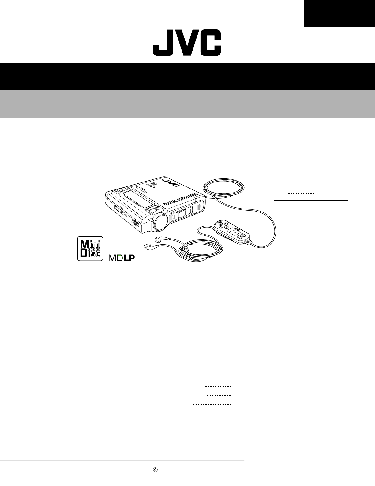
SERVICE MANUAL
PORTABLE MINIDISC RECORDER
XM-R700SL
US Singapore
XM-R700SL
Area Suffix
Contents
Safety Precautions
Important for laser products
Attention when
MD pick up is exchanged
Disassembly method
Adjustment method
Maintenance of laser pickup
Replacement of laser pickup
Description of major ICs
COPYRIGHT 2001 VICTOR COMPANY OF JAPAN, LTD.
1-2
1-3
1-4
1-5
1-15
1-17
1-17
1-18~37
No.20911
Jan. 2001
Page 2
XM-R700SL
1. This design of this product contains special hardware and many circuits and components specially
for safety purposes. For continued protection, no changes should be made to the original design
unless authorized in writing by the manufacturer. Replacement parts must be identical to those
used in the original circuits. Services should be performed by qualified personnel only.
2. Alterations of the design or circuitry of the product should not be made. Any design alterations of
the product should not be made. Any design alterations or additions will void the manufacturer`s
warranty and will further relieve the manufacture of responsibility for personal injury or property
damage resulting therefrom.
3. Many electrical and mechanical parts in the products have special safety-related characteristics.
These characteristics are often not evident from visual inspection nor can the protection afforded
by them necessarily be obtained by using replacement components rated for higher voltage,
wattage, etc. Replacement parts which have these special safety characteristics are identified in
the Parts List of Service Manual. Electrical components having such features are identified by
shading on the schematics and by ( ) on the Parts List in the Service Manual. The use of a
substitute replacement which does not have the same safety characteristics as the recommended
replacement parts shown in the Parts List of Service Manual may create shock, fire, or other
hazards.
4. The leads in the products are routed and dressed with ties, clamps, tubings, barriers and the
like to be separated from live parts, high temperature parts, moving parts and/or sharp edges
for the prevention of electric shock and fire hazard. When service is required, the original lead
routing and dress should be observed, and it should be confirmed that they have been returned
to normal, after re-assembling.
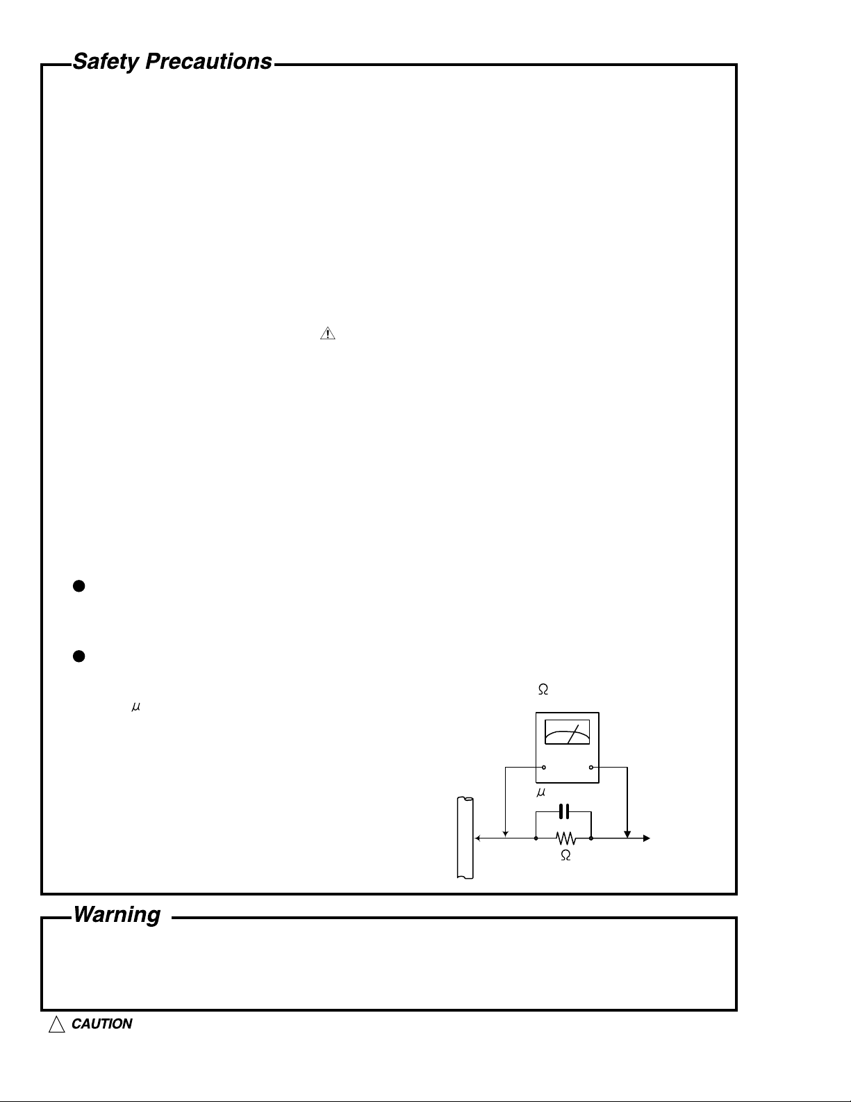
5. Leakage currnet check (Electrical shock hazard testing)
After re-assembling the product, always perform an isolation check on the exposed metal parts
of the product (antenna terminals, knobs, metal cabinet, screw heads, headphone jack, control
shafts, etc.) to be sure the product is safe to operate without danger of electrical shock.
Do not use a line isolation transformer during this check.
Plug the AC line cord directly into the AC outlet. Using a "Leakage Current Tester", measure
the leakage current from each exposed metal parts of the cabinet , particularly any exposed
metal part having a return path to the chassis, to a known good earth ground. Any leakage
current must not exceed 0.5mA AC (r.m.s.)
Alternate check method
Plug the AC line cord directly into the AC outlet. Use an AC voltmeter having, 1,000 ohms
per volt or more sensitivity in the following manner. Connect a 1,500 10W resistor paralleled by
a 0.15 F AC-type capacitor between an exposed
metal part and a known good earth ground.
Measure the AC voltage across the resistor with the
AC voltmeter.
AC VOLTMETER
(Having 1000
ohms/volts,
or more sensitivity)
Move the resistor connection to eachexposed metal
part, particularly any exposed metal part having a
return path to the chassis, and meausre the AC
voltage across the resistor. Now, reverse the plug in
the AC outlet and repeat each measurement. voltage
measured Any must not exceed 0.75 V AC (r.m.s.).
0.15 F AC TYPE
1500 10W
Place this
probe on
each exposed
metal part.
This corresponds to 0.5 mA AC (r.m.s.).
Good earth ground
1. This equipment has been designed and manufactured to meet international safety standards.
2. It is the legal responsibility of the repairer to ensure that these safety standards are maintained.
3. Repairs must be made in accordance with the relevant safety standards.
4. It is essential that safety critical components are replaced by approved parts.
5. If mains voltage selector is provided, check setting for local voltage.
!
Burrs formed during molding may be left over on some parts of the chassis. Therefore,
pay attention to such burrs in the case of preforming repair of this system.
1-2
Page 3
Important for laser products
XM-R700SL
1.CLASS 1 LASER PRODUCT
2.DANGER : Invisible laser radiation when open and inter
lock failed or defeated. Avoid direct exposure to beam.
3.CAUTION : There are no serviceable parts inside the
Laser Unit. Do not disassemble the Laser Unit. Replace
the complete Laser Unit if it malfunctions.
4.CAUTION : The compact disc player uses invisible
laserradiation and is equipped with safety switches
whichprevent emission of radiation when the drawer is
open and the safety interlocks have failed or are de
feated. It is dangerous to defeat the safety switches.
VARNING : Osynlig laserstrålning är denna del är öppnad
och spårren är urkopplad. Betrakta ej strålen.
VARO : Avattaessa ja suojalukitus ohitettaessa olet
alttiina näkymättömälle lasersäteilylle.Älä katso
säteeseen.
5.CAUTION : If safety switches malfunction, the laser is able
to function.
6.CAUTION : Use of controls, adjustments or performance of
procedures other than those specified herein may result in
hazardous radiation exposure.
CAUTION
!
Please use enough caution not to
see the beam directly or touch it
in case of an adjustment or operation
check.
ADVARSEL : Usynlig laserstråling ved åbning , når
sikkerhedsafbrydere er ude af funktion. Undgå
udsættelse for stråling.
ADVARSEL : Usynlig laserstråling ved åpning,når
sikkerhetsbryteren er avslott. unngå utsettelse
for stråling.
REPRODUCTION AND POSITION OF LABELS
WARNING LABEL
DANGER : Invisibie laser radiation
when open and interlock or
defeated.
AVOID DIRECT EXPOSURE TO
BEAM (e)
VARNING : Osynlig laserstrålning är
denna del är öppnad och spårren är
urkopplad. Betrakta ej strålen. (s)
VARO : Avattaessa ja suojalukitus
ohitettaessa olet alttiina
näkymättömälle lasersäteilylle.Älä
katso säteeseen. (d)
ADVARSEL :Usynlig laserstråling
ved åbning , når
sikkerhedsafbrydere er ude af
funktion. Undgå udsættelse for
stråling. (f)
1-3
Page 4
XM-R700SL
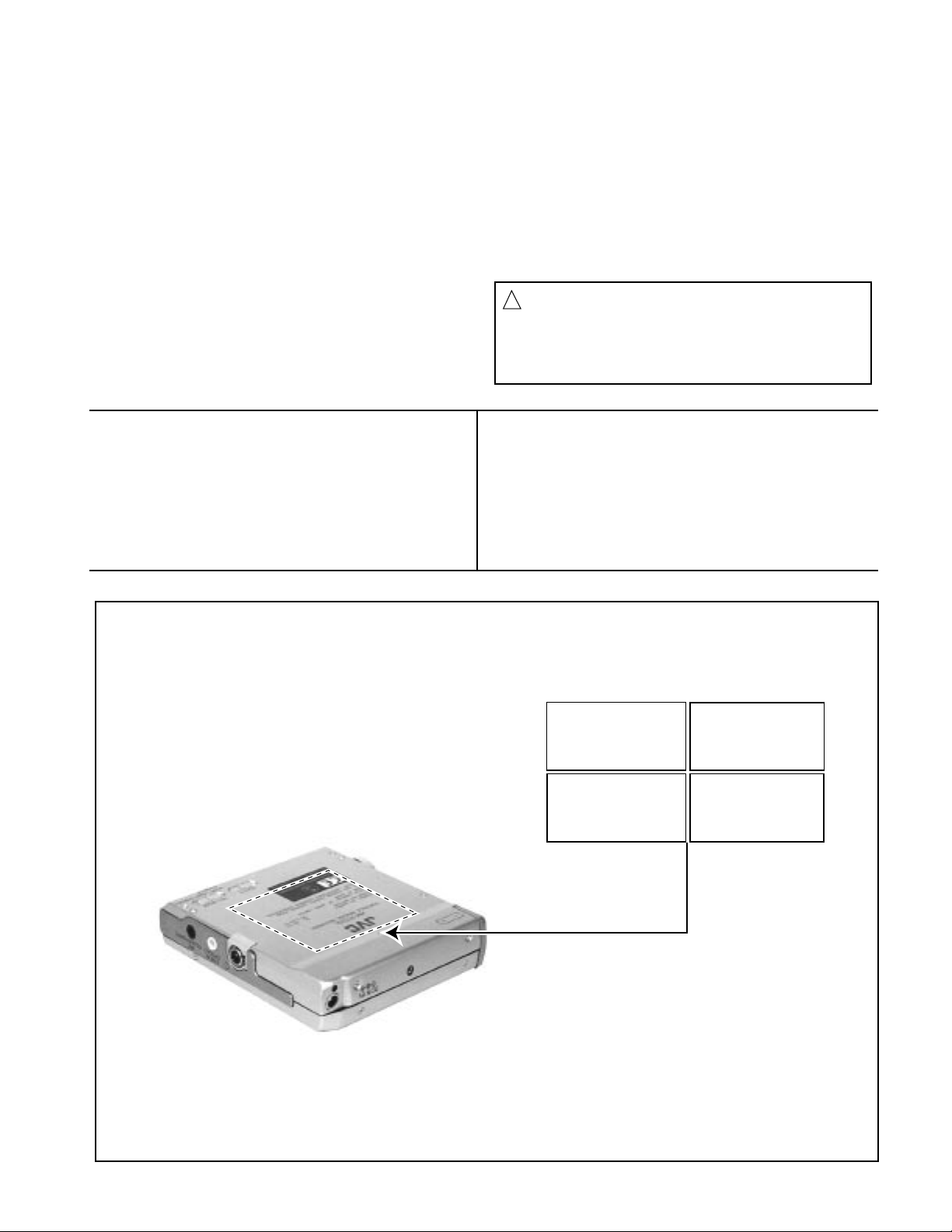
Attention when MD pick up is exchanged
1. About the static electricity protection measures
The laser diode in the traverse unit (optical pick up) is easy to be destroyed by clothes and the human body
to the electrified static electricity.
Please note the explosion by static electricity when repairing.
2. About the earth processing for the electrostatic destruction prevention
In the equipment which uses an optical pick up (laser diode), an optical pick up is destroyed by the static
electricity of the work environment.
Please do the earth processing and work.
1) Earth of work stand
Please pull the conductive material (conductive sheet) or the iron plate to the depository
place of the traverse unit (optical pick up), and take the earth to ground.
2) Human body earth
Please use the anti-static wrist strap to exhaust the electrified static electricity to the human body.
anti-static wrist strap
Conductive material (conductive
sheet) or the iron plate
3. Handling the optical pick up
1) Please return according to a correct procedure based on short processing after exchanging
parts.
2) Do not use a tester to check the condition of the laser diode in the optical pick up .The tester 's internal
power source can easily destroy the laser diode.
4. Attention when unit is disassembled
Please refer to "Disassembling method" for how to detach .
1) Please be sure to solder before a flexible wire is removed from connector on a main printed
circuit board as shown.
if you removes without soldering.the MD picking up assembly might destroy
2) When installing , solder in the part of short round should be removed after a flexible wire is connected with
connector.
Solder short
1-4
Page 5
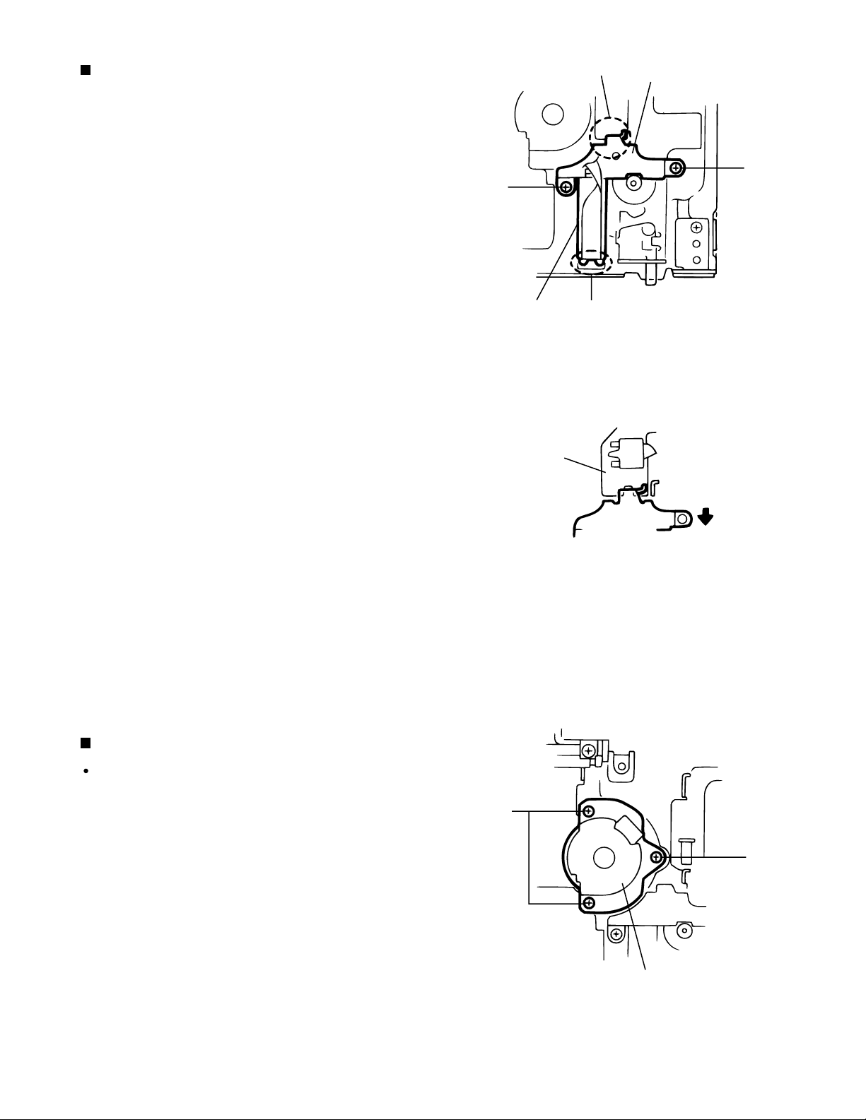
XM-R700SL
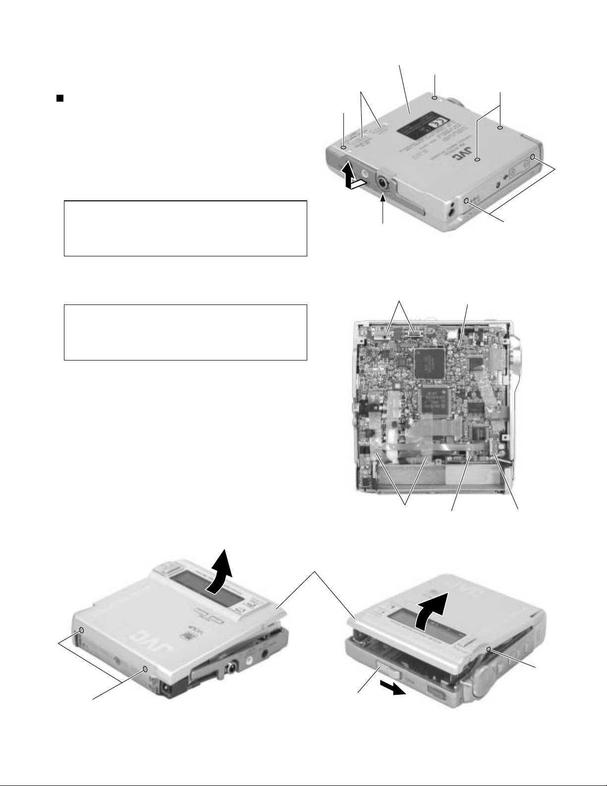
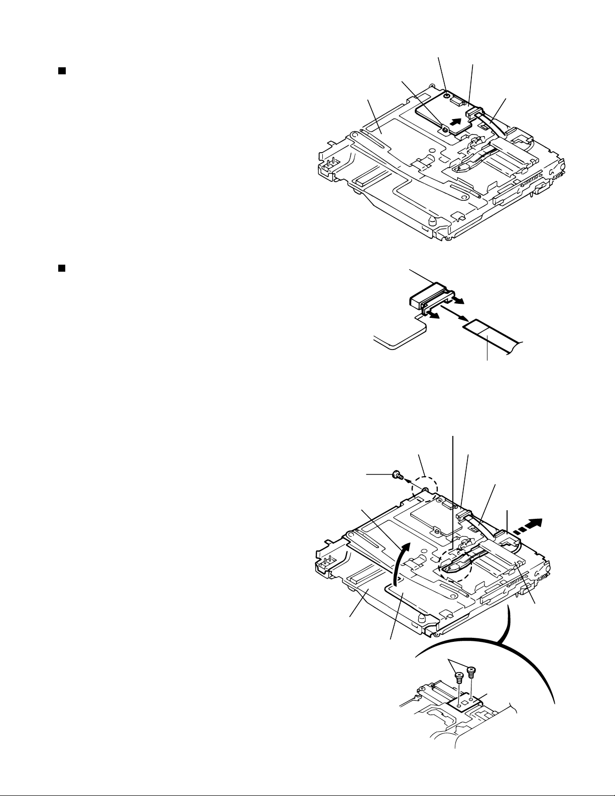
Disassembly method
<Main body>
Removing the MD door assembly and
the bottom cover (See Fig. 1 to 6)
1.
Turn over the body and remove the six screws A
attaching the bottom cover.
2.
Release the joint a outside and remove the bottom
cover.
ATTENTION:
3.
Disconnect the flexible wires from connector CN522
and CN571 on the main board.
ATTENTION:
When reattaching the bottom cover, fit
the hole knobs b to the hold switches
on the main board correctly (See Fig.1
and 2).
Peel off the adhesive tapes attaching
the flexible wires. Whenreconnecting
the flexible wires to the connectors, fix
them with adhesive tapes (SeeFig.2).
Bottom cover
Hole knobs b
A
Joint a
Hold switches
A
A
A
Fig.1
Main board
4.
Turn the MD door assembly up and open the door by
sliding the door lever.
5.
Remove the one screw B and the two screws C
attaching the MD door assembly.
MD door assembly
Adhesive tape
CN571
Fig.2
CN522
C
B
door lever
Fig.3Fig.4
1-5
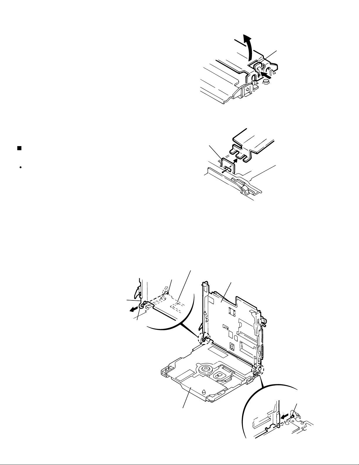
Page 6
XM-R700SL
6.
Unhook the joint tab c on the left side, then the right
side of the MD door.
7.
Remove the MD door assembly from the body while
pulling out the flexible wires another end of which
has already disconnected as shown in Fig.7.
Left
ATTENTION:
When pulling out the flexible wires, get
it through the opening of themain
board and the cabinet.
Removing the main board
(See Fig.7 to 10)
Prior to performing the following procedures, remove
the bottom cover.
ATTENTION:
Before disconnecting the flexible wire
extending from the pickup, makesure
to solder the short circuit round to
prevent damage to the pickup.
MD door assembly
Right
Holder assembly
Tab c
Tab c
Fig.5
B
MD door assembly
Holder assembly
1.
Turn the body and disconnect the flexible wire from
connector CN522, CN571, CN-401 and CN701
onthe main board respectively.
ATTENTION:
Peel off the adhesive tapes attaching the
flexible wires. Whenreconnecting the
flexible wires to the connectors, fix them
with adhesive tapes (SeeFig.2).
Main board
D
CN701
CN401
Fig.6
CN571
Fig.7
Short circuit round
CN300
E
CN522
Battery lead
1-6
Page 7
XM-R700SL
2.
Remove the two screws D and the one screw E
attaching the main board.
3.
Move the battery lead on the side of the body in the
direction of the arrow and removethe screw F
attaching the main board and the cabinet assembly.
4.
Remove the main body in the direction of the arrow
while releasing the part d, thenpart e of the cabinet
assembly from the flame assembly.
ATTENTION:
When reassembling, connect the
flexible wire extending from the
pickupto the connector on the main
board and unsolder the short circuit
round.
F
Main board
CN300
Short circuit round
Solder
Fig.8
Main board
Battery lead
Removing the MD mechanism assembly
(See Fig.11)
Prior to performing the following procedures, remove
the MD door assembly, thebottom cover and the
main board.
1.
Remove the two screws G and detach the MD
mechanism assembly from the cabinetassembly.
Part d
Cabinet assembly
Fig.10Fig.9
MD mechanism assembly
Part e
G
G
Cabinet assembly
Fig.11
1-7
Page 8
XM-R700SL
Removing the jog assembly
(See Fig.7 and 11)
Prior to performing the following procedures, remove
the MD door assembly and the bottom cover.
1.
Disconnect the flexible wire from connector CN--- on
the main board (See Fig.7).
2.
Remove the screw H attaching the jog assembly on
the right side of the cabinet assembly.
3.
Slide and release the three joints f attaching the jog
assembly, and pull out the jog assembly fromthe part
g on the cabinet assembly.
Jog assembly
H
Part g
Joints f
Joints f
Fig.12
Removing the LCD assembly and the 5
key sheet (See Fig.12 to 15)
Prior to performing the following procedures, remove
the MD door assembly and the bottom cover.
1.
Remove the two screws I and the one screw J
attaching the door plate on the inside of the MDdoor
assembly. Peel off the adhesive tape attaching the
flexible wire.
2.
Pull out the door plate assembly in the direction of
the arrow from the part h on the MD doorassembly.
3.
Remove the LCD assembly and the 5 key sheet from
the door plate assembly (They are attachedwith the
adhesive tapes).
Door plate assembly
I
J
Part h
I
J
Adhesive tape
5 key sheet
Part h
Door plate assembly
I
MD door assembly
Fig.13
LCD assembly
1-8
I
Door plate assembly
Fig.15Fig.14
Page 9
XM-R700SL
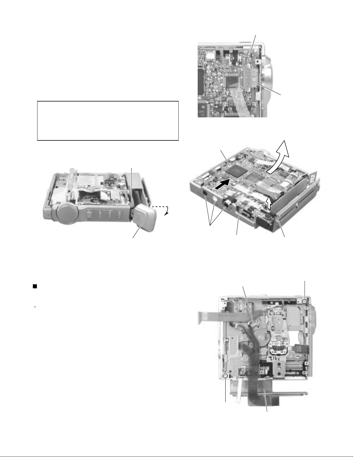
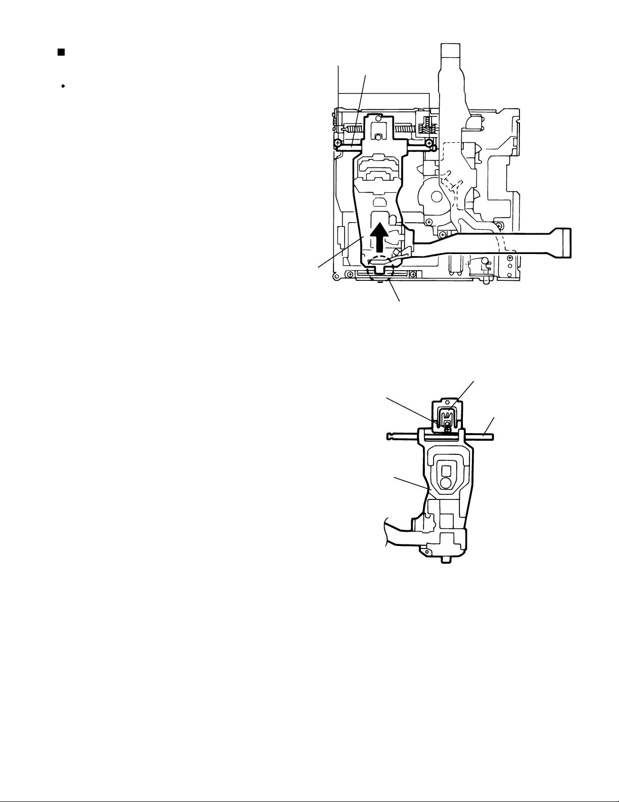
< Removal of the MD mechanism >
Removing the Magnetic head board
(See Fig.1 and 2)
1.
Disconnect the magnetic head flexible harness
from the connector of the magnetic head board on
the holder assembly.
2.
Remove the screw A attaching the magnetic head
board and pull out the magnetic head board from
the slit (a) in the direction of the arrow.
Removing the Magnetic head assembly
(See Fig.2 to 5)
1.
Disconnect the magnetic head flexible harness
from the connector of the magnetic head board on
the holder assembly.
Slit a
Holder assembly
Magnetic head
board
A
Magnetic head board
Magnetic head
flexible harness
Fig. 1
2.
Push the convex part b on the right side of the
head protector in the direction of the arrow. Lift the
right edge of the head protector (See Fig.4).
3.
Pull the left tab of the head protector from the slit
(See Fig.5).
4.
Remove the two B screws attaching the magnetic
head assembly on the underside of the chassis
assembly.
5.
Pull out the magnetic head assembly in the
direction of the arrow while paying attention to the
magnetic head.
C
d
Chassis assembly
Fig. 2
Part c
Magnetic head
flexible harness
Magnetic head
Magnetic head board
Magnetic head
flexible harness
Magnetic head
assembly
Pull
Head protector
Holder assembly
Pickup assembly
Fig. 3
B
Magnetic
head assembly
Underside of the
chassis assembly
1-9
Page 10
XM-R700SL
CAUTION:
When reassembling the magnetic head
assembly, reverse the order of the
removing procedure.
1.
Attach the magnetic head assembly by cramping
the MD mechanism assembly. Then, fix the
magnetic head assembly to the pickup assembly
on the underside of the chassis assembly by
tightening the two B screws.
2.
Attach the left edge of the head protector and the
right edge.
3.
Connect the magnetic head flexible harness to the
connector on the magnetic head board.
Removing the Holder assembly
(See Fig.3 and 6)
Prior to performing the following procedure,
remove the magnetic head assembly.
1.
Remove the screw C of the chassis assembly part
c and lift the edge of the holder assembly in the
direction of the arrow d (See Fig.3).
2.
Move the part e of the holder assembly in the
direction of the arrow to release the U-shaped
notch from the shaft.
Right side of the
head protector
Slit
Lift up
Convex part (b)
Push
Fig. 4
Left side of the
head protector
Pull
Fig. 5
3.
Pull the part f of the holder assembly in the
direction of the arrow to release it from the shaft.
Holder assembly
U-shaped notch
Chassis assembly
Shaft
Part e
Chassis assembly
Holder assembly
Holder
assembly
Part f
Shaft
1-10
Fig. 6
Chassis assembly
Page 11
XM-R700SL
Removing the Pickup unit
(See Fig.7 and 8)
Prior to performing the following procedure,
remove the magnetic head assembly.
1.
Remove the two D screws fixing the main shaft of
the pickup unit on the underside of the chassis
assembly. Remove the pickup unit by pulling out
the part g in the direction of the arrow.
2.
Remove the screw E attaching the lead spring on
the pickup unit.
3.
Remove the main shaft from the pickup unit.
Pickup unit
D
Main shaft
Part g
Fig. 7
E
Pickup unit
Lead spring
Main shaft
Fig. 8
1-11
Page 12
XM-R700SL
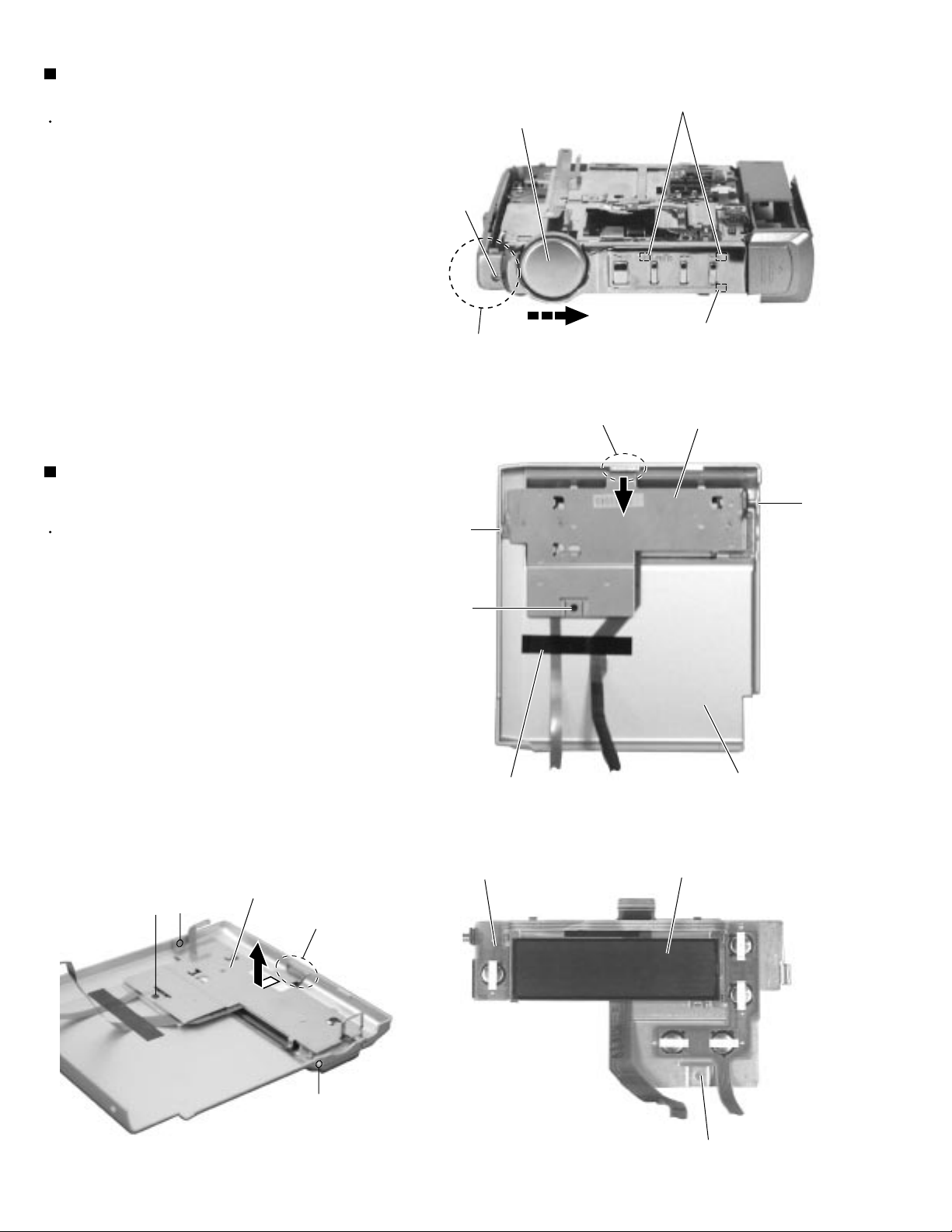
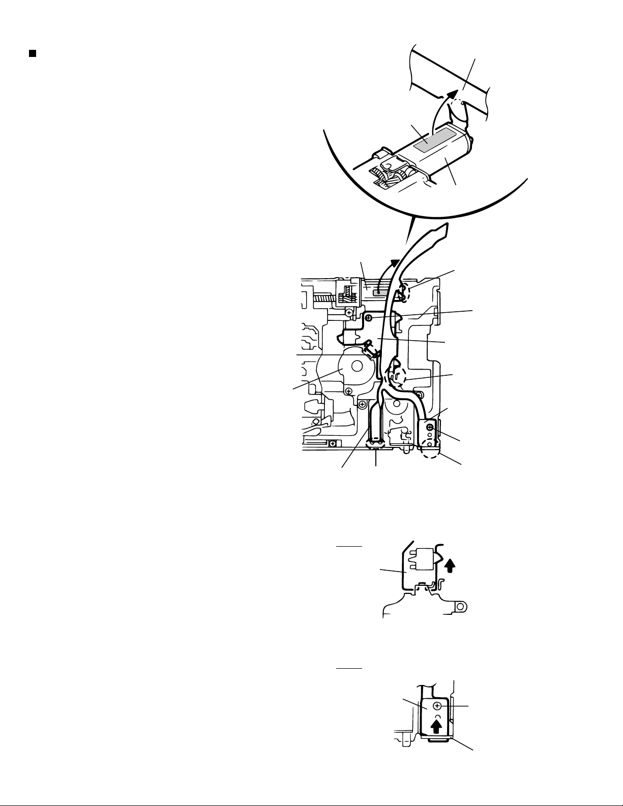
Removing the Flexible harness assembly
and the Protective/reflective switch
assembly (See Sig.9 to 11)
1.
Peel the double-sided tape attaching the flexible
harness on the feed motor on the underside of the
chassis assembly.
2.
Unsolder the flexible harnesses connected to the
part h of the spindle motor, the part i of the feed
motor and the part j of the lift motor.
3.
Remove the two F screws attaching the flexible
harness assembly and the protect/ reflect switch
assembly respectively.
Part h - unsoldering
Double-sided tape
Feed motor
Flexible harness
Peel off
Feed motor
Peel off
Part i - unsoldering
F
Flexible harness assembly
Spindle motor
4. Pull out the part k and l in the direction of the
arrows respectively and remove the flexible
harness assembly and the protective / reflective
switch assembly.
Lift motor
Part k
Flexible harness
assembly
Part j - unsoldering
Part l
Part k
Protective/ reflective switch
assembly
F
Part l
Fig. 9
Pull out
Lift motor
bracket
Fig. 10
1-12
Protective/reflective
switch assembly
Fig. 11
F
Chassis assembly
Page 13
XM-R700SL
Removing the Lift motor
(See Fig.12 and 13)
1.
Unsolder the part j of the flexible harness
connected to the lift motor on the underside of the
chassis assembly.
2.
Remove the two G screws attaching the lift motor
bracket.
3.
Remove the lift motor with the lift motor bracket by
pulling out the part k.
G
Lift motor
Flexible harness
assembly
Part k
Part j - unsoldering
Lift motor bracket
Fig. 12
G
Removing the Spindle motor (See Fig.14)
Prior to performing the following procedure,
remove the flexible harness assembly.
1.
Remove the three H screws attaching the spindle
motor on the underside of the chassis assembly.
H
Pull out
Lift motor
bracket
Fig. 13
Fig. 8
H
Spindle motor
Fig. 14
1-13
Page 14
XM-R700SL
Removing the Feed motor
(See Fig.15 and 16)
Prior to performing the following procedure,
remove the magnetic head assembly and the
pickup unit.
1.
Peel the double-sided tape attaching the flexible
harness on the feed motor on the underside of the
chassis assembly.
2.
Unsolder the part i of the flexible harness
connected to the feed motor.
3.
Remove the two I screws attaching the feed motor
base, then the feed motor base and the feed motor.
Flexible harness
Peel off
Double-sided tape
Feed motor
Fig. 15
I
Feed motor base
Feed motor
When connecting the flexible harness to the feed
*
motor, use the double-sided tape to stick them fast.
(See Fig.17)
Part i
Fig. 16
Flexible harness
Double-sided tape
Feed motor
1-14
Fig. 17
Page 15
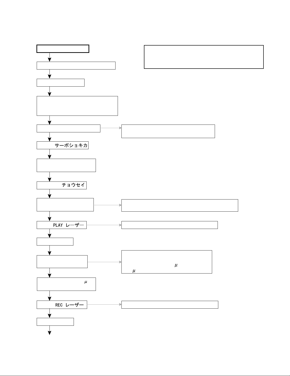
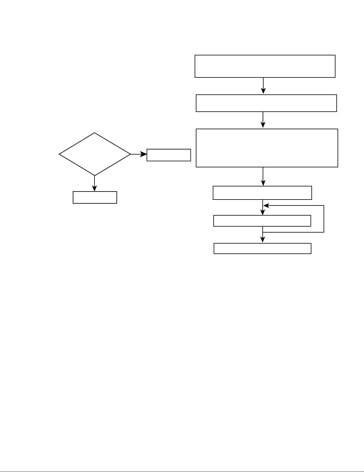
Adjustment method
(Adjustment should done when change the PICKUP, mechanism, Printed circuit board.)
XM-R700SL
Open the bottom cover
Joint the AC adaptor to main body
Powe OFF condition
Press EDIT key keep pressing
condition with press B.SKIP(|<<) key
more than 3sec.
Set change to TEST MODE
Select
Press PLAY key, clear the
last adjust ment data
Select DA (Voltage adjustment)
(servo initialize)
LCD full on then indicate TEST MODE
Select the item by F.SKIP(>>|),B.SKIP key
Adjustment DISC
Pre mastered(PRE DISC):TGYS 1
Recordable (MO DISC):AU-1 or full recorded normality set
80min tracking off set adjust:SONY 80min DISC
Press PLAY key, goto the
voltage adjust mode
Select
(Play laser)
Press PLAY key
Insert the laser power
meter sensor
Adjust more than 875 W
and more cross this
Select
(Rec laser)
Press PLAY key
Adjust the voltage to less than 2.7V or same as 2.7V
at test point (VCC and GND)
Adjustment mode of playback laser power
Adjust the laser power by F.SKIP, B.SKIP
then fix by STOP key
Adjust to more than 875 W or same as
875 W
Adjust ment mode of recording laser power
Continue next page
1-15
Page 16
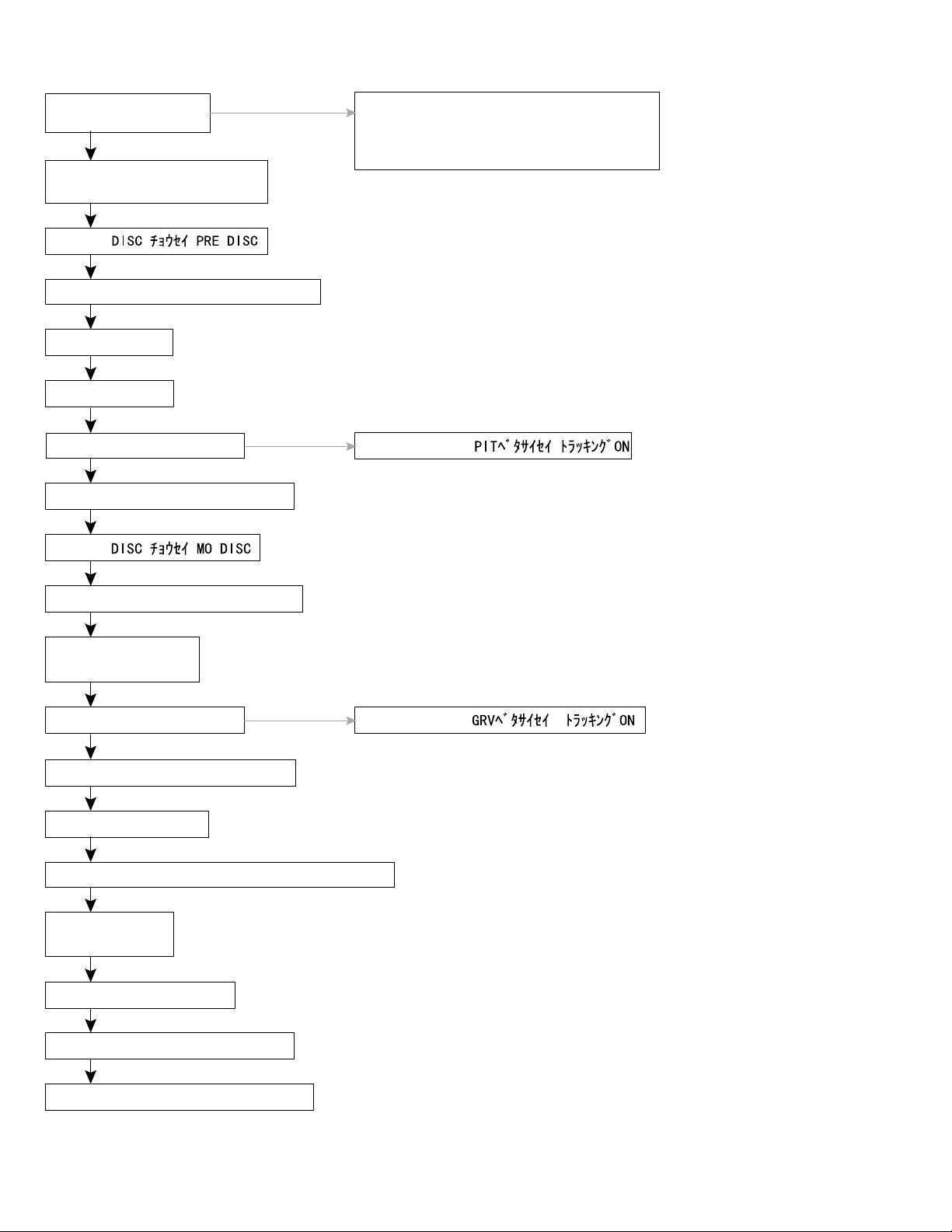
XM-R700SL
From the previous page
Insert the laser power
meter sensor
Adjust less than 6.32mW
and more cross this
Select
Insert the adjustment DISC (TGYS 1)
Press PLAY key
Start adjustment (auto adjustment)
Complete the adjustment
Press STOP key then eject DISC
Select
Adjust the laser power by F.SKIP, B.SKIP
then fix by STOP key
Adjust to less than 6.32mW or same as
6.32mW
LCD indication
Insert the adjustment DISC (AU-1)
Press PLAY key
Start the adjustment (auto adjustment)
Complete the adjustment
Press STOP key then eject DISC
Select R_TOF AUTO
Insert the adjustment DISC (SONY 80min DISC)
Press PLAY key
Start adjustment (auto adjustment)
Complete the adjustment
Press STOP key then eject DISC
LCD indication
Power off by release the AC adapter
1-16
Page 17
XM-R700SL
Maintenance of laser pickup
(1) Cleaning the pick up lens
Before you replace the pick up, please try to
clean the lens with a alcohol soaked cotton
swab.
(2) Life of the laser diode
When the life of the laser diode has expired,
the following symptoms will appear.
1. The level of RF output (EFM output:ampli
tude of eye pattern) will below.
Is the level of
RFOUT under
0.35Vp-p?
YES
O.K
NO
Replace it.
Replacement of laser pickup
Turn off the power switch and,disconnect the
power cord from the ac outlet.
Replace the pickup with a normal one.(Refer
to "Pickup Removal" on the previous page)
Plug the power cord in,and turn the power on.
At this time,check that the laser emits for
about 3seconds and the objective lens moves
up and down.
Note: Do not observe the laser beam directly.
Play a disc.
Check the eye-pattern at TP1.
Finish.
(3) Semi-fixed resistor on the APC PC board The semi-fixed resistor on the APC printed circuit board which is
attached to the pickup is used to adjust the laser power.Since this adjustment should be performed to match the
characteristics of the whole optical block, do not touch the semi-fixed resistor.
If the laser power is lower than the specified value,the laser diode is almost worn out, and the laser pickup should
be replaced.
If the semi-fixed resistor is adjusted while the pickup is functioning normally,the laser pickup may be damaged
due to excessive current.
1-17
Page 18
XM-R700SL
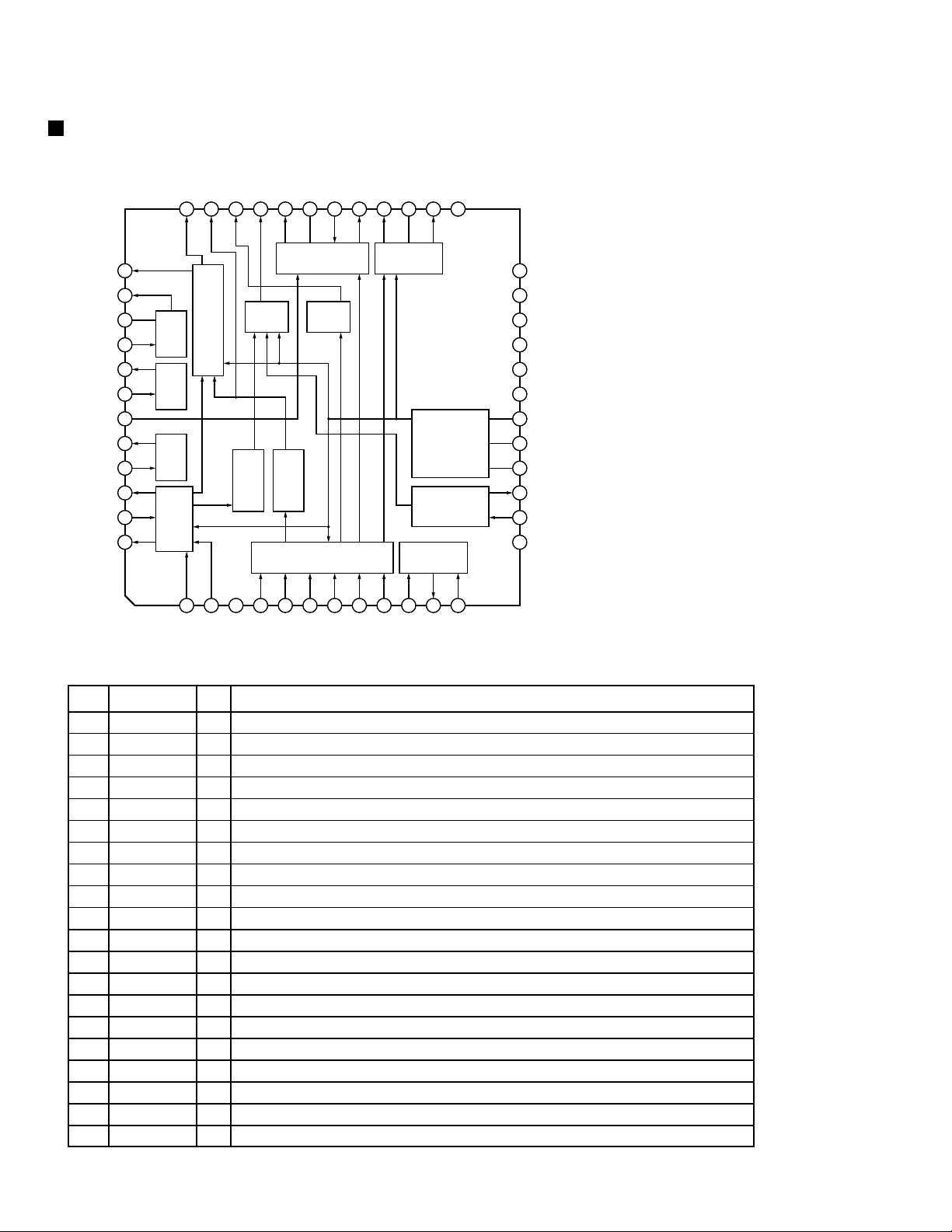
Description of major ICs
CXA2523AR (IC300) : MD servo
1.Block diagram
BOTM
ABCD34FE33AUX32ADFG31ADAGC30ADIN29ADFM28SE27CSLED26TE25WBLADJ
36 35
PEAK
37
38
RF
39RFAGC
40AGCI
41COMPO
42COMPP
43ADDC
44OPO
45OPN
46RFO
47MORFI
MORFO
48
2.Pin function
Pin No.
Symbol
1
2
3
4
5
6
7
8
9
10
11
12
APCREF
13
14
15
16
17
18
19
20
TEMPI
TEMP R
SWDT
SCLK
XLAT
XSTBY
F0CNT
I
J
VC
A
B
C
D
E
F
PD
APC
GND
AGC, EQ
Comp
USER
USER
OP Amp
RF Amp
1 2
I
I/O
ADIP Amp TE/SE Amp
MUX FE Amp
Peak, Bottom Detector
ABCD Amp
3T Detector
I-V Amp APC
3VC4A5B6C7D8E9F10PD11
J
CPU
Command I/F
TEMP Amp
12
APC
APCREF
Vcc
24
23
3TADJ
22 EQADJ
21 VREF
20 F0CNT
19 XSTBY
18 XLAT
17 SCLK
16 SWDT
15 TEMP R
14 TEMP I
13 GND
Function
I-V converted RF signal I input.
I
I-V converted RF signal J input.
I
Vcc/2 voltage output.
O
A current input for main beam servo signal.
I
B current input for main beam servo signal.
I
C current input for main beam servo signal.
I
D current input for main beam servo signal.
I
E current input for side beam servo signal.
I
F current input for side beam servo signal.
I
Reflection light quantity monitor signal input.
I
Laser APC output.
O
Reference voltage input for the laser power intensity setting.
I
Connect to GND.
Connects the temperature sensor.
I
Connects the temperature sensor. outputs the reference voltage.
I
Data input for microcomputer serial interface.
I
Shift clock input for microcomputer serial interface.
I
Latch signal input for microcomputer serial interface.Latched when low.
I
Standby setting pin. Normal operation when high Standby when low.
I
Internal current source setting pin.
I
1-18
Page 19

XM-R700SL
Pin No.
21
22
23
24
25
26
27
28
29
30
31
32
33
34
35
36
37
38
39
40
41
42
43
44
45
46
47
48
Symbol
VREF
EQADJ
3TADJ
Vcc
WBLADJ
TE
CSLED
SE
ADFM
ADIN
ADAGC
ADFG
AUX
FE
ABCD
BOTM
PEAK
RF
RFAGC
AGCI
COMPO
COMPP
ADDC
OPO
OPN
RFO
MORFI
MORFO
I/O
Reference voltage output.
O
Equalizer center frequency setting pin.
I/O
BPF3T center frequency setting pin.
I/O
Power supply.
BPF22 center frequency setting pin.
I/O
Tracking error signal output.
O
Connects the sled error signal LPF capacitor.
Sled error signal output.
O
ADIP FM signal output.
O
ADIP signal comparator input.
I
Connects the ADIPAGC capacitor.
ADIP2 binary value signal output.
O
13 output / temperature signal output. Switched with serial commands.
O
Focus error signal output.
O
Reflection light quantity signal output for the main beam servo detector.
O
RF/ABCD bottom hold signal output.
O
Peak hold signal output for the RF/ABCD signals.
O
RF equalizer output.
O
Connects the RFAGC capacitor.
RFAGC input.
I
User comparator output.
O
User comparator non-inverted input.
I
Connects the capacitor for ADIP amplifier feedback circuit.
I/O
User operational amplifier output.
O
User operational amplifier inverted input.
I
RF amplifier output. Eye pattern checkpoint.
O
Input of the groove RF signal with AC coupling.
I
Groove RF signal output.
O
Function
1-19
Page 20

XM-R700SL
CXA8059Q (IC450) : Motor driver
1. Pin layout
36
37
~
25
24
2. Block diagram
~
48
CPC3
1
VSWFVFUFCOMFCPOUT
CP3
~
13
~
UIN
12
VIN
Voltage
Driver
WIN
COM
UOUT
VOUT
WOUT
Sample
and Hard
GNDPGNDFG2FGSLOPE
CPC2
CPC1
RMAX
CP2
CP1VCO
RMINVCOINVCC
Charge Pump
VCO
Phase
Comparator
Timing
controllor
MCLOCK
1/8
CLKSEL
S/S
Sensoeless Logic
PWM
F/R
Controllor
BRAKE
Full Wave
Rectifilter
VCREF
VCONT
OSC CLOCK RESET FC CF RF
1-20
Page 21

3.
Pin function
Pin
Symbol Function
no.
1
2
3
4
CPOUT
5
6
7
8
9
10
11
12
13
BRAKE
14
VCONT
15
VCREF
16
17
18
19
20
21
22
23
VCOIN
24
CLKSEL
25
26
SLOPE
27
CLOCK
28
29
30
31
32
33
34
MCLOCK
35
36
RESET
37
38
39
40
41
42
43
44
45
46
47
48
PGND
COM
VS
CPC3
CP3
CPC2
CP2
CPC1
CP1
GND
S/S
FC
CF
FG
FG2
VCO
RMAX
RMIN
OSC
GND
WF
VF
UF
COMF
VCC
VS
RF
NC
NC
WIN
WOUT
VIN
VOUT
UIN
UOUT
NC
NC
RF
XM-R700SL
The GND to guard the power stage.
The terminal to detect the voltage.
The terminal to supply the voltage for the power stage.
The terminal to connect the capacitor in the final charge pump.
The terminal to connect the capacitor in the third charge pump.
The terminal to connect the capacitor in the third charge pump.
The terminal to connect the capacitor in the second charge pump.
The terminal to connect the capacitor in the second charge pump.
The terminal to connect the capacitor in the first charge pump.
The terminal to connect the capacitor in the first charge pump.
The GND for the part except the power section.
The terminal for start and stop.
The terminal for braking.
The terminal for controlling velocity.
The terminal as referable voltage of controlling velocity.
The terminal to compensate the frequency characteristics of the loop controlling velocity.
The terminal of sampling and holding for detecting motor current.
The terminal to output FG pulse.
The terminal to output FG pulse divided Pin15 signal by 2.
The terminal to set oscillation frequency of VCO.
The terminal to set maximum oscillation frequency of VCO.
The terminal to set minimum oscillation frequency of VCO.
The terminal to control oscillation frequency of VCO.
The terminal to select inside and outside clock.
The terminal to oscillation sawtooth for PWM signal.
The terminal to oscillation sawtooth for soft-switching signal.
The terminal to monitor CLOCK signal.
The GND for the part except the power section.
The terminal to shape waveform of motor voltage.
The terminal to shape waveform of motor voltage.
The terminal to shape waveform of motor voltage.
The terminal to shape waveform of motor voltage.
The terminal to supply the voltage except the power section.
The terminal to input clock.
The terminal to supply the voltage for the power stage.
The terminal to reset a register for checking the movement.
The terminal to monitor current.
Non connect
Non connect
The terminal to sense the back electro magnetic force of coils.
The terminal to supply the motor current.
The terminal to sense the back electro magnetic force of coils.
The terminal to supply the motor current.
The terminal to sense the back electro magnetic force of coils.
The terminal to supply the motor current.
Non connect
Non connect
The terminal to monitor current.
1-21
Page 22

XM-R700SL
CXD2672GA(IC351):DSP
1.Pin layout
17
16
TFDR TRDR
15
FRDR FFDR VDC4
14
VSC4
13
12
11
10
9
8
7
SRDR
SPFD SPRD
TEST1 FGIN
TEST2
TST2 EFM0
VSI03
SPCU SPDW SPDV
TST4 SPCW SPCV
LDDR
DTRF VSI02 ADFG ADRB AVS2 ADI0 FE PEAK FILI
APCR CKRF FOCN APC SE ADRT VC ABCD
XLRF VDI02 DCHG TE AVD2 AUX1
FS4
SFDR
TEST3
TST3
VDI03
TOP
VIEW
CLTV
PCO BIAS ASYO XWE TST6
BOTH
FILO RFI AVD1 MVCI
AVS1
ASYI
DVSS1
PD0
DVDD1
VDC3
D1
A09
A07
DVI01
A05 A01
A03
A11
XOE
D3
VSC3
D2
D0
XCAS IXWE
IXOE
XRAS
A08
A10
A00
VSI01
A06
A02
A04
VSC5 SLDW SLDV
6
SLCV SLCU VDC5
5
BYPS TST5
4
MNT1
3
MNT0
2
1
SLCW
VDC0
MNT2 SWDT
MNT3
SCLK
SENS XRST
SRDT
SQSY XINT OSCI
VSCO DQSY TX
XLAT
RPWR
VDI
OSC
DVDD0
DVSS0
OSCO
DA
VDDLDAVDDR
AOUTL VREFL
DA
VSI
VSSLDAVSSR
OSC
VREFR TST1
AOUTR XTSL DOUT
VSC1 DIN1
F256
XBCK
DADT LRCK
VDC2
VDI00
TST8
VDC1 TST0 DATAI TST7
MT
MT
FLGR
FLGL
VSI00
DA
PWMLP
ABCDEFG JH KLMNPRTU
2.Pin function (1)
Pin
Symbol I/O Function
No.
A-1
A-2
A-3
B-1
B-2
B-3
C-1
C-2
C-3
D-1
D-2
D-3
NC
NC
MNT1
NC
NC
MNT0
MNT3
MNT2
NC
SCLK
SWDT
VDC0
-
Open
-
Open
O
Monitor output
-
Open
-
Open
I/O
Monitor in/output
O
Monitor output
O
Monitor output
-
Open
I
Micon serial bus clock input
I
Micon serial bus data write input
-
Internal logic VDD(1.8V)
VSC2
ADDT
DA
PWMRP
DA
PWMLN
1-22
Page 23

2.Pin function(2)
Pin No.
E-1
E-2
E-3
F-1
F-2
F-3
G-1
G-2
G-3
H-1
H-2
H-3
K-1
K-2
K-3
L-1
L-2
L-3
M-1
M-2
M-3
N-1
N-2
N-3
P-1
P-2
P-3
U-1
R-1
U-2
R-2
U-3
R-3
U-4
R-4
U-5
R-5
U-6
R-6
U-7
R-7
U-8
R-8
Symbol I/O Function
XLAT
SRDT
SENS
VSC0
SQSY
XRST
DQSY
XINT
RPWR
TX
OSCI
VDIOSC
J-1
J-2
J-3
T- 1
T- 2
T- 3
T- 4
T- 5
T- 6
T- 7
T- 8
OSCO
DVSS0
DVDD0
VSIOSC
AOUTL
DAVDDL
DAVSSL
VREFL
DAVDDR
DAVSSR
AOUTR
VREFR
VSC1
XTSL
TST1
DIN1
DOUT
VDC1
DAPWMLN
DAPWMLP
VSIO0
DAPWMRP
MTFLGR
MTFLGL
TST7
DATA I
TST0
ADDT
TST8
VDIO0
LRCK
DADT
VDC2
VSC2
XBCK
F256
A02
A04
A03
A06
A01
A05
I
Micon serial bus latch input
O
Micon serial bus data read out output
O
Internal output of micon serial bus address
-
Internal logic GND
O
PTGR=0 ADIPsink output / PTGR=1 DISC SUB-Q sink output
I
Reset input L:reset
O
Ubit SUB-Q sink output from digital audio input from MD or CD
O
Request status output L:request status
I
Laser power select input (H=rec power / L=playback power)
I
Output permit input of recorded data
I
X'tal osc circuit input
-
OSC sel VDD (2.5V)
O
X'tal osc circuit output
-
Internal 16bit DRAM GND
-
Internal 16bit DRAM GND
-
OSC sel GND
O
Internal DAC Lch output
-
Internal DAC VDD (Lch,2.5V)
-
Internal DAC GND
O
Internal DAC GND VREF(Lch)
-
Internal DAC VDD (Rch,2.5V)
-
Internal DAC GND (Rch)
O
Internal DAC Rch output
O
Internal DAC VREF (Rch)
-
Internal logic GND
I
X'tal frequency select (L=45.1584MHz/H=22.5792MHz)
I
Test terminal Connect to GND
I
Digital audio input Outer I/F mode EXRQ input
O
Digital audio output
-
Internal logic VDD (1.8V)
O
Internal DAC PWM output L-
O
Internal DAC PWM output L+
-
2.5V I/O VSS
O
Internal DAC PWM output R+
O
Internal DAC zero detect flag (Rch)
O
Internal DAC zero detect flag (Lch)
I
Test terminal Connect to GND
I
Serial data input
O
Open
I
Data input from A/D converter
I
Test terminal Connect to GND
-
2.5V I/O VDD
O
LR clock(44.1kHz) for A/D, internal DAC
O
Data output for internal DAC / Internal DAC PWM output R-
-
Internal logic VDD (1.8V)
-
Internal logic GND
O
A/D, internal DAC bit clock (2.8224MHz)
O
11.2896MHz clock output (X'tal)
O
External DRAM address output
O
External DRAM address output
O
External DRAM address output
O
External DRAM address output
O
External DRAM address output
O
External DRAM address output
XM-R700SL
1-23
Page 24

XM-R700SL
2.Pin function (3)
Pin No.
U-9
R-9
U-10
T-10
R-10
U-11
T-11
R-11
U-12
T-12
R-12
U-13
T-13
R-13
U-14
T-14
R-14
U-17
U-16
U-15
T-17
T-16
T-15
R-17
R-16
R-15
P-17
P-16
P-15
N-17
N-16
N-15
M-17
M-16
M-15
L-17
L-16
L-15
K-17
K-16
K-15
J-17
J-16
J-15
H-17
H-16
H-15
G-17
G-16
G-15
F-17
F-16
F-15
Symbol
VSIO1
T- 9
ADIO1
XRAS
IXWE
XCAS
VDC3
VSC3
DVDD1
TST6
DVSS1
ASYO
MVCI
AVS1
AVD1
PEAK
CLTV
ABCD
BOTOM
ADIO
AUX1
AVS2
ADRT
AVD2
ADRB
ADFG
DCHG
A00
A08
A10
A07
IXOE
A09
D1
D2
D0
D3
NC
NC
XOE
NC
A11
XWE
PDO
ASYI
BIAS
FILI
PCO
RFI
FILO
FE
VC
SE
TE
APC
I/O
-
2.5V I/O sel Vss
O
External DRAM address output
-
2.5V I/O sel VDD
O
External DRAM address output
O
External DRAM address output
O
External DRAM address output
O
Open
O
External DRAM RAS output
O
External DRAM address output
O
Open
O
External DRAM CAS output
I/O
External DRAM data input/output
I/O
External DRAM data input/output
I/O
External DRAM data input/output
-
Internal logic VDD
-
Internal logic GND
I/O
External DRAM data input/output
-
Internal 16Mbit DRAM VDD
-
Open
-
Open
O
External DRAM output chip enable output
-
Open
O
Open
O
Open
-
Internal 16Mbit DRAM GND
O
External DRAM write enable output
O
Analog PLL phase compare output
I
Playback EFM comparator slice level input
O
Playback EFM binarization signal output
I
Clock input from external VCO
-
Analog GND
I
Playback EFM comparator bias current input
O
Analog power supply (2.5V)
I
Filter input for playback EFM system mastering PLL
I
Phase comparison output for playback EFM system mastering PLL
I
Playback EFM RF signal input
O
Peak holding input optical amount signal
I
Internal VCO control voltage input for playback EFM system mastering PLL
I
Filter output for playback EFN system mastering PLL
I
Focus error signal input
O
Optical amount signal input
I
Bottom holding input of optical amount signal
I
Open
-
Middle point voltage input
I
Assistance A/D input
-
Analog GND
I
A/D converter operation range upper bound voltage input
-
Analog power supply (2.5V)
I
A/D converter operation range lower bound voltage input
I
Sled error input
I
Tracking error input
I
ADIP binary-coded FM signal input
I
Error signal input for laser digital APC
I
Connects with an analog power supply of low impedance
Function
1-24
Page 25

2.Pin function (4)
XM-R700SL
Pin No.
E-17
E-16
E-15
D-17
D-16
D-15
A-17
B-17
C-17
A-16
B-16
C-16
A-15
B-15
C-15
A-14
B-14
C-14
A-13
B-13
C-13
A-12
B-12
C-12
A-11
B-11
C-11
A-10
B-10
C-10
A-9
B-9
C-9
A-8
B-8
C-8
A-7
B-7
C-7
A-6
B-6
C-6
A-5
B-5
C-5
A-4
B-4
C-4
Symbol I/O Function
VSIO2
F0CN
VDIO2
DTRF
CKRF
XLRF
NC
NC
LDDR
NC
NC
APCR
TFDR
TRDR
NC
FRDR
FFDR
VDC4
VSC4
SRDR
FS4
SPFD
SPRD
SFRD
TEST2
TEST1
FGIN
TST2
EFMO
TEST3
VSIO3
TST3
VDIO3
SPCU
SPDW
SPDV
TST4
SPCW
SPCV
VSC5
SLDW
SLDV
SLCV
SLCU
VDC5
BYPS
TST5
SLCW
-
2.5V I/O Vss
O
Filter cutoff control output
-
2.5V I/O VDD
O
Controller data output
O
Controller clock output
O
Controller latch output
-
Open
-
Open
O
Laser digital APC PWM output
-
Open
-
Open
O
Laser APC reference PWM output
O
Tracking servo drive PWM output (+)
O
Tracking servo drive PWM output (-)
-
Open
O
Focus servo drive PWM output (-)
O
Focus servo drive PWM output (+)
-
Internal logic VDD (1.8V)
-
Internal logic GND
O
Sled servo drive PWM output (-)
O
176.4kHz clock output (X'tal system)
O
Spindle servo drive output
O
Spindle servo drive output
O
Sled servo drive PWM output (+)
I
Test terminal Connect to GND
I
Test terminal Connect to GND
I
Spindle CAV servo FG input
O
Test terminal Open
O
EFM output at recording
I
Test terminal Connect to GND
-
2.5V I/O Vss
O
Test terminal Open
-
2.5V I/O VDD
I
Blush less spindle motor drive comparate input (U)
O
Blush less spindle motor 3 phase drive truth output (W)
O
Blush less spindle motor 3 phase drive truth output (V)
O
Test terminal Open
I
Blush less spindle motor drive comparete input (W)
I
Blush less spindle motor drive comparate input (V)
-
Internal logic GND
O
Blush less sled motor 3 phase drive truth output (W)
O
Blush less sled motor 3 phase drive truth output (V)
I
Blush less sled motor 3 phase drive comparate input (V)
I
Blush less sled motor 3 phase drive comparate input (U)
-
Internal logic VDD (1.8V)
O
Open
O
Test terminal Open
I/O
Blush less sled motor 3 phase drive comparate input
1-25
Page 26

XM-R700SL
MPC17A139MTB-X (IC400) : 4ch bridge driver
1. Pin layout
2. Pin function
Clock detector
1
AGND
2
CLK
3
PS
4
OE
5
VD1
6
FO1
7
PGND
8
RO1
9
VD1
10
VD2
11
RO2
12
PGND
13
FO2
14
VD2
15
RI1
16
FI1
17
FI2
18
RI2
CLK PS
36
35
34
33
32
31
30
PGND
29
28
27
26
25
PGND
24
23
22
21
20
19
OSC.circuit
VG
VC
LG
GND
VD3
FO3
RO3
VD3
VD4
RO4
FO4
VD4
RI3
FI3
FI4
RI4
XH
H
X
L
Auto
Synchronization
Stop
Driver
PS , OE INPUT OUTPUT 1~4
PS
H
H
H
H
H
L
OE
L
L
L
L
H
X
FI
H
H
X
X
RI
L
L
L
H
L
H
X
X
FO
L
L
H
L
L
Z
RO
L
H
L
L
L
Z
1-26
X:Don't care
Z:High impedance
Page 27

XM-R700SL
3.Block diagram
35
Vc
2
CLK
3
PS
4
OE
FI1
16
RI1
15
GND
33
Vc
CLK
Detector
CLOCK
Vc
Control
Vc
Vc
DC/DC
Converter
G
V
Pre-driver
V
G
V
G
36 34
L
G
1
AGND
5
V
9
V
6
F
8
R
7
R
14
V
10
V
MPC17A139MTB-X
D1
D1
O1
O1
GND
D2
D2
FI2
RI2
FI3
RI3
FI4
RI4
19
17
18
21
22
20
Control
Vc
Control
Vc
Control
V
V
Pre-driver
Pre-driver
Pre-driver
13
F
O2
11
R
O2
12
P
GND
32
V
28
31
29
30
23
27
24
26
V
F
R
P
V
V
F
R
D3
D3
O3
O3
GND
D4
D4
O4
O4
G
G
25
P
GND
1-27
Page 28

XM-R700SL
AK4562VN-W (IC801) : A/D, D/A comverter
1. Pin layout
28272625242322
1
2
3
4
5
6
7
2. Block diagram
LIN1
LIN2
RIN1
RIN2
OPGAL
8
9
1011121314
21
20
19
18
17
16
15
ADC
VREF
VA
AGND
VT
VD
DGND
LOUT2
CCLK
(SCK)
DAC
Clock Divider
(SSI)
OPGAR
ROUT2
Control Register I/F
CSNLOUT1ROUT1
3. Pin function
No. Pin Name I/O Function
10
11
12
13
14
15
16
17
18
19
20
21
22
23
24
25
26
27
28
OPGAR
1
LOUT2
2
ROUT2
3
LIN1
4
RIN1
5
LIN2
6
RIN2
7
VCOM
8
AGND
9
VA
VREF
VD
DGND
VT
SDTO
SDTI
BCLK
TST
MCLK
LRCK
CDTI
CCLK
CSN
PDN
SSB
LOUT1
OPGAL
ROUT1
Rch OPGA Input Pin
I
Lch OPGA Output Pin
O
Rch OPGA Output Pin
O
Lch #1 Input Pin
I
Rch #1 Input Pin
I
Lch #2 Input Pin
I
Rch #2 Input Pin
I
Analog Common Voltage Output Pin, 0.45 x VA
Analog Ground Pin
Analog Power Supply Pin, +2.5V
Analog voltage Reference Input Pin.
-
Used as a voltage reference of ADC & DAC. VREF is connected externally to filterd VA.
Digital power supply Pin, +2.5V
Digital Ground Pin
Digital Interface Power Suooly Pin
Audio Serial Data Output Pin
O
Audio Serial Data Intput Pin
I
Audio Serial Data Clock Pin
I
Test Mode Pin, Fixed to "L"
I
Master Clock Input Pin
I
Input/Output Channel Clock Pin
I
Control Data Input Pin, SSB Mode : SSI
I
Control Clock Input Pin, SSB Mode : SCK
I
Chip Select Pin, SSB Mode : "H"
I
Resect & Power Down Pin, "L" : Power down & Reset, "H" : Normal Operation
I
Control I/F Mode Select Pin, "L" : AKM Mode, "H" : SSB Mode
I
Lch DAC Output Pin
O
Lch OPGA Input Pin
I
Rch DAC Option Pin
O
HPF
Audio I/F
Controller
VCOMMCLKSSBCDTI
LRCK
BCLK
SDTO
SDTI
PDN
TST
1-28
Page 29

JCV8002-W (IC851) : Head phone amp
1. Pin layout
24 ~ 19
1
XM-R700SL
18
2. Block diagram
3. Pin function
~
6
7 ~ 12
PW
SW
18
B
A
PW
SW
1
CUT
MT
SW
A
19
20
21
22
23
24
MT
TC
V
CC1
IN
B
IN
A
BEEP
OUT
BEEP
OUT
V
CC2
17
MT
SW
PW
A
2
BST
SW
PWR
GND
13
~
16
BST
SW
3
BEEP
IN
PW
B
OUT
15
BEEP
B
4
GND
DET
14
BST1
5
BST2
BST
AGC
Vref
IN
AGC
IN
13
Vref
6
Vref
ADD
IN
BST
OUT
12
11
10
BST
NF1
9
LPF
2
8
BST
NF
2
7
Pin
Symbol
no.
CC2
1
V
2
OUT
3
4
5
6
7
8
9
10
11
12
13
14
15
16
17
18
19
20
21
22
23
24
A
PWR GND
OUT
B
DET
AGC IN
BST OUT
BST NF
LPF
2
BST NF
ADD IN
V
ref
V IN
ref
GND
BEEP IN
BST SW
MT SW
PW SW
MT TC
V
CC1 CC
IN
B
IN
A
BEEP OUT
BEEP OUT
FUNCTION
V
(+B) in power amplifier output steps
CC2
Power amplifier output
GND in power amplifier output steps
Power amplifier output
Smoothness of level detection of boost
AGC
BST amplifier input signal level variable control by input lever to boost AGC input terminal
Output terminal of BST amplifier2
2
Terminal NF of BST amplifier2
Output BST amplifier1
NF of BST amplifier1
1
ADD amplifier input
Standard potential circuit
Standard potential circuit
Power part input steps GND
Beep input terminal
Beep output terminal
Mute switch
Power On/OFF switch
Mute smoothing Power mute switch
Main parts V
Power amplifier input
Power amplifier input
Beep output terminal
B
Beep output terminal
A
1-29
Page 30

XM-R700SL
AK93C55BH-W (IC502) : EEPROM
1. Pin layout
CS
SK
DI
DO
1
2
3
4
3. Block diagram
DI
INSTRUCTION
REGISTER
8
7
6
5
INSTRUCTION
DECODE,
CONTROL
AND
CLOCK
GENERATION
VCC
NC
PE
GND
DATA
REGISTER
ADD.
BUFFER
2.Pin function
Pin name
CS
SK
DI
DO
PE
VCC
GND
NC
16
R/W AMPS
AUTO ERASE
DECODER
Fnction
Chip select
Serial data clock
Serial data input
Serial data output
Program enable
Ground
Power supply
Not connected
DO
16
AND
EEPROM
2048bit
128 X 16
CS
VPP SW
SK
PE
VREF
SN74AHCT540PW-X (IC601) : Buffer
1. Pin layout, Block diagram 2. Truth value table
G1
A1
A2
A3
A4
A5
A6
A7
A8
GND
1
2
3
4
5
6
7
8
9
10
20
19
18
17
16
15
14
13
12
11
Vcc
G2
Y1
Y2
Y3
Y4
Y5
Y6
Y7
Y8
Input Output
G2
X
H
L
L
An
X
X
H
L
G1
H
X
L
L
VPP
GENERATOR
Yn
Z
Z
H
L
1-30
Page 31

HD6433048SV67X (IC501) : CPU
1. Pin layout
100 ~ 76
1 ~ 25
75 ~ 51
XM-R700SL
2. Pin function
Pin
Symbol
No.
1
VCC
2
XRST2
3
SWDT2
4
SCLK2
5
XLAT2
6
RECP
7
TX
8
XRST
9
XLAT
10
RESO
11
VSS
12
RMTX
13
SWDT
14
RMRX
15
SRDT
16
RFOFF
17
SCLK
18
RFVCTL
19
LDON
20
MHON
21
SLOFF
22
GND
23
PS
24
25
26
27
28
29
30
31
32
33
34
35
36
37
38
39
40
41
42
43
44
45
46
47
48
49
50
-
MM+
MM-
SSTOP
MREF
MPROT
MHUP
MHDN
OPEN
AC_XDC
MWUP
VCC
FFCLR
ACB
L3LCK
L3MODE
L3DATA
MUTE
MICIN
OPTIN
GND
-
ADPWR/DIR
PSW
LCDDATA
LCDCLK
LCDLAT
26 ~ 50
I/O
O
O
O
O
O
O
O
O
-
O
O
I
I
O
O
O
O
O
O
-
O
O
O
I
I
I
I
I
I
I
O
O
O
O
O
I/O
O
I
I
-
O
O
O
O
O
Pin function
Power supply terminal
RF reset
Data output for RF
Clock output for RF
Latch output for RF
Rec power
Permission of recorded data output
LSI reset output
Latch output
Non use
Ground
Status output to remote control
CXA2652 data output
Command input from remote control
CXA2652 data input
RF power ON/OFF control
CDXA2652 serial clock
RF ON sub signal output
Laser output
Magnetic head driver ON/OFF
Sled control power supply
Ground
4CH, CLV driver power save
Non use
Magnetic head UP signal output
Magnetic head DOWN signal output
Sled rest position detection input
Reflex ratio select switch input
Write prohibition switch input
Magnetic head position detection input
Magnetic head position detection input
OPEN/CLOSE detection
AC/BATTERY select input
LSI, Magnetic head driver power supply control
Power supply
FF clear of start circuit
Active bass control
Clock output for AD/DA
Mode setting for AD/DA
Data output for AD/DA
Driver mute signal output
Mic connect detection
Optical cable connect detection
Ground
Non use
Power save control output of A/D section
Driver power supply control signal output
Data output for LCD
clock output for LCD
Latch output for LCD
Pin
Symbol
No.
51
52
53
54
55
56
57
58
SYSCNY
59
60
REMOFF
61
62
63
64
65
66
67
68
69
70
71
72
73
74
75
76
77
78
79
80
EXTBATT
81
BATTERY
82
BATSTATUS
83
84
85
86
87
88
89
90
DOM/EXP
91
92
93
94
95
96
97
98
99
100
DATA
CLK
LAT
JOG+
JOG-
-
GND
CHRGE
STBY
RES
NMI
VSS
EXTAL
XTAL
VCC
CS2
SCL
DI
CS
MD0
MD1
MD2
AVCC
VREF
KEY1
KEY2
TEMP
RPLY
HOLD
AVSS
XINT
DQSY
SQSY
MNT2
GND
MNT0
MNT1
BEEP
MNT3
SENS
DO
AC/DC
-
I/O
O
O
O
I
I
-
O
O
O
-
-
-
-
-
-
-
O
O
O
O
-
-
-
-
-
I
I
I
I
I
I
I
-
I
I
I
I
-
I
I
I/O
I
I
I
O
-
Pin function
Data output for Debag/Test mode
Clock output for Debag/Test mode
Latch output for Debag/Test mode
JOG pulse input
JOG pulse input
Non use
Ground
5V power supply control
Charge control signal
Power supply control for remote control
Non use
Standby signal input terminal
Reset signal input terminal
Power supply
Ground
X'tal osc. connect terminal
X'tal osc. connect terminal
Power supply
EEPROM2 chip select terminal
Clock for EEPROM
Data output for EEPROM
Chip select terminal for EEPROM1
Power supply
Power supply
Power supply
Power supply
Reference voltage
KEY 1 A/D
KEY 2 A/D
A/D external battery voltage detect
Battery leavings level detect
Supply voltage detect
Temp. detect thermistor connect terminal
Remote controller PLAY key input
HOLD detection input
Ground
Squeeze request
CXA2652 DQSY
Sub code Q/Adip sync.
DO/EXP select setting input
LSI monitor signal input
Ground
LSI monitor signal input
LSI monitor signal input
BEED output
LSI monitor signal output
Connect to CXA2652 SENS terminal
Data input for EEPROM
Chargeable battery select SW control
Non use
1-31
Page 32

XM-R700SL
IC-PST3424U-X (IC504) : Reset
1. Pin layout
VOUT
VDD
2. Block diagram
VDD
VSS
1
2
43VSS
NC
2
+
-
1 VOUT
Vref
3
3. Pin function
No. Pin Name Function
1
2
3
4
Vout
VDD
NC
VSS
Reset Signal Output PIN
VDD PIN / Voltage Detect PIN
Non connect
VSS PIN
1-32
Page 33

MB3817PFV-X (IC911) : Switching regurator controller
1. Pin layout
XM-R700SL
2. Block diagram
FB
-IN
+IN
DTC
CS
1
8 9
5
4
3
6
13
1
CS
1u
Q1
OSC
Error
Amp.
-
+
(0.9V)
16
Soft Start
-
Comp. Comp.
+
1.5V
-1.4V
bias
-1.0V
RS
Latch
OUT
PWM
Cotp.
+
+
-
-
SCP
-
+
UVLO
Q5
SCP
1u
Q3Q2 Ref
(1.5V)
OFF
current
setting
bias
D1
(0.5V)
Powe r
ON/OFF
Vcc
Q4
Q6
7
CB1
8
CB2
9
Vcc
10
OUT
VE
11
15
CTL
3. Pin function
CT RT CSCPVREF GND
Pin
no.
1
2
3
4
5
6
7
8
9
10
11
12
13
14
15
16
Symbol
CT
RT
+IN
-IN
FB
DTC
CBI
CB2
Vcc
OUT
VE
GND
CS
CSCP
CTL
V
REF
I/O
This pin connects to a capacitor for setting the triangular-wave frequency
-
This pin connects to a resistor for setting the triangular-wave frequency
-
Error amplifier non-inverted input pin
I
Error amplifier inverted input pin
I
Error amplifier output pin
O
Dead time control pin
I
Boot capacitor connection pin
-
Boot capacitor connection pin
-
Power supply pin
-
Totem-pole type output pin
O
Output current setting pin
-
Ground pin
-
Soft start setting capacitor connection pin
-
Short detection setting capacitor connection pin
-
Power supply control pin .When this pin is High ,IC is inactive state .When this pin is Low , IC is standby state.
I
Reference voltage output pin
O
Function
12161421
1-33
Page 34

XM-R700SL
NJM2115V-W (IC821) : Regulator
1. Pin layout
1. A OUTPUT
2. A -INPUT
3. A +INPUT
-
4. V
2. Block diagram
-INPUT
+INPUT
+
8. V
A
7. B OUTPUT
B
6. B -INPUT
5. B +INPUT
+
V
OUTPUT
1-34
-
V
Page 35

S-8321AAMPDNA-W (IC931) : Switching
XM-R700SL
1. Pin layout
3. Pin function
No. Pin Name Function
1
2
3
4
5
2. Block diagram
54
123
ON/OFF
VOUT
VSS
CONT
Power off terminal
Voltage output terminal
(N.C.)
Terminal
Ext indnctor Connection terminal
Protect circuit
ON/OFF
PFM
Control circuit
VOUTCONT
VREF
+
-
VSS
TK1125BMC-X (IC802) : Regulator
1. Pin layout
2. Block diagram
VIN
VOUT
THERMAL SENSOR
CONT
BANDGAP REFERENC
GND
Cnp
1-35
Page 36

XM-R700SL
TK1124BMC-X (IC341) : Regulator
1. Pin layout
2. Block diagram
VIN
CONT
THERMAL SENSOR
BANDGAP REFERENC
GND
VOUT
Cnp
1-36
Page 37

XC6366B102M-X (IC921) : Regulator
XM-R700SL
1. Pin layout
2. Block diagram
FB
5
4
123
Phase
Compensation
Error Amp.
+
-
PWM
Conparator
+
-
Buffer,
Driver
VDD
EXT/
CE
3. Pin function
No. Pin Name Function
Vref with
Soft Start,
CE
1
2
3
4
5
EXT/
VDD
GND
CE
FB
EXT transistor connect
Power supply
GND
Chip enable
Output voltage setting
PWM/PFM
Contoroler
Ramp Wave
Generator,
OSC
GND
1-37
Page 38

XM-R700SL
VICTOR COMPANY OF JAPAN, LIMITED
AUDIO & COMMUNICATION BUSINESS DIVISION
PERSONAL & MOBILE NETWORK BUSINESS UNIT. 10-1,1chome,Ohwatari-machi,Maebashi-city,371-8543,Japan
(No.20991)
Printed in Japan
200101(O)
Page 39

Block diagram
XM-R700SL
MIC
J802 J801 J851
LIN2
RIN2
IC801
ADDT,DADT
AUX IN
OPT. IN
LIN1
RIN1
LOUT1
A/D,D/A
CONVERTER
CCLK
LRCK,XBCK
FS256
ROUT1
CLAT
PDN
HEAD PHONE
OUTA
OUTB
H.P.
IC851
DRIVER
PSW,MUTE,BEEP
REMOCON
RMDT
OPTIN
IC502
EEPROM
SCL,DI,DO
IC504
RESET
RESET
LCDCLK
KEY2 LCDDATA
JOG+
JOG-
LCDLAT
CN571
CN552CN551
KEY1
DIN
IC351
PEAK,BOTOM
ABCD,FE,AUX1
ADFG,SE,TE
RF,APCREF
IC300
RF AMP
A,B,C,D,E
F,I,J,PD
CN300 CN701
SENS,XLAT
DSP
TX
SPFD
PICKUP
SCLK,SWDT
MNT0~MNT3
BYPS
XINT
RECP
DQSY
SPRD
SPFG
FCS+
FCS-
SLDIN
XRST
SQSY
IC400
SLDOUT
MMDRVUP
MMDRVDN
PS
MM+
MM-
DRIVER
CN401
FRRD
MOTOR
CPU
IC501
MHDN
MHUP
VG
W,V,U
LIFT
SSTOP
IC450
COM
MREF
MPROT
DRIVER
SPINDLE
PS
MHON
CN601
MHON
EFM
IC601
BUFFER
CN602
HEAD
MAGNETIC
2-1
Page 40

XM-R700SL
< MEMO >
2-2
Page 41

Standard schematic diagrams
MD servo & main amp section
XM-R700SL
MD servo & main amp section
C358
1
R378
R381
1M
R382
RFVCTL
150
C360
R379
0.47
C361
R380
1k
0.015
PEAK
BOTM
ABCD
FE
AUX1
SE
TE
ADFG
TRDR
TFDR
FFDR
FRDR
R383
FS4
220
SRDR
SFDR
SPRD
SPFD
SPFG
100
R370
XRST2
LDON
RFOFF
EFMO
100k
R384
C365
0.1
R386 R385
10k 10k
C362
R389
1
10/6.3
6
C305
0.001
10/6.3
TP309
TP308
C303
C304
0.01
5
FCSTRK+
TRKFCS+
CN300
QGF0513F2-22X
C300
0.1
2SB1219/RS/-X
C301
10/6.3
R300
22
R303
2.2K
R305
330
R306
R304
470k
0.0068
Q300
Q301
DTA144EE-X
C302
100K
R302
0.01
R301
0.22
R308
10K
C318
TP319
0.022
C319
0.1
I
J
VC
A
B
C
D
E
F
PD
APC
APCREF
470K
C307C306
0.022
R307
2.2K
D301
R310
18K
1SS355-X
C308
0.001
4
R450
C450
22K
R451
0.047
47K
0.047
C460
IC450
CXA8095Q
22K
NI
0.047
TP451
R465
C458
0.0068
C461
R461
R460
680k
1M
2.2
R459
C459
0.001
C457
C456
0.0022
C315
0.0068
TP332
R329
C316
100
0.22
C317
0.01
IC300
CXA2523AR
1K
1K1K1K
R314
R311
R312
R313
DTRF
CKRF
XLRF
24K
13K
C323
0.1
R316
R315
220
R341
TK11224BMC-X
Q342
TP450
DTA114YE-X
VG
TP331
PEAK
TP330
TP325
TP335
330
R328
R327
330
R325
1K
R324
330
C314
1
C313
0.0047
R323
330
C312
R322
330
R321
56K
R317
91k
R318
13k
C343
IC341
C341
0.1
BOTM
ABCD
TP328
FE
AUX1
ADFG
R326
4.7K
TP324
SE
1
TP323
TE
TP321
IC301
R330R331
2.2k2.2k
10/6.3
C322 C321
SN74AHC1G08DC-X
0.022
0.022
C320
C342
0.1
0.1
3
C455
0.1
C463
10/6.3
R466
1
W
XBCK
SLDIN
SLDOUT
MHUP
SSTOP
COM
U
V
W
R526
100K
MMDRVDN
MMDRVUP
MHDN
MREF
MPROT
OPEN
MHON
2
CN401
QGF0513F2-16X
S502
NSW0121-001X
CN701
QGF0513F1-05X
V
C407
3.3/16
L403
FCS+
NQL365K-100X
C406
3.3/16
L402
FCS-
NQL365K-100X
C409
L405
3.3/16
TRK-
NQL365K-100X
C408
3.3/16
L404
TRK+
NQL365K-100X
C454
R455
1
1
U
COM
SPFG
SPRD
SPFD
PS
PS
IC400
FS4
FRDR
FFDR
TFDR
TRDR
EFMO
MPC17A139MTB-X
R400
100K
C403
1
F02J4L-X
D400
NQL114K-471X
R402
L400
1
C401
C402
3.3/16
10/6.3
SLDOUT
SLDIN
MMDRVDN
MMDRVUP
SRDR
SFDR
MM+
MM-
C404
1
DTRF
CKRF
XLRF
TP501
R501
2.2K
R502
27K
R503
1
C357
470P
680k
3.3k
1k
RMDT
C502
0.01
NI
C356
0.01
0.47
C359
R377
R376
100k
R375
10k
220
220
470
R373
R374
R372
LRCK
XBCK
FS256
IC351
CXD2672GA
BYPS
RPLY
UNREG
TH501
D504
NAD0021-103X
1SS388-X
330K
R522
R523
220K
C508
1
C505
100k
R524
NI
R527
R531
TP516
100k
DO
BEEP
MNT3
SENS
AC/DC
XRST2
RECP
TX
XRST
XLAT
SWDT
SRDT
RFOFF
SCLK
RFVCTL
LDON
MHON
BYPS
PS
TP502
MM+
SSTOP
MREF
MPROT
MHUP
MHDN
MM-
D501 R556
1SS388-X
R505
R504
100k
OPEN
100k
100k
100k
100k
R506
R507
R508
R509
0.1
DQSY
MNT2
MNT1
SQSY
XINT
MNT0
HD6433048SV67X
MWUP
1SS388-X
D503
ACXDC
470k
R510
100k
WAKEUP
KEYON
BATTERY
EXTBATT
BATTSTATUS
IC501
CLAT
PDN
LCDDATA
LCDCLK
PSW
CDATA
MUTE
MICIN
OPTIN
CCLK
FFCLR
1k1k1k
R528
R529
ADPWR
TP537
TP505
R371
DADT
470
ADDT
DIN
C354
R369
100
7P
R368
2.2k
C366
R361
R359
C352
10/6.3
S501
NSW0099-001X
QSW0678-001X
NAX0439-001X
0.1
10k
10k
R388
1
S551
CN551
QGF0513F2-07X
C353
X351
7P
R519
330K
R520
C507
IC502
AK93C55BH-W
R517
100K
X500
NAX0248-001X
R525
100k
5.6k
R555
R367
1k
TX
R366
1k
XINT
R365
1k
RECP
R364
1k
DQSY
R363
1k
SQSY
R362
1k
XRST
1k
R360
SENS
R358
1k
SRDT
R357
1k
XLAT
R356
1k
SCLK
R355
1k
SWDT
R354
1k
MNT3
R353
1k
MNT2
R352
1k
MNT1
R351
1k
MNT0
C351
10/6.3
R387
1
TP355
R521
10K
VCNTDA
CS
DI
SCL
TP569
R515
1k
REMOFF
CHARGE
SYSCNT
TP519
TP508
TP507
TP506
LCDLAT
R530
R801
C805
0.1
10
C806
C803
NI
C807
0.1
R806
470
ADDT
DADT
XBCK
FS256
LRCK
CDATA
C808
1
C812
10/6.3
C811
C810
TK11225BMC-X
0.1
220K
1
C506
0.1
R551
10k
C551
0.01
D552
1SS388-X
R552
2.2k
R553
2.7k
R554
3.9k
CN552
QGF0513F1-06X
C804
NI
0.1
C801
C802
3.3/4
0.1
IC801
AK4562VN-W
R807
2.2k
PDN
CCLK
CLAT
20k
R251
R151
C151 C251
330p 330p
R152
R252
3.3k
3.3k
C252
C152
1
1
0.1
IC802
IC-PST3424U-X
IC504
TP510
R514
470K
C504
C503
0.1
0.1
100k
C552
0.01
R562
120k
R557
15k
R558
18k
R559
R561
68k
27k
R560
39k
20k
NSW0117-001X
QGF0513F1-07X
Q822
2SA2018-X
MICIN
R827
100k
R229
C228
1k
R828
0.1
4.7k
R829
R228
10K
1M
IC825
RN1964-X
D821
DAP222-X
R128
1M
C128
0.1
R129
1k
Q803
NI
R816
C206
NI
R817
1
NI
NI
Q804
C106
1
ADPWR
PSW
MUTE
R859
100K
R861
100K
R862
100K
C864
1
C865
INB
0.1
TP504
S552
C571
1
CN571
IC851
INA
JCV8002-W
R162
3.9k
R262
3.9k
C863
0.1
L501
NQL302N-100X
C501
10/6.3
R572R571
10k
10k
LCDLAT
LCDCLK
C572
1
LCDDATA
C573
C574
C575
IC824
UMW1N-W
C205
NI
C105
NI
BEEP
C823
IC821
0.1
NJM2115V-W
C225
NI
R227
R823
10k
33k
C824
R226
10/6.3
R824
10k
C825
3.3/10
R826
R825
2.7k
4.7M
0
R204
R814
NI
R205
NI
R815
NI
C815
NI
R105
NI
R104
0
C861
C862
10/6.3
4.7/4
VREF
C127
IC821
NJM2115V-W
R225
150
IC823
C227
270P
C226
15k
10/6.3
UMW2N-W
C126
10/6.3
R125
15k
270P
R126
150
R127
33k
C125
NI
IC803
NI
C814
NI
R203
NI
R103
NI
NI
IC803
0.22
C163
0.22
C263
0.1
C223
3.3/4
C224
R224
1k
IC822
R124
1k
UMW1N-W
C124
3.3/4
0.1
C123
C202
R201
47k
NI
R202
NI
R102
NI
C102
47k
R101
NI
150/4
C162
C161
0.22
R166
10k
R161
10
R261
10
R266
10k
C261
0.22
150/4
C262
ANALOG PB SIGNAL
220p
220p
220p
DIGITAL PB SIGNAL
ANALOG REC SIGNAL
DIGITAL REC SGNAL
R121
MICIN
Q821
4.7k
2SC4617/R/-X
R221
R822
4.7k
10/6.3
C821
47k
R821
C822
10/6.3
100k
C222
R222
1k
1/16
R223
100k
R123
100k
C122
R122
1k
1/16
R812
1k
R813
100
DTC144EE-X
DIN
OPTIN
R820
100
K221
C221
K121
330P
C121
330P
C201
100p
C101
100p
RMDT
R863
4.7
J821
K821
NNS0004-001X
C826
330p
BATTGND
C817
BATTGND
330p
K201
K101
K801
K802
K803
J801
Q802
C813
QNZ0416-001X
0.1
Q801
R811
DTA114EE-X
10k
C866
330p
BATTGND
K851
K151
K251
K852
K853
J851
K854
QNS0098-002
C868
C867
330p
330p
BATTGND
RMVCC
AGND
VCCAUDIO
MECHAGND
BATT
2.7V
DGND
RFGND
MGND
5.0V
CPUGND
2.0V
SVCC
HEADGND
BATTGND
1.8V
BC
DE
F
G
HA
I
2-3
Page 42

Magnetic head amp section
6
XM-R700SL XM-R700SL
C603
Q601
5
4
2SK2315-W
100p/100
R607
C604
2
R608
2
CN602
QGF0513F1-05X
FS05J10-X
D601
D602
FS05J10-X
Q603
2SK2315-W
Q602
2SK2315-W
SN74AHCT540PW-X
Q604
2SK2315-W
3
IC601
0.1
R601
R602
R603
R604
R605
220k
220k
220k
220k
220k
R606
22k
Q605
DTC144EE-X
0.1
C602C601
10/10
CN601
QGF0513F1-05X
2
ANALOG REC SIGNAL
1
BC
DE
2-4
F
G
HA
I
Page 43

Power supply section
XM-R700SL
6
BATTGND
VCCAUDIO
AGND
DGND
RFGND
MGND
CPUGND
HEADGND
MECHAGND
SVCC
BATT
2.7V
RMVCC
2.0V
5.0V
0.033
C952
R951
56
D951
1SS355-X
D957
1SS388-X
5
S503
NSW0121-001X
J901
QNA0023-001
F1J2E-X
D901
2SC4617/R/-X
Q971
R971
1M
R972
C971
82k
0.01
R901
330K
C903
R902
1.0
220K
4
Q904
R908
10K
R909
470K
R907
220K
Q903
SI2305DS-X
F1J2E-X
2SA1774/R/-X
R941
R942
1.5
1.5
R943
R944
1.5
1.5
D902
Q905
Q906
2SC4617/R/-X
2SB1132/QR/-X
R905
R904
10K
220
Q902
NI
Q907
2SA1774/R/-X
TP901
TP902
C953
D956
1SS355-X
C911
4.7
3
2
TC7W00FU-X
IC951
C951
0.01
TP951
R957
100k
D955
1SS388-X
0.1
C954
0.001
Q911
L911
NQL32CM-330X
FMMT717-X
C912
D911
22/4
CRS01-W
C918
C919
2.2
0.1
IC911
MB3817PFV-X
R913
C909
5.6K
C915
1000P
220P
R914
270K
R916
C916
R915
1K
18K
0.033
SSM3J01F-X
R923
2.2
IC921
C921
4.7
XC6366B102M-X
L931
NQL114K-331X
C931
1.0
C955
0.1
Q921
C910
D953
RB717F-X
1000P
C923
R958
100k
R959
470k
C956
NQL114M-1R0X
R911
8.2k
VR911
NI
R912
10K
150
R918
C917
0.001
NQL32CM-470X
NI
D921
CRS01-W
D931
MA729-X
IC931
S-8321AAMPDNA-W
R952
47k
2SC4617/R/-X
0.1
L912
C920
0.001
L921
Q953
C957
0.01
2SC4617/R/-X
R960
R920
0
C922
22/4
R953
R955
470k
470k
D954
1SS388-X
R954
470k
R956
270k
Q954
2SC4617/R/-X
Q952
Q951
2SC4617/R/-X
R962
470k
47k
TP911
C914
0.01
R921
200K
R961
180k
TP912
C913
22/4
R919
47k
Q955
DTC144EE-X
C924
120P
R922
180k
C932
10/10
R963
4.7k
2SA2018-X
Q956
EXTBATT
VCNTDA
WAKEUP
R965
100
REMOFF
CHARGE
SYSCNT
KEYON
FFCLR
ACXDC
AC/DC
UNREG
RPLY
OPEN
1.8V
IC941
C941
TK11118SC-W
0.1
1
BC
DE
C943
1
C942
0.1
F
G
HA
I
2-5
Page 44

Printed circuit boards
Printed circuit boards
XM-R700SL XM-R700SL
S503
6
Q911
C911
D911
5
Q921
C921
D921
4
C221
R221
K221
R820
3
K821
C826
C821
R121
Q821
C822
R822
R825
R826
R908
K121
L911
R909
L921
R105
R205
IC823
C227
R227
C126
C825
Q907
C205
R204
R126
Q904
C813
C105
R226
C226
C127
R127
IC824
R812
R813
R128
C128
C912
R162
R229
C503
C504
R129
R228
R827
C228
D821
Q822
R262
R862
R817
C823
C263C163
R861
R859
R251
IC504
R514
C252
R252
C251
C151
R151
Q803
Q804
IC825
C931
C863
C152
R816
R829 R828
Min board (Forward side)
D957
L931
R152
R356
R901
D931
C501
C366
R357
R355
R902
C903
R508
R509
D955
C953
C932
C506
L501
R362
R504
R510
R366
IC502
R367
R365
R364
R385 C365
C954
R958C955
R905
R503
R363
R386
R959
C956
R960
R506
R370
X500
C352
R526
R507
R505
Q952Q951
R972
R515 R517
R502
R501
R961
Q971
R962
C971R971
R558
R557
C402
R555
R552
R553
D400
C407
CN552
C455
C463
R466
R402
C401
L400
C450
R451
CN551
R554
L403
C406 C409
R300
C304
C303
C301
C306
R303
CN300
R307
R302
C302C300
R301
Q300
R305
R561
R560
D552
IC450
R450
IC400
L402 L405
C305
C317
R304
R306
C307
R310
D301
S551
Q301
R559
C572
C571
C318
C308
R572
R571
C461
C316C319
IC300
R465
R318
C460
C408
C343
C459
R461
L404
R315
C322
C342
R341
R316
C321
R331
CN571
R455
C456
C457
C458
R459
R460
IC341
R321
R317
R329
R328
R327
R322
R400
C403 C404
R325
R324
C313
R323
C312
R330
R527
R531
R525
C323
Q342
C320
C454
C508
R522
C341
Min board (Reverse side)
C573
C575
C574
CN401
R523
C356
R376 R375
C357
C315
R326
C314
IC301
R524
R308
S552
D504
R381
C360
R382
R314
C359
R378
D954
C505
R311
R377
R379
C361
C358
R380R380
R312
C362
C957
R313
R389
R955R956
IC501
C502
R387
C351
D953
R954 R953
Q954 Q953
R519
R520
C507
TH501
R521
IC351
IC941
C942
C941
R952
R556
C552
R951
R957
R551
C551
R384R383
R388C943
IC951
R374R373
R530
R529
D501
S501
D951
C952
D503
R352
R919
R528
C811
R372
R371
R806
R351
C951
IC931
C810
D956
R963
IC802
C812
C816
C807
R353
R904 Q906
L912
R921
Q955
Q956
R965
C261 C161
C862
R801
C806
IC801
C808
R807
R354
R358
R361
C353
CN701
C920
C913
C924
C162
C262
R261 R161
IC851
C804
C803C805
R360
C354R359
R369R368
X351
R911
R912
C922
C801
R823
R823R824
R821
C206
R920
R166
R266
C106
C824
K151
K851C866
Q801
C864
C802
R944
VR911
C923
IC921
R922
K251
C865
C125
Q905
R943
Q902
R923
R863
R811
R104
R814
R815
S552
R941
R942
K852
K802
Q802
C102
IC821
C915
R916
R913
C815
C814
C225
K854
R224
Q903
R907
C910
C918 R918
C919
J851
C867
K853
C101
R101
R102
IC803
R225
C224
C124
IC911
K101
K801
R203
R125
R103
R124
C201
R201
R202
C202
C223
IC823
C123
R562
D902
C868
K803
R123
R123
K201
C817
R223
C122
C914
C909
R915
C917
R222
D901
R914C916
C222
C121
2
R607
Q603
Q601
CN602
D602
DE
2-6
F
G
HA
I
Charger board
CN601
Q605
C604
C601
C602
IC601
R606
D601
1
R603
R605
R604
C603
R601
R602
R608
Q604
Q602
BC
Page 45

PARTS LIST
[ XM-R700SL ]
* All printed circuit boards and its assemblies are not available as service parts.
XM-R700SL
Area suffix
US --------------------- Singapore
- Contents -
Exploded view of general assembly and parts list
MD mechanism assembly and parts list
Electrical parts list
Packing materials and accessories parts list
3- 3
3- 6
3- 8
3-12
3-1
Page 46

XM-R700SL
< MEMO >
3-2
Page 47

Exploded view of general assembly and parts list
Block No.
43
30
32
45
Magnetic
head board
34
1
54
XM-R700SL
M
M
1
M
35
33
41
39
44
31
43
40
47
36
37
21
20
3
2
22
5
7
23
8
6
24
27
22
12
19
11
20
4
48
46
48
10
9
18
38
42
50
56
53
51
52
56
Main board
25
29
57
56
25
49
57
55
55
26
28
14
15
13
17
16
3-3
Page 48

XM-R700SL
)
)
)
)
)
)
A
Parts list (General assembly)
Item Parts number Parts name Area
A
1 QYSPSPU1411M SCREW 1
2 LV30225-037A SPACER 1 FOR MECHA
3 LV10231-203A CABINET 1
4 LV31193-003A EJECT ASSY 1
5 LV41215-005A MINI SCREW 1 FOR EJECT ASSY
6 LV30225-034A SPACER 2 FOR EJECT ASSY
7 LV31189-003A EJECT KNOB 1
8 LV31188-002A REC KNOB 1
9 LV31198-001A HINGE PLATE (A
10 LV31199-001A HINGE PLATE (B
11 LV31203-001A BATT CONTACT(+
12 LV31205-001A HOLDER (+
13 LV31204-001A BATT CONTACT(14 LV31206-001A HOLDER (15 LV41050-001A SHAFT 1
16 LV41215-003A MINI SCREW 1 FOR BATT HOLDER
17 LV31207-003A BATT LID 1
18 QSW0833-001 JOG ASSY 1
19 VKZ4616-008 SCREW 1 FOR JOG ASSY
20 LV30225-055A CUSHION 3 FOR MECHA
21 LV30225-032A CUSHION 1
22 LV40406-001A SPECIAL SCREW 2 FOR MECHA
23 LV41237-001A INSULATOR 1 FOR JACK
24 LV41237-002A INSULATOR 1 FOR JACK
25 VKZ4616-008 SCREW 2 FOR PCB
26 QYSPSPU1425N SCREW 1
27 LV30225-033A SPACER 1 FOR PCB
28 F00411-02 LUG TERMINAL 1
29 LV30225-036A SPACER 1 FOR PCB
30 LV32648-002A MD DOOR ASSY 1
31 LV31186-002A SET BUTTON 1
32 LV31190-003A ESCUTCHEON 1
33 LV31183-001A LCD LENS 1
34 --------------- MD MECHA 1 FLM-SRM2
35 LV31185-003A EDIT BUTTON 1
36 LV31184-003A VOL BUTTON 1
37 LV42035-001A LASER CAUTION
38 LV31273-001A DOOR PLATE ASSY 1
39 QLD0086-001 LCD MODULE 1
40 LV41237-005A INSULATOR 1 FOR LCD MODULE
41 QSW0835-001 5KEY SHEET 1
42 LV41215-001A MINI SCREW 1 FOR DOOR PLATE
43 VKZ4616-008 SCREW 2 FOR DOOR PLATE
44 LV41237-004A INSULATOR 1 FOR DOOR
45 VKZ4616-008 SCREW 2 FOR HINGE
46 LV31208-001A DOOR ARM ASSY 1
47 LV41100-001A SCREW 1 FOR DOOR ARM
48 VKZ4616-008 SCREW 2 FOR ARM ASSY
Q'ty Description
1
1
1
1
1
1
1
Block No. M1MM
3-4
Page 49

Parts list (General assembly)
Block No.
M1MM
A
Item Parts number Parts name Area
A
49 LV20433-006A BOTTOM COVER
50 LV41043-001A INSULATOR 1 FOR BOTTOM COVE
51 LV31191-001A H.P.JACK COVER 1
52 LV31192-001A DC JACK COVER 1
53 LV31187-001A SLIDE KNOB 2
54 QUQ605-0506AA FFC WIRE 1
55 LV41237-003A INSULATOR 3
56 VKZ4616-008 SCREW 4 FOR BOTTOM COVER
57 LV41215-003A MINI SCREW 2
Q'ty Description
1 FOR JES PRODUCT
XM-R700SL
3-5
Page 50

XM-R700SL
MD mechanism assembly and parts list
Block No.
M
M
2
M
FLM-SRM2
30
31
Grease
28
29
1
0.45 0.1mm
CFD4007HYZ
FG-87HS
MOBIL-1
11
15
14
19
15
17
14
26
27
13
18
12
20
16
11
25
26
21
4
5
24
25
2
27
10
9
3
10
8
7
3
22
23
3-6
6
Page 51

Item Parts number Parts name Area
Parts list (MD mechanism)
M2MM
A
1 LV20359-001A CHASSIS ASS'Y 1
2 LV31098-002A FEED UNIT 1
3 LV40501-001A SPECIAL SCREW 2 M1.4X1.6
4 LV40928-001A P.U. GUIDE 1
5 LV40500-001A SPECIAL SCREW 2 M1.4X3.0
6 QAL0170-001 PICK UP 1
7 LV40926-001A LEAD SPRING 1
8 VKZ4616-008 SCREW 1 M1.4X1.5
9 LV40927-001A MAIN SHAFT 1
10 LV41021-001A SPECIAL SCREW 2 M1.4X3.5
11 LV41012-001A LIFT BKT ASSY 1
12 LV40921-002A L WHEEL GEAR 1
13 WDM082520 SLIT WASHER 1
14 LV40920-001A L. WORM GEAR 1
15 QAR0096-001 MOTOR 1
16 LV40931-001A SPECIAL SCREW 2 M1X1.2
17 LV41228-001A TORSION SPRING 1
18 LV40501-001A SPECIAL SCREW 2 M1.4X1.6
19 LV31053-001A LIFT SLIDER 1
20 LV40922-001A LIFT GEAR 1
21 WDM082520 SLIT WASHER 1
22 QAH0031-001 MD HEAD 1
23 LV41020-001A SPECIAL SCREW 2 M1.7X2.0
24 QAR0053-001 SPINDLE MOTOR 1
25 LV40501-001A SPECIAL SCREW 3 M1.4X1.6
26 LV40501-001A SPECIAL SCREW 2 M1.4X1.6
27 LV41194-001A SHEET 2
28 LV20360-002A C.HOLDER ASSY 1
29 VKZ4616-008 SCREW 1 M1.4X1.5
30 LV41036-001A COVER SHEET ASY 1
31 LV31100-002A HEAD PROTECTER 1
XM-R700SL
Block No.
Q'ty Description
3-7
Page 52

XM-R700SL
Electrical parts list (Main board)
Item
A
C 101 NCS31HJ-101X C CAPACITOR
C 106 NCB21CK-105X C CAPACITOR
C 121 NCS31HJ-331X C CAPACITOR
C 122 NBE91CM-105X E CAPACITOR
C 123 NFV81CM-104X F CAPACITOR
C 124 NBE90GM-335X E CAPACITOR
C 126 NBE90JM-106X E CAPACITOR
C 127 NCS31HJ-271X C CAPACITOR
C 128 NCB21CK-104X C CAPACITOR
C 151 NCS31HJ-331X C CAPACITOR
C 152 NCB30JK-105X C CAPACITOR
C 161 NCB21CK-224X C CAPACITOR
C 162 NBFA0GM-157X E CAPACITOR
C 163 NCB21CK-224X C CAPACITOR
C 201 NCS31HJ-101X C CAPACITOR
C 206 NCB21CK-105X C CAPACITOR
C 221 NCS31HJ-331X C CAPACITOR
C 222 NBE91CM-105X E CAPACITOR
C 223 NFV81CM-104X F CAPACITOR
C 224 NBE90GM-335X E CAPACITOR
C 226 NBE90JM-106X E CAPACITOR
C 227 NCS31HJ-271X C CAPACITOR
C 228 NCB21CK-104X C CAPACITOR
C 251 NCS31HJ-331X C CAPACITOR
C 252 NCB30JK-105X C CAPACITOR
C 261 NCB21CK-224X C CAPACITOR
C 262 NBFA0GM-157X E CAPACITOR
C 263 NCB21CK-224X C CAPACITOR
C 300 NCB31CK-104X C CAPACITOR
C 301 NBE90JM-106X E CAPACITOR
C 302 NCB31HK-103X C CAPACITOR
C 303 NBE90JM-106X E CAPACITOR
C 304 NCB31HK-103X C CAPACITOR
C 305 NCB31HK-102X C CAPACITOR
C 306 NCB31HK-682X C CAPACITOR
C 307 NCB31EK-223X C CAPACITOR
C 308 NCB31HK-102X C CAPACITOR
C 312 NCB21AK-105X C CAPACITOR
C 313 NCB31HK-472X C CAPACITOR
C 314 NCB21AK-105X C CAPACITOR
C 315 NCB31HK-682X C CAPACITOR
C 316 NCB21CK-224X C CAPACITOR
C 317 NCB31HK-103X C CAPACITOR
C 318 NCB31HK-223X C CAPACITOR
C 319 NCB31CK-104X C CAPACITOR
C 320 NCB31CK-104X C CAPACITOR
C 321 NCB31EK-223X C CAPACITOR
C 322 NCB31EK-223X C CAPACITOR
C 323 NCB31CK-104X C CAPACITOR
C 341 NCB31CK-104X C CAPACITOR
C 342 NCB31CK-104X C CAPACITOR
C 343 NBE90JM-106X E CAPACITOR
C 351 NBE20JM-106X E CAPACITOR
C 352 NBE20JM-106X E CAPACITOR
C 353 NCS31HJ-7R0X C CAPACITOR
C 354 NCS31HJ-7R0X C CAPACITOR
C 356 NCB31CK-103X C CAPACITOR
C 357 NCB21CK-474X C CAPACITOR
C 358 NCB21AK-105X C CAPACITOR
C 359 NCS31HJ-471X C CAPACITOR
C 360 NCB21CK-474X C CAPACITOR
C 361 NCB31HK-153X C CAPACITOR
C 362 NBE20JM-106X E CAPACITOR
Parts number Parts name Area
Block No. 01
Remarks
Item
A
C 365 NCB31CK-104X C CAPACITOR
C 366 NCB31CK-104X C CAPACITOR
C 401 NBE90JM-106X E CAPACITOR
C 402 NBE21CM-335X E CAPACITOR
C 403 NCB21AK-105X C CAPACITOR
C 404 NCB21AK-105X C CAPACITOR
C 406 NBE21CM-335X E CAPACITOR
C 407 NBE21CM-335X E CAPACITOR
C 408 NBE21CM-335X E CAPACITOR
C 409 NBE21CM-335X E CAPACITOR
C 450 NCB31CK-473X C CAPACITOR
C 454 NCB30JK-105X C CAPACITOR
C 455 NCB31CK-104X C CAPACITOR
C 456 NCB31HK-222X C CAPACITOR
C 457 NCB31HK-102X C CAPACITOR
C 458 NCB31CK-473X C CAPACITOR
C 459 NCB21AK-225X C CAPACITOR
C 460 NCB31HK-682X C CAPACITOR
C 461 NCB31CK-473X C CAPACITOR
C 463 NBE20JM-106X E CAPACITOR
C 501 NBE90JM-106X E CAPACITOR
C 502 NCB31CK-103X C CAPACITOR
C 503 NCB31CK-104X C CAPACITOR
C 504 NCB31CK-104X C CAPACITOR
C 505 NCB31CK-104X C CAPACITOR
C 506 NCB31CK-104X C CAPACITOR
C 507 NCF31AZ-105X C CAPACITOR
C 508 NCF31AZ-105X C CAPACITOR
C 551 NCB31HK-103X C CAPACITOR
C 552 NCB31HK-103X C CAPACITOR
C 571 NCF31AZ-105X C CAPACITOR
C 572 NCF31AZ-105X C CAPACITOR
C 573 NCS31HJ-221X C CAPACITOR
C 574 NCS31HJ-221X C CAPACITOR
C 575 NCS31HJ-221X C CAPACITOR
C 801 NCB31CK-104X C CAPACITOR
C 802 NBE20GM-335X E CAPACITOR
C 803 NCB31CK-104X C CAPACITOR
C 805 NCB31CK-104X C CAPACITOR
C 807 NCB31CK-104X C CAPACITOR
C 808 NCF31AZ-105X C CAPACITOR
C 810 NCB31CK-104X C CAPACITOR
C 811 NCB31CK-104X C CAPACITOR
C 812 NBE90JM-106X E CAPACITOR
C 813 NCB31CK-104X C CAPACITOR
C 817 NCS31HJ-331X C CAPACITOR
C 821 NBE20JM-106X E CAPACITOR
C 822 NBE90JM-106X E CAPACITOR
C 823 NCB31CK-104X C CAPACITOR
C 824 NBE20JM-106X E CAPACITOR
C 825 NBE21AM-335X E CAPACITOR
C 826 NCS31HJ-331X C CAPACITOR
C 861 NBE90JM-106X E CAPACITOR
C 862 NBE90GM-475X E CAPACITOR
C 863 NCB31CK-104X C CAPACITOR
C 864 NCB21AK-105X C CAPACITOR
C 865 NCB31CK-104X C CAPACITOR
C 866 NCS31HJ-331X C CAPACITOR
C 867 NCS31HJ-331X C CAPACITOR
C 868 NCS31HJ-331X C CAPACITOR
C 903 NCF31AZ-105X C CAPACITOR
C 909 NCS31HJ-221X C CAPACITOR
C 910 NCB31HK-102X C CAPACITOR
Parts number Parts name Area
Remarks
3-8
Page 53

XM-R700SL
Q
Q
Q
Q
Q
Q
Q
Q
Q
Q
Q
Q
Q
Q
Q
Q
Q
Q
Q
Q
Q
Electrical parts list (Main board)
Item
A
C 911 NCB11AK-475X C CAPACITOR
C 912 NBG40GM-226X E CAPACITOR
C 913 NBE40GM-226X E CAPACITOR
C 914 NCB31CK-103X C CAPACITOR
C 915 NCB31HK-102X C CAPACITOR
C 916 NCB31CK-333X C CAPACITOR
C 917 NCB31HK-102X C CAPACITOR
C 918 NCB31CK-104X C CAPACITOR
C 919 NCB21AK-225X C CAPACITOR
C 920 NCB31HK-102X C CAPACITOR
C 921 NCB11AK-475X C CAPACITOR
C 922 NBG40GM-226X E CAPACITOR
C 924 NCS31HJ-121X C CAPACITOR
C 931 NCB21AK-105X C CAPACITOR
C 932 NBE21AM-106X E CAPACITOR
C 941 NCB31CK-104X C CAPACITOR
C 942 NCB31CK-104X C CAPACITOR
C 943 NCB21CK-105X C CAPACITOR
C 951 NCB31HK-103X C CAPACITOR
C 952 NCB31CK-333X C CAPACITOR
C 953 NCB31CK-104X C CAPACITOR
C 954 NCS31HJ-102X C CAPACITOR
C 955 NCB31CK-104X C CAPACITOR
C 956 NCB31CK-104X C CAPACITOR
C 957 NCB31HK-103X C CAPACITOR
C 971 NCB31HK-103X C CAPACITOR
CN300 QGF0513F2-22X CONNECTOR FOR PICK UP
CN401 QGF0513F2-16X CONNECTOR FOR MECHA
CN551 QGF0513F2-07X CONNECTOR FOR JOG
CN552 QGF0513F1-06X CONNECTOR FOR KEY
CN571 QGF0513F1-07X CONNECTOR FOR LCD
CN701 QGF0513F1-05X CONNECTOR FOR MH DRIVE
D 301 1SS355-X DIODE
D 400 F02J4L-X DIODE
D 501 1SS388-X SB DIODE
D 503 1SS388-X SB DIODE
D 504 1SS388-X SB DIODE
D 552 1SS388-X SB DIODE
D 821 DAP222-X DIODE
D 901 F1J2E-X DIODE
D 902 F1J2E-X DIODE
D 911 CRS01-W SB DIODE
D 921 CRS01-W SB DIODE
D 931 MA729-X DIODE
D 951 1SS355-X DIODE
D 953 RB717F-X DIODE
D 954 1SS388-X SB DIODE
D 955 1SS388-X SB DIODE
D 956 1SS355-X DIODE
D 957 1SS388-X SB DIODE
IC300 CXA2523AR IC
IC301 SN74AHC1G08DC-X IC
IC341 TK11224BMC-X IC
IC351 CXD2672GA IC
IC400 MPC17A139MTB-X IC
IC450 CXA8095Q IC
IC501 HD6433048SV67X IC
IC502 AK93C55BH-W IC
IC504 IC-PST3424U-X IC
IC801 AK4562VN-W IC
IC802 TK11225BMC-X IC
IC821 NJM2115V-W IC
IC822 UMW1N-W TRANSISTOR
Parts number Parts name Area
Block No. 01
Remarks
Item
A
IC823 UMW2N-W TRANSISTOR
IC824 UMW1N-W TRANSISTOR
IC825 RN1964-X TRANSISTOR
IC851 JCV8002-W IC
IC911 MB3817PFV-X IC
IC921 XC6366B102M-X IC
IC931 S-8321AAMPDNA-W IC
IC941 TK11118SC-W IC
IC951 TC7W00FU-X IC
J 801 QNZ0416-001X LINE/OPT JACK
J 821 NNS0004-001X 3.5 JACK
J 851 QNS0098-002 3.5 JACK
J 901 QNA0023-001 DC.JACK
K 101 NQR0265-003X FERRITE BEADS
K 121 NQR0265-003X FERRITE BEADS
K 151 NQR0265-003X FERRITE BEADS
K 201 NQR0265-003X FERRITE BEADS
K 221 NQR0265-003X FERRITE BEADS
K 251 NQR0265-003X FERRITE BEADS
K 801 NQR0265-003X FERRITE BEADS
K 802 NQR0265-003X FERRITE BEADS
K 803 NQR0265-003X FERRITE BEADS
K 821 NQR0265-003X FERRITE BEADS
K 851 NQR0265-003X FERRITE BEADS
K 852 NQR0265-003X FERRITE BEADS
K 853 NQR0265-003X FERRITE BEADS
K 854 NQR0265-003X FERRITE BEADS
L 400 NQL114K-471X INDUCTOR
L 402 NQL365K-100X INDUCTOR
L 403 NQL365K-100X INDUCTOR
L 404 NQL365K-100X INDUCTOR
L 405 NQL365K-100X INDUCTOR
L 501 NQL302N-100X INDUCTOR
L 911 NQL32CM-330X INDUCTOR
L 912 NQL114M-1R0X INDUCTOR
L 921 NQL32CM-470X INDUCTOR
L 931 NQL114K-331X INDUCTOR
R 101 NRSA63J-473X MG RESISTOR
R 104 NRSA6AJ-0R0W MG RESISTOR
R 121 NRSA63J-472X MG RESISTOR
R 122 NRSA63J-102X MG RESISTOR
R 123 NRSA63J-104X MG RESISTOR
Parts number Parts name Area
300 2SB1219/RS/-X TRANSISTOR
301 DTA144EE-X TRANSISTOR
342 DTA114YE-X TRANSISTOR
801 DTA114EE-X TRANSISTOR
802 DTC144EE-X TRANSISTOR
821 2SC4617/R/-X TRANSISTOR
822 2SA2018-X TRANSISTOR
903 SI2305DS-X TRANSISTOR
904 2SA1774/R/-X TRANSISTOR
905 2SB1132/QR/-X TRANSISTOR
906 2SC4617/R/-X TRANSISTOR
907 2SA1774/R/-X TRANSISTOR
911 FMMT717-X TRANSISTOR
921 SSM3J01F-X FET
951 2SC4617/R/-X TRANSISTOR
952 2SC4617/R/-X TRANSISTOR
953 2SC4617/R/-X TRANSISTOR
954 2SC4617/R/-X TRANSISTOR
955 DTC144EE-X TRANSISTOR
956 2SA2018-X TRANSISTOR
971 2SC4617/R/-X TRANSISTOR
Remarks
3-9
Page 54

XM-R700SL
Electrical parts list (Main board)
Item
A
R 124 NRSA63J-102X MG RESISTOR
R 125 NRSA63J-153X MG RESISTOR
R 126 NRSA63J-151X MG RESISTOR
R 127 NRSA63J-333X MG RESISTOR
R 128 NRSA63J-105X MG RESISTOR
R 129 NRSA63J-102X MG RESISTOR
R 151 NRSA63J-203X MG RESISTOR
R 152 NRSA63J-332X MG RESISTOR
R 161 NRSA63J-100X MG RESISTOR
R 162 NRSA63J-392X MG RESISTOR
R 166 NRSA63J-103X MG RESISTOR
R 201 NRSA63J-473X MG RESISTOR
R 204 NRSA6AJ-0R0W MG RESISTOR
R 221 NRSA63J-472X MG RESISTOR
R 222 NRSA63J-102X MG RESISTOR
R 223 NRSA63J-104X MG RESISTOR
R 224 NRSA63J-102X MG RESISTOR
R 225 NRSA63J-153X MG RESISTOR
R 226 NRSA63J-151X MG RESISTOR
R 227 NRSA63J-333X MG RESISTOR
R 228 NRSA63J-105X MG RESISTOR
R 229 NRSA63J-102X MG RESISTOR
R 251 NRSA63J-203X MG RESISTOR
R 252 NRSA63J-332X MG RESISTOR
R 261 NRSA63J-100X MG RESISTOR
R 262 NRSA63J-392X MG RESISTOR
R 266 NRSA63J-103X MG RESISTOR
R 300 NRSA63J-220X MG RESISTOR
R 301 NRZ0053-R22X MG RESISTOR
R 302 NRSA63J-104X MG RESISTOR
R 303 NRSA63J-222X MG RESISTOR
R 304 NRSA63J-474X MG RESISTOR
R 305 NRSA63J-331X MG RESISTOR
R 306 NRSA63J-474X MG RESISTOR
R 307 NRSA63J-222X MG RESISTOR
R 308 NRSA6AJ-103W MG RESISTOR
R 310 NRSA63J-183X MG RESISTOR
R 311 NRSA6AJ-102W MG RESISTOR
R 312 NRSA6AJ-102W MG RESISTOR
R 313 NRSA6AJ-102W MG RESISTOR
R 314 NRSA6AJ-102W MG RESISTOR
R 315 NRSA63J-133X MG RESISTOR
R 316 NRSA63J-243X MG RESISTOR
R 317 NRSA63J-913X MG RESISTOR
R 318 NRSA63J-133X MG RESISTOR
R 321 NRSA63J-563X MG RESISTOR
R 322 NRSA63J-331X MG RESISTOR
R 323 NRSA63J-331X MG RESISTOR
R 324 NRSA63J-331X MG RESISTOR
R 325 NRSA63J-102X MG RESISTOR
R 326 NRSA63J-472X MG RESISTOR
R 327 NRSA63J-331X MG RESISTOR
R 328 NRSA63J-331X MG RESISTOR
R 329 NRSA63J-101X MG RESISTOR
R 330 NRSA63J-222X MG RESISTOR
R 331 NRSA63J-222X MG RESISTOR
R 341 NRSA63J-221X MG RESISTOR
R 351 NRSA63J-102X MG RESISTOR
R 352 NRSA63J-102X MG RESISTOR
R 353 NRSA63J-102X MG RESISTOR
R 354 NRSA63J-102X MG RESISTOR
R 355 NRSA63J-102X MG RESISTOR
R 356 NRSA63J-102X MG RESISTOR
Parts number Parts name Area
Block No. 01
Remarks
Item
A
R 357 NRSA63J-102X MG RESISTOR
R 358 NRSA63J-102X MG RESISTOR
R 359 NRSA63J-103X MG RESISTOR
R 360 NRSA63J-102X MG RESISTOR
R 361 NRSA63J-103X MG RESISTOR
R 362 NRSA6AJ-102W MG RESISTOR
R 363 NRSA63J-102X MG RESISTOR
R 364 NRSA63J-102X MG RESISTOR
R 365 NRSA63J-102X MG RESISTOR
R 366 NRSA63J-102X MG RESISTOR
R 367 NRSA6AJ-102W MG RESISTOR
R 368 NRSA63J-222X MG RESISTOR
R 369 NRSA63J-101X MG RESISTOR
R 370 NRSA6AJ-101W MG RESISTOR
R 371 NRSA63J-471X MG RESISTOR
R 372 NRSA63J-221X MG RESISTOR
R 373 NRSA63J-221X MG RESISTOR
R 374 NRSA63J-471X MG RESISTOR
R 375 NRSA63J-103X MG RESISTOR
R 376 NRSA63J-104X MG RESISTOR
R 377 NRSA63J-684X MG RESISTOR
R 378 NRSA63J-332X MG RESISTOR
R 379 NRSA63J-102X MG RESISTOR
R 380 NRSA63J-102X MG RESISTOR
R 381 NRSA63J-105X MG RESISTOR
R 382 NRSA63J-151X MG RESISTOR
R 383 NRSA63J-221X MG RESISTOR
R 384 NRSA63J-104X MG RESISTOR
R 385 NRSA63J-103X MG RESISTOR
R 386 NRSA63J-103X MG RESISTOR
R 387 NRSA02J-1R0X MG RESISTOR
R 388 NRSA02J-1R0X MG RESISTOR
R 389 NRSA02J-1R0X MG RESISTOR
R 400 NRSA63J-104X MG RESISTOR
R 402 NRSA63J-1R0X MG RESISTOR
R 450 NRSA63J-223X MG RESISTOR
R 451 NRSA63J-223X MG RESISTOR
R 455 NRSA63J-1R0X MG RESISTOR
R 459 NRSA63J-105X MG RESISTOR
R 460 NRSA63J-684X MG RESISTOR
R 461 NRSA63J-473X MG RESISTOR
R 466 NRSA63J-1R0X MG RESISTOR
R 501 NRSA63J-222X MG RESISTOR
R 502 NRSA63J-273X MG RESISTOR
R 504 NRSA63J-104X MG RESISTOR
R 505 NRSA63J-104X MG RESISTOR
R 506 NRSA63J-104X MG RESISTOR
R 507 NRSA63J-104X MG RESISTOR
R 508 NRSA63J-104X MG RESISTOR
R 509 NRSA63J-104X MG RESISTOR
R 510 NRSA63J-474X MG RESISTOR
R 514 NRSA63J-474X MG RESISTOR
R 515 NRSA63J-102X MG RESISTOR
R 517 NRSA63J-104X MG RESISTOR
R 519 NRSA63D-334X MG RESISTOR
R 520 NRSA63D-224X MG RESISTOR
R 521 NRSA63J-103X MG RESISTOR
R 522 NRSA63D-334X MG RESISTOR
R 523 NRSA63D-224X MG RESISTOR
R 524 NRSA63J-104X MG RESISTOR
R 525 NRSA63J-104X MG RESISTOR
R 526 NRSA63J-104X MG RESISTOR
R 528 NRSA63J-102X MG RESISTOR
Parts number Parts name Area
Remarks
3-10
Page 55

XM-R700SL
Q
Q
Q
Q
Q
Electrical parts list (Main board)
Item
A
R 529 NRSA63J-102X MG RESISTOR
R 530 NRSA63J-102X MG RESISTOR
R 531 NRSA63J-104X MG RESISTOR
R 551 NRSA63J-103X MG RESISTOR
R 552 NRSA63J-222X MG RESISTOR
R 553 NRSA63J-272X MG RESISTOR
R 554 NRSA63J-392X MG RESISTOR
R 555 NRSA63J-562X MG RESISTOR
R 556 NRSA63J-104X MG RESISTOR
R 557 NRSA63J-153X MG RESISTOR
R 558 NRSA63J-183X MG RESISTOR
R 559 NRSA6AJ-273W MG RESISTOR
R 560 NRSA6AJ-393W MG RESISTOR
R 561 NRSA6AJ-683W MG RESISTOR
R 562 NRSA63J-124X MG RESISTOR
R 571 NRVA63D-103X MF RESISTER
R 572 NRVA63D-103X MF RESISTER
R 801 NRSA63J-100X MG RESISTOR
R 806 NRSA63J-471X MG RESISTOR
R 807 NRSA6AJ-222W MG RESISTOR
R 811 NRSA6AJ-103W MG RESISTOR
R 812 NRSA63J-102X MG RESISTOR
R 813 NRSA63J-101X MG RESISTOR
R 820 NRSA63J-101X MG RESISTOR
R 821 NRSA63J-104X MG RESISTOR
R 822 NRSA63J-473X MG RESISTOR
R 823 NRSA63J-103X MG RESISTOR
R 824 NRSA63J-103X MG RESISTOR
R 825 NRSA63J-475X MG RESISTOR
R 826 NRSA63J-272X MG RESISTOR
R 827 NRSA63J-104X MG RESISTOR
R 828 NRSA63J-472X MG RESISTOR
R 829 NRSA63J-103X MG RESISTOR
R 859 NRSA6AJ-104W MG RESISTOR
R 861 NRSA6AJ-104W MG RESISTOR
R 862 NRSA6AJ-104W MG RESISTOR
R 863 NRSA63J-4R7X MG RESISTOR
R 901 NRSA63D-334X MG RESISTOR
R 902 NRSA63D-224X MG RESISTOR
R 904 NRSA63J-221X MG RESISTOR
R 905 NRSA63J-103X MG RESISTOR
R 907 NRSA63J-224X MG RESISTOR
R 908 NRSA63J-103X MG RESISTOR
R 909 NRSA63J-474X MG RESISTOR
R 911 NRSA63D-822X MG RESISTER
R 912 NRVA63D-103X MF RESISTER
R 913 NRVA63D-562X MF RESISTER
R 914 NRSA63J-274X MG RESISTOR
R 915 NRSA63J-183X MG RESISTOR
R 916 NRVA63D-102X MF RESISTOR
R 918 NRSA63J-151X MG RESISTOR
R 919 NRSA63J-473X MG RESISTOR
R 920 NRSA6AJ-0R0W MG RESISTOR
R 921 NRVA63D-204X MF RESISTER
R 922 NRVA63D-184X MG RESISTOR
R 923 NRSA63J-2R2X MG RESISTOR
R 941 NRV142F-1R5X MG RESISTOR
R 942 NRV142F-1R5X MG RESISTOR
R 943 NRV142F-1R5X MG RESISTOR
R 944 NRV142F-1R5X MG RESISTOR
R 951 NRSA63J-560X MG RESISTOR
R 952 NRSA63J-473X MG RESISTOR
R 953 NRSA63J-474X MG RESISTOR
Parts number Parts name Area
Block No. 01
Remarks
Item
A
R 954 NRSA63J-474X MG RESISTOR
R 955 NRSA63J-474X MG RESISTOR
R 956 NRSA63J-274X MG RESISTOR
R 957 NRSA63J-104X MG RESISTOR
R 958 NRSA63J-104X MG RESISTOR
R 959 NRSA63J-474X MG RESISTOR
R 960 NRSA63J-473X MG RESISTOR
R 961 NRSA63J-184X MG RESISTOR
R 962 NRSA63J-474X MG RESISTOR
R 963 NRSA63J-472X MG RESISTOR
R 965 NRSA63J-101X MG RESISTOR
R 971 NRSA63J-105X MG RESISTOR
R 972 NRSA63J-823X MG RESISTOR
S 501 NSW0099-001X SLIDE SWITCH HOLD
S 502 NSW0121-001X PUSH SWITCH OPEN/CLOSE
S 503 NSW0121-001X PUSH SWITCH AC/DC
S 551 QSW0678-001X PUSH SWITCH REC PAUSE
S 552 NSW0117-001X SLIDE SWITCH REC MODE
TH501 NAD0021-103X THERMISTOR
X 351 NAX0439-001X CRYSTAL
X 500 NAX0248-001X C OSCILLATOR
Electrical parts list (Magnetic head board)
A
C 601 NCB31CK-104X C CAPACITOR
C 602 NBE21AM-106X E CAPACITOR
C 603 NCB31CK-104X C CAPACITOR
C 604 NDC32AJ-101X C CAPACITOR
CN601 QGF0513F1-05X CONNECTOR
CN602 QGF0513F1-05X CONNECTOR
D 601 FS05J10-X S.B.DIODE
D 602 FS05J10-X S.B.DIODE
IC601 SN74AHCT540PW-X IC
R 601 NRSA63J-224X MG RESISTOR
R 602 NRSA63J-224X MG RESISTOR
R 603 NRSA63J-224X MG RESISTOR
R 604 NRSA63J-224X MG RESISTOR
R 605 NRSA63J-224X MG RESISTOR
R 606 NRSA63J-223X MG RESISTOR
R 607 NRSA63J-2R0X MG RESISTOR
R 608 NRSA63J-2R0X MG RESISTOR
Electrical parts list (MD switch board)
A
S 1 NSW0108-001X DETECT SWITCH REST SW
S 2 NSW0108-001X DETECT SWITCH DOWN DET SW
S 3 NSW0108-001X DETECT SWITCH UP DET SW
S 4 NSW0109-001X DETECT SWITCH W.PROT SW
S 5 NSW0104-001X DETECT SWITCH MO/PIT DET SW
Parts number Parts name Area
Block No. 02
Item
Parts number Parts name Area
601 2SK2315-W TRANSISTOR
602 2SK2315-W TRANSISTOR
603 2SK2315-W TRANSISTOR
604 2SK2315-W TRANSISTOR
605 DTC144EE-X TRANSISTOR
Block No. 03
Item
Parts number Parts name Area
Remarks
Remarks
Remarks
3-11
Page 56

XM-R700SL
Packing materials and accessories parts list
P2
P1
A9
A8
Block No.
Block No.
A7
M
M
3
M
M
4
M
M
A2
A3
P3
A10
A6
A4
A5
A1
3-12
P4
Page 57

Parts list (Packing)
Block No.
M3MM
Parts list (Accessories)
M4MM
,
A
Item Parts number Parts name Area
A
P 1 QPA01202505 POLY BAG 1
P 2 LV30245-003A POLY BAG 1 AIR-CAP BAG
P 3 LV32599-001A PAPER CUSHION 1
P 4 LV32290-003A CARTON 1
Item Parts number Parts name Area
A
A 1 LVT0621-004A INSTRUCTIONS
A
A 2 QAB0021-002 LI-ION BATTERY
A
A 3 QAL0181-001 AC ADAPTOR
A 4 QAN0021-002 HEAD PHONE 1
A 5 QAL0252-004 REMOCON 1
A 6 LV31256-002A BATT CASE ASSY 1
A 7 LV32289-001A SOFT CASE 1
A 8 QMP39F0-183E POWER CORD
A
A 9 QAM0060-001 SIEMENS PLUG 1
A 10 QAM0227-001 OPT CABLE 1
Q'ty Description
Q'ty Description
1
1 BN-R3610
1
1
ENG
SPA,CHI
Block No.
XM-R700SL
3-13
 Loading...