Page 1
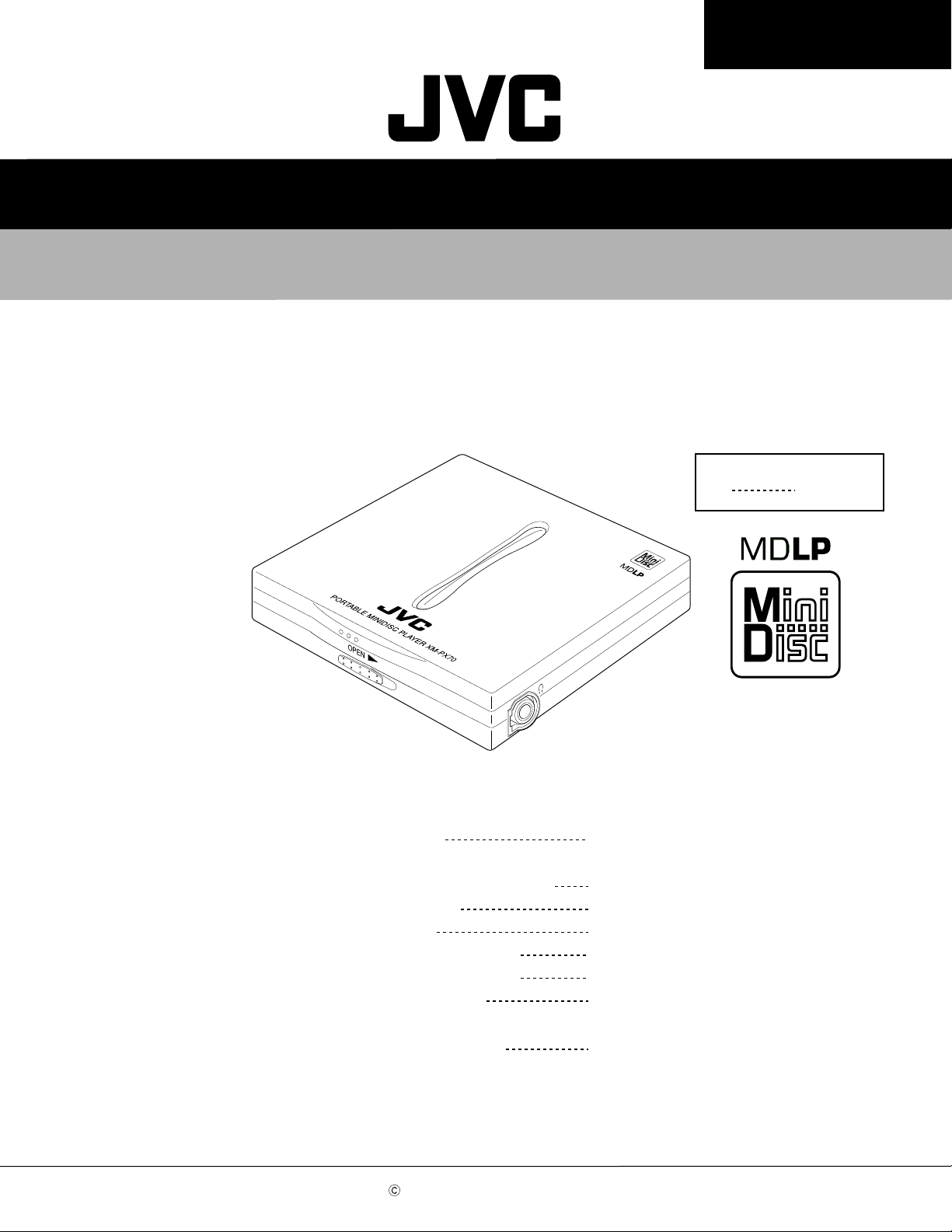
XM-PX70WT/BU/PN
SERVICE MANUAL
PORTABLE MINIDISC PLAYER
XM-PX70WT/BU/PN
UB Hong Kong
Area Suffix
Contents
Safety Precautions
Attention when
MD pick up is exchanged
Disassembly method
Adjustment method
Maintenance of laser pickup
Replacement of laser pickup
Description of major ICs
Attention when parts
are exchanged
COPYRIGHT 2001 VICTOR COMPANY OF JAPAN, LTD.
1-2
1-3
1-4
1-9
1-10
1-10
1-11
1-24
No.20897
Jan. 2001
Page 2
XM-PX70WT/BU/PN
1. This design of this product contains special hardware and many circuits and components specially
for safety purposes. For continued protection, no changes should be made to the original design
unless authorized in writing by the manufacturer. Replacement parts must be identical to those
used in the original circuits. Services should be performed by qualified personnel only.
2. Alterations of the design or circuitry of the product should not be made. Any design alterations of
the product should not be made. Any design alterations or additions will void the manufacturer`s
warranty and will further relieve the manufacture of responsibility for personal injury or property
damage resulting therefrom.
3. Many electrical and mechanical parts in the products have special safety-related characteristics.
These characteristics are often not evident from visual inspection nor can the protection afforded
by them necessarily be obtained by using replacement components rated for higher voltage,
wattage, etc. Replacement parts which have these special safety characteristics are identified in
the Parts List of Service Manual. Electrical components having such features are identified by
shading on the schematics and by ( ) on the Parts List in the Service Manual. The use of a
substitute replacement which does not have the same safety characteristics as the recommended
replacement parts shown in the Parts List of Service Manual may create shock, fire, or other
hazards.
4. The leads in the products are routed and dressed with ties, clamps, tubings, barriers and the
like to be separated from live parts, high temperature parts, moving parts and/or sharp edges
for the prevention of electric shock and fire hazard. When service is required, the original lead
routing and dress should be observed, and it should be confirmed that they have been returned
to normal, after re-assembling.
5. Leakage currnet check (Electrical shock hazard testing)
After re-assembling the product, always perform an isolation check on the exposed metal parts
of the product (antenna terminals, knobs, metal cabinet, screw heads, headphone jack, control
shafts, etc.) to be sure the product is safe to operate without danger of electrical shock.
Do not use a line isolation transformer during this check.
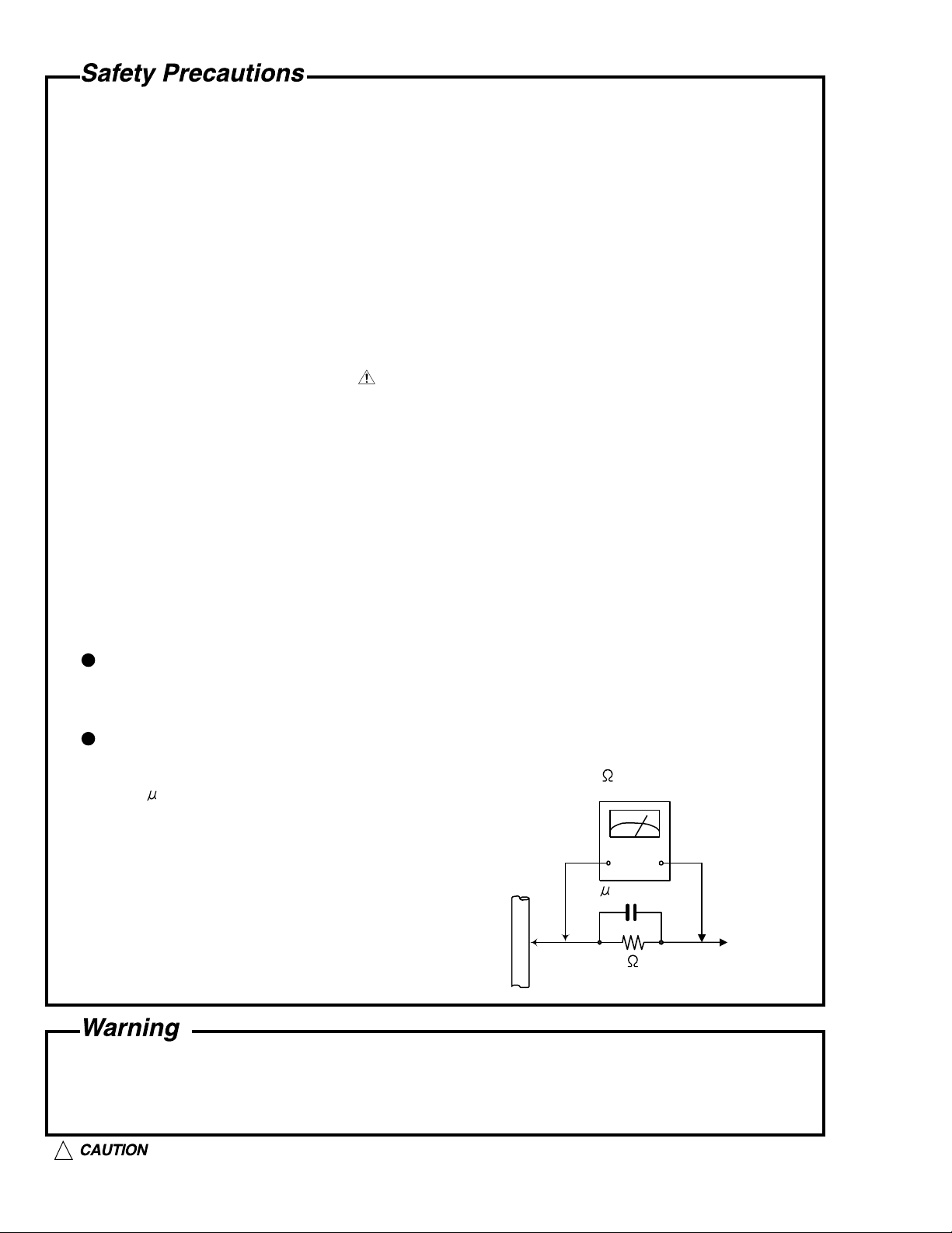
Plug the AC line cord directly into the AC outlet. Using a "Leakage Current Tester", measure
the leakage current from each exposed metal parts of the cabinet , particularly any exposed
metal part having a return path to the chassis, to a known good earth ground. Any leakage
current must not exceed 0.5mA AC (r.m.s.)
Alternate check method
Plug the AC line cord directly into the AC outlet. Use an AC voltmeter having, 1,000 ohms
per volt or more sensitivity in the following manner. Connect a 1,500 10W resistor paralleled by
a 0.15 F AC-type capacitor between an exposed
metal part and a known good earth ground.
Measure the AC voltage across the resistor with the
AC voltmeter.
AC VOLTMETER
(Having 1000
ohms/volts,
or more sensitivity)
Move the resistor connection to eachexposed metal
part, particularly any exposed metal part having a
return path to the chassis, and meausre the AC
voltage across the resistor. Now, reverse the plug in
the AC outlet and repeat each measurement. voltage
measured Any must not exceed 0.75 V AC (r.m.s.).
0.15 F AC TYPE
1500 10W
Place this
probe on
each exposed
metal part.
This corresponds to 0.5 mA AC (r.m.s.).
Good earth ground
1. This equipment has been designed and manufactured to meet international safety standards.
2. It is the legal responsibility of the repairer to ensure that these safety standards are maintained.
3. Repairs must be made in accordance with the relevant safety standards.
4. It is essential that safety critical components are replaced by approved parts.
5. If mains voltage selector is provided, check setting for local voltage.
!
Burrs formed during molding may be left over on some parts of the chassis. Therefore,
pay attention to such burrs in the case of preforming repair of this system.
1-2
Page 3
XM-PX70WT/BU/PN
Attention when MD pickup is exchanged
1. About the static electricity protection measures
The laser diode in the traverse unit (optical pick up) is easy to be destroyed by clothes and the human body
to the electrified static electricity.
Please note the explosion by static electricity when repairing.
2. About the earth processing for the electrostatic destruction prevention
In the equipment which uses an optical pick up (laser diode), an optical pick up is destroyed by the static
electricity of the work environment.
Please do the earth processing and work.
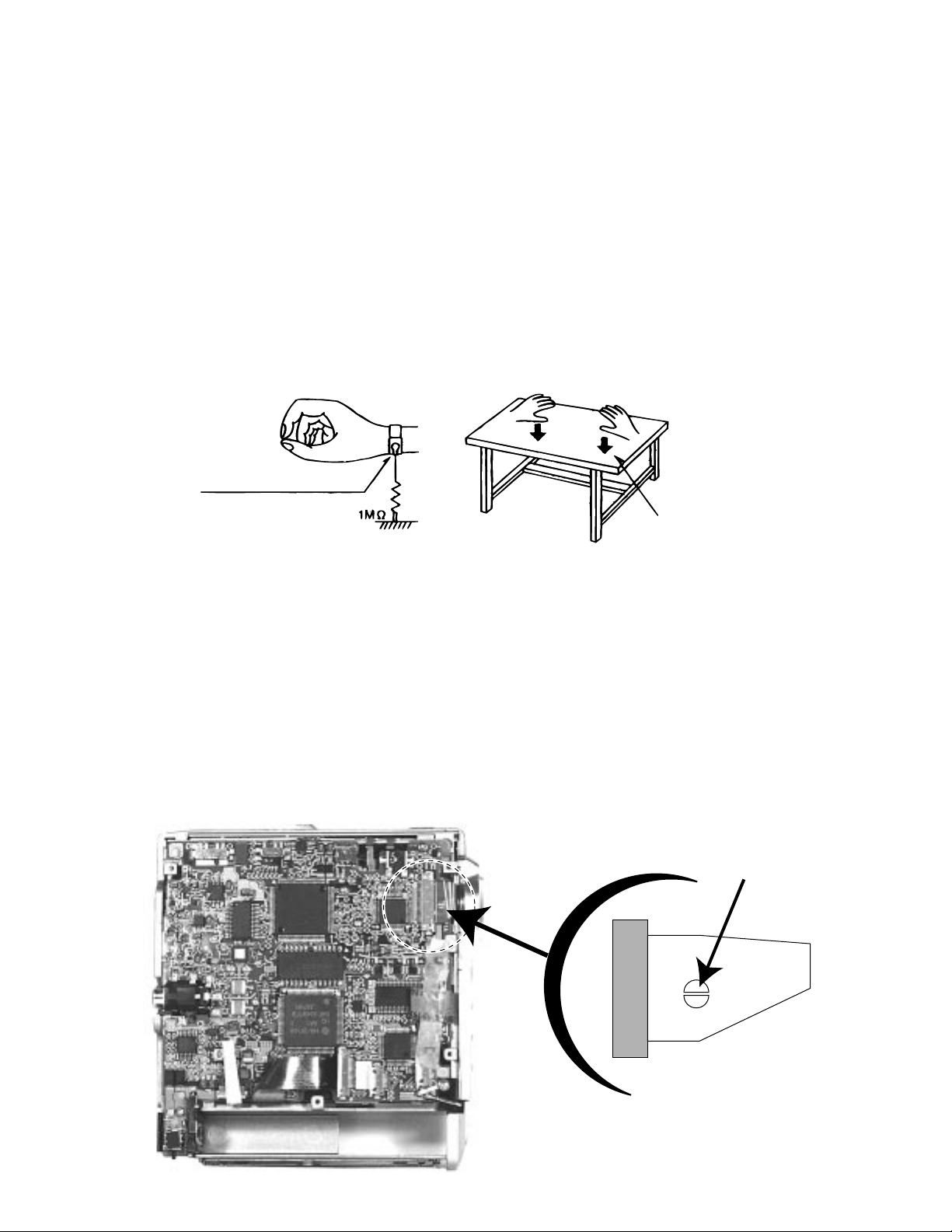
1) Earth of work stand
Please pull the conductive material (conductive sheet) or the iron plate to the depository
place of the traverse unit (optical pick up), and take the earth to ground.
2) Human body earth
Please use the anti-static wrist strap to exhaust the electrified static electricity to the human body.
anti-static wrist strap
Conductive material (conductive
sheet) or the iron plate
3. Handling the optical pick up
1) Please return according to a correct procedure based on short processing after exchanging
parts.
2) Do not use a tester to check the condition of the laser diode in the optical pick up .The tester 's internal
power source can easily destroy the laser diode.
4. Attention when unit is disassembled
Please refer to "Disassembling method" for how to detach .
1) Please be sure to solder before a flexible wire is removed from connector on a main printed
circuit board as shown.
if you removes without soldering.the MD picking up assembly might destroy
2) When installing , solder in the part of short round should be removed after a flexible wire is connected with
connector.
Solder short
1-3
Page 4
XM-PX70WT/BU/PN
Disassembly method
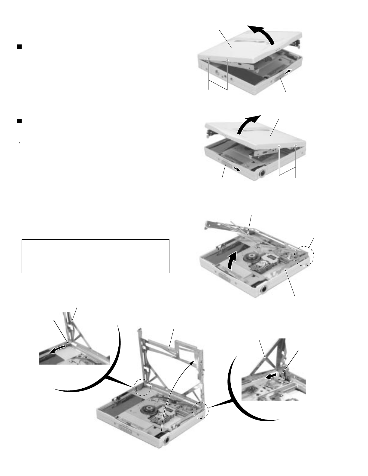
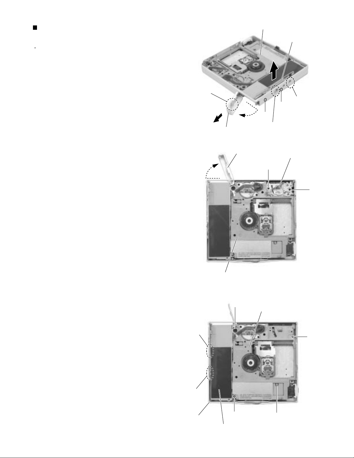
Removing the MD door assembly
(See Fig.1 and 2)
1.
Shift the door lever to open the door.
2.
Remove the four screws A and detach the MD
assembly from the main body.
Removing the holder assembly
(See Fig.3 and 4)
Prior to performing the following procedure, remove
the MD door assembly.
1.
Turn the holder assembly as shown in Fig.3.
2.
Pull the side arm (L) marked a and
Open the holder assembly as
3.
Move the marked b in the direction of the arrow and
release it from the shaft.
shown in Fig.4.
remove outward.
door
MD door assembly
A
Door lever
Holder assembly
Door lever
Fig.1
MD door assembly
A
Fig.2
4.
Move the part c inward and pull out the holder
assembly from the shaft.
ATTENTION:
“U-shaped” notch
When reassembling, first reattach the
part c to the shaft of the chassis
assembly. And next, fit the “U-shaped”
notch to the shaft.
Holder assembly
Part b
Part a
Side arm (L)
Fig.3
Holder assembly
Holder assembly
Part c shaft
1-4
Part c
Fig.4
Page 5
XM-PX70WT/BU/PN
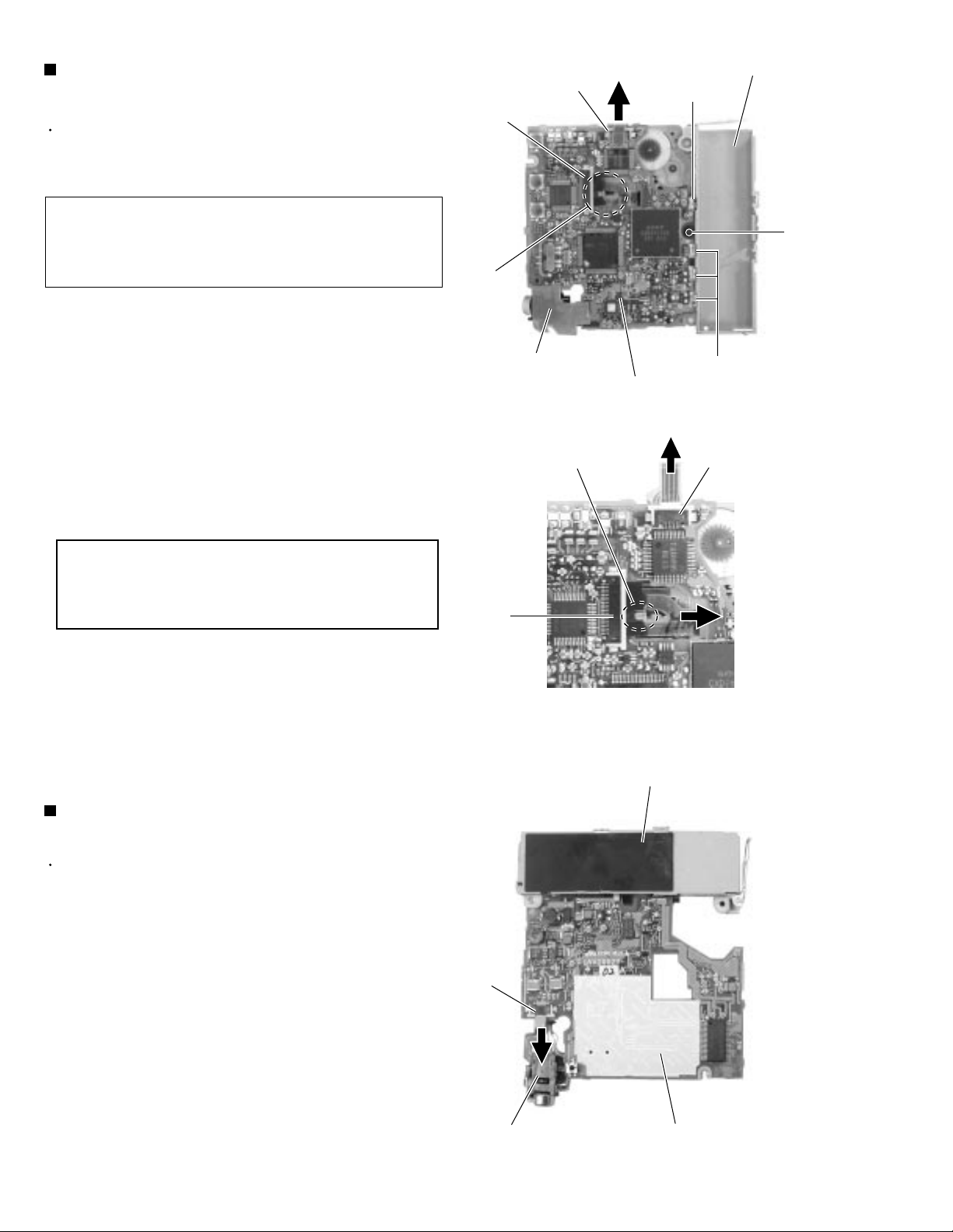
Removing the chassis assembly
(See Fig.5 to 7)
Prior to performing the following procedure, remove
the MD door assembly and the holder assembly.
1.
Open the battery lid. Release the tab d and pull out
the battery lid.
2.
Remove the screw B and pull out the side arm (R)
upward.
3.
Remove the two screws C and pull out the eject unit.
4.
Remove the screw D, E, F, G and H attaching the
chassis assembly respectively.
5.
Disengage the three joints e of the bottom case and
the battery holder. Remove the chassis assembly
and the jack cover at once.
Tab d
Battery lid
Battery lid
Chassis assembly
Side arm (R)
Joint e
D
B
Joint e
Fig.5
Eject unit
C
C
Chassis assembly
Joint e
Joint e
Bottom case
E
F
Battery holder
Fig.6
Chassis assembly
H
G
Fig.7
1-5
Page 6
XM-PX70WT/BU/PN
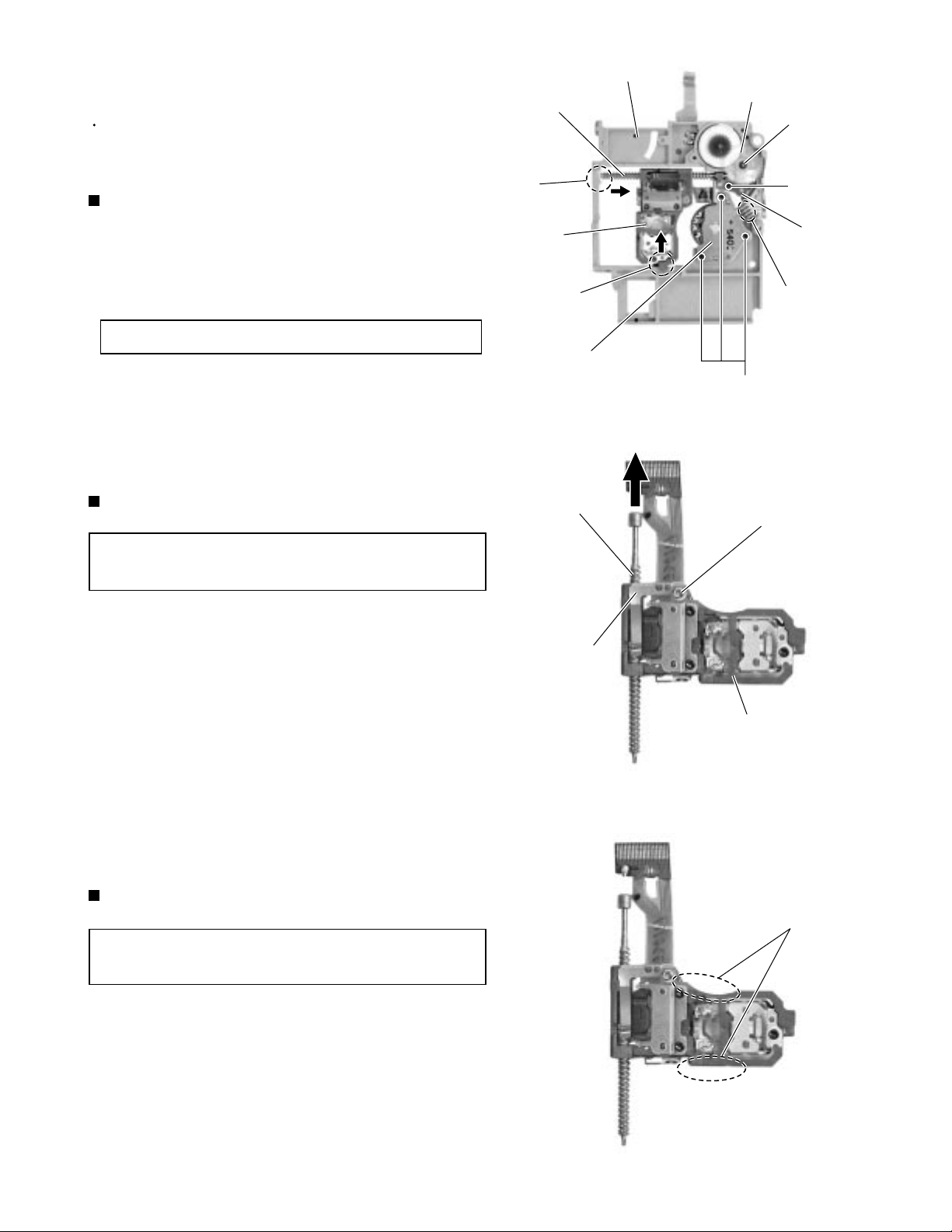
Removing the main board and the
battery holder (See Fig.8 and 9)
Prior to performing the following procedures, remove
the MD door assembly, the holder assembly and the
chassis assembly.
ATTENTION:
1.
Solder the short circuit round of the flexible wire on
the main board.
2.
Disconnect the flexible wires from connector CN301
and CN401 on the main board.
3.
Remove the one screw I attaching the main board.
Remove the main board with the battery holder .
4.
Unsolder the four soldered parts f retaining the main
board and the battery holder.
Before disconnecting the flexible wire
extending from the pickup, make sure to
solder the short circuit round to prevent
damage to the pickup.
CN401
CN301
Short circuit
round
Headphone jack assembly
Short circuit round
Battery holder
Soldering f
I
Soldering f
Main board
Fig.8
CN401
ATTENTION:
When reassembling, connect the
flexible wire extending from the pickup
to the connector on the main board
and unsolder the short circuit round.
Removing the headphone jack assembly
(See Fig.10)
Prior to performing the following procedures, remove
the MD door assembly, the holder assembly, chassis
assembly and the main board.
1.
Disconnect the flexible wire extending from the
headphone jack from connector CN601 on the main
board.
CN301
Fig.9
Battery holder
CN601
1-6
Headphone jack assembly
Main board
Fig.10
Page 7
XM-PX70WT/BU/PN
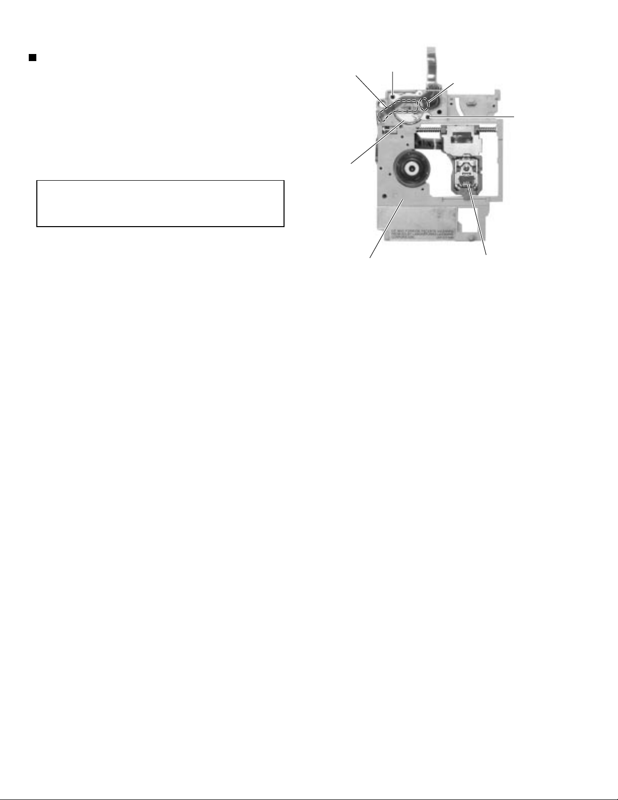
<Removal of the MD
mechanism section>
Prior to performing the following procedures, remove
the MD door assembly, the holder assembly, the
chassis assembly and the main board.
Removing the spindle motor
(See Fig.11)
1.
Unsolder the part g on the flexible wire extending
from the underside of the chassis assembly to the
spindle motor.
ATTENTION:
2.
Remove the three screws J attaching the spindle
motor.
Removing the pickup unit (See Fig.11)
Do not spill flux on the gear and others.
Lead screw
Part i
Pickup unit
Part h
Spindle motor
Lead screw
Chassis assembly
Worm gear
Slit washer
K
Shaft holder
Part g
J
Fig.11
L
ATTENTION:
1.
Remove the slit washer and the worm gear from the
underside of the chassis assembly.
2.
Remove the screw K attaching the shaft holder and
draw out the shaft (lead screw).
3.
Pull out the pickup unit and the lead screw while
disengaging the part h and i.
When handling the pickup unit, touch the
parts marked in Fig.13 only.
Removing the pickup (See Fig.12 and 13)
ATTENTION:
When handling the pickup unit, touch the
parts marked in Fig.13 only.
Lead spring
Pickup
Fig.12
Touch these parts only.
1.
Remove the screw L and the lead spring.
2.
Pull out the shaft from the pickup.
Fig.13
1-7
Page 8
XM-PX70WT/BU/PN
Removing the feed motor (See Fig.14)
1.
Peel off the adhesive tape j on the flexible wire on
the underside of the feed motor.
2.
Unsolder soldering k connecting the flexible wire to
the feed motor.
3.
Remove the two screws M attaching the feed motor.
ATTENTION:
When reassembling, reattach the
flexible wire with an adhesive tape and
solder.
j
Feed motor
Chassis assembly
M
Soldering k
M
Pickup unit
Fig.14
1-8
Page 9

XM-PX70WT/BU/PN
Adjustment method
This model is auto adjustment by Remote Controller.
Please adjust the attached remote controller.
Equipments----- 1. Remote controller 2. DC power supply
3. Laser power meter 4. MO disc (AU-1)
5. Pre master disc (TGYS 1)
<Test mode setting method>
Press < PLAY MODE + DISPLAY + BASS > and < PLAY >key together more than 3sec. at power off condition.
< VOL > next item .< VOL+ >before item.
LCD indication
0. TMD-V2
Test mode setting OK. Indicate at 2sec.
When LCD indicate [NG] at another item,
Return back this item by press (STOP) key
Resume initialize
LCD Indication change :
* Initializing
*
Servo initialize
LCD Indication change : [ ]
PLAY LASER Insert the laser power meter.
Executes by < BASS > LCD Indication change :[XX:YY]
Up by < VOL+> .Down by <VOL > LCD Indication change :[VW.YY]
Setting by <STOP> LCD Indication change :[ OK ]
Laser power adjust 560 adjust
Adjust power-supply voltage 1.5v 20mv before the laser power is adjusted and stops.
Resume
Initializing
Servo
PLAY LASER
5. M o T G
7.
FEED
Executes by < BASS >
<VOL+> :Pickup is go to outside
Press < STOP >
MO TG Insert the Recordable disc.
Executes by < BASS >
LCD Indication change : [ ]
MO DISC ADJUST
Executes by < BASS >
LCD Indication change : [ ]
*
Press < STOP >
LCD Indication change : [OK
Pre TG Insert the Pre master disc.
Executes by < BASS >
LCD Indication change : [ ]
Pre DISC ADJUST
Executes by < BASS >
LCD Indication change : [
Press < STOP >
RESET
Executes by < BASS >
LCD Indication :
*
*
Left out the test mode ,power off ,and END.
LCD Indication change :[FwdBwd]
< VOL-> :Pickup is go to inside
LCD Indication change :[OK ]
*
*
Adjusting
]
*
Adjusting
Adjusting
Adjusting
MO DISC ADJUST
XXYYZZ
FEED
]
1-9
Page 10

XM-PX70WT/BU/PN
Maintenance of laser pickup
(1) Cleaning the pick up lens
Before you replace the pick up, please try to
clean the lens with a alcohol soaked cotton
swab.
(2) Life of the laser diode
When the life of the laser diode has expired,
the following symptoms will appear.
1. The level of RF output (EFM output:ampli
tude of eye pattern) will below.
Is the level of
RFOUT under
0.35Vp-p?
YES
O.K
NO
Replace it.
Replacement of laser pickup
Turn off the power switch and,disconnect the
power cord from the ac outlet.
Replace the pickup with a normal one.(Refer
to "Pickup Removal" on the previous page)
Plug the power cord in,and turn the power on.
At this time,check that the laser emits for
about 3seconds and the objective lens moves
up and down.
Note: Do not observe the laser beam directly.
Play a disc.
Check the eye-pattern at TP1.
Finish.
(3) Semi-fixed resistor on the APC PC board The semi-fixed resistor on the APC printed circuit board which is
attached to the pickup is used to adjust the laser power.Since this adjustment should be performed to match the
characteristics of the whole optical block, do not touch the semi-fixed resistor.
If the laser power is lower than the specified value,the laser diode is almost worn out, and the laser pickup should
be replaced.
If the semi-fixed resistor is adjusted while the pickup is functioning normally,the laser pickup may be damaged
due to excessive current.
1-10
Page 11

Description of major ICs
JCV8002-W (IC601) : Head phone amp
1. Pin layout
24 ~ 19
1
XM-PX70WT/BU/PN
18
2. Block diagram
3. Pin function
Pin
Symbol
no.
CC2
1
V
2
OUT
3
PWR GND
4
OUT
5
DET
6
AGC IN
7
BST OUT
8
BST NF
9
LPF
10
BST NF
11
ADD IN
12
V
ref
13
V IN
ref
14
GND
15
BEEP IN
16
BST SW
17
MT SW
18
PW SW
19
MT TC
20
V
CC1 CC
21
IN
22
IN
23
BEEP OUT
BEEP OUT
24
V
Power amplifier output
A
GND in power amplifier output steps
Power amplifier output
B
Smoothness of level detection of boost
BST amplifier input signal level variable control by input lever to boost AGC input terminal
Output terminal of BST amplifier2
2
Terminal NF of BST amplifier2
Output BST amplifier1
2
NF of BST amplifier1
1
ADD amplifier input
Standard potential circuit
Standard potential circuit
Power part input steps GND
Beep input terminal
Beep output terminal
Mute switch
Power On/OFF switch
Mute smoothing Power mute switch
Main parts V
Power amplifier input
B
Power amplifier input
A
Beep output terminal
B
Beep output terminal
A
~
6
7 ~ 12
PW
SW
18
MT
TC
PW
19
SW
V
CC1
20
IN
B
21
IN
A
22
BEEP
OUT
B
23
BEEP
OUT
A
24
V
CC2
1
FUNCTION
(+B) in power amplifier output steps
CC2
CUT
MT
SW
~
13
BST2
BST
AGC
Vref
IN
AGC
IN
13
Vref
6
Vref
ADD
IN
BST
OUT
12
11
10
BST
NF1
9
LPF
2
8
BST
NF
2
7
BST
SW
PWR
GND
16
BST
SW
3
BEEP
IN
PW
B
OUT
15
BEEP
B
4
GND
DET
14
BST1
5
17
MT
SW
PW
A
A
2
AGC
1-11
Page 12

XM-PX70WT/BU/PN
CXA2588R (IC300) : RF amp.
1. Pin layout & block diagram
BOTM
ABCDFEAUX
36 35 34 33 32 29 28 26
ADFG
ADAGC
ADIN
ADFMSECSLEDTEWBLADJ
31 30 27 25
PEAK 37
RF 38
RFAGC 39
AGCI 40
NC 41
NC 42
ADDC 43
NC 44
TEGC 45
RFO 46
MORFI 47
MORFO 48
2.Pin function
Pin
No.
1
2
3
4
5
6
7
8
9
10
11
12
13
14
15
16
17
18
19
20
21
22
23
24
Symbol
APCREF
OPOUT
SWDT
XSTBY
F0CNT
EQADJ
3TADJ
I/O
I
J
VC
A
B
C
D
E
F
PD
APC
GND
OPIN
SCLK
XLAT
VREF
I/O
I/O
Vcc
AGC,EQ
Peak,Bottom Detector
0/-2dB
RF Amp
123456789101112
I
J
Function
I-V converted RF signal I input
I
I-V converted RF signal J input
I
Vcc/2 voltage output
O
A current input for main beam servo signal
I
B current input for main beam servo signal
I
C current input for main beam servo signal
I
D current input for main beam servo signal
I
E current input for side beam servo signal
I
F current input for side beam servo signal
I
Reflection light q'ty monitor signal input
I
Laser APC output
O
Ref. voltage input for laser power intensity setting
I
Ground
-
Ope. amp output terminal
O
21dB ope. amp input terminal
I
Serial data input terminal
I
Shift clock input terminal
I
Latch input terminal
I
Stand by setting terminal
I
F0 count setting terminal
I
Reference voltage output terminal
O
EQ IF setting terminal
BPF3T IF setting terminal
Power supply
-
ADIP Amp
FE Amp
3T Detector
ABCD Amp
TE
SE
ADIN
AUX
FE
RF
NC
NC
NC
RFO
I-V
Amp
E
D
I/O
I/O
O
O
O
I
O
O
O
O
O
O
O
-
I
-
-
I/O
-
I
O
I
O
I-V Amp APC
A
B
25
26
27
28
29
30
31
32
33
34
35
36
37
38
39
40
41
42
43
44
45
46
47
48
Pin
No.
C
Symbol
WBLADJ
CSLED
ADFM
ADAGC
ADFG
ABCD
BOTM
PEAK
RFAGC
AGCI
ADDC
TEGC
MORFI
MORFO
VC
TE/SE Amp
24 Vcc
23 3TADJ
22 EQADJ
21 VREF
20 F0CNT
19 XSTBY
18 XLAT
CPU
Command
I/F
OP
Amp
F
PD
APC
APCREF
Function
BPF3T IF setting terminal
Tracking error signal output terminal
Sled error signal LPF capacitor connect terminal
Sled error signal output terminal
ADIP FM signal output terminal
ADIP signal completer input terminal
ADIP AGC capacitor connect terminal
ADIP binary signal output
I3 output/temp.signal output
Focus error signal output
Reflection light q'ty signal output for main beam servo detector
RF/ABCD bottom-hold signal output
RF/ABCD peak-hold signal output
RF equalizer output
RFAGC capacitor connection
RFAGC input
Non connect
Non connect
ADIP amp. feedback circuit capacitor connection
Non connection
TE amp. gain switching
RF amp. output
Groove RF signal AC-coupled input
Groove RF signal output
17 SCLK
16 SWDT
15 OP IN
14 OP OUT
13 GND
1-12
Page 13

CXA8059Q (IC450) : Motor driver
1. Pin layout
25
37
36
~
XM-PX70WT/BU/PN
24
2. Block diagram
~
48
CPC3
1
VSWFVFUFCOMFCPOUT
CP3
~
13
~
UIN
12
VIN
Voltage
Driver
WIN
COM
UOUT
VOUT
WOUT
Sample
and Hard
GNDPGNDFG2FGSLOPE
CPC2
CP2
CPC1
CP1VCO
RMAX
RMINVCOINVCC
Charge Pump
VCO
Phase
Comparator
Timing
controllor
MCLOCK
1/8
CLKSEL
S/S
Sensoeless Logic
PWM
F/R
Controllor
BRAKE
Full Wave
Rectifilter
VCREF
VCONT
OSC CLOCK RESET FC CF RF
1-13
Page 14

XM-PX70WT/BU/PN
3.
Pin function
Pin
Symbol Function
no.
1
2
3
4
CPOUT
5
6
7
8
9
10
11
12
13
BRAKE
14
VCONT
15
VCREF
16
17
18
19
20
21
22
23
24
CLKSEL
25
26
SLOPE
27
CLOCK
28
29
30
31
32
33
34
MCLOCK
35
36
RESET
37
38
39
40
41
42
43
44
45
46
47
48
PGND
COM
VS
CPC3
CP3
CPC2
CP2
CPC1
CP1
GND
S/S
FC
CF
FG
FG2
VCO
RMAX
RMIN
VCOIN
OSC
GND
WF
VF
UF
COMF
VCC
VS
RF
NC
NC
WIN
WOUT
VIN
VOUT
UIN
UOUT
NC
NC
RF
The GND to guard the power stage.
The terminal to detect the voltage.
The terminal to supply the voltage for the power stage.
The terminal to connect the capacitor in the final charge pump.
The terminal to connect the capacitor in the third charge pump.
The terminal to connect the capacitor in the third charge pump.
The terminal to connect the capacitor in the second charge pump.
The terminal to connect the capacitor in the second charge pump.
The terminal to connect the capacitor in the first charge pump.
The terminal to connect the capacitor in the first charge pump.
The GND for the part except the power section.
The terminal for start and stop.
The terminal for braking.
The terminal for controlling velocity.
The terminal as referable voltage of controlling velocity.
The terminal to compensate the frequency characteristics of the loop controlling velocity.
The terminal of sampling and holding for detecting motor current.
The terminal to output FG pulse.
The terminal to output FG pulse divided Pin15 signal by 2.
The terminal to set oscillation frequency of VCO.
The terminal to set maximum oscillation frequency of VCO.
The terminal to set minimum oscillation frequency of VCO.
The terminal to control oscillation frequency of VCO.
The terminal to select inside and outside clock.
The terminal to oscillation sawtooth for PWM signal.
The terminal to oscillation sawtooth for soft-switching signal.
The terminal to monitor CLOCK signal.
The GND for the part except the power section.
The terminal to shape waveform of motor voltage.
The terminal to shape waveform of motor voltage.
The terminal to shape waveform of motor voltage.
The terminal to shape waveform of motor voltage.
The terminal to supply the voltage except the power section.
The terminal to input clock.
The terminal to supply the voltage for the power stage.
The terminal to reset a register for checking the movement.
The terminal to monitor current.
Non connect
Non connect
The terminal to sense the back electro magnetic force of coils.
The terminal to supply the motor current.
The terminal to sense the back electro magnetic force of coils.
The terminal to supply the motor current.
The terminal to sense the back electro magnetic force of coils.
The terminal to supply the motor current.
Non connect
Non connect
The terminal to monitor current.
1-14
Page 15

CXD2672GA(IC351):DSP
1.Pin layout
XM-PX70WT/BU/PN
17
16
TFDR TRDR
15
FRDR FFDR VDC4
14
VSC4
13
12
11
10
9
8
7
SRDR
SPFD SPRD
TEST1 FGIN
TEST2
TST2 EFM0
VSI03
SPCU SPDW SPDV
TST4 SPCW SPCV
LDDR
DTRF VSI02 ADFG ADRB AVS2 ADI0 FE PEAK FILI
APCR CKRF FOCN APC SE ADRT VC ABCD
XLRF VDI02 DCHG TE AVD2 AUX1
FS4
SFDR
TEST3
TST3
VDI03
TOP
VIEW
CLTV
PCO BIAS ASYO XWE TST6
BOTH
FILO RFI AVD1 MVCI
AVS1
ASYI
DVSS1
PD0
DVDD1
VDC3
D1
A09
A07
DVI01
A05 A01
A03
A11
XOE
D3
VSC3
D2
D0
XCAS IXWE
IXOE
XRAS
A08
A10
A00
VSI01
A06
A02
A04
VSC5 SLDW SLDV
6
SLCV SLCU VDC5
5
BYPS TST5
4
MNT1
3
MNT0
2
1
SLCW
VDC0
MNT2 SWDT
MNT3
SCLK
SENS XRST
SRDT
SQSY XINT OSCI
VSCO DQSY TX
XLAT
RPWR
VDI
OSC
DVDD0
DVSS0
OSCO
DA
VDDLDAVDDR
AOUTL VREFL
DA
VSI
VSSLDAVSSR
OSC
VREFR TST1
AOUTR XTSL DOUT
VSC1 DIN1
F256
XBCK
DADT LRCK
VDC2
VDI00
TST8
VDC1 TST0 DATAI TST7
MT
MT
FLGR
FLGL
VSI00
DA
PWMLP
ABCDEFG JH KLMNPRTU
2.Pin function (1)
Pin
Symbol
No.
A-1
A-2
A-3
B-1
B-2
B-3
C-1
C-2
C-3
D-1
D-2
D-3
NC
NC
MNT1
NC
NC
MNT0
MNT3
MNT2
NC
SCLK
SWDT
VDC0
I/O Function
-
Open
-
Open
O
Monitor output
-
Open
-
Open
I/O
Monitor in/output
O
Monitor output
O
Monitor output
-
Open
I
Micon serial bus clock input
I
Micon serial bus data write input
-
Internal logic VDD(1.8V)
VSC2
ADDT
DA
PWMRP
DA
PWMLN
1-15
Page 16

XM-PX70WT/BU/PN
2.Pin function(2)
Pin No.
E-1
E-2
E-3
F-1
F-2
F-3
G-1
G-2
G-3
H-1
H-2
H-3
K-1
K-2
K-3
L-1
L-2
L-3
M-1
M-2
M-3
N-1
N-2
N-3
P-1
P-2
P-3
U-1
R-1
U-2
R-2
U-3
R-3
U-4
R-4
U-5
R-5
U-6
R-6
U-7
R-7
U-8
R-8
Symbol I/O Function
XLAT
SRDT
SENS
VSC0
SQSY
XRST
DQSY
XINT
RPWR
TX
OSCI
VDIOSC
J-1
J-2
J-3
T- 1
T- 2
T- 3
T- 4
T- 5
T- 6
T- 7
T- 8
OSCO
DVSS0
DVDD0
VSIOSC
AOUTL
DAVDDL
DAVSSL
VREFL
DAVDDR
DAVSSR
AOUTR
VREFR
VSC1
XTSL
TST1
DIN1
DOUT
VDC1
DAPWMLN
DAPWMLP
VSIO0
DAPWMRP
MTFLGR
MTFLGL
TST7
DATA I
TST0
ADDT
TST8
VDIO0
LRCK
DADT
VDC2
VSC2
XBCK
F256
A02
A04
A03
A06
A01
A05
I
Micon serial bus latch input
O
Micon serial bus data read out output
O
Internal output of micon serial bus address
-
Internal logic GND
O
PTGR=0 ADIPsink output / PTGR=1 DISC SUB-Q sink output
I
Reset input L:reset
O
Ubit SUB-Q sink output from digital audio input from MD or CD
O
Request status output L:request status
I
Laser power select input (H=rec power / L=playback power)
I
Output permit input of recorded data
I
X'tal osc circuit input
-
OSC sel VDD (2.5V)
O
X'tal osc circuit output
-
Internal 16bit DRAM GND
-
Internal 16bit DRAM GND
-
OSC sel GND
O
Internal DAC Lch output
-
Internal DAC VDD (Lch,2.5V)
-
Internal DAC GND
O
Internal DAC GND VREF(Lch)
-
Internal DAC VDD (Rch,2.5V)
-
Internal DAC GND (Rch)
O
Internal DAC Rch output
O
Internal DAC VREF (Rch)
-
Internal logic GND
I
X'tal frequency select (L=45.1584MHz/H=22.5792MHz)
I
Test terminal Connect to GND
I
Digital audio input Outer I/F mode EXRQ input
O
Digital audio output
-
Internal logic VDD (1.8V)
O
Internal DAC PWM output L-
O
Internal DAC PWM output L+
-
2.5V I/O VSS
O
Internal DAC PWM output R+
O
Internal DAC zero detect flag (Rch)
O
Internal DAC zero detect flag (Lch)
I
Test terminal Connect to GND
I
Serial data input
O
Open
I
Data input from A/D converter
I
Test terminal Connect to GND
-
2.5V I/O VDD
O
LR clock(44.1kHz) for A/D, internal DAC
O
Data output for internal DAC / Internal DAC PWM output R-
-
Internal logic VDD (1.8V)
-
Internal logic GND
O
A/D, internal DAC bit clock (2.8224MHz)
O
11.2896MHz clock output (X'tal)
O
External DRAM address output
O
External DRAM address output
O
External DRAM address output
O
External DRAM address output
O
External DRAM address output
O
External DRAM address output
1-16
Page 17

2.Pin function (3)
Pin No.
U-9
R-9
U-10
T-10
R-10
U-11
T-11
R-11
U-12
T-12
R-12
U-13
T-13
R-13
U-14
T-14
R-14
U-17
U-16
U-15
T-17
T-16
T-15
R-17
R-16
R-15
P-17
P-16
P-15
N-17
N-16
N-15
M-17
M-16
M-15
L-17
L-16
L-15
K-17
K-16
K-15
J-17
J-16
J-15
H-17
H-16
H-15
G-17
G-16
G-15
F-17
F-16
F-15
T- 9
Symbol
VSIO1
A00
ADIO1
A08
A10
A07
IXOE
XRAS
A09
IXWE
XCAS
D1
D2
D0
VDC3
VSC3
D3
DVDD1
NC
NC
XOE
NC
TST6
A11
DVSS1
XWE
PDO
ASYI
ASYO
MVCI
AVS1
BIAS
AVD1
FILI
PCO
RFI
PEAK
CLTV
FILO
FE
ABCD
BOTOM
ADIO
VC
AUX1
AVS2
ADRT
AVD2
ADRB
SE
TE
ADFG
APC
DCHG
I/O
-
2.5V I/O sel Vss
O
External DRAM address output
-
2.5V I/O sel VDD
O
External DRAM address output
O
External DRAM address output
O
External DRAM address output
O
Open
O
External DRAM RAS output
O
External DRAM address output
O
Open
O
External DRAM CAS output
I/O
External DRAM data input/output
I/O
External DRAM data input/output
I/O
External DRAM data input/output
-
Internal logic VDD
-
Internal logic GND
I/O
External DRAM data input/output
-
Internal 16Mbit DRAM VDD
-
Open
-
Open
O
External DRAM output chip enable output
-
Open
O
Open
O
Open
-
Internal 16Mbit DRAM GND
O
External DRAM write enable output
O
Analog PLL phase compare output
I
Playback EFM comparator slice level input
O
Playback EFM binarization signal output
I
Clock input from external VCO
-
Analog GND
I
Playback EFM comparator bias current input
O
Analog power supply (2.5V)
I
Filter input for playback EFM system mastering PLL
I
Phase comparison output for playback EFM system mastering PLL
I
Playback EFM RF signal input
O
Peak holding input optical amount signal
I
Internal VCO control voltage input for playback EFM system mastering PLL
I
Filter output for playback EFN system mastering PLL
I
Focus error signal input
O
Optical amount signal input
I
Bottom holding input of optical amount signal
I
Open
-
Middle point voltage input
I
Assistance A/D input
-
Analog GND
I
A/D converter operation range upper bound voltage input
-
Analog power supply (2.5V)
I
A/D converter operation range lower bound voltage input
I
Sled error input
I
Tracking error input
I
ADIP binary-coded FM signal input
I
Error signal input for laser digital APC
I
Connects with an analog power supply of low impedance
Function
XM-PX70WT/BU/PN
1-17
Page 18

XM-PX70WT/BU/PN
2.Pin function (4)
Pin No.
E-17
E-16
E-15
D-17
D-16
D-15
A-17
B-17
C-17
A-16
B-16
C-16
A-15
B-15
C-15
A-14
B-14
C-14
A-13
B-13
C-13
A-12
B-12
C-12
A-11
B-11
C-11
A-10
B-10
C-10
A-9
B-9
C-9
A-8
B-8
C-8
A-7
B-7
C-7
A-6
B-6
C-6
A-5
B-5
C-5
A-4
B-4
C-4
Symbol I/O Function
VSIO2
F0CN
VDIO2
DTRF
CKRF
XLRF
NC
NC
LDDR
NC
NC
APCR
TFDR
TRDR
NC
FRDR
FFDR
VDC4
VSC4
SRDR
FS4
SPFD
SPRD
SFRD
TEST2
TEST1
FGIN
TST2
EFMO
TEST3
VSIO3
TST3
VDIO3
SPCU
SPDW
SPDV
TST4
SPCW
SPCV
VSC5
SLDW
SLDV
SLCV
SLCU
VDC5
BYPS
TST5
SLCW
-
2.5V I/O Vss
O
Filter cutoff control output
-
2.5V I/O VDD
O
Controller data output
O
Controller clock output
O
Controller latch output
-
Open
-
Open
O
Laser digital APC PWM output
-
Open
-
Open
O
Laser APC reference PWM output
O
Tracking servo drive PWM output (+)
O
Tracking servo drive PWM output (-)
-
Open
O
Focus servo drive PWM output (-)
O
Focus servo drive PWM output (+)
-
Internal logic VDD (1.8V)
-
Internal logic GND
O
Sled servo drive PWM output (-)
O
176.4kHz clock output (X'tal system)
O
Spindle servo drive output
O
Spindle servo drive output
O
Sled servo drive PWM output (+)
I
Test terminal Connect to GND
I
Test terminal Connect to GND
I
Spindle CAV servo FG input
O
Test terminal Open
O
EFM output at recording
I
Test terminal Connect to GND
-
2.5V I/O Vss
O
Test terminal Open
-
2.5V I/O VDD
I
Blush less spindle motor drive comparate input (U)
O
Blush less spindle motor 3 phase drive truth output (W)
O
Blush less spindle motor 3 phase drive truth output (V)
O
Test terminal Open
I
Blush less spindle motor drive comparete input (W)
I
Blush less spindle motor drive comparate input (V)
-
Internal logic GND
O
Blush less sled motor 3 phase drive truth output (W)
O
Blush less sled motor 3 phase drive truth output (V)
I
Blush less sled motor 3 phase drive comparate input (V)
I
Blush less sled motor 3 phase drive comparate input (U)
-
Internal logic VDD (1.8V)
O
Open
O
Test terminal Open
I/O
Blush less sled motor 3 phase drive comparate input
1-18
Page 19

AK93C55BH-W (IC502) : EEPROM
XM-PX70WT/BU/PN
1. Pin layout
CS
SK
DI
DO
1
2
3
4
3. Block diagram
DI
INSTRUCTION
REGISTER
8
7
6
5
INSTRUCTION
DECODE,
CONTROL
AND
CLOCK
GENERATION
VCC
NC
PE
GND
DATA
REGISTER
ADD.
BUFFER
2.Pin function
Pin name
CS
SK
DI
DO
PE
VCC
GND
NC
16
R/W AMPS
AUTO ERASE
DECODER
Fnction
Chip select
Serial data clock
Serial data input
Serial data output
Program enable
Ground
Power supply
Not connected
DO
16
AND
EEPROM
2048bit
128 X 16
CS
SK
PE
VREF
VPP SW
VPP
GENERATOR
1-19
Page 20

XM-PX70WT/BU/PN
IC-PST3421U-X(IC504):System reset
1.Pin layout 2.Pin function
VOUT 1
VDD 2
3.Block diagram
2
VDD
Vref
4
VSS
4 VSS
3 NC
Pin
No.
1
2
3
4
VOUT
VDD
NC
VSS
FunctionSymbol
Reset signal output terminal
Power supply terminal
Non connect
VSS terminal
1
VOUT
1-20
Page 21

MPC17A139MTB-X (IC400) : 4ch bridge driver
1.Pin layout 2.Pin function
Driver section
VGVCLG
3635343332313029282726252423222120
GND
VD3
FO3
PGND
RO3
VD3
VD4
RO4
PGND
FO4
VD4
RI3
FI3
FI4
RI4
19
PS,OE INPUT OUTPUT 1~4
PS
H
H
H
H
H
123456789
PS
OE
AGND
CLK
VD1
FO1
RO1
PGND
101112131415161718
VD1
VD2
RO2
PGND
FO2
VD2
RI1
FI1
FI2
RI2
L
X:Don't Care
Z:High Impedance
OE
L
L
L
L
H
X
FI
L
L
H
H
X
X
XM-PX70WT/BU/PN
RI
L
H
L
H
X
X
FO
L
L
H
L
L
Z
Clock detector section
CLK PS OSC circuit
X
X
RO
L
H
L
L
L
Z
H
H
L
Auto
Syncro
Stop
3.Block diagram
G
L
G
36 34
V
Vc
DC/DC
CLOCK
CLK
Vc
2
35
Vc
CLK
Converter
Detector
D1VD1
V
AGND
159
G
V
Vc
3
PS
Pre-driver
4
OE
O1
FO1R
6
8
Control
15
16
FI1
RI1
GND
R
7
33
GND
VD2VD2FO2R
14
G
V
Vc
10
Pre-driver
13
Control
17
FI2
O2
11
18
RI2
GNDVD3VD3
P
12
32
G
V
Vc
28
O3
FO3R
31
29
Pre-driver
Control
22
21
FI3
RI3
GNDVD4VD4
P
30
23
G
V
Vc
27
Pre-driver
O4
FO4R
24
26
Control
20
19
FI4
RI4
GND
P
25
1-21
Page 22

XM-PX70WT/BU/PN
UPD784225GK-617C(IC501):CPU
1.Pin layout
1 ~ 20
2.Pin function
Pin
Symbol
No.
1
ANI5
2
ANI6
3
SPSEL
4
AVSS
5
-
6
VADJ
7
AVREF1
8
RMRX
9
RMTX
10
11
12
13
14
15
16
17
18
19
20
21
22
23
24
25
26
27
28
29
30
31
32
33
34
35
36
37
38
39
40
-
SRDT
SWDT
SCLK
-
BEEP
PSW
MONDATA
MONCLK
XRST2
TG
ACB
TRAIN
XRST
XLAT
LVCTL
LDON
RFOFF
SLOFF
-
MUTE
-
DIR
VSS1
PS
SS
MON1
MON2
MONXLAT
-
-
80 ~ 61
60 ~ 41
21 ~ 40
Function
GND
GND
Non connect
GND
Non connect
Voltage adjust
Analog reference voltage
Remocon data input terminal
Remocon data output terminal
Non connect
Serial data read input terminal
Serial data write input terminal
Serial bus clock output terminal
Non connect
BEEP output terminal
Power ON/OFF output terminal
Test terminal
Test terminal
Standby setting output terminal
Tracking gain setting terminal
Non connect
Non connect
Reset signal output terminal
Serial bus latch output terminal
LSI power supply control signal output
Laser diode ON signal output terminal
RF OFF signal input terminal
Sled OFF signal output terminal
Non connect
Mute signal output terminal
Mon connect
Test terminal
GND
Standby mode output terminal
Start/Stop output terminal
Test terminal
Test terminal
Test terminal
Non connect
Non connect
Pin
No.
41
42
43
44
45
46
47
48
49
50
51
52
53
54
55
56
57
58
59
60
61
62
63
64
65
66
67
68
69
70
71
72
73
74
75
76
77
78
79
80
Symbol
-
-
-
-
DPON
-
RFVCTL
PSAVE
RPON
DPON
REMOFF
CS2
SCL
DI
CS1
MNT0
MNT3
SENS
DO
RESET
XINT
SQSY
-
RPLY
DOOR
PLAYKEY
VSS0
VDD1
X2
X1
VPP
XT2
XT1
VDD0
AVD0
KEY
BATTERY
TEMP
ANI3
ANI4
Function
Non connect
Non connect
Non connect
Test terminal
Test terminal
Non connect
Test terminal
Non connect
RP ON signal input terminal
DP ON signal input terminal
Remocon OFF signal output terminal
Chip select 2
Serial clock signal output terminal
Data output terminal
Chip select 1
Monitor 0 input terminal
Monitor 3 input terminal
DSP internal status input terminal
Data input terminal
Reset signal input terminal
Interrupt status data input terminal
Sink input terminal
Non connect
Remocon PLAY detect terminal
Door open/close detect terminal
PLAY key detect terminal
GND
Reference voltage terminal
Connect to X'tal osc
Connect to X'tal osc
Test terminal
Non connect
GND
GND
Reference voltage terminal
Remocon STOP key detect terminal
Battery voltage detect terminal
Connect to temp. detect
GND
GND
1-22
Page 23

XC6367B101M-X (IC901,IC921,IC941):Regulator
XM-PX70WT/BU/PN
1.Pin layout
54
123
3.Block diagram
FB
Error Amp.
2.Pin function
Pin No. Symbol
1
2
3
4
5
Phase
Compensation
FB
VDD
CE
GND
EXT
PWM
Comparator
Function
Output voltage setting
Power supply
Chip enable
GND
Ext. Tr connection
Buffer,
Driver
VDD
EXT
CE
Vref with
Soft Start,
CE
PWM/PFM
Controler
Ramp Wave
Generator,
OSC
GND
1-23
Page 24

XM-PX70WT/BU/PN
Attention when parts are exchanged
The 2 bottom case and 35 MD door assembly are indicated on
Exploded view of general assembly, there are two kind of parts at
same color.
When you exchange parts confirm the marking and change same parts.
Marking
Bottom case(Reverse side) Bottom case(Reverse side)
Marking
MD door assy(Reverse side) MD door assy(Reverse side)
1-24
Parts Number
Bottom case (BU) LV10423-002A LV10423-202A
Bottom case (PN) LV10423-003A LV10423-203A
MD door assy (BU) LV32219-002A LV32219-202A
MD door assy (PN) LV32219-003A LV32219-203A
WT is 1 kind of parts.
Marking non Marking have
Page 25

XM-PX70WT/BU/PN
VICTOR COMPANY OF JAPAN, LIMITED
AUDIO & COMMUNICATION BUSINESS DIVISION
PERSONAL & MOBILE NETWORK BUSINESS UNIT. 10-1,1chome,Ohwatari-machi,Maebashi-city,371-8543,Japan
(No.20897)
Printed in Japan
200101(O)
 Loading...