

Page 1
SERVICE MANUAL
PORTABLE MINIDISC PLAYER
XM-P55
XM-PJ1
XM-P55
XM-PJ1
Contents
B
E
EE
EN
J
UB
US
UT
UX
UY
5
5
P
-
M
X
OPEN
XM-P55
Area Suffix
(XM-P55 )
U.K. (BU,SL)
Continental Europe (BU,SL)
Russian Federation (BU,SL)
Northern Europe (BU,SL)
U.S.A. (SL)
Hong kong (BU,GN,SL)
Singapore (BU,SL)
Taiwan (SL)
Saudi Arabia (SL)
Argentina (SL)
B
E
EE
EN
J
UB
US
UT
UX
UY
XM-PJ1
Area Suffix
(XM-PJ1 )
U.K. (BU)
Continental Europe (BU)
Russian Federation (BU)
Northern Europe (BU)
U.S.A. (BU)
Hong kong (BU,GD)
Singapore (BU)
Taiwan (BU)
Saudi Arabia (BU)
Argentina (BU)
Safety Precautions
Instructions (For XM-P55&PJ1)
Description of Major ICs
Removal of Main Parts
Maintenance of MD Pickup
Procedures of Changing the MD Pickup
Self-diagnosis Function of MD
1-2
1-3~16
2-1
2-12
2-23
2-23
2-24
COPYRIGHT 1999 VICTOR COMPANY OF JAPAN, LTD.
Block Diagrams
Standard Schematic Diagrams (XM-P55)
Standard Schematic Diagrams (XM-PJ1)
Printed Circuit Boards
Parts List (XM-P55)
Parts List (XM-PJ1)
2-27
2-29
2-36
2-42,43
3-1~15
4-1~15
No.20738
Jan. 1999
Page 2

XM-P55
XM-PJ1
Safety Precaution
CAUTION
CAUTION
Burrs formed during molding may be left over on some parts of the chassis. Therefore,
pay attention to such burrs in the case of preforming repair of this system.
Please use enough caution not to see the beam directly or touch it in case of an
adjustment or operation check.
1-2 4-15
Page 3
Description of Major ICs
CXA2523AR(IC310):MD RF & Servo
1.Block Diagram
BOTM
ABCD34FE33AUX32ADFG31ADAGC30ADIN29ADFM28SE27CSLED26TE25WBLADJ
36 35
XM-P55
XM-PJ1
37
PEAK
38
RF
39RFAGC
40AGCI
41COMPO
42COMPP
43ADDC
44OPO
45OPN
46RFO
47MORFI
48
MORFO
2.Pin Function
AGC, EQ
Comp
USER
USER
OP Amp
RF Amp
1 2
I
ADIP Amp TE/SE Amp
MUX FE Amp
Peak, Bottom Detector
ABCD Amp
3T Detector
I-V Amp APC
3VC4A5B6C7D8E9F10PD11
J
CPU
Command I/F
TEMP Amp
12
APC
APCREF
24
Vcc
23
3TADJ
22 EQADJ
21 VREF
20 F0CNT
19 XSTBY
18 XLAT
17 SCLK
16 SWDT
15 TEMP R
14 TEMP I
13 GND
Pin No.
1
2
3
4
5
6
7
8
9
10
11
12
13
14
15
16
17
18
19
20
Symbol
I
J
VC
A
B
C
D
E
F
PD
APC
APCREF
GND
TEMPI
TEMP R
SWDT
SCLK
XLAT
XSTBY
F0CNT
I/O
I-V converted RF signal I input.
I
I-V converted RF signal J input.
I
Vcc/2 voltage output.
O
A current input for main beam servo signal.
I
B current input for main beam servo signal.
I
C current input for main beam servo signal.
I
D current input for main beam servo signal.
I
E current input for side beam servo signal.
I
F current input for side beam servo signal.
I
Reflection light quantity monitor signal input.
I
Laser APC output.
O
Reference voltage input for the laser power intensity setting.
I
Connect to GND.
Connects the temperature sensor.
I
Connects the temperature sensor. outputs the reference voltage.
I
Data input for microcomputer serial interface.
I
Shift clock input for microcomputer serial interface.
I
Latch signal input for microcomputer serial interface.Latched when low.
I
Standby setting pin. Normal operation when high Standby when low.
I
Internal current source setting pin.
I
Function
2-1
Page 4

XM-P55
XM-PJ1
Pin No.
21
22
23
24
25
26
27
28
29
30
31
32
33
34
35
36
37
38
39
40
41
42
43
44
45
46
47
48
Symbol
VREF
EQADJ
3TADJ
Vcc
WBLADJ
TE
CSLED
SE
ADFM
ADIN
ADAGC
ADFG
AUX
FE
ABCD
BOTM
PEAK
RF
RFAGC
AGCI
COMPO
COMPP
ADDC
OPO
OPN
RFO
MORFI
MORFO
I/O
Reference voltage output.
O
Equalizer center frequency setting pin.
I/O
BPF3T center frequency setting pin.
I/O
Power supply.
BPF22 center frequency setting pin.
I/O
Tracking error signal output.
O
Connects the sled error signal LPF capacitor.
Sled error signal output.
O
ADIP FM signal output.
O
ADIP signal comparator input.
I
Connects the ADIPAGC capacitor.
ADIP2 binary value signal output.
O
13 output / temperature signal output. Switched with serial commands.
O
Focus error signal output.
O
Reflection light quantity signal output for the main beam servo detector.
O
RF/ABCD bottom hold signal output.
O
Peak hold signal output for the RF/ABCD signals.
O
RF equalizer output.
O
Connects the RFAGC capacitor.
RFAGC input.
I
User comparator output.
O
User comparator non-inverted input.
I
Connects the capacitor for ADIP amplifier feedback circuit.
I/O
User operational amplifier output.
O
User operational amplifier inverted input.
I
RF amplifier output. Eye pattern checkpoint.
O
Input of the groove RF signal with AC coupling.
I
Groove RF signal output.
O
Function
2-2
Page 5
CXA8069M(IC450):Sensorless Motor Driver
1.Pin Layout
48 37
36
XM-P55
XM-PJ1
2.Block Diagram
VS
WF
VF
UF
COMF
CPOUT
CPC2
CP2
CPC1
CP1
VCO
RMAX
RMIN
12 1
13 24
Charge
Pump
VCO
25
UIN
VIN
Voltage Driver
WIN
+ -+ -+ -
Sensorless
Logic
COM
UOUT
Power Stage
Level Shifter
VOUT
WOUT
Sample
and Hold
PGND
RF
CF
GND
FC
FG2
FG
VCOIN
VCC
Phase
Comparator
Timing
Controllor
MCLOCK
1/8
S/S
PWM
F/R
BRAKE
Full Wave
Rectifier
Controllor
+ -
VCONT
RESET
CLOCK
SLOPE
OSC
VCREF
2-3
Page 6
XM-P55
XM-PJ1
Pin Functions
Pin
Pin Name Functions
No.
2-4
Non connection
Detection of motor current
Motor driven power supply
Non connection
Connect first condenser of charge pump to this terminal.
Connect first condenser of charge pump to this terminal.
Connect second condenser of charge pump to this terminal.
Connect second condenser of charge pump to this terminal.
Connect last condenser of charge pump / VG external input
Ground of circuits except for output section
Start / Stop
Brake
Speed control
Reference voltage of speed control
FG pulse output
FG pulse output when pin15 FG signal goes half round
Correction of frequency characteristic of speed control loop
Setting of VCO oscillation frequency
Setting of VCO maximum oscillation frequency
Setting of VCO minimum oscillation frequency
Forms motor waveform
Forms motor waveform
Forms motor waveform
Forms motor waveform
VCO oscillation frequency control
Monitors CLOCK signal
Ground of circuits except for output section
Sample board for output current detection
Forms saw-tooth wave for PWM wave formation
Forms santooth waveform for soft switching wave formation
Clock input
Power supply except for output section
Non connection
Motor driven power supply
Detection of motor current
Non connection
Reset for operation check
Detection of counter electromotive voltage
Motor source output
Non connection
Detection of counter electromotive voltage
Motor source output
Non connection
Non connection
Detection of counter electromotive voltage
Motor source output
Detection of motor common voltage
Ground for output guard
Page 7
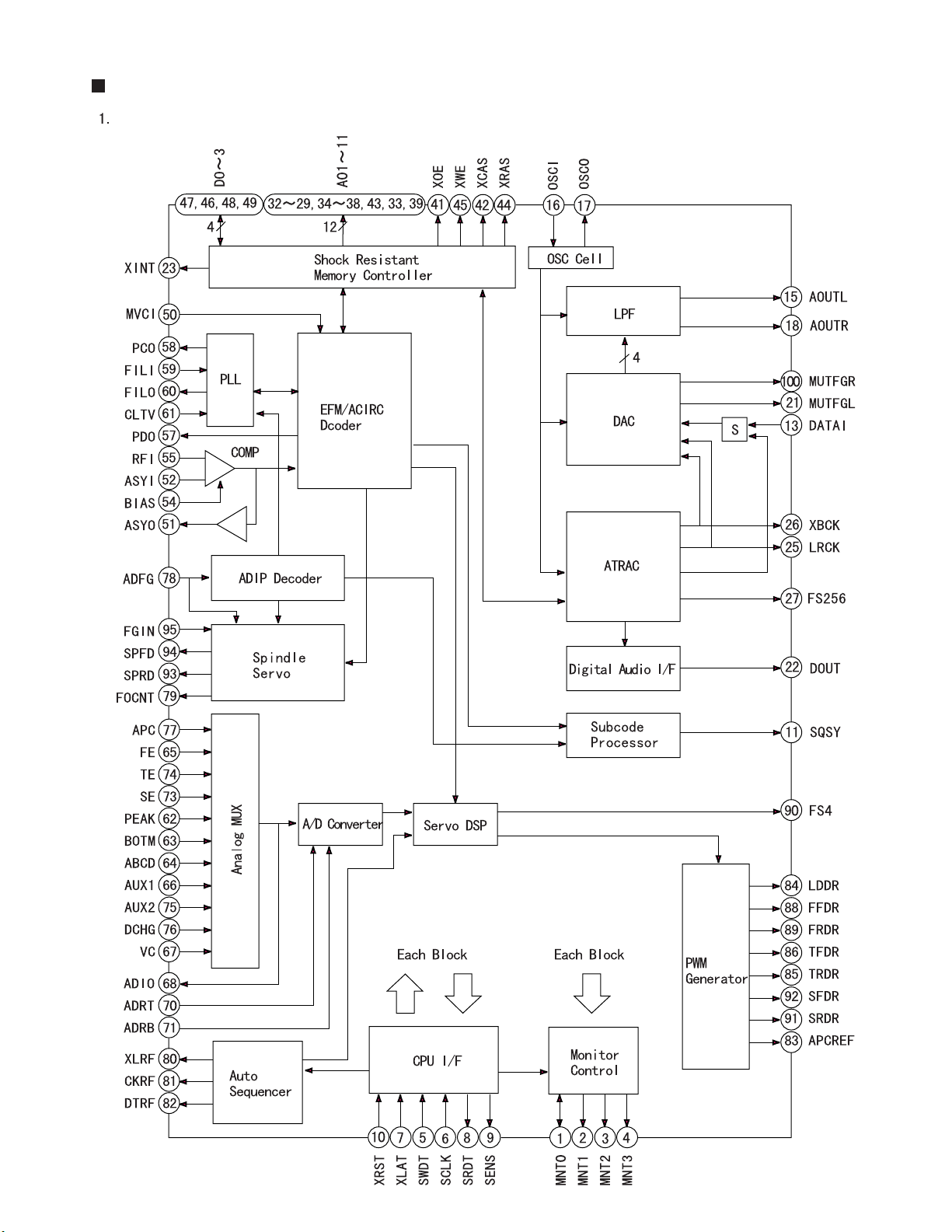
CXD2655R (IC351):Digital Servo Processor
Block Diagram
XM-P55
XM-PJ1
2-5
Page 8
XM-P55
XM-PJ1
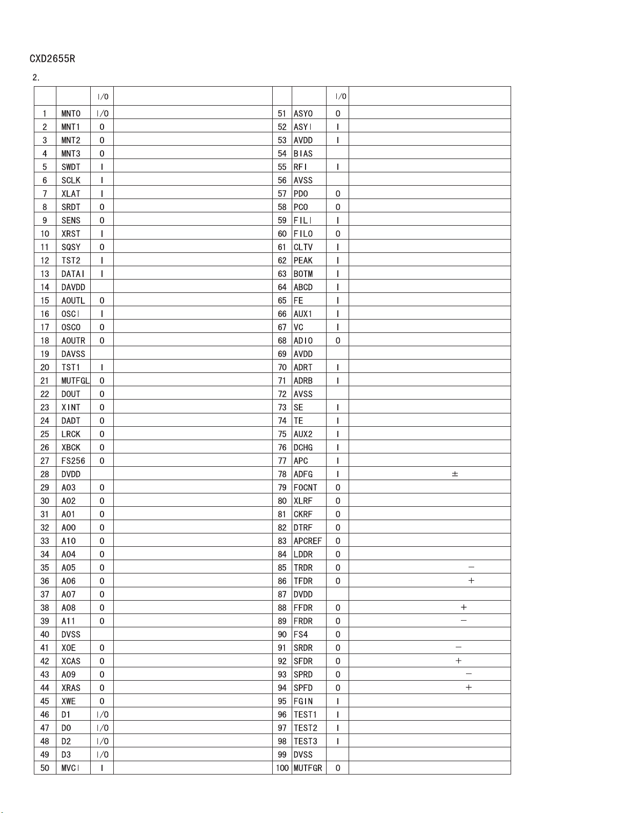
Pin Function Description
Pin
Symbol
No.
Functions and Operations
Monitor input and output
Monitor output
Monitor output
Monitor output
Data input of microcomputer serial interface
Shift lock input of microcomputer serial interface
Latch input of microcomputer serial interface/
Latch at the Falling edge
Date output of microcomputer serial interface
Output of internal status corresponding to
microcomputer serial interface address
Reset input L : reset
Disc sub cord Q sync / ADIP sync output
Test pin
Input of external audio data to internal DAC
DAC power supply
Integrated DAC Lch output
Crystal oscillation circuit input (512Fs=22.5792MHz)
Crystal oscillation circuit output (Inverted output of OSCI)
Integrated DAC Rch output
DAC ground
Test pin
Detection of Lch zero data / flag output
Out put of digital audio interface signal
Interrupt request output L: When the interrupt
status occurs.
Output of audio date to external audio block
LRCK to external audio block (44.1kHz)
Output pin (2.8224MHz)
256Fs output (11.2896MHz)
Digital power supply
External DRAM address output
External DRAM address output
External DRAM address output
External DRAM address output
External DRAM address output
External DRAM address output
External DRAM address output
External DRAM address output
External DRAM address output
External DRAM address output
External DRAM address output
Digital ground
External DRAM output enable
External DRAM CAS output
External DRAM address output
External DRAM RAS output
External DRAM write enable
External DRAM date bus
External DRAM date bus
External DRAM date bus
External DRAM date bus
External VCO (784Fs) clock input
Pin
No.
Symbol
Functions and Operations
Playback EFM full-swing output
Playback EFM comparator slice voltage input
Analog power supply
Playback EFM comparator bias current input
Playback EFM RF signal input
Analog ground
Phase comparison output for analog PLL of
EFM decoder
Phase comparison output for master PLL of
playback digital PLL
Filter input for master PLL of playback digital PLL
Filter output for master PLL of playback digital PLL
Internal VCO control voltage input for master PLL of
playback digital PLL
Peak hold signal input for quantity of light
Bottom hold signal input for quantity of light
Signal input for quantity of light
Focus error signal input
Auxiliary input 1
Center voltage input
Monitor output of A/D converter input signal
Analog power supply
Input of upper-limit voltage of the A/D converter
operating range
Input of lower-limit voltage of the A/D converter
operating range
Analog ground
Sled error signal input
Tracking error signal input
Auxiliary input 2
Connect to the low-impeddance power supply
Error signal input for laser digital APC
ADIP binary FM signal (22.05
Output for setting of CXA 2523 current source
Latch output for CXA 2523 control
Shift lock output for CXA 2523 control
Data output for CXA 2523 control
Reference PWM output for laser APC
PWM output for laser digital APC
Tracking servo drive PWM output (
Tracking servo drive PWM output (
Digital power supply
Focus servo drive PWM output (
Focus servo drive PWM output (
4Fs output (176.4kHz)
Sled servo drive PWM output (
Sled servo drive PWM output (
Spindle servo drive PWM output (
Spindle servo drive PWM output (
FG input of spindle CAV servo
Test pin
Test pin
Test pin
Digital ground
Detection of Rch zero date / flag output
1kHz) input
)
)
)
)
)
)
)
)
2-6
Page 9
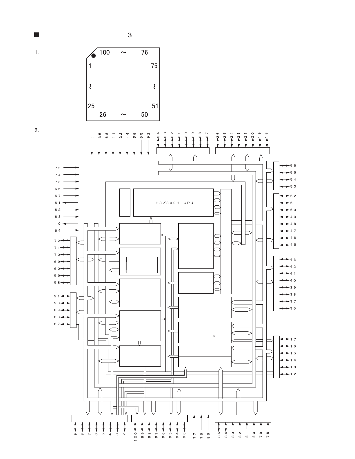
HD6433045SV14X (IC501): Beams Microcomputer
Terminal Layout
Block Diagram
XM-P55
XM-PJ1
Port 3
Address bus
Data bus (upper level)
Data bus (lower level)
Clock generator
Port 4
Port 5Port 2
Interrupt controller
DMA
ROM
Mask ROM
Port 6Port 8
PROM
Flash memory
RAM
16 bits
integrated
timer unit
(ITU)
controller
(DMAC)
Refresh
controller
Watch dog timer
(WDT)
Serial communication
interface (SCI)
2ch
Bus Controller
Port 1Port 9
Programmable
timing pattern
controller (TPC)
A/D converter
D/A converter
Port B Port A Port 7
2-7
Page 10
XM-P55
XM-PJ1
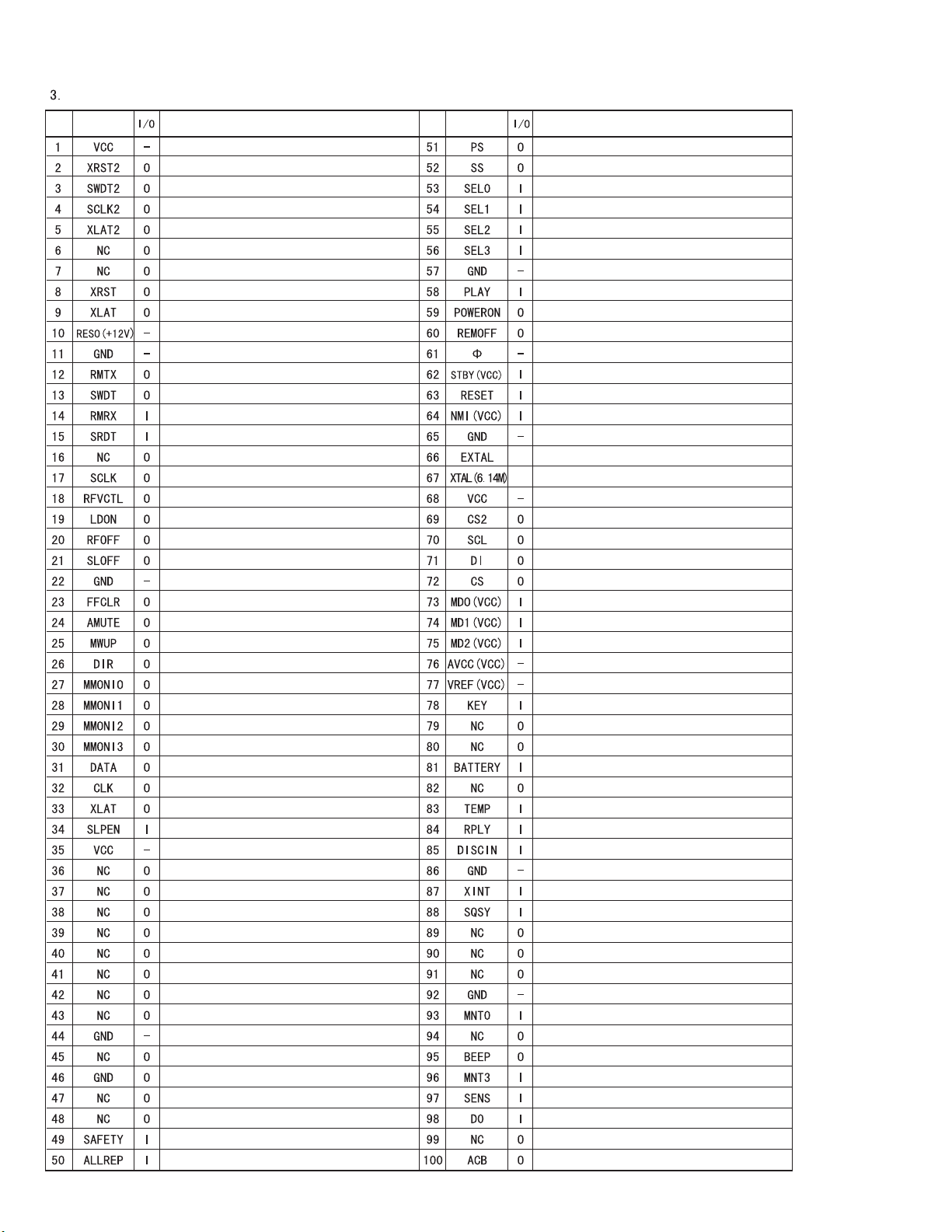
Description
Pin
Symbol
No.
Function and Operation
Power supply
Communications line terminals to CXA2523AR,
connect to XSTB terminal
Communications line terminals to CXA2523AR,
connect to SWDT terminal
Communications line terminals to CXA2523AR,
connect to SCLK terminal
Communications line terminals to CXA2523AR,
connect to XLAT terminal
Non connection
Non connection
Connect to XRST terminal of CXD2655R
Connect to XLAT terminal of CXD2655R
Supplies +12V when flash memory is writing.
Ground
Remote control UART output
Connect to SWDT terminal of CXD2655R
Remote control URAT input
Connect to SRDT terminal of CXD2655R
Non connection
Connect to SCLK terminal of CXD2655R
RF source pre-charge output
Laser ON / OFF output
RF source OFF output
Sled driven voltage ON/OFF
Ground
Clear signal of power supply circuit flip-flop
MUTE output for audio circuit
Starting control output
Debug / test mode
Parallel mode monitor
Parallel mode monitor
Parallel mode monitor
Parallel mode monitor
Debug / test mode
Debug / test mode
Debug / test mode
Sleep function enable input
Power supply
Non connection
Non connection
Non connection
Non connection
Non connection
Non connection
Non connection
Non connection
Ground
Non connection
Ground
Non connection
Non connection
LSI source down detective input
ALL tracks repeat key input
Pin
No.
Symbol
Function and Operation
Connect to MPC17A39 power save terminal
Connect to CXA8069 start / stop terminal
CXD2655R monitor output selection
CXD2655R monitor output selection
CXD2655R monitor output selection
CXD2655R monitor output selection
Ground
PLAY key input
Starting signal output for power supply circuit
Remote control power OFF
Non connection
Power supply
Microcomputer reset input
Power supply
Ground
Connect to Crystal NAX0275-001X
Connect to Crystal NAX0275-001X
Power supply
EEPROM2 chip select terminal output
EEPROM communication serial clock output
EEPROM communication serial DATA output
EEPROM chip select terminal output
Power supply
Power supply
Power supply
Power supply
Power supply
Key input (analog)
Non connection
Non connection
Battery voltage input (analog)
Non connection
Connect to temperature-detective thermistor
Remote control PLAY key input
Disc detective switch input
Ground
Connect to XINT terminal of CXD2655R
Connect to SQSY terminal of CXD2655R
Non connection
Non connection
Non connection
Ground
Connect to MINT0 terminal of CXD2655R
Non connection
Connect to BEEP of audio circuit
Connect to MINT3 terminal of CXD2655R
Connect to SENS terminal of CXD2655R
EEPROM communication serial data input
Non connection
ACTIVE CLEAR BASS circuit ON / OFF output
2-8
Page 11
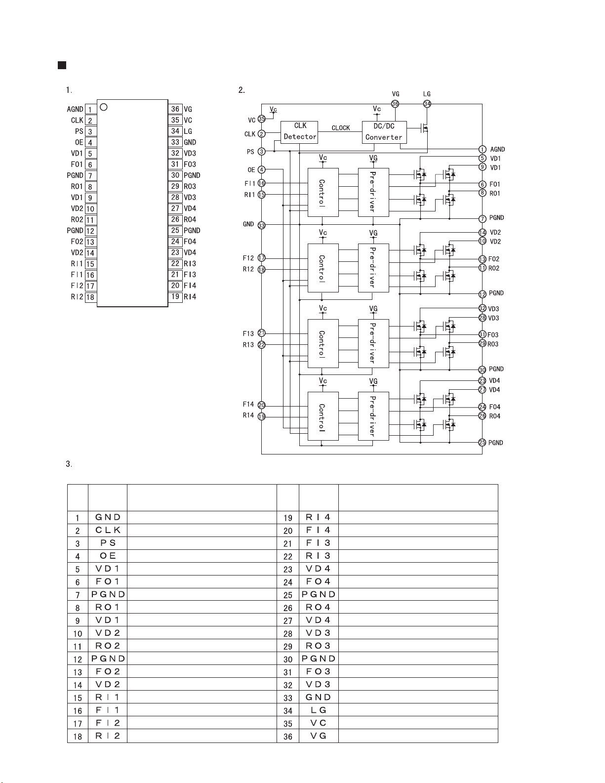
MPC17A39DTB-X (IC400):4Channel Bridge Driver
XM-P55
XM-PJ1
Terminal Layout
Block Diagram
Pin Function Description
Pin
No.
Symbol
Functions and Operations
DC / DC Converter circuit ground
External CLOCK input connection
Standby mode control
Output enable
Driver power supply
Driver output
Power ground
Driver output
Driver power supply
Driver power supply
Driver output
Power ground
Driver output
Driver power supply
CH 1 control signal input
CH 1 control signal input
CH 2 control signal input
CH 2 control signal input
Pin
No.
Symbol
Functions and Operations
CH 4 control signal input
CH 4 control signal input
CH 3 control signal input
CH 3 control signal input
Driver output
Driver output
Power ground
Power ground
Driver power supply
Driver power supply
Driver output
Power ground
Driver output
Driver power supply
Control circuit ground
DC / DC Converter boosting inductance, diode ground
Control circuit power supply
Pre-driver circuit power supply
2-9
Page 12
XM-P55
XM-PJ1
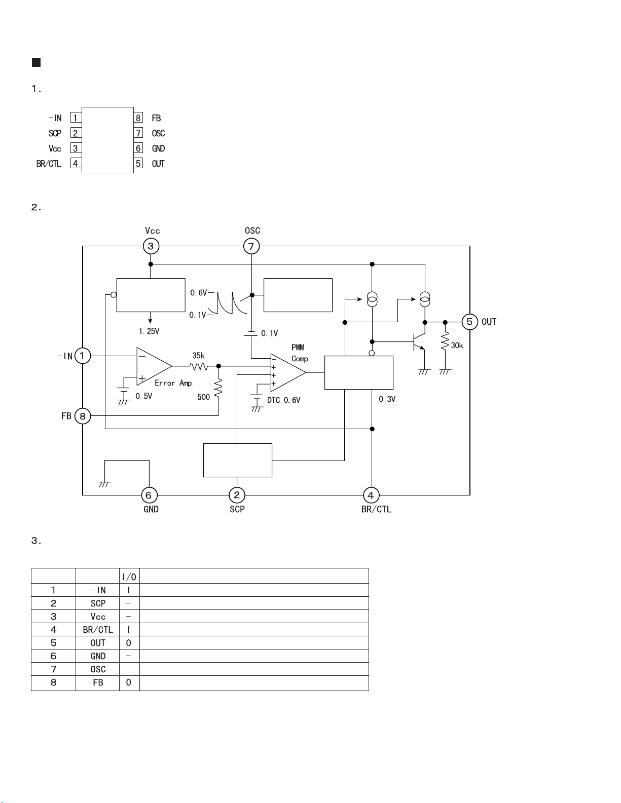
MB3800PFV-W(IC931):Switching Regulator Controller
Terminal Layout
Block Diagram
Reference
voltage
Soft start
S.C.P
Pin Function Description
Pin No. Symbol Functions and operations
Error amplifier inversion input
Soft start, capacity for SCP setting connection
Power supply
Output current setting, control
Totem-pole output
Ground
Capacity for oscillation frequency setting, resistant connection
Error amplifier output
Santooth
wave generator
Output drive
control circuit
2-10
Page 13
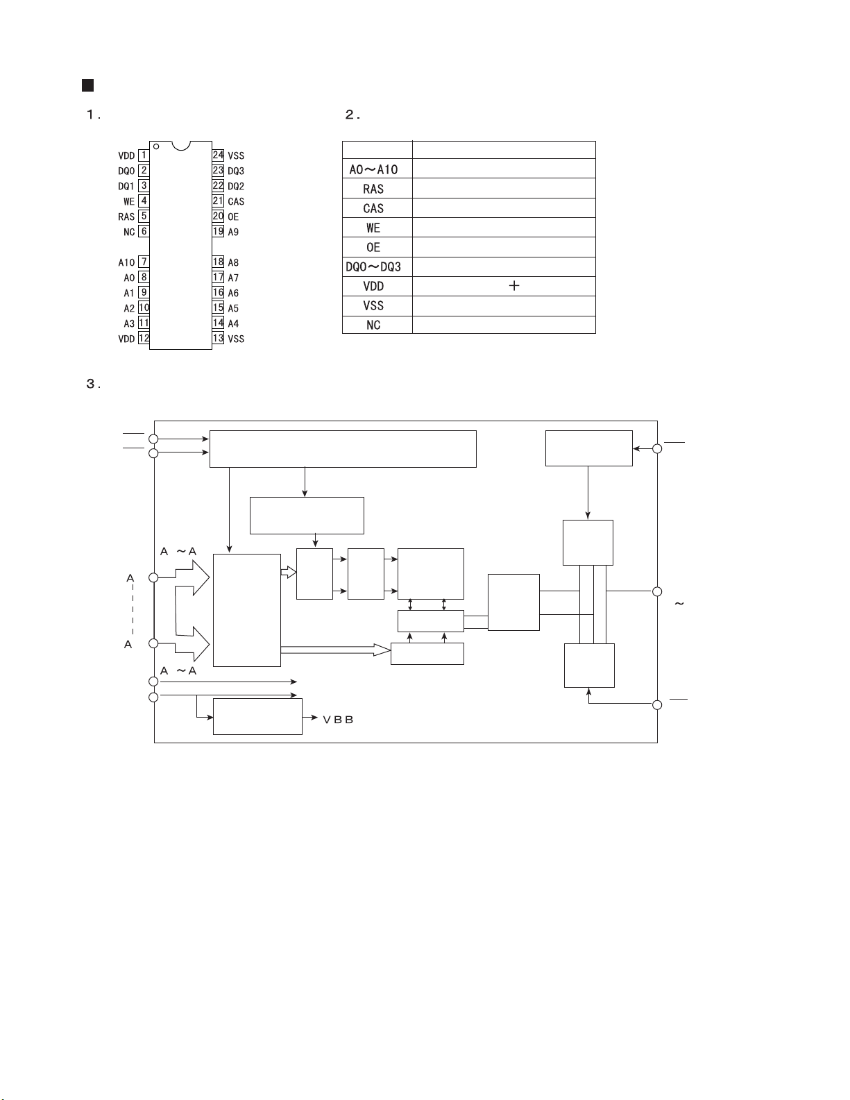
MN41X17400CTT10X(IC391):DRAM
XM-P55
XM-PJ1
Terminal Layout
Block Diagram
RAS
CAS
0 10
0
10
VSS
VDD
0 10
Row
Address
Buffer
Column
Address
Buffer
On Chip
VBB
Generator
Clock Generator
CBR Refresh
Counter
Row
Decoder
Pin Functions
Symbol
Word
Driver
Function
Address input
Row address / strove
Column address / strove
Write enabling input.
Output enabling input.
Data input
Power supply (
3.3V)
Power supply (0V)
Non connection
Memory
Cell
Sense.
Amp
Column
Decoder
I/O
Selector
Write
Clock
Generator
Data
Input
Buffer
Data
Output
Buffer
WE
DQ0
DQ3
OE
2-11
Page 14
XM-P55
XM-PJ1
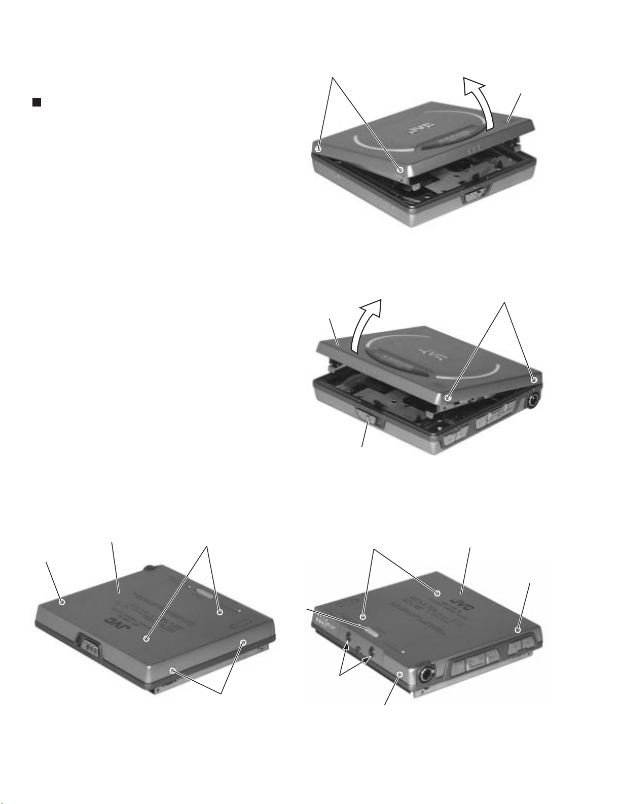
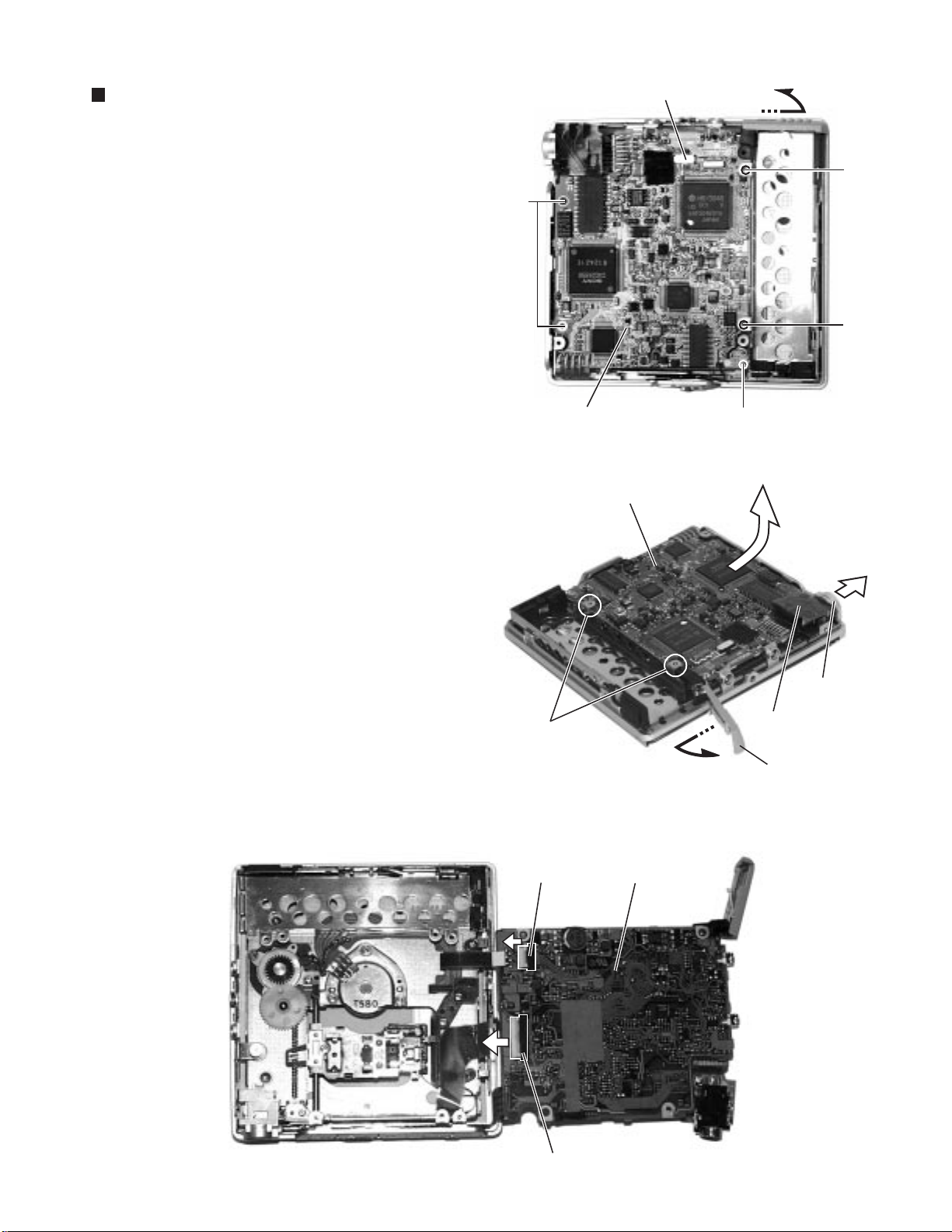
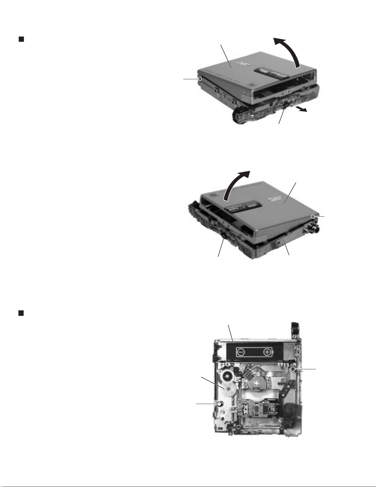
Removal of Main Parts
<XM-P55 Section>
Removing the MD Door Assembly and
the Bottom Cover (See Fig.1 to 4)
1.
Move the door lever and open the door.
2.
Remove the four A screws attaching the MD door
assembly and remove the MD door assembly from the
body.
Reverse the body and remove the six B screws attaching
3.
the bottom cover.
Release the joint a outside and remove the bottom cover
4.
from the body.
CAUTION: When reassembling the bottom cover, fit the
part b of the hold knob slot to the hold
switch on the main board (See Fig.4, 5).
A
MD door assembly
MD door
assembly
Fig.1
A
B
Bottom cover
B
B
Part b
Part a
Door lever
B
Fig.2
Bottom cover
B
B
Fig.4Fig.3
2-12
Page 15
XM-P55
XM-PJ1
Removing the Main Board
(See Fig.5 to 7)
1.
Remove the three C screws and the screw D attaching
the main board.
2.
Unsolder the part c of the battery terminal.
3.
Open the battery lid and remove it from the flame
assembly.
Remove the headphone jack assembly while pulling the
4.
cabinet assembly of the headphone jack outwards.
Move the main board in the direction of the arrow in Fig.6
5.
and remove it upward from the two parts d of the
bending on the flame assembly.
Disconnect the flexible harnesses from connector CN300
6.
and CN401 on the reverse side of the main board.
C
Main board
Main board
Hold switch
D
C
Part c : unsoldering
Fig.5
Parts d
CN401
Flame assembly
Headphone jack assembly
Battery lid
Fig.6
Main board
Fig.7
CN300
2-13
Page 16
XM-P55
XM-PJ1
Removing the Mechanism Assembly
(See Fig.8)
1. Remove the two E screws attaching the mechanism
assembly and remove the mechanism assembly from the
flame assembly.
Flame assembly
E
Mechanism assembly
E
Fig.8
2-14
Page 17
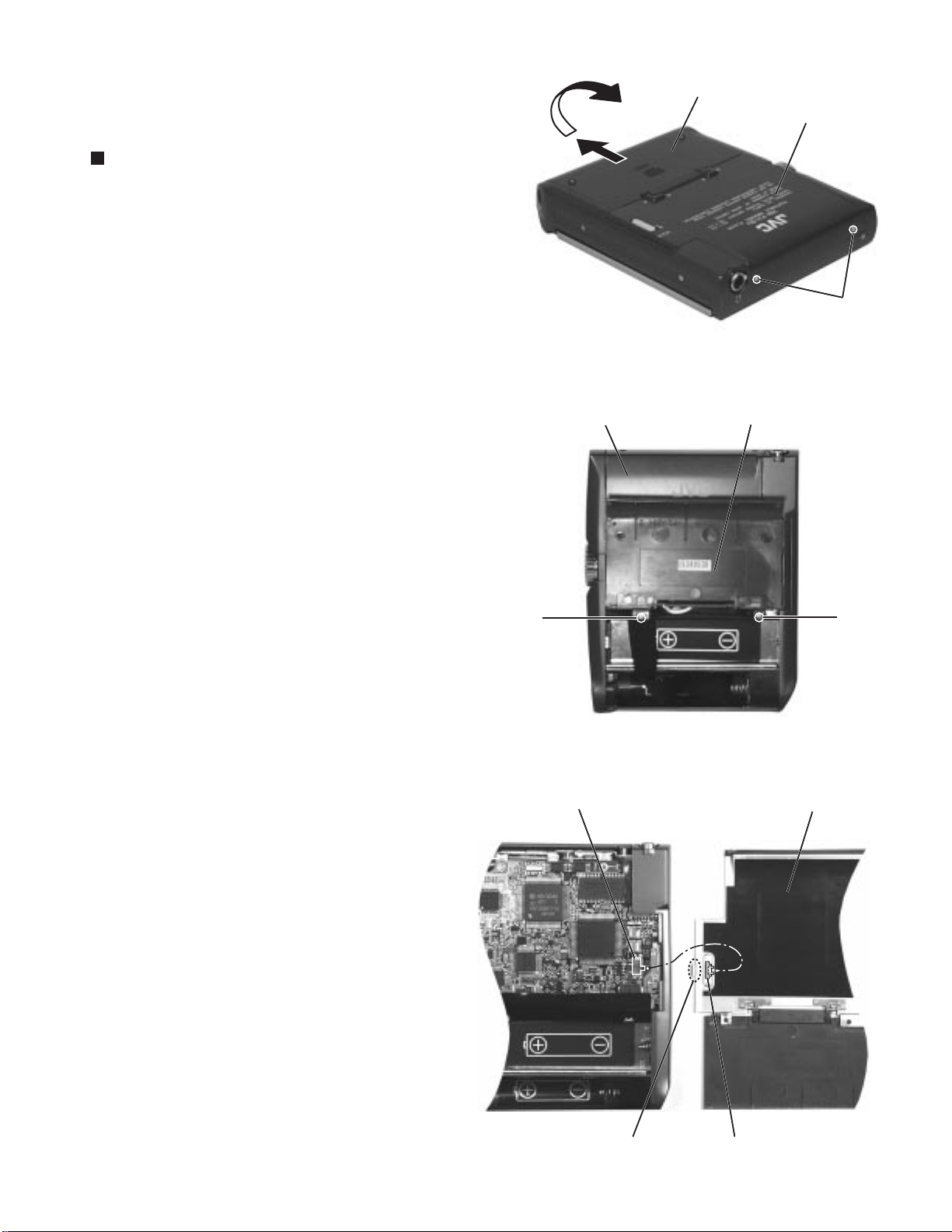
Removal of Main Parts
<XM-PJ1 Section>
Removing the Bottom Cover
(See Fig.1 to 3)
1.
1.
Move and remove the battery lid of the bottom cover
assembly on the side of the body in the direction of the
arrow.
2.
2.
Remove the two A screws attaching the bottom cover on
the bottom of the body.
3.
Remove the two B screws attaching the bottom cover on
3.
the side of the body.
Remove the bottom cover from the body while releasing
4.
4.
the tab a of the bottom cover on the side of the hold
switch to the inside.
CAUTION: When reassembling, make sure that the
convexity of the hold switch is fitted to the
concave of the switch knob before inserting
the tab a of the bottom cover assembly.
Bottom cover assembly
XM-P55
XM-PJ1
Battery lid
Bottom cover assembly
B
Fig. 1
Battery lid
A
Hold switch
A
Fig. 2
Bottom cover assembly
Fig. 3
Switch knobJoint a
2-15
Page 18
XM-P55
XM-PJ1
Removing the Front Cover Assembly
(See Fig.4)
1.
Remove the bottom cover assembly.
2.
Remove the two C screws attaching the front cover
assembly, and remove the front cover assembly while
turning it in the direction of the arrow in the Fig.4.
Removing the Cabinet (See Fig.5 to 8)
1.
Remove the bottom cover assembly.
2.
Remove the front cover assembly.
3.
Remove the screw D attaching the cabinet on the upper
side of the body.
4.
Reverse the body and remove the two E screws attaching
the cabinet on the back of the body.
Release the two joints b on the flame assembly side of
5.
the battery case in the direction of the arrow, and remove
the cabinet from the flame assembly.
Unsolder the two harnesses (one is orange, the other is
6.
gray) connected to the main board. Disconnect the
battery connector B with the brown harness by pulling
upward.
CAUTION: When reassembling, attach the harnesses
with a double-sided tape to the part c on the
inside of the cabinet (See Fig.8).
C
Cabinet
Flame assembly
C
Front cover assembly
Fig. 4
D
Main board
Fig. 5
2-16
Cabinet
Main board
Fig. 7
Unsoldering
Battery connector B
Joints b
Part c
Cabinet
E
Fig. 6
Cabinet
Main board
Fig. 8
Page 19

Removing the Main Board
(See Fig.9 to 11)
1.
Remove the four F screws attaching the main board.
2.
Remove the headphone jack fixed with a double-sided
tape upward.
3.
Unsolder the part d of the main board.
4.
Remove the flexible harness 1 fixed to the front side of
the flame assembly with a double-sided tape.
5.
Move the battery terminal e from the flame assembly
upward.
Move the main board to the inside, and remove it upward
6.
while releasing it from the two hinges f on the bending of
the flame assembly.
Disconnect the flexible harnesses from connector CN300
7.
and CN401 on the reverse side of the main board.
CAUTION: When reattaching the flexible harness 1,
position it to the six g points and fix it with a
double-sided tape (See Fig.10).
Headphone jack
F
Main board
Main board
F
Fig. 9
F
Joints f
Part d
F
XM-P55
XM-PJ1
Battery
terminal e
F
Positioning
points g
F
Positioning points g
Positioning points g
Fig. 10
Main board
CN401
CN300
Fig. 11
2-17
Page 20
XM-P55
XM-PJ1
Removing the Door Cover
(See Fig.12, 13)
Remove the bottom cover.
1.
Remove the front cover.
2.
Remove the cabinet.
3.
Push the lower part of the door lock lever outside on the
4.
lower front side of the body, and open the door.
Remove the two G screws attaching the door cover on
5.
both sides of the body, and remove the door cover.
CAUTION: When reattaching the flexible harness 1,
position it to the six g points and fix it with a
double-sided tape (See Fig.10).
Door cover
G
Door lock lever
Fig. 12
Door cover
G
Removing the Mechanism Assembly
(See Fig.14)
1.
Remove the bottom cover.
2.
Remove the front cover.
3.
Remove the cabinet.
4.
Remove the main board.
5.
Remove the two H screws attaching the mechanism
assembly and remove the mechanism assembly from the
flame assembly.
Door lock lever
Mechanism assembly
H
Flame assembly
Fig. 13
Flame assembly
H
2-18
Fig. 14
Page 21

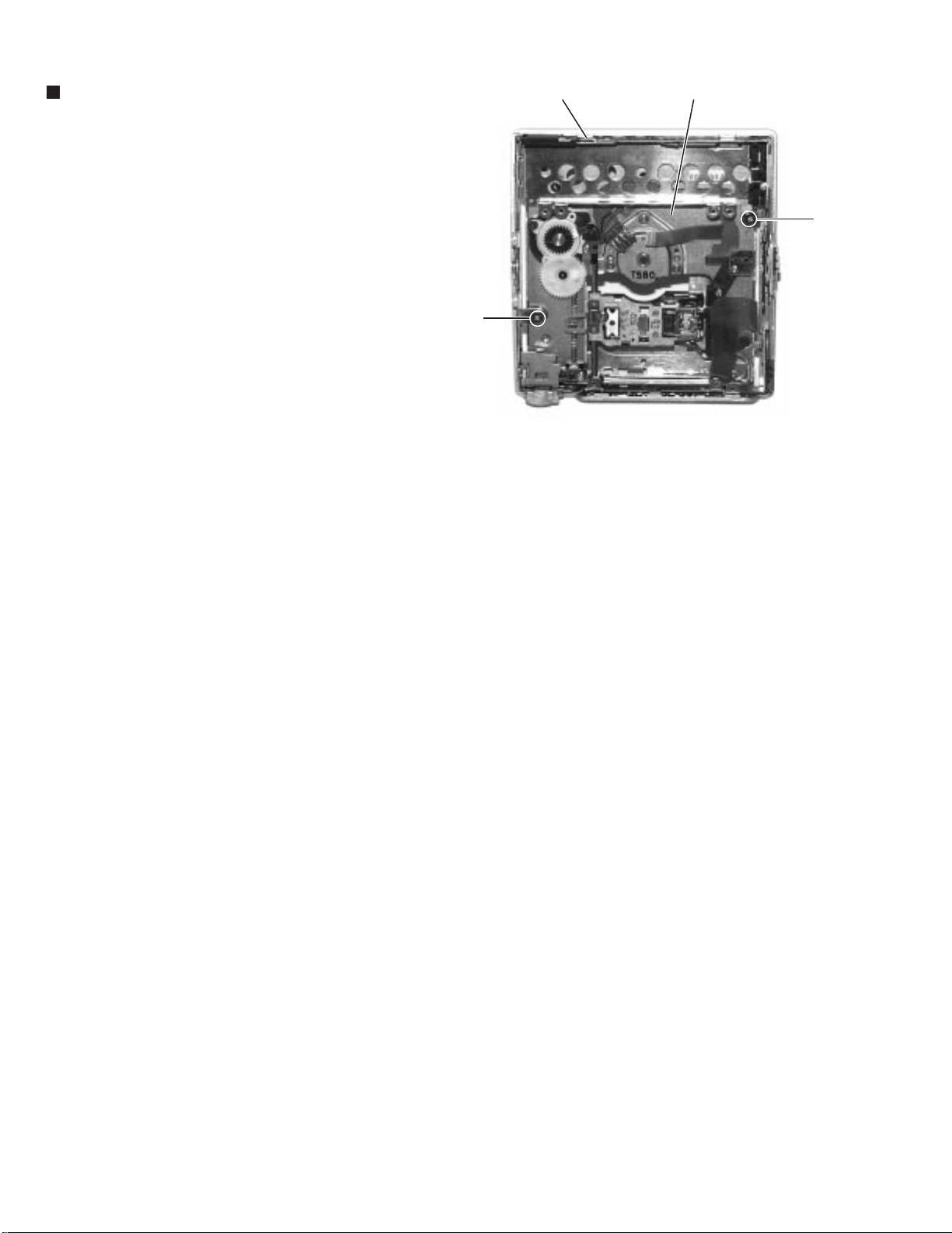
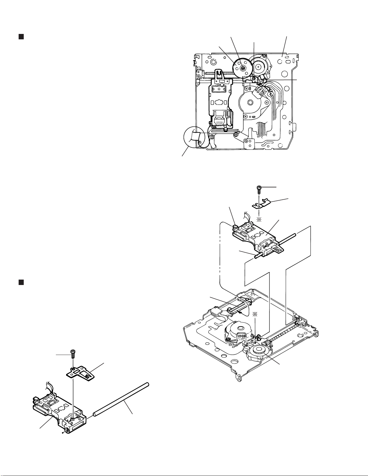
<Removal of MD Mechanism Assembly>
Removing the Holder Assembly
(See Fig.1, 2)
Turn the holder assembly as shown in Fig.1.
1.
Push the stopper of the holder assembly to release its
2.
tab, and turn the holder assembly as shown in Fig.2.
Move the part a of the holder assembly in the direction of
the arrow and release its U-shaped notch from the shaft
of the chassis assembly.
Push the part b of the holder assembly and pull out the
3.
holder assembly from the shaft of the chassis assembly.
CAUTION: When reassembling, first attach the part (b)
of the holder assembly to the shaft of the
chassis assembly. Next, attach the U-shaped
notch to the shaft.
XM-P55
XM-PJ1
Holder Assembly
Stopper
Push inside
Fig.1
Holder assembly
Shaft
U-shaped notch
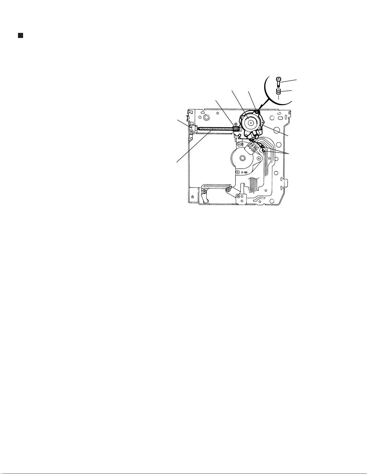
Removing the Spindle Motor
(See Fig.3)
1.2.Unsolder the part c of the flexible harness connected to
the spindle motor.
Remove the three A screws attaching the spindle motor
and remove the spindle motor from the chassis assembly.
Chassis assembly
A
Part a
Fig.2
Chassis assembly
Part b
Chassis assembly
Part c : unsoldering
A
Fig.4
Fig.3
Spindle motor
2-19
Page 22
XM-P55
XM-PJ1
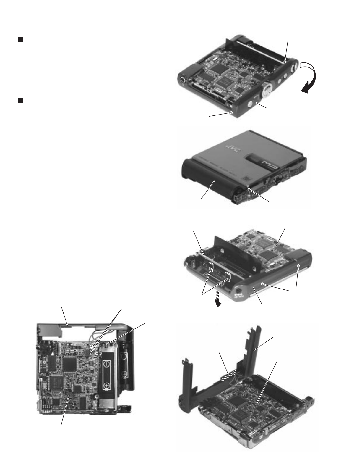
Removing the Pickup Unit
(See Fig.4, 5)
1.
Remove the slit washer on the reverse side of the MD
mechanism and remove the worm gear.
2.
Remove the screw B and the hold spring.
Detach the shaft of the pickup unit on the feed motor
3.
side, and the other side.
Remove the spacer of the flexible harness extending from
4.
the pickup unit (marked d), and remove the pickup unit
from the chassis assembly.
Slit washer
Worm gear
B
B
Chassis assembly
Hold spring
Removing the Pickup (See Fig.5, 6)
1.2.Remove the screw C from the pickup unit and the lead
spring.
Pull out the main shaft from the pickup.
d
Guide base
Fig.4
B
Hold spring
Part e
Pickup unit
Shaft
2-20
Pickup
C
Lead spring
Feed motor
Fig.5
Main shaft
Fig.6
Page 23
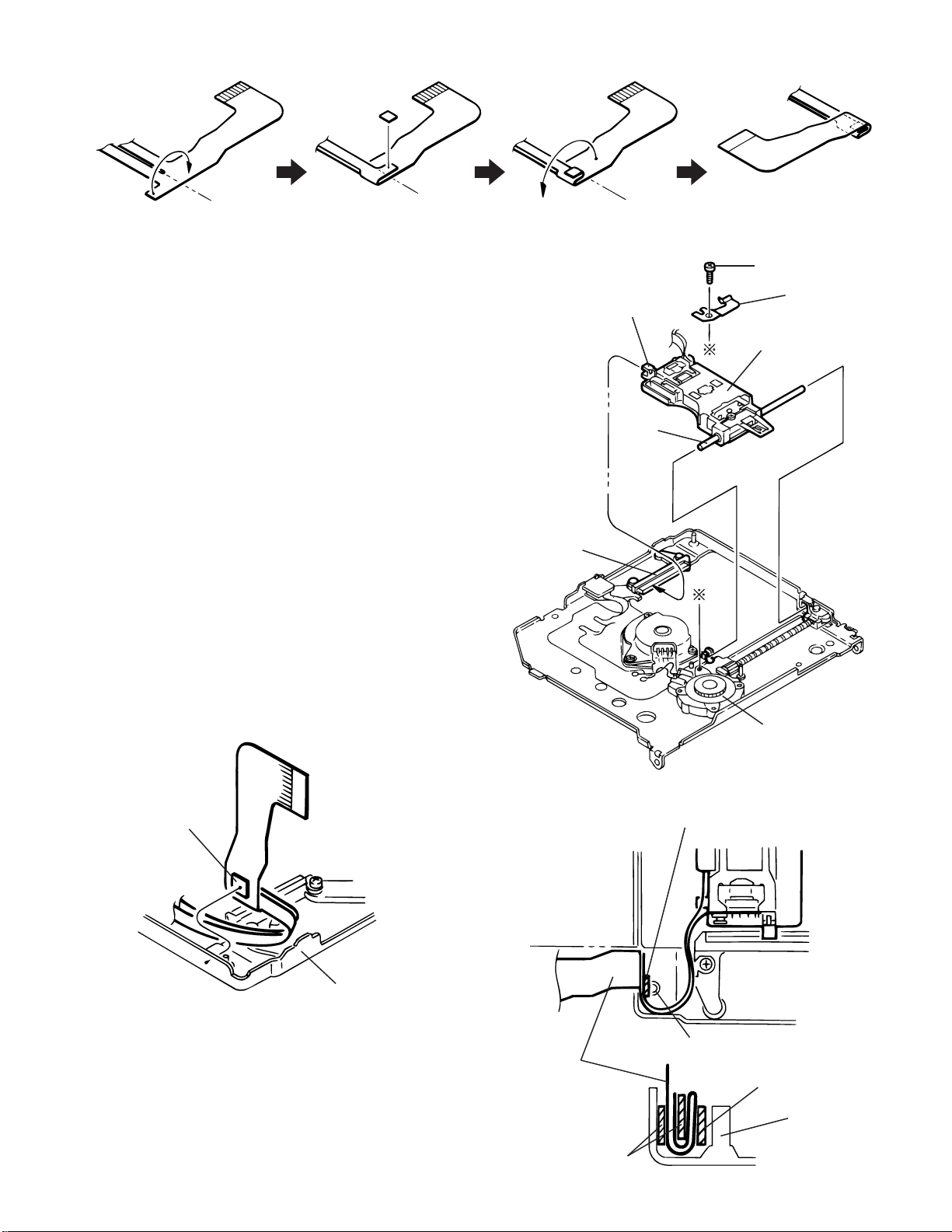
(Fold fast.) (Attach a spacer.) (Fix fast not to unfold.) (Fold fast.)
<Reassembling the Pickup Unit>
1.
Prior to performing the following procedures, fold the
flexible harness of the pickup unit (see Fig.7,8 and 9). Fix
the flexible harness with a spacer not to unfold.
2.
Attach the U-shaped slot of the pickup marked ’e’ to the
guide base.
For the shaft, firstly attach its shaft base side and next
3.
attach its feed motor base side.
XM-P55
XM-PJ1
Fig.7
B
Hold spring
Part e
Pickup unit
Shaft
Attach a spacer to the folded flexible harness and fix the
4.
flexible harness to the chassis assembly (see Fig.7, 8).
Attach a spacer between the chassis boss and the
5.
flexible harness (see Fig.9).
Make sure that the flexible harness is folded fast and
6.
fixed to the right position.
Attach a spacer
Guide base
Feed motor
Fig.5
Attach a spacer
Attach this position
Fig.8
Chassis assembly
Flexible harness
Spacer
Chassis boss
Spacer
Chassis boss
Fig.9
2-21
Page 24
XM-P55
XM-PJ1
Removing the Feed Motor/ Screw
Shaft Assembly and Wheel Gear
1.
Unsolder the two harnesses extending from the feed
motor.
2.
Remove the screw D attaching the feed motor, then the
spring. Remove the feed motor from the feed motor base.
Lift the feed motor base and pull out the screw shaft
3.
assembly.
Screw shaft gear
Shaft base
Feed motor
Wheel gear
D
D
Spring
Feed motor base
Soldering
Fig.10
2-22
Page 25

XM-P55
XM-PJ1
Maintenance of MD Pickup
1. Cleaning of pickup lens
(1) Prior to changing the pickup, clean the pickup lens.
(2) For cleaning the lens, use the following cotton swab after
mearsing it in alcohol.
Product No. JCB-B4; Manufacturer;Nippon Cotton Swab
2. Confirmation of the service life of laser
diode when the service life of the laser
diode has been exhausted, the following
symptoms will appear.
(1) Recording will become impossible.
(2) The RF output (EFM output and eye pattern amplitude)
will become lower.
(3) The drive current required for light emitting of laser diode
will be increased.
Confirm the service life according to the following flow chart:
Procedures of Changing
the MD pickup
Change the MD pickup by referring
to "Removing the MD pickup" in the
Disassembly Method.
Set the pickup to [TEST] mode according
to the procedures described in the
Adjustment Method.
Adjust the laser power 75 .
Adjust the disc.
How to operation
Return to feed .
Can the laser power
adjust under test mode?
Is the power output
750
Is the drive current
of laser diode
45mA or less?
YES
YES
NO
Change the pickup
NO
Change the pickup
OK.
3. Method of measuring the drive current of
laser diode
When the voltage measured at the both side of carbon resistor
R301 on the MD servo P.C. board (VMW2424A) have become
45mV or over, the service life of the laser diode is judged to have
been exhausted.
Adjust the Pre D
have been become OK
Return to feed .
Adjust the Mo D
have been become OK
Completion of changing the MD pickup.
Since this system is designed to perform magnetic
recording, the laser power ten times or over of the
conventional MD player will be output. Therefore, be
sure to perform not only adjustment and operation
of this system so carefully as not to directly look at the
laser beam or touch on the body.
4. Semi-solid state resistors on
the APC P.C. board
The semi-solid state resistor on the APC P.C.board
attached to the pickup is used for adjusting the laser
power. Since these resistor should be adjusted in
pair according to the characteristics of the optical
block, be sure not to touch on the resistors.
Since the service life of the laser diode will be
exhausted when the laser power is low, it is
necessary to change the pickup. Meanwhile, do not
pickup. Otherwise, the pickup will be damaged due
to over current.
2-23
Page 26

XM-P55
XM-PJ1
Self diagnosis Function of MD
Power Supply ------------- Use to a battery charger by more than 1.3volt
Establishment ------------ Set up the horizontal
1. The method of changing to the self-diagnosis mode turns off
the power supply of the main body first.
2. The power supply of the main body is turned on while pushing
"PLAYMODE +DISPLAY+A.B.BASS "of the remote control unit at the same time.
3. It changes into the self-diagnosis mode, and the self-diagnosis starts.
Test 's Command for the self-diagnosis mode
Command data1 data2 data3 data4 data5 data6 data7
Ope.mode State PLY P REC P EEP R EEP S
[Indicators on the display
of the remote control]
Play Mode button
A.C.BASS
=00: Wait to Test command
=DD: Going to Resume's EEPROM initialize
=DE: Going to servo's EEPROM initialize
=E2: Turn on the leaser of PLAY
=D3: Turn up the laser
=D4: Turn down the laser
=D1: Turn off the laser
=D5: Rewind to the FEED
=D6: Adjust to the PRE DISC
=D7: Adjust to the MO DISC
=92: Break out the trouble
DISPLAY button
VOL
The following are displayed
and it stops at the NG generation.
The KEY input afterwards
is disregarded.
FAV
Repeat
Battery
2-24
A.C.BASS
(Active Clear Bass) button
JOG
MODE
Disc
mark
BASS
Random
MONO
Page 27

Self-diagnosis Fllow Chart
XM-P55
XM-PJ1
Rewind to the FEED
by PLAY
Turn on the laser
Recieve time out
at 200ms
Except to
recieve DF:E2.
Issue to
Push to "BASS"
E2
Recieve time out
at 200ms
Except to
DF
Issue to
recieve DF:00.
Recieve DF:00
Recieve time out
at 200ms
Except to
recieve DF:D1.
Issue to
Issue to
Push to "VOL -" Push to "SHIFT"
Issue to
Push to "VOL +"
Recieve DF:D1
"D1"
Recieve DF:00
"D4:01"
Except above it
Recieve DF:00:XX:YY
"D3:01"
Recieve time out
at 200ms
Recieve DF:00
DF
Issue to
(Lock to display at 2sec)
Recieve time out at 200ms
Recievable above it.
START
DB
Issue to
Recieve DF:00
Recieve time out
at 200ms
Except to
Recieve time out
at 200ms
Except to
recieve DF:DD.
Recieve DF:00
DE
Issue to
Push to "BASS"
Recieve time out
at 200ms
Except to
recieve DF:DD.
Recieve DF:00
DE
Issue to
Initial to resume Initial to the servo
Push to "BASS"
Recieve time out
Processer Processer
recieve DF:DD.
at 200ms
Except to
recieve DF:DD.
DE
Issue to
DE
Issue to
Recieve DF:00:XX:YY
Recieve DF:00
(Lock to display at 2sec)
Recieve DF:00
(Lock to display at 2sec)
2-25
Page 28

XM-P55
XM-PJ1
Recieve time out
at 200ms
Except to
recieve DF:D7
Recieve time out
at 200ms
Except to
recieve DF:00
Adjust t MO-D
Push to "BASS"
Recieve time out
at 200ms
Except to
recieve DF:D6
Receive DF:D7
D7
Issue to
Receive DF:D6
D6
Issue to
Recieve time out
at 200ms
Except to
DF
Issue to
recieve DF:00
DF
Issue to
Receive DF:00
Receive DF:00
(Lock to display at 2sec)
OK
(Lock to display at 2sec)
Rewind to FEED Adjust PRE -D
Rewind to FEED
Recieve time out
at 200ms
Except to
Push to "BASS" Push to "BASS"
recieve DF:D5
D5
Issue to
Receive DF:D5
Recieve time out
at 200ms
Processor Processor Processor
Except to
recieve DF:00
DF
Issue to
Receive DF:00
(Lock to display at 2sec)
OK OK
2-26
Page 29

Block Diagrams
XM-P55
XM-PJ1
PICKUP
SLED
SPINDLE
FCS, TRK
RF IC DSP
Servo
DRIVER
DRIVER
Each Block
POWER
SUPPLY
Micro
computer
CNT
16M D RAM
ACB BEEP
MUTE
REMOTE
CONTROL
Audio
HP JACK
LEVEL DIAGRAM
ACB Circuit
Headphone AMP
2-27
Page 30

XM-P55
XM-PJ1
-MEMO-
2-28
Page 31

Standard Schematic Diagrams
XM-P55 (Except to U.S.A.)
XM-P55
XM-PJ1
BLOCK B
BLOCK D
5
4
3
2
1
BLOCK A
BLOCK C
ABCD
2-29
Page 32

XM-P55
XM-PJ1
BLOCK A
XM-P55 (Except to U.S.A.)
To BLOCK B
5
4
3
To BLOCK C
2
1
2-30
Digital signal
ABCD
Page 33

XM-P55 (Except to U.S.A.)
XM-P55
XM-PJ1
5
BLOCK B
4
3
To BLOCK D
2
1
To BLOCK A
Digital signal
Analogue signal
ABCD
2-31
Page 34

XM-P55
XM-PJ1
5
4
BLOCK C
XM-P55 (Except to U.S.A.)
To BLOCK D
To BLOCK A
3
2
1
2-32
ABCD
Page 35

XM-P55
XM-PJ1
5
4
BLOCK D
XM-P55 (Except to U.S.A.)
To BLOCK B
3
2
1
To BLOCK C
ABCD
2-33
Page 36

XM-P55
XM-PJ1
-MEMO-
2-34
Page 37

XM-P55
XM-PJ1
XM-P55J ONLY
5
4
3
2
1
ABCD E F G
2-35
Page 38

XM-PJ1 (Except to U.S.A.)
Digital signal
BLOCK A
To BLOCK B
To BLOCK C
XM-PJ1(Except to U.S.A.)
XM-P55
XM-PJ1
5
4
B BLOCK
D BLOCK
3
2
1
A BLOCK
C BLOCK
2-36
HABC DEFG
Page 39

XM-P55
XM-PJ1
5
4
BLOCK B
XM-PJ1(Except to U.S.A.)
3
2
1
Digital signal
To BLOCK A
ABCD
Anologue signal
To BLOCK C
2-37
Page 40

XM-P55
XM-PJ1
5
4
BLOCK C
XM-PJ1(Except to U.S.A.)
To BLOCK D
3
To BLOCK A
2
1
2-38
ABCD
Page 41

BLOCK D
XM-PJ1(Except to U.S.A.)
5
4
XM-P55
XM-PJ1
3
To BLOCK B
2
1
To BLOCK C
ABCD
2-39
Page 42

XM-P55
XM-PJ1
-MEMO-
2-40
Page 43

XM-P55
XM-PJ1
XM-PJ1 J ONLY
5
4
3
2
1
ABCD E F G
2-41
Page 44

Printed Circuit Boards
XM-P55
XM-PJ1
Main board
5
Block No.
XM-P55 ONLY
(Parts side)
: chip parts
(Solder side)
4
3
2
1
2-42
HABC DEFG
Page 45

XM-P55
XM-PJ1
Switch Board
Block No.
5
4
Block No. Headphone Jack Board
3
2
1
ABCD
2-43
Page 46

XM-P55
XM-PJ1
-MEMO-
2-44
Page 47

PARTS LIST
[ XM-P55 ]
* All printed circuit boards and its assemblies are not available as service parts.
XM-P55
XM-PJ1
Area Suffix
B
E
EE
EN
J
UB
US
UT
UX
UY
U.K. (BU,SL)
Continental Europe (BU,SL)
Russian Federation (BU,SL)
Northern Europe (BU,SL)
U.S.A. (SL)
Hong kong (BU,GN,SL)
Singapore (BU,SL)
Taiwan (SL)
Saudi Arabia (SL)
Argentina (SL)
- Contents -
Exploded View of General Assembly and Parts List ..............................................3-2
MD Mechanism Ass'y and Parts List .....................................................................3-4
Electrical Parts List ................................................................................................3-6
Packing Materials and Accessories Parts List (J) .................................................3-10
Packing Materials and Accessories Parts List (E/EE/EN) .................................... 3-12
Packing Materials and Accessories Parts List (B/UB/US/UT/UX/UY) .................. 3-14
3-1
Page 48

XM-P55
XM-PJ1
General Exploded View and Parts List
Block No
5
4
3
(MODEL:XM-P55)
2
44
1
3-2
ABCD
Page 49

XM-P55
XM-PJ1
3-3
Page 50

XM-P55
XM-PJ1
MD Mechanism Ass’y and Parts List
(MODEL:PPM)
5
4
Block No.
3
2
1
3-4
ABCD
Page 51

XM-P55
XM-PJ1
3-5
Page 52

XM-P55
XM-PJ1
Electrical Parts List
¡¡
¡¡
¡ Main board
3-6
Page 53

XM-P55
XM-PJ1
3-7
Page 54

XM-P55
XM-PJ1
3-8
Page 55

XM-P55
XM-PJ1
¡¡
¡¡
¡ Headphone Jack board
¡¡
¡¡
¡ Switch board
3-9
Page 56

XM-P55
XM-PJ1
Packing Materials and Accessories Parts List
J Ver sion Section
5
4
Block No.
Block No.
3
2
turn up
turn down
1
3-10
ABCD
Page 57

¡¡
¡ Packing Parts list
¡¡
¡¡
¡ Accessories Parts list
¡¡
XM-P55
XM-PJ1
3-11
Page 58

XM-P55
XM-PJ1
Packing Materials and Accessories Parts List
E/EE/EN/ Ver sion Section
Block No.
Block No.
5
4
3
2
turn up
turn down
1
3-12
ABCD
Page 59

¡¡
¡ Packing Parts list
¡¡
¡¡
¡ Accessories Parts list
¡¡
XM-P55
XM-PJ1
3-13
Page 60

XM-P55
XM-PJ1
Packing Materials and Accessories Parts List
B/UB/US/UT/UX/UY/ Ver sion Section
Block No.
Block No.
5
4
3
2
1
3-14
turn up
turn down
ABCD
Page 61

¡¡
¡ Packing Parts list
¡¡
¡¡
¡ Accessories Parts list
¡¡
XM-P55
XM-PJ1
3-15
Page 62

XM-P55
XM-PJ1
-MEMO-
3-16
Page 63

PARTS LIST
* All printed circuit boards and its assemblies are not available as service parts.
[ XM-PJ1 ]
B
E
EE
EN
J
UB
US
UT
UX
UY
Area Suffix
U.K. (BU)
Continental Europe (BU)
Russian Federation (BU)
Northern Europe (BU)
U.S.A. (BU)
Hong kong (BU,GD)
Singapore (BU)
Taiwan (BU)
Saudi Arabia (BU)
Argentina (BU)
- Contents -
Exploded View of General Assembly and Parts List ............................................. 4-2
MD Mechanism Ass'y and Parts List .....................................................................4-4
Electrical Parts List ................................................................................................4-5
Packing Materials and Accessories Parts List (J) .................................................4-10
Packing Materials and Accessories Parts List (E/EE/EN) .................................... 4-12
Packing Materials and Accessories Parts List (B/UB/US/UT/UX/UY) .................. 4-14
XM-P55
XM-PJ1
4-1
Page 64

XM-P55
XM-PJ1
General Exploded View and Parts List
(MODEL:XM-PJ1)
5
4
Block No.
C991
J991
3
2
1
4-2
ABCD
Page 65

XM-P55
XM-PJ1
4-3
Page 66

XM-P55
XM-PJ1
MD Mechanism Exploded View and Parts List
MD Mechanism as same as XM-P55.
Please refer of the page 3-4 and 3-5.
Block No.
4-4
Page 67

Electrical Parts List
XM-P55
XM-PJ1
¡¡
¡¡
¡ Main board
4-5
Page 68

XM-P55
XM-PJ1
4-6
Page 69

XM-P55
XM-PJ1
4-7
Page 70

XM-P55
XM-PJ1
4-8
Page 71

XM-P55
XM-PJ1
¡¡
¡¡
¡ Headphone Jack board
¡¡
¡¡
¡ Switch board
4-9
Page 72

XM-P55
XM-PJ1
Packing Materials and Accessories Parts List
J Ver sion Section
Block No.
Block No.
5
4
3
2
1
4-10
turn up
turn down
ABCD
Page 73

¡¡
¡ Packing Parts list
¡¡
¡¡
¡ Accessories Parts list
¡¡
XM-P55
XM-PJ1
4-11
Page 74

XM-P55
XM-PJ1
Packing Materials and Accessories Parts List
E/EE/EN/ Ver sion Section
Block No.
Block No.
5
4
3
2
1
4-12
turn up
turn down
ABCD
Page 75

¡¡
¡ Packing Parts list
¡¡
¡¡
¡ Accessories Parts list
¡¡
XM-P55
XM-PJ1
4-13
Page 76

XM-P55
XM-PJ1
Packing Materials and Accessories Parts List
B/UB/US/UT/UX/UY/ Ver sion Section
A1 A4
5
4
Block No.
Block No.
3
2
1
4-14
turn up
turn down
ABCD
Page 77

Packing Parts List
Accessories Parts List
XM-P55
XM-PJ1
Page 78

XM-P55
XM-PJ1
VICTOR COMPANY OF JAPAN, LIMITED
AUDIO DIVISION,10-1,1Chome,Ohwatari-machi,Maebashi-city,371-8543,Japan
(No.20738)
Printed in Japan
9901 (V )
 Loading...