

Page 1
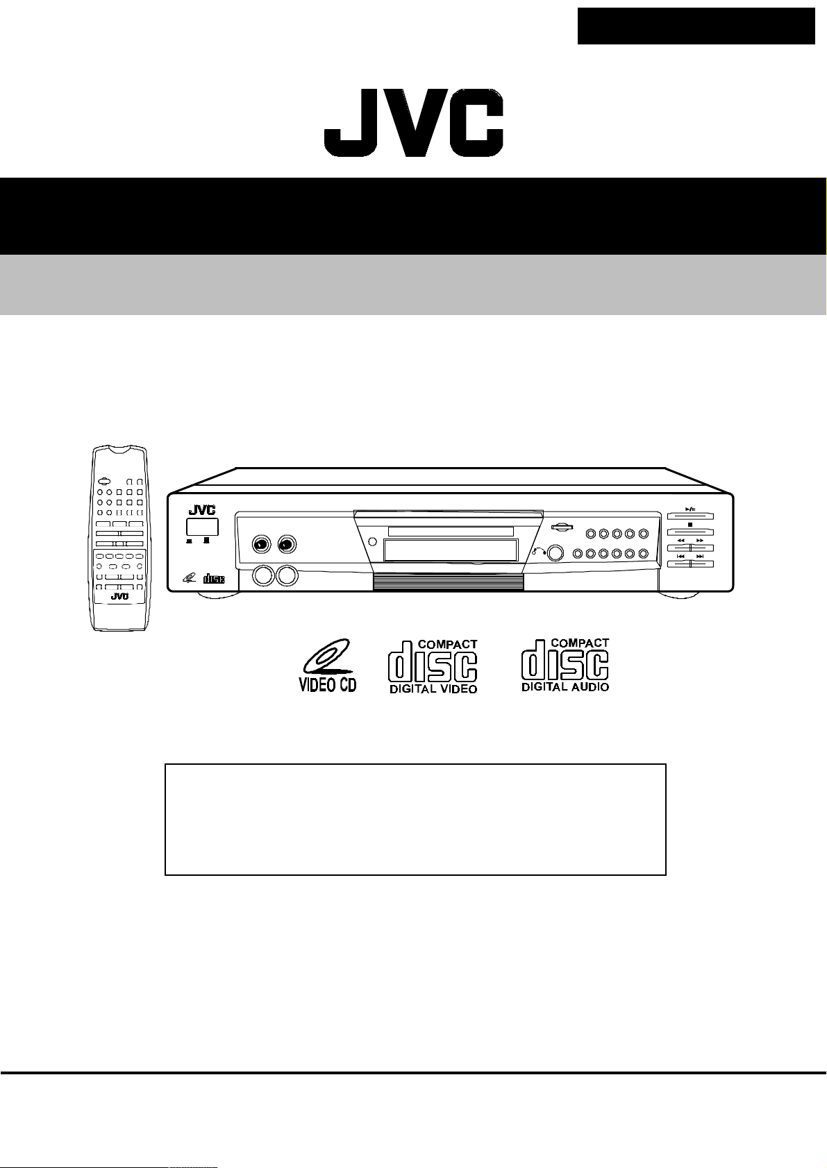
XL-SV320SL/305GD/308BU
SERVICE MANUAL
VIDEO CD PLAYER
XL-SV302SL/SV305GD
XL-SV308BU
POWER
ON / OFF
COMPACT
VIDEO CD
DIGITAL VIDEO
PLEASE TAKE NOTE BEFORE ORDERING
1. Order all service parts through JVC Asia Pte Ltd.- Customer Satisfaction Dept.
2. Two orders are available: Initial order and last order (Before End Of Line)
3. Minimum order quantity: 100pcs
4. Delivery term: Minimum 2 months upon confirmation of order.
1 – MIC VOLUME – 2
MIN MAX MIN MAX
1 – MIC – 2
OPEN/CLOSE
RETURN
IMPORTANT
123 45
+10 678910/0
Contents
Safety precautions ............................................................ 1-2
Preventing static electricity ...............................................1-3
Disassembly ......................................................................1-4
Description of major IC ....................................................1-5
COPYRIGHT
2001 VICTOR COMP ANY OF JAP AN L TD.
No: 28207
OCT. 2001
Page 2
XL-SV320SL/305GD/308BU
Safety precautions
1. This design of this product contains special hardware and many circuits and components specially for
safety purposes. For continued protection, no changes should be made to the original design unless
authorised in writing by the manufacturer. Replacement parts must be identical to those used in the
original circuits. Services should be performed by qualified personnel only.
2. Alterations of the design or circuitry of the product should not be made. Any design alterations of the
product should not be made. Any design alterations or additions will void the manufacturer’s warranty
and will further relieve the manufacture of responsibility for personal injury or property damage resulting
therefrom.
3. Many electrical and mechanical parts in the products have special safety-related characteristics.
These characteristics are often not evident from visual inspection nor can the protection afforded by
them necessarily be obtained by using replacement components rated for higher voltage, the Parts
List of Service Manual. Electrical components having such features are identified by shading on the
schematics and by ( ) on the Parts List in the Service Manual. The use of a substitute replacement
which does not have the same safety characteristics as the recommended replacement parts shown
in the Parts List of Service Manual may create shock, fire, or other hazards.
4. The leads in the products are routed and dressed with ties, clamps, tubing’s, barriers and the like to
be separated from live parts, high temperature parts, moving parts and/or sharp edges for the prevention
of electric shock and fire hazard. When service is required, the original lead routing and dress should
be observed, and it should be confirmed that they have been returned to normal, after re-assembling.
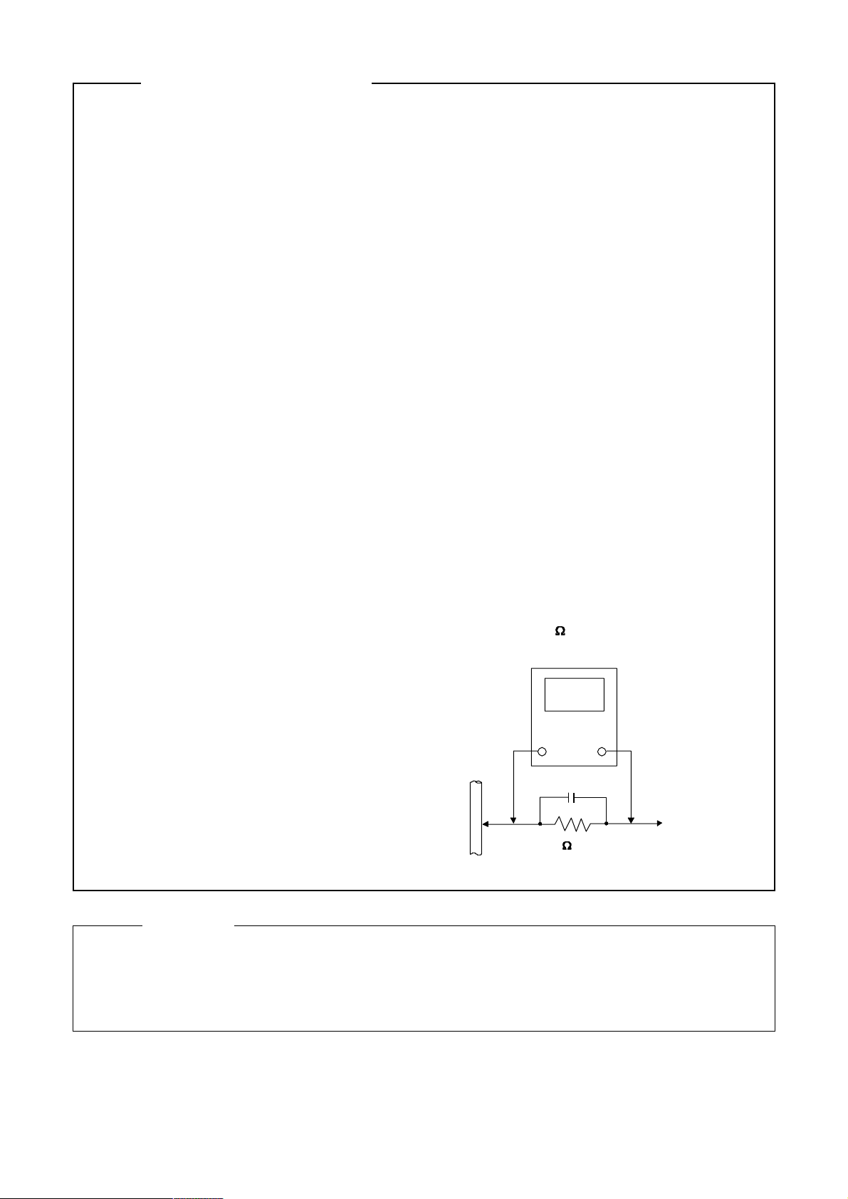
5. Leakage current check (Electrical Shock hazard testing)
After re-assembling the product, always perform an isolation check on the exposed metal parts of the
product (antenna terminals, knobs, metal cabinet, screw heads, headphone jack, control shafts, etc.)
to be sure the product is safe to operate without danger of electrical shock.
Do not use a line isolation transformer during this check.
• Plug the AC line cord directly into the AC outlet. Using a “Leakage Current Tester”, measure the
leakage current from each exposed metal parts of the cabinet, particularly and exposed metal
part having a return path to the chassis, to a known good earth ground. Any leakage current must
not exceed 0.5mA AC (r.m.s.)
• Alternate check method
Plug the AC line cord directly into the AC outlet. Use an AC voltmeter having, 1,000 ohms per
volt or more sensitivity in the following manner. Connect a 1,500
0.15µF AC-type capacitor between an exposed
metal part and a known good earth ground.
Measure the AC voltage across the resistor
with the AC voltmeter.
Move the resistor connection to each exposed
metal part, particularly any exposed metal part
having a return path to the chassis, and
measure the AC voltage across the resistor.
Now, reverse the plug in the AC outlet and
repeat each measurement. voltage measured
Any must not exceed 0.75 V AC (r.m.s.). This
corresponds to 0.5 mA AC (r.m.s.).
0.15µF AC TYPE
1500
XL-SV320SL/SV305GD
XL-SV308BU
10W resistor paralleled by a
AC Voltmeter
(Having 1000
ohms/volts,
or more sensitivity
Place this
probe on
each exposed
10W
metal part.
Good earth ground
Warning
1. This equipment has been designed and manufactured to meet international safety standards.
2. It is the legal responsibility of the repairer to ensure that these safety standards are maintained.
3. Repairs must be made in accordance with the relevant safety standards.
4. It is essential that safety critical components are replaced by approved parts.
5. If mains voltage selector is provided, check setting for local voltage.
1-2
Page 3
XL-SV320SL/305GD/308BU
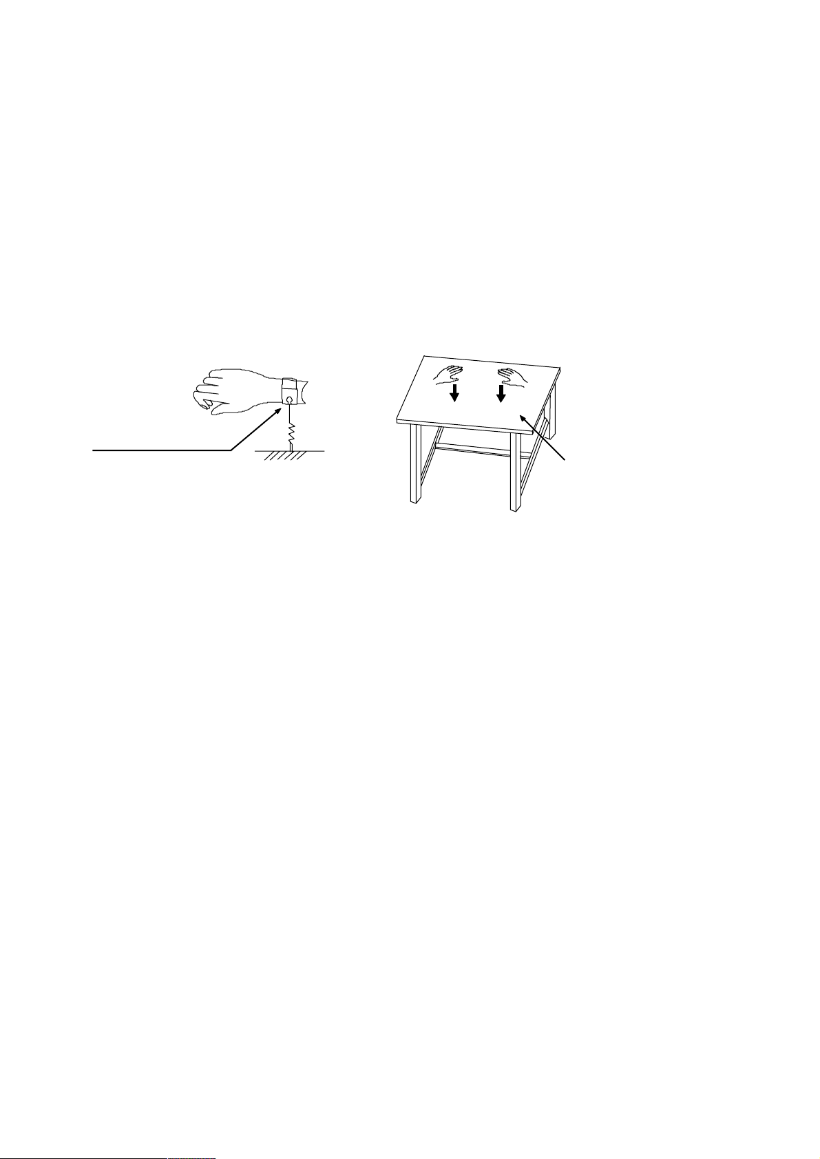
Preventing static electricity
Electrostatic discharge (ESD), which occurs when static electricity stored in the body, fabric, etc. is discharged, can destroy the laser diode in the traverse unit (optical pickup). Take care to prevent this when
performing repairs.
1.1. Grounding to prevent damage by static electricity
Static electricity in the work area can destroy the optical pickup (laser diode) in devices such as DVD players.
Be careful to use proper grounding in the area where repairs are being performed.
1.1.1. Ground the workbench
1. Ground the workbench by laying conductive material (such as a conductive sheet) or an iron plate over
it before placing the traverse unit (optical pickup) on it.
1.1.2. Ground yourself
1. Use an anti-static wrist strap to release any static electricity built up in your body.
(caption)
Anti-static wrist strap
Conductive material
(conductive sheet) or
iron plate
1.1.3. Handling the optical pickup
1. In order to maintain quality during transport and before installation, both sides of the laser diode on the
replacement optical pickup are shorted. After replacement, return the shorted parts to their original
condition. (Refer to the text.)
2. Do not use a tester to check the condition of the laser diode in the optical pickup. The tester’s internal
power source can easily destroy the laser diode.
1.2. Handling the traverse unit (optical pickup)
1. Do not subject the traverse unit (optical pickup) to strong shocks, as it is a sensitive, complex unit.
2. Cut off the shorted part of the flexible cable using nippers, etc. after replacing the optical pickup. For specific details, refer to the replacement procedure in the text. Remove the anti-static pin when replacing the
traverse unit. Be careful not to take too long a time when attaching it to the connector.
3. Handle the flexible cable carefully as it may break when subjected to strong force.
4. It is not possible to adjust the semi-fixed resistor that adjusts the laser power. Do not turn it.
1-3
Page 4
XL-SV320SL/305GD/308BU
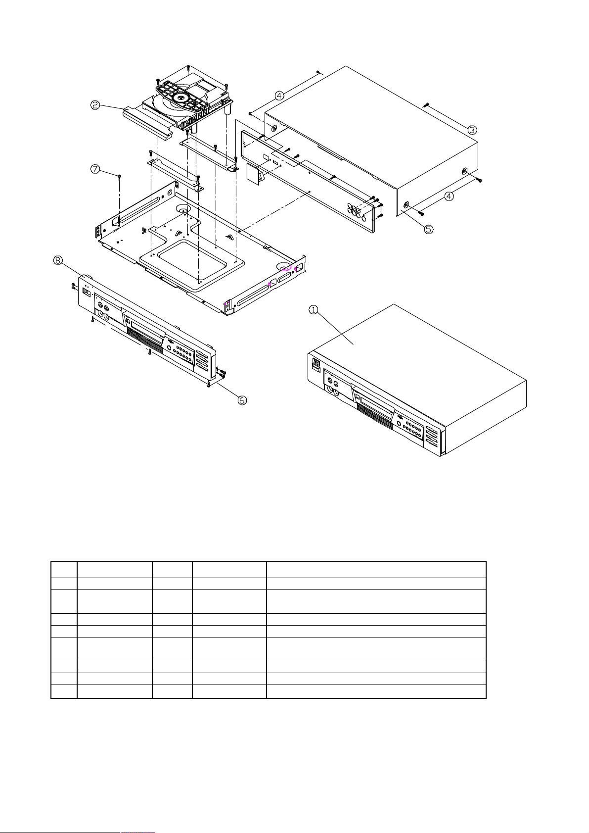
Disassembly
XL-SV320SL/SV305GD
XL-SV308BU
Procedure of disassembly
No. Description QTY. Action Remark
1 Main part 1 Place
2 Plane tray 1 Remove Turn on VCD, open the plane tray
then take up the CD door.
3 Self screw 1 Loosen screw Loose the screw, remove from the upper cover.
4 ¢4.0 Self screw 4 Loosen screw
5 Upper cover 1 Remove Loose screws then remove the upper cover
from the main part.
6 Self screw 5 Loosen screw
7 Self screw 1 Loosen screw
8 Front panel block 1 Remove Remove the front panel block from the main part.
1-4
Page 5
XL-SV320SL/305GD/308BU
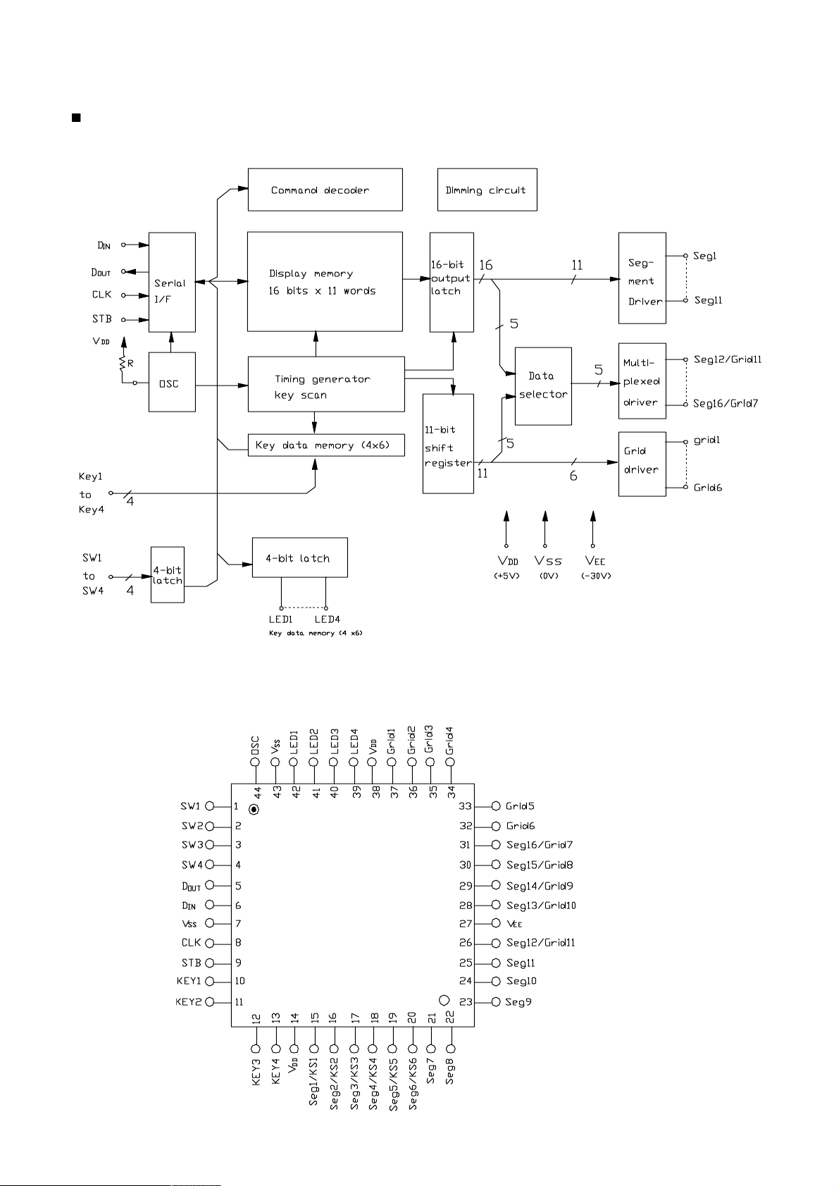
IC lead identification, internal diagram and description
IC301: HT16512 (VFD DRIVER)
Block diagram
Pin configuration (Top view)
1-5
Page 6
XL-SV320SL/305GD/308BU
Pin description
XL-SV320SL/SV305GD
Symbol Pin Name Pin No. Description
DIN Data input 6 Inputs serial data at the rising edge of the shift clock, starting from
the low order bit.
DOUT Data output 5 Output serial data at the falling edge of the shift clock, starting from
the low order bit. This is the N-ch open-drain output pin.
STB Strobe 9 Initializes the serial interface at the rising or falling edge of the µPD16512.
It then waits for reception of a command. Data input after STB has fallen is
processed as a command. While command data is processed, current
processing is stopped, and the serial interface is initialized. While STB is
high, CLK is ignored.
CLK Clock input 8 Reads serial data at the rising edge, and outputs data at the falling edge.
OSC Oscillator pin 44 Connect a resistor to this pin to determine the oscillation frequency to this pin.
Seg1/KS1 to High-voltage 15 to 20 Segment output pins (Dual function as key source)
Seg6/KS6 output
Seg7 to seg11 High-voltage 21 to 25 Segment output pins
output (segments)
Grid1 to Grid6 High-voltage 37 to 32 Grid output pins
output (grid)
Seg12/Grid11 to High-voltage 26,28 to 31 These pins are selectable for segment or grid driving.
Seg16/Grid7 output
(segment/grid)
Led to Led Led output 42 to 39 CMOS output. +20 mA max.
Key1 to Key4 Key data input 10 to 13 Data input to these pins is latched at the end of the display cycle.
SW1 to SW4 Switch input 1 to 4 These pins constitute a 4-bit general-purpose input port.
VDD Logic power 14, 38 5V ± 10%
Vss Logic ground 7, 43 Connect this pin to system GND.
VEE Pull-down level 27 VDD-35 V max.
XL-SV308BU
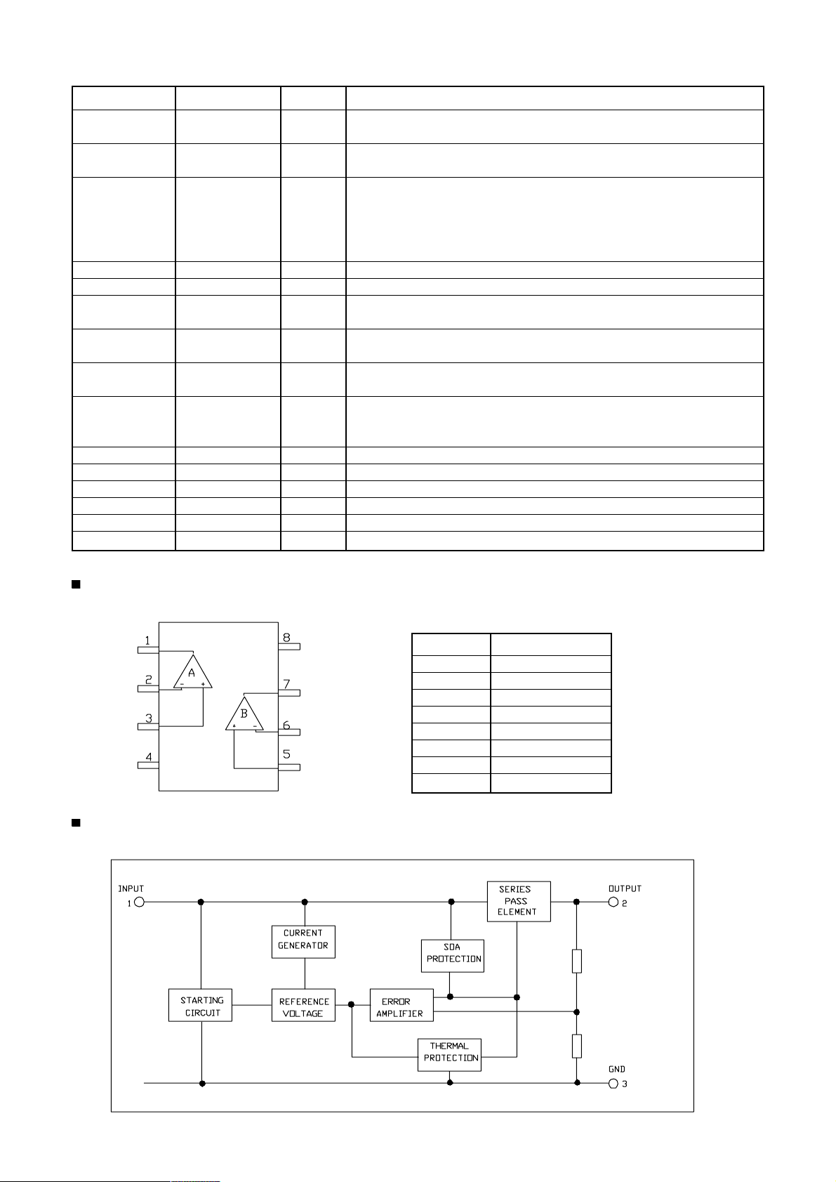
IC201/IC202,U5/U6: BA4558 (OP-AMP)
Pin configuration
IC101: 7805 (REGULATOR)
Block diagram
Pin description
Pin Function
1 A Output
2 A-Input
3 A+Input
4V5 B+Input
6 B-Input
7 B Output
8V+
1-6
Page 7
Pin configuration
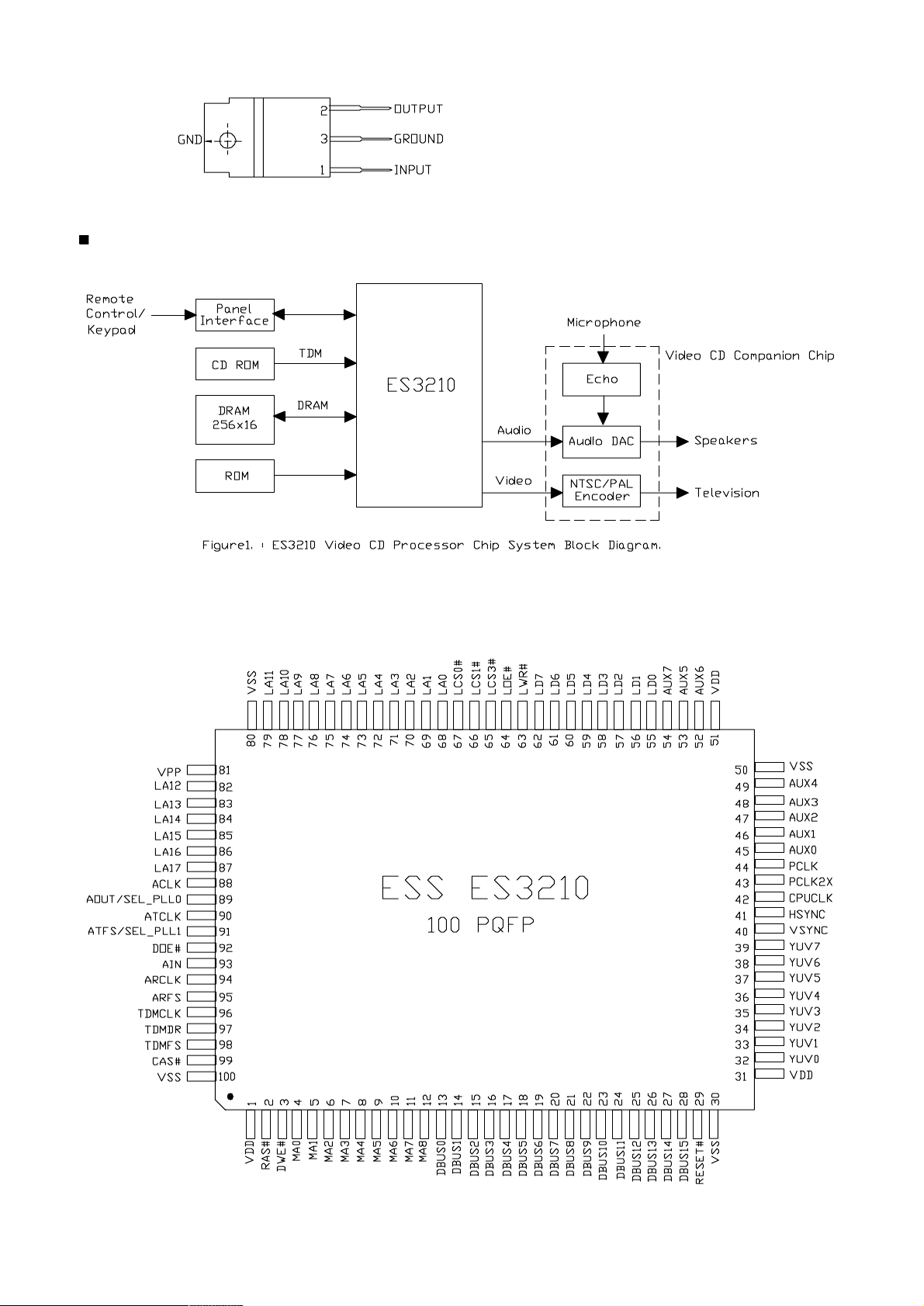
U1: ES3210
Block diagram
XL-SV320SL/305GD/308BU
Pin configuration
1-7
Page 8
XL-SV320SL/305GD/308BU
ES3210 Pin description
XL-SV320SL/SV305GD
Name Number I/O Definition
V DD 1, 31, 51 I Voltage supply for 3.3V.
RAS# 2 O DRAM row address strobe (active low).
DWE# 3 O DRAM write enable (active low).
DA[8:0] 12:4 O DRAM multiplexed row and column address bus.
DBUS[15:0] 28:13 I/O DRAM data bus.
RESET# 29 I System rest (active low).
VSS 30,50,80,100 I Ground.
YUV[7:0] 39:32 O Y is luminance, UV are chrominance data bus for screen video interface.
YUV[7:0] for 8-bit YUV mode.
VSYNC 40 I/O Vertical sync for screen video interface. programmable for rising or falling edge.
HSYNC 4 1 I/O Horizontal sync for screen video interface, programmable for rising or falling edge.
CPUCLK 42 I RISC and system clock input. CPUCLK is used only if SEL-PLL[1:0]=00.
PCLK2X 43 I/O Pixel clock; two times the actual pixel clock for screen video interface.
PCLK 44 I/O Pixel clock qualifier in for screen video interface.
AUX[7.0] 54,52,53,49:45 I/O Auxiliary control pins (AUX0 and AUX1 are open collectors).
LD[7:0] 62:55 I/O RISC interface data bus.
LWR# 6 3 O RISC interface write enable (active low).
LOE# 64 O RISC interface output enable (active low).
LCS[3,1,0]# 65,66,67 O RISC interface chip select (active low).
LA[17:0] 87:82, 79:68 O RISC interface address bus.
VPP 81 I Digital supply voltage for 5V.
ACLK 8 8 I/O Master clock for external audio DAC (8.192MHz, 11.2896MHz, 12.288MHz,16.9344MHz,
and 18.432MHz).
AOUT 89 O Dual-purpose pin. AOUT is the audio interface serial data output.
/SEL-PLLO I Pins SEL-PLL[1:0] select phase-lock loop (PLL) clock frequency CPUCLK for the
ES3210: 00=bypass PLL.
01=54MHz PLL.
10=67.5MHz PLL.
11=81MHz PLL.
ATCLK 9 0 I/O Audio transmit bit clock.
ATFS/ 91 O Dual-purpose pin. ATFS is the audio interface transmit frame sync.
SEL-PLL I Pins SEL-PLL[1:0] select phase-lick loop(PLL) clock frequency CPUCLK for the
ES3210. See the SEL-PLL0 pin above for the sttings.
DOE# 92 O DRAM output enable (active low).
AIN 93 I Audio interface serial data input.
ARCLK 94 I Audio receive bit clock.
ARFS 95 I Audio interface receive frame sync.
TDMCLK 96 I TDM interface serial clock.
TDMDR 97 I TDM interface serial data receive.
TDMFS 98 I TDM interface frame sync.
CAS# 99 O DRAM column address strobe bank 0 (active low).
XL-SV308BU
1-8
Page 9
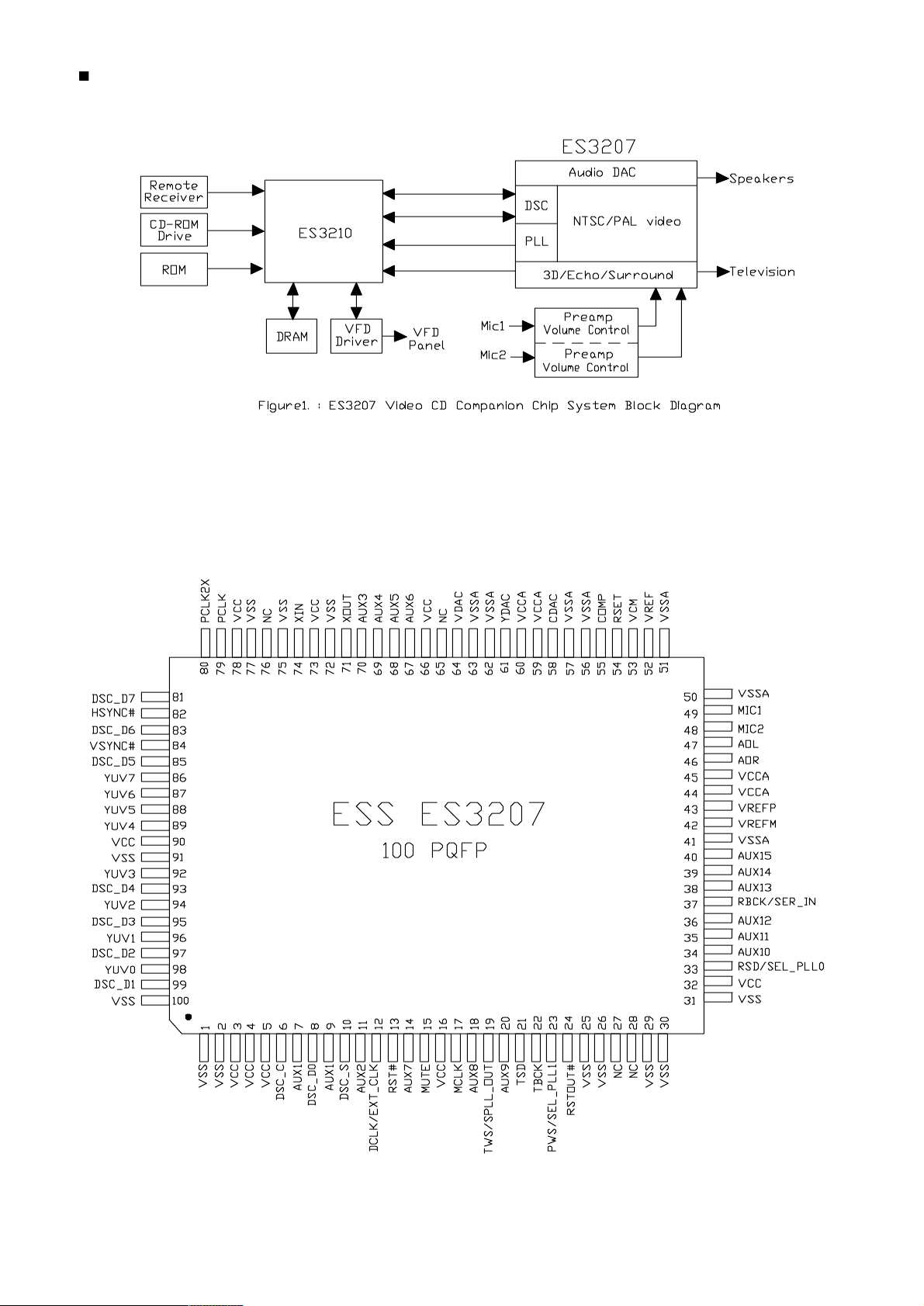
U4: ES3207
Block diagram
XL-SV320SL/305GD/308BU
Pin configuration
1-9
Page 10
XL-SV320SL/305GD/308BU
ES3207 Pin description
XL-SV320SL/SV305GD
Name Number I/O Definition
VSS 1,2,25,26,29,30,31, I Ground.
72,75,77,91,100
VCC 3,4,5,16,32 I Voltage supply 5V.
66,73,78,90
DSC-C 6 I Clock for programming to access internal registers.
AUX[15:0] 40-38,36-34,20,18, I/O Auxiliary control pins.
14,67-70,11,9,7
DSC-D[7:0] 81,83,85,93, I Data for programming to access internal registers.
95,97,99,8
DSC-S 10 I Strobe for programming to access internal registers.
DCLK/ 12 O Dual-purpose pin. DCLK is the mpeg decoder clock.
EXT-CLK I EXT-CLK is the external clock. EXT-CLK input during bypass PLL mode.
RST# 13 I Video reset (active low).
MUTE 15 O Audio mute.
MCLK 17 I Audio master clock.
TWS/ I Dual-purpose pin. TWS is the transmit audio frame sync.
SPLLOUT 19 O SPLLOUT is the select PLL output.
TS D 21 I Transmit audio data input.
TBCK 22 I Transmit audio bit clock.
RWS/ O Dual purpose pin. RWS is the receive audio frame sync.
SEL-PLL1 2 3 I Pins SEL-PLL[1:0] select the PLL clock frequency for DCLK output.
SEL PLL1 SEL PLL0 DCLK
0 0 Bypass PLL (Input Mode)
0 1 27MHz (Output Mode)
1 0 32.4MHz (Output Mode)
1 1 40.5MHz (Output Mode)
RSTOUT# 24 O Reset output (active low).
NC 27,28,65,76 No connect. Do not connect to these pins.
RSD/ 33 O Dual purpose pin. RSD is the receive audio data input.
SEL-PLL0 I SEL-PLL0 is the select PLL. See the table for pin no. 23.
RBCK 37 O Dual purpose pin. RBCK is the receive audio bit clock.
SER-IN I SER-IN is serial input DSC mode.
0=Parallel DSC mode.
1=Serial DSC mode.
VSSA 41,50,51,56,57,62,63 I Analog ground.
VREFM 42 I DAC and ADC minimum reference. Bypass to VCMR with 10µF in parallel with 0.1µF.
VREFP 43 I DAC and ADC maximum reference. Bypass to VCMR with 10µF in parallel with 0.1µF.
VCCA 44,45,59,60 I Analog VCC. 5V.
AOR 46 O Right channel output.
AOL 47 O Left channel output.
MIC2 48 I Microphone input 2.
MIC1 49 I Microphone input 1.
VREF 52 I Internal resistor divider generates Common Mode Reference (CMR) voltage. Bypass to
analog ground with 0.1µF.
VCM 53 I ADC Common Mode Reference (CMR) buffer output. CMR is approximately 2.25V.
Bypass to analog ground with 47µF electrolytic in parallel with 0.1µF.
RSET 54 I Full scale DAC current adjustment.
COMP 55 I Compensation pin.
CDAC 58 O Modulated chrominance output.
YDAC 61 O Y luminance data bus for screen video port.
VDAC 64 O Composite video output.
XOUT 71 O Crystal output.
XIN 74 I 27MHz crystal input.
PCLK 79 I/O 13.5MHz pixel clock.
PCLK2X 80 I/O 27MHz (2 times pixel clock).
HSYNC# 82 I/O Horizontal sync (active low).
VSYNC# 84 I/O Vertical sync (active low).
YUV[7:0] 86-89,92,94,96,98 O YUV luminance and chrominance data bus for screen video port.
XL-SV308BU
1-10
Page 11
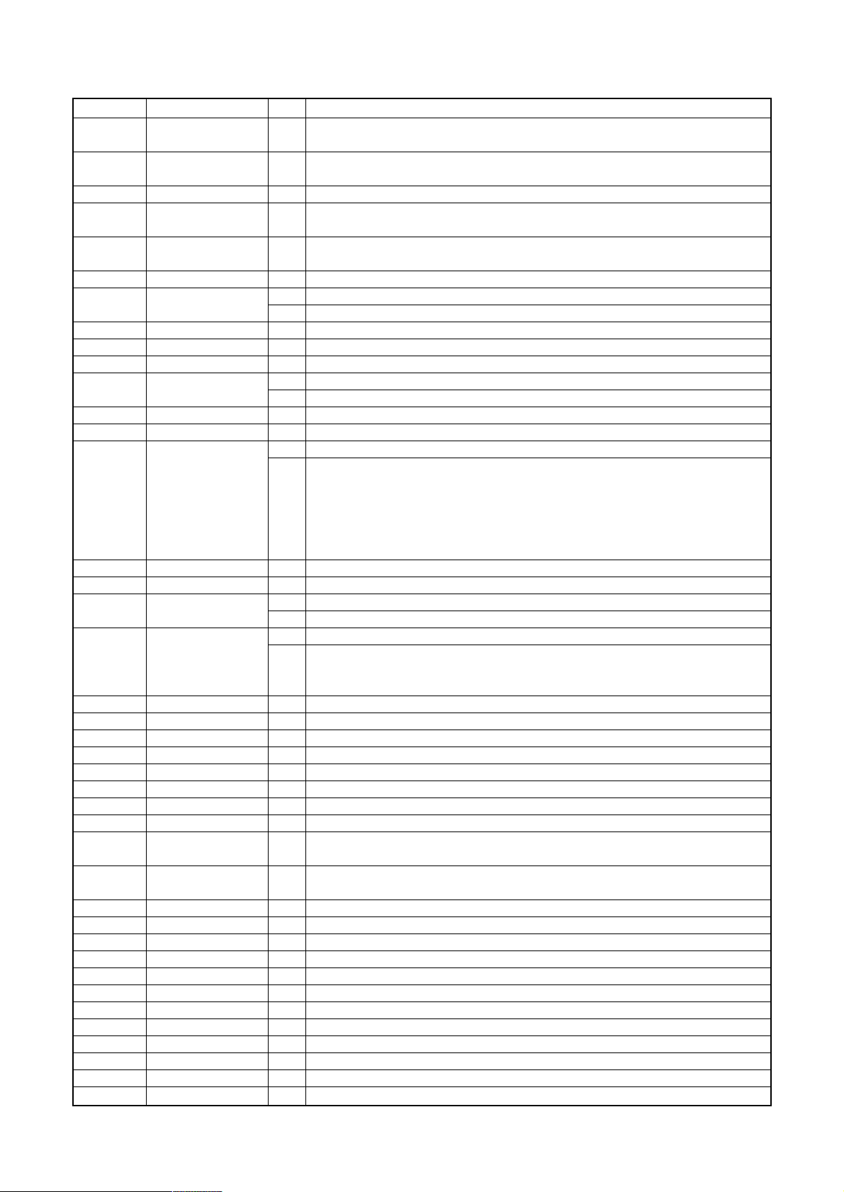
U3: C16256 (4MB DRAM)
Block diagram
XL-SV320SL/305GD/308BU
Pin configuration
Pin description
Pin No. Pin Name Type Description
16~19,22~26 A0-A8 Input Address input
14 RAS Input Row address
strobe
28 CASH Input Column address
strobe/Upper
byte control
29 CASL Input Column address
strobe/lower
byte control
13 WE Input Write enable
27 OE Input Output enable
2~5,6~10, I/O1 - I/O16 Input/Output Data input/
31~34,36~39 output
1,6,20 V c c Supply Power, 5V
21, 35, 40 V ss Ground Ground
11,12,15,30 NC - No connect
1-11
Page 12
XL-SV320SL/305GD/308BU
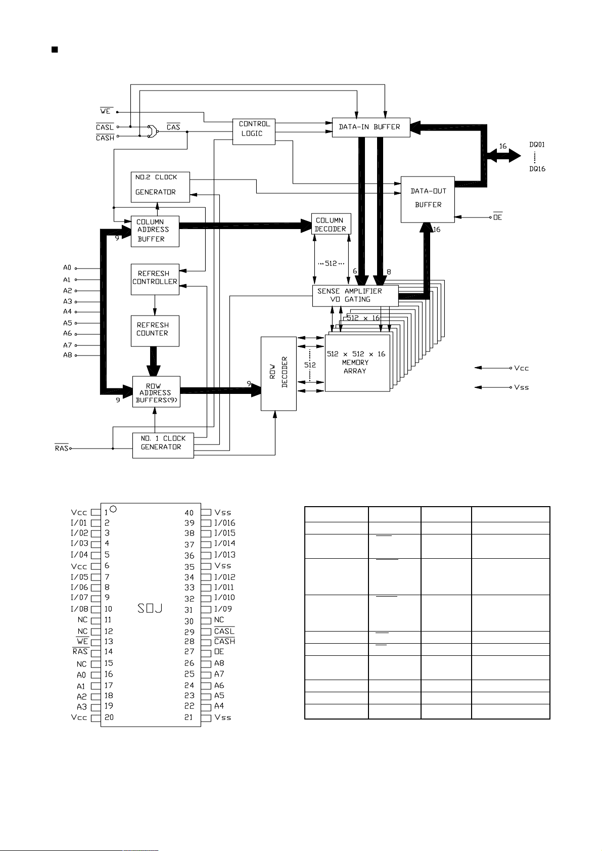
U2: 27C020 (2MB EEPROM)
Block diagram
XL-SV320SL/SV305GD
XL-SV308BU
Pin configuration
Pin description
I/O Pin Name Pin No. Description
- Vpp 1 Voltage input for program erase
operations
I A16,A15,A12 2,3,4 Address input pins
I A7-A0 5-12 Address input pins
I/O D0-D2 13-15 Input/Output pins
- GND 16 Ground
I/O D3-D7 17-21 Input/Output pins
I CE 22 Chip enable (Active low)
I A1 0 23 Address input pins
I OE 24 Output enable (Active low)
I A11,A9,A8 25,26,27 Address input pins
I A13,A14,A17 28,29,30 Address input pins
I WE 31 Write enable bar (Active low)
- VCC 32 Power supply for device
operation (5V ± 10%)
1-12
Page 13
U5: CXD3068Q (CD DSP)
Block diagram
XL-SV320SL/305GD/308BU
1-13
Page 14

XL-SV320SL/305GD/308BU
Pin configuration
XL-SV320SL/SV305GD
XL-SV308BU
Pin description
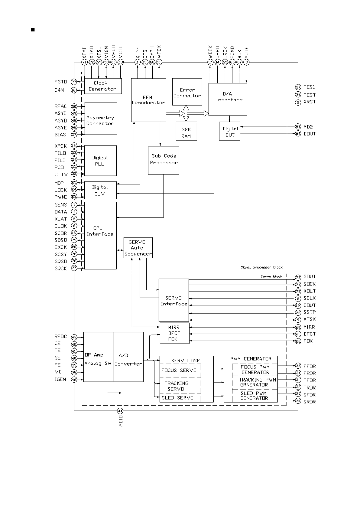
Pin No. Pin Name I/O Description
1DVDD0 - Digital power supply
2 XRST I System reset. Reset when low.
3 MUTE I Mute input (Low: off, high : on)
4 DATA I Serial data input from CPU
5 XLAT I Latch input from CPU. Serial data is latched at the falling edge.
6 CLOK I Serial data transfer clock input from CPU.
7 SENS O 1,0 SENS output to CPU.
8 SCLK I SENS serial data readout clock input.
9 ATSK I/O 1,0 Anti-shock input/output
10 WFCK O 1,0 WFCK output
11 XUGF O 1,0 XUGF output. MNT0 or RFCK is output by switching with the command.
12 XPCK O 1,0 XPCK output. MNT1 is output by switching with the command.
13 GFS O 1,0 GFS output. MNT2 or XROF is output by switching with the command.
14 C2PO O 1,0 G2PO output. MNT3 or GTOP is output by switching with the command.
15 SCOR O 1,0 Outputs a high signal when either subcode sync S0 or S1 is detected.
16 C4M O 1,0 4.2336MHz output. 1/4 frequency division output for V16M in CAV-W mode or variable
pitch mode.
17 WDCK O 1,0 Word clock output. f=2Fs. GRSCOR is output by the command switching.
18 DVss0 - - Digital GND.
19 COUT I/O 1,0 Track count signal I/O
20 MIRR I/O 1,0 Mirror signal I/O
21 DFCT I/O 1,0 Detect signal I/O
22 FO K I/O 1,0 Focus OK signal I/O
23 PWMI I Spindle motor external control input.
24 LOCK I/O 1,0 GFS is sampled at 460Hz; when GFC is high, this pin outputs a high signal. If GFS is low
eight consecutive samples, this pin outputs low. Input when LKIN=1.
25 MDP O 1,Z,0 Spindle motor servo control output.
26 SSTP I Disc innermost track detection signal input.
27 FSTO O 1,0 2/3 frequency division output for XTAI pin.
28 DVDD1 - - Digital power supply.
29 SFDR O 1,0 Sled drive output.
30 SRDR O 1,0 Sled drive output.
31 TFDR O 1,0 Tracking drive output.
32 TRDR O 1,0 Tracking drive output.
33 FFDR O 1,0 Focus drive output.
1-14
Page 15

XL-SV320SL/305GD/308BU
Pin No. Pin Name I/O Description
34 FRDR O 1,0 Focus drive output.
35 DVss1 - - Digital GND.
36 TEST I T est normally , GND
37 TES1 I Test normally, GND
38 V C I Center voltage input
39 FE I Focus error signal input
40 SE I Sled error signal input
41 TE I Tracking error signal input
42 CE I Center servo analog input
43 RFDC I RF signal input
44 ADIO O Analog Test No. connected
45 AVss0 - - Analog GND
46 IGEN I Constant current input for operational amplifier
47 AVDD0 - - Analog power supply
48 ASYO O 1,0 EFM full-swing output. (low=Vss, high=VDD)
49 ASYI I Asymmetry comparator voltage input
50 RF AC I EFM signal input
51 AVss1 - - Analog GND
52 CLTV I Multiplier VCO1 control voltage input
53 FILO O Analog Master PLL filter output (slave=digital PLL)
54 FILI I Master PLL filter input
55 PCO O 1,Z,0 Master PLL charge pump output
56 AVDD1 - - Analog power supply
57 BIAS I Asymmetry circuit constant current input
58 VCTL I Wide-band EFM PLL VCO2 control voltage input
59 V16M I/O 1,0 Wide-band EFM PLL VCO2 oscillation output. Serves as wide-band EFM PLL clock
input by switching with the command.
60 VPCO O 1,Z,0 Wide-band EFM PLL change pump output
61 DVDD2 - - Digital power supply
62 ASYE I Asymmetry circuit on/off (low=off, high=on)
63 MD2 I Digital Out on/off control (low=off, high=on)
64 DOUT O 1,0 Digital Out output
65 LRCK O 1,0 D/A interface. LR clock output. f=Fs
66 PCMD O 1,0 D/A interface. Serial data output (two’s complement, MSB first)
67 BCK O 1,0 D/A interface. Bit clock output
68 EMPH O 1,0 Outputs a high signal when the playback disc has emphasis, and a low signal when
there is no emphasis.
69 XTSL I Crystal selection input. Low when the crystal is 16.9344MHz; high when it is
33.8688MHz.
70 DVss2 - - Digital GND
71 XTAI I Crystal oscillation circuit input. When the master clock is input externally, input it from
this pin.
72 XTAO O Crystal oscillation circuit output.
73 SOUT O 1,0 Serial data output in servo block.
74 SOCK O 1,0 Serial data readout clock output in servo block.
75 XOLT O 1,0 Serial data latch output in servo block.
76 SQCO O 1,0 Sub-Q 80-bit, PCM peak or level data outputs. CD TEXT data output.
77 SQCK I SQCO readout clock input.
78 SCSY I GRSCOR resynchronization input.
79 SBSO O 1,0 Sub-Q P to W serial output.
80 EXCK I SBSO readout clock input.
1-15
Page 16

XL-SV320SL/305GD/308BU
U6: CXA2550N (RF AMPLIFIER)
Block diagram
XL-SV320SL/SV305GD
XL-SV308BU
Pin configuration
Pin description
Pin No. Pin Name I/O Description
1 AGCVTH - Reference level variable pin for RF level control. The reference level can be varied by the
external resistor.
2 LD O APC amplifier output pin.
3 PD I APC amplifier input pin.
4 PD1 I Inversion input pin for RF I-V amplifiers.
5 PD2 I Connect these pins to the photodiodes A + C and B + D respectively. The current is supplied.
6VEE - //VEE pin
7 F I Inversion input pin for F and E I-V amplifiers
8 E I Connect these pins to the photodiodes F and E respectively. The current is supplied.
9 EI - Gain adjustment pin for I-V amplifier.
10 VC O DC voltage output pin of (Vcc + VEE)/2. Connect to GND for ±1.75 power supply; connect a
smoothing capacitor for single +3.5V Power supply.
11 TE O Tracking error amplifier output pin. E-F signal is output.
12 FE_BIAS I Bias adjustment pin for inverted side of focus error amplifier.
13 FE O Focus error amplifier output pin.
14 FRM I RF amplifier inverted side input pin. RF amplifier gain is determined by the resistor connected
between this pin and RFO pin.
15 RF O O RF amplifier output pin.
16 RF I I The RF amplifier output RFO is input with its capacitance coupled.
17 RFTC - External time-constant pin for RF level control.
18 AGCCONT I RF level control ON (limit level of 50%/30%)/OFF switching pin. OFF for Vcc, 30% for open or Vc
and 50% for VEE.
19 LD_ON I APC amplifier ON/OFF switching pin. OFF for Vcc and ON for VEE.
20 V c c Vcc pin
1-16
Page 17

U7: AT6392 (BTL DRIVER)
Block diagram
Pin description
XL-SV320SL/305GD/308BU
Pin No. Pin Name Description
1 BIAS IN Input for Bias-amplifier
2 OPIN1(+) Non inverting input for CH1 OP-AMP
3 OPIN1(-) Inverting input for CH1 OP-AMP
4 OPOUT1 Output for CH1 OP-AMP
5 OPIN2(+) Non inverting input for CH2 OP-AMP
6 OPIN1(-) Non inverting input for CH2 OP-AMP
7 OPOUT2 inverting input for CH2 OP-AMP
8 GND Substrate ground
9 STBY1 Input for CH1/2/3 stand by control
10 PowVcc1 Vcc for CH1/2 power block
11 VO2(-) Inverted output of CH2
12 VO2(+) Non inverted output of CH2
13 VO1(-) Inverted output of CH1
14 VO1(+) Non inverted output of CH1
15 VO4(+) Non inverted output of CH4
16 VO4(-) Inverted output of CH4
17 VO3(+) Non inverted output of CH3
18 VO3(-) Inverted output of CH3
19 PowVcc2 Vcc for CH3/4 power block
20 STBY2 Input for CH4 stand by control
21 GND Substrate ground
22 OPOUT3 Output for CH3 OP-AMP
23 OPIN3(-) Inverting input for CH3 OP-AMP
24 OPIN3(+) Non inverting input for CH3 OP-AMP
25 OPOUT4 Output for CH4 OP-AMP
26 OPOUT4(-) Inverting input for CH4 OP-AMP
27 OPOUT4(+) Non inverting input for CH4 OP-AMP
28 PreVcc Vcc for pre block
1-17
Page 18

XL-SV320SL/305GD/308BU
JVC Asia Pte Ltd
101 Thomson Road, #28-04 United Squares, Singapore 307591
(No: 28207)
Printed in Singapore
0006(L)
Page 19

XL-SV320SL/305GD/308BU
P ARTS LIST
[XL-SV302SL/305GD/308BU]
IMPROTANT
PLASE T AKE NOTE BEFORE ORDERING
1. Order all service parts through JVC Asia Pte Ltd.-Customer Satisfaction Dept.
2. Two orders are available: Initial order and last order (Before End Of Line).
3. Minimum order quantity: 100pcs
4. Delivery term: Minimum 2 months upon confirmation of order.
Contents
Exploded view diagram and mechanical parts list ......... 3-2
Electrical parts list ............................................................ 3-4
Packing list .......................................................................3-8
Parts ordering form ..........................................................3-9
3-1
Page 20

XL-SV320SL/305GD/308BU
Exploded view diagram and mechanical parts list
XL-SV320SL/SV305GD
Main unit exploded view diagram
XL-SV308BU
3-2
Page 21

Enclosure components parts list
Ref. Parts Number Description QTY.
1 620-300606-70 S-TAP.SCREW P-B 3X6 A BZN +H 24
2 620-300610-70 S-TAP.SCREW P-B 3X10 A BZN +H 2
3 E4101-023001 SWITCH POW KDC-A09 1
4 322-SV2001-01Y CUSHION FOOT FRONT 2
5 207-323911-04R CABINET FOOT FRONT SV302 SL R 2 (FOR XL-SV302SL/XL-SV308BU)
207-323911-01R CABINET FOOT FRONT SV20 R 2 (FOR XL-SV305GD)
6 E3701-00L010C3 PCB AC SW VO 1
7 612-300212-10 S-TAP.SCREW WHR 3X12 A NIP +H 2
8 E3701-01B010-1 PCB MIC AMP 75X98 HB 1
9 273-SV2001-04S VOLUME MIC KNOB SILVER SV302 SL S 2 (FOR XL-SV302SL/XL-SV308BU)
273-SV2001-01S KNOB ECHO 2 (FOR XL-SV305GD)
10 E3701-00L010A3 PCB POWER 168X68 VO 1
11 E2301-237001 IC L7805CV 1
12 E5102-114002 TRANSFORMER POW T57-0123018-10 IEC EI57 1
13 620-400606-70 S-TAP SCREW P-B 4X6 4
14 459-SV2001-01 HOLDER MECH(1) 1
15 E4103-020001 SWITCH SLIDE LZ1-22A2 44 1
16 459-SV2002-01 HOLDER MECH(2) 1
17 E7701-005001 MECHANISM VCD KSS-213V 1
18 211-SV2011-05S CD TRAY SILVER JVC-SV302 S 1 (FOR XL-SV302SL)
211-SV2011-03S CD TRAY GOLD JVC-SV305 S 1 (FOR XL-SV305GD)
211-SV2011-06S CD TRAY BLUE JVC-SV308 S 1 (FOR XL-SV308BU)
19 402-SV2001-05 PANEL REAR SV302 SL 1 (FOR XL-SV302SL)
402-SV2001-03 PANEL REAR SV305 GD 1 (FOR XL-SV305GD)
402-SV2001-06 PANEL REAR SV308 BU 1 (FOR XL-SV308BU)
20 E7801-003002 PCB ASSY HY-26 1
21 322-SV2002-01Y CUSHION FOOT BACK 2
22 403-SV2001-01 CHASSIS BOTTOM 1
23 610-260108-00 S-TAP.SCREW RND 2.6X8 B BZN +H 12
24 620-400605-90 S-TAP SCREW P-B 4X5 4
25 372-SV2001-01Y SPACER FLD 10X10X4 2
26 E6201-019002 DISPLA Y FLD 20U39119BAN 1
27 279-SV2002-04S SPATIALIZER KNOB SL SV302 SL S 1 (FOR XL-SV302SL)
279-SV2002-01S BUTTON SPA TIALIZER 1 (FOR XL-SV305GD)
279-SV2002-05S SPATIALIZER KNOB BLUE SV308 BU S 1 (FOR XL-SV308BU)
28 279-SV2003-04S PLAY KNOB SIL VER SV302 SL S 1 (FOR XL-SV302SL/XL-SV308BU)
279-SV2003-01S BUTTON PLA Y 1 (FOR XL-SV305GD)
29 260-SV2001-01K WINDOW LEN FLD 1
30 200-SV2002-03R FRONT PANEL SIL VER SV302 SL R 1 (FOR XL-SV302SL)
200-SV2002-01R FRONT PANEL GOLD SV305 GD R 1 (FOR XL-SV305GD)
200-SV2002-04R FRONT PANEL BLUE SV308 BU R 1 (FOR XL-SV308BU)
31 286-SV2001-02S NAME PLATE 1 (FOR XL-SV302SL/XL-SV308BU)
286-SV2001-01S NAME PLATE 1 (FOR XL-SV305GD)
32 279-SV2001-04S POWER KNOB SIL VER SV302 SL S 1 (FOR XL-SV302SL/XL-SV308BU)
279-SV2001-01S BUTTON POWER 1 (FOR XL-SV305GD)
33 603-305005-00 MACH.SCREW TRS 3X5 BZN +H 2
XL-SV320SL/305GD/308BU
3-3
Page 22

XL-SV320SL/305GD/308BU
Electrical parts list
XL-SV320SL/SV305GD
Electrical parts list (Remote board)
Mark Ref. Parts Number Description QTY.
C001 E1301-004030 CAPACITOR EC V SA T 05 4 70M 16DC 5 1
C001 E1301A002002A CAPACIT OR E C V A S B 470M 16DC T05 5X1 1 1 [FOR XL-SV305GD]
C002 E1321-001053 CAPACIT OR C E V TC S L221J 5 0DC T0 5 7 2
C003 E1321-001053 CAPACIT OR C E V TC S L221J 5 0DC T0 5 7
CF001 E4302-044001 OSCILLATOR CE XZT455E 455K 1
D001 E2501-010001 DIODE SILICON H 1N4148-T72 T52 4
D002 E2501-010001 DIODE SILICON H 1N4148-T72 T52
D003 E2501-010001 DIODE SILICON H 1N4148-T72 T52
D004 E2501-010001 DIODE SILICON H 1N4148-T72 T52
IC001 E2351-033001 IC HT-6222-24 1
IC001 E2351-050001 IC PT2222-001 1
JP001 E3409-001001 WIRE JUMPER 0.6MM 1KG=375M 0.0001
LED001 E2509-029001 DIODE LED TSAL6200 INFRARED 1
Q001 E2103-109001 TRANSISTOR 3DA8050(8050) C T05 1
R001 E1501-002007 RESISTOR CBF H 1/4W 1R0J T52 1
090-385610-03 PCB HANSET 119X46 HB 1
Electrical parts list (Power board)
Mark Ref. Parts Number Description QTY.
A1-A2 E3451-000078 WIRE WD CG-2N-0140-D0A-D0A 1
B1-B2 E3451-000079 WIRE WD CG-3N-0140-D0A-D0A 1
C101 E1325-012002 CAPACIT O R CE V CT81-4 E 222M 250AC 13 1
C102 E1333-010002 CAPACITOR SPP MPX 473K 275AC 2
C104 E1321-002002 CAPACIT OR C E V HIK F 103Z 50DC T05 8 8
C105 E1321-002002 CAPACIT OR C E V HIK F 103Z 50DC T05 8
C106 E1321-002002 CAPACIT OR C E V HIK F 103Z 50DC T05 8
C107 E1321-002002 CAPACIT OR C E V HIK F 103Z 50DC T05 8
C108 E1301A002006A CAPACIT OR EC V A SB 332M 25DC 16X25 1
C109 E1301A002009A CAPACIT OR EC V A SB 1R0M 50DC T05 5X1 1 1
C120 E1321-011006 CAP ACIT OR C E V SC F 104Z 50 DC T05 7 5
C121 E1301A002015A CAPACIT OR E C V A S B 471M 16DC T05 8X12 1
C123 E1321-002002 CAPACIT OR C E V HIK F 103Z 50DC T05 8
C124 E1321-002002 CAPACIT OR C E V HIK F 103Z 50DC T05 8
C125 E1321-002002 CAPACIT OR C E V HIK F 103Z 50DC T05 8
C126 E1321-002002 CAPACIT OR C E V HIK F 103Z 50DC T05 8
C127 E1301A002020A CAPACIT OR EC V A SB 222M 16DC 13X20 1
C128 E1301A002004A CAPACIT OR E C V A S B 102M 16DC T05 10X17 1
C129 E1321-011006 CAP ACIT OR C E V SC F 104Z 50 DC T05 7
C130 E1321-011006 CAP ACIT OR C E V SC F 104Z 50 DC T05 7
C131 E1321-011006 CAP ACIT OR C E V SC F 104Z 50 DC T05 7
C132 E1301A002019A CAPACIT OR EC V A SB 221M 35DC 10X13 1
C133 E1321-011006 CAP ACIT OR C E V SC F 104Z 50 DC T05 7
C134 E1333-010002 CAPACITOR SPP MPX 473K 275AC
C1-C2 E3451-000215 WIRE WD CG-4N-0140-DOA-DOA 1
CN101 E3421-799001 WIRE ASSY 1H2.5-2T2.5 9- L361 GG 10P 1
CN103 E3101-175004 PLUG V HX2503-5A P2.5 5P WHI 1
CN104 E3101-094004 PLUG EH-5A 5P 1
CN106 E3421-798001 WIRE ASSY 1H8.0-2TKN5 2- L367 CG 2P 1
D101 E2501-087001 DIODE SILICON H RL201 2A 50V DO-15 4
D102 E2501-087001 DIODE SILICON H RL201 2A 50V DO-15
D103 E2501-087001 DIODE SILICON H RL201 2A 50V DO-15
D104 E2501-087001 DIODE SILICON H RL201 2A 50V DO-15
D105 E2501-055001 DIODE SILICON H 1N4004 1A400V T52 D0-41 6
D106 E2501-055001 DIODE SILICON H 1N4004 1A400V T52 D0-41
D107 E2501-055001 DIODE SILICON H 1N4004 1A400V T52 D0-41
D108 E2501-055001 DIODE SILICON H 1N4004 1A400V T52 D0-41
D1 1 0 E2501-055001 DIODE SILICON H 1N4004 1A400V T52 D0-41
XL-SV308BU
3-4
Page 23

Mark Ref. Parts Number Description QTY.
D1 11 E2501-055001 DIODE SILICON H 1N4004 1A400V T52 D0-41
EY1 437-015030-02 EYELET 1.5X3 N+T 4B 2
EY2 437-015030-02 EYELET 1.5X3 N+T 4B
EY3 437-020030-02 EYELET 2X3 N+T 4B 6
EY4 437-020030-02 EYELET 2X3 N+T 4B
EY5 437-020030-02 EYELET 2X3 N+T 4B
EY6 437-020030-02 EYELET 2X3 N+T 4B
EY7 437-020030-02 EYELET 2X3 N+T 4B
EY8 437-020030-02 EYELET 2X3 N+T 4B
F101 456-701201-01 FUSE HOLDER 7012 2
F101 E5301-055001 FUSE 19195 T 250V 0.63A 1
IC101 E2301-237001 IC L7805CV1
JP101 E3409-001001 WIRE JUMPER 0.6MM 1KG=375M 0.0004
JP102 E3409-001001 WIRE JUMPER 0.6MM 1KG=375M
JP103 E3409-001001 WIRE JUMPER 0.6MM 1KG=375M
L101 E4405-021001 FILTER LINE LCL-2002WH 1
L102 E3409-001001 WIRE JUMPER 0.6MM 1KG=375M
P101 E3101-172001 PLUG V VH-3A P4.0 2P 1
P102 E3101-065001 PLUG STV8-2W 2P 1
R101 E1509-005013 RESISTOR FUSE H 1/2W R22J F10 1
R102 E3409-001001 WIRE JUMPER 0.6MM 1KG=375M
R103 E3409-001001 WIRE JUMPER 0.6MM 1KG=375M
R105 E1501-002082 RESISTOR CBF H 1/4W 681J T52 1
R106 E1501-002066 RESISTOR CBF H 1/4W 471J T52 2
R107 E1501-002066 RESISTOR CBF H 1/4W 471J T52
R108 E1501-002035 RESISTOR CBF H 1/4W 223J T52 1
R109 E1509-011019 RESISTOR FUSE H 1/4W R22J S10 1
R111 E3409-001001 WIRE JUMPER 0.6MM 1KG=375M
R112 E3409-001001 WIRE JUMPER 0.6MM 1KG=375M
SW101 E4103-020001 SWITCH SLIDE LZ1-22A2 4410206 1
SW102 E4101-023001 SWITCH POW KDC-A09 1
ZD101 E2504-003017 DIODE ZENER H TZX6V8-B 1/2W T52 6.8V 1
ZD102 E2504-003006 DIODE ZENER H TZX20V-B 1/2W T52 20V 1
E3701-00L010A3 PCB POWER 168X68 VO 1
E3701-00L010B3 PCB SELEC VO 1
E3701-00L010C3 PCB AC SW VO 1
XL-SV320SL/305GD/308BU
Electrical parts list (MIC board)
Mark Ref. Parts Number Description QTY.
C202 E1321-002002 CAPACIT OR C E V HIK F 103Z 50DC T05 8 2
C203 E1321-001016 CAPACIT OR C E V TC SL221K 50DC T05 7 2
C204 E1321-002023 CAPACIT OR C E V HIK B 331K 50DC T05 5 3
C205 E1301-004014 CAPACITOR EC V SA T05 2R2M 50DC 5 2
C206 E1301A002001A CAPACIT OR E C V A S B 100M 16DC T05 5X1 1 2
C207 E1301A002001A CAPACIT OR E C V A S B 100M 16DC T05 5X1 1
C208 E1301A002002A CAPACIT OR E C V A S B 470M 16DC T05 5X1 1 2
C209 E1321-011006 CAP ACIT OR C E V SC F 104Z 50 DC T05 7 2
C210 E1321-002002 CAPACIT OR C E V HIK F 103Z 50DC T05 8
C212 E1321-001016 CAPACIT OR C E V TC SL221K 50DC T05 7
C213 E1321-002023 CAPACIT OR C E V HIK B 331K 50DC T05 5
C214 E1321-002023 CAPACIT OR C E V HIK B 331K 50DC T05 5
C215 E1301-004014 CAPACITOR EC V SA T05 2R2M 50DC 5
C232 E1301A002002A CAPACIT OR E C V A S B 470M 16DC T05 5X1 1
C233 E1321-011006 CAP ACIT OR C E V SC F 104Z 50 DC T05 7
CN201 E3101-094004 PLUG EH-5A 5P 1
CN202 E3421-718003 WIRE ASSY 1H2.5-2T2.5 8- L80 KD 5P 1
IC201 E2301-145001 IC BA4558 2
IC202 E2301-145001 IC BA4558
JP201 E3409-001001 WIRE JUMPER 0.6MM 1KG=375M 0.0006
JP202 E3409-001001 WIRE JUMPER 0.6MM 1KG=375M
JP203 E3409-001001 WIRE JUMPER 0.6MM 1KG=375M
3-5
Page 24

XL-SV320SL/305GD/308BU
Mark Ref. Parts Number Description QTY.
L201 E3409-001001 WIRE JUMPER 0.6MM 1KG=375M
L202 E3409-001001 WIRE JUMPER 0.6MM 1KG=375M
L203 E3409-001001 WIRE JUMPER 0.6MM 1KG=375M
L204 E3409-001001 WIRE JUMPER 0.6MM 1KG=375M
M1 E3202-031001 MIC JACK CK3-6.35-31 2
M2 E3202-031001 MIC JACK CK3-6.35-31
R201 E1501-001085 RESISTOR CBF H 1/6W 681J T52 2
R202 E1501-001004 RESISTOR CBF H 1/6W 103J T52 2
R205 E1501-001068 RESISTOR CBF H 1/6W 473J T52 3
R206 E1501-001003 RESISTOR CBF H 1/6W 102J T52 3
R207 E1501-001033 RESISTOR CBF H 1/6W 223J T52 2
R208 E1501-001068 RESISTOR CBF H 1/6W 473J T52
R209 E1501-002002 RESISTOR CBF H 1/4W 101J T52 2
R210 E1501-002002 RESISTOR CBF H 1/4W 101J T52
R21 1 E1501-001085 RESISTOR CBF H 1/6W 681J T52
R212 E1501-001004 RESISTOR CBF H 1/6W 103J T52
R214 E1501-001068 RESISTOR CBF H 1/6W 473J T52
R215 E1501-001003 RESISTOR CBF H 1/6W 102J T52
R216 E1501-001033 RESISTOR CBF H 1/6W 223J T52
R232 E1501-001003 RESISTOR CBF H 1/6W 102J T52
E1301-004003 CAPACIT O R E C V S A T0 5 1 00M 16DC 5 2
E1301-004030 CAPACIT O R E C V S A T0 5 4 70M 16DC 5 2
E3701-01B010-1 PCB MIC AMP 75X98 HB 1
XL-SV320SL/SV305GD
XL-SV308BU
Electrical parts list (Key board)
Mark Ref. Parts Number Description QTY.
C301 E1321-001016 CAPACIT OR CE V TC SL221K 50DC T05 7 3
C302 E1321-001016 CAPACIT OR CE V TC SL221K 50DC T05 7
C303 E1321-001016 CAPACIT OR CE V TC SL221K 50DC T05 7
C304 E1321-011006 CAP ACIT OR CE V SC F 104Z 5 0DC T0 5 7 1
C305 E1301A002018A CAPACIT OR EC V A SB 101M 10DC T05 5X1 1 1
C306 E1301A002013A CAPACIT OR EC V A SB 220M 16DC T05 5X1 1 1
C307 E1321-002002 CAPACIT OR CE V HIK F 103Z 50DC T05 8 1
CN301 E3421-792001 WIRE ASSY 1H2.5-2T2.5 08- L231 AF 5P 1
CN302 E3421-793001 WIRE ASSY 1H2.5-2T2.5 92- L230 GE 5P 1
CN303 E3421-718002 WIRE ASSY 1H2.5-2T2.5 8- L90 KD 5P 1
D301 E2501-010001 DIODE SILICON H 1N4148-T72 T52 5
D302 E2501-010001 DIODE SILICON H 1N4148-T72 T52
D303 E2501-010001 DIODE SILICON H 1N4148-T72 T52
D304 E2501-010001 DIODE SILICON H 1N4148-T72 T52
D305 E2501-010001 DIODE SILICON H 1N4148-T72 T52
FLD301 E6201-019002 DISPLA Y FLD 20U391 19BAN 1
IC301 E2351-077001 IC HT16512 1
JP301-JP325 E3409-001001 WIRE JUMPER 0.6MM 1KG=375M
JP326 E3409-001001 WIRE JUMPER 0.6MM 1KG=375M
K301 E4102-028001 SWITCH TACT HCT-1 141A 19
K302 E4102-028001 SWITCH TACT HCT-1 141A
K303 E4102-028001 SWITCH TACT HCT-1 141A
K304 E4102-028001 SWITCH TACT HCT-1 141A
K305 E4102-028001 SWITCH TACT HCT-1 141A
K306 E4102-028001 SWITCH TACT HCT-1 141A
K307 E4102-028001 SWITCH TACT HCT-1 141A
K308 E4102-028001 SWITCH TACT HCT-1 141A
K309 E4102-028001 SWITCH TACT HCT-1 141A
K310 E4102-028001 SWITCH TACT HCT-1 141A
K311 E4102-028001 SWITCH T ACT HCT-1141A
K312 E4102-028001 SWITCH TACT HCT-1 141A
K313 E4102-028001 SWITCH TACT HCT-1 141A
K314 E4102-028001 SWITCH TACT HCT-1 141A
K315 E4102-028001 SWITCH TACT HCT-1 141A
K316 E4102-028001 SWITCH TACT HCT-1 141A
3-6
Page 25

XL-SV320SL/305GD/308BU
Mark Ref. Parts Number Description QTY.
K317 E4102-028001 SWITCH TACT HCT-1 141A
K318 E4102-028001 SWITCH TACT HCT-1 141A
K319 E4102-028001 SWITCH TACT HCT-1 141A
OP301 E2701-017002 DETECTOR IR SPS-440-1-E 1
R301 E1501-001054 RESISTOR CBF H 1/6W 333J T52 9
R302 E1501-001054 RESISTOR CBF H 1/6W 333J T52
R303 E1501-001054 RESISTOR CBF H 1/6W 333J T52
R304 E1501-001054 RESISTOR CBF H 1/6W 333J T52
R305 E1501-001054 RESISTOR CBF H 1/6W 333J T52
R306 E1501-001054 RESISTOR CBF H 1/6W 333J T52
R307 E1501-001054 RESISTOR CBF H 1/6W 333J T52
R308 E1501-001054 RESISTOR CBF H 1/6W 333J T52
R309 E1501-001004 RESISTOR CBF H 1/6W 103J T52 3
R310 E1501-001004 RESISTOR CBF H 1/6W 103J T52
R31 1 E1501-001004 RESISTOR CBF H 1/6W 103J T52
R312 E1501-001054 RESISTOR CBF H 1/6W 333J T52
R313 E1501-001073 RESISTOR CBF H 1/6W 512J T52 1
R314 E1501-001001 RESISTOR CBF H 1/6W 100J T52 1
VR302 E1701-048002 VAR RESISTOR ROT R0903N1PFNH-B10K 2
VR303 E1701-048002 VAR RESISTOR ROT R0903N1PFNH-B10K
E3701-00L030-1 PCB KEY ANDFLD DISPL Y HB 1
3-7
Page 26

XL-SV320SL/305GD/308BU
Packing
XL-SV320SL/SV305GD
XL-SV308BU
NO. P/N QTY. DESCRIPTION
1 790-010116-01 1 JVC REMOTE 43KEYS FOR XL-SV302SL
790-010116-02 1 JVC REMOTE 43KEYS FOR XL-SV305GD
790-010116-04 1 REMOVE 47 KEYS XL-SV308
2 310-040804-03T 1 POLYBAG
3 300-SV2001-01C 1 POLYFOAM L
4 XL-SV30 1 MAIN P ART
5 310-222406-04V 1 POLYBAG
6 580-SV3001-02 1 INST. BOOKLET E
7 310-101504-02T 1 POLYBAG
8 510-SV3001-XXK 1 GIFT BOX
9 300-SV2002-01C 1 POLYFOAM R
10 310-040804-03T 2 POLYBAG
11 E4405-021001 1 FILTER LINE LCL-2002WH
12 579-SV2001-06 1 BAR CODE LABEL SV302 SL
579-SV2001-04 1 BAR CODE LABEL SV305 GD
579-SV2001-07 1 BAR CODE LABEL SV308 BU
13 E3103-004001 1 PLUG ADAPTER ADP-01
3-8
Page 27

TO: Customer Satisfaction Dept.
FAX: (65) 2543284
PARTS-ORDERING FORM
PAGE ______OF_____
Buyer’s Name Date Of Order Buyer’s Signature /Chop
Destination Ship Via AIR AIR MAIL DHL-MAIL
SEA SEA MAIL SEA&AIR
Account Code Destination Code Purchase Order No.
Item No. Model No. Parts No. Parts Name Qty Remarks
★
Please do not forget to describe Model No with Tail code.
3-9
Page 28

XL-SV320SL/305GD/308BU
SERVICE MANUAL
VIDEO CD PLAYER
XL-SV302SL/SV305GD
XL-SV308BU
POWER
ON / OFF
COMPACT
VIDEO CD
DIGITAL VIDEO
PLEASE TAKE NOTE BEFORE ORDERING
1. Order all service parts through JVC Asia Pte Ltd.- Customer Satisfaction Dept.
2. Two orders are available: Initial order and last order (Before End Of Line)
3. Minimum order quantity: 100pcs
4. Delivery term: Minimum 2 months upon confirmation of order.
1 – MIC VOLUME – 2
MIN MAX MIN MAX
1 – MIC – 2
OPEN/CLOSE
RETURN
IMPORTANT
123 45
+10 678910/0
Contents
Wiring diagram .................................................................2-2
Block diagram...................................................................2-3
Schematic diagram ...........................................................2-4
Printed circuit boards............................................................. 2-10
COPYRIGHT
2001 VICTOR COMP ANY OF JAP AN L TD.
No: 28207SCH
OCT. 2001
Page 29

XL-SV320SL/305GD/308BU
Wiring diagram
XL-SV320SL/SV305GD
XL-SV308BU
2-2
Page 30

Block diagram
XL-SV320SL/305GD/308BU
2-3
Page 31

Schematic Diagrams
MIC AMP, Power, Key & VFD Circuit
XL-SV302SL/305GD/308BU
2-4
Page 32

MPEG Circuit
XL-SV302SL/305GD/308BU
2-5
Page 33

Servo Circuit
XL-SV302SL/305GD/308BU
2-6
Page 34

Output Circuit
XL-SV302SL/305GD/308BU
2-7
Page 35

D/A Circuit
XL-SV302SL/305GD/308BU
2-8
Page 36

Memory Circuit
XL-SV302SL/305GD/308BU
2-9
Page 37

Printed Circuit Boards
Power Supply, AC Selector & AC Switch Board
Top View Bottom View
XL-SV302SL/305GD/308BU
2-10
Page 38

MPEG, Servo and Output PCB
XL-SV302SL/305GD/308BU
Top View
2-11
Page 39

MIC AMP Board
XL-SV302SL/305GD/308BU
2-12
Page 40

Key and FLD Display Board
XL-SV302SL/305GD/308BU
2-13
Page 41

XL-SV320SL/305GD/308BU
JVC Asia Pte Ltd
101 Thomson Road, #28-04 United Squares, Singapore 307591
(No: 28207)
Printed in Singapore
0006(L)
 Loading...