

Page 1
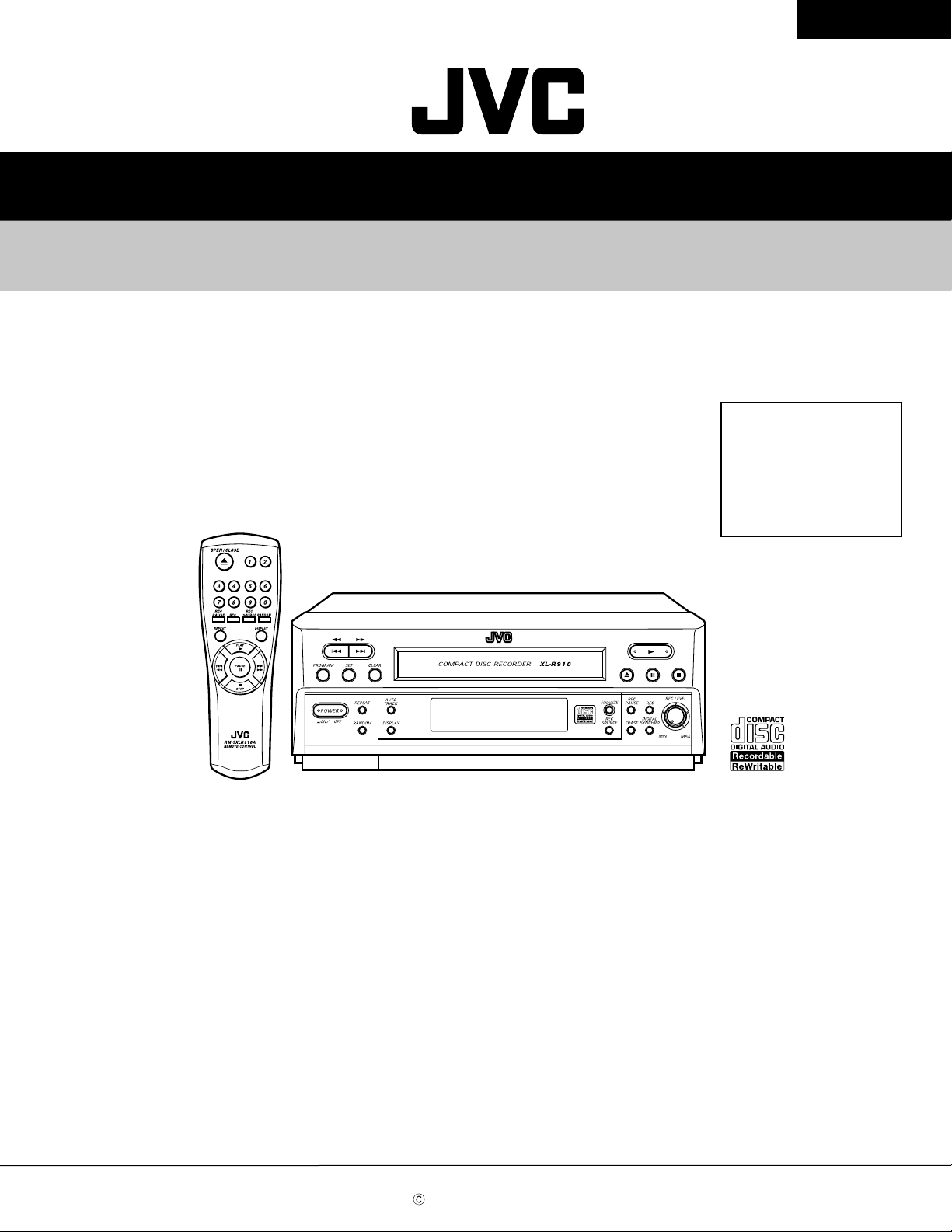
SERVICE MANUAL
COMPACT DISC RECORDER
XL-R910SL
J ------------------- U.S.A.
C ---------------- Canada
B --------------------- U.K.
E -- Continental Europe
EN --- Northern Europe
XL-R910SL
Area Suffix
Contents
Safety precautions ----------------------- 1-2
Disassembly method -------------------- 1-3
Troubleshooting -------------------------- 1-6
Description of major ICs ---------------- 1-11
This service manual is printed on 100% recycled paper.
COPYRIGHT 2001 VICTOR COMPANY OF JAPAN, LTD.
No.A0009
Apr. 2001
Page 2

XL-R910SL
1. This design of this product contains special hardware and many circuits and components specially
for safety purposes. For continued protection, no changes should be made to the original design
unless authorized in writing by the manufacturer. Replacement parts must be identical to those
used in the original circuits. Services should be performed by qualified personnel only.
2. Alterations of the design or circuitry of the product should not be made. Any design alterations of
the product should not be made. Any design alterations or additions will void the warranty
and will further relieve the manufacture of responsibility for personal injury or property damage
resulting therefrom.
3. Many electrical and mechanical parts in the products have special safety-related characteristics.
These characteristics are often not evident from visual inspection nor can the protection afforded
by them necessarily be obtained by using replacement components rated for higher voltage,
wattage, etc. Replacement parts which have these special safety characteristics are identified in
the Parts List of Service Manual. Electrical components having such features are identified by
shading on the schematics and by ( ) on the Parts List in the Service Manual. The use of a
substitute replacement which does not have the same safety characteristics as the recommended
replacement parts shown in the Parts List of Service Manual may create shock, fire, or other
hazards.
4. The leads in the products are routed and dressed with ties, clamps, tubings, barriers and the
like to be separated from live parts, high temperature parts, moving parts and/or sharp edges
for the prevention of electric shock and fire hazard. When service is required, the original lead
routing and dress should be observed, and it should be confirmed that they have been returned
to normal, after reassembling.
5. Leakage current check (Electrical shock hazard testing)
After reassembling the product, always perform an isolation check on the exposed metal parts of
the product (antenna terminals, knobs, metal cabinet, screw heads, headphone jack, control
shafts, etc.) to be sure the product is safe to operate without danger of electrical shock.
Do not use a line isolation transformer during this check.
Plug the AC line cord directly into the AC outlet. Using a "Leakage Current Tester", measure
the leakage current from each exposed metal parts of the cabinet , particularly any exposed
metal part having a return path to the chassis, to a known good earth ground. Any leakage
current must not exceed 0.5mA AC (r.m.s.)
Alternate check method
Plug the AC line cord directly into the AC outlet. Use an AC voltmeter having, 1,000 ohms
per volt or more sensitivity in the following manner. Connect a 1,500 10W resistor paralleled by
a 0.15 F AC-type capacitor between an exposed
metal part and a known good earth ground.
Measure the AC voltage across the resistor with the
AC voltmeter.
AC VOLTMETER
(Having 1000
ohms/volts,
or more sensitivity)
Move the resistor connection to each exposed
metal part, particularly any exposed metal part
having a return path to the chassis, and measure
the AC voltage across the resistor. Now, reverse
the plug in the AC outlet and repeat each
measurement. voltage measured Any must not
0.15 F AC TYPE
1500 10W
Place this
probe on
each exposed
metal part.
exceed 0.75 V AC (r.m.s.). This corresponds to 0.5
Good earth ground
1. This equipment has been designed and manufactured to meet international safety standards.
2. It is the legal responsibility of the repairer to ensure that these safety standards are maintained.
3. Repairs must be made in accordance with the relevant safety standards.
4. It is essential that safety critical components are replaced by approved parts.
5. If mains voltage selector is provided, check setting for local voltage.
!
Burrs formed during molding may be left over on some parts of the chassis. Therefore,
pay attention to such burrs in the case of preforming repair of this system.
1-2
Page 3
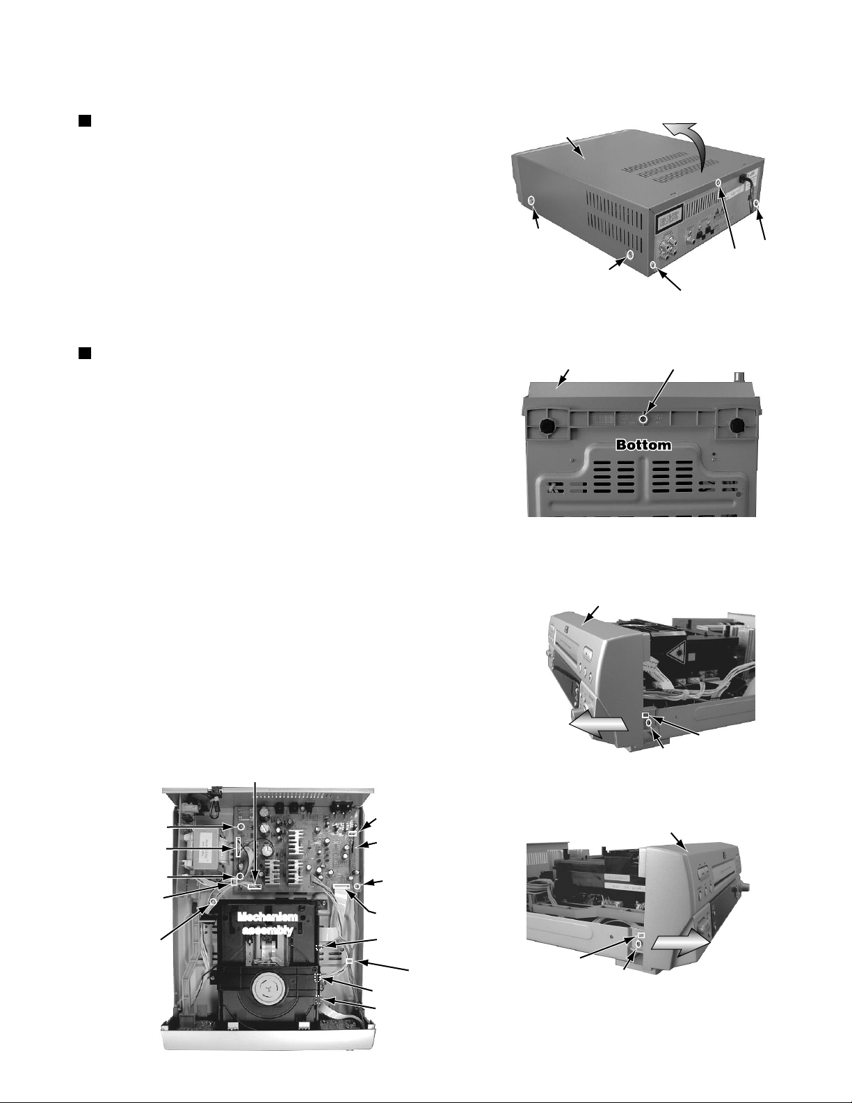
Disassembly method
<Main body>
XL-R910SL
Removing the metal cover (See Fig.1)
1.Remove the three screws A attaching the metal cover
on the back of the body.
2.Remove the four screws B attaching the metal cover
on both sides of the body.
3.Remove the metal cover from the body by lifting the
rear part of the cover.
ATTENTION : Do not break the front panel tab fitted
to the metal cover.
Removing the front panel assembly (See Fig.2~5)
* Prior to performing the following procedure, remove the
metal cover.
1.Remove the three screws C attaching the front panel
assembly on the bottom of the body and both sides of
the body.
2.Disconnect the card wire from connector CN601 on the
servo control board.
Metal cover
B x 2
B x 2
Front panel assembly
Fig. 1
Fig. 2
A
A
A
C
3.Disconnect the 4pin wire from connector CN502 on the
servo control board.
4.Disconnect the 3pin wire and 8pin wire from connector
ACW1 and RCW2 on the main board.
Please remove a tie band if necessary.
Please fix the wire again with a tie band when assembling.
5.Release the two joints a on the lower part of the sides
using a screwdriver, and remove the front panel assembly
toward the front.
RCW2
ACW1
F
RCW1
F
Tie band
Mechanism
assembly
D
Main board
G
NCW1
CN502
Tie band
CN701
CN601
Front panel assembly
Fig. 3
Front panel assembly
Joint a
C
joint a
C
Fig. 4
Fig. 5
1-3
Page 4
XL-R910SL
Removing the power button arm (See Fig.6)
* Prior to performing the following procedure,
remove the metal cover and front panel assembly.
The power button arm is lifted up while holding the
power switch(orange color part) and removes.
Removing the mechanism assembly
(See Fig.6)
* Prior to performing the following procedure,
remove the metal cover and front panel
assembly.
1.Disconnect the card wire from connector CN501
on the servo control board.
2.Disconnect the 6pin wire from connector CN701
on the servo control board.
3.Remove the four screws D attaching the
mechanism assembly.
*Please fix two earth wires together when you
install the mechanism assembly.
Removing the main board (See Fig.5,7)
F
RCW1
F
Tie band
D
Orange
color part
Earth wire
RCW2
Mechanism
assembly
Mechanism
assembly
ACW1
Main board
G
NCW1
CN502
Tie band
CN701
CN601
Fig. 5
Main board
D
CN501
* Prior to performing the following procedure,
remove the metal cover.
1.Remove the four screws E attaching the each
terminal on the rear panel.
2.Disconnect the 9pin,8pin and 3pin wire from
connector RCW1,RCW2 and ACW1 on the main
board.
3.Disconnect the card wire from connector NCW1
on the main board.
4.Disconnect the 6pin wire from connector CN701
on the servo control board.
5.Remove the screw D attaching the earth wire.
6.Remove the two screws F and one screw G
attaching the main board.
Please remove a tie band if necessary.
Please fix the wire again with a tie band
when assembling.
Power
button
arm
D
D
Earth wire
CN701
D
Fig. 6
E
E
E
E
Cord bushing
Fig. 7
1-4
Page 5

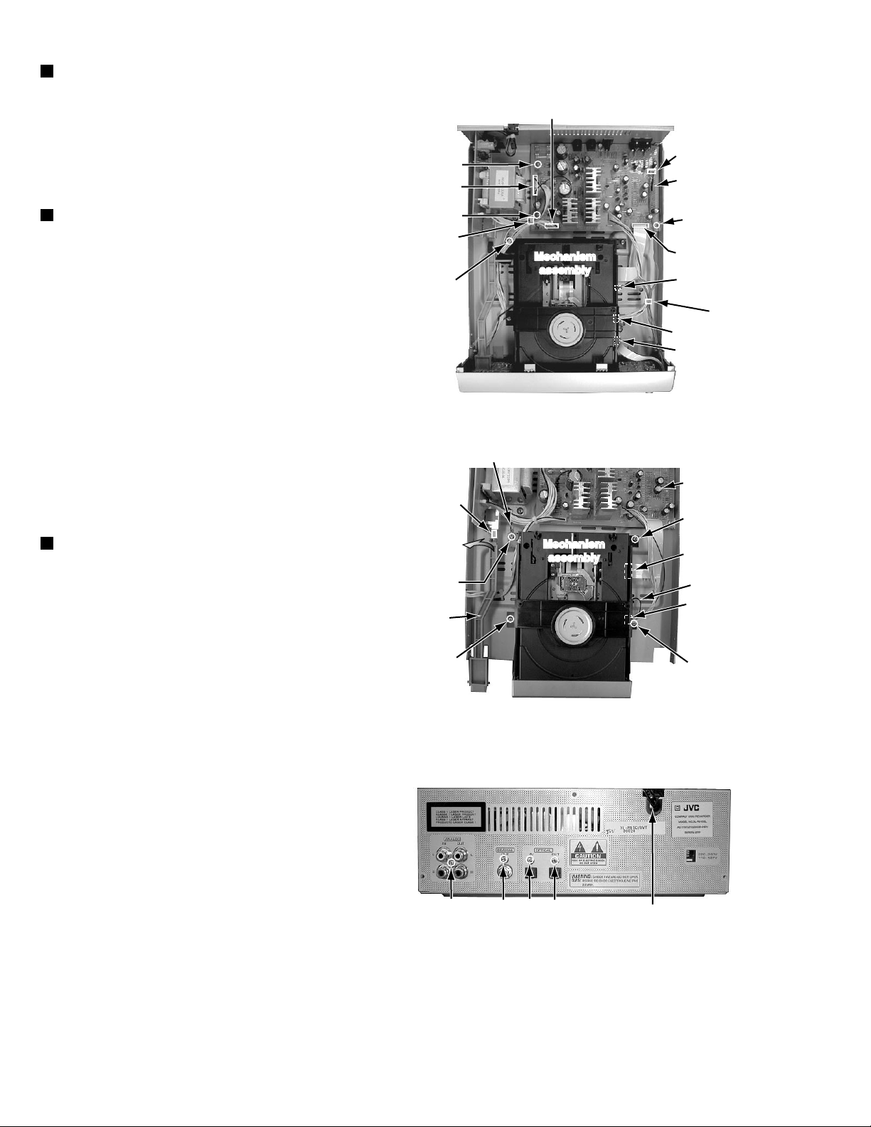
Removing the power transformer (See Fig.6~8)
* Prior to performing the following procedure,
remove the metal cover.
XL-R910SL
Tie band
1.Power button arm is removed from power switch
2.Disconnect 9pin wire from connector RCW1 on
the main board.
3.The code bushing is pulled out for above.
4.Remove the four screws H attaching the power
transformer.
Please remove a tie band if necessary.
Please fix the wire again with a tie band when
assembling.
Orange
color part
Mechanism
assembly
Power
button
arm
Fig. 6
Main board
Tie band
RCW1
H
Power transformer board
Fig. 7
Power transformer
Cord bushing
H
Fig. 8
1-5
Page 6

XL-R910SL
Troubleshooting
Power supply / VFD (FL display) section
When trouble is found in the power supply and the FL display.
Check voltage
pin No13,14,18,46,72 of
UIC1 front PCB
: 5V(VDD)
Ye s Ye s Ye s Ye s
Check oscillation
of UX1(6MHz) at front
PCB
Ye s Ye s Ye s
Check voltage
pin No46 of UIC1
:-30V?
Ye s
No No No No
No No No
Check voltage
output of RIC1(7805)
:5V?
Check connector (UCW1)
front PCB to main PCB
Check voltage
pin No27(p.sense)
of UIC1 : 5V
Check voltage
input of RIC1(7805)
:8V?
Replace RIC1
Check for RC7,RD5,RD6,RD7,RD8,
RFU3,RCW1,PFU1/PFU2
Check voltage
output of RIC3(78L05) at
main PCB : 5V?
Check voltage
positive of RC7(6800uF/25V)
at main PCB : 12V?
Replace RQ4,
RZD4,RR5
Check voltage
positive of MC1(10uF/50V)
:15V?
No
Ye s
Check for UCW1(8P),
SR3,UC7,UD1,UQ1,UC6,UR2
Check voltage
negative of RC8
(100uF/100V)
:-42V?
Replace RIC3
Check for MC1,MR1,MD1,
RCW1,RFU3,PFU1/PFU2
Check for RC8,RD9,RR9
RCW1,PFU1/PFU2
No
Replace UX1,SC4,
SC5,UIC1
Check voltage
negative of RC9
(100uF/500V)
:-30V?
No No
Ye s Ye s
Check voltage
between 1 and 2, between
48 and 49 of VFD1
:AC4V?
Ye s
Replace micom ,VFD1
Check connector(UCW1)
from front PCB to main PCB
No
-Check connector of UCW1
-Check for RCW1,PFU1/PFU2
Check for RR6,RZD5,
RZD6,RR7,RZD7
1-6
Page 7

Analog output (play mode)
When trouble is found in the analog signal output.
XL-R910SL
Check voltage
pin No2,3 of DAC(NIC1,
AK4324) at main
PCB : 5V?
Ye s Ye s Ye s Ye s
Check voltage pin
No5 of MIC1(DAC,
AK4324):5V?
Ye s Ye s Ye s
Check wave
input pin No 4(MCLK:
16,9344MHz),6(BCK),7(DATA),
8(LRCK), of NIC1
(DAC,AK4324)
: normal?
Ye s
No No No No
No No No
No
Check voltage
output of RIC2(78L05)
:5V?
Check NL1(10uF)
Check voltage
output of RIC3(78L05)
:5V?
Check for NC20,NR20
Check wave
output pin No 1,2,3,4, of
NCW1(17P FPC)
:normal?
No
Check voltage
input of RIC2(78L05)
:8V?
Replace RIC2
Check for RC7,RD5,RD6,RD7,RD8,
RFU3,RCW1,PFU1/PFU2
Check voltage
positive of MC1(10uF/
50V) :15V?
Replace RIC3
-Check connecting of NCW1(17P FPC)
-Replace mechanism
Check voltage
positive of RC7(6800uF/25v)
at main PCB : 12V?
Replace RQ3,
RZD3,RR3
Check for MC1,MR1,MD1,
RCW1,RFU3,PFU1/PFU2
Ye s
Check voltage
pin No 9 of NIC1(DAC,
AK4324) : 0V?
Ye s
Check analog
wave output of AR1,2,3,4
(10k)
Ye s
Check voltage
of RJW2 : -8V?
RJW4 : +8V?
Ye s
Check analog
wave output at pin No1,7
of AIC2(4560)
Ye s
Check voltage
base of MQ5,MQ6(C945)
:0.6V
No
No
No
No
Check NR1,2,3,4
-Check for mute micom and RCW2
Check solder of NIC1
Check for AIC1,AIC2(4560),
OP amp 4560
-Check solder of AJA1
-Check analog wave of AJA1
-Check connector of audio cable
Check voltage
No No
output of
RC6(2200uF/25) : +12V?
RC7(2200uF/25V) : -12V?
Ye s
Check for RQ2,RZD2,RR2,
RQ1,RZD1,RR1
Check for RD1,2,3,4(IN4002)
RFU1,RFU2(1A),RCW1,PFU1,PFU2
Ye s
Check for micom mute line,
MR6,MQ3,MQ4,MD4,MD5,MQ1
1-7
Page 8

XL-R910SL
Digital output
When trouble is found in the optical output and coaxial output.
Check signal
(digital) input pin No 1
of NIC1(74HCN04)
Ye s Ye s
Check signal
(digital) output pin No 4,6
of NIC1(74HCU04)
Ye s Ye s Ye s
Check voltage
pin No2 of NOM2
(optical transmitter)
:5V?
Ye s
No No
No No No
No
Check signal
(digital) input pin No 15
of NCW1(17P)
Check for MR14,NC7
Check voltage
of NIC1(74HCU04)
pin No14:5V?
No7:0V?
Replace NIC1
Check connector to NCW1(17P)
Check mechanism
Check voltage
input of RIC2(78L05)
:8V?
Replace RIC2
Check for RC7,RD5,RD6,RD7,RD8,
RFU3(2.5A),RCW1,PFU1/PFU2
Check voltage
positive of RC7(6800uF/25v)
at main PCB : 12V?
Ye s
Replace RQ3,
RZD3,RR3
No
-Check for NEF1,NEF2,NR10,NR11,NR12
-Replace NOM2
-Check solder of between NOM2 and NJA1
-Check for optical cable and coaxial cable
1-8
Page 9

Mechanism operation
When trouble is found in the mechanism operating. (rotation,play,tray open/close,lead)
XL-R910SL
Check voltage
pin No 2 of RCW3(6P)
at main PCB : 8V?
Ye s Ye s
Check voltage
pin No 4,6 of RCW3(6P)
at main PCB : 5V?
Ye s
Check wave
pin No3(CDR-RCT) of
UCW2(9P) at front PCB
when power ON
Ye s
No No
No No
Check voltage
positive of RC7(6800uF/
25V) : 12V?
Check for RQ3,RZD3,RR3
Check voltage
input of RC1(7805)
:8V?
Ye s Ye s
Replace RIC1
-Check pin No 1 of micom(UIC1)
No
-Check connecting of UCW2(9P)
Check for RC7,RD5,RD6,RD7,RD8
RFU3(2.5A),RCW1,PFU1,PFU2
Ye s
Check voltage
positive of RC7(6800uF/
25V) : 12V?
Check for RQ4,RZD4,RR5
Check wave
pin No4~9 of UCW2(9P)
:interface wave ?
Ye s
Replace mechanism
No
1-9
Page 10

XL-R910SL
Digital recording (CD-R/CD-RW Disc, Unfinalize condition)
When trouble is found in the digital recording (optical recording).
Check selecting
for source at front panel
:optical
No
Selecting optical mode by source key
Ye s
Check signal
(digital) input pin No11
of NCW1(17P)
No No
Check voltage
pin No3 of NOM1(optical
receiver) : 5V?
Check voltage of RIC2(78L05)
Ye s Ye s
-Check connector of NCW1(17P)
-Check mechanism
-Check for NR13,NC13
-Check solder of NOM1,NCW1
Analog recording (CD-R/CD-RW Disc, Unfinalize condition)
When trouble is found in the analog recording.
Check selecting
mode for source at front
panel : analog
Ye s
Check location
VR(ana.rec) at front panel
: 3o'clock
No
Selecting analog mode by source key
No
Adjust volume (analog rec.)
Ye s
Check signal
(analog) input pin No
1,3 of ACW1(3P)
Ye s
Check signal
(analog) input pin No
5,6 of UVR1 at
front PCB
Ye s
Check signal
(analog) input pin No
1,3 of connector
(4P) from mecha.
to front PCB
Ye s
Replace mechanism
-Check for AC6,AC7,AC22,AD23,AC24
No
AC25,AR25,AR26,AR27,AR28
-Check solder AJA1
No
-Check connector UCW3
No
-Check signal of UVR1
-Check connector (4P) of mechanism
1-10
Page 11

Description of major ICs
AK4324(NIC1) : D/A Converter
1. Pin layout
XL-R910SL
DVSS
DVDD
CKS
MCLK
BICK
S DATA
LRCK
SMUTE
DFS
DEM0
DEM1
PD
1
2
3
4
5
6
7
8
9
10
11
12
2. Block diagram
LRCK
BICK
S DATA
PD
SMUTE
DFS
DZFL
24
DZFR
23
AVDD
22
VREF
21
AVSS
20
AOUTL+
19
AOUTL-
18
AOUTR+
17
AOUTR-
16
DIF2
15
DIF1
14
DIF0
13
DIF0 DIF1 DIF2 DEM0 DEM1 AVDD AVSS
Serial Input
Interface
8x
Interpolator
8x
Interpolator
De-emphasis
Control
Modulator
Modulator
SCF
SCF
DZFL
AOUTL+
AOUTL-
AOUTR+
AOUTR-
3. Pin function
Pin
Symbol Function
No.
1
DVSS
2
DVDD
3
CKS
4
MCLK
5
PD
6
BICK
7
S DATA
8
LRCK
9
SMUTE
10
DFS
11
DEM0
12
DEM1
I/O I/O
-
-
I
I
I
I
I
I
I
I
I
I
Clock OSC/Divider
MCLK CKS DVDD DVSS VREF
Pin
Symbol Function
No.
Digital ground terminal
Digital power supply terminal
Master clock select pin
Master clock input pin
Power down mode pin
Audio serial data clock pin
Audio serial data input
L/R clock pin
Soft mute pin
Double speed sampling mode
De-emphasis frequency select
De-emphasis frequency select
13
14
15
16
17
18
19
20
21
22
23
24
AOUTR-
AOUTR+
AOUTL-
AOUTL+
DIF0
DIF1
DIF2
AVSS
VREF
AVDD
DZFR
DZFL
I
Digital input format pin
I
Digital input format pin
I
Digital input format pin
O
Rch negative analog output
O
Rch positive analog output
O
Lch negative analog output
O
Lch positive analog output
-
Analog ground terminal
I
Voltage reference input
-
Analog power supply terminal
O
Rch zero input detect pin
O
Lch zero input detect pin
DZFR
1-11
Page 12

XL-R910SL
AH11-00018B(UIC1):System controller
1.Terminal layout
~
50 31
51
~
30
~
80
81 100
2.Pin function
Pin No.
1
2~10
11
12
13
14
15
16
17
18
19
20
21~26
27
28
29
30~41
42~45
46
47
48
49.50
51
52~63
64~71
72
73~88
89
90
91.92
93
94
95
96
97
98
99
100
REMOCON
~
Symbol
XRST
GND
RESET
VDD
VDD
GND
XIN
XOUT
VDD
KEY1
KEY2
GND
P.SENSE
R-REQ
1G~12G
P18~P15
VDD
P14
P13
VPP
P12~P1
VDD
GND
VDD
MUTE
SIN
SOUT
ACLK
S-RDY
S-REQ
1
I/O
O
-
I
-
-
I
O
I
I
I
I
I
O
O
O
O
-
O
-
-
-
-
-
O
O
I
I
O
O
Mechanism reset signal output
Non connect
Connect to ground
Micom reset signal input
Power supply terminal (+5V)
Power supply terminal (+5V)
Connect to ground
Oscillation input terminal (6MHz)
Oscillation output terminal (6MHz)
Power supply terminal (+5V)
Key matrix input terminal (AD1)
Key matrix input terminal (AD2)
Connect to ground
Power detect input terminal
RW-I/F, RW-REQUEST input
Remote control signal input
FL Grid control signal output
FL Segment control signal output
Power supply terminal (+5V)
FL Segment control signal output
FL Segment control signal output
Non connect
VP (-30V)
FL Segment control signal output
Non connect
Power supply terminal (+5V)
Non connect
Connect to ground
Power supply terminal (+5V)
Non connect
Audio muting signal output
Non connect
RW-I/F, Serial data output
RW-I/F, Serial data input
RW-I/F, Clock input
Non connect
RW-I/F, SYS READY output
RW-I/F, SYS REQUEST output
Description
1-12
Page 13

XL-R910SL
VICTOR COMPANY OF JAPAN, LIMITED
PERSONAL & MOBILE NETWORK BUSINESS UNIT
1644, Shimotsuruma, Yamato, Kanagawa 242-8514, Japan
No.A0009
Printed in Japan
200104(O)
 Loading...