

Page 1
XL-R5020BK
SERVICE MANUAL
CD/CDR MULTIPLE COMPACT DISC RECORDER
XL-R5020BK
Area Suffix
J ------------- U.S.A.
CD1 CD2 CD3
1
2
5
4
8
7
10
10
PLAY
MODE
REPEAT CD CDR
Y
A
L
P
S
I
D
GROUP
SET
R
E
GROUP
C
S
O
U
R
C
E
CD REC CD EDIT SYNCHRO FADE
REC
PITCH 0
FINALIZE
REC MUTING
RM-SXL001J
REMOTE CONTROL
STANDBY/ON
3
6
9
GROUP
CONTROL
M
E
N
U
L
E
C
N
A
C
MIN MAX
PITCH
XLÐR5020 CD/CDR MULTIPLE COMPACT DISC RECORDER
COMPACT
DIGITAL AUDIO
MP3 PLAYBACK
COMPACT
DIGITAL AUDIO
Recordable
ReWritable
COPYRIGHT 2002 VICTOR COMPANY OF JAPAN, LTD.
No.A0035
Aug. 2002
Page 2

XL-R5020BK
TABLE OF CONTENTS
1 Important Safety Precautions . . . . . . . . . . . . . . . . . . . . . . . . . . . . . . . . . . . . . . . . . . . . . . . . . . . . . . . . . . . . . 3
1.1 Safety Precautions . . . . . . . . . . . . . . . . . . . . . . . . . . . . . . . . . . . . . . . . . . . . . . . . . . . . . . . . . . . . . . . . . 3
1.2 Warning. . . . . . . . . . . . . . . . . . . . . . . . . . . . . . . . . . . . . . . . . . . . . . . . . . . . . . . . . . . . . . . . . . . . . . . . . . 3
1.3 Caution . . . . . . . . . . . . . . . . . . . . . . . . . . . . . . . . . . . . . . . . . . . . . . . . . . . . . . . . . . . . . . . . . . . . . . . . . . 3
1.4 Critical parts for safety. . . . . . . . . . . . . . . . . . . . . . . . . . . . . . . . . . . . . . . . . . . . . . . . . . . . . . . . . . . . . . . 3
1.5 Preventing static electricity . . . . . . . . . . . . . . . . . . . . . . . . . . . . . . . . . . . . . . . . . . . . . . . . . . . . . . . . . . . 4
1.6 Handling the traverse unit (optical pickup) . . . . . . . . . . . . . . . . . . . . . . . . . . . . . . . . . . . . . . . . . . . . . . . 4
1.7 Importance admistering point on the safety . . . . . . . . . . . . . . . . . . . . . . . . . . . . . . . . . . . . . . . . . . . . . . 5
1.8 Precautions for Service. . . . . . . . . . . . . . . . . . . . . . . . . . . . . . . . . . . . . . . . . . . . . . . . . . . . . . . . . . . . . . 6
2 Disassembly method . . . . . . . . . . . . . . . . . . . . . . . . . . . . . . . . . . . . . . . . . . . . . . . . . . . . . . . . . . . . . . . . . . . . 7
2.1 Main body . . . . . . . . . . . . . . . . . . . . . . . . . . . . . . . . . . . . . . . . . . . . . . . . . . . . . . . . . . . . . . . . . . . . . . . . 7
3 MECHANISM . . . . . . . . . . . . . . . . . . . . . . . . . . . . . . . . . . . . . . . . . . . . . . . . . . . . . . . . . . . . . . . . . . . . . . . . . . 11
3.1 Changer mechanism assembly. . . . . . . . . . . . . . . . . . . . . . . . . . . . . . . . . . . . . . . . . . . . . . . . . . . . . . . 11
4 Confirm method of operation . . . . . . . . . . . . . . . . . . . . . . . . . . . . . . . . . . . . . . . . . . . . . . . . . . . . . . . . . . . . 19
4.1 Check mode . . . . . . . . . . . . . . . . . . . . . . . . . . . . . . . . . . . . . . . . . . . . . . . . . . . . . . . . . . . . . . . . . . . . . 19
4.2 All release of set content. . . . . . . . . . . . . . . . . . . . . . . . . . . . . . . . . . . . . . . . . . . . . . . . . . . . . . . . . . . . 19
4.3 Service menu . . . . . . . . . . . . . . . . . . . . . . . . . . . . . . . . . . . . . . . . . . . . . . . . . . . . . . . . . . . . . . . . . . . . 19
4.4 Running operation. . . . . . . . . . . . . . . . . . . . . . . . . . . . . . . . . . . . . . . . . . . . . . . . . . . . . . . . . . . . . . . . . 19
4.5 Display of version number. . . . . . . . . . . . . . . . . . . . . . . . . . . . . . . . . . . . . . . . . . . . . . . . . . . . . . . . . . . 19
4.6 Extension cord for diagnosis of changer mechanism unit. . . . . . . . . . . . . . . . . . . . . . . . . . . . . . . . . . . 19
5 Description of major ICs . . . . . . . . . . . . . . . . . . . . . . . . . . . . . . . . . . . . . . . . . . . . . . . . . . . . . . . . . . . . . . . . 20
5.1 AN22000A-W(IC601):RF & SERVO AMP. . . . . . . . . . . . . . . . . . . . . . . . . . . . . . . . . . . . . . . . . . . . . . . 20
5.2 BU4066BCF-X(IC831,IC841,IC861):Source selector . . . . . . . . . . . . . . . . . . . . . . . . . . . . . . . . . . . . . . 20
5.3 BU4052BCF-X(IC821):Channel switch controller . . . . . . . . . . . . . . . . . . . . . . . . . . . . . . . . . . . . . . . . . 21
5.4 LB1641 (IC851,IC852) : DC Motor driver . . . . . . . . . . . . . . . . . . . . . . . . . . . . . . . . . . . . . . . . . . . . . . . 21
5.5 TC74HC00AF(IC301,IC311):Digital I/O selector. . . . . . . . . . . . . . . . . . . . . . . . . . . . . . . . . . . . . . . . . . 21
5.6 BR24C01AFV-W-X (IC201) : EEPROM . . . . . . . . . . . . . . . . . . . . . . . . . . . . . . . . . . . . . . . . . . . . . . . . 22
5.7 LA6541-X (IC801) : Focus & Spindle & Feed & Tracking BTL driver . . . . . . . . . . . . . . . . . . . . . . . . . . 23
5.8 M66004SP(IC721):FL Driver. . . . . . . . . . . . . . . . . . . . . . . . . . . . . . . . . . . . . . . . . . . . . . . . . . . . . . . . . 24
5.9 MN35505-X (IC361) : DAC . . . . . . . . . . . . . . . . . . . . . . . . . . . . . . . . . . . . . . . . . . . . . . . . . . . . . . . . . . 25
5.10 TC9246F-X(IC404):Clock generation for digital audio . . . . . . . . . . . . . . . . . . . . . . . . . . . . . . . . . . . . . 26
5.11 TC74HCU04AF-W(IC331):Digital input selector . . . . . . . . . . . . . . . . . . . . . . . . . . . . . . . . . . . . . . . . . 26
5.12 74VHC00MTC-X (IC406) : 2-input nand gate . . . . . . . . . . . . . . . . . . . . . . . . . . . . . . . . . . . . . . . . . . . . 27
5.13 74VHC08SJ-X(IC407):2-input AND gate . . . . . . . . . . . . . . . . . . . . . . . . . . . . . . . . . . . . . . . . . . . . . . . 27
5.14 TC94A02F-005(IC401) : MP3 Decoder. . . . . . . . . . . . . . . . . . . . . . . . . . . . . . . . . . . . . . . . . . . . . . . . . 28
5.15 TC9412AF(IC891) : Rec Level. . . . . . . . . . . . . . . . . . . . . . . . . . . . . . . . . . . . . . . . . . . . . . . . . . . . . . . 31
5.16 MN662790RSC(IC651):Digital servo & processor . . . . . . . . . . . . . . . . . . . . . . . . . . . . . . . . . . . . . . . . 32
5.17 UPD780076GK-533(IC251):Unit microcomputer . . . . . . . . . . . . . . . . . . . . . . . . . . . . . . . . . . . . . . . . . 34
5.18 UPD784215AGF513(IC501):System controller. . . . . . . . . . . . . . . . . . . . . . . . . . . . . . . . . . . . . . . . . . . 36
5.19 W24L010AJ-12-X (IC402) : SRAM . . . . . . . . . . . . . . . . . . . . . . . . . . . . . . . . . . . . . . . . . . . . . . . . . . . . 38
2
Page 3
SECTION 1
Important Safety Precautions
1.1 Safety Precautions
(1) This design of this product contains special hardware and
many circuits and components specially for safety purposes.
For continued protection, no changes should be made to the
original design unless authorized in writing by the
manufacturer. Replacement parts must be identical to
those used in the original circuits. Services should be
performed by qualified personnel only.
(2) Alterations of the design or circuitry of the product should
not be made. Any design alterations of the product should
not be made. Any design alterations or additions will vo id
the manufacturers warranty and will further relieve the
manufacture of responsibility for personal injury or property
damage resulting therefrom.
(3) Many electrical and mechanical parts in the products have
special safety-related characteristics. These characteristics are often not evident from visual inspection nor can the
protection afforded by them necessarily be obtained by
using replacement components rated for higher voltage,
wattage, etc. Replacement parts which have these specia l
safety characteristics are identified in the Parts List of Service
Manual. Electrical components having such features are
identified by shading on the schematics and by ( )
on the Parts List in the Service Manual. The use of a substitute replacement which does not have the same safety
characteristics as the recommended replacement parts
shown in the Parts List of Service Manual may create
shock, fire, or other hazards.
(4) The leads in the products are routed and dressed with ties,
clamps, tubings, barriers and the like to be separated from
live parts, high temperature parts, moving parts and/or
sharp edges for the prevention of electric shock and fire
hazard. When service is required, the original lead routing
and dress should be observed, and it should be confirmed
that they have been returned to normal, after reassembling.
(5) Leakage shock hazard testing)
After reassembling the product, always perform an isolation
check on the exposed metal parts of the product (antenna
terminals, knobs, metal cabinet, screw heads, headphone
jack, control shafts, etc.) to be sure the product is safe to
operate without danger of electrical shock.
Do not use a line isolation transformer during this check.
• Plug the AC line cord directly into the AC outlet. Using a
"Leakage Current Tester", measure the leakage current
from each exposed metal parts of the cabinet, particularly any exposed metal part having a return path to the
chassis, to a known good earth ground. Any leakage
current must not exceed 0.5mA AC (r.m.s.).
• Alternate check method
Plug the AC line cord direct ly into the AC outle t. Use a n AC
voltmeter having, 1,000 ohms per volt or more sensitivity in
the following manner. Connect a 1,500 ohm 10W resistor
paralleled by a 0.15 µF AC-type capacitor between an
exposed metal part and a known good earth ground.
Measure the AC voltage across the resistor with the AC
XL-R5020BK
voltmeter.
Move the resistor connection to each exposed metal part,
particularly any exposed metal part having a return path to
the chassis, and measure the AC voltage across the
resistor. Now, reverse the plug in the AC outlet and repeat
each measurement. Voltage measured any must not
exceed 0.75 V AC (r.m.s.). This corresponds to 0.5 mA AC
(r.m.s.).
1.2 Warning
(1) This equipment has been designed and manufactured to
meet international safety standards.
(2) It is the legal responsibility of the repairer to ensure that
these safety standards are maintained.
(3) Repairs must be made in accordance with the relevant
safety standards.
(4) It is essential that safety critical components are replaced
by approved parts.
(5) If mains voltage selector is provided, check setting for lo-
cal voltage.
1.3 Caution
Burrs formed during molding may be left over on some
parts of the chassis.
Therefore, pay attention to such burrs in the case of preforming repair of this system.
1.4 Critical parts for safety
In regard with component parts appearing on the silk-screen
printed side (parts side) of the PWB diagrams, the parts that are
printed over with black such as the resistor ( ), diode ( ) and
ICP ( ) or identified by the " " ma rk nearby are critical for safety.
When replacing them, be sure to use the parts of the same type
and rating as specified by the manufacturer. (Except the JC version)
3
Page 4

XL-R5020BK
1.5 Preventing static electricity
Electrostatic discharge (ESD), which occurs when static electricity stored in the body, fabric, etc. is discharged,
can destroy the laser diode in the traverse unit (optical pickup). Take care to prevent this when performing repairs.
1.5.1 Grounding to prevent damage by static electricity
Static electricity in the work area can destroy the optical pickup (laser dio de) in devices such as DVD players.
Be careful to use proper grounding in the area where repairs are being performed.
(1) Ground the workbench
Ground the workbench by laying conductive material (such as a conductive sheet) or an iron pl ate over it before placing the
traverse unit (optical pickup) on it.
(2) Ground yourself
Use an anti-static wrist strap to release any static electricity built up in your body.
(3) Handling the optical pickup
• In order to maintain quality during transport and before installation, both sides of the laser diode on the replacement optical
pickup are shorted. After replacement, return the shorted parts to their original condition.
(Refer to the text.)
• Do not use a tester to check the condition of the laser diode in the optical pickup. The tester's internal power source can
easily destroy the laser diode.
1.6 Handling the traverse unit (optical pickup)
(1) Do not subject the traverse unit (optical pickup) to strong shocks, as it is a sensitive, complex unit.
(2) Cut off the shorted part of the flexible cable using nippers, etc. after replacing the optical pickup. For specific details, refer to the
replacement procedure in the text. Remove the anti-static pin when replacing the traverse unit. Be careful not to take too
long a time when attaching it to the connector.
(3) Handle the flexible cable carefully as it may break when subjected to strong force.
(4)I t is not possible to adjust the semi-fixed resistor that adjusts the laser power. Do not turn it.
4
Page 5
1.7 Importance admistering point on the safety
XL-R5020BK
5
Page 6
XL-R5020BK
1.8 Precautions for Service
1.8.1 Handling of Traverse Unit and Laser Pickup
(1) Do not touch any peripheral element of the pickup or the actuator.
(2) The traverse unit and the pickup are precision devices and therefore must not be subjected to strong shock.
(3) Do not use a tester to examine the laser diode. (The diode can easily be destroyed by the internal power supply of the tester.)
(4) To replace the traverse unit, pull out the metal short pin for protection from charging.
(5) When replacing the pickup, after mounting a new pickup, remove the solder on the short land which is provided at the center
of the flexible wire to open the circuit.
(6) Half-fixed resistors for laser power adjustment are adjusted in pairs at shipment to match the characteristics of the optical block.
Do not change the setting of these half-fixed resistors for laser power adjustment.
1.8.2 Destruction of Traverse Unit and Laser Pickup by Static Electricity
Laser diodes are easily destroyed by static electricity charged on clothing
or the human body. Before repairing peripheral elements of the traverse unit or pickup, be sure to take the following electrostatic
protection:
(1) Wear an antistatic wrist wrap.
(2) With a conductive sheet or a steel plate on the workbench on wh ich the trave rse unit or the pick up is to be repaired, grou nd
the sheet or the plate.
(3) After removing the flexible wire from the connector (CN101), short-circuit the flexible wire by the metal clip.
(4) Short-circuit the laser diode by soldering the land which is provided at the center of the flexible wire for the pickup.
After completing the repair, remove the solder to open the circuit.
Please refer to "Fig.2-4" of "Disassembly
method" for details.
6
Page 7
SECTION 2
Disassembly method
2.1 Main body
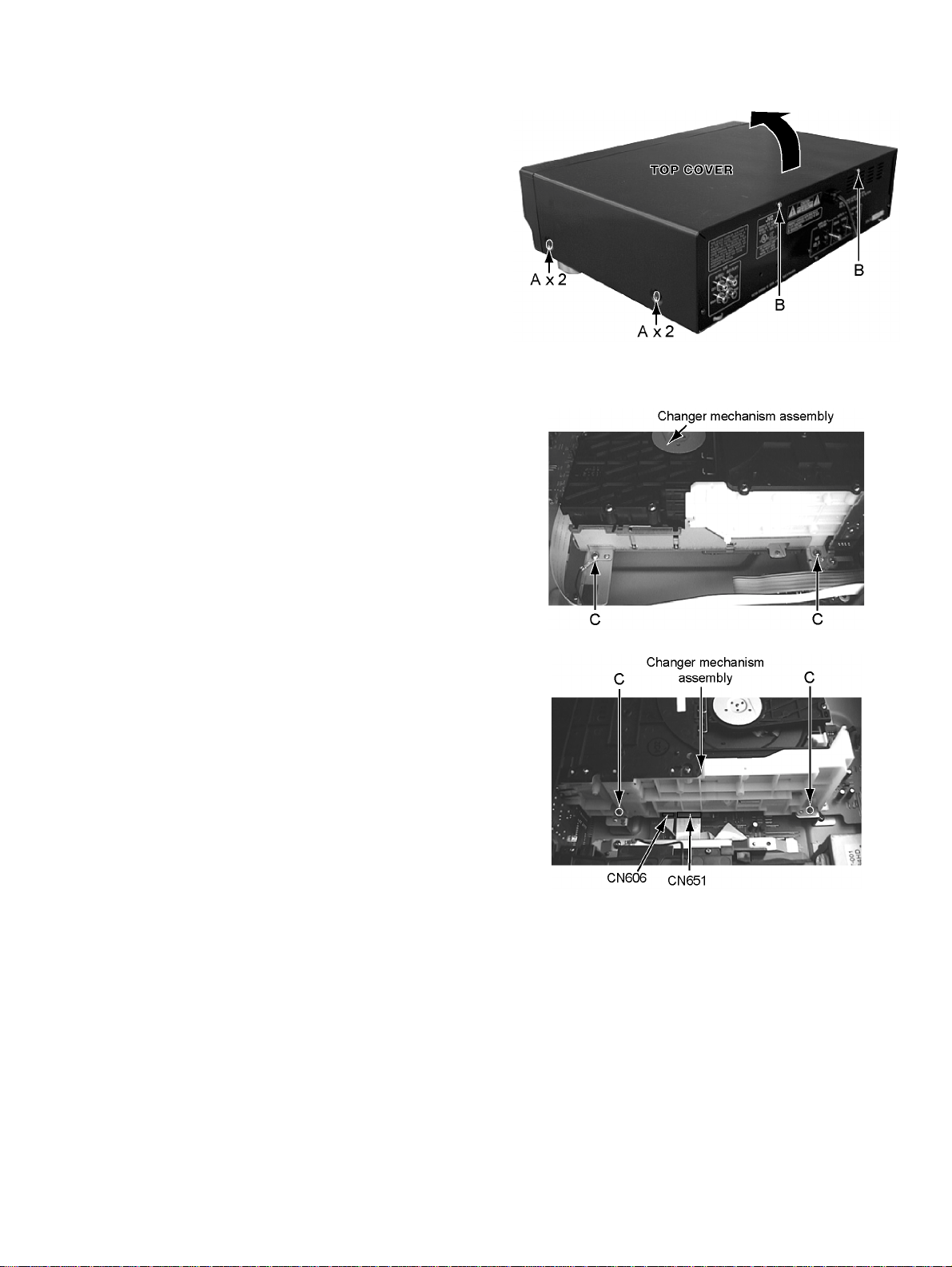
2.1.1 Removing the top cover (see Fig.1)
(1) Remove the four screws A attaching the top cover on both
sides of the body.
(2) Remove the two screws B attaching the top cover on the
back of the body.
(3) Remove the top cover from the body by lifting the rear part
of the top cover.
ATTENTION:
Do not break the front panel tab fitted to the top cover.
2.1.2 Removing the changer mechanism assembly
(see Fig.2~3)
*Prior to performing the following procedure, remove the top
cover.
(1) Remove the four screws C attaching the changer mecha-
nism assembly.
(2) Disconnect the card wire from connector CN606 and
CN651 on the CD servo control board respectively.
(3) Remove the changer mechanism assembly from the body
by lifting the rear part of the changer mechanism asse mbly.
XL-R5020BK
Fig.1
Fig.2
Fig.3
7
Page 8
XL-R5020BK
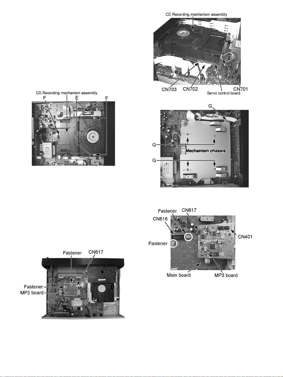
2.1.3 Removing the CD recording mechanism assembly
(see Fig.4~6)
*Prior to performing the following procedure, remove the top
cover.
*There is no need to remove the changer mechanism assembly.
(1) Remove the two screws E attaching the mechanism chas-
sis.
(2) Remove the three screws F attaching the CD recording
mechanism assembly.
(3) Disconnect the card wire from connector CN702 and
CN703 on the servo control board respectively.
(4) Disconnect the connect wire from connector CN701 on the
servo control board.
(5) Remove the five screws G attaching the mechanism chas-
sis
Fig.5
Fig.4
2.1.4 Removing the MP3 board
(see Fig.7,8)
*Prior to performing the following procedure, remove the top
cover, CD recording mechanism assembly.
*There is no need to remove the changer mechanism assembly.
(1) Pull out the MP3 board from the fastener.
At this time, disconnect the connector CN401 of the MP3
board from connector CN616 on the Main board.
(2) Disconnect the card wire from connector CN617 on the
MP3 board.
Fig.6
Fig.8
Fig.7
8
Page 9
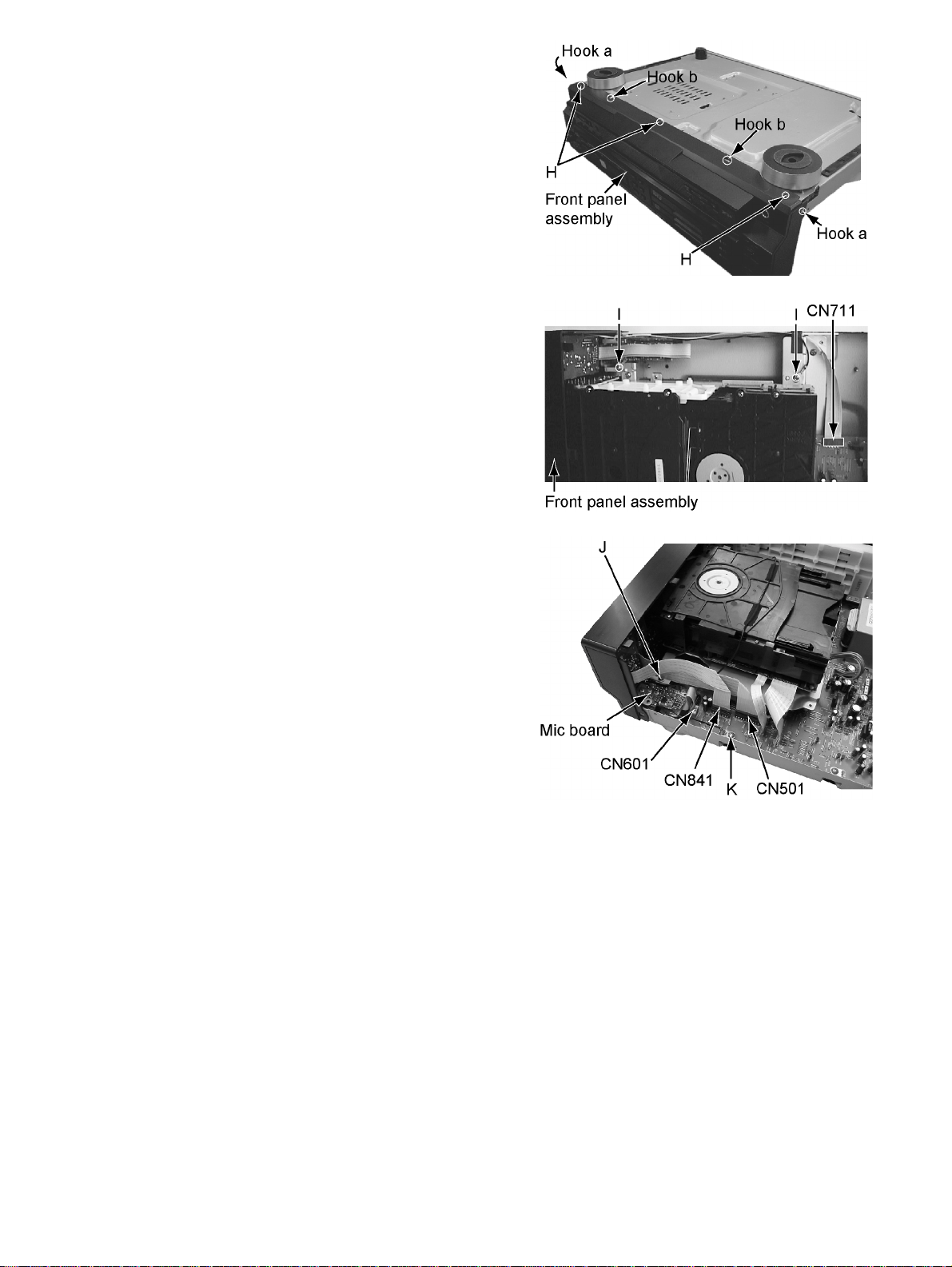
2.1.5 Removing the front panel assembly
(see Fig.9~11)
*Prior to performing the following procedure, remove the top
cover.
*There is no need to remove the changer mechanism assembly
and CD recording mechanism assembly.
(1) Remove the three screws H attaching the front panel as-
sembly on the bottom of the body.
(2) Remove the two screws I attaching the headphone jack
bracket.
(3) Remove the one screw J attaching the mic jack bracket.
(4) Remove the one screw K attaching the main board.
(5) Disconnect the card wire from connector CN711, CN841
and CN501 on the main board respectively.
(6) Disconnect the flat wire from connector CN601 on the
main board from mic board.
(7) Hook a and b are removed respectively, and the front
panel assembly is removed.
XL-R5020BK
Fig.9
Fig.10
Fig.11
9
Page 10
XL-R5020BK
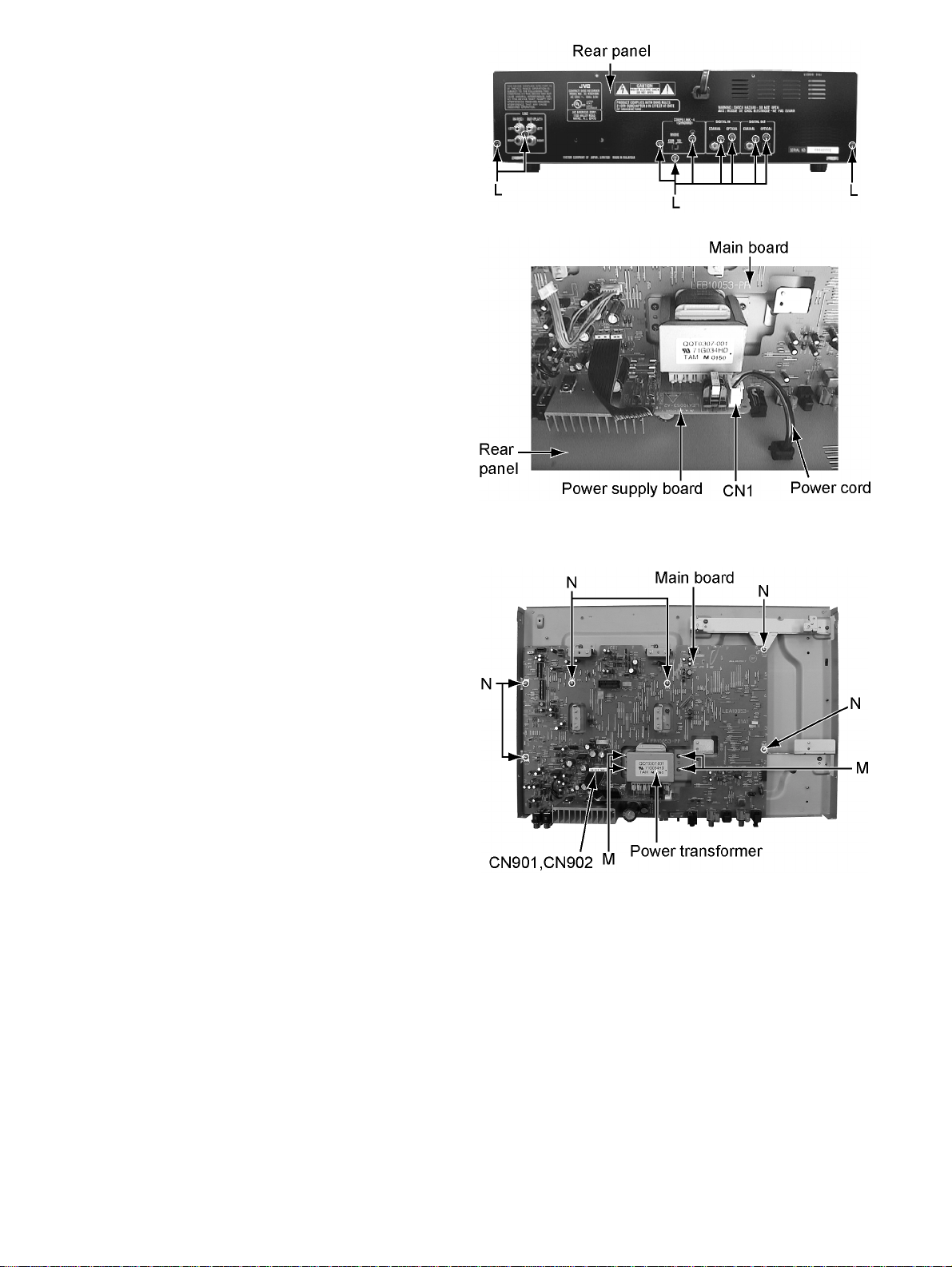
2.1.6 Removing the rear panel
(see Fig.12,13)
*Prior to performing the following procedure, remove the top
cover.
(1) Remove the ten screws L attaching the rear panel.
(2) Disconnect the power cord from connector CN1 on the
power supply board.
Fig.12
2.1.7 Removing the main board and power supply board
(see Fig.14)
*Prior to performing the following procedure, remove the top
cover, front panel assembly, changer mechanism assembly, CD
recording mechanism assembly and rear panel.
(1) Remove the four screws M attaching the power transform-
er.
(2) Disconnect the flat wire from connector CN901 and
CN902 on the main board.
(3) Remove the six screws N attaching the main board.
Fig.13
Fig.14
10
Page 11
SECTION 3
MECHANISM
3.1 Changer mechanism assembly
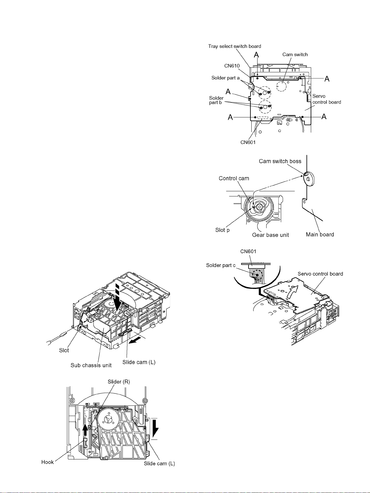
3.1.1 Removing the servo control board
(See Fig.1 to 5)
ATTENTION:
Make sure the sub chassis unit is locating at the lowest position. If not,perform the following procedure from 1 to 3.
(1) Insert a screwdriver into the sub chassis slot on the back
of the body and push the slider (R) toward the front.
(2) From the top of the body, slide the hook and the slider (R)
forward until they stop.
(3) From the right side of the body, slide the slide cam (L)
backward until it stops. The sub chassis unit will move to
the lowest position.
(4) From the bottom of the body, unsolder each soldered part
a and b of the motors on the servo control board.
(5) Remove the five screws A attaching the servo control
board.
(6) Disconnect connector CN610 on the servo control board
from the tray select switch board to suspend the servo
control board tentatively. Solder the part c of the flexible
wire connected to connector CN601 on the underside of
the servo control board.
(7) Disconnect the flexible wire from connect or CN601 and
remove the servo control board from the body.
ATTENTION:
In case of disconnecting the flexible wire without soldering, the CD pick up may be damaged.
ATTENTION:
When reassembling, make sure the cam switch boss of
the servo control board is fitted to the slot p of the control cam on the bottom of the body
(Refer to Fig.3).
XL-R5020BK
Fig.3
Fig.4
Fig.1
Fig.2
Fig.5
11
Page 12
XL-R5020BK
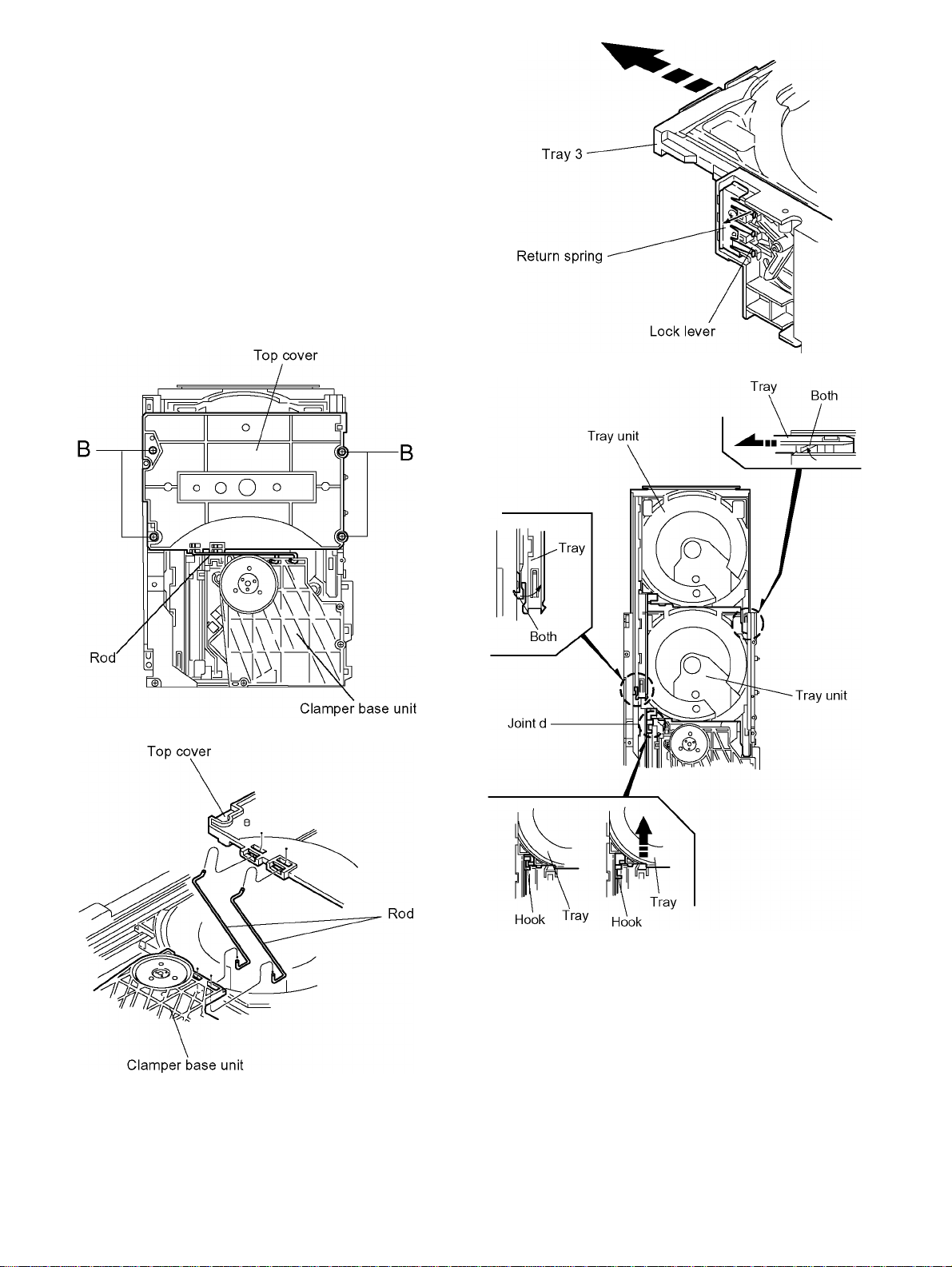
3.1.2 Removing the tray unit
(See Fig.6 to 9)
*The tray unit can be removed despite the position of the sub
chassis unit, but the lowest position is recommended to expedite
the work.
(1) Remove the four screws B attaching the top cover on the
top of the body.
(2) Remove the top cover with the two rods attached to the top
cover and the clamper base unit.
(3) Pull the lock lever of the return spring on the right si de of
the body to eject the tray unit.
(4) From the top of the body, release the tray from the joi nt
hook marked d (Push the tray toward the front).
(5) Release the stoppers on both sides in the direction of the
arrow and pull out the tray unit from the body.
ATTENTION:
Pull out the tray unit from the top tray 3 in sequence.
Fig.8
Fig.6
Fig.7
Fig.9
12
Page 13

3.1.3 Removing the side unit (L) and (R)
(See Fig.10 to 14)
*Prior to performing the following procedures, remove the servo
control board, the top cover and the tray unit.
(1) Remove the two screws C attaching the side unit (L).
(2) Slide and remove the side unit (L) toward the fro nt while
releasing the two joints e and the joint f with the chassis
unit.
(3) Slide the slide cam (L) toward the front until it stops to
place the sub chassis unit at the top position.
ATTENTION:
The side unit (R) can be removed when the sub chassis
unit is located at the top position.
(4) Turn the hook gear counterclockwise to move th e slide
hook and the slider (R) backward until they stop.
(5) Remove the three screws D attaching the side unit (R).
Raise the side unit (R) upward and release the joint g with
the chassis unit and the boss from the select arm marked
h. Then remove the side unit (R) from the body.
ATTENTION:
When reassembling, make sure the boss is fitted to the
select arm marked h.
XL-R5020BK
Fig.12
Fig.10
Fig.11
Fig.13
Fig.14
13
Page 14

XL-R5020BK
3.1.4 Removing the sub chassis unit
(See Fig.15 to 17)
*Prior to performing the following procedures, remove the servo
control board, the top cover, the tray unit,the side unit (L) and
the side unit (R).
(1) Turn the hook gear counterclockwise to move the slide
hook and the slider (R) backward until they stop.
(2) Slide the slide cam (L) and the slide cam (R) in the direction
of the arrow until they stop.
(The notches of each slide cam are fitted to the pins on
both sides of the sub chassis unit.)
(3) Detach the sub chassis unit upward.
ATTENTION:
When reassembling, turn the hook gear of the chassis
unit counterclockwise until it stops and slide the slide
hook and the slider (R) of the sub chassis unit backward
until they stop.
Fig.15
Fig.16
Fig.17
14
Page 15

3.1.5 Removing the flap base unit and the gear ba se unit
(See Fig.18 and 19)
*Prior to performing the following procedures, remove the servo
control board, the top cover, the tray unit,the side unit (L) and
the side unit (R).
(1) Remove the screw E attaching the flap base unit. Release
the joint tabs i and j, then remove the flap base unit from
the body.
(2) Remove the belts from the two pulleys on the gear base
unit.
(3) Remove the three screws F and remove the gear base unit
from the body.
XL-R5020BK
Fig.18
3.1.6 Removing the motors
(See Fig.20)
*Prior to performing the following procedure, remove the main
board.
(1) Remove the belts from the two pulleys.
(2) Remove the four screws G and detach each motor from
the body.
Fig.19
Fig.20
15
Page 16

XL-R5020BK
3.1.7 Removing the pickup
(See Fig.21 to 25)
(1) From the top of the body, remove the three screws H
attaching the clamper base unit.
(2) Remove the clamper base unit with the two rods attached
to the clamper base unit and the top cover.
(3) Turn the screw shaft gear marked k in the direction of the
arrow to move the pickup unit.
(4) Remove the screw I attaching the shaft holder.
(5) Move the screw shaft in the direction of the arrow and
release it from the joint l. Then release it from the joint m
with the pickup holder. Detach the pickup with the screw
shaft.
(6) Solder the part n of the flexible board on the underside of
the pickup. After soldering, disconnect the flexible wire
connected to the pickup (In case of disconnecting the
flexible wire without soldering, it may cause damage to the
CD pickup).
(7) Remove the two screws J attaching the rack arm to the
pickup unit.
(8) Pull out the screw shaft from the pickup.
Fig.23
Fig.21
Fig.24
Fig.25
16
Fig.22
Page 17

3.1.8 Removing the traverse mechanism assemb ly
(See Fig.26)
*Prior to performing the following procedure, remove the servo
control board and the clamper base unit.
(1) Remove the three screws K attaching the traverse
mechanism assembly.
(2) Detach the rear part of the traverse mechanism assembly
upward to release the joint o with the sub chassis unit.
Then remove the assembly from the body.
3.1.9 Removing the feed motor
(See Fig.27)
*Prior to performing the following procedure,remove the
traverse mechanism assembly.
(1) Remove the screw L attaching the feed motor.
XL-R5020BK
Fig.26
Fig.27
17
Page 18

XL-R5020BK
3.1.10 Removing the tray select switch board
(See Fig.6,7 and 28)
(1) Remove the four screws B attaching the top cover on the
top of the body.
(2) Remove the top cover with the two rods attached to the top
cover and the clamper base unit.
(3) Remove the screw M on the right side of the body.
Fig.6
18
Fig.7
Fig.28
Page 19

SECTION 4
Confirm method of operation
XL-R5020BK
4.1 Chec k mod e
All lighting FL display and reducing time operation of clock
(1) Setting method of all lighting FL display
"STANDBY/ON" key is pushed while pushing "REC/REC
MUTING" key by the stand-by state.
(2) Setting method of reducing time operation of clock
FL display is put into the state of all lighting by the method of the
above-mentioned, and "STANDBY/ON" key is pushed afterwards.
The clock display comes to advance during one minute a
second in actual time when changing to this mode.
Because other operation can do the normal operation,
Uses for the confirmation of the operation of the timer
function etc.
(3) Release method
"STANDBY/ON" key is pushed while pushing "REC/REC
MUTING" key.
4.2 All release of set content
All content of the item in the following set is returned to initial
state. (State of factory shipment)
(1) Setting method
"STANDBY/ON" key is pushed while pushing "REC
SOURCE SELECTOR" key by the stand-by state.
[Set items]
• Deletion of time setting
• The setting of the timer is deleted.
• The program of the program play is deleted.
• The content of the registration of the listen ing editing
and the program editing is deleted.
The repeat setting is turned off.
• Release of disc lock
• The unit of busy is adjusted to the changer mechanism side.
• The play mode of changer mechanism is made a normal mode.
• The pitch control setting is turned off.
• The selection of the recording source is made DIGITAL of CD.
• DUB-SPEED setting is made HIGH.
• AUTO TRACK setting is turned ON.
• TRACK SPACE setting is turned ON.
• CONVERTER setting is turned ON.
• D-IN SYNCHRO setting is START
• FINALISE setting is ON
4.3 Service menu
There is an item displayed besides "SYSTEM_AGING" and
"READ_VERSION" in the service menu.
However, because the effective item is only "SYSTEM_AGING" and
"READ_VERSION", the function does not actually use other items.
The running operation and the version of the firmware can be
confirmed by the undermentioned method.
(1) Setting method of service menu
a) "STANDBY/ON" key is pushed while pushing "FI-
NALIZE" key by the stand-by state.
b) When the blinking display of the disk distinction
ends, "MENU" key is pushed.
The menu display changes if "MULTI JOG" knob of
the main body is turned.
c) The execution of the each item is completed or either
"CANCEL"key, "CD-RW STOP"key or "MENU"key
is pushed when going out of the menu mode.
(2) Release method
a) If "STANDBY/ON" key is pushed, and the power
supply is turned off once, becomes a normal menu.
4.4 Running operation
When this mode is executed, the operation of the recording and
the playback is repeated.
Please use to confirm operation.
It is necessary to put the recorded disk or CD-DA in tray 1
of changer mechanism beforehand to execute this item,
and put CD-RW of the blank disk in recording mechanism.
(1) Setting method of running operation
a) "Service menu" is made to be displayed on the FL
display referring to the above-mentioned.
b) "SYSTEM_AGING" is made to turn "MULTI JOG"
knob, and to be displayed on the FL display.
c) The undermentioned operation starts when "SET"
key is pushed.
The undermentioned control becomes possible according to the
content of the disk turned on to tray 1 of changer mechanism.
* The time required of operation of running once
* Movement frequency of pick-up
F L display becomes " ", and the frequency to which the
running operation is done is displayed by the figure when
"STOP" key is pushed to the running working or interrupted because of the error etc.
4.5 Display of versio n n umber
When this item is executed, version number "system controller",
"CD recording unit", and "3CD changer unit" respectively is displayed in FL display for five seconds.
When five seconds pass, this mode is automatically made clear.
Setting method of display of version number
(1) "Service menu" is made to be displayed on the FL dis-
play referring to the previous page.
(2) "READ_VERSION" is made to turn "MULTI JOG" knob,
and to be displayed on the FL display.
(3) The undermentioned operation starts when "SET " key is pushed.
It is displayed instead of version number when failing in reading
version number, "000".
4.6 Extension cord for diagnosis of changer mechanism unit
There is an extension cord to diagnose chan ger mechanism unit.
The undermentioned connector is connected, and used mutually.
19
Page 20

XL-R5020BK
SECTION 5
Description of major ICs
5.1 AN22000A-W(IC601):RF & SERVO AMP
• Pin layout
• Pin function
Pin
Symbol Description
No.
1 PD APC Amp. Input terminal 16 GND Connect to ground
2 LD APC Amp.Output terminal 17 VREF VREF output terminal
3 VCC Power supply terminal 18 VDET VDET output terminal
4 RFN RF addition Amp.Reversing input terminal 19 TEBPF VDET input terminal
5 RF OUT RF addition Amp.Output terminal 20 TEOUT TE Amp. output terminal
6 RF IN AGC input terminal 21 TEN TE Amp. reversing input terminal
7 C.AGC Terminal of connection of capacity of AGC loop
filter.
8 ARF AGC output terminal 24 GCTRL Terminal GCTL & APC
9 CEA Capacity connection terminal for HPF-Amp. 25 FBAL FBAL control terminal
10 3TOUT 3TENV output terminal 26 TBAL TBAL control terminal
11 CBDO Capacity connection terminal for RF shade side
envelope detection
12 BDO BDO output terminal 29 D Focus signal input terminal 4
13 COFTR Capacity connection terminal for RF discernment
side envelope detection
14 OFTR OFTR output terminal 32 A Focus signal input terminal 1
15 RFDET
RFDET output terminal
Pin
Symbol Description
No.
22 FEN FE Amp. reversing input terminal
23 FEOUT FE Amp. output terminal
27 PDE Tracking signal input terminal 1
28 PDF Tracking signal input terminal 2
30 B Focus signal input terminal 2
31 C Focus signal input terminal 3
5.2 BU4066BCF-X(IC831,IC841,IC861):Source selector
• Pin layout & block diagram • Truth table
Control Switch
HON
LOFF
20
Page 21

5.3 BU4052BCF-X(IC821):Channel switch controller
• Pin layout
• Truth table
INHIBIT A B ON SWITCH
LLLX0Y0
LHLX1Y1
LLHX2Y2
LHHX3Y3
HXX NONE
X : Don't Care
5.4 LB1641 (IC851,IC852) : DC Motor driver
• Pin layout • Truth table
Input Output
IN1 IN2 OUT1 OUT2
0000 Brake
1010 CLOCKWISE
0 1 0 1 COUNTER-CLOCKWISE
1100 Brake
XL-R5020BK
Mode
5.5 TC74HC00AF(IC301,IC311):Digital I/O selector
• Pin layout & block diagram
21
Page 22

XL-R5020BK
5.6 BR24C01AFV-W-X (IC201) : EEPROM
• Pin layout
• Block diagram
• Pin function
Pin name I/O Description
Vcc - Power supply
GND - Ground (0v)
A0A1A2 IN Slave address set
SCL IN Serial clock input
SDA IN / OUT Slave and word address,seri al data input serial data output *1
WP IN Write protect in pu t
*1 An open drain output requires a pull-up resister.
22
Page 23

5.7 LA6541-X (IC801) : Focus & Spindle & Feed & Tracking BTL driver
• Pin layout & Block diagram
• Pin function
XL-R5020BK
Pin No. Symbol Description
1 Vcc Power supply (Shorted to pin 24)
2 Mute All BTL amplifier outputs ON/OFF
3 Vin1 BTL AMP 1 input pin
4 Vg1 BTL AMP 1 input pin (For gain adjustment)
5 Vo1 BTL AMP 1 input pin (Non inverting side)
6 Vo2 BTL AMP 1 input pin (Inverting side)
7 Vo3 BTL AMP 2 input pin (Inverting side)
8 Vo4 BTL AMP 2 input pin (Non inverting side)
9 Vg2 BTL AMP 2 input pin (For gain adjustment)
10 Vin2 BTL AMP 2 input pin
11 Reg Out External transistor collector (PNP) connection. 5V power supply output
12 Reg In External transistor (PNP) base connection
13 Res
14 Cd Reset output delay time setting (Capacitor connected externally)
15 Vin3 BTL AMP 3 input pin
16 Vg3 BTL AMP 3 input pin (For gain adjustment)
17 Vo5 BTL AMP 3 output pin (Non inverting side)
18 Vo6 BTL AMP 3 output pin (Inverting side)
19 Vo7 BTL AMP 4 output pin (Inverting side)
20 Vo8 BTL AMP 4 output pin (Non inverting side)
21 Vg4 BTL AMP 4 output pin (For gain adjustment)
22 Vin4 BTL AMP 4 output pin
23 Vref Level shift circuit's reference voltage application
24 Vcc Power supply (Shorted to pin 1)
Reset output
23
Page 24

XL-R5020BK
5.8 M66004SP(IC721):FL Driver
• Block diagram
• Pin function
Pin.No. Symbol I/O Description
1~12 12G~1G O FL grid control signal output.
13 SRST I Reset signal input
14 FLCS I Chip select signal input.
15 FLCLK I Shift clock signal input.
16 FLDATA I Serial data input.
17 P1 O Outp ut port (static operation)
18 P0 O Outp ut port (static operation)
19 VCC1 - Power supply for internal logic.
20 XOUT O Clock signal output.
21 XIN I Clock signal input.
22 VSS - Connect to ground.
23~31 P36~P28 O FL Segment control signal output.
32 VP - Power supply.
33~59 P27~P01 O FL Segment control signal output.
60 VCC2 - Power supply for grid output and segment output.
61~64 16G~13G O FL grid control signal output.
24
Page 25

5.9 MN35505-X (IC361) : DAC
• Terminal layout
• Pin function
XL-R5020BK
Pin No.
1 M5 I Control signal for DAC
2 DIN I Digital data input
3 LRCK I L and R clock for DAC
4 BCK I Bit clock for DAC
5 M3 I Control signal for DAC
6 DVDD2 - Power supply terminal
7 CKO - Non connect
8 DVSS2 - Connect to ground
9 M2 I Control signal for DAC
10 M1 I Control signal for DAC
11 OUT1C O Analog output 1
12 AVDD1 - Power supply terminal
13 OUT1D O Analog output 1
14 AVSS1 - Connect to ground
15 AVSS2 - Connect to ground
16 OUT2D O Analog output 2
17 AVDD2 - Power supply terminal
18 OUT2C O Analog output 2
19 M9 - Non connect
20 DVSS1 - Connect to ground
21 XOUT - Non connect
22 XIN - Non connect
23 VCOF I VCO Frequency
24 DVDD1 - Power supply D+5V
25 M7 I System clock rate selection
26 M8 I System clock rate selection
27 M4 I Control signal for DAC
28 M6 - Connect to ground
Symbol I/O Description
25
Page 26

XL-R5020BK
5.10 TC9246F-X(IC404):Clock generation for digital audio
• Pin layout
• Pin function
Pin No.
1 REF I Standard signal input terminal
2 PD O Phase difference signal output terminal
3 VDDA - Power supply voltage terminal for analog circuit
4 AMPI I AMP input terminal for LPF or oscillator 1
5 AMPO O AMP output terminal for LPF or oscillator 1
6 VSSA - Connect to ground for analog circuit
7 XI I AMP input terminal for oscillator 3
8 XO O AMP output terminal for oscillator 3
9 VSS - Connect to ground for digital circuit
10 CKO O Oscillation clock output terminal
11 M1 I Mode select terminal
12 M2 I Mode select terminal
13 S1 I Parallel mode : Dividing frequency selection terminal
14 S2 I Parallel mode : Dividing frequency selection terminal
15 LOCK O Lock detect signal output terminal
16 VDD - Power supply voltage terminal for digital circuit
5.11 TC74HCU04AF-W(IC331):Digital input selector
• Pin layout & block diagram • Truth table
Symbol I/O Description
Serial mode : Microcomputer data input terminal
Serial mode : Shift clock input terminal
AY
LH
HL
26
Page 27

5.1274VHC00MTC-X (IC406) : 2-input nand gate
• Pin layout
5.1374VHC08SJ-X(IC407):2-input AND gate
• Pin layout
XL-R5020BK
• Truth table
ABY
LLH
LHH
HLH
HHL
L : High impedance
• Truth table
GYA
LZL
LZH
HZL
HLH
27
Page 28

XL-R5020BK
5.14TC94A02F-005(IC401) : MP3 Decoder
• Block diagram
28
Page 29

• Pin function
Pin No.
1 /RESET I Hard reset input terminal(H:Normal operation L: Reset)
2 MiMD I Micon I/F mode select input terminal
3 AD0 O External SRAM address output 0 terminal
4 AD1 O External SRAM address output 1 terminal
5 MiDio I/O Micon I/F data input/output terminal
6 /MiCK I Micon I/F clock input terminal
7 AD2 O External SRAM address output 2 terminal
8 VDDT - Digital power supply (3.3V)
9 SDo O Data output terminal
10 AD3 O External SRAM address output 3 terminal
11 AD4 O External SRAM address output 4 terminal
12 SDi0 I Data input terminal 0
13 BCKiA I Bit clock input terminal A
14 LRCKiA I LR clock input terminal A
15 AD5 O External SRAM address output 5 terminal
16 CE O External SRAM chip enable terminal
17 OE O External SRAM output enable terminal
18 VDD - Digital power supply (2.5V)
19 STANBY I Standby mode control terminal
20 VSS - Digital GND
21 VSSL - DAC Lch GND
22 VRAL - DAC Lch reference voltage terminal
23 LO O DAC Lch output terminal
24 VDAL - DAC Rch power supply terminal(2.5V)
25 VDAR - DAC Lch power supply terminal(2.5V)
26 RO O DAC Rch output terminal
27 VRAR - DAC Rch reference voltage terminal
28 VSSR - DAC Rch GND
29 TESTP I Test terminal
30 CKS I VCO select terminal
31 AD12 O External SRAM address output 12 te rminal
32 AD11 O External SRAM address output 11 te rminal
33 AD10 O External SRAM address output 10 te rminal
34 AD9 O External SRAM address output 9 terminal
35 VDDT - Digital power supply terminal (3.3V)
36 AD8 O External SRAM address output 8 terminal
37 AD7 O External SRAM address output 7 terminal
38 AD6 O External SRAM address output 6 terminal
39 REQ O Squeeze request terminal to host
40 VSS - Digital GND
41 AD13 O External SRAM address output 13 te rminal
42 AD14 O External SRAM address output 14 te rminal
43 WR O External SRAM write signal
44 AD16 O External SRAM address output 16 te rminal
45 AD15 O External SRAM address output 15 te rminal
46 io0 I/O External SRAM data input/output 0 terminal
47 io1 I/O External SRAM data input/output 1 terminal
Symbol I/O Description
XL-R5020BK
29
Page 30

XL-R5020BK
Pin No.
48 VSS - Digital GND
49 io2 I/O External SRAM data input/output 2 terminal
50 io3 I/O External SRAM data input/output 3 terminal
51 io4 I/O External SRAM data input/output 4 terminal
52 VDD - Digital power supply (2.5V) terminal
53 io5 I/O External SRAM data input/output 5 terminal
54 io6 I/O External SRAM data input/output 6 terminal
55 io7 I/O External SRAM data input/output 7 terminal
56 VSSP - VCO GND
57 Pdo O PLL phase error detection signal output terminal
58 Vcoi I VCO control voltage input terminal
59 VDDP - VCO power supply
60 Cko O 16.934 MHz clock output terminal
61 VDDX - Power supply (2.5V) terminal for oscillator
62 Xi I Connection terminal for oscillator (input)
63 Xo O Connection terminal for oscillator (output)
64 VSSX - GND for oscillator
Symbol I/O Description
30
Page 31

5.15 TC9412AF(IC891) : Rec Level
• Pin layout
• Block diagram
XL-R5020BK
• Pin functions
Pin No. Symbol Description Pin No. Symbol Description
1 VSS Negative power supply temrinal 13 DATA Volume setup serial data input terminal
2 NC Non connect 14 STB Data write strobe input terminal
3 L-OUT L-ch Volume output terminal 15 NC Non connect
4 L-IN L-ch Volume input terminal 16 CS2 Chip select terminal
5 LD1 L-ch Loudness ta p output terminal 17 NC Non connect
6 LD2 L-ch Loudness ta p output terminal 18 A-GND R-ch Analog ground
7 A-GND L-ch Analog ground 19 LD2 R-ch Loudness tap output terminal
8 NC Non connect 20 LD1 R-ch Loudness tap output terminal
9 CS1 Chip select input terminal 21 R-IN R-ch Volume input terminal
10 NC Non connect 22 R-OUT R-ch Volume output terminal
11 GND Digital ground 23 NC Non connect
12 CK Data transfer clock input terminal 24 VDD Positive power supply terminal
31
Page 32

XL-R5020BK
5.16MN662790RSC(IC651):Digital servo & processor
• Pin layout
• Pin function
MN662790RSC (1/2)
Pin No. Symbol I/O Description
1 BCLK O Bit clock output for SRDATA
2 LRCK O Identifying signal output of LR
3 SRDATA O Serial data ou tput
4 DVDD1 - Power supply for digital circuit
5 DVSS1 - Connect to ground for digital circuit
6 TX O Digital audio interface output signal
7 MCLK I Micom command clock signal input
8 MDATA I Micom command data signal input
9 MLD I Micom command load signal input L:load
10 SENSE - Non connect
11 FLOCK - Non connect
12 TLOCK - Non connect
13 BLKCK O Sub code block clock signal (Command execution : CD-TEXT data readout enabling signal (DQSY) output)
14 SQCK I Export clock signal input for sub code Q resister
15 SUBQ O Sub code Q data output
16 DMUTE I Muting input H:muting
17 STAT O Status signal output
18 LSI_RST I Reset signal input L:reset
19 SMCK O Clock signal output MSEL is H : 8.4672 MHz MSEL is L : 4.2336 MHz
20 CSEL I Oscillation frequency specification terminal H:33.8688 MHz L:16.9344 MHz
21 TEST2 - TEST2 terminal usually : open
22 TVD O Traverse drive output
23 PC - Non connect
24 ECM O Spindle motor drive signal output (Compulsion mode ou tput)
25 ECS O Spindle motor drive signal output (Servo error signal output)
26 VDETMON - Non connect
27 TRD O Tracking drive signal output
28 FOD O Focus drive signal output
29 VREF - Reference voltage for DA output section
30 FBAL O Focus balance adjust signal output
31 TBAL O Tracking balance adjust signal output
32 FE I Focus error signal input (an alog input)
33 TE I Tracking error signal input (analog input)
34 RFENV I RF Envelope signal input (analog input)
35 TEST3 I TEST3 Terminal usually : Fixation L
36 OFT I Off track signal input H : off track
37 TRCRS I Track cross signal input (analog input)
38 RFDET I RF detection signal input L : detection
39 BDO I Dropout signal input H : dropout
40 LDON - Non connect
32
Page 33

Pin No. Symbol I/O Functions
41 PLLF2 I/O Terminal for loop filter characteristic switch for PLL
42 DSLBDA - Non connect
43 WVEL - Non connect
44 ARF I RF Signal output
45 IREF I Standard electric current input terminal
46 DRF I Bias terminal for DSL
47 DSLF I/O Loop filter terminal for DSL
48 PLLF I/O Loop filter terminal for PLL
49 VCOF I/O Loop filter terminal for VCO
50 AVDD2 - Power supply terminal for analog circuit
51 AVSS2 - Connect to ground terminal for analog circuit
52 EFM - Non connect
53 DSLB O PLL extraction clock output
54 VCOF2 I/O Loop filter terminal for VCO
55 SUBC O Sub code serial output
56 SBCK I Clock signal input for sub code serial output
57 VSS - Connect to ground terminal for oscillation circuit
58 X1 I Oscillation circuit input terminal f=16.9344 MHz 33.8688 MHz
59 X2 O Oscillation circuit output terminal f=16.9344 MHz 33.8688 MHz
60 VDD - Power supply terminal for oscillation circuit
61 BYTCK - Non connect
62 LDON O Laser ON signal output H : ON
63 GCTRL O General I/O port
64 IPFLAG - Non connect
65 FLAG O Flag signal outp ut
66 CLVS - Non connect
67 CRC - Non connect
68 DEMPH O De -emphasis detection signal output
69 RESY - Non connect
70 IOSEL I Mode switch terminal
71 TEST I TEST terminal usually : H
72 AVDD1 - Power supply terminal for analog circuit (for audio output section)
73 OUTL O Lch audio output
74 AVSS1 - Connect to ground terminal for analog circuit (for audio output section)
75 OUTR O Rch audio output
76 DQSY I RF signal polarity specification termin al
77 VCC5V - Power supply terminal (5V)
78 PSEL O IOSEL=H TEST terminal IOSEL=L SRDATA input
79 MSEL O IOSEL=H SMCK terminal output (frequency switch terminal) IOSEL=L LRCK input
80 SSEL O IOSEL=H SUBQ terminal output mode switch terminal IOSEL=L BCLK input
XL-R5020BK
MN662790RSC (2/2)
33
Page 34

XL-R5020BK
5.17UPD780076GK-533(IC251):Unit microcomputer
• Pin layout
• Pin layout
UPD780076GK-533 1/2
Pin No. Symbol I/O Description
1 E2SCK O Serial clock output to IC201
2 E2SDL I/O Serial data input/output with IC201
3 MCS I Communication method selection input from system microcomputer
L : Synchronization H : Asynchronous
4 MRDY O Signal output to system microcomputer by which command can be received
L H : Status output enable H L : command can be received
5 ITRVP3 I Play position switch (SW3) detection input
6 ITRVP2 I Play position switch (SW2) detection input
7 ITRVP1 I Play position switch (SW1) detection input
8 ITRYSoc I Sub tray open/close detection switch input
9 VSS0 - Connect to ground
10 VDD0 - Power supply terminal (+)
11 RESET I REST switch detection input (traverse mechanism)
12,13 - Non connect
14 ICAMP1 I Cam switch position 1 input
15 KCMND/TXD I/O Command input from system microcomputer (synchronization) or status output (asynchronous)
16 MSTAT/RXD I/O Status output to system microcomputer (synchronization) or command input (asynchronous)
17 KCLK I System microcomputer data/serial/clock input
18 SUBQ I Sub code Q data in put
19 CDCOPY O Right or wrong of CD copy signal output
20 SQCK O Clock output for sub code Q register
21 CDINDEX O CD index information
22 CDTNO O CD track information
23 ICAMP2 I Cam switch position 2 input
24 VDD1 - Power supply terminal (+)
25 AVSS - Connect to ground for A/D converter
26 VDET_LEVEL I Input for vibration detecting changeable level
27 KEY2 I Output voltage monitor of regulator (IC291)
28 TRY3CLOSE I Main tray 3 close switch detection input
29 TRY3OPEN I Main tray 3 open switch detection input
30 TRY2CLOSE I Main tray 2 close switch detection input
31 TRY2OPEN I Main tray 2 open switch detection input
32 TRY1OPEN I Main tray 1 open switch detection input
33 TRY1CLOSE I Main tray 1 close switch detection input
34 AVREF - Standard voltage of A/D converter and analog power supply
35 CAM_CW O Cam motor drive signal output (clockwise)
36 RESET I System reset input
34
Page 35

Pin No. Symbol I/O Description
37 XT2 - Non connect
38 XT1 I Sub system clock oscillation terminal
39 IC I Connect to ground
40 X2 O Main system clock output
41 X1 I Main system clock input
42 VSS1 - Connect to ground
43 FLAG I Flag (C1 error) signal input
44 BLKCK I Sub code/block/clock signal input
45 RFDET I RF signal detection input
46 CAM_CCW O Cam motor drive signal output (counterclockwise)
47 ACT_CCW O Actuator motor drive signal output (counterclockwise)
48 ACT_CW O Actuator motor drive signal output (clockwise)
49 - Non connect
50 EQX2 O Equalizer switch output (H:one time velocity L:double-speed/four time velocity)
51 ICAMP3 I Cam switch position 3 input
52 ICAMP4 I Cam switch position 4 input
53 RESET O Reset output to IC651
54 STAT I Status signal input from IC651
55 D MUTE O Muting output to IC651 H : muting
56 P.ON O Control signal output of 3.5V regulator (IC291)
57 MLD O Command load signal output to IC651
58 MDATA O Command data signal output to IC651
59 MCLK O Command clock signal output to IC651
60 CL KSW O Clock output control terminal to the outside
61 EQX4 I Equalizer switch output (H:one time velocity/double-speed L:four time velocity)
62,63 - Non connect
64 DR_MUTE O Driver IC muting output H : muting
XL-R5020BK
UPD780076GK-533 2/2
35
Page 36

XL-R5020BK
5.18UPD784215AGF513(IC501):System controller
• Pin layout
• Pin function
Pin No. Symbol I/O Description
1 CKSL2 - Not use
2 CKSL1 - Not use
3IDFS2-Not use
4 TEST- I Test mode input terminal L : Test mode
5 VR_STB O Strobe signal output to IC891
6 V R_DATA O Data output to IC891
7 VR_CK O Clock signal output to IC891
8 NC - Non connect
9 VDD - Power supply terminal +5V
10,11 CS1/CS2 I Chip select terminal
12,13 JOGA/JOGB I Multi jog dial A/B input
14 FLDAT O Serial data output to FL driver
15 FLCLK O Shift clock signal output to FL driver
16 FLCS O Chip select signal output to FL driver L : data output
17,18 NC - Non connect
19 PLL LOOK I PLL LOCK detect signal from IC404
20 DIN_COA - When digital input is coaxial for output H
21 NC - Non connect
22 VPP - Connect to ground
23 DIG_LED O Digital LED control signal output L : Lighting
24 CD_LED O 3CD LED control signal output L : Lighting
25 LIN_LED O Line IN LED control signal output L : Lighting
26 MIC_LED O MIC LED control signal output L : Lighting
27 CC LED - Non use
28 MIXBL I Mix balance volume level input
29 DIN_OPT O When digital input is optical for output H
30 SMUTE O System muting signal output
31 DACMUTE O DAC muting signal output
32 CD_DRT O It is a power output to the direct conne c ti o n of an al o g re cording
source 3CD to the A/D input of CD-RW as for L
33 SCD O Analog recording source 3CD select control output
L : selected 3CD
34,35 SLIN1/SLIN2 O Analog recording source select control output
36 SMIC O Analo g recording source MIC select control output
L : selected MIC
37 VDD - Power supply terminal +5V
(connects with the backup capacitor at power supply off. )
38 X2 O Main system clock output terminal 10MHz
39 X1 I Main system clock input terminal 10MHz
40 VSS - Connect to ground
41 XT2 O Sub clock output terminal 32.768KHz
42 XT1 I Sub clock input terminal 32.768KHz
43 RESET I Reset signal input
UPD784215AGF513 1/2
36
Page 37

Pin No. Symbol I/O Description
44 REM I Remote control signal input
45 NC - Non connect
46 ACON I The AC power supply existence detection terminal
L : No AC power supply (backup mode)
H : AC power supply having (normal mode : Backup mode Release)
47 CDR_RREQ I Request demand input from CD-RW unit
48 MP3REQ I Request demand input from MP3 decoder
49 DOCD O Output select control H : selected 3CD L : selected CD-RW
50 SLCDR O Output select control H : selected CD-RW L : selected 3CD
51 AVDD - Power supply terminal +5V
(connects with the backup capacitor at power supply off.)
52 AVREF0 - 3CD Analog signal level reference voltage
53~56 KEY1~4 I Operation switch input terminal 1~4
57 NC - Non use
58 3CDINR I 3CD analog signal level input (for Rch level meter)
59 3CDINL I 3CD analog signal level input (for Lch level meter)
60 MODE I DCS mode setting switch input
61 AVSS - Connect to ground
62 DCSI I DCS command input
63 DCSO O DCS command output
64 AVREF1 - Power supply terminal +5V
65 NC - Non connect
66 NC - Non connect
67 NC - Non connect
68 STAT I 3CD status input
69 COMD O 3CD command output
70 ASCK1 I Connect to ground
71 SRST O System reset signal output L : active
72 POWER O System power supply control terminal / standby LED control
H : power OFF / LED turning off L : power ON / LED lighting
73 CDR_DTI I Serial data input from CD-RW unit
74 CDR_DTO O Serial data output to CD-RW unit
75 CDR_ACLK I Clock signal input from CD-RW unit
76 CDR_SREQ O Request sign al output to CD-RW unit L : active
77 SYS_RDY O System ready output to CD-RW unit L : active
78 NC - Non connect
79 DACPD O DAC power down control output
80 SLCD O Output select control H : 3CD L : CD-RW
81 3CD_RES O Reset signal output to 3CD unit micom (IC251)
82 NC - Non connect
83 DOCDR O Digital output select control H : selected CD-RW L : selected 3CD
84~88 NC - Non connect
89 MP3BYPAS O Bypas signal outpct to IC406 L : MP3 decoder is bypassed
90 MP3LED O MP3LED control signal output L : Lighting
91,92 NC - Non connect
93 MP3RST O Reset signal output to MP3 decoder(IC401) L : Reset
94 DIFENA O M P3 Board(LEB10055) enable/disable control signal output H : operable
95 MP3SDA I/O MP3 Decoder I/F data input/output teminal
96 MP3SCL O MP3 Decoder I/F clock output terminal
97 NC - Non connect
98 CDRRST O Reset signal output to CD-RW unit L : reset ON
99 STBY_LED O Standby LED control signal output L : lighting
100 VSS - Connect to ground
XL-R5020BK
UPD784215AGF513 2/2
37
Page 38

XL-R5020BK
5.19W24L010AJ-12-X (IC402) : SRAM
• Pin layout
• Pin functions
Symbol Description
A0-A16 Address inputs
I/O1-I/O8 Data inputs/outputs
CS1,CS2 Chip select input
WE Write enable input
OE Output enable input
VDD Power supply
VSS Ground
NC No connection
• Block diagram
38
Page 39

XL-R5020BK
39
Page 40

XL-R5020BK
VICTOR COMPANY OF JAPAN, LIMITED
PERSONAL & MOBILE NETWORK BUSINESS UNIT
1644, Shimotsuruma, Yamato, Kanagawa 242-8514, Japan
No.A0035
200208
 Loading...