

Page 1
XL-R5020BK
SERVICE MANUAL
CD/CDR MULTIPLE COMPACT DISC RECORDER
XL-R5020BK
Area Suffix
J ------------- U.S.A.
CD1 CD2 CD3
1
2
5
4
8
7
10
10
PLAY
MODE
REPEAT CD CDR
Y
A
L
P
S
I
D
GROUP
SET
R
E
GROUP
C
S
O
U
R
C
E
CD REC CD EDIT SYNCHRO FADE
REC
PITCH 0
FINALIZE
REC MUTING
RM-SXL001J
REMOTE CONTROL
STANDBY/ON
3
6
9
GROUP
CONTROL
M
E
N
U
L
E
C
N
A
C
MIN MAX
PITCH
XLÐR5020 CD/CDR MULTIPLE COMPACT DISC RECORDER
COMPACT
DIGITAL AUDIO
MP3 PLAYBACK
COMPACT
DIGITAL AUDIO
Recordable
ReWritable
COPYRIGHT 2002 VICTOR COMPANY OF JAPAN, LTD.
No.A0035
Aug. 2002
Page 2

XL-R5020BK
TABLE OF CONTENTS
1 Important Safety Precautions . . . . . . . . . . . . . . . . . . . . . . . . . . . . . . . . . . . . . . . . . . . . . . . . . . . . . . . . . . . . . 3
1.1 Safety Precautions . . . . . . . . . . . . . . . . . . . . . . . . . . . . . . . . . . . . . . . . . . . . . . . . . . . . . . . . . . . . . . . . . 3
1.2 Warning. . . . . . . . . . . . . . . . . . . . . . . . . . . . . . . . . . . . . . . . . . . . . . . . . . . . . . . . . . . . . . . . . . . . . . . . . . 3
1.3 Caution . . . . . . . . . . . . . . . . . . . . . . . . . . . . . . . . . . . . . . . . . . . . . . . . . . . . . . . . . . . . . . . . . . . . . . . . . . 3
1.4 Critical parts for safety. . . . . . . . . . . . . . . . . . . . . . . . . . . . . . . . . . . . . . . . . . . . . . . . . . . . . . . . . . . . . . . 3
1.5 Preventing static electricity . . . . . . . . . . . . . . . . . . . . . . . . . . . . . . . . . . . . . . . . . . . . . . . . . . . . . . . . . . . 4
1.6 Handling the traverse unit (optical pickup) . . . . . . . . . . . . . . . . . . . . . . . . . . . . . . . . . . . . . . . . . . . . . . . 4
1.7 Importance admistering point on the safety . . . . . . . . . . . . . . . . . . . . . . . . . . . . . . . . . . . . . . . . . . . . . . 5
1.8 Precautions for Service. . . . . . . . . . . . . . . . . . . . . . . . . . . . . . . . . . . . . . . . . . . . . . . . . . . . . . . . . . . . . . 6
2 Disassembly method . . . . . . . . . . . . . . . . . . . . . . . . . . . . . . . . . . . . . . . . . . . . . . . . . . . . . . . . . . . . . . . . . . . . 7
2.1 Main body . . . . . . . . . . . . . . . . . . . . . . . . . . . . . . . . . . . . . . . . . . . . . . . . . . . . . . . . . . . . . . . . . . . . . . . . 7
3 MECHANISM . . . . . . . . . . . . . . . . . . . . . . . . . . . . . . . . . . . . . . . . . . . . . . . . . . . . . . . . . . . . . . . . . . . . . . . . . . 11
3.1 Changer mechanism assembly. . . . . . . . . . . . . . . . . . . . . . . . . . . . . . . . . . . . . . . . . . . . . . . . . . . . . . . 11
4 Confirm method of operation . . . . . . . . . . . . . . . . . . . . . . . . . . . . . . . . . . . . . . . . . . . . . . . . . . . . . . . . . . . . 19
4.1 Check mode . . . . . . . . . . . . . . . . . . . . . . . . . . . . . . . . . . . . . . . . . . . . . . . . . . . . . . . . . . . . . . . . . . . . . 19
4.2 All release of set content. . . . . . . . . . . . . . . . . . . . . . . . . . . . . . . . . . . . . . . . . . . . . . . . . . . . . . . . . . . . 19
4.3 Service menu . . . . . . . . . . . . . . . . . . . . . . . . . . . . . . . . . . . . . . . . . . . . . . . . . . . . . . . . . . . . . . . . . . . . 19
4.4 Running operation. . . . . . . . . . . . . . . . . . . . . . . . . . . . . . . . . . . . . . . . . . . . . . . . . . . . . . . . . . . . . . . . . 19
4.5 Display of version number. . . . . . . . . . . . . . . . . . . . . . . . . . . . . . . . . . . . . . . . . . . . . . . . . . . . . . . . . . . 19
4.6 Extension cord for diagnosis of changer mechanism unit. . . . . . . . . . . . . . . . . . . . . . . . . . . . . . . . . . . 19
5 Description of major ICs . . . . . . . . . . . . . . . . . . . . . . . . . . . . . . . . . . . . . . . . . . . . . . . . . . . . . . . . . . . . . . . . 20
5.1 AN22000A-W(IC601):RF & SERVO AMP. . . . . . . . . . . . . . . . . . . . . . . . . . . . . . . . . . . . . . . . . . . . . . . 20
5.2 BU4066BCF-X(IC831,IC841,IC861):Source selector . . . . . . . . . . . . . . . . . . . . . . . . . . . . . . . . . . . . . . 20
5.3 BU4052BCF-X(IC821):Channel switch controller . . . . . . . . . . . . . . . . . . . . . . . . . . . . . . . . . . . . . . . . . 21
5.4 LB1641 (IC851,IC852) : DC Motor driver . . . . . . . . . . . . . . . . . . . . . . . . . . . . . . . . . . . . . . . . . . . . . . . 21
5.5 TC74HC00AF(IC301,IC311):Digital I/O selector. . . . . . . . . . . . . . . . . . . . . . . . . . . . . . . . . . . . . . . . . . 21
5.6 BR24C01AFV-W-X (IC201) : EEPROM . . . . . . . . . . . . . . . . . . . . . . . . . . . . . . . . . . . . . . . . . . . . . . . . 22
5.7 LA6541-X (IC801) : Focus & Spindle & Feed & Tracking BTL driver . . . . . . . . . . . . . . . . . . . . . . . . . . 23
5.8 M66004SP(IC721):FL Driver. . . . . . . . . . . . . . . . . . . . . . . . . . . . . . . . . . . . . . . . . . . . . . . . . . . . . . . . . 24
5.9 MN35505-X (IC361) : DAC . . . . . . . . . . . . . . . . . . . . . . . . . . . . . . . . . . . . . . . . . . . . . . . . . . . . . . . . . . 25
5.10 TC9246F-X(IC404):Clock generation for digital audio . . . . . . . . . . . . . . . . . . . . . . . . . . . . . . . . . . . . . 26
5.11 TC74HCU04AF-W(IC331):Digital input selector . . . . . . . . . . . . . . . . . . . . . . . . . . . . . . . . . . . . . . . . . 26
5.12 74VHC00MTC-X (IC406) : 2-input nand gate . . . . . . . . . . . . . . . . . . . . . . . . . . . . . . . . . . . . . . . . . . . . 27
5.13 74VHC08SJ-X(IC407):2-input AND gate . . . . . . . . . . . . . . . . . . . . . . . . . . . . . . . . . . . . . . . . . . . . . . . 27
5.14 TC94A02F-005(IC401) : MP3 Decoder. . . . . . . . . . . . . . . . . . . . . . . . . . . . . . . . . . . . . . . . . . . . . . . . . 28
5.15 TC9412AF(IC891) : Rec Level. . . . . . . . . . . . . . . . . . . . . . . . . . . . . . . . . . . . . . . . . . . . . . . . . . . . . . . 31
5.16 MN662790RSC(IC651):Digital servo & processor . . . . . . . . . . . . . . . . . . . . . . . . . . . . . . . . . . . . . . . . 32
5.17 UPD780076GK-533(IC251):Unit microcomputer . . . . . . . . . . . . . . . . . . . . . . . . . . . . . . . . . . . . . . . . . 34
5.18 UPD784215AGF513(IC501):System controller. . . . . . . . . . . . . . . . . . . . . . . . . . . . . . . . . . . . . . . . . . . 36
5.19 W24L010AJ-12-X (IC402) : SRAM . . . . . . . . . . . . . . . . . . . . . . . . . . . . . . . . . . . . . . . . . . . . . . . . . . . . 38
2
Page 3
SECTION 1
Important Safety Precautions
1.1 Safety Precautions
(1) This design of this product contains special hardware and
many circuits and components specially for safety purposes.
For continued protection, no changes should be made to the
original design unless authorized in writing by the
manufacturer. Replacement parts must be identical to
those used in the original circuits. Services should be
performed by qualified personnel only.
(2) Alterations of the design or circuitry of the product should
not be made. Any design alterations of the product should
not be made. Any design alterations or additions will vo id
the manufacturers warranty and will further relieve the
manufacture of responsibility for personal injury or property
damage resulting therefrom.
(3) Many electrical and mechanical parts in the products have
special safety-related characteristics. These characteristics are often not evident from visual inspection nor can the
protection afforded by them necessarily be obtained by
using replacement components rated for higher voltage,
wattage, etc. Replacement parts which have these specia l
safety characteristics are identified in the Parts List of Service
Manual. Electrical components having such features are
identified by shading on the schematics and by ( )
on the Parts List in the Service Manual. The use of a substitute replacement which does not have the same safety
characteristics as the recommended replacement parts
shown in the Parts List of Service Manual may create
shock, fire, or other hazards.
(4) The leads in the products are routed and dressed with ties,
clamps, tubings, barriers and the like to be separated from
live parts, high temperature parts, moving parts and/or
sharp edges for the prevention of electric shock and fire
hazard. When service is required, the original lead routing
and dress should be observed, and it should be confirmed
that they have been returned to normal, after reassembling.
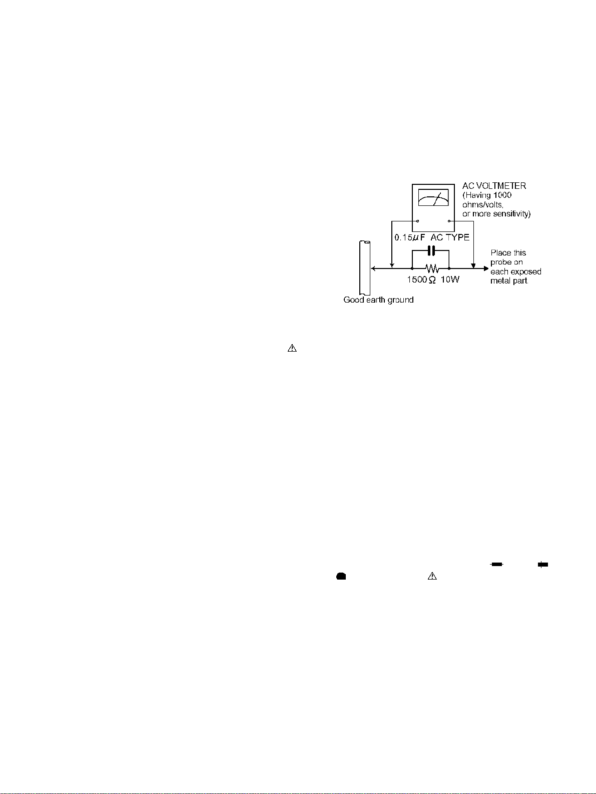
(5) Leakage shock hazard testing)
After reassembling the product, always perform an isolation
check on the exposed metal parts of the product (antenna
terminals, knobs, metal cabinet, screw heads, headphone
jack, control shafts, etc.) to be sure the product is safe to
operate without danger of electrical shock.
Do not use a line isolation transformer during this check.
• Plug the AC line cord directly into the AC outlet. Using a
"Leakage Current Tester", measure the leakage current
from each exposed metal parts of the cabinet, particularly any exposed metal part having a return path to the
chassis, to a known good earth ground. Any leakage
current must not exceed 0.5mA AC (r.m.s.).
• Alternate check method
Plug the AC line cord direct ly into the AC outle t. Use a n AC
voltmeter having, 1,000 ohms per volt or more sensitivity in
the following manner. Connect a 1,500 ohm 10W resistor
paralleled by a 0.15 µF AC-type capacitor between an
exposed metal part and a known good earth ground.
Measure the AC voltage across the resistor with the AC
XL-R5020BK
voltmeter.
Move the resistor connection to each exposed metal part,
particularly any exposed metal part having a return path to
the chassis, and measure the AC voltage across the
resistor. Now, reverse the plug in the AC outlet and repeat
each measurement. Voltage measured any must not
exceed 0.75 V AC (r.m.s.). This corresponds to 0.5 mA AC
(r.m.s.).
1.2 Warning
(1) This equipment has been designed and manufactured to
meet international safety standards.
(2) It is the legal responsibility of the repairer to ensure that
these safety standards are maintained.
(3) Repairs must be made in accordance with the relevant
safety standards.
(4) It is essential that safety critical components are replaced
by approved parts.
(5) If mains voltage selector is provided, check setting for lo-
cal voltage.
1.3 Caution
Burrs formed during molding may be left over on some
parts of the chassis.
Therefore, pay attention to such burrs in the case of preforming repair of this system.
1.4 Critical parts for safety
In regard with component parts appearing on the silk-screen
printed side (parts side) of the PWB diagrams, the parts that are
printed over with black such as the resistor ( ), diode ( ) and
ICP ( ) or identified by the " " ma rk nearby are critical for safety.
When replacing them, be sure to use the parts of the same type
and rating as specified by the manufacturer. (Except the JC version)
3
Page 4
XL-R5020BK
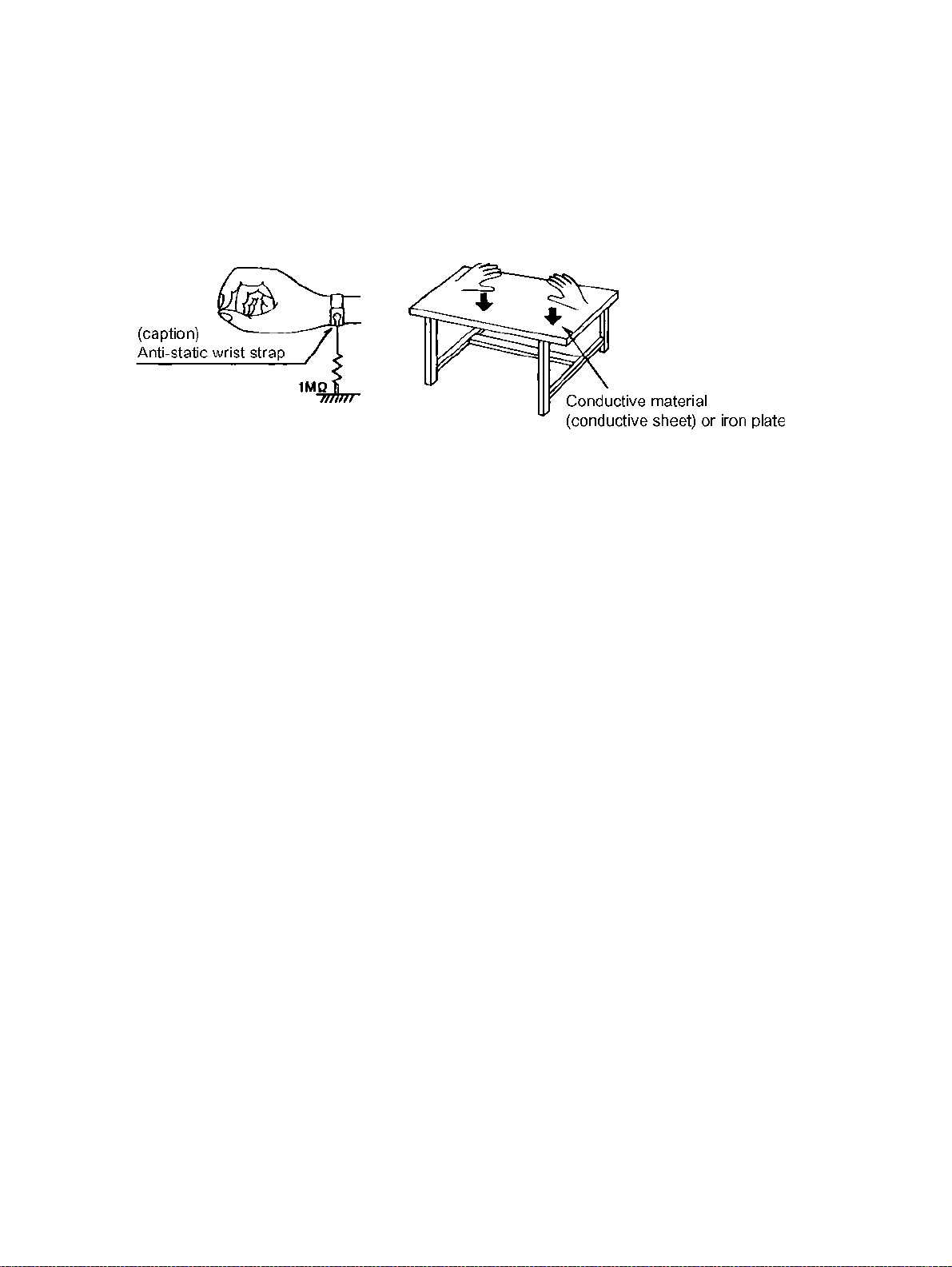
1.5 Preventing static electricity
Electrostatic discharge (ESD), which occurs when static electricity stored in the body, fabric, etc. is discharged,
can destroy the laser diode in the traverse unit (optical pickup). Take care to prevent this when performing repairs.
1.5.1 Grounding to prevent damage by static electricity
Static electricity in the work area can destroy the optical pickup (laser dio de) in devices such as DVD players.
Be careful to use proper grounding in the area where repairs are being performed.
(1) Ground the workbench
Ground the workbench by laying conductive material (such as a conductive sheet) or an iron pl ate over it before placing the
traverse unit (optical pickup) on it.
(2) Ground yourself
Use an anti-static wrist strap to release any static electricity built up in your body.
(3) Handling the optical pickup
• In order to maintain quality during transport and before installation, both sides of the laser diode on the replacement optical
pickup are shorted. After replacement, return the shorted parts to their original condition.
(Refer to the text.)
• Do not use a tester to check the condition of the laser diode in the optical pickup. The tester's internal power source can
easily destroy the laser diode.
1.6 Handling the traverse unit (optical pickup)
(1) Do not subject the traverse unit (optical pickup) to strong shocks, as it is a sensitive, complex unit.
(2) Cut off the shorted part of the flexible cable using nippers, etc. after replacing the optical pickup. For specific details, refer to the
replacement procedure in the text. Remove the anti-static pin when replacing the traverse unit. Be careful not to take too
long a time when attaching it to the connector.
(3) Handle the flexible cable carefully as it may break when subjected to strong force.
(4)I t is not possible to adjust the semi-fixed resistor that adjusts the laser power. Do not turn it.
4
Page 5

1.7 Importance admistering point on the safety
XL-R5020BK
5
Page 6
XL-R5020BK
1.8 Precautions for Service
1.8.1 Handling of Traverse Unit and Laser Pickup
(1) Do not touch any peripheral element of the pickup or the actuator.
(2) The traverse unit and the pickup are precision devices and therefore must not be subjected to strong shock.
(3) Do not use a tester to examine the laser diode. (The diode can easily be destroyed by the internal power supply of the tester.)
(4) To replace the traverse unit, pull out the metal short pin for protection from charging.
(5) When replacing the pickup, after mounting a new pickup, remove the solder on the short land which is provided at the center
of the flexible wire to open the circuit.
(6) Half-fixed resistors for laser power adjustment are adjusted in pairs at shipment to match the characteristics of the optical block.
Do not change the setting of these half-fixed resistors for laser power adjustment.
1.8.2 Destruction of Traverse Unit and Laser Pickup by Static Electricity
Laser diodes are easily destroyed by static electricity charged on clothing
or the human body. Before repairing peripheral elements of the traverse unit or pickup, be sure to take the following electrostatic
protection:
(1) Wear an antistatic wrist wrap.
(2) With a conductive sheet or a steel plate on the workbench on wh ich the trave rse unit or the pick up is to be repaired, grou nd
the sheet or the plate.
(3) After removing the flexible wire from the connector (CN101), short-circuit the flexible wire by the metal clip.
(4) Short-circuit the laser diode by soldering the land which is provided at the center of the flexible wire for the pickup.
After completing the repair, remove the solder to open the circuit.
Please refer to "Fig.2-4" of "Disassembly
method" for details.
6
Page 7
SECTION 2
Disassembly method
2.1 Main body
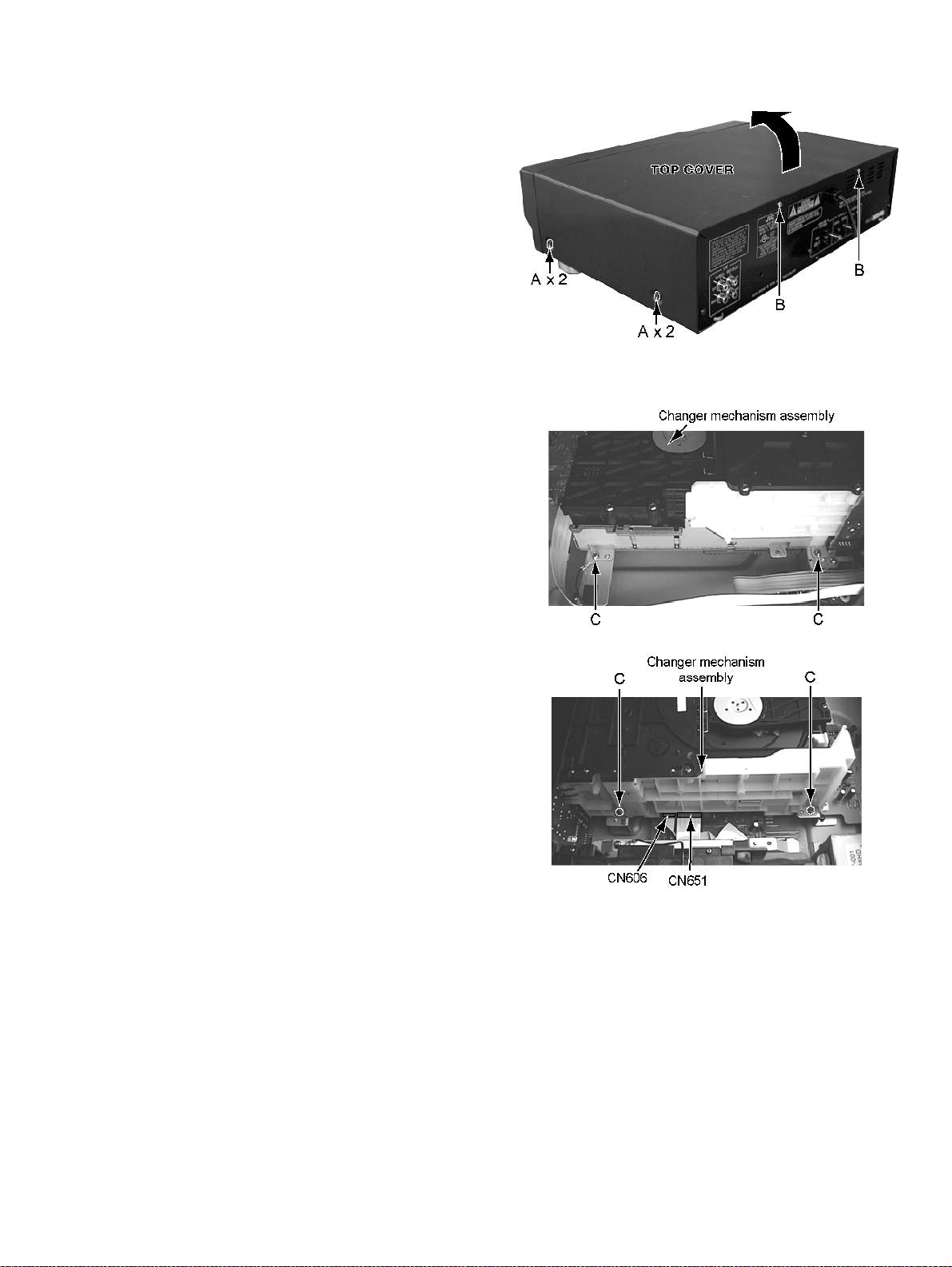
2.1.1 Removing the top cover (see Fig.1)
(1) Remove the four screws A attaching the top cover on both
sides of the body.
(2) Remove the two screws B attaching the top cover on the
back of the body.
(3) Remove the top cover from the body by lifting the rear part
of the top cover.
ATTENTION:
Do not break the front panel tab fitted to the top cover.
2.1.2 Removing the changer mechanism assembly
(see Fig.2~3)
*Prior to performing the following procedure, remove the top
cover.
(1) Remove the four screws C attaching the changer mecha-
nism assembly.
(2) Disconnect the card wire from connector CN606 and
CN651 on the CD servo control board respectively.
(3) Remove the changer mechanism assembly from the body
by lifting the rear part of the changer mechanism asse mbly.
XL-R5020BK
Fig.1
Fig.2
Fig.3
7
Page 8

XL-R5020BK
2.1.3 Removing the CD recording mechanism assembly
(see Fig.4~6)
*Prior to performing the following procedure, remove the top
cover.
*There is no need to remove the changer mechanism assembly.
(1) Remove the two screws E attaching the mechanism chas-
sis.
(2) Remove the three screws F attaching the CD recording
mechanism assembly.
(3) Disconnect the card wire from connector CN702 and
CN703 on the servo control board respectively.
(4) Disconnect the connect wire from connector CN701 on the
servo control board.
(5) Remove the five screws G attaching the mechanism chas-
sis
Fig.5
Fig.4
2.1.4 Removing the MP3 board
(see Fig.7,8)
*Prior to performing the following procedure, remove the top
cover, CD recording mechanism assembly.
*There is no need to remove the changer mechanism assembly.
(1) Pull out the MP3 board from the fastener.
At this time, disconnect the connector CN401 of the MP3
board from connector CN616 on the Main board.
(2) Disconnect the card wire from connector CN617 on the
MP3 board.
Fig.6
Fig.8
Fig.7
8
Page 9
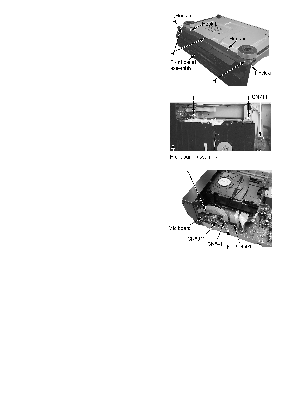
2.1.5 Removing the front panel assembly
(see Fig.9~11)
*Prior to performing the following procedure, remove the top
cover.
*There is no need to remove the changer mechanism assembly
and CD recording mechanism assembly.
(1) Remove the three screws H attaching the front panel as-
sembly on the bottom of the body.
(2) Remove the two screws I attaching the headphone jack
bracket.
(3) Remove the one screw J attaching the mic jack bracket.
(4) Remove the one screw K attaching the main board.
(5) Disconnect the card wire from connector CN711, CN841
and CN501 on the main board respectively.
(6) Disconnect the flat wire from connector CN601 on the
main board from mic board.
(7) Hook a and b are removed respectively, and the front
panel assembly is removed.
XL-R5020BK
Fig.9
Fig.10
Fig.11
9
Page 10
XL-R5020BK
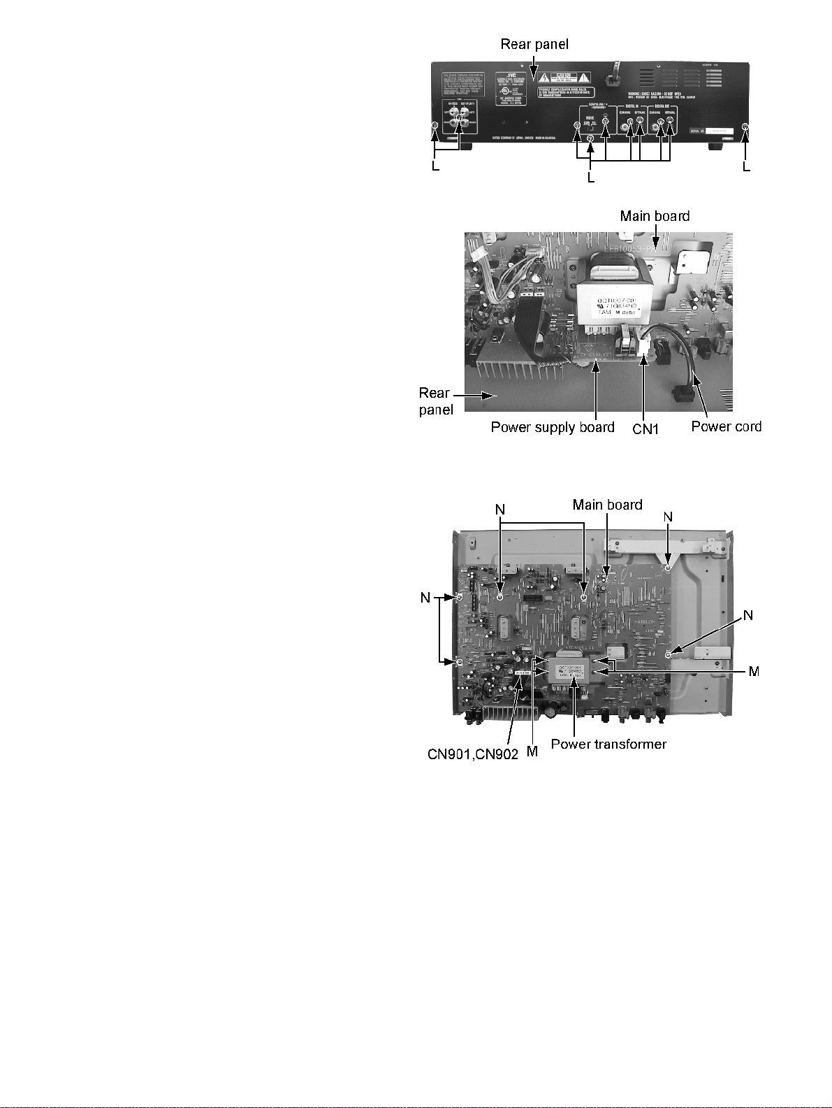
2.1.6 Removing the rear panel
(see Fig.12,13)
*Prior to performing the following procedure, remove the top
cover.
(1) Remove the ten screws L attaching the rear panel.
(2) Disconnect the power cord from connector CN1 on the
power supply board.
Fig.12
2.1.7 Removing the main board and power supply board
(see Fig.14)
*Prior to performing the following procedure, remove the top
cover, front panel assembly, changer mechanism assembly, CD
recording mechanism assembly and rear panel.
(1) Remove the four screws M attaching the power transform-
er.
(2) Disconnect the flat wire from connector CN901 and
CN902 on the main board.
(3) Remove the six screws N attaching the main board.
Fig.13
Fig.14
10
Page 11
SECTION 3
MECHANISM
3.1 Changer mechanism assembly
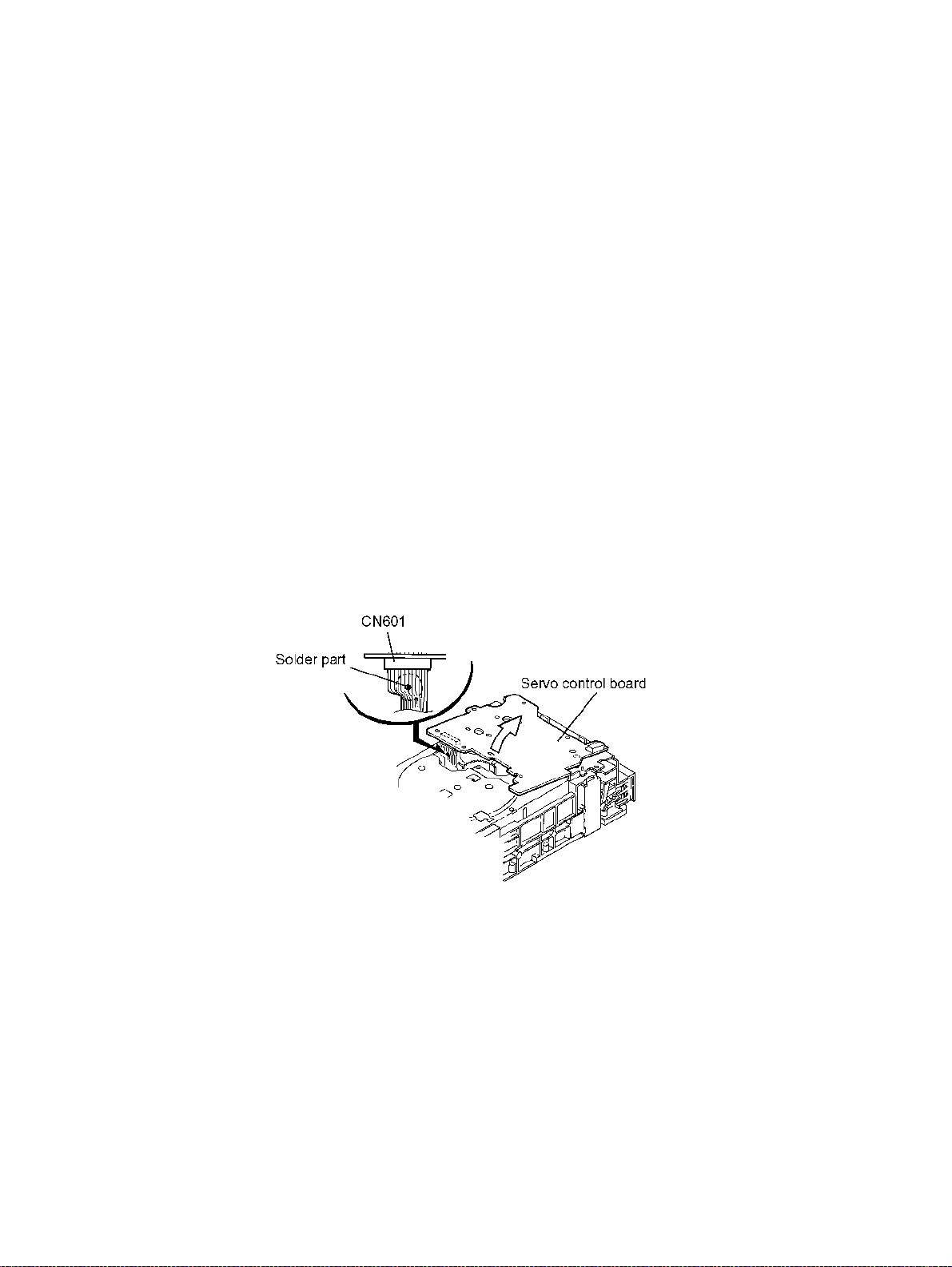
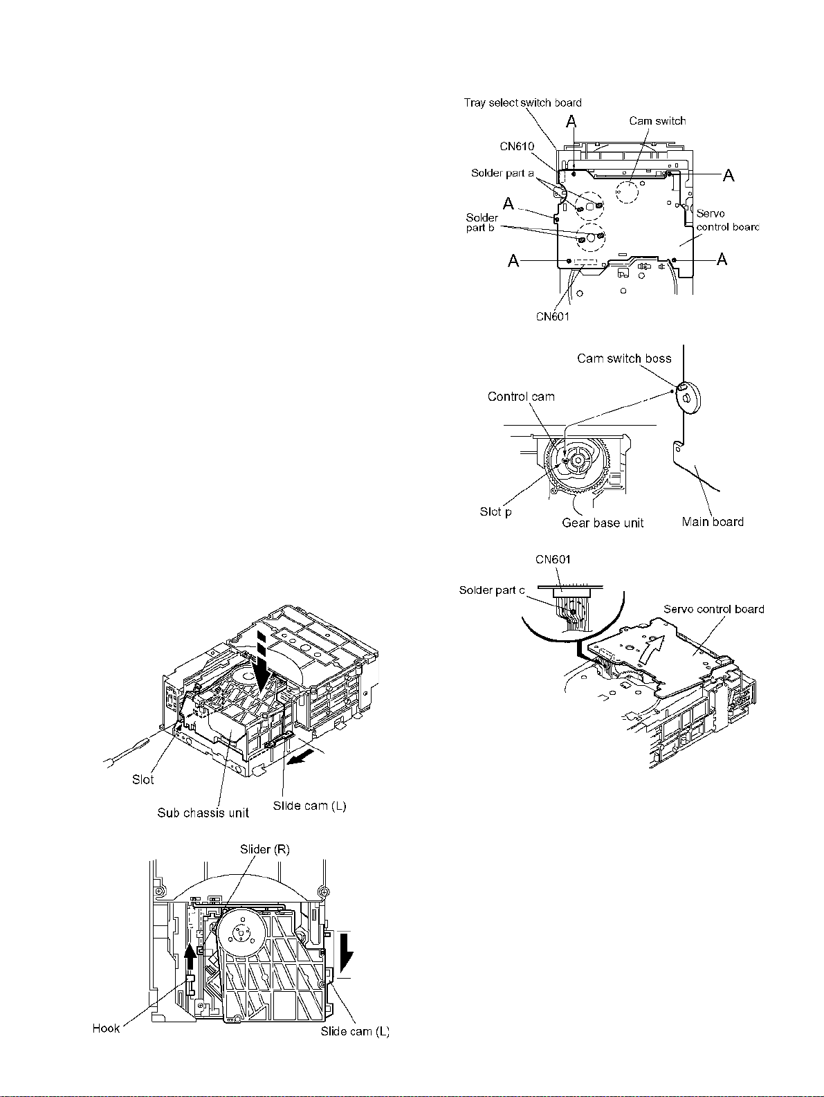
3.1.1 Removing the servo control board
(See Fig.1 to 5)
ATTENTION:
Make sure the sub chassis unit is locating at the lowest position. If not,perform the following procedure from 1 to 3.
(1) Insert a screwdriver into the sub chassis slot on the back
of the body and push the slider (R) toward the front.
(2) From the top of the body, slide the hook and the slider (R)
forward until they stop.
(3) From the right side of the body, slide the slide cam (L)
backward until it stops. The sub chassis unit will move to
the lowest position.
(4) From the bottom of the body, unsolder each soldered part
a and b of the motors on the servo control board.
(5) Remove the five screws A attaching the servo control
board.
(6) Disconnect connector CN610 on the servo control board
from the tray select switch board to suspend the servo
control board tentatively. Solder the part c of the flexible
wire connected to connector CN601 on the underside of
the servo control board.
(7) Disconnect the flexible wire from connect or CN601 and
remove the servo control board from the body.
ATTENTION:
In case of disconnecting the flexible wire without soldering, the CD pick up may be damaged.
ATTENTION:
When reassembling, make sure the cam switch boss of
the servo control board is fitted to the slot p of the control cam on the bottom of the body
(Refer to Fig.3).
XL-R5020BK
Fig.3
Fig.4
Fig.1
Fig.2
Fig.5
11
Page 12

XL-R5020BK
3.1.2 Removing the tray unit
(See Fig.6 to 9)
*The tray unit can be removed despite the position of the sub
chassis unit, but the lowest position is recommended to expedite
the work.
(1) Remove the four screws B attaching the top cover on the
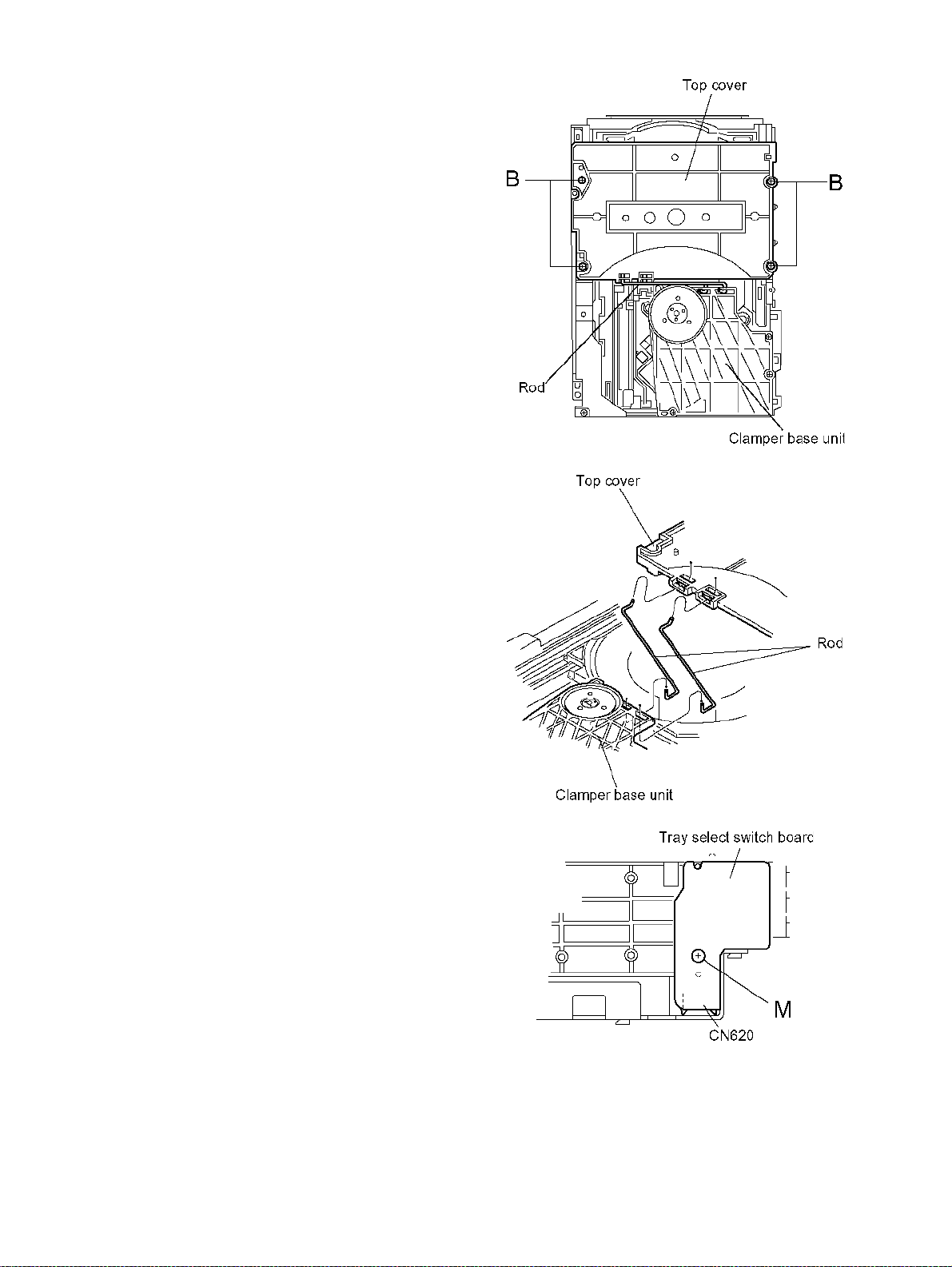
top of the body.
(2) Remove the top cover with the two rods attached to the top
cover and the clamper base unit.
(3) Pull the lock lever of the return spring on the right si de of
the body to eject the tray unit.
(4) From the top of the body, release the tray from the joi nt
hook marked d (Push the tray toward the front).
(5) Release the stoppers on both sides in the direction of the
arrow and pull out the tray unit from the body.
ATTENTION:
Pull out the tray unit from the top tray 3 in sequence.
Fig.8
Fig.6
Fig.7
Fig.9
12
Page 13
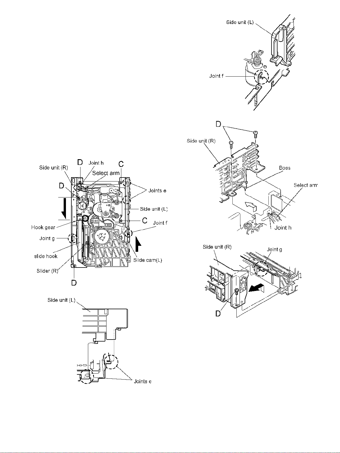
3.1.3 Removing the side unit (L) and (R)
(See Fig.10 to 14)
*Prior to performing the following procedures, remove the servo
control board, the top cover and the tray unit.
(1) Remove the two screws C attaching the side unit (L).
(2) Slide and remove the side unit (L) toward the fro nt while
releasing the two joints e and the joint f with the chassis
unit.
(3) Slide the slide cam (L) toward the front until it stops to
place the sub chassis unit at the top position.
ATTENTION:
The side unit (R) can be removed when the sub chassis
unit is located at the top position.
(4) Turn the hook gear counterclockwise to move th e slide
hook and the slider (R) backward until they stop.
(5) Remove the three screws D attaching the side unit (R).
Raise the side unit (R) upward and release the joint g with
the chassis unit and the boss from the select arm marked
h. Then remove the side unit (R) from the body.
ATTENTION:
When reassembling, make sure the boss is fitted to the
select arm marked h.
XL-R5020BK
Fig.12
Fig.10
Fig.11
Fig.13
Fig.14
13
Page 14
XL-R5020BK
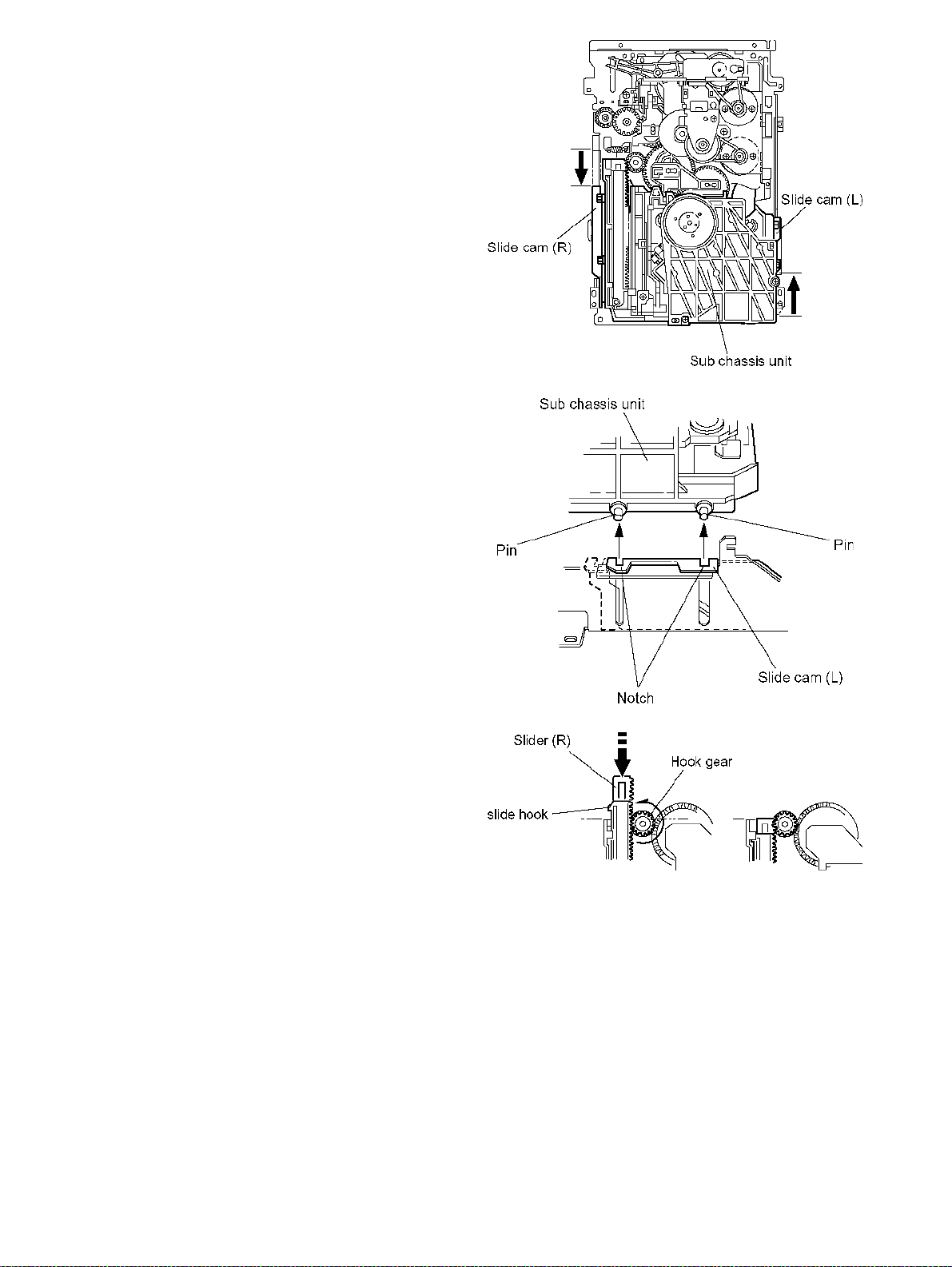
3.1.4 Removing the sub chassis unit
(See Fig.15 to 17)
*Prior to performing the following procedures, remove the servo
control board, the top cover, the tray unit,the side unit (L) and
the side unit (R).
(1) Turn the hook gear counterclockwise to move the slide
hook and the slider (R) backward until they stop.
(2) Slide the slide cam (L) and the slide cam (R) in the direction
of the arrow until they stop.
(The notches of each slide cam are fitted to the pins on
both sides of the sub chassis unit.)
(3) Detach the sub chassis unit upward.
ATTENTION:
When reassembling, turn the hook gear of the chassis
unit counterclockwise until it stops and slide the slide
hook and the slider (R) of the sub chassis unit backward
until they stop.
Fig.15
Fig.16
Fig.17
14
Page 15
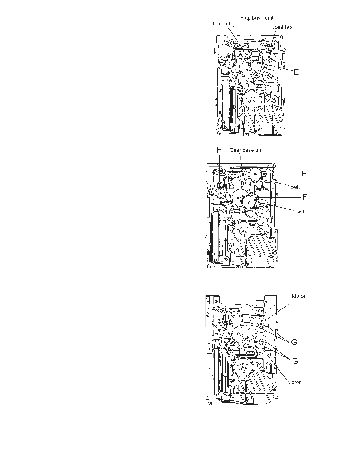
3.1.5 Removing the flap base unit and the gear ba se unit
(See Fig.18 and 19)
*Prior to performing the following procedures, remove the servo
control board, the top cover, the tray unit,the side unit (L) and
the side unit (R).
(1) Remove the screw E attaching the flap base unit. Release
the joint tabs i and j, then remove the flap base unit from
the body.
(2) Remove the belts from the two pulleys on the gear base
unit.
(3) Remove the three screws F and remove the gear base unit
from the body.
XL-R5020BK
Fig.18
3.1.6 Removing the motors
(See Fig.20)
*Prior to performing the following procedure, remove the main
board.
(1) Remove the belts from the two pulleys.
(2) Remove the four screws G and detach each motor from
the body.
Fig.19
Fig.20
15
Page 16
XL-R5020BK
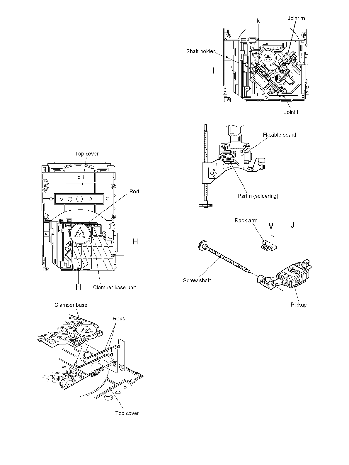
3.1.7 Removing the pickup
(See Fig.21 to 25)
(1) From the top of the body, remove the three screws H
attaching the clamper base unit.
(2) Remove the clamper base unit with the two rods attached
to the clamper base unit and the top cover.
(3) Turn the screw shaft gear marked k in the direction of the
arrow to move the pickup unit.
(4) Remove the screw I attaching the shaft holder.
(5) Move the screw shaft in the direction of the arrow and
release it from the joint l. Then release it from the joint m
with the pickup holder. Detach the pickup with the screw
shaft.
(6) Solder the part n of the flexible board on the underside of
the pickup. After soldering, disconnect the flexible wire
connected to the pickup (In case of disconnecting the
flexible wire without soldering, it may cause damage to the
CD pickup).
(7) Remove the two screws J attaching the rack arm to the
pickup unit.
(8) Pull out the screw shaft from the pickup.
Fig.23
Fig.21
Fig.24
Fig.25
16
Fig.22
Page 17
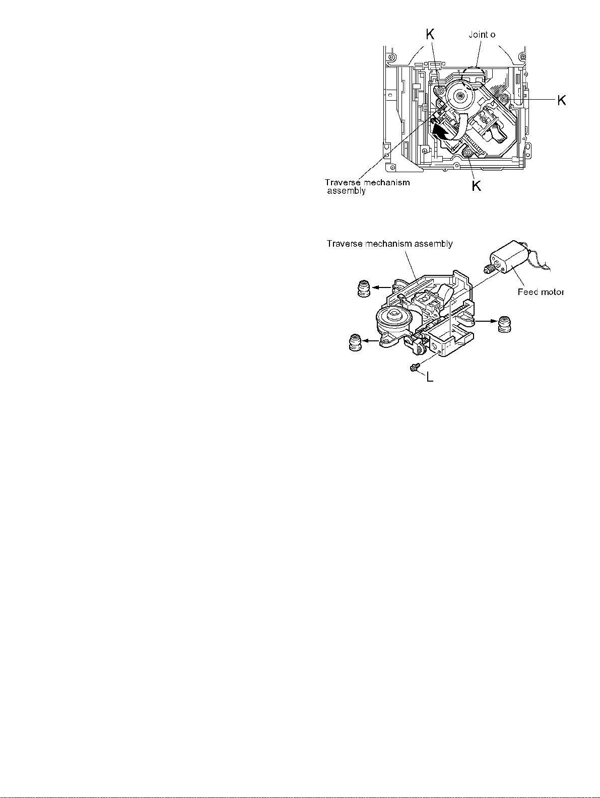
3.1.8 Removing the traverse mechanism assemb ly
(See Fig.26)
*Prior to performing the following procedure, remove the servo
control board and the clamper base unit.
(1) Remove the three screws K attaching the traverse
mechanism assembly.
(2) Detach the rear part of the traverse mechanism assembly
upward to release the joint o with the sub chassis unit.
Then remove the assembly from the body.
3.1.9 Removing the feed motor
(See Fig.27)
*Prior to performing the following procedure,remove the
traverse mechanism assembly.
(1) Remove the screw L attaching the feed motor.
XL-R5020BK
Fig.26
Fig.27
17
Page 18
XL-R5020BK
3.1.10 Removing the tray select switch board
(See Fig.6,7 and 28)
(1) Remove the four screws B attaching the top cover on the
top of the body.
(2) Remove the top cover with the two rods attached to the top
cover and the clamper base unit.
(3) Remove the screw M on the right side of the body.
Fig.6
18
Fig.7
Fig.28
Page 19
SECTION 4
Confirm method of operation
XL-R5020BK
4.1 Chec k mod e
All lighting FL display and reducing time operation of clock
(1) Setting method of all lighting FL display
"STANDBY/ON" key is pushed while pushing "REC/REC
MUTING" key by the stand-by state.
(2) Setting method of reducing time operation of clock
FL display is put into the state of all lighting by the method of the
above-mentioned, and "STANDBY/ON" key is pushed afterwards.
The clock display comes to advance during one minute a
second in actual time when changing to this mode.
Because other operation can do the normal operation,
Uses for the confirmation of the operation of the timer
function etc.
(3) Release method
"STANDBY/ON" key is pushed while pushing "REC/REC
MUTING" key.
4.2 All release of set content
All content of the item in the following set is returned to initial
state. (State of factory shipment)
(1) Setting method
"STANDBY/ON" key is pushed while pushing "REC
SOURCE SELECTOR" key by the stand-by state.
[Set items]
• Deletion of time setting
• The setting of the timer is deleted.
• The program of the program play is deleted.
• The content of the registration of the listen ing editing
and the program editing is deleted.
The repeat setting is turned off.
• Release of disc lock
• The unit of busy is adjusted to the changer mechanism side.
• The play mode of changer mechanism is made a normal mode.
• The pitch control setting is turned off.
• The selection of the recording source is made DIGITAL of CD.
• DUB-SPEED setting is made HIGH.
• AUTO TRACK setting is turned ON.
• TRACK SPACE setting is turned ON.
• CONVERTER setting is turned ON.
• D-IN SYNCHRO setting is START
• FINALISE setting is ON
4.3 Service menu
There is an item displayed besides "SYSTEM_AGING" and
"READ_VERSION" in the service menu.
However, because the effective item is only "SYSTEM_AGING" and
"READ_VERSION", the function does not actually use other items.
The running operation and the version of the firmware can be
confirmed by the undermentioned method.
(1) Setting method of service menu
a) "STANDBY/ON" key is pushed while pushing "FI-
NALIZE" key by the stand-by state.
b) When the blinking display of the disk distinction
ends, "MENU" key is pushed.
The menu display changes if "MULTI JOG" knob of
the main body is turned.
c) The execution of the each item is completed or either
"CANCEL"key, "CD-RW STOP"key or "MENU"key
is pushed when going out of the menu mode.
(2) Release method
a) If "STANDBY/ON" key is pushed, and the power
supply is turned off once, becomes a normal menu.
4.4 Running operation
When this mode is executed, the operation of the recording and
the playback is repeated.
Please use to confirm operation.
It is necessary to put the recorded disk or CD-DA in tray 1
of changer mechanism beforehand to execute this item,
and put CD-RW of the blank disk in recording mechanism.
(1) Setting method of running operation
a) "Service menu" is made to be displayed on the FL
display referring to the above-mentioned.
b) "SYSTEM_AGING" is made to turn "MULTI JOG"
knob, and to be displayed on the FL display.
c) The undermentioned operation starts when "SET"
key is pushed.
The undermentioned control becomes possible according to the
content of the disk turned on to tray 1 of changer mechanism.
* The time required of operation of running once
* Movement frequency of pick-up
F L display becomes " ", and the frequency to which the
running operation is done is displayed by the figure when
"STOP" key is pushed to the running working or interrupted because of the error etc.
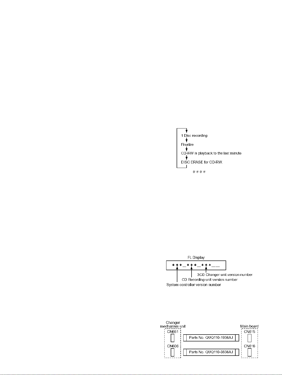
4.5 Display of versio n n umber
When this item is executed, version number "system controller",
"CD recording unit", and "3CD changer unit" respectively is displayed in FL display for five seconds.
When five seconds pass, this mode is automatically made clear.
Setting method of display of version number
(1) "Service menu" is made to be displayed on the FL dis-
play referring to the previous page.
(2) "READ_VERSION" is made to turn "MULTI JOG" knob,
and to be displayed on the FL display.
(3) The undermentioned operation starts when "SET " key is pushed.
It is displayed instead of version number when failing in reading
version number, "000".
4.6 Extension cord for diagnosis of changer mechanism unit
There is an extension cord to diagnose chan ger mechanism unit.
The undermentioned connector is connected, and used mutually.
19
Page 20
XL-R5020BK
SECTION 5
Description of major ICs
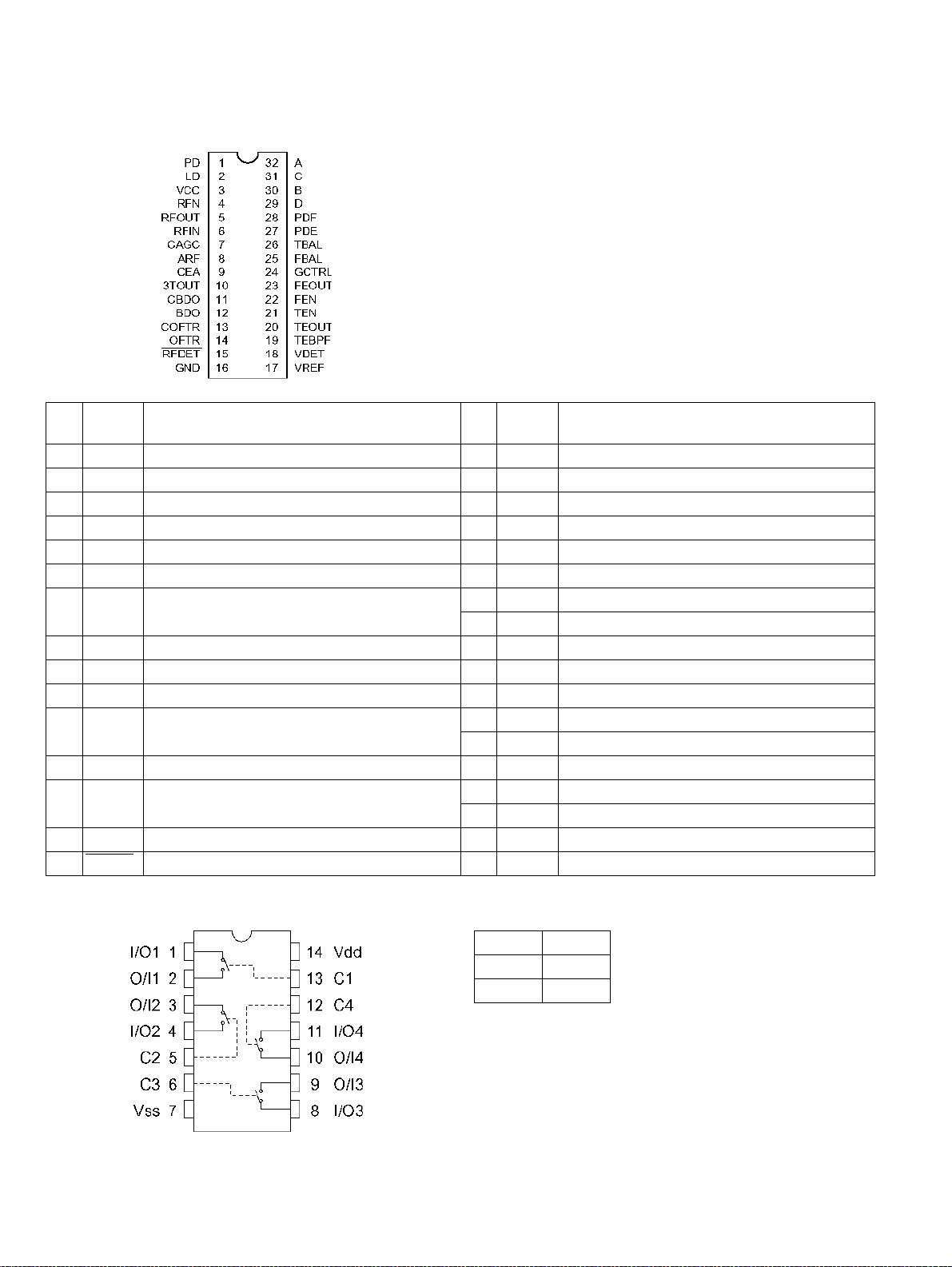
5.1 AN22000A-W(IC601):RF & SERVO AMP
• Pin layout
• Pin function
Pin
Symbol Description
No.
1 PD APC Amp. Input terminal 16 GND Connect to ground
2 LD APC Amp.Output terminal 17 VREF VREF output terminal
3 VCC Power supply terminal 18 VDET VDET output terminal
4 RFN RF addition Amp.Reversing input terminal 19 TEBPF VDET input terminal
5 RF OUT RF addition Amp.Output terminal 20 TEOUT TE Amp. output terminal
6 RF IN AGC input terminal 21 TEN TE Amp. reversing input terminal
7 C.AGC Terminal of connection of capacity of AGC loop
filter.
8 ARF AGC output terminal 24 GCTRL Terminal GCTL & APC
9 CEA Capacity connection terminal for HPF-Amp. 25 FBAL FBAL control terminal
10 3TOUT 3TENV output terminal 26 TBAL TBAL control terminal
11 CBDO Capacity connection terminal for RF shade side
envelope detection
12 BDO BDO output terminal 29 D Focus signal input terminal 4
13 COFTR Capacity connection terminal for RF discernment
side envelope detection
14 OFTR OFTR output terminal 32 A Focus signal input terminal 1
15 RFDET
RFDET output terminal
Pin
Symbol Description
No.
22 FEN FE Amp. reversing input terminal
23 FEOUT FE Amp. output terminal
27 PDE Tracking signal input terminal 1
28 PDF Tracking signal input terminal 2
30 B Focus signal input terminal 2
31 C Focus signal input terminal 3
5.2 BU4066BCF-X(IC831,IC841,IC861):Source selector
• Pin layout & block diagram • Truth table
Control Switch
HON
LOFF
20
Page 21
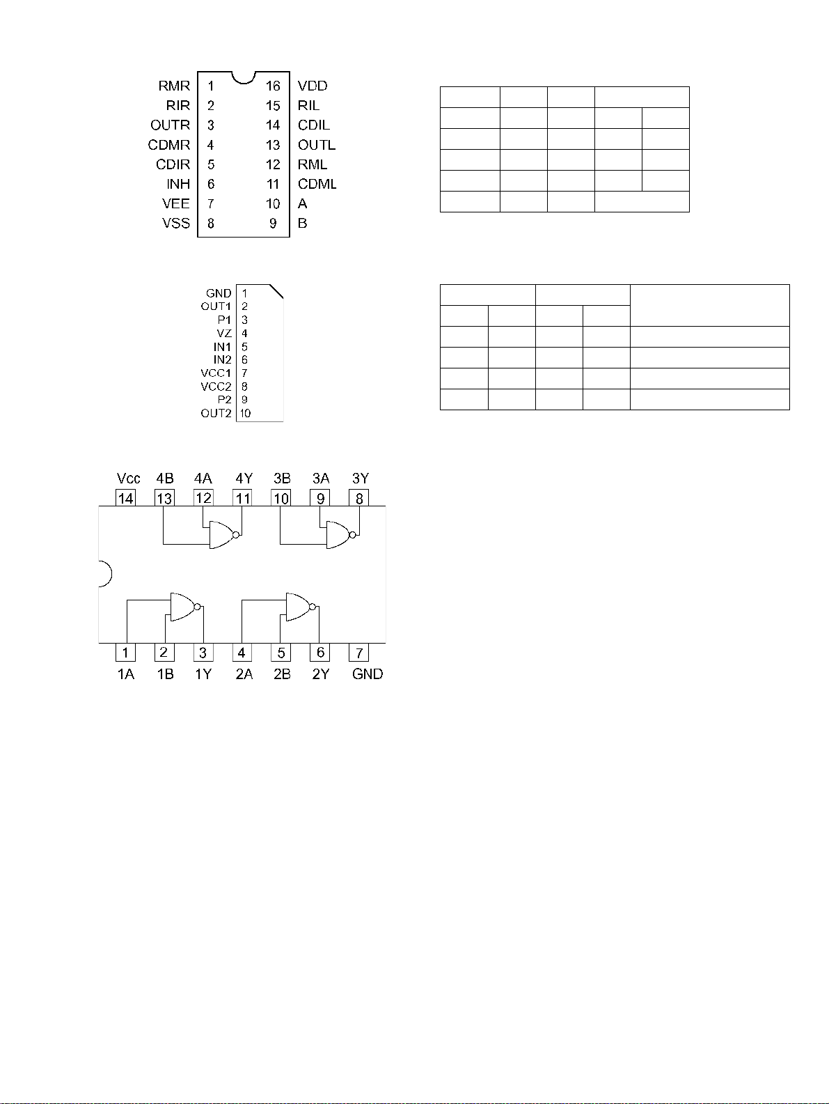
5.3 BU4052BCF-X(IC821):Channel switch controller
• Pin layout
• Truth table
INHIBIT A B ON SWITCH
LLLX0Y0
LHLX1Y1
LLHX2Y2
LHHX3Y3
HXX NONE
X : Don't Care
5.4 LB1641 (IC851,IC852) : DC Motor driver
• Pin layout • Truth table
Input Output
IN1 IN2 OUT1 OUT2
0000 Brake
1010 CLOCKWISE
0 1 0 1 COUNTER-CLOCKWISE
1100 Brake
XL-R5020BK
Mode
5.5 TC74HC00AF(IC301,IC311):Digital I/O selector
• Pin layout & block diagram
21
Page 22
XL-R5020BK
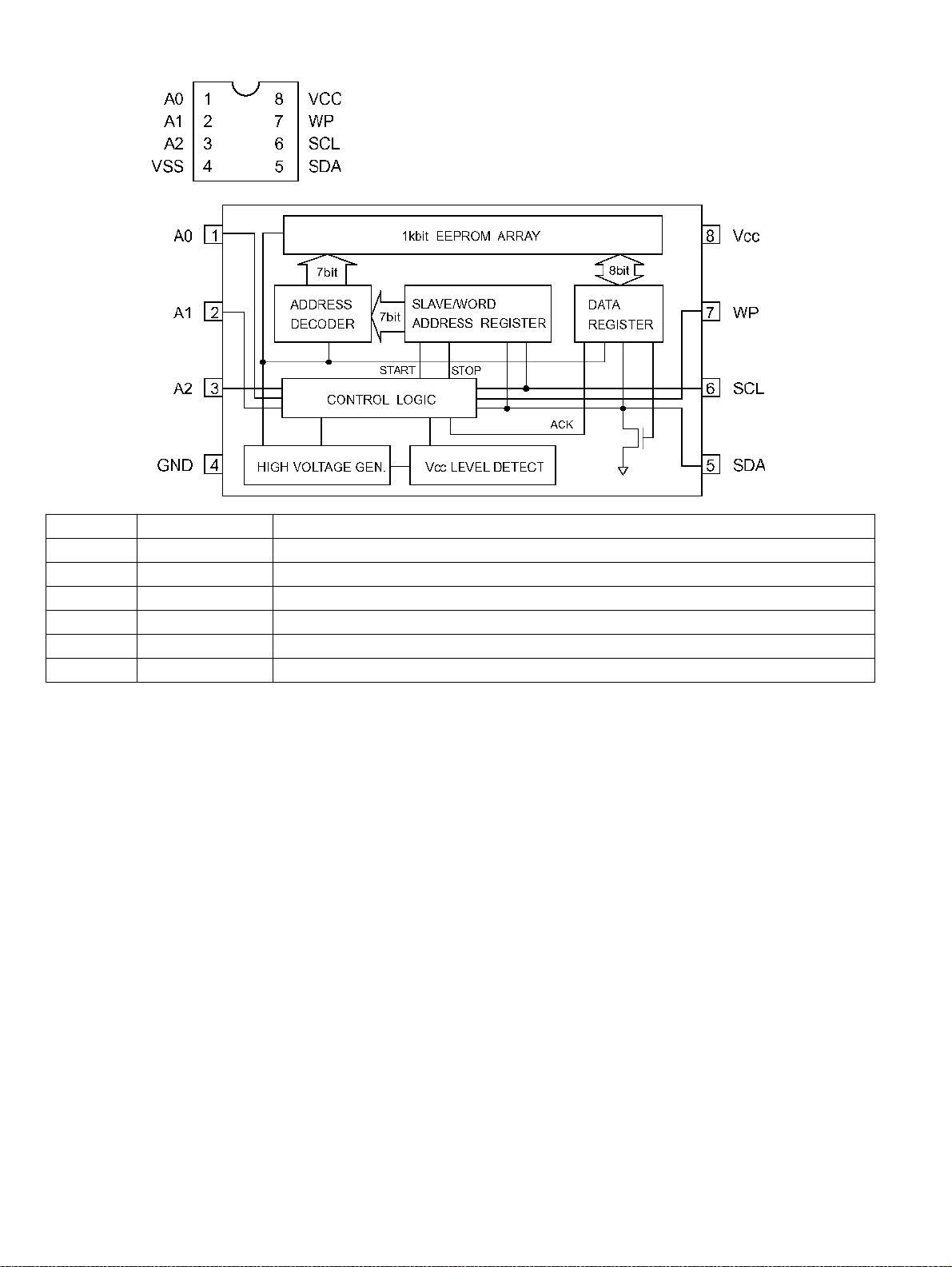
5.6 BR24C01AFV-W-X (IC201) : EEPROM
• Pin layout
• Block diagram
• Pin function
Pin name I/O Description
Vcc - Power supply
GND - Ground (0v)
A0A1A2 IN Slave address set
SCL IN Serial clock input
SDA IN / OUT Slave and word address,seri al data input serial data output *1
WP IN Write protect in pu t
*1 An open drain output requires a pull-up resister.
22
Page 23
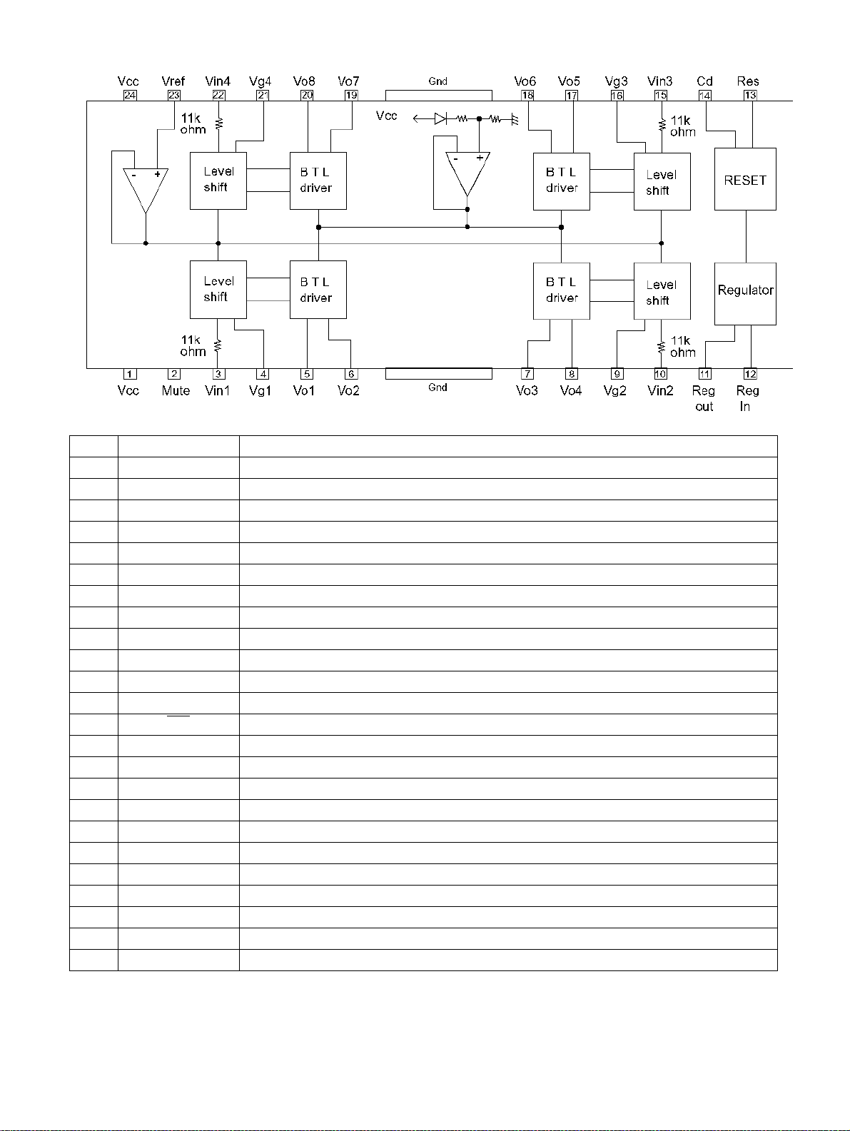
5.7 LA6541-X (IC801) : Focus & Spindle & Feed & Tracking BTL driver
• Pin layout & Block diagram
• Pin function
XL-R5020BK
Pin No. Symbol Description
1 Vcc Power supply (Shorted to pin 24)
2 Mute All BTL amplifier outputs ON/OFF
3 Vin1 BTL AMP 1 input pin
4 Vg1 BTL AMP 1 input pin (For gain adjustment)
5 Vo1 BTL AMP 1 input pin (Non inverting side)
6 Vo2 BTL AMP 1 input pin (Inverting side)
7 Vo3 BTL AMP 2 input pin (Inverting side)
8 Vo4 BTL AMP 2 input pin (Non inverting side)
9 Vg2 BTL AMP 2 input pin (For gain adjustment)
10 Vin2 BTL AMP 2 input pin
11 Reg Out External transistor collector (PNP) connection. 5V power supply output
12 Reg In External transistor (PNP) base connection
13 Res
14 Cd Reset output delay time setting (Capacitor connected externally)
15 Vin3 BTL AMP 3 input pin
16 Vg3 BTL AMP 3 input pin (For gain adjustment)
17 Vo5 BTL AMP 3 output pin (Non inverting side)
18 Vo6 BTL AMP 3 output pin (Inverting side)
19 Vo7 BTL AMP 4 output pin (Inverting side)
20 Vo8 BTL AMP 4 output pin (Non inverting side)
21 Vg4 BTL AMP 4 output pin (For gain adjustment)
22 Vin4 BTL AMP 4 output pin
23 Vref Level shift circuit's reference voltage application
24 Vcc Power supply (Shorted to pin 1)
Reset output
23
Page 24
XL-R5020BK
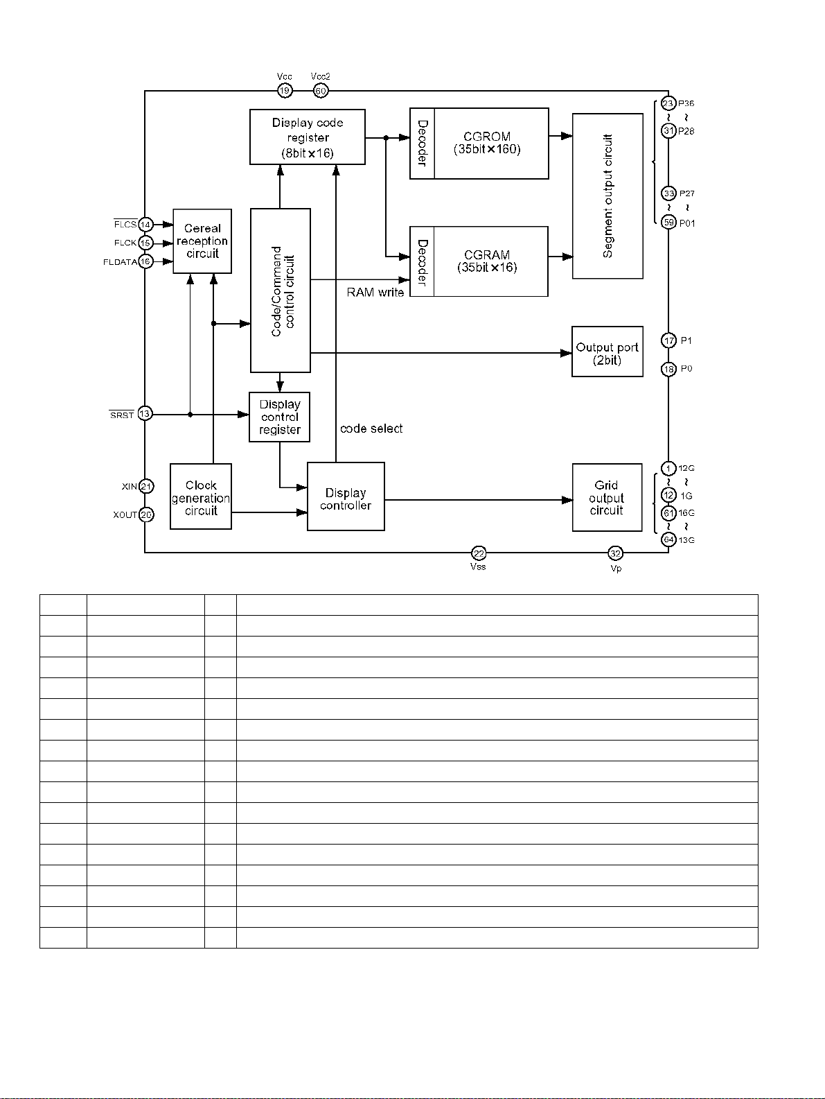
5.8 M66004SP(IC721):FL Driver
• Block diagram
• Pin function
Pin.No. Symbol I/O Description
1~12 12G~1G O FL grid control signal output.
13 SRST I Reset signal input
14 FLCS I Chip select signal input.
15 FLCLK I Shift clock signal input.
16 FLDATA I Serial data input.
17 P1 O Outp ut port (static operation)
18 P0 O Outp ut port (static operation)
19 VCC1 - Power supply for internal logic.
20 XOUT O Clock signal output.
21 XIN I Clock signal input.
22 VSS - Connect to ground.
23~31 P36~P28 O FL Segment control signal output.
32 VP - Power supply.
33~59 P27~P01 O FL Segment control signal output.
60 VCC2 - Power supply for grid output and segment output.
61~64 16G~13G O FL grid control signal output.
24
Page 25
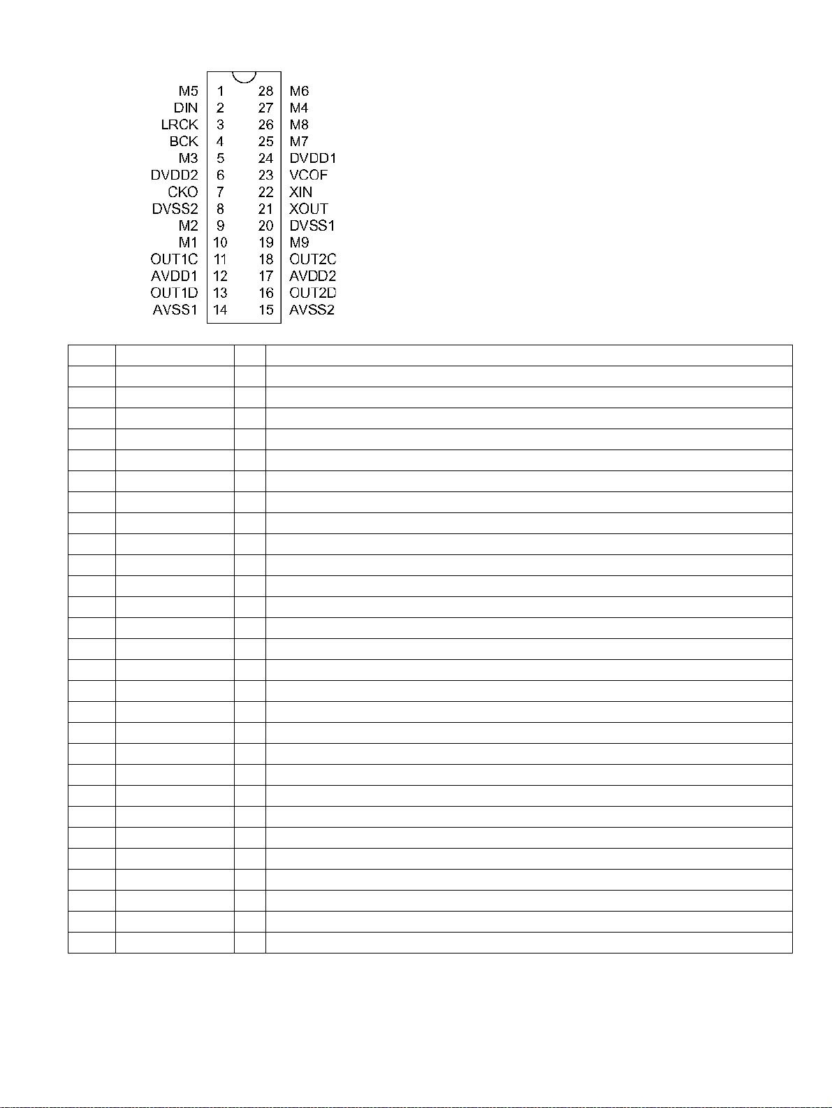
5.9 MN35505-X (IC361) : DAC
• Terminal layout
• Pin function
XL-R5020BK
Pin No.
1 M5 I Control signal for DAC
2 DIN I Digital data input
3 LRCK I L and R clock for DAC
4 BCK I Bit clock for DAC
5 M3 I Control signal for DAC
6 DVDD2 - Power supply terminal
7 CKO - Non connect
8 DVSS2 - Connect to ground
9 M2 I Control signal for DAC
10 M1 I Control signal for DAC
11 OUT1C O Analog output 1
12 AVDD1 - Power supply terminal
13 OUT1D O Analog output 1
14 AVSS1 - Connect to ground
15 AVSS2 - Connect to ground
16 OUT2D O Analog output 2
17 AVDD2 - Power supply terminal
18 OUT2C O Analog output 2
19 M9 - Non connect
20 DVSS1 - Connect to ground
21 XOUT - Non connect
22 XIN - Non connect
23 VCOF I VCO Frequency
24 DVDD1 - Power supply D+5V
25 M7 I System clock rate selection
26 M8 I System clock rate selection
27 M4 I Control signal for DAC
28 M6 - Connect to ground
Symbol I/O Description
25
Page 26
XL-R5020BK
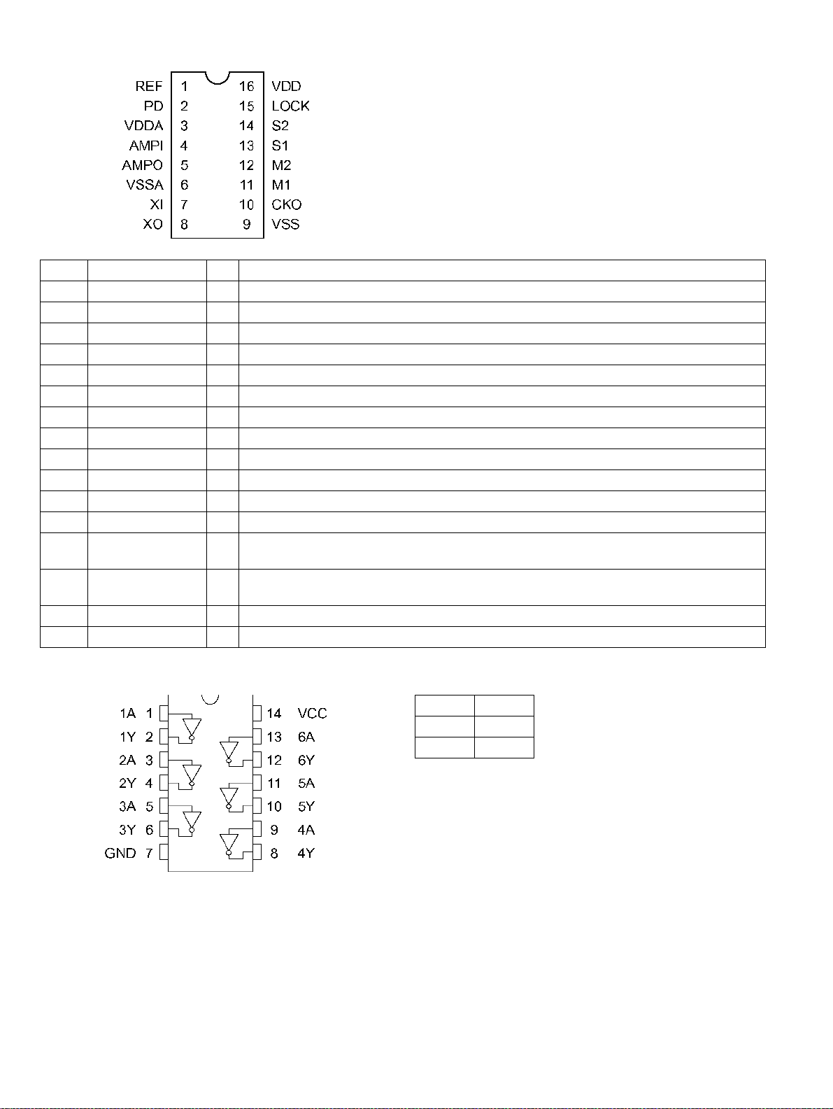
5.10 TC9246F-X(IC404):Clock generation for digital audio
• Pin layout
• Pin function
Pin No.
1 REF I Standard signal input terminal
2 PD O Phase difference signal output terminal
3 VDDA - Power supply voltage terminal for analog circuit
4 AMPI I AMP input terminal for LPF or oscillator 1
5 AMPO O AMP output terminal for LPF or oscillator 1
6 VSSA - Connect to ground for analog circuit
7 XI I AMP input terminal for oscillator 3
8 XO O AMP output terminal for oscillator 3
9 VSS - Connect to ground for digital circuit
10 CKO O Oscillation clock output terminal
11 M1 I Mode select terminal
12 M2 I Mode select terminal
13 S1 I Parallel mode : Dividing frequency selection terminal
14 S2 I Parallel mode : Dividing frequency selection terminal
15 LOCK O Lock detect signal output terminal
16 VDD - Power supply voltage terminal for digital circuit
5.11 TC74HCU04AF-W(IC331):Digital input selector
• Pin layout & block diagram • Truth table
Symbol I/O Description
Serial mode : Microcomputer data input terminal
Serial mode : Shift clock input terminal
AY
LH
HL
26
Page 27
5.1274VHC00MTC-X (IC406) : 2-input nand gate
• Pin layout
5.1374VHC08SJ-X(IC407):2-input AND gate
• Pin layout
XL-R5020BK
• Truth table
ABY
LLH
LHH
HLH
HHL
L : High impedance
• Truth table
GYA
LZL
LZH
HZL
HLH
27
Page 28
XL-R5020BK
5.14TC94A02F-005(IC401) : MP3 Decoder
• Block diagram
28
Page 29

• Pin function
Pin No.
1 /RESET I Hard reset input terminal(H:Normal operation L: Reset)
2 MiMD I Micon I/F mode select input terminal
3 AD0 O External SRAM address output 0 terminal
4 AD1 O External SRAM address output 1 terminal
5 MiDio I/O Micon I/F data input/output terminal
6 /MiCK I Micon I/F clock input terminal
7 AD2 O External SRAM address output 2 terminal
8 VDDT - Digital power supply (3.3V)
9 SDo O Data output terminal
10 AD3 O External SRAM address output 3 terminal
11 AD4 O External SRAM address output 4 terminal
12 SDi0 I Data input terminal 0
13 BCKiA I Bit clock input terminal A
14 LRCKiA I LR clock input terminal A
15 AD5 O External SRAM address output 5 terminal
16 CE O External SRAM chip enable terminal
17 OE O External SRAM output enable terminal
18 VDD - Digital power supply (2.5V)
19 STANBY I Standby mode control terminal
20 VSS - Digital GND
21 VSSL - DAC Lch GND
22 VRAL - DAC Lch reference voltage terminal
23 LO O DAC Lch output terminal
24 VDAL - DAC Rch power supply terminal(2.5V)
25 VDAR - DAC Lch power supply terminal(2.5V)
26 RO O DAC Rch output terminal
27 VRAR - DAC Rch reference voltage terminal
28 VSSR - DAC Rch GND
29 TESTP I Test terminal
30 CKS I VCO select terminal
31 AD12 O External SRAM address output 12 te rminal
32 AD11 O External SRAM address output 11 te rminal
33 AD10 O External SRAM address output 10 te rminal
34 AD9 O External SRAM address output 9 terminal
35 VDDT - Digital power supply terminal (3.3V)
36 AD8 O External SRAM address output 8 terminal
37 AD7 O External SRAM address output 7 terminal
38 AD6 O External SRAM address output 6 terminal
39 REQ O Squeeze request terminal to host
40 VSS - Digital GND
41 AD13 O External SRAM address output 13 te rminal
42 AD14 O External SRAM address output 14 te rminal
43 WR O External SRAM write signal
44 AD16 O External SRAM address output 16 te rminal
45 AD15 O External SRAM address output 15 te rminal
46 io0 I/O External SRAM data input/output 0 terminal
47 io1 I/O External SRAM data input/output 1 terminal
Symbol I/O Description
XL-R5020BK
29
Page 30

XL-R5020BK
Pin No.
48 VSS - Digital GND
49 io2 I/O External SRAM data input/output 2 terminal
50 io3 I/O External SRAM data input/output 3 terminal
51 io4 I/O External SRAM data input/output 4 terminal
52 VDD - Digital power supply (2.5V) terminal
53 io5 I/O External SRAM data input/output 5 terminal
54 io6 I/O External SRAM data input/output 6 terminal
55 io7 I/O External SRAM data input/output 7 terminal
56 VSSP - VCO GND
57 Pdo O PLL phase error detection signal output terminal
58 Vcoi I VCO control voltage input terminal
59 VDDP - VCO power supply
60 Cko O 16.934 MHz clock output terminal
61 VDDX - Power supply (2.5V) terminal for oscillator
62 Xi I Connection terminal for oscillator (input)
63 Xo O Connection terminal for oscillator (output)
64 VSSX - GND for oscillator
Symbol I/O Description
30
Page 31

5.15 TC9412AF(IC891) : Rec Level
• Pin layout
• Block diagram
XL-R5020BK
• Pin functions
Pin No. Symbol Description Pin No. Symbol Description
1 VSS Negative power supply temrinal 13 DATA Volume setup serial data input terminal
2 NC Non connect 14 STB Data write strobe input terminal
3 L-OUT L-ch Volume output terminal 15 NC Non connect
4 L-IN L-ch Volume input terminal 16 CS2 Chip select terminal
5 LD1 L-ch Loudness ta p output terminal 17 NC Non connect
6 LD2 L-ch Loudness ta p output terminal 18 A-GND R-ch Analog ground
7 A-GND L-ch Analog ground 19 LD2 R-ch Loudness tap output terminal
8 NC Non connect 20 LD1 R-ch Loudness tap output terminal
9 CS1 Chip select input terminal 21 R-IN R-ch Volume input terminal
10 NC Non connect 22 R-OUT R-ch Volume output terminal
11 GND Digital ground 23 NC Non connect
12 CK Data transfer clock input terminal 24 VDD Positive power supply terminal
31
Page 32

XL-R5020BK
5.16MN662790RSC(IC651):Digital servo & processor
• Pin layout
• Pin function
MN662790RSC (1/2)
Pin No. Symbol I/O Description
1 BCLK O Bit clock output for SRDATA
2 LRCK O Identifying signal output of LR
3 SRDATA O Serial data ou tput
4 DVDD1 - Power supply for digital circuit
5 DVSS1 - Connect to ground for digital circuit
6 TX O Digital audio interface output signal
7 MCLK I Micom command clock signal input
8 MDATA I Micom command data signal input
9 MLD I Micom command load signal input L:load
10 SENSE - Non connect
11 FLOCK - Non connect
12 TLOCK - Non connect
13 BLKCK O Sub code block clock signal (Command execution : CD-TEXT data readout enabling signal (DQSY) output)
14 SQCK I Export clock signal input for sub code Q resister
15 SUBQ O Sub code Q data output
16 DMUTE I Muting input H:muting
17 STAT O Status signal output
18 LSI_RST I Reset signal input L:reset
19 SMCK O Clock signal output MSEL is H : 8.4672 MHz MSEL is L : 4.2336 MHz
20 CSEL I Oscillation frequency specification terminal H:33.8688 MHz L:16.9344 MHz
21 TEST2 - TEST2 terminal usually : open
22 TVD O Traverse drive output
23 PC - Non connect
24 ECM O Spindle motor drive signal output (Compulsion mode ou tput)
25 ECS O Spindle motor drive signal output (Servo error signal output)
26 VDETMON - Non connect
27 TRD O Tracking drive signal output
28 FOD O Focus drive signal output
29 VREF - Reference voltage for DA output section
30 FBAL O Focus balance adjust signal output
31 TBAL O Tracking balance adjust signal output
32 FE I Focus error signal input (an alog input)
33 TE I Tracking error signal input (analog input)
34 RFENV I RF Envelope signal input (analog input)
35 TEST3 I TEST3 Terminal usually : Fixation L
36 OFT I Off track signal input H : off track
37 TRCRS I Track cross signal input (analog input)
38 RFDET I RF detection signal input L : detection
39 BDO I Dropout signal input H : dropout
40 LDON - Non connect
32
Page 33

Pin No. Symbol I/O Functions
41 PLLF2 I/O Terminal for loop filter characteristic switch for PLL
42 DSLBDA - Non connect
43 WVEL - Non connect
44 ARF I RF Signal output
45 IREF I Standard electric current input terminal
46 DRF I Bias terminal for DSL
47 DSLF I/O Loop filter terminal for DSL
48 PLLF I/O Loop filter terminal for PLL
49 VCOF I/O Loop filter terminal for VCO
50 AVDD2 - Power supply terminal for analog circuit
51 AVSS2 - Connect to ground terminal for analog circuit
52 EFM - Non connect
53 DSLB O PLL extraction clock output
54 VCOF2 I/O Loop filter terminal for VCO
55 SUBC O Sub code serial output
56 SBCK I Clock signal input for sub code serial output
57 VSS - Connect to ground terminal for oscillation circuit
58 X1 I Oscillation circuit input terminal f=16.9344 MHz 33.8688 MHz
59 X2 O Oscillation circuit output terminal f=16.9344 MHz 33.8688 MHz
60 VDD - Power supply terminal for oscillation circuit
61 BYTCK - Non connect
62 LDON O Laser ON signal output H : ON
63 GCTRL O General I/O port
64 IPFLAG - Non connect
65 FLAG O Flag signal outp ut
66 CLVS - Non connect
67 CRC - Non connect
68 DEMPH O De -emphasis detection signal output
69 RESY - Non connect
70 IOSEL I Mode switch terminal
71 TEST I TEST terminal usually : H
72 AVDD1 - Power supply terminal for analog circuit (for audio output section)
73 OUTL O Lch audio output
74 AVSS1 - Connect to ground terminal for analog circuit (for audio output section)
75 OUTR O Rch audio output
76 DQSY I RF signal polarity specification termin al
77 VCC5V - Power supply terminal (5V)
78 PSEL O IOSEL=H TEST terminal IOSEL=L SRDATA input
79 MSEL O IOSEL=H SMCK terminal output (frequency switch terminal) IOSEL=L LRCK input
80 SSEL O IOSEL=H SUBQ terminal output mode switch terminal IOSEL=L BCLK input
XL-R5020BK
MN662790RSC (2/2)
33
Page 34

XL-R5020BK
5.17UPD780076GK-533(IC251):Unit microcomputer
• Pin layout
• Pin layout
UPD780076GK-533 1/2
Pin No. Symbol I/O Description
1 E2SCK O Serial clock output to IC201
2 E2SDL I/O Serial data input/output with IC201
3 MCS I Communication method selection input from system microcomputer
L : Synchronization H : Asynchronous
4 MRDY O Signal output to system microcomputer by which command can be received
L H : Status output enable H L : command can be received
5 ITRVP3 I Play position switch (SW3) detection input
6 ITRVP2 I Play position switch (SW2) detection input
7 ITRVP1 I Play position switch (SW1) detection input
8 ITRYSoc I Sub tray open/close detection switch input
9 VSS0 - Connect to ground
10 VDD0 - Power supply terminal (+)
11 RESET I REST switch detection input (traverse mechanism)
12,13 - Non connect
14 ICAMP1 I Cam switch position 1 input
15 KCMND/TXD I/O Command input from system microcomputer (synchronization) or status output (asynchronous)
16 MSTAT/RXD I/O Status output to system microcomputer (synchronization) or command input (asynchronous)
17 KCLK I System microcomputer data/serial/clock input
18 SUBQ I Sub code Q data in put
19 CDCOPY O Right or wrong of CD copy signal output
20 SQCK O Clock output for sub code Q register
21 CDINDEX O CD index information
22 CDTNO O CD track information
23 ICAMP2 I Cam switch position 2 input
24 VDD1 - Power supply terminal (+)
25 AVSS - Connect to ground for A/D converter
26 VDET_LEVEL I Input for vibration detecting changeable level
27 KEY2 I Output voltage monitor of regulator (IC291)
28 TRY3CLOSE I Main tray 3 close switch detection input
29 TRY3OPEN I Main tray 3 open switch detection input
30 TRY2CLOSE I Main tray 2 close switch detection input
31 TRY2OPEN I Main tray 2 open switch detection input
32 TRY1OPEN I Main tray 1 open switch detection input
33 TRY1CLOSE I Main tray 1 close switch detection input
34 AVREF - Standard voltage of A/D converter and analog power supply
35 CAM_CW O Cam motor drive signal output (clockwise)
36 RESET I System reset input
34
Page 35

Pin No. Symbol I/O Description
37 XT2 - Non connect
38 XT1 I Sub system clock oscillation terminal
39 IC I Connect to ground
40 X2 O Main system clock output
41 X1 I Main system clock input
42 VSS1 - Connect to ground
43 FLAG I Flag (C1 error) signal input
44 BLKCK I Sub code/block/clock signal input
45 RFDET I RF signal detection input
46 CAM_CCW O Cam motor drive signal output (counterclockwise)
47 ACT_CCW O Actuator motor drive signal output (counterclockwise)
48 ACT_CW O Actuator motor drive signal output (clockwise)
49 - Non connect
50 EQX2 O Equalizer switch output (H:one time velocity L:double-speed/four time velocity)
51 ICAMP3 I Cam switch position 3 input
52 ICAMP4 I Cam switch position 4 input
53 RESET O Reset output to IC651
54 STAT I Status signal input from IC651
55 D MUTE O Muting output to IC651 H : muting
56 P.ON O Control signal output of 3.5V regulator (IC291)
57 MLD O Command load signal output to IC651
58 MDATA O Command data signal output to IC651
59 MCLK O Command clock signal output to IC651
60 CL KSW O Clock output control terminal to the outside
61 EQX4 I Equalizer switch output (H:one time velocity/double-speed L:four time velocity)
62,63 - Non connect
64 DR_MUTE O Driver IC muting output H : muting
XL-R5020BK
UPD780076GK-533 2/2
35
Page 36

XL-R5020BK
5.18UPD784215AGF513(IC501):System controller
• Pin layout
• Pin function
Pin No. Symbol I/O Description
1 CKSL2 - Not use
2 CKSL1 - Not use
3IDFS2-Not use
4 TEST- I Test mode input terminal L : Test mode
5 VR_STB O Strobe signal output to IC891
6 V R_DATA O Data output to IC891
7 VR_CK O Clock signal output to IC891
8 NC - Non connect
9 VDD - Power supply terminal +5V
10,11 CS1/CS2 I Chip select terminal
12,13 JOGA/JOGB I Multi jog dial A/B input
14 FLDAT O Serial data output to FL driver
15 FLCLK O Shift clock signal output to FL driver
16 FLCS O Chip select signal output to FL driver L : data output
17,18 NC - Non connect
19 PLL LOOK I PLL LOCK detect signal from IC404
20 DIN_COA - When digital input is coaxial for output H
21 NC - Non connect
22 VPP - Connect to ground
23 DIG_LED O Digital LED control signal output L : Lighting
24 CD_LED O 3CD LED control signal output L : Lighting
25 LIN_LED O Line IN LED control signal output L : Lighting
26 MIC_LED O MIC LED control signal output L : Lighting
27 CC LED - Non use
28 MIXBL I Mix balance volume level input
29 DIN_OPT O When digital input is optical for output H
30 SMUTE O System muting signal output
31 DACMUTE O DAC muting signal output
32 CD_DRT O It is a power output to the direct conne c ti o n of an al o g re cording
source 3CD to the A/D input of CD-RW as for L
33 SCD O Analog recording source 3CD select control output
L : selected 3CD
34,35 SLIN1/SLIN2 O Analog recording source select control output
36 SMIC O Analo g recording source MIC select control output
L : selected MIC
37 VDD - Power supply terminal +5V
(connects with the backup capacitor at power supply off. )
38 X2 O Main system clock output terminal 10MHz
39 X1 I Main system clock input terminal 10MHz
40 VSS - Connect to ground
41 XT2 O Sub clock output terminal 32.768KHz
42 XT1 I Sub clock input terminal 32.768KHz
43 RESET I Reset signal input
UPD784215AGF513 1/2
36
Page 37

Pin No. Symbol I/O Description
44 REM I Remote control signal input
45 NC - Non connect
46 ACON I The AC power supply existence detection terminal
L : No AC power supply (backup mode)
H : AC power supply having (normal mode : Backup mode Release)
47 CDR_RREQ I Request demand input from CD-RW unit
48 MP3REQ I Request demand input from MP3 decoder
49 DOCD O Output select control H : selected 3CD L : selected CD-RW
50 SLCDR O Output select control H : selected CD-RW L : selected 3CD
51 AVDD - Power supply terminal +5V
(connects with the backup capacitor at power supply off.)
52 AVREF0 - 3CD Analog signal level reference voltage
53~56 KEY1~4 I Operation switch input terminal 1~4
57 NC - Non use
58 3CDINR I 3CD analog signal level input (for Rch level meter)
59 3CDINL I 3CD analog signal level input (for Lch level meter)
60 MODE I DCS mode setting switch input
61 AVSS - Connect to ground
62 DCSI I DCS command input
63 DCSO O DCS command output
64 AVREF1 - Power supply terminal +5V
65 NC - Non connect
66 NC - Non connect
67 NC - Non connect
68 STAT I 3CD status input
69 COMD O 3CD command output
70 ASCK1 I Connect to ground
71 SRST O System reset signal output L : active
72 POWER O System power supply control terminal / standby LED control
H : power OFF / LED turning off L : power ON / LED lighting
73 CDR_DTI I Serial data input from CD-RW unit
74 CDR_DTO O Serial data output to CD-RW unit
75 CDR_ACLK I Clock signal input from CD-RW unit
76 CDR_SREQ O Request sign al output to CD-RW unit L : active
77 SYS_RDY O System ready output to CD-RW unit L : active
78 NC - Non connect
79 DACPD O DAC power down control output
80 SLCD O Output select control H : 3CD L : CD-RW
81 3CD_RES O Reset signal output to 3CD unit micom (IC251)
82 NC - Non connect
83 DOCDR O Digital output select control H : selected CD-RW L : selected 3CD
84~88 NC - Non connect
89 MP3BYPAS O Bypas signal outpct to IC406 L : MP3 decoder is bypassed
90 MP3LED O MP3LED control signal output L : Lighting
91,92 NC - Non connect
93 MP3RST O Reset signal output to MP3 decoder(IC401) L : Reset
94 DIFENA O M P3 Board(LEB10055) enable/disable control signal output H : operable
95 MP3SDA I/O MP3 Decoder I/F data input/output teminal
96 MP3SCL O MP3 Decoder I/F clock output terminal
97 NC - Non connect
98 CDRRST O Reset signal output to CD-RW unit L : reset ON
99 STBY_LED O Standby LED control signal output L : lighting
100 VSS - Connect to ground
XL-R5020BK
UPD784215AGF513 2/2
37
Page 38

XL-R5020BK
5.19W24L010AJ-12-X (IC402) : SRAM
• Pin layout
• Pin functions
Symbol Description
A0-A16 Address inputs
I/O1-I/O8 Data inputs/outputs
CS1,CS2 Chip select input
WE Write enable input
OE Output enable input
VDD Power supply
VSS Ground
NC No connection
• Block diagram
38
Page 39

XL-R5020BK
39
Page 40

XL-R5020BK
VICTOR COMPANY OF JAPAN, LIMITED
PERSONAL & MOBILE NETWORK BUSINESS UNIT
1644, Shimotsuruma, Yamato, Kanagawa 242-8514, Japan
No.A0035
200208
Page 41

XL-R5020BK
In regard with component parts appearing on the silk-screen printed side (parts side) of
the PWB diagrams, the parts that are printed over with black such as the resistor ( ),
diode ( ) and ICP ( ) or identified by the " " mark nearby are critical for safety.
When replacing them, be sure to use the parts of the same type and rating as specified
by the manufacturer. (Except the JC version)
2-1
Page 42

XL-R5020BK
Block diagrams
System control and I/O terminal section (SHEET 1,2)
TO CD Recording
mechanism unit
CN723
TO MP3 decoder unit
CN616
CN401
TO CD Recording
mechanism unit
CN722 CN615
LRCK CDINDEX
DATA CDTNO
XBCK CDCOPY
CDEMP
DOUT3
MP3SDA MP3BYPAS MP3RST
MP3SCL MP3REQ
IC862
LIN
RIN
DAC
IC361
WCK3
BCK3
OUT1C/D
OUT2C/D
DACMUTE
CKSL1,2
IDFS2
IC362
3CDLOUT
3CDROUT
CD-R TAPE
DCS I/O
J541
DCS
SYSTEM CONTROLLER
IC501
S531
MODE
TO FL Display &
Operation switch
CN541
CN501
CN711 CN841
CN701
TO Headphone &
Power switch
mechanism unit
TO Changer
CN651
OPTICAL
DIGITAL OUT
J353
COAXIAL
OUT
J354
COAXIAL
IN
OPTICAL
DIGITAL IN
STAT
COMD
3CDRES
TX
J351
J352
DOUT
T301
IC331
CD Direct switch
IC861
IC851
IC891
Digital OUT
Digital IN
MROUT
MLOUT
CD LPF
IC811
selector
IC301
DIN
selector
IC311
DOCDR
DOCD
DIN_OPT
DIN_COA
3CDLOUT
3CDROUT
MLIN1
MRIN1
MLIN2
MRIN2
VR_STB
VR_DATA
VR_CK
3CDLOUT
3CDROUT
Line OUT
selector
IC821
CDRLOUT
CDRROUT
REC Source
selector 1
IC831
REC Source
selector 2
IC841
LNLI
LNRI
MIC IN
JOGA,B
Line OUT
buffer
IC881
Line IN
AMP.
IC871
HP
CN801
CN601
Balance volume
TO Multi jog &
LINE OUT LINE IN
2-2
MIC IN J6001
FW601
MIC AMP.
IC601
Page 43

Headphone & power switch section (SHEET 3)
XL-R5020BK
CN712
FW702
Headphone
volume
VR701
Headphone
J6201
Headphone AMP.
IC621
LOUT
L/R
FL Display & Operation switch section (SHEET 3)
LED
control section
TO System
CN501
CN541
D755~D760
FLDATA FLCLK FLCS SRST
KEY1
KEY2
KEY3
KEY4
Operation
switch
S760~S763
Operation
switch
S710,S721~S726
Operation
S702~S708
Operation
switch
S751~S756
FL Driver
switch
P01~P35
1G~16G
F1,F2
IC721
FL Display
DI721
Standby
indicator
D701
HPLIN HPRIN
STBY_LED
KEY1
Power
button
S701
REM
Remote
control
IC701
control section
CN701
CN711
TO System
Multi jog & Balance volume section (SHEET 3)
Multi jog
JS721
Mix balance
volume
VR641
TO System
control section
CN841
JOGA,B
CN801
MLIN1,2 MRIN1,2
MLOUT MROUT
IC722
2-3
Page 44

XL-R5020BK
MP3 decoder section (SHEET 4)
MP3 Decoder
IC401
AD0~16
IO0~7
CE,OE,WR
SRAM
IC402
TO Changer
CN617
DATA0
XBCK0
LRCK0
IC407
DATA
XBCK
LRCK
MP3 CLK
IC410
PLL LOCK
PLL
IC404
mechanism unit
CN606
3CD Changer mechanism section (SHEET 5)
ACTU Motor
M851
CAM Motor
M852
AM+
CM+
CM-
AM-
ACTU Motor
driver
IC851
CAM Motor
driver
IC852
DATA0 CDEMP0 CDCOPY CDTNO CDINDEX
SDOUT
DATA
CAM Switch
SW690~693
P.POSI1~3
SUB_OP/CL
ACTU_CW
ACTU_CCW
CAM_CW
CAM_CCW
IC406
MP3 SDA MP3 RST
CAM Switch
SW680
CAMP1~4
UNIT MICOM
IC251
REST
CDATA
MP3 BYPASS
MP3 SCL
CN616
CN401
CN651 CN606
CN615
CN617
control section
TO System
control section
TO System
decoder unit
TO MP 3
2-4
OPTICAL
PICK-UP
CN699
Feed motor
Spindle motor
Rest switch
CN001
CN601
F+ F- T+ T-
SM+/- FM+/-
RF & Servo AMP
IC601
Focus,spindle,feed,
tracking BTL driver
IC801
Digital servo
processor
IC651
TRAY1~3
OPEN/CLOSE
CN610
CN620
Tray open/close
switch
SW1~6
Page 45

XL-R5020BK
Standard schematic diagrams
Power supply and I/O section
R1305
27k
C1303
C2303
0.47/50
K806
B103
B104
R1306
R2305
R2306
100p 100p
C814 C815
C812
220/10
C992
0.001
82k
27k
82k
C817
3CD_RES-
D812
11ES2-T4
C806
0.1
STAT
COMD
R1304
6.8K
100p
R2304
100p
0.001
Q1301
KTC3199/GL/-T
C1301
R1301
0.47/50
D1301
1.5k
R1307
15k
Q2301
6.8k
KTC3199/GL/-T
R2307
15k
C811
27p
K801
C816
100p
C818
C807
C808
100p
0.1
C993
0.001
C994
C809
0.1
R1302
15k
C1322
0.47/50
C2322
0.47/50
C2301
0.47/50
R2301
D2301
1.5k
R2302
15k
C805
0.1
R1314
2.2k
R1303
100k
R1312
15k
C1312
100/10
R2303
100k
0.1
22/50
C801
C802
C112
180p
C111
22/50
R112
22k
R111
22k
R211
22k
R212
C211
22k
22/50
C212
220p
CN615
QGF1016C1-19
TO CN651
SHEET 5
CN721
QGA2001C1-06
TO CD Recording
mechanism UNIT
0.01
EP802
QNZ0136-001Z
K804
K803
K802
1SS133-T2
D811
R811
22k
R812
0
QQR0779-001Z
0.01
C813
C819
QQR0779-001Z
B102
B101
0.47/50
K805
QQR0779-001Z
QQR0779-001Z
QQR0779-001Z
B100
TO SHEET 2
F2
F1
A5V
3.3V
SLCD
A8V
A-8V
R1313
15k
3CDINL
C1323
N.I.
D1310
C2323
N.I.
3CDINR
3CDLOUT
3CDROUT
220
R801
220
R802
220
R803
220
R804
0.1
22/50
C803
C804
R114
2.2k
R113
22k
R115
C113
3k
180p
R215
3k
C213
220p
R213
22k
R214
2.2k
NJM4580M-X
R117
33k
R217
33k
C114
22/50
IC811
R116
47k
R216
47k
C214
22/50
CDRROUT
CDRLOUT
DD5V
COMD
CD_DOUT
STAT
M9V
3CD_RES-
R872
SLCDR
5.6k
15k 15k
SCD-
R852
5.6k
R871 R851
SLIN1-
R821
470
R828
Q822
KRC103M-T
15k
5.6k
R854
R874
5.6k
15k
R873
VP
PON-
ACON
DS5V
SMIC-
SLIN2-
C821
0.1
R827
IC821
BU4052BCF-X
6.8k
R131
R231
6.8k
47k
Q821
KRC103M-T
680
680
R233
47k
R853
5V
BU5V
JOGA
JOGB
HPRIN
HPLIN
MIXCD
SMUTE-
R188
10
C182
C183
R181
470k
22/50
NJM4580M-X
C283
R281
22/50
470k
C881
1/50
R883
100
R832
10k
C831
0.1
IC831
BU4066BCF-X
C822
0.01
R133
R132
R232
12k
12k
C841
R842
10k
0.1
IC841
BU4066BCF-X
100/10
IC881
C282
100/10
10
R288
R881
10k
Q831
KRA103M-T
KRA103M-T
Q841
KRA103M-T
Q832
Q842
KRA103M-T
Q881
2SA933AS/RS/-T
R882
22k
R831
2.2k
R833
47k
R834
47k
R841
2.2k
R843
47k
R844
47k
TO FW601 SHEET 3
QGD2501C1-04Z
R187
C185
22k
0.0027
R287
C285
0.0018
22k
SLCDR
SCD-
C832
0.01
SLIN1-
SMIC-
C842
0.01
SLIN2-
CN601
K602
K603
K604
K601
Q182
R186
10k
R885
100/10
C972
10
ACON
PON-
!
NJU7223F50
2SC3576-JVC-T
Q282
2SC3576-JVC-T
R286
10k
C172
22/50
R177
100k
R190
C190
1000p
47k
IC903
KRC103M-T
C906
100/25
R277
100k
C272
22/50
R922
10k
R921
Q981
1000/6.3
D907
D906
R904
4.7k
R906
4.7k
1SS133-T
2SA1359/OY/
R943
33k
C991
0.47/50
C918
D915
Q905
R185
1k
R285
1k
R884
10
IC871
NJM4580M-X
R925
C925
C916
1000/16
C905
100/25
Q904
2SA933AS/RS/-T
100/10
330
C924
2200/6.3
!
Q906
2SK301/QR/-T
!
C944
22/50
620
R182
R282
560
C872
22/50
C871
0.1
C873
0.1
C874
22/50
D950
D951
11ES2-T4
1000/6.3
NJU7223F33
IC902
!
IC904
NJM2396F08
!
4.7
C943
10/50
0.47
R912
R905
D944
1SS133-T2
!
2SB647/CD/-T
D945C945
MTZJ7.5B-T2
C181
0.0047
C281
0.0033
2SC3576-JVC-T
220/6.3
C928
!
NJM2396F09
R926
470
Q941
Q281
!
IC921
NJM78M05FA
C908
470/6.3
IC905
D943
MTZJ36C-T2
Q181
2SC3576-JVC-T
C922
0.01
1
R911
R941
4.7k
!
R942
4.7
R183
10k
R283
10k
8200/25
C901C902
220/63
R173
150k
1000/25470/25
C942
R184
220
R284
220
C171
R171
22/50
1k
R172
100k
150k
C173
100p
C273
100p
R272
R273
100k
R271
C271
1k
22/50
1SS133-T2
D991
R992
D992
10k
1SS133-T2
D921
!
11ES2-T4
!
D922
11ES2-T4
C926
0.01
!
4700/25
!
C917
IC901
!
!
11ES2-T4
!
D941
11ES2-T4
D901
11ES2-T4
D902
C910
0.01
C911
0.01
C913
D913
C912
D912
C927
!
!
!
D923
11ES2-T4
0.01
D924
11ES2-T4
NJM2396F05
D911
11ES2-T4
D910
11ES2-T4
0.01
11ES2-T4
0.01
11ES2-T4
D903
11ES2-T4
D904
11ES2-T4
!
D942
11ES2-T4
C921
220/50
EP201 J871
0.1
C201
QNZ0136-001Z
QNN0126-001
R991
10k
QGD2501C1-05Z
FW901
CN902
CN901
QGD2501C1-04Z
C941
!
F903
F904
F902
F901
!
T901
!
!
!
L901
QQR0799-001
!
QGA7901C1-02
CN1
!
EP801
QNZ0136-001Z
MLOUT
MROUT
TO CN801 SHEET3
MIXBC
CN841
QGF1205C1-13
Parts are safety assurance parts.
When replacing those parts make
sure to use the specified one.
3CD Digital signal CD-R Analog signal
3CD Analog signal Analog signal
SHEET 1
2-5
Page 46

XL-R5020BK
System control and digital I/O terminal section
TO CD Recording
IC365
K388
CN616
QGB2027M9-22
K381
K382
K383
K386
K380
K385
J351
J352
J353
J354
CN722
QGF1016C1-23
MP3RST
DIFENA
MP3SDA
MP3SCL
MP3REQ
MP3BYPAS
PLLLOCK
M9V
K722
R568
R569
R570
R571
R572
R573
R574
C351
0.1
100
R302
R301
100
C303
27p
C353
0.1
150p
C357
220p
C359
C358
0.022
K311
C369
C370
0.1
0.1
J353
TO CN401
SHEET 4
TO CD Recording
mechanism UNIT
GP1FA550TZ
GP1FA550RZ
QNN0347-001
QNN0347-001
mechanism UNIT
CDINDEX
K391
K392
K393
K172
C395
CDINDEX
CDTNO
CDCOPY
R362
CDEMP
10k
K389
100
S_REQ-
100
RDY
100
R_REQ-
100
ACLK
100
DTO
100
DTI
100
K501
1SS133-T2
D301
1SS133-T2
IC301
D302
TC74HC00AF-X
5.6k
K351
C356
R308
75
47/25
T301
QQR0880-001
R309
27
C354
100
R313
0.1
R307
75
C355
100p
C371
0.1
J354
R322
R303
180
IC311
TC74HC00AF-X
R311
3.3k
R312
C311
0.1
3.3k
CDTNO
CN723
QGF1016C1-08
DATA
XBCK
LRCK
CDEMP
CDCOPY
R371
27
K387
B365
C381
C383
C382
R369
1k
R370
1k
R368
1k
10
1.5
R384
C368
D361
C375
1.5
C376
1000/6.3
R377
C386
10p
C380
10p
C385
10p
C305
DO
DIN_OPT
0.1
C313
100
R305
IC331
TC74HCU04AF-W
4.7k
IDFS2
R326
10k
C306
0.01
100/10
C302
22/50
5.6k
R325
0.1
C301
DOCD
DIN_COA
0.1
C312
MN35505-X
IC361
EP541
E409182-001SM
S531
QNS0073-001
J541
1k
R365
R383
180
K384
C362
220/10
3.3k
1.5
0.22
R361
0.01
C361
C364
C363
1.5
C365
1000/6.3
C366
K375
47
R385
K376
R375
R367
R374
R376
4.7k
47
4.7k
4.7k
DACMUTE-
CKSL2
CKSL1
C387
R1501
R1503
18k
18k
R1504
R1502
3.3k
C1502
18k
470p
27k
R1511
27k
NJM4580M-X
C1501
R1512
2200p
R1505
3.6k
R2501
18k
R2502
18k
C2501
2200p
27k
27k
R2512
R2511
3.6k
R2505
R2506
IC362
R1506
3.6k
0.0068
C1503
R1507
3.6k
R2503
18k
C2502
R2504
3.3k
470p
IC363
NJM4580M-X
3.6k
C2503
R2507
0.0068
3.6k
0.018
C1509
R1515
1.3k
R1514
1200p
C1510
0.018
C2509
R2514
R2515
1.3k
1.3k
1200p
C2510
2SC3576-JVC-T
R1526
10k
Q362
2SC3576-JVC-T
R2526
10k
Q363
47k
C1530
NJM4580M-X
R1524
C1511
NJM4580M-X
R2524
C2511
1000p
R1530
1.8k
1200p
1.8k
1200p
R1517
101.3k
R1519
10
22/50
22/50
R1523
18k
C1513
C1512
R2517
10
R2519
10
22/50
22/50
18k
R2523
C2512
C2513
100/10
3CDLOUT
C1516
C2516
100/10
3CDROUT
KRA103M-T
Q367
DACMUTE-
KRA103M-T
Q541
1SS133-T2
R541
22k
K370
R544
220
D541
R542
47k
KTC3199/GL/-T
33p
C372
C373
33p
K371
R549
100
C541
0.01
22k
R543
Q542
R557
47k
R512
1k
R511
1k
QSW0871-001
R532
8.2k
4.7k
R531
4.7k
8.2k
8.2k
8.2k
47k
8.2k
R523
0.1
C810
3CDINL
3CDINR
R526
R527
R528
R530
R529
CN505
1k
1k1k1k
R566
R534
R567
R513
R514
DTI
DTO
ACLK
RDY
100
1k
1k
S_REQ-
150
47k
DOCDR
MP3BYPAS
MP3RST
CDDRT-
C861
R865
22/50
2.2k
R862
10k
C862
R864
Q861
470k
R867
1.2k
R857
TC9412AF-X
R141
1.2k
IC861
R863
47k
R242
1k
BU4066BCF-X
C2507
0.0047
KRA103M-T
KRC103M-T
R241
1.2k
Q862
10
R876
R869
10
C863
100/10
22/50
C864
100/10
100/10
C853
R860
47k
R850
47k
IC862
NJM4580M-X
R870
NJM4580M-X
10
NJM4580M-X
NJM4580M-X
IC851
B862
R868
470k
IC862
B863
IC851
B851
R856
R858
3.6k
1.2k
B852
3.6k
R855
C865
C866
22/50
C840
22/50
C830
22/50
100/10
C854
22/50
47k
C1507
0.0047
R142
1k
220
R866
R875
10
IC891
MROUT
VR_STB
VR_DATA
VR_CK
MLOUT
SLCDR
SCD-
SLIN1-
SLIN2-
SMIC-
SLCD
3.3V
CDRROUT
CDRLOUT
3CD_RES-
CD_DOUT
STAT
COMD
PON-
MP3LED-
D503
1SS133-T2
SMUTE-
F1
ACON
F2
VP
DIFENA
MP3SDA
MP3SCL
CKSL2
CKSL1
IDFS2
VR_STB
R540
47k
22k
R538
R537
1k
R536
R539
JOGB
MIXBC
5V
BU5V
JOGA
HPRIN
HPLIN
A8V
A-8V
QGF1205F1-11
CN711
VR_DATA
VR_CK
C503
UPD78F4216GF***
0.1
K716
R563
100
1k
R520
R522
R521
R519
R515
IC501
DIN_COA
PLLLOCK
FLCS-
FLDAT
FLCLK
C520
1
A-8V
A8V
K715
HPLIN
HPRIN
K712
K713
K714
K711
DIN_OPT
CCLED-
DIG_LED-
CD_LED-
LIN_LED-
MIC_LED-
10k
R558
C710
C610
0.1
100p
QNZ0136-001Z
EP701
R_REQ-
C505
0.1
SLCDR
DOCD
R562
1k
SMIC-
SLIN2-
SLIN1-
SCD-
CDDRT-
DACMUTE-
MP3REQ
47k
R555
R556
47k
R533
47k
47k
R559
R503
22k
B509
0.1
R506
4.7K
C512
Q501
DTC114ESA-T
0
C508
R509
X502
C507
R510
R508
R504
22k
1k
X501
QAX0356-001Z
IC-PST600/H/-T
B508
IC502
C502
R551
4.7/50
4.7k
FLCS-
FLCLK
FLDAT
C504
0.01
R502
100k
MIC_LED-
LIN_LED-
CD_LED-
DIG_LED-
CCLED-
MP3LED-
R565
R564
R561
QNZ0136-001Z
470
470
470
C551
0.1
EP501
QGF1205C1-06
TO CN541
SHEET 3
CN501
QGF1205C1-19
TO CN701
SHEET 3
TO SHEET 1
3CD Digital signal
3CD Analog signal
CD-R Digital signal
CD-R Analog signal
Digital signal
SHEET 2
2-6
Page 47

FL Display and operation switch section
JS721
QSW0446-001
XL-R5020BK
TO CN601
SHEET 1
W6002
W1210
W1220
W7000
FW702
100/10
C704
QVQ0301-A14
VR701
CN701
TO CN711 SHEET 2
FW601
C6014
QGD2503F1-05
CN712
C6213
C705
C1204
22/16
C2204
22/16
GP1UM271XK
C701
0.01
C702
R710
C703
680p
QGF1205C1-11
0.001
K1211
R1201
R1208
12k
R2208
12k
K1212
330
R711
D701
Q701
KRC103M-T
S701
QSW0683-001Z
IC701
47
R6006
560
C6002
10k
R2202 R1202
R2201
10k
SLR-342VC-T
R6102
C6005
1/50
R6007
47k
NJM4580M-X
NJM4580M-X
R1204
R1207
R2207
R6101
R6103
R6104
KEY3
R1407
10
1k
10
R1401
22K
R1402
22K
R2401
22K
R2402
22K
C6013
C6012
0.022
J6001
QNS0031-001
J6201
R6011
R2407
VR641
QVQ0115-W15
0
Q2401
2SC3576-JVC-T
W6001
EP601
LE40542-001A
W6000
W1200
R2406
8.2K
R1406
R2405
8.2K
8.2K
R1405
Q1401
2SC3576-JVC-T
KRA103M-T
Q724
R2403
10K
R1403
10K
QGF1205C1-13
CN801
TO CN841 SHEET 1
C742
0.1
P32
P31
P30
P29
P28
P26
P25
P24
P23
P22
P27
R1404
0.0022
R6002
K6202
0.01
C2203
IC722
NJM4580M-X
R6001
220
10k
R6010
C6008
K1201
0.01
C6209
30K
R2404
30K
R6020
0
0
C6010
C6211
C6009
K1200
K2201
QNS0091-001
0.01
C6212
0.01
0.047
N.I.
C1401
0.10.1
22/1622/16
22/16
C722C724
C723C725
C2401
22/16
C6102
22/16
10
C6101
NI
0.1
R6005
12k
330p
C6003
IC601
C6103
0.1
10
C6104
22/16
NI
C6202
22/16
C6201
0.1
IC621
22k
C1201
100p
22k
C2201
100p
22k
R2204
22k
C6203
0.1
C6204
22/16
R6004
R1205
R2205
68
68
C1205C2205
C6002
1/50
10k
R6003
C6001
120
R1206
82
47p47p
0.010.01
C1202C2202
0.01
R2206
82
C1203
S702
QSW0683-001Z
S703
QSW0683-001Z
S704
QSW0683-001Z
S705
QSW0683-001Z
S706
QSW0683-001Z
S707
QSW0683-001Z
S708
QSW0683-001Z
C743
100/10
C741
0.01
C749
100p
R749
22k
P35
P34
P33
P36
IC721
M66004SP
P21
P20
P19
P18
P17
P16
P15
2G3G4G
1G
P35
P34
P33
P32
P31
P30
R701
R786
D756
CD_LED-
P19
330
SLR-342VC-T
KTC3199/GL/-T
P17
P18
Q728
P16
R787
D757
LINE_LED-
1G
P15
330
SLR-342VC-T
Q727
5G6G7G8G9G
P12
P13
P14
16G
P11
R785
330
D755
SLR-342VC-T
R707 R706 R705 R704 R703 R702
5.6k 3.3k 2.7k 1.8k 1.2k 1k
DIG_LED-
KEY1
12G
11G
FLCS
FLDAT
FLCLK
SRST-
P14
P13
P12
P11
P10
P09
P08
P07
P06
P05
P04
P29
P28
P27
P26
P20
P25
P24
P23
P22
P21
10G9G8G7G6G5G4G3G2G
14G
P01
13G
DI721
QLF0075-001
P03
P02
R788
330
D758
SLR-342VC-T
TP759
MIC_LED-
Q726
KTC3199/GL/-T
15G
10G
P08
P09
P10
R789
D759
KTC3199/GL/-T
33k
R737
R738
11G
12G
13G
P05
P06
P07
MP3LED-
33k
14G
P04
180
SLR-342DC-T
R736
15G
16G
P02
P03
R790
N.I.
D760
N.I.
N.I.
D730
CCLED-
33k
P36
P01
S760
QSW0683-001Z
QSW0683-001Z
QSW0683-001Z
QSW0683-001Z8.2K
K701
NQR0227-004X
33k
R741
R760
S761
S762
R762 R761
S763
QSW0683-001Z
1K
QSW0683-001Z
QSW0683-001Z
1.2K 1K
QSW0683-001Z
QSW0683-001Z
QSW0683-001Z
S751
S752
S753
S754
S755
S756
S721
QSW0683-001Z
S722
QSW0683-001Z
S723
QSW0683-001Z
S724
QSW0683-001Z
S725
QSW0683-001Z
S726
QSW0683-001Z
S710
QSW0683-001Z
KEY2
1K
R751
R755 R754 R753 R752
2.7K 1.8K 1.2K 1K
KEY4
KEY3
KEY2
FLDAT
FLCLK
FLCS
SRST-
MP3LEDKEY1
CCLED-
DIG_LEDCD_LED-
LINE_LED-
MIC_LED-
R724 R723 R722
1.8k 1.2k 1k
2.7k 1k
R725 R721
R726
3.3k
TO CN501
SHEET 2
QGF1205F1-19
CN541
SHEET 3
2-7
Page 48

XL-R5020BK
MP3 decoder section
TO CN606
SHEET 5
TP416
R4070 TP423
LRCK0
C4113
LRCK
R4114
R4071
DATA0
C4114
DATA
R4115
TP417
QGF1016F2-08W
100
R4077
100
R4072
R4001
CN617
TP414
R4067
R4068
R4069
74VHCO8SJ-X
IC407
C4108
C4009
100p
C4008
IO0
IO1
R4010
470k
R4011
470k
R4012
470k
R4013
470k
470k
470k
470k
470k
R4014
R4005
C4005
R4006
0.01
LRCK
R4007
0.0027
C4019
470k
R4008
C4007
0.1
R4015
330
330
R4017
1M
R4018
R4019
R4020
470k
R4021
470k
R4022
100k
C4017
C4018
XBCK
0.012
C4061
47/4
0
R4104
R4105
R4065
390
D.GND
0.1
IC410
100
MP3RST
TC7SET08FU-X
3.3k
R4062
C4058
C4059
0.01
C4001
R4002
R4031
NQR0339-001X
K4009
R4004
MP3SCL
MP3CLK
C4107
C4006
1000p
C4023
L4002
C4022
C4024
IC408
TP413
10
10
10
100p
100p
C4109
K4002
TP415
R4075
C4115
R4076
100
R4116
TP412
C4110
D.GND
100p
0.1
C4060
CDINDEX
CDTNO
CDCOPY
LRCK0
CDEMPO
DATA0
XBCK0
XBCK0
XBCK
R4003
K4006
IO2
IO3
IO4
IO5
IO6
IO7
C4002
0.33
C4003
100p
C4004
0.01
22/6.3
C4020
0.01
330
C4021
K4004
AD0
R4064
0.47
AD13
AD14WRAD16
AD15
IC401
TC94A02F-005
4700
R4023
C4015
0.01
AD1
AD2
SDOUT
MP3SDA
MP3CLK
K4008
NQR0339-001X
C4106
0.1
D.GND
C4111
C4057
0.1
0.01
AD9
AD8
AD7
AD6
AD10
R4035
470k
R4034
470k
R4033
470k
TP401
0
R4027
R4024
R4025
R4026
R4028
470k
R4029
470k
CE
AD5
AD3
AD4
LRCK
DATA
XBCK
R4030
LRCK
XBCK
P5V
R4060
R4103
330
L4006
TC9246F-X
0
MP3REQ-
0
R4108
C4010
100p
C4011
0.1
AD11
AD12
C4012
0.1
0.1
C4013
0.1
C4014
OE
470k
R4032
C4016
Q4001
DTC143TKA-X
R4066
10k
TP411
L4005
L4007IC404
R4059
R4058
820
R4111
C4055
TP424
K4003
R4057
AD16
AD14
AD12
AD7
AD6
AD5
AD4
AD3
AD2
AD1
AD0
IO0
IO1
IO2
L4001
TP408
SDOUT
DATA
TP409
R4109
R4110
R4063
0
1k
0.1
C4054
47/6.3
C4053
R4061
0
100p
0.1
22/6.3
IC402
C4035
C4036
C4037
W24L010AJ-12-X
IC406
74VHC00MTC-X
C4047
AD15
WR
AD13
AD8
AD9
AD11
OE
AD10
CE
IO7
IO6
IO5
IO4
IO3
330
L4003
K4005
NQR0339-001X
0.1
TP405
CDATA
TP471
P5V
C4070
15/6.3
0.1
22/6.3
C4052
C4051
0.1
C4071
IC405
NJU7241F25-X
D4070
DA204U-X
IC470
NJM78L05UA-X
P.GND
NQR0339-001X
K4001
C4050
TP470
0.1
C4072
C4073
22/16
C4101
GND1
C4102
GND1
100p
GND2
GND2
C4103
GND3
GND3
C4104
GND4
GND4
D.GND
QGB2027L1-22X
CDINDEX
R4083
R4082
R4081
0
P.GND
C4048
R4056
R4055
1k
0.1
TP407
C4049
CDTNO
CDCOPY
LRCK0
CDEMPO
DATA0
XBCK0
0.1
LRCK
CDATA
0.1
XBCK
MP3RST
MP3SDA
MP3SCL
MP3REQ-
TP406
CN401
R4133
R4134
R4135
R4130
0
0
R4131
R4132
0
R4084
100
100
R4085
0
R4086
100
R4087
100
R4088
100
R4089
100
R4090
P.GND
C4112
0.1
TO CN616
SHEET 2
3CD Digital signal
MP3 Decode signal
2-8
P.GND
SHEET 4
Page 49

3CD Changer mechanism section
TP3
TP4
TP6
QSW0886-002
QSW0886-002
QSW0886-002
QSW0886-002
TP8
TP5
TP9
TP10
QGB1214J1-08S
CN610
F-
F+
T+
T-
FM+
FM-
SM-
SM+
CN601
QGF1016C1-21
RF-500TB-12560
QSW0865-001
SW680
SW690
SW691
SW692
SW693
SW1
SW2
SW3
SW4
SW5
SW6
!
HDU-110
0.1
VSH1173-001
C003 C002
0.1
1
C001
CN699
EMV7169-006R
PPN-13KA10C
QAR0123-001
SW690
SW691
SW692
SW693
CN620
QGB1214K1-08S
CN001
VR001
1k
TP7
47k
47k
TP11
RF-500TB-12560
A+C
F
R608
E
R607
B+D
R636
150
M851
M852
B+D
SUB_OP/CL
TRY1OPEN
TRY1CLOSE
TRY2OPEN
TRY2CLOSE
TRY3OPEN
TRY3CLOSE
F
E
A+C
P.POSI1
P.POSI2
P.POSI3
CAMP1
CAMP2
CAMP3
CAMP4
XL-R5020BK
BR24C01AFV-W-X
IC201
NI
R264
R251
1k
1k
R252
1k
R253
1k
R254
0.1/16
C253
100
R666
D653
NI
47k
R659
R670
100
OUT_L
OUT_R
/RESET
C254
DMUTE
STAT
MCLK
MDATA
MLD
0.1/16
C250
NI
TXD0
RXD0
NI
R265
D251
MA112-X
47/6.3
KCMND
R258
MSTAT
MRDY
KCLK
R260
MCS
R255
R286
C658
OUT_L
0.1/16
OUT_R
DQSY
SBCK
SUBC
CDINDEX
CDTNO
CDCOPY
LRCK
SRDATA
BCLK
IC291
1
1
1/16
C292
1/16
C291
C654
XC62HR3502P-X
R291
R292
IC652
NI
NI
CN671
QGF1016F3-19
CN651
1k
1k
1k
1k
TO CN615
SHEET 1
CN608
QGF1016F3-04
R657
100
CN606
QGF1016F3-08
TO CN617
SHEET 4
K651
NI
CN652
NI
3CD Digital signal
IC851
LB1641
SW690
SW691
SW692
SW693
L853
NI
AM+
B853
C859
0
1/10
AM-
L854
NI
CM+
B854
C860
0
1/10
CM-
C604
0.022
AN22000A-W
1SS355-X
C603
0.022
1/10
C623
D631
C608
NI
5.6k
R613
R611
3.3k
R617
T+
F+
10k
R804
C814
C602C601
0.0010.001
C633
0.022
IC601
R635
10
Q631
2SA1037AK/RS/-X
LA6541-X
IC801
C624
100/10
R631
2.2
C631
10/16
47k
R811
C632
1/10
R632
3.9
R634
3.9
NI
R851
AM-
ACTU_CW
ACTU_CCW
39k
R603
0.1/16
0.039/16
0.0027
C611
C614
C615
0.1/50
C612
DTC114EUA-X
15p
Q602
C641
22p
Q601
C642
5.6k
6p
DTC114EUA-X
C643
R812
1.5k
C802
F-
C815
1/10
1000p
R813
1.8k
C816
C801
0.022
390p390p
1.5/6.3
R801
C811
2.7k
IC852
LB1641
NI
C258
10k
RXD0
TXD0
KCLK
R283
1k
R257
1k
R285
1k
R284
1k
R269
NI
NI
10k
22k
R277
R276
R275
10k
R295
NI
470p
C661
ARF
0.1/16
100/10
C680
C679
R672
UDZS5.6B-X
D852
0.1/16
C621
TRD
FOD
ECM
ECS
CAM_CCW
TBAL
FBAL
CAM_CW
FE
TE
100/10
C622
TP2
GCTRL
OFT
RFENV
EQSW
1SR154-400-X
C853
0.01
NI
R854
0.1/16
C855
CM-
BDO
ARF
D801
C821C822
1/10220/10
SUBQ
CDCOPY
SQCK
CDINDEX
CDTNO
CAMP2
TRY3CLOSE
TRY3OPEN
TRY2CLOSE
TRY2OPEN
TRY1OPEN
22k
22k
22k
22k
R271
R272
R274
R273
C260
R261
0
TVD
ECM
ECS
TRD
FOD
FBAL
TBAL
FE
R682
TE
RFENV
1k
C676
OFT
0.1/16
BDO
R683
1M
R667
4.7
D667
MA152WA-X
C852
0.01
10/16
C851
AM+
CM+
R601
220k
R602
82k
270p
C605
82p
220k
R605
C606
C625
C626
NI
0.1/16
680p
C617
C616
0
R803
R802
R808
TP1
330p
R614
C610
0.056/16
4.7k
1.5k
18k
R809
1.5k
MSTAT
KCMND
NI
C256
NI
C257
CAMP1
R259
X251
TRY1CLOSE
QAX0684-001Z
BLKCK
1k
R654
C653
0.33/10
R664
C666
C665
OUTL
OUTR
IC651
MN662790RSC
330
NI
0.15/10
10k
UPD780076GK-533
MLD
680k
Q673
68k
DTA114EUA-X
R673
R691
R692
R293
IC251
MDATA
R671
C667
1k
R288
22k
R270
R279
CAM_CW
STAT
SUBQ
SQCK
DMUTE
/RESET
1k
1k
1k
R651
R652
R653
68k
R685
68k
68k
NI
R662
R663
0.022
0.022
1.5M
C663
C664
R668
MCLK
680
680
P.POSI1
SUB_OP/CL
K655
1k
SUBC
5.6k
R669
0.47/10
P.POSI3
P.POSI2
BLKCK
NQR0007-002X
SBCK
R658
C659
0.047/16
R695
C691
0.001
C692
0.001
R696
SRDATA
K656
MRDY
LRCK
K657
100
R665
C651
1p
MCS
1k
R256
1k1k1k
R278
R280
CAM_CCW
ACTU_CCW
BCLK
K658
QAX0599-001Z
560
560
R201
1k
10k
R281
R294
ACTU_CW
NQR0251-004X
NQR0251-004X
X651
C652
1p
C693
10k
NQR0251-004X
220/10
0.0027
C694
0.0027
CAMP4
CAMP3
EQSW
C259
NI
C255
NI
C657
C655
220/10
0.1/16
C695
0.1/16
R656
DQSY
OUTR
1k
C677
C673
OUTL
220/10
0.1/16
R701
1k
20k
R661
0.1/25
C656
C669
GCTRL
C812
C813
390p 390p
SM- T-
SM+
FM-
FM+
R805
TVD
5.6k
SHEET 5
2-9
Page 50

XL-R5020BK
Printed circuit boards
Main board
R326
C306
EP702
C710
EP701
CN711
C305
J351
X502
C508
C610
R325
X501
C507
R322
C351
C504
R563
K711
K712
K713
K714
K715
K716
IC301
K351
R302
C512
R558
C505
C520
R508
R509
C357
R510
J353
R504
C356
R308
T301
R538
R556
C2322
C313
R533
C370
R537
R555
R562
C369
C359
R1313
C358
R526
R2303
IC311
R536
R539
R1314
D301
C503
D1310
R515
R1303
C1312
R303
R309
R529
R540
R530
R1312
C810
D302
C1322
R1302
R2302
R2301
R1301
R305
R301
C312
R557
D1301
D2301
R312
C303
J352
R534
R521
R522
R528
R527
C1301
C2301
IC331
C353
R514
R520
R1307
R2307
R519
C311
C1323
C2323
R311
C355
C816
R513
Q1301
Q2301
R313
R307
R512
R2305
R2306
C354
R1304
R2304
C371
R511
R566
R567
C302
C301
K311
D811
IC891
C1303
R1305
C2303
J354
IC851
R875
C815
R1306
R523
R858
K801
C811
R544
R542
R856
R811
J541
R857
C818
Q541
K370
R812
D541
R855
K371
R506
R876
C814
R541
R559
C819
Q501
IC502
C853
C854
C840
C812
C817
C502
Q542
R543
C541
R549
D812
R551
FC905
FC907
C813
C373
C372
K805
K806
C806
FC903
FC904
R531
C830
C807
R532
C808
S531
FC906
FC908
R371
K384
FW901
FC901
FC902
R383
EP802
C362
R377
R365
EP541
R376
T901
R374
C368
B365
R375
K387
C361
R361
R384
IC361
C363
C364
R369
D361
R370
L901
C916
R368
R2511
R2512
R1512
R1502
R2502
R2501
C365
R1511
R367
C387
K376
C375
R2506
R2505
R385
K172
R502
R2503
R2504
K375
R1501
R1503
C366
C376
C385
K385
C395
C917
IC365
R503
D503
R1505
K388
C2501
C1501
C380
K386
C2502 C1503
C2503
R1506
R1504
C1502
C386
K380
K382
R911
CN1
K383
R2507
IC362
IC363
R2524
C2511
R1523
R1507
R1514
K381
C1511
R1524
K391
R2515
C1510
R1515
C381
K392
R362
C2510
C382
IC905
R2514
R2523
Q362
C1509
CN616
C383
C912
K389
K393
C993
D901
C2512
C2509
C1513
R912
D902
D912
R2517
CN901
R1519
K804
C901
C911
D911
C2513
R1526
CN721
D904
D910
R2519
C1512
C992
C921
R1517
D913
Q363
R2526
CN902
R1530
D903
C913
C927
C1530
R821
K802
C902
R827
R828
K803
C910
C922
Q821
IC921
B101
B100
D942
D922
C918
D924
HS1
Q367
D941
C925
C928
Q822
C994
C941
D921
IC904
C926
D923
C924
C2516
C809
R925
D950
D951
R850
C805
HS902
R905
D944
D943
C908
R860
C1516
EP801
C942
R942
IC901
R866
IC902
R926
Q941
R941
C862
R991
D945
R142
R883
R141
IC811
R802
C991
R114
R115
C906
Q906
D991
R992
R117
Q981
R241
C802
R801
C801
C905
R921
IC861
D915
C943
C945
C881
C2507
R215
Q881
R882
Q861
R214
D992
R242
Q862
C1507
R217
C804
Q905
D907
R803
Q904
C944
R922
J871
R804
D906
C972
R862
C213
C113
C822
C821
R881
C863
R864
R871
R872
IC821
C803
R904
WC801
R284
R869
C212
C114
R943
C861
K722
C112
R216
IC903
R561
C841
W901
R906
R863
R865
B862
R564
R113
C214
R565
R112
R867
R111
R286
R285
R281
R184
IC862
B863
R843
R282
R116
R873
R841
C285
C183
R186
C281
R870
R212
R213
Q281
R211
C111
R852
Q282
R283
CN505
C865
C864
CN501
R853
R854
R851
C283
Q182
C181
R271
C211
R568
R183
R868
CN841
R570
R874
R842
R572
R188
R181
R185
C185
Q841
C873
C273
R844
R182
IC841
C190
C874
Q181
R272
C866
R569
R232
C831
C282
R273
R574
R833
IC831
IC881
C872
R171
R832
C842
R287
R571
C271
CN601
Q842
Q832
R190
C871
R573
R233
R831
R277
C171
R172
CN723
R834
R834
R187
K501
R231
R288
C272
CN722
R133
C172
C173
K601
C551
EP501
C832
EP201
C201
C182
R885
R884
IC871
R132
R177
K602
R131
K603
K604
Q831
R173
2-10
Page 51

Changer mechanism & servo control board
XL-R5020BK
CN652
CN608
CN601
CN651
SW693
SW690
M851
C631
C612
C822
C254
C622
CN606
C673
C624
C669
C679
L853
L854
X651
CN606
Forward side Reverse side
CN671
R284
R285
R257
R295
X251
R851
R653
C653
IC251
R654
R668
IC852
D852
R279
C855
R278
R652
R280
R651
C657
R281
C664
C851
R672
C663
R662
R682
R854
R673
R601
R602
R663
R277
R276
R269
R275
R274
R273
X251
SW680
C657
IC852
M852
SW692SW691
C851
IC851
CN610
R272
R271
R270
R294
C259
IC291
TP3
C291
C852
TP4
IC851
TP5
TP6
SW680
R291
R292
CN610
TP7
C292
C853
C258
C655
IC651
R669
R683
R288
R259
C253
K655
Q673
C676
M852
TP9
C257
C256
R254
R253
R685
SW692
R252
C666
K656
K657
K658
C665
R283
R256
R201
C860
R293
R664
C680
C667
L854
R251
R691
C661
C255
R659
R661
C695
X651
R671
D667
TP10
R692
C692
R695
R701
C656
R667
C691
C673
C652
C651
IC201
C260
R261
R264
R265
C693
C677
R665
C679
TP1
L853
SW691
C250
R656
R696
C694
C654
R657
C254
R670
C624
R614
R666
R631
K651
D631
IC652
C622
C859
D251
M851
R805
R813
R658
C632
C821
C813
D653
C621
C623
C658
R286
R801
C816
D801
C822
C626
C606
R605
R808
C625
C812
R809
R811
C617
TP2
C801
C811
C631
R802
C814
C610
C612
R260
R632
IC601
C605
Q631
R603
TP11
CN651
C604
IC801
Q601
Q602
C603
C802
R812
C815
R804
R803
C601
C602
R258
TP8
R634
R608
R255
SW693
C643
R607
CN608
R617
C611
C608
C616
SW690
C642
R613
C615
CN652
B602
C641
R611
C614
CN601
R636
R635
C633
2-11
Page 52

XL-R5020BK
Front board
S760
CN541
B3802
B3131
R721
R722
S724
R723
LEB10054-001A
K1212
C6203
C1201
R1202
R1204
R1201
B3128
B3204
B3129
R2208
CN712
C2204
R2201
K1211
S762
R760
R761
B3406
S707 S708
S722
C1204
C6204
B3405
S723
W1210
C6202
B3127
B3404
R707
R2202
B3303
B3126
B3124
C2201
C6201
W1220
R2204
B3125
B3123
IC621
R1207
R2205
K6202
C2202
R788
C1202
R2207
S726
S721
K1200
R2206
R1206
K1201
C6209
C1203
W1200
B3206
K2201
C6212
R787
B3205
S725
B3132
C2203
C6211
B3302
C2205
R1208
J6201
B3122
B3121
R725
S761
C1205
R724
C6213
Q727
Q726
R1205
B3120
Q730
B3119
Q729
R740
R786
B3118
R739
R736
B3117
R737
R741
B3101
D727
B3301
B3203
B3116
B3115
D726
B3403
B3402
D755 D756 D757 D758
R785
K701
C743
B3114
B3113
B4001
Q728
B3401
B3111
D728
B3112
IC721
C741
D729
R738
R749
R754 R755
C749
S756
S754
S755
R751
R753
R752
C742
S751
S752
S753
B3202
DI721
B3133
B3103
B4002
B3107
B3108
B3109
B3110
B3104
B3201
B3106
CN801
Q2401
R1403
R1407
B3102
R2403
B3801
Q724
R2405
R1405
R1402
Q1401
R2407
C723
R1401
JS721
C724
R1406
R2406
B2200
B3207
B3304
VR641
R1404
R2404
C725
B3135
B3136
R2401
R2402
C722
D730
D759
IC722
B3134
C1401
C2401
C701
C702
W7000
R789
IC701
R763
B3139
D760
S763 S764
R762
R710
C705
C703
VR701
C704
R790
S701
R711
D701
FW702
Q701
S704
B3137
B3138
R726
CN701
S710
R6101
R6102
C6102
W6002
C6013
C6014 R6007
C6002
C6001
R6001
R6010
W6001
S706
R706
R6006
R6002
R6020
R705
C6101
C6005
C6010
C6008
R704
C6003
J6001
R703
R6005
R6004
R6003
S705
C6009
C6012
B3105
FW601
R6104
C6103
IC601
S702
R6103
C6104
W6000
R6011
EP601
R701
S703
R702
B3130
Detection switch board Loading motor board
LVB10270-001A
SW5 SW6
SW3 SW4
SW1 SW2
LVB10242-001B
S2
S1
2-12
CN620
Page 53

MP3 decoder board
A
GND3
C4103
3
R4089
R4087
22
R4088
R4090
21
CN401
S1A
R4056
R4055
R4086
R4084
C4049
R4131
R4134
R4130
R4133
R4132
R4135
R4085
C4101
GND1
R4009
R4008
R4007
R4006
R4014
C4005
L4001
R4105 IC410
R4104
R4111
C4055
R4058
R4059
K4003
R4057
R4063
R4109
R4110
R4082
C4048
R4083
R4081
Forward side
C4007
R4005
IC402
R4015
C4002
C4004
R4017
C4019
C4018
C4106
K4008
C4053
UL
L4002
C4020
C4006
C4107
1
C4054
L4005
2
MARK
R4010
R4011
R4033
R4012
R4013
C4008
IC401
C4003
C4017
R4018
K4006
IC408
R4064
R4060
R4103
L4007
R4108
R4004
L4006
C4112
C4021
R4003
R4061
IC404
C4024
C4057
LEA10055-
R4034
R4035
Q4001
R4001
C4001
R4031
C4023
C4071
C4009
C4036
R4026
R4025
C4037
C4035
C4016
R4002
C4022
K4004
C4111
IC470
C4010
C4011
R4066
C4012
C4013
R4027
C4014
R4032
R4022
R4021
C4070
R4028
R4029
R4030
R4020
C4058
C4059
R4062
D4070
C4072
C4073
L4003
R4019
C4015
R4067
R4068
C4050
C4051
R4023
R4065
C4061
C4108
C4109
R4069
GND2
R4024
C4110
K4001
IC406
C4102
01
IC405
K4005
8
CN617
1
GND4
C4052
C4047
K4009
IC407
R4116
R4075
B
C4104
R4070
R4114
R4115
R4071
R4072
C4114
K4002
C4060
C4115
R4077
C4113
R4076
XL-R5020BK
GND4
TP408
TP412
TP414
TP413
TP415
TP409
TP405
TP401
TP416
TP417
TP471
Reverse side
TP424
TP411
TP423
GND3
TP407
TP406
GND1
GND2
TP470
TP410
2-52-13
Page 54

PARTS LIST
[XL-R5020BK]
* All printed circuit boards and its assemblies are not available as service parts.
XL-R5020BK
- Contents -
Area Suffix
J ------------------- U.S.A.
Exploded view of general assembly and parts list
3CD changer mechanism assembly and parts list
CD-R/RW Loading mechanism assembly and parts list
Electrical parts list
Packing materials and accessories parts list
3-2
3-6
3-8
3-10
3-20
3-1
Page 55

XL-R5020BK
Exploded view of general assembly and parts list
Exploded view of general assembly 1/2
Block No.
M
M
1
M
73
1
14
13
5
73
38
15
74
72
74
73
73
16
16
15
7
59
17
16
78
16
3-2
6
2
4
12
37
3
37
11
12
10
37
8
18
18
39
61
14
15
13
9
60
15
Page 56

Exploded view of general assembly 2/2
49
41
41
41
44
43
42
40
63
68
35
36
52
53
51
53
55
52
56
57
Block No.
50
54
52
57
M
XL-R5020BK
M
1
M
26
25
66
31
h
62
B
31
28
31
h
32
31
69
70
67
71
76
75
36
31
46
47
58
48
34
34
48
45
64
65
e
34
58
B
28
27
26
77
31
33
30
29
30
29
30
30
29
20
22
23
24
21
22
22
23
20
29
19
21
22
24
3-3
Page 57

XL-R5020BK
Parts list (General assembly) 1/2
A
Item
1 LE10247-006A
2 VJD5429-001SS
3 LE20529-004A
4 LE10249-001A
5 LE40746-001A
6 E408131-002
7 LE20533-001A
8 LE30893-001A
9 LE10248-001A
10 LE20528-001A
11 LE30894-001A
12 LV40061-001A
13 LE40748-001A
14 LE40844-001A
15 QYSDSF2608Z
16 QYSDSF2608Z
17 QYSDSF2608Z
18 QYSDSF2608Z
19 LV10014-003A
20 QZF6019-001
21 E47227-037SM
22 QYSBST3010Z
23 LV31244-002A
24 QYSDSG3008M
25 LE30918-001A
26 QYSBST3006Z
27 LE30919-001A
28 QYSBST3006Z
29 LE40754-001A
30 QYSBST3006Z
31 QYSBSTG3006E
32 QZW0091-001
33 LE20531-001A
34 QYSBST3006Z
35 QQT0307-001
A
36 QYSBST3006Z
37 QYSDSG3008M
38 QYSBST3006Z
39 QYSBST3006Z
40 -------
41 QYSBST3006Z
42 LE20564-001A
43 LE20565-001A
44 LE20566-001A
45 EMU-R7-1M
46 LE20530-001A
47 LE40763-001A
48 QYSBST3010Z
Parts number Parts name Area
FRONT PANEL 1
JVC MARK
WINDOW SCREEN
SUB PANEL
INDICATOR
REMOTE LENS
P.BUTTON
INDICATOR
P.BUTTON 1
P.BUTTON
JOG KNOB
KNOB 2
MIC BRACKET 2
NUT
SCREW 4
SCREW 11
SCREW
SCREW
CHASSIS BASE 1
FOOT
FOOT ASS’Y
T.SCREW 4
SPACER
SCREW 2
CD BKT(F) 1
T.SCREW
CD BKT(R)
T.SCREW
CDR BRACKET
T.SCREW
T.SCREW
PC SUPPORT
MECHA BASE
T.SCREW
POWER TRANS
T.SCREW
SCREW
T.SCREW
T.SCREW
3CD CAHNGER MEC
T.SCREW
FITTING(1)
FITTING(2)
FITTING(3)
CDR UNI See page 3-8T
FITTING
MARK
T.SCREW
Q’ty
1
1
1
1
POWER
1
1
POWER
1
SOURCE
1
1
PHONE/MIX
2
JACK
MIC BKT
FRONT CB
3
P.SW CB
4
JOG CB
2
FRONT
2
REAR
FOOT
2
+CHASSIS
2
CD BKT(F)
1
2
4
4
CDR BKT
6
MAIN CB
2
1
4
MECHA BASE
1
J/C
4
P.TRANS
3
+CHASSIS
1
+CD BKT
1
1
See page 3-6
4
ZC4+CD BKT
1
1
1
1
1
1
3
+CDR MECHA
Block No. M1MM
Description
3-4
Page 58

XL-R5020BK
Parts list (Genenral assembly) 2/2
A
Item
49 LV20010-039A
50 QMPD330-200-JD
A
51 QHS4077-108
52 QYSBSGY3008E
53 QYSBSGY3008E
54 QYSBSGY3008E
55 QYSBSGY3008E
56 QYSBSGY3008E
57 LV30225-090A
58 QYSBST3006Z
59 QUQ412-1134CJ
60 QUQ412-1917CJ
61 QUQ412-1318CJ
62 QUQ110-0810AJ
63 QUQ110-1912AJ
64 QUQ110-0810AJ
65 QUQ110-2310AJ
66 LV30225-090A
67 QJJ015-061001
68 QMF51U1-1R0-J8
A
69 QMF51U1-1R0-J8
A
70 QMF51U1-2R0-J8
A
71 QMF51U1-2R0-J8
A
72 LV20009-311A
73 E406308-003
74 QYSBSGY3008E
75 LE31033-001A
76 QYSDSP3008Z
77 QYSDSP3008M
78 LV31897-001A
Parts number Parts name Area
REAR PANEL 1
POWER CORD
S.R BUSHING
SPECIAL SCREW
SPECIAL SCREW
SPECIAL SCREW
SPECIAL SCREW
SPECIAL SCREW
SPACER 3
T.SCREW
FFC WIRE
FFC WIRE 1
FFC WIRE 1
FFC WIRE
FFC WIRE 1
FFC WIRE 1
FFC WIRE
SPACER
SIN CR C-C WIRE 1
FUSE
FUSE
FUSE 1
FUSE
METAL COVER 1
SPECIAL SCREW 4
SPECIAL SCREW
HEAT SINK
SCREW
SCREW
FL HOLDER
Q’ty
1
1
3
+CHASSIS
4
IN/OUT
1
LINE
1
COMPU LINK
1
EARTH PLAT
2
1
HP VOL - MAIN
FL - MAIN
JOG - MAIN
1
1
1
CDR POWER - MAI
1
F901
1
F902
F903
1
F904
SIDE
2
REAR
1
IC901,905,921
3
2
1
Block No. M1MM
Description
3-5
Page 59

XL-R5020BK
3CD changer mechanism assembly and parts list
FMU-ZC4-11M
0.2mm66.7
23
25
0.2mm9.8
Block No.
M MM2
Grease
=EM-30L
=FL-7750
13
0.1mm10.8
34
34
12
11
14
41
21
24
47
32
31
20
15
17
19
16
31
10
33
22
28
29
26
27
18
31
32
32
5
7
30
1
6
8
4
37
49
48
36
35
36
46
2
3
2
46
3-6
0.2mm
6.6
9
39
44
45
44
44
8
44
40
38
43
40
39
42
42
42
46
Page 60

XL-R5020BK
Parts list ( CD Changer mechanism )
Item
A
01 LV20581-001A
02 RF-500TB-12560
03 VKS5548-001
04 QYSPSP2603Z
05 LV31586-001A
06 LV41427-001A
07 LV20588-001A
08 QYSDST2606Z
09 LV41431-001A
10 LV20586-003A
11 OPTIMA-725B2
12 LV32013-003A
13 QYSPSPT1720M
14 LV31744-001A
15 QYSPSGT1425M
16 VKS1161-006
17 LV31745-001A
18 QAR0123-001
19 VKZ4743-001
20 WFM214025
21 VKS5556-001
22 VKS5557-001
23 PPN-13KA10C
24 VWE292-07AZAZ
25 VWE290-08AZAZ
26 VKS5558-001
27 VKM3904-001
28 VKZ4248-204
29 QYSPSPL2004Z
30 LVB30006-002A
31 LV41424-001A
32 LV41659-001A
33 LV31799-003A
34 QYSBSF2608Z
35 LV20594-002A
36 QYSDST2606Z
37 LV31575-001A
38 LV10308-001A
39 QYSBSF2608Z
40 QYSDST2606Z
41 LV32067-001A
42 LV20590-002A
43 LV10309-001A
44 QYSBSF2608Z
45 LV41429-002A
46 QYSDST2606Z
47 LV42703-001A
48 EMV7169-006R
49 VSH1173-001
Parts number Parts name Area
CHASSIS UNIT
MOTOR
MOTOR PULLEY
SCREW
SELECT GEAR
SELECT SPRING
GEAR BASE UNIT
SCREW
BELT
SUB CHAS. UNIT
CD PICK UP
RACK ARM
MINI SCREW
P.S.SPRING
TAP SCREW
T.MECHA CHASSIS
TURN TABLE ASSY
SPINDLE MOTOR
SPECIAL SCREW
WASHER
S.S. GEAR
F.M. GEAR
MOTOR
UL VINYL WIRE
WIRE
MIDDLE GEAR
SHAFT HOLDER
MINI TAP SCREW
SCREW
FPC
SPECIAL SCREW
INSULATOR
CLAMPER UNIT
T.SCREW
SIDE(R) UNIT 1
SCREW
CLICK SPRING
SIDE BKT(L)
T.SCREW
QYSBSF2608Z
T.SCREW
SCREW
FLAP BASE UNIT
TRAY UNIT
TOP COVER
T.SCREW
ROD
SCREW
SCREW SHAFT
CONNECTOR
LEAF SWITCH
Q'ty
1
2
2
4
1
1
1
3
2
1
1
1
2
1
1
1
1
1
2
1
1
1
1
1
1
1
1
1
1
1
3
3
1
3
3
1
1
1
1
2
1
3
1
4
2
5
1
1
1
Block No. M2MM
Description
CN699
S699
3-7
Page 61

XL-R5020BK
CD-R/RW Loading mechanism assembly and parts list
Block No. M M M3
22
20
16
23
16
22
19
17
21
BACK SIDE
18
21
16
23
15
22
22
10
9
A
12
11
7
6
16
23
23
Grease
UD-24H2
EM-30L
CFD-4007ZY2
13
3
2
6.85mm 0.1mm
24
24
BACK SIDE
8
5
14
A
4
1
3
2
25
26
26
26
3-8
26
26
26
Page 62

XL-R5020BK
Parts list (CD-R/RW Loading mechanism assembly)
Item
A
1 LV10454-007A-CK LOADING BASE 1
2 QAR0164-001 MOTOR 1
3 LV42087-001A MOTOR PULLEY 1
4 QYSPSPU1730Z SCREW 1
5 VKZ4777-003 MINI SCREW 1
6 LV42209-001A BELT 1
7 LV42084-002A PULLEYGEAR 1
8 LV42085-002A MIDDLE GEAR 1
9 LV42086-001A IDLE GEAR 1
10 LV32514-002A SLIDE CAM 1
11 LV42348-001A GEAR BRACKET 1
12 VKZ4777-003 SCREW 1
13 LV20912-002A ELEVATOR 1
14 QUQ110-0606AJ FFC WIRE 1
15 --------- CD-R/RW TRAVERSE MECHA. 1
16 LV41424-001A SCREW 4
17 LV32417-001A CLAMPER 1
18 LV42089-002A YOKE 1
19 LV41118-003A MAGNET 1
20 LV41741-001A SPECIAL SCREW 1
21 LV20913-002A CLAMPER BASE 1
22 QYSBSF2008Z SCREW 4
23 LV41659-001A INSULATOR 4
24 LV10455-002A-CK TRAY 1
25 LV32525-002A PWB BKT 1
26 QYSBSF2608Z T.SCREW 6
Parts number Parts name Area
Q'ty
Block No. M3MM
Description
Electrical parts list (Loading motor board)
Item
A
CN 1
Parts number Parts name Area
CONNECTOR
SWITCH
SWITCH
S 1
S 2
QGF1016F3-06
QSW0910-002
QSW0910-002
Block No. 06
Remarks
<ATTENTION>
CD-R/RW recording mechanism can be replaced in either of the following ways:
unit of the whole mechanism can be replaced, or parts in loading mechanism
can be changed.
Neither assembly unit or parts of the traverse mechanism nor assembly unit or
parts of the servo control board are not provided.
Part number of CD-R/RW recording mechanism assembly (Refer to page 3-4 item 45)
Part number : EMU-R7-1M
3-9
Page 63

XL-R5020BK
r
)
)
)
X
X
)
)
r
A
Electrical parts list (Main board)
A
Item
Parts numbe
C 111 QETN1HM-226Z E CAPACITOR 22MF 20% 50V
C 112 QFLC1HJ-181Z M CAPACITOR 180PF 5% 50V
C 113 QFLC1HJ-181Z M CAPACITOR
C 114 QETN1HM-226Z E CAPACITOR
C 171 QETN1HM-226Z E CAPACITOR
C 172 QETN1HM-226Z E CAPACITOR
C 173 QFLC1HJ-101Z M CAPACITOR
C 181 QFLC1HJ-472Z M CAPACITOR
C 182 QETN1AM-107Z E CAPACITOR 100MF 20% 10V
C 183 QETN1HM-226Z E CAPACITOR 22MF 20% 50V
C 185 QFLC1HJ-272Z M CAPACITOR 2700PF 5% 50V
C 190 NCB31HK-102X C CAPACITOR
C 201 NCF31CZ-104X C CAPACITOR
C 211 QETN1HM-226Z E CAPACITOR
C 212 QFLC1HJ-181Z M CAPACITOR
C 213 QFLC1HJ-181Z M CAPACITOR
C 214 QETN1HM-226Z E CAPACITOR
C 271 QETN1HM-226Z E CAPACITOR 22MF 20% 50V
C 272 QETN1HM-226Z E CAPACITOR 22MF 20% 50V
C 273 QFLC1HJ-101Z M CAPACITOR 100PF 5% 50V
C 281 QFLC1HJ-472Z M CAPACITOR 4700PF 5% 50V
C 282 QETN1AM-107Z E CAPACITOR
C 283 QETN1HM-226Z E CAPACITOR
C 285 QFLC1HJ-272Z M CAPACITOR
C 301 NCF31CZ-104X C CAPACITOR
C 302 QETN1HM-226Z E CAPACITOR
C 303 NCS31HJ-270X C CAPACITOR
C 305 QETN1AM-107Z E CAPACITOR 100MF 20% 10V
C 306 NCB31HK-103X C CAPACITOR
C 311 NCF31CZ-104X C CAPACITOR
C 312 NCF31CZ-104X C CAPACITOR
C 313 NCF31CZ-104X C CAPACITOR
C 351 NCF31CZ-104X C CAPACITOR
C 353 NCF31CZ-104X C CAPACITOR
C 354 NCF31CZ-104X C CAPACITOR
C 355 NCS31HJ-101X C.CAPA. C.M
C 356 QETN1EM-476Z E CAPACITOR 47MF 20% 25V
C 357 NCS31HJ-151X C CAPACITOR
C 358 NCB31HK-221X C CAPACITOR
C 359 NCB31EK-223X C CAPACITOR
C 361 QCZ0202-155Z ML C CAPA I/M
C 362 QETN1AM-227Z E CAPACITOR
C 363 NCF31CZ-224X C CAPACITOR
C 364 NCB31HK-103X C CAPACITOR
C 365 QCZ0202-155Z ML C CAPA I/M
C 366 QETN0JM-108Z E CAPACITOR
C 368 QCZ0202-155Z ML C CAPA I/M 1.5MF
C 369 NCF31CZ-104X C CAPACITOR
C 370 NCF31CZ-104X C CAPACITOR
C 371 NCF31CZ-104X C CAPACITOR
C 372 NCS31HJ-330X C CAPACITOR
C 373 NCS31HJ-330X C CAPACITOR
C 375 QCZ0202-155Z ML C CAPA I/M
C 376 QETN0JM-108Z E CAPACITOR
C 380 NCS31HJ-100X C CAPACITOR
C 385 NCS31HJ-100X C CAPACITOR FOR BCK3(DAC
C 386 NCS31HJ-100X C CAPACITOR FOR WCK3(DAC
C 502 QETN1HM-475Z E CAPACITOR 4.7MF 20% 50V
C 503 NCF31CZ-104X C CAPACITOR
C 504 NCB31HK-103X C CAPACITOR
C 505 NCF31CZ-104X C CAPACITOR
C 512 NCF31CZ-104X C CAPACITOR
C 520 QCFB1HZ-105Y C CAPACITOR
C 541 NCB31HK-103X C CAPACITOR
C 551 NCF31CZ-104X C CAPACITOR
C 610 NCS31HJ-101X C.CAPA. C.M
Parts name Area
Remarks
180PF 5% 50V
22MF 20% 50V
22MF 20% 50V
22MF 20% 50V
100PF 5% 50V
4700PF 5% 50V
FOR MUTE TR
FOR PIN JACK
22MF 20% 50V
180PF 5% 50V
180PF 5% 50V
22MF 20% 50V
100MF 20% 10V
22MF 20% 50V
2700PF 5% 50V
22MF 20% 50V
1.5MF
220MF 20% 10V
1.5MF
1000MF 20% 6.3V
1.5MF
1000MF 20% 6.3V
FOR DOUT3(DAC
1.0MF +80:-20%
FOR DCS
FOR EP501
A
Item
Parts numbe
C 710 NCF31CZ-104X C CAPACITOR FOR EP701
C 801 NCF31CZ-104X C CAPACITOR
C 802 QETN1HM-226Z E CAPACITOR
C 803 NCF31CZ-104X C CAPACITOR
C 804 QETN1HM-226Z E CAPACITOR
C 805 NCF31CZ-104X C CAPACITOR
C 806 NCF31CZ-104X C CAPACITOR
C 807 NCF31CZ-104X C CAPACITOR
C 808 NCS31HJ-101X C.CAPA. C.M FOR EP802
C 809 NCF31CZ-104X C CAPACITOR FOR EP801
C 810 NCF31CZ-104X C CAPACITOR FOR IC501
C 811 NCS31HJ-270X C CAPACITOR
C 812 QER61AM-227Z E CAPACITOR
C 813 NCB31HK-103X C CAPACITOR
C 814 NCS31HJ-101X C.CAPA. C.M
C 815 NCS31HJ-101X C.CAPA. C.M
C 816 NCS31HJ-101X C.CAPA. C.M
C 817 NCS31HJ-101X C.CAPA. C.M FOR ZC4 MCS
C 818 NCS31HJ-101X C.CAPA. C.M FOR ZC4 T
C 819 NCB31HK-103X C CAPACITOR FOR ZC4 8V
C 821 NCF31CZ-104X C CAPACITOR
C 822 NCB31HK-103X C CAPACITOR
C 830 QER61CM-226Z E CAPACITOR
C 831 NCF31CZ-104X C CAPACITOR
C 832 NCB31HK-103X C CAPACITOR
C 840 QER61CM-226Z E CAPACITOR
C 841 NCF31CZ-104X C CAPACITOR
C 842 NCB31HK-103X C CAPACITOR
C 853 QER61AM-107Z E CAPACITOR 100MF 20% 10V
C 854 QER61AM-107Z E CAPACITOR 100MF 20% 10V
C 861 QETN1HM-226Z E CAPACITOR
C 862 QETN1HM-226Z E CAPACITOR
C 863 QETN1AM-107Z E CAPACITOR
C 864 QETN1AM-107Z E CAPACITOR
C 865 QETN1HM-226Z E CAPACITOR
C 866 QETN1HM-226Z E CAPACITOR
C 871 NCF31CZ-104X C CAPACITOR
C 872 QETN1HM-226Z E CAPACITOR 22MF 20% 50V
C 873 NCF31CZ-104X C CAPACITOR
C 874 QETN1HM-226Z E CAPACITOR 22MF 20% 50V
C 881 QETN1HM-105Z E CAPACITOR
C 901 QETM1EM-108 E CAPACITOR
C 902 QETN1EM-477Z E CAPACITOR
C 905 QETN1EM-107Z E CAPACITOR
C 906 QETN1EM-107Z E CAPACITOR
C 908 QETN0JM-477Z E CAPACITOR
C 910 QCF31HZ-103Z C CAPACITOR .010MF +80:-20%
C 911 QCF31HZ-103Z C CAPACITOR .010MF +80:-20%
C 912 QCF31HZ-103Z C CAPACITOR .010MF +80:-20%
C 913 QCF31HZ-103Z C CAPACITOR
C 916 QETN1CM-108Z E CAPACITOR
C 917 QETM1EM-828 E CAPACITOR
C 918 QETN0JM-108Z E CAPACITOR
C 921 QETM1EM-478 E CAPACITOR
C 922 QCF31HZ-103Z C CAPACITOR
C 924 QETN0JM-108Z E CAPACITOR 1000MF 20% 6.3V
C 925 QETN0JM-228Z E CAPACITOR 2200MF 20% 6.3V
C 926 QCF31HZ-103Z C CAPACITOR .010MF +80:-20%
C 927 QCF31HZ-103Z C CAPACITOR .010MF +80:-20%
C 928 QETN0JM-227Z E CAPACITOR
C 941 QETN1HM-227Z E CAPACITOR
C 942 QETN1JM-227Z E CAPACITOR
C 943 QETN1HM-106Z E CAPACITOR
C 944 QETN1HM-226Z E CAPACITOR
C 945 QETN1AM-107Z E CAPACITOR
C 972 QETN1AM-107Z E CAPACITOR 100MF 20% 10V
Parts name
Remarks
22MF 20% 50V
22MF 20% 50V
FOR EP802
FOR EP802
FOR EP802
FOR ZC4 T
FOR ZC4 M8V
FOR ZC4 5V
FOR ZC4 KCMND
FOR ZC4 MSTAT
FOR ZC4 RESET
22MF 20% 16V
22MF 20% 16V
22MF 20% 50V
22MF 20% 50V
FOR IC862
FOR IC862
ZC4 TO R7(L
ZC4 TO R7(R
FOR MUTE TR
1000MF 20% 25V
470MF 20% 25V
100MF 20% 25V
100MF 20% 25V
470MF 20% 6.3V
.010MF +80:-20%
1000MF 20% 16V
8200MF 20% 25V
1000MF 20% 6.3V
4700MF 20% 25V
.010MF +80:-20%
220MF 20% 6.3V
220MF 20% 50V
220MF 20% 63V
10MF 20% 50V
22MF 20% 50V
100MF 20% 10V
Block No. 01
rea
3-10
Page 64

XL-R5020BK
r
)
)
r
Electrical parts list (Main board)
A
Item
Parts numbe
C 991 QETN1HM-474Z E CAPACITOR .47MF 20% 50V
C 992 NCB31HK-102X C CAPACITOR
C 993 NCB31HK-102X C CAPACITOR
C 994 NCB31HK-102X C CAPACITOR
CN 1 QGA7901C1-02 CONNECTOR
CN501 QGF1205C1-19 CONNECTOR
CN601 QGD2501C1-04Z SOCKET
CN615 QGF1016C1-19 CONNECTOR
CN616 QGB2027M4-22S CONNECTOR FROM D.I/F
CN711 QGF1205F1-11 CONNECTOR TO HP VOL PW B
CN721 QGA2001C1-06 6P PLUG ASSY CDR UNIT POWER
CN722 QGF1016C1-23 CONNECTOR
CN723 QGF1016C1-08 CONNECTOR
CN841 QGF1205C1-13 CONNECTOR
CN901 QGD2501C1-04Z SOCKET
CN902 QGD2501C1-05Z SOCKET I.M
C1301 QETN1HM-474Z E CAPACITOR
C1303 QETN1HM-474Z E CAPACITOR .47MF 20% 50V
C1312 QETN1AM-107Z E CAPACITOR 100MF 20% 10V
C1322 QETN1HM-474Z E CAPACITOR .47MF 20% 50V
C1501 QFLC1HJ-222Z M CAPACITOR 2200PF 5% 50V
C1502 QFLC1HJ-471Z M CAPACITOR
C1503 QFLC1HJ-682Z M CAPACITOR
C1507 QFLC1HJ-472Z M CAPACITOR
C1509 QFLC1HJ-183Z M CAPACITOR
C1510 QFLC1HJ-122Z M CAPACITOR
C1511 QFLC1HJ-122Z M CAPACITOR
C1512 QETN1HM-226Z E CAPACITOR 22MF 20% 50V
C1513 QETN1HM-226Z E CAPACITOR 22MF 20% 50V
C1516 QETN1AM-107Z E CAPACITOR 100MF 20% 10V
C1530 NCB31HK-102X C CAPACITOR
C2301 QETN1HM-474Z E CAPACITOR
C2303 QETN1HM-474Z E CAPACITOR
C2322 QETN1HM-474Z E CAPACITOR
C2501 QFLC1HJ-222Z M CAPACITOR
C2502 QFLC1HJ-471Z M CAPACITOR
C2503 QFLC1HJ-682Z M CAPACITOR 6800PF 5% 50V
C2507 QFLC1HJ-472Z M CAPACITOR 4700PF 5% 50V
C2509 QFLC1HJ-183Z M CAPACITOR .018MF 5% 50V
C2510 QFLC1HJ-122Z M CAPACITOR 1200PF 5% 50V
C2511 QFLC1HJ-122Z M CAPACITOR
C2512 QETN1HM-226Z E CAPACITOR
C2513 QETN1HM-226Z E CAPACITOR
C2516 QETN1AM-107Z E CAPACITOR
D 301 1SS133-T2 SI DIODE IM
D 302 1SS133-T2 SI DIODE IM
D 361 1SS133-T2 SI DIODE IM
D 503 1SS133-T2 SI DIODE IM
D 541 1SS133-T2 SI DIODE IM
D 811 1SS133-T2 SI DIODE IM
D 812 11ES2-T4 DIODE I.M
A
D 901 11ES2-T4 DIODE I.M
A
D 902 11ES2-T4 DIODE I.M
A
D 903 11ES2-T4 DIODE I.M
A
D 904 11ES2-T4 DIODE I.M
D 906 1SS133-T2 SI DIODE IM
D 907 1SS133-T2 SI DIODE IM
D 910 11ES2-T4 DIODE I.M
D 911 11ES2-T4 DIODE I.M
D 912 11ES2-T4 DIODE I.M
D 913 11ES2-T4 DIODE I.M
D 915 1SS133-T2 SI DIODE IM
A
D 921 11ES2-T4 DIODE I.M
A
D 922 11ES2-T4 DIODE I.M
A
D 923 11ES2-T4 DIODE I.M
A
D 924 11ES2-T4 DIODE I.M
Parts name Area
Remarks
AC IN
FRONT PWB
TO MIC JACK PWB
TO CD UNIT
TO CDR GENERAL
TO CDR SREAL
TO JOG PWB
DENGEN
DENGEN
.47MF 20% 50V
470PF 5% 50V
6800PF 5% 50V
4700PF 5% 50V
.018MF 5% 50V
1200PF 5% 50V
1200PF 5% 50V
FOR MUTE TR
.47MF 20% 50V
.47MF 20% 50V
.47MF 20% 50V
2200PF 5% 50V
470PF 5% 50V
1200PF 5% 50V
22MF 20% 50V
22MF 20% 50V
100MF 20% 10V
CD STATUS
1V DOWN ZC4 8V
A
Item
Parts numbe
A
D 941 11ES2-T4 DIODE I.M
A
D 942 11ES2-T4 DIODE I.M
D 943 MTZJ36C-T2 Z.DIODE I.M
D 944 1SS133-T2 SI DIODE IM
D 945 MTZJ7.5B-T2 Z.DIODE I.M
D 950 1SS133-T2 SI DIODE IM
D 951 11ES2-T4 DIODE I.M
D 991 1SS133-T2 SI DIODE IM
D 992 1SS133-T2 SI DIODE IM
D1301 1SS133-T2 SI DIODE IM FOR LEVEL
D1310 1SS133-T2 SI DIODE IM
D2301 1SS133-T2 SI DIODE IM
EP201 QNZ0136-001Z EARTH PLATE
EP501 QNZ0136-001Z EARTH PLATE
EP541 E409182-001SM GRAND TERMINAL
EP701 QNZ0136-001Z EARTH PLATE
EP801 QNZ0136-001Z EARTH PLATE
EP802 QNZ0136-001Z EARTH PLATE
FC901 QNG0019-001Z FUSE CLIP
FC902 QNG0019-001Z FUSE CLIP
FC903 QNG0019-001Z FUSE CLIP
FC904 QNG0019-001Z FUSE CLIP
FC905 QNG0019-001Z FUSE CLIP
FC906 QNG0019-001Z FUSE CLIP
FC907 QNG0019-001Z FUSE CLIP
FC908 QNG0019-001Z FUSE CLIP
FW801 QUM132-06Z4Z4 PARA RIBON WIRE
FW901 QUM139-12DGZ3 PARA RIBON WIRE TRANS-MAIN
IC301 TC74HC00AF-X IC D.OUT SEL
IC311 TC74HC00AF-X IC
IC331 TC74HCU04AF-W IC
IC361 MN35505-X IC C M
IC362 NJM4580M-X IC
IC363 NJM4580M-X IC
IC501 UPD784215AGF513 IC
IC502 IC-PST600/H/-T IC
IC811 NJM4580M-X IC CDR LPF
IC821 BU4052BCF-X IC LINE OUT SEL
IC831 BU4066BCF-X IC REC SEL1
IC841 BU4066BCF-X IC REC SEL2
IC851 NJM4580M-X IC
IC861 BU4066BCF-X IC
IC862 NJM4580M-X IC
IC871 NJM4580M-X IC
IC881 NJM4580M-X IC
IC891 TC9412AF-X IC
A
IC901 NJM2396F05 I.C.
A
IC902 NJU7223F33 IC
A
IC903 NJU7223F50 IC
A
IC904 NJM2396F08 IC
A
IC905 NJM2396F09 IC
A
IC921 NJM78M05FA IC
J 351 GP1FA550TZ OPT TRANSMITTER
J 352 GP1FA550RZ OPT RECEIVER
J 353 QNN0347-001 PIN JACK
J 354 QNN0347-001 PIN JACK COAX IN
J 541 QNS0073-001 JACK DCS JACK
J 871 QNN0126-001 PIN JACK LINE JACK
K 311 NQR0227-004X FERRITE BEADS
K 351 NQR0227-004X FERRITE BEADS
K 370 NQR0227-004X FERRITE BEADS
K 371 NQR0227-004X FERRITE BEADS
K 375 NQR0227-004X FERRITE BEADS
K 376 NQR0227-004X FERRITE BEADS
K 380 NQR0227-004X FERRITE BEADS
K 381 NQR0227-004X FERRITE BEADS LRCK(ZC4
Parts name Area
FOR LEVEL
MAIN JUMP
DATA SLICE
DAC
DAC LPF .ZC4
DAC LPF .ZC4
PP ONLY(FLASH
RESET
D.VOL BUFFER
CD DRT SWITCH
CD OUT BUFFER
LINE IN AMP
LINE OUT BUFFER
LINE IN VOLUME
DD5V
3.3V
A+5V
A+8V
M9V
DS5V
OPT OUT
OPT IN
COAX OUT
+5V
Block No. 01
Remarks
3-11
Page 65

XL-R5020BK
r
)
)
)
r
Electrical parts list (Main board)
A
Item
Parts numbe
K 382 NQR0227-004X FERRITE BEADS DATA(ZC4
K 383 NQR0227-004X FERRITE BEADS XBCK(ZC4
K 384 NQR0227-004X FERRITE BEADS
K 385 NQR0227-004X FERRITE BEADS
K 386 NQR0227-004X FERRITE BEADS
K 387 NQR0227-004X FERRITE BEADS
K 388 NQR0227-004X FERRITE BEADS
K 389 NQR0227-004X FERRITE BEADS
K 391 NQR0227-004X FERRITE BEADS
K 392 NQR0227-004X FERRITE BEADS
K 393 NQR0227-004X FERRITE BEADS
K 501 NQR0227-004X FERRITE BEADS
K 601 NQR0227-004X FERRITE BEADS
K 602 NQR0227-004X FERRITE BEADS
K 603 NQR0227-004X FERRITE BEADS
K 604 NQR0227-004X FERRITE BEADS
K 711 NQR0227-004X FERRITE BEADS
K 712 NQR0227-004X FERRITE BEADS
K 713 NQR0227-004X FERRITE BEADS
K 714 NQR0227-004X FERRITE BEADS
K 715 NQR0227-004X FERRITE BEADS
K 716 NQR0227-004X FERRITE BEADS
K 722 NQR0227-004X FERRITE BEADS
K 801 NQR0227-004X FERRITE BEADS
K 802 QQR0779-001Z INDUCTOR
K 803 QQR0779-001Z INDUCTOR
K 804 QQR0779-001Z INDUCTOR
K 805 QQR0779-001Z INDUCTOR
K 806 QQR0779-001Z INDUCTOR
L 901 QQR0799-001 INDUCTOR
A
Q 181 2SC3576-JVC-T TRANSISTOR I/M
Q 182 2SC3576-JVC-T TRANSISTOR I/M
Q 281 2SC3576-JVC-T TRANSISTOR I/M
Q 282 2SC3576-JVC-T TRANSISTOR I/M
Q 362 2SC3576-JVC-T TRANSISTOR I/M
Q 363 2SC3576-JVC-T TRANSISTOR I/M
Q 367 KRA103M-T TRANSISTOR *
Q 501 DTC114ESA-T DIGITAL.TR TAPE
Q 541 KRA103M-T TRANSISTOR *
Q 542 KTC3199/GL/-T TRANSISTOR
Q 821 KRC103M-T TR I/M
Q 822 KRC103M-T TR I/M
Q 831 KRA103M-T TRANSISTOR *
Q 832 KRA103M-T TRANSISTOR *
Q 841 KRA103M-T TRANSISTOR *
Q 842 KRA103M-T TRANSISTOR *
Q 861 KRA103M-T TRANSISTOR *
Q 862 KRC103M-T TR I/M
Q 881 2SA933AS/RS/-T TRANSISTOR
Q 904 2SA933AS/RS/-T TRANSISTOR
A
Q 905 2SA1359/OY/ TRANSISTOR
Q 906 2SK301/QR/-T FET I/M
A
Q 941 2SB647/CD/-T TRANSISTOR
Q 981 KRC103M-T TR I/M
Q1301 KTC3199/GL/-T TRANSISTOR
Q2301 KTC3199/GL/-T TRANSISTOR
R 111 NRSA63J-223X MG RESISTOR
R 112 NRSA63F-223X MG RESISTOR
R 113 NRSA63F-223X MG RESISTOR
R 114 QRA14CF-2201Y MF RESISTOR
R 115 QRA14CF-3001Y MF RESISTOR
R 116 NRSA63J-473X MG RESISTOR
R 117 QRE141J-333Y C RESISTOR
R 131 NRSA63J-682X MG RESISTOR
R 132 QRE141J-123Y C RESISTOR
R 133 QRA14CF-3001Y MF RESISTOR 30 1/4W
Parts name Area
Remarks
DAMCLK(ZC4
CDR DOUT
L.OUT MUTING
HP MUTE
L.OUT MUTING
HP MUTE
POWER ON SW
22 1/4W
30 1/4W
33K 5% 1/4W
12K 5% 1/4W
A
Item
Parts numbe
R 141 QRE141J-122Y C RESISTOR 1.2K 5% 1/4W
R 142 QRE141J-102Y C RESISTOR 1.0K 5% 1/4W
R 171 NRSA63J-102X MG RESISTOR
R 172 NRSA63J-104X MG RESISTOR
R 173 QRE141J-154Y C RESISTOR
R 177 NRSA63J-104X MG RESISTOR
R 181 NRSA63J-474X MG RESISTOR
R 182 QRA14CF-6200Y MF RESISTOR
R 183 NRSA63J-103X MG RESISTOR
R 184 NRSA63J-221X MG RESISTOR
R 185 NRSA63J-102X MG RESISTOR
R 186 NRSA63J-103X MG RESISTOR
R 187 NRSA63J-223X MG RESISTOR
R 188 NRSA63J-100X MG RESISTOR
R 190 NRSA63J-473X MG RESISTOR
R 211 NRSA63J-223X MG RESISTOR
R 212 NRSA63F-223X MG RESISTOR
R 213 NRSA63F-223X MG RESISTOR
R 214 QRA14CF-2201Y MF RESISTOR 22 1/4W
R 215 QRA14CF-3001Y MF RESISTOR 30 1/4W
R 216 NRSA63J-473X MG RESISTOR
R 217 QRE141J-333Y C RESISTOR
R 231 NRSA63J-682X MG RESISTOR
R 232 QRE141J-123Y C RESISTOR
R 233 QRA14CF-3001Y MF RESISTOR
R 241 QRE141J-122Y C RESISTOR
R 242 QRE141J-102Y C RESISTOR
R 271 NRSA63J-102X MG RESISTOR
R 272 NRSA63J-104X MG RESISTOR
R 273 QRE141J-154Y C RESISTOR 150K 5% 1/4W
R 277 NRSA63J-104X MG RESISTOR
R 281 NRSA63J-474X MG RESISTOR
R 282 QRA14CF-6200Y MF RESISTOR
R 283 NRSA63J-103X MG RESISTOR
R 284 NRSA63J-221X MG RESISTOR
R 285 NRSA63J-102X MG RESISTOR
R 286 NRSA63J-103X MG RESISTOR
R 287 NRSA63J-223X MG RESISTOR
R 288 NRSA63J-100X MG RESISTOR
R 301 QRE141J-101Y C RESISTOR 100 5% 1/4W
R 302 QRE141J-101Y C RESISTOR
R 303 NRSA63J-181X MG RESISTOR
R 305 QRE141J-101Y C RESISTOR
R 307 NRSA63J-750X MG RESISTOR
R 308 NRSA63J-750X MG RESISTOR
R 309 NRSA63J-270X MG RESISTOR
R 311 NRSA63J-332X MG RESISTOR
R 312 NRSA63J-332X MG RESISTOR
R 313 NRSA63J-101X MG RESISTOR
R 322 NRSA63J-562X MG RESISTOR
R 325 NRSA63J-562X MG RESISTOR
R 326 NRSA63J-103X MG RESISTOR
R 361 NRSA63J-332X MG RESISTOR
R 362 NRSA63J-103X MG RESISTOR
R 365 NRSA63J-102X MG RESISTOR
R 367 QRE141J-470Y C RESISTOR 47 5% 1/4W
R 368 QRE141J-102Y C RESISTOR 1.0K 5% 1/4W
R 369 QRE141J-102Y C RESISTOR 1.0K 5% 1/4W
R 370 QRE141J-102Y C RESISTOR 1.0K 5% 1/4W
R 371 NRSA63J-270X MG RESISTOR
R 374 NRSA63J-472X MG RESISTOR
R 375 NRSA63J-472X MG RESISTOR
R 376 NRSA63J-472X MG RESISTOR
R 377 NRSA63J-472X MG RESISTOR
R 383 QRE141J-181Y C RESISTOR
R 384 QRE141J-100Y C RESISTOR 10 5% 1/4W
Parts name Area
150K 5% 1/4W
62 1/4W
33K 5% 1/4W
12K 5% 1/4W
30 1/4W
1.2K 5% 1/4W
1.0K 5% 1/4W
62 1/4W
100 5% 1/4W
100 5% 1/4W
DAC P.DOWN
180 5% 1/4W
Block No. 01
Remarks
3-12
Page 66

XL-R5020BK
r
r
Electrical parts list (Main board)
A
Item
Parts numbe
R 385 QRE141J-470Y C RESISTOR 47 5% 1/4W
R 502 QRE141J-104Y C RESISTOR 100K 5% 1/4W
R 503 NRSA63J-223X MG RESISTOR
R 504 NRSA63J-102X MG RESISTOR
R 506 NRSA63J-472X MG RESISTOR
R 508 NRSA63J-223X MG RESISTOR
R 511 NRSA63J-102X MG RESISTOR
R 512 NRSA63J-102X MG RESISTOR
R 513 NRSA63J-151X MG RESISTOR
R 514 NRSA63J-102X MG RESISTOR
R 515 NRSA63J-102X MG RESISTOR
R 519 NRSA63J-102X MG RESISTOR
R 520 NRSA63J-102X MG RESISTOR
R 521 NRSA63J-102X MG RESISTOR
R 522 NRSA63J-102X MG RESISTOR
R 523 NRSA63J-472X MG RESISTOR
R 526 NRSA63J-473X MG RESISTOR
R 527 NRSA63J-822X MG RESISTOR
R 528 NRSA63J-822X MG RESISTOR
R 529 NRSA63J-822X MG RESISTOR
R 530 NRSA63J-822X MG RESISTOR
R 531 NRSA63J-822X MG RESISTOR
R 532 NRSA63J-472X MG RESISTOR
R 533 NRSA63J-473X MG RESISTOR
R 534 NRSA63J-473X MG RESISTOR
R 536 QRE141J-102Y C RESISTOR
R 537 NRSA63J-223X MG RESISTOR
R 540 NRSA63J-473X MG RESISTOR
R 541 NRSA63J-223X MG RESISTOR
R 542 NRSA63J-473X MG RESISTOR
R 543 NRSA63J-223X MG RESISTOR
R 544 QRE141J-221Y C RESISTOR
R 549 NRSA63J-101X MG RESISTOR
R 551 NRSA63J-472X MG RESISTOR
R 555 NRSA63J-473X MG RESISTOR
R 556 NRSA63J-473X MG RESISTOR
R 557 QRE141J-473Y C RESISTOR STATUS PULL UP
R 558 QRE141J-103Y C RESISTOR 10K 5% 1/4W
R 559 QRE141J-473Y C RESISTOR 47K 5% 1/4W
R 561 QRE141J-471Y C RESISTOR 470 5% 1/4W
R 562 NRSA63J-102X MG RESISTOR
R 563 QRE141J-101Y C RESISTOR
R 564 QRE141J-471Y C RESISTOR
R 565 QRE141J-471Y C RESISTOR
R 566 QRE141J-101Y C RESISTOR
R 567 NRSA63J-102X MG RESISTOR
R 568 QRE141J-101Y C RESISTOR 100 5% 1/4W
R 569 QRE141J-101Y C RESISTOR 100 5% 1/4W
R 570 QRE141J-101Y C RESISTOR 100 5% 1/4W
R 571 QRE141J-101Y C RESISTOR
R 572 QRE141J-101Y C RESISTOR
R 573 QRE141J-101Y C RESISTOR
R 574 QRE141J-101Y C RESISTOR
R 801 QRE141J-221Y C RESISTOR
R 802 QRE141J-221Y C RESISTOR
R 803 QRE141J-221Y C RESISTOR 220 5% 1/4W
R 804 QRE141J-221Y C RESISTOR 220 5% 1/4W
R 811 NRSA63J-223X MG RESISTOR
R 812 NRSA63J-0R0X MG RESISTOR
R 821 QRE141J-471Y C RESISTOR
R 827 NRSA63J-473X MG RESISTOR
R 828 NRSA63J-473X MG RESISTOR
R 831 NRSA63J-222X MG RESISTOR
R 832 QRE141J-103Y C RESISTOR
R 833 NRSA63J-473X MG RESISTOR
R 834 NRSA63J-473X MG RESISTOR
Parts name Area
Remarks
1.0K 5% 1/4W
220 5% 1/4W
JOG-A PULL UP
JOG-B PULL UP
100 5% 1/4W
470 5% 1/4W
470 5% 1/4W
100 5% 1/4W
100 5% 1/4W
100 5% 1/4W
100 5% 1/4W
100 5% 1/4W
220 5% 1/4W
220 5% 1/4W
470 5% 1/4W
10K 5% 1/4W
A
Item
Parts numbe
R 841 NRSA63J-222X MG RESISTOR
R 842 QRE141J-103Y C RESISTOR 10K 5% 1/4W
R 843 NRSA63J-473X MG RESISTOR
R 844 NRSA63J-473X MG RESISTOR
R 850 NRSA63J-473X MG RESISTOR
R 851 NRSA63J-153X MG RESISTOR
R 852 NRSA63J-562X MG RESISTOR
R 853 NRSA63J-153X MG RESISTOR
R 854 NRSA63J-562X MG RESISTOR
R 855 NRSA63F-362X MG.RES C.M
R 856 NRSA63F-362X MG.RES C.M
R 857 QRE141J-122Y C RESISTOR
R 858 QRE141J-122Y C RESISTOR
R 860 NRSA63J-473X MG RESISTOR
R 862 NRSA63J-103X MG RESISTOR
R 863 NRSA63J-473X MG RESISTOR
R 864 NRSA63J-473X MG RESISTOR
R 865 NRSA63J-222X MG RESISTOR
R 866 NRSA63J-221X MG RESISTOR
R 867 NRSA63J-474X MG RESISTOR
R 868 NRSA63J-474X MG RESISTOR
R 869 NRSA63J-100X MG RESISTOR
R 870 NRSA63J-100X MG RESISTOR
R 871 NRSA63J-153X MG RESISTOR
R 872 NRSA63J-562X MG RESISTOR
R 873 NRSA63J-153X MG RESISTOR
R 874 NRSA63J-562X MG RESISTOR
R 875 NRSA63J-100X MG RESISTOR
R 876 NRSA63J-100X MG RESISTOR
R 881 QRE141J-103Y C RESISTOR 10K 5% 1/4W
R 882 NRSA63J-223X MG RESISTOR
R 883 QRE141J-101Y C RESISTOR
R 884 NRSA63J-100X MG RESISTOR
R 885 NRSA63J-100X MG RESISTOR
R 904 QRE141J-472Y C RESISTOR
A
R 905 QRZ9006-4R7X F RESISTOR
R 906 QRE141J-472Y C RESISTOR 4.7K 5% 1/4W
R 911 QRT027J-1R0 UNF.MF.RES. 1.0 5% 1/2W
R 912 QRT01DJ-R47X MF RESISTOR 5% 1/1W
R 921 NRSA63J-103X MG RESISTOR
R 925 QRE141J-331Y C RESISTOR
R 926 QRE141J-471Y C RESISTOR
R 941 QRE141J-472Y C RESISTOR
A
R 942 QRJ146J-4R7X UNF C RESISTOR
R 943 QRE141J-333Y C RESISTOR
R 991 QRE141J-103Y C RESISTOR
R 992 QRE141J-103Y C RESISTOR 10K 5% 1/4W
R1301 QRE141J-152Y C RESISTOR 1.5K 5% 1/4W
R1302 QRE141J-153Y C RESISTOR 15K 5% 1/4W
R1303 NRSA63J-104X MG RESISTOR
R1304 NRSA63J-682X MG RESISTOR
R1305 NRSA63J-273X MG RESISTOR
R1306 NRSA63J-823X MG RESISTOR
R1307 QRE141J-153Y C RESISTOR
R1312 NRSA63J-153X MG RESISTOR
R1313 QRE141J-153Y C RESISTOR 15K 5% 1/4W
R1314 NRSA63J-222X MG RESISTOR
R1501 QRA14CF-1802Y MF RESISTOR 18 1/4W
R1502 QRA14CF-1802Y MF RESISTOR 18 1/4W
R1503 QRA14CF-1802Y MF RESISTOR
R1504 QRA14CF-3301Y MF RESISTOR
R1505 NRSA63F-362X MG.RES C.M
R1506 NRSA63F-362X MG.RES C.M
R1507 NRSA63F-362X MG.RES C.M
R1511 NRSA63J-273X MG RESISTOR
R1512 NRSA63J-273X MG RESISTOR
Parts name Area
1.2K 5% 1/4W
1.2K 5% 1/4W
100 5% 1/4W
4.7K 5% 1/4W
4.7 1/0W
330 5% 1/4W
470 5% 1/4W
4.7K 5% 1/4W
4.7 5% 1/4W
33K 5% 1/4W
10K 5% 1/4W
15K 5% 1/4W
18 1/4W
33 1/4W
Block No. 01
Remarks
3-13
Page 67

XL-R5020BK
r
A
Electrical parts list (Main board)
A
Item
Parts numbe
R1514 QRA14CF-1301Y MF RESISTOR 13 1/4W
R1515 QRA14CF-1301Y MF RESISTOR 13 1/4W
R1517 NRSA63J-100X MG RESISTOR
R1519 NRSA63J-100X MG RESISTOR
R1523 QRA14CF-1802Y MF RESISTOR
R1524 QRE141J-182Y C RESISTOR
R1526 NRSA63J-103X MG RESISTOR
R1530 NRSA63J-473X MG RESISTOR
R2301 QRE141J-152Y C RESISTOR 1.5K 5% 1/4W
R2302 QRE141J-153Y C RESISTOR 15K 5% 1/4W
R2303 NRSA63J-104X MG RESISTOR
R2304 NRSA63J-682X MG RESISTOR
R2305 NRSA63J-273X MG RESISTOR
R2306 NRSA63J-823X MG RESISTOR
R2307 QRE141J-153Y C RESISTOR
R2501 QRA14CF-1802Y MF RESISTOR
R2502 QRA14CF-1802Y MF RESISTOR
R2503 QRA14CF-1802Y MF RESISTOR 18 1/4W
R2504 QRA14CF-3301Y MF RESISTOR 33 1/4W
R2505 NRSA63F-362X MG.RES C.M
R2506 NRSA63F-362X MG.RES C.M
R2507 NRSA63F-362X MG.RES C.M
R2511 NRSA63J-273X MG RESISTOR
R2512 NRSA63J-273X MG RESISTOR
R2514 QRA14CF-1301Y MF RESISTOR
R2515 QRA14CF-1301Y MF RESISTOR
R2517 NRSA63J-100X MG RESISTOR
R2519 NRSA63J-100X MG RESISTOR
R2523 QRA14CF-1802Y MF RESISTOR 18 1/4W
R2524 QRE141J-182Y C RESISTOR 1.8K 5% 1/4W
R2526 NRSA63J-103X MG RESISTOR
S 531 QSW0871-001 SLIDE SWITCH
T 301 QQR0880-001 PULSE TRANS
X 501 QAX0356-001Z RESONATOR
Parts name
18 1/4W
1.8K 5% 1/4W
15K 5% 1/4W
18 1/4W
18 1/4W
13 1/4W
13 1/4W
TAPE/CDR
10MHZ EFO-EC100
Remarks
Block No. 01
rea
3-14
Page 68

XL-R5020BK
r
Y
r
Electrical parts list (Front board)
A
Item
Parts numbe
C 701 NCB31HK-103X C CAPACITOR
C 702 QER61AM-107Z E CAPACITOR 100MF 20% 10V
C 703 NCB31HK-681X C CAPACITOR
C 722 NCF31CZ-104X C CAPACITOR
C 723 QER61CM-226Z E CAPACITOR
C 724 NCF31CZ-104X C CAPACITOR
C 725 QER61CM-226Z E CAPACITOR
C 741 NCB31HK-103X C CAPACITOR
C 742 NCF31CZ-104X C CAPACITOR
C 743 QER61AM-107Z E CAPACITOR 100MF 20% 10V
C 749 NCS31HJ-101X C.CAPA. C.M
CN541 QGF1205F1-19 CONNECTOR
CN701 QGF1205C1-11 CONNECTOR
CN712 QGD2503F1-05 SOCKET
CN801 QGF1205C1-13 CONNECTOR
C1201 NCS31HJ-101X C.CAPA. C.M
C1202 NCB31HK-103X C CAPACITOR
C1203 NCB31HK-103X C CAPACITOR
C1204 QER61CM-226Z E CAPACITOR 22MF 20% 16V
C1205 NCS31HJ-470X C.CAPA. C.M
C1401 QER61CM-226Z E CAPACITOR 22MF 20% 16V
C2201 NCS31HJ-101X C.CAPA. C.M
C2202 NCB31HK-103X C CAPACITOR
C2203 NCB31HK-103X C CAPACITOR
C2204 QER61CM-226Z E CAPACITOR
C2205 NCS31HJ-470X C.CAPA. C.M
C2401 QER61CM-226Z E CAPACITOR
C6001 NCB31HK-222X C CAPACITOR
C6002 QER61HM-105Z E CAPACITOR 1.0MF 20% 50V
C6003 NCB31HK-331X C CAPACITOR
C6005 QER61HM-105Z E CAPACITOR
C6008 NCB31HK-103X C CAPACITOR
C6009 NCB31HK-103X C CAPACITOR
C6012 NCB31HK-223X C CAPACITOR
C6101 NCF31CZ-104X C CAPACITOR
C6102 QER61CM-226Z E CAPACITOR
C6103 NCF31CZ-104X C CAPACITOR
C6104 QER61CM-226Z E CAPACITOR 22MF 20% 16V
C6201 NCF31CZ-104X C CAPACITOR
C6202 QER61CM-226Z E CAPACITOR 22MF 20% 16V
C6203 NCF31CZ-104X C CAPACITOR
C6204 QER61CM-226Z E CAPACITOR
C6209 NCB31HK-103X C CAPACITOR
C6211 NCF31CZ-473X C CAPACITOR
D 701 SLR-342VC-T LED
D 755 SLR-342VC-T LED
D 756 SLR-342VC-T LED S-CD
D 757 SLR-342VC-T LED S-LINE
D 758 SLR-342VC-T LED S-MIC
D 759 SLR-342DC-T LED I.M
DI721 QLF0088-001 FL TUBE
EP601 LE40542-001A EARTH PLATE
FW601 QUM024-08DGZ3 PARA RIBON WIRE
FW702 QUM025-14DGZ3 PARA RIBON WIRE
IC601 NJM4580M-X IC
IC621 NJM4580M-X IC HP AMP
IC701 GP1UM271XK IR DETECT UNIT
IC721 M66004SP FL DRIVER IC
IC722 NJM4580M-X IC MIX AMP
JS721 QSW0446-001 R ENCODER
J6001 QNS0091-001 JACK
J6201 QNS0031-001 JACK
K 701 NQR0227-004X FERRITE BEADS
K1200 NQR0227-004X FERRITE BEADS
K1201 NQR0227-004X FERRITE BEADS
K1211 NQR0227-004X FERRITE BEADS
Parts name Area
22MF 20% 16V
22MF 20% 16V
FRONT - MAIN
H.P. - MAIN
H.P - H.P JACK
JOG PWB TO MAIN
22MF 20% 16V
22MF 20% 16V
1.0MF 20% 50V
22MF 20% 16V
22MF 20% 16V
STANB
DIGITAL
MP3
FOR MIC JACK
MIC +-8V MAIN
TO CN712
MIC AMP
JOG
MIC JACK
HP JACK
Remarks
A
Item
Parts numbe
K1212 NQR0227-004X FERRITE BEADS
K2201 NQR0227-004X FERRITE BEADS
Q 701 KRC103M-T TR I/M
Q 724 KRA103M-T TRANSISTOR *
Q 726 KTC3199/GL/-T TRANSISTOR
Q 727 KTC3199/GL/-T TRANSISTOR
Q 728 KTC3199/GL/-T TRANSISTOR
Q1401 2SC3576-JVC-T TRANSISTOR I/M
Q2401 2SC3576-JVC-T TRANSISTOR I/M MIX VR SW
R 701 NRSA63J-102X MG RESISTOR
R 702 NRSA63J-102X MG RESISTOR
R 703 NRSA63J-122X MG RESISTOR
R 704 NRSA63J-182X MG RESISTOR
R 705 NRSA63J-272X MG RESISTOR
R 706 NRSA63J-332X MG RESISTOR
R 707 NRSA63J-562X MG RESISTOR
R 710 NRSA63J-470X MG RESISTOR
R 711 NRSA63J-331X MG RESISTOR FOR STANBY LED
R 721 NRSA63J-102X MG RESISTOR
R 722 NRSA63J-102X MG RESISTOR
R 723 NRSA63J-122X MG RESISTOR
R 724 NRSA63J-182X MG RESISTOR
R 725 NRSA63J-272X MG RESISTOR
R 726 NRSA63J-332X MG RESISTOR
R 736 NRSA63J-333X MG RESISTOR
R 737 NRSA63J-333X MG RESISTOR
R 738 NRSA63J-333X MG RESISTOR
R 741 NRSA63J-333X MG RESISTOR
R 749 NRSA63J-223X MG RESISTOR
R 751 NRSA63J-102X MG RESISTOR
R 752 NRSA63J-102X MG RESISTOR
R 753 NRSA63J-122X MG RESISTOR
R 754 NRSA63J-182X MG RESISTOR
R 755 NRSA63J-272X MG RESISTOR
R 760 NRSA63J-102X MG RESISTOR
R 761 NRSA63J-102X MG RESISTOR
R 762 NRSA63J-122X MG RESISTOR
R 785 NRSA63J-331X MG RESISTOR FOR DIGITAL LED
R 786 NRSA63J-331X MG RESISTOR FOR S-CD LED
R 787 NRSA63J-331X MG RESISTOR FOR S-LINE LED
R 788 NRSA63J-331X MG RESISTOR
R 789 NRSA63J-181X MG RESISTOR
R1201 NRSA63J-103X MG RESISTOR
R1202 NRSA63J-104X MG RESISTOR
R1204 NRSA63J-223X MG RESISTOR
R1205 NRSA63J-680X MG RESISTOR
R1206 NRSA63J-820X MG RESISTOR
R1207 NRSA63J-223X MG RESISTOR
R1208 NRSA63J-123X MG RESISTOR
R1401 NRSA63J-223X MG RESISTOR
R1402 NRSA63J-223X MG RESISTOR
R1403 NRSA63J-103X MG RESISTOR
R1404 NRSA63J-303X MG RESISTOR
R1405 NRSA63J-822X MG RESISTOR
R1406 NRSA63J-822X MG RESISTOR
R1407 NRSA63J-100X MG RESISTOR
R2201 NRSA63J-103X MG RESISTOR
R2202 NRSA63J-104X MG RESISTOR
R2204 NRSA63J-223X MG RESISTOR
R2205 NRSA63J-680X MG RESISTOR
R2206 NRSA63J-820X MG RESISTOR
R2207 NRSA63J-223X MG RESISTOR
R2208 NRSA63J-123X MG RESISTOR
R2401 NRSA63J-223X MG RESISTOR
R2402 NRSA63J-223X MG RESISTOR
R2403 NRSA63J-103X MG RESISTOR
Parts name Area
Remarks
FOR POWER LED
HP DIST KAIZEN
FOR 1G
FOR 15G
FOR 16G
MIX VR SW
FOR S-MIC LED
FOR MP3 LED
Block No. 02
3-15
Page 69

XL-R5020BK
r
A
Y
Y
Electrical parts list (Front board)
A
Item
Parts numbe
R2404 NRSA63J-303X MG RESISTOR
R2405 NRSA63J-822X MG RESISTOR
R2406 NRSA63J-822X MG RESISTOR
R2407 NRSA63J-100X MG RESISTOR
R6001 NRSA63J-221X MG RESISTOR
R6002 NRSA63J-103X MG RESISTOR
R6003 NRSA63J-103X MG RESISTOR
R6004 NRSA63J-121X MG RESISTOR
R6005 NRSA63J-123X MG RESISTOR
R6006 NRSA63J-561X MG RESISTOR
R6007 NRSA63J-473X MG RESISTOR
R6010 NRSA63J-0R0X MG RESISTOR
R6011 NRSA63J-0R0X MG RESISTOR
R6020 NRSA63J-0R0X MG RESISTOR
R6101 NRSA63J-100X MG RESISTOR
R6103 NRSA63J-100X MG RESISTOR
S 701 QSW0683-001Z PUSH SWITCH
S 702 QSW0683-001Z PUSH SWITCH STOP
S 703 QSW0683-001Z PUSH SWITCH PLAY MODE
S 704 QSW0683-001Z PUSH SWITCH PAUSE
S 705 QSW0683-001Z PUSH SWITCH CD EDIT
S 706 QSW0683-001Z PUSH SWITCH
S 707 QSW0683-001Z PUSH SWITCH
S 708 QSW0683-001Z PUSH SWITCH
S 710 QSW0683-001Z PUSH SWITCH
S 721 QSW0683-001Z PUSH SWITCH
S 722 QSW0683-001Z PUSH SWITCH
S 723 QSW0683-001Z PUSH SWITCH PLA
S 724 QSW0683-001Z PUSH SWITCH REC/REC MUTE
S 725 QSW0683-001Z PUSH SWITCH DIG.SYNC
S 726 QSW0683-001Z PUSH SWITCH
S 751 QSW0683-001Z PUSH SWITCH
S 752 QSW0683-001Z PUSH SWITCH
S 753 QSW0683-001Z PUSH SWITCH
S 754 QSW0683-001Z PUSH SWITCH
S 755 QSW0683-001Z PUSH SWITCH
S 756 QSW0683-001Z PUSH SWITCH DISC1
S 760 QSW0683-001Z PUSH SWITCH EJECT
S 761 QSW0683-001Z PUSH SWITCH FINALIZE
S 762 QSW0683-001Z PUSH SWITCH REC SOURCE SELE
VR641 QVQ0115-W1 5 V RESISTOR
VR701 QVQ0301-A14 V RESISTOR
W6000 QUB220-09HPDM SIN TWIST WIRE
Parts name
Remarks
POWER
PLA
CANCEL
SET
CD REC
STOP
PAUSE
MENU
OPEN/CLOSE3
OPEN/CLOSE2
OPEN/CLOSE1
DISC3
DISC2
MIX VOL
H.P.VOL
MIC - EP
Block No. 02
rea
3-16
Page 70

XL-R5020BK
r
r
Electrical parts list (MP3 Decoder board)
A
Item
Parts numbe
CN401 QGB2027L1-22X CONNECTOR TO MAIN
CN617 QGF1037F1-08W CONNECTOR C.M FROM CD UNIT
C4002 NCB21CK-334X C.CAPA. C.M
C4003 NDC31HJ-101X C.CAPACITOR
C4004 NCB31HK-103X C CAPACITOR
C4005 NCB31HK-272X C CAPACITOR
C4006 NCB31HK-102X C CAPACITOR
C4007 NCF31CZ-104X C CAPACITOR
C4008 NDC31HJ-101X C.CAPACITOR
C4009 NCB31HK-103X C CAPACITOR
C4010 NDC31HJ-101X C.CAPACITOR
C4011 NCF31CZ-104X C CAPACITOR
C4012 NCF31CZ-104X C CAPACITOR
C4013 NCF31CZ-104X C CAPACITOR
C4014 NCF31CZ-104X C CAPACITOR
C4015 NCB31HK-103X C CAPACITOR
C4017 NCF31CZ-104X C CAPACITOR
C4018 NEA70GM-476X E.CAPA. C.M.
C4019 NCB31HK-103X C CAPACITOR
C4020 NEA70JM-226X E CAPACITOR
C4021 NCB31HK-103X C CAPACITOR
C4035 NDC31HJ-101X C.CAPACITOR
C4036 NCF31CZ-104X C CAPACITOR
C4037 NEA70JM-226X E CAPACITOR
C4047 NCF31CZ-104X C CAPACITOR
C4048 NCF31CZ-104X C CAPACITOR
C4049 NCF31CZ-104X C CAPACITOR
C4050 NCF31CZ-104X C CAPACITOR
C4051 NEA70JM-226X E CAPACITOR
C4052 NCF31CZ-104X C CAPACITOR
C4053 NEA70JM-476X E.CAPACITOR
C4054 NCF31CZ-104X C CAPACITOR
C4057 NCF31CZ-104X C CAPACITOR
C4058 NCB21CK-474X C CAPACITOR
C4059 NCB31HK-103X C CAPACITOR
C4060 NCF31CZ-104X C CAPACITOR
C4061 NCB31HK-123X C CAPACITOR
C4070 NEX50JM-156X E.CAPA.C.M
C4071 NCF31CZ-104X C CAPACITOR
C4072 NCF31CZ-104X C CAPACITOR
C4073 NEA71CM-226X E.CAPAP. C.M
C4106 NCF31CZ-104X C CAPACITOR
C4108 NDC31HJ-101X C.CAPACITOR
C4109 NDC31HJ-101X C.CAPACITOR
C4110 NDC31HJ-101X C.CAPACITOR
C4112 NCF31CZ-104X C CAPACITOR
D4070 DA204U-X DIODE
IC401 TC94A02F-005 IC
IC402 W24L010AJ-12-X IC
IC404 TC9246F-X IC
IC405 NJU7241F25-X IC
IC406 74VHC00MTC-X IC
IC407 74VHC08SJ-X IC
IC410 TC7SET08FU-X IC
IC470 NJM78L05UA-X IC
K4001 NQR0339-001X F.BEADS
K4005 NQR0339-001X F.BEADS
K4008 NQR0339-001X F.BEADS
K4009 NQR0339-001X F.BEADS
L4001 NQL114K-470X INDUCTOR
L4002 NQL044K-331X INDUCTOR C.M
L4003 NQL044K-331X INDUCTOR C.M
L4006 NQL044K-331X INDUCTOR C.M
Q4001 DTC143TKA-X DIGI TRANSISTOR
R4005 NRSA63J-474X MG RESISTOR
R4006 NRSA63J-474X MG RESISTOR
Parts name Area
Remarks
A
Item
Parts numbe
R4007 NRSA63J-474X MG RESISTOR
R4008 NRSA63J-474X MG RESISTOR
R4009 NRSA63J-474X MG RESISTOR
R4010 NRSA63J-474X MG RESISTOR
R4011 NRSA63J-474X MG RESISTOR
R4012 NRSA63J-474X MG RESISTOR
R4013 NRSA63J-474X MG RESISTOR
R4014 NRSA63J-331X MG RESISTOR
R4015 NRSA63J-331X MG RESISTOR
R4017 NRSA63J-105X MG RESISTOR
R4020 NRSA63J-474X MG RESISTOR
R4021 NRSA63J-474X MG RESISTOR
R4022 NRSA63J-104X MG RESISTOR
R4023 NRSA63J-470X MG RESISTOR
R4024 NRSA63J-0R0X MG RESISTOR
R4025 NRSA63J-0R0X MG RESISTOR
R4026 NRSA63J-0R0X MG RESISTOR
R4028 NRSA63J-474X MG RESISTOR
R4029 NRSA63J-474X MG RESISTOR
R4030 NRSA63J-0R0X MG RESISTOR
R4032 NRSA63J-474X MG RESISTOR
R4033 NRSA63J-474X MG RESISTOR
R4034 NRSA63J-474X MG RESISTOR
R4035 NRSA63J-474X MG RESISTOR
R4055 NRSA63J-102X MG RESISTOR
R4057 NRSA63J-102X MG RESISTOR
R4058 NRSA63J-821X MG RESISTOR
R4061 NRSA63J-0R0X MG RESISTOR
R4062 NRSA63J-101X MG RESISTOR
R4063 NRSA63J-0R0X MG RESISTOR
R4064 NRSA63J-332X MG RESISTOR
R4065 NRSA63J-391X MG RESISTOR
R4066 NRSA63J-103X MG RESISTOR
R4067 NRSA63J-100X MG RESISTOR
R4068 NRSA63J-100X MG RESISTOR
R4069 NRSA63J-100X MG RESISTOR
R4072 NRSA63J-101X MG RESISTOR
R4076 NRSA63J-101X MG RESISTOR
R4077 NRSA63J-101X MG RESISTOR
R4081 NRSA63J-0R0X MG RESISTOR
R4084 NRSA63J-101X MG RESISTOR
R4085 NRSA63J-101X MG RESISTOR
R4086 NRSA63J-0R0X MG RESISTOR
R4087 NRSA63J-101X MG RESISTOR
R4088 NRSA63J-101X MG RESISTOR
R4089 NRSA63J-101X MG RESISTOR
R4090 NRSA63J-101X MG RESISTOR
R4104 NRSA63J-0R0X MG RESISTOR
R4108 NRSA63J-0R0X MG RESISTOR
R4130 NRSA63J-0R0X MG RESISTOR
R4131 NRSA63J-0R0X MG RESISTOR
R4132 NRSA63J-0R0X MG RESISTOR
Block No. 03
Parts name Area
Remarks
3-17
Page 71

XL-R5020BK
)
Q
Q
Q
Q
Electrical parts list ( Changer mecha. control board )
Item
A
C 250 NCB31CK-104X C CAPACITOR E2P VDD-VSS
C 253 NCB31CK-104X C CAPACITOR VDD-VSS
C 254 QERF0JM-476Z E CAPACITOR VDD-VSS
C 291 NCB21CK-105X C CAPACITOR +5V-D.GND
C 292 NCB21CK-105X C CAPACITOR
C 601 NCB31HK-102X C CAPACITOR PU E
C 602 NCB31HK-102X C CAPACITOR PU F
C 603 NCB31HK-223X C CAPACITOR TBAL
C 604 NCB31HK-223X C CAPACITOR FBAL
C 605 NCS31HJ-271X C CAPACITOR FE
C 606 NCS31HJ-820X C CAPACITOR TE
C 610 NCB31CK-563X C CAPACITOR RFENV
C 611 NCB31CK-104X C CAPACITOR RF
C 612 QERF1HM-104Z E CAPACITOR CAGC
C 614 NCB31CK-393X C CAPACITOR CEA
C 615 NCB31HK-272X C CAPACITOR CBDO
C 616 NCB31HK-681X C CAPACITOR COFTR
C 617 NCB31HK-331X C CAPACITOR OFT-D.GND
C 621 NCB31CK-104X C CAPACITOR VREF-D.GND
C 622 QERF1AM-107Z E CAPACITOR VREF-D.GND
C 623 NCF31AZ-105X C CAPACITOR VCC-D.GND
C 624 QERF1AM-107Z E CAPACITOR VCC-D.GND
C 625 NCB31CK-104X C CAPACITOR VREF-D.GND
C 631 QERF1CM-106Z E CAPACITOR APC +5V-BASE
C 632 NCF31AZ-105X C CAPACITOR APC +5V-D.GND
C 633 NCB31HK-223X C CAPACITOR PU K-VREF
C 641 NCS31HJ-150X C CAPACITOR EQ X1X2
C 642 NCS31HJ-220X C CAPACITOR EQ X1
C 643 NCS31HJ-6R0X C CAPACITOR
C 651 NCS31HJ-1R0X C.CAPA. C.M X1
C 652 NCS31HJ-1R0X C.CAPA. C.M X2
C 653 NCB31AK-334X C.CAPA. C.M RST-VSS
C 655 NCB31CK-104X C CAPACITOR DVDD1-DVSS1
C 656 NCB11EK-104X C.CAPA. C.M VDD-VSS
C 657 QERF1AM-227Z E CAPACITOR DVDD1-DVSS1
C 658 NCB31CK-104X C CAPACITOR A.GND-D.GND
C 659 NCB31CK-473X C CAPACITOR
C 661 NCS31HJ-471X C CAPACITOR ARF
C 663 NCB31HK-223X C CAPACITOR ARF
C 664 NCB31HK-223X C CAPACITOR IREF
C 665 NCB31AK-154X C CAPACITOR PLLF
C 667 NCB31AK-474X C CAPACITOR VCOF
C 669 QERF1AM-227Z E CAPACITOR VDD-VSS
C 673 QERF1AM-227Z E CAPACITOR AVDD1-AVSS1
C 676 NCB31CK-104X C CAPACITOR OFT
C 677 NCB31CK-104X C CAPACITOR AVDD1-AVSS1
C 679 QERF1AM-107Z E CAPACITOR AVDD2-AVSS2
C 680 NCB31CK-104X C CAPACITOR AVDD2-AVSS2
C 691 NCS31HJ-102X C CAPACITOR OUTL
C 692 NCS31HJ-102X C CAPACITOR OUTR
C 693 NCB31HK-272X C CAPACITOR OUTL
C 694 NCB31HK-272X C CAPACITOR OUTR
C 695 NCB31CK-104X C CAPACITOR VCC4.3V-GND
C 801 NCB31HK-223X C CAPACITOR VG3
C 802 NCS31HJ-102X C CAPACITOR TRD
C 811 NCS31HJ-391X C CAPACITOR FOCUS
C 812 NCS31HJ-391X C CAPACITOR SPINDLE
C 813 NCS31HJ-391X C CAPACITOR FEED
C 814 NCS31HJ-391X C CAPACITOR TRACKING
C 815 NCB21AK-105X C CAPACITOR TRD
C 816 NCB20JK-155X C.CAPA. C.M FOD
C 821 NCF31AZ-105X C CAPACITOR VCC-M.GND
C 822 QERF1AM-227Z E CAPACITOR VCC-M.GND
C 851 QERF1CM-106Z E CAPACITOR VCC-M.GND
Parts number Parts name Area
Remarks
Item
A
C 852 NCB31HK-103X C CAPACITOR
C 853 NCB31HK-103X C CAPACITOR
C 855 NCB31CK-104X C CAPACITOR VCC-M.GND
C 859 NCF31AZ-105X C CAPACITOR CAM MOTOR
C 860 NCF31AZ-105X C CAPACITOR ACTU MOTOR
CN601 QGF1016C1-21 CONNECTOR TRAVERSE
CN606 QGF1016F3-08 CONNECTOR 4T I/F
CN608 QGF1016F3-04 CONNECTOR CD-TEXT
CN610 QGB1214J1-08S CONNECTOR TO SW CB(CN620
CN651 QGF1016F3-19 CONNECTOR MAIN
D 251 MA112-X DIODE
D 631 1SS355-X DIODE C.M
D 667 MA152WA-X DIODE
D 801 1SR154-400-X DIODE
D 852 UDZS5.6B-X Z DIODE VZ
IC201 BR24C01AFV-W-X IC E2PROM
IC251 UPD780076GK-533 IC MICOM
IC291 XC62HR3502P-X IC
IC601 AN22000A-W I.C C.M RF AMP
IC651 MN662790RSC IC DSP & DAC
IC801 LA6541-X IC PU DRIVE
IC851 LB1641 IC ACTU MOTOR DRIV
IC852 LB1641 IC CAM MOTOR DRIVE
K 655 NQR0007-002X FERRITE BEADS TX
K 656 NQR0251-004X FERRITE BEADS SRDATA
K 657 NQR0251-004X FERRITE BEADS LRCK
K 658 NQR0251-004X FERRITE BEADS BCLK
R 201 NRSA63J-103X MG RESISTOR SDA PULL UP
R 251 NRSA63J-102X MG RESISTOR MCLK
R 252 NRSA63J-102X MG RESISTOR MDATA
R 253 NRSA63J-102X MG RESISTOR MLD
R 254 NRSA63J-102X MG RESISTOR /DMUTE
R 255 NRSA63J-102X MG RESISTOR MCS
R 256 NRSA63J-102X MG RESISTOR MRDY
R 257 NRSA63J-102X MG RESISTOR SQCK
R 258 NRSA63J-102X MG RESISTOR KCMND
R 259 NRSA63J-102X MG RESISTOR MSTAT
R 260 NRSA63J-102X MG RESISTOR KCLK
R 261 NRSA63J-0R0X MG RESISTOR
R 270 NRSA63J-223X MG RESISTOR TRY1 CLOSE
R 271 NRSA63J-223X MG RESISTOR TRY1OP PULL-UP
R 272 NRSA63J-223X MG RESISTOR TRY2OP PULL-UP
R 273 NRSA63J-223X MG RESISTOR TRY2 CLOSE
R 274 NRSA63J-223X MG RESISTOR TRY3OP PULL-UP
R 275 NRSA63J-223X MG RESISTOR TRY3 CLOSE
R 277 NRSA63J-103X MG RESISTOR
R 278 NRSA63J-102X MG RESISTOR CAM CCW
R 279 NRSA63J-102X MG RESISTOR CAM CW
R 280 NRSA63J-102X MG RESISTOR ACTU CCW
R 281 NRSA63J-102X MG RESISTOR ACTU CW
R 283 NRSA63J-102X MG RESISTOR CDEMF
R 284 NRSA63J-102X MG RESISTOR CDCOPY
R 285 NRSA63J-102X MG RESISTOR CDTNO
R 286 NRSA63J-102X MG RESISTOR
R 288 NRSA63J-103X MG RESISTOR CDTNO PULL UP
R 291 NRSA63J-1R0X MG RESISTOR
R 292 NRSA63J-1R0X MG RESISTOR
R 293 NRSA63J-103X MG RESISTOR /REST PULL UP
R 294 NRSA63J-103X MG RESISTOR IC PULL DOWN
R 295 NRSA63J-103X MG RESISTOR
Parts number Parts name Area
601 DTC114EUA-X TRANSISTOR EQX2
602 DTC114EUA-X TRANSISTOR EQX4
631 2SA1037AK/RS/-X TRANSISTOR APC
673 DTA114EUA-X DIGITAL.TR IREF CHANGE
Remarks
Block No.04
3-18
Page 72

XL-R5020BK
Q
Electrical parts list ( Changer mecha. control board )
Item
A
R 601 NRSA63J-224X MG RESISTOR TBAL
R 602 NRSA63J-823X MG RESISTOR FBAL
R 603 NRSA63J-393X MG RESISTOR FE
R 605 NRSA63J-224X MG RESISTOR TE
R 607 NRSA63J-473X MG RESISTOR PDE
R 608 NRSA63J-473X MG RESISTOR PDF
R 611 NRSA63J-562X MG RESISTOR RF
R 613 NRSA63J-562X MG RESISTOR RF
R 614 NRSA63J-0R0X MG RESISTOR ARF
R 617 NRSA63J-332X MG RESISTOR
R 631 NRSA02J-2R2X MG RESISTOR +5V DE-COUPLE
R 632 NRSA02J-3R9X MG RESISTOR APC EMITTER
R 634 NRSA02J-3R9X MG RESISTOR APC COLECTOR
R 635 NRSA63J-100X MG RESISTOR PU K
R 636 NRSA63J-151X MG RESISTOR PU LD
R 651 NRSA63J-102X MG RESISTOR LSI RESET
R 652 NRSA63J-102X MG RESISTOR STATAS
R 653 NRSA63J-102X MG RESISTOR SUB
R 654 NRSA63J-102X MG RESISTOR BLKCK
R 656 NRSA63J-102X MG RESISTOR DQSY
R 657 NRSA63J-101X MG RESISTOR SBCK
R 658 NRSA63J-102X MG RESISTOR SUBC
R 659 NRSA63J-473X MG RESISTOR LD ON
R 661 NRSA63J-203X MG RESISTOR LDON
R 662 NRSA63J-683X MG RESISTOR ARFF
R 663 NRSA63J-683X MG RESISTOR IREF
R 664 NRSA63J-331X MG RESISTOR PLLF
R 665 NRSA63J-101X MG RESISTOR X2
R 666 NRSA02J-101X MG RESISTOR AVDD1 DE-COUPLE
R 667 NRSA02J-4R7X MG RESISTOR AVDD2 DE-COUPLE
R 668 NRSA63J-155X MG RESISTOR
R 669 NRSA63J-562X MG RESISTOR VCOF
R 670 NRSA02J-101X MG RESISTOR VDD DE-COUPLE
R 671 NRSA63J-684X MG RESISTOR DSLB-DSLF
R 673 NRSA63J-683X MG RESISTOR IREF CHANGE
R 682 NRSA63J-102X MG RESISTOR TE
R 683 NRSA63J-105X MG RESISTOR TRSRC
R 685 NRSA63J-683X MG RESISTOR DRF
R 691 NRSA63J-681X MG RESISTOR OUTL
R 692 NRSA63J-681X MG RESISTOR OUTR
R 695 NRSA63J-561X MG RESISTOR OUTL
R 696 NRSA63J-561X MG RESISTOR OUTR
R 701 NRSA63J-102X MG RESISTOR DEMPH
R 801 NRSA63J-272X MG RESISTOR VG3
R 802 NRSA63J-152X MG RESISTOR FOD
R 803 NRSA63J-472X MG RESISTOR TRD
R 804 NRSA63J-103X MG RESISTOR TRD
R 805 NRSA63J-562X MG RESISTOR TVD
R 808 NRSA63J-183X MG RESISTOR ECM
R 809 NRSA63J-152X MG RESISTOR ECS
R 811 NRSA63J-473X MG RESISTOR /DRMUTE
R 812 NRSA63J-152X MG RESISTOR TRD
R 813 NRSA63J-182X MG RESISTOR FOD
SW680 QSW0865-001 CAM SWITCH CAM SW
SW690 QSW0886-002 DETECT SWITCH P.POSI1
SW691 QSW0886-002 DETECT SWITCH P.POSI2
SW692 QSW0886-002 DETECT SWITCH P.POSI3
SW693 QSW0886-002 DETECT SWITCH SUB.TRY OP/CL
X 251 QAX0684-001Z C RESONATOR FOR IC251 8.38M
X 651 QAX0599-001Z CRYSTAL FOR IC651
Parts number Parts name Area
Remarks
Block No. 04
Electrical parts list ( Changer mecha. switch board )
Item
A
CN620 QGB1214K1-08S CONNECTOR
SW 1 QSW0844-001 PUSH SWITCH
SW 2 QSW0844-001 PUSH SWITCH
SW 3 QSW0844-001 PUSH SWITCH
SW 4 QSW0844-001 PUSH SWITCH
SW 5 QSW0844-001 PUSH SWITCH
SW 6 QSW0844-001 PUSH SWITCH
Parts number Parts name Area
Block No. 05
Remarks
3-19
Page 73

XL-R5020BK
Packing materials and accessories parts list
A1 A4
P5
Block No. M4MM
Block No. M5MM
P6
A6 A8
P2
P3
A9
P4
P4
P1
Packing parts list
A
Item
P 1 LE20556-009A
P 2 LE20554-001A
P 3 LE20555-001A
P 4 QPC06506515P
P 5 QPC02503510P
P 6 QPA01502505
Parts number Parts name Area
Accessories parts list
Item
A
A 1 LET0206-001A
A 2 BT-51001-5
A 3 BT-51028-2
A 4 YU20333
A 5 QAM0223-001
A 6 QAM0424-001
A 7 RM-SXL001J
A 8 -------
A 9 LV32110-001A
Parts number Parts name Area
PACKING CASE
P.PAD(F)
P.PAD(R)
POLY BAG
POLY BAG
ENVELOPE
INST BOOK
J=W.CARD
J=REGIST CARD
SAFETY INST.
PLUG CORD
PIN CORD
REMOCON UNIT
BATTERY
CAUTION SHEET
Q’ty
Q’ty
1
1
1
1
SET
1
INST
1
REMOCON
1
English
1
J
1
J
1
J/C
1
2
1
2
REMOCON
1
Block No. M4MM
Description
Block No. M5MM
Description
3-20
Page 74

CD/CDR MULTIPLE COMPACT DISC RECORDER
XL-R5020BK
STANDBY/ON
CD1 CD2 CD3
1
2
3
4
5
6
7
8
9
GROUP
10
10
CONTROL
PLAY
MODE
REPEAT CD CDR
Y
M
A
E
L
P
S
I
D
R
E
C
S
O
U
N
U
GROUP
SET
GROUP
L
E
C
N
A
R
C
C
E
XL–R5020 CD/CDR MULTIPLE COMPACT DISC RECORDER
COMPACT
DIGITAL AUDIO
DIGITAL AUDIO
Recordable
ReWritable
COMPACT
CD REC CD EDIT SYNCHRO FADE
REC
PITCH 0
FINALIZE
REC MUTING
RM-SXL001J
REMOTE CONTROL
MIN MAX
PITCH
MP3 PLAYBACK
INSTRUCTIONS
For Customer Use:
Enter below the Model No. and Serial
No. which are located either on the rear,
bottom or side of the cabinet. Retain this
information for future reference.
Model No.
Serial No.
LET0206-001A
[J]
Page 75

Warnings, Cautions and Others
CAUTION
RISK OF ELECTRIC SHOCK
DO NOT OPEN
CAUTION: TO REDUCE THE RISK OF ELECTRIC SHOCK,
DO NOT REMOVE COVER (OR BACK).
NO USER SERVICEABLE PARTS INSIDE.
REFER SERVICING TO QUALIFIED SERVICE PERSONNEL.
The lightning flash with arrowhead symbol,
within an equilateral triangle is intended to
alert the user to the presence of uninsulated
"dangerous voltage" within the product's
enclosure that may be of sufficient
magnitude to constitute a risk of electric
shock to persons.
The exclamation point within an equilateral
triangle is intended to alert the user to the
presence of important operating and
maintenance (servicing) instructions in the
literature accompanying the appliance.
WARNING: TO REDUCE THE RISK OF FIRE
OR ELECTRIC SHOCK, DO NOT EXPOSE
THIS APPLIANCE TO RAIN OR MOISTURE.
For U.S.A.
This equipment has been tested and found to comply with the limits
for a Class B digital device, pursuant to part 15 of the FCC Rules.
These limits are designed to provide reasonable protection against
harmful interference in a residential installation.
This equipment generates, uses and can radiate radio frequency
energy and, if not installed and used in accordance with the
instructions, may cause harmful interference to radio
communications. However, there is no guarantee that interference
will not occur in a particular installation. If this equipment does cause
harmful interference to radio or television reception, which can be
determined by turning the equipment off and on, the user is
encouraged to try to correct the interference by one or more of the
following measures:
Reorient or relocate the receiving antenna.
Increase the separation between the equipment and receiver.
Connect the equipment into an outlet on a circuit different from that
to which the receiver is connected.
Consult the dealer or an experienced radio/TV technician for help.
IMPORTANT FOR LASER PRODUCTS
1. CLASS 1 LASER PRODUCT
2. DANGER: Invisible laser radiation when open and
interlock failed or defeated. Avoid direct exposure to
beam.
3. CAUTION: Do not open the top cover. There are no user
serviceable parts inside the Unit; leave all servicing to
qualified service personnel.
CAUTION
To reduce the risk of electrical shocks, fire, etc.:
1. Do not remove screws, covers or cabinet.
2. Do not expose this appliance to rain or moisture.
Caution –– STANDBY/ON button!
Disconnect the mains plug to shut the power off completely.
The STANDBY/ON button in any position does not
disconnect the mains line. The power can be remote
controlled.
– G-1 –
Page 76

Table of Contents
Introduction ................................................ 2
About This Manual .................................................. 2
Precautions ............................................................. 2
Precautions on Disc Playback and Recording ........ 3
Parts Identification ...................................... 4
Main Unit ................................................................. 4
Display Window ...................................................... 4
Remote Control ....................................................... 5
Menu Configuration ................................................. 5
Getting Started ........................................... 6
Supplied Accessories .............................................. 6
Putting the Batteries into the Remote Control ......... 6
Connecting Other Components .............................. 7
Basic Operations ......................................... 9
Turning On and Off the Power ................................ 9
Listening with Headphones ..................................... 9
Playing Back Discs on 3-CD Changer ........... 10
Loading Discs ....................................................... 10
Playing Back All Loaded Discs
—Continuous Play ........................................... 10
Basic Disc Operations ............................................ 11
Programing the Playing Order of the Tracks
—Program Play................................................ 12
Playing at Random—Random Play ...................... 14
Repeating Tracks—Repeat Play ........................... 15
Adjusting the Playback Speed—Pitch Control ...... 15
Prohibiting Disc Ejection—Tray Lock .................... 15
Playing Back a Disc on CD Recorder ............ 16
Loading a Disc ...................................................... 16
Playing Back a Disc—Normal Play ....................... 16
Basic Disc Operations ........................................... 17
Repeating Tracks—Repeat Play ........................... 17
Playing Back MP3 Discs on 3-CD Changer.... 18
About MP3 ............................................................ 18
Playing Back MP3 Discs ....................................... 19
Basic MP3 Disc Operations .................................. 20
Repeating Tracks—Repeat Play ........................... 20
Recording on a CD-R/CD-RW ...................... 21
Before You Start Recording .................................. 21
Recording Manually—Standard Recording ........... 22
Preparing for CD Synchronized Recording ........... 25
7 Changing the recording speed ........................... 25
7 Finalizing discs automatically ............................. 25
Recording from 3-CD Changer
—CD Synchronized Recording ........................ 26
7 Disc Direct Recording ........................................ 26
7 One Track Recording ......................................... 28
7 Listening Edit Recording .................................... 29
7 Program Edit Recording ..................................... 30
Recording from the External Sources
—Sound Synchronized Recording ................... 31
Recording from the Two Sources Mixed
—Sound Mixing Recording .............................. 32
Other Recording Functions ................................... 33
7 Setting auto-stop for analog
Synchronized Recording .................................. 33
7 Finalizing a disc—CD-R/CD-RW ....................... 33
7 Unfinalizing a disc—only for CD-RW ................. 34
7 Recording only one track from
an external component .................................... 34
7 Recording track marks manually ........................ 34
7 Separating recording tracks automatically ......... 35
7 Turning on or off sampling frequency rate
converter .......................................................... 35
7 Recording skip marks onto a CD-R/CD-RW
—Track Skip .................................................... 35
7 Erasing tracks (only for CD-RW)
—Track Erase .................................................. 36
7 Erasing all tracks (only for CD-RW)
—Disc Erase .................................................... 36
Using the Timer ......................................... 37
Setting the Clock ................................................... 37
Using Daily Timer and Once Timer ....................... 38
COMPU LINK Remote Control System ......... 40
Maintenance ............................................. 41
Glossary ................................................... 42
Message................................................... 43
Troubleshooting ......................................... 44
Specifications ............................................ 45
1
Page 77

Introduction
We would like to thank you for purchasing one of our JVC products.
Before operating this unit, read this manual carefully and thoroughly to obtain the best
possible performance from your unit, and retain this manual for future reference.
About This Manual
This manual is organized as follows:
• You can use the buttons and controls both on the
remote control and on the unit for the same operations
if they have the same or similar names (or marks),
unless mentioned otherwise.
• Basic and common information that is the same for many
functions is grouped in one place, and is not repeated in
each procedure. For instance, we do not repeat the
information about turning on/off the unit and others, which
are explained in the section “Basic Operations” on page 9.
• The following marks are used in this manual:
Gives you warning and caution to prevent
from damage or risk of fire/electric shock.
Furthermore, gives you information which is
not good for obtaining the best possible
performance from the unit.
Gives you information and hints you had
better know.
Precautions
Installation
• Install the unit in a place which is level, dry and neither too
hot nor too cold—between 5˚C (41˚F) and 35˚C (95˚F).
• Install the unit in a location with adequate ventilation to
prevent internal heat build-up in the unit.
DO NOT install the unit in a location near
heat sources, or in a place subject to direct
sunlight, excessive dust or vibration.
Power sources
• When unplugging the unit from the wall outlet, always pull
the plug, not the AC power cord.
DO NOT handle the AC power cord with wet
hands.
Moisture condensation
Moisture may condense on the lens inside the unit in the
following cases:
• After starting heating in the room
• In a damp room
• If the unit is brought directly from a cold to a warm place
Should this occur, the unit may malfunction. In this case,
leave the unit turned on for a few hours until the moisture
evaporates, unplug the AC power cord, then plug it in again.
Others
• Should any metallic object or liquid fall into the unit, unplug
the AC power cord and consult your dealer before
operating any further.
• If you are not going to operate the unit for an extended
period of time, unplug the AC power cord from the wall
outlet.
DO NOT disassemble the unit since there are
no user serviceable parts inside.
If anything goes wrong, unplug the AC power cord and
consult your dealer.
2
Page 78

Precautions on Disc Playback and Recording
Playback
This unit has been designed to play back discs bearing the
following logos:
Recording
This unit has been designed to record on the discs bearing
the following logos:
CD ReWritable (CD-RW)
CD ReWritable (CD-RW)
CD Recordable (CD-R)
Audio CD
In addition to the above discs, this unit can play back audio
data recorded on CD-G (CD Graphics), CD-Text, CD-Extra
and CD-R/CD-RW (single session) including MP3 tracks
(files).
Notes on playing a CD-R or CD-RW:
• The built-in CD Recorder can play back both finalized and
unfinalized CD-Rs/CD-RWs, however 3-CD Changer
cannot play back unfinalized CD-RWs.
• Either on 3-CD Changer or on CD Recorder, you can play
back CD-Rs or CD-RWs recorded on a personal computer
only if they have been recorded in the CD audio format.
Also 3-CD Changer can play back CD-Rs/CD-RWs (single
session) including MP3 tracks (files).
• Some CD-Rs and CD-RWs may not be played back either
on 3-CD Changer or on CD Recorder because of their disc
characteristics, damage or stains.
Important notice:
• Continuous use of irregular–shaped discs (heart-shape,
octagonal, etc.) can damage the disc rotating mechanism.
CD Recordable (CD-R)
In addition to the logos shown above, the words shown below
or their equivalent should also be indicated somewhere on
the package or accompanying documentation.
• FOR CONSUMER
• FOR CONSUMER USE
• FOR MUSIC USE ONLY
Make sure the words, DIGITAL AUDIO, is shown on the discs.
The following discs cannot be used for recording:
• Discs bearing logos other than the above.
• Discs intended for professional use.
• Discs intended for recording computer data.
Important notice:
• The manufacturer assumes no liability whatsoever for any
damage resulting from missed opportunity or accidental
erasure that occurs while conducting recording or
playback operations due to malfunctioning of or trouble in
the unit, or for any incidental damage.
• Before recording on a CD-R, it is recommended to make a
test recording using a CD-RW.
• If PCA (Power Calibration Area) or PMA (Program Memory
Area) of the disc is already recorded fully, any further
recording cannot be performed on this disc even though
there are still unused memory spaces on the disc. (See
“Glossary” on page 42.)
• CD-RWs may require a longer read-out time. This is caused
by the fact that the reflectance of CD-RWs is lower than for
regular CDs.
• MP3 discs require a longer read-out time. It differs
depending on the complexity of the group/track
configuration.
• DO NOT subject the unit to any shock or
vibration while recording.
• DO NOT use a dusty or scratched CD-R/
CD-RW for recording; otherwise, you cannot
obtain the satisfactory recording quality.
It should be noted that it may be unlawful to re-record
pre-recorded tapes, records, or discs without the
consent of the owner of copyright in the sound or
video recording, broadcast or cable program and in
any literary, dramatic, musical, or artistic embodied
therein.
3
Page 79

Parts Identification
See pages in the parentheses for details.
Main Unit
4
e
3
XL – R5020 CD/CDR MULTIPLE COMPACT DISC RECORDER
COMPACT
DIGITAL AUDIO
PROGRAM
RANDOM
REPEAT
ALL
3
2
1
r
t i
y
1
q
2
MIN MAX
w
1 STANDBY/ON button and STANDBY lamp (9, 38)
2 Remote sensor
3 CD EDIT button (29, 30)
4 3-CD Changer disc trays (CD1, CD2, CD3) (10, 19)
5 3-CD Changer disc eject 0 buttons
(0 CD1, 0 CD2, 0 CD3) (10, 15)
6 3-CD Changer disc number buttons (CD1, CD2, CD3)
(9, 10, 19)
7 CD Recorder disc tray (16)
8 CD Recorder EJECT 0 button
9 REC SOURCE SELECTOR button and recording source
lamps (DIGITAL, CD, LINE, MIC) (22, 31, 32)
p MULTI JOG ¢ / 4 (11, 17, 20)
REC LEVEL +/− control (23, 32)
q PHONES LEVEL control (9)
w PHONES jack (9)
e PLAY MODE button (12, 14)
a
8
9
sd f
g
p
h
5
6
1CD
LISTENING
PROGRAMEDIT
ANALOG
CD PLAYER
EDIT
1 CD
CD REC
–PITCH+
CD RECORDER
SYNCHRO
SKIP ON
5
4
3
2
1
DAlLY
HIGH SPEED AUTO TRACK
REC
DIGITAL
10
9
8
7
6
32kHz
CD CD-R
15
14
13
12
11
17
16
L
CD-RW
ONCE
44.1kHz
FINALIZED
20
19
18
48kHz
u
7
COMPACT
DIGITAL AUDIO
Recordable
ReWritable
OVER
0R3dB61015203040
o ;
r 3-CD Changer operating buttons
STOP 7 button
PLAY 3 button
PAUSE 8 button
t CD REC ¶ button (26, 28)
y MP3 lamp (19)
u Display window (See below.)
i SYNCHRO button (31)
o FINALIZE button (33)
; MENU button
a CD Rocorder operating buttons
STOP 7 button
PLAY 3 button
PAUSE 8 button
s CANCEL button
d ¶ REC/REC MUTING button (22, 24, 30, 32)
f SET button
g MIC jack (21)
h MIX BALANCE control (32)
Display Window
1
q
PROGRAM
RANDOM
REPEAT
ALL
3
2
1
1CD
2
CD PLAYER
LISTENING
PROGRAM
CD REC
w
3
–PITCH+
e
EDIT
EDIT
1 CD
4
r
1 Disc play mode indicators (12, 14, 15, 17, 20)
• PROGRAM, RANDOM, REPEAT (ALL/1CD/1) indicators
2 LISTENING EDIT indicator (29)
3 CD PLAYER indicator (10)
4 PROGRAM EDIT indicator (30)
5 SKIP ON indicator (35)
6 Display
7 CD RECORDER indicator (16)
8 HIGH SPEED indicator (25)
9 SYNCHRO indicator (26, 28, 31)
p AUTO TRACK indicator (34)
q Disc indicators (11)
w 3-CD Changer operating indicators
• 3 (play), 8 (pause) indicators
e PITCH +/− indicators (15)
5
6 7 8 9 p
ANALOG
DIGITAL
32kHz
44.1kHz
48kHz
u
CD RECORDER
FINALIZED
i
1
7
6
12
11
17
16
t
DAlLY
10
9
8
15
14
13
ONCE
20
19
18
y
SKIP ON
5
4
3
2
HIGH SPEED AUTO TRACK
REC
FADER
CD CD-R
L
CD-RW
;
o
SYNCHRO
a
OVER
0R3dB61015203040
s
r Direct recording indicators (26, 28)
• CD REC 1CD, CD REC 1 indicators
t Track number indicators
y Timer indicators (38, 39)
(timer), DAILY 3 (playing) and ¶ (recording),
•
ONCE 3 (playing) and ¶ (recording)
u Signal indicators
• ANALOG, DIGITAL, 32 kHz, 44.1 kHz, 48 kHz indicators
i CD Recorder operating indicators
• 3 (play), 8 (pause), REC (recording) indicators
o CD Recorder disc type indicators (16)
• CD, CD-R, CD-RW, FINALIZED indicators
; FADER indicator (24)
a Level meter
s OVER indicator (23)
4
Page 80

Remote Control
1
2
3
4
5
6
R
7
8
9
p
q
w
e
REC MUTING
r
2
5
8
10
GROUP
SET
GROUP
CONTROL
PITCH 0
STANDBY/ON
GROUP
C
PITCH
CD1 CD2 CD3
1
4
7
10
PLAY
MODE
REPEAT CD CDR
Y
A
L
P
S
I
D
E
C
S
O
U
R
C
E
CD REC CD EDIT SYNCHRO FADE
REC
FINALIZE
RM-SXL001J
REMOTE CONTROL
1 Disc number buttons (CD1, CD2, CD3) (9, 11, 19)
2 Number buttons (11, 17, 20)
3 PLAY MODE button (12, 14)
4 REPEAT button (15, 17, 20)
5 DISPLAY button (20, 24)
6 GROUP +/− buttons (20)
t
3
6
9
y
u
i
M
E
N
U
o
;
a
L
E
C
N
A
s
7 REC SOURCE button (22, 31, 32)
8 ¢ / 4 (forward search/reverse search) buttons
(11, 17, 20)
9 7 (stop) button
p 3 (play) button
q CD REC button (26, 28)
w CD EDIT button (29, 30)
e ¶ REC/REC MUTING button (22, 24, 30, 32)
r FINALIZE button (33)
t STANDBY/ON
button (9, 38)
y GROUP button (20)
u CONTROL CDR button (17)
i CONTROL CD button
o 3 / 2 buttons
; MENU button
a SET button
s CANCEL button
d
d 8 (pause) button
f ¡ / 1 (fast reverse/fast forward) buttons (11, 17, 20)
f
g
g FADE button (24)
h SYNCHRO button (31)
j PITCH +/− buttons (15)
h
k PITCH 0 button (15)
j
k
IMPORTANT
When using the remote control to operate 3-CD Changer or
CD Recorder, press CONTROL CD or CONTROL CDR
before pressing other operating buttons (8, 9, p, d, f);
—To operate 3-CD Changer, press CONTROL CD.
—To operate CD Recorder, press CONTROL CDR.
Menu Configuration
You can show a menu on the display by pressing MENU while neither 3-CD Changer nor CD Recorder are playing (in
stop mode).
By turning MULTI JOG ¢ / 4 on the unit, or pressing 3 or 2 on the remote control, menu items change as follows.
See pages in the parentheses for details.
TRACK ERASE (36)
TRACK SKIP (35)
DISC DUB MODE (27)
CONVERTER (35)
SET DEFAULT*
* You can reset all of the menu items to the initial settings when you
purchased this unit. To reset:
1.While 3-CD Changer and CD Recorder are in stop mode, press
MENU.
2.Turn MULTI JOG ¢ / 4 on the unit, or press 3 or 2 on the
remote control to select “SET DEFAULT,” then press SET.
“SET DEFAULT ?” appears on the display.
• To cancel the reset, press CANCEL.
3.Press SET.
All of the menu items are reset to the initial settings when you
DISC ERASE (36)
DUB-SPEED (25)
AUTO TRACK (34)
DIG-IN SYNC (34)
CLOCK/TIMER (37)
UNFINALIZE (34)
AUTO FINALIZE (25)
TRACK SPACE (35)
ANALOG SYNC (33)
Back to the beginning
Initial settings
Menu item Initial setting
DUB-SPEED HIGH
AUTO FINALIZE OFF
DISC DUB MODE NORMAL
AUTO TRACK ON
TRACK SPACE ON
CONVERTER ON
DIG-IN SYNC ALL
ANALOG SYNC START
purchased this unit.
5
Page 81

Getting Started
COMPACT
DIGITAL AUDIO
Recordable
ReWritable
MIN MAX
COMPACT
DIGITAL AUDIO
C
A
N
C
E
L
R
E
C
S
O
U
R
C
E
D
I
S
P
L
A
Y
M
E
N
U
1
CD1 CD2 CD3
STANDBY/ON
PLAY
CD REC CD EDITSYNCHRO FADE
REC
RM-SXL001J
REMOTE CONTROL
PITCH 0
PITCH
FINALIZE
REC MUTING
MODE
SET
GROUP
REPEAT CD CDR
4
7
10
2
5
8
3
6
9
10
GROUP
CONTROL
GROUP
Supplied Accessories
After unpacking, check to be sure that you have all the
following items.
The number in the parentheses indicates the quantity of the
pieces supplied.
• Remote control—RM-SXL001J (1)
• Batteries—R6P(SUM-3)/AA(15F) (2)
• Audio cord with RCA pin plugs (2)
• Cable with monaural mini-plugs (1)
If anything is missing, consult your dealer immediately.
Putting the Batteries into the Remote Control
Insert the batteries—R6(SUM-3)/AA(15F)—into the remote
control, by matching the polarity (+ and –) on the batteries
with the + and – markings on the battery compartment.
When the remote control can no longer operate the unit,
replace both batteries at the same time.
When using the remote control, point it at
the remote sensor on the unit.
1
2
3
• DO NOT use an old battery together with a
new one.
• DO NOT use different types of batteries
together.
• DO NOT expose batteries to heat or flame.
• DO NOT leave the batteries in the battery
compartment when you are not going to
use the remote control for an extended
period of time. Otherwise, it will be
damaged from battery leakage.
6
Page 82

Connecting Other Components
When you connect and use other components, refer also to
the manuals supplied with them.
• DO NOT connect other components while
the power is on.
• DO NOT plug in any component until all
connections are complete.
To connect an analog component
White plugs and jacks are for left audio signals, and red
ones for right audio signals.
You can enjoy playback and recording on the connected
component.
By using audio cords with RCA pin plugs (supplied),
connect:
• Between the audio input jacks on the other component and
the LINE OUT (PLAY) jacks.
• Between the audio output jacks on the other component
and the LINE IN (REC) jacks.
TAPE/CDR
L
Audio cords with RCA
pin plugs (supplied)
R
OUT
(REC)IN(PLAY)
When connecting a JVC audio component equipped with
the COMPU LINK remote control system
You can use COMPU LINK remote control system (see
page 40) by connecting this unit and a JVC audio
component through the COMPU LINK-4 (SYNCHRO) jacks
using cables with monaural mini-pugs in addition to the
audio cord connection.
When using COMPU LINK remote control system for
operating a receiver equipped with TAPE and/or CDR
jacks, set the MODE selector to the appropriate position
(see below).
• Set the MODE selector to “CDR” when connecting to
the CDR input/output jacks on the receiver.
The connected receiver (or amplifier) recognizes this
unit as a CD recorder.
• Set the MODE selector to “TD” when connecting to
the TAPE/MD or TAPE input/output jacks on the receiver.
The connected receiver (or amplifier) recognizes this
unit as a cassette deck.
L
R
JVC’s receiver
(or amplifier)
COMPU LINK-4
SYNCHRO
LINE
IN (REC) OUT (PLAY)
LEFT
RIGHT
LEFT
RIGHT
CDR
MODE
TD
COMPU LINK-4
MODE
CDR
Cable with monaural mini-plugs
(supplied one cable)
(SYNCHRO)
TD
COAXIAL OPTICAL
Cable with monaural
mini-plugs (supplied
one cable)
DIGITAL IN
DIGITAL OUT
COAXIAL OPTICAL
COMPU LINK-3
SYNCHRO
Turn off the unit and unplug the AC power
cord before setting the MODE selector.
JVC’s audio component
Ex.: MD recorder
7
Page 83

To connect digital components
This unit is equipped with two types of digital input/output
terminals—coaxial and optical.
When connecting a digital component equipped with a
digital output terminal
The following connection allows you to perform digital-todigital recording on this unit (through the digital terminals).
Audio component with
digital output
To coaxial
digital output
To optical
digital output
When connecting a digital component equipped with a
digital input terminal
The following connection allows you to perform digital-todigital recording (from 3-CD Changer onto the other
component).
Before connecting
digital optical cable,
remove the protective
cover from the terminal.
Protective plug
MODE
CDR
COMPU LINK-4
(SYNCHRO)
TD
DIGITAL IN
COAXIAL OPTICAL
DIGITAL OUT
COAXIAL OPTICAL
Digital coaxial
cable
(not supplied)
Digital optical
cable
(not supplied)
Before connecting
digital optical cable,
remove the protective
cover from the terminal.
Protective plug
COMPU LINK-4
(SYNCHRO)
MODE
TD
CDR
• When playing back an MP3 disc, digital signal cannot be output
from this unit. Connect also this unit to LINE OUT (PLAY) jacks by
using audio cords with RCA pin plugs (supplied).
• Digital signal cannot be output through the DIGITAL OUT terminals
while recording digitally from an external component.
DIGITAL IN
COAXIAL OPTICAL
DIGITAL OUT
COAXIAL OPTICAL
Digital coaxial
cable
(not supplied)
To coaxial
digital input
Digital optical
cable
(not supplied)
To optical
digital input
Audio component with
digital input
When this unit cannot recognize a component connected to the
DIGITAL IN COAXIAL or OPTICAL terminal, “UNLOCK” appears on
the display. If this happens, press PLAY 3 for 3-CD Changer so that
the connected component will be recognized.
NOW, you can plug in the unit and other connected
components FINALLY!
8
LINK-4
HRO)
DIGITAL IN
COAXIAL OPTICAL
DIGITAL OUT
COAXIAL OPTICAL
To a wall outlet
Page 84

Basic Operations
IMPORTANT
When using operating buttons (3, 7, 8) on the remote control, check which indicator lights up on the display—CD PLAYER (3-CD
Changer) or CD RECORDER. If the incorrect indicator is lit, press CONTROL CD or CONTROL CDR to select the correct target source.
On the unit:
STANDBY/ON
STANDBY lamp
and
Disc eject 0 buttons
(0 CD1, 0 CD2 or 0 CD3)
Disc number buttons
(CD1, CD2, CD3)
MIN MAX
XL – R5020 CD/CDR MULTIPLE COMPACT DISC RECORDER
COMPACT
DIGITAL AUDIO
PLAY 3 for 3-CD Changer
COMPACT
DIGITAL AUDIO
Recordable
ReWritable
PLAY 3 for CD Recorder
PHONES jack
PHONES LEVEL control
Before operating the unit any further, first set the clock built in
this unit (see page 37).
Turning On and Off the Power
To turn on the unit without playing, press STANDBY ON
so that the STANDBY lamp on the unit goes off.
• Last selected disc tray is selected again.
Remote control:
2
5
8
10
CONTROL
REPEAT CD CDR
GROUP
SET
GROUP
E
STANDBY/ON
3
6
9
GROUP
M
A
C
E
N
U
L
E
C
N
STANDBY/ON
Disc number
buttons
(CD1, CD2,
CD3)
CD1 CD2 CD3
1
4
7
10
PLAY
MODE
Y
A
L
P
S
I
D
R
E
C
S
O
U
R
C
To turn off the unit (on standby), press STANDBY/ON
again so that the STANDBY lamp lights red and current time
appears on the display.
• A little power is always consumed even while the unit is in
standby mode.
To switch off the power supply completely, unplug the
AC power cord from the AC outlet.
3
CD PLAYER
2
1
5
4
3
2
1
7
6
12
11
17
16
DIGITAL
10
9
8
15
14
13
44.1kHz
20
19
18
CD CD-R
CD-RW
FINALIZED
HIGH SPEED AUTO TRACK
L
0R3dB61015203040
Ex.: When previously selected disc is CD1 on 3-CD Changer.
To start playback after turning on the unit, press one of the
following buttons.
Disc number buttons (CD1, CD2 or CD3)
—3-CD Changer starts continuous play from the selected
disc.
PLAY 3 for 3-CD Changer on the unit
—3-CD Changer starts playing the last selected disc (if a
disc is loaded on the disc tray).
PLAY 3 for CD Recorder on the unit
—CD Recorder starts playing if a disc is loaded on the CD
Recorder tray.
• Pressing 3-CD Changer disc eject 0 buttons (0 CD1, 0
CD2 or 0 CD3) or EJECT 0 for CD Recorder also turns on
the unit and opens the corresponding disc tray, but the
currently selected disc does not change, and the playback
will not start.
When you unplug the AC power cord or if a power failure occurs,
the clock will be reset to “AM 12:00” and the timer settings will be
erased. If this happens, set the clock and the timer again.
Listening with Headphones
When this unit is not connected to a receiver (amplifier), you
can listen to the sound reproduced on 3-CD Changer or CD
Recorder by connecting a pair of headphones to PHONES
jack on the unit.
To increase the volume level, turn PHONE LEVEL control to
the right.
To decrease the volume level, turn PHONE LEVEL control to
the left.
• Be sure to turn down PHONE LEVEL fully before
connecting or putting on the headphones.
9
Page 85

Playing Back Discs on 3-CD Changer
R
O
105948
3
12
7
2
11
6
1
44.1kHz
HIGH SPEED AUTO TRACK
1
2
3
L
0R3dB61015203040
DIGITAL
CD-R
CD PLAYER
• For the playable discs on 3-CD Changer, refer to page 3.
• This 3-CD Changer can play back MP3 discs. You can place either an audio disc or an MP3 disc on any disc tray. See
page 18 for details.
IMPORTANT
When using operating buttons (3, 7, 8) on the remote control for the following operations, check the CD PLAYER
(3-CD Changer) indicator lights up on the display. If not, press CONTROL CD to select 3-CD Changer.
Loading Discs
3-CD Changer
disc trays
MIN MAX
On the unit ONLY:
1
Press one of the 3-CD Changer disc eject 0
buttons (0 CD1, 0 CD2, and 0 CD3) for the disc
tray you want to load a disc onto.
The unit automatically turns on and the selected disc tray
comes out.
2
Load a disc correctly on the
circle of the disc tray, with its
label side up.
Disc eject 0 buttons
(0 CD1, 0 CD2, and 0 CD3)
XL – R5020 CD/CDR MULTIPLE COMPACT DISC RECO
COMPACT
DIGITAL AUDIO
S
T
A
N
D
B
Y
S
T
A
N
D
B
Y
/
O
N
P
H
O
N
E
S
L
E
V
E
L
M
I
N
M
A
X
P
L
A
Y
M
O
D
E
C
S
P
T
H
O
O
P
N
E
S
Playing Back All Loaded Discs—Continuous Play
On the unit:
3-CD Changer
disc trays
MIN MAX
PLAY 3
STOP 7
1
Load discs onto the 3-CD Changer disc trays
(see the left).
2
Press one of the disc number buttons (CD1, CD2
or CD3).
The CD PLAYER indicator lights up on the display and
3-CD Changer reads out the disc contents.
The playback starts with the first track of the selected
disc.
C
OM
PA
C
T
D
I
G
IT
A
L
A
U
DI
O
C
D
3
C
D
2
C
D
D
E
D
I
T
P
L
A
Y
1
C
D
R
E
C
P
A
U
S
E
M
P
3
• 3-CD Changer stops playing after playing back all
loaded discs once.
Selected disc No.
Track No.
Disc eject 0 buttons
(0 CD1, 0 CD2, and
0 CD3)
XL – R5020 CD/CDR MULTIPLE COMPACT DISC REC
COMPACT
DIGITAL AUDIO
PAUSE 8
Disc number buttons
(CD1, CD2, CD3)
Elapsed playing time
of the track
• When using a CD single (8 cm), place it on the inner
circle of the disc tray.
3
Press the same 3-CD Changer disc eject button
(0 CD1, 0 CD2, or 0 CD3) you have pressed in
step 1.
The disc tray closes.
• When loading more than one disc continuously, press
All track numbers of the selected disc*
* Track numbers already played go off from the display.
If a disc includes more than 20 tracks, the track
numbers exceeding 20 cannot be shown.
• Pressing PLAY 3 for 3-CD Changer also starts playing
back with the currently selected disc (the disc marked
with
on the display).
the 3-CD Changer disc eject button (0 CD1, 0 CD2, or
0 CD3) for the next tray you want to load another disc
onto. The first disc tray automatically closes and the
next disc tray comes out.
To stop playback for a moment, press PAUSE 8. To resume
play, press PLAY 3. The playback starts from where it has
been stopped.
To stop playback, press STOP 7.
To remove a disc, press the corresponding 3-CD Changer
disc eject 0 button (0 CD1, 0 CD2, or 0 CD3).
10
Page 86

Remote control:
1
4
7
10
2
5
8
3
6
9
10
CD3
CD2
CD1
Basic Disc Operations
2
5
8
10
CONTROL
REPEAT CD CDR
GROUP
SET
GROUP
E
STANDBY/ON
3
6
9
GROUP
M
A
C
E
N
U
L
E
C
N
CONTROL CD
8
Disc number
buttons
(CD1, CD2,
CD3)
CD1 CD2 CD3
1
4
7
10
PLAY
MODE
Y
A
L
P
S
I
D
R
E
C
S
O
U
R
C
7
3
1
Load discs onto the 3-CD Changer disc trays
(see page 10).
2
Press one of the disc number buttons (CD1, CD2
or CD3).
The CD PLAYER indicator lights up on the display and
3-CD Changer reads out the disc contents.
The playback starts with the first track of the selected
disc.
• 3-CD Changer stops playing after playing back all
loaded discs once.
• Pressing 3 also starts playing back with the currently
selected disc (the disc marked with
on the display).
To stop playback for a moment, press 8. To resume play,
press 3. The playback starts from where it has been
stopped.
To stop during play, press 7.
About disc indicators
The disc indicator rotates when a disc
on the corresponding disc tray plays
back (in this example, CD1).
It goes off when no disc is loaded on the
1
CD1 disc tray.
This indicates the currently selected disc
tray.
To start playing a disc during playback of another disc
Press one of the disc number buttons (CD1, CD2 or CD3).
The selected disc starts playing.
CD1 CD2 CD3
On the unit
From the remote control
To go to another track
MULTI JOG
On the unit:
/ REC LEVEL
Turn MULTI JOG ¢ / 4.
From the remote control:
Press ¢ or 4.
• ¢: Skips to the beginning of the next or
succeeding tracks.
• 4: Goes back to the beginning of the
current or previous tracks.
While the last track of a disc is playing, turning MULTI JOG ¢ /
on the unit to the right or pressing ¢ on the remote control goes to
the first track of the next disc.
4
To go to another track directly
From the remote control ONLY:
Select a track number using the number buttons.
Ex.: For track number 5, press 5.
For track number 15,
press +10, then 5.
For track number 20,
press +10, then 10.
For track number 32,
press +10, +10, +10, then 2.
To locate a particular point in a track during play
From the remote control ONLY:
Press and hold ¡ or 1.
• ¡: Fast-forwards the tracks.
• 1: Fast-reverses the tracks.
• When 3 discs are loaded on the disc trays, they are played in one of
the following sequences.
• When CD 1 is pressed : CD 1 ] CD 2 ] CD 3 (then stops)
• When CD 2 is pressed : CD 2 ] CD 3 ] CD 1 (then stops)
• When CD 3 is pressed : CD 3 ] CD 1 ] CD 2 (then stops)
*
If no disc is on a disc tray, 3-CD Changer skips such an empty
• If you press and hold ¡ or 1 during pause, no sound comes
out. When you release your finger from the button, the pause mode
will resume.
• While the last track of a disc is playing, holding down ¡ goes to
the first track of the next disc.
tray.
11
Page 87

Programing the Playing Order of the Tracks—Program Play
C
A
N
C
E
L
R
E
C
S
O
U
R
C
E
D
I
S
P
L
A
Y
M
E
N
U
1
CD1 CD2 CD3
STANDBY/ON
PLAY
CD REC CD EDIT SYNCHRO FADE
REC
PITCH 0
PITCH
FINALIZE
REC MUTING
MODE
SET
GROUP
REPEAT CD CDR
4
7
10
2
5
8
3
6
9
10
GROUP
CONTROL
GROUP
44.1kHz
HIGH SPEED AUTO TRACK
L
0R3dB61015203040
DIGITAL
CD-R
CD PLAYER
PROGRAM
1
2
3
You can arrange the playing order in which the tracks play before you start playing. You can program up to 32 tracks. The
programed tracks can be also recorded (see page 30).
• Program Play is possible only on 3-CD Changer.
IMPORTANT
When using operating buttons (3, 7, 8) on the remote control for the following operations, check the CD PLAYER
(3-CD Changer) indicator lights up on the display. If not, press CONTROL CD to select 3-CD Changer.
On the unit:
3-CD Changer
disc trays
MIN MAX
PLAY 3
STOP 7
PLAY MODE
You cannot make a program using MP3 discs.
1
Load discs onto the 3-CD Changer disc trays.
If the current disc is CD Recorder:
—On the unit: Press PLAY 3, then STOP 7 for 3-CD Changer.
—From the remote control: Press CONTROL CD.
2
Press PLAY MODE repeatedly until “PG” appears
on the display.
The PROGRAM indicator also lights up on the display.
• If a program has been memorized, it is called up. If no
program is stored, “NO PROGRAM” appears on the
display.
PROGRAM indicator
Disc number buttons
(CD1, CD2, CD3)
XL – R5020 CD/CDR MULTIPLE COMPACT DISC RECORDER
COMPACT
DIGITAL AUDIO
COMPACT
DIGITAL AUDIO
Recordable
ReWritable
SET
Remote control:
MULTI JOG
¢ / 4
PLAY
MODE
3 / 2
CANCEL
7
CANCEL
4
Select a disc number you want.
On the unit:
Turn MULTI JOG ¢ / 4, then press SET.
From the remote control:
Press 3 or 2, then press SET.
The track number position starts flashing.
• You can also select a disc number by pressing one of
the disc number buttons (CD1, CD2, CD3). When using
the disc number buttons (CD1, CD2, CD3), you do not
have to press SET.
Disc number
buttons (CD1,
CD2, CD3)
Number
buttons
CONTROL
CD
SET
3
3
12
PROGRAM
3
CD PLAYER
2
1
• Each time you press the button, the play mode changes
as follows:
Program Play
PROGRAM
3
2
1
(PG)
Continous Play
CD PLAYER
Press SET.
The disc number position starts flashing.
DIGITAL
44.1kHz
Disc No.Program step No.
DIGITAL
44.1kHz
HIGH SPEED AUTO TRACK
CD-R
L
0R3dB61015203040
Random Play
(CD RANDOM)
Track No.
HIGH SPEED AUTO TRACK
CD-R
L
0R3dB61015203040
Ex.: When selecting “CD2.”
5
Select a track number you want.
On the unit:
Turn MULTI JOG ¢ / 4, then press SET.
From the remote control:
Press 3 or 2, then press SET.
• You can also select a track number by using the
number buttons on the remote control. When using the
number buttons, you do not have to press SET.
6
Repeat steps 4 and 5 to program more tracks.
• You can program up to 32 tracks.
Page 88

7
Start playing.
On the unit:
Press PLAY 3 for 3-CD Changer.
From the remote control:
Press 3.
The tracks are played in the order you have programed.
Program Play stops when all the programed tracks are
played once (unless Repeat Play is activated—see page
15).
To stop playing, press STOP 7 for 3-CD Changer on the
unit or 7 on the remote control.
To exit from Program Play, before or after play, press
PLAY MODE once or twice so that the unit enters another
play mode (Random Play or Continuous Play).
• You cannot program the track numbers exceeding 99.
• If you try to program a 33rd step, “MEMORY FULL” will appear on
the display.
• If you have a track number which does not exist, or if you select an
empty disc tray number, such a step may be programed but
skipped during the Program Play.
• MP3 disc cannot be played back even though they can be
programmed. If this unit detects an MP3 disc during Program Play,
the playback will stop. (“CANNOT PLAY” appears on the display.)
To modify the program
You can modify the program before or after play.
To add steps, select the disc number and the track number
you want to add by following steps 3 to 6 on page 12.
To erase the last step, press CANCEL twice.
• The track number of the last step is erased by pressing
CANCEL once, and pressing it again erases the disc
number of the last step.
To erase a particular programed track, select the program
step number you want to erase by turning MULTI JOG ¢ / 4
on the unit or pressing 3 or 2 on the remote control, then press
CANCEL.
To erase all programed tracks, press CANCEL repeatedly
until “PG NO PROGRAM” appears on the display.
• The program you have made is also erased:
—when unpluging the AC power cord.
—when ejecting the currently selected disc tray.
To check the programed contents
On the unit:
Turn MULTI JOG ¢ / 4 before starting playback.
From the remote control:
Press 3 or 2 before starting playback.
• ¢ or 3 : Shows the programed tracks in the programed
order.
• 4 or 2 : Shows them in the reverse order.
13
Page 89

Playing at Random—Random Play
The tracks of all loaded discs in 3-CD Changer will play at random.
• Random Play is possible only on 3-CD Changer.
IMPORTANT
When using operating buttons (3, 7, 8) on the remote control for the following operations, check the CD PLAYER
(3-CD Changer) indicator lights up on the display. If not, press CONTROL CD to select 3-CD Changer.
On the unit: Remote control:
1
2
GROUP
SET
GROUP
5
8
10
PITCH 0
CONTROL
3
6
9
GROUP
M
C
E
N
U
L
E
C
N
A
MIN MAX
PLAY MODE
3-CD Changer
disc trays
PLAY 3
STOP 7
XL – R5020 CD/CDR MULTIPLE COMPACT DISC RECORDER
COMPACT
DIGITAL AUDIO
MULTI JOG ¢ / 4
COMPACT
DIGITAL AUDIO
Recordable
ReWritable
PLAY
MODE
3 / 2
4
7
10
PLAY
MODE
REPEAT CD CDR
Y
A
L
P
S
I
D
R
E
C
S
O
U
R
C
E
7
CD REC CD EDIT SYNCHRO FADE
REC
FINALIZE
CONTROL
CD
¢
3
You cannot use Random Play for MP3 discs.
1
Load discs onto the 3-CD Changer disc trays.
If the current disc is CD Recorder:
—On the unit: Press PLAY 3, then STOP 7 for 3-CD Changer.
—From the remote control: Press CONTROL CD.
2
Press PLAY MODE repeatedly until “CD RANDOM”
appears on the display.
The RANDOM indicator also lights up on the display.
RANDOM indicator
RANDOM
3
CD PLAYER
2
1
5
4
3
2
1
7
6
12
11
17
16
DIGITAL
10
9
8
15
14
13
44.1kHz
20
19
18
HIGH SPEED AUTO TRACK
CD-R
L
0R3dB61015203040
• Each time you press the button, the play mode changes
as follows:
Program Play
(PG)
Random Play
(CD RANDOM)
Continous Play
3
Start playing.
On the unit:
Press PLAY 3 for 3-CD Changer.
From the remote control:
Press 3.
The tracks are played at random up to 99 tracks.
Random Play stops when all the tracks are played once
(unless Repeat Play is activated—see page 15).
Elapsed playing time
of current track
DIGITAL
44.1kHz
HIGH SPEED AUTO TRACK
CD-R
L
0R3dB61015203040
Current disc No.
3
CD PLAYER
1
2
1
6
Current
track No.
1211
53
10
Track numbers already played go off.
To go to another track, turn MULTI JOG ¢ / 4 on the
unit to the right or press ¢ on the remote control.
• Even if you turn MULTI JOG ¢ / 4 on the unit to the
left or press 4, you cannot go back to the previous
tracks.
To stop Random Play during play, press STOP 7 for
3-CD Changer or 7 on the remote control.
• Ejecting the currently playing disc also cancels
Random Play.
To exit from Random Play, before or after play, press
PLAY MODE once or twice so that the unit enters another
play mode (Program Play or Continuous Play).
• The track numbers exceeding 99 are not played back.
• The skip marked tracks are not played back.
• You cannot select track numbers by using the number buttons.
• If this unit detects an MP3 disc during Random Play, the playback
will stop. (“CANNOT PLAY” appears on the display.)
14
Page 90

Repeating Tracks—Repeat Play
MIN MAX
COMPACT
DIGITAL AUDIO
XL – R5020 CD/CDR MULTIPLE COMPACT DISC REC
From the remote control ONLY:
You can repeat playing all the discs, the program or the
individual track currently playing as many times as you like.
1
2
3
5
REPEAT
4
7
10
PLAY
MODE
A
L
P
S
I
D
R
E
C
S
O
U
REPEAT CD CDR
Y
R
C
E
GROUP
SET
GROUP
6
8
9
GROUP
10
CONTROL
M
E
N
U
L
E
C
N
A
C
From the remote control ONLY:
Press REPEAT during or before playing.
The REPEAT indicator lights up on the display.
• Each time you press the button, Repeat Play changes as
follows:
REPEAT
ALL
Canceled
(Continuous Play)
• REPEAT ALL: Repeats all the tracks on all the loaded
discs (continuously or at random), or
all the tracks in the program.
• REPEAT 1CD*: Repeats all the tracks on one disc.
• REPEAT 1: Repeats one track.
REPEAT
1CD
REPEAT
1
Press PITCH + or − during play.
• PITCH +: Increases the playback speed (pitch) up to
12% faster. The PITCH + indicator lights up on
the display.
• PITCH −: Decreases the playback speed (pitch) up to
12% slower. The PITCH − indicator lights up on
the display.
To restore normal speed playback, press PITCH 0.
The PITCH + or PITCH − indicator goes off from the display.
• Ejecting the currently playing disc also restores the normal
playback speed.
• During CD Synchronized Recording from 3-CD Changer to CD
Recorder, playback speed adjustment is automatically canceled
temporarily. The PITCH
display.
• Pitch Control is available only for analog signal. No signal comes out
of the DIGITAL OUT terminals.
• Pitch Control is not available while playing back a disc on CD Recorder.
• Pitch Control is not available for MP3 discs.
+
or PITCH − indicator goes off from the
Prohibiting Disc Ejection—Tray Lock
You can prohibit the disc ejection both from 3-CD Changer
and from CD Recorder.
* REPEAT 1CD is not used for Program Play and Random
Play.
To cancel Repeat Play, press REPEAT repeatedly until the
REPEAT indicator goes off from the display.
• Ejecting the currently playing disc also cancels Repeat Play.
Adjusting the Playback Speed—Pitch Control
You can change the playback speed up to 12% faster or 12%
slower when playing back a disc on 3-CD Changer.
This function will be useful when you want to enjoy singing
along.
• You can also record tracks with adjusted speed on this CD
Recorder using analog recording.
CD REC CD EDIT SYNCHRO FADE
REC
PITCH 0
FINALIZE
REC MUTING
RM-SXL001J
REMOTE CONTROL
PITCH
PITCH + / −
PITCH 0
STOP 7
Disc eject 0 button (0 CD1)
On the unit ONLY:
Press STOP 7 for 3-CD Changer and disc eject 0
CD1 at the same time while the unit is in standby
mode.
• “TRAY LOCKED” appears on the display for a while, and
the loaded discs (both in 3-CD Changer and in CD
Recorder) are locked.
To cancel the prohibition and unlock the discs, press
STOP 7 for 3-CD Changer and disc eject 0 CD1 at the same
time again while the unit is in standby mode.
• “TRAY UNLOCKED” appears on the display for a while,
and the loaded discs (both in 3-CD Changer and in CD
Recorder) are unlocked.
• If you try to eject discs when trays are locked, “TRAY LOCKED”
appears on the display to inform you that the Tray Lock is in use.
• Tray Lock is released when unpluging the power cord.
15
Page 91

Playing Back a Disc on CD Recorder
• You can play back both finalized and unfinalized discs on CD Recorder.
• Program Play, Random Play and Pitch Control cannot be used on CD Recorder.
IMPORTANT
When using operating buttons (3, 7, 8) on the remote control for the following operations, check the CD RECORDER
indicator lights up on the display. If not, press CONTROL CDR to select CD Recorder.
Loading a Disc
CD Recorder
disc tray
L – R5020 CD/CDR MULTIPLE COMPACT DISC RECORDER
COMPACT
DIGITAL AUDIO
COMPACT
DIGITAL AUDIO
Recordable
ReWritable
On the unit ONLY:
1
Press EJECT 0.
The unit automatically turns on and the selected disc tray
comes out.
2
Load a disc correctly
on the circle of the
disc tray, with its label
side up.
Eject 0
CD3
CD2
DIGITAL
CD1
CD
C
O
M
P
A
C
T
D
I
G
I
T
A
L
A
U
D
I
O
R
e
c
o
r
d
a
b
l
e
R
e
W
r
i
t
a
b
le
LINE
M
IC
REC SOURCE SELE
SYN
CHRO
MENU
SET
FINALIZE
STOP
PLAY
Playing Back a Disc—Normal Play
On the unit:
L – R5020 CD/CDR MULTIPLE COMPACT DISC RECORDER
COMPACT
DIGITAL AUDIO
1
Load a disc onto the CD Recorder disc tray (see
the left).
2
Press PLAY 3 for CD Recorder.
The CD RECORDER indicator lights up on the display.
CD Recorder reads out the disc contents and the
playback starts with the first track.
M
ULTI JOG
/ REC LEVEL
EJECT
CTOR
MIX BALANCE
LINE
CD
MIC
LINE
CAN
CEL
PAUSE
REC/
REC MUTIN
G
MIC
• CD Recorder stops playing after playing back the
loaded disc.
CD Recorder
disc tray
COMPACT
DIGITAL AUDIO
Recordable
ReWritable
STOP 7
Track No.
Eject 0
PAUSE 8
PLAY 3
Elapsed playing time
of the track
• When using a CD single (8 cm), place it on the inner
circle of the disc tray.
3
Press EJECT 0 again.
The disc tray closes.
• CD Recorder requires a longer read-out time than 3-CD
Changer does. This is caused by the fact that CD
Recorder needs to read out more disc information.
3
2
1
All track numbers*
5
4
3
2
1
10
9
8
7
6
15
14
13
12
11
17
16
CD RECORDER
DIGITAL
44.1kHz
HIGH SPEED AUTO TRACK
CD-R
L
Shows disc type.
0R3dB61015203040
* Track numbers already played go off from the display.
If a disc includes more than 20 tracks, the track
numbers exceeding 20 cannot be shown.
To stop playback for a moment, press PAUSE 8. To resume
play, press PLAY 3. The playback starts from where it has
been stopped.
To stop playback, press STOP 7.
To remove the disc, press EJECT 0.
16
Page 92

REPEAT
1
REPEAT
1CD
Canceled
(Normal Play)
Remote control:
CD1 CD2 CD3
1
4
7
10
PLAY
MODE
Y
A
L
P
S
I
D
R
E
C
S
O
U
R
C
2
5
8
10
CONTROL
REPEAT CD CDR
GROUP
SET
GROUP
E
STANDBY/ON
3
6
9
GROUP
M
A
C
E
N
U
L
E
C
N
CONTROL
CDR
3
7
1
Load a disc onto the CD Recorder disc tray (see
8
page 16).
2
Press CONTROL CDR, then 3.
The CD RECORDER indicator lights up on the display.
CD Recorder reads out the disc contents and the
playback starts with the first track.
• CD Recorder stops playing after playing back the
loaded disc.
To stop playback for a moment, press 8. To resume play,
press 3. The playback starts from where it has been
stopped.
To locate a particular point in a track during play
From the remote control ONLY:
Press and hold ¡ or 1.
• ¡: Fast-forwards the tracks.
• 1: Fast-reverses the tracks.
If you press and hold ¡ or 1 during pause, no sound comes out.
When you release your finger from the button, the pause mode will
resume.
Repeating Tracks—Repeat Play
You can repeat playing individual tracks or all tracks in a disc
as many times as you like.
1
2
3
5
10
GROUP
SET
GROUP
6
8
9
GROUP
CONTROL
M
E
N
U
L
E
C
N
A
C
REPEAT
4
7
10
PLAY
MODE
Y
A
L
P
S
I
D
R
E
C
S
O
U
R
REPEAT CD CDR
C
E
To stop during playback, press 7 .
Basic Disc Operations
To go to another track
On the unit:
Turn MULTI JOG ¢ / 4.
From the remote control:
Press ¢ or 4.
• ¢: Skips to the beginning of the next or
succeeding tracks.
• 4: Goes back to the beginning of the
current or previous tracks.
To go to another track directly
From the remote control ONLY:
Select a track number using the number buttons.
Ex.: For track number 5, press 5.
For track number 15,
press +10, then 5.
For track number 20,
press +10, then 10.
For track number 32,
press +10, +10, +10, then 2.
1
4
7
10
MULTI JOG
/ REC LEVEL
2
5
8
10
From the remote control ONLY:
Press REPEAT during or before playing.
The REPEAT indicator lights up on the display.
• Each time you press the button, Repeat Play mode
changes as follows:
• REPEAT 1CD: Repeats all the tracks on the loaded
disc.
• REPEAT 1: Repeats one track.
To cancel Repeat Play, press REPEAT repeatedly until the
REPEAT indicator goes off from the display.
• Ejecting the disc also cancels Repeat Play.
3
6
9
17
Page 93

Playing Back MP3 Discs on 3-CD Changer
1312
18
19
17
87
1 2
5 6
3 4
02
03
ROOT
15 1614
06 07
05
01
91011
04
ROOT
:ROOT
01
:Groups
:MP3 tracks
Level 1
Level 2
Level 3
Level 4
Level 5
Level 6
Hierarchy
• You can play back MP3 tracks (files) recorded on MP3 discs (CD-R/CD-RW) on the built-in 3-CD Changer.
• You cannot record MP3 tracks using the built-in CD Recorder.
• Program Play, Random Play and Pitch Control are not available for MP3 discs.
About MP3
MP3 is an abbreviation of Motion Picture Experts Group (or
MPEG) Audio Layer 3. MP3 is simply a file format with a data
compression ratio of 1:10 (128 kbps*). That means, by using
MP3 format, one CD-R or CD-RW can contain 10 times as
much data volume as a regular CD can.
Bit rate is the average number of bits that one second of audio
*
data will consume. The unit used is kbps (1024 bits/second). To
get a better audio quality, choose a higher bit rate. The most
popular bit rate for encoding and the most recommended for this
3-CD Changer is 128 kbps.
Compatible with ID3v1
Extra information data such as album title, performer name,
song title, recording year, music genre and a brief comment
can be stored within an MP3 track.
3-CD Changer can show ID3v1 tags (album title, performer
name and song title) on the display.
• Some characters cannot be shown correctly.
• 3-CD Changer is not compatible with ID3v2.
Other Main Features in this unit:
• Maximum number of groups (directories)/files (files):
512 (total)
• Available characters for group/track names:
A–Z, 0–9, _ (underscore)
• Maximum number of characters for track name
(ISO 9660 Level 1): 12 (inclusive of separation mark—“.”
and extension code—“mp3”)
(ISO 9660 Level 2): 31 (inclusive of separation mark—“.”
and extension code—“mp3”)
• Maximum number of characters for group name: 31
MP3 Disc Structure
MP3 “tracks (files)” can be recorded in “groups
(directories)”—in PC terminology.
During recording, the tracks and groups can be arranged in a
way similar to arranging files and directories of computer
data.
“Root” is similar to the root of a tree. Every track and group
can be linked to and be accessed from the root.
Playback order, track search order, and group search order
of the MP3 tracks recorded on a disc are determined by the
writing (or encoding) application; therefore, playback order
may be different from the one you have intended while
recording the groups and the tracks.
The illustration below shows an example of how MP3 tracks
are recorded on a CD-R or CD-RW, how they are played
back, and how they are searched for on this 3-CD Changer.
MP3 group/track configuration
• 3-CD Changer cannot read or play an MP3 track without the
extension code—mp3.
• 3-CD Changer can only read MP3 tracks compliant with ISO 9660
Level 1 or Level 2.
• Unfinalized discs cannot be played back.
• “Packet Writing” discs cannot be played back.
• If a disc is recorded with multiple sessions, only the first session
can be played back. However if a session is not closed (not
finalized), it cannot be played back.
18
MP3 playback and search order
• The numbers in circles below the MP3 tracks ( ) indicate
the playback order and search order of the MP3 tracks.
Normally 3-CD Changer plays back MP3 tracks in the
recorded order.
• The numbers inside the groups indicate the playback order
and search order of the groups on an MP3 disc. Normally
3-CD Changer plays back MP3 tracks in the groups in the
recorded order.
Page 94

Playing Back MP3 Discs
You can play back MP3 discs on 3-CD Changer.
• You can place either an audio CD or an MP3 disc on any disc tray.
IMPORTANT
When using operating buttons (3, 7, 8) on the remote control for the following operations, check the CD PLAYER
(3-CD Changer) indicator lights up on the display. If not, press CONTROL CD to select 3-CD Changer.
On the unit: Remote control:
3-CD Changer
disc trays
(0 CD1, 0 CD2, and 0 CD3)
Disc number buttons
(CD1, CD2, CD3)
Disc eject 0 buttons
XL – R5020 CD/CDR MULTIPLE COMPACT DISC RECORDER
COMPACT
DIGITAL AUDIO
MIN MAX
MP3 lamp
PAUSE 8
PLAY 3
STOP 7
1
Load MP3 discs onto the 3-CD Changer disc
trays (see page 10).
2
Press one of the disc number buttons (CD1, CD2
or CD3) you want to play.
The CD PLAYER indicator lights up on the display.
When 3-CD Changer reads out the disc contents and
detects it as an MP3 disc, the disc information appears on
the display as follows. The MP3 lamp on the unit lights up.
Current disc No.
Total number
of groups
Total number
of tracks
COMPACT
DIGITAL AUDIO
Recordable
ReWritable
To stop playback for a moment, press PAUSE 8 for 3-CD
Changer on the unit or 8 on the remote control. To resume
recording, press PLAY 3 for 3-CD Changer on the unit or 3
on the remote control.
Disc number
buttons
• 3-CD Changer stops after playing back all loaded discs
once.
• Pressing PLAY 3 for 3-CD Changer on the unit, or
pressing CD CONTROL then 3 on the remote control
also starts playing back from the disc marked
2
5
8
10
CONTROL
REPEAT CD CDR
GROUP
SET
GROUP
E
STANDBY/ON
3
6
9
GROUP
M
C
E
N
U
L
E
C
N
A
3
8
CD1 CD2 CD3
1
4
7
10
PLAY
MODE
Y
A
L
P
S
I
D
R
E
C
S
O
U
R
C
7
CD REC CD EDIT SYNCHRO FADE
.
3
CD PLAYER
2
1
5
4
3
2
1
7
6
12
11
17
16
DIGITAL
10
9
8
15
14
13
44.1kHz
20
19
18
HIGH SPEED AUTO TRACK
CD-R
L
0R3dB61015203040
All track numbers included in the selected disc
Playback starts with the first track of the first group. (For
playback order of an MP3 disc, see page 18.) The
playback information appears on the display as follows.
• If a track has ID3v1 tags, album title, performer name
and song title also appear on the display. If not, group
(directory) name and track (file) name appear.
Current
group No.
3
2
1
CD PLAYER
Current
track No.
54321
All track numbers included in the
currently playing group*
DIGITAL
44.1kHz
CD-R
Elapsed playing
time of the track
HIGH SPEED AUTO TRACK
L
0R3dB61015203040
* Track numbers already played go off from the display.
To stop playback, press STOP 7 for 3-CD Changer on the unit
or 7 on the remote control.
To remove a disc, press the corresponding 3-CD Changer
disc eject 0 button (0 CD1, 0 CD2, or 0 CD3) on the unit.
• MP3 discs may require a longer read-out time (either CD-R or
CD-RW). This is due to the complexity of the group/track
configuration.
• No signal comes out through the DIGITAL OUT terminals while
playing back an MP3 disc.
19
Page 95

Basic MP3 Disc Operations
REPEAT
ALL
Normal Play
REPEAT
1CD
REPEAT
1
C
A
N
C
E
L
R
E
C
S
O
U
R
C
E
D
I
S
P
L
A
Y
M
E
N
U
1
PLAY
MODE
SET
GROUP
REPEAT CD CDR
4
7
10
2
5
8
3
6
9
10
GROUP
CONTROL
GROUP
Group No., track No.
and elapsed track playing time
Album title,
performer name
and song title
Group No., track No.
and elapsed track playing time
Group name
and track name
To go to another track
On the unit:
Turn MULTI JOG ¢ / 4.
From the remote control:
Press ¢ or 4.
• ¢: Skips to the beginning of the next
or succeeding tracks (beyond the
group boundaries).
• 4: Goes back to the beginning of the current or previous
tracks (beyond the group boundaries).
While the last track of the last group is playing, turning
MULTI JOG
remote control goes to the first track of the next disc.
¢
/ 4 on the unit to the right or pressing ¢ on the
To go to another track within a group directly
From the remote control ONLY:
Select a track number using the number
buttons.
Ex.: For track number 5, press 5.
For track number 15,
press +10, then 5.
For track number 20,
press +10, then 10.
For track number 32, press +10 three times, then 2.
For track number 125, press +10 twelve times, then 5.
MULTI JOG
/ REC LEVEL
1
2
3
4
5
6
7
8
9
10
10
To change the display information
You can change the information on the display.
DISPLAY
From the remote control ONLY:
Press DISPLAY while playing.
The display shows album title, performer name and song title
(or group name and track name appear) for about 3 seconds.
Tracks with ID3v1 tags
Tracks without ID3v1 tags
Repeating Tracks—Repeat Play
You can repeat playing individual tracks or all tracks in a disc
as many times as you like.
To locate a particular point in a track during play
From the remote control ONLY:
Press and hold ¡ or 1.
• ¡: Fast-forwards the tracks.
• 1: Fast-reverses the tracks.
• If you press and hold ¡ or 1 during pause, no sound comes
out. When you release your finger from the button, the pause mode
will resume.
• Fast-forward and fast-reverse may not be performed smoothly on
MP3 discs.
To go to another group
From the remote control ONLY:
Press GROUP + or GROUP −.
• GROUP +: Skips to the beginning of the
next groups.
• GROUP −: Goes back to the beginning of
the previous groups.
To go to another group directly
From the remote control ONLY:
Press GROUP, then select a group number by
pressing the number buttons.
20
Ex.: For group number 5, press 5.
For group number 15, press +10, then 5.
For group number 32, press +10 three times, then 2.
GROUP
GROUP
GROUP
1
2
3
5
REPEAT
4
7
10
PLAY
MODE
Y
A
L
P
S
I
D
R
E
C
S
O
U
R
REPEAT CD CDR
C
E
GROUP
SET
GROUP
6
8
9
GROUP
10
CONTROL
M
E
N
U
L
E
C
N
A
C
From the remote control ONLY:
Press REPEAT repeatedly during or before playing.
The REPEAT indicator lights up on the display.
• Each time you press the button, Repeat Play changes as
follows:
• REPEAT ALL: Repeats all tracks on all the loaded
discs.
• REPEAT 1CD: Repeats all the tracks on one disc.
• REPEAT 1: Repeats one track.
To cancel Repeat Play, press REPEAT repeatedly until the
REPEAT indicator goes off from the display.
• Ejecting the current playing disc also cancels Repeat Play.
Page 96

Recording on a CD-R/CD-RW
Before You Start Recording
Before you start, remember...
• Perform recording onto a CD-R AUDIO or CD-RW AUDIO
disc (see page 3).
• When you record onto a partially recorded unfinalized CD-R
or CD-RW, its contents are not erased or overwritten. The
recording starts from the point following the last recorded
track of the disc.
For CD-RW only: If you want to record on such a CD-RW
from the beginning, you have to erase its contents first (see
“Erasing all tracks (only for CD-RW)—Disc Erase” on page
36). (You cannot erase the contents recorded on a CD-R.)
• You can record up to 99 tracks on a CD-R or CD-RW. When
the data recordable memory area of a CD-R or CD-RW
becomes full while recording, recording will stop
automatically.
• If PCA (Power Calibration Area) or PMA (Program Memory
Area) of the disc is recorded fully, recording cannot be
performed on this disc even though there are still unused
memory spaces on it.
• Before recording on a CD-R, it is recommended to make a
test recording on a CD-RW.
• You cannot perform digital-recording from the digitally
recorded CD-R or CD-RW because only the first generation
digital copy is allowed; This is to protect copyrights (see
page 42).
• CD Recorder automatically selects appropriate recording—either
digital or analog—during CD Synchronized Recording.
When digital source is selected as the playback sound, it will be
recorded digitally if it is a first-generation digital copy (see page 42).
If not, CD Recorder selects analog recording.
• MP3 files cannot be recorded on this CD Recorder. If you are going
to record MP3 files on CD Recorder, “CANNOT REC” appears on
the display.
• Before recording, finalizing, or adding track skip marks, make sure
that all the disc trays are closed. You cannot open any disc tray
while these operations are done.
Available recording methods
This CD Recorder provides a variety of the recording
methods.
You can select and use the following recording methods
according to the playback source.
Recording from any source
7
—Standard Recording:
• Standard Recording—see page 22.
Connecting a microphone
You can record your voice through MIC jack on the unit.
When using a microphone, connect a microphone with a
standard 6.3 mm plug.
Microphone (not supplied)
After connecting, turn on the microphone if it has the ON/OFF switch.
Finalization
This is the final process in recording on a CD-R or CD-RW.
“Finalizing a disc” means writing the TOC (Table of Contents)
on the recorded disc.
Only after this process is completed, a recorded CD-R or
CD-RW can be played back on a CD player compatible with
CD-R/CD-RW. It is also recommended to finalize a disc
before playing back on this 3-CD Changer.
CD-R : You cannot add any track after finalizing.
CD-RW : You can add tracks after finalizing by unfinalizing
the disc (see page 34).
About track-marking
Whenever you turn on the unit, auto track-marking is activated.
(The AUTO TRACK indicator lights up on the display.)
When auto track-marking is activated
Recording from 3-CD Changer (CD DIGITAL, CD ANALOG):
•
Track marks are recorded automatically at the points where
the tracks change.
Recording from an external component connected to the
•
LINE IN and MIC jacks (LINE IN, MIC IN, CD+LINE MIX,
CD+MIC MIX, LINE+MIC MIX):
If there is a blank of 4 seconds or more, CD Recorder will
consider it as a blank separating 2 tracks and
consequently put a track mark.
• Recording through the DIGITAL IN terminals (OPTICAL IN,
COAXIAL IN):
—If the playback source is an MD recorder, CD player or
DAT deck, they are recorded automatically at the points
where the tracks change.
—If the playback source is other than above, this unit
functions in the same way for recording an analog
source.
To cancel auto track-marking and use manual track-marking,
see “Recording track marks manually” on page 34.
7
Recording from 3-CD Changer
—CD Synchronized Recording:
• Disc Direct Recording—see page 26.
• One Track Recording—see page 28.
• Listening Edit Recording—see page 29.
• Program Edit Recording—see page 30.
7
Recording from external components
• Sound Synchronized Recording—see page 31.
• Sound Mixing Recording—see page 32.
21
Page 97

Recording Manually—Standard Recording
You can use this method to record any sources and to record any combination of two sources.
IMPORTANT
When using operating buttons (3, 7, 8) on the remote control, check which indicator lights up on the display—CD PLAYER (3-CD
Changer) or CD RECORDER. If the incorrect indicator is lit, press CONTROL CD or CONTROL CDR to select the correct target source.
On the unit:
Disc number
buttons
COMPACT
DIGITAL AUDIO
MIN MAX
Recording
source lamps
REC SOURCE
1
Load a recordable CD-R or CD-RW onto the CD
Recorder disc tray.
2
Press REC SOURCE SELECTOR on the unit or
REC SOURCE on the remote control to select a
source to record from.
Selected recording source lamp on the unit lights up.
• Each time you press the button, the following recording
sources appear:
OPTICAL IN :Records through the DIGITAL IN/
COAXIAL IN :Records through the DIGITAL IN/
CD DIGITAL :Records from 3-CD Changer (digital
CD ANALOG :Records from 3-CD Changer (analog
LINE IN :Records through the LINE IN (REC)
MIC IN :Records through the MIC jack (analog
CD+LINE MIX :See page 32.
CD+MIC MIX :See page 32.
LINE+MIC MIX :See page 32.
3
Press ¶ REC/REC MUTING.
The unit enters recording pause. The remaining time of
CD-R or CD-RW is shown on the display. The 8 and REC
indicators light up on the display.
• If OPC (see page 42) is being performed, “UPDATE
OPC” flashes on the display.
OPTICAL terminal (digital recording).
The DIGITAL lamp lights up.
COAXIAL terminal (digital recording).
The DIGITAL lamp lights up.
recording). The CD lamp lights up.
Prepare discs on the 3-CD Changer
disc trays.
recording). The CD lamp lights up.
Prepare discs on the 3-CD Changer
disc trays.
jacks (analog recording). The LINE
lamp lights up.
recording). The MIC lamp lights up.
CD Recorder
disc tray
STOP 7
PLAY 3
SELECTOR
PAUSE 8
Remote control:
EJECT 0
COMPACT
DIGITAL AUDIO
Recordable
ReWritable
Disc number
buttons
REC SOURCE
CD1 CD2 CD3
1
4
7
10
PLAY
MODE
Y
A
L
P
S
I
D
R
E
C
S
O
U
R
C
7
¶ REC/REC
MUTING
3
2
1
¶ REC/REC
MUTING
Paying time
of 1st track
CD PLAYER
2
1
7
6
12
11
17
16
Signal type
(analog or digital)
5
4
3
10
9
8
15
14
13
ANALOG
44.1kHz
CD-R
CD REC CD EDIT SYNCHRO FADE
REC
REC MUTING
REC
L
STANDBY/ON
2
3
5
6
8
9
GROUP
10
CONTROL
REPEAT CD CDR
M
E
N
SET
PITCH 0
C
PITCH
U
C
N
A
GROUP
GROUP
E
FINALIZE
CD-R or CD-RW
remaining time
AUTO TRACK
0R3dB61015203040
L
E
8
3
All track numbers of the selected disc
EX.: When selecting “CD ANALOG” as a recording
source.
4
Adjust the recording level when recording from
an external component connected to the LINE IN
and MIC jacks (see page 23 for details).
• Recording level adjustment is stored until you change
the recording source.
5
Start recording.
When recording from 3-CD Changer:
1) Press PLAY 3 for CD Recorder on the unit or
3 on the remote control.
Recording starts. The 3 and REC indicators light up
on the display.
• Pressing ¶ REC/REC MUTING also starts recording.
2) Press one of the disc number buttons (CD1,
CD2, CD3) you want.
When recording from another source:
1) Press PLAY 3 for CD Recorder on the unit or
3 on the remote control.
Recording starts. The 3 and REC indicators light up
on the display.
• Pressing ¶ REC/REC MUTING also starts recording.
2) Start playback of the external components.
22
Page 98

To stop recording for a moment, press PAUSE 8 for CD
Recorder on the unit or 8 on the remote control. To resume
recording, press PLAY 3 for CD Recorder on the unit or 3 on
the remote control. (A track mark is recorded when you
resume recording.)
To stop recording, press STOP 7 for CD Recorder on the
unit or 7 on the remote control.
To eject the disc, press EJECT 0.
“FINALIZE ?” appears on the display.
—To finalize, press FINALIZE or SET. After finalizing, the disc
is ejected.
—Not to finalize, press EJECT 0 again or wait for 5 seconds
so that the disc comes out without being finalized.
• If “UNLOCK” appears on the display when selecting “OPTICAL IN”
or “COAXIAL IN,” digital component connected to the DIGITAL IN
terminals is not recognized. Check the connection (see page 8).
• When selecting “CD DIGITAL” as the recording source with Pitch
Control activated (see page 15), the recording source is
automatically changed to “CD ANALOG.”
To adjust the analog recording level
You can adjust the recording level when recording from an
external component connected to the LINE IN jacks.
• When you record through the microphone, you can also
adjust the recording level.
1
While CD Recorder is in recording pause mode
(or recording), press MENU.
2
Turn REC LEVEL +/− control on the unit or press
3 or 2 on the remote control to adjust the
recording level.
• Adjust the recording level so that the OVER indicator
never lights. If the OVER indicator lights up in red
intermittently, the recorded sound will be distorted.
3
2
1
• You can adjust the recording level within the range of
–68 dB to +12 dB. Normally set it to 0 dB (initial
setting).
3
Press SET or MENU to finish the adjustment.
• Recording level adjustment is stored until the recording
source is changed.
When you unplug the AC power cord or if a power failure occurs
recording level adjustment will be erased. If this happens, adjust the
recording level again.
ANALOG
44.1kHz
CD RECORDER
REC
CD-R
L
0R3dB61015203040
indicator
OVER
OVER
5437261
On the unit:
0 CD/CDR MULTIPLE COMPACT DISC RECORDER
MPACT
L AUDIO
Remote control:
3/2
COMPACT
DIGITAL AUDIO
Recordable
ReWritable
MENU
71089
GROUP
10
REPEAT CD CDR
Y
A
GROUP
SET
GROUP
U
R
C
E
CONTROL
PLAY
MODE
L
P
S
I
D
R
E
C
S
O
REC LEVEL +/−
SET
M
MENU
E
N
U
SET
L
E
C
N
A
C
CD REC CD EDIT SYNCHRO FADE
23
Page 99

To fade in and out recording—only for analog source
4
586
C
A
N
C
E
L
R
E
C
S
O
U
R
C
E
CD REC CD EDIT SYNCHRO FADE
REC
RM-SXL001J
PITCH 0
PITCH
FINALIZE
REC MUTING
SET
GROUP
COMPACT
DIGITAL AUDIO
Recordable
ReWritable
COMPACT
DIGITAL AUDIO
XL – R5020 CD/CDR MULTIPLE COMPACT DISC RECORDER
You can fade in and fade out the for about 5 seconds when
recording analog source is either “LINE IN,” “MIC IN,”
“CD+LINE MIX,” “CD+MIC MIX” or “LINE+MIC MIX.”
To make a silent portion while recording
You can record a 4-second silence when using Standard
Recording.
REPEAT CD CDR
Y
GROUP
SET
GROUP
R
C
E
CONTROL
M
A
C
CONTROL CDR
E
N
U
L
E
C
N
PLAY
MODE
A
L
P
S
I
D
R
E
C
S
O
U
7
CD REC CD EDIT SYNCHRO FADE
REC
PITCH 0
FINALIZE
REC MUTING
PITCH
FADE
From the remote control ONLY:
To start recording by fading in—press FADE when
the unit is in recording pause mode.
The FADER indicator lights up for a while.
To finish recording by fading out—press FADE
while the unit is recording.
The FADER indicator lights up for a while.
• The unit enters recording pause after fading out.
To stop recording, press CONTROL CDR, then 7.
On the unit:
PLAY 3
¶ REC/REC
MUTING
Remote control:
3
¶ REC/
REC MUTING
To change the display information while recording
You can change the information on the main display.
DISPLAY
From the remote control ONLY:
Press DISPLAY to change the display information.
The display changes to show track information for 3 seconds
as follows:
7
When the recording source is 3-CD Changer
Elapsed playing
time of current track
7
When the recording source is other than 3-CD Changer
CDR remaining
Ex.: When “LINE IN” is selected as a recording source.
24
10
PLAY
MODE
P
S
I
D
R
E
C
S
O
CDR remaining
time
time
7
10
REPEAT CD CDR
Y
A
L
GROUP
SET
GROUP
U
R
C
E
9
GROUP
CONTROL
M
E
N
U
L
E
C
N
A
C
Current disc &
track no.
Recording
source
Current CDR
track no.
Current CDR
track no.
Press ¶ REC/REC MUTING while recording to make
a silent portion.
Recording enters recording pause after recording a 4-second
silence.
• You can also make a silent portion as long as you want by
holding the button.
To resume recording, press PLAY 3 for CD Recorder on the
unit or 3 on the remote control. (A track mark is recorded
when you resume recording.)
Page 100

C
A
N
C
E
L
R
E
C
S
O
U
R
C
E
D
I
S
P
L
A
Y
M
E
N
U
PLAY
CD REC CD EDIT SYNCHRO FADE
MODE
SET
GROUP
REPEAT CD CDR
71089
10
GROUP
CONTROL
GROUP
Preparing for CD Synchronized Recording
The following four methods are available when recording from discs in 3-CD Changer onto a CD-R or CD-RW in CD Recorder.
Disc Direct Recording—Records a disc in 3-CD Changer (see page 26).
One Track Recording—Records a track of a disc in 3-CD Changer (see page 28).
Listening Edit Recording—Records only tracks you select while playing back discs in 3-CD Changer (see page 29).
Program Edit Recording—Records tracks you program from discs in 3-CD Changer (see page 30).
When using these CD Synchronized Recording, you can set the following settings before recording if necessary.
On the unit: Remote control:
MULTI JOG ¢ / 4
0 CD/CDR MULTIPLE COMPACT DISC RECORDER
MPACT
L AUDIO
COMPACT
DIGITAL AUDIO
Recordable
ReWritable
CANCEL
MENU
77
7 Changing the recording speed
77
SET
The speed of digital recording on a CD-R and CD-RW is initially
set to high speed—4 times normal speed for CD-Rs and 2 times
for CD-RWs. (The HIGH SPEED indicator lights up on the
display.) You cannot listen playback sound while recording.
To change the setting to normal speed follow the procedure
below.
• When analog recording is performed, the recording speed
is fixed to normal speed.
Available recording methods
Disc Direct Recording, One Track Recording, Listening Edit
Recording, Program Edit Recording
1
While 3-CD Changer and CD Recorder are in stop
mode, press MENU.
2
Turn MULTI JOG ¢ / 4 on the unit or press 3
or 2 on the remote control until “DUB-SPEED”
appears on the display, then press SET.
“SPEED HIGH” (initial setting) appears on the display.
• To cancel the setting, press CANCEL.
3
Turn MULTI JOG ¢ / 4 on the unit or press 3
or 2 on the remote control to select “SPEED 1X,”
then press SET.
To set to the high speed again, select “SPEED HIGH” in
step 3. The HIGH SPEED indicator lights up on the display.
MENU
SET
3 / 2
77
7 Finalizing discs automatically
77
CANCEL
CD-R and CD-RW are not finalized automatically when
performing Listening Edit Recording and Program Edit
Recording, since they are expected further additional
recordings. To finalize a disc automatically after these
recordings are performed, follow the procedure below.
Available recording methods
Disc Direct Recording, Listening Edit Recording,
Program Edit Recording
1
While 3-CD Changer and CD Recorder are in stop
mode, press MENU.
2
Turn MULTI JOG ¢ / 4 on the unit or press 3
or 2 on the remote control until “AUTO FINALIZE”
appears on the display, then press SET.
“FINALIZE OFF” (initial setting) appears on the display.
• To cancel the setting, press CANCEL.
3
Turn MULTI JOG ¢ / 4 on the unit or press 3
or 2 on the remote control to select “FINALIZE
ON,” then press SET.
How this function actually works?
When you start one of the recording methods—Disc
Direct Recording, Listening Edit Recording and Program
Edit Recording, “ADD FINALIZE?” appears.
—To finalize the disc after recording is done, press SET.
—Not to finalize the disc, press CANCEL.
• If you do not press any button within 5 seconds,
recording will start automatically. After recording is over,
the disc will be finalized.
To turn off the automatic finalization, select “FINALIZE
OFF” in step 3.
Finalization is not performed when the recording is stopped manually.
25
 Loading...