

Page 1
SERVICE MANUAL
DVD AUDIO/VIDEO PLAYER
XV-D9000
Area Suffix
J ------------- U.S.A.
XV-D9000
Contents
Safety precautions ------------------------ 1-2
Preventing static electricity ------------- 1-3
Dismantling and assembling
the traverse unit ----- 1-4
Important for laser products ------------ 1-5
Importance admistering point
on the safety ----- 1-6
Disassembly method -------------------- 1-7
Method of initializing EEPROM
and display of jitter value ----- 1-18
Description of major ICs ---------------- 1-19
This service manual is printed on 100% recycled paper.
COPYRIGHT 2001 VICTOR COMPANY OF JAPAN, LTD.
No.A0004
Mar. 2001
Page 2
XV-D9000
1. This design of this product contains special hardware and many circuits and components specially
for safety purposes. For continued protection, no changes should be made to the original design
unless authorized in writing by the manufacturer. Replacement parts must be identical to those
used in the original circuits. Services should be performed by qualified personnel only.
2. Alterations of the design or circuitry of the product should not be made. Any design alterations of
the product should not be made. Any design alterations or additions will void the warranty
and will further relieve the manufacture of responsibility for personal injury or property damage
resulting therefrom.
3. Many electrical and mechanical parts in the products have special safety-related characteristics.
These characteristics are often not evident from visual inspection nor can the protection afforded
by them necessarily be obtained by using replacement components rated for higher voltage,
wattage, etc. Replacement parts which have these special safety characteristics are identified in
the Parts List of Service Manual. Electrical components having such features are identified by
shading on the schematics and by ( ) on the Parts List in the Service Manual. The use of a
substitute replacement which does not have the same safety characteristics as the recommended
replacement parts shown in the Parts List of Service Manual may create shock, fire, or other
hazards.
4. The leads in the products are routed and dressed with ties, clamps, tubings, barriers and the
like to be separated from live parts, high temperature parts, moving parts and/or sharp edges
for the prevention of electric shock and fire hazard. When service is required, the original lead
routing and dress should be observed, and it should be confirmed that they have been returned
to normal, after reassembling.
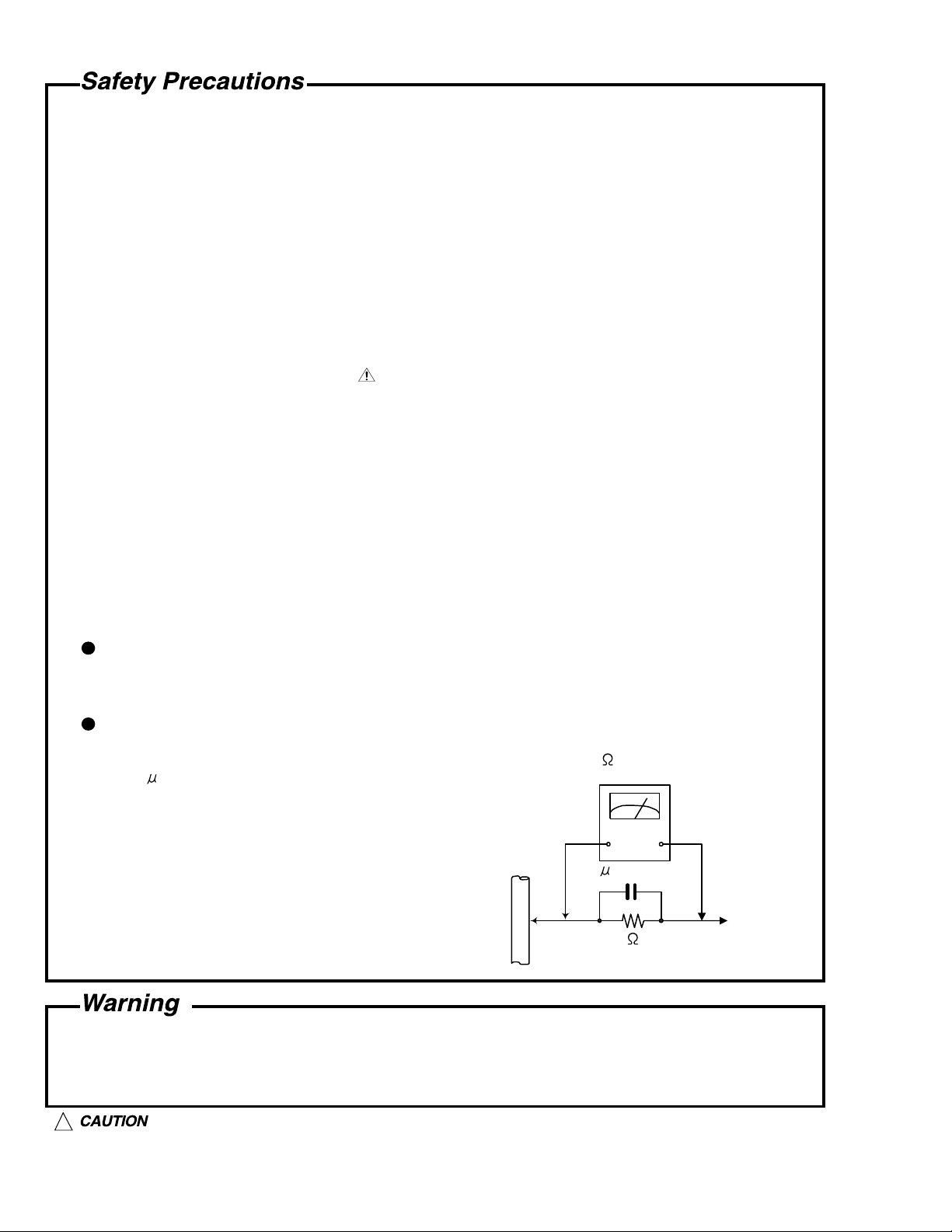
5. Leakage current check (Electrical shock hazard testing)
After reassembling the product, always perform an isolation check on the exposed metal parts of
the product (antenna terminals, knobs, metal cabinet, screw heads, headphone jack, control
shafts, etc.) to be sure the product is safe to operate without danger of electrical shock.
Do not use a line isolation transformer during this check.
Plug the AC line cord directly into the AC outlet. Using a "Leakage Current Tester", measure
the leakage current from each exposed metal parts of the cabinet , particularly any exposed
metal part having a return path to the chassis, to a known good earth ground. Any leakage
current must not exceed 0.5mA AC (r.m.s.)
Alternate check method
Plug the AC line cord directly into the AC outlet. Use an AC voltmeter having, 1,000 ohms
per volt or more sensitivity in the following manner. Connect a 1,500 10W resistor paralleled by
a 0.15 F AC-type capacitor between an exposed
metal part and a known good earth ground.
Measure the AC voltage across the resistor with the
AC voltmeter.
AC VOLTMETER
(Having 1000
ohms/volts,
or more sensitivity)
Move the resistor connection to each exposed
metal part, particularly any exposed metal part
having a return path to the chassis, and measure
the AC voltage across the resistor. Now, reverse
the plug in the AC outlet and repeat each
measurement. voltage measured Any must not
0.15 F AC TYPE
1500 10W
Place this
probe on
each exposed
metal part.
exceed 0.75 V AC (r.m.s.). This corresponds to 0.5
Good earth ground
1. This equipment has been designed and manufactured to meet international safety standards.
2. It is the legal responsibility of the repairer to ensure that these safety standards are maintained.
3. Repairs must be made in accordance with the relevant safety standards.
4. It is essential that safety critical components are replaced by approved parts.
5. If mains voltage selector is provided, check setting for local voltage.
!
Burrs formed during molding may be left over on some parts of the chassis. Therefore,
pay attention to such burrs in the case of preforming repair of this system.
1-2
Page 3
XV-D9000
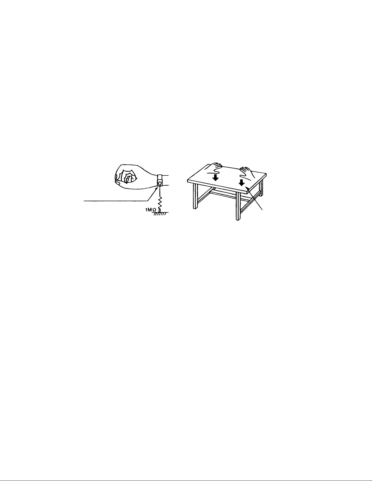
Preventing static electricity
Electrostatic discharge (ESD), which occurs when static electricity stored in the body, fabric, etc. is discharged,
can destroy the laser diode in the traverse unit (optical pickup). Take care to prevent this when performing repairs.
1.1. Grounding to prevent damage by static electricity
Static electricity in the work area can destroy the optical pickup (laser diode) in devices such as DVD players.
Be careful to use proper grounding in the area where repairs are being performed.
1.1.1. Ground the workbench
1. Ground the workbench by laying conductive material (such as a conductive sheet) or an iron plate over
it before placing the traverse unit (optical pickup) on it.
1.1.2. Ground yourself
1. Use an anti-static wrist strap to release any static electricity built up in your body.
(caption)
Anti-static wrist strap
Conductive material
(conductive sheet) or iron plate
1.1.3. Handling the optical pickup
1. In order to maintain quality during transport and before installation, both sides of the laser diode on the
replacement optical pickup are shorted. After replacement, return the shorted parts to their original condition.
(Refer to the text.)
2. Do not use a tester to check the condition of the laser diode in the optical pickup. The tester's internal power
source can easily destroy the laser diode.
1.2. Handling the traverse unit (optical pickup)
1. Do not subject the traverse unit (optical pickup) to strong shocks, as it is a sensitive, complex unit.
2. Cut off the shorted part of the flexible cable using nippers, etc. after replacing the optical pickup. For specific
details, refer to the replacement procedure in the text. Remove the anti-static pin when replacing the traverse
unit. Be careful not to take too long a time when attaching it to the connector.
3. Handle the flexible cable carefully as it may break when subjected to strong force.
4. It is not possible to adjust the semi-fixed resistor that adjusts the laser power. Do not turn it
1-3
Page 4
XV-D9000
Dismantling and assembling the traverse unit
1. Notice regarding replacement of optical pickup
Electrostatic discharge (ESD), which occurs when static electricity stored in the body, fabric, etc. is discharged,
can destroy the laser diode in the traverse unit (optical pickup). Take care to prevent this when performing
repairs to the optical pickup or connected devices.
(Refer to the section regarding anti-static measures.)
1. Do not touch the area around the laser diode and actuator.
2. Do not check the laser diode using a tester, as the diode may easily be destroyed.
3. It is recommended that you use a grounded soldering iron when shorting or removing the laser diode.
Recommended soldering iron: HAKKO ESD-compatible product
4. Solder the land on the optical pickup's flexible cable.
Note : Short the land after shorting the terminal on the flexible cable using a clip, etc., when using an
ungrounded soldering iron.
Note : After shorting the laser diode according to the procedure above, remove the solder according
to the text explanation.
Short circuit land
Laser pick-up unit
Flexible cable
Shorting
Shot with the clip
1-4
Page 5
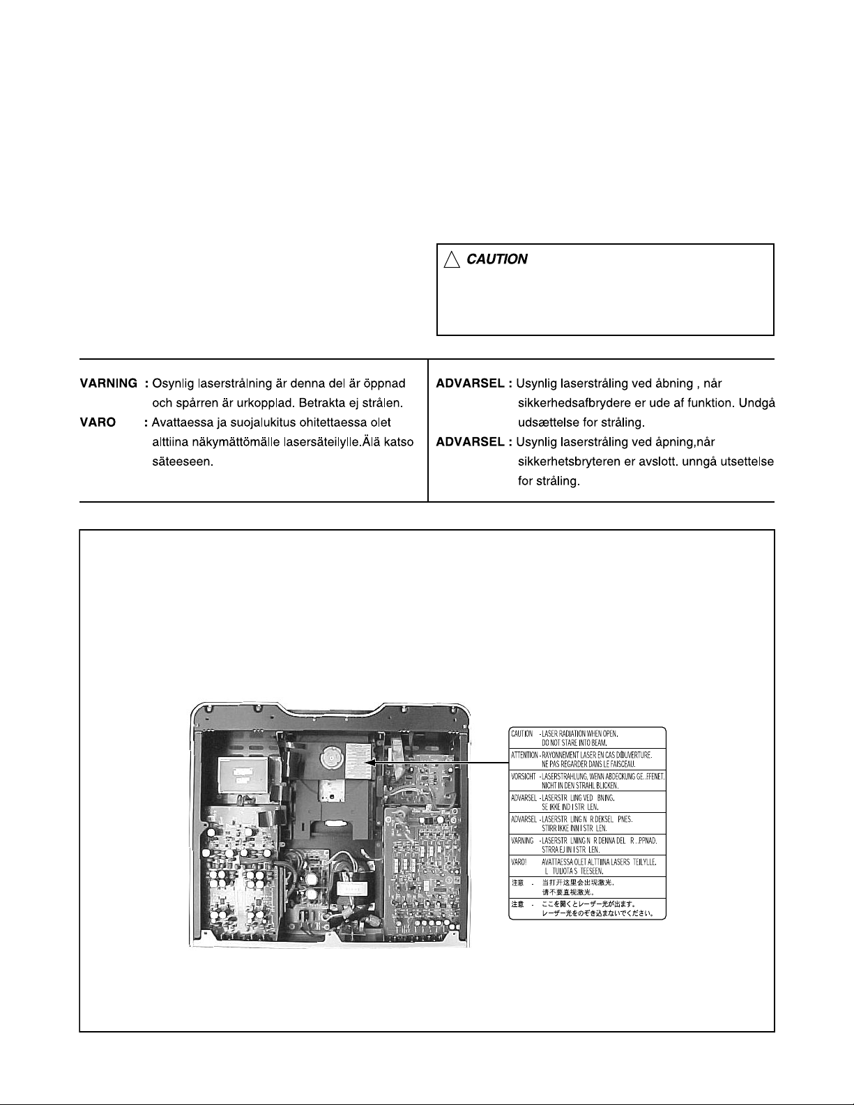
Important for Laser Products
XV-D9000
1.CLASS 1 LASER PRODUCT
2.DANGER : Invisible laser radiation when open and inter
lock failed or defeated. Avoid direct exposure to beam.
3.CAUTION : There are no serviceable parts inside the
Laser Unit. Do not disassemble the Laser Unit. Replace
the complete Laser Unit if it malfunctions.
4.CAUTION : The compact disc player uses invisible laser
radiation and is equipped with safety switches which
prevent emission of radiation when the drawer is open and
the safety interlocks have failed or are de
feated. It is dangerous to defeat the safety switches.
5.CAUTION : If safety switches malfunction, the laser is able
to function.
6.CAUTION : Use of controls, adjustments or performance of
procedures other than those specified herein may result in
hazardous radiation exposure.
!
Please use enough caution not to
see the beam directly or touch it
in case of an adjustment or operation
check.
REPRODUCTION AND POSITION OF LABELS
WARNING LABEL
1-5
Page 6
XV-D9000
Importance Admistering point on the Safety
Full Fuse Replacement Marking
Graphic symbol mark
(This symbol means fast blow type fuse.)
should be read as follows ;
FUSE CAUTION
FOR CONTINUED PROTECTION AGAINST RISK
OF FIRE, REPLACE ONLY WITH SAME TYPE
AND RATING OF FUSES ;
F9991 : 1.6 A / 250 V
Marquage Pour Le Remplacement
Complet De Fusible
Le symbole graphique (Ce symbole signifie
fusible de type a fusion rapide.)
doit etre interprete comme suit ;
PRECAUTIONS SUR LES FUSIBLES
POUR UNE PROTECTION CONTINUE CONTRE
DES RISQUES D'INCENDIE, REMPLACER
SEULEMENT PAR UN FUSIBLE DU MEME TYPE ;
F9991 : 1.6 A / 250 V
1-6
Page 7
XV-D9000
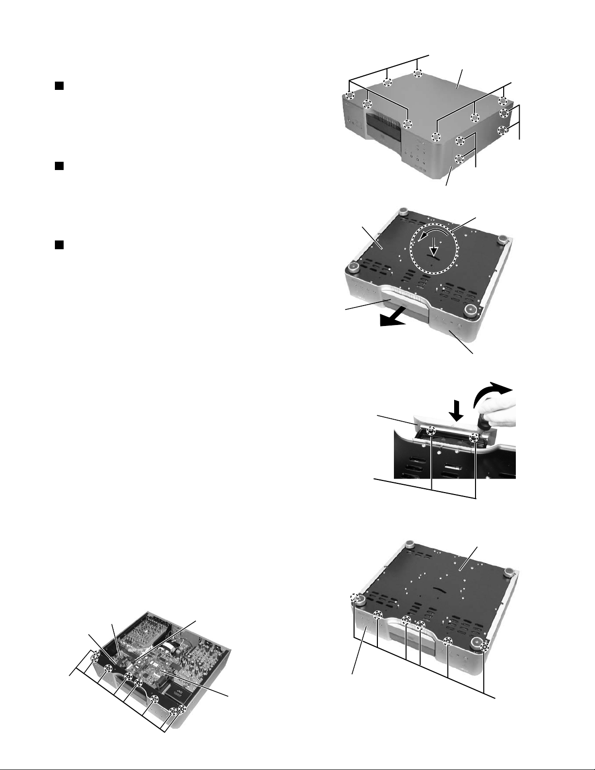
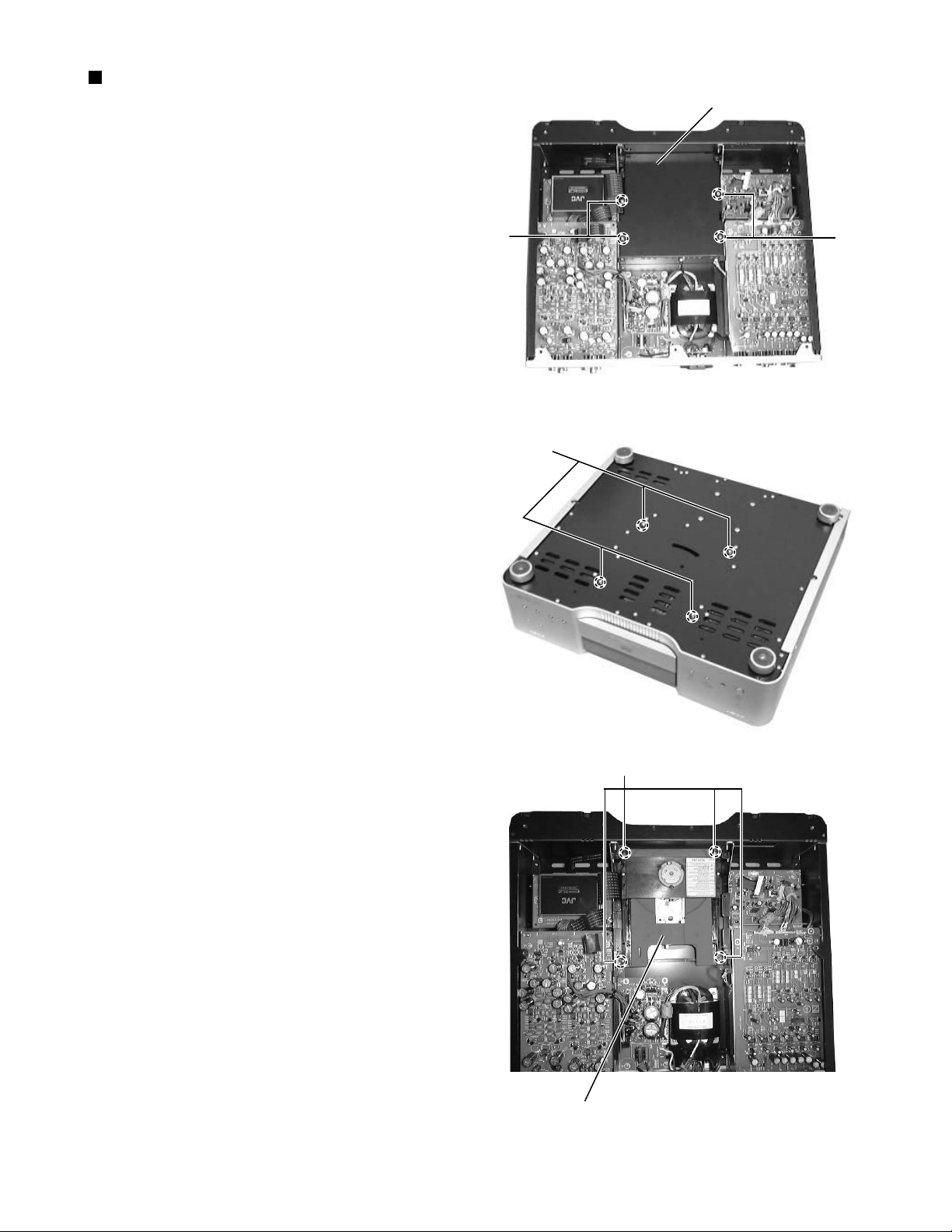
Disassembly method
<Main body>
Removing the top panel(See Fig.1)
1.Remove the eight screws A by hexagonal driver
attaching the top panel.
2.A top panel is lifted up and it is removed.
Removing the side panel(See Fig.1)
1.Remove the four screws B by hexagonal driver
attaching the side panel.
2.The left side also similarly removes the side panel.
Removing the front panel assembly
(See Fig.1~5)
*Prior to performing the following procedure, remove
the top panel.
1.The bottom of the main body is done up.
2.A minus driver is inserted in the incision part at the
center of the bottom, the bar in the interior of the
incision part is moved in the direction of the arrow of
Figure 2, and the tray is drawn out forward.
Fig.1
Bottom plate
Tr ay
Fig.2
A
Top panel
Side panel
Front panel assembly
A
B
B
Incision part
3.Hook a which connects the tray covers to the tray is
removed by a minus driver etc. , the tray cover is
pushed downward, and removes.
4.Remove the six screws C attaching the front panel
assembly.
5.The top of the main body is done up.
6.Remove the eight screws D attaching the front panel
assembly from the upper side of main body.
7.Disconnect the wire from connector CN507 on the main
board and CN981 on the power supply board.
8.It comes off when the front panel assembly is drawn out
forward.
Power supply
board
CN981
CN507
Tray cover
Hook a
Fig.3
Bottom plate
D
Main board
Fig.5
Front panel assembly
Fig.4
C
1-7
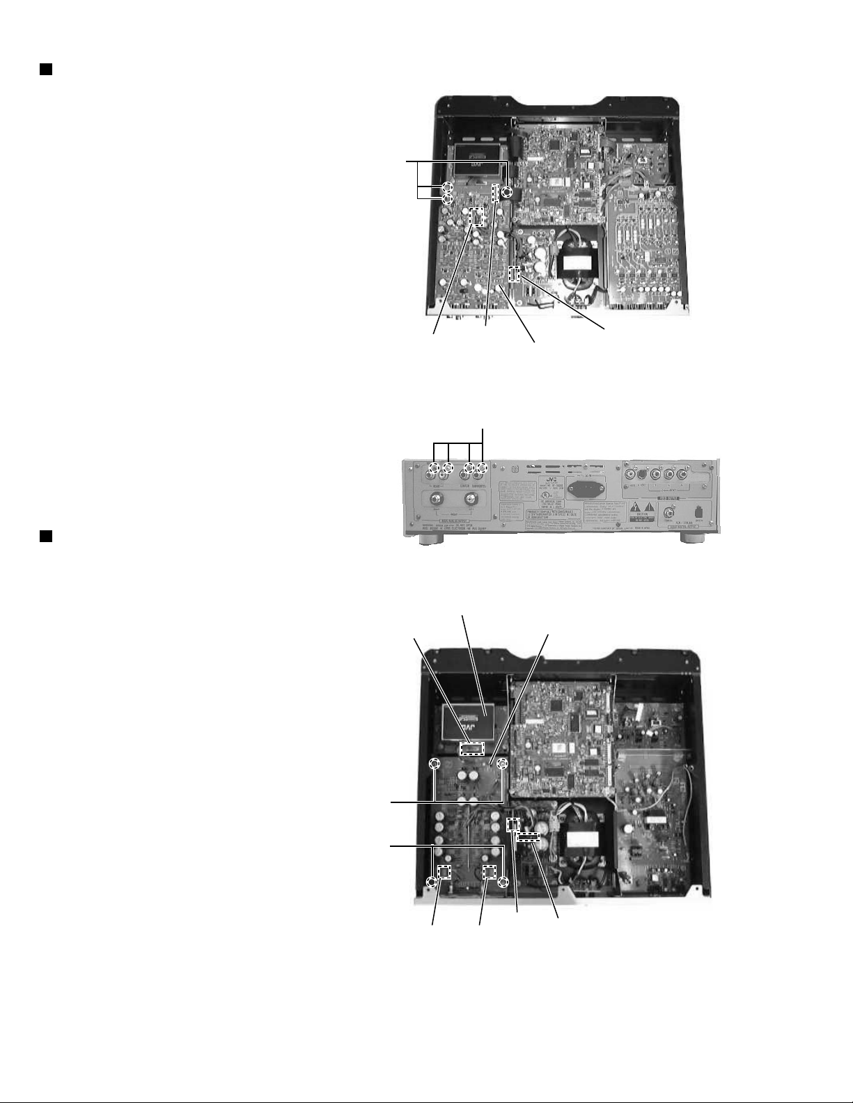
Page 8
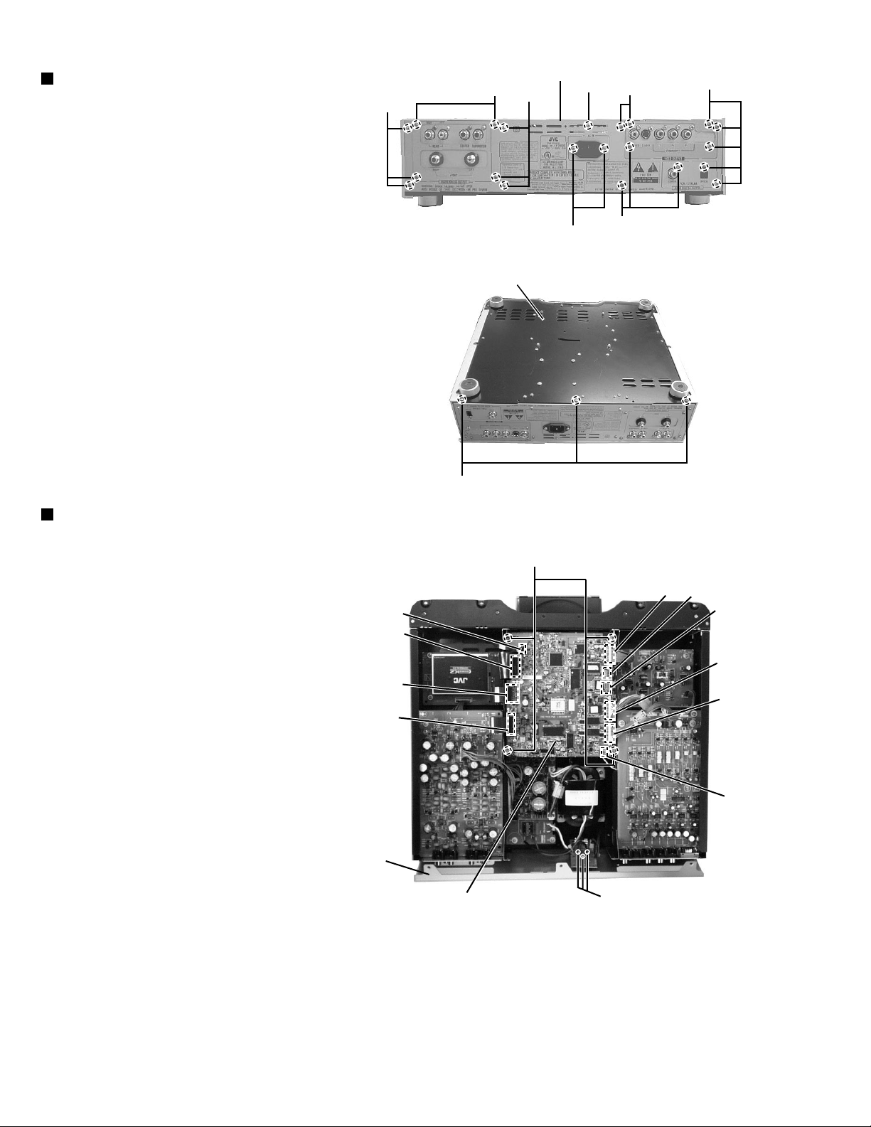
XV-D9000
Removing the rear cover(See Fig.6~8)
*Prior to performing the following procedure,
remove the top panel.
1.Remove the eighteen screws E attaching the
rear cover from back of the main body.
2.Remove the three screws F attaching the
bottom plate from back of the main body.
3.Solder on the power supply board is removed
by three places.(See Fig.8)
4.Remove the two screws G attaching the
AC socket and one screw G' attaching the
power supply board.
Rear cover
G'
E
E
E
Fig.6
G
E
E
E
Bottom plate
Removing the main board(See Fig.8)
*Prior to performing the following procedure,
remove the top panel.
1.Remove the four screws H attaching the
main board.
2.Disconnect the connector from CN101,CN103
CN504,CN505,CN501,CN502,CN503,CN506
CN507 on the main board.
Rear cover
CN103
CN101
CN504
CN505
F
Fig.7
H
CN501
CN507
CN509
CN503
CN502
CN506
1-8
Main board
Fig.8
Solder parts
Page 9
XV-D9000
Removing the DVD mechanism assembly
(See Fig.9~11)
*Prior to performing the following procedure, remove
the top panel and main board.
1.Remove the four screws I attaching the DVD
mechanism assembly cover, and DVD mechanism
assembly cover lifted up and it is removed.
2.The bottom of the main body is done up.
3.Remove the four nut J attaching the DVD mechanism
assembly
4.The top of the main body is done up.
5.Remove the four screws K attaching the DVD
mechanism assembly.
6.It is removed while lifting the DVD mechanism
assembly backward while noting the card wire.
DVD Mechanism
assembly cover
I
Fig.9
J
I
Fig.10
K
DVD Mechanism assembly
Fig.11
1-9
Page 10
XV-D9000
Removing the audio(rear L/R) board
(See Fig.12~13)
*Prior to performing the following procedure, remove
the top panel and rear cover.
1.Remove the three screws L attaching the
audio(rear L/R) board.
2.Remove the four screws M attaching the
audio(rear L/R) board from back of the body.
3.Disconnect the card wire from CN761 and
connector from CN751 on the audio(rear L/R)
board.
4.Disconnect the connector from CN697 on the
audio power board.
Removing the audio(front L/R) board
(See Fig.14)
L
CN751
CN761 CN697
Audio-analog
(rear L/R)board
Fig.12
M
Fig.13
*Prior to performing the following procedure,
remove the top panel and rear cover.
1.Remove the audio(rear L/R) board(upper step).
2.Remove the two screws N of the pillar which
supports audio(rear L/R) board(upper step).
3.Remove the two screws O attaching the
audio(front L/R)board(lower step).
4.Disconnect the connector from CN721 and
CN722 on the audio signal(front) output
terminal.
5.Disconnect the connector from CN695 and
CN696 on the DVD audio power board.
6.Disconnect the connector from CN741 on the
signal processing board.
Signal processing board
CN741
N
O
CN722
CN696
CN721
Audio-analog
(front L/R)board
CN695
Fig.14
1-10
Page 11
XV-D9000
Removing the video signal board(See Fig.15,16)
*Prior to performing the following procedure,
remove the top panel and rear cover.
1.Remove the three screws P attaching the
video signal board.
2.Remove the five screws Q attaching the video
signal board from back of the body.
3.Disconnect the connector from CN502 and CN503
on the main board.
4.Disconnect the connector from CN601 on the
video signal board.
Removing the power supply board
(See Fig.17,18)
*Prior to performing the following procedure,
remove the top panel, rear cover and video
signal board.
1.Remove the two screws S attaching the power
supply board cover and it is remove.
CN502
Rear cover
CN503
Fig.15
Fig.16
P
CN601
Video signal board
Q
2.Remove the two screws T of the pillar which
supports power supply board cover.
3.Remove the four screws U attaching the power
supply board.
4.Disconnect the connector from CN991 on the
power supply board.
5.Disconnect the connector from CN501 and CN506
on the main board.
CN506
Fig.17
CN501
S
Power supply board cover
U
T
Power supply board
Fig.18
U
CN991
1-11
Page 12
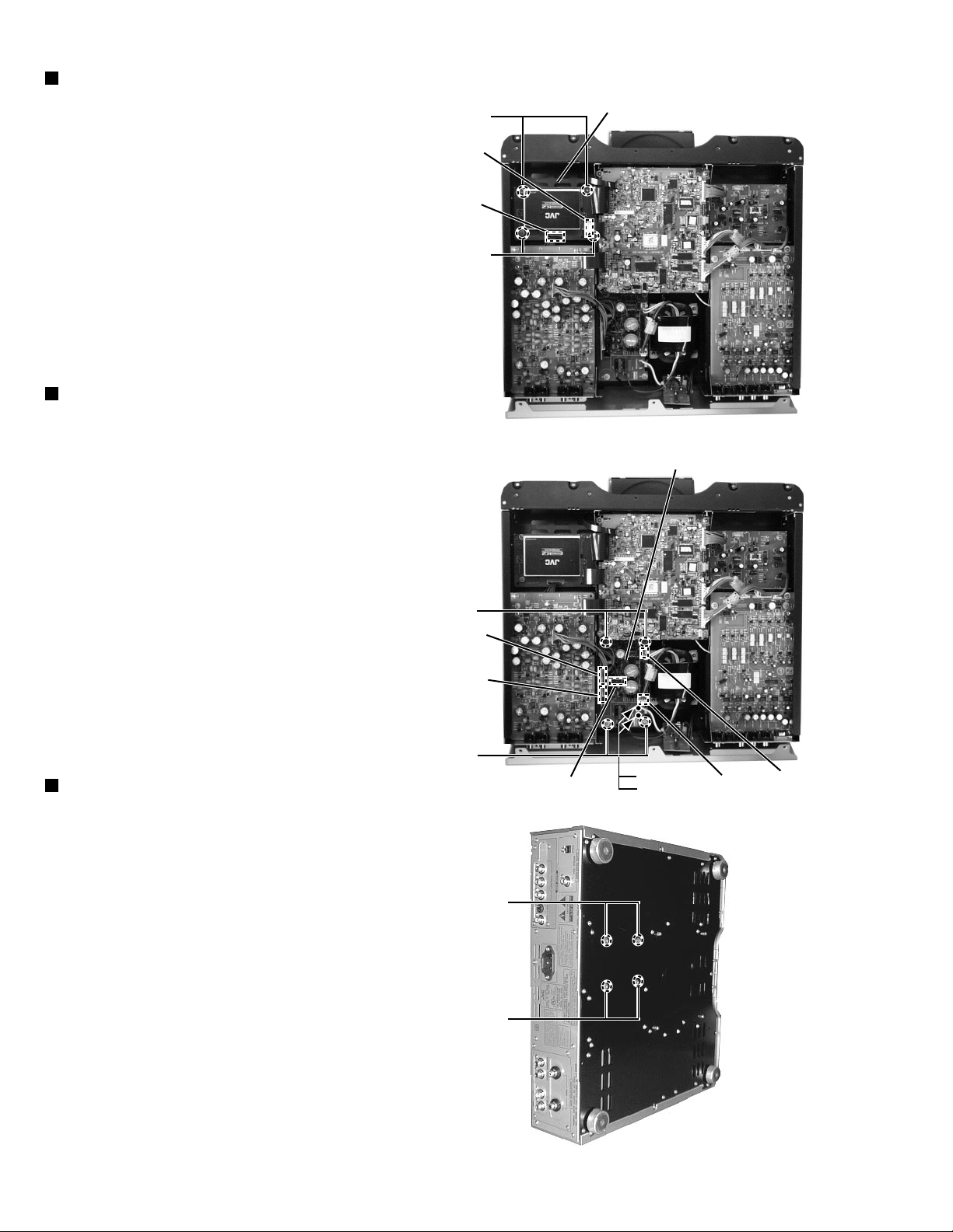
XV-D9000
Removing the signal processing board
(See Fig.19)
*Prior to performing the following procedure,
remove the top panel.
1.Remove the four screws V attaching the signal
processing board.
2.Disconnect the connector from CN711 and
CN741 on the signal processing board.
Removing the audio-power supply board
(See Fig.20)
*Prior to performing the following procedure,
remove the top panel and rear cover.
V
Signal processing board
CN711
CN741
V
Fig.19
Audio-power supply board
1.Remove the four screws W attaching the audio power supply board.
2.Disconnect the connector from CN691,CN692,CN695,
CN696,CN697 on the audio-power supply board.
3.The solder(PP691 and PP692) of wire connected
with power transformer is removed.
Removing the power transformer
(See Fig.21)
*Prior to performing the following procedure,
remove the top panel.
1.Disconnect the connector from CN691 and CN692 on
the audio-power supply board.
2.The solder(PP691 and PP692) of wire connected
with power transformer is removed.
W
CN696
CN697
W
X
PP692
PP691
Fig.20
CN691CN695
CN692
3.Remove the four screws X attaching the power transformer
from bottom of the body.
<ATTENTION>
Please the power transformer must become unstable and put
up the main body sideways, and work while supporting the
power transformer by one of hands when you remove the screw
of the power transformer.
1-12
X
Fig.21
Page 13
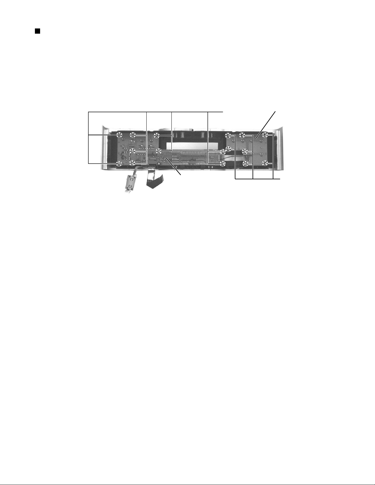
Removing the operation switch board/
FL and operation switch board(See Fig.22)
1.Remove the front panel assembly.(See Fig.1~5)
2.Remove the ten screws Y attaching the FL and operation switch board.
3.Remove the seven screws Z attaching the operation switch board.
XV-D9000
FL and operation
switch board
Fig.22
Y
Operation switch board
Z
1-13
Page 14
XV-D9000
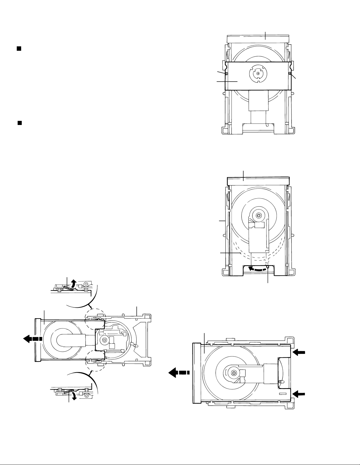
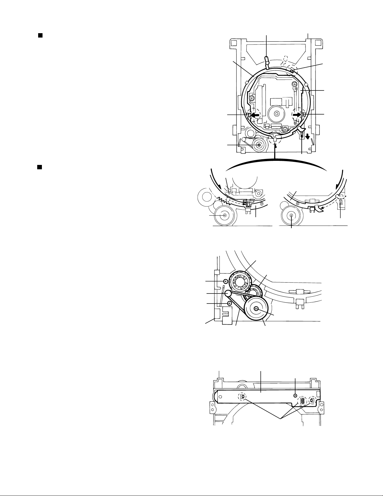
<Removing DVD mechanism unit>
Removing the clamper base (See Fig.1)
* Remove the top cover.
* Remove the DVD mechanism unit.
1. Remove the two screws A attaching the clamper base.
Removing the loading tray (See Fig.2~4)
* Remove the clamper base.
1. Turn the up-down cam lever clockwise (in the direction
of the arrow in Fig.2) to lower the position of the mechanism.
2. Manually set the loading tray to the fully-open position.
3. Stretch the tray stoppers on both sides of the loading
base outward and pull out the tray.
Clamper base
Loading tray
A
A
Fig.1
Loading tray (front side)
Tray stopper
Loading tray
Loading base
Up-down cam
Lever
Fig.2
Loading base
Loading tray
Push
Push
1-14
Tray stopper
Fig.4
Fig.3
Page 15
XV-D9000
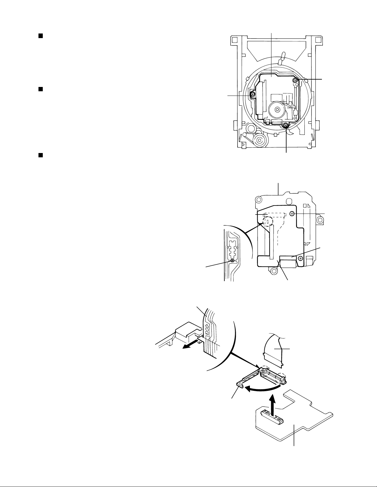
Removing the traverse mechanism unit (See Fig.5)
* Remove the loading tray.
1. Remove the three screws B attaching the traverse
mechanism unit.
Protecting the optical pickup
* Solder the flexible ground point on the optical pickup
when replacing the pickup or before detaching the
mechanism control board. When assembling the unit,
remove the solder last.
Removing the mechanism control board
(See Fig.6~7)
* Remove the traverse unit. (Can be detached without
detaching the T-mechanism unit.)
1. Remove the two screws C attaching the mechanism
control base from the bottom of the traverse unit.
2. Pull out the CN12 connector and detach the
mechanism control board.
3. Remove the card wire from the CN13 connector
on the mechanism control board.
4. Pull out the FPC holder from the CN12 connector
on the reverse side of the mechanism control board
and remove the flexible harness, referring to Fig.7.
B
Enlargement
Traverse mechanism unit
B
Fig.5
Traverse mechanism unit
CN12
B
C
CN13
Connection area
(Solder the flexible
ground point)
Flexible harness
3
Enlargement
FPC holder
Fig.7
Mechanism control board
Fig.6
Flexible harness
2
1
CN12
Mechanism control board
1-15
Page 16
XV-D9000
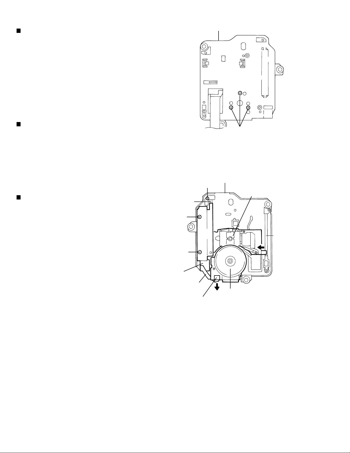
Removing the turntable and spindle motor assembly
(See Fig.8~9)
* Remove the traverse mechanism unit.
* Solder the flexible ground point on the optical pickup.
(See Fig.6)
* Remove the mechanism control board.
1. Remove the flexible harness from the feed motor
connector on the spindle motor board assembly.
2. Remove the three screws D attaching the spindle motor
from the bottom of the traverse chassis.
Removing the feed motor unit (See Fig.9)
* Remove the traverse mechanism unit.
* Remove the mechanism control board.
1. Remove the FPC from the feed motor connector
on the turntable spindle motor board.
2. Remove the two screws E attaching the feed motor unit.
Removing the optical pickup unit (See Fig.9)
* Remove the traverse mechanism unit.
Guide shaft b
* Remove the mechanism control board.
* Remove the feed motor unit.
1. Remove the screw F attaching the guide shaft holder at b,
then simultaneously remove the guide shaft at B and the
optical pickup unit. While doing so, slide the unit
horizontally away from the guide shaft at a.
Traverse chassis
D
Fig.8
Traverse mechanism unit
F
Pick-up assembly
E
Guide
shaft a
E
Feed motor assembly
Flexible harness
Feed motor connector
Turn table/spindle motor unit
Fig.9
1-16
Page 17
XV-D9000
Removing the loading mechanism parts
(See Fig.10~11)
* Remove the clamper base.
* Remove the disk tray.
1. Turn the lever counterclockwise until it stops (position 1),
while pushing the switch lever in the direction of the
arrow and pushing up the pawl at a using a screwdriver.
2. Stretch the two pawls at b outward using a screwdriver
and remove the chassis.
3. Turn the lever clockwise (position 2) to remove the
up-down cam.
4. Remove the pulley gear and the pulley gear belt after
removing the screw G attaching the pulley gear.
5. Pull out drive gear 2 then drive gear 1.
(1)When detaching
Removing the loading motor board
the chassis.
(See Fig.11~12)
* Remove the clamper base.
* Remove the disk tray.
1. Remove the loading belt.
2. Remove the two screws H attaching the loading motor.
3. Remove the screw at I and the three pawls at c fixing
the loading motor base from the reverse side of the
loading base.
Up-down
Pawl b
chassis.
G
cam
G
Lever
1
Up-down cam
Fig.10
Loading base
2
Pawl a
Chassis
Pawl b
Switch lever
(2)When detaching
the up-down cam.
Up-down cam
Switch lever
G
H
Loading motor unit
Loading base
H
Loading belt
Loading base
Drive gear 1
Drive gear 2
G
Pulley gear
Fig.11
Loading motor board
I
Pawl c
Fig.12
1-17
Page 18
XV-D9000
Method of initializing EEPROM and display of jitter value
Initializing EEPROM
Please initialize EEPROM when you exchange Microcomputer(IC401,IC402) and
optical pick-up by the undermentioned method.
1. It is confirmed that there is no disk in the tray.
2. The power supply plug is inserted while pushing the PLAY key and the OPEN/CLOSE key to the main body.
3. It is displayed in the FL display part as "TEST JC1".
4. The EX K2 key is pushed.
5. The POWER key is pushed if displayed in the FL display part as "EFP****".
(**** is a check sum of device key display. )
6.When normally entering the state of the power standby, initialization is normal and completion.
Jitter value (We will separately inform of the method of adjusting jitter.)
1. It is confirmed that there is no disk in the tray.
2. The power supply plug is inserted while pushing the PLAY key and the OPEN/CLOSE key to the main body.
3. It is displayed in the FL display part as "TEST JC1".
4. Press the OPEN/CLOSE key to move the tray outward.
Put the test disc (VT-501) on the tray and press OPEN/CLOSE key.
The tray should move inward (NOTE:Don't push to close the tray directly by hand etc,)
5.Keeps pushing SETUP key to remote controller for ten seconds or more.
6.Press the PLAY key of the main body.
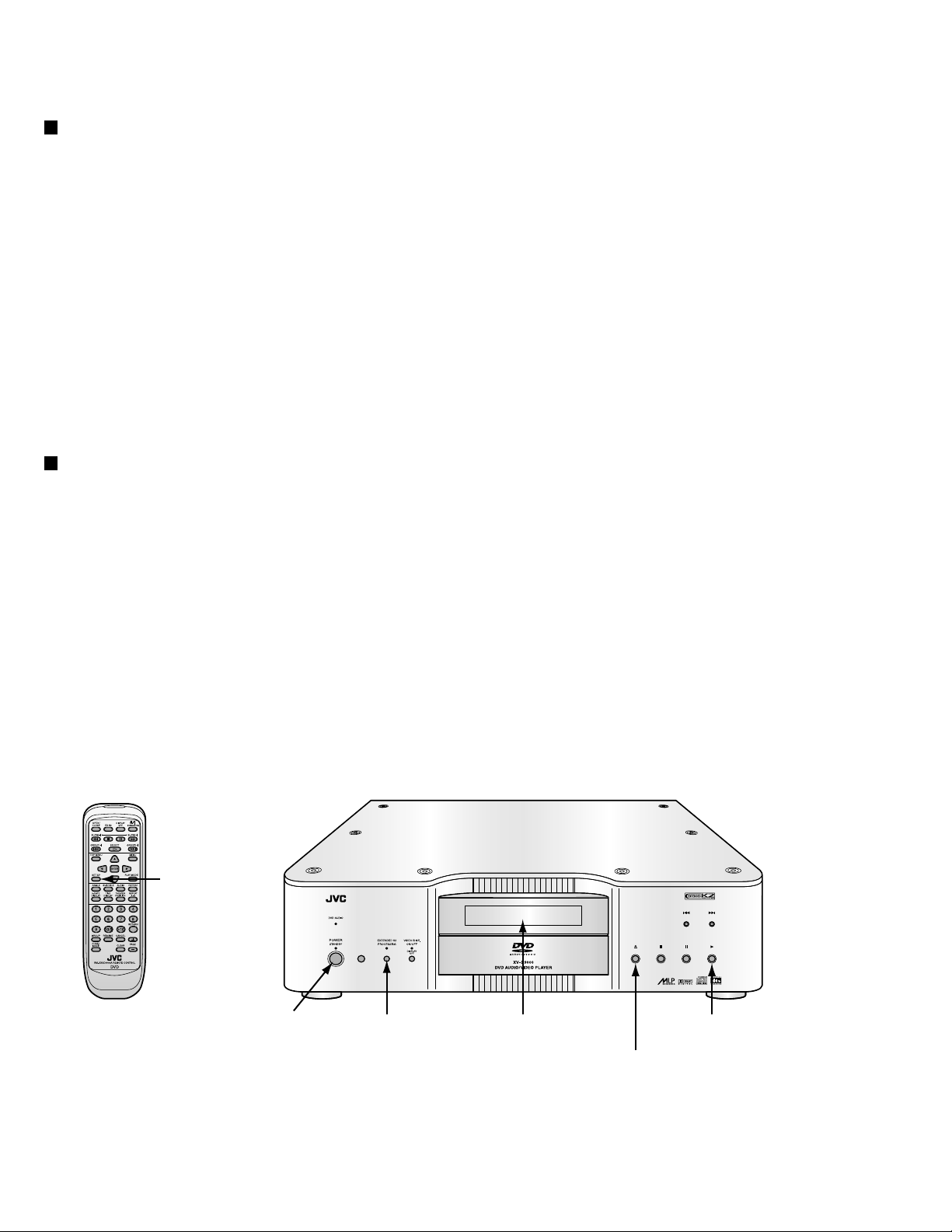
Remote controller Main body
SETUP key
1-18
POWER/
STANDBY key
EX K2 key FL Display PLAY key
OPEN/CLOSE key
Page 19

Description of major ICs
ADV7123KST50(IC359):Video DAC
VAA
XV-D9000
BLANK
SYNK
R9-R0
G9-G0
B9-B0
10
10
10
PSAVE
CLOCK
Pin Function (1/2)
Pin No.
Symbol
1~10
11
12
13
14~23
24
CLOCK
25,26
27
28
29,30
31
32
33
34
35
36
37
38
39~48
DATA
REGISTER
DATA
REGISTER
DATA
REGISTER
POWER-DOWN
MODE
GND
G0~G9
BLANK
SYNC
VAA
B0~B9
GND
IOB
IOB
VAA
IOG
IOG
IOR
IOR
COMP
VREF
RSET
PSAVE
R0~R9
10
10
10
RSET COMP
DAC
DAC
I/O
Green pixel data input terminal (TTL compatible)
I
Composite blank control input terminal (TTL compatible)
I
Composite sync control input (TTL compatible)
I
Analog power supply terminal
Blue pixel data input terminal (TTL compatible)
I
Clock signal input (TTL compatible)
I
Connect to ground
-
O
O
O
O
O
O
I/O
Differential blue current output (high impedance current source)
Blue current output
Analog power supply terminal
Differential green current output (high impedance current source)
Green current output
Differential red current output (high impedance current source)
Red current output
Compensation pin
Voltage reference input for DAC or voltage reference output (1.235V)
A resistor connected between this pin and ground
I
Power save control pin
I
Red pixel data input (TTL compatible)
I
DAC
REFERENCE
BLANK AND
SYNK LOGIC
IOR
IOR
IOG
IOG
IOB
IOB
VOLTAGE
VREF
CIRCUIT
Function
1-19
Page 20

XV-D9000
AN8706FHQ (IC101) : Front end processor
1.Pin layout
CBDOSL
CSAG
DCAGC
AGCG
PEAK
BOTTOM
RFENVFCBOOST
OFTR
BDO
JITOUT
GND3
75747372717069686766656463626160595857565554535251
RBCA
RFINP
RFINN
VCC2
GND2
VREF2
RFON
RFOP
TS
DCRF
FS
VIN6
VIN5
VCC1
VIN1
VIN2
VIN3
VIN4
VREF4
DIFP
DIFN
76
77
78
79
80
81
82
83
84
85
86
87
88
89
90
91
92
93
94
95
96
97
98
99
100
AN8706FHQ
CBDOFS
TESTSG
COFTFS
COFTSL
FUPDN
ITDLI
VCOIN
PLFLT
PLFLT2
FCPO
PCPO
VCC3
CAPA
DTRD
IDGT
VCC5
50
RDCKP
49
RDCKN
48
RDTP
47
RDTN
46
GND5
45
GND4
44
VCC4
43
DTMONN
42
DTMONP
41
DSLFLT
40
DSLO
39
FLTOUT
38
DCFLT
37
VREF3
36
VPWBDO
35
VPWOFT
34
IDDLY
33
DBAL
32
GND1
31
VREF1
30
TKCNT
29
TKCFLT
28
TEOUT
27
TEI
26
RSCL
2.Block diagram
Head Amp.
SSD Signal
Head Amp.
DPD Signal
12345678910111213141516171819202122232425
TG
LPCOA
LDONB
LDONA
LPC1
VHARF
RFOUT
FS/TS
POFLT
TGBAL
PTH
TBAL
FBAL
FGCTL
FEN
VREFL
FEOUT
PULIN
VREFC
VREFH
TGTETKCNTTBALFBALFE
SEN
SCK
STDI
FC/Boost
AGC Cont
TKCNT
FE(SSD)
FE BAL
AGC EQ
MU
TE(DPD)
TE BAL
TG(DPD)
LPC(Amp)
VREF reg
STNBY
XTRON
MTRON
RFIN
ROMRAM
RF ENV
DFLTOP/NRFENV
DSL
BDO Det
OFTR Det
INTERFACE
PLL
JITTER Det
SYNC
JITOUT
CLK
DATA
DSLOUT
BDO
OFTR
1-20
OPTICAL HEAD
(650nm)
TGBAL CPU STNBY MTRON
SERVO PROCESSOR
Head Amp.
Page 21

XV-D9000
3.Pin function
Pin No. Symbol I/O
1
2
3
4
5
6
7
8
9
10
11
12
13
14
15
16
17
18
19
20
21
22
23
24
25
26
27
28
29
30
31
32
33
34
35
36
37
38
39
40
41
42
43
44
45
46
47
48
49
50
LDONB
LDONA
LPCOA
VHARF
TGBAL
FGCTL
FEOUT
VREFL
VREFC
VREFH
STNBY
XTRON
MTRON
ROMRAM
TEOUT
TKCFLT
TKCNT
VREF1
VPWOFT
VPWBDO
VREF3
DCFLT
FLTOUT
DSLFLT
DTMONP
DTMONN
RDCKN
RDCKP
LPC1
POFLT
PTH
TBAL
TG
FBAL
FEN
PULIN
SEN
SCK
STDI
RSCL
TEI
GND1
DBAL
IDDLY
DSLO
VCC4
GND4
GND5
RDTN
RDTP
Functions
I
Laser ON (CD Head) terminal
I
Laser ON (DVD Head) terminal
O
Laser drive output terminal
I
Laser PIN input terminal
O
VHALF voltage output terminal
I
Tangential phase balance control terminal
O
Track detection Threshold value level terminal
I
Track detection Threshold value level terminal
I
Tracking balance control terminal
O
Tangential phase error signal output terminal
I
Focus amplifier Gain control terminal
I
Focus balance control terminal
O
Focus error signal output terminal
I
Focus error output amplifier reversing input terminal
O
VREFL voltage output terminal
O
VREFC voltage output terminal
O
VREFH voltage output terminal
I
DSL,PLL drawing mode switch terminal
I
SEN(Cereal data input terminal)
I
SCK(Cereal data input terminal)
I
STDI(Cereal data input terminal)
I
Standby mode control terminal
I
Tracking OFF holding input terminal
I
Monitor output ON/OFF switch terminal
I
ROM RAM switch terminal
O
Standard current source terminal
I
Tracking error output Amp reversing input terminal
O
Tracking error signal output terminal
O
Track count detection filter terminal
O
Track count output terminal
O
VREF1 voltage output terminal
O
Earth terminal 1
I
Data slice offset adjustment terminal
I
Data slice delay adjustment terminal
I
OFTR detection level setting terminal
I
BDO detection level setting terminal
O
VREF3 voltage output terminal
O
Capacity connection terminal for data slice input filter
O
Filter amplifier output terminal
O
Data slice single data output terminal
O
Constant filter terminal when data is sliceddelly
O
PLL differential motion 2 making to value edge signal monitor output (+)
O
PLL differential motion 2 making to value edge signal monitor output (-)
I
Power terminal 4 (5V)
O
Earth terminal 4
O
Earth terminal 5
O
PLL differential motion making to synchronization RF signal reversing output
O
PLL differential motion making to synchronization RF signal rotation output
O
PLL differential motion making synchronization clock reversing output
O
PLL differential motion making synchronization clock rotation output
AN8706FHQ (1/2)
1-21
Page 22

XV-D9000
3.Pin function
51
52
53
54
55
56
57
58
59
60
61
62
63
64
65
66
67
68
69
70
71
72
73
74
75
76
77
78
79
80
81
82
83
84
85
86
87
88
89
90
91
92
93
94
95
96
97
98
99
100
VCC5
IDGT
DTRD
CAPA
VCC3
PCPO
FCPO
PLFLT2
PLFLT
VCOIN
ITDLI
FUPDN
GND3
JITOUT
BDO
OFTR
BOOST
FC
RFENV
BOTTOM
PEAK
AGCG
DCAGC
CSAG
CBDOSL
CBDOFS
RBCA
TESTSG
RFINP
RFINN
VCC2
GND2
VREF2
COFTFS
COFTFL
RFON
RFOP
TS
DCRF
FS
VIN6
VIN5
VCC1
VIN1
VIN2
VIN3
VIN4
VREF4
DIFP
DIFN
I/OPin No. Symbol Functions
Power terminal 5 (3.3V)
I
Data slice part address part gate signal input terminal (For RAM)
I
Data slice data read signal input terminal(For RAM)
I
Data slice CAPA(Address)signal input terminal (For RAM)
I
Power terminal 3 (5V)
I
PLL phase gain set terminal
O
PLL frequency gain set terminal
O
PLL low region filter terminal
O
PLL high region filter terminal
O
PLL VCO input terminal
I
PLL jitter free current ripple removal filter terminal
O
PLL frequency control input terminal
I
Earth terminal 3
O
Detection signal output of jitter
O
BDO output terminal
O
OFTR output terminal
O
Booth control terminal for filter
I
FC control terminal for filter
I
RF envelope output terminal
O
Bottom envelope detection filter terminal
O
Peak envelope detection filter terminal
O
AGC amplifier gain control terminal
O
AGC amp filter terminal
O
Sag cancellation circuit filter terminal
O
BDO detection capacitor terminal
O
BDO detection capacitor terminal
O
BCA detection level setting terminal
O
TEST signal input terminal
I
RF signal positive moving input terminal
I
RF signal reversing input terminal
I
Power terminal 2 (5V)
I
Earth terminal 2
O
VREF2 voltage output terminal
O
OFTR detection capacitor terminal
O
OFTR detection capacitor terminal
O
RF signal output terminal P
O
RF signal output terminal N
O
All addition amplifier (DVD) output terminal
O
All addition amplifier capacitor terminal
O
All addition amplifier (CD) output terminal
O
Focus input of external division into two terminal
I
Focus input of external division into two terminal
I
Power terminal 1 (5V)
I
External division into four (DVD/CD) RF input terminal 1
I
External division into four (DVD/CD) RF input terminal 2
I
External division into four (DVD/CD) RF input terminal 3
I
External division into four (DVD/CD) RF input terminal 4
I
VREF4 voltage output terminal
O
RF signal (RAM) output terminal P
O
RF signal (RAM) output terminal N
O
AN8706FHQ(2/2)
1-22
Page 23

BA5983FM-X (IC271) : 4CH DRIVER
1.Block diagram
27
28
Vcc
25
26
10k
20k
24
23 22
10k
20k
XV-D9000
21
20
19
Vcc
STAND BY
CH4
10k
10k
18
Level Shift
17 16
10k
10k
10k
10k
15
10k
10k
Level Shift
10k
10k
1
2
3
5
4
10k
10k
6
7
2.Pin function
Pin No. Pin No.
10
11
12
13
14
Symbol Symbol
1
BIAS IN
2
OPIN1(+)
3
OPIN1(-)
4
OPOUT1
5
OPIN2(+)
6
OPIN2(-)
7
OPOUT2
8
9
GND
STBY1
PowVcc1
VO2(-)
VO2(+)
VO1(-)
VO1(+)
I/O I/O
Input for Bias-amplifier
I
Non inverting input for CH1 OP-AMP
I
Inverting input for CH1 OP-AMP
I
Output for CH1 OP-AMP
O
Non inverting input for CH2 OP-AMP
I
Inverting input for CH2 OP-AMP
I
Output for CH2 OP-AMP
O
Substrate ground
-
Input for CH1/2/3 stand by control
I
Vcc for CH1/2 power block
-
Inverted output of CH2
O
Non inverted output of CH2
O
Inverted output of CH1
O
Non inverted output of CH1
O
Function
15
16
17
18
19
20
21
22
23
24
25
26
27
28
STAND BY
CH1/2/3
89
VO4(+)
VO4(-)
VO3(+)
VO3(-)
PowVcc2
STBY2
GND
OPOUT3
OPIN3(-)
OPIN3(+)
OPOUT4
OPIN4(-)
OPIN4(+)
PreVcc
Vcc
10
Level Shift
Level Shift
10k
10k
11
10k
10k
10k
10k
12
13
14
Function
O
Non inverted output of CH4
O
Inverted output of CH4
O
Non inverted output of CH3
O
Inverted output of CH3
-
Vcc for CH3/4 power block
I
Input for Ch4 stand by control
-
Substrate ground
O
Output for CH3 OP-AMP
I
Inverting input for CH3 OP-AMP
I
Non inverting input for CH3 OP-AMP
O
Output for CH4 OP-AMP
I
Inverting input for CH4 OP-AMP
I
Non inverting input for CH4 OP-AMP
-
Vcc for pre block
10k
10k
1-23
Page 24

XV-D9000
IS61LV256-12T(IC163,IC164,IC165,IC173):32k X 8 Low voltage CMOS Static RAM
1.Pin layout 2.Block diagram
OE 22
A11 23
A9 24
A8 25
A13 26
WE 26
VCC 28
A14 1
A12 2
A7 3
A6 4
A5 5
A4 6
A3 7
A10
21
CE
20
I/O7
19
I/O6
18
I/O5
17
I/O4
16
I/O3
15
GND
14
I/O2
13
I/O1
12
I/O0
11
A0
10
A1
9
A2
8
A0-A14
VCC
GND
I/O0-I/O7
DECODER
I/O
DATA
CIRCUIT
256 X 1024
MEMORY ARRAY
COLUMN I/O
3.Pin function
Pin No. Symbol I/O
1
2
3~10
11~13
14
15~19
20
21
22
23
24,25
26
27
28
A14
A12
A7~A0
I/O0~I/O2
GND
I/O3~I/O7
CE
A10
OE
A11
A9,A8
A13
WE
VCC
Function
I
Address input
I
Address input
I
Address input
I/O
Data I/O
-
Connects with the ground
I/O
Data I/O
I
Chip enable input
I
Address input
I
Output enable input
I
Address input
I
Address input
I
Address input
I
Write enable input
-
Power supply terminal
CE
OE
WE
CONTROL
CIRCUIT
1-24
Page 25

JCE8011(IC551):Graphic controller
XV-D9000
Pin No. Symbol
1~8
9
10
11
12
13
14
15
16~23
24
25
26
27
28
29
30
31
32
33
34
35
36
37
38
39~46
47
48
49
50
51
52
53
54~61
62
63~70
71
72
73~82
83
84~93
94
95
96
97
98
99
100
VD0~7
VCLKI
HSYNCI
VSYNCI
VCC
VCLKO
HSYNCO
VSYNCO
DOUT0~7
TEST
RESETB
GND
NTB
DTSF0
DTSF1
VIDEG
DOSF0
DOSF1
XVRST
F1
HBL
VBL
VOEDG
VCC
FRD7~0
GND
FRCK
FWCK
FREB
FWEB
FRRSTB
FWRSTB
FWD7~0
VCC
CHD7~0
GND
CHOEB
CHA19~10
VCC
CHA9~0
GND
ACK
CS1B
CS2B
SCK
RXD
TXD
I/O
O
O
O
O
O
O
O
O
O
O
O
O
O
O
O
O
O
O
O
O
Function
DVD Image signal input (Multi plex data Y,Cr,Cb)
I
Dot clock signal input (27MHz)
I
The horizontal synchronous signal input
I
Vertical synchronous signal input
I
Power supply
Dot clock signal output (27MHz)
'H' blanking output
'V' blanking output
Digital data output
Test terminal (Uses as GND usually)
System reset signal
I
Connect to GND
Mode switching NTSC(low) / PAL(high)
I
Taking timing shift of VD input
I
Taking timing shift of VD input
I
Taking edge specification of VD input (0:up , 1:down)
I
Timing shift input of output data
I
Timing shift input of output data
I
Non connect
Field Identification signal output
'H' blanking output
'V' blanking output
Output timing setting of DOUT (0:up , 1:down)
I
Power supply
Field memory read data input
I
Connect to GND
Field memory read clock
Field memory write clock
Field memory read enable
Field memory write enable
Field memory read address reset
Field memory write address reset
Field memory write data output
Power supply
Character ROM data
I
Connect to GND
Character ROM output enable
Character ROM address output
Power supply
Character ROM address output
Connect to GND
-
Serial data chip select for graphic control
I
Serial data chip select for encoder control
I
Serial clock input
I
Serial input data
I
Serial output data
1-25
Page 26

XV-D9000
JCV8005-2(IC471):CPPM
1.Pin layout
80 51
81
50
100
1 30
2.Pin function
Pin No. I/O
1
2
3~10
11
12
13~20
21
22
23
24
25
26
27
28
29
30
31
32
33~36
37
38~41
42
43
44
45
46
47
48
49
50
51
52
53
54
55
56
57
58
31
Symbol
VDD
GND
HDATA0~7
VDD
GND
HADDR0~7
VDD
GND
NCS
NRD
NWR
NIRQ
WAIT
NRESET
VDD
GND
VDD
GND
STD7~4_OUT
GND
STD3~0_OUT
VDD
GND
REQ_IN
DACK_OUT
STCLK_OUT
SYNC_OUT
STERROUT
VDD
GND
VDD
GND
NG_RD
NG_WR
G_WITODC
G_CSDEC
G_WITDEC
VDD
-
-
I/O
-
I
-
I
I
I
O
O
I
-
-
-
-
O
-
O
-
-
I
O
O
O
-
-
-
-
-
I
I
I
I
I
-
JCV8005-2 1/2
Description
Power supply
Connect to ground
Data input/output terminal (both by 8 bits)
Power supply
Connect to ground
8 bit address bus to internal address (connect to host)
Power supply
Connect to ground
Chip select signal from host
Data read signal from host
Data write signal from host
Interrupt of request to host
Wait demand to host
Reset signal from host
Power supply
Connect to ground
Power supply
Connect to ground
Data output to DVD decoder (8 bits)
Connect to ground
Data output to DVD decoder (8 bits)
Power supply
Connect to ground
Request signal for forwarding control by decoder
Output signal to decoder which shows effective data
Data strobe signal to decoder
Sector sink signal to decoder
Non connect
Power supply
Connect to ground
Power supply
Connect to ground
Glue logic input signal from host
Glue logic input signal from host
Glue logic input signal from front end
Glue logic input signal from host
Glue logic input signal from decoder
Power supply
1-26
Page 27

XV-D9000
2.Pin function
Pin No. I/O
59
60
61
62
63
64
65
66,67
68
69
70
71
72
73
74
75
76
77
78
79
80
81
82
83
84
85
86
87
88
89
90~93
94
95~98
99
100
Symbol
GND
WAIT1
WAIT2
WAITIN
VDD
GND
TEST_IN
NC
VDD
GND
CLKOCTL
NC
OSCI
OSCO
NC
VDD
GND
33OUT
16OUT
VDD
GND
VDD
GND
STERR_IN
SYNC_IN
STCLK_IN
DACK_IN
REQ_OUT
VDD
GND
STD0~3_IN
GND
STD4~7_IN
VDD
GND
JCV8005-2 2/2
Description
-
O
I
-
I
-
-
I
I
O
-
-
-
O
O
-
-
-
I
I
I
I
O
-
I
I
-
-
Connect to ground
Glue logic output signal to host
Non connect
Glue logic input signal (connect to 27 pin)
Power supply
Connect to ground
Connect to ground
Non connect
Power supply
Connect to ground
Input terminal for crystal-oscillator circuit on/off control
Non connect
Crystal oscillation terminal (input side)
Crystal oscillation terminal (output side)
Non connect
Power supply
Connect to ground
Oscillation output terminal
Oscillation output terminal
Power supply
Connect to ground
Power supply
Connect to ground
Presence of data error from front end
Sector sink signal from front end
Data clock signal from front end
Signal which shows effective data from front end
Request signal for forwarding control to front end
Power supply
Connect to ground
Data input from front end (8 bits)
Connect to ground
Data input from front end (8 bits)
Power supply
Connect to ground
1-27
Page 28

XV-D9000
M27C1602CZ(IC402,IC553):16M ROM
1.Pin layout
44
WE
A19
A18
A8
A7
A6
A5
A4
A3
10
A2
11
A1
12
CE
13
VSS
14
OE
15
D0
16
D8
17
D1
18
D9
19
D2
20
D10
21
D3
22
D11
2.Pin function
1
2
3
4
5
6
7
8
9
WP
43
A20
42
A9
41
A10
40
A11
39
A12
38
A13
37
A14
36
A15
35
A16
34
A17
33
BYTE
32
VSS
31
A0
30
D7
29
D14
28
D6
27
D13
26
D5
25
D12
24
D4
23
VCC
Pin No.
1
2
3
4
5
6
7
8
9
10
11
12
13
14
15
16
17
18
19
20
21
22
Symbol
WE
A19
A18
A8
A7
A6
A5
A4
A3
A2
A1
CE
VSS
OE
D0
D8
D1
D9
D2
D10
D3
D11
I/O I/OFunction Function
Write enable
I
Address bus 19
I
Address bus 18
I
Address bus 8
I
Address bus 7
I
Address bus 6
I
Address bus 5
I
Address bus 4
I
Address bus 3
I
Address bus 2
I
Address bus 1
I
Chip enable
I
Connect to GND
Output enable
I
Data bus 0
O
Data bus 8
O
Data bus 1
O
Data bus 9
O
Data bus 2
O
Data bus 10
O
Data bus 3
O
Data bus 11
O
Pin No.
23
24
25
26
27
28
29
30
31
32
33
34
35
36
37
38
39
40
41
42
43
44
Symbol
VCC
D4
D12
D5
D13
D6
D14
D7
A0
VSS
BYTE
A17
A16
A15
A14
A13
A12
A11
A10
A9
A20
WP
-
Power supply +3.3V
O
Data bus 4
O
Data bus 12
O
Data bus 5
O
Data bus 13
O
Data bus 6
O
Data bus 14
O
Data bus 7
I
Address bus 0
-
Connect to GND
I
Data width selection input
I
Address bus 17
I
Address bus 16
I
Address bus 15
I
Address bus 14
I
Address bus 13
I
Address bus 12
I
Address bus 11
I
Address bus 10
I
Address bus 9
I
Address bus 20
-
Non connect
1-28
Page 29

M30622EC-FP(IC451):System controller
1.Pin layout
100 ~ 81
1
80
XV-D9000
~
30
~
51
31 ~ 50
2.Key Matrix
KEY IN 2
DISPLAY OFF
PAUSE
PLAY
KEY OUT 0
KEY OUT 1
KEY OUT 2
KEY IN 0
POWER
OPEN/CLOSE
KEY IN 1
K2
STOP
3.Pin Function (1/2)
Pin No. Pin No.
Symbol Symbol
1
FLDAT
2
FLSCK
3
4
5
6
7
8
9
10
11
12
13
14
15
16
17
18
19
20
21
22
23
24
25
26
27
28
29
30
31
32
33
CS4
VLINEOFF
EEPEI
EEPEO
EECK
GND
GND
EECS
POWERON
RESET
XOUT
VSS
XIN
VCC
NMI
REQ
REMO
VSYNC
TRAYIN
BUSY
SS1
SS2
HREQ1
HREQ2
OSDCS2
OSDCK
OSDDI
OSDDO
MDSPOUT
MDSPIN
MDSPCK
I/O I/O
FL driver data output
O
FL driver clock output
O
VFPIC chip select output
O
Video line OFF control
O
EEPROM set data input
I
EEPROM set data output
O
EEPROM clock signal output
O
Connect to ground
Connect to ground
EEPROM chip select
O
Power on signal output
O
Reset signal input
I
Clock signal output
O
Connect to ground
Clock signal input
I
Power supply +5V
Non connect
Request signal input
I
Remote control signal input
I
Video sync input
I
Tray close detection signal
I
Busy signal output
O
Selection output for DSP1
O
Selection output for DSP2
O
Request signal input for DSP1
I
Request signal input for DSP2
I
OSD Chip select signal
O
OSD Clock signal
O
OSD Data input
I
OSD Data output
O
Data output for DSP
O
Data input for DSP
I
Clock signal output for DSP
O
Function
34
35
36
37
38
39
40
41
42
43
44
45
46
47
48
49
50
51
52
53
54
55
56
57
58
59
60
61
62
63
64
CPURST
S2UDT
U2SDT
SCLK
DSPRST
BANK
ACK
TRAYOUT
OSDCS1
OSDCS3
ENCDRST
K2RESET
VS1
VCD
MULTI/2CH
96K/48K
DDCLK
DDDATA
DDCS1
DDCS2
K2ONOFF
192K/48K
GAINSL
GAINSR
GAINNC
GAINLFE
MLPSEL2
MLPSEL1
VCC
MLPSEL0
VSS
Function
O
CPU Reset signal output
O
Communication data output
for unit micon
I
Communication data input
From unit micon
I
System clock signal input
O
Reset signal output for DSP
O
OSDROM switch output
I
OSD active input
O
Tray open detection signal
O
OSD Chip select
O
Encoder Chip select
O
Encoder reset
O
K2 Reset signal output
O
S1 Switch output
O
Video mode switch output
-
Non connect
-
Non connect
O
Clock signal output for DAC
O
Data output for DAC
O
Chip select output for front CH
O
Chip select output for rear CH
O
K2 power control output
O
Switch output of front CH lpffc
O
Gain switch output of rear Lch
O
Gain switch output of rear Rch
O
Gain switch output of center CH
O
Gain switch output of LFE CH
Master clock switch output of DSP
O
Master clock switch output of DSP
O
Power supply +5V
-
Master clock switch output of DSP
O
Connect to ground
-
1-29
Page 30

XV-D9000
3.Pin Function (2/2)
Pin No.
65
66
67
68
69
70
71
72
73
74
75
76
77
78
79
80
81
82
83
84
85
86
87
88
89
90
91
92
93
94
95
96
97
98
99
100
Symbol
K2LATCH
PLLSEL1
PLLSEL0
LMUTE
CMUTE
SMUTE
FMUTE
K2SCK
K2DATA
K2CS
FLCS
FLPOR
STANDBYIND
AUDIOIND
PROGSCL
PROGSDA
PROGPWA
PROGRST
D60P60I
DOUT1
DOUT2
KEYO2
KEYO1
KEYO0
KEYI2
KEYI1
KEYI0
DEVIDE-MCK
AICCTRL
IECZIVA
IECDSP
AVSS
VDFF
VREF
AVCC
GND
I/O
O
O
O
O
O
O
O
O
O
O
O
O
O
O
O
O
O
O
O
O
O
O
O
O
O
O
O
O
O
M30622EC-FP
Function
Latch output for K2
Switch output for PLL
Switch output for PLL
Sub woofer mute output
Center mute output
Surround mute output
Front mute output
Clock signal output for K2
Data output for K2
Chip select output to K2
Chip select output for FL driver
Reset signal output for FL driver
STANDBY indicator control signal output
AUDIO indicator control signal output
Clock signal output for progressive
Data output for progressive
ON/OFF output for progressive
Reset signal output for progressive
D terminal control signal output
D terminal aspect ratio output
D terminal aspect ratio output
Key matrix output 2
Key matrix output 1
Key matrix output 0
I
I
I
-
I
-
-
Key matrix input 2
Key matrix input 1
Key matrix input 0
Clock control output for DSP
Clock control output for DSP
Digital output control signal output
Digital output control signal output
Connect to ground
Control signal output for video power
Internal AD reference input
Power supply +5V
Connect to ground
1-30
Page 31

M66004SP(IC802):FL DRIVER
1.Block diagram
FLCS
14
FLCK
15
16
FLDATA
Serial
reception
circuit
Vcc Vcc2
19 60
Display code
register
(8bit 16)
control circuit
Code/Command
RAM write
CGROM
(35bit 160)
DecoderDecoder
(35bit 16)
CGRAM
Segment output circuit
Output port
(2bit)
23
31
33
59
17
18
XV-D9000
SEG35
SEG27
SEG26
SEG00
P1
P0
13
RESET
XIN
21
XOUT
20
2.Pin function
Pin.No.
1
2~12
13
14
15
16
17
18
19
20
21
22
23
24~31
32
33~59
60
61~64
Clock
generation
circuit
FLOFFIND
S34~S27
D15~D12
Display
register
Symbol
D11
D10~D0
POR
CS
SCK
SDATA
K2IND
VCC1
XOUT
XIN
VSS
S35
VP
S26~S0
VCC2
control
code select
Display
controller
22 32
Vss
I/O
Non connect
-
FL digit control signal output.
O
FL Driver chip select.
I
Chip select signal input.
I
Shift clock signal input.
I
Serial data input.
I
Indicator control signal output.
O
Indicator control signal output.
O
Power supply for internal logic.
-
Clock signal output.
O
Clock signal input.
I
Connect to GND.
-
Non connect.
-
FL Segment control signal output.
O
Power supply.
-
FL Segment control signal output.
O
Power supply for grid output and segment output.
-
Non connect
-
Function
Digit
output
circuit
Vp
12
61
64
1
DIG11
DIG00
DIG15
DIG12
1-31
Page 32

XV-D9000
MBM29LV2TC9TN(IC357):2Mbit Flash memory
1.Pin layout
N.C.
N.C.
RESET
N.C.
N.C.
RY/BY
N.C.
N.C.
A15
A14
A13
A12
A11
A10
A9
A8
WE
A
A6
A5
A4
A3
A2
A1
7
(TOP VIEW)
1
2
3
4
5
6
7
8
9
10
11
12
13
14
15
16
17
18
19
20
21
22
23
24
48
47
46
45
44
43
42
41
40
39
38
37
36
35
34
33
32
31
30
29
28
27
26
25
A16
BYTE
Vss
DQ
15/A-1
DQ7
DQ14
DQ6
DQ13
DQ5
DQ12
DQ4
Vcc
11
DQ
DQ3
DQ10
DQ2
DQ9
DQ1
DQ8
DQ0
OE
Vss
CE
A
0
2.Pin function
Symbol Pin function
A-1,A0~A16
DQ0~DQ15
CE
OE
WE
RY/BY
RESET
Address inputs
Data inputs / outputs
Chip enable
Output enable
Write enable
Ready / busy output
Hardware reset pin / Temporary sector
unprotection
BYTE
N.C.
Vss
Vcc
Selects 8-bit or 16-bit mode
Non connect
Connect to ground
Power supply
3.Block diagram
Vcc
Vss RY/BY
WE
BYTE
RESET
CE
OE
A0~A16
A-1
RY/BY
Buffer
State
Control
Command
Register
Low Vcc Detector
Program Voltage
Generator
Timer for
program/erase
Erase voltage
generator
STB
Chip enable
output enable
logic
Y-Decoder
X-Decoder
Address Latch
STB
DQ0~DQ15
Input/Output
buffers
Data latch
Y-Gating
Cell matrix
1-32
Page 33

XV-D9000
MC44724AVFU (IC554) : VIDEO ENCODER
1.Terminal layout 2.Block diagrams
64 ~ 49
1
~
16
17 ~ 32
3.Pin function
No. Symbol
1
CVBS/Cb/B1
2
CVBS/Cb/B1
3
CVBS/Cb/B1Vdd
4
Y/G1
5
Y/G1
6
Y/G1/Vdd
7
C/Cr/R1
8
C/Cr/R1
9
C/Cr/R1Vdd
10
DAVss
11
TBIAS1
12
Vref1
13
DAVdd
14
Vref2
15
TBIAS2
16
NC
17
CVBS/Cb/B2
18
CVBS/Cb/B2
19
CVBS/Cb/B2Vdd
20
Y/G2
21
Y/G2
22
Y/GVdd
23
C/Cr/R2
24
C/Cr/R2
25
C/Cr/R2Vdd
26
ChipA
27
TEST
28
DVdd
29
CLOCK
30
DVss
31
Reset
32
PAL/NTSC
48
~
33
I/O
O
Analog composite drive signal (+)
O
Analog composite drive signal (-)
-
Power supply for CVBS/Cb/B DAC1
O
Analog brightness signal/G drive signal (+)
O
Analog brightness signal/G drive signal (-)
-
Power supply for Y/G DAC
O
Analog chroma signal (+)
O
Analog chroma signal (-)
-
Power supply for C/Cr/RDAC
-
Connect to ground for DAC
O
Standard BIAS for DAC1
-
Standard voltage for DAC1
-
Power supply for DAC
-
Standard voltage for DAC2
O
Standard BIAS for DAC2
-
Non connect
O
Analog composite drive signal (+)
O
Analog composite drive signal (-)
-
Power supply for CVBS/Cb/B DAC2
O
Analog brightness signal/G drive signal (+)
O
Analog brightness signal/G drive signal (-)
-
Power supply for Y/G DAC
O
Analog chroma signal (+)
O
Analog chroma signal (-)
-
Power supply for C/Cr/RDAC2
-
Chip address selection
I
Connect to test pin
-
Digital ground
I
Clock signal input (27MHz)
-
Power supply for digital circuit
I
Reset signal input L:ON
I
Selection NTSC/PAL NTSC:L PAL:H
DVdd
DVss
DVIA[7:0]
DVIB[7:0]
A/B_sel
TP
Clock
ChipA
Reset
PAL/NTSC
Function
H.V
DEMAX
Y
cb
cr
12C / SPI
SO
SDA/SI
C/Fsync/VBI
Sync_ generator
CGMS,
wss gen
0
off_set
0
0
sub carrier
SEL
SCL/SCK
No. Symbol
33
34
35
36
37
38
39
40
41
42
43
44
45
46
47
48
49
50
51
52
53
54
55
56
57
58
59
60
61
62
63
64
F/Vsync
CCwss gen
Modulator
gen
SO
SDA/SI
SCL/SCK
SEL
DVdd
DVss
DVIN7
DVIN6
DVIN5
DVIN4
DVIN3
DVIN2
DVIN1
DVIN0
TVIN
EXT
F/Vsyac
Chsyac
DATST
TP8
TP7
TP6
TP5
DVss
DVdd
TP4
TP3
TP2
TP1
TP0
DLVdd
DLVss
Hsync
RGB
matrix
Y/G2Vdd
C/Cr/R2Vdd
CVBS/Cb/B2Vdd
Copy,
protection
bus
0
+
0
+
0
0
0
Output Selector
0
DAC BIAS DAC DAC DAC
DAC
DAC
BIAS
TEST
bus
TEST
I/O
-
Non connect
I
SPI Mode : Serial data input
I
Serial clock input
I
Power supply for serial data,chip select,digital
--
Power supply for digital circuit
--
Digital ground
I/O
Y data input / test data I/O
I/O
Y data input / test data I/O
I/O
Y data input / test data I/O
I/O
Y data input / test data I/O
I/O
Y data input / test data I/O
I/O
Y data input / test data I/O
I/O
Y data input / test data I/O
I/O
Y data input / test data I/O
I
VIDEO mute on Reset(0:nomal, 1:mute)
I/O
Frame output / VBI information input
I/O
Frame / Vertical, synchronous I/O
I/O
The horizontal, synchronous I/O
I
Data input
I/O
Multiplex data input
I/O
Multiplex data input
I/O
Multiplex data input
I/O
Multiplex data input
-
Ground for digital circuit
-
Power supply for digital circuit
I/O
Data input / Test data I/O
I/O
Data input / Test data I/O
I/O
Data input / Test data I/O
I/O
Data input / Test data I/O
I/O
Data input / Test data I/O
-
Power supply for D/A converter
-
Ground for D/A converter
DAVss
DAVdd
Function
Y/G1Vdd
CVBS/Cb/B1Vdd
C/Cr/R1Vdd
Y/G1
Y/G1
CVBS/Cb/B1
CVBS/Cb/B1
C/Cr/R1
C/Cr/R1
Vref1
iBIAS1
Y/G2
Y/G2
CVBS/Cb/B2
CVBS/Cb/B2
C/Cr/R2
C/Cr/R2
Vref2
Ibias
1-33
Page 34

XV-D9000
MN102LP25G(IC401):UNIT CPU
Pin No. Pin No.
Symbol Symbol
1
WAIT
2
3
4
5
6
7
8
9
10
11
12
13
14
15
16
17
18
19
20
21
22
23
24
25
26
27
28
29
30
31
32
33
34
35
36
37
38
39
40
41
42
43
44
45
46
47
48
49
50
RE
MUTE
WEM
CS0
CS1
CS2
CS3
TCLOSE
TOPEN
LSIRST
WORD
A0
A1
A2
A3
VDD
SYSCLK
VSS
XI
XO
VDD
OSCI
OSCO
MODE
A4
A5
A6
A7
A8
A9
A10
A11
VDD
A12
A13
A14
A15
A16
A17
A18
A19
VSS
A20
TXSEL
TMPSN
ADPD
-
-
TRVSW
I/O I/O
Micon wait signal input
I
Read enable
O
Driver mute
O
Write enable
O
Non connect
O
Chip select for ODC
O
Chip select for ZIVA
O
Chip select for outer ROM
O
Tray close signal output
O
Tray open signal output
O
LSI reset
I
Bus selection input
O
Address bus 0 for CPU
O
Address bus 1 for CPU
O
Address bus 2 for CPU
O
Address bus 3 for CPU
O
Power supply
System clock signal output
O
Power supply
Non connect
Non connect
Power supply
Clock signal input(13.5MHz)
I
Non connect
CPU Mode selection input
I
Address bus 4 for CPU
O
Address bus 5 for CPU
O
Address bus 6 for CPU
O
Address bus 7 for CPU
O
Address bus 8 for CPU
O
Address bus 9 for CPU
O
Address bus 10 for CPU
O
Address bus 11 for CPU
O
Power supply
Address bus 12 for CPU
O
Address bus 13 for CPU
O
Address bus 14 for CPU
O
Address bus 15 for CPU
O
Address bus 16 for CPU
O
Address bus 17 for CPU
O
Address bus 18 for CPU
O
Address bus 19 for CPU
O
Power supply
Address bus 20 for CPU
O
TX Select signal
Connect to ground
Non connect
Non connect
Non connect
Detection switch of traverse
I
inside
Function
51
52
53
54
55
56
57
58
59
60
61
62
63
64
65
66
67
68
69
70
71
72
73
74
75
76
77
78
79
80
81
82
83
84
85
86
87
88
89
90
91
92
93
94
95
96
97
98
99
100
SWCLOSE
SWOPEN
ADSCEN
VDD
EFPEN
SLEEP
BUSY
REQ
CIRCEN
TEHC
VSS
EECS
EECK
EEDI
EEDO
VDD
SCLK0
S2UDT
S2SDT
CPSCK
SDIN
SDOUT
-
-
NMI
ADSCIRQ
ODCIRQ
DECIRQ
CSSIRQ
ODCIRQ2
ADSEP
RST
VDD
TEST1
TEST2
TEST3
TEST4
TEST5
TEST6
TEST7
TEST8
VSS
D0
D1
D2
D3
D4
D5
D6
D7
Function
Detection switch of tray close
I
Detection switch of tray open
I
Serial enable signal for ADSC
O
Non connect
Serial enable signal for FEP
O
Standby signal for FEP
O
Communication busy
I
Communication Request
O
Serial I/F chip selection
O
To front end processor
O
Power supply
Chip select signal for EEPROM
O
Clock signal for EEPROM
O
Input data for EEPROM
I
Output data for EEPROM
O
Power supply
Communication clock
I
Communication input data
I
Communication output data
O
Clock for ADSC serial
O
ADSC serial data input
I
ADSC serial data output
O
Non connect
Non connect
Non connect
Interrupt input of ADSC
I
Interrupt input of ODC
I
Interrupt input of ZIVA
I
O
Non connect
I
Address data selection input
I
Reset input
I
Power supply
Test signal 1 input
I
Test signal 2 input
I
Test signal 3 input
I
Test signal 4 input
I
Test signal 5 input
I
Test signal 6 input
I
Test signal 7 input
I
Test signal 8 input
I
Power supply
Data bus 0 of CPU
I/O
Data bus 1 of CPU
I/O
Data bus 2 of CPU
I/O
Data bus 3 of CPU
I/O
Data bus 4 of CPU
I/O
Data bus 5 of CPU
I/O
Data bus 6 of CPU
I/O
Data bus 7 of CPU
I/O
1-34
Page 35

MN103007BGA (IC301) : Optical disc controller
1.Pin layout
DMARQ
NIOWR
VSS
NIORD
IORDY
NDMACK
5VDD
INTRQ
IOCS16
DA1
VSS
NPDIAG
DA0
DA2
VDD
NCS1FX
NCS3FX
NDASP
NTRYCL
144
143
142
141
140
139
138
137
136
135
134
133
132
131
130
129
128
127
HDD15
HDD0
HDD14
5VDD
HDD1
HDD13
HDD2
VSS
HDD12
VDD
HDD3
HDD11
HDD4
HDD10
5VDD
HDD5
HDD9
VSS
HDD6
HDD8
HDD7
5VDD
NRESET
MASTER
NINT0
NINT1
WAITOOC
NMRST
DASPST
VDD
OSCO2
OSCI2
UATASEL
VSS
PVSSDRAM
PVDDDAM
1
2
3
4
5
6
7
8
9
10
11
12
13
14
15
16
17
18
19
20
21
22
23
24
25
26
27
28
29
30
31
32
33
34
35
36
3738394041424344454647484950515253545556575859606162636465666768697071
MN103007BGA
126
5VDD
125
NEJECT
VSS
124
123
MONI0
MONI1
122
121
MONI2
MONI3
120
119
SDATA
SCLOCK
118
117
VDD
116
FAT0
115
DAT1
114
DAT2
113
DAT3
112
CHCK4
XCLDCK
111
110
72
SUBC
109
108
107
106
105
104
103
102
101
100
99
98
97
96
95
94
93
92
91
90
89
88
87
86
85
84
83
82
81
80
79
78
77
76
75
74
73
SBCK
VSS
P0
P1
PVDD
PVSS
VDD
OSC01
OSCI1
VSS
LRCK
BLKCK
IPFLAG
DACCLK
DACLRCK
DA C DATA
NTRON
LG
JMPINH
IDDHOLD
PLLOK
CLKOUT2
VDD
NRST
MMOD
VSS
CPDET1
CPDET2
BDO
IDGT
DTRO
TEHLD
VDD
CLKOUT1
CPUDT0
CPUDT1
XV-D9000
2.Block diagram
DVD-ROM
Formatter
CGEN
MODE
VSS
CPUASR15
CPUNDA17
CPUADR16
CD-PRE
Instruction
memory
(40KB)
DATA
MEMORY
(6KB)
VDD
CPUADR9
CPUADR8
CPUADR11
CPUADR10
CPUADR7
CPUADR14
CPUADR13
CPUADR12
Formatter
General purpose IO bus
CPUADR6
CPUADR5
CPUADR4
CPUADR3
CPUADR2
i /t
High speed IO bus
32 bit
CPU core
GCAL
VSS
CPUADR1
NCS
CPUADR0
ECC
NWR
NRD
VDD
CPUDT17
CPUDT16
PVPODRAM
OVDDDRAM
PTESTORAM
Host i / f
MPEG i / t
DMA
BCU
DRAMC
CPUDT15
CPUDT14
CPUDT13
PVSSDRAM
VSS
CPUDT2
ATAPI
4Mbit
DRAM
WDT
16 bit
timer x 2
SYSTEM
i / f
INTC
1-35
Page 36

XV-D9000
3.Pin function
Pin NO.
1
2
3
4
5
6
7
8
9
10
11
12
13
14
15
16
17
18
19
20
21
22
23
24
25
26
27
28
29
30
31
32
33
34
35
36
37
38
39
40
41
42
43
44
45
46
47
Symbol
NRESET
MASTER
WAITODC
DASPST
UATASEL
PVSSDRAM
PVDODRAM
CPUADR17
CPUADR18
CPUADR15
CPUADR14
CPUADR13
CPUADR12
CPUADR11
CPUADR10
CPUADR9
HDD15
HDD0
HDD14
5VDD
HDD1
HDD13
HDD2
VSS
HDD12
VDD
HDD3
HDD11
HDD4
HDD10
5VDD
HDD5
HDD9
VSS
HDD6
HDD8
HDD7
5VDD
NINT0
NINT1
NMRST
VDD
OSCO2
OSCI2
VSS
VSS
VDD
I/O
Function
I/O
ATAPI data
I/O
ATAPI data
I/O
ATAPI data
I/O
ATAPI data
I/O
ATAPI data
I/O
ATAPI data
I/O
ATAPI data
I/O
ATAPI data
I/O
ATAPI data
I/O
ATAPI data
I/O
ATAPI data
I/O
ATAPI data
I/O
ATAPI data
I/O
ATAPI data
I/O
ATAPI data
I/O
ATAPI data
I
ATAPI reset
I/O
ATAPI master / slave selection
O
System control interruption 0
O
System control interruption 1
O
System control weight control
O
System control reset
I
DASP signal initializing
I,O
VSS connection,OPEN
I,O
VSS connection, OPEN
I
VSS connection
I
System control address
I
System control address
I
System control address
I
System control address
I
System control address
I
System control address
I
System control address
I
System control address
I
System control address
Pin NO.
48
49
50
51
52
53
54
55
56
57
58
59
60
61
62
63
64
65
66
67
68
69
70
71
72
73
74
75
76
77
78
79
80
81
82
83
84
85
86
87
88
89
90
Symbol
CPUADR8
CPUADR7
CPUADR6
CPUADR5
CPUADR4
CPUADR3
CPUADR2
CPUADR1
VSS
CPUADR0
NCS
NWR
NRD
VDD
CPUDT7
CPUDT6
PVPPDRAM
PTESTDRAM
OVDDDRAM
PVSSDRAM
CPUDT5
CPUDT4
CPUDT3
VSS
CPUDT2
CPUDT1
CPUDT0
CLKOUT1
VDD
TEHLD
DTRO
IDGT
BDO
CPDET2
CPDET1
VSS
MMOD
NRST
VDD
CLKOUT2
PLLOK
IDOHOLD
JMPINH
MN103007BGA(1/2)
I/O
Function
System control address
I
System control address
I
System control address
I
System control address
I
System control address
I
System control address
I
System control address
I
System control address
I
GND
System control address
I
System control chip selection
I
System control wright
I
System control lead
I
Apply 3V
System control data
System control data
C=10000PF is connected
O
between VSS
VSS connected
I
System control data
System control data
System control data
GND
System control data
System control data
I/O
System control data
I/O
16.9/11.2/8.45MHz clock
O
Apply 3V
-
Mirror gate
O
Data part frequency control
O
switch
Part CAPA switch
O
RF dropout / BCA data of
I
making to binary
Outer side CAPA detection
I
Side of surroundings on inside
I
GND
VSS connected
I
System reset
I
Apply 3V
-
16.9MHz clock
O
Frame mark detection
O
ID gate for tracking holding
O
Jump prohibition
O
1-36
Page 37

XV-D9000
3.Pin function
Pin NO.
100
101
102
103
104
105
106
107
108
109
110
111
112
113
114
115
116
117
118
119~122
123
124
125
126
127
128
129
130
131
132
Symbol I/O Function
91
92
93
94
95
96
97
98
99
LG
NTRON
DAC D ATA
DACLRCK
DACCLK
IPFLAG
BLKCK
LRCK
VSS
OSCI1
OSCO1
VDD
PVSS
PVDD
P1
P0
VSS
SBCK
SUBC
XCLDCK
CHCK4
DAT3
DAT2
DAT1
DAT0
VDD
SCLOCK
S DATA
MONI3~0
VSS
NEJECT
5VDD
NTRYCL
NDASP
NCS3FX
NCS1FX
VDD
DA2
DA0
O
Land / group switch
I
Tracking ON
O
Cereal output
O
L and R identification output
I
Clock for cereal output
I
Interpolation flag input
I
Sub-code,Block clock input
I
L and R identification signal output
I,O
16.9MHz oscillation
I,O
16.9MHz oscillation
I/O
Terminal MASTER polarity switch
input
I/O
CIRC-RAM OVER/UNDER
Interruption signal input
O
Sub-code, Clock output for serial input
I
Sub-code, Cereal input
I
Sub-code, Frame clock input
I
Read clock to DAT3~0(Output of
dividing frequency four from ADSC)
I
Read data from DISC
I
(Parallel output from ADSC)
I
I
I/O
Debugging cereal clock
(270 pull up)
I/O
Debugging cereal data
(270 pull up)
O
Internal goods title monitor
I
Eject detection
I
Tray close detection
I/O
ATAPI Drive active/
Sulave connection I/O
I
ATAPI host chip selection
I
ATAPI host chip selection
I/O
ATAPI host address
I/O
ATAPI host address
Pin NO.
133
134
135
136
137
138
139
140
141
142
143
144
MN103007BGA(2/2)
Symbol I/O Function
I/O
NPDIAG
VSS
DA1
IOCS16
INTRQ
5VDD
NDMACK
IORDY
NIORD
VSS
NIOWR
DMARQ
ATAPI slave master diagnosis input
I/O
ATAPI host address
O
ATAPI output of selection of width
of host data bus
ATAPI host interruption output
O
ATAPI host DMA response
I
ATAPI host ready output
O
ATAPI host read
I
ATAPI host writes
I/O
ATAPI host DMA demand
O
1-37
Page 38

XV-D9000
MN4SV17160BT-10(IC504,IC505,IC352,IC353):16MB SDRAM
1.Block diagram
DQ0
DQ15
Column decoder
Sense amplifier
Bank 0
Memory cell array
2048 Row x 256
Column x 16 bit
Column decoder
~
DQ buffer
LDQM
UDQM
Sense amplifier
Bank 1
Memory cell array
2048 Row x 256
Column x 16 bit
Row decoder Row decoder
Column
address
counter
Column
address
buffer
Row
address
buffer
Refresh
counter
generator
Control signal
Mode
register
Clock
CLK
buffer
CKE
CS
RAS
CAS
WE
Command decoderAddress buffer
A11
A10
A9
~
A0
2.Pin function
Pin No. Symbol Description Pin No. Symbol Description
1
2,3
4
5,6
7
8,9
10
11,12
13
14
15
16
17
18
19,20
21~24
25
VCC
DQ0,1
VSS
DQ2,3
VDD
DQ4,5
VSS
DQ6,7
VCC
LDQM
WE
CAS
RAS
CS
A11,10
A0~3
VCC
Power supply
Data input/output
Connect to GND
Data input/output
Power supply
Data input/output
Connect to GND
Data input/output
Power supply
Lower DQ mask enable
Write enable
Column address strobe
Row address strobe
Chip enable
Address inputs
Address inputs
Power supply
26
27~32
33
34
35
36
37
38
39,40
41
42,43
44
45,46
47
48,49
50
VSS
A4~9
NC
CKE
CLK
UDQM
NC
VCC
DQ8,9
VSS
DQ10,11
VDD
DQ12,13
VSS
DQ14,15
VSS
Connect to GND
Address inputs
Non connect
Clock enable
System clock input
Upper DQ mask enable
Non connect
Power supply
Data input/output
Connect to GND
Data input/output
Power supply
Data input/output
Connect to GND
Data input/output
Connect to GND
1-38
Page 39

MN67705EA(IC201):Digital servo controller
1.Pin layout
FEPNTRON
N.C.
N.C.
CDDVD
N.C.
N.C.
N.C.
ECR(PWM3B)
EC(PWM3A)
DVSS
SYSCLK
VCOF1
128
127
126
125
124
123
122
121
120
119
118
117
1
FGC
2
LDONA
3
LDONB
4
PULIN
5
SRF
6
DVSS
DVDD
TRVSW
ST/SP
HFMON
BRK
DVSS
PLLOK
N.C.
N.C.
N.C.
N.C.
DVSS
DVDD
TSTSG
FUPDN
MONA
MONB
7
8
9
10
11
12
13
14
15
16
17
18
19
20
21
22
23
24
25
26
27
28
29
30
31
32
33343536373839404142434445464748495051525354555657585960616263
CPSEN
CPCEN
CPUIRQ
CPUCLK
CPUDTIN
MN67705
BDO
SDAT-
CHK4I
SCLK-
SDAT+
SCLK+
CPUDTOUT
TRAYSET1
TRAYSET2
DRVMUTE
TRAY-CLOSE
TRAY-OPEN
TBAL(PWMDA1)
GBAL(PWMDA2)
BDOLVL(PWMDA3)
OFTLVL(PWMDA4)
DVSS
IREF1
116
115
N.C.
SBCK
XRESET
TEST
MINTESTFGDSLO
114
113
112
N.C.
N.C.
DVSS
111
N.C.
TKCRS2
110
109
DVSS
DVDD
TKCRS1
OFTR
DVDD
108
107
106
SUBC
MONC
BLKCLK
TRSDRVB(DA8)
TRSDRVA(DA7)
TRDRV(DA6)
105
104
103
LRCK
NTRON
NCLDCK
FODRV(DA5)
102
DVSS
DBAL(DA4)
101
DAT0
BOOST(DA3)
FC(DA2)
999897
100
DAT1
DAT2
FBAL(DA1)
AVDD
64
DAT3
CHCK4
96
AVSS
95
TS(AD1)
94
FS(AD2)
93
FE(AD3)
92
TROFS(AD4)
91
TE(AD5)
90
VREFLDA
89
VREFMDA
88
VREFHDA
87
TG(AD6)
86
N.C.(AD7)
85
N.C.(AD8)
84
RFENV(AD9)
83
VREFOP
82
LDCUR(AD10)
81
JITOUT(AD11)
80
VREFC
79
AVDD(AD12)
78
VREFHAD
77
VREFMAD
76
VREFLAD
75
AVSS
74
DVDD
73
DVSS
72
TX
71
MOND
70
IPFLAG
69
CIRCIRQ
68
N.C.
67
N.C.
66
N.C
65
DVSS
XV-D9000
2.Block diagram
The signal of the error
of the servo input
from FEP.
Driver
ODC
A/Dconverter
Track crossing
counter
Phase
comparison
Line speed
detection
Detection at
FG cycle
CIRC core
Focus servo
Tracking servo
Traverse servo
Spindle servo
SERVO
DSP core
Serial port
CPU I/F
PLL
A/D converter
(Analog control)
PWM
Standard
clock
generation
PLL
FEP I/F
PLL
Focus tracking
driving value output
Spindle / traverse
driving value output
Crystal
33.8MHz
FEP
CPU
ADSC function block of the second generation.
1-39
Page 40

XV-D9000
3.Pin function
Pin No. Symbol I/O
1
2
3
4
5
6
7
8
9
TRAYSET1
TRAYSET2
DRVMUTE
10
11
12
13
TRAY-CLOSE
TRAY-OPEN
14
15
16
17
18
19
TBAL(PWMDA1)
20
GBAL(PWMDA2)
21
BDOLVL(PWMDA3)
22
OFTLVL(PWMDA4)
23
24
25
26
27
28
29
30
31
32
33
34
35
36
37
38
CPUCLK
CPUDTIN
CPUDTOUT
39
40
41
42
43
44
45
46
FGC
LDONA
LDONB
PULIN
SRF
DVSS
DVDD
TRVSW
ST/SP
HFMON
BRK
DVSS
PLLOK
N.C.
N.C.
N.C.
N.C.
DVSS
DVDD
TSTSG
FUPDN
MONA
MONB
CPSEN
CPCEN
CPUIRQ
CHK4I
SCLK+
SCLK-
SDAT+
SDAT-
BDO
SBCK
IREF2
0
O
O
O
O
O
O
O
O
O
O
O
O
O
O
O
O
O
O
O
O
O
Function
H fixation
Laser drive controlA (ON / OFF)
Laser drive controlB (ON / OFF)
DSL and PLL high boost signal (FEP)
Head amplifier gain H/L selection
Ground for digital circuit
Tray drive ON/OFF and direction control
Tray drive ON/OFF and direction control
Drive IC mute control
Power supply for digital circuit
I
Surroundings position detection in traverse
I
Tray close detection SW
I
Tray opening detection SW
Spindle motor drive switch (START /STOP)
High cycle module control
Spindle motor IC short brake control
Ground for digital circuit
I
SYNC detection (DVD : 18T / CD : 22T)
Non connect
Tracking balance (FEP)
Tangential balance (FEP)
BDO slice level (FEP)
Off-track error slice level (FEP)
-
Non connect
-
Non connect
-
Non connect
Ground for digital circuit
Power supply for digital circuit
Self calibration signal (FEP)
Signal of frequency UP/DOWN of PLL (FEP)
Monitor terminal A
Monitor terminal B
I
Servo DSP cereal I/F chip selection (SYSCOM)
I
CIRC cereal I/F chip selection (SYSCOM)
Interrupt request to silicon (SYSCOM)
I
Silicon cereal I/F clock (SYSCOM)
I
Silicon cereal I/F data input (SYSCOM)
Silicon cereal I/F data output (SYSCOM)
I
Connects with unused DVSS
I
Lead channel clock differential motion signal (positive)
I
Lead channel clock differential motion signal (negative)
I
Lead channel data differential motion signal (positive)
I
Lead channel data differential motion signal (negative)
I
BDO + BCA (FEP)
I
CD sub-code data shift clock (ODC)
Connects with unused DVSS
MN67705EA (1/3)
1-40
Page 41

XV-D9000
3.Pin function
Pin No. Symbol I/O
47
48
49
50
51
52
53
54
55
56
57
58
59
60
61
62
63
64
65
66
67
68
69
70
71
72
73
74
75
76
77
78
79
80
81
82
83
84
85
86
87
88
89
90
91
92
93
IREF3
VCOF2
DVSS
VCOE3
DVSS
DVDD
SUBC
BLKCLK
MONC
NCLDCK
LRCK
NTRON
DVSS
DAT0
DAT1
DAT2
DAT3
CHCK4
DVSS
DACCLK
DACLRCK
DAC D ATA
CIRCIRQ
IPFLAG
MOND
TX
DVSS
DVDD
AVSS
VREFLAD
VREFMAD
VREFHAD
AVDD
VREFC(AD12)
JIOUT(AD11)
LDCUR(AD10)
VREFOP
RFENV(AD9)
N.C.(AD8)
N.C.(AD7)
TG(AD6)
VREFHDA
VREFMDA
VREFLDA
TE(AD5)
TROFS(AD4)
FE(AD3)
O
O
O
O
O
O
O
O
O
O
O
O
O
O
O
O
Function
Connects with unused DVSS
Connects with unused DVSS
Ground for digital circuit
Connects with unused DVSS
Ground for digital cirucuit
Power supply for digital cirucuit
CD sub-code (ODC)
CD sub-code synchronous signal (ODC)/Jump output of one at DVD
Monitor terminal C
Sub-code data frame clock (ODC)
LR channel data strobe clock (ODC)
L: Tracking ON (ODC)
Ground for digital cirucuit
CIRC / Binary making DVD data output
CIRC / Binary making DVD data output
CIRC / Binary making DVD data output
CIRC / Binary making DVD data output
Synchronous clock of DAT0 3
Ground for digital circuit
Connects with unused DVSS
I
Connects with unused DVSS
I
RAM with built-in CIRC exceeds / Underflow interrupt
CIRC error flag
Monitor terminal D
Digital audio interface
Ground for digital cirucuit
Power supply for digital cirucuit
Ground for analog cirucuit
AD subordinate position standard voltage (0.6 0.1v)
It is a place standard voltage in AD (1.4 0.1V)
High-ranking AD standard voltage (2.2 0.1V)
Power supply for analog circuit
I
Jitter signal(FEP)
I
Laser drive current signal
I
Operation amplifier standard voltage(VREFC)
RFENV(FEP)
I
Connects with VREFC
I
Connects with VREFC
I
Tangential Phase difference (FEP)
I
High-ranking AD standard voltage (2.2 0.1V)
It is a place standard voltage in AD (1.4 0.1V)
AD subordinate position standard voltage (0.6 0.1v)
Tracking error (FEP)
I
Tracking drive IC input offset
I
Focus error (FEP)
I
MN67705EA (2/3)
1-41
Page 42

XV-D9000
3.Pin function
Pin No. Symbol I/O
94
95
96
97
98
99
100
101
102
103
104
105
106
107
108
109
110
111
112
113
114
115
116
117
118
119
120
121
122
123
124
125
126
127
128
FS(AD2)
TS(AD1)
AVSS
AVDD
FBAL(DA1)
FC(DA2)
BOOST(DA3)
TBAL(DA4)
FODRV(DA5)
TRDRV(DA6)
TRSDRVA(DA7)
TRSDRVB(DA8)
DVDD
OFTR
TKCRS1
TKCRS2
DSLO
FG
MINTEST
TEST
XRESET
IREF1
DVSS
VCOF1
SYSCLK
DVSS
EC(PWM3A)
ECR(PWM3B)
N.C.(PWM3A)
N.C.(PWM2B)
N.C.(PWM1A)
CDDVD
N.C.(PWM0A)
N.C.(PWM0B)
FEPNTRON
Function
FS (FEP)
I
TS (FEP)
I
Ground for analog circuit
Power supply for analog circuit
Focus balance(FEP)
O
Cutting off frequency (FEP)
O
Amount of boost (FEP)
O
O
DSL offset balance (FEP)
O
Focus drive
O
Tracking drive
O
Traverse drive A aspect
O
Traverse drive B aspect
Power supply for digital circuit
I
Off-track error signal (FEP)
I
Track crossing signal 1 (FEP)
I
Track crossing signal 2 (FEP)
I
Binary making data slice signal (FEP)
I
FG signal input (spindle motor driver)
Connects with DVSS
Connects with DVSS
I
Reset L : Reset
VCO reference current 1( for SYSCLK)
Ground for digital circuit)
VCO control voltage 1 (for SYSCLK)
I
33.8MHz system clock input
Ground for digital circuit
O
Spindle motor drive
O
O
O
O
O
CD/DVD control signal (FEP) CD : H DVD : L
O
O
O
Tracking ON (FEP)
MN67705EA(3/3)
1-42
Page 43

MN8271AT(IC351):I/P Converter
Pin Function (1/3)
Pin No.
1~7
8
9~11
12
13
14
15
16
17
18
19
20
21
22
23
24
25
26
27
28
29
30
31
32
33
34
35
36
37
38
39
40
41
42
43
44
45
46
47
48
49
50~52
53
54
55
56
57
Symbol
VIN6~0
VSS
IICAD0~2
IICSCL
IICSDA
VDD
XRST
VSYNC0
HSYNC0
SCK0
VSS
SCK1
HSYNC1
VSYNC1
VSYNC2
HSYNC2
SCK2
VDD
SCK3
HSYNC3
VSYNC3
IGFLGC
IGFLGD
VSS
TESTMD
TESTGO
BIST
BURNIN
TESTBE
TESTAK
CKSEL
SCANEN
MINTEST
VDD
TDI
TMS
TCK
TRSTZ
TDO
XROMENA
VSS
PDIV2~0
PVCORNG
AVSS
PLF
AVCC
PCKREF
I/O
I
I
I
I/O
I
I
I
I
I
I
I
I
I
I
I
I
I
I
I
I
O
I
I
I
O
I
I
I
I
I
I
I
O
O
-
I
I
-
I/O
-
I
XV-D9000
Function
Video data signal input
Connect to ground
IIC Slave address input
IIC Transfer clock input
IIC Data input/output
Power supply terminal
Processor reset signal input (L:active)
Vertical synchronization timing 0 input
Horizontal synchronization timing 0 input
Video data clock 0 signal input
Connect to ground
Video data clock 1 signal input
Horizontal synchronization timing 1 input
Vertical synchronization timing 1 input
Vertical synchronization timing 2 input
Horizontal synchronization timing 2 input
Video data clock 2 signal input
Power supply terminal
Video data clock 3 signal input
Horizontal synchronization timing 3 input
Vertical synchronization timing 3 input
Flag-C input for SVP-IG
Flag-D input for SVP-IG
Connect to ground
Factory test signal
Factory test signal
Factory test signal
Factory test signal
Factory test signal
Factory test signal
Factory test signal
Factory test signal
Factory test signal
Power supply terminal
JTAG test data input
JTAG test mode select
JTAG test clock signal input
JTAG test reset signal input
JTAG test data output
External program ROM output enable
Connect to ground
SVP-PE PLL multiplying factor
VCO Range selection for SVP-PE PLL
Connect to ground
Analog VCO control voltage input and charge pump output
Power supply terminal
Reference clock for SVP-PE PLL
1-43
Page 44

XV-D9000
Pin Function (2/3)
Pin No.
58
59
60~63
64
65~68
69
70~73
74
75~78
79
80~83
84
85~88
89
90~93
94
95~98
99
100~103
104
105
106
107
108~110
111
112
113
114
115
116
117
118~121
122
123~126
127
128
129
130
131
132
133,134
135~138
139
140~143
144
145~148
149
Symbol
PPLLPDN
VOUT0~3
VOUT4~7
VOUT8~11
VOUT12~15
VOUT16~19
VOUT20~23
VOUT24~27
VOUT28~31
VOUT32~35
XPLLRST
PLLTST
SDIV2~0
SVCORNG
SDCKREF
SDPLLPDN
SDD00~03
SDD04~07
SDCAS
SDRAS
SDA11,10
SDA0~3
SDD015~012
SDD011~08
VDD
VSS
VDD
VSS
VDD
VSS
VDD
VSS
VDD
VSS
VDD
AVSS
SLF
AVCC
VSS
VDD
VSS
SDWE
VDD
VDDP
VSS
VDD
VSS
I/O
I
-
O
-
O
-
O
-
O
-
O
-
O
-
O
-
O
-
O
I
I
I
I
-
I/O
I
I
-
I/O
-
I/O
O
O
O
-
O
O
-
I/O
-
I/O
-
MN8271AT
Function
SVP-PE PLL,power down
Power supply terminal
Video data signal output
Connect to ground
Video data signal output
Power supply terminal
Video data signal output
Connect to ground
Video data signal output
Power supply terminal
Video data signal output
Connect to ground
Video data signal output
Power supply terminal
Video data signal output
Connect to ground
Video data signal output
Power supply terminal
Video data signal output
Connect to ground
PLL Reset signal input L : active
Factory test signal
Power supply terminal
SDRAM PLL multiplying factor
VCO Range selection for SDRAM PLL
Connect to ground
Analog VCO control voltage input and charge pump output
Power supply terminal
Reference clock for SDRAM PLL
SDRAM PLL, power down
Connect to ground
SDRAM Data input/output
Power supply terminal
SDRAM Data input/output
Connect to ground
SDRAM Write enable
SDRAM Column address strobe
SDRAM row address strobe
Power supply terminal
Power supply for RF0/RF1 & DIR/DOR write circuit
SDRAM Address data output
SDRAM Address data output
Connect to ground
SDRAM Data input/output
Power supply terminal
SDRAM Data input/output
Connect to ground
1-44
Page 45

XV-D9000
Pin Function (3/3)
Pin No.
150
151
152
153,154
155
156~159
160
161,162
163,164
165
166~169
170
171~174
175
176~179
180
181~188
189
190~197
198
199~206
207
208
Symbol
SDCKE
SDA9,SDA8
SDA7~4
SDD18,19
SDD110,111
SDD112~115
SDD17~14
SDD13~10
VIN31~24
VIN23~16
VIN15~8
SDCK
VDD
VDD
VSS
VDD
VSS
VDD
VSS
VDD
VSS
VDD
VIN7
I/O
O
O
O
O
-
I/O
I/O
-
I/O
-
I/O
-
I/O
-
I
-
I
-
I
-
I
MN8271AT
Function
SDRAM Clock signal output
Power supply terminal
SDRAM Clock enable
SDRAM Address data output
Power supply terminal
SDRAM Address data output
Connect to ground
SDRAM data input/output
SDRAM data input/output
Power supply terminal
SDRAM data input/output
Connect to ground
SDRAM data input/output
Power supply terminal
SDRAM data input/output
Connect to ground
Video data signal input
Power supply terminal
Video data signal input
Connect to ground
Video data signal input
Power supply terminal
Video data signal input
1-45
Page 46

XV-D9000
MX27L1000TC-15(IC172,IC162):PROM
1.Pin layout
A3
A2
A1
A0
Q0
Q1
Q2
GND
Q3
Q4
Q5
Q6
Q7
CE
A10
OE
3.Pin function
17
18
19
20
21
22
23
24
25
26
27
28
29
30
31
32
16
15
14
13
12
11
10
2. Block diagram
A4
A5
A6
A7
A12
A15
A16
9
8
7
6
5
4
3
2
1
VPP
VCC
PGM
NC
A14
A13
A8
A9
A11
PGM
A0-A16
Address
Input
CE
OE
VCC
GND
Control
Logic
Y-Decoder
X-Decoder
VPP
Output
Buffer
Y-Select
1M Bit
cell matrix
Q0-Q7
Symbol
A0-A16
Q0-Q7
CE
OE
PGM
VPP
NC
VCC
GND
Address input
Data input/output
Chip enable input
Output enable input
Write enable input
Power supply (write)
Non connect
Power supply (+5V)
Connect to ground
Description
TC74AC393FT-X(IC715) : Dual binary counter
1.Pin layout
1
1CK
QA
1QB
1QC
1QD
2
3
4
5
6
1CLR
14
13
12
11
10
9
VCC
2CK
2CLR
2QA
2QB
2QC
2.Truth table
INPUTS
CLR
CK
X
X : Don't Care
OUTPUTS
D
CK
H
L
L
L
COUNT UP
NO CHANGE
Q
L
L
Q
L
1-46
GND
7
8
2QD
Page 47

TC74ACT153F-X(IC183):Dual 4-channel multiplexer
1.Pin layout
XV-D9000
2.Truth table
1G
B
1C3
1C2
1C1
1C0
1Y
GND
SELECT
B
X
H
H
H
H
1
2
3
4
5
6
7
8
INPUTS
L
L
L
L
(TOP VIEW)
A
X
L
L
H
H
L
L
H
H
DATA INPUTS
C0
X
L
H
X
X
X
X
X
X
16
15
14
13
12
11
10
9
C1
X
X
X
L
H
X
X
X
X
Vcc
2G
A
2C3
2C2
2C1
2C0
2Y
C2
X
X
X
X
X
L
H
X
X
C3
X
X
X
X
X
X
X
L
H
STORE
G
H
L
L
L
L
L
L
L
L
OUTPUT
Y
L
L
H
L
H
L
H
L
H
X:Don't Care
TC74HC08AP(IC915) / TC74HCT08AP(IC916):2-input and gate
TC74VHC08FT-X(IC722) / TC74VHCT08AFT-X(IC721):2-input and gate
1.Pin layout 2.Truth table
1A
1B
1Y
2A
2B
2Y
GND
1
2
3
4
5
6
7
14
13
12
11
10
9
8
VCC
4B
4A
4Y
3B
3A
3Y
A
L
L
H
H
(TOP VIEW)
B
L
H
L
H
Y
L
L
L
H
1-47
Page 48

XV-D9000
TC74HC74AF-W(IC181):Dual D-type flip flop preset and clear
TC74VHC74FT-X (IC726,IC725)
1.Pin layout 2.Truth table
14
13
12
11
VCC
2CLR
2D
2CK
CLR
L
H
L
INPUTS
PR
H
L
L
D
X
X
X
1CLR
1D
1CK
1PR
1
2
3
CK
D
Q
Q
4
CK
X
X
X
OUTPUTS
Q
L
H
H
Q
H
L
H
FUNCTION
CLEAR
PRESET
1Q
1Q
GND
10
5
6
CKQD
(TOP VIEW)
Q
7
2PR
9
2Q
8
2Q
H
H
H
X : Don't Care
H
H
H
L
H
X
TC74VHC03F-X(IC182):2-input nand gate
1.Pin layout 2.Truth table
1A
1B
1Y
2A
2B
2Y
GND
1
2
3
4
5
6
7
14
13
12
11
10
9
8
VCC
4B
4A
4Y
3B
3A
3Y
A
L
L
H
H
L : High impedance
L
H
Qn
B
L
H
L
H
H
L
Qn
Y
Z
Z
Z
L
NO CHANGE
(TOP VIEW)
TC74VHC125FT-X (IC557,IC558,IC559,IC361,IC362) : Buffer
1. Pin layout & block diagram 2. Truth table
INPUTS OUTPUTS
G
H
L
L
X: Don't care
Z:High impedance
1-48
1G 1
1A 2
1Y 3
2G 4
2A 5
2Y 6
GND 7
14 Vcc
13 4G
12 4A
11 4Y
10 3G
9 3A
8 3Y
A
X
L
H
Y
Z
L
H
Page 49

TC74VHCT32AF-X (IC723) : Buffer
XV-D9000
1. Pin layout
1A 1
1B 2
1Y 3
2A 4
2B 5
2Y 6
GND 7
14 Vcc
13 4B
12 4A
11 4Y
10 3B
9 3A
8 3Y
2.Truth table
A
B
Y
H
H
H
L
H
H
H
L
H
L
L
L
TC74VHCT541AFTX (IC358) : Buffer
1. Pin layout, Block diagram 2. Truth value table
G1
A1
A2
A3
A4
A5
A6
A7
A8
GND
1
2
3
4
5
6
7
8
9
10
20
19
18
17
16
15
14
13
12
11
Vcc
G2
Y1
Y2
Y3
Y4
Y5
Y6
Y7
Y8
Input Output
G2
X
H
An
X
X
H
L
L
L
G1
H
X
L
L
X : Don't care
Z : High impedance
Yn
Z
Z
H
L
TC7WH241FU-X (IC724): Dual bus buffer
2. Truth table1.Block diagram
V
CC
G7Y16A2
8
1234
G A1 Y2 GND
5
INPUTS OUTPUTS
G
L
L
H
G
H
H
L
X: Don't care
Z:High impedance
A
L
H
X
Y
L
H
Z
1-49
Page 50

XV-D9000
TC7WH74FU-X(IC713,IC716) : Clock buffer
1.Pin layout
2.Truth table
CK
GND
1
2
D
3
Q
4
8
VCC
7
PR
6
CLR
5
Q
CLR
L
H
L
H
H
H
X : Don't Care
INPUTS
PR
H
L
L
H
H
H
D
X
X
X
L
H
X
CK
X
X
X
OUTPUTS
Q
L
H
H
L
H
Qn
Q
H
L
H
H
L
Qn
FUNCTION
CLEAR
PRESET
NO CHANGE
1-50
Page 51

XCF56362PV100(IC161,IC171):DSP
Pin Function (1/2)
Pin No.
1
2
3
4
5
6
7
8
9
10
11
12
13
14
15
16
17
18
19
20
21
22
23
24
25
26
27
28
29
30
31
32
33
34
35
36
37
38
39
40
41
42
43
44
45
46
47
Symbol
SCK/SCL
SS/HA2
HREQ
SDO0
SDO1
SDO2/SDI3
SDO3/SDI2
VCCS
GNDS
SDO4/SDI1
SDO5/SDI0
FST
FSR
SCKT
SCKR
HSCKT
HSCKA
VCCQL
GNDQ
VCCQH
HDS.HWR
HRW.HRD
HACK.HRRD
HOREQ.HTRQ
VCCS
GNDS
ADO
ACI
TIO0
HCS.HA10
HA2.HA9
HA1.HA8
HA0.HAS
H7.HAD7
H6.HAD6
H5.HDA5
H4.HDA4
VCCH
GNDH
H3.HAD3
H2.HAD2
H1.HAD1
H0.HAD0
RESET
VCCP
PCAP
GNDP
I/O
I
I
I/O
O
O
I/O
I/O
-
I/O
I/O
I/O
I/O
I/O
I/O
-
-
-
-
-
I
I
I/O
O
-
-
O
I
I/O
I
I
I
I
I/O
I/O
I/O
I/O
-
I/O
I/O
I/O
I/O
I
-
I
-
SPI Serial clock / IC Serial clock
SPI Slave select signal input / IC Slave address 2 input
Host request signal input/output
Serial data output 0
Serial data output 1
Serial data output 2 / Serial data input 3
Serial data output 3 / Serial data input 2
SHI,ESAI,DAX, and timer power supply terminal
SHI,ESAI,DAX, and timer ground terminal
Serial data output 4 / Serial data input 1
Serial data output 5 / Serial data input 0
Frame sync for transmitter
Frame sync for receiver
Transmitter serial clock
Receiver serial clock
Non connect
Non connect
Quiet core (low) power supply terminal
Quiet ground terminal
Quiet external (high) power supply terminal
Host data strobe / Host write data
Host read/write / Host read data
Host acknowledge input / Receive host request output
Host request / Transmit host request
SHI,ESAI,DAX, and timer power supply terminal
SHI,ESAI,DAX, and timer ground terminal
Digital audio data output
Audio clock input
Timer 0 schmitt-trigger input/output
Host chip select / Host address 10
Host address 2,9
Host address 1,8
Host address 0 / Host address strobe
Host data 7 / Host address 7
Host data 6 / Host address 6
Host data 5 / Host address 5
Host data 4 / Host address 4
Host power supply terminal
Host ground terminal
Host data 3 / Host address 3
Host data 2 / Host address 2
Host data 1 / Host address 1
Host data 0 / Host address 0
Reset signal input
PLL Power supply terminal
PLL Capacitor
PLL Ground terminal
XV-D9000
Function
1-51
Page 52

XV-D9000
Pin Function (2/2)
Pin No.
48
49
50
51
52
53
54
55
56
57
58
59
60
61
62
63
64
65
66
67
68
69
70
71
72
73
74
75
76~79
80
81
82~85
86
87
88,89
90
91
92~94
95
96
97~99
100~102
103
104
105~108
Symbol
GNDP1
VCCQH
AA3/RAS3
AA2/RAS2
VCCQL
CLKOUT
PINIT/NMI
AA1/RAS1
AA0/RAS0
A0/RAS0
A10,A11
VCCQL
A12~14
VCCQH
A15~A17
CAS
DE
GNDQ
EXTAL
VCCC
GNDC
NC
TA
BR
BB
VCCC
GNDC
WR
RD
BG
A1
VCCA
GNDA
A2~A5
VCCA
GNDA
A6~A9
VCCA
GNDA
GNDQ
GNDA
D0~2
VCCD
GNDD
D3~D6
I/O
O
O
O
I/O
O
O
I/O
O
O
O
O
O
O
O
O
O
O
O
I/O
I/O
PLL Ground 1 terminal
Quiet external (high) power supply terminal
Address attribute or Row address strobe
Address attribute or Row address strobe
Column address strobe
Debug event
Quiet ground terminal
External clock input terminal
I
Quiet core (low) power supply terminal
Bus control power supply terminal
Bus control ground terminal
Clock output terminal
Non connect
PLL Initial / Nonmaskable interrupt
I
Transfer acknowledge terminal
I
Bus request terminal
Bus busy terminal
Bus control power supply terminal
Bus ground terminal
Write enable signal output
Read enable signal output
Address attribute or row address strobe
Address attribute or row address strobe
Bus grant terminal
I
Address attribute or row address strobe
Address bus terminal
Address bus power supply terminal
Address bus ground terminal
Address bus terminal
Address bus power supply terminal
Address bus ground terminal
Address bus terminal
Address bus power supply terminal
Address bus ground terminal
Address bus terminal
Quiet ground terminal
Quiet core (low) power supply terminal
Address bus terminal
Quiet external (high) power supply terminal
Address bus ground terminal
Address bus terminal
Data bus terminal
Data bus power supply terminal
Data bus ground terminal
Data bus terminal
XCF56362PV100
Function
1-52
Page 53

ZIVA3-PE0(IC501) : AV Decoder
Pin No.
1
2
3
4
5
6
7
8
9
10
11
12
13
14
15
16
17
18
19
20
21
22
23
24
25
26
27
28
29
30
31
32
33
34
35
36
37
38
39
40
41
42
Symbol
PIO0
H DATA 0
H DATA 1
H DATA 2
VDD-3.3
H DATA 3
VSS
H DATA 4
H DATA 5
H DATA 6
H DATA 7
VDD-2.5
RESET
VSS
WAIT/DTACK
INT
VDD-3.3
NC
VSS
NC
PIO11
PIO12
PIO13
PIO14
PIO15
PIO16
VDD-3.3
PIO17
VSS
PIO18
PIO19
PIO20
PIO21
PIO22
PIO23
VDD-3.3
PIO24
VSS
PIO25
VDD-2.5
PIO26
VSS
I/O
Programmable I/O pins.Input mode after reset.
I/O
8-bit bi-directional host data bus. writes data to the decoder Code FIFO via HDATA.
MSB of the 32-bit word is written first. The host also reads and writes the decoder
I/O
internal registers and local SDRAM via HDATA.
3.3-V supply voltage for I/O signals.
8-bit bi-directional host data bus. writes data to the decoder Code FIFO via HDATA.
I/O
MSB of the 32-bit word is written first. The host also reads and writes the decoder
internal registers and local SDRAM via HDATA.
Ground for core logic and I/O signals.
8-bit bi-directional host data bus. writes data to the decoder Code FIFO via HDATA.
MSB of the 32-bit word is written first. The host also reads and writes the decoder
internal registers and local SDRAM via HDATA.
I/O
2.5-V supply voltage for core logic.
Hardware reset. An external device asserts RESET(active LOW) to execute a
I
decoder hardware reset. To ensure proper initialization after power is stable,assert
RESET for at least 20 ms.
Ground for core logic and I/O signals.
Transfer not complete / data acknowledge. Active LOW to indicate host initiated transfer
O
is not complete.WAIT is asserted after the falling edge of CS and reasserted when
decoder is ready to complete transfer cycle. Open drain signal, must be pulled-up via
1kW to 3.3 volts. Driven high for 10 ns before tristate.
Host interrupt. Open drain signal, must be pulled-up via 4.7kW to 3.3 volts.
O
Driven high for 10 ns before tristate.
3.3-V supply voltage for I/O signals.
No Connection
O
Ground for core logic and I/O signals.
No Connection
O
Programmable I/O pins. Input mode after reset
I/O
3.3-V supply voltage for I/O signals.
Programmable I/O pins. Input mode after reset
I/O
Ground for core logic and I/O signals.
Programmable I/O pins. Input mode after reset
I/O
Programmable I/O pins. Output mode after reset
I/O
3.3-V supply voltage for I/O signals.
Programmable I/O pins. Output mode after reset
I/O
Ground for core logic and I/O signals.
Programmable I/O pins. Output mode after reset
I/O
2.5-V supply voltage for core logic.
Programmable I/O pins. Output mode after reset
I/O
Ground for core logic and I/O signals.
-
XV-D9000
ZIVA3-PEO (1/5)
Function
1-53
Page 54

XV-D9000
Pin No.
PIO28
44
PIO29
45
PIO30
46
VDD-3.3
47
PIO31
48
VSS
49
NC
50
51
52
PIO1
53
MDATA15
54
M DATA 0
55
VDD-3.3
56
MDATA14
57
VSS
58
M DATA 1
59
MDATA13
60
M DATA 2
61
VDD-3.3
62
MDATA12
63
VSS
64
M DATA 3
65
VDD-2.5
66
MDATA11
67
VSS
68
M DATA 4
69
VDD-3.3
70
MDATA10
71
VSS
72
M DATA 5
73
M DATA 9
74
M DATA 6
75
VDD-3.3
76
M DATA 8
77
VSS
78
M DATA 7
79
LDQM
80
UDQM
81
VDD-3.3
82
MWE
83
VSS
84
SD-CLK
85
SD-CAS
86
SD-RAS
87
VDD-3.3
88
SD-CS1
89
VSS
90
SD-CS0
91
VDD-2.5
92
NC
93
VSS
94
NC
95
VDD-3.3
96
MADDR9
97
VSS
98
MADDR11
Symbol
I/O
I/O
Programmable I/O pins. Output mode after reset
-
3.3-V supply voltage for I/O signals.
I/O
Programmable I/O pins. Output mode after reset
-
Ground for core logic and I/O signals.
O
No Connection
Programmable I/O pins. Input mode after reset
I/O
Memory data
I/O
Memory data
I/O
3.3-V supply voltage for I/O signals.
Memory data.
I/O
Ground for core logic and I/O signals.
-
Memory data.
I/O
3.3-V supply voltage for I/O signals.
Memory data.
I/O
Ground for core logic and I/O signals.
Memory data.
I/O
2.5-V supply voltage for core logic.
Memory data.
I/O
Ground for core logic and I/O signals.
Memory data.
I/O
3.3-V supply voltage for I/O signals.
Memory data.
I/O
Ground for core logic and I/O signals.
-
Memory data.
I/O
3.3-V supply voltage for I/O signals.
Memory data.
I/O
Ground for core logic and I/O signals.
Memory data.
I/O
SDRAM LDQM.
O
SDRAM UDQM.
O
3.3-V supply voltage for I/O signals.
SDRAM write enable. Decoder asserts active LOW to request a write operation to the
O
Function
SDRAM array.
Ground for core logic and I/O signals.
SDRAM system clock.
O
Active LOW SDRAM column address.
O
Active LOW SDRAM row address.
O
3.3-V supply voltage for I/o signals.
Active LOW SDRAM bank select.
O
Ground for core logic and I/O signals.
Active LOW SDRAM bank select.
O
2.5-V supply voltage for core logic.
No Connection.
O
Ground for core logic and I/O signals.
No Connection.
O
3.3-V supply voltage for I/O signals.
Memory address.
O
Ground for core logic and I/O signals.
Memory address.
O
ZIVA3-PEO (2/5)
1-54
Page 55

Pin No.
99
100
101
102
103
104
105
106
107
108
109
110
111
112
113
114
115
116
117
118
119
120
121
122
123
124
125
126
127
128
129
130
131
132
133
134
135
136
137
138
139
140
141
142
143
144
145
146
147
148
Symbol
MADDR8
MADDR10
VDD-3.3
MADDR7
VSS
MADDR0
MADDR6
MADDR1
VDD-3.3
MADDR5
VSS
MADDR2
MADDR4
MADDR3
VDD-3.3
NC
VSS
NC
VDD-2.5
NC
VSS
NC
VDD-3.3
NC
VSS
NC
RESERVED
PIO2
NC
RESERVED
PIO3
VDD-3.3
RESERVED
VSS
RESERVED
PIO4
RESERVED
PIO5
V DATA 0
V DATA 1
VDD-2.5
V DATA 2
VSS
PIO6
V DATA 3
I/O
Memory address.
O
3.3-V supply voltage for I/O signals.
Memory address.
O
Ground for core logic and I/O signals.
-
Memory address.
O
3.3-V supply voltage for I/O signals.
Memory address.
O
Ground for core logic and I/O signals.
-
Memory address.
O
3.3-V supply voltage for I/O signals.
No Connection
O
Ground for core logic and I/O signals.
No Connection
O
2.5-V supply voltage for core logic.
No Connection
O
Ground for core logic and I/O signals.
-
No Connection
O
3.3-V supply voltage for I/O signals.
No Connection
O
Ground for core logic and I/O signals.
No Connection
O
Open drain signal, must be pulled-up via 4.7kW to 3.3 volts.
O
Programmable I/O pins. Input mode after reset.
I/O
No Connection
O
Tie to VSS or VDD-3.3
I
Programmable I/O pins. Input mode after reset.
I/O
3.3-V supply voltage for I/O signals.
Tie to VSS or VDD-3.3
I
Ground for core logic and I/O signals.
Tie to VSS or VDD-3.3
I
Programmable I/O pins. Input mode after reset.
I/O
Tie to VSS or VDD-3.3
I
Programmable I/O pins.Input mode after reset.
I/O
Video data bus. Byte serial CbYCrY data synchronous with VCLK. At power-up,
O
Function
the decoder does not drive VDATA. During boot-up, the decoder uses configuration
parameters to drive or 3-state VDATA
2.5-V supply voltage for core logic.
Video data bus. Byte serial CbYCrY data synchronous with VCLK. At power-up,
O
the decoder does not drive VDATA. During boot-up, the decoder uses configuration
parameters to drive or 3-state VDATA
Ground for core logic and I/O signals.
Programmable I/O pins. Input mode after reset.
I/O
Video data bus. Byte serial CbYCrY data synchronous with VCLK. At power-up,
O
the decoder does not drive VDATA. During boot-up, the decoder uses configuration
parameters to drive or 3-state VDATA
XV-D9000
ZIVA3-PEO (3/5)
1-55
Page 56

XV-D9000
Pin No.
149
VDD-3.3
150
V DATA 4
151
VSS
152
V DATA 5
153
PIO7
154
V DATA 6
155
V DATA 7
156
PIO8
157
HSYNC
158
VSYNC
159
DA-IEC
160
VDD-3.3
161
DA-DATA0
162
VSS
163
DA-DATA1
164
DA-DATA2
165
DA-DATA3
166
DA-LRCK
167
DA-BCK
168
VDD-2.5
169
DA-XCK
170
VSS
171
DAI-DATA
172
DAI-LRCK
173
DAI-BCK
174
PIO9
175
CLKSEL
176
A-VDD
177
VCLK
178
SYSCLK
179
A-VSS
DVD-DATA0
180
/CD-DATA
VDD-3.3
181
DVD-DATA1
182
/CD-LRCK
VSS
183
DVD-DATA2
184
/CD-BCK
DVD-DATA3
185
/CD-C2PO
Symbol
ZIVA3-PEO (4/5)
I/O
3.3-V supply voltage for I/O signals.
Video data bus. Byte serial CbYCrY data synchronous with VCLK. At power-up,
O
Function
the decoder does not drive VDATA. During boot-up, the decoder uses configuration
parameters to drive or 3-state VDATA
Ground for core logic and I/O signals.
Video data bus. Byte serial CbYCrY data synchronous with VCLK. At power-up,
O
the decoder does not drive VDATA. During boot-up, the decoder uses configuration
parameters to drive or 3-state VDATA
Programmable I/O pins. input mode after reset.
I/O
Video data bus. Byte serial CbYCrY data synchronous with VCLK. At power-up,
O
the decoder does not drive VDATA. During boot-up, the decoder uses configuration
parameters to drive or 3-state VDATA
pins. Input mode after reset.
I/O
Horizontal sync. The decoder begins outputting pixel data for a new horizontal line
I/O
after the falling (active) edge of HSYNC.
Vertical sync.Bi-directional, the decoder outputs the top border of a new field on the
I/O
first HSYNC after the falling edge of VSYNC. VSYNC can accept vertical
synchronization or top/bottom field notification from an external source.
(VSYNC HIGH = bottom field. VSYNC LOW = Top field)
Bitstream data in IEC-1937 or PCM data out in IEC-958 format.
O
3.3-V supply voltage for I/O signals.
PCM data out, eight channels. Serial audio samples relative to DA-BCK clock.
O
Ground for core logic and I/O signals.
-
PCM data out, eight channels. Serial audio samples relative to DA-BCK clock.
O
PCM left-right clock. Identifies the channel for each audio sample. the polarity is
O
programmable.
PCM bit clock. Divided by 8 from DA-XCK can be either 48 or 32 times the sampling
O
clock.
2.5-V supply voltage for core logic.
Audio master frequency clock. Used to generate DA-BCK and DA-LRCK. DA-XCK can
I/O
be either 384 or 256 times the sampling frequency.
Ground for core logic and I/O signals.
PCM input data. two channels. Serial audio samples relative to DAI-BCK clock.
I
PCM input left-right clock.
I
PCM input bit clock.
I
Programmable I/O pins. Input mode after reset.
I/O
Clock Select: Internal = VDD, External = VSS
I
3.3-V analog supply voltage.
Video clock. Clocks out data on input. VDATA7.Clock is typically 27 MHz.
I
System clock.Decoder requires external 27 MHz TTL oscillator.
I
Drive with the same 27-MHz as VCK.
Analog ground for PLL
Serial CD data. This pin is shared with DVD compressed data DVD-DATA0.
I
3.3-V supply voltage for I/O signals.
Programmable polarity 16-bit word synchronization to the decoder
I
(right channel HIGH). This pin is shared with DVD compressed data DVD-DATA1.
Ground for core logic and I/O signals.
CD bit clock. Decoder accept multiple BCK rates. This pin is shared with DVD
I
compressed data DVD-DATA2.
Asserted HIGH indicates a corrupted byte.Decoder keeps the previous valid picture
I
on-screen unit the next valid picture is decoded. This pin is shares with DVD
compressed data DVD-DATA3.
1-56
Page 57

Pin No.
186
187
188
189
190
191
192
193
194
195
196
197
198
199
200
201
202
203
204
205
206
207
208
Symbol
DVD-DATA7
/CDG-SCLK
DVD-DATA6
/CDG-SOS1
DVD-DATA5
/CDG-VFSY
DVD-DATA4
/CDG-SDATA
PIO10
VREQUEST
VSTROBE
VDD-3.3
NC
VSS
V-DAC K
VDD-2.5
RESERVED
VSS
ERROR
HOST8SEL
HADDR0
HADDR1
HADDR2
DTACKSEL
CS
R/W
RD
ZIVA3-PEO (5/5)
I/O
DVD parallel compressed data from DVD DSP. When DVD DSP sends 32-bit words, it must write
I
the MSB first.
CDG-SDATA:CD+G (Sub code) Data.Indicates serial sub code data input.
CDG-VSFY:CD+G (Sub code)Frame Sync. Indicates frame-start or composite synchronization
input.
CDG-SOS1:CD+G (Sub code) Block Sync.Indicates block-start synchronization input.
CDG-SCLK: CD+G(Sub code)Clock. Indicates sub code data clock input or output.
Programmable I/O pins. Input mode after reset.
I/O
Video request. Decoder asserts VREQUEST to indicate that the video input buffer has available
O
space.Polarity is programmable.
Video strobe. Programmable dual mode pulse. Asynchronous and synchronous. In Asynchronous
I
mode, an external source pulses VSTROBE to indicate data is ready for transfer. In synchronous
mode VSTROBE clock data.
3.3-V supply voltage for I/O signals.
-
No Connection
O
Ground for core logic and I/O signals.
-
In synchronous mode, Video data acknowledge. Asserted when DVD data is valid.Polarity is
I
programmable.
2.5-V supply voltage for core logic.
-
Tie to VSS or VDD-3.3
I
Ground for core logic and I/O signals.
-
Error in input data. If ERROR signal is not available from the DSP it must be grounded.
I
Always Ttie to VDD-3.3
I
Host address bus. 3-bit address bus selects one of eight host interface registers.
I
Tie HIGH to select WAIT signal, LOW to select DTACK signal (Motorola 68K mode).
I
Host chip select.Host asserts CS to select the decoder for a read or write operation.The falling
I
edge of this signal triggers the read or write operation.
Read/write strobe in M mode. write strobe in l mode.Host asserts R/W LOW to select write and
I
LOW to select read.
Read strobe in I mode. Must be held HIGH in M Mode
I
Function
XV-D9000
1-57
Page 58

XV-D9000
VICTOR COMPANY OF JAPAN, LIMITED
PERSONAL & MOBILE NETWORK BUSINESS UNIT
1644, Shimotsuruma, Yamato, Kanagawa 242-8514, Japan
No.A0004
Printed in Japan
200103(S)
 Loading...