

Page 1
22042200302
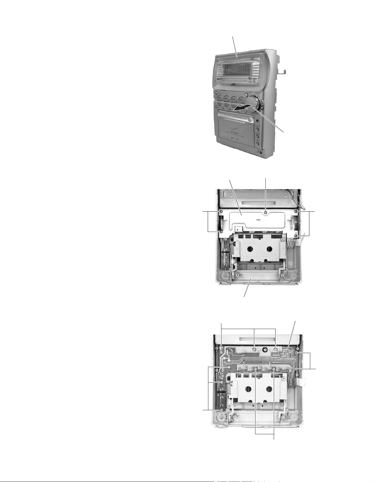
UX-Z7MDR
SERVICE MANUAL
MICRO COMPONENT MD SYSTEM
UX-Z7MDR
Area Suffix
E -------- Continental Europe
TABLE OF CONTENTS
1 Important Safety Precautions . . . . . . . . . . . . . . . . . . . . . . . . . . . . . . . . . . . . . . . . . . . . . . . . . . . . . . . . . . . 1-2
2 Disassembly Method. . . . . . . . . . . . . . . . . . . . . . . . . . . . . . . . . . . . . . . . . . . . . . . . . . . . . . . . . . . . . . . . . . . 1-5
3 Adjustment method. . . . . . . . . . . . . . . . . . . . . . . . . . . . . . . . . . . . . . . . . . . . . . . . . . . . . . . . . . . . . . . . . . . 1-37
4 Description of major ICs. . . . . . . . . . . . . . . . . . . . . . . . . . . . . . . . . . . . . . . . . . . . . . . . . . . . . . . . . . . . . . . 1-44
COPYRIGHT © 2003 VICTOR COMPANY OF JAPAN, LTD.
No.22042
2003/02
Page 2
UX-Z7MDR
Important Safety Precautions
1.1 Safety Precautions
(1) This design of this product contains special hardware and
many circuits and components specially for safety purposes.
For continued protection, no changes should be made to the
original design unless authorized in writing by the manufacturer. Replacement parts must be identical to those
used in the original circuits. Services should be performed by qualified personnel only.
(2) Alterations of the design or circuitry of the product should
not be made. Any design alterations of the product should
not be made. Any design alterations or additions will void
the manufacturers warranty and will further relieve the
manufacture of responsibility for personal injury or property
damage resulting therefrom.
(3) Many electrical and mechanical parts in the products have
special safety-related characteristics. These characteristics are often not evident from visual inspection nor can the
protection afforded by them necessarily be obtained by using replacement components rated for higher voltage, wattage, etc. Replacement parts which have these special safety
characteristics are identified in the Parts List of Service Manual. Electrical components having such features are identified by shading on the schematics and by ( ) on the
Parts List in the Service Manual. The use of a substitute replacement which does not have the same safety characteristics as the recommended replacement parts shown in the
Parts List of Service Manual may create shock, fire, or other hazards.
(4) The leads in the products are routed and dressed with ties,
clamps, tubings, barriers and the like to be separated from
live parts, high temperature parts, moving parts and/or
sharp edges for the prevention of electric shock and fire
hazard. When service is required, the original lead routing
and dress should be observed, and it should be confirmed
that they have been returned to normal, after reassembling.
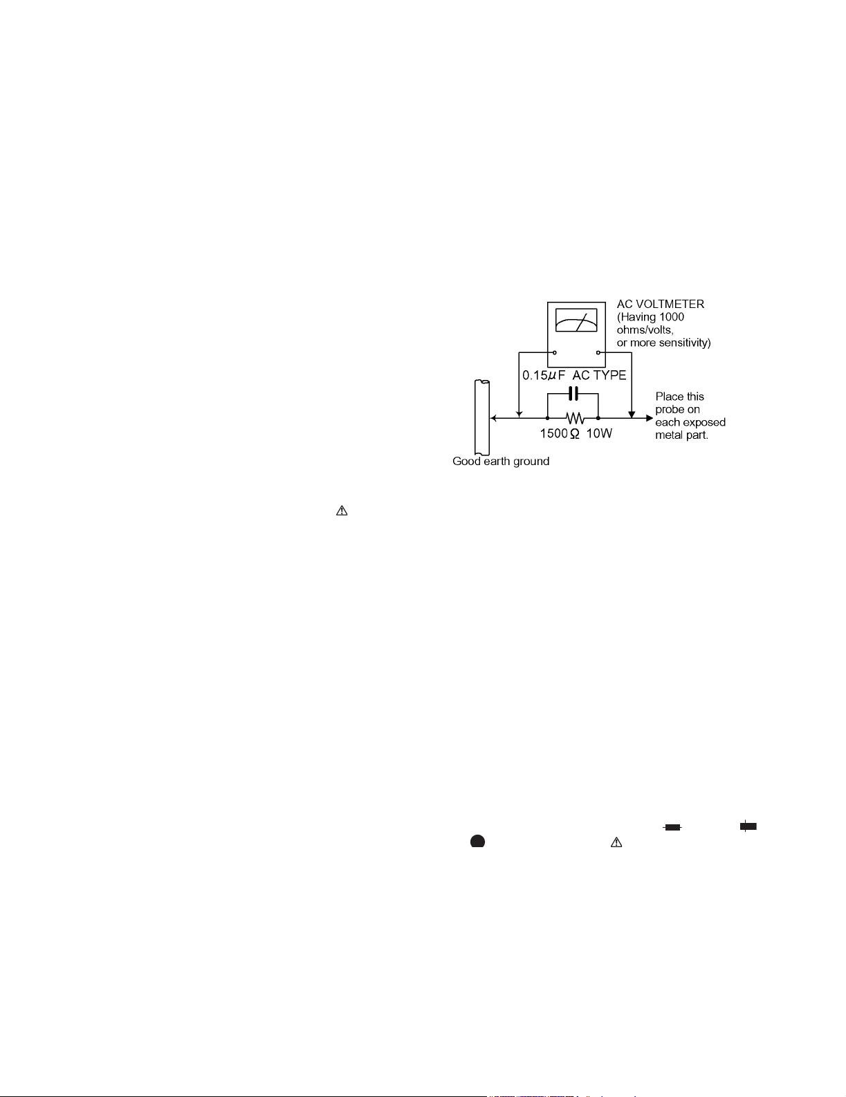
(5) Leakage shock hazard testing)
After reassembling the product, always perform an isolation
check on the exposed metal parts of the product (antenna
terminals, knobs, metal cabinet, screw heads, headphone
jack, control shafts, etc.) to be sure the product is safe to
operate without danger of electrical shock.
Do not use a line isolation transformer during this check.
• Plug the AC line cord directly into the AC outlet. Using a
"Leakage Current Tester", measure the leakage current
from each exposed metal parts of the cabinet, particularly any exposed metal part having a return path to the
chassis, to a known good earth ground. Any leakage current must not exceed 0.5mA AC (r.m.s.).
• Alternate check method
Plug the AC line cord directly into the AC outlet. Use an AC
voltmeter having, 1,000 ohms per volt or more sensitivity in
the following manner. Connect a 1,500 ohm 10W resistor
paralleled by a 0.15 µF AC-type capacitor between an
SECTION 1
exposed metal part and a known good earth ground.
Measure the AC voltage across the resistor with the AC
voltmeter.
Move the resistor connection to each exposed metal part,
particularly any exposed metal part having a return path to
the chassis, and measure the AC voltage across the resistor.
Now, reverse the plug in the AC outlet and repeat each
measurement. Voltage measured any must not exceed 0.75
V AC (r.m.s.). This corresponds to 0.5 mA AC (r.m.s.).
1.2 Warning
(1) This equipment has been designed and manufactured to
meet international safety standards.
(2) It is the legal responsibility of the repairer to ensure that
these safety standards are maintained.
(3) Repairs must be made in accordance with the relevant
safety standards.
(4) It is essential that safety critical components are replaced
by approved parts.
(5) If mains voltage selector is provided, check setting for local
voltage.
1.3 Caution
Burrs formed during molding may be left over on some parts
of the chassis.
Therefore, pay attention to such burrs in the case of preforming repair of this system.
1.4 Critical parts for safety
In regard with component parts appearing on the silk-screen
printed side (parts side) of the PWB diagrams, the parts that are
printed over with black such as the resistor ( ), diode ( )
and ICP ( ) or identified by the " " mark nearby are critical
for safety.
When replacing them, be sure to use the parts of the same type
and rating as specified by the manufacturer. (Except the JC version)
1-2 (No.22042)
Page 3
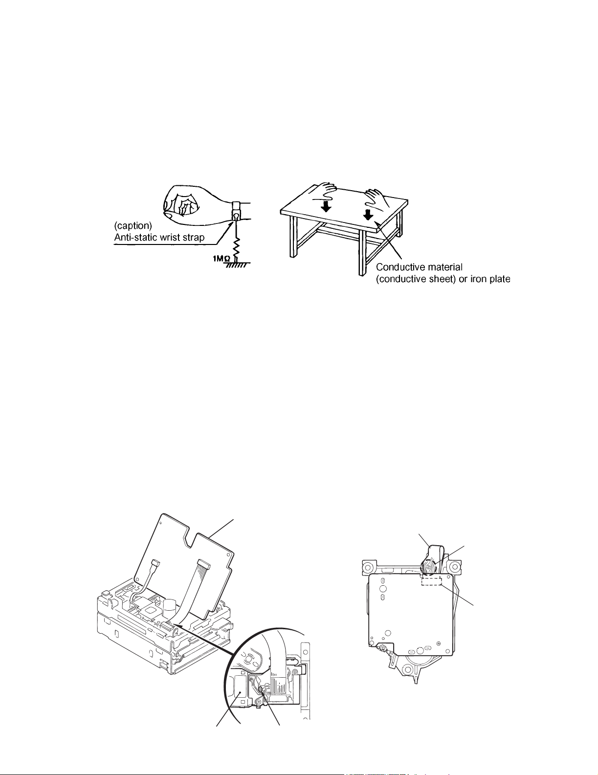
1.5 Preventing static electricity
Electrostatic discharge (ESD), which occurs when static electricity stored in the body, fabric, etc. is discharged,
can destroy the laser diode in the traverse unit (optical pickup). Take care to prevent this when performing repairs.
1.5.1 Grounding to prevent damage by static electricity
Static electricity in the work area can destroy the optical pickup (laser diode) in devices such as DVD players.
Be careful to use proper grounding in the area where repairs are being performed.
(1) Ground the workbench
Ground the workbench by laying conductive material (such as a conductive sheet) or an iron plate over it before placing the
traverse unit (optical pickup) on it.
(2) Ground yourself
Use an anti-static wrist strap to release any static electricity built up in your body.
UX-Z7MDR
(3) Handling the optical pickup
• In order to maintain quality during transport and before installation, both sides of the laser diode on the replacement optical
pickup are shorted. After replacement, return the shorted parts to their original condition.
(Refer to the text.)
• Do not use a tester to check the condition of the laser diode in the optical pickup. The tester's internal power source can easily
destroy the laser diode.
1.6 Handling the traverse unit (optical pickup)
(1) Do not subject the traverse unit (optical pickup) to strong shocks, as it is a sensitive, complex unit.
(2) Cut off the shorted part of the flexible cable using nippers, etc. after replacing the optical pickup. For specific details, refer to the replace-
ment procedure in the text. Remove the anti-static pin when replacing the traverse unit. Be careful not to take too long a time
when attaching it to the connector.
(3) Handle the flexible cable carefully as it may break when subjected to strong force.
(4) I t is not possible to adjust the semi-fixed resistor that adjusts the laser power. Do not turn it.
1.7 Attention when traverse unit is decomposed
*Please refer to "Disassembly method" in the text for the CD pickup unit.
• Apply solder to the short land before the flexible wire is disconnected from the connector on the CD pickup unit.
(If the flexible wire is disconnected without applying solder, the CDpickup may be destroyed by static electricity.)
• In the assembly, be sure to remove solder from the short land after connecting the flexible wire.
Main board
Flexible wire
Shorting round
Pickup Solder part b
CN601 on
mechanism
P.C. board
(No.22042)1-3
Page 4
UX-Z7MDR
1.8 Important for laser products
(1) CLASS 1 LASER PRODUCT
(2) DANGER : Invisible laser radiation when open and inter
lock failed or defeated. Avoid direct exposure to beam.
(3) CAUTION : There are no serviceable parts inside the
Laser Unit. Do not disassemble the Laser Unit. Replace the
complete Laser Unit if it malfunctions.
(4) CAUTION : The compact disc player uses invisible laser
radiation and is equipped with safety switches which
prevent emission of radiation when the drawer is open and
the safety interlocks have failed or are de feated.
It is dangerous to defeat the safety switches.
VARNING
Osynlig laserstrålning är denna del är öppnad och spårren är
urkopplad. Betrakta ej strålen.
VARO
Avattaessa ja suojalukitus ohitettaessa olet alttiina näkymättömälle lasersäteilylle. Älä katso säteeseen.
REPRODUCTION AND POSITION OF LABELS
(5) CAUTION : If safety switches malfunction, the laser is able
to function.
(6) CAUTION : Use of controls, adjustments or performance of
procedures other than those specified herein may result in
hazardous radiation exposure.
CAUTION
Please use enough caution not to see the beam directly
or touch it in case of anadjustment or operation check.
ADVARSEL
Usynlig laserstråling ved åbning, når sikkerhedsafbrydere er
ude af funktion. Undgå udsasttelse for stråling.
ADVARSEL
Usynlig laserstråling ved åpning, når sikkerhetsbryteren er
avslott. unngå utsettelse for stråling.
WARNING LABEL
CLASS 1
LASER PRODUCT
DANGER : Invisibie laser radiation
when open and interlock or
defeated.
AVOID DIRECT EXPOSURE TO
BEAM (e)
VARO : Avattaessa ja suojalukitus
ohitettaessa olet alttiina
näkymättömälle lasersäteilylle.Älä
katso säteeseen. (d)
VARNING : Osynlig laserstrålning är
denna del är öppnad och spårren är
urkopplad. Betrakta ej strålen. (s)
ADVARSEL :Usynlig laserstråling
ved åbning , når
sikkerhedsafbrydere er ude af
funktion. Undgå udsættelse for
stråling. (f)
1-4 (No.22042)
Page 5
SECTION 2
A
A
r
Disassembly Method
UX-Z7MDR
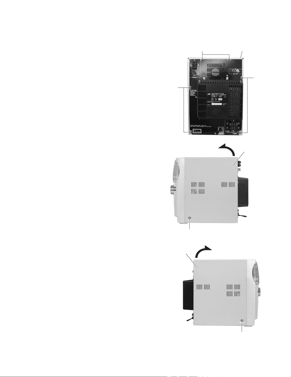
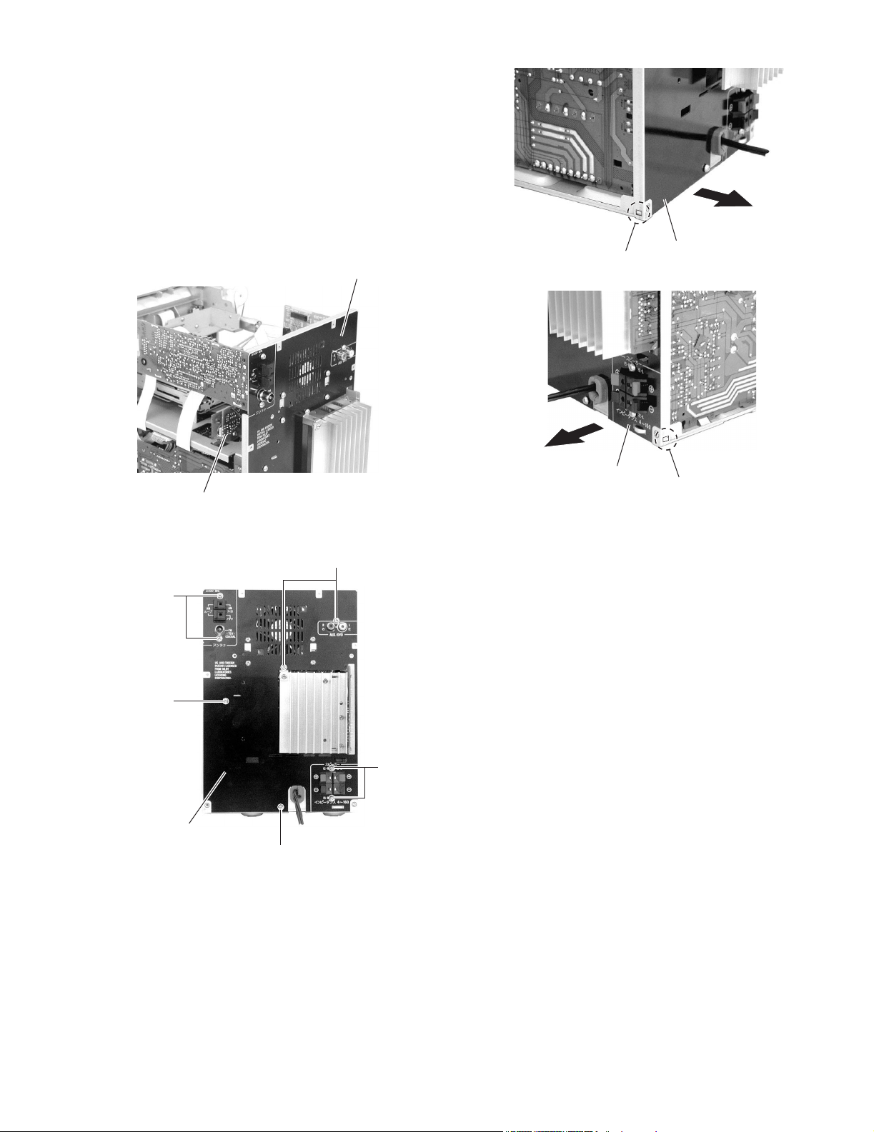
2.1 Main body
2.1.1 Removing the metal cover
(See Fig.1 to 3.)
(1) Remove the six screws A on the rear part of the main body
that attach the metal cover.
(2) Remove the two screws B on each side of the main body
that attach the metal cover.
(3) Lift the rear part of the metal cover upward while releasing
the lower sides of the metal cover in the right and left direction. The metal cover will be removed.
A
Matal cover
Fig.1
Matal cove
B
Fig.2
Matal cover
B
Fig.3
(No.22042)1-5
Page 6
UX-Z7MDR
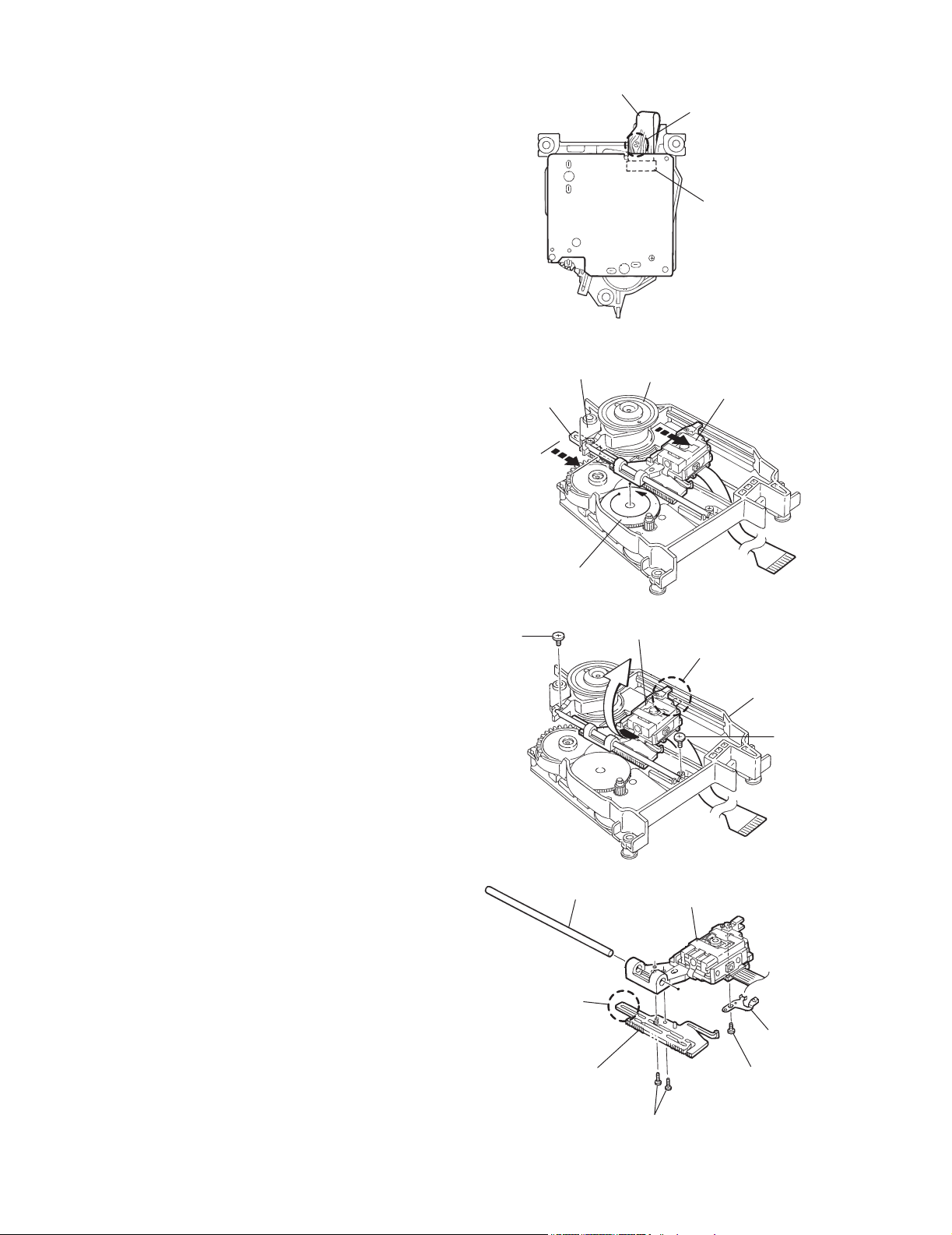
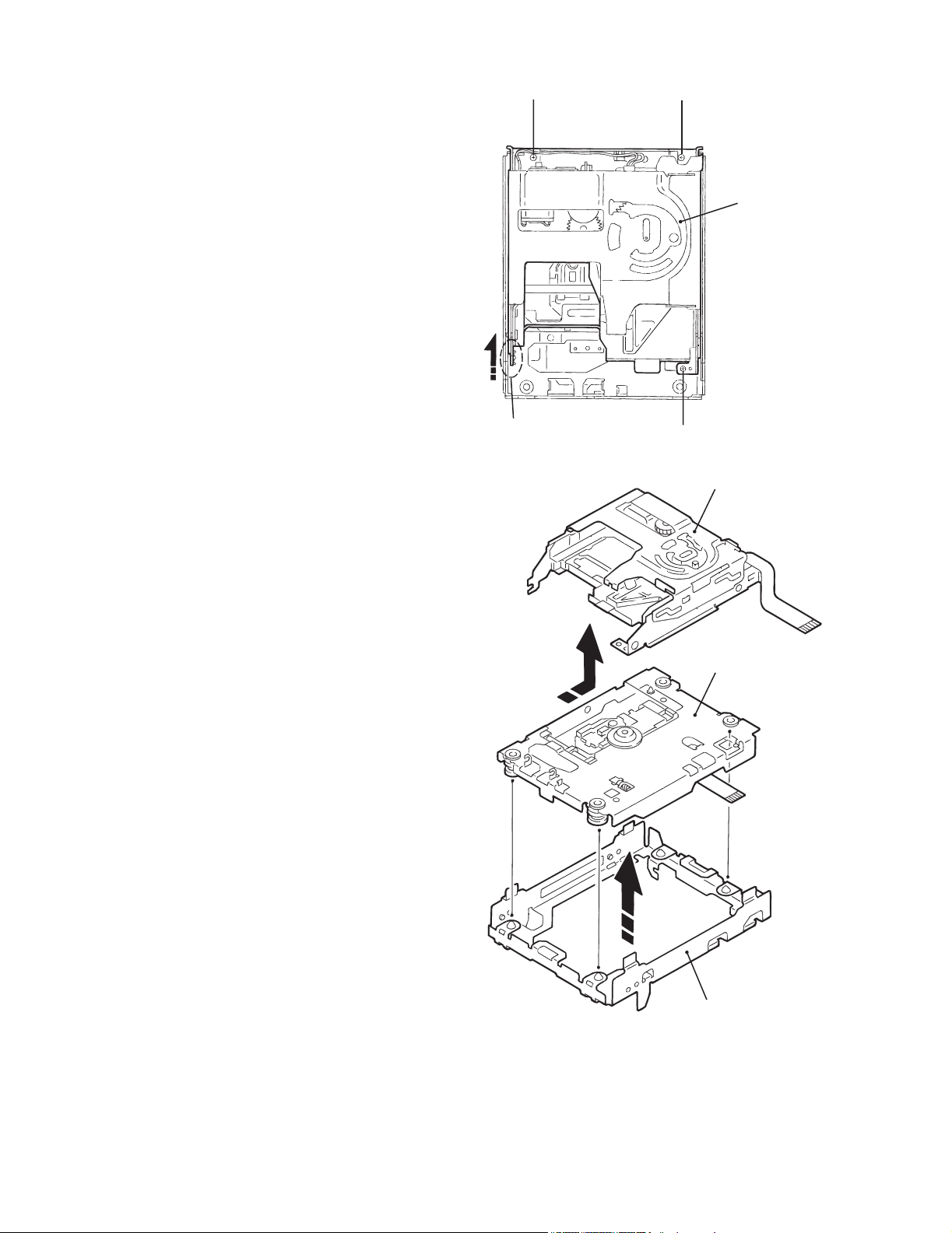
2.1.2 Removing the CD mechanism assembly
(See Fig.4 to 7.)
• Prior to this procedure, remove the metal cover.
(1) Remove the card wire from the connector CN302 on amp
board on the left side of the main body.
(2) Remove the three screws C on top of the body that attach
the CD mechanism assembly.
(3) Lift the CD mechanism assembly upward and move it
backward to remove.
(4) Remove the card wire from CN606 on CD servo board, on
the bottom of the CD mechanism assembly.
Amp board
CN302
C
CD mechanism ass'y
Fig.4
C
CD mechanism ass'y
CD mechanism ass'y
CD mechanism ass'y
Amp board
CN302
C
Fig.5
Fig.6
CD servo board
CN606
1-6 (No.22042)
Fig.7
Page 7
UX-Z7MDR
y
j
y
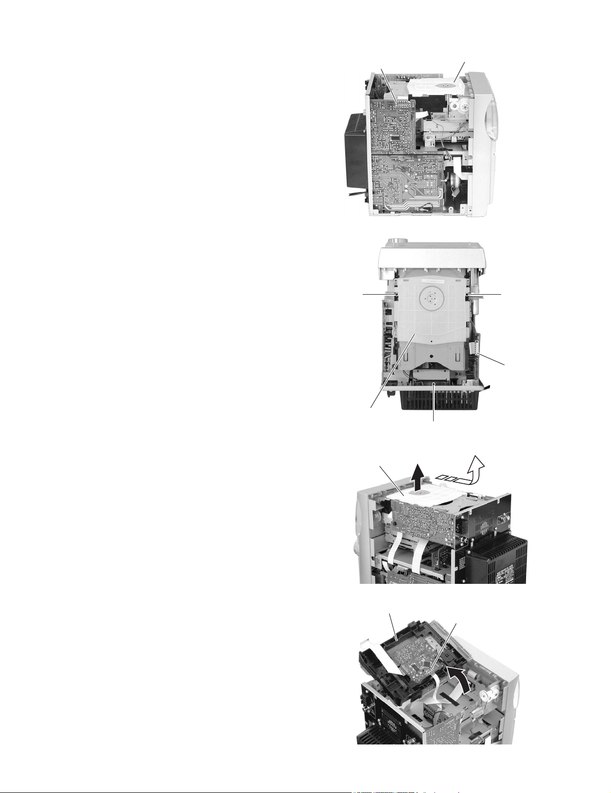
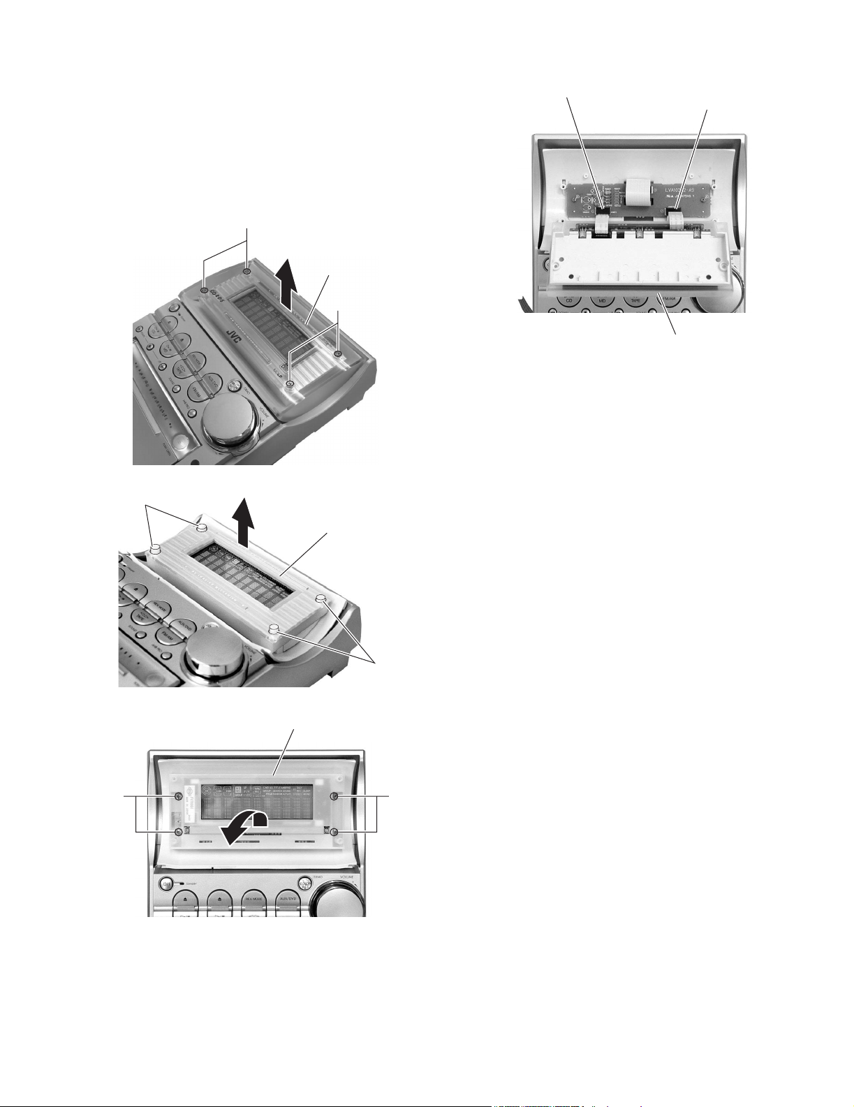
2.1.3 Removing the front panel
(See Fig.8 to11.)
• Prior to this procedure, remove the metal cover and the CD
mechanism assembly.
(1) Remove the card wire from the connector CN705 on micon
board, in the center of the right side of the main body.
(2) Remove the plastic rivet in the right side of the main body
that attaches tuner board.
(3) Remove the card wire from the connector CN301 on amp
board in the center of the left side of the main body.
Remove the card wire from the connector CN704 on micon
board.
Remove the wire from each connector CN703 and CN710
respectively.
(4) Remove the card wire from the connector CN452 on FL
connection board on top of the main body.
(5) Remove the two screws D on the right and left sides of the
main body that attach the front panel assembly.
(6) Remove the two screws E on the bottom of the main body
that attach the front panel assembly.
(7) Remove the joint "a" on the bottom of the main body and
the joint "b" on the right and left sides respectively by using
a screwdriver. Remove the front panel assembly in the
front direction.
Plastic rivet
Front panel ass'y
Tuner board
FL connect board
CN710
CN452
CN703
Fig.10
Front panel ass'
Micon board
CN704
Front panel ass'
EE
D
Micon board
CN705
Amp board
CN301
CN710
joint b
Fig.8
Front panel ass'y
joint b
Fig.9
oint a
Fig.11
D
Micon board
CN704
CN703
(No.22042)1-7
Page 8
UX-Z7MDR
j
c
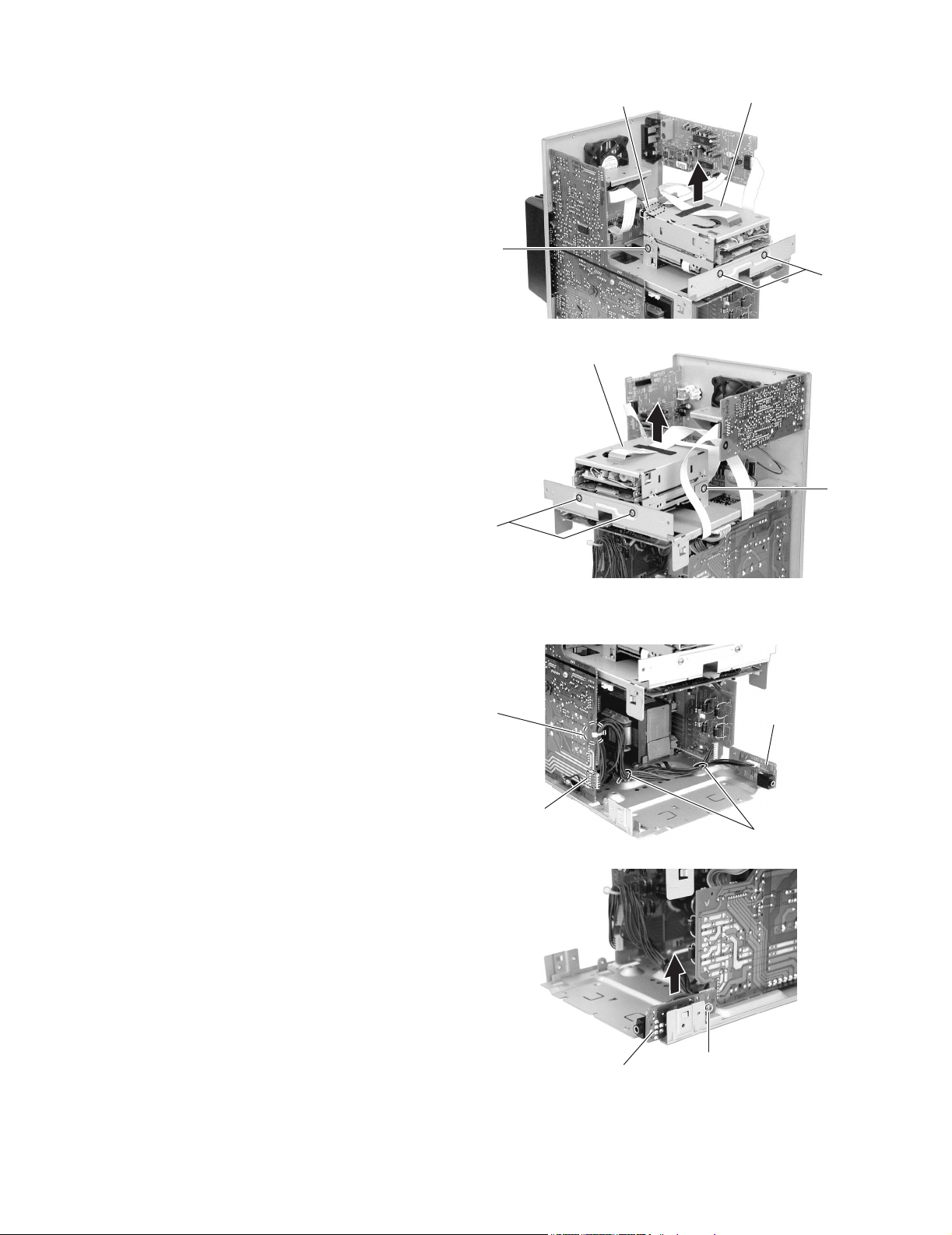
2.1.4 Removing the tuner board
(See Fig.12.)
• Prior to this procedure, remove the metal cover.
(1) Remove the card wire on the right side of the main body
from the connector CN1 on the tuner board.
(2) Remove the plastic rivet on the right side of the main body
that attaches the tuner board.
(3) Remove the two screws F on the rear side of the main body
that attach the tuner board.
2.1.5 Removing the rear cover
(See Fig.13.)
• Prior to this procedure, remove the metal cover and the CD
mechanism assembly.
(1) Remove the two screws G on the rear side of the main
body that attach the rear cover.
CN1
Plastic rivet
G
Tuner doard
F
Fig.12
Rear panel
G
2.1.6 Removing the fan
(See Fig.14 to 16.)
• Prior to this procedure, remove the metal cover, the CD mech-
anism assembly, and the rear cover.
(1) Remove the wire from the connector CN603 on the MD
connect board in the right side of the main body.
(2) Remove the four screws H on the rear side of the main
body that attach the fan.
(3) Move the fan bracket that attaches the fan from inside the
rear panel upward to remove the two fixing points "c". Fan
will be detached at the same time.
Notice
When attaching the fan, attach the two "e" to the two "d" respectively before pressing the fan with fan bracket.
Fan
Rear panel
H
H
oint c
hook d
Rear cover
Fan blacket
Fan
Fig.13
Rear panel
Fig.15
Fan
joint
hole e
MD connect board
1-8 (No.22042)
CN603
Fig.14
hook d
hole e
Fig.16
Page 9
2.1.7 Removing the rear panel
(See Fig.17 to 20.)
• Prior to this procedure, remove the metal cover, the CD mech-
anism assembly, and the rear cover.
(1) Remove the wire from the connector CN603 on MD con-
nect board on the right side of the main body.
(2) Remove the eight screws F on the rear side of the main
body that attach the rear panel.
(3) Remove the two joint "f" on the right and left bottom of the
rear panel.
Notice
The fan assembly will be kept attached to the rear panel.
Rear panel
UX-Z7MDR
Rear panel
joint f
Fig.19
MD connect doard
CN603
F
F
Rear panel
Fig.17
Fig.18
F
F
F
Rear panel
Fig.20
joint f
(No.22042)1-9
Page 10
UX-Z7MDR
y
A
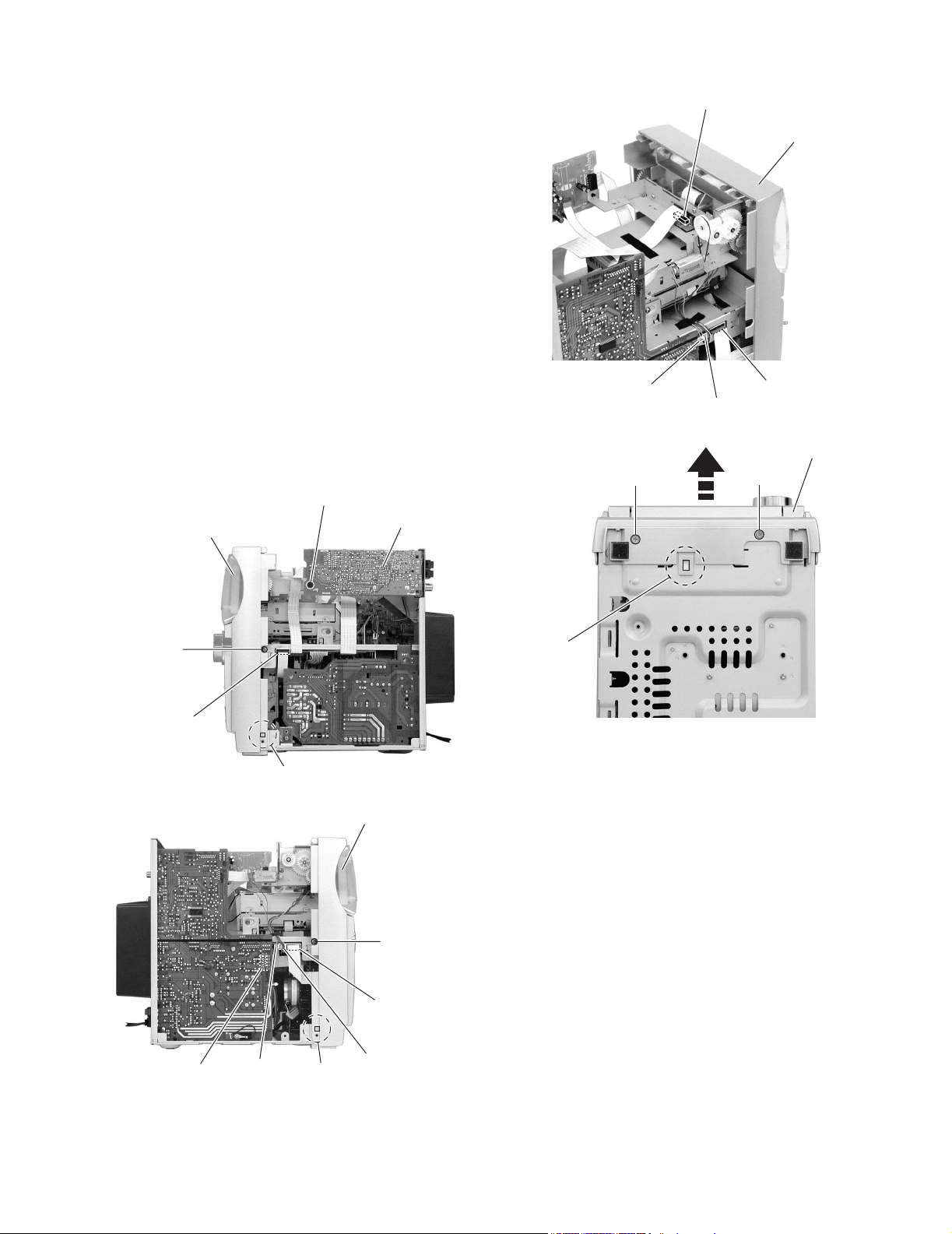
2.1.8 Removing the MD mechanism assembly
(See Fig.21 and 22.)
• Prior to this procedure, remove the metal cover, the CD mech-
anism assembly, and the rear cover.
(1) Remove the card wire from the connector CN601 on the
MD connect board in the rear part of the MD mechanism
assembly.
(2) Remove the four screws H on the front side and the rear
side that attach the MD mechanism assembly.
Remove the MD mechanism assembly upward.
MD connect board
H
MD mechanism ass'y
CN601
MD mechanism ass'
H
Fig.21
H
2.1.9 Removing the headphone board
(See Fig.23 and 24.)
• Prior to this procedure, remove the metal cover, the CD mech-
anism assembly, and the rear cover.
(1) Remove the wire from the connector CN101 on the amp
board on the left side of the main body.
(2) Remove the band that fixes the wire to the amp board. Re-
move the wire from the two clamps in the bottom chassis.
(3) Remove the screw I on the right side of the main body that
attaches the headphone board.
H
Fig.22
Band
Headphone board
mp board
CN101
clamp
Fig.23
1-10 (No.22042)
Headphone board
Fig.24
I
Page 11
UX-Z7MDR
A
2.1.10 Removing the amp board and heat sink
(See Fig.25 and 26.)
• Prior to this procedure, remove the metal cover, the CD mech-
anism assembly, the front panel assembly, and the rear cover.
(1) Remove the wire from the connector CN101 and CN102 on
the amp board on the left side of the main body. Remove
the band that fixes the wire. Remove the card wire from the
connector CN303.
(2) Remove the two screws J that attach the amp board.
(3) Pull out and remove the connector CN304 and CN305 on
the amp board outward. Remove the two joint "g" that fix
the bottom chassis.
Notice
The heat sink will be kept attached to the amp board. The
heat sink can be removed without removing the amp
board.
(4) Remove the three screws K that attach the heat sink.
mp board
Heat sink
J
Heat sink
joint g
CN303
J
Fig.25
K
CN304
joint g
CN305
Band
CN102
CN101
Amp board
K
Fig.26
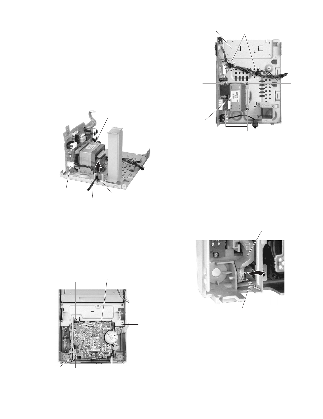
2.1.11 Removing the MD connect board
(See Fig.27.)
• Prior to this procedure, remove the metal cover, the CD mech-
anism assembly, and the rear cover.
(1) Remove the card wire from the connector CN601 on the
MD connect board.
(2) Remove the two screws L on the rear side of the main body
that attach the MD connect board.
(3) Pull out the connector CN604 on the MD connect board in
the rear direction.
MD connect board
CN601
L
L
Fig.27
CN604
(No.22042)1-11
Page 12
UX-Z7MDR
s
2.1.12 Removing the MD base chassis/the micon board
(See Fig.28 to 30.)
• Prior to this procedure, remove the metal cover, the CD mech-
anism assembly, the front panel assembly,
the rear cover, the amp board, and the MD connect board.
Notice
The MD base chassis/the micon board can be removed without removing the MD mechanism assembly.
(1) Remove the wire from the micon board connector CN707
in the center of the right side of the main
body. Remove the card wire from the connector CN708.
(2) Remove the screw M on top of the main body that attaches
the MD base chassis.
Notice
The MD mechanism assembly will be kept attached to
the MD base chassis.
(3) Remove the two screws N that attach the micon board. Re-
move the two joint "h" that fix the MD base chassis.
MD mechanism ass'y
Micon board
CN707
MD mechanism ass'y
MD base chassis
CN708
Fig.28
MD base chassi
M
Fig.29
N
joint h
Fig.30
Micon board
1-12 (No.22042)
Page 13
UX-Z7MDR
y
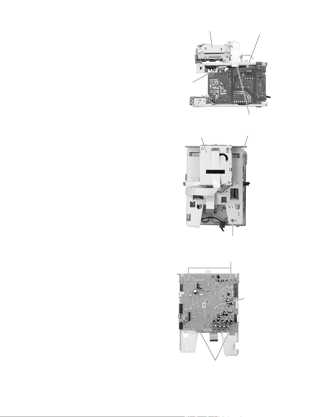
2.1.13 Removing the power trans assembly
(See Fig.31 and 32.)
• Prior to this procedure, remove the metal cover, the CD mech-
anism assembly, the front panel assembly, the rear cover, the
amp board, and the MD base chassis.
(1) Move the power cord stopper upward from the rear part of
the main body to remove. Remove the power supply cord
from the connector CN901 on the power trans board.
Notice
The power cord can be removed without removing the
power trans assembly.
(2) Remove the four screws O on top of the main body that at-
tach the power trans assembly. Remove the wire from the
two clamps on the bottom chassis.
Power trans assembly
Bottom chassis
clamp
OO
Power trans
assembly
O
Fig.32
Power trans board
CN901
Power cord
2.2 Front panel assembly
• Prior to this procedure, remove the metal cover, the CD mech-
anism assembly, and the front panel assembly.
2.2.1 Removing the cassette mechanism assembly
(See Fig.33 and 34.)
(1) Remove the spring that is attached to the cassette door
from inside the front panel.
(2) Remove the four screws P that attach the cassette mecha-
nism assembly.
Cassette mechanism assembl
P
cord stopper
Fig.31
P
Cassette door
Spring
Fig.34
Spring
P
Fig.33
(No.22042)1-13
Page 14
UX-Z7MDR
2.2.2 Removing the key board
(See Fig.35 to 37.)
• Prior to this procedure, remove the cassette mechanism as-
sembly.
(1) Pull out the volume knob in the front side of the front panel
to remove.
(2) Remove the five screws Q that attach the bracket (1) from
inside the front panel.
(3) Remove the ten screws R that attach the key board.
Front panel assembly
Bracket(1)
Volume knob
Fig.35
Q
Q
Front panel
R
Q
Fig.36
Key boad
R
1-14 (No.22042)
R
R
Fig.37
Page 15
UX-Z7MDR
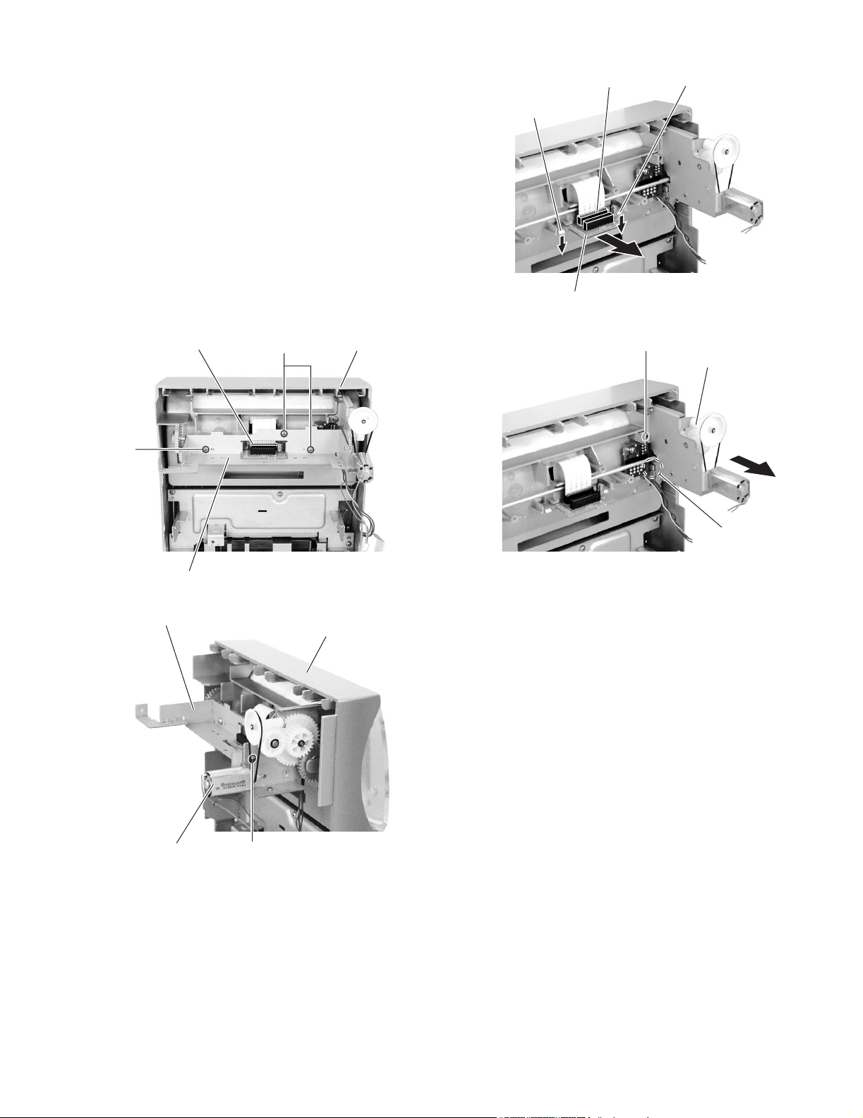
2.2.3 Removing the FM connection board
(See Fig.38 to 40.)
(1) Remove the three screws S and the screw T that attach the
bracket (2) from inside the front panel.
(2) Remove the card wire from the connector CN451 on the FL
connection board.
(3) Press the tab in the front panel and the one in joint "i"
downward to remove. Pull out the FL connection board to
remove.
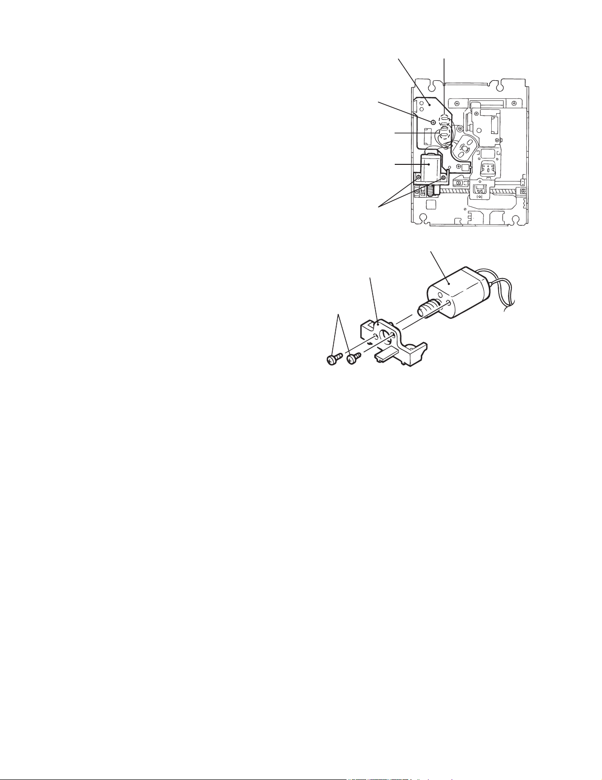
2.2.4 Removing the drive motor assembly
(See Fig.38, 39, and 41.)
(1) Remove the three screws S and the screw T that attach the
bracket (2) from inside the front panel.
(2) Remove the screw U that attaches the drive motor assem-
bly. Remove the tab in joint "j" that fixes the front panel. Pull
out the drive motor assembly to remove.
FL connect board
CN451
S
Front panel
S
CN451
joint i
FL connect board
joint i
Fig.40
U
Drive motor
Bracket(2)
Bracket(2)
Drive motor
joint j
Fig.41
Fig.38
Front panel
T
Fig.39
(No.22042)1-15
Page 16
UX-Z7MDR
j
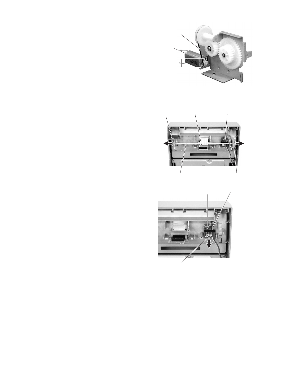
2.2.5 Removing the belt/drive motor
(See Fig.42.)
• Prior to this procedure, remove the drive motor assembly.
(1) Remove the belt from the pulley.
(2) Remove the two screws V that attach the drive motor.
2.2.6 Removing the switch board
(See Fig.43 and 44.)
• Prior to this procedure, remove the bracket (2) / the drive motor
assembly.
(1) Remove the card wire from the connector CN451 on FL
connection board.
(2) Remove the joint "k" by releasing it outward. And then, re-
move the joint "l" in the same way.
(3) Remove the screw W that attaches the switch board. Re-
move the tab on the joint "m" that fixes the front panel.
Drive motor
oint l
Belt
V
FL connect board
Fig.42
CN451
Switch board
Shift gear
Fig.43
W
joint m
Fig.44
joint k
Switch board
1-16 (No.22042)
Page 17
UX-Z7MDR
r
j
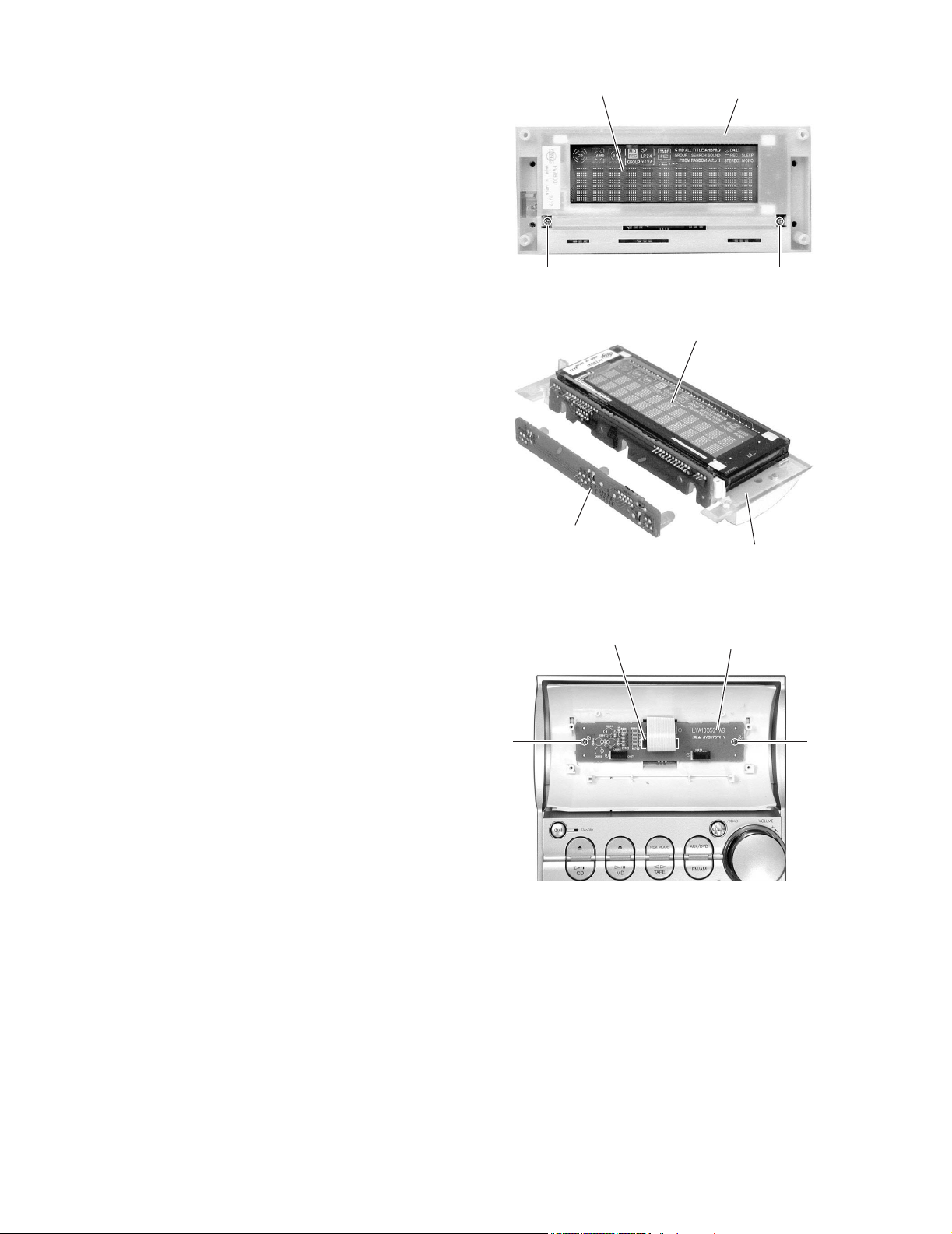
2.2.7 Removing the FL display
(See Fig.45 to 50.)
(1) Remove the four screws X on the front side of the front pan-
el that attach the case cover.
(2) Pull out the FL panel from the bosses of the four joint "n"
on the FL display cover.
(3) Remove the four screws Y that attach the FL display cover.
Remove the card wire from the connector CN671 and CN
672 on the FL connect board inside the FL display cover.
X
Case cove
X
FL connect board
CN671
CN672
FL cover
Fig.48
Fig.45
oint n
FL panel
joint n
Fig.46
FL cover
YY
Fig.47
(No.22042)1-17
Page 18
UX-Z7MDR
(4) Remove the two screws Z on the front side of the FL dis-
play cover that attach the FL display.
(5) FL board and lens will be detached from the FL display.
FL
FL cover
ZZ
Fig.49
FL
2.2.8 Removing the FL connect board
(See Fig.51.)
• Prior to this procedure, remove the FL display cover.
(1) Remove the card wire from the connector CN673 on the FL
connect board.
(2) Remove the two screws Z’ that attach the FL connect
board.
FL board
CN673
Fig.50
Lens
FL connect board
Z'Z'
Fig.51
1-18 (No.22042)
Page 19
UX-Z7MDR
r
r
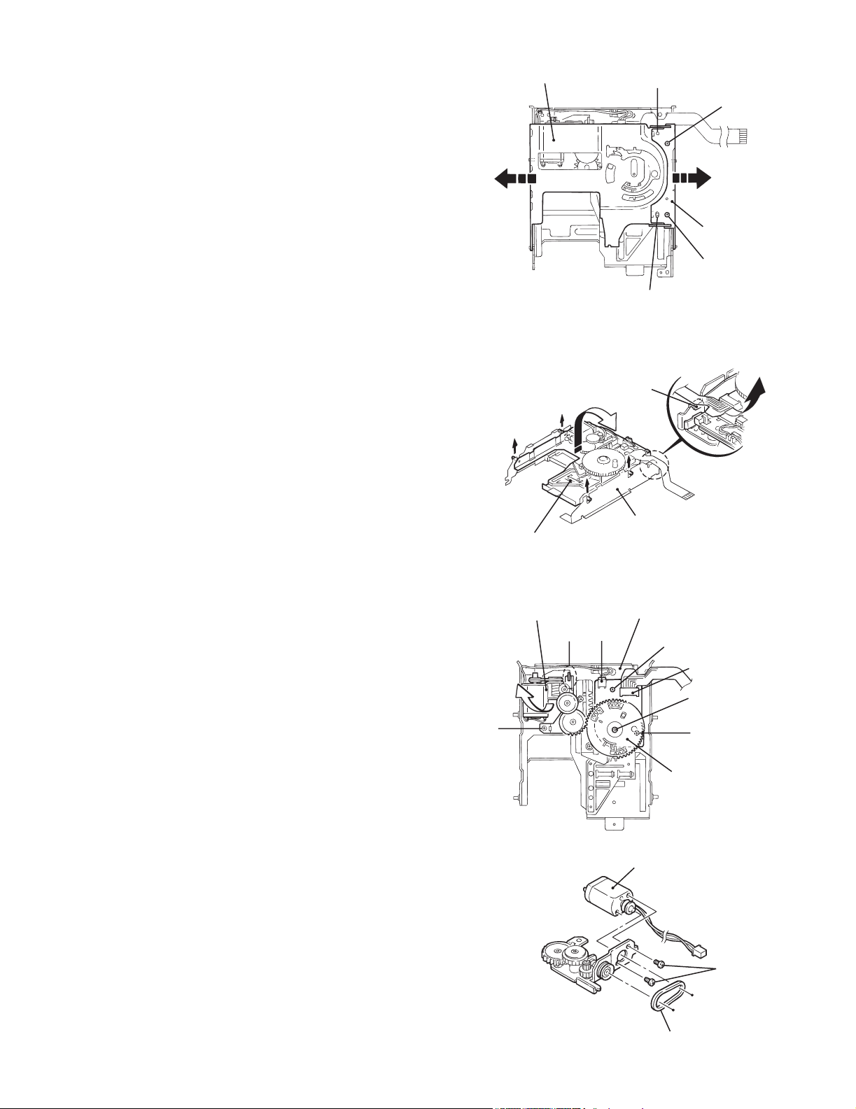
2.3 CD Mechanism Assembly
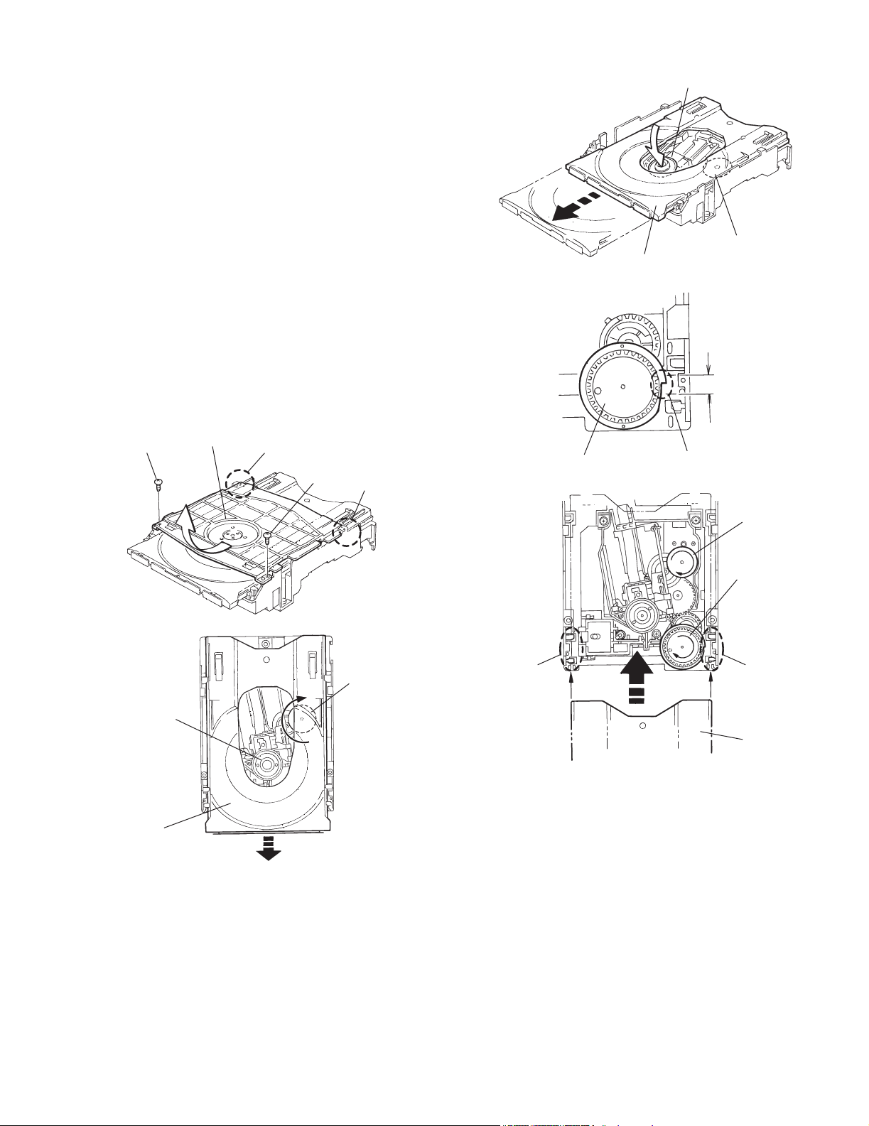
2.3.1 Removing the CL. Base Assembly and Tray
(Refer to Figs. 1 to 5.)
(1) Remove the two screws A fastening the CL. base assembly
from the top of the CD mechanism assembly.
(2) Move the CL. base assembly diagonally upwards as in-
dicated by the arrow to release it from the two hooks a.
(3) Turn the idle gear in the arrow-marked direction from the
upper side of the CD mechanism assembly. Accordingly,
the TRAMECHA assembly moves downwards.
Note:
When drawing out the tray, shift down the TRAMECHA
assembly to the position where the tray does not contact
the T-T assembly of the TRAMECHA assembly.
(4) Draw out the tray frontwards for removing it.
Note:
When reinstalling the tray:
• Turn the idle gear so that the part b of the tray gear is
positioned in the part c shown in Fig. 4. (Eject position)
• Engage the right and left hooks d and e of the tray with
the right and left grooves of the TRAMECHA assembly
respectively for retaining the tray.
CL. base assembly
A
Hook a
A
Hook a
Tray gear
TRAMECHA assembly
Idle gear
Tray
Fig.3
Part c
Part b
Fig.4
TRAMECHA
assembly
Tray
Fig.1
Fig.2
Idle gea
Tray gear
Hook d
Idle gea
Fig.5
Hook d
Tray
(No.22042)1-19
Page 20
UX-Z7MDR
r
r
2.3.2 Removing the TRAMECHA Assembly
(Refer to Figs. 6 to 9.)
• Remove the CL. base assembly and tray.
Reference:
The TRAMECHA assembly can be removed without removal
of the mechanism P.C. board.
(1) If the TRAMECHA assembly is lowered and it is located out
of the PLAY position, turn the idle gear in the arrow-marked
direction so that the hole in the part f of the tray gear meets
the hole on the CL. base assembly. (Set the TRAMECHA
assembly at the PLAY position.)
(2) Remove the three screws B fastening the
TRAMECHA assembly and then remove the
TRAMECHA assembly upwards from the front side.
(3) At the same time, remove the spring from the groove of the
CH. base assembly in the part g of the TRAMECHA assembly.
Note:
When reinstalling the TRAMECHA assembly:
• Check to see if the spring is properly engaged with
groove of the CH. base assembly in the part g of the
TRAMECHA assembly.
• After making sure that the three insulators of the
TRAMECHA assembly are properly set on the bosses of the L. base assembly's guide, fasten them
with the screws.
TRAMECHA
assembly
B
Part g
B
Idle gear
Tray gea
B
Fig.6
Tray gea
Part f
L. base assembly
Fig.7
Spring
Part g
Fig.8
Spring
Groove of CH. base assembly
Fig.9
1-20 (No.22042)
Page 21

2.3.3 Removing the Mechanism P.C. Board
(Refer to Fig 10.)
Reference:
The mechanism P.C. board can be removed without removal
of the TRAMECHA assembly.
Note:
Before disconnecting the flexible wire coming from the pickup
from the connector, be sure to solder its shorting round.
If the flexible wire is connected without soldering, it may cause
breakdown of the pickup.
(1) Solder the shorting round of the flexible wire connected
with the mechanism P.C. board from the back of the mechanism assembly.
(2) Disconnect the flexible wire from the connector CN601 on
the mechanism P.C. board.
(3) Remove the three screws C fastening the mechanism P.C.
board.
(4) Unsolder the two points of the part h and one point of the
part i of the mechanism P.C. board. Then, remove the
mechanism P.C. board upwards.
Note:
When reinstalling the mechanism P.C. board, connect the flexible wire coming from the pickup to the connector first and then
remove the solder from the shorting round of the flexible cable.
Flexible wire
C
UX-Z7MDR
Soldered
part h
C
Shorting round
CN601 on
mechanism
P.C. board
C
Soldered part i
Fig.10
(No.22042)1-21
Page 22
UX-Z7MDR
2.3.4 Removing the Pickup(Refer to Figs. 11 to 14.)
• Remove the CL. base assembly and tray.
• Remove the TRAMECHA assembly.
Reference:
The pickup can be removed without removal of the mechanism
P.C. board.
Note:
Before disconnecting the flexible wire coming from the pickup
from the connector, be sure to solder its shorting round.
If the flexible wire is connected without soldering, it may cause
breakdown of the pickup.
(1) Solder the shorting round of the flexible wire connected
with the mechanism P.C. board from the back of the TRAMECHA assembly.
(2) Disconnect the flexible wire from the connector CN601 on
the mechanism P.C. board.
(3) Turn the idle gear in the arrow-marked direction from the top
of the TRAMECHA assembly so that the pickup assembly is
shifted to the reverse side of the T-T assembly.
Move the pickup assembly until the part j of the rack plate
in the lower part of the pickup assembly comes out of the
CH. base assembly.
(4) Remove the two screws D retaining the shaft of the pickup
assembly. Next, disengage the hook k from the CH. base
assembly and then remove the pickup assembly together
with the shaft.
(5) Pull the shaft out of the pickup.
(6) Remove the two screws E fastening the rack plate from the
pickup.
(7) Remove the screw F retaining the P.S. spring from the
pickup.
Part j of
rack plate
Idle gear
D
Flexible wire
CH. base
assembly
Pickup assembly
Shorting round
CN601 on
mechanism
P.C. board
Fig.11
T-T assembly
Pickup assembly
Fig.12
Part k
Shaft
jPart j
Rack plateE
CH. base
assembly
D
Fig.13
Pickup
P.S. spring
F
E
Fig.14
1-22 (No.22042)
Page 23
UX-Z7MDR
2.3.5 Reinstalling the Pickup Assembly
(Refer to Figs. 15 and 16.)
Reference:
Refer to the explanation of "Removing the Pickup" on the
preceding page.
(1) Fit the P.S. spring and rack plate to the pickup.
(2) Insert the shaft into the pickup.
(3) Engage the hook k of the pickup assembly with the CH.
base assembly first, and set the part j of the rack plate in
the opening I next. Then, reinstall the pickup assembly
while shifting it to the T-T side (inward) so that the part m
of the rack plate is positioned as shown in Fig. 16.
(4) Move the pickup assembly to the center position and fasten
the shaft with the two screws D. (Make sure that the part n
of the rack plate is correctly engaged with the middle gear.)
(5) After passing the flexible wire coming from the pickup
through the opening of the CH. base assembly, connect it
to the connector CN601.
Note:
When reinstalling the pickup assembly, remove the solder from the shorting round after connecting the flexible
wire coming from the pick to the connector CN601.
Part k
Part j
2.3.6 Removing the Feed Motor Assembly
(Refer to Fig. 17.)
• Remove the CL. base assembly and tray.
• Remove the mechanism P.C. board.
Remove the two screws E fastening the feed motor assembly
from the top of the mechanism assembly.
E
Feed motor assembly
Fig.17
Part I
Part m
Pickup
assembly
CH. base
assembly
Fig.15
Middle gear
Fig.16
Rack plate
Part n
(No.22042)1-23
Page 24
UX-Z7MDR
b
r
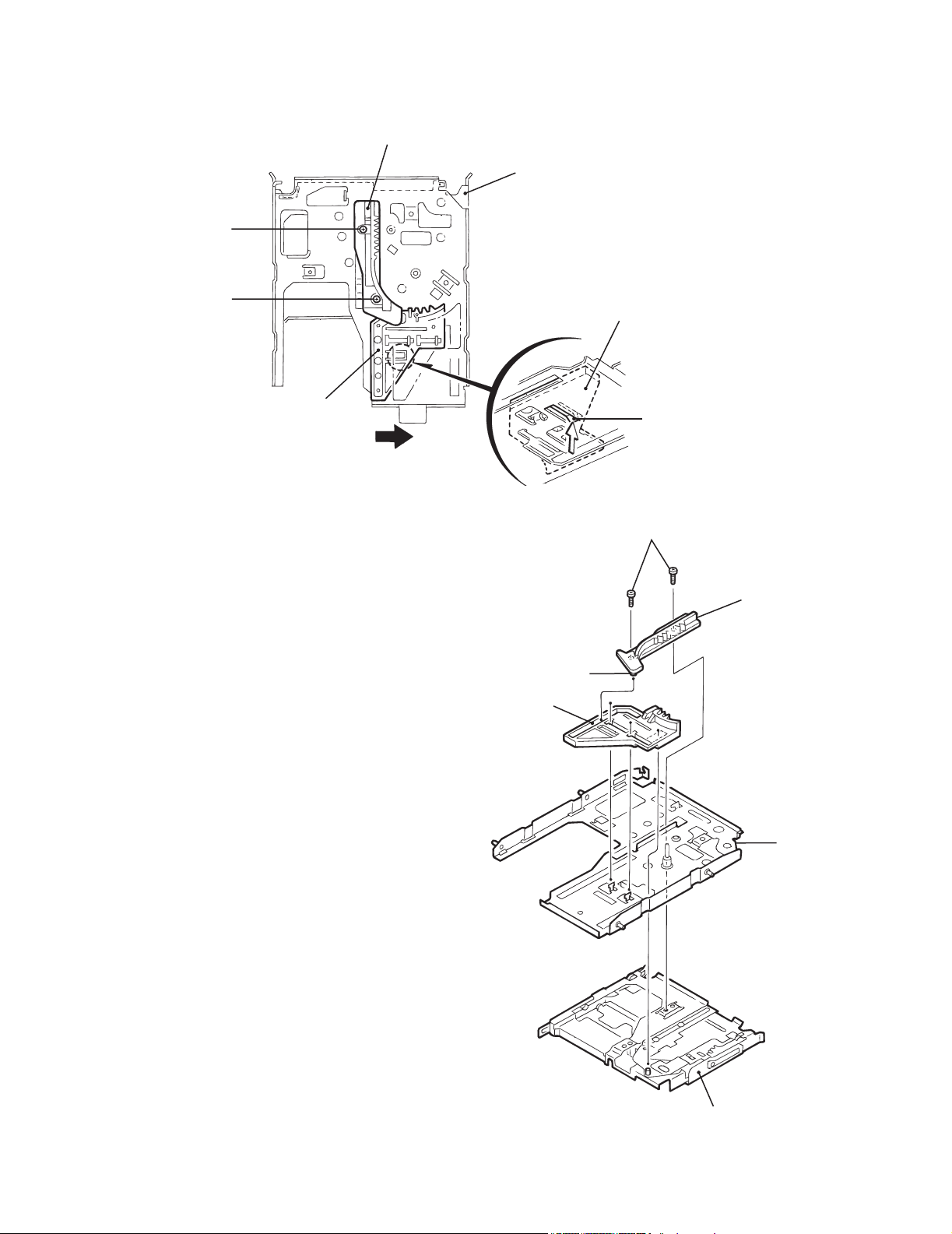
2.4 MD mechanism assembly
2.4.1 Removing the main board
(See Fig.1 and 2)
(1) Turn over the body and disconnect the card wire from con-
nector CN408 and the flexible wire from CN407 on the
main board.
(2) Remove the two screws A attaching the main board. Slide
the main board in the direction of the arrow to release the
two joints a with the single flame.
(3) Solder part b on the pickup in the body. Disconnect the
flexible harness from connector CN321 and CN451 on the
underside of the main board. Then remove the main board.
AA
(Bottom)
Main board
CN408
CN407
2.4.2 Removing the mechanism cover
(See Fig.3)
(1) Remove the four screws B on both sides of the body.
(2) Move the mechanism cover toward the front to disengage
the front hook of the mechanism cover from the internal
loading assembly (Joint c). Then remove the mechanism
cover upward.
Joint c
B
Fook
Joint c
Mechanism cove
B
Fig.3
Joint b Joint b
Fig.1
CN451
Pickup Solder part
Fig.2
Main board
CN321
1-24 (No.22042)
Page 25
2.4.3 Removing the head lifter (See Fig.4 to 6)
(1) Move the head lifter on top of the body in the direction of the arrow and turn around.
(2) Detach the spring from the hook of the body. Remove the head lifter with the spring.
(3) If necessary, remove the spring from the head lifter.
Head lifter
Spring
Head lifter
Fig.5
UX-Z7MDR
Fig.4
2.4.4 Removing the head assembly (See Fig.7)
(1) Remove the screw C on the upper side of the body.
Remove the head assembly while pulling the flexible harness from the body.
Head lifter
Spring
Fig.6
Fig.4,5,6
Head assembly
C
Fig.7
(No.22042)1-25
Page 26
UX-Z7MDR
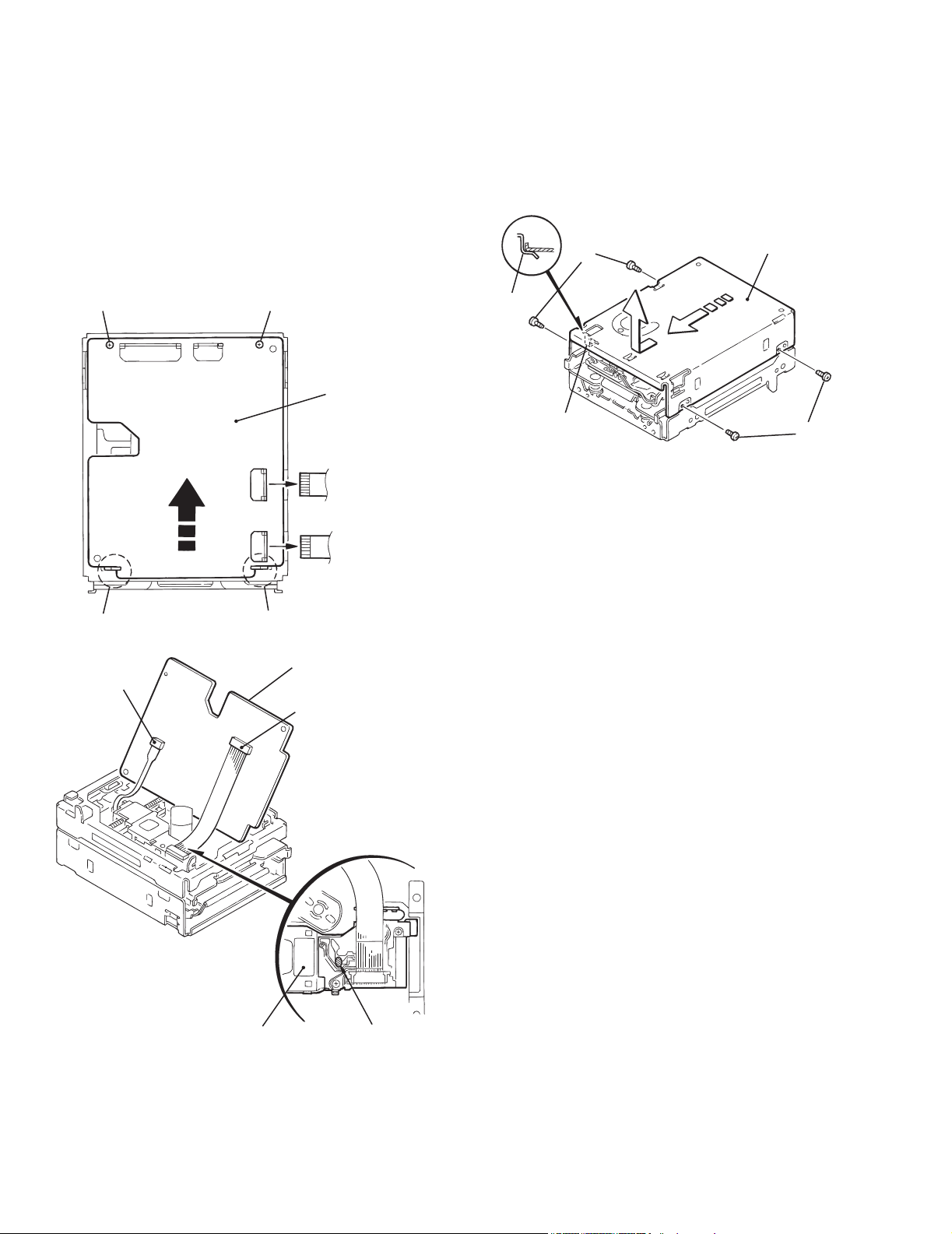
2.4.5 Removing the Loading assembly
(See Fig.8 and 9)
Ref:
The loading assembly, the traverse mechanism assembly and
the single flame will be removable after removing the loading
assembly from the body.
• Prior to performing the following procedure, remove the main
board, the mechanism cover, the head lifter and the head assembly.
(1) Remove the three screws D on the upper side of the body.
(2) Move the loading assembly forward to disengage it from
the traverse mechanism assembly (Joint d). Then remove
it upward.
(3) Remove the traverse mechanism assembly from the single
flame.
D
D
Loading assembly
Joint d
D
Fig.8
Loading assembly
Traverse mechanism
assembly
1-26 (No.22042)
Fig.9
Single flame
Page 27
UX-Z7MDR
)
2.4.6 Loading assembly
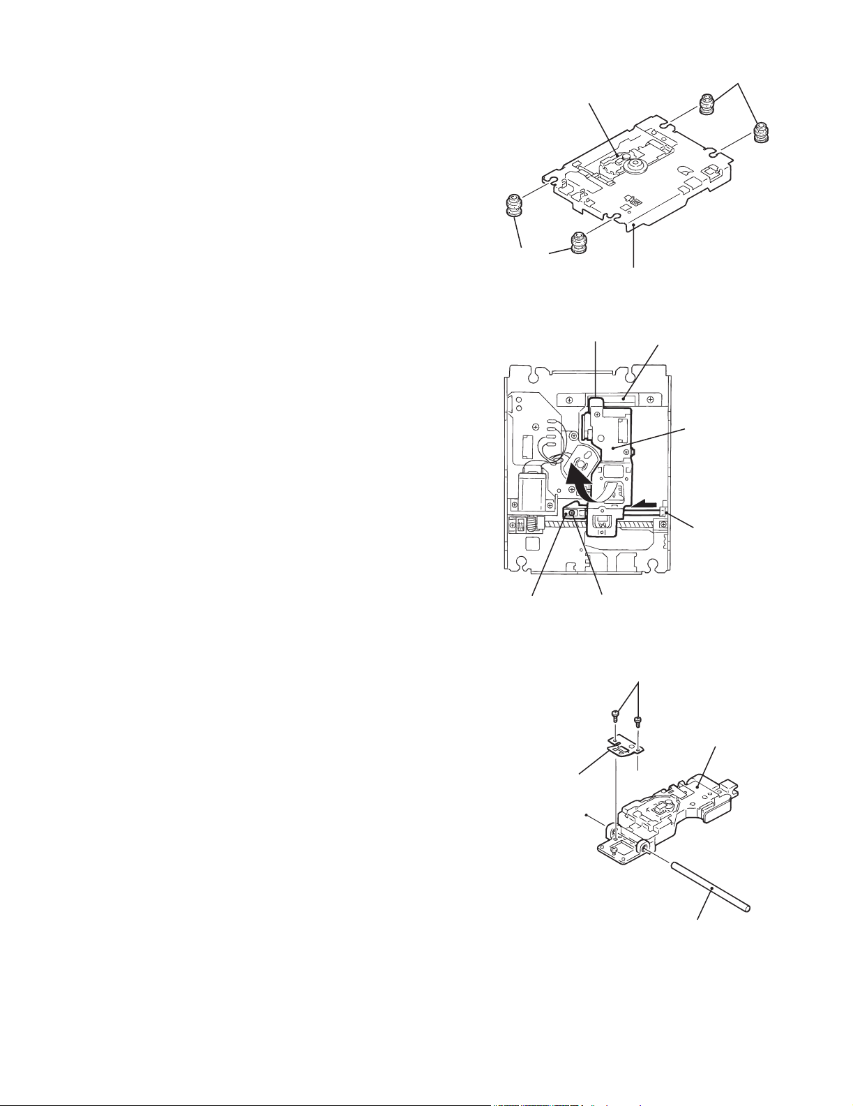
2.4.6.1 Removing the slide base (L) / (R)
(See Fig.10)
(1) Remove the two screws E on the upper side of the loading
assembly.
(2) Remove the slide base (L) outward. (Release it from the
joint bosses E.)
(3) Remove the slide base (R) outward.
2.4.6.2 Removing the loading mechanism assembly
(See Fig.11)
(1) Detach the loading mechanism assembly upward to re-
lease the four pins on both sides from the loading motor,
paying attention to the part e of the loading mechanism
base.
Slide base (R)
E'
E
Slide base (L
E
E'
Fig.10
Part e
2.4.7 Loading mechanism assembly
2.4.7.1 Removing the loading motor
(See Fig.12 and 13)
(1) Disconnect the harnesses from the wire holder and from
connector CN612 on the cam switch board.
(2) Remove the screw F attaching the loading motor and re-
lease the joint f.
(3) Remove the belt from the loading motor assembly.
(4) Remove the two screws G attaching the loading motor.
2.4.7.2 Removing the cam gear and the cam switch board
(See Fig.12)
(1) Remove the slit washer attaching the cam gear and pull out
the cam gear.
(2) Disconnect the harness from the wire holder and from con-
nector CN612 on the cam switch board.
(3) Remove the two screws H and the clamp. Remove the
cam switch board.
Loading mechanism
assembly
Loading motor assembly
Joint f CN612
F
Loading mechanism base
Fig.11
Wire holder
H
Cam switch board
Slit washer
H
Cam gear
Fig.12
Loading motor
G
Fig.13
Belt
(No.22042)1-27
Page 28
UX-Z7MDR
y
2.4.7.3 Removing the cartridge holder assembly
(See Fig.14 and 15)
(1) Remove the two screws I on the upper side of the loading assembly.
Slide bar
I
Cartridge holder assembly
I
Eject bar
2.4.7.4 Removing the slide bar and the eject bar
(See Fig.14 and 15)
• Prior to performing the following procedure, remove the car-
tridge holder assembly.
(1) Remove the slide bar upward.
(2) Move the eject bar outward until it stops as shown in
Fig.14. Push the convex part g on the bottom of the body
and remove the eject bar from the chassis.
Eject bar
Part g
Fig.14
I
Slide bar
k
Eject bar
1-28 (No.22042)
UD base
Cartridge holder assembl
Fig.15
Page 29
UX-Z7MDR
2.4.8 Traverse mechanism assembly
2.4.8.1 Removing the Insulators (See Fig.16)
(1) Disengage the four insulators from the notches of the
traverse mechanism chassis.
2.4.8.2 Removing the pickup unit (See Fig.17)
(1) Turn over the traverse mechanism assembly and remove
the screw J attaching the shaft holder (F).
(2) Move the shaft inward and remove it from the shaft holder
(R).
(3) Detach the shaft side of the pickup unit upward and release
the joint h with the pickup guide. Then remove the pickup
unit with the shaft.
Pickup unit
Insulators
Insulators
Traverse machanism chassis
Fig.16
Joint h
Pickup guide
Pickup unit
2.4.8.3 Removing the pickup (See Fig.18)
(1) Draw out the shaft from the pickup.
(2) Remove the two screws K attaching the rack spring.
Shaft holder (F)
Rack spring
Shaft holder (R)
J
Fig.17
K
Pickup
Shaft
Fig.18
(No.22042)1-29
Page 30
UX-Z7MDR
2.4.8.4 Removing the feed motor assembly
(See Fig.15, 20)
• It is not necessary to remove the pickup unit.
(1) For the white and black harnesses extending from the feed
motor assembly, unsolder the soldering i on the traverse
mechanism board.
(2) Remove the two screws L attaching the feed motor assem-
bly.
(3) Remove the two screws N attaching the feed motor brack-
et.
2.4.8.5 Removing the traverse mechanism board
(See Fig.19)
• Prior to performing procedure, remove the feed motor assem-
bly.
(1) For the red and black harnesses extending from the spin-
dle motor, unsolder the soldering j on the traverse mechanism board.
(2) Remove the screw M attaching the traverse mechanism
board.
Traberse mechanism board Soldering j
M
Soldering i
Feed motor assembly
L
Fig.19
Feed motor
Feed motor bracket
N
Fig.20
1-30 (No.22042)
Page 31

UX-Z7MDR
2.4.9 Reattaching the loading assembly
(1) Reattach the eject bar to the UD base. (Fig.15 and 21)
(2) Reattach the slide bar to the loading mechanism chassis while fitting the boss marked k to the eject bar slot. (Fig.21)
(3) Slide the slide bar and the eject bar in the direction of the arrow in Fig.20 and reattach the cartridge holder assembly using the
two screws I. (Fig.21 and 22)
ATTENTION:
Make sure the pin of the eject lever marked l is fitted to the slot of the eject bar marked m at the bottom of the loading mechanism chassis after moving the eject lever and the loading slider of the cartridge holder assembly in the direction of the arrow.
(Refer to Fig.22)
Slide bar
I
I
Eject bar
UD base (Bottom)
Cam switch board
H
Point marked
H
Cam switch boss
Ditch
UD base
Fig.21
Ditch m
Cartridge holder assembly
Loading slider
Eject lever
l
Fig.22
(No.22042)1-31
Page 32

UX-Z7MDR
(4) Reattach the wire holder to the UD base while engaging the UD base hook marked u to the wire holder slot marked t (At the
same time, the boss on the reverse side of the wire holder is fitted to the UD base round hole).
(5) Reattach the cam switch board using the two screws H. (Fig.23)
(6) Turn the cam switch to bring the boss to the point marked on the cam switch board. Reattach the cam gear using a slit washer
while fitting the cam gear slot to the cam switch boss. (Fig.23)
ATTENTION:
When reattaching the cam gear, the cam switch boss should be fitted to the cam gear slot, and the triangle mark of the cam
gear should be aligned to the hole of the eject bar as shown in Fig.23.
(7) Reattach the loading motor assembly, using the screw F. Connect the harness extending from the loading motor to connector
CN612 on the switch board and fix it with the wire holder. (Fig.23)
Loading motor assembly
F
Eject lever
Slide bar CN612
Fig.23
Cam gear
n
Point marked
Boss
Cam switch
Cam switch board
Cam gear
(Triangle mark)
Eject lever
1-32 (No.22042)
Page 33

UX-Z7MDR
(8) Reattach the UD base while engaging the four pins on both
sides of the UD base to the notches of the loading mechanism base and placing the edge (marked e’) of the cartridge holder assembly under the hook e of the loading
mechanism base. (Fig.24)
Pin
Hook e'
Pin
Hook e
Hook e'
Loading mechanism base
Fig.24
(9) Reattach the slide base (R) while fitting the two pins on an-
other side of the UD base to the slots of the slide base (R).
(Fig.25)
Slide base (R)
Part v
E
Slide base (R)
Cam gear
Part v
Fig.26
(10) Reattach the slide base (L) on the slide base (R) while fit-
ting the two pins on another side of the UD base to the slots
of the slide base (L) (Fig.26). Make sure the two slots of the
slide base (L) are fitted to the two bosses marked E’ and
tighten the two screws E. (Fig.27)
E'
Slide base (L)Slide base (R)
Part w
E
Pin
Slide base (L)
Pin
Part w
Fig.25
ATTENTION:
Fit the part v of the slide base (R) to the part w on the inward side of the cam gear rib. (Fig.26)
E'
Fig.27
Ref:
To expedite the work, bring up the UD base slightly when
fitting each pin to the appropriate notch.
(No.22042)1-33
Page 34

UX-Z7MDR
w
2.5 Cassette mechanism section
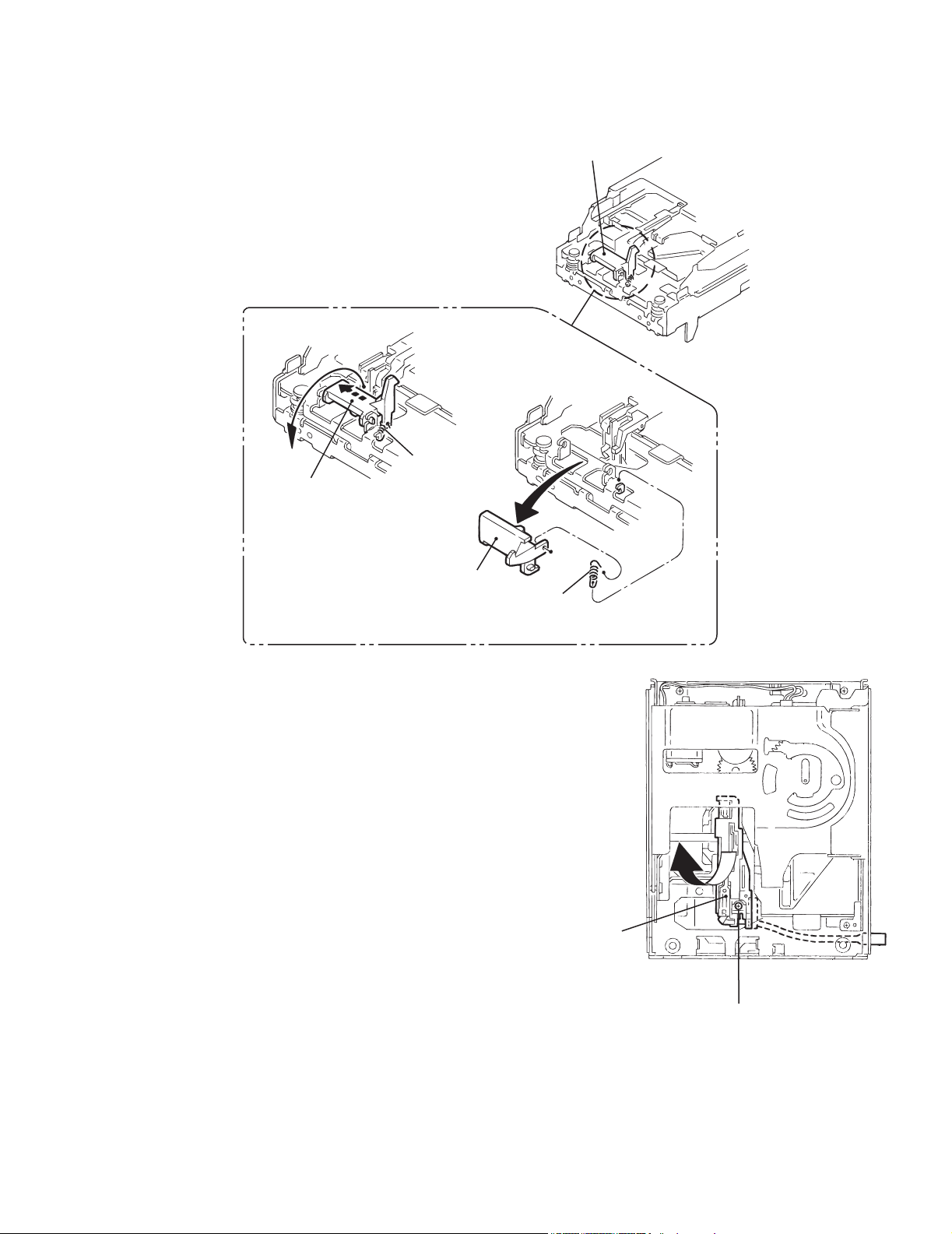
2.5.1 Removing the playback / recording & eraser head
(See Fig. 1 to 3)
(1) While shifting the trigger arms seen on the right side of the
head mount in the arrow direction, turn the flywheel R in
counterclockwise direction until the head mount has gone
out with a click (See Fig. 1).
(2) When the flywheel R is rotated in counterclockwise direc-
tion, the playback / recording & eraser head will be turned
in counterclockwise direction from the position in Fig. 2 to
that in Fig. 3.
(3) At this position, disconnect the flexible P.C. board (outgo-
ing from the playback / recording & eraser head) from the
connector CN31 on the head amplifier & mechanism con-
trol P.C. board.
(4) Remove the flexible P.C. board from the chassis base.
(5) Remove the spring 1 from behind the playback / recording
& eraser head.
(6) Loosen the reversing azimuth screw retaining the playback
/ recording & eraser head.
(7) Take out the playback / recording & eraser head from the
front of the head mount.
(8) The playback / recoring & eraser head should also be re-
moved similarly according to steps 1 to 7 above.
2.5.2 Reassembling the playback / recording & eraser head
(See Fig.3)
(1) Reassemble the playback head from the front of the head
mount to the position as shown in Fig. 3.
(2) Fix the reversing azimuth screw.
(3) Set the spring 1 from behind the playback / recording &
eraser head.Attach the flexible P.C. board to the chassis
base, as shown in Fig. 3.
(4) Attach the flexible P.C. board to the chassis base, as
shown in Fig. 3.
(5) The playback / recording & eraser head should also be re-
assembled similarly to step 1 to 4 above.
Cassette mechanism
Fig.1
Playback / Recording &
eraser head
Flexible
board
CN31
Head amplifier & mechanism
control P.C. board
Fig.2
Playback / Recording &
eraser head
Flywheel R
Trigger armHead mount
Spring 1
Trigger arm
Flywheel R
Reversing azimuth scre
Spring 1
Head mount
Flexible
board
Head amplifier & mechanism control
P.C. board
Fig.3
1-34 (No.22042)
Page 35

UX-Z7MDR
y
r
2.5.3 Removing the head amplifier & mechanism control
board
(See Fig. 4)
(1) Remove the cassette mechanism assembly.
(2) After turning over th cassette mechanism assembly, re-
move the three screws A retaining the head amplifier &
mechanism control board.
(3) Disconnect the connector CN32 on the board including the
connector CN 1 on the reel pulse P.C. board.
(4) When necessary, remove the 4 pin parallel wire soldered
to the main motor.
A
CN32
A
Belt
Main motor
assembly
B
CN31
Head amplifier &
mechanism control
board
A
4pin parallel wire
B
2.5.4 Removing the main motor assembly
(1) Remove the two screws B retaining the main motor assem-
bly (See Fig. 4 and 5).
(2) While raising the main motor, remove the capstan belt from
the motor pulley (See Fig. 5).
CAUTION:
Be sure to handle the capstan belt so carefully that this
belt will not be stained by grease and other foreign matter. Moreover, this belt should be hanged while referring
to the capstan belt hanging method in Fig. 5 and 6.
Main motor
assembly
Capstan belt
Motor
pulle
Fig.5
Flexible board
Fig.4
Mechanism moto
Main
motor
assembly
Capstan belt
Main motor
assembly
Flywheel
Fig.6
Fig.7
assembly
Motor
pulley
Motor pulleyCapstan belt
(No.22042)1-35
Page 36

UX-Z7MDR
2.5.5 Removing the flywheel
(See Fig. 8 and 9)
(1) Remove the head amplifier & mechanism control P.C.
board.
(2) Remove the main motor assembly.
(3) After turning over the cassette mechanism, remove the two
slit washers 1 and fixing the capstan shafts R and L, and
pull out the flywheel R and L respectively from behind the
cassette mechanism.
Flywheel R Flywheel L
Capstan
shaft R
Slit
washer 1
Fig.8
Slit
washer 1
Capstan
shaft L
Flywheel R Flywheel L
Fig.9
2.5.6 Removing the reel pulse P.C. board and solenoid
(See Fig. 10)
(1) Remove the five pawls a to e reattaining the reel pulse board.
(2) From the surface of the reel pulse board parts, remove the two pawls f and g retaining the solenoid.
Reel pulse board
a b c d e
g
f
Solenoid
Fig.10
1-36 (No.22042)
Page 37

3.1 MD adjustment(Auto adjust)
(1) Setting of MD adjustment (2) Initialize of EEPROM
UX-Z7MDR
SECTION 3
Adjustment method
Press MD REC button and
POWER button together,
then connect AC cord.
INDICATION
"TEST MODE1"
Power to ON by MD PLAY
button by main body,then MD
to stop by STOP button on
meinbody.
INDICATION
"TEST MODE1"
Complete setting
(3) Adjust the laser power
Set to MD
adjustment mode
set to MD
adjustment mode
INDICATION
"TEST MODE1"
Press PLAY MODE
button of remote controller
INDICATION
"TEST MODE1"
Comolete the Initialize
of EEPROM
Press 4 button of
remote controller
Insert the sensor of
laser power meter
Press 2 button of
remote controller
Setting the PLAYBACK
LASER POWER
Laser power to
up by F.SKIP button
of remote controller
Adjust to
morthsn 0.68mW or
same as 0.68mW
Press STOP button of
remote controller
Laser power to
down by B.SKIP button
of remote controller
Setting the RECORDING
LASER POWER
Laser power to up
by F.SKIP button of
remote controller
Adjust to
less than 6.23mW or
same as 6.23mW
Press STOP button of
remote controller
Eject the sensor to laser
power meter by EJECT
button of main body
Complete the RECORDING
LASER POWER adjustment
Laser power to down
by B.SKIP button of
remote controller
Complete the PLAYBACK
LASER POWER adjustment
(No.22042)1-37
Page 38

UX-Z7MDR
(4) Disc adjustment(Auto adjust)
Set to MD adjustment
mode
Insert Pre-Mastard disc
Press PLAY / button
of remote controller
INDICATION
"ON TUNING"
START the AUTO
ADJUSTMENT
Adjustment
OK?
Yes
INDICATION
"ON TUNING"
Press STOP button
of remote controller
Press EJECT button
of main body,then took
out Recordable disc
NO
INDICATION
"NG ERR;**
Adjustment
OK?
Yes
INDICATION
"ON TUNING"
Press STOP button
of remote controller
Press EJECT button
of main body,then took
out Pre-Masterd disc
Insert Recordable disc
Press MD PLAY /
button of remote controller
INDICATION
"ON TUNING"
Start the AUTO
ADJUSTMENT
NO
INDICATION
"NG ERR ; **
Complete the AUTO
ADJUSTMENT
Press STANDBY/ON button of
main body or remote controller
Release the TEST MODE
then power OFF
RESET by disconnect
the AC cord
CODE
00
01
02
03
04
05
06
07
08
09
0A
0B
0C
0D
0E
FF
Adjustment NG part
Not complete the AUTO ADJUSTMENT
Rest swith detection
Focus ON
Pit area EF barance,Tr offset adj
Pit area ABCD level adj
Pit area Focus servo AGC
Pit area Tracking servo AGC
Pit area Focus bias adj
GRV area EF baranee,TR offset adj
GRV area ABCD level adj
GRV area Focus servo AGC
GRV area Tracking servo AGC
GRV area Focus bias adj
Temp
EEPROM write
AUTO ADJUST complte
1-38 (No.22042)
Page 39

3.2 Cassette adjustment
3.2.1 Cassette mechanism section 3.2.2 Cassette mechanism section (Back side)
UX-Z7MDR
Head azimuth
adjusting screw
(Forward side)
3.2.3 Cassette AMP board
MOTOR SPEED
VR37
BIAS ADJ
VR31
Head azimuth
adjusting screw
(Reverse side)
VR37
C308
C310
R315
R314
L301
R327
B155
VR31
C221
Q302
C319
R313
C314
RECRAGRECL
C313
C317
C121
B112
SW8V
L303
C316
Head azimuth
adjusting screw
(Forward side)
Head azimuth
adjusting screw
(Reverse side)
Playback/Recording &
eraser head
B102
B152
C302
R103
1
C301
C111
B164
C306
R304
C109
B158
8
B106
C101
6
B166
R116
R212
R211
C211
R216
9
9
IC32
B101
C201
B109B108
C209
MB
PBRAGPBL
MS
MG
1
CN34
Q305
R310
R335
C106
Q103
R305
B198
R353
C307
R303
R122
Q101
C103
B163
Q321
R221
10
B156
C303
R115
R101
B157
R108
C113
R110
R109
R102
C110
C104
R301
R121
1
C108
C107
9
B151
R112
R111
C102
R107
CN33
R342
C213
R210
R209
C207
B159
16
R341
C208
R207
B200
1
B110
CN31
1
R205
R208
B160
R340
R105
C105
R343
C206
R345
NC
C305
R201
1IC31
TAP
C304
B113
C202
C210
Q331
RRE
C375
C205
B161
R215
R339
C203
C334
R106
R206
5VMGSOL
R203
R204
C204
B168
PHO
B153
R104
R222
R202
C333
C332
R375
Q201
PLA
C331
Q372
Q203
R331
FRE
B167
16
1
10
70u
CN32
B162
R372
R373
C371
Q375
R371
R376
C374
R338
C376
B
E
D375
Q376
B
Q371
E
R337
R336
9
IC33
8
(No.22042)1-39
Page 40

UX-Z7MDR
3.2.4 Tape Recorder Section
Items
Confirmation of
head angle
Confirmation of
tape speed
3.2.5 Reference Values for Confirmation Items
Items
Difference
between the
forward and
reverse speed
Wow & flutter Test tape
Measurement
conditions
Test tape
: VT703L (8kHz)
Measurement output
terminal
: Speaker terminal
Speaker R
(Load resistance: 4 ohm)
: Headphone terminal
Test tape
: VT712 (3kHz)
Measurement output terminal
: Headphone terminal
Measurement
conditions
Test tape
: VT712 (3kHz)
Measurement output terminal
: Speaker terminal Speak-
er R
(Load resistance: 4 ohm)
Measurement output terminal
: Headphone
: VT712 (3kHz)
Measurement output terminal
: Headphone terminal
Measurement method Standard Values Adjusting positions
1 Playback the test tape VT703L (8kHz)
2 With the recording & playback mechanism,
adjust the head azimuth screw so that the forward and reverse output levels become maximum. After adjustment lock the head
azimuth at least by half turn.
3 In either case this adjustment should be per-
formed in both the forward and reverse directions with the head azimuth screw.
Adjust VR37 so that the frequency counter
reading becomes 2,940~3,090Hz when playing back the test tape VT712 (3kHz) with playback and recording mechanism after ending
forward winding of the tape.
Measurement method Standard Values Adjusting positions
When the test tape VT712 (3kHz) has been
played back with the recording and playback
mechanism at the beginning of forward winding, the frequency counter reading of the difference between both of the mechanism should
be 6.0Hz or less.
When the test tape VT712 (3kHz) has been
played back with the recording and playback
mechanism at the beginning of forward winding, the frequency counter reading of wow &
flutter should be 0.25% or less (WRMS).
Maximum output Adjust the head
azimuth screw only
when the head has
been changed.
Tape speed
of deck
: 2,940 ~ 3,090Hz
6.0Hz or less Head azimuth screw
0.25% or less
(WRMS)
VR37
1-40 (No.22042)
Page 41

3.2.6 Electrical Performance
Items
Adjustment of
recording bias
current
(Reference
Value)
Adjustment of
recording and
playback
frequency
characteristics
Measurement
conditions
Mode
: Forward or reverse mode
• Recording mode
• Test tape
: AC-514 to TYPE ll and
AC-225 to TYPE l
Measurement output terminal
: Both recording and
headphone terminals
Reference frequency
: 1kHz and 10kHz
(REF.: -20dB)
Test tape
: AC-514 to TYPE ll
Measurement input
terminal
: OSC IN
Measurement method Standard Values Adjusting positions
1 With the recording and playback mechanism
load the test tapes(AC-514 to TYPE ll and
AC-225 to TYPE l ), and set the mechanism
to the recording and pausing condition in advance.
2 After connecting 100 ohm in series to the re-
corder head measure the bias current with a
valve voltmeter at both of the terminals.
3 After resetting the [PAUSE] mode start re-
cording. At this time adjust VR31 for Lch and
VR32 for Rch so that the recording bias current values become 4.0µA (TYPE l ) and
4.20µA (TYPE ll ).
1 With the recording and playback mechanism
load the test tapes (AC-514 to TYPE ll ), and
set the mechanism to the recording and
pausing condition in advance.
2 While repetitively inputting the reference fre-
quency signal of 1kHz and 10kHz from OSC
IN record and playback the rape.
3 While recording and playback the test tape in
TYPE ll ,adjust VR31 for Lch and VR32 for
Rch so that the output deviation between
1kHz and 10kHz becomes -1dB 2dB.
AC-225
: 4.20µA
AC-514
: 4.0µA
Output deviation
between
1kHz and 10kHz
: -1dB 2dB
UX-Z7MDR
VR31
VR31
3.2.7 Reference Values for Electrical Function Confirmation Items
Items
Recording
bias frequency
Eraser current
(Reference
value)
Measurement
conditions
Forward or reverse
• Test tape
: TYPE ll (AC-514)
Measurement terminal
: BIAS TP on P.C. board
Forward or reverse
• Recording mode
• Test tape
: AC-514 to TYPE ll and
AC-225 to TYPE l
Measurement terminal
: Both of the eraser head
terminals
Measurement method Standard Values Adjusting positions
1 While changing over to and from BIAS 1 and
2, confirm that the frequency is changed.
2 With the recording and playback mechanism
load the test tape.
(AC-514 to TYPE ll ), and set the mechanism
to the recording and pausing condition in advance.
3 Confirm that the BIAS TP frequency on the
P.C. board is 100kHz 6kHz.
1 While recording and playback mechanism,
load the test tapes (AC-514 to TYPE ll and
AC-225 to TYPE l), and set the mechanism to
the recording and pausing conditions in advance.
2 After setting to the recording conditions, con-
nect 1W in series to the eraser head on connect 1W in series to the eraser head on the
recording and playback mechanism side and
measure the eraser current from both of the
eraser terminals.
100 kHz
6 kHz
TYPE ll
: 120 mA
TYPE l
: 75 mA
(No.22042)1-41
Page 42

UX-Z7MDR
3.3 Flow of functional operation until TOC read
Power ON
Play Key
Slider turns REST
SW ON.
Automatic tuning
of TE offset
Check Point
Confirm that the voltage at the pin5
of CN801 is "H"\"L"\"H".
Tracking error waveform at TOC reading
Approx.3sec
Tracking
servo
off states
Automatic measurement
of TE amplitude and
automatic tuning of
TE balance
VREF
pin 25 of
IC601(TE)
Approx
1.8V
Disc states
to rotate
Tracking
servo
on states
Disc to be
braked to stop
TOC reading
finishes
500mv/div
2ms/div
Fig.1
Laser ON
Detection of disc
Automatic tuning of
Focus offset
Automatic measurement of
Focus S-curve amplitude
Disc is rotated
Focus servo ON
(Tracking servo ON)
Automatic measurement of
Tracking error amplitude
Automatic tuning of
Tracking error balance
Check that the voltage at the
pin40 of IC651 is + 5V?
Confirm that the Focus error
S-cuve signal at the pin28 of
IC651 is approx.2Vp-p
Confirm that the signal from
pin24 IC651 is 0V as a
accelerated pulse during
approx.400ms.
Confirm the waveform of
the Tracking error signal.
at the pin 25 of IC601 (R604)
(See fig-1)
1-42 (No.22042)
Automatic tuning of
Focus error balance
Automatic tuning of
Focus error gain
Automatic tuning of
Tracking error gain
TOC reading
Play a disc
Confirm the eys-pattern
at the lead of TP1
Page 43

UX-Z7MDR
3.4 Maintenance of laser pickup
(1) Cleaning the pick up lens
Before you replace the pick up, please try to clean the lens
with a alcohol soaked cotton swab.
(2) Life of the laser diode
When the life of the laser diode has expired, the following
symptoms will appear.
1.The level of RF output (EFM output : ampli tude of eye
pattern) will below.
Is the level of
RFOUT under
1.25V 0.22Vp-p?
NO
Replace it.
YES
O.K
(3) Semi-fixed resistor on the APC PC board
The semi-fixed resistor on the APC printed circuit board
which is attached to the pickup is used to adjust the laser
power. Since this adjustment should be performed to
match the characteristics of the whole optical block, do not
touch the semi-fixed resistor.
If the laser power is lower than the specified value, the laser diode is almost worn out, and the laser pickup should
be replaced.
If the semi-fixed resistor is adjusted while the pickup is
functioning normally, the laser pickup may be damaged
due to excessive current.
3.5 Replacement of laser pickup
Turn off the power switch and, disconnect the
power cord from the ac outlet.
Replace the pickup with a normal one.(Refer
to "Pickup Removal" on the previous page)
Plug the power cord in, and turn the power on.
At this time, check that the laser emits for
about 3seconds and the objective lens moves
up and down.
Note: Do not observe the laser beam directly.
Play a disc.
Check the eye-pattern at TP1.
Finish.
(No.22042)1-43
Page 44

UX-Z7MDR
A
4.1 AK4519VF-X (IC480) : A/D D/A converter
• Pin layout
SECTION 4
Description of major ICs
• Block diagram
1
2
3
4
5
6
7
8
9
10
11
12
AINL
VCML
AINR
VCMR
VRAD
ARDV
VCOM
AOUTL
24
23
22
21
20
19
18
17
16
15
14
13
VA AGND VB VD DGND
Modulator
Modulator
Common Voltage
LPF
Modulator
Decimation
Filter
Decimation
Filter
8x
Interpolator
Clock
Divider
Serial I/O
Interface
MCLK
CMODE
LRCK
SCLK
SDTO
SDTI
OUTR
LPF
Modulator
PWAD PWDA
• Pin Function
Pin
Symbol I/O Function
No.
1 VRDA I Voltage Reference Input Pin for DAC, VA
2 VRAD I Voltage Reference Input Pin for ADC, VA
3 AINR I RCH Analog Input Pin
4 VCMR O Rch Common Voltage Output Pin, 0.45xVA
5 VCML O Lch Common Voltage Output Pin, 0.45xVA
6 AINL I Lch Analog Input Pin
7 PWAD I ADC Power-Down Mode Pin "L":Power
Down
8 PWDA I DAC Power-Down Mode Pin "L":Power
Down
9 MCLK I Master Clock Input Pin
10 LRCK I Input/Output Channel Clock Pin
11 SCLK I Audio Serial Data Clock Pin
8x
Interpolator
Pin
Symbol I/O Function
No.
12 SDTO O Audio Serial Data Output Pin
13 DGND - Digital Ground Pin
14 VD - Digital Power Supply Pin
15 SDTI I Audio Serial Data Input Pin
16 CMODE I Master Clock Select Pin
17 DEM1 I De-emphasis Frequency Select Pin
18 DEM0 I De-emphasis Frequency Select Pin
19 AOUTL O Lch Analog Output Pin
20 AOUTR O Rch Analog Output Pin
21 VCOM O Common Voltage Output Pin, 0.45xVA
22 AGND - Analog Ground Pin
23 VB - Substrate Pin
24 VA - Analog Power Supply Pin
1-44 (No.22042)
Page 45

4.2 AN22000A-W (IC601) : RF & SERVO AMP
• Terminal layout
ACBDPDF
323130292827262524232221201918
123456789
LD
PD
VCC
RFN
PDE
RFIN
RFOUT
TBAL
FBAL
ARF
CAGC
GCTRL
CEA
FEOUT
FEN
TEN
TEOUT
TEBPF
10111213141516
BDO
OFTR
CBDO
3TOUT
COFTR
• Block diagram
32
31
30
29
27
28
RFOUT
RF_EQ
AMP
AMP
AMP
AMP17GCA BCA
+
-
624754 8
RFIN
AGC
NRFDET
GCA BCA
GCA BCA
GCA BCA
GCTL26TBAL
11 12
BDO
SUBT
SUBT
FBAL
25 16 3
VDET
VREF
17
GND
RFDET
13 14
OFTR
3TENV
VDET
UX-Z7MDR
• Pin function
Pin
Symbol I/O Function
No.
1 PD I APC Amp. input terminal
2 LD O APC Amp. output terminal
3 VCC - Power supply terminal
4 RFN I RF adder Amp. inverting input terminal
5 RFOUT O RF adder Amp. output terminal
6 RFIN I AGC input terminal
7 CAGC I Input terminal for AGC loop filter capacitor
8 ARF O AGC output terminal
9 CEA I Capacitor connecting terminal
for HPF-Amp.
9
10
10 3TOUT O 3 TENV output terminal
11 CBDO I Capacitor connecting terminal for envelope
detection on the darkness side
12 BDO O BDO output terminal
15
22
13 COFTR I Capacitor connecting terminal for envelope
detection on the light side
14 OFTR O OFTR output terminal
-
+
23
15 NRFDET O NRFDET output terminal
16 GND - Ground
21
-
+
20
17 VREF O VREF output terminal
18 VDET O VDET output terminal
19 TEBPF I VDET output terminal
20 TEOUT O TE Amp. output terminal
21 TEN I TE Amp. inverting input terminal
19
22 FEN I FE Amp. inverting input terminal
23 FEOUT O FE Amp. output terminal
18
24 GCTL O GCTL & APC terminal
25 FBAL O FBAL control terminal
26 TBAL O TBAL control terminal
-
+
2
LD
27 E I Tracking signal input terminal 1
28 F I Tracking signal input terminal 2
29 D I Focus signal input terminal 4
PD
1
30 B I Focus signal input terminal 3
31 C I Focus signal input terminal 2
32 A I Focus signal input terminal 1
(No.22042)1-45
Page 46

UX-Z7MDR
2
10
T
O
4.3 AN7317 (IC32) : R / P amp.
• Pin layout & block diagram
16
1
60k
60k
15
112k
Pre
Pre
112k
2
• Pin functions
Pin No. Function
1 Channel 1 playback amplifier input
2 Channel 1 playback amplifier negative feedback
3 Channel 1 playback amplifier output
4 Channel 1 record amplifier input
5 Channel 1 record amplifier output
6 ALC low-cut
7ALC time
8 Ground
9Vcc
10 Ripple filter
11 Record-Amplifier mute
12 Channel 2 record amplifier output
13 Channel 2 record amplifier input
14 Channel 2 playback amplifier output
15 Channel 2 playback amplifier negative feedback
16 Channel 2 playback amplifier input
14
13 12 11 10 9
30k
30k
3
Pre
Pre
45678
Mute R.R
ALC
4.4 BU4094BCF-X (IC33) : Shift / store registor
• Pin layout • Block diagram
16 15 14 13 12 11 10 9
VDD
ENABLE
STROVE DATA CLOCK Q1 Q2 Q3 Q4 Vss
Q5 Q6 Q7 Q8 Q'S Q'SOUTPUT
1 2 3 4 5 6 7 8
1-46 (No.22042)
DATA
CLOCK
STROBE
UTPUT
ENABLE
3
1
8-STAGE
SHIFT REGISTER
8-BIT
LATCHES
15
3-STATE
OUTPUTS
Q1
PARALLEL OUTPUT
Q8
Q'S
QS
SERIAL
OUTPU
9
Page 47

4.5 XC62HR3502P-X (IC291) : Regulator
S
• Pin layout • Block diagram
54
VIN
UX-Z7MDR
VOUT
Current
Limit
123
CE
• Pin function
Pin No. Symbol Function
1 VSS Ground
2 VIN Supply voltage input
3 CE Chip enable
4 NC Non connect
5 VOUT Regulated output voltage
4.6 GM71VS17400CLT5 (IC390,IC790) : DRAM
•Pin layout •Pin function
Vcc 1
I/O1 2
I/O2 3
WE 4
RAS 5
A11 6
A10 8
A0 9
A1 10
A2 11
A3 12
Vcc 13
26 Vss
25 I/O4
24 I/O3
23 CA
22 OE
21 A9
19 A8
18 A7
17 A6
16 A5
15 A4
14 Vss
Pin No. Symbol Function
1 Vcc Power supply (+3.3V)
2 I/O1 Date input/output
3 I/O2 Date input/output
4 WE Read/write enable
5 RAS Addres stroke
6 A11 Addres input
7-Not use
8 A10 Address input
9~12 A0~A3 Address input
13 Vcc Power supply (+3.3V)
14 Vss GND
15~19 A4~A8 Addres input
20 - Not use
21 A9 Address input
22 OE Output enable
23 CAS Calum address stroke
24 I/O3 Date input/output
25 I/O4 Date input/output
26 Vss GND
Output
Control
Voltage
Reference
VSS
(No.22042)1-47
Page 48

UX-Z7MDR
4.7 MN662790RSC(IC651):Digital servo & processor
• Pin layout
60 41
61
40
80
21
1 20
• Pin function
Pin No. Symbol I/O Description
1 BCLK O Bit clock output for SRDATA
2 LRCK O Identifying signal output of L,R
3 SRDATA O Serial data output
4 DVDD1 - Power supply for digital circuit
5 DVSS1 - Connect to ground for digital circuit
6 TX O Digital audio interface output signal
7 MCLK I Micom command clock signal input
8 MDATA I Micom command data signal input
9 MLD I Micom command load signal input L:load
10 SENSE - Non connect
11 FLOCK - Non connect
12 TLOCK - Non connect
13 BLKCK O Sub code block clock signal (Command execution : CD-TEXT data readout enabling signal (DQSY) out-
put)
14 SQCK I Export clock signal input for sub code Q resister
15 SUBQ O Sub code Q data output
16 DMUTE I Muting input H:muting
17 STAT O Status signal output
18 LSI_RST I Reset signal input L:reset
19 SMCK O Clock signal output MSEL is H : 8.4672 MHz MSEL is L : 4.2336 MHz
20 CSEL I Oscillation frequency specification terminal H:33.8688 MHz L:16.9344 MHz
21 TEST2 - TEST2 terminal usually : open
22 TVD O Traverse drive output
23 PC - Non connect
24 ECM O Spindle motor drive signal output (Compulsion mode output)
25 ECS O Spindle motor drive signal output (Servo error signal output)
26 VDETMON - Non connect
27 TRD O Tracking drive signal output
28 FOD O Focus drive signal output
29 VREF - Reference voltage for DA output section
30 FBAL O Focus balance adjust signal output
31 TBAL O Tracking balance adjust signal output
32 FE I Focus error signal input (analog input)
33 TE I Tracking error signal input (analog input)
34 RFENV I RF Envelope signal input (analog input)
35 TEST3 I TEST3 Terminal usually : Fixation L
36 OFT I Off track signal input H : off track
37 TRCRS I Track cross signal input (analog input)
1-48 (No.22042)
Page 49

Pin No. Symbol I/O Description
38 RFDET I RF detection signal input L : detection
39 BDO I Dropout signal input H : dropout
40 LDON I Non connect
41 PLLF2 I/O Terminal for loop filter characteristic switch for PLL
42 DSLBDA - Non connect
43 WVEL - Non connect
44 ARF I RF Signal output
45 IREF I Standard electric current input terminal
46 DRF I Bias terminal for DSL
47 DSLF I/O Loop filter terminal for DSL
48 PLLF I/O Loop filter terminal for PLL
49 VCOF I/O Loop filter terminal for VCO
50 AVDD2 - Power supply terminal for analog circuit
51 AVSS2 - Connect to ground terminal for analog circuit
52 EFM - Non connect
53 DSLB O PLL extraction clock output
54 VCOF2 I/O Loop filter terminal for VCO
55 SUBC O Sub code serial output
56 SBCK I Clock signal input for sub code serial output
57 VSS - Connect to ground terminal for oscillation circuit
58 X1 I Oscillation circuit input terminal f=16.9344 MHz,33.8688 MHz
59 X2 O Oscillation circuit output terminal f=16.9344 MHz,33.8688 MHz
60 VDD - Power supply terminal for oscillation circuit
61 BYTCK - Non connect
62 LDON O Laser ON signal output H : ON
63 GCTRL O General I/O port
64 IPFLA - Non connect
65 FLAG O Flag signal output
66 CLVS - Non connect
67 CRC - Non connect
68 DEMPH O De-emphasis detection signal output
69 RESY - Non connect
70 IOSEL I Mode switch terminal
71 TEST I TEST terminal usually : H
72 AVDD1 - Power supply terminal for analog circuit (for audio output section)
73 OUTL O Lch audio output
74 AVSS1 - Connect to ground terminal for analog circuit (for audio output section)
75 OUTR O Rch audio output
76 DQSY I RF signal polarity specification terminal
77 VCC5V - Power supply terminal (5V)
78 PSEL O IOSEL=H TEST terminal IOSEL=L SRDATA input
79 MSEL O IOSEL=H SMCK terminal output (frequency switch terminal) IOSEL=L LRCK input
80 SSEL O IOSEL=H SUBQ terminal output mode switch terminal IOSEL=L BCLK input
UX-Z7MDR
(No.22042)1-49
Page 50

UX-Z7MDR
4.8 GP1UM261XK (IC602) : Receiver
• Pin layout
Vout
• Block diagram
GND
Vcc
4.9 M63008FP-X (IC604) : 5ch Actuator driver
• Pin layout
CH3IN
OUT3
REG+
REGB
• Block diagram
Vm1
5
VBS2
CH1
CH2
VBS1
VREF
X5
X5
E2
E1
VBS1
VBS1
VBS1
VBS1
IN1+
IN1-
OUT1
VM1(+)
VM1(-)
VM2(+)
VM2(-)
OUT2
IN2-I
IN2+
VREFO
VREF
REGB
REG+
3
6
7
9
8
12
13
14
15
16
21
20
2
VREG
1
IN3-
VBS2
IN1+
VBS1
SS,GND
Vm2
IN3+
N.C
IN1-
Vm1
OUT1
R
R
Vrefm1
1.25V
19 17
MUTE1 MUTE2
BIAS
VM3-
VM1-
VBS1
Low,Open
MUTE ON
VM3+
VM1+
4
1~4
CH
GND
GND
Vm1
VBS1
B.P.F.LimiterAmp
VM4+
VM2+
VBS2
18
Demodulator
VM4-
VM5+
VM5-
IN2-
VM2-
OUT2
39
Vm2
VREFO
HI :Sleep
SLEEP
5CH
TSD
10 113233
GND (4PIN)
OUT5
IN5-
IN2+
MUTE1
Vrefm2
R
R
IN5+
IN4+
MUTE2
SS,GND
Integrator
Comparator
GND Vdd Vout
IN4-
OUT4
VREF
VREFO
VBS2
E3
VBS2
CH3
X8
VBS2
CH4
X8
E4
VBS2
CH5
X8
VBS2
E5
Vm2
38
40
37
41
42
34
35
31
30
23
24
22
29
28
26
25
27
IN3IN3+
OUT3
CH3 IN
VM3(+)
VM3(-)
VM4(+)
VM4(-)
IN4IN4+
OUT4
VM5(+)
vm5(-)
IN5IN5+
OUT5
1-50 (No.22042)
Page 51

4.10 LB1641 (IC402) : DC Motor driver
•Pin layout
1
GND
2
OUT1
3
P1
4
VZ
5
IN1
6
IN2
7
VCC1
8
VCC2
9
P2
10
OUT2
4.11 BD7910FV-X (IC450) : Pre driver
• Block diagram
20 19 18 17 16 15 14 13 12 11
UX-Z7MDR
• Truth table
Input Output Mode
IN1 IN2 OUT1 OUT2
0000 Brake
1 0 1 0 CLOCKWISE
0 1 0 1 COUNTER-CLOCKWISE
1100 Brake
- +
Vregin
1 2 3 4 5 6 7 8 9 10
- +
VG
SVcc
Pre driver
Mute
EFM
• Pin function
Pin No. Symbol I/O Function
1 Vreg IN I Regulator input and regulator power supply
2 Reg GN - Regulator GND
3 NC - Non connect
4 VG I Voltage input for power MOS drive
5 SVCC O EFM high level output voltage
6 PDGND - Pre-driver GND
7 EFM I EFM signal input
8 MUTE I Mute control (Low active)
9 NC O Non conncet
10 NC O Non connect
11 NC - Non connect
12 VOD2 O Sync.output (Lower power MOS,drain)
13 VSS - Hbridge GND (Lower power MOS,source)
14 VOD1 O Sync.output (Lower power MOS,drain)
15 VOS1 O Source output (Upper power MOS,source)
16 VDD - H bridge power supply terminal(Upper power MOSsource)
17 VOS2 O Source output (Upper power MOSsource)
18 Reg DRV O External PNP drive output for regulator
19 Reg OUT O Reglator output (Emitter follower output)
20 Reg NF - Regulator feedbaack terminal
(No.22042)1-51
Page 52

UX-Z7MDR
4.12 BA3126N(IC31) : R/P Switch
S W
R E C
G
P / B
S W
C O N T .
G N D
V c c
123456789
4.13 BR93LC66F-X (IC403):EEPROM
• Terminal layout • Pin Functions
Symbol I/O Function
NC
VCC
CS
SK
1
2
3
4
8
NC
7
GND
6
DO
5
DI
VCC - Power supply
GND - Connect to GND
CS I Chip select input
SK I Serial clock input
DI I Start bit, OP-code,address, serial data input
DO O
4.14 CXA2523AR (IC300) : MD servo
• Block diagram
BOTM
ABCD34FE33AUX32ADFG31ADAGC30ADIN29ADFM28SE27CSLED26TE25WBLADJ
36 35
P / B
S W
G
S W
R E C
Serial data output
Internal state display output of READY/BUSY
PEAK
RF
MORFO
37
38
39RFAGC
40AGCI
41COMPO
42COMPP
43ADDC
44OPO
45OPN
46RFO
47MORFI
48
AGC, EQ
Peak, Bottom Detector
Comp
USER
USER
OP Amp
RF Amp
1 2
I
J
3VC4A5B6C7D8E9F10PD11
ADIP Amp TE/SE Amp
MUX FE Amp
ABCD Amp
3T Detector
I-V Amp APC
CPU
Command I/F
TEMP Amp
12
APC
PCREF
24
Vcc
23
3TADJ
22 EQADJ
21 VREF
20 F0CNT
19 XSTBY
18 XLAT
17 SCLK
16 SWDT
15 TEMP R
14 TEMP I
13 GND
1-52 (No.22042)
Page 53

• Pin function
Pin No. Symbol I/O Function
1 I I I-V converted RF signal I input.
2 J I I-V converted RF signal J input.
3 VC O Vcc/2 voltage output.
4 A I A current input for main beam servo signal.
5 B I B current input for main beam servo signal.
6 C I C current input for main beam servo signal.
7 D I D current input for main beam servo signal.
8 E I E current input for side beam servo signal.
9 F I F current input for side beam servo signal.
10 PD I Reflection light quantity monitor signal input.
11 APC O Laser APC output.
12 APCREF I Reference voltage input for the laser power intensity setting.
13 GND - Connect to GND.
14 TEMPI I Connects the temperature sensor.
15 TEMP R I Connects the temperature sensor. outputs the reference voltage.
16 SWDT I Data input for microcomputer serial interface.
17 SCLK I Shift clock input for microcomputer serial interface.
18 XLAT I Latch signal input for microcomputer serial interface.Latched when low.
19 XSTBY I Standby setting pin. Normal operation when high Standby when low.
20 F0CNT I Internal current source setting pin.
21 VREF O Reference voltage output.
22 EQADJ I/O Equalizer center frequency setting pin.
23 3TADJ I/O BPF3T center frequency setting pin.
24 Vcc - Power supply.
25 WBLADJ I/O BPF22 center frequency setting pin.
26 TE O Tracking error signal output.
27 CSLED - Connects the sled error signal LPF capacitor.
28 SE O Sled error signal output.
29 ADFM O ADIP FM signal output.
30 ADIN I ADIP signal comparator input.
31 ADAGC - Connects the ADIPAGC capacitor.
32 ADFG O ADIP2 binary value signal output.
33 AUX O 13 output / temperature signal output. Switched with serial commands.
34 FE O Focus error signal output.
35 ABCD O Reflection light quantity signal output for the main beam servo detector.
36 BOTM O RF/ABCD bottom hold signal output.
37 PEAK O Peak hold signal output for the RF/ABCD signals.
38 RF O RF equalizer output.
39 RFAGC - Connects the RFAGC capacitor.
40 AGCI I RFAGC input.
41 COMPO O User comparator output.
42 COMPP I User comparator non-inverted input.
43 ADDC I/O Connects the capacitor for ADIP amplifier feedback circuit.
44 OPO O User operational amplifier output.
45 OPN I User operational amplifier inverted input.
46 RFO O RF amplifier output. Eye pattern checkpoint.
47 MORFI I Input of the groove RF signal with AC coupling.
48 MORFO O Groove RF signal output.
UX-Z7MDR
(No.22042)1-53
Page 54

UX-Z7MDR
4.15 CXD2662R (IC350) : DSP
• Pin layout
• Block diagram
59
PCO
60
FILI
61
FILO
62
CLTV
100
EFM
57
RFI
54
ASYI
56
BIAS
ASYO
53
78
ADFG
95
FGIN
94
SPFD
93
SPRD
79
F0CNT
75 ~ 51
76
50
~~
100
26
1 ~ 25
PLL
EFM / ACIRC
ENCODER / DECODER
COMP
ADIP DECODER
SPINDLE
SERVO
OSCI
OSCO
XTSL
16 17 18 29
CLOCK
GENERATOR
each block
SAMPLING
RATE
CONVERTER
FS256
LRCK
XBCK
FS4
MDDT1
90 52
27 28
SHOCK RESISTANT
MEMORY CONTROLLER
ATRAC/ATRAC3
ENCODER/DECODER
DIGITAL
AUDIO
I/F
XRAS
46
XCAS
44
XWE
4
12
4
47
XOE
43
A00~A11
D0~D3
14
XINT
15
TX
DADT
26
ADDT
25
XBCKI
24
4
LRCKI
23
DATA I
22
2
DIN~DIN1
DOUT
21
APC
FE
TE
SE
PEAK
BOTM
ABCD
AUX1
DCHG
VC
ADIO
ADRT
ADRB
DTRF
CKRF
XLRF
12
11
84
88
89
86
85
92
91
83
DQSY
SQSY
LDDR
FFDR
FRDR
TFDR
TRDR
SFDR
SRDR
APCREF
77
66
75
74
63
64
65
67
76
68
69
71
72
82
81
80
ANALOG MUX
AUTO
SEQUENCER
A/D
CONVERTER
SERVO
DSP
each block each block
SENS
MONITOR
CONTROL
MNT0
MNT1
MNT2
CPU I/F
5689 12 34 13
10 7
WDT
XLAT
XRST
SCLK
SRDT
MNT3
SUBCODE
PROCESSOR
PWM
GENERATOR
RECP
1-54 (No.22042)
Page 55

• Pin function (CXD2662R)
Pin No. Symbol I/O Function
1 MNT0 I/O Monitor output.
2 MNT1 O Monitor output.
3 MNT2 O Monitor output.
4 MNT3 O Monitor output.
5 SWDT I Data input for microcomputer serial interface.
6 SCLK I Shift clook input for microcomputer serial interface.
7 XLAT I Latch input for microcomputer serial interface.Latched at the falling edge.
8 SRDT O Data output for microcomputer serial interface.
9 SENS O Outputs the internal status corresponding to the microcomputer serial interface address.
10 XRST I Reset input. Low : reset
11 SQSY O Disc subcode Q sync / ADIP sync output.
12 DQSY O Subcode Q sync output in U-bit CD or MD format when the Digital In source is CD or MD.
13 RECP I Laser power switching input.
High : recording power ; low ; playback power
14 XINT O Interruption request output. Low when the interruption status occurs.
15 TX I Enable signal input for recoding data output. High : enabled
16 OSCI I Crystal oscillation circuit input.
17 OSCO O Crystal oscillation circuit output. (inverted output of the OSCI pin)
18 OSCO I OSCI input frequency switching.
XTSL1(command) = low and XTSL = high : 512Fs (22.5792MHz)
XTSL1(command) = low and XTSL = low : 1024Fs (45.1584MHz)
XTSL1(command) = high : 2048Fs (90.3168MHz)
19 DIN0 I Digital audio interface signal input 1.
20 DIN1 I Digital audio interface signal input 2.
21 DOUT O Digital audio interface signal output.
22 DATAI I Test pin. Connect to GND.
23 LRCKI I Test pin. Connect to GND.
24 XBCKI I Test pin. Connect to GND.
25 ADDT I Data input from A / D converter.
26 DADT O REC monitor output / decoded audio data output.
27 LRCK O LA clock (44.1kHz) output to the external audio block.
28 XBCK O Bit clock (2.8224kHz) output to the external audio block.
29 FS256 O 256Fs output.
30 DVDD - Digital power supply.
31 A03 O External DRAM address output.
32 A02 O External DRAM address output.
33 A01 O External DRAM address output.
34 A00 O External DRAM address output.
35 A10 O External DRAM address output.
36 A04 O External DRAM address output.
37 A05 O External DRAM address output.
38 A06 O External DRAM address output.
39 A07 O External DRAM address output.
40 A08 O External DRAM address output.
41 A11 O External DRAM address output.
42 DVSS - Digital ground.
43 XOE O External DRAM output enable.
44 XCAS O External DRAM CAS output.
45 A09 O External DRAM address output.
46 XRAS O External DRAM RAS output.
47 XWE O External DRAM write enable.
48 D1 I/O External DRAM data bus.
49 D0 I/O External DRAM data bus.
50 D2 I/O External DRAM data bus.
UX-Z7MDR
(No.22042)1-55
Page 56

UX-Z7MDR
Pin No. Symbol I/O Function
51 D3 I/O External DRAM data bus.
52 MDDTI I MD-DATA mode 1 switching input. (Low : normal mode ; high : MD-DATA mode 1)
53 ASYO O Playback EFM full-swing input. (Low : vss ; high : Vdd)
54 ASYI I Playback EFM comparator slice voltage input.
55 AVDD - Analog power supply.
56 BIAS I Playback EFM comparator bias current input.
57 RFI I Playback EFM RE signal input.
58 AVSS - Analog ground.
59 PCO O Phase comparison output for master PLL of playback digital PLL and recording EFM PLL.
60 FILI I Filter input for master PLL of playback digital PLL and recording EFM PLL.
61 FILO O Filter output for master PLL of playback digital PLL and recording EFM PLL.
62 CLTV I Internal VCO control voltage input for master PLL of playback digital EFM PLL and
63 PEAK I Peak hold signal input for quantity of light.
64 BOTM I Bottom hold signal input for quantity of light.
65 ABCD I Signal input for quantity of light.
66 FE I Focus error signal input. Auxillary input 1.
67 AUXI I Auxillary input 1.
68 VC I Center voltage input.
69 ADIO I Monitor output for A / D converter input signal.
70 AVDD - Analog power supply.
71 ADRT I Voltage input for the upper limit of the A / D converter operating range.
72 ADRB I Voltage input for the lower limit of the A / D converter operating range.
73 AVSS - Analog ground.
74 SE I Sled error signal input.
75 TE I Tracking error signal input.
76 DCHG I Connect to he low-inpedance power supply.
77 APC I Error signal input for laser digital APC.
78 ADFG I ADIP binary FM signal (22.05 +/- 1kHz) input.
79 F0CNT O CXA2523 current source setting output.
80 XLRF O CXA2523 control latch output. Latched at the falling edge.
81 CKRF O CXA2523 control shift clock output.
82 DTRF O CXA2523 control data output.
83 APCREF O Reference PWM output for laser APC.
84 LDDR O PWM output for laser digital APC.
85 TRDR O Tracking servo drive PWM output. (-)
86 TFDR O Tracking servo drive PWM output. (+)
87 DVDD - Digital power supply.
88 FFDR O Focus servo drive PWM output. (+)
89 FRDR O Focus servo drive PWM output. (-)
90 FS4 O 4Fs output. (176.4kHz)
91 SRDR O Sled servo drive PWM output. (-)
92 SFDR O Sled servo drive PWM output. (+)
93 SPRD O Spindle servo drive output. (PWM (-) or polarity)
94 SPFD O Spindle servo drive output. (PWM (+) or PWM absolute value)
95 FGIN I Spindle CAV servo FG input.
96 TEST1 I Test pin. Connect to GND.
97 TEST2 I Test pin. Connect to GND.
98 TEST3 I Test pin. Connect to GND.
99 DVSS - Digital ground.
100 EFMO O Low when playback ; EFM (encoded data) output when recording.
recording EFM PLL.
1-56 (No.22042)
Page 57

4.16 L4909 (IC910) : Regulator
A
•Pin layout
1 2 34 56 78 9101112131415
• Block diagram
UX-Z7MDR
EN1
EN2
EN3
OC
TRIG
GND
THERMAL
SHUTDOWN
6
7
9
5
4
8
ENABLE
CONTROL
OVER
CURRENT
CHECK
REFERENCE
GENERATOR
REG1
REG2
REG3
• Pin functions
Pin No. Symbol Function
1 FB1 REG1 feedback voltage input
2 VO1 REG1 output voltage
3 VINA Input DC supply voltage
4 TRIG Trigger for external SCR (crowbar protection)
5 OC Over current warning output
6 EN1 REG1 enable input
7 EN2 REG2 enable input
8 GND Analog ground
9 EN3 REG3 enable input
10 FB3 REG3 feedback voltage input
11 VO3 REG3 output voltage
12 N.C. Not connected
13 VINB Input DC supply voltage
14 VO2 REG2 output voltage
15 FB2 REG2 feedback voltage input
REF+20%
REF
REG1
REG2
REG3
3,13
14
15
11
10
VIN
VINB
2
VO1
1
FB1
VO2
FB2
VO3
FB3
(No.22042)1-57
Page 58

UX-Z7MDR
4.17 LA1838 (IC1): FM AM IF AMP&detector, FM MPX Decoder
• Block Diagram
30
ALC
BUFF
FM
S-METER
FM IF
1
29
AM
OSC
S-CLRVE
PM
DET
2
28
REG
AM
MIX
SD
COMP
AM/FM
IF-BUFF
3
27
FM
RF.AMP
AM IF
4
26
AGC
AM
S-METER
GND
25
24
DET
TUNING
DRIVE
5
6
STEREO
DRIVE
7
22
23
VCC
89
P-DET
VCO
384KHz
21
DECODER
ANIT-BIRDIE
STEREO
5N
SW
10
20
FF
38k
11
18
19
MUTE
FF
/
19k
2
12 13
FF
19k
17 16
/LS
14
PILOT
DET
15
• Pin Function
Pin No. Symbol I/O Function
1 FM IN I This is an input terminal of FM IF signal.
2 AM MIX O This is an out put terminal for AM mixer.
3 FM IF I Bypass of FM IF
4 AM IF I Input of AM IF Signal.
5 GND - This is the device ground terminal.
6
7
TUNED
STEREO
O When the set is tunning,this terminal becomes "L".
O Stereo indicator output. Stereo "L", Mono: "H"
8 VCC - This is the power supply terminal.
9 FM DET - FM detect transformer.
10 AM SD - This is a terminal of AM ceramic filter.
11 FM VSM O Adjust FM SD sensitivity.
12 AM VSM O Adjust AM SD sensitivity.
13 MUTE I/O When the signal of IF REQ of IC121(LC72131) appear, the signal of FM/AM IF output. //Muting
control input.
14
15
FM/AM
MONO
/ST
I Change over the FM/AM input. "H" :FM, "L" : AM
O Stereo : "H", Mono: "L"
16 L OUT O Left channel signal output.
17 R OUT O Right channel signal output.
18 L IN I Input terminal of the Left channel post AMP.
19 R IN I Input terminal of the Right channel post AMP.
20 RO O Mpx Right channel signal output.
21 LO O Mpx Left channel signal output.
22 MPX IN I Mpx input terminal
23 FM OUT O FM detection output.
24 AM DET O AM detection output.
25 AM AGC I This is an AGC voltage input terminal for AM
26 AFC - This is an output terminal of voltage for FM-AFC.
27 AM RF I AM RF signal input.
28 REG O Register value between pin 26 and pin28 besides the frequency width of the input signal.
29 AM OSC - This is a terminal of AM Local oscillation circuit.
30 OSC BUFFER O AM Local oscillation Signal output.
1-58 (No.22042)
Page 59

4.18 LA4628 (IC905) : Power amp.
A
•Pin layout
UX-Z7MDR
• Block diagram
PRE GND
1
2
13
14
Vcc
2
RIPPLE
FILTER
PREDRIVER
1
3
4
IN
PREDRIVER
BIAS
CIRCUIT
STANDBY
SW
PREDRIVER
POWER
LOAD SHORT
PROTECTOR
POWER
OVER VOLTAGE/
SURGE PROTECTOR
THERMAL
SHUT DOWN
POWER
OUTPUT PPIN TO VCC
SHORT PROTECTOR
OUTPUT PIN TO GND
SHORT PROTECTOR
Vcc
OUTPUT PIN TO GND
SHORT PROTECTOR
1314-OUT1
POWER
12
GND
11
+OUT1
-OUT2
9
6
IN2
POP NOISE
PREVENTION
CIRCUIT
4.19 TC7S08F-W (IC340) : Buffer
• Pin layout • Block diagram
IN
PREDRIVER
5
7
POWER
LOAD SHORT
PROTECTOR
OUTOUT PIN TO VCC
SHORT PROTECTOR
10
8
POWER
GND2
+OUT2
Vcc
IN B
IN A
1
2
5 4VDD
Y
3
Vss
OUT X
B
GND
(No.22042)1-59
Page 60

UX-Z7MDR
4.20 LC72136N (IC2) : PLL frequency synthesizer
• Pin layout
1
XT
FM/AM
CE
DI
CLOCK
DO
FM/ST/VCO
AM/FM
SDIN
2
3
4
5
6
7
8
9
10
11
22
21
20
19
18
17
16
15
14
13
12
XT
GND
LPFOUT
LPFIN
PD
VCC
FMIN
AMIN
IFCONT
IFIN
• Block diagram
1
22
16
15
3
4
5
6
17
21
C
I/F
2B
Power
on
Reset
1/2
Data Shift Register & Latch
7821113
• Pin function
Pin
Symbol I/O Function
No.
1 XT I X'tal oscillator connect (75kHz)
2FM
/AM O LOW:FM mode
3 CE I When data output/input for 4pin(input)
and 6pin(output): H
4 DI I Input for receive the serial data from
controller
5 CLOCK I Sync signal input use
6 DO O Data output for Controller Output port
7 FM/ST/VCO O Low: MW mode
8AM
/FM O Open state after the power on reset
9 LW I/O Input/output port
10 MW I/O Input/output port
11 SDIN I/O Data input/output
12 IFIN I IF counter signal input
Reference
Driver
Swallow Counter
Swallow Counter
1/16,1/17 4bit
1/16,1/17 4bit
12bit
Programmable
DriverS
Phase
Detector
Charge Pump
Unlock
Detector
Universal
Counter
Pin
Symbol I/O Function
No.
18
19
20
12
13 IFCONT O IF signal output
14 - Not use
15 AMIN I AM Local OSC signal output
16 FMIN I FM Local OSC signal input
17 VCC - Power suplly(VDD=4.5-5.5V)
When power ON:Reset circuit move
18 PD O PLL charge pump output (H: Local
OSC frequency Height than Reference frequency.L: Low Agreement:
Height impedance)
19 LPFIN I Input for active lowpassfilter of PLL
20 LPFOUT O Output for active lowpassfilter of PLL
21 GND - Connected to GND
22 XT
I X'tal oscillator(75KHz)
1-60 (No.22042)
Page 61

4.21 LA6541-X (IC801) : Servo driver
• Pin layout & Block diagram
Vcc Vref Vin4 Vg4 Vo8 Vo7
24 23
22
21
11k
ohm
UX-Z7MDR
20
19
Gnd
Vcc
Vo6 Vo5 Vg3 Vin3 Cd Res
18
17 16
15
14
13
11k
ohm
- +
- +
Level
shift
Level
shift
B T L
driver
B T L
driver
11k
ohm
1
Vcc Mute Vin1 Vg1 Vo1 Vo2 Vo3 Vo4 Vg2 Vin2 Reg
2
3456
Gnd
78 9101112
• Pin function
Pin No. Symbol Description
1 Vcc Power supply (Shorted to pin 24)
2 Mute All BTL amplifier outputs ON/OFF
3 Vin1 BTL AMP 1 input pin
4 Vg1 BTL AMP 1 input pin (For gain adjustment)
5 Vo1 BTL AMP 1 input pin (Non inverting side)
6 Vo2 BTL AMP 1 input pin (Inverting side)
7 Vo3 BTL AMP 2 input pin (Inverting side)
8 Vo4 BTL AMP 2 input pin (Non inverting side)
9 Vg2 BTL AMP 2 input pin (For gain adjustment)
10 Vin2 BTL AMP 2 input pin
11 Reg Out External transistor collector (PNP) connection. 5V power supply output
12 Reg In External transistor (PNP) base connection
13 Res
Reset output
14 Cd Reset output delay time setting (Capacitor connected externally)
15 Vin3 BTL AMP 3 input pin
16 Vg3 BTL AMP 3 input pin (For gain adjustment)
17 Vo5 BTL AMP 3 output pin (Non inverting side)
18 Vo6 BTL AMP 3 output pin (Inverting side)
19 Vo7 BTL AMP 4 output pin (Inverting side)
20 Vo8 BTL AMP 4 output pin (Non inverting side)
21 Vg4 BTL AMP 4 output pin (For gain adjustment)
22 Vin4 BTL AMP 4 output pin
23 Vref Level shift circuit's reference voltage application
24 Vcc Power supply (Shorted to pin 1)
B T L
driver
B T L
driver
Level
shift
Level
shift
11k
ohm
out
RESET
Regulator
Reg
In
(No.22042)1-61
Page 62

UX-Z7MDR
/
4.22 LA72723(IC3): RDS demodulation
• Pin layout
VREF
MPXIN
Vdda
Vssa
FLOUT
CIN
TES
XOUT
• Block Diagram
1
2
3
4
5
6
7
8
+5V
Vdda
Vssa
MPXIN
TEST
RDS-ID/READY
16
RDCL
15
RDDA
14
RST
13
MODE
12
Vddd
11
Vssd
10
XIN
9
REFERENCE
VOLTAGE
ANTI ALIASING
FILTER
TEST
VREF
57kHz
(SCF)
BPF
FLOUT
SMOOTHING
FILTER
CLK(4.332MHz)
OSC
VREF
CIN
+
PLL
(57kHz)
-
CLOCK
RECOVERY
(1187.5Hz)
DATA
DECODER
RAM
(128-bits)
RDS-ID
DETECT
Vddd
Vssd
RDDA
RDCL
MODE
RST
RDS-ID
READY
+5V
XIN
XOUT
• Pin functions
Pin No. Symbol I/O Function
1 VREF O Reference voltage output (Vdda/2)
2 MPXIN I Baseband (multiplexed) signal input
3 Vdda - Analog power supply (+5V)
4 Vssa - Analog ground
5 FLOUT O Subcarrier input (filter output)
6 CIN I Subcarrier input (comparator input)
7 TEST I Test input
8 XOUT O Crystal oscillator output (4.332MHz)
9 XIN I Crystal oscillator input (exeternal reference input)
10 Vssd - Digtal ground
11 Vddd - Digtal power supply
12 MODE I Read mode setting (0:master, 1:slave)
13 RST I RDS-ID/RAM reset (positive polarity)
14 RDDA O RDS data output
15 RDCL I/O RDS clock output (master mode)/RDS clock input (slave mode)
16 RDS-ID/READY O RDS-ID/READY output (negative polarity)
1-62 (No.22042)
Page 63

4.23 XC62ER3602M-X (IC400) : Regulator
T
•Pin layout
54
UX-Z7MDR
1
23
• Block diagram
V
DD
EXT
CE
• Pin function
Pin No. Symbol Function
1V
2V
3V
SS
IN
OUT
GND
Power supply input
Regulator output
4 EXT Base current control terminal
5 CE Chip enable
Current
Limit
+
-
Voltage
Reference
V
OU
V
SS
4.24 TK11140SC-W (IC485) : Regulator
•Pin layout
on / off control 1
GND 2
Np (Vref) 3
• Block diagram
VIN
Rin=550k
on / off Ccont.
6 Vin
4 Vout
VOUT
Thermal Sensor
Bandgap Reference
Cnp
GND
(No.22042)1-63
Page 64

UX-Z7MDR
4.25 LC75345M-X (IC901) : E.volume
• Pin layout
36 35 34 33 32 31 30 29 28 27 26 25 24 23 22 21 20 19
• Block diagram
CL
DI
VDD
CE
ROPOUT
RINM
VSS
LOPOUT
LSELO
RINP
LINM
LVRIN
ROOUT
RSB
LINP
LOUT
LTRE
RBASS2
RBASS1
LSB
LBASS2
RTRE
RVRIN
LTRE
LBASS1
LBASS1
RSELOR5R4
LVRIN
LSELO
LBASS2
LSB
L5
R3
L4
LOUT
R2
L3
R1
L2
Vref
181716151413121110987654321
L1
L5
L4
L3
L2
L1
Vref
R1
R2
R3
R4
R5
14
15
16
17 18
19
20
21
22 23
24
13
12
11
LVref
RVref
CONTROL
CIRCUIT
LOGIC
CIRCUIT
CONTROL
CIRCUIT
10
9
8
CCB
INTERFACE
7
6
LINP
5
LINM
LOPOUT
34
VSS
2
CE
1
DI
36
CL
35
VDD
34
ROPOUT
33
RINM
32
RINP
1-64 (No.22042)
25
RESLO
26
RVRIN
27
RTRE
28
RBASS1
29
RBASS2
30
RSB
31
ROUT
Page 65

• Pin function
Pin No. Symbol Function
1 DI Serial data and clock input pin for control.
2 CE Chip enable pin.
3 VSS Ground pin.
4 LOPOUT Output pin of general-purpose operation amplifier.
5 LINM Non-inverted input pin of general-purpuse operation amplifier.
6 LINP Non-inverted input pin of general-purpuse operation amplifier.
7 LOUT ATT + equalizer output pin.
8 LSB Capacitor and resistor connection pin comprising filters for bass and super-bass band.
9 LBASS2 Capacitor and resistor connection pin comprising filters for bass and super-bass band.
10 LBASS1 Capacitor and resistor connection pin comprising filters for bass and super-bass band.
11 LTRE Capacitor and resistor connection pin comprising treble band filter.
12 LVRIN Volume input pin.
13 LSELO Input selector output pin.
14 L5 Input signal pin.
15 L4 Input signal pin.
16 L3 Input signal pin.
17 L2 Input signal pin.
18 L1 Input signal pin.
19 Vref 0.5 x VDD voltage generation block for analog ground.
20 R1 Input signal pin.
21 R2 Input signal pin.
22 R3 Input signal pin.
23 R4 Input signal pin.
24 R5 Input signal pin.
25 RSELO Input selector output pin.
26 RVRIN Volume input pin.
27 RTRE Capacitor connection pin comprising treble band filter.
28 RBASS1 Capacitor and resistor connection pin comprising filter for bass and super-bass band.
29 RBASS2 Capacitor and resistor connection pin comprising filter for bass and super-bass band.
30 RSB Capacitor and resistor connection pin comprising filter for bass and super-bass band.
31 ROUT ATT + equalizer output pin.
32 RINP Non inverted input pin of general-purpose operation amplifier.
33 RINM Non inverted input pin of general purpose operation amplifier.
34 ROPOUT Output pin of general-purpose operation amplifier.
35 VDD Supply pin.
36 CL Serial data and clock input pin for control.
UX-Z7MDR
(No.22042)1-65
Page 66

UX-Z7MDR
VICTOR COMPANY OF JAPAN, LIMITED
AV & MULTIMEDIA COMPANY 10-1,1chome,Ohwatari-machi,Maebashi-city,371-8543,Japan
(No.22042)
Printed in Japan
200302WPC
Page 67

UX-Z7MDR
SCHEMATIC DIAGRAMS
MICRO COMPONENET MD SYSTEM
UX-Z7MDR
CD-ROM No.SML200302
Contents
Block diagram
Standard schematic diagrams
Printed circuit boards
COPYRIGHT 2003 VICTOR COMPANY OF JAPAN, LTD.
----------------------------------------
-------------------
-------------------------------
Area Suffix
E -------- Continental Europe
2-1
2-2
2-9~12
No.22042SCH
Feb. 2003
Page 68

In regard with component parts appearing on the silk-screen printed side (parts side) of
the PWB diagrams, the parts that are printed over with black such as the resistor ( ),
diode ( ) and ICP ( ) or identified by the " " mark nearby are critical for safety.
(This regulation does not correspond to J and C version.)
Page 69

Block diagram
CD servo control section
PICKUP
5
FOCUS
COIL
TRACKING
COIL
4
Main amp section
AUXL
J3001 CN301 CN302
AUXR
FUNCTION
TAPEL
TAPER
RECL
RECR
CDL
CDR
3
2
1
CDSTAT
CDCMD
CDRESET
MDL,MDR
LSELO
RSELO
CN303 CN305
Tuner section
ANT
FM ANT
J1
AM ANT
Fan control section
LIN,RIN
CN601
LOUT,ROUT,DIN
RESET
STATUS
COMAND
IC301
VOL IC
TUL
TUR
TU1
FMRF
OSC OUT
MW RF
& OSC
CN601
FEED
MOTOR
SPINDLE
MOTOR
VOLCK
VOLCE
VOLDATA
CN304
IF OUT
VDD
CN602
A+C,B+D
E,F,MD,LD
F+,F-,T+,T-
FM+
FM-
SM+
SM-
LOPOUT
ROPOUT
SW10V
FMIF
AMP
IC2
PLL
IC3
RDS
CN603
FAN+B
IC601
RF & SERVO
AMP
IC801
FCS,SPDL
FEED,TRK
BTL DRIVER
IC101
POWER
AMP
AHB
IC201
REG.IC
VCC
POUTPAMP
POUTMDAMP
FCD
SAFETY2
SAFETY3
FM IN
AMOSC
IFREQ
ST/MONO
CK
CE
DATA
CN1
CN604
+OUTL
-OUTL
+OUTR
-OUTR
SDIN
SW102
OPEN SW
TBAL
FBAL
FE,TE
GCTL
RFDET
OFT
BDO
ARF
RFENV
TRD
FOD
ECM
ECS
TVD
FM DET /
AM DET
STEREO
LOUT
ROUT
REST SW
CN101J1001
CN102
IC1
OPEN
REST
SW101
W5201
IC251
UNIT
MICON
SUBQ
SQCK
FLAG
BLKCK
MCLK
IC651
DSP
MDATA
MLD
DMUTE
STAT
RESET
IREFx4
CDCOPY
CDTNO
CDINDEX
CDEMP
SRDATA
LRCK
BCLK
W5201
H.P.
JACK
Cassette control section
IC31
HEAD
SWITCH
L+,LR+,R-
CN31
R/P
HEAD
R/P AMP
A,B
MOTOR
SPEED
IC32
MS
PBL
PBR
RECL
RECR
CN34 CN33
KCMND
MSTAT
MRDY
KCLK
MCS
RESET
TX
OUTL
OUTR
DQSY
SBCK
SUBQ
M
FW31
MB
MB
MOTOR
DRIVE
MB
SOLCTL
IC33
SERIAL to
PARALLEL PORT
EXTENSION
STTA,SDATA SCK
Micon section
CN710 CN706 CN701 CN702
M
CN605CN606CN651
REEL PULSE
CN1
CN32
SOL
SORENOID
DRIVE
OUT1
OUT2
TUL
TUR
S5301
S5302
FREC
PLAY
PHOTO
SOL
Q7701~
Q7709
MOTOR
DRIVER
RDDATA
RDSCK
MPX
TUCLK
TUST
TUDATA
CDSTAT
CDCMD
CDRESET
FCD
SPINDLE
MOTOR
MOTOR
LRED,LBLUE,LGREEN
CRRED,CRBLUE,CRGREEN
RRED,RBLUE,RGREEN
IC741
W5301
BLRED
BLBLUE
BLGREEN
BCRED
BCBLUE
BDGREEN
BRRED
BRBLUE
BRGREEN
RMT0
RMT1
POUTMDAMP
VOLCLK
VOLCE
VOLDATA
CN703
PANELSW1
PANELSW
PANELSW4
FLCLK
FLDATA
AHB
POUTPAMP
SMUTE
PBMUTE
SAFETY2
SAFETY3
MD servo control section
PICKUP
FOCUS
COIL
TRACKING
COIL
LOADING
MOTOR
CN612
S611
FEED
S601
S602
CN611
CN601
I,J,A,B
C,D,E
CN321
F,PD
LM+
CN407
LM-
CAM1
~CAM4
SM+,SM-
CN408
FM+,FM-
MPROT
MREF
SSTOP
FCS+
FCSTRK+
TRK-
IC410
DRIVER
MAG
HEAD
CN708
IC310
RF
SRDR,SFDR
SPFD,SPRD
FRDR,FFDR
TRDR,TFDR
VREF
LOAD
EJECT
CN451
CN451
CN452
IC701
MICON
CN705
RF
DTRF
CKRF
XLRF
PEAK
BOTOM
MAG+
MAG-
CN673
FKEY1
FKEY2
PIN
JOGL
JOGR
LEDCTL
BUZZER
REM
STTA
SDATA
SCK
ABCD
FE
AUX
ADFG
SE
TE
XRST
IC450
M.HEAD
DRIVER
CN671
CN401
CN672
CN511
REMOCON
REM
SAFETY1
KEY
PLAY
MNTO~MNT3
SWDT,SCLK
XLAT,SRDT
SENS,XRST
SQSY,DQSY
RECP,XINT
TX,XTSL
4REC
EFMO
MHON
FI,DG,VH,FL5V,FLBK
FLSTB,FLCLK,FLDATA,F2
LRED
LBLUE
LGREEN
CRED
CBLUE
CGREEN
IC861
JOGL
JS861
JOGR
LEDCTL
BUZZER
CN851
CN704
CN709
MDRESET
MDCMD
MDSTAT
IC390
DRAM
A00~A11,XOE,XCAS
XRAS,XWE,D0~D3
IC350
DSP
IC500
MCU
EDO
EDI
ESL
ECS
ADDT,DADT
LRCK,XBCK
FS256
CDTNO
CDCOPY
CDEMP
PWAD
PWDA
EMPHA
COMMAND
STASUS
COMCLK
STSRDY
SET3
DIN1
SET1
MODESE
RESET
DOUT
DIN
IC590
EEPROM
FL
RRED
RBLUE
RGREEN
FKEY1
FKEY2
ASWAMD
ASWBMD
FANON
F1,F2
IC480
ADC/DAC
LIN,RIN
LOUT,ROUT
UX-Z7MDR
D5101D5111D5121
S8501~
S8509
S8511~
S8518
CN707
LRCKI
DATAI
XBCKI
CN521CN522
ABCD E F G
2-1
Page 70

Standard schematic diagrams
Main amp section
5
VOLCK
2.2k
R3302
IC301
LC75345M-X
4
J3001
QNN0215-001
C3305
0.01/16
3
CN301
QGF1205F1-10
CN302
QGF1036F1-19
D3303
1N4003S-T5
R3306
R3305
C3118
C3218
R3307
R3309
R3112
39k
220P
220P
R3116
R3216
10k
100
10k10k
R3113R3213
R3212
39k
1.8k
R3115
15k
15k
Q3202
*3
*3
K3301
K3302
K3303
K3304
K3305
NI
1.8k
R3215
Q3102
NI
R3308
R3114
R3214
*3
R3117
R3217
R3118
R3218
1.5k
1.5k
4.7k
4.7k
NI
Q3301
NI
NI
PBMUTE
CDSTAT
CDCMD
CDRESET
*3
*3
*3
*3
*3
2
C3306
NI
L3301
D3305
NI
NI
K3306
NI
R3310
J3002
NI
NI
AUXL
AUXR
LSELO
RSELO
TAPEL
TAPER
D3304
CDL
CDR
VOLDATA
VOLCE
AHB
51k
R3311
NI
C3304
10/50
!
D2322
R3210
D2321
*4
KTC3199/GL/-T
R3209
0.27
C3216
C3217
0.082
R3301
NI
B1034
R3303
2.2k
R3304
2.2k
C3117
0.082
C3116
R3109
10k
D3302 D3301
1SS133-T2
Q3201
Q2306
4.7k
MTZJ5.1C-T2
R2320
4.7k
C2317
100/16
C3302
4.7k
2.2k
R3207
R3208
22/16
0.27
1SS133-T2
R3111R3211
KTC3203/OY/-T
47/25
C2316
47/16
1.8k
C3215
R3107
10k10k
R3108
2.2k
!
R3206
2.4k
0.082
C3214
C3115
C3114
22/16
1.8k
R3106
R3110
R2319
D2320
MTZJ5.6C-T2
C3213
270
R3205
0.18
2.4k
10k
Q3101
7.5k
C3212
C3210
0.18
0.082
C3112
0.18
C3113
7.5k
R3105
KTC3199/GL/-T
R2318
4.7
C2315
0.01/16
!
R3204
0.1
0.18
!
7.5k
C3211
C3111
R3312
120k
D2324
0.1
0.1
R3104
UX-Z7MDR
CDR
MDR
TUR
TAPER
RSELO
1.8k
R3203
1.8k
R3202
4.7/50
0.0027
0.001
C2314
R3103
2.2/50
Q2305
C3206
C3108
4.7/50
C3207
4.7/50
1.8k
R3313
0.015
C3106
LSELO
68k
C2313
C3107
4.7/50
R3102
!
C3204
0.015
1.8k
TUL
0.0027
C3209
C3208
C3109
0.1
C3110
7.5k
C3303
*4
!
10/35
4.7/50
4.7/50
C3104
TAPEL
KTC3199/GL/-T
270
R2317
D2319
MTZJ10B-T2
100/16
C3203
C3103
CDL
10/35
AUXR
C3201
MDL
4.7/50
C3101 C3301
AUXL
4.7/50 22/50
R3201
180k
R3101
180k
R1211
12k
R1111
POUTMDAMP
FCD
SAFETY2
SAFETY3
12k
15k
R1110
D2323
1N4003S-T5
15k
R1210
Q1103
Q1203
2SC3576-JVC-T
2SC3576-JVC-T
1SS133-T2
9.1k1.2k
R2315R2316
R1109
D2316
1k
C2312
R1209
100/16
C1209
10/35
C1109
10/35
1k
Q1302
KRA101M-T
!
1SS133-T2
D2315
UX-Z7MDR
IC101
!
LA4628
150P
C1208
C1310
10/50
SMUTE
IC201
L4909
D2313
!!!
MTZJ12B-T2
*4
D2314
C1309
D2311
*4
100/16
R1301
POUTPAMP
D2309
MTZJ10C-T2
*4
D2312
C1108
R2313R2314
150P
33/50
C1307
10k
D1302
1SS133-T2
4.7k1.2k
C2311
MTZJ6.2A-T2
D2310
100/16
C2310
0.47/50
C1306
100/16
R2311R2312
R1108
C1106
6.2k1.2k
2.2
0.1/50
R1107
C1107
2.2
0.1/50
C2309
LF201
*1
5.6k
R1201
D2302
1N5401-TM
!
5.6k
C1203
1N5401-TM
!
LF101
*1
10/25
Q1201
KRA109M-T
NI
C2302
*1*1
C1202C1102
D2301
!
0.022
1N5401-TM
C2301
C1201
C1101
C1210
*1
*1
0.01
0.01
C1110
CN101
QGA2501F1-05
J1001
QNB0117-001
W5201
QNZ0136-001Z
EP101
CN102
QGA2501F1-07
R5211
R5222
R5221
R5212
K5221
300
300
L5231
*2
300
L5221
300
*2
L5211
*2
K5211
*2
*2
C5231
0.01/16
EP521
QNZ0136-001Z
J5201
QNS0177-001
30k
30k
30k
30k
R1205
R1104
0.047
C1105
C1104
220P/50
Q2303
C2306
2.2/50
R1106
R1204
2.2/50
C1204
7.5k
7.5k
R1206
0.047
C1205
KTB772/Y/
Q2301
4.7k
R2305
R2304
680
R2303
0.1
C1305
1k
R2302
NI
C1304
!
Q2302
KTC3199/GL/-T
1k
1k
R2301
!
8200/25
C1303
D2305
NI
11EQS03LN-T2
11EQS03LN-T2
D1202
D1102
Q1101
SAFETY2
D1301
1SS133-T2
Q1301
KRC109M-T
4700/25
!
C2305
470
R1203
C1302
KRA109M-T
C2304
R1103
100/16
C1103
10/25
Q1102
KRA109M-T
0.022
470
R1102
D2304
!
5.6k
R1101
C1301
1N5401-TM
C2303
5.6k
R1202
KRA109M-T
Q1202
10/50
D2303
NI
R1105
2.2
2.2
R1208
R1207
C1206
C1207
0.1/50
0.1/50
D1101
1SS133-T2
D1201
1SS133-T2
D2306
0.01/50
C2307
MTZJ9.1C-T2
1
C2308
330/25
R2307
680
R2306
2.7k
KTC3199/GL/-T
TUNER SIGNAL
D2308
R2308
R2310
NI
R2309
NI
NI
NI
Q2304
NI
CD SIGNAL
MD SIGNAL
CASSETTE SIGNAL
AUX IN SIGNAL
MAIN SIGNAL
MDL
MDR
LSELO
RSELO
1
CN303
QGF1205F1-09
CN304
QGB1214J1-10S
2-2
POUTMDAMP
CDRESET
CDSTAT
CDCMD
VOLCK
VOLCE
VOLDATA
AHB
TUR
TUL
FCD
POUTPAMP
SMUTE
PBMUTE
SAFETY2
SAFETY3
CN305
QGB1214J1-16S
Parts are safety assurance parts.
When replacing those parts make
sure to use the specified one.
HABC DE FG
Page 71

UX-Z7MDR
R6802
NININI
D7002
C7901
C6804
100
0.01
C6806
C6805
1SS133-T2
D7901
100/16
R7903
US5.4V
NI
R7998
MTZJ5.6B-T2
R7904
1K
1K
CN671
QGF1036F1-09
NI
R6701
NI
R6702
NI
R6703
NI
100P
C6702
C6701
CN672
QGF1036F1-10
C8601
0.001
DG
PIN
JOGL
JOGL
PIN
VH
R6704
100P
100P
C6704
C6703
CGREEN
LRED
CBLUE
LBLUE
CRED
LGREEN
SW10V
RRED
RGREEN
RBLUE
IC861
GP1UM261XK
S8601
C8602
22/16
JOGR
LEDCTL
BUZZER
BUZZER
LEDCTL
JOGR
R7960
NI
!
KTA1023/OY/-T
R7901
10K
Q7903
KTC3199/GL/-T
100P
QSW0651-001Z
JS861
QSW0975-001
D8603
Q8602
UN2111-X
REM
REM
D7902
Fig.1
Q7901
Q7902
KTC3199/GL/-T
R7902
JS861
JOGL
SLR-342VC-T
R8603
560
BZ861
QAN0052-001
KEYG
FKEY1
FKEY2
FKEY2
FKEY1
1K
DG
VH
F1
FL5V
F2
FLBK
FLDATA
FLSTB
FLCLK
CN401
QGF1036F1-09
CGREEN
LRED
CBLUE
LBLUE
CRED
LGREEN
SW10V
RRED
RGREEN
RBLUE
CN511
QGF1036F1-10
REM
PIN
JOGR
LEDCTL
BUZZER
CN851
QGF1205F1-11
CN704
QGF1205F1-11
R7954
22
NI
NI
C7959
C7955
FKEY1
FKEY2
15K
R7958
15K
R7959
DI401
Fig.2
C4001
F1
NI
FL5V
VH
CRED
ASWBMD
!
D7953
1N4003S-T5
47/63
C7952
NI
C7960
C7332
C7333
C7334
CBLUE
CGREEN
QSW0651-001Z
S8504
QSW0651-001Z
S8514
FANON
ASWAMD
!
1N4003S-T5
C7951
100/50
!
D7952
NI
NI
NI
FLBK
MDRESET
D7951
1N4003S-T5
DG
LRED
LBLUE
D5121 D5111 D5101
NSTM515AS NSTM515AS NSTM515AS
LGREEN
R8501 R8502 R8503 R8504 R8505 R8506 R8507
2K 1.2K 1.5K 2.2K 2.7K 3.9K 5.6K
QSW0651-001Z
QSW0651-001Z
S8502
QSW0651-001Z
S8512
KTA1268/GL/-T
Q7952
Q7953
KTC3200/GL/-T
82K
R7331
R7956
R7955
S8503
S8513
NI
100K
R7957
QSW0651-001Z
QSW0651-001Z
NI
S8501
QSW0651-001Z
S8511
R8511 R8512 R8513 R8514 R8515 R8516 R8517
2K 1.2K 1.5K 2.2K 2.7K 3.9K 5.6K
!
Q7951
KTD863/Y/-T
!
0.01
C7953
R7952
12K
NI
R7953
D7954
NI
C7954
0.47/50
R7961
!
PHOTO
Q7331
2SD601A/RS/-X
C7331
D7956
MTZJ22C-T2
0.01
R7333
MTZJ18C-T2
!
R7332
390K
100K
FLSTB
FLCLK
QSW0651-001Z
S8505
QSW0651-001Z
S8515
MDCMD
MDSTAT
4.7/50
C7958
D7955
MTZJ5.1C-T2
STTA
SDATA
FLDATA
R7951
Fig.1
S8506
S8516
CN709
QGB2510K2-08
!!
SCK
RRED
QSW0651-001Z
S8507
QSW0651-001Z
S8517
C7956
C7957
PLAY
KEY1
SAFETY1
F2
SW10V
RBLUE
RGREEN
R8508
10K
QSW0651-001Z
QSW0651-001Z
S8508
QSW0651-001ZNIQSW0651-001Z
S8518
CN707
QGA2501F1-08
ACFL35V
F1
0.1
0.1
F2
US6V
PREUS6V
CN705
QGF1205F1-09
S8509
QSW0651-001Z
FL & Key control section
CN451
CGREEN
Q7704Q7707 Q7705Q7708
NI
390
390
R7711
R7712
R7713
C7704
47/50
CN799
CN703
QGA2001C1-04
PANELSW1
PANELSW3
PANELSW4
BCGREEN
TXD
RXD
RRED
Q7703
KTC3199/GL/-T
430
430
430
R7710
R7709
R7708
C7703
47/50
430
R7707
RBLUE
KTC3199/GL/-T
390
R7706
BRRED
47K
R7123
390
R7705
C7702
47/50
6.8K
10K
2.2K
2.2K
Fig.2
NI
NI
2.2K
2.2K
NI
2.2K
NI
10
2.2K
2.2K
2.2K
2.2K
10K
NI
10K
2.2K
2.2K
2.2K
47K
R7125
NI
R7704
47K
R7126
KTC3199/GL/-T
BRBLUE
R7114
2.2K
R7001
R7029
10K
10K
R7130
R7129
RGREEN
Q7701Q7702
390
390
R7702
R7703
C7701
R7002
R7003
R7004
R7005
R7006
R7007
R7010
R7011
R7012
R7013
R7014
R7015
R7016
R7017
R7018
R7019
R7020
R7021
R7022
R7023
R7025
R7026
R7027
2.2K
2.2K
R7030
2.2K
47/50
R7131
10K
NI
R7701
BRGREEN
C7030
C7031
C7034
C7753
100/16
POUTRELAY
POUTFL
MDRESET
CDRESET
FANON
ASWAMD
ASWBMD
VDD
RMT0
RMT1
RMSPEED
FCD
POUTMDAMP
BUZZER
VOLCE
VOLDATA
AHB
POUTPAMP
SMUTE
PBMUTE
TEST
PANELSW1
PANELSW3
PANELSW4
PIN
JOGL
NI
NI
VH
1/50
C7751
BRGREEN
BRBLUE
BRRED
5.6K
5.6K
5.6K
R7092
R7093
R7094
IC701
UPD784215AGF517
R7036
1SS133-T2
R7038
1M
FLBK
DG
FLSTB
F1
FLCLK
F2
FLDATA
CRED
CBLUE
SW10V
CGREEN
RGREEN
LRED
RBLUE
LBLUE
RRED
LGREEN
CN708
QGF1036F1-19
BCRED
100
100
5.6K
R7089
R7090
R7091
R7088
FLBK
FLSTB
XT2X2X1I
XT1I
R7043
1K
QAX0401-001
22P
C7041
Fig.1
NI
R7085
C7085
NI
C7081
NI
5.6K
R7086
FTU
RDDATA
POUTLOG
RESET
RDSCLK
REM
R7044
R7045
Fig.1
2.2K
L7001
QQL244K-100Z
X7001
2.2K
R7084
R7047
C7042
2.2K
R7083
MPX
PHOTO
2.2K
22P
2.2K
R7082
TUST
TUCLK
D7321C7321
1SS133-T2
C7754
NI
1/50
C7752
BLGREEN
BLBLUE
BLRED
BCGREEN
BCBLUE
5.6K
5.6K
5.6K
5.6K
5.6K
R7095
R7096
R7097
R7098
R7099
BUP
XKILL
LEDCTL
VOLCK
JOGR
2.2K
R7031
1K
R7032
R7033
R7034
R7035
D7036
1K
NI
2.2k
2.2K
100/16
1
C7102
C7101
CF701
QAX0671-001Z
NI
390
R7721
R7722
C7707
47/50
12
39
D7851
MTZJ3.9B-T2
R7853
S5301
QSW0933-001
S5302
QSW0933-001
430
R7720
BLGREEN
D7406
NI
D7403
MTZJ5.6C-T2
!
Q7851
2SB709A/QR/-X
27K
R7854
CRED
Q7706Q7709
KTC3199/GL/-T
430
430
430
R7717
R7719
R7718
C7706
47/50
IC741
R7402
R7403
2.2K
2.2K
C7401
D7404
NI
Q7852
D7853 D7852
2SD601A/RS/-X
1K
KTC3199/GL/-T
BCRED
LB1641
100/16
Q7401
NI
1SS133-T2
1SS133-T2
W5301
CBLUE
390
R7716
C7403
DG
390
R7715
C7705
0.01
NI
R7714
47/50
RMT1
RMT0
LOCK
RMSPEED
KTC3199/GL/-T
BCBLUE
LRED
KTC3199/GL/-T
430
430
430
430
R7727
R7730
R7729
5
R7728
C7709
47/50
BLRED
LBLUE
KTC3199/GL/-T
390
NI
390
R7724
R7726
R7725
C7708
47/50
LGREEN
KTC3199/GL/-T
390
R7723
BLBLUE
4
C7404
QGA2001F1-02
CN706
RDDATA
RDSCLK
AG
5.6V
9V
MPX
TUCLK
TUST
TUDATA
C7854
0
CN701
QGB1214K1-10S
CDSTAT
CDCMD
CDRESET
FCD
POUTMDAMP
VOLCK
VOLCE
VOLDATA
AHB
POUTPAMP
SMUTE
PBMUTE
SAFETY2
SAFETY3
CN702
QGB1214K1-16S
1
R7410
NI
D7401
1N4003S-T5
D7405
1N4003S-T5
D7402
1N4003S-T5
1212NI
NI
12
C7402
NI
R7405
R7406
R7407
R7408
R7409
R7852
NI
R7851
4.7/50
R7404
C7851
C7852
C7335
1000P
0.01
FTU
CN710
QAR0219-001
3
2
1
FL5V
VH
FLBK
DG
FLSTB
F1
FLCLK
F2
FLDATA
CRED
CBLUE
SW10V
CGREEN
RGREEN
LRED
RBLUE
LBLUE
RRED
LGREEN
CN452
QGF1036C1-19
2.2K
R7081
TUDATA
PLAY
SCK
SDATA
STTA
FLCLK
FLDATA
CDCMD
CDSTAT
MDCMD
MDSTAT
SAFETY1
KEY1
FKEY2
VERSION
FKEY1
LOCK
SAFETY3
SAFETY2
AVDD
C7043
0.01
C7045
NI
330
R7321
2200/6.3
QGF1036C1-19
C4501
10/50
TXD
L7002
QQL244K-100Z
R7312
10K
Q7311
2.2/50
UN2211-X
C7312
2.2K
2.2K
2.2K
R7056
R7055
R7054
C7100
0.01
RXD
R7260
3.3K
FL5V
FLBK
VH
FLSTB
DG
FLCLK
F1
FLDATA
F2
CBLUE
CRED
CGREEN
SW10V
LRED
RGREEN
LBLUE
RBLUE
LGREEN
RRED
Q7088
NI
2.2K
2.2K
2.2K
K7075
K7074
R7314
1SS133-T2
R7079
2.2K
2.2K
3.9K
C7053
D7054
MTZJ5.6B-T2
R7313
NI
D7003
2.2K
R7078
R7077
R7076
NQR0251-004X
NQR0251-004X
2.2K
2.2K
R7060
R7059
R7058
R7057
2.2K
2.2K
2.2K
R7053
D7053
Fig.2
Fig.2
82k
R7147
CPUG
Q7035
NI
NI
D7311
CN673
QGF1036F1-19
FL5V
FLBK
VH
FLSTB
DG
FLCLK
F1
FLDATA
F2
CBLUE
CRED
CGREEN
SW10V
LRED
RGREEN
LBLUE
RBLUE
LGREEN
RRED
R7962
NI
R7179
10K
R7069
R7068
R7066
R7065
R7156
R7158
R7159
10K
Fig.2
R7153
R7157
R7257
K7001
QQR0621-001Z
R7303
10K
R7311
1SS133-T2
Q7301
2SD601A/RS/-X
10K
10K
10K
10K
R7254
D7001
1SS133-T2
100K
C7311
4.7/50
Fig.2
R7301
47K
D7004
DG
VH
F1
FL5V
F2
FLBK
FLDATA
FLSTB
FLCLK
CTL5V
D7302
MTZJ5.1C-T2
33K
R7302
R6801
C6801
POUTRELAY
NI
R7999
POUTFL
NI
NI
0.01
C6803
C6802
Parts are safety assurance parts.
When replacing those parts make
sure to use the specified one.
ABCD E F G
2-3
Page 72

Primary section
UX-Z7MDR
UX-Z7MDR
CN602
QGF1205F1-09
!
!
D6034
D6033
1SS133-T2
1SS133-T2
KTC3199/GL/-T
Q6033
5
K6031
QQR0621-001Z
K6032
QQR0621-001Z
K6033
QQR0621-001Z
K6034
QQR0621-001Z
C6038
0.1
K6035
QQR0621-001Z
K6036
QQR0621-001Z
R6033
100
R6034
100
R6035
100
C6033
47/25
C6032
R6032
180
D6032
MTZJ5.6C-T2
C6037
4.7/50
R6038
3.3K
0.01
R6040
3.3K 3.3K
C6034
10/50
C6036
4.7/50
R6039
*1
Q6032
R6037
3.3K
C6035
10/50
Q6031
KTA1267/YG/-T
R6031
10K
C6039
4
CN601
QGF1036F1-21
MD SIGNAL
CN606
QGF1005F1-08
CN605
QGF1005F1-08
1N5401-TM
CN603
QGA2501F1-02
!
D6031
1SS133-T2
C6031
10/50
CN604
*1
QGB2510J1-08
QAR0230-001
W9001
W9002
C9011
0.1/50
D9011
!
1N5401-TM
D9013
!
1N5401-TM
C9013
0.1/50
!
D9014
1N5401-TM
KTC3199/GL/-T
Q9001
!
T8AL/250V
!
T3.15AL/250V
C9005
NI
F9002
F9003
!
D9002
1N4003S-T5
!
C9002
1000/25
C9006
NI
EP901
NI
C9003
NI
C9004
NI
QSK0124-001
R9002
BUS
!
RY901
1SS133-T2
!
T9001
QQT0373-006
!
C9001
0.0047/250
D9001
!
T9002
QQT0253-002
B9022
B9021
*
*
LF901
QQR1321-001
!
F9001
!
T800mAL/250V
!
CN901
QGA7901C1-02
!
D9012
3
C9011
0.1/50
D9011
!
1N5401-TM
D9013
!
C9013
0.1/50
!
D9014
1N5401-TM
KTC3199/GL/-T
Q9001
!
T8AL/250V
!
T3.15AL/250V
C9005
NI
F9002
F9003
D9002
1N4003S-T5
C9002
1000/25
C9006
NI
EP901
NI
C9003
NI
C9004
NI
QSK0124-001
R9002
BUS
QQT0373-005
!
RY901
D9001
1SS133-T2
!
QQT0253-002
!
T9001
!
C9001
0.0047/250
Parts are safety assurance parts.
When replacing those parts make
sure to use the specified one.
T9002
LF901
QQR1321-001
T800mAL/250V
!
!
CN901
QGA7901C1-02
F9001
!
!
D9012
1N5401-TM
1N5401-TM
W9001
2
W9002
1
2-4
HABC DE FG
Page 73

UX-Z7MDR
Tuner section
5
TU1
QAU0160-001
0.022/16
C1
C3
1SS133-T2
1SS133-T2
1SS133-T2
1SS133-T2
10/50
R5
33
D2
CF1
QAX0420-001Z
D3
D4
R3
470K
Q1
C2
0.01/16
R2
330
2SC1623/5-6/-X
Q2
R11
1.8K
R4
330
2SC1623/5-6/-X
C5
1.5K
0
R7
R6
0.01/16
Q3
0.01/16
C4
2SC1623/5-6/-X
R12
1.8K
Q4
DTA114YKA-X
C25
100/16
C15
12P
C16
12P
56
R1
D1
C82
0.01
4
J1
QNB0153-001
C83
1
C10
5P
L3
4.7
3
R9
100
L1
QQR1094-001
C13
C12
0.047/16
10P
R14
100K
R16
4.7K
C14
10/50
1K
R17
C7
0.001
10K
R13
R15
3.3K
C11
0.1/16
2
X1
LC72136N
IC2
QAX0402-001
150P
C22
C23
150P
C24
150P
C17
0.0039
C18
0.47/50
R23
1.8K
R10
2.2K
R22
1K
1K
1K
R18
R19
R20
C20
1000P
0.047/16
C19
R26
2.2K
R25
4.7K
330
R21
5.6K
Q5
UN2114-X
R30
2.7K
R29
10K
R24
10K
R27
R28
10K
10K
0.001
C54
C53
0.047/16
22/50
C77
680P
R41
3.3K
T1
QQR0793-001
C6
R43
3.9K
C57
0.001
CF2
QAX0458-001Z
C51
1/50
0.047/16
LA1838
IC1
C48
0.0022
C58
C49
470P
C50
22/50
R40
C46
C33
C32
0.047/16
22/16
0.022/16
C80
4.7/50
4.7/50
0.047/16
C21
R33
R76
6.8K
R77
6.8K
C81
C31
R60
39k
0.022/16
47
R34C34
0.022/16
0.047/16
C35
5.6k
R35
CF3
QAX0610-001Z
270
0.0082
0.0082
NC
0
C60
C47
1/50
R38
C45
10/50
39K
C44
10/50
R39
39K
C43
0.022/16
C42
0.022/16
C40
C41
10/50
10/50
R37
10K
TUNER SIGNAL
R36
3.3K
1/50
0.22/50
C38
C37
1/50
C39
C36
1/50
C73
C70
0.1/16
1K
1K
R72
R73
LC72723
IC3
C30
100/16
R74
C78
C79
2.2K
C59
0.001
R75
2.2K
10/50
C76
330P
C74
C75
L70
C72
0.1/16
560P
100
22P
X70
QAX0263-001Z
C71
22P
CN1
QGF1205F1-13
1
ABCD E F G
2-5
Page 74

UX-Z7MDR
UX-Z7MDR
MD servo control section
C325
0.01
C327
0.1
47/4
C311
C312
1
5
IC310
CXA2523AR
R309
0.001
470k
8.2
R330
R331
Q400
27
Q330R338R337
2SA1362/G/-X
4.71
C334
0.1
330p
C402
IC410
IC450
BD7910FV-X
C310
TP309
100k
0.15
C333
R336
R401R402
15k5.6k
M63008FP-X
0.0022
C307
100/6.3
C401
RB160L-60-X
RB160L-60-X
0.022
R310
C314
330
R451
R452
56k
D451
D452
47k
KRA102S-X
Q331
TP441
LM+
LM-TRDR
NAD0006-103X
R311
SM+
FM+
FM-
C452
R456
D310
1SS355-X
6.8k
C315
0.001
R340
2.2k
XC62ER3602M-X
C431
0.0039
NI
Q451
100/4
0.1
C451
D454
NI
D453
NI
IC400
R429
C439
3.9k
C429
3.9k
R431
R437
0.0056
C435
DTRF
R403
470
2SA1363/EF/-X
0.0039
R428
0.01
C437
3k
0.01
3k
8.2k
R435
8.2k
0.0056
24k
R430
24k
R439
R433
CKRF
R312
R404 C409
XLRF
NI
0.0220.022
Q401
R438
R432C433
IC590
C331
NI
C330
0.1
C302
0.1
R305
2.2k
NI
FRDR
FFDR
TFDR
VREF
0
CAM4
CAM3
CAM2
CAM1
SM+
SMFM+
FM-
MPROT
MREF
SSTOP
100p/100
R420
22k
R422
22k
R424
R426
R302
22k
22k
C303
C425
C423
R454
C456
R453
C300
C301
NI
R421
C421
R423
10k
560p
560p
R425
10k
R427
C427
LM-
LM+
1
NI
1
KRA116S-X
470k
R306
0.1
0
10k
560p
10k
560p
0.1
C453
R455
NI
Q333
R301
Q332
KRA116S-X
MODON
MODCHG
2SA1363/EF/-X
22/16
C400
NI
C410
C411
1
FCS+ SMFCS-
TRK+
TRK-
C412
0.1
100/16
C450
FCS+
FCSTRK+
TRK-
4
CN321
QGF0501F2-21X
3
QAR0144-001
MT603
C406
NI
CN407
QGF1006F2-08W
2
1
CN612
QGA1501F1-02
S611
QSW0848-001
FF-110PH-08280
QAR0144-001
NSW0165-001X
S601
S602
S602
NSW0007-001X
QAH0039-001
CN601
QGF1006F2-09W
MT601
MT602
H601
CN611
QGF1016F3-08
C405
NI
C407
100p
C408
NI
C415
C416
NI
CN451 CN408
QGF1016F2-04W QGF1006F2-09W
NI
C455
TP422
C326
R314
13k
R313
100k
C341C340
0.1
33k
R436
22k
22k
12k
R434
12k
BR93LC66F-X
0.22
0.022
C324
R315
24k
R342R341
2.2k2.2k
47/4
C403
Q411
KRC102S-X
C323
0.0068
R328
100
C316
0
R300
SPRD
SPFD
LOAD
EJECT
R440
10k
SFDR
SRDR
10k
R441
Q410
KRC102S-X
1
C342
0.1
SVIB
4REC
0.1
C591
R591
0.0047
0.1
C317
NI
IC340
TC7S08F-W
100k
10k
R592
R593
NI
R320
C320
R326
C321
1
56k
C328
R316
100k
R324
R323
C318
0.0068
EDO
EDI
ESCL
ECS
C322
R327
330
1
R321
330
SPFD
SPRD
SFDR
SRDR
FRDR
FFDR
TFDR
TRDRA11
330
R389
SET3
R558
10k
C355
0.1
IC350
CXD2662R
1k1k1k
560
A03
R394
R393
R392
R391
47/4
FS256
XBCK
LRCK
DADT
DIN1
SET1
MODESE
1k
100k
R554
R557
R556
R555
NI
R553
100k
R552
100k
R551
000
R560
R562
R561
R532
R537
10k
R531
R536
10k
R534 R533
10k
R535
1k
1k1kNI
NI
R564
R565
R566
R563
CAM3
CAM4
CAM1
CAM2
C351
A05
A06
A07
R559
A10
0
XINT
DQSY
SQSY
R568
SSTOP
C378
A04
33p
R569
MREF
R570
A08
47k
R538
R501
22k
A02
A01
A00
1
NI
NI
NI
1k1k1k
R567
MPROT
PEAK
10k
10k
NI
C361
1k
1k
1k
1k
1k
1k
1k
1k
1k
1k
330
3301k1k
R396
R397
R398
DIN1
DOUT
SWDT
SRDT
1k
R520
R516
IC500
UPD784217AGC174
R513
R370
R399
R390
LRCKI
DATAI
STATUS
COMCLK
1k
1k
R515
R519
1k
XRST
SENS
0.1
1k
R387
10
XBCKI
COMMAND
1k
R518
1k
R514
XLAT
MNT3
NI
NI
L351
LOAD
MNT2
R509
R517
EJECT ADDT
MNT1
MNT0
C350
1k1k1k
R506
R372
R371
NQR0360-002X
R355R354
10k10k
NI
C510
1k1k1k
R512
XTSLTXRECP
D351
D350
R335
R339
R334
R333
R332
R510
R361
R362
R363
R364
R365
R366
R356
R367
R368
R369
NI
NI
330
47k
47k
47k
47k
47k
DIN0
SCLK
1k
R511
BOTM
330
ABCD
FE
1k
AUX
TP331
330
ADFG
R322
SE
330
TP332
TE
C329
NI
R325
4.7k
R343
1k
F0CNT
R317
APCREF
10k
C319
0.033
EDO
EDI
ESCL
ECS
PWAD
PWDA
EMPHA
NI
R549
MODON
MODCHG
C515
R522
2.2k
XRST
STSRDY
R523
R524
R525
R546
0
R545
0.1
R521
R547
R548
MNT0
MNT1
MNT2
MNT3
SWDT
SCLK
XLAT
SRDT
SENS
XRST
SQSY
DQSY
RECP
XINT
TX
K346
XTSL
X350
NAX0547-001X
C358
0.1
K353
NQR0389-003X
VREF
0.1
C359
K505
NQR0389-003X
4REC
SVIB
1k
1k
1k
1k
0
0
0
APCREF
XOE
47k
R540
C511
0.1
C512
0.1
NI
R502
1.5k
DTRF
XCAS
47k
R541
R529
R528
ADFG
XLRF
CKRF
F0CNT
XRAS
A09D1XWED3D0
R530
1k
CDTNO
1k
CDCOPY
1k
CDEMP
R503
2.2k
R504
33k
C501
18p
X500
C502
18p
NAX0426-001X
TE
47/4
C352
SE
1
C353
AUX
FE
ABCD
BOTM
PEAK
1
C354
R375 R376
10k 100k
0.01
C376
C375
D2
C492
0.001
C491
0.001
NI
C480
1
C481
10/16
C484
C485
0.1
0.1
C486
C488
10/16
PWAD
PWDA
FS256
LRCK
EMPHA
XBCK
ADDT
DADT
R395
1k
R490
NI
R378
3.3k 1k
0.47
R382
150
1k
R381
R380
1M
470p
R492
R491
IC480
AK4519VF-X
R379
470
470
C380
0.015
D0
D1
XWE
C379
0.47
XRAS
A11
C377
R377
680k
A10
A00
A01
10
L352
A02
A03
C390
NI
0.01
C490
C497
0.1
R497
1
R483
0
R481
10
4.7/35
C489
C495
R496
C487
0.1
470
R495
470
NI
C482
C483
0.1
IC390
C493
IC485
TK11140SC-W
C496
NQR0389-003X
NI
NI
M11L1644SA-50T
NI
1
K524
C494
NI
K496
K495
L526
L525
NQL274M-1R5X
NQL274M-1R5X
C391
K492
0
K491
0
NQR0389-003X
0
0
K523
XCAS
XOE
A09
A08
A07
A06
A05
A04
CDTNO
CDCOPY
LRCKI
CDEMP
DATAI
XBCKI
K521
K522
NQR0354-001X
NQR0354-001X
DOUT
DIN0
KRA116S-X
KRA102S-X
KRC102S-X
D3
D2
C590
0
0
0
0
0
COMMAND
STATUS
100p
RESET
COMCLK
STSRDY
SET3
DIN1
SET1
MODESE
K530
K531
K528
K532
K527
K529
0
CN522
CN521
QGF1006F2-08W
QGF1006F2-21W
MD SIGNAL
2-6
HABC DE FG
Page 75

UX-Z7MDR
CD servo control section
CDEMP
CDTNO
MCS
MRDY
CDCOPY
IC251
UPD780024AGKB**
MLD
MCLK
MDATA
CDINDEX
1k
1k1k100
1k
R282
R281
R283
R256
K655
R284
BLKCK
FLAG
NQR0007-002X
SRDATA
K656
R251
1k
MCLK
R252
1k
MDATA
R253
1k
MLD
R254
1k
/DMUTE
STAT
/RESET
IREFx4
R264
10k
R265
18k
D251
DA204U-X
D292
10k
C255
0.1/16
R275
R291
10k
1SS355-X
LRCK
BCLK
K657
K658
NQR0251-004X
NQR0251-004X
NQR0251-004X
D603
R675
10
100/6.3
0.1/16
C657
C655
MA112-X
47/10
C254
IC291
1
1
R292
R293
C291
XC62HR3502P-X
1/16
C292
1/16
R258
KCMND
MSTAT
MRDY
R260
KCLK
R255
MCS
R285
C658
0.1/16
NI
CN671
QGF1016F3-19
CN651
1k
1k
1k
1k
220k
R601
82k
R602
C604
0.022
C602C601
0.001
AN22000A-W
IC601
C603
0.022
1/16
100/6.3
C623
C624
C608
R611
5
F
E
0.001
B+D
A+C
HDU-110
4
0.1
C003 C002
0.1
1
C001
CN001
47k
FF+
T+
T-
CN601
QGF1037F1-15W
47k
VR001
1k
C633
0.022
A+C
F
R635
R608
R607
10
E
B+D
R636
150
R632
C632
1/16
R634
3.9
D601
NI
R631
2.2
C631
3.9
10/16
2SA1037AK/RS/-X
Q631
39k
C605
270p
R603
82p
220k
R604
C606
0.1/16
100/6.3
C622
C621
0.039
0.0027
0.1/50
C614
C615
C612
0.1/16
C610
C611
0.056/16
NI
R617
3.3k
R613
5.6k
5.6k
C617
680p
330p
C616
C681
8P
C682
22P
C683
39P
TP1
Q651
DTC114EUA-X
Q652
DTC114EUA-X
3
TBAL
FBAL
FE
TE
SUBQ
C270
NI
C272
C271
100p
100p
R257
1k
SQCK
GCTL
/RFDET
OFT
BDO
ARF
RFENV
TP2
KCMND
R259
1k
MSTAT
KCLK
/OPEN
/REST
R261
0
1k
R263
1k
R262
0.1/16
C256
NI
10k
10k
10k
6.8k
R276
R272
R271
R273
R274
/RESET
R651
1k
C273
0.1/16
STAT
R652
1k
QAX0664-001Z
SUBQ
/DMUTE
R653
1k
X251
SQCK
BLKCK
R654
C653
0.33/10
1k
C261
NI
TVD
ECM
ECS
TRD
R812
C802
1.5k
C815
1/10
1000p
R803
4.7k
TRD
T+
390p
2
SW102
QSW0931-001
SW101
QSW0927-001
M851
QAR0176-001
M852
QAR0175-001
/OPEN
LA6541-X
/REST
FM-
C818
1/16
FM+
SM-
C817
1/16
SM+
IC801
C814
1/16
R804
10k
C821
47k
R811
390p
390p
C812
C813
SM- T-
SM+
R813
F+
F-
1.8k
C816
C801
0.022
390p
1.5/6.3
R802
1.5k
C811
R801
2.7k
R808
R805
FM-
FM+
FOD
C822
220/10
18k
ECM
ECS
R809
1.5k
TVD
12K
FBAL
TBAL
FE
TE
RFENV
OFT
/RFDET
BDO
GCTL
FOD
R682
1k
C676
0.1/16
R683
1M
ARF
R667
4.7
D602
NI
0.1/161k100/6.3
C680
C679
C661
470p
Q673
UN2211-X
NI
R673
R663
68k
R672
0.022
C664
IC651
MN662790RSC
R679
68k
R685
R671
680k
C667
330
R662
68k
R664
68k
0.15/16
0.022
1.5M
R668
C663
C665
0.47/16
C668
5.6k
0.047
R669
100
R665
NAX0476-001X
C651
1p
1k
X651
C652
1p
0.1/16
C678
C673
100/6.3
R666
100
C677
0.1/16
K652
R677
FLAG
47k
R661
20k
R659
0.1/16
C656
IREFx4
NI
R656 R655
R862
680
R861 R863
680
NI NI
C862
560
C864R864
2700p
1000p
C861
C863
2700p
1000p
560
IC652
NI
R657
NI
C654
NI
R658
NI
CDINDEX
CDTNO
CDCOPY
LRCK
CDEMP
SRDATA
BCLK
K651
NI
QGF1016F2-08W
CN606
NI
CN607
QGF1016F2-04W
CN605
R678
1k
1
CD SIGNAL
ABCD E F G
2-7
Page 76

UX-Z7MDR
UX-Z7MDR
Cassette mechanism control section
IC1
22
R201
C203
220/6.3
5
BA3126N
IC31
1K1K
R216R116
R301
220
4.7/25
C301
QAH0047-001
QGF1205F1-06
CN31
100/10
4
3
R327
470K
R207
R107
C209
C210
12K
12K
R121
R221
0.0068
C110
0.0068
4.7/25
C109
C121
15K
330P
C221
15K
330P
820P
C201
820P
C101
220P
0.033
C202
C104
0.033
C103
220P
R101
C102
QVP0008-203Z
VR31
C204
DTC114TKA
220/6.3
22
R203
2.4K
Q203
DTC114TKA
R103
2.4K
2
Q103
R102
1.8K
Q201
R202
1.8K
1K
R122
Q101
DTC114TKA
0.0047
C319
DTC114TKA
R222
R305
2.2K
0.022
C316
C205
1K
0.0022
R206
C206
C106
R106 R205
100K
R105
3.3K
10/16
10/16
3.3K 100K
0.0022
C105
L301
QQR1118-001
22/16
C304
C302
0.039
39K
R303
22/16
C305
C303
C306
220/6.3
47/16
560P
C107
QQL244K-100Z
1.5
100/10
C314
C313
560P
C207
R204
1.2K
R304
100
IC32
AN7317
L303
R108
5.6K
R208
5.6K
Q302
2SC2001/K/
2.2
R313
R310
C108
4.7/25
QRZ9005-100X
C310
4.7
Q305
2SC2001/LK/
4.7/25
C208
R315
R109
R353
100
0.022
R210
2.7K
1K
R209
C213
C113
1K
R110
2.7K
!
0.0015
0.039
R314
C308
C211
R212
C111
R104
R111
0.0015
R211
2.2K
36K
1.2K
36K
R112
2.2K
R335
Q321
DTC144EKA
1.5K
C307
0.01
2SC2412K/RS/
Q375
Q376
R375
2SB562/C/
150
DTC114TKA
C376
R376
0.01
D375
MA3051/M/
DTC124EKA
4.7K
2.2K
R345
Q331
C334
4.7/25
0.039
0.0015
15K
VR37
QVP0008-103Z
Q371
Q372
SW4
VWS304-06A13K
R371
2SA952/LK/
1K
R372
IC33
R339
R336
SW5
FW31
12K
BU4094BCF
2.2K
4.7K
SW6
SW1
SW2
QSW0859-001
SG-105F3-BB,C
MSI-5U2LWA
C374
100/10
R338
3.9K
390
R340
47/16
C331
C371
3.3K
4.7/25
R337
D1
1SR139-400-T2
12K
R341
20K
R342
VKZ3174-00A
CN1
QGB2011L1-10
CN32
QGB2011M1-10
18K
R343
CN34
QGF1205F1-10
CN33
QGF1205F1-09
Parts are safety assurance parts.
1
CASSETTE SIGNAL
2-8
When replacing those parts make
sure to use the specified one.
HABC DE FG
Page 77

UX-Z7MDR
Printed circuit boards
Main board
5
4
3
2
1
CN656
CN653
CN606
C6031
CN603
D6031
R6031
Q6032
C6531
Q6031
R6036
D5121
D6531
CN655
Q6532
CN601
K6031
D5122
R6531
K6032
CN672
K6033
Q6531
D5123
K6034
R6532
R6539
C6038
CN652
Q6535
K6036
R6538
R6536
CN654
Q6534
CN604
R6034
R6534
R6535
R6521
R6035
R6522
D6033
CN673
IC651
R6033
R6512
K6035
K6536
R6511
CN605
D6034
R6537
D5111
R6701
R6703
R6704
R6702
K6535
C6032
Q6033
R6032
R6041
B6008
K6533
D6032
K6532
K6534
C6534
C6704
C6702
D5113
C6033
R6801
C6701
C6703
C6535
D5112
S5301
S5302
CN651
D6533
R6541
C6035
C6034
K6531
C6524
CN401
D6534
CN671
C6514
R6039
R6040
W5301
Q6533
C6037
B6071
R6802
C6806
C6805
B6054
R6533
R6038
C6802
C6801
C6532
CN511
D6532
R6037
C6513
C6521 C6522
C6036
C6804
C6803
C6533
C6511 C6512
CN602
D5103
D5102
C4001 C4002
C6523
R6515
R6525
R6516
R6526
D5101
DI401
R6524
R6523
R6514
R6513
CN101
CN301
R3114
R3115
R3215
R3214
CN102
R3116
C4501
C2303 C2304
Q3102
R3117
R3216
R3218
D3303
CN451
Q3202
CN305
CN452
D2304
D2303
R3217
D3304
R3118
R5212
R5211
D1301
D2301
R3311
R5222
R5221
K5211
D2302
C3204
L5211
C2301 C2302
C3104
Q3301
L5221
EP521
D2308
D2324
R2321
J5201
R2310
L5231
C5231
Q2304
C1310
K5221
W5201
EP101
R2308
R2309
Q1302
C2305
R3309
R3306
R3305
R3308
R3103
D2305
D2314
CN303
R3102
R3201
R3202
R3203
K3305
D2313
CN304
C3106
R3101
C3108
C3206
C3208
D1302
K3304
C1303
R3104
C3203
C3110
C3301
C3201
K3303
CN302
R1206
C1105
R1106
C3109
C3111
R3105
C3101
C3116
C3103
C1106
C1206
C1205
C1104
C3303
C3107
IC301
C3207
C1107
R1108
D1201
C3112
C3210
C3209
R3313
C3304
R3204
D3302
C3113
R3113
R1207
C1204
D1101
R3312
R3109
C3117
R3307
R1107
C1207
R1208
C3211
R3205
R3302
R3108
C1302
D3301
D2316
R3106
R3209
R1103
R1203
R3304
C3212
R1104
C3114
IH301
R3208
R3212 R3213
R3112
R3303
R3110
R3111
R3107
C3115
C3216
K3302
K3301
R1105
D2318
C3213
R1204
R1205
D2317
C3217
C3214
C1102
R1109
R3206
C1202
R1102
R1209
C2314
D2319
C3215
C3302
LF101
R1301
Q1203
Q3101
R2317
R3301
R3210
Q3201
K3306
R3211
Q1301
R1111
D3305
Q2305
R3207
C1301
Q1103
D2310
D2309
R3310
L3301
R1110
R2301
C2318
C1101
LF201
R1101
R1202
R1201
R2302
C1201
C1110
R1210
R2303
C2313
D2311 D2312
D1202
D2321 D2322
R1211
Q2302
D2323
C2311
C2317
C3118
C3218
D1102
C1306
C3305
C1210
WR101
C2310
C3306
C1103
C1203
C1309
C2312
C1308
Q2303
R2314
R2313
Q2306
D2320
R2320
C2316
R2304
R2316
R2319
C2315
Q1101
Q1201
Q1202
R2307
D2315
Q1102
C1304
C1307
C1209
R2305
C2306
R2306
R2315
R2318
J3002
J1001
J3001
C1109
C1305
D2306
C1108
C1208
C2307
R2311
C2308
C2309
R2312
IC101
Q2301
IC201
ABCD E F G
2-9
Page 78

Micon board
UX-Z7MDR
UX-Z7MDR
R8603
D8601
Q8601
R8602
D8603
R8501
EP901
FT911 FT912
R8601
LF901
B8101
S8501
CN851
B8201
S8601
C9006
CN901
J1
R7053
D7053
R7312
C82
C83
C7312
C8
C7053
D7
D8
C7854
R7303
C10
L3
R7257
R7254
R7054
C7311
C17
C18
R25
C60
Q7088
C7956
R26
IC2
R7033
C7960
C7958
C30
C49
C46
R7126
R7029
D7953
C7957
R24
R10
R7125
R7026
R7027
CN707
B68
R33
R60
C47
R7123
R7025
R7012
D7952
D7955
R22
C19
C44
R7023
R7011
R7094
R7092
R7090
C7085
C7952
R7021
R7010
IC701
C15
C16
CF3
R21
C38
C42
R38
R39
C45
CN702
R7022
R7020
B57
C57
CF2
IC1
R42
R7038
K7075
C7851
B67
R7065
R7077
R7076
R7078
Q5
C51
C7404
R7030
C7101
R7079
C7951
R30
T1
R41
C7030
R7035
K7074
R7081
C32
R7082
D7951
R7951
C20
C31
C50
R7129
R7130
C7081
R7083
R7084
C21
R40
R1
C12
R7153
R7999
R7314
R7311
D7302
B62
D7311
Q4
Q3
B65
R7321
R7156
R7158
R7331
D7321
R7043
R7044
R7045
R7047
R7147
R7058
R7159
R7060
Q7301
Q7331
R7332
TU1
C3
B64
C1
B66
B63
L7001
R13
CN704
C7901
C7331
CN705
CN799
K7001
R5
B51
L1
R7333
B52
B1
R3
R12
Q2
R7157
R7059
C7334
C2
C7102
C7043 C7045
R7902
R7903
C7332
C7333
D7853
D7851
R15
C4
R11
D7903
R7904
R7179
B53
CF1
Q1
C7321
R7036
C7042
L7002
R7055
R7056
R7057
D7901
Q7903
R7851
R4
C56
R7998
D7036
R7901
CN703
X7001
C7041
D7054
R7260
Q7902
Q7852
CN706
B54
R43
C53
R7131
C7100
C11
C54
R7069
D7002
R7852
D7852
B55
C55
D7004
R7853
R7854
Q7851
B56
R6
C5
C58
L2
C77
CN710
C7031
R7031
R7032
CF701
R7068
R2
R7
C48
R7034
C7034
R7066
D7902
Q7901
C7852
D5
D6
D1
D2
R8
TP1
R9
R14
C13
D3
D4
Q7035
Q7311
D7001
R7313
R7302
R7301
C7335
R23
C43
R7018 R7019
R7960
D7003
R19
C40
C41
R7016
R7015
R7017
R18
R36
C36
R7014
Q7952
X1
B58
C27
C59
C76
R7085
R7086
R7956
Q7951
C7753
R16
C14
R20
R37
C37
R7088
R7954
R17
C24
R7013
R7098
R7096
R7089
C7959
C22
C39
C7403
R7007
R7006
R7005
R7004
R7002
R7114
R7961
R28
R32
C26
R31
C75
C7402
R7003
R7955
R7952
C7953
R7958
C33
C7
R27
C34
R7402
C23
R29
R34
C72
C74
R7409
C7955
R7959
C35
C71
Q7401
R7001
R7099
R7097
R7095
R7093
R7091
R7957
C7751
C25
C6
R35
IC3
R7408
C7954
R7953
D7954
D7956
D11
L4
R74
R75
X70
R7407
D7404
Q7953
C7752
B69
R7406
D7403
C7701 C7702 C7703
C7706
R76
R77
R7405
D7406
C78
C79
C70
C73
R7404
R7403
C7005
C7707
L70
R7723
R7722
R7721
C81
R70
R73
R72
IC741
C7401
D7405
D7402
CN708
C80
B61
R7410
D7401
R7710
R7709
R7708
R7707
R7706
R7705
R7704
R7728
R7727
R7703
R7702
R7701
Q7701 Q7702 Q7703
R7720
R7719
Q7706 Q7707
R7718
R7717
CN701
R7716
R7715
R7714
C7705
C7704
C7709
R7711
R7726
R7725
R7724
C7708
CN1
R7713
R7712
R7730
R7729
CN709
Q7705
Q7704
Q7708 Q7709
R8504
S8512
S8504
R8503
B8502
B8501
S8514
S8515
R8514
BZ861
5
JS861
R8508
S8509
C8602
C8601
IC861
S8508
B8503
R8507
R8506
S8507
S8513
R8512 R8513
R8505
S8506
S8505
S8503
S8511
R8511
Q8602
R8502
S8502
4
R8515
S8516
J8501
R8516
S8517 S8518
R8517
3
R9002
C9007
C9002
R9001
L9001
L9002
Q9001
D9002
C9003 C9004
R9007
D9001
RY901
T9001
C9001
T9002
R9004
R9003
C9013
C9012
W9001
C9005
C9008
D9011
D9014
C9015
W9002
C9011
R9006
FT922
C9014
FT921
FT931 FT932
D9003
R9005
2
D9012
D9013
1
2-10
HABC DE FG
Page 79

UX-Z7MDR
Traverse mechanism board (Forward side)
Traverse mechanism board (Reverse side)
S602
5
MT602
MT601
S601
CN601
MD servo board (Forward side) MD servo board (Reverse side)
L525 L526
K491
C491 C492
R490
R558
R521
C342
R342
R341
C340
R338
Q332
C312
C329
R553
R330
K492
R554
C302
C341
R337
R331
C334
C590
R395
C330
Q333
C331
C480
Q331
C311
IC480
R325
C486
C482
C485
Q330
C317
C316
R483
C481
C315
IC340
C322
C487
C483
R311
R312
C495
C494
R496
R495
R481
D310
R300
C320
4
3
2
1
R343
C328
R316
R317
C319
C318
R313
R328
C323
R320
C324
C326
R497
C321
C325
K495
K496
C496
C484
R314
C489
R315
IC310
C497
IC485
R340
C493
C400
C488
R309
K523
C490
R310
C314
K524
R302
R327
R324
R306
R322
R321
R305
R326
R323
Q400
C303
C310
C327
K521
C307
C301
C300
K522
C401
R592
IC590
C375
R404
R504
R301
C409
R375
R376
C376
R591
IC400
Q401
C591
R398
R377
R546
C378
C377
R335
R339
R397
C390
R403
R593
R547
R394
R393
C402
R548
IC390
CN521
R401
R396
R390
R392
D350
R391
C403
R387
R402
R378
R379
CN522
C421
C427
R427
R399
R421
R510
D351
C379
R380
R512
R562
IC500
R511
R423
R425
R561
R513
R369
C423
C425
R355
C359
R560
R367
R368
IC410
R354
R530
R533
R356
R381
R382
C380
R529
R501
R528
R540
R541
R559
R531
R567
IC350
C412
R538
X500
C501
R532
C511
R514
R503
R502
R536
R535
R364
R389
R534
R428
R422
R537
R363
R430
R420
C410
C411
R565 R566
R362
R361
C502
R563
CN407
R570
C429 C431
R564
C405
R429
R431
R569
C415
R568
CN408
C408
C407
C406
C416
R455
C453
C450
C435
R435
R434
IC450
Q411
R451
R432
R522
R452
R426
Q410
R424
R456
R441
Q451
C433
R433
R439
C352
R372
R440
C452
C437 C439
R365
C451
D451
R371
K531
R506
C512
R366
C355
D454
D452
C353
K530
R454
R436 R437
R438
D453
C361
R370
C354
K528
C351
K532
CN451
C455
R453
C515
R520
K527
TP422
C456
R516
K346
K529
K505
R333
R334
R332
C350
L352
C510
R549
R517
X350
R545
L351
R509
R518
R555
R556
R515
R552
R551
C358
K353
R519
R557
R524
R523
C391
R492
R491
C333
R336
R525
CN321
ABCD E F G
2-11
Page 80

UX-Z7MDR
UX-Z7MDR
CD servo board (Forward side) Cassette mechanism control board
9
R212
C211
9
IC32
B101
CN33
C209
R342
C213
R210 R211
R209
16
R371
R341
C208
C207
CN31
1
B110
B105
1
R340
R205
R105
C105
R208
C206
NC
R343
C305
C304
1
R345
TAP
IC31
B113
RRE
SOL
C375
C205
C201
B109
R339
MG
R106
C204
R203
R202
C203
5V
R206
R204
C202
C210
R207
R331
PHO
Q372
R104
R222
C333
C332
C334
Q331
PLA
R375
Q203
Q201
R215
C331
FRE
R201
70u
16
1
10
CN32
C371
M851
R255
M852
R285
C802
R812
C815
C658
CN651
C821
C822
R809
R254
SW102
C812
R805
R801
C801
R804
R803
C254
R808
R284
R261
R282
R256
R813
C816
R281
C261
R802
R283
R257
C272
R272
R271
X251
CN607
C271
CN606
CN605
VR37
R314
L301
VR31
R604
CN601
C622
C617
R682
Q631
C624
IC651
R617
C679
C612
C661
R672
C606
C610
C676
C605
5
R603
IC601
C611
C608
R611
R613
R634
R632
C631
C657
R652
R653
R654
IC291
C291
R291
R292
R293
R258
C292
R260
4
C653
R651
K655
K656
K657
SW101
C651
C652
X651
R661
R659
R665
C663
R668
C665
C667
R662
R685
R664
C668
R669
C677
C673
R677
R671
K658
C678
C308
R315
R327
C221
C310
Q302
C319
R313
RECL
AG
C314
3
RECR
C313
C317
Q103
C121
B112
PBL
SW8V
L303
C316
R122
Q101
R115
AG
R102
PBR
MS
1
C104
C102
C110
MB
CN34
R310
R335
C106
R103
MG
R305
R353
Q305
C307
Q321
R303
C103
R221
10
C303
R108
R101
C113
R110
R109
C302
1
C108
C107
9
R301
R121
R112
R111
R107
B107
1
C301
B104
C111
C306
B103
R304
8
B106
C101
B108
C109
6
R216
R116
Q375
R372
R373
R376
C374
R338
E
R337
C376
B
D375
Q376
B
Q371
E
FW31
R336
9
IC33
8
CD servo board (Reverse side)
R636
C633
C621
R683
R679
R864
R656
R655
K652
C622
C623
D602
R666
C602
R608
C615
C616
C612
C656
R607
C614
TP1
C682
C683
R667
R657
K651
R663
R658
C680
C664
C601
C603
C681
Q651 Q652
C679
R673
Q673
C654
IC652
C254
R251
R252
R253
IC801
C255
CN651
C822
D292
SW101
C861
M852
C817
M851
C813
CN671
2
R273
R274
R262
R276
R263
R678
R259
C273
C818
C256
R275
IC251
X251
1
R265
C811
R811
C814
D251
R264
SW102
R635
R601
R602
C631
C632
TP2
R631
D601
R675
D603
C655
C863 C864
R863
R861
C604
C624
C657
C862
R862
C673
2-12
HABC DE FG
Page 81

< MEMO >
Page 82

UX-Z7MDR
VICTOR COMPANY OF JAPAN, LIMITED
AUDIO & COMUNICATION BUSINESS DIVISION
PERSONAL & MOBILE NETWORK BUSINESS UNIT. 10-1,1chome,Ohwatari-machi,Maebashi-city,371-8543,Japan
(No.22042SCH)
Printed in Japan
200302
Page 83

PARTS LIST
[ UX-Z7MDR ]
* All printed circuit boards and its assemblies are not available as service parts.
UX-Z7MDR
Area suffix
E ----------- Continental Europe
- Contents -
Exploded view of general assembly and parts list (Block No.M1)
Speaker assembly and parts list (Block No.M2)
CD mechanism assembly and parts list (Block No.MB)
MD mechanism assembly and parts list (Block No.ME)
Cassette mechanism assembly and parts list (Block No.MP)
Electrical parts list (Block No.01~07)
Packing materials and accessories parts list (Block No.M3,M5)
3- 3
3- 6
3- 7
3- 9
3-12
3-14
3-28
3-1
Page 84

UX-Z7MDR
< MEMO >
3-2
Page 85

3
Exploded view of general assembly and parts list
Block No.
M
UX-Z7MDR
1
M
M
40
40
10
10
48
48
84
83
39
39
11
11
85
j
j
2.7
2.7
47
47
10
10
10
10
13
13
mm
mm
F
F
123
40
40
+0.3
+0.3
0
0
d
d
126
125
12
12
28
28
20
20
106
105
92
91
82
82
h
81
Main board
91
89
90
104
J
59
65
64
63
62
102
B2
B2
Tu ne r
board
o
l
98
111
99
107
98
107
101100
103
B1
65
o
Powe r
amplifier
board
60
61
66
p
g
94
88
87
k
l
80
72
16
78
78
13
C
C
73
e
12
I
120
21
12
2
74
J
71
L
93
122
76
97
j
i
77
96
124
h
79
i
79
95
121
75
73
M
125
M
117
62
68
n
69
69
m
69
b
63
112
113
k
59
73
Micon
board
71
29
31
70
78
m
n
L
f
A
58
H
30
I
d
p
c
f
g
119
21
21
27
21
108
5
110
109
83
84
109
109
86 84
86
C
116
4
a
114
50
D
115
51
54
46
b
14
10
10
G
Switch board
4
A
37
15
57
36
35
c
56
53
49
9
E
F
B1
110
3
38
33
38
43
34
42
43
42
43
D
2
19
17
1
32
44
118
55
41
41
52
45
a
e
8
18
32
G
H
25
26
E
7
1
2
24
6
5
67
3
AB CD E F G
3-3
Page 86

UX-Z7MDR
UX-Z7MDR
Parts list (General assembly)
Item
A
1 LV10667-009A
2 LV40301-001A FELT SPACER 2 FOOT
3 LV21252-005A
4 LV33551-001A
5 LV42979-001A
6 QYSBSF2608Z
7 LV33553-001A
8 E408131-001SM
9 LV41550-001A INDICATOR 1 PS CLEAR
10 QYSBSF2608Z
11 LV21253-001A
12 QYSBSF2608Z
13 QYSBSF2608Z
14 LV33554-001A
15 QYSBSF2608Z
16 LV30225-011A SPACER 1 O/C SW PWB(WIRE
17 LV10668-003A
18 LV33555-004A
19 VKY4180-401 CASSETTE SPRING 2
20 -------------------
21 QYSBSF3012Z
22 VKL7850-002
23 VKW5258-003
24 GV40220-001A
25 LV43142-001A
26 GV40034-001A DAMPER ASSY 1
27 GV30268-001A
28 QYSBSG3008Z
29 GV40278-001A
30 VKZ4341-205
31 GV40279-001A
32 GV40269-001A
33 LV21254-002A FRONT LENS 1 PMMA/SILK X1
34 LV33556-001A
35 LV33557-002A
36 LV33558-001A
37 LV33559-001A
38 LV40744-001A
39 LV21255-003A
40 GV40269-001A ROLLER 2 F.CASE
41 QYSDSF2006Z
42 QYSDSF2006Z
43 QYSDSF2612Z SCREW 4 F.CASE+FL COVER
44 LV33560-001A
45 QYSBST2604Z
46 QYSBSF2608Z
47 QAR0219-001
48 LV41341-001A
Parts number Parts name Area
FRONT PANEL
MAIN BUTTON
REC BUTTON
VOL RING
T.SCREW
VOL KNOB
REMOTE LENS
T.SCREW
MD STAY BKT
T.SCREW
T.SCREW
CD BKT(FRONT)
T.SCREW
CASS DOOR
CASS LENS
SLC MECHA.
SCREW
EJECT SAFTY(R)
TORSION SPRING
LACH
DOOR SPRING
MECHA BRACKET
T.SCREW
SAFTY ARM
SPECIAL SCREW
ARM SPRING
ROLLER
FL LENS
LED LENS
LENS HOLDER
FL COVER
SOCKET BOLT
FRONT CASE
SCREW
SCREW
MOTOR BKT ASSY
T.SCREW
T.SCREW
LOADING MOTOR
MOTOR PULLEY
Q'ty
1
PS/SPRAY/PADX2
1
PS/SPRAY/PADX2
1
PS/SPRAY
1
ABS/PLATING
2
VOL RING+F.PANE
1
ABS/PLATING
1
ABS
10
SW PWB
1
EGC T1.0
5
MD STAY+F.PANEL
3
CD BKT(F)+F.PAN
1
EGC T1.0
1
F.PANEL+O/C SW
1
PS/SPRAY/SILK X
1
PMMA/SILKX1/H.S
1
PP=SLC-S101YPM
4
SLC+F.PANEL
1
1
1
1
1
1
M.BKT+SLC
1
1
S.ARM+M.BKT
1
2
FRONT PANEL
1
GPPS/SILK/HOT S
1
PMMA/EMBOSS
1
ABS/WHITE
1
PS/SPRAY
4
F.LEN+F.CASE
1
PS
2
F.CASE+PWB
2
FL COVER+LENS H
1
1
M.BKT+CD S.BKT
1
M.BKT+F.PANEL
1
1
POM
Description
Block No. M1MM
Parts list (General assembly)
Item
A
49 QYSPSPT2020Z
50 LV42525-001A PULLY WORM 1 POM
51 LV42972-001A
52 LV42491-001A
53 LV33561-001A
54 WDL163225-0
55 LV42701-001A
56 WDM214540
57 LV33602-001A ROD GEAR 1
58 LV10669-002A
59 LV40301-002A
60 QMPK200-200-JD
61 QZW0033-001
62 VKZ4001-111S
63 QYSBST3006Z
64 QQT0373-006 POWER TRANS
65 QYSBST4006Z
66 QYSBST3006Z
67 QYSSST3006Z SCREW 2 F.PANEL+B.CHASS
68 LV33563-001A
69 QYSBSG3006E
70 LV10670-001A
71 QYSBST3006Z
72 --------------------
73 QYSBST3006Z
74 QYSBST3006Z T.SCREW 1 S5 EARTH WIRE
75 VYSH101-009
76 LV30225-079A
77 QYSBSG3006E
78 QYSBST3006Z
79 QYSBST3006Z
80 QYSBSG3014E
81 QYSBSG3006E T.SCREW 1 MAIN PWB+C.CHAS
82 --------------------
83 LV41843-001A
84 QYSBSG3008Z
85 QYSBSG3008Z
86 VYSH101-009
87 LV33564-002A
88 GV30166-003A HEAT SINK(A)
89 GV40167-001A
90 QYSBSG3008Z
91 QYSBSF3012Z SCREW 3 IC HOLD.+ H.SIN
92 LV43100-001A
93 LV43303-001A
94 VYSH101-009
95 LV21257-002A
96 GV30413-001A
Parts number Parts name Area
MINI SCREW
BELT
GEAR4
GEAR A
SLIT WASHER
WASHER
WASHER
BOTTOM CHASSIS
FELT SPACER
POWER CORD
STRAIN RELIEF
WIRE CLAMP
T.SCREW
T.SCREW
T.SCREW
C CHASSISS BKT
T.SCREW
CENTER CHASSISS
T.SCREW
JEM MD MECHA
T.SCREW
SPACER
SPACER
T.SCREW
T.SCREW
T.SCREW
T.SCREW
CD UNIT
LASER CAUTION
T.SCREW
T.SCREW
SPACER
IC BRACKET
H.SINL BRACKET
T.SCREW
MICA SHEET
SHIELD CASE
SPACER
REAR PANEL
CD BKT(REAR)
Q'ty
2
MOTOR+M.BKT ASS
1
1
POM
1
POM
1
WORM
1
GEAR4
1
GEAR A
1
EGC T1.0
2
FOOT(BOTTOM C)
1
1
2
HP/TRANS WIRE
2
WIRE.H+B.CHASS
1 T9001
4
TRANS+B.CHASSIS
1
HP PWB+B.CHASS
1
EGC T1.0
3
C.C.BKT+B.CHASS
1
EGC T1.0
2
MICON+C.CHASS
1
4
S5M+C.CHASSIS
1
CD-MD FFC
1
FL-MICON FFC
1
C.C.BKT+C.CHASS
2
MD S.BKT+C.CHAS
2
MD CONECT+C.CHA
1
CHASSIS
1
1
N1 LEFT SIDE
2
CD BKT(F)
1
CD BKT(R)
2
FOR CD FFC
1
1
1
1
H.S.BKT+H.SINK
1
HEAT SINK
1
1
1
EGC T0.8
1
EGC T1.0
Block No. M1MM
Description
3-4
Page 87

UX-Z7MDR
Parts list (General assembly)
Item
A
97 QAR0124-003
98 QYSBSGY3008E SPECIAL SCREW 4 FAN+CD BKT+R.PA
99 QYSBSGY3008E
100 QYSBSGY3008E
101 QYSBSGY3008E
102 QYSBSGY3008E
103 QYSBSGY3008E
104 GV10068-002A
105 LV33690-001A RATING LABEL 1 E/B/EN
106 QYSBSGY3008E
107 QYSBSGY3008E
108 LV21258-001A/S/
109 QYSBSGY3008E
110 QYSDSG3006N
111 QMF51W2-R80-J8
112 QMFZ051-8R0-J8 FUSE
113 QMF51W2-3R15-J8
114 QUQ110-0908AF
115 QUQH10-1006AJ FFC WIRE 1 LED - FL JOIN
116 QUQ610-1910AJ
117 QUQH10-1926AJ
118 QUQH12-1112AJ
119 QUQH12-1016AJ
120 QUQH12-0913AJ
121 QUQ110-2110AM
122 QUQH10-0817AJ FFC WIRE 1 MD - CD
123 QUQH10-1917AJ
124 QUQH12-0912AJ
125 QUQH12-1315AJ
126 WJM0195-003A
Parts number Parts name Area
FAN MOTOR
SPECIAL SCREW
SPECIAL SCREW
SPECIAL SCREW
SPECIAL SCREW
SPECIAL SCREW
REAR COVER
SPECIAL SCREW
SPECIAL SCREW
METAL COVER
SPECIAL SCREW
T.SCREW
FUSE
FUSE
FFC WIRE
FFC WIRE
FFC WIRE
FFC WIRE
FFC WIRE
FFC WIRE
FFC WIRE
FFC WIRE
FFC WIRE
FFC WIRE
E-SI C WIRE C-F
Q'ty
1
FAN MOTOR
1
H.S.BKT+R.PANEL
2
SPK+R.PANEL
1
C.CHASS+R.PANEL
1
AUX+R.PANEL
1
BTM CHASS+R.PAN
1
PS/EMBOSS
2
R.COVER+R.PANEL
2
TUNER+R.PANEL
1
EGC T0.6
6
M.COVER+R.PANEL
2
M.COVER+B.CHASS
1
F9001
1 F9002
1
F9003
1
FL - FL JOIN
1
FL JON-MOVE JON
1
MOVE JON - MICO
1
KEY - MICON
1
SLC - MAIN
1
SLC - MICON
1
MD - MD JOIN
1
CD - MAIN
1
MAIN - MD JOIN
1
TUNER - MICON
1
MOTOR - MICON
Block No. M1MM
Description
3-5
Page 88

UX-Z7MDR
r
Speaker assembly and parts list
SP-UXZ7MD
3
Block No.
M
M
M
2
1
2
4
9
8
9
6
4
6
4
4
6
Parts list (Speaker)
Item
A
1 -------------------
2 53-000-173-01
3 99-100-066-11
4 56-000-033-11
5 CF100147-01 SPK 2
6 70-015-440-01
7 28-100-042-01
8 TF040011-01
9 70-069-308-01
Parts numbe
CABINET ASSY
FRONT PANEL
SARAN BOARD
HOLDER
SCREW
SPACER
SPK
SCREW
Parts name Area
7
5
Block No. M2MM
Q'ty
2
2
2
8
8
2
2
4
Description
3-6
Page 89

CD mechanism assembly and parts list
Block No.
M
B
M
UX-Z7MDR
M
FMU-N1H-1M
Grease
UD-24H2
EM-30L
11
12
22
A
13
15
a
16
6
7
9
8
17
19
15
17
10
18
10
21
22
21
BACK SIDE
4
2
17
5
3
18
13.8 0.1 mm
13
14
a
14
23
23
24
CD servo board
24
A
1
5
3
7.2 0.2 mm
20
BACK SIDE
20
3-7
Page 90

UX-Z7MDR
Parts list (CD mechanism)
Item
A
1 LV32649-005A
2 LV32651-002A CH.BASE ASSY 1
3 QAR0176-001
4 VKZ4743-001
5 LV42229-001A
6 OPTIMA-725B1
7 LV20993-002A
8 QYSPSGT1735M
9 E406777-002SM C.D SHAFT 1
10 LV41741-001A
11 LV31744-001A
12 QYSPSGT1425M
13 LV42350-001A
14 QAR0175-001
15 VKZ4743-001
16 LVB30008-001A FPC 1
17 LV41424-001A
18 LV41659-001A
19 LV41659-002A INSULATOR 1
20 LV10503-002A
21 LV32650-001A
22 QYSBSF2005Z
23 LV30225-0B6A
24 QYSBSF2005Z
Parts number Parts name Area
L.BASE ASSY
FEED MOTOR
SPECIAL SCREW
MOTOR GEAR
CD PICK UP
RACK PLATE
MINI SCREW
SPECIAL SCREW
P.S.SPRING
TAP SCREW
T.T.ASSY
SP.MOTOR
SPECIAL SCREW
SPECIAL SCREW
INSULATOR
TRAY
CL.BASE ASSY
T.SCREW
SPACER
T.SCREW
Q'ty
Block No. MBMM
Description
1
1
2
1
1
1
2
2
1
1
1
1
2
3
2
1
1
2
2
3
3-8
Page 91

MD mechanism assembly and parts list
Block No.
M
E
M
UX-Z7MDR
M
Grease
=EM-30L
=CFD-4007ZY2
58
A
17
16
15
2
MD cam switch
board
a
19
b
8
5
20
FMU-S5M-4M
+
-
3.2 0.1mm
28
21
22
26
57
38
10.0 0.2mm
39
53
52
28
37
36
30
35
31
d
21
34
33
42
47
51
58
39
B
c
38
40
37
C
51
e
3
49
51
c
24
25
23
25
22
4
50
27
27
32
55
48
41
54
51
42
61.5 0.1mm
41
26
29
44
43
44
f
46
45
32
56
12
A
1
20
11
10
6
7
59
B
b
20
C
18
9
9
7.0 0.2mm
7
13
a
f
14
e
MD servo control
board
d
60
3-9
Page 92

UX-Z7MDR
Parts list (MD mechanism)
Item
A
1 LV20548-019A
2 LV31472-004A CAM GEAR 1
3 QYWDL1230252
4 LV41477-002A
5 LV32168-002A
6 LV31710-002A
7 QAR0144-001
8 WJM0117-003A
9 LV41341-001A MOTOR PULLEY 1
10 QYSPSPT2020M
11 LV41342-001A
12 LV41477-002A
13 LV30225-068A
14 LV30225-085A
15 LV20543-002A
16 LV31483-001A SLIDE BASE L 1
17 LV41477-002A
18 LV10286-003A
19 LVB40003-001A FPC CABLE 1
20 LV41477-002A
21 LV31709-004A
22 LV20545-001A
23 LE40515-001A
24 LV42825-001A
25 QYSPSPU1720N
26 FF-110PH-08280 SP.MOTOR 1 MT603
27 LV41477-002A
28 LE30470-202A
29 LV41343-001A
30 LV41344-002A
31 VKH5803-001
32 LV41477-002A
33 LV31484-001A T.SPRING HOLDER 1
34 LV41350-001A
35 LV41477-002A
36 LV31485-001A
37 QYSPSPT2025N
38 QAR0144-001
39 LV41345-001A
40 LV41477-002A MINI TAP SCREW 2 FEED MOTOR BKT.
41 LV42702-001A
42 LV41347-001A
43 LV31486-001A PICK UP GUIDE 1
44 LV41477-002A
45 KMS-260E
46 LVB30007-002A
47 LV41348-001A
48 QYSPSPT1414M
Parts number Parts name Area
LOADING ASSY
SLIT WASHER
MINI TAP SCREW
WIRE HOLDER
L.MOTOR ASSY
MOTOR
E-SI C WIRE C-F
MINI SCREW
BELT
MINI TAP SCREW
SPACER
SPACER
SLIDE BASE R
MINI TAP SCREW
LOAD.MECHA BASE
MINI TAP SCREW
TM.CHASSIS ASSY
SP.MOTOR BASE
COLLAR
S.R.SPRING
SCREW
MINI TAP SCREW
T.TABLE ASSY
SHAFT HOLDER R
SHAFT HOLDER F
GUIDE SHAFT
MINI TAP SCREW
COM.SPRING
MINI TAP SCREW
FEED MOTOR BKT.
MINI SCREW
MOTOR
FEED WORM
SCREW SHAFT
S.SHAFT GEAR
MINI TAP SCREW
MD PICK UNIT
FPC CABLE
RACK SPRING
MINI SCREW
Q'ty
1
1
RED(OR BLUE)
2
CAM SW PWB
1
1
1
MT601
1
2
LOAD.MOTOR
1
1
L.MOTOR BKT.
1
1
1
2
SLIDE BASE
1
3
L.MECHA BASE
1
1
1
1
2
SP.MOTOR
2
SP.MOTOR BASE
1
1
1
1
2
SHAFT HOLDER
1
1
T.SP.HOLDER
1
2
FEED MOTOR
1
MT602
1
1
1
2
P-UP GUIDE
1
1
1
2
RACK SPRING
Block No. MEMM
Description
3-10
Page 93

UX-Z7MDR
Parts lis (MD mechanism)
Item
A
49 WJT0042-001A
50 LV41477-002A MINI TAP SCREW 1 T.MECHA PWB
51 LV40761-003A
52 QAH0039-002
53 QYSPSPT1740N
54 LV31487-003A
55 LV41349-001A
56 LV10284-002A
57 LV10285-003A MECHA COVER 1
58 LV41477-002A
59 LV30225-096A
60 VKZ4539-024
Parts number Parts name Area
E-CARD WIRE
INSULATOR
MD HEAD
MINI SCREW
HEAD LIFTER
H.LIFTER SPRING
SINGLE FRAME
MINI TAP SCREW
SPACER
MINI SCREW
Q'ty
1
4
1
1
1
1
1
4
1
2
Block No. MEMM
Description
H601
MD HEAD
MECHA COVER
SERVO PWB
3-11
Page 94

UX-Z7MDR
Cassette mechanism assembly and parts list
Grease
= EM-30L
=UD-24
=UD-24H2
=LEN-320M
=JC-888B
=MOBIL-1
34
SLC-S102M
8
3
13
27
Block No.
M
M
M
P
15
2
2
10
14
9
16
12
23
3
4
11
6
5
7
1
A
19
B
29
24
5
Switch board
6
1
The lower side
30
25
11
18
21
20
22
17
31
28
26
A
33
33
3-12
32
0.1
0.15 mm
_
+
8.7
32
B
35
Head amplifier
board
35
Page 95

UX-Z7MDR
Parts list (Cassette mechanism)
Item
A
1 VKS1165-00L
2 VKS2274-002 REEL GEAR 2
3 VKW5286-002
4 VKS5559-001
5 VKS5595-002
6 VKS5560-003
7 LV42013-001A
8 SLC-RP3SVM
9 VKY3149-002 CASSETTE SP. 1
10 LV31786-001A
11 VKS1166-003
12 VKW5279-002
13 VKW5280-001
14 LV41584-001A
15 LV41585-003A
16 QYSBSF2005Z T.SCREW 1
17 VKS5603-00G
18 VKS3785-001MM
19 VKW5284-002 SWING SPRING 1
20 VKS2278-003
21 VKW5301-001
22 VKW5266-001
23 WDL214025
24 QYSBSF2005Z
25 VKS3786-00G
26 VKF3205-00B F.WHEEL ASSY(R) 1
27 WDL183425
28 VKF3207-00C
29 WDL173525-6
30 VKZ3174-00A
31 LV42836-001A
32 MSI-5U2LWA
33 VKR4761-003 MOTOR PULLEY 1
34 QYSPSP2604Z
35 QYSBSF2608Z
Parts number Parts name Area
CHASSIS B.ASS'Y
B.T. SPRING
PLAY IDLE GEAR
BLIND
FR IDLE GEAR
EARTH SPRING
HEAD MOUNT ASSY
PLAY SW LEVER
CONTROL CAM
HEAD BASE SP(R)
HEAD BASE SP(L)
BRAKE(R)
BRAKE(L)
MAIN PULLEY ASY
FR ARM
TRIGGER ARM
FR SPRING
ELEVATOR SPRING
WASHER
T.SCREW
CLUTCH ASS'Y
SLIT WASHER
F.WHEEL ASSY(L)
SLIT WASHER
DC SOLENOID
CAPSTAN BELT
D.C.MOTOR ASS'Y
SCREW
T.SCREW
Q'ty
1
2
1
1
1
1
1
1
1
1
1
1
1
1
1
1
1
1
1
1
1
1
1
1
1
1
1
2
3
FOR P.W.B.
Block No. MPMM
Description
3-13
Page 96

UX-Z7MDR
(
)
(
)
Electrical parts list (Main board)
Item
A
CN101 QGA2501F1-05 CONNECTOR FOR HP
CN102 QGA2501F1-07 CONNECTOR FOR PRI
CN301 QGF1201F3-10 CONNECTOR FOR SLC
CN302 QGF1036F1-19 FFC/FPC CONNE FOR CD
CN303 QGF1205F1-09 CONNECTOR
CN304 QGB1214J1-10S CONNECTOR
CN305 QGB1214J1-16S CONNECTOR
CN401 QGF1036F1-09 FFC/FPC CONNE
CN451 QGF1036C1-19 FFC/FPC CONNE
CN452 QGF1036C1-19 FFC/FPC CONNE
CN511 QGF1036F1-10 CONNECTOR
CN601 QGF1036F1-21 CONNECTOR
CN602 QGF1205F1-09 CONNECTOR
CN603 QGA2501F1-02 CONNECTOR
CN604 QGB2510J1-08 CONNECTOR TO UCON
CN671 QGF1036F1-09 FFC/FPC CONNE TO FL
CN672 QGF1036F1-10 CONNECTOR TO LED
CN673 QGF1036F1-19 FFC/FPC CONNE TO FL JOIN
C1101 QCBB1HK-332Y C CAPACITOR 3300PF 10% 50V
C1102 QCBB1HK-221Y C CAPACITOR 220PF 10% 50V
C1103 QENC1EM-106Z NP E CAPACITOR 10MF 20% 25V
C1104 QETN1HM-225Z E CAPACITOR 2.2MF 20% 50V
C1105 QFLC1HJ-473Z M CAPACITOR .047MF 5% 50V
C1106 QFLC1HJ-104Z M CAPACITOR .10MF 5% 50V
C1107 QFLC1HJ-104Z M CAPACITOR .10MF 5% 50V
C1108 QCBB1HK-151Y C CAPACITOR 150PF 10% 50V
C1109 QTE1V06-106Z E CAPACITOR
C1110 QCBB1HK-103Y C CAPACITOR .010MF 10% 50V
C1201 QCBB1HK-332Y C CAPACITOR 3300PF 10% 50V
C1202 QCBB1HK-221Y C CAPACITOR 220PF 10% 50V
C1203 QENC1EM-106Z NP E CAPACITOR 10MF 20% 25V
C1204 QETN1HM-225Z E CAPACITOR 2.2MF 20% 50V
C1205 QFLC1HJ-473Z M CAPACITOR .047MF 5% 50V
C1206 QFLC1HJ-104Z M CAPACITOR .10MF 5% 50V
C1207 QFLC1HJ-104Z M CAPACITOR .10MF 5% 50V
C1208 QCBB1HK-151Y C CAPACITOR 150PF 10% 50V
C1209 QTE1V06-106Z E CAPACITOR
C1210 QCBB1HK-103Y C CAPACITOR .010MF 10% 50V
C1301 QETN1HM-106Z E CAPACITOR
C1302 QETN1CM-107Z E CAPACITOR
C1303 QEZ0578-828 E CAPACITOR
A
C1305 QFLC1HJ-104Z M CAPACITOR
C1306 QETN1HM-474Z E CAPACITOR
C1307 QETN1HM-336Z E CAPACITOR
C1309 QETN1CM-107Z E CAPACITOR
C1310 QETN1HM-106Z E CAPACITOR
C2301 QFLC1HJ-223Z M CAPACITOR
C2304 QFLC1HJ-223Z M CAPACITOR
C2305 QETM1EM-478 E CAPACITOR
A
C2306 QCBB1HK-221Y C CAPACITOR 220PF 10% 50V
C2307 QCBB1HK-103Y C CAPACITOR .010MF 10% 50V
C2308 QETN1EM-337Z E CAPACITOR 330MF 20% 25V
C2309 QCFB1HZ-105Y C CAPACITOR 1.0MF +80:-20%
C2310 QETN1CM-107Z E CAPACITOR 100MF 20% 16V
C2311 QETN1CM-107Z E CAPACITOR 100MF 20% 16V
C2312 QETN1CM-107Z E CAPACITOR 100MF 20% 16V
C2313 QTE1C06-107Z E CAPACITOR
C2314 QDGB1HK-102Y C CAPACITOR
C2315 QDYB1CM-103Y C CAPACITOR
A
C2316 QTE1C06-476Z E CAP. SILMIC
C2317 QETN1EM-476Z E CAPACITOR 47MF 20% 25V
Parts number Parts name Area
Block No. 01
FOR MD JOIN
FOR U-CON
FOR U-CON
TO S5MD
TO AMP
TO FAN
10MF 20% 50V
100MF 20% 16V
8200MF
.10MF 5% 50V
.47MF 20% 50V
33MF 20% 50V
100MF 20% 16V
10MF 20% 50V
.022MF 5% 50V
.022MF 5% 50V
4700MF 20% 25V
Remarks
Item
A
C3101 QETN1HM-475Z E CAPACITOR 4.7MF 20% 50V
C3103 QTE1V06-106Z E CAPACITOR
C3104 QETN1HM-475Z E CAPACITOR 4.7MF 20% 50V
C3106 QETN1HM-475Z E CAPACITOR 4.7MF 20% 50V
C3107 QFLC1HJ-153Z M CAPACITOR
C3108 QETN1HM-475Z E CAPACITOR
C3109 QFG32AJ-272Z PP CAPACITOR
C3110 QFLC1HJ-104Z M CAPACITOR
C3111 QFLC1HJ-104Z M CAPACITOR
C3112 QFVF1HJ-184Z MF CAPACITOR
C3113 QFVF1HJ-184Z MF CAPACITOR
C3114 QFLC1HJ-823Z M CAPACITOR
C3115 QTE1C06-226Z E CAP. SILMIC
C3116 QFVF1HJ-274Z MF CAPACITOR
C3117 QFLC1HJ-823Z M CAPACITOR .082MF 5% 50V
C3118 QCBB1HK-221Y C CAPACITOR 220PF 10% 50V
C3201 QETN1HM-475Z E CAPACITOR 4.7MF 20% 50V
C3203 QTE1V06-106Z E CAPACITOR
C3204 QETN1HM-475Z E CAPACITOR 4.7MF 20% 50V
C3206 QETN1HM-475Z E CAPACITOR 4.7MF 20% 50V
C3207 QFLC1HJ-153Z M CAPACITOR .015MF 5% 50V
C3208 QETN1HM-475Z E CAPACITOR 4.7MF 20% 50V
C3209 QFG32AJ-272Z PP CAPACITOR 2700PF 5% 100V
C3210 QFLC1HJ-104Z M CAPACITOR .10MF 5% 50V
C3211 QFLC1HJ-104Z M CAPACITOR .10MF 5% 50V
C3212 QFVF1HJ-184Z MF CAPACITOR .18MF 5% 50V
C3213 QFVF1HJ-184Z MF CAPACITOR .18MF 5% 50V
C3214 QFLC1HJ-823Z M CAPACITOR .082MF 5% 50V
C3215 QTE1C06-226Z E CAP. SILMIC
C3216 QFVF1HJ-274Z MF CAPACITOR
C3217 QFLC1HJ-823Z M CAPACITOR .082MF 5% 50V
C3218 QCBB1HK-221Y C CAPACITOR 220PF 10% 50V
C3301 QETN1HM-226Z E CAPACITOR 22MF 20% 50V
C3302 QETN1CM-107Z E CAPACITOR 100MF 20% 16V
C3303 QETN1HM-225Z E CAPACITOR 2.2MF 20% 50V
C3304 QETN1HM-106Z E CAPACITOR 10MF 20% 50V
C3305 QDYB1CM-103Y C CAPACITOR
C4501 QEKC1HM-106Z E CAPACITOR 10MF 20% 50V
C5231 QDYB1CM-103Y C CAPACITOR
C6031 QETN1HM-106Z E CAPACITOR
C6032 QCBB1HK-103Y C CAPACITOR
C6033 QETN1EM-476Z E CAPACITOR
C6034 QETN1HM-106Z E CAPACITOR
C6035 QETN1HM-106Z E CAPACITOR
C6036 QETN1HM-475Z E CAPACITOR
C6037 QETN1HM-475Z E CAPACITOR
C6038 QFLC1HJ-104Z M CAPACITOR
C6701 QCBB1HK-101Y C CAPACITOR
C6702 QCBB1HK-101Y C CAPACITOR
C6703 QCBB1HK-101Y C CAPACITOR MDA5V
C6704 QCBB1HK-101Y C CAPACITOR MDA5V
C6802 QCBB1HK-103Y C CAPACITOR MDA5V
C6805 QCBB1HK-103Y C CAPACITOR MDA5V
DI401 QLF0104-002 FL TUBE
D1101 1SS133-T2 SI DIODE
D1102 11EQS03LN-T2 SB DIODE 10MM PITCH IM
D1201 1SS133-T2 SI DIODE
D1202 11EQS03LN-T2 SB DIODE 10MM PITCH IM
D1301 1SS133-T2 SI DIODE
D1302 1SS133-T2 SI DIODE
D2301 1N5401-TM DIODE
A
Parts number Parts name Area
.015MF 5% 50V
4.7MF 20% 50V
2700PF 5% 100V
.10MF 5% 50V
.10MF 5% 50V
.18MF 5% 50V
.18MF 5% 50V
.082MF 5% 50V
B1033
B1033
10MF 20% 50V
MDA5V
MDA5V
MD REC R
MD REC L
MD R
MD R
.10MF 5% 50V
MDA5V
MDA5V
Remarks
3-14
Page 97

UX-Z7MDR
(
)
(
)
(
)
(
)
Y
Y
Y
K
(
)
(
)
(
)
(
)
(
)
Q
Q
Q
Q
Q
Q
Q
Q
Q
Q
Q
Q
Q
Q
Q
(
)
Electrical parts list (Main board)
Item
A
D2302 1N5401-TM DIODE
A
D2303 1N5401-TM DIODE
A
D2304 1N5401-TM DIODE
A
D2306 MTZJ9.1C-T2 ZENER DIODE
D2309 MTZJ6.2A-T2 ZENER DIODE
A
D2310 1SS133-T2 SI DIODE
D2311 MTZJ10C-T2 Z.DIODE
A
D2312 1SS133-T2 SI DIODE
D2313 MTZJ12B-T2 ZENER DIODE
A
D2314 1SS133-T2 SI DIODE
D2315 1SS133-T2 SI DIODE
D2316 1SS133-T2 SI DIODE
D2319 MTZJ10B-T2 ZENER DIODE
D2320 MTZJ5.6C-T2 ZENER DIODE
D2321 MTZJ5.1C-T2 ZENER DIODE
D2322 1SS133-T2 SI DIODE
A
D2323 1N4003S-T5 SI DIODE =B1043
D2324 1SS133-T2 SI DIODE R-FIL SAFET
A
D3301 1SS133-T2 SI DIODE
D3302 1SS133-T2 SI DIODE
D3303 1N4003S-T5 SI DIODE
D5101 NSTM515AS LED MDA5V
D5111 NSTM515AS LED MDA5V
D5121 NSTM515AS LED MDA5V
D6031 1SS133-T2 SI DIODE
A
D6032 MTZJ5.6C-T2 ZENER DIODE MDA5V
D6033 1SS133-T2 SI DIODE MDA5V SAFET
A
D6034 1SS133-T2 SI DIODE MDA5V SAFET
A
EP101 QNZ0136-001Z EARTH PLATE
EP521 QNZ0136-001Z EARTH PLATE
IC101 LA4628 IC
A
IC201 L4909 REGULATOR IC
A
IC301 LC75345M-X IC
IH301 VYH7653-003 IC HOLDER FOR IC301
J1001 QNB0117-001 SPK TERMINAL SP
J3001 QNN0215-001 PIN JACK
J5201 QNS0177-001 JACK SILVER
K3301 QQR0621-001Z FERRITE BEADS
K3302 QQR0621-001Z FERRITE BEADS
K3303 QQR0621-001Z FERRITE BEADS
K3304 QQR0621-001Z FERRITE BEADS
K3305 QQR0621-001Z FERRITE BEADS
K6031 QQR0621-001Z FERRITE BEADS
K6032 QQR0621-001Z FERRITE BEADS
K6033 QQR0621-001Z FERRITE BEADS
K6034 QQR0621-001Z FERRITE BEADS
K6035 QQR0621-001Z FERRITE BEADS
K6036 QQR0621-001Z FERRITE BEADS
LF101 QQR0797-001 INDUCTOR
LF201 QQR0797-001 INDUCTOR
L5211 QQL231K-470Y INDUCTOR
L5221 QQL231K-470Y INDUCTOR
L5231 QQL231K-470Y INDUCTOR
Q1101 KRA109M-T D.TRANSISTOR
Q1102 KRA109M-T D.TRANSISTOR
Q1103 2SC3576-JVC-T TRANSISTOR
Parts number Parts name Area
B1036
B1037
B1035
B1038
POWER AMP
B1028
B1027
B1026
B1025
B1024
1201 KRA109M-T D.TRANSISTOR
1202 KRA109M-T D.TRANSISTOR
1203 2SC3576-JVC-T TRANSISTOR
1301 KRC109M-T D.TRANSISTOR
1302 KRA101M-T TRANSISTOR
Block No. 01
Remarks
Item
A
A
A
A
R1101 QRE141J-562Y C RESISTOR
R1102 QRE141J-562Y C RESISTOR
R1103 QRE141J-471Y C RESISTOR
R1104 QRE141J-303Y C RESISTOR
R1105 QRE141J-303Y C RESISTOR 30K 5% 1/4W
R1106 QRE141J-752Y C RESISTOR 7.5K 5% 1/4W
R1107 QRE141J-2R2Y C RESISTOR 2.2 5% 1/4W
R1108 QRE141J-2R2Y C RESISTOR 2.2 5% 1/4W
R1109 QRE141J-102Y C RESISTOR 1.0K 5% 1/4W
R1110 QRE141J-153Y C RESISTOR 15K 5% 1/4W
R1111 QRE141J-123Y C RESISTOR 12K 5% 1/4W
R1201 QRE141J-562Y C RESISTOR 5.6K 5% 1/4W
R1202 QRE141J-562Y C RESISTOR 5.6K 5% 1/4W
R1203 QRE141J-471Y C RESISTOR 470 5% 1/4W
R1204 QRE141J-303Y C RESISTOR 30K 5% 1/4W
R1205 QRE141J-303Y C RESISTOR 30K 5% 1/4W
R1206 QRE141J-752Y C RESISTOR 7.5K 5% 1/4W
R1207 QRE141J-2R2Y C RESISTOR 2.2 5% 1/4W
R1208 QRE141J-2R2Y C RESISTOR 2.2 5% 1/4W
R1209 QRE141J-102Y C RESISTOR 1.0K 5% 1/4W
R1210 QRE141J-153Y C RESISTOR 15K 5% 1/4W
R1211 QRE141J-123Y C RESISTOR 12K 5% 1/4W
R1301 QRE141J-103Y C RESISTOR 10K 5% 1/4W
R2301 QRE141J-102Y C RESISTOR 1.0K 5% 1/4W
R2302 QRE141J-102Y C RESISTOR 1.0K 5% 1/4W
R2303 QRE141J-102Y C RESISTOR 1.0K 5% 1/4W
R2304 QRE141J-681Y C RESISTOR 680 5% 1/4W
R2305 QRE141J-472Y C RESISTOR 4.7K 5% 1/4W
R2306 QRE141J-272Y C RESISTOR
R2307 QRE141J-681Y C RESISTOR
R2311 QRE141J-622Y C RESISTOR
R2312 QRE141J-122Y C RESISTOR
R2313 QRE141J-472Y C RESISTOR
R2314 QRE141J-122Y C RESISTOR
R2315 QRE141J-912Y C RESISTOR
R2316 QRE141J-122Y C RESISTOR
R2317 QRE141J-271Y C RESISTOR
R2318 QRZ9006-4R7X F RESISTOR
A
R2319 QRE141J-271Y C RESISTOR
R2320 QRE141J-472Y C RESISTOR 4.7K 5% 1/4W
R3101 QRE141J-184Y C RESISTOR 180K 5% 1/4W
R3102 QRE141J-182Y C RESISTOR 1.8K 5% 1/4W
R3103 QRE141J-182Y C RESISTOR 1.8K 5% 1/4W
R3104 QRE141J-752Y C RESISTOR 7.5K 5% 1/4W
R3105 QRE141J-752Y C RESISTOR 7.5K 5% 1/4W
R3106 QRE141J-242Y C RESISTOR 2.4K 5% 1/4W
R3107 QRE141J-222Y C RESISTOR 2.2K 5% 1/4W
R3108 QRE141J-182Y C RESISTOR 1.8K 5% 1/4W
R3109 QRE141J-472Y C RESISTOR 4.7K 5% 1/4W
R3110 QRE141J-103Y C RESISTOR 10K 5% 1/4W
R3111 QRE141J-103Y C RESISTOR 10K 5% 1/4W
Parts number Parts name Area
2301 KTB772/Y/ TRANSISTOR
2302 KTC3199/GL/-T TRANSISTOR
2303 KTC3199/GL/-T TRANSISTOR
2305 KTC3199/GL/-T TRANSISTOR
2306 KTC3203/OY/-T TRANSISTOR
3101 KTC3199/GL/-T TRANSISTOR
3201 KTC3199/GL/-T TRANSISTOR
6031 KTA1267/YG/-T TRANSISTOR
6032 KRC102M-T D.TRANSISTOR
6033 KTC3199/GL/-T TRANSISTOR
MDA5V
5.6K 5% 1/4W
5.6K 5% 1/4W
470 5% 1/4W
30K 5% 1/4W
2.7K 5% 1/4W
680 5% 1/4W
6.2K 5% 1/4W
1.2K 5% 1/4W
4.7K 5% 1/4W
1.2K 5% 1/4W
9.1K 5% 1/4W
1.2K 5% 1/4W
270 5% 1/4W
B1031
270 5% 1/4W
Remarks
3-15
Page 98

UX-Z7MDR
(
)
Electrical parts list (Main board)
Item
A
R3112 QRE141J-393Y C RESISTOR 39K 5% 1/4W
R3113 QRE141J-103Y C RESISTOR 10K 5% 1/4W
R3114 QRE141J-152Y C RESISTOR 1.5K 5% 1/4W
R3115 QRE141J-182Y C RESISTOR 1.8K 5% 1/4W
R3116 QRE141J-153Y C RESISTOR
R3117 QRE141J-472Y C RESISTOR
R3201 QRE141J-184Y C RESISTOR
R3202 QRE141J-182Y C RESISTOR
R3203 QRE141J-182Y C RESISTOR
R3204 QRE141J-752Y C RESISTOR
R3205 QRE141J-752Y C RESISTOR
R3206 QRE141J-242Y C RESISTOR
R3207 QRE141J-222Y C RESISTOR
R3208 QRE141J-182Y C RESISTOR
R3209 QRE141J-472Y C RESISTOR 4.7K 5% 1/4W
R3210 QRE141J-103Y C RESISTOR 10K 5% 1/4W
R3211 QRE141J-103Y C RESISTOR 10K 5% 1/4W
R3212 QRE141J-393Y C RESISTOR 39K 5% 1/4W
R3213 QRE141J-103Y C RESISTOR 10K 5% 1/4W
R3214 QRE141J-152Y C RESISTOR 1.5K 5% 1/4W
R3215 QRE141J-182Y C RESISTOR 1.8K 5% 1/4W
R3216 QRE141J-153Y C RESISTOR 15K 5% 1/4W
R3217 QRE141J-472Y C RESISTOR 4.7K 5% 1/4W
R3302 QRE141J-222Y C RESISTOR 2.2K 5% 1/4W
R3303 QRE141J-222Y C RESISTOR 2.2K 5% 1/4W
R3304 QRE141J-222Y C RESISTOR 2.2K 5% 1/4W
R3307 QRE141J-103Y C RESISTOR 10K 5% 1/4W
R3309 QRE141J-101Y C RESISTOR
R3311 QRE141J-513Y C RESISTOR 51K 5% 1/4W
R3312 QRE141J-124Y C RESISTOR 120K 5% 1/4W
R3313 QRE141J-683Y C RESISTOR 68K 5% 1/4W
R5211 QRE141J-301Y C RESISTOR 300 5% 1/4W
R5212 QRE141J-301Y C RESISTOR 300 5% 1/4W
R5221 QRE141J-301Y C RESISTOR 300 5% 1/4W
R5222 QRE141J-301Y C RESISTOR 300 5% 1/4W
R6031 QRE141J-103Y C RESISTOR 10K 5% 1/4W
R6032 QRE141J-181Y C RESISTOR MDA5V
R6033 QRE141J-101Y C RESISTOR 100 5% 1/4W
R6034 QRE141J-101Y C RESISTOR
R6035 QRE141J-101Y C RESISTOR
R6036 QRE141J-470Y C RESISTOR
R6037 QRE141J-332Y C RESISTOR
R6038 QRE141J-332Y C RESISTOR
R6039 QRE141J-332Y C RESISTOR
R6040 QRE141J-332Y C RESISTOR
R6802 QRE141J-101Y C RESISTOR
S5301 QSW0933-001 DETECT SWITCH
S5302 QSW0933-001 DETECT SWITCH
W5201 QJK007-053200 SIN CR C-B WIRE
W5301 QJB002-041804 SIN ID C-B WIRE PANL SW - MICON
Parts number Parts name Area
Block No. 01
Remarks
15K 5% 1/4W
4.7K 5% 1/4W
180K 5% 1/4W
1.8K 5% 1/4W
1.8K 5% 1/4W
7.5K 5% 1/4W
7.5K 5% 1/4W
2.4K 5% 1/4W
2.2K 5% 1/4W
1.8K 5% 1/4W
B1020
100 5% 1/4W
100 5% 1/4W
=B6007
MD REC R
MD REC R
MD REC R
MD REC R
100 5% 1/4W
HP - MAIN
3-16
Page 99

UX-Z7MDR
Y
Y
)
Electrical parts list (Micon board)
Item
A
BZ861 QAN0052-001 BUZZER
C 1 NCB31CK-223X C CAPACITOR
C 2 NCB31CK-103X C CAPACITOR
C 3 QETN1HM-106Z E CAPACITOR 10MF 20% 50V
C 4 NCB31CK-103X C CAPACITOR
C 5 NCB31CK-103X C CAPACITOR
C 6 NCB31HK-102X C CAPACITOR
C 7 NCB31HK-102X C CAPACITOR
C 10 NDC31HJ-5R0X C CAPACITOR
C 11 NCB31CK-104X C CAPACITOR
C 12 NCB31CK-473X C CAPACITOR
C 13 NCS31HJ-100X C CAPACITOR
C 14 QETN1HM-106Z E CAPACITOR
C 15 NCS31HJ-120X C CAPACITOR
C 16 NCS31HJ-120X C CAPACITOR
C 17 NCB31HK-392X C CAPACITOR
C 18 QETN1HM-474Z E CAPACITOR .47MF 20% 50V
C 19 NCB31CK-473X C CAPACITOR
C 20 NCB31HK-102X C CAPACITOR
C 21 NCB31CK-223X C CAPACITOR
C 22 NCS31HJ-151X C CAPACITOR
C 23 NCS31HJ-151X C CAPACITOR
C 24 NCS31HJ-151X C CAPACITOR
C 25 QETN1CM-107Z E CAPACITOR 100MF 20% 16V
C 30 QETN1CM-107Z E CAPACITOR 100MF 20% 16V
C 31 QEKC1CM-226Z E CAPACITOR 22MF 20% 16V
C 32 NCB31CK-473X C CAPACITOR
C 33 NCB31CK-473X C CAPACITOR
C 34 NCB31CK-223X C CAPACITOR
C 35 NCB31CK-473X C CAPACITOR
C 36 QETN1HM-105Z E CAPACITOR 1.0MF 20% 50V
C 37 QETN1HM-105Z E CAPACITOR 1.0MF 20% 50V
C 38 QETN1HM-224Z E CAPACITOR .22MF 20% 50V
C 39 QETN1HM-105Z E CAPACITOR 1.0MF 20% 50V
C 40 QETN1HM-106Z E CAPACITOR 10MF 20% 50V
C 41 QETN1HM-106Z E CAPACITOR 10MF 20% 50V
C 42 NCB31CK-223X C CAPACITOR
C 43 NCB31CK-223X C CAPACITOR
C 44 QETN1HM-106Z E CAPACITOR
C 45 QETN1HM-106Z E CAPACITOR
C 46 NCB31CK-223X C CAPACITOR
C 47 QETN1HM-105Z E CAPACITOR
C 48 NCB31HK-222X C CAPACITOR
C 49 NCB31HK-471X C CAPACITOR
C 50 QETN1HM-226Z E CAPACITOR
C 51 QETN1HM-105Z E CAPACITOR
C 53 QETN1HM-226Z E CAPACITOR
C 54 NCB31CK-473X C CAPACITOR
C 57 NCB31HK-102X C CAPACITOR
C 58 NCB31CK-473X C CAPACITOR
C 59 NCB31HK-102X C CAPACITOR
C 70 NCS31HJ-220X C CAPACITOR
C 71 NCS31HJ-220X C CAPACITOR
C 72 NCB31HK-561X C CAPACITOR
C 73 NCB31CK-104X C CAPACITOR
C 74 NCB31CK-104X C CAPACITOR
C 75 QETN1HM-106Z E CAPACITOR 10MF 20% 50V
C 76 NCB31HK-331X C CAPACITOR
C 77 NCB31HK-681X C CAPACITOR
C 78 NCB31HK-822X C CAPACITOR FOR IMMUNIT
C 79 NCB31HK-822X C CAPACITOR FOR IMMUNIT
Parts number Parts name Area
10MF 20% 50V
10MF 20% 50V
10MF 20% 50V
1.0MF 20% 50V
22MF 20% 50V
1.0MF 20% 50V
22MF 20% 50V
Block No. 02
Remarks
Item
A
C 80 QETN1HM-475Z E CAPACITOR 4.7MF 20% 50V
C 81 QETN1HM-475Z E CAPACITOR 4.7MF 20% 50V
C 82 QCBB1HK-103Y C CAPACITOR .010MF 10% 50V
C 83 QCFB1HZ-105Y C CAPACITOR AM999
CF 1 QAX0420-001Z C FILTER
CF 2 QAX0458-001Z C FILTER
CF 3 QAX0610-001Z C DISCRIMINATOR
CF701 QAX0671-001Z RESONATOR
CN 1 QGF1205F1-13 CONNECTOR
CN701 QGB1214K1-10S CONNECTOR
CN702 QGB1214K1-16S CONNECTOR
CN703 QGA2001C1-04 4P PLUG ASSY
CN704 QGF1205F1-11 CONNECTOR
CN705 QGF1205F1-09 CONNECTOR
CN706 QGF1205F1-13 CONNECTOR TO TUNER
CN707 QGA2501F1-08 CONNECTOR TO PRIMARY
CN708 QGF1036F1-19 FFC/FPC CONNE TO CHUKEI1
CN709 QGB2510K2-08 CONNECTOR TO CHUKEI2
CN710 QGA2001F1-02 CONNECTOR TO MOVING MOTOR
CN851 QGF1205F1-11 CONNECTOR TO UCON
CN901 QGA7901C1-02 CONNECTOR
A
C7041 NCS31HJ-220X C CAPACITOR
C7042 NCS31HJ-220X C CAPACITOR
C7043 NCB31HK-103X C CAPACITOR
C7053 QETN1AM-107Z E CAPACITOR 100MF 20% 10V
C7100 NCB31HK-103X C CAPACITOR
C7101 QCFB1HZ-105Y C CAPACITOR 1.0MF +80:-20%
C7102 QETN1CM-107Z E CAPACITOR 100MF 20% 16V
C7311 QETN1HM-475Z E CAPACITOR 4.7MF 20% 50V
C7312 QETN1HM-225Z E CAPACITOR 2.2MF 20% 50V
C7321 QETN0JM-228Z E CAPACITOR 2200MF 20% 6.3V
C7331 NCB31HK-103X C CAPACITOR
C7335 NCB31HK-102X C CAPACITOR
C7401 QETN1CM-107Z E CAPACITOR 100MF 20% 16V
C7403 NCB31HK-103X C CAPACITOR
C7404 QCFB1HZ-105Y C CAPACITOR 1.0MF +80:-20%
C7701 QETN1HM-476Z E CAPACITOR 47MF 20% 50V
C7702 QETN1HM-476Z E CAPACITOR 47MF 20% 50V
C7703 QETN1HM-476Z E CAPACITOR
C7704 QETN1HM-476Z E CAPACITOR
C7705 QETN1HM-476Z E CAPACITOR
C7706 QETN1HM-476Z E CAPACITOR
C7707 QETN1HM-476Z E CAPACITOR
C7708 QETN1HM-476Z E CAPACITOR
C7709 QETN1HM-476Z E CAPACITOR
C7751 QETN1HM-105Z E CAPACITOR
C7752 QETN1HM-105Z E CAPACITOR
C7753 QETN1CM-107Z E CAPACITOR
C7851 QETN1HM-475Z E CAPACITOR
C7852 NCB31HK-103X C CAPACITOR
C7854 NRSA63J-0R0X MG RESISTOR FOR TUNER
C7901 QETN1CM-107Z E CAPACITOR 100MF 20% 16V
C7951 QETN1HM-107Z E CAPACITOR 100MF 20% 50V
C7952 QETN1JM-476Z E CAPACITOR 47MF 20% 63V
C7953 NCB31HK-103X C CAPACITOR
C7954 QETN1HM-474Z E CAPACITOR .47MF 20% 50V
C7956 QFLC1HJ-104Z M CAPACITOR .10MF 5% 50V
C7957 QFLC1HJ-104Z M CAPACITOR .10MF 5% 50V
C7958 QETN1HM-475Z E CAPACITOR 4.7MF 20% 50V
C8601 NCB31HK-102X C CAPACITOR MDA5V
C8602 QEKC1CM-226Z E CAPACITOR 22MF 20% 16V
Parts number Parts name Area
Remarks
8MHZ
TO MAIN
TO MAIN
TO PANEL SW
TO KEY
TO SLC
POWER CORD(PRI
47MF 20% 50V
47MF 20% 50V
47MF 20% 50V
47MF 20% 50V
47MF 20% 50V
47MF 20% 50V
47MF 20% 50V
1.0MF 20% 50V
1.0MF 20% 50V
100MF 20% 16V
4.7MF 20% 50V
3-17
Page 100

UX-Z7MDR
(
)
(
)
Q
Q
Q
Q
Q
Q
Q
Q
Q
Q
Q
Q
Q
Q
Q
Q
Q
Q
Q
Q
Electrical parts list (Micon board)
Item
A
C9001 QCZ9104-472 C.CAPACITOR 4700PF
A
C9002 QETM1EM-108 E CAPACITOR 1000MF 20% 25V
A
C9011 QFLC1HJ-104Z M CAPACITOR .10MF 5% 50V
C9013 QFLC1HJ-104Z M CAPACITOR .10MF 5% 50V
D 1 1SS133-T2 SI DIODE
D 2 1SS133-T2 SI DIODE
D 3 1SS133-T2 SI DIODE
D 4 1SS133-T2 SI DIODE
D7001 1SS133-T2 SI DIODE
D7002 1SS133-T2 SI DIODE
D7003 1SS133-T2 SI DIODE
D7004 MA700A-T2 S.B.DIODE
D7036 1SS133-T2 SI DIODE
D7053 MA111-X DIODE
D7054 MTZJ5.6B-T2 ZENER DIODE
D7302 MTZJ5.1C-T2 ZENER DIODE
D7311 1SS133-T2 SI DIODE
D7321 1SS133-T2 SI DIODE
D7401 1N4003S-T5 SI DIODE
D7402 1N4003S-T5 SI DIODE
D7403 MTZJ5.6C-T2 ZENER DIODE
D7405 1N4003S-T5 SI DIODE
D7851 MTZJ3.9B-T2 ZENER DIODE
D7852 1SS133-T2 SI DIODE
D7853 1SS133-T2 SI DIODE
D7901 MTZJ5.6B-T2 ZENER DIODE
D7902 1SS133-T2 SI DIODE
D7951 1N4003S-T5 SI DIODE
A
D7952 1N4003S-T5 SI DIODE
A
D7953 1N4003S-T5 SI DIODE
A
D7954 MTZJ18C-T2 Z.DIODE
A
D7955 MTZJ5.1C-T2 ZENER DIODE
D7956 MTZJ22C-T2 Z.DIODE
A
D8603 SLR-342VC-T LED MDA5V
D9001 1SS133-T2 SI DIODE
D9002 1N4003S-T5 SI DIODE
A
D9011 1N5401-TM DIODE
A
D9012 1N5401-TM DIODE
A
D9013 1N5401-TM DIODE
A
D9014 1N5401-TM DIODE
A
FT911 QNG0003-001Z FUSE CLIP
FT912 QNG0003-001Z FUSE CLIP
FT921 QNG0003-001Z FUSE CLIP
FT922 QNG0003-001Z FUSE CLIP
FT931 QNG0003-001Z FUSE CLIP
FT932 QNG0003-001Z FUSE CLIP
IC 1 LA1838 IC
IC 2 LC72136N IC
IC 3 LC72723 IC(RDS)
IC701 UPD784215AGF523 IC
IC741 LB1641 IC PANEL M.DRIVE
IC861 GP1UM261XK IR DETECT UNIT
J 1 QNB0153-001 ANT TERMINAL
JS861 QSW0975-001 ROTARY ENCODER
K7001 QQR0621-001Z FERRITE BEADS
K7074 NQR0251-004X FERRITE BEADS
K7075 NQR0251-004X FERRITE BEADS
L 1 QQR1094-001 COIL BLOCK
L 3 QQL231K-4R7Y INDUCTOR
L 70 QQL231K-101Y INDUCTOR
LF901 QQR1321-001 LINE FILTER
A
Parts number Parts name Area
FOR F9001
FOR F9001
FOR F9002
FOR F9002
FOR F9003
FOR F9003
R7074
R7075
Block No. 02
Remarks
Item
A
L7001 QQL244K-100Z INDUCTOR
L7002 QQL244K-100Z INDUCTOR
Q7705 KTC3199/GL/-T TRANSISTOR
Q7706 KTC3199/GL/-T TRANSISTOR
Q7707 KTC3199/GL/-T TRANSISTOR
Q7708 KTC3199/GL/-T TRANSISTOR
Q7709 KTC3199/GL/-T TRANSISTOR
Q7851 2SB709A/QR/-X TRANSISTOR
A
Q7852 2SD601A/RS/-X TRANSISTOR
A
A
R 1 NRSA63J-560X MG RESISTOR
R 2 NRSA63J-331X MG RESISTOR
R 3 NRSA63J-474X MG RESISTOR
R 4 NRSA63J-331X MG RESISTOR
R 5 NRSA63J-330X MG RESISTOR
R 6 NRSA63J-152X MG RESISTOR
R 7 NRSA63J-0R0X MG RESISTOR
R 9 NRSA63J-101X MG RESISTOR
R 10 NRSA63J-222X MG RESISTOR
R 11 NRSA63J-182X MG RESISTOR
R 12 NRSA63J-182X MG RESISTOR
R 13 NRSA63J-103X MG RESISTOR
R 14 NRSA63J-104X MG RESISTOR
R 15 NRSA63J-332X MG RESISTOR
R 16 NRSA63J-472X MG RESISTOR
R 17 NRSA63J-102X MG RESISTOR
R 18 NRSA63J-102X MG RESISTOR
R 19 NRSA63J-102X MG RESISTOR
R 20 NRSA63J-102X MG RESISTOR
R 21 NRSA63J-562X MG RESISTOR
R 22 NRSA63J-472X MG RESISTOR
R 23 NRSA63J-182X MG RESISTOR
R 24 NRSA63J-103X MG RESISTOR
R 25 NRSA63J-331X MG RESISTOR
R 26 NRSA63J-222X MG RESISTOR
R 27 NRSA63J-103X MG RESISTOR
R 28 NRSA63J-103X MG RESISTOR
R 29 NRSA63J-103X MG RESISTOR
R 30 NRSA63J-272X MG RESISTOR
R 31 NRSA63J-0R0X MG RESISTOR
R 32 NRSA63J-0R0X MG RESISTOR
R 33 NRSA63J-271X MG RESISTOR
Parts number Parts name Area
1 2SC1623/5-6/-X TRANSISTOR
2 2SC1623/5-6/-X TRANSISTOR
3 2SC1623/5-6/-X TRANSISTOR
4 DTA114YKA-X TRANSISTOR
5 UN2114-X D.TRANSISTOR
7301 2SD601A/RS/-X TRANSISTOR
7311 UN2211-X TRANSISTOR
7331 2SD601A/RS/-X TRANSISTOR
7701 KTC3199/GL/-T TRANSISTOR
7702 KTC3199/GL/-T TRANSISTOR
7703 KTC3199/GL/-T TRANSISTOR
7704 KTC3199/GL/-T TRANSISTOR
7901 KTA1023/OY/-T TRANSISTOR
7902 KTC3199/GL/-T TRANSISTOR
7903 KTC3199/GL/-T TRANSISTOR
7951 KTD863/Y/-T TRANSISTOR
7952 KTA1268/GL/-T TRANSISTOR
7953 KTC3200/GL/-T TRANSISTOR
8602 UN2111-X TRANSISTOR
9001 KTC3199/GL/-T TRANSISTOR
Remarks
3-18
 Loading...