

Page 1

MB338200412
SERVICE MANUAL
MICRO COMPONENT SYSTEM
UX-QD9S
Area suffix
A ------------------------ Australia
US ------------------------ Singapore
UN ----------------------------- Asean
(SP-UXQD9S)
(CA-UXQD9S)
(SP-UXQD9S)
TABLE OF CONTENTS
1 PRECAUTION. . . . . . . . . . . . . . . . . . . . . . . . . . . . . . . . . . . . . . . . . . . . . . . . . . . . . . . . . . . . . . . . . . . . . . . . . 1-3
2 SPECIFIC SERVICE INSTRUCTIONS . . . . . . . . . . . . . . . . . . . . . . . . . . . . . . . . . . . . . . . . . . . . . . . . . . . . . . 1-6
3 DISASSEMBLY . . . . . . . . . . . . . . . . . . . . . . . . . . . . . . . . . . . . . . . . . . . . . . . . . . . . . . . . . . . . . . . . . . . . . . . 1-7
4 ADJUSTMENT . . . . . . . . . . . . . . . . . . . . . . . . . . . . . . . . . . . . . . . . . . . . . . . . . . . . . . . . . . . . . . . . . . . . . . . 1-28
5 TROUBLESHOOTING . . . . . . . . . . . . . . . . . . . . . . . . . . . . . . . . . . . . . . . . . . . . . . . . . . . . . . . . . . . . . . . . . 1-32
COPYRIGHT © 2004 Victor Company of Japan, Limited
No.MB338
2004/12
Page 2

SPECIFICATION
DVD receiver (CA-UXQD9S)
Amplifier Output power 20 W + 20 W at 4 Ω (10% THD)
Input terminals Analog AUX×1,
500 mV/47 kΩ:LEVEL1
250 mV/47 kΩ:LEVEL2
Output terminals Analog Speaker×1, 20 W/4 Ω, Impedance 4 Ω - 16 Ω
Headphone (×1), 25 mW/32 Ω, Impedance 16 Ω - 1 kΩ
Digital DVD/CD optical input × 1
-23 dBm to -15 dBm (Optical square terminal)
Other AV COMPU LINK × 2 (Ø 3.5)
Tuner Frequency FM 87.50 MHz - 108.00 MHz
AM 531 kHz - 1 710 kHz (9 kHz spacing)
530 kHz - 1 710 kHz (10 kHz spacing)
DVD player Playable discs DVD VIDEO, DVD AUDIO, CD, VCD, SVCD, CD-R/CDRW (CD, VCD, SVCD,
MP3/ WMA/JPEG format), DVD-R/ DVD-RW (video format)
Cassette deck Frequency response Normal (type I) 60 Hz - 14 000 Hz
Wow and flutter 0.15% (WRMS)
General Power requirement AC 240 V , 50/60 Hz (UN,US only)
AC 240 V , 50 Hz (A only)
Power consumption 70 W (at operation) 1.3 W (on standby)
Dimensions 165 mm (W) × 200 mm (H) × 355 mm (D)
Mass (approx.) 4.6 kg
Speaker (SP-UXQD9S)
System 3-way bass reflex type, Magnetically shielded type
Speakers Woofer 10 cm × 1
Midrange 4 cm × 1
Tweeter 1.5 cm × 1
Power handling capacity 20 W
Impedance 4 Ω
Frequency range 55 Hz - 40 kHz
Sound pressure level 85 dB/W·m
Dimensions 140 mm (W) × 231 mm (H) × 204.5 mm (D)
Mass (approx.) 2.2 kg (1 unit)
Micro component system (UX-QD9S)
General Dimensions 445 mm (W) × 231 mm (H) × 355 mm (D)
Mass (approx.) 9.0 kg
• U.S. and foreign patents licensed from Dolby Laboratories.
• Design and specifications are subject to change without notice.
1-2 (No.MB338)
Page 3

SECTION 1
PRECAUTION
1.1 Safety Precautions
(1) This design of this product contains special hardware and
many circuits and components specially for safety purposes. For continued protection, no changes should be made
to the original design unless authorized in writing by the
manufacturer. Replacement parts must be identical to
those used in the original circuits. Services should be performed by qualified personnel only.
(2) Alterations of the design or circuitry of the product should
not be made. Any design alterations of the product should
not be made. Any design alterations or additions will void
the manufacturers warranty and will further relieve the
manufacture of responsibility for personal injury or property
damage resulting therefrom.
(3) Many electrical and mechanical parts in the products have
special safety-related characteristics. These characteristics are often not evident from visual inspection nor can the
protection afforded by them necessarily be obtained by using replacement components rated for higher voltage, wattage, etc. Replacement parts which have these special
safety characteristics are identified in the Parts List of Service Manual. Electrical components having such features
are identified by shading on the schematics and by ( ) on
the Parts List in the Service Manual. The use of a substitute
replacement which does not have the same safety characteristics as the recommended replacement parts shown in
the Parts List of Service Manual may create shock, fire, or
other hazards.
(4) The leads in the products are routed and dressed with ties,
clamps, tubings, barriers and the like to be separated from
live parts, high temperature parts, moving parts and/or
sharp edges for the prevention of electric shock and fire
hazard. When service is required, the original lead routing
and dress should be observed, and it should be confirmed
that they have been returned to normal, after reassembling.
(5) Leakage shock hazard testing
After reassembling the product, always perform an isolation check on the exposed metal parts of the product (antenna terminals, knobs, metal cabinet, screw heads,
headphone jack, control shafts, etc.) to be sure the product
is safe to operate without danger of electrical shock.Do not
use a line isolation transformer during this check.
• Plug the AC line cord directly into the AC outlet. Using a
"Leakage Current Tester", measure the leakage current
from each exposed metal parts of the cabinet, particularly any exposed metal part having a return path to the
chassis, to a known good earth ground. Any leakage current must not exceed 0.5mA AC (r.m.s.).
• Alternate check method
Plug the AC line cord directly into the AC outlet. Use an
AC voltmeter having, 1,000Ω per volt or more sensitivity
in the following manner. Connect a 1,500Ω 10W resistor
paralleled by a 0.15µF AC-type capacitor between an ex-
posed metal part and a known good earth ground.
Measure the AC voltage across the resistor with the AC
voltmeter.
Move the resistor connection to each exposed metal
part, particularly any exposed metal part having a return
path to the chassis, and measure the AC voltage across
the resistor. Now, reverse the plug in the AC outlet and
repeat each measurement. Voltage measured any must
not exceed 0.75 V AC (r.m.s.). This corresponds to 0.5
mA AC (r.m.s.).
AC VOLTMETER
(Having 1000
ohms/volts,
or more sensitivity)
0.15 F AC TYPE
Place this
probe on
1500 10W
Good earth ground
1.2 Warning
(1) This equipment has been designed and manufactured to
meet international safety standards.
(2) It is the legal responsibility of the repairer to ensure that
these safety standards are maintained.
(3) Repairs must be made in accordance with the relevant
safety standards.
(4) It is essential that safety critical components are replaced
by approved parts.
(5) If mains voltage selector is provided, check setting for local
voltage.
1.3 Caution
Burrs formed during molding may be left over on some parts
of the chassis.
Therefore, pay attention to such burrs in the case of preforming repair of this system.
1.4 Critical parts for safety
In regard with component parts appearing on the silk-screen
printed side (parts side) of the PWB diagrams, the parts that are
printed over with black such as the resistor ( ), diode ( )
and ICP ( ) or identified by the " " mark nearby are critical
for safety. When replacing them, be sure to use the parts of the
same type and rating as specified by the manufacturer.
(This regulation dose not Except the J and C version)
each exposed
metal part.
(No.MB338)1-3
Page 4

1.5 Preventing static electricity
r
Electrostatic discharge (ESD), which occurs when static electricity stored in the body, fabric, etc. is discharged, can destroy the laser
diode in the traverse unit (optical pickup). Take care to prevent this when performing repairs.
1.5.1 Grounding to prevent damage by static electricity
Static electricity in the work area can destroy the optical pickup (laser diode) in devices such as laser products.
Be careful to use proper grounding in the area where repairs are being performed.
(1) Ground the workbench
Ground the workbench by laying conductive material (such as a conductive sheet) or an iron plate over it before placing the
traverse unit (optical pickup) on it.
(2) Ground yourself
Use an anti-static wrist strap to release any static electricity built up in your body.
(caption)
Anti-static wrist strap
1M
Conductive material
(conductive sheet) or iron palate
(3) Handling the optical pickup
• In order to maintain quality during transport and before installation, both sides of the laser diode on the replacement optical
pickup are shorted. After replacement, return the shorted parts to their original condition.
(Refer to the text.)
• Do not use a tester to check the condition of the laser diode in the optical pickup. The tester's internal power source can easily
destroy the laser diode.
1.6 Handling the traverse unit (optical pickup)
(1) Do not subject the traverse unit (optical pickup) to strong shocks, as it is a sensitive, complex unit.
(2) Cut off the shorted part of the flexible cable using nippers, etc. after replacing the optical pickup. For specific details, refer to the
replacement procedure in the text. Remove the anti-static pin when replacing the traverse unit. Be careful not to take too long a
time when attaching it to the connector.
(3) Handle the flexible cable carefully as it may break when subjected to strong force.
(4) I t is not possible to adjust the semi-fixed resistor that adjusts the laser power. Do not turn it.
1.7 Attention when traverse unit is decomposed
*Please refer to "Disassembly method" in the text for the pickup unit.
• Apply solder to the short land sections before the flexible wire is disconnected from the connecto on the servo board. (If the flexible
wire is disconnected without applying solder, the pickup may be destroyed by static electricity.)
• In the assembly, be sure to remove solder from the short land sections after connecting the flexible wire.
Short land sections
Pickup
1-4 (No.MB338)
Card wire
Connecto
Page 5

1.8 Important for laser products
!
1.CLASS 1 LASER PRODUCT
2.DANGER : Invisible laser radiation when open and inter
lock failed or defeated. Avoid direct exposure to beam.
3.CAUTION : There are no serviceable parts inside the
Laser Unit. Do not disassemble the Laser Unit. Replace
the complete Laser Unit if it malfunctions.
4.CAUTION : The CD,MD and DVD player uses invisible
laser radiation and is equipped with safety switches which
prevent emission of radiation when the drawer is open and
the safety interlocks have failed or are defeated. It is
dangerous to defeat the safety switches.
5.CAUTION : If safety switches malfunction, the laser is able
to function.
6.CAUTION : Use of controls, adjustments or performance of
procedures other than those specified here in may result in
hazardous radiation exposure.
Please use enough caution not to
see the beam directly or touch it
in case of an adjustment or operation
check.
REPRODUCTION AND POSITION OF LABELS
WARNING LABEL
CAUTION : Visible and Invisible
laser radiation when open and
interlock failed or defeated.
AVOID DIRECT EXPOSURE TO
BEAM. (e)
CLASS 1
LASER PRODUCT
ADVARSEL : Synlig og usynlig
laserstråling når maskinen er
åben eller interlocken fejeler.
Undgå direkte eksponering til
stråling. (d)
CAUTION : Visible and Invisible
laser radiation when open and
interlock failed or defeated.
AVOID DIRECT EXPOSURE TO
BEAM. (e)
VARNING : Synlig och
osynling laserstrålning när
den öppnas och spärren är
urkopplad. Betrakta ej
strålen. (s)
VARNING : Synlig och
osynling laserstrålning när
den öppnas och spärren är
urkopplad. Betrakta ej
strålen. (s)
VARO : Avattaessa ja suojalukitus
ohitettuna tai viallisena olet alttiina
näkyvälle ja näkymättömälle
lasersäteilylle. Vältä säteen
kohdistumista suoraan itseesi. (f)
ADVARSEL : Synlig og usynlig
laserstråling når maskinen er
åben eller interlocken fejeler.
Undgå direkte eksponering til
stråling. (d)
VARO : Avattaessa ja suojalukitus
ohitettuna tai viallisena olet alttiina
näkyvälle ja näkymättömälle
lasersäteilylle. Vältä säteen
kohdistumista suoraan itseesi. (f)
(No.MB338)1-5
Page 6

SECTION 2
SPECIFIC SERVICE INSTRUCTIONS
This service manual does not describe SPECIFIC SERVICE INSTRUCTIONS.
1-6 (No.MB338)
Page 7

SECTION 3
DISASSEMBLY
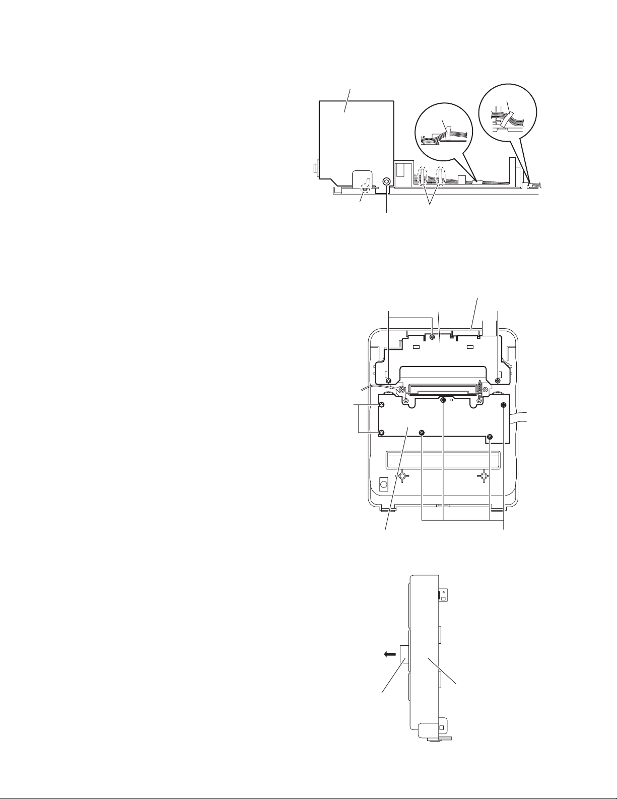
3.1 Main body section
3.1.1 Removing the rear cover
(See Figs.1 and 2)
(1) From the back side of the main body, remove the eleven
screws A attaching the rear cover. (See Fig.1.)
(2) From the bottom side of the main body, remove the three
screws B attaching the rear cover. (See Fig.2.)
(3) Remove the rear cover from the main body.
A
Rear cover
B
A AA
Fig.1
Rear cover
Fig.2
(No.MB338)1-7
Page 8

3.1.2 Removing the side panels (L)/(R)
(See Fig.3)
• Remove the rear cover.
(1) From the bottom side of the main body, remove the two
screws C attaching the side panels (L)/(R).
(2) Slide the side panels (L)/(R) in the direction of the arrow
and remove the side panels (L)/(R).
C
Side panel(R)
3.1.3 Removing the top cover assembly
(See Figs.4 and 5)
• Remove the rear cover and side panels(L)/(R).
(1) From the left side of the main body, disconnect the card
wires from the connectors (CN703
board. (See Fig.4.)
(2) Remove the screw D attaching the top cover assembly.
(See Fig.4.)
(3) From the right side of the main body, disconnect the card
wire from the connector CN105
Fig.5.)
(4) Disconnect the wire from the connector CN108 on the main
board. (See Fig.5.)
Reference:
When connecting the wire, pass it through the slot b of
the main board as before. (See Fig.5.)
(5) From the both sides of the main body, remove the two
screws E and screw F attaching the top cover assembly.
(See Figs.4 and 5.)
(6) Release the joints a and remove the top cover assembly.
(See Figs.4 and 5.)
, CN709) on the micon
on the main board. (See
C
E
Side panel(R)
Fig.3
Top cover assembly a
Fig.4
Top cover assembly
a CN108 CN105
ED
Micon boardCN703 CN709
F
b
1-8 (No.MB338)
Main board
Fig.5
Page 9

3.1.4 Removing the front panel assembly
(See Figs.6 to 8)
• Remove the rear cover, side panels(L)/(R) and top cover as-
sembly.
(1) From the left side of the main body, disconnect the card
wires from the connectors (CN702
board. (See Fig.6.)
(2) From the right side of the main body, disconnect the earth
wire from the micon board. (See Fig.7.)
(3) From the both sides and bottom sides of the main body, re-
lease the joints c and joint d. (See Figs.6 to 8.)
(4) Remove the front panel assembly in the direction of the ar-
row. (See Figs.6 to 8.)
, CN710) on the micon
Front panel assembly
CN710
CN702
Micon board
c
Front panel assembly
c
Fig.6
Earth wire
Micon board
Fig.7
Front panel assembly
d
Fig.8
(No.MB338)1-9
Page 10

3.1.5 Removing the fan motor
(See Figs.9 and 10)
• Remove the rear cover, side panels(L)/(R) and top cover as-
sembly.
(1) From the back side of the top cover assembly, remove the
screw G attaching the fan motor. (See Fig.9.)
Reference:
When attaching the screw G, attach the spacer with it.
(See Fig.9.)
(2) Take out the fan motor.
Reference:
When attaching the fan motor, pass the wire through the slot
e. (See Fig.10.)
3.1.6 Removing the tuner
(See Figs.9 and 10)
• Remove the rear cover, side panels(L)/(R) and top cover as-
sembly.
(1) From the back side of the top cover assembly, remove the
two screws H attaching the tuner bracket. (See Fig.9.)
(2) From the inside of the top cover assembly, remove the
screw J attaching the tuner bracket. (See Fig.10.)
(3) Take out the tuner with the tuner bracket.
(4) Remove the tuner from the tuner bracket.
Fan motor
Fan motor
G
G
Tuner bracket
H
3.1.7 Removing the cassette mechanism assembly
(See Fig.10)
• Remove the rear cover, side panels(L)/(R) and top cover as-
sembly.
(1) From the inside of the top cover assembly, remove the
screw K, screw L, screws L’ and screw L” attaching the
cassette mechanism assembly.
(2) Loosen the screw M attaching the cassette mechanism as-
sembly.
(3) Remove the cassette mechanism assembly.
Reference:
• When attaching the screw L’, attach the lug wire and shield
with it.
• When attaching the screw L”, attach the shield with it.
Spacer
Fig.9
Cassette mechanism assembly
Lug wire
L"L'
Shield
M
J
K
1-10 (No.MB338)
Tuner
Tuner bracket
e
Fan motor
L
Fig.10
Page 11

3.1.8 Removing the heat sink
(See Fig.11)
• Remove the rear cover, side panels(L)/(R) and top cover as-
sembly.
(1) From the back side of the main body, remove the eight
screws N attaching the heat sink.
(2) Remove the heat sink from the main board and regulator
board.
3.1.9 Removing the main board
(See Fig.12)
• Remove the rear cover, side panels(L)/(R), top cover assem-
bly and heat sink.
(1) From the right side of the main body, remove the two
screws P attaching the main board. (See Fig.12.)
(2) Disconnect the connectors (CN101
CN110) on the main board toward this side. (See Fig.12.)
(3) From the forward side of the main board, disconnect the
wires from the connectors (CN109
Fig.12.)
Reference:
Remove it when a lug wire from the main board is installed with
a screw Q.
(When the screw Q and lug wire are installed, apply it.) (See
Fig.13.)
to CN104, CN106 and
and CN111). (See
Main board
Main board
N
Regulator board
Heat sink
N
Fig.11
P
CN104
CN103
Lug wire
CN102
Fig.12
Main board
Fig.13
Q
CN111
CN101CN106
CN109
CN110
(No.MB338)1-11
Page 12

3.1.10 Removing the regulator board
(See Fig.14)
• Remove the rear cover, side panels(L)/(R), top cover assem-
bly, heat sink and main board.
(1) From the top side of the main body, disconnect the wire
from the connector CN902
(2) Disconnect the wire from the connector CN202
ulator board.
(3) Remove the three screws R attaching the regulator board.
(4) Take out the regulator board from the main body.
Reference:
After attaching the regulator board, attach the barrier (C) as
before.
on the transformer board.
on the reg-
Regulator board
CN202
R
Transformer
board
CN902
CN902
Transformer
board
3.1.11 Removing the transformer board
(See Fig.15)
• Remove the rear cover, side panels(L)/(R), top cover assem-
bly, heat sink, main board and regulator board.
(1) From the back side of the main body, remove the two
screws S attaching the heat sink bracket.
(2) From the left side of the main body, remove the tie band.
Reference:
After attaching the transformer board, fix the power cord
with the new tie band as before.
(3) Disconnect the wire from the connector CN903
transformer board.
(4) Disconnect the power cord from the connector CN901 on
the transformer board.
(5) Remove the three screws T attaching the power transform-
er and take out the transformer board from the main body.
Reference:
Remove the transformer shield as required.
on the
R
Transformer shield
Transformer board
CN903
Barrier (C)
Fig.14
CN901
Power cord
Tie band
Heat sink
bracket
S
S
1-12 (No.MB338)
TT
Fig.15
Page 13

3.1.12 Removing the power transformer
(See Fig.16)
• Remove the rear cover, side panels(L)/(R), top cover assem-
bly, heat sink, main board, regulator board and transformer
board.
(1) From the reverse side of the transformer board, remove the
solders from the sections f on the transformer board.
(2) Remove the power transformer from the transformer
board.
3.1.13 Removing the jack board and component board
(See Fig.17)
• Remove the rear cover, side panels(L)/(R), top cover assem-
bly, heat sink, main board and regulator board.
(1) From the back side of the main body, remove the two
screws U attaching the heat sink bracket.
(2) From the top side of the main body, remove the screw V at-
taching the PWB holder and take out the PWB holder.
Reference:
When attaching the PWB holder, put the section g under
the hook of the bottom chassis.
(3) Remove the screw W attaching the jack board and take out
the jack board with the component board.
Reference:
• Remove the connector CN631
from the jack board as required.
• When attaching the jack board, attach it after putting a projection h of the bottom chassis in a hole of the jack board.
on the component board
f
CN631
W
Component board
PWB holder
g
Bottom chassis
V
Fig.16
h
Jack board
Transformer board
Heat sink
bracket
U
U
Fig.17
(No.MB338)1-13
Page 14

3.1.14 Removing the joint board
(See Fig.18)
• Remove the rear cover, side panels(L)/(R), top cover assem-
bly, heat sink, main board, regulator board and transformer
board.
Reference:
Remove the jack board as required.
(1) From the back side of the main body, remove the two
screws X attaching the joint board.
(2) Remove the connector CN805
micon board toward this side.
(3) From the forward side of the joint board, disconnect the
card wires from the connectors (CN801
joint board.
(4) Take out the joint board from the main body.
3.1.15 Removing the micon board
(See Fig.19)
• Remove the rear cover, side panels(L)/(R), top cover assem-
bly, front panel assembly, heat sink, main board and regulator
board.
(1) Remove the two screws Y attaching the MD holder to the
micon board. (See Fig.19.)
(2) Take out the MD holder.
(3) Disconnect the wire from the connector CN903
transformer board. (See Fig.20.)
(4) Disconnect the card wires from the connectors (CN705 and
) on the micon board. (See Fig.20.)
CN711
(5) Remove the screw Z attaching the micon board. (See
Fig.20.)
(6) Disconnect the micon board from the connector CN805
the joint board. (See Fig.20.)
(7) Take out the micon board from the main body.
on the joint board from the
and CN802) on the
on the
on
X
CN801
Micon board
CN805
CN802
Fig.18
Micon board
X
Y
Joint board
MD holder
CN711
Z
Fig.19
CN705
Micon board
Fig.20
Y
CN903
Transformer board
CN805
Joint board
1-14 (No.MB338)
Page 15

3.1.16 Removing the DVD mechanism assembly
(See Figs.21 and 22)
• Remove the rear cover, side panels(L)/(R), top cover assem-
bly, heat sink, main board, regulator board, transformer board
and joint board.
(1) From the top side of the main body, disconnect the card
wires from the connectors (CN705
con board. (See Fig.21.)
(2) From the left side of the main body, remove the spacers fix-
ing the card wires. (See Fig.21.)
(3) From the top side of the main body, remove the two screws
AA attaching the DVD mechanism bracket. (See Fig.21.)
(4) Move the DVD mechanism bracket in the direction of the
arrow to release the claws i and remove the DVD mechanism bracket. (See Fig.21.)
(5) Remove the screw AB attaching the DVD mechanism as-
sembly. (See Fig.22.)
(6) Take out the DVD mechanism assembly from the main
body. (See Fig.22.)
and CN711) on the mi-
CN711
Spacer
CN711
Card
wire
AA
CN705
Spacer
CN705
Card
wire
Micon board
i
AA
DVD mechanism bracket
Fig.21
DVD mechanism assembly
Fig.22
i
AB
(No.MB338)1-15
Page 16
3.1.17 Removing the headphone board
(See Fig.23)
• Remove the rear cover, side panels(L)/(R), top cover assem-
bly, heat sink, main board, regulator board, transformer board,
joint board and DVD mechanism assembly.
(1) From the right side of the main body, remove the screw AC
attaching the headphone board.
(2) Take out the headphone board from the main body.
Reference:
• When attaching the headphone board, put the headphone
board in the slot j.
• When attaching the headphone board, pass the wire
through the section k.
• After attaching the headphone board, fix the wires with the
spacers as before.
3.1.18 Removing the FL board
(See Fig.24)
• Remove the rear cover, side panels(L)/(R), top cover assem-
bly and front panel assembly.
(1) From the inside of the front panel assembly, remove the
three screws AD attaching the FL board.
(2) Take out the FL board from the front panel assembly.
Note:
When attaching the FL board, be careful not to damage the
LCD panel.
Headphone board
j
AC
AD
Spacer
k
Fig.23
Front panel assembly
FL board
Spacer
AD
3.1.19 Removing the key board
(See Figs.24 and 25)
• Remove the rear cover, side panels(L)/(R), top cover assem-
bly and front panel assembly.
(1) From the front side of the front panel assembly, pull out the
volume knob in the direction of the arrow. (See Fig.25.)
(2) From the inside of the front panel assembly, remove the six
screws AE attaching the key board. (See Fig.24.)
(3) Take out the key board from the front panel assembly.
AE
Key board
AE
Fig.24
1-16 (No.MB338)
Volume knob
Front panel
assembly
Fig.25
Page 17

3.2 DVD mechanism assembly section
• Remove the DVD mechanism assembly from the main body.
(See "3.1.16 Removing the DVD mechanism assembly".)
3.2.1 Removing the DVD cover
(See Fig.1)
(1) From the top side of the DVD mechanism assembly, re-
move the two screws A attaching the DVD cover.
(2) Remove the double-stick tape fixing the card wire.
(3) Lift the DVD cover in an upward direction and remove it
from the projections a of the DVD mechanism assembly.
(4) Slide the DVD cover in the direction of the arrow and re-
move it from the sections b.
(5) Release the lock of the connector CN4
and disconnect the card wire.
on the LED board
Double-stick tape
Card wire
CN4
A
a
b
Card wire
LED board
3.2.2 Removing the joint board
(See Fig.2)
• Remove the DVD cover.
(1) From the inside of the DVD cover, remove the screw B at-
taching the joint board.
(2) Remove the spacer attaching the joint board and take out
the joint board from the DVD cover.
a
A
DVD mechanism assembly
Clamper base
B
Clamper base
Fig.1
Joint board
Fig.2
b
Spacer
(No.MB338)1-17
Page 18

3.2.3 Removing the tray assembly
(See Figs.3 and 4)
• Remove the DVD cover.
(1) From the right side of the DVD mechanism assembly, push
the slide cam and pull the tray assembly out of the DVD
mechanism assembly in the direction of the arrow. (See
Fig.3.)
(2) From the top side of the DVD mechanism assembly, re-
move the two screws C attaching the tray assembly. (See
Fig.4.)
(3) Remove the bushing of the tray assembly from the projec-
tions c on the DVD mechanism assembly and take out the
tray assembly in an upward direction. (See Fig.4.)
Tray assembly DVD mechanism assembly
Slide cam
Fig.3
C
c
Shaft guide
c
3.2.4 Removing the LED board
(See Fig.5)
• Remove the DVD cover and tray assembly.
(1) From the top side of the tray assembly, remove the sec-
tions d which were fixed in bond.
(2) Remove the double-stick tape attaching the LED board and
take out the LED board.
Note:
When removing the LED board, be sure not to damage the
LED board.
DVD mechanism assembly
Fig.4
Tray assembly
Double-stick tape
Fig.5
Tray assembly
d
d
LED board
1-18 (No.MB338)
Page 19

3.2.5 Removing the traverse mechanism assembly
(See Figs.6)
• Remove the DVD cover.
(1) From the bottom side of the DVD mechanism assembly, re-
move the four screws D attaching the traverse mechanism
assembly.
(2) Take out the traverse mechanism assembly with the DVD
module board.
DVD mechanism assembly
DVD module board
3.2.6 Removing the DVD module board
(See Figs.7 and 8)
• Remove the DVD cover and traverse mechanism assembly.
(1) From the side of the traverse mechanism assembly, solder
the short land sections e of the pickup. (See Fig.7.)
(2) From the bottom side of the traverse mechanism assem-
bly, release the lock of the connector CN101
module board in the direction of the arrow and disconnect
the card wire. (See Fig.8.)
Caution:
• Solder the short land section e on the pickup before
disconnecting the card wire from the connector CN101
on the DVD module board. If the card wire is disconnected without attaching solder, the pickup may be destroyed by static electricity. (See Figs.7 and 8.)
• When attaching the DVD module board, be sure to remove solders from the short land section e after connecting the card wire to the connector CN101
DVD module board. (See Figs.7 and 8.)
(3) Disconnect the card wire from the connector CN201
DVD module board. (See Fig.8.)
(4) Remove the two screws E attaching the DVD module
board. (See Fig.8.)
(5) Remove the DVD module board from the projection f in an
upward direction and remove the claw h in the direction of
the arrow 2 while removing the claw g in the direction of the
arrow 1. (See Fig.8.)
on the DVD
on the
on the
D
Traverse mechanism assembly
Fig.6
e
Traverse mechanism assembly
Fig.7
Card wire
CN101
f
E
1
D
Pickup
Card wire
CN201
E
h
2
g
DVD module board
Traverse mechanism assembly
Fig.8
(No.MB338)1-19
Page 20

3.2.7 Removing the pickup
(See Figs.7, 9 to 11)
• Remove the DVD cover and traverse mechanism assembly.
(1) From the side of the traverse mechanism assembly, solder
the short land sections e of the pickup. (See Fig.7.)
(2) Release the lock of the connector of the pickup in the direc-
tion of the arrow and disconnect the card wire. (See Fig.9.)
Caution:
• Solder the short land section e on the pickup before
disconnecting the card wire from the connector on the
pickup. If the card wire is disconnected without attaching solder, the pickup may be destroyed by static electricity. (See Figs.7 and 9.)
• When attaching the pickup, be sure to remove solders
from the short land section e after connecting the card
wire to the connector on the pickup. (See Figs.7 and
9.)
(3) Remove the screw F attaching the plate and thrust spring.
(See Fig.9.)
(4) Remove the plate from the joint i of the feed holder and
take out the plate with the thrust spring. (See Fig.9.)
(5) Remove the shaft of the pickup from the section j of the
traverse mechanism assembly and remove it from the section k while moving the shaft in the direction of the arrow.
(See Fig.10.)
(6) Remove the pickup from the section m of the traverse
mechanism assembly and take out the pickup with the
shaft. (See Fig.10.)
(7) From the bottom side of the pickup, remove the two screws
G attaching the SW actuator and LEAD spring. (See
Fig.11.)
(8) Pull the shaft out of the pickup. (See Fig.11.)
Plate
F
Feed holder
j
Shaft
i
Thrust spring
Card wire
Fig.9
Traverse mechanism assembly
Connector
Pickup
k
Pickup
Shaft
m
Fig.10
Pickup
SW actuator
LEAD spring
G
Fig.11
1-20 (No.MB338)
Page 21

3.2.8 Attaching the pickup
(See Figs.7, 9 to 12)
• See "3.2.7 Removing the pickup".
(1) Attach the shaft, SW actuator and LEAD spring to the pick-
up. (See Fig.11.)
(2) Align the pickup to the section m of the traverse mecha-
nism assembly first, and set the both ends of the shaft of
the pickup in the sections (j, k) of the traverse mechanism
assembly. (See Fig.10.)
(3) Attach the plate and thrust spring. (See Fig.9.)
(4) Remove the solders from the soldered sections e after at-
taching the card wire to the connector on the pickup. (See
Figs.7 and 9.)
(5) Turn the feed gear M in the direction of the arrow 1 to move
the pickup fully in the direction of the arrow 2. (See Fig.12.)
Feed gear M
1
2
Pickup
Fig.12
(No.MB338)1-21
Page 22

3.2.9 Removing the feed motor
(See Figs.13 to 15)
• Remove the DVD cover and traverse mechanism assembly.
(1) From the top side of the traverse mechanism assembly, re-
move the screw H attaching the plate and thrust spring.
(See Fig.13.)
(2) Remove the plate from the joint n of the feed holder and
take out the plate with the thrust spring. (See Fig.13.)
(3) Remove the wires from the soldered sections p on the spin-
dle motor board. (See Fig.14.)
Reference:
When attaching the feed motor, pass the wires through
the section q on the spindle base. (See Fig.14.)
(4) Remove the three screws J attaching the feed holder. (See
Fig.14.)
(5) Remove the feed holder, feed motor, lead screw, feed gear
E and feed gear M simultaneously. (See Fig.14.)
(6) From the side of the feed holder, remove the two screws K
attaching the feed motor. (See Fig.15.)
3.2.10 Removing the spindle motor board
(See Fig.14 and 16)
• Remove the DVD cover, traverse mechanism assembly and
DVD module board.
(1) From the top side of the traverse mechanism assembly, re-
move the wires from the soldered sections p on the spindle
motor board. (See Fig.14.)
(2) From the bottom side of the traverse mechanism assem-
bly, remove the three screws L attaching the spindle motor
board. (See Fig.16.)
n
Plate
H
Feed gear M
Feed gear E
J
Thrust spring
Fig.13
Feed motor
Traverse mechanism assembly
Lead screw
Wires
q
p
Feed holder
J
Traverse mechanism assembly
Spindle base
Fig.14
K
Fig.15
Traverse mechanism assembly
L
Spindle motor board
Feed holder
1-22 (No.MB338)
Fig.16
Page 23

3.2.11 Removing the DVD loading switch board
(See Fig.17)
(1) From the bottom side of the DVD mechanism assembly, re-
move the screw M attaching the DVD loading switch board.
(2) Remove the wires from the soldered sections r on the DVD
loading switch board.
(3) Lift the DVD loading switch board while pressing the claw
s of the DVD mechanism assembly in the direction of the
arrow and remove the DVD loading switch board from the
section t.
(4) From the forward side of the DVD loading switch board,
disconnect the card wire from the connector CN1
Reference:
• Put the wires on the section u after attaching the DVD loading switch board to the DVD mechanism assembly.
• Fix the claw t on the DVD mechanism assembly with bonds
after attaching the DVD loading switch board.
3.2.12 Removing the motor
(See Figs.17 and 18)
• Remove the DVD cover and tray assembly.
(1) From the bottom side of the DVD mechanism assembly, re-
move the wires from the soldered sections r on the DVD
loading switch board. (See Fig.17.)
(2) From the top side of the DVD mechanism assembly, re-
move the belt from the motor pulley. (See Fig.18.)
Note:
Take care not to attach grease on the belt.
(3) Remove the two screws N attaching the motor to the DVD
mechanism assembly and take out the motor from the bottom side of the DVD mechanism assembly. (See Fig.18.)
.
DVD loading switch board
Wires
r
CN1
t
u
M
DVD mechanism
assembly
DVD mechanism assembly
Fig.17
N
s
Motor
Belt
Motor pulley
Fig.18
(No.MB338)1-23
Page 24

3.3 Cassette mechanism assembly
3.3.1 Removing the Play/Record & Clear head
(See Fig.1~3)
(1) While moving the trigger arm on the right side of the head
mount in the direction of the arrow, turn the flywheel R
counterclockwise until the head mount comes ahead and
clicks.
(2) The head turns counterclockwise as you turn the flywheel
R counterclockwise (See Fig.2 and 3).
(3) Disconnect the flexible wire from connector CN31
head amplifier & mechanism control board.
(4) Remove the spring from the back of the head.
(5) Loosen the azimuth screw for reversing attaching the head.
(6) Remove the head on the front side of the head mount.
on the
Cassette mechanism assembly
Fig.1
Head
Fly wheelR
Trigger armHead mount
Flexible wire
Fly wheel R
Fig.2
Azimuth screw
Head
for reversing
Spring
CN31
Head amplifer & mecha control board
Fig.3
1-24 (No.MB338)
Page 25

3.3.2 Removing the head amplifier & mechanism control board
(See Fig.4)
(1) Turn over the cassette mechanism assembly and remove
the three screws A attaching the head amplifier & mechanism control board.
(2) Disconnect the flexible wire from connector CN31
head amplifier & mechanism control board.
(3) Disconnect connector CN32
anism control board from connector CN1
board.REFERENCE: If necessary, unsolder the 4-pin wire
soldered to the main motor.
3.3.3 Removing the main motor
(See Fig.4~7)
(1) Remove the two screws B .
(2) Half raise the motor and remove the capstan belt from the
motor pulley.
ATTENTION:
Be careful to keep the capstan belt from grease. When reassembling, refer to Fig.6 and 7 for attaching the capstan belt.
Head amplifier & mecha control board
of the head amplifier & mech-
on the reel pulse
on the
Main motor assembly
Capstan belt
Fig.5
Main motor assembly
CN31
Flexible wire
A
AA
Fig.4
CN32
4pin wire
B
Main motor assembly
Motor pulley
Capstan belt
Fig.6
Main motor assembly
Fly wheel
Capstan belt
Motor pulley
Fig.7
(No.MB338)1-25
Page 26

3.3.4 Removing the flywheel
(See Fig.8, 9)
• Prior to performing the following procedure, remove the head
amplifier & mechanism control board and the main motor assembly.
(1) From the front side of the cassette mechanism, remove the
slit washers attaching the capstan shaft L and R. Pull out
the flywheels backward.
Fly wheel R Fly wheel L
Fig.8
Fly wheel R
Capstan shaft R Capstan shaft L
Slit washer
Fig.9
3.3.5 Removing the reel pulse board and solenoid
(See Fig.10)
• Prior to performing the following procedure, remove the head amplifier & mechanism control board.
(1) Remove the screw C.
(2) Release the tab a, b, c, d and e retaining the reel pulse board.
(3) Release the tab f and g attaching the solenoid on the reel pulse board.
(4) The reel pulse board and the solenoid come off.
Fly wheel L
bc
a
Solenoid
g
f
d
Reel pulse board
C
e
Fig.10
1-26 (No.MB338)
Page 27

3.3.6 Reattaching the Play/ Record & Clear head
r
r
(See Fig.11~13)
(1) Reattaching the head mount assembly.
a) Change front of the direction cover of the head
mount assembly to the left (Turn the head forward).
b) Fit the bosses O', P', Q', U' and V' on the head mount
assembly to the holes P and V, the slots O, U and Q
of the mechanism sub assembly (See Fig.11 to 13).
CAUTION:
To remove the head mount assembly, turn the direction
cover to the left to disengage the gear. If the gear can not
be disengaged easily, push up the boss Q' slightly and
raise the rear side of the head mounts slightly to return
the direction lever to the reversing side.
(2) Tighten the azimuth screw for reversing.
(3) Reattach the spring from the back of the Play/ Record &
Clear head.
(4) Connect the flexible wire to connector CN31
amplifier & mechanism control board.
on the head
U' Q'
Head mount assembly
Head mount assembly
O'
Fig.11
P'
P'
V'
V'
Direction cove
Spring
Flexible wire
V
O
P
Q
Head
Direction cove
U
Fig.12
Azimuth screw for reversing
Head mount
CN31
Fig.13
Head amplifier &
mechanism control board
(No.MB338)1-27
Page 28

SECTION 4
ADJUSTMENT
4.1 Adjustment method for DVD section
4.1.1 Jigs and test instruments
(1) Upgrade disc
(2) Remote controller
4.1.3 Adjustment and check method
1. EEPROM initialization
Confirm that a disc is not in a tray.
While pressing both the [STOP] key
and [DVD PLAY] key on the main unit,
insert the AC power cord in an outlet.
LCD indication
TEST
Press the [F.SKIP] key
on the main unit.
EEPROM initialization starts.
LCD indication
TEST 00
: Area suffix
: Region code
(Refer to item 4)
4.1.2 Adjustment and check items
(1) EEPROM initialization
(2) Upgrade of back-end firm
(3) Upgrade of system microcomputer (ROM correction)
(4) Confirm of region code and system control version
(5) DVD IOP check
[POWER] key
[DVD PLAY] key
LCD
[STOP] key
[F.SKIP] key
Press the [F.SKIP] key on the main unit
more than 2 seconds.
LCD indication
TEST 33
EEPROM initialization is complete.
1-28 (No.MB338)
Page 29

2. Upgrade of back-end firm
r
This set can do upgrade of a back-end firm
with an upgrade disc.
LCD indication
NO DISC
Press the [POWER] key on the
main unit and put the main body
into a standby mode.
Press the [OPEN/CLOSE] key
on the main unit to open the tray.
Insert the upgrade disc.
Source : DVD
3. Upgrade of system microcomputer
(ROM correction)
This set can do upgrade of a microcompute
with a ROM correction disc.
LCD indication
NO DISC
Press the [POWER] key on the
main unit and put the main body
into a standby mode.
Press the [OPEN/CLOSE] key
on the main unit to open the tray.
Source : DVD
Press the [OPEN/CLOSE] key
on the main unit to close the tray.
LCD indication
UPGRADE
Press the [ ] key on a remote controller.
Upgrade starts.
Take out the disc from the tray after
opening the tray automatically.
Press the [OPEN/CLOSE] key
on the main unit to close the tray.
Press the [POWER] key on the
main unit and put the main body
into a standby mode.
Pull the power cord
out of the outlet.
Upgrade is complete.
Insert the ROM correction disc.
Press the [OPEN/CLOSE] key
on the main unit to close the tray.
LCD indication
UPGRADE
LCD indication
UPGRADE & ROM CORR
Upgrade starts automatically.
LCD indication
COMPLETE
Take out the disc from the tray after
opening the tray automatically.
Press the [OPEN/CLOSE] key
on the main unit to close the tray.
Press the [POWER] key on the
main unit and put the main body
into a standby mode.
[ ] key
[POWER] key
LCD
Pull the power cord
out of the outlet.
Upgrade is complete.
[OPEN/CLOSE] key
(No.MB338)1-29
Page 30

4. Confirmation of region code and system control version
(1) Insert the AC power cord in an outlet while pressing both the [STOP] key and [DVD PLAY] key on the main
unit and put the main unit in a test mode.
(2) Indication of LCD changes sequentially as follows by pushing a [MENU] key of a remote controller.
TEST XXX #
XXXX
SC: 0.30 00
CHECK
-----------------------------
-----------------------------
-----------------------------
-----------------------------
Area suffix # : Region code
XXX :
Confirm that the area suffix fits the region code.
XXXX : Key index indication of device key
2.00 00 : Version number of the system control
Check mode of the front-end
(3) Version indication of a DVD unit is displayed by pressing the [ON SCREEN] key on the remote controller in the
system controller version indication
SC: 0.30 00
UT: XXX
-----------------------------
-----------------------------
0.30 00 : Version number of the system control
Confirm a number by a working standard which was provided with
by manufacturing technique department.
XXX : Version number of the DVD unit
Confirm a number by a working standard which was provided with
by manufacturing technique department.
(3) Press the [POWER] key of the main unit in order to let the test mode finish.
[MENU] key
[ON SCREEN] key
[POWER] key
[DVD PLAY] key
LCD
[STOP] key
1-30 (No.MB338)
Page 31

5. DVD IOP check
Confirm that a disc is not in a tray.
(1) Insert the AC power cord in an outlet while pressing both the [STOP] key and [DVD PLAY] key on the main
unit and put the main unit in a test mode.
(2) Turn indication of LCD into CHECK by pushing a [MENU] key of a remote controller.
LCD indication
CHECK
Press the [4] key
on the remote controller.
LCD indication
AABB 0000
Press the [5] key
on the remote controller.
LCD indication
AABB 0000
Press the [POWER] key on the
main unit and put the main body
into a standby mode.
Pull the power cord
out of the outlet.
DVD IOP check is complete.
AA : CD laser power in production (mA)
BB : CD laser power of the present (mA)
AA : DVD laser power in production (mA)
BB : DVD laser power of the present (mA)
(No.MB338)1-31
Page 32

SECTION 5
TROUBLESHOOTING
This service manual does not describe TROUBLESHOOTING.
1-32 (No.MB338)
Page 33

(No.MB338)1-33
Page 34

Victor Company of Japan, Limited
AV & MULTIMEDIA COMPANY AUDIO/VIDEO SYSTEMS CATEGORY 10-1,1chome,Ohwatari-machi,Maebashi-city,371-8543,Japan
(No.MB338)
Printed in Japan
VPT
Page 35

PARTS LIST
[ UX-QD9S ]
* All printed circuit boards and its assemblies are not available as service parts.
Area suffix
A ------------------------- Australia
US ---------------------- Singapore
UN ----------------------------Asean
No.MB338
- Contents -
Exploded view of general assembly and parts list (Block No.M1)
Speaker assembly and parts list (Block No.M2)
DVD mechanism assembly and parts list (Block No.MJ)
DVD loading base assembly and parts list (Block No.MN)
Cassette mechanism assembly and parts list (Block No.MP)
Electrical parts list (Block No.01~07)
Packing materials and accessories parts list (Block No.M3)
3- 2
3- 6
3- 7
3- 9
3-11
3-13
3-22
3-1
Page 36

Exploded view of general assembly and parts list
d
2
2
Block No.
86
80
82
70
81
72
83
89
90
88
119
m
74
c
98
96
85
84
L
87
B
121
A
71
69
M
68
M
1
M
50
117
e
99
118
46
99
a
45
49
w
39
43
d
120
74
79
79
11
73
79
b
14
a
14
115
41
37
56
w
113
14
18
FL board
18
9
e
6
Key board
9
109
9
22
23
25
A
6
21
77
76
79
78
F
100
J
10
H
3
97
15
13
16
75
12
17
15
B
H
97
5
G
8
19
3-2
2
102
4
110
2
1
7
102
J
K
Hea
Page 37

46
99
118
45
w
43
37
99
a
49
50
117
39
41
51
51
105
107
111
105
108
105
105
105
e
Micon board
c
t
d
40
116
v
s
38
26
53
Joint board
U
Component board
114
52
v
s
P
Q
43
M
61
Regulator board
44
z
F
E
103
104
D
42
T
106
106
106
63
64
65
62
61
z
66
64
64
65
60
u
61
Trans board
28
31
29
35
R
L
t
u
p
31
36
32
36
30
Y
105
105
32
27
J
19
21
23
54
x
N
55
67
Jack board
95
y
91
59
55
94
93
K
D
101
G
112
92
34
47
E
20
K
Headphone board
33
p
Y
20
24
x
57
y
Q
M
U
48
58
P
N
Main board
R
b
m
T
3-3
Page 38

General Assembly
Symbol No. Part No. Part Name Description Local
1 LV10934-019A FRONT PANEL
2 LV40301-002A FELT SPACER (x2)
3 LV21750-013A FRONT LENS
4 LV21751-010A CD LENS
5 LV35099-001A ORNAMENT
6 QYSDSF2608ZA TAP SCREW M2.6 x 8mm(x2)
7 GV30527-001A VOLUME ORNAMENT
8 LV21752-002A MAIN BUTTON
9 QYSDSF2608ZA TAP SCREW M2.6 x 8mm(x6)
10 LV35059-001A LENS COVER
11 LV35060-001A LCD HOLDER
12 LV35061-001A LIGHT GUIDE
13 LV43905-001A LCD SHEET
14 QYSDSF2608ZA TAP SCREW M2.6 x 8mm(x3)
15 LV30225-0W8A SPACER (x2)
16 LV30225-0Y7A SPACER
17 LV44015-001A SHIELD(B)
18 VYSH101-034 SPACER (x2)
19 LV10936-001A BOTTOM CHASSIS
20 LV40301-002A FELT SPACER (x2)
21 LV21582-003A MECHA HOLDER
22 LV30225-0X8A SPACER (x2)
23 LV30226-044A SPACER
24 LV30225-011A SPACER
25 QYSSST3006ZA TAP SCREW M3 x 6mm
26 QYSDST3006ZA TAP SCREW M3 x 6mm
27 QQT0451-003 POWER TRANSF T 9001 A,UN
27 QQT0451-004 POWER TRANSF T 9001 US
28 QMF51W2-1R0-J8 FUSE F 9001 1A AC250V
29 QMF51W2-3R15-J8 FUSE F 9003 3.15A AC250V
30 LV34403-001A TRANS SHIELD
31 LV30225-0P5A SPACER (x2)
32 QYSBST4006ZA TAP SCREW M4 x 6mm(x3)
33 QZW0033-001 STRAIN RELIEF
34 QMPG080-244-JD POWER CORD(EU) 2.44m BLACK A
34 QMPK210-205-JN POWER CORD(EU) 2.05m BLACK UN,US
35 LV35064-001A HEAT SINK BKT
36 QYSDST3006EA TAP SCREW M3 x 6mm(x2)
37 QYSBSF3012ZA TAP SCREW M3 x 12mm
38 LV30225-011A SPACER (x2)
39 LV42035-002A LASER CAUTION
40 LV21754-001A DVD MECHA BKT
41 LV30225-0Q7A SPACER
42 LV30225-0U5A SPACER
43 QYSDST3006EA TAP SCREW M3 x 6mm(x3)
44 QYSBSG3008ZA TAP SCREW M3 x 8mm(x2)
45 LV30225-011A SPACER
46 LV30225-011A SPACER
47 LV30225-011A SPACER
48 QYSBSGY3008EA TAP SCREW M3 x 8mm
49 QYSBSG3008ZA TAP SCREW M3 x 8mm
50 LV21755-003A MD HOLDER
51 QYSBSG3008ZA TAP SCREW M3 x 8mm(x2)
52 LV35065-001A PWB HOLDER
53 QYSBSG3008ZA TAP SCREW M3 x 8mm
54 LV34406-001A IC BRACKET(PWR)
55 QYSBSG3008EA TAP SCREW M3 x 8mm(x2)
56 VYSH101-009 SPACER
57 LV30225-011A SPACER
58 LV30225-0M5A SPACER
59 LV30225-0Y1A SPACER
60 LV34405-001A IC BRACKET(RG)
61 QYSBSG3010ZA TAP SCREW M3 x 10mm(x3)
62 LV35066-001A HEAT SINK
63 QYSBSG3014E TAP SCREW M3 x 14mm(x2)
64 QYSBSG3014E TAP SCREW M3 x 14mm(x3)
65 QYSBSG3014E TAP SCREW M3 x 14mm(x3)
66 LV30225-0V8A SPACER (x2)
67 QYSDST3006ZA TAP SCREW M3 x 6mm
68 LV21844-001A TOP COVER ASSY
69 VKL7850-003 EJECT SAFETY
70 LV30225-0G9A SPACER
71 VKW5258-003 TORSION SPRING
72 LV43116-001A MECHA BRACKET
Block No. [M][1][M][M]
3-4
Page 39

Symbol No. Part No. Part Name Description Local
73 QYSBSG3008ZA TAP SCREW M3 x 8mm
74 VYSH101-009 SPACER (x2)
75 LV30225-079A SPACER
76 LV34035-001A SHIELD
77 LV30225-0J1A SPACER
78 LV30225-0M5A SPACER
79 QYSBSF3010ZA TAP SCREW M3 x 10mm(x4)
80 E65923-009 TAPPING SCREW
81 GV40034-001A DAMPER ASSY.
82 GV40220-001A LACH
83 LV43579-001A DOOR SPRING
84 QAU0346-001 TUNER TU 1
85 LV35102-001A TUNER BKT
86 QYSBSG3008ZA TAP SCREW M3 x 8mm(x2)
87 QYSBSF3010ZA TAP SCREW M3 x 10mm
88 QAR0312-001 FAN MOTOR
89 QYSBSF3025ZA TAP SCREW M3 x 25mm
90 LV30226-039A SPACER
91 LV44068-001A BARRIER(A)
92 VYSH101-009 SPACER
93 QYSBSG3008ZA TAP SCREW M3 x 8mm
94 LV44069-001A BARRIER(B)
95 VYSH101-009 SPACER
96 LV44070-001A BARRIER(C)
97 QYSBSG3010ZA TAP SCREW M3 x 10mm(x2)
98 QYSBSG3008ZA TAP SCREW M3 x 8mm
99 LV30225-011A SPACER (x2)
100 LV10938-001A SIDE PANEL(L)
101 LV10939-001A SIDE PANEL(R)
102 QYSSST3008ZA TAP SCREW M3 x 8mm(x2)
103 LV10937-007A REAR COVER
104 LV35067-001A EARTH PLATE
105 QYSDSG3010NA TAP SCREW M3 x 10mm(x11)
106 QYSSST3008ZA TAP SCREW M3 x 8mm(x3)
107 GV40526-001A CAUTION LABEL
108 LV44071-004A REGION LABEL A
108 LV44071-003A REGION LABEL UN,US
109 LV35063-004A TRAY FITTING
110 GV30443-001A VOLUME KNOB
111 LV35431-002A RATING LABEL A
111 LV35431-001A RATING LABEL UN
111 LV35431-003A RATING LABEL US
112 LV43614-001A LABEL
113 QUQ410-0508DJ FFC WIRE 5pin 8cm
114 QUQ110-1910AJ FFC WIRE 19pin 10cm
115 QUQ410-0710DJ FFC WIRE 7pin 10cm
116 QUQ110-1710BJ FFC WIRE 17pin 10cm
117 QUQH10-0914AC FFC WIRE 9pin 14cm
118 QUQ410-1518CJ FFC WIRE 15pin 18cm
119 QUQ412-0920CJ FFC WIRE 9pin 20cm
120 QUQ412-1020DJ FFC WIRE 10pin 20cm
121 QUQ412-1124CJ FFC WIRE 11pin 24cm
3-5
Page 40

Speaker assembly and parts list
2
Block No.
M
M
2
M
1
4
The parts without symbol number are not service.
Speaker
Symbol No. Part No. Part Name Description Local
1 LV21811-001A NET ASSY (x2)
2 5600008011 HOLDER (x8)
3 9000007941 FOOT (x8)
4 LV43473-002A JVC MARK (x2)
3
3
Block No. [M][2][M][M]
3-6
Page 41

DVD mechanism assembly and parts list
23
Block No.
M
J
M
M
Grease
=JVG-31N
=CFD-4007ZY2
=PG-641
=1401C
< Back side >
25
24
29
FTU-JZ1-11M
26
27
16
DVD module board
27
22
21
A
6
17
A
27
20
19
18
14
13
< Back side >
63.3mm
15
27
+
0.1mm
-
12
30
10.5mm
2
+
0.1mm
-
3
28
5
11
8
31
1
4
9
7
11
10
The parts without symbol number are not service.
3-7
Page 42

DVD mechanism
Symbol No. Part No. Part Name Description Local
1 LV21814-001A MECHA BASE
2 LE20731-001A SPINDLE BASE
3 QYSDST2605M TAP SCREW M2.6 x 5mm(x2)
4 LE40931-001A SHAFT
5 LE40995-001A BAR SPRING
6 QYSPSTU2080M TAP SCREW M2 x 8mm
7 LE20730-002A FEED HOLDER
8 QAR0165-001 FEED MOTOR
9 LV41510-201A FEED GEAR T
10 QYSPSPU2040M SCREW M2 x 4mm(x2)
11 QYSDST2605M TAP SCREW M2.6 x 5mm(x3)
12 QAL0577-001 P.UP
13 LE20732-001A SW ACTUATOR
14 LE31093-001A LEAD SPRING
15 QYSPSFU1740Z TAP SCREW M1.7 x 4mm(x2)
16 QUQ105-2412AC FFC WIRE 24pin 12cm
17 LE40931-001A SHAFT
18 LE40855-002A FEED GEAR E
19 LV41517-003A LEAD SCREW
20 LE40930-001A FEED GEAR M
21 LE40928-002A THURUST SPRING
22 LE40927-002A PLATE
23 QYSDST2614Z TAP SCREW M2.6 x 14mm
24 QAR0334-001 S.MOTOR
25 QYSPSPU1760Z SCREW M1.7 x 6mm(x3)
26 LE40994-001A T.SPRING
27 LE40858-002A SPECIAL SCREW (x4)
28 QYSDST2004Z TAP SCREW M2 x 4mm(x2)
29 LV30225-0X6A SPACER
30 LV30225-0X5A SPACER
31 LV44007-001A TAPE
Block No. [M][J][M][M]
3-8
Page 43

DVD loading base assembly and parts list
Grease
JVG-31N
FL-7750E
30
FMU-JZ1-11M
Block No.
21
M
N
M
M
26
h
Joint board
9
23
16
29
28
25
24
11
27
22
26
5
LED board
10
6
15
14
2
7
3
4
19
h
1
18
17
j
0.10mm
7.75mm
Backside
e
f
a
b
34
13
20
8
12
j
34
Switch board
33
c
a
34
32
c
d
31
e
f
d
b
The parts without symbol number are not service.
3-9
Page 44

DVD loading base
Symbol No. Part No. Part Name Description Local
1 LV10932-003A LOADING BASE
2 LV35052-001A PULLEY GEAR
3 LV35053-001A MIDDLE GEAR
4 LV35054-001A IDLE GEAR
5 E407140-001SS C.D ROLLER
6 E407149-001SS RUBBER TUBE
7 LV35055-003A SLIDE CAM ASSY
8 LV21749-002A ELEVATOR
9 LV10933-003A TRAY
10 NSTM515AS LED
11 NSTM515AS LED
12 LV35050-001A SHAFT GUIDE
13 LV43847-001A SHAFT
14 QYSSSP2010ZA SCREW M2 x 10mm
15 QYNNS2000ZA NUT M2
16 QYSDSF2008Z TAP SCREW M2 x 8mm(x2)
17 QAR0197-001 MOTOR
18 LV43844-001A MOTOR PULLEY
19 QYSPSPU1730Z SCREW M1.7 x 3mm(x2)
20 QYSDSF2008Z TAP SCREW M2 x 8mm
21 LV43974-001A BELT
22 LV21747-001A CLAMPER BASE
23 LV43958-001A SPECIAL SCREW
24 LV30225-011A SPACER
25 QUQ710-0712AE FFC WIRE 7pin 12cm
26 QYSDSF2008Z TAP SCREW M2 x 8mm(x2)
27 LV35056-001A DVD CLAMPER
28 LV42930-003A P.C.MAGNET
29 LV43848-001A YOKE
30 LE40906-001A SPECIAL SCREW
31 ------------------ DVD TRAMECHA UN
32 LE40900-003A INSULATOR (x2)
33 LE40900-005A INSULATOR (x2)
34 LE40901-001A SPECIAL SCREW (x4)
Block No. [M][N][M][M]
3-10
Page 45

Cassette mechanism assembly and parts list
SLC-S302M
Block No.
M
M
M
P
Grease
= EM-30L
=UD-24
=LEN-320M
=MOBIL-1
34
1
27
A
19
B
3
13
8
15
2
2
10
14
9
16
12
23
3
4
11
6
5
7
29
C
1
The lower side
24
5
6
Switch board
30
25
18
22
11
21
28
20
26
31
17
C
36
A
32
33
B
35
Head amplifier
board
35
33
32
0.1
0.15 mm
_
+
8.7
The parts without symbol number are not service.
3-11
Page 46

Cassette mechanism
Symbol No. Part No. Part Name Description Local
1 VKS1165-00N CHASSIS B. ASSY
2 VKS2274-002 REEL GEAR (x2)
3 VKW5286-002 B.T. SPRING (x2)
4 VKS5559-001 PLAY IDLE GEAR
5 VKS5595-002 BLIND
6 VKS5560-003 FR IDLE GEAR
7 LV42013-001A EARTH SPRING
8 SLC-RP4SVM HEAD MOUNT ASSY
9 VKY3149-002 CASSETTE SP.
10 LV31786-002A PLAY LEVER
11 VKS1166-003 CONTROL CAM
12 VKW5279-002 HEAD BASE SP(R)
13 VKW5280-001 HEAD BASE SP(L)
14 LV41584-001A BRAKE(R)
15 LV41585-003A BRAKE(L)
16 QYSBSF2005Z SCREW 2mm x 5mm
17 VKS5603-00G MAIN PULLEY ASS
18 VKS3785-001MM FR ARM
19 VKW5284-002 SWING SPRING
20 VKS2278-003 TRIGGER ARM
21 VKW5301-001 FR SPRING
22 VKW5266-001 ELEVATOR SPRING
23 WDL214025 WASHER
24 QYSBSF2005Z SCREW 2mm x 5mm
25 VKS3786-00G CLUTCH ASSY
26 VKF3205-00B F.WHEEL ASSY(R)
27 WDL183425 SLIT WASHER
28 VKF3207-00C F.WHEEL ASSY(L)
29 WDL173525-6 SLIT WASHER
30 VKZ3174-00B DC SOLENOID
31 LV42836-001A CAPSTAN BELT
32 MSI-5U2LWA D.C.MOTOR
33 VKR4761-003 MOTOR PULLEY
34 QYSPSP2604Z SCREW 2.6mm x 4mm(x2)
35 QYSBSF2608Z TAPPING SCREW 2.6mm x 8mm(x3)
36 QUQH12-0906BF WIRE
Block No. [M][P][M][M]
3-12
Page 47

Electrical parts list
Main board
Block No. [0][1]
Symbol No.
IC101 LA4628 IC
IC311 LC75345M-X IC
IC501 GP1UM261XKVF IR DETECT UNIT
IC601 MM1623XF-X IC
IC801 SN74LVC08ANS-X IC
Q1101 UN211E-X DIGI TRANSISTOR
Q1102 UN211E-X DIGI TRANSISTOR
Q1103 2SC3576-JVC-T TRANSISTOR
Q1201 UN211E-X DIGI TRANSISTOR
Q1202 UN211E-X DIGI TRANSISTOR
Q1203 2SC3576-JVC-T TRANSISTOR
Q1301 UN221E-X TRANSTSTOR
Q1302 2SB709A/R/-X TRANSISTOR
Q1401 2SB941A/QP/ TRANSISTOR
Q1402 2SD601A/RS/-X TRANSISTOR
Q1403 2SD601A/RS/-X TRANSISTOR
Q1404 2SD601A/RS/-X TRANSISTOR
Q3101 2SD601A/RS/-X TRANSISTOR
Q3201 2SD601A/RS/-X TRANSISTOR
Q6901 KTA1267/YG/-T TRANSISTOR
Q6902 2SD601A/RS/-X TRANSISTOR
Q6951 KTC3199/GL/-T TRANSISTOR
D1101 1SS133-T2 SI DIODE
D1102 11EQS03LN-T2 FR DIODE
D1201 1SS133-T2 SI DIODE
D1202 11EQS03LN-T2 FR DIODE
D1301 1SS133-T2 SI DIODE
D1401 1SS133-T2 SI DIODE
D1402 MTZJ10A-T2 Z DIODE
D2301 1SS133-T2 SI DIODE
D2803 1SS133-T2 SI DIODE
D3301 1SS133-T2 SI DIODE
D3302 1SS133-T2 SI DIODE
D3303 MTZJ4.7C-T2 Z DIODE
D3321 1N4003S-T5 SI DIODE
D3351 1N4003S-T5 SI DIODE
D3352 1N4003S-T5 SI DIODE
D5341 NSTM515AS LED
D5351 NSTM515AS LED
D6901 1SS133-T2 SI DIODE
D6902 MTZJ5.6A-T2 Z DIODE
C1103 QENC1EM-106Z BP E CAPACITOR 10uF 25V M
C1104 QETN1HM-475Z E CAPACITOR 4.7uF 50V M
C1105 NCB31CK-473X C CAPACITOR 0.047uF 16V K
C1106 QFVF1HJ-104Z MF CAPACITOR 0.1uF 50V J
C1107 QFVF1HJ-104Z MF CAPACITOR 0.1uF 50V J
C1108 NDC31HJ-151X C CAPACITOR 150pF 50V J
C1109 QTE1V06-106Z E CAPACITOR 10uF 35V
C1110 QDGB1HK-102Y C CAPACITOR 1000pF 50V K
C1111 QETN1CM-107Z E CAPACITOR 100uF 16V M
C1203 QENC1EM-106Z BP E CAPACITOR 10uF 25V M
C1204 QETN1HM-475Z E CAPACITOR 4.7uF 50V M
C1205 NCB31CK-473X C CAPACITOR 0.047uF 16V K
C1206 QFVF1HJ-104Z MF CAPACITOR 0.1uF 50V J
C1207 QFVF1HJ-104Z MF CAPACITOR 0.1uF 50V J
C1208 NDC31HJ-151X C CAPACITOR 150pF 50V J
C1209 QTE1V06-106Z E CAPACITOR 10uF 35V
C1210 QDGB1HK-102Y C CAPACITOR 1000pF 50V K
C1211 QETN1CM-107Z E CAPACITOR 100uF 16V M
C1301 QETN1HM-106Z E CAPACITOR 10uF 50V M
C1303 QEZ0578-828 E CAPACITOR 8200uF
C1305 QFVC1HJ-474Z MF CAPACITOR 0.47uF 50V J
C1306 QETN1HM-474Z E CAPACITOR 0.47uF 50V M
C1307 QETN1HM-336Z E CAPACITOR 33uF 50V M
C1309 QTE1E28-107Z E CAPACITOR 100uF 25V
C1310 QETN1HM-226Z E CAPACITOR 22uF 50V M
C1401 QENC1HM-105Z BP E CAPACITOR 1uF 50V M
C1402 NCB31HK-561X C CAPACITOR 560pF 50V K
C1403 QETN1CM-227Z E CAPACITOR 220uF 16V M
Part No. Part Name Description Local
Symbol No.
C1404 QETN1HM-104Z E CAPACITOR 0.1uF 50V M
C3101 QETN1HM-475Z E CAPACITOR 4.7uF 50V M
C3102 QETN1HM-475Z E CAPACITOR 4.7uF 50V M
C3104 QETN1HM-475Z E CAPACITOR 4.7uF 50V M
C3105 QTE1H15-106Z E CAPACITOR 10uF 50V
C3106 QETN1HM-475Z E CAPACITOR 4.7uF 50V M
C3107 QFLC1HJ-332Z M CAPACITOR 3300pF 50V J
C3108 QETN1HM-475Z E CAPACITOR 4.7uF 50V M
C3109 QFG32AJ-272Z PP CAPACITOR 2700pF 100V J
C3110 QFVF1HJ-104Z MF CAPACITOR 0.1uF 50V J
C3111 QFVF1HJ-104Z MF CAPACITOR 0.1uF 50V J
C3112 QFVF1HJ-184Z MF CAPACITOR 0.18uF 50V J
C3113 QFVF1HJ-184Z MF CAPACITOR 0.18uF 50V J
C3114 QFVF1HJ-823Z MF CAPACITOR 0.082uF 50V J
C3115 QETN1HM-226Z E CAPACITOR 22uF 50V M
C3116 QETN1HM-334Z E CAPACITOR 0.33uF 50V M
C3117 QFVF1HJ-823Z MF CAPACITOR 0.082uF 50V J
C3118 QTE1V06-106Z E CAPACITOR 10uF 35V
C3201 QETN1HM-475Z E CAPACITOR 4.7uF 50V M
C3202 QETN1HM-475Z E CAPACITOR 4.7uF 50V M
C3204 QETN1HM-475Z E CAPACITOR 4.7uF 50V M
C3205 QTE1H15-106Z E CAPACITOR 10uF 50V
C3206 QETN1HM-475Z E CAPACITOR 4.7uF 50V M
C3207 QFLC1HJ-332Z M CAPACITOR 3300pF 50V J
C3208 QETN1HM-475Z E CAPACITOR 4.7uF 50V M
C3209 QFG32AJ-272Z PP CAPACITOR 2700pF 100V J
C3210 QFVF1HJ-104Z MF CAPACITOR 0.1uF 50V J
C3211 QFVF1HJ-104Z MF CAPACITOR 0.1uF 50V J
C3212 QFVF1HJ-184Z MF CAPACITOR 0.18uF 50V J
C3213 QFVF1HJ-184Z MF CAPACITOR 0.18uF 50V J
C3214 QFVF1HJ-823Z MF CAPACITOR 0.082uF 50V J
C3215 QETN1HM-226Z E CAPACITOR 22uF 50V M
C3216 QETN1HM-334Z E CAPACITOR 0.33uF 50V M
C3217 QFVF1HJ-823Z MF CAPACITOR 0.082uF 50V J
C3218 QTE1V06-106Z E CAPACITOR 10uF 35V
C3301 QTE1A28-107Z E CAPACITOR 100uF 10V
C3302 QTE1A28-337Z E CAPACITOR 330uF 10V
C3304 QETN1EM-476Z E CAPACITOR 47uF 25V M
C3305 QETN1HM-105Z E CAPACITOR 1uF 50V M
C3306 QETN1HM-106Z E CAPACITOR 10uF 50V M
C5031 QEKJ1CM-476Z E CAPACITOR 47uF 16V M
C5032 NCB31HK-102X C CAPACITOR 1000pF 50V K
C5301 NDC31HJ-101X C CAPACITOR 100pF 50V J
C5302 NDC31HJ-101X C CAPACITOR 100pF 50V J
C5303 NDC31HJ-101X C CAPACITOR 100pF 50V J
C5304 NCS31HJ-470X C CAPACITOR 47pF 50V J
C5305 NCS31HJ-470X C CAPACITOR 47pF 50V J
C5306 NCF31AZ-105X C CAPACITOR 1uF 10V Z
C5307 NCF31AZ-105X C CAPACITOR 1uF 10V Z
C5601 QCBB1HK-103Y C CAPACITOR 0.01uF 50V K
C6001 QETN1AM-477Z E CAPACITOR 470uF 10V M
C6002 NCF31CZ-104X C CAPACITOR 0.1uF 16V Z
C6003 QFVF1HJ-104Z MF CAPACITOR 0.1uF 50V J
C6004 QFVF1HJ-104Z MF CAPACITOR 0.1uF 50V J
C6005 QFVF1HJ-104Z MF CAPACITOR 0.1uF 50V J
C6006 QFVF1HJ-104Z MF CAPACITOR 0.1uF 50V J
C6007 QFVF1HJ-104Z MF CAPACITOR 0.1uF 50V J
C6008 QETN1HM-226Z E CAPACITOR 22uF 50V M
C6093 QFVF1HJ-104Z MF CAPACITOR 0.1uF 50V J
C6901 QETN1HM-106Z E CAPACITOR 10uF 50V M
C6902 QETN1HM-106Z E CAPACITOR 10uF 50V M
C6951 QTE1C06-107Z E CAPACITOR 100uF 16V
C6952 NCB31HK-102X C CAPACITOR 1000pF 50V K
C8001 NCB31CK-104X C CAPACITOR 0.1uF 16V K
C8002 QETN1EM-476Z E CAPACITOR 47uF 25V M
R1101 NRSA63J-562X MG RESISTOR 5.6k
R1102 NRSA63J-562X MG RESISTOR 5.6k
R1103 QRE141J-471Y C RESISTOR 470Ω 1/4W J
R1105 NRSA63J-303X MG RESISTOR 30k
R1106 NRSA63J-103X MG RESISTOR 10k
R1107 QRE141J-2R2Y C RESISTOR 2.2Ω 1/4W J
R1108 QRE141J-2R2Y C RESISTOR 2.2
R1109 NRSA63J-102X MG RESISTOR 1k
R1110 NRSA63J-153X MG RESISTOR 15kΩ 1/16W J
R1111 N RSA6 3J-153X MG RESISTOR 15k
Part No. Part Name Description Local
Ω
1/16W J
Ω
1/16W J
Ω
1/16W J
Ω
1/16W J
Ω
1/4W J
Ω
1/16W J
Ω
1/16W J
3-13
Page 48

Symbol No.
Part No. Part Name Description Local
Symbol No.
Part No. Part Name Description Local
R1201 NRSA63J-562X MG RESISTOR 5.6kΩ 1/16W J
R1202 NRSA63J-562X MG RESISTOR 5.6kΩ 1/16W J
R1203 QRE141J-471Y C RESISTOR 470Ω 1/4W J
R1205 NRSA63J-303X MG RESISTOR 30kΩ 1/16W J
R1206 NRSA63J-103X MG RESISTOR 10kΩ 1/16W J
R1207 QRE141J-2R2Y C RESISTOR 2.2
R1208 QRE141J-2R2Y C RESISTOR 2.2
R1209 NRSA63J-102X MG RESISTOR 1kΩ 1/16W J
R1210 NRSA63J-153X MG RESISTOR 15kΩ 1/16W J
R1211 NRSA63J-153X MG RESISTOR 15kΩ 1/16W J
R1301 NRSA63J-103X MG RESISTOR 10kΩ 1/16W J
R1302 NRSA63J-562X MG RESISTOR 5.6kΩ 1/16W J
R1401 NRSA63J-564X MG RESISTOR 560kΩ 1/16W J
R1402 QRE141J-221Y C RESISTOR 220Ω 1/4W J
R1403 NRSA63J-223X MG RESISTOR 22kΩ 1/16W J
R1404 NRSA63J-223X MG RESISTOR 22kΩ 1/16W J
R1405 NRSA63J-472X MG RESISTOR 4.7kΩ 1/16W J
R1406 NRSA63J-331X MG RESISTOR 330Ω 1/16W J
R1407 NRSA63J-223X MG RESISTOR 22kΩ 1/16W J
R1408 NRSA63J-101X MG RESISTOR 100Ω 1/16W J
R1409 NRSA63J-222X MG RESISTOR 2.2k
R1410 NRSA63J-102X MG RESISTOR 1k
R2302 NRSA63J-822X MG RESISTOR 8.2kΩ 1/16W J
R2303 NRSA63J-332X MG RESISTOR 3.3kΩ 1/16W J
R2803 NRSA63J-622X MG RESISTOR 6.2kΩ 1/16W J
R2804 NRSA63J-472X MG RESISTOR 4.7kΩ 1/16W J
R2806 NRSA63J-0R0X MG RESISTOR 0Ω 1/16W J
R3101 NRSA63J-224X MG RESISTOR 220kΩ 1/16W J
R3102 NRSA63J-912X MG RESISTOR 9.1kΩ 1/16W J
R3103 NRSA63J-273X MG RESISTOR 27kΩ 1/16W J
R3104 NRSA63J-752X MG RESISTOR 7.5kΩ 1/16W J
R3105 NRSA63J-752X MG RESISTOR 7.5kΩ 1/16W J
R3106 NRSA63J-182X MG RESISTOR 1.8kΩ 1/16W J
R3107 NRSA63J-182X MG RESISTOR 1.8kΩ 1/16W J
R3108 NRSA63J-182X MG RESISTOR 1.8kΩ 1/16W J
R3109 NRSA63J-392X MG RESISTOR 3.9kΩ 1/16W J
R3110 NRSA63J-103X MG RESISTOR 10kΩ 1/16W J
R3111 NRSA63J-103X MG RESISTOR 10kΩ 1/16W J
R3112 NRSA63J-103X MG RESISTOR 10kΩ 1/16W J
R3151 NRSA63J-101X MG RESISTOR 100Ω 1/16W J
R3154 NRSA63J-822X MG RESISTOR 8.2kΩ 1/16W J
R3155 NRSA63J-332X MG RESISTOR 3.3kΩ 1/16W J
R3192 NRSA63J-303X MG RESISTOR 30kΩ 1/16W J
R3193 NRSA63J-273X MG RESISTOR 27kΩ 1/16W J
R3201 NRSA63J-224X MG RESISTOR 220kΩ 1/16W J
R3202 NRSA63J-912X MG RESISTOR 9.1kΩ 1/16W J
R3203 NRSA63J-273X MG RESISTOR 27kΩ 1/16W J
R3204 NRSA63J-752X MG RESISTOR 7.5kΩ 1/16W J
R3205 NRSA63J-752X MG RESISTOR 7.5kΩ 1/16W J
R3206 NRSA63J-182X MG RESISTOR 1.8k
R3207 NRSA63J-182X MG RESISTOR 1.8kΩ 1/16W J
R3208 NRSA63J-182X MG RESISTOR 1.8k
R3209 NRSA63J-392X MG RESISTOR 3.9k
R3210 NRSA63J-103X MG RESISTOR 10kΩ 1/16W J
R3211 NRSA63J-103X MG RESISTOR 10k
R3212 NRSA63J-103X MG RESISTOR 10k
R3251 NRSA63J-101X MG RESISTOR 100Ω 1/16W J
R3254 NRSA63J-822X MG RESISTOR 8.2k
R3255 NRSA63J-332X MG RESISTOR 3.3kΩ 1/16W J
R3292 NRSA63J-303X MG RESISTOR 30k
R3293 NRSA63J-273X MG RESISTOR 27k
R3301 NRSA63J-222X MG RESISTOR 2.2kΩ 1/16W J
R3302 NRSA63J-222X MG RESISTOR 2.2k
R3303 NRSA63J-222X MG RESISTOR 2.2k
R3304 NRSA63J-102X MG RESISTOR 1kΩ 1/16W J
R3306 NRSA63J-513X MG RESISTOR 51k
R3307 NRSA63J-124X MG RESISTOR 120k
R3308 NRSA63J-683X MG RESISTOR 68k
R3309 QRE141J-101Y C RESISTOR 100
R5011 NRSA63J-332X MG RESISTOR 3.3kΩ 1/16W J
R5012 NRSA63J-272X MG RESISTOR 2.7k
R5013 NRSA63J-392X MG RESISTOR 3.9k
R5014 NRSA63J-682X MG RESISTOR 6.8kΩ 1/16W J
R5015 NRSA63J-123X MG RESISTOR 12k
R5016 NRSA63J-393X MG RESISTOR 39k
R5021 NRSA63J-332X MG RESISTOR 3.3kΩ 1/16W J
R5022 NRSA63J-272X MG RESISTOR 2.7k
R5023 NRSA63J-392X MG RESISTOR 3.9k
Ω
1/4W J
Ω
1/4W J
Ω
1/16W J
Ω
1/16W J
Ω
1/16W J
Ω
1/16W J
Ω
1/16W J
Ω
1/16W J
Ω
1/16W J
Ω
1/16W J
Ω
1/16W J
Ω
1/16W J
Ω
1/16W J
Ω
1/16W J
Ω
1/16W J
Ω
1/16W J
Ω
1/16W J
Ω
1/4W J
Ω
1/16W J
Ω
1/16W J
Ω
1/16W J
Ω
1/16W J
Ω
1/16W J
Ω
1/16W J
R5024 NRSA63J-682X MG RESISTOR 6.8kΩ 1/16W J
R5025 NRSA63J-123X MG RESISTOR 12kΩ 1/16W J
R5301 NRSA63J-272X MG RESISTOR 2.7kΩ 1/16W J
R5601 QRE141J-301Y C RESISTOR 300Ω 1/4W J
R5602 QRE141J-301Y C RESISTOR 300Ω 1/4W J
R5603 QRE141J-301Y C RESISTOR 300
R5604 QRE141J-301Y C RESISTOR 300
R6001 NRSA63J-161X MG RESISTOR 160Ω 1/16W J
R6003 NRSA63J-161X MG RESISTOR 160Ω 1/16W J
R6005 NRSA63J-161X MG RESISTOR 160Ω 1/16W J
R6007 NRSA63J-121X MG RESISTOR 120Ω 1/16W J
R6008 NRSA63J-471X MG RESISTOR 470Ω 1/16W J
R6009 NRSA63J-121X MG RESISTOR 120Ω 1/16W J
R6010 NRSA63J-471X MG RESISTOR 470Ω 1/16W J
R6012 NRSA63J-103X MG RESISTOR 10kΩ 1/16W J
R6013 NRSA63J-103X MG RESISTOR 10kΩ 1/16W J
R6094 NRSA63J-103X MG RESISTOR 10kΩ 1/16W J
R6901 QRE141J-561Y C RESISTOR 560Ω 1/4W J
R6902 NRSA63J-183X MG RESISTOR 18kΩ 1/16W J
R6951 NRSA63J-561X MG RESISTOR 560Ω 1/16W J
R8001 NRSA63J-222X MG RESISTOR 2.2k
R8002 NRSA63J-332X MG RESISTOR 3.3k
R8005 NRSA63J-622X MG RESISTOR 6.2kΩ 1/16W J
R8006 NRSA63J-472X MG RESISTOR 4.7kΩ 1/16W J
R8007 NRSA63J-470X MG RESISTOR 47Ω 1/16W J
R8021 NRSA63J-0R0X MG RESISTOR 0Ω 1/16W J
R8022 NRSA63J-0R0X MG RESISTOR 0Ω 1/16W J
R8025 NRSA63J-0R0X MG RESISTOR 0Ω 1/16W J
L5603 QQL231K-470Y COIL 47uH K
CN101 QGB2510J1-09 CONNECTOR B-B (1-9)
CN102 QGB1214J1-10S CONNECTOR B-B (1-10)
CN103 QGB1214J1-14S CONNECTOR B-B (1-14)
CN104 QGB2510J1-09 CONNECTOR B-B (1-9)
CN105 QGF1205F1-10 CONNECTOR FFC/FPC (1-10)
CN106 QGB1214J1-16S CONNECTOR B-B (1-16)
CN108 QGA2501F1-02 CONNECTOR W-B (1-2)
CN109 QGA2501C1-06 CONNECTOR W-B (1-6)
CN110 QGB1214J1-20S CONNECTOR B-B (1-20)
CN111 QGA2501C3-03Z CONNECTOR W-B (1-3)
CN501 QGF1036F1-09 CONNECTOR FFC/FPC (1-9)
CN531 QGF1036F1-15 CONNECTOR FFC/FPC (1-15)
CN801 QGF1036C1-19 CONNECTOR FFC/FPC (1-19)
CN802 QGF1036C1-17 CONNECTOR FFC/FPC (1-17)
CN805 QGB1214J1-10S CONNECTOR B-B (1-10)
CN806 QGB1214K1-16S CONNECTOR B-B (1-16)
DI531 QLD0334-001 LCD MODULE
EP102 QNZ0136-001Z EARTH PLATE
EP561 QNZ0136-001Z EARTH PLATE
J1001 QNB0204-001 SPK TERMINAL
J5601 QNS0170-001 HEADPHONE JACK
JS501 QSW0993-001 ROTARY ENCODER
K6001 QQR0621-001Z COIL
K8002 QQR0621-001Z COIL
K8003 QQR0621-001Z COIL
K8004 QQR0621-001Z COIL
S5001 QSW0683-001Z PUSH SW
S5002 QSW0683-001Z PUSH SW
S5003 QSW0683-001Z PUSH SW
S5004 QSW0683-001Z PUSH SW
S5005 QSW0683-001Z PUSH SW
S5006 QSW0683-001Z PUSH SW
S5007 QSW0683-001Z PUSH SW
S5008 QSW0683-001Z PUSH SW
S5009 QSW0683-001Z PUSH SW
S5010 QSW0683-001Z PUSH SW
S5011 QSW0683-001Z PUSH SW
S5012 QSW0683-001Z PUSH SW
S5013 QSW0683-001Z PUSH SW
S5014 QSW0683-001Z PUSH SW
WC561 QZW0112-002 WIRE CLAMP
WR101 QJK026-063601 SIN TWIST WIRE
WR111 QUB220-50DMHP SIN TWIST WIRE
WR112 QUB220-22HPHP SIN TWIST WIRE
WR114 QUB030-12PPPP SIN TWIST WIRE
WR501 QUB220-08BXHP SIN TWIST WIRE
WR807 QJK005-111101 SIN CR C-B WIRE
Ω
1/4W J
Ω
1/4W J
Ω
1/16W J
Ω
1/16W J
3-14
Page 49

Micon board
Symbol No.
IC621 GP1FAV50TK0F OPT TRANSMITTER
IC701 UPD784217AGF545 IC
IC741 BR24L02F-W-X IC
IC745 SN74AHCT08NS-X IC
IC751 LB1641 IC
Q2401 2SD601A/RS/-X TRANSISTOR
Q2501 2SB941A/QP/ TRANSISTOR
Q2502 2SD601A/RS/-X TRANSISTOR
Q2801 KTB772/Y/ TRANSISTOR
Q2802 2SD601A/RS/-X TRANSISTOR
Q2901 2SB740/BC/-T TRANSISTOR
Q2902 2SD601A/RS/-X TRANSISTOR
Q7035 UN2111-X TRANSISTOR
Q7301 2SD601A/RS/-X TRANSISTOR
Q7302 2SD601A/RS/-X TRANSISTOR
Q7311 UN2211-X TRANSISTOR
Q7331 2SD601A/RS/-X TRANSISTOR
Q7351 KTA1267/YG/-T TRANSISTOR
Q7352 UN2211-X TRANSISTOR
Q7601 UN2214-X TRANSISTOR
Q7631 KTC3195/O/-T TRANSISTOR
Q7632 KTC3195/O/-T TRANSISTOR
Q7801 KTC3199/GL/-T TRANSISTOR
Q7802 KTC3199/GL/-T TRANSISTOR
Q7803 KTC3199/GL/-T TRANSISTOR
Q7804 KTC3199/GL/-T TRANSISTOR
Q7805 2SD601A/RS/-X TRANSISTOR
Q7806 2SD601A/RS/-X TRANSISTOR
Q7807 2SD601A/RS/-X TRANSISTOR
Q7808 2SD601A/RS/-X TRANSISTOR
Q7809 2SD601A/RS/-X TRANSISTOR
Q7810 2SD601A/RS/-X TRANSISTOR
Q7811 2SD601A/RS/-X TRANSISTOR
Q7812 2SD601A/RS/-X TRANSISTOR
Q7901 KTA1273/Y/-T TRANSISTOR
Q7902 2SD601A/RS/-X TRANSISTOR
Q7903 2SD601A/RS/-X TRANSISTOR
Q9001 2SD601A/RS/-X TRANSISTOR
D2401 1N5402M-20 DIODE
D2402 1N5402M-20 DIODE
D2403 1N5402M-20 DIODE
D2404 1N5402M-20 DIODE
D2405 1N5402M-20 DIODE
D2406 1N5402M-20 DIODE
D2407 1N5402M-20 DIODE
D2408 1N5402M-20 DIODE
D2501 1SS133-T2 SI DIODE
D2502 1SS133-T2 SI DIODE
D2801 1SS133-T2 SI DIODE
D2802 1SS133-T2 SI DIODE
D2901 1SS133-T2 SI DIODE
D2902 1SS133-T2 SI DIODE
D6203 MTZJ6.2C-T2 Z DIODE
D7016 1SS133-T2 SI DIODE
D7301 1SS133-T2 SI DIODE
D7302 MTZJ6.8C-T2 Z DIODE
D7303 1SS133-T2 SI DIODE
D7311 1SS133-T2 SI DIODE
D7321 1SS133-T2 SI DIODE
D7401 1SS133-T2 SI DIODE
D7402 1SS133-T2 SI DIODE
D7501 1N4003S-T5 SI DIODE
D7502 1N4003S-T5 SI DIODE
D7503 1N4003S-T5 SI DIODE
D7505 MTZJ4.7C-T2 Z DIODE
D7601 1SS133-T2 SI DIODE
D7901 MTZJ5.6B-T2 Z DIODE
D7902 1N4003S-T5 SI DIODE
D7903 MTZJ8.2B-T2 Z DIODE
D9001 1SS133-T2 SI DIODE
D9002 1N4003S-T5 SI DIODE
Part No. Part Name Description Local
Block No. [0][2]
Symbol No.
C2401 QETM1EM-828 E CAPACITOR 8200uF 25V M
C2402 QFVF1HJ-104Z MF CAPACITOR 0.1uF 50V J
C2403 QFVF1HJ-104Z MF CAPACITOR 0.1uF 50V J
C2404 QFVF1HJ-104Z MF CAPACITOR 0.1uF 50V J
C2405 QFVF1HJ-104Z MF CAPACITOR 0.1uF 50V J
C2501 QETN1HM-106Z E CAPACITOR 10uF 50V M
C2502 NCB31HK-103X C CAPACITOR 0.01uF 50V K
C2503 QETN1CM-107Z E CAPACITOR 100uF 16V M
C2504 QETN1HM-226Z E CAPACITOR 22uF 50V M
C2801 QETN1HM-106Z E CAPACITOR 10uF 50V M
C2802 NCB31HK-103X C CAPACITOR 0.01uF 50V K
C2803 QTE1C06-476Z E CAPACITOR 47uF 16V
C2901 QTE1E28-106Z E CAPACITOR 10uF 25V
C2902 NCB31HK-103X C CAPACITOR 0.01uF 50V K
C2903 QETN1CM-107Z E CAPACITOR 100uF 16V M
C6211 QETN1EM-476Z E CAPACITOR 47uF 25V M
C6212 NCB31HK-103X C CAPACITOR 0.01uF 50V K
C6215 NCB31HK-561X C CAPACITOR 560pF 50V K
C6225 NCB31HK-561X C CAPACITOR 560pF 50V K
C6230 NCB31HK-103X C CAPACITOR 0.01uF 50V K
C6291 QETN0JM-477Z E CAPACITOR 470uF 6.3V M
C6292 QETN0JM-477Z E CAPACITOR 470uF 6.3V M
C6294 NDC31HJ-101X C CAPACITOR 100pF 50V J
C6295 NDC31HJ-101X C CAPACITOR 100pF 50V J
C6296 NDC31HJ-101X C CAPACITOR 100pF 50V J
C6297 NCB31CK-104X C CAPACITOR 0.1uF 16V K
C6299 NCB31HK-221X C CAPACITOR 220pF 50V K
C6321 QETN0JM-477Z E CAPACITOR 470uF 6.3V M
C6322 QETN0JM-477Z E CAPACITOR 470uF 6.3V M
C6323 QETN0JM-477Z E CAPACITOR 470uF 6.3V M
C6324 NDC31HJ-101X C CAPACITOR 100pF 50V J
C6325 NDC31HJ-101X C CAPACITOR 100pF 50V J
C6326 NDC31HJ-101X C CAPACITOR 100pF 50V J
C6327 NCB31HK-103X C CAPACITOR 0.01uF 50V K
C6328 NCB31HK-103X C CAPACITOR 0.01uF 50V K
C6351 NDC31HJ-101X C CAPACITOR 100pF 50V J
C7001 QEKC1CM-107Z E CAPACITOR 100uF 16V M
C7002 NCB31CK-104X C CAPACITOR 0.1uF 16V K
C7043 NCB31HK-103X C CAPACITOR 0.01uF 50V K
C7052 NCB31HK-103X C CAPACITOR 0.01uF 50V K
C7311 QEKC1EM-475Z E CAPACITOR 4.7uF 25V M
C7312 QEKC1HM-225Z E CAPACITOR 2.2uF 50V M
C7321 QETN0JM-228Z E CAPACITOR 2200uF 6.3V M
C7331 NCB31HK-103X C CAPACITOR 0.01uF 50V K
C7351 QEKC1EM-106Z E CAPACITOR 10uF 25V M
C7352 QEKC1EM-106Z E CAPACITOR 10uF 25V M
C7353 NCB31HK-103X C CAPACITOR 0.01uF 50V K
C7354 NCB31HK-103X C CAPACITOR 0.01uF 50V K
C7401 QEKC1EM-476Z E CAPACITOR 47uF 25V M
C7402 NCB31HK-103X C CAPACITOR 0.01uF 50V K
C7451 QEKC1EM-476Z E CAPACITOR 47uF 25V M
C7452 NCB31HK-103X C CAPACITOR 0.01uF 50V K
C7501 QEKC1CM-107Z E CAPACITOR 100uF 16V M
C7502 QCFB1HZ-104Y C CAPACITOR 0.1uF 50V Z
C7503 NCB31HK-103X C CAPACITOR 0.01uF 50V K
C7631 NDC31HJ-470X C CAPACITOR 47pF 50V J
C7632 NDC31HJ-330X C CAPACITOR 33pF 50V J
C7633 NDC31HJ-330X C CAPACITOR 33pF 50V J
C7634 NDC31HJ-470X C CAPACITOR 47pF 50V J
C7635 NCB31HK-102X C CAPACITOR 1000pF 50V K
C7636 NCB31HK-102X C CAPACITOR 1000pF 50V K
C7651 NDC31HJ-220X C CAPACITOR 22pF 50V J
C7652 NDC31HJ-220X C CAPACITOR 22pF 50V J
C7801 QEKC1CM-107Z E CAPACITOR 100uF 16V M
C7803 QEKC1CM-107Z E CAPACITOR 100uF 16V M
C7805 QEKC1CM-107Z E CAPACITOR 100uF 16V M
C7807 QEKC1CM-107Z E CAPACITOR 100uF 16V M
C7809 QEKC1CM-107Z E CAPACITOR 100uF 16V M
C7811 QEKC1CM-107Z E CAPACITOR 100uF 16V M
C7901 QETN1CM-107Z E CAPACITOR 100uF 16V M
C9001 QCZ9104-472 C CAPACITOR 4700pF
C9002 QETM1EM-108 E CAPACITOR 1000uF 25V M
C9003 NCB31HK-103X C CAPACITOR 0.01uF 50V K
R2401 NRSA63J-393X MG RESISTOR 39k
R2402 NRSA63J-103X MG RESISTOR 10kΩ 1/16W J
R2501 NRSA63J-183X MG RESISTOR 18k
R2502 QRE141J-131Y C RESISTOR 130
Part No. Part Name Description Local
Ω
1/16W J
Ω
1/16W J
Ω
1/4W J
3-15
Page 50

Symbol No.
Part No. Part Name Description Local
Symbol No.
Part No. Part Name Description Local
R2505 NRSA63J-912X MG RESISTOR 9.1kΩ 1/16W J
R2506 QRE141J-131Y C RESISTOR 130Ω 1/4W J
R2801 NRSA63J-103X MG RESISTOR 10kΩ 1/16W J
R2802 QRE141J-561Y C RESISTOR 560Ω 1/4W J
R2901 NRSA63J-103X MG RESISTOR 10kΩ 1/16W J
R2902 QRE141J-102Y C RESISTOR 1k
R6215 NRSA63J-101X MG RESISTOR 100
R6216 NRSA63J-202X MG RESISTOR 2kΩ 1/16W J
R6226 NRSA63J-202X MG RESISTOR 2kΩ 1/16W J
R6291 NRSA63J-750X MG RESISTOR 75Ω 1/16W J
R6292 NRSA63J-750X MG RESISTOR 75Ω 1/16W J
R6293 NRSA63J-750X MG RESISTOR 75Ω 1/16W J
R6295 NRSA63J-101X MG RESISTOR 100Ω 1/16W J
R6296 NRSA63J-101X MG RESISTOR 100Ω 1/16W J
R6321 NRSA63J-750X MG RESISTOR 75Ω 1/16W J
R6322 NRSA63J-750X MG RESISTOR 75Ω 1/16W J
R6323 NRSA63J-750X MG RESISTOR 75Ω 1/16W J
R7001 NRSA63J-222X MG RESISTOR 2.2kΩ 1/16W J
R7002 NRSA63J-222X MG RESISTOR 2.2kΩ 1/16W J
R7003 NRSA63J-133X MG RESISTOR 13kΩ 1/16W J
R7007 NRSA63J-222X MG RESISTOR 2.2k
R7008 NRSA63J-222X MG RESISTOR 2.2k
R7010 NRSA63J-222X MG RESISTOR 2.2kΩ 1/16W J
R7011 NRSA63J-222X MG RESISTOR 2.2kΩ 1/16W J
R7013 NRSA63J-222X MG RESISTOR 2.2kΩ 1/16W J
R7014 NRSA63J-222X MG RESISTOR 2.2kΩ 1/16W J
R7015 NRSA63J-222X MG RESISTOR 2.2kΩ 1/16W J
R7016 NRSA63J-392X MG RESISTOR 3.9kΩ 1/16W J
R7017 NRSA63J-392X MG RESISTOR 3.9kΩ 1/16W J
R7018 NRSA63J-392X MG RESISTOR 3.9kΩ 1/16W J
R7019 NRSA63J-392X MG RESISTOR 3.9kΩ 1/16W J
R7020 NRSA63J-392X MG RESISTOR 3.9kΩ 1/16W J
R7021 NRSA63J-392X MG RESISTOR 3.9kΩ 1/16W J
R7022 NRSA63J-103X MG RESISTOR 10kΩ 1/16W J
R7023 NRSA63J-222X MG RESISTOR 2.2kΩ 1/16W J
R7024 NRSA63J-222X MG RESISTOR 2.2kΩ 1/16W J
R7026 NRSA63J-222X MG RESISTOR 2.2kΩ 1/16W J
R7027 NRSA63J-222X MG RESISTOR 2.2kΩ 1/16W J
R7028 NRSA63J-222X MG RESISTOR 2.2kΩ 1/16W J
R7029 NRSA63J-393X MG RESISTOR 39kΩ 1/16W J
R7030 NRSA63J-222X MG RESISTOR 2.2kΩ 1/16W J
R7031 NRSA63J-222X MG RESISTOR 2.2kΩ 1/16W J
R7032 NRSA63J-222X MG RESISTOR 2.2kΩ 1/16W J
R7033 NRSA63J-222X MG RESISTOR 2.2kΩ 1/16W J
R7034 NRSA63J-102X MG RESISTOR 1kΩ 1/16W J
R7035 NRSA63J-222X MG RESISTOR 2.2kΩ 1/16W J
R7036 NRSA63J-222X MG RESISTOR 2.2kΩ 1/16W J
R7043 NRSA63J-102X MG RESISTOR 1kΩ 1/16W J
R7044 NRSA63J-102X MG RESISTOR 1kΩ 1/16W J
R7045 NRSA63J-471X MG RESISTOR 470
R7046 NRSA63J-222X MG RESISTOR 2.2kΩ 1/16W J
R7048 NRSA63J-222X MG RESISTOR 2.2k
R7049 NRSA63J-222X MG RESISTOR 2.2k
R7050 NRSA63J-222X MG RESISTOR 2.2kΩ 1/16W J
R7053 NRSA63J-222X MG RESISTOR 2.2k
R7054 NRSA63J-222X MG RESISTOR 2.2k
R7055 NRSA63J-222X MG RESISTOR 2.2kΩ 1/16W J
R7056 NRSA63J-222X MG RESISTOR 2.2k
R7057 NRSA63J-222X MG RESISTOR 2.2kΩ 1/16W J
R7058 NRSA63J-222X MG RESISTOR 2.2k
R7059 NRSA63J-222X MG RESISTOR 2.2k
R7060 NRSA63J-222X MG RESISTOR 2.2kΩ 1/16W J
R7062 NRSA63J-103X MG RESISTOR 10k
R7066 NRSA63J-222X MG RESISTOR 2.2k
R7067 NRSA63J-222X MG RESISTOR 2.2kΩ 1/16W J
R7068 NRSA63J-222X MG RESISTOR 2.2k
R7070 NRSA63J-102X MG RESISTOR 1k
R7071 NRSA63J-332X MG RESISTOR 3.3k
R7072 NRSA63J-102X MG RESISTOR 1k
R7073 NRSA63J-470X MG RESISTOR 47Ω 1/16W J
R7074 NRSA63J-470X MG RESISTOR 47
R7075 NRSA63J-470X MG RESISTOR 47
R7076 NRSA63J-682X MG RESISTOR 6.8kΩ 1/16W J
R7077 NRSA63J-222X MG RESISTOR 2.2k
R7078 NRSA63J-222X MG RESISTOR 2.2k
R7079 NRSA63J-222X MG RESISTOR 2.2kΩ 1/16W J
R7080 NRSA63J-222X MG RESISTOR 2.2k
R7081 NRSA63J-222X MG RESISTOR 2.2k
Ω
1/4W J
Ω
1/16W J
Ω
1/16W J
Ω
1/16W J
Ω
1/16W J
Ω
1/16W J
Ω
1/16W J
Ω
1/16W J
Ω
1/16W J
Ω
1/16W J
Ω
1/16W J
Ω
1/16W J
Ω
1/16W J
Ω
1/16W J
Ω
1/16W J
Ω
1/16W J
Ω
1/16W J
Ω
1/16W J
Ω
1/16W J
Ω
1/16W J
Ω
1/16W J
Ω
1/16W J
Ω
1/16W J
Ω
1/16W J
R7083 NRSA63J-222X MG RESISTOR 2.2kΩ 1/16W J
R7084 NRSA63J-222X MG RESISTOR 2.2kΩ 1/16W J
R7085 NRSA63J-222X MG RESISTOR 2.2kΩ 1/16W J
R7086 NRSA63J-222X MG RESISTOR 2.2kΩ 1/16W J
R7087 NRSA63J-223X MG RESISTOR 22kΩ 1/16W J
R7088 NRSA63J-222X MG RESISTOR 2.2k
R7089 NRSA63J-222X MG RESISTOR 2.2k
R7090 NRSA63J-222X MG RESISTOR 2.2kΩ 1/16W J
R7091 NRSA63J-222X MG RESISTOR 2.2kΩ 1/16W J
R7093 NRSA63J-222X MG RESISTOR 2.2kΩ 1/16W J
R7094 NRSA63J-222X MG RESISTOR 2.2kΩ 1/16W J
R7095 NRSA63J-222X MG RESISTOR 2.2kΩ 1/16W J
R7096 NRSA63J-222X MG RESISTOR 2.2kΩ 1/16W J
R7097 NRSA63J-222X MG RESISTOR 2.2kΩ 1/16W J
R7098 NRSA63J-102X MG RESISTOR 1kΩ 1/16W J
R7099 NRSA63J-102X MG RESISTOR 1kΩ 1/16W J
R7102 NRSA63J-103X MG RESISTOR 10kΩ 1/16W J
R7110 NRSA63J-473X MG RESISTOR 47kΩ 1/16W J
R7111 NRSA63J-473X MG RESISTOR 47kΩ 1/16W J
R7123 NRSA63J-103X MG RESISTOR 10kΩ 1/16W J
R7124 NRSA63J-103X MG RESISTOR 10k
R7126 NRSA63J-103X MG RESISTOR 10k
R7127 NRSA63J-103X MG RESISTOR 10kΩ 1/16W J
R7128 NRSA63J-103X MG RESISTOR 10kΩ 1/16W J
R7146 NRSA63J-823X MG RESISTOR 82kΩ 1/16W J
R7150 NRSA63J-104X MG RESISTOR 100kΩ 1/16W J
R7153 NRSA63J-103X MG RESISTOR 10kΩ 1/16W J
R7154 NRSA63J-103X MG RESISTOR 10kΩ 1/16W J
R7155 NRSA63J-103X MG RESISTOR 10kΩ 1/16W J
R7156 NRSA63J-104X MG RESISTOR 100kΩ 1/16W J
R7157 NRSA63J-104X MG RESISTOR 100kΩ 1/16W J
R7158 NRSA63J-104X MG RESISTOR 100kΩ 1/16W J
R7159 NRSA63J-104X MG RESISTOR 100kΩ 1/16W J
R7160 NRSA63J-104X MG RESISTOR 100kΩ 1/16W J
R7177 NRSA63J-103X MG RESISTOR 10kΩ 1/16W J
R7186 NRSA63J-473X MG RESISTOR 47kΩ 1/16W J
R7301 NRSA63J-473X MG RESISTOR 47kΩ 1/16W J
R7302 NRSA63J-333X MG RESISTOR 33kΩ 1/16W J
R7303 NRSA63J-104X MG RESISTOR 100kΩ 1/16W J
R7304 NRSA63J-103X MG RESISTOR 10kΩ 1/16W J
R7305 NRSA63J-473X MG RESISTOR 47kΩ 1/16W J
R7311 NRSA63J-104X MG RESISTOR 100kΩ 1/16W J
R7312 NRSA63J-103X MG RESISTOR 10kΩ 1/16W J
R7321 QRE141J-331Y C RESISTOR 330Ω 1/4W J
R7331 NRSA63J-823X MG RESISTOR 82kΩ 1/16W J
R7332 NRSA63J-394X MG RESISTOR 390kΩ 1/16W J
R7333 NRSA63J-104X MG RESISTOR 100kΩ 1/16W J
R7351 NRSA63J-392X MG RESISTOR 3.9kΩ 1/16W J
R7352 NRSA63J-473X MG RESISTOR 47kΩ 1/16W J
R7451 NRSA63J-470X MG RESISTOR 47
R7452 NRSA63J-470X MG RESISTOR 47Ω 1/16W J
R7454 NRSA63J-471X MG RESISTOR 470
R7455 NRSA63J-473X MG RESISTOR 47k
R7456 NRSA63J-473X MG RESISTOR 47kΩ 1/16W J
R7457 NRSA63J-473X MG RESISTOR 47k
R7458 NRSA63J-473X MG RESISTOR 47k
R7501 NRSA63J-222X MG RESISTOR 2.2kΩ 1/16W J
R7502 NRSA63J-222X MG RESISTOR 2.2k
R7601 NRSA63J-103X MG RESISTOR 10kΩ 1/16W J
R7602 NRSA63J-221X MG RESISTOR 220
R7631 NRSA63J-222X MG RESISTOR 2.2k
R7632 NRSA63J-222X MG RESISTOR 2.2kΩ 1/16W J
R7633 NRSA63J-822X MG RESISTOR 8.2k
R7634 NRSA63J-822X MG RESISTOR 8.2k
R7801 QRE141J-101Y C RESISTOR 100Ω 1/4W J
R7802 QRE141J-101Y C RESISTOR 100
R7803 QRE141J-101Y C RESISTOR 100
R7804 QRE141J-101Y C RESISTOR 100
R7805 QRE141J-181Y C RESISTOR 180
R7806 QRE141J-181Y C RESISTOR 180Ω 1/4W J
R7807 QRE141J-181Y C RESISTOR 180
R7808 QRE141J-181Y C RESISTOR 180
R7809 QRE141J-181Y C RESISTOR 180Ω 1/4W J
R7810 QRE141J-181Y C RESISTOR 180
R7811 QRE141J-181Y C RESISTOR 180
R7812 QRE141J-181Y C RESISTOR 180Ω 1/4W J
R7813 NRSA63J-101X MG RESISTOR 100
R7814 NRSA63J-101X MG RESISTOR 100
Ω
1/16W J
Ω
1/16W J
Ω
1/16W J
Ω
1/16W J
Ω
1/16W J
Ω
1/16W J
Ω
1/16W J
Ω
1/16W J
Ω
1/16W J
Ω
1/16W J
Ω
1/16W J
Ω
1/16W J
Ω
1/16W J
Ω
1/16W J
Ω
1/4W J
Ω
1/4W J
Ω
1/4W J
Ω
1/4W J
Ω
1/4W J
Ω
1/4W J
Ω
1/4W J
Ω
1/4W J
Ω
1/16W J
Ω
1/16W J
3-16
Page 51

Symbol No.
Part No. Part Name Description Local
Symbol No.
Part No. Part Name Description Local
R7815 NRSA63J-101X MG RESISTOR 100Ω 1/16W J
R7816 NRSA63J-101X MG RESISTOR 100Ω 1/16W J
R7817 NRSA63J-101X MG RESISTOR 100Ω 1/16W J
R7818 NRSA63J-101X MG RESISTOR 100Ω 1/16W J
R7901 NRSA63J-103X MG RESISTOR 10kΩ 1/16W J
R7902 QRE141J-102Y C RESISTOR 1k
R7903 NRSA63J-102X MG RESISTOR 1k
R7904 NRSA63J-102X MG RESISTOR 1kΩ 1/16W J
R7905 QRE141J-2R2Y C RESISTOR 2.2Ω 1/4W J
L6211 QQL244K-4R7Z COIL 4.7uH K
L7001 QQL244K-100Z COIL 10uH K
L7024 QQL244K-100Z COIL 10uH K
T9002 QQT0253-002 POWER TRANSF
CN201 QGB2510K2-09 CONNECTOR B-B (1-9)
CN202 QGA2501C1-11 CONNECTOR W-B (1-11)
CN621 QGB1214K1-20S CONNECTOR B-B (1-20)
CN623 QGB2510J1-07 CONNECTOR B-B (1-7)
CN631 QGB2510K2-07 CONNECTOR B-B (1-7)
CN701 QGB2510K2-09 CONNECTOR B-B (1-9)
CN702 QGF1036C1-15 CONNECTOR FFC/FPC (1-15)
CN703 QGF1205C1-09 CONNECTOR FFC/FPC (1-9)
CN705 QGF1036F1-07 CONNECTOR FFC/FPC (1-7)
CN706 QGB1214K1-14S CONNECTOR B-B (1-14)
CN707 QGB1214K1-10S CONNECTOR B-B (1-10)
CN708 QGB1214K1-10S CONNECTOR B-B (1-10)
CN709 QGF1205C1-11 CONNECTOR FFC/FPC (1-11)
CN710 QGF1036C1-09 CONNECTOR FFC/FPC (1-9)
CN711 QGF1036F1-05 CONNECTOR FFC/FPC (1-5)
CN901 QGA7901C1-02 CONNECTOR W-B (1-2)
CN902 QGA2501F1-05 CONNECTOR W-B (1-5)
CN903 QGA2501F1-04 CONNECTOR W-B (1-4)
EP601 QNZ0136-001Z EARTH PLATE
EP701 QNZ0136-001Z EARTH PLATE
FT911 QNG0003-001Z FUSE CLIP
FT912 QNG0003-001Z FUSE CLIP
FT931 QNG0003-001Z FUSE CLIP
FT932 QNG0003-001Z FUSE CLIP
J6202 QNN0420-001 SURROUND JACK
J6203 QNS0089-001 3.5 JACK
J6204 QNN0557-002 PIN JACK
J6301 QNN0661-001 PIN JACK
K6211 QQR0621-001Z COIL
K6291 QQR0621-001Z COIL
K7001 QQR0621-001Z COIL
LF901 QQR1321-001 LINE FILTER
RY901 QSK0124-001 RELAY
S6301 QSW0454-001 SW
TH241 NAD0038-471X P THERMISTOR 470
TP701 QNZ0104-001 POST PIN
WC601 QZW0112-002 WIRE CLAMP
WR201 QJK008-050700 SIN CR C-B WIRE
WR622 WJP0062-002A E-SH C WIRE C-B
WR701 QJK008-040704 SIN CR C-B WIRE
X7001 QAX0416-001Z C RESONATOR 8.000MHz
X7002 QAX0401-001 CRYSTAL 32.768KHz
Ω
1/4W J
Ω
1/16W J
Ω
DVD module board
Block No. [0][3]
Symbol No.
IC201 LA6502-X IC
IC301 MN2DS0003AA-H IC
IC302 LM1117MP-ADJ-X IC
IC453 S-80827CNNB-W IC
IC505 K4S641632H-UC75 IC
IC509 AT49BV162AT70TI IC (FLASH)
IC701 AK4384VT-X IC
Q101 KTA1001/Y/-X TRANSISTOR
Q102 2SC4617/R/-X TRANSISTOR
Q103 KTA1001/Y/-X TRANSISTOR
Part No. Part Name Description Local
Q104 2SC4617/R/-X TRANSISTOR
Q105 UN2119-X TRANSISTOR
C101 NCB31CK-104X C CAPACITOR 0.1uF 16V K
C102 NCB31CK-104X C CAPACITOR 0.1uF 16V K
C103 NCB31CK-104X C CAPACITOR 0.1uF 16V K
C104 NCB31CK-104X C CAPACITOR 0.1uF 16V K
C105 NEA70JM-476X E CAPACITOR 47uF 6.3V M
C106 NEA70JM-476X E CAPACITOR 47uF 6.3V M
C107 NCB31CK-104X C CAPACITOR 0.1uF 16V K
C108 NEA70JM-476X E CAPACITOR 47uF 6.3V M
C111 NCB31CK-104X C CAPACITOR 0.1uF 16V K
C204 NCB31CK-104X C CAPACITOR 0.1uF 16V K
C205 NCB31HK-271X C CAPACITOR 270pF 50V K
C206 NDC31HJ-151X C CAPACITOR 150pF 50V J
C208 NCB31HK-561X C CAPACITOR 560pF 50V K
C211 NCB31HK-223X C CAPACITOR 0.022uF 50V K
C212 NCB31CK-103X C CAPACITOR 0.01uF 16V K
C217 NCB31CK-104X C CAPACITOR 0.1uF 16V K
C251 NCB31AK-474X C CAPACITOR 0.47uF 10V K
C253 NCB31HK-561X C CAPACITOR 560pF 50V K
C255 NCB31CK-153X C CAPACITOR 0.015uF 16V K
C256 NCB31CK-104X C CAPACITOR 0.1uF 16V K
C257 NCB31HK-822X C CAPACITOR 8200pF 50V K
C258 NCB31CK-153X C CAPACITOR 0.015uF 16V K
C259 NCB31CK-153X C CAPACITOR 0.015uF 16V K
C260 NCB31EK-223X C CAPACITOR 0.022uF 25V K
C261 NCB31EK-223X C CAPACITOR 0.022uF 25V K
C262 NCB31EK-223X C CAPACITOR 0.022uF 25V K
C264 NEA70JM-227X E CAPACITOR 220uF 6.3V M
C265 NDC31HJ-221X C CAPACITOR 220pF 50V J
C266 NDC31HJ-221X C CAPACITOR 220pF 50V J
C267 NCB31CK-103X C CAPACITOR 0.01uF 16V K
C301 NEA70GM-227X E CAPACITOR 220uF 4V M
C302 NEA70GM-476X E CAPACITOR 47uF 4V M
C303 NEA70GM-476X E CAPACITOR 47uF 4V M
C304 NCB30JK-105X C CAPACITOR 1uF 6.3V K
C305 NCB31CK-104X C CAPACITOR 0.1uF 16V K
C306 NCB31CK-104X C CAPACITOR 0.1uF 16V K
C307 NCB31CK-104X C CAPACITOR 0.1uF 16V K
C308 NCB31CK-104X C CAPACITOR 0.1uF 16V K
C309 NCB31CK-104X C CAPACITOR 0.1uF 16V K
C310 NCB31CK-104X C CAPACITOR 0.1uF 16V K
C311 NCB31CK-104X C CAPACITOR 0.1uF 16V K
C312 NCB31CK-104X C CAPACITOR 0.1uF 16V K
C313 NCB31CK-104X C CAPACITOR 0.1uF 16V K
C314 NCB31CK-104X C CAPACITOR 0.1uF 16V K
C315 NCB31CK-104X C CAPACITOR 0.1uF 16V K
C316 NCB31CK-104X C CAPACITOR 0.1uF 16V K
C317 NCB31CK-104X C CAPACITOR 0.1uF 16V K
C318 NCB31CK-104X C CAPACITOR 0.1uF 16V K
C319 NCB31CK-104X C CAPACITOR 0.1uF 16V K
C320 NCB31CK-104X C CAPACITOR 0.1uF 16V K
C321 NCB31CK-104X C CAPACITOR 0.1uF 16V K
C322 NCB31CK-104X C CAPACITOR 0.1uF 16V K
C323 NCB31CK-104X C CAPACITOR 0.1uF 16V K
C324 NCB30JK-105X C CAPACITOR 1uF 6.3V K
C325 NDC31HJ-180X C CAPACITOR 18pF 50V J
C326 NDC31HJ-150X C CAPACITOR 15pF 50V J
C327 NCB31HK-103X C CAPACITOR 0.01uF 50V K
C330 NCB31CK-104X C CAPACITOR 0.1uF 16V K
C331 NCB31CK-333X C CAPACITOR 0.033uF 16V K
C332 NCB31CK-104X C CAPACITOR 0.1uF 16V K
C333 NCB31CK-104X C CAPACITOR 0.1uF 16V K
C334 NCB31CK-104X C CAPACITOR 0.1uF 16V K
C335 NCB31CK-104X C CAPACITOR 0.1uF 16V K
C337 NCB31CK-183X C CAPACITOR 0.018uF 16V K
C338 NCB31HK-562X C CAPACITOR 5600pF 50V K
C339 NCB31CK-104X C CAPACITOR 0.1uF 16V K
C340 NCB30JK-105X C CAPACITOR 1uF 6.3V K
C341 NCB30JK-105X C CAPACITOR 1uF 6.3V K
C347 NCB31CK-104X C CAPACITOR 0.1uF 16V K
C348 NCB31CK-104X C CAPACITOR 0.1uF 16V K
C349 NCB31CK-104X C CAPACITOR 0.1uF 16V K
C350 NCB31CK-104X C CAPACITOR 0.1uF 16V K
C356 NCB30JK-105X C CAPACITOR 1uF 6.3V K
C359 NCB31CK-104X C CAPACITOR 0.1uF 16V K
C371 NCB30JK-105X C CAPACITOR 1uF 6.3V K
3-17
Page 52

Symbol No.
Part No. Part Name Description Local
Symbol No.
Part No. Part Name Description Local
C374 NCB31CK-104X C CAPACITOR 0.1uF 16V K
C391 NCB31CK-104X C CAPACITOR 0.1uF 16V K
C392 NCB31CK-104X C CAPACITOR 0.1uF 16V K
C455 NCB31CK-103X C CAPACITOR 0.01uF 16V K
C505 NDC31HJ-330X C CAPACITOR 33pF 50V J
C506 NDC31HJ-330X C CAPACITOR 33pF 50V J
C507 NDC31HJ-330X C CAPACITOR 33pF 50V J
C508 NDC31HJ-330X C CAPACITOR 33pF 50V J
C509 NDC31HJ-330X C CAPACITOR 33pF 50V J
C510 NDC31HJ-330X C CAPACITOR 33pF 50V J
C547 NCB31CK-104X C CAPACITOR 0.1uF 16V K
C551 NCB31CK-104X C CAPACITOR 0.1uF 16V K
C552 NCB31CK-104X C CAPACITOR 0.1uF 16V K
C553 NBE20JM-226X TA E CAPACITOR 22uF 6.3V M
C554 NCB31CK-104X C CAPACITOR 0.1uF 16V K
C555 NCB31CK-104X C CAPACITOR 0.1uF 16V K
C556 NCB31CK-104X C CAPACITOR 0.1uF 16V K
C557 NCF31AZ-105X C CAPACITOR 1uF 10V Z
C558 NCB31CK-104X C CAPACITOR 0.1uF 16V K
C559 NCB31CK-104X C CAPACITOR 0.1uF 16V K
C701 NCB31CK-104X C CAPACITOR 0.1uF 16V K
C704 NEA70JM-227X E CAPACITOR 220uF 6.3V M
C706 NEA71CM-106X E CAPACITOR 10uF 16V M
C707 NCB31CK-104X C CAPACITOR 0.1uF 16V K
C721 NCB31HK-102X C CAPACITOR 1000pF 50V K
C902 NCB31CK-104X C CAPACITOR 0.1uF 16V K
C903 NCB31CK-104X C CAPACITOR 0.1uF 16V K
C904 NCB31CK-104X C CAPACITOR 0.1uF 16V K
C906 NCB31CK-104X C CAPACITOR 0.1uF 16V K
R101 NRSA63J-101X MG RESISTOR 100Ω 1/16W J
R102 NRSA63J-101X MG RESISTOR 100Ω 1/16W J
R103 NRSA63J-243X MG RESISTOR 24kΩ 1/16W J
R104 NRSA63J-303X MG RESISTOR 30kΩ 1/16W J
R105 NRS125J-270X MG RESISTOR 27Ω 1/2W J
R106 NRSA63J-2R2X MG RESISTOR 2.2Ω 1/16W J
R107 NRSA63J-101X MG RESISTOR 100Ω 1/16W J
R108 NRSA63J-471X MG RESISTOR 470Ω 1/16W J
R109 NRSA63J-471X MG RESISTOR 470Ω 1/16W J
R110 NRSA63J-0R0X MG RESISTOR 0Ω 1/16W J
R111 NRSA63J-243X MG RESISTOR 24kΩ 1/16W J
R112 NRSA63J-303X MG RESISTOR 30kΩ 1/16W J
R113 NRS125J-270X MG RESISTOR 27Ω 1/2W J
R114 NRSA63J-2R2X MG RESISTOR 2.2Ω 1/16W J
R115 NRSA63J-101X MG RESISTOR 100Ω 1/16W J
R116 NRSA63J-471X MG RESISTOR 470Ω 1/16W J
R117 NRSA63J-331X MG RESISTOR 330Ω 1/16W J
R118 NRSA63J-0R0X MG RESISTOR 0Ω 1/16W J
R119 NRSA63J-0R0X MG RESISTOR 0Ω 1/16W J
R120 NRSA63J-0R0X MG RESISTOR 0
R122 NRSA63J-0R0X MG RESISTOR 0Ω 1/16W J
R123 NRSA63J-0R0X MG RESISTOR 0
R125 NRS125J-1R0X MG RESISTOR 1
R126 NRSA02J-101X MG RESISTOR 100Ω 1/10W J
R128 NRSA63J-0R0X MG RESISTOR 0
R204 NRSA63J-273X MG RESISTOR 27k
R205 NRSA63J-273X MG RESISTOR 27kΩ 1/16W J
R206 NRSA63J-303X MG RESISTOR 30k
R207 NRSA63J-473X MG RESISTOR 47kΩ 1/16W J
R208 NRSA63J-223X MG RESISTOR 22k
R213 NRSA63J-103X MG RESISTOR 10k
R214 NRSA63J-103X MG RESISTOR 10kΩ 1/16W J
R215 NRSA63J-103X MG RESISTOR 10k
R219 NRSA63J-183X MG RESISTOR 18k
R220 NRSA63J-243X MG RESISTOR 24kΩ 1/16W J
R221 NRSA63J-682X MG RESISTOR 6.8k
R251 NRS125J-R47X MG RESISTOR 0.47
R252 NRSA63J-2R2X MG RESISTOR 2.2
R254 NRSA63J-203X MG RESISTOR 20k
R255 NRSA63J-103X MG RESISTOR 10kΩ 1/16W J
R257 NRSA63J-0R0X MG RESISTOR 0
R259 NRSA63J-103X MG RESISTOR 10k
R302 NRSA63J-240X MG RESISTOR 24Ω 1/16W J
R303 NRSA63J-101X MG RESISTOR 100
R306 NRSA63J-102X MG RESISTOR 1k
R307 NRSA63J-102X MG RESISTOR 1kΩ 1/16W J
R308 NRSA63J-223X MG RESISTOR 22k
R309 NRSA63J-104X MG RESISTOR 100k
Ω
1/16W J
Ω
1/16W J
Ω
1/2W J
Ω
1/16W J
Ω
1/16W J
Ω
1/16W J
Ω
1/16W J
Ω
1/16W J
Ω
1/16W J
Ω
1/16W J
Ω
1/16W J
Ω
1/2W J
Ω
1/16W J
Ω
1/16W J
Ω
1/16W J
Ω
1/16W J
Ω
1/16W J
Ω
1/16W J
Ω
1/16W J
Ω
1/16W J
R310 NRS125J-R47X MG RESISTOR 0.47Ω 1/2W J
R312 NRSA63J-0R0X MG RESISTOR 0Ω 1/16W J
R313 NRSA63J-0R0X MG RESISTOR 0Ω 1/16W J
R314 NRSA63J-0R0X MG RESISTOR 0Ω 1/16W J
R315 NRSA63J-0R0X MG RESISTOR 0Ω 1/16W J
R316 NRSA63J-0R0X MG RESISTOR 0
R317 NRSA63J-0R0X MG RESISTOR 0
R318 NRSA63J-333X MG RESISTOR 33kΩ 1/16W J
R319 NRSA63J-0R0X MG RESISTOR 0Ω 1/16W J
R320 NRSA63J-103X MG RESISTOR 10kΩ 1/16W J
R322 NRSA63J-473X MG RESISTOR 47kΩ 1/16W J
R325 NRSA63J-331X MG RESISTOR 330Ω 1/16W J
R326 NRSA63J-331X MG RESISTOR 330Ω 1/16W J
R333 NRSA63J-163X MG RESISTOR 16kΩ 1/16W J
R334 NRSA63J-151X MG RESISTOR 150Ω 1/16W J
R335 NRSA63J-151X MG RESISTOR 150Ω 1/16W J
R336 NRSA63J-151X MG RESISTOR 150Ω 1/16W J
R337 NRSA63J-151X MG RESISTOR 150Ω 1/16W J
R338 NRSA63J-0R0X MG RESISTOR 0Ω 1/16W J
R339 NRSA63J-0R0X MG RESISTOR 0Ω 1/16W J
R340 NRSA63D-303X MG RESISTOR 30k
R341 NRSA63D-362X MG RESISTOR 3.6k
R342 NRSA63D-222X MG RESISTOR 2.2kΩ 1/16W D
R343 NRSA63J-0R0X MG RESISTOR 0Ω 1/16W J
R344 NRSA63J-6R8X MG RESISTOR 6.8Ω 1/16W J
R345 NRSA63J-221X MG RESISTOR 220Ω 1/16W J
R351 NRSA63J-681X MG RESISTOR 680Ω 1/16W J
R352 NRSA63J-105X MG RESISTOR 1MΩ 1/16W J
R357 NRSA63J-0R0X MG RESISTOR 0Ω 1/16W J
R358 NRSA63J-0R0X MG RESISTOR 0Ω 1/16W J
R361 NRSA63J-0R0X MG RESISTOR 0Ω 1/16W J
R362 NRSA63J-331X MG RESISTOR 330Ω 1/16W J
R363 NRSA63J-151X MG RESISTOR 150Ω 1/16W J
R372 NRSA63J-102X MG RESISTOR 1kΩ 1/16W J
R373 NRSA63J-102X MG RESISTOR 1kΩ 1/16W J
R374 NRSA63J-102X MG RESISTOR 1kΩ 1/16W J
R375 NRSA63J-102X MG RESISTOR 1kΩ 1/16W J
R376 NRSA63J-102X MG RESISTOR 1kΩ 1/16W J
R377 NRSA63J-102X MG RESISTOR 1kΩ 1/16W J
R378 NRSA63J-102X MG RESISTOR 1kΩ 1/16W J
R379 NRSA63J-102X MG RESISTOR 1kΩ 1/16W J
R384 NRSA63J-102X MG RESISTOR 1kΩ 1/16W J
R385 NRSA63J-102X MG RESISTOR 1kΩ 1/16W J
R390 NRSA63J-472X MG RESISTOR 4.7kΩ 1/16W J
R391 NAD0025-103X N THERMISTOR 10k
R392 NRSA63J-103X MG RESISTOR 10kΩ 1/16W J
R393 NRSA63J-0R0X MG RESISTOR 0Ω 1/16W J
R394 NRSA63J-0R0X MG RESISTOR 0Ω 1/16W J
R395 NRSA02J-0R0X MG RESISTOR 0Ω 1/10W J
R457 NRSA63J-0R0X MG RESISTOR 0
R458 NRSA63J-102X MG RESISTOR 1kΩ 1/16W J
R501 NRSA63J-471X MG RESISTOR 470
R502 NRSA63J-471X MG RESISTOR 470
R503 NRSA63J-101X MG RESISTOR 100Ω 1/16W J
R530 NRSA63J-103X MG RESISTOR 10k
R551 NRSA63J-102X MG RESISTOR 1k
R558 NRSA63J-102X MG RESISTOR 1kΩ 1/16W J
R701 NRSA63J-100X MG RESISTOR 10
R702 NRSA63J-0R0X MG RESISTOR 0Ω 1/16W J
R711 NRSA63J-221X MG RESISTOR 220
R712 NRSA63J-221X MG RESISTOR 220
R713 NRSA63J-221X MG RESISTOR 220Ω 1/16W J
R716 NRSA63J-0R0X MG RESISTOR 0
R718 NRSA63J-473X MG RESISTOR 47k
R719 NRSA63J-0R0X MG RESISTOR 0Ω 1/16W J
R723 NRSA63J-101X MG RESISTOR 100
R724 NRSA63J-101X MG RESISTOR 100
R725 NRSA63J-101X MG RESISTOR 100
R727 NRSA63J-101X MG RESISTOR 100
R728 NRSA63J-0R0X MG RESISTOR 0Ω 1/16W J
R909 NRSA02J-0R0X MG RESISTOR 0
R911 NRSA02J-0R0X MG RESISTOR 0
L501 NQL044K-100X COIL 0.26
CN101 QGF0523F1-24W CONNECTOR FFC/FPC (1-24)
CN201 QGF1016F2-08W CONNECTOR FFC/FPC (1-8)
CN501 QGF1016F2-19W CONNECTOR FFC/FPC (1-19)
Ω
1/16W J
Ω
1/16W J
Ω
1/16W D
Ω
1/16W D
Ω
Ω
1/16W J
Ω
1/16W J
Ω
1/16W J
Ω
1/16W J
Ω
1/16W J
Ω
1/16W J
Ω
1/16W J
Ω
1/16W J
Ω
1/16W J
Ω
1/16W J
Ω
1/16W J
Ω
1/16W J
Ω
1/16W J
Ω
1/16W J
Ω
1/10W J
Ω
1/10W J
Ω
10uH K
3-18
Page 53

Symbol No.
Part No. Part Name Description Local
Symbol No.
Part No. Part Name Description Local
CN502 QGF1016F2-08W CONNECTOR FFC/FPC (1-8)
CN503 QGF1016F2-17W CONNECTOR FFC/FPC (1-17)
K101 NRSA02J-0R0X MG RESISTOR 0Ω 1/10W J
K102 NRSA02J-0R0X MG RESISTOR 0Ω 1/10W J
K251 NRSA63J-0R0X MG RESISTOR 0Ω 1/16W J
K252 NRSA63J-102X MG RESISTOR 1k
K301 NQR0354-001X FERRITE BEADS
K302 NRSA63J-101X MG RESISTOR 100
K303 NRSA63J-101X MG RESISTOR 100Ω 1/16W J
K304 NQR0502-001X FERRITE BEADS
K501 NQR0129-002X FERRITE BEADS
K551 NQR0129-002X FERRITE BEADS
K552 NQR0129-002X FERRITE BEADS
K553 NQR0129-002X FERRITE BEADS
K554 NQR0129-002X FERRITE BEADS
K555 NQR0022-005X FERRITE BEADS
K556 NQR0129-002X FERRITE BEADS
K563 NQR0129-002X FERRITE BEADS
K564 NQR0129-002X FERRITE BEADS
K565 NQR0129-002X FERRITE BEADS
K566 NQR0129-002X FERRITE BEADS
K567 NQR0129-002X FERRITE BEADS
K710 NQR0129-002X FERRITE BEADS
K721 NQR0251-004X FERRITE BEADS
K722 NQR0251-004X FERRITE BEADS
K723 NQR0251-004X FERRITE BEADS
X351 NAX0550-001X CRYSTAL 27.000MHz
Ω
1/16W J
Ω
1/16W J
DVD loading switch board
Block No. [0][4]
Symbol No.
CN1 QGF1016F3-05 CONNECTOR FFC/FPC (1-5)
S1 QSW1074-001 DETECT SWITCH
Part No. Part Name Description Local
LED board
Block No. [0][5]
Symbol No.
D4 UDZS7.5B-X Z DIODE
D5 UDZS7.5B-X Z DIODE
D6 UDZS7.5B-X Z DIODE
R1 NRSA63J-0R0X MG RESISTOR 0
CN2 QGF1006F1-07W CONNECTOR FFC/FPC (1-7)
CN3 QGF1037F2-07W CONNECTOR FFC/FPC (1-7)
CN4 QGF1006F2-07W CONNECTOR FFC/FPC (1-7)
Part No. Part Name Description Local
Ω
1/16W J
Cassette switch board
Block No. [0][6]
Symbol No.
IC1 SG-105F3-BB,C PHOTO SENSER
D1 1SR139-400-T2 SI DIODE
R371 QRE141J-123Y C RESISTOR 12k
VR37 QVP0077-103Z TRIM RESISTOR 10k
CN1 QGF1205F1-09 CONNECTOR FFC/FPC (1-9)
FW100 QUM024-07A2Z3 PARA RIBON WIRE
P1 QNZ0104-001 POST PIN
Part No. Part Name Description Local
Ω
1/4W J
Ω
SW1 QSW0832-001 CASS.SWITCH
SW2 QSW0832-001 CASS.SWITCH
SW5 QSW0832-001 CASS.SWITCH
SW6 QSW0859-001 DETECT SWITCH
Head amplifier board
Block No. [0][7]
Symbol No.
IC32 HA12238F IC R/P Equalizer
IC33 CD4094BC IC
Q302 2SC2001/K/-T TRANSISTOR
Q305 2SC2001/K/-T TRANSISTOR
Q342 KRA111M-T DIGI TRANSISTOR
Q343 2SC3576-JVC-T TRANSISTOR
Q344 2SC3576-JVC-T TRANSISTOR
Q345 2SC3576-JVC-T TRANSISTOR
Q346 2SC3576-JVC-T TRANSISTOR
Q347 KRC107M-T DIGI TRANSISTOR
Q371 KTA1271/OY/-T TRANSISTOR
Q372 KRC107M-T DIGI TRANSISTOR
Q375 2SB562/C/-T TRANSISTOR
Q376 KTC3199/GL/-T TRANSISTOR
D340 MTZJ5.1B-T2 Z DIODE
D375 MTZJ5.1B-T2 Z DIODE
C101 QDGB1HK-821Y C CAPACITOR 820pF 50V K
C102 QDYB1CM-103Y C CAPACITOR 0.01uF 16V M
C103 QFLA1HJ-104Z M CAPACITOR 0.1uF 50V J
C104 QCBB1HK-221Y C CAPACITOR 220pF 50V K
C105 QCBB1HK-391Y C CAPACITOR 390pF 50V K
C106 QERF1HM-225Z E CAPACITOR 2.2uF 50V M
C107 QCBB1HK-271Y C CAPACITOR 270pF 50V K
C109 QEKJ1EM-475Z E CAPACITOR 4.7uF 25V M
C110 QDYB1CM-682Y C CAPACITOR 6800pF 16V M
C113 QFLA1HJ-104Z M CAPACITOR 0.1uF 50V J
C120 QCSB1HK-4R7Y C CAPACITOR 4.7pF 50V K
C121 QCBB1HK-331Y C CAPACITOR 330pF 50V K
C201 QDGB1HK-821Y C CAPACITOR 820pF 50V K
C202 QDYB1CM-103Y C CAPACITOR 0.01uF 16V M
C203 QFLA1HJ-104Z M CAPACITOR 0.1uF 50V J
C204 QCBB1HK-221Y C CAPACITOR 220pF 50V K
C205 QCBB1HK-391Y C CAPACITOR 390pF 50V K
C206 QERF1HM-225Z E CAPACITOR 2.2uF 50V M
C207 QCBB1HK-271Y C CAPACITOR 270pF 50V K
C209 QEKJ1EM-475Z E CAPACITOR 4.7uF 25V M
C210 QDYB1CM-682Y C CAPACITOR 6800pF 16V M
C213 QFLA1HJ-104Z M CAPACITOR 0.1uF 50V J
C220 QCSB1HK-4R7Y C CAPACITOR 4.7pF 50V K
C221 QCBB1HK-331Y C CAPACITOR 330pF 50V K
C300 QEKJ1HM-105Z E CAPACITOR 1uF 50V M
C301 QEKJ1AM-107Z E CAPACITOR 100uF 10V M
C304 QEKJ1CM-106Z E CAPACITOR 10uF 16V M
C306 FQETJ1AM-227Z E CAPACITOR
C307 QDGB1HK-102Y C CAPACITOR 1000pF 50V K
C308 QDXB1CM-152Y C CAPACITOR 1500pF 16V M
C310 QCBB1HK-223Y C CAPACITOR 0.022uF 50V K
C313 QEKJ1AM-107Z E CAPACITOR 100uF 10V M
C314 QCFB1HZ-105Y C CAPACITOR 1uF 50V Z
C316 QFG32AJ-223Z PP CAPACITOR 0.022uF 100V J
C319 QFLC1HJ-472Z M CAPACITOR 4700pF 50V J
C331 QEKJ1CM-476Z E CAPACITOR 47uF 16V M
C340 QEKJ1CM-476Z E CAPACITOR 47uF 16V M
C341 QEKJ1HM-105Z E CAPACITOR 1uF 50V M
C342 QEKJ1CM-476Z E CAPACITOR 47uF 16V M
C371 QEKJ1EM-475Z E CAPACITOR 4.7uF 25V M
C374 QEKJ1AM-107Z E CAPACITOR 100uF 10V M
C376 QDYB1CM-103Y C CAPACITOR 0.01uF 16V M
R101 QRE141J-512Y C RESISTOR 5.1k
Part No. Part Name Description Local
Serial to parallel
port extension
Ω
1/4W J
3-19
Page 54

Symbol No.
R102 QRE141J-512Y C RESISTOR 5.1kΩ 1/4W J
R104 QRE141J-222Y C RESISTOR 2.2kΩ 1/4W J
R105 QRE141J-104Y C RESISTOR 100kΩ 1/4W J
R106 QRE141J-113Y C RESISTOR 11kΩ 1/4W J
R107 QRE141J-912Y C RESISTOR 9.1kΩ 1/4W J
R108 QRE141J-273Y C RESISTOR 27k
R110 QRE141J-103Y C RESISTOR 10k
R116 QRE141J-102Y C RESISTOR 1kΩ 1/4W J
R121 QRE141J-153Y C RESISTOR 15kΩ 1/4W J
R201 QRE141J-512Y C RESISTOR 5.1kΩ 1/4W J
R202 QRE141J-512Y C RESISTOR 5.1kΩ 1/4W J
R204 QRE141J-222Y C RESISTOR 2.2kΩ 1/4W J
R205 QRE141J-104Y C RESISTOR 100kΩ 1/4W J
R206 QRE141J-113Y C RESISTOR 11kΩ 1/4W J
R207 QRE141J-912Y C RESISTOR 9.1kΩ 1/4W J
R208 QRE141J-273Y C RESISTOR 27kΩ 1/4W J
R210 QRE141J-103Y C RESISTOR 10kΩ 1/4W J
R216 QRE141J-102Y C RESISTOR 1kΩ 1/4W J
R221 QRE141J-153Y C RESISTOR 15kΩ 1/4W J
R301 QRE141J-221Y C RESISTOR 220Ω 1/4W J
R302 QRE141J-222Y C RESISTOR 2.2k
R303 QRE141J-222Y C RESISTOR 2.2k
R304 QRJ146J-101X UNF C RESISTOR 100Ω 1/4W J
R305 QRE141J-103Y C RESISTOR 10kΩ 1/4W J
R306 QRE141J-472Y C RESISTOR 4.7kΩ 1/4W J
R310 QRJ146J-4R7X UNF C RESISTOR 4.7Ω 1/4W J
R313 QRE141J-2R2Y C RESISTOR 2.2Ω 1/4W J
R314 QRE141J-153Y C RESISTOR 15kΩ 1/4W J
R315 QRE141J-101Y C RESISTOR 100Ω 1/4W J
R327 QRE141J-474Y C RESISTOR 470kΩ 1/4W J
R335 QRE141J-222Y C RESISTOR 2.2kΩ 1/4W J
R336 QRE141J-223Y C RESISTOR 22kΩ 1/4W J
R337 QRE141J-332Y C RESISTOR 3.3kΩ 1/4W J
R338 QRE141J-392Y C RESISTOR 3.9kΩ 1/4W J
R339 QRE141J-104Y C RESISTOR 100kΩ 1/4W J
R340 QRE141J-681Y C RESISTOR 680Ω 1/4W J
R341 QRE141J-123Y C RESISTOR 12kΩ 1/4W J
R342 QRE141J-243Y C RESISTOR 24kΩ 1/4W J
R343 QRE141J-183Y C RESISTOR 18kΩ 1/4W J
R344 QRE141J-472Y C RESISTOR 4.7kΩ 1/4W J
R345 QRE141J-472Y C RESISTOR 4.7kΩ 1/4W J
R346 QRE141J-472Y C RESISTOR 4.7kΩ 1/4W J
R347 QRE141J-103Y C RESISTOR 10kΩ 1/4W J
R353 QRZ9005-100X FUSI RESISTOR 10
R372 QRE141J-102Y C RESISTOR 1kΩ 1/4W J
R375 QRE141J-151Y C RESISTOR 150Ω 1/4W J
R376 QRE141J-472Y C RESISTOR 4.7kΩ 1/4W J
VR31 QVP0008-203Z TRIM RESISTOR 20k
Part No. Part Name Description Local
Ω
1/4W J
Ω
1/4W J
Ω
1/4W J
Ω
1/4W J
Ω
Ω
L301 QQR1118-002 OSC COIL(BIAS)
L303 QQL244K-100Z COIL 10uH K
CN31 QGF1205F1-06 CONNECTOR FFC/FPC (1-6)
CN32 QGF1205F1-09 CONNECTOR FFC/FPC (1-9)
CN33 QGF1205F1-09 CONNECTOR FFC/FPC (1-9)
CN34 QGF1201F3-10 CONNECTOR FFC/FPC (1-10)
H32 GV40397-002A IC HOLDER
3-20
Page 55

< MEMO >
3-21
Page 56

Packing materials and accessories parts list
No additional / supplemental order of WARRANTY CARDs are available
A2
Block No.
M
3
M
M
P3
2/2
P2
2/2
P4
A1,
A8
A3,
A6, A7,A5,
P5
A4,
P3
1/2
P2
1/2
P6
P1
P9
P7
P11
A9
P8
1/2
1/2
P10
P10
A10
2/2
P11
P7
P8
2/2
3-22
Page 57

Packing and Accessories
Symbol No. Part No. Part Name Description Local
A 1 LVT1220-005A INST BOOK ENG A
A 1 LVT1220-004A INST BOOK ENG CHI(PEKIN) UN
A 1 LVT1220-006A INST BOOK ENG CHI(PEKIN) US
A 2 RM-SUXQD9U REMOCON
A 3 ------------------- BATTERY (x2)
A 4 QAM0216-001 SIGNAL CORD
A 5 QAM0112-002 PLUG ADAPTOR UN,US
A 6 QAL0457-001 ANT.WIRE
A 7 QAL0014-001 AM LOOP ANT
A 8 ------------------- WARRANTY CARD BT-56012-1 A
A 9 UXQD9SK-SPBOX-L SPEAKER BOX
A 10 UXQD9SK-SPBOX-R SPEAKER BOX
P 1 LV35434-001A CARTON A
P 1 LV35434-002A PACKING CASE UN,US
P 2 LV21756-001A CUSHION(BOTTOM)
P 3 LV21757-001A CUSHION(TOP)
P 4 QPC05006515P POLY BAG 50cm x 65cm
P 5 QPC02503510P POLY BAG 25cm x 35cm
P 6 QPA01503503 POLY BAG 15cm x 35cm A
P 7 LV35279-001A TOP CUSHION
P 8 LV35279-002A BOTTOM CUSHION
P 9 LV35231-024A CARTON BOX A
P 9 LV35231-023A CARTON BOX UN,US
P 10 8500048091 MIRROR SHEET (x2)
P 11 8500041601 POLY BAG (x2)
Block No. [M][3][M][M]
3-23
Page 58

SCHEMATIC DIAGRAMS
MICRO COMPONENT SYSTEM
UX-QD9S
CD-ROM No.SML200412
Area suffix
A ------------------------ Australia
US ------------------------ Singapore
UN ----------------------------- Asean
(SP-UXQD9S)
Contents
Block diagram
Standard schematic diagrams
Printed circuit boards
COPYRIGHT 2004 Victor Company of Japan, Limited.
(CA-UXQD9S)
(SP-UXQD9S)
2-1
2-2
2-10 to 13
No.MB338SCH
2004/12
Page 59

In regard with component parts appearing on the silk-screen printed side (parts side) of the PWB diagrams, the
parts that are printed over with black such as the resistor ( ), diode ( ) and ICP ( ) or identified by the " "
mark nearby are critical for safety.
Page 60

A
Block diagram
DVD traverse
mechanism
DVD traverse
mechanism
COMPONENT
VIDEO OUT
DVD servo control section
CN101
A, B, C, D, E, F, RF+, PD(CD), PD(DVD)
FM+/WOUT
VOUT
UOUT
CN201
COM
TRVSW
IC505
SDRAM
LD(CD)
LD(DVD)
IC201
DRVER
MA0 to 11
BA0, BA1
MDQ0 to 15
DQM0, DQM1
NCSM, NRAS
NCAS, NWE
MCK
F+/T+/-
SPDRV,
TRSDRV
FODRV
TRDRV
/DRVMUTE
/SPMUTE
FG, VHALF
IC301
DV2.1
IC509
FLASH ROM
Q101
to
Q104
LPCO1
LPCO2
CDLDCUR
DVDLDCUR
EXADT0 to 15
EXDAT0 to 15
EXADR16 to 20
NEXCE
NEXOE
NEXWE
CPURST
J6301
AV COMPULINK2
IC453
RESET
X351
27MHz
CPURST
CY
CB
CR
VSW
Jack section
CN623
CN631
S6301
PAL / NTSC
SWITCH
IC621
OPTOUT
OPTICAL OUT
J6203
COMPLNK
J6204
S/COMPOSITE
COMPOSITE
SDC, YOUT
VIDEO OUT
J6202
AUXL
AUX
AUXR
Jack section
IC701
DAC
FAOUTL
FAOUTR
TX
DAC1OUT
DAC2OUT
DAC3OUT
DAC4OUT
DAC5OUT
UCS, SCS, SCLK
U2SDT, S2UDT
CPURST
CN501 CN503
CN802CN801
LED & DVD loading section
(LED)
D1, D2
LED
LED & DVD loading section
(DVD loading)
LOADING
MOTOR
M
SPDIF
DOUT
U2SDT
SCLK
UCS
SCS2
S2UDT2
CPURST2
SCS
S2UDT
CPURST
IC801
BUFFER
CN4
S1
TRAY SWITCH
DVDOPSW
DVDCLSW
OUTL
OUTR
CN2
CN621
WR622
CN806
CN805
CN3
CN1
TO
TUNER
CN1
Main section
CN110
CN111
DOUT
RECL
RECR
DVDL
CBIP
CRIP
YIP
CI, YI
DVDR
CN106
System control
section
CN709
TUCLK, TUDATAO
TUCE, TUDATAI
LCDR, RCDR
CN705
LCDG, RCDG
LCDB, RCDB
CN708 CN711
U2SCLKO
U2SO, UCSO
BUFFER
DVDOPSW
DVDCLSW
TRAY+
TRAY-
DVD LOADER
AUXL
TAP EL
AUXR
TAP ER
IC311
FUNCTION
VOL IC
CN104
CN701 CN707
S2UDT, SCS
CPURST, FDVD
IC745
3V to 5V
IC751
TUL
TUR
SIGL
SIGR
U2SCLK
U2SDT
UCS
M+
M-
INL
INR
POUTPAMP
CN102
POUTPAMP
VOLCK
VOLCE
VOLDATA
CN103
CN706
IC701
SYSTEM
MICON
COMPLINK
VSW
VMUTE1
VMUTE2
VS1, VS2
VIP
CYOUT
CBOUT
CROUT
COMPO
YOUT
SDC/CH
IC601
VIDEO
DRIVER
CBIP
CRIP
YIP
CI, YI
IC101
POWER
AMP
Q6951
R.FILTER
Q1401
Q6901
DC FAN
DRIVER
IC741
ROM
S1+
POUTRELAY
SCK
SD ATA
STTA
KEY1
PLAY
PHOTOOUT
LLCR, RLCR
LLCG, RLCG
LLCB, RLCB
Q1103
SMUTE
Q1203
Q1302
S.MUTE
RF10V
SW10V
FANO N
VS1, VS2, VIP, VMUTE1, VMUTE2
SMUTE, VOLCK, VOLCE, VOLDATA
COMPLINK, FANON, D2IP, VSW
COMPLINK
AVCI, AVCO
SW10V REG.
Q7601
AVCOMPU
Q7801 to Q7812
LED DRIVER
LLEDR, LLEDG, LLEDB
RLEDR, RLEDG, RLEDB
LCDSO, LCDRS
LCDSCL, LCDCSB
LCDXRESET
REM, KEYP
FKEY1, FKEY2
JOGL, JOGR
E2CLK
E2DATA
CORRECTION
S1+
L+
R+
L-
R-
Cassette mechanism section
CN105
CN34
PBL,PBR
RECL,RECR
IC32
PB/REC
AMP
IC33
SERIAL TO PARALLEL
PORT EXTENSION
STTA
SD ATA
SCK
SOLCTL
Q375,Q376
SOLENOID
SOL
DRIVE
CN33
MOTOR
Q371,Q372
MOTOR
DRIVE
MB
WR101
Main section (HP board)
Transformer section (Regulator)
TO
SPEAKER
CN101J1001
CN108CN109
M
FAN
MOTOR
DVD3.3V
DVD5V
DVDA5V
CN201
Transformer section
(Trans.)
WR701
CN703
CN903
System control section (LCD)
LLCR, LLCG, LLCB
CN702
CN531
RLCR, RLCG, RLCB
LCDSO, LCDRS, LCDSCL
LCDXRESET, LCDCSB
System control section (Key)
CN710
CN501
REMOCON
KEY1
PLAY
PHOTO
Q9001
RELAY SW
KEYP
REM
IC501
CN42
CN32
Q2501
DVD3.3V REG.
Q2801
DVD5V REG.
Q2901
DVDA5V REG.
T9002
S5014
POWER
SW
JS501
HEAD
SWITCH
L+, L–
R+, R–
SW1,SW2
SW5,SW6
FREC
SWITCH
RREC
PLAY
TAP E
PHOTO
REEL
PULSE
VR37
MOTOR
SPEED ADJ.
SOLENOID
S2+
S2+
S2+
D2401 to D2408
AC-DC
WR201
CN902
T9001
LF901
D5351D5341
DI531
LCD DISPLAY
FKEY1
S5008 to
S5013
FKEY2
S5001 to
JOGL
JOGR
S5007
IC1
CN31
RP
MECH
HEAD
FW100
A,B
J5601
HP
M
MB
JACK
CN901
AC
INPUT
2-1
Page 61

Standard schematic diagrams
Transformer section
CN101
UX-QD7
UX-QD9
(SHEET 2)(SHEET 4)
TO LVA10523-A1
VIDEO5V
WR807
TO LVA10523-A2
S1GND
S1+
FANUP
S2GND
REGGND
MD5.4V
DVD5V
POUTMD
M9V
DVDGND
D3.3V
S3.3V
FDVD
SGND
DGND
MGND
D2402
1N5402M-20
D2406
!
13.6V
5.1V
1N5402M-20
1N5402M-20
LVA10524-A2
0.1/50
C2405
!
D2405
1N5402M-20
!
D2901
R2901
10/25
C2901
C2403
0.1/50
!
1SS133-T2
10K
WR201
1
2
3
4
5
(SHEET 3)
LVA10524-A3
CN902
QGA2501F1-05
1
2
3
4
5
CN903
WR701TO LVA10524-A1
6.0V
0.8V
0V
9.4V
US6V
1
POUTRELAY
2
DG
3
SUBTRDC
4
QGA2501F1-04
T9001
T9002
F9001
F9003
B9903
2SD601A/RS/-X
0.8V
* LIST
!
Q9001
0.1V
0V
QQT0451-003
QQT0253-003
T3.15AL
FT932
QNG0003-001Z
T1AL
-
T9001
!
*
9
11
13
!
14
13
RY901
QSK0124-001
!
61
7
8
!
T9002
4
*
24
C9004
NI
7
B9902
NI
6
B9903
0
5
B9904
NI
4
B9905
NI
2
C9001
0.0047/250
!
!
F9001
FT912
QNG0003-001Z
*
CN901
QGA7901C1-02
!
!
LF901
QQR1321-001
41
!
3
2
FT911
QNG0003-001Z
!
FT922
!
D9002
1N4003S-T5
C9002
1000/25
B9601
NI
QNG0003-001Z
F9003
C9003
0.01
0
FT921
NI
FT931
*
!
D9001
1SS133-T2
(B9901)
R9901
NI
UB:HONG KONG UN:INDONESIA A:AUSTRALIA US:SINGAPORE
QQT0451-003
QQT0253-002
QQT0451-003
QQT0253-002
T3.15AL T3.15AL
BUS
QD9 AQD9 UNQD7 UB
T1ALT1AL
BUS
QD9 US
QQT0451-004
QQT0253-002
T1AL
T3.15AL
BUS
1
2
!
D2404
C2404
!
0.1/50
2
4
6
8
CN201
QGB2510K2-09
0V
1
19.3V
9.2V
3
0V
0V
5
5.2V
3.8V
7
9.5V
9
R2402 10k
9.2V
Q2401
0V
2SD601A/RS/-X
0V
R2401
0.1V
39k
TH241
NAD0038-471X
!
ONLY UX-QD7 UB
!
C2903
C2401
D2902
1SS133-T2
100/16
!
0.1/50C2402
8200/25
!
C2902
2SD601A/RS/-X
0.6V
R2604
R2602
560k
0.7V
5.2V
Q2602
22k
Q2601
KTA1046/Y/
1/4W
R2601
13.6V
13.0V
0V
270
1/4W
0V
Q2603
2SD601A/RS/-X
0V
R2611
270
R2612
270
1/4W
MD5.4V REG.
4.7k
100
0.1/50C2603
R2609
220/10C2604
D2602
MTZJ5.1B-T2
C2602
560P
R2608
1k
R2610
B8202
ONLY_UX-QD9
B8105
0
QGA2501C1-11
CN202
5.3V
1
A5V
5.1V
2
M5V
5.1V
3
S5V
5.1V
4
3.5V
5
3.5V
6
5.0V
7
8
0V
9
10
11
M9V
9.5V
B8103 NI
B8104 NI
B8102
0
2.2k
0.6V
Q2604
2SD601A/RS/-X
R2606
D2601
R2603
1SS133-T2
330
N
C2601
1/50
0.6V
A5V
22k
R2607
R2605
4.7K
0V
D2403
1N5402M-20
1N5402M-20
D2407
!
DVDA5V
!
5.3V
0.01
1N5402M-20
REG.
Q2901
2SB740/BC/-T
4.6V
1/4W
R2902
!
D2401
!
D2408
1N5402M-20
!
13.0V
Q2902
2SD601A/RS/-X
1K
UNF
C2503
3.5V
D2501
100/16
C2504
C2502
1SS133-T2
R2506
22/50
DVD3.3V
REG.
Q2501
2SB941A/QP/!
0.01
2.7V
130
R2502
1/4W
1/4W
13.6V
13.0V
Q2502
2SD601A/RS/-X
3.3V
130
C2501
UNF
10/50
D2502
R2501
1SS133-T2
R2505
18K
--
-
DVD5V
REG.
B9904
BUS
Parts are safety assurance parts.
When replacing those parts make
sure to use the specified one.
Q2801
C2802
1SS133-T2
KTB772/Y/!
5.1V
0.01
UNF
4.5V
1/4W
13.6V
13.0V
Q2802
2SD601A/RS/-X
560
R2802
D2801
1SS133-T2
5.0V
10K
R2801
C2801
10/50
NOTES
1.VOLTAGES ARE DC-MEASURED A WITH DIGITAL VOLT METER OR OSCILLOSCOPE WITHOUT INPUT SIGNAL
ARE DC-MEASURED WITH A DIGITAL VOLT METER
OR OSCILLOSCOPE WITHOUT INPUT SIGNAL.
CONDITION-CD STOP MODE
2.UNLESS OTHERWISE SPECIFIED.
ALL RESISTANCE VALUES ARE IN OHM( ).
ALL RESISTORS ARE 1/16W
ALL CAPACITORS CAPACITOR. ARE CERAMIC CAPACITOR OR MYLAR
ALL CAPACITANCE VALUES ARE IN F(P=pF).
ALL INDUCTANCE VALUES ARE IN H(m=mH).
ALL E.CAPACITORS ARE SHOWN IN THE FORM OF
CAPACITANCE( F)/RATED VOLTAGE (V).
DVD5V
D2802
C2803
9.1K
47/16
SHEET 1
2-2
Page 62

Main section
(SHEET 8)
S1
S2
S-DC
OUT
(SHEET 4)
RECL
NC
RECR
SW8V
PBL
CN34
PBR
TO TAPE
NC
SLC-S302
MB
MG
TO FAN MOTOR
(SHEET 4)
TO LVA10523-A2
LL H
LLH
0V 2.1V 4.6V
4:3 4:3 16:9
CN111
0V
0V
0V
TO LVA10524-A4
WR622
0V
0V
0V
8.6V
0V
0V
0V
3.0V
9.3V
0V
CN105
QGF1205F1-10
7.9V
0V
QGA2501F1-02
CN108
QAR0312-001
-
0V
2.5V
0V
0V
2.5V
5.1V
0.4V
0V
0.6V
CN806
0.4V
0.9V
0V
0.4V
CN106
QGB1214J1-16S
LVA10523-A1
AUX
QGA2501C3-03Z
AUX-L
1
2
AUX-R
3
1
2
3
D3352
1N4003S-T5
4
5
6
7
8
9
10
B1901
1
2
FAN UP
WR112
1
TO WR113
DOUT
1
NC(AG)
2
DVDR
3
AG
4
AG
5
DVDL
6
VIDEO5V
7
Y/G
8
VGND
9
Cb/B
10
VGND
11
Cr/R
12
VGND
13
COUT
14
VGND
15
Y/COMP
16
CN110
QGB1214J1-20S
R3193
27K
C3192
NI
C3292
R3293
NI
27K
3.3KR3155
3.3KR3255
8.2K
8.2K
R3254
R3154
R3151
NI
100
R3251
B1902
100
D3351
1N4003S-T5
0
10/50C6901
YIP
CBIP
CRIP
CI
YI
*UB ONLY
CHASSIS-GND
CHASSIS-GND
0V0V0V0V0V
123456789
TO LVA10524-A4 CN621
GND
DC FAN DRIVER
D6901
1SS133-T2
CROUT
CBOUT
CYOUT
YOUT
COMPO
SDC/CH
R6094
10K
SDC/CH
COMPO
0V
1.8V
(SHEET 4)
D6902
R2803
R2804
0V
KTA1267/YG/-T
7.9V
MTZJ5.6A-T2
C6093
0.1
YOUT
1.8V
NIR3256
Q6901
R6901
6.2k
1SS133-T2
4.7K
VS2
VS1
0V
30K
R3192
30K
R3292
B1903
B1904
NIR3156
10.0V
9.3V
2SD601A/RS/-X
Q6902
3.1V
2.5V
18K
10/50
560
1/4W
R6902
C6902
D2803
VIDEO DRIVER
IC601
0V
MM1623XF-X
GND 2
2.5V
Cr OUT
0V
GND 2
2.5V
0V
GND 2
1.8V
CY OUT
1.8V
Y OUT
0V
GND 2
1.8V
COMPOSITE OUT
0V
S2
0V
S1
2.5V
CHROMA OUT
0V
S-DC OUT
VCC 2
28 27 26 25 24 23 22 21 20 19 18 17 16 15
CBOUT
CYOUT
CROUT
DOUT
0V
5.2V
5.2V
1.8V
0V
1011121314151617181920
-
2.5V
0V
2.5V
VSW
VGND
MD5.4V
DGND
COMPOSITE IN
4.2V
OPTOUT
YC MIX SW
MUTE1 SW
CHROMA IN
5.0V
COMPLINK
2SD601A/RS/-X
Q3101
0V
VOLCK
AUXL
AUXR
TAPEL
TAPER
R2806
0
R6010
2.4V
C6007
1413121110987654321
4.9V
2.4V
C6006
0V
R6013
1.4V
4.9V
2.5V
0V
1.4V
0V
1.4V
4.9V
2.4V
5.1V5.1V
QQR0621-001Z
470
R6009
0.1
120
R6008
470
R6007
0.1
120
R6006
10K
C6005
R6005
0.1
160
C6008
22/50
R6012
10K
R6004
C6004
R6003
0.1
160
R6002
C6003
R6001
0.1
C6002
C6001
K6001
Cr IN
MUTE 2
Cb IN
CLPCb OUT
CY IN
I/P
BIAS
GND 1
Y IN
VCC 1
DOUT
DVDR
DVDL
CRIP
VMUTE2
CBIP
NI
YIP
VIP
NI
YI
VMUTE1
NI
CI
160
0.1/16
470/10
VOLCE
VOLDATA
NC
VSW
FANON
3.1V
5.2V
0V
COMPLINK
4.9V
VMUTE1
VMUTE2
4.9V
1011121314
QGB1214J1-14S
47/25
MTZJ4.7C-T2
C3304
D3303
R3304
1K
R3309
100
R3101
220K
R3302
2.2k
R3201
220K
R3303
2.2k
R3301
2.2k
VIP
VS1
VS2
AHB
VOLCE
VOLCK
VOLDATA
4.9V
0V
0V
4.9V
0V
0V
0V
CN103
CN706 CN707 CN701
R3111
10k
0.1V
0V
330/10
R3110
3.9K
1.8K
R3106
C3117
LINM
ROPOUT
R3207
1.8K
0V
0V
POUTSW10V
4.8V0V3.8V
QGB1214J1-10S
0.082
10K
POUTMD
7.5K
R3109
R3105
R3104
0.1
0.18
C3113
C3116
0.18
C3112
0.33/50
R3108
C3111
1.8K
0.082
3.5V
4.5V
3.5V
3.5V
LSB
LINP
LOUT
LBASS2
IC311
LC75345M-X
RINM
RINP
ROUT
RSB
4.5V
3.5V
4.6V
C3214
22/50
R3206
0.1V
3.5V
0.082
C3217
R3208
0.082
1.8K
0.18
0.18
1.8K
C3212
C3216
C3213
0.33/50
R3209
7.5K
R3205
3.9K
R3211
10k
FANON
SAFETY3
NCNCNCNCNC
SAFETY3
SAFETY4
2.5V
3.1V
2.7V
5.1V0V-
-
123456789
CN102
C3302
10K
R3107
1.8K
R3112
10K
1/4W
22/50
C3114
C3115
4.6V
0V
7.0V
VDD
VOLCK
LOPOUT
FUNCTION VOL IC
VOLDATA
VOLCE
Vss
1 2 3 4 5 6 7 8 9 10 11 12 13 14 15 16 17 18
0V
0V
0V
C3215
10k
R3212
R3210
2SD601A/RS/-X
Q3201
SMUTE
PROTECT
POUTPAMP
0V
4.6V
5.2V
4.9V
123456789
10
POUTMD
7.5k
0.1
0.0027
C3110
C3109
3.5V
3.5V
LTRE
LBASS1
RBASS2
RBASS1
3.5V
3.5V
0.1
C3210
C3211
7.5k
R3204
27K
R3103
R3102
9.1K
C3106
C3108
4.7/50
4.7/50
10/50
C3107
0.0033
C3105
3.5V
3.5V
LVRIN
LSELO
RTRE
RVRIN
3.5V
3.5V
C3207
0.0027
0.1
4.7/50
C3206
C3208
R3202
9.1K
C3209
27K
R3203
TUR
TUGND
RF10V
LEDGND
MOTORG
TUL
0V
0V
0V
0V
9.3V
123456789
CN104
QGB2510J1-09
TO LVA10524-A1
(SHEET 3)
TUL
DVDL
TAPEL
4.7/50
C3104
C3102
4.7/50
3.5V
3.5V
3.5V
3.5V
MDL
DVDL
TAPEL
TUNERL
TAPERAGDVDR
MDR
RSELO
3.5V
3.5V
3.5V
3.5V
C3205
10/50
0.0033
4.7/50
C3204
4.7/50
TAPER
DVDR
SAFETY4
D2301
1SS133-T2
8.2K
R2302
3.3K
R2303
SW10V
DGND
US5.4V
10.0V
5.3V
NOTES
1.VOLTAGES ARE DC-MEASURED A WITH DIGITAL VOLT METER OR OSCILLOSCOPE WITHOUT INPUT SIGNAL
ARE DC-MEASURED WITH A DIGITAL VOLT METER
OR OSCILLOSCOPE WITHOUT INPUT SIGNAL.
CONDITION-CD STOP MODE
2.UNLESS OTHERWISE SPECIFIED.
ALL RESISTANCE VALUES ARE IN OHM( ).
ALL RESISTORS ARE 1/16W
ALL CAPACITORS CAPACITOR. ARE CERAMIC CAPACITOR OR MYLAR
ALL CAPACITANCE VALUES ARE IN F(P=pF).
ALL INDUCTANCE VALUES ARE IN H(m=mH).
ALL E.CAPACITORS ARE SHOWN IN THE FORM OF
CAPACITANCE( F)/RATED VOLTAGE (V).
AUXL
C3101
4.7/50
3.5V
AUXL
TUNERR
3.5V
4.7/50C3202
R.FILTER
!
KTC3199/GL/-T
9.3V
C6952
0.001
1SS133-T2
Q6951
C6951
3.5V
192021222324252627282930313233343536
3.5V
4.7/50C3201
AUXR
Vref
AUXR
D3302
1SS133-T2
D3301
10.0V
SILMIC
SILMIC
TUR
AHB
C3301
100/10
C3118
10/35
C3218
10/35
10.0V
100/16
R1111
15k
R1211
15k
R3307
120k
R3306
51k
10/50
C3305
C3306
1/50
D3321
1N4003S-T5
100
R1408
D1402
MTZJ10A-T2
220/16
C1403
560
R6951
R1409
2.2k
1k
R1410
!
IC101
LA4628
GND
+OUTR
INR
STB
PP
RF
SG
0V
3.1V
SILMIC
1.7V
C1109
2.4V
9.3V
1.7V
10/35
SILMIC
150P
C1208
C1209
150P
C1108
10/35
0V
R1209
0.8V
Q1203
2SC3576-JVC-T
1k
0V
0V
R1109
15k
15kR1110
0.8V
1k
0V
R1210
Q1103
2SC3576-JVC-T
5.2V
2SB709A/R/-X
68K
R3308
0.1/50
C1404
C1402
560P
0.6V
0V
WR113
TO WR112
0.8V
Q1404
2SD601A/RS/-X
1
POUTSW10V
4.6V
4.7k
R1405
D1401
1SS133-T2
R1406
N
C1401
22k
R1407
B1908
Q1302
SMUTE
SW10V REG.
330
1/50
R1403
22k
10kR1301
C1311 NI
33/50C1307
C1309
100/25
5.3V
22/50
5.6K
C1310
POUTPAMP
PROTECT
R1302
10.0V
0.8V
R1404
!
19.3V
Q1401
2SB941A/QP/
18.7V
Q1402
2SD601A/RS/-X
0.2V
R1401
560k
1/4W
220
R1402
0V
Q1403
0.6V
2SD601A/RS/-X
0V
22k
-OUTL
POP
INL
D1301
1SS133-T2
+OUTL
2.0V
9.3V
9.3V
2.2
1/4W
R1108
R1107
0.47/50C1306
C1107
C1106
0.1/50
C1399
NI
B1909 NI
WR114
TO WR115
GND
-OUTR
VCC
1413121110987654321
0V
0V
9.3V
9.3V
19.3V
0.47C1305
8200/25C1303
2.2
2.2
1/4W
R1208
1/4W
C1206
0.1/50
0.1/50
WR115
R1398
ECAP NI
R1399
1
ECAP NI
!
2.2
1/4W
R1207
C1207
0.1/50
PROTECTOR
Q1301
5.0V
0V
UN221E-X
1
R1102
N
10/25
C1103
9.3V
0V
9.3V
9.3V
Q1101
10/50
UN211E-X
0V
C1301
Q1102
UN211E-X
5.6k
R1101
9.3V
QGA2501C1-06
LVA10523-A4
5.6k
5.6k
5.6k
R1201
R1202
N
10/25
C1203
9.3V
0V
9.3V
9.3V
Q1201
9.3V
0V
UN211E-X
Q1202
UN211E-X
CN109
WR101
AHBFB
HPGND
12345
0V
0V
12345
AHBFB
HPGND
OUTR
R+
OUTL
L+
6
9.3V
9.3V
9.3V
9.3V
6
L+
R+
OUTL
OUTR
100/16
R5601
C1111
C1211
R5602
R5603
R5604
D1201
1SS133-T2
D1101
1SS133-T2
30k
R1205
R1105
B1910 NI
WR110
1
C1398(B1907)
NI
C1397
NI
C1105 0.047/16
WR111
30k
C1204
C1104
4.7/50
10k
10k
R1106
R1206
C1205
0.047/16
1
EP102
QNZ0136-001Z
123
0V
4.7/50
D1202
11EQS03LN-T2
11EQS03LN-T2
D1102
0V
19.3V
13.5V
0V
0V
5.2V
3.8V
9.5V
0V
1
3
5
7
9
1/4W
R1203
QQL231K-470Y
CN101
S1GND
S1+
2
FANUP
4
S2GND
REGGND
6
MD5.4V
POUTMD
8
M9V
DVDGND
470
R1103
QGB2510J1-09
470
1/4W
WR116
1
100/16
300
300
300
300
L5603
9.3V
9.3V
9.3V
9.3V
0.001
C1210
C1110
0.001
2
6
1
3
7
4
5
0.01/50
C5601
EP561
QNZ0136-001Z
(SHEET 1)
TO LVA10524-A2
CN201
J5601
4
R-
2
3
1
J1001
QNS0170-001
R+
L-
L+
QNB0204-001
Parts are safety assurance parts.
When replacing those parts make
sure to use the specified one.
SHEET 2
2-3
Page 63

System control section
LVA10523-A5
D5341
NSTM515AS
DI531
QLD0334-001
LVA10523-A3
S5001-5013 FIG.2
12
QSW0683-001Z
R5025
12K
12
QSW0683-001Z
6.8K
R5024
12
QSW0683-001Z
3.9K
R5023
12
QSW0683-001Z
TAPE REC
2.7K
R5022
12
QSW0683-001Z
MD REC
G.B.SKIP TAPE
3.3K
R5021
12
FKEY1
JOGL
2
134
LLCG
LLCR
LLCB
VO
VSS
VDD
1234567
-
4.6V
0V
5.3V
VO
1/10C5307
2.7K
R5301
1/10
C5306
QSW0683-001Z
S5013
QSW0683-001Z
SKIP 3D PHONIC
S5012
QSW0683-001Z
STOP
S5011
QSW0683-001Z
B.SKIP
S5010
QSW0683-001Z
S5009
QSW0683-001Z
S5008
QSW0683-001Z
QSW0683-001Z
JOGR
JS501
QSW0993-001
4
5
0V 0V
0V 0V 0V
132
JS501
LCDSO
LCDSCL
---
47P C5305
47P C5304
12
S5007
CD OP/CL
12
S5006
12
S5005
MD EJECT
TAPE REC
12
S5004
TU/AUX
AUX
12
S5003
TAPE
TUG.SKIP
12
S5002
MD
12
S5001
DVDCOLOR/DEMO
REM
LCDCSB
100P C5303
5.3V
D5351
NSTM515AS
LCDRS
100P C5302
5.3V
C5032
LCDXRESET
5.3V
0V
IC501
123
0.001
134
RLCR
8
100P C5301
FKEY2
RLCB
39K
R5016
12K
R5015
6.8K
R5014
3.9K
R5013
2.7K
R5012
3.3K
R5011
5
2
RLCG
QSW0683-001Z
12
IC501
GP1UM261XKVF
4
C5031
S5014
POWER
0V
0.8V
DG
SUBTRDC
2.2
R7905
FR
D7902
2.2K R7008
2.2K R7007
0V
5.3V
M-
Vdd
U2SDT
S2UDT
5.2V
5.2V
47R7074
47R7073
NI
(SHEET 7)
TO DVD MECHA
9.4V
4
NI
C7504
M+
M-
1N4003S-T5
NI
Q7503
R7504
NI R7004
13K R7003
0V
0V
0V
0V
5.2V
M+
FANCTL
POUTRELAY
PLAY
SCK
U2SCLK
5.2V
5.2V
5.2V
5.2V
5.2V
2.2KR7078
2.2KR7077
6.8KR7076
47R7075
R7177
CN1
0.6V
0.6V
54321
TRAY-
TRAY+
NI
NI
VSW
2.2K R7001
2.2K R7002
0V
5.2V
123456789
D2IP
VSW
FANON
POUTPAMP
POUTSW10V
STTA
SDATA
0V
0V
2.2KR7080
2.2KR7079
10K
0V0V0V
VMUTE2
VMUTE1
VOLDATA
PROTECT
POUTMD
MDRESET
DVDOPSW
AVCO
VOLCK
VOLCE
SMUTE
AVCI
VS1
AHB
DVDCLSW
Vss
VS2
VIP
FTU-JZ1-11
CN711
QGF1036F1-05
C7502
DVD
LOADER
R7102
10K
0V
100
5.2V
99
0V
98
5.2V
97
5.2V
96
0V
95
0V
94
5.2V
93
0V
92
0V
91
0V
90
0V
89
0V
88
0V
87
5.2V
86
5.2V
85
5.2V
84
5.2V
83
0V
82
5.2V
81
0.1
1K R7099
1K R7098
2.2K R7097
2.2K R7096
2.2K R7095
2.2K R7094
2.2K R7093
2.2K R7091
2.2K R7090
2.2K R7089
2.2K R7088
22K R7087
2.2K
2.2K R7085
2.2K R7084
2.2K R7083
2.2K R7081
QAU0348-001 (Dom)/QAU0346-001(Others)
IC751 LB1641
VZP1OUT1
GND
IN2
VCC1
IN1
12345678910
0.8V
8.0V
8.0V0V0V
0.4V
0.8V
0.6V
0V
2.2K
2.2K
C7503
R7501
R7502
D7506
NI
C7501
!
D7505
MTZJ4.7C-T2
R7086
47K
R7186
0V0V0V0V0V0V0V0V0V0V0V
11
TUG
OUT2P2VCC2
0.6V
0.01
D7501
1N4003S-T5
D7502
1N4003S-T5
100/16
D7503
1N4003S-T5
D7504
NI
C7353
C7453
NI
47K
R7455
NI
C7454
R7456
47K
10
0.01
AVCI
U2SCLK
U2SO
U2SDT
C7046
98765
SIGR
TU9V
C7351
C7352
0V
AVCO
U2SCLKO
47
R7451
R7452
47
NI
C7047
321
4
TUDATAO
TUCLK
SIGL
TUDATAI
TU SW
Q7351
KTA1267/YG/-T
9.3V
0V
R7352
9.2V
47K
NI
D7351
3.9K
R7351
9.2V
10/25
0V
Q7352
0V
10/25
0.01 C7354
10K
R7601
R7602
D7601
1SS133-T2
220
4.9V
Q7601
UN2214-X
0V
3V to 5V
IC745 SN74AHCT08NS-X
1A
3.4V
1B
5.2V
1Y
2A
3.4V
2B
5.2V
2Y
0V
7654321
NI
K7451 NI
B7903
UN2211-X
BUFFER
CN709
QGF1205C1-11
TUCE
NI C7355
NI C7356
NI C7357
Vcc
0.01C7452
47/25C7451
4B
4A
4Y
3B
3A
3YGND
C7456
1SS133-T2
1SS133-T2
5.2V
141312111098
0V
0V
3.4V
5.2V
NI
COMPLINK
D7402
D7401
UCSO
R7454
470
SIGL
SIGR
SAFETY2
SAFETY1
UCS
47K
R7458
R7457
47K
LVA10524-A1
S2UDT
SCS
CPURST
FDVD
MOTORG
COMPLINK
PROTECT
POUTPAMP
POUTSW10V
POUTMD
MDRESET
MDCMD
MDSTAT
SAFETY5
SAFETY4
SAFETY3
U2SCLKO
U2SO
UCSO
RF10V
LEDGND
SW10V
US5.4V
VMUTE2
VMUTE1
VOLDATA
SAFE2
SAFE1
AGND
DGND
FANON
VOLCK
VOLCE
SMUTE
TUL
TUR
CN701
CN706
QGB1214K1-14S
VSW
D2IPFTU
VS2
VS1
VIP
AHB
CN707
CN708
1
2
3
4
5
6
7
8
9
QGB2510K2-09
14
13
12
11
10
9
8
7
6
5
4
3
2
1
10
9
8
7
6
5
4
3
2
1
QGB1214K1-10S
QGB1214K1-10S
10
9
8
7
6
5
4
3
2
1
0V
0V
0V
9.3V
0V
0V
10.0V
CN104
0V
5.3V
3.1V
5.2V
0V
4.9V
4.9V
4.9V
0V
0V
4.9V
0V
CN103
0V
0V
0V
4.6V
5.2V
4.9V
4.8V
3.8V
5.1V
-
-
CN102
2.5V
3.1V
2.7V
0V
5.2V
5.2V
5.2V
5.0V
2.3V
2.1V
3.4V
3.4V
3.4V
TO LVA10523-A2
(SHEET 2)
TO LVA10523-A1
CN805
(SHEET 4)
(SHEET 8)
SLC-S302 CN33
TO TAPE
5.2V
3.9V
1234567
PLAY
0.6V
0.01
R7333
C7331
-
-
5.3V
TXD1
RXD1
CLOCK SHIFTER
QAX0416-001Z
47P
C7634
0V
8.2k
C7652
L7001
K7001
0V
A0
A1
A2
GND
4321
ROM CORRECTION
PHOTOOUT
R7332
390K
100K
6
0V
5.3V
8MHz
X7001
33P
33P
C7633
C7632
C7631
R7634
22P
X7002
QAX0401-001
C7002
100/16
C7001
D7016
1SS133-T2
Vcc
8765
WP
SCL
SDA
0.01C7402
47/25C7401
for LED
LCDR
1
-
CN3
(SHEET 7)
TO DVD MECHA
FTU-JZ1-11
RLCR
RLCG
RLCB
LLCR
LLCG
LLCB
SW10V
DG
US5.4V
LCDCSB
LCDRS
LCDXRESET
LCDSO
LCDSCL
CN531
QGF1036F1-15
CN501
QGF1036F1-09
REM
JOGL
JOGR
KEYP
FKEY1
FKEY2
US5.4
DGND
KEYP
47/16
LCDB
2
LCDG
3
-
4
10.0V
RCDR
5
RCDB
6
RCDG
7
-
CN705
1
15
-
2
14
-
3
13
-
4
12
-
5
11
-
6
10
-
7
9
10.0V
8
8
0V
9
7
0V
10
6
5.3V
11
5
-
12
4
-
13
3
5.3V
14
2
-
15
1
-
CN702
for KEY
9
1
5.3V
8
2
0V
7
3
0V
6
4
5.2V
5
5
5.2V
4
6
5.2V
3
7
5.3V
2
8
0V
1
9
0V
QGF1036F1-07
RLCR
RLCG
RLCB
LLCR
LLCG
LLCB
QGF1036C1-15
CN710
QGF1036C1-09
LCDCSB
LCDRS
LCDXRESET
LCDSO
LCDSCL
for LCD
REM
JOGL
JOGR
KEYP
FKEY1
FKEY2
US5.4V
DG
RLCR
-
-
Q7801
-
C7802
KTC3199/GL/-T
NI
100
R7801
LLCR
-
-
Q7803
-
C7804
100
NI
R7803
KTC3199/GL/-T
RLCG
-
-
Q7805
-
2SD601A/RS/-X
180
C7806
NI
R7805
RLCB
-
-
Q7807
--
180
C7808
NI
R7807
2SD601A/RS/-X
LLCG
-
-
Q7809
-
2SD601A/RS/-X
C7810
NI
180
R7809
LLCB
-
-
-
C7812
180
NI
Q7811
2SD601A/RS/-X
R7811
EP701
QNZ0136-001Z
123
CHASSIS
LCDR
RCDG
RCDB
Q7808
LCDG
Q7810
LCDB
-
Q7802
-
KTC3199/GL/-T
-
Q7804
-
KTC3199/GL/-T
-
Q7806
-
2SD601A/RS/-X
-
2SD601A/RS/-X
-
-
2SD601A/RS/-X
-
-
Q7812
2SD601A/RS/-X
0V
RCDR
R7813
100
-
RLEDR
C7801
100
100/16
R7802
LEDGND
R7814
100
-
LLEDR
C7803
100
R7804
100/16
R7815
100
-
RLEDG
C7805
100/16
180
R7806
R7816
100
-
RLEDB
C7807
180
100/16
R7808
R7817
100
LLEDG
-
C7809
100/16
180
R7810
R7818
100
LLEDB
-
C7811
180
100/16
R7812
QNZ0104-001
TP701
0V
0V
0V
C7635
IC741
BR24L02F-W-X
K7401
PHOTO BUFFER
PHOTO
Q7331
2SD601A/RS/-X
CN799
NI
12345
0V
2.2k
R7632
Q7631
KTC3195/O/-T
0.001
QQL244K-100Z
QQR0621-001Z
NI
0V
0V
5.2V
5.2V
5.2V
0V
0V
0V
9
8
CN703
QGF1205C1-09
SCK
SDATA
KEY1
SW5.4V
STTA
B7902
NI
D7301
1SS133-T2
10K
100K
R7303
5.3V
0.8V
D7321
Q7035
UN2111-X
SW5.4V
1SS133-T2
C7321
2200/6.3
1K
R7146
5.2V
R7331
82K
47P
2.2k
R7631
Q7632
KTC3195/O/-T
0V
0V
0V
8.2k
0.001
C7636
R7633
22P
C7651
R7043
0.1/16
C7043
0.01
5.2V
0V
0V
5.2V
100K
R7150
10K
330
R7321
R7312
1/4W
RESET
Q7311
UN2211-X
5.3V
0V
0V
C7312
R7314
2.2/50
82K
R7304
5.0V
BUP
0V
0V
C7311
4.7/25
R7313
NI
NI
100K
D7311
R7311
1SS133-T2
NI
NI
NI
NI
C7034
2.2KR7031
0V
31
2.2KR7032
0V
32
2.2KR7033
0V
33
1KR7034
5.0V
34
2.2KR7035
0V
35
2.2KR7036
0V
36
5.3V
37
38
39
0V
40
41
42
5.3V
43
1KR7044
0V
44
470R7045
5.2V
45
2.2KR7046
0V
46
0V
47
2.2KR7048
5.2V
48
2.2KR7049
0V
49
2.2KR7050
5.2V
50
QQL244K-100Z
L7024
47K
R7305
C7030
C7027
C7026
TUDATAO
TUCLK
TUCE
BUP
BCTL
BEATCUT
VDD
X2
X1I
CPUG
XT2
XT1I
RESET
XKILL
UCS
PHOTO
REM
E2CLK
E2DATA
0V
Q7302
Q7301
2SD601A/RS/-X
2SD601A/RS/-X
R712810K
R7030
2.2K
39K R7029
2.2K R7028
0V
0V
FTU
TUDATAI
Vref(A/D)
AVdd
KEY1
51
52
53 54 55 56 57 58 59 60 61
5.3V
5.2V
VREF
2.2KR7053
C7052
0.6V
5.2V
KEYP
5.2V
0.01
10K R7153
B7901
D7302
D7903
MTZJ6.8C-T2
R7301
MTZJ8.2B-T2
47K
33K
R7302
LEDGND
NI
R712710K
R712610K
R7125
R7124 FIG.1
R7123 FIG.1
R7225
NI
FIG.1
R7223
FIG.1
R7224
R7025
NI
2.2K R7026
2.2K R7027
2.2K R7023
2.2K R7024
0V0V0V
0V
0V
0V
TEST
JOGL
JOGR
DELIV
FOREIGN
FKEY1
SAFETY1
SAFETY3
SAFETY4
FKEY2
SAFETY2
5.2V
5.2V
2.5V
2.7V
2.7V
3.1V
2.2KR7056
2.2KR7055
2.2KR7054
2.2KR7059
2.2KR7058
2.2KR7057
R7159100K
10K R7155
10K R7154
100K R7156
100K R7158
100K R7157
(SHEET 1)
TO LVA10524-A3
CN903 TO TUNER CN1
WR701
NI
100/16
C7901
1SS133-T2
10KR7022
3.9K R7021
-
LLEDB
SAFETY5
2.5V
2.2KR7060
R7160100K
US6V REG.
KTA1273/Y/-T
6.0V
R7901
D7901
10K
0.8V
MTZJ5.6B-T2
D7303
1K
R7903
US5.4V
3.9K R7020
3.9K R7019
-
-
LLEDR
LLEDG
FIG.3
AVss
CBTEST
62 63 64
0V
0V
R7062
0.3V
0.8V
R7904
0.6V
1K
Q7903
0V
3.9K R7016
2.2K R7015
2.2K R7014
2.2K R7013
3.9K R7018
3.9K R7017
-
---
-
5.3V
RLEDB
RLEDR
LCDRS
RLEDG
LCDCSB
LCDXRESET
IC701
LCDSO
LCDSCL
MDSTAT
Vref(D/A)
65 66 67 68 69 70 71 72 73 74 75 76 77 78 79 80
-
-
-
-
0V
5.2V
TXD1
RXD1
2.2KR7068
2.2KR7066
2.2KR7067
10K
Q7901
8.6V
2SD601A/RS/-X
R7902
R7111
47K
2.2K R7011
0V
0V
DVDCLSW
MDCMD
FDVD
-
5.2V
1KR7070
3.3KR7069
101112131415161718192021222324252627282930
US6V
Q7902
1K
2.2K R7010
0V
CPURST
5.2V
3.3KR7071
6.0V
123
DVDOPSW
POUTRELAY
9.3V
2SD601A/RS/-X
47K
R7110
SCS
1KR7072
R7271
Parts are safety assurance parts.
When replacing those parts make
sure to use the specified one.
SHEET 3
2-4
Page 64

Jack section
(SHEET 6)
(SHEET 2)
(SHEET 1)
(SHEET 3)
(SHEET 6)
(SHEET 2)
SHEET 4
2-5
Page 65

DVD servo control section (1/2)
CN101
QGF0523F1-24W
CN201
QGF1016F2-08W
MDQ7
MDQ8
MDQ6
DQM1
P3.3V
C372
C306
0.1/16
MDQ9
MDQ5
MDQ10
EXADR20
NEXWE
EXADT0
EXADT4
EXADT8
EXADT12
EXADR16
EXADR18
EXADT14
EXADT10
EXADT6
EXADT2
NEXCE
EXADT1
EXADT5
EXADT9
EXADT13
EXADR17
EXADR19
EXADT15
EXADT11
EXADT7
EXADT3
NEXOE
DAC2CS
UCS
DCLK
DDATA
DAC1CS
DAC0CS
SWMUTE
DACPDN
CPURST
MDQ11
MDQ3
MDQ12
MDQ2
MDQ13
MDQ1
MDQ14
MDQ0
MDQ15
MDQ4
C307
0.1/16
R321
NI
C377
NI
TP351
R325
330
R326
330
C378
NI
TP350
/TALK
DGND
P3.3V
R381
NI
NI
R382
NI
R383
C308
0.1/16
DGND
R323
NI
R309
R320
10k
S5V
LPCO1
TP19
C101
0.1/16
VREFH
K101
C102
0.1/16
R101
100
0.1/16
C107
C103
0.1/16
C104
TP3
TP2
TP1
TP26
TP27
TP28
TP99
C907
NI
DGND
TP98
R909
0
R102
1000.1/16
F+
F-
T+
T-
TP9
TP7
TP6
TP5
TP4
TP8
TP10 TP11
FM+
FM-
K251
0
K252
1k
WOUT
VOUT
UOUT
COM
TP24
TP25
TP22
TP23
TP21
M9V
C908
NI
DGND
C910
NI
DGNDDGND
MGND
0
E
F
D
A
B
C
RF+
M5V
C263
NI
TP310
0.015/16
NI
NI
NI
NI
R121
C109
C110
R124
R123
R122
0
0
LPC2
LPC1
R120
R119
0
0
COM
C260
C261
C262
0
R257
C255
R255
10k
SPDRV
WOUT
VOUT
UOUT
0.022
0.022
0.022
C217
0.1/16
R252
NI
2.2
R251
0.47
R256
10K
6.8K
R221
R259
R213
10K
C256
C211
0.1/16
0.022
10K
R214
C212
0.01/16
10k
R215
TRSDRV
UN2119-X
K102
C111
0.1/16
R126
100
DVDLDCUR
S3.3V
Q105
0
FM+
TP311
R105
R104
30k
0
R128
C267
KTA1001/Y/-X
24k
R103
2SC4617/R/-X
T+
F+
F-
FM-
220p
C266
0.01
IC201
LA6502-X
0.47/10
0.0082
0.015/16
0.015/16
C257
C258
C259
C251
FG
TP12
TP13
TP14
TP15
TP20
TP16
TP17
TP18
CDLDCUR/SPMUTE
0
R110
C106
470
NI
K201
27k
20k
VHALF
R111
C205
270P
R206
30K
R219
NI
/DRVMUTE
27
R113
R112
30k
KTA1001/Y/-X
2SC4617/R/-X
24k
C264
220/6.3
R204
27K
18K
C253
560p
R108
22/6.3
27
2.2
R106
R107
1k
Q101
Q102
330
R109
T-
220p
C265
C204
0.1/16
24K
R220
R207
47K
C206
R201
150P
R205
TP331
R254
TP326
FODRV
LPCO2
1
0
R125
R118
AD4
C108
470
R116
47/6.3
2.2
R114
R115
100
Q103
Q104
TP330
C105
47/6.3
330
R117
DGND
/HFMON
TRVSW
R208
TRDRV
22k
C208
560p
1k
R384
1k
1/6.3
R385
C371
DGND
NI
100
100
K302
K303
C309
0.1/16
C327
100k
C310
0.1/16
R371
SCLK
U2SDT
S2UDT
SCS
LRMUTE
MCK
NWE
DQM0
0.01
NI
FG
1k
R372
TRSDRV
NCSM
NRAS
NCAS
100
R303
HAGUP
TP327
22K
R308
1k
1k
1k
1k
1k
R373
R374
R375
R376
R377
SPDRV
/HFMON
TRVSW
/SPMUTE
/DRVMUTE
C455
0.01/16
MA8
MA9
BA0
BA1
MA11
C373 C374
NI 0.1
TP329
TP328
NI
R324
TP313
TRACK
INDEX
1k
0
R457
R458
IC453
S-80827CNNB-W
MA1
MA6
MA0
MA7
MA10
IC301
MN2DS0003AA-H
TP306
TP309
TP308
TP307
TP312
TP302
TP303
DEMP
COPY
MA3
MA4
MA2
MA5
0.033/16
0.1/16
C331
C333
C335
0.1/16
0
R314
TP315
0.1/16
0.018/16
C332
C337
0.1/16
0.0056
0.1/16
C330
C334
C338
C358
0
R313
EXDAT0
TP314
EXDAT15
0.1/16
C350
NI
R363
EXDAT1
0.1/16
C348
RF+
EXDAT13
EXDAT2
EXDAT14
0.1/16
0.1/16
C320
C321
150
EXDAT12
EXDAT3
C375 C376
NI
0.1/16
0.1/16
0.1/16
C322
C323
C314
R312
EXDAT11
EXDAT5
EXDAT10
EXDAT6
EXDAT9
EXDAT4
NI
0.1/16
0.1/16
C319
C347
C349
0
EXDAT7
D3.3V
P3.3V
K301
C359
0.1/16
DGND
EXDAT8
TP325
TP324
TP323
TP322
TP321
TP320
R307
TP319
1K
R306
TP317
1K
C315
0.1/16
C311
0.1/16
C379
NI
R395
0
C313
C339
C341
1/6.3
R344
C318
6.8
R342
R340
30k
TP333
TP332
C356
1/6.3
C316
C324
1/6.3
C340
1/6.3
0.1/16
VREFH
VHALF
LPCO2
LPC2
LPCO1
LPC1
C317
0.1/16
R334
R335
R336
R337
R338
R339
0
0
R393
R394
R390
C346
NI
C345
NI
C344
NI
C343
NI
NQR0354-001X
C305
0.1/16
47/4
C302
DGND
R362
330
R361
0
R360
NI
R359
NI
R358
0
0
R357
R351
C325
680
X351
NAX0550-001X
1M
R352
C326
R345
0.1/16
R315
0.1/16
R316
R343
0
0.1/16
2.2K
R341
3.6k
C312
R333
16k
0.1/16
150
150
150
150
NAD0025-103X
C391
0.1/16
TP305
R317
R378
1k
R379
1k
R318
33k
R319
0
0
R391
R392
0.1/16
4.7k
IC302
LM1117MP-ADJ-X
D1.2V
K304
NQR0502-001X
R301
NI
24
47/4
0.1/16
C392
TP318
18p
15p
220
0
0
0
0
10K
1/6.3
R302
C303
C304
TP316
TX
AOUT0
AOUT1
AOUT2
BCK
LRCLK
PCMCLK
DAC5OUT
DAC4OUT
DAC3OUT
DAC2OUT
DAC1OUT
FODRV
TRDRV
AD4
DVDLDCUR
CDLDCUR
A
B
C
D
E
F
R310
0.47
K305
NI
DGND
S3.3V
C329
C328
NI
NI
DGND
(SHEET 6)
D3.3V
NI
CN301
(SHEET 6)(SHEET 6)
C301
220/4
2-6
SHEET 5
Page 66

DVD servo control section (2/2)
(SHEET 5)
K501
NQR0129-002X
0.1/16
C556
C547
0.1
NI
C548
C549
NI
C550
NI
EXADR16
EXADT15
EXADT14
EXADT13
EXADT12
EXADT11
EXADT10
EXADT9
EXADT8
EXADR19
EXADR20
NEXWE
CPURST
R511
R322
EXADR18
EXADR17
EXADT7
EXADT6
EXADT5
EXADT4
EXADT3
EXADT2
EXADT1 EXADT0
IC509
AT49BV162AT70TI
R510
NI
NI
47k
C554
0.1/16
R530
10k
EXDAT15
EXDAT7
EXDAT14
EXDAT6
EXDAT13
EXDAT5
EXDAT12
EXDAT4
EXDAT11
EXDAT3
EXDAT10
EXDAT2
EXDAT9
EXDAT1
EXDAT8
EXDAT0
DGND
MDQ0
MDQ1
MDQ2
MDQ3
MDQ4
MDQ5
MDQ6
MDQ7
MA10
MA0
MA1
MA2
MA3
NEXOE
NEXCE
C713
NI
K710
NQR0129-002X
R711
R713
R712
R714
R715
R716
0
IC704
NI
R717
NI
NI
C712
TP701
TP702
TP703
TP704
TP705
TP706
220
220
220
R718
NI
NI
R719
0
C715
NI
IC705
NI
R720
NI
NI
C714
DGND
IC701
AK4384VT-X
C701
0.1/16
C706
10/16
C707
47k
0.1/16
IC702
NI
IC703
NI
C705
NI
C702
NI
C709
NI
C703
NI
C711
NI
R701
10
C704
220/6.3
0.001
C721
R745
NI
R741
NI
R746
NI
R742
NI
R747
NI
R743
NI
R748
NI
R744
NI
S5VP3.3V
S3.3V
D3.3V
R702
0
C502
NI
IC501
C903
0.1/16
C904
0.1/16
C902
NQR0251-004X
NI
K722
K725
LRCLK
AOUT2
NI
DGND
NQR0251-004X
NI
K724
K721
R728
K723
SWMUTE
AOUT1
AOUT0
DAC1OUT
DAC2OUT
DAC3OUT
DAC5OUT
DAC4OUT
NI
C906
0.1/16
R703
NI
NI
R722
R721
0.1/16
NQR0022-005X
NI0NQR0251-004X
NI
K555
R729
R730
TX
M5V
M9V
NI
C501
C503
NI
470
R501
470
R502
C912
NI
C901
100
100
100
100
R727
R725
R723
R724
DEMP
COPY
TRACK
INDEX
C905
NI
K502
NI
L501
NQL044K-100X
NI
R911
0
MGND
K554
NQR0129-002X
NQR0129-002X
K553
K551
NQR0129-002X
K552
NQR0129-002X
K556
LRMUTE
SWMUTE
UCS
SCS
SCLK
U2SDT
S2UDT
CPURST
NQR0129-002X
R551
R503
NI
C511
R552
100
K563
K564
K565
K566
K567
R558
33p
33p
33p
33p
33p
33p
C506
C508
C507
C509
C505
C510
DGND
TP58
TP57
TP78
NQR0129-002X
NQR0129-002X
NQR0129-002X
NQR0129-002X
NQR0129-002X
1k
TP54
TP51TP86
TP52
TP53
TP55
TP56
QGF1016F2-19W
CN501
R704
NI
TO CN801
(SHEET 4)
TP64
TP65
TP59
TP60
TP61
TP62
TP63
TP71
TP72
TP73
TP74
TP75
TP76
TP77
TO CN804
(SHEET 4)
QGF1016F2-08W
CN502
TP85
TP84
TP82
TP81
TP83
1k
NI
TP93
TP94
TP87
TP88
TP89
TP90
TP91
TP92
QGF1016F2-17W
CN503
TO CN802
(SHEET 4)
PCMCLK
IC505
C553
22/6.3
C551
0.1/16
C558
0.1/16
C552
0.1/16
DQM0
NWE
NCAS
NRAS
NCSM
BA0
BA1
C555
0.1/16
K4S641632H-UC75
C559
0.1/16
C557
1/10
BCK
MDQ15
MDQ14
MDQ13
AOUT0
LRCLK
MDQ12
DACPDN
DAC0CS
MDQ11
DCLK
DDATA
MDQ10
MDQ9
MDQ8
DQM1
MCK
MA11
MA9
MA8
AOUT1
MA7
MA6
MA5
DAC1CS
MA4
AOUT2
DAC2CS
(SHEET 5)
SHEET 6
2-7
Page 67

LED & DVD loading section
D3 D4
UDZS7.5B-X UDZS7.5B-X
D1
NSTM515AS
R1
0
CN4
QGF1006F2-07W
CN2 CN3
QGF1006F1-07W QGF1037F2-07W
TO CN705
(SHEET 3)
D2
NSTM515AS
D5 D6
UDZS7.5B-X UDZS7.5B-X
S1
QSW1074-001
CN1
QGF1016F3-05
TO CN711
(SHEET 3)
2-8
SHEET 7
Page 68

Cassette mechanism section
QAH0101-001
CN31
TP100
C220
4.7P
QGF1205F1-06
4.7P
C120
R327
470K
C301
R346
Q342
R306
R344
R345
4.7K
4.7K
4.7K
4.7K
100/10
R301
IC1
SG-105F3
QSW0832-001
SW1
SW2
C371
QSW0859-001
QSW0832-001
SW6
QGF1205F1-09
QGF1205F1-09
R340
680
R338
3.9K
R337
3.3K
4.7/25
R347
1SR139-400-T2
CN42
CN32
24K
R342
C374
100/10
Q348
KRC113M-T
10K
22/16
C331
QSW0832-001
R371
12K
QVP0077-103Z
KTA1271/OY/-T
1K
R372
IC33
SW5
VR37
CD4094BC
KRC107M-T
Q347
B345
D340
MTZJ5.1B-T
2.2K
R303
R302
2.2K
KRA111M-T
Q343
2SC3576-JVC-T
Q344
2SC3576-JVC-T
Q345
2SC3576-JVC-T
Q346
2SC3576-JVC-T
220
R207
9.1K
R107
9.1K
R121
15K
R221
15K
C209
R216
R116
C109
1K
4.7/25
C121
330P
C221
330P
1K
4.7/25
0.0068
0.0068
C110
C210
C101
820P
QVP0008-203Z
C201
VR31
820P
0.0047
C319
1/50V
47/50V
C214
150P
C104
220p
47/50V
C340
C341
C342
C204
C211
150P
C102
0.01
C202
0.01
220p
L301
QQR1118-001
0.022
C316
R102
5.1K
R101
HA12238F
R201
5.1K
R202
C103
C203
R104
5.1K
0.1
0.1
C113
C106
2.2/50V
IC32
0.1
C213
C206
2.2/50V
0.1
5.1K
R204
100/10
C313
270p
C212
2.2K
R106
11K
R206
11K
2.2K
L303
VQP0033-100Z
1.5
C314
R105
R205
100K
100K
C105
R313
C205
Q302
2SK2001
4.7
2SK2001
390P
390P
2.2
R310
Q372
KRC107M-T
FW100
Q371
NI
C107
R108
RECL
27K
PRL
R110
10k
R336
22K
R339
100K
C304
10/16V
C306
C208
1000p
220/10V
R210
10k
!
R353
10
R314
R315
C310
!
Q305
100
0.022
R335
2.2K
C308
0.0015
15K
1/50V
C207
270P
C300
R304
R305
R208
27K
100
10K
C307
RECR
PBR
0.001
KTC3199/GL/-T
Q375
Q376
R375
2SB562/C/
150
C376
R376
MSI-5U2LWA
0.01
D375
MTZJ5.1B-T
4.7K
VKZ3174-00B
D1
12K
R341
18K
R343
CN34
QGF1201F3-10
TO CN105
(SHEET 2)
Parts are safety assurance parts.
When replacing those parts make
sure to use the specified one.
CN33
QGF1205F1-09
TO CN703
(SHEET 3)
SHEET 8
2-9
Page 69

Printed circuit boards
Main board
C5032
C5031
EP801
C8013
WR501
IC501
S5007
R5025
S5012
R5024
R5023
S5009
CN806
S5013
S5011
S5010
(FL board)
S5006
R5016
JS501
S5003
S5002
R5011
R5021
R5022
CN501
WR807
C8005
C8003
K8001
B4901
CN801
S5004
S5001
C8004
K8002
R5015
R5014
R5013
R5012
S5008
K8003
R8006
R8002
R8025
S5014
R8005
R8001
S5005
CN803
K8004
CN804
R8020
R6070
J1002
C1210
C1212
R8022
R8021
B4001
B4002
R6079
C1110
J1001
C1112
R8019
C8011
C6076
WR116
CN805
R8018
D8001
C6074
C6075
R6078
B4003
C6099
R6074
R6072
R6073
R6075
R1108
B4004
Q1401
R8017
C8007
R6094
C6071
R6071
R6076
C6072
C6002
C6073
R6002
CN109
R1208
R1102
R1202
R1101
C1208
IC101
Q1501
R1402
C1401
Q1402
R1401
R1406
R1408
R1405
C8010
IC802
C8012
C8006
R8024 R8023
R8008
R8010
R8011
D8002
CN802
B4005
(Joint board)
C6003
C1203
C1106
C1108
C1402
R8015
R8013
R8016
R8014
R8012
IC601
R1399
C1309
C1209
C6093
R6001
R1107
C1306
C1305
Q1403
D1402
R6012
C6004
R1210
Q1203
C1107
R6003
C1109
WR114
D1401
R8007
R1201
R1398
Q1404
C1404
R8009
R6004
C1206
R1207
R1404
R1409
C8009
R6005
Q1202
C1207
R1110
R1403
R1407
C8008
C6008
R6006
R1211
R1209
C1307
C6951
C8002
C6005
R1111
R1410
Q1201
Q1102
Q1101
C1103
Q1103
R1301
R6013
R6007
R1109
C1311
C6006
C8001
C1301
C1310
IC801
CN110
C6007
R6008
Q1301
D1301
IC803
Q1302
D1502
Q6951
C6001
R6009
C1502
C1403
R6010
R1302
C6952
R6951
R1505
R1506
WR113
R1507
D3321
K6001
R1501
R2303
C1399
B1909
R1502
R2302
R1503
WR115
D2301
D1501
C1501
Q1503
CN101
(Main board)
CN111
C1398
C1303
WR110
R3307
R3207
R3308
WR111
C3305
R3206
R3212
D3302
C3218
R3211
C3306
D3301
R3107
Q3201
R3306
R3111
R3106
R3209
C3118
C3215
D5341
Q3101
R3112
C3217
R3210
R3205
C3216
R2806
D3351
C3115
C3214
C3212
D3352
CN106
C3116
R3110
C3117
R3208
C3213
CN105
C3114
R2805
R2803
R3101
R2804
B1902
R3109
R3108
R3201
C3113
R3151
C1397
R3105
C3112
C3110
C3111
D3303
R3156
R3251
D2803
CN102
R3304
C3304
R3256
EP102
C3109
B1903
CN531
R3309
CN108
R3104
R3302
C3302
R3301
C3211
R3204
R3254
R3303
C3210
R3154
IC311
B1904
R3255
C3108
C5301
C3209
R3203
C5302
C3207
R3155
C5303
R3102
C6901
C5304
R3103
C3105
C3208
C5305
CN103
C3106
C3107
C3102
C3101
C3301
C3202
C3205
C3204
R3202
C3206
R3163
C3161
R3164
R3263
C3261
(Key board)
DI531
R3264
R3391
R5301
C3104
C3393
R3393
D3391
C3192
R3262
C5306
R3193
R3192
C3263
C3392
C3266
C5307
Q3391
C3292
C3163
C3394
C3362
R3392
R3292
R3293
C3201
K3361
C3363
R6901
C3166
(Headphone board)
D1101
R1106
C1105
C1104
R1105
J5601
C1204
R1205
CN104
R6902
C6902
R3162
K3362
D6901
L3362
D6902
CN107
Q6902
L3361
Q6901
L3363
WR112
R3362
R3366
R3364
R3365
R3363
D1202
D1102
R1103
R1203
D1201
C5611
L5603
R5602
R5601
R5603
R5604
C1211
R1206
K3363
WR101
C1111
C1205
C5601
WC561
EP561
C5621
D5351
2-10
Page 70

Micon board
Q7301
C7807
Q7808
R7808
C7808
Q7807
Q7311
D7321
R7807
R7305
C7311
D7501
D7502
C7504
D7301
R7321
C7503
R7816
R7817
C6326
C6327
C6328
C6324
C7801
R6326
R6323
C6325
R7301
R7312
R7813
C7809
CN711
S6301
R7303
R7304
Q7302
C7321
D7311
C7312
R7332
IC751
C7502
R7502
C7501
Q7810
D7302
Q7035
R7302
D7903
R7314
R7311
R7333
C7901
R7331
Q7331
J6301
R6325
R6322
R6324
R6321
R7903 D7901
C7331
D7503
Q7802
C7806
C7802
R7810
C6322
R7815
R7806
C7810
C6351
C6321
Q7903
R7904
R7313
C7805
Q7806
R7805
R7802
Q7801
R7801
Q7809
TP701
D7303
EP701
Q7804
Q7805
C6323
R7501
D7504
R7814
D7505
D7506
C7803
R7809
CN631
Q7901
B7901
C7804
R7818
Q7803
Q7902
B7902
R7804
R7803
R7901
R7905
C7811
D7902
Q7812
R7812
C7812
R7811
CN702
R7902
Q7811
CN705
(Micon board)
CN701
R7031
R7032
R7033
R7035
C6296
EP601
R6293
TP601
C6294
R6291
C6291
CN621
C7026
R7223
R7225 R7125
R7030
R7027
C7030
C7027
R7224
R7123
R7127
R7028
C7401
C6295
R7124
R7128
CN710
K7401
R7351
R7352
J6204
K7001
L7001
R7036
R7631
C7402
R7017
R7021
R7632
IC741
Q7351
R7016
R7018
R7019
C7635
R7014
R7015
C7636
R7043
WC601
R6292
Q7632
C7354
R7111
R7034
C6292
R7110
C7001
R7633
CN799
Q7352
D7351
C7351
R7011
R7010
R7013
R7020
Q7631
R7150
R7008
C7034
R7634
C7634
C7631
R7007
K6211
L6211
R7004
R7003
R7601
Q7601
Q7503
R7102
D7601
R7002
R7001
R7022
R7023
R7024
R7126
R7026
R7025
R7029
C7633
C7651
C7632
C7002
X7001
X7002
C7652
D7016
R7044
C7043
R7146
R7055
R7053
R7054
R7153
R7154
R7155
C7353
C7352
C7356
C7355
CN709
(Jack board)
C6211
CN623
C7357
CN706
R7045
IC621
R6215
R7048
R7046
R7049
C6212
D6202
L7024
R7050
R6297
R7602
R7504
R7099
R7098
R7086
R7085
C7052
R7062
R7097
IC701
R7076
C2402
R7095
R7096
R7083
R7084
R7077
R7078
CN703
C6213
D6201
R7094
R7079
R7080
R7066
IC622
D2407
R7093
R7067
R7056
R7156
R7091
R7081
R7057
R7058
R7158
R7157
R7090
R7454
R7059
R7159
WR701
R6214
D2406
R7088
R7089
C7451
R7060
R7160
R7087
R7186
K7451
R7456
C7454
C7046
R7452
C7456
R7457
R7458
R7271
R7074 R7075
R7072
R7070
R7069
R7068
R7177
J6202
WR622
C6226
C6225
R6226
D2408
R7073
R7071
C6216
C6215
R7451
C7047
C7452
C6230
D2405
CN707
IC745
R7455
C7453
D7402
R6216
D7401
C6298
CN708
C6297
C6299
K6291
R6296
C2403
D6203
J6203
R6295
WC201
CN901
RY901
C9001
D9001
C2404
CN201
FT911
FT912
D2404
D2403
D2402
D2401
TH241
CN202
C2405
R2401
T9001
(Transformer board)
R9901
LF901
C9004
C2401
Q2603
R2505
R2612
R2611
R2601
R2501
D2502
C2503
D2603
R2801
R2506
C2504
Q2902
C2501
R2402
Q2401
D2503
D2903
D9002
T9002
C9003
FT932
FT931
C9002
(Regulator board)
C2803
R2608
R2610
C2604
R2603
C2601
D2601
R2502
D2801
D2501
R2901
C2603
R2606
R2602
C2901
Q2802
D2602
Q2602
D2901
D2802
Q2502
D2902
R2902
C2802
R2609
C2502
C2903
C2902
Q2604
R2604
C2801
C2602
R2605
R2607
R2802
D2804
Q9001
CN903
FT922
CN902
FT921
Q2801
Q2601
Q2501
Q2901
(Component board)
WR201
2-11
Page 71

DVD module board
CN501
TP53
TP52
TP55
TP51
TP54
TP56
TP57
TP58
TP701
TP702
TP704
C910
TP59
TP60
TP703
TP706
TP98
R909
R704
TP61
IC701
R254
R502
R501
TP331
C253
C206
R207
R205
R206
C205
C259
TP326
IC201
C208
TP330
C266
R204
C265
R208
CN201
R746
TP62
TP705
TP27
C267
TP64
TP63
IC702
C257
C258
TP28
K555
R747
C251
TP26
TP65
TP71
R748
K721
IC703
R712
C212
C211
R215
R745
K710
R214
R213
TP73
K723
R720
R711
TP311
C550
TP24
K722
C714
R717
C712
C256
R257
K252
TP22
TP23
TP77
R724
R729
TP75
IC705
TP21
R384
R256
Forward side
CN502
CN503
TP74
TP76
TP72
TP78
TP81
TP82
TP83
TP84
R719
C715
R716
C713
IC704
R112
TP310
R113
R115
R116
Q104
TP25
Q105
C549
R385
C371
K554
TP85
TP86
C255
C328
R111
C111
R128
TP1
TP2
TP3
K553
TP87
TP88
R255
R117
R118
R126
TP4
K551
TP89
TP90
C325
C326
X351
TP305
Q103
R378
TP5
C104
K552
TP91
TP92
TP6
R102
R552
K556
TP93
TP94
TP332
TP333
TP7
C107
TP319
C547
TP323
R357
R358
R345
R316
R341
R317
R379
TP9
TP8
CN101
C103
TP317
TP321
R340
R315
C316
R101
TP10
TP322
TP320
R342
C343
C344
C345
TP11
TP13
TP14
R558
K565
K501
TP324
C341
TP15
TP16
TP325
C556
R530
C313
R344
C312
TP17
TP18
K567
C555
C553
C554
C339
R510
C318
TP19
K566
IC505
C323
C322
C321
C320
TP20
C101
TP12
R335
R336
K564
C552
IC509
C337
C332
TP314
TP315
R337
R334
C338
R338
R339
C511
TP303
C333
C331
C548
C334
TP302
TP306
C346
TP312
TP313
R383
TP309
TP308
C508
C510
C509
C559
R382
TP329
R324
TP328
TP307
C558
R323
K302
TP327
C907
TP99
R325
R326
R306
R307
TP318
TP316
C908
C551
R511
C557
R321
R322
TP351
CN301
TP350
DVD loading switch board
S1
CN1
LED board
C377
C310
R309
K303
R381
R320
C306
C307
IC301
C378
R372
C327
C372
R303
R373
R395
R371
R503
C373
C308
R374
K563
R551
C505
C506
C309
R375
R308
R376
R377
C507
C330
C335
R314
R458 C455
IC453
C374
C375
C350
R313
C358
R363
C376
C348
R122
R123
C109
C102
C329
C392
R457
C359
C315
C391
C324
K101
Reverse side
IC302
C311
C379
R360
R352
R343
C317
R394
R393
C340
R124
C110
R362
R361
R351
R318
C356
R333
R119
R121
R120
C314
C349
R312
R359
R319
K102
R105
C319
C347
C302
R723
R392
R391
Q101
R110
R109
Q102
R302
R730
C301
R114
R390
K304
C304
R301
R744
K725
R725
R107
C305
R742
R743
R741
R727
K724
C303
R728
C721
R106
R201
R108
C711
R722
K305
C703
R104
C704
R125
C108
R103
C106
C262
R310
R259
C105
C261
C260
K301
C706
R715
C902
K502
L501
R221
R251
R252
C217
C263 C264
K251
R911
C901
C904
C709
C705
R220
K201
C702
C204
C903
R703
C501
R714
C905
C912
R702
C701
C707
R713
R219
C906
R721
R718
C502
IC501
R701
C503
(LED board)
D2
CN4 D1
(Joint board)
CN3
D5 D6
CN2
D4
D3
R1
2-12
Page 72

Cassette switch board
D1
VR37
P1
R371
CN1
FW100
Head amplifier board
PP300
Q305
C308
R315
R327
VR31
R313
Q302
R314
C316
C319
C121
C314
L301
C221
C313
R104
R310
C107
C310
L303
R102
R121
R221
R335
R353
C113
R303
R108
R304
R339
R302
Q343
C207
R110
C304
C301
C212
Q342
R208
C105
C205
R301
C106
C103
CN34
R106
C306
R101
C104
R306
Q344
R105
R205
C102
R344
Q345
C307
R345
R336
C340
R346
R206
C206
R107
R305
C341
C110
W1
Q346
R210
C300
C214
R372
Q372
C120
CN33
C371
R116
IC32
C201
C101
C109
CN31
Q371
C374
C211
R376
R216
C220
Q375
C376
C202
C204
W1
D375
Q376
R375
R204
C213
R201
C342
R207
C209
IC1
R338
R337
CN32
C203
R202
R340
C331
C210
R342
R347
Q347
SW6
R343
R341
IC33
Q348
2-13
Page 73

Victor Company of Japan, Limited
AV & MULTIMEDIA COMPANY AUDIO/VIDEO SYSTEMS CATEGORY 10-1,1chome,Ohwatari-machi,Maebashi-city,371-8543,Japan
(No.MB338SCH)
Printed in Japan
VPT
 Loading...