

Page 1
MB496200512
SERVICE MANUAL
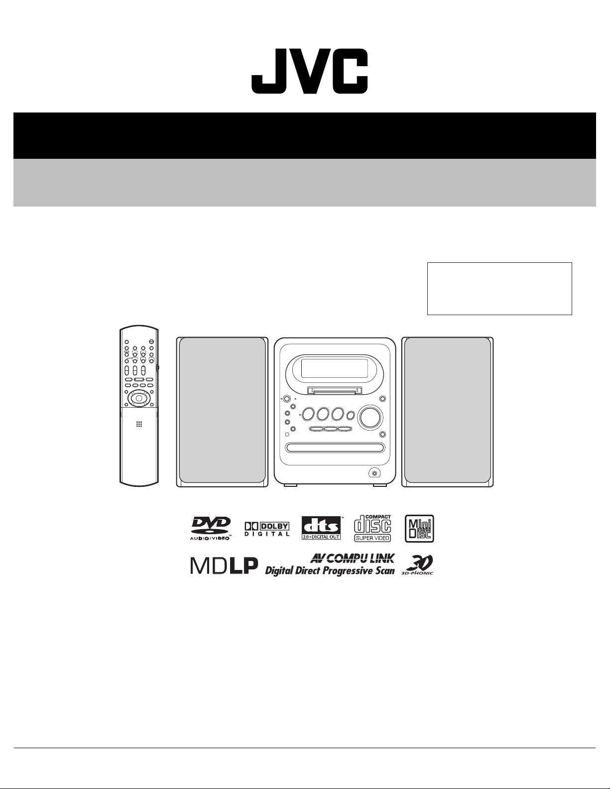
MICRO COMPONENT MD SYSTEM
UX-QD70S,UX-QD70W
Area suffix
UB ---------------------- Hong Kong
(SP-UXK30S)
(SP-UXK30W)
Lead free solder used in the board (material : Sn-Ag-Cu, melting point : 219 Centigrade)
(CA-UXQD70S)
(CA-UXQD70W)
(SP-UXK30S)
(SP-UXK30W)
TABLE OF CONTENTS
1 PRECAUTION. . . . . . . . . . . . . . . . . . . . . . . . . . . . . . . . . . . . . . . . . . . . . . . . . . . . . . . . . . . . . . . . . . . . . . . . . 1-4
2 SPECIFIC SERVICE INSTRUCTIONS . . . . . . . . . . . . . . . . . . . . . . . . . . . . . . . . . . . . . . . . . . . . . . . . . . . . . . 1-8
3 DISASSEMBLY . . . . . . . . . . . . . . . . . . . . . . . . . . . . . . . . . . . . . . . . . . . . . . . . . . . . . . . . . . . . . . . . . . . . . . . 1-9
4 ADJUSTMENT . . . . . . . . . . . . . . . . . . . . . . . . . . . . . . . . . . . . . . . . . . . . . . . . . . . . . . . . . . . . . . . . . . . . . . . 1-43
5 TROUBLESHOOTING . . . . . . . . . . . . . . . . . . . . . . . . . . . . . . . . . . . . . . . . . . . . . . . . . . . . . . . . . . . . . . . . . 1-53
COPYRIGHT © 2005 Victor Company of Japan, Limited
No.MB496
2005/12
Page 2
SPECIFICATION
MD/DVD receiver (CA-UXQD70S/CA-UXQD70W)
Amplifier Output power 20 W × 2 (10% THD/4 Ω)
Input terminals Analog AUX × 1
650 mV/47 kΩ: LEVEL1
260 mV/47 kΩ: LEVEL2
Digital Digital optical input × 1
-23 dBm to -15 dBm (Optical square terminal)
(Compatible with frequency of 32 kHz, 44.1 kHz and 48 kHz)
Output terminals Analog Speaker × 1, 20 W/4 Ω
Impedance 4 Ω - 16 Ω
Headphone (×1), 25 mW/32 Ω
Impedance 16 Ω - 1 kΩ
Digital DVD/CD optical output × 1
-23 dBm to -15 dBm (Optical square terminal)
Other AV COMPU LINK × 2 (Ø 3.5)
Tuner Frequency FM 87.50 MHz - 108.00 MHz
AM 531 kHz - 1 710 kHz (9 kHz spacing)
530 kHz - 1 710 kHz (10 kHz spacing)
DVD player Playable discs DVD VIDEO, DVD AUDIO, CD, VCD, SVCD,
CD-R/CDRW(CD, VCD, SVCD, MP3/WMA/JPEG format),
DVD-R(video format, MP3/WMA/JPEG format),
DVD-RW(video format, DVD VR format, MP3/WMA/JPEG format)
MD recorder Audio playing system MiniDisc digital audio system
Recording system Magneto-optical overwrite system
Reading system Non-contact, semiconductor laser pickup
Recording/Playback time
(when using an 80-minute MD)
Sampling frequency 44.1 kHz
Audio compression ATRAC (Adaptive TRansform
system Acoustic Coding)/ATRAC3 (MDLP)
Cassette deck Frequency response Normal (type l) 60 Hz - 14 000 Hz
General Power source AC 220 V , 50 Hz
Power consumption 55 W (at operation)
Dimensions 165 mm (W) × 200 mm (H) × 350 mm (D)
Mass (approx.) 5.1 kg
SP 80 minutes
LP2 160 minutes
LP4 320 minutes
Wow and flutter 0.15% (WRMS)
1.1 W (on standby)
1-2 (No.MB496)
Page 3
Speaker (SP-UXK30S/SP-UXK30W)
System 3-way bass reflex type
Magnetically shielded type
Speakers Woofer 10 cm cone speaker × 1
Midrange 4 cm cone speaker × 1
Tweeter 1.5 cm dome speaker × 1
Power handling capacity 20 W
Impedance 4 Ω
Frequency range 56 Hz - 40 kHz
Sound pressure level 85 dB/W·m
Dimensions 135 mm (W) × 200.5 mm (H) × 213.5 mm (D)
Mass (approx.) 2.1 kg (1 unit)
Micro component MD system (UX-QD70S/UX-QD70W)
Dimensions 435 mm (W) × 200.5 mm (H) × 350 mm (D)
Mass (approx.) 9.3 kg
U.S. and foreign patents licensed from Dolby Laboratories.
Design and specification are subject to change without notice.
(No.MB496)1-3
Page 4
SECTION 1
PRECAUTION
1.1 Safety Precautions
(1) This design of this product contains special hardware and
many circuits and components specially for safety purposes. For continued protection, no changes should be made
to the original design unless authorized in writing by the
manufacturer. Replacement parts must be identical to
those used in the original circuits. Services should be performed by qualified personnel only.
(2) Alterations of the design or circuitry of the product should
not be made. Any design alterations of the product should
not be made. Any design alterations or additions will void
the manufacturers warranty and will further relieve the
manufacture of responsibility for personal injury or property
damage resulting therefrom.
(3) Many electrical and mechanical parts in the products have
special safety-related characteristics. These characteristics are often not evident from visual inspection nor can the
protection afforded by them necessarily be obtained by using replacement components rated for higher voltage, wattage, etc. Replacement parts which have these special
safety characteristics are identified in the Parts List of Service Manual. Electrical components having such features
are identified by shading on the schematics and by ( ) on
the Parts List in the Service Manual. The use of a substitute
replacement which does not have the same safety characteristics as the recommended replacement parts shown in
the Parts List of Service Manual may create shock, fire, or
other hazards.
(4) The leads in the products are routed and dressed with ties,
clamps, tubings, barriers and the like to be separated from
live parts, high temperature parts, moving parts and/or
sharp edges for the prevention of electric shock and fire
hazard. When service is required, the original lead routing
and dress should be observed, and it should be confirmed
that they have been returned to normal, after reassembling.
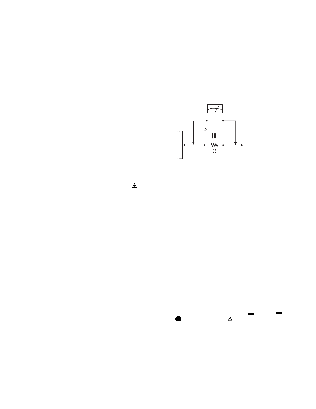
(5) Leakage shock hazard testing
After reassembling the product, always perform an isolation check on the exposed metal parts of the product (antenna terminals, knobs, metal cabinet, screw heads,
headphone jack, control shafts, etc.) to be sure the product
is safe to operate without danger of electrical shock.Do not
use a line isolation transformer during this check.
• Plug the AC line cord directly into the AC outlet. Using a
"Leakage Current Tester", measure the leakage current
from each exposed metal parts of the cabinet, particularly any exposed metal part having a return path to the
chassis, to a known good earth ground. Any leakage current must not exceed 0.5mA AC (r.m.s.).
• Alternate check method
Plug the AC line cord directly into the AC outlet. Use an
AC voltmeter having, 1,000Ω per volt or more sensitivity
in the following manner. Connect a 1,500Ω 10W resistor
paralleled by a 0.15µF AC-type capacitor between an ex-
posed metal part and a known good earth ground.
Measure the AC voltage across the resistor with the AC
voltmeter.
Move the resistor connection to each exposed metal
part, particularly any exposed metal part having a return
path to the chassis, and measure the AC voltage across
the resistor. Now, reverse the plug in the AC outlet and
repeat each measurement. Voltage measured any must
not exceed 0.75 V AC (r.m.s.). This corresponds to 0.5
mA AC (r.m.s.).
AC VOLTMETER
(Having 1000
ohms/volts,
or more sensitivity)
0.15 F AC TYPE
Place this
probe on
1500 10W
Good earth ground
1.2 Warning
(1) This equipment has been designed and manufactured to
meet international safety standards.
(2) It is the legal responsibility of the repairer to ensure that
these safety standards are maintained.
(3) Repairs must be made in accordance with the relevant
safety standards.
(4) It is essential that safety critical components are replaced
by approved parts.
(5) If mains voltage selector is provided, check setting for local
voltage.
1.3 Caution
Burrs formed during molding may be left over on some parts
of the chassis.
Therefore, pay attention to such burrs in the case of preforming repair of this system.
1.4 Critical parts for safety
In regard with component parts appearing on the silk-screen
printed side (parts side) of the PWB diagrams, the parts that are
printed over with black such as the resistor ( ), diode ( )
and ICP ( ) or identified by the " " mark nearby are critical
for safety. When replacing them, be sure to use the parts of the
same type and rating as specified by the manufacturer.
(This regulation dose not Except the J and C version)
each exposed
metal part.
1-4 (No.MB496)
Page 5
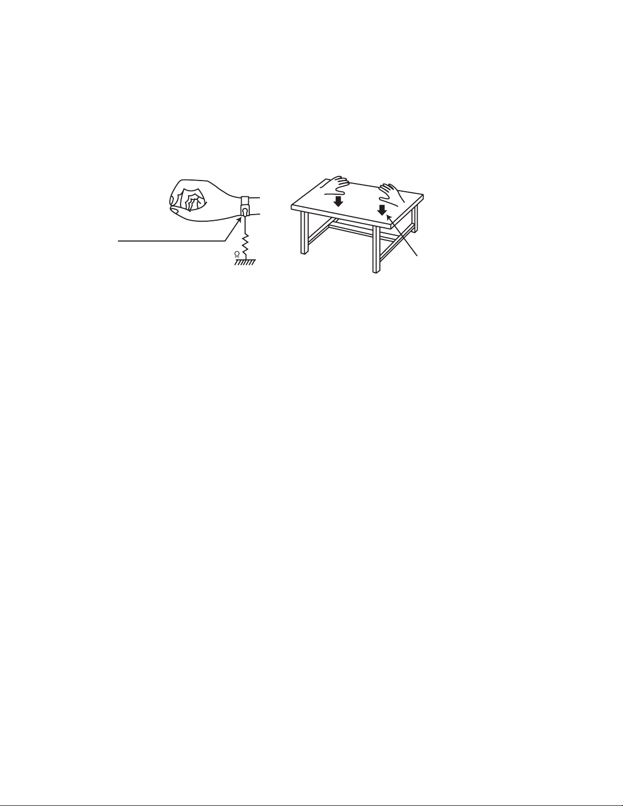
1.5 Preventing static electricity
Electrostatic discharge (ESD), which occurs when static electricity stored in the body, fabric, etc. is discharged, can destroy the laser
diode in the traverse unit (optical pickup). Take care to prevent this when performing repairs.
1.5.1 Grounding to prevent damage by static electricity
Static electricity in the work area can destroy the optical pickup (laser diode) in devices such as laser products.
Be careful to use proper grounding in the area where repairs are being performed.
(1) Ground the workbench
Ground the workbench by laying conductive material (such as a conductive sheet) or an iron plate over it before placing the
traverse unit (optical pickup) on it.
(2) Ground yourself
Use an anti-static wrist strap to release any static electricity built up in your body.
(caption)
Anti-static wrist strap
1M
Conductive material
(conductive sheet) or iron palate
(3) Handling the optical pickup
• In order to maintain quality during transport and before installation, both sides of the laser diode on the replacement optical
pickup are shorted. After replacement, return the shorted parts to their original condition.
(Refer to the text.)
• Do not use a tester to check the condition of the laser diode in the optical pickup. The tester's internal power source can easily
destroy the laser diode.
1.6 Handling the traverse unit (optical pickup)
(1) Do not subject the traverse unit (optical pickup) to strong shocks, as it is a sensitive, complex unit.
(2) Cut off the shorted part of the flexible cable using nippers, etc. after replacing the optical pickup. For specific details, refer to the
replacement procedure in the text. Remove the anti-static pin when replacing the traverse unit. Be careful not to take too long a
time when attaching it to the connector.
(3) Handle the flexible cable carefully as it may break when subjected to strong force.
(4) I t is not possible to adjust the semi-fixed resistor that adjusts the laser power. Do not turn it.
(No.MB496)1-5
Page 6
1.7 Attention when pickup unit is removed
r
1.7.1 Attention when MD pickup unit is removed
*Please refer to "DISASSEMBLY" in the text.
(1) Apply solder to short land section before the flexible wire is disconnected from the connector CN310 on the MD servo control
board.
(If the flexible wire is disconnected without applying solder, the pickup may be destroyed by static electricity.)
(2) In the assembly, be sure to remove solder from the short land section after connecting the flexible wire.
MD servo control board
MD servo control board
CN310
Short land section
Flexible wire
Pickup
(3) Apply solder to short land section before the flexible wire is disconnected from the connector on the pickup.
(If the flexible wire is disconnected without applying solder, the pickup may be destroyed by static electricity.)
(4) In the assembly, be sure to remove solder from the short land section after connecting the flexible wire.
Pickup
Short land section
Flexible wire
1.7.2 Attention when DVD pickup unit is removed
*Please refer to "DISASSEMBLY" in the text.
(1) Apply solder to short land sections before the card wire is disconnected from the connector on the pickup.
(If the card wire is disconnected without applying solder, the pickup may be destroyed by static electricity.)
(2) In the assembly, be sure to remove solder from the short land sections after connecting the card wire.
Short land sections
Pickup
Card wire
Connecto
1-6 (No.MB496)
Page 7
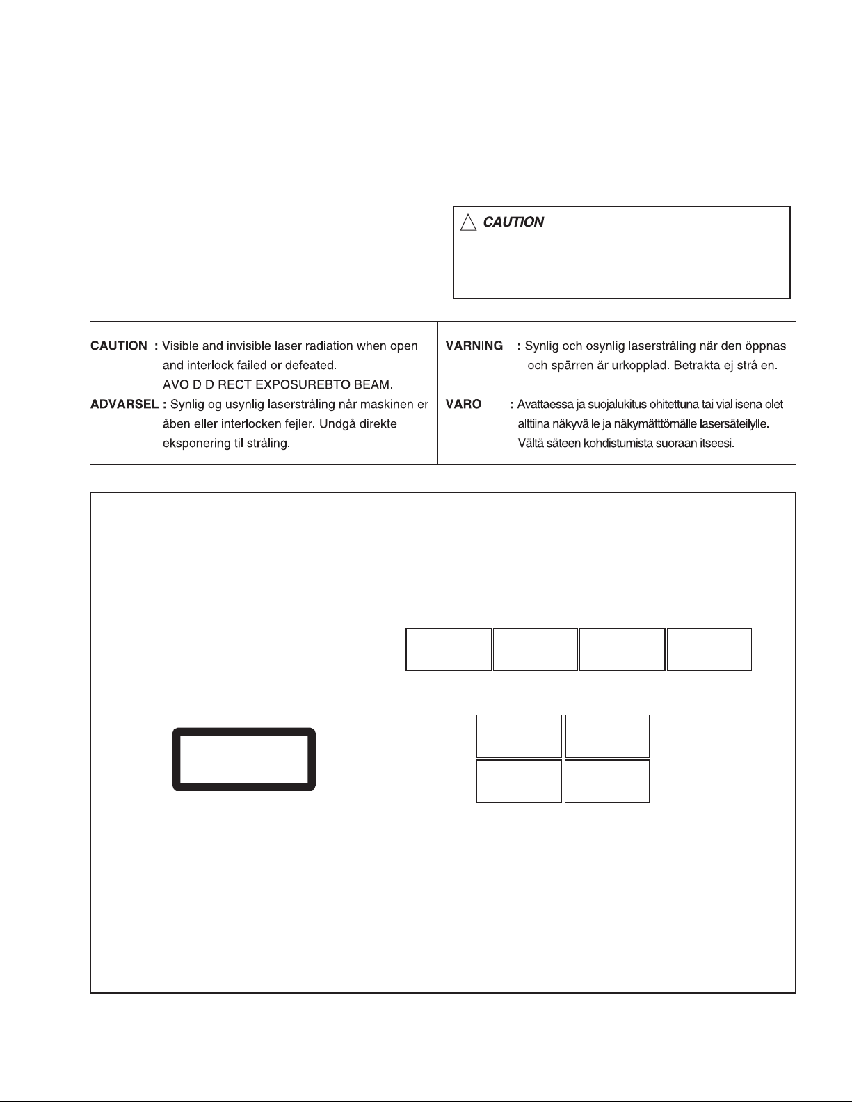
1.8 Important for laser products
!
1.CLASS 1 LASER PRODUCT
2.DANGER : Invisible laser radiation when open and inter
lock failed or defeated. Avoid direct exposure to beam.
3.CAUTION : There are no serviceable parts inside the
Laser Unit. Do not disassemble the Laser Unit. Replace
the complete Laser Unit if it malfunctions.
4.CAUTION : The CD,MD and DVD player uses invisible
laser radiation and is equipped with safety switches which
prevent emission of radiation when the drawer is open and
the safety interlocks have failed or are defeated. It is
dangerous to defeat the safety switches.
5.CAUTION : If safety switches malfunction, the laser is able
to function.
6.CAUTION : Use of controls, adjustments or performance of
procedures other than those specified here in may result in
hazardous radiation exposure.
Please use enough caution not to
see the beam directly or touch it
in case of an adjustment or operation
check.
REPRODUCTION AND POSITION OF LABELS
WARNING LABEL
CAUTION : Visible and Invisible
laser radiation when open and
interlock failed or defeated.
AVOID DIRECT EXPOSURE TO
BEAM. (e)
CLASS 1
LASER PRODUCT
ADVARSEL : Synlig og usynlig
laserstråling når maskinen er
åben eller interlocken fejeler.
Undgå direkte eksponering til
stråling. (d)
CAUTION : Visible and Invisible
laser radiation when open and
interlock failed or defeated.
AVOID DIRECT EXPOSURE TO
BEAM. (e)
VARNING : Synlig och
osynling laserstrålning när
den öppnas och spärren är
urkopplad. Betrakta ej
strålen. (s)
VARNING : Synlig och
osynling laserstrålning när
den öppnas och spärren är
urkopplad. Betrakta ej
strålen. (s)
VARO : Avattaessa ja suojalukitus
ohitettuna tai viallisena olet alttiina
näkyvälle ja näkymättömälle
lasersäteilylle. Vältä säteen
kohdistumista suoraan itseesi. (f)
ADVARSEL : Synlig og usynlig
laserstråling når maskinen er
åben eller interlocken fejeler.
Undgå direkte eksponering til
stråling. (d)
VARO : Avattaessa ja suojalukitus
ohitettuna tai viallisena olet alttiina
näkyvälle ja näkymättömälle
lasersäteilylle. Vältä säteen
kohdistumista suoraan itseesi. (f)
(No.MB496)1-7
Page 8

SECTION 2
SPECIFIC SERVICE INSTRUCTIONS
This service manual does not describe SPECIFIC SERVICE INSTRUCTIONS.
1-8 (No.MB496)
Page 9
SECTION 3
DISASSEMBLY
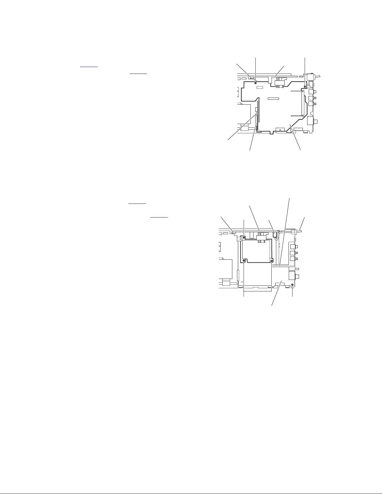
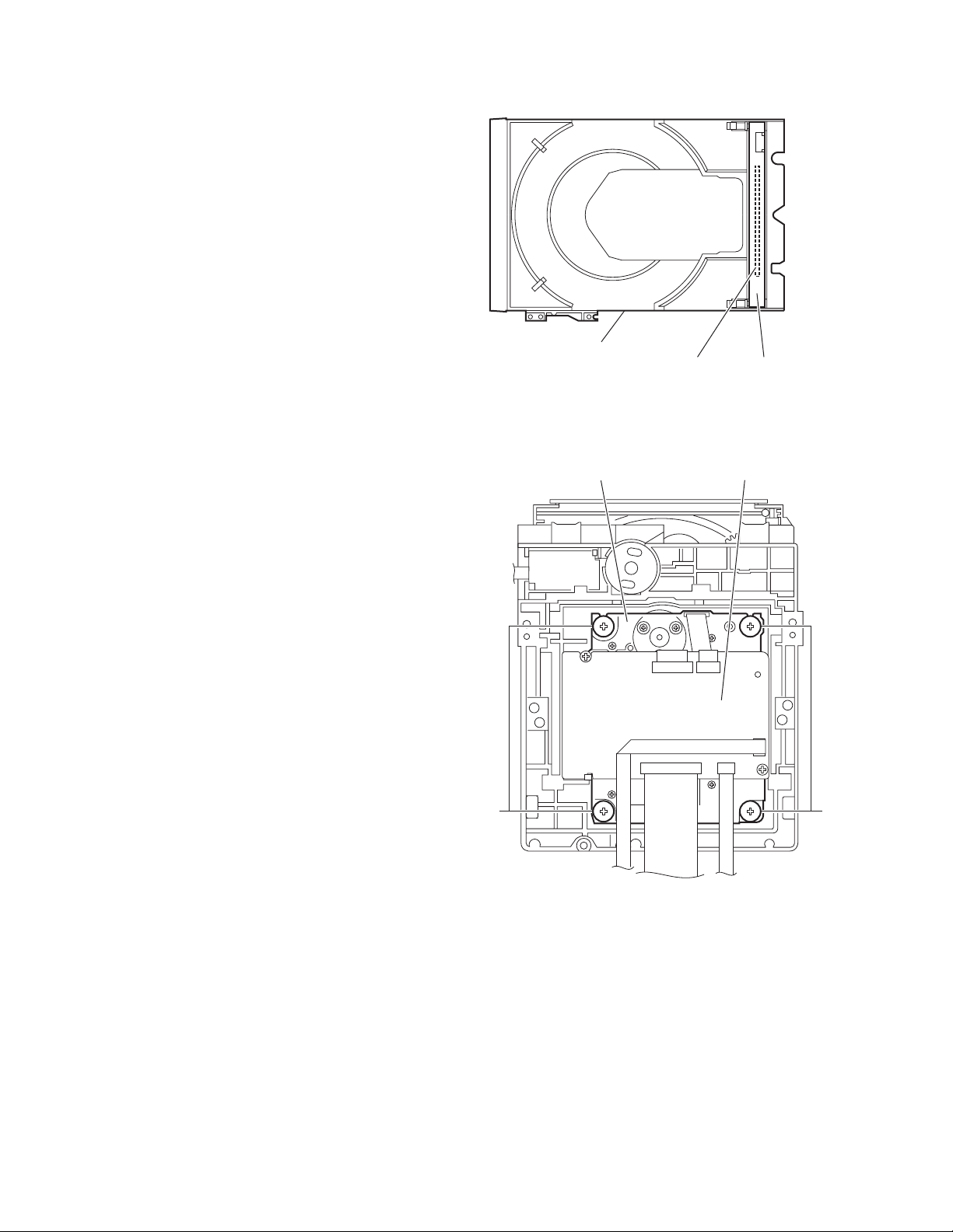
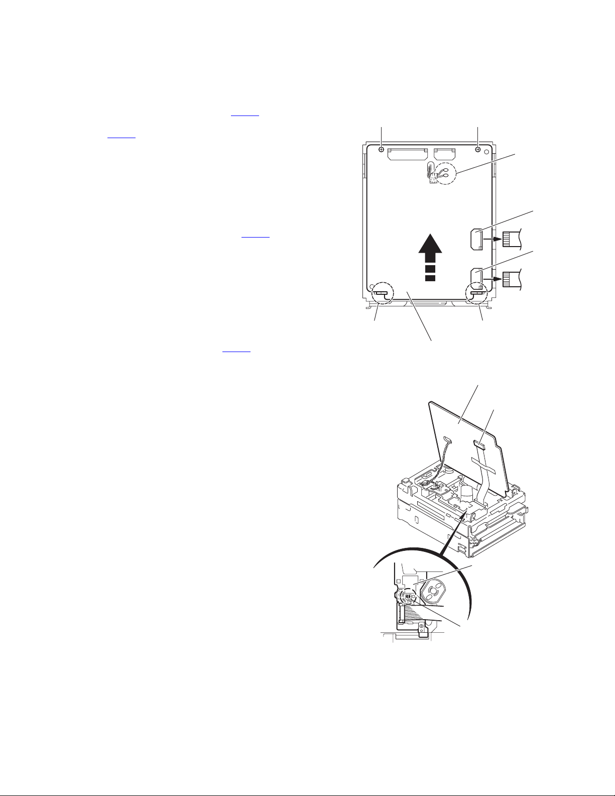
3.1 Main body section
3.1.1 Removing the rear cover(B)
(See Figs.1 and 2)
(1) From the back side of the main body, remove the twelve
screws A attaching the rear cover(B). (See Fig.1.)
(2) From the bottom side of the main body, remove the three
screws B attaching the rear cover(B). (See Fig.2.)
(3) Remove the rear cover(B) from the main body.
A
Rear cover(B)
B
A AA
Fig.1
Rear cover(B)
Fig.2
(No.MB496)1-9
Page 10
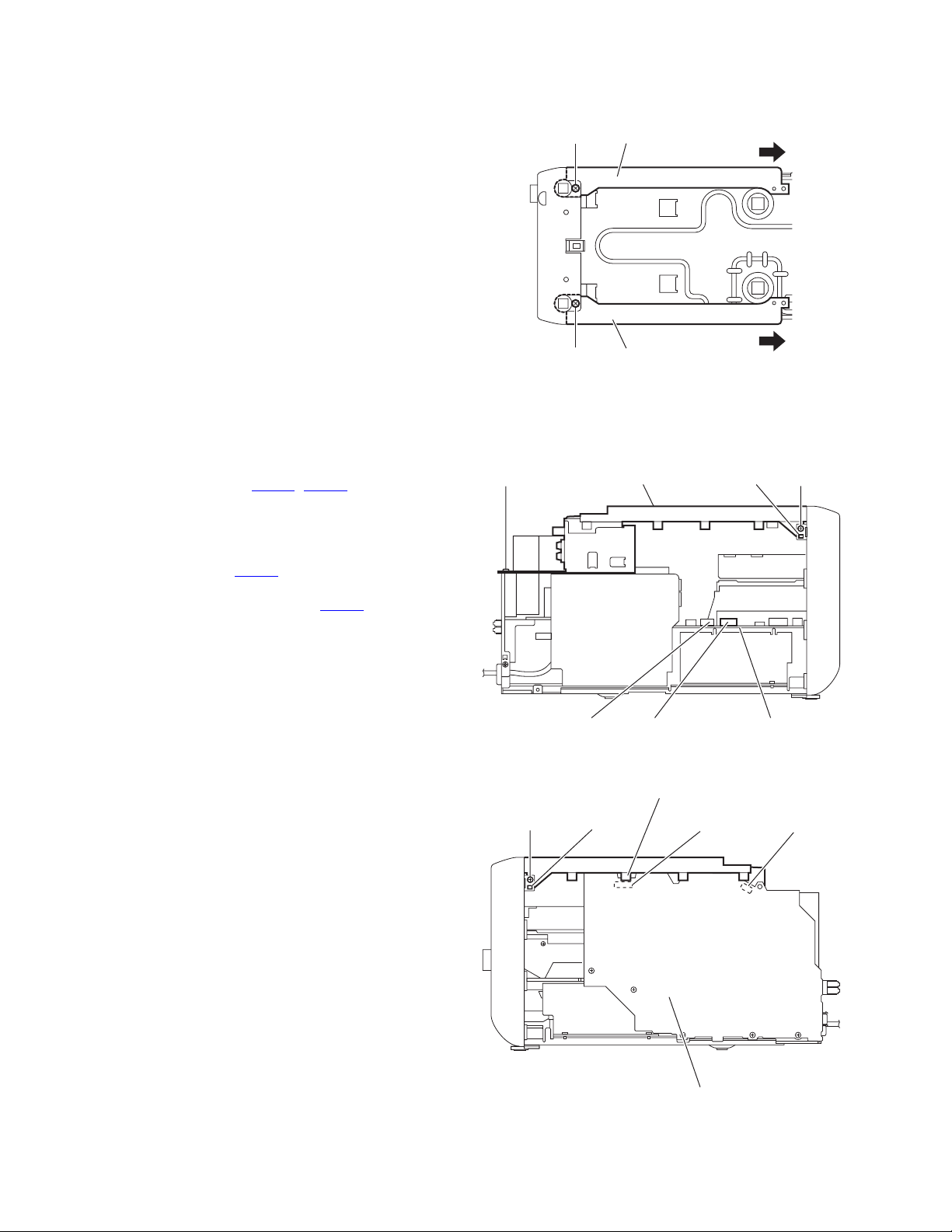
3.1.2 Removing the side panels (L)/(R)
(See Fig.3)
• Remove the rear cover(B).
(1) From the bottom side of the main body, remove the two
screws C attaching the side panels (L)/(R).
(2) Slide the side panels (L)/(R) in the direction of the arrow
and remove the side panels (L)/(R).
3.1.3 Removing the top cover assembly
(See Figs.4 and 5)
• Remove the rear cover(B) and side panels(L)/(R).
(1) From the left side of the main body, disconnect the card
wires from the connectors (CN703
board. (See Fig.4.)
(2) Remove the screw D attaching the top cover assembly.
(See Fig.4.)
(3) From the right side of the main body, disconnect the card
wire from the connector CN105
Fig.5.)
(4) Disconnect the wire from the connector CN108
board. (See Fig.5.)
(5) From the both sides of the main body, remove the two
screws E attaching the top cover assembly. (See Figs.4
and 5.)
(6) Release the joints a and remove the top cover assembly.
(See Figs.4 and 5.)
, CN709) on the micon
on the main board. (See
on the main
Side panel (R)
C
Side panel (L)
C
Fig.3
Top cover assembly
a
ED
Micon boardCN703 CN709
1-10 (No.MB496)
E
Fig.4
Top cover assembly
a
CN105
Main board
Fig.5
CN108
Page 11
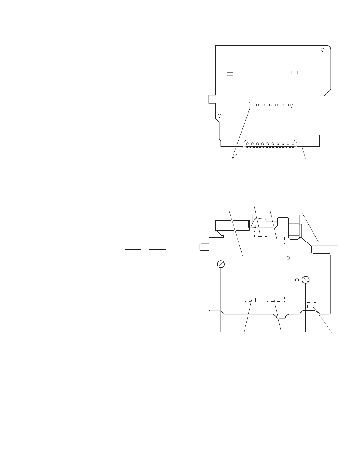
3.1.4 Removing the front panel assembly
(See Figs.6 to 8)
• Remove the rear cover(B), side panels(L)/(R) and top cover
assembly.
(1) From the left side of the main body, disconnect the card
wires from the connectors (CN702
board. (See Fig.6.)
(2) From the both sides and bottom sides of the main body, re-
lease the joints b and joint c. (See Figs.6 to 8.)
(3) Remove the front panel assembly in the direction of the ar-
row. (See Fig 8.)
, CN710) on the micon
Front panel assembly
CN702
CN710
Micon board
Front panel assembly
c
b
Fig.6
b
Fig.7
Front panel assembly
Fig.8
(No.MB496)1-11
Page 12
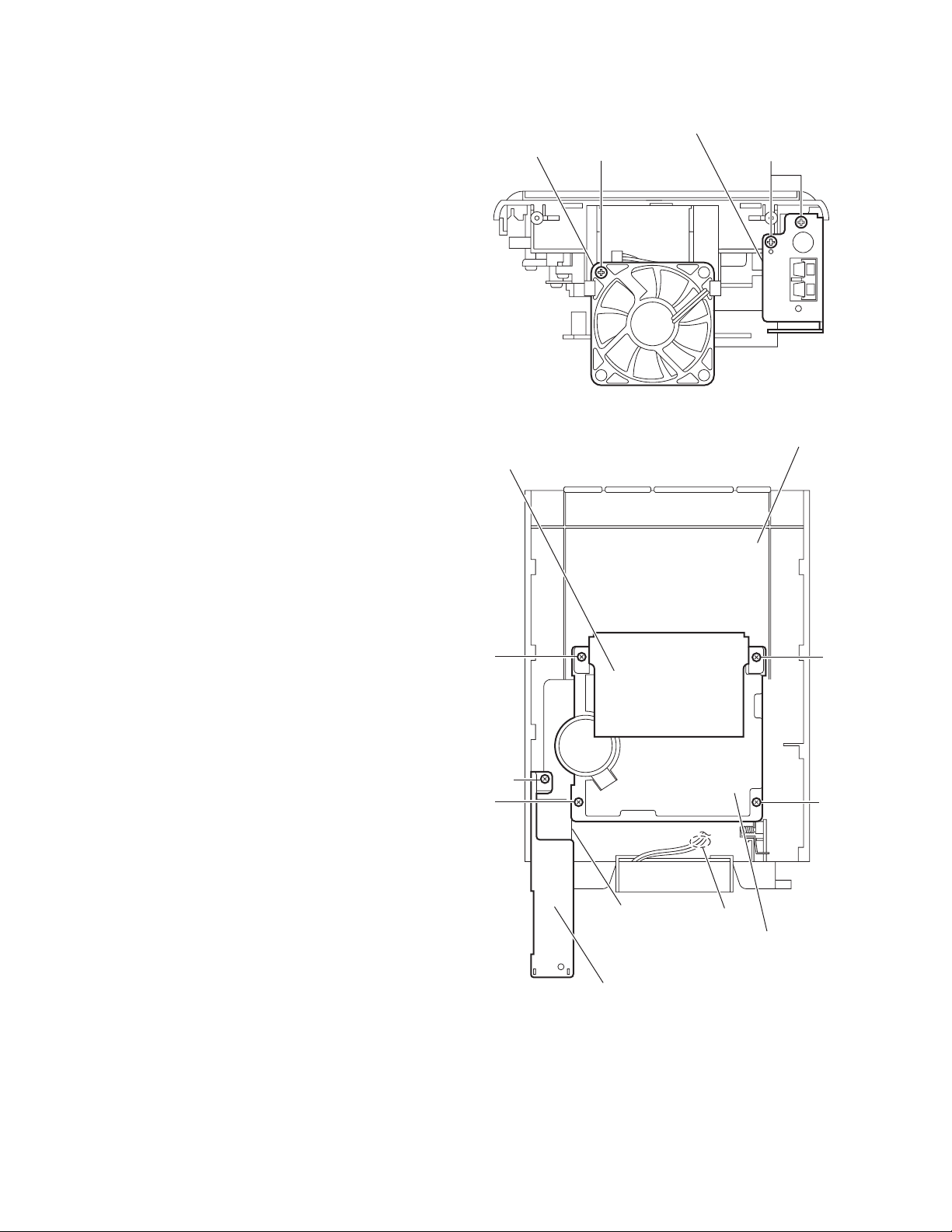
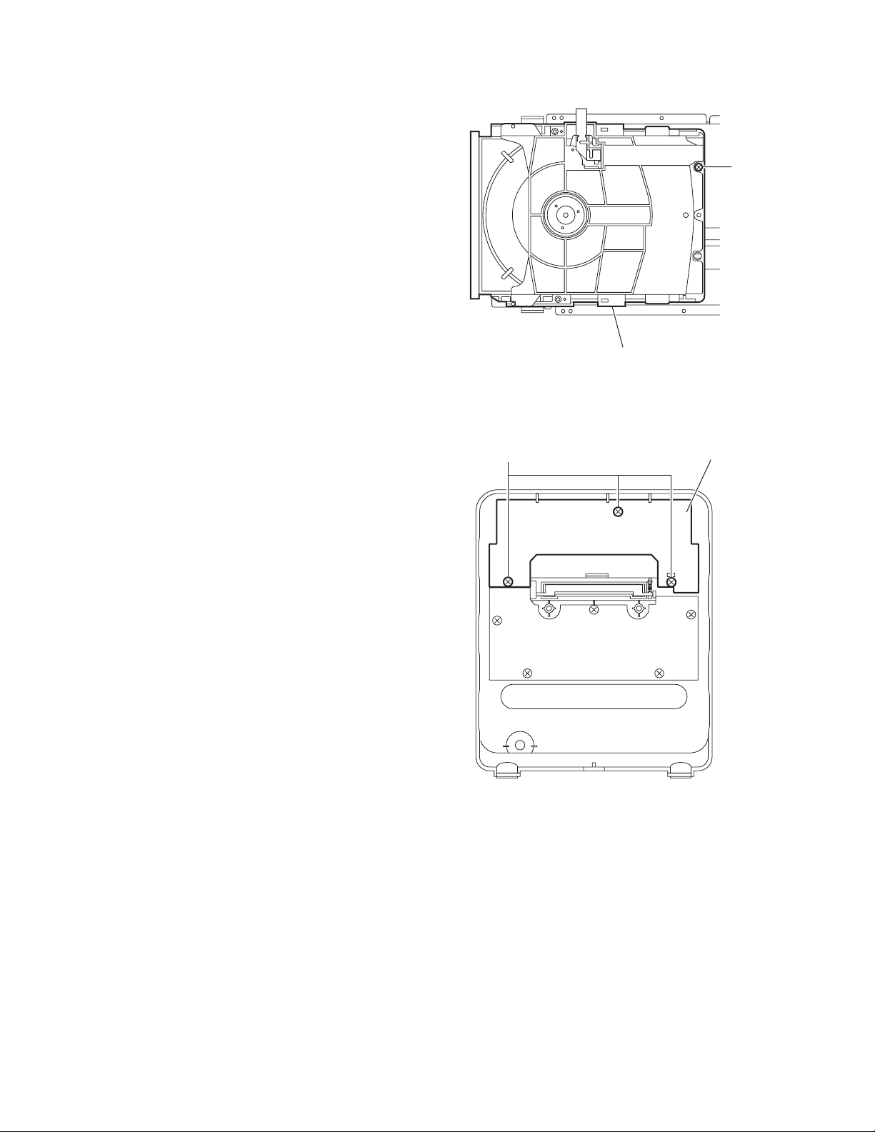
3.1.5 Removing the fan motor
(See Figs.9 and 10)
• Remove the rear cover(B), side panels(L)/(R) and top cover
assembly.
(1) From the back side of the top cover assembly, remove the
screw F attaching the fan motor. (See Fig.9.)
(2) Take out the fan motor.
Reference:
When attaching the fan motor, pass the wire through the slot
d. (See Fig.10.)
3.1.6 Removing the tuner and tuner bracket
(See Figs.9 and 10)
• Remove the rear cover(B), side panels(L)/(R) and top cover
assembly.
(1) From the back side of the top cover assembly, remove the
two screws G attaching the tuner bracket. (See Fig.9.)
(2) From the inside of the top cover assembly, remove the
screw H attaching the tuner bracket. (See Fig.10.)
(3) Take out the tuner with the tuner bracket.
Fan motor
F
Tuner bracket
G
Fig.9
3.1.7 Removing the cassette mechanism assembly
(See Fig.10)
• Remove the rear cover(B), side panels(L)/(R) and top cover
assembly.
(1) From the inside of the top cover assembly, remove the four
screws J attaching the cassette mechanism assembly.
(2) Remove the cassette mechanism assembly.
Top cover assembly
Shield
J
J
H
JJ
1-12 (No.MB496)
Tuner
Tuner bracket
d
Cassette mechanism assembly
Fig.10
Page 13
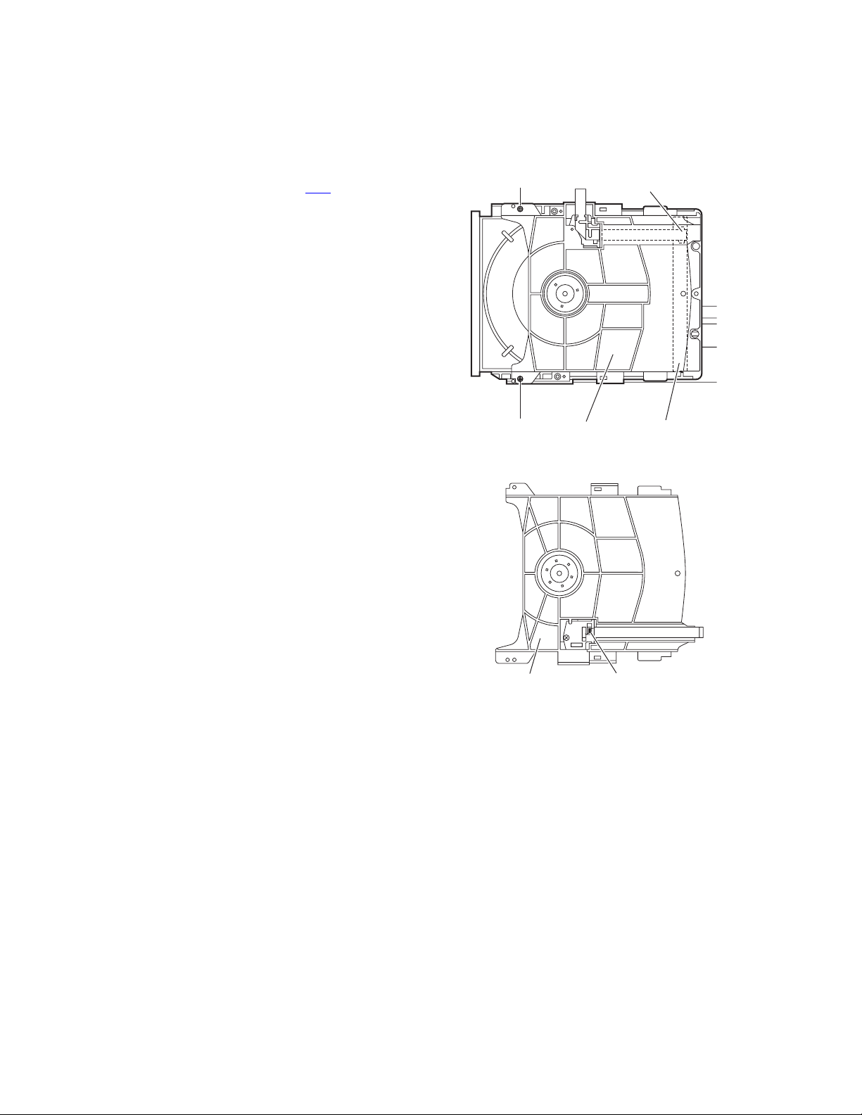
3.1.8 Removing the heat sink(B)
(See Fig.11)
• Remove the rear cover(B), side panels(L)/(R) and top cover
assembly.
(1) From the back side of the main body, remove the three
screws K and two screws M attaching the heat sink(B).
(2) Remove the heat sink(B) from the main body.
3.1.9 Removing the heat sink bracket
(See Figs.11 and 12)
• Remove the rear cover(B), side panels(L)/(R), top cover as-
sembly and heat sink(B).
(1) From the back side of the main body, remove the two
screws N attaching the heat sink bracket. (See Fig.11.)
(2) From the top side of main body, remove the screw P at-
taching the heat sink bracket to the regulator board.(See
Fig.12)
(3) Take out the heat sink(B) from the main body.
K
Heat sink bracket
Heat sink(B)
M
3.1.10 Removing the main board
(See Figs.12 and 13)
• Remove the rear cover(B), side panels(L)/(R), top cover as-
sembly and heat sink(B).
(1) From the forward side of the main board, disconnect the
card wire from the connector CN107
(2) From the right side of the main body, remove the four
screws Q attaching the main board. (See Fig.13.)
(3) Disconnect the connectors (CN101
CN110) on the main board toward this side. (See Fig.13.)
(4) From the forward side of the main board, disconnect the
wires from the connectors (CN109
Fig.13.)
. (See Fig.12.)
to CN103, CN106 and
and CN111). (See
CN107
CN103 CN102
Fig.11
Fig.12
CN 111
Main board
CN101
N
P
CN110
CN109
Main board
CN106
QQ
Fig.13
(No.MB496)1-13
Page 14
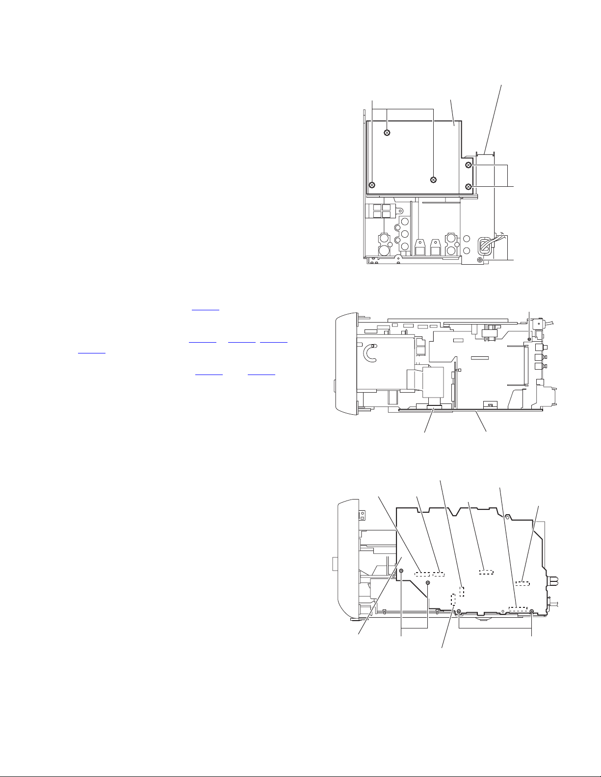
3.1.11 Removing the regulator board
(See Fig.14)
• Remove the rear cover(B), side panels(L)/(R), top cover as-
sembly, heat sink(B) and main board.
(1) From the top side of the main body, disconnect the wire
from the connector CN902
(2) Disconnect the wire from the connector CN807
board.
(3) Remove the two screws R attaching the regulator board.
(4) Take out the regulator board from the main body.
Reference:
After reassembling, bundle the wire with the new tie band as
before.
3.1.12 Removing the trans board
(See Fig.15)
• Remove the rear cover(B), side panels(L)/(R), top cover as-
sembly, heat sink(B), main board and regulator board.
(1) Disconnect the wire from the connector CN903
board.
(2) Disconnect the power cord from the connector CN901
the trans board.
(3) Remove the three screws S attaching the power transform-
er and take out the trans board from the main body.
Reference:
After reassembling, bundle the wire with the new tie band as
before.
on the trans board.
on the joint
on the trans
on
CN902
Joint board
Trans board
CN903
CN807
S
R
Fig.14
CN901
R
Trans board
Regulator board
Video board
Power cord
3.1.13 Removing the jack board and video board
(See Fig.15)
• Remove the rear cover(B), side panels(L)/(R), top cover as-
sembly, heat sink(B), main board and regulator board.
(1) Remove the screw T attaching the jack board and take out
the jack board with the video board.
S T
Jack board
Fig.15
1-14 (No.MB496)
Page 15
3.1.14 Removing the power transformer
(See Fig.16)
• Remove the rear cover(B), side panels(L)/(R), top cover as-
sembly, heat sink(B), main board, regulator board and trans
board.
(1) From the reverse side of the trans board, remove the sol-
ders from the sections e on the trans board.
(2) Remove the power transformer from the trans board.
3.1.15 Removing the joint board
(See Fig.17)
• Remove the rear cover(B), side panels(L)/(R), top cover as-
sembly, heat sink(B), main board, regulator board and trans
board.
(1) From the back side of the main body, remove the two
screws U attaching the joint board.
(2) Remove the connector CN805
micon board toward this side.
(3) From the forward side of the joint board, disconnect the
card wires from the connectors (CN801
joint board.
(4) Take out the joint board from the main body.
on the joint board from the
to CN804) on the
e
Joint board
CN803
Fig.16
CN805
Trans board
Micon board
UU
CN802
CN801
Fig.17
(No.MB496)1-15
CN804
Page 16
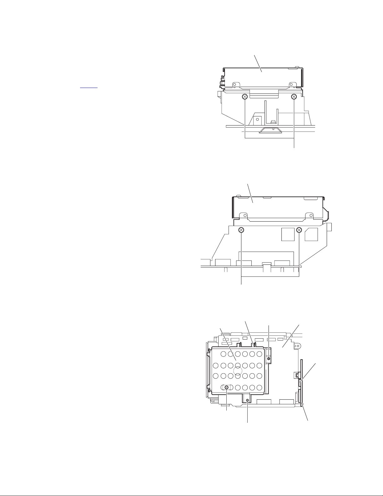
3.1.16 Removing the MD mechanism assembly
(See Figs.18 to 20)
• Remove the rear cover(B), side panels(L)/(R), top cover as-
sembly, front panel assembly, heat sink(B) and main board.
(1) From the both side of the main body, remove the four
screws V attaching the MD mechanism assembly. (See
Figs.18 and 19.)
(2) From the top of the main body, disconnect the card wire
from the connector CN803
(3) Take out the MD mechanism assembly from the main
body.
3.1.17 Removing the MD holder
(See Fig 20)
• Remove the rear cover(B), side panels(L)/(R), top cover as-
sembly, front panel assembly, heat sink(B), main board and
MD mechanism assembly.
(1) From the top side of the main body, remove the shield(MD).
(2) Remove the two screws W and screw X attaching the MD
holder to the micon board.
(3) Take out the MD holder from main body.
on the joint board. (See Fig.20)
MD mechanism assembly
V
Fig.18
MD mechanism assembly
MD holder
Shield(MD)
X
V
W
Fig.19
W
Fig.20
Micon board
CN803
Joint board
1-16 (No.MB496)
Page 17
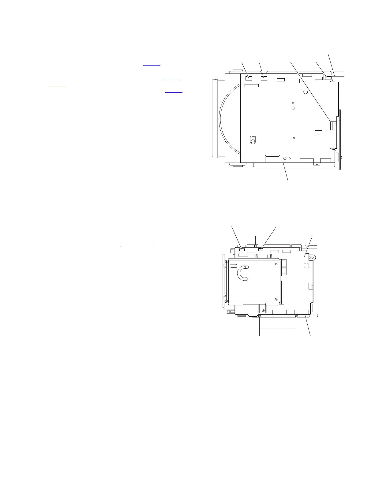
3.1.18 Removing the micon board
(See Fig.21)
• Remove the rear cover(B), side panels(L)/(R), top cover as-
sembly, front panel assembly, heat sink(B), main board, MD
mechanism assembly, MD holder and regulator board.
(1) Disconnect the wire from the connector CN903
board. (See Fig.21.)
(2) Disconnect the card wires from the connectors (CN705
) on the micon board. (See Fig.21.)
CN711
(3) Disconnect the micon board from the connector CN805
the joint board. (See Fig.21.)
(4) Take out the micon board from the main body.
3.1.19 Removing the CD mechanism bracket
(See Fig.22)
• Remove the rear cover(B), side panels(L)/(R), top cover as-
sembly, heat sink(B), heat sink bracket, main board, regulator
board, trans board and joint board.
(1) From the top side of the main body, disconnect the wires
from the connectors (CN705
board.
(2) Remove the four screws Y attaching the CD mechanism
bracket.
(3) Take out the CD mechanism bracket from the main body.
and CN711) on the micon
on the trans
and
on
Y
Micon board
Fig.21
CN705CN711
Y
Trans board
CN903CN705CN711 CN805
Micon board
Y
CD mechanism bracket
Fig.22
(No.MB496)1-17
Page 18
3.1.20 Removing the DVD mechanism assembly
(See Fig.23)
• Remove the rear cover(B), side panels(L)/(R), top cover as-
sembly, heat sink(B), main board, regulator board, trans
board, CD mechanism bracket and joint board.
(1) From the top side of the main body, remove the screw Z at-
taching the DVD mechanism assembly.
(2) Take out the DVD mechanism assembly from the main
body.
Note:
When removing the DVD mechanism assembly, be careful not
to damage the lower board and parts.
3.1.21 Removing the LCD board
(See Fig.24)
• Remove the rear cover(B), side panels(L)/(R), top cover as-
sembly and front panel assembly.
(1) From the inside of the front panel assembly, remove the
three screws AA attaching the LCD board.
(2) Take out the LCD board from the front panel assembly.
Note:
When attaching the LCD board, be careful not to damage the
LCD panel.
AA
Z
DVD mechanism assembly
Fig.23
LCD board
1-18 (No.MB496)
Fig.24
Page 19
3.1.22 Removing the key board
(See Fig.25)
• Remove the rear cover(B), side panels(L)/(R), top cover as-
sembly and front panel assembly.
(1) From the inside of the front panel assembly, remove the
five screws AB attaching the key board.
(2) Take out the key board from the front panel assembly.
Key board
AB
3.1.23 Removing the headphone board
(See Fig.26)
• Remove the rear cover(B), side panels(L)/(R), top cover as-
sembly, heat sink(B), main board, regulator board, trans
board, joint board, CD mechanism bracket and DVD mechanism assembly.
(1) From the top side of the main body, remove the screw AC
attaching the headphone board.
(2) Take out the headphone board from the main body.
Fig.25
AC
Headphone board
Fig.26
(No.MB496)1-19
Page 20
3.2 DVD mechanism assembly
• Remove the DVD mechanism assembly from main body.
(Refer the Disassembly method)
3.2.1 Removing the DVD cover
(See fig.1 and 2)
(1) Remove the two screws A attaching the DVD cover from
top side of DVD mechanism assembly. (See fig.1)
(2) Remove the card wire from the connector CN4
assembly. (See fig.1)
(3) Remove the DVD cover.
Caution:
The spring which presses down a card wire is attached to the
DVD cover. Please do not let me lose a spring.
on the LED
A
CN4
A
DVD cover
DVD cover
Fig.1
Spring
Fig.2
LED assembly
1-20 (No.MB496)
Page 21
3.2.2 Removing the tray assembly
(See fig.3 and 4)
• Remove the DVD cover.
(1) From the right-hand side of a DVD mechanism assembly,
a slide cam is pushed and a tray assembly is pulled out in
the direction of an arrow. (See fig.3)
(2) Remove the two screws B attaching the tray assembly
form the upper surface of a DVD mechanism assembly.
(See fig.4)
(3) Bushing of a tray assembly is removed from the projection
part a of a DVD mechanism, and a tray assembly is removed. (See fig.4)
Tray assembly DVD mechanism assembly
Slide cam
Fig.3
Projection part a
B
Projection part a
Fig.4
Tray assembly
(No.MB496)1-21
Page 22
3.2.3 Removing the LED assembly
(See fig. 5)
• Remove the DVD cover and tray assembly.
(1) From the upper surface of a tray assembly, the double-sid-
ed tape which has attached the LED assembly is removed,
and a LED board is removed.
3.2.4 Removing the traverse mechanism assembly
(See fig.6)
• Remove the DVD cover.
(1) Remove the four screws C attaching the traverse mecha-
nism assembly form bottom surface of the DVD mechanism.
(2) Remove the traverse mechanism and DVD servo board to-
gether.
Tray assembly
Fig.5
Traverse mechanism assembly
LED assemblyDouble face tape
DVD servo board
1-22 (No.MB496)
CC
Fig.6
Page 23
3.2.5 Removing the DVD servo board
(See fig.7 and 8)
• Remove the DVD cover and traverse mechanism.
(1) The short land section b of a pickup is soldered. (See fig.7)
Caution:
• Please solder to the short land section b of a pickup
before removing a card wire from the connector
of a DVD servo board.
CN101
If a card wire is removed without soldering, a pickup
may be destroyed by static electricity. (See fig.7 and 8)
• At the time of DVD servo board attachment, please remove the solder of the short land section b of a pickup
after attaching a card wire in a connector CN101
fig.7 and 8)
(2) The lock of connector CN101
moved in the direction of an arrow, and a card wire is removed. (See fig.8)
(3) Remove the two screws D attaching the DVD servo board
from bottom surface of traverse mechanism assembly.
(See fig.8)
(4) Remove the card wire from connector CN201
board. (See fig.8)
(5) A DVD servo board is raised from the connection part c,
and it removes in the direction of an arrow from hook d.
(See fig.8)
of a DVD servo board is re-
of DVD servo
. (See
b
Traverse mechanism assembly
Card wire
D
DVD pickup
Fig.7
CN101 CN201
Card wire
c
d
DVD servo board
D
Traverse mechanism assembly
Fig.8
(No.MB496)1-23
Page 24
3.2.6 Removing the pickup
(See fig.7 to 11)
• Remove the DVD cover and traverse mechanism assembly.
(1) The short land section b of a pickup is soldered. (See fig.7)
Caution:
• Please solder to the short land section b of a pickup
before removing a card wire from the connector of
pickup.
If a card wire is removed without soldering, a pickup
may be destroyed by static electricity. (See fig.7 and 9)
• At the time of pickup attachment, please remove the
solder of the short land section b of a pickup. (See fig.7
and 9)
(2) Remove the card wire from connector of pickup. (See fig.9)
(3) From the upper surface of traverse mechanism, remove
the one screw E attaching the feed bracket from part e.
(See fig.9)
(4) A trust spring is removed from hook f and a trust spring is
removed in the direction of an arrow. (See fig.9)
(5) From the g section of a traverse mechanism assembly, the
guide shaft of a DVD pickup is moved in the direction of an
arrow, and it removes from the h section. (See fig.10)
(6) From the j section of a traverse mechanism assembly, a
pickup is removed and a pickup is removed together with a
shaft. (See fig.10)
(7) Remove the tow screws F attaching the lock arm and lock
arm spring. (See fig.10)
(8) Remove the shaft from pickup. (See fig.11)
g
Guide chaft
DVD pickup
Traverse mechanism assembly
Rod spring
h
j
Fig.10
DVD pickup
Feed bracket
E
Trust spring
e
Card wire
f
Trust spring
Connector
Lock arm
Guide shaft
F
Lock arm spring
Fig.11
DVD pickup
1-24 (No.MB496)
Fig.9
Page 25
3.2.7 Attaching the pickup
(See fig.9 to 12)
• Refer the "Removing the pickup".
(1) Attach the guide shaft, lock arm and lock arm spring to
DVD pickup. (See fig.11)
(2) A pickup is united with the j section of a traverse mecha-
nism assembly, and the both ends of a pickup shaft are attached in the g section and the h section. (See fig.10)
Reference:
When attaching a guide shaft in the h section, it puts into
the bottom of a rod spring.
(3) Attach the trust spring and feed bracket. (See fig.9)
(4) The solder of the short land section b of a pickup is re-
moved after attaching a card wire in the connector of a
pickup. (See fig.7)
(5) A screw shaft gear is turned in the direction 1 of an arrow,
and until full movement of the pickup is made to carry out
in the direction 2 of an arrow. (See fig.12)
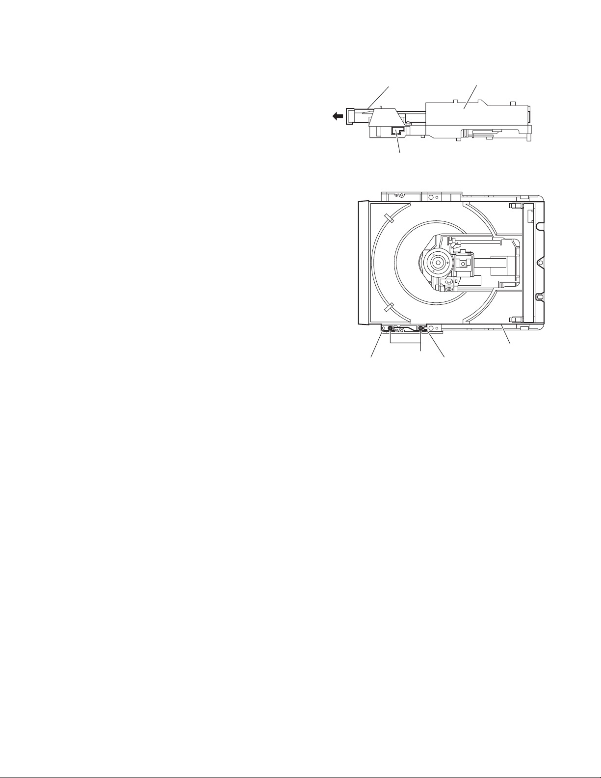
3.2.8 Removing the feed motor
(See fig.9 and 13)
• Remove the DVD cover and traverse mechanism assembly.
(1) Remove the one screw E attaching the feed bracket is re-
moved from the upper surface of a traverse mechanism assembly, and a feed bracket is removed from the e section.
(See fig.9)
(2) A trust spring is removed from hook f and a trust spring is
removed in the direction of an arrow. (See fig.13)
(3) Remove the yellow wire and white wire from soldered sec-
tion k of spindle motor board. (See fig.13)
Reference:
Attaching the feed motor, the wire through the part m of
spindle base. (See fig.13)
(4) The screw shaft shift to direction of the arrow.
(5) Remove the one screw G attaching the feed motor from
side surface of traverse mechanism assembly. (See fig.13)
(6) Remove the feed motor. (See fig.13)
Screw shaft gear
DVD pickup
Fig.12
G
Rod spring
Screw shaft
Wire
m
k
Spindle moter board
Traverse mechanism assembly
Fig.13
(No.MB496)1-25
Page 26
3.2.9 Removing the spindle motor board
(See fig.13 and 14)
• Remove the DVD cover, traverse mechanism assembly and
DVD servo board.
(1) Remove the yellow wire and white wire from soldered sec-
tion k of spindle motor board. (See fig.13)
(2) Remove the three screws H attaching the feed motor
board. (See fig.14)
Reference:
• When attach the spindle motor board, card wire through the
part n of the traverse mechanism assembly. (See fig.14)
• When attach the screw H, apply grew. (See fig.14)
Traverse mechanism assembly
n
H
3.2.10 Removing the switch board
(See fig.15)
(1) Remove the wire attaching the soldered section of switch
board on part p of switch board from bottom surface of
DVD mechanism.
(2) Remove the one screw J attaching the switch board.
(3) A switch board is raised pushing the hook of a DVD mech-
anism assembly in the direction of an arrow, and it removes
from the r section.
Reference:
Wire hook to part s after switch board attach to DVD mechanism.
3.2.11 Removing the motor
(See fig.15 and 16)
• DVD cover and tray assembly.
(1) Remove the wire attach to part p of switch board from bot-
tom surface of DVD mechanism assembly. (See fig.15)
(2) Remove the belt of motor pulley from top surface of DVD
mechanism. (See fig.16)
Caution:
Be careful not to make grease adhere to a belt.
(3) Remove the two screws K attaching the motor to DVD
mechanism assembly, remove the motor from bottom surface of DVD mechanism assembly. (See fig.16)
Reference:
Wire hook to part s after motor attached DVD mechanism.
(See fig.15)
Spindle motor
board
Switch board
p
H
wire
J
r
s
DVD mechanism assembly
DVD mechanism assembly
Motor Pulley
Fig.14
q
Tray assembly
Fig.15
J
Belt
1-26 (No.MB496)
K
Fig.16
Page 27
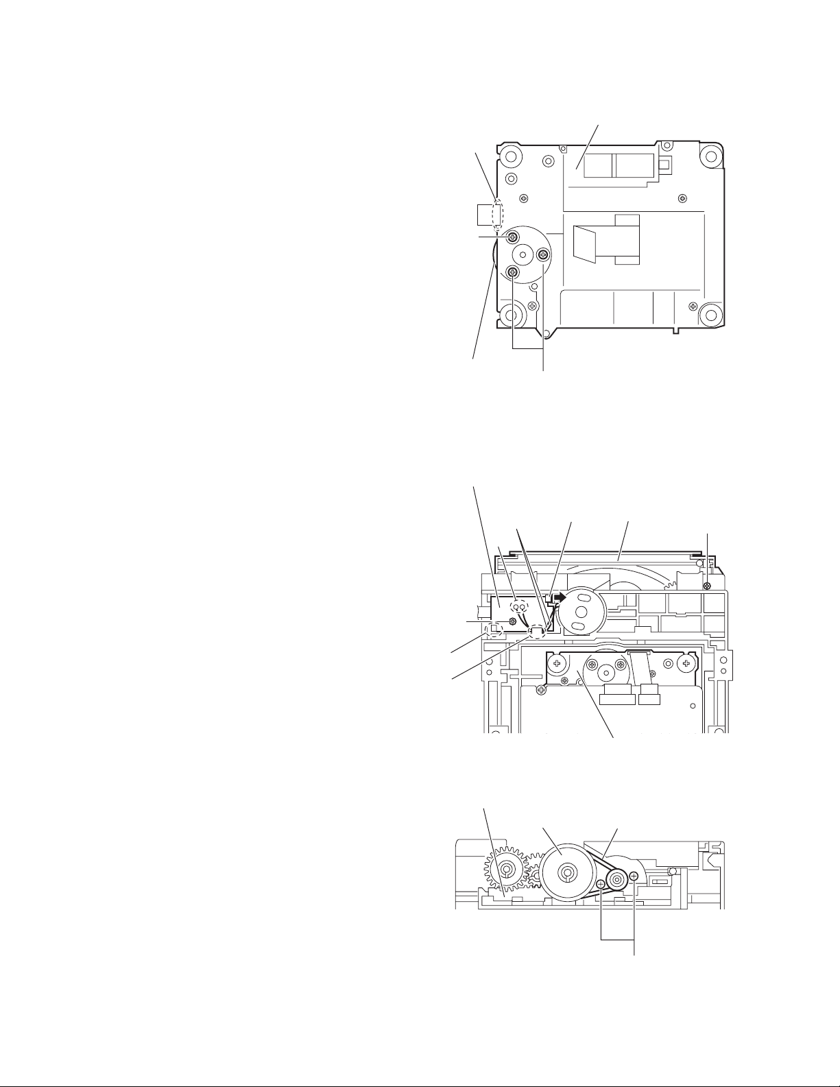
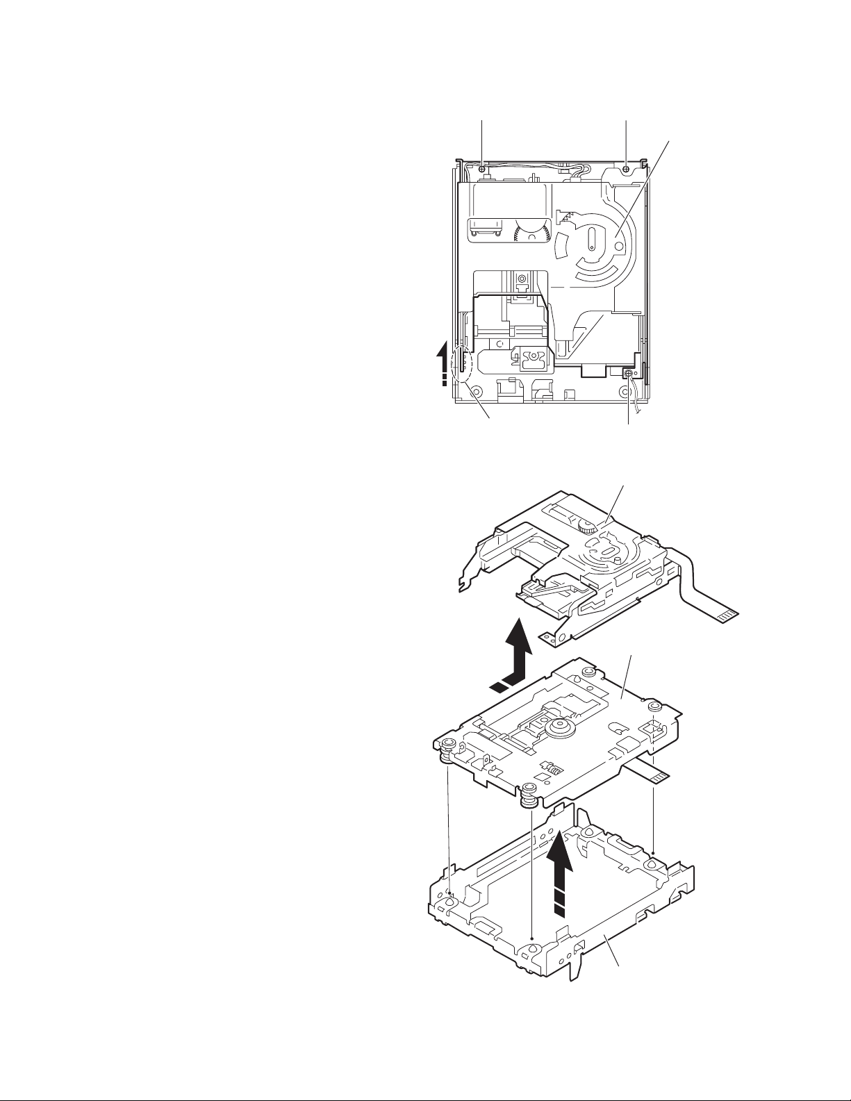
3.3 MD mechanism assembly
• Remove the MD mechanism assembly from main body.
(Refer to "Removing the MD mechanism assembly" of main unit.)
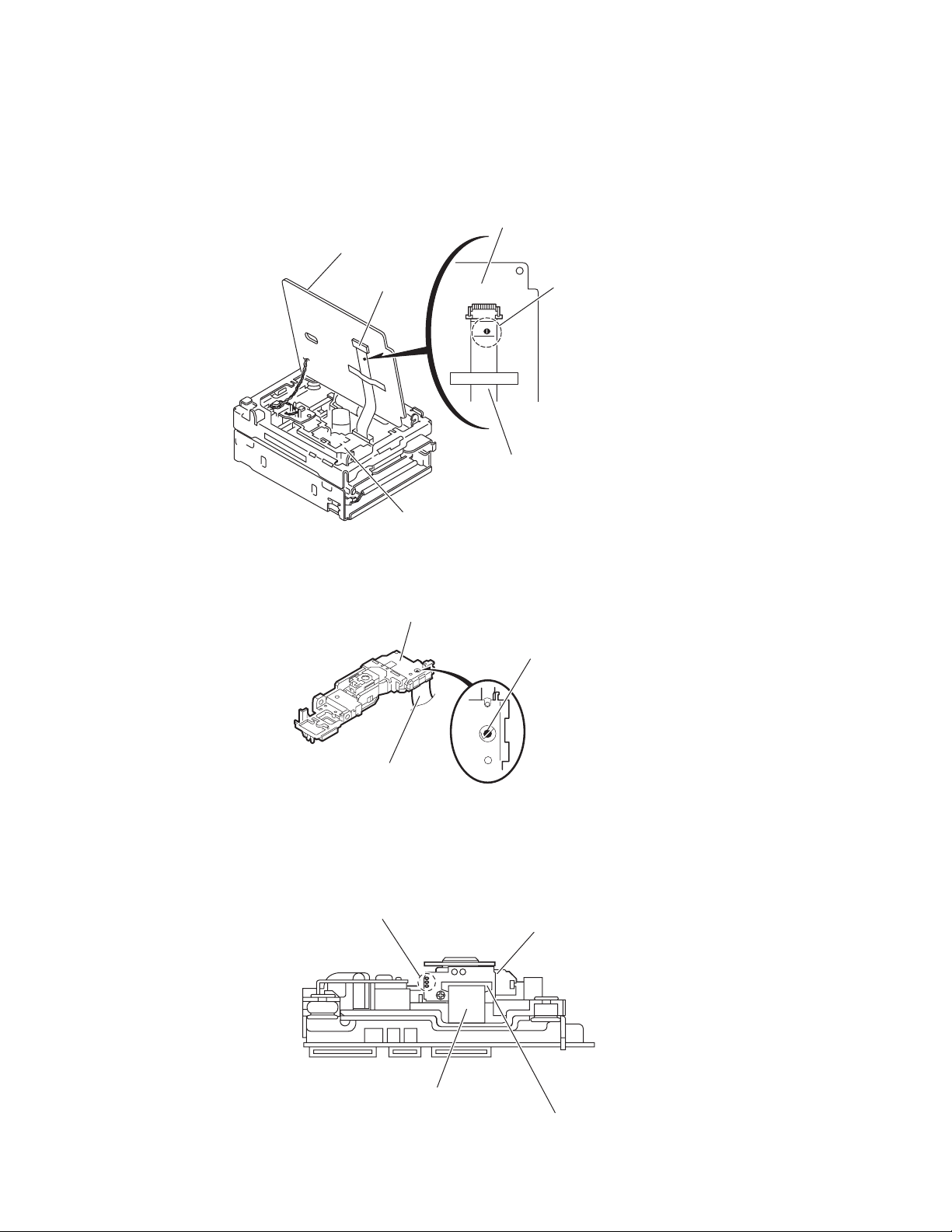
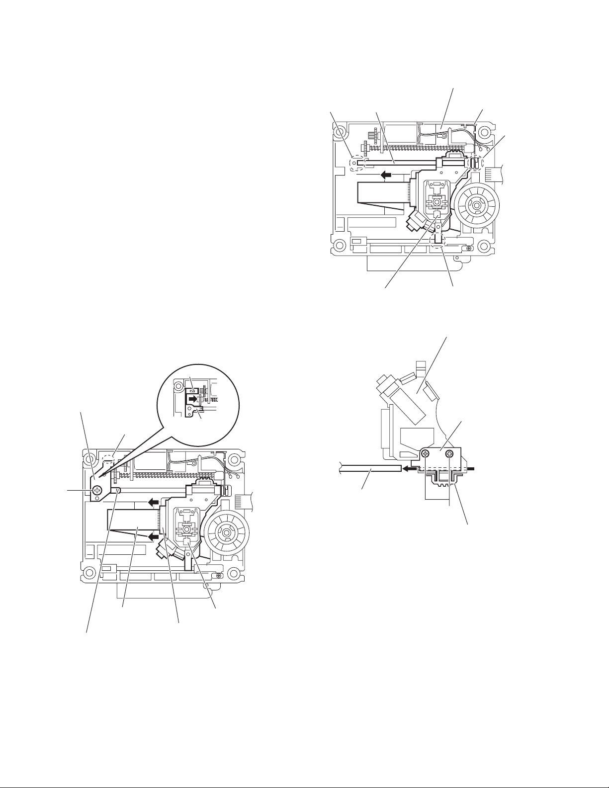
3.3.1 Removing he MD servo control board
(See fig.1 and 2)
(1) Remove the card wire from connector CN408
control board, and then remove the flexible wire from connector CN407
(2) Remove the wire of head assembly from soldered section
a of MD servo control board. (See fig.1)
(3) Remove the two screws A attaching the MD servo control
board. (See fig.1)
(4) Shift the MD servo control board to direction the arrow,
then remove the MD servo control board from fixing point
b. (See fig.1)
(5) Solder the short land section of the pickup. (See fig.2)
(6) Remove the flexible wire from connector CN310
side of MD servo control board, and then remove the MD
servo control board. (See fig.2)
Caution:
• Please solder to the short land section of a pickup before re-
moving a flexible wire from the connector of a MD servo control board. If a card wire is removed without soldering, a
pickup may be destroyed by static electricity. (See fig.2)
• At the time of MD servo control board attachment, please re-
move the solder of the short land section of a pickup after attaching a flexible wire in a connector CN310
. (See fig.1)
on MD servo
on bottom
. (See fig.2)
AA
Soldered
section a
CN408
CN407
Fixing part b Fixing part b
MD servo control board
Fig.1
MD servo control board
CN310
Pickup
Short land section
Fig.2
(No.MB496)1-27
Page 28
3.3.2 Removing the mecha cover
(See fig.3)
(1) Remove the four screws B attaching the mecha cover.
(2) Remove the hook from fixing part c of the internal loading
assembly.
(3) Shift the mecha cover to front side, and then remove to up-
per direction.
3.3.3 Removing the head lifter
(See fig.4 to 6)
(1) Remove the spring from hook d of main body. (See fig.4)
Reference:
• Spring can be removed in the state where it was attached, to head lifter.
• Spring is removed from head lifter if needed.
(2) Shift the head lifter to direction the arrow, and then discon-
nect the fixing part e. (See fig.5)
(3) Remove the spring from the head lifter, and then remove
the head lifter. (See fig.6)
Fixing part c
Hook
Fixing part c
Head lifter
B
Mecha cover
B
Fig.3
Spring
Fixing part e
Head lifter
Hook d
Fig.4
Spring
Fixing part e
Fig.5
1-28 (No.MB496)
Head lifter
Spring
Fig.6
Page 29
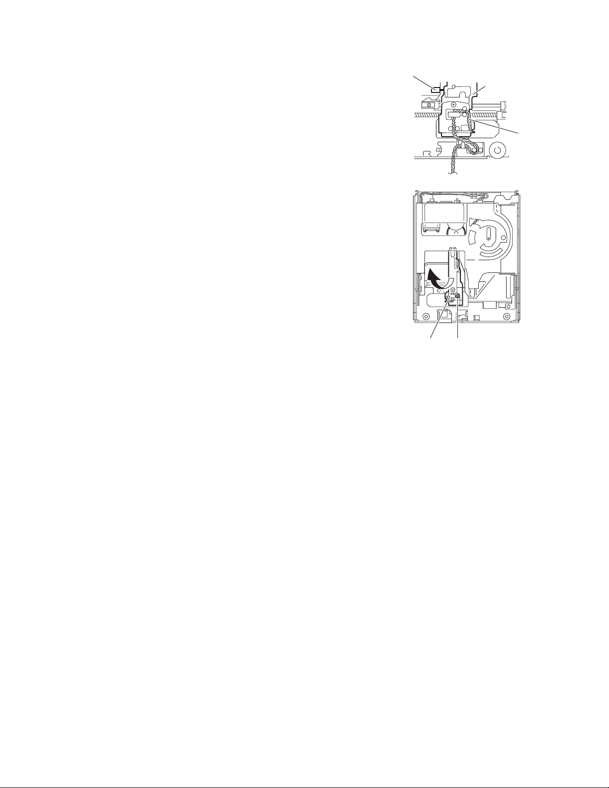
3.3.4 Removing the head assembly
(See fig.7 and 8)
• Remove the MD servo control board.
(1) Remove the wire from head assembly to fixed bottom part
of pickup. (See fig.7)
(2) Remove the screw C attaching the head assembly. (See
fig.8)
Caution:
When you attach a head assembly, please fix the wire from a
head assembly to a pickup. When fix a wire, please attach a
pickup by most inside of position. And confirm the pickup
pushed rest switch. (See fig.7)
Rest switch
Pickup
Wire
Fig.7
Head assembly
C
Fig.8
(No.MB496)1-29
Page 30
3.3.5 Removing the loading assembly and traverse mechanism assembly
(See fig.9 and 10)
• Remove the MD servo control board, mecha cover, head lifter
and head assembly.
(1) Remove the three screws D attaching the loading assem-
bly from upper side of main body. (See fig.9)
(2) Shift the loading assembly to front side, and then discon-
nect the fixing part f of traverse mechanism assembly.
(See fig.9)
(3) Remove the loading assembly to upper side, and then re-
move the traverse mechanism from the single flame. (See
fig.10)
D
D
Loading assembly
Fixing part f
D
Fig.9
Loading assembly
Traverse mechanism assembly
1-30 (No.MB496)
Single frame
Fig.10
Page 31

3.3.6 Removing the slide base (L) and slide base (R)
(See fig.11)
• Remove the MD servo control board, mecha cover, head lifter,
head assembly and loading assembly.
(1) Remove the two screws E attaching the slide base (L) and
slide base (R) from upper side of loading assembly.
(2) Take out the slide base (L) and slide base (R)
Reference:
When attach the slide base (L), slide base (L) is attached according to fixing point g.
Slide base (R) Fixing part g
E
Slide base (L)
3.3.7 Removing the loading mechanism assembly
(See fig.12)
• Remove the MD servo control board, mecha cover, head lifter,
head assembly and loading assembly.
(1) Remove the bend part h of mecha base from upper surface
of loading assembly.
(2) Pull up and remove take out the loading mechanism as-
sembly.
Fixing part g
Fig.11
Bend part h
Loading mechanism assembly
Fig.12
E
Loading mehca base
(No.MB496)1-31
Page 32

3.3.8 Removing the loading motor
r
(See fig.13 and 14)
• Remove the MD servo control board, mecha cover, head lifter,
head assembly, loading assembly and loading mechanism assembly.
(1) Disconnect the card wire from connector CN612
switch board and then remove the card wire from wire holder at upper side of loading mechanism assembly. (See
fig.13)
(2) Remove the screw F attaching the loading motor assem-
bly. (See fig.13)
(3) Disconnect fixing part i and take out the loading motor as-
sembly. (See fig.13)
(4) Remove the belt from loading mechanism assembly. (See
fig.14)
(5) Remove the two screws G attaching the loading motor and
take out loading motor. (See fig.14)
3.3.9 Removing the cam gear and cam switch board
(See fig.13)
• Remove the MD servo control board, mecha cover, head lifter,
head assembly, loading assembly and loading mechanism assembly.
(1) Remove the slit washer attaching the cam gear and take
out it from upper surface of loading mechanism assembly.
(2) Disconnect the wire from connector CN612
board.
(3) Remove the two screws H and clampers attaching the cam
switch board and take out cam switch board.
of cam
of cam switch
Loading motor assembly
Fixing part i
F
Wireholder
CN612
Fig.13
Loading moto
H
Cam switch board
Slit washer
H
Cam gear
G
Belt
Fig.14
1-32 (No.MB496)
Page 33

3.3.10 Removing the slide bar and cartridge holder assembly
(See fig.15 and 16)
• Remove the MD servo control board, mecha cover, head lifter,
head assembly, loading assembly and loading mechanism assembly.
(1) Remove the two screws J attaching the slide cover to fix
cartridge holder assembly from upper surface of loading
assembly. (See fig.15 and 16)
(2) Take out the slide cover to upper surface and then take out
the cartridge holder assembly.
3.3.11 Removing the eject bar
(See fig.15)
• Remove the MD servo control board, mecha cover, head lifter,
head assembly, loading assembly loading mechanism assembly and cartridge holder assembly.
(1) Shift eject bar to direction the arrow until to stop from upper
surface of loading assembly.
(2) Press hook j from bottom surface of loading assembly, and
then take out the eject bar.
J
J
Slide ber
Eject bar
Cartridge holder assembly
Eject bar
Eject bar
Hook j
Fig.15
J
Slide bar
UD base
Cartridge holder assembly
Fig.16
(No.MB496)1-33
Page 34

3.3.12 Removing the insulator
(See fig.17)
• Remove the MD servo control board, mecha cover, head lifter,
head assembly and traverse mechanism assembly.
(1) Remove the insulator from cut part of traverse mecha
chassis at upper surface of traverse mechanism.
Insulator
Pickup unit
3.3.13 Removing the pickup
(See fig.18)
• Remove the MD servo control board, mecha cover, head lifter,
head assembly, traverse mechanism assembly and insulator.
(1) Remove the screw K attaching the shaft holder (F) from
bottom surface of traverse mechanism.
(2) Shift the pickup to inner side, and then take out the shaft
holder (R).
(3) Shift the pickup unit to upper surface from shaft, and then
remove the fixing part k of pickup guide, remove the shaft
and pickup unit together.
3.3.14 Removing the pickup
(See fig.19)
• Remove the MD servo control board, mecha cover, head lifter,
head assembly, traverse mechanism assembly, insulator and
pickup unit.
(1) Take out the shaft from pickup.
(2) Remove the two screws M attaching the lack spring from
pickup.
Caution:
• Please solder to the short land section of a pickup before removing a flexible wire from the connector of a MD servo control board. If a card wire is removed without soldering, a
pickup may be destroyed by static electricity.
• At the time of MD servo control board attachment, please remove the solder of the short land section of a pickup after attaching a flexible wire in a connector.
Insulator
Shaft holder(F)
Traverse mecha chassis
Fig.17
Pickup guideFixing part k
Pickup unit
Shaft holder(R)
K
Fig.18
M
Rack spring
Pickup
1-34 (No.MB496)
Shaft
Fig.19
Page 35

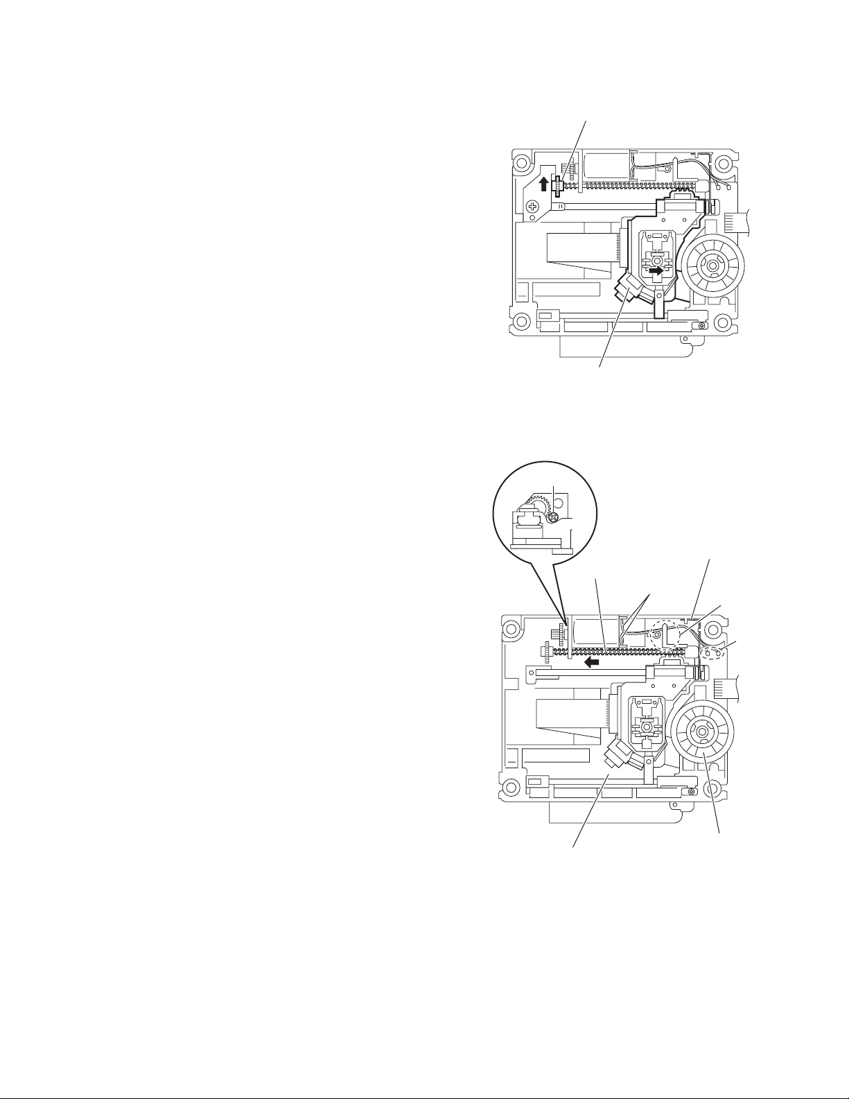
3.3.15 Removing the feed motor assembly
(See fig.20 and 21)
• Remove the MD servo control board, mecha cover, head lifter,
head assembly, traverse mechanism assembly and insulator.
(1) Remove the white wire and black wire attached soldered
section m of traverse mechanism board. (See fig.20)
(2) Remove the two screws N attaching the feed motor assem-
bly. (See fig.20)
(3) Remove the two screws P attaching the feed motor brack-
et. (See fig.21)
(4) Take out the feed motor.
3.3.16 Removing the traverse mechanism board
(See fig.20)
• Remove the MD servo control board, mecha cover, head lifter,
head assembly, traverse mechanism assembly, insulator and
feed motor assembly.
(1) Remove the red wire and black wire of feed motor attached
soldered section of traverse mechanism board.
(2) Remove the screw Q attaching the traverse mechanism
board.
Caution:
• When an inner circumference has a pickup most in the case
of attachment of a traverse mechanism board, in order to interfere with a rest switch, it is necessary to move a pickup to
the perimeter for a while.
• When make it move, turn a screw shaft gear.
Traverse mechanism assembly
Soldered section m
Q
Feed motor assembly
N
Soldered section n
Rest SW
Fig.20
Feed motor
Spindle motor
Pickup
Screw shaft gear
Feed motor bracket
P
Fig.21
(No.MB496)1-35
Page 36

3.3.17 Attaching the loading assembly
(See fig.22 to 29)
(1) Attach the eject bar to UD base. (See fig.22 and 23)
(2) A slide bar is attached to loading mecha chassis, uniting
the p section of the boss of a slide bar with the slot of an
ejection bar. (See fig.22)
(3) Where a slide bar and an ejection bar are moved in the di-
rection of an arrow, a cartridge holder is attached with two
screws R. (See fig.23 and 24)
Caution:
Where the eject bar and loading slider of a cartridge
holder assembly are moved in the direction of an arrow,
please check that the pin of the q section of an ejection
lever is correctly inserted in the slot r section at the bottom of a loading chassis.
(4) UD base bends in the cut part of a wire holder, and a
through wire holder is put for the part f section on UD base.
(See fig.23)
Caution:
Please change into the state where the boss on the wire
holder back side went into the hole of UD base.
(5) Cam switch board is attached with the two screws S. (See
fig.23)
(6) The boss on a cam switch board is rotated and it unites with
triangle mark on a board. (See fig.25)
(7) The hole of a cam gear is attached with a slit washer ac-
cording to the boss of a cam switch. (See fig.25)
Caution:
When you attach a cam gear, after the boss of a cam
gear has clung to the hole of a cam gear correctly, please
check that it is in the state which triangle mark of the gear
u section and a cam gear in which the hole of an ejection
bar opened simultaneously suited.
Loading motor assembly is attached with screw T. (See fig.25)
(8)
(9) Wire from loading motor is attached with connector CN612
of switch board, and then hook to UD base bend part v.
(See fig.25)
(10) Wire fix with wire holder. (See fig.25)
Four pins of right and left of UD base are set and attached in
(11)
the cut part of loading mecha base, respectively. (See fig.26)
Caution:
As the w part of loading mecha base bends and the portion bottom is made to pass through x parts of a cartridge
holder assembly first, since, please attach. (See fig.26)
(12) Two pins of UD base part are set by the clipping hole of the
side of a slide base (R), and a slide base (R) is attached.
(See fig.27 and 28)
Caution:
At this time, please attach so that a slide base (R) bends
and Part y comes to the inner side (shaft side) z section
of the rib of a cam gear.
(13) Two pins of UD base part are set by the clipping hole of the
side of a slide base (L), and a slide base (R) is attached.
(See fig.27)
(14) In the state of entering certainly, boss aa attaches the two
screws U a slide base (L) in the hole of a slide base (L).
(See fig.27 and 29)
Reference:
Work is easy, if each pin is cut and lacked in the state where
UD base part was floated, in the case of attachment of a slide
base (L) and a slide base (R), and it unites and attaches in a
hole.
Eject bar
Slide bar
R
R
Boss p
Part p
R
Slide bar
UD base
Cartridge holder
assembly
Fig.22
Wire holder Cam switch board
Part s
Part t
Cam switch boss
UD base
Slot rEject bar
Fig.23
S
Mark
S
1-36 (No.MB496)
Page 37

Slot r
r
Eject bar
Fig.24
Cartridge holder
assembly
Loading
slider
Part q pin
Loading motor assembly
Bend part v
Slide bar
CN612
mark
Boss
Cam switch
Cam switch board
Wire holder
Slit washe
Cam gear
Eject bar
T
Cam gear
( mark)
Eject barPart u
Fig.25
(No.MB496)1-37
Page 38

Part x
Part w
Part x
Pin
Loading mecha base
Fig.26
Slide base(R)
Bend part y
T
Pin
Slide base(R)
Boss aa
Slide base(L)
U
Boss aa
Fig.29
Pin
Bend part y
Pin
Slide base(L)
Part z
Fig.27
Slide base(R)
Cam gear
Part z
1-38 (No.MB496)
Fig.28
Page 39

3.4 Cassette mechanism assembly
3.4.1 Removing the Play/Record & Clear head
(See Fig.1~3)
(1) While moving the trigger arm on the right side of the head
mount in the direction of the arrow, turn the flywheel R
counterclockwise until the head mount comes ahead and
clicks.
(2) The head turns counterclockwise as you turn the flywheel
R counterclockwise (See Fig.2 and 3).
(3) Disconnect the flexible wire from connector CN31
head amplifier & mechanism control board.
(4) Remove the spring from the back of the head.
(5) Loosen the azimuth screw for reversing attaching the head.
(6) Remove the head on the front side of the head mount.
on the
Cassette mechanism assembly
Fig.1
Head
Fly wheelR
Trigger armHead mount
Flexible wire
Fly wheel R
Fig.2
Azimuth screw
Head
for reversing
Spring
CN31
Head amplifer & mecha control board
Fig.3
(No.MB496)1-39
Page 40

3.4.2 Removing the head amplifier & mechanism control board
(See Fig.4)
(1) Turn over the cassette mechanism assembly and remove
the three screws A attaching the head amplifier & mechanism control board.
(2) Disconnect the flexible wire from connector CN31
head amplifier & mechanism control board.
(3) Disconnect connector CN32
anism control board from connector CN1
board.REFERENCE: If necessary, unsolder the 4-pin wire
soldered to the main motor.
3.4.3 Removing the main motor
(See Fig.4~7)
(1) Remove the two screws B .
(2) Half raise the motor and remove the capstan belt from the
motor pulley.
ATTENTION:
Be careful to keep the capstan belt from grease. When reassembling, refer to Fig.6 and 7 for attaching the capstan belt.
Head amplifier & mecha control board
of the head amplifier & mech-
on the reel pulse
on the
Main motor assembly
Capstan belt
Fig.5
Main motor assembly
CN31
Flexible wire
A
AA
Fig.4
CN32
4pin wire
B
Main motor assembly
Motor pulley
Capstan belt
Fig.6
Main motor assembly
Fly wheel
1-40 (No.MB496)
Capstan belt
Motor pulley
Fig.7
Page 41

3.4.4 Removing the flywheel
(See Fig.8, 9)
• Prior to performing the following procedure, remove the head
amplifier & mechanism control board and the main motor assembly.
(1) From the front side of the cassette mechanism, remove the
slit washers attaching the capstan shaft L and R. Pull out
the flywheels backward.
Fly wheel R Fly wheel L
Fig.8
Fly wheel R
Capstan shaft R Capstan shaft L
Slit washer
Fig.9
3.4.5 Removing the reel pulse board and solenoid
(See Fig.10)
• Prior to performing the following procedure, remove the head amplifier & mechanism control board.
(1) Remove the screw C.
(2) Release the tab a, b, c, d and e retaining the reel pulse board.
(3) Release the tab f and g attaching the solenoid on the reel pulse board.
(4) The reel pulse board and the solenoid come off.
Fly wheel L
bc
a
Solenoid
g
f
d
Reel pulse board
C
e
Fig.10
(No.MB496)1-41
Page 42

3.4.6 Reattaching the Play/ Record & Clear head
r
r
(See Fig.11~13)
(1) Reattaching the head mount assembly.
a) Change front of the direction cover of the head
mount assembly to the left (Turn the head forward).
b) Fit the bosses O', P', Q', U' and V' on the head mount
assembly to the holes P and V, the slots O, U and Q
of the mechanism sub assembly (See Fig.11 to 13).
CAUTION:
To remove the head mount assembly, turn the direction
cover to the left to disengage the gear. If the gear can not
be disengaged easily, push up the boss Q' slightly and
raise the rear side of the head mounts slightly to return
the direction lever to the reversing side.
(2) Tighten the azimuth screw for reversing.
(3) Reattach the spring from the back of the Play/ Record &
Clear head.
(4) Connect the flexible wire to connector CN31
amplifier & mechanism control board.
on the head
U' Q'
Head mount assembly
Head mount assembly
O'
Fig.11
P'
P'
V'
V'
Direction cove
Spring
Flexible wire
V
O
P
Q
Head
Direction cove
U
Fig.12
Azimuth screw for reversing
Head mount
1-42 (No.MB496)
CN31
Fig.13
Head amplifier &
mechanism control board
Page 43

4.1 Jigs and test instruments
(1) Laser power meter (Wavelength : 780um)
(2) Laser power meter sensor (disk type)
(3) Premastered disk
(4) Recordable disk
4.2 Adjustment and check items
4.2.1 Test mode
(1) FL display all lighting-up mode
4.2.2 MD section
(1) Setup of the TEST MODE 1
(2) Initialization of EEPROM
(3) Setup of the laser power
(4) Adjustment of stray light offset
(5) Iop check
(6) Adjustment of the disk
(7) Setup of the TEST MODE 2
(8) Cancel of the TEST MODE
4.3 Adjustment and check method
SECTION 4
ADJUSTMENT
4.2.3 DVD section
(1) Setup of the TEST MODE
(2) Initialization setting in shipment
(3) Initialization of EEPROM
(4) Destination version display of main microcomputer and
main unit.
(5) Check mode
4.2.4 Error log
(1) Outline
(2) Written to ERROR
(3) The error logs check method
(4) ERROR details
1. Test mode
(1) FL display all lighting-up mode
Press the [POWER] key and
[3D PHONIC] key over the five
seconds on the main unit.
FL display
All of the FL light up.
By pressing the any key on the
main unit, the initial display screen
is resumed.
FL display normal function display.
2. MD section
(1) Setup of the TEST MODE 1
While pressing both the [STOP ] key
and [MD PLAY ] key on the main unit,
insert the AC power cord in an outlet.
FL display
MD TEST
Press the [POWER] key on
the main unit.
FL display
MD TEST 1
Setup is complete.
[POWER] key
[3D PHONIC] key
[MD REC] key
(2)
Initialization of EEPROM
(Note)
When EEPROM is initialized, all data is deleted
and any adjustment will be disabled. Give the
most careful consideration to performing this
operation.
This operation should be executed only when an
EEPROM is replaced.
The setting of the TEST MODE 1 should be
completed for performing the initialization. Carry
out the following operations with a remote
controller.
MD TEST 1
Press the [MD PLAY ] key
on the remote controller.
FL display
[MD PLAY] key
[STOP] key
I
nitialization
FL display
MD TEST 1
is complete.
(No.MB496)1-43
Page 44

(3)
r
Setup of the laser power
MD TEST 1
Insert the laser power
meter sensor.
Press the [MD EJECT ]
key on the main unit.
Press the [2] key on
the remote controller.
Insert the laser power
meter sensor again.
Increase the laser
power with the
[UP ] key on the
main unit.
Adjust the power to be 0.68 mW or
more. If the value exceeds 0.68 mW,
approximate it to 0.68 mW as
accurately as possible.
Press the [STOP ] key
on the remote controller.
FL display
MD TEST 1
Press the [MD EJECT ]
key on the main unit.
Playback laser power
adjustment is complete.
A laser power meter
sensor is ejected.
MD mechanism starts
its operation.
Decrease the laser
power with the
[DOWN ] key on
the main unit.
A laser power meter
sensor is ejected.
Insert the laser power
meter sensor.
Press the [4] key on
the remote controller.
Press the [MD EJECT ]
key on the main unit.
Insert the laser power
meter sensor again.
Increase the laser
power with the
[UP ] key on the
main unit.
Adjust the power to be 6.23 mW or
less than 6.23mW.
If the value exceeds 6.23 mW,
approximate it to 6.23 mW as
accurately as possible.
Press the [STOP ] key
on the remote controller.
MD TEST 1
Press the [MD EJECT ]
key on the main unit.
Record laser power
adjustment is complete.
Decrease the laser
power with the
[DOWN ] key on
the main unit.
FL display
MD mechanism starts
its operation.
A laser power meter
sensor is ejected.
A laser power mete
sensor is ejected.
(4)
Adjustment of stray light offset
(Note)
Execute
1-44 (No.MB496)
adjustment of stray light offset
Press the [MD PLAY ] key
on the remote controller.
MD TEST 1
FL display
OK TUNING
in the state that a disk is not inserted in by all means.
Press the [STOP ] key
on the remote controller.
FL display
MD TEST 1
Adjustment is complete.
Page 45

(5) Iop check
In the MD test mode 1, when [ 0 ] key is pressed, the Iop display is performed by the following methods.
Purpose:
In order to check pick failure and static electricity failure by the laser ON current.
Measurement means:
"Laser ON current" mode was added to the static test mode. Laser current is measured in this mode.
Adjustment is not performed. Only a recording side corresponds.
AA : Laser power of playback in present (Current value mA)
BB : Laser power of recording in present (Current value mA)
CC : Laser power of playback in factory shipments (Current value mA)
DD : Laser power of recording in factory shipments (Current value mA)
Iop display (Only a recording side corresponds.)
The current of laser operation is measured and displayed.
Since change of the laser current of shipment and
the now can be seen, degradation of a pickup can be checked.
Adjustment is not performed.
* Pushing the [cancel] key of the remote controller,
it returns to the MD test mode.
It will display, if "DF, FF, AA, BB, CC, DD" are received from MD module.
@@@ :
The amount of change is displayed by three figures. [ BB DD x 100 ]
(Below a decimal point is omission)
BB : Laser power of recording in present (Current value mA)
DD : Laser power of recording in factory shipments (Current value mA)
@@@ :
The amount of change is displayed by three figures.
AA : Laser power of playback in present (Current value mA)
BB : Laser power of recording in present (Current value mA)
CC : Laser power of playback in factory shipments (Current value mA)
DD : Laser power of recording in factory shipments (Current value mA)
@@@ =
The amount of change is displayed by three figures. [ BB DD x 100 ]
(Below a decimal point is omission)
Check the display of @@@ portion is 120% or less.
If a check is completed, pull out AC socket without pressing other keys..
MD is put in before a test.
(The data may be eliminated)
MD TEST MODE 1
Press the [0] key on the remote controller.
FL indication
IOP CHECK
FL indication
IO BB DD
@@@
display is finished.
It will display,
if "DF, FF, AA, BB, CC, DD" are
received from MD module.
(No.MB496)1-45
Page 46

(6)
Adjustment of the disk
MD TEST 1
Insert the
disk for the adjustment
Reading of TOC ends.
Press the [MD PLAY ]
key on the remote controller.
FL display
ON TUNING
premastered
Insert the
for the adjustment.
.
Press the [MD PLAY ]
key on the remote controller.
recordable disk
FL display
ON TUNING
Automatic adjustment starts.
Complete?
NO
Automatic adjustment starts.
Complete?
YES
FL display
OK?TUNING
Press the [STOP ] key
on the remote controller.
Press the [MD EJECT ]
key on the main unit.
The
premastered
the adjustment
disk for
is ejected.
Judgment Code Table
Recordable disk
adjustment code
00
20
21
22
23
24
25
26
27
28
29
2A
2B
2C
2D
3E
3F
Judgment Code Table of error factor
Code
0 Error being anonymous / Other factor
1
2
4 TLOCK detects an unlocking state before command execution
11 TRD sensitivity learning error (TRD arrives at a limit value)
12 TRD sensitivity learning error (Error of truck counter number is big.)
14
Premastered
adjustment code
Focus loser search
FLOCK detects an unlocking state before command execution
Offset gap of A B signal is big
NO
FL display
NG Err : !
: Refer to the judgment
code table.
disk
0
30
32
31
33
34
35
36
37
38
39
3A
3B
3C
-
3F
Error being anonymous
Focus on with focus error gain adjustment
Tracking error gain balance adjustment (Lens shift ON)
Tracking drive (TRD) sensitivity adjustment
Spindle low voltage drive
Tracking ON
Spindle ADIP/EFM rough servo ON
Focus loop gain adjustment
Focus balance adjustment
Tracking error gain balance adjustment (Lens shift OFF)
Lens position servo sensitivity adjustment
Tracking ON
Spindle ADIP/EFM rough servo ON
Tracking loop gain adjustment
NRFDETslice level measurement
Pit Grv movement
Other processing
FL display
OK?TUNING
Press the [STOP ] key
on the remote controller.
Press the [MD EJECT ]
key on the main unit.
The
adjustment
Automatic adjustment complete.
When a wrong setting is performed for the
disc type, switch the power off and on and
start the setting procedure again.
NG item in adjustment
Error factor
YES
FL display
NG Err : !
: Refer to the judgment
code table.
recordable disk for the
is ejected.
1-46 (No.MB496)
Page 47

(7) Setup of the TEST MODE 2
While pressing both the [STOP ] key
and [MD PLAY ] key on the main unit,
insert the AC power cord in an outlet.
FL display
MD TEST
Press the [POWER] key on
the main unit.
FL display
MD TEST 1
1. Quantity of change display of pickup adjustment value
Only the TOC reading end back becomes effective.
FL display
MD TEST 2
Press the [6] key on the
remote controller.
####:
FL display
####:
Quantity of change display
Status table
FL display
LPOW Laser power, Premastered disc=0, Recordable disc=recordable power
(There is temperature revision)
ASGN
TGAN
TBAL Tracking balance adjustment value
FBAL Focus balance adjustment value
FRGN Focus loop gain adjustment value
TRGN Tracking loop gain adjustment value
NRFD NRFDET threshold value
LPGN Lens position servo gain adjustment value
AS gain adjustment value
Tracking gain adjustment value
Refer to the status table.
: Adjustment value
Next status display.
Press the [STOP ] key and
[MD EJECT ] key on the main unit
at the same time.
FL display
MD TEST 2
Setup is complete.
Press the [STOP ] key
on the remote controller.
FL display
MD TEST 2
Status contents
1. C1 errer display
Only the TOC reading end back becomes effective.
FL display
MD TEST 2
Press the [8] key on the
remote controller.
The command is transmitted
in order of A1 to 00.
(8)
Cancel of the TEST MODE
To cancel the test mode, press the [POWER] key on the main unit.
The command A1 to 01 is transmitted
for every ten seconds.
display is finished.
Repeats 432 time .
FL display
---
(No.MB496)1-47
Page 48

3. DVD section
r
Attention in service of DVD section
1. When pickup, Flash ROM, DVD module board were changed, initialize EEPROM by all means.
2. When full initialization was executed, execute learning with a DVD test disk by all means.
Test disc : VT-501, VT-502
Learning method : It is adjusted automatically by normal playback of a DVD test disc.
(1)
Setup of the TEST MODE
(2) Initialization setting in shipment
While pressing both the [STOP ] key
and [DVD ] key on the main unit,
insert the AC power cord in an outlet.
FL display
TEST JC#
Setup is complete.
(3)
Initialization of EEPROM
(Note)
When EEPROM is initialized, all data is deleted
and any adjustment will be disabled. Give the
most careful consideration to performing this
operation.
This operation should be executed only when an
EEPROM and PICUP is replaced.
FL display
TEST JC#
Press the [ ] key over the two seconds
on the main unit .
FL display
TEST JC#
Initialization is complete.
FL display
TEST JC#
Press the [ ] key
on the main unit .
FL display
TEST JC#
Initialization is complete.
(4) Destination version display of
main microcomputer and main unit.
FL display
TEST JC#
Press the [MENU] key two times
on the main unit .
FL display
SC ##
Press the [ON SCREEN] key
on the remote controller .
FL display
UT
Version display of
main unit.
Version display of
main microcompute
1-48 (No.MB496)
Page 49

(5) Check mode
FL display
TEST JC#
Press the [MENU] key
on the main unit
FL display
CHECK
Press the [5] key
on the main unit
FL display
Press the [6] key
on the main unit
FL display
Press the [9] key
on the main unit
FL display
Press the [10] key
on the main unit
FL display
Upper side
4 digit:
Lower side
4 digit:
Lower side
4 digit:
Lower side
4 digit:
Cancel of the check mode
Press the [POWER] key on the main unit.
Lighting of DVD LD
Laser current display
Measurement value
display of the jitter value
Measurement value display of
the temperature (AD value)
DVD DL (parallel and opposite)
Measurement value display of the jitter value
and the serge on predetermined position
(No.MB496)1-49
Page 50

4. Error history
(1) Outline
The failure that is not reproduced may occur in a market.
Presumption of the cause of failure is difficult.
This error log is recorded when failure occurs.
It is displayed again and can use to service.
Using the EEPROM of 256bytes.
When an unusual state occurs, it writes the factor in EEPROM.
It leaves the history for 16 times to each item.
The error log displays in TEST code of remote controller,
and enables it to check the contents of each address by the key.
(2) Written to ER R O R
The contents of ERROR are written in the EEPROM address.
No Item
1 SAFETY
2 Timer playback is not starting Timer playback is not starting
Timer recording is not starting Timer recording is not starting
316
4 Recording is not starting Normal recording is not starting16
Time out power OFF 16
5
6 CD 16 Error with CD
7 DVD 16 Mechanical failure
8MD 16
9TAPE
Power OFF
10 16 When starting of power OFF process
Number
AD value
Writing
times Writing contents Writing conditions
SAFETY number
16
and AD value
16
16 Factor of failure
Factor of failure
Factor of failure
Factor of failure
Factor of failure
Factor of failure
Factor of failure
Factor of failure
16
Factor of power OFF
When detecting of SAFETY error,
writing SAFETY number and AD value
(except TIMER RECORDING)
Time out of power OFF process
Error with DVD
Error with MD
Error with TAPE
Factor of failure
Power circuit failure.
Damage of card wire.
Missing key operation.
User operation
User operation
User operation
Mechanical and module failure
Damage of card wire.
Missing key operation.
Mechanical and pick up failure
Mechanical and module failure
Mechanical failure
User operation
(3)The error log check method
Read-out of a error history can be displayed by code of remote control at the time of POWER ON and OFF of a set.
(Press the [3] key ,[STOP ] key and [POWER] key on the remote controller,
it will become the read-out mode of the error log.)
Press the [3] key ,[STOP ] key
and [power] key on the remote controller.
Press the [SKIP ] key, Increase and decrease the lower address.
Press the [GULP SKIP ] key, Increase and decrease the ten column address.
Press the [3] key ,[STOP ] key
and [power] key on the remote controller.
1-50 (No.MB496)
FL display
ERR INFO
FL display
address 00
data 01
Normal function display
Starting address is the 00.
byte display.
Example:
Operation
Pressing the
Pressing the
Pressing the
Pressing the
Pressing the
address data
key
key
key
key
key
Display
:
05
01
:
21
10
:
11
0F
:
01
00
:
00
F0
Page 51

(4) ERROR details
Item Top Low address and contents
address
SAFETY Number 00 SAFETY error number
(When SAFETY ERROR detecting, main unit is non active.)
01 DVD4.0V
02 DVDA6V
03 VIDEO5V
04 SW10V
05 MD5.4V
AD value 10 AD value at SAFETY error
00 to FF
Timer playback is not starting
20 10 DVD,CD NODISC
11 DVD,CD OPEN
30 TAPE NONE
31 TAPE OPEN
50 MD NODISC
90 Others
Timer recording is not starting
30 10 DVD,CD NODISC
11 DVD,CD OPEN
30 TAPE NONE
31 TAPE OPEN
32 TAPE REC PROHIBIT (Protect tag damage)
50 MD NODISC
51 DISC_PROTECTED
52 PLAYBACK_MD
53 DISC_FULL
54 SCMS_CANNOT_COPY
55 DIGITAL_IN_UNLOCK
56 NON_AUDIO_CANNOT_COPY
57 LOW_TEMP_CANNOT_REC
90 Others
When both playback sauce and recording sauce have a factor at
the REC start NG, the factor of playback sauce is written in.
Example) When it records in the state without MD and CD in CD sauce,
[10 DVD, CD NODISC] are written in.
Normal recording is not starting
40 10 DVD,CD NODISC
11 DVD,CD OPEN
30 TAPE NONE
31 TAPE OPEN
32 TAPE REC PROHIBIT (Protect tag damage)
50 MD NODISC
51 DISC_PROTECTED
52 PLAYBACK_MD
53 DISC_FULL
54 SCMS_CANNOT_COPY
55 DIGITAL_IN_UNLOCK
56 NON_AUDIO_CANNOT_COPY
57 LOW_TEMP_CANNOT_REC
90 Others
When both playback sauce and recording sauce have a factor at
the REC start NG, the factor of playback sauce is written in.
Example) When it records in the state without MD and CD in CD sauce,
[10 DVD, CD NODISC] are written in.
(No.MB496)1-51
Page 52

Item Top low address and contents
Address
Time out of power OFF process
50 10 DVD,CD TIMEOUT
50 MD TIMEOUT
70 MECHA CLOSE TIMEOUT
90 Others
Error with DVD
70 70 MECHA CLOSE TIMEOUT
71 MECHA OPEN TIMEOUTMD
Error with MD
80 61 TRACK_PROTECTED
62 CANNOT_JOIN
63 (Reserve)
68 CANNOT_TITLE
69 GROUP_FULL
6A GROUP_FULL
6B GROUP_TRACK
6C CANNOT_FORM
6D CANNOT_ENTRY
81 LOAD_ERROR
82 MD_NO_DISC
83 READ_ERROR
84 EMERGENCY STOP
Error with TAPE
90 10 INITIALIZE ERROR
When starting of power OFF process
(When initialization retries, it writes in only once.)
A0 10 NORMAL
20 AUTO STANDBY
30 SLEEP
40 TIMER
1-52 (No.MB496)
Page 53

SECTION 5
TROUBLESHOOTING
This service manual does not describe TROUBLESHOOTING.
(No.MB496)1-53
Page 54

Victor Company of Japan, Limited
Audio/Video Systems Category 10-1,1chome,Ohwatari-machi,Maebashi-city,371-8543,Japan
(No.MB496)
Printed in Japan
VPT
Page 55

SCHEMATIC DIAGRAMS
MICRO COMPONENT MD SYSTEM
UX-QD70S,UX-QD70W
CD-ROM No.SML200512
Area suffix
UB ---------------------- Hong Kong
(SP-UXK30S)
(SP-UXK30W)
Lead free solder used in the board (material : Sn-Ag-Cu, melting point : 219 Centigrade)
Contents
Block diagrams
Standard schematic diagrams
Printed circuit boards
COPYRIGHT 2005 Victor Company of Japan, Limited.
(CA-UXQD70S)
(CA-UXQD70W)
(SP-UXK30S)
(SP-UXK30W)
2-1
2-2
2-11 to 15
No.MB496SCH
2005/12
Page 56

In regard with component parts appearing on the silk-screen printed side (parts side) of the PWB diagrams, the
parts that are printed over with black such as the resistor ( ), diode ( ) and ICP ( ) or identified by the " "
mark nearby are critical for safety.
Page 57

OPTIN
OPTOUT
FAN
MOTOR
REM
JOGL
JOGR
FKEY1
FKEY2
KEYP
System control section (Key)
DI531
LCD DISPLAY
LCDSO, LCDRS, LCDSCL
LCDXRESET, LCDCSB
LLCR, LLCG, LLCB
RLCR, RLCG, RLCB
D5351D5341
CN531
System control section (LCD)
Trans section (Trans.)
T9002
AC
INPUT
Q9001
RELAY SW
LF901
T9001
Trans section (Regulator)
D2401 to D2408
AC-DC
S1+
Q2601
MD5.4V REG.
IC281
DVD5V REG.
DVD5V
Q2901
DVDA6V REG.
DVDA6V
MD5.4V
Q2501
DVD4V REG.
DVD4V
Main section (HP board)
TUCLK, TUDATAO
TUCE, TUDATAI
System control section
TO
TUNER
M+
M-
U2SCLK
U2SDT
UCS
DVDOPSW
DVDCLSW
TRAY+
TRAY-
REM, KEYP
FKEY1, FKEY2
JOGL, JOGR
LCDSO, LCDRS
LCDSCL, LCDCSB
LCDXRESET
QA781 to QA787
LED DRIVER
POUTRELAY
LLEDR, LLEDG, LLEDB
RLEDR, RLEDG, RLEDB
IC741
EEP ROM
IC751
DVD
LOADER
IC745
BUFFER
E2CLK
E2DATA
SCK, SDATA
STTA, KEY1
PLAY, PHOTOOUT
VS1, VS2, VIP, VMUTE1, VMUTE2
SMUTE, VOLCK, VOLCE, VOLDATA
COMPLINK, FANON, D2IP
LLCR, RLCR
LLCG, RLCG
LLCB, RLCB
LCDR, RCDR
LCDG, RCDG
LCDB, RCDB
S2UDT, SCS, CPURST
FDVD, U2SCLK0
U2SO, UCS0
MDSTAT
MDCMD
MDRESET
POUTAMP
Main section
IC311
FUNCTION
VOL IC
VOLCK
VOLCE
VOLDATA
POUTAMP
MDL
MDR
LIN
RIN
TUL
TUR
TAPEL, TAPER
DVDL
DVDR
INL, INR
AUXL
AUXR
DOUT
CBIP
CRIP
YIP
CI, YI
D2IP
CYOUT
CBOUT
CROUT
COMPO
YOUT
SDC/CH
OPTIN
OPTOUT
CYOUT
CBOUT
CROUT
COMPLINK
OPTIN
DOUT
MDSTAT
MDCMD
MDRESET
FANO N
RECL, RECR
S1+
TO
SPEAKER
J1002
D2
TERMINAL
L-
R-
L+
R+
CN102
S1+
SW10V
LED & DVD loading section (LED)
A, B, C, D, E, F, RF+, PD(CD), PD(DVD)
F+/T+/-
FM+/WOUT
VOUT
UOUT
COM
LD(CD)
LD(DVD)
FAOUTL
FAOUTR
EXADT0 to 15
EXADR16 to 20
NEXCE
NEXOE
NEXWE
MA0 to 10
BA0, BA1
MDQ0 to 15
DQM0 to 3
NCSM, NRAS
NCAS, NWE
DAC1OUT
DAC2OUT
DAC3OUT
DAC4OUT
DAC5OUT
LRMUTE, SWMUTE
UCS, SCS, SCLK
U2SDT, S2UDT
CPURST
LPCO1
LPCO2
CDLDCUR
DVDLDCUR
SPDRV,
TRSDRV
FODRV
TRDRV
/DRVMUTE
/SPMUTE
FG, WHALF
TRVSW
CN712
INDEX, TRACK
COPY, AOUT0
BCK, LRCLK
DVD servo control section
CN805
CN804 CN801CN802
Jack section (Joint)
OUTL
OUTR
SCLK
U2SDT, UCS
S2UDT
SCS
CPURST
DOUT
SPDIF
COMPLINK
COMPOSITE
SDC, YOUT
AUXL
AUXR
IC621
IC622
OPTICAL IN
OPTICAL OUT
J6203
AV COMPULINK2
J6204
S/COMPOSITE
VIDEO OUT
J6202
AUX
Jack section
CN623
CN631
CN110
CN621
CN111
WR622
J6301
COMPONENT
VIDEO OUT
Y
Cb
Cr
CN34
IC1
REEL
PULSE
SW1,SW2
SW5,SW6
SWITCH
SOLENOID
MB
VR37
MOTOR
SPEED ADJ.
A,B
M
FW100
CN42
L+, L–
R+, R–
PBL,PBR
RECL,RECR
STTA
SDATA
SCK
KEY1
PLAY
PHOTO
RP
MECHA
HEAD
HEAD
SWITCH
Q371,Q372
MOTOR
DRIVE
Q375,Q376
SOLENOID
DRIVE
IC32
PB/REC
AMP
IC33
SERIAL TO PARALLEL
PORT EXTENSION
SOLCTL
SOL
Cassette mechanism section
MB
MOTOR
CN32
CN33
CN31
PHOTO
FREC
RREC
PLAY
TAP E
IC701
SYSTEM
MICON
IC101
POWER
AMP
IC601
VIDEO
DRIVER
JS501
S5007 to
S5013
S5001 to
S5006
IC501
REMOCON
CN501
S5014
POWER
SW
PICKUP
FOCUS
COIL
TRACKING
COIL
CN408
IC460
ADC
IC500
MCU
IC590
EEPROM
IC450
M.HEAD
DRIVER
IC411
LOADING
MOTOR
DRIVER
IC310
RF
MD LOADING
MOTOR
SPINDLE
MOTOR
FEED
MOTOR
MAG
HEAD
SWITCH
SM+, SMFM+, FM-
A, B, C, D, E, F
RF1, RF2
ILCC, PD
MAG+, MAG-
MHON
DO, DI
SCL, CS
SDAR
SWS
SCL
FS384
LIN, RIN
COMMAND
STATUS
COMCLK
STRDY
SET1, SET3
MODESE
RESET
DOUT
DIN0
DIN1
LOUTA/B
ROUTA/B
APCOM
LOAD
EJECT
MD servo control section
SWITCH
IC410
MOTOR
DRIVER
CN407
LM+, LM-
LDRVON, DRVON
IC390
DRAM
IC350
DSP A
RDT0A to RDT3A
RAD0A to RAD11A
NWEA, NRASA
EFM
NRFSTBY, TFMP
CN521
CAM1
CAM2
CAM3
CAM4
LDON, CLV2
RFSWPG
RFSWHL
APCD, ADIP
AA, BB, CC
DD, FF1, FF2,
MON3T, NREC
BOTM, PEAK
SPDM, SPDP
FODM, FODP
TRDM, TRDP
TVDM, TVDP
CN522
CDTNO
CDCOPY
CDEMP
SSDR
SSDW
LRCKI
DATAI
XBCKI
CN310
FCS+, FCSTRK+, TRK-
CN903
CN901
CN902
CN201
WR201
WR101
J5601
HP
JACK
CN710WR701
CN709
CN702
CN706
CN708 CN711
CN707
CN703
CN705
CN103
CN106 CN107
Q1103
Q1203
Q1302
S.MUTE
CN101J1001 CN108CN109
M
Q6901
FAN
DRIVER
Q1401
SW10V REG.
TRAY
SWITCH
LOADING
MOTOR
CN1
LED & DVD
loading section
(DVD loading)
CN4
D1, D2
LED
IC201
DRVER
IC301
DV3.2
IC505
SDRAM
IC509
FLASH ROM
DVD traverse
mechanism
CN101
Q101
to
Q104
X301
27MHz
DVD traverse
mechanism
CN201
CN703 CN701
IC701
DAC
CN803 CN806
IC802
IC803
BUFFER
IC801
BUFFER
CN105
Block diagram
2-1
Page 58

Parts are safety assurance parts.
When replacing those parts make
sure to use the specified one.
PLUG
MAINS
Q9001
KTC3875/YG/-X
FT932
QNG0003-001Z
CN901
QGA7901C1-02
!
2
1
FT912
QNG0003-001Z
D9001
1SS133-T2
D9002
1N4003S-T5
0.0047/250
C9001
!
1000/25
C9002
!
RY901
QSK0124-001
!
34
12
FT911
QNG0003-001Z
LF901
QQR1321-001
!
3
41
2
FT931
QNG0003-001Z
T9002
QQT0253-003
!
8
7
61
4
CN902
QGA2501F1-05
1
2
3
4
5
C9003
0.01
T9001
QQT0496-001
!
9
11
13
14
7
6
5
4
2
C9004
NI
B9903
BUS
B9904
NI
R9901
NI
B9902
NI
B9901
NI
F9003
QMF51W2-3R15-J8
T3.15AL
!
F9001
QMF51W2-R80-J8
!
T800mAL
CN903
QGA2501F1-04
1
2
3
4
5
6
!
!
LVA10596-A3
16.7VAC
16.7VAC
12.8VAC
12.8VAC
220V
SUBTRDC
0.7V
US6V
0.1V
POUTRELAY
0V
DG
S1GND
MD5.4V
FDVD
M9V
FANUP
S1+
S2GND
POUTMD
A6V
M9V
REGGND
DVDGND
D2V
220/10C2604
2.2k
R2608
Q2601
KTA1046/Y/
!
D2602
MTZJ5.1B-T2
D2601
1SS133-T2
D2403
1N5402-F46
!
270
R2601
1/4W
1k
R2610
Q2602
KTC3875/YG/-X
Q2603
KTC3875/YG/-X
0.1/50
C2402
!
22k
R2604
D2407
1N5402-F46
!
D2404
1N5402-F46
!
D2406
1N5402-F46
!
D2401
1N5402-F46
!
D2408
1N5402-F46
!
4.7K
R2605
0.1/50
C2404
!
22k
R2607
270
R2612
1/4W
270
R2611
1/4W
0.1/50
C2403
!
8200/25
C2401
!
560k
R2602
330
R2603
D2405
1N5402-F46
!
560P
C2602
0.1/50
C2405
!
4.7k
R2606
Q2604
KTC3875/YG/-X
D2402
1N5402-F46
!
4.3K
R2902
10/25
C2901
Q2901
KTA1273/Y/-T
!
100/16
C2903
Q2902
KTC3875/YG/-X
D2901
1SS133-T2
WR201
WJK0212-001A-E
1
2
3
4
5
NIC2603
1/16
C2601
CN201
QGB2510K2-10
1
2
3
4
5
6
7
8
9
10
Q2401
KTC3875/YG/-X
R2401
39k
R2402 10k
TH241
NAD0038-471X
!
D2505
1N4003S-T5
D2501
NI
NI
R2505
NI
C2501
Q2501
NI
!
NI
R2501
NI
C2502
NI
C2503
NI
R2506
Q2502
NI
NI
R2502
D2502
NI
IC281
BD9703FP-X
!
12345
100/25
C2801
L2801
QQL28AK-470
D2801
RB051L-40-X
470/25
C2804
R2801
1K
R2802
4.3K
C2805
NI
C2803
NI
C2802
2.2/25
D2507
B8912=BUS
D2506
NI
2.2K
R2901
1.5K
R2903
B8903
NI
K2801
QQR0621-001Z
B8901
BUS/C2410
L2802
QQL244K-100Z
NI
C2521
NI
C2522
NI
C2821
NI
C2822
B8902
BUS/C2411
B8910
NI
WR202
QJK005-111101-E
1
2
3
4
5
6
7
8
9
10
11
B8908
BUS
B8909
BUS
B8906
NI
B8911
NI
B8905
NI
D2504
1N4003S-T5
!
D2503
1N4003S-T5
!
D2508
NI
LVA10596-A2
REG.MD5.4V
VIDEO5V
REG.
DVD 5V
S5V
SW REG.
DGND
MGND
M5V
NC
DVDA6V
9.2V
0V
0.1V
DVD D4V
4V
REG.(NI)
VCC
OUT
GND
INV
STBY
5.3V
4.1V
5V
4.4V
3.5V
4.3V
3.3V
10V
6V
5V
4.4V
9.4V
TO LVA10595-A1
CN101
TO LVA10595-A2
CN807
0V
0V
0.6V
0V
0.6V
13.6V
0.6V
13.0V
0V
0.7V
5.2V
D4V
LVA10596-A3
LVA10596-A2
0V
WR701
TO LVA10596-A1
6.0V
9.4V
0.8V
S1+
S1-
S2+
S2-
NC
ALL CAPACITORS ARE CERAMIC CAPACITOR
NOTES
OR MYLAR CAPACITOR.
CONDITION- CD STOP MODE.
3.NI MEANS NO INSERT
OR OSCILLOSCOPE WITHOUT INPUT SIGNAL.
2.UNLESS OTHERWISE SPECIDIED.
ALL E.CAPACITORS ARE SHOWN IN THE FORM
1,VOLTAGES ARE DC-MEASURED WITH A DIGITAL VOLT METER
ALL INDUCTANCE CALUES ARE IN
Ǵ
H(m=mH).
ALL RESISTANCE VALUES ARE IN OHM(
ǡ
).
CAPACITANCE (
Ǵ
F)/RATED VOLTAGE (V).
ALL CAPACITANCE VALUES ARE IN
Ǵ
F(P=pF).
(SHEET 4)
(SHEET 2)
(SHEET 3)
Standard schematic diagrams
Transformer section
2-2
SHEET 1
Page 59

Parts are safety assurance parts.
When replacing those parts make
sure to use the specified one.
CBIP
YOUT
PROTECT
SAFETY5
DIN1
AUXL
VS2
AHB
SMUTE
VS1
TUL
TAPEL
TUR
VS2
VMUTE2
VS1
POUTPAMP
FANON
VIDEO5V
CBOUT
CI
YOUT
CYOUT
MDR
TAPEL
AUX-L
YIP
SDC/CH
COMPLINK
OPTIN
MDCMD
OUTR
FANON
DVDL
D2IP
SAFETY3
DVDR
COMPO
VMUTE1
VIP
COMPO
VMUTE1
TAPER
CYOUT
AUXR
DVDL
OPTIN
SDC/CH
COMPLINK
MDL
CBOUT
VOLDATA
DVDR
MDSTAT
AUXL
CI
VOLCE
TAPER
MDRESET
YIP
OUTL
VOLCK
VOLCK
YI
MDR
CBIP
MDL
CRIP
DIN0
VOLCE
AUXR
CROUT
VIP
AUX-R
CRIP
POUTMD
POUTSW10V
SMUTE
CROUT
D2IP
VOLDATA
YI
VMUTE2
AHB
AHBFB
SAFETY5
MDCMD
POUTMD
POUTPAMP
PROTECT
TUR
TUL
FANUP
CHASSISGND
M9V
DOUT
GND
R+
L+
POUTSW10V
MDRESET
MDSTAT
SAFETY3
22k
R1404
Q3201
KTC3875/YG/-X
D1402
MTZJ10A-T2
R3304
1K
100
R3362
820P
C3107
3.3KR3255
100
R3251
0.1/50
C1107
100/10
C3301
30K
R3192
10L3362
4.7/50C3261
4.7k
R1405
R3106
1.8K
3K
R3393
220
R1402
30K
R3292
D3303
MTZJ4.7C-T2
D1401
1SS133-T2
0.1/50
C1206
0.1
C3211
4.7/50
C3101
J1001
QNB0204-001
4
2
3
1
0.18
C3112
8.2K
R3254
1K
R3363
22k
R1407
D3301
NI
7.5K
R3205
4.7/50
C3204
2.2k
R3301
Q1201
UN211E-X
C1110
330P
560k
R1401
R3108
1.8K
0.1/50
C1207
K3361
NQR0502-001X
4.7/50
C3166
R3201
220K
2.2k
R1409
R3306
NI
B1901
BUS
2.2K
R3164
Q3101
KTC3875/YG/-X
27K
R3293
7.5k
R3204
330P
C1210
15kR1210
IC101
LA4628
1413121110987654321
NIR3156
C3117
0.082
150P
C1208
4.7/50C3201
Q1404
KTC3875/YG/-X
8.2K
R3154
NIR3256
C3214
0.082
CN107
QGF1036C1-21
1
2
3
4
5
6
7
8
9
10
11
12
13
14
15
16
17
18
19
20
21
1k
R1410
R3307
120k
D3352
1N4003S-T5
2.2k
R3303
B1902
NI
5.6k
R1201
R311210K
D3391
1SS133-T2
1K
R3364
7.5K
R3105
5.6k
R1202
10/25
C1103
N
R3109
3.9K
820P
C3207
150P
C1108
5.6k
R1101
0.1/50
C1404
C3217
0.082
100
R1408
27K
R3193
R3308
62K
CN105
QGF1205F1-10
1
2
3
4
5
6
7
8
9
10
K3363 NQR0502-001X
10/25
C1203
N
0.0027
C3109
0.18
C3212
2.2
R1108
1/4W
100/25C1309
K3362
NQR0502-001X
R3209
3.9K
220/16C1403
5.6K
R3392
560P
C1402
1/50
C3305
27K
R3103
B1904
BUS
0.33/50
C3116
4.7K
R3162
R3111
10k
100
R3365
0.0027
C3209
D3351 1N4003S-T5
R3207
1.8K
2.2
R1107
1/4W
33/50C1307
3.3K
R3163
22k
R1403
0.1
C3210
4.7/50
C3161
4.7/50
C3208
B1903
BUS
4.7K
R3262
Q1401
KTA1046/Y/
SW10V REG.
5.6K
R1302
220P
C3163
Q1102
UN211E-X
0.47/50C1306
2.2
R1208
1/4W
C3362
0.1
5.6k
R1102
10/50
C1301
Q1403
KTC3875/YG/-X
Q1402
KTC3875/YG/-X
22/50
C1310
IC311
LC75345M-X
FUNCTION VOL. IC
1
VOLDATA2VOLCE3Vss4ROPOUT5RINM6RINP7ROUT8RSB9RBASS210RBASS111RTRE12RVRIN13RSELO14DVDR15TAPER16MDR17TUNERR18AUXR
19
Vref
20
AUXL
21
TUNERL
22
MDL
23
TAPEL
24
DVDL
25
LSELO
26
LVRIN
27
LTRE
28
LBASS129LBASS2
30
LSB
31
LOUT
32
LINP
33
LINM
34
LOPOUT
35
VDD
36
VOLCK
R3210
10K
10L3363
100
R3151
0.1/50
C1106
2.2
R1207
1/4W
C1399
0.001
(B1909)
Q1202
UN211E-X
220P
C3263
4.7/50
C3266
330
R1406
Q1302
2SB709A/R/-X
330/10
C3302
R3107
1.8K
15k
R1111
100
R3309
1/4W
C3114
0.082
R3212
10k
R3208
1.8K
1.8K
R3206
0.18
C3113
4.7/50
C3108
4.7/50
C3104
0.1
C3111
0.1
C3110
9.1K
R3102
7.5k
R3104
R3110
10K
C3216
0.33/50
0.18
C3213
9.1K
R3202
27K
R3203
C3304
47/25
2.2k
R3302
C3118
22/35
SILMIC
CN109
QGA2501C1-06
12345
6
0.47C1305
C3218
22/35
SILMIC
4.7/50
C3102
4.7/50
C3202
R3101
220K
15k
R1211
15kR1110
Q1203
2SC3576-JVC-T
2SC3576-JVC-T
Q1103
1k
R1109
1k
R1209
10/35
C1109
SILMIC
10/35
C1209
SILMIC
8200/25C1303
R3211
10k
10kR1301
Q1301
UN221E-X
Q1101
UN211E-X
3.3KR3155
560
R6901
D6901
1SS133-T2
D6902
MTZJ3.9B-T2
Q6901
KTA1267/YG/-T
DC FAN DRIVER
18K
R6902
10/50C6901
CN108
QGA2501F1-02
2
1
NI
R6071
22/50
C6008
NI
R6002
100
R6007
IC601
MM1623XF-X
VIDEO DRIVER
28 27 26 25 24 23 22 21 20 19 18 17 16 15
1413121110987654321
NI
C6099
NI
J1002
1
2
3
4
5
6
7
8
9
10
11
12
13
14
0.1
C6006
K6001
NQR0502-001X
100
R6009
NI
R6072
0.1
C6003
0.1
C6004
C6001
470/10
C6007
0.1
10K
R6013
NIC6076
NIC6075
NI
R6006
R6008
NI
NI
R6004
10K
R6012
0.1/16
C6002
R6079
NI
NIC6074
NI
R6070 NI
R6073NIC6073
NI
C6071
0.1
C6005
NI
R6010
200
R6005
200
R6003
200
R6001
Q6902 KTC3875/YG/-X
10/50
C6902
CN106
QGB1214J1-16S
1
2
3
4
5
6
7
8
9
10
11
12
13
14
15
16
BUSR3366
0.1
C6093
10K
R6094
NI
C6072
CN110
QGB1214J1-18S
123456789
1011121314151617181920
2.2k
R2803
3.3K
R2804
D2803
1SS133-T2
B1910
NI
C3105
10/35
C3205
10/35
BUS/B1905
D3321
C1398
BUS/B1907
EP102
QNZ0136-001Z
123
C3192
NI
C3292
NI
CN111
QGA2501C3-03Z
1
2
3
C1311 NI
WR111
1
QUB070-14PPPP-E
WR110
1
R3310
68K
D3304
1SS133-T2
NI
C3307
1/16
C1401
CN103
QGB1214J1-18S
123456789
101112131415161718
CN101
QGB2510J1-10
1
2
3
4
5
6
7
8
9
10
CN102
QGB1214J1-14S
123456789
1011121314
D3302
BUS/B1913
R3367
47
1/4W
3.3K
R3263
2.2K
R3264
470
R3213
470
R3214
470
R3113
470
R3114
R6951
BUS/B1920
C6952
NI
Q6951
NI
B1915
BUS
C6951
47/16
B1916
NI
B1917
BUS
NI
C3363
NI
C3364
B1911
BUS
B1919
BUS
B1918
BUS
0.015
C3219
0.015
C3119
4.7/50
C3206
4.7/50
C3106
BUS/B1935
R3215
BUS/B1934
R3115
100R3402
220R3401
0.001
C3365
B1921
NI
0.001
C3366
B1704
BUS
330P
C1212
C1112
330P
B1914
NI
TO LVA10596-A4
CN621
TO LVA10596-A1
CN706 CN707
TO LVA10596-A2
CN201
TO SPEAKER
PROTECTOR
REGGND
SW10V
DGND
US5.4V
TO MD MECHA
RF
SG
COMMAND
AG
MB
MG
INL
+OUTL
MODESEL
GND
UART
-OUTR
STB
VCC
PP
TO TAPE
GND
+OUTR
DOUTOFF
FMU-S8M-21M
STSRDY
DOUT
RIN
PBL
RECL
AGND
CN521
LIN
A5V
ROUT
D5V
LOUT
CN34
DG
M5V
MGND
-OUTL
RESET
COMCLK
STATUS
*
R+
POUTMD
L+
MD5.4V
S1+
1/4W
INR
POP
*
R-
L-
NC
RECR
SW8V
PBR
NC
SLC-S302M
1/4W
GND 2
CY IN
GND 2
YC MIX SW
LINE2
S2
VCC 1
Y IN
GND 2
CLP
Cb OUT
LINE3
I/P
CHROMA OUT
S1
BIAS
Cb IN
Cr OUT
Pb
GND 1
Pr
COMPOSITE OUT
Y
Y-GND
LINE1
Pb-GND
GND 2
CHASSIS
CHROMA IN
MUTE1 SW
COMPOSITE IN
VCC 2
CY OUT
Pr-GND
SW-GND
D2 TERMINAL
Y OUT
S-DC OUT
Cr IN
MUTE 2
AGND(TUGND)
LEDGND
MOTORG
A6V
DVDR
AGND
AGND
DVDL
VGND
VGND
VGND
VGND
CHASSIS-GND
CHASSIS-GND
OPTOUT
MD5.4V
DGND
AUX
DVDGND
S1GND
Y/G
CB/B
CR/R
COUT
Y/COMP
HPGND
J1002SG
LVA10595-A1
!
!
TO LVA10596-A4
WR622
!
TO FAN MOTOR
TO LVA10595-A2
CN806
VGND
QAR0312-001
!
S2GND
9.3V
0V
13.5V
0V
0V
1.8V
0V
1.8V
0V
10.0V
1.4V
4.6V
0V
3.5V
0V
4.9V
9.5V
3.5V
0V
0.4V
9.3V
3.5V
3.5V
3.5V
9.3V
0V
1.7V
5.3V
1.7V
3.5V
3.1V
0V
0V
5.2V
0V
0V
0V
4.5V
0V
-
1.5V
0.4V
4.2V
0.6V
0V
0V
0V
0V
1.5V
0V
8.6V
3.5V
2.5V
0.9V
9.3V
5.2V
0V
9.3V
3.5V
9.3V
4.9V
1.7V
3.5V
0V
0.6V
0.6V
0V
0V
9.3V
0V
0V
0V
3.5V
0.2V
2.4V
0V
1.4V
3.5V
2.5V
4.5V
0V
0.8V
-
3.5V
0V
10.0V
3.5V
0V
1.4V
0V
0V
5.2V
0.4V
5.3V
0V
0V
3.5V
4.6V
2.5V
0V
19.3V
0V
0V
3.0V
0V
5.1V
3.5V
0V
0V
0V
0V
3.8V
0V
0.8V
0V
4.9V
0V
3.5V
4.6V
3.5V
0V
3.5V
3.5V
9.3V
0V
0V
4.6V
0V
3.5V
0V
9.3V
2.4V
0V
0V
0V
10.0V
0V
0V
3.5V
9.3V
9.3V
5.1V
3.5V
0V
0V
7.9V
0V
2.0V
5.2V
2.5V
0V
0.8V
0V
0V
18.7V
-
2.5V
0.1V
4.5V
4.6V
0V
3.5V
4.6V
9.3V
0.1V
7.0V
0V
-
0V
0V
0V
0V
0V
2.4V
0.8V
2.5V
1.8V
9.3V
0V
0V
9.3V
3.5V
4.6V
2.4V
2.5V
5.1V
1.7V
0V
3.1V
4.6V
7.9V
5.1V
3.5V
9.3V
0V
19.3V
9.3V
19.3V
0V0V0V
0V
1.8V
0V
0V
1.8V
5.2V
0V-1.8V
4.2V
0V
5.0V
2.5V
0V
2.5V
A6V
DOUT
4.6V
4.6V
AGND
RIPPLE FILTER
AHBFB
L+
R+
OUTL
HPGND
OUTR
D1201
1SS133-T2
0.068/16
C1205
L5603
QQL231K-470Y
(B5891)
R1103
1/4W
470 C1111
100/16
300
R5601
4.7/50
C1204
D1101
1SS133-T2
0.01/50
C5601
100/16
C1211
J5601
QNS0266-001
2
6
1
3
7
4
5
R5603
300
11k
R1106
470R1203
1/4W
51k
R1205
R1105
51k
QJK009-063201-E
WR101
12345
6
4.7/50
C1104
300
R5604
300
R5602
11k
R1206
EP561 QNZ0136-001Z
C1105 0.068/16
D1203
11EQS03L-T4
D1103 11EQS03L-T4
150pC5611
150pC5621
EP561 QNZ0136-001ZEP561 QNZ0136-001Z
150pC5622
150pC5612
LVA10595-A4
LVA10595-A1
NOTES
3.NI MEANS NO INSERT
OR OSCILLOSCOPE WITHOUT INPUT SIGNAL.
CONDITION- CD STOP MODE.
2.UNLESS OTHERWISE SPECIFIED.
ALL RESISTANCE VALUES ARE IN OHM(
ǡ
).
ALL CAPACITORS ARE CERAMIC CAPACITOR OR MYLAR CAPACITOR.
ALL CAPACITANCE VALUES ARE IN
Ǵ
F(P=pF).
ALL INDUCTANCE VALUES ARE IN
Ǵ
H(m=mH).
ALL E.CAPACITORS ARE SHOWN IN THE FORM OF CAPACITANCE(
Ǵ
F)/RATED VOLTAGE(V).
1.VOLTAGES ARE DC-MEASURED WITH A DIGITAL VOLT METER
(SHEET 4)
(SHEET 5)
(SHEET 9)
(SHEET 4)
(SHEET 4)
(SHEET 3)
(SHEET 1)
Main section
SHEET 2
2-3
Page 60

Parts are safety assurance parts.
When replacing those parts make
sure to use the specified one.
JOGR
DGND
DGND
SW10V
REM
REM
RLCB
JOGL
JOGL
REM
RLCG
KEYP
RLCR
FKEY1
FKEY1
STANDBYLED
RLCR
KEYP
RLCG
FKEY2
US5.4V
FKEY2
JOGR
RLCB
S5013
QSW0683-001Z
12
S5010
QSW0683-001Z
12
S5012
QSW0683-001Z
12
3.9K
R5023
0.001
C5032
S5009
QSW0683-001Z
12
IC501
GP1UM271XKVF
4
5
JS501
QSW0993-001
4
5
S5005
QSW0683-001Z
12
JS501
QSW0993-001
132
3.3K
R5021
IC501
GP1UM271XKVF
123
S5006
QSW0683-001Z
12
R5025
12K
2.7K
R5012
S5014
QSW0683-001Z
12
47/16
C5031
S5008
QSW0683-001Z
12
2.7K
R5022
S5004
QSW0683-001Z
12
S5003
QSW0683-001Z
12
S5002
QSW0683-001Z
12
S5001
QSW0683-001Z
12
3.9K
R5013
12K
R5015
6.8K
R5014
S5011
QSW0683-001Z
12
3.3K
R5011
6.8K
R5024
D5033
NSTM515AS
2
1
3
4
D5030
SPR-325MVW/L/-T
2
1
3
Q5030
UN2215-X
R5030
150
D5032
1SS133-T2
D5031
1SS133-T2
39K
R5016
S5007
QSW0683-001Z
12
R50310R50320R5033
0
R5034
NI
D5034 NI
D5036 NI
D5035 NI
WR501
NI
R5035
330
CN501
QGF1205C1-15
1
2
3
4
5
6
7
8
9
10
11
12
13
14
15
[STOP]
[DVD]
[MD]
POWER
[MD EJECT]
[3D PHONIC] [DVD EJECT]
[COLOR/DEMO]
[MD REC]
[TAPE REC]
[BSKIP]
[FSKIP]
[TAPE]
LVA10595-A3
[TU/AUX]
0V
5.3V
5.3V
0V
0V5.2V
STANDBY LED
VOL ILLUMI
US5.4V
SW10V
RLCR
LCDRS
LLCB
RLCR
LLCG
V0
LLCR
LCDSCL
RLCB
LLCG
LCDSCL
LLCR
LCDCSB
RLCG
LCDSO
LCDSO
LCDXRESET
RLCB
DGND
DGND
LCDRS
RLCG
LCDXRESET
LLCB
LCDCSB
D5341
NSTM515AS
2
1
3
4
R5353
0
R5342
0
R5352
0
47P C5305
100P C5303
CN531
QGF1205F1-15
1
2
3
4
5
6
7
8
9
10
11
12
13
14
15
R5341
0
2.7K
R5301
100P C5302
R5343
0
100P C5301
D5351
NSTM515AS
2
1
3
4
47P C5304
DI531
QLD0334-002
1234567
8
R5351
0
1C5307 /10
1
C5306
/10
D5344 NI
D5343 NI
D5342 NI
D5354 NI
D5353 NI
D5352 NI
5.2V
VSS
VDD
5.3V
4.5V-0V--
-
FTU
KEY1
TUCE
POUTSW10V
RLEDG
KEY1
LLEDR
JOGL
D2IP
VOLCK
CPURST
VMUTE1
JOGL
JOGR
BCTL
UCS
BUP
MODEL
VDD
POUTRELAY
VS2
KEYP
SAFETY1
FDVD
VIP
SMUTE
TUDATAI
AVCI
VOLDATA
STANDBYLED
KEYP
MDSTAT
E2CLK
TUCE
CPURST
MDRESET
FDVD
VS1
LCDR
FKEY2
VOLCK
MDCMD
U2SO
RLEDB
UCS
RVOR
U2SCLKO
XKILL
TXD1
LCDRS
E2DATA
PHOTOOUT
LLEDG
PROTECT
S2UDT
FKEY1
POUTSW10V
SIGL
M-
M+
M-
US6V
SAFETY3
TRAY+
RVOG
LCDCSB
MOTORG
MOTORG
SAFETY5
PHOTO
AVCI
LCDSCL
U2SDT
SAFETY1
CBTEST
RVOB
RLCG
M+
AGND
LCDG
X1I
AVCO
POUTPAMP
XT1I VOLCE
VS1
AVCO
DVDOPSW
DVDOPSW
CPUG
FANON
SDATA
LCDCSB
D2IP
SIGL
U2SCLKO
SCK
U2SO
LCDB
TU9V
RLCB
S2UDT
TUDATAI
LLCG
SIGR
DVDCLSW
DVDCLSW
SIGR
POUTPAMP
X2
SAFETY3
SAFETY5
FKEY1
COMPLINK
PLAY
RLCR
VS2
TUCLK
SENSOR1
SENSOR1
LCDRS
SCK
U2SCLK
SCS
U2SDT
LCDXRESET
PLAY
SAFETY4
SAFETY2
TUDATAO
COMPLINK
BEATCUT
TXD1
VMUTE2
PROTECT
SAFETY2
PHOTO
AHB
LLEDB
VERSION1
SENSOR1
SENSOR1
FTU
TUCLK
U2SCLK
RLEDR
FANON
MDCMD
TEST
VIP
XT2
LCDSO
AHB
STANDBYLED
DVDOPSW
LCDXRESET
MDSTAT
VMUTE2
TRAY-
VOLCE
REM
RESET
RESET
UCSO
RXD1
REM
REM
TUDATAO
STTA
SAFETY4
MDRESET
VMUTE1
UCSO
VREF
DVDCLSW
RXD1
POUTMD
POUTMD
STTA
FKEY2
SMUTE
SCS
VOLDATA
SDATA
JOGR
LCDSCL
LCDSO
US5.4V
US5.4V
US5.4V
DGND
DGND
DGND
DGND
DGND
DGND
DGND
SW5.4V
RCDR
RCDR
RVOR
RLCR
RLEDB
RLEDG
SW10V
SW10V
SW10V
SW10V
RLCB
LLEDG
RVOB
LCDR
RLEDR
RVOG
LLEDB
RCDB
RCDB
RCDG
LLEDR
LLCB
LCDB
LLCR
LCDG
LLCG
RLCG
LEDGND
TUG
EP701
QNZ0136-001Z
sakujo_kinsi_kikou_rakka_taisaku
123
TP701
QNZ0104-001
R7160100K
R7159NI
D7402
NI
D7401
1SS133-T2
C7030
NI
CN708
QGB1214K1-10S
1
2
3
4
5
6
7
8
9
10
R7186
47K
R7177
10K
R7110
47K
R7111
47K
R712810K
R712710K
R712610K
R7224
NI
R7124
10k
R7123
NI
R7223
10k
NI R7004
22K R7087
IC701
UPD784217AGF549
(FLASH : UPD78F4218AGF-)
123456789
Vdd
101112131415161718192021222324252627282930
31
32
33
34
35
36
37
38
39
40
41
42
43
44
45
46
47
48
49
50
51
AVdd
52
Vref(A/D)
53 54 55 56 57 58 59 60 61
AVss
62 63 64
Vref(D/A)
65 66 67 68 69 70 71 72 73 74 75 76 77 78 79 80
81
82
83
84
85
86
87
88
89
90
91
92
93
94
95
96
97
98
99
100
Vss
2.2KR7050
47K
R7458
47K
R7457
47K
R7456
47K
R7455
220
R7602
Q7601
UN2214-X
D7601
1SS133-T2
10K
R7601
0.01
C7354
0.01
C7353
K7451
BUS/B7903
470
R7454
47
R7452
47
R7451
NI
C7456
NI
C7454
NI
C7453
NI
C7046
NI
C7047
0.01
C7052
NI C7355
NI C7356
NI C7357
NI
C7034
NI
C7026
1KR7072
3.3KR7071
2.2K
R7086
CN799
QGF1205C1-06
12345
6
NI
C7027
100K R7158
0.01
C7043
1K
R7043
1KR7034
2.2KR7036
100K
R7150
47/25C7401
0.01C7402
2.2KR7049
2.2KR7048
IC741
BR24L04F-W-X
8765
4321
1KR7070
3.3KR7069
2.2KR7068
L7024
QQL244K-100Z
10K
R7062
2.2KR7060
2.2KR7059
2.2KR7058
2.2KR7057
10K
R7022
1.8K R7021
1.8K R7020
1.8K R7019
1.8K R7018
1.8K R7017
2.2K R7095
2.2K R7094
2.2K R7093
2.2K R7091
2.2K R7090
2.2K R7089
2.2K R7088
NI R7157
2.2K R7085
2.2K R7084
2.2K R7083
2.2K R7081
2.2KR7080
2.2KR7079
2.2KR7078
2.2KR7077
6.8KR7076
1.8K R7016
2.2K R7015
2.2K R7014
2.2K R7013
2.2K R7011
2.2K R7010
13K R7003
2.2K R7001
NI R7002
1K R7098
1K R7099
2.2K R7096
2.2K R7097
2.2KR7056
47R7075
47R7074
47R7073
2.2KR7066
2.2K R7024
2.2K R7026
2.2K R7027
2.2K R7028
2.2KR7067
2.2KR7055
2.2K R7008
2.2K R7007
1KR7044
2.2KR7054
2.2KR7053
2.2KR7046
2.2KR7033
2.2KR7032
2.2k
R7631
2.2k
R7632
47P
C7634
CN709
QGF1205C1-11
11
10
987654321
2.2K R7023
470R7045
47P
C7631
L7001
QQL244K-100Z
NI
R7271
47/25C7451
IC745 SN74AHCT08NS-X
141312111098
7654321
0.01C7452
D7016
1SS133-T2
10K R7155
10K R7154
10K R7153
0.01
C7331
2.2KR7031
100/16
C7001
8.2k
R7633
390K
R7332
Q7631
KTC3195/O/-T
82K
R7331
CN703
QGF1205C1-09
123456789
100K
R7333
Q7331
KTC3875/YG/-X
82K
R7146
22P
C7652
0.001
C7636
100K R7156
2.2KR7035
8.2k
R7634
Q7035
UN2111-X
33P
C7633
33P
C7632
22P
C7651
X7002
QAX0401-001
32KHz
X7001
QAX0416-001Z
8MHz
K7001
NQR0502-001X
2.2K
R7030
39K R7029
Q7632
KTC3195/O/-T
0.1/16
C7002
0.001
C7635
CN702
QGF1205C1-15
for LCD
1
2
3
4
5
6
7
8
9
10
11
12
13
14
15
CN705
QGF1036F1-07
for LED
1
2
3
4
5
6
7
D7352
MTZJ10B-T2
NI
C7352
4.7/50
C7351
D7351
1SS133-T2
NI R7006
NI R7005
2.2K R7012
2.2KR7047
R7114
NI
R7391
36K
R7392
10K
R7115
NI
CN706
QGB1214K1-18S
1
2
3
4
5
6
7
8
9
10
11
12
13
14
15
16
17
18
CN707
QGB1214K1-14S
1
2
3
4
5
6
7
8
9
10
11
12
13
14
Q7353
KTC3199/GL/-T
C7358
47/25
R7352
220
1/4W
Q7351
UN2113-X
CN712
NI
1
2
3
4
5
NI R7092
NI R7082
NI
R7063
R7212
NI
R7112
10k
CN710
QGF1205C1-15
1
2
3
4
5
6
7
8
9
10
11
12
13
14
15
C7504
NI
B7902
NI
D7504
NI
47K
R7305
10K
R7304
Q7302
KTC3875/YG/-X
B7901
NI
2.2
R7905
1/4W
Q7301
KTC3875/YG/-X
1K
R7904
D7902
1N4003S-T5
D7903
MTZJ8.2B-T2
1K
R7902
1/4W
10K
R7901
100/16
C7901
D7901
MTZJ5.6B-T2
1K
R7903
100K
R7303
4.7/50
C7311
D7302
MTZJ6.8C-T2
33K
R7302
47K
R7301
100K
R7311
D7311
1SS133-T2
NI
R7313
NI
R7314
Q7311
UN2211-X
2.2/50
C7312
10K
R7312
330R7321
1/4W
D7503
1N4003S-T5
D7502
1N4003S-T5
Q7903
KTC3875/YG/-X
D7501
1N4003S-T5
Q7902
KTC3875/YG/-X
0.1
C7502
0.01
C7503
2200/6.3
C7321
D7321
1SS133-T2
D7301
1SS133-T2
Q7901
KTA1273/Y/-T
2.2K
R7501
2.2K
R7502
D7506
NI
100/16
C7501
D7505
MTZJ4.7C-T2
!
IC751 LB1641
12345678910
CN711
QGF1036F1-05
54321
D7303
1SS133-T2
WR701
12345
6
Q7352
KTC3875/YG/-X
R7833
180
1/4W
R7824
180
1/4W
R7834
NI
R7813
100
C7807
220/10
R7803
180
1/4W
R7816
100
QA782
IMX2FT8-W
123
456
QA787
IMX2FT8-W
123
456
R7805
100
1/4W
C7809
220/10
QA781
IMX2FT8-W
123
456
C7811
220/10
R7814
100
C7803
220/10
R7809
180 1/4W
R7818
100
R7810
NI
C7801
220/10
R7832
180
1/4W
C7805
220/10
R7802
NI
QA784
IMX2FT8-W
123
456
R7815
100
R7820
100
1/4W
R7804
180
1/4W
R7808
100
1/4W
R7835
NI
R7829
180
1/4W
QA785
IMX2FT8-W
123
456
R7811
NI
R7837
180
1/4W
R7806
NI
QA783
IMX2FT8-W
123
456
R7825
180
1/4W
R7828
100
1/4W
R7817
100
QA786
IMX2FT8-W
123
456
R7836
100
1/4W
Q7805
2SD601A/RS/-X
R7819
180
1/4W
5.6K
R7353
TO DVD MECHA
CN4
TO TAPE
CN903
TO TUNER
CN1
TO LVA10595-A1
CN103CN102
TO LVA10595-A2
CN805
FMU-UM1-31M
CHASSIS
LVA10596-A1
3V to 5V
BUFFER
SW5.4V
Vcc
4B
4A
4Y
3B
3A
3YGND
2Y
2B
2A
1Y
ROM CORRECTION
1B
1A
0.6V
0V
0V
0V
0V
0V
SDA
SCL
0V
WP
Vcc
GND
A2
A1
CLOCK SHIFTER
A0
0V
0V
0V
5.2V
5.2V
0V
0V
0V
-
-
5.3V
0V
4.9V
0V
0V
3.4V
5.2V
3.4V
5.2V
0V
5.2V
0V
0V
3.4V
5.2V
5.3V
5.2V
5.2V
5.2V
5.2V
2.5V
2.7V
2.7V
3.1V
2.5V
0V
0V
0V
5.2V
-
-
-
-
-
5.2V
5.2V
5.2V
5.2V
5.2V
5.2V
5.2V
5.2V
5.2V
0V
0V
5.2V
0V
5.2V
5.2V
5.2V
5.2V
5.2V
5.2V
5.2V
5.2V
0V
0V
0V
0V
0V
0V
0V
0V
0V
0V
0V
0V
0V
0V
0V
0V
0V
0V
5.2V
5.2V
5.2V
5.3V
5.3V
0V
0V
0V
0V
0V
0V0V0V
-
-
-
-
---
-
0V
5.2V
5.2V
5.2V
5.3V
5.3V
5.0V
0V
0V
0V
0V
0V
0V
0V
0V
0V
-
-
-
-
0V
5.2V
0V
5.2V
5.2V
5.0V
2.3V
2.1V
3.4V
3.4V
3.4V
4.6V
0V
0V
0V
0V
0V
0V
0V
4.9V
4.9V
4.9V
4.9V
0V
0V
0V0V0V0V0V0V0V0V0V
0V
0V
0V
0V
3.9V
5.2V
5.2V
5.2V
5.2V
0.8V
5.3V
5.2V
5.3V
PHOTO BUFFER
0V
TUL
TUR
-
0V
0V
-
-
-
-
-
-
-
-
-
-
-
-
10.0V
-
-
10.0V
5.3V
5.2V
-
TU9V REG
SENSOR2
VERSION2
NC
SW10V
SAFETY
FMU-UM1-31M
0.6V
0.6V
9.4V
0.8V
6.0V
REV SUMICARD
REV SUMICARD
NC(OUT)
NC(OUT)
NC(OUT)
NC(OUT)
NC(OUT)
0V
0V
0V
SUBTRDC
DG
POUTRELAY
0.8V
0.6V
0.8V
8.0V
8.0V0V0V
0.4V
0.8V
0V
0.8V
0.3V
8.6V
9.3V
6.0V
0.6V
0V
0V
0V
5.3V
0.6V
0V
OUT2P2VCC2
IN2
VCC1
IN1VZP1
OUT1
GND
0.6V
0V
5.0V
0V
RESET
BUP
US6V REG.
DVD
LOADER
CN33
TO DVD MECHATO LVA10596-A3
QAU0346-001
RLEDR
RLEDR
RLEDB
LLEDG
RLEDR
RLEDB
RLEDG
LLEDB
LLEDG
RLEDB
LLEDR
RLEDG
LLEDR
LLEDB
RLEDG
CN1
SLC-S302M
(SCKL)
(U2SDT)
(UCS)
LVA10595-A3
LVA10595-A5
LVA10596-A1
UN-2111-X
10K
10K
UN2211-X
10K
10K
MODEL
VERSION1
VERSION2
L
H
H
ALL INDUCTANCE CALUES ARE IN
Ǵ
H(m=mH).
ALL E.CAPACITORS ARE SHOWN IN THE FORM OF
ALL CAPACITANCE VALUES ARE IN
Ǵ
F(P=pF).
ALL CAPACITORS ARE CERAMIC CAPACITOR OR MYLAR CAPACITOR.
CAPACITANCE (
Ǵ
F)/RATED VOLTAGE (V).
OR OSCILLOSCOPE WITHOUT INPUT SIGNAL.
2.UNLESS OTHERWISE SPECIDIED.
3.NI MEANS NO INSERT
1,VOLTAGES ARE DC-MEASURED WITH A DIGITAL VOLT METERNOTES
CONDITION- CD STOP MODE.
ALL RESISTANCE VALUES ARE IN OHM(
ǡ
).
(SHEET 8)
(SHEET 9)
(SHEET 1)
(SHEET 8)
(SHEET 2)
(SHEET 4)
System control section
SHEET 3
2-4
Page 61

Parts are safety assurance parts.
When replacing those parts make
sure to use the specified one.
SDC/CH
OPTIN
CBOUT
CBOUT
OPTOUT
MD5.4V
CYOUT
CYOUT
AUXL
COMPLNK
COMPLNK
AUXR
CROUT
CROUT
DGND
COMPO
YOUT
AGND
VGND
VGND
VGND
VGND
VGND
VGND
VGND
J6203
4
J6204
9
4
J6202
QNN0420-001
1
2
3
CN621
QGB1214K1-18S
123456789
1011121314151617181920
100P
C6226
100P
C6216
C6299
220P
560P
C6215
0.01
C6230
2K
R6216
B2902
NI
560P
C6225
2K
R6226
K6291
NQR0502-001X
(B2903)
100
R6295
100
R6296
D6203
MTZJ6.2C-T2
NI
C6298
0.1/16
C6297
BUS/B2905
R6215
0.01
C6212
0.01
C6213
IC621
GP1FAV50TK0F
123
47/25
C6211
4.7
L6211
100
R6214
IC622
GP1FAV50RK0F
123
K6211
NQR0502-001X
J6204
QNN0557-002
8
7
470/10
C6292
75
R6292
75
R6293
470/10
C6291
75
R6291
J6204
QNN0557-002
12
34
5
J6204
6
100PC6295
100P
C6296
100P
C6294
WR622
WJP0062-002A-E
134
R6297
NI
B2901
BUS
EP601
QNZ0136-001Z
123
CN623
QGB2510J1-05
12345
TP601
1
J6203
QNS0089-001
1
2
3
K6212
NQR0502-001X
(B2904)
K6213
NI
CHASSIS
EARTH
GND
R
L
AUX
AV COMPULINK2
VCC
GND
VIN
VCC
OPTICAL IN
VOUT
GND
OPTICAL OUT
CHASSIS
CHASSIS
Y
VIDEO OUT
C
S/COMPOSIT
S1
0V
0V
0V
VGND
1.7V
0V
5.2V
SGND
4.9V
0V
0V
0V
3.8V
4.2V
0V
5.2V0V2.5V
0V
0V
1.7V
4.2V
0V
0V
0V
0V
0V
0V
0V
0V
1.8V
0V
0V
-
0V
0V
0V
-
0V
0V
SGND
4.9V
2.5V
0V
0V
MBCK
MDATA
CB/B
SCLK
MTNO
DEMP
MLRCK
DBCK
OUTR
DINDEX
DOUT
S5V
MBCK
MLRCK
U2SDT
OUTL
SCS
DTNO
MEMP
CR/R
Y/G
MCOPY
CPURST2
DDATA
S2UDT
DCOPY
SCS2
MINDEX
CB/B
S2UDT
DGND
SAFETY2
MCOPY
UCS
DINDEX
VGND
VGND
VGND
VGND
SAFETY1
DCOPY
SCLK
S2UDT2
Y/G
MINDEX
Y/COMP
DBCK
UCS
MGND
SCS
M9V
VIDEO5V
VIDEO5V
DTNO
MDATA
DEMP
CR/R
COUT
AGND2
CPURST
OUTL
DLRCK
DLRCK
COUT
M5V
D4V
DDATA
FDVD
FDVD
U2SDT
OUTR
Y/COMP
D2V
MEMP
MTNO
AGND
AGND
A6V
0.1/16C8001
47/16
C8002
CN803
QGF1036F1-08
8
MINDEX7MTNO6MCOPY5MLRCK4MEMP3MDATA2GND
1
MBCK
4.7K
R8002
R8007
47
CN805
QGB1214J1-10S
1
2
3
4
5
6
7
8
9
10
K8003
NQR0502-001X
B4903
K8001 NQR0502-001X
B4901
CN806
QGB1214K1-16S
1
2
3
4
5
6
7
8
9
10
11
12
13
14
15
16
3.9K
R8001
IC801 SN74LVC08ANS-X
141312111098
7654321
27K
R8005
C8005
NI
10K
R8006
CN804
QGF1036F1-08
1234567
8
EP801
NI
123
IC802
SN74LV08ANS-X
14
Vcc
13
4B
12
4A
11
4Y
10
3B
9
3A
8
3Y7GND
6
2Y
5
2B
4
2A
3
1Y
2
1B
1
1A
IC803
SN74AHCT08NS-X
!
14
Vcc
13
4B
12
4A
11
4Y
10
3B
9
3A
8
3Y7GND
6
2Y
5
2B
4
2A
3
1Y
2
1B
1
1A
R8010 470
R8011
560
R8013 470
R8012
BUS/B4912
R8014
BUS/B4913
R8015
BUS/B4914
R8016
BUS/B4915
D8001
1SS133-T2
!
D8002
MTZJ3.6B-T2
R8008 220
C8008
0.1/16
C8006
0.1/16
C8009 47/25
R8009
3.9K
C8007 47/25
C8011
NI
C8010
NI
C8012
NI
CN801
QGF1036C1-25
1
2
3
4
5
6
7
8
9
10
11
12
13
14
15
16
17
18
19
20
21
22
23
24
25
CN802
QGF1036C1-05
1
2
3
4
5
K8004 NQR0502-001X
B4904
K8002 NQR0502-001X
B4902
CN807
QGA2501F1-11
1
2
3
4
5
6
7
8
9
10
11
C8020
NI
C8003 NI
R8025
NI
B4924
K8005
NQR0502-001X
B4905
K8009
NQR0502-001X
B4909
K8010
NQR0502-001X
B4910
K8006 NQR0502-001X
B4906
K8007
NQR0502-001X
B4907
K8008
NQR0502-001X
B4908
K8011
NI
(B4911)
C8013
NI
D8004
MTZJ3.3A-T2
330
R8026
1/4W
R8027
0R0
R8028
0R0
K8024
NQR0389-003X
(B4916)
K8025
NQR0389-003X
(B4918)
K8021
NQR0389-003X
(B4920)
K8023
NQR0389-003X
(B4922)
K8022
NQR0389-003X
(B4921)
K8027
BUS/B4919
K8026
BUS/B4917
K8028
BUS/B4923
B4006
0R0
C8015
NI
OUT
IN
5Vޓ 3V
IN
IN
IN
OUT
OUT
OUT
IN
IN
BUFFER
IN
IN
D.AUDIO BUFFER
TR INFO. BUFFER
(DVDR)
(DVDL)
SCS
S2UDT
DVDPWR
M9V
M5V
RX
MGND
MGND
TX(SPDIF)
D2V
D2V
LRMUTE
S5V
D4V
A6V
VGND
VGND
VGND
0V
-
2.1V
FMU-S8M-21M
-
3.4V
3.5V
0.4V
0V
3.8V
0V
5.3V
0V
0V
5.1V
CN712
3.3V
0V
5.1V
5.3V
0V
0.6V
0V
0V
3.4V
0V
4.5V
-
3.3V
0V
5.3V
2.5V
9.5V
0V
-
CN701
0V
TO MD MECHA
-
5.3V
0V
5.3V
0V
5.0V
0V
-
4.5V
-
3.5V
3.4V
0V
-
-
0.5V
2.5V
0V
5.0V
0V
3.4V
0V
-
0.9V
0.4V
0V
3.3V
TO DVD MECHA
5.3V
5.3V
3.3V
0V0V0V
0V
CN502
2.3V
FMU-UM1-31M
4.5V
TO LVA10595-A1
TO DVD MECHA
0V
3.4V
0V
0V
0V
5.1V
FMU-UM1-31M
5.1V
3.3V
0V
-
3.3V
0V
CN522
TO LVA10596-A1
CN708
TO LVA10596-A2
CN202 CN106
TO DVD MECHA
FMU-UM1-31M
GND
CYOUT
CROUT
CBOUT
VGND
VGND
8
100p
C6324
6
5
470/10
C6321
470/10
C6322
75
R6321
75
R6323
470/10
C6323
4
3
100p
C6325
7
75
R6322
0.01
C6328
0.01
C6327
100p
C6326
J6301
QNN0661-001
2
1
NI
R6324
NI
R6325
NI
R6326
CN631
QGB2510K2-05
12345
VIDEO OUT
COMPONENT
3.NI MEANS NO INSERT
OR OSCILLOSCOPE WITHOUT INPUT SIGNAL.
ALL CAPACITORS ARE CERAMIC CAPACITOR OR MYLAR CAPACITOR.
ALL CAPACITANCE VALUES ARE IN
Ǵ
F(P=pF).
ALL RESISTANCE VALUES ARE IN OHM(
ǡ
).
NOTES
ALL E.CAPACITORS ARE SHOWN IN THE FORM OF CAPACITANCE(
Ǵ
F)/RATED VOLTAGE(V).
ALL INDUCTANCE VALUES ARE IN
Ǵ
H(m=mH).
2.UNLESS OTHERWISE SPECIFIED.
CONDITION- CD STOP MODE.
1.VOLTAGES ARE DC-MEASURED WITH A DIGITAL VOLT METER
LVA10596-A4
TO LVA10595-A1
CN110
CN111
LVA10595-A2
YCrCb
LVA10595-A6
(SHEET 7)
(SHEET 2)(SHEET 1)(SHEET 3)
(SHEET 7)
(SHEET 5)
(SHEET 7)
(SHEET 1)
Jack section
SHEET 4
2-5
Page 62

TP539
R301
C300
R322
R342
TP330
R310
FF1
Q332
Q333
R331 C327
C325
C324
TP352
FF2
IC310
C302
VCC_P
C316
C317
C355
R384
C357
TP366
R358
IC450
R482
MON3T
C318
R315
R316
C390
PEAK
R397
C350
C496
R320
C455
R424
R423
FF
C311
D452
C312
C310
C453
VEE
D
EFJ
R434
IC411
C423
TP503
TP504
R420
B
VC
I
A
TP978
TP979
IC350
VCC
D451
MOD
R350
R352
R351
R353
R433
R432
PD
R431
C352
ILCC
PD-K
R360
ILCC_P
TP502
C330
EE
R430
R403
R404
R500
IC590
IC390
R429
R427
R428
C367
TP514
TP517
R483
C516
R381
R382
TP519
C591
C512
R537
R505
TP516
R501
R559
R519
R562
R561
R518
R556
R555
R503
C511
R516
R515
R563
K351
IC500
TP515
R564
C497
C403
C490
R380
R496
R571
C510
R495
R506
IC461
C468
TP365
R391
C359
TP430
TP431
TP450
TP451
R521
TP582
R517
C353
R319
R386
R385
C362
C361
R523
TP518
R387
C363
TP520
TP501
TP920
R538
R388
R570
X300
R455
TP403
K495
TP558
TP559
TP560
K523
K524
TP402
K496
TP552
R539
TP571
TP572
TP574
TP405
C401
TP406
IC485
C402
BOTM
C480
C487
IC460
TP453
IC420
C464
C465
R460
C366
C365
R321
C370
R471
TP362
TP961
RF
C303
TP452
TH301
R313
C314
TP537
C460
R473
R474
C462 C463
C467
C466
TP400
C322
RFGND
RED
RED
C474
TP544
C364
TP401
R374
R373
S601
S602
CN601
TP551
TP553
R560
R522
R345
X500
TP550
R545
TP509
TP507
TP506
R390
TP554
TP556
TP557
C521
TP409
TP944
R399
K532
K528
K527
K529
K531
K530
TP408
TP410
TP411
TP412
TP413
TP966
TP969
TP970
TP548
C470
R529
R371
R520
R540
R422
R412
R413
R411
R410
TP312
TP313
TP314
C411
C413
IC410
CN500
R354
R330
C424
TP311
R524
C356
RFDSP
L401
L400
C498
C469
K462
R498
C342
R317
C315
C340
Q330
R312
R337
C333
CN310
C450
R323
IC400
R481
C351
R336
R509
C358
C451
C452
R375
C
R494
TP511
TP512
R396
IC351
R421
R338
R526
R527
R534
R528
IC501
R504
R511
R514
R510
R502
R533
R532
R376
R377
R378
R379
CN521
K499
C472
R531
TP549
R512
R513
R497
R536
C360
C515
K498
TP564
TP565
TP566
TP567
TP562
TP568
TP569
K491
TP563
TP561
TP981
R389
TP573
C400
R565
TP361
TP363
R302
TP576
R366C354
TP577
R318
TP513
TP578
TP579
TP547
TP580
TP546
R367
R368
R369
R370
R372
TP545
TP581
CN407CN408
R552
C501
K492
TP570
R549
R550
R551
R553
C513
TP540
TP541
TP555
TP407
C495
C494
TP542
TP543
CN522
R334
R333
R332
TP965
TP967
TP968
TP971
TP972
TP973TP975
TP976
TP977
TP974
C471
R535
TP328
TP538
R530
ILPH
ILPR
LNPL
C514
ADIP
R435
C410
R436
R414
R417
C417
C415
C414
C416
C420
C421
C419
TP575
R590
NI
0.1
NI
1.5k
470
KRA116S-X
KRA116S-X39
0.47
0.1
0.1
AN22011A-VT
0.1
1
47/4
0.068
47K
0.1
1k
BD7910FV-X
56k
0.01
20k
470k
1
2.2 47/4
1
NI
100p/100
3k
3k
1
RB160L-60-X
NI
NI
0.1
1k
BH6578FVM-X
0.1
NI
MN66621BPG1
RB160L-60-X
1.5k
1k
1k
1k
1k
1k
1k
10/16
1k
0.1
1k
1
1
47k
BR93L66F-W-X
MSM51V17405F5TS
1k
1k
1k
47/4
220k
0.001
10k
10k
0.1
0.001
1k
47k
47k
3k
1k
3k
3k
1k
NI
3k
1k
0.1
1k
1k
NI
NQR0251-004X
MN101C49KMS3
NI
1
470p
0.1
10k
470
100k
10/16
470
NI
TC7SHU04F-X
0.01
QAH0106-001
330
0.47
47k
1k
10/16
KRA116S-X
47k
12k
220
0.22
NI
47k
NI
0.1
1k
4.7k
2.7
NAX0476-001X
NI
0
NQR0354-001X
NQR0354-001X
0
1k
47/6.3
MM3143DN-X
NI
NI
0.1
AK5357ET-X
MM3144GN-X
0.1
10/16
5.1
1
1
NI
8p
10k
NI
NAD0030-103X
56k
470p
1
100
100
10/16
0.1
0.1
NI
0.1
47k
47k
QSW0848-001
NSW0165-001X
QAR0144-002
NSW0213-001X
QAR0179-001
QGF1006F2-09W
3k
47k
1.5k
NAX0560-001X
22k
330
100p
330
0
NQR0251-004X
NQR0251-004X
NQR0251-004X
0
0
1
1k
1k
NI
NI
10k
NI
NI
NI
NI
0.1
0.1
BH6565FV-X
NI
220
8.2
100/6.3
1k
0.001
NQL114K-220X
NI
NI
0.1
NI
220
0.022
10k
0.1
0.022
2SA1362/G/-X
2.2
5.6
0.15
QGF0527F2-21W
100/6.3
NI
MM1563GF-X
43k
1
100k
1k
0.1
100/4
0.1
330
NI
2.2
MM3141KN-X
NI
1k
1k
1kNI1k
SN74AHC1G08V-X
1k
1k1k1k
330
NI
NI
1.5k
1.5k
1.5k
1.5k
QGF1006F2-21W
NQR0354-001X
NI
NI
1k
1k
470k
NI
8p
0.47
NQR0354-001X
0
4.7
1
3k
NI
10k
0.001
10k
NI
NI
1k1k1k
1k
1k
QGF1006F2-08WQGF1006F2-09W
QGF1016F3-08
QGA1501F1-02
QAR0144-002
22
0.1
0
15k
15k
15k
NI
0.001
NI
NI
QGF1006F2-08W
47k
47k
47k
1
NI
3k
NI
47k
100/6.3
47k
2.2
2.2k
NININI
NI
NI
22/16
0.1
NI
CAM2
FS384
A3V
RFDSP
TRDP
MODESETRDM
SET1
FODP
DIN1
SET3
STSRDY
DRVON
LOAD
EJECT
MPROT
MREF
SSTOP
LOAD
EJECT
LDDRV
TVDP
TVDM
SPDP
FODM SPDM
SM-
LRCKI
SM+FCS+
FCS-
DATAI
TRK+
XBCKI
TRK-
FCS+
CDEMP
CDCOPY
CDTNO
FCS-
TRK+
TRK-
DRVON
FM-
FM+
LDDRV
MODON
ILCC
LDON
TVDM
D5V
TVDP
TRDP
TRDM
FODP
SDAR
SPDM
SPDP
FODM
ROUT
LOUT
RFDSP
ADIP
DATAI
RDT3A
RDT2A
RDT0A
RDT1A
SCL
SWS
XBCKI
VREF
LRCKI
ADIP
PEAK
MON3T
EE
CAM4
FF2
CAM3
CAM1
BOTM
FF
NRFSTBY
MODCHG
MODON
TEMP
SSDR
COMMAND
FF1
SCTSY
MDISY
FM-
FM+
SM-
SGSYNC
SM+
MPROT
MREF
SSTOP
NREC
PDN
SSDW
MODCHG
MHON
NRFSTBY
SSCK
SELAD
NRST
STATUS
STSRDY
COMCLK
BOTM
DIN0
DOUT
SET3
DIN1
SET1
MODESE
CLV2
RFSWHL
RFSWPG
VREF
MON3T
EE
FF1
FF2
RAD11A
RAD4A
NWEA
NRASA
RAD0A
RAD1A
RAD2A
RAD3A
RAD9A
RAD10A
RAD5A
RAD6A
RAD7A
RAD8A
NCASA
PEAK
FF
CAM3
CAM1
CAM4
TEMP
ILCC
A3V
DIN0
CDEMP
DIN1
SCL
CDCOPY
CDTNO
NRSTO
STATUS
COMMAND
COMCLK
SDAR
LDON
CLV2
RFSWPG
RFSWHL
NREC
SWS
FS384
SSDW
SSDR
DATA
LAT
CLK
MHON
SCTSY
MDISY
SGSYNC
NWEA
SSCK
SELAD
NRSTO
RAD9A
RAD10A
RAD11A
NCASA
NRASA
RDT0A
RDT1A
RDT2A
RDT3A
RAD0A
RAD1A
RAD2A
RAD3A
RAD4A
RAD5A
RAD6A
RAD7A
RAD8A
DOUT
LOUT
ROUT
TO CN803
(SHEET 4)
TO CN107
(SHEET 2)
MD servo control section
2-6
SHEET 5
Page 63

TH301
R126
Q102Q104
C261
R104
R112
Q101Q103
IC301
R290
R341
R356
C107
R107
R115
TP381
R362
C307 C311
C328
C315
IC201
C204
R355
R354
C356
R340
TP301
R213
C211
C316
TP300
C260
C262
C340
R215
R207
R206
C206
C205
R204
C312
C101
R332
TP292
C341
C313
TP328
Q105
TP329
TP221
C326
TP320
C325
R392
C393
R342
C318
R364
TP325
R345
C324
R360
R359
R358
R367
R365
C102
C104
C264
R384
R351
R101
R102
C103
R366
R357
R347
R346
TP331
TP330
C351
C290
TP291
TP335
TP332
IC302
TP337
C329
C203
C372
C373
C374
C375
C376
C339
TP333
TP334
R202
R318
R327
R361
R363
R331
R330
R201
IC302
CN101
R105
R109
R113
R108
R103
TP226
R219
C106
C108
R106
TP305
R114
R110
CN301
R303
C564
R118
C305
C350
R116
C217
R117
C306
C771
TP202
TP203
TP201
R393
TP204
TP205 TP206
TP207
TP303
TP220
TP208
R394
TP306
R111
R372
R373
R374
R542
R214
R353
C257
C258
C259
R251
R252
C251
C109
C353
R322
TP227
C256
R205
R255
C110
C354
R125
C105
R352
R323
R208
TP338
TP326
C314
R541
C331
C330
C334
C333
C332
C335
C337
C338
R337
R336
C319
R335
R334
TP115
TP118
TP108
TP314
X301
C310
R349
R350
TP315
C308
R257
C309
C348
R339
R338
C304
C774
C301
C302
C303
R128
R306
R307
C349
C320
C321
R308
R309
C322
C323
R348
C347
R371
R376
R321
R377
C263
CN201
R385
C371
R320
R383
D301
TP111
TP106
TP105
TP107
TP104
TP103
TP102
TP101
TP110
TP112
TP114
TP122
TP116
TP117
TP123
TP121
TP120
TP119
TP124
TP109
R220
R221
R259
TP304
R127
K352
R254
TP231
C352
TP321
TP323TP324
C336
C359
C777
C300
C201
C202
C383
C386
C379
C378
C377
C210
TP113
R375
R310
R316
IC510
R324
R325
R326
TP307
TP308
TP309
R319
C776
C770
C772
NAD0025-103X
100
2SC4617/R/-X
2SC4617/R/-X
0.022
4.3K4.3K
MN2DS0009AA
NI
5.1k
NI
0.1
S5V
1k1K
330
0.1
NI
D1.2V
0.01
0.1
LA6502-X
0.1
NI
NI
1
30k
10k
0.022
0.1
0.022
0.022
1
M9V
MGND
M5V
NI
47k
30k
150p
270p
27k
0.1
0.1
NI
1
0.1
UN2119-X
NAX0741-001X
10P
D2V
12p
10k
0.01
2.4K
0.1
DGND
47
DGND
S3.3V
220
1
NI
NI
220
220
47
0.1
0.1
NI
1k
680
100
100
0.1
P3.3V
47
220
20k
22k
NI
MM1701CH-X
DGND
0.1
0.01
0.1
NI
NI
0.1
0.1
10/6.3
1k
NI
330
NI
NI
NI
NI
DGND
DGND
DGND
DGND
470
QGF0523F1-25W
18
330
18
470
5.6K
KTA1001/Y/-X
KTA1001/Y/-X
18k
22/6.3
22/6.3
2.2
2.2
NI
NI
22
0.1
NI
0.1
0.01
470
0.1
330
0.1
NI
0
0
5.6K
10k
10k
1k
NI
10k
100
0.0082
0.015
0.015
0.39
NI
0.47
NI
560p
100
0.1
27k
NI
NI
560p
1
47/6.3
1M
100
NI
0.1
47k
0.033
0.1
0.1
0.1
0.1
0.1
0.018
0.0056
150
150
0.1
150
150
0.1
150
750
0.1
NI
0.1
0.1
0
0
1
NI
220/4
47/4
47/6.3
5.6K
1k
1k
0.1
0.1
0.1
10k
100k
0.1
0.1
150
0.1
NI
1k
100
1k
100/16
QGF1016F2-08W
1k
1
100
100
NI
24k
6.8k
10k
4.3K
NQR0502-001X
NI
0.015
0.01
NI
1
NI
0.1
220p
220p
0.1
0.1
0.1
NI
0.1
1
470
100
1k
BR24L16FV-W-X
330
330
330
10k
NI
NI
NI
DAC4OUT
DVDPWR
TRVSW
TX
DACCK
DATAM
SWMUTE
DACPDN
DAC1CS
ADCRST
DAC2CS
EXADR20
RX
LRCKM
BCKM
RF-
EXDT0
EXDT8
EXDT9
AOUT1
AOUT2
EXDT2
EXDT11
EXDT4
EXDT12
EXDT5
EXDT6
EXDT14
BCK
LRCK
AOUT0
EXDT7
EXADT14
EXADT12
EXADT8
EXADT6
EXADT4
EXDT1
DVDLDCUR
E1+F1
E2+F2
CDLDCUR
AD4
TRDRV
FODRV
CPURST
TRDRV
/HFMON
E4+F4
E3+F3
D
A
B
C
RF+
T+
F+
F-
T-
VREFH
AD4
DAC5OUT
DAC3OUT
DAC2OUT
DAC1OUT
FM+
FM-
WOUT
VOUT
UOUT
COM
NEXWE
EXADT0
EXDT10
EXDT3
EXADR16
EXADR18
EXDT13
EXADT10
EXDT15
EXADT2
NEXCE
EXADT1
EXADT5
EXADT9
EXADT13
EXADR17
EXADR19
EXADT15
EXADT11
EXADT7
EXADT3
NEXOE
LPCO2
DVDLDCUR
AIN
UCS
DDATA
DCLK
DAC0CS
LRMUTE
/HFMON
/DRVMUTE
/SPMUTE
LPC2
RF-
RF+
LPC1
E2+F2
UCLK
E1+F1
CPURST
U2SDT
TRVSW
A
MA4
INDEX
TRACK
COPY
DEMP
E3+F3
E4+F4CD
B
FG
MDQ15
MDQ0
MDQ14
MDQ1
MDQ13
MDQ2
MDQ12
MDQ3
MDQ11
MDQ4
MDQ10
MDQ5
MDQ9
MDQ6
NCAS
MA11
MA1
LPCO1
NRAS
SPDRV
FODRV
TRSDRV
SPDRV
TRSDRV
CDLDCUR
/SPMUTE
/DRVMUTE
FG
T-
MDQ7
MDQ8
MA3
MA2
MA5
MA6
MA0
MA7
MA10
MA8
MA9
MCK
NWE
BA0
BA1
NCSM
DQM0
DQM1
VREFHT+LPCO2
F+
S2UDT
F-
LPC2
FM-
FM+
LPCO1
LPC1
SCS
COM
WOUT
VOUT
UOUT
(TO SHEET 7)
DVD servo control section (1/2)
SHEET 6
2-7
Page 64

IC509
C741
C742
R732
K708
R723
C707
C708
K707
R741
K709
K731
K732
K733
C558
K710
K711
R721
K721
K722
R743
K723
C709
C706
C554
R701
C701
R727
R725
R724
R728
C702
C703
IC701
IC702
IC708
IC703
IC704
R742
C711
R734
TP702
R733
C730
K702
K706
IC305
C382
C380
K705
K701
K703
K704
C745
C744
R535
K720
C551
C557
C559
C555
C562
C743
R714
R715
IC706
R716
TP714
TP711
R722
TP716
TP713
R730
K501 R731
C563
C560
C556
C729
C728
R726
R720
K726
IC707
R713
R712
K713
R719
R460
IC453
R458
IC454
C456
IC505
C739
C740
R740
CN703
TP737
TP735
C704
TP746
TP736
TP745
TP734 TP733
TP732
TP731
R718
TP738
R711
D701
TP707
C731
K351
TP703
IC705
C381
TP701
TP709
TP724
R388
C712
TP761
C713
CN701
TP380
TP741
C714
C715
TP705
R530
C721
TP755
TP723
TP719
TP742
TP708
TP718
TP748
TP720
TP710
TP721
TP744
TP751
TP749
TP747
TP743
TP725
TP722
TP753
CN712
TP717
C752
C753
C754
C755
C756
CN702
K762
K761
K759
K756
K755
K754
K753
K763
K765
K751
TP752
TP750
CN704
K712
R729
C455
R462
C773
C778
C775
TP391
SG32M90TFIR3
NI
NI
1k
NQR0022-002X
470
0.1
NI
NQR0022-002X
NI
NQR0022-002X
P3.3V
NQR0251-004X
NQR0251-004X
NQR0251-004X
22/6.3
NQR0022-002X
NQR0022-002X
470
0
0
NI
NI
NI
10/16
0.1
2.2
0.1
NI
NI
NI
NI
NI
NI
AK4384VT-X
NI
NI
NI
NI
NI
1
NI
S5V
D2V0M5V
NI
NQR0022-002X
S3.3V
NQR0022-005X
M9V
MM1563BF-X
470p
1
NQR0022-002X
NQR0022-002X
NQR0022-002X
NQR0022-002X
MGND
DGND
NI
NI
47k
NQR0022-002X
0.1
0.001
0.1
0.1
1
NI
NI
NI
NI
NI
0
470
NQR0502-001X
1k
0.1
0.1
NI D4V
NI
NI
NI
NI
NI
NI
NI
NI
NI
NI
NI
S-80827CNNB-G-W
1k
D1.2V
NI
NI
K4S641632H-UC75
DGND DGND DGND
NI
DGND
0.1
NI
QGF1016F2-08W
47/6.3
47k
NI
NI
NI
NQR0502-001X
MM1615AN-X
2.2
NI
0.01
1
QGF1016F2-25W
NI
NI
NI
NI
QGF1016F2-05W
NININININI
NI
NININI
NININININI
NI
NI
NI
NI
NI
0.01
NI
NININI
EXADT15
EXADT14
INDEX
MA11
DVDPWR
BA0
MA3
EXADT0
AIN
TX
ADCRST
CPURST
RX
DACCK
AOUT2
AOUT1
AOUT0
S2UDT
U2SDT
UCLK
SCS
UCS
DAC5OUT
DAC4OUT
DAC3OUT
DAC2OUT
DAC1OUT
NEXOE
DATAM
NEXCE
LRCKM
CPURST
TRACK
COPY
DEMP
DACPDN
BCK
LRCK
DAC0CS
DAC1CS
DAC2CS
DCLK
DDATA
EXADR20
MA1
EXADT13
EXADT12
EXADT11
EXADT10
EXADT9
EXADT8
EXADT7
EXADT6
EXADT5
EXADT4
EXADT3
MDQ15
MDQ14
EXADT2
MDQ13
EXADT1
MDQ12
MDQ11
MDQ10
MDQ9
MDQ8
MA9
MA8
MA7
MA6
MA5
MA4
EXADR16
MDQ0
MDQ1EXDT15
EXDT7 MDQ2
EXDT14
MDQ3
MDQ4
EXDT6
EXDT13
EXDT5
EXDT12
EXDT4
EXDT11
EXADR19
EXADR18
EXADR17
EXDT3
EXDT10
EXDT2
EXDT9
EXDT1
EXDT8
EXDT0
NEXWE
MDQ5
MDQ6
MDQ7
DQM0
NRAS
NCAS
NWE
NCSM
BA1
MA10
MA0
MA2
DQM1
MCK
AOUT0
BCK
AOUT1
AOUT2
LRCK
DAC2CS
DDATA
DAC1CS
DCLK
DAC0CS
BCKM
AIN
SWMUTE
LRMUTE
TO CN804
(SHEET 4)
TO CN801
(SHEET 4)
TO CN802
(SHEET 4)
(TO SHEET 6)
DVD servo control section (2/2)
2-8
SHEET 7
Page 65

D3 D4
CN4
D1
D5 D6
D2
CN1
S1
R1
UDZS7.5B-X UDZS7.5B-X
QGF1006F2-07W
NSTM515AS
UDZS7.5B-X UDZS7.5B-X
NSTM515AS
QGF1016F3-05
QSW1074-001
0
TO CN705
(SHEET 3)
TO CN711
(SHEET 3)
LED & DVD loading section
SHEET 8
2-9
Page 66

Parts are safety assurance parts.
When replacing those parts make
sure to use the specified one.
C204
R301
R210
R206
VR31
Q376
Q371
R339
D375
CN33
C104
R302
CN34
IC33
R353
C221
IC32
R310
R305
R347
R121
R221
Q347
C202
R371
R107
R304
FW100
R208
R335
CN42
CN32
VR37
C121
L301
C304
R338
D1
IC1
R207
R337
C207
Q375
Q372
C102
R336
C340
C214
C341
C342
C211
Q302
C110
R108
R106
R327
C208
R306
Q342
R344
R345
R346
Q343
Q345
Q344
Q346
R110
Q305
C308
R314
C210
C374
L303
TP100
R315
R340
C307
C205
C101
C106
CN31
R372
D340
C201
R201
C213
R202
C331
C203
C113
C206
R341
R376
R205
R303
R342
SW6
C109
R343
R104
C306
SW5
C107
C300
C209
C103
C301
R101
SW1
SW2
R375
C376
C220
R204
R102
C120
R216
R116
B345
C212
C105
R105
Q348
C319
C316
C310
C314
C313
R313
C371
NI
220
10k
11K
QVP0008-203Z
KTC3199/GL/-T
KTA1271/OY/-T
100K
MTZJ5.1B-T
QGF1205F1-09
NI
MSI-5U2LWA
2.2K
QGF1201F3-10
CD4094BC
10
330P/50
HA12238F
4.7
10K
10K
15K
15K
KRC107M-T
0.01/16
12K
9.1K
100
27K
2.2K
QGF1205F1-09
QGF1205F1-09
QVP0077-103Z
330P/50
QQR1118-001
10/16
VKZ3174-00B
3.9K
GP2S24CJ000F
9.1K
3.3K
270P/50
2SB562/C/
KRC107M-T
0.01/16
22K
47/50
150P/50
1/50
47/50
150P/50
QAH0101-001
2SK2001
0.0068/16
27K
11K
470K
0.01/50
4.7K
KRA111M-T
4.7K
4.7K
4.7K
2SC3576-JVC-T
2SC3576-JVC-T
2SC3576-JVC-T
2SC3576-JVC-T
10k
2SK2001
0.0015/16
15K
0.0068/16
100/10
VQP0033-100Z
100
470
0.001/50
390P/50
820P/50
2.2/50
QGF1205F1-06
1K
MTZJ5.1B-T
820P/50
5.1K
0.1/50
5.1K
22/16
0.1/50
0.1/50
2.2/50
12K
4.7K
100K
2.2K
24K
QSW0859-001
4.7/25
18K
2.2K
220/10
1SR139-400-T2
QSW0832-001
NI
1/50
4.7/25
0.1/50
100/10
5.1K
QSW0832-001
QSW0832-001
150
0.01/16
4.7P/50
2.2K
5.1K
4.7P/50
1K
1K
270P/50
330P/50
100K
KRC113M-T
0.0047/50
0.022/10
0.022/50
1.5/50
100/10
2.2
4.7/25
PBR
RECL
RECR
PRL
TO CN105
(SHEET 2)
TO CN703
(SHEET 3)
Cassette mechanism section
2-10
SHEET 9
Page 67

R1404
Q3201
D1402
R3304
R3362
C3107
R3255
R3251
C1107
C3301
R3192
L3362
C3261
R1405
R3106
R3393
R1402
R3292
D3303
D1401
C1206
C3211
C3101
J1001
C3112
R3254
R3363
R1407
D3301
R3205
C3204
R3301
Q1201
C1110
R1401
R3108
C1207
K3361
C3166
R3201
R1409
R3306
R3164
Q3101
R3293
R3204
C1210
R1210
IC101
R3156
C3117
C1208
C3201
Q1404
R3154
R3256
C3214
CN107
R1410
R3307
D3352
R3303
R1201
R3112
D3391
R3364
R3105
R1202
C1103
R3109
C3207
C1108
R1101
C3206
C1404
C3217
R1408
R3193
R3308
CN105
K3363
C1203
C3109
C3212
R1108
C1309
K3362
R3209
C1403
R3392
C1402
C3305
R3103
B1904
C3116
R3162
R3111
R3365
C3209
D3351
R3207
R1107
C1307
R3163
R1403
C3210
C3161
C3208
B1903
R3262
Q1401
R1302
C3163
Q1102
C1306
R1208
C3362
R1102
C1301
Q1403
Q1402
C1310
IC311
R3210
L3363
R3151
C1106
R1207
C1399
Q1202
C3263
C3266
R1406
Q1302
C3302
R3107
R1111
R3309
C3114
R3212
R3208
R3206
C3113
C3108
C3104
C3111
C3110
C3106
R3102
R3104
R3110
C3216
C3213
R3202
R3203
C3304
R3302
C3118
CN109
C1305
C3218
C3102
C3202
R3101
R1211
R1110
Q1203
Q1103
R1109
R1209
C1109
C1209
C1303
R3211
R1301
Q1301
Q1101
R3155
R6901
D6901
D6902
Q6901
R6902
C6901
CN108
B1919
WR114
R6071
C6008
R6002
R6007
IC601
C6099
J1002
C6006
K6001
R6009
R6072
C6003
C6004
C6001
C6007
R6013
C6076
C6075
R6006
R6008
R6004
R6012
C6002
R6079
C6074
R6070
R6073
C6073
C6071
C6005
R6010
R6005
R6003
R6001
Q6902
C6902
CN106
R3366
C6093
R6094
C6072
CN110
R2803
R2804
D2803
C3105
C3205
D3321
C1398
EP102
C3192 C3292
CN111
C1311
WR111
WR110
R3310
D3304
C3307
C1401
CN103
CN101
CN102
D3302
R3367
R3263
R3264
R3213
R3214
R3113
R3114
R6951
C6952
Q6951
C6951
C3363
C3366
C3119
C3219
R3115
C3364
R3215
WR112
WR113
WC101
B1934
B1935
WR115
R3401
R3402
B1937
B1936
C3365
C1212
C1112
C8001
C8002
CN803
R8002
R8007
CN805
K8003
K8001
CN806
R8001
IC801
R8005
C8005
R8006
CN804
EP801
IC802
IC803
R8010
R8011
R8013
R8012R8014
R8015
R8016
D8001
D8002
R8008
C8008
C8006
C8009
R8009
C8007
K8022
K8026
K8027
K8028
K8021
K8023
K8024
K8025
C8011
C8010
C8012
CN801
CN802
K8004
K8002
CN807
C8020
C8003
K8006
K8007
K8008
K8009
R8026
R8025
K8005
K8010
B4000
B4001
B4002
B4003
B4004
K8011
B4901
B4902
B4903
B4904
B4905
B4906
B4907
B4908
B4909
B4910
B4911
C8013
B4913 B4912
B4914
B4915
B4916
B4917
B4918
B4919
B4920
B4921
B4922
B4923
B4924
R8028
R8027
D8004
B4006
C8015
C5304
D5351
D5341
C5305
C5303
C5307
C5306
C5302
R5301
DI531
CN531
C5301
R5341
R5342
R5343
R5351
R5352
R5353
D5342
D5343
D5352
D5353
D5354
D5344
S5013
S5010
S5012
R5023
C5032
S5009
IC501
JS501
S5005
R5021
S5006
R5025
R5012
S5014
C5031
S5008R5022
S5004
S5003
S5002
S5001
R5013
R5015
R5014
S5011
R5011
R5024
D5033
CN501
D5030
Q5030
R5030
D5032
D5031
R5016
S5007
R5031
R5032
R5033
R5035
R5034
WR501
D5034
D5035
D5036
R1105
R1205
C1105
R1106
C1205
C1204
D1201
C5612
L5603
R5604
J5601
R5603
C5601
EP561
C1211
R1206
C1104
R1203
C5622
D1101
D1103
R5601
R5602
R1103
C1111
WR101
D1203
C5611
C5621
D5605
D5606
(Main board)
(LCD board)
(Key board)
(Joint board)
(Headphone board)
Printed circuit boards
Main board
Lead free solder used in the board (material : Sn-Ag-Cu, melting point : 219 Centigrade)
2-11
Page 68

Q9001
FT932
CN901
FT912
D9001
D9002
C9001
C9002
RY901
FT911
LF901
FT931
T9002
CN902
C9003
T9001
C9004
R9901
CN903
EP701
TP701
R7160
R7159
D7402
D7401
C7030
CN708
R7186
R7177
R7110
R7111
R7128
R7127
R7126
R7224R7124
R7123 R7223
R7004
R7087
IC701
R7050
R7458
R7457
R7456
R7455
R7602
Q7601
D7601
R7601
C7354
C7353
K7451
R7454
R7452
R7451
C7456
C7454
C7453
C7046
C7047
C7052
C7355
C7356
C7357
C7034
C7026
R7072
R7071
R7086
CN799
C7027
R7158
C7043
R7043
R7034
R7036
R7150
C7401
C7402
R7049
R7048
IC741
R7070
R7069
R7068
L7024
R7062
R7060
R7059
R7058
R7057
R7022
R7021
R7020
R7019
R7018
R7017
R7095
R7094
R7093
R7091
R7090
R7089
R7088
R7157
R7085
R7084
R7083
R7081
R7080
R7079
R7078
R7077
R7076
R7016
R7015
R7014
R7013
R7011
R7010
R7003
R7001
R7002
R7098
R7099
R7096
R7097
R7056
R7075R7074
R7073
R7066
R7024
R7026
R7027
R7028
R7067
R7055
R7008
R7007
R7044
R7054
R7053
R7046
R7033
R7032
R7631
R7632
C7634
CN709
R7023
R7045
C7631
L7001
R7271
C7451
IC745
C7452
D7016
R7155
R7154
R7153
C7331
R7031
C7001
R7633
R7332
Q7631
R7331
CN703
R7333
Q7331
R7146
C7652
C7636
R7156
R7035
R7634
Q7035
C7633
C7632
C7651
X7002
X7001
K7001
R7030
R7029
Q7632
C7002
C7635
CN702
R7832
Q7805
R7829
C7807
QA785
R7820
B7001
R7805
R7353
C7805
R7804
R7816
R7828
C7801
R7815
R7814
R7825
R7819
R7817
B7000
R7808
R7824
R7833
CN705
R7818
C7811
C7809
C7803
R7813
R7809
D7352
C7352
Q7352
C7351
D7351
R7006
R7005
R7012
R7047
R7114
R7391
R7392
R7115
CN706
CN707
Q7353
C7358
R7352
Q7351
CN712
R7092
R7082
R7063
R7212
R7112
CN710
C7504
D7504
R7305
R7304
Q7302
R7905
Q7301
R7904
D7902
D7903
R7902
R7901
C7901
D7901
R7903
R7303
C7311
D7302
R7302R7301
R7311
D7311
R7313
R7314
Q7311
C7312
R7312
R7321
D7503
D7502
Q7903
D7501
Q7902
C7502
C7503
C7321
D7321
D7301
Q7901
R7501
R7502
D7506
C7501
D7505
IC751
CN711
D7303
WR701
R7803
R7811
EB701
R7802
R7834
R7837
R7835
R7836
R7810
R7806
QA782
QA783
QA781
QA784
QA787
QA786
C2604
R2608
Q2601
D2602
D2601
D2403
R2601
R2610
Q2602
Q2603
C2402
R2604
D2407
D2404
D2406
D2401
D2408
R2605
C2404
R2607
R2612
R2611
C2403
C2401
R2602
R2603
D2405
C2602
C2405
R2606
Q2604
D2402
R2902
C2901
Q2901
C2903
Q2902
D2901
WR201
C2603
C2601
CN201
WR202
Q2401
R2401
R2402
TH241
D2505
D2501
R2505
C2501
Q2501
R2501
C2502
C2503
R2506
Q2502
R2502
D2504
D2502
IC281
C2801
L2801
D2801
C2804
R2801
R2802
C2805
C2803
C2802
D2507
D2508
R2901
R2903
D2506
D2503
K2801
L2802
C2521
C2522
C2821
C2822
B8911
J6301
C6324
C6321
C6322
R6321
R6323
C6323
C6325
R6322
C6328
C6327
C6326
R6324
R6325
R6326
CN631
J6203
J6204
J6202
CN621
C6226
C6216
C6299
C6215
C6230
R6216
C6225
R6226
K6291
R6295
R6296
D6203
C6298
C6297
R6215
C6212
C6213
IC621
C6211
L6211
R6214
IC622
K6211
C6292
R6292
R6293
C6291
R6291
C6295
C6296
C6294
WR622
R6297
EP601
K6213
WC601
TP601
CN623
B2904
K6212
B2903
B2905
(Micom board)
(Video board)
(Transformer board)
(Regulator board)
(Jack board)
Lead free solder used in the board (material : Sn-Ag-Cu, melting point : 219 Centigrade)
Micom board
2-12
Page 69

C310
C314
C318
C324
C325
E
C327
C350
C351
C352
C353
C355
F
C357
C360
C361
C362
C363
C370
I
C400
C401
C402
C411
TP352
C414
C415
C416
C417
IC420
TP548
IC351
R414
J
R531
R532
C453
C455
C460
C487
C464
C465
C470
C471
C472
R533
R534
C496
C497
C501
C512
C513
C423
TP330
CN407
CN408
TP402
CN521
CN522
D451
D452
C356
IC350
IC390
C466
C467
IC450
IC460
R460
IC500
IC501
IC590
K523
K524
K527
K528
K529
C474
C365
C366
TP538
R302
TP328
R313
L400
R315
R316
R317
R319
R320
R321
R322
TP549
R337
L401
C480
R535
R369
R370
R371
R372
R375
R384
R385
R386
R387
R388
R389
R396
R397
R403
R404
TP403
R410
R411
R412
R413
C516
R520
C514
R540
IC485
R536
R436
LNPL
ILPR
ILPH
C367
TP452
TP453
TP405
TP406
R455
IC400
C403
TP411
TP410
R471
C498
K499
R500
R501
R502
R503
R505
R506
R509
R510
R511
R512
R513
R514
R521
R522
R523
TP401
R417
TP400
R537
R538
R539
R545
R553
R555
R556
R559
R560
R561
R565
R481
R482
K498
R571
R483
TP311
TP312
TP313
TP314
PD
VEE
VCC
ILCC
VC
PD-K
TP361
TP362
TP363
TP365
TP366
R524
TP430
TP431
CN500
IC310
TP450
TP451
TP501
TP502
TP503
TP504
TP506
TP507
C421
TP509
IC410
TP511
TP512
TP513
TP514
TP515
TP516
TP517
TP518
TP519
TP520
IC411
C490
TP537
TP540
TP541
TP542
TP543
TP550
TP551
TP552
TP553
TP554
TP555
TP556
TP557
TP558
TP559
TP560
TP561
TP562
TP563
TP564
TP565
TP566
TP567
TP568
TP569
TP570
TP575
TP576
TP577
TP578
TP579
TP580
TP581
TP409
TP408
TP920
TP407
A
B
D
C
TP944
ADIP
FF
FF1
FF2
RFDSP
EE
MON3T
BOTM
PEAK
RF
RFGND
MOD
ILCC_P
VCC_P
TP961
TP965
TP966
TP967
TP968
TP969
TP970
TP971
TP972
TP973
TP974
TP975
TP976
TP977
TP978
TP979
TP981
X300
X500
TP544
TP545
TP546
TP547
RED
TP412
TP582
R427
R428
R429
R430
R434
R433
R432
R431
R435
R424
R423
R422
R420
R421
C419
TP574
TP573
TP572
TP571
TP539
S601
C300
C302
C303
C311
C312
C315
C316
C317
C322
C330
C333
C340
C342
C354
C358C359
C364
C410
C413
C450
C451
C452
C462
C463
C494
C495
C510
C511
C515
C521
C591
CN310
C424
K491
K492
K495
K496
K530
K531
K532
Q330
Q332 Q333
R301
R310
R312
R318
R323
R330
R331
R332
R333
R334
R336
R342
C390
R345
R350
R351
R352
R353
R358
IC461
R360
R590
R366
R367
R368
R373
R374
R376
R377
R378
R379
R380
R381
R382
R390
R399
C468
R529
K462
K351
R338
R354
R473
R474
R495
R496
R504
R515
R516
R517
R518
R519
R526
R527
R528
R530
R549
R550
R551
R552
R562
R563
R564
R570
R391
TH301
C420
C469
R498
R494
R497
CN601
MT601
MT602
S602
CN611
CN612
S611
Forward side
Forward side
Reverse side
Reverse side
(MD servo control board) (MD servo control board)
(Mechanism board)
(Mechanism board)
Lead free solder used in the board (material : Sn-Ag-Cu, melting point : 219 Centigrade)
Lead free solder used in the board (material : Sn-Ag-Cu, melting point : 219 Centigrade)
MD servo control board
MD cam switch board
2-13
Page 70

C101
C108
CN712
C201
C202
C203
C204
C205
C210
C217
C251
C256
C257
C260
C261
C262
C290
C303
C304
C318
C320
C321
C322
C323
C325
C326
C328
C331
C332
C333
C336
C338
C339
C341
C347
C348
C351
C352
C353
C354
C356
C359
C371
C455
C456
C551
C554
C555
C556
C557
C558
C559
C560
D301
C562
C563
C564
C714
C715
C740
C741
CN101
CN201
CN701
CN702
CN703
CN301
CN704
IC201
IC302
IC453
IC454
C739
IC509
IC510
IC701
IC702
IC703
IC704
K501
K701
K702
K703
K704
K705
K706
K707
K708
K709 K710
K711
R101
Q103
Q104
R111
R112
R113
R114
R115
R116
R117
R118
R202
R204
R205
R206
R207
R208
R213
R214
R215
R219
R251
R252
R254
R255
R290
R308
R309
R340
R341
R342
R346
R347
R348
R349
R351
R352
R362
R371
R372
R373
R375
R384
R385
R458
R460
R462
R530
R535
R541
R542
R714
R715
R718
R719
R720
R721
R723
R724
R725
R727
R728
R730
R731
R732
TP105
TP106
TP107
TP108
TP109
TP110
TP111
TP112
TP123
TP124
R740
TP202
TP203
TP204
TP205
TP206
TP207
TP208
TP101
TP102
TP103
TP301
TP303
TP104
TP201
TP220
TP221
TP226
TP227
TP231
TP291
TP292
TP300
TP305
TP306
TP307
TP308
TP309
TP314
TP315
TP320
TP701
TP702
TP703
TP705
TP707
TP708
TP709
TP710
TP711
TP713
TP714
TP716
TP717
TP718
TP719
TP720
TP721
TP722
TP723
TP724
TP725
TP731
TP732
TP733
TP734
TP735
TP736
TP737
TP738
TP741
TP742
TP743
TP744
TP745
TP746
TP747
TP748
TP749
TP750
TP751
TP752
TP753
TP755
TP321
TP323
TP324
TP325
TP326
TP328
TP329
TP330
TP331
TP332
TP333
TP334
TP335
TP337
TP338
TP380
TP381
TP761
X301
IC505
TP391
R319
C102
C103
C104
C105
C106
C107
C109
C110
C206
C211
C258
C259
C263C264
C300
C301
C302
C305
C306
C307
C308
C309
C310
C311
C312
C313
C314
C315
C316
C319
C324
C329
C330
C334
C335
C337
C340
C349
C350
C372
C373
C374
C375
C376
C377
C378 C379
C380
C381
C382
C383
C386
C393
C701C702
C703
C704
C706
C707
C708
C709
C711
C712
C713
C721
C728
C729
C730
C731
C742
C743
C744
C745
C752
C753
C754
C755
C756
D701
IC301
IC305
IC705
IC706
IC707
IC708
K351
K352
K712
K713
K720
K721
K722
K723
K726
K731
K732
K733
K751
K753
K754
K755
K756
K759
K761
K762
K763
K765
Q101
Q102
Q105
R102
R103
R104
R105
R106
R107
R108
R109
R110
R125
R126
R127
R128
R220
R221
R257
R259
R303
R306
R307
R310
R316
R318
R320 R321
R322 R323
R324
R325
R326
R327
R330
R331
R332
R334
R335
R336
R337
R338
R339
R345
R350
R353
R354
R355
R356
R357
R358
R359
R360
R361
R363
R364
R365
R366
R367
R374
R376
R377
R383
R388
R392
R393
R394
R201
R701
R711
R712
R713
R716
R722
R726
R729
R733
R734
R741
R742
R743
TH301
C770
C771
C772
C773
C774
C775
C776
C777
C778
CN4 D1
D2
D3
D4
D5 D6
R1
S1
CN1
Lead free solder used in the board (material : Sn-Ag-Cu, melting point : 219 Centigrade)
Lead free solder used in the board (material : Sn-Ag-Cu, melting point : 219 Centigrade)
Lead free solder used in the board (material : Sn-Ag-Cu, melting point : 219 Centigrade)
DVD servo control board
LED board
DVD loading switch board
Forward side Reverse side
(DVD servo control board)(DVD servo control board)
2-14
Page 71

Cassette switch board
Lead free solder used in the board (material : Sn-Ag-Cu, melting point : 219 Centigrade)
P1
D1
VR37
R371
CN1
FW100
IC1
Head amplifier board
Lead free solder used in the board (material : Sn-Ag-Cu, melting point : 219 Centigrade)
CN33
C371
R116
IC32
C201
C109
CN31
Q371
C101
C374
C211
C220
Q375
R376
R216
C376
C202
C204
W1
D375
Q376
R375
R204
C213
R201
C342
R207
C209
R338
R337
CN32
C203
R202
C210
R340
C331
R342
C308
R327
VR31
R313
Q302
R315
C316
R314
C319
C121
C314
L301
C221
C313
R104
Q305
PP300
C310
R310
C107
L303
R102
R121
R221
R353
R303
R108
R335
C113
R339
R304
R302
Q343
C301
C212
C207
R110
Q342
R301
C304
R208
C105
C205
C106
C103
R106
R101
C104
R306
CN34
C306
R344
Q344
R105
R205
C102
Q345
C208
R345
R336
C340
R346
C307
R206
C206
R107
R372
Q372
R210
R305
C300
C214
C341
C110
C120
W1
Q346
R347
Q347
SW6
R343
R341
IC33
Q348
2-15
Page 72

Victor Company of Japan, Limited
Audio/Video Systems Category 10-1,1chome,Ohwatari-machi,Maebashi-city,371-8543,Japan
(No.MB496SCH)
Printed in Japan
VPT
Page 73

PARTS LIST
[ UX-QD70S ]ޓ[ UX-QD70W ]
* All printed circuit boards and its assemblies are not available as service parts.
UX-QD70S, UX-QD70W
Area suffix
UB --------------------- Hong Kong
MB496
- Contents -
Exploded view of general assembly and parts list (Block No.M1)
Speaker assembly and parts list (Block No.M2)
MD mechanism assembly and parts list (Block No.ME)
DVD mechanism assembly and parts list (Block No.MJ)
DVD loading base assembly and parts list (Block No.MN)
Cassette mechanism assembly and parts list (Block No.MP)
Electrical parts list (Block No.01~08)
Packing materials and accessories parts list (Block No.M3)
3-2
3-6
3-7
3-9
3-11
3-13
3-15
3-26
3-1
Page 74

Exploded view of general assembly and parts list
2
Block No.
55
98
90
121
d
92
91
Q
93
B
79
84
83
85
99
J
81
88
78
64
67
56
89
60
87
A
94
82
95
96
61
80
c
119
63
62
118
86
85
120
82
b
58
a
21
17
85
18
21
19
16
LCD board
13
97
B
14
1
H
F
108
G
M
M
1
M
50
e
d
a
j
65
66
115
n
57
z
53
48
116
f
47
59
62
68
42
47
j
z
114
61
C
20
20
107
117
Key board
e
25
15
26
24
6
Holder
board
15
11
7
A
5
10
9
8
J
97
22
3-2
101
3
1
H
4
2
101
2
Page 75

104
109
104
106
53
f
47
47
z
114
board
15
48
25
z
24
11
u
50
Micom board
e
a
c
d
j
C
w
h
N
P
46
n
x
49
s
r
g
Joint board
q
Trans board
103
F
E
D
102
104
104
105
45
31
p
u
t
M
34
35
j
26
43
44
40
111
s
r
33
113
41
112
39
Q
38
S
w
34
Regulator board
y
p
32
30
35
72
t
P
R
72
x
29
Jack board
105
73
122
77
k
S
74
75
76
39
28
15
36
27
37
28
10
R
v
23
E
v
52
J
51
54
f
y
q
k
b
123
22
g
h
12
K
Headphone
board
M
N
70
K
100
D
110
69
Main board
71
G
3-3
Page 76

General Assembly
Symbol No. Part No. Part Name Description Local
1 LV11119-010A FRONT PANEL S
1 LV11119-011A FRONT PANEL W
2 LV40301-002A FELT SPACER (x2)
3 LV30225-011A SPACER (x2)
4 LV22047-004A FRONT LENS S
4 LV22047-005A FRONT LENS W
5 GV30489-003A MD LID S
5 GV30489-004A MD LID W
6 LV43984-001A SPRING
7 QYSDSF2608ZA TAP SCREW M2.6 x 8mm
8 LV36026-001A VOL.RING
9 LV44257-001A LIGHT GUIDE(B)
10 LV36027-001A RING CASE
11 LV44249-001A LED HOLDER
12 LV22048-007A MAIN BUTTON
13 LV44251-001A POWER INDICATOR
14 LV44252-002A REMOTE LENS
15 QYSDSF2608ZA TAP SCREW M2.6 x 8mm(x5)
16 LV36028-002A LENS COVER
17 LV36029-001A LCD HOLDER
18 LV36030-002A LIGHT GUIDE(A)
19 LV44253-002A LCD SHEET
20 QYSDSF2608ZA TAP SCREW M2.6 x 8mm(x3)
21 LV44249-001A LED HOLDER (x2)
22 LV11120-006A BOTTOM CHASSIS
23 LV40301-002A FELT SPACER (x2)
24 LV21582-003A MECHA HOLDER
25 LV30225-0X8A SPACER (x2)
26 QYSDST3006ZA TAP SCREW M3 x 6mm
27 LV36036-001A JACK BKT
28 QYSDST3006ZA TAP SCREW M3 x 6mm(x2)
29 QYSDST3006ZA TAP SCREW M3 x 6mm
30 QQT0496-001 POWER TRANSF
31 QMF51W2-R80-J8 FUSE 0.8A AC250V
32 QMF51W2-3R15-J8 FUSE 3.15A AC250V
33 LV34403-001A TRANS SHIELD
34 LV30225-0R3A SPACER (x2)
35 QYSDST3006EA TAP SCREW M3 x 6mm(x3)
36 QZW0033-001 STRAIN RELIEF
37 QMPN160-200-JD POWER CORD(EK) 2m BLACK
38 LV35064-001A HEAT SINK BKT
39 QYSDST3006EA TAP SCREW M3 x 6mm(x2)
40 LV30225-0M7A SPACER
41 LV30225-011A SPACER
42 LV30225-011A SPACER
43 QYSBSF3010ZA TAP SCREW M3 x 10mm
44 LV30225-011A SPACER
45 LV22049-002A CD MECHA BKT
46 LV42035-002A LASER CAUTION
47 LV30225-011A SPACER (x2)
48 QYSDST3006EA TAP SCREW M3 x 6mm(x4)
49 QYSBSG3008ZA TAP SCREW M3 x 8mm(x2)
50 LV30225-011A SPACER
51 QYSDST3006ZA TAP SCREW M3 x 6mm
52 LV30225-011A SPACER
53 LV42919-002A TAPPING SCREW
54 LV30225-011A SPACER
55 QYSBST3008EA TAP SCREW M3 x 8mm
56 LV30225-011A SPACER
57 LV30225-011A SPACER
58 LV22050-001A MD HOLDER
59 LV30226-042A SPACER
60 LV36033-001A SHIELD(MD)
61 QYSBSG3008ZA TAP SCREW M3 x 8mm(x4)
62 QYSBSG3008EA TAP SCREW M3 x 8mm(x2)
63 LV30225-0M7A SPACER
64 LV44530-001A WIRE SHEILD(B)
65 VYSH101-009 SPACER
66 LV30225-0M5A SPACER
67 QYSBST3008EA TAP SCREW M3 x 8mm
68 VYSH101-009 SPACER
69 QYSBSG3008EA TAP SCREW M3 x 8mm
70 QYSBSG3008EA TAP SCREW M3 x 8mm(x2)
71 QYSBSG3008EA TAP SCREW M3 x 8mm
Block No. [M][1][M][M]
3-4
Page 77

Symbol No. Part No. Part Name Description Local
72 QYSBSG3010ZA TAP SCREW M3 x 10mm(x2)
73 LV36035-002A HEAT SINK(B)
74 QYSBSG3014EA TAP SCREW M3 x 14mm
75 QYSBSG3014EA TAP SCREW M3 x 14mm
76 QYSBSG3014EA TAP SCREW M3 x 14mm(x2)
77 LV30225-0V8A SPACER
78 LV21844-017A TOP COVER ASSY S
78 LV21844-018A TOP COVER ASSY W
79 VKL7850-003 EJECT SAFETY
80 LV30225-0G9A SPACER
81 VKW5258-003 TORSION SPRING
82 LV30225-0D8A SPACER (x2)
83 LV34035-001A SHIELD
84 LV30225-0J1A SPACER
85 QYSBSF3010ZA TAP SCREW M3 x 10mm(x3)
86 E65923-009 TAPPING SCREW
87 GV40034-001A DAMPER ASSY.
88 GV40220-001A LACH
89 LV43579-001A DOOR SPRING
90 QAU0346-001 TUNER TU 1
91 LV36039-001A TUNER BKT
92 QYSBSG3008ZA TAP SCREW M3 x 8mm(x2)
93 QYSBSF3010ZA TAP SCREW M3 x 10mm
94 QAR0312-001 FAN MOTOR
95 QYSBSF3025ZA TAP SCREW M3 x 25mm
96 LV30225-011A SPACER
97 QYSBSG3010ZA TAP SCREW M3 x 10mm(x2)
98 QYSBSG3008EA TAP SCREW M3 x 8mm
99 LV11121-001A SIDE PANEL(L) S
99 LV11121-002A SIDE PANEL(L) W
100 LV11122-001A SIDE PANEL(R) S
100 LV11122-002A SIDE PANEL(R) W
101 QYSSST3008ZA TAP SCREW M3 x 8mm(x2)
102 LV11124-005A REAR COVER(B)
103 LV35067-002A EARTH PLATE
104 QYSBSG3010EA TAP SCREW M3 x 10mm(x12)
105 QYSSST3008ZA TAP SCREW M3 x 8mm(x3)
106 GV40526-002A CAUTION LABEL
107 LV36040-002A TRAY FITTING
108 GV30443-001A VOLUME KNOB
109 LV36044-001A RATING LABEL S
109 LV36044-002A RATING LABEL W
110 LV43614-001A LABEL
111 QUQ110-2509BJ-E FFC WIRE 25pin 9cm
112 QUQ110-0819BJ-E FFC WIRE 8pin 19cm
113 QUQ110-0509BJ-E FFC WIRE 5pin 9cm
114 QUQ410-0508DJ-E FFC WIRE 5pin 8cm
115 QUQ410-0814CJ-E FFC WIRE 8pin 14cm
116 WJU0020-001A-E E-CARD SH WIRE
117 QUQ412-1510CF-E FFC WIRE 15pin 10cm
118 QUQ412-1511DE-E FFC WIRE 15pin 11cm
119 QUQ412-0922CJ-E FFC WIRE 9pin 22cm
120 QUQ412-1024DJ-E FFC WIRE 10pin 24cm
121 QUQ412-1124DF-E FFC WIRE 11pin 24cm
122 LV34405-001A IC BRACKET(RG)
123 LV34406-001A IC BRACKET(PWR)
3-5
Page 78

Speaker assembly and parts list
4
Block No.
M
2
M
M
1
3
The parts without symbol number are not service.
Speaker
Symbol No. Part No. Part Name Description Local
1 LV22084-010A SPK NET (x2) S
1 LV22084-011A SPK NET (x2) W
2 9000007941 FOOT (x8)
3 LV43473-002A JVC MARK (x2)
4 5600008011 HOLDER (x8)
2
Block No. [M][2][M][M]
3-6
Page 79

MD mechanism assembly and parts list
Block No.
E
M
MM
16
Grease
=JVG-31N
=CFD-4007ZY2
61
A
17
15
2
FMU-S8M-21M
+
-
38
39
60
10.0 0.2mm
28
37
36
51
61
39
B
c
38
40
37
C
51
e
3
MD cam switch
4
board
49
51
c
50
24
25
27
23
25
22
27
35 42
30
34
55
d
47
53
57
21
33
41
48
3.2 0.1mm
56
51
42
61.5 0.1mm
28
21
22
26
41
58
19
5
31
32
a
26
29
b
8
44
43
44
f
46
45
32
52
12
A
54
1
C
20
20
20
18
11
10
9
9
7.0 0.2mm
7
6
7
63
f
b
13
e
a
59
d
62
MD servo control
board
64
B
The parts without symbol number are not service.
3-7
Page 80

MD mechanism
Symbol No. Part No. Part Name Description Local
1 LV20548-033A LOADING ASSY
2 LV31472-004A CAM GEAR
3 QYWDL1230252 SLIT WASHER 3mm/1.2mm x 0.25mm
4 LV41477-004A MINI TAP SCREW (x2)
5 LV32168-002A WIRE HOLDER
6 LV31710-002A L.MOTOR ASSY
7 QAR0251-002 MOTOR
8 WJM0117-003A-E E-SI C WIRE C-F
9 LV41341-001A MOTOR PULLEY
10 QYSPSPT2020MA SCREW M2 x 2mm
11 LV41342-001A BELT
12 LV41477-004A MINI TAP SCREW
13 LV30225-068A SPACER
15 LV20543-003A SLIDE BASE R
16 LV31483-001A SLIDE BASE L
17 LV41477-004A MINI TAP SCREW (x2)
18 LV10286-004A LOAD.MECHA BASE
19 LVB40003-001A FPC
20 LV41477-004A MINI TAP SCREW (x3)
21 LV31709-005A TM.CHASSIS ASSY
22 FMUSP-3 SP.MOTOR ASSY
23 LE40515-001A COLLAR
24 LV42825-001A S.R.SPRING
25 QYSPSPU1720NA SCREW M1.7 x 2mm(x2)
26 QAR0179-001 SP.MOTOR
27 LV41477-004A MINI TAP SCREW (x2)
28 LE30470-203A T.TABLE ASSY
29 LV41343-001A SHAFT HOLDER R
30 LV41344-003A SHAFT HOLDER F
31 VKH5803-001 GUIDE SHAFT
32 LV41477-004A MINI TAP SCREW (x2)
33 LV31484-001A T.SPRING HOLDER
34 LV41350-001A COMP.SPRING
35 LV41477-004A MINI TAP SCREW
36 LV31485-001A FEED MOTOR BKT
37 QYSPSPT2025NA SCREW M2 x 2.5mm(x2)
38 QAR0144-003 MOTOR
39 LV41345-001A FEED WORM
40 LV41477-004A MINI TAP SCREW (x2)
41 LV42702-001A SCREW SHAFT
42 LV41347-001A S.SHAFT GEAR
43 LV31486-001A PICK UP GUIDE
44 LV41477-004A MINI TAP SCREW (x2)
45 QAL0681-001 MD PICK UNIT
46 QUQ105-2108AH-E FFC WIRE 21pin 8cm
47 LV41348-001A RACK SPRING
48 QYSPSPT1414MA SCREW M1.4 x 1.4mm(x2)
49 WJT0042-002A-E E-CARD WIRE
50 LV41477-004A MINI TAP SCREW
51 LV40761-003A INSULATOR (x4)
52 LV33488-001A H.WIRE HOLDER 1
53 QAH0090-003 MD HEAD
54 QYSPSPU1740NA SCREW M1.7 x 4mm
55 QYSPSPU1740NA SCREW M1.7 x 4mm
56 LV31487-004A HEAD LIFTER
57 LV41349-001A H.LIFTER SPRING
58 LV33606-001A H.WIRE HOLDER 2
59 LV10284-002A SINGLE FRAME
60 LV10285-005A MECHA COVER
61 LV41477-004A MINI TAP SCREW (x4)
62 LV30225-073A SPACER
63 LV30225-096A SPACER
64 VKZ4539-054 MINI SCREW (x2)
Block No. [M][E][M][M]
3-8
Page 81

DVD mechanism assembly and parts list
Grease
=JVG-31N
=JVS-1003
FTU-UM1-31M
Block No.
11
J
M M
12
13
M
4
5
Letter side
14
18
7.0mm + 0.1mm
16
19
14
10
1
17
8
APPLY AREA
9
2.4mm + 0.1mm
-
Reverse side
15
-
23
20
6
7
24
21
DVD
module board
b
22
a
21
b
2
3
a
21
23
24
The parts without symbol number are not service.
3-9
Page 82

DVD mechanism
Symbol No. Part No. Part Name Description Local
1 LV10984-001A S.TM CHASSIS
2 QAR0334-002 S.MOTOR
3 QYSPSPU1740ZA SCREW M1.7 x 4mm(x3)
4 QAR0144-003 MOTOR
5 VKS5557-001 F.M. GEAR
6 QYSPSPT2025ZA SCREW M2 x 2.5mm
7 LV35461-002A MIDDLE GEAR
8 LV44040-001A SCREW SHAFT
9 LV35462-001A SCREW SHAFT GEA
10 QAL0667-001 DVD PICK
11 LV21869-001A RACK ARM
12 LV35463-001A RACK ARM SPRING
13 QYSPSFU1740ZA TAP SCREW M1.7 x 4mm(x2)
14 LV44041-001A GUIDE SHAFT (x2)
15 LV35464-001A G.SHAFT ADJ.SP
16 QYSDSF2005ZA TAP SCREW M2 x 5mm
17 LV35465-002A THRUST SPRING
18 LV44042-001A ROD SPRING
19 LV35467-001A FEED BRACKET
20 QYSDSF2005ZA TAP SCREW M2 x 5mm
21 LV44046-001A ADJUST SCREW (x4)
22 LV44092-001A PICK FFC
23 LV44209-001A WASHER SCREW (x2)
24 LV30225-0V6A SPACER (x2)
Block No. [M][J][M][M]
3-10
Page 83

DVD loading base assembly and parts list
Grease
JVS-1003
CFD-4007ZY2
26
25
FMU-UM1-31M
Block No.
M
N
M
M
19
20
18
Back side
22
h
In side
21
24
17
2
16
3
14
1
h
22
6
23
13
j
Front side
5
10
12
0.00mm
0.00mm
9
4
8
Backside
11
15
30
28
7
DVD loading switch board
j
e
30
29
c
f
30
28
d
30
29
c
d
27
e
f
The parts without symbol number are not service.
3-11
Page 84

DVD loading base
Symbol No. Part No. Part Name Description Local
1 LV11065-004A LOADER SUB ASSY
2 E407140-001SS C.D ROLLER
3 E407149-001SS RUBBER TUBE
4 LV11125-002A TRAY
5 NSTM515AS LED
6 NSTM515AS LED
7 LV35499-003A SHAFT GUIDE
8 LV44022-001A SHAFT
9 QYSSSP2010ZA SCREW M2 x 10mm
10 QYNNS2000ZA NUT M2
11 QYSDSF2008ZA TAP SCREW M2 x 8mm(x2)
12 QAR0197-001 MOTOR
13 LV43844-002A MOTOR PULLEY
14 QYSPSPU1730ZA SCREW M1.7 x 3mm(x2)
15 QYSDSF2008ZA TAP SCREW M2 x 8mm
16 LV43974-001A BELT
17 LV21747-008A CLAMPER BASE
18 LV36060-001A FFC HOLDER
19 LV44259-002A FFC SPRING
20 LV43958-001A SPECIAL SCREW
21 LV44260-001A FFC
22 QYSDSF2008ZA TAP SCREW M2 x 8mm(x2)
23 LV35056-002A DVD CLAMPER
24 LV42930-003A P.C.MAGNET
24 or LV41118-003A MAGNET
25 LV43848-001A YOKE
26 LE40906-002A SPECIAL SCREW
27 ------------ SINGLE DVD TRAM
28 LV44043-002A INSULATOR (x2)
29 LV44043-003A INSULATOR (x2)
30 LV44044-001A SPECIAL SCREW (x4)
Block No. [M][N][M][M]
3-12
Page 85

Cassette mechanism assembly and parts list
Grease
= EM-30L
=UD-24
=LEN-320M
=MOBIL-1
8
2
3
SLC-S304M
2
15
10
16
14
Block No.
9
M
MM
P
11
34
29
13
12
23
3
4
11
5
6
7
1
27
C
1
The lower side
24
6
Switch board
5
30
25
22
17
18
21
A
B
19
20
28
31
26
C
36
A
32
33
B
35
Head amplifier
board
35
33
32
0.1
_
+
8.7
0.15 mm
The parts without symbol number are not service.
3-13
Page 86

Cassette mechanism
Symbol No. Part No. Part Name Description Local
1 VKS1165-00N CHASSIS B. ASSY
2 VKS2274-002 REEL GEAR (x2)
3 VKW5286-002 B.T. SPRING (x2)
4 VKS5559-001 PLAY IDLE GEAR
5 VKS5595-002 BLIND
6 VKS5560-003 FR IDLE GEAR
7 LV42013-001A EARTH SPRING
8 SLC-RP4SVM HEAD MOUNT ASSY
9 VKY3149-002 CASSETTE SP.
10 LV31786-004A PLAY SW LEVER
11 VKS1166-003 CONTROL CAM
12 VKW5279-002 HEAD BASE SP(R)
13 VKW5280-001 HEAD BASE SP(L)
14 LV41584-001A BRAKE(R)
15 LV41585-003A BRAKE(L)
16 LV44098-001A SPECIAL SCREW
17 VKS5603-00H MAIN PULLEY ASS
18 VKS3785-001MM FR ARM
19 VKW5284-002 SWING SPRING
20 VKS2278-003 TRIGGER ARM
21 VKW5301-001 FR SPRING
22 VKW5266-001 ELEVATOR SPRING
23 QYWDL2140352 SLIT WASHER 4mm/2.1mm x 0.35mm
24 QYSBSF2005ZA TAP SCREW M2 x 5mm
25 VKS3786-00G CLUTCH ASSY
26 VKF3205-00B F.WHEEL ASSY(R)
27 QYWDL183425 SLIT WASHER 3.4mm/1.8mm x 0.25mm
28 VKF3207-00C F.WHEEL ASSY(L)
29 QYWDL1735256 SLIT WASHER 3.5mm/1.7mm x 0.25mm
30 VKZ3174-00B DC SOLENOID
31 LV42836-001A CAPSTAN BELT
32 QAR0309-001 D.C.MOTOR
33 VKR4761-003 MOTOR PULLEY
34 QYSPSP2604ZA SCREW M2.6 x 4mm(x2)
35 QYSBSF2608ZA TAP SCREW M2.6 x 8mm(x3)
36 QUQH12-0906BF-E FFC WIRE 9pin 6cm
Block No. [M][P][M][M]
3-14
Page 87

Electrical parts list
Main board
Block No. [0][1]
Symbol No.
IC101 LA4628 IC
IC311 LC75345M-X IC
IC501 GP1UM271XKVF IR DETECT UNIT
IC601 MM1623XF-X IC
IC801 SN74LVC08ANS-X IC
IC802 SN74LV08ANS-X IC
IC803 SN74AHCT08NS-X IC
Q1101 UN211E-X DIGI TRANSISTOR
Q1102 UN211E-X DIGI TRANSISTOR
Q1103 2SC3576-JVC-T TRANSISTOR
Q1201 UN211E-X DIGI TRANSISTOR
Q1202 UN211E-X DIGI TRANSISTOR
Q1203 2SC3576-JVC-T TRANSISTOR
Q1301 UN221E-X TRANSTSTOR
Q1302 2SB709A/R/-X TRANSISTOR
Q1401 KTA1046/Y/ TRANSISTOR
Q1402 KTC3875/YG/-X SI TRANSISTOR
Q1403 KTC3875/YG/-X SI TRANSISTOR
Q1404 KTC3875/YG/-X SI TRANSISTOR
Q3101 KTC3875/YG/-X SI TRANSISTOR
Q3201 KTC3875/YG/-X SI TRANSISTOR
Q5030 UN2215-X TRANSISTOR
Q6901 KTA1267/YG/-T TRANSISTOR
Q6902 KTC3875/YG/-X SI TRANSISTOR
D1101 1SS133-T2 SI DIODE
D1103 11EQS03L-T4 SB DIODE
D1201 1SS133-T2 SI DIODE
D1203 11EQS03L-T4 SB DIODE
D1401 1SS133-T2 SI DIODE
D1402 MTZJ10A-T2 Z DIODE
D2803 1SS133-T2 SI DIODE
D3303 MTZJ4.7C-T2 Z DIODE
D3304 1SS133-T2 SI DIODE
D3351 1N4003S-T5 SI DIODE
D3352 1N4003S-T5 SI DIODE
D3391 1SS133-T2 SI DIODE
D5030 SPR-325MVW/L/-T LED GREEN-RED
D5031 1SS133-T2 SI DIODE
D5032 1SS133-T2 SI DIODE
D5033 NSTM515AS LED
D5341 NSTM515AS LED
D5351 NSTM515AS LED
D6901 1SS133-T2 SI DIODE
D6902 MTZJ3.9B-T2 Z DIODE
D8001 1SS133-T2 SI DIODE
D8002 MTZJ3.6B-T2 Z DIODE
D8004 MTZJ3.3A-T2 Z DIODE
C1103 QENC1EM-106Z BP E CAPACITOR 10uF 25V M
C1104 QETN1HM-475Z E CAPACITOR 4.7uF 50V M
C1105 NCB31CK-683X C CAPACITOR 0.068uF 16V K
C1106 QFVF1HJ-104Z MF CAPACITOR 0.1uF 50V J
C1107 QFVF1HJ-104Z MF CAPACITOR 0.1uF 50V J
C1108 NDC31HJ-151X C CAPACITOR 150pF 50V J
C1109 QTE1V06-106Z E CAPACITOR 10uF 35V
C1110 QCBB1HK-331Y C CAPACITOR 330pF 50V K
C1111 QETN1CM-107Z E CAPACITOR 100uF 16V M
C1112 NCB31HK-331X C CAPACITOR 330pF 50V K
C1203 QENC1EM-106Z BP E CAPACITOR 10uF 25V M
C1204 QETN1HM-475Z E CAPACITOR 4.7uF 50V M
C1205 NCB31CK-683X C CAPACITOR 0.068uF 16V K
C1206 QFVF1HJ-104Z MF CAPACITOR 0.1uF 50V J
C1207 QFVF1HJ-104Z MF CAPACITOR 0.1uF 50V J
C1208 NDC31HJ-151X C CAPACITOR 150pF 50V J
C1209 QTE1V06-106Z E CAPACITOR 10uF 35V
C1210 QCBB1HK-331Y C CAPACITOR 330pF 50V K
C1211 QETN1CM-107Z E CAPACITOR 100uF 16V M
C1212 NCB31HK-331X C CAPACITOR 330pF 50V K
C1301 QETN1HM-106Z E CAPACITOR 10uF 50V M
C1303 QEZ0578-828 E CAPACITOR 8200uF
Part No. Part Name Description Local
Symbol No.
C1305 QFVC1HJ-474Z MF CAPACITOR 0.47uF 50V J
C1306 QETN1HM-474Z E CAPACITOR 0.47uF 50V M
C1307 QETN1HM-336Z E CAPACITOR 33uF 50V M
C1309 QTE1E28-107Z E CAPACITOR 100uF 25V
C1310 QETN1HM-226Z E CAPACITOR 22uF 50V M
C1399 QFLC1HJ-102Z M CAPACITOR 1000pF 50V J
C1401 NCB21CK-105X C CAPACITOR 1uF 16V K
C1402 NCB31HK-561X C CAPACITOR 560pF 50V K
C1403 QETN1CM-227Z E CAPACITOR 220uF 16V M
C1404 QETN1HM-104Z E CAPACITOR 0.1uF 50V M
C3101 QETN1HM-475Z E CAPACITOR 4.7uF 50V M
C3102 QETN1HM-475Z E CAPACITOR 4.7uF 50V M
C3104 QETN1HM-475Z E CAPACITOR 4.7uF 50V M
C3105 QTE1V39-106Z E CAPACITOR 10uF 35V
C3106 QETN1HM-475Z E CAPACITOR 4.7uF 50V M
C3107 QFG32AJ-821Z PP CAPACITOR 820pF 100V J
C3108 QETN1HM-475Z E CAPACITOR 4.7uF 50V M
C3109 QFG32AJ-272Z PP CAPACITOR 2700pF 100V J
C3110 QFVF1HJ-104Z MF CAPACITOR 0.1uF 50V J
C3111 QFVF1HJ-104Z MF CAPACITOR 0.1uF 50V J
C3112 QFVF1HJ-184Z MF CAPACITOR 0.18uF 50V J
C3113 QFVF1HJ-184Z MF CAPACITOR 0.18uF 50V J
C3114 QFVF1HJ-823Z MF CAPACITOR 0.082uF 50V J
C3116 QETN1HM-334Z E CAPACITOR 0.33uF 50V M
C3117 QFVF1HJ-823Z MF CAPACITOR 0.082uF 50V J
C3118 QTE1V06-226Z E CAPACITOR 22uF 35V
C3119 QFG32AJ-153Z PP CAPACITOR 0.015uF 100V J
C3161 QETN1HM-475Z E CAPACITOR 4.7uF 50V M
C3163 NCB31HK-221X C CAPACITOR 220pF 50V K
C3166 QETN1HM-475Z E CAPACITOR 4.7uF 50V M
C3201 QETN1HM-475Z E CAPACITOR 4.7uF 50V M
C3202 QETN1HM-475Z E CAPACITOR 4.7uF 50V M
C3204 QETN1HM-475Z E CAPACITOR 4.7uF 50V M
C3205 QTE1V39-106Z E CAPACITOR 10uF 35V
C3206 QETN1HM-475Z E CAPACITOR 4.7uF 50V M
C3207 QFG32AJ-821Z PP CAPACITOR 820pF 100V J
C3208 QETN1HM-475Z E CAPACITOR 4.7uF 50V M
C3209 QFG32AJ-272Z PP CAPACITOR 2700pF 100V J
C3210 QFVF1HJ-104Z MF CAPACITOR 0.1uF 50V J
C3211 QFVF1HJ-104Z MF CAPACITOR 0.1uF 50V J
C3212 QFVF1HJ-184Z MF CAPACITOR 0.18uF 50V J
C3213 QFVF1HJ-184Z MF CAPACITOR 0.18uF 50V J
C3214 QFVF1HJ-823Z MF CAPACITOR 0.082uF 50V J
C3216 QETN1HM-334Z E CAPACITOR 0.33uF 50V M
C3217 QFVF1HJ-823Z MF CAPACITOR 0.082uF 50V J
C3218 QTE1V06-226Z E CAPACITOR 22uF 35V
C3219 QFG32AJ-153Z PP CAPACITOR 0.015uF 100V J
C3261 QETN1HM-475Z E CAPACITOR 4.7uF 50V M
C3263 NCB31HK-221X C CAPACITOR 220pF 50V K
C3266 QETN1HM-475Z E CAPACITOR 4.7uF 50V M
C3301 QTE1A28-107Z E CAPACITOR 100uF 10V
C3302 QTE1A28-337Z E CAPACITOR 330uF 10V
C3304 QETN1EM-476Z E CAPACITOR 47uF 25V M
C3305 QETN1HM-105Z E CAPACITOR 1uF 50V M
C3362 QFVF1HJ-104Z MF CAPACITOR 0.1uF 50V J
C3365 NCB31HK-102X C CAPACITOR 1000pF 50V K
C3366 QDGB1HK-102Y C CAPACITOR 1000pF 50V K
C5031 QEKJ1CM-476Z E CAPACITOR 47uF 16V M
C5032 NCB31HK-102X C CAPACITOR 1000pF 50V K
C5301 NDC31HJ-101X C CAPACITOR 100pF 50V J
C5302 NDC31HJ-101X C CAPACITOR 100pF 50V J
C5303 NDC31HJ-101X C CAPACITOR 100pF 50V J
C5304 NDC31HJ-470X C CAPACITOR 47pF 50V J
C5305 NDC31HJ-470X C CAPACITOR 47pF 50V J
C5306 NCF31AZ-105X C CAPACITOR 1uF 10V Z
C5307 NCF31AZ-105X C CAPACITOR 1uF 10V Z
C5601 QCBB1HK-103Y C CAPACITOR 0.01uF 50V K
C5611 NDC31HJ-151X C CAPACITOR 150pF 50V J
C5612 NDC31HJ-151X C CAPACITOR 150pF 50V J
C5621 NDC31HJ-151X C CAPACITOR 150pF 50V J
C5622 NDC31HJ-151X C CAPACITOR 150pF 50V J
C6001 QETN1AM-477Z E CAPACITOR 470uF 10V M
C6002 NCF31CZ-104X C CAPACITOR 0.1uF 16V Z
C6003 QFVF1HJ-104Z MF CAPACITOR 0.1uF 50V J
C6004 QFVF1HJ-104Z MF CAPACITOR 0.1uF 50V J
C6005 QFVF1HJ-104Z MF CAPACITOR 0.1uF 50V J
Part No. Part Name Description Local
3-15
Page 88

Symbol No.
Part No. Part Name Description Local
Symbol No.
Part No. Part Name Description Local
C6006 QFVF1HJ-104Z MF CAPACITOR 0.1uF 50V J
C6007 QFVF1HJ-104Z MF CAPACITOR 0.1uF 50V J
C6008 QETN1HM-226Z E CAPACITOR 22uF 50V M
C6093 QFVF1HJ-104Z MF CAPACITOR 0.1uF 50V J
C6901 QETN1HM-106Z E CAPACITOR 10uF 50V M
C6902 QETN1HM-106Z E CAPACITOR 10uF 50V M
C6951 QTE1C06-476Z E CAPACITOR 47uF 16V
C8001 NCB31CK-104X C CAPACITOR 0.1uF 16V K
C8002 QEKC1CM-476Z E CAPACITOR 47uF 16V M
C8006 NCB31CK-104X C CAPACITOR 0.1uF 16V K
C8007 QETN1EM-476Z E CAPACITOR 47uF 25V M
C8008 NCB31CK-104X C CAPACITOR 0.1uF 16V K
C8009 QETN1EM-476Z E CAPACITOR 47uF 25V M
R1101 NRSA63J-562X MG RESISTOR 5.6kΩ 1/16W J
R1102 NRSA63J-562X MG RESISTOR 5.6kΩ 1/16W J
R1103 QRE141J-471Y C RESISTOR 470Ω 1/4W J
R1105 NRSA63J-513X MG RESISTOR 51kΩ 1/16W J
R1106 NRSA63J-113X MG RESISTOR 11kΩ 1/16W J
R1107 QRE141J-2R2Y C RESISTOR 2.2Ω 1/4W J
R1108 QRE141J-2R2Y C RESISTOR 2.2
R1109 NRSA63J-102X MG RESISTOR 1k
R1110 NRSA63J-153X MG RESISTOR 15kΩ 1/16W J
R1111 NR SA6 3J-153X MG RESISTOR 15kΩ 1/16W J
R1201 NRSA63J-562X MG RESISTOR 5.6kΩ 1/16W J
R1202 NRSA63J-562X MG RESISTOR 5.6kΩ 1/16W J
R1203 QRE141J-471Y C RESISTOR 470Ω 1/4W J
R1205 NRSA63J-513X MG RESISTOR 51kΩ 1/16W J
R1206 NRSA63J-113X MG RESISTOR 11kΩ 1/16W J
R1207 QRE141J-2R2Y C RESISTOR 2.2Ω 1/4W J
R1208 QRE141J-2R2Y C RESISTOR 2.2Ω 1/4W J
R1209 NRSA63J-102X MG RESISTOR 1kΩ 1/16W J
R1210 NRSA63J-153X MG RESISTOR 15kΩ 1/16W J
R1211 NRSA63J-153X MG RESISTOR 15kΩ 1/16W J
R1301 NRSA63J-103X MG RESISTOR 10kΩ 1/16W J
R1302 NRSA63J-562X MG RESISTOR 5.6kΩ 1/16W J
R1401 NRSA63J-564X MG RESISTOR 560kΩ 1/16W J
R1402 QRE141J-221Y C RESISTOR 220Ω 1/4W J
R1403 NRSA63J-223X MG RESISTOR 22kΩ 1/16W J
R1404 NRSA63J-223X MG RESISTOR 22kΩ 1/16W J
R1405 NRSA63J-472X MG RESISTOR 4.7kΩ 1/16W J
R1406 NRSA63J-331X MG RESISTOR 330Ω 1/16W J
R1407 NRSA63J-223X MG RESISTOR 22kΩ 1/16W J
R1408 NRSA63J-101X MG RESISTOR 100Ω 1/16W J
R1409 NRSA63J-222X MG RESISTOR 2.2kΩ 1/16W J
R1410 NRSA63J-102X MG RESISTOR 1kΩ 1/16W J
R2803 NRSA63J-222X MG RESISTOR 2.2kΩ 1/16W J
R2804 NRSA63J-332X MG RESISTOR 3.3kΩ 1/16W J
R3101 NRSA63J-224X MG RESISTOR 220kΩ 1/16W J
R3102 NRSA63J-912X MG RESISTOR 9.1k
R3103 NRSA63J-273X MG RESISTOR 27kΩ 1/16W J
R3104 NRSA63J-752X MG RESISTOR 7.5k
R3105 NRSA63J-752X MG RESISTOR 7.5k
R3106 NRSA63J-182X MG RESISTOR 1.8kΩ 1/16W J
R3107 NRSA63J-182X MG RESISTOR 1.8k
R3108 NRSA63J-182X MG RESISTOR 1.8k
R3109 NRSA63J-392X MG RESISTOR 3.9kΩ 1/16W J
R3110 NRSA63J-103X MG RESISTOR 10k
R3111 NRSA63J-103X MG RESISTOR 10kΩ 1/16W J
R3112 NRSA63J-103X MG RESISTOR 10k
R3113 NRSA63J-471X MG RESISTOR 470
R3114 NRSA63J-471X MG RESISTOR 470Ω 1/16W J
R3151 NRSA63J-101X MG RESISTOR 100
R3154 NRSA63J-822X MG RESISTOR 8.2k
R3155 NRSA63J-332X MG RESISTOR 3.3kΩ 1/16W J
R3162 NRSA63J-472X MG RESISTOR 4.7k
R3163 NRSA63J-332X MG RESISTOR 3.3k
R3164 NRSA63J-222X MG RESISTOR 2.2k
R3192 NRSA63J-303X MG RESISTOR 30k
R3193 NRSA63J-273X MG RESISTOR 27kΩ 1/16W J
R3201 NRSA63J-224X MG RESISTOR 220k
R3202 NRSA63J-912X MG RESISTOR 9.1k
R3203 NRSA63J-273X MG RESISTOR 27kΩ 1/16W J
R3204 NRSA63J-752X MG RESISTOR 7.5k
R3205 NRSA63J-752X MG RESISTOR 7.5k
R3206 NRSA63J-182X MG RESISTOR 1.8kΩ 1/16W J
R3207 NRSA63J-182X MG RESISTOR 1.8k
R3208 NRSA63J-182X MG RESISTOR 1.8k
Ω
1/4W J
Ω
1/16W J
Ω
1/16W J
Ω
1/16W J
Ω
1/16W J
Ω
1/16W J
Ω
1/16W J
Ω
1/16W J
Ω
1/16W J
Ω
1/16W J
Ω
1/16W J
Ω
1/16W J
Ω
1/16W J
Ω
1/16W J
Ω
1/16W J
Ω
1/16W J
Ω
1/16W J
Ω
1/16W J
Ω
1/16W J
Ω
1/16W J
Ω
1/16W J
Ω
1/16W J
R3209 NRSA63J-392X MG RESISTOR 3.9kΩ 1/16W J
R3210 NRSA63J-103X MG RESISTOR 10kΩ 1/16W J
R3211 NRSA63J-103X MG RESISTOR 10kΩ 1/16W J
R3212 NRSA63J-103X MG RESISTOR 10kΩ 1/16W J
R3213 NRSA63J-471X MG RESISTOR 470Ω 1/16W J
R3214 NRSA63J-471X MG RESISTOR 470
R3251 NRSA63J-101X MG RESISTOR 100
R3254 NRSA63J-822X MG RESISTOR 8.2kΩ 1/16W J
R3255 NRSA63J-332X MG RESISTOR 3.3kΩ 1/16W J
R3262 NRSA63J-472X MG RESISTOR 4.7kΩ 1/16W J
R3263 NRSA63J-332X MG RESISTOR 3.3kΩ 1/16W J
R3264 NRSA63J-222X MG RESISTOR 2.2kΩ 1/16W J
R3292 NRSA63J-303X MG RESISTOR 30kΩ 1/16W J
R3293 NRSA63J-273X MG RESISTOR 27kΩ 1/16W J
R3301 NRSA63J-222X MG RESISTOR 2.2kΩ 1/16W J
R3302 NRSA63J-222X MG RESISTOR 2.2kΩ 1/16W J
R3303 NRSA63J-222X MG RESISTOR 2.2kΩ 1/16W J
R3304 NRSA63J-102X MG RESISTOR 1kΩ 1/16W J
R3307 NRSA63J-124X MG RESISTOR 120kΩ 1/16W J
R3308 NRSA63J-623X MG RESISTOR 62kΩ 1/16W J
R3309 QRE141J-101Y C RESISTOR 100
R3310 NRSA63J-683X MG RESISTOR 68k
R3362 NRSA63J-101X MG RESISTOR 100Ω 1/16W J
R3363 NRSA63J-102X MG RESISTOR 1kΩ 1/16W J
R3364 NRSA63J-102X MG RESISTOR 1kΩ 1/16W J
R3365 NRSA63J-101X MG RESISTOR 100Ω 1/16W J
R3366 NRSA63J-0R0X MG RESISTOR 0Ω 1/16W J
R3367 QRE141J-470Y C RESISTOR 47Ω 1/4W J
R3392 NRSA63J-562X MG RESISTOR 5.6kΩ 1/16W J
R3393 NRSA63J-302X MG RESISTOR 3kΩ 1/16W J
R3401 NRSA63J-221X MG RESISTOR 220Ω 1/16W J
R3402 NRSA63J-101X MG RESISTOR 100Ω 1/16W J
R5011 NRSA63J-332X MG RESISTOR 3.3kΩ 1/16W J
R5012 NRSA63J-272X MG RESISTOR 2.7kΩ 1/16W J
R5013 NRSA63J-392X MG RESISTOR 3.9kΩ 1/16W J
R5014 NRSA63J-682X MG RESISTOR 6.8kΩ 1/16W J
R5015 NRSA63J-123X MG RESISTOR 12kΩ 1/16W J
R5016 NRSA63J-393X MG RESISTOR 39kΩ 1/16W J
R5021 NRSA63J-332X MG RESISTOR 3.3kΩ 1/16W J
R5022 NRSA63J-272X MG RESISTOR 2.7kΩ 1/16W J
R5023 NRSA63J-392X MG RESISTOR 3.9kΩ 1/16W J
R5024 NRSA63J-682X MG RESISTOR 6.8kΩ 1/16W J
R5025 NRSA63J-123X MG RESISTOR 12kΩ 1/16W J
R5030 NRSA02J-151X MG RESISTOR 150Ω 1/10W J
R5031 NRSA63J-0R0X MG RESISTOR 0Ω 1/16W J
R5032 NRSA63J-0R0X MG RESISTOR 0Ω 1/16W J
R5033 NRSA63J-0R0X MG RESISTOR 0Ω 1/16W J
R5035 NRSA63J-331X MG RESISTOR 330Ω 1/16W J
R5301 NRSA63J-272X MG RESISTOR 2.7kΩ 1/16W J
R5341 NRSA63J-0R0X MG RESISTOR 0
R5342 NRSA63J-0R0X MG RESISTOR 0Ω 1/16W J
R5343 NRSA63J-0R0X MG RESISTOR 0
R5351 NRSA63J-0R0X MG RESISTOR 0
R5352 NRSA63J-0R0X MG RESISTOR 0Ω 1/16W J
R5353 NRSA63J-0R0X MG RESISTOR 0
R5601 QRE141J-301Y C RESISTOR 300
R5602 QRE141J-301Y C RESISTOR 300Ω 1/4W J
R5603 QRE141J-301Y C RESISTOR 300
R5604 QRE141J-301Y C RESISTOR 300Ω 1/4W J
R6001 NRSA63J-201X MG RESISTOR 200
R6003 NRSA63J-201X MG RESISTOR 200
R6005 NRSA63J-201X MG RESISTOR 200Ω 1/16W J
R6007 NRSA63J-101X MG RESISTOR 100
R6009 NRSA63J-101X MG RESISTOR 100
R6012 NRSA63J-103X MG RESISTOR 10kΩ 1/16W J
R6013 NRSA63J-103X MG RESISTOR 10k
R6094 NRSA63J-103X MG RESISTOR 10k
R6901 QRE141J-561Y C RESISTOR 560
R6902 NRSA63J-183X MG RESISTOR 18k
R8001 NRSA63J-392X MG RESISTOR 3.9kΩ 1/16W J
R8002 NRSA63J-472X MG RESISTOR 4.7k
R8005 NRSA63J-273X MG RESISTOR 27k
R8006 NRSA63J-103X MG RESISTOR 10kΩ 1/16W J
R8007 NRSA63J-470X MG RESISTOR 47
R8008 QRE141J-221Y C RESISTOR 220
R8009 NRSA63J-392X MG RESISTOR 3.9kΩ 1/16W J
R8010 NRSA63J-471X MG RESISTOR 470
R8011 NRSA63J-561X MG RESISTOR 560
Ω
1/16W J
Ω
1/16W J
Ω
1/4W J
Ω
1/16W J
Ω
1/16W J
Ω
1/16W J
Ω
1/16W J
Ω
1/16W J
Ω
1/4W J
Ω
1/4W J
Ω
1/16W J
Ω
1/16W J
Ω
1/16W J
Ω
1/16W J
Ω
1/16W J
Ω
1/16W J
Ω
1/4W J
Ω
1/16W J
Ω
1/16W J
Ω
1/16W J
Ω
1/16W J
Ω
1/4W J
Ω
1/16W J
Ω
1/16W J
3-16
Page 89

Symbol No.
R8013 NRSA63J-471X MG RESISTOR 470Ω 1/16W J
R8026 QRE141J-331Y C RESISTOR 330Ω 1/4W J
R8027 NRSA63J-0R0X MG RESISTOR 0Ω 1/16W J
R8028 NRSA63J-0R0X MG RESISTOR 0Ω 1/16W J
L3362 QQL244K-100Z COIL 10uH K
L3363 QQL244K-100Z COIL 10uH K
L5603 QQL231K-470Y COIL 47uH K
CN101 QGB2510J1-10 CONNECTOR B-B (1-10)
CN102 QGB1214J1-14S CONNECTOR B-B (1-14)
CN103 QGB1214J1-18S CONNECTOR B-B (1-18)
CN105 QGF1205F1-10 CONNECTOR FFC/FPC (1-10)
CN106 QGB1214J1-16S CONNECTOR B-B (1-16)
CN107 QGF1036C1-21 CONNECTOR FFC/FPC (1-21)
CN108 QGA2501F1-02 CONNECTOR W-B (1-2)
CN109 QGA2501C1-06 CONNECTOR W-B (1-6)
CN110 QGB1214J1-18S CONNECTOR B-B (1-18)
CN111 QGA2501C3-03Z CONNECTOR W-B (1-3)
CN501 QGF1205C1-15 CONNECTOR FFC/FPC (1-15)
CN531 QGF1205F1-15 CONNECTOR FFC/FPC (1-15)
CN801 QGF1036C1-25 CONNECTOR FFC/FPC (1-25)
CN802 QGF1036C1-05 CONNECTOR FFC/FPC (1-5)
CN803 QGF1036F1-08 CONNECTOR FFC/FPC (1-8)
CN804 QGF1036F1-08 CONNECTOR FFC/FPC (1-8)
CN805 QGB1214J1-10S CONNECTOR B-B (1-10)
CN806 QGB1214K1-16S CONNECTOR B-B (1-16)
CN807 QGA2501F1-11 CONNECTOR W-B (1-11)
DI531 QLD0334-002 LCD MODULE
EP102 QNZ0136-001Z EARTH PLATE
EP561 QNZ0136-001Z EARTH PLATE
J1001 QNB0204-001 SPK TERMINAL
J5601 QNS0266-001 JACK
JS501 QSW0993-001 ROTARY ENCODER
K3361 NQR0502-001X FERRITE BEADS
K3362 NQR0502-001X FERRITE BEADS
K3363 NQR0502-001X FERRITE BEADS
K6001 NQR0502-001X FERRITE BEADS
K8001 NQR0502-001X FERRITE BEADS
K8002 NQR0502-001X FERRITE BEADS
K8003 NQR0502-001X FERRITE BEADS
K8004 NQR0502-001X FERRITE BEADS
K8005 NQR0502-001X FERRITE BEADS
K8006 NQR0502-001X FERRITE BEADS
K8007 NQR0502-001X FERRITE BEADS
K8008 NQR0502-001X FERRITE BEADS
K8009 NQR0502-001X FERRITE BEADS
K8010 NQR0502-001X FERRITE BEADS
K8021 NQR0389-003X FERRITE BEADS
K8022 NQR0389-003X FERRITE BEADS
K8023 NQR0389-003X FERRITE BEADS
K8024 NQR0389-003X FERRITE BEADS
K8025 NQR0389-003X FERRITE BEADS
S5001 QSW0683-001Z PUSH SW
S5002 QSW0683-001Z PUSH SW
S5003 QSW0683-001Z PUSH SW
S5004 QSW0683-001Z PUSH SW
S5005 QSW0683-001Z PUSH SW
S5006 QSW0683-001Z PUSH SW
S5007 QSW0683-001Z PUSH SW
S5008 QSW0683-001Z PUSH SW
S5009 QSW0683-001Z PUSH SW
S5010 QSW0683-001Z PUSH SW
S5011 QSW0683-001Z PUSH SW
S5012 QSW0683-001Z PUSH SW
S5013 QSW0683-001Z PUSH SW
S5014 QSW0683-001Z PUSH SW
WC101 QZW0112-002 WIRE CLAMP
WR101 QJK009-063201-E SIN CR C-B WIRE
WR110 QUB070-14PPPP-E SIN TWIST WIRE
WR113 QUB072-13PPPP-E SIN CR C-B WIRE
Part No. Part Name Description Local
Micon board
Symbol No.
IC281 BD9703FP-X IC
IC621 GP1FAV50TK0F OPT TRANSMITTER
IC622 GP1FAV50RK0F OPT RECEIVER
IC701 UPD784217AGF549 IC
IC741 BR24L04F-W-X IC
IC745 SN74AHCT08NS-X IC
IC751 LB1641 IC
Q2401 KTC3875/YG/-X SI TRANSISTOR
Q2601 KTA1046/Y/ TRANSISTOR
Q2602 KTC3875/YG/-X SI TRANSISTOR
Q2603 KTC3875/YG/-X SI TRANSISTOR
Q2604 KTC3875/YG/-X SI TRANSISTOR
Q2901 KTA1273/Y/-T TRANSISTOR
Q2902 KTC3875/YG/-X SI TRANSISTOR
Q7035 UN2111-X TRANSISTOR
Q7301 KTC3875/YG/-X SI TRANSISTOR
Q7302 KTC3875/YG/-X SI TRANSISTOR
Q7311 UN2211-X TRANSISTOR
Q7331 KTC3875/YG/-X SI TRANSISTOR
Q7351 UN2113-X TRANSISTOR
Q7352 KTC3875/YG/-X SI TRANSISTOR
Q7353 KTC3199/GL/-T TRANSISTOR
Q7601 UN2214-X TRANSISTOR
Q7631 KTC3195/O/-T TRANSISTOR
Q7632 KTC3195/O/-T TRANSISTOR
Q7805 2SD601A/RS/-X TRANSISTOR
Q7901 KTA1273/Y/-T TRANSISTOR
Q7902 KTC3875/YG/-X SI TRANSISTOR
Q7903 KTC3875/YG/-X SI TRANSISTOR
Q9001 KTC3875/YG/-X SI TRANSISTOR
QA781 IMX2FT8-W TRANSISTOR
QA782 IMX2FT8-W TRANSISTOR
QA783 IMX2FT8-W TRANSISTOR
QA784 IMX2FT8-W TRANSISTOR
QA785 IMX2FT8-W TRANSISTOR
QA786 IMX2FT8-W TRANSISTOR
QA787 IMX2FT8-W TRANSISTOR
D2401 1N5402-F46 DIODE
D2402 1N5402-F46 DIODE
D2403 1N5402-F46 DIODE
D2404 1N5402-F46 DIODE
D2405 1N5402-F46 DIODE
D2406 1N5402-F46 DIODE
D2407 1N5402-F46 DIODE
D2408 1N5402-F46 DIODE
D2503 1N4003S-T5 SI DIODE
D2504 1N4003S-T5 SI DIODE
D2505 1N4003S-T5 SI DIODE
D2601 1SS133-T2 SI DIODE
D2602 MTZJ5.1B-T2 Z DIODE
D2801 RB051L-40-X SB DIODE
D2901 1SS133-T2 SI DIODE
D6203 MTZJ6.2C-T2 Z DIODE
D7016 1SS133-T2 SI DIODE
D7301 1SS133-T2 SI DIODE
D7302 MTZJ6.8C-T2 Z DIODE
D7303 1SS133-T2 SI DIODE
D7311 1SS133-T2 SI DIODE
D7321 1SS133-T2 SI DIODE
D7351 1SS133-T2 SI DIODE
D7352 MTZJ10B-T2 Z DIODE
D7401 1SS133-T2 SI DIODE
D7501 1N4003S-T5 SI DIODE
D7502 1N4003S-T5 SI DIODE
D7503 1N4003S-T5 SI DIODE
D7505 MTZJ4.7C-T2 Z DIODE
D7601 1SS133-T2 SI DIODE
D7901 MTZJ5.6B-T2 Z DIODE
D7902 1N4003S-T5 SI DIODE
D7903 MTZJ8.2B-T2 Z DIODE
D9001 1SS133-T2 SI DIODE
D9002 1N4003S-T5 SI DIODE
Part No. Part Name Description Local
Block No. [0][2]
3-17
Page 90

Symbol No.
Part No. Part Name Description Local
Symbol No.
Part No. Part Name Description Local
C2401 QETM1EM-828 E CAPACITOR 8200uF 25V M
C2402 QFVF1HJ-104Z MF CAPACITOR 0.1uF 50V J
C2403 QFVF1HJ-104Z MF CAPACITOR 0.1uF 50V J
C2404 QFVF1HJ-104Z MF CAPACITOR 0.1uF 50V J
C2405 QFVF1HJ-104Z MF CAPACITOR 0.1uF 50V J
C2601 NCB21CK-105X C CAPACITOR 1uF 16V K
C2602 NCB31HK-561X C CAPACITOR 560pF 50V K
C2604 QETN1AM-227Z E CAPACITOR 220uF 10V M
C2801 QETN1EM-107Z E CAPACITOR 100uF 25V M
C2802 NCF21EZ-225X C CAPACITOR 2.2uF 25V Z
C2804 QETN1EM-477Z E CAPACITOR 470uF 25V M
C2901 QTE1E28-106Z E CAPACITOR 10uF 25V
C2903 QETN1CM-107Z E CAPACITOR 100uF 16V M
C6211 QETN1EM-476Z E CAPACITOR 47uF 25V M
C6212 NCB31HK-103X C CAPACITOR 0.01uF 50V K
C6213 NCB31HK-103X C CAPACITOR 0.01uF 50V K
C6215 NCB31HK-561X C CAPACITOR 560pF 50V K
C6216 NDC31HJ-101X C CAPACITOR 100pF 50V J
C6225 NCB31HK-561X C CAPACITOR 560pF 50V K
C6226 NDC31HJ-101X C CAPACITOR 100pF 50V J
C6230 NCB31HK-103X C CAPACITOR 0.01uF 50V K
C6291 QETN1AM-477Z E CAPACITOR 470uF 10V M
C6292 QETN1AM-477Z E CAPACITOR 470uF 10V M
C6294 NDC31HJ-101X C CAPACITOR 100pF 50V J
C6295 NDC31HJ-101X C CAPACITOR 100pF 50V J
C6296 NDC31HJ-101X C CAPACITOR 100pF 50V J
C6297 NCB31CK-104X C CAPACITOR 0.1uF 16V K
C6299 NCB31HK-221X C CAPACITOR 220pF 50V K
C6321 QETN1AM-477Z E CAPACITOR 470uF 10V M
C6322 QETN1AM-477Z E CAPACITOR 470uF 10V M
C6323 QETN1AM-477Z E CAPACITOR 470uF 10V M
C6324 NDC31HJ-101X C CAPACITOR 100pF 50V J
C6325 NDC31HJ-101X C CAPACITOR 100pF 50V J
C6326 NDC31HJ-101X C CAPACITOR 100pF 50V J
C6327 NCB31HK-103X C CAPACITOR 0.01uF 50V K
C6328 NCB31HK-103X C CAPACITOR 0.01uF 50V K
C7001 QETN1CM-107Z E CAPACITOR 100uF 16V M
C7002 NCB31CK-104X C CAPACITOR 0.1uF 16V K
C7043 NCB31HK-103X C CAPACITOR 0.01uF 50V K
C7052 NCB31HK-103X C CAPACITOR 0.01uF 50V K
C7311 QETN1HM-475Z E CAPACITOR 4.7uF 50V M
C7312 QEKC1HM-225Z E CAPACITOR 2.2uF 50V M
C7321 QETN0JM-228Z E CAPACITOR 2200uF 6.3V M
C7331 NCB31HK-103X C CAPACITOR 0.01uF 50V K
C7351 QETN1HM-475Z E CAPACITOR 4.7uF 50V M
C7353 NCB31HK-103X C CAPACITOR 0.01uF 50V K
C7354 NCB31HK-103X C CAPACITOR 0.01uF 50V K
C7358 QETN1EM-476Z E CAPACITOR 47uF 25V M
C7401 QETN1EM-476Z E CAPACITOR 47uF 25V M
C7402 NCB31HK-103X C CAPACITOR 0.01uF 50V K
C7451 QETN1EM-476Z E CAPACITOR 47uF 25V M
C7452 NCB31HK-103X C CAPACITOR 0.01uF 50V K
C7501 QETN1CM-107Z E CAPACITOR 100uF 16V M
C7502 QCFB1HZ-104Y C CAPACITOR 0.1uF 50V Z
C7503 NCB31HK-103X C CAPACITOR 0.01uF 50V K
C7631 NDC31HJ-470X C CAPACITOR 47pF 50V J
C7632 NDC31HJ-330X C CAPACITOR 33pF 50V J
C7633 NDC31HJ-330X C CAPACITOR 33pF 50V J
C7634 NDC31HJ-470X C CAPACITOR 47pF 50V J
C7635 NCB31HK-102X C CAPACITOR 1000pF 50V K
C7636 NCB31HK-102X C CAPACITOR 1000pF 50V K
C7651 NDC31HJ-220X C CAPACITOR 22pF 50V J
C7652 NDC31HJ-220X C CAPACITOR 22pF 50V J
C7801 QETN1AM-227Z E CAPACITOR 220uF 10V M
C7803 QETN1AM-227Z E CAPACITOR 220uF 10V M
C7805 QETN1AM-227Z E CAPACITOR 220uF 10V M
C7807 QETN1AM-227Z E CAPACITOR 220uF 10V M
C7809 QETN1AM-227Z E CAPACITOR 220uF 10V M
C7811 QETN1AM-227Z E CAPACITOR 220uF 10V M
C7901 QETN1CM-107Z E CAPACITOR 100uF 16V M
C9001 QCZ9104-472 C CAPACITOR 4700pF
C9002 QETM1EM-108 E CAPACITOR 1000uF 25V M
C9003 NCB31HK-103X C CAPACITOR 0.01uF 50V K
R2401 NRSA63J-393X MG RESISTOR 39kΩ 1/16W J
R2402 NRSA63J-103X MG RESISTOR 10k
R2601 QRE141J-271Y C RESISTOR 270
Ω
1/16W J
Ω
1/4W J
R2602 NRSA63J-564X MG RESISTOR 560kΩ 1/16W J
R2603 NRSA63J-331X MG RESISTOR 330Ω 1/16W J
R2604 NRSA63J-223X MG RESISTOR 22kΩ 1/16W J
R2605 NRSA63J-472X MG RESISTOR 4.7kΩ 1/16W J
R2606 NRSA63J-472X MG RESISTOR 4.7kΩ 1/16W J
R2607 NRSA63J-223X MG RESISTOR 22k
R2608 NRSA63J-222X MG RESISTOR 2.2k
R2610 NRSA63J-102X MG RESISTOR 1kΩ 1/16W J
R2611 QRE141J-271Y C RESISTOR 270Ω 1/4W J
R2612 QRE141J-271Y C RESISTOR 270Ω 1/4W J
R2801 NRSA63J-102X MG RESISTOR 1kΩ 1/16W J
R2802 NRSA63J-432X MG RESISTOR 4.3kΩ 1/16W J
R2901 NRSA63J-222X MG RESISTOR 2.2kΩ 1/16W J
R2902 NRSA63J-432X MG RESISTOR 4.3kΩ 1/16W J
R2903 NRSA63J-152X MG RESISTOR 1.5kΩ 1/16W J
R6214 NRSA63J-101X MG RESISTOR 100Ω 1/16W J
R6216 NRSA63J-202X MG RESISTOR 2kΩ 1/16W J
R6226 NRSA63J-202X MG RESISTOR 2kΩ 1/16W J
R6291 NRSA63J-750X MG RESISTOR 75Ω 1/16W J
R6292 NRSA63J-750X MG RESISTOR 75Ω 1/16W J
R6293 NRSA63J-750X MG RESISTOR 75
R6295 NRSA63J-101X MG RESISTOR 100
R6296 NRSA63J-101X MG RESISTOR 100Ω 1/16W J
R6321 NRSA63J-750X MG RESISTOR 75Ω 1/16W J
R6322 NRSA63J-750X MG RESISTOR 75Ω 1/16W J
R6323 NRSA63J-750X MG RESISTOR 75Ω 1/16W J
R7001 NRSA63J-222X MG RESISTOR 2.2kΩ 1/16W J
R7003 NRSA63J-133X MG RESISTOR 13kΩ 1/16W J
R7007 NRSA63J-222X MG RESISTOR 2.2kΩ 1/16W J
R7008 NRSA63J-222X MG RESISTOR 2.2kΩ 1/16W J
R7010 NRSA63J-222X MG RESISTOR 2.2kΩ 1/16W J
R7011 NRSA63J-222X MG RESISTOR 2.2kΩ 1/16W J
R7012 NRSA63J-222X MG RESISTOR 2.2kΩ 1/16W J
R7013 NRSA63J-222X MG RESISTOR 2.2kΩ 1/16W J
R7014 NRSA63J-222X MG RESISTOR 2.2kΩ 1/16W J
R7015 NRSA63J-222X MG RESISTOR 2.2kΩ 1/16W J
R7016 NRSA63J-182X MG RESISTOR 1.8kΩ 1/16W J
R7017 NRSA63J-182X MG RESISTOR 1.8kΩ 1/16W J
R7018 NRSA63J-182X MG RESISTOR 1.8kΩ 1/16W J
R7019 NRSA63J-182X MG RESISTOR 1.8kΩ 1/16W J
R7020 NRSA63J-182X MG RESISTOR 1.8kΩ 1/16W J
R7021 NRSA63J-182X MG RESISTOR 1.8kΩ 1/16W J
R7022 NRSA63J-103X MG RESISTOR 10kΩ 1/16W J
R7023 NRSA63J-222X MG RESISTOR 2.2kΩ 1/16W J
R7024 NRSA63J-222X MG RESISTOR 2.2kΩ 1/16W J
R7026 NRSA63J-222X MG RESISTOR 2.2kΩ 1/16W J
R7027 NRSA63J-222X MG RESISTOR 2.2kΩ 1/16W J
R7028 NRSA63J-222X MG RESISTOR 2.2kΩ 1/16W J
R7029 NRSA63J-393X MG RESISTOR 39kΩ 1/16W J
R7030 NRSA63J-222X MG RESISTOR 2.2k
R7031 NRSA63J-222X MG RESISTOR 2.2kΩ 1/16W J
R7032 NRSA63J-222X MG RESISTOR 2.2k
R7033 NRSA63J-222X MG RESISTOR 2.2k
R7034 NRSA63J-102X MG RESISTOR 1kΩ 1/16W J
R7035 NRSA63J-222X MG RESISTOR 2.2k
R7036 NRSA63J-222X MG RESISTOR 2.2k
R7043 NRSA63J-102X MG RESISTOR 1kΩ 1/16W J
R7044 NRSA63J-102X MG RESISTOR 1k
R7045 NRSA63J-471X MG RESISTOR 470Ω 1/16W J
R7046 NRSA63J-222X MG RESISTOR 2.2k
R7047 NRSA63J-222X MG RESISTOR 2.2k
R7048 NRSA63J-222X MG RESISTOR 2.2kΩ 1/16W J
R7049 NRSA63J-222X MG RESISTOR 2.2k
R7050 NRSA63J-222X MG RESISTOR 2.2k
R7053 NRSA63J-222X MG RESISTOR 2.2kΩ 1/16W J
R7054 NRSA63J-222X MG RESISTOR 2.2k
R7055 NRSA63J-222X MG RESISTOR 2.2k
R7056 NRSA63J-222X MG RESISTOR 2.2k
R7057 NRSA63J-222X MG RESISTOR 2.2k
R7058 NRSA63J-222X MG RESISTOR 2.2kΩ 1/16W J
R7059 NRSA63J-222X MG RESISTOR 2.2k
R7060 NRSA63J-222X MG RESISTOR 2.2k
R7062 NRSA63J-103X MG RESISTOR 10kΩ 1/16W J
R7066 NRSA63J-222X MG RESISTOR 2.2k
R7067 NRSA63J-222X MG RESISTOR 2.2k
R7068 NRSA63J-222X MG RESISTOR 2.2kΩ 1/16W J
R7069 NRSA63J-332X MG RESISTOR 3.3k
R7070 NRSA63J-102X MG RESISTOR 1k
Ω
1/16W J
Ω
1/16W J
Ω
1/16W J
Ω
1/16W J
Ω
1/16W J
Ω
1/16W J
Ω
1/16W J
Ω
1/16W J
Ω
1/16W J
Ω
1/16W J
Ω
1/16W J
Ω
1/16W J
Ω
1/16W J
Ω
1/16W J
Ω
1/16W J
Ω
1/16W J
Ω
1/16W J
Ω
1/16W J
Ω
1/16W J
Ω
1/16W J
Ω
1/16W J
Ω
1/16W J
Ω
1/16W J
Ω
1/16W J
3-18
Page 91

Symbol No.
Part No. Part Name Description Local
Symbol No.
Part No. Part Name Description Local
R7071 NRSA63J-332X MG RESISTOR 3.3kΩ 1/16W J
R7072 NRSA63J-102X MG RESISTOR 1kΩ 1/16W J
R7073 NRSA63J-470X MG RESISTOR 47Ω 1/16W J
R7074 NRSA63J-470X MG RESISTOR 47Ω 1/16W J
R7075 NRSA63J-470X MG RESISTOR 47Ω 1/16W J
R7076 NRSA63J-682X MG RESISTOR 6.8k
R7077 NRSA63J-222X MG RESISTOR 2.2k
R7078 NRSA63J-222X MG RESISTOR 2.2kΩ 1/16W J
R7079 NRSA63J-222X MG RESISTOR 2.2kΩ 1/16W J
R7080 NRSA63J-222X MG RESISTOR 2.2kΩ 1/16W J
R7081 NRSA63J-222X MG RESISTOR 2.2kΩ 1/16W J
R7083 NRSA63J-222X MG RESISTOR 2.2kΩ 1/16W J
R7084 NRSA63J-222X MG RESISTOR 2.2kΩ 1/16W J
R7085 NRSA63J-222X MG RESISTOR 2.2kΩ 1/16W J
R7086 NRSA63J-222X MG RESISTOR 2.2kΩ 1/16W J
R7087 NRSA63J-223X MG RESISTOR 22kΩ 1/16W J
R7088 NRSA63J-222X MG RESISTOR 2.2kΩ 1/16W J
R7089 NRSA63J-222X MG RESISTOR 2.2kΩ 1/16W J
R7090 NRSA63J-222X MG RESISTOR 2.2kΩ 1/16W J
R7091 NRSA63J-222X MG RESISTOR 2.2kΩ 1/16W J
R7093 NRSA63J-222X MG RESISTOR 2.2k
R7094 NRSA63J-222X MG RESISTOR 2.2k
R7095 NRSA63J-222X MG RESISTOR 2.2kΩ 1/16W J
R7096 NRSA63J-222X MG RESISTOR 2.2kΩ 1/16W J
R7097 NRSA63J-222X MG RESISTOR 2.2kΩ 1/16W J
R7098 NRSA63J-102X MG RESISTOR 1kΩ 1/16W J
R7099 NRSA63J-102X MG RESISTOR 1kΩ 1/16W J
R7110 NRSA63J-473X MG RESISTOR 47kΩ 1/16W J
R7111 NRSA63J-473X MG RESISTOR 47kΩ 1/16W J
R7112 NRSA63J-103X MG RESISTOR 10kΩ 1/16W J
R7124 NRSA63J-103X MG RESISTOR 10kΩ 1/16W J
R7126 NRSA63J-103X MG RESISTOR 10kΩ 1/16W J
R7127 NRSA63J-103X MG RESISTOR 10kΩ 1/16W J
R7128 NRSA63J-103X MG RESISTOR 10kΩ 1/16W J
R7146 NRSA63J-823X MG RESISTOR 82kΩ 1/16W J
R7150 NRSA63J-104X MG RESISTOR 100kΩ 1/16W J
R7153 NRSA63J-103X MG RESISTOR 10kΩ 1/16W J
R7154 NRSA63J-103X MG RESISTOR 10kΩ 1/16W J
R7155 NRSA63J-103X MG RESISTOR 10kΩ 1/16W J
R7156 NRSA63J-104X MG RESISTOR 100kΩ 1/16W J
R7158 NRSA63J-104X MG RESISTOR 100kΩ 1/16W J
R7160 NRSA63J-104X MG RESISTOR 100kΩ 1/16W J
R7177 NRSA63J-103X MG RESISTOR 10kΩ 1/16W J
R7186 NRSA63J-473X MG RESISTOR 47kΩ 1/16W J
R7223 NRSA63J-103X MG RESISTOR 10kΩ 1/16W J
R7301 NRSA63J-473X MG RESISTOR 47kΩ 1/16W J
R7302 NRSA63J-333X MG RESISTOR 33kΩ 1/16W J
R7303 NRSA63J-104X MG RESISTOR 100kΩ 1/16W J
R7304 NRSA63J-103X MG RESISTOR 10kΩ 1/16W J
R7305 NRSA63J-473X MG RESISTOR 47k
R7311 NRSA63J-104X MG RESISTOR 100kΩ 1/16W J
R7312 NRSA63J-103X MG RESISTOR 10k
R7321 QRE141J-331Y C RESISTOR 330
R7331 NRSA63J-823X MG RESISTOR 82kΩ 1/16W J
R7332 NRSA63J-394X MG RESISTOR 390k
R7333 NRSA63J-104X MG RESISTOR 100k
R7352 QRE141J-221Y C RESISTOR 220Ω 1/4W J
R7353 NRSA63J-562X MG RESISTOR 5.6k
R7391 NRSA63J-363X MG RESISTOR 36kΩ 1/16W J
R7392 NRSA63J-103X MG RESISTOR 10k
R7451 NRSA63J-470X MG RESISTOR 47
R7452 NRSA63J-470X MG RESISTOR 47Ω 1/16W J
R7454 NRSA63J-471X MG RESISTOR 470
R7455 NRSA63J-473X MG RESISTOR 47k
R7456 NRSA63J-473X MG RESISTOR 47kΩ 1/16W J
R7457 NRSA63J-473X MG RESISTOR 47k
R7458 NRSA63J-473X MG RESISTOR 47k
R7501 NRSA63J-222X MG RESISTOR 2.2k
R7502 NRSA63J-222X MG RESISTOR 2.2k
R7601 NRSA63J-103X MG RESISTOR 10kΩ 1/16W J
R7602 NRSA63J-221X MG RESISTOR 220
R7631 NRSA63J-222X MG RESISTOR 2.2k
R7632 NRSA63J-222X MG RESISTOR 2.2kΩ 1/16W J
R7633 NRSA63J-822X MG RESISTOR 8.2k
R7634 NRSA63J-822X MG RESISTOR 8.2k
R7803 QRE141J-181Y C RESISTOR 180Ω 1/4W J
R7804 QRE141J-181Y C RESISTOR 180
R7805 QRE141J-101Y C RESISTOR 100
Ω
1/16W J
Ω
1/16W J
Ω
1/16W J
Ω
1/16W J
Ω
1/16W J
Ω
1/16W J
Ω
1/4W J
Ω
1/16W J
Ω
1/16W J
Ω
1/16W J
Ω
1/16W J
Ω
1/16W J
Ω
1/16W J
Ω
1/16W J
Ω
1/16W J
Ω
1/16W J
Ω
1/16W J
Ω
1/16W J
Ω
1/16W J
Ω
1/16W J
Ω
1/16W J
Ω
1/16W J
Ω
1/4W J
Ω
1/4W J
R7808 QRE141J-101Y C RESISTOR 100Ω 1/4W J
R7809 QRE141J-181Y C RESISTOR 180Ω 1/4W J
R7813 NRSA63J-101X MG RESISTOR 100Ω 1/16W J
R7814 NRSA63J-101X MG RESISTOR 100Ω 1/16W J
R7815 NRSA63J-101X MG RESISTOR 100Ω 1/16W J
R7816 NRSA63J-101X MG RESISTOR 100
R7817 NRSA63J-101X MG RESISTOR 100
R7818 NRSA63J-101X MG RESISTOR 100Ω 1/16W J
R7819 QRE141J-181Y C RESISTOR 180Ω 1/4W J
R7820 QRE141J-101Y C RESISTOR 100Ω 1/4W J
R7824 QRE141J-181Y C RESISTOR 180Ω 1/4W J
R7825 QRE141J-181Y C RESISTOR 180Ω 1/4W J
R7828 QRE141J-101Y C RESISTOR 100Ω 1/4W J
R7829 QRE141J-181Y C RESISTOR 180Ω 1/4W J
R7832 QRE141J-181Y C RESISTOR 180Ω 1/4W J
R7833 QRE141J-181Y C RESISTOR 180Ω 1/4W J
R7836 QRE141J-101Y C RESISTOR 100Ω 1/4W J
R7837 QRE141J-181Y C RESISTOR 180Ω 1/4W J
R7901 NRSA63J-103X MG RESISTOR 10kΩ 1/16W J
R7902 QRE141J-102Y C RESISTOR 1kΩ 1/4W J
R7903 NRSA63J-102X MG RESISTOR 1k
R7904 NRSA63J-102X MG RESISTOR 1k
R7905 QRE141J-2R2Y C RESISTOR 2.2Ω 1/4W J
L2801 QQL28AK-470 CHOKE COIL 47uH K
L2802 QQL244K-100Z COIL 10uH K
L6211 QQL244K-4R7Z COIL 4.7uH K
L7001 QQL244K-100Z COIL 10uH K
L7024 QQL244K-100Z COIL 10uH K
T9002 QQT0253-003 POWER TRANSF
CN201 QGB2510K2-10 CONNECTOR B-B (1-10)
CN621 QGB1214K1-18S CONNECTOR B-B (1-18)
CN623 QGB2510J1-05 CONNECTOR B-B (1-5)
CN631 QGB2510K2-05 CONNECTOR B-B (1-5)
CN702 QGF1205C1-15 CONNECTOR FFC/FPC (1-15)
CN703 QGF1205C1-09 CONNECTOR FFC/FPC (1-9)
CN705 QGF1036F1-07 CONNECTOR FFC/FPC (1-7)
CN706 QGB1214K1-18S CONNECTOR B-B (1-18)
CN707 QGB1214K1-14S CONNECTOR B-B (1-14)
CN708 QGB1214K1-10S CONNECTOR B-B (1-10)
CN709 QGF1205C1-11 CONNECTOR FFC/FPC (1-11)
CN710 QGF1205C1-15 CONNECTOR FFC/FPC (1-15)
CN711 QGF1036F1-05 CONNECTOR FFC/FPC (1-5)
CN901 QGA7901C1-02 CONNECTOR W-B (1-2)
CN902 QGA2501F1-05 CONNECTOR W-B (1-5)
CN903 QGA2501F1-04 CONNECTOR W-B (1-4)
EB701 E409182-001SM GRAND TERMINAL
EP601 QNZ0136-001Z EARTH PLATE
EP701 QNZ0136-001Z EARTH PLATE
FT911 QNG0003-001Z FUSE CLIP
FT912 QNG0003-001Z FUSE CLIP
FT931 QNG0003-001Z FUSE CLIP
FT932 QNG0003-001Z FUSE CLIP
J6202 QNN0420-001 SURROUND JACK
J6203 QNS0089-001 3.5 JACK
J6204 QNN0557-002 PIN JACK
J6301 QNN0661-001 PIN JACK
K2801 QQR0621-001Z FERRATE BEADS
K6211 NQR0502-001X FERRITE BEADS
K6212 NQR0502-001X FERRITE BEADS
K6291 NQR0502-001X FERRITE BEADS
K7001 NQR0502-001X FERRITE BEADS
LF901 QQR1321-001 LINE FILTER
RY901 QSK0124-001 RELAY
TH241 NAD0038-471X P THERMISTOR 470
WC601 QZW0112-002 WIRE CLAMP
WR201 WJK0212-001A-E SIN CR C-B WIRE
WR202 QJK005-111101-E SIN CR C-B WIRE
WR622 WJP0062-002A-E E-SH C WIRE C-B
WR701 QJK008-040704-E SIN CR C-B WIRE
X7001 QAX0416-001Z C RESONATOR 8.000MHz
X7002 QAX0401-001 CRYSTAL 32.768KHz
Ω
1/16W J
Ω
1/16W J
Ω
1/16W J
Ω
1/16W J
Ω
3-19
Page 92

MD servo control board
Block No. [0][3]
Symbol No.
IC310 AN22011A-VT IC
IC350 MN66621BPG1 IC
IC351 MM3141KN-X IC
IC390 or IC41LV44002-50T IC
IC390 MSM51V17405F5TS IC
IC400 MM1563GF-X IC 3.6V Regulator
IC410 BH6565FV-X IC
IC411 BH6578FVM-X IC
IC420 MM3144GN-X IC
IC450 BD7910FV-X IC M.HEAD DRIVE
IC460 AK5357ET-X IC
IC461 TC7SHU04F-X IC
IC485 MM3143DN-X IC
IC500 MN101C49KMS3 IC(MASK MICOM)
IC501 SN74AHC1G08V-X IC
IC590 BR93L66F-W-X IC
Q330 2SA1362/G/-X TRANSISTOR
Q332 KRA116S-X TRANSISTOR
Q333 KRA116S-X TRANSISTOR
D451 RB160L-60-X SB DIODE
D452 RB160L-60-X SB DIODE
C300 NCF31EZ-104X C CAPACITOR 0.1uF 25V Z
C302 NCF31EZ-104X C CAPACITOR 0.1uF 25V Z
C311 NCF31AZ-105X C CAPACITOR 1uF 10V Z
C314 NCB31HK-471X C CAPACITOR 470pF 50V K
C315 NCB31CK-104X C CAPACITOR 0.1uF 16V K
C316 NCF31AZ-105X C CAPACITOR 1uF 10V Z
C317 NEAF0GM-476X E CAPACITOR 47uF 4V M
C318 NCB31HK-103X C CAPACITOR 0.01uF 50V K
C322 NCB31CK-104X C CAPACITOR 0.1uF 16V K
C324 NCB31CK-104X C CAPACITOR 0.1uF 16V K
C325 NCB31CK-104X C CAPACITOR 0.1uF 16V K
C327 NCB21CK-474X C CAPACITOR 0.47uF 16V K
C330 NCF31EZ-104X C CAPACITOR 0.1uF 25V Z
C333 NCB21CK-154X C CAPACITOR 0.15uF 16V K
C340 NCB31EK-223X C CAPACITOR 0.022uF 25V K
C342 NCB31EK-223X C CAPACITOR 0.022uF 25V K
C350 NEAG0GM-476X E CAPACITOR 47uF 4V M
C351 NCF31AZ-105X C CAPACITOR 1uF 10V Z
C352 NEAG1CM-106X E CAPACITOR 10uF 16V M
C353 NEAG1CM-106X E CAPACITOR 10uF 16V M
C354 NCB31HK-102X C CAPACITOR 1000pF 50V K
C355 NCB31CK-683X C CAPACITOR 0.068uF 16V K
C356 NCB31HK-102X C CAPACITOR 1000pF 50V K
C357 NCF31EZ-104X C CAPACITOR 0.1uF 25V Z
C358 NCF31EZ-104X C CAPACITOR 0.1uF 25V Z
C359 NCF31CZ-474X C CAPACITOR 0.47uF 16V Z
C360 NDC31HJ-8R0X C CAPACITOR 8pF 50V J
C362 NCB31CK-224X C CAPACITOR 0.22uF 16V K
C363 NCF31EZ-104X C CAPACITOR 0.1uF 25V Z
C364 NCB31CK-104X C CAPACITOR 0.1uF 16V K
C365 NCB30JK-105X C CAPACITOR 1uF 6.3V K
C366 NCB30JK-105X C CAPACITOR 1uF 6.3V K
C367 NEAG0GM-476X E CAPACITOR 47uF 4V M
C370 NDC31HJ-8R0X C CAPACITOR 8pF 50V J
C390 NCF31AZ-105X C CAPACITOR 1uF 10V Z
C400 NCB30JK-105X C CAPACITOR 1uF 6.3V K
C401 NEAG0JM-476X E CAPACITOR 47uF 6.3V M
C403 NCB31HK-471X C CAPACITOR 470pF 50V K
C410 NEAF0JM-107X E CAPACITOR 100uF 6.3V M
C411 NCF31EZ-104X C CAPACITOR 0.1uF 25V Z
C413 NCF31EZ-104X C CAPACITOR 0.1uF 25V Z
C419 NCF31EZ-104X C CAPACITOR 0.1uF 25V Z
C421 NEAG1CM-226X E CAPACITOR 22uF 16V M
C423 NCF31EZ-104X C CAPACITOR 0.1uF 25V Z
C424 NEAF0JM-107X E CAPACITOR 100uF 6.3V M
C450 NEAF0JM-107X E CAPACITOR 100uF 6.3V M
C451 NEAF0GM-107X E CAPACITOR 100uF 4V M
C452 NCF31EZ-104X C CAPACITOR 0.1uF 25V Z
C453 NCF31EZ-104X C CAPACITOR 0.1uF 25V Z
C455 NDC32AJ-101X C CAPACITOR 100pF 100V J
Part No. Part Name Description Local
Symbol No.
C460 NCF31AZ-105X C CAPACITOR 1uF 10V Z
C464 NCF31EZ-104X C CAPACITOR 0.1uF 25V Z
C465 NEAG1CM-106X E CAPACITOR 10uF 16V M
C466 NCF31EZ-104X C CAPACITOR 0.1uF 25V Z
C467 NEAG1CM-106X E CAPACITOR 10uF 16V M
C468 NCB31HK-103X C CAPACITOR 0.01uF 50V K
C469 NCF31EZ-104X C CAPACITOR 0.1uF 25V Z
C470 NCB30JK-105X C CAPACITOR 1uF 6.3V K
C471 NCB30JK-105X C CAPACITOR 1uF 6.3V K
C487 NCF31EZ-104X C CAPACITOR 0.1uF 25V Z
C490 NCF31EZ-104X C CAPACITOR 0.1uF 25V Z
C496 NCB30JK-105X C CAPACITOR 1uF 6.3V K
C497 NCB30JK-105X C CAPACITOR 1uF 6.3V K
C501 NCF31EZ-104X C CAPACITOR 0.1uF 25V Z
C510 NEAF1CM-106X E CAPACITOR 10uF 16V M
C511 NCF31EZ-104X C CAPACITOR 0.1uF 25V Z
C512 NCB31HK-102X C CAPACITOR 1000pF 50V K
C513 NCB31HK-102X C CAPACITOR 1000pF 50V K
C515 NCF31CZ-474X C CAPACITOR 0.47uF 16V Z
C516 NCB31HK-102X C CAPACITOR 1000pF 50V K
C521 NDC31HJ-101X C CAPACITOR 100pF 50V J
C591 NCF31EZ-104X C CAPACITOR 0.1uF 25V Z
R310 NRSA63J-471X MG RESISTOR 470Ω 1/16W J
R312 NRSA63J-2R2X MG RESISTOR 2.2Ω 1/16W J
R313 NRSA63J-563X MG RESISTOR 56kΩ 1/16W J
R315 NRSA63J-203X MG RESISTOR 20kΩ 1/16W J
R316 NRSA63J-474X MG RESISTOR 470kΩ 1/16W J
R317 NRSA63J-103X MG RESISTOR 10kΩ 1/16W J
R318 NRSA63J-103X MG RESISTOR 10kΩ 1/16W J
R319 NRSA63J-473X MG RESISTOR 47kΩ 1/16W J
R330 NRSA63J-8R2X MG RESISTOR 8.2Ω 1/16W J
R331 NRSA63J-390X MG RESISTOR 39Ω 1/16W J
R332 NRSA63J-473X MG RESISTOR 47kΩ 1/16W J
R333 NRSA63J-473X MG RESISTOR 47kΩ 1/16W J
R334 NRSA63J-473X MG RESISTOR 47kΩ 1/16W J
R336 NRSA63J-104X MG RESISTOR 100kΩ 1/16W J
R337 NRSA63J-5R6X MG RESISTOR 5.6Ω 1/16W J
R338 NRSA63J-102X MG RESISTOR 1kΩ 1/16W J
R342 NRSA63J-152X MG RESISTOR 1.5kΩ 1/16W J
R345 NRSA63J-152X MG RESISTOR 1.5kΩ 1/16W J
R350 NRSA63J-152X MG RESISTOR 1.5kΩ 1/16W J
R351 NRSA63J-102X MG RESISTOR 1kΩ 1/16W J
R352 NRSA63J-102X MG RESISTOR 1kΩ 1/16W J
R353 NRSA63J-102X MG RESISTOR 1kΩ 1/16W J
R354 NRSA63J-221X MG RESISTOR 220Ω 1/16W J
R358 NRSA63J-102X MG RESISTOR 1kΩ 1/16W J
R360 NRSA63J-102X MG RESISTOR 1kΩ 1/16W J
R366 NRSA63J-103X MG RESISTOR 10kΩ 1/16W J
R367 NRSA63J-102X MG RESISTOR 1k
R368 NRSA63J-102X MG RESISTOR 1kΩ 1/16W J
R369 NRSA63J-102X MG RESISTOR 1k
R370 NRSA63J-102X MG RESISTOR 1k
R371 NRSA63J-102X MG RESISTOR 1kΩ 1/16W J
R372 NRSA63J-102X MG RESISTOR 1k
R373 NRSA63J-473X MG RESISTOR 47k
R374 NRSA63J-473X MG RESISTOR 47kΩ 1/16W J
R375 NRSA63J-331X MG RESISTOR 330
R376 NRSA63J-152X MG RESISTOR 1.5kΩ 1/16W J
R377 NRSA63J-152X MG RESISTOR 1.5k
R378 NRSA63J-152X MG RESISTOR 1.5k
R379 NRSA63J-152X MG RESISTOR 1.5kΩ 1/16W J
R380 NRSA63J-103X MG RESISTOR 10k
R381 NRSA63J-103X MG RESISTOR 10k
R382 NRSA63J-103X MG RESISTOR 10kΩ 1/16W J
R384 NRSA63J-473X MG RESISTOR 47k
R385 NRSA63J-221X MG RESISTOR 220
R386 NRSA63J-123X MG RESISTOR 12k
R388 NRSA63J-472X MG RESISTOR 4.7k
R389 NRSA63J-4R7X MG RESISTOR 4.7Ω 1/16W J
R390 NRSA63J-331X MG RESISTOR 330
R391 NRSA63J-331X MG RESISTOR 330
R396 NRSA63J-2R2X MG RESISTOR 2.2Ω 1/16W J
R397 NRSA63J-2R2X MG RESISTOR 2.2
R399 NRSA63J-331X MG RESISTOR 330
R403 NRSA63J-1R0X MG RESISTOR 1Ω 1/16W J
R404 NRSA63J-1R0X MG RESISTOR 1
R414 NRSA63J-2R2X MG RESISTOR 2.2
Part No. Part Name Description Local
Ω
1/16W J
Ω
1/16W J
Ω
1/16W J
Ω
1/16W J
Ω
1/16W J
Ω
1/16W J
Ω
1/16W J
Ω
1/16W J
Ω
1/16W J
Ω
1/16W J
Ω
1/16W J
Ω
1/16W J
Ω
1/16W J
Ω
1/16W J
Ω
1/16W J
Ω
1/16W J
Ω
1/16W J
Ω
1/16W J
Ω
1/16W J
Ω
1/16W J
3-20
Page 93

Symbol No.
Part No. Part Name Description Local
Symbol No.
Part No. Part Name Description Local
R417 NRSA63J-222X MG RESISTOR 2.2kΩ 1/16W J
R422 NRSA63J-103X MG RESISTOR 10kΩ 1/16W J
R423 NRSA63J-302X MG RESISTOR 3kΩ 1/16W J
R424 NRSA63J-302X MG RESISTOR 3kΩ 1/16W J
R427 NRSA63J-102X MG RESISTOR 1kΩ 1/16W J
R428 NRSA63J-102X MG RESISTOR 1k
R429 NRSA63J-102X MG RESISTOR 1k
R430 NRSA63J-102X MG RESISTOR 1kΩ 1/16W J
R431 NRSA63J-102X MG RESISTOR 1kΩ 1/16W J
R432 NRSA63J-102X MG RESISTOR 1kΩ 1/16W J
R433 NRSA63J-102X MG RESISTOR 1kΩ 1/16W J
R434 NRSA63J-102X MG RESISTOR 1kΩ 1/16W J
R435 NRSA63J-473X MG RESISTOR 47kΩ 1/16W J
R436 NRSA63J-473X MG RESISTOR 47kΩ 1/16W J
R460 NRSA63J-5R1X MG RESISTOR 5.1Ω 1/16W J
R471 NRSA63J-103X MG RESISTOR 10kΩ 1/16W J
R473 NRSA63J-101X MG RESISTOR 100Ω 1/16W J
R474 NRSA63J-101X MG RESISTOR 100Ω 1/16W J
R481 NRSA63J-433X MG RESISTOR 43kΩ 1/16W J
R482 NRSA63J-563X MG RESISTOR 56kΩ 1/16W J
R483 NRSA63J-224X MG RESISTOR 220k
R495 NRSA63J-471X MG RESISTOR 470
R496 NRSA63J-471X MG RESISTOR 470Ω 1/16W J
R497 NRSA63J-474X MG RESISTOR 470kΩ 1/16W J
R498 NRSA63J-221X MG RESISTOR 220Ω 1/16W J
R500 NRSA63J-473X MG RESISTOR 47kΩ 1/16W J
R501 NRSA63J-473X MG RESISTOR 47kΩ 1/16W J
R502 NRSA63J-331X MG RESISTOR 330Ω 1/16W J
R503 NRSA63J-102X MG RESISTOR 1kΩ 1/16W J
R504 NRSA63J-102X MG RESISTOR 1kΩ 1/16W J
R505 NRSA63J-473X MG RESISTOR 47kΩ 1/16W J
R509 NRSA63J-102X MG RESISTOR 1kΩ 1/16W J
R510 NRSA63J-102X MG RESISTOR 1kΩ 1/16W J
R511 NRSA63J-102X MG RESISTOR 1kΩ 1/16W J
R512 NRSA63J-102X MG RESISTOR 1kΩ 1/16W J
R513 NRSA63J-102X MG RESISTOR 1kΩ 1/16W J
R514 NRSA63J-102X MG RESISTOR 1kΩ 1/16W J
R515 NRSA63J-102X MG RESISTOR 1kΩ 1/16W J
R516 NRSA63J-102X MG RESISTOR 1kΩ 1/16W J
R517 NRSA63J-102X MG RESISTOR 1kΩ 1/16W J
R518 NRSA63J-102X MG RESISTOR 1kΩ 1/16W J
R519 NRSA63J-102X MG RESISTOR 1kΩ 1/16W J
R521 NRSA63J-473X MG RESISTOR 47kΩ 1/16W J
R522 NRSA63J-473X MG RESISTOR 47kΩ 1/16W J
R523 NRSA63J-473X MG RESISTOR 47kΩ 1/16W J
R524 NRSA63J-102X MG RESISTOR 1kΩ 1/16W J
R526 NRSA63J-102X MG RESISTOR 1kΩ 1/16W J
R527 NRSA63J-102X MG RESISTOR 1kΩ 1/16W J
R528 NRSA63J-102X MG RESISTOR 1kΩ 1/16W J
R529 NRSA63J-102X MG RESISTOR 1k
R530 NRSA63J-302X MG RESISTOR 3kΩ 1/16W J
R537 NRSA63J-102X MG RESISTOR 1k
R538 NRSA63J-102X MG RESISTOR 1k
R539 NRSA63J-102X MG RESISTOR 1kΩ 1/16W J
R545 NRSA63J-223X MG RESISTOR 22k
R549 NRSA63J-153X MG RESISTOR 15k
R550 NRSA63J-153X MG RESISTOR 15kΩ 1/16W J
R551 NRSA63J-153X MG RESISTOR 15k
R552 NRSA63J-220X MG RESISTOR 22Ω 1/16W J
R555 NRSA63J-302X MG RESISTOR 3k
R559 NRSA63J-302X MG RESISTOR 3k
R560 NRSA63J-302X MG RESISTOR 3kΩ 1/16W J
R561 NRSA63J-302X MG RESISTOR 3k
R562 NRSA63J-302X MG RESISTOR 3k
R565 NRSA63J-302X MG RESISTOR 3kΩ 1/16W J
R570 NRSA63J-2R7X MG RESISTOR 2.7
R571 NRSA63J-104X MG RESISTOR 100k
L401 NQL114K-220X COIL 22uH K
CN310 QGF0527F2-21W CONNECTOR FFC/FPC (1-21)
CN407 QGF1006F2-08W CONNECTOR FFC/FPC (1-8)
CN408 QGF1006F2-09W CONNECTOR FFC/FPC (1-9)
CN521 QGF1006F2-21W CONNECTOR FFC/FPC (1-21)
CN522 QGF1006F2-08W CONNECTOR FFC/FPC (1-8)
CN601 QGF1006F2-09W CONNECTOR FFC/FPC (1-9)
K351 NQR0251-004X FERRITE BEADS
K491 NRSA63J-0R0X MG RESISTOR 0Ω 1/16W J
Ω
1/16W J
Ω
1/16W J
Ω
1/16W J
Ω
1/16W J
Ω
1/16W J
Ω
1/16W J
Ω
1/16W J
Ω
1/16W J
Ω
1/16W J
Ω
1/16W J
Ω
1/16W J
Ω
1/16W J
Ω
1/16W J
Ω
1/16W J
Ω
1/16W J
Ω
1/16W J
K492 NRSA63J-0R0X MG RESISTOR 0Ω 1/16W J
K495 NRSA63J-0R0X MG RESISTOR 0Ω 1/16W J
K496 NRSA63J-0R0X MG RESISTOR 0Ω 1/16W J
K498 NQR0354-001X FERRITE BEADS
K499 NQR0354-001X FERRITE BEADS
K523 NQR0354-001X FERRITE BEADS
K524 NQR0354-001X FERRITE BEADS
K527 NQR0251-004X FERRITE BEADS
K528 NQR0251-004X FERRITE BEADS
K529 NQR0251-004X FERRITE BEADS
K530 NRSA63J-0R0X MG RESISTOR 0Ω 1/16W J
K531 NRSA63J-0R0X MG RESISTOR 0Ω 1/16W J
K532 NRSA63J-0R0X MG RESISTOR 0Ω 1/16W J
S601 NSW0165-001X DETECT SWICH
S602 NSW0213-001X PUSH SWITCH
TH301 NAD0030-103X THERMISTOR 10k
X300 NAX0476-001X CRYSTAL 33.8688MHz
X500 NAX0560-001X C RESONATOR 20.0MHz
Ω
MD cam switch board
Block No. [0][4]
Symbol No.
CN611 QGF1016F3-08 CONNECTOR FFC/FPC (1-8)
CN612 QGA1501F1-02 CONNECTOR W-B (1-2)
S611 QSW0848-001 CAM SW
Part No. Part Name Description Local
DVD Module board
Block No. [0][5]
Symbol No.
IC201 LA6502-X IC
IC301 MN2DS0009AA IC
IC302 MM1701CH-X IC
IC305 MM1563BF-X IC 3.1V Regulator
IC453 S-80827CNNB-G-W IC
IC505 K4S641632H-UC75 IC
IC505 or HY57V641620ETP7 IC(DIGITAL)
IC509 ------------ IC(MICRO C ROM)
IC510 BR24L16FV-W-X IC
IC701 AK4384VT-X IC
IC701 or AK4384ET-X IC
IC705 MM1615AN-X IC
Q101 KTA1001/Y/-X TRANSISTOR
Q101 or 2SB1424/R/-W TRANSISTOR
Q102 2SC4617/R/-X TRANSISTOR
Q103 KTA1001/Y/-X TRANSISTOR
Q103 or 2SB1424/R/-W TRANSISTOR
Q104 2SC4617/R/-X TRANSISTOR
Q105 UN2119-X TRANSISTOR
Q105 or KRA116S-X TRANSISTOR
C101 NCF31EZ-104X C CAPACITOR 0.1uF 25V Z
C102 NCF31EZ-104X C CAPACITOR 0.1uF 25V Z
C103 NCF31EZ-104X C CAPACITOR 0.1uF 25V Z
C104 NCF31EZ-104X C CAPACITOR 0.1uF 25V Z
C105 NEAF0JM-476X E CAPACITOR 47uF 6.3V M
C106 NBE20JM-226X TA E CAPACITOR 22uF 6.3V M
C107 NCF31EZ-104X C CAPACITOR 0.1uF 25V Z
C108 NBE20JM-226X TA E CAPACITOR 22uF 6.3V M
C201 NDC31HJ-221X C CAPACITOR 220pF 50V J
C202 NDC31HJ-221X C CAPACITOR 220pF 50V J
C203 NCB31HK-103X C CAPACITOR 0.01uF 50V K
C204 NCF31EZ-104X C CAPACITOR 0.1uF 25V Z
C205 NCB31HK-271X C CAPACITOR 270pF 50V K
C206 NDC31HJ-151X C CAPACITOR 150pF 50V J
C210 NCF31AZ-105X C CAPACITOR 1uF 10V Z
Part No. Part Name Description Local
3-21
Page 94

Symbol No.
Part No. Part Name Description Local
Symbol No.
Part No. Part Name Description Local
C211 NCB31HK-223X C CAPACITOR 0.022uF 50V K
C217 NCF31EZ-104X C CAPACITOR 0.1uF 25V Z
C251 NCB31AK-474X C CAPACITOR 0.47uF 10V K
C256 NCB31CK-104X C CAPACITOR 0.1uF 16V K
C257 NCB31HK-822X C CAPACITOR 8200pF 50V K
C258 NCB31CK-153X C CAPACITOR 0.015uF 16V K
C259 NCB31CK-153X C CAPACITOR 0.015uF 16V K
C260 NCB31HK-223X C CAPACITOR 0.022uF 50V K
C261 NCB31HK-223X C CAPACITOR 0.022uF 50V K
C262 NCB31HK-223X C CAPACITOR 0.022uF 50V K
C263 NEAF1CM-107X E CAPACITOR 100uF 16V M
C300 NCF31EZ-104X C CAPACITOR 0.1uF 25V Z
C301 NEAF0GM-227X E CAPACITOR 220uF 4V M
C302 NEAF0GM-476X E CAPACITOR 47uF 4V M
C303 NBE20JM-476X TA E CAPACITOR 47uF 6.3V M
C304 NCB30JK-105X C CAPACITOR 1uF 6.3V K
C305 NCF31EZ-104X C CAPACITOR 0.1uF 25V Z
C306 NCF31EZ-104X C CAPACITOR 0.1uF 25V Z
C307 NCF31EZ-104X C CAPACITOR 0.1uF 25V Z
C308 NCF31EZ-104X C CAPACITOR 0.1uF 25V Z
C309 NCF31EZ-104X C CAPACITOR 0.1uF 25V Z
C310 NCF31EZ-104X C CAPACITOR 0.1uF 25V Z
C312 NCF31EZ-104X C CAPACITOR 0.1uF 25V Z
C313 NCF31EZ-104X C CAPACITOR 0.1uF 25V Z
C314 NCF31EZ-104X C CAPACITOR 0.1uF 25V Z
C315 NCF31EZ-104X C CAPACITOR 0.1uF 25V Z
C316 NCF31EZ-104X C CAPACITOR 0.1uF 25V Z
C318 NCF31EZ-104X C CAPACITOR 0.1uF 25V Z
C319 NCF31EZ-104X C CAPACITOR 0.1uF 25V Z
C320 NCB31CK-104X C CAPACITOR 0.1uF 16V K
C321 NCB31CK-104X C CAPACITOR 0.1uF 16V K
C322 NCB31CK-104X C CAPACITOR 0.1uF 16V K
C323 NCB31CK-104X C CAPACITOR 0.1uF 16V K
C324 NCB30JK-105X C CAPACITOR 1uF 6.3V K
C325 NDC31HJ-120X C CAPACITOR 12pF 50V J
C326 NDC31HJ-100X C CAPACITOR 10pF 50V J
C328 NCB31HK-103X C CAPACITOR 0.01uF 50V K
C329 NCF31EZ-104X C CAPACITOR 0.1uF 25V Z
C330 NCF31EZ-104X C CAPACITOR 0.1uF 25V Z
C331 NCB31CK-333X C CAPACITOR 0.033uF 16V K
C332 NCF31EZ-104X C CAPACITOR 0.1uF 25V Z
C333 NCF31EZ-104X C CAPACITOR 0.1uF 25V Z
C334 NCF31EZ-104X C CAPACITOR 0.1uF 25V Z
C335 NCF31EZ-104X C CAPACITOR 0.1uF 25V Z
C337 NCB31CK-183X C CAPACITOR 0.018uF 16V K
C338 NCB31HK-562X C CAPACITOR 5600pF 50V K
C339 NBE20JM-106X TA E CAPACITOR 10uF 6.3V M
C340 NCB30JK-105X C CAPACITOR 1uF 6.3V K
C341 NCB30JK-105X C CAPACITOR 1uF 6.3V K
C347 NCB31CK-104X C CAPACITOR 0.1uF 16V K
C348 NCB31CK-104X C CAPACITOR 0.1uF 16V K
C349 NCF31EZ-104X C CAPACITOR 0.1uF 25V Z
C350 NCB31HK-103X C CAPACITOR 0.01uF 50V K
C351 NCB31HK-103X C CAPACITOR 0.01uF 50V K
C352 NCB31CK-153X C CAPACITOR 0.015uF 16V K
C353 NCB31HK-561X C CAPACITOR 560pF 50V K
C354 NCB31HK-561X C CAPACITOR 560pF 50V K
C356 NCB30JK-105X C CAPACITOR 1uF 6.3V K
C359 NCB30JK-105X C CAPACITOR 1uF 6.3V K
C371 NCF31AZ-105X C CAPACITOR 1uF 10V Z
C372 NCF31EZ-104X C CAPACITOR 0.1uF 25V Z
C375 NCF31EZ-104X C CAPACITOR 0.1uF 25V Z
C376 NCF31EZ-104X C CAPACITOR 0.1uF 25V Z
C377 NCF31EZ-104X C CAPACITOR 0.1uF 25V Z
C379 NCF31EZ-104X C CAPACITOR 0.1uF 25V Z
C380 NCB21CK-105X C CAPACITOR 1uF 16V K
C381 NCB21AK-225X C CAPACITOR 2.2uF 10V K
C382 NCB31HK-471X C CAPACITOR 470pF 50V K
C383 NCF31EZ-104X C CAPACITOR 0.1uF 25V Z
C386 NCF31EZ-104X C CAPACITOR 0.1uF 25V Z
C393 NCB31HK-103X C CAPACITOR 0.01uF 50V K
C455 NCB31HK-103X C CAPACITOR 0.01uF 50V K
C551 NCF31EZ-104X C CAPACITOR 0.1uF 25V Z
C554 NCF31EZ-104X C CAPACITOR 0.1uF 25V Z
C555 NCF31EZ-104X C CAPACITOR 0.1uF 25V Z
C557 NCB31HK-102X C CAPACITOR 1000pF 50V K
C558 NBE20JM-226X TA E CAPACITOR 22uF 6.3V M
C559 NCF31EZ-104X C CAPACITOR 0.1uF 25V Z
C560 NCF31EZ-104X C CAPACITOR 0.1uF 25V Z
C562 NCF31AZ-105X C CAPACITOR 1uF 10V Z
C563 NCF31EZ-104X C CAPACITOR 0.1uF 25V Z
C564 NCF31EZ-104X C CAPACITOR 0.1uF 25V Z
C701 NCF31EZ-104X C CAPACITOR 0.1uF 25V Z
C704 NEAF0JM-476X E CAPACITOR 47uF 6.3V M
C706 NEAF1CM-106X E CAPACITOR 10uF 16V M
C707 NCF31EZ-104X C CAPACITOR 0.1uF 25V Z
C711 NCB21CK-105X C CAPACITOR 1uF 16V K
C712 NCB31HK-103X C CAPACITOR 0.01uF 50V K
C713 NCB21CK-105X C CAPACITOR 1uF 16V K
C740 NCB31CK-104X C CAPACITOR 0.1uF 16V K
R101 NRSA63J-101X MG RESISTOR 100Ω 1/16W J
R102 NRSA63J-101X MG RESISTOR 100Ω 1/16W J
R103 NRSA63J-562X MG RESISTOR 5.6kΩ 1/16W J
R104 NRSA63J-432X MG RESISTOR 4.3kΩ 1/16W J
R105 NRS181J-180X MG RESISTOR 18Ω 1/8W J
R106 NRSA63J-2R2X MG RESISTOR 2.2Ω 1/16W J
R107 NRSA63J-102X MG RESISTOR 1kΩ 1/16W J
R108 NRSA63J-471X MG RESISTOR 470
R109 NRSA63J-331X MG RESISTOR 330
R111 NRSA63J-562X MG RESISTOR 5.6kΩ 1/16W J
R112 NRSA63J-432X MG RESISTOR 4.3kΩ 1/16W J
R113 NRS181J-180X MG RESISTOR 18Ω 1/8W J
R114 NRSA63J-2R2X MG RESISTOR 2.2Ω 1/16W J
R115 NRSA63J-102X MG RESISTOR 1kΩ 1/16W J
R116 NRSA63J-471X MG RESISTOR 470Ω 1/16W J
R117 NRSA63J-331X MG RESISTOR 330Ω 1/16W J
R125 NRSA63J-1R0X MG RESISTOR 1Ω 1/16W J
R126 NRSA63J-101X MG RESISTOR 100Ω 1/16W J
R127 NRSA63J-432X MG RESISTOR 4.3kΩ 1/16W J
R128 NRSA63J-562X MG RESISTOR 5.6kΩ 1/16W J
R201 NRSA63J-471X MG RESISTOR 470Ω 1/16W J
R202 NRSA63J-102X MG RESISTOR 1kΩ 1/16W J
R204 NRSA63J-273X MG RESISTOR 27kΩ 1/16W J
R205 NRSA63J-273X MG RESISTOR 27kΩ 1/16W J
R206 NRSA63J-303X MG RESISTOR 30kΩ 1/16W J
R207 NRSA63J-473X MG RESISTOR 47kΩ 1/16W J
R213 NRSA63J-103X MG RESISTOR 10kΩ 1/16W J
R214 NRSA63J-103X MG RESISTOR 10kΩ 1/16W J
R219 NRSA63J-183X MG RESISTOR 18kΩ 1/16W J
R220 NRSA63J-243X MG RESISTOR 24kΩ 1/16W J
R221 NRSA63J-682X MG RESISTOR 6.8kΩ 1/16W J
R251 NRS125J-R39X MG RESISTOR 0.39Ω 1/2W J
R259 NRSA63J-103X MG RESISTOR 10kΩ 1/16W J
R303 NRSA63J-220X MG RESISTOR 22Ω 1/16W J
R306 NRSA63J-102X MG RESISTOR 1kΩ 1/16W J
R307 NRSA63J-102X MG RESISTOR 1kΩ 1/16W J
R308 NRSA63J-103X MG RESISTOR 10k
R309 NRSA63J-104X MG RESISTOR 100kΩ 1/16W J
R310 NRSA63J-101X MG RESISTOR 100
R316 NRSA63J-102X MG RESISTOR 1k
R319 NRSA63J-103X MG RESISTOR 10kΩ 1/16W J
R320 NRSA63J-101X MG RESISTOR 100
R321 NRSA63J-101X MG RESISTOR 100
R322 NRSA63J-101X MG RESISTOR 100Ω 1/16W J
R323 NRSA63J-101X MG RESISTOR 100
R324 NRSA63J-331X MG RESISTOR 330Ω 1/16W J
R325 NRSA63J-331X MG RESISTOR 330
R326 NRSA63J-331X MG RESISTOR 330
R327 NRSA63J-331X MG RESISTOR 330Ω 1/16W J
R334 NRSA63J-151X MG RESISTOR 150
R335 NRSA63J-151X MG RESISTOR 150
R336 NRSA63J-151X MG RESISTOR 150Ω 1/16W J
R337 NRSA63J-151X MG RESISTOR 150
R338 NRSA63J-0R0X MG RESISTOR 0
R339 NRSA63J-0R0X MG RESISTOR 0
R340 NRSA63D-303X MG RESISTOR 30k
R341 NRSA63D-512X MG RESISTOR 5.1kΩ 1/16W D
R342 NRSA63D-242X MG RESISTOR 2.4k
R345 NRSA63J-221X MG RESISTOR 220
R346 NRSA63J-223X MG RESISTOR 22kΩ 1/16W J
R347 NRSA63J-203X MG RESISTOR 20k
R348 NRSA63J-151X MG RESISTOR 150
R349 NRSA63J-151X MG RESISTOR 150Ω 1/16W J
R350 NRSA63J-751X MG RESISTOR 750
R351 NRSA63J-681X MG RESISTOR 680
Ω
1/16W J
Ω
1/16W J
Ω
1/16W J
Ω
1/16W J
Ω
1/16W J
Ω
1/16W J
Ω
1/16W J
Ω
1/16W J
Ω
1/16W J
Ω
1/16W J
Ω
1/16W J
Ω
1/16W J
Ω
1/16W J
Ω
1/16W J
Ω
1/16W J
Ω
1/16W D
Ω
1/16W D
Ω
1/16W J
Ω
1/16W J
Ω
1/16W J
Ω
1/16W J
Ω
1/16W J
3-22
Page 95

Symbol No.
Part No. Part Name Description Local
Symbol No.
Part No. Part Name Description Local
R352 NRSA63J-105X MG RESISTOR 1MΩ 1/16W J
R353 NRSA63J-101X MG RESISTOR 100Ω 1/16W J
R357 NRSA63J-221X MG RESISTOR 220Ω 1/16W J
R358 NRSA63J-221X MG RESISTOR 220Ω 1/16W J
R362 NRSA63J-331X MG RESISTOR 330Ω 1/16W J
R364 NRSA63J-470X MG RESISTOR 47
R365 NRSA63J-470X MG RESISTOR 47
R366 NRSA63J-470X MG RESISTOR 47Ω 1/16W J
R367 NRSA63J-221X MG RESISTOR 220Ω 1/16W J
R372 NRSA63J-103X MG RESISTOR 10kΩ 1/16W J
R373 NRSA63J-103X MG RESISTOR 10kΩ 1/16W J
R374 NRSA63J-102X MG RESISTOR 1kΩ 1/16W J
R375 NRSA63J-471X MG RESISTOR 470Ω 1/16W J
R376 NRSA63J-102X MG RESISTOR 1kΩ 1/16W J
R377 NRSA63J-102X MG RESISTOR 1kΩ 1/16W J
R383 NRSA63J-101X MG RESISTOR 100Ω 1/16W J
R384 NRSA63J-102X MG RESISTOR 1kΩ 1/16W J
R385 NRSA63J-102X MG RESISTOR 1kΩ 1/16W J
R392 NRSA63J-103X MG RESISTOR 10kΩ 1/16W J
R393 NRSA63J-0R0X MG RESISTOR 0Ω 1/16W J
R394 NRSA63J-0R0X MG RESISTOR 0
R458 NRSA63J-102X MG RESISTOR 1k
R535 NRSA63J-473X MG RESISTOR 47kΩ 1/16W J
R541 NRSA63J-473X MG RESISTOR 47kΩ 1/16W J
R701 NRSA63J-2R2X MG RESISTOR 2.2Ω 1/16W J
R718 NRSA63J-473X MG RESISTOR 47kΩ 1/16W J
R721 NRSA63J-471X MG RESISTOR 470Ω 1/16W J
R722 NRSA63J-0R0X MG RESISTOR 0Ω 1/16W J
R723 NRSA63J-471X MG RESISTOR 470Ω 1/16W J
R730 NRSA63J-471X MG RESISTOR 470Ω 1/16W J
R731 NRSA63J-102X MG RESISTOR 1kΩ 1/16W J
R732 NRSA63J-102X MG RESISTOR 1kΩ 1/16W J
R733 NRSA63J-0R0X MG RESISTOR 0Ω 1/16W J
CN101 QGF0523F1-25W CONNECTOR FFC/FPC (1-25)
CN201 QGF1016F2-08W CONNECTOR FFC/FPC (1-8)
CN701 QGF1016F2-25W CONNECTOR FFC/FPC (1-25)
CN703 QGF1016F2-08W CONNECTOR FFC/FPC (1-8)
CN712 QGF1016F2-05W CONNECTOR FFC/FPC (1-5)
K351 NQR0502-001X FERRITE BEADS
K352 NQR0502-001X FERRITE BEADS
K501 NQR0502-001X FERRITE BEADS
K701 NQR0022-002X FERRITE BEADS
K702 NQR0022-002X FERRITE BEADS
K703 NQR0022-002X FERRITE BEADS
K704 NQR0022-002X FERRITE BEADS
K705 NQR0022-002X FERRITE BEADS
K706 NQR0022-005X FERRITE BEADS
K707 NQR0022-002X FERRITE BEADS
K708 NQR0022-002X FERRITE BEADS
K709 NQR0022-002X FERRITE BEADS
K710 NQR0022-002X FERRITE BEADS
K711 NQR0022-002X FERRITE BEADS
K720 NQR0022-002X FERRITE BEADS
K721 NRSA63J-0R0X MG RESISTOR 0Ω 1/16W J
K722 NRSA63J-0R0X MG RESISTOR 0
K731 NQR0251-004X FERRITE BEADS
K732 NQR0251-004X FERRITE BEADS
K733 NQR0251-004X FERRITE BEADS
TH301 NAD0025-103X N THERMISTOR 10k
X301 NAX0741-001X CRYSTAL
Ω
1/16W J
Ω
1/16W J
Ω
1/16W J
Ω
1/16W J
Ω
1/16W J
Ω
LED board
Block No. [0][6]
Symbol No.
D3 UDZS7.5B-X Z DIODE
D4 UDZS7.5B-X Z DIODE
D5 UDZS7.5B-X Z DIODE
D6 UDZS7.5B-X Z DIODE
R1 NRSA63J-0R0X MG RESISTOR 0
Part No. Part Name Description Local
Ω
1/16W J
CN4 QGF1006F2-07W CONNECTOR FFC/FPC (1-7)
DVD Loading Switch board
Block No. [0][7]
Symbol No.
CN1 QGF1016F3-05 CONNECTOR FFC/FPC (1-5)
S1 QSW1074-001 DETECT SWITCH
Part No. Part Name Description Local
Head amplifier & Cassette switch board
Block No. [0][8]
Symbol No.
IC1 GP2S24CJ000F PHOTO SENSOR
IC32 HA12238F IC
IC33 CD4094BE IC
Q302 2SC2001/K/-T TRANSISTOR
Q305 2SC2001/K/-T TRANSISTOR
Q342 KRA111M-T DIGI TRANSISTOR
Q343 2SC3576-JVC-T TRANSISTOR
Q344 2SC3576-JVC-T TRANSISTOR
Q345 2SC3576-JVC-T TRANSISTOR
Q346 2SC3576-JVC-T TRANSISTOR
Q347 KRC107M-T DIGI TRANSISTOR
Q348 KRC113M-T TRANSISTOR
Q371 KTA1271/OY/-T TRANSISTOR
Q372 KRC107M-T DIGI TRANSISTOR
Q375 2SB562/C/-T TRANSISTOR
Q376 KTC3199/GL/-T TRANSISTOR
D1 1SR139-400-T2 SI DIODE
D375 MTZJ5.1B-T2 Z DIODE
C101 QDGB1HK-821Y C CAPACITOR 820pF 50V K
C102 QDYB1CM-103Y C CAPACITOR 0.01uF 16V M
C103 QFLA1HJ-104Z M CAPACITOR 0.1uF 50V J
C105 QCBB1HK-391Y C CAPACITOR 390pF 50V K
C106 QERF1HM-225Z E CAPACITOR 2.2uF 50V M
C109 QEKJ1EM-475Z E CAPACITOR 4.7uF 25V M
C110 QDXB1CM-682Y C CAPACITOR 6800pF 16V M
C113 QFLA1HJ-104Z M CAPACITOR 0.1uF 50V J
C120 QCSB1HK-4R7Y C CAPACITOR 4.7pF 50V K
C121 QCBB1HK-331Y C CAPACITOR 330pF 50V K
C201 QDGB1HK-821Y C CAPACITOR 820pF 50V K
C202 QDYB1CM-103Y C CAPACITOR 0.01uF 16V M
C203 QFLA1HJ-104Z M CAPACITOR 0.1uF 50V J
C205 QCBB1HK-391Y C CAPACITOR 390pF 50V K
C206 QERF1HM-225Z E CAPACITOR 2.2uF 50V M
C207 QCBB1HK-271Y C CAPACITOR 270pF 50V K
C208 QDYB1CM-103Y C CAPACITOR 0.01uF 16V M
C209 QEKJ1EM-475Z E CAPACITOR 4.7uF 25V M
C210 QDXB1CM-682Y C CAPACITOR 6800pF 16V M
C211 QCBB1HK-151Y C CAPACITOR 150pF 50V K
C212 QCBB1HK-271Y C CAPACITOR 270pF 50V K
C213 QFLA1HJ-104Z M CAPACITOR 0.1uF 50V J
C214 QCBB1HK-151Y C CAPACITOR 150pF 50V K
C220 QCSB1HK-4R7Y C CAPACITOR 4.7pF 50V K
C221 QCBB1HK-331Y C CAPACITOR 330pF 50V K
C300 QEKJ1HM-105Z E CAPACITOR 1uF 50V M
C301 QEKJ1AM-107Z E CAPACITOR 100uF 10V M
C304 QEKJ1CM-106Z E CAPACITOR 10uF 16V M
C306 QETJ1AM-227Z E CAPACITOR 220uF 10V M
C307 QDGB1HK-102Y C CAPACITOR 1000pF 50V K
C308 QDXB1CM-152Y C CAPACITOR 1500pF 16V M
C310 QCBB1HK-223Y C CAPACITOR 0.022uF 50V K
C313 QEKJ1AM-107Z E CAPACITOR 100uF 10V M
Part No. Part Name Description Local
3-23
Page 96

Symbol No.
C314 QCFB1HZ-105Y C CAPACITOR 1uF 50V Z
C316 QFG32AJ-223Z PP CAPACITOR 0.022uF 100V J
C319 QFLC1HJ-472Z M CAPACITOR 4700pF 50V J
C331 QEKJ1CM-476Z E CAPACITOR 47uF 16V M
C340 QEKJ1CM-476Z E CAPACITOR 47uF 16V M
C341 QEKJ1HM-105Z E CAPACITOR 1uF 50V M
C342 QEKJ1CM-476Z E CAPACITOR 47uF 16V M
C371 QEKJ1EM-475Z E CAPACITOR 4.7uF 25V M
C374 QEKJ1AM-107Z E CAPACITOR 100uF 10V M
C376 QDYB1CM-103Y C CAPACITOR 0.01uF 16V M
R101 QRE141J-512Y C RESISTOR 5.1kΩ 1/4W J
R102 QRE141J-512Y C RESISTOR 5.1kΩ 1/4W J
R104 QRE141J-222Y C RESISTOR 2.2kΩ 1/4W J
R105 QRE141J-104Y C RESISTOR 100kΩ 1/4W J
R106 QRE141J-113Y C RESISTOR 11kΩ 1/4W J
R107 QRE141J-912Y C RESISTOR 9.1kΩ 1/4W J
R108 QRE141J-273Y C RESISTOR 27kΩ 1/4W J
R110 QRE141J-103Y C RESISTOR 10kΩ 1/4W J
R116 QRE141J-102Y C RESISTOR 1kΩ 1/4W J
R121 QRE141J-153Y C RESISTOR 15k
R201 QRE141J-512Y C RESISTOR 5.1k
R202 QRE141J-512Y C RESISTOR 5.1kΩ 1/4W J
R204 QRE141J-222Y C RESISTOR 2.2kΩ 1/4W J
R205 QRE141J-104Y C RESISTOR 100kΩ 1/4W J
R206 QRE141J-113Y C RESISTOR 11kΩ 1/4W J
R207 QRE141J-912Y C RESISTOR 9.1kΩ 1/4W J
R208 QRE141J-273Y C RESISTOR 27kΩ 1/4W J
R210 QRE141J-103Y C RESISTOR 10kΩ 1/4W J
R216 QRE141J-102Y C RESISTOR 1kΩ 1/4W J
R221 QRE141J-153Y C RESISTOR 15kΩ 1/4W J
R301 QRE141J-221Y C RESISTOR 220Ω 1/4W J
R302 QRE141J-222Y C RESISTOR 2.2kΩ 1/4W J
R303 QRE141J-222Y C RESISTOR 2.2kΩ 1/4W J
R304 QRJ146J-101X UNF C RESISTOR 100Ω 1/4W J
R305 QRE141J-103Y C RESISTOR 10kΩ 1/4W J
R306 QRE141J-472Y C RESISTOR 4.7kΩ 1/4W J
R310 QRJ146J-4R7X UNF C RESISTOR 4.7Ω 1/4W J
R313 QRE141J-2R2Y C RESISTOR 2.2Ω 1/4W J
R314 QRE141J-153Y C RESISTOR 15kΩ 1/4W J
R315 QRE141J-101Y C RESISTOR 100Ω 1/4W J
R327 QRE141J-474Y C RESISTOR 470kΩ 1/4W J
R335 QRE141J-222Y C RESISTOR 2.2kΩ 1/4W J
R336 QRE141J-223Y C RESISTOR 22kΩ 1/4W J
R337 QRE141J-332Y C RESISTOR 3.3kΩ 1/4W J
R338 QRE141J-392Y C RESISTOR 3.9kΩ 1/4W J
R339 QRE141J-104Y C RESISTOR 100kΩ 1/4W J
R340 QRE141J-471Y C RESISTOR 470Ω 1/4W J
R341 QRE141J-123Y C RESISTOR 12kΩ 1/4W J
R342 QRE141J-243Y C RESISTOR 24k
R343 QRE141J-183Y C RESISTOR 18kΩ 1/4W J
R344 QRE141J-472Y C RESISTOR 4.7k
R345 QRE141J-472Y C RESISTOR 4.7k
R346 QRE141J-472Y C RESISTOR 4.7kΩ 1/4W J
R347 QRE141J-103Y C RESISTOR 10k
R353 QRZ9005-100X FUSI RESISTOR 10
R371 QRE141J-123Y C RESISTOR 12kΩ 1/4W J
R372 QRE141J-102Y C RESISTOR 1k
R375 QRE141J-151Y C RESISTOR 150Ω 1/4W J
R376 QRE141J-472Y C RESISTOR 4.7k
VR31 QVP0008-203Z TRIM RESISTOR 20k
VR37 QVP0077-103Z TRIM RESISTOR 10k
L301 QQR1118-002 OSC COIL(BIAS)
L303 QQL244K-100Z COIL 10uH K
CN1 QGF1205F1-09 CONNECTOR FFC/FPC (1-9)
CN31 QGF1205F1-06 CONNECTOR FFC/FPC (1-6)
CN32 QGF1205F1-09 CONNECTOR FFC/FPC (1-9)
CN33 QGF1205F1-09 CONNECTOR FFC/FPC (1-9)
CN34 QGF1201F3-10 CONNECTOR FFC/FPC (1-10)
FW100 QUM024-07A2Z3-E PARA RIBON WIRE
H32 GV40397-002A IC HOLDER
P1 QNZ0104-001 POST PIN
SW1 QSW0832-001 CASS.SWITCH
SW2 QSW0832-001 CASS.SWITCH
SW5 QSW0832-001 CASS.SWITCH
SW6 QSW0859-001 DETECT SWITCH
Part No. Part Name Description Local
Ω
1/4W J
Ω
1/4W J
Ω
1/4W J
Ω
1/4W J
Ω
1/4W J
Ω
1/4W J
Ω
Ω
1/4W J
Ω
1/4W J
Ω
Ω
3-24
Page 97

<MEMO>
3-25
Page 98

Packing materials and accessories parts list
Block No.
M
3
M
M
P11
A10
P8
P10
P9
P4
A2
P2
2/2
P2
1/2
P6
A9
P5
P3
2/2
P3
1/2
3-26
P7
A1,A3,A4,
A5,A6
P1
A8
Page 99

Packing and Accessories
Symbol No. Part No. Part Name Description Local
A 1 LVT1367-002A INST BOOK ENG CHI(PEKIN)
A 2 RM-SUXQD70U REMOCON
A 3 QAL0457-001 ANT.WIRE
A 4 QAL0014-001 AM LOOP ANT
A 5 ------------ BATTERY (x2)
A 6 QAM0216-001 SIGNAL CORD
A 8 LE40796-001A VERANCE LABEL
A 9 SPUXK30S-SPBOXR SPEAKER BOX S
A 9 SPUXK30W-SPBOXR SPEAKER BOX W
A 10 SPUXK30S-SPBOXL SPEAKER BOX S
A 10 SPUXK30W-SPBOXL SPEAKER BOX W
P 1 LV36050-001A CARTON S
P 1 LV36050-002A CARTON W
P 2 LV22054-001A CUSHION(TOP)
P 3 LV22055-001A CUSHION(BOTTOM)
P 4 LV36399-001A CARTON SPACER
P 5 QPC05006515P POLY BAG 50cm x 65cm
P 6 QPA01503503 POLY BAG 15cm x 35cm
P 7 QPC02503510P POLY BAG 25cm x 35cm
P 8 LV36116-001A TOP CUSHION
P 9 LV36117-001A BOTTOM CUSHION
P 10 8500048081 MIRROR SHEET (x2)
P 11 8500041601 POLY BAG (x2)
Block No. [M][3][M][M]
3-27
 Loading...