

Page 1
SERVICE MANUAL
MICRO COMPONENT SYSTEM
UX-M5R
Area suffix
B ------------------------------- U.K.
E ----------- Continental Europe
EN ------------ Northern Europe
EV -------------- Eastern Europe
UX-M5R
Contents
Safety precautions
Preventing static electricity
Important for laser products
Disassembly method
Adjustment method
Flow of functional operation
until TOC read
CA-UXM5R SP-UXM5SP-UXM5
1-2
1-3
1-5
1-6
1-15
1-18
Maintenance of laser pickup
Replacement of laser pickup
Trouble shooting
Description of major ICs
Wiring connection
1-19
1-19
1-20
1-21
1-36
COPYRIGHT 2002 VICTOR COMPANY OF JAPAN, LTD.
No.21110
Jul. 2002
Page 2
UX-M5R
1. This design of this product contains special hardware and many circuits and components specially for safety
purposes. For continued protection, no changes should be made to the original design unless authorized in
writing by the manufacturer. Replacement parts must be identical to those used in the original circuits. Services
should be performed by qualified personnel only.
2. Alterations of the design or circuitry of the product should not be made. Any design alterations of the product
should not be made. Any design alterations or additions will void the manufacturer`s warranty and will further
relieve the manufacture of responsibility for personal injury or property damage resulting therefrom.
3. Many electrical and mechanical parts in the products have special safety-related characteristics. These
characteristics are often not evident from visual inspection nor can the protection afforded by them necessarily
be obtained by using replacement components rated for higher voltage, wattage, etc. Replacement parts which
have these special safety characteristics are identified in the Parts List of Service Manual. Electrical
components having such features are identified by shading on the schematics and by ( ) on the Parts List in
the Service Manual. The use of a substitute replacement which does not have the same safety characteristics
as the recommended replacement parts shown in the Parts List of Service Manual may create shock, fire, or
other hazards.
4. The leads in the products are routed and dressed with ties, clamps, tubings, barriers and the like to be
separated from live parts, high temperature parts, moving parts and/or sharp edges for the prevention of
electric shock and fire hazard. When service is required, the original lead routing and dress should be
observed, and it should be confirmed that they have been returned to normal, after re-assembling.
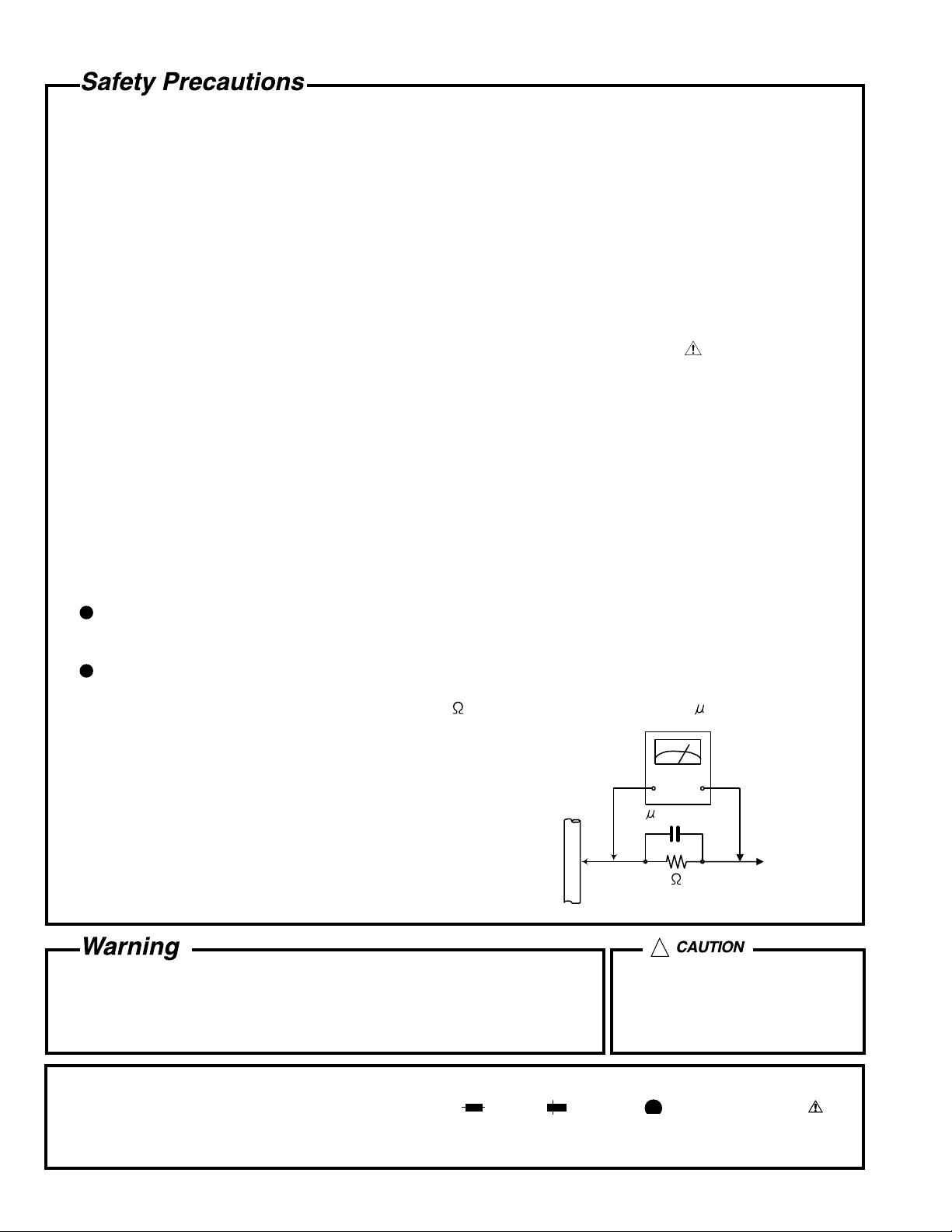
5. Leakage currnet check (Electrical shock hazard testing)
After re-assembling the product, always perform an isolation check on the exposed metal parts of the product
(antenna terminals, knobs, metal cabinet, screw heads, headphone jack, control shafts, etc.) to be sure the
product is safe to operate without danger of electrical shock.
Do not use a line isolation transformer during this check.
Plug the AC line cord directly into the AC outlet. Using a "Leakage Current Tester", measure the leakage
current from each exposed metal parts of the cabinet, particularly any exposed metal part having a return
path to the chassis, to a known good earth ground. Any leakage current must not exceed 0.5mA AC (r.m.s.).
Alternate check method
Plug the AC line cord directly into the AC outlet. Use an AC voltmeter having, 1,000 ohms per volt or more
sensitivity in the following manner. Connect a 1,500 10W resistor paralleled by a 0.15 F AC-type capacitor
between an exposed metal part and a known good earth ground.
Measure the AC voltage across the resistor with the AC
voltmeter.
Move the resistor connection to each exposed metal part,
particularly any exposed metal part having a return path to
the chassis, and meausre the AC voltage across the resistor.
Now, reverse the plug in the AC outlet and repeat each
measurement. Voltage measured any must not exceed 0.75 V
AC (r.m.s.). This corresponds to 0.5 mA AC (r.m.s.).
0.15 F AC TYPE
1500 10W
Good earth ground
AC VOLTMETER
(Having 1000
ohms/volts,
or more sensitivity)
Place this
probe on
each exposed
metal part.
!
1. This equipment has been designed and manufactured to meet international safety standards.
2. It is the legal responsibility of the repairer to ensure that these safety standards are maintained.
3. Repairs must be made in accordance with the relevant safety standards.
4. It is essential that safety critical components are replaced by approved parts.
5. If mains voltage selector is provided, check setting for local voltage.
Burrs formed during molding may
be left over on some parts of the
chassis. Therefore, pay attention to
such burrs in the case of
preforming repair of this system.
In regard with component parts appearing on the silk-screen printed side (parts side) of the PWB diagrams, the
parts that are printed over with black such as the resistor ( ), diode ( ) and ICP ( ) or identified by the " "
mark nearby are critical for safety.
(This regulation does not correspond to J and C version.)
1-2
Page 3
UX-M5R
(U.K only)
1. This design of this product contains special hardware and many circuits and components specially
for safety purposes. For continued protection, no changes should be made to the original
design unless authorized in writing by the manufacturer. Replacement parts must be identical to
those used in the original circuits.
2. Any unauthorised design alterations or additions will void the manufacturer's guarantee ; furthermore the
manufacturer cannot accept responsibility for personal injury or property damage resulting therefrom.
3. Essential safety critical components are identified by ( ) on the Parts List and by shading on the
schematics, and must never be replaced by parts other than those listed in the manual. Please note
however that many electrical and mechanical parts in the product have special safety related
characteristics. These characteristics are often not evident from visual inspection. Parts other than
specified by the manufacturer may not have the same safety characteristics as the recommended
replacement parts shown in the Parts List of the Service Manual and may create shock, fire, or
other hazards.
4. The leads in the products are routed and dressed with ties, clamps, tubings, barriers and the
like to be separated from live parts, high temperature parts, moving parts and/or sharp edges
for the prevention of electric shock and fire hazard. When service is required, the original lead
routing and dress should be observed, and it should be confirmed that they have been returned
to normal, after re-assembling.
1. Service should be performed by qualified personnel only.
2. This equipment has been designed and manufactured to meet international safety standards.
3. It is the legal responsibility of the repairer to ensure that these safety standards are maintained.
4. Repairs must be made in accordance with the relevant safety standards.
5. It is essential that safety critical components are replaced by approved parts.
6. If mains voltage selector is provided, check setting for local voltage.
!
Burrs formed during molding may be left over on some parts of the chassis. Therefore,
pay attention to such burrs in the case of preforming repair of this system.
1-3
Page 4
UX-M5R
Preventing static electricity
1. Grounding to prevent damage by static electricity
Electrostatic discharge (ESD), which occurs when static electricity stored in the body, fabric, etc. is discharged,
can destroy the laser diode in the traverse unit (optical pickup). Take care to prevent this when performing repairs.
2. About the earth processing for the destruction prevention by static electricity
Static electricity in the work area can destroy the optical pickup (laser diode) in devices such as CD players.
Be careful to use proper grounding in the area where repairs are being performed.
2-1 Ground the workbench
Ground the workbench by laying conductive material (such as a conductive sheet) or an iron plate over it
before placing the traverse unit (optical pickup) on it.
2-2 Ground yourself
Use an anti-static wrist strap to release any static electricity built up in your body.
(caption)
Anti-static wrist strap
Conductive material
(conductive sheet) or iron plate
3. Handling the optical pickup
In order to maintain quality during transport and before installation, both sides of the laser diode on the
1.
replacement optical pickup are shorted. After replacement, return the shorted parts to their original condition.
(Refer to the text.)
Do not use a tester to check the condition of the laser diode in the optical pickup. The tester's internal power
2.
source can easily destroy the laser diode.
4. Handling the traverse unit (optical pickup)
1.
Do not subject the traverse unit (optical pickup) to strong shocks, as it is a sensitive, complex unit.
2.
Remove solder of the short land on the card wire after replacing the optical pickup. For specific details, refer to
the replacement procedure in the text. Remove the anti-static pin when replacing the traverse unit.
Be careful not to take too long a time when attaching it to the connector.
3.
Handle the card wire carefully as it may break when subjected to strong force.
4.
It is not possible to adjust the semi-fixed resistor that adjusts the laser power. Do not turn it.
5. Attention when traverse unit is decomposed
Connector
*Please refer to "Disassembly method" in the text for the CD pickup unit.
Short land
Apply solder to the short land before the card wire is disconnected from
the connector on the CD pickup unit.
(If the card wire is disconnected without applying solder, the CD pickup
may be destroyed by static electricity.)
In the assembly, be sure to remove solder from the short land after
connecting the card wire.
1-4
CD pickup unit
Page 5
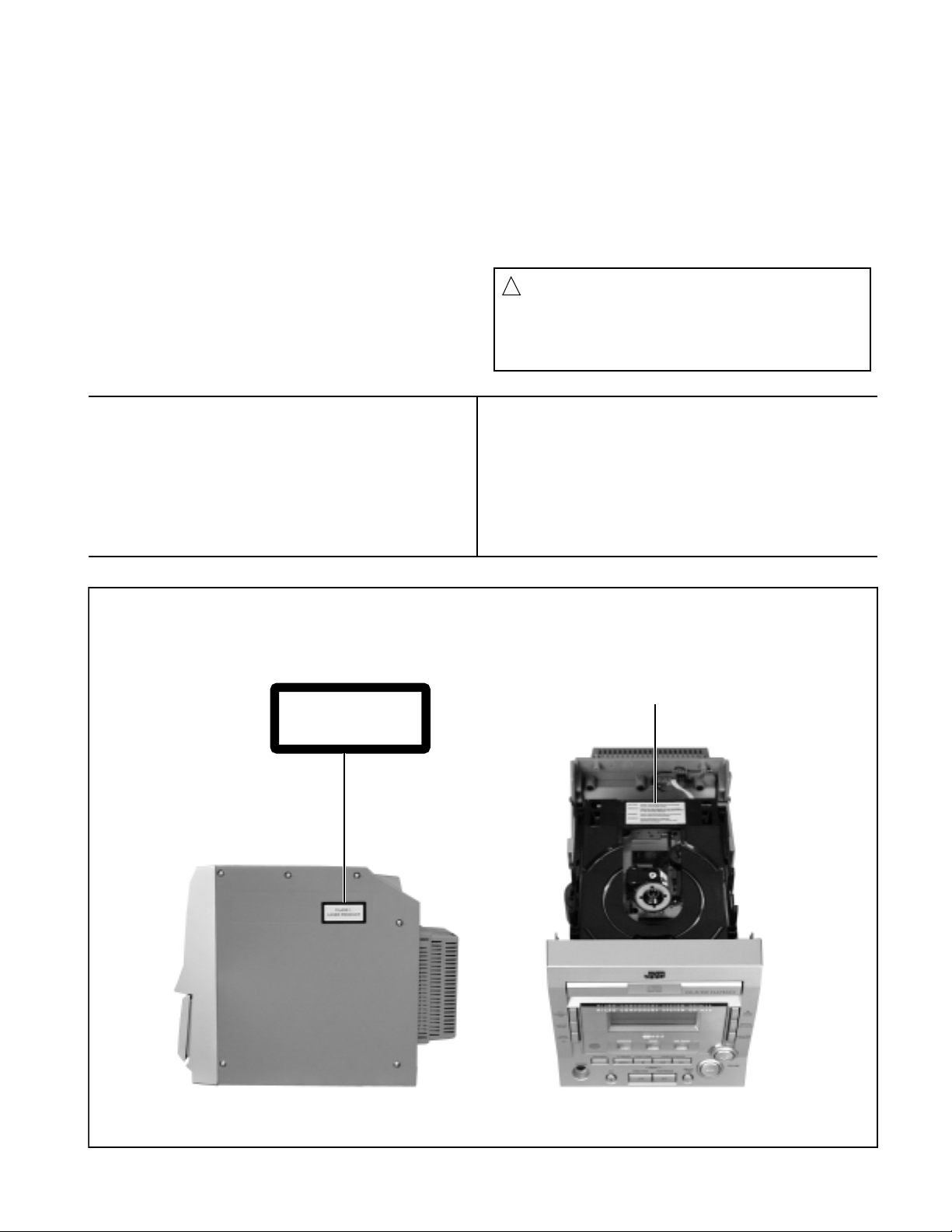
Important for laser products
UX-M5R
1.CLASS 1 LASER PRODUCT
2.DANGER : Invisible laser radiation when open and inter
lock failed or defeated. Avoid direct exposure to beam.
3.CAUTION : There are no serviceable parts inside the
Laser Unit. Do not disassemble the Laser Unit. Replace
the complete Laser Unit if it malfunctions.
4.CAUTION : The compact disc player uses invisible
laserradiation and is equipped with safety switches
whichprevent emission of radiation when the drawer is
open and the safety interlocks have failed or are de
feated. It is dangerous to defeat the safety switches.
VARNING : Osynlig laserstrålning är denna del är öppnad
och spårren är urkopplad. Betrakta ej strålen.
VARO : Avattaessa ja suojalukitus ohitettaessa olet
alttiina näkymättömälle lasersäteilylle.Älä katso
säteeseen.
5.CAUTION : If safety switches malfunction, the laser is able
to function.
6.CAUTION : Use of controls, adjustments or performance of
procedures other than those specified herein may result in
hazardous radiation exposure.
CAUTION
!
Please use enough caution not to
see the beam directly or touch it
in case of an adjustment or operation
check.
ADVARSEL : Usynlig laserstråling ved åbning , når
sikkerhedsafbrydere er ude af funktion. Undgå
udsættelse for stråling.
ADVARSEL : Usynlig laserstråling ved åpning,når
sikkerhetsbryteren er avslott. unngå utsettelse
for stråling.
REPRODUCTION AND POSITION OF LABELS
CLASS 1
LASER PRODUCT
WARNING LABEL
1-5
Page 6
UX-M5R
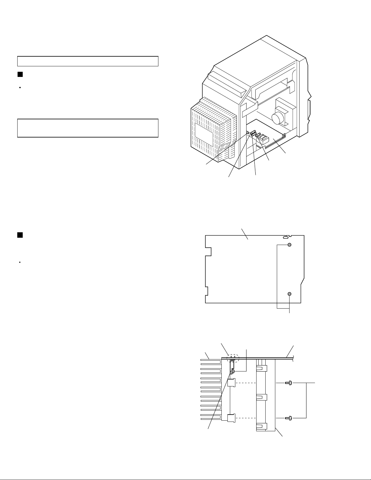
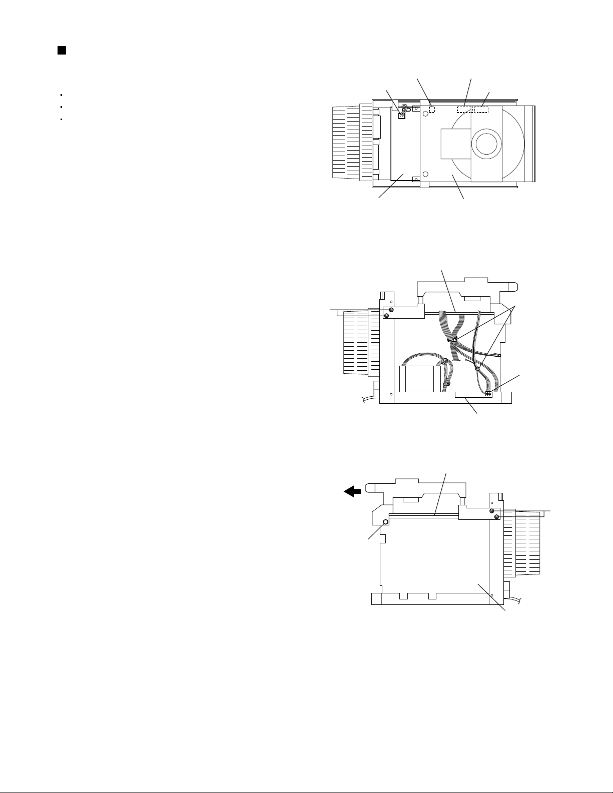
Disassembly method
<Main body section>
Replacement of the fuses and power amplifier IC
Replacing the fuses (See Fig. 1.)
Remove the left side panel according to its
disassembly method (see Figs. 6 and 7).
Fuses are located inside the left side panel.
[Caution] Be sure to replace the required fuses
with designated ones.
Fuse(F904)
1.6A 250V
Fuse(F903)
2.5A 250V
Power board
Fuse(F901)
1.6A 250V
Fuse(F902)
2.5A 250V
Replacing the power amplifier IC on
the main board (See Fig. 2.)
Remove the main board according to its
disassembly method (see Figs. 18 and 19).
1.
From the reverse side of the main board, remove
the two screws A retaining the bracket.
2.
From the forward side of the main board, remove
the four screws B retaining the bracket.
3.
Remove the screw C attaching the power amplifier
IC onto the heat sink.
4.
In order to replace the power amplifier IC, remove
the solder from soldered part a on the reverse side
of the main board.
Soldered part a
Heat sink
Fig.1
Main board (Reverse side)
Fig.2
C
A
Main board
1-6
Power amplifier IC
(IC402)
B
Bracket
Fig.3
Page 7
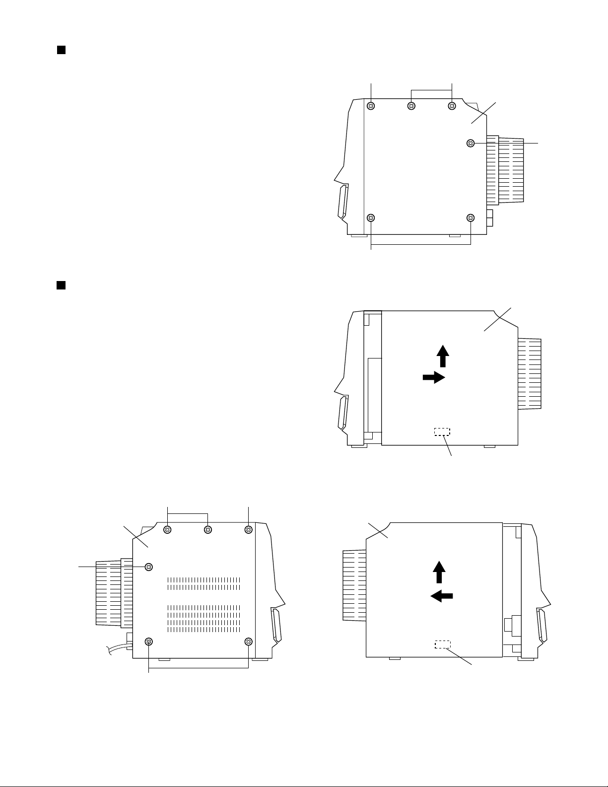
Removing the right side panel
(See Figs. 4 and 5.)
1.2.From the right side of the main body, remove the
three screws D and three screws E retaining the
right side panel.
Slide the right side panel toward the rear (in the
direction of arrow 1) until the claw b at the back of
the panel is hooked by the chassis and then lift the
panel upward (in the direction of arrow 2) to
remove it.
Removing the left side panel
(See Figs. 6 and 7.)
1.2.From the left side of the main body, remove the
three screws D and three screws E retaining the
left side panel.
D
D
UX-M5R
E
Right side
panel
E
Fig.4
Right side
panel
2
Slide the left side panel toward the rear (in the
direction of arrow 3) until the claw c at the back of
the panel is hooked by the chassis, and then lift the
panel upward (in the direction of arrow 4) to
remove it.
E
Left side
panel
D
E
1
Claw b
Fig.5
Left side
panel
4
3
D
Fig.6
Claw c
Fig.7
1-7
Page 8
UX-M5R
Removing the top cover
(See Figs. 8 and 9.)
Remove the left and right side panels.
1.2.From the back side of the main body, loosen the
two screws F retaining the top cover.
Lift the rear part of the top cover to remove it.
Removing the front panel assembly
(See Figs. 10 to 12.)
Remove the left and right side panels.
Remove the top cover.
1.
Remove the tie band bundling the wires.
2.
Disconnect the wire from the connector on the
cassette switch board.
3.
Remove the screw G retaining the bracket on the
earphone board.
4.
Disconnect the wires from the two connectors
CN607 and CN608 on the CD & MCU board.
5.
Remove the four screws H and the two screws J
retaining the bracket of the CD mechanism
assembly from the left and right.
6.
Remove the screw K retaining the front panel
assembly from the bottom side of the main body.
7.
While opening the hooks d to the left and right of
the lower part of the front panel assembly (in the
direction of arrows 1), slide the front panel
assembly toward the front (in the direction of arrow
2).
8.
Disconnect the wire from the connector on the
PB/REC head board, and then remove the front
panel assembly.
[Note] After assembly, apply a locking agent to
the screws G, H and J.
Lift the rear
part to remove.
F
CD mechanism
assembly
H
Fig.8
Fig.9
(To be loosened)
F
Top cover
Rear panel
Brackets
H
CN608
J
G
Earphone
board
Tie band
1-8
H
CN607
J
Brackets
Fig.11
CD mechanism
assembly
Connector on the
cassette switch
board
Chassis
Power board
Fig.10
Hook d
Hook d
Fig.12
Connector on the
PB/REC head board
1
Front panel assembly
2
K
1
Page 9
Removing the CD mechanism
assembly (See Figs. 13 to 15.)
Remove the left and right side panels.
Remove the top cover.
Remove the front panel assembly.
1.
Disconnect the wires from the four connectors
CN601, CN602, CN603 and CN701 on the CD &
MCU board.
2.
From the left side of the main body, remove the tie
bands bundling the wires.
3.
Disconnect the wire from the connector CN902 on
the power board.
4.
From the left and right sides of the main body,
remove the four screws L retaining the bracket.
5.
Slide the CD mechanism assembly toward the front
and remove it from the stud of the main board.
CN603
CN701
CD & MCU board CD mechanism assembly
CD & MCU board
CN601
CN602
Fig.13
L
UX-M5R
Tie bands
Stud
CN902
Power board
Fig.14
CD & MCU board
L
Main board
Fig.15
1-9
Page 10
UX-M5R
Removing the power board
(See Figs. 16 and 17.)
Remove the left and right side panels.
1.
Disconnect the wires from the connector CN901 on
the power board.
2.
Remove the tie bands bundling the wires.
3.
Remove the screw M retaining the lug wire.
4.
Remove the two screws N retaining the chassis .
5.
Remove the power board by pinching the two studs
retaining the power board using radio pliers, etc.
Removing the main board
(See Figs. 18 and 19.)
Remove the left and right side panels.
Remove the top cover.
Remove the front panel assembly.
Remove the CD mechanism assembly.
Chassis
Power board
StudPower transformer
Main board
NM
Fig.16
Fig.17
CN901
Stud
Tie bands
Lug wire
Power board
Radio pliers, etc.
Stud
Chassis
P
1.
From the inside of the rear panel, remove the five
screws P retaining the bracket.
2.
Remove the two screws Q retaining the speaker
terminal of the main board.
3.
Remove the solder from the soldered part e that
attaches the FM antenna wire to the antenna
board.
4.
Remove the three screws R retaining the rear
panel, then remove the rear panel.
5.
From the top side of the main body, remove the
screw S retaining the bracket of the main board.
6.
Remove the screw T retaining the regulator
IC(IC302).
7.
Remove the tie bands bundling the wires.
8.
Disconnect the wire from the connector CN901 on
the power board.
9.
Remove the stud on the main board, and then take
out the main board from the chassis.
FM antenna wire
S
Soldered
part e
Heat sink
Bracket
Power transformer
R
QR
Regulator IC
(IC302)
Antenna board
Power board
Fig.18
T
Fig.19
Main board
Stud
Tie bands
P
CN901
Chassis
1-10
Page 11
UX-M5R
<Front panel assembly section>
Remove the left and right side panels.
Remove the top cover.
Remove the front panel assembly.
Removing the key board
(See Fig. 20.)
Remove the ten screws U retaining the key board.
Removing the cassette mechanism
assembly (See Fig. 20.)
Remove the two screws V and the two screws W
retaining the cassette mechanism assembly.
[Note] After assembly, apply a locking agent
to the screws V and W.
Removing the cassette door damper
(See Fig. 20.)
Remove the screw X retaining the damper bracket
and take out the cassette door damper.
Removing the cassette door stopper
(See Fig. 20.)
Remove the two screws Y retaining the cassette
door stopper and remove the cassette door
stopper.
Removing the cassette door cover
(See Fig. 21.)
[Note] Use the following procedure to remove
only the cassette door cover.
This procedure does not require the
removal of exterior parts such as the
side panels.
1.2.Open the cassette door.
Slide the cassette door cover in the direction of the
arrow and disengage the two claws f and the two
claws g on the left and right of the cassette door
cover from the cassette door.
Front panel assembly
U
Cassette door
stopper
Y
X
Damper bracket
Cassette door
damper
Cassette door
Claw f
Claw g
Cassette door cover
Key board
U
V
Cassette
mechanism
assembly
W
W
Fig.20
Fig.21
Front panel assembly
Removing the cassette door
(See Figs. 22 and 23.)
Remove the cassette mechanism assembly.
Remove the cassette door cover.
1.
Open the cassette door, disengage the spring
hooked across the front of the front panel assembly
and the cassette door in the outward direction, and
remove it from the claw h.
2.
From the back side of the front panel assembly,
remove the two screws Z retaining the bracket.
3.
While pushing the arm section i of the cassette
door in the direction of the arrow, remove the shaft
section j of the cassette door from the front panel
assembly.
4.
While pushing the cassette door arm section k in
the direction of the arrow, remove the shaft section
m of the cassette door from the front panel
assembly.
5.
Take out the cassette door from the back side of
the front panel assembly.
[Caution] In the assembly, be sure to put the
spring around the shaft j before
attaching the cassette door.
Arm section i
Shaft section j
Spring
Spring
Claw h
Disengage the spring so
that it comes to the front
of the claw h.
Fig.22
Front panel assembly
Arm section k
Shaft section m
Bracket
Z
Fig.23
1-11
Page 12
UX-M5R
<CD mechanism section>
Remove the left and right side panels.
Remove the top cover.
Remove the front panel assembly.
Remove the CD mechanism assembly.
Removing the CD & MCU board
(See Figs. 1 and 2.)
1.
From the back side of the CD mechanism
assembly, remove the two screws A retaining the
CD & MCU board.
2.
Disengage the two studs retaining the CD & MCU
board.
3.
Disconnect the wires from the two connectors
CN702 and CN703 on the CD & MCU board.
4.
Lift the CD & MCU board and attach solder to the
short land part a on the CD pickup assembly.
Stud
Stud
CD & MCU board
CD & MCU board
Fig.1
CN704
A
CN702
A
CD pickup unit
5.
Disconnect the card wire from the connector
CN704 on the CD & MCU board, and take out the
CD & MCU board.
[Caution] Be sure to solder the short land
part a on the CD pickup unit before
disconnecting the card wire from the
CD pickup assembly (see Fig. 2).
If the card wire is disconnected
without attaching solder, the CD
pickup may be destroyed by static
electricity.
In the assembly, be sure to remove
solder from the short land part a
after connecting the card wire.
Removing the CD pickup assembly
(See Fig. 3.)
Remove the CD & MCU board.
1.
From the back side of the CD mechanism
assembly, remove the four screws B retaining the
CD pickup assembly.
CN703
CD pickup
assembly
CD mechanism assembly
CD pickup assembly
Damper(Gray)
B
Short land part a
Fig.2
Damper(Blue)
B
2.
Take out the CD pickup assembly.
[Note] When removing or replacing the
dampers, note their colors and be sure
to attach them in their correct positions.
1-12
Damper(Blue)Damper(Gray)
Fig.3
Page 13

UX-M5R
Removing the tray motor
(See Figs. 4 to 7.)
Remove the CD & MCU board.
1.
On the top of the CD mechanism assembly, open
up the claws b and c at the left and right of the
clamper assembly and lift the assembly to remove
it.
2.
On the top of the CD mechanism assembly, push
the section d of the elevator in the direction of the
arrow and lower the CD pickup assembly.
3.
Pull out the tray.
4.
While opening up the claws e at the left and right of
the tray in the directions of the arrows, remove the
tray.
5.
While pushing the claw f on the CD mechanism
assembly downwards, slide the elevator fully in the
direction of the arrow.
6.
Remove the transparent cover.
CD mechanism assembly
Claw b
Claw c
Fig.4
Clamper assembly
Claw c
Tray
7.
Remove the belt from the tray motor pulley.
8.
Remove the two screws C retaining the tray motor
and remove it.
[Note] Take care not to attach grease on the
belt.
After attaching the tray motor in the
assembly, apply a locking agent to the
screws C.
Fig.5
d section
TrayClaw e
Claw e
Fig.6
CD mechanism assembly
Claw f
Tray motor pulley
Fig.7
C
Transparent
Belt
cover
1-13
Page 14

UX-M5R
Replacing the CD pickup unit
(See Figs. 8 to 11.)
[Note] Use the following procedure to replace
only the CD pickup unit.
1.
Remove the left and right side panels (see Figs.4
to 7 of "Main body section" on page 1-7).
2.
Remove the top cover (see Figs.8 and 9 "Main
body section" on page 1-8).
3.
On the top of the main body, open up the claws b
and c on the left and right of the clamper assembly
in the direction of the arrows and lift the assembly
to remove it.
4.
On the top of the main body, push section d on the
elevator of the CD mechanism assembly and lower
the CD pickup assembly.
5.
Pull out the tray.
6.
Remove the slit washer retaining the feed middle
gear, and take out the feed middle gear.
Clamper assembly
Claw c
Claw b
Front panel assembly
Claw c
Fig.8
Front panel assembly
7.
Remove the two screws D retaining the shaft.
8.
Turn the CD pickup unit upside down and apply
solder to the short land part a.
9.
Disconnect the card wire from the CD pickup unit
and replace the unit.
[Caution] Be sure to solder the short land
part a on the CD pickup unit before
disconnecting the card wire from the
CD pickup unit (see Fig. 11).
If the card wire is disconnected
without attaching solder, the CD
pickup may be destroyed by static
electricity.
In the assembly, be sure to remove
solder from the short land part a
after connecting the card wire.
[Note] Removing the CD pickup unit
involves the removal of the sliding
spring. In the assembly, be sure to
attach the spring in the correct
orientation before attaching the CD
pickup unit (see Fig. 11).
D
Feed middle gear
Sliding spring
Fig.9
CD pickup assembly
D
Fig.10
Card wire
d section
TraySlit washer
1-14
Short land part a
Fig.11
Page 15

Adjustment method
UX-M5R
Measuring instructions required for
adjustment
1. AM signal generator
2. FM signal generator
3. Inter mediate frequency sweep generator
4. FM stereo signal generator
5. Low-frequency oscillator
(oscillation frequency 50Hz-20kHz, 0dB output
with 600 ohm impedance)
6. Attenuator (600 ohm impedance)
7. Electronic voltmeter
8. Distortion meter
9. Torque gauge (cassette for CTG-N)
10. Wow & flutter meter
11. Frequency counter meter
12. Test tape
VT712 : For tape speed and wow flutter
VT724 : For reference level
VT702 : For playback frequency
VT702 : For head azimuth adjustment
13. Blank tape
TAPE : AC-225
Measuring instruments
Radio section
FM 1kHz, 22.5kHz deviation
FM STEREO : 1kHz, 67.5kHz deviation
pilot signal 7.5kHz
AM : 1kHz, 30% modulation
Reference output :
H.phone output -10dBs(0.245V) 32 ohm
Speaker output 0dBs(2.8V) 8 ohm
Cassette amplifier section
Reference output :
H.phone output -10dBs(0.245V) 32 ohm
Speaker output 0dBs(2.8V) 8 ohm
Standard mode of function knob :
Press TAPE knob of select TAPE mode
CD section
CD test disc : CTS-1000
Measurement conditions
Power supply voltage
AC230V/50Hz
1-15
Page 16

UX-M5R
Cassette amplifier section
Item Measuring condition Check and adjustment procedure Standard value Adjusting part
Head azimuth
adjustment
Tape speed and
wow/flutter check
and adjustment
PB frequency
response check
Bias frequency
check
REC and PB
frequency
response
adjustment
Test tape:
VT702 (8kHz)
Signal output terminal:
H.phone out
(with 32 ohm load)
Test tape:
VT712 (3kHz)
Signal output terminal:
H.phone out
(with 32 ohm load)
Test tape: VT702
Signal output terminal:
H.phone out
(with 32 ohm load)
Tape: Normal
Signal output terminal:
Cassette REC./PLAY
HEAD
Test tape: AC225
Signal input:
SG 1kHz -20dBs
with emphasis
Signal output terminal:
H.phone out
(with 32 ohm load)
Play back the test tape VT702 (8kHz).
1.
Adjust the head azimuth adjusting screw so that the
2.
phase difference between the R and L channels is
minimized at an output level that is within 2dB of the
maximum output level. After this adjustment, lock the
head azimuth adjusting screw with screw sealant to
cover more than a half of the screw head.
When the head azimuth is maladjusted, correct it with
3.
the head azimuth adjusting screw.
Play back the test tape VT712 (3kHz) by the end
1.
portion.
Connect a frequency counter and check that it reads
2.
between 2940 and 3090Hz. If not, adjust the frequency
with the motor semifixed resistor.
Check that the wow/flutter is within 0.38%
3.
(unweighted).
Play back the test tape VT702 while con-firming that
deviation between the 1kHz signal and 8kHz signal
should be (0+3dB-6dB).
Set the TUNER or CD function and with TAPE to
record. Check to see if the frequency at the measuring
point P201 is 67kHz 1kHz if not adjust L203 until the
frequency counter indicates 67 kHz 1kHz.
At TUNER, set the BAND to the FM position, and
record the reference 1kHz signal and 8kHz signal
alternately repeatedly. While playing back the recorded
signal of the 1kHz signal differ from that of the 8kHz
signal by within (0+3dB-6dB).
Output level:
Within 2dB of
maximum output
level
Phase difference R
and L channels:
Minimum
2940 to 3090Hz
Within 0.38%
(unweighted)
Deviation between
1kHz and 8kHz:
(0+3dB-6dB)
Level difference for
1kHz singnal: Within
(0+3dB-6dB)
Head azimuth
adjusting screw
(To be used only
after head
replacement)
See Fig.1 on
page 1-17.
Tape speed:
Motor semifixed
resistor
See Fig.2 on
page 1-17.
Check only
L203, P201
See Fig.3 on
page 1-17.
Tuner section
Item Measuring condition Check and adjustment procedure Standard value Adjusting part
AM IF adjustment 1.
AM tracking
adjustment
FM tracking
adjustment
Signal input:
Loop antenna
Signal output:
IC101 pin19
Signal input:
Loop antenna
Signal output:
H.phone out
(with 32 ohm load)
Signal input:
Dummy antenna
FM ANT
FM GND
Signal output:
H.phone out
(with 32 ohm load)
Set the intermediate frequency sweep generator to AM
450kHz.
Adjust T101 for maximum and center output.
2. T101
See Fig.3 on
page 1-17.
Set the TUNER at 522kHz adjust L101 until the test
1.
point P107 voltage at 1.1V 0.1V.
Set the TUNER at 1629kHz, check the test point P107
2.
voltage at 7.0V 0.3V.
Set the TUNER and S/G at 603kHz, adjust L102 for
3.
maximum output.
Set the TUNER and S/G at 1404kHz, adjust the TC101
4.
for maximum output.
Repeat the above steps 3 and 4.
5.
Set the TUNER at 87.5MHz adjust the L104 until the
1.
test point P105 voltage at 2.3V 0.1V.
Set the TUNER at 108MHz, check the test point P105
2.
voltage at 6.5V 0.3V.
Set the TUNER and S/G at 90.1MHz, adjust L103 for
3.
maximum output.
Set the TUNER and S/G at 106.1MHz, adjust the
4.
TC102 for maximum output.
Repeat the above steps 3 and 4.
5.
L101, P107
L102
TC101
See Fig.3 on
page 1-17.
L104, P105
L103
TC102
See Fig.3 on
page 1-17.
1-16
Page 17

Location of adjusting parts
Cassette mechanism section
UX-M5R
CASSETTE MOTOR
Tape Speed Adj.
Fig.1 Head azimuth adjustment
Main board (Forward side)
Note: Measuring points (P105, P107 and P201) are located on the reverse side.
P105
(FM VT)
L104
(FM OSC)
TC101
(AM RF)
L101
L102
(AM RF)
TC102
(FM RF)
L103
(FM RF)
P107
(AM VT)
IC101
-
+
Fig.2
T101
(AM IF)
Fig.3
P201
(BIAS FREQUENCY)
L203
(BIAS FREQUENCY ADJ.)
1-17
Page 18

UX-M5R
Flow of functional operation until TOC read
Power ON
Slider turns REST
SW ON.
Laser ON
Focus start
FOK
Turn on focus
servo
Confirm that the voltage at the pin5 of CN703 is
"H"/"L"/"H"
Check that the voltage at the pin10(LD) of
CN704 is +1.35V.
Caution
Before connecting a measuring instrument to
the measuring point, turn the power of the
main unit to OFF.
After performing a measurement and before
disconnecting the measuring instrument,
again turn the power of the main unit to OFF.
(If a measuring instrument is disconnected
while an electric current is being output to the
main unit, the pick up of the main unit will be
damaged.)
Disc spinning
Radial_error
scaling
PLL Lock
Turn on radial
servo
Read TOC
Check that the voltage at the pin1 and pin2 of
CN703 is +0.65V.
Confirm the eye-pattern at the pin25 (RFGO) of IC704
on the CD & MCU board.
1-18
Page 19

UX-M5R
Maintenance of laser pickup
(1) Cleaning the pick up lens
Before you replace the pick up, please try to
clean the lens with a alcohol soaked cotton
swab.
(2) Life of the laser diode
When the life of the laser diode has expired,
the following symptoms will appear.
The level of RF output (EFM output:ampli tude of eye pattern) will below.
Is the level of
RF OUT under
1.25V 0.22Vp-p?
YES
O.K
NO
Replace it.
Replacement of laser pickup
Turn off the power switch and,disconnect the
power cord from the AC OUTLET.
Replace the pickup with a normal one.(Refer
to "Removing the CD pickup" on the previous page)
Plug the power cord in,and turn the power on.
At this time,check that the laser emits for
about 3 seconds and the objective lens moves
up and down.
Note: Do not observe the laser beam directly.
Play a disc.
Check the eye-pattern at the pin25 (RFGO)
of IC704 on the CD & MUC board.
Finish.
(3) Semi-fixed resistor on the APC PC board
The semi-fixed resistor on the APC printed circuit board which is attached to the pickup is used to adjust the laser
power.
Since this adjustment should be performed to match the characteristics of the whole optical block, do not touch the
semi-fixed resistor.
If the laser power is lower than the specified value,the laser diode is almost worn out, and the laser pickup should
be replaced.
If the semi-fixed resistor would be adjusted when the pickup operates normally,the laser pickup may be damaged
due to excessive current.
1-19
Page 20

UX-M5R
Trouble shooting
Circuit Symptom Cause
No soundGeneral
AM
FM Connect the built-in or external antenna.
No sound, weak sound
(Low sensitivity)
No sound, weak sound
(Low sensitivity)
Speakers are not connected.
Wrong function is selected.
Defective volume control
Defective earphone jack
Defect in IC402
Defect in IC301
Improper location of unit
Defect in IF T101
Defect AM antenna coil L102 or oscilloscope
coil L101
Intermediate frequency tuning faulty
RF tracking faulty
Defective IC101
Defective IC102
Poor contact in antenna circuit
FM antenna not connected
Defective band selector switch
Check the speaker connection.
Set switch to the proper position.
Set the volume control to a proper sound
level.
Replace the earphone jack.
Check voltages. Replace if necessary.
Check voltages. Replace if necessary.
Rotate or reposition the unit.
Check resistance, voltage, and current.
Replace as needed.
Replace if necessary.
Readjust (see "Adjustment method").
Readjust (see "Adjustment method").
Check voltages. Replace if necessary.
Check voltages. Replace if necessary.
Check resistance and resolder.
Replace or repair the switch.
Remedy
Defective IC101
Defective IC102
Intermediate frequency tuning faulty
Poor contact in FM antenna circuit
Tape Clean the capstan or head with alcohol.
CD Insert disc correctly.
No sound/recording,
unsteady tape sound,
weak sound
Cannot read the table
of content.
No sound
Dirty capstan or head
Irregular cassette tape winding
Defective IC201
Defective IC202
Cassette erasure prevention tabs broken out
Disc is inserted upside down.
Disc is dirty.
Disc is scratched.
Disc is seriously warped.
A non-standard disc has been inserted.
Moisture has formed inside the CD deck.
Defective IC701
Defective IC704
Check voltages. Replace if necessary.
Check voltages. Replace if necessary.
Readjust (see "Adjustment method").
Resolder or repair as required.
Replace tape.
Check voltages. Replace if necessary.
Check voltages. Replace if necessary.
Replace tape or cover tab openings with
adhesive tape.
Wipe clean with a soft cloth.
Use a new disc.
Use a new disc.
Use only a brand name disc.
Wait about 20 to 30 minutes.
Check voltages. Replace if necessary.
Check voltages. Replace if necessary.
1-20
Defective IC703
Defect in the CD pickup mechanism
Check voltages. Replace if necessary.
Replace as required.
Page 21

Description of major ICs
TC9462F (IC701) : Digital servo single chip processor
1. Terminal layout
80 51
UX-M5R
100 81
1 30
2. Pin function
Pin No. Symbol I/O Function
1
2
3
4
5
6
7
8
9
10
11
12
13
14
15
16
17
18
19
20
21
22
23
24
25
26
27
28
TEST0
HSO
UHSO
EMPH
LRCK
VSS1
BCK
AOUT
DOUT
MBOV
IPF
SBOK
CLCK
VDD1
VSS2
DATA
SFSY
SBSY
SPCK
SPDA
COFS
MONIT
VDD2
TESIO0
P2VREF
HSSW
ZDET
PDO
I
O
O
O
O
O
O
O
O
O
O
I/O
-
O
O
O
O
O
O
O
-
I
O
O
O
31 50
Test mode terminal. Normally, keep at open.
Playback speed mode flag output terminal.
UHSO
H
H
L
L
Subcode Q data emphasis flag output terminal. Emphasis ON at "H" level and
OFF at "L" level. The output polarity can invert by command.
Channel clock output terminal. (44.1kHz) L-ch at "L" level and R-ch at "H" level.
The output polarity can invert by command.
Digital ground terminal.
Bit clock output terminal. (1.4112MHz)
Audio data output terminal.
Digital data output terminal.
Buffer memory over signal output terminal. Over at "H" level.
Correction flag output terminal. At "H" level, AOUT output is made to correction
impossibility by C
Subcode Q data CRCC check adjusting result output terminal. The adjusting
result is OK at "H" level.
Subcode P W data readout clock input/output terminal. This terminal can select
by command bit.
Digital power supply voltage terminal.
Digital ground terminal.
Subcode P W data output terminal.
Playback frame sync signal output terminal.
Subcode block sync signal output terminal.
Processor status signal readout clock output terminal.
Processor status signal output terminal.
Correction frame clock output terminal. (7.35kHz)
Internal signal (DSP internal flag and PLL clock) output terminal. Selected by
command. This terminal output the text data with serial by command.
Digital power supply voltage terminal.
Test input/output terminal. Normally, keep at "L" level. The terminal that inputted
the clock for read of text data by command.
PLL double reference voltage supply terminal.
2/4 times speed at "VREF" voltage.
1 bit DA converter zero detect flag output terminal.
Phase difference signal output terminal of EFM signal and PLCK signal.
HSO
PLAYBACK SPEED
H
L
H
L
2
correction processing.
Normal
2 times
4 times
-
1-21
Page 22

UX-M5R
Pin No. Symbol I/O
29
30
31
32
33
34
35
36
37
38
39
40
41
42
43
44
45
46
47
48
49
50
51
52
53
54
55
56
57
58
59
60
61
62
63
64
65
66
67
TMAXS
TMAX
LPFN
LPFO
PVREF
VCOREF
VCOF
AVSS1
SLCO
RFI
AVDD1
RFCT
RFZI
RFRP
FEI
SBAD
TSIN
TEI
TEZI
FOO
TRO
VREF
RFGC
TEBC
FMO
FVO
DMO
2VREF
SEL
FLGA
FLGB
FLGC
FLGD
VDD3
VSS3
IO0
IO1
IO2
IO3
O
O
I
O
I
O
-
O
I
I
I
I
I
I
I
I
I
O
O
O
O
O
O
O
O
O
O
O
O
-
-
I/O
I/O
I/O
I/O
Function
TMAX detection result output terminal. Selected by command bit (TMPS).
TMAX detection result output terminal. Selected by command bit (TMPS).
DIFFERENCE RESULT TMAX OUTPUT
Longer than fixed freq.
Shorter than fixed freq.
Within the fixed freq.
LPF amplifier inverting input terminal for PLL.
LPF amplifier output terminal for PLL.
PLL reference voltage supply terminal.
VCO center frequency reference level terminal. Normally, keep at "PVREF" level.
VCO filter terminal.
Analog ground terminal.
Data slice level output terminal.
RF signal input terminal.
Analog power supply voltage terminal.
RFRP signal center level input terminal.
RFRP zero cross input terminal.
RF ripple signal input terminal.
Focus error signal input terminal.
Sub-beam adder signal input terminal.
Test input terminal. Normally, keep at "VREF" level.
Tracking error signal input terminal. Take in at tracking servo on.
Tracking error zero cross input terminal.
Focus servo equalizer output terminal.
Tracking servo equalizer output terminal.
Analog reference voltage supply terminal.
RF amplitude adjustment control signal output terminal.
Tracking balance control signal output terminal.
Feed equalizer output terminal.
Speed error signal or feed search equalizer output terminal.
Disk equalizer output terminal.
(PWM carrier=88.2kHz for DSP, Synchronize to PXO)
Analog double reference voltage supply terminal.
APC circuit ON/OFF indication signal output terminal.
At the laser on time, UHF = L at "HiZ" level and UHF = H at "H" level.
External flag output terminal for internal signal.
Can select signal from TEZC, FOON, FOK and RFZC by command.
External flag output terminal for internal signal.
Can select signal from DFCT, FOON, FMON and RFZC by command.
External flag output terminal for internal signal.
Can select signal from TRON, TRSR, FOK and SRCH by command.
External flag output terminal for internal signal.
Can select signal from TRON, DMON, HYS and SHC by command.
Digital power supply voltage terminal.
Digital ground terminal.
General I/O terminal. Can change over input port or output port by command.
At the input mode time can readout a state of terminal (H/L) by read command.
At the output mode time can control a state of terminal (H/L/HiZ) by command.
"P2VREF"
"Vss"
"HiZ"
1-22
Page 23

UX-M5R
Pin No. Symbol I/O
68
69
70
71
72
73
74
75
76
77
78
79
80
81
82
83
84
85
86
87
88
89
90
91
92
93
94
95
96
97
98
99
100
DMOUT
CKSE
DACT
TESIN
TESIO1
VSS4
PXI
PXO
VDD4
XVSS
XI
XO
XVDD
DVSR
RO
DVDD
DVR
LO
DVSL
TEST1
TEST2
TEST3
BUS0
BUS1
BUS2
BUS3
VDD5
VSS5
BUCK
CCE
TEST4
TSMOD
RST
I
I
I
I
I
I
O
-
I
O
-
-
O
-
-
O
I
I
I
I/O
I/O
I/O
I/O
-
-
I
I
I
I
I
Function
This terminal controls IO0 IO3 terminal. At "L" level time, IO0, 1 out feed
equalizer signal of 2-state PWM, IO2,3 out disk equalizer signal of 2-state PWM.
Normally, keep at open.
DAC test mode terminal. Normally, keep at open.
Test input terminal. Normally, keep at "L" level.
Test input/output terminal. Normally, keep at "L" level.
Digital ground terminal.
Crystal oscillator connecting input terminal for DSP. Normally, keep at "L" level.
Crystal oscillator connecting output terminal for DSP.
Digital power supply voltage terminal.
Oscillator ground terminal for system clock.
Crystal oscillator connecting input terminal for system clock.
Crystal oscillator connecting output terminal for system clock.
Oscillator power supply voltage terminal for system clock.
Analog ground terminal for DA converter.(R-ch)
R channel data forward output terminal.
Analog supply voltage terminal for DA converter.
Reference voltage terminal for DA converter.
L channel data forward output terminal.
Analog ground terminal for DA converter.(L-ch)
Test mode terminal. Normal, keep at open.
Test mode terminal. Normal, keep at open.
Test mode terminal. Normal, keep at open.
Micon interface data input/output terminal.
Digital power supply voltage terminal.
Digital ground terminal.
Micon interface clock input terminal.
Command and data sending/receiving chip enable signal input terminal.
The bus line becomes active at "L" level.
Test mode terminal. Normal, keep at open.
Local test mode selection terminal.
Reset signal input terminal. Reset at "L" level.
1-23
Page 24

UX-M5R
TMP87EP26F (IC601) : MCU
1. Terminal layout
80 51
81
50
(Top view)
100
130
31
2.Pin function
Pin No. Symbol I/O Function
GND (0V)
VSS
1
XOUT
2
XIN
3
RESET
4
XTOUT(P22)
5
XTIN(P21)
6
TEST
7
SHIFT FREQ
8
REMOTE
9
MUTE
10
PLAY MUTE
11
REC MUTE
12
PLAY/REC
13
NC(SCK2)
14
NC(SI2)
15
NC(SO2)
16
REC SW (RVS)/(WAIT)
17
Resonator connecting pins for high clock(4-8MHz).
O
For inputting external clock, XIN is used and XOUT is opened.
I
Reset signal input or watchdog timer output/address-trap-reset output
I/O
Resonator connecting pins for slow clock(32.768kHz)
I/O
or general purpose I/O.
I/O
Test pin for out-going test. Always fixed to low.
I
Shift the crystal oscillation frequency to reduce tuner noise.
O
Remote control signal input
I
Audio mute output
O
Muting output during play
O
Muting output during recording
O
Play or recording output, low for recording.
O
Not connect
Not connect
Not connect
Deck reverse record protection input. Low means can record on
I
reverse side.
Deck forward record protection input. Low means can record on
REC SW (FWD)
18
I
forward side.
Solenoid output for deck B.
B-SOL+
19
B-MODE SW
20
VOL STB
21
POWER
22
B-HALF SW
23
JOG-B/VOL DATA
24
JOG-A/VOL CLK
25
RDS CLK
26
V MOTOR
27
B-PHOTO OUT
28
CD-RW
29
RES
30
O
Mode switch input of deck B. Low means the head is up.
I
TC9422F volume STB output
O
Power output control
O
Half switch input of deck B. Low means deck B have tape.
I
Jog dial input and TC9422F volume data output
I/O
Jog dial input and TC9422F volume clock output
I/O
BU1923F(RDS demodulator) interface CLK input
I
Motor output
O
Reel pulse input of deck B. Have pulse input means the tape is rotating.
I
CD-RW control output
O
CD servo reset output
O
1-24
Page 25

Pin No. Symbol I/O Function
Servo DSP chip enable output
31
32
33
34
35
36
37
38
39
40
41
42
43
44
45
46
47
48
49
50
51
52 91
92 95
96
97
98
99
100
CCE
BUCK
BUS0
BUS1
BUS2
BUS3
SLOUT
SLIN
SLT
SLEND
NC
RDS DATA
STEREO
POWER DETECT
AD K3
AD K2
AD K1
VAREF
BOOT
VSS
VDD
SEG39 0
COM3 0
VLC
PLL DATA
PLL CLK
PLL PERIOD
VDD
O
Servo DSP clock output
O
Servo DSP command and data I/O
I/O
Servo DSP command and data I/O
I/O
Servo DSP command and data I/O
I/O
Servo DSP command and data I/O
I/O
Tray open/close outputs for current sensor drawer type mechanism.
O
O
CD pick up position input: L if pick up is in inner side.
I
Current sensor input
I
Not connected
BU1923F(RDS demodulator) interface data input
I
Stereo input pin for tuner stereo indication
I
Power down detection
I
Panel key analog input
I
Panel key analog input
I
Panel key analog input
I
Analog reference voltage input
Control input for writing MCU program area via ICU interface.
I
GND (0V)
VDD (+5V)
LCD segment outputs
O
LCD common outputs
O
LCD drive power supply
TC9257P (PLL) interface
I/O
TC9257P (PLL) interface
O
TC9257P (PLL) interface
O
VDD (+5V)
-
UX-M5R
1-25
Page 26

UX-M5R
AN7312 (IC202) : Dual recording/Playback pre-amplifier circuit with ALC
1. Terminal layout
14 8
~
2. Block diagram
Vcc
14 13 12 11 10
8
9
Ripple Filter
17
~
1 2 3 4 5 6
GND
ALC
3. Pin function
Pin No. Symbol Function
1
GND
2
ALC time constant
3
ALC input Ch.1
4
Output Ch.1
5
Phase compensation Ch.1
6
N.F.B. Ch.1
7
Input Ch.1
8
Input Ch.2
9
N.F.B. Ch.2
10
Phase compensation Ch.2
11
Output Ch.2
12
ALC input Ch.2
13
Ripple filter
14
Vcc
I/O
GND
ALC time constant by resistance and capacitor
Right channel ALC input
I
Right channel output
O
No connect
Right channel negative feed back input
I
Right channel signal input
I
Left channel signal input
I
Left channel negative feed back input
I
No connect
Left channel output
O
Left channel ALC input
I
Ripple filter
Power supply
-
Amp.
Ch2
Amp.
Ch1
7
BA4558N (IC401,IC403) : Dual operational amplifier
1. Terminal layout & Block diagram
1ch 2ch
2
34
EE
5678
+IN2 -IN2 OUT2 Vcc
1
OUT1 -IN1 +IN1 V
2. Pin function
Pin No. Symbol I/O Function
1
OUT1
2
3
4
5
6
OUT2
7
8
-IN1
+IN1
EE
V
+IN2
-IN2
CC
V
O
I
I
I
I
O
-
A output
A -input
A +input
VB +input
B -input
B output
V+
1-26
Page 27

LM1876TF (IC402) : Overture audio power amplifier series
1. Terminal layout
LM1876TF
1
23456 7891011 1213 14 15
2. Pin function
Pin No. Symbol I/O Function
1
2
3
4
5
6
7
8
9
10
11
12
13
14
15
OUT B
VCC A
OUT A
-Vcc
GND A
MUTE A
-IN A
+IN A
Standby A
GND B
MUTE B
-IN B
+IN B
Standby B
VCC B
O
B output
-
A V+
O
A output
-
V-
-
Power terminal
-
Control
I
A -input
I
A +input
-
Control
-
Power terminal
-
Control
I
B -input
I
B +input
-
Control
-
B V+
3. Block diagram
+IN A
-IN A
+IN B
-IN B
8
7
13
12
5
AMP A
AMP B
10
Standby A
VCC AGND A
2
15 14
Standby B
MUTE A
96
11
MUTE BVCC BGND B
3
4
1
UX-M5R
OUT A
-VCC
OUT B
NJM7812A (IC302) : Regulator
1. Terminal layout
1.INPUT
2.OUTPUT (+12V)
3.GND
1 2 3
2. Block diagram
1
INPUT
THERMAL SHUTDOWN
BANDGAP REFERENCE
OVER VOLTAGE PROTECTION
SOA PROTECTION
SHORT CIRCUIT
PROTECTION
3
GND
2
R1
R2
OUTPUT
1-27
Page 28

UX-M5R
TA2092N (IC703) : Power driver
1.Terminal Layout & Block Diagram
PW GND1
OUT(-)1
PW VCC1
OUT(+)1
VIN1
VRI
VCI
VIN2
OUT(+)2
PW VCC2
OUT(-)2
PW GND2
1
2
3
4
5
6
7
8
9
10
11
12
PW GND4
24
OUT(-)4
23
PW VCC4
22
OUT(+)4
21
VIN4
20
SVCC1
19
18
SGND
17
VIN3
16
OUT(+)3
15
PW VCC3
14
OUT(-)3
13
PW GND3
2. Pin function
Pin No. Symbol I/O Function
PW GND1
1
2
3
4
5
6
7
8
9
10
11
12
13
14
15
16
17
18
19
20
21
22
23
24
OUT(-)1
PW VCC1
OUT(+)1
VIN1
VRI
VCI
VIN2
OUT(+)2
PW VCC2
OUT(-)2
PW GND2
PW GND3
OUT(-)3
PW VCC3
OUT(+)3
VIN3
SGND
SVCC1
VIN4
OUT(+)4
PW VCC4
OUT(-)4
PW GND4
Power GND
Inverted output for CH1
O
Supply terminal of output stage for CH1
Non-inverted output for CH1
O
Input for CH1
I
Input reference voltage
I
Output reference voltage
O
Input for CH2
I
Non-inverted output for CH2
O
Supply terminal of output stage for CH2
Inverted output for CH2
O
Power GND
Power GND
Inverted output for CH3
O
Supply terminal of output stage for CH3
Non-inverted output for CH3
O
Input for CH3
I
Supply terminal of small signal GND
Small signal GND
Input for CH4
I
Non-inverted output for CH4
O
Supply terminal of output stage for CH4
Inverted output for CH4
O
Power GND
-
UPC1330 (IC201) : REC/PB audio head switch
1. Terminal layout
19
3. Pin function
Pin No. Symbol I/O Function
SWR1
1
GND
2
SWP1
3
CONT
4
GND
5
VCC
6
SWP2
7
GND
8
SWR2
9
Record SW (Left channel)
GND
Play SW (Left channel)
Record/play control pin
GND
Power supply
Play SW (Right channel)
GND
Record SW (Right channel)
-
2. Block diagram
123456 789
INVERTER
COMPARATOR
1-28
Page 29

TA2104BN (IC101) : 1chip AM/FM, MPX tuner system
1. Terminal layout 2. Pin function
UX-M5R
RFGND
FMRF IN
AM LOW CUT
MIX OUT
VCC
AMIF IN
FMIF IN
GND
AGC
QUAD
R OUT
L OUT
10
11
12
1
2
3
4
5
6
7
8
9
24
FMRF OUT
23
RF VCC
22
AMRF IN
21
FM OSC
20
AM OSC
19
OSC OUT
18
ST LED
17
IF REQ
16
DET OUT
15
MPX IN
14
LPF1
13
LPF2
Pin No. Symbol I/O Function
RFGND
1
FMRF IN
2
AM LOW CUT
3
MIX OUT
4
VCC
5
AMIF IN
6
FMIF IN
7
GND
8
AGC
9
QUAD
10
R OUT
11
L OUT
12
LPF2
13
LPF1
14
MPX IN
15
DET OUT
16
IF REQ
17
ST LED
18
OSC OUT
19
AM OSC
20
FM OSC
21
AMRF IN
22
RF VCC
23
FMRF OUT
24
Ground terminal for RF
Input of FMRF signal
I
AM low frequency cut
I
Output of FM/AM RF mix
O
Power supply terminal
Input of AMIF signal
I
Input of FMIF signal
I
Ground terminal
AGC voltage input terminal
I
OSC terminal for FM DET.
I
Output R-channel
O
Output L-channel
O
FM/AM switch
I
Stereo/monoral switch
I
Multiplex signal input
I
AM/FM detection output
O
IF out/REQ out
O
Stereo indicator output
O
PLL data bus for FM or AM
O
AM local oscillation circuit
FM local oscillation circuit
Input of AMRF signal
I
Power supply terminal for RF
Output of FMRF signal
O
3. Block diagram
FMRF
OUTRFVCC
RF
GND
AMRFINFM
OSCAMOSC
2324 2122 1920 1718 1516 1314
FM
OSC
AM
MIX
LOW
CUT
FM
MIX
MIX
OUT
FMRF
21 43 65 87 109 1211
FMRFINAM
OSC
OUTSTLEDIFREQ
AM
OSC
FMRF
FMRF
VCC AMIFINFMIFINGND AGC R OUT L OUTQUAD
ST SW
BUFF
LEVEL
1/8
DET
AMIF FMIF
IF
IF
REQ
AM
DET
DET
OUT
AF
BUFF
AGC
FM
DET
AF
MPX
IN
LPF1 LPF2
VCD
DIVIDE
ST/MO
FM/AM
MUTE
DECODE
1-29
Page 30

UX-M5R
TA2153FN (IC704) : RF amplifier for digital servo
1. Terminal layout 2. Block diagram
VCC
RFGC
GMAD
FNI
FPI
TPI
TNI
MDI
LDO
SEL
TEB
2VRO
TEN
TEO
SBAD
1
2
3
4
5
6
7
8
9
10
11
12
13
14
15
30
29
28
27
26
25
24
23
22
21
20
19
18
17
16
RFN2
GND
RFO
AGCIN
GVSW
RFGO
RFRPIN
PKC
RFCT
BTC
RFRP
VRO
SEB
FEN
FEO
RFN229GND28RFO27AGCIN26GVSW25RFGO24RFRPIN23PKC22RFCT21BTC20RFRP19VRO18SEB17FEN16FEO
30
+
1
VCC
2
RFGC
3
GMAD
AGC Amp.
+
-
+
4
FNI
+
-
5
FPI6TPI
-
I-I
PEAK
BOTTOM
+
-
I-I
7
8
TNI
-
MDI
3. Pin function
Pin No. Symbol I/O Function
1
VCC
2
RFGC
Power supply input terminal
RF amplitude adjustment control signal input terminal. Controlled by 3-PWM
I
signals. (PWM carrier = 88.2kHz)
3
4
5
6
7
8
9
10
GMAD
FNI
FPI
TPI
TNI
MDI
LDO
SEL
Open loop gain adjustment terminal for AGC amplifier
I
Main beam I-V amplifier input terminal
I
Main beam I-V amplifier input terminal
I
Sub beam I-V amplifier input terminal
I
Sub beam I-V amplifier input terminal
I
Monitor photo diode amplifier input terminal
I
Laser diode amplifier input terminal
O
Laser diode control signal input terminal and APC circuit ON/OFF control signal
I
terminal
SEL level APC circuit LDO Detect frequency
GND OFF Connected to Vcc through Low
resistor (1kohm)
Hiz ON Control signal output Low
Vcc ON Control signal output High
+
+
SW3
9
-
-
+
LDO
+
-
10
+
SW2
SW1
11
SEL
+
-
-
-
+
-
+
3 STATE DET.
12
13
14
TEB
TEN
2VRO
+
-
+
TEO
+
15
SBAD
-
1-30
11
12
13
14
15
16
17
TEB
2VRO
TEN
TEO
SBAD
FEO
FEN
Tracking error balance adjustment signal input terminal. Controlled by 3-PWM
I
signals. (PWM carrier = 88.2kHz)
Reference voltage (2VRO) output terminal 2RVO = 4.2V when Vcc = 5V
O
TE amplifier negative input terminal
I
TE error signal output terminal
O
Sub beam adder signal output terminal
O
Focus error signal output terminal
O
FE amplifier negative input terminal
I
Page 31

Pin No. Symbol I/O Function
18
SEB
RFRP output circuit switching terminal
I
SEL level Bottom detection Peak detection
GND ON ON
Vcc OFF ON
19
20
21
22
23
24
25
26
VRO
RFRP
BTC
RFCT
PKC
RFRPIN
RFGO
GVSW
Reference signal (VRO) output terminal
O
Track count signal output terminal
O
Time constant adjustment terminal for bottom detection
I
RFRP signal center level output terminal
O
Time constant adjustment terminal for peak detection
I
Input terminal for track count signal output amplifier
I
Output terminal for RF signal amplitude adjustment amplifier
O
Amplifier (AGC, FE, TE) gain switching terminal
I
GVSW Mode
GND CD-RW
Hiz Normal
Vcc Normal
27
28
29
30
AGCIN
RFO
GND
RFN2
Input terminal for RF signal amplitude adjustment amplifier
I
Output terminal RF signal amplifier
O
Ground terminal
Input terminal for RF signal amplifier
I
UX-M5R
TA7291S (IC702) : Bridge driver
1.Terminal Layout
123456789
Vs
NC
Vcc
IN2(M+)
OUT2
3.Block diagram
Vcc Vref
28
GND
PROTECTOR
CIRCUIT
(TSD)
OUT1
REG
Vref
IN1(M+)
2.Pin function
Pin No. Symbol I/O Function
IN2(M-)
1
2
3
4
5
6
7
8
9
Vcc
OUT2
NC
GND
Vs
OUT1
Vref
IN1(M+)
Input terminal
I
Supply voltage terminal for logic
Output terminal
O
Not connect
Ground terminal
Supply voltage terminal for motor driver
Output terminal
O
Supply voltage terminal for control
Input terminal
I
6
Vs
OUT1
7
OUT2
3
91
IN1 IN2
5
GND
1-31
Page 32

UX-M5R
TC9422F (IC301) : System electronic volume
1.Terminal Layout
VDD
GND
L-IN1
L-IN2
L-IN3
L-IN4
L-SW-OUT
L-VR-IN
L-B1
L-B2
L-B3
L-TONE-OUT
L-T1
Vref
CK
1
2
3
4
5
6
7
8
9
10
11
12
13
14
28
R-IN1
27
R-IN2
26
R-IN3
25
R-IN4
24
R-SW-OUT
23
R-VR-IN
22
R-B1
21
R-B2
20
R-B3
19
R-TONE-OUT
18
R-T1
17
STB
16
DATA
15
2.Block Diagram
L-IN1
L-IN2
L-IN3
L-IN4
L-SW-OUT
L-VR-IN
L-B1
L-B2
L-B3
L-TONE-OUT
L-T1
INPUT SELECTOR
2
3
4
5
6
7
8
9
1k
10
CAPACITOR FOR
OSCILLATION
11
500
12
750
100k
GAIN CONTROL
MAIN VR
50k /64STEP
50k
13k
0,6,12,18dB
13k
BASS VR
50k /16STEP
TREBLE VR
50k /16STEP
GND VDD
281
LATCH
DECODER
CIRCUIT
100k
GAIN CONTROL
0,6,12,18dB
MAIN VR
50k /64STEP
BASS VR
50k /16STEP
TREBLE VR
50k /16STEP
INPUT SELECTOR
50k
CAPACITOR FOR
OSCILLATION
13k
13k
500
750
27
26
25
24
23
22
21
20
1k
19
18
17
R-IN1
R-IN2
R-IN3
R-IN4
R-SW-OUT
R-VR-IN
R-B1
R-B2
R-B3
R-Tone-OUT
R-T1
1-32
32BIT SR
50k
50k
Vref CK DATA STB
1613 14 15
Page 33

3.Pin Function
Pin No. Symbol I/O Function
GND
1
L-IN1
2
L-IN2
3
L-IN3
4
L-IN4
5
L-SW-OUT
6
L-VR-IN
7
L-B1
8
L-B2
9
L-B3
10
L-TONE-OUT
11
L-T1
12
Vref
13
CK
14
DATA
15
STB
16
R-T1
17
R-TONE-OUT
18
R-B3
19
R-B2
20
R-B1
21
R-VR-IN
22
R-SW-OUT
23
R-IN4
24
R-IN3
25
R-IN2
26
R-IN1
27
VDD
28
Ground pin
Audio signal input pin (L-ch)
I
Audio signal input pin (L-ch)
I
Audio signal input pin (L-ch)
I
Audio signal input pin (L-ch)
I
Audio signal output pin (L-ch)
O
Main volume input pin (L-ch)
I
Tone control tap pin 1 for bus
I
Tone control tap pin 2 for bus
I
Tone control tap pin 3 for bus
I
Tone control output pin (L-ch)
O
Tone control tap pin for treble (L-ch)
I
Reference voltage input pin
I
Clock input pin
I
Data input pin
I
Strobe input pin
I
Tone control tap pin for treble (R-ch)
I
Tone control output pin (R-ch)
O
Tone control tap pin 3 for bus
I
Tone control tap pin 2 for bus
I
Tone control tap pin 1 for bus
I
Main volume input pin (R-ch)
I
Audio signal output pin (R-ch)
O
Audio signal input pin (R-ch)
I
Audio signal input pin (R-ch)
I
Audio signal input pin (R-ch)
I
Audio signal input pin (R-ch)
I
Power supply voltage pin
-
UX-M5R
1-33
Page 34

UX-M5R
TC9257F (IC102) : PLL frequency synthesizer
1. Terminal layout
1
XT
2
XT
3
PRD
4
CLK
5
DATA
6
MUTE
CD
AUX
7
8
9
10
TUNER
ST MONO
2. Block diagram
FM OSC
14
AM OSC
13
XT
2
XT
1
DATA
5
CLK
4
PRD
3
AMP
20
19
18
17
16
15
14
13
12
11
FM VT
AM VT
B1
B0
IF
GND
FM OSC
AM OSC
VDD
EE
FM
L
1/2
FMHHF
OSC
CIRCUIT
2 MODULUS
PRESCALER
FM MODE LF
OSC
1ms
ADDRESS
DECODER
OUTPUT PORT
MUTE
TUNER
PSC
4bit SWALLOW
COUNTER
12bit PROGRAMMABLE COUNTER
4
REFERENCE COUNTER
24bit REGISTER
24bit SHIFT REGISTER
4
TEST
24bit REGISTER
4 4
20bit BINARY COUNTER
UNIVERSAL COUNTER CONTROL
OT-4
9876
CD
AUX
12
24 22
XT
POWER ON
15
10
1ms
VDD
12
RESET
MAX
5
4
RESET
PHASE
COMPARATOR
UNLOCK
5
GATE
GND
15
TRI-STATE
BUFFER
TRI-STATE
BUFFER
OT4
I/O PORT
AMP
AMP
AM VT
19
FM VT
20
ST MONO
10
EE
11
IF
16
B0
17
B1
18
3. Pin function
Pin No. Symbol I/O Function
XT
1
2
3
4
5
6
7
8
9
10
XT
PRD
CLK
DATA
MUTE
TUNER
CD
AUX
ST MONO
Crystal oscillator pins
I
Crystal oscillator pins
O
Period signal input
I
Clock signal input
I
Serial data input/output
I/O
General-purpose output port
O
General-purpose output port
O
General-purpose output port
O
General-purpose output port
O
General-purpose I/O port
I/O
1-34
Pin No. Symbol I/O Function
EE
11
12
13
14
15
16
17
18
19
20
VDD
AM OSC
FM OSC
GND
IF
B0
B1
AM VT
FM VT
General-purpose I/O port
I/O
Power supply pin
Programmable counter input
I
Programmable counter input
I
Ground pin
General-purpose I/O port
I/O
General-purpose I/O port
I/O
General-purpose I/O port
I/O
Phase comparator output
O
Phase comparator output
O
Page 35

BU1923F (IC602) : RDS decoder
1. Terminal layout 2. Block diagram
1
2
3
4
5
6
7
8
16
15
14
13
12
11
10
9
MUX
REF
V
V
DD1
V
SS1
100k
4
120k
3
5
Analog
power supply
6
100k
+
anti-aliasing
filter
8th Switched
capacitor filter
CMPVSS3
87
comparator
16
1
UX-M5R
RCLK
QUAL
12
V
DD2
V
SS2
Digital
power supply
11
3. Pin function
Pin No. Symbol I/O Function
1
2
3
4
5
6
7
8
9
10
11
12
13
14
15
16
QUAL
R DATA
VREF
MUX
VDD1
VSS1
VSS3
CMP
T1
T2
VSS2
VDD2
XI
XO
NC
RCLK
O
Demodulator quality good: HI
O
Demodulator data
-
1/2 VDD1 see application
-
Composite see application
-
Analog power supply
-
Analog power supply
-
Analog power supply
-
See application
-
H: Internal clock stop L: operation
-
Testing (do not use)
-
Digital power supply
-
Digital power supply
-
4.332MHz see application
-
4.332MHz see application
-
No connection
-
1187.5Hz
PLL
57kHz
RDS/ARI
13 14 10 9
XO
Xl
PLL
1187.5Hz
Reference
clock
Bi-phase
decoder
Differential
decoder
Measurement
circuit
T1 T2
2
RDATA
1-35
Page 36

UX-M5R
Wiring connection
OW23-04910-00
Antenna
board
OW29-00003-00
Main board
OW20-42032-17
(Forward side)
OW20-41063-00
CN302
OW20-41102-27
OW25-25150-03
Earphone board
(Forward side)
(Forward side)
Tray motor board
OW20-42021-48
OW20-41042-26
OW20-42032-13
CN902
OW20-42051-36
OW20-51061-11
OW25-61080-01
OW20-41022-25
OW20-61033-24
OW20-41082-39
OW20-41092-43
CD&MCU board
(Forward side)
OW25-23070-02K
OW30-00020-06E (30-00020-05G)
OW20-41062-26
(Forward side)
Back LED board
OW20-41032-17
Key board
(Reverse side)
BLUE
VIOLET
GREY
67890
WHITE
BLACK
1-36
(Forward side)
Power board
CN901
BROWN
12345
Color codes are shown below.
RED
ORANGE
YELLOW
GREEN
Page 37

< MEMO >
UX-M5R
1-37
Page 38

UX-M5R
VICTOR COMPANY OF JAPAN, LIMITED
AUDIO & COMMUNICATION BUSINESS DIVISION
PERSONAL & MOBILE NETWORK BUSINESS UNIT. 10-1,1Chome,Ohwatari-machi,maebashi-city,371-8543,Japan
No.21110
200207
 Loading...