

Page 1
SERVICE MANUAL
MICRO COMPONENT SYSTEM
UX-M55
Area suffix
E ----------- Continental Europe
EN ------------ Northern Europe
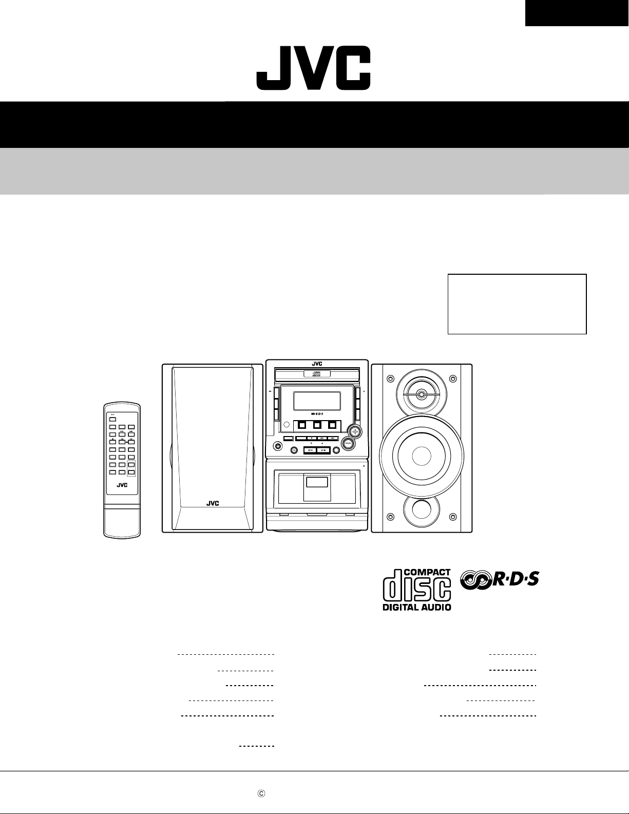
UX-M55
STANDBY/ON
TUNER
TAPE
/BAND
/REV.MODE
CD
/RANDOM
PRE DOWN PRE UP
REC
REMAIN
REPEAT
SLEEP
/RDS MODE
ST/MONO
INTRO
TIMER PROGRAM
/RDS SEARCH
PRE EQ
DISPLAY
+
/HBS
MODE
VOLUME
MUTING BEAT CUT
Ð
RM-SUXM5R REMOTE CONTROL
SP-UXM5
Contents
Safety precautions
Preventing static electricity
Important for laser products
Disassembly method
Adjustment method
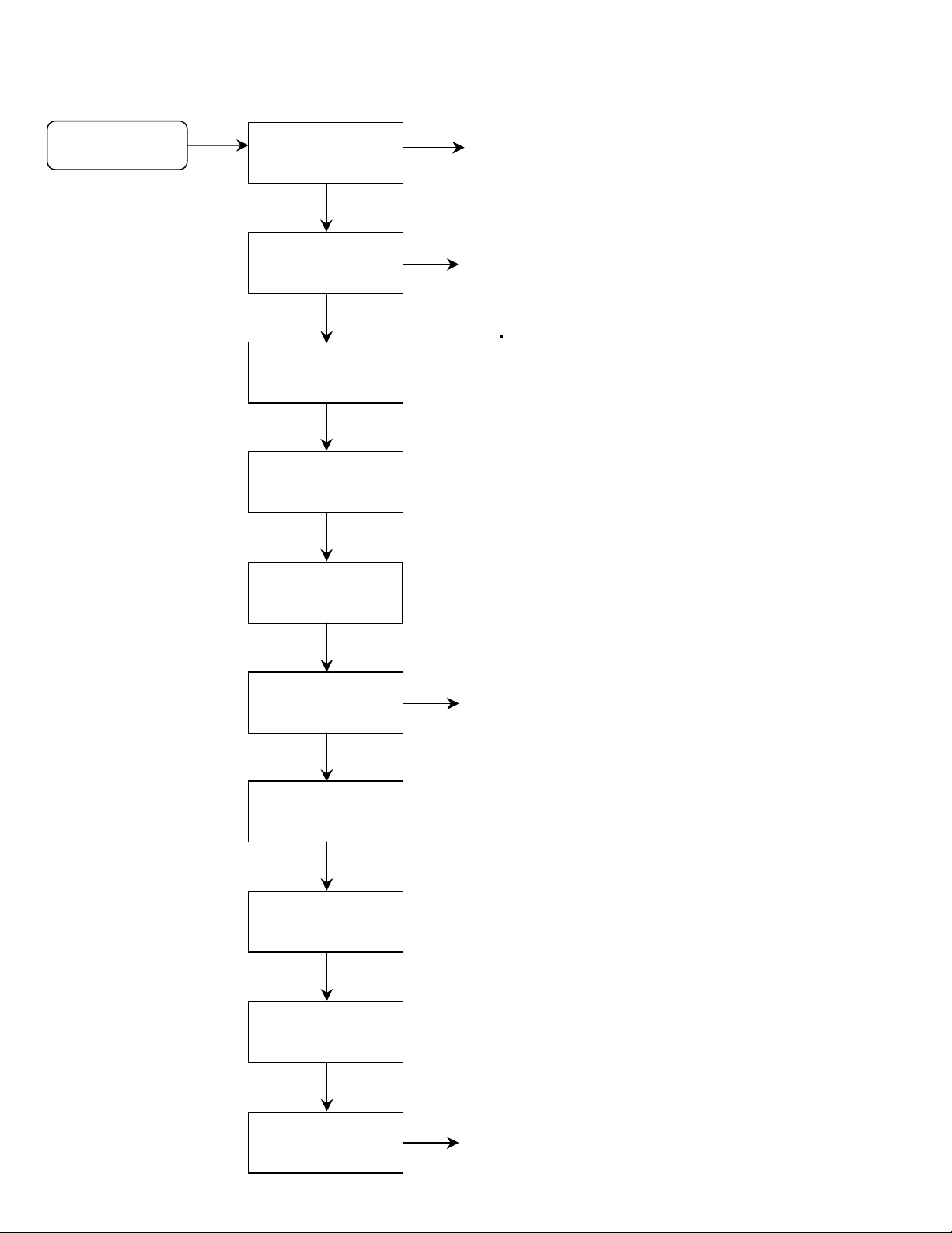
Flow of functional operation
until TOC read
CD-R/RW PLAYBACK
MICRO COMPONENT SYSTEM UX-M55
STANDBY
/ON
DISPLAY
MODE
TIMER
ON/OFF
SET
RANDOM
CD
PROGRAM
ST/MONO
STOP/CLEAR
REPEAT
PHONES
DIRECTION PLAY/PAUSE
REC
AUTO REVERSE
FULL LOGIC DECK
BAND REV. MODE
TUNER TAPE
SEARCH/TUNING
PRESET
OPEN/
CLOSE
REMAIN
/RDS MODE
INTRO/RDS
SEARCH
VOLUME
PRE EQ
/HBS
EJECT
CA-UXM55 SP-UXM5
1-2
1-3
1-4
1-5
1-15
Maintenance of laser pickup
Replacement of laser pickup
Trouble shooting
Description of major ICs
Wiring connections
1-18
1-19
1-19
1-20
1-21
1-35
COPYRIGHT 2002 VICTOR COMPANY OF JAPAN, LTD.
No.21190
Jan. 2003
Page 2
UX-M55
1. This design of this product contains special hardware and many circuits and components specially for safety
purposes. For continued protection, no changes should be made to the original design unless authorized in
writing by the manufacturer. Replacement parts must be identical to those used in the original circuits. Services
should be performed by qualified personnel only.
2. Alterations of the design or circuitry of the product should not be made. Any design alterations of the product
should not be made. Any design alterations or additions will void the manufacturer`s warranty and will further
relieve the manufacture of responsibility for personal injury or property damage resulting therefrom.
3. Many electrical and mechanical parts in the products have special safety-related characteristics. These
characteristics are often not evident from visual inspection nor can the protection afforded by them necessarily
be obtained by using replacement components rated for higher voltage, wattage, etc. Replacement parts which
have these special safety characteristics are identified in the Parts List of Service Manual. Electrical
components having such features are identified by shading on the schematics and by ( ) on the Parts List in
the Service Manual. The use of a substitute replacement which does not have the same safety characteristics
as the recommended replacement parts shown in the Parts List of Service Manual may create shock, fire, or
other hazards.
4. The leads in the products are routed and dressed with ties, clamps, tubings, barriers and the like to be
separated from live parts, high temperature parts, moving parts and/or sharp edges for the prevention of
electric shock and fire hazard. When service is required, the original lead routing and dress should be
observed, and it should be confirmed that they have been returned to normal, after re-assembling.
5. Leakage currnet check (Electrical shock hazard testing)
After re-assembling the product, always perform an isolation check on the exposed metal parts of the product
(antenna terminals, knobs, metal cabinet, screw heads, headphone jack, control shafts, etc.) to be sure the
product is safe to operate without danger of electrical shock.
Do not use a line isolation transformer during this check.
Plug the AC line cord directly into the AC outlet. Using a "Leakage Current Tester", measure the leakage
current from each exposed metal parts of the cabinet, particularly any exposed metal part having a return
path to the chassis, to a known good earth ground. Any leakage current must not exceed 0.5mA AC (r.m.s.).
Alternate check method
Plug the AC line cord directly into the AC outlet. Use an AC voltmeter having, 1,000 ohms per volt or more
sensitivity in the following manner. Connect a 1,500 10W resistor paralleled by a 0.15 F AC-type capacitor
between an exposed metal part and a known good earth ground.
Measure the AC voltage across the resistor with the AC
voltmeter.
Move the resistor connection to each exposed metal part,
particularly any exposed metal part having a return path to
the chassis, and meausre the AC voltage across the resistor.
Now, reverse the plug in the AC outlet and repeat each
measurement. Voltage measured any must not exceed 0.75 V
AC (r.m.s.). This corresponds to 0.5 mA AC (r.m.s.).
0.15 F AC TYPE
1500 10W
Good earth ground
AC VOLTMETER
(Having 1000
ohms/volts,
or more sensitivity)
Place this
probe on
each exposed
metal part.
!
1. This equipment has been designed and manufactured to meet international safety standards.
2. It is the legal responsibility of the repairer to ensure that these safety standards are maintained.
3. Repairs must be made in accordance with the relevant safety standards.
4. It is essential that safety critical components are replaced by approved parts.
5. If mains voltage selector is provided, check setting for local voltage.
Burrs formed during molding may
be left over on some parts of the
chassis. Therefore, pay attention to
such burrs in the case of
preforming repair of this system.
In regard with component parts appearing on the silk-screen printed side (parts side) of the PWB diagrams, the
parts that are printed over with black such as the resistor ( ), diode ( ) and ICP ( ) or identified by the " "
mark nearby are critical for safety.
(This regulation does not correspond to J and C version.)
1-2
Page 3
Preventing static electricity
1. Grounding to prevent damage by static electricity
Electrostatic discharge (ESD), which occurs when static electricity stored in the body, fabric, etc. is discharged,
can destroy the laser diode in the traverse unit (optical pickup). Take care to prevent this when performing repairs.
2. About the earth processing for the destruction prevention by static electricity
Static electricity in the work area can destroy the optical pickup (laser diode) in devices such as CD players.
Be careful to use proper grounding in the area where repairs are being performed.
2-1 Ground the workbench
Ground the workbench by laying conductive material (such as a conductive sheet) or an iron plate over it
before placing the traverse unit (optical pickup) on it.
2-2 Ground yourself
Use an anti-static wrist strap to release any static electricity built up in your body.
(caption)
Anti-static wrist strap
UX-M55
Conductive material
(conductive sheet) or iron plate
3. Handling the optical pickup
In order to maintain quality during transport and before installation, both sides of the laser diode on the
1.
replacement optical pickup are shorted. After replacement, return the shorted parts to their original condition.
(Refer to the text.)
Do not use a tester to check the condition of the laser diode in the optical pickup. The tester's internal power
2.
source can easily destroy the laser diode.
4. Handling the traverse unit (optical pickup)
1.
Do not subject the traverse unit (optical pickup) to strong shocks, as it is a sensitive, complex unit.
2.
Remove solder of the short land on the card wire after replacing the optical pickup. For specific details, refer to
the replacement procedure in the text. Remove the anti-static pin when replacing the traverse unit.
Be careful not to take too long a time when attaching it to the connector.
3.
Handle the card wire carefully as it may break when subjected to strong force.
4.
It is not possible to adjust the semi-fixed resistor that adjusts the laser power. Do not turn it.
5. Attention when traverse unit is decomposed
Connector
*Please refer to "Disassembly method" in the text for the CD pickup unit.
Short land
Apply solder to the short land before the card wire is disconnected from
the connector on the CD pickup unit.
(If the card wire is disconnected without applying solder, the CD
pickup may be destroyed by static electricity.)
In the assembly, be sure to remove solder from the short land after
connecting the card wire.
CD pickup unit
1-3
Page 4
UX-M55
Important for laser products
1.CLASS 1 LASER PRODUCT
2.DANGER : Invisible laser radiation when open and inter
lock failed or defeated. Avoid direct exposure to beam.
3.CAUTION : There are no serviceable parts inside the
Laser Unit. Do not disassemble the Laser Unit. Replace
the complete Laser Unit if it malfunctions.
4.CAUTION : The compact disc player uses invisible
laserradiation and is equipped with safety switches
whichprevent emission of radiation when the drawer is
open and the safety interlocks have failed or are de
feated. It is dangerous to defeat the safety switches.
VARNING : Osynlig laserstrålning är denna del är öppnad
och spårren är urkopplad. Betrakta ej strålen.
VARO : Avattaessa ja suojalukitus ohitettaessa olet
alttiina näkymättömälle lasersäteilylle.Älä katso
säteeseen.
5.CAUTION : If safety switches malfunction, the laser is able
to function.
6.CAUTION : Use of controls, adjustments or performance of
procedures other than those specified herein may result in
hazardous radiation exposure.
CAUTION
!
Please use enough caution not to
see the beam directly or touch it
in case of an adjustment or operation
check.
ADVARSEL : Usynlig laserstråling ved åbning , når
sikkerhedsafbrydere er ude af funktion. Undgå
udsættelse for stråling.
ADVARSEL : Usynlig laserstråling ved åpning,når
sikkerhetsbryteren er avslott. unngå utsettelse
for stråling.
REPRODUCTION AND POSITION OF LABELS
CLASS 1
LASER PRODUCT
WARNING LABEL
1-4
Page 5
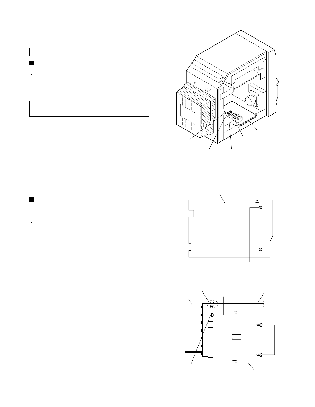
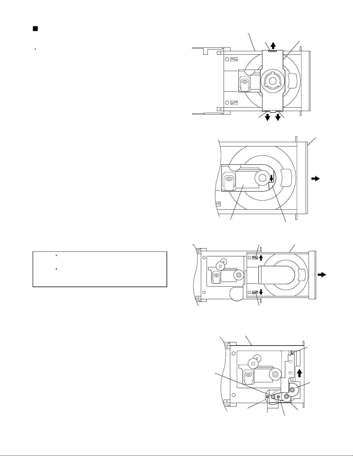
Disassembly method
<Main body section>
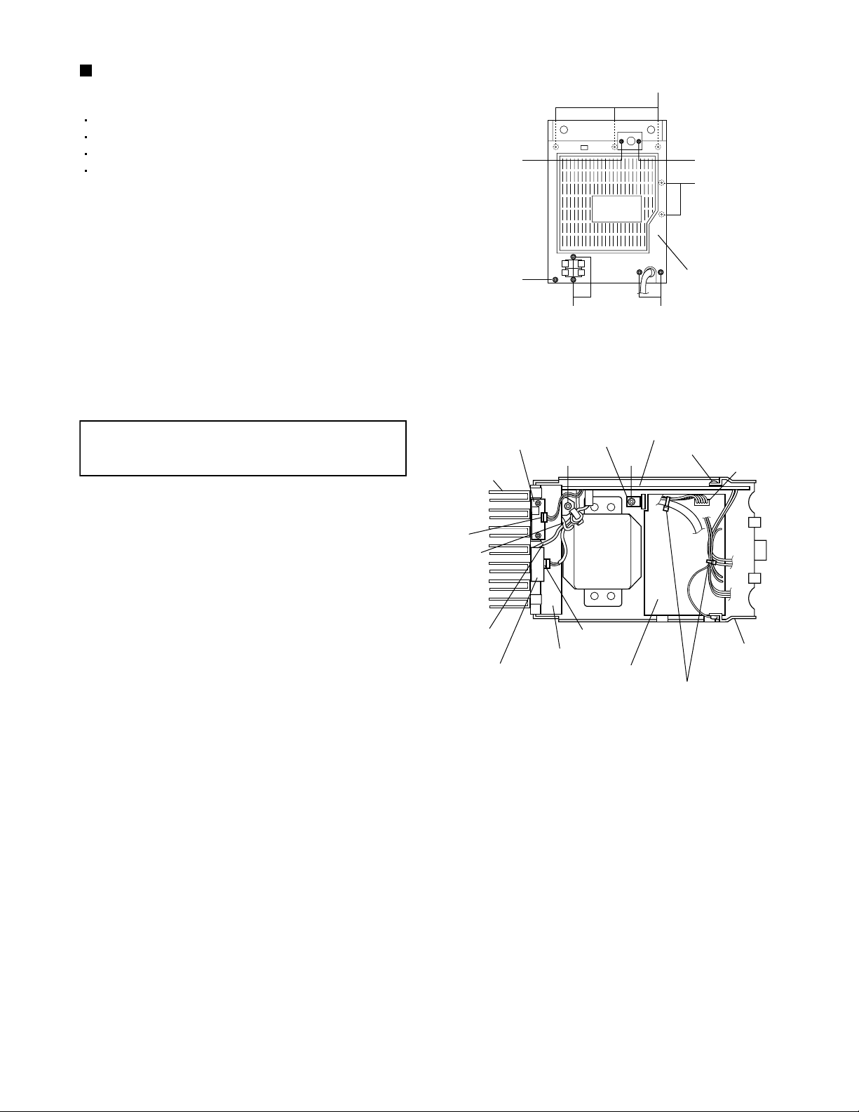
Replacement of the fuses and power amplifier IC
Replacing the fuses (See Fig. 1.)
Remove the left side plate according to its
disassembly method (see Figs. 6 and 7).
Fuses are located inside the left side plate.
[Caution] Be sure to replace the required fuses
with designated ones.
Fuse(F904)
1.6A 250V
Fuse(F903)
2.5A 250V
UX-M55
Power board
Fuse(F901)
1.6A 250V
Fuse(F902)
2.5A 250V
Replacing the power amplifier IC on
the main board (See Figs. 2 and 3.)
Remove the main board according to its
disassembly method. (See Figs. 18 and 19.)
1.
From the reverse side of the main board, remove
the two screws A retaining the bracket.
(See Fig.2.)
2.
From the forward side of the main board, remove
the four screws B retaining the bracket.
(See Fig.3.)
3.
Remove the screw C attaching the power amplifier
IC onto the heat sink. (See Fig.3.)
4.
In order to replace the power amplifier IC, remove
the solder from the soldered part a on the reverse
side of the main board. (See Fig.3.)
Soldered part a
Heat sink
Fig.1
Main board (Reverse side)
Fig.2
C
A
Main board
B
Power amplifier IC
(IC402)
Bracket
Fig.3
1-5
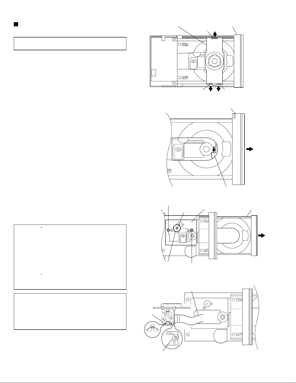
Page 6
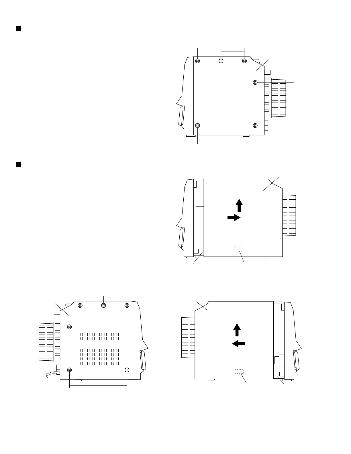
UX-M55
Removing the right side plate
(See Figs. 4 and 5.)
1.2.From the right side of the main body, remove the
three screws D and three screws E retaining the
right side plate. (See Fig.4.)
Slide the right side plate toward the rear (in the
direction of the arrow 1) until the claw b at the back
of the right side plate is hooked by the bottom case
and then lift the right side plate upward (in the
direction of the arrow 2) to remove it. (See Fig.5.)
Removing the left side plate
(See Figs. 6 and 7.)
1.2.From the left side of the main body, remove the
three screws D and three screws E retaining the
left side plate. (See Fig.6.)
D
D
E
Right side
plate
E
Fig.4
Right side
plate
2
Slide the left side plate toward the rear (in the
direction of the arrow 3) until the claw c at the back
of the left side plate is hooked by the bottom case,
and then lift the left side plate upward (in the
direction of the arrow 4) to remove it. (See Fig.7.)
E
Left side
plate
D
E
Bottom case
Left side
plate
1
Claw b
Fig.5
4
3
1-6
D
Fig.6
Fig.7
Claw c
Bottom case
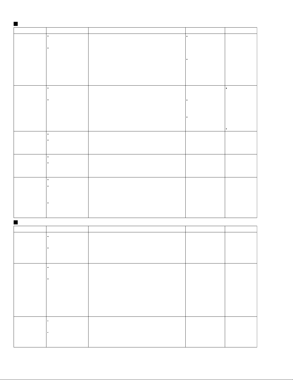
Page 7
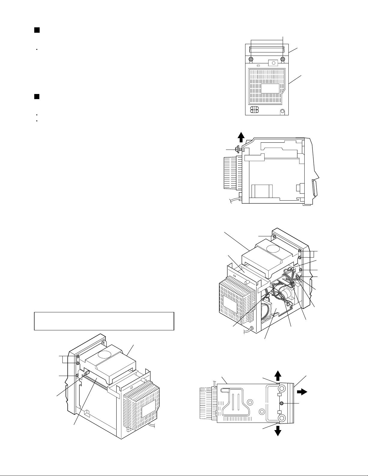
UX-M55
Removing the top cabinet
(See Figs. 8 and 9.)
Remove the left and right side plates.
1.2.From the back side of the main body, loosen the
two screws F retaining the top cabinet. (See Fig.8.)
Lift the rear part of the top cabinet to remove it.
(See Fig.9.)
Removing the front cabinet assembly
(See Figs. 10 to 12.)
Remove the left and right side plates.
Remove the top cabinet.
1.
From the left side of the main body, remove the tie
band bundling the wires. (See Fig.10.)
2.
Disconnect the wire from the connector on the
cassette switch board. (See Fig.10.)
3.
Remove the screw G retaining the holder on the
earphone board. (See Fig.10.)
4.
Disconnect the wires from the two connectors
CN607 and CN608 on the CD & MCU board.
(See Figs.10 and 11.)
Lift the rear
part to remove.
F
Fig.8
(To be loosened)
F
Top cabinet
Rear cabinet
5.
Remove the four screws H and the two screws J
retaining the CD mechanism assembly from the left
and right. (See Figs.10 and 11.)
6.
Remove the screw K retaining the front cabinet
assembly from the bottom side of the main body.
7.
While opening the hooks d to the left and right of
the lower part of the front cabinet assembly (in the
direction of the arrows 1), slide the front cabinet
assembly toward the front (in the direction of the
arrow 2). (See Fig.12.)
8.
Disconnect the wire from the connector on the
PB/REC head board, and then remove the front
cabinet assembly. (See Fig.10.)
[Note] After assembly, apply a locking agent to
the screws G, H and J.
(See Fig.12.)
CD mechanism
assembly
H
J
CD mechanism
assembly
CD & MCU board
Connector on the
cassette switch
board
Bottom case
Fig.9
H
Power board
Fig.10
Hook d
Tie band
Connector on the
PB/REC head board
1
Front cabinet assembly
H
CN608
J
G
Earphone
board
Holder
CN607
CD & MCU board
Fig.11
2
K
Hook d
1
Fig.12
1-7
Page 8
UX-M55
Removing the CD mechanism
assembly (See Figs. 13 to 15.)
Remove the left and right side plates.
Remove the top cabinet.
Remove the front cabinet assembly.
1.
From the top side of the main body, disconnect the
wires from the four connectors CN601, CN602,
CN603 and CN701 on the CD & MCU board.
(See Fig.13.)
2.
From the left side of the main body, remove the tie
bands bundling the wires. (See Fig.14.)
3.
Disconnect the wire from the connector CN902 on
the power board. (See Fig.14.)
4.
From the left and right sides of the main body,
remove the four screws L retaining the CD rear
mounting bracket. (See Figs.14 and 15.)
5.
Slide the CD mechanism assembly toward the front
(in the direction of the arrow) and remove it from
the locking board support of the main board.
(See Fig.15.)
CN603
CN701
CD & MCU board
CD & MCU board
CD rear mounting bracket
L
CN601
CN602
CD mechanism assembly
Fig.13
Tie bands
CN902
Power board
Fig.14
Removing the power board
(See Figs. 16 and 17.)
Remove the left and right side plates.
1.
Disconnect the wires from the connector CN901 on
the power board. (See Fig.16.)
2.
Remove the tie bands bundling the wires.
(See Fig.16.)
3.
Remove the screw M retaining the lug wire.
(See Fig.16.)
4.
Remove the two screws N retaining the bottom
case. (See Fig.16.)
5.
Remove the power board by pinching the two
locking board supports retaining the power board
using radio pliers, etc. (See Fig.17.)
Radio pliers, etc.
Power board
Locking board support
Locking board
support
Locking board supports
Power transformer
CD & MCU board
Fig.15
Main board
L
Main board
CN901
Tie bands
Lug wire
1-8
Fig.17
Bottom case
Bottom case
NM
Fig.16
Power board
Page 9
UX-M55
Removing the main board
(See Figs. 18 and 19.)
Remove the left and right side plates.
Remove the top cabinet.
Remove the front cabinet assembly.
Remove the CD mechanism assembly.
1.
From the inside of the main body, remove the five
screws P retaining the bracket. (See Fig.18.)
2.
From the top side of the main body, remove the
wires from the connectors CN104 and CN106 on
the AM and FM antenna boards. (See Fig.19.)
3.
From the rear side of the main body, remove the
two screws Q and three screws R retaining the rear
cabinet. (See Fig.18.)
4.
Remove the screw S and screw S' retaining the FM
antenna board and earth wire. (See Fig.18.)
[Note] When attaching the screw S', attach the
earth wire together the FM antenna
board.
5.
Remove the rear cabinet.
S'
R
AM antenna board
Heat sink
P
S
P
Rear cabinet
QR
Fig.18
Regulator IC
(IC302)
TU
Main board
Locking board support
CN901
6.
From the top side of the main body, remove the
wire clamp bundling the wires. (See Fig.19.)
7.
Remove the screw T retaining the bracket of the
main board. (See Fig.19.)
8.
Remove the screw U retaining the regulator
IC(IC302). (See Fig.19.)
9.
Remove the tie bands bundling the wires.
(See Fig.19.)
10.
Disconnect the wire from the connector CN901 on
the power board. (See Fig.19.)
11.
Remove the locking board support on the main
board, and then take out the main board from the
bottom case. (See Fig.19.)
CN104
Wire clamp
Earth wire
FM antenna board
Bracket
CN106
Bottom case
Power board
Tie bands
Fig.19
1-9
Page 10
UX-M55
<Front cabinet assembly section>
Remove the left and right side plates.
Remove the top cabinet.
Remove the front cabinet assembly.
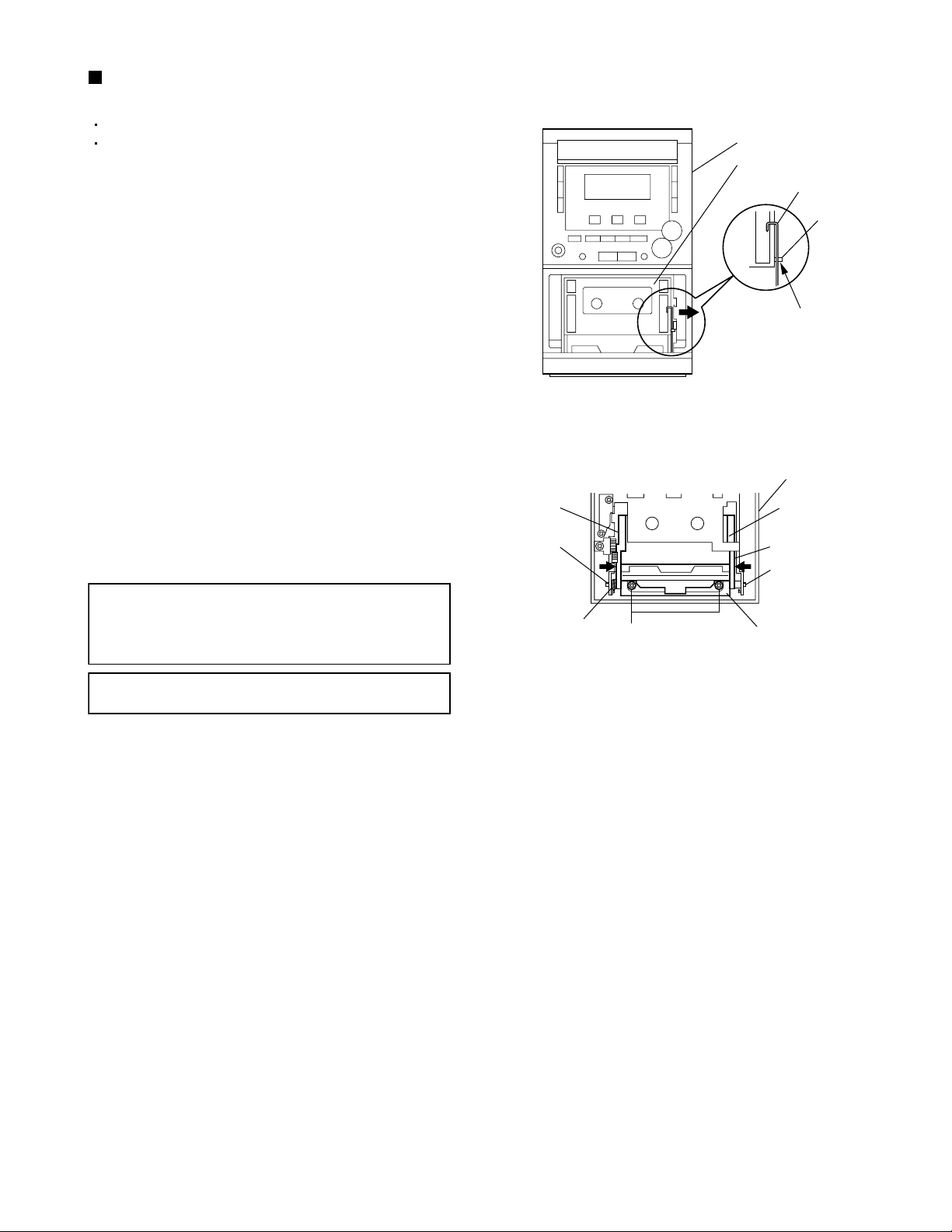
Removing the key board (See Fig. 20.)
Remove the ten screws V retaining the key board.
Removing the cassette mechanism
assembly (See Fig.20.)
Remove the two screws W and the two screws X
retaining the cassette mechanism assembly.
[Note] After assembly, apply a locking agent
to the screws W and X.
Front cabinet assembly
V
Latching
cam assembly
Z
Y
Key board
V
W
Cassette
mechanism
assembly
Removing the damp gear (See Fig. 20.)
Remove the screw Y retaining the damping gear
holder and take out the damp gear.
[Note] After assembly, apply a locking agent
to the screw Y.
Removing the latching cam assembly
(See Fig.20.)
Remove the two screws Z retaining the latching
cam assembly and remove the latching cam
assembly.
[Note] After assembly, apply a locking agent
to the screw Z.
Removing the cassette door cover
(See Fig.21.)
[Note] Use the following procedure to remove
only the cassette door cover.
This procedure does not require the
removal of exterior parts such as the
side panels.
Damping gear holder
Damp gear
Technical door
Claw e
X
X
Fig.20
1.2.Open the cassette door.
Slide the cassette door cover in the direction of
the arrow, and disengage the two claws e and the
two claws f on the left and right of the cassette
door cover from the technical door.
1-10
Claw f
Cassette door cover
Fig.21
Page 11
Removing the technical door
(See Figs. 22 and 23.)
Remove the cassette mechanism assembly.
Remove the cassette door cover.
1.
Open the technical door, disengage the cassette
torsion spring hooked across the front of the front
cabinet assembly and the technical door in the
outward direction, and remove it from the claw g.
(See Fig.22.)
2.
From the back side of the front cabinet assembly,
remove the two screws AA retaining the logic
deck bracket. (See Fig.23.)
3.
While pushing the arm section h of the technical
door in the direction of the arrow, remove the shaft
section i of the technical door from the front
cabinet assembly. (See Fig.23.)
4.
While pushing the arm section j of the technical
door in the direction of the arrow, remove the shaft
section k of the technical door from the front
cabinet assembly. (See Fig.23.)
Arm section h
UX-M55
Front cabinet assembly
Technical door
Cassette torsion spring
Claw g
Disengage the cassette
torsion spring so that it
comes to the front of the
claw g.
Fig.22
Front cabinet assembly
Technical door
5.
Take out the technical door from the back side of
the front cabinet assembly.
[Caution] In the assembly, be sure to put the
cassette torsion spring around
the shaft section i before attaching
the technical door.
[Note] After assembly, apply a locking agent
to the screws AA.
Shaft section i
Cassette torsion spring
AA
Arm section j
Shaft section k
Logic deck bracket
Fig.23
1-11
Page 12
UX-M55
g
<CD mechanism section>
Remove the left and right side plates.
Remove the top cabinet.
Remove the front cabinet assembly.
Remove the CD mechanism assembly.
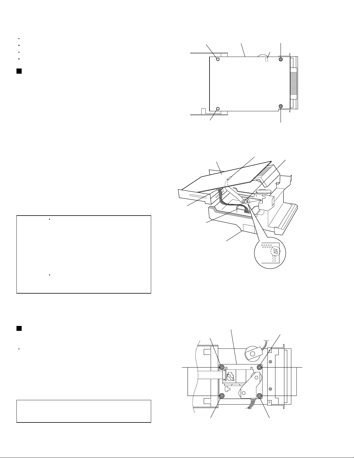
Removing the CD & MCU board
(See Figs. 1 and 2.)
1.
From the bottom side of the CD mechanism
assembly, remove the two screws A retaining the
CD & MCU board. (See Fig.1.)
2.
Disengage the two locking board supports
retaining the CD & MCU board. (See Fig.1.)
3.
Disconnect the wires from the two connectors
CN702 and CN703 on the CD & MCU board.
(See Figs.1 and 2.)
4.
Lift the CD & MCU board and attach solder to the
short land part a on the CD pickup assembly.
(See Fig.2.)
Locking board support
Locking board support
CD & MCU board
CD & MCU board
CN702
Fig.1
CN704
A
A
CD pickup unit
5.
Disconnect the card wire from the connector
CN704 on the CD & MCU board, and take out the
CD & MCU board. (See Fig.2.)
[Cautions] Be sure to solder the short land
part a on the CD pickup unit before
disconnecting the card wire from
the CD pickup unit. (See Fig. 2.)
If the card wire is disconnected
without attaching solder, the CD
pickup may be destroyed by static
electricity.
In the assembly, be sure to remove
solder from the short land part a
after connecting the card wire.
Removing the CD pickup assembly
(See Fig. 3.)
Remove the CD & MCU board.
CN703
CD pickup
assembly
CD mechanism assembly
CD pickup assembly
Damper(Gray)
Short land part a
Fig.2
Damper(Blue)
1.
From the back side of the CD mechanism
assembly, remove the four screws B retaining the
CD pickup assembly.
2.
Take out the CD pickup assembly.
[Note] When removing or replacing the
dampers, note their colors and be sure
to attach them in their correct positions.
1-12
B
B
Damper(Blue)Damper(Gray)
.3
Fi
Page 13
UX-M55
Removing the tray motor
(See Figs. 4 to 7.)
Remove the CD & MCU board.
1.
From the top side of the CD mechanism assembly,
open up the claws b and c at the left and right of
the clamper assembly and lift the assembly to
remove it. (See Fig.4.)
2.
Push the section d of the elevator in the direction
of the arrow and lower the CD pickup assembly.
(See Fig.5.)
3.
Pull out the tray. (See Fig.5.)
4.
While opening up the claws e at the left and right
of the tray in the directions of the arrows, remove
the tray. (See Fig.6.)
5.
While pushing the claw f on the CD mechanism
assembly downwards, slide the elevator fully in
the direction of the arrow. (See Fig.7.)
6.
Lift the gear slightly, remove the transparent cover.
(See Fig.7.)
CD mechanism assembly
Claw b
Claw c
Fig.4
Clamper assembly
Claw c
Tray
7.
Remove the belt from the tray motor pulley.
(See Fig.7.)
8.
Remove the two screws C retaining the tray motor
and remove it from the bottom side of the CD
mechanism assembly. (See Fig.7.)
[Notes] Take care not to attach grease on the
belt.
After attaching the tray motor in the
assembly, apply a locking agent to the
screws C.
CD pickup assembly
Tray motor pulley
Fig.5
Section d
TrayClaw e
Claw e
Fig.6
CD mechanism assembly
Claw f
Tray motor
Fig.7
C
Transparent
Belt
Gear
cover
1-13
Page 14
UX-M55
g
Replacing the CD pickup unit
(See Figs. 8 to 11.)
[Note] Use the following procedure to replace
only the CD pickup unit.
1.
Remove the left and right side plates. (See Figs. 4
to 7 of "Main body section" on page 1-7.)
2.
Remove the top cabinet. (See Figs. 8 and 9 of
"Main body section" on page 1-8.)
3.
From the top side of the main body, open up the
claws b and c on the left and right of the clamper
assembly in the direction of the arrows and lift the
assembly to remove it. (See Fig.8.)
4.
Push the section d on the elevator of the CD
mechanism assembly and lower the CD pickup
assembly. (See Fig.9.)
5.
Pull out the tray. (See Fig.10.)
6.
Remove the slit washer retaining the feed middle
gear, and take out the feed middle gear.
(See Fig.10.)
Clamper assembly
Claw c
Claw b
Front cabinet assembly
Claw c
Fig.8
Front cabinet assembly
7.
Loosen the two screws D retaining the shaft.
(See Fig.10.)
8.
Turn the CD pickup unit upside down and apply
solder to the short land part a. (See Fig.11.)
9.
Disconnect the card wire from the CD pickup unit
and replace the unit. (See Fig.11.)
[Cautions] Be sure to solder the short land
part a on the CD pickup unit before
disconnecting the card wire from
the CD pickup unit. (See Fig. 11.)
If the card wire is disconnected
without attaching solder, the CD
pickup may be destroyed by static
electricity.
In the assembly, be sure to remove
solder from the short land part a
after connecting the card wire.
[Note] Removing the CD pickup unit involves
the removal of the sliding spring.
In the assembly, be sure to attach the
spring in the correct orientation before
attaching the CD pickup unit.
(See Fig. 11.)
Feed middle gear
Sliding spring
(To be loosened)
D
Slit washer
D
Card wire
Section d
Fig.9
CD pickup assembly
(To be loosened)
Fig.10
Tray
1-14
Short land part a
Fi
.11
Page 15

Adjustment method
UX-M55
Measuring instructions required for
adjustment
1. AM signal generator
2. FM signal generator
3. Inter mediate frequency sweep generator
4. FM stereo signal generator
5. Low-frequency oscillator
(oscillation frequency 50Hz-20kHz, 0dB output
with 600 ohm impedance)
6. Attenuator (600 ohm impedance)
7. Electronic voltmeter
8. Distortion meter
9. Torque gauge (cassette for CTG-N)
10. Wow & flutter meter
11. Frequency counter meter
12. Test tape
VT712 : For tape speed and wow flutter
VT724 : For reference level
VT702 : For playback frequency
VT702 : For head azimuth adjustment
13. Blank tape
TAPE : AC-225
Measuring instruments
Radio section
FM 1kHz, 22.5kHz deviation
FM STEREO : 1kHz, 67.5kHz deviation
pilot signal 7.5kHz
AM : 1kHz, 30% modulation
Reference output :
Speaker output 0dBs(2.8V) 8 ohm
PHONES output -10dBs(0.245V)/32 ohm
Cassette amplifier section
Reference output :
Speaker output 0dBs(2.8V) 8 ohm
PHONES output -10dBs(0.245V)/32 ohm
CD section
CD test disc : CTS-1000
Measurement conditions
Power supply voltage
AC220~240V(50Hz/60Hz)
1-15
Page 16
UX-M55
Cassette amplifier section
Item Measuring condition Check and adjustment procedure Standard value Adjusting part
Head azimuth
adjustment
Tape speed and
wow/flutter check
and adjustment
PB frequency
response check
Bias frequency
check
REC and PB
frequency
response
adjustment
Test tape:
VT702 (8kHz)
Signal output terminal:
PHONES output
(with 32 ohm load)
Test tape:
VT712 (3kHz)
Signal output terminal:
PHONES output
(with 32 ohm load)
Test tape: VT702
Signal output terminal:
PHONES output
(with 32 ohm load)
Tape: Normal
Signal output terminal:
Cassette REC./PLAY
HEAD
Test tape: AC225
Signal input:
FM22.5 DEV 60dBµ
with emphasis
Signal output terminal:
PHONES output
(with 32 ohm load)
Play back the test tape VT702 (8kHz).
1.
Adjust the head azimuth adjusting screw so that the
2.
phase difference between the R and L channels is
minimized at an output level that is within +2dB-2dB of
the maximum output level. After this adjustment, lock
the head azimuth adjusting screw with screw sealant
to cover more than a half of the screw head.
3.
When the head azimuth is maladjusted, correct it with
the head azimuth adjusting screw.
Play back the test tape VT712 (3kHz) by the end
1.
portion.
Connect a frequency counter and check that it reads
2.
between 2940 and 3090Hz. If not, adjust the frequency
with the motor semifixed resistor.
Check that the wow/flutter is within 0.38%
3.
(unweighted).
Play back the test tape VT702 while con-firming that
deviation between the 1kHz signal and 8kHz signal
should be (0+3dB-6dB).
Set the TUNER or CD function and with TAPE to
record. Check to see if the frequency at the measuring
point P201 is 68kHz+1kHz-1kHz if not adjust L203 until
the frequency counter indicates 68 kHz+1kHz-1kHz.
At TUNER, set the BAND to the FM position, and
record the reference 1kHz signal and 8kHz signal
alternately repeatedly. While playing back the
recorded signal differ from that of the 1kHz signal by
within (0+3dB-6dB).
Output level:
Within +2dB-2dB of
maximum output
level
Phase difference R
and L channels:
Minimum
2940 to 3090Hz
Within 0.38%
(unweighted)
Deviation between
1kHz and 8kHz:
(0+3dB-6dB)
Level difference
between REC and
PB: Within
(0+3dB-6dB)
Head azimuth
adjusting screw
(To be used only
after head
replacement)
See Fig.1 on
page 1-17.
Tape speed:
Motor semifixed
resistor
See Fig.2 on
page 1-17.
Check only
L203, P201
See Fig.3 on
page 1-17.
Tuner section
Item Measuring condition Check and adjustment procedure Standard value Adjusting part
AM IF adjustment 1.
AM tracking
adjustment
Tuner 114kHz
Filter the waves
adjustment
Signal input:
Loop antenna
Signal output:
IC101 pin18
Signal input:
Loop antenna
Signal output:
PHONES output
(with 32 ohm load)
Signal input:
IC101 pin19
Signal output:
IC101 pin18
Set the intermediate frequency sweep generator to AM
450kHz.
Adjust the T101 for maximum and center output.
2. T101
Set the TUNER at 522kHz adjust L102 until the test
1.
pin of R121 voltage at 1.7V+0.1V-0.1V.
Set the TUNER at 1629kHz, check the test pin of R121
2.
voltage at 8.0V+0.3V-0.3V.
Set the TUNER and S/G at 612kHz, adjust L103 for
3.
maximum output.
Set the TUNER and S/G at 1404kHz, adjust the TC101
4.
for maximum output.
Repeat the above steps 3 and 4.
5.
Set standby and input 114kHz signal to IC101 pin19.
1.
Adjust the L104 for output voltage minimum.
2. L104
See Fig.3 on
page 1-17.
L102
L103
TC101
See Fig.3 on
page 1-17.
See Fig.3 on
page 1-17.
1-16
Page 17
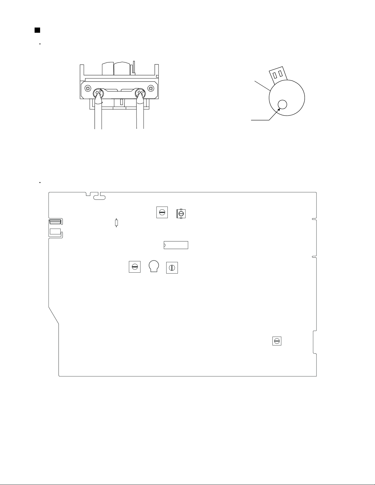
Location of adjusting parts
Cassette mechanism section
UX-M55
Main board
Fig.1 Head output signal
(AM VT)
R121
T101
(AM IF)
L104
(114kHz)
IC101
TA2099
CASSETTE MOTOR
Tape Speed Adj.
-
+
Fig.2
L103
(AM RF)
L102
(AM OSC)
TC101
(AM RF)
P201
(BIAS FREQUENCY)
L203
(BIAS FREQUENCY ADJ.)
Fig.3
1-17
Page 18
UX-M55
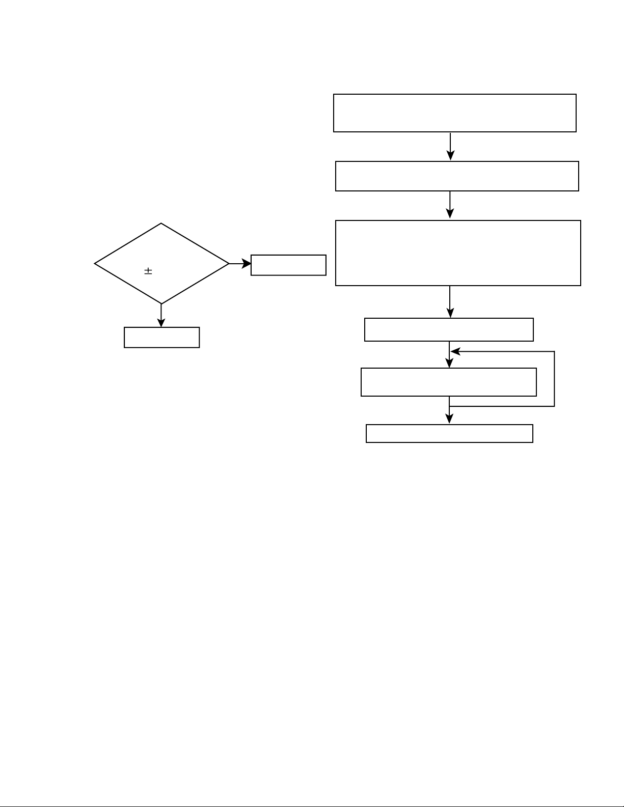
Flow of functional operation until TOC read
Power ON
Slider turns REST
SW ON.
Laser ON
Focus start
FOK
Turn on focus
servo
Confirm that the voltage at the pin5 of CN703 is
"H"/"L"/"H"
Check that the voltage at the pin10(LD) of
CN704 is +1.35V.
Caution
Before connecting a measuring instrument to
the measuring point, turn the power of the
main unit to OFF.
After performing a measurement and before
disconnecting the measuring instrument,
again turn the power of the main unit to OFF.
(If a measuring instrument is disconnected
while an electric current is being output to the
main unit, the pick up of the main unit will be
damaged.)
Disc spinning
Radial_error
scaling
PLL Lock
Turn on radial
servo
Read TOC
Check that the voltage at the pin1 and pin2 of
CN703 is +0.65V.
Confirm the eye-pattern at the "RFO" test point.
(Refer to "Printed circuit boards" section.)
1-18
Page 19
UX-M55
Maintenance of laser pickup
(1) Cleaning the pick up lens
Before you replace the pick up, please try to
clean the lens with a alcohol soaked cotton
swab.
(2) Life of the laser diode
When the life of the laser diode has expired,
the following symptoms will appear.
The level of RF output (EFM output:ampli tude of eye pattern) will below.
Is the level of
RF OUT under
1.25V 0.22Vp-p?
YES
O.K
NO
Replace it.
Replacement of laser pickup
Turn off the power switch and, disconnect the
power cord from the AC OUTLET.
Replace the pickup with a normal one. (Refer
to "Removing the CD pickup" on the previous page)
Plug the power cord in, and turn the power on.
At this time, check that the laser emits for
about 3 seconds and the objective lens moves
up and down.
Note: Do not observe the laser beam directly.
Play a disc.
Check the eye-pattern at the "RFO" test point.
(Refer to "Printed circuit boards" section.)
Finish.
(3) Semi-fixed resistor on the APC PC board
The semi-fixed resistor on the APC printed circuit board which is attached to the pickup is used to adjust the laser
power.
Since this adjustment should be performed to match the characteristics of the whole optical block, do not touch the
semi-fixed resistor.
If the laser power is lower than the specified value, the laser diode is almost worn out, and the laser pickup should
be replaced.
If the semi-fixed resistor would be adjusted when the pickup operates normally, the laser pickup may be damaged
due to excessive current.
1-19
Page 20

UX-M55
Trouble shooting
Circuit Symptom Cause
No soundGeneral
MW Rotate or reposition the unit.
FM Connect the built-in or external antenna.
No sound, weak sound
(Low sensitivity)
No sound, weak sound
(Low sensitivity)
Speakers are not connected.
Wrong function is selected.
Defective volume control
Defective earphone jack
Defect in IC402
Defect in IC301
Improper location of unit
Defect in IF T101
Defect AM antenna coil L103 or oscilloscope
coil L102
Intermediate frequency tuning faulty
RF tracking faulty
Defective IC101
Defective IC102
Poor contact in antenna circuit
FM antenna not connected
Defective band selector switch
Check the speaker connection.
Set switch to the proper position.
Set the volume control to a proper sound
level.
Replace the earphone jack.
Check voltages. Replace if necessary.
Check voltages. Replace if necessary.
Check resistance, voltage, and current.
Replace as needed.
Replace if necessary.
Readjust (see "Adjustment method").
Readjust (see "Adjustment method").
Check voltages. Replace if necessary.
Check voltages. Replace if necessary.
Check resistance and resolder.
Replace or repair the switch.
Remedy
Defective IC101
Defective IC102
Intermediate frequency tuning faulty
Poor contact in FM antenna circuit
Tape Clean the capstan or head with alcohol.
CD Insert disc correctly.
No sound/recording,
unsteady tape sound,
weak sound
Cannot read the table
of content.
No sound
Dirty capstan or head
Irregular cassette tape winding
Defective IC201
Defective IC202
Cassette erasure prevention tabs broken out
Disc is inserted upside down.
Disc is dirty.
Disc is scratched.
Disc is seriously warped.
A non-standard disc has been inserted.
Moisture has formed inside the CD deck.
Defective IC701
Check voltages. Replace if necessary.
Check voltages. Replace if necessary.
Readjust (see "Adjustment method").
Resolder or repair as required.
Replace tape.
Check voltages. Replace if necessary.
Check voltages. Replace if necessary.
Replace tape or cover tab openings with
adhesive tape.
Wipe clean with a soft cloth.
Use a new disc.
Use a new disc.
Use only a brand name disc.
Wait about 20 to 30 minutes.
Check voltages. Replace if necessary.
1-20
Defective IC704
Defective IC703
Defect in the CD pickup mechanism
Check voltages. Replace if necessary.
Check voltages. Replace if necessary.
Replace as required.
Page 21

Description of major ICs
TC9462F (IC701) : Digital servo single chip processor
1. Terminal layout
80 51
UX-M55
100 81
1 30
2. Pin function
Pin No. Symbol I/O Function
1
2
3
4
5
6
7
8
9
10
11
12
13
14
15
16
17
18
19
20
21
22
23
24
25
26
27
28
TEST0
HSO
UHSO
EMPH
LRCK
VSS
BCK
AOUT
DOUT
MBOV
IPF
SBOK
CLCK
VDD
VSS
DATA
SFSY
SBSY
SPCK
SPDA
COFS
MONIT
VDD
TESIO0
P2Vref
HSSW
ZDET
PDO
I
O
O
O
O
O
O
O
O
O
O
I/O
-
O
O
O
O
O
O
O
-
I
O
O
O
31 50
Test mode terminal. Normally, keep at open.
Playback speed mode flag output terminal. (Not connect)
UHSO
H
H
L
L
Subcode Q data emphasis flag output terminal. Emphasis ON at "H" level and
OFF at "L" level. The output polarity can invert by command. (Not connect)
Channel clock output terminal. (44.1kHz) L-ch at "L" level and R-ch at "H" level.
The output polarity can invert by command. (Not connect)
Digital ground terminal.
Bit clock output terminal. (1.4112MHz) (Not connect)
Audio data output terminal. (Not connect)
Digital data output terminal. (Not connect)
Buffer memory over signal output terminal. Over at "H" level. (Not connect)
Correction flag output terminal. At "H" level, AOUT output is made to correction
impossibility by C2 correction processing. (Not connect)
Subcode Q data CRCC check adjusting result output terminal. The adjusting
result is OK at "H" level. (Not connect)
Subcode P W data readout clock input/output terminal. This terminal can select
by command bit. (Not connect)
Digital power supply voltage terminal.
Digital ground terminal.
Subcode P W data output terminal. (Not connect)
Playback frame sync signal output terminal. (Not connect)
Subcode block sync signal output terminal. (Not connect)
Processor status signal readout clock output terminal. (Not connect)
Processor status signal output terminal. (Not connect)
Correction frame clock output terminal. (7.35kHz) (Not connect)
Internal signal (DSP internal flag and PLL clock) output terminal. Selected by
command. This terminal output the text data with serial by command. (NC)
Digital power supply voltage terminal.
Test input/output terminal. Normally, keep at "L" level. The terminal that inputted
the clock for read of text data by command.
PLL double reference voltage supply terminal.
2/4 times speed at "VREF" voltage. (Not connect)
1 bit DA converter zero detect flag output terminal.
Phase difference signal output terminal of EFM signal and PLCK signal.
HSO
PLAYBACK SPEED
H
L
H
L
Normal
2 times
4 times
-
1-21
Page 22

UX-M55
Pin No. Symbol I/O
29
30
31
32
33
34
35
36
37
38
39
40
41
42
43
44
45
46
47
48
49
50
51
52
53
54
55
56
57
58
59
60
61
62
63
64
65
66
67
TMAXS
TMAX
LPFN
LPFO
PVref
VCOREF
VCOF
AV
SS
SLCO
RFI
DD
AV
RFCT
RFZI
RFRP
FEI
SBAD
TSIN
TEI
TEZI
FOO
TRO
Vref
RFGC
TEBC
FMO
FVO
DMO
2Vref
SEL
FLGA
FLGB
FLGC
FLGD
DD
V
V
SS
IO0
IO1
IO2
IO3
O
O
O
O
O
O
O
O
O
O
O
O
O
O
O
O
O
I/O
I/O
I/O
I/O
Function
TMAX detection result output terminal. Selected by command bit (TMPS).
TMAX detection result output terminal. Selected by command bit (TMPS).
DIFFERENCE RESULT TMAX OUTPUT
Longer than fixed freq.
Shorter than fixed freq.
Within the fixed freq.
I
LPF amplifier inverting input terminal for PLL.
"P2VREF"
"Vss"
"HiZ"
LPF amplifier output terminal for PLL.
-
PLL reference voltage supply terminal.
I
VCO center frequency reference level terminal. Normally, keep at "PVREF" level.
VCO filter terminal.
-
Analog ground terminal.
Data slice level output terminal.
I
RF signal input terminal.
-
Analog power supply voltage terminal.
I
RFRP signal center level input terminal.
I
RFRP zero cross input terminal.
I
RF ripple signal input terminal.
I
Focus error signal input terminal.
I
Sub-beam adder signal input terminal.
I
Test input terminal. Normally, keep at "VREF" level.
I
Tracking error signal input terminal. Take in at tracking servo on.
I
Tracking error zero cross input terminal.
Focus servo equalizer output terminal.
Tracking servo equalizer output terminal.
-
Analog reference voltage supply terminal.
RF amplitude adjustment control signal output terminal.
Tracking balance control signal output terminal.
Feed equalizer output terminal.
Speed error signal or feed search equalizer output terminal. (Not connect)
Disk equalizer output terminal.
(PWM carrier=88.2kHz for DSP, Synchronize to PXO)
-
Analog double reference voltage supply terminal.
APC circuit ON/OFF indication signal output terminal.
At the laser on time, UHF = L at "HiZ" level and UHF = H at "H" level.
External flag output terminal for internal signal. (Not connect)
Can select signal from TEZC, FOON, FOK and RFZC by command.
External flag output terminal for internal signal. (Not connect)
Can select signal from DFCT, FOON, FMON and RFZC by command.
External flag output terminal for internal signal. (Not connect)
Can select signal from TRON, TRSR, FOK and SRCH by command.
External flag output terminal for internal signal. (Not connect)
Can select signal from TRON, DMON, HYS and SHC by command.
-
Digital power supply voltage terminal.
-
Digital ground terminal.
General I/O terminal. Can change over input port or output port by command.
At the input mode time can readout a state of terminal (H/L) by read command.
At the output mode time can control a state of terminal (H/L/HiZ) by command.
(Not connect)
1-22
Page 23

UX-M55
Pin No. Symbol I/O
68
69
70
71
72
73
74
75
76
77
78
79
80
81
82
83
84
85
86
87
88
89
90
91
92
93
94
95
96
97
98
99
100
DMOUT
CKSE
DACT
TESIN
TESIO1
V
SS
PXI
PXO
V
DD
XVSS
XI
XO
XV
DD
DVSR
RO
DV
DD
DVR
LO
DV
SL
TEST1
TEST2
TEST3
BUS0
BUS1
BUS2
BUS3
V
DD
VSS
BUCK
CCE
TEST4
TSMOD
RST
I
I
I
I
I
I
O
-
I
O
-
-
O
-
-
O
I
I
I
I/O
I/O
I/O
I/O
-
-
I
I
I
I
I
Function
This terminal controls IO0 IO3 terminal. At "L" level time, IO0, 1 out feed
equalizer signal of 2-state PWM, IO2,3 out disk equalizer signal of 2-state PWM.
Normally, keep at open.
DAC test mode terminal. Normally, keep at open.
Test input terminal. Normally, keep at "L" level.
Test input/output terminal. Normally, keep at "L" level.
Digital ground terminal.
Crystal oscillator connecting input terminal for DSP. Normally, keep at "L" level.
Crystal oscillator connecting output terminal for DSP. (Not connect)
Digital power supply voltage terminal.
Oscillator ground terminal for system clock.
Crystal oscillator connecting input terminal for system clock.
Crystal oscillator connecting output terminal for system clock.
Oscillator power supply voltage terminal for system clock.
Analog ground terminal for DA converter.(R-ch)
R channel data forward output terminal.
Analog supply voltage terminal for DA converter.
Reference voltage terminal for DA converter.
L channel data forward output terminal.
Analog ground terminal for DA converter.(L-ch)
Test mode terminal. Normal, keep at open.
Test mode terminal. Normal, keep at open.
Test mode terminal. Normal, keep at open.
Micon interface data input/output terminal.
Digital power supply voltage terminal.
Digital ground terminal.
Micon interface clock input terminal.
Command and data sending/receiving chip enable signal input terminal.
The bus line becomes active at "L" level.
Test mode terminal. Normal, keep at open.
Local test mode selection terminal. (Not connect)
Reset signal input terminal. Reset at "L" level.
1-23
Page 24

UX-M55
TMP87EP26F-1J15 (IC601) : MCU
1. Terminal layout
80 51
81
50
(Top view)
100
130
31
2.Pin function
Pin No. Symbol I/O Function
1
VSS
2
XOUT
3
XIN
4
RESET
5
XTOUT(P22)
6
XTIN(P21)
7
TEST
8
SHIFT FREQ
9
REMOTE
10
MUTE
11
PLAY MUTE
12
REC MUTE
13
PLAY/REC
14
N.C.
15
N.C.
16
N.C.
17
REC SW (RVS)/(WAIT)
GND (0V)
Resonator connecting pins for high clock(4-8MHz).
O
For inputting external clock, XIN is used and XOUT is opened.
I
Reset signal input or watchdog timer output/address-trap-reset output
I/O
Resonator connecting pins for slow clock(32.768kHz)
I/O
or general purpose I/O.
I/O
Test pin for out-going test. Always fixed to low.
I
Shift the crystal oscillation frequency to reduce tuner noise.
O
Remote control signal input
I
Audio mute output
O
Muting output during play, not connect
O
Muting output during recording, not connect
O
Play or recording output, low for recording.
O
Not connect
Not connect
Not connect
Deck reverse record protection input. Low means can record on
I
reverse side.
18
REC SW (FWD)
Deck forward record protection input. Low means can record on
I
forward side.
19
B-SOL+
20
B-MODE SW
21
VOL STB
22
POWER
23
B-HALF SW
24
JOG-B/VOL DATA
25
JOG-A/VOL CLK
26
RDS CLK
27
V MOTOR
28
B-PHOTO OUT
29
CD-RW
30
RES
Solenoid output for deck B.
O
Mode switch input of deck B. Low means the head is up.
I
TC9422F volume STB output
O
Power output control
O
Half switch input of deck B. Low means deck B have tape.
I
Jog dial input and TC9422F volume data output
I/O
Jog dial input and TC9422F volume clock output
I/O
BU1923F(RDS demodulator) interface CLK input
I
Motor output
O
Reel pulse input of deck B. Have pulse input means the tape is rotating.
I
CD-RW control output, not connect
O
CD servo reset output
O
1-24
Page 25

Pin No. Symbol I/O Function
Servo DSP chip enable output
31
32
33
34
35
36
37
38
39
40
41
42
43
44
45
46
47
48
49
50
51
52~91
92~95
96
97
98
99
100
CCE
BUCK
BUS0
BUS1
BUS2
BUS3
TRAY IN(SLOUT)
TRAY OUT(SLIN)
SLT
CLT(SLEND)
N.C.
RDS DATA
STEREO
POWER DETECT
AD K3
AD K2
AD K1
VAREF
(BOOT)
V
SS
VDD
SEG39~SEG0
COM3~COM0
VLC
PLL DATA
PLL CLK
PLL PERIOD
V
DD
O
Servo DSP clock output
O
Servo DSP command and data I/O
I/O
Servo DSP command and data I/O
I/O
Servo DSP command and data I/O
I/O
Servo DSP command and data I/O
I/O
Tray open/close outputs for current sensor drawer type mechanism.
O
O
CD pick up position input: L if pick up is in inner side.
I
Current sensor input
I
Not connected
BU1923F(RDS demodulator) interface data input
I
Stereo input pin for tuner stereo indication
I
Power down detection
I
Panel key analog input
I
Panel key analog input
I
Panel key analog input
I
Analog reference voltage input
Control input for writing MCU program area via ICU interface.
I
GND (0V)
VDD (+5V)
LCD segment outputs (Pin 55 and 56: Not connect)
O
LCD common outputs
O
LCD drive power supply
TC9257P (PLL) interface
I/O
TC9257P (PLL) interface
O
TC9257P (PLL) interface
O
VDD (+5V)
-
UX-M55
TA7291S (IC702) : Bridge driver
1.Terminal Layout
123456789
VS
VCC
OUT2
NC
GND
OUT1
VREF
IN1
IN2
2.Pin function
Pin No. Symbol I/O Function
IN2(M-)
1
2
3
4
5
6
7
8
9
Vcc
OUT2
NC
GND
Vs
OUT1
Vref
IN1(M+)
Input terminal
I
Supply voltage terminal for logic
Output terminal
O
Not connect
Ground terminal
Supply voltage terminal for motor driver
Output terminal
O
Supply voltage terminal for control
Input terminal
I
1-25
Page 26

UX-M55
AN7312 (IC202) : Dual recording/Playback pre-amplifier circuit with ALC
1. Terminal layout
14 8
~
2. Block diagram
Vcc
14 13 12 11 10
9
8
Ripple Filter
17
3. Pin function
Pin No. Symbol Function
1
2
3
4
5
6
7
8
9
10
11
12
13
14
~
GND
ALC Time Constant
ALC Input Ch.1
Output Ch.1
Phase Compensation Ch.1
N.F.B. Ch.1
Input Ch.1
Input Ch.2
N.F.B. Ch.2
Phase Compensation Ch.2
Output Ch.2
ALC Input Ch.2
Ripple Filter
Vcc
1 2 3 4 5 6
GND
I/O
GND
ALC time constant by resistance and capacitor
Right channel ALC input
I
Right channel output
O
Not connect
Right channel negative feed back input
I
Right channel signal input
I
Left channel signal input
I
Left channel negative feed back input
I
Not connect
Left channel output
O
Left channel ALC input
I
Ripple filter
Power supply
-
ALC
Amp.
Ch2
Amp.
Ch1
7
LM1876TF (IC402) : Overture audio power amplifier series
1. Terminal layout
2. Block diagram
GND A VCC A
5
+IN A
-IN A
+IN B
-IN B
8
7
13
12
+
-
+
-
10
GND B VCC B
2
AMP A
AMP B
15 14
15
14
13
12
11
10
9
8
7
6
LM1876TF
5
4
3
2
1
STANDBY A
96
STANDBY B
MUTE A
3
4
1
11
MUTE B
OUT A
-VCC
OUT B
3. Pin function
Pin No. Symbol I/O Function
1
2
3
4
5
6
7
8
9
10
11
12
13
14
15
OUT B
VCC A
OUT A
-Vcc
GND A
MUTE A
-IN A
+IN A
Standby A
GND B
MUTE B
-IN B
+IN C22B
Standby B
VCC B
O
-
O
-
-
I
I
-
-
I
I
-
-
B output
A V+
A output
VPower Terminal
Control
A -input
A +input
Control
Power Terminal
Control
B -input
B +input
Control
B V+
1-26
Page 27

BA4558N (IC401/IC403) : Dual operational amplifier
1. Terminal layout & Block diagram
1ch 2ch
2
34
5678
EE +IN2 -IN2 OUT2 Vcc
1
OUT1 -IN1 +IN1 V
2. Pin function
Pin No. Symbol I/O Function
1
OUT1
2
3
4
5
6
OUT2
7
8
BU1924F (IC602) : RDS demodulator
1. Terminal layout 2. Block diagram
1
2
3
4
5
6
7
8
16
15
14
13
12
11
10
9
MUX
V
REF
V
DD1
100k
4
120k
100k
3
5
Analog
anti-aliasing
-IN1
+IN1
EE
V
+IN2
-IN2
CC
V
+
filter
O
I
I
I
I
O
-
A output
A -input
A +input
VB +input
B -input
B output
V+
8th Switched
capacitor filter
CMPVSS3
87
comparator
16
UX-M55
RCLK
6
V
SS1
12
V
DD2
V
SS2
Digital
power supply
11
3. Pin function
Pin No. Symbol I/O Function
1
2
3
4
5
6
7
8
9
10
11
12
13
14
15
16
QUAL
RDATA
VREF
MUX
VDD1
VSS1
VSS3
CMP
T1
T2
VSS2
VDD2
XI
XO
NC
RCLK
O
Demodulator quality good: HI (Not connect)
O
Demodulator data
-
1/2 VDD1 see application
-
Composite see application
-
Analog power supply
-
Analog power supply
-
Analog power supply
-
See application
-
H: Internal clock stop L: Operation
-
Testing (do not use)
-
Digital power supply
-
Digital power supply
-
4.332MHz see application
-
4.332MHz see application
-
Not connect
-
1187.5Hz
PLL
57kHz
RDS/ARI
13 14 10 9
XO
Xl
Clock
PLL
1187.6Hz
Diphaser
decoder
Differential
decoder
Test
T1 T2
1
QUAL
2
RDATA
1-27
Page 28

UX-M55
TA2092N (IC703) : Power driver
1. Terminal Layout & Block Diagram
PW GND1
OUT(-)1
PW VCC1
OUT(+)1
OUT(+)2
PW VCC2
OUT(-)2
PW GND2
VIN1
VRI
VCI
VIN2
1
2
3
4
5
6
7
8
9
10
11
12
24
23
22
21
20
19
18
17
16
15
14
13
PW GND4
OUT(-)4
PW VCC4
OUT(+)4
VIN4
SVCC1
SGND
VIN3
OUT(+)3
PW VCC3
OUT(-)3
PW GND3
2. Pin function
Pin No. Symbol I/O Function
PW GND1
1
2
3
4
5
6
7
8
9
10
11
12
13
14
15
16
17
18
19
20
21
22
23
24
OUT(-)1
PW VCC1
OUT(+)1
VIN1
VRI
VCI
VIN2
OUT(+)2
PW VCC2
OUT(-)2
PW GND2
PW GND3
OUT(-)3
PW VCC3
OUT(+)3
VIN3
SGND
SVCC1
VIN4
OUT(+)4
PW VCC4
OUT(-)4
PW GND4
Power GND
Inverted output for CH1
O
Supply terminal of output stage for CH1
Non-inverted output for CH1
O
Input for CH1
I
Input reference voltage
I
Output reference voltage
O
Input for CH2
I
Non-inverted output for CH2
O
Supply terminal of output stage for CH2
Inverted output for CH2
O
Power GND
Power GND
Inverted output for CH3
O
Supply terminal of output stage for CH3
Non-inverted output for CH3
O
Input for CH3
I
Supply terminal of small signal GND
Small signal GND
Input for CH4
I
Non-inverted output for CH4
O
Supply terminal of output stage for CH4
Inverted output for CH4
O
Power GND
-
UPC1330HA (IC201) : REC/PB audio head switch
1. Terminal layout
19
3. Pin function
Pin No. Symbol I/O Function
SW
1
2
3
4
5
6
7
8
9
R1
GND
SW
P1
CONT
GND
V
CC
SW
P2
GND
SW
R2
Record SW (Left channel)
GND
Play SW (Left channel)
Record/Play control pin
GND
Power supply
Play SW (Right channel)
GND
Record SW (Right channel)
-
2. Block diagram
123456 789
INVERTER
COMPARATOR
1-28
Page 29

TA2099 (IC101) : AM/FM tuner
1. Terminal layout
UX-M55
2. Block diagram
REF
AM
OSC
21
FM
DET
AM
IF
IF
BUFF
1
2
3
4
5
6
7
8
9
10
11
12 13
24
23
22
21
20
19
18
17
16
15
14
AM
MIX
1 2 43 5 76
FM
IF
3. Pin function
Pin No. Symbol I/O Function
AM RF IN
1
FM BW
2
FM VL SENS
3
AM OSC
4
AM OSC OUT
5
Vcc
6
AGC
7
GND
8
IF OUT/REQ
9
TUN LED
10
ST LED
11
R OUT
12
L OUT
13
BLENDER
14
LPF2
15
LPF1
16
FM ST DET IN
17
AM DET OUT
18
FM DET OUT
19
QUAD
20
AM IF IN
21
Vstb
22
AM MIX OUT
23
FM IF IN
24
AM RF input signal terminal
I
FM band width adjust terminal
O
FM LED ON sensitivity adjust terminal
I
AM OSC input terminal
I
AM OSC output terminal
O
Power terminal
I
FM S-meter
O
Ground
IF count output terminal
O
Connect tuner LED
O
Connect stereo LED
O
R-CH output signal terminal
O
L-CH output signal terminal
O
FM blender control adjust terminal
O
LPF terminal for synchronous
O
LPF terminal for phase detector
O
FM ST DET input terminal
I
AM DET output terminal
O
FM DET output terminal
O
FM demodulator
O
AM IF input signal terminal
I
Set to 2V internally
O
AM MIX output terminal
O
FM IF input signal terminal
I
AM
DET
FM
S-METER
AGC
AF
LEVEL
SW
IF
BUFF
IF REQ
8 129 1110
DIVIDE
DECODE
ANTI BIRDIE
ST/MO
FM/AM
SW TUN
131415161718192024 23 22
VCD
MUTE
ST
1-29
Page 30

UX-M55
g
TA2153FN (IC704) : RF amplifier for digital servo CD system
1. Terminal layout 2. Block diagram
VCC
RFAGC
GMAD
FNI
FPI
TPI
TNI
MDI
LDO
SEL
TEB
2VRO
TEN
TEO
SBAD
1
2
3
4
5
6
7
8
9
10
11
12
13
14
15
30
29
28
27
26
25
24
23
22
21
20
19
18
17
16
RFN2
GND
RFO
AGCIN
GVSW
RFGO
RFRPIN
PKC
RFCT
BTC
RFRP
VRO
SEB
FEN
FEO
RFN229GND28RFO27AGCIN26GVSW25RFGO24RFRPIN23PKC22RFCT21BTC20RFRP19VRO18SEB17FEM16FEO
30
+
1
VCC
2
RFAGC
3
GMAD
AGC Amp.
+
-
+
4
FNI
+
-
5
FPI6TPI
-
I-I
PEAK
BOTTOM
+
-
I-I
7
8
TNI
-
MDI
3. Pin function
Pin No. Symbol I/O Function
1
2
VCC
RFAGC
-
Power supply input terminal
I
RF amplitude adjustment control signal input terminal. Controlled by 3-PWM
signals. (PWM carrier = 88.2kHz)
3
4
5
6
7
8
9
10
GMAD
FNI
FPI
TPI
TNI
MDI
LDO
SEL
I
Open loop gain adjustment terminal for AGC amplifier
I
Main beam I-V amplifier input terminal
I
Main beam I-V amplifier input terminal
I
Sub beam I-V amplifier input terminal
I
Sub beam I-V amplifier input terminal
I
Monitor photo diode amplifier input terminal
O
Laser diode amplifier input terminal
I
Laser diode control signal input terminal and APC circuit ON/OFF control signal
terminal
SEL level APC circuit LDO Detect frequency
GND OFF Connected to Vcc through Low
resistor (1kohm)
Hiz ON Control signal output Low
Vcc ON Control signal output High
+
+
SW3
9
-
-
+
LDO
+
-
10
+
SW2
SW1
11
SEL
+
-
-
-
+
-
+
3 STATE DET.
12
13
14
TEB
TEN
2VRO
+
-
+
TEO
+
15
-
SBAD
1-30
11
12
13
14
15
16
17
TEB
2VRO
TEN
TEO
SBAD
FEO
FEN
I
Tracking error balance adjustment signal input terminal. Controlled by 3-PWM
signals. (PWM carrier = 88.2kHz)
O
Reference voltage (2VRO) output terminal 2RVO = 4.2V when Vcc = 5V
I
TE amplifier negative input terminal
O
TE error signal output terminal
O
Sub beam adder signal output terminal
O
Focus error signal output terminal
I
FE amplifier ne
ative input terminal
Page 31

Pin No. Symbol I/O Function
18
SEB
RFRP output circuit switching terminal
I
SEL level Bottom detection Peak detection
GND ON ON
Vcc OFF ON
19
20
21
22
23
24
25
26
VRO
RFRP
BTC
RFCT
PKC
RFRPIN
RFGO
GVSW
Reference signal (VRO) output terminal
O
Track count signal output terminal
O
Time constant adjustment terminal for bottom detection
I
RFRP signal center level output terminal
O
Time constant adjustment terminal for peak detection
I
Input terminal for track count signal output amplifier
I
Output terminal for RF signal amplitude adjustment amplifier
O
Amplifier (AGC, FE, TE) gain switching terminal
I
GVSW Mode
GND CD-RW
Hiz Normal
Vcc Normal
27
28
29
30
AGCIN
RFO
GND
RFN2
Input terminal for RF signal amplitude adjustment amplifier
I
Output terminal RF signal amplifier
O
Ground terminal
Input terminal for RF signal amplifier
I
UX-M55
NJM7812A (IC302) : Regulator
1. Terminal layout
1.INPUT
2.OUTPUT (+12V)
3.GND
1 2 3
2. Block diagram
1
INPUT
THERMAL SHUTDOWN
BANDGAP REFERENCE
OVER VOLTAGE PROTECTION
SOA PROTECTION
SHORT CIRCUIT
PROTECTION
3
GND
Q1
R1
R2
2
OUTPUT
1-31
Page 32

UX-M55
T
TC9422F (IC301) : System electronic volume
1.Terminal Layout
VDD
GND
L-IN1
L-IN2
L-IN3
L-IN4
L SW-OUT
L VR-IN
L-B1
L-B2
L-B3
L TONE-OUT
L-T1
Vref
CK
1
2
3
4
5
6
7
8
9
10
11
12
13
14
28
R-IN1
27
R-IN2
26
R-IN3
25
R-IN4
24
R SW-OUT
23
R VR-IN
22
R-B1
21
R-B2
20
R-B3
19
R TONE-OUT
18
R-T1
17
STB
16
DATA
15
2.Block Diagram
L-IN1
L-IN2
L-IN3
L-IN4
L SW-OUT
L VR-IN
L-B1
L-B2
L-B3
L TONE-OUT
L-T1
INPUT SELECTOR
2
3
4
5
6
7
8
9
1k
10
CAPACITOR FOR
OSCILLATION
11
500
12
750
100k
GAIN CONTROL
0,6,12,18dB
MAIN VR
50k /64STEP
50k
13k
13k
BASS VR
50k /16STEP
TREBLE VR
50k /16STEP
GND VDD
281
LATCH
DECODER
CIRCUIT
GAIN CONTROL
0,6,12,18dB
BASS VR
50k /16STEP
TREBLE VR
50k /16STEP
INPUT SELECTOR
100k
MAIN VR
50k /64STEP
50k
CAPACITOR FOR
OSCILLATION
13k
13k
500
750
27
26
25
24
23
22
21
20
1k
19
18
17
R-IN1
R-IN2
R-IN3
R-IN4
R SW-OUT
R VR-IN
R-B1
R-B2
R-B3
R TONE-OU
R-T1
1-32
32BIT SR
50k
50k
Vref CK DATA STB
1613 14 15
Page 33

3.Pin Function
Pin No. Symbol I/O Function
GND
1
L-IN1
2
L-IN2
3
L-IN3
4
L-IN4
5
L SW-OUT
6
L VR-IN
7
L-B1
8
L-B2
9
L-B3
10
L TONE-OUT
11
L-T1
12
Vref
13
CK
14
DATA
15
STB
16
R-T1
17
R TONE-OUT
18
R-B3
19
R-B2
20
R-B1
21
R VR-IN
22
R SW-OUT
23
R-IN4
24
R-IN3
25
R-IN2
26
R-IN1
27
VDD
28
Ground pin
Audio signal input pin (L-ch)
I
Audio signal input pin (L-ch)
I
Audio signal input pin (L-ch)
I
Audio signal input pin (L-ch), not connect
I
Audio signal output pin (L-ch)
O
Main volume input pin (L-ch)
I
Tone control tap pin 1 for bus
I
Tone control tap pin 2 for bus
I
Tone control tap pin 3 for bus
I
Tone control output pin (L-ch)
O
Tone control tap pin for treble (L-ch)
I
Reference voltage input pin
I
Clock input pin
I
Data input pin
I
Strobe input pin
I
Tone control tap pin for treble (R-ch)
I
Tone control output pin (R-ch)
O
Tone control tap pin 3 for bus
I
Tone control tap pin 2 for bus
I
Tone control tap pin 1 for bus
I
Main volume input pin (R-ch)
I
Audio signal output pin (R-ch)
O
Audio signal input pin (R-ch), not connect
I
Audio signal input pin (R-ch)
I
Audio signal input pin (R-ch)
I
Audio signal input pin (R-ch)
I
Power supply voltage pin
-
UX-M55
1-33
Page 34

UX-M55
TC9257F (IC102) : PLL frequency synthesizer
1. Terminal layout
1
XT
2
XT
3
PRD
4
CLK
5
DATA
6
MUTE
CD
AUX
7
8
9
10
TUNER
ST MONO
2. Block diagram
FM OSC
14
AM OSC
13
XT
2
XT
1
DATA
5
CLK
4
PRD
3
AMP
20
19
18
17
16
15
14
13
12
11
FM VT
AM VT
B1
B0
IF
GND
FM OSC
AM OSC
VDD
EE
FM
L
1/2
FMHHF
OSC
CIRCUIT
2 MODULUS
PRESCALER
FM MODE LF
OSC
1ms
ADDRESS
DECODER
OUTPUT PORT
MUTE
TUNER
PSC
4bit SWALLOW
COUNTER
12bit PROGRAMMABLE COUNTER
4
REFERENCE COUNTER
24bit REGISTER
24bit SHIFT REGISTER
4
TEST
24bit REGISTER
4 4
20bit BINARY COUNTER
UNIVERSAL COUNTER CONTROL
OT-4
9876
CD
AUX
12
24 22
XT
POWER ON
15
10
1ms
VDD
12
RESET
MAX
5
4
RESET
PHASE
UNLOCK
5
GATE
GND
15
TRI-STATE
BUFFER
TRI-STATE
BUFFER
COMPARATOR
OT4
I/O PORT
AMP
AMP
19
20
10
11
16
17
18
AM VT
FM VT
ST MONO
EE
IF
B0
B1
3. Pin function
Pin No. Symbol I/O Function
XT
1
2
3
4
5
6
7
8
9
10
XT
PRD
CLK
DATA
MUTE
TUNER
CD
AUX
ST MONO
Crystal oscillator pins
I
Crystal oscillator pins
O
Period signal input
I
Clock signal input
I
Serial data input/output
I/O
General-purpose output port
O
General-purpose output port
O
General-purpose output port
O
General-purpose output port
O
General-purpose I/O port
I/O
1-34
Pin No. Symbol I/O Function
EE
11
12
13
14
15
16
17
18
19
20
VDD
AM OSC
FM OSC
GND
IF
B0
B1
AM VT
FM VT
General-purpose I/O port
I/O
Power supply pin
Programmable counter input
I
Programmable counter input
I
Ground pin
General-purpose I/O port
I/O
General-purpose I/O port
I/O
General-purpose I/O port
I/O
Phase comparator output
O
Phase comparator output
O
Page 35

Wiring connections
P/N: OW23-04910-02
UX-M55
P/N: OW29-21400-01
Earphone board
(Forward side)
AM antenna board
P/N: OW20-41042-35
P/N: OW20-42022-21
(Forward side)
Main board
P/N: OW20-42051-36
P/N: OW20-51061-11
CN302
P/N: OW20-62023-06K
P/N: OW20-61033-27
FM antenna board
P/N: OW20-41063-03
P/N: OW20-41102-27
P/N: OW94-33439-01
P/N: OW20-41082-39
P/N: OW20-41062-26
P/N: OW98-00110-02
Tray motor board
P/N: OW20-42021-48
P/N: OW25-61080-01
P/N: OW20-42032-13
CN902
Power board
P/N: OW20-41022-25
(Forward side)
CN901
P/N: OW20-41092-43
(Forward side)
CD & MCU board
P/N: OW30-00020-06E
Power
transformer
P/N: OW20-41032-17
P/N: OW15-80005-00
(Forward side)
LED board
P/N: OW25-23070-02K
Key board
(Forward side)
1-35
Page 36

UX-M55
VICTOR COMPANY OF JAPAN, LIMITED
AUDIO & COMMUNICATION BUSINESS DIVISION
PERSONAL & MOBILE NETWORK BUSINESS UNIT. 10-1,1Chome,Ohwatari-machi,maebashi-city,371-8543,Japan
No.21190
200301
Page 37

SCHEMATIC DIAGRAMS
MICRO COMPONENT SYSTEM
UX-M55
CD-ROM No.SML200301
Area suffix
E ----------- Continental Europe
EN ------------ Northern Europe
UX-M55
STANDBY/ON
TUNER
TAPE
/BAND
/REV.MODE
CD
/RANDOM
PRE DOWN PRE UP
REC
REMAIN
REPEAT
SLEEP
/RDS MODE
ST/MONO
INTRO
TIMER PROGRAM
/RDS SEARCH
PRE EQ
DISPLAY
+
/HBS
MODE
VOLUME
MUTING BEAT CUT
Ð
RM-SUXM5R REMOTE CONTROL
SP-UXM5
Contents
Block diagram
Standard schematic diagrams
Printed circuit boards
CD-R/RW PLAYBACK
MICRO COMPONENT SYSTEM UX-M55
STANDBY
/ON
DISPLAY
MODE
TIMER
ON/OFF
SET
RANDOM
CD
PROGRAM
ST/MONO
STOP/CLEAR
REPEAT
PHONES
DIRECTION PLAY/PAUSE
REC
AUTO REVERSE
FULL LOGIC DECK
BAND REV. MODE
TUNER TAPE
SEARCH/TUNING
PRESET
OPEN/
CLOSE
REMAIN
/RDS MODE
INTRO/RDS
SEARCH
VOLUME
PRE EQ
/HBS
EJECT
CA-UXM55 SP-UXM5
2-1
2-2
2-5~6
COPYRIGHT 2002 VICTOR COMPANY OF JAPAN, LTD.
No.21190SCH
Jan. 2003
Page 38

UX-M55
In regard with component parts appearing on the silk-screen printed side (parts side) of the PWB diagrams, the
parts that are printed over with black such as the resistor ( ), diode ( ) and ICP ( ) or identified by the " "
mark nearby are critical for safety.
(This regulation does not correspond to J and C version.)
2-2
Page 39

Block diagram
5
UX-M55
TUNER
TA2099
4
REMOTE
CONTROL
3
CD DOOR
MOTOR
CD PICK UP
REMOTE SENSOR
PLL
TC9257F
RDS
BU1924F
KEY BOARD
CD DOOR DRIVE
TA7291S
CD RF AMP
TA2153FN
LCD DISPLAY
MCU
TMP87EP26F-1J15
CD DSP
TC9462F
BACK LIGHT
FOR TUNER
MAIN
VOLTAGE
REGULATOR
FOR TAPE
TAPE
SECTION
AN7312
SOURCE
SELECTOR
TC9422F
RECTIFIER
REC./PLAY
SWITCH
UPC1330HA
EARPHONE AMP
BA4558N
POWER AMP
LM1876TF
POWER SUPPLY
LOGIC DECK
PHONE JACK
L/R SPEAKER
AC SUPPLY
2
CD SERVO
TA2092N
CD
VOLTAGE
REGULATOR
1
AB CD E F G
2-1
Page 40

Standard schematic diagrams
Main section
Voltage charts
Q101
Q102
Q103
Q104
Q105
0.67V
0V
0V
Q106
2SC945P
0V
0V
5.3V
UPC1330HA
5
4
3
2
9018G
2.1V
2.9V
8V
2SA733P
11.2V
11.9V
E
B
C
Voltage charts
IC101 : TA2099
PIN1
1.96 V
1.81 V
PIN2
0.11 V
PIN3
1.95 V
PIN4
1.35 V
PIN5
5.82 V
PIN6
0.24 V
PIN7
PIN8
PIN9
PIN10
PIN11
PIN12
PIN13
PIN14
PIN15
PIN16
PIN17
PIN18
PIN19
PIN20
PIN21
PIN22
PIN23
PIN24
0 V
2.54 V
2.25 V
5.63 V
1.33 V
1.32 V
0 V
4.33 V
4.37 V
1.18 V
0.24 V
1.37 V
1.82 V
1.95 V
1.95 V
5.83 V
1.95 V
To CD & MCU board
CN603
Voltage charts
IC201 : UPC1330HA
PIN1~5
PIN6
PIN7~9
IC202 : AN7312
PIN1~4
PIN5
PIN6
PIN7
PIN8
PIN9
PIN10
PIN11
PIN12
PIN13
PIN14
IC301 : TC9422F
PIN1
PIN2
PIN3
PIN4
PIN5
PIN6~12
PIN13~15
PIN16~19
PIN20
PIN21
PIN22,23
PIN24
PIN25,26
PIN27,28
7.30 V
1.35 V
1.27 V
1.23 V
1.35 V
3.4 V
6.87 V
6.92 V
7.89 V
3.9 V
2.24 V
3.9 V
3.97 V
3.9 V
3.9 V
3.9 V
0 V
0 V
0 V
0 V
0 V
0 V
0 V
0 V
0 V
0 V
0 V
0 V
12V
2SA733P
4.8V
4.4V
0V
2SC945P
5.8V
6.1V
6.2V
2SC945P
TA2099
UX-M55
Voltage charts
Q301
2SC945P
E
0.68V
1.3V
B
2.8V
C
Q302
2SC945P
0.7V
1.3V
2.5V
Q303
2SC1383R
8.4V
9V
11.6V
UX-M55
BA4558N
BA4558N
NJM7812A
BA4558N
BA4558N
TC9257F
LM1876TF
To CD & MCU board
CN103
To Earphone board
CN403
To Main board
CN402
Earphone board
Voltage charts
Q107
2SC945P
E
0V
B
0V
C
1.6V
Q110
2SC945P
E
0V
0.61V
B
4.88V
C
Q112
2SC945P
E
0V
0.6V
B
5.9V
C
Q114
2SC945P
E
0V
0.7V
B
0V
C
Voltage charts
IC102 : TC9257F
PIN1
2.26 V
2.27 V
PIN2
4.54 V
PIN3
4.54 V
PIN4
0.43 V
PIN5
0.05 V
PIN6
4.23 V
PIN7
0.37 V
PIN8
0.02 V
PIN9
0.02 V
PIN10
IC401 :
BA4558N
PIN1~3
-7.58 V
PIN4
PIN5~7
PIN8
7.48 V
Voltage charts
Q304
2SC945P
0V
E
0.7V
B
0.1V
C
Q402
8050D
0V
E
0V
B
0V
C
Q405
2SA733P
12V
E
11.94V
B
-1.4V
C
Q410
8050D
0V
E
0V
B
21V
C
Q109
2SC945P
0.6V
1.1V
5V
Q111
2SC945P
0.6V
1V
5.9V
Q113
2SA733P
8.1V
7.3V
8.1V
PIN11
PIN12
PIN13
PIN14
PIN15
PIN16
PIN17
PIN18
PIN19
PIN20
IC402 :
0 V
PIN1
PIN2
0 V
PIN3
PIN4
PIN5~14
PIN15
Q305
2SB1240Q
16.4V
15.7V
16.4V
Q403
8050D
0V
0V
0V
Q406
2SC945P
0V
0V
11.93V
Q411
8050D
-17.7V
-18.2V
-23.5V
0.02 V
4.53 V
0 V
2.25 V
0 V
2.23 V
4.41 V
0 V
1.08 V
1.08 V
LM1876TF
0 V
25.4 V
0 V
-25.4 V
0 V
25.4 V
Q401
8050D
0V
0V
0V
Q404
8050D
0V
0V
0.9V
Q407
2SC945P
0V
0.65V
0V
1
Voltage charts
Q201
8050D
E
0V
0V
B
0V
C
Q202
2SC945P
0V
0.64V
0V
Q203
2SC945P
0V
0.63V
0V
Q204
2SC945P
0V
0V
0V
Q205
2SC945P
0V
0V
0V
Q206
8050D
0V
0V
0V
Q207
2SC945P
0V
0.64V
0V
Q208
2SC945P
0V
0V
0V
Q209
2SC945P
0V
0V
0V
Q210
2SC945P
0V
0V
0V
Q211
2SA733P
8.4V
8.3V
0V
Q212
2SC945P
0V
0V
8.3V
Q213
2SC945P
0V
0V
7.8V
Q214
2SC945P
0V
0.65V
0V
Q215
2SC945P
0V
0V
0.5V
To CD & MCU board CN602
AM SIGNAL
FM/RADIO SIGNAL
2-2
TAPE PB SIGNAL
TAPE REC SIGNAL
CD SIGNALRADIO SIGNAL
To Power board CN901
MAIN SIGNAL
HEAD PHONE SIGNAL
Voltage charts
IC302 : NJM7812A
PIN1
17.43 V
12.13 V
0 V
PIN2
PIN3
IC403 :
BA4558N
PIN1~8 -
Parts are safety assurance parts.
When replacing those parts, make
sure to use the specified one.
HAB C DE FG
Page 41

CD & MCU section
UX-M55
To Key board
CN802
To Key board
CN801
CD & MCU board
Voltage charts
Q707
Q709
0V
0V
4.5V
12V
12V
0V
Q708
2SC945P
0V
0V
0V
Voltage charts
IC602 : BU1924F
PIN1
PIN2
PIN3
PIN4
PIN5
PIN6,7
PIN8
2.8V
2.9V
5.4V
2.9V
3V
0V
0V
PIN9~11
PIN12
PIN13
PIN14
PIN15
PIN16
5.4V
2.0V
2.6V
2.7V
0V
0V
5
2SA733P
E
B
C
E
B
C
2SC945P
MCU : TMP87EP26F-1J15
4
To Main board CN103
Voltage charts
IC601 : TMP87EP26F-1J15
PIN1
PIN2
PIN3
PIN4
PIN5
PIN6
PIN7,8
PIN9
PIN10
PIN11
PIN12
PIN13
PIN14~16
PIN17,18
PIN19
PIN20
PIN21
PIN22
PIN23
PIN24~27
PIN28
PIN29
PIN30
PIN31
PIN32~36
PIN37,38
PIN39
PIN40
PIN41
PIN42
PIN43
PIN44
PIN45
PIN46,47
PIN48
PIN49
PIN50
2.4V
4.6V
2.3V
2.81V
1.8V
4.77V
4.7V
3.59V
5.28V
5.28V
4.7V
5.28V
5.28V
4.8V
5.26V
5.28V
1.1V
4.43V
5.26V
5.27V
5.36V
5.35V
0V
2V
0V
0V
0V
0V
0V
0V
0V
5V
0V
0V
0V
0V
0V
PIN51
PIN52~54
PIN55,56
PIN57~60
PIN61
PIN62
PIN63
PIN64
PIN65
PIN66,67
PIN68
PIN69
PIN70
PIN71
PIN72
PIN73
PIN74
PIN75
PIN76
PIN77
PIN78
PIN79~81
PIN82,83
PIN84,85
PIN86
PIN87
PIN88
PIN89
PIN90
PIN91
PIN92
PIN93
PIN94
PIN95~97
PIN98
PIN99,100
1.3V
2.38V
2.36V
2.34V
2.33V
2.34V
2.4V
2.34V
2.31V
2.41V
2.45V
2.33V
2.34V
2.37V
2.38V
2.3V
2.38V
2.32V
2.31V
2.44V
2.45V
2.38V
2.4V
2.36V
2.41V
2.43V
2.3V
2.32V
2.44V
2.47V
2.43V
2.48V
2.37V
5.27V
4.78V
0V
Voltage charts
IC701 : TC9462F
PIN1
PIN2
4.8V
3.2V
2.1V
0.1V
3.9V
2.4V
2.3V
4.2V
2.1V
1.9V
2.1V
2.1V
1.8V
2.6V
1.8V
1.2V
2.1V
1.9V
4.7V
2.1V
2.6V
2.5V
2.1V
2V
0V
PIN3
PIN4
PIN5
PIN6
PIN7
PIN8~11
PIN12
PIN13
PIN14
PIN15,16
PIN17
PIN18
PIN19
PIN20
PIN21
PIN22
PIN23
PIN24
PIN25
PIN26
PIN27
PIN28~34
PIN35
PIN36
PIN37,38
PIN39
PIN40,41
PIN42
PIN43
PIN44
PIN45~50
PIN1
PIN2
PIN3~5
PIN6
PIN1
PIN2
PIN3
PIN4
PIN5
PIN6
PIN7
PIN8
PIN9
PIN10
PIN11
PIN12
To CD servo board To Tray motor board
3
CN301
To Main board
CN302
To Main board
Voltage charts
IC704 : TA2153FN
PIN1
2
CN903
To Power board
RFO
To Cassette board
To LED board To Power board
1
CN903
Voltage charts
Q601
2SC945P
E
0V
0V
B
4.7V
C
Q603
2SD882Q
0V
0V
0V
Q604
2SB1240Q
12V
12V
0V
Q605
2SC945P
0V
0V
12V
Q606
8050D
8.5V
9.1V
12V
Q607
2SC1383R
5.5V
6.2V
7.8V
Q610
8050D
5.3V
6V
6.8V
Q701
2SC945P
0V
0V
0V
Q702
2SC945P
0V
0V
0V
Q703
2SA733P
0V
0V
0V
Q704
2SC1383R
0V
0V
0V
Q705
2SA733P
0V
0V
0V
Q791
2SB1240Q
11.1V
11V
0V
Q792
2SC945P
0V
0V
10.8V
CD SIGNAL
Parts are safety assurance parts.
When replacing those parts, make
sure to use the specified one.
PIN2
PIN3~7
PIN8
PIN9
PIN10
PIN11
PIN12
PIN13,14
PIN15
PIN16
PIN17
PIN18
PIN19
PIN20
PIN21
PIN22
PIN23
PIN24
PIN25
PIN26
PIN27
PIN28
PIN29
PIN30
4.78V
PIN51
4.86V
PIN52~55
4.84V
PIN56
0V
PIN57
2.45V
PIN58~61
0V
PIN62
2.48V
PIN63
0V
PIN64
2.21V
PIN65~67
1.27V
PIN68~70
4.9V
PIN71~74
0V
PIN75,76
2.28V
PIN77
0V
PIN78
2.49V
PIN79
0.48V
PIN80
1.65V
PIN81
0V
PIN82
4.9V
PIN83
0V
PIN84
4V
PIN85
2V
PIN86
0V
PIN87~89
2V
PIN90,91
1.5V
PIN92
0V
PIN93
2V
PIN94
4.9V
PIN95
2V
PIN96
2.5V
PIN97
2V
PIN98,99
2.2V
PIN100
2V
IC702 : TA7291S
0V
PIN7
12.07V
PIN8
0V
PIN9
12.06V
IC703 : TA2092N
0V
PIN13
3.42V
PIN14
7.69V
PIN15
3.72V
PIN16
2.09V
PIN17
2.05V
PIN18
3.58V
PIN19
2.03V
PIN20
3.52V
PIN21
7.69V
PIN22
3.64V
PIN23
0V
PIN24
1.6V
2.4V
0.7V
2.4V
4.8V
4.9V
2.36V
4.8V
2.6V
4.9V
2.49V
2.6V
4.9V
4.7V
4.5V
4.6V
4.98V
4.6V
4.15V
4.96V
4.94V
6.13V
3.7V
7.7V
3.43V
1.99V
7.71V
2.14V
3.92V
7.7V
3.3V
2V
4V
0V
5V
0V
0V
0V
2V
0V
0V
0V
0V
0V
0V
0V
0V
AB CD E F G
2-3
Page 42

UX-M55
UX-M55
Power sectionKey & LED section
To CD & MCU board CN608
To CD & MCU board CN605
Voltage charts
Q901
2SA733P
E
4.5V
B
3.6V
C
4.3V
Q902
2SC945P
0V
0.6V
0V
5
LED board
4
3
Key board
2
Parts are safety assurance parts.
1
To CD & MCU board CN607
Voltage charts
Q801
2SC945P
E
0.87V
B
0.64V
C
3.1V
Q802
2SA733P
2V
1.2V
1.8V
Q803
2SC945P
2V
2.7V
2.2V
Q804
2SA733P
3.14V
3.16V
-1V
Q805
2SC945P
1.8V
2.5V
1.97V
Q806
2SA733P
3.14V
3.16V
-0.87V
To CD & MCU board CN609 To CD & MCU board CN701
To Main board CN303
When replacing those parts, make
sure to use the specified one.
2-4
HAB C DE FG
Page 43

Printed circuit boards
Main board
5
4
UX-M55
Reverse side
3
2
1
AB CD E F G
2-5
Page 44

UX-M55
Power board
Reverse side
UX-M55
CD & MCU board
Reverse side
Key board
Reverse side
5
(Back LED board) (Earphone board) (Tray motor board)
4
(Antenna board)
3
2
1
2-6
HAB C DE FG
Page 45

< MEMO >
UX-M55
2-3
Page 46

UX-M55
VICTOR COMPANY OF JAPAN, LIMITED
AUDIO & COMMUNICATION BUSINESS DIVISION
PERSONAL & MOBILE NETWORK BUSINESS UNIT. 10-1,1Chome,Ohwatari-machi,maebashi-city,371-8543,Japan
No.21190SCH
200301
Page 47

PARTS LIST
[ UX-M55 ]
* All printed circuit boards and its assemblies are not available as service parts.
Area suffix
E ----------- Continental Europe
EN ------------ Northern Europe
UX-M55
- Contents -
Exploded view of general assembly and parts list (Block No.M1)
Electrical parts list (Block No.01~04)
Packing materials and accessories parts list (Block No.M3,M5)
3- 3
3- 5
3-16
3-1
Page 48

UX-M55
< MEMO >
3-2
Page 49

UX-M55
Exploded view of general assembly and parts list
Block No.
3
M
8
M
1
M
14
5
2
23
28
25
24
8
16
Antenna board
17
13
15
12
80
79
82
10
3
11
19
14
4
Main board
7
6
11
8
9
3
2
56
8
8
60
59
27
65
66
68
58
51
8
8
57
8
61
22
8
8
8
2
8
69
70
71
Key switch
board
63
64
17
9
8
14
14
73
Power
supply
board
75
14
72
Connect board
a
77
14
9
a
81
1
26
4
31
32
LED board
33
3
35
36
17
39
8
2
38
37
41
44
42
1
43
40
8
CD/MCU board
30
H.phone
j.board
46
45
49
48
51
21
20
53
14
78
55
54
8
8
14
67
8
50
47
ABCD E F G
3-3
Page 50

UX-M55
UX-M55
Parts list (General assembly)
Item
A
1 OW84-10002-02
2 OW40-23010-52
3 OW40-13012-01
4 OW61-30000-02
6 OW84-00006-01
7 OW84-30000-02
8 OW40-13008-91
9 OW40-03006-53
10 OW61-50000-05
11 OW40-03008-53
12 OW39-50000-01
13 OW39-50000-02
14 OW40-03006-81
15 OW40-13012-03
16 OW60-30000-08
17 OW40-12608-21
19 OW48-50000-01
20 OW39-30000-03
21 OW84-30000-05
22 OW39-30000-01
23 OW39-30000-00
24 OW98-00110-03
25 OW66-30000-04
26 OW40-12605-11
27 OW39-30000-02
28 OW61-30000-01
30 OW39-00013-00A
31 OW48-30000-01
32 OW68-50000-00
33 OW43-30000-05
35 OW68-30000-03
36 OW91-80005-00
37 OW43-30000-19
38 OW55-30000-00
39 OW39-30000-04
40 OW43-30000-11
41 OW66-30000-01
42 OW81-00155-01
43 OW66-00155-03
44 OW39-30000-07
45 OW36-30000-00
46 OW60-30000-07
47 OW39-30000-05
48 OW39-00055-01
49 OW94-33439-01
50 OW63-00155-01
51 OW39-00155-13
53 OW53-30000-06
Parts number Parts name Area
Q'ty
S. R BUSHING
SCREW
SCREW
RIGHT SIDE PLATE 1
PCB LOCK SUPPORT
PCB LOCK SUPPORT 1
SCREW
SCREW
REAR CABINET
SCREW
HEAT SINK
HEAT SINK
SCREW
SCREW
TOP CABINET
SCREW
MAIN PCB BRACKET
CD REAR MOUNT BKT
PCB LOCK SUPPORT
CD F.MOUNT BKT 1
CD F.MOUNT BKT
CD MECHA 1
CD DOOR 1
SCREW 2
CD F.MOUNT BKT
SIDE PLATE 1
CDT13 HEAT SINK
LCD BRACKET
LIGHT GUIDE PAPER
LIGHT GUIDE
LCD FILTER
LCD
DISPLAY LENS 1
BADGE 1
FP MOUNT BRACKET 1
CASS DOOR LENS
CASS DOOR COVER 1
RUBER FOOT 2
TECHANICAL DOOR
CASS TAPE SPRING 2
TORSION SPRING
FRONT CABINET
FP MOUNT BRACKET
MECHA BRACKET
CASSETTE MECHA
DAMP GEAR 1
GEAR HOLDER
KEY BUTTON
10
41
13
Description
1
SR-F41
M3X10 BH/MS
8
M3X12 BH/ST
1
RS-5
RS-3
M3X8 BH/ST
5
M3X6 WH/MS
1
4
M3X8 WH/MS
1
2
M3X6 BH/MS
2
M3X12 WH/ST
1
5
M2.6X8 BH/ST
1
1
2
CS-0813
RIGHT
1
LEFT
TCP11TK4+TD001
M2.6X5 BH/ST
1
FRONT
LEFT
1
1
1
1
1
1
92194TT-P YEEBO
LEFT SIDE BASE
1
1
1
1
1
RIGHT SIDE BASE
1
1
12V/AUTO-REV
2
1
RECORD/DIRECTION
Block No. M1MM
Parts list (General assembly)
Item
A
54 OW53-30000-09
55 OW43-30000-14
56 OW43-30000-15
57 OW43-30000-16
58 OW68-30000-02
59 OW53-30000-04
60 OW53-30000-01
61 OW48-30000-02
63 OW53-30000-00
64 OW53-30000-05
65 OW48-30000-00
66 OW49-00155-01
67 OW36-00155-03A
68 OW49-00155-02
69 OW40-10408-81
70 OW35-20001-01
71 OW35-00010-03
72 OW15-80005-00
73 OW39-00006-02
75 OW84-30000-04
77 OW39-50000-00
78 OW68-05000-07
79 OW11-80055-01
80 OW40-12612-01
81 OW30-00020-06E
82 OW87-50000-35
Parts number Parts name Area
Q'ty
KEY BUTTON
LENS FUNCTION
LENS FUNCTION
LENS FUNCTION 1
F.KEY FILTER
KEY BUTTON 1
KEY BUTTON
REMOTE SENSOR
KEY BUTTON
KEY BUTTON
ORNAMENTAL
LATCHING CAM
COMPRESS SPRING 1
LATCH CAM HOLDER
SCREW
TOOTH WASHER
METAL WASHER
POWER TRANS.
TRANS. BRACKET
PCB LOCK SUPPOR
BOTTOM CASE
SPONGE
FM-ANT
SCREW 2
AC POWER CORD
RATING LABEL 1
Description
1
STOP/PROGRAM
1
CD
1
TUNER
TAPE
3
FUNCTION
FUNCTION
1
OPEN/CLOSE
1
1
STANDBY
1
VOLUME
1
RING
1
1
4
M4X8 BH
4
4
1
1
2
CS-0610
1
1
1
F2.6X12 BH/ST
1
7 VED BLK
Block No. M1MM
3-4
Page 51

UX-M55
ea
ea
Electrical parts list (Main board)
Item
A
BP101 OW09-80001-00T FM BP FILTER BPF-10833KF
CF101 OW09-50107-20J CERAMIC FILTER LT10.7MS3
CF102 OW09-50107-20J CERAMIC FILTER LT10.7MS3
CF103 OW09-50107-20J CERAMIC FILTER LT10.7MS3
CF104 OW09-50450-00J CERAMIC FILTER SFU450B 450HK2
CF105 OW09-50107-07J CER DIS JT10.7 MS3
CN101 OW20-62023-06K CONNECTOR HOUG P=2.5 L=200 2PIN
CN102 OW20-42022-21 CONNECTOR HOUG P=2.5 2PIN
CN103 OW20-41102-27 CONNECTOR HOUG P=2 L=110 10PIN
CN105 OW12-00007-21 FM ANT.SOCKET TC-103 75 OHM
CN106 OW20-22020-01 CONNECTOR P=2.5 2PIN
CN201 OW20-41063-03 CONNECTOR HOUG P=2 L=390 6PIN
CN301 OW20-41082-39 CONNECTOR HOUG P=2 L=270 8PIN
CN302 OW20-61033-27 CONNECTOR HOUG L=370 3PIN
CN303 OW20-42051-36 CONNECTOR HOUG P=2.5 5PIN
CN401 OW12-00006-02 CONNECTOR CJ-9007-040
CN402 OW20-41042-35 CONNECTOR HOUG P=2 L=410 4PIN
C101 OW05-03101-06T C CAPACITOR 100PF N101J 500A
C102 OW05-03103-10T C CAPACITOR B103K 500A
C105 OW05-03020-03T CHIP CAPACITOR 2PF N500 J020
C107 OW06-16477-00 E CAPACITOR 470MF 16V
C108 OW05-03104-03T CHIP CAPACITOR 0.1MF 10%
C109 OW05-02333-10 M CAPACITOR 0.033MF 10%
C111 OW06-50105-02 E CAPACITOR 1MF 50V
C113 OW06-50474-20 E CAPACITOR 0.47MF 50V
C114 OW06-50105-02 E CAPACITOR 1MF 50V
C115 OW06-50104-03 E CAPACITOR 0.1MF 50V
C116 OW05-03300-10 CHIP CAPACITOR 30PF 5%
C117 OW05-03103-06T C CAPACITOR 0.01MF B500 K103
C119 OW05-03102-06T C CAPACITOR 1000PF B500 K102
C121 OW05-00102-20 C CAPACITOR 0.001MF 20%
C124 OW05-00223-82 C CAPACITOR 0.022MF +80%-20%
C126 OW05-00150-06 C CAPACITOR 15PF 5%
C127 OW05-09361-05 POLY FILM CAPACITOR360PF 5%
C128 OW05-00080-06 C CAPACITOR 8PF 5%
C130 OW06-50105-02 E CAPACITOR 1MF 50V
C131 OW06-16477-00 E CAPACITOR 470MF 16V
C132 OW05-03104-03T CHIP CAPACITOR 0.1MF 10%
C133 OW05-03104-03T CHIP CAPACITOR 0.1MF 10%
C134 OW06-50225-00 E CAPACITOR 2.2MF 50V
C142 OW06-50335-02 E CAPACITOR 3.3MF 50V
C144 OW06-50105-02 E CAPACITOR 1MF 50V
C150 OW05-03102-06T C CAPACITOR 1000PF B500 K102
C151 OW05-03103-06T C CAPACITOR 0.01MF B500 K103
C152 OW05-03103-06T C CAPACITOR 0.01MF B500 K103
C153 OW06-50475-02 E CAPACITOR 4.7MF 50V
C154 OW06-50475-02 E CAPACITOR 4.7MF 50V
C163 OW05-03101-06T C CAPACITOR 100PF N101J 500A
C164 OW05-03101-06T C CAPACITOR 100PF N101J 500A
C167 OW05-03104-03T CHIP CAPACITOR 0.1MF 10%
C169 OW05-07101-10A C CAPACITOR 100P 10%
C172 OW05-03020-03T CHIP CAPACITOR 2PF N500 J020
C175 OW05-00103-00 C CAPACITOR 0.01MF 10% 50V
C176 OW05-07103-20A C CAPACITOR 0.01MF 20%
C177 OW05-03103-06T C CAPACITOR 0.01MF B500 K103
C178 OW05-07103-20A C CAPACITOR 0.01MF 20%
C179 OW05-03103-06T C CAPACITOR 0.01MF B500 K103
C180 OW05-03103-06T C CAPACITOR 0.01MF B500 K103
C181 OW05-03103-06T C CAPACITOR 0.01MF B500 K103
C182 OW05-03103-06T C CAPACITOR 0.01MF B500 K103
C201 OW05-03151-03T C CAPACITOR 150PF N151J 500A
C202 OW05-03182-06T C CAPACITOR 0.0018MF B500 K182
C203 OW06-50105-02 E CAPACITOR 1MF 50V
Parts number Parts name Ar
Block No. 01
Remarks
Item
A
C204 OW06-16227-00 E CAPACITOR 220MF 16V
C205 OW05-03102-06T C CAPACITOR 1000PF B500 K102
C206 OW05-03102-06T C CAPACITOR 1000PF B500 K102
C207 OW06-50475-00 E CAPACITOR 4.7MF 50V
C208 OW06-16227-00 E CAPACITOR 220MF 16V
C209 OW05-03272-06T C CAPACITOR 0.0027MF B500 K272
C210 OW05-03331-03T CHIP CAPACITOR 330PF N500 J331
C211 OW06-50475-00 E CAPACITOR 4.7MF 50V
C212 OW05-03102-06T C CAPACITOR 1000PF B500 K102
C213 OW05-03563-06T C CAPACITOR 0.056MF
C214 OW05-03473-06T C CAPACITOR 0.047MF B500 K473
C215 OW06-50224-02 E CAPACITOR 0.22MF 50V
C216 OW06-16476-00 E CAPACITOR 47MF 16V
C217 OW05-03561-03T CHIP CAPACITOR 560PF N500 J560
C220 OW05-03151-03T C CAPACITOR 150PF N151J 500A
C221 OW05-03151-03T C CAPACITOR 150PF N151J 500A
C222 OW05-03151-03T C CAPACITOR 150PF N151J 500A
C223 OW05-03182-06T C CAPACITOR 0.0018MF B500 K182
C224 OW06-50105-02 E CAPACITOR 1MF 50V
C225 OW06-16227-02 E CAPACITOR 220MF 16V
C226 OW06-50475-00 E CAPACITOR 4.7MF 50V
C227 OW06-16227-00 E CAPACITOR 220MF 16V
C228 OW05-03331-03T CHIP CAPACITOR 330PF N500 J331
C229 OW06-50475-02 E CAPACITOR 4.7MF 50V
C230 OW05-03272-06T C CAPACITOR 0.0027MF B500 K
C231 OW05-03473-06T C CAPACITOR 0.047MF B500 K473
C232 OW05-03102-06T C CAPACITOR 1000PF B500 K102
C233 OW05-03563-06T C CAPACITOR 0.056MF
C234 OW06-16106-00 E CAPACITOR 10MF 16V
C235 OW06-16227-00 E CAPACITOR 220MF 16V
C236 OW05-03223-06T C CAPACITOR 0.022MF B500 K223
C237 OW06-50224-00 E CAPACITOR 0.22MF 50V
C238 OW06-16106-00 E CAPACITOR 10MF 16V
C239 OW05-03561-03T CHIP CAPACITOR 560PF N500 J560
C240 OW05-02183-10 M CAPACITOR 0.018MF 10%
C241 OW05-02102-10 M CAPACITOR 0.001MF 10%
C242 OW05-02102-10 M CAPACITOR 0.001MF 10%
C243 OW06-16107-00 E CAPACITOR 100MF 16V
C245 OW05-03104-03T CHIP CAPACITOR 0.1MF 10%
C250 OW05-03223-06T C CAPACITOR 0.022MF B500 K223
C251 OW05-02102-10 M CAPACITOR 0.001MF 10%
C252 OW05-03104-03T CHIP CAPACITOR 0.1MF 10%
C253 OW05-03223-06T C CAPACITOR 0.022MF B500 K223
C254 OW05-03223-06T C CAPACITOR 0.022MF B500 K223
C255 OW05-03101-06T C CAPACITOR 100PF N101J 500A
C256 OW05-03101-06T C CAPACITOR 100PF N101J 500A
C258 OW05-03101-06T C CAPACITOR 100PF N101J 500A
C259 OW05-03101-06T C CAPACITOR 100PF N101J 500A
C261 OW05-07103-20A C CAPACITOR 0.01MF 20%
C262 OW05-00103-00 C CAPACITOR 0.01MF 10% 50V
C263 OW05-03103-06T C CAPACITOR 0.01MF B500 K103
C264 OW05-07103-20A C CAPACITOR 0.01MF 20%
C302 OW06-16227-00 E CAPACITOR 220MF 16V
C303 OW06-50475-00 E CAPACITOR 4.7MF 50V
C304 OW06-50475-00 E CAPACITOR 4.7MF 50V
C305 OW06-50475-00 E CAPACITOR 4.7MF 50V
C306 OW06-50475-00 E CAPACITOR 4.7MF 50V
C307 OW06-50475-00 E CAPACITOR 4.7MF 50V
C308 OW06-50475-00 E CAPACITOR 4.7MF 50V
C309 OW06-50475-00 E CAPACITOR 4.7MF 50V
C310 OW06-50475-00 E CAPACITOR 4.7MF 50V
C311 OW06-50225-00 E CAPACITOR 2.2MF 50V
C312 OW06-50225-00 E CAPACITOR 2.2MF 50V
Parts number Parts name Ar
Remarks
272
3-5
Page 52

UX-M55
ea
ea
Electrical parts list (Main board)
Item
A
C313 OW05-03470-03T C CAPACITOR 47PF N500 J470
C314 OW05-03470-03T C CAPACITOR 47PF N500 J470
C315 OW06-50475-00 E CAPACITOR 4.7MF 50V
C316 OW06-50475-00 E CAPACITOR 4.7MF 50V
C317 OW05-03104-03T CHIP CAPACITOR 0.1MF 10%
C318 OW05-03104-03T CHIP CAPACITOR 0.1MF 10%
C319 OW06-50105-90 E CAPACITOR 1MF 50V 10%
C320 OW06-50105-90 E CAPACITOR 1MF 50V 10%
C321 OW06-50475-00 E CAPACITOR 4.7MF 50V
C322 OW06-50475-00 E CAPACITOR 4.7MF 50V
C323 OW05-03103-06T C CAPACITOR 0.01MF B500 K103
C324 OW05-03103-06T C CAPACITOR 0.01MF B500 K103
C325 OW06-16227-00 E CAPACITOR 220MF 16V
C326 OW05-03104-03T CHIP CAPACITOR 0.1MF 10%
C327 OW06-16337-00 E CAPACITOR 330MF 16V
C328 OW06-16227-00 E CAPACITOR 220MF 16V
C329 OW05-03223-06T C CAPACITOR 0.022MF B500 K223
C330 OW06-16476-00 E CAPACITOR 47MF 16V
C331 OW06-16107-00 E CAPACITOR 100MF 16V
C332 OW06-25107-00 E CAPACITOR 100MF 25V
C333 OW05-03104-03T CHIP CAPACITOR 0.1MF 10%
C334 OW06-25228-00 E CAPACITOR
A
C335 OW05-03102-06T C CAPACITOR 1000PF B500 K102
C336 OW05-03102-06T C CAPACITOR 1000PF B500 K102
C4 OW05-00473-82 C CAPACITOR 0.047MF
C401 OW06-16227-00 E CAPACITOR 220MF 16V
C402 OW06-16106-02 E CAPACITOR 10MF 16V
C403 OW06-16226-00 E CAPACITOR 22MF 16V
C404 OW06-16106-02 E CAPACITOR 10MF 16V
C405 OW06-16106-02 E CAPACITOR 10MF 16V
C406 OW05-03101-06T C CAPACITOR 100PF N101J 500A
C407 OW05-03101-06T C CAPACITOR 100PF N101J 500A
C408 OW05-03101-06T C CAPACITOR 100PF N101J 500A
C409 OW05-03101-06T C CAPACITOR 100PF N101J 500A
C410 OW06-50105-00 E CAPACITOR 1MF 50V
C411 OW06-50105-00 E CAPACITOR 1MF 50V
C412 OW05-07101-10A C CAPACITOR 100PF 10%
C413 OW05-07101-10A C CAPACITOR 100PF 10%
C414 OW06-16106-00 E CAPACITOR 10MF 16V
C415 OW06-16106-00 E CAPACITOR 10MF 16V
C416 OW05-02104-10 M CAPACITOR 0.1MF 10%
C417 OW05-02104-10 M CAPACITOR 0.1MF 10%
C418 OW06-35228-00 E CAPACITOR
A
C419 OW06-35228-00 E CAPACITOR
A
C420 OW06-16227-00 E CAPACITOR 220MF 16V
C421 OW06-25227-00 E CAPACITOR 220MF 25V 20%
C422 OW06-50225-00 E CAPACITOR 2.2MF 50V
C423 OW06-50225-00 E CAPACITOR 2.2MF 50V
C424 OW05-03101-06T C CAPACITOR 100PF N101J 500A
C425 OW05-03101-06T C CAPACITOR 100PF N101J 500A
C426 OW05-03101-06T C CAPACITOR 100PF N101J 500A
C427 OW05-03101-06T C CAPACITOR 100PF N101J 500A
C432 OW05-03101-06T C CAPACITOR 100PF N101J 500A
C433 OW05-03101-06T C CAPACITOR 100PF N101J 500A
C434 OW06-25227-00 E CAPACITOR 220MF 25V 20%
C435 OW06-35477-00 E CAPACITOR 470MF 35V
C436 OW06-35477-00 E CAPACITOR 470MF 35V
C441 OW05-03101-06T C CAPACITOR 100PF N101J 500A
C442 OW05-07101-10A C CAPACITOR 100PF 10%
C450 OW05-07223-82A C CAPACITOR 0.022MF
C451 OW05-00104-82 C CAPACITOR 0.1MF +80%-20%
C452 OW06-50225-00 E CAPACITOR 2.2MF 50V
C453 OW06-50225-02 E CAPACITOR 2.2MF 50V
Parts number Parts name Ar
Block No. 01
Remarks
2200MF 25V
2200MF 35V
2200MF 35V
Item
A
C454 OW06-25476-00 E CAPACITOR 47MF 25V
C455 OW05-03223-06T C CAPACITOR 0.022MF B500 K223
C457 OW06-50225-00 E CAPACITOR 2.2MF 50V
C458 OW06-25476-00 E CAPACITOR 47MF 25V
C459 OW05-00104-82 C CAPACITOR 0.1MF +80%-20%
C463 OW05-03102-06T C CAPACITOR 1000PF B500 K102
C464 OW05-03102-06T C CAPACITOR 1000PF B500 K102
C470 OW05-03223-06T C CAPACITOR
A
C471 OW05-03223-06T C CAPACITOR 0.022MF B500 K223
C472 OW05-03271-03T C CAPACITOR 270PF N271J 500A
C473 OW05-03271-03T C CAPACITOR 270PF N271J 500A
C479 OW05-03101-06T C CAPACITOR 100PF N101J 500A
C480 OW05-03101-06T C CAPACITOR 100PF N101J 500A
C481 OW05-00104-82 C CAPACITOR 0.1MF +80%-20%
C482 OW05-00104-82 C CAPACITOR 0.1MF +80%-20%
C483 OW05-00104-82 C CAPACITOR 0.1MF +80%-20%
C484 OW05-00104-82 C CAPACITOR 0.1MF +80%-20%
C485 OW05-00102-20 C CAPACITOR 0.001MF 20%
C487 OW05-03104-03T CHIP CAPACITOR 0.1MF 10%
C488 OW05-03104-03T CHIP CAPACITOR 0.1MF 10%
C494 OW06-25227-00 E CAPACITOR 220MF 25V 20%
C495 OW06-25227-00 E CAPACITOR 220MF 25V 20%
D101 OW02-04148-00R DIODE IN4148
D102 OW02-04148-00R DIODE IN4148
D103 OW02-04148-00R DIODE IN4148
D104 OW02-04148-00R DIODE IN4148
D105 OW02-00348-00 TUNING DIODE SVC348-S
D201 OW02-04148-00R DIODE IN4148
D202 OW02-04148-00R DIODE IN4148
D301 OW02-04148-00R DIODE IN4148
D302 OW02-04148-00R DIODE IN4148
D303 OW02-04148-00R DIODE IN4148
D401 OW02-04148-00R DIODE IN4148
D402 OW02-04148-00R DIODE IN4148
D403 OW02-04148-00R DIODE IN4148
D404 OW02-04148-00R DIODE IN4148
D405 OW02-04148-00R DIODE IN4148
D406 OW02-04148-00R DIODE IN4148
D407 OW02-04148-00R DIODE IN4148
D408 OW02-04148-00R DIODE IN4148
FP101 OW00-00505-00 TUNER PAD ENV17105G1
IC101 OW03-02099-00 IC TA2099
IC102 OW03-09257-01 IC TC9257F
IC201 OW03-01330-00 IC UPC1330HA
IC202 OW03-07312-00 IC AN7312
IC301 OW03-09422-00 IC TC9422F
IC302 OW03-07812-00 IC
A
IC401 OW03-04558-03 IC BA4558N
IC402 OW03-01876-00 IC LM1876TF
IC403 OW03-04558-03 IC BA4558N
J456 OW07-25000-60K CARBON RESISTOR 0 1/16 000J
L101 OW09-70101-00 INDUCTOR 10MH
L102 OW08-01014-02 IFT RED 1A1014N
L103 OW08-86436-70 AM ANT COIL OA10-864367
L104 OW08-73995-00 FM DET 114KHZ FILTER
L105 OW09-70101-00 INDUCTOR 10MH
L201 OW09-40474-00W CHOKE COIL 47MH
L202 OW09-40474-00W CHOKE COIL 47MH
L203 OW08-07163-00 OSC COIL 7L1A63N BIAS
L301 OW09-70222-03T INDUCTOR 220UH CESS-221K
L401 OW09-40080-00W CHOKE COIL 8MH WLF-800081
L402 OW09-40080-00W CHOKE COIL 8MH WLF-800081
L403 OW09-40080-00W CHOKE COIL 8MH WLF-800081
Parts number Parts name Ar
Remarks
0.022MF B500 K223
NJM7812A
3-6
Page 53

UX-M55
ea
Q
Q
Q
Q
Q
Q
Q
Q
Q
Q
Q
Q
Q
Q
Q
Q
Q
Q
Q
Q
Q
Q
Q
Q
Q
Q
Q
Q
Q
Q
Q
Q
Q
Q
Q
Q
Q
Q
Q
Q
Q
Q
Q
ea
Electrical parts list (Main board)
Item
A
L404 OW09-40080-00W CHOKE COIL 8MH WLF-800081
L405 OW09-70222-00 INDUCTOR 220UH
L406 OW09-70222-00 INDUCTOR 220UH
L407 OW09-70222-00 INDUCTOR 220UH
L408 OW09-70470-01 INDUCTOR 4.7UH CESS-4R7K
R101 OW07-25331-60K CARBON RESISTOR 330 1/8W
R102 OW07-25474-60K CARBON RESISTOR 470K 1/16 474J
R103 OW07-25471-60K CARBON RESISTOR 470 1/16 471J
R104 OW07-25331-60K CARBON RESISTOR 330 1/8W
R105 OW07-15101-50T CARBON RESISTOR 100 1/8W 5%
R106 OW07-15100-50T CARBON RESISTOR 10 1/8W 5%
R107 OW07-25103-60K CARBON RESISTOR 10K 1/16 103J
R108 OW07-25223-60K CARBON RESISTOR 22K 1/16 223J
R109 OW07-25274-60K CARBON RESISTOR 270K 1/16 274J
R110 OW07-25183-60K CARBON RESISTOR 18K 1/16 183J
R111 OW07-25273-60K CARBON RESISTOR 27K 1/16 273J
R112 OW07-25222-60K CARBON RESISTOR 2.2K 1/16 222J
R113 OW07-25102-60K CARBON RESISTOR 1K 1/16 102J
R114 OW07-25223-60K CARBON RESISTOR 22K 1/16 223J
R115 OW07-25104-60K CARBON RESISTOR 100K 1/16 104J
R116 OW07-25104-60K CARBON RESISTOR 100K 1/16 104J
Parts number Parts name Ar
101 OW01-09018-07 TRANSISTOR 9018G
102 OW01-00733-16 TRANSISTOR 2SA733P
103 OW01-00733-16 TRANSISTOR 2SA733P
104 OW01-00945-16 TRANSISTOR 2SC945P
105 OW01-00945-16 TRANSISTOR 2SC945P
106 OW01-00945-16 TRANSISTOR 2SC945P
107 OW01-00945-16 TRANSISTOR 2SC945P
109 OW01-00945-16 TRANSISTOR 2SC945P
110 OW01-00945-16 TRANSISTOR 2SC945P
111 OW01-00945-16 TRANSISTOR 2SC945P
112 OW01-00945-16 TRANSISTOR 2SC945P
113 OW01-00733-16 TRANSISTOR 2SA733P
114 OW01-00945-16 TRANSISTOR 2SC945P
201 OW01-08050-04S TRANSISTOR 8050D
202 OW01-00945-16 TRANSISTOR 2SC945P
203 OW01-00945-16 TRANSISTOR 2SC945P
204 OW01-00945-16 TRANSISTOR 2SC945P
205 OW01-00945-16 TRANSISTOR 2SC945P
206 OW01-08050-04S TRANSISTOR 8050D
207 OW01-00945-16 TRANSISTOR 2SC945P
208 OW01-00945-16 TRANSISTOR 2SC945P
209 OW01-00945-16 TRANSISTOR 2SC945P
210 OW01-00945-16 TRANSISTOR 2SC945P
211 OW01-00733-16 TRANSISTOR 2SA733P
212 OW01-00945-16 TRANSISTOR 2SC945P
213 OW01-00945-16 TRANSISTOR 2SC945P
214 OW01-00945-16 TRANSISTOR 2SC945P
215 OW01-00945-16 TRANSISTOR 2SC945P
301 OW01-00945-16 TRANSISTOR 2SC945P
302 OW01-00945-16 TRANSISTOR 2SC945P
303 OW01-01383-18 TRANSISTOR 2SC1383R
304 OW01-00945-16 TRANSISTOR 2SC945P
305 OW01-01240-00 TRANSISTOR 2SB1240
401 OW01-08050-04S TRANSISTOR 8050D
402 OW01-08050-04S TRANSISTOR 8050D
403 OW01-08050-04S TRANSISTOR 8050D
404 OW01-08050-04S TRANSISTOR 8050D
405 OW01-00733-16 TRANSISTOR 2SA733P
406 OW01-00945-16 TRANSISTOR 2SC945P
407 OW01-00945-16 TRANSISTOR 2SC945P
410 OW01-08050-04S TRANSISTOR 8050D
411 OW01-08550-04S TRANSISTOR 8550D
Block No. 01
Remarks
Item
A
R117 OW07-25102-60K CARBON RESISTOR 1K 1/16 102J
R118 OW07-25103-60K CARBON RESISTOR 10K 1/16 103J
R119 OW07-25103-60K CARBON RESISTOR 10K 1/16 103J
R120 OW07-25103-60K CARBON RESISTOR 10K 1/16 103J
R121 OW07-15104-50T CARBON RESISTOR 100K 1/8W 5%
R122 OW07-15104-50T CARBON RESISTOR 100K 1/8W 5%
R123 OW07-25101-60K CARBON RESISTOR 100 1/16 101J
R124 OW07-25223-60K CARBON RESISTOR 22K 1/16 223J
R125 OW07-25122-60K CARBON RESISTOR 1.2K 1/16 122J
R126 OW07-25222-60K CARBON RESISTOR 2.2K 1/16 222J
R127 OW07-25223-60K CARBON RESISTOR 22K 1/16 223J
R128 OW07-25332-60K CARBON RESISTOR 3.3K 1/16 332J
R129 OW07-25563-60K CARBON RESISTOR 56K 1/16 563J
R133 OW07-25473-60K CARBON RESISTOR 47K 1/16 473J
R134 OW07-15221-50T CARBON RESISTOR 220 1/8W 5%
R135 OW07-15221-50T CARBON RESISTOR 220 1/8W 5%
R136 OW07-15102-50T CARBON RESISTOR 1K 1/8W 5%
R137 OW07-25472-60K CARBON RESISTOR 4.7K 1/16 472J
R138 OW07-25472-60K CARBON RESISTOR 4.7K 1/16 472J
R139 OW07-25102-60K CARBON RESISTOR 1K 1/16 102J
R140 OW07-25152-60K CARBON RESISTOR 1.5K 1/16 152J
R141 OW07-25152-60K CARBON RESISTOR 1.5K 1/16 152J
R142 OW07-15561-50T CARBON RESISTOR 560 1/8W 5%
R143 OW07-25103-60K CARBON RESISTOR 10K 1/16 103J
R144 OW07-15103-50T CARBON RESISTOR 10K 1/8W 5%
R145 OW07-15103-50T CARBON RESISTOR 10K 1/8W 5%
R146 OW07-15103-50T CARBON RESISTOR 10K 1/8W 5%
R147 OW07-15103-50T CARBON RESISTOR 10K 1/8W 5%
R148 OW07-15472-50T CARBON RESISTOR 4.7K 1/8W 5%
R149 OW07-15472-50T CARBON RESISTOR 4.7K 1/8W 5%
R150 OW07-25103-60K CARBON RESISTOR 10K 1/16 103J
R151 OW07-25102-60K CARBON RESISTOR 1K 1/16 102J
R152 OW07-25103-60K CARBON RESISTOR 10K 1/16 103J
R153 OW07-25103-60K CARBON RESISTOR 10K 1/16 103J
R154 OW07-25103-60K CARBON RESISTOR 10K 1/16 103J
R155 OW07-25472-60K CARBON RESISTOR 4.7K 1/16 472J
R156 OW07-15101-50T CARBON RESISTOR 100 1/8W 5%
R161 OW07-25562-60K CARBON RESISTOR 5.6K 1/16 562J
R162 OW07-25562-60K CARBON RESISTOR 5.6K 1/16 562J
R163 OW07-25183-60K CARBON RESISTOR 18K 1/16 183J
R164 OW07-25183-60K CARBON RESISTOR 18K 1/16 183J
R165 OW07-25682-60K CARBON RESISTOR 6.8K 1/16 682J
R166 OW07-25682-60K CARBON RESISTOR 6.8K 1/16 682J
R167 OW07-15100-50T CARBON RESISTOR 10 1/8W 5%
R168 OW07-15472-50T CARBON RESISTOR 4.7K 1/8W 5%
R169 OW07-15472-50T CARBON RESISTOR 4.7K 1/8W 5%
R201 OW07-25183-60K CARBON RESISTOR 18K 1/16 183J
R202 OW07-25102-60K CARBON RESISTOR 1K 1/16 102J
R203 OW07-25333-60K CARBON RESISTOR 33K 1/16 333J
R204 OW07-25180-60K CARBON RESISTOR 18 1/16 180J
R205 OW07-25333-60K CARBON RESISTOR 33K 1/16 333J
R206 OW07-25472-60K CARBON RESISTOR 4.7K 1/16 472J
R207 OW07-25472-60K CARBON RESISTOR 4.7K 1/16 472J
R208 OW07-25153-60K CARBON RESISTOR 15K 1/16 153J
R209 OW07-25684-60K CARBON RESISTOR 680K 1/16 684J
R210 OW07-25153-60K CARBON RESISTOR 15K 1/16 153J
R211 OW07-25333-60K CARBON RESISTOR 33K 1/16 333J
R212 OW07-25823-60K CARBON RESISTOR 82K 1/16 823J
R213 OW07-25103-60K CARBON RESISTOR 10K 1/16 103J
R214 OW07-25473-60K CARBON RESISTOR 47K 1/16 473J
R215 OW07-25391-60K CARBON RESISTOR 390 1/16 391J
R216 OW07-25683-60K CARBON RESISTOR 68K 1/16 683J
R217 OW07-15010-50T CARBON RESISTOR 1 1/8W 5%
Parts number Parts name Ar
Remarks
3-7
Page 54

UX-M55
ea
ea
Electrical parts list (Main board)
Item
A
R218 OW07-25273-60K CARBON RESISTOR 27K 1/16 273J
R219 OW07-25273-60K CARBON RESISTOR 27K 1/16 273J
R220 OW07-15103-50T CARBON RESISTOR 10K 1/8W 5%
R221 OW07-25221-60K CARBON RESISTOR 220 1/16 221J
R222 OW07-25183-60K CARBON RESISTOR 18K 1/16 183J
R223 OW07-25333-60K CARBON RESISTOR 33K 1/16 333J
R224 OW07-25331-60K CARBON RESISTOR 330 1/8W
R225 OW07-15101-26T CARBON RESISTOR 100 1/4W 5%
R226 OW07-25102-60K CARBON RESISTOR 1K 1/16 102J
R227 OW07-25180-60K CARBON RESISTOR 18 1/16 180J
R228 OW07-15472-50T CARBON RESISTOR 4.7K 1/8W 5%
R229 OW07-15153-50T CARBON RESISTOR 15K 1/8W 5%
R231 OW07-25472-60K CARBON RESISTOR 4.7K 1/16 472J
R232 OW07-25333-60K CARBON RESISTOR 33K 1/16 333J
R233 OW07-15221-26T CARBON RESISTOR 220 1/4W
R234 OW07-25153-60K CARBON RESISTOR 15K 1/16 153J
R235 OW07-25102-60K CARBON RESISTOR 1K 1/16 102J
R236 OW07-25103-60K CARBON RESISTOR 10K 1/16 103J
R237 OW07-25823-60K CARBON RESISTOR 82K 1/16 823J
R238 OW07-25391-60K CARBON RESISTOR 390 1/16 391J
R239 OW07-25683-60K CARBON RESISTOR 68K 1/16 683J
R240 OW07-25047-60K CARBON RESISTOR 4.7 1/16 4R7J
R241 OW07-25273-60K CARBON RESISTOR 27K 1/16 273J
R242 OW07-25100-60K CARBON RESISTOR 10 1/16 100J
R243 OW07-25103-60K CARBON RESISTOR 10K 1/16 103J
R244 OW07-25104-60K CARBON RESISTOR 100K 1/16 104J
R245 OW07-25103-60K CARBON RESISTOR 10K 1/16 103J
R246 OW07-25333-60K CARBON RESISTOR 33K 1/16 333J
R247 OW07-25103-60K CARBON RESISTOR 10K 1/16 103J
R248 OW07-25102-60K CARBON RESISTOR 1K 1/16 102J
R249 OW07-25472-60K CARBON RESISTOR 4.7K 1/16 472J
R250 OW07-25223-60K CARBON RESISTOR 22K 1/16 223J
R251 OW07-25104-60K CARBON RESISTOR 100K 1/16 104J
R252 OW07-15103-50T CARBON RESISTOR 10K 1/8W 5%
R255 OW07-25103-60K CARBON RESISTOR 10K 1/16 103J
R256 OW07-25473-60K CARBON RESISTOR 47K 1/16 473J
R257 OW07-25104-60K CARBON RESISTOR 100K 1/16 104J
R258 OW07-25104-60K CARBON RESISTOR 100K 1/16 104J
R259 OW07-25223-60K CARBON RESISTOR 22K 1/16 223J
R301 OW07-15680-50T CARBON RESISTOR 68 1/8W 5%
R302 OW07-25471-60K CARBON RESISTOR 470 1/16 471J
R303 OW07-25394-60K CARBON RESISTOR 390K 1/16 394J
R304 OW07-25681-60K CARBON RESISTOR 680 1/16 681J
R307 OW07-25471-60K CARBON RESISTOR 470 1/16 471J
R308 OW07-25394-60K CARBON RESISTOR 390K 1/16 394J
R309 OW07-25472-60K CARBON RESISTOR 4.7K 1/16 472J
R310 OW07-25681-60K CARBON RESISTOR 680 1/16 681J
R312 OW07-25472-60K CARBON RESISTOR 4.7K 1/16 472J
R313 OW07-25471-60K CARBON RESISTOR 470 1/16 471J
R314 OW07-15100-26T CARBON RESISTOR 10 1/4W 5%
R315 OW07-15561-50T CARBON RESISTOR 560 1/8W 5%
R316 OW07-15103-50T CARBON RESISTOR 10K 1/8W 5%
R317 OW07-25104-60K CARBON RESISTOR 100K 1/16 104J
R318 OW07-25473-60K CARBON RESISTOR 47K 1/16 473J
R319 OW07-25102-60K CARBON RESISTOR 1K 1/16 102J
R351 OW07-25473-60K CARBON RESISTOR 47K 1/16 473J
R352 OW07-25473-60K CARBON RESISTOR 47K 1/16 473J
R353 OW07-25822-60K CARBON RESISTOR 8.2K 1/16 822J
R354 OW07-25822-60K CARBON RESISTOR 8.2K 1/16 822J
R355 OW07-15472-50T CARBON RESISTOR 4.7K 1/8W 5%
R356 OW07-15472-50T CARBON RESISTOR 4.7K 1/8W 5%
R401 OW07-15682-26T CARBON RESISTOR 6.8K 1/4W 5%
R402 OW07-25153-60K CARBON RESISTOR 15K 1/16 153J
Parts number Parts name Ar
Block No. 01
Remarks
Item
A
R403 OW07-25223-60K CARBON RESISTOR 22K 1/16 223J
R404 OW07-15103-50T CARBON RESISTOR 10K 1/8W 5%
R405 OW07-15103-50T CARBON RESISTOR 10K 1/8W 5%
R406 OW07-25103-60K CARBON RESISTOR 10K 1/16 103J
R407 OW07-25103-60K CARBON RESISTOR 10K 1/16 103J
R408 OW07-25472-60K CARBON RESISTOR 4.7K 1/16 472J
R409 OW07-25472-60K CARBON RESISTOR 4.7K 1/16 472J
R410 OW07-25472-60K CARBON RESISTOR 4.7K 1/16 472J
R411 OW07-25472-60K CARBON RESISTOR 4.7K 1/16 472J
R412 OW07-25223-60K CARBON RESISTOR 22K 1/16 223J
R413 OW07-25223-60K CARBON RESISTOR 22K 1/16 223J
R414 OW07-25563-60K CARBON RESISTOR 56K 1/16 563J
R415 OW07-25563-60K CARBON RESISTOR 56K 1/16 563J
R416 OW07-15102-26T CARBON RESISTOR 1K 1/4W 5%
R417 OW07-15102-26T CARBON RESISTOR 1K 1/4W 5%
R418 OW07-15563-50T CARBON RESISTOR 56K 1/8W 5%
R419 OW07-15563-50T CARBON RESISTOR 56K 1/8W 5%
R420 OW07-15223-00 CARBON RESISTOR 22K 1/4W 5%
R421 OW07-15223-00 CARBON RESISTOR 22K 1/4W 5%
R422 OW07-15102-26T CARBON RESISTOR 1K 1/4W 5%
R423 OW07-15102-26T CARBON RESISTOR 1K 1/4W 5%
R424 OW07-05047-10 CARBON RESISTOR 4.7 1/2W
R425 OW07-05047-10 CARBON RESISTOR 4.7 1/2W
R426 OW07-25103-60K CARBON RESISTOR 10K 1/16 103J
R428 OW07-15682-26T CARBON RESISTOR 6.8K 1/4W 5%
R429 OW07-25223-60K CARBON RESISTOR 22K 1/16 223J
R430 OW07-25103-60K CARBON RESISTOR 10K 1/16 103J
R431 OW07-25103-60K CARBON RESISTOR 10K 1/16 103J
R432 OW07-25103-60K CARBON RESISTOR 10K 1/16 103J
R433 OW07-25103-60K CARBON RESISTOR 10K 1/16 103J
R434 OW07-25682-60K CARBON RESISTOR 6.8K 1/16 682J
R435 OW07-25682-60K CARBON RESISTOR 6.8K 1/16 682J
R436 OW07-25473-60K CARBON RESISTOR 47K 1/16 473J
R437 OW07-25473-60K CARBON RESISTOR 47K 1/16 473J
R438 OW07-25223-60K CARBON RESISTOR 22K 1/16 223J
R439 OW07-25223-60K CARBON RESISTOR 22K 1/16 223J
R440 OW07-25152-60K CARBON RESISTOR 1.5K 1/16 152J
R441 OW07-25152-60K CARBON RESISTOR 1.5K 1/16 152J
R442 OW07-25221-60K CARBON RESISTOR 220 1/16 221J
R443 OW07-25221-60K CARBON RESISTOR 220 1/16 221J
R445 OW07-15103-50T CARBON RESISTOR 10K 1/8W 5%
R446 OW07-25104-60K CARBON RESISTOR 100K 1/16 104J
R447 OW07-25103-60K CARBON RESISTOR 10K 1/16 103J
R448 OW07-25104-60K CARBON RESISTOR 100K 1/16 104J
R449 OW07-15103-50T CARBON RESISTOR 10K 1/8W 5%
R450 OW07-15104-50T CARBON RESISTOR 100K 1/8W 5%
R451 OW07-15103-50T CARBON RESISTOR 10K 1/8W 5%
R452 OW07-05022-10 CARBON RESISTOR 2.2 1/2W
R453 OW07-05022-10 CARBON RESISTOR 2.2 1/2W
R458 OW07-15181-50T CARBON RESISTOR 180 1/8W 5%
R459 OW07-25122-60K CARBON RESISTOR 1.2K 1/16 122J
R463 OW07-15181-50T CARBON RESISTOR 180 1/8W 5%
R464 OW07-25122-60K CARBON RESISTOR 1.2K 1/16 122J
R482 OW07-25103-60K CARBON RESISTOR 10K 1/16 103J
R483 OW07-25103-60K CARBON RESISTOR 10K 1/16 103J
R484 OW07-25103-60K CARBON RESISTOR 10K 1/16 103J
R485 OW07-25104-60K CARBON RESISTOR 100K 1/16 104J
R486 OW07-25103-60K CARBON RESISTOR 10K 1/16 103J
R487 OW07-25103-60K CARBON RESISTOR 10K 1/16 103J
R488 OW07-25103-60K CARBON RESISTOR 10K 1/16 103J
R489 OW07-25022-60K CARBON RESISTOR 2R2 1/16 2R20J
R490 OW07-25022-60K CARBON RESISTOR 2R2 1/16 2R20J
TC101 OW05-08100-03 TRIM CAPACITOR 10PF 3PIN
Parts number Parts name Ar
Remarks
3-8
Page 55

UX-M55
ea
M
Electrical parts list (Main board)
Item
A
T101 OW08-00332-24C IFT YEL 10MM 810017
X101 OW04-07200-05 CRYSTAL 7.2MHZ HC-49U 30PP
Z101 OW02-50100-00 ZENER DIODE 10V 0.5W
Z301 OW02-50091-00 ZENER DIODE 9.1V 0.5W
Z401 OW02-50180-00 ZENER DIODE 18V 0.5W
Z402 OW02-50180-00 ZENER DIODE
A
Parts number Parts name Ar
Block No. 01
Remarks
18V 0.5W
3-9
Page 56

UX-M55
ea
ea
Electrical parts list (CD&MCU board)
Item
A
CN601 OW20-21100-00 CONNECTOR P=2 10PIN
CN602 OW20-21080-00 CONNECTOR P=2 8PIN
CN603 OW20-21030-00 CONNECTOR P=2 3PIN
CN604 OW20-41092-43 CONNECTOR HOUG P=2 L=220 9PIN
CN607 OW20-11060-00 CONNECTOR P=2 6PIN
CN608 OW20-21030-00 CONNECTOR P=2 3PIN
CN609 OW20-42032-13 CONNECTOR HOUG P=2.5 3PIN
CN701 OW20-12020-00 CONNECTOR P=2.5 2PIN
CN702 OW20-21020-00 CONNECTOR P=2 2PIN
CN703 OW20-21060-00 CONNECTOR P=2 6PIN
CN704 OW20-80160-00I FFC SOCKET P=1 16PIN
C601 OW06-10477-00 E CAPACITOR 470MF 10V
C602 OW06-10108-00 E CAPACITOR 1000MF 10V
C602A OW05-07104-82B C CAPACITOR 0.1MF 50V
C603 OW06-10227-00S E CAPACITOR 220MF 10V
C605 OW05-07104-82B C CAPACITOR 0.1MF 50V
C606 OW05-07250-06T C CAPACITOR 25PF
C607 OW05-07250-06T C CAPACITOR 25PF
C608 OW05-07250-06T C CAPACITOR 25PF
C609 OW05-07250-06T C CAPACITOR 25PF
C610 OW06-10107-00S E CAPACITOR 100MF 10V
C611 OW06-10107-00S E CAPACITOR 100MF 10V
C612 OW06-10476-00S E CAPACITOR 47MF 10V
C613 OW06-10107-00S E CAPACITOR 100MF 10V
C614 OW05-07104-82B C CAPACITOR 0.1MF 50V
C615 OW06-50225-02 E CAPACITOR 2.2MF 50V
C616 OW05-07271-10T C CAPACITOR 270PF 10%
C617 OW05-07561-05 C CAPACITOR 560PF 5%
C618 OW06-10107-00S E CAPACITOR 100MF 10V
C619 OW05-07330-06T C CAPACITOR 33PF
C620 OW05-07330-06T C CAPACITOR 33PF
C621 OW06-10107-00S E CAPACITOR 100MF 10V
C622 OW06-10106-02 E CAPACITOR 10MF 10V
C630 OW05-07102-10A C CAPACITOR 1000PF 10%
C641 OW06-10107-02 E CAPACITOR 100MF 10V
C642 OW06-10476-02 E CAPACITOR 47MF 10V
C643 OW06-16226-02 E CAPACITOR 22MF 16V
C646 OW05-07104-82B C CAPACITOR 0.1MF 50V
C648 OW05-07223-82A C CAPACITOR 0.022MF
C701 OW05-07103-20A C CAPACITOR 0.01MF 20%
C702 OW05-07104-82B C CAPACITOR 0.1MF 50V
C703 OW05-07223-82A C CAPACITOR 0.022MF
C704 OW06-10227-00S E CAPACITOR 220MF 10V
C705 OW06-10477-00 E CAPACITOR 470MF 10V
C706 OW06-10106-00 E CAPACITOR 10MF 10V
C707 OW06-10106-00 E CAPACITOR 10MF 10V
C708 OW05-07222-82A C CAPACITOR 2200PF
C709 OW06-10476-02 E CAPACITOR 47MF 10V
C710 OW06-10226-02 E CAPACITOR 22MF 10V
C711 OW05-07222-82A C CAPACITOR 2200PF
C712 OW05-07473-82B C CAPACITOR 0.047MF
C713 OW06-10476-00S E CAPACITOR 47MF 10V
C714 OW06-10105-02 E CAPACITOR 1MF 10V
C715 OW05-03103-10T C CAPACITOR B103K 500A
C716 OW05-07473-82B C CAPACITOR 0.047MF
C717 OW05-07150-06T C CAPACITOR 15PF
C718 OW05-07150-06T C CAPACITOR 15PF
C719 OW06-10476-00S E CAPACITOR 47MF 10V
C720 OW05-07473-82B C CAPACITOR 0.047MF
C721 OW05-07473-82B C CAPACITOR 0.047MF
C722 OW06-10476-00S E CAPACITOR 47MF 10V
C723 OW06-10476-00S E CAPACITOR 47MF 10V
C724 OW06-16337-00 E CAPACITOR 330MF 16V
Parts number Parts name Ar
Block No. 02
Remarks
Item
A
C725 OW05-07104-82B C CAPACITOR 0.1MF 50V
C726 OW05-07104-82B C CAPACITOR 0.1MF 50V
C727 OW05-07104-82B C CAPACITOR 0.1MF 50V
C728 OW05-07104-82B C CAPACITOR 0.1MF 50V
C729 OW05-07104-82B C CAPACITOR 0.1MF 50V
C730 OW05-07104-82B C CAPACITOR 0.1MF 50V
C731 OW05-07473-82B C CAPACITOR 0.047MF
C732 OW05-07473-82B C CAPACITOR 0.047MF
C733 OW06-10476-00S E CAPACITOR 47MF 10V
C736 OW05-07153-00 C CAPACITOR 0.015MF
C737 OW05-07103-20A C CAPACITOR 0.01MF 20%
C738 OW05-07470-00A C CAPACITOR 47PF 5%
C739 OW05-07272-00 C CAPACITOR 0.0027MF 50V 10%
C740 OW06-10476-00S E CAPACITOR 47MF 10V
C741 OW05-02472-10 M CAPACITOR 0.0047MF 10%
C742 OW05-07471-10A C CAPACITOR 470PF 10%
C743 OW05-07471-10A C CAPACITOR 470PF 10%
C744 OW05-07473-82B C CAPACITOR 0.047MF
C746 OW05-02472-10 M CAPACITOR 0.0047MF 10%
C747 OW06-10476-02 E CAPACITOR 47MF 10V
C748 OW05-07104-82B C CAPACITOR 0.1MF 50V
C749 OW05-07473-82B C CAPACITOR 0.047MF
C753 OW06-10227-02 E CAPACITOR 220MF 10V
C754 OW06-10227-02 E CAPACITOR 220MF 10V
C761 OW05-07104-82B C CAPACITOR 0.1MF 50V
C762 OW06-10106-02 E CAPACITOR 10MF 10V
C763 OW06-50225-02 E CAPACITOR 2.2MF 50V
C765 OW05-07103-20A C CAPACITOR 0.01MF 20%
C766 OW05-07103-20A C CAPACITOR 0.01MF 20%
C771 OW05-00560-06 C CAPACITOR 56PF 5%
C772 OW05-07224-00 C CAPACITOR 0.22MF
C773 OW05-07224-00 C CAPACITOR 0.22MF
C774 OW05-07104-82B C CAPACITOR 0.1MF 50V
C775 OW05-07082-10A C CAPACITOR 8.2PF 10%
C776 OW05-07104-82B C CAPACITOR 0.1MF 50V
C777 OW06-10476-02 E CAPACITOR 47MF 10V
C778 OW05-07104-82B C CAPACITOR 0.1MF 50V
C779 OW06-10107-02 E CAPACITOR 100MF 10V
C780 OW06-10476-02 E CAPACITOR 47MF 10V
C781 OW05-07473-82B C CAPACITOR 0.047MF
C790 OW06-16228-00 E CAPACITOR 2200MF 16V
C791 OW05-07104-82B C CAPACITOR 0.1MF 50V
D601 OW02-04148-00R DIODE IN4148
D602 OW02-04148-00R DIODE IN4148
D603 OW02-04148-00R DIODE IN4148
D604 OW02-04148-00R DIODE IN4148
D605 OW02-50091-00 ZENER DIODE 9.1V 0.5W
D606 OW02-50062-00 ZENER DIODE 6.2V 0.5W
D608 OW02-04148-00R DIODE IN4148
D609 OW02-50062-00 ZENER DIODE 6.2V 0.5W
D610 OW02-04001-00 DIODE IN4001
D611 OW02-04148-00R DIODE IN4148
D702 OW02-50056-00 ZENER DIODE 5.6V 0.5W
D703 OW02-50062-00 ZENER DIODE 6.2V 0.5W
D704 OW02-04148-00R DIODE IN4148
D705 OW02-04148-00R DIODE IN4148
IC601 OW03-87261-15 IC TMP87EP26F-1J15
IC602 OW03-01924-00 IC BU1924F
IC701 OW03-09462-00 IC TC9462F
IC702 OW03-07291-00 IC TA7291S
IC703 OW03-02092-00 IC TA2092N
IC704 OW03-02153-00 IC TA2153FN
L601 OW09-70102-00C INDUCTOR 100MH
Parts number Parts name Ar
Remarks
3-10
Page 57
UX-M55
ea
Q
Q
Q
Q
Q
Q
Q
Q
Q
Q
Q
Q
Q
Q
Q
Q
Q
Q
Q
Q
ea
Electrical parts list (CD&MCU board)
Item
A
L602 OW09-70102-00C INDUCTOR 100MH
L603 OW09-70102-00C INDUCTOR 100MH
L604 OW08-01122-00 FERRITE BEAD RH03509ST-B246
L605 OW09-70102-00C INDUCTOR 100MH
L606 OW09-70102-00C INDUCTOR 100MH
L607 OW08-01122-00 FERRITE BEAD RH03509ST-B246
L608 OW08-01122-00 FERRITE BEAD RH03509ST-B246
L701 OW08-01122-00 FERRITE BEAD RH03509ST-B246
L702 OW08-01122-00 FERRITE BEAD RH03509ST-B246
L703 OW09-70101-00 INDUCTOR 10MH
L704 OW09-70101-00 INDUCTOR 10MH
L705 OW09-70102-00C INDUCTOR 100MH
R602 OW07-15102-50T CARBON RESISTOR 1K 1/8W 5%
R603 OW07-15102-50T CARBON RESISTOR 1K 1/8W 5%
R604 OW07-15102-50T CARBON RESISTOR 1K 1/8W 5%
R605 OW07-15102-50T CARBON RESISTOR 1K 1/8W 5%
R606 OW07-15102-50T CARBON RESISTOR 1K 1/8W 5%
R607 OW07-15102-50T CARBON RESISTOR 1K 1/8W 5%
R608 OW07-15102-50T CARBON RESISTOR 1K 1/8W 5%
R609 OW07-15102-50T CARBON RESISTOR 1K 1/8W 5%
R610 OW07-15102-50T CARBON RESISTOR 1K 1/8W 5%
R612 OW07-15103-50T CARBON RESISTOR 10K 1/8W 5%
R616 OW07-15102-50T CARBON RESISTOR 1K 1/8W 5%
R617 OW07-15153-50T CARBON RESISTOR 15K 1/8W 5%
R618 OW07-15103-50T CARBON RESISTOR 10K 1/8W 5%
R620 OW07-15103-50T CARBON RESISTOR 10K 1/8W 5%
R622 OW07-05022-10 CARBON RESISTOR 2.2 1/2W
R623 OW07-15223-50T CARBON RESISTOR 22K 1/8W 5%
R624 OW07-15102-50T CARBON RESISTOR 1K 1/8W 5%
R625 OW07-15103-50T CARBON RESISTOR 10K 1/8W 5%
R626 OW07-15103-50T CARBON RESISTOR 10K 1/8W 5%
R627 OW07-15122-50T CARBON RESISTOR 1.2K 1/8W 5%
R628 OW07-15100-50T CARBON RESISTOR 10 1/8W 5%
R630 OW07-15101-50T CARBON RESISTOR 100 1/8W 5%
R631 OW07-15222-50T CARBON RESISTOR 2.2K 1/8W 5%
R632 OW07-15102-50T CARBON RESISTOR 1K 1/8W 5%
R633 OW07-15102-50T CARBON RESISTOR 1K 1/8W 5%
R634 OW07-15103-50T CARBON RESISTOR 10K 1/8W 5%
R635 OW07-15103-50T CARBON RESISTOR 10K 1/8W 5%
R636 OW07-15103-50T CARBON RESISTOR 10K 1/8W 5%
R637 OW07-15472-50T CARBON RESISTOR 4.7K 1/8W 5%
R641 OW07-15102-50T CARBON RESISTOR 1K 1/8W 5%
R643 OW07-15682-50T CARBON RESISTOR 6.8K 1/8W 5%
R644 OW07-15682-50T CARBON RESISTOR 6.8K 1/8W 5%
R645 OW07-15222-50T CARBON RESISTOR 2.2K 1/8W 5%
R646 OW07-15103-50T CARBON RESISTOR 10K 1/8W 5%
Parts number Parts name Ar
601 OW01-00945-16 TRANSISTOR 2SC945P
603 OW01-00882-00 TRANSISTOR 2SD882
604 OW01-01240-00 TRANSISTOR 2SB1240
605 OW01-00945-16 TRANSISTOR 2SC945P
606 OW01-08050-04S TRANSISTOR 8050D
607 OW01-01383-18 TRANSISTOR 2SC1383R
610 OW01-08050-04S TRANSISTOR 8050D
701 OW01-00945-16 TRANSISTOR 2SC945P
702 OW01-00945-16 TRANSISTOR 2SC945P
703 OW01-00733-16 TRANSISTOR 2SA733P
704 OW01-01383-18 TRANSISTOR 2SC1383R
705 OW01-00733-16 TRANSISTOR 2SA733P
707 OW01-00733-16 TRANSISTOR 2SA733P
708 OW01-00945-16 TRANSISTOR 2SC945P
709 OW01-00945-16 TRANSISTOR 2SC945P
791 OW01-01240-00 TRANSISTOR 2SB1240
792 OW01-00945-16 TRANSISTOR 2SC945P
Block No. 02
Remarks
Item
A
R647 OW07-15103-50T CARBON RESISTOR 10K 1/8W 5%
R648 OW07-15103-50T CARBON RESISTOR 10K 1/8W 5%
R649 OW07-15103-50T CARBON RESISTOR 10K 1/8W 5%
R650 OW07-15103-50T CARBON RESISTOR 10K 1/8W 5%
R651 OW07-15103-50T CARBON RESISTOR 10K 1/8W 5%
R652 OW07-15103-50T CARBON RESISTOR 10K 1/8W 5%
R653 OW07-15103-50T CARBON RESISTOR 10K 1/8W 5%
R701 OW07-15104-50T CARBON RESISTOR 100K 1/8W 5%
R702 OW07-15104-50T CARBON RESISTOR 100K 1/8W 5%
R703 OW07-15473-50T CARBON RESISTOR 47K 1/8W 5%
R704 OW07-15473-50T CARBON RESISTOR 47K 1/8W 5%
R705 OW07-15103-50T CARBON RESISTOR 10K 1/8W 5%
R706 OW07-15271-50T CARBON RESISTOR 270 1/8W 5%
R707 OW07-15271-50T CARBON RESISTOR 270 1/8W 5%
R708 OW07-15103-50T CARBON RESISTOR 10K 1/8W 5%
R709 OW07-15103-50T CARBON RESISTOR 10K 1/8W 5%
R710 OW07-15103-50T CARBON RESISTOR 10K 1/8W 5%
R711 OW07-15103-50T CARBON RESISTOR 10K 1/8W 5%
R712 OW07-15103-50T CARBON RESISTOR 10K 1/8W 5%
R713 OW07-15103-50T CARBON RESISTOR 10K 1/8W 5%
R714 OW07-15103-50T CARBON RESISTOR 10K 1/8W 5%
R715 OW07-15103-50T CARBON RESISTOR 10K 1/8W 5%
R716 OW07-15561-50T CARBON RESISTOR 560 1/8W 5%
R717 OW07-15100-50T CARBON RESISTOR 10 1/8W 5%
R718 OW07-25561-50K CARBON RESISTOR 560 1/10 561J
R721 OW07-15332-50T CARBON RESISTOR 3.3K 1/8W 5%
R722 OW07-15332-50T CARBON RESISTOR 3.3K 1/8W 5%
R723 OW07-15332-50T CARBON RESISTOR 3.3K 1/8W 5%
R724 OW07-15332-50T CARBON RESISTOR 3.3K 1/8W 5%
R725 OW07-15332-50T CARBON RESISTOR 3.3K 1/8W 5%
R726 OW07-15103-50T CARBON RESISTOR 10K 1/8W 5%
R727 OW07-15332-50T CARBON RESISTOR 3.3K 1/8W 5%
R729 OW07-15224-50T CARBON RESISTOR 220K 1/8W 5%
R730 OW07-15683-50T CARBON RESISTOR 68K 1/8W 5%
R731 OW07-15103-50T CARBON RESISTOR 10K 1/8W 5%
R732 OW07-15153-50T CARBON RESISTOR 15K 1/8W 5%
R733 OW07-15473-50T CARBON RESISTOR 47K 1/8W 5%
R735 OW07-15103-50T CARBON RESISTOR 10K 1/8W 5%
R736 OW07-15103-50T CARBON RESISTOR 10K 1/8W 5%
R737 OW07-15103-50T CARBON RESISTOR 10K 1/8W 5%
R738 OW07-15102-50T CARBON RESISTOR 1K 1/8W 5%
R739 OW07-15103-50T CARBON RESISTOR 10K 1/8W 5%
R742 OW07-15101-50T CARBON RESISTOR 100 1/8W 5%
R743 OW07-15333-50T CARBON RESISTOR 33K 1/8W 5%
R744 OW07-15473-50T CARBON RESISTOR 47K 1/8W 5%
R745 OW07-15473-50T CARBON RESISTOR 47K 1/8W 5%
R746 OW07-15473-50T CARBON RESISTOR 47K 1/8W 5%
R747 OW07-15473-50T CARBON RESISTOR 47K 1/8W 5%
R748 OW07-15333-50T CARBON RESISTOR 33K 1/8W 5%
R750 OW07-15102-50T CARBON RESISTOR 1K 1/8W 5%
R751 OW07-15561-00 CARBON RESISTOR 560 1/4W 5%
R752 OW07-15102-50T CARBON RESISTOR 1K 1/8W 5%
R753 OW07-15101-50T CARBON RESISTOR 100 1/8W 5%
R754 OW07-05082-10 CARBON RESISTOR 8.2 1/2W
R755 OW07-15101-50T CARBON RESISTOR 100 1/8W 5%
R757 OW07-15562-50T CARBON RESISTOR 5.6K 1/8W 5%
R758 OW07-15104-50T CARBON RESISTOR 100K 1/8W 5%
R759 OW07-15512-50T CARBON RESISTOR 5.1K 1/8W 5%
R760 OW07-15222-50T CARBON RESISTOR 2.2K 1/8W 5%
R761 OW07-15562-50T CARBON RESISTOR 5.6K 1/8W 5%
R762 OW07-15103-50T CARBON RESISTOR 10K 1/8W 5%
R763 OW07-15102-50T CARBON RESISTOR 1K 1/8W 5%
R764 OW07-15103-50T CARBON RESISTOR 10K 1/8W 5%
Parts number Parts name Ar
Remarks
3-11
Page 58

UX-M55
ea
Electrical parts list (CD&MCU board)
Item
A
R781 OW07-15102-50T CARBON RESISTOR 1K 1/8W 5%
R782 OW07-15273-50T CARBON RESISTOR 27K 1/8W 5%
R783 OW07-15222-50T CARBON RESISTOR 2.2K 1/8W 5%
R784 OW07-15473-50T CARBON RESISTOR 47K 1/8W 5%
R785 OW07-15221-50T CARBON RESISTOR 220 1/8W 5%
R786 OW07-15683-50T CARBON RESISTOR 68K 1/8W 5%
R789 OW07-15823-50T CARBON RESISTOR 82K 1/8W 5%
R790 OW07-15100-50T CARBON RESISTOR 10 1/8W 5%
R791 OW07-15223-50T CARBON RESISTOR 22K 1/8W 5%
R792 OW07-15473-50T CARBON RESISTOR 47K 1/8W 5%
R793 OW07-15103-50T CARBON RESISTOR 10K 1/8W 5%
R794 OW07-15102-50T CARBON RESISTOR 1K 1/8W 5%
X601 OW04-07200-00H CRYSTAL 7.2MHZ HC-49S
X602 OW04-32768-03S CRYSTAL 32.768KHZ
X603 OW04-04332-01N CRYSTAL 4.332MHZ 49U-NEW
X701 OW04-16934-41M CRYSTAL 16.9344MHZ
Parts number Parts name Ar
Block No. 02
Remarks
3-12
Page 59

UX-M55
ea
Q
Q
ea
Electrical parts list (Power board)
Item
A
CN403 OW20-21040-00 CONNECTOR P=2 4PIN
CN705 OW20-41022-25 CONNECTOR HOUG P=2 L=70 2PIN
CN901 OW20-12050-00 CONNECTOR P=2.5 5PIN
CN902 OW20-12030-00 CONNECTOR P=2.5 3PIN
CN903 OW20-42021-48 CONNECTOR HOUG P=2.5 L=400 2PIN
C901 OW05-00203-82 C CAPACITOR
A
C902 OW05-00203-82 C CAPACITOR
A
C903 OW05-00203-82 C CAPACITOR
A
C904 OW05-00203-82 C CAPACITOR
A
C905 OW05-00203-82 C CAPACITOR
A
C906 OW05-00203-82 C CAPACITOR
A
C907 OW05-00203-82 C CAPACITOR
A
C908 OW05-00203-82 C CAPACITOR
A
C909 OW05-06104-11 MLCC
A
C910 OW05-06104-11 MLCC
A
C911 OW05-06104-11 MLCC
A
C912 OW05-06104-11 MLCC
A
C913 OW05-00203-82 C CAPACITOR
A
C914 OW05-00203-82 C CAPACITOR
A
C915 OW05-00203-82 C CAPACITOR
A
C916 OW05-00203-82 C CAPACITOR
A
C917 OW06-16477-00 E CAPACITOR
A
C918 OW06-25477-00 E CAPACITOR
A
C919 OW06-35477-00 E CAPACITOR
A
C920 OW06-35477-00 E CAPACITOR
A
C921 OW06-25477-00 E CAPACITOR
A
C922 OW06-16336-00 E CAPACITOR 33MF 16V
C923 OW05-00203-82 C CAPACITOR 0.02MF +80/-20%
C924 OW05-00203-82 C CAPACITOR 0.02MF +80/-20%
C925 OW05-00203-82 C CAPACITOR 0.02MF +80/-20%
D901 OW02-04001-00 DIODE
A
D902 OW02-04001-00 DIODE
A
D903 OW02-04001-00 DIODE
A
D904 OW02-04001-00 DIODE
A
D905 OW02-04001-00 DIODE
A
D906 OW02-04001-00 DIODE
A
D907 OW02-04001-00 DIODE
A
D908 OW02-04001-00 DIODE
A
D909 OW02-05402-00 DIODE
A
D910 OW02-05402-00 DIODE
A
D911 OW02-05402-00 DIODE
A
D912 OW02-05402-00 DIODE
A
D913 OW02-04001-00 DIODE
A
D914 OW02-04001-00 DIODE
A
D915 OW02-04001-00 DIODE
A
D916 OW02-04001-00 DIODE
A
D917 OW02-04001-00 DIODE IN4001
D918 OW02-04148-00R DIODE IN4148
F901 OW33-57162-02 FUSE
A
F902 OW33-57252-02 FUSE
A
F903 OW33-57252-02 FUSE
A
F904 OW33-57162-02 FUSE
A
HF901 OW39-10001-00A FUSE HOLDER
HF902 OW39-10001-00A FUSE HOLDER
HF903 OW39-10001-00A FUSE HOLDER
HF904 OW39-10001-00A FUSE HOLDER
JK401 OW12-00035-42 PHONE JACK MSJ-0350-10AB
L409 OW08-04344-40 FERRITE COIL 4T 3.5X3X1.3
L410 OW08-04344-40 FERRITE COIL 4T 3.5X3X1.3
L411 OW08-04344-40 FERRITE COIL 4T 3.5X3X1.3
L901 OW09-00400-00 COM MODE CHOKE TR12.5X7.5X5
Parts number Parts name Ar
901 OW01-00733-16 TRANSISTOR 2SA733P
902 OW01-00945-16 TRANSISTOR 2SC945P
Block No. 03
Remarks
0.02MF +80/-20%
0.02MF +80/-20%
0.02MF +80/-20%
0.02MF +80/-20%
0.02MF +80/-20%
0.02MF +80/-20%
0.02MF +80/-20%
0.02MF +80/-20%
0.1MF 100V 10%
0.1MF 100V 10%
0.1MF 100V 10%
0.1MF 100V 10%
0.02MF +80/-20%
0.02MF +80/-20%
0.02MF +80/-20%
0.02MF +80/-20%
470MF 16V
470MF 25V
470MF 35V
470MF 35V
470MF 25V
IN4001
IN4001
IN4001
IN4001
IN4001
IN4001
IN4001
IN4001
IN5402-F
IN5402-F
IN5402-F
IN5402-F
IN4001
IN4001
IN4001
IN4001
250V 1.6A
250V 2.5A
250V 2.5A
250V 1.6A
Item
A
RL901 OW16-50105-00 RELAY SWITCH
A
R901 OW07-15472-50T CARBON RESISTOR 4.7K 1/8W 5%
R902 OW07-15473-50T CARBON RESISTOR 47K 1/8W 5%
R903 OW07-15473-50T CARBON RESISTOR 47K 1/8W 5%
R904 OW07-15152-50T CARBON RESISTOR 1.5K 1/8W 5%
R905 OW07-15680-26T CARBON RESISTOR 68 1/4W
TR901 OW15-80005-00 POWER TRANS.
A
TR902 OW15-80003-01 POWER TRANS.
A
Parts number Parts name Ar
OJ-SH-105LM
EI-76 T05875A
T28-012200500
Remarks
3-13
Page 60

UX-M55
ea
Q
Q
Q
Q
Q
Q
ea
Electrical parts list (Key board)
Item
A
CN103 OW20-12020-01K CONNECTOR P=2.5 2PIN
CN104 OW20-22020-01 CONNECTOR P=2.5 2PIN
CN801 OW20-41032-17 CONNECTOR HOUG P=2 L=150 3PIN
CN802 OW20-41062-26 CONNECTOR HOUG P=2 L=160 6PIN
C801 OW06-10476-00S E CAPACITOR 47MF 10V
C802 OW05-00203-82 C CAPACITOR 0.02MF +80/-20%
C803 OW05-00203-82 C CAPACITOR 0.02MF +80/-20%
D801 OW02-30004-07 LED BLUE 31B4SCB04
D802 OW02-30004-07 LED BLUE 31B4SCB04
D804 OW02-50000-10D LED L-59EGW
D805 OW02-50000-10D LED L-59EGW
D806 OW02-50000-10D LED L-59EGW
D807 OW02-04148-00R DIODE IN4148
D808 OW02-04148-00R DIODE IN4148
D809 OW02-04148-00R DIODE IN4148
D810 OW02-04148-00R DIODE IN4148
LED OW25-23070-02K CONNECTOR UL2651 28 70MM
R801 OW07-15103-50T CARBON RESISTOR 10K 1/8W 5%
R802 OW07-15103-50T CARBON RESISTOR 10K 1/8W 5%
R803 OW07-15101-50T CARBON RESISTOR 100 1/8W 5%
R804 OW07-15121-50T CARBON RESISTOR 120 1/8W 5%
R805 OW07-15103-50T CARBON RESISTOR 10K 1/8W 5%
R806 OW07-15103-50T CARBON RESISTOR 10K 1/8W 5%
R807 OW07-15101-50T CARBON RESISTOR 100 1/8W 5%
R808 OW07-15121-50T CARBON RESISTOR 120 1/8W 5%
R809 OW07-15103-50T CARBON RESISTOR 10K 1/8W 5%
R810 OW07-15103-50T CARBON RESISTOR 10K 1/8W 5%
R811 OW07-15121-50T CARBON RESISTOR 120 1/8W 5%
R812 OW07-15101-50T CARBON RESISTOR 100 1/8W 5%
R813 OW07-15750-50T CARBON RESISTOR 75 1/8W 5%
R814 OW07-15471-50T CARBON RESISTOR 470 1/8W 5%
R815 OW07-15152-50T CARBON RESISTOR 1.5K 1/8W 5%
R816 OW07-15102-50T CARBON RESISTOR 1K 1/8W 5%
R817 OW07-15272-50T CARBON RESISTOR 2.7K 1/8W 5%
R818 OW07-15562-50T CARBON RESISTOR 5.6K 1/8W 5%
R819 OW07-15682-50T CARBON RESISTOR 6.8K 1/8W 5%
R820 OW07-15333-50T CARBON RESISTOR 33K 1/8W 5%
R821 OW07-15273-50T CARBON RESISTOR 27K 1/8W 5%
R822 OW07-15823-50T CARBON RESISTOR 82K 1/8W 5%
R823 OW07-15750-50T CARBON RESISTOR 75 1/8W 5%
R824 OW07-15471-50T CARBON RESISTOR 470 1/8W 5%
R825 OW07-15681-50T CARBON RESISTOR 680 1/8W 5%
R826 OW07-15182-50T CARBON RESISTOR 1.8K 1/8W 5%
R827 OW07-15912-50T CARBON RESISTOR 9.1K 1/8W 5%
R828 OW07-15392-50T CARBON RESISTOR 3.9K 1/8W 5%
R829 OW07-15822-50T CARBON RESISTOR 8.2K 1/8W 5%
R830 OW07-15153-50T CARBON RESISTOR 15K 1/8W 5%
R831 OW07-15273-50T CARBON RESISTOR 27K 1/8W 5%
R832 OW07-15823-50T CARBON RESISTOR 82K 1/8W 5%
R833 OW07-15100-50T CARBON RESISTOR 10 1/8W 5%
R834 OW07-15103-50T CARBON RESISTOR 10K 1/8W 5%
R835 OW07-15103-50T CARBON RESISTOR 10K 1/8W 5%
R836 OW07-15103-50T CARBON RESISTOR 10K 1/8W 5%
R837 OW07-15560-50T CARBON RESISTOR 56 1/8W 5%
SEN81 OW02-67138-00 SENSOR RPM7138-V4
SW801 OW16-10101-08S TACT SWITCH EVQJAE05R H=5MM
SW802 OW16-10101-08S TACT SWITCH EVQJAE05R H=5MM
Parts number Parts name Ar
801 OW01-00945-16 TRANSISTOR 2SC945P
802 OW01-00733-16 TRANSISTOR 2SA733P
803 OW01-00945-16 TRANSISTOR 2SC945P
804 OW01-00733-16 TRANSISTOR 2SA733P
805 OW01-00945-16 TRANSISTOR 2SC945P
806 OW01-00733-16 TRANSISTOR 2SA733P
Block No. 04
Remarks
Item
A
SW803 OW16-10101-08S TACT SWITCH EVQJAE05R H=5MM
SW804 OW16-10101-08S TACT SWITCH EVQJAE05R H=5MM
SW805 OW16-10101-08S TACT SWITCH EVQJAE05R H=5MM
SW806 OW16-10101-08S TACT SWITCH EVQJAE05R H=5MM
SW807 OW16-10101-08S TACT SWITCH EVQJAE05R H=5MM
SW808 OW16-10101-08S TACT SWITCH EVQJAE05R H=5MM
SW809 OW16-10101-08S TACT SWITCH EVQJAE05R H=5MM
SW810 OW16-10101-08S TACT SWITCH EVQJAE05R H=5MM
SW811 OW16-10101-08S TACT SWITCH EVQJAE05R H=5MM
SW812 OW16-10101-08S TACT SWITCH EVQJAE05R H=5MM
SW813 OW16-10101-08S TACT SWITCH EVQJAE05R H=5MM
SW814 OW16-10101-08S TACT SWITCH EVQJAE05R H=5MM
SW815 OW16-10101-08S TACT SWITCH EVQJAE05R H=5MM
SW816 OW16-10101-08S TACT SWITCH EVQJAE05R H=5MM
SW817 OW16-10101-08S TACT SWITCH EVQJAE05R H=5MM
SW818 OW16-10101-08S TACT SWITCH EVQJAE05R H=5MM
SW819 OW16-10101-08S TACT SWITCH EVQJAE05R H=5MM
SW820 OW16-10101-08S TACT SWITCH EVQJAE05R H=5MM
Parts number Parts name Ar
Remarks
3-14
Page 61

< MEMO >
UX-M55
3-15
Page 62

UX-M55
Packing materials and accessories parts list
A3
P2
P1
A1,A2
A7
P3
Block No.
Block No.
P8
M
M
3
M
M
5
M
M
P4
P5
A4
A5
No service
A8
A6
P6
No service
3-16
P7
Page 63

UX-M55
Parts list(Packing)
Item
A
P 1 OW85-91014-02
P 2 OW85-00025-01A
P 3 OW86-50000-00
P 4 OW85-00025-01A
P 5 OW85-92224-04
P 6 OW86-50000-01
P 7 OW83-30000-16
P 8 OW85-90710-04
Parts number Parts name Area
Parts list (Accessories)
Item
A
A 1 OW88-50000-64
A 2 OW88-50000-67
A 3 OWV-RE-JVC
A 4 --------------A 5 OW23-04910-02
A 6 UXM55-SPBOX
A 7 OW29-21400-01
A 8 OW55-50000-00
Parts number Parts name Area
OW88-50000-67
OW88-50000-63
Q'ty
POLY BAG
POLY BAG
POLY FOAM
POLY BAG
POLY BAG
POLY FOAM
GIFT BOX
POLY BAG
Q'ty
WARRANTY CARD 1
INSTRUCTIONS
INSTRUCTIONS
INSTRUCTIONS
REMOTE UNIT
BATTERY
AM ANT LOOP
SPEAKER BOX
FM ANT.
SPK NET ASSY
Description
1
INSTRUCTIONS
1
REMOTE UNIT
1
TOP
1
AC POWER COARD
1
SET
1
BOTTOM
1
1
Description
1
FRE,SPA,ITA
1
SWE,FIN,DAN,GER
1
GER,FRE,DUT
1
RM-SUXM5R
2
1
4910 L= 1M W/JS
2
1
WIRE 22 1400
2
Block No. M3MM
Block No. M5MM
EN
EN
E
3-17
 Loading...