

Page 1
SERVICE MANUAL
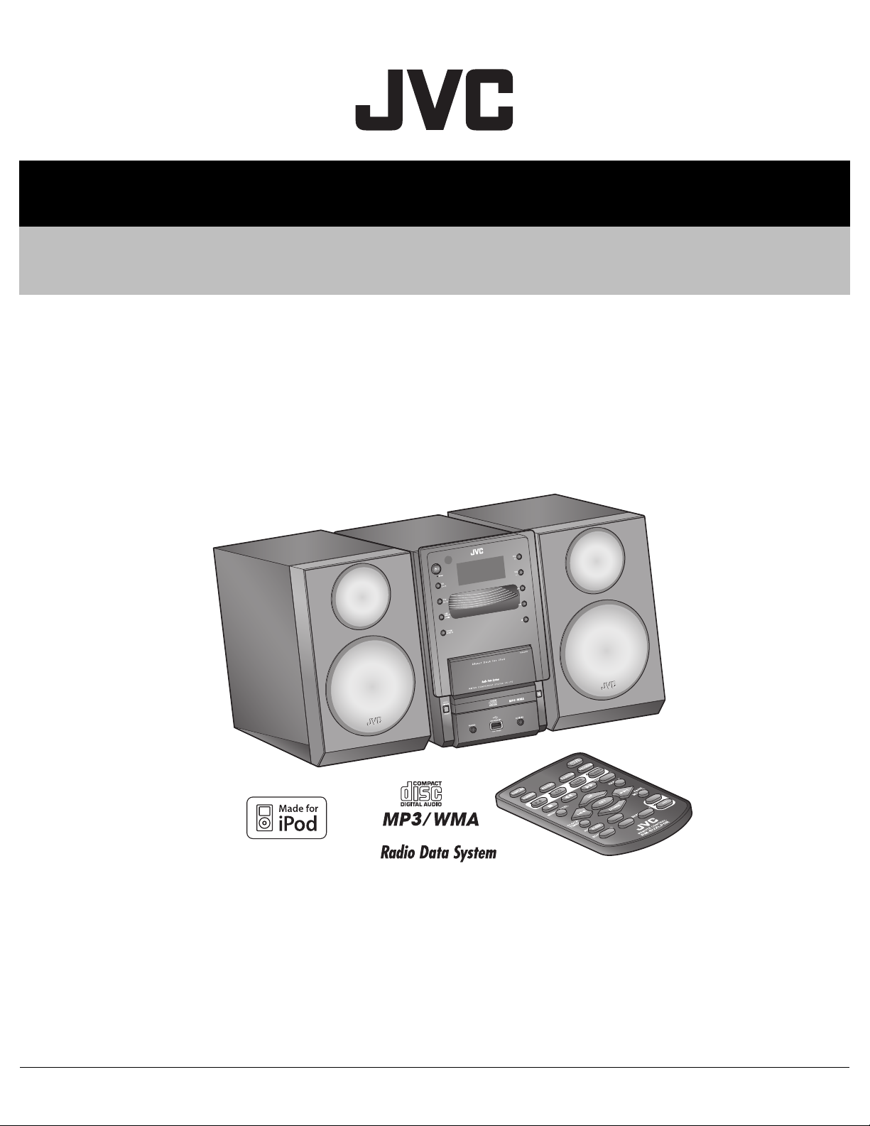
MICRO COMPONENT SYSTEM
MB698<Rev.004>200910SERVICE MANUAL
UX-LP5B, UX-LP5E, UX-LP5EN,
UX-LP5EV, UX-LP5J, UX-LP5C,
UX-LP5A, UX-LP5US, UX-LP5UB,
UX-LP5UP, UX-LP5UT
SP-UXLP5
CA-UXLP5
SP-UXLP5
(for Europe)
COPYRIGHT © 2009 Victor Company of Japan, Limited
Lead free solder used in the board (material : Sn-Ag-Cu, melting point : 219 Centigrade)
TABLE OF CONTENTS
1 PRECAUTION. . . . . . . . . . . . . . . . . . . . . . . . . . . . . . . . . . . . . . . . . . . . . . . . . . . . . . . . . . . . . . . . . . . . . . . . . 1-5
2 SPECIFIC SERVICE INSTRUCTIONS . . . . . . . . . . . . . . . . . . . . . . . . . . . . . . . . . . . . . . . . . . . . . . . . . . . . . . 1-9
3 DISASSEMBLY . . . . . . . . . . . . . . . . . . . . . . . . . . . . . . . . . . . . . . . . . . . . . . . . . . . . . . . . . . . . . . . . . . . . . . 1-10
4 ADJUSTMENT . . . . . . . . . . . . . . . . . . . . . . . . . . . . . . . . . . . . . . . . . . . . . . . . . . . . . . . . . . . . . . . . . . . . . . . 1-14
5 TROUBLESHOOTING . . . . . . . . . . . . . . . . . . . . . . . . . . . . . . . . . . . . . . . . . . . . . . . . . . . . . . . . . . . . . . . . . 1-14
COPYRIGHT © 2009 Victor Company of Japan, Limited
No.MB698<Rev.004>
2009/10
Page 2
SPECIFICATION
UX-LP5 for Europe
Amplifier section
OUTPUT POWER 60 W (30 W + 30 W) at 6 Ω (10% THD)
Speakers/Impedance 6 Ω - 16 Ω
Audio input AUDIO IN 500 mV/47 kΩ (at “LEVEL 1”)
250 mV/47 kΩ (at “LEVEL 2”)
125 mV/47 kΩ (at “LEVEL 3”)
Digital input USB MEMORY
Tuner section
FM tuning range 87.50 MHz - 108.00 MHz
AM (MW) tuning range 522 kHz - 1 629 kHz
CD player section
Dynamic range 88 dB
Signal-to-noise ratio 85 dB
Wow and flutter Immeasurable
iPod section
iPod output power DC 5 V 500 mA
VIDEO OUT Composite
USB storage
USB specification Compatible with USB 2.0 Full Speed
Compatible device Mass storage class
Compatible file system FAT16, FAT32
Bus power supply DC 5 V 500 mA
General
Power requirements AC 230 V , 50 Hz
Power consumption 35 W (power on)
8 W (standby mode)
1 W or less (Ecology Mode)
Dimensions (approx) 165 mm × 259 mm × 258 mm (W × H × D)
Mass (approx) 1.9 kg
Speakers
Speaker units 10 cm × 1; 1.5 cm × 1
Impedance 6 Ω
Dimensions (approx.) 140 mm × 250 mm × 188 mm (W × H × D)
Mass (approx.) 1.4 kg each
Specifications and appearance are subject to change without prior notice.
1-2 (No.MB698<Rev.004>)
Page 3
UX-LP5J/C
Amplifier section
OUTPUT POWER 35 W per channel, min. RMS, driven into 4 Ω at 1 kHz with no more than 10%
total harmonic distortion
Speakers/Impedance 6 Ω - 16 Ω
Audio input AUDIO IN 500 mV/47 kΩ (at “LEVEL 1”)
250 mV/47 kΩ (at “LEVEL 2”)
125 mV/47 kΩ (at “LEVEL 3”)
Tuner section
FM tuning range 87.5 MHz - 108.0 MHz
AM tuning range 530 kHz - 1 710 kHz
CD player section
Dynamic range 88 dB
Signal-to-noise ratio 85 dB
Wow and flutter Immeasurable
iPod section
iPod output power DC 5 V 500 mA
VIDEO OUT Composite
General
Power requirements AC 120 V , 60 Hz
Power consumption 35 W (power on)
8 W (standby mode)
1 W or less (Ecology Mode)
Dimensions (approx.) 165 mm × 259 mm × 258 mm
(6-1/2 inches × 10-1/4 inches × 10-3/16 inches) (W × H × D)
Mass (approx.) 1.9 kg (4.2 lbs)
Speakers
Speaker units 10 cm (3-15/16 inches) × 1; 1.5 cm (5/8 inch) × 1
Impedance 6 Ω
Dimensions (approx.) 140 mm × 250 mm × 188 mm
(5-9/16 inches × 9-7/8 inches × 7-7/16 inches) (W × H × D)
Mass (approx.) 1.4 kg (3.1 lbs) each
Specifications and appearance are subject to change without prior notice.
(No.MB698<Rev.004>)1-3
Page 4
UX-LP5 for Asia, Australia
Amplifier section
OUTPUT POWER 60 W (30 W + 30 W) at 6 Ω (10% THD)
Speakers/Impedance 6 Ω - 16 Ω
Audio input AUDIO IN 500 mV/47 kΩ (at “LEVEL 1”)
250 mV/47 kΩ (at “LEVEL 2”)
125 mV/47 kΩ (at “LEVEL 3”)
Digital input USB MEMORY
Tuner section
FM tuning range 87.50 MHz - 108.00 MHz
AM tuning range 531 kHz - 1 710 kHz (in 9 kHz spacing)
530 kHz - 1 710 kHz (in 10 kHz spacing)
CD player section
Dynamic range 88 dB
Signal-to-noise ratio 85 dB
Wow and flutter Immeasurable
iPod section
iPod output power DC 5 V 500 mA
VIDEO OUT Composite
USB storage
USB specification Compatible with USB 2.0 Full Speed
Compatible device Mass storage class
Compatible file system FAT16, FAT32
Bus power supply DC 5 V 500 mA
General
Power requirements AC 110 V - 127 V/AC 220 V - 240 V (adjustable with the voltage selector),
50 Hz/60 Hz
AC 240 V , 50 Hz (only Australia)
AC 220 V , 50 Hz (only Hong Kong)
Power consumption 35 W (power on)
8 W (standby mode)
1 W or less (Ecology Mode)
Dimensions (approx) 165 mm × 259 mm × 258 mm (W × H × D)
Mass (approx) 1.9 kg
Speakers
Speaker units 10 cm × 1; 1.5 cm × 1
Impedance 6 Ω
Dimensions (approx.) 140 mm × 250 mm × 188 mm (W × H × D)
Mass (approx.) 1.4 kg each
Specifications and appearance are subject to change without prior notice.
1-4 (No.MB698<Rev.004>)
Page 5
SECTION 1
PRECAUTION
1.1 Safety Precautions
(1) This design of this product contains special hardware and
many circuits and components specially for safety purposes. For continued protection, no changes should be made
to the original design unless authorized in writing by the
manufacturer. Replacement parts must be identical to
those used in the original circuits. Services should be performed by qualified personnel only.
(2) Alterations of the design or circuitry of the product should
not be made. Any design alterations of the product should
not be made. Any design alterations or additions will void
the manufacturers warranty and will further relieve the
manufacture of responsibility for personal injury or property
damage resulting therefrom.
(3) Many electrical and mechanical parts in the products have
special safety-related characteristics. These characteristics are often not evident from visual inspection nor can the
protection afforded by them necessarily be obtained by using replacement components rated for higher voltage, wattage, etc. Replacement parts which have these special
safety characteristics are identified in the Parts List of Service Manual. Electrical components having such features
are identified by shading on the schematics and by ( ) on
the Parts List in the Service Manual. The use of a substitute
replacement which does not have the same safety characteristics as the recommended replacement parts shown in
the Parts List of Service Manual may create shock, fire, or
other hazards.
(4) The leads in the products are routed and dressed with ties,
clamps, tubings, barriers and the like to be separated from
live parts, high temperature parts, moving parts and/or
sharp edges for the prevention of electric shock and fire
hazard. When service is required, the original lead routing
and dress should be observed, and it should be confirmed
that they have been returned to normal, after reassembling.
(5) Leakage shock hazard testing
After reassembling the product, always perform an isolation check on the exposed metal parts of the product (antenna terminals, knobs, metal cabinet, screw heads,
headphone jack, control shafts, etc.) to be sure the product
is safe to operate without danger of electrical shock.Do not
use a line isolation transformer during this check.
• Plug the AC line cord directly into the AC outlet. Using a
"Leakage Current Tester", measure the leakage current
from each exposed metal parts of the cabinet, particularly any exposed metal part having a return path to the
chassis, to a known good earth ground. Any leakage current must not exceed 0.5mA AC (r.m.s.).
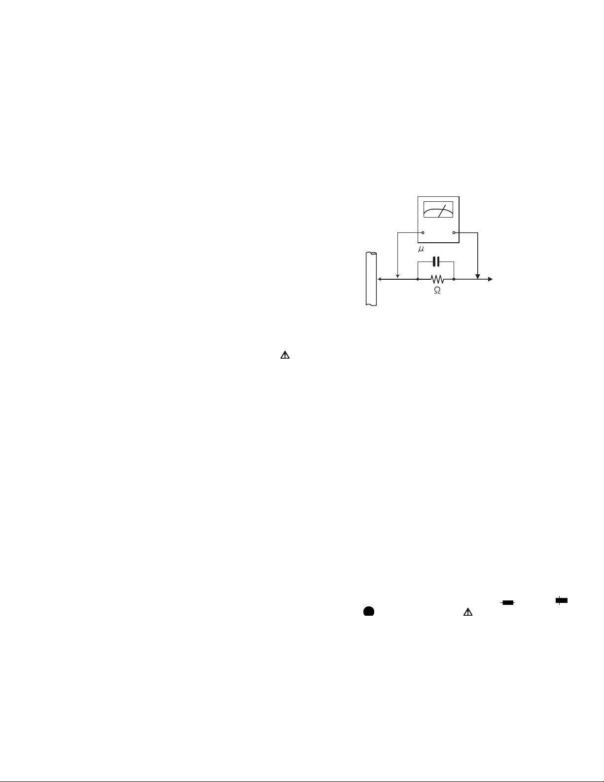
• Alternate check method
Plug the AC line cord directly into the AC outlet. Use an
AC voltmeter having, 1,000Ω per volt or more sensitivity
in the following manner. Connect a 1,500Ω 10W resistor
paralleled by a 0.15µF AC-type capacitor between an ex-
posed metal part and a known good earth ground.
Measure the AC voltage across the resistor with the AC
voltmeter.
Move the resistor connection to each exposed metal
part, particularly any exposed metal part having a return
path to the chassis, and measure the AC voltage across
the resistor. Now, reverse the plug in the AC outlet and
repeat each measurement. Voltage measured any must
not exceed 0.75 V AC (r.m.s.). This corresponds to 0.5
mA AC (r.m.s.).
AC VOLTMETER
(Having 1000
ohms/volts,
or more sensitivity)
0.15 F AC TYPE
Place this
probe on
1500 10W
Good earth ground
1.2 Warning
(1) This equipment has been designed and manufactured to
meet international safety standards.
(2) It is the legal responsibility of the repairer to ensure that
these safety standards are maintained.
(3) Repairs must be made in accordance with the relevant
safety standards.
(4) It is essential that safety critical components are replaced
by approved parts.
(5) If mains voltage selector is provided, check setting for local
voltage.
1.3 Caution
Burrs formed during molding may be left over on some parts
of the chassis.
Therefore, pay attention to such burrs in the case of preforming repair of this system.
1.4 Critical parts for safety
In regard with component parts appearing on the silk-screen
printed side (parts side) of the PWB diagrams, the parts that are
printed over with black such as the resistor ( ), diode ( )
and ICP ( ) or identified by the " " mark nearby are critical
for safety. When replacing them, be sure to use the parts of the
same type and rating as specified by the manufacturer.
(This regulation dose not Except the J and C version)
each exposed
metal part.
(No.MB698<Rev.004>)1-5
Page 6
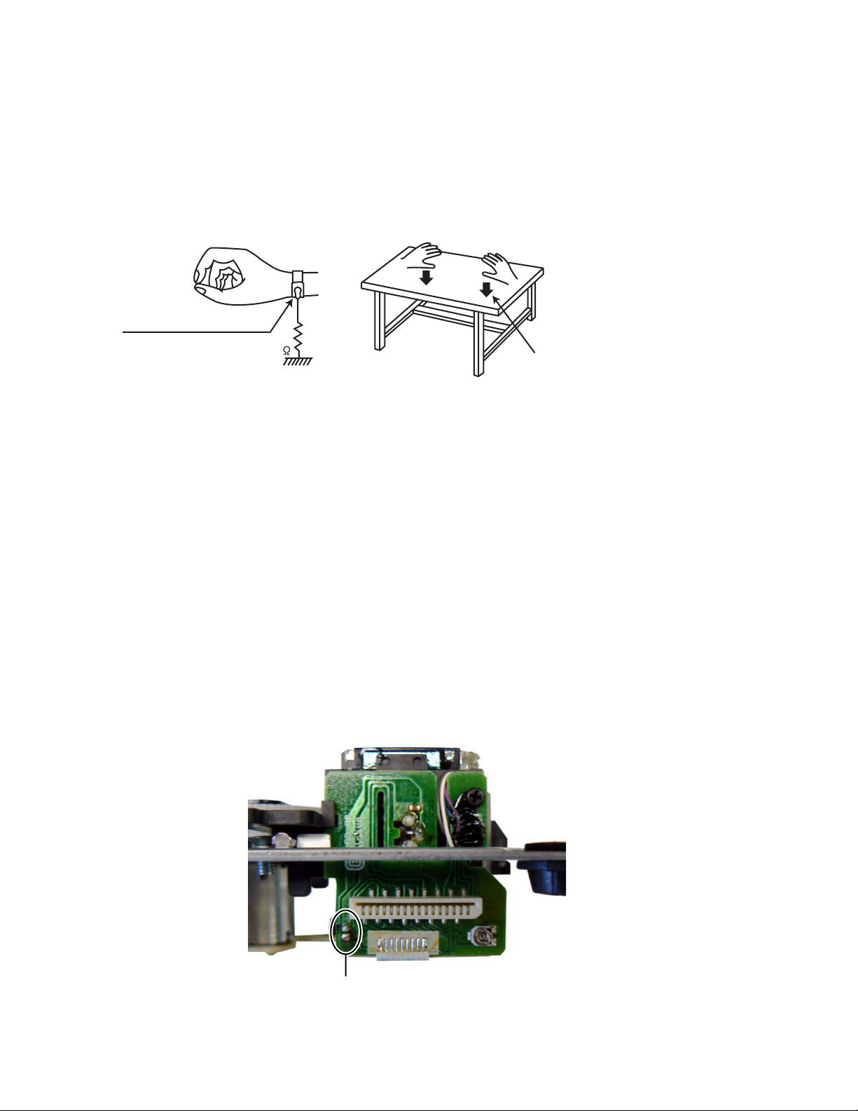
1.5 Preventing static electricity
Electrostatic discharge (ESD), which occurs when static electricity stored in the body, fabric, etc. is discharged, can destroy the laser
diode in the traverse unit (optical pickup). Take care to prevent this when performing repairs.
1.5.1 Grounding to prevent damage by static electricity
Static electricity in the work area can destroy the optical pickup (laser diode) in devices such as laser products.
Be careful to use proper grounding in the area where repairs are being performed.
(1) Ground the workbench
Ground the workbench by laying conductive material (such as a conductive sheet) or an iron plate over it before placing the
traverse unit (optical pickup) on it.
(2) Ground yourself
Use an anti-static wrist strap to release any static electricity built up in your body.
(caption)
Anti-static wrist strap
1M
Conductive material
(conductive sheet) or iron palate
(3) Handling the optical pickup
• In order to maintain quality during transport and before installation, both sides of the laser diode on the replacement optical
pickup are shorted. After replacement, return the shorted parts to their original condition.
(Refer to the text.)
• Do not use a tester to check the condition of the laser diode in the optical pickup. The tester's internal power source can easily
destroy the laser diode.
1.6 Handling the traverse unit (optical pickup)
(1) Do not subject the traverse unit (optical pickup) to strong shocks, as it is a sensitive, complex unit.
(2) Cut off the shorted part of the flexible cable using nippers, etc. after replacing the optical pickup. For specific details, refer to the
replacement procedure in the text. Remove the anti-static pin when replacing the traverse unit. Be careful not to take too long a
time when attaching it to the connector.
(3) Handle the flexible cable carefully as it may break when subjected to strong force.
(4) I t is not possible to adjust the semi-fixed resistor that adjusts the laser power. Do not turn it.
1.7 Attention when traverse unit is decomposed
*Please refer to "Disassembly method" in the text for the pickup unit.
• Apply solder to the short land sections before the card wire is disconnected from the connecto on the servo board. (If the card wire
is disconnected without applying solder, the pickup may be destroyed by static electricity.)
• In the assembly, be sure to remove solder from the short land sections after connecting the card wire.
1-6 (No.MB698<Rev.004>)
Solder short part
Page 7
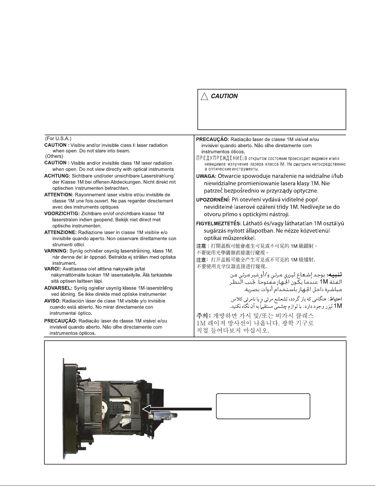
1.8 Important for laser products
1.CLASS 1 LASER PRODUCT
2.CAUTION :
(For U.S.A.) Visible and/or invisible class II laser radiation
when open. Do not stare into beam.
(Others) Visible and/or invisible class 1M laser radiation
when open. Do not view directly with optical instruments.
3.CAUTION : Visible and/or invisible laser radiation when
open and inter lock failed or defeated. Avoid direct
exposure to beam.
4.CAUTION : This laser product uses visible and/or invisible
laser radiation and is equipped with safety switches which
prevent emission of radiation when the drawer is open and
the safety interlocks have failed or are defeated. It is
dangerous to defeat the safety switches.
5.CAUTION : If safety switches malfunction, the laser is able
to function.
6.CAUTION : Use of controls, adjustments or performance of
procedures other than those specified here in may result in
hazardous radiation exposure.
!
Please use enough caution not to
see the beam directly or touch it
in case of an adjustment or operation
check.
REPRODUCTION AND POSITION
CAUTION:
DANGER:
INVISIBLE LASER RADIATION WHEN OPEN
DO NOT STARE INTO BEAM
INVISIBLE LASER RADIATION WHEN OPEN
AVOID DIRECT EXPOSER TO THE BEAM
(No.MB698<Rev.004>)1-7
Page 8
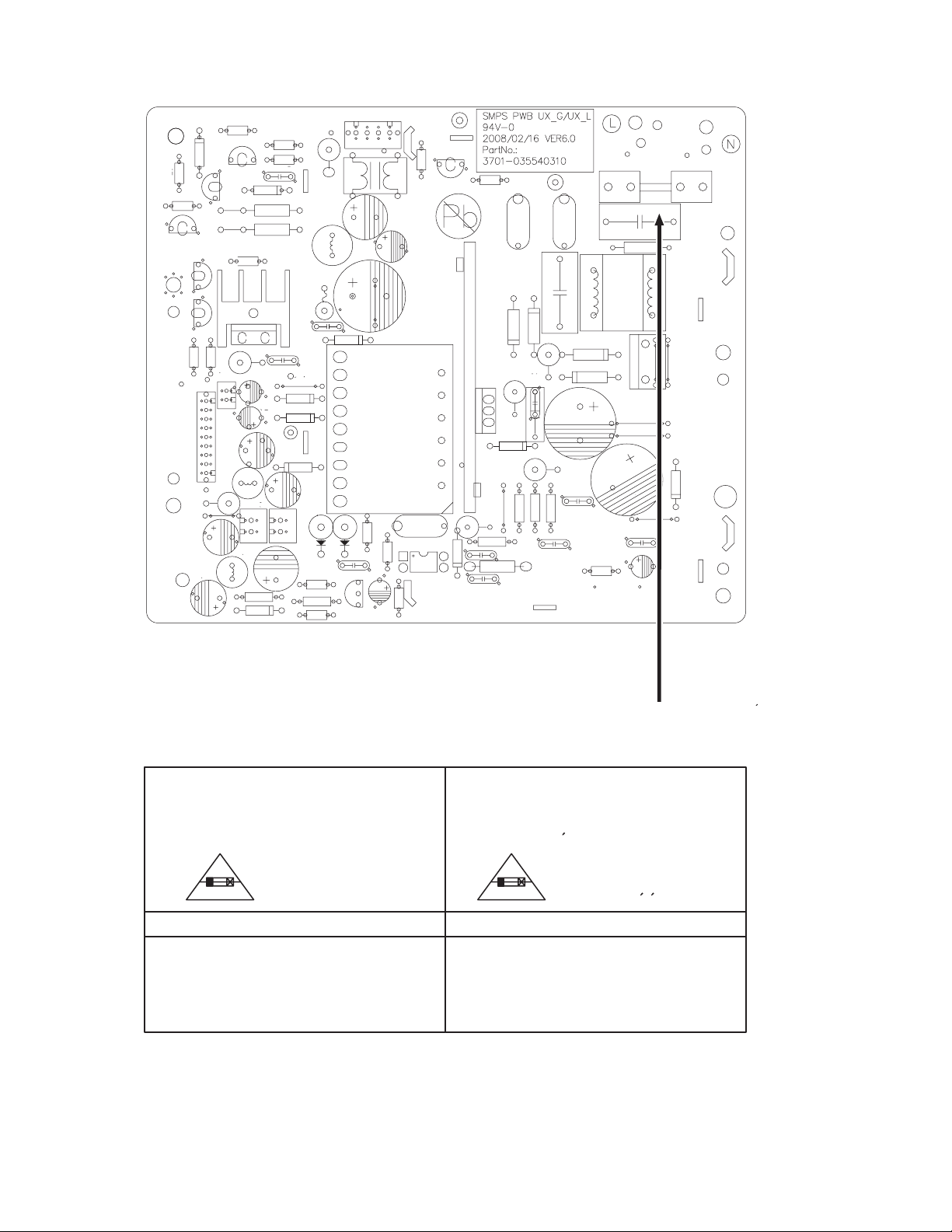
1.9 Importance administering point on the safety
R27
R26
U6
D17
R28
V7
R29
V5
V3
V4
R22
R15
CN5
FL+
CN2
-25V
ECO
FL+
5VE
GND
12V
GND
GND
5VD
5VD
L4
R23
JP7
C14
L3
C21
R25
C26
D18
R16
HS1
D9
C11
C25
R10
CN1
5V
GND
JP8
GND3
D10
D19
C27
GND2
C16
D12
CN4
C13
L6
D13
PVCCPVCC
CN3
L7
R13
R30
R31
L5
F2
C31
C15
5V
GND
D16D11
C12
R18
U3
R20
R21
PGND PGND
JP9
D14
R11
R19
C20
GND
R14
F1
V2
C18
C19
C17
T1
R12
HS2
C22
U2
D8
R9
C3
R2R1C6
V1
D6
JP5
R7
R24
C28
C24
GND
C4
C2
D2
D1
R3
C7
R6
R5
C8
R8
L2
R4
T2.5AH250V
C1
R32
L1
D3
D4
JP3
JP4
C5
SW1
JP1
JP2
C23
D5
JP6
C10
C9
Full Fuse Replacement Marking
Graphic symbol mark
(This symbol means slow blow type fuse.)
should be read as follows ;
FUSE CAUTION
FOR CONTINUED PROTECTION AGAINST RISK
OF FIRE, REPLACE ONLY WITH SAME TYPE
AND RATING OF FUSES ;
F901 : T1.6AH 250V F901 : T1.6AH 250V
slow blow type / type a fusion lent
Marquage Pour Le Remplacement
Complet De Fusible
Le symbole graphique (Ce symbole signifie
fusible de type a fusion lent.)
^
doit etre interprete comme suit ;
PRECAUTIONS SUR LES FUSIBLES
POUR UNE PROTECTION CONTINUE CONTRE
DES RISQUES D'INCENDIE, REMPLACER
SEULEMENT PAR UN FUSIBLE DU MEME TYPE ;
1-8 (No.MB698<Rev.004>)
Page 9

SECTION 2
SPECIFIC SERVICE INSTRUCTIONS
This service manual does not describe SPECIFIC SERVICE INSTRUCTIONS.
(No.MB698<Rev.004>)1-9
Page 10
SECTION 3
DISASSEMBLY
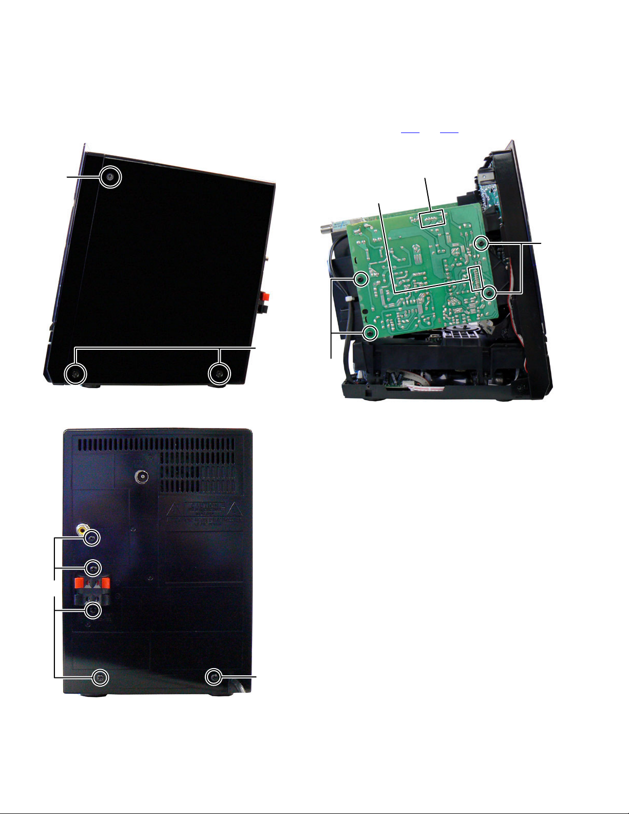
3.1 Main body (Used figure are UX-LP5E)
3.1.1 Removing the Top cabinet (See Fig.1, 2)
(1) Remove the six screws A attaching the both side of the Top
cabinet. (See Fig.1)
A
A
3.1.2 Removing the SMPS board (See Fig.3)
(1) Remove the four screws C attaching the SMPS board.
(2) Disconnect the connector wires from MCU board connect-
ed to connectors CN2
CN2
and CN3 of the SMPS board.
CN3
C
C
Fig.1
(2) Remove the five screws B attaching the Top cabinet. (See
Fig.2)
B
B
Fig.3
1-10 (No.MB698<Rev.004>)
Fig.2
Page 11
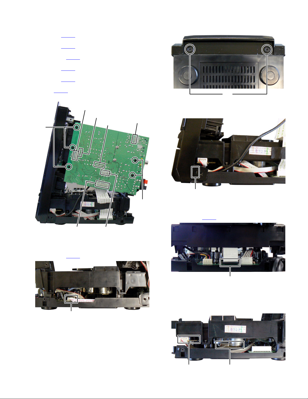
3.1.3 Removing the MCU board (See Fig.4)
(1) Disconnect the card wire from Tuner pack connected to
connector CN201
(2) Disconnect the card wire from Display board connected to
connector CN202
(3) Disconnect the connector wire from USB board connected
to connector CN210 of the MCU board.
(4) Disconnect the connector wire from CD board connected to
connector CN208
(5) Disconnect the card wire from iPod board connected to
connector CN206
(6) Disconnect the card wire from CD board connected to con-
nector CN207 of the MCU board.
(7) Remove the five screws D attaching the MCU board.
of the MCU board.
of the MCU board.
of the MCU board.
of the MCU board.
CN202
CN208
CN210
CN201
D
(2) Remove the two screws E attaching the Front cabinet.
(See Fig.6)
E
Fig.6
(3) Disengage two hooks a engaged both side of the Front
cabinet. (See Fig.7)
D
CN207
3.1.4 Removing the Front cabinet (See Fig.5 to 7)
(1) Disconnect the connector wire from USB board connected
to connector CN114
CN114
of the CD board. (See Fig.5)
CN206
Fig.4
Fig.5
hook
a
Fig.7
3.1.5 Removing the CD mechanism (See Fig.8 to 10)
(1) Disconnect the card wire from CD mechanism connected
to connector CN102
(2) Disconnect the connector wire from CD board connected to
connector of the Loader board. (See Fig.9)
(3) Disconnect the connector wire from CD board connected to
connector of Mechanism board. (See Fig.9)
of the CD board. (See Fig.8)
CN102
Fig.8
Loader board Mechanism board
Fig.9
(No.MB698<Rev.004>)1-11
Page 12

(4) Remove the four screws F attaching the CD mechanism.
(See Fig.10)
3.1.7 Removing the CD board (See Fig.12)
(1) Remove the four screws H attaching the CD board.
F
F
Fig.10
3.1.6 Removing the Traverse mechanism (See Fig.11)
(1) Remove the two screws G attaching the Traverse mecha-
nism.
GG
H
H
Fig.12
3.1.8 Removing the LED board (See Fig.13)
(1) Disconnect the connector wire from Display board connect-
ed to connector CN45
(2) Remove the two screws J and one screw K attaching the
Reflector bracket.
of the LED board.
J
Fig.11
K
Fig.13
3.1.9 Removing the Display board (see Fig.14 to 16)
(1) Remove the six screws L attaching the USB board. (See
Fig.14)
(2) Disconnect the connector wire from Display board connect-
ed to connector CN43
of the USB board. (See Fig.14)
CN45
L
L
Fig.14
CN43
1-12 (No.MB698<Rev.004>)
Page 13

(3) Remove the four screws M attaching the PCB bracket.
(See Fig.15)
M
M
3.1.10 Removing the iPod board (See Fig.17, 18)
(1) Remove the iPod door cover.
(2) Remove the Eject spring. (See Fig.17)
(3) Remove the one screw Q and one screw R attaching the
Cassette lid latch. (See Fig.17)
(4) Remove the one screw S attaching the Cassette cam
bracket. (See Fig.17)
(5) Remove the one screw T and one screw U attaching the
iPod door bracket. (See Fig.17)
S
Q
U
R
T
Fig.15
(4) Remove the two screws N and one screw P attaching the
Display board. (See Fig.16)
N
N
P
Fig.16
Eject spring
Fig.17
(6) Remove the four screws V attaching the Cosmetic frame.
(See Fig.18)
(7) It takes both picks off the hook and take off iPod door while
inclining the fulcrum of the door inward. (See Fig.18)
V
Fig.18
(No.MB698<Rev.004>)1-13
Page 14

SECTION 4
ADJUSTMENT
This service manual does not describe ADJUSTMENT.
SECTION 5
TROUBLESHOOTING
This service manual does not describe TROUBLESHOOTING.
1-14 (No.MB698<Rev.004>)
Page 15

Page 16

Victor Company of Japan, Limited
Audio/Video Systems Division 10-1,1chome,Ohwatari-machi,Maebashi-city,371-8543,Japan
(No.MB698<Rev.004>)
Printed in Japan
VSE
Page 17

SCHEMATIC DIAGRAMS
MICRO COMPONENT SYSTEM
UX-LP5B, UX-LP5E, UX-LP5EN,
UX-LP5EV, UX-LP5J, UX-LP5C,
UX-LP5A, UX-LP5US, UX-LP5UB,
UX-LP5UP, UX-LP5UT
DVD-ROM No.SML2009S2
Lead free solder used in the board (material : Sn-Ag-Cu, melting point : 219 Centigrade)
Contents
Block diagrams
Standard schematic diagrams
Printed circuit boards
COPYRIGHT 2009 Victor Company of Japan, Limited.
SP-UXLP5
CA-UXLP5
SP-UXLP5
(for Europe)
2-1
2-2
2-10 to 14
No.MB698SCH<Rev.004>
2009/10
Page 18

In regard with component parts appearing on the silk-screen printed side (parts side) of the PWB diagrams, the
parts that are printed over with black such as the resistor ( ), diode ( ) and ICP ( ) or identified by the " "
mark nearby are critical for safety.
Page 19

Block diagram
r
to iPod
CN51
iPod DOCK & OP section
IC402
OP AMP
IPOD L/R
System control & Audio Amp section
IPOD_ON
SLEEP_DET
CN52
CN206
IPOD
TXD/RXD
IC203
UART
SELECT
X203
32.768K
EEPROM
SCLK
SDA
IC202
IPOD L/R
IC204
E,VOLUME
IC212
POWER AMP
CVBS
OUT
JK203CN212
TO
Speake
CD traverse
mechanism
CD PICKUP
mechanism
TRY SW
M
LOADER
Section
CN104
CN102
CN103
IC104
MOTOR
DRIVER
Q106 to Q109
LOADER DRIVER
D+/-
CN114
CP42
SDRAM
X101
27MHz
IC103
IC101, IC102
1V8,3V3 REG
IC106
MPEG
IC105
FLASH
ROM
SCLK
SDA
AUTHENTIC
CD servo control section
CD R/L
N_RST
IC109
IPOD
CN208
CN106
CN207
CN107
CD
TXD/RXD
CD_ON N_RST
TR+
TROPEN
CLOSE
CN210
CP41
SCLK
SDA
HP_MUTE
IC205
HP AMP
MUTE
HP L/R
TXD/RXD
IC201
MICON
Q201
RESET
IC210,IC211
SUBWOOFER
LFT OUT
CN202
CN41
TU_CLK
TU_DA
TU_RST
TU_DET
JK204
SUB OUT
CD R/L
AUX L/R
POWER ON
Q207
+9V REG
Q205,Q206
A+12V
SWITCH
CN203
CN2
D11,D16
5VD REG
Q217,Q218
AMP_MUTE
AMP_STBY
Q202,Q203
Z201
+5V REG
TU_ON
TUNER L/R
CN211
CN3
D9
+23V REG
CN201
UNIT
TUNER
HP L/R
JK41JK42JK43
AUX L/R
D+/-
USB AUDIO IN HEADPHONE
+5V_USB
CN43
KEY_1
KEY_2
Ornament
Blue LED
SW401-SW413
CP43
CP44
CN45
KEY MATRIX
TACT SW LED section
HP&AUDIO&USB JACK section
LED ON
IPOD_LED
LED MATRIX
WITH DIM
LED1
STANDBY
LED
DIM OFF
STB LED OFF
VFD_DATA
VFD_STB
U501
VFD DRIVER
GR1 to 12
VFD1 DISPLAY
IR_RXVFD_CLK
IR401
REMOCON
LCD section
SG1 to 16
CN5
CN42
CN1
CP45
+12V REG
D13
5VE REG
D19
-25V REG
D10
FL+/- REG
D12
POWER TRANS
SW REG.
CONTROL
T1
SW1
110V/230V
U1
AC IN
AC CORD
D1 to D4
DIODE
BRIDGE
SMPS section
2-1
Page 20

Standard schematic diagrams
Smps section
D2
D1
RL207
RL207
C2
!
0.22uF/275V
!
L1
40mH_0.35mm
C1
0.22uF/275V
!
F1
T2.5AH250V
LN
AC_plug
R1
NC
1M/0.5W
L
T5AL250V
C11
2/1KV_M
D10
FR104
R33 2 2
C12
103
L6
R27
2K2
C19 47UF/50V
F2
C27
22UF/50V
D17
4.3V
U6
AZ431
R9
18K
+
L5
10UH
+
C17
2200UF/35V
R34 22
C15
330UF/16V
+
+
+
R14
4K7
+
L4
10UH
C13
1000UF/16V
L 3 10UH
5VE
C21
330UF/16V
KTA1275A
+
C18
470UF/35V
-25 V
C16
330UF/16V
C14
330UF/16V
R22
4K7
R28
330
V7
S8050
D18
1N4148
V2
AGND
12V
R16
1K
+
+
33/2W
R29
2K2
L7
33UH
FL-
+
100UF/16V
FL+
DGND
R23
4.7K/0.5W
C25
1N4148
5VD
S8050C
PVCC
R13
PGND
D15
V5
S 8 550
V3
EC O
R17
1K
R30
22/2W
V4
S8050C
R15
1K
R31
22/2W
D14 FR104
+
C5
120uF/200V
!
T1
P
NC
DAIN
EMI
VCC
5VD
R24
10/1W
1
23
U3
AZ431
DGND
2
2302- 285000500
R18
100
R19
1K
C20
1UF/50V
CN4
1
NC
+
+
C23
!
CN1
CN2-2.0
5VD
5VD
9
120uF/200V
1
2
3
4 5
0
12V
DGND
DGND
AGN D
4
5
6
7
8
R6
10K
U1
ADJ
FB
CS
GND DRV
NCP1216D65G2
C7
471
C8
471
R8
22
EC O
-25 V
5VE
2
3
8
HV
7
NC
6
VCC
C9
47UF/25V
+
C10
104
VD1
24V
PVC C
PGN D
PGN D
2
3
1
4
D3
RL207
R32
N
D4
RL207
SW1
NC
1N4007
D5
!
C3
102/250V_Y1
CN2.0-9
CN2
FL-
FL+
2
C4
102/250V_Y1
1
PVC C
1
R2
47K/2W
R7
1K
1000UH(0410)
C24
102
CN2.5-4
CN3
D7
1N4148
R4
47
R5
3K3
L2
FQPF5N60C
!
4
C22
!
NC
5VD
!
6
C6
472/1KV_M
5
D6
FR107
4
V1
3
R3
0R47/2W
2
Hot_GND
1 15
D8
FR104
472K/100V
C28
U2
EL817C
DGND
CN1
1
2
NC
Parts are safety assurance parts.
!
When replacing those parts make
R20
3K3 1%
STB
21V
PGND
-25V
FL-
FL+
12V
GND
5V
D13
1N5819
R21
3K6 1%
R12
100K
7
8
9
11
10
12
13
14
R11
10
R26
180 K
C26
104
D9
UF802
R10
33/2W
47
D19
FR104
D12
FR104
C29 102/100V
D11
1N5822
1N5822
PVCC 5VD
R25
24K
C32 102
D16
10UH(0307)
sure to use the specified one.
2-2
Page 21

Main section 1
T81
CN202
16-PINS FFC HEADER.1.0MM
1
2
3
4
5
6
7
8
9
10
11
12
TO DISPLAY BOARD
13
14
15
16
T29
CN203
9-PINS HEADER.2.0MM
1
2
3
4
5
6
7
8
FROM_SMPS BOARD
9
IPOD_CVBS
T87
TUNER_DAB_L
TUNER_DAB_R
T82
T83
T84
T88
T89
T90
D+5V
FB07
T25
T26
T27
+5V_TUNER
D+5V
100U/16V(LP5)
R20
75R(LP5)
T91
T23
T24
T28
T22
T16
T13
T14
T15
T17
T18
T85
T93
R23
OPEN
0R(LP5)
C12
CHGND
T86
R304
R303 0R
SYSTEM_ON
C8B
OEN
R22
CHGND
TO TUNER MODULE
TUNED
CN213
1 3 5 7 9
OPEN
0R
T92
T94
T95
+12V ST+5V -25V
0R
C8A
0.1U
OPEN
R16
75R(LP5)
+
R17
75R(LP5)
R7
OPEN
R21
OR(LP5)
855OC,TO-92(LP5)
ST_IND
SDA
2 4 6
R301
1K5
R302
1K5
VFD_DATA
VFD_CLK
VFD_STB
IR_RX
LED_ON
SYSTEM_ON
IPOD_LED_ON
KEY_2
KEY_1
VOL+
VOL-
C8
0.1U
75R(LP5)
C13
100P(LP5)
Q2
SCL
PORT_SEL
C7
R18
75R(LP5)
R19
L_OUT
TU_GND
R_out
VCC
RDS_CLK
8
10
T20 T21
-25V +12V_VFD
R327
4K7
R328
487K
C7B
C7A
OPEN
OPEN
C15
10P(LP5)
L4
1U(LP5)
RDS DATA
11
ST+5V
+3V6
R321
4K7
R326
10k
Q206
8050C
C14
100P(LP5)
TO TUNER MODULE(SI47XX SERIES)
L_CH
GND
R_CH
T19
1
2
3
4
Q204
8050C
C305
OPEN
Q205
AP2301N
S
G
R329
CVBS_OUT
AT24C02
A0
A1
A2
GND
R325
47K
C301
0.1U
1M
2 4 6
1 3 5 7 9
IC202
8
VCC
7
WP
6
SCL
5
SDA
MCU_SCL
MCU_SDA
AMP_STB
ECO_STBY
LED_ON
VFD_STB
VFD_DATA
VFD_CLK
VOL+
VOL-
ST+5V
R324
10K
R323
1K
A+12V
100UH,AXIAL
D
+
C302
100U/16V,SHORT TYPE
L213
C303
0.1U
VCC
C307
0.1U
ECO_STBY
SCLK
SDIO
SEN/
RDS DATA
8
OR
OPENOROR
FB03
FB05
FB04
R320
22K
+12V_VFD
+
100U/16V,SHORT TYPE
ST+5V
D203 D202
LL4148 LL4148
CN201
10-PINS FFC HEADER, 1.25MM
RST/
RDS_CLK
10
11
T69
R26 100R
OPEMOROPEN
OPEN
FB10
FB06
FB09
FB02
FB01
R322
22K
C306
0.1U
7-PINS HEADER,2.0MM(SOFTWARE UPGRADE)
MCU_UPGRADE
C304
+3V6
A
R305
100R
4K7
R306
100R
R310
100R
R311
1K
R312
1K
R313
1K
R314
1K
R315
1K
R316
1K
R317
1K
R13
1K
R14
1K
R15
1K
R318
IPOD_LED_ON
AMP_MUTE
SLEEP_DET
CN204
7
6
5
4
3
2
1
+3V6
GND AGND
C309
4.7U/16V
+
100UH,AXIAL
4K7
4K7
R307
R308
A
+3V6
+3V6
L212
R395
4K7
R393
12K
R394
D201
6K8
LL4148
STB+5V
+
315
100U/16V
4K7
R309
1
P60/SCL0
2
P61/SDA0
3
P62/EXSCL0
4
P63
5
P33/TI51/TO51/INTP4
6
P75
7
P74
8
P73/KR3
9
P72/KR2
10
P71K/KE1
11
P70K/KE0
12
P32/INTP3
R300 1K
R330
1K
R256
1K
IPOD_ON/OFF(SCLK)
FMLDO
RESET
D6
LL4148
D7
LL4148
C16
0.01U
C17
0.01U
C18
0.01U
C19
0.01U
R392
22K
Q201
8050C
C316
48
VDD
P31/INP2
13
C310
0.1U
0.1U
C317
47
VSS
P30/INTP1
14
R445
10K
RESET
C311
C312
24P
24P
X203
32.768K
R397
T97
OPEN
0.1U
R433
0R
46
45
44
43
42
41
REGC
FLMDO
P123/XT1
P121/X1/OCDOA
P124/XT2/EXCLKS
P122/X2/EXCLK/OCDOA
IC201
UPD78F0514GA(T)-8EU-A
P17/TI50/I050
P16/TOH1/INTP5
P15/TOH0
P14/RXD6
P13/TXD6
R347
16
R8
OPEN
17
22R
R331
47K(LP5)
18
R350
19
22R
R332
R348
4K7(LP5)
P12/SO10
20
RXD
15
4K7(LP5)
C3
0.01U
R396
10K
C1
0.01U
40 3938
P40
RESET
P11/SI10/RXD0
P10/SCK10/TXD0
21
22
22R
22R
R334
R335
TXD
R349
10K(LP5)
C313
0.1U
37
P41
P120/NT
P140/PCL/INTP6
P00/TI000
P01/TI010/T000
P130
P20/ANI0
ANI1/P21
ANI2/P22
ANI3/P23
ANI4/P24
ANI5/P25
ANI6/P26
ANI7/P27
AV-REF
AVSS
23
24
C319
0.1U
74HC4052(LP5)
1
2Y0
2
2Y2
3
2Z
4
2Y3
5
2Y1
6
E
7
VEE
GND
8
R351
47K(LP5)
+5V_TUNER
L211
100UH,AXIAL
++
C314
100U/16V
C318
100P
+3V6
R375
36
35
34
33
32
31
30
29
28
27
26
25
R383
OR
3K9(G355,LP5),8K2(L5V)
IC203
UART_SEL2
UART_SEL1
10K
10K
10K
R387
R388
R389
R390
3K9(G355,LP5),8K2(L5V)
16
VCC
15
1Y2
14
1Y1
13
1Z
12
1Y0
11
1Y3
10
S0
S1
9
R25
OPEN (AXIAL)
R24
OPEN (AXIAL)
R358
120R,1/2W (AXIAL)
R443
OR
C340
OPEN
R367
10K
1K
R366
10K
R446
1K(UX-G355/UX-LP5),OR(UX_L)
1K(UX-G355/UX-LP5),OR(UX_L)
10K
10K
10K
R391
R385
R384
C320
0.1U
R333 22R
R338 0R(G355 0R L5V)
0R(G355 0R L5V)
R339
R340 1K(LP5)
R342 1K(LP5)
R343 1K(LP5)
R344 1K(LP5)
R346
10K(LP5)
UART_SEL1
UART_SEL2
Z201
5V1,AXIAL
10K
R368
+3V6
+
T96
Q202
8550C,TO-92
Q203
8050C
R363 1K
R434 22R
R364 1K
R365 1K
R431 1K
R370
10K
22K
R369
R380
10K
R371
R372
R373
1K(G355 OR LP5)
R374
R376
R377 1K
R378 1K
R382 1K
R337 1K
R336
C308
100U/16V,SHORT TYPE
ST+5V
CD
IPOD DAB
10011
R360
4K7
C337
0.1U(LP5)
1
A+12V
R359
22K
R361
4K7
R362
10K
1K(L5V)
1K(L5V)
1K
1K
R379
R381
1K
DAB_TUNER_ON
AM_HOP
IPOD_ON/OFF(SCLK)
FMLDO
LINE_MUTE
STB+5V
HP_MUTE
IR_RX
IPOD_SEL1
IPOD_SEL2
NREST
IPOD_DET
DAB_TUNER_ON
CD_ON
CLOSE_SW
OPEN_SW
TRAY-
TRAY+
HP_DET
KEY_1
KEY_2
DVD_STB
RXD/DVD/_DAT
TXD/DVD_CLK
UR_FROM_IPOD
UR_TO_IPOD
9-PINS FFC HEADER,1.0MM(L5V)
FROM DVD BOARD
CN205
SPDF_OUT
SPDF+5V
CVBS_OUT
Y_OUT
PB_OUT
PR_OUT
VGND
CVBS_OUT
IPOD_CVBS
T48
1
2
3
4
5
6
7
8
9
SLEEP_DET
IPOD_DET
UR_TO_IPOD
UR_FROM_IPOD
D+5V
IPOD_ON/OFF(SCLK)
IPOD_L
IPOD_R
A+12V
TRAY+
TRAY-
OPEN_SW
CLOSE_SW
DVD_STB
RXD/DVD_DAT
TXD/DVD_CLK
CD_ON
MCU_SCL
MCU_SDA
NREST
IR_RX
IPOD_SEL1
IPOD_SEL2
CD/DVD_LIN
CD/DVD_RIN
T49
R357
33R(L5V)
T50
T51
T52
T53
T54
T55
T56
R1
0R(UX-G355,UX-LP5),OPEN(UX-L5V)
0R(UX-G355,UX-LP5),OPEN(UX-L5V)
F201
JK60-075(LP5)
T57
T58
T59
T32
T33
T34
T35
T36
T37
R356
0R(CD)
R355
0R(CD)
T60
T62
T38
T39
T42
47U/16V(L5V)
C321
0.1U(L5V)
R2
SUB_OUT
C338
1000P(SUBWOOFER)
T63
T64
T65
T74
T73
T40
T41
T43
T44
T45
T71
C322
+
Z202
5V1(L5V)
Z203
5V1(L5V)
T61
T30
C339
0.1U
T31
T72
T107
T105
T108
Z204
Z208
5V1(L5V)
5V1(L5V)
Z207
Z205
5V1(L5V)
5V1(L5V)
Z211
5V1(L5V)
Z212
5V1(L5V)
+5V_IPOD
D+5V
1
3
5
7
9
10
11
12
13
14
15
16
17
18
19
20
CHGND
CN208
3-PINS HEADER,2.0MM
T111
T110
T109
GND
1
VCC
2
IN
3
T106
1
2
3
4
5
6
Z210
5V1(LP5 0R L5V)
1
2
Z209
5V1(LP5 0R L5V)
T104
T103
1
2
T167
T102
A+12V
T168
16-PINS FFC HEADER 1.0MM(LP5)
JK202
YPBPR RCA JACK(L5V)
JK203
CVBS RCA JACK(LP5 0R L5V)
JK204
SUB RCA JACK(L5V)
16
15
14
13
12
11
10
9
8
7
6
5
4
3
2
1
CN206
TO iPod BOARD (CD MODELS)
2
4
CN207
6
20-PINS FFC HEADER,1.25MM
8
TO CD BOARD OR DVD BOARD
1
2
3
4
FROM CD BOARD OR DVD BOARD
5
6
7
JK201
GP1FA553TZ(L5V)
2-3
Page 22

Main section 2
IPOD_L
R220
6K8
(LP5)
C280
R215
1U
2K4
CD/DVD_LIN
CD/DVD_RIN
4.7U/16V
4.7U/16V
R9
(L5V)
56K
C328
(REVERSE INSERT)
R10
(L5V)
56K
C327
(REVERSE INSERT)
A+12V
R11
33K
(L5V)
R12
33K
(L5V)
R436
3K3
R255
3K3
R223
3K9
R257
3K9
TO HEADPHONE BOARD
C4
(L5V)
100U/16V
C332
1U
C325
1000P
C336
1U
C325
1000P
CN210
7-PINS HEADER, 2.0MM
1
2
3
4
5
6
7
TUNER_DAB_R
TUNER_DAB_L
T75
T76
IPOD_R
AUX_R
AUX_L
CD/DVD_L
CD/DVD_R
CD/DVD_L
CD/DVD_R
T77
T78
HP_L_OUT
T79
T80
HP_R_OUT
R247
R248
R213
R224
(LP5)
6K8
A+12V
C270
0.1U
MCU_SDA
MCU_SCL
R430
470R
1K8
1K8
R229
5K6
R201
5K6
Q207
C271
100U/16V
R250 R251
5K6 5K6
C283
22U/16V
TO-928050C,
Z214
9V1, AXIAL
AUX_L
AUX_R
HP_DET
R437
C284
1000P
C268
1U
C269
1U
IC204
ET2314
C256
0.1U
C279
1U
1U
1U
DGND
OUT_L
TREB_R
RIN
2700P MYLAR
C274
C276
2U2/16V
2K4
2K4
2K4
2K4
C266
220U/16V
C257
220U/16V
IC205
BH4453F
C258
220U/16V
R214
R216
OUT_T
100U/16V
2K4
R227
5K6
0.1U MYLAR
C291
BOUT_R
ROUT
LOUD_R
0.1U MYLAR
C275
VDD
OUT1
C2
2K4
2K4
0.1U MYLAR
0.1U MYLAR
C292
C293
BIN_R
BOUT_L
RIN4
RIN3
8
OUT2
MUTE
1
0 = MUTE
0.1U MYLAR
C294
1011121314
R203
5K6
C278
C286
R202
C285
5K6
1000P
100RR200
100R
28272625242322212019181716
CLK
REF
DATA
VDD
AGND
TREB_L
123456789
2700P MYLAR
C273
C272
47U/16V
R210
R212
R217
R218
R228
5K6
C295
2U2/16V
LIN
LOUT
BIN_L
RIN2
RIN1
LOUD_L
0.1U MYLAR
C277
R231 R230
560R
R232
47K
657
IN2
BIAS
IN1
GND
342
C260
0.1U
LIN1
LIN4
15
R233
100K
LIN2
LIN3
D206
LL4148
R242
47K
560R
C265
47U/16V
R234
10K
Q219
8050C
C267
47U/16V
C264
C262
Q212
8050C, TO-92
1U
1U
R235
10K
C5
1000P
C6
1000P
Z218
5V6, AXIAL
R236
10K
R241
820R
R239
OPEN
C281 C282
10U/16V 10U/16V
A+12V
R237
OPEN
R240
47K
R238
SUB_L
SUB_R
R244
2K2
R243
10K
R245
2K2
R246
10K
47K
HP_MUTE
PRE_L
PRE_R
HPR
HPL
Headphone amplifier section
2-4
Page 23

Main section 3
AM_HOP
For AM TUNER
4-PINS HEADER, 2.5MM
FROM SMPS BOARD
A+12V
4K7
R3
R424
0R (AM)
C201
1000P (AM)
C202
0R (AM)
C211
1
+25V
2
3
4
T46 T47
+25V
D1
LL4148
R5
10K
R4
Q1
8550C
ZD1
11V ZENER
R421
C203
OPEN
R423
OPEN
OPEN
R422
OPEN
EC1
10U/16V
SCREW2SCREW1
R425
0R (AM)
0.47U/63V, BOX
UNPLUG_MUTE
R419
1K (AM)
R420
C9
1
2
3
4
5
6
7
OPEN
C207
OPEN
AGND
1A
1Y
2A
2Y
3A
3Y
GND
C210
0.1U
IC214
OPEN
R426
OPEN
220K (AXIAL)
OPEN
+25V
VCC
6A
6Y
5A
5Y
4A
4Y
X201
Q213
2SK3018 (AM)
X202
R286
1M
Z217
OPEN (AXIAL)
C204
14
0R (L5V)
13
12
11
10
9
8
C206
OPEN
Q214
0R (E-C)
C208
0R (AM)
SUB_L
SUB_R
A+12V
R283
560R (L5V)
R284
10K (L5V)
R285
10K (L5V)
OPEN (1206)
R428
3K9
(L5V)
R440
OPEN
AMP_STB
ECO_STBY
UNPLUG_MUTE
AMP_MUTE
2
3
8
6
5
220U/16V (L5V)
C214
100U/16V (L5V)
IC210-B
4
C215
1
IC210-A
AZ4558 (L5V)
AZ4558 (L5V)
7
+12VV
+12VV
R281
2K2 (L5V)
R282
2K2 (L5V)
C216
0.1U (L5V)
VREF
D3
LL4148
D2
LL4148
VREF
C209
OPEN
R429
OPEN
C213
10U/16V (L5V)
OPEN (L5V)
R287
A+12V
R402
22K
R401
22K
R288
2K2 (L5V)
R406
2K2
Z215
3V3, AXIAL
R405
2K2
Z216
3V3, AXIAL
R403
51K
3
2
+12VV
1K (L5V)
R289
8
T98
PRE_L
PRE_R
C222
0.1U
C221
0.1U
Q217
8050C
C220
0.1U
IC211-A
AZ4558 (L5V)
1
R441
OPEN
R290
100K (L5V)
R404
51K
SYNCLK
C237
0.47U
C238
0.47U
R291
100K (L5V)
4700P (L5V)
Q218
8050C
C217
R407
33K
R408
33K
ST+5V
C10
1U
0.01U (L5V)
C223
C219
1U
C225
2U2/16V
C224
1U
1K (L5V)
R6
R410
1M
R409
C226
0.1U
IC211-B
AZ4558 (L5V)
5
6
4
LINE_MUTE
19
VDDPW
PGND
22R
STBY
OUTPA
C229
1500U_35V
T1
R450
10K (L5V)
R413
39K
C241
1000P
1M
R411
C240
0.47U
R412
C239
0.1U
R435
100K
INPA
INNA
VDDS
MUTE
OUTPA
R417
22R
SGND
ROSC
SYNCLK
OUTNA
OUTNA
PVCCA
PVCCA
PGNDA
PGNDA
101112131415161718
C227 C228
0.1U
C296
330P
T3
T2
C218
10U/16V (L5V)
7
R296
47K (L5V)
Q215
8550C (L5V)
R299
47K (L5V)
C242
1000P
1M
SVR
R415
SVR
DIAG
GAIN0
PVCCB
OUTNB
OUTNB
R418
22R
R295
1K (L5V)
Q222
8050C (L5V)
C244
0.1U
C243
0.47U
1M
R414
0R
0R
R416
0.1U
C11
3635343332313029282726252423222120
VSS
INPB
INNB
VREF
SVCC
GAIN1
SUB_GND
OUTPB
OUTPB
PGNDB
PGNDB
PVCCB
123456789
0.1U
C230
330P
T4
0.47U/63V, BOX
L206
22UH CHOKE
L207
22UH CHOKE
0.47U/63V, BOX
L208
22UH CHOKE
FB11
0R (L5V)
Q216
8050C, TO-92 (L5V) + 10U (0805 B-E)
C245
1U
C246
1U
C247
0.1U
IC212
TDA7492
L205
22UH CHOKE
C231
C234
SUB_OUT
L1
FERRITE BEAD, AXIAL
C232
0.22U
C233
0.22U
C235
0.22U
C236
0.22U
Gain
R415
R416
20dB 26dB 30dB 32dB
NC NC
NC NC
0R 0R
L3
30UH COMMON MODE CHOKE
1
3
4
2
1
3
4
2
L2
30UH COMMON MODE CHOKE
0R0R
CN212
2X2 SPEAKER JACK
4
L+
3
L-
6 OHM 35WX2
2
R+
1
R-
T66
T99
T101
T100
T10
T5
T11
T6
T7
T12
T8
T9
SUBWOOFER PRE-OUT (DVD MODELS)
2-5
Page 24

Front section
2
1
CN42
TO SMPS BOARD
TP11
TP12
TP13
CN41
FFC-16P/1.00
16
15
14
13
12
11
10
9
8
7
6
5
4
3
2
1
TO MCU BOARD
TP14
FB404
FB100R
TO USB BOARD
GND_KEY
KEY_1
TP15
TP16
TP17
TP18
TP19
TP20
TP21
100RFB100R 1206
GND
+5V_VFD
IR_RX
GND_KEY
LED_ON
IPOD_LED_ON
KEY_2
KEY_1
VOL+
VOL-
TP32
TP33
OPTION:NOT FOR G355
CP43
3P/2.0MM
1
2
3
TP10
JW13
JW12
CK402
FB401
1000P
FB100R
TP30
VFD1
QV503
CV501
0.1U
CV514
0R
STOP
FR
FF
VOL-
VOL+
(REC)
0.1U
JR04
8550, TO-92
RV518
EC501
EC514
GND
STBLED_ON
KEY_2
0R
RK435
RK434
RK433
RK432
RK431
150R
ZD507
100U/16V
8050C, TO-92
RV514
220U/16V
IR_RX
-25V
3K9
3K3
2K7
470R
RV520
1K
QV504
ZD508
470R
4V7
220R
RV519
+5V_VFD
5V1
LED_ON
F-
FILAMENT
F+
FILAMENT
JW08
CV502
0.1U
NOTE
SW403
SW404
SW405
SW408
JW16
JW15
+5V_LED
JW04
USB
TUNER
AUX
REC
CK411
RK420
2K2
0.1U
CP44
8050C
QK401
RK407
1
2
10K
F-
F+
-25V
+5V_VFD
VFD_STB
VFD_CLK
VFD_DATA
UX-L5VUX-G355
USB
REC
TUNER
AUX
VOL+
RK439
150R
LED9
BLUE
STBLED_ON
RK438
LED8
150R
BLUE
iPod
TUNER
AUX
USB
VOL+
RK437
150R
BLUE
LED7
RK421
2K2
21
ZD502
5V6
0.1U
CV503
EC505
47U/35V
ZD501
27V
UX-LP5
+5V_VFD
CN45
1
2
RK402
QK402
8050C
10K
RK410
RV509
FB502
FB100R
NO USBWITH USB
RV507
RV508
470R
12K
iPod
AUX
TUNER
VOL+
2K2
LED1
RED
F-F-NCP1P2P3P4P5P6P7P8P9P10
3534333231302928272625242322212019
P1P2P3P4P5P6P7P8P9
P[1:16]
BLUE
LED3
RK423
2K2
SS0520
150R
RK404
22
21
20
19
18
17
16
15
14
13
12
JR06
0R
RK424
S/K_10
S/K_9
S/K_8
S/K_7
S/K_6
S/K_5
S/K_4
S/K_3
S/K_2
S/K_1
VDD1
VSS1
RV501
10K
EC504
470R
10U/50V
0.1U
CK401
P9
P8
P7
P6
P5
P4
P3
P2
P1
OPEN
0.1U
CV506
IPOD_LED_ON
CV504
DV501
RK403
BLUE
LED2
150R
FB513
FB100R
FB512
FB100R
+12V_VFD
FB402
FB100R
JW09
TP24
CK403
+12V_VFD
RV502FB511
NOTE
SW405
NOTE
SW404
NOTE
SW403
CD
SW402
STBY
SW401
VFD_DATA
VFD_CLK
VFD_STB
-25V
7K5
RK416
3K9
RK415
3K3
RK414
2K7
RK413
1K8 1K8
RK412
470R
RK411
GND_KEY
KEY_2
1000P
JR02
FB501
FB100R
JW10
JW11
0R
SW413
SW412
SW411
SW409
SW408
JW01
JW02
JR03
JW19
JW17
SW409 NOT FOR G355
SW410 ONLY FOR G355
SW406 SW407 ONLY FOR G355
JVC VFD 35P PH=2.54
P17
P18
P19
P11
P12
P13
P14
P15
18
P10
P11
P12
P13
P14
P15
P16
P10
P11
P12
P13
P14
P15
P16
2324252627282930313233
S/K_11
S/K_12
S/K_13
S/K_14
S/K_15
U501
ET16315
KEY2
KEY1
STB
CLK
DIN
220R
RV504
FB504
FB100R
LED+
GND_KEY
220R
RV505
FB100R
FB505
DOUT
FB100R
ZD505
ZD504
987654321
11
10
220R
RV503
10K
FB503
FOR iPod
QK403
8050C
P20NC1G2G3G4G5G6G7G8GNCF+F+
P16
1716151413
G1G2G3G4G5G6G7G8G9
G1G2G3
VEE
S/K_16
S17/G12
S18G11
LED2
OSC
LED4
LED3
RV506
20K
220P
CV527
220P
CV526
220P
CV525
ZD503
5V1
5V1
5V1
5V1
ZD506
IR_RX
+5V_VFD
GND_KEY
121110
S19/G10
S20/G9
S21/G8
S22/G7
S23/G6
S24/G5
VDD2
VSS2
LED1
QK405
8550
G4
G3
G1
G1
JW03
FB403
FB100R
98765
34
35
36
37
34
39
40
41
42
43
44
JW20
DK401
GND_KEY
G10
G11
G[1:12]
EC503
10U/50V
G4
G5
G6
G7
G8
G9
G10
G11
G12
EC502
100U/16V
STBLED_ON
JW07
JW18
RK401
220R
ZD405
SM4001
10K
RK417
G12
3.9V
RK425
2K2
432
0.1U
CV505
DV502
JW
RK422
OPEN
QK404
8050C
1
CV507
OPEN
JW14
IR401
ARM-3837BW
VCC
0.1U
100U/16V
EC412
CK404
+5V_LED
JW06
JW05
GND
RK418
123
RK419
10K
STBLED_ON
JR01
0R
ROUT
DIM_OFF
2K2
2-6
Page 25

Front jack section
AUDIO_IN
TP2
TP1
5
4
2
3
6
7
1
TC38-103
JK42
CH06
ESD
TP3
CH05
ESD
LH03
10uH
LH04
10uH
SW416
SW415
ECO
EJECT
OPTION:NOT FOR G355
CN43
CON3P/2.0
1
2
3
TO DIASPLAY BOARD
USB
JK43
USB-4P
HEADPHONE
JK41
TC38-103
VCC
D-
D+
GND
6
1
2
3
4
5
5
4
2
3
1
CK406
TP25
TP4
NC
TP22
TP31
CH08
FB42
0R
GND_USB
TP6
ZD43
ZD44
TP23TP5
ESD
ESD
CH07
TP7
5V15V1
LH01
0R
LH02
0R
CH04
1000P
ZD41
5V1
5V1
ZD42
TP8
CH03
1000P
TP9
CH10
PTC01
JK60-075F
NC
CH09
FB45
NC
NC
CK405
FB46
0.1U
NC
510R
RH01
FB43
FB44
510R
RH02
0R
0R
CP45
2P/2.5MM
1
2
CP42
3P/2.0MM
1
2
3
CP41
7P/2.0MM
1
LINE_LIN
2
LINE_GND
3
LINE_RIN
4
HP_DET
5
HP_LOUT
6
HP_GND
7
HP_ROUT
+5V_USB
GND_ESD
USB_DM
USB_DP
GND_USB
TO SMPS BOARD
TO MPEG BOARD
TO MCU BOARD
CK407
NC
FB41
0R
GND_USB
CH02
100P
CH01
100P
2-7
Page 26

ipod section
+5V
+12V
RA26
RA27
OPEN
560R
APPLE 30-PINS CONNECTOR
iPod Dock
RA25
RA19
CN51
56K
56K
AGND
5
6
C2
47U/16V
TP26
TP27
IC402-B
LM324
RA32
7
373533
30
29
28
27
26
25
24
23
22
21
20
19
18
17
16
15
14
13
12
11
10
9
8
7
6
5
4
3
2
1
363432
OPEN
31
CA13
2U2
TP21
TP20
TP19
TP18
TP12
TP9
TP7
TP5
TP3
TP17
TP16
TP15
TP1
CA3
2U2
CA4
CA11
RA10
549K
2U2
2U2
1%
RA33
49K9 1%
49K9 1%
RA36
RA31
49K9 1%
RA30
49K9 1%
RA34
49K9 1%
RA24
0R
RA13
RA17
RA20
10K
1%
75K
1%
49.9K
13
12
RA29
10
RA23
OPEN
RA22
RA21
1%
49K9
9
1%
75K
1%
49.9K
CA09
11
GND
4
VCC
LM324
IC402-D
IC402-C
LM324
49K9
RA38
0.1U
49K9 1%
RA37
14
8
1%
R2
R1
CA10
0R
OPEN
47U/16V
OPEN
CA5
0R
C3
RA08
0R
RA09
0R
RA14
RA281K0R
RA11
RA12
OPENOPEN
RA15
OPEN
RA07
OPEN
+12V
CA08
OPEN
TP28
TP29
16-PINS FFC HEADER, 1.25MM
IPOD_OFF
VGND
+5V
UR_FROM_IPOD
UR_TO_IPOD
IPOD_DET
SLEEP_DET
IPOD_CVBS
IPOD_R
IPOD_L
AGND
VGND
RA18
OPEN (1812P075TF)
RA16
0R
RA03
4K7
CN52
1
2
3
4
5
6
7
8
9
10
11
12
13
14
15
16
RA04
4K7
CD
QA01
AP2305
S
RA01
10K
10K
RA06
QA03
8050C
DVD
G
RA05
1K
NOTE:
13PIN TO MCU BOARD
16PIN TO DVD BOARD
D
RA02
10K
+5V_IPOD
QA02
8050C
2-8
Page 27

CD section
TRAY_IN
1
2
MGND
TRAY_OUT
3
4
MOTOR-
5
MOTOR+
CN103
5-PINS HEADER, 2.0MM
TP37
TP38
CN104
6-PINS HEADER, 2.0MM
TP41
1
2
3
4
5
6
OPEN_SW
CLOSE_SW
SP+
SP-
SLED+
SLED-
HOME
TP36
MGND
R161
R169
C103
0.1U
R116
OPEN
C122
10U/16V
TP6
2R2, 0.5W
(AXIAL)
D101
IN4001, AXIAL
LM1117-ADJ
MGND
C124
100U/16V
0.1U
C123
TP16
12S_IN
OR
(close to CN107)
MGND
R164
C101
0.1U
IC102
R103
51R,1%
OPEN
MD0
MD1
MD2
MD3
MD4
MD5
MD6
MD7
R117
R170
OR
MGND
R101
OR
2
Out
In
ADJ
1
120R,1%
F118
OR
600R/100MHZ
R113
OPEN
CHGND
RFGND
LM1117-3V3
2
ADJ
3
R104
F107
1
2
3
4
RN101
33RX4
RN102
1
2
3
4
33RX4
IC101
3
Out
In
1
VVCC1V8
C104
220U/16V
(Close to CN107)
100U/16V,SHORT
8
7
6
5
8
7
6
5
R102
OPEN
C186
0.1U
C118
C105
0.1U
MGND
1
2
3
4
5
6
7
8
9
10
11
12
13
14
15
16
17
18
19
20
21
22
23
24
25
VCC3
C100
0.1U
C102
220U/16V
CHGND
C119
0.1U
SDRAM 16M-BITS
VCC
DQ0
DQ1
VSSQ
DQ2
DQ3
VCCQ
DQ4
DQ5
VSSQ
DQ6
DQ7
VCCQ
DQML
WE
CAS
RAS
CS
BA/A11
A10
A0
A1
A2
A3
VCC
+5V
R2
(LP5)
82R
MGND
(LP5)
3V3
3-WAYS SHIELD CABLE,2.0MM
TP64
CD_L
CD_R
CD_R
AGND
CD_L
C120
0.1U
IC103
DQ15
DQ14
VSSQ
DQ13
DQ12
VCCQ
DQ10
VSSQ
VCCQ
DQMH
Z13
1
TP62
C121
0.1U
VSS
DQ11
DQ9
DQ8
NC
CLK
CKE
NC
A9
A8
A7
A6
A5
A4
VSS
Q105
2
R167
47K
TV_AVDD
M_CLK
C111
R165
47K
MGND
VCC3
TV_AVSS
VDD_33
TP16
100U/16V
1
R168
680R
3
Q104
1
8050C
2
R122
1K
TP15
TV_DAC0
TV_AVDD
GPIO35/I2S_LRCK
GPIO29/SPDIF_IN
GPIO28/SPDIF_OUT
M_A9
M_A11/GPIO25
0.1U
C112
3
AP2301GN
3-PINS HEADER, 2.0MM, 90 DEGREE (USB)
TP58
R171
22R (USB)
R135
15K (USB)
C130
C131
OPEN
0.1U
VGND
1U
C129
65
ADAC_AVSS
64
ADAC_AVDD
63
V_FSADJ
AOUT_FL
AOUT_FR
V_COMOP
62
VREF
61
GPIO38
60
GPIO37/I2S_XCK
59
GPIO36/I2S_BCK
58
57
GPIO34/I2S_D0
56
GPIO33/I2S_D1
55
GPIO32/I2S_D2
54
GPIO31/I2S_DIN
53
GPIO30
52
51
50
M_A3
49
M_A2
48
M_A1
47
M_A0
46
M_A10
45
M_BA1/GPIO27
44
M_BA0
43
M_RAS
42
M_CAS
41
M_WE
40
M_DQM0
M_A4
39
M_A5
M_A6
M_A7
M_A8
3837363534333231302928272625242322212019181716151413121110
CN114
5
2
3
1
4
+5VV
TP59
TP60
TP61
R10
R11
OR
OPEN
CHGND
R172
22R (USB)
R153
15K (USB)
R100
F119
OPEN
C132
0.1U
MS
R111
47K
OR
VCC3
R114
OR
R115
OR
TP1
TP5
MAIN_CLK
BCLK
L/R_CLK
TP14
TP15
R112
10K
TP23
TP3
PLL_VSS
M_D15
MD15
DQ2
DQ0
100P
MD14
4
3
2
1
USB_AVSS
M_D14
L102
1UH
USB_DM
M_D13
MD13
CD_ON
C137
0.1U
USB_DP
M_D12
MD12
N7
N6
N5
USB_AVDD
M_D11
MD11
+5V
C136
0.1U
C134
100U/16V
C135
1000P
L101
1UH
VDD_18
M_D10
MD10
VCC1.8V
TP12
TV_AVSS
M_D9
MD9
R166
10K
C133
0.1U
TP13
TV_DAC3
M_D8
MD8
F120
600R/100MHZ
0.1U
C187
TP14
TV_DAC1
TV_DAC2
M_DQM1
VSS
MDVRLD
MGND
MGND
T-
T+
F+
F-
123456789
VCC3
TP47
R118
OR
C160
0.1U
C161
100U/16V
TP44
R120
4K7
D103
LL4148
TP42
TP43
+5VV
C159
0.1U
RFGND
TR-_CD
TR+_CD
TP46
C162
0.1U
MGND
TP45
IC104
AM5888
28
27
26
25
24
23
22
21
20
19
18
17
16
15
30
MGND
1
2
3
4
5
6
7
8
9
10
11
12
13
14
29
MGND
R145
TP48
C163
47U/16V
LL4148
OR
TP49
VCC3
F124
600R/100MHZ
C155
0.01U
C164
0.1U
D104
B
F
10
TP51
TP50
F125
600R/100MHZ
RFGND
C156
0.01U
RFGND
RFGND
C167
0.1U
R119
VCC3
C165
1500P
4K7
C174
0.1U
11
TP52
MGND
C157
0.01U
M+5V
TP39
R157
TP40
R3
4R7,0.5W(AXIAL)
N2
N3
TP82
TP83
F110
OR
5
6
7
8
EN25T40,SOP
R162
OPEN
DQ1
SCK
DQ3
VDD
IC105
+5VV
C127
470U/16V
MGND
GND
DQ2
DQ0
CE_B
LOAD-
LOAD+
F127
(close to CN103)
0R
F128
0R
(close to CN103)
N1
R163
10K
C171
0.1U
N7
4
3
2
1
F104
OPEN
C172
10U/16V
R154
N6
N5
F102
600R/100MHZ
VCC3
0R
R155
10U/16V
R105
10K
C170
C169
0.1U
0.1U
MGND
OR
R160
OR
R156
10K
N4
C168
470U/16V
R159
R158
1R
OR
TP35
OR
TP34
TP33
TP32
TP19
D
12
TP53
C152
0.1U
2SB1132R
1000P
OPEN
R151
0R
R183
2K2
R181
R180
C196
0.1U
C106
VC(ref)
C
E
CN102
16-PINS FFC HEADER, 1.0MM, 90 DEGREE
16
131415
C149
0.1U
TP56
TP55
TP54
C151
47U/16V
5R1
R144
2
1
Q102
3
R143
OR
C158
100U/16V
C166
R148
39K
R147
10K
R149
2K2
R150
2K2
TP21
TP22
I2C_DA
RFGND
I2C_CLK
TP20
TP81
5K6
R4
R5
R6
5K6
R1
C1
VCC3
0.01U
OPEN
R152
C3
0.01U
R182
2K2
2K2
2K2
R107
22R
R106
100R
3
1
D102
2
LL4148
TP7
RFGND
C147
1U
C148
RFIS
RFSUM
VDD_18
M_DQ2/HSYNC
100R
100R
R7
R8
0.1U
UR_TO_CD
C193
0.1U
C194
0.1U
C140
TP26
C146
0.1U
0.1U
AGCCAP
AD_AVSS
AD_AVDD
M_D1
M_D0
M_DQ3/HSYNC
MDO
MD1
MD2
UR_FROM_CD
51P
RF3.3V
R142
TRAY-
HOME/GPIO39
M_D3
M_D2
MD3
C139
51P
R123
4K7
X101
27MHZ
PLLVCC1.8
4K7
CLKIN
VDD_18
CLKOUT
IC106
SPHE8104TW-128
M_D6
M_D5
M_D4
MD4
MD5
MD6
N2
N1
N3
N4
OPEN (EN25T40, DIP)
5
6
7
8
PLLVCC3
TP31
PLL_VDD
M_D7
MD7
DQ1
SCK
DQ3
VDD
CE_B
IC107
C138
GND
TP4
TP57
C195
C150
47U/16V
AGND
C192
0.1U
0.1U
MGND
RFGND
RF3.3V
RFGND
APC_AVSS
102
101
10099989796959493929190898887868584838281807978777675747372717069686766
103
104
105
106
107
108
109
110
111
112
113
114
115
116
117
118
119
120
121
122
123
1K
124
125
1K
126
127
128
R199
4K7
600R/100MHZ
CDLDO
CDMDI
SRV_AVDD
V21
V165
DA_AVSS
DA_TEO
DA_FEO
DA_AVDD
SPDC_OUT
SC_OUT
TRAY+
DMEA/GPIO3
GPIO4/SD_D1
GPIO5/SD_D0
GPIO6/SD_CLK
VSS
GPIO7/SD_CMD
GPIO8/SD_D3
GPIO9/SD_D2
TRAYIN
SPI_D0
SPI_CE
SPI_CLK
SPI_D1
TRAYOUT
GPIO16
TP8
CDF
CDB
CDA
OPVIN
GPIO17
TP10TP9
OPVIP
GPIO18
CDE
VDD_33
C173
0.1U
RESET_B
R9
0R
VSS
TP25
CDC
GPIO20
IR/GPIO19
TP2
CDD
GPIO21
987654321
TP11
VCC1.8V
F105
C109
100U/16V
C110
VVCC1V8
F103
600R/100MHZ
R108
47R
R109
100R
Q101
8050C
C107
C108
1U
0.1U
VCC
A
GND
2
50
49
48
47
46
45
44
43
42
41
40
39
38
37
36
35
34
33
32
31
30
29
28
27
26
CN106
3
AGND
TP63
C189
2
1
0.1U
(LP5)
0
2
9
1
AUTHENTICATION IC
8
1
7
1
6
1
15
141312
(LP5)
10K
R174
R173
(LP5)
10K
(LP5)
10K
R146
C2
R129
(LP5)
0.1U
220R
(LP5)
4
5
6
7
SEL_L
SEL_R
TP66
TP65
TP27
TP28
TP29
TP84
TP85
TP30
8
7
6
5
RN103
33RX4
8
7
6
5
RN104
33RX4
1
2
3
4
1
2
3
4
MAIN_CLK
L/R_CLK
600R/100MHZ
MD15
MD14
MD13
MD12
MD11
MD10
MD9
MD8
BCLK
12S_IN
F106
TP80
R110
33R
C113
10P
MD[0:30]
3
IC109
APPLE
(LP5)
(LP5)
220R
R124
NREST
VCC3
VCC3
SDA
OPEN
4
C145
5
11
R131
220R
SCK
F114
OPEN
TR+
TR-
0.1U
C114
C115
C190
100U/16V, SHORT(LP5)
6
7
8
9
10
MGND
(LP5)
OPEN_SW
CLOSE_SW
C142
OPEN
C188
OPEN
OPEN
R126
OPEN
R136
OPEN
R140
OPEN
R141
D110
LL4148
TR+_CD
D111
LL4148
TR-_CD
0.1U
C116
0.1U
0.1U
C117
CN107
20-PINS FFC HEADER, 1.25MM
1
3
7
9
2
5
4
6
F121
+5V
OR
TP17
F123
OR
TP79
TP77
F108
TR+
OR
F109
TR-
OR
F117
OR
F122
OR
F115
OPEN
C144
C143
OPEN
OPEN
1
14
Vref
Vref
VinR
13
2
AGND
AGND
VinL
12
3
Vcc
Vcc
MS
4
11
MC
Vdd
Vdd
10
5
DGND
DGND
MD
6
9
DOUT
SCK1
SCK1
7
8
LRCK
LRCK
BCK
OPEN
IC108
SEL_R
SEL_L
TP76
C175
C154
C185
8
TP75
C184
OPEN
OPEN
TP74
10
TP73
11
121314
TP18
TP68
TP67
+5VV
MS
F111
OPEN
C176
OPEN
OPEN
R134
OPEN
OPEN(REC)
OPEN(REC)
R139
OPEN
TP69
15
R137
R138
161718
TP70
OPEN
TP71
TP72
19
OPEN
C182
20
F113
OR
F112
OR
OPEN
C181
CHGND
NREST
SDA
SCK
CD_ON
UR_FROM_CD
UR_TO_CD
C141
OPEN
C153
OPEN
+5V
F101
C178
1
1
1
Q103
8050C
3
2
C179
0.1U
2
Q108
8550C,TO-92
3
Q107
8050C,TO-92
8050C,TO-92
OR
MGND
8550C,TO-92
C180
0.1U
R127
2R2,0.25W
(AXIAL)
Q109
Q106
47U/16V
2
1
3
R130
2K2
LOADLOAD+
3
1
R132
2
100R
R125
10K
R133
100R
C177
47U/16V
R128
2K2
MGND
3
2
MGND
2-9
Page 28

Printed circuit boards
Smps board ( forward side )
( Lead free solder used in the board (material : Sn-Ag-Cu, melting point : 219 Centigrade) )
GND
GND
D13
R21
R12
C20
R20
GND
5VD
JP7
C14
C21
L3
GND
R18
U3
C12
R19
5V
C13
GND
5V
D16D11
R11
U2
L6
5VD
R23
L4
CN1
CN4
C16
D12
C15
12V
GND2
5VE
FL+
ECO
C27
D19
-25V
D10
CN2
CN5
FL+
R10
C25
GND3
C11
JP8
R22
R15
V4
D9
C31
D14
T1
HS1
F2
JP9
C17
R16
Smps board ( reverse side )
( Lead free solder used in the board (material : Sn-Ag-Cu, melting point : 219 Centigrade) )
R28
C19
R30
C18
R29
V7
D18
C26
R25
R13
D17
R27
U6
R26
L7
CN3
PVCC PVCC
PGND PGND
PVCC
D15
R17
R35
EC0
FL+
C32
R34
FL-
C30
-25V
AGND
R33
PGND
R14
GND
D5V
12V
DGND
C29
5VE
V5
V3
L5
R31
C24
C22
D8
R24
C28
L2
R4
C9
JP5
R3
C23
D6
JP2
JP1
R7
R8
R5
R6
C8
C7
C10
JP6
D5
C5
SW1
V1
R2
R1
C6
D4
JP3
JP4
HS2
C3
D1
C2
D2
C4
D3
L1
R32
V2
VD1D7
R9
GND
C1
F1
T2.5AH250V
L
HOT_GND
N
U1
2-10
Page 29

Main board ( forward side )
( Lead free solder used in the board (material : Sn-Ag-Cu, melting point : 219 Centigrade) )
Z216
R242
R329
Q204
D202
SCREW2
Q2
C306
CN213
FB02
C19
IC212
SCREW1
C262
R20
R21
R7
Q205
R326
R368
R232
CN207
CN201
R25
Z201
D7
D6
R405
C16
Q217
R409
C247
Q219
R235
C264
R238
R240
R239
R365
R233
R17
R323
R16
R369
R324
R313R325
R358
R24
R26
R5
D1
Z215
R406
C222
R403
C220
R401
C223
C209
C10
C224
C244
R413
C239
R435
R412
C245
C11
C246
C243
R414
C238
C241
C237
C242
Q207
C265
C258
C2
CN206
R19
R256
F201
R18
R445
IC203
FB07
D3
ZD1
R407
C240
R411R410
R430
R429
C6
CN210
R11
R4
EC1
Q1
D2
R441
R416
R415
R245
R246
R243
R244
R440
C225
Z214
C271
C281
C283
C270
C272
C5
C268
C282
R247 R250R251 R248
C12
R340
R22
R342
R343
R381
R379
R389
C339
GND1
Q203
R359 R360
Q202
X201
Z217
R3
R428
C4
C203
R12
R227 R228
R437
R200
C291
IC204
R212
R210
C269
C273 C274
D201
C266
R374
R394
Q201
R23
C310
R351
R348
R350
R338
R349
R339
R344
C320
R388
R378
C7B
CN203
X202
R422
R423
C206
R421
C207
R426
C204
R346
R387
C8B
Q213
IC214
R419
C202
R425
R10
C292C293
C294
C276
C275
C309
R393
R382
R446
R395
R391
R390
R333
R334
R335
R377
R370
R380
L212
R356
R355
R372
R373R371
JK203
JK204
JK202
CN212
JK201
CN213
CN205
1
11
R1
Z208
C236
C235
R295
C218
R291
C219
Q216
GND2
1
C313
11
CN201
R2
Z207
C234
C233
C231
C232
CN211
R296
C214 C215
C18
R283
R284
R285
C216
Q215
R450
R6
IC210
C217
FB03
FB05
Z204
Z205
Z209
Z212
Z211
L2
L3
T96
C314
C340
FB01
R443
L211
L208
Q218
L207
C229
L206
T3
T4
L205
R286
C210
C9
C213
R282
R287
IC211
R290
R289
R288
R364
R299
Q222
C221
R408
R404
R402
R417
C296
C226
C228
R418
C227
C230
R236
R237
R234
C17
D206
R230
Z218
C256
R241
R231
C267
Q212
IC205
C260
C257
C13
C14
L4
C15
C302
R327
R328
R321
C305
Q206
L213
C301
R281
C308
C304
D203
C337
C303
L1
R303
FB04
C322
FB10
FB09
FB06
C321
R357
Z202 Z203
Z210
C338
FB11
Main board ( reverse side )
( Lead free solder used in the board (material : Sn-Ag-Cu, melting point : 219 Centigrade) )
T22
R362
R361
R376
R424
R363
C201
C327
C208
Q214
R420
R302
R301
C278
C285
R202
C328
R9
C284
R201
R214
R255
R436R223
C295
C325
C336 C326
R216
C332C286
R203
R218
R220
R217
C280
C279
R213
R215
R347
R383
C319
C277
R332
R431
C318
C1
R397
1
3
C
R396
C3
C315
X203
IC202
R310
C8
R304
C7
CN208
CN202
R257
R229
R224
CN204
R322
R367
R331
R300
R8
R330
IC201
R392
C316
R434
C317
2
C311
C307
R318
R15
R14
R13
R320
R337
R336
R384
R316
R385
R433
R306
R309
R311
R312
R317
R315
R314
R308
R307
R375
R366
R305
T92
T95
T94
T91T93
T88
T87
T86
T84
T82
T83
T90
T81
T72
T71
T89
T85
T97
T45
T42
T25
T26
T23
T24
T98
T78
T75
T27
T76
T79
T77
C8A
C7A
T28
T80
T63
T62
RXD/DVD_DAT
T61
T36
T35
T34
DVD_STB
CLOSE_SW
T65
TRAY-
OPEN_SW
TRAY+
T64
T33
A+12V
T74
T32
CHGND
CHGND
T73
T68
D+5V
D+5V
T59
T57
T58
T60
T38
T31
T29
T40
T41
T39
T44
T30
T43
GND
CHGND
IR_RX
MCU_SDA
NREST
CD_ON
GND
MCU_SCL
T37
TX/DVD_CLK
T17
T46
T47
T14
T15
T111
T13
T110
T18
T109
T19
T20
T21
T54
T48
T50
T16
T69
T52
T56
T51
T55
T49
T108
T53
T107
T106
T105
T104
T103
T67
T102
TP3
T66
T101
T100
T99
iPod board ( forward side )
( Lead free solder used in the board (material : Sn-Ag-Cu, melting point : 219 Centigrade) )
RA17
RA20
RA22
RA02
QA02
RA04
RA03
QA01
QA03
CN52
RA05
RA01
RA06
RA21
RA18
RA16
CN51
CA09
RA10
RA15
RA14
IPOD_R
IPOD_L
CA08
RA13
IPOD_OFF
AGND
DGND
RA28
DGND
+5V
RA27
RA26
+5V
RA23
IPOD_DET
IPOD_CVBS
SLEEP_DET
UR_FM_IPOD
UR_TO_IPOD
RA24
VGND
+12V
P/N: 3702-081130230
IPOD DOCKING PWB UX-L-05
FR4 1.0MM REV:4.0
RA07
RA32
RA08
RA11
+12V
C2 C3
CA13
CA11
LF
07/JAN/2009
RA12
RA09
iPod board ( reverse side )
( Lead free solder used in the board (material : Sn-Ag-Cu, melting point : 219 Centigrade) )
RA37
RA36
R1
RA30
RA25
IC402
RA29
RA31
RA38
R2
RA19
CA10
RA33
CA3
CA4
RA34
CA5
2-11
Page 30

Front board ( forward side )
( Lead free solder used in the board (material : Sn-Ag-Cu, melting point : 219 Centigrade) )
SW415
CN43
SW401
LED1
SW402
IR401
JW03
JK41
ZD405
EC412
QV503
ZD507
JW16
JW06
TP31
EC501
CN42
PTC01
TP26
CP45
JW18
ZD501
JK43
EC504
JW20
ZD502
EC503
TP25
CP42
JW02
EC505
DV502
JK42
EC502
JW14
JW19
JW17
SW416
CP41
SW408
JW05
SW409
SW403
SW405
CP43
SW404
LED9
JW04
VFD1
LED2
CN45
QV504
ZD508
LED8
EC514
JW07
CN41
JW15
JW01
LED3
LED7
JW10
JW12
SW411
SW412
JW08
JW09
JW11
JW13
CP44
SW413
2-12
Page 31

Front board ( reverse side )
( Lead free solder used in the board (material : Sn-Ag-Cu, melting point : 219 Centigrade) )
RH02
CH02
RH01
FB513
FB512
FB502
CH01
LH01
LH02
FB41
CK407
CV501
RV518
FB44
FB43
RK432 RK433
CH04
CK403
FB402
RK431
CH03
LH04
LH03
FB42
CH05
ZD504
ZD503
CV506
RV501
FB505
FB504
FB503
ZD505
ZD506
CH06
CK406
CV527
CV504
RV506
ZD43 ZD44
RV505
CV525
RV504
CV526
RV503
ZD41
ZD42
U501
CH09
CH10
CV503
CV505
RV509
FB45 FB46
RV507
RV508
CK405
DV501
CH08 CH07
RV520
RK422
FB403
RK402
CV507
RK401
QK402
RK410RK421
CK404
RK412
CK402
RK411
RK435
RV502
RK434
RK417
JR01
CK411
DK401
QK405
RK419
RK425
QK401
RK407
RK420
JR06
FB511
RK423
FB404
RK403
RK404
CK401
RK437
JR02JR03JR04
FB501
CV514
RK438
FB401
RK439
RK413
RK414
RK415 RK416
CV502
RV519
RV514
RK418
QK404
RK424
QK403
2-13
Page 32

R120
D103
D104
R152
F128
CHGND
CHGND
+5V
USB_DM
USB_DP
C196
C111
R135
R151
R119
F127
C108
C171
F104
F105
5
CN114
R10
C109
R171
R172
RN102
IC103
R11
R105
R109
R162
R154
R153
RN101
C114
R106
R108
C107
R180
R163
R181
R8
RN103
C113 C115
C172
R155
C173
C110
D102
F103
R7
RN104
1
C155
C116
R182
R199
TP9
TP10
TP25
TP2
TP11
R9
C112
R107
R156
R183
F102
Q101
TP8
R110
IC107
C1
TP16
R147
R6
R1
M1
C158
R112
C106
IC105
R111
C103
R5
TP3
R141
R150
C165
R149
C164
C3
R4
TP81
TP23
R136
C169
R148
C157
TP20
TP6
C193
TP22
TP1
C192
TP21
TP5
C167
C166
C156
R126
F111
CD board ( forward side )
IC104
R161
R160
R157
R159
R158
R143
IC106
C148
C147
C135
TP12
TP13
TP14
TP15
C138
C131
M2
L102
R115
R114
F120
L101
C132
R117 R116
( Lead free solder used in the board
(material : Sn-Ag-Cu,
melting point : 219 Centigrade) )
C162
C174
C170
C168
Q102
R122
R170
R144
R3
C152
C151
C150
R142
C146
C137 C139
C133
C129
C134
F125
C136
TP83
F124
X101
R123
C187
C140
C160
CN104
1
CN102
C149
R145
TP82
16
16
SP+
SP-
SLED+
SLED-
MGND
HOME
F-
T+
T-
F+
MD
VR
LD
GND
F
B
A
D
C
E
VCC
VCC(ref)
F110
C127
CD board ( reverse side )
( Lead free solder used in the board
(material : Sn-Ag-Cu,
melting point : 219 Centigrade) )
TP56
TP32
TP45
TP34
TP44
TP54
TP35
TP55
TP50
TP48
TP53
TP57
TP26
TP47
TP36
TP33
TP19
TP43
TP42
TP44
TP49
TP51
TP31
TP52
TP80
TP58
TP59
TP7
TP60
TP61
Q108
R125
F108
C120
C118
R127
F109
5
R132
CN107
20
R128
Q107
D111 D11 0
CHGND
CHGND
NC
F101
NREST
C121
R129
SDA
C179
Q109
Q106
1
C180
R133
R131
SCK
R130
Q103
R124
CO_ON
CHGND
C117
F114
CN103
C178
C177
UR_TO
MOTOR+
C119
TRAY_IN
TRAY_OUT
MOTOR-
MGND
C189
F113
CLOSE_SW
TEST
UR_FROM
F106
C143
F115
C2
R146
R173
R174
OPEN_SW
TR+
TR-
IC109
TEST
C175
C176
C188
MGND
F112
+5V
MGND
C154
C142
R2
F122
+5V
R165
Z13
F117
R168
F123
1
C190
C144
F121
R140
C141
R166
C194
IC102
C145
C182
R167
IC108
C123
F107
C122
C105
R103
R104
D101
Q105 Q104
C130
C103
C101
C153
C181
R139
R102
C100
F119
R138
C161
C124
C104
R100
R113
F118
R137 R101
R164
R169
C185
R134
C159
C195
C186
R118
C184
IC101
C102
17
CD_L
CD_R
AGND
NC
NC
SEL_R
SEL_L
CN106
TP63
TP66
TP62
TP64
TP65
TP79
TP77
TP17
TP76
TP74
TP75
TP18
TP73
TP70
TP67
TP68
TP37
TP69
TP71
TP4
TP72
TP41
TP39
TP38
TP40
2-14
Page 33

< MEMO >
Page 34

Victor Company of Japan, Limited
Audio/Video Systems Division 10-1,1chome,Ohwatari-machi,Maebashi-city,371-8543,Japan
(No.MB698SCH<Rev.004>)
Printed in Japan
VSE
 Loading...