

Page 1
22013200303
UX-A7DVD
SERVICE MANUAL
MICRO COMPONENT SYSTEM
UX-A7DVD
123
456
789
10 0 +10
PLAY MODE
ON SCREEN
ZOOM
SUB TITLE
AUDIO
TOP MENU
SET
DVD
TAP
SELEC
T
STROBE
PREV.
NEXT
GROUP SKIPÐ+SLOW
KEY
DIGITAL
CONTROL
ECHO
KEY
FM MODE
CONTROL
SHIF
T
RM-SUXA7DVDU REMOTE CONTROL
ENTER
E
REV. MODE
DIGEST
ANGLE
F
M/AM
SLOW
3D PHONIC AHB PRO
FADE
MUTING
VOLUM
DISPLAY
COMPACT
SUPER VIDEO
TREBL
E
BASSFM/AM
3¥WAY SPEAKER SYSTE
M3¥WAY SPEAKER SYSTE
DVD/SUPER VCD/VCD/CD
DVD
MULTI COLOR
AUX/MD
REV.MOD
E
TAP
E
TO REVERSE
AU
UX-A7DVD
DIGITAL
STANDBY/ON
DISPLAY
CLOCK/TIMER
AP
SLEEP
OFF
DVD
COLOR
LEVEL
DIMMER
MENU CHOICE
CANCEL
AUX/MD
RETURN
BASS/
TREBLE
E
M
COMPACT
SUPER VIDEO
DIGITAL
Area suffix
US ------------------- Singapore
UN ------------------------ Asean
TABLE OF CONTENTS
1 Important Safety Precautions . . . . . . . . . . . . . . . . . . . . . . . . . . . . . . . . . . . . . . . . . . . . . . . . . . . . . . . . . . . 1-2
2 Disassembly method . . . . . . . . . . . . . . . . . . . . . . . . . . . . . . . . . . . . . . . . . . . . . . . . . . . . . . . . . . . . . . . . . . 1-5
3 Adjustment method. . . . . . . . . . . . . . . . . . . . . . . . . . . . . . . . . . . . . . . . . . . . . . . . . . . . . . . . . . . . . . . . . . . 1-34
4 Description of major ICs. . . . . . . . . . . . . . . . . . . . . . . . . . . . . . . . . . . . . . . . . . . . . . . . . . . . . . . . . . . . . . . 1-41
COPYRIGHT © 2003 VICTOR COMPANY OF JAPAN, LTD.
No.22013
2003/03
Page 2
UX-A7DVD
Important Safety Precautions
1.1 Safety Precautions
(1) This d esign of this product co ntains special hardware and
many circuits and components specially for safety purposes.
For continued protection, no changes should be made to the
original design unless authorized in writing by the manufacturer. Replacement parts must be identical to those
used in the original circuits. Services should be performed by qualified personnel only.
(2) Alteratio ns of the design or circuitry of the p roduct should
not be made. Any design alterations of the product should
not be made. Any design alterations or additions will void
the manufacturers warranty and will further relieve the
manufacture of responsibility for personal injury or property
damage resulting therefrom.
(3) Many electrical and mechanical parts in the products have
special safety-related characteristics. These characteristics are often not evident from visual inspection nor can the
protection afforded by them necessarily be obtained by using replacement components rated for higher voltage, watt age, etc. Replacement parts which have these specia l safety
characteristics are identified in the Parts List of Service Manual. Electrical components having such feat ures are iden tified by shading on the schematics and by ( ) on the
Parts List in the Service Manual. The use of a substitute replacement which does not have the same safety characteristics as the recommended replacement parts shown in the
Parts List of Service Manual may create shock, fire, or other hazards.
(4) The leads in the products are routed and dressed with ties,
clamps, tubings, barriers and the like to be separated from
live parts, high temperature parts, moving parts and/or
sharp edges for the prevention of electric shock and fire
hazard. When service is required, the origin al lead routing
and dress should be observed, and it should be confirmed
that they have been returned to normal, after reassembling.
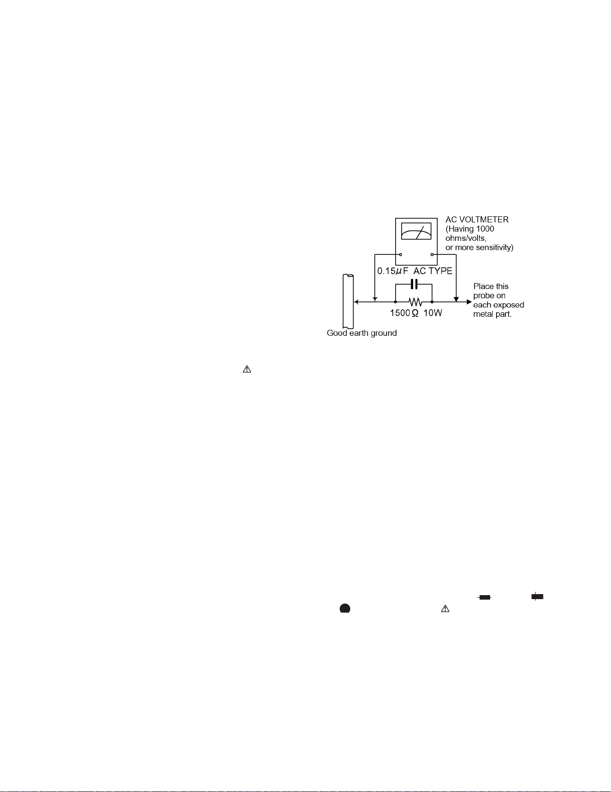
(5) Leakage shock hazard testing)
After reassembling the product, always perform an isolation
check on the exposed metal parts of the product (antenna
terminals, knobs, metal cabinet, screw heads, headphone
jack, control shafts, etc.) to be sure the product is safe to
operate without danger of electrical shock.
Do not use a line isolation transformer during this check.
• Plug the AC line cord directly into the AC outlet. Using a
"Leakage Current Tester", measure the leakage current
from each exposed metal parts of the cabinet, particularly any exposed metal part having a return path to the
chassis, to a known good earth ground. Any leakage current must not exceed 0.5mA AC (r.m.s.).
• Alternate check method
Plug the AC line cord directly into the AC outlet. Use an AC
voltmeter having, 1,000 ohms per volt or more sensitivity in
the following manner. Connect a 1,500 ohm 10W resistor
paralleled by a 0.15 µF AC-type capacitor between an
SECTION 1
exposed metal part and a known good earth ground.
Measure the AC voltage across the resistor with the AC
voltmeter.
Move the resistor connection to each exposed metal part,
particularly any exposed metal part having a return path to
the chassis, and measure the AC voltage across the resistor.
Now, reverse the plug in the AC outlet and repeat each
measurement. Voltage measured any must not exceed 0.75
V AC (r.m.s.). This corresponds to 0.5 mA AC (r.m.s.).
1.2 Warning
(1) This equipment has been designed and manufactured to
meet international safety standards.
(2) It is the leg al responsibility of the repairer to ensure that
these safety standards are maintained.
(3) Repairs must be made in accordance with the relevant
safety standards.
(4) It is essential that safety critical components a re replaced
by approved parts.
(5) If mains voltage selector is provided, check setting for local
voltage.
1.3 Caution
Burrs formed during molding may be left over on some parts
of the chassis.
Therefore, pay attention to such burrs in the case of preforming repair of this system.
1.4 Critical parts for safety
In regard with component parts appearing on the silk-screen
printed side (parts side) of the PWB diagrams, the parts that are
printed over with black such as the resistor ( ), diode ( )
and ICP ( ) or identified by the " " mark nearby are critical
for safety.
When replacing them, be sure to use the parts o f the same type
and rating as specified by the manufacturer. (Except the JC version)
1-2 (No.22013)
Page 3
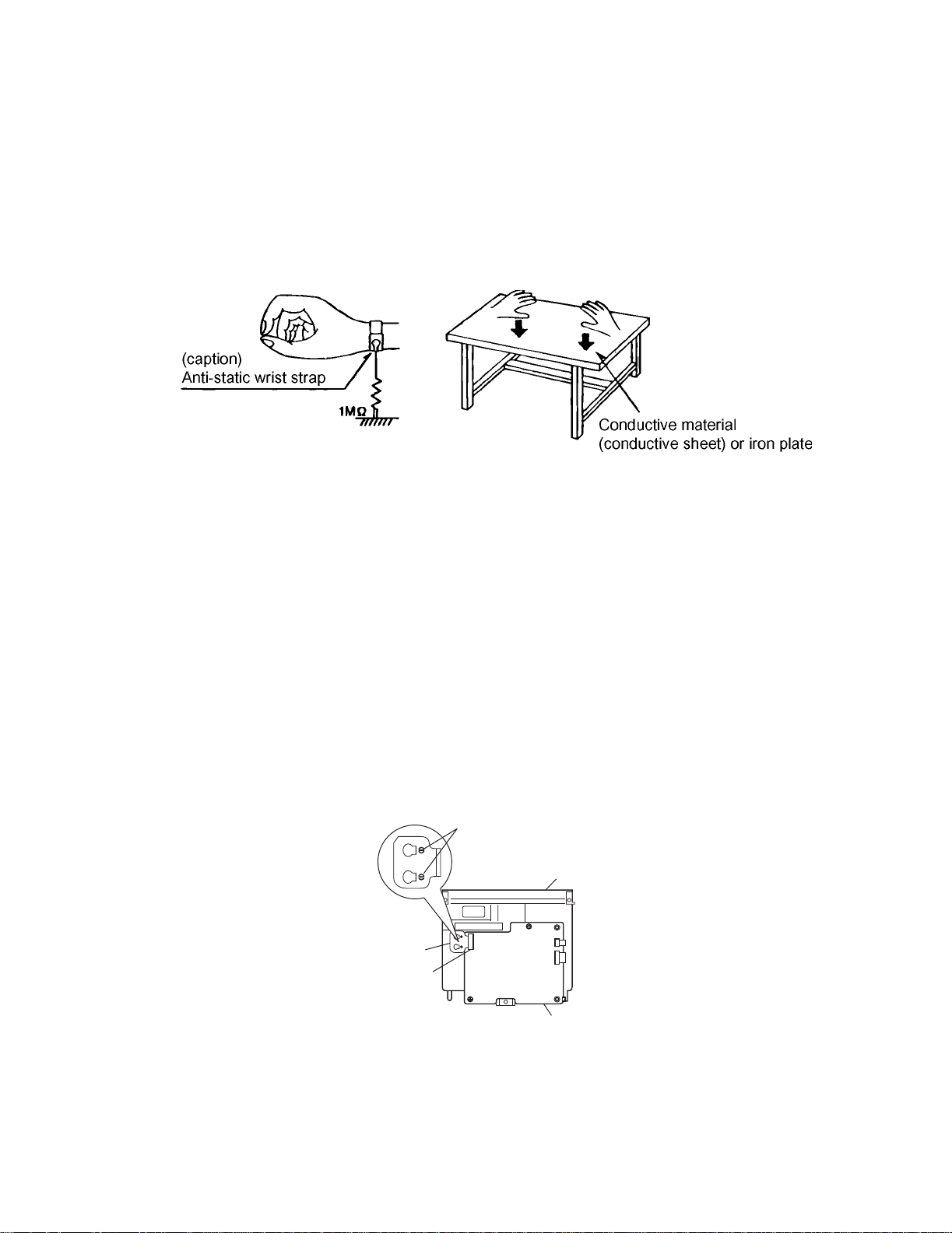
1.5 Preventing static electricity
Electrostatic discharge (ESD), which occurs when static electricity stored in the body, fabric, etc. is discharged,
can destroy the laser diode in the traverse unit (optical pickup). Take care to prevent this when performing repairs.
1.5.1 Grounding to preve nt damage by static electricity
Static electricity in the work area can destroy the optical pickup (laser diode) in devices such as DVD players.
Be careful to use proper grounding in the area where repairs are being performed.
(1) Ground the workbench
Ground the workbench by laying conductive material (such as a conducti ve sheet) or an iron plate over it before placing the
traverse unit (optical pickup) on it.
(2) Grou nd yourself
Use an anti-static wrist strap to release any static electricity built up in your body.
UX-A7DVD
(3) Handling the optical pickup
• In order to maintain quality during transport and before installatio n, both sides of the laser diod e on the replacement opti cal
pickup are shorted. After replacement, return the shorted parts to their original condition.
(Refer to the text.)
• Do not use a tester to check the condition of the laser diode in the optical pickup. The tester's internal power source can easily
destroy the laser diode.
1.6 Handling the traverse unit (optical pickup)
(1) Do not subject the traverse unit (optical pickup) to strong shocks, as it is a sensitive, complex unit.
(2) Cut off the shorted part of the flexible cable using nippers, etc. after replacing the optical pickup. For specific details, refer to the replace-
ment procedure in the text. Remove the anti-static pin whe n replac ing the traverse un it. Be careful not to take too long a time
when attaching it to the connector.
(3) Handle the flexible cable carefully as it may break when subjected to strong force.
(4) It is not possible to adjust the semi-fixed resistor that adjusts the laser power. Do not turn it.
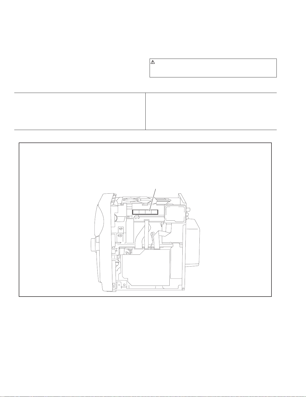
1.7 Attention when traverse unit is decomposed
*Please refer to "Disassembly method" in the text for the DVD pickup unit.
• Apply solder to the short land sections before the flexible wire is disconnected from the connector CN101 on the DVD servo board.
(If the flexible wire is disconnected without applying solder, the DVD pickup may be destroyed by static electricity.)
• In the assembly, be sure to remove solder from the short land sections after connecting the flexible wire.
Short lands
DVD mechanism assembly
Flexible wire
Connector
CN202
CN201
DVD servo board
(No.22013)1-3
Page 4
UX-A7DVD
1.8 Important for laser products
(1) CLASS 1 LASER PRODUCT
(2) DAN GER : Invisible laser radiation when open and inter
lock failed or defeated. Avoid direct exposure to beam.
(3) CAUTION : There are no serviceable parts inside the
Laser Unit. Do not disassemble the Laser Unit. Replace the
complete Laser Unit if it malfunctions.
(4) CAU TION : The compact disc player uses invisible laser
radiation and is equipped with safety switches which
prevent emission of radiation when the drawer is open and
the safety interlocks have failed or are de feated.
It is dangerous to defeat the safety switches.
(5) CAUTION : If safety switches malfunction, the laser is able
to function.
(6) CAUTION : Use of controls, adjustments or performance of
procedures other than those specified herein may result in
hazardous radiation exposure.
CAUTION
Please use enough caution not to see the beam directly
or touch it in case of anadjustment or operation check.
VARNING
Osynlig laserstrålning är denna del är öppnad och spårren är
urkopplad. Betrakta ej strålen.
VARO
Avattaessa ja suojalukitus ohitettaessa olet alttiina näkymättömälle lasersäteilylle. Älä katso säteeseen.
REPRODUCTION AND POSITION OF LABELS
ADVARSEL
Usynlig laserstråling ved åbning, når sikkerhedsafbrydere er
ude af funktion. Undgå udsasttelse for stråling.
ADVARSEL
Usynlig laserstråling ved åpning, når sikkerhetsbryteren er avslott. unngå utsettelse for stråling.
Caution label
1-4 (No.22013)
Page 5
SECTION 2
A
A
Disassembly method
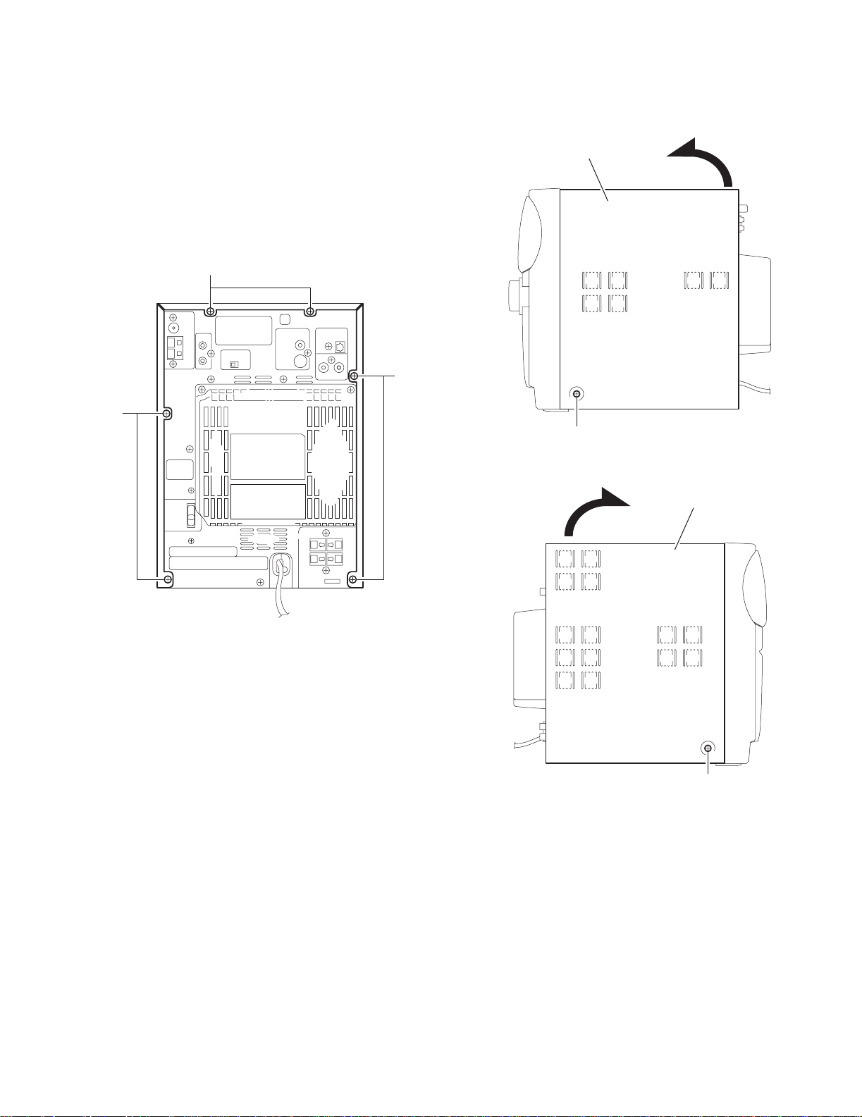
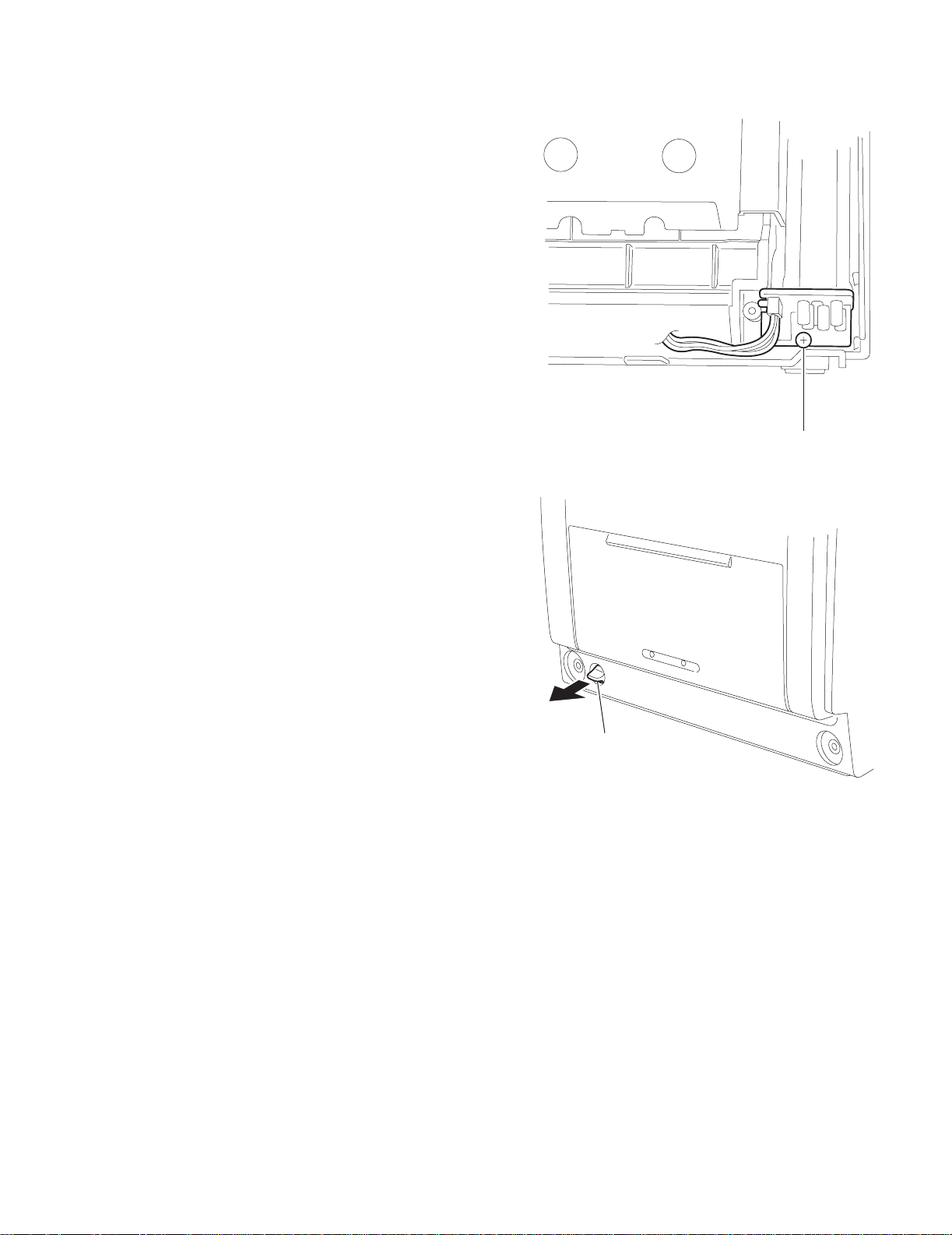
2.1 Main body
2.1.1 Removing the metal cover
(See Fig.1~3)
(1) Remove the six screws A on the back of the body.
(2) Remove the screw B on each side of the body.
(3) Detach the rear side of the metal cover upward while pull-
ing the lower sides outward.
A
UX-A7DVD
Metal cover
Fig.1
B
Fig.2
Metal cover
B
Fig.3
(No.22013)1-5
Page 6
UX-A7DVD
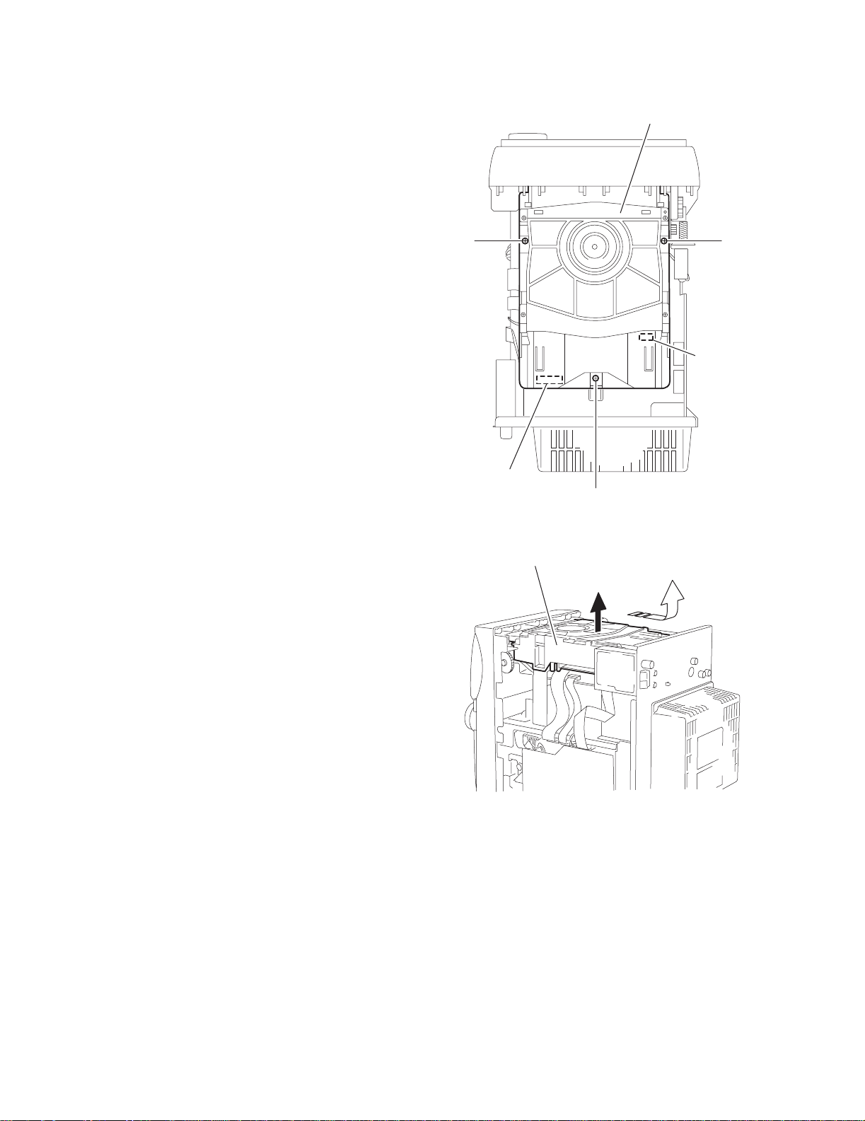
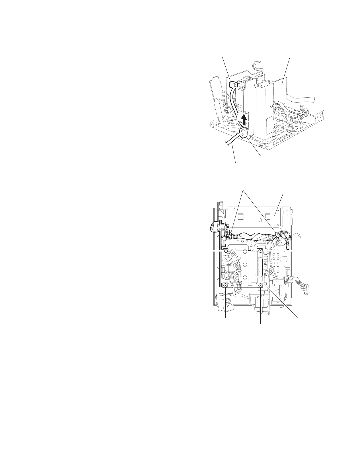
2.1.2 Removing the DVD mechanism assembly
(See Fig.4, 5)
• Prior to performing the following procedure, remove the metal
cover.
(1) Remo ve the three screws C attaching the DVD mecha-
nism assembly on top of the body.
(2) Disconnect connector CN502 and CN503 on the DVD ser-
vo board upward at the bottom of the DVD mechanism assembly.
Bring up the DVD mechanism assembly and remove backward.
DVD mechanism assembly
CC
CN502
CN503
C
Fig.4
DVD mechanism assmbly
Fig.5
1-6 (No.22013)
Page 7
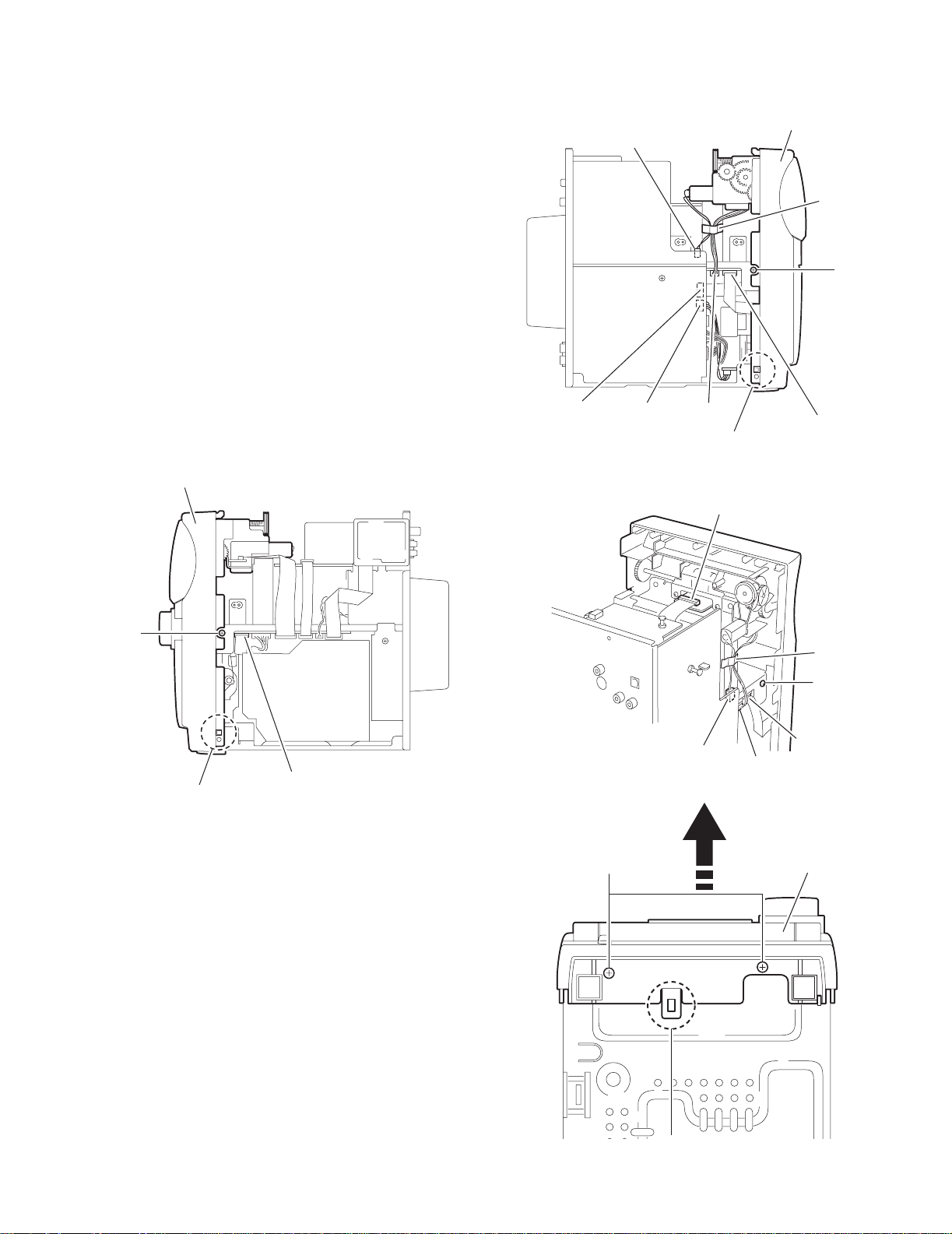
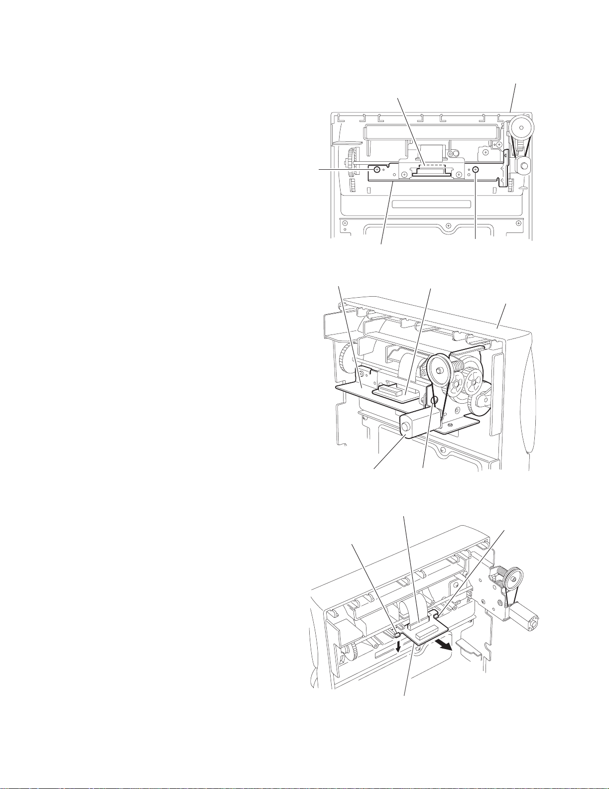
2.1.3 Removing the front panel assembly
r
(See Fig.6~9)
• Prior to performing the following procedure, remove the metal
cover and the DVD mechanism assembly.
(1) Disconnect the card wire from connector CN705 on the mi-
crocomputer board in the center of the right side of the
body.
(2) Disconn ect the card wire from connector CN301,and the
wires from connector CN300 and CN710 on the main
board in the center of the left side of the body.
(3) Disconn ect the card wire from connector CN704, and the
wire from CN703 on the microcomputer board.
ATTENTION:
When disconnecting the wires from CN703 and CN710,
remove the spacer attaching the wires.
(4) Disconnect the card wire from connector CN442 on the FL
connection board on top of the body.
(5) Remove the screw D on each side of the body.
(6) Remove the two screws E on the bottom of the body.
(7) Release the joint a on the bottom and the two joints b on
the right and left sides of the body using a screwdriver. Re-
move the front panel assembly toward the front.
Front panel assembly
Main board
CN710
CN301 CN300
Front panel assembly
CN703
Fig.7
FL connection board
CN442
Micro computer board
b
UX-A7DVD
Spacer
D
CN704
D
Space
D
CN710
b
Micro computer board
CN705
Fig.6
Fig.8
E
CN703
Front panel assembly
CN704
a
Fig.9
(No.22013)1-7
Page 8
UX-A7DVD
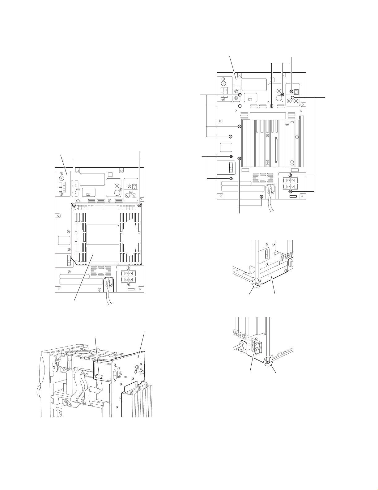
2.1.4 Removing the rear cover / rear panel
(See Fig.10~14)
• Prior to performing the following procedure, remove the metal
cover and the DVD mechanism assembly.
(1) Remove the two screws F on the back of the body.
REFERENCE:
There is no need to remove the metal cover.
(2) Disconnect the card wire from connector CN1 on the tuner
pack on the right side of the body.
(3) Remove the twelve screws G and the two screws H on the
back of the body.
(4) Release the two joints c on the lower right and left sides of
the rear panel.
REFERENCE:
The rear panel with the tuner pack comes off.
G
Rear cover
G
G
Rear panel
Rear cover
Fig.10
F
H
G
c
Fig.12
Rear panel
Fig.13
1-8 (No.22013)
Tuner pack
CN1
Fig.11
Rear panel
Rear panel
Fig.14
c
Page 9
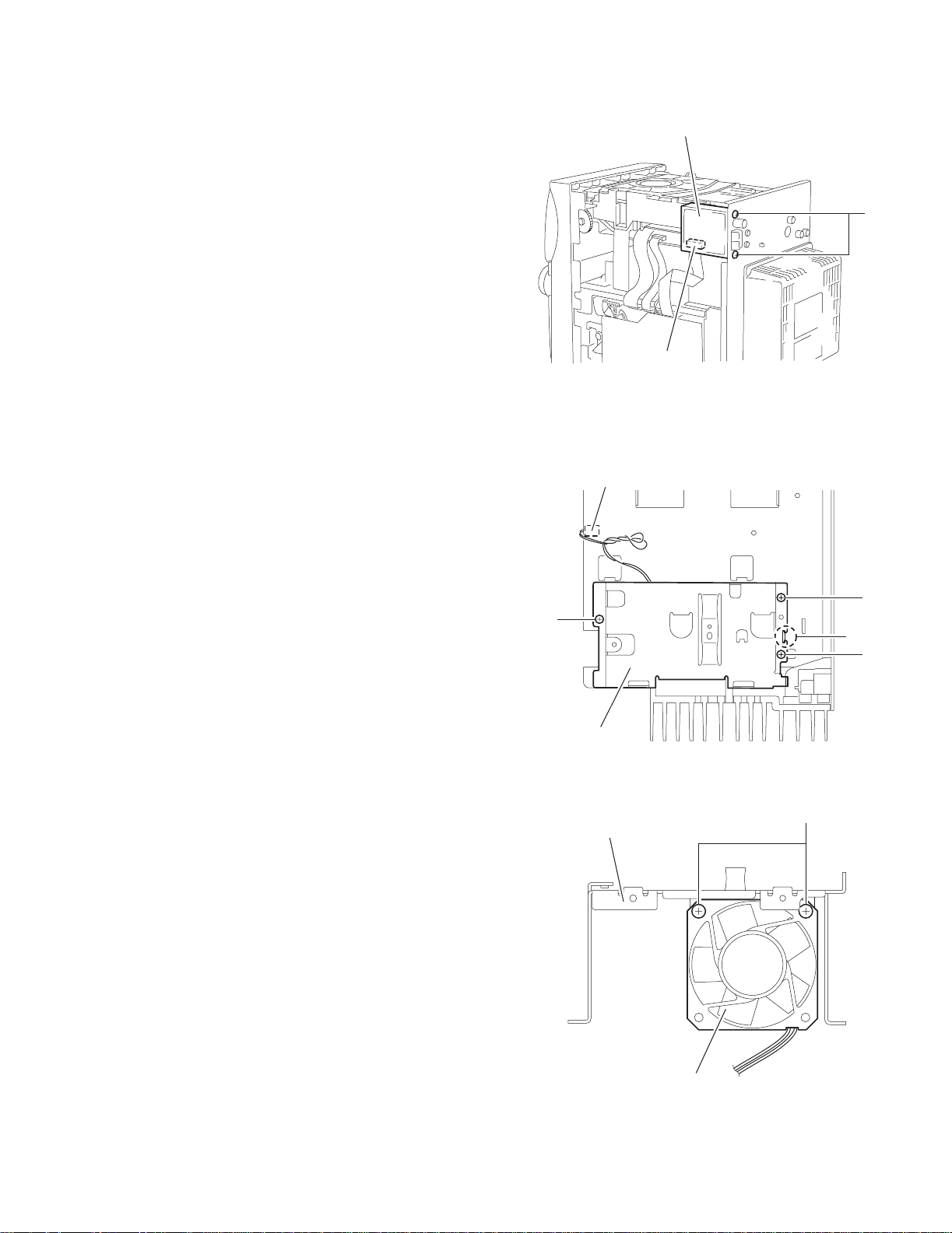
2.1.5 Removing the tuner pack
(See Fig.15)
• Prior to performing the following procedure, remove the metal
cover.
(1) Disconnect the card wire from connector CN1 on the tuner
pack on the right side of the body.
(2) Remove the two screws I on the back of the body.
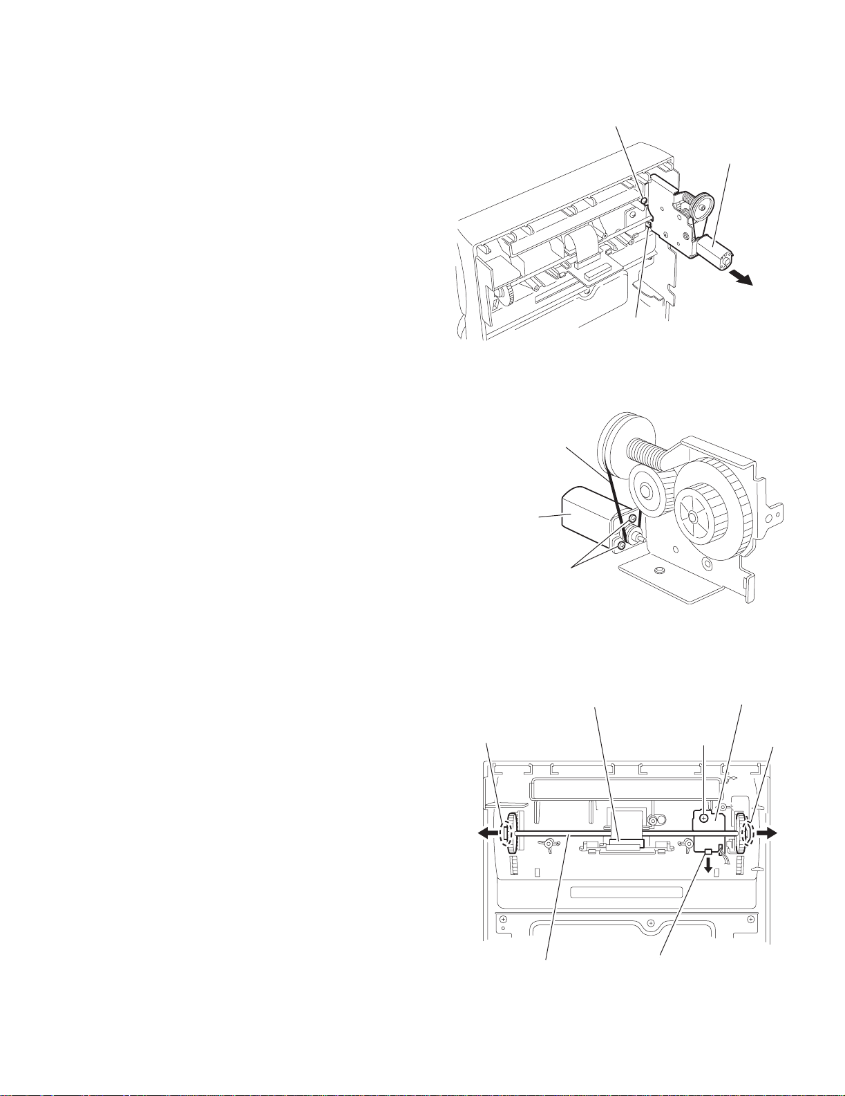
2.1.6 Removing the fan
(See Fig.16,17)
• Prior to performing the following procedure, remove the metal
cover, the DVD mechanism assembly, the rear cover/rear panel and the DVD relay board.
(1) Disconn ect the wire from connector CN711 on the micro-
computer board on the right side of the body.
(2) Remove the three screws J attaching the fan bracket on
top of the body and release the joint d.
(3) Remove the two screws K attaching the fan.
UX-A7DVD
Tuner pack
I
CN1
Fig.15
Micro computer board
CN711
J
Fan bracket
Fan bracket
J
d
J
Fig.16
K
Fan
Fig.17
(No.22013)1-9
Page 10
UX-A7DVD
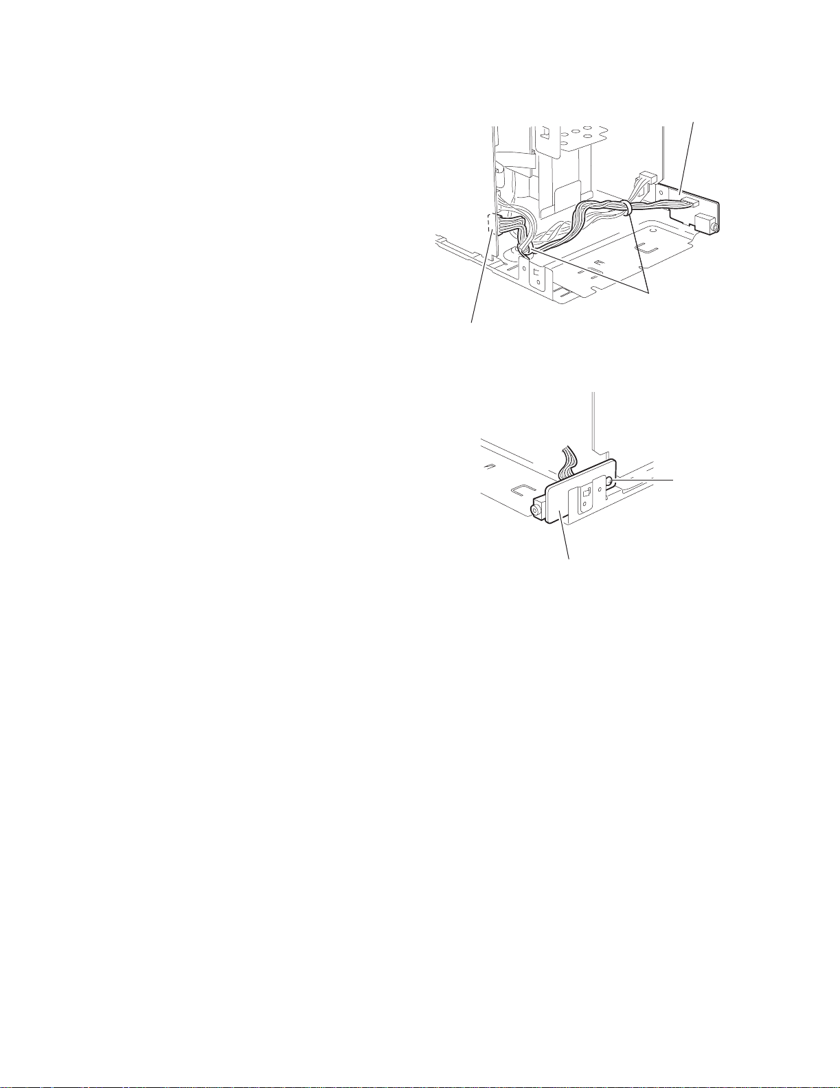
2.1.7 Removing the headphone board
(See Fig.18, 19)
• Prior to performing the following procedure, remove the metal
cover, the DVD mechanism assembly and the front panel assembly.
(1) Disco nnect the wire from connector CN310 on the main
board on the left side of the body.
(2) Release the wires from the two clamps on the bottom chas-
sis.
(3) Remov e the screw L attaching the headphone board on
the right side of the body.
Headphone board
Clamp
Main board
CN310
Fig.18
Headphone board
Fig.19
L
1-10 (No.22013)
Page 11
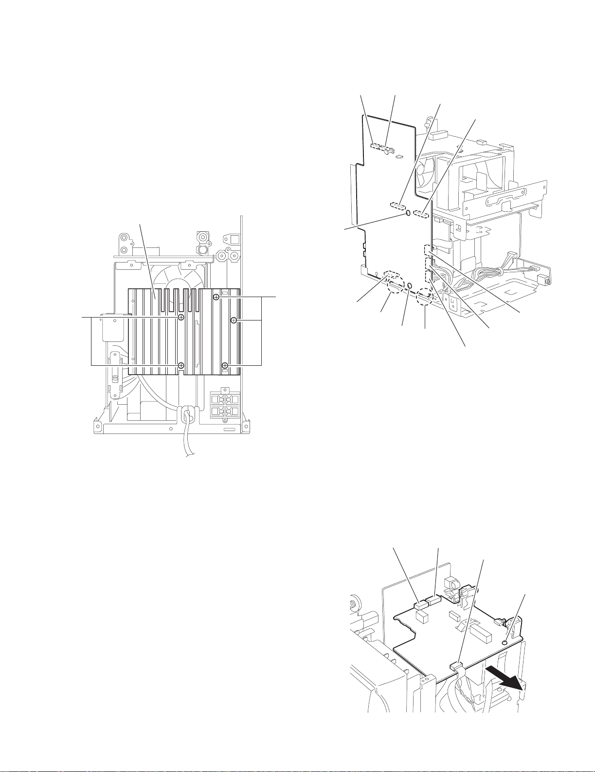
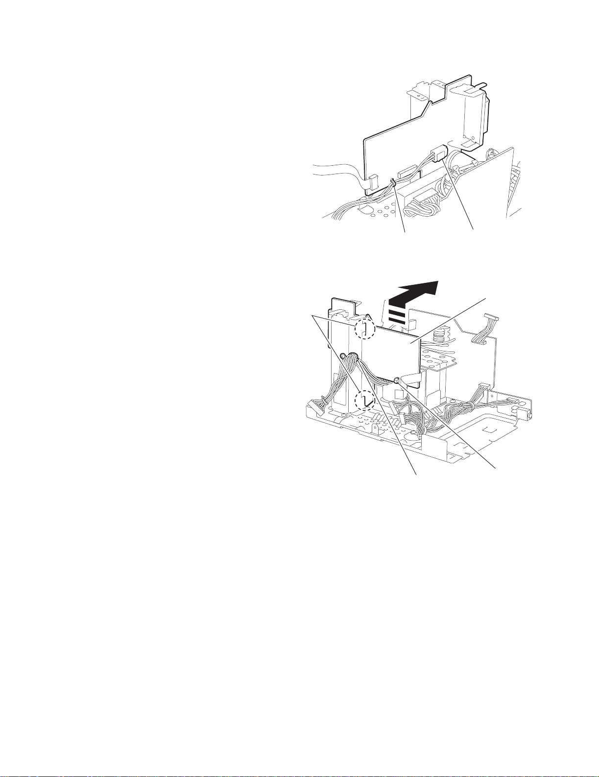
2.1.8 Removing the main board
(See Fig.20, 21)
• Prior to performing the following procedure, remove the metal
cover, the DVD mechanism assembly, the front panel assembly and the rear cover/ rear panel.
(1) Remove the two screws M and the three screws N, and
then remove the heat sink.
(2) Disconn ect the wires from connector CN307 and CN310,
the card wire from CN312 on the main board on the left side
of the body.
(3) Remove the screw O and P attaching the main board.
(4) Disconnect connector CN303, CN304, CN305 and CN306
on the main board. Release the two joints e at the bottom.
(5) Draw out the main board and disconnect the wire from con-
nector CN311.
Heat sink
Main board
CN303
O
UX-A7DVD
CN304
CN305
CN306
N
M
Fig.20
2.1.9 Removing the DVD relay board
(See Fig.22)
• Prior to performing the following procedure, remove the metal
cover, the DVD mechanism assembly and the rear cover/ rear
panel.
(1) Disconnect the card wire from connector CN515 on the
DVD relay board.
(2) Remove the screw Q attaching the DVD relay board on top
of the body.
(3) Disconnect connector CN511 and CN512 on the DVD relay
board.
CN311
e
DVD relay baoard
CN512 CN511
P
e
Fig.21
CN312
CN307
CN310
CN515
Q
Fig.22
(No.22013)1-11
Page 12
UX-A7DVD
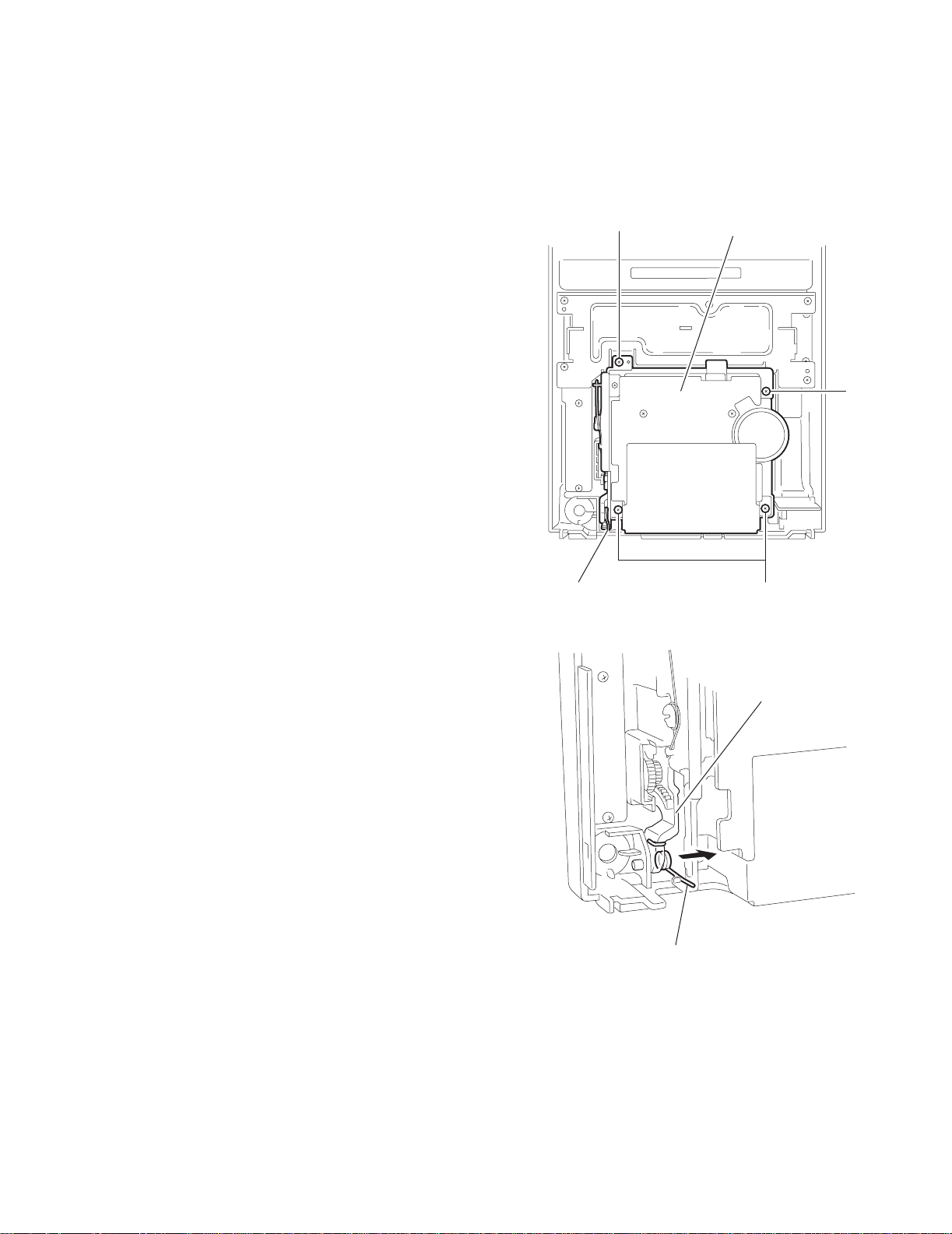
2.1.10 Removing the base chassis / microcomputer board
(See Fig.23~25)
• Prior to performing the following procedure, remove the metal
cover, the DVD mechanism assembly, the front panel assembly, the rear cover/ rear panel, the main board and the DVD relay board.
(1) Di sconnect the wires from connector CN701 and CN711
on the microcomputer board in the center of the right side
of the body.
(2) Remove the screw R attaching the voltage selector board.
(3) Re move the two screws S attaching the ba se chassis on
top of the body.
(4) Remo ve the two screws T attaching the microcomputer
board and release the two joints f .
Base chassis
Base chassis
S
Microcomputer board
CN701
CN711
Fig.23
Voltage selector board
R
Fan bracket
Microcomputer
board
Fig.24
T
1-12 (No.22013)
f
Fig.25
Page 13
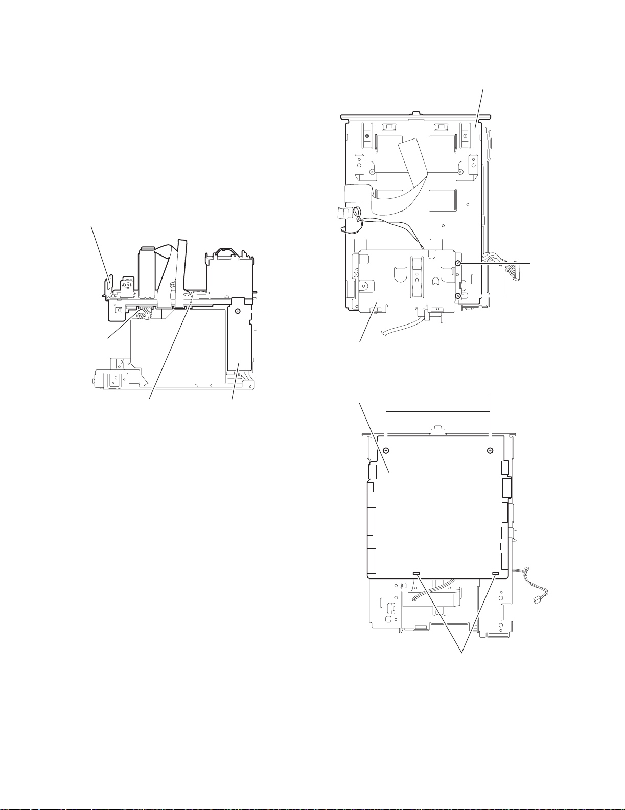
2.1.11 Removing the power transformer assembly
r
(See Fig.26, 27)
• rior to performing the following procedure, remove the metal
cover, the DVD mechanism assembly, the front panel assembly, the rear cover/ rear panel, the main board and the base
chassis.
(1) Mo ve the power cord stopper upward on the back of the
body and remove. Disconnect the power cord from connector CN901 on the power transformer board.
REFERENCE:
The power cord can be removed alone.
(2) Remove the four screws U and release the wires from the
two clamps on the bottom chassis.
Power transformer board
CN901
Power cord
UX-A7DVD
Power amplifier board
Power cord stopper
Fig.26
U
Clamp
U
Fig.27
Bottom chassis
U
Power transforme
assembly
(No.22013)1-13
Page 14
UX-A7DVD
2.1.12 Removiing the power amplifier board
(See Fig.28, 29)
• Prior to performing the following procedure, remove the metal
cover, the DVD mechanism assembly, the front panel assembly, the rear cover/ rear panel, the main board and the base
chassis.
(1) Di sconnect the wire from connector CN111 on the power
amplifier board.
(2) Remove the band attaching the wire to the power amplifier
board.
(3) Release the wires from the clamp.
(4) Move the power amplifier board upward to release the two
joints g and remove to the right.
Band
Power amplifier board
CN111
Fig.28
Power amplifier
board
g
Clamp
Fig.29
Band
1-14 (No.22013)
Page 15
2.2 Front panel assembly
• Prior to performing the following procedure, remove the metal
cover, the DVD mechanism assembly and the front panel assembly.
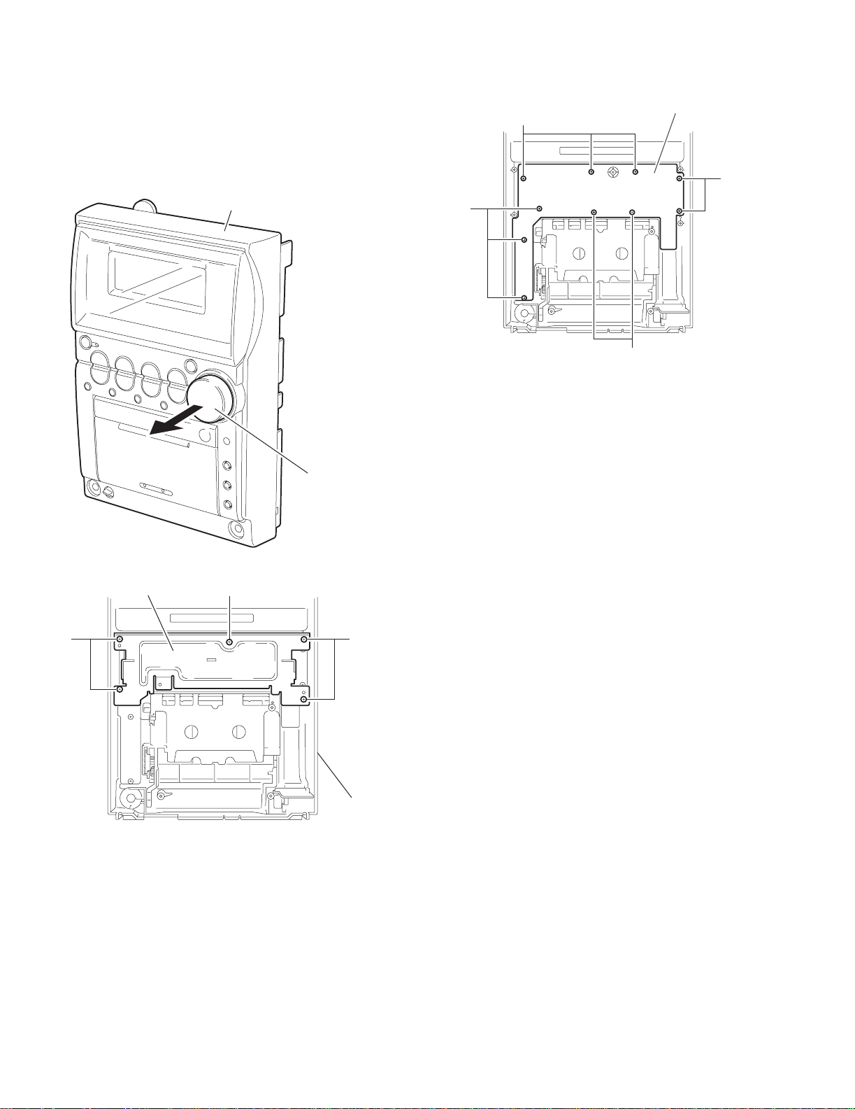
2.2.1 Removing the cassette mechanism assembly
(See Fig.30, 31)
(1) Remove the spring attached to the cassette door on the
back of the front panel.
(2) Remove the fo ur screws V atta ch ing th e cassette mecha-
nism assembly.
V
UX-A7DVD
Cassette mechanism
assembly
V
Spring
V
Fig.30
Cassette door
Spring
Fig.31
(No.22013)1-15
Page 16
UX-A7DVD
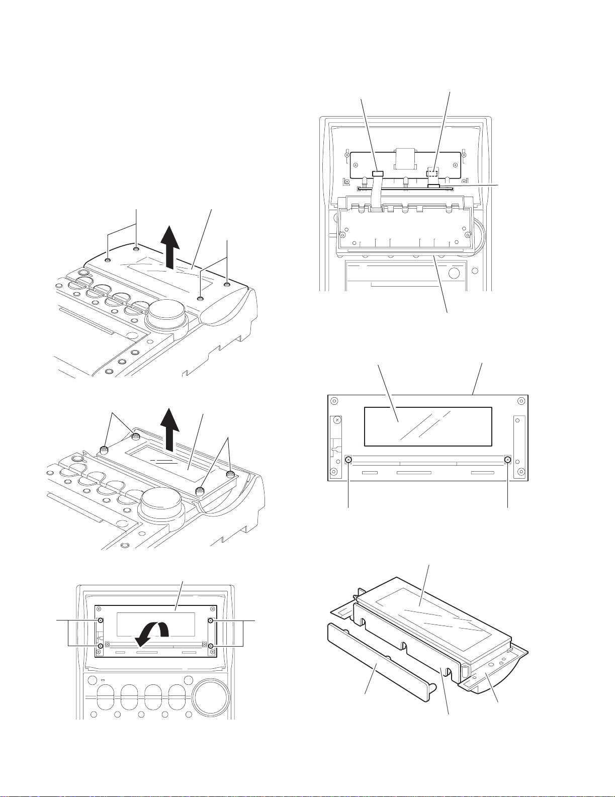
2.2.2 Removing the key board
(See Fig.32~34)
• Prior to performing the following procedure, remove the cas-
sette mechanism assembly.
(1) Pull out the volume knob on the front side of the front panel.
(2) Remove the five screws W attaching the bracket (1) on the
back of the front panel.
(3) Remove the ten screws X attaching the key board.
Front panel assembly
X
Key board
X
X
X
Fig.34
Volume knob
Fig.32
Bracket(1)
W
WW
Front panel
Fig.33
1-16 (No.22013)
Page 17
2.2.3 Removing the MIC board
(See Fig.35, 36)
• Prior to performing following procedure, remove the cassette
mechanism assembly
(1) Remove the screw Y attaching the MIC board.
(2) Pull out the mic volume knob on the front side of the front
panel.
UX-A7DVD
Y
Mic volume knob
Fig.35
Fig.36
(No.22013)1-17
Page 18
UX-A7DVD
2.2.4 Removing the FL connection board
(See Fig.37~39)
(1) Remove the two screws Z and the screw AA attaching the
bracket (2) on the back of the front panel.
(2) Disconnect the card wire from connector CN441 on the FL
connection board.
(3) Push the two joint tabs h downward to release and pull out
the FL connection board.
Z
FL connection board
CN441
Front panel
Bracket(2)
Bracket(2)
Drive motor assembly
FL connection board
CN441
h
Z
Fig.37
Front panel
AA
Fig.38
h
1-18 (No.22013)
FL connection board
Fig.39
Page 19
2.2.5 Removing the drive motor assembly
(See Fig.37,38,40)
(1) Remove the two screws Z and the screw AA attaching the
bracket (2) on the back of the front panel.
(2) Remove th e screw AB attaching the drive motor assem-
bly. Release the joint tab i and pull out the drive motor assembly.
2.2.6 Removing the belt / drive motor
(See Fig.41)
• Prior to performing the following procedure, remove the drive
motor assembly.
(1) Remove the belt from the pulley.
(2) Remove the two screws AC attaching the drive motor.
UX-A7DVD
AB
Drive motor assembly
i
Fig.40
Belt
2.2.7 Removing the switch board.
(See Fig.42)
• Prior to performing the following procedure, remove the brack-
et (2) / drive motor assembly.
(1) Disconnect the card wire from connector CN441 on the FL
connection board (Do not fold down the card wire).
(2) Release the joint j and k in order on the right and left sides
of the shaft gear.
(3) Remove the screw AD attaching the switch board and re-
lease the joint tab k.
Drive motor
AC
Fig.41
FL connection board
CN441
kj
Switch board
AD
Shaft gear
Tab k
Fig.42
(No.22013)1-19
Page 20
UX-A7DVD
A
2.2.8 Removing the FL display section
(See Fig.43~48)
(1) Remove the four screws AE attaching the case cover on
the front panel.
(2) Pull out the FL panel from the four joint bosses m on the FL
display cover.
(3) Remo ve the four screws AF attaching the FL display cov-
er. Disconnect the card wire from connector CN451 and
CN452 on the FL relay board.
(4) Remove the two screws AG attaching the FL display on
the FL display cover.
(5) The FL boa rd and the lens come off from the FL display
section.
AE
Case cover
AE
FL relay board
CN451
CN452
LED board
CN461
m
Fig.43
Fig.44
FL display cover
FL panel
m
FL display cover
Fig.46
FL display section
FL display cover
AG AG
Fig.47
FL display section
1-20 (No.22013)
FAF
LED board
Fig.45
FL board
Fig.48
Lens
Page 21
2.2.9 Removing the FL relay board
A
(See Fig.49)
• Prior to performing the following procedure, remove the FL dis-
play cover.
(1) Disconnect the card wire from connector CN453 on the FL
relay board.
(2) Remove the two screws AH attaching the FL relay board.
FL relay board
CN453
HAH
UX-A7DVD
Fig.49
(No.22013)1-21
Page 22
UX-A7DVD
A
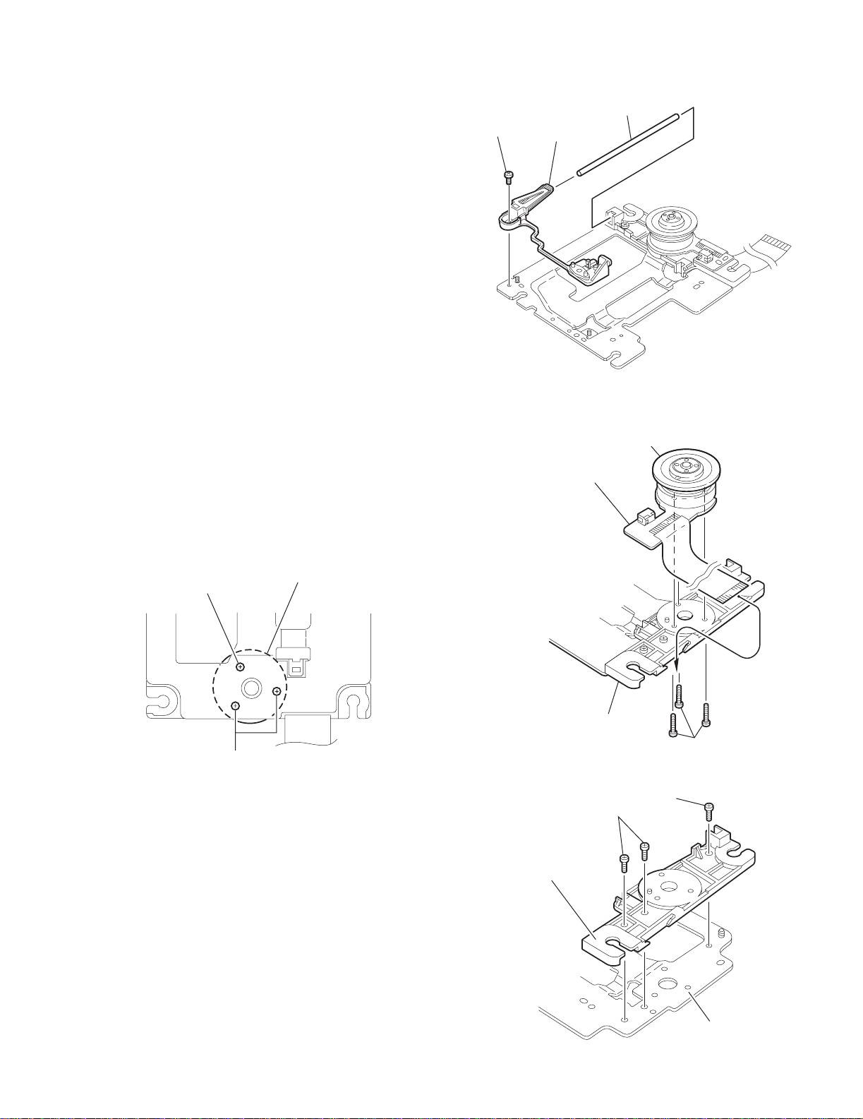
2.3 DVD loading mechanism section
2.3.1 Removing the clamper assembly
(See Fig.1)
(1) Re move the four screws A attaching the cla mper assem-
bly.
(2) Move the clamper assembly in the direction of the arrow to
release the joint a on each side, and remove.
ATTENTION:
When reassembling, reattach the clamper assembly at the two
joints a.
2.3.2 Removing the tray
(See Fig.2, 3)
• Prior to performing the following procedure, remove the
clamper assembly.
(1) Push the part b of the slide cam through the slot on the left
side of the loading base.
(2) Draw out the tray toward the front.
ATTENTION:
When reattaching the tray, move the part c of the slide cam to
the right (See Fig.3).
A
a
a
A
Clamper
assembly
A
Fig.1
Loading base
Tray
b
Fig.2
c
Slide cam
Fig.3
1-22 (No.22013)
Page 23
2.3.3 Removing the servo control board
(See Fig.4)
CAUTION:
Solder the sorting round point before disconnecting the flexible
wire extending from the pickup. If you do not follow this instruction, the pickup may be damaged.
(1) Solder the sorting round point on the flexible wire connect-
ed to connector CN101 on the servo control board.
(2) Disconnect the flexible wire from connector CN101 on the
servo control board.
(3) Disconnect the card wires from connector CN201 and
CN202 on the servo control board. Release the two joints
d.
(4) Move the servo control board in the direction of the arrow
to release the joint e, and remove upward.
CAUTION:
Unsolder the sorting round point after reassembling.
2.3.4 Removing the traverse mechanism assembly
(See Fig.5, 6)
• Prior to performing the following procedure, remove the
clamper assembly, the tray and the servo control board.
(1) Remove the four screws B attaching the traverse mecha-
nism assembly.
CAUTION:
When reassembling, get the flexible wire extending from the
spindle motor board through the slot f of the elevator.
CN201
d
e
Servo control board
B
Traverse mechanism
assembly
UX-A7DVD
Sorting round point
CN101
Flexible wire
d
CN202
CN101
Fig.4
B
B
B
Traverse mechanism
assembly
B
Fig.5
B
f
Fig.6
(No.22013)1-23
Page 24
UX-A7DVD
2.3.5 Removing the elevator
(See Fig.7,8)
• Prior to performing the following procedure, remove the
clamper assembly, the tray, the servo control board and the
traverse mechanism assembly.
(1) Pul l the two tabs g outward and release the two shafts of
the elevator.
ATTENTION:
When reassembling, fit the two shafts on the front side of the
elevator into the grooves h of the slide cam.
Elevator
Tab g
Elevator
Elevator
Loading base
Shaft
Fig.7
Fig.8
Elevator
Tab g
Slide cam
h
1-24 (No.22013)
Page 25
2.3.6 Removing the motor assembly
(See Fig.9, 10)
• Prior to performing the following procedure, remove the
clamper assembly, the tray, the servo control board, the
traverse mechanism assembly and the elevator.
(1) Remove the belt from the pulley.
(2) Remove the screw C attaching the loading motor.
(3) Remove the screw D attachin g the motor board on the
back of the loading assembly.
(4) Release the tab i fixing the motor board and remove the
motor assembly.
UX-A7DVD
Belt
C
Loading motor pulley
Fig.9
Tab i
Motor assembly
Motor board
Fig.10
D
Loading assembly
(No.22013)1-25
Page 26
UX-A7DVD
p
2.3.7 Removing the idle gear/ pulley gear/ middle gear/ slide cam
(See Fig.11~13)
• Prior to performing the following the procedures, remove the
clamper assembly, the tray, the servo control board, the
traverse mechanism assembly, the elevator and the motor assembly.
(1) Push the two tabs j attaching the idle gear inward and pull
out the idle gear.
(2) Remove the screw E attaching the pulley gear bracket.
Move the pulley gear bracket in the direction of the arrow
and remove upward.
(3) Pull out the pulley gear.
(4) Move the sli de cam in the di re ction of th e arrow to relea se
the two joints k and remove upward.
(5) Remove the middle gear.
Pulley gear bracket
Pulley gear
Motor assembly
E
Pulley gear bracket
E
Idle gear
Fig.11
Idle gear
Tab j
Pulley gear
Pulley gear
1-26 (No.22013)
OK.
YES
Fig.12
NO
Change the picku
Slide cam
Fig.13
Middle gear
Loading base
Page 27
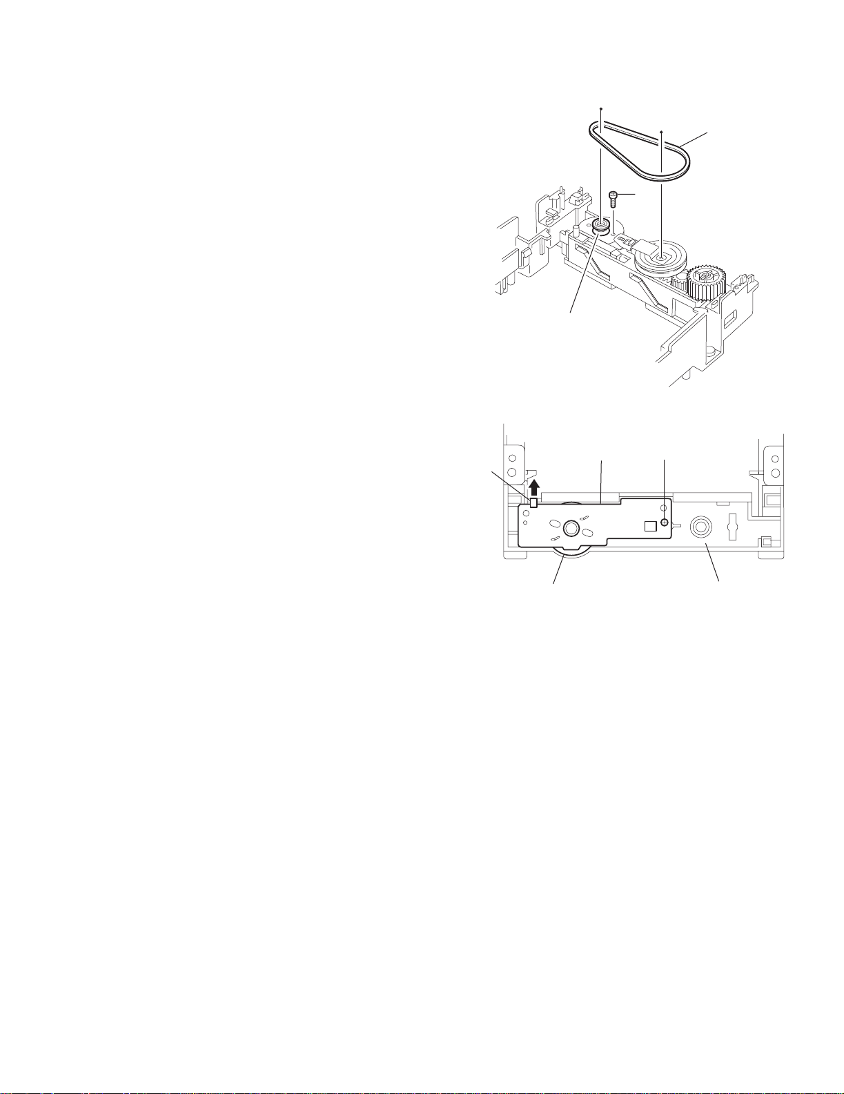
2.4 DVD traverse mechanism assembly
2.4.1 Removing the feed motor assembly
(See Fig.14)
(1) Unsolder the two soldering l on the spindle motor board.
(2) Remove the two screws F attaching the feed motor assem-
bly.
UX-A7DVD
Feed motor assembly
F
2.4.2 Removing the feed motor
(See Fig.14~16)
• Prior to performing the following procedure, remove the feed
motor assembly.
(1) Remove the screw G and the spring.
CAUTION:
When reassembling, attach the spring correctly to press
the feed gear M and E.
(2) Remove the feed gear M.
(3) Pull out the feed gear E and the lead screw.
(4) Remove the two screws H and the feed motor.
CAUTION:
When reassembling, set the two wires extending from
the feed motor to the notch m of the feed holder as
shown in Fig.14.
F
Pickup
m
l
Spindle motor board
Feed motor
Spindle motor
Fig.14
Lead screw
Feed gear M
Feed gear E
Fig.15
Spring
G
Feed motor
H
Fig.16
(No.22013)1-27
Page 28
UX-A7DVD
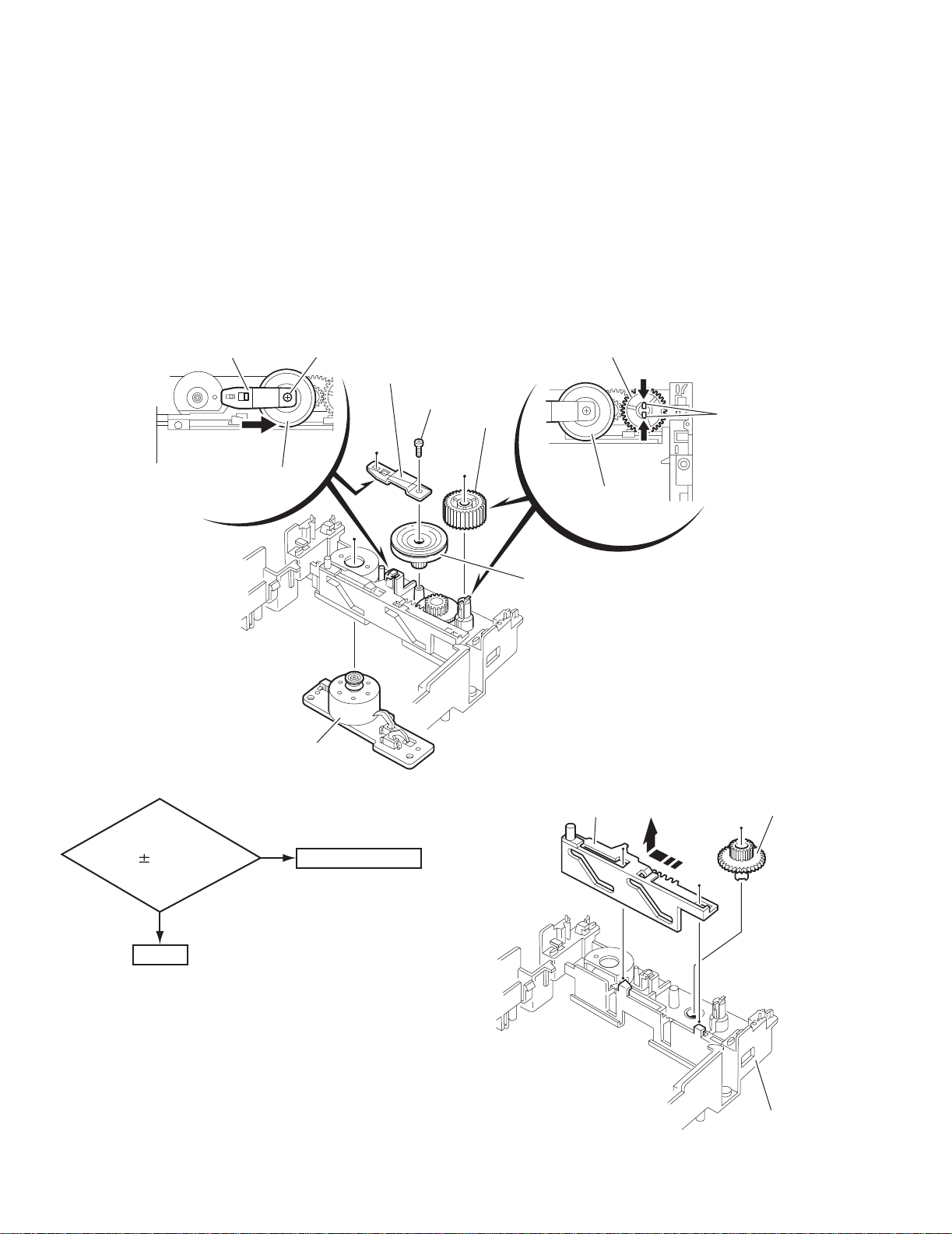
2.4.3 Removing the pickup
(See Fig.17~19)
• Prior to performing the following procedure, remove the feed
motor assembly.
(1) Remove the screw l, the T spring(S) and the shaft holder
with the plate.
ATTENTION:
When reassembling, reattach the T spring (s) correctly to
press the shaft
(2) Detach the part n of the shaft upward and move the part o
in the direction of the arrow, then remove the shaft from the
spindle base.
(3) Release the joint p in the direction of the arrow.
(4) Pul l out the shaft from the pickup.
(5) Remove the two screws J attaching the actuator.
(6) Re lease the joint of the actuato r and the lead spring, and
pull out the lead spring.
ATTENTION:
When reattaching the pickup, attach the spring under the
shaft (See fig.19)
I
Plate
T spring(S)
p
Pickup
n
Fig.17
Spindle base
o
Shaft holder
Pickup
J
Actuator
Actuator
Lead spring
Lead spring
Shaft
Fig.18
Pickup
1-28 (No.22013)
Shaft
Spring
Fig.19
Page 29
2.4.4 Removing the shaft holder/ shaft
(See Fig.20)
• Prior to performing the following procedure, remove the feed
motor assembly and the pickup.
(1) Remove the screw K attaching the shaft holder.
(2) Remove the shaft.
2.4.5 Removing the spindle motor assembly
(See Fig.21~23)
• Prior to performing the following procedure, remove the feed
motor assembly, the pickup, the shaft and the shaft holder.
(1) Turn over the mechanism base and remove the three
screws L attaching the spindle motor assembly.
ATTENTION:
When reassembling, set the card wire extending from
the spindle motor board to the notch of the spindle base.
(2) Remove the three screws M and the spindle base.
K
Shaft holder
Spindle motor board
UX-A7DVD
Shaft
Fig.20
Spindle motor assembly
L
Spindle motor
Spindle base
L
L
Fig.21
Spindle base
M
Fig.22
M
Fig.23
Mechanism base
(No.22013)1-29
Page 30
UX-A7DVD
2.5 Cassette mechanism assembly section
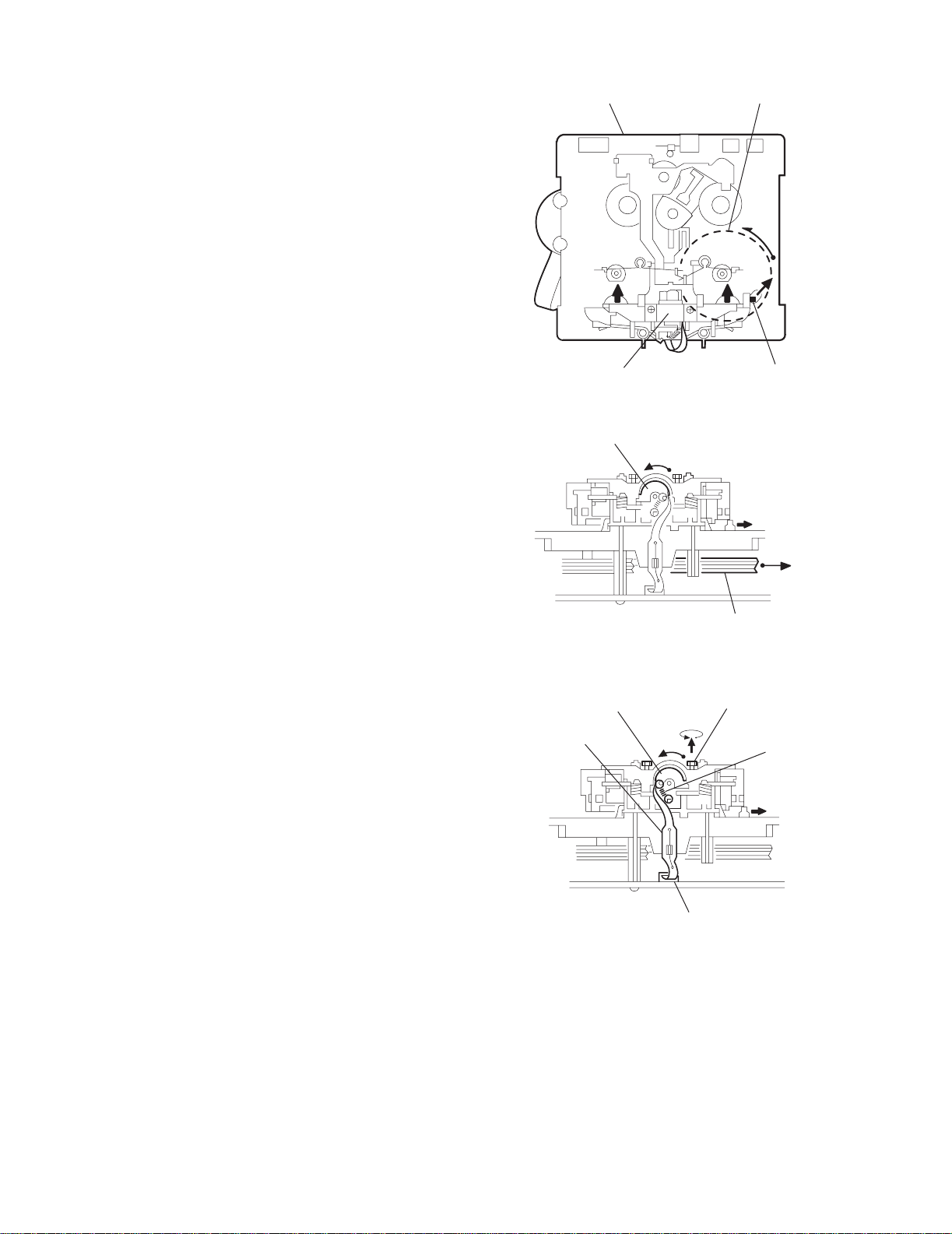
2.5.1 Removing the Play/Record & Clear head
(See Fig.1~3)
(1) W hile moving the trigger arm o n the right side o f the head
mount in the direction of the arrow, turn the flywheel R
counterclockwise until the head mount comes ahead and
clicks.
(2) The head turns counterclockwise a s you turn the flyw heel
R counterclockwise(See Fig.2 and 3).
(3) Di sconnect the flexible wire from connector CN31 on the
head amplifier & mecha control board.
(4) Re mo v e the spring from the back of the head.
(5) Loosen the azimuth screw for reversing attaching the head.
(6) Remove the head on the front side of the head mount.
Cassette mechanism assembly
Fig.1
Head
Fly wheelR
Trigger armHead mount
Flexible wire
Fly wheel R
Fig.2
Azimuth screw
Head
for reversing
Spring
CN31
Head amplifer & mecha control board
Fig.3
1-30 (No.22013)
Page 31

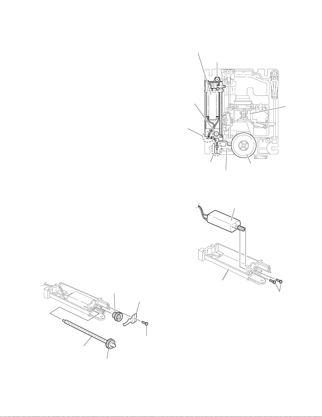
2.5.2 Removing the head amplifier & mechanism control board
(See Fig.4)
(1) Turn over the cassette mechanism assembly and remove
the three screws A attaching the head amplifier & mechanism control board.
(2) Disconn ect the flexible wire from connector CN31 on the
head amplifier & mechanism control board.
(3) Disconnect connector CN32 of the head amplifier & mech-
anism control board from connector CN1 on the reel pulse
board.
REFERENCE:
If necessary, unsolder the 4 pin wire soldered to the main motor.
Head amplifier & mecha control board
CN32
A
UX-A7DVD
2.5.3 Removing the main motor
(See Fig.4~7)
(1) Remove the two screws B .
(2) Half raise the motor and remove the capstan belt from the
motor pulley.
ATTENTION:
Be careful to keep the capstan belt from grease. When reassembling, refer to Fig.6 and 7 for attaching the capstan belt.
Main motor assembly
Capstan belt
CN31
Flexible wire
B
A
4pin wire
Main motor assembly
Fig.4
Main motor
assembly
Motor pulley
Fig.5
Capstan belt
Capstan belt
Fig.6
Main motor assembly
Fly wheel
Motor pulley
Fig.7
(No.22013)1-31
Page 32

UX-A7DVD
2.5.4 Removing the flywheel
(See Fig.8, 9)
• Prior to performing the following procedure, remove the head
amplifier & mechanism control board and the main motor assembly.
(1) From the front side of the cassette mechanism, remove the
slit washers attaching the capstan shaft L and R. Pull out
the flywheels backward.
Fly wheel R Fly wheel L
Fig.8
Fly wheel R
Capstan shaft R Capstan shaft L
2.5.5 Removing the reel pulse board and solenoid
(See Fig.10)
• Prior to performing the following procedure, remove the head
amplifier & mechanism control board.
(1) Remove the screw C.
(2) Re lease the tab a, b, c, d and e reta ining the reel pulse
board.
a
Solenoid
Fly wheel L
Slit washer
Fig.9
(3) Re lease the ta b f and g attaching the so lenoid on the reel
pulse board.
(4) The reel pulse board and the solenoid come off.
bc
d
Reel pulse board
1-32 (No.22013)
fg
C
e
Fig.10
Page 33

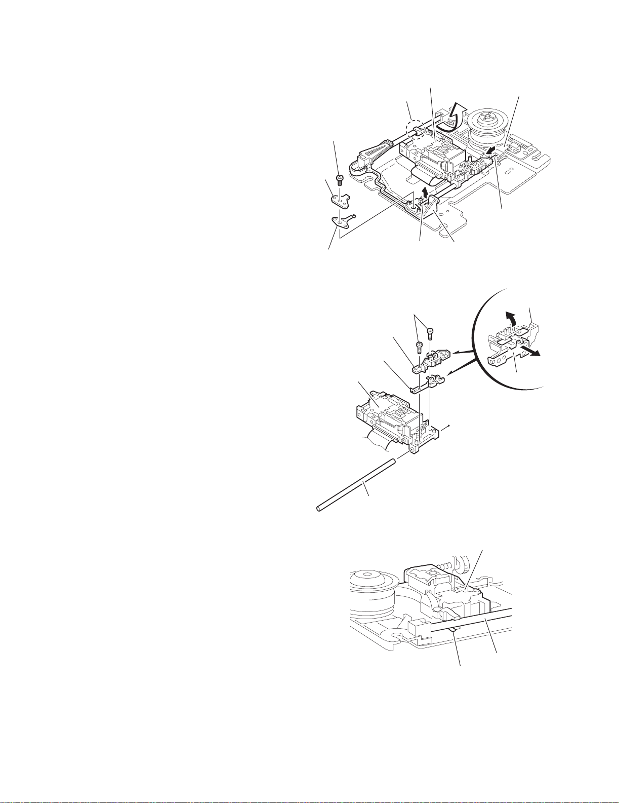
2.5.6 Reattaching the Play/ Record & Clear head
r
r
(See Fig.11~13)
(1) Reattaching the head mount assembly.
a) Change front of the direction cover of the head mount
assembly to the left (Turn the head forward).
b) Fit the bosses O',P',Q',U' and V' on the head mount
assembly to the holes P and V, the slots O,U and Q
of the mecha sub assembly (See Fig.11 to 13).
CAUTION:
To remove the head mount assembly, turn the direction cover to the left to disengage the gear. If the
gear can not be disengaged easily, push up the
boss Q' slightly and raise the rear side of the head
mounts slightly to return the direction lever to the
reversing side.
c) Tighten the azimuth screw for reversing.
d) Reattach the spring from the back of the Play/ Record
& Clear head.
e) Connect the flexible wire to connector CN31 on the
head amplifier & mechanism control board.
U' Q'
Head mount assembly
Head mount assembly
UX-A7DVD
O'
P'
V'
Direction cove
Fig.11
O
P
Q
V
Head
Spring
Flexible wire
U
Fig.12
Azimuth screw for reversing
Direction cove
Head mount
CN31
Fig.13
Head amplifier &
mechanism control board
(No.22013)1-33
Page 34

UX-A7DVD
SECTION 3
Adjustment method
3.1 Method of setting DVD test mode
1.Main body "Stop button " and "DVD ej ect button " are pushed at the same time, and the power supply is turned on.
2.The display of the FL display becomes "TEST D", and becomes a test mode.
TEST D R2
3.Comes off the test mode when the power supply is turned off by "STANDBY button ".
4.Use key in test mode
[STOP]+[DVD EJECT]+AC opening:Test mode
[STANDBY]:Test mode release
[ON SCREEN] : Self adjustment command for test
[DVD EJECT] : EJECT command for test
[STOP] : STOP command for test
[DVD PAUSE] : Self adjustment command for test
[DVD PLAY] : Jitter measurement command for test
[ENTER] : EEPROM initialization command
[ ] : Outer tracking OFF command
[ ] : Tracking OFF of surroundings on inside command
[1]~[9] : Servo relation examination command
[MENU] : Display of number of ROM
[TOP MENU] : Display of number of ROM
5.Content of processing
(1) A reproduction and posed inside display the jitter measurement value and the value of the current of the laser on the FL display
in the TEST mode.
FIX4 BYTE7 Value of current of laser (subordinate position)
BYTE8 Value of current of laser (high rank)
BYTE9 Jitter measurement value (subordinate position)
BYTE10 Jitter measurement value (high rank)
FL display
TEXS
Value of current of laser Jitter measurement value
T
X
XX
D
YYRY
2
Y
1-34 (No.22013)
Page 35

UX-A7DVD
D
x
F
• Value of current of laser
FL display(Example)
0033 0000
Value of current of laser
As for the value of the current of the laser, the figure displayed on the FL display reaches the current value as it is by the unit
of mA.
It is 33mA if displayed as "0033".
<For DVD>
If the value of the current of the laser is 64mA or less, it is possible to judge simply with about normal.
The deterioration of the laser diode of picking up is thought when there are 65mA or more value of the current of the laser.
<For CD>
If the value of the current of the laser is 49mA or less, it is possible to judge simply with about normal.
The deterioration of the laser diode of picking up is thought when there are 50mA or more value of the current of the laser.
• Jitter measurement value
Remote control "4" button Value of current of laser for CD
Remote control "5" button Value of current of laser for DV
FL display(Example)
0033 20A2
jitter value
<Please adjust when corresponding to the following.>
- When you exchange picking up.
- When you replace the spindle motor.
- When the reading accuracy of the signal is low.
(The screen sometimes stops in outer which with the block noise to the screen on the disk)
(2) EEPROM initialization
When the ENTER key is pushed in the test mode; Done the intialize for EEPROM of system CPU and unit CPU.
The jitter value is displayed by the he
L display
TESET
R2
EPRODM
(3) In si de and outside surroundings tracking OFF
After searches for the DA disk to first TR and each last TR when " " and the " " key are pushed in the test mode, tracking
OFF is processed.
(No.22013)1-35
Page 36

UX-A7DVD
(4) Display of number of ROM
When MENU and the TOP MENU key are pushed in the test mode, the number of ROM of the main microcomputer, a submicrocomputer, the unit microcomputer, and microcode is displayed on the FL display instead of the test display.
Transmission command: C2(ROM VERSION REQUEST)
Data from unit CPU is as follows.
FIX4 BYTE11: Ver subordinate position byte of unit CPU
BYTE12: Ver high-ranking byte of unit CPU (HEX)
BYTE13: Date of microcode(ASCII)
FL display (When you press MENU:five seconds).
Version of unit microcomputer
U
M
N
C
I
:
T:
120J
FL display (When you press TOP MENU:five seconds).
Version of the main microcomputer
S
D
Y
V
S
D
:
:
Version of sub-microcomputer
(5) Servo rel ation examination command
The following processing is done to ten keys in the test mode respectively.
[ 1 ] : Start & reproduction of DISC (reproduction from starting position)
[ 2 ] : TNO+1 search of CD
[ 3 ] : TNO-1 search of CD
[ 4 ] : The CD_LD lighting (Turn off with the stop button).
[ 5 ] : The DVD_LD lighting (Turn off with the stop button).
[ 6 ] : DVDx1.4 jitter measurement mode
[ 7 ] : Unused
[ 8 ] : The display (The address is done and -1 is done).
[ 9 ] : The display (The address is done and +1 is done).
( [8] and [9] are the stop button and Back to Top. )
Microcode
1
1
0
A
.
.
1
N
0
0
9
00
8
7
1-36 (No.22013)
Page 37

3.2 Cassette mechanism section
UX-A7DVD
Head angle
azimuth screw
(foward)
Mechanism control P.C. board
Motor speed
VR37
BIAS adjustment
VR31
L301
VR37
VR31
R314
B155
C308
R315
R327
Head angle
azimuth screw
(reverse)
MB
PBRAGPBL
RECRAGRECL
MS
SW8V
MG
1
CN34
C307
R313
C310
C314
Q302
C317
C319
C221
B112
C313
C121
L303
C316
R310
R335
C106
Q103
R305
B198
R353
Q305
R303
R122
Q101
C103
B163
Q321
R221
10
B156
C303
R115
B157
R108
R101
C113
R110
R109
R102
C110
C104
R301
R121
1
C108
C107
9
B151
R112
R111
C102
R107
B152
C302
R103
1
C301
C111
C306
B164
R304
C109
B158
8
B106
C101
6
B166
R116
R212
R211
C211
R216
Head angle
azimuth screw
(foward)
CN31
Recording and play head/Erase head
9
9
IC32
C201
C209
B109B108
B101
CN33
R342
C213
R210
R209
C207
B159
16
B102
R341
C208
R207
1
CN31
B200
B110
1
R205
R208
B160
R340
R105
C105
R343
C206
R345
NC
C305
R201
1IC31
TAP
C304
B113
C202
C210
Q331
RRE
C375
C205
C203
B161
R215
R339
C334
R106
R206
5VMGSOL
R204
R203
B153
R104
R222
C204
B168
PHO
R202
C333
C332
R375
Q201
PLA
C331
Q372
Q203
FRE
R331
B167
1
70u
16
10
CN32
B162
C371
R372
R373
Q375
R371
R376
C374
R338
C376
E
D375
Q376
Q371
E
R337
R336
9
IC33
8
Head angle
azimuth screw
(reverse)
B
B
(No.22013)1-37
Page 38

UX-A7DVD
3.2.1 Mechanism section
Item
Mesurement
condition
Mesurement
procedure
Standard
value
Adjustment
position
Confirmation of angle of head Tape speed confirmation
Test tape: VT703L (8kHz)
Measurement output terminal:
Speaker terminal
1.Test tape VT703L (8kHz) is played.
2.It is adjusted that becomes an output
that both are the maximum on a forward
side and a reverse side with the screw
for the azimuth adjustment.
Test tape: VT712 (3kHz)
Measurement output terminal:
Speaker terminal or headphone terminal
Test tape VT712(3kHz) of the forward is
reproduced by finishing rolling , and
adjusted for the display of the frequency
counter to become 2,940-3,090Hz by
VR37.
3.This adjustment is adjusted respectively
with the adjustment screw for the forward
side and the adjustment screw for a
reverse side.
The maximum output
Only when the head is exchanged,
2,940 ~ 3,090Hz
VR37
adjusts.
3.2.2 Reference and standard value of confirmation matter
Item
Mesurement
condition
Mesurement
procedure
Forward/reverse tape speed difference Wow & flutter
Test tape: VT712 (3kHz)
Measurement output terminal: Speaker terminal or headphone terminal
Both reverse must forward/reproduce, and
the speed difference must be 6.0Hz or
less as for finish wrapping of test tape
VT712 (3kHz).
Standard
value
Adjustment
position
6.0Hz or less
VR31
Both reverse must forward/reproduce,
and each wow & flutter must be 0.25%
(WRMS) or less as for begin to wrap of
test tape VT712 (3kHz).
0.25% or less (WRMS)
1-38 (No.22013)
Page 39

3.2.3 Electric adjustment
,
UX-A7DVD
Item
Mesurement
condition
Mesurement
procedure
Standard
value
Adjustment
position
Recording BIAS adjustment
Forward or reverse
Test tape: AC-514 TYPE and
AC-225 TYPE
Measurement output terminal:
Recording and headphone terminal
1.Test tape (AC-514 TYPE ,AC-225
TYPE )is installed, and makes to
recording/pose.
2.Connects in the head for the recording
and to connect 100 with the series and
to measure the current of the bias,
connects with VTVM.
3.The pose is released after sets and the
recording begins. It is adjusted that the
current of the bias reaches the following
value by VR31 for L side at this time and
VR32 for R side.
4.0 (TYPE )and4.20 (TYPE )
AC-225: 4.20
AC-514: 4.0
VR31
Recording reproduction
frequency characteristic
Standard frequency: 1kHz/10kHz
(Srandard: -20dB)
Test tape: AC-514 TYPE
Measurement input terminal: OSC IN
1.Test tape (AC-514 TYPE )is installed,
and makes to recording/pose.
2.Records the recording's releasing the
pose, beginning, and repeating 1kHz
and 10kHz of a standard frequency from
the frequency transmitter.
3.VR31 for L side and VR32 for R side are
adjusted so that the recorded part may
be reproduced and there is a difference
between 1kHz and 10kHz in 1dB }2dB,
and the recording is repeated again.
Output difference
1kHz/10kHz:-1dB 2dB
3.2.4 Electric characteristic confirmation
Item
Mesurement
condition
Forward or reverse
Test tape: AC-514 TYPE
Measurement terminal:
Current of recording bias Deletion current (standard value)
BIAS TP on P.C.board
Mesurement
procedure
1. It is confirmed that BIAS1 and 2 are
switched, and the frequency changes.
2.Test tape (AC-514 TYPE ) is installed,
and recording/makes to the pose.
3.It is confirmed that it is BIAS TP on the
substrate and the frequency is 100Hz
6kHz.
Standard
value
Adjustment
position
100kHz 6kHz
Forward or reverse
State of recording
Test tape: AC-514 TYPE and
AC-225TYPE
Measurement terminal:
Erase head's both ends
1.Test tape (AC-514 TYPE )is installed,
and makes to recording/pose.
2.The pose is released and after sets in
the state of the recording, 1W is
confirmed, and connects with the series
and the deletion current is confirmed
from erase head's both ends to the
erase head.
TYPE : 120mA
TYPE : 75mA
(No.22013)1-39
Page 40

UX-A7DVD
p
3.3 Maintenance of DVD pickup
(1) Cl eaning of pickup lens
a) Prior to changing the pickup, clean the pickup lens.
(2) Confirmation of the service life of laser diode when the ser-
vice life of the laser diode has been exhausted, the following symptoms will appear.
a) The RF output (EFM output a nd eye pattern ampli-
tude) will become lower.
b) The drive current required for light emitting of laser di-
ode will be increased.
Confirm the service life according to the following flow chart:
Is the RF output
1.25 0.22VP-P?
YES
NO
Change the picku
OK.
3.4 Procedures of changing the DVD pickup
The power switch is turned off,
and the power code is pulled out from the outlet.
Change the DVD pickup by referring
to "Removing the DVD pickup" in the
Disassembly Method.
The power code is inserted, and the power switch is
turned on. It is confirmed that the laser emits light
for about three seconds at that time, and object lens
moves vertically.
Completion the disc.
(3) Semi-sol id state resistors on the APC P.C. board
The semi-solid state resistor on the APC P.C.board attached to the pickup is used for adjusting the laser power.
Since these resistor should be adjusted in pair according to
the characteristics of the optical block, be sure not to touch
on the resistors.
Since the service life of the laser diode will be exhausted
when the laser power is low, it is necessary to change the
pickup. Meanwhile, do not pickup. Otherwise, the pickup
will be damaged due to over current.
It is confirmed to be able to observe the shape of
waves of the eye pattern to TP602.
Completion of changing the DVD pickup.
Therefore, besure to perform not only adjustment and
operation of this system so carefully as not to directly
look at thelaser beam or touch on the body.
1-40 (No.22013)
Page 41

Description of major ICs
4.1 74VHC00MTC-X (IC455,IC503) : NAND Gate
•Pin layout
UX-A7DVD
SECTION 4
• Truth table
14
13
12
11
10
9
8
14
13
12
11
10
9
8
Vcc
CLR2
D2
CK2
PR2
Q2
Q2
V
cc
A
2
B
2
O
2
A
3
B
3
O
3
1
A
0
2
B
0
3
O
0
4
A
1
5
B
1
6
O
1
7
GND
4.2 74VHC74MTC-X (IC454) : Flip-Flop with Preset and Clenar
• Terminal layout
D1
CK1
PR1
Q1
Q1
1
2
3
4
CK1 D1
PR1CLR1
Q1 Q1
5
6
7
CK2D2
PR2CLR2
Q2 Q2
CLR1
GND
ABY
LLH
LHH
HLH
HHL
L : High impedance
• Trouth table
Input Output
CLR
PR
D
L
H
X
H
L
X
L
L
X
H
H
L
H
H
H
H
H
X
CK
X
X
X
Q
L
H
H(Note 1)
L
H
Qn
Q
H
L
H(Note 1)
H
L
Qn
Function
Clear
Preset
No change
• Pin function
Pin No. Symbol I/O Description
1 CLR1 I Direct clear input 1
2 D1 I Data input 1
3 CK1 I Clock pulse input 1
4 PR1 I Direct preset input 1
5 Q1 O Output
6 Q1 O Output
7 GND - Connect to ground
8 Q2 O Output
9 Q2 O Output
10 PR2 I Direct preset input 2
11 CK2 I Click pulse input 2
12 D2 I Data input 2
13 CLR2 I Clock clear input 2
14 VCC - Power supply
(No.22013)1-41
Page 42

UX-A7DVD
4.3 AN8703FH-V (IC101) : Frontend processor
• Pin layout
48 33~
49
~
64
116
~
• Block diagram
DCFLT
DCFLT
RFENV
PEAK
23
19
30
31
25
32
41
42
43
+-
+-
HOLD EQ
+-+-
AGOFST
AGCBAL
DFLTOP
AGCLVL
BOTTOM
32
~
17
UDO
OFTR
AGCO
AGCG
VHALP
VREF2
VREF1
VCC3
VCC2
40 39 45 44 29 27 56 36 36 28 55 26 61
Level
Level
Cont.
Cont.
Vol. Adg
VGA
OFTR
Det.
AGC Cont.
Boost
Cont.
FC
Cont.
BDO
Det.
VCC1
GND3
GND2
GND1
REG SIF
LPC AMP
DTRD
9
10
IDGT
11
STANBY
12
SEN
13
SCK
14
STDI
64
HDTYPE
1
LPC1
2
LPCO1
LPC2
3
LPCO2
4
+-
18
TEOUT
RFINP
RFINN
TESTSG
VFOSHORT
DCRF
RFOUT
RFC
FEOUT
FEN
FBAL
ASOUT
47
48
46
38
35
37
22
21
20
TEN
+-
S-line
J-line
17
6
8
24
34
15
16
TBAL
POFLT
MON
RFDIFO
RSCL
JLINE
+-
+-
VIN8
SW
+-
VIN9
VIN10
AMP
Differential
Phase
TBAL
Det.
EQ EQ EQ EQ
63 57 58 59 60
VIN1
VIN11
VIN12
TBAL
VIN2
VIN3
VIN4
5
+-
+-
FBAL
ADD ADD ADD
7
49 50 51 52 53 54 62
VIN5
VIN6
VIN7
Micro
Det.
ADD
+-
ADD
1-42 (No.22013)
Page 43

• Pin function
Pin No. Symbol Function
1 LPC1 L aser pin input (DVD head)
2 LPCO1 Laser drive output (DVD head)
3 LPC2 Laser in inp ut (CD head)
4 LPCO2 Laser drive output (CD head)
5VFOS-
HORT
6 TBAL Tracking balance control
7 FBAL Focus balance control
8 POFLT Track detection threshold level
9 DTRD Data slice data read signal input (for RAM)
10 IDGT Data slice address gate signal input
11 STANBY Standby mode control
12 SEN SEN (serial data input)
13 SCK SCK(serial data input)
14 STDI STDI(serial data I/O)
15 RSCL Reference current setting
16 JLINE J-line vurrent setting
17 TEN Tracking error amplifier inverted input
18 TEOUT Tracking error signal output
19 AGCBAL Offset adjustment for DRC-1
20 ASOUT Full addition signal output
21 F EN Focus error amplifier inverted input
22 FEOUT Focus error signal output
23 AGCOFST Offeset adjustment for DRC-2
24 MON Monitor
25 AGCLVL Output amplitude adjustment for DRC
26 GND2 Ground 2
27 VREF2 VREF2 voltage output
28 VCC2 Power supply 2 (5V)
29 VHALF VHALF voltage output
30 DFLTON Filter amplifier inverted output
31 DFLTOP Filter amplifier positive output
32 DCFLT Filter output capa citance connection
33 GND3 Groud 3
34 RFDIFO Raidal differntial output
35 RFOUT RF full-addition amplifier output
36 VCC3 Power supply 3 (3.3V)
37 RFC Filter for RF-group delay correction ampli-
38 DCRF DC-cut filter for RF full-addition amplifier
39 OFTR OFTR output
40 BDO BDO output
41 RFENV RF envelope output
42 BOTTOM Bottom envelope detection filter
43 PEAK Peak envelope detection filter
VFOSHORT control
(for RAM)
fier
UX-A7DVD
Pin No. Symbol Function
44 AGCG AGC amplifier again control
45 AGCO AGC amplifier level control
46 TESTSG TEST signal input
47 REFINP RF signal positive input
48 RFINN RE signal in verterd input
49 VIN5 Internal four-partition (CD) RF input 1
50 VIN6 Internal four-partition (CD) RF input 2
51 VIN7 Internal four-partition (CD) RF input 3
52 VIN8 Internal four-partition (CD) RF input 4
53 VIN9 Internal four-partition (DVD) RF input 2
54 VIN10 Internal four-partition (DVD) RF input 1
55 VCC1 Power supply 1 (5V)
56 VREF1 VREF1 voltage output
57 VIN1 Internal four-partition (DVD) RF input 1
58 VIN2 Internal four-partition (DVD) RF input 2
59 VIN3 Internal four-partition (DVD) RF input 3
60 VIN4 Internal four-partition (DVD) RF input 4
61 GND1 Groud 1
62 VIN11 3-deam sub (CD) input 2
63 VIN12 3-deam sub (CD) input 1
64 HDTYPE HD type selection
(No.22013)1-43
Page 44

UX-A7DVD
4.4 AK93C65AF-X (IC451) : EEPROM
• Pin layout
48 33~
49
~
64
• Block diagram
AGOFST
AGCBAL
DFLTOP
AGCLVL
DCFLT
DCFLT
RFENV
BOTTOM
TESTSG
VFOSHORT
RFOUT
FEOUT
ASOUT
32
~
17
116
~
23
19
30
+-
31
25
32
41
42
HOLD EQ
43
PEAK
+-+-
47
RFINP
48
RFINN
46
5
38
DCRF
35
37
RFC
22
21
FEN
7
FBAL
20
+-
UDO
OFTR
AGCO
AGCG
VHALP
VREF2
VREF1
VCC3
40 39 45 44 29 27 56 36 36 28 55 26 61
Level
Level
Cont.
Cont.
OFTR
BDO
Det.
Det.
Vol. Adg
+-
AGC Cont.
Boost
Cont.
FC
Cont.
VGA
+-
+-
+-
SW
+-
FBAL
ADD ADD ADD
VCC2
TBAL
VCC1
GND3
REG SIF
Differential
Phase
Det.
TBAL
EQ EQ EQ EQ
GND2
GND1
LPC AMP
+-
Micro
Det.
DTRD
9
10
IDGT
11
STANBY
12
SEN
13
SCK
14
STDI
64
HDTYPE
1
LPC1
2
LPCO1
LPC2
3
LPCO2
4
18
TEOUT
TEN
17
+-
+-
6
8
24
34
TBAL
POFLT
MON
RFDIFO
AMP
49 50 51 52 53 54 62
VIN5
VIN6
VIN7
VIN8
VIN9
VIN10
63 57 58 59 60
VIN11
VIN12
• Pin function
Pin no. Symbol Function
1 PE Program enable (With built-in pull-up resistor)
2 VCC Power supply
3 CS Chip selection
4 SK Cereal clock input
5 DI Cereal data input
6 DO Cereal data output
7 GND Ground
8 NC No connection
NOTE :
The pull-up resistor of the PE pin is about 2.5Mohm (VCC=5V)
1-44 (No.22013)
VIN1
VIN2
VIN3
VIN4
ADD
ADD
S-line
J-line
15
RSCL
JLINE
16
Page 45

4.5 BA5983FM-X (IC201) : BTL driver
• Pin layout & Block diagram
UX-A7DVD
28 27 26
VCC
+-
25 24 23 22 21 20 19 18 17 16 15
+-
STAND BY
C #4
10k
10k
10k
20k
+-
+-
10k
10k
20k
+-
+-
10k
STAND BY
+-+-
3 4
21
6 7
5
• Pin function
Pin No Symbol Function
1 BIAS IN NC
2 O PIN1(+) Output3 for motor
3 OPIN1(-) NC
4 O POUT1 Output2 for motor
5OPIN2(+)NC
6 OPIN2(-) NC
7 O POUT2 Output1 for motor
8GNDGND
9 STBY1 Positive input for hall input Amp1.
10 PowVCC1 Negative input for hall input Amp1.
11 VO2(-) Positive input for hall input Amp2.
12 VO2(+) Negative input for hall input Amp2.
13 VO1(-) Positive input for hall input Amp3.
14 VO1(+) Negative input for hall input Amp3.
15 VO4(-) Hall bias terminal
16 VO4(+) Brake Mode terminal
17 VO3(-) Capacitor connection pin for phase compensation
18 VO3(+) Short brake terminal
19 PowVCC2 3Phase synthesized FG signal output termnal
20 STBY2 Rotation detect signal outpu t terminal
21 GND Torque control standard voltage input terminal
22 OPOUT3 Torque con trol voltage input terminal
23 OPIN3(-) START/STOP switch
24 OPIN3(+) FG signal output terminal
25 OPOUT4 Power supply for drive r division
26 OPIN4(-) Gain switch
27 OPIN4(+) Power supply for driver division
28 PreVCC Resistance connection pin for output current sense
C #1/2/3
89
VCC
10k
10k
VCC
10 11
10k
+- +- +- +-
10k
Level
Sblft
Level
Sblft
10k
+-
10k
10k
12
10k
10k
10k
10k10k
10k
13
Level
Sblft
Level
Sblft
+- +-
10k
10k
10k
+-
10k
14
(No.22013)1-45
Page 46

UX-A7DVD
4.6 BA6664FM-X (IC251) : Motor driver
• Pin layout & Block diagram
RNF
VM GSW VCC
27 26
28
TSD
GAIN
SWITCH
FG PS EC ECR FR FG2 SB CNF
25 24 23 22 21 20 19 18 17 16 15
VCC
PS
TORQUE
+-
VCC
SENSE AMP
VCC
+ -
CURRENT
SENSE AMP
DRIVER
GAIN
CONTROL
TL
HALL AMP
4
2
7
8
A3 A2 A1 GND H1
• Pin function
Pin No. Symbol Function
1NCNC
2 A3 Output3 for motor
3NCNC
4 A3 Output2 for motor
5NCNC
6NCNC
7 A1 Output1 for motor
8GNDGND
9 H1+ Positive input for hall input Amp1.
10 H1- Negative input for hall input Amp1.
11 H2+ Positive input for hall input Amp2.
12 H2- Negative input for hall input Amp2.
13 H3+ Positive input for hall input Amp3.
14 H3- Negative input for hall input Amp3.
15 VH Hall bias terminal
16 BR Brake Mode terminal
17 CNF Capacitor connection pin for phase compensation
18 SB Short brake terminal
19 FG2 3Phase synthesized FG signal output termnal
20 FR Rotation detect signal output terminal
21 ECR Torque control standard voltage input terminal
22 EC Torque control voltage input terminal
23 PS START/STOP switch
24 FG FG signal output terminal
25 VCC Power supply for driver divisi on
26 GSW Gain switch
27 VM Power supply for driver division
28 RNF Resistance connection pin for output current sense
FIN FIN GND
910
+
SHORT BRAKE BRAKE MODE
Q Q
R
D
CK
12
+
H2
-
H1
-
11
H2
VHBR
Hall Bias
+-+-+-+-+-+-
13
+
H3
14
H3
-
1-46 (No.22013)
Page 47

4.7 CS5960AT-X (IC571) : MPEG/Audio clock generator with VCXO
•Pin layout
UX-A7DVD
XIN
VDD
VCXO
VSS
1
2
3
4
XOUT
8
27 MHz
7
13.5 MHz
6
16.93421053 MHz
5
• Block diagram
27XIN
XOUT
VCXC
OSC
ADC
8bit
7bit
/Q
VCO
/P
11bit
PLL
/2
VDD
4.8 GP1FA550TZ (IC392) : Fiber-optic transmitter unit
•Pin layout
VSS
OUTPUT
DIVIDERS
7bit
• Pin function
27MHz
18.33421053 MHz(-3)
13.5MHz
1
Vin
2
Vcc
3
GND
321
(No.22013)1-47
Page 48

UX-A7DVD
4.9 HA12238F (IC32) : R/P Equalizer
• Pin layout
PB-NF1(L)
TEST 2
RIP
PBIN(l)
REC Return
GND
PBIN(R)
NC
TEST 3
PB-NF1(R)
31
32
33
34
35
36
37
38
39
40
PB-NF2(L)
PB-EQ(L)
30
29
+
Return SW
Return SW
+
-
EQ OUT(L)
TAI(L)
28
27
MUTE
MUTE
NC
PB OUT(L)
26
25
REC IN(L)
ALC(L)
24
23
NC
22
EQ
EQ
REC OUT(L)
21
ALC
TEST
20
(Open for nomal use)
19
Iraf
18
GND
ALC DET
17
16
Vcc
REC MUTE OFF/ON
15
MUTO ON/OFF
14
REC RETURN ON/OFF
13
TEST 4
12
ALC ON/OFF
11
1
2
PB-EQ(R)
PB-NF2(R)
3
4
TAI(R)
EQOUT(R)
5
6
NC
PB OUT(R)
7
8
ARC(R)
REC IN(R)
9
10
NC
REC OUT(R)
1-48 (No.22013)
Page 49

• Pin function
Pin No. Symbol Function
1 PB-NF2(R) PB EQ feed back
2 PB-EQ(R) NAB output
3 EQOUT(R) EQ output
4 TAI(R) Tape input
5 PBOUT(R) PB output
6 NC NC pin
7 REC IN(R) REC-EQ input
8 ALC(R) ALC(R) signal out put
9 NC NC pin
10 REC OUT(R) REC output
11 ALC ON/OFF Mode control input
12 TEST4 TEST pin
13 REC Return ON/OFF Mode control input
14 MUTE ON/OFF Mode control input
15 REC Return ON/OFF Mode control input
16 Vcc Vcc Pin
17 ALC DET ALC detection signal out put
18 GND GND pin
19 I REF Equa lizer reference current input
20 Test mode Test modepin
21 REC OUT(L) REC output
22 NC NC pin
23 ALC(L) ALC(L) signal out put
24 REC IN(L) REC-EQ input
25 NC NC pin
26 PBOUT(L) PB output
27 TAI(L) Tape input
28 EQOUT(L) EQ output
29 PB-EQ(L) NAB output
30 PB-NF2(L) PB EQ feed back
31 PB-NF1(L) PB EQ feed back
32 TEST2 TEST pin
33 RIP Ripple fillter
34 PBIN(L) PB input
35 REC-RETURN REC Return
36 GND GND pin
37 PBIN(R) PB input
38 NC NC pin
39 TEST3 TEST pin
40 PB-NF1(R) PB EQ feed back
UX-A7DVD
(No.22013)1-49
Page 50

UX-A7DVD
4.10 GP1UM261XK (IC861) : Receiver
• Pin layout
Vout
• Block diagram
GND
Vcc
B.P.F.LimiterAmp
Demodulator
Integrator
Comparator
GND Vdd Vout
1-50 (No.22013)
Page 51

4.11 K4S641632 F-TC75 (IC504) :CMOS SDRAM
A
•Pin layout
VSS
DQ15
VSSQ
DQ14
DQ13
VDDQ
DQ12
DQ11
VSSQ
DQ10
DQ9
VDDQ
DQ8
VSS
54 53 52 51 50 49 48 47 46 45 44 43 42 41 40 39 38 37
DQ0
VDD
• Block diagram
VDDQ
DQ1
DQ2
VSSQ
DQ3
DQ4
DQ5
VDDQ
DQ6
VSSQ
DQ7
VDD
Data Input Register
Bank Select
Refresht Counter
Address Register
Row Buffer
Row Decoder
CLK
DD
LCBR
LRAS
Col. Buffer
Column Decoder
Latency & Burst Length
N,C/RFU
UDQM
1716151413121110987654321
WE
LDQM
16
1M
16
1M
1M
16
16
1M
CLK
CKE
N,C/RFU
A11
A9
A8
A7
A6
A5
36 35 34 33 32 31 30 29 28
18 19 20 21 22 23 24 25 26 27
A0
A1
CAS
RAS
CS
BA0
BA1
10/AP
A2
I/O Control Output Buffer
LWE
LDQM
Sense AMP
DQ1
A4
A3
UX-A7DVD
VSS
VDD
LCKE
Programming Register
LDQMLWCBRLCASLWELCBRLRAS
Timing Register
CLK CKE CS RAS CAS WE L(U)DQM
• Pin function
Pin No. Symbol Function
1 VDD Power and ground for the input buffers and the core logic.
2 DQ0 Data inputs/outputs are multiplexed on the sam e pins.
3 VDDQ Isolated power supply and ground for the output buffers to provlde improved nolse immunity.
4 DQ1 Data inputs/outputs are multiplexed on the sam e pins.
5 DQ2 Data inputs/outputs are multiplexed on the sam e pins.
6 VSSQ Isolated power supply and ground for the output buffers to provlde improved nolse immunity.
7 DQ3 Data inputs/outputs are multiplexed on the sam e pins.
8 DQ4 Data inputs/outputs are multiplexed on the sam e pins.
(No.22013)1-51
Page 52

UX-A7DVD
4.12 LA730 54-X (IC601) : Video driver
• Pin layout & Block diagram
36 35 34 33 32 31 30 29 28 27 26 25 24 23 22 21 20 19
75
DRIVER
LPF
2Step
Amp1
C_OFFSET
DC_CTL
CLAMP
1 2 3 4 5 6 7 8 9 10 11 12 13 14 15 16 17 18
75
DRIVER
LPF1
2Step
Amp2
Y/C
MIX
75
DRIVER
LPF1
2Step
Amp3
CLAMP
SYNC
SEP
75
DRIVER
2Step
Amp4
PEDESTAL
CLAMP
• Pin function
Pin No. Symbol I/O Function
1 VCC1 - VCC except for 75ohm driver
2 COMPOSITE.IN I Input composite
3 SQUEEZE.SW I Selecting squeeze mode
4 LETTER-BOX.SW I Selecting letter-box mode
5 MUTE-SW-1 I Composite/S signal mute selection
6 C-IN I Input Chroma signal
7 GND11 - Composite/S GND exce pt for 75ohm driver
8 Y-IN-1 I Input Y signal
9 YC-MIX.SW I Selecting of doing Y/C-MIX or not
10 SIGNAL-IN.SW I Selection of a kind of signal
11 Y-IN-2 I Input component Y or baseband signal
12 MUTE-SW-2 I Component signal mute selection
13 LPF.SW I Selection of a kind of component LPF
14 CB.IN I Input component or baseband signal
15 AMP.SW-2 I Selecting amplifier gain for component signal
16 CR.IN I Input component or baseband signal
17 GND12 - Component GND except for 75ohm driver
18 REG O Capacitor terminal for regulator
19 DRIVE.SW-2 I 2drive/1drive select for component signal
20 GND26 - CR-GND for 75ohm driver
21 CR.OUT O 75ohm driver output of pin16 input
22 GND25 - CB-OUT for 75ohm driver
23 CB.OUT O 75ohm driver output of pin14 input
24 VCC22 - Component Vcc for 75ohm driver
25 Y-OUT-2 O 75ohm driver output of pin 11 input
26 GND24 - Component Y out for 75ohm driver
27 GND23 - Y out for 75ohm driver
28 Y-OUT-1 O 75ohm driver output of pin8 input
29 GND22 - Chroma out for 75ohm driver
30 C-DC.OUT O DC voltage output for S1,S2
31 C-OUT O 75ohm driver output of pin6 input
32 GND21 - Composite out for 75ohm driver
33 COMPOSITE-OUT O 75ohm driver output of pin2 input
34 VCC21 - Composite/S Vcc for 75ohm driver
35 DRIVE.SW-1 I 2drive/1drive select for composite/S signal
36 AMP.SW-1 I Selecting amplifier gain for composite /S signal
LPF1LPF2
CLAMP
75
DRIVER
LPF1LPF2 LPF1LPF2
2Step
Amp5
PEDESTAL
CLAMP
75
DRIVER
2Step
Amp6
PEDESTAL
CLAMP
VCC
REG
1-52 (No.22013)
Page 53

4.13 L4909 (IC 212) : Regulator
A
•Pin layout
123456789101112131415
UX-A7DVD
• Block diagram
REF
REF+20%
EN1
EN2
EN3
OC
TRIG
GND
THERMAL
SHUTDOWN
6
7
9
5
4
8
ENABLE
CONTROL
OVER
CURRENT
CHECK
REFERENCE
GENERATOR
REG1
REG2
REG3
• Pin functions
Pin No. Symbol Function
1 FB1 REG1 feedback voltage input
2 VO1 REG1 output voltage
3 VINA Input DC supply voltage
4 TRIG Trigger for external SCR (crowbar protection)
5 OC Over current warning output
6 EN1 REG1 enable input
7 EN2 REG2 enable input
8 GND Analog ground
9 EN3 REG3 enable input
10 FB3 REG3 feedback voltage input
11 VO3 REG3 output voltage
12 N.C. Not connected
13 VINB Input DC supply voltage
14 VO2 REG2 output voltage
15 FB2 REG2 feedback voltage input
REG1
REG2
REG3
3,13
14
15
11
10
VIN
VINB
2
VO1
1
FB1
VO2
FB2
VO3
FB3
(No.22013)1-53
Page 54

UX-A7DVD
4.14 LC75345M-X (IC311) : E.volume
• Pin layout
36 35 34 33 32 31 30 29 28 27 26 25 24 23 22 21 20 19
• Block diagram
CL
DI
VDD
CE
ROPOUT
RINM
VSS
LOPOUT
LSELO
RINP
LINM
LVRIN
ROOUT
RSB
LINP
LOUT
LTRE
RBASS2
RBASS1
LSB
LBASS2
RTRE
RVRIN
LTRE
LBASS1
LBASS1
RSELOR5R4
LVRIN
LSELO
LBASS2
LSB
L5
R3
L4
LOUT
R2
L3
R1
L2
Vref
181716151413121110987654321
L1
L5
L4
L3
L2
L1
Vref
R1
R2
R3
R4
R5
14
15
16
17 18
19
20
21
22 23
24
13
12
11
LVref
RVref
10
CONTROL
CIRCUIT
LOGIC
CIRCUIT
CONTROL
CIRCUIT
9
8
CCB
INTERFACE
7
6
LINP
5
LINM
LOPOUT
34
VSS
2
CE
1
DI
36
CL
35
VDD
34
ROPOUT
33
RINM
32
RINP
1-54 (No.22013)
25
RESLO
26
RVRIN
27
RTRE
28
RBASS1
29
RBASS2
30
RSB
31
ROUT
Page 55

• Pin function
Pin No. Symbol Function
1 DI Serial data and clock input pin for control.
2 CE Chip enable pin.
3 VSS Ground pin.
4 LOPOUT Output pin of general-purpose operation amplifier.
5 LINM Non-inverted input pin of general-purpuse operation amplifier.
6 LINP Non-inverted input pin of general-purpuse operation amplifier.
7 LOUT ATT + equalizer output pin.
8 LSB Capacitor and resistor connection pin comprising filters for bass and super-bass band.
9 LBASS2 Capacitor and resistor connection pin comprising filters for bass and super-bass band.
10 LBASS1 Capacitor and resistor connection pin comprising filters for bass and super-bass band.
11 LTRE Capacitor and resistor connection pin comprising treble band filter.
12 LVRIN Volume input pin.
13 LSELO Input selector output pin.
14 L5 Input signal pin.
15 L4 Input signal pin.
16 L3 Input signal pin.
17 L2 Input signal pin.
18 L1 Input signal pin.
19 Vref 0.5 x VDD voltage generation block for analog ground.
20 R1 Input signal pin.
21 R2 Input signal pin.
22 R3 Input signal pin.
23 R4 Input signal pin.
24 R5 Input signal pin.
25 RSELO Input selector output pin.
26 RVRIN Volume input pin.
27 RTRE Ca pacitor connection pin comprising treble band filter.
28 RBASS1 Capacitor and resistor connection pin comprising filter for bass and super-bass band.
29 RBASS2 Capacitor and resistor connection pin comprising filter for bass and super-bass band.
30 RSB Capacitor and resistor connection pin comprising filter for bass and super-bass band.
31 ROUT ATT + equalizer output pin.
32 RINP Non inverted input pin of general-purpose operation amplifier.
33 RINM Non inverted input pin of general purpose operation amplifier.
34 ROPOUT Output pin of general-purpose operation amplifier.
35 VDD Supply pin.
36 CL Serial data and clock input pin for control.
UX-A7DVD
(No.22013)1-55
Page 56

UX-A7DVD
A
4.15 LB164 1 (IC741) : DC Motor driver
• Pin layout • Pin function
1 2 3 4 5 6 7 8 9
GND OUT1 P1
4.16NJM4580M-X (IC211) : Ope. amp
• Block diagram
VZ IN1 IN2
VCC1
VCC2 P2
10
OUT2
Input Output
IN1 IN2 OUT1 OUT2
0000 Brake
1010 CLOCKWISE
0 1 0 1 COUNTER-CLOCKWISE
1100 Brake
Mode
OUT
A -IN
A +IN
V
1
2
8
7
+
V
B OUT
BA
3
4
6
5
B - IN
B +IN
1-56 (No.22013)
Page 57

4.17 MN35505-X (IC202) : DAC
• Terminal layout
28 15~
114~
• Pin function
Pin No. Symbol I/O Function
1 M5 I Control signal for DAC
2 DIN I Digital data input
3 LRCK I L and R clock for DAC
4 BCK I Bit clock for DAC
5 M3 I Control signal for DAC
6 DVDD2 - Power supply
7 CKO - Non connect
8 DVSS2 - Connect to ground
9 M2 I Control signal for DAC
10 M1 I Co ntrol signal for DAC
11 OUT1C O Analog output 1
12 AVDD1 - Power supply
13 OUT1D O Analog output 1
14 AVSS1 - Connect to GND
15 AVSS2 - Connect to GND
16 OUT2D O Analog output 2
17 AVDD2 - Power supply
18 OUT2C O Analog output 2
19 M9 I Co ntrol signal for DAC
20 DVSS2 - Connect to GND
21 XOUT - Non connect
22 XIN - Non connect
23 VCOF I VCO Frequency
24 DVDD1 - Power supply D+5V
25 M7 - Connect to GND
26 M8 - Connect to GND
27 M4 I Co ntrol signal for DAC
28 M6 I Clock for control signal
UX-A7DVD
(No.22013)1-57
Page 58

UX-A7DVD
p
A
A
A
A
A
A
A
A
A
A
A
A
A
A
A
A
A
A
A
A
4.18 MR27V1602 EGST PX (IC402) : P2ROM
• Pin layout
NC
A19A8A9
44 43 42 41 40 39 38 37 36 35 34 33 32 31 30 29 28 27 26 25 24 23
1 2 3 4 5 6 7 8 9 10 11 12 13 14 15 16 17 18 19 20 21 22
NC
A18
• Block diagram
A17
A10
A11
A7A6A5
Vss
A12
A4
A13
A3
A14
A2
A15
A1
A16
A0
BYTE/Vp
CE
D15/A-1D7D14D6D13D5D12D4Vcc
OE
Vss
A-1
x8/x16 output selector
CE OE BYTE
D0
D8
D1D9D2
D10
D3
D11
• Pin function
1-58 (No.22013)
CE
0
1
2
3
4
5
6
7
8
9
10
11
12
13
14
15
16
17
18
19
Address Buffer
Row Decoder
Column Decoder
Pin No Symbol Function
1 NC No connect
2,3 A18,A17 Address input
4~11 A7~A0 Address input
12 CE Chip enable
13 Vss GND
14 OE Output enable
15 D0 Data output
16 D8 Data output
17 D1 Data output
18 D9 Data output
19 D2 Data output
20 D10 Data output
21 D3 Data output
22 D11 Data output
OE
Memory Cell Matrix
1,048,576 x 16-Bit or 2,097,152 x 8-Bit
Multiplexer
Output Buffer
D0 D2 D4 D6 D8 D10 D12 D14
D1 D3 D5 D7 D9 D11 D13 D15
Pin No Symbol Function
23 Vcc Power supply
24 D4 Data output
25 D12 Data output
26 D5 Data output
27 D13 Data output
28 D6 Data output
29 D14 Data output
30 D7 Data output
31 D15/A-1 Data output/Address input
32 Vss GND
33 BYTE/Vpp Mode switch
34~42 A16~A8 Address input
43 A19 Address input
44 NC No connect
Page 59

4.19 SAA6588T /V2-X (IC751) : RDS/RBDS pre-processor
•Pin layout
LVI N
CIN
SCOUT
Vref
MPX
VSSA
VDDA
AFIN
MAD
PSWN
20 1819 17 1516 14 12 1113
1324 6579108
SCL
MRO
MPTH
TCON
OSCO
OSCI
VSSD
VDDD
DAVN
SDA
• Block diagram
UX-A7DVD
MPX
AFIN
LVIN
VDDA
16
13
20
14
57 kHz
8th ORDER
BAND-PASS
PAU SE
DETECTOR
POWER
SUPPLY
AND RESET
15 17
Vref
VSSA
SCOUT
CIN
18 19
CLOCKED
COMPARATOR
MULTI-PATH
DETECTOR
TEST
CONTROL
3
TCON
MRO
DEMODULATOR
SIGNAL QUALITY
1
OSCI
RDS/RDBS
DETECTOR
OSCILLATOR
AND CLOCK
5
• Pin function
Pin No Symbol Function
1 MRO Multi-path rectifier output
2 MPTH Multi-path detector output
3 TCON Test control input pin
4 OSCO Oscillator output
5 OSCI Oscil lator inp ut
6 VSSD Digital GND
7 VDDD Digital supply voltage (5V)
8 DAVN Data available output
9 SDA I2C-bus serial dat a I/O
10 SCL I2C-bus serial clock input
11 PSWN Pause switch output
12 MAD Slave address input
13 AFIN Audio si gnal input
14 VDDA Analog supply voltage
15 VSSA Analog GND
16 MPX Multiplex input signal
17 Vref Reference voltage output
18 SCOUT Band-pass filter output
19 CIN Comparator input
20 LVIN Level input
VDDD
7
DAVN
RDS/RDBS
DECODER
4
INTERFACE
REGISTER
4
OSCO
5
I2C-BUS SLAVE
TRANSCEIVER
6
VSSD MAD
4
8
11
PSWN
2
MPTH
9
SDA
10
SCL
12
(No.22013)1-59
Page 60

UX-A7DVD
4.20 ZIVA-4.1-PB0 (IC501) : AV decoder
• Pin layout
156 105
~
104157
~~
208
53
152
~
• Pin function
Pin No. Symbol I/O Description
1RD
2R/W
3 VDD_3.3 - Power supply terminal 3.3V
4WAIT
5 RESET
6 VSS - Connect to ground
7 VDD_3.3 - Power supply terminal 3.3V
8INT
9 NC - Non connect
10 NC - Non connect
11 NC - Non connect
12 NC - Non connect
13 VDD_2.5 - Power supply terminal 2.5V
14 VSS - Connect to ground
15 NC - Non connect
16 NC - Non connect
17 NC - Non connect
18 NC - Non connect
19 VSS - Connect to ground
20 VDD_3.3 - Power supply 3.3V
21 VDATA0 O Video data bus output. Byte serial CbYCrY data synchronous with VCLK.
22 VDATA1 O Video data bus output. Byte serial CbYCrY data synchronous with VCLK.
23 VDATA2 O Video data bus output. Byte serial CbYCrY data synchronous with VCLK.
24 VDATA3 O Video data bus output. Byte serial CbYCrY data synchronous with VCLK.
25 VDATA4 O Video data bus output. Byte serial CbYCrY data synchronous with VCLK.
26 VDATA5 O Video data bus output. Byte serial CbYCrY data synchronous with VCLK.
27 VDATA6 O Video data bus output. Byte serial CbYCrY data synchronous with VCLK.
28 VDATA7 O Video data bus output. Byte serial CbYCrY data synchronous with VCLK.
29 VSYNC
30 HSYNC
31 VSS - Connect to ground
32 VDD_3.3 - Power supply terminal 3.3V
I Read strobe input
I Read/write strobe input
O Transfer not complete / data acknowledge.
Active LOW to indicate host initiated transfer is complete.
I Active LOW : reset signal input
O Host interrupt signal output
I/O Vertical sync. Bi-directional, the decoder output the top border of a new field on the first
HSYNC after the falling edge of VSYNC.
I/O Horizontal sync. The decoder begins outputting pixel data for a new horizontal line after the
falling (active) edge of HSYNC.
1-60 (No.22013)
Page 61

Pin No. Symbol I/O Description
33 NC - Non connect
34 NC - Non connect
35 NC - Non connect
36 VDD_2.5 - Power supply terminal 2.5V
37 VSS - Connect to ground
38 NC - Non connect
39 NC - Non connect
40 NC - Non connect
41 NC - Non connect
42 NC - Non connect
43 PIO0 I/O Programmable I/O terminal
44 VSS - Connect to ground
45 VDD_3.3 - Power supply terminal 3.3V
46 PIO1 I/O Programmable I/O terminal
47 PIO2 I/O Programmable I/O terminal
48 PIO3 I/O Programmable I/O terminal
49 PIO4 I/O Programmable I/O terminal
50 PIO5 I/O Programmable I/O terminal
51 PIO6 I/O Programmable I/O terminal
52 PIO7 I/O Programmable I/O terminal
53 MDATA0 I/O SDRAM data
54 MDATA1 I/O SDRAM data
55 VDD_3.3 - Power supply terminal 3.3V
56 VSS - Connect to ground
57 MDATA2 I/O SDRAM data
58 MDATA3 I/O SDRAM data
59 MDATA4 I/O SDRAM data
60 MDATA5 I/O SDRAM data
61 MDATA6 I/O SDRAM data
62 MDATA7 I/O SDRAM data
63 MDATA15 I/O SDRAM data
64 VDD_3.3 - Power supply terminal 3.3V
65 VSS - Connect to ground
66 MDATA14 I/O SDRAM data
67 VDD_2.5 - Power supply terminal 2.5
68 VSS - Connect to ground
69 MDATA13 I/O SDRAM data
70 MDATA12 I/O SDRAM data
71 MDATA11 I/O SDRAM data
72 MDATA10 I/O SDRAM data
73 MDATA9 I/O SDRAM data
74 VDD_3.3 - Power supply terminal 3.3V
75 VSS - Connect to ground
76 MDATA8 I/O SDRAM data
77 LDQM O SDRAM Lower or upper mask
78 SD-CLK O SDRAM Clock
UX-A7DVD
(No.22013)1-61
Page 62

UX-A7DVD
Pin No. Symbol I/O Description
79 CLKSEL I Selects SYSCLK or VCLK as clock source. Normal operation is to tie HIGH.
80 MADDR9 O SDRAM address
81 MADDR8 O SDRAM address
82 VDD_3.3 - Power supply terminal 3.3V
83 VSS - Connect to ground
84 MADDR7 O SDRAM address
85 MADDR6 O SDRAM address
86 MADDR5 O SDRAM address
87 VDD_2.5 - Power supply terminal 2.5V
88 VSS - Connect to ground
89 MADDR4 O SDRAM address
90 MWE
91 SD-CAS
92 VDD_3.3 - Power supply terminal 3.3V
93 VSS - Connect to ground
94 SD-RAS
95 SD-CS0
96 SD-CS
97 SD-BS
98 MADDR10 O SDRAM address
99 MADDR0 O SDRAM address
100 VDD_3.3 - Power supply terminal 3.3V
101 VSS - Connect to ground
102 MADDR1 O SDRAM address
103 MADDR2 O SDRAM address
104 MADDR3 O SDRAM address
105 RESERVED I Tie to VSS or VDD_3.3 as specified in table 1
106 NC - Non connect
107 NC - Non connect
108 RESERVED I Tie to VSS or VDD_3.3 as specified in table 1
109 NC - Non connect
110 RESERVED I Tie to VSS or VDD_3.3 as specified in table 1
111 RESERVED I Tie to VSS or VDD_3.3 as specified in table 1
112 RESERVED I Tie to VSS or VDD_3.3 as specified in table 1
113 DAI-LRCK I PCM left/right clock
114 DAI-BCK I PCM input bit clock
115 VDD_3.3 - Power supply 3.3V
116 VSS - Connect to ground
117 DAI-DATA I PCM data input
118 DA-DATA3 O PCM data output. Eight channels. Serial audio samples relative to DA_BCK and DA_LRCK
119 DA-DATA2 O PCM data output. Eight channels. Serial audio samples relative to DA_BCK and DA_LRCK
120 DA-DATA1 O PCM data output. Eight channels. Serial audio samples relative to DA_BCK and DA_LRCK
121 DA-DATA0 O PCM data output. Eight channels. Serial audio samples relative to DA_BCK and DA_LRCK
122 DA-LRCK O PCM left clock. Identifies the channel for each sample
123 VDD_3.3 - Power supply terminal 3.3V
124 VSS - Connect to ground
/MADDR11 O Active LOW SDRAM chip select 1 or use as MADDR11 for larger SDRAM
O SDRAM write enable
O Active LOW SDRAM column address
O Active LOW SDRAM row address
O Active LOW SDRAM chip select 0
O SDRAM bank select
1-62 (No.22013)
Page 63

UX-A7DVD
Pin No. Symbol I/O Description
125 DA-XCK I/O Audio external frequency clock input or output
126 DA-BCK O PCM bit clock output
127 DA-IEC O PCM data out in IEC-958 format or compressed data out in IEC-1937 format
128 VDD_2.5 - Power supply terminal 2.5V
129 VSS - Connect to ground
130 NC - Non connect
131 VSS_DAC - Connect to ground for analog video DAC
132 VSS_VIDEO - Connect to ground for analog video
133 CVBS O DAC video output format : CVBS. Macrovision encoded
134 VDD_DAC - Power supply terminal for analog vid eo DAC
135 VDD_VIDEO - Power supply terminal for analog video
136 NC - Non connect
137 VSS_DAC - Connect to ground for analog video DAC
138 VSS_VIDEO - Connect to ground for analog video
139 CVBS/G/Y O DAC video output format. Macrovision encoded
140 VDD_DAC - Power supply terminal for analog vid eo DAC
141 VDD_VIDEO - Power supply terminal for analog video
142 NC - Non connect
143 VSS_DAC - Connect to ground for analog video DAC
144 VSS_VIDEO - Connect to ground for analog video
145 Y/B/U O DAC video output format. Macrovision encoded
146 VDD_DAC - Power supply terminal for analog vid eo DAC
147 VDD_VIDEO - Power supply terminal for analog video
148 NC - Non connect
149 VSS_DAC - Connect to ground for analog video DAC
150 VSS_VIDEO - Connect to ground for analog video
151 C/R/V O DAC video output format. Macrovision encoded
152 VDD_DAC - Power supply terminal for analog vid eo DAC
153 VDD_VIDEO - Power supply terminal for analog video
154 VSS_RREF - Connect to ground for analog video
155 RREF O Reference resistor. Connecting to pin 154
156 VDD_RREF - Power supply terminal for analog video 3.3V
157 A_VSS - Power supply terminal for analog PLL 3.3V
158 SYSCLK I Optical system clock. Tie to A_VDD through a 1K ohm resistor
159 VCLK I System clock input
160 A_VDD - Power supply terminal for analog PLL 3.3V
161 DVD-DATA0/CD-DATA I Serial CD data. This pin is shared with DVD compressed data DVD-DATA0
162 DVD-DATA1/CD-LRCK I Programmable polarity 16-bit word synchronization to the decoder.
This pin is shared with DVD compressed data DVD-DATA1
163 DVD-DATA2/CD-BCK I CD bit clock. Decoder accept multiple BCK rates. This pin is shared with DVD compressed
DVD-DATA2
164 DVD-DATA3/CD-C2PO I Asserted HIGH indicates a corrupted byte. This pin is shared with D VD compressed data
DVD-DATA3
165 DVD-DATA4/CDGSDATA I DVD parallel compressed data from DVD DSP. or CD-G data indicating serial sub code
data input
166 VSS - Connect to ground
167 VDD_3.3 - Power supply terminal 3.3V
(No.22013)1-63
Page 64

UX-A7DVD
Pin No. Symbol I/O Description
168 DVD-DATA5/CDG-VFSY I DVD parallel compressed data from DVD DSP. or CD-G frame sync indicating frame-start
or composite synchronization input.
169 DVD-DATA6/CDG-SOS1 I DVD parallel compressed data from DVD DSP. or CD-G block sync indicating block-start
synchronization input
170 DVD-DATA7/CDG-SCLK I DVD parallel compressed data from D VD DSP. or CD-G clock indicating sub code data
clock input or output
171 VDACK I In synchronous mode, bit stream data acknowledge. Asserted when DVD data is valid. Po-
larity is programmable
172 VREQUEST O Bit stream request
173 VSTROBE I Bit stream strobe
174 ERROR I Error in input data
175 VDD_3.3 - Power supply terminal 3.3V
176 RESERVED I Tie to VSS or VDD_3.3 as specified in table 1
177 VDD_3.3 - Power supply terminal 3.3V
178 VSS - Connect to ground
179 NC - Non connect
180 RESERVED I Tie to VSS or VDD_3.3 as specified in table 1
181 NC - Non connect
182 HADDR0 I Host address bus. 3-bit add ress bus selects one of eight host interface registers
183 HADDR1 I Host address bus. 3-bit add ress bus selects one of eight host interface registers
184 HADDR2 I Host address bus. 3-bit add ress bus selects one of eight host interface registers
185 RESERVED I Tie to VSS or VDD_3.3 as specified in table 1
186 RESERVED I Tie to VSS or VDD_3.3 as specified in table 1
187 RESERVED I Tie to VSS or VDD_3.3 as specified in table 1
188 VSS - Connect to ground
189 VDD_2.5 - Power supply terminal 2.5V
190 RESERVED I Tie to VSS or VDD_3.3 as specified in table 1
191 VSS - Connect to ground
192 VDD_3.3 - Power supply terminal 3.3V
193 RESERVED I Tie to VSS or VDD_3.3 as specified in table 1
194 RESERVED I Tie to VSS or VDD_3.3 as specified in table 1
195 RESERVED I Tie to VSS or VDD_3.3 as specified in table 1
196 RESERVED I Tie to VSS or VDD_3.3 as specified in table 1
197 HDATA7 I/O The 8-bit bi-derectional host data throu gh which the host writes data to the decoder code.
198 VSS - Connect to ground
199 HDATA6 I/O The 8-bit bi-derectional host data throu gh which the host writes data to the decoder code.
200 HDATA5 I/O The 8-bit bi-derectional host data throu gh which the host writes data to the decoder code.
201 HDATA4 I/O The 8-bit bi-derectional host data throu gh which the host writes data to the decoder code.
202 HDATA3 I/O The 8-bit bi-derectional host data throu gh which the host writes data to the decoder code.
203 HDATA2 I/O The 8-bit bi-derectional host data throu gh which the host writes data to the decoder code.
204 VDD_3.3 - Power supply terminal 3.3V
205 VSS - Connect to ground
206 HDATA1 I/O The 8-bit bi-derectional host data throu gh which the host writes data to the decoder code.
207 HDATA0 I/O The 8-bit bi-derectional host data throu gh which the host writes data to the decoder code.
208 CS
I Host chip select input
1-64 (No.22013)
Page 65

4.21STK402-050 (IC111) : 2ch AF power amp.
•Pin layout
1 ~ 15
• Block diagram
4
R1
TR7
TR9
UX-A7DVD
8
R13
R8
TR12
TR13
R9
TR1E
C2
R15R14
R11
R12
R10
TR16
R14
TR4
TR6
R6
R7
TR8
TR10
C1
1
TR2TR1
2
TR3
R2
D1
TR5
R3
R4
R5
9
SUB
151411106712513
(No.22013)1-65
Page 66

UX-A7DVD
VICTOR COMPANY OF JAPAN, LIMITED
AV & MULTIMEDIA COMPANY 10-1,1chome,Ohwatari-machi,Maebashi-city,371-8543,Japan
(No.22013)
Printed in Japan
200303WPC
Page 67

UX-A7DVD
SCHEMATIC DIAGRAMS
MICRO COMPONENET SYSTEM
UX-A7DVD
CD-ROM No.SML200303
STANDBY/ON
123
DISPLAY
456
CLOCK/TIMER
789
AP
SLEEP
OFF
10 0 +10
DVD
PLAY MODE
REV. MODE
COLOR
LEVEL
ON SCREEN
ZOOM
DIGEST
DIMMER
ANGLE
SUB TITLE
AUDIO
TOP MENU
MENU CHOICE
ENTER
CANCEL
SET
DVD
TAP
E
AUX/MD
F
M/AM
SELEC
T
RETURN
STROBE
PREV.
NEXT
GROUP SKIPÐ+SLOW
SLOW
KEY
DIGITAL
3D PHONIC AHB PRO
CONTROL
ECHO
FADE
BASS/
KEY
FM MODE
MUTING
TREBLE
CONTROL
SHIF
T
VOLUM
E
RM-SUXA7DVDU REMOTE CONTROL
M
COMPACT
SUPER VIDEO
DIGITAL
Contents
Block diagrams
Standard schematic diagrams
Printed circuit board
DVD/SUPER VCD/VCD/CD
MULTI COLOR
AUX/MD
REV.MOD
E
F
DVD
TAP
E
TO REVERSE
AU
UX-A7DVD
DIGITAL
COMPACT
SUPER VIDEO
DISPLAY
TREBL
E
BASS
M/AM
3¥WAY SPEAKER SYSTE
M3¥WAY SPEAKER SYSTE
Area suffix
US ------------------- Singapore
UN ------------------------ Asean
2-1
2-3
2-9~12
COPYRIGHT 2003 VICTOR COMPANY OF JAPAN, LTD.
No.22013SCH
Mar. 2003
Page 68

UX-A7DVD
In regard with component parts appearing on the silk-screen pr inted side (par ts side) of
the PWB diagrams, the parts that are printed over with black such as the resistor ( ),
diode ( ) and ICP ( ) or identified by the " " mark nearby are critical for safety.
(This regulation does not correspond to J and C version.)
Page 69

Block diagrams
UX-A7DVD
5
STTA
SDTA
SCK
TAPE
4
CN33
MICON
CN705
IC33
S/P PORT
EXTENSION
SOL,KEY1
PLAY,PHOTO
SOL,KEY1
PLAY
PHOTO
P.B.MUTE
MB
CN32
CN42
MB
FW101
REEL
PULSE
IC32
HEAD
AMP
L+,LR+,R-
CN31
R/P
HEAD
MOTOR
RECL,RECR
PBL,PBR,MS
AUX
DOOR
MOTOR
SUB MICON
CN511
SUB MICON
CN512
3
MICON
CN702
CN515
CN34
CN301
TAPEL
TAPER
LSELO
RSELO
J3004
AUXL
AUXR
CN710
OUT1
OUT2
DAC0CS
DCLK
DA_BCK
CN303
DA_LRCK
DA_DATA1
DDATA
CN304
MAIN
IC741
DOOR MOTOR
DRIVER
IC202
DAC
LOCK.BASE
OUT1D
OUT2D
RMT0
RMT1
DVDL
DVDR
IC211
OPE.AMP
TUL
TUR
VOLCK
VOLDATA
VOLCE
MAIN
CN707
IC311
FUNCTION
VOL.IC
IC212
REG.IC
SAFETY2
POUTMDAMP
DVDTRAY
FDVD
SPKRELAY,POUTPAMP
HPMUTE,SMUTE,PROTECT
DVD958
DVD3.3V
REG.
SAFETY5
CN306CN305
MAIN
CN705
SIG-L
SIG-R
AHB
AHB
CTL
DVDM5V
REG.
CN307
TRANS
W922
AHBL+R
CN311
A+B
IC392
OPTICAL
OUT
IC111
L/R POWER
AMP
A+B
A-B
SPL
SPR
W121
SPL,SPR
J3002
SPEAKER
SIG-L,SIG-R
AHBL+R
SMUTEP
ROTECT
POUTPAMP
SAFETY2
CN122
CN312
SMUTE
POUTPAMP
PROTECT
SPKRELAY
SPL,SPR
CN310
W320
J3001
CN111
S2MREQ
S2MDATA
DDATA
DACOCS
CN511 CN512
2
MAIN
CN303
MAIN
CN304
DCLK
DA_BCK
DA_LRCK
DA_DATA1
DVD958
IC511
SUB MICON
DVDCPURST
DVD2VDT
DVD2SDT
DVDSCLK
DVDBUSY
DVDREQ
TCLOSE
TOPEN
/LMMUTE
SWOPEN
SWUPDM
1
M2RST1
M2SCLK1
M2SDATA1
M2SREQ1
VMUTE1
VMUTE2
IC601
VIDEO
DRIVER
CVBS
CVBS/G/Y
Y/B/U
C/R/V
M2RST
M2SCLK
M2SDATA
M2SREQ
Q5401
~
Q5404
C,Y
CN621
COMPULINK
CN611
J6003
C,Y
J6004
J6001
SCRAT
TERMINAL
S/COMPOSIT
VIDEO OUT
AV
COMPULINK
HEAD
PHONE
W921 W922 W923
T9001
CN901
MAINS
PLUG
T9002
TRANS
SUB MICON
CN513
DVD
CN502
CN514
DVD
CN503
ABC DEFGH
2-1
Page 70

UX-A7DVD
UX-A7DVD
5
4
DVD
TRA
MECHA
DVD
LOADER
MECHA
F2CD,T2CD,TA,TB,TC
TD,F1CD,T1CD,LD+DVD
CN101
RF+,RF-,F1DVD,GAIN
H/L,F2VD,PIN_DVD
HAGUP,HFMON
T+,T-,F+,F-
CN201
TRVSW
CN202
LM+
SW1~SW3
LM-
H1+,H1H2+,H2H3+,H3VH
SWOPEN
SWUPDM
FM+
FM-
DRIVER
SP MOTOR
FRONT END
PROCESSOR
TRSDRV
FODRV
TRDRV
TDOFS
IC201
/DRVMUTE
IC251
DRIVER
TOPEN,TCLOSE
/LMMUTE
IC101
HDTYPE
SLEEP
FEOEN
CPSCK
SDOUT
FG
SPDRV
F-F RESET
/CLEANER
IC455
NAND
GATE
IC454
WAITODC
WAIT ,CS2
CLR1
Q1
SBRK
/SPMUTE
SODC
WAITDET
IC301
IC401
UNIT
MICON
EEPROM
CK169
EPDO
EPDI
EPSK
EPCS
IC451
CK135
CSROM
STD0~STD7,STEN,STVALID,STCLK
CPUD0~CPUD7
/WR,/RD
CPUA0
~CPUA20
IC402
ROM
CPUA0~CPUA20
LSIRST,WAITODC
CSDET,DECIRQ
IC504
RAM
CPURAT,U2SDT,S2UDT,SCLKO,REQ,BUSY
MD0~MD15
LDQM,BS1
MA0~MA11
/MWE,SC_CAS
SDRAS,SD_CSO
SP_DCLK
DECODER
ACSCTX,TXSEL
/LMLUTE,TCLOSE,TOPEN
SWOPEN,WUPDN
IC571
IC501
AV
VCLK
C/R/V,Y/B/U
CVBS/G/Y,CVBS
DA_BCK,DA_LRCK
DADAT A1
DADAT A2,DA/DA TA3
DECTX
IC503
NAND
GATE
DVD
CN502
SUB MICON
CN513
TX
CN503
SUB MICON
CN514
MICON
TAPE
CN33
CN701
TRANS
W923
CN708
FANON
PIN,REM
JOGL
JOGR
LEDCTL
FKEY1
FKEY2
CN442
CN711
CN704
CN441
FAN
CN851
FLDATA,FLSTB,FLCLK
CN453
LRED
LBLUE
LGREEN
RRED
RBLUE
RGREEN
IC861
REMOCON
REM
FKEY1
FKEY2
S8501~S8509
S8511S8517
KEY
MATRIX
VH,F1,F2,FLBK
CRED
CBLUE
CGREEN
LED
CONTROL
LEDCTL
PIN
JOGL
JOGR
JS861
JOG
CN451
CN452
S8601
CN471
CN461
FL
D4621 D4611 D4601
LRED
LBLUE
LGREEN
CRED
CBLUE
CGREEN
RRED
RBLUE
RGREEN
Q7701
~
Q7709
LRED
LBLUE
LGREEN
CRED
CBLUE
CGREEN
RRED
RBLUE
RGREEN
VH,F1,F2
3
BLRED
BLBLUE
BLGREEN
CN709
TUNER
PACK
CN707 CN706
MAIN
2
CN305
MAIN
CN306
SAFETY2,RMT0,RMT1
FDVD,POUTMDAMP
DVDTRAY,VOL_CE
VOLDATA,VOLCK
AHB,RMSPEED,MDRST
SAFETY3~5,ECHO1,ECHO2
MICIN,MDSTAT,MDCMD,PROTECT
SMUTE,POUTPAMP,SPKRELAY
HPMUTE
1
BCRED
BCBLUE
BCGREEN
TUCE,TUDATA\OUT
TUDATA_IN,TUCLK
TUL,TUR
S4801
S4802
W4801
BRRED
BRBLUE
BRGREEN
CN703
PANELSW1
PANELSW3
PANELSW4
FLDATA
IC701
MICON
M2SDATA
M2SREQ
M2SRST
M2SCLK
M2MDATA1
M2MREQ
CN702
SUB MICON
CN515
FLBK
FLSTB
FLCLK
STTA
SDATA
SCK
SAFETY1
KEY1
PLAY
CN705
ABC DEFGH
2-2
Page 71

UX-A7DVD
Standard schematic diagrams
J3003
QNS0072-001
5
J3004
QNN0215-001
4
CN301
QGF1205F1-10
C3369
1
D3371
R3161
1N4003S-T5
39k
R3261
39k
R3173
R3273
12K
C3161
C3261
12K
K9501
220P
R3162R3262
220P
R3272
R3172
2.2K
D3372
1N4003S-T5
R9516
QQR0621-001Z
R9515
R9501
10k10k
R3171
R3271
2.2K
R3274 R3174
NI NI
100K
R9502
1K
150K
150K
C9509
3.3K
3.3K
R9507
10K
IC951
BA15218F-XE
R9503 R9504
10K
47/25
AUXL
AUXR
LSELO
RSELO
TAPEL
TAPER
3
LB1641
IC741
C9506
C9501
Q9502
KTC3875/YG/-X
0.47/50
R9505
MICIN
560K
C9502
47P
0.22/50
2.2K
C9503
C9505
3.3/50
C9504
4.7/50
R9506
22/50
100
R9508
C9510
1/50
VR951
QVQ0112-B24
1K
R9510
Q9501
KTC3875/YG/-X
Main section
LSELO
4.7/50
C3107
4.7/50
R3102
TAPER
C3204
0.015
C3119
1.8k
TUL
4.7/50
4.7/50
DVDR
C3203
C3104
TAPEL
10/50
4.7/50
MDR
C3103
DVDL
10/50
AUXR
C3201
MDL
4.7/50
C3101 C3301
AUXL
4.7/50 22/50
R3201
180K
R3101
180K
C3218
10/35
C3118
10/35
US5.4V
SIG-R
SIG-L
AHBL+R
A-12V
SMUTE
POUTPAMP
PROTECT
SAFETY2
HPMUTE
SPKRELAY
DVD958
A+B
DVD5V
TUR
0.1
0.18
C3210
C3111
4.7/50
1.8k
7.5k
RSELO
R3203
R3202
1.8k
C3208
C3206
0.0027
0.1
C3109
7.5k
C3341
MTZJ12B-T2
R2318
1K
4.7/50
0.0027
1/50
C3108
R3103
4.7/50
C3207
4.7/50
1.8k
C3219
0.015
C3106
R3104
R3341
D2320
100K
0.1
C3209
0.1
C3110
7.5k
R3204
2.2k
R3210
10/50
R3208
1.8K
10k10k
C3115
R3107
R3205
R3206
2.4K
47K
R3108C3117
1.8K
2.2k
C3214
10/50
R3110
0.082
C3114
47K
R3141
C3213
R3106
15k
0.18
0.18
C3212
C3211
0.082
0.18
2.4K
C3112
C3113
7.5k
R3105
R3342
270
Q3341
KTC3875/YG/-X
Q3141
KTC3875/YG/-X
C2316
4.7k
R3209
C3302
R3207
100/16
IC351
BU9253FS-X
C3354
C3357
C3351
2.2/50
20K
0.01
R3351
C3352
15K
R3352
0.47
Q3351
UN2115-X
0.01
R3357
DVDR
DVDL
Q3352
UN2115-X
Q3353
UN2115-X
1K
R3356
R3355
20K
FDVD
ECHO2
ECHO1
R3122
R3123
C3122
150K
5.6K
220K
0.001
C2314
15P
Q2305
C3222
R3223
IC212
L4909
220K
15P
IC321
!
BA15218F-XE
C2313
R3222
150K
KTC3199/GL/-T
270
R2317
D2319
MTZJ10B-T2
100/16
R3224
47K
R3124
47K
R3221
220K
R3121
C3221
10/35
C3321
47/25
R3323 R3322
C3121
10/35220K
R3302
VOLCK
100
R3321
2.2k
100/16
C3322
10K 10K
VOLDATA
VOLCE
R3241
AHB
51k
R3343
C3342
10/50
CN308
W318
QGA2501F1-04
C3363
3.3/50
10K
R9514
10K
33/50
C9508
R9513
1K
R9509
D9501
220K
D9502
C3365
220
D3351
R3365
MTZJ5.1B-T2
0.01
0.1
C3361
C3362
100/10
C3360
100P
C3364
0.1
R3364
20K
R3363
8.2K
R3362
10K
33K
R3361
QQR0621-001Z
R3360
R3366
R2024
C3358
0.0047
C3359
!
22k
22k
K2006
680
Q2023
0.01
UN2111-X
Q2021
KTA1267/YG/-T
R2025
Q2022
UN2214-X
C3353
0.0033
R3353
4.7K
R3354
10K
C3355
0.01
C3356
22/50
20K
2.7K
R3358
R3359
D2021
R2022
1SS133-T2
2.2K
1K
R2023 R2021
10K 10K
C3216
C3217
0.082
R3301
100
IC311
LC75345M-X
R3303
2.2k
R3304
2.2k
0.082
15k
D3341
Q3241
KTC3875/YG/-X
0.27
C3116
R3109
C3215
0.27
4.7k
R3142R3242
SAFETY2
POUTMDAMP
FDVD
DVDTRAY
SAFETY3
SAFETY5
C2101
0.0039
R2106
16k
R2108
16k
R2112
R2115
C2102
1.6k
1.6k
1.6k
R2117
0.0039
R2113
C2105
0.033
C2103
R2116
1.6k
NJM4580M-X
1.6k
C2104
R2118
16k
180p
IC211
NJM4580M-X
R2114
16k
C2106
180p
0.033
C2132
R2133
R2119
IC211
22/16
1.2K
R2132
150
5.6K
C2133
0.0056
150
R2131
1.2K
R2134
5.6K
22/16
0.0056
R2120
C2131
C2134
R2105
16k
R2107
1
2.2K
C7404
CN710
QGA2001F1-02
R7408
R7409
C7402
2
CN303
QGB1214J1-12S
CN304
QGB1214J1-10S
DA_BCK
DA_LRCK
DA_DATA1
DDATA
DAC0CS
DCLK
DVD958
R7407
R7406
R7405
D7406
121212NINI12NI
R7404
NI
D7403
MTZJ5.6C-T2
R7403
R7402
2.2K
100/16
C7401
0.01
C7403
RMT1
RMT0
LOCK.BASE
D7402D7405D7401
1N4003S-T51N4003S-T51N4003S-T5
IC202
C2001
K2001
!
DDATA
DA_DATA1
DA_LRCK
DA_BCK
R2005
1.5
QQR0621-001Z
QQR0621-001Z
100
C2002
!
K2003
NI
!
K2002
QQR0621-001Z
!
NQR0022-002X
220
R2006
K2007
C2003 C2012
1.5
C2004
470/10
MN35505-X
NI
!
K2004
470p
C2007
C2009
C2008
1.5
0.01/50
R2010
3.3k
!
K2009K2008
NQR0022-002X
QQR0621-001Z
56
R2007
DCLK
DAC0CS
C2010
1.5
100/6.3
0.22
C2011
C2013
470/10
K2005
QQR0621-001Z
220
R2011
R2101
!
16k
24k
24k
R2103
R2111
R2109
1.6k
1.6k
24k
24k
R2104
R2102
R2110
1.6k
1
TUL
TUR
SAFETY2
RMT0
RMT1
FDVD
POUTMDAMP
DVDTRAY
VOLCE
VOLDATA
VOLCK
AHB
RMSPEED
LOCK.BASE
MDRST
SAFETY4
SAFETY5
SAFETY3
ECHO2
ECHO1
MICIN
MDCMD
MDSTAT
POUTPAMP
SMUTE
PROTECT
SPKRELAY
US5.4V
HPMUTE
R2503
R2504
R2315R2316
D2316
D2306
C2307
0.01/50
1
8.2k1.2k
C2312
D2315
100/16
MA152WK-XMA152WK-X
D2313
D2312D2312
C2311
100/16
D2309
MTZJ10B-T2
D2310
R2313R2314
9.1K1.5K
MTZJ9.1A-T2
C2310
100/16
D2311
4.7K1.6K
R2311R2312
MTZJ5.1A-T2
C2309
R2307
D2317
2.7K
220P/50
C2306
MTZJ9.1C-T2
R2306
2.7k
Q2303
KTC3875/YG/-X
R2305
Q2304
UN2216-X
D2307
Q2301
KTA1046/Y/
4.7k
R2304
680
R2310
!
Q2302
KTC3875/YG/-X
1k
1k
1k
R2302
R2301
R2303
R2308
10k
R2319
1.2K
D2322 D2321
1.8K
C2318
47/25
C2305
4700/25
1000/16
C2315
0.022
C2303
0.022
C2304
6800/16
C2317
!
!
D2303
D2304
D2301
!
1N5401-TM
D2302
!
1N5401-TM
0.022
1N5401-TM
C2301
0.022
1N5401-TM
C2302
CN307
QGA2501F1-06
EP332
QNZ0136-001Z
Parts are safety assurance parts.
Q2501
KTA1046/Y/
0.01
D2501
100/16
C2502
1SS133-T2
Q2502
KTC3875/YG/-X
100
R2502
C2501
10K
8.2K
C2503
10/50
D2503
R2501
R2505
4.7K
C2803
9.1K
D2802
100/16
C2802
Q2801
KTB772/Y/
0.01
Q2802
KTC3875/YG/-X
680
C2801
R2802
10/50
D2801
R2801
2.7K
R2803
2.2K
When replacing those parts make
sure to use the specified one.
TUNER SIGNAL
AUX IN SIGNAL
TAPE SIGNAL
DVD AUDIO SIGNAL
MAIN OUTPUT SIGNAL
CN305
QGB1214J1-18S
CN306
QGB1214J1-18S
ABC DEFGH
2-3
Page 72

Amp section
!
IC111
STK402-050
UX-A7DVD
C1322
UX-A7DVD
4700/42
D1311
R1217
R1218
0.1
1SS133-T2
6.8K
R1117
1K
R1118
6.8K
1K
QNB0117-001
J3002
CN111
QGA3901F1-03
EP101
NI
W923
W921 W922
W922
W923
W921
!
!
D9322D9324
C9321
D9321
1N5402M-20
1N5402M-20
!
!
1N5402M-20
1N5402M-20
D9323
Q9001
KTC3199/GL/-T
R9001
NI
!
!
D9322
C9321
D9321
1N5402M-20
1N5402M-20
!
!
D9323
1N5402M-20
1N5402M-20
D9324
C9323
C9323
QMF51W2-4R0-J8
0.1/50 0.1/50
C9005
NI
QMF51W2-4R0-J8
0.1/50 0.1/50
C9005
NI
!
QMF51W2-2R0-J8
D9002
1N4003S-T5
C9002
1000/25
C9006
NI
EP901
NI
!
F9002
C9006
NI
EP901
NI
F9002
F9003
!
!
RY901
QSK0124-001
1SS133-T2
R9002
BUS
F9003
!
T9001
D9001
!
!
QQT0377-003
!
C9001
0.0047/250
T9002
QQT0253-002
QQT0377-002
!
LF901
QQR1321-001
!
QMF51W2-1R25-J8
QMF51W2-1R25-J8
F9004
QMF51W2-2R5-J8
!
LF901
QQR1321-001
F9001
F9001
!
CN901
QGA7901C1-02
S9001
CN901
!
QGA7901C1-02
QSW0838-001QMF51W2-2R0-J8
!
!
!
C1324
4700/42
5
!
R1111
!
0.33
R1112
!
0.33
KTA1268/GL/-T
18K18K 1K1K
R1115R1215 R1114R1214
D1111D1211
1SS133-T21SS133-T2
KTA1268/GL/-T
R1211
!
0.33
!!
R1212
0.33
Q3131
2SC3576-JVC-T
R3131
220220
10K
Q3231
2SC3576-JVC-T
R3231
10K
Q3331
UN2111-X
1/50
C3334
!
R3334
330
Q3332
KTC3199/GL/-T
QQLZ005-R45
Q1211
QQLZ005-R45
RY331
QSK0109-001
C3335
1/50
R1113
4.7
L1111
Q1111
L1211
R1213
SPKRELAY
QGA2501F1-05
CN310
R1312
10K
R1313
2SA733/QP/-T
D1112
D1212
82K
R1317
C3233
C3133
Q1311
C3131
100K
100P
0.0033
0.0033
C3232
KTC3199/GL/-T
100K
R1314
47/25
C1312
82K
R1316
1SS133-T2
1SS133-T2
C1211
100P
C3331
C3231
EP331
QNZ0136-001Z
0.01
C3132
Q1313
0.01
100K
R1315
0.68
100P
C3236
C1111
QNS0177-001
0.1
C3136
0.68
J3001
2SC945/QP/-T
Q1312
10K
C1311
R1311
10/50
47K 47K
R1216 R1116
4.7
R1318
8.2K
!
W320
QQR0621-001Z
K3131
!
QQR0621-001Z
K3331
QQR0621-001Z
K3231
!
L3231
QQR0797-001
220P220P
C3234C3134
L3131
QQR0797-001
1.5K
100K
R3333 R3332
D1302
1SS133-T2
R1305
Q1304
1SS133-T2
UN2216-X
C1102
220P
100K
R1105
R1104
C1105
180
10/35
68K
R1103
100P
C1104
C1103
680
R1102
47/50
100/50
C1302
R1302
68K
10K
3.3P
!
100
R1101
R1304
C1101
0.1
C1303
0.1
C1304
Q1301
KTC3199/GL/-T
68K
3.3P
R1308R1309
R1201
C1201
10K10K
C1301
Q1303
UN2113-X
100/50
R1106 R1206
6.8K
Q1302
R1306R1307
UN2111-X
47K12K
C1305
10K
D1301
10/50
Q1101
2SC3576-JVC-T
R1107
1k
C1202
220P
C1205
R1204
47/50100P
C1203
10/35
100
100
680
68K
C1204
R1202
R1203
R1301
R1303
!
!
6.8K
180
Q1201
100K
2SC3576-JVC-T
1k
R1205
R1207
4
CN122
SMUTE
POUTPAMP
R3133
!
390
HPMUTE
R3233
!
390
C3235
C3135
0.1
SAFETY2
PROTECT
R3331
0.1
QGF1205F1-08
CN312
QGF1205F1-08
R3132
R3232
22K
W121
CN311
QGA2501C1-09
3
US5.4V
SIG-R
AGND
SIG-L
AHBL+R
A-12V
SMUTE
POUTPAMP
PROTECT
SAFETY2
HPMUTE
SPKRELAY
DVD958
A+B
DVD5V
2
1
R3393
100
K3391
!
QQR0621-001Z
4.7
L3392
C3393
47/25
IC392
GP1FA550TZ
MAIN OUTPUT SIGNAL
D3333
22/50
MTZJ12B-T2
C3338
Parts are safety assurance parts.
When replacing those parts make
C3337C3336
22/50
0.01
!
Q3333
KTA1046/Y/
D3332
MTZJ10B-T2
!
R3335
!
R3336
12K
!
D3331
4.7
1N5401-TM
!
R3236
4.7
!
R3136
4.7
sure to use the specified one.
ABC DEFGH
2-4
Page 73

UX-A7DVD
Micon section
CN451
NI
NININI
C4504
MTZJ8.2B-T2
0.01
C4506
C4505
POUTRELAY
POUTFL
FANON
D7303
1SS133-T2
C7901
100/16
QGF1036F1-09
NI
R4503
NI
R4504
NI
R4505
NI
100P
470P
C4508
C4507
CN452
QGF1036F1-10
DG
US5.4V
UN2211-X
D7901
MTZJ5.6B-T2
R7904
1K
R7903
R4506
100P
C4509
CGREEN
LRED
CBLUE
LBLUE
CRED
LGREEN
SW10V
RRED
RGREEN
RBLUE
C8601
PIN
JOGL
JOGL
PIN
D7342
NI
R7342
47K
Q7342
1K
100P
C4510
IC861
GP1UM261XK
S8601
C8602
0.001
22/16
JOGR
LEDCTL
LEDCTL
JOGR
Q7341
KTA1267/YG/-T
R7341
1N4003S-T5
R7901
10K
QSW0651-001Z
JS861
QSW0975-001
D8603
SLR-342VC-T
Q8602
UN2111-X
CN851
REM
FKEY1
FKEY2
QGF1205F1-09
CN704
QGF1205F1-09
FKEY2
FKEY1
REM
D7341
10K
1SS133-T2
D7902
Q7901
KTB772/Y/
KTC3875/YG/-X
Q7903
KTC3875/YG/-X
R7902
VH
DG
F1
FL5V
F2
FLBK
FLDATA
FLSTB
FLCLK
CN471
QGF1036F1-09
CGREEN
LRED
CBLUE
LBLUE
CRED
LGREEN
SW10V
RRED
RGREEN
RBLUE
CN461
QGF1036F1-10
JS861
JOGL
R8603
560
LEDCTL
C7341
R7905
Q7902
1K
JOGR
10/50
D4613
NI
S8505
S8515
4.7/50
C7958
1N4003S-T5
D7955
MTZJ5.1C-T2
STTA
SDATA
DI471
F2
RRED
RBLUE
S8506
QSW0651-001Z
S8516
QSW0651-001Z
CN711
QGA2501F1-02
!
R7951
4.7
SCK
SW10V
RGREEN
QSW0651-001Z
QSW0651-001Z
C7961
R7961
47
PLAY
KEY1
SAFETY1
D4602
D4603
NI
NI
R8508
10K
S8507
S8508
QSW0651-001Z
QSW0651-001Z
S8517
S8518
QSW0651-001ZNIQSW0651-001Z
0.1
R7962
47
ACFL35V
F2
US6V
PREUS6V
CN705
QGF1205F1-09
S8509
QSW0651-001Z
CN701
QGA2501F1-07
DI471
QLF0107-001
VH
DG
C4701
F1
NI
FL5V
NI
NI
R4701
NI
CRED
S8503
QSW0651-001Z
S8513
QSW0651-001Z
100K
R7955
KTC3200/GL/-T
82K
FLBK
FLSTB
FLCLK
100
D4612
CBLUE
CGREEN
S8504
QSW0651-001Z
QSW0651-001Z
S8514
QSW0651-001Z
QSW0651-001Z
!!
D7953
1N4003S-T5
!
C7952
47/63
NI
C7332
NI
C7333
NI
C7334
FLDATA
NI
D7951
1N4003S-T5
C7951
100/50
D7952
C4702
C4703
D4622
D4623
NI
D4621 D4611 D4601
LRED
LBLUE
NSTM515AS NSTM515AS NSTM515AS
LGREEN
REM
PIN
R8501 R8502 R8503 R8504 R8505 R8506 R8507
FKEY1
FKEY2
VH
R7954
22
!
15K
15K
NI
R7958
C7955
R7959
2.2
2K 1.2K 1.5K 2.2K 2.7K 3.9K 5.6K
S8501
S8502
QSW0651-001Z
S8511
S8512
QSW0651-001Z
R8511 R8512 R8513 R8514 R8515 R8516 R8517
2K 1.2K 1.5K 2.2K 2.7K 3.9K 5.6K
Q7951
KTD863/Y/-T
0.01
C7953
C7954
0.47/50
PHOTO1
R7952
12K
D7954
MTZJ20C-T2
D7956
MTZJ20C-T2
Q7331
2SD601A/RS/-X
0.01
C7331
R7332
R7333
KTA1268/GL/-T
NI
R7953
R7331
390K
100K
Q7952
Q7953
47K
C7066
NI
NI
10K
10K
10K
D7055
D7301
1SS133-T2
D7089
MA700
1SS133-T2
R7301
47K
VH
DG
F1
FL5V
F2
FLBK
FLDATA
FLSTB
FLCLK
R7179
10K
QQR0621-001Z
R4501
C4501
QQR0621-001Z
D7302
MTZJ5.1C-T2
33K
R7302
NI
R4502
NI
0.01
C4503
C4502
D7903
CN453
3.3K
MTZJ5.6B-T2
D7054
R7313
NI
NI
Q7088
R7147
Q7035
NI
2.2K
2.2K
2.2K
2.2K
2.2K
100
100
2.2K
2.2K
100
100
100
2.2K
2.2K
NI
NI
R7159
2.2K
2.2K
3.9K
2.2K
2.2K
2.2K
2.2K
2.2K
2.2K
NI
82k
D7053
UN2111-X
D7311
QGF1036F1-19
FL5V
FLBK
VH
FLSTB
DG
FLCLK
F1
FLDATA
F2
CBLUE
CRED
CGREEN
SW10V
LRED
RGREEN
LBLUE
RBLUE
LGREEN
RRED
R7187
47K
D7088
1SS133-T2
R7167
C7065
K7075
K7074
10K
R7158
R7156
CTL5V
NI
R7157
R7154
10K
R7257
NI
K7001
QQR0621-001Z
100K
R7303
C7311
4.7/50
Q7301
2SD601A/RS/-X
10K
R7311
1SS133-T2
CN441
FL5V
VH
FLBK
DG
FLSTB
F1
FLCLK
F2
FLDATA
CRED
CBLUE
SW10V
CGREEN
RGREEN
LRED
RBLUE
LBLUE
RRED
LGREEN
CN442
QGF1036F1-19
C7084
C7083
R7182
2.2K
2.2K
R7081
R7082
TUDATA_IN
SPKRELAY
TUDATA_OUT
PLAY
SCK
SDATA
STTA
FLCLK
FLDATA
SMON
M2SREQ
M2SCLK
M2SDATA
S2MDATA
MICIN
MDCMD
MDSTAT
ECHO2
ECHO1
SAFETY1
FKEY1
FKEY2
VERSION
KEY1
SAFETY5
SAFETY3
SAFETY4
RDS_ST
2.2K
2.2K
R7049
R7050
1SS133-T2
R7321
D7321
2200/6.3
330
C7043
0.01
C7081
C4401
10/50
NI
NI
R7312
C7312
NI
NI
2.2/50
QGF1036C1-19
FL5V
FLBK
VH
FLSTB
DG
FLCLK
F1
FLDATA
F2
CBLUE
CRED
CGREEN
SW10V
LRED
RGREEN
LBLUE
RBLUE
LGREEN
RRED
RXD
R7160
R7060
R7059
R7058
R7057
R7056
R7055
R7054
R7053
C7051
0.01
L7051
QQL244K-100Z
10K
Q7311
UN2211-X
TXD
R7063
R7062
R7314
R7080
R7079
R7078
R7077
R7076
R7075
R7074
R7073
R7072
R7071
R7070
R7069
R7068
R7067
R7066
R7065
Q7704Q7707 Q7705Q7708
390
390
R7712
C7704
18K
R7168
M2SDATA
NI
R7711
47/25
S2MDATA
M2SREQ
M2SRST
430
R7710
BCGREEN
R7107
47K
18K
R7146
S2MDATA1
M2SCLK
RRED
Q7703
KTC3199/GL/-T
430
430
430
R7709
R7708
R7707
C7703
47/25
S2MREQ
Q7046
UN2214-X
C7362
S2MREQ1
KTC3199/GL/-T
BRRED
C7003
NI
C7007
0.001
47K
R7123
KTC3199/GL/-T
47/25
CN702
QGF1205F1-08
RBLUE
390
R7706
C7361
390
R7705
C7702
R7025
47K
R7125
47/25
R7001
R7002
R7003
R7004
R7005
R7007
R7008
R7010
R7011
R7012
R7013
R7014
R7016
R7017
R7018
R7019
R7020
R7021
R7022
R7023
R7026
Q7361
47/25
NI
R7704
47K
R7126
D7361
R7027
R7029
KTC3199/GL/-T
BRBLUE
2.2K
2.2K
1K
R7030
2.2K
10K
10K
R7129
R7130
R7361
R7362
330
MTZJ3.9B-T2
RGREEN
Q7701Q7702
390
390
R7702
R7703
C7701
4.7K
10K
NI
2.2K
2.2K
2.2K
2.2K
2.2K
10K
1K
2.2K
22K
22K
2.2K
2.2K
10K
2.2K
10K
2.2K
2.2K
10
R7363
NI
R7701
47/25
R7131
10K
C7030
Q7362
UN2111-X
10K
BRGREEN
POUTRELAY
POUTFL
MDRST
M2SRST
FANON
PROTECT
HPMUTE
VDD
RMT0
RMT1
RMSPEED
FDVD
POUTMDAMP
VOLCE
VOLDATA
AHB
POUTPAMP
SMUTE
DVDTRAY
TEST
PANELSW1
PANELSW3
PANELSW4
PIN
JOGL
C7031
C7034
Q7363
UN2211-X
SMON
C7753
100/16
NI
NI
R7031
FL5V
VH
FLBK
C7754
NI
DG
FLSTB
F1
FLCLK
F2
FLDATA
CRED
C7751
C7752
1/50
1/50
CBLUE
SW10V
CGREEN
RGREEN
LRED
RBLUE
LBLUE
RRED
LGREEN
CN708
QGF1036F1-19
BCRED
BRGREEN
BRBLUE
BRRED
BLGREEN
BLBLUE
BLRED
BCGREEN
BCBLUE
2.2K
2.2K
2.2K
2.2K
5.6K
100
100
5.6K
5.6K
5.6K
5.6K
5.6K
5.6K
5.6K
5.6K
5.6K
R7094
R7095
R7096
R7097
R7098
R7099
XKILL
LEDCTL
VOLCK
JOGR
1K
1K
2.2K
22K
1K
2.2K
R7036
R7034
R7035
R7032
R7033
D7036
R7038
100/16
1
C7102
C7101
X7002
QAX0667-001Z
R7091
R7092
R7093
IC701
UPD784215AGF
1SS133-T2
1M
R7089
R7090
FLBK
FLSTB
XT2X2X1I
XT1I
QAX0401-001
22P
C7041
NI
R7086
R7087
R7088
FTU
POUTLOG
SAFETY2
RESET
REM
RDS_CK
1K
2.2K
2.2K
R7043
R7044
R7045
L7001
QQL244K-100Z
X7001
R7085
RDS_DT
S2MREQ
1K
R7046
R7084
TUCE
PHOTO1
2.2K
R7047
22P
C7042
R7083
TUCLK
LOCK
2.2K
R7048
C7321
LRED
5
KTC3199/GL/-T
430
430
430
R7730
R7729
R7728
C7709
430
R7727
47/25
BLRED
LBLUE
KTC3199/GL/-T
390
390
NI
R7726
R7725
R7724
C7708
47/25
LGREEN
KTC3199/GL/-T
R7723
BLBLUE
CRED
Q7706Q7709
KTC3199/GL/-T
430
430
430
390
390
R7722
C7707
NI
R7721
47/25
R7720
BLGREEN
R7719
R7718
C7706
430
R7717
47/25
BCRED
CBLUE
KTC3199/GL/-T
390
390
NI
R7716
R7715
R7714
C7705
47/25
CGREEN
KTC3199/GL/-T
R7713
BCBLUE
4
8200P
C7854
8200P
C7852
C7851
0.01
Q7351
2SB709A/R/-X
R7352
0.01
10K
1K
R7351
Q7352
UN2211-X 1K
FTU
C7351
4.7/50
CN709
QGF1205F1-11
AG
C7853
TUDATA_IN
TUCLK
TUDATA_OUT
TUCE
3
C7501
TXD
RXD
10/50
C7502
560P
C7503
2.2/50
C7504
330P
Q7068
UN2214-X
SAFETY2
QGB1214K1-18S
RMT0
RMT1
FDVD
POUTMDAMP
CN707
DVDTRAY
VOLCE
VOLDATA
VOLCK
AHB
RMSPEED
MDRST
SAFETY4
SAFETY3
QGB1214K1-18S
CN706
QSW0933-001
SAFETY5
ECHO2
ECHO1
MICIN
MDSTAT
MDCMD
SMUTE
POUTPAMP
SPKRELAY
PROTECT
HPMUTE
S4801
2
W4801
LOCK
R7411
390
QAX0263-001Z
RDS_DT
DG
C7505
0.1
R7501
470K
C7506
82P
C7507
47P
C7508
RDS_ST
CN703
QGA2001F1-04
PANELSW1
PANELSW3
PANELSW4
Q7402
KTC3875/YG/-X
R7502
1K
X7501
0.047
10K
10K
R7504
R7503
RDS_CK
R7412
10K
IC751
SAA6588T/V2-X
1
S4802
QSW0933-001
TUNER SIGNAL
ABC DEFGH
2-5
Page 74

UX-A7DVD
UX-A7DVD
Sub micon section
4.7K
R5041
2.2k
2.2K
1K
QQR0621-001Z
C5103
10k
R5038
0.1
R5035
100
R5009
100
R5010
R5034
1K
R5011
R5033
IC511
MN101C49G
100
R5015
100
R5016
100
R5017
100
R5018
R5030
R5029
R5021
R5020
R5019
R5028
R5027
R5026
R5025
R5024
R5023
1K
R5012
1K
R5013
100
VMUTE2
100
VMUTE1
1K
1K
1K
100
100
100
10K
100
100
R5022
R5044
R5032
4.7K
10K
4.7K
VS1
VS3
VSW
DVDCPURST
SWUPDN
SWOPEN
/LMMUTE
TOPEN
TCLOSE
M2SREQ1
M2SDATA1
M2SCLK1
M2SRST1
R5401
Q5401
UN2214-X
8.2K
5
D1.8V
X5001
QAX0667-001Z
C5101
100/10
C5102
R5101
1M
0.1
4
DVDS2UDT
DVDU2SDT
DVDSCLK
DVDBUSY
R5052
NAD0025-103X
R5051
10K
R5001
R5056
5.6K
R5055
10K
R5002
R5003
R5004
R5005
R5006
R5007
R5008
1K
K5001
100
100
100
100
100
100
100
R5403
Q5403
UN2214-X
CN515
M2SDATA
8.2K
M2SREQ
M2SRST
R5402
Q5402
UN2214-X
QGF1205F1-08
M2SCLK
S2MDATA
S2MREQ
8.2K
R5404
UN2214-X
8.2K
Q5404
M2SRST
M2SCLK
M2SDATA
M2SREQ
S2MDATA
S2MREQ
Q6054
UN2111-X
Q6055
UN2214-X
J6001
180p
C6038
C6039
QNZ0516-001
0.01
150
R6031
150
R6032
180p
22K
R6035
C6037
S6052
QSW0454-001
QGF1205C1-07
CN611
CN621
QGF1205C1-07
S6051
QSW0454-001
VSW
D6051
MTZJ5.6B-T2
VS1
VS3
Q6052
UN2214-X
Q6053
UN2214-X
100p
C6051
C6035
C6036
470/6.3
R6036
75
0.1
R6039
75
DVDREQ
M2SREQ1
M2SRST1
S2MREQ
S2MDATA
M2SCLK1
M2SDATA1
3
10K
R5201
COMPLNK
0.1
Q5201
UN2214-X
RD2.4ES/B1/-T2
C5303
100/10
D5301
R5202
220
0.1
C5304
R6022
TOPEN
DVD958
220
TCLOSE
/LMMUTE
DVDSCLK
DVDCPURST
DVDU2SDT
DVDREQ
DVDBUSY
DVDS2UDT
SWUPDN
SWOPEN
C/R/V
Y/B/U
CVBS/G/Y
DA_DATA1
CVBS
DA_LRCK
DA_BCK
R6021
QQR0621-001Z
K6001
C6001
470/10
0.1
C6002
R6001
C6003
0.1
R6009
R6002
10K
R6003
10K
VMUTE1
R6004
R6005
R6008
R6007
R6006
R6010
VMUTE2
470/10
56
120
C6009
C6004
0.1
56
C6005
0.1
56
39
C6006
0.1
NI
C6007
0.1
120
C6008
0.1
120
CVBS
CVBS/G/Y
Y/B/U
C/R/V
100
IC601
LA73054-X
R6013
R6012
R6011
*1
*1
C6094
180p
EP601
C6098
0.1
J6003
QNN0434-001
J6003
QNN0434-001
J6004
QNS0009-001
C6091
R6091
75470/6.3
C6092
470/6.3
R6092
75
0.1
C6093
R6093
75
180p
180p
C6097
C6096
D6091
C6099
0.1
R6096
100
R6097
100
K6091
QQR0621-001Z
QNZ0136-001Z
COMPLNK
MTZJ6.2C-T2
10K
D5201
1SS133-T2
330P
C5201
DA_BCK
DA_LRCK
DA_DATA1
DDATA
DAC0CS
DCLK
DVD958
QGB1214K1-12S
2
CN511
QGB1214K1-10S
CN512
AGND
R5310
2.2
S3V
D3V D1.8V
S5V
M5V
M9V
DMGND
DSGND
C5301
R5301
91
100/10
Q5301
KTD863/Y/-T
C5302
1
CN513
QGB2027M9-10
CN514
QGB2027M9-26
ABC DEFGH
2-6
Page 75

UX-A7DVD
DVD servo control section
STD7
STD6
STD5
STD4
STD3
STD2
STD1
STD0
STEN
ODCIRQ2
ODCIRQ
ADSCIRQ
CPUA17
CPUA16
CPUA15
CPUA14
CPUA13
CPUA12
CPUA11
CPUA10
CPUA9
CPUA8
CPUA7
CPUA6
CPUA5
CPUA4
CPUA3
CPUA2
CPUA1
CPUA0
SODCCS
/WR
/RD
CPUD7
CPUD6
CPUD5
CPUD4
CPUD3
CPUD2
CPUD1
CPUD0
/RD
/WR
SODCCS
CPUA0
CPUA1
CPUA2
CPUA3
CK135
K304
S5V
5
4
3
QGF1016F2-06W
2
1
QGF0522F1-30W
QGF1016F2-15W
TP10
TP11
TP12
TP13
TP15
TP16
TP21
TP22
TP23
TP25
TP27
TP28
CN101
K101
TP9
TP7
TP6
TP5
TP4
TP3
TP2
TP1
TP45
TP44
TP43
TP42
TP41
TP40
CN201
CN202
TP39
TP34
TP35
TP36
TP37
TP31
TP46
TP38
TP32
TP33
SWOPEN
SWUPDN
TP49
TP50
TP47
TP48
R114
TB
TC
TD
TA
R115
0
F2DVD
F1DVD
R117
0
NQR0007-002X
TFF+
T+
TRVSW
FMFM+
LM+
LM-
TP30
TP29
T2CD
F2CD
T1CD
F1CD
R116
TP26
C141
0.1/16
0
C142
0.1/16
TP20
TP19
TP18
TP17
0
RFRF+
TP14
C143
C146
0.1/16
0.1/16
Q101
KTA1001/Y/-X
C102
NI
C138
1/16
27
2.2
R119
R104
22K
22K
R103
R102
C105
47/6.3 47/6.3
33K
D101
RB521S-30-X
HAGUP
C139
1/16
S5V
VH
H3+
H3H2+
H2H1+
H1-
R201
47
SM3
SM2
SM1
33K
R101
R110
DVDLDCUR
R218
220
C215
200
R217
0.1/16
R105
D202
1SS355-X
TP24
Q102
C103
NI
27
C106
CDLDCUR
KTA1001/Y/-X
R120
S5V
M9V
MGND
2.2
Q103
DTA144EE-X
22/6.3
0.1/16
C201
C203
HDTYPE
TBAL
FBAL
SLEEP
FEPEN
CPSCK
SDOUT
JLINE
M5V
DGND
R202
R108 R109
6.8K 1K
1
R106
27K
R107
27K
0.15/16
C109
/HFMON
F-F+T+
T-
C213 C214
NI NI
LM+
LM-
FM+
VH
M9V
M5V
MGND DGND
0.01/16
C145
NI
24K
220P
C110
R111
C205
C204
0.1/16
IC201
BA5983FM-X
C217
0.1/16
0.022
FM-
H2-
H2+
H3-
H3+
0.1/16
C257
C258
R256
47
C256
0.1/16
SBRK
TB
TA
TC
TD
T2CD
T1CD
10K
8.2K
R113
R112
C144
C124
47P
R213
10K
C211
H1-
H1+
0.1/16
0.1/16
C259
R259
10K
R130
1.8K
TE
C206
NI120P
R207R206
30K30K
R211
2.4k
C210
NI
R214
10K
IC251
BA6664FM-X
0.022/16
C255
C111
IC101
AN8703FH-V
C125
270P
TP105TP104
AS
FE
R203
0
R204
27K
R205
27K
C207
390P
18K
R219
18K
R220
R221
6.8K
R210
2.4k
R222
10k
R212
10k
C212
C216
0.01/16
SM1
SM2
0
20k
R258
R254
R253
C252
C253
0.1/16
R255
/SPMUTE
F1CD
F2CD
F1DVD
F2DVD
0.1/16
0.1/16
C112
C126
0.1/16
C127
0.1/16
D201
NI
NI
C209
390P
C208
R223
9.1k
1
C218
R216
9.1k
R215
10K
1
SM3
0.1/16
C260
C261
C262
R251
0.47
0
R252
2.2
C251
0.1/1633/10
10K
C128
ARF-
R208
22K
R209
22K
/DRVMUTE
C113
22/6.3
C115
0.1/16
RF-
R124
RF+
NI
C116
TESTSG
0.1/16
C117
C118
0.047/16
C119
0.027/16
560P
R125
RFENV
TP103
TP101
C129
0.1/16
0.0047
ARF+
TDOFS
TRDRV
FODRV
TRSDRV
0.1/16
0.1/16
C263
0.1/16
FG
C264
0.01/16
SPDRV
TOPEN
1M
R126
1M
BDO
C120
560P
OFTR
0.1/16
C121
C122
R127
2.2K
12P
C123
0.1/16
S5V
S3V
1
1
R128
R129
47/6.3
47/4
C137
C135
SGND
TP102
D3V
IC455
74VHC00MTC-X
D3V
WAITDEC
0.1/16
C453
DGND
TCLOSE
/LMMUTE
C454
0.1/16
DGND
R453
1k
IC454
74VHC74MTC-X
LSIRST
R341
5.6K
C347
0.1/16
C346
0.1/16
C345
0.1/16
C344
0.1/16
C343
0.1/16
CSROM
CSDEC
HDTYPE
R411R412
4.7KNI
R413
4.7K
C403C404
NI
R416
/SPMUTE
SBRK
/DRVMUTE
C348
0.1/16
10K
47K
47K
R301
R340
R302
TP303
OFTR
BDO
CPUD4
CPUD5
CPUD6
CPUD7
0.1/160.1/16
4.7K
NI
R415
R414
CPUA4
CPUA5
CPUA6
CPUA7
0.1/16
C301
47K
47K
47K
R306
R304
R303
R305
0.1/16
C341
C342
0.1/16
R338
CPUD0
CPUA11
NI
R410
CPUA12
R409
CPUA13
R408
IC401
CPUA14
4.7K
R339
4.7K
C340
0.1/16
C339
0.1/16
R406
R407
CPUA15
CPUA16
C405
0.1/16
TP304
CPUD1
CPUD2
CPUD3
CPUA8
CPUA9
CPUA10
47K
R405
CPUA17
R307
CPUA18
27K
R337
TBAL
TP401
R404
C302
47K
IC301
MN103S28EGA
FBAL
C402
0.1/16
****NI*NI
R403
CPUA19
0.1/16
R336
TRSDRV
CPUA20
0.1/16
C303
0
R308
27K
SPDRV
R402
4.7K
FG
ODCIRQ2
TP408
TRVSW
TP305
R309
DECIRQ
/HFMON
47K
ODCIRQ
HAGUP
ADSCIRQ
NI
R310
C338
0.1/16
R427
0
R425
NI
R428
4.7K
TP407
STCLK
STVALID
NI
NI
R311
C337
0.1/16
CK169
CPURST
R424
4.7K
R422
R421
0
U2SDT
S2UDT
SCLKO
C407
0.1/16
REQ
BUSY
47KNININI47K
R317
R316
R315
R314
R313
R312
NI
R318
47K
R319
TP309
TP308
TP307
TP306
C310
0.1/16
C311
C312
560P
560P
C313
560P
C314
330P
C315
470P
C316
270P
C317
120P
C318
0.1/16
TP302
C319
0.001
C320
0.001
C321
0.001
C322
0.0056
R327
1M
C324
0.1/16
C323
0.001
C349
0.1/16
C350
R328
15K
C325
47P
0.1/16
C351
C326
0.018/16
NI
0.001
C327
C328
47K
R329
0.1/16
R330
47K
R331
47K
C329
0.01/16
R332
C330
1K
0.1/16
C331
0.01/16
C332
1/16
1k
R334
R333
6.8K
C333
0.1/16
C334
0.15
JLINE
TESTSG
K401
D3V
C401
47/4
DGND
R423
4.7K
4.7K
SDOUT
CPSCK
EPDO
EPDI
EPSK
EPCS
TP402
SLEEP
FEPEN
C406
0.1/16
TP403
TP404
TP405
TP406
IC451
AK93C65AF-X
C450
0.1/16
EPCS
EPSK
ADSCTX
TXSEL
C308
100/4
CDLDCUR
R320
0
TDOFS
R321
47K
DVDLDCUR
R322
0
RFENV
R323
47K
AS
R324
47K
TE
R325
12K
FE
R326
47K
TP301
FODRV
TRDRV
ARF+
ARF-
TE
EPDO
EPDI
K301
S3V
K302
D3V
K303
D1.8V
C304
C306
100/4
100/4
DGND
SGND
DVD AUDIO SIGNAL
ABC DEFGH
2-7
Page 76

UX-A7DVD
UX-A7DVD
DVD servo section 2
Z3V
K571
NQR0007-002X
22/6.3
NQR0007-002X
C571
R573
DGND
CK169
C533
K501
0.1/16
DGND
5
Z3V
D501
1SR154-400-X
4
K506
NQR0007-002X
C530
C531
0.1/16
CSDEC
/RD
/WR
WAITDEC
LSIRST
K504
MD0
MD1
MD2
MD3
MD4
MD5
MD6
MD7
LDQM
/MWE
SD_CAS
SD_RAS
SD-CS0
BS1
MA10
MA0
MA1
MA2
MA3
NQR0201-001X
47/4
0.1/16
IC504
W986416DH
C540
C541
CSROM
R432
4.7k
CPUA19
CPUA18
CPUA8
3
CPUA7
CPUA6
CPUA5
CPUA4
CPUA3
CPUA2
CPUA1
/RD
CPUD0
CPUD1
CPUD2
CPUD3
R431
4.7k
K402
NQR0007-002X
D3V
IC402
CPUA20
CPUA9
CPUA10
CPUA11
CPUA12
CPUA13
CPUA14
CPUA15
CPUA16
CPUA17
CPUA0
CPUD7
CPUD6
CPUD5
CPUD4
C411
0.1/16
DGND
2
SD_CLK
DECIRQ
MD15
MD14
MD13
MD12
MD11
MD10
MD9
MD8
LDQM
MA11
MA9
MA8
MA7
MA6
MA5
MA4
DGND
100/4
C556
100/4
C557
NI
C501
0.1/16
R501
1k
C502
0.1/16
R502
4.7k
C503
0.1/16
C504
0.1/16
C505
0.1/16
C506
0.1/16
C507
0.1/16
DGND
0
R572
CK135
K502
NQR0007-002X
CPUD0
MD1
MD0
47
R577
R575
C573
0.1/16
R574
0
NI
C577
C534
100/4
CPUD2
CPUD1
C547
0.1/16
0.1/16
C508
MD3
MD2
NI
CPUD3
MD4
10k
X571
NAX0513-001X
C578
CPUD4
MD5
IC571
CY24203SC-X
C572
10k
0.1/16
R576
NI
C536
C535
0.01/16
0.1/16
CK27
CPUD7
CPUD6
CPUD5
C544
C529
0.1/16
0.1/16
C510
C509
0.1/16
MD7
MD6
MD15
MD9
MD10
MD11
MD12
MD13
MD14
0.1/16
C511
IC501
ZIVA-4.1-PB0
0.1/16
MD8
R571
33
STD4
STD5
STD6
STD7
STEN
STCLK
STVALID
33
33
33
33
000
CPUA0
CPUA1
CPUA2
33
R504
R511
R513
NQR0269-001X
K505
LDQM
SD_CLK
MA9
MA8
R542
R541
C527
0.1/16
4.7k
R545
C528
0.1/16
C513
C512
0.1/16
0.1/16
33
R521
R515
R519
R517
MA7
MA6
MA5
MA4
R537
R538
R539
R540
R543
C526
0.1/16
C514
0.1/16
33
33
33333333333333
33
33
R510
R509
R506
R507
R508
MA11
SD_CAS
SD_RAS
SD-CS0
/MWE
TP505
M9V
M5V
S5V
Z3V
D3V
STD2
STD1
STD0
STD3
33
333333
R533
R534
R535
R536
R532
C515
0.1/16
R514
R516
R520
R518
R512
BS1
MA10
MA0
MA1
MA2
R552
0
1k
C525
R546
R528
0.1/16
180
1k
C566
C567
C/R/V
47/4
0.1/16
R551
C524C522C520
0.1/160.1/160.1/16
Y/B/U
VGND
CVBS/G/Y
CVBS
C518
0.1/16
C517
0.1/16
C516
0.1/16
3333333333
R522
MA3
DECTX
DA_BCK
R529
180
R527
180
DA_LRCK
DA_DATA1
R524
180
R525
NI
DA_DATA2
R526
NI
DA_DATA3
ADSCTX
TXSEL
R547
2.2K
0
DGND
R558
NI
Z3V
C539
0.1/16
74VHC00MTC-X
IC503
R548
3.3K
S3V
TOPEN
TX
/LMMUTE
TCLOSE
U2SDT
CPURST
SCLKO
S2UDT
BUSY
REQ
SWUPDN
SWOPEN
C/R/V
DA_DATA3
Y/B/U
DGND
DA_DATA2
CVBS/G/Y
DA_DATA1
CVBS
DA_LRCK
DA_BCK
TP91
C7
DGND
C1
C2
C3
C4
C5
NQR0007-002X
K580
NI
TP92
C8
0.1/16
0.1/16
0.1/16
0.1/16
0.1/16
K561
D1.8V
K566
NI
K564
NI
K565
NQR0007-002X
K563
NQR0007-002X
K562
NQR0007-002X
C9
MGND
TP93
NININI
SGND
C10
47P
DGND
R555
0
K579
NQR0007-002X
K578
NQR0007-002X
K577
NQR0007-002X
K575
NQR0007-002X
TP86
TP80
TP82
TP84
TP87
TP83
TP81
TP85
CN502
SGND
TP59
TP52
TP53
TP55
TP63
TP56
TP62
TP51
TP54
TP57
C6
TP58
TP60
TP74
TP73
TP65
TP66
TP67
QGB2027L1-10X
TP70
TP61
TP64
0.1/16
CN503
QGB2027L1-26X
TP71
TP72
TP69
TP68
DGND
1
DVD AUDIO SIGNAL
ABC DEFGH
2-8
Page 77

Cassette mechanism section
UX-A7DVD
IC1
SG-105F3
QSW0832-001
SW1
C371
QSW0832-001
SW2
4.7/25
QSW0859-001
SW6
QGF1205F1-09
QGF1205F1-09
R340
680
R338
3.3K
R337
3.3K
R347
1SR139-400-T2
CN42
CN32
24K
R342
C374
100/10
10K
22/16
C331
QSW0832-001
D340
MTZJ5.1B-T
5
Q342
R306
4.7K
R344
4.7K
R345
4.7K
R346
4.7K
R301
QAH0101-001
QGF1205F1-06
CN31
4
C301
220
100/10
3
TP100
R327
470K
2.2K
R303
R302
2.2K
KRA111M-T
Q343
2SC3576-JVC-T
Q344
2SC3576-JVC-T
Q345
2SC3576-JVC-T
Q346
2SC3576-JVC-T
R207
15K
R107
15K
R121
15K
R221
15K
C209
R216
R116
C109
1K
4.7/25
C121
330P
C221
330P
1K
4.7/25
0.0068
0.0068
C210
C110
C101
820P
QVP0008-203Z
VR31
C201
820P
1/50V
0.0047
C319
47/50V
47/50V
C104
C102
0.01
220p
C340
C341
C342
C204
C202
0.01
220p
L301
QQR1118-001
0.022
C316
R102
R101
HA12237F
R201
R202
R104
5.1K
5.1K
0.1
0.1
C113
C106
2.2/50V
C103
IC32
C206
C203
0.1
C213
2.2/50V
0.1
5.1K
5.1K
R204
100/10
C313
2
2.2K
R106
11K
R206
11K
2.2K
L303
VQP0033-100Z
1.5
C314
R105
R205
4.3K
C105
390P
R336
22K
R339
1M
C304
10/16V
C306
R210
10k
C205
4.3K
390P
R353
10
Q302
R313
R310
2SK2001
2.2
4.7
2SK2001
C310
Q305
R315
100
0.022
R335
2.2K
R314
C308
0.0015
15K
100/10V
C107
1/50V
C207
560P
560P
C300
R110
10k
R304
R305
R208
12K
R108
12K
MSI-5U2LWA
RECL
PRL
100
10K
C307
RECR
PBR
0.01
2SB562/C/
Q375
0.01
KTC3199/GL/-T
Q376
R375
C376
150
R376
D375
MTZJ5.1B-T
4.7K
Q372
KRC107M-T
FW100
Q371
R371
12K
QVP0077-103Z
KTA1271/OY/-T
1K
R372
IC33
SW5
VR37
BU4094BCF
KRC107M-T
Q347
VKZ3174-00B
D1
12K
R341
18K
R343
CN34
QGF1201F3-10
CN33
QGF1205F1-09
TAPE SIGNAL
1
ABC DEFGH
2-9
Page 78

UX-A7DVD
UX-A7DVD
Printed circuit boards
Sub micon board
J6004
C6098
5
R6096
D6091
EP601
C6099
R6097
CN514
4
R5010
R5011
R5014
R5202
D5201
3
CN515
K5001
R5403
R5404
R6021
Q5201
R5402
K6091
C5103
C5201
R5401
S6051
C6051
Q6053
R5005 R5006
C5101
R5052
R5051
X5001
R5101
C5102
R5009
R6022
R5008
R5007
Q6052
D6051
R5001
Q6054
R6010
R6071
R6076
R5035
Q6055
R6009
C6005
R6005
R5028
C6076
Q6071
R5041
R5038
J6002
C6006
R5034
R5033
R6006
IC511
R5055
R5056
R6073 R6074
R6080
C6074
R6077
R6003
C6003
R6001
R5030
R5029
R5021
R5019
R5022
C6073
CN621
R6002
K6001
C6075
R6078
R6079
R6081
R6011
C6001
C6002
R6013
R6072
R6004
R6075
C6007
C6008
C6095
C6072
R6012
C6004
R6093
IC601
C6097
C6071
R6008
R6007
C6094
Q6091
CN513
J6003
R6094
R6095
R6091
R6092
C6096
C6093
C6009
R5004
R5002
R5003
C6091
C5304
C5303
C6092
B1001
Q5301
D5301
CN511
C5301
CN512
R5301
C5302
CN307
C3364
CN308
Main board
D3333
C3338
C3365
CN310
CN312
R3366
R3365
C3362
C3361
C3363
R3172
D3371
R3173
CN301
R3273
R3174
CN306
C3337
C3218
C3118
D3351
C3204
D3332
R3360
C3360
C3115
R3361
R3274
C3104
R3335
Q3333
C3336
D2322
R2319
R3242
R3110
R3362 R3363
C3359
R3359
C3356
R3358
R3356
R3355
R3272
R3357
Q3353
Q3352
R3271
D2321
R3107
C3358
R3336
C2318
Q3241
C3215
Q3351
R3141
C3355
R3354
R3210
C3353
C3354
R3353
D3331
R3241
R3364
IC351
R3352
C3357
R3171
D2302
C2302
D2304
C2304
R3207
R3351
R3343
C3352
Q3141
Q3341
C3351
C3341
R3206
C3217
R3142
EP332
C3342
R3131
C3214
R3342
D3341
Q3131
R3231
R3301
R3341
C3302
R3303
C3117
R3109
Q3231
R3302
R3106
Q3331
C3216
R3304
C2301
D2301
C2303
D2303
R3208
C3116
R3232
R3132
C3114
C3113
R3331
R3209
C3213
R3108
R3205
C3212
R3104
C3110
C3211
C3111
C3334
IC311
R3233
C3112
R3105
R3204
C3109
R3103
R3133
C2305
C3210
C3108
CN305
C3208 C3209
C3301
C2317
R3203
C3321
C3121
R3101
C3221
C3207
R3201
C3107
R3323
C3206
C3119
R3202
C3219
C3322
R3102
R3332
R3321
C3106
CN311
C3235
R3333
R3236
Q3332
RY331
R3221 R3222
C3222
R3223
R3322
IC321
R3123
C3122
R3121
PP2
R3136
R3122
R3224
R3124
C3135
Q2304
R2310
R2503
C3134
C3234
L3231
C3335
C2306
Q2303
C3136
R3234
R2307
R2309
C2503
L3131
D2308
R2504
R2306
Q2606
R2614
C3236
C3132
R3334
C2307
D2306
D2317
D2305
C2603
C2604
R2607
R3134
C3232
R2305
R2308
R2610
D2602
C3133
C3233
D2307
R2304
R2502
C2602
C2601
R2303
R2302
R2301
R2609
C2501
R2608
Q2604
R2613
R2801
Q2302
Q2502
R2501
D2801
J3002
R2606
C2801
C2315
D2601
Q2602
R2601
R2802
Q2802
C2502
D2501
R2603
R2602
D2503
C2803
Q2301
Q2501
R2505
Q2601
C2802
R2803
D2802
Q2801
D2310
D3391
C2308
R3161
D2313
C2310
L3392
C3393
IC392
IC391
L3391
C3391
R3162
C3161
C3369
D2312
D2311
C2311
D2309
R3262
C3261
R3391
C2309
R3261
R2313
D2315
R2312
R2311
R2314 R2315
R2316
IC212
R5018
R5013
Q5402
R1218
R1217
R1117
R1118
Q5401
R1314
Q1302
R5015
R5012
Q1313
R5016
R1316
R5023
R5017
R5201
R1312
C1305
D1311
R5025
R5024
C1312
R5405
Q5403
Q5404
CN122
2
R1317
R1318
C1211
D1212
D1112
C1111
R5026
R5027
R1315
Q1312
R1313
R5032
R5044
R1311
R5020
C1311
Q1311
R1116
R1216
W121
Q1211
Q1111
D1211
D1111
R1115
L1111 L1211
R1215
R1305
R1213
R1113
D1302
R1306
R1114
D1301
R1307
Q1303
R1303
Q1304
R1308
1
Power amp board
R1309
R1107
CN111
R1106
C1322
C1301 C1302
Q1301
R1302
R1301
R1105
Q1101
C1203
C1324
C1201
R1214
C1304
C1303
R1101
R1104
R1202
R1201
C1103
C1205
R1212
R1112
R1204
R1211
R1304
R1111
C1105
C1101
Q1201
R1102
R1205
R1103
R1206
R1207
C1204
C1102
C1202
R1203
C1104
IC111
CN710
J6001
C6039
S6052
C7404
C6037
C6035
R6036
R6031
CN611
C6038
R6032
R6039
C6036
R6035
IC741
R7409
R7408
R7407
R7406
R7405
R7404
C2134
CN302
R3382
R2131
R3383
C3203
R2134
C2132
C2133
R7402
C7403
R2133
C2106
R2119
R2120
C2131
R3381
K3384
R2113
R7403
C2105
D7406
D7403
C3103
R2114
R2115
K3383
Q2701
R2116
D2316
D7404
C7401
R2702
R2701
IC211
R2117
C2101
C7402
R2132
R2118
C2102
R2105
C3182
R3182
K3382
C2104
R2109
Q7401
C3282
C3181
R2703
C2103
R2107
C2702
R2111
R2106
R2112
K2005
D7405
D7402
R3282
C3281
R2110
C2701
R2108
R2101
D7401
R3181
R2102
R2104
K2007
K3381
PP1
K2008
C2003
R2103
C2013
D3372
R3281
C3201
C2004
R2011
C3101
R2006
K2009
C2012
C2010
K2003
C2002
K2002
C2009
D2319
R2010
Q2305
R2317
R2005
C2313
C2001
C2008
K2001
C2007
IC202
C2314
Q2023
C2011
K2004
R2024
R2007
R2025
CN303 CN304
K2006
R2022
Q2022
IC393
R3392
R2023
D2320
C2316
D2021
R2318
C2312
J3004
R2021
Q2021
D3392
C3392
K3391
R3393
ABC DEFGH
2-10
Page 79

UX-A7DVD
Key switch board
HP board
R8511
S8503
R8502
S8511
Q8602
S8502
R8603
R8501
D8603
S8501
LF901
EP901
FT912
FT911
CN851
C9006
S8601
CN901
D7053
D7055
R7321
D7321
D7301
C7311
R7311
R7303
R7301
R7302
C3231
Q7902
R8504
R9516
R9515
C9508
C9505
S8512
S8504
C9504
R8503
D9502
D9501
T9002
W318
R9513
R9506
CN441
S8514
S8515
R9001
FT931 FT932
C9002
FT921 FT922
S8509
R8508
R8514
J3003
Q9001
S8508
W4801
R8507
VR951
D9001
R9502
R9501
RY901
S4802
S4801
S8507
D9002
C9502
R9504
Q9502
R8506
R9508
K9501
C9510
C9501
R9503
5
JS861
C8602
C8601
D9324
D9321
IC861
W921
S8516
S8517 S8518
R8515
R8516
R8517
C9005
W923
C9003
D9323
C9323
C9321
D9322
W922
4
3
2
1
R9002
T9001
S8506
C9506
C9509
R8512 R8513
C9503
Q9501
R8505
S8513
R9507
R9510
C9001
R9505
R9514
C4401
S8505
IC951
R9509
CN442
R7147
Q7311
R7313 R7314
Q7331
K3231
D7311
R7901
R7902
Q7301
Q7903
C7331
R7903
R7333
K3131
R7158
R7159
C7312
R7332
J3001
C3331
EP331
L7001
D7903
D7901
K3331
C3131
W320
CN704
C7102
C7101
K7001
C7321
Q7035
R7312
Q7068
R7168
D7302
D7303
R7904
D7902
C7901
R7905
Q7901
R7331
C7333 C7334
C7332
CN705
DVD joint board
FL board
Micon board
R7131
B2008
R7057
R7058
R7059
R7257
R7146
C7066
Q7046
R7048
R7055
R7060
R7130
CN701
R7129
R7049
R7050
C7065
R7126
R7156
C7951
D7951
R7047
R7167
R7067
R7068
R7951
R7046
CN703
R7157
R7063
R7062
K7075
R7962
R7045
R7056
R7160
R7065
R7066
D7953
D4621
R7043
R7044
K7074
D7952
L7051
D7054
C7051
D7088
R7961
R7154
R7069
D7089
C7961
D4622
D7036
R7054
R7070
R7071
C7958
CN452
R7123 R7125
C7043
C7042
R7053
R7072
D4623
X7001
IC701
R7073
R7074
R7075
B2006
C7041
C7952
D7955
R7036
X7002
R7038
R7955
R7953
Q7953
R7107
R7035
R7076
Q7088
C7753
R7954
C7754
C7034
R7077
R7034
R7078
D7956
R7032
R7079
R7031
D7954
R7029
C7030
C7031
Q7952
C7954
R7030
R7080
R7179
CN708
R7022
R7952
Q7951
C7955
C7752
C7751
R7026
R7012
C7081
C7953
R7958
R7959
CN453
R7020
R7025
R7089
B2007
B2005
R7023
R7011
Q7363
R7363
R7010
R7090
CN706
R7021
R7027
R7013
Q7362
R7019
R7014
R7008
R4503
R4505
R4504
R4506
R7362
D7361
C7361
D4611
C7007
R7007
R7001
R7087
R7083
R7082
R7084
R7081
R7361
R7341
Q7361
D7362
C7362
C4703
R7018
R7002
R7088
R4502
C4507
C4509
C4508
C4510
D4612
D4613
LED board
CN471
B2002
R7411
Q7402
R7412
R7015
R7016
R7017
B2003
R7033
R7503
R7086
R7085
R7707
R7708
R7709
R7710
C7703
R7182
C7084
R7704
R7705
C7083
R7706
C7701 C7702
R7701
R7702
R7703
D7342
R7342
Q7341
C7706
D7341
Q7342
C7341
CN702
R4701
C7501
IC751
R7504
CN711
C4505
CN451
C4702
C4701
C7503
R7720
R7719
R7718
R7717
Q7707
R4501
C7508
Q7701
Q7706
C7852
C4506
CN461
R7187
C7507
Q7703
Q7702
C7709
C7708
DI471
C7506
C7504
C7705
C7704
C4502
R7502
C4504
Q7352
X7501
C7707
C7854
C4503
B2001
C4501
D4603
B2004
R7723
R7501
R7722
D4602
C7502
Q7709
R7724
R7725
Q7708
R7726
R7721
R7098
R7096
R7094
R7092
R7091
Q7705
R7713
R7712
Q7704
R7711
R7730
R7729
R7728
R7727
C7851
CN707
R7352
C7505
R7716
R7715
R7714
C7351
C7853
CN709
D4601
R7351
Q7351
C7003
R7006
R7005
R7004
R7003
R7099
R7097
R7095
R7093
ABC DEFGH
2-11
Page 80

UX-A7DVD
UX-A7DVD
DVD servo board (forward side) Loading motor board DVD servo board (reversse side)
C10
C7
C539
R558
S2
K501
C530
C531
R501
R502
D501
K504
C540
IC501
C556
C454
K506
C557
C511
C571
K571
C512
C513
TP80
TP82
TP84
R427
C514
K303
C402
R425
TP401
CN502
C308
C401
R402
IC402
R432
K401
TP92
TP93
C8
C9
K402
C411
R411
R412
R413
R541
R545
R542
C515
TP81
TP83
TP85
TP86
TP87
C342
R538
R540
R539
R543
C341
TP303 TP304
R431
C301
R416
C404
C403
R536
R535
R537
C406 C407
R215
R534
R533
C127
C128
TP101
R529
R527
R524
R525
R526
R255
TP305
R331
R209
R532
C534
C124 C125
TP104 TP105
C129
C337
R330
C350
C349
R208
TP302
TP301
C302
C303
R414 R415
C567
C252
C201
C304
C331
C330
R329
TP307
TP306
TP308
TP309
C405
C109
R108
R109
TP103
TP102
C310
R111
C110
C332
R332
C327
C306
R106
R107
C135
C137
R251
C217
R202
C329
C321
C320
R326
R325
R324
C328
R323
R322
R321
R320
C324
C318
R318
R319
TP27 TP28
TP25
TP22
TP21
TP19 TP20
TP17
TP12 TP13
C106
C105
C251
R252
R201
TP40
TP41
TP14 TP15
R116
C113
TP10 TP11
C253
R253
C261
C262
TP31
TP32
TP33
TP34
TP35
TP36
TP37
TP38
TP39
TP42
TP43
TP7
R117
TP5
IC101
TP9
C115
C116
R120
R119
C264
C260
TP44
TP45
TP16
TP29
TP26
TP18
K101
R127
C122
C255
R254
C263
TP1
R125
C121
TP48
TP50
TP49
R258
TP3
TP4
TP30
TP46
TP24
C117
C118
CN202
R259
IC251
TP23
TP47
R124
C257 C258 C259
CN201
TP2
CN101
TP6
R217
R218
C215
D202
5
C333
C334
K301
R422
R129
R128
R333
K302
TP408
TP407
TP403
TP404
TP405 TP406
C119
C256
R256
R220
C206
C207
R205
IC201
C351
R327
C315
R301
R410
R408
R406
R404
C144
R130
R102
R101
R103
C348
R423 R424
R421
R110
R105
R104
C213 C214
R340
R341
R409
R407
R405
R403
R428
C111
C112
C208
R219
C205
R206 R207
R204
R203
C209
4
D201
C204
C326
C325
R328
C323
C322
R317
C319
C317
C316
C314
C313
C312
C311
3
C141
R114
C142
R115
C143
C146
C138
C139
D101
Q103
R112 R113
C145
2
Q102
C103
Q101
C102
C203
R222
R210
R211
R221
R213
R334
TP402
C566
C524 C525
C126
C120
R126
C210 C211
R214
C338
R336
C533
R528
R546
C123
R516
R520
C218
R212
C216
C212
C339
K502
C536
C535
R552
C526
C522
C520
C518
C516
R509
R512
R223
R338
R339
R507
R521
R216
C340
R337
C517
R517
C450
R513
R522
C1
C5
IC401
IC451
R514
R518
C3
R508
R510
R506
R519
C2
C4
IC301
R515
C343
C344 C345 C346 C347
K304
R511
R504
K505
IC455
IC504
C510
IC454
C453
C509
R453
R547
C508
IC503
C507
C501
C502
C503
C504
C541
C505 C506
R548
K566
K564
K565
K563
K562
C527
C528
TP505
R573
R572
R571
K561
R575
C6
R551
C572
C529
R577
K580
R555
K579
K578
K577
K575
R576
C573
IC571
C544
C547
C578
R574
X571
C577
S1
TP64
TP61
TP53
TP54
TP51
TP57
TP59
TP74
TP58
TP60
TP73
TP72
TP91
TP70
TP62
TP56
TP55
TP52
TP63
TP65
TP66
TP67
CN503
TP68
TP69
TP71
1
ABC DEFGH
2-12
Page 81

UX-A7DVD
5
Trans board
EP901
4
W923
C9003
D9323
D9324
D9321
3
C9323
C9321
D9322
W921
W922
FT932
C9005
C9006
LF901
FT921 FT922
FT931
FT912
FT911
CN901
FT941 FT942
S9001
T9001
2
1
A
BC
D
2-13
Page 82

UX-A7DVD
5
Cassette board
SW1
SW2
D1
4
Q305
R310
C313
R104
R304
D340
C310
R102
R121
R221
C107
L303
R303
R108
R335
R353
R339
C113
Q343
R313
Q302
R315
C314
R314
C308
L301
3
R327
C316
C319
VR31
C121
C221
2
R302
R301
C301
C103
Q342
C207
R208
C105
C205
C304
C106
R101
C104
R306
CN34
R106
C306
Q344
R105
R205
R110
C102
R344
Q345
C307
R345
R336
C340
R206
C206
R346
R210
R305
C300
C341
C110
R107
W1
Q346
VR37
R372
R109
Q372
CN33
C371
R116
P1
IC32
C109
CN31
Q371
C101
R371
C374
Q375
R376
R216
C376
R204
R201
C202
C204
C201
W1
D375
R375
C213
C342
R207
Q376
C209
FW100
IC1
R338
R337
CN32
C203
R202
CN1
C210
R340
C331
R342
Q347
R347
SW6
R343
SW5
R341
IC33
1
2-14
A
BC
D
Page 83

< MEMO >
UX-A7DVD
Page 84

UX-A7DVD
VICTOR COMPANY OF JAPAN, LIMITED
AV & MULTIMEDIA COMPANY 10-1,1chome,Ohwatari-machi,Maebashi-city,371-8543,Japan
(No.22013SCH)
Printed in Japan
200303
Page 85

PARTS LIST
[ UX-A7DVD ]
* All printed circuit boards and its assemblies are not available as service parts.
UX-A7DVD
Area suffix
US ------------------- Singapore
UN ------------------- Asean
- Contents -
Exploded view of general assembly and parts list (Block No.M1)
Speaker assembly and parts list (Block No.M2)
DVD mechanism assembly and parts list (Block No.MJ)
DVD Loading mechanism assembly and parts list (Block No.MN)
Cassette mechanism assembly and parts list (Block No.MP)
Electrical parts list (Block No.01~07)
Packing materials and accessories parts list (Block No.M3,M5)
---------------------------------------------------
-------------------------------------
--------------------------
--------------------
---------------
--------------
-----------------
3- 3
3- 6
3- 7
3- 9
3-11
3-13
3-28
3-1
Page 86

UX-A7DVD
< MEMO >
3-2
Page 87

C
4
Exploded view of general assembly and parts list
Block No.
M
UX-A7DVD
M
1
M
109
38
18
17
33
107
38
147
16
15
f
12
d
g
148
118
Main board
J
124
J
c
e
71
I
12
L
p
120
21
29
27
103
143
142
j
M
138
s
144
127
133
126
I
p
127
123
C
134
70
Micon
board
78
134
n
77
105
n
u
h
b
71
21
121
m
f
62
L
A
21
58
31
30
H
u
145
104
69
69
63
68
139
141
131
130
128
129
141
59
90
q
69
112
t
151
92
86
k
m
97
59
153
B2
s
87
65
64
63
62
152
159
B1
t
85
B2
o
Headphone board
r
156
158
157
155
157
154
100
154
Power amplifier
o
61
102
101
159
board
M
140
65
88
89
Power trans board
60
66
39
28
14
10
20
11
84
82
149
149
81
83
g
i
k
q
r
40
+0.3
2.7
mm
0
d
125
47
78
14
12
10
119
21
22
108
108
83
j
132
136
DVD board
135
108
C
40
h
137
A
37
116
57
36
35
56
53
49
c
E
19
109
43
32
34
B1
42
43
42
43
D
1
F
72
32
G
115
41
a
D
113
114
41
54
46
51
13
48
44
55
45
52
50
a
75
b
9
73
i
74
e
8
117
10
10
10
H
25
7
6
76
2
24
5
67
2
26
E
3
G
Key board
4
F
23
AB
E F
3-3
Page 88

UX-A7DVD
UX-A7DVD
Parts list (General assembly)
Item
A
1 LV10667-008A
2 LV40301-001A
3 LV21252-004A
4 LV33551-001A REC BUTTON 1 PS/SPRAY
5 LV42979-001A
6 QYSBSF2608Z
7 LV33553-001A VOL KNOB 1 ABS/PLATING
8 E408131-001SM
9 LV41550-001A
10 QYSBSF2608Z
11 LV21253-001A
12 QYSBSF2608Z
13 LV33733-001A
14 LV43128-001A SPECIAL SCREW 2 F.S.BKT+F.PANEL
15 LV34034-001A
16 QYSBST2604Z
17 LV10668-007A
18 LV33555-003A
19 VKY4180-401
20 ---------------
21 QYSBSF3012Z SCREW 4 CASS.MECHA+F.PANEL
22 VKL7850-002
23 VKW5258-003
24 GV40220-001A
25 LV43142-001A
26 GV40034-001A
27 GV30268-001A
28 QYSBSG3008Z T.SCREW 1 M.BKT+CASS.MECHA
29 GV40278-001A
30 VKZ4341-205
31 GV40279-001A ARM SPRING 1
32 GV40269-001A
33 LV21254-008A
34 LV33734-003A
35 LV33557-002A
36 LV33558-001A
37 LV33559-001A
38 LV40744-001A SOCKET BOLT 4 F.LENS+F.CASE
39 LV21255-004A
40 GV40269-001A
41 QYSDSF2006Z
42 QYSDSF2006Z
43 QYSDSF2612Z
44 LV33560-001A
45 QYSBST2604Z T.SCREW 1 M.BKT+F.STY BKT
46 QYSBSF2608Z
47 QAR0219-001
48 LV41341-001A
Parts number Parts name Area
FRONT PANEL
FELT SPACER
MAIN BUTTON
VOL RING
T.SCREW
REMOTE LENS
INDICATOR
T.SCREW
MD STAY BKT
T.SCREW
FRONT STAY BKT
FFC BARRIER
T.SCREW
CASS DOOR
CASS LENS
CASSETTE SPRING
CASSETTE MECHANISM
EJECT SAFTY(R)
TORSION SPRING
LACH
DOOR SPRING CASS.DOOR
DAMPER ASSY
MECHA BRACKET
SAFTY ARM
SPECIAL SCREW
ROLLER
FRONT LENS
FL LENS
LED LENS
LENS HOLDER
FL COVER
FRONT CASE
ROLLER
SCREW
SCREW
SCREW
MOTOR BKT ASSY
T.SCREW
LOADING MOTOR
MOTOR PULLEY
Q'ty
1
ABS/SPRAY/PAD3
2
FOOT
1
ABS/PAINT/H.STM
1
ABS/PLATING
2
VOL RING+F.PANEL
1
ABS
1
PS CLEAR
10
SW PWB
1
EGC T1.0
5
MD STAY BKT+F.PANEL
1
EGC T1.0
1
FRONT STAY BKT
2
FFC BARRIER+F.S.BKT
1
ABS/SPRAY/SILK1
1
PMMA/H.STMP/SIL
2
1
1
1
1
1
1
1
1
1
S.ARM+M.BKT
2
FRONT PANEL
1
PMMA/SILK X1
1
GPPS/SILK/HOT S
1
PMMA/EMBOSS
1
ABS/WHITE
1
PS/SPRAY
1
PS
2
F.CASE
2
F.CASE+PWB
2
FL COVER+LENS HOLDER
4
F.CASE+FL COVER
1
1
M.BKT+F.PANEL
1
1
POM
Description
Block No. M1MM
Parts list (General assembly)
Item
A
49 QYSPSPT2020Z
50 LV42525-001A
51 LV42972-001A
52 LV42491-001A GEAR4 1 POM
53 LV33561-001A
54 WDL163225-0
55 LV42701-001A WASHER 1 GEAR4
56 WDM214540
57 LV33602-001A
58 LV10669-002A
59 LV40301-002A
60 QMPK200-200-JD
61 QZW0033-001
62 VKZ4001-111S WIRE CLAMP 2 HP/TRANS WIRE
63 QYSBST3006Z
64 QQT0377-003
65 QYSBST4006Z
66 QYSBST3006Z
67 QYSSST3006Z
68 LV33737-001A
69 QYSBSG3006E T.SCREW 3 C.C.BKT+B.CHASS
70 LV10697-001A
71 QYSBST3006Z
72 LV33747-001A
73 QYSBSF2608Z
74 QYSBSF2608Z
75 QUQH10-1922BJ
76 VXL4431-004 VOL KNOB 1 MIC VOL
77 VYSH101-009
78 QYSBST3006Z
81 LV41843-002A LASER CAUTION 1 DVD MECHA SIDE
82 ---------------
83 QYSBSG3010Z
84 QYSBSG3010Z
85 QMF51W2-2R5-J8
86 QMF51W2-4R0-J8
87 QMF51W2-1R25-J8
88 LV34125-001A WIRE BARRIER 1
89 QYSBST3006Z
90 QUQH12-0810BJ
92 LV21322-004A
97 QYSBSGY3008E
100 QYSBSGY3008E
101 GV10068-003A
102 LV33744-004A
103 QYSBSGY3008E
104 VKZ4001-111S
Parts number Parts name Area
MINI SCREW
PULLY WORM
BELT
GEAR A
SLIT WASHER
WASHER
ROD GEAR
BOTTOM CHASSIS
FELT SPACER
POWER CORD
STRAIN RELIEF
T.SCREW
POWER TRANS
T.SCREW
T.SCREW
SCREW
C CHASSISS BKT
CENTER CHASSISS
T.SCREW
JACK HOLDER
T.SCREW
T.SCREW
FFC WIRE
SPACER
T.SCREW
DVD MECHANISM
T.SCREW
T.SCREW
FUSE
FUSE
FUSE
T.SCREW
FFC WIRE
REAR PANEL
SPECIAL SCREW
SPECIAL SCREW
REAR COVER
GV10068-002A REAR COVER 1 US
RATING LABEL
SPECIAL SCREW
WIRE CLAMP
Q'ty
2
MOTOR+M.BKT ASSY
1
POM
1
1
POM
1
WORM
1
GEAR A
1
1
EGC T1.0
2
FOOT(BOTTOM C)
1
1
2
WIRE CLAMP+B.CHASS
1
MAIN TRANS T9001
4
TRANS+B.CHASS
1
HP PWB+B.CHASS
2
F.PANEL+B.CHASS
1
EGC T1.0
1
EGC T1.0
2
MICON PWB+C.CHASS
1
MIC PWB
1
J.HOLDER+MIC PWB
1
MIC PWB SA+F.PANEL
1
MOVE JON - MICON
1
2
MD STY BKT+C.CHASS
1
SUB MICON PWB
2
CD BKT(F)+DVD MECHA
1
CD BKT(R)+DVD MECHA
1
2.5A/250V F9001
1
4A/250V F9002
1
1.25A/250V F9004
1
VOL SELE PWB
1
MAIN - AMP
1
EGC T0.8
2
SPK+R.PANEL
1
BTM CHASS+R.PANEL
1
1
2
R.COVER+R.PANEL
1
AMP-MAIN WIRE
Block No. M1MM
Description
UN
3-4
Page 89

UX-A7DVD
Parts list (General assembly)
Item
A
105 QYSBSG3006E
107 LV21258-005A/S/
108 QYSBSGY3008E
109 QYSDSG3006N T.SCREW 2 M.COVER SIDE
112 QMF51W2-2R0-J8
113 QUQ410-0908CF
114 QUQH10-1006AJ FFC WIRE 1 LED - FL JOIN
115 QUQ610-1910BJ
116 QYSBSF2608Z
117 QUQH12-0912AJ
118 QUQH12-1016AJ
119 QUQH12-0913AJ
120 LV30225-0J1A
121 LV34035-001A SHIELD 1 CASS.MECHA
123 QUQH12-1114BJ
124 LV30225-011A
125 WJM0195-004A
126 LV33735-001A
127 QYSBST3006Z
128 LV33736-001A
129 QYSBSG3006E T.SCREW 1 CD BKT(R)+C.CHASS
130 QAR0124-001
131 QYSBSG3020Z
132 QYSBSG3010Z
133 VYSH101-009
134 QYSBSG3006E
135 QUQH12-0812AJ
136 QZW0036-003 PC SUPPORT 1 SUB MICON PWB
137 LV30225-0G6A
138 LV33742-001A
139 QYSBSG3014E T.SCREW 3 IC BKT(REG)+IC
140 LV33743-001A
141 QYSBSG3020Z
142 LV33740-001A
143 LV43100-001A
144 QAU0279-002
145 VYSH101-009
147 QYSBSG3014E T.SCREW 1 MAIN PWB+B.CHASS
148 QZW0036-001
149 QYSBSG3006E
151 QYSBSGY3008E
152 QYSBSGY3008E
153 QYSBSGY3008E
154 QYSBSF2608E
155 QYSBSGY3008E SPECIAL SCREW 1 C.CHASS+R.PANEL
156 QYSBSGY3008E
157 QYSBSGY3008E
158 QYSBSGY3008E
159 QYSBSGY3008E
Parts number Parts name Area
T.SCREW
METAL COVER
SPECIAL SCREW
FUSE
FFC WIRE
FFC WIRE
T.SCREW
FFC WIRE
FFC WIRE
FFC WIRE
SPACER
FFC WIRE
SPACER
E-SI C WIRE C-F
CD BKT(FRONT)
T.SCREW
CD BKT(REAR)
FAN MOTOR
TAP SCREW
T.SCREW
SPACER
T.SCREW
FFC WIRE
SPACER
IC BRACKET(REG)
IC BRACKET(PWR)
TAP SCREW
HEAT SINK(A)
MICA SHEET
TUNER
SPACER
PC SUPPORT
T.SCREW
SPECIAL SCREW
SPECIAL SCREW
SPECIAL SCREW
SCREW
SPECIAL SCREW
SPECIAL SCREW
SPECIAL SCREW
SPECIAL SCREW
Q'ty
1
W.CLAMP+C.C.BKT
1
EGC T0.6
6
M.COVER+R.PANEL
1
2A/250V F9003
1
FL - FL JOIN
1
FL JON-MOVE JON
1
F.PANEL+O/C SW
1
KEY - MICON
1
SLC - MAIN
1
SLC - MICON
1
SHIELD + CASS.MECHA
1
TUNER - MICON
1
O/C & MOTOR WIRE
1
MOTOR - MICON
1
EGC T1.0
2
CD BKT(F)+C.CHASS
1
EGC T1.0
1
COPAL
2
FAN+CD BKT(R)
1
DVD PWB+CD BKT(R)
1
FL-MICON FF
2
C.C.BKT+C.CHASS
1
MD - CD
1
SUB MICON PA
1
EGC T1.0
1
EGC T1.0
2
IC BKT(PWR)+IC
1
AL
1
HEAT SINK
1
TU 1
1
TUNER FFC
1
MAIN PWB PAT
1
MAIN PWB+C.CHASS
1
OPT OUT+R.PANEL
1
VIDEO OUT+R.PANEL
1
COMPU LINK+R.PANEL
2
VOL SEL+R.PANEL
1
AUX+R.PANEL
2
HEAT SINK+R.PANEL
2
CD BKT(R)+R.PANEL
2
TUNER+R.PANEL
Block No. M1MM
Description
3-5
Page 90

UX-A7DVD
Speaker assembly and parts list
SP-UXA7DVD
14
6
Block No.
M
M
M
2
13
9
4
5
3
5
Parts list (Speaker assembly)
Item
A
1 Z11ML0201
2 Z11ML0101
3 Z11BK0201
4 Z11LQ0001
5 SD5-CX0001
6 Z11MB0101
7 Z11FC0001
8 Z11TW0001
9 Z11FM0001
10 A10WF0001
11 Z11TZ0001
12 A10JD0001
13 A7DHT0201
14 Z11KS0001
Parts number Parts name
7
1
8
5
2
2
SCREW 4
SCREW 8
GRILLE FRAME 2
ALUMINIUM RING 2
LATCH 8
FRONT PANEL 2
PIEZO CAP 2
TWEETER 2
PIEZO ELEMENT 2
WOOFER 2
WOOFER HOLDER 2
FOOT MAT 8
RATING LABEL 2
PROTECT SHEET 2
10
Q'ty
11
12
Description
12
Block No. M2MM
Area
3-6
Page 91

DVD mechanism assembly and parts list
EXL-V73-1YPC
+
12.0mm 0.2mm
5
32
33 13
_
1110
12
6
8
9
7
Block No.
21
19
20
18
M
UX-A7DVD
J
M
M
22
4
23
28
+
65.2mm 0.2mm
_
3
16
24
27
2
26
17
25
14
29
15
Grease
CFD-4007ZYZ
JVG-31N
PG-641
1401C
1
3130
3-7
Page 92

UX-A7DVD
Parts list (DVD mechanism)
Item
A
1 LE20520-002A
2 LE20516-001A
3 QYSDST2605M
4 LE30909-001A FEED HOLDER ASSY 1
5 QAR0165-001
6 LV41510-001A
7 QYSPSPU2040M SCREW 2
8 LV41512-001A
9 LV41517-003A
10 LV41511-002A
11 LE40742-001A
12 QYSDSF2005Z
13 QYSDST2605M
14 LE20517-001A SHAFT HOLDER 1
15 LE40744-001A
16 LV41121-002A
17 QYSDST2605M
18 QAL0452-001
19 LE20519-001A
20 LE30886-001A
21 QYSPSFU1740Z SCREW 2
22 LE30888-003A
23 QYSPSGU1430Z
24 LV41121-002A
25 LE40743-001A
26 LE40774-001A
27 QYSDST2606Z
28 QAL0284-001 FPC 1
29 QAR0241-001
30 QYSPSPU1760Z
31 QYYASPF2608N HEX SCREW 3
32 QUB549-05A1A1
33 QUB544-05A1A1
Parts number Parts name Area
MECHA.BASE
SPINDLE BASE
SCREW
FEED MOTOR
FEED GEAR T
FEED GEAR E
LEAD SCREW
FEED GEAR M
THRUST SPRING
SCREW
SCREW
BAR SPRING(1)
SHAFT
SCREW
PICK UP
SW.ACTUATOR
LEAD SPRING
P.U.SPRING
SCREW
SHAFT
T.SPRING(S)
PLATE
SCREW
SPINDLE MOTOR
SCREW
SIN TWIST WIRE
SIN TWIST WIRE
Q'ty
Block No. MJMM
Description
1
1
3
1
1
1
1
1
1
1
2
1
1
1
1
1
1
1
1
1
1
1
1
1
3
1
1
3-8
Page 93

DVD Loading mechanism assembly and parts list
Block No.
M
UX-A7DVD
N
M
M
22
22
Grease
=JVG-31N
=JVS-1003
17
21
18
19
20
21
BACK SIDE
FMU-ZA3-1M
23
15
16
23
22
13
22
10
9
A
12
23
B
11
7
6
16
16
23
16
3
8
2
6.85mm 0.1mm
24
5
14
4
1
3
2
DVD servo control
24
BACK SIDE
A
board
B
3-9
Page 94

UX-A7DVD
Parts list (DVD Loading mechanism)
Item
A
1 LV10454-007A
2 QAR0164-001
3 LV42087-001A
4 QYSPSPU1730Z SCREW 1
5 VKZ4777-003
6 LV42209-001A
7 LV42084-002A PULLEY GEAR 1
8 LV42085-002A
9 LV42086-001A
10 LV32514-002A
11 LV42348-001A
12 VKZ4777-003
13 LV20912-002A
14 QUQ110-0610AJ FFC WIRE 1
15 ---------------
16 LV43254-001A
17 LV32417-001A
18 LV42089-002A
19 LV41118-003A
20 LV41741-001A
21 LV20913-002A CLAMPER BASE 1
22 QYSBSF2008Z
23 LV41659-001A
24 LV10455-002A-CK
Parts number Parts name Area
LOADING BASE
MOTOR
MOTOR PULLEY
MINI SCREW
BELT
MIDDLE GEAR
IDLE GEAR
SLIDE CAM
GEAR BRACKET
MINI SCREW
ELEVATOR
DVD TRAVERSE MECHA
SPECIAL SCREW
CLAMPER
YOKE MOUNT
MAGNET
SPECIAL SCREW
TAPPING SCREW
INSULATOR
TRAY
Q'ty
Block No. MNMM
Description
1
1
1
1
1
1
1
1
1
1
1
1
4
1
1
1
1
4
4
1
3-10
Page 95

Cassette mechanism assembly and parts list
UX-A7DVD
Grease
= EM-30L
=UD-24
=LEN-320M
=MOBIL-1
34
SLC-S202M
8
3
13
27
Block No.
15
2
14
9
16
11
12
23
2
3
10
4
7
M
M
M
P
6
5
1
29
C
1
The lower side
5
6
26
24
31
Switch board
30
25
22
17
C
11
18
21
28
A
B
19
20
A
33
33
32
0.1
0.15 mm
_
+
8.7
32
B
35
Head amplifier
board
35
3-11
Page 96

UX-A7DVD
Parts list (Cassette mechanism)
Item
A
1 VKS1165-00L
2 VKS2274-002
3 VKW5286-002
4 VKS5559-001 PLAY IDLE GEAR 1
5 VKS5595-002
6 VKS5560-003
7 LV42013-001A EARTH SPRING 1
8 SLC-RP3SVM
9 VKY3149-002
10 LV31786-001A
11 VKS1166-004
12 VKW5279-002
13 VKW5280-001
14 LV41584-001A BRAKE(R) 1
15 LV41585-003A
16 QYSBSF2005Z
17 VKS5603-00G
18 VKS3785-001MM
19 VKW5284-002
20 VKS2278-003
21 VKW5301-001 FR SPRING 1
22 VKW5266-001
23 WDL214025
24 QYSBSF2005Z
25 VKS3786-00G
26 VKF3205-00B
27 WDL183425
28 VKF3207-00C F.WHEEL ASSY(L) 1
29 WDL173525-6
30 VKZ3174-00B
31 LV42836-001A CAPSTAN BELT 1
32 MSI-5U2LWA
33 VKR4761-003
34 QYSPSP2604Z
35 QYSBSF2608Z
Parts number Parts name Area
CHASSIS B. ASSY
REEL GEAR
B.T. SPRING
BLIND
FR IDLE GEAR
HEAD MOUNT ASSY
CASSETTE SP.
PLAY SW LEVER
CONTROL CAM
HEAD BASE SP(R)
HEAD BASE SP(L)
BRAKE(L)
T.SCREW
MAIN PULLEY ASSY
FR ARM
SWING SPRING
TRIGGER ARM
ELEVATOR SPRING
WASHER
T.SCREW
CLUTCH ASS'Y
F.WHEEL ASSY(R)
SLIT WASHER
SLIT WASHER
DC SOLENOID
D.C.MOTOR ASS'Y
MOTOR PULLEY
SCREW
T.SCREW
Q'ty
1
2
2
1
1
1
1
1
1
1
1
1
1
1
1
1
1
1
1
1
1
1
1
1
1
1
1
2
3
FOR P.W.B.
Block No. MPMM
Description
3-12
Page 97

UX-A7DVD
(
)
(
)
Electrical parts list (Main board)
Item
A
CN111 QGA3901F1-03 3P CONNECTOR
CN122 QGF1205F1-08 CONNECTOR
CN301 QGF1201F3-10 CONNECTOR
CN303 QGB1214J1-12S CONNECTOR DVD JOINT
CN304 QGB1214J1-10S CONNECTOR DVD JOINT
CN305 QGB1214J1-18S CONNECTOR MICOM
CN306 QGB1214J1-18S CONNECTOR MICOM
CN307 QGA2501F1-06 CONNECTOR TRANS
CN308 QGA2501F1-04 CONNECTOR MIC
CN310 QGA2501F1-05 CONNECTOR
CN311 QGA2501C1-09 9P CONNECTOR
CN312 QGF1205F1-08 CONNECTOR
CN511 QGB1214K1-12S CONNECTOR MAIN
CN512 QGB1214K1-10S CONNECTOR MAIN
CN513 QGB2027M9-10 CONNECTOR DVD
CN514 QGB2027M9-26 CONNECTOR DVD
CN515 QGF1205F1-08 CONNECTOR U-COM
CN710 QGA2001F1-02 CONNECTOR MOVING MOTOR
C1101 QCSB1HK-3R3Y C CAPACITOR 3.3PF 10% 50V
C1102 QCBB1HK-221Y C CAPACITOR 220PF 10% 50V
C1103 QENB1VM-476 E CAPACITOR 47MF 20% 35V
C1104 QCBB1HK-101Y C CAPACITOR
C1105 QENC1HM-106Z NP E CAPACITOR
C1111 QFVF1HJ-684Z MF CAPACITOR
C1201 QCSB1HK-3R3Y C CAPACITOR
C1202 QCBB1HK-221Y C CAPACITOR
C1203 QENB1VM-476 E CAPACITOR
C1204 QCBB1HK-101Y C CAPACITOR
C1205 QENC1HM-106Z NP E CAPACITOR
C1211 QFVF1HJ-684Z MF CAPACITOR
C1301 QENB1HM-107 E CAPACITOR
C1302 QENB1HM-107 E CAPACITOR
C1303 QFLC1HJ-104Z M CAPACITOR .10MF 5% 50V
C1304 QFLC1HJ-104Z M CAPACITOR .10MF 5% 50V
C1305 QETN1HM-106Z E CAPACITOR 10MF 20% 50V
C1311 QETN1HM-106Z E CAPACITOR 10MF 20% 50V
C1312 QETN1EM-476Z E CAPACITOR 47MF 20% 25V
C1322 QEZ0589-478 E CAPACITOR 4700MF
C1324 QEZ0589-478 E CAPACITOR 4700MF
C2002 QCZ0202-155Z ML C CAPACITOR 1.5MF
C2003 QCZ0202-155Z ML C CAPACITOR 1.5MF
C2004 QETL1AM-477 E CAPACITOR 470MF 20% 10V
C2007 NCS31HJ-471X C CAPACITOR
C2008 QCZ0202-155Z ML C CAPACITOR 1.5MF
C2009 QFLC1HJ-103Z M CAPACITOR .010MF 5% 50V
C2010 QFVF1HJ-224Z MF CAPACITOR .22MF 5% 50V
C2011 QEKC0JM-107Z E CAPACITOR 100MF 20% 6.3V
C2012 QCZ0202-155Z ML C CAPACITOR 1.5MF
C2013 QETL1AM-477 E CAPACITOR 470MF 20% 10V
C2101 QFLC1HJ-392Z M CAPACITOR 3900PF 5% 50V
C2102 QFLC1HJ-392Z M CAPACITOR 3900PF 5% 50V
C2103 QFLC1HJ-333Z M CAPACITOR .033MF 5% 50V
C2104 QFLC1HJ-333Z M CAPACITOR .033MF 5% 50V
C2105 QFLC1HJ-181Z M CAPACITOR 180PF 5% 50V
C2106 QFLC1HJ-181Z M CAPACITOR 180PF 5% 50V
C2131 QER61CM-226Z E CAPACITOR 22MF 20% 16V
C2132 QER61CM-226Z E CAPACITOR
C2133 QFLC1HJ-562Z M CAPACITOR
C2134 QFLC1HJ-562Z M CAPACITOR
C2301 QFLC1HJ-223Z M CAPACITOR
C2302 QFLC1HJ-223Z M CAPACITOR
Parts number Parts name Area
Block No. 01
Remarks
100PF 10% 50V
10MF 20% 50V
.68MF 5% 50V
3.3PF 10% 50V
220PF 10% 50V
47MF 20% 35V
100PF 10% 50V
10MF 20% 50V
.68MF 5% 50V
100MF 20% 50V
100MF 20% 50V
22MF 20% 16V
5600PF 5% 50V
5600PF 5% 50V
.022MF 5% 50V
.022MF 5% 50V
Item
A
C2303 QFLC1HJ-223Z M CAPACITOR .022MF 5% 50V
C2304 QFLC1HJ-223Z M CAPACITOR .022MF 5% 50V
C2305 QETM1EM-478 E CAPACITOR 4700MF 20% 25V
C2306 NCS31HJ-221X C CAPACITOR
C2307 NCB31HK-103X C CAPACITOR
C2309 QFVF1HJ-105Z MF CAPACITOR 1.0MF 5% 50V
C2310 QETN1CM-107Z E CAPACITOR 100MF 20% 16V
C2311 QETN1CM-107Z E CAPACITOR 100MF 20% 16V
C2312 QETN1CM-107Z E CAPACITOR 100MF 20% 16V
C2313 QTE1C06-107Z E CAPACITOR
C2314 NCB31HK-102X C CAPACITOR
C2315 QETN1CM-108Z E CAPACITOR 1000MF 20% 16V
C2317 QETM1CM-688 E CAPACITOR 6800MF 20% 16V
C2318 QETN1EM-476Z E CAPACITOR 47MF 20% 25V
C2501 QETN1HM-106Z E CAPACITOR 10MF 20% 50V
C2502 NCB31HK-103X C CAPACITOR
C2503 QETN1CM-107Z E CAPACITOR 100MF 20% 16V
C2801 QETN1HM-106Z E CAPACITOR 10MF 20% 50V
C2802 NCB31HK-103X C CAPACITOR
C2803 QETN1CM-107Z E CAPACITOR 100MF 20% 16V
C3101 QETN1HM-475Z E CAPACITOR 4.7MF 20% 50V
C3103 QTE1H15-106Z E CAPACITOR
C3104 QETN1HM-475Z E CAPACITOR
C3106 QETN1HM-475Z E CAPACITOR
C3107 QFLC1HJ-153Z M CAPACITOR
C3108 QETN1HM-475Z E CAPACITOR
C3109 QFG32AJ-272Z PP CAPACITOR
C3110 QFVF1HJ-104Z MF CAPACITOR
C3111 QFVF1HJ-104Z MF CAPACITOR
C3112 QFVF1HJ-184Z MF CAPACITOR
C3113 QFVF1HJ-184Z MF CAPACITOR
C3114 QFVF1HJ-823Z MF CAPACITOR
C3115 QETN1HM-106Z E CAPACITOR 10MF 20% 50V
C3116 QFVF1HJ-274Z MF CAPACITOR
C3117 QFVF1HJ-823Z MF CAPACITOR .082MF 5% 50V
C3118 QTE1V06-106Z E CAPACITOR
C3119 QETN1HM-475Z E CAPACITOR 4.7MF 20% 50V
C3121 QTE1V06-106Z E CAPACITOR
C3122 NCS31HJ-150X C CAPACITOR
C3132 NCB31HK-103X C CAPACITOR
C3133 NCB31HK-332X C CAPACITOR
C3134 NCS31HJ-221X C CAPACITOR
C3135 NCF31CZ-104X C CAPACITOR
C3136 NCB31EK-104X C CAPACITOR
C3161 NCS31HJ-221X C CAPACITOR
C3201 QETN1HM-475Z E CAPACITOR 4.7MF 20% 50V
C3203 QTE1H15-106Z E CAPACITOR
C3204 QETN1HM-475Z E CAPACITOR 4.7MF 20% 50V
C3206 QETN1HM-475Z E CAPACITOR 4.7MF 20% 50V
C3207 QFLC1HJ-153Z M CAPACITOR .015MF 5% 50V
C3208 QETN1HM-475Z E CAPACITOR 4.7MF 20% 50V
C3209 QFG32AJ-272Z PP CAPACITOR 2700PF 5% 100V
C3210 QFVF1HJ-104Z MF CAPACITOR .10MF 5% 50V
C3211 QFVF1HJ-104Z MF CAPACITOR .10MF 5% 50V
C3212 QFVF1HJ-184Z MF CAPACITOR .18MF 5% 50V
C3213 QFVF1HJ-184Z MF CAPACITOR .18MF 5% 50V
C3214 QFVF1HJ-823Z MF CAPACITOR
C3215 QETN1HM-106Z E CAPACITOR
C3216 QFVF1HJ-274Z MF CAPACITOR
C3217 QFVF1HJ-823Z MF CAPACITOR
C3218 QTE1V06-106Z E CAPACITOR
Parts number Parts name Area
4.7MF 20% 50V
4.7MF 20% 50V
.015MF 5% 50V
4.7MF 20% 50V
2700PF 5% 100V
.10MF 5% 50V
.10MF 5% 50V
.18MF 5% 50V
.18MF 5% 50V
.082MF 5% 50V
B1033
.082MF 5% 50V
10MF 20% 50V
B1033
.082MF 5% 50V
Remarks
3-13
Page 98

UX-A7DVD
Electrical parts list (Main board)
Item
A
C3219 QETN1HM-475Z E CAPACITOR 4.7MF 20% 50V
C3221 QTE1V06-106Z E CAPACITOR
C3222 NCS31HJ-150X C CAPACITOR
C3232 NCB31HK-103X C CAPACITOR
C3233 NCB31HK-332X C CAPACITOR
C3234 NCS31HJ-221X C CAPACITOR
C3235 NCF31CZ-104X C CAPACITOR
C3236 NCB31EK-104X C CAPACITOR
C3261 NCS31HJ-221X C CAPACITOR
C3301 QETN1HM-226Z E CAPACITOR 22MF 20% 50V
C3302 QETN1CM-107Z E CAPACITOR 100MF 20% 16V
C3321 QETN1EM-476Z E CAPACITOR 47MF 20% 25V
C3322 QETN1CM-107Z E CAPACITOR 100MF 20% 16V
C3334 QETN1HM-105Z E CAPACITOR 1.0MF 20% 50V
C3335 QETN1HM-105Z E CAPACITOR 1.0MF 20% 50V
C3336 NCB31HK-103X C CAPACITOR
C3337 QETN1HM-226Z E CAPACITOR 22MF 20% 50V
C3338 QETN1HM-226Z E CAPACITOR 22MF 20% 50V
C3341 QETN1HM-105Z E CAPACITOR 1.0MF 20% 50V
C3342 QETN1HM-106Z E CAPACITOR 10MF 20% 50V
C3351 QETN1HM-225Z E CAPACITOR 2.2MF 20% 50V
C3352 NCB31HK-103X C CAPACITOR
C3353 NCB31HK-332X C CAPACITOR
C3354 QFVF1HJ-474Z MF CAPACITOR
C3355 NCB31HK-103X C CAPACITOR
C3356 QETN1HM-226Z E CAPACITOR
C3357 NCB31HK-103X C CAPACITOR
C3358 NCB31HK-472X C CAPACITOR
C3359 NCB31HK-103X C CAPACITOR
C3360 NCS31HJ-101X C CAPACITOR
C3361 QETN1AM-107Z E CAPACITOR
C3362 NCF31CZ-104X C CAPACITOR
C3363 QETN1HM-335Z E CAPACITOR 3.3MF 20% 50V
C3364 NCB31EK-104X C CAPACITOR
C3365 NCB31HK-103X C CAPACITOR
C3369 NCF21CZ-105X C CAPACITOR
C3393 QETN1EM-476Z E CAPACITOR 47MF 20% 25V
C5101 QERF1AM-107Z E CAPACITOR 100MF 20% 10V
C5102 NCF31CZ-104X C CAPACITOR
C5103 NCF31CZ-104X C CAPACITOR
C5201 NCS31HJ-331X C CAPACITOR
C5301 QER61AM-107Z E CAPACITOR 100MF 20% 10V
C5302 NCF31CZ-104X C CAPACITOR
C5303 QER61AM-107Z E CAPACITOR 100MF 20% 10V
C5304 NCF31CZ-104X C CAPACITOR
C6001 QETN1AM-477Z E CAPACITOR 470MF 20% 10V
C6002 NCF31CZ-104X C CAPACITOR
C6003 QFV61HJ-104Z MF CAPACITOR .10MF 5% 50V
C6004 NCB31CK-104X C CAPACITOR
C6005 QFV61HJ-104Z MF CAPACITOR .10MF 5% 50V
C6006 QFV61HJ-104Z MF CAPACITOR .10MF 5% 50V
C6007 QFV61HJ-104Z MF CAPACITOR .10MF 5% 50V
C6008 QFV61HJ-104Z MF CAPACITOR .10MF 5% 50V
C6009 QETN1AM-477Z E CAPACITOR 470MF 20% 10V
C6051 NCS31HJ-101X C CAPACITOR
C6091 QETN0JM-477Z E CAPACITOR 470MF 20% 6.3V
C6092 QETN0JM-477Z E CAPACITOR
C6093 NCB31CK-104X C CAPACITOR
C6094 NCS31HJ-181X C CAPACITOR
C6096 NCS31HJ-181X C CAPACITOR
C6097 NCS31HJ-181X C CAPACITOR
Parts number Parts name Area
.47MF 5% 50V
22MF 20% 50V
100MF 20% 10V
470MF 20% 6.3V
Block No. 01
Remarks
Item
A
C6098 NCB31EK-104X C CAPACITOR
C6099 NCB31EK-104X C CAPACITOR
C7401 QETN1CM-107Z E CAPACITOR 100MF 20% 16V
C7403 QCBB1HK-103Y C CAPACITOR .010MF 10% 50V
C7404 QCFB1HZ-105Y C CAPACITOR 1.0MF +80:-20%
D1111 1SS133-T2 SI DIODE
D1112 1SS133-T2 SI DIODE
D1211 1SS133-T2 SI DIODE
D1212 1SS133-T2 SI DIODE
D1301 1SS133-T2 SI DIODE
D1302 1SS133-T2 SI DIODE
D1311 1SS133-T2 SI DIODE
D2021 1SS133-T2 SI DIODE
D2301 1N5401-TM DIODE
A
D2302 1N5401-TM DIODE
A
D2303 1N5401-TM DIODE
A
D2304 1N5401-TM DIODE
A
D2306 MTZJ9.1C-T2 ZENER DIODE
D2307 1SS133-T2 SI DIODE
D2309 MTZJ9.1A-T2 ZENER DIODE
D2310 1SS133-T2 SI DIODE
D2311 MTZJ5.1A-T2 ZENER DIODE
D2312 MA152WK-X SI DIODE
D2313 MTZJ10B-T2 ZENER DIODE
D2315 1SS133-T2 SI DIODE
D2316 1SS133-T2 SI DIODE
D2317 1SS133-T2 SI DIODE
D2319 MTZJ10B-T2 ZENER DIODE
D2321 1SS133-T2 SI DIODE
D2322 1SS133-T2 SI DIODE
D2501 1SS133-T2 SI DIODE
D2503 1SS133-T2 SI DIODE
D2801 1SS133-T2 SI DIODE
D2802 1SS133-T2 SI DIODE
D3331 1N5401-TM DIODE
A
D3332 MTZJ10B-T2 ZENER DIODE
D3333 MTZJ12B-T2 ZENER DIODE
D3341 1SS133-T2 SI DIODE
D3351 MTZJ5.1B-T2 ZENER DIODE
D3371 1N4003S-T5 SI DIODE
D3372 1N4003S-T5 SI DIODE
D5201 1SS133-T2 SI DIODE
D5301 RD2.4ES/B1/-T2 ZENER DIODE
D6091 MTZJ6.2C-T2 ZENER DIODE
D7401 1N4003S-T5 SI DIODE
D7402 1N4003S-T5 SI DIODE
D7403 MTZJ5.6C-T2 ZENER DIODE
D7405 1N4003S-T5 SI DIODE
EP332 QNZ0136-001Z EARTH PLATE
EP601 QNZ0136-001Z EARTH PLATE
IC111 STK402-050 IC(HYBRID)
A
IC202 MN35505-X IC DAC
IC211 NJM4580M-X IC
IC212 L4909 REGULATOR IC
A
IC311 LC75345M-X IC
IC321 BA15218F-XE IC
IC351 BU9253FS-X IC
IC392 GP1FA550TZ OPT TRANSMITTER
IC511 MN101C49GKZ IC
IC601 LA73054-X IC
IC741 LB1641 IC
Parts number Parts name Area
POWER AMP
MASK
Remarks
3-14
Page 99

UX-A7DVD
Electrical parts list (Main board)
Item
A
J3002 QNB0117-001 SPK TERMINAL
J3004 QNN0215-001 PIN JACK
J6003 QNN0434-001 PIN JACK
J6004 QNS0009-001 3.5 JACK
K2001 QQR0621-001Z FERRITE BEADS
A
K2002 QQR0621-001Z FERRITE BEADS
A
K2003 QQR0621-001Z FERRITE BEADS
A
K2004 QQR0621-001Z FERRITE BEADS
A
K2005 QQR0621-001Z FERRITE BEADS =B1168
A
K2006 QQR0621-001Z FERRITE BEADS
A
K2008 NQR0022-002X FERRITE BEADS
A
K2009 NQR0022-002X FERRITE BEADS
A
K3391 QQR0621-001Z FERRITE BEADS
A
K5001 QQR0621-001Z FERRITE BEADS
A
K6001 QQR0621-001Z FERRITE BEADS
A
K6091 QQR0621-001Z FERRITE BEADS
A
L1111 QQLZ005-R45 INDUCTOR
L1211 QQLZ005-R45 INDUCTOR
L3131 QQR0797-001 INDUCTOR
L3231 QQR0797-001 INDUCTOR
L3392 QQL244K-4R7Z INDUCTOR
A
Q1101 2SC3576-JVC-T TRANSISTOR
Q1111 KTA1268/GL/-T TRANSISTOR
Q1201 2SC3576-JVC-T TRANSISTOR
Q1211 KTA1268/GL/-T TRANSISTOR
Q1301 KTC3199/GL/-T TRANSISTOR
Q1302 UN2111-X TRANSISTOR
Q1303 UN2113-X TRANSISTOR
Q1304 UN2216-X TRANSISTOR
Q1311 2SA733/QP/-T TRANSISTOR
Q1312 2SC945/QP/-T TRANSISTOR
Q1313 KTC3199/GL/-T TRANSISTOR
Q2021 KTA1267/YG/-T TRANSISTOR
Q2022 UN2214-X TRANSISTOR
Q2023 UN2111-X TRANSISTOR
Q2301 KTA1046/Y/ TRANSISTOR
A
Q2302 KTC3875/YG/-X TRANSISTOR
Q2303 KTC3875/YG/-X TRANSISTOR
Q2304 UN2216-X TRANSISTOR
Q2305 KTC3199/GL/-T TRANSISTOR
Q2501 KTA1046/Y/ TRANSISTOR
A
Q2502 KTC3875/YG/-X TRANSISTOR
Q2801 KTB772/Y/ TRANSISTOR
A
Q2802 KTC3875/YG/-X TRANSISTOR
Q3131 2SC3576-JVC-T TRANSISTOR
Q3141 KTC3875/YG/-X TRANSISTOR
Q3231 2SC3576-JVC-T TRANSISTOR
Q3241 KTC3875/YG/-X TRANSISTOR
Q3331 UN2111-X TRANSISTOR
Q3332 KTC3199/GL/-T TRANSISTOR
Q3333 KTA1046/Y/ TRANSISTOR
A
Q3341 KTC3875/YG/-X TRANSISTOR
Q3351 UN2115-X D TRANSISTOR
Q3352 UN2115-X D TRANSISTOR
Q3353 UN2115-X D TRANSISTOR
Q5201 UN2214-X TRANSISTOR
Q5301 KTD863/Y/-T TRANSISTOR
Q5401 UN2214-X TRANSISTOR
Q5402 UN2214-X TRANSISTOR
Q5403 UN2214-X TRANSISTOR
Q5404 UN2214-X TRANSISTOR
Parts number Parts name Area
Block No. 01
Remarks
Item
A
RY331 QSK0109-001 RELAY SPK
R1101 QRE141J-683Y C RESISTOR 68K 5% 1/4W
R1102 QRJ146J-681X UNF C RESISTOR 1/4W
R1103 QRE141J-683Y C RESISTOR 68K 5% 1/4W
R1104 QRE141J-181Y C RESISTOR 180 5% 1/4W
R1105 QRE141J-104Y C RESISTOR 100K 5% 1/4W
R1106 QRE141J-682Y C RESISTOR 6.8K 5% 1/4W
R1107 QRE141J-102Y C RESISTOR 1.0K 5% 1/4W
R1111 QRT01DJ-R33X MF RESISTOR 1W
A
R1112 QRT01DJ-R33X MF RESISTOR 1W
A
R1113 QRJ146J-4R7X UNF C RESISTOR 1/4W
A
R1114 QRE141J-102Y C RESISTOR 1.0K 5% 1/4W
R1115 QRE141J-183Y C RESISTOR 18K 5% 1/4W
R1116 QRE141J-473Y C RESISTOR 47K 5% 1/4W
R1117 NRSA63J-682X MG RESISTOR
R1118 NRSA63J-102X MG RESISTOR
R1201 QRE141J-683Y C RESISTOR 68K 5% 1/4W
R1202 QRJ146J-681X UNF C RESISTOR 1/4W
R1203 QRE141J-683Y C RESISTOR 68K 5% 1/4W
R1204 QRE141J-181Y C RESISTOR 180 5% 1/4W
R1205 QRE141J-104Y C RESISTOR 100K 5% 1/4W
R1206 QRE141J-682Y C RESISTOR
R1207 QRE141J-102Y C RESISTOR
R1211 QRT01DJ-R33X MF RESISTOR
A
R1212 QRT01DJ-R33X MF RESISTOR
A
R1213 QRJ146J-4R7X UNF C RESISTOR
A
R1214 QRE141J-102Y C RESISTOR
R1215 QRE141J-183Y C RESISTOR
R1216 QRE141J-473Y C RESISTOR
R1217 NRSA63J-682X MG RESISTOR
R1218 NRSA63J-102X MG RESISTOR
R1301 QRZ9005-101X F RESISTOR
A
R1302 QRZ9005-101X F RESISTOR 1/4W
A
R1303 QRZ9005-101X F RESISTOR 1/4W
A
R1304 QRE141J-103Y C RESISTOR 10K 5% 1/4W
R1305 QRE141J-103Y C RESISTOR 10K 5% 1/4W
R1306 QRE141J-473Y C RESISTOR 47K 5% 1/4W
R1307 QRE141J-123Y C RESISTOR 12K 5% 1/4W
R1308 NRSA63J-103X MG RESISTOR
R1309 NRSA63J-103X MG RESISTOR
R1311 QRE141J-103Y C RESISTOR 10K 5% 1/4W
R1312 QRE141J-103Y C RESISTOR 10K 5% 1/4W
R1313 QRE141J-104Y C RESISTOR 100K 5% 1/4W
R1314 QRE141J-104Y C RESISTOR 100K 5% 1/4W
R1315 QRE141J-104Y C RESISTOR 100K 5% 1/4W
R1316 QRE141J-823Y C RESISTOR 82K 5% 1/4W
R1317 NRSA63J-823X MG RESISTOR
R1318 NRSA63J-822X MG RESISTOR
R2005 QRE141J-101Y C RESISTOR 100 5% 1/4W
R2006 QRE141J-221Y C RESISTOR 220 5% 1/4W
R2007 QRE141J-560Y C RESISTOR 56 5% 1/4W
R2010 NRSA63D-332X MF RESISTOR
R2011 QRE141J-221Y C RESISTOR 220 5% 1/4W
R2021 NRSA63J-103X MG RESISTOR
R2022 NRSA63J-102X MG RESISTOR
R2023 NRSA63J-103X MG RESISTOR
R2024 NRSA63J-681X MG RESISTOR
R2025 NRSA63J-222X MG RESISTOR
R2101 NRSA63D-243X MG RESISTOR
R2102 NRSA63D-243X MG RESISTOR
R2103 NRSA63D-243X MG RESISTOR
Parts number Parts name Area
6.8K 5% 1/4W
1.0K 5% 1/4W
1W
1W
1/4W
1.0K 5% 1/4W
18K 5% 1/4W
47K 5% 1/4W
1/4W
Remarks
3-15
Page 100

UX-A7DVD
Electrical parts list (Main board)
Item
A
R2104 NRSA63D-243X MG RESISTOR
R2105 NRSA63D-163X MG RESISTOR
R2106 NRSA63D-163X MG RESISTOR
R2107 NRSA63D-163X MG RESISTOR
R2108 NRSA63D-163X MG RESISTOR
R2109 NRSA63J-162X MG RESISTOR
R2110 NRSA63J-162X MG RESISTOR
R2111 NRSA63J-162X MG RESISTOR
R2112 NRSA63J-162X MG RESISTOR
R2113 NRSA63J-163X MG RESISTOR
R2114 NRSA63J-163X MG RESISTOR
R2115 NRSA63J-162X MG RESISTOR
R2116 NRSA63J-162X MG RESISTOR
R2117 NRSA63J-162X MG RESISTOR
R2118 NRSA63J-162X MG RESISTOR
R2119 NRSA63J-562X MG RESISTOR
R2120 NRSA63J-562X MG RESISTOR
R2131 QRE141J-151Y C RESISTOR 150 5% 1/4W
R2132 QRE141J-151Y C RESISTOR 150 5% 1/4W
R2133 NRSA63J-122X MG RESISTOR
R2134 NRSA63J-122X MG RESISTOR
R2301 QRE141J-102Y C RESISTOR
R2302 QRE141J-102Y C RESISTOR
R2303 QRE141J-102Y C RESISTOR
R2304 NRSA63J-681X MG RESISTOR
R2305 NRSA63J-472X MG RESISTOR
R2306 NRSA63J-272X MG RESISTOR
R2307 NRSA63J-272X MG RESISTOR
R2308 NRSA63J-103X MG RESISTOR
R2310 NRSA63J-122X MG RESISTOR
R2311 NRSA63J-472X MG RESISTOR
R2312 NRSA63J-162X MG RESISTOR
R2313 NRSA63J-912X MG RESISTOR
R2314 NRSA63J-152X MG RESISTOR
R2315 NRSA63J-822X MG RESISTOR
R2316 NRSA63J-122X MG RESISTOR
R2317 NRSA63J-271X MG RESISTOR
R2319 QRE141J-182Y C RESISTOR 1.8K 5% 1/4W
R2501 NRSA63J-912X MG RESISTOR
R2502 QRE141J-101Y C RESISTOR 100 5% 1/4W
R2503 NRSA63J-103X MG RESISTOR
R2504 NRSA63J-822X MG RESISTOR
R2505 NRSA63J-472X MG RESISTOR
R2801 NRSA63J-272X MG RESISTOR
R2802 QRE141J-681Y C RESISTOR 1/4W
R2803 NRSA63J-222X MG RESISTOR
R3101 NRSA63J-184X MG RESISTOR
R3102 NRSA63J-182X MG RESISTOR
R3103 NRSA63J-182X MG RESISTOR
R3104 NRSA63J-752X MG RESISTOR
R3105 NRSA63J-752X MG RESISTOR
R3106 NRSA63J-242X MG RESISTOR
R3107 NRSA63J-222X MG RESISTOR
R3108 NRSA63J-182X MG RESISTOR
R3109 NRSA63J-472X MG RESISTOR
R3110 NRSA63J-473X MG RESISTOR
R3121 NRSA63J-224X MG RESISTOR
R3122 NRSA63J-154X MG RESISTOR
R3123 NRSA63J-224X MG RESISTOR
R3124 NRSA63J-473X MG RESISTOR
R3131 NRSA63J-103X MG RESISTOR
Parts number Parts name Area
1.0K 5% 1/4W
1.0K 5% 1/4W
1.0K 5% 1/4W
Block No. 01
Remarks
Item
A
R3132 QRE141J-221Y C RESISTOR 220 5% 1/4W
R3133 QRL01DJ-391X OMF RESISTOR 1W
A
R3136 QRZ9006-4R7X F RESISTOR 1/4W
A
R3141 NRSA63J-153X MG RESISTOR
R3142 NRSA63J-103X MG RESISTOR
R3161 NRSA63J-393X MG RESISTOR
R3162 NRSA63J-103X MG RESISTOR
R3171 NRSA63J-332X MG RESISTOR
R3172 NRSA63J-222X MG RESISTOR
R3173 NRSA63J-123X MG RESISTOR
R3201 NRSA63J-184X MG RESISTOR
R3202 NRSA63J-182X MG RESISTOR
R3203 NRSA63J-182X MG RESISTOR
R3204 NRSA63J-752X MG RESISTOR
R3205 NRSA63J-752X MG RESISTOR
R3206 NRSA63J-242X MG RESISTOR
R3207 NRSA63J-222X MG RESISTOR
R3208 NRSA63J-182X MG RESISTOR
R3209 NRSA63J-472X MG RESISTOR
R3210 NRSA63J-473X MG RESISTOR
R3221 NRSA63J-224X MG RESISTOR
R3222 NRSA63J-154X MG RESISTOR
R3223 NRSA63J-224X MG RESISTOR
R3224 NRSA63J-473X MG RESISTOR
R3231 NRSA63J-103X MG RESISTOR
R3232 QRE141J-221Y C RESISTOR
R3233 QRL01DJ-391X OMF RESISTOR
A
R3236 QRZ9006-4R7X F RESISTOR
A
R3241 NRSA63J-153X MG RESISTOR
R3242 NRSA63J-103X MG RESISTOR
R3261 NRSA63J-393X MG RESISTOR
R3262 NRSA63J-103X MG RESISTOR
R3271 NRSA63J-332X MG RESISTOR
R3272 NRSA63J-222X MG RESISTOR
R3273 NRSA63J-123X MG RESISTOR
R3301 QRE141J-101Y C RESISTOR 100 5% 1/4W
R3302 NRSA63J-222X MG RESISTOR
R3303 NRSA63J-222X MG RESISTOR
R3304 NRSA63J-222X MG RESISTOR
R3321 QRE141J-101Y C RESISTOR 100 5% 1/4W
R3322 NRSA63J-103X MG RESISTOR
R3323 NRSA63J-103X MG RESISTOR
R3331 NRSA63J-223X MG RESISTOR
R3332 NRSA63J-152X MG RESISTOR
R3333 NRSA63J-104X MG RESISTOR
R3334 QRZ9005-331X F RESISTOR 1/4W
A
R3335 NRSA63J-123X MG RESISTOR
R3336 QRZ9006-4R7X F RESISTOR 1/4W
A
R3341 NRSA63J-104X MG RESISTOR
R3342 NRSA63J-271X MG RESISTOR
R3343 NRSA63J-513X MG RESISTOR
R3351 NRSA63J-203X MG RESISTOR
R3352 NRSA63J-153X MG RESISTOR
R3353 NRSA63J-472X MG RESISTOR
R3354 NRSA63J-103X MG RESISTOR
R3355 NRSA63J-203X MG RESISTOR
R3356 NRSA63J-102X MG RESISTOR
R3357 NRSA63J-562X MG RESISTOR
R3358 NRSA63J-203X MG RESISTOR
R3359 NRSA63J-272X MG RESISTOR
R3360 NRSA63J-223X MG RESISTOR
Parts number Parts name Area
220 5% 1/4W
1W
1/4W
Remarks
3-16
 Loading...