

Page 1
SERVICE MANUAL
MICRO COMPONENT MD SYSTEM
UX-A70MD
UX-A70MD
UX-A70MD
DEF
ABCMARK
21 3
GHI JKL MNO
54 6
PQRS TUV WXYZ
87
9
0
10
+10
Contents
Safety precautions
Preventing static electricity
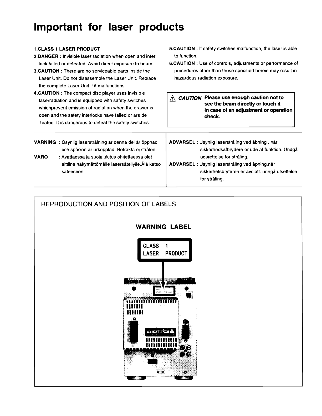
Important for laser products
Disassembly method
Main adjustment
Flow of functional operation
until TOC read (CD)
Flow of functional operation
until TOC read (MD)
1-2
1-3
1-5
1-6
1-28
1-32
1-33
COMPACT
DIGITAL AUDIO
Area Suffix
UB
US
UT
UF
UJ
Maintenance of laser pickup
Replacement of laser pickup
Maintenance of MD pickup
Procedures of changing
the MD pickup
Description of major ICs
Hong Kong
Singapore
Taiwan
China
U.S.Military
1-34
1-34
1-35
1-35
1-36~56
This service manual is printed on 100% recycled paper.
COPYRIGHT 2001 VICTOR COMPANY OF JAPAN, LTD.
No.20901
1-1
Jan. 2001
Page 2
UX-A70MD
Safety Precautions
1. This design of this product contains special hardware and many circuits and components specially
for safety purposes. For continued protection, no changes should be made to the original design
unless authorized in writing by the manufacturer. Replacement parts must be identical to those
used in the original circuits. Services should be performed by qualified personnel only.
2. Alterations of the design or circuitry of the product should not be made. Any design alterations of
the product should not be made. Any design alterations or additions will void the manufacturer`s
warranty and will further relieve the manufacture of responsibility for personal injury or proper ty
damage resulting therefrom.
3. Many electrical and mechanical par ts in the products have special safety-related characteristics.
These characteristics are often not evident from visual inspection nor can the protection afforded
by them necessarily be obtained by using replacement components rated for higher voltage,
wattage, etc. Replacement parts which have these special safety characteristics are identified in
the Parts List of Service Manual. Electrical components having such features are identified by
shading on the schematics and by ( ) on the Parts List in the Service Manual. The use of a
substitute replacement which does not have the same safety characteristics as the recommended
replacement parts shown in the Parts List of Service Manual may create shock, fire, or other
hazards.
4. The leads in the products are routed and dressed with ties, clamps, tubings, barriers and the
like to be separated from live parts, high temperature parts, moving parts and/or sharp edges
for the prevention of electric shock and fire hazard. When service is required, the or iginal lead
routing and dress should be observed, and it should be confirmed that they have been returned
to normal, after re-assembling.
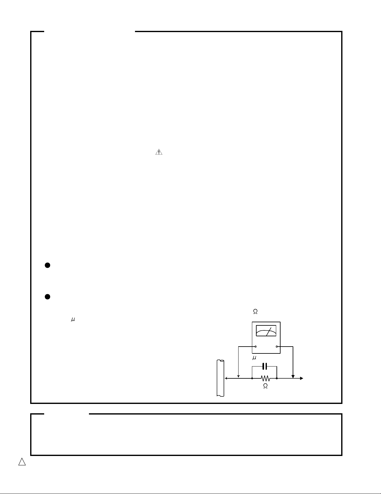
5. Leakage currnet check (Electrical shock hazard testing)
After re-assembling the product, always perform an isolation check on the exposed metal parts
of the product (antenna terminals, knobs, metal cabinet, screw heads, headphone jack, control
shafts, etc.) to be sure the product is safe to operate without danger of electrical shock.
Do not use a line isolation transformer during this check.
Plug the AC line cord directly into the AC outlet. Using a "Leakage Current Tester", measure
the leakage current from each exposed metal parts of the cabinet , particularly any exposed
metal part having a return path to the chassis, to a known good earth ground. Any leakage
current must not exceed 0.5mA AC (r.m.s.)
Alternate check method
Plug the AC line cord directly into the AC outlet. Use an AC voltmeter having, 1,000 ohms
per volt or more sensitivity in the following manner. Connect a 1,500 10W resistor paralleled by
a 0.15 F AC-type capacitor between an exposed
metal part and a known good earth ground.
Measure the AC voltage across the resistor with the
AC voltmeter.
Move the resistor connection to eachexposed metal
part, par ticularly any exposed metal part having a
return path to the chassis, and meausre the AC
voltage across the resistor. Now, reverse the plug in
the AC outlet and repeat each measurement. voltage
measured Any must not exceed 0.75 V AC (r.m.s.).
This corresponds to 0.5 mA AC (r.m.s.).
0.15 F AC TYPE
1500 10W
Good earth ground
AC VOLTMETER
(Having 1000
ohms/volts,
or more sensitivity)
Place this
probe on
each exposed
metal part.
!
1-2
Warning
1. This equipment has been designed and manufactured to meet international safety standards.
2. It is the legal responsibility of the repairer to ensure that these safety standards are maintained.
3. Repairs must be made in accordance with the relevant safety standards.
4. It is essential that safety critical components are replaced by approved parts.
5. If mains voltage selector is provided, check setting for local voltage.
CAUTION
Burrs formed during molding may be left over on some parts of the chassis. Therefore,
pay attention to such burrs in the case of preforming repair of this system.
Page 3
UX-A70MD
Preventing static electricity
Electrostatic discharge (ESD), which occurs when static electricity stored in the body, fabric, etc. is discharged,
can destroy the laser diode in the traverse unit (optical pickup). Take care to prevent this when performing repairs.
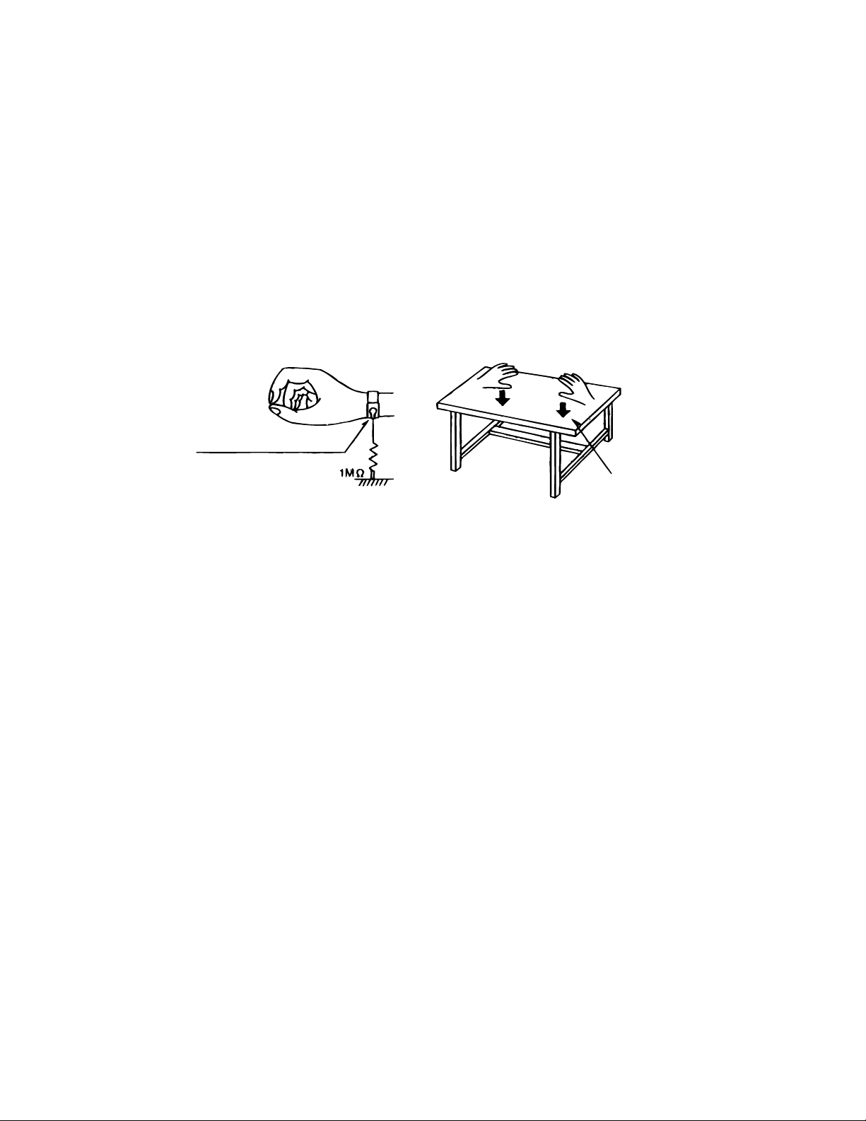
1.1. Grounding to prevent damage by static electricity
Static electricity in the work area can destroy the optical pickup (laser diode) in devices such as DVD players.
Be careful to use proper grounding in the area where repairs are being performed.
1.1.1. Ground the workbench
1. Ground the workbench by laying conductive material (such as a conductive sheet) or an iron plate over
it before placing the traverse unit (optical pickup) on it.
1.1.2. Ground yourself
1. Use an anti-static wrist strap to release any static electricity built up in your body.
(caption)
Anti-static wrist strap
Conductive material
(conductive sheet) or iron plate
1.1.3. Handling the optical pickup
1. In order to maintain quality during transport and before installation, both sides of the laser diode on the
replacement optical pickup are shorted. After replacement, return the shorted parts to their original condition.
(Refer to the text.)
2. Do not use a tester to check the condition of the laser diode in the optical pickup. The tester's internal power
source can easily destroy the laser diode.
1.2. Handling the traverse unit (optical pickup)
1. Do not subject the traverse unit (optical pickup) to strong shocks, as it is a sensitive, complex unit.
2. Cut off the shorted part of the flexible cable using nippers, etc. after replacing the optical pickup. For specific
details, refer to the replacement procedure in the text. Remove the anti-static pin when replacing the traverse
unit. Be careful not to take too long a time when attaching it to the connector.
3. Handle the flexible cable carefully as it may break when subjected to strong force.
4. It is not possible to adjust the semi-fixed resistor that adjusts the laser power. Do not turn it
1-3
Page 4
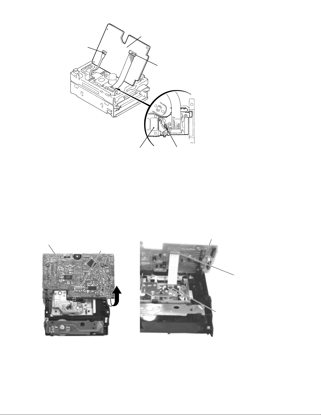
UX-A70MD
MAIN board
CN451
CN321
CD SERVO board
Pickup
Soldering part b
1.3. Cautions on removing the CD traverse unit
* For removing the CD traverse unit in detail, refer to the "Adjustment Method" section of this manual.
1. Before disconnecting the flexible wire from the connector CN601 on the CD SERVO board, solder the part shown in
the figure below.
(Note:If the flexible wire is disconnected from the CN601 without presoldering, it may cause breakdown of the CD
pickup assembly.)
2. When reassembling the CD traverse unit, be sure to remove the solder from the soldered part after reconnecting the
flexible wire to the CN601.
CD SERVO board
CD SERVO board
CN601
CN601
1-4
Soldering part
Page 5
UX-A70MD
1-5
Page 6
UX-A70MD
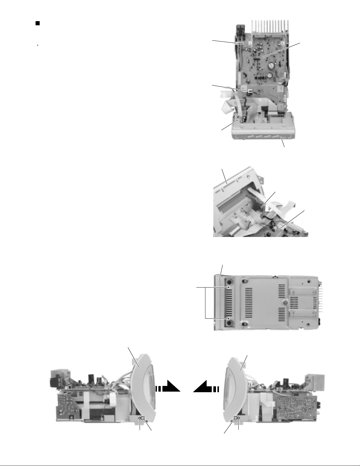
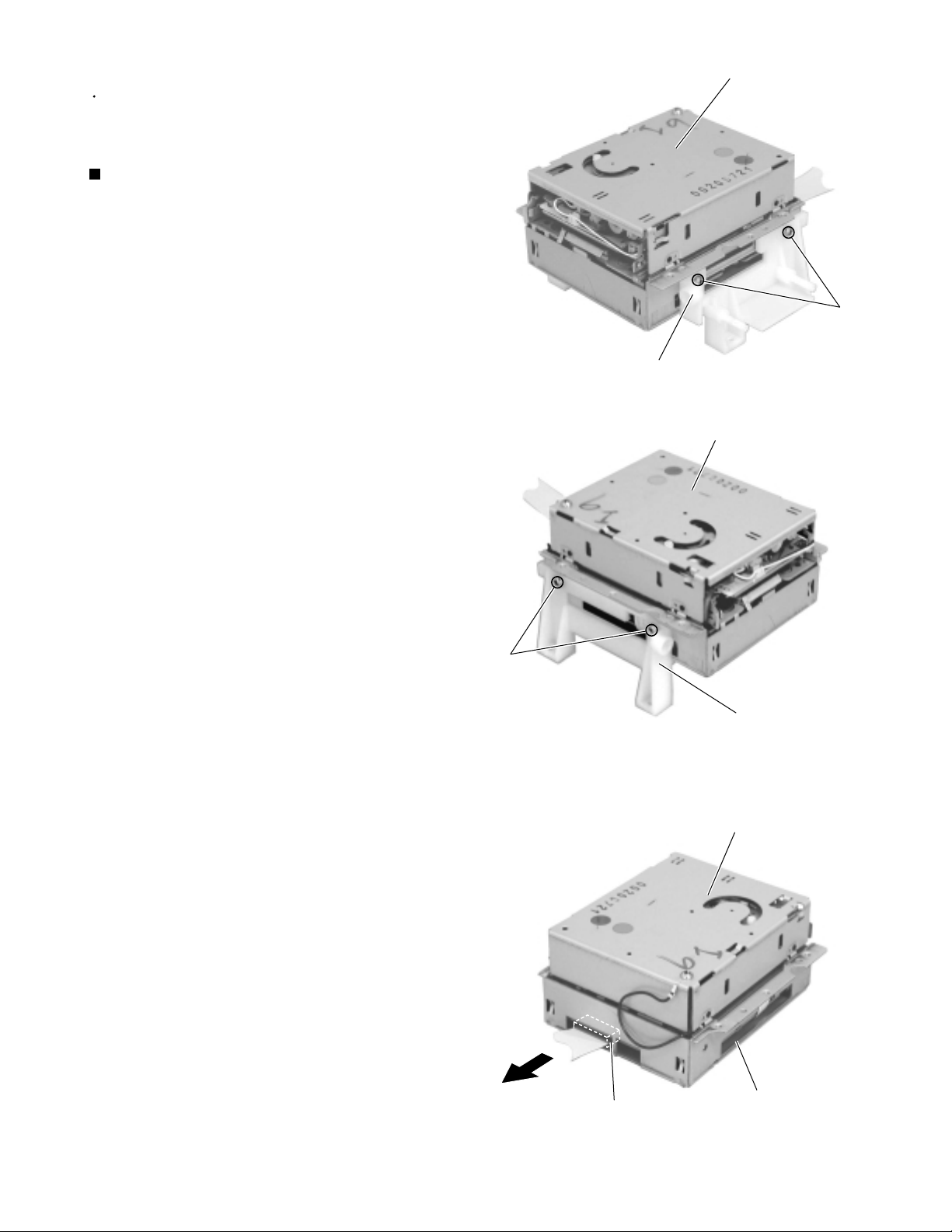
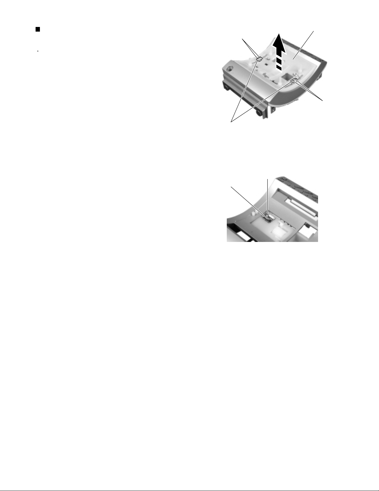
Disassembly method
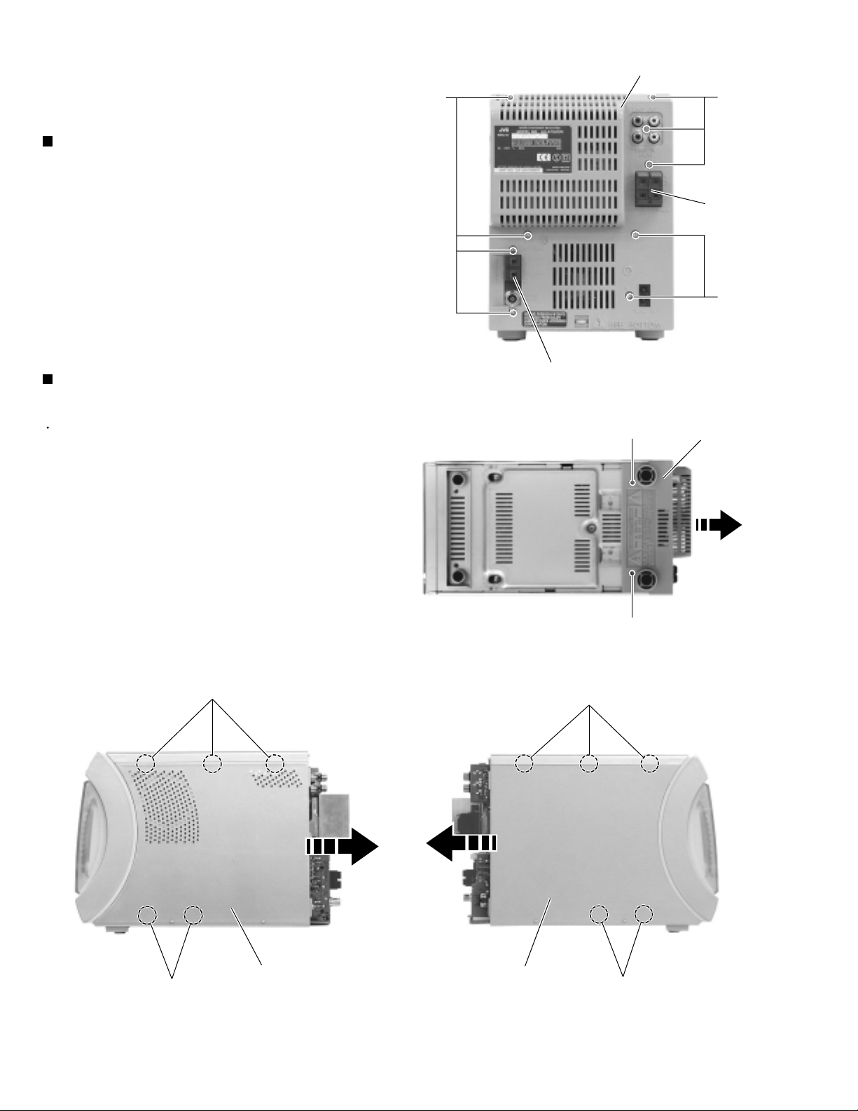
<Main body>
Removing the rear cover
(See Fig.1 and 2)
1.
Remove the nine screws A attaching the rear cover
on the back of the body.
2.
Remove the two screws B attaching the rear cover
on the bottom of the body.
3.
Unlock the speaker terminal and the antenna
terminal, then remove the rear cover backward with
releasing the hooks.
Removing the side panels
(See Fig.3 and 4)
Prior to performing the following procedure, remove
the rear cover.
A
Antenna terminal
Fig.1
Rear cover
B
A
Speaker
terminal
A
Rear cover
1.
Remove each side panel backward while releasing
the joints a.
Joints a
Fig.2
Joints a
B
1-6
Joints a
Side panel (Right)
Fig.4
Side panel (Left)
Joints a
Fig.3
Page 7
UX-A70MD
Removing the top cover
(See Fig.5 and 6)
Prior to performing the following procedure, remove
the rear cover and the side panels.
1.
Remove the two screws C on each side of the body.
2.
Release the joint b on each side of the body and
remove the top cover backward and upward.
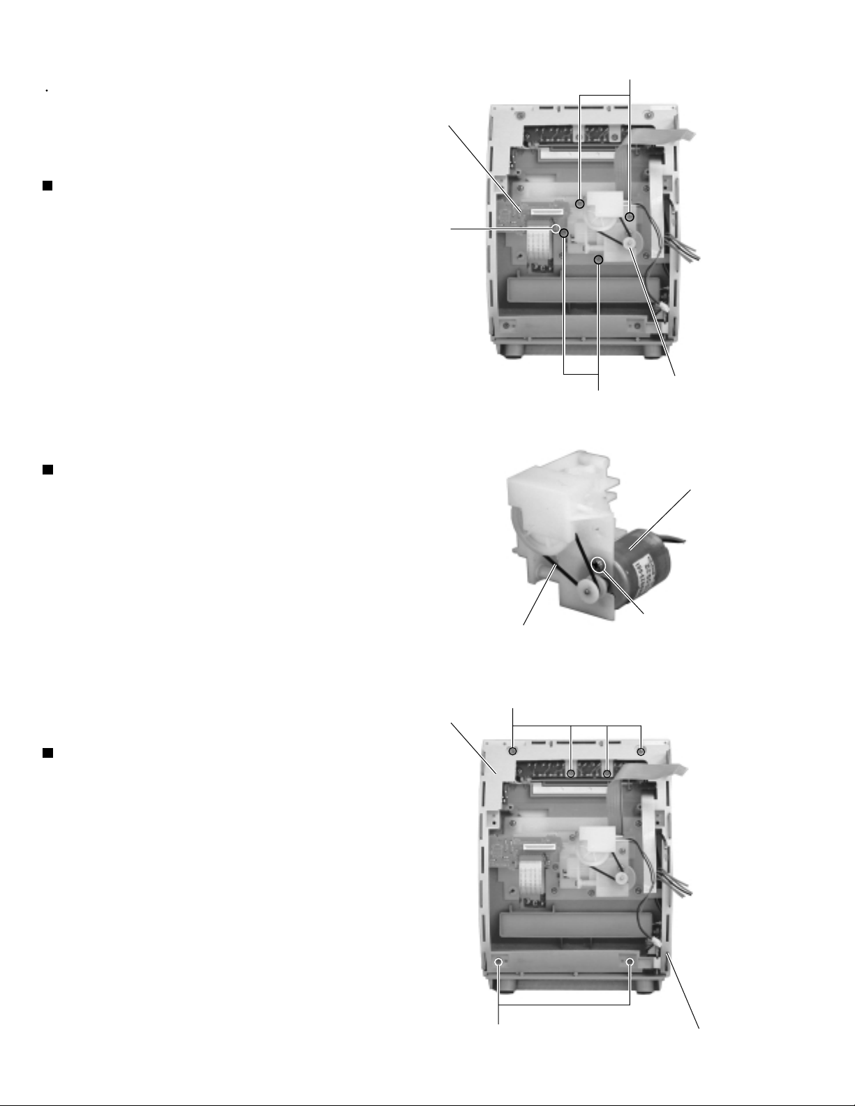
Removing the fan assembly (See Fig.6)
*Prior to performing the following procedure, remove
the rear cover, the right and left side panels.
1.
Remove the two screws D on the right side of the
body and pull out the fan assembly sideward.
D
C
Joint b
Top cover
Tuner & function board
Fan assembly
Joint b
C
Fig.5
Top cover
2.
Disconnect the wire from connector CN807 on the
main board.
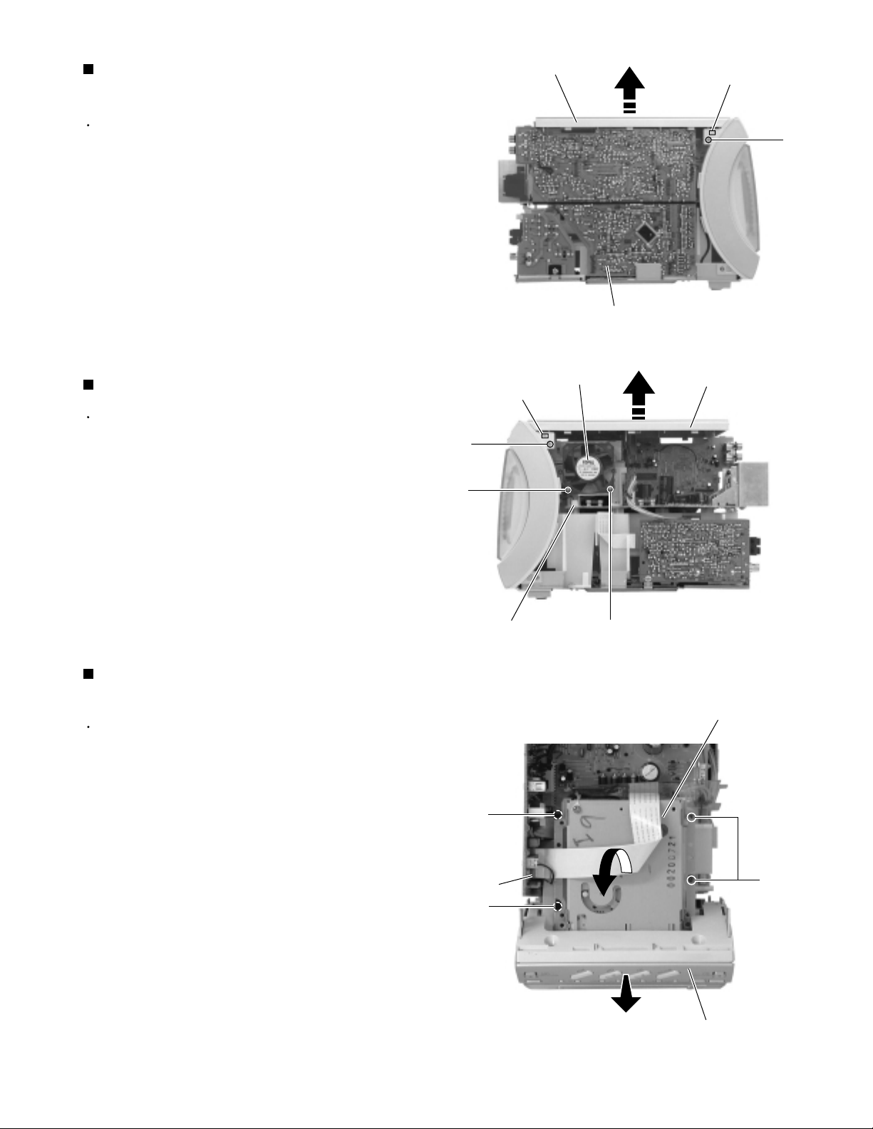
Removing the MD mechanism assembly
unit (See Fig.7)
Prior to performing the following procedure, remove
the rear cover, the side panels, the top cover and the
fan assembly.
1.
Disconnect the card wire from connector CN721 on
the tuner & function board.
2.
Remove the four screws D and the MD mechanism
assembly backward and upward while pulling the
front panel assembly forward.
CN807
D
CN721
D
D
Fig.6
MD mechanism assembly
D
Front panel assembly
Fig.7
1-7
Page 8
UX-A70MD
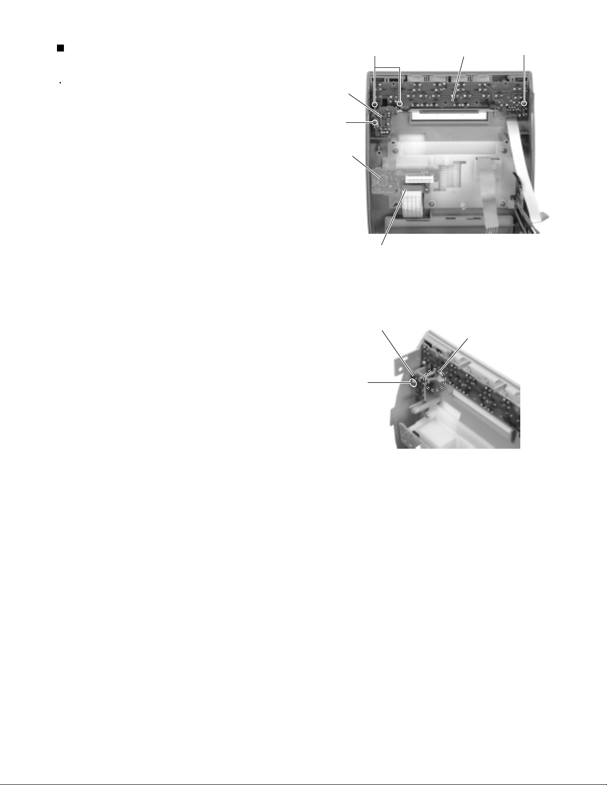
Removing the tuner & function board
(See Fig.8)
Prior to performing the following procedure, remove
the rear cover, the side panels and the top cover.
1.
Disconnect the card wire from connector CN701,
CN705, CN707, CN708 and CN721 on the tuner &
function board on the right side of the body.
Similarly, disconnect the harness from CN706.
CAUTION:
2.
Disconnect connector CN711 and CN712 on the
tuner & function board from CN801 and CN802 on
the main board by pulling them outward.
3.
Disconnect connector CN703 and CN704 on the
tuner & function board from CN603 and CN604 on
the CD servo board by pulling them upward.
For the card wire connected to CN707,
disconnect it after performing the following
procedure 2 and 3.
CN712
AC jack board
CN707
CN701
CN705
CN704
CN703
Fig.8
CN721
CN706
CN708
CN711
Removing the AC jack board (See Fig.9)
Prior to performing the following procedure, remove
the rear cover and the right side panel.
1.
Remove the screw E on the right side of the body
and release the AC jack board from the two joints c.
2.
Disconnect the harness from connector CN805 on
the AC jack board.
Removing the antenna terminal board
(See Fig.10)
Prior to performing the following procedure, remove
the rear cover and the left side panel.
1.
Disconnect the card wire from connector CN1 on the
left side of the body.
E
AC jack board
Fig.9
Joints c
2.
Remove the screw F and release the antenna
terminal board from the joint d upward.
1-8
CN1
F
Antenna terminal board
Fig.10
Joint d
Page 9
Removing the front panel assembly unit
(See Fig.11 to 15)
Prior to performing the following procedure, remove
the rear cover, the side panels, thetop cover, the MD
mechanism assembly and the tuner & function
board.
1.
Disconnect the wire from connector CN804 and
CN806 on the main board. Disconnectthe wire from
W802 pin terminal.
2.
Remove the two screws G on the bottom of the
body.
3.
Remove the lower screw H on each side of the body.
4.
Release the lower joint e on each side of the body.
Pull out the front panel assemblytoward the front.
CN804
CN806
W802
Front panel assembly
UX-A70MD
Main board
Front panel assembly
Fig.11
Front panel assembly
W802
Main board
Fig.12
Front panel assembly
G
Fig.13
Front panel assembly
Fig.15
H
Joint e
Joint e
H
Fig.14
1-9
Page 10
UX-A70MD
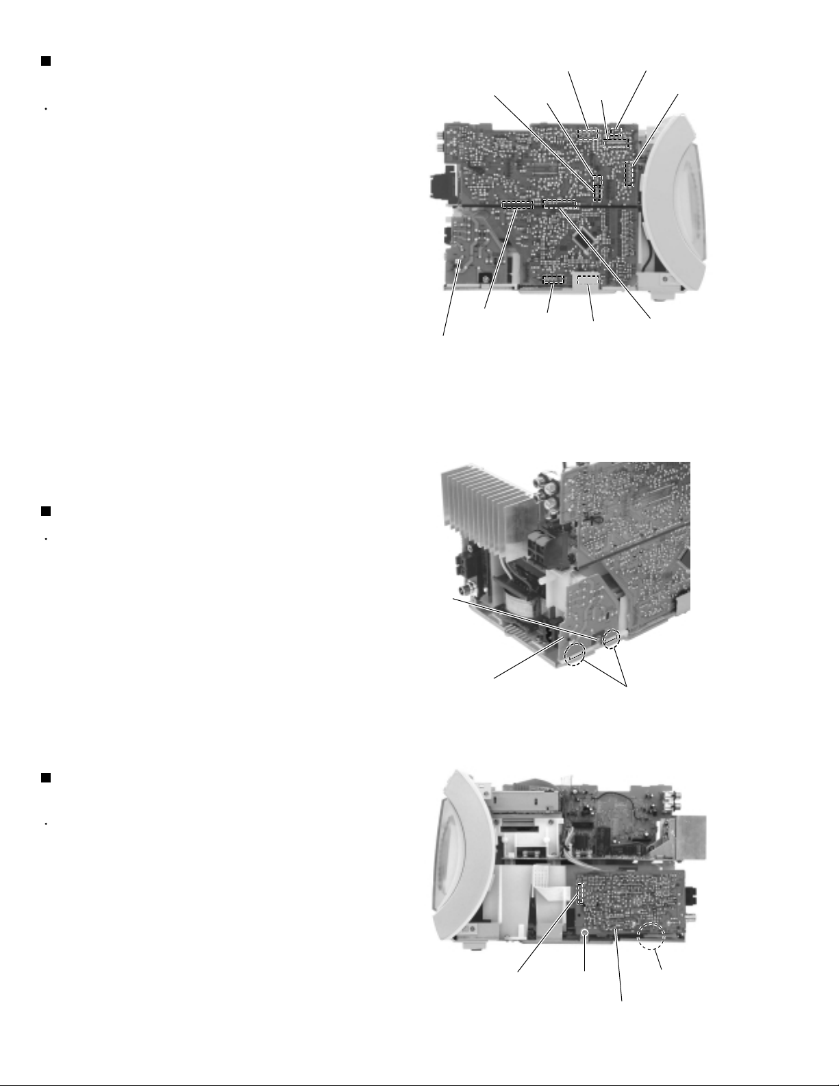
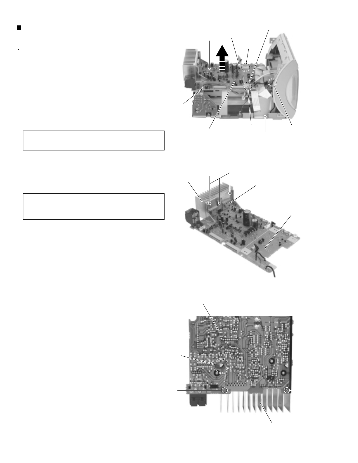
Removing the main board / heat sink
(See Fig.16 to 18)
Prior to performing the following procedure, remove
the rear cover, the side panels, thetop cover, the MD
mechanism assembly and the tuner & function
board.
1.
Disconnect the wire from connector CN803, CN804
and CN806 on the main boardrespectively.
Disconnect the wire from W802 pin terminal.
2.
Remove the screw I attaching the main board and
the screw J attaching the wireterminal.
CAUTION:
3.
Remove the three screws K on the heat sink bracket.
4.
Remove the two screws L on the back of the main
board.
When reasse mbling, fit the slots of the
main board to the two bosses.
CN804
Heat sink
I
Main board
K
CN803
Fig.16
CN806
Bosse
Bosse
J
Heat sink bracket
W802
CAUTION:
When removing the heat sink bracket,
disengage the two joints d on theback of
the main board.
Main board
Fig.17
Main borad
Joint d
1-10
L
Heat sink
Fig.18
L
Page 11
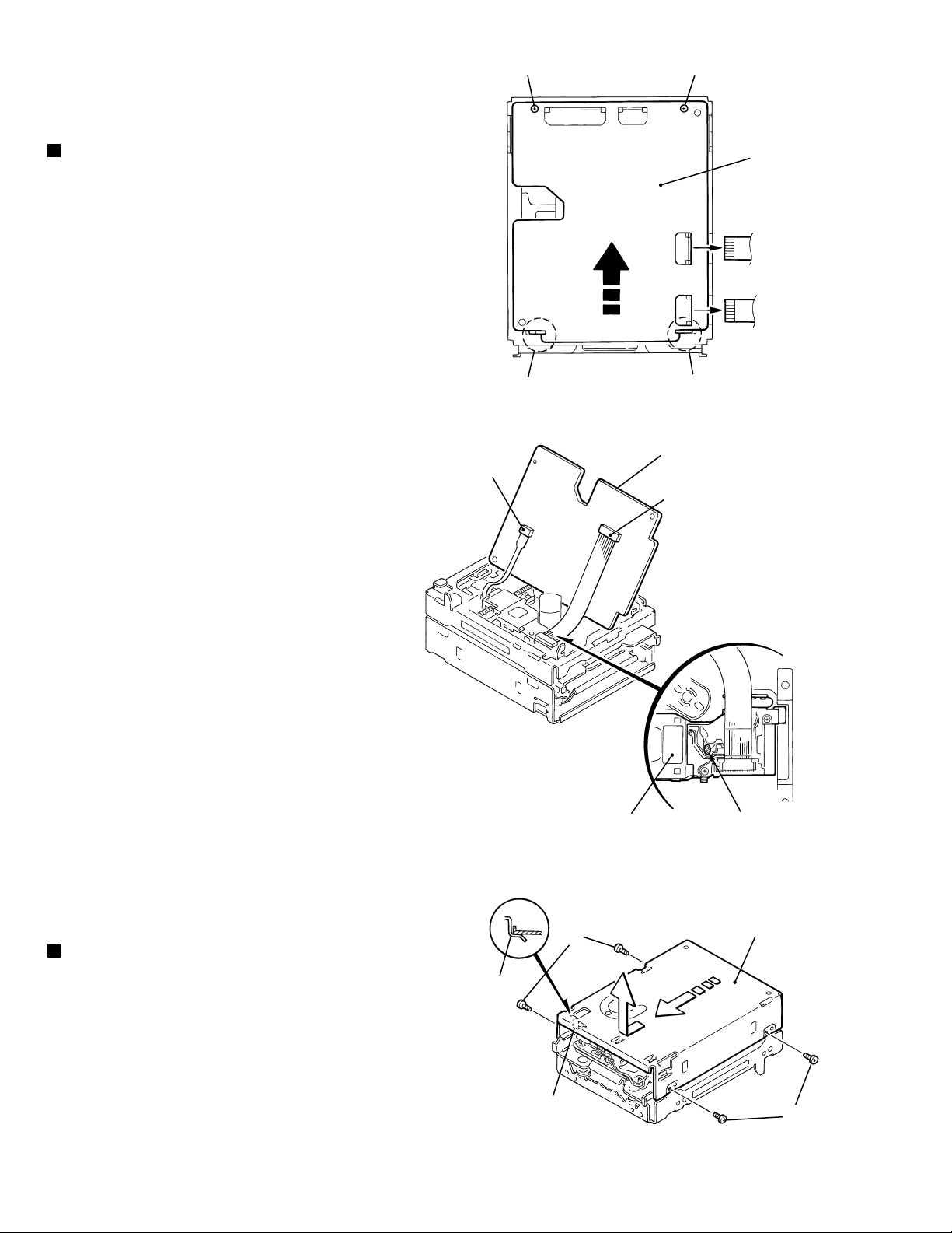
Removing the CD mechanism assembly
and the CD servo board
(See Fig.19 to 24)
Prior to performing the following procedure, remove
the rear cover, the side panels, the top cover, the
MD mechanism assembly, the tuner & function
board, the AC jack board, the antenna terminal
board, the front panel assembly and the main board.
1.
Cut off the two tie band on the back of the CD
mechanism assembly top cover.
2.
Remove the screw M and the top cover.
3.
Move the lever f in the direction of the arrow to draw
the loading tray manually.
4.
Remove the screw N on the CD tray and pull out the
CD tray from the CD mechanism assembly.
5.
Remove the two screws O attaching the clamper
base on top of the CD mechanism assembly.
Release the two joints g with the CD mechanism
assembly and remove the clamper base upward.
6.
Remove the three screws P attaching the CD
mechanism assembly.
M
CD mechanism assembly
Loading tray
CD mechanism assembly
Clamper base
UX-A70MD
Tie band
Fig.19
Lever f
Fig.20
N
7.
Remove the three screws Q attaching the CD servo
board on the back of the CD mechanism assembly.
8.
Disconnect the harness from connector P031 on the
CD mechanism assembly. Disconnect the harness
and the card wire from connector CN602 and CN601
on the CD servo control board respectively.
CD mechanism assembly
P
P
Joint g
O
Loading tray
Fig.21
CD mechanism assembly
Joint g
Clamper base
O
Fig.23
Fig.22
1-11
Page 12
UX-A70MD
CD servo board
Q
Removing the transformer assembly
(See Fig.19 and 25)
Prior to performing the following procedure, remove
the rear cover, the side panels, the top cover, the
MD mechanism assembly, the tuner & function
board, the AC jack board, the antenna terminal
board, the front panel assembly and the main board.
Cut off the two wire clamp on the back of the CD
1.
mechanism assembly upper cover.
Remove the screw M and the CD mechanism
2.
assembly upper cover.
Remove the four screws R attaching the transformer
3.
assembly.
CN602
CN601
P031
R
Q
CD mechanism board
Fig.24
R
Transformer assembly
Fig.25
1-12
Page 13
UX-A70MD
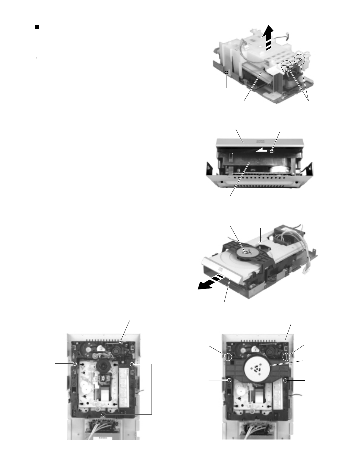
<MD mechanism assembly unit>
Prior to performing the following procedure, remove
the rear cover, the side panels, the top cover unit
and the MD mechanism assembly unit.
Removing the MD mechanism assembly
(See Fig.26 to 28)
1.
Remove the four screws S attaching the bracket (a)
and (b) on both sides of the MD mechanism
assembly unit.
2.
Disconnect the card wire from connector CN521 on
the MD mechanism board. Remove the MD
mechanism assembly bottom cover downward.
MD mechanism assembly
S
Bracket (a)
Fig.26
MD mechanism assembly
S
CN521
Bracket (b)
Fig.27
MD mechanism assembly
MD mechanism assembly
bottom cover
Fig.28
1-13
Page 14
UX-A70MD
<Front panel assembly unit>
Prior to performing the following procedure,remove
the rear cover,the side panels, the top cover, the MD
mechanism assembly unit,the tuner & function board
and the front panel assembly unit.
Removing the relay board (See Fig.29)
1.
Disconnect the card wire from connector CN908 on
the relay board respectively.
2.
Remove the screw T attaching the relay board.
Removing the drive motor assembly
(See Fig.29 and 30)
U
Relay board
T
Drive motor assembly
U
Fig.29
Drive motor
1.
Remove the four screws U attaching the drive motor
assembly.
2.
Remove the belt and the screw V attaching the drive
motor.
Removing the headphone jack board
(See Fig.31)
1.
Remove the six screws W attaching the bracket (c),
and detach the headphone jack board.
Bracket (c)
Belt
W
V
Fig.30
1-14
W
Headphone jack board
Fig.31
Page 15
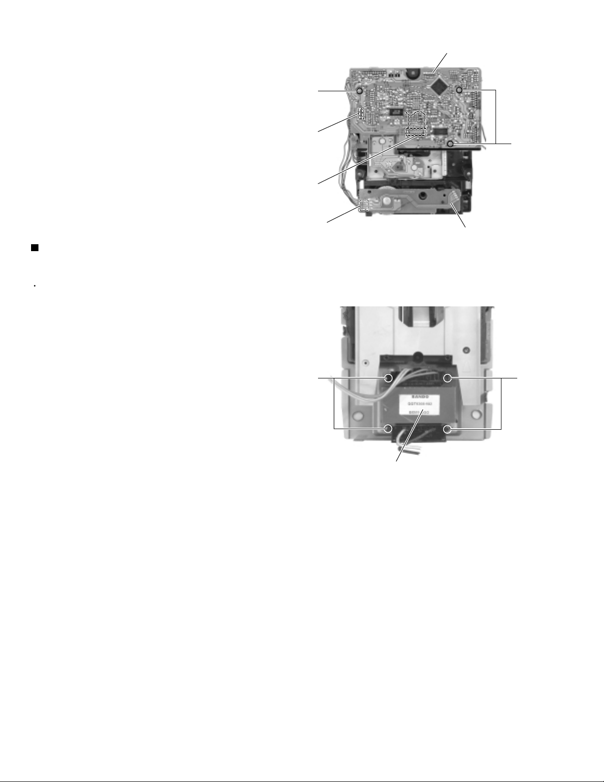
UX-A70MD
Removing the key switch board / (d)
board (See Fig.32 and 33)
Prior to performing the following procedure, remove
the bracket (c).
1.
Remove the three screws X attaching the key switch
board.
2.
Remove the spring g and the screw Y attaching the
(d) board.
(d) board
Y
Relay board
X
CN908
(d) board
Key switch board
Fig.32
Spring g
X
Y
Fig.33
1-15
Page 16
UX-A70MD
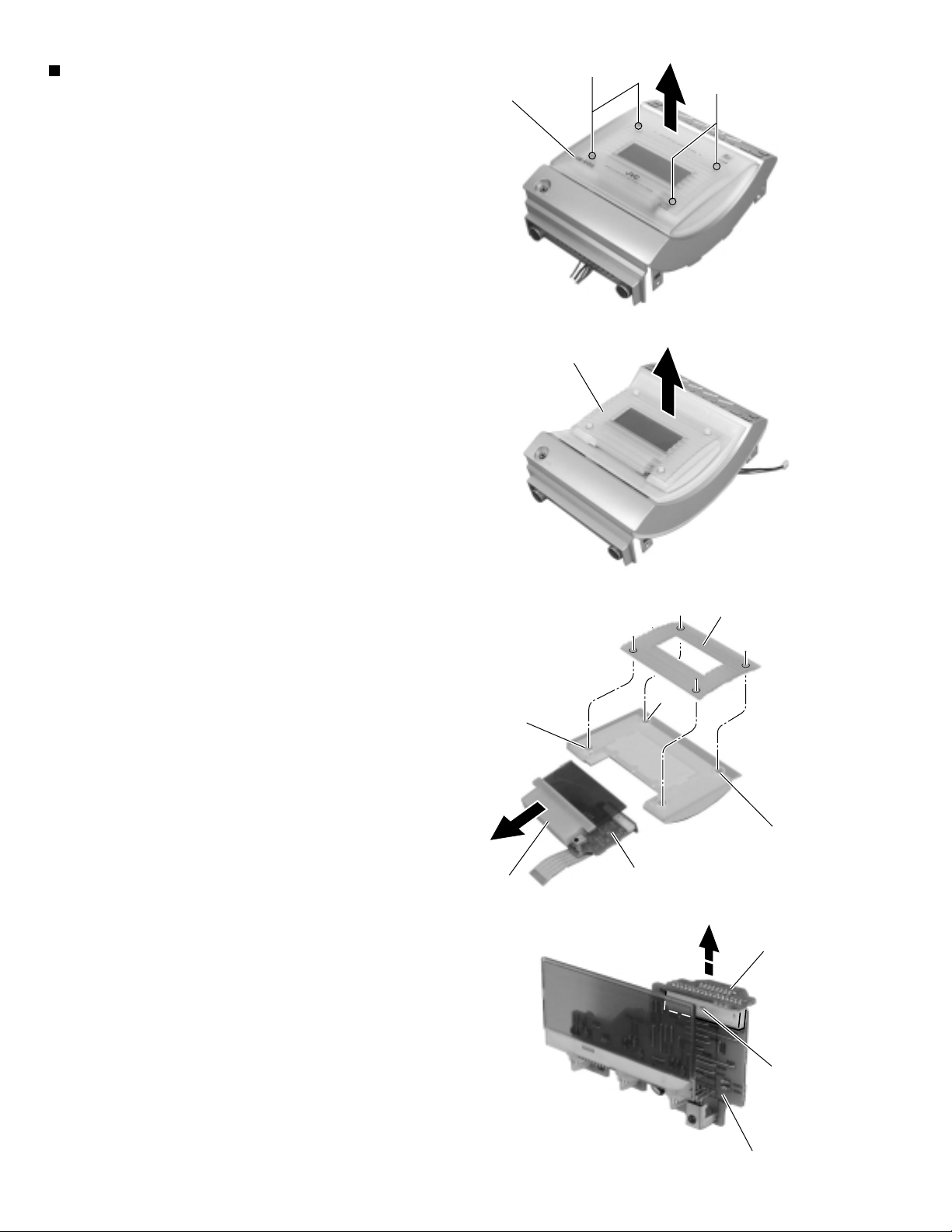
Removing the LCD board / sub board
(See Fig.32 and 34 to 37)
1.
Disconnect the card wire from connector CN908 on
the relay board on the back of thefront panel
assembly.
2.
Remove the four screws A’ attaching the CD / MD
door cover on the front side of the frontpanel
assembly. Remove the CD / MD door cover, then the
LCD board unit.
3.
Pull out the LCD lens from the four bosses on the
LCD board unit.
4.
Remove the LCD board and the lens cover in the
direction of the arrow (The lens cover isattached with
a double-sided tape).
5.
Disconnect the sub board from connector CN913 on
the LCD board.
CD / MD door cover
LCD board unit
A'
A'
Fig.34
Slot h
Lens cover
Fig.35
LCD lens
Slot h
Slot h
LCD board
Fig.36
Sub board
1-16
Fig.37
CN913
LCD board
Page 17
UX-A70MD
Removing the CD / MD door board
(See Fig.38 and 39)
Prior to performing the following procedure,remove
the LCD board unit.
1.
Remove the four screws B' attaching the two
brackets (e). Remove the CD / MD door base and
the two brackets (e).
2.
Remove the screw C' attaching the CD / MD door
board.
CD / MD door base
B'
B'
Brackets (e)
Fig.38
C'
CD / MD door board
Fig.39
1-17
Page 18
UX-A70MD
Disassembly method
<Main body>
Removing the main board
(See Fig.1 and 2)
1.
Turn over the body and disconnect the card wire
from connector CN408 and the flexible wire from
CN407 on the main board.
2.
Remove the two screws A attaching the main board.
Slide the main board in the direction of the arrow to
release the two joints a with the single flame.
3.
Solder part b on the pickup in the body. Disconnect
the flexible harness from connector CN321 and
CN451 on the underside of the main board. Then
remove the main board.
AA
(Bottom)
Main board
CN408
CN407
Joint b Joint b
Fig.1
Main board
CN451
CN321
Removing the mechanism cover
(See Fig.3)
1.
Remove the four screws B on both sides of the
body.
2.
Move the mechanism cover toward the front to
disengage the front hook of the mechanism cover
from the internal loading assembly (Joint c). Then
remove the mechanism cover upward.
1-18
Fook
Joint c
Joint c
B
Pickup
Fig.2
Fig.3
Solder part b
Mechanism cover
B
Page 19

Removing the head lifter (See Fig.4 to 6)
1.
Move the head lifter on top of the body in the
direction of the arrow and turn around.
2.
Detach the spring from the hook of the body.
Remove the head lifter with the spring.
3.
If necessary, remove the spring from the head lifter.
Head lifter
Fig.5
UX-A70MD
Head lifter
Fig.4
Spring
Removing the head assembly (See Fig.7)
1.
Remove the screw C on the upper side of the body.
Remove the head assembly while pulling the flexible
harness from the body.
Head lifter
Spring
Fig.6
Head assembly
Fig.7
C
1-19
Page 20

UX-A70MD
Removing the Loading assembly
(See Fig.8 and 9)
Ref:
The loading assembly, the traverse mechanism
assembly and the single flame will be
removable after removing the loading assembly
from the body.
D
D
Prior to performing the following procedure, remove
the main board, the mechanism cover, the head lifter
and the head assembly.
1.
Remove the three screws D on the upper side of the
body.
2.
Move the loading assembly forward to disengage it
from the traverse mechanism assembly (Joint d).
Then remove it upward.
3.
Remove the traverse mechanism assembly from the
single flame.
Joint d
Loading assembly
D
Fig.8
Loading assembly
1-20
Traverse mechanism
assembly
Single flame
Fig.9
Page 21

<Loading assembly>
Slide base (R)
UX-A70MD
E'
Removing the slide base (L) / (R)
(See Fig.10)
1.
Remove the two screws E on the upper side of the
loading assembly.
2.
Remove the slide base (L) outward. (Release it from
the joint bosses E.)
3.
Remove the slide base (R) outward.
Removing the loading mechanism
assembly (See Fig.11)
1.
Detach the loading mechanism assembly upward to
release the four pins on both sides from the loading
motor, paying attention to the part e of the loading
mechanism base.
E
Slide base (L)
E
E'
Fig.10
Part e
Loading mechanism assembly
Removing the loading motor
(See Fig.12 and 13)
1.
Disconnect the harnesses from the wire holder and
from connector CN612 on the cam switch board.
2.
Remove the screw F attaching the loading motor
and release the joint f.
3.
Remove the belt from the loading motor assembly.
4.
Remove the two screws G attaching the loading
motor.
Removing the cam gear and the cam
switch board (See Fig.12)
Loading mechanism
assembly
Loading motor assembly
Joint f
CN612
F
Loading mechanism base
Fig.11
Wire holder
H
Cam switch board
Slit washer
H
Cam gear
Fig.12
Loading motor
1.
Remove the slit washer attaching the cam gear and
pull out the cam gear.
2.
Disconnect the harness from the wire holder and
from connector CN612 on the cam switch board.
3.
Remove the two screws H and the clamp. Remove
the cam switch board.
G
Belt
Fig.13
1-21
Page 22

UX-A70MD
Removing the cartridge holder assembly
(See Fig.14 and 15)
1.
Remove the two screws I on the upper side of the
loading assembly.
I
I
Removing the slide bar and the eject bar
(See Fig.14 and 15)
Prior to performing the following procedure, remove
the cartridge holder assembly.
Slide bar
Cartridge holder assembly
Eject bar
Eject bar
Part g
Fig.14
I
1.
Remove the slide bar upward.
2.
Move the eject bar outward until it stops as shown in
Fig.14. Push the convex part g on the bottom of the
body and remove the eject bar from the chassis.
Slide bar
k
Eject bar
UD base
1-22
Cartridge holder assembly
Fig.15
Page 23

<Traverse mechanism assembly>
UX-A70MD
Removing the Insulators (See Fig.16)
1.
Disengage the four insulators from the notches of the
traverse mechanism chassis.
Removing the pickup unit (See Fig.17)
1.
Turn over the traverse mechanism assembly and
remove the screw J attaching the shaft holder (F).
2.
Move the shaft inward and remove it from the shaft
holder (R).
Pickup unit
Insulators
Traverse machanism chassis
Fig.16
Joint h
Pickup guide
Pickup unit
Insulators
3.
Detach the shaft side of the pickup unit upward and
release the joint h with the pickup guide. Then
remove the pickup unit with the shaft.
Removing the pickup (See Fig.18)
1.
Draw out the shaft from the pickup.
2.
Remove the two screws K attaching the rack spring.
Shaft holder (F)
Rack spring
Shaft holder (R)
J
Fig.17
K
Pickup
Fig.18
Shaft
1-23
Page 24

UX-A70MD
Removing the feed motor assembly
(See Fig.19-1, 19-2)
It is not necessary to remove the pickup unit.
1.
For the white and black harnesses extending from
the feed motor assembly, unsolder the soldering i on
the traverse mechanism board.
Traberse mechanism board Soldering j
M
2.
Remove the two screws L attaching the feed motor
assembly.
3.
Remove the two screws N attaching the feed motor
bracket.
Removing the traverse mechanism
board (See Fig.19-1)
Prior to performing procedure, remove the feed
motor assembly.
1.
For the red and black harnesses extending from the
spindle motor, unsolder the soldering j on the
traverse mechanism board.
Soldering i
Feed motor assembly
L
Fig.19-1
Feed motor
Feed motor bracket
N
2.
Remove the screw M attaching the traverse
mechanism board.
Fig.19-2
1-24
Page 25

<Reattaching the loading assembly>
1.
Reattach the eject bar to the UD base.
(Fig.15 and 20)
2.
Reattach the slide bar to the loading mechanism
chassis while fitting the boss marked k to the eject
bar slot. (Fig.20)
3.
Slide the slide bar and the eject bar in the direction
of the arrow in Fig.20 and reattach the cartridge
holder assembly using the two screws I.
(Fig.20 and 21)
UX-A70MD
ATTENTION:
Make sure the pin of the eject lever
marked l is fitted to the slot of the eject
bar marked m at the bottom of the
loading mechanism chassis after
moving the eject lever and the loading
slider of the cartridge holder assembly
in the direction of the arrow.
(Refer to Fig.21)
Slide bar
I
I
Cam switch board
H
Point marked
H
Cam switch boss
Ditch
UD base
Eject bar
Fig.20
Ditch m
UD base (Bottom)
Cartridge holder assembly
Loading slider
Eject lever
l
Fig.21
1-25
Page 26

UX-A70MD
4.
Reattach the wire holder to the UD base while
engaging the UD base hook marked u to the wire
holder slot marked t (At the same time, the boss on
the reverse side of the wire holder is fitted to the UD
base round hole).
5.
Reattach the cam switch board using the two screws
H. (Fig.22)
6.
Turn the cam switch to bring the boss to the point
marked on the cam switch board. Reattach the
cam gear using a slit washer while fitting the cam
gear slot to the cam switch boss. (Fig.22)
ATTENTION:
When reattaching the cam gear, the
cam switch boss should be fitted to the
cam gear slot, and the triangle mark of
the cam gear should be aligned to the
hole of the eject bar as shown in
Fig.22.
7.
Reattach the loading motor assembly, using the
screw F. Connect the harness extending from the
loading motor to connector CN612 on the switch
board and fix it with the wire holder. (Fig.22)
Slide bar CN612
Loading motor assembly
Point marked
Boss
Cam switch
Cam switch board
1-26
F
Eject lever
Fig.22
Cam gear
n
Cam gear
(Triangle mark)
Eject lever
Page 27

UX-A70MD
8.
Reattach the UD base while engaging the four pins
on both sides of the UD base to the notches of the
loading mechanism base and placing the edge
(marked e’) of the cartridge holder assembly under
the hook e of the loading mechanism base. (Fig.23)
9.
Reattach the slide base (R) while fitting the two pins
on another side of the UD base to the slots of the
slide base (R). (Fig.24)
ATTENTION:
10.
Reattach the slide base (L) on the slide base (R)
while fitting the two pins on another side of the UD
base to the slots of the slide base (L) (Fig.25). Make
sure the two slots of the slide base (L) are fitted to
the two bosses marked E’ and tighten the two
screws E. (Fig.26)
Ref:
To expedite the work, bring up the UD base
slightly when fitting each pin to the appropriate
notch.
Fit the part v of the slide base (R) to
the part w on the inward side of the
cam gear rib. (Fig.25)
Hook e
Hook e'
Hook e'
Pin
Loading mechanism base
Fig.23
Slide base (R)
Part v
Pin
E
E'
Pin
Slide base (L)
Pin
Part w
Fig.24
Slide base (L)Slide base (R)
Slide base (R)
Cam gear
E
Part v
Part w
E'
Fig.25Fig.26
1-27
Page 28

UX-A70MD
Adjustment Method (CD/MD section)
1. Jigs and test instruments
Laser power meter
Laser power meter sensor (or disk sensor)
Premastered disk (MRG-1018 or TGYS1)
Recordable disk (MDW-74/AU1)
2. Adjustment and check items
1) Indications in the modes that all LCD's are on
2) CD section
(1) Indication of the C1 error
(2) Cancel of the C1 error indication
3) MD section
(1) Setup of the TEST MODE 1
(2) Initialization of the EEPROM
(3) Adjustment of the laser power
(4) Adjustment of the disk
(5) Setup of the TEST MODE 2
(6) Indication of variation in the pickup adjustment value
(7) Indication of the C1 error
(8) Cancel of the TEST MODE
3. Adjustment and check method
1) CD section
(1) Indication of the C1 error
While pressing both the POWER key
and BACK SKIP key on the main unit,
turn on the primary power supply.
FL indication
CRC = 0
Press the CD OPEN/CLOSE key
and insert the test disk.
Press the CD PLAY key. The set starts
counting and the number of error correction
times is indicated every 10 seconds.
FL indication
CRC = ***
200 Hz or less
1-28
(2) Cancel of the C1 error indication
To cancel the C1 error indication, cut off the power supply.
Page 29

2) MD section
UX-A70MD
(1) Setup of the TEST MODE 1
While pressing both the POWER
key and FORWARD SKIP key, turn
on the primary power supply.
FL indication
MD TEST MODE 1
Setup is complete.
(3) Adjustment of the playback laser power
Set up the MD TEST MODE 1.
(2) Initialization of the EEPROM
(The EEPROM can be initialized on the precondition that the
setup of the TEST MODE 1 is complete. After setup of the
TEST MODE 1, proceed to the following operations with the
remote controller*.)
* For EJECT operation, use the EJECT key on the main unit.
Initialization of the EEPROM
Press the PLAY MODE key
on the remote controller.
FL indication MD
TEST MODE 1
Setup is complete.
(4) Adjustment of the recording laser power
Set up the MD TEST MODE 1.
Insert the laser power
meter sensor.
Press the "2" key on
the remote controller.
Set up the playback
laser power.
Increase the laser
power with the F.
SKIP key on the
remote controller.
Adjust the power to be 0.68 mW or
more. If the value exceeds 0.68 mW,
approximate it to 0.68 mW as
accurately as possible.
Press the MD EJECT
key on the main unit.
Decrease the laser
power with the B.
SKIP key on the
remote controller.
Insert the laser power
meter sensor.
Press the "4" key on
the remote controller.
Set up the recording
laser power.
Increase the laser
power with the F.
SKIP key on the
remote controller.
Adjust the power to be 6.23 mW or
more. If the value exceeds 6.23 mW,
approximate it to 0.68 mW as
accurately as possible.
Press the MD EJECT
key on the main unit.
Decrease the laser
power with the B.
SKIP key on the
remote controller.
Setup of the MD laser
power is complete.
Setup of the MD laser
power is complete.
1-29
Page 30

UX-A70MD
(5) Adjustment of the disk
Set up the MD TEST MODE 1.
Insert the
premastered disk.
Reading of TOC ends.
Press the MD PLAY
key on the remote
controller.
FL indication
ON TUNING
Automatic adjustment starts.
Adjustment OK?
YES
FL indication
OK TUNING
Press the STOP key on
the remote controller.
Press the EJECT key
on the main unit.
Insert a recordable
disk.
Press the MD PLAY key
on the remote controller.
FL indication
ON TUNING
Automatic adjustment starts.
Adjustment OK?
YES
NO
NO
* If an error indication of "ERR:07"
appears at the first adjustment, try
to make a fresh start of the same
adjustment.
FL indication
NG ERR: XX
XX: Refer to the NG judgment code table.
NG Judgment Code Table
Code
00 Automatic adjustment is incomplete.
01 Rest switch detection
02 Focus-on
03 EF balance, tracking offset adjustment (Pit area)
04 ABCD level (I-V resistance) adjustment (Pit area)
05 Focus servo AGC (Pit area)
06 Tracking servo AGC (Pit area)
07 Focus bias adjustment (Pit area)
08 EF balance, tracking offset adjustment (GRV area)
09 ABCD level (I-V resistance) adjustment (GRV area)
0A Focus servo AGC (GRV area)
0B Tracking servo AGC (GRV area)
0C Focus bias adjustment (GRV area)
0D Room temperature measurement
0E Write in EEPROM
10 (Focus, TRK, SLED) AGC data read time-out
20 Pit area spindle lock
30 Groove area spindle lock
XX Automatic adjustment is complete.
NG item in adjustment
FL indication
ON TUNING
Press the STOP key on
the remote controller.
Press the MD EJECT
key on the main unit.
1-30
FL indication
NG ERR: XX
Refer to the NG judgment code table.
Automatic adjustment
ends.
Press the POWER key on the
main unit or remote controller.
Cut off the power supply after
cancelling the TEST MODE.
Page 31

UX-A70MD
For investigating the mode in which an error
occurred during the disk adjustment, freeze the
set in the mode by pressing the proper key
(refer to the table on the right) on the remote
controller before cancelling the TEST MODE 1.
(6) Setup of the TEST MODE 2
While pressing both the POWER key and
FORWARD STOP key on the main unit,
turn on the primary power supply.
FL indication MD
TEST MODE 1
While pressing the STOP key on the main
unit, press the FM/AM key on the main
unit double. The TEST MODE 2 is set up.
Key to press Mode
SLEEP key (Remote controller)
"6" key (Remote controller)
"7" key (Remote controller)
"8" key (Remote controller)
"9" key (Remote controller)
STOP key (Remote controller)
EJECT key (Main unit)
FOCUS SEARCH
PIT ROUGH SERVO
GROOVE ROUGH SERVO
TRACKING ON
TRACKING OFF
STOP
EJECT
FL indication MD
TEST MODE 2
Setup is complete.
(7) Indication of variation in the pickup adjustment value
Set up the TEST MODE 2.
Press the MD OPEN/CLOSE key
and insert the MD test disk.
Press the "6" key on the
remote controller.
Press the "8" key on the remote controller. Counting of
number of C1 errors starts and it continues until it
counts up the maximum number of C1 errors with
indication (maximum number of error indication is 432).
FL indication*
XXXXX - XXXX
*Each time the
"6" key on the
remote
controller is
pressed, the
indication
changes from
ASG to TRG,
from TRG to
TRB, and so
on as shown
in the figure.
ASG
TRG
TRB
FOB
FGR
FEXP
FGC
FG
TGR
TEXP
TGC
TG
-1
-2
:
-128
127
126
:
1
0
(8) Indication of the C1 error
Set up the TEST MODE 2.
Press the MD OPEN/CLOSE key
and insert the MD test disk.
FL indication*
200 Hz or less
X X Y Y Z Z
(9) Cancel of the TEST MODE
(The cancel operation is common to the TEST
MODE 1 and 2.)
Cut off the primary power supply to cancel the
TEST MODE.
1-31
Page 32

UX-A70MD
Flow of functional operation until TOC read (CD)
Power ON
Power Key
Slider turns REST
SW ON.
Automatic tuning
of TE offset
Check that the voltage at the pin17
of CN604 is 0V (a moment)?
Check Point
VREF
Tracking error waveform at TOC reading
pin 25 of
IC601(TE)
Approx
1.8V
Tracking
servo
Disc statas
to rotate
off statas
Automatic measurement
of TE amplitude and
automatic tuning of
TE balance
Approx.3sec
Tracking
servo
on statas
Disc to be
braked to stop
TOC reading
finishes
500mv/div
2ms/div
Fig.1
Laser ON
Detection of disc
Automatic tuning of
Foucus offset
Automatic measurement of
Focus A-curve amplitude
Disc is rotated
Focus servo ON
(Tracking servo ON)
Automatic measurement of
Tracking error amplitude
Automatic tuning of
Tracking error balance
Check that the voltage at the
pin3 of IC601 + side is + 5V?
Confirm that the Focus error
S-cuve siganl at the pin27 of
IC601 is approx.2Vp-p
Confirm that the siganl from
pin24 IC603 is 0V as a
accelerated pulse during
approx.400ms.
Confirm the waveform of
the Tracking error signal
at the pin25 of IC601 (R612)
(See fig-1)
1-32
Automatic tuning of
Focus error balance
Automatic tuning of
Focus error gain
Automatic tuning of
Tracking error gain
TOC reading
Play a disc
Confirm the eys-pattern
at the lead of TP1
Page 33

Flow of functional operation until TOC read (MD)
Power ON
MD play key
Check Point
Slider turns REST
Switch ON.
Confirm that the voltage
at the pin 4 of CN406 are 0V
UX-A70MD
Mechanism Operation ON
Laser ON
Detection of Disc
Automatic tuning of
Focus S-curve amplitude
Disc is rotated
Focus servo ON
(Tracking servo ON)
Automatic tuning of
Focus error gain
Confirm that the voltage
at the pin 19 of IC500 are 4V
Confirm that the Focus error
S-cuve signal at the pin34 of
IC310 is approx.2Vpp
It is confirmed that pin7 of CN408
become 0V from VREF as an acceleration
pulse between about 400ms.
Automatic tuning of
Tracking error gain
TOC reading
Play a disc
Confirm that the eye-pattern
at the pin38 of IC310
1-33
Page 34

UX-A70MD
Maintenance of laser pickup
(1) Cleaning the pick up lens
Befor you replace the pick up, please try to
clean the lens with a alcohol soaked cotton
swab.
(2) Life of the laser diode (Fig.1)
When the life of the laser diode has expired,
the following symptoms wil appear.
(1) The level of RF output (EFM output:ampli
tude of eye pattern) will below.
Is RF output
1.1 0.15Vp-p?
YES
O.K
NO
Replace it.
Replacement of laser pickup
Turn off the power switch and,disconnect the
power cord from the ac outlet.
Replace the pickup with a normal one.(Refer
to "Pickup Removal" on the previous page)
Plug the power cord in,and turn the power on.
At this time,check that the laser emits for
about 3seconds and the objective lens moves
up and down.
Note: Do not observe the laser beam directly.
Play a disc.
(Fig.1)
(3) Semi-fixed resistor on the APC PC board
The semi-fixed resistor on the APC printed
circuit board which is attached to the pickup
is used to adjust the laser power.Since this
adjustment should be performed to match the
characteristics of the whole optical block,
do not touch the semi-fixed resistor.
If the laser power is lower than the specified
value,the laser diode is almost worn out, and
the laser pickup should be replaced.
If the semi-fixed resistor is adjusted while
the pickup is functioning normally,the laser
pickup may be damaged due to excessive current.
Check the eye-pattern at TP1.
Finish.
1-34
Page 35

UX-A70MD
Maintenance of MD pickup
1. Cleaning of pickup lens
(1) Prior to changing the pickup, clean the pickup lens.
(2) For cleaning the lens, use the following cotton swab after
mearsing it in alcohol.
Product No. JCB-B4; Manufacturer;Nippon Cotton Swab
2. Confirmation of the service life of laser
diode when the service life of the laser
diode has been exhausted, the following
symptoms will appear.
(1) Recording will become impossible.
(2) The RF output (EFM output and eye pattern amplitude)
will become lower.
(3) The drive current required for light emitting of laser diode
will be increased.
Confirm the service life according to the following flow chart:
Procedures of changing the MD pickup
Change the MD pickup by referring
to "Removing the MD pickup" in the
Disassembly Method.
Set the pickup to [TEST] mode according
to the procedures described in the
Adjustment Method.
Adjust the laser power.
Completion the disc.
Is the recording power
(6.23mV) output with the
laser power under
test mode?
YES
Is the drive current
of laser diode
120mA or less?
YES
NO
Change the pickup
NO
Change the pickup
OK.
3. Method of measuring the drive current of
laser diode
When the voltage measured at TP ILCC (Q301 emitter)
and +5V (Q303 emitter) of the MD servo P.C. board
(ENX-0223) have become 600mV or over, the service life
of the laser diode is judged to have been exhausted.
[Caution] When TP ILCC (Q301 collector) and
+5V (Q303 emitter have been is short
circuit on such an occasion, then the
laser diode will be broken. Therefore,
take utmost care in handling the MD
pickup.
Completion of changing the MD pickup.
Since this system is designed to perform magnetic
recording, the laser power ten times or over of the
conventional MD player will be output. Therefore, be
sure to perform not only adjustment and operation
of this system so carefully as not to directly look at the
laser beam or touch on the body.
4. Semi-solid state resistors on
the APC P.C. board
The semi-solid state resistor on the APC P.C.board
attached to the pickup is used for adjusting the laser
power. Since these resistor should be adjusted in
pair according to the characteristics of the optical
block, be sure not to touch on the resistors.
Since the service life of the laser diode will be
exhausted when the laser power is low, it is
necessary to change the pickup. Meanwhile, do not
pickup. Otherwise, the pickup will be damaged due
to over current.
1-35
Page 36

UX-A70MD
Description of major ICs
AK4519VF-X (IC480) : A / D D / A converter
1.Pin layout
1
2
3
4
5
6
7
8
9
10
11
12
24
23
22
21
20
19
18
17
16
15
14
13
2.Block diagram
AINL
VCML
AINR
VCMR
VRAD
ARDV
VCOM
AOUTL
AOUTR
3.Pin Function
Pin
Symbol I/O Function
NO.
1
2
3
4
5
6
7
8
9
10
11
12
13
14
15
16
17
18
19
20
21
22
23
24
VRDA
VRAD
AINR
VCMR
VCML
AINL
PWAD
PWDA
MCLK
LRCK
SCLK
SDTO
DGND
VD
SDTI
CMODE
DEM1
DEM0
AOUTL
AOUTR
VCOM
AGND
VB
VA
Voltage Reference Input Pin for DAC, VA
I
Voltage Reference Input Pin for ADC, VA
I
RCH Analog Input Pin
I
Rch Common Voltage Output Pin, 0.45xVA
O
Lch Common Voltage Output Pin, 0.45xVA
O
Lch Analog Input Pin
I
ADC Power-Down Mode Pin "L":Power Down
I
DAC Power-Down Mode Pin "L":Power Down
I
Master Clock Input Pin
I
Input/Output Channel Clock Pin
I
Audio Serial Data Clock Pin
I
Audio Serial Data Output Pin
O
Digital Ground Pin
Digital Power Supply Pin
Audio Serial Data Input Pin
I
Master Clock Select Pin
I
De-emphasis Frequency Select Pin
I
De-emphasis Frequensy Select Pin
I
Lch Analog Output Pin
O
Rch Analog Output Pin
O
Common Voltage Output Pin, 0.45xVA
O
Analog Ground Pin
Substrate Pin
Analog Power Supply Pin
-
VA AGND VB VD DGND
Decimation
Modulator
Filter
Decimation
Modulator
Filter
Common V oltage
LPF
LPF
Modulator
Modulator
PWAD PWDA
8x
Interpolator
8x
Interpolator
Clock
Divider
Serial I/O
Interface
MCLK
CMODE
LRCK
SCLK
SDTO
SDTI
1-36
Page 37

AK93C65AF-X (IC590) : EEPROM
1.Pin layout
UX-A70MD
PE
VCC
CS
SK
2.Block diagram
DI
CS
INSTRUCTION
1
2
3
4
8 PIN SOP
REGISTER
8
7
6
5
INSTRUCTION
GENERATION
NC
GND
DO
DI
DECODE,
CONTROL
AND
CLOCK
DATA
REGISTER
ADD.
BUFFERS
16
R/W AMPS
AND
AUTO ERASE
DECODER
DO
16
EEPROM
4096bit
256 x 16
SK
PE
3.Pin function
Pin no. Symbol
1 PE
2 VCC
3 CS
4 SK
5 DI
6 DO
7 GND
8 NC
Function
Program enable (With built-in pull-up resistor)
Power supply
Chip selection
Cereal clock input
Cereal data input
Cereal data output
Ground
No connection
NOTE : The pull-up resistor of the PE pin is about 2.5M (VCC=5V)
VREF
VPP SW
VPP
GENERATOR
1-37
Page 38

UX-A70MD
AN8806SB-W (IC601) : RF&Servo AMP
1.Pin layout
PD
LD
LDON
LDP
VCC
RF-
RF OUT
RF IN
C.AGC
ARF
C.ENV
C.EA
CS BDO
BDO
CS BRT
OFTR
/NRFDET
GND
2.Block diagram
1
2
3
4
5
6
7
8
9
10
11
12
13
14
15
16
17
18
36
35
34
33
32
31
30
29
28
27
26
25
24
23
22
21
20
19
PDAC
PDBD
PDF
PDE
PDER
PDFR
TBAL
FBAL
EF EF OUT
TE TE OUT
CROSS
TE BPF
VDET
LD OFF
VREF
ENV
6
-+
36
-+
35
--
+
31
34
--
+
VCBA
--
+
VCBA
--
--
VCBA
+
29
728
--
+
-+
27
-+
910 17
8
AGC
EQ
OFTR
BDO
RF
DET
11
12 19
ENV CURCUIT
13
14
15
16
-+
20
+
+
32
33
-+
--
VCBA
+
+
--
-+
--
--
+
+
--
21
2
+
--
1-38
24 25
30
23
26
22
14
3
Page 39

3. Pin function
UX-A70MD
Pin No.
1
2
3
4
5
6
7
8
9
10
11
12
13
14
15
16
17
18
19
20
21
22
23
24
25
26
27
28
29
30
31
32
33
34
35
36
Symbol
PD
LD
LD ON
LDP
VCC
RF-
RF OUT
RF IN
C.AGC
ARF
C.ENV
C.EA
CS BDO
BDO
CS BRT
OFTR
/NRFDET
GND
ENV
VREF
LD OFF
VDET
TE BPF
CROSS
TE OUT
TE-
FE OUT
FEFBAL
TBAL
PDFR
PDER
PDF
PDE
PD BD
PD AC
I/O
I
APC amp input terminal
APC amp output terminal
O
APC ON/OFF control terminal
I
--
Connect to ground
Power supply
-Inverse input pin for RF amp
I
RFamp output
O
RF input
I
Connecting pin of AGC loop filter
I/O
RF output
O
I/O
A capacitor is connected to this terminal to detect the envelope of RF signal
I/O
A capacitor is connected to this terminal to detect the envelope of RF signal
A capacitor is connected to detect the lower envelope of RF signal
I/O
BDO output pin
O
A capacitor is connected to detect the lower envelope of RF signal
I/O
O
Of-track status signal output
RF detection signal output
O
--
Ground
O
Envelope output
Reference voltage output
O
--
Connect to ground
O
Vibration detection signal output
I
Input pin of tracking error through BPF
O
Tracking error cross output
O
Tracking error signal output
Inverse input pin for tracking error amp
I
O
Output pin of focus error
Inverse input pin for focus error amp
I
I
Focus balance control
I
Tracking balance control
F I-V amp gain control
I/O
E I-V amp gain control
I/O
I
I-V amp input
I-V amp input
I
I
I-V amp input
Function
I I-V amp input
1-39
Page 40

UX-A70MD
BA15218N (IC32 / IC35) : Dual Ope. Amp.
+
+
1
-
1 2 3 4 5 6 7 8
OUT1 +IN1 +IN1
+IN2 -IN2 OUT2
GND
2
-
Vcc
BA3126N(IC31) : R/P Switch
S W
R E C
G
123456789
P / B
S W
C O N T .
BU4094B(IC811):Serial to parallel port extension
1.Pin layout
STROBE
DATA
CLOCK
Q1
Q2
Q3
Q4
Vss
1
2
3
4
5
6
7
8
16
Vdd
15
OUTPUT ENABLE
14
Q5
13
Q6
12
Q7
11
Q8
10
Q's
9
Qs
CLOCK
STROBE
2.Block diagram
DATA
2
3
1
S W
V c c
P / B
G N D
8-STAGE
SHIFT REGISTER
8-BIT
LATHES
G
R E C
10
9
S W
Q's
Qs
SERIAL
OUTPUT
1-40
OUTPUT
ENABLE
15
3-STATE
OUTPUTS
Q1
PARALLEL OUTPUT
Q8
Page 41

BD7910FV-X (IC450) : Pre driver
1.Block diagram
20 19 18 17 16 15 14 13 12 11
UX-A70MD
- +
Vregin
1 2 3 4 5 6 7 8 9 10
- +
VG
SVcc
Pre driver
EFM
2.Pin function
Pin
Symbol Symbol
No.
1
Vreg IN
I/O I/O
Regulator input and regulator
I
power supply
2
3
4
5
6
7
8
9
10
Reg GN
NC
VG
SVCC
PDGND
EFM
MUTE
NC
NC
Regulator GND
Non connect
Voltage input for power MOS drive
I
EFM high level output voltage
O
Pre-driver GND
EFM signal input
I
Mute control (Low active)
I
Non conncet
O
Non connect
O
Function Function
Pin
No.
11
12
13
14
15
16
17
18
19
20
Mute
NC
VOD2
VSS
VOD1
VOS1
VDD
VOS2
Reg DRV
Reg OUT
Reg NF
-
Non connect
O
Sync.output (Lower power MOS,drain)
-
"H"bridge GND (Lower power MOS,source)
O
Sync.output (Lower power MOS,drain)
O
Source output (Upper power MOS,source)
-
"H" bridge power supply terminal
(Upper power MOS,source)
O
Source output (Upper power MOS,source)
O
External PNP drive output for regulator
O
Reglator output (Emitter follower output)
-
Regulator feedbaack terminal
1-41
Page 42

UX-A70MD
CXA2523AR (IC310) : MD servo
1.Block diagram
BOTM
ABCD34FE33AUX32ADFG31ADAGC30ADIN29ADFM28SE27CSLED26TE25WBLADJ
36 35
PEAK
37
38
RF
39RFAGC
40AGCI
41COMPO
42COMPP
43ADDC
44OPO
45OPN
46RFO
47MORFI
48
MORFO
2.Pin function
Pin No.
Symbol
1
2
3
4
5
6
7
8
9
10
11
12
APCREF
13
14
15
16
17
18
19
20
GND
TEMPI
TEMP R
SWDT
SCLK
XLAT
XSTBY
F0CNT
I
J
VC
A
B
C
D
E
F
PD
APC
AGC, EQ
Comp
USER
USER
OP Amp
RF Amp
1 2
I
ADIP Amp TE/SE Amp
MUX FE Amp
Peak, Bottom Detector
CPU
Command I/F
ABCD Amp
3T Detector
I-V Amp APC
3VC4A5B6C7D8E9F10PD11
J
I/O
I-V converted RF signal I input.
I
I-V converted RF signal J input.
I
Vcc/2 voltage output.
O
A current input for main beam servo signal.
I
B current input for main beam servo signal.
I
C current input for main beam servo signal.
I
D current input for main beam servo signal.
I
E current input for side beam servo signal.
I
F current input for side beam servo signal.
I
Reflection light quantity monitor signal input.
I
Laser APC output.
O
Reference voltage input for the laser power intensity setting.
I
Connect to GND.
Connects the temperature sensor.
I
Connects the temperature sensor. outputs the reference voltage.
I
Data input for microcomputer serial interface.
I
Shift clock input for microcomputer serial interface.
I
Latch signal input for microcomputer serial interface.Latched when low.
I
Standby setting pin. Normal operation when high Standby when low.
I
Internal current source setting pin.
I
TEMP Amp
12
APC
APCREF
Function
Vcc
24
23
3TADJ
22 EQADJ
21 VREF
20 F0CNT
19 XSTBY
18 XLAT
17 SCLK
16 SWDT
15 TEMP R
14 TEMP I
13 GND
1-42
Page 43

UX-A70MD
Pin No.
21
22
23
24
25
26
27
28
29
30
31
32
33
34
35
36
37
38
39
40
41
42
43
44
45
46
47
48
Symbol
VREF
EQADJ
3TADJ
Vcc
WBLADJ
TE
CSLED
SE
ADFM
ADIN
ADAGC
ADFG
AUX
FE
ABCD
BOTM
PEAK
RF
RFAGC
AGCI
COMPO
COMPP
ADDC
OPO
OPN
RFO
MORFI
MORFO
I/O
Reference voltage output.
O
Equalizer center frequency setting pin.
I/O
BPF3T center frequency setting pin.
I/O
Power supply.
BPF22 center frequency setting pin.
I/O
Tracking error signal output.
O
Connects the sled error signal LPF capacitor.
Sled error signal output.
O
ADIP FM signal output.
O
ADIP signal comparator input.
I
Connects the ADIPAGC capacitor.
ADIP2 binary value signal output.
O
13 output / temperature signal output. Switched with serial commands.
O
Focus error signal output.
O
Reflection light quantity signal output for the main beam servo detector.
O
RF/ABCD bottom hold signal output.
O
Peak hold signal output for the RF/ABCD signals.
O
RF equalizer output.
O
Connects the RFAGC capacitor.
RFAGC input.
I
User comparator output.
O
User comparator non-inverted input.
I
Connects the capacitor for ADIP amplifier feedback circuit.
I/O
User operational amplifier output.
O
User operational amplifier inverted input.
I
RF amplifier output. Eye pattern checkpoint.
O
Input of the groove RF signal with AC coupling.
I
Groove RF signal output.
O
Function
1-43
Page 44

UX-A70MD
CXD2662R (IC350) : DSP
1.Pin layout
2.Block diagram
59
PCO
60
FILI
61
FILO
62
CLTV
100
EFM
57
RFI
54
ASYI
BIAS
56
75 ~ 51
76
~~
100
1 ~ 25
PLL
COMP
50
26
ACIRC
EFM
ENCODER DECODER
OSCI
OSCO
XTSL
FS256
LRCK
16 17 18 29
ONE OFF EACH BLOCK
27 28
CLOCK
GENERATOR
SHOCK RESISTANT
MEMORY CONTROLLER
XBCK
FS4
90 52
MDDT1
12
XRAS
46
XCAS
44
XWE
4
4
47
43
14
15
XOE
A00
D0 D3
XINT
TX
A11
ASYO
ADFG
FGIN
SPFD
SPRD
F0CNT
APC
FE
TE
SE
PEAK
BOTM
ABCD
AUX1
DCHG
VC
ADIO
ADRT
ADRB
DTRF
CKRF
XLRF
53
78
95
94
93
79
77
66
75
74
63
64
65
67
76
68
69
71
72
82
81
80
ADIP DECODER
SPINDLE
SERVO
A/D
CONVERTER
ANALOG MUX
AUTO
SEQUENCER
SERVO
DSP
ONE OFF EACH BLOCK
CPU I/F
ATRAC/ATRAC3
ENCODER/DECODER
SAMPLING
RATE
CONVERTER
ONE OFF
EACH BLOCK
MONITOR
CONTROL
DIGITAL
AUDIO
I/F
SUBCODE
PROCESSOR
PWM
GENERATOR
DADT
26
ADDT
25
XBCKI
4
24
LRCKI
23
DATAI
22
2
21
12
11
84
88
89
86
85
92
91
83
DIN1
DIN
DOUT
DQSY
SQSY
LDDR
FFDR
FRDR
TFDR
TRDR
SFDR
SRDR
APCREF
1-44
10 7
XRST
5689 1234 13
XLAT
SCLK
SWDT
SRDT
SENS
MNT0
MNT1
MNT2
MNT3
RECP
Page 45

3.Pin function
UX-A70MD
Pin No.
1
2
3
4
5
6
7
8
9
10
11
12
13
14
15
16
17
18
19
20
21
22
23
24
25
26
27
28
29
30
31
32
33
34
35
36
37
38
39
40
41
42
43
Symbol
MNT0
MNT1
MNT2
MNT3
SWDT
SCLK
XLAT
SRDT
SENS
XRST
SQSY
DQSY
RECP
XINT
TX
OSCI
OSCO
XTSL
DIN0
DIN1
DOUT
DA TAI
LRCKI
XBCKI
ADDT
DADT
LRCK
XBCK
FS256
DVDD
A03
A02
A01
A00
A10
A04
A05
A06
A07
A08
A11
DVSS
XOE
I/O
I/O
Monitor output.
O
Monitor output.
O
Monitor output.
O
Monitor output.
I
Data input for microcomputer serial interface.
I
Shift clook input for microcomputer serial interface.
I
Latch input for microcomputer serial interface.Latched at the falling edge.
O
Data output for microcomputer serial interface.
Outputs the internal status corresponding to the microcomputer serial
O
interface address.
I
Reset input. Low : reset
O
Disc subcode Q sync / ADIP sync output.
Subcode Q sync output in U-bit CD or MD format when the Digital In
O
source is CD or MD.
Laser power switching input.
I
High : recording power ; low ; playback power
Interruption request output. Low when the interruption status occurs.
O
Enable signal input for recoding data output. High : enabled
I
Crystal oscillation circuit input.
I
Crystal oscillation circuit output. (inverted output ofthe OSCI pin)
O
Function
OSCI input frequency switching.
XTSL1(command) = low and XTSL = high : 512Fs (22.5792MHz)
I
XTSL1(command) = low and XTSL = low : 1024Fs (45.1584MHz)
XTSL1(command) = high : 2048Fs (90.3168MHz)
Digital audio interface signal input 1.
I
Digital audio interface signal input 2.
I
Digital audio interface signal output.
O
Test pin. Connect to GND.
I
Test pin. Connect to GND.
I
Test pin. Connect to GND.
I
Data input from A / D converter.
I
REC monitor output / decoded audio data output.
O
LA clock (44.1kHz) output to the external audio block.
O
Bit clock (2.8224kHz) output to the external audio block.
O
256Fs output.
O
Digital power supply.
External DRAM address output.
O
External DRAM address output.
O
O
External DRAM address output.
O
External DRAM address output.
O
External DRAM address output.
O
External DRAM address output.
O
External DRAM address output.
O
External DRAM address output.
O
External DRAM address output.
O
External DRAM address output.
O
External DRAM address output.
-
Digital ground.
O
External DRAM output enable.
1-45
Page 46

UX-A70MD
Pin No.
44
45
46
47
48
49
50
51
52
53
54
55
56
57
58
59
60
61
62
63
64
65
66
67
68
69
70
71
72
73
74
75
76
77
78
79
80
81
82
83
84
85
86
87
88
89
90
Symbol
XCAS
A09
XRAS
XWE
D1
D0
D2
D3
MDDTI
ASYO
ASYI
AVDD
BIAS
RFI
AVSS
PCO
FILI
FILO
CLTV
PEAK
BOTM
ABCD
FE
AUXI
VC
ADIO
AVDD
ADRT
ADRB
AVSS
SE
TE
DCHG
APC
ADFG
F0CNT
XLRF
CKRF
DTRF
APCREF
LDDR
TRDR
TFDR
DVDD
FFDR
FRDR
FS4
I/O
O
External DRAM CAS output.
O
External DRAM address output.
O
External DRAM RAS output.
O
External DRAM write enable.
External DRAM data bus.
I/O
External DRAM data bus.
I/O
External DRAM data bus.
I/O
External DRAM data bus.
I/O
MD-DATA mode 1 switching input. (Low : normal mode ; high : MD-DATA mode 1)
I
Playback EFM full-swing input. (Low : vss ; jigh : Vdd)
O
Playback EFM comparator slice voltage input.
I
Analog power supply.
Playback EFM comparator bias current input.
I
Playback EFM RE signal input.
I
Analog ground.
Phase comparison output for master PLL of playback digital PLL and recording
O
EFM PLL.
I
Filter input for master PLL of playback digital PLL and recording EFM PLL.
O
Filter output for master PLL of playback digital PLL and recording EFM PLL.
Internal VCO control voltage input for master PLL of playback digital EFM PLL and
I
recording EFM PLL.
I
Peak hold signal input for quantity of light.
I
Bottom hold signal input for quantity of light.
I
Signal input for quantity of light.
I
Focus error signal input.
I
Auxillary input 1.
I
Center voltage input.
I
Monitor output for A / D converter input signal.
-
Analog power supply.
I
Voltage input for the upper limit of the A / D converter operating range.
Voltage input for the lower limit of the A / D converter operating range.
I
Analog ground.
Sled error signal input.
I
Tracking error signal input.
I
Connect to he low-inpedance power supply.
I
Error signal input for laser digital APC.
I
ADIP binary FM signal (22.05 1kHz) input.
I
O
CXA2523 current source setting output.
O
CXA2523 control latch output. Latched at the falling edge.
O
CXA2523 control shift clook output.
O
CXA2523 control data output.
O
Referevce PWM output for laser APC.
O
PWM output for laser digital APC.
O
Tracking servo drive PWM output. ( )
O
Tracking servo drive PWM output. (+)
-
Digital power supply.
O
Focus servo drive PWM output. (+)
O
Focus servo drive PWM output. ( )
O
4Fs output. (176.4kHz)
Function
1-46
Page 47

UX-A70MD
Pin No.
91
92
93
94
95
96
97
98
99
100
Symbol
SRDR
SFDR
SPRD
SPFD
FGIN
TEST1
TEST2
TEST3
DVSS
EFMO
I/O
O
Sled servo drive PWM output. ( )
O
Sled servo drive PWM output. (+)
O
Spindle servo drive output. (PWM ( ) or polarty)
O
Spindle servo drive output. (PWM (+) or PWM absolute value)
I
Spindle CAV servo FG input.
I
Test pin. Connect to GND.
I
Test pin. Connect to GND.
I
Test pin. Connect to GND.
-
Digital ground.
O
Low when playback ; EFM (encoded data) output when recording.
GP1U271X (IC701) : Receiver for remote
+
–
Amp.
Limiter Integrator Comparator
B.P.F
Function
Demodulator
GND
VCC Vout
1-47
Page 48

UX-A70MD
HY51V17400CT-60 (IC390) : DRAM
1.Pin layout
Vcc
DQ0
DQ1
WE
RAS
A11
A10
A0
A1
A2
A3
Vcc
3.Block diagram
Vss
DQ3
DQ2
CAS
OE
A9
A8
A7
A6
A5
A4
Vss
2.Pin function
Pin Name Parameter
/RAS
/CAS
/WE
/OE
A0~A11
A0~A10
DQ0~DQ3
Vcc
Vss
NC
Row Address Strobe
Column Address Strobe
Write Enable
Output Enable
Address Input (4K Refresh Product)
Address Input (2K Refresh Product)
Data In/Out
Power (3.3V)
Ground
No Connection
DQ0 DQ1 DQ2 DQ3
4
4
WE
CAS
A0
A1
A2
A3
A4
A5
A6
A7
A8
A9
A10
*(A11)
CAS Clock
Generator
Cloumn Predecoder
(11/12)*
Refresh Counter
Refresh Counter
Address Buffer
Row Presecoder
(11/12)*
Data Input Buffer
DQ0~3 DQ0~3
44
(11/10)*
Decoder
(11/12)*
Row
Data Output Buffer
Column Decoder
Sense Amp
I/O Gate
Memory Array
4,194,304 x 4
OE
1-48
RAS
RAS Clock
Generator
X16 Parallel
Test
Substrate Bias
Generator
Vcc
Vss
Page 49

LA1838(IC1): FM AM IF AMP&detector, FM MPX decoder
1. Block Diagram
UX-A70MD
30
ALC
BUFF
FM
S-METER
FM IF
1
2. Pin Function
Pin
Symbol
No.
FM IN
1
AM MIX
2
3
FM IF
AM IF
4
GND
5
6
TUNED
STEREO
7
8
VCC
9
FM DET
10
AM SD
FM VSM
11
AM VSM
12
13
MUTE
14
FM/AM
MONO/ST O
15
29
AM
OSC
SD
COMP
S-CLRVE
PM
DET
2
I/O
I
This is an input terminal of FM IF
28
REG
AM
MIX
AM/FM
IF-BUFF
3
27
FM
RF.AMP
AM IF
4
26
AGC
AM
S-METER
Function
GND
5
DET
TUNING
DRIVE
signal.
This is an out put terminal for AM
O
mixer.
I
Bypass of FM IF
Input of AM IF Signal.
I
I
This is the device ground terminal.
When the set is tuning, this terminal
O
becomes "L".
O
Stereo indicator output. Stereo "L",
Mono: "H"
III
This is the power supply terminal.
I
FM detect transformer.
I
This is a terminal of AM ceramic filter.
O
Adjust FM SD sensitivity.
O
Adjust AM SD sensitivity.
I/O
When the signal of IF REQ of IC121(
LC72131) appear, the signal of FM/AM
IF output. //Muting control input.
Change over the FM/AM input.
I
"H" :FM, "L" : AM
Stereo : "H", Mono: "L"
25
6
24
STEREO
DRIVE
7
22
23
P-DET
VCC
89
Pin
Symbol
No.
16
L OUT
17
R OUT
18
19
20
21
22
23
24
25
26
27
28
29
30
L IN
R IN
RO
LO
IF IN
FM OUT
AM DET
AM AGC
AFC
AM RF
REG
AM OSC
OSC BUFFER
21
DECODER
ANIT-BIRDIE
VCO
384KHz
10
20
STEREO
5N
SW
FF
38k
11
I/O
O
Left channel signal output.
O
Right channel signal output.
Input terminal of the left channel post
I
18
19
MUTE
FF
/
19k
2
12 13
FF
19k
/
LS
Function
17 16
PILOT
DET
14
AMP.
Input terminal of the right channel
I
post AMP.
Mpx Right channel signal output.
O
O
Mpx Left channel signal output.
I
Mpx input terminal
FM detection output.
O
AM detection output.
O
This is an AGC voltage input terminal
I
for AM
I
This is an output terminal of voltage
for FM-AFC.
AM RF signal input.
I
Register value between pin 26 and pin28
O
desides the frequency width of the
input signal.
I
This is a terminal of AM Local
oscillation circuit.
AM Local oscillation Signal output.
O
15
1-49
Page 50

UX-A70MD
LB1641 (IC851,IC852) : DC motor driver
1. Pin layout
1 2 3 4 5 6 7 8 9
GNDOUT1 P1
VZ IN1 IN2
2. Pin function
Input Output
IN1 IN2 OUT1 OUT2
0 0 0 0
1 0 1 0
0 1 0 1
1 1 0 0
VCC1
10
VCC2 P2
OUT2
Mode
Brake
CLOCKWISE
COUNTER-CLOCKWISE
Brake
1-50
Page 51

LC72136N (IC2) : PLL frequency synthesizer
1. Pin layout
FM/AM
CLOCK
FM/ST/VCO
AM/FM
2. Block diagram
XT
CE
DI
DO
SDIN
1
2
3
4
5
6
7
8
9
10
11
22
21
20
19
18
17
16
15
14
13
12
XT
GND
LPFOUT
LPFIN
PD
VCC
FMIN
AMIN
IFCONT
IFIN
UX-A70MD
1
22
16
15
3
4
5
6
17
21
3. Pin function
Pin
Symbol
No.
1
2
3
4
5
6
7
8
9
10
11
XT
FM/AM
CE
DI
CLOCK
DO
FM/ST/VCO
AM/FM
LW
MW
SDIN
Reference
Driver
Swallow Counter
1/2
2
B
C
I/F
Power
on
Reset
Function
I/O
X'tal oscillator connect (75kHz)
I
LOW:FM mode
O
When data output/input for 4pin(input) and
I
Swallow Counter
1/16,1/17 4bit
1/16,1/17 4bit
12bit
Programmable
DriverS
Data Shift Register & Latch
7821113
6pin(output): H
Input for receive the serial data from
I
controller
Sync signal input use
I
Data output for Controller
O
Output port
"Low": MW mode
O
Open state after the power on reset
O
Input/output port
I/O
Input/output port
I/O
Data input/output
I/O
Phase
Detector
Charge Pump
Unlock
Detector
Universal
Counter
Pin
Symbol
No.
12
IFCONT
13
14
15
16
17
18
19
LPFOUT
20
21
22
IFIN
AMIN
FMIN
VCC
PD
LPFIN
GND
XT
18
19
20
12
I/O
Function
IF counter signal input
I
IF signal output
O
Not use
-
AM Local OSC signal output
I
FM Local OSC signal input
I
Power suplly(VDD=4.5-5.5V)
When power ON:Reset circuit move
PLL charge pump output(H: Local OSC
O
frequency Height than Reference frequency.
L: Low Agreement: Height impedance)
Input for active lowpassfilter of PLL
I
Output for active lowpassfilter of PLL
O
Connected to GND
X'tal oscillator(75KHz)
I
1-51
Page 52

UX-A70MD
MN35510(IC501):Digital servo & Digital signal processer
1. Terminal Layout
20 ~ 1
2.Block Diagram
LRCKIN(MSEL)
BCLK(SSEL)
SRDATAIN
(PSEL)
IOSEL
CLVS
CRC
BLKCK
CLDCK
SBCK
SUBC
DEMPH
RESY
FLAG6(RESY)
SSEL
SQCK
SUBQ
AVDD2
AVDD2
PCK
EFM
PLLF
DSLF
IREF
DRF
ARF
RSEL
PSEL
MLD
MCLK
MDATA
CK384(EFM)
VCOF
BYTCK
SMCK
FCLK
CSEL
MSEL
X2
X1
ÊSTAT
DIGITAL
DEEMPHSIS
SUB
CODE
BUFFER
DSL.
PLL
VCO
VCO
ITUNING
GENERATION
PITCH
CONTROL
21
~
40
41 ~ 60
8TIMES
OVER SAMPUNC
DIGITAL FILTER
EFM
DEMODULATION
SYNC
INTERPOLATION
SUBCODE
DEMODULATION
MICRO
COMPUTER
INTERFACE
COVERTER
A/D
80
~
61
1BIT
DAC
LOGIC
S
CIRC
ERROR
CORRECTION
DEINTERLEVE
CLV
SERVO
16k
SRAM
INPUT
PEM
(R)
PEM
(L)
D/A
CONVERTER
OUTPUT
DIGITAL
AUDIO
INTERFASE
DIGITAL
AUDIO
INTERFASE
INTER POLATION
SOFT MUTING DIGITAL
ATTENUATION
PEAK DETECTIVE
AUTO CUE
PORT
SERVO
TIMING GENERATOR
AVSS1
AVDD1
OUTR
OUTL
FLAG
IPFLAG
TX
ECM
PC
LRCK
SRDATA
BCLK
DMUTE
TRKV
KICK
VREF
TRVSTR
ECS
TVD
TRD
FOD
TBAL
FBAL
TOFS
TES
/TLOCK
/FLOCK
PLAY
LDON
WVEL
SENSE
1-52
D
/
D
V
V
V
S
D
D
S
D
D
1
/
R
V
T
S
S
E
T
S
S
1
T
F
E
R
T
F
E
E
N
V
T
R
C
R
S
B
V
D
D
O
E
T
/
R
F
D
E
O
F
T
Page 53

3. Description
Pin
No.
1
2
3
4
5
6
7
8
9
10
11
12
13
14
15
16
17
18
19
20
21
22
23
24
25
26
27
28
29
30
31
32
33
34
35
36
37
38
39
40
symbol
BCLK
LRCK
SRDATA
DVDD1
DVSS1
TX
MCLK
MDATA
MLD
SENSE
FLOCK
TLOCK
BLKCK
SQCK
SUBQ
DMUTE
STATUS
RST
SMCK
PMCK
TRV
TVD
PC
ECM
ECS
KICK
TRD
FOD
VREF
FBAL
TBAL
FE
TE
RF ENV
VDET
OFT
TRCRS
RFDET
BDO
LDON
I/O
O
O
O
O
O
Description
Not used
Not used
Not used
I
Power supply (Digital)
I
Connected to GND
Digital audio interface output
Micom command clock signal input
I
(Data is latched at signal's rising point)
Micom command data input
I
I
Micom command load signal input
Sence signal output
O
Focus lock signal output Active :Low
O
Tracking lock signal output Active :Low
sub-code - block - clock signal output
O
I
Outside clock for sub-code Q resister input
Sub-code Q -code output
O
I
Connected to GND
Status signal
O
(CRC,CUE,CLVS,TTSTOP,ECLV,SQOK)
Reset signal input (L:Reset)
I
I
Not used
I
Not used
O
Traverse enforced output
O
Traverse drive output
I
Not used
Spindle motor drive signal (Enforced
O
mode output) 3-State
Spindle motor drive signal (Servo error
O
signal output)
Kick pulse output
O
Tracking drive output
O
O
Focus drive output
Reference voltage input pin for D/A
I
output block (TVD,FOD,FBA,TBAL)
Focus Balance adjust signal output
O
O
Tracking Balance adjust signal output
Focus error signal input(Analog input)
I
Tracking error signal input(Analog input)
I
I
RF envelope signal input(Analog input)
Vibration detect signal input(H:detect)
I
Off track signal input(H:off track)
I
Track cross signal input
I
RF detect signal input(L:detect)
I
BDO input pin(L:detect)
I
Laser ON signal output(H:on)
O
Pin
No.
41
42
43
44
45
46
47
48
49
50
51
52
53
54
55
56
57
58
59
60
61
62
63
64
65
66
67
68
69
70
71
72
73
74
75
76
77
78
79
80
symbol
TES
PLAY
WVEL
ARF
IREF
DRF
DSLF
PLLF
VCOF
AVDD2
AVSS2
EFM
PCK
PDO
SUBC
SBCK
VSS
XI
X2
VDD
BYTCK
CLDCK
FLAG
IPPLAG
FLAG
CLVS
CRC
DEMPH
RESY
IOSEL
TEST
AVDD1
OUT L
AVSS1
OUT R
RSEL
CSEL
PSEL
MSEL
SSEL
I/O
Tracking error shunt signal output(H:shunt)
O
I
Not used
I
Not used
I
RF signal input
Reference current input pin
I
Bias pin for DSL
I
I/O
Loop filter pin for DSL
Loop filter pin for PLL
I/O
I
Not used
I
Power supply(Analog)
Connected to GND(Analog)
Not used
III
Not used
I
Not used
I
Not used
I
Not used
Connected to GND(for X'tal oscillation
I
circuit)
Input of 16.9344MHz X'tal oscillation circuit
I
Output of X'tal oscillation circuit
O
I
Power supply(for X'tal cscillation circuit)
I
Not used
I
Not used
I
Not used
I
Not used
I
Not used
I
Not used
I
Not used
Not used
I
Not used
III
pull up
pull up
Power supply(Digital)
Lch audio output
O
I
Connected to GND
Rch audio output
O
II
pull up
Connected to GND
I
Connected to GND
I
Connected to GND
I
Pull up
Description
UX-A70MD
1-53
Page 54

UX-A70MD
M63008FP-X (IC410) : 5ch Actuator driver
1.Pin layout
REG+
REGB
IN1+
VBS1
Vm1
IN1-
OUT1
VM1-
VM1+
GND
VM2+
VM2-
OUT2
IN2-
IN2+
MUTE1
MUTE2
SS,GND
VREF
VREFO
2.Block diagram
CH3IN
OUT3
IN3VBS2
Vm2
IN3+
N.C
VM3VM3+
GND
VM4+
VM4VM5+
VM5OUT5
IN5IN5+
IN4+
IN4OUT4
IN1+
IN1-
OUT1
VM1(+)
VM1(-)
VM2(+)
VM2(-)
OUT2
IN2-I
IN2+
VREFO
VREF
REGB
REG+
Vm1
5
VBS2
CH1
CH2
VBS1
VREF
X5
X5
E1
E2
VBS1
VBS1
VBS1
VBS1
1.25V
19 17
3
6
7
9
8
12
13
14
15
16
21
20
2
VREG
1
R
R
Vrefm1
BIAS
VBS1
4
Low,Open
MUTE ON
1~4
CH
Vm1
VBS1
18
VBS2
39
Vm2
5CH
10 113233
VREFO
HI :Sleep
SLEEP
TSD
Vrefm2
Vm2
38
VBS2
R
R
E3
VBS2
CH3
X8
VBS2
CH4
X8
E4
VBS2
CH5
X8
VBS2
E5
40
37
41
42
34
35
31
30
23
24
22
29
28
26
25
27
IN3IN3+
OUT3
CH3 IN
VM3(+)
VM3(-)
VM4(+)
VM4(-)
IN4IN4+
OUT4
VM5(+)
vm5(-)
IN5IN5+
OUT5
MUTE1 MUTE2
SS,GND
GND (4PIN)
1-54
Page 55

TC7S08F-W (IC340) : Buffer
UX-A70MD
1. Pin layout 2. Block diagram
Vss
1
2
3
54VDD
OUT X
A
B
IN B
IN A
Vcc
Y
GND
1-55
Page 56

UX-A70MD
LA6541-X (IC801) : Servo driver
1. Pin Layout & block diagram
Vcc Vref Vin4 Vg4 Vo8 Vo7
24 23
22
21
20
19
11k
Vcc
Gnd
Vo6 Vo5 Vg3 Vin3 Cd Res
18
17 16
ohm
- +
- +
Level
shift
Level
shift
B T L
driver
B T L
driver
B T L
driver
B T L
driver
Level
shift
Level
shift
11k
ohm
1
Vcc Mute Vin1 Vg1 Vo1 Vo2 Vo3 Vo4 Vg2 Vin2 Reg
2
3456
Gnd
7 8 9101112
2. Pin function
Pin
Symbol Function
No.
1
10
11
12
13
14
15
16
17
18
19
20
21
22
23
24
2
3
4
5
6
7
8
9
Vcc
Mute
Vin1
Vg1
Vo1
Vo2
Vo3
Vo4
Vg2
Vin2
Reg Out
Reg In
Res
Cd
Vin3
Vg3
Vo5
Vo6
Vo7
Vo8
Vg4
Vin4
Vref
Vcc
Power supply (Shorted to pin 24)
All BTL amplifier outputs ON/OFF
BTL AMP 1 input pin
BTL AMP 1 input pin (For gain adjustment)
BTL AMP 1 input pin (Non inverting side)
BTL AMP 1 input pin (Inverting side)
BTL AMP 2 input pin (Inverting side)
BTL AMP 2 input pin (Non inverting side)
BTL AMP 2 input pin (For gain adjustment)
BTL AMP 2 input pin
External transistor collector (PNP) connection. 5V power supply output
External transistor (PNP) base connection
Reset output
Reset output delay time setting (Capacitor connected externally)
BTL AMP 3 input pin
BTL AMP 3 input pin (For gain adjustment)
BTL AMP 3 output pin (Non inverting side)
BTL AMP 3 output pin (Inverting side)
BTL AMP 4 output pin (Inverting side)
BTL AMP 4 output pin (Non inverting side)
BTL AMP 4 output pin (For gain adjustment)
BTL AMP 4 output pin
Level shift circuit's reference voltage application
Power supply (Shorted to pin 1)
15
14
13
11k
ohm
RESET
Regulator
11k
ohm
Reg
out
In
1-56
Page 57

UX-A70MD
UX-A70MD
VICTOR COMPANY OF JAPAN, LIMITED
AUDIO & COMMUNICATION BUSINESS DIVISION
PERSONAL & MOBILE NETWORK BUSINESS UNIT 10-1,1Chome,Ohwatari-machi,Maebashi-city,371-8543,Japan
No.20901
Printed in Japan
200101(O)
1-57
 Loading...