

Page 1
SERVICE MANUAL
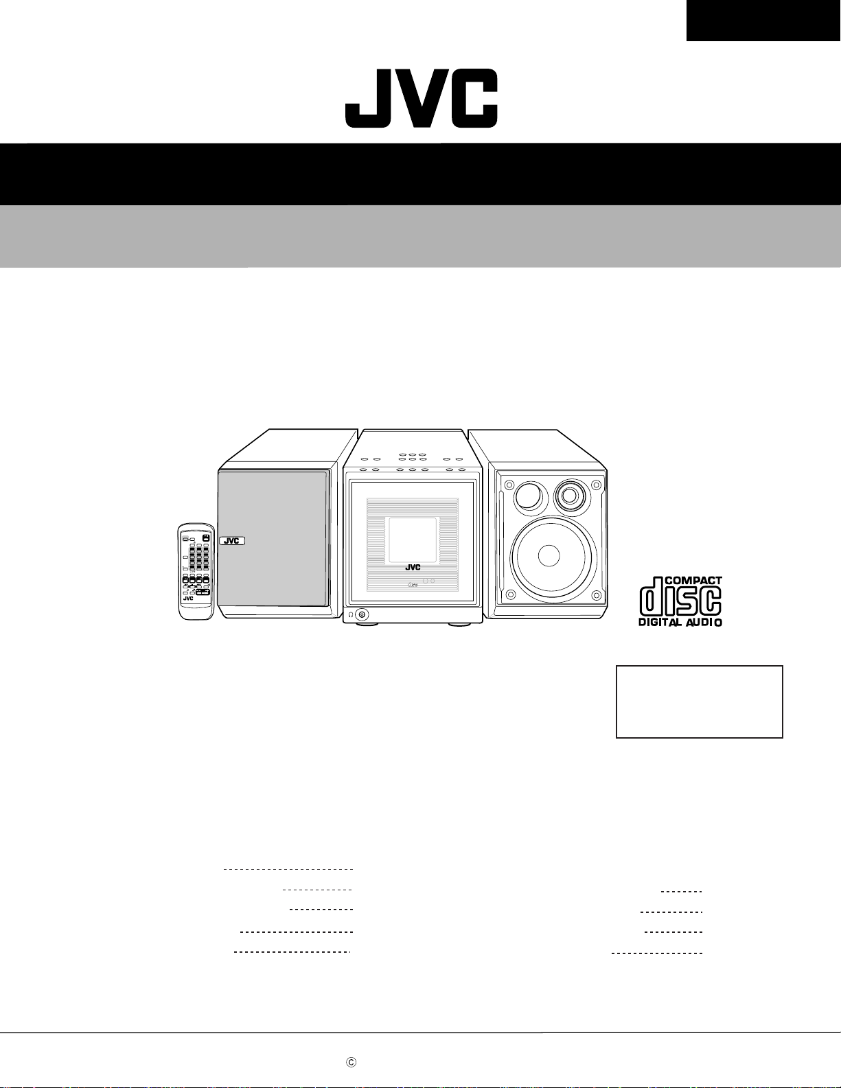
MICRO COMPONENT SYSTEM
UX-A52
UX-A52
UX-A52
COLOR
DIMMER
STANDBY/ON
CLOCK
SLEEP
FM MODE
/TIMER
123
456
DISPLAY
789
0
+
10
10
SET
CANCEL
REV.MODE
REPEAT
PLAY MODE
CD
TAPE
AUX/MD
FM/AM
BEEP
SOUND
AHB
VOLUME
MODE
PRO
RM-SUXA52U
Contents
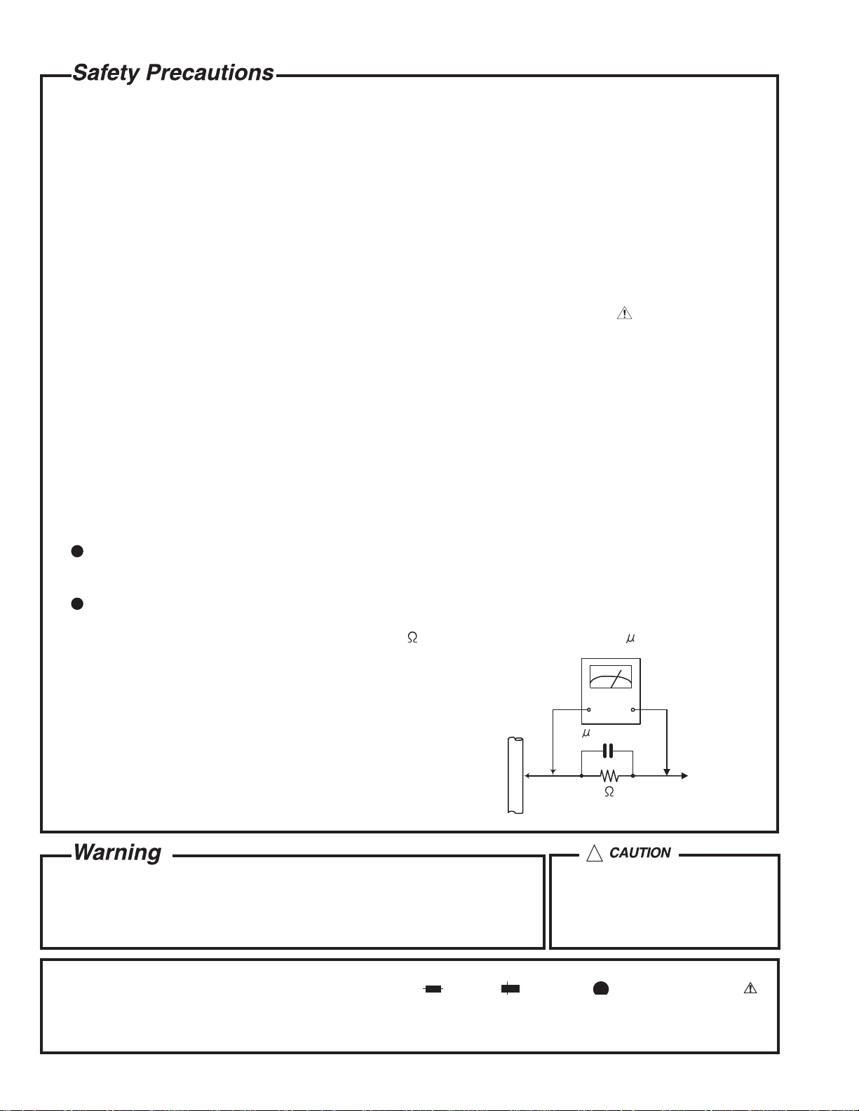
Safety precautions
Preventing static electricity
Important for laser products
Disassembly method
Adjustment method
PHONES
1-2
1-3
1-4
1-5
1-24
MICRO COMPONENT SYSTEM UX-A52
STANDBY/ON
COMPACT
DIGITAL AUDIO
Flow of functional operation
until TOC read (CD)
Maintenance of laser pickup
Replacement of laser pickup
Description of major ICs
Area Suffix
A ---------------------Australia
UF ---------------------- China
1-28
1-29
1-29
1-30~47
COPYRIGHT 2002 VICTOR COMPANY OF JAPAN, LTD.
No.21091
Apr. 2002
1-1
Page 2
UX-A52
1. This design of this product contains special hardware and many circuits and components specially for safety
purposes. For continued protection, no changes should be made to the original design unless authorized in
writing by the manufacturer. Replacement parts must be identical to those used in the original circuits. Services
should be performed by qualified personnel only.
2. Alterations of the design or circuitry of the product should not be made. Any design alterations of the product
should not be made. Any design alterations or additions will void the manufacturer`s warranty and will further
relieve the manufacture of responsibility for personal injury or property damage resulting therefrom.
3. Many electrical and mechanical parts in the products have special safety-related characteristics. These
characteristics are often not evident from visual inspection nor can the protection afforded by them necessarily
be obtained by using replacement components rated for higher voltage, wattage, etc. Replacement parts which
have these special safety characteristics are identified in the Parts List of Service Manual. Electrical
components having such features are identified by shading on the schematics and by ( ) on the Parts List in
the Service Manual. The use of a substitute replacement which does not have the same safety characteristics
as the recommended replacement parts shown in the Parts List of Service Manual may create shock, fire, or
other hazards.
4. The leads in the products are routed and dressed with ties, clamps, tubings, barriers and the like to be
separated from live parts, high temperature parts, moving parts and/or sharp edges for the prevention of
electric shock and fire hazard. When service is required, the original lead routing and dress should be
observed, and it should be confirmed that they have been returned to normal, after re-assembling.
5. Leakage currnet check (Electrical shock hazard testing)
After re-assembling the product, always perform an isolation check on the exposed metal parts of the product
(antenna terminals, knobs, metal cabinet, screw heads, headphone jack, control shafts, etc.) to be sure the
product is safe to operate without danger of electrical shock.
Do not use a line isolation transformer during this check.
Plug the AC line cord directly into the AC outlet. Using a "Leakage Current Tester", measure the leakage
current from each exposed metal parts of the cabinet, particularly any exposed metal part having a return
path to the chassis, to a known good earth ground. Any leakage current must not exceed 0.5mA AC (r.m.s.).
Alternate check method
Plug the AC line cord directly into the AC outlet. Use an AC voltmeter having, 1,000 ohms per volt or more
sensitivity in the following manner. Connect a 1,500 10W resistor paralleled by a 0.15 F AC-type capacitor
between an exposed metal part and a known good earth ground.
Measure the AC voltage across the resistor with the AC
voltmeter.
Move the resistor connection to each exposed metal part,
particularly any exposed metal part having a return path to
the chassis, and meausre the AC voltage across the resistor.
Now, reverse the plug in the AC outlet and repeat each
measurement. Voltage measured any must not exceed 0.75 V
AC (r.m.s.). This corresponds to 0.5 mA AC (r.m.s.).
0.15 F AC TYPE
1500 10W
Good earth ground
AC VOLTMETER
(Having 1000
ohms/volts,
or more sensitivity)
Place this
probe on
each exposed
metal part.
!
1. This equipment has been designed and manufactured to meet international safety standards.
2. It is the legal responsibility of the repairer to ensure that these safety standards are maintained.
3. Repairs must be made in accordance with the relevant safety standards.
4. It is essential that safety critical components are replaced by approved parts.
5. If mains voltage selector is provided, check setting for local voltage.
Burrs formed during molding may
be left over on some parts of the
chassis. Therefore, pay attention to
such burrs in the case of
preforming repair of this system.
In regard with component parts appearing on the silk-screen printed side (parts side) of the PWB diagrams, the
parts that are printed over with black such as the resistor ( ), diode ( ) and ICP ( ) or identified by the " "
mark nearby are critical for safety.
(This regulation does not correspond to J and C version.)
1-2
Page 3
Preventing static electricity
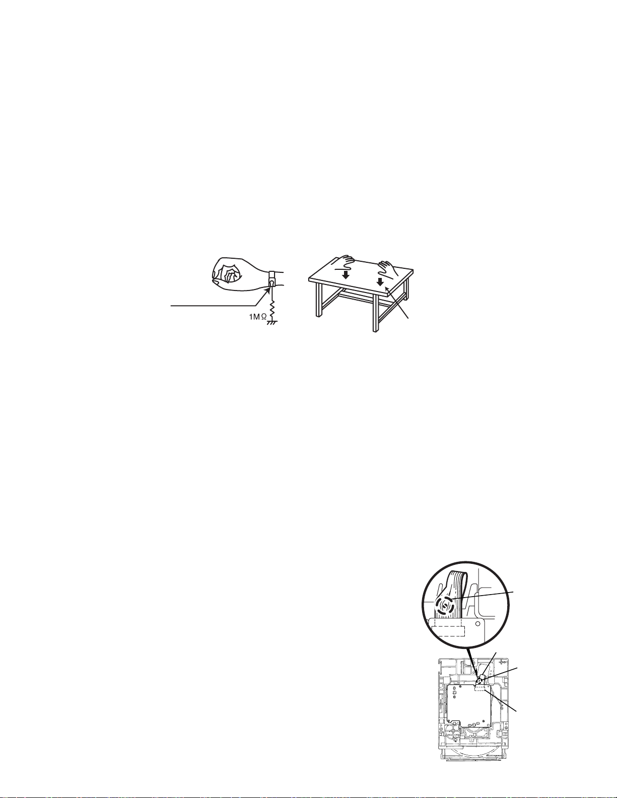
1.Grounding to prevent damage by static electricity
Electrostatic discharge (ESD), which occurs when static electricity stored in the body, fabric, etc. is discharged,
can destroy the laser diode in the traverse unit (optical pickup). Take care to prevent this when performing repairs.
2.About the earth processing for the destruction prevention by static electricity
Static electricity in the work area can destroy the optical pickup (laser diode) in devices such as CD players.
Be careful to use proper grounding in the area where repairs are being performed.
2-1 Ground the workbench
Ground the workbench by laying conductive material (such as a conductive sheet) or an iron plate over
it before placing the traverse unit (optical pickup) on it.
2-2 Ground yourself
Use an anti-static wrist strap to release any static electricity built up in your body.
(caption)
Anti-static wrist strap
UX-A52
Conductive material
(conductive sheet) or iron plate
3. Handling the optical pickup
1. In order to maintain quality during transport and before installation, both sides of the laser diode on the
replacement optical pickup are shorted. After replacement, return the shorted parts to their original condition.
(Refer to the text.)
2. Do not use a tester to check the condition of the laser diode in the optical pickup. The tester's internal power
source can easily destroy the laser diode.
4.Handling the traverse unit (optical pickup)
1. Do not subject the traverse unit (optical pickup) to strong shocks, as it is a sensitive, complex unit.
2. Cut off the shorted part of the flexible cable using nippers, etc. after replacing the optical pickup. For specific
details, refer to the replacement procedure in the text. Remove the anti-static pin when replacing the traverse
unit. Be careful not to take too long a time when attaching it to the connector.
3. Handle the flexible cable carefully as it may break when subjected to strong force.
4. It is not possible to adjust the semi-fixed resistor that adjusts the laser power. Do not turn it
Attention when traverse unit is decomposed
*Please refer to "Disassembly method" in the text for pick-up and how to
detach the substrate.
Shorting round
1.Solder is put up before the card wire is removed from connector on
the CD substrate as shown in Figure.
(When the wire is removed without putting up solder, the CD pick-up
assembly might destroy.)
2.Please remove solder after connecting the card wire with
when you install picking up in the substrate.
Flexible wire
Shorting round
CN601 on
mechanism
board
1-3
Page 4
UX-A52
Important for laser products
1.CLASS 1 LASER PRODUCT
2.DANGER : Invisible laser radiation when open and inter
lock failed or defeated. Avoid direct exposure to beam.
3.CAUTION : There are no serviceable parts inside the
Laser Unit. Do not disassemble the Laser Unit. Replace
the complete Laser Unit if it malfunctions.
4.CAUTION : The compact disc player uses invisible
laserradiation and is equipped with safety switches
whichprevent emission of radiation when the drawer is
open and the safety interlocks have failed or are de
feated. It is dangerous to defeat the safety switches.
VARNING : Osynlig laserstrålning är denna del är öppnad
och spårren är urkopplad. Betrakta ej strålen.
VARO : Avattaessa ja suojalukitus ohitettaessa olet
alttiina näkymättömälle lasersäteilylle.Älä katso
säteeseen.
5.CAUTION : If safety switches malfunction, the laser is able
to function.
6.CAUTION : Use of controls, adjustments or performance of
procedures other than those specified herein may result in
hazardous radiation exposure.
CAUTION
!
Please use enough caution not to
see the beam directly or touch it
in case of an adjustment or operation
check.
ADVARSEL : Usynlig laserstråling ved åbning , når
sikkerhedsafbrydere er ude af funktion. Undgå
udsættelse for stråling.
ADVARSEL : Usynlig laserstråling ved åpning,når
sikkerhetsbryteren er avslott. unngå utsettelse
for stråling.
REPRODUCTION AND POSITION OF LABELS
WARNING LABEL
CLASS 1
LASER PRODUCT
1-4
Page 5
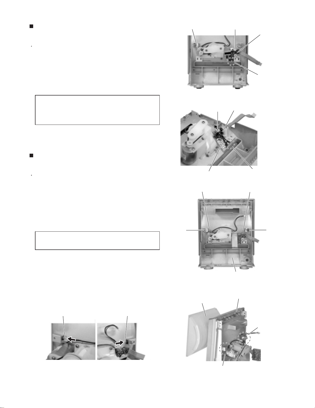
UX-A52
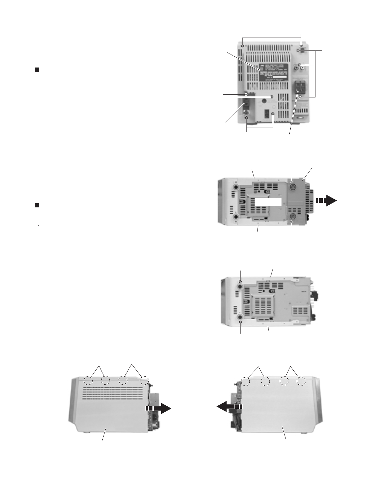
Disassembly method
<Main body>
Removing the rear cover
(See Fig.1 and 2)
1.
Remove the nine screws A on the back of the body.
2.
Remove the two screws B on the bottom of the
body.
3.
Unlock the speaker terminal and the antenna
terminal, then remove the rear cover backward with
releasing the hooks.
Removing the side panels
(See Fig.3 to 5)
Rear cover
A
Antenna terminal
Side panel (R)
A
Speaker terminal
Fig.1
(Bottom)
B
A
A
Rear cover
Prior to performing the following procedure, remove
the rear cover.
1.
Remove the two screws C attaching the side panels
on the bottom of the body.
2.
Remove each side panel backward while releasing
the eight joints a as shown in Fig.4 and 5.
Joint a
Joint a
Side panel (L)
Fig.2
C
C
Side panel (R)
Side panel (L)
Fig.3
Joint a
B
Joint a
Side panel (R)
Fig.4
Side panel (L)
Fig.5
1-5
Page 6
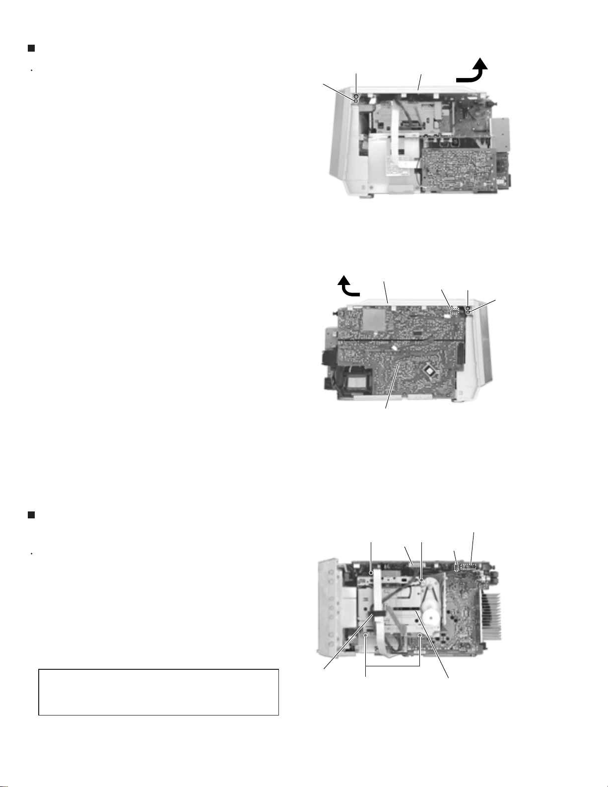
UX-A52
Removing the top panel (See Fig.6 and 7)
Prior to performing the following procedure, remove
the rear cover and the side panels.
1.
Remove the two screws D on each side of the body.
2.
Release the two joints b on each side of the body
and remove the top panel in the direction of the
arrow.
3.
Disconnect the card wires from connector CN705 on
the system control board on the left side of the body.
Joint b
D
Top panel
Top panel
Fig.6
CN705
D
Joint b
Removing the cassette mechanism
assembly section (See Fig.8)
Prior to performing the following procedure, remove
the rear cover, the side panels and the top panel.
1.
Disconnect each wire from connector CN706, CN715
and CN716 on the system control board on top of the
body.
2.
Remove the four screws E retaining the cassette
mechanism assembly section on top of the body.
REFERENCE:
Reference: If necessary, remove the
spacer marked h and the wire from the
Cassette mechanism assembly section.
h (spacer)
System control board
Fig.7
E E
CN715
E
Cassette mechanism section
Fig.8
System control board
CN706
CN716
1-6
Page 7
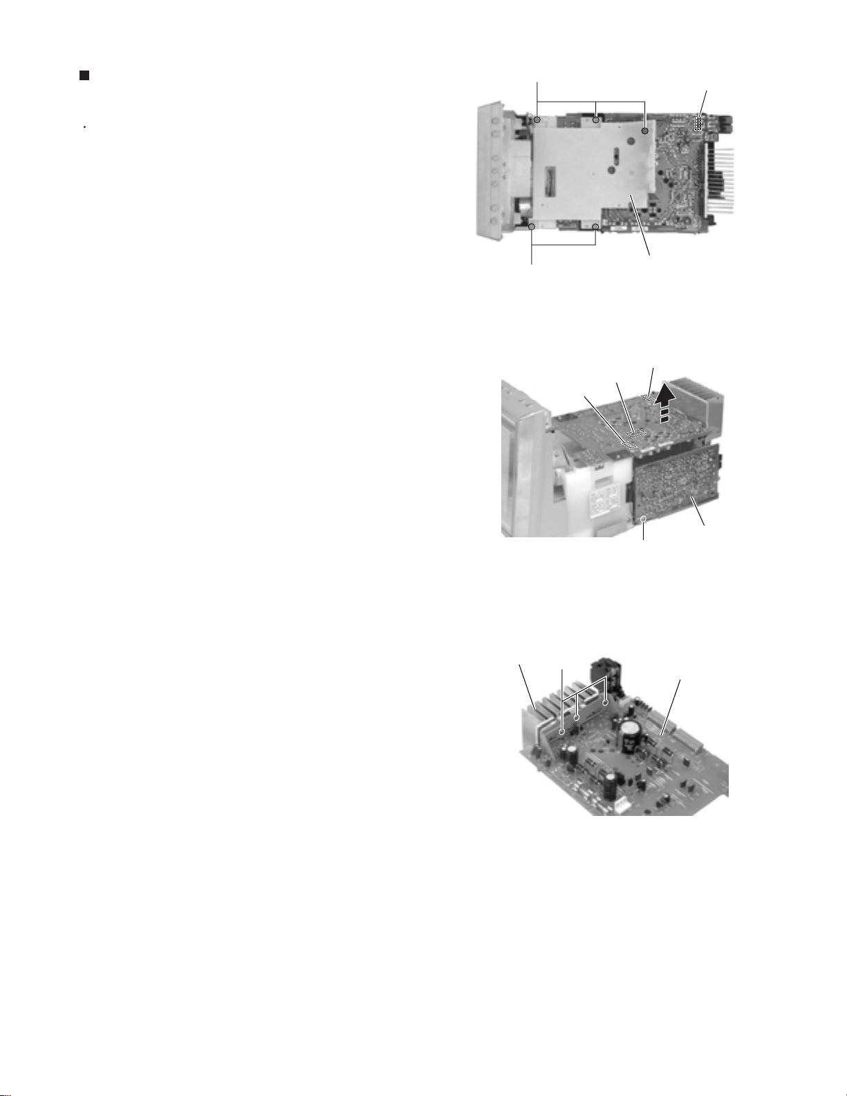
Removing the system control board
(See Fig.9)
UX-A52
Prior to performing the following procedure, remove
the rear cover, the side panels and the top panel.
1.
Disconnect the card wire from connector CN701 and
the wire from connector CN706, CN715, CN716 on
the system control board.
2.
Remove the screw F on the left side of the body.
3.
Disconnect connector CN709, CN711 and CN712 on
the system control board from the body outward.
4.
Disconnect the card wire from connector CN704 on
the underside of the system control board.
Removing the tuner board (See Fig.10)
Prior to performing the following procedure, remove
the rear cover and the right side panel.
CN706
CN716
CN712
CN704
CN715
CN701
CN711
CN709
F
System control board
Fig.9
Tuner board
1.
Disconnect the card wire from connector CN1 on the
tuner board on the right side of the body.
2.
Remove the screw G and remove the tuner board
upward while disengaging the three joints c.
CN1
G
Joints c
Fig.10
1-7
Page 8
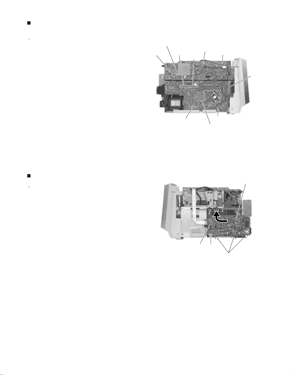
UX-A52
Removing the front panel assembly
(See Fig.11 and 12)
Prior to performing the following procedure, remove
the rear cover, the side panels, the top panel and the
system control board.
1.
Release the two joints d on the lower right and left
sides of the front panel assembly, then remove the
front panel assembly toward the front.
Front panel assembly
Front panel assembly
Fig.11
Joint d
Removing the headphone jack board
(See Fig.13 and 14)
Prior to performing the following procedure, remove
the rear cover, the side panels, the top panel, the
system control board and the front panel assembly
section.
1.
Disconnect the wire from connector CN804 on the
main board.
2.
Remove the plastic rivet fixing the headphone jack
board.
Joint d
Fig.12
Main board
CN804
Headphone jack board
Fig.13
1-8
Plastic rivet
Headphone jack board
Fig.14
Page 9
UX-A52
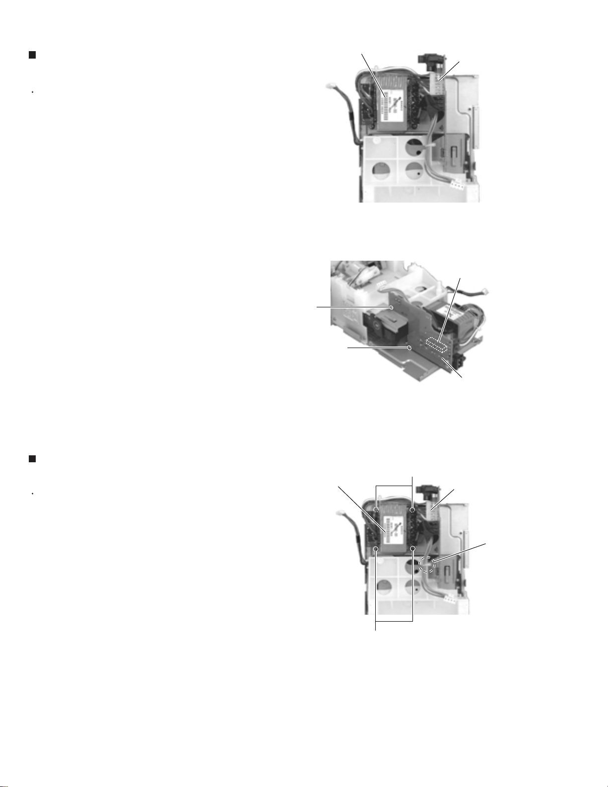
Removing the main board / the heat sink
(See Fig.15 to 17)
Prior to performing the following procedure, remove
the rear cover, the side panels, the top panel, the
cassette mechanism assembly section and and the
system control board.
1.
Disconnect the wire from connector CN804 on the
main board.
2.
Remove the five screws H attaching the cassette
mechanism bracket.
3.
Remove the screw G attaching the grounding
terminal extending from the main board.
4.
Disconnect connector CN805 on the main board
from the AC jack board while pulling out it. Remove
the main board in the direction of the arrow and
disconnect the wire from connector CN803 on the
reverse side of the main board.
5.
Remove the three screws I attaching the heat sink
on the reverse side of the main board.
H
H
Main board
CN804
Cassette mechanism bracket
Fig.15
Main board
CN804
CN805
CN803
Heat sink
Tuner board
G
Fig.16
I
Fig.17
Main board
1-9
Page 10
UX-A52
Removing the AC jack board
(See Fig.18 and 19)
Prior to performing the following procedure, remove
the rear cover, the side panels, the top panel, the
cassette mechanism assembly section, the system
control board and the main board / the tuner board.
1.
Disconnect the wire from connector CN809 on the
AC jack board.
2.
Remove the screw J and screw K attaching the AC
jack board.
Power transformer assembly
J
AC jack board
CN809
Fig.18
CN809
Removing the power transformer
assembly (See Fig.20)
Prior to performing the following procedure, remove
the rear cover, the side panels, the top panel, the
cassette mechanism assembly section, the system
control board and the main board.
1.
Disconnect the wire from connector CN809 on the
AC jack board.
2.
Cut off the band setting the wire on the CD
mechanism cover.
3.
Remove the four screws L attaching the power
transformer assembly.
K
Power transformer
assembly
L
Fig.19
L
Fig.20
AC jack board
AC jack board
CN809
Band
1-10
Page 11
UX-A52
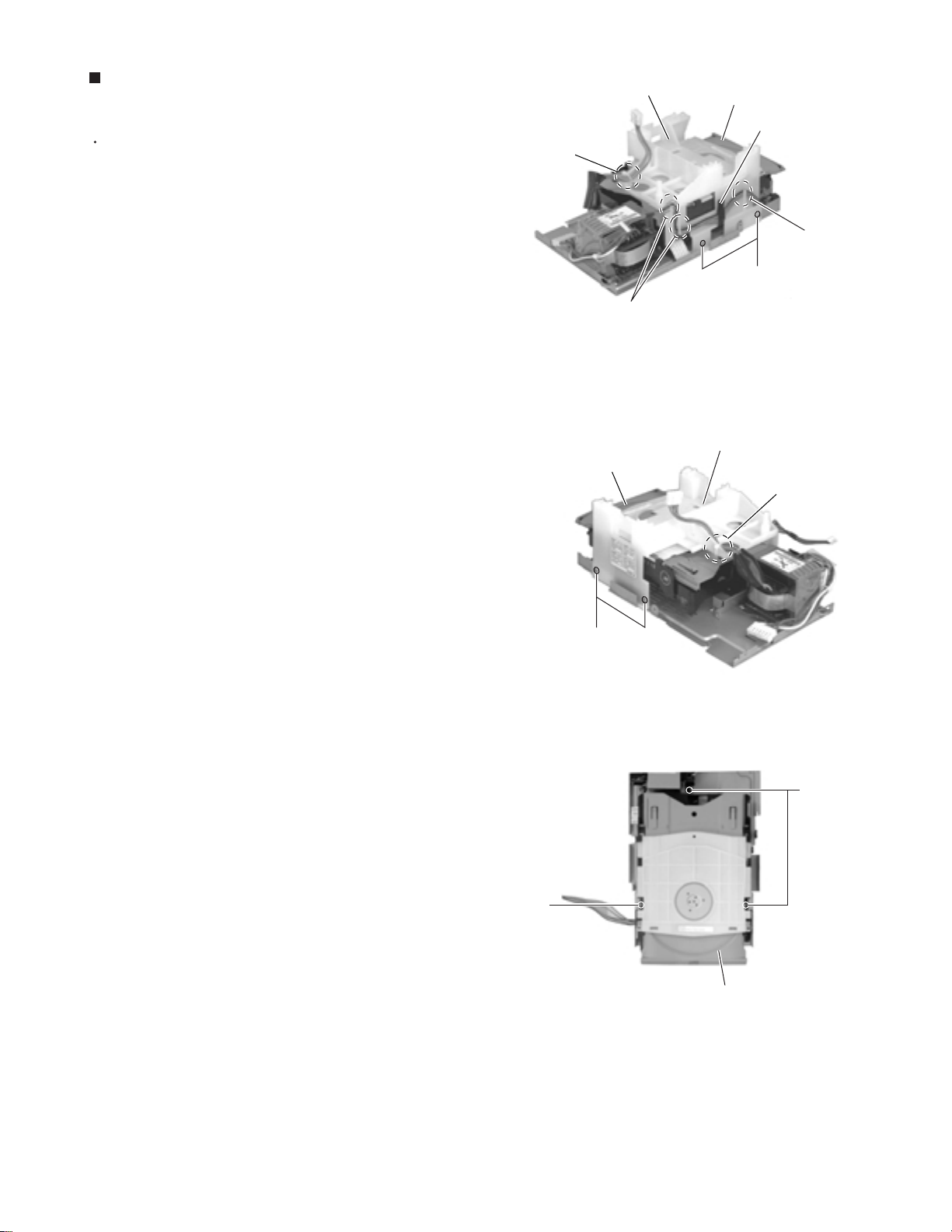
Removing the CD mechanism assembly
(See Fig.21 to 23)
Prior to performing the following procedure, remove
the rear cover, the side panels, the top panel, the
cassette mechanism assembly section, the system
control board, the front panel assembly section, the
main board / the tuner board and the AC jack board.
1.
Cut off the band setting the wire on the CD
mechanism cover.
2.
Release the wire extending from the headphone jack
board from the spacer and the three notches of the
CD mechanism cover on the left side of the body.
3.
Remove the four screws M on the left and right side
of the CD mechanism cover. Then remove the CD
mechanism cover upward.
4.
Remove the three screws N attaching the CD
mechanism assembly.
CD mechanism cover
Band
Notches
CD mechanism assembly
CD mechanism assembly
Spacer
Notch
M
Fig.21
CD mechanism cover
Band
N
M
Fig.22
N
CD mechanism assembly
Fig.23
1-11
Page 12
UX-A52
<Front panel assembly section>
Prior to performing the following procedure, remove
the rear cover, the side panels, the top panel, the
system control board and the front panel assembly
section.
Removing the relay board (See Fig. 24)
Disconnect the wire from connector CN906, CN907
1.
and the card wire from CN908 on the relay board
respectively.
Remove the two screws O.
2.
Removing the drive motor assembly
(See Fig.25)
Prior to performing the following procedure, remove
the relay board.
CN907
Drive motor assembly
CN908
Fig.24
O
O
Door switch board
P
Relay board
CN906
1.
Remove the four screws P attaching the drive motor
assembly.
Removing the belt and the drive motor
(See Fig.26)
REFERENCE:
1.
Remove the two screws Q attaching the plate.
2.
Remove the belt from the two pulleys.
3.
Remove the two screws R attaching the drive motor.
REFERENCE:
The belt and the drive motor can be
removed respectively without removing the
drive motor assembly from the front panel
section.
When removing the drive motor only,
remove the belt from the drive motor
pulleys in advance.
P
Fig.25
Belt
Plate
1-12
Drive motor
R
Fig.26
Q
Page 13
UX-A52
Removing the door switch board
(See Fig.27 and 28)
Prior to performing the following procedure, remove
the relay board.
1.
Loosen the screw S attaching the door switch.
2.
Remove the door switch board while releasing it from
the joint e.
CAUTION:
When reattaching the door switch board,
fit it to the joint e and check the
operating state of the switch before
tightening the screw S.
Removing the LCD section
(See Fig.29 to 31)
Prior to performing the following procedure, remove
the relay board.
1.
Loosen the two screws T attaching the lock lever.
Drive motor assembly
Switch section
Lock lever
S
Fig.27
Door switch board
S
Fig.28
Door switch board
Joint e
Joint e
Lock lever
2.
Push the part f of the lock lever in the direction of
the arrow as shown in Fig.30-1 / 30-2 and disengage
the LCD section from the front panel assembly.
CAUTION:
Because the LCD may come off, hold it
when loosening the screws T.
Lock lever f Lock lever f
T
LCD section
T
Front panel assembly
Fig.29
Front panel assembly
Joint f
Fig.30-1 Fig.30-2
Joint f
Fig.31
1-13
Page 14
UX-A52
Removing the LCD board assembly
(See Fig.32 to 36)
Prior to performing the following procedure, remove
the relay board and the LCD section.
1.
Remove the four screws U attaching the case cover.
2.
Remove the four screws V attaching the LCD panel
on the back of the LCD section.
3.
Remove the LCD cover.
4.
Release the three joints g and remove the LCD
board assembly in the direction of the arrow.
U
V
U
Case cover
U
U
Fig.32
LCD section
LCD panel
Joint g
V
Fig.33
Fig.34
Joint g
Joint g
1-14
LCD cover
LCD board assembly
Fig.35 Fig.36
Page 15
<Top panel section>
Prior to performing the following procedure, remove
the rear cover, the side panels and the top panel.
Removing the operation switch board
(See Fig.37)
1.
Remove the seven screws W attaching the
operation switch board on the reverse side of the top
panel.
W
Cassette amplifier board
W
Fig.37
UX-A52
Operation switch board
W
1-15
Page 16

UX-A52
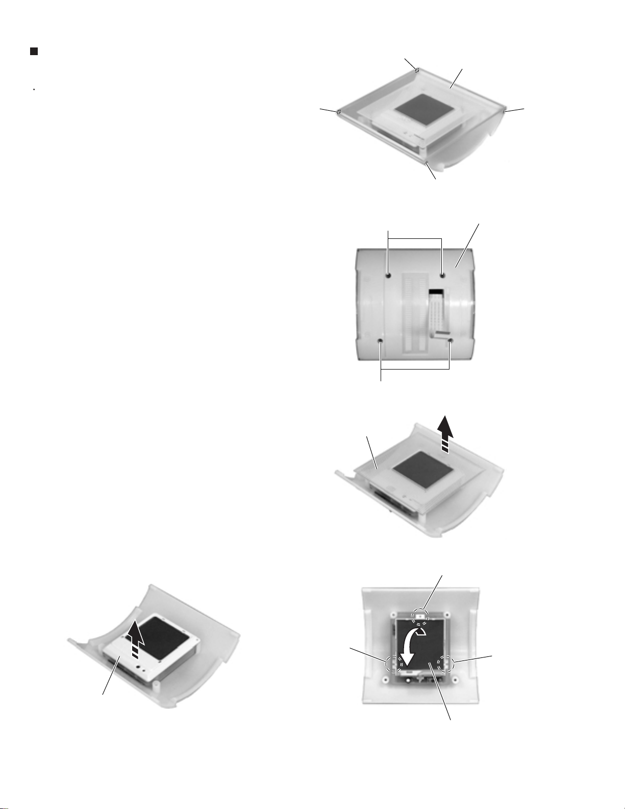
<CD Mechanism Assembly>
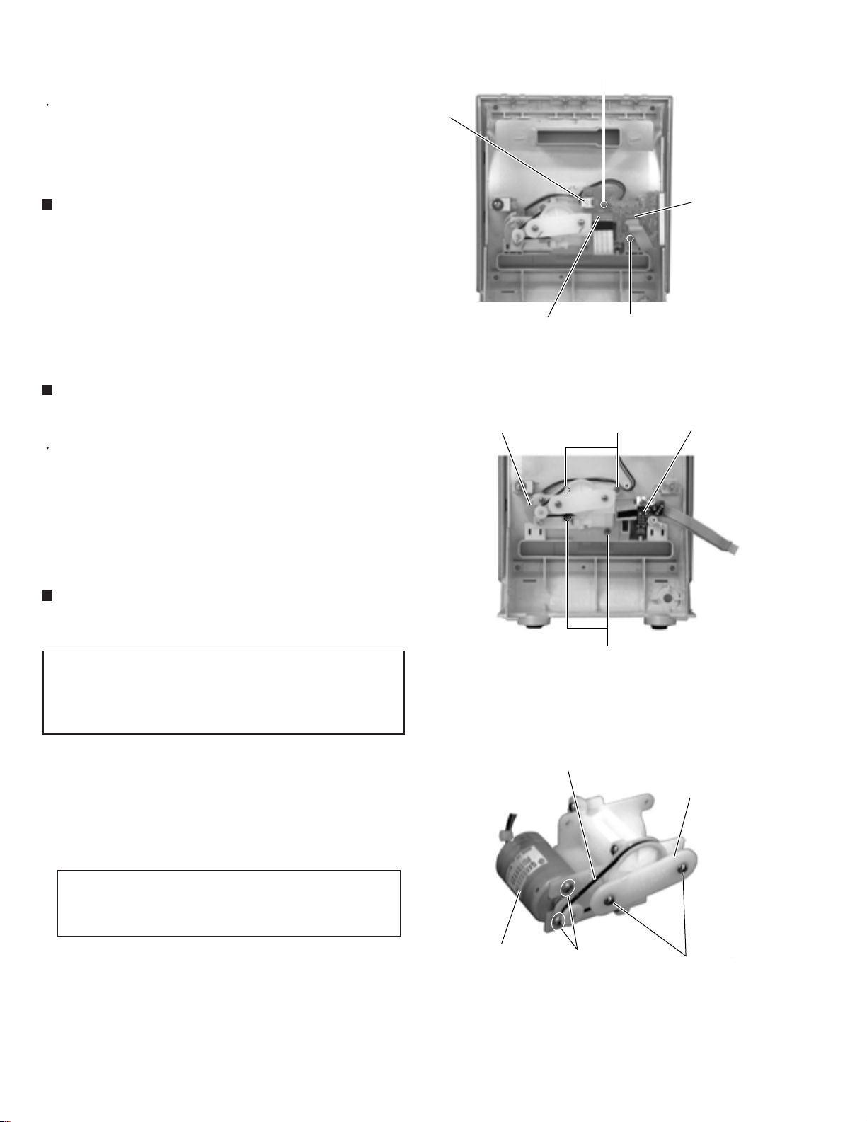
Removing the CL. Base Assembly and Tray
(Refer to Figs. 1 to 5.)
1. Remove the two screws A fastening the CL. base
assembly from the top of the CD mechanism
assembly.
2. Move the CL. base assembly diagonally upwards
as indicated by the arrow to release it from the two
hooks a.
3. Turn the idle gear in the arrow-marked direction
from the upper side of the CD mechanism
assembly. Accordingly, the TRAMECHA assembly
moves downwards.
Note: When drawing out the tray, shift down the
TRAMECHA assembly to the position where
the tray does not contact the T-T assembly
of the TRAMECHA assembly.
4. Draw out the tray frontwards for removing it.
CL. base assembly
A
TRAMECHA
assembly
Hook a
Fig. 1
A
Hook a
Idle gear
Note: When reinstalling the tray:
Turn the idle gear so that the part b of the
tray gear is positioned in the part c shown in
Fig. 4. (Eject position)
Engage the right and left hooks d and e of
the tray with the right and left grooves of the
TRAMECHA assembly respectively for
retaining the tray.
Idle gear
Tray gear
Tray
Fig. 2
TRAMECHA assembly
Idle gear
Tray
Fig. 3
1-16
Hook d
Hook d
Tray
Tray gear
Part c
Part b
Fig. 4Fig. 5
Page 17

UX-A52
Removing the TRAMECHA Assembly
(Refer to Figs. 6 to 9.)
Remove the CL. base assembly and tray.
Reference: The TRAMECHA assembly can be
removed without removal of the
mechanism board.
1. If the TRAMECHA assembly is lowered and it is
located out of the PLAY position, turn the idle gear
in the arrow-marked direction so that the hole in the
part f of the tray gear meets the hole on the CL.
base assembly. (Set the TRAMECHA assembly at
the PLAY position.)
2. Remove the three screws B fastening the
TRAMECHA assembly and then remove the
TRAMECHA assembly upwards from the front side.
3. At the same time, remove the spring from the groove of
the CH. base assembly in the part g of the TRAMECHA
assembly.
Note: When reinstalling the TRAMECHA assembly:
Check to see if the spring is properly
engaged with groove of the CH. base
assembly in the part g of the TRAMECHA
assembly.
After making sure that the three insulators of
the TRAMECHA assembly are properly set
on the bosses of the L. base assembly's
guide, fasten them with the screws.
TRAMECHA
assembly
B
Part g
L. base assembly
B
Fig. 6
Fig. 7
B
Idle gear
Tray gear
Tray gear
Part f
Spring
Part g
Fig. 8
Spring
Groove of CH. base assembly
Fig. 9
1-17
Page 18

UX-A52
Removing the Mechanism Board
(Refer to Fig 10.)
Reference:The mechanism board can be removed
without removal of the TRAMECHA
assembly.
C
Flexible wire
Shorting round
Note: Before disconnecting the flexible wire coming
from the pickup from the connector, be sure to
solder its shorting round.
If the flexible wire is connected without
soldering, it may cause breakdown of the
pickup.
1. Solder the shorting round of the flexible wire
connected with the mechanism board from the back
of the mechanism assembly.
2. Disconnect the flexible wire from the connector
CN601 on the mechanism board.
3. Remove the three screws C fastening the
mechanism board.
4. Unsolder the two points of the part h and one point
of the part i of the mechanism board. Then, remove
the mechanism board upwards.
Note: When reinstalling the mechanism board,
connect the flexible wire coming from the
pickup to the connector first and then remove
the solder from the shorting round of the
flexible cable.
Soldered
part h
C
CN601 on
mechanism
board
C
Soldered part i
Fig. 10
1-18
Page 19

UX-A52
Removing the Pickup
(Refer to Figs. 11 to 14.)
Remove the CL. base assembly and tray.
Remove the TRAMECHA assembly.
Reference: The pickup can be removed without
removal of the mechanism board.
Note: Before disconnecting the flexible wire coming
from the pickup from the connector, be sure to
solder its shorting round.
If the flexible wire is connected without
soldering, it may cause breakdown of the
pickup.
1. Solder the shorting round of the flexible wire
connected with the mechanism board from the back
of the TRAMECHA assembly.
2. Disconnect the flexible wire from the connector
CN601 on the mechanism board.
Part j of
rack plate
CH. base
assembly
Flexible wire
Shorting round
CN601 on
mechanism
board
Fig. 11
T-T assembly
Pickup assembly
3. Turn the idle gear in the arrow-marked direction from
the top of the TRAMECHA assembly so that the
pickup assembly is shifted to the reverse side of the
T-T assembly.
Move the pickup assembly until the part j of the rack
plate in the lower part of the pickup assembly comes
out of the CH. base assembly.
4. Remove the two screws D retaining the shaft of the
pickup assembly. Next, disengage the hook k from
the CH. base assembly and then remove the pickup
assembly together with the shaft.
5. Pull the shaft out of the pickup.
6. Remove the two screws E fastening the rack plate
from the pickup.
7. Remove the screw F retaining the P.S. spring from
the pickup.
D
Idle gear
Shaft
Fig. 12
Pickup assembly
Part k
CH. base
assembly
D
Fig. 13
Pickup
Part j
Rack plate
P.S. spring
F
E
Fig. 14
1-19
Page 20

UX-A52
Reinstalling the Pickup Assembly
(Refer to Figs. 15 and 16.)
Reference: Refer to the explanation of "Removing
the Pickup" on the preceding page.
1. Fit the P.S. spring and rack plate to the pickup.
2. Insert the shaft into the pickup.
3. Engage the hook k of the pickup assembly with the
CH. base assembly first, and set the part j of the
rack plate in the opening I next. Then, reinstall the
pickup assembly while shifting it to the T-T side
(inward) so that the part m of the rack plate is
positioned as shown in Fig. 16.
4. Move the pickup assembly to the center position
and fasten the shaft with the two screws D. (Make
sure that the part n of the rack plate is correctly
engaged with the middle gear.)
5. After passing the flexible wire coming from the
pickup through the opening of the CH. base
assembly, connect it to the connector CN601.
Part I
Part j
Part m
Part k
Pickup
assembly
CH. base
assembly
Fig. 15
Middle gear
Note: When reinstalling the pickup assembly,
remove the solder from the shorting round
after connecting the flexible wire coming from
the pick to the connector CN601.
Removing the Feed Motor Assembly
(Refer to Fig. 17.)
Remove the CL. base assembly and tray.
Remove the mechanism board.
Remove the two screws E fastening the feed motor
assembly from the top of the mechanism assembly.
Rack plate
Part n
Fig. 16
E
Feed motor assembly
1-20
Fig. 17
Page 21

UX-A52
<Cassette mechanism section>
CAUTION:
Removing the side bracket (L) and (R) /
load board (See Fig.1 to 4)
1.
Remove the E-washer attaching the load arm on the
right side of the body.
2.
Turn the load arm in the direction of the arrow to
release from the cassette hook at the joint a.
3.
Remove the spring (1) attaching the trig lever.
4.
Move the trig lever in the direction of the arrow and
release it from the two holes b.
5.
Remove the screw A attaching the load board on
the right side of the body and unsolder the wire
extending from the sub motor.
Prior to performing the following
procedures, turn the mode gear in the
direction of the arrow to move each section
to the eject position.
Joint a
Slide bracket
Load arm
E-washer
Load arm
Fig.1
Hole b
Hole b
Spring (1)
REFERENCE:
6.
Remove the spring (2) and the holder collar on the
right side of the body.
7.
Remove the two screws B attaching the side
bracket unit (R) in the direction of the arrow.
8.
Remove the four screws C attaching the side
bracket (L) in the direction of the arrow.
The side bracket unit (R) can be
removed even if the load board is
attached. In such case, make sure to
unsolder the wire extending from the
sub motor.
A
Side bracket unit (L)
C
Fig.2
Load board
Soldering
Fig.3
Cassette hanger assembly
C
C
B
C
Side bracket unit (R)
B
Spring (2)
Holder collar
Fig.4
1-21
Page 22

UX-A52
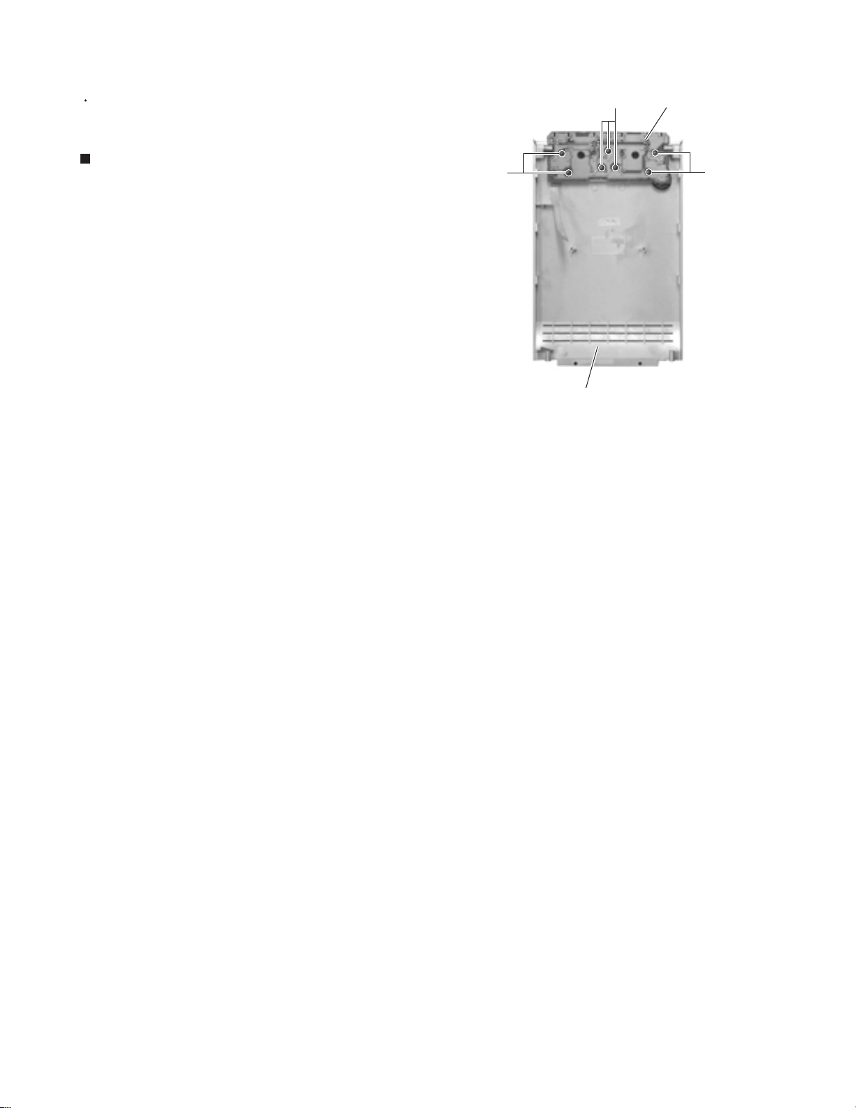
Removing the cassette hanger assembly
/ cassette holder (See Fig.5)
Prior to performing the following procedure, remove
the side bracket (L) and (R).
1.
Remove the slit washer attaching the cassette
hanger assembly and pull out the pin.
2.
Move the cassette hanger assembly in the direction
of the arrow to release the boss of the joint c on the
left rear side and detach the cassette hanger
assembly upward.
REFERENCE:
The cassette hanger assembly is
detached with the cassette holder.
Removing the pinch roller (F) and (R)
(See Fig.6 to 8)
Pin
Cassette hanger assembly
Cassette holder
E-washer
Fig.5
Prior to performing the following procedure, remove
the side bracket (L), (R), cassette hanger assembly /
cassette holder.
1.
Release the tab d in the direction of the arrow and
pull out the pinch roller upward.
REFERENCE:
The above method is for removing the
pinch roller (F) and (R).
Pinch roller (F)
Pinch roller (F)
Pinch roller (R)
Pinch roller (R)
Fig.6
1-22
Tab d
Tab d
Fig.8Fig.7
Page 23

UX-A52
Removing the head assembly / head
board (See Fig.9 and 10)
Prior to performing the following procedure, remove
the side bracket (L), (R), cassette hanger assembly /
cassette holder.
1.
Remove the spring on the lower side of the head
assembly.
2.
Remove the two screws D and remove the head
assembly upward.
3.
Remove the screw E attaching the head board.
Unsolder the flexible wire extending from the head
assembly if necessary.
Head board
Fig.9
Head assembly
DD
Head assembly
Soldering
E
Removing the flywheel assembly (F) and
(R) (See Fig.11 and 12)
Prior to performing the following procedure, remove
the side bracket (L), (R), cassette hanger assembly /
cassette holder.
1.
Remove the belt and sub belt on the bottom of the
body.
2.
Remove the polywasher from the flywheel (F) and
(R) on top of the body.
3.
Pull out the flywheel (F) and (R).
Sub belt
Flywheel assembly (R)
Fig.10
Belt
Flywheel assembly (F)
Fig.11
Polywasher
Fig.12
Polywasher
1-23
Page 24

UX-A52
Adjustment method
1. Jigs and test instruments
Test disc (CTS-1000)
Test tape (VT712)
Test tape (VT703)
Test tape (AC225)
2. Adjustment and check items
1) Indications in the modes that all LCD's are on
2) CD section
(1) Indication of the C1 error
(2) Cancel of the C1 error indication
3. Adjustment and check method
1) CD section
(1) Indication of the C1 error
While pressing both the POWER key
and BACK SKIP key on the main unit,
turn on the primary power supply.
FL indication
CRC = 0
Press the CD OPEN/CLOSE key
and insert the test disk.
Press the CD PLAY key. The set starts
counting and the number of error correction
times is indicated every 10 seconds.
FL indication
CRC = ***
(2) Cancel of the C1 error indication
To cancel the C1 error indication, cut off the power supply.
200 Hz or less
1-24
Page 25

Cassette section
UX-A52
Playback/Recording &
eraser head
Head azimuth
adjusting screw
(Forward side)
Head azimuth
adjusting screw
(Forward side)
Playback/Recording &
eraser head
Removing the Cassette Mechanism Assembly
1. Remove the rear cover.
2. Remove the side panels (right and left).
3. Remove the cassette mechanism assembly.
4. Remove the four screws S fastening the cassette mechanism assembly from the back
of the cassette mechanism.
5. Press the EJECT button on the front side of the cassette mechanism assembly to open
the cassette door, and then remove the cassette mechanism assembly.
Head azimuth
adjusting screw
(Reverse side)
Head azimuth
adjusting screw
(Reverse side)
BIAS TEST POINT
GND
PCB FMB
1-25
Page 26

UX-A52
Check and adjustment of the Head amplifier section
Item
1. Head azimuth
adjustment
2. Tape speed
adjustment
(Reference value)
Speed difference
between the
normal and
reverse directions
Check/Adjustment Method
1) Play back the end part of the test tape VT703 (10 kHz).
2) Adjust the head azimuth screws so that the output becomes
maximum in both the normal and reverse directions. After
adjustment, lock the screws with screw bond without fail.
Measuring output terminal: Speaker terminal, 4 load resistance
Difference between L-ch and R-ch: Within 3 dB
Difference between FWD and REV directions: Within 4 dB
Adjust max level in FWD and REV. After adjusting, should be
Applied bond (THREEBOND 1401 A/C) to screw.
Azimuth screw
Screw for
REV
Neji Lock
1) Play back the end part of the test tape VT712 (3 kHz).
2) Adjust VR37 so that the frequency counter reads 3000 15 Hz
in playback in the normal direction.
Measuring output terminal: Speaker terminal
Make sure that speed difference between the normal and
reverse directions is 60 Hz or less by reading of the frequency
counter. (With the beginning part of the test tape)
Azimuth
for FWD
Neji Lock
Adjusting
Point
Head
azimuth
screw
phase
(0 ) (45 )
VR37
Standard
Value
Maximum
output
3000 15Hz
60 Hz or less
Wow and flutter
3. Recording /
playback
frequency
characteristic
adjustment
(Reference value)
Recording bias
frequency
(Reference value)
Erasing current
Play back the end part of the test tape VT712 (3 kHz).
Make sure that the wow and flutter meter reads 0.25 % (WRMS)
or less.
1) Set a blank cassette tape (Type I: AC225) and enter the set into
the recording pause mode.
2) Cancel the pause mode and start recording. Repeat to input the
1 kHz and 10 kHz reference signals alternately from the CD test
disk to record the signals on the blank tape.
3) While playing back the repeatedly input 1 kHz and 10 kHz
reference signals, adjust VR31 so that output level of 10 kHz
signals is +2 dB 1 dB of 1 kHz.
1) Set a blank cassette tape (Type I: AC225) and enter the set into
the recording pause mode.
2) Make sure that the bias frequency at the bias test point (Refer on
1-25 board drowing) on the head amplifier board is 70 9 kHz.
1) Set a blank cassette tape (Type I: AC225) and enter the set into
the recording pause mode.
2) After connecting a 1 resistor to the erasing head in series,
cancel the pause mode and start recording. Connect the
electronic voltmeter to both the terminals and measure the
erasing current.
0.25 %
(WRMS) or
less
VR31
-1dB 1dB
70 9kHz
Erasing
current: 60
mA (Type I
tape)
1-26
Page 27

Extension code connecting method
Cassette mechanism assembly
UX-A52
System control board
(CN706, CN715, CN716)
QUQ110-1940BJ
CD mechanism assembly
CD servo control board
(CN651)
Extension wire
System control board
(CN704)
1-27
Page 28

UX-A52
Flow of functional operation until TOC read (CD)
Power ON
Power Key
Slider turns REST
SW ON.
Automatic tuning
of TE offset
Check to see if the voltage at the
pin 72 of IC701 or pin 5 of CN602
becomes 0 V for an instant. (The
moment the switch is turned on,
the voltage becomes 0 V.)
Check Point
VREF
Tracking error waveform at TOC reading
pin 25 of
IC601(TE)
Approx
1.8V
Tracking
servo
Disc statas
to rotate
off statas
Automatic measurement
of TE amplitude and
automatic tuning of
TE balance
Approx.3sec
Tracking
servo
on statas
Disc to be
braked to stop
TOC reading
finishes
500mv/div
2ms/div
Fig.1
Laser ON
Detection of disc
Automatic tuning of
Foucus offset
Automatic measurement of
Focus A-curve amplitude
Disc is rotated
Focus servo ON
(Tracking servo ON)
Automatic measurement of
Tracking error amplitude
Automatic tuning of
Tracking error balance
Make sure of the H level at
the pin 40 of IC603.
Confirm that the Focus error
S-curve siganl at the pin28 of
IC603 is approx.2Vp-p
Confirm that the siganl from
pin24 IC603 (R645) is 0V as
a accelerated pulse during
approx.400ms.
Make sure that the TE
signal (1.8 Vp-p approx.)
indicating the tracking
servo off status is output
from the pin 25 (one side
of R609) of IC601.
1-28
Automatic tuning of
Focus error balance
Automatic tuning of
Focus error gain
Automatic tuning of
Tracking error gain
TOC reading
Play a disc
Confirm the eys-pattern
at the lead of TP602
Page 29

UX-A52
Maintenance of laser pickup
(1) Cleaning the pick up lens
Befor you replace the pick up, please try to
clean the lens with a alcohol soaked cotton
swab.
(2) Life of the laser diode (Fig.1)
When the life of the laser diode has expired,
the following symptoms wil appear.
(1) The level of RF output (EFM output:ampli
tude of eye pattern) will below.
Is RF output
1.25 0.22Vp-p?
YES
O.K
NO
Replace it.
Replacement of laser pickup
Turn off the power switch and,disconnect the
power cord from the ac outlet.
Replace the pickup with a normal one.(Refer
to "Pickup Removal" on the previous page)
Plug the power cord in,and turn the power on.
At this time,check that the laser emits for
about 3seconds and the objective lens moves
up and down.
Note: Do not observe the laser beam directly.
Play a disc.
(Fig.1)
(3) Semi-fixed resistor on the APC PC board
The semi-fixed resistor on the APC printed
circuit board which is attached to the pickup
is used to adjust the laser power.Since this
adjustment should be performed to match the
characteristics of the whole optical block,
do not touch the semi-fixed resistor.
If the laser power is lower than the specified
value,the laser diode is almost worn out, and
the laser pickup should be replaced.
If the semi-fixed resistor is adjusted while
the pickup is functioning normally,the laser
pickup may be damaged due to excessive current.
Check the eye-pattern at TP602.
Finish.
1-29
Page 30

UX-A52
Description of major ICs
UPD784216AGF (IC701) : System micon
1. Pin layout
1
100
76
75
2. Block diagram
INTP2/NMI
INTP0.INTP1.
INTP3-INTP6
TI00
TI01
TO0
TI1
TO1
TI2
TO2
TI5/TO5
TI6/TO6
TI7/TO7
TI8/TO8
RTP0-RTP7
ANO0
ANO1
REF1
AV
AV
SS
ANI0-ANI7
REF0
AV
AV
D0
AV
SS
P03/INTP3
PCL
BUZ
25
26
PROGRAMMABLE
INTERRUPT
CONTROLLER
TIMER/EVENT
COUNTER
(16BITS)
TIMER/EVENT
COUNTER1
(8BITS)
TIMER/EVENT
COUNTER2
(8BITS)
TIMER/EVENT
COUNTER5
(8BITS)
TIMER/EVENT
COUNTER6
(8BITS)
TIMER/EVENT
COUNTER7
(8BITS)
TIMER/EVENT
COUNTER8
(8BITS)
WATCH TIMER
WATCHDOG TIMER
REAL-TIME
OUTPUT PORT
D/A
CONVERTER
A/D
CONVERTER
CLOCK OUTPUT
CONTROL
BUZZER OUTPUT
50
51
78K/1V
CPU CORE
RAM
8192BITS
ROM
128K BITS
UART/IOE1
BAUD-RATE
GENERATOR
UART/IOE2
BAUD-RATE
GENERATOR
CLOCKED
SERIAL
INTERFACE
BUS I/F
PORT0
PORT1
PORT2
PORT3
PORT4
PORT5
PORT6
PORT7
PORT8
PORT9
PORT10
PORT12
PORT13
SYSTEM CONTROL
RxD1/SI1
TxD1/SO1
ASCK1/SCK1
RxD2/SI2
TxD2/SO2
ASCK2/SCK2
SI0
SO0
SCK0
AD0-AD7
A0-A7
A8-A15
A16-A19
RD
WR
WAIT
ASTB
P00-P06
P10-P17
P20-P27
P30-P37
P40-P47
P50-P57
P60-P67
P70-P72
P80-P87
P90-P95
P100-P103
P120-P127
P130.P131
RESET
X1
X2
XT1
XT2
V
DD
V
SS
TEST
1-30
Page 31

3. Pin function (1/2)
UX-A52
Pin No.
1
2
3
4
5
6
7
8
9
10
11
12
13
14
15
16
17
18
19
20
21
22
23
24
25
26
27
28
29
30
31
32
33
34
35
36
37
38
39
40
41
42
43
44
45
46
47
48
49
50
Symbol
FAUX2
NC
RDSDATA
MPX
TUST
NC
FTUNER
FCD
VDD
NC
PBMUTE
NC
PIN
LEDCTL
BUZER
MDPOUT
MDRESET
SMUTE
NC
NC
POUT
VPP
UP
RMT0
RMT1
MIDDLE
DOWN
RMSPEED
VOLCK
VOLCE
VOLDA
AHB
BUB
BTCL
NC
XKILL
VDD
X1
X2
VSS
XT2
XT1
RESET
REM
RDSCK
NC
PHOTO
SAFTEY4
NC
NC
I/O
Not connected
-
Not connected
-
Not connected
-
Stereo detection
I
Stereo indicator detection
I
Not connected
O
Tuner switch output
O
CD switch output
O
Connected with VDD
-
Not connected
-
PB mute output
O
Not connected
-
Power key input
I
LED control output
O
Buzzer output
O
MD PB output
O
MD reset output
O
System mute output
O
Not connected
-
Not connected
-
Power-on control output
O
GND
I
Door position detection - UP
I
Door open/shut motor control output
O
Door open/shut motor control output
O
Door position detection - MIDDLE
I
Door position detection - DOWN
I
Door open/shut motor speed control output
O
Volume control clock
O
Volume control chip enable
O
Volume control data
O
Active hyper bus control
O
Backup detection
I
Battery control
O
Not connected
O
Power-off clock oscillator control
I/O
Power supply
I
Master clock
I
Master clock
O
GND
I
Clock for timer
O
Clock for timer
I
Power-on reset
I
Remote control sensor
I
Not connected
-
Not connected
-
Reel pulse detection
I
Current detection
I
-
Not connected
Not connected
-
Description
1-31
Page 32

UX-A52
3. Pin function (2/2)
Pin No.
51
52
53
54
55
56
57
58
59
60
61
62
63
64
65
66
67
68
69
70
71
72
73
74
75
76
77
78
79
80
81
82
83
84
85
86
87
88
89
90
91
92
93
94
95
96
97
98
99
100
Symbol
AVRE F
AVREF0
SEFTY2
SEFTY3
LDCK
FKEY1
VERSION
FKEY2
KEY1
SEFTY1
VSS
RCDL
BCDL
AVREF1
RXD
TXD
NC
CDRXD
CDTXD
CDRST
GCDL
NC
T UDATA
T UDATA
TUCK
NC
NC
NC
NC
NC
NC
NC
NC
NC
NC
NC
NC
SCL
CS
RESET
SDA
NC
RS
NC
NC
S DATA
SCK
STTA
PLAY
VSS
UPD784216AGF(2/2)
I/O
Reference power supply +5 V
I
Reference power supply +5 V
I
Current detection
I
Current detection
I
Description
I/O
Function switch key input
I
Destination switch input
I
Function switch key input
I
Cassette key input
I
Current detection
I
GND
I
LED color display control
O
LED color display control
O
Reference power supply +5 V
I
Digital input
I
Digital output
O
Not connected
-
CD digital input
I
CD digital output
O
CD reset
O
LED color display control
O
Not connected
-
1
Tuner data
I
Tuner data
O
Tuner clock
O
Not connected
-
Not connected
-
Not connected
-
Not connected
-
Not connected
-
Not connected
-
Not connected
-
Not connected
-
Not connected
-
Not connected
-
Not connected
-
Not connected
-
LCD clock
O
LCD power supply
O
LCD reset
O
LCD serial data
I/O
Not connected
-
LCD start
I
Not connected
-
Not connected
-
Cassette control serial data
I/O
Cassette control serial clock
I/O
Cassette control status signal
I/O
Cassette PB switch detection
O
I
GND
1-32
Page 33

AN22000A-W (IC601) : RF head amp.
1. Pin layout
1234 5678910111213141516
2. Block diagram
OFTR
COFTR
12
BDO
11
BCDO
14
13
3TOUT
CEA
9
OFTR
BDO
10
3TENV
NRFDET
15
FEN
22
FEOUT
23
SUBT
TEN
21
20
SUBT
19
17181920212223242526272829303132
18
VDET
UX-A52
PDLDVDETTEBPFTEOUT
2
1
3
VCC
16
GND
2526
8
ARF
7
CAGC
RFIN
56
RFOUT
4
RFN
3. Pin function
Pin No.
1
2
3
4
5
6
7
8
9
10
11
12
13
14
15
16
AGC
A
GCA BCA
AMP
32
31
C
NRFDET
RF_EQ
Function
APC amp input terminal.
APC amp output terminal.
Power supply.
RF amp negative input terminal.
RF amp output terminal.
AGC input terminal.
AGC loop filter capacitor connection terminal.
AGC output terminal.
Capacitor connection terminal for HPF-amp.
3TENV output terminal.
Capacitor connection terminal for RF enberope detection.
BDO output terminal.
Capacitor connection terminal for RF enverope detection.
OFTR output terminal.
NRDET output terminal.
Ground terminal.
GCA BCA
AMP
30
29
B
D
E
GCA BCA
AMP
27
Pin No.
GCA BCA
AMP
28
F
Function
VREF output terminal.
17
VDET output terminal.
18
VDET input terminal.
19
TE amp. output terminal.
20
TE amp. negative input terminal.
21
FE amp. negative input terminal.
22
FE amp. output terminal.
23
GCTL & APC terminal.
24
FBAL control terminal.
25
TBAL control terminal.
26
Tracking signal input terminal 1.
27
Tracking signal input terminal 2.
28
Focus signal input terminal 4.
29
Focus signal input terminal 3.
30
Focus signal input terminal 2.
31
Focus signal input terminal 1.
32
TBAL FBAL
24
GCTL
17
VREF
1-33
Page 34

UX-A52
UPD780024AGKB21 (IC251) : Unit micon
1. Pin layout
64 ~ 49
1
48
~
16
17 ~ 32
2. Pin function (1/2)
Pin
No.
Symbol I/O Description
P50/A8
1
P59/A9
2
MCS
3
MRDY
4
CDINDEX
5
CDEMP
6
CDTNO
7
CDCOPY
8
VSS0
9
VDD0
10
P30
11
P31
12
P32
13
MUTE
14
SUBQ
15
P35/SO31
16
SQCK
17
KCMND
18
M STAT
19
MCLK
20
RXDO
21
TXDO
22
P25/SCK0
23
VDD1
24
AVSS
25
KEY1
26
KEY2
27
PCHK
28
P14/AN14
29
P13/AN13
30
/OPEN
31
/REST
32
~
33
Connected to GND
Not used
Pull-up +B
Not used
Not used
CD emphasis detection
I
CD track No. detection
I
CD copy detection
I
GND
Power supply
Not used
Not used
Not used
Mute output
O
Sub-code Q data input from IC651
I
Not used
Sub-code Q register clock output to IC651
O
Kick command data
O
CD control status output to IC801
O
CD control command clock input from IC801
I
Digital data input
I
Digital data output
O
Connected to GND
Power supply
GND
Key input 1
I
Key input 2
I
Parity check
I
Connected to GND
Connected to GND
Open switch input
I
Rest switch input
I
1-34
Page 35

2. Pin function (2/2)
UX-A52
Pin
No.
33
34
35
36
37
38
39
40
41
42
43
44
45
46
47
48
49
50
51
52
53
54
55
56
57
58
59
60
61
62
63
64
Symbol I/O
P10/AN10
AVREF
AVDD
/RESET
XT2
XT1
IC
X2
X1
VSS1
FLAG
BLKCK
/RFDET
EQx2
EQx4
VCOx4
OPEN
/CLOSE
IREFx4
P75/BUZ
/RESET
S TAT
/DMUTE
/P.ON
MLD
M DATA
MCLK
CLKSW
JIG
JIG
JIG
JIG
Function
-
Connected to GND
-
Analog circuit reference voltage. Connected with analog circuit power supply
-
Analog circuit power supply
I
CD control reset input from IC801
-
Not used
-
Connected with power supply
O
Flash memory control
-
Connected with external crystal oscillator
-
Connected with external crystal oscillator
-
GND
I
Flag signal input from IC651
I
Sub-code block clock signal input from IC651
I
RF signal amplitude detection input
O
2 equalizer switch output
O
4 equalizer switch output
-
Not used
I
Open door detection
I
Closed door detection
O
4 DSP current switch output
-
Not used
O
Reset signal output to IC651 (L: Reset)
I
Status signal input from IC651
O
Muting output to IC651
O
Power on/off switch signal output to IC291
O
Microcomputer command load signal output to IC651
O
Microcomputer command data output to IC651
O
Microcomputer command clock signal output to IC651
-
Not used
-
Not used
-
Not used
-
Not used
-
Connected to GND
1-35
Page 36

UX-A52
LC75345M-X (IC702) : E.volume
1. Pin layout
CL
VDD
ROPOUT
RINM
36 35 34 33 32 31 30 29 28 27 26 25 24 23 22 21 20 19
DI
CE
VSS
LOPOUT
RINP
LINM
ROOUT
LINP
RSB
LOUT
RBASS2
RBASS1
LSB
LBASS2
RTRE
RVRIN
LTRE
LBASS1
RSELOR5R4
L5
LVRIN
LSELO
R3
L4
R2
L3
R1
L2
Vref
181716151413121110987654321
L1
2. Block diagram
14
L5
15
L4
16
L3
17 18
L2
L1
19
Vref
20
R1
21
R2
22 23
R3
R4
24
R5
LSELO
13
LVRIN
12
LTRE
11
LVref
RVref
CONTROL
CIRCUIT
LOGIC
CIRCUIT
CONTROL
CIRCUIT
LBASS1
10
LBASS2
9
LSB
8
CCB
INTERFACE
LOUT
7
6
LINP
5
LINM
LOPOUT
34
VSS
2
CE
1
DI
36
CL
35
VDD
34
ROPOUT
33
RINM
32
RINP
1-36
25
RESLO
26
RVRIN
27
RTRE
28
RBASS1
29
RBASS2
30
RSB
31
ROUT
Page 37

3. Pin function
UX-A52
Pin No.
1
2
3
4
5
6
7
8
9
10
11
12
13
14
15
16
17
18
19
20
21
22
23
24
25
26
27
28
29
30
31
32
33
34
35
36
Symbol
DI
CE
VSS
LOPOUT
LINM
LINP
LOUT
LSB
LBASS2
LBASS1
LTRE
LVRIN
LSELO
L5
L4
L3
L2
L1
Vref
R1
R2
R3
R4
R5
RSELO
RVRIN
RTRE
RBASS1
RBASS2
RSB
ROUT
RINP
RINM
ROPOUT
VDD
CL
Function
Serial data and clock input pin for control.
Chip enable pin.
Ground pin.
Output pin of general-purpose operation amplifier.
Non-inverted input pin of general-purpuse operation amplifier.
Non-inverted input pin of general-purpuse operation amplifier.
ATT + equalizer output pin.
Capacitor and resistor connection pin comprising filters for bass and super-bass band.
Capacitor and resistor connection pin comprising filters for bass and super-bass band.
Capacitor and resistor connection pin comprising filters for bass and super-bass band.
Capacitor and resistor connection pin comprising treble band filter.
Volume input pin.
Input selector output pin.
Input signal pin.
Input signal pin.
Input signal pin.
Input signal pin.
Input signal pin.
0.5 x VDD voltage generation block for analog ground.
Input signal pin.
Input signal pin.
Input signal pin.
Input signal pin.
Input signal pin.
Input selector output pin.
Volume input pin.
Capacitor connection pin comprising treble band filter.
Capacitor and resistor connection pin comprising filter for bass and super-bass band.
Capacitor and resistor connection pin comprising filter for bass and super-bass band.
Capacitor and resistor connection pin comprising filter for bass and super-bass band.
ATT + equalizer output pin.
Non inverted input pin of general-purpose operation amplifier.
Non inverted input pin of general purpose operation amplifier.
Output pin of general-purpose operation amplifier.
Supply pin.
Serial data and clock input pin for control.
1-37
Page 38

UX-A52
MN662790RSC (IC651) : Digital servo & Processor
1.Pin layout
60 41
61
40
80
21
1 20
2.Pin function
Pin No. Symbol I/O
1
2
3
4
5
6
7
8
9
10
11
12
13
14
15
16
17
18
19
20
21
22
23
24
25
26
27
28
29
30
31
32
33
34
35
36
37
38
39
40
BCLK
LRCK
SRDATA
DVDD1
DVSS1
TX
MCLK
M DATA
MLD
SENSE
FLOCK
TLOCK
BLKCK
SQCK
SUBQ
DMUTE
S TAT
LSI_RST
SMCK
CSEL
TEST2
TVD
PC
ECM
ECS
VDETMON
TRD
FOD
VREF
FBAL
TBAL
FE
TE
RFENV
TEST3
OFT
TRCRS
RFDET
BDO
LDON
O
O
O
O
O
O
O
O
O
O
O
O
O
O
O
Description
Bit clock output for SRDATA
Identifying signal output of L,R
Serial data output
-
Power supply for digital circuit
-
Connect to ground for digital circuit
Digital audio interface output signal
I
Micom command clock signal input
I
Micom command data signal input
I
Micom command load signal input L:load
-
Non connect
-
Non connect
-
Non connect
Sub code block clock signal
Export clock signal input for sub code Q resister
I
Sub code Q data output
Muting input H:muting
I
Status signal output
Reset signal input L:reset
I
Clock signal output MSEL is H : 8.4672 MHz MSEL is L : 4.2336 MHz
Oscillation frequency specification terminal H:33.8688 MHz L:16.9344 MHz
I
TEST2 terminal usually : open
-
Traverse drive output
Non connect
-
Spindle motor drive signal output (Compulsion mode output)
Spindle motor drive signal output (Servo error signal output)
Non connect
-
Tracking drive signal output
Focus drive signal output
Reference voltage for DA output section
-
Focus balance adjust signal output
Tracking balance adjust signal output
Focus error signal input (analog input)
I
Tracking error signal input (analog input)
I
RF Envelope signal input (analog input)
I
TEST3 Terminal usually : Fixation L
I
Off track signal input H : off track
I
Track cross signal input (analog input)
I
RF detection signal input L : detection
I
Dropout signal input H : dropout
I
Non connect
-
(Command execution : CD-TEXT data readout enabling signal (DQSY) output)
MN662790RSC (1/2)
1-38
Page 39

UX-A52
2.Pin function
Pin No. Symbol I/O
41
42
43
44
45
46
47
48
49
50
51
52
53
54
55
56
57
58
59
60
61
62
63
64
65
66
67
68
69
70
71
72
73
74
75
76
77
78
79
80
PLLF2
DSLBDA
WVEL
ARF
IREF
DRF
DSLF
PLLF
VCOF
AVDD2
AVSS2
EFM
DSLB
VCOF2
SUBC
SBCK
VSS
X1
X2
VDD
BYTCK
LDON
GCTRL
IPFLAG
FLAG
CLVS
CRC
DEMPH
RESY
IOSEL
TEST
AVDD1
OUTL
AVSS1
OUTR
DQSY
VCC5V
PSEL
MSEL
SSEL
I/O
-
-
I/O
I/O
I/O
-
-
-
O
I/O
O
-
O
-
O
O
O
-
O
-
O
O
O
O
O
MN662790RSC (2/2)
Functions
Terminal for loop filter characteristic switch for PLL
Non connect
Non connect
RF Signal output
I
Standard electric current input terminal
I
Bias terminal for DSL
I
Loop filter terminal for DSL
Loop filter terminal for PLL
Loop filter terminal for VCO
Power supply terminal for analog circuit
Connect to ground terminal for analog circuit
Non connect
PLL extraction clock output
Loop filter terminal for VCO
Sub code serial output
Clock signal input for sub code serial output
I
Connect to ground terminal for oscillation circuit
Oscillation circuit input terminal f=16.9344 MHz, 33.8688 MHz
I
Oscillation circuit output terminal f=16.9344 MHz, 33.8688 MHz
Power supply terminal for oscillation circuit
Non connect
Laser ON signal output H : ON
General I/O port
Non connect
Flag signal output
Non connect
Non connect
De-emphasis detection signal output
Non connect
Mode switch terminal
I
TEST terminal usually : H
I
Power supply terminal for analog circuit (for audio output section)
Lch audio output
Connect to ground terminal for analog circuit (for audio output section)
Rch audio output
RF signal polarity specification terminal
I
Power supply terminal (5V)
IOSEL=H TEST terminal IOSEL=L SRDATA input
IOSEL=H SMCK terminal output (frequency switch terminal) IOSEL=L LRCK input
IOSEL=H SUBQ terminal output mode switch terminal IOSEL=L BCLK input
1-39
Page 40

UX-A52
LA6541-X (IC801) : Servo driver
1. Pin layout & Block diagram
Vcc Vref Vin4 Vg4 Vo8 Vo7
24 23
11k
ohm
22
21
20
19
Vcc
Gnd
Vo6 Vo5 Vg3 Vin3 Cd Res
18
17 16
- +
- +
Level
shift
Level
shift
11k
ohm
1
2
3456
Vcc Mute Vin1 Vg1 Vo1 Vo2 Vo3 Vo4 Vg2 Vin2 Reg
B T L
driver
B T L
driver
Gnd
B T L
driver
B T L
driver
7 8 9101112
Level
shift
Level
shift
2. Pin function
Pin
Symbol Function
No.
1
10
11
12
13
14
15
16
17
18
19
20
21
22
23
24
2
3
4
5
6
7
8
9
Vcc
Mute
Vin1
Vg1
Vo1
Vo2
Vo3
Vo4
Vg2
Vin2
Reg Out
Reg In
Res
Cd
Vin3
Vg3
Vo5
Vo6
Vo7
Vo8
Vg4
Vin4
Vref
Vcc
Power supply (Shorted to pin 24)
All BTL amplifier outputs ON/OFF
BTL AMP 1 input pin
BTL AMP 1 input pin (For gain adjustment)
BTL AMP 1 input pin (Non inverting side)
BTL AMP 1 input pin (Inverting side)
BTL AMP 2 input pin (Inverting side)
BTL AMP 2 input pin (Non inverting side)
BTL AMP 2 input pin (For gain adjustment)
BTL AMP 2 input pin
External transistor collector (PNP) connection. 5V power supply output
External transistor (PNP) base connection
Reset output
Reset output delay time setting (Capacitor connected externally)
BTL AMP 3 input pin
BTL AMP 3 input pin (For gain adjustment)
BTL AMP 3 output pin (Non inverting side)
BTL AMP 3 output pin (Inverting side)
BTL AMP 4 output pin (Inverting side)
BTL AMP 4 output pin (Non inverting side)
BTL AMP 4 output pin (For gain adjustment)
BTL AMP 4 output pin
Level shift circuit's reference voltage application
Power supply (Shorted to pin 1)
15
14
11k
ohm
13
RESET
Regulator
11k
ohm
out
Reg
In
1-40
Page 41

LA1838 (IC1) : FM AM IF amp & Detector, FM MPX decoder
1. Block diagram
UX-A52
30
ALC
BUFF
FM
S-METER
FM IF
1
2. Pin function
Pin
Symbol
No.
FM IN
1
AM MIX
2
3
FM IF
AM IF
4
GND
5
6
TUNED
STEREO
7
8
VCC
9
FM DET
10
AM SD
FM VSM
11
AM VSM
12
13
MUTE
14
FM/AM
MONO/ST O
15
29
28
REG
AM
MIX
OSC
SD
COMP
S-CLRVE
PM
DET
2
I/O
I
This is an input terminal of FM IF
AM
AM/FM
IF-BUFF
3
27
FM
RF.AMP
AM IF
4
26
AGC
AM
S-METER
GND
Function
DET
5
signal.
This is an out put terminal for AM
O
mixer.
I
Bypass of FM IF
Input of AM IF Signal.
I
I
This is the device ground terminal.
When the set is tunning,this terminal
O
becomes "L".
O
Stereo indicator output. Stereo "L",
Mono: "H"
III
This is the power supply terminal.
I
FM detect transformer.
I
This is a terminal of AM ceramic filter.
O
Adjust FM SD sensitivity.
O
Adjust AM SD sensitivity.
I/O
When the signal of IF REQ of IC121(
LC72131) appear, the signal of FM/AM
IF output. //Muting control input.
Change over the FM/AM input.
I
"H" :FM, "L" : AM
Stereo : "H", Mono: "L"
25
TUNING
DRIVE
6
24
STEREO
DRIVE
7
22
23
P-DET
VCC
89
Pin
Symbol
No.
16
L OUT
17
R OUT
18
19
20
21
22
23
24
25
26
27
28
29
30
L IN
R IN
RO
LO
MPX IN
FM OUT
AM DET
AM AGC
AFC
AM RF
REG
AM OSC
OSC BUFFER
21
DECODER
ANIT-BIRDIE
VCO
384KHz
10
20
STEREO
5N
SW
FF
38k
11
I/O
O
Left channel signal output.
O
Right channel signal output.
Input terminal of the Left channel post
I
18
19
MUTE
FF
/
19k
2
12 13
FF
19k
/
LS
Function
17 16
PILOT
DET
14
AMP.
Input terminal of the Right channel
I
post AMP.
Mpx Right channel signal output.
O
O
Mpx Left channel signal output.
I
Mpx input terminal
FM detection output.
O
AM detection output.
O
This is an AGC voltage input terminal
I
for AM
I
This is an output terminal of voltage
for FM-AFC.
AM RF signal input.
I
Register value between pin 26 and pin28
O
besides the frequency width of the
input signal.
I
This is a terminal of AM Local
oscillation circuit.
AM Local oscillation Signal output.
O
15
1-41
Page 42

UX-A52
LC72136N (IC2) : PLL frequency synthesizer
1. Pin layout
FM/AM
CLOCK
FM/ST/VCO
AM/FM
2. Block diagram
XT
CE
DI
DO
SDIN
1
2
3
4
5
6
7
8
9
10
11
22
21
20
19
18
17
16
15
14
13
12
XT
GND
LPFOUT
LPFIN
PD
VCC
FMIN
AMIN
IFCONT
IFIN
1
22
16
15
3
4
5
6
17
21
3. Pin function
Pin
Symbol
No.
1
2
3
4
5
6
7
8
9
10
11
XT
FM/AM
CE
DI
CLOCK
DO
FM/ST/VCO
AM/FM
LW
MW
SDIN
Reference
Driver
Swallow Counter
1/2
C
2
B
I/F
Powe r
on
Reset
Function
I/O
X'tal oscillator connect (75kHz)
I
LOW:FM mode
O
When data output/input for 4pin(input) and
I
Swallow Counter
1/16,1/17 4bit
1/16,1/17 4bit
12bit
Programmable
DriverS
Data Shift Register & Latch
7821113
6pin(output): H
Input for receive the serial data from
I
controller
Sync signal input use
I
Data output for Controller
O
Output port
"Low": MW mode
O
Open state after the power on reset
O
Input/output port
I/O
Input/output port
I/O
Data input/output
I/O
Phase
Detector
Charge Pump
Unlock
Detector
Universal
Counter
Pin
No.
12
IFCONT
13
14
15
16
17
18
19
LPFOUT
20
21
22
Symbol
IFIN
AMIN
FMIN
VCC
PD
LPFIN
GND
XT
18
19
20
12
I/O
Function
IF counter signal input
I
IF signal output
O
Not use
-
AM Local OSC signal output
I
FM Local OSC signal input
I
Power suplly(VDD=4.5-5.5V)
-
When power ON:Reset circuit move
PLL charge pump output(H: Local OSC
O
frequency Height than Reference frequency.
L: Low Agreement: Height impedance)
Input for active lowpassfilter of PLL
I
Output for active lowpassfilter of PLL
O
Connected to GND
-
X'tal oscillator(75KHz)
I
1-42
Page 43

LA4628 (IC801) : Power amp.
1. Pin layout
UX-A52
1
2
2. Block diagram
PRE GND
4
6
IN2
13
14
Vcc
2
RIPPLE
FILTER
PREDRIVER
1
3
IN
PREDRIVER
BIAS
CIRCUIT
STANDBY
SW
PREDRIVER
IN
PREDRIVER
POWER
LOAD SHORT
PROTECTOR
POWER
OVER VOLTAGE/
SURGE PROTECTOR
THERMAL
SHUT DOWN
POWER
LOAD SHORT
PROTECTOR
POWER
OUTPUT PPIN TO VCC
SHORT PROTECTOR
OUTPUT PIN TO GND
SHORT PROTECTOR
Vcc
OUTPUT PIN TO GND
SHORT PROTECTOR
1314-OUT1
POWER
12
GND
11
+OUT1
-OUT2
9
POWER
10
GND2
+OUT2
8
POP NOISE
PREVENTION
CIRCUIT
5
OUTOUT PIN TO VCC
SHORT PROTECTOR
7
1-43
Page 44

UX-A52
L4909 (IC802) : Regulator
1. Pin layout
1 2 34 56 789101112131415
2. Block diagram
EN1
EN2
EN3
OC
TRIG
GND
3. Pin functions
Pin No.
1
2
3
4
5
6
7
8
9
10
11
12
13
14
15
6
7
9
5
4
8
THERMAL
SHUTDOWN
ENABLE
CONTROL
CURRENT
Symbol
FB1
VO1
VINA
TRIG
OC
EN1
EN2
GND
EN3
FB3
VO3
N.C.
VINB
VO2
FB2
REFERENCE
GENERATOR
REG1
REG2
REG3
OVER
CHECK
REF
REF+20%
Function
REG1 feedback voltage input
REG1 output voltage
Input DC supply voltage
Trigger for external SCR (crowbar protection)
Over current warning output
REG1 enable input
REG2 enable input
Analog ground
REG3 enable input
REG3 feedback voltage input
REG3 output voltage
Not connected
Input DC supply voltage
REG2 output voltage
REG2 feedback voltage input
REG1
REG2
REG3
3,13
14
15
11
10
VINA
VINB
2
VO1
1
FB1
VO2
FB2
VO3
FB3
1-44
Page 45

KIA78S05P-T (IC803) : Regulator
1. Pin layout 2. Block diagram
Q14
Q1
R9
1 2 3
Z1
Q16
R10R11
Q2
Q7
Q4
R1
Q6
R2
Q8
C1
Q5Q3
R4
Q9
Q10
Q11
Q12
R8
UX-A52
3 INPUT
Q13
R7
1 OUTPUT
R5
XC62HR3502P-X (IC291) : Regulator
1. Pin layout
54
2. Block diagram
VIN
R3
R6
2 COMMON
VOUT
Current
Limit
123
3. Pin function
Pin No.
1
2
3
4
5
Symbol
VSS
VIN
CE
NC
VOUT
CE
Function
Ground
Supply voltage input
Chip enable
Non connect
Regulated output voltage
Output
Control
Voltage
Reference
VSS
1-45
Page 46

UX-A52
BA3126N (IC331) : R/P switch
1. Pin layout & Block diagram
S W
R E C
G
123456789
S W
P / B
AN7317 (IC332) : R/P amp
1. Pin layout & Block diagram
C O N T .
G N D
V c c
S W
P / B
G
S W
R E C
2. Pin function
Pin No.
10
11
12
13
14
15
16
16
1
60k
60k
15
2
Pre
Pre
112k
112k
14
3
13 12 11 10 9
30k
30k
Pre
Pre
Mute R.R
ALC
45678
Function
1
2
3
4
5
6
7
8
9
CH1 playback amp input
Feedback of CH1 playback amp
CH1 playback amp output
CH1 recording amp input
CH1 recording amp output
Low cut of ALC
Time of ALC
GND
Vcc
Lipple filter
Recording amp mute
CH2 recording amp output
CH2 recording amp input
CH2 playback amp output
Feedback of CH2 playback amp
CH2 playback amp input
1-46
Page 47

GP1UM271XK (IC901) : Remocon
1. Block diagram
R
UX-A52
L
Amp Limiter B.P.F Demodu-
lator
Integrrator
BU4094BCF-X (IC333) : Shift/Store registor
1. Pin layout 2. Block diagram
16 15 14 13 12 11 10 9
VDD OUTPUT
ENABLE
Q5 Q6 Q7 Q8 Q'S Q'S
DATA
CLOCK
STROBE
2
3
SHIFT REGISTER
1
Comparator
GND Vcc Vout
8-STAGE
8-BIT
LATCHES
10
9
Q'S
QS
SERIAL
OUTPUT
STROVE DATA CLOCK Q1 Q2 Q3 Q4 Vss
1 2 3 4 5 6 7 8
LB1641 (IC703, IC704) : DC motor driver
1. Pin layout
1 2 3 4 5 6 7 8 9
GND OUT1 P1
VZ IN1 IN2
VCC1
VCC2 P2
10
OUT2
OUTPUT
15
ENABLE
Q1
PARALLEL OUTPUT
2. Pin function
Input Output
IN1 IN2 OUT1 OUT2
0 0 0 0
1 0 1 0
0 1 0 1
1 1 0 0
3-STATE
OUTPUTS
Q8
Mode
Brake
CLOCKWISE
COUNTER-CLOCKWISE
Brake
1-47
Page 48

UX-A52
UX-A52
VICTOR COMPANY OF JAPAN, LIMITED
AUDIO & COMUNICATION BUSINESS DIVISION
PERSONAL & MOBILE NETWORK BUSINESS UNIT. 10-1,1chome,Ohwatari-machi,Maebashi-city,371-8543,Japan
1-48
(No.21091)
Printed in Japan
200204
 Loading...