

Page 1
SERVICE MANUAL
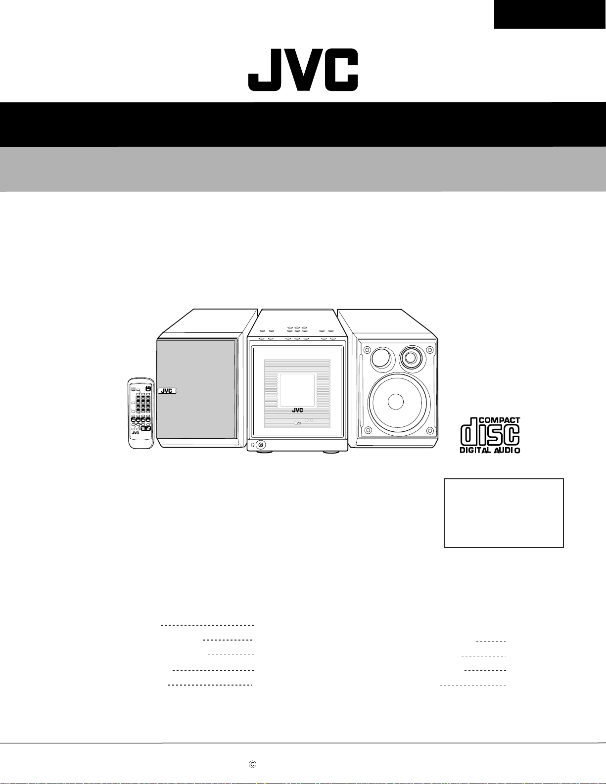
MICRO COMPONENET SYSTEM
UX-A52
UX-A52
UX-A52
COLOR
DIMMER
STANDBY/ON
CLOCK
SLEEP
FM MODE
/TIMER
123
456
DISPLAY
789
0
+
10
10
SET
CANCEL
REV.MODE
REPEAT
PLAY MODE
CD
AUX/MD
TAPE
FM/AM
BEEP
AHB
SOUND
VOLUME
PRO
MODE
RM-SUXA52U
Contents
Safety precautions
Preventing static electricity
Important for laser products
Disassembly method
Adjustment Method
PHONES
1-2
1-3
1-4
1-5
1-24
MICRO COMPONENT SYSTEM UX-A52
STANDBY/ON
COMPACT
DIGITAL AUDIO
Flow of functional operation
until TOC read (CD)
Maintenance of laser pickup
Replacement of laser pickup
Description of major ICs
Area Suffix
US ----------------- Singapore
UJ ---------------- U.S.Military
UP ----------------------- Korea
UW ------ Brazil,Mexico,Peru
1-28
1-29
1-29
1-30~48
COPYRIGHT 2002 VICTOR COMPANY OF JAPAN, LTD.
No.21074
Feb. 2002
1-1
Page 2
UX-A52
1. This design of this product contains special hardware and many circuits and components specially for safety
purposes. For continued protection, no changes should be made to the original design unless authorized in
writing by the manufacturer. Replacement parts must be identical to those used in the original circuits. Services
should be performed by qualified personnel only.
2. Alterations of the design or circuitry of the product should not be made. Any design alterations of the product
should not be made. Any design alterations or additions will void the manufacturer`s warranty and will further
relieve the manufacture of responsibility for personal injury or property damage resulting therefrom.
3. Many electrical and mechanical parts in the products have special safety-related characteristics. These
characteristics are often not evident from visual inspection nor can the protection afforded by them necessarily
be obtained by using replacement components rated for higher voltage, wattage, etc. Replacement parts which
have these special safety characteristics are identified in the Parts List of Service Manual. Electrical
components having such features are identified by shading on the schematics and by ( ) on the Parts List in
the Service Manual. The use of a substitute replacement which does not have the same safety characteristics
as the recommended replacement parts shown in the Parts List of Service Manual may create shock, fire, or
other hazards.
4. The leads in the products are routed and dressed with ties, clamps, tubings, barriers and the like to be
separated from live parts, high temperature parts, moving parts and/or sharp edges for the prevention of
electric shock and fire hazard. When service is required, the original lead routing and dress should be
observed, and it should be confirmed that they have been returned to normal, after re-assembling.
5. Leakage currnet check (Electrical shock hazard testing)
After re-assembling the product, always perform an isolation check on the exposed metal parts of the product
(antenna terminals, knobs, metal cabinet, screw heads, headphone jack, control shafts, etc.) to be sure the
product is safe to operate without danger of electrical shock.
Do not use a line isolation transformer during this check.
Plug the AC line cord directly into the AC outlet. Using a "Leakage Current Tester", measure the leakage
current from each exposed metal parts of the cabinet, particularly any exposed metal part having a return
path to the chassis, to a known good earth ground. Any leakage current must not exceed 0.5mA AC (r.m.s.).
Alternate check method
Plug the AC line cord directly into the AC outlet. Use an AC voltmeter having, 1,000 ohms per volt or more
sensitivity in the following manner. Connect a 1,500 10W resistor paralleled by a 0.15 F AC-type capacitor
between an exposed metal part and a known good earth ground.
Measure the AC voltage across the resistor with the AC
voltmeter.
Move the resistor connection to each exposed metal part,
particularly any exposed metal part having a return path to
the chassis, and meausre the AC voltage across the resistor.
Now, reverse the plug in the AC outlet and repeat each
measurement. Voltage measured any must not exceed 0.75 V
AC (r.m.s.). This corresponds to 0.5 mA AC (r.m.s.).
0.15 F AC TYPE
1500 10W
Good earth ground
AC VOLTMETER
(Having 1000
ohms/volts,
or more sensitivity)
Place this
probe on
each exposed
metal part.
!
1. This equipment has been designed and manufactured to meet international safety standards.
2. It is the legal responsibility of the repairer to ensure that these safety standards are maintained.
3. Repairs must be made in accordance with the relevant safety standards.
4. It is essential that safety critical components are replaced by approved parts.
5. If mains voltage selector is provided, check setting for local voltage.
Burrs formed during molding may
be left over on some parts of the
chassis. Therefore, pay attention to
such burrs in the case of
preforming repair of this system.
In regard with component parts appearing on the silk-screen printed side (parts side) of the PWB diagrams, the
parts that are printed over with black such as the resistor ( ), diode ( ) and ICP ( ) or identified by the " "
mark nearby are critical for safety.
(This regulation does not correspond to J and C version.)
1-2
Page 3
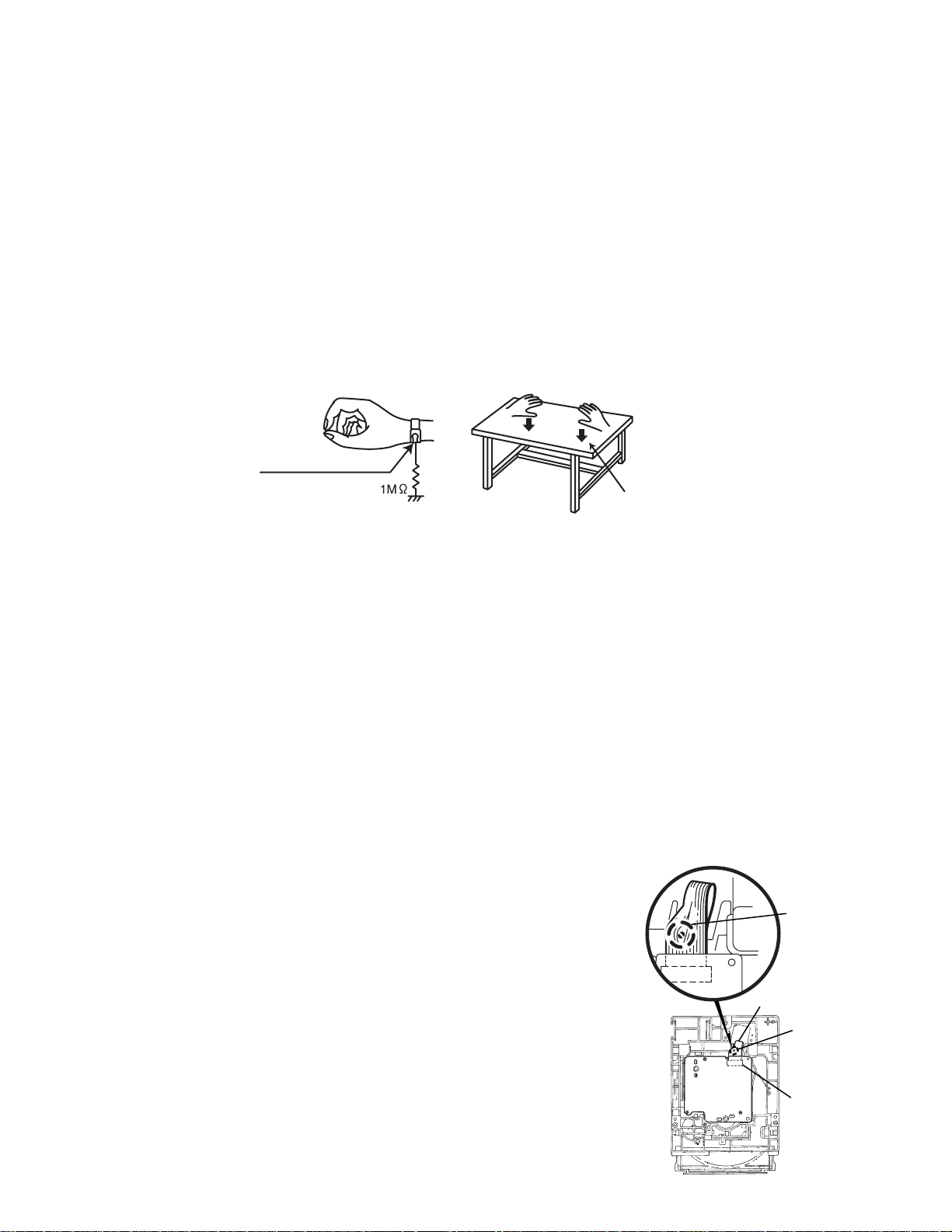
Preventing static electricity
1.Grounding to prevent damage by static electricity
Electrostatic discharge (ESD), which occurs when static electricity stored in the body, fabric, etc. is discharged,
can destroy the laser diode in the traverse unit (optical pickup). Take care to prevent this when performing repairs.
UX-A52
2.About the earth processing for the destruction prevention by static electricity
Static electricity in the work area can destroy the optical pickup (laser diode) in devices such as CD players.
Be careful to use proper grounding in the area where repairs are being performed.
2-1 Ground the workbench
Ground the workbench by laying conductive material (such as a conductive sheet) or an iron plate over
it before placing the traverse unit (optical pickup) on it.
2-2 Ground yourself
Use an anti-static wrist strap to release any static electricity built up in your body.
(caption)
Anti-static wrist strap
Conductive material
(conductive sheet) or iron plate
3. Handling the optical pickup
1. In order to maintain quality during transport and before installation, both sides of the laser diode on the
replacement optical pickup are shorted. After replacement, return the shorted parts to their original condition.
(Refer to the text.)
2. Do not use a tester to check the condition of the laser diode in the optical pickup. The tester's internal power
source can easily destroy the laser diode.
4.Handling the traverse unit (optical pickup)
1. Do not subject the traverse unit (optical pickup) to strong shocks, as it is a sensitive, complex unit.
2. Cut off the shorted part of the flexible cable using nippers, etc. after replacing the optical pickup. For specific
details, refer to the replacement procedure in the text. Remove the anti-static pin when replacing the traverse
unit. Be careful not to take too long a time when attaching it to the connector.
3. Handle the flexible cable carefully as it may break when subjected to strong force.
4. It is not possible to adjust the semi-fixed resistor that adjusts the laser power. Do not turn it
Attention when traverse unit is decomposed
Flexible wire
Shorting round
Shorting round
CN601 on
mechanism
board
*Please refer to "Disassembly method" in the text for pick-up and how to
detach the substrate.
1.Solder is put up before the card wire is removed from connector on
the CD substrate as shown in Figure.
(When the wire is removed without putting up solder, the CD pick-up
assembly might destroy.)
2.Please remove solder after connecting the card wire with
when you install picking up in the substrate.
1-3
Page 4
UX-A52
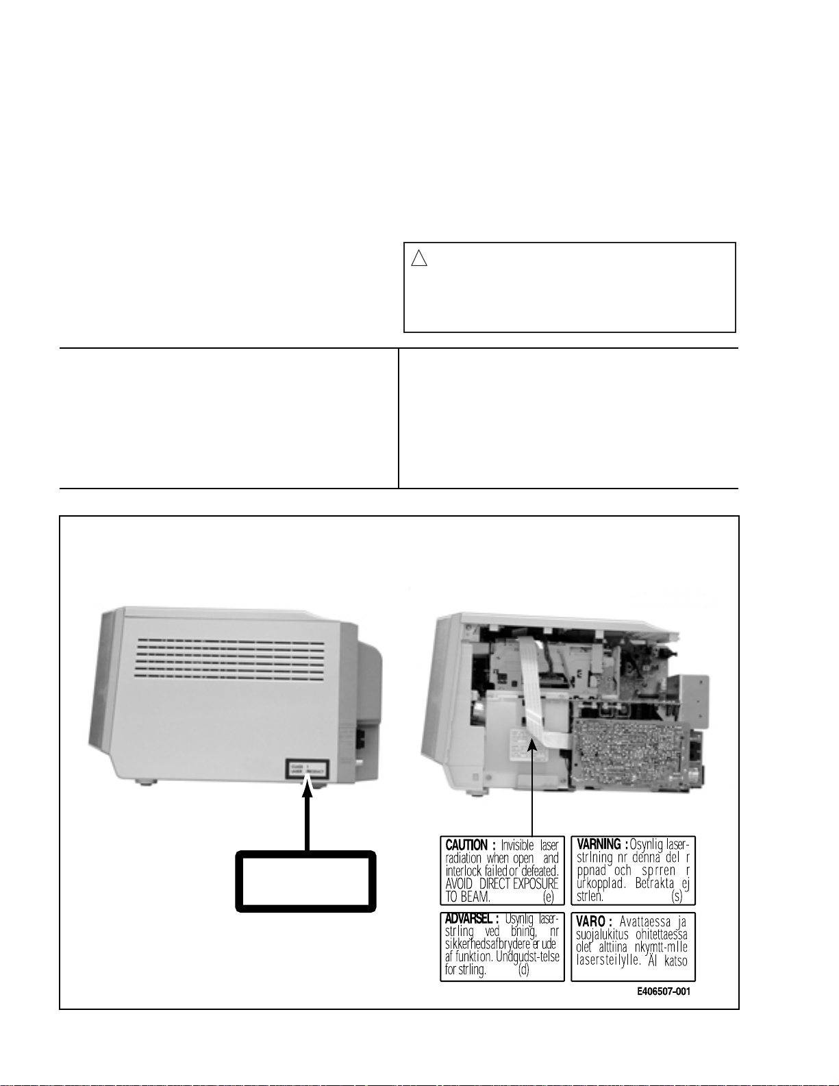
Important for laser products
1.CLASS 1 LASER PRODUCT
2.DANGER : Invisible laser radiation when open and inter
lock failed or defeated. Avoid direct exposure to beam.
3.CAUTION : There are no serviceable parts inside the
Laser Unit. Do not disassemble the Laser Unit. Replace
the complete Laser Unit if it malfunctions.
4.CAUTION : The compact disc player uses invisible
laserradiation and is equipped with safety switches
whichprevent emission of radiation when the drawer is
open and the safety interlocks have failed or are de
feated. It is dangerous to defeat the safety switches.
VARNING : Osynlig laserstrålning är denna del är öppnad
och spårren är urkopplad. Betrakta ej strålen.
VARO : Avattaessa ja suojalukitus ohitettaessa olet
alttiina näkymättömälle lasersäteilylle.Älä katso
säteeseen.
5.CAUTION : If safety switches malfunction, the laser is able
to function.
6.CAUTION : Use of controls, adjustments or performance of
procedures other than those specified herein may result in
hazardous radiation exposure.
CAUTION
!
Please use enough caution not to
see the beam directly or touch it
in case of an adjustment or operation
check.
ADVARSEL : Usynlig laserstråling ved åbning , når
sikkerhedsafbrydere er ude af funktion. Undgå
udsættelse for stråling.
ADVARSEL : Usynlig laserstråling ved åpning,når
sikkerhetsbryteren er avslott. unngå utsettelse
for stråling.
REPRODUCTION AND POSITION OF LABELS
WARNING LABEL
CLASS 1
LASER PRODUCT
1-4
Page 5
UX-A52
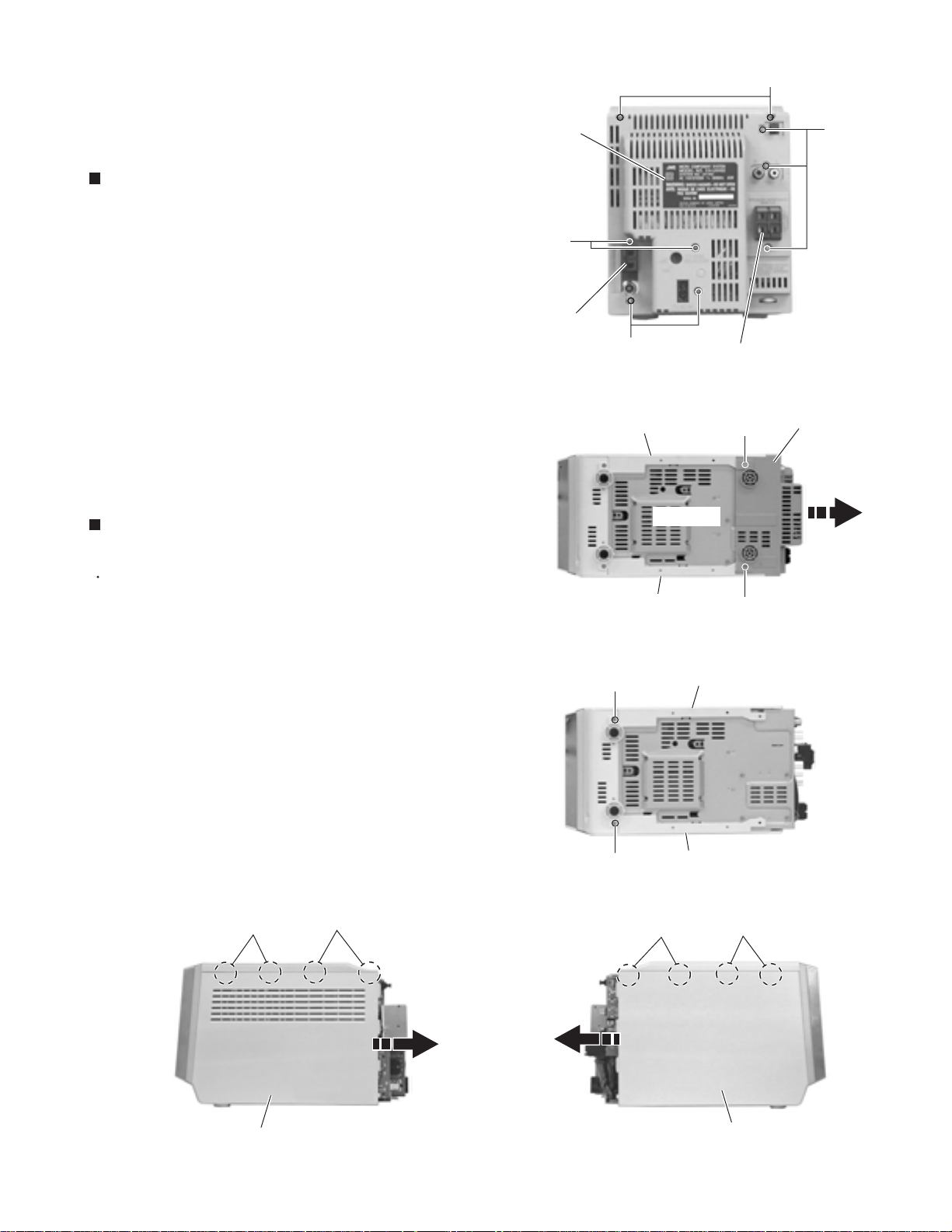
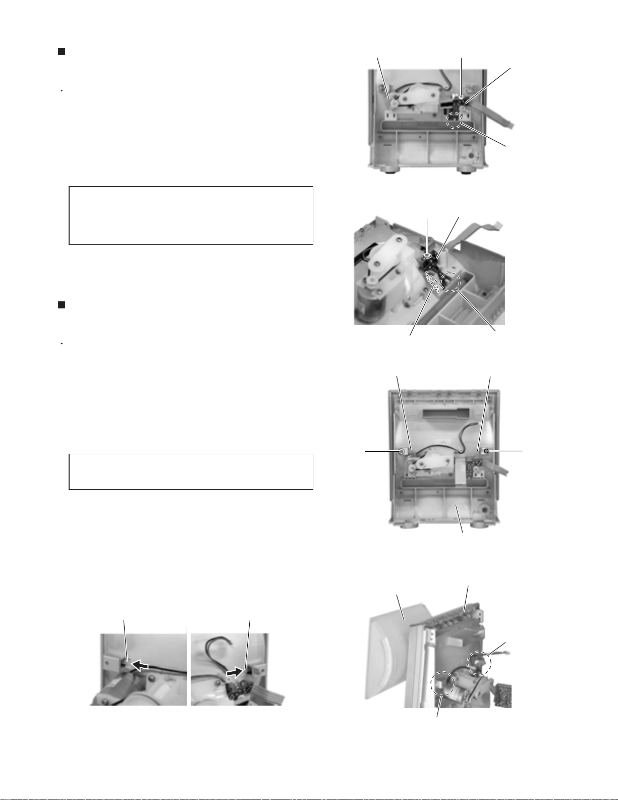
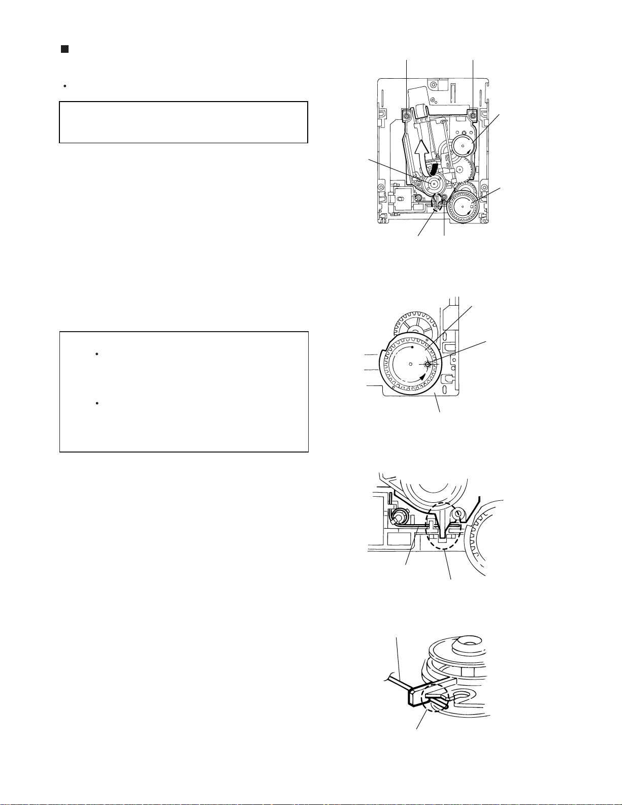
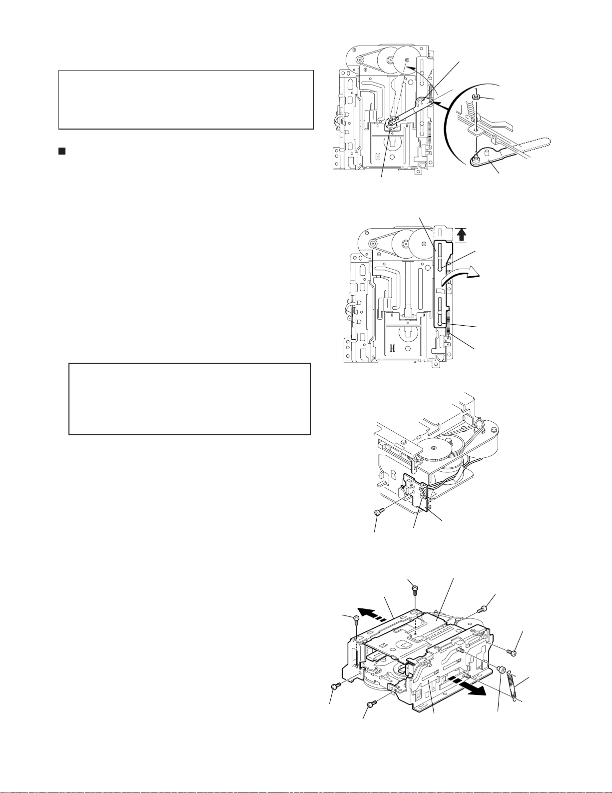
Disassembly method
<Main body>
Removing the rear cover
(See Fig.1 and 2)
1.
Remove the nine screws A on the back of the body.
2.
Remove the two screws B on the bottom of the
body.
3.
Unlock the speaker terminal and the antenna
terminal, then remove the rear cover backward with
releasing the hooks.
Removing the side panels
(See Fig.3 to 5)
Rear cover
A
Antenna terminal
Side panel (R)
A
Speaker terminal
Fig.1
(Bottom)
B
A
A
Rear cover
Prior to performing the following procedure, remove
the rear cover.
1.
Remove the two screws C attaching the side panels
on the bottom of the body.
2.
Remove each side panel backward while releasing
the eight joints a as shown in Fig.4 and 5.
Joint a
Joint a
Side panel (L)
Fig.2
C
C
Side panel (R)
Side panel (L)
Fig.3
Joint a
B
Joint a
Side panel (R)
Fig.4
Side panel (L)
Fig.5
1-5
Page 6
UX-A52
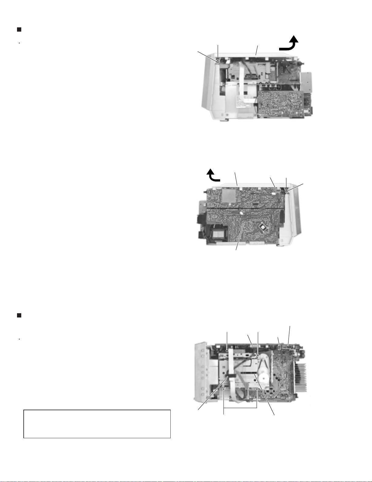
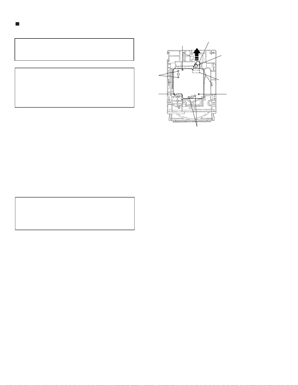
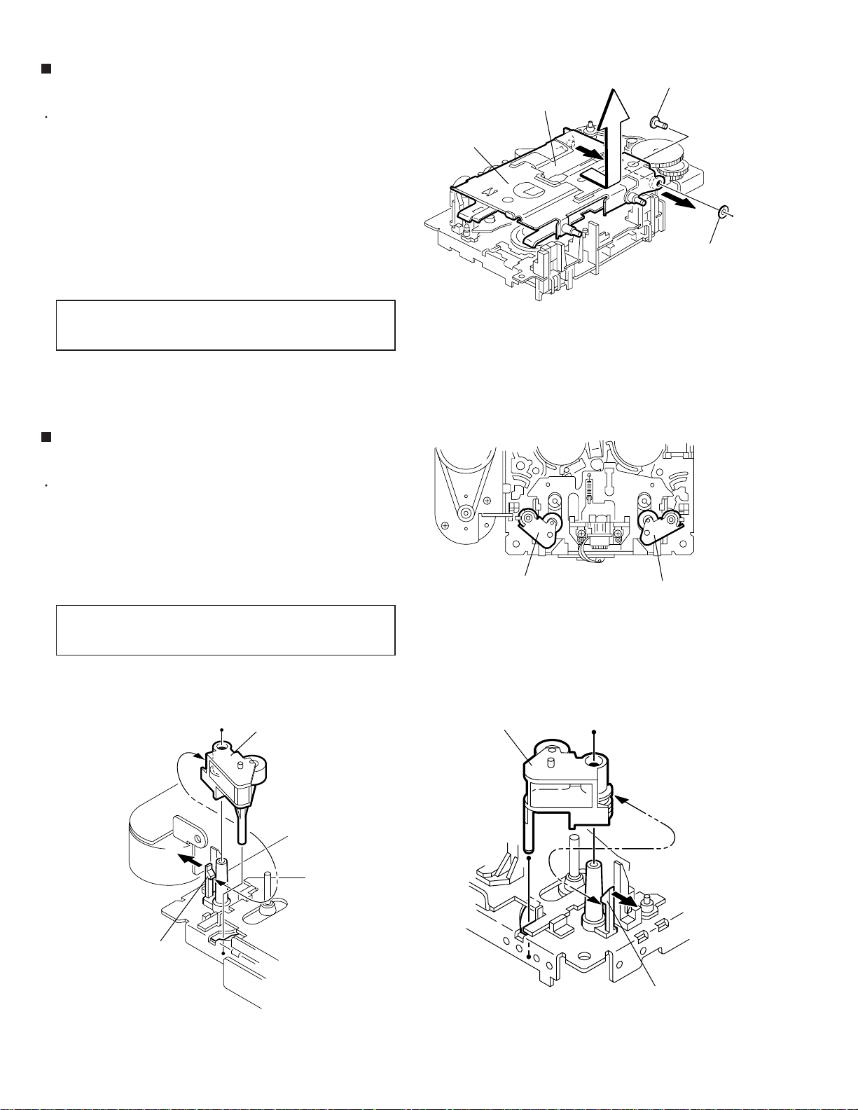
Removing the top panel (See Fig.6 and 7)
Prior to performing the following procedure, remove
the rear cover and the side panels.
1.
Remove the two screws D on each side of the body.
2.
Release the two joints b on each side of the body
and remove the top panel in the direction of the
arrow.
3.
Disconnect the card wires from connector CN705 on
the system control board on the left side of the body.
Joint b
D
Top panel
Top panel
Fig.6
CN705
D
Joint b
Removing the cassette mechanism
assembly section (See Fig.8)
Prior to performing the following procedure, remove
the rear cover, the side panels and the top panel.
1.
Disconnect each wire from connector CN706, CN715
and CN716 on the system control board on top of the
body.
2.
Remove the four screws E retaining the cassette
mechanism assembly section on top of the body.
REFERENCE:
Reference: If necessary, remove the
spacer marked h and the wire from the
Cassette mechanism assembly section.
h (spacer)
System control board
Fig.7
E E
CN715
E
Cassette mechanism section
Fig.8
System control board
CN706
CN716
1-6
Page 7
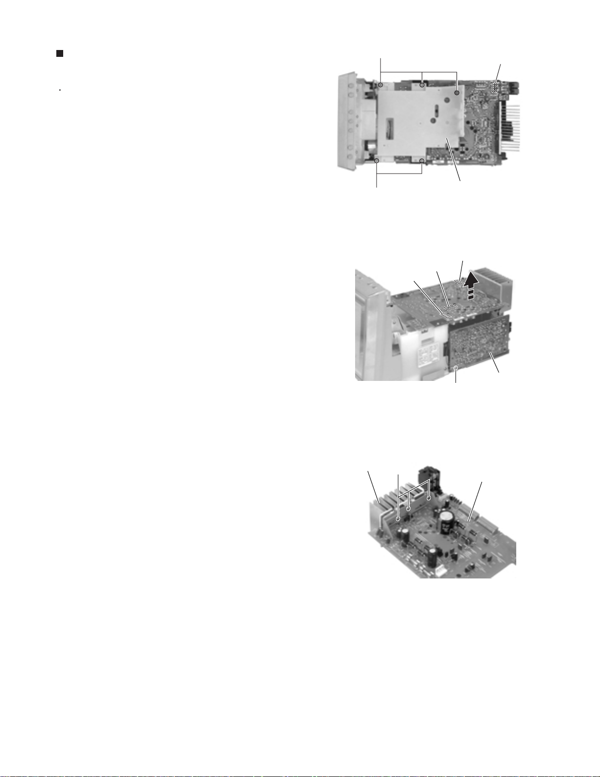
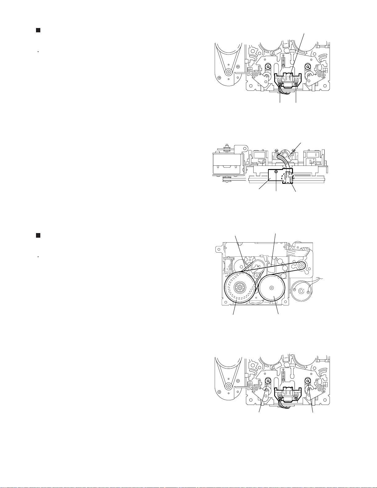
Removing the system control board
(See Fig.9)
UX-A52
Prior to performing the following procedure, remove
the rear cover, the side panels and the top panel.
1.
Disconnect the card wire from connector CN701 and
the wire from connector CN706, CN715, CN716 on
the system control board.
2.
Remove the screw F on the left side of the body.
3.
Disconnect connector CN709, CN711 and CN712 on
the system control board from the body outward.
4.
Disconnect the card wire from connector CN704 on
the underside of the system control board.
Removing the tuner board (See Fig.10)
Prior to performing the following procedure, remove
the rear cover and the right side panel.
CN706
CN716
CN712
CN704
CN715
CN701
CN711
CN709
F
System control board
Fig.9
Tuner board
1.
Disconnect the card wire from connector CN1 on the
tuner board on the right side of the body.
2.
Remove the screw G and remove the tuner board
upward while disengaging the three joints c.
CN1
G
Joints c
Fig.10
1-7
Page 8
UX-A52
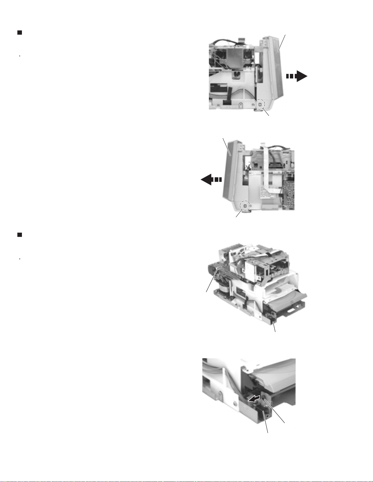
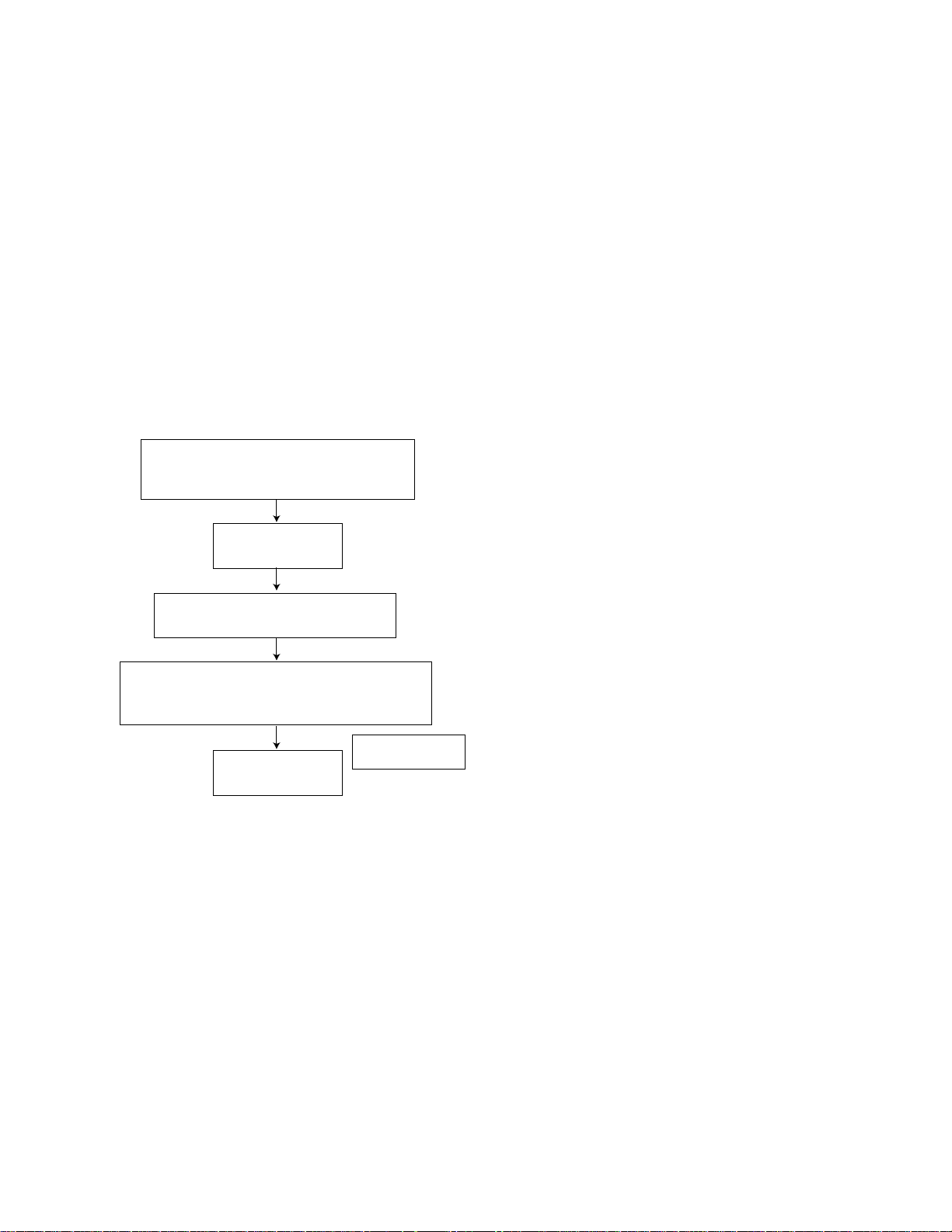
Removing the front panel assembly
(See Fig.11 and 12)
Prior to performing the following procedure, remove
the rear cover, the side panels, the top panel and the
system control board.
1.
Release the two joints d on the lower right and left
sides of the front panel assembly, then remove the
front panel assembly toward the front.
Front panel assembly
Front panel assembly
Fig.11
Joint d
Removing the headphone jack board
(See Fig.13 and 14)
Prior to performing the following procedure, remove
the rear cover, the side panels, the top panel, the
system control board and the front panel assembly
section.
1.
Disconnect the wire from connector CN804 on the
main board.
2.
Remove the plastic rivet fixing the headphone jack
board.
Joint d
Fig.12
Main board
CN804
Headphone jack board
Fig.13
1-8
Plastic rivet
Headphone jack board
Fig.14
Page 9
UX-A52
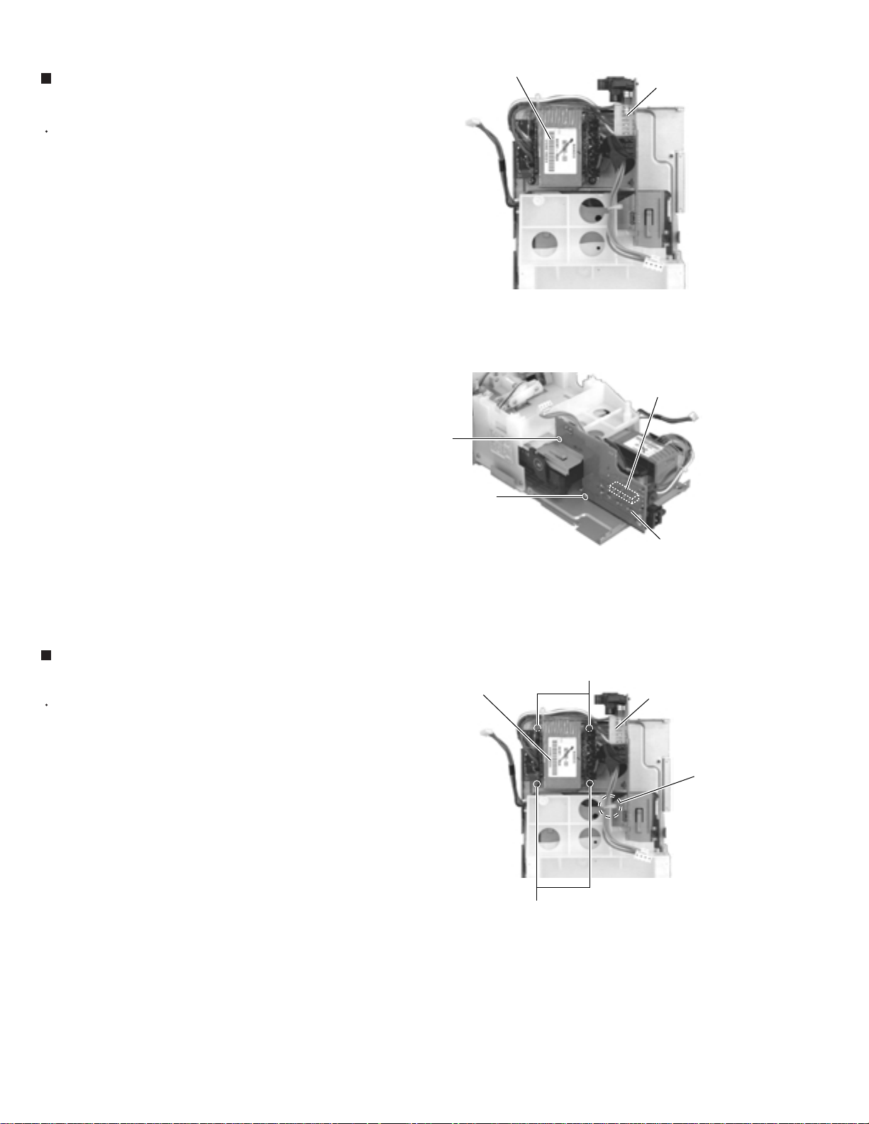
Removing the main board / the heat sink
(See Fig.15 to 17)
Prior to performing the following procedure, remove
the rear cover, the side panels, the top panel, the
cassette mechanism assembly section and and the
system control board.
1.
Disconnect the wire from connector CN804 on the
main board.
2.
Remove the five screws H attaching the cassette
mechanism bracket.
3.
Remove the screw G attaching the grounding
terminal extending from the main board.
4.
Disconnect connector CN805 on the main board
from the AC jack board while pulling out it. Remove
the main board in the direction of the arrow and
disconnect the wire from connector CN803 on the
reverse side of the main board.
5.
Remove the three screws I attaching the heat sink
on the reverse side of the main board.
H
H
Main board
CN804
Cassette mechanism bracket
Fig.15
Main board
CN804
CN805
CN803
Heat sink
Tuner board
G
Fig.16
I
Fig.17
Main board
1-9
Page 10
UX-A52
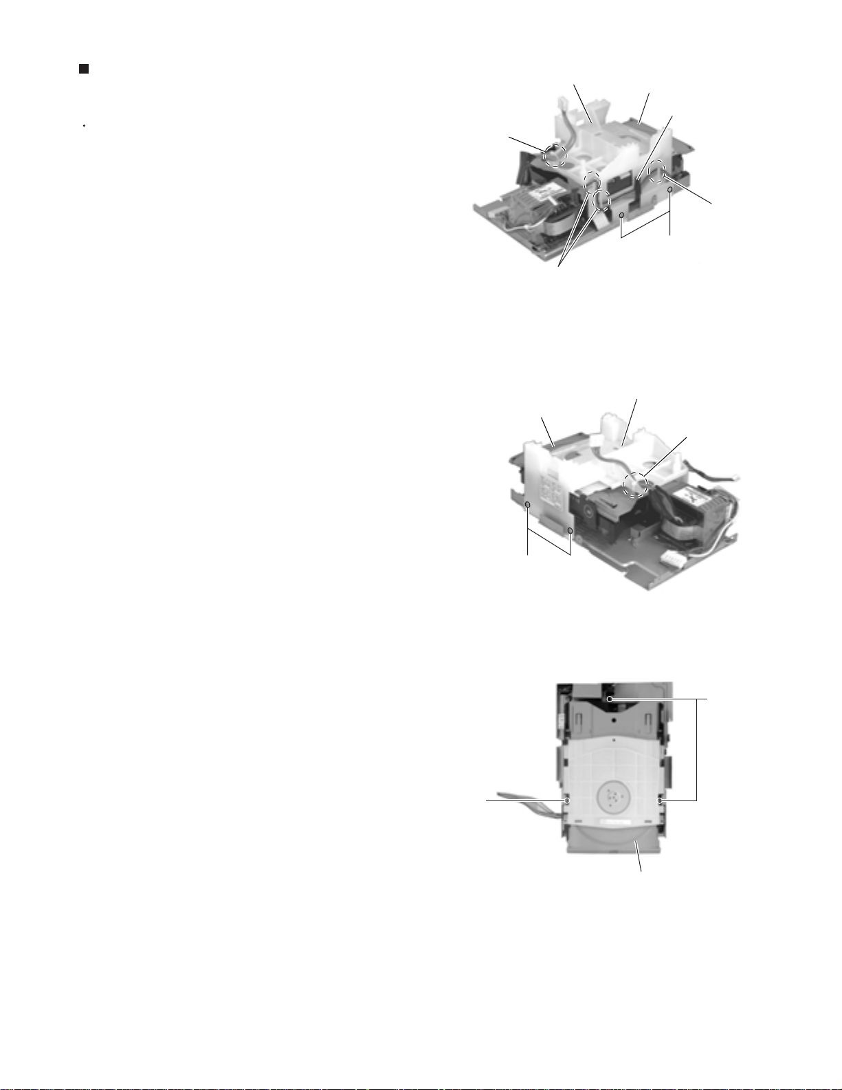
Removing the AC jack board
(See Fig.18 and 19)
Prior to performing the following procedure, remove
the rear cover, the side panels, the top panel, the
cassette mechanism assembly section, the system
control board and the main board / the tuner board.
1.
Disconnect the wire from connector CN809 on the
AC jack board.
2.
Remove the screw J and screw K attaching the AC
jack board.
Power transformer assembly
J
AC jack board
CN809
Fig.18
CN809
Removing the power transformer
assembly (See Fig.20)
Prior to performing the following procedure, remove
the rear cover, the side panels, the top panel, the
cassette mechanism assembly section, the system
control board and the main board.
1.
Disconnect the wire from connector CN809 on the
AC jack board.
2.
Cut off the band setting the wire on the CD
mechanism cover.
3.
Remove the four screws L attaching the power
transformer assembly.
K
Power transformer
assembly
L
Fig.19
L
Fig.20
AC jack board
AC jack board
CN809
Band
1-10
Page 11
UX-A52
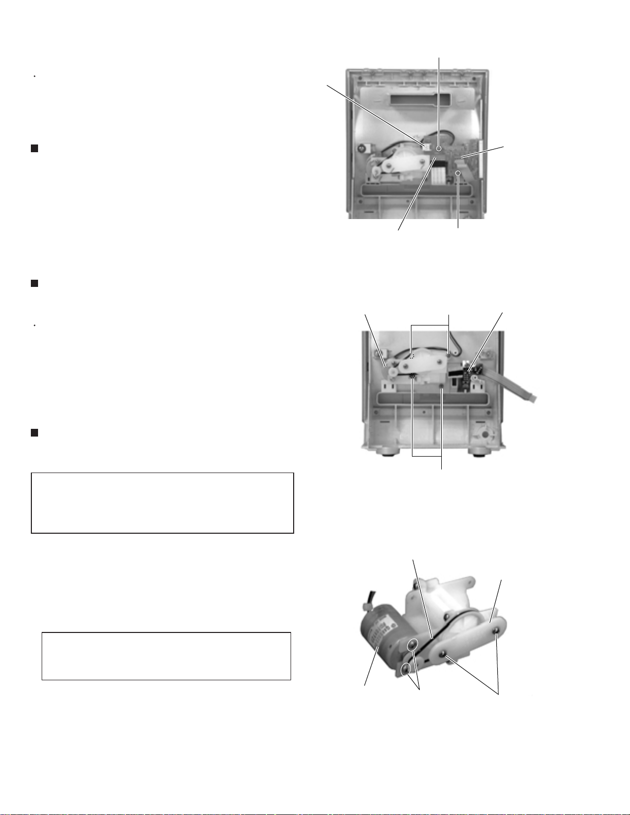
Removing the CD mechanism assembly
(See Fig.21 to 23)
Prior to performing the following procedure, remove
the rear cover, the side panels, the top panel, the
cassette mechanism assembly section, the system
control board, the front panel assembly section, the
main board / the tuner board and the AC jack board.
1.
Cut off the band setting the wire on the CD
mechanism cover.
2.
Release the wire extending from the headphone jack
board from the spacer and the three notches of the
CD mechanism cover on the left side of the body.
3.
Remove the four screws M on the left and right side
of the CD mechanism cover. Then remove the CD
mechanism cover upward.
4.
Remove the three screws N attaching the CD
mechanism assembly.
CD mechanism cover
Band
Notches
CD mechanism assembly
CD mechanism assembly
Spacer
Notch
M
Fig.21
CD mechanism cover
Band
N
M
Fig.22
N
CD mechanism assembly
Fig.23
1-11
Page 12
UX-A52
<Front panel assembly section>
Prior to performing the following procedure, remove
the rear cover, the side panels, the top panel, the
system control board and the front panel assembly
section.
Removing the relay board (See Fig. 24)
Disconnect the wire from connector CN906, CN907
1.
and the card wire from CN908 on the relay board
respectively.
Remove the two screws O.
2.
Removing the drive motor assembly
(See Fig.25)
Prior to performing the following procedure, remove
the relay board.
CN907
Drive motor assembly
CN908
Fig.24
O
O
Door switch board
P
Relay board
CN906
1.
Remove the four screws P attaching the drive motor
assembly.
Removing the belt and the drive motor
(See Fig.26)
REFERENCE:
1.
Remove the two screws Q attaching the plate.
2.
Remove the belt from the two pulleys.
3.
Remove the two screws R attaching the drive motor.
REFERENCE:
The belt and the drive motor can be
removed respectively without removing the
drive motor assembly from the front panel
section.
When removing the drive motor only,
remove the belt from the drive motor
pulleys in advance.
P
Fig.25
Belt
Plate
1-12
Drive motor
R
Fig.26
Q
Page 13
UX-A52
Removing the door switch board
(See Fig.27 and 28)
Prior to performing the following procedure, remove
the relay board.
1.
Loosen the screw S attaching the door switch.
2.
Remove the door switch board while releasing it from
the joint e.
CAUTION:
When reattaching the door switch board,
fit it to the joint e and check the
operating state of the switch before
tightening the screw S.
Removing the LCD section
(See Fig.29 to 31)
Prior to performing the following procedure, remove
the relay board.
1.
Loosen the two screws T attaching the lock lever.
Drive motor assembly
Switch section
Lock lever
S
Fig.27
Door switch board
S
Fig.28
Door switch board
Joint e
Joint e
Lock lever
2.
Push the part f of the lock lever in the direction of
the arrow as shown in Fig.30-1 / 30-2 and disengage
the LCD section from the front panel assembly.
CAUTION:
Because the LCD may come off, hold it
when loosening the screws T.
Lock lever f Lock lever f
T
LCD section
T
Front panel assembly
Fig.29
Front panel assembly
Joint f
Fig.30-1 Fig.30-2
Joint f
Fig.31
1-13
Page 14
UX-A52
Removing the LCD board assembly
(See Fig.32 to 36)
Prior to performing the following procedure, remove
the relay board and the LCD section.
1.
Remove the four screws U attaching the case cover.
2.
Remove the four screws V attaching the LCD panel
on the back of the LCD section.
3.
Remove the LCD cover.
4.
Release the three joints g and remove the LCD
board assembly in the direction of the arrow.
U
V
U
Case cover
U
U
Fig.32
LCD section
LCD panel
Joint g
V
Fig.33
Fig.34
Joint g
Joint g
1-14
LCD cover
LCD board assembly
Fig.35 Fig.36
Page 15
<Top panel section>
Prior to performing the following procedure, remove
the rear cover, the side panels and the top panel.
Removing the operation switch board
(See Fig.37)
1.
Remove the seven screws W attaching the
operation switch board on the reverse side of the top
panel.
W
Cassette amplifier board
W
Fig.37
UX-A52
Operation switch board
W
1-15
Page 16
UX-A52
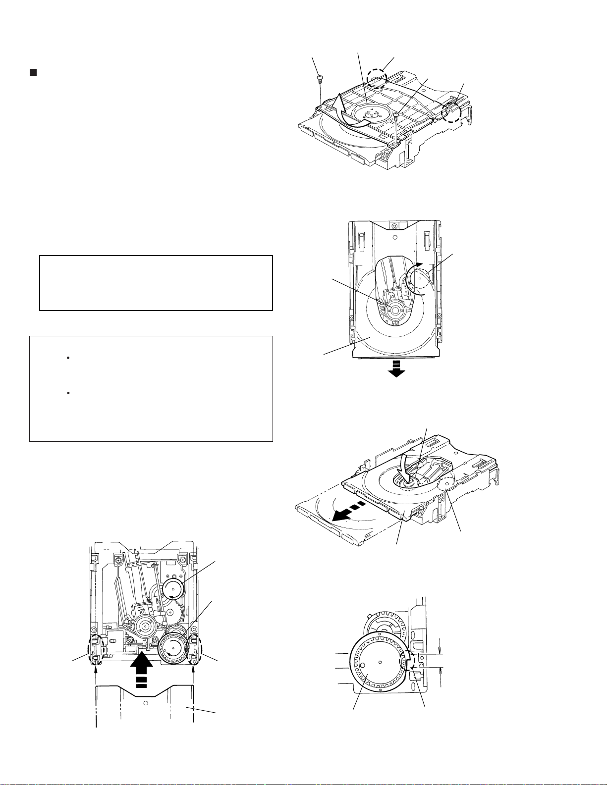
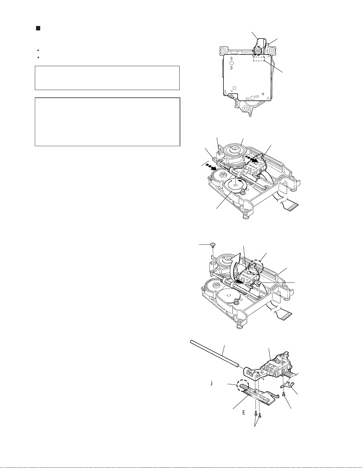
<CD Mechanism Assembly>
Removing the CL. Base Assembly and Tray
(Refer to Figs. 1 to 5.)
1. Remove the two screws A fastening the CL. base
assembly from the top of the CD mechanism
assembly.
2. Move the CL. base assembly diagonally upwards
as indicated by the arrow to release it from the two
hooks a.
3. Turn the idle gear in the arrow-marked direction
from the upper side of the CD mechanism
assembly. Accordingly, the TRAMECHA assembly
moves downwards.
Note: When drawing out the tray, shift down the
TRAMECHA assembly to the position where
the tray does not contact the T-T assembly
of the TRAMECHA assembly.
4. Draw out the tray frontwards for removing it.
CL. base assembly
A
TRAMECHA
assembly
Hook a
Fig. 1
A
Hook a
Idle gear
Note: When reinstalling the tray:
Turn the idle gear so that the part b of the
tray gear is positioned in the part c shown in
Fig. 4. (Eject position)
Engage the right and left hooks d and e of
the tray with the right and left grooves of the
TRAMECHA assembly respectively for
retaining the tray.
Idle gear
Tray gear
Tray
Fig. 2
TRAMECHA assembly
Idle gear
Tray
Fig. 3
1-16
Hook d
Hook d
Tray
Tray gear
Part c
Part b
Fig. 4Fig. 5
Page 17
UX-A52
Removing the TRAMECHA Assembly
(Refer to Figs. 6 to 9.)
Remove the CL. base assembly and tray.
Reference: The TRAMECHA assembly can be
removed without removal of the
mechanism board.
1. If the TRAMECHA assembly is lowered and it is
located out of the PLAY position, turn the idle gear
in the arrow-marked direction so that the hole in the
part f of the tray gear meets the hole on the CL.
base assembly. (Set the TRAMECHA assembly at
the PLAY position.)
2. Remove the three screws B fastening the
TRAMECHA assembly and then remove the
TRAMECHA assembly upwards from the front side.
3. At the same time, remove the spring from the groove of
the CH. base assembly in the part g of the TRAMECHA
assembly.
Note: When reinstalling the TRAMECHA assembly:
Check to see if the spring is properly
engaged with groove of the CH. base
assembly in the part g of the TRAMECHA
assembly.
After making sure that the three insulators of
the TRAMECHA assembly are properly set
on the bosses of the L. base assembly's
guide, fasten them with the screws.
TRAMECHA
assembly
B
Part g
L. base assembly
B
Fig. 6
Fig. 7
B
Idle gear
Tray gear
Tray gear
Part f
Spring
Part g
Fig. 8
Spring
Groove of CH. base assembly
Fig. 9
1-17
Page 18
UX-A52
Removing the Mechanism Board
(Refer to Fig 10.)
Reference:The mechanism board can be removed
without removal of the TRAMECHA
assembly.
C
Flexible wire
Shorting round
Note: Before disconnecting the flexible wire coming
from the pickup from the connector, be sure to
solder its shorting round.
If the flexible wire is connected without
soldering, it may cause breakdown of the
pickup.
1. Solder the shorting round of the flexible wire
connected with the mechanism board from the back
of the mechanism assembly.
2. Disconnect the flexible wire from the connector
CN601 on the mechanism board.
3. Remove the three screws C fastening the
mechanism board.
4. Unsolder the two points of the part h and one point
of the part i of the mechanism board. Then, remove
the mechanism board upwards.
Note: When reinstalling the mechanism board,
connect the flexible wire coming from the
pickup to the connector first and then remove
the solder from the shorting round of the
flexible cable.
Soldered
part h
C
CN601 on
mechanism
board
C
Soldered part i
Fig. 10
1-18
Page 19
UX-A52
Removing the Pickup
(Refer to Figs. 11 to 14.)
Remove the CL. base assembly and tray.
Remove the TRAMECHA assembly.
Reference: The pickup can be removed without
removal of the mechanism board.
Note: Before disconnecting the flexible wire coming
from the pickup from the connector, be sure to
solder its shorting round.
If the flexible wire is connected without
soldering, it may cause breakdown of the
pickup.
1. Solder the shorting round of the flexible wire
connected with the mechanism board from the back
of the TRAMECHA assembly.
2. Disconnect the flexible wire from the connector
CN601 on the mechanism board.
Part j of
rack plate
CH. base
assembly
Flexible wire
Shorting round
CN601 on
mechanism
board
Fig. 11
T-T assembly
Pickup assembly
3. Turn the idle gear in the arrow-marked direction from
the top of the TRAMECHA assembly so that the
pickup assembly is shifted to the reverse side of the
T-T assembly.
Move the pickup assembly until the part j of the rack
plate in the lower part of the pickup assembly comes
out of the CH. base assembly.
4. Remove the two screws D retaining the shaft of the
pickup assembly. Next, disengage the hook k from
the CH. base assembly and then remove the pickup
assembly together with the shaft.
5. Pull the shaft out of the pickup.
6. Remove the two screws E fastening the rack plate
from the pickup.
7. Remove the screw F retaining the P.S. spring from
the pickup.
D
Idle gear
Shaft
Fig. 12
Pickup assembly
Part k
CH. base
assembly
D
Fig. 13
Pickup
Part j
Rack plate
P.S. spring
F
E
Fig. 14
1-19
Page 20
UX-A52
Reinstalling the Pickup Assembly
(Refer to Figs. 15 and 16.)
Reference: Refer to the explanation of "Removing
the Pickup" on the preceding page.
1. Fit the P.S. spring and rack plate to the pickup.
2. Insert the shaft into the pickup.
3. Engage the hook k of the pickup assembly with the
CH. base assembly first, and set the part j of the
rack plate in the opening I next. Then, reinstall the
pickup assembly while shifting it to the T-T side
(inward) so that the part m of the rack plate is
positioned as shown in Fig. 16.
4. Move the pickup assembly to the center position
and fasten the shaft with the two screws D. (Make
sure that the part n of the rack plate is correctly
engaged with the middle gear.)
5. After passing the flexible wire coming from the
pickup through the opening of the CH. base
assembly, connect it to the connector CN601.
Part I
Part j
Part m
Part k
Pickup
assembly
CH. base
assembly
Fig. 15
Middle gear
Note: When reinstalling the pickup assembly,
remove the solder from the shorting round
after connecting the flexible wire coming from
the pick to the connector CN601.
Removing the Feed Motor Assembly
(Refer to Fig. 17.)
Remove the CL. base assembly and tray.
Remove the mechanism board.
Remove the two screws E fastening the feed motor
assembly from the top of the mechanism assembly.
Rack plate
Part n
Fig. 16
E
Feed motor assembly
1-20
Fig. 17
Page 21
UX-A52
<Cassette mechanism section>
CAUTION:
Removing the side bracket (L) and (R) /
load board (See Fig.1 to 4)
1.
Remove the E-washer attaching the load arm on the
right side of the body.
2.
Turn the load arm in the direction of the arrow to
release from the cassette hook at the joint a.
3.
Remove the spring (1) attaching the trig lever.
4.
Move the trig lever in the direction of the arrow and
release it from the two holes b.
5.
Remove the screw A attaching the load board on
the right side of the body and unsolder the wire
extending from the sub motor.
Prior to performing the following
procedures, turn the mode gear in the
direction of the arrow to move each section
to the eject position.
Joint a
Slide bracket
Load arm
E-washer
Load arm
Fig.1
Hole b
Hole b
Spring (1)
REFERENCE:
6.
Remove the spring (2) and the holder collar on the
right side of the body.
7.
Remove the two screws B attaching the side
bracket unit (R) in the direction of the arrow.
8.
Remove the four screws C attaching the side
bracket (L) in the direction of the arrow.
The side bracket unit (R) can be
removed even if the load board is
attached. In such case, make sure to
unsolder the wire extending from the
sub motor.
A
Side bracket unit (L)
C
Fig.2
Load board
Soldering
Fig.3
Cassette hanger assembly
C
C
B
C
Side bracket unit (R)
B
Spring (2)
Holder collar
Fig.4
1-21
Page 22
UX-A52
Removing the cassette hanger assembly
/ cassette holder (See Fig.5)
Prior to performing the following procedure, remove
the side bracket (L) and (R).
1.
Remove the slit washer attaching the cassette
hanger assembly and pull out the pin.
2.
Move the cassette hanger assembly in the direction
of the arrow to release the boss of the joint c on the
left rear side and detach the cassette hanger
assembly upward.
REFERENCE:
The cassette hanger assembly is
detached with the cassette holder.
Removing the pinch roller (F) and (R)
(See Fig.6 to 8)
Pin
Cassette hanger assembly
Cassette holder
E-washer
Fig.5
Prior to performing the following procedure, remove
the side bracket (L), (R), cassette hanger assembly /
cassette holder.
1.
Release the tab d in the direction of the arrow and
pull out the pinch roller upward.
REFERENCE:
The above method is for removing the
pinch roller (F) and (R).
Pinch roller (F)
Pinch roller (F)
Pinch roller (R)
Pinch roller (R)
Fig.6
1-22
Tab d
Tab d
Fig.8Fig.7
Page 23
UX-A52
Removing the head assembly / head
board (See Fig.9 and 10)
Prior to performing the following procedure, remove
the side bracket (L), (R), cassette hanger assembly /
cassette holder.
1.
Remove the spring on the lower side of the head
assembly.
2.
Remove the two screws D and remove the head
assembly upward.
3.
Remove the screw E attaching the head board.
Unsolder the flexible wire extending from the head
assembly if necessary.
Head board
Fig.9
Head assembly
DD
Head assembly
Soldering
E
Removing the flywheel assembly (F) and
(R) (See Fig.11 and 12)
Prior to performing the following procedure, remove
the side bracket (L), (R), cassette hanger assembly /
cassette holder.
1.
Remove the belt and sub belt on the bottom of the
body.
2.
Remove the polywasher from the flywheel (F) and
(R) on top of the body.
3.
Pull out the flywheel (F) and (R).
Sub belt
Flywheel assembly (R)
Fig.10
Belt
Flywheel assembly (F)
Fig.11
Polywasher
Fig.12
Polywasher
1-23
Page 24
UX-A52
Adjustment Method
1. Jigs and test instruments
Test disc (CTS-1000)
Test tape (VT712)
Test tape (VT703)
Test tape (AC225)
2. Adjustment and check items
1) Indications in the modes that all LCD's are on
2) CD section
(1) Indication of the C1 error
(2) Cancel of the C1 error indication
3. Adjustment and check method
1) CD section
(1) Indication of the C1 error
While pressing both the POWER key
and BACK SKIP key on the main unit,
turn on the primary power supply.
FL indication
CRC = 0
Press the CD OPEN/CLOSE key
and insert the test disk.
Press the CD PLAY key. The set starts
counting and the number of error correction
times is indicated every 10 seconds.
FL indication
CRC = ***
(2) Cancel of the C1 error indication
To cancel the C1 error indication, cut off the power supply.
200 Hz or less
1-24
Page 25
Cassette section
UX-A52
Playback/Recording &
eraser head
Head azimuth
adjusting screw
(Forward side)
Head azimuth
adjusting screw
(Forward side)
Playback/Recording &
eraser head
Removing the Cassette Mechanism Assembly
1. Remove the rear cover.
2. Remove the side panels (right and left).
3. Remove the cassette mechanism assembly.
4. Remove the four screws S fastening the cassette mechanism assembly from the back
of the cassette mechanism.
5. Press the EJECT button on the front side of the cassette mechanism assembly to open
the cassette door, and then remove the cassette mechanism assembly.
Head azimuth
adjusting screw
(Reverse side)
Head azimuth
adjusting screw
(Reverse side)
BIAS TEST POINT
GND
PCB FMB
1-25
Page 26

UX-A52
Check and adjustment of the Head amplifier section
Item
1. Head azimuth
adjustment
2. Tape speed
adjustment
(Reference value)
Speed difference
between the
normal and
reverse directions
Check/Adjustment Method
1) Play back the end part of the test tape VT703 (10 kHz).
2) Adjust the head azimuth screws so that the output becomes
maximum in both the normal and reverse directions. After
adjustment, lock the screws with screw bond without fail.
Measuring output terminal: Speaker terminal, 4 load resistance
Difference between L-ch and R-ch: Within 3 dB
Difference between FWD and REV directions: Within 4 dB
Adjust max level in FWD and REV. After adjusting, should be
Applied bond (THREEBOND 1401 A/C) to screw.
Azimuth screw
Screw for
REV
Neji Lock
1) Play back the end part of the test tape VT712 (3 kHz).
2) Adjust VR37 so that the frequency counter reads 3000 15 Hz
in playback in the normal direction.
Measuring output terminal: Speaker terminal
Make sure that speed difference between the normal and
reverse directions is 60 Hz or less by reading of the frequency
counter. (With the beginning part of the test tape)
Azimuth
for FWD
Neji Lock
Adjusting
Point
Head
azimuth
screw
phase
(0 ) (45 )
VR37
Standard
Value
Maximum
output
3000 15Hz
60 Hz or less
Wow and flutter
3. Recording /
playback
frequency
characteristic
adjustment
(Reference value)
Recording bias
frequency
(Reference value)
Erasing current
Play back the end part of the test tape VT712 (3 kHz).
Make sure that the wow and flutter meter reads 0.25 % (WRMS)
or less.
1) Set a blank cassette tape (Type I: AC225) and enter the set into
the recording pause mode.
2) Cancel the pause mode and start recording. Repeat to input the
1 kHz and 10 kHz reference signals alternately from the CD test
disk to record the signals on the blank tape.
3) While playing back the repeatedly input 1 kHz and 10 kHz
reference signals, adjust VR31 so that output level of 10 kHz
signals is +2 dB 1 dB of 1 kHz.
1) Set a blank cassette tape (Type I: AC225) and enter the set into
the recording pause mode.
2) Make sure that the bias frequency at the bias test point (Refer on
1-25 board drowing) on the head amplifier board is 70 9 kHz.
1) Set a blank cassette tape (Type I: AC225) and enter the set into
the recording pause mode.
2) After connecting a 1 resistor to the erasing head in series,
cancel the pause mode and start recording. Connect the
electronic voltmeter to both the terminals and measure the
erasing current.
0.25 %
(WRMS) or
less
VR31
-1dB 1dB
70 9kHz
Erasing
current: 60
mA (Type I
tape)
1-26
Page 27

Extension code connecting method
Cassette mechanism assembly
UX-A52
System control board
(CN706, CN715, CN716)
QUQ110-1940BJ
CD mechanism assembly
CD servo control board
(CN651)
Extension wire
System control board
(CN704)
1-27
Page 28

UX-A52
Flow of functional operation until TOC read (CD)
Power ON
Power Key
Slider turns REST
SW ON.
Automatic tuning
of TE offset
Check to see if the voltage at the
pin 72 of IC701 or pin 5 of CN602
becomes 0 V for an instant. (The
moment the switch is turned on,
the voltage becomes 0 V.)
Check Point
VREF
Tracking error waveform at TOC reading
pin 25 of
IC601(TE)
Approx
1.8V
Tracking
servo
Disc statas
to rotate
off statas
Automatic measurement
of TE amplitude and
automatic tuning of
TE balance
Approx.3sec
Tracking
servo
on statas
Disc to be
braked to stop
TOC reading
finishes
500mv/div
2ms/div
Fig.1
Laser ON
Detection of disc
Automatic tuning of
Foucus offset
Automatic measurement of
Focus A-curve amplitude
Disc is rotated
Focus servo ON
(Tracking servo ON)
Automatic measurement of
Tracking error amplitude
Automatic tuning of
Tracking error balance
Make sure of the H level at
the pin 40 of IC603.
Confirm that the Focus error
S-curve siganl at the pin28 of
IC603 is approx.2Vp-p
Confirm that the siganl from
pin24 IC603 (R645) is 0V as
a accelerated pulse during
approx.400ms.
Make sure that the TE
signal (1.8 Vp-p approx.)
indicating the tracking
servo off status is output
from the pin 25 (one side
of R609) of IC601.
1-28
Automatic tuning of
Focus error balance
Automatic tuning of
Focus error gain
Automatic tuning of
Tracking error gain
TOC reading
Play a disc
Confirm the eys-pattern
at the lead of TP602
Page 29

UX-A52
Maintenance of laser pickup
(1) Cleaning the pick up lens
Befor you replace the pick up, please try to
clean the lens with a alcohol soaked cotton
swab.
(2) Life of the laser diode (Fig.1)
When the life of the laser diode has expired,
the following symptoms wil appear.
(1) The level of RF output (EFM output:ampli
tude of eye pattern) will below.
Is RF output
1.25 0.22Vp-p?
YES
O.K
NO
Replace it.
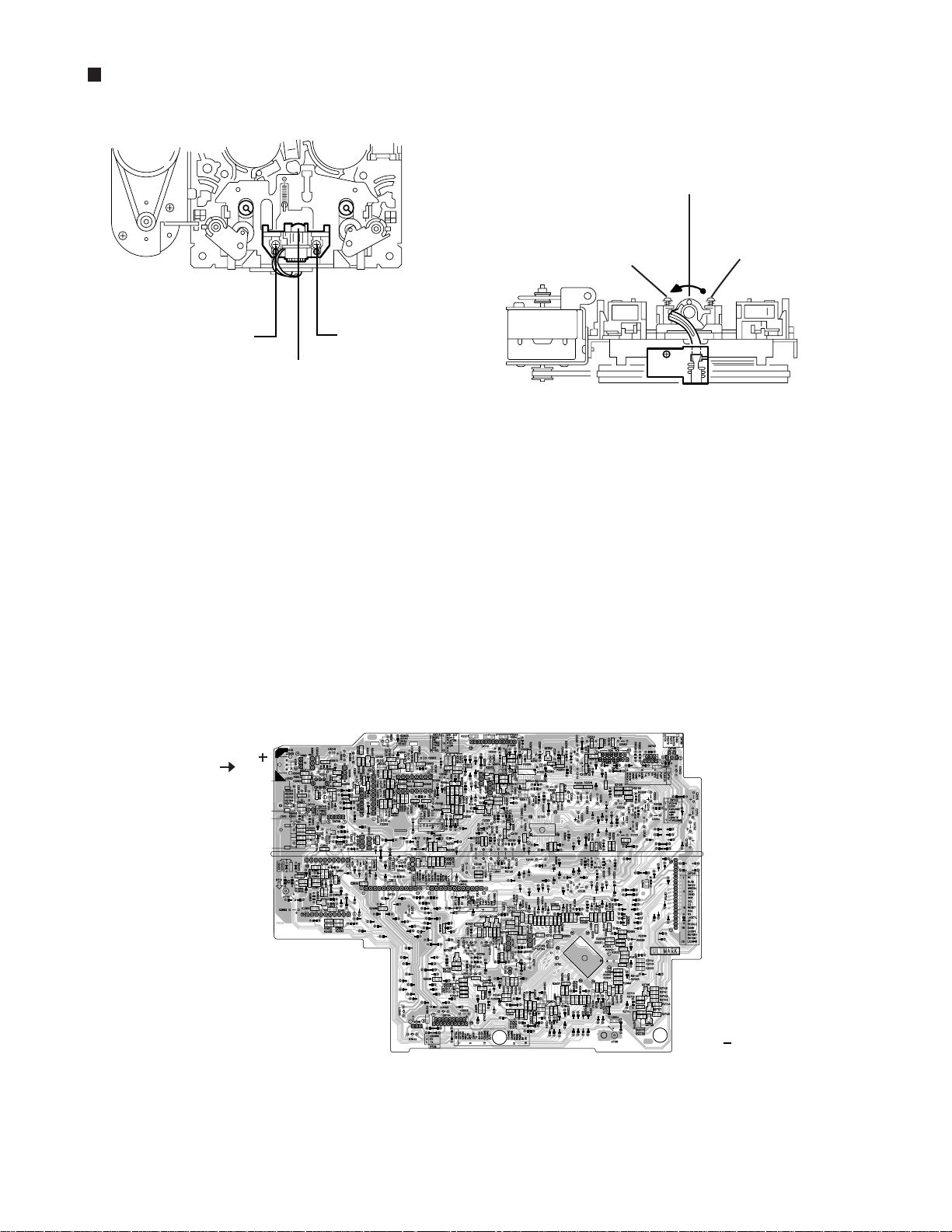
Replacement of laser pickup
Turn off the power switch and,disconnect the
power cord from the ac outlet.
Replace the pickup with a normal one.(Refer
to "Pickup Removal" on the previous page)
Plug the power cord in,and turn the power on.
At this time,check that the laser emits for
about 3seconds and the objective lens moves
up and down.
Note: Do not observe the laser beam directly.
Play a disc.
(Fig.1)
(3) Semi-fixed resistor on the APC PC board
The semi-fixed resistor on the APC printed
circuit board which is attached to the pickup
is used to adjust the laser power.Since this
adjustment should be performed to match the
characteristics of the whole optical block,
do not touch the semi-fixed resistor.
If the laser power is lower than the specified
value,the laser diode is almost worn out, and
the laser pickup should be replaced.
If the semi-fixed resistor is adjusted while
the pickup is functioning normally,the laser
pickup may be damaged due to excessive current.
Check the eye-pattern at TP602.
Finish.
1-29
Page 30

UX-A52
Description of major ICs
UPD784216AGF (IC701) : System micon
1. Pin layout
1
100
76
75
2. Block diagram
INTP2/NMI
INTP0.INTP1.
INTP3-INTP6
TI00
TI01
TO0
TI1
TO1
TI2
TO2
TI5/TO5
TI6/TO6
TI7/TO7
TI8/TO8
RTP0-RTP7
ANO0
ANO1
REF1
AV
AV
SS
ANI0-ANI7
REF0
AV
AV
D0
AV
SS
P03/INTP3
PCL
BUZ
25
26
PROGRAMMABLE
INTERRUPT
CONTROLLER
TIMER/EVENT
COUNTER
(16BITS)
TIMER/EVENT
COUNTER1
(8BITS)
TIMER/EVENT
COUNTER2
(8BITS)
TIMER/EVENT
COUNTER5
(8BITS)
TIMER/EVENT
COUNTER6
(8BITS)
TIMER/EVENT
COUNTER7
(8BITS)
TIMER/EVENT
COUNTER8
(8BITS)
WATCH TIMER
WATCHDOG TIMER
REAL-TIME
OUTPUT PORT
D/A
CONVERTER
A/D
CONVERTER
CLOCK OUTPUT
CONTROL
BUZZER OUTPUT
50
51
78K/1V
CPU CORE
RAM
8192BITS
ROM
128K BITS
UART/IOE1
BAUD-RATE
GENERATOR
UART/IOE2
BAUD-RATE
GENERATOR
CLOCKED
SERIAL
INTERFACE
BUS I/F
PORT0
PORT1
PORT2
PORT3
PORT4
PORT5
PORT6
PORT7
PORT8
PORT9
PORT10
PORT12
PORT13
SYSTEM CONTROL
RxD1/SI1
TxD1/SO1
ASCK1/SCK1
RxD2/SI2
TxD2/SO2
ASCK2/SCK2
SI0
SO0
SCK0
AD0-AD7
A0-A7
A8-A15
A16-A19
RD
WR
WAIT
ASTB
P00-P06
P10-P17
P20-P27
P30-P37
P40-P47
P50-P57
P60-P67
P70-P72
P80-P87
P90-P95
P100-P103
P120-P127
P130.P131
RESET
X1
X2
XT1
XT2
V
DD
V
SS
TEST
1-30
Page 31

3. Pin function (1/2)
UX-A52
Pin No.
1
2
3
4
5
6
7
8
9
10
11
12
13
14
15
16
17
18
19
20
21
22
23
24
25
26
27
28
29
30
31
32
33
34
35
36
37
38
39
40
41
42
43
44
45
46
47
48
49
50
Symbol
FAUX2
NC
RDSDATA
MPX
TUST
NC
FTUNER
FCD
VDD
NC
PBMUTE
NC
PIN
LEDCTL
BUZER
MDPOUT
MDRESET
SMUTE
NC
NC
POUT
VPP
UP
RMT0
RMT1
MIDDLE
DOWN
RMSPEED
VOLCK
VOLCE
VOLDA
AHB
BUB
BTCL
NC
XKILL
VDD
X1
X2
VSS
XT2
XT1
RESET
REM
RDSCK
NC
PHOTO
SAFTEY4
NC
NC
I/O
Not connected
-
Not connected
-
Not connected
-
Stereo detection
I
Stereo indicator detection
I
Not connected
O
Tuner switch output
O
CD switch output
O
Connected with VDD
-
Not connected
-
PB mute output
O
Not connected
-
Power key input
I
LED control output
O
Buzzer output
O
MD PB output
O
MD reset output
O
System mute output
O
Not connected
-
Not connected
-
Power-on control output
O
GND
I
Door position detection - UP
I
Door open/shut motor control output
O
Door open/shut motor control output
O
Door position detection - MIDDLE
I
Door position detection - DOWN
I
Door open/shut motor speed control output
O
Volume control clock
O
Volume control chip enable
O
Volume control data
O
Active hyper bus control
O
Backup detection
I
Battery control
O
Not connected
O
Power-off clock oscillator control
I/O
Power supply
I
Master clock
I
Master clock
O
GND
I
Clock for timer
O
Clock for timer
I
Power-on reset
I
Remote control sensor
I
Not connected
-
Not connected
-
Reel pulse detection
I
Current detection
I
-
Not connected
Not connected
-
Description
1-31
Page 32

UX-A52
3. Pin function (2/2)
Pin No.
51
52
53
54
55
56
57
58
59
60
61
62
63
64
65
66
67
68
69
70
71
72
73
74
75
76
77
78
79
80
81
82
83
84
85
86
87
88
89
90
91
92
93
94
95
96
97
98
99
100
Symbol
AVREF
AVREF0
SEFTY2
SEFTY3
LDCK
FKEY1
VERSION
FKEY2
KEY1
SEFTY1
VSS
RCDL
BCDL
AVREF1
RXD
TXD
NC
CDRXD
CDTXD
CDRST
GCDL
NC
T UD ATA
T UD ATA
TUCK
NC
NC
NC
NC
NC
NC
NC
NC
NC
NC
NC
NC
SCL
CS
RESET
SDA
NC
RS
NC
NC
S DATA
SCK
STTA
PLAY
VSS
UPD784216AGF(2/2)
I/O
Reference power supply +5 V
I
Reference power supply +5 V
I
Current detection
I
Current detection
I
Description
I/O
Function switch key input
I
Destination switch input
I
Function switch key input
I
Cassette key input
I
Current detection
I
GND
I
LED color display control
O
LED color display control
O
Reference power supply +5 V
I
Digital input
I
Digital output
O
Not connected
-
CD digital input
I
CD digital output
O
CD reset
O
LED color display control
O
Not connected
-
1
Tuner data
I
Tuner data
O
Tuner clock
O
Not connected
-
Not connected
-
Not connected
-
Not connected
-
Not connected
-
Not connected
-
Not connected
-
Not connected
-
Not connected
-
Not connected
-
Not connected
-
Not connected
-
LCD clock
O
LCD power supply
O
LCD reset
O
LCD serial data
I/O
Not connected
-
LCD start
I
Not connected
-
Not connected
-
Cassette control serial data
I/O
Cassette control serial clock
I/O
Cassette control status signal
I/O
Cassette PB switch detection
O
I
GND
1-32
Page 33

AN22000A-W (IC601) : RF head amp.
1. Pin layout
1234 5678910111213141516
2. Block diagram
OFTR
COFTR
12
BDO
11
BCDO
14
13
3TOUT
CEA
9
OFTR
BDO
10
3TENV
NRFDET
15
FEN
22
FEOUT
23
SUBT
TEN
21
20
SUBT
19
17181920212223242526272829303132
18
VDET
UX-A52
PDLDVDETTEBPFTEOUT
2
1
3
VCC
16
GND
2526
8
ARF
7
CAGC
RFIN
56
RFOUT
4
RFN
3. Pin function
Pin No.
1
2
3
4
5
6
7
8
9
10
11
12
13
14
15
16
AGC
A
GCA BCA
AMP
32
31
C
NRFDET
RF_EQ
Function
APC amp input terminal.
APC amp output terminal.
Power supply.
RF amp negative input terminal.
RF amp output terminal.
AGC input terminal.
AGC loop filter capacitor connection terminal.
AGC output terminal.
Capacitor connection terminal for HPF-amp.
3TENV output terminal.
Capacitor connection terminal for RF enberope detection.
BDO output terminal.
Capacitor connection terminal for RF enverope detection.
OFTR output terminal.
NRDET output terminal.
Ground terminal.
GCA BCA
AMP
30
29
B
D
E
GCA BCA
AMP
27
Pin No.
GCA BCA
AMP
28
F
Function
VREF output terminal.
17
VDET output terminal.
18
VDET input terminal.
19
TE amp. output terminal.
20
TE amp. negative input terminal.
21
FE amp. negative input terminal.
22
FE amp. output terminal.
23
GCTL & APC terminal.
24
FBAL control terminal.
25
TBAL control terminal.
26
Tracking signal input terminal 1.
27
Tracking signal input terminal 2.
28
Focus signal input terminal 4.
29
Focus signal input terminal 3.
30
Focus signal input terminal 2.
31
Focus signal input terminal 1.
32
TBAL FBAL
24
GCTL
17
VREF
1-33
Page 34

UX-A52
UPD780024AGKB21 (IC251) : Unit micon
1. Pin layout
64 ~ 49
1
48
~
16
17 ~ 32
2. Pin function (1/2)
Pin
No.
Symbol I/O Description
P50/A8
1
P59/A9
2
MCS
3
MRDY
4
CDINDEX
5
CDEMP
6
CDTNO
7
CDCOPY
8
VSS0
9
VDD0
10
P30
11
P31
12
P32
13
MUTE
14
SUBQ
15
P35/SO31
16
SQCK
17
KCMND
18
M STAT
19
MCLK
20
RXDO
21
TXDO
22
P25/SCK0
23
VDD1
24
AVSS
25
KEY1
26
KEY2
27
PCHK
28
P14/AN14
29
P13/AN13
30
/OPEN
31
/REST
32
~
33
Connected to GND
Not used
Pull-up +B
Not used
Not used
CD emphasis detection
I
CD track No. detection
I
CD copy detection
I
GND
Power supply
Not used
Not used
Not used
Mute output
O
Sub-code Q data input from IC651
I
Not used
Sub-code Q register clock output to IC651
O
Kick command data
O
CD control status output to IC801
O
CD control command clock input from IC801
I
Digital data input
I
Digital data output
O
Connected to GND
Power supply
GND
Key input 1
I
Key input 2
I
Parity check
I
Connected to GND
Connected to GND
Open switch input
I
Rest switch input
I
1-34
Page 35

2. Pin function (2/2)
UX-A52
Pin
No.
33
34
35
36
37
38
39
40
41
42
43
44
45
46
47
48
49
50
51
52
53
54
55
56
57
58
59
60
61
62
63
64
Symbol I/O
P10/AN10
AVREF
AVDD
/RESET
XT2
XT1
IC
X2
X1
VSS1
FLAG
BLKCK
/RFDET
EQx2
EQx4
VCOx4
OPEN
/CLOSE
IREFx4
P75/BUZ
/RESET
S TAT
/DMUTE
/P.ON
MLD
M DATA
MCLK
CLKSW
JIG
JIG
JIG
JIG
Function
-
Connected to GND
-
Analog circuit reference voltage. Connected with analog circuit power supply
-
Analog circuit power supply
I
CD control reset input from IC801
-
Not used
-
Connected with power supply
O
Flash memory control
-
Connected with external crystal oscillator
-
Connected with external crystal oscillator
-
GND
I
Flag signal input from IC651
I
Sub-code block clock signal input from IC651
I
RF signal amplitude detection input
O
2 equalizer switch output
O
4 equalizer switch output
-
Not used
I
Open door detection
I
Closed door detection
O
4 DSP current switch output
-
Not used
O
Reset signal output to IC651 (L: Reset)
I
Status signal input from IC651
O
Muting output to IC651
O
Power on/off switch signal output to IC291
O
Microcomputer command load signal output to IC651
O
Microcomputer command data output to IC651
O
Microcomputer command clock signal output to IC651
-
Not used
-
Not used
-
Not used
-
Not used
-
Connected to GND
1-35
Page 36

UX-A52
LC75345M-X (IC702) : E.volume
1. Pin layout
CL
VDD
ROPOUT
RINM
36 35 34 33 32 31 30 29 28 27 26 25 24 23 22 21 20 19
DI
CE
VSS
LOPOUT
RINP
LINM
ROOUT
LINP
RSB
LOUT
RBASS2
RBASS1
LSB
LBASS2
RTRE
RVRIN
LTRE
LBASS1
RSELOR5R4
L5
LVRIN
LSELO
R3
L4
R2
L3
R1
L2
Vref
181716151413121110987654321
L1
2. Block diagram
14
L5
15
L4
16
L3
17 18
L2
L1
19
Vref
20
R1
21
R2
22 23
R3
R4
24
R5
LSELO
13
LVRIN
12
LTRE
11
LVref
RVref
CONTROL
CIRCUIT
LOGIC
CIRCUIT
CONTROL
CIRCUIT
LBASS1
10
LBASS2
9
LSB
8
CCB
INTERFACE
LOUT
7
6
LINP
5
LINM
LOPOUT
34
VSS
2
CE
1
DI
36
CL
35
VDD
34
ROPOUT
33
RINM
32
RINP
1-36
25
RESLO
26
RVRIN
27
RTRE
28
RBASS1
29
RBASS2
30
RSB
31
ROUT
Page 37

3. Pin function
UX-A52
Pin No.
1
2
3
4
5
6
7
8
9
10
11
12
13
14
15
16
17
18
19
20
21
22
23
24
25
26
27
28
29
30
31
32
33
34
35
36
Symbol
DI
CE
VSS
LOPOUT
LINM
LINP
LOUT
LSB
LBASS2
LBASS1
LTRE
LVRIN
LSELO
L5
L4
L3
L2
L1
Vref
R1
R2
R3
R4
R5
RSELO
RVRIN
RTRE
RBASS1
RBASS2
RSB
ROUT
RINP
RINM
ROPOUT
VDD
CL
Function
Serial data and clock input pin for control.
Chip enable pin.
Ground pin.
Output pin of general-purpose operation amplifier.
Non-inverted input pin of general-purpuse operation amplifier.
Non-inverted input pin of general-purpuse operation amplifier.
ATT + equalizer output pin.
Capacitor and resistor connection pin comprising filters for bass and super-bass band.
Capacitor and resistor connection pin comprising filters for bass and super-bass band.
Capacitor and resistor connection pin comprising filters for bass and super-bass band.
Capacitor and resistor connection pin comprising treble band filter.
Volume input pin.
Input selector output pin.
Input signal pin.
Input signal pin.
Input signal pin.
Input signal pin.
Input signal pin.
0.5 x VDD voltage generation block for analog ground.
Input signal pin.
Input signal pin.
Input signal pin.
Input signal pin.
Input signal pin.
Input selector output pin.
Volume input pin.
Capacitor connection pin comprising treble band filter.
Capacitor and resistor connection pin comprising filter for bass and super-bass band.
Capacitor and resistor connection pin comprising filter for bass and super-bass band.
Capacitor and resistor connection pin comprising filter for bass and super-bass band.
ATT + equalizer output pin.
Non inverted input pin of general-purpose operation amplifier.
Non inverted input pin of general purpose operation amplifier.
Output pin of general-purpose operation amplifier.
Supply pin.
Serial data and clock input pin for control.
1-37
Page 38

UX-A52
MN662790RSC (IC651) : Digital servo & processor
1.Pin layout
60 41
61
40
80
21
1 20
2.Pin function
Pin No. Symbol I/O
1
2
3
4
5
6
7
8
9
10
11
12
13
14
15
16
17
18
19
20
21
22
23
24
25
26
27
28
29
30
31
32
33
34
35
36
37
38
39
40
BCLK
LRCK
SRDATA
DVDD1
DVSS1
TX
MCLK
M DATA
MLD
SENSE
FLOCK
TLOCK
BLKCK
SQCK
SUBQ
DMUTE
S TAT
LSI_RST
SMCK
CSEL
TEST2
TVD
PC
ECM
ECS
VDETMON
TRD
FOD
VREF
FBAL
TBAL
FE
TE
RFENV
TEST3
OFT
TRCRS
RFDET
BDO
LDON
O
O
O
O
O
O
O
O
O
O
O
O
O
O
O
Description
Bit clock output for SRDATA
Identifying signal output of L,R
Serial data output
-
Power supply for digital circuit
-
Connect to ground for digital circuit
Digital audio interface output signal
I
Micom command clock signal input
I
Micom command data signal input
I
Micom command load signal input L:load
-
Non connect
-
Non connect
-
Non connect
Sub code block clock signal
Export clock signal input for sub code Q resister
I
Sub code Q data output
Muting input H:muting
I
Status signal output
Reset signal input L:reset
I
Clock signal output MSEL is H : 8.4672 MHz MSEL is L : 4.2336 MHz
Oscillation frequency specification terminal H:33.8688 MHz L:16.9344 MHz
I
TEST2 terminal usually : open
-
Traverse drive output
Non connect
-
Spindle motor drive signal output (Compulsion mode output)
Spindle motor drive signal output (Servo error signal output)
Non connect
-
Tracking drive signal output
Focus drive signal output
Reference voltage for DA output section
-
Focus balance adjust signal output
Tracking balance adjust signal output
Focus error signal input (analog input)
I
Tracking error signal input (analog input)
I
RF Envelope signal input (analog input)
I
TEST3 Terminal usually : Fixation L
I
Off track signal input H : off track
I
Track cross signal input (analog input)
I
RF detection signal input L : detection
I
Dropout signal input H : dropout
I
Non connect
-
(Command execution : CD-TEXT data readout enabling signal (DQSY) output)
MN662790RSC (1/2)
1-38
Page 39

UX-A52
2.Pin function
Pin No. Symbol I/O
41
42
43
44
45
46
47
48
49
50
51
52
53
54
55
56
57
58
59
60
61
62
63
64
65
66
67
68
69
70
71
72
73
74
75
76
77
78
79
80
PLLF2
DSLBDA
WVEL
ARF
IREF
DRF
DSLF
PLLF
VCOF
AVDD2
AVSS2
EFM
DSLB
VCOF2
SUBC
SBCK
VSS
X1
X2
VDD
BYTCK
LDON
GCTRL
IPFLAG
FLAG
CLVS
CRC
DEMPH
RESY
IOSEL
TEST
AVDD1
OUTL
AVSS1
OUTR
DQSY
VCC5V
PSEL
MSEL
SSEL
I/O
-
-
I/O
I/O
I/O
-
-
-
O
I/O
O
-
O
-
O
O
O
-
O
-
O
O
O
O
O
MN662790RSC (2/2)
Functions
Terminal for loop filter characteristic switch for PLL
Non connect
Non connect
RF Signal output
I
Standard electric current input terminal
I
Bias terminal for DSL
I
Loop filter terminal for DSL
Loop filter terminal for PLL
Loop filter terminal for VCO
Power supply terminal for analog circuit
Connect to ground terminal for analog circuit
Non connect
PLL extraction clock output
Loop filter terminal for VCO
Sub code serial output
Clock signal input for sub code serial output
I
Connect to ground terminal for oscillation circuit
Oscillation circuit input terminal f=16.9344 MHz, 33.8688 MHz
I
Oscillation circuit output terminal f=16.9344 MHz, 33.8688 MHz
Power supply terminal for oscillation circuit
Non connect
Laser ON signal output H : ON
General I/O port
Non connect
Flag signal output
Non connect
Non connect
De-emphasis detection signal output
Non connect
Mode switch terminal
I
TEST terminal usually : H
I
Power supply terminal for analog circuit (for audio output section)
Lch audio output
Connect to ground terminal for analog circuit (for audio output section)
Rch audio output
RF signal polarity specification terminal
I
Power supply terminal (5V)
IOSEL=H TEST terminal IOSEL=L SRDATA input
IOSEL=H SMCK terminal output (frequency switch terminal) IOSEL=L LRCK input
IOSEL=H SUBQ terminal output mode switch terminal IOSEL=L BCLK input
1-39
Page 40

UX-A52
LA6541-X (IC801) : Servo driver
1. Pin layout & Block diagram
Vcc Vref Vin4 Vg4 Vo8 Vo7
24 23
11k
ohm
22
21
20
19
Vcc
Gnd
Vo6 Vo5 Vg3 Vin3 Cd Res
18
17 16
- +
- +
Level
shift
Level
shift
11k
ohm
1
2
3456
Vcc Mute Vin1 Vg1 Vo1 Vo2 Vo3 Vo4 Vg2 Vin2 Reg
B T L
driver
B T L
driver
Gnd
B T L
driver
B T L
driver
7 8 9101112
Level
shift
Level
shift
2. Pin function
Pin
Symbol Function
No.
1
10
11
12
13
14
15
16
17
18
19
20
21
22
23
24
2
3
4
5
6
7
8
9
Vcc
Mute
Vin1
Vg1
Vo1
Vo2
Vo3
Vo4
Vg2
Vin2
Reg Out
Reg In
Res
Cd
Vin3
Vg3
Vo5
Vo6
Vo7
Vo8
Vg4
Vin4
Vref
Vcc
Power supply (Shorted to pin 24)
All BTL amplifier outputs ON/OFF
BTL AMP 1 input pin
BTL AMP 1 input pin (For gain adjustment)
BTL AMP 1 input pin (Non inverting side)
BTL AMP 1 input pin (Inverting side)
BTL AMP 2 input pin (Inverting side)
BTL AMP 2 input pin (Non inverting side)
BTL AMP 2 input pin (For gain adjustment)
BTL AMP 2 input pin
External transistor collector (PNP) connection. 5V power supply output
External transistor (PNP) base connection
Reset output
Reset output delay time setting (Capacitor connected externally)
BTL AMP 3 input pin
BTL AMP 3 input pin (For gain adjustment)
BTL AMP 3 output pin (Non inverting side)
BTL AMP 3 output pin (Inverting side)
BTL AMP 4 output pin (Inverting side)
BTL AMP 4 output pin (Non inverting side)
BTL AMP 4 output pin (For gain adjustment)
BTL AMP 4 output pin
Level shift circuit's reference voltage application
Power supply (Shorted to pin 1)
15
14
11k
ohm
13
RESET
Regulator
11k
ohm
out
Reg
In
1-40
Page 41

LA1838 (IC1) : FM AM IF amp & Detector, FM MPX decoder
1. Block diagram
UX-A52
30
ALC
BUFF
FM
S-METER
FM IF
1
2. Pin function
Pin
Symbol
No.
FM IN
1
AM MIX
2
3
FM IF
AM IF
4
GND
5
6
TUNED
STEREO
7
8
VCC
9
FM DET
10
AM SD
FM VSM
11
AM VSM
12
13
MUTE
14
FM/AM
MONO/ST O
15
29
28
REG
AM
MIX
OSC
SD
COMP
S-CLRVE
PM
DET
2
I/O
I
This is an input terminal of FM IF
AM
AM/FM
IF-BUFF
3
27
FM
RF.AMP
AM IF
4
26
AGC
AM
S-METER
GND
Function
DET
TUNING
DRIVE
5
signal.
This is an out put terminal for AM
O
mixer.
I
Bypass of FM IF
Input of AM IF Signal.
I
I
This is the device ground terminal.
When the set is tunning,this terminal
O
becomes "L".
O
Stereo indicator output. Stereo "L",
Mono: "H"
III
This is the power supply terminal.
I
FM detect transformer.
I
This is a terminal of AM ceramic filter.
O
Adjust FM SD sensitivity.
O
Adjust AM SD sensitivity.
I/O
When the signal of IF REQ of IC121(
LC72131) appear, the signal of FM/AM
IF output. //Muting control input.
Change over the FM/AM input.
I
"H" :FM, "L" : AM
Stereo : "H", Mono: "L"
25
21
DECODER
ANIT-BIRDIE
STEREO
5N
SW
10
I/O
O
O
I
20
FF
38k
11
Left channel signal output.
Right channel signal output.
Input terminal of the Left channel post
24
STEREO
DRIVE
6
7
22
23
P-DET
VCC
89
Pin
Symbol
No.
16
L OUT
17
R OUT
18
L IN
VCO
384KHz
18
19
MUTE
FF
/
19k
2
12 13
FF
19k
/
LS
Function
17 16
PILOT
DET
15
14
AMP.
Input terminal of the Right channel
19
R IN
I
post AMP.
Mpx Right channel signal output.
20
21
22
23
24
25
RO
LO
MPX IN
FM OUT
AM DET
AM AGC
O
O
Mpx Left channel signal output.
I
Mpx input terminal
FM detection output.
O
AM detection output.
O
This is an AGC voltage input terminal
I
for AM
I
26
AFC
This is an output terminal of voltage
for FM-AFC.
27
28
AM RF
REG
AM RF signal input.
I
Register value between pin 26 and pin28
O
besides the frequency width of the
input signal.
29
AM OSC
I
This is a terminal of AM Local
oscillation circuit.
30
OSC BUFFER
AM Local oscillation Signal output.
O
1-41
Page 42

UX-A52
LC72136N (IC2) : PLL frequency synthesizer
1. Pin layout
FM/AM
CLOCK
FM/ST/VCO
AM/FM
2. Block diagram
XT
CE
DI
DO
SDIN
1
2
3
4
5
6
7
8
9
10
11
22
21
20
19
18
17
16
15
14
13
12
XT
GND
LPFOUT
LPFIN
PD
VCC
FMIN
AMIN
IFCONT
IFIN
1
22
16
15
3
4
5
6
17
21
3. Pin function
Pin
Symbol
No.
1
2
3
4
5
6
7
8
9
10
11
XT
FM/AM
CE
DI
CLOCK
DO
FM/ST/VCO
AM/FM
LW
MW
SDIN
Reference
Driver
Swallow Counter
1/2
C
2
B
I/F
Powe r
on
Reset
Function
I/O
X'tal oscillator connect (75kHz)
I
LOW:FM mode
O
When data output/input for 4pin(input) and
I
Swallow Counter
1/16,1/17 4bit
1/16,1/17 4bit
12bit
Programmable
DriverS
Data Shift Register & Latch
7821113
6pin(output): H
Input for receive the serial data from
I
controller
Sync signal input use
I
Data output for Controller
O
Output port
"Low": MW mode
O
Open state after the power on reset
O
Input/output port
I/O
Input/output port
I/O
Data input/output
I/O
Phase
Detector
Charge Pump
Unlock
Detector
Universal
Counter
Pin
No.
12
IFCONT
13
14
15
16
17
18
19
LPFOUT
20
21
22
Symbol
IFIN
AMIN
FMIN
VCC
PD
LPFIN
GND
XT
18
19
20
12
I/O
Function
IF counter signal input
I
IF signal output
O
Not use
-
AM Local OSC signal output
I
FM Local OSC signal input
I
Power suplly(VDD=4.5-5.5V)
-
When power ON:Reset circuit move
PLL charge pump output(H: Local OSC
O
frequency Height than Reference frequency.
L: Low Agreement: Height impedance)
Input for active lowpassfilter of PLL
I
Output for active lowpassfilter of PLL
O
Connected to GND
-
X'tal oscillator(75KHz)
I
1-42
Page 43

LA72723 (IC3) : RDS demodulation
1. Pin layout
UX-A52
VREF
MPXIN
Vdda
Vssa
FLOUT
CIN
TES
XOUT
2. Block Diagram
+5V
Vdda
Vssa
MPXIN
TEST
1
2
3
4
5
6
7
8
REFERENCE
VOLTAGE
ANTI ALIASING
FILTER
TEST
RDS-ID/READY
16
RDCL
15
RDDA
14
RST
13
MODE
12
Vddd
11
Vssd
10
XIN
9
VREF
57kHz
BPF
(SCF)
FLOUT
SMOOTHING
FILTER
CLK(4.332MHz)
OSC
VREF
CIN
+
PLL
(57kHz)
-
CLOCK
RECOVERY
(1187.5Hz)
DATA
DECODER
RAM
(128-bits)
RDS-ID
DETECT
Vddd
Vssd
RDDA
RDCL
MODE
RST
RDS-ID/
READY
+5V
3. Pin functions
Pin
Symbol
No.
1
VREF
2
MPXIN
Vdda
3
4
Vssa
5
FLOUT
6
CIN
TEST
7
8
XOUT
9
XIN
10
Vssd
11
Vddd
12
MODE
13
RST
14
RDDA
RDCL
15
16
RDS-ID
READY
I/O
O
I
O
O
O
I/O
O
XIN
XOUT
Function
Reference voltage output (Vdda/2)
Baseband (multiplexed) signal input
Analog power supply (+5V)
Analog ground
Subcarrier input (filter output)
Subcarrier input (comparator input)
I
Test input
I
Crystal oscillator output (4.332MHz)
Crystal oscillator input (exeternal reference input)
I
Digtal ground
Digtal power supply
I
Read mode setting (0:master,1:slave)
RDS-ID/RAM reset (positive polarity)
I
RDS data output
RDS clock output (master mode)/RDS clock input (slave mode)
RDS-ID/READY output (negative polarity)
1-43
Page 44

UX-A52
LA4628 (IC801) : Power amp.
1. Pin layout
1
2
2. Block diagram
1
PRE GND
3
4
6
IN2
2
RIPPLE
FILTER
IN
BIAS
CIRCUIT
STANDBY
SW
IN
13
14
PREDRIVER
PREDRIVER
PREDRIVER
PREDRIVER
POWER
LOAD SHORT
PROTECTOR
POWER
OVER VOLTAGE/
SURGE PROTECTOR
THERMAL
SHUT DOWN
POWER
LOAD SHORT
PROTECTOR
POWER
Vcc
OUTPUT PPIN TO VCC
SHORT PROTECTOR
OUTPUT PIN TO GND
SHORT PROTECTOR
Vcc
OUTPUT PIN TO GND
SHORT PROTECTOR
1314-OUT1
POWER
12
GND
11
+OUT1
-OUT2
9
POWER
10
GND2
+OUT2
8
1-44
POP NOISE
PREVENTION
CIRCUIT
5
OUTOUT PIN TO VCC
SHORT PROTECTOR
7
Page 45

L4909 (IC802) : Regulator
1. Pin layout
1 2 34 5678 9101112131415
2. Block diagram
UX-A52
EN1
EN2
EN3
OC
TRIG
GND
3. Pin functions
Pin No.
10
11
12
13
14
15
THERMAL
SHUTDOWN
6
7
9
5
4
8
1
2
3
4
5
6
7
8
9
ENABLE
CONTROL
CURRENT
Symbol
FB1
VO1
VINA
TRIG
OC
EN1
EN2
GND
EN3
FB3
VO3
N.C.
VINB
VO2
FB2
OVER
CHECK
Function
REG1 feedback voltage input
REG1 output voltage
Input DC supply voltage
Trigger for external SCR (crowbar protection)
Over current warning output
REG1 enable input
REG2 enable input
Analog ground
REG3 enable input
REG3 feedback voltage input
REG3 output voltage
Not connected
Input DC supply voltage
REG2 output voltage
REG2 feedback voltage input
REFERENCE
GENERATOR
REG1
REG2
REG3
REF
REF+20%
REG1
REG2
REG3
3,13
14
15
11
10
VINA
VINB
2
VO1
1
FB1
VO2
FB2
VO3
FB3
1-45
Page 46

UX-A52
KIA78S05P-T (IC803) : Reglator
1. Pin layout 2. Block diagram
Q14
Q1
R9
1 2 3
Z1
Q16
R10R11
Q2
Q7
Q4
R1
Q6
R2
Q8
C1
Q5Q3
R4
Q9
Q10
Q11
Q12
R8
3 INPUT
Q13
R7
1 OUTPUT
R5
XC62HR3502P-X (IC291) : Regulator
1. Pin layout
54
2. Block diagram
VIN
R3
R6
2 COMMON
VOUT
Current
Limit
3. Pin function
1-46
123
Pin No.
Symbol
1
2
3
4
5
VSS
VIN
CE
NC
VOUT
CE
Function
Ground
Supply voltage input
Chip enable
Non connect
Regulated output voltage
Output
Control
Voltage
Reference
VSS
Page 47

BA3126N (IC331) : R / P switch
1. Pin layout & Block diagram
S W
R E C
G
123456789
S W
P / B
C O N T .
AN7317 (IC332) : R / P amp
1. Pin layout & Block diagram
G N D
V c c
S W
P / B
UX-A52
G
S W
R E C
2. Pin function
Pin No.
1
2
3
4
5
6
7
8
9
10
11
12
13
14
15
16
16
1
60k
60k
15
14
112k
Pre
Pre
112k
2
30k
30k
3
Function
CH1 playback amp input
Feedback of CH1 playback amp
CH1 playback amp output
CH1 recording amp input
CH1 recording amp output
Low cut of ALC
Time of ALC
GND
Vcc
Lipple filter
Recording amp mute
CH2 recording amp output
CH2 recording amp input
CH2 playback amp output
Feedback of CH2 playback amp
CH2 playback amp input
13 12 11 10 9
Mute R.R
Pre
Pre
ALC
45678
1-47
Page 48

UX-A52
GP1UM271XK (IC901) : Remocon
1. Block diagram
R
L
Amp Limiter B.P.F Demodu-
lator
Integrrator
BU4094BCF-X (IC333) : Shift / Store registor
1. Pin layout 2. Block diagram
16 15 14 13 12 11 10 9
VDD OUTPUT
ENABLE
Q5 Q6 Q7 Q8 Q'S Q'S
DATA
CLOCK
STROBE
2
3
SHIFT REGISTER
1
Comparator
GND Vcc Vout
10
8-STAGE
8-BIT
LATCHES
Q'S
QS
SERIAL
OUTPUT
9
STROVE DATA CLOCK Q1 Q2 Q3 Q4 Vss
1 2 3 4 5 6 7 8
LB1641 (IC703, IC704) : DC motor driver
1. Pin layout
1 2 3 4 5 6 7 8 9
GND OUT1 P1
VZ IN1 IN2
VCC1
VCC2 P2
10
OUT2
OUTPUT
15
ENABLE
Q1
2. Pin function
Input Output
IN1 IN2 OUT1 OUT2
0 0 0 0
1 0 1 0
0 1 0 1
1 1 0 0
3-STATE
OUTPUTS
Q8
PARALLEL OUTPUT
Mode
Brake
CLOCKWISE
COUNTER-CLOCKWISE
Brake
1-48
Page 49

< MEMO >
UX-A52
1-49
Page 50

UX-A52
UX-A52
VICTOR COMPANY OF JAPAN, LIMITED
AUDIO & COMUNICATION BUSINESS DIVISION
PERSONAL & MOBILE NETWORK BUSINESS UNIT. 10-1,1chome,Ohwatari-machi,Maebashi-city,371-8543,Japan
1-50
(No.21074)
Printed in Japan
200202
Page 51

Block diagram
UX-A52
LED
6
FM/AM
FMA-006
J1
ANT
TU1
FM RF
L1
AM RF
& OSC
IFOUT
AMRF
AFC
AMOSC
OSCOUT
IC2
PLL
MUTE/IFOUT
FM/AM
SQIN
ST/MONO
AMOSC
STEREO,CK
CE,DATA
IC1
FMDET
AM DET
LOUT
ROUT
CN1
CN701 CN744 CN743
FMB-031-1
TUL,TUR
TUDATA
TUST
TUCK
MPX
SW201
SW202
5
LVA10166-A1
CN31
R/P
HEAD
L+,LR+,R-
FW31
M
4
REEL
CN1
CN32
PULSE
IC31
HEAD
SWITCH
MOTOR
DRIVE
SOLENOLIDE
DRIVE
SWITCH
3
A+C
CN001
CD
B+D
CN601
E,F
LD,MD
PICKUP
T+,TF+,F-
OPEN
2
SWITCH
/OPEN
REST
SWITCH
/REST
IC801
FCS/SP/FE/TR
FEED
MOTOR
SPINDLE
FM+,FM-
SM+,SM-
BTL DRIVER
MOTOR
IC601
RF & SERVO
AMP
TBAL
OFT
FBAL
BDO
FE,TE
ARF
RFENV
GCTL
RFDET
TRD
FOD
ECM
ECS
TVD
1
IC32
PB/REC
AMP
MS,PBL,PBR
RECL,RECR
IC33
PORT
EXTENSION
SQL,KEY1,PLAY,PHOTO
SWITCH
IC251
UNIT
MICOM
/RESET
S TAT
/DMUTE
SUBQ
SQCK
BLKCK
M DATA
MCLK
FLAG
IREFx4
MLD
CDCOPY
CDTNO
CDEMP
CDINDEX
IC651
DSP
DQSY,SBCK
SUBC
STTA
S DATA
SCK
M
TXDO,RXDO
IC,/RESET
MCS
KCMND
M STAT
MRDY
KCLK
TX
OUTL
OUTR
SRDATA
LRCK
BCLK
CN34 CN33
/RESET
CN606
to FLASH MICON
CN605CN651CN671
PBL,PBR
CN706
CN704
PHOTO
PLAY,KEY1
SAFETY1
SCK,SDATA
STTA
OUTL,OUTR
IC704
MOTOR
DRIVER
LOAD
UNLOAD
CDTXD
CDRXD
CDRST
TX
J2003
RESET,SDA,RS
DOWN,UP,MIDDLE
IC701
SYSTEM
MICOM
RMT0,RMT1
LOCK
RMSPEED
IC703
MOTOR
DRIVER
MATRIX
LEDCTL
RED
BLUE
GREEN
FW907
DOWN
MIDDLE
UP
VOLDA,VOLCE
IC901
REMOCON
REM
CN918
CN908
CN906
CN909
CN709
MOTOR+
MOTOR-
BUZZER,PIN
FKEY1,FKEY2
SDA
SCL,RS
RESET
MOTOR+
MOTOR-
IC702
FUCTION/
VOL/AHB
LCD
CN907
AHB,FCD
MDPOUT
SMUTE
POUT
SAFETY4
OUTL,OUTR
SAFETY2
SAFETY3
CN705
M
CN905
CN711
CN712
KEY1
KEY2
PIN
BUZZER
US6V
SW5V
CN802CN801
S2601~S2617
KEY MATRIX
BZ201
L1006
S1001
WITHOUT UP
VOLTAGE
CONTROL
IC802
REG.
LOUT
ROUT
IC801
POWER
AMP
INL
INR
LIN
RIN
+OUTL
-OUTL
+OUTR
-OUTR
J1003
AC INPUT
CN809
CN803
CN804
J1001
T1001
W1001
J1002
BC
DIGITAL OUT
DE
F
G
HA
I
2-1
Page 52

Standard schematic diagrams
Main & control circuit
UX-A52
UX-A52
KTC3875/GR/-X
R2733
SCL
R2706
2.2/50
C2713
Q2716
10K
MTZJ7.5C-T2
D2911
270
CS
KTC3875/GR/-X
270
R2734
SDA
RESET
R2099
R2098
R2097
R2089
R2061
R2060
R2057
R2062
R2064
R2066
R2624
R2052
R2051
R2050
R2048
R2046
R2044
R2043
R2042
R2041
0.01
C2005
QQL244K-100Z
Q2704
IC901
GP1UM271XK
C2904
100P
C2909
100P
C2908
100P
C2907
100P
0.001
C2902
C2901
100/10
REM%
UP
RS
DOWN
LCD5V
LEDCTL
MOTOR-
MOTOR+
MIDDLE
TLMT+
2.2K
TLMT-
2.2K
LOAD
2.2K
UNLOAD
2.2K
2.2K
TUCK
TUDATA
2.2K
2.2K
CDRST%
1K
CDTXD
1K
1K
CDRXD
BCOL
2.2K
RCOL
2.2K
2.2K
2.2K
2.2K
2.2K
2.2K
2.2K
2.2K
R2095
R2096
10K
10K
K2001
QQR0621-001Z
L2002
R2710
R2708
10K
KTC3875/GR/-X
10K
R2707
10K
D2702
R2709
R2901
QGF1016F1-14
QGF1016F1-14
100K
Q2705
CS
SDA
SCL
RS
RESET
VDD
C1+
1
C1-
C2905
V5OUT
VSS
1
V5
10K
C2906
CN918
CN908
1
C1009
CN907
QGA2501F1-02
C2010
100P
100P
C2009
R2088
100K
C2015
47/10
100P
C2011
R2047
10K
R2045
10K
D2705
C2714
4.7/50
R2711
47K
R2049
D2708
AHB%
D2703
MTZJ5.1C-T2
33K
R2712
10K
KI901
QGB2510J1-12
QLD0184-001
J2003
GP1FA550TZ
2.2K
2.2K
C2502
100/16
1.8K
R2227
2.2K
VOLCK
R2505
VOLDA
VOLCE
R2127
4.7K
R2128
R2237
R2235
51K
K2002
QQR0621-001Z
CN711
MGNDB
SW5V
FCD
TUNER+B
1.8K
TUNERPOUT
DOUT
DGND
VCC5V
R2620
82
R2621
82
7.5K
R2229
0.082
0.082
104
C2206
C2205
C2602
C2603
R2226
4.7K
R2228
R2225
2.2K
R2503
C2103
0.082
0.27
C2104
2.2K
R2126
15K
C2219
10/16
SMUTE
POUT
A9V
C2201
22/16
Q2203
KTC3875/GR/-X
7.5K
R2230
0.1
0.10.1
0.082 0.27
C2203 C2204
C2207
C2208
0.082
C2202
IC702
LC75345M-X
0.082 104
C2101
22/16
C2102
C2107
0.082
0.082
104
104
2.2K
C2106
C2105
C2600
C2604
R2125
7.5K
R2129
R2130
D2201
R2234
10K
1000p
C2750
AHB
1.8K
R2232
R2231
1.8K
0.0027
4.7/50
C2209
C2210
0.1
0.0027
C2108
C2109
7.5K
R2131
D2202
R2134
10K
DGND
BUZZER
FKEY1
FKEY2
PIN%
CN705
4.7/50
C2225
4.7/50
C2110
1.8K
QGF1201C3-05
22/16
10/35
4.7/50
4.7/50
4.7/50
220K
R2233
C2231
C2226
C2227
C2229
C2230
0.012
C2211
0.012
C2119
10/35
4.7/50
4.7/50
4.7/50
4.7/50
C2129
C2127
C2126
C2125
C2130
1.8K
R2132
R2137
15K
R2135
120K
Q2103
1/50
KTC3875/GR/-X
S2601
PIN%
R2601 R2602 R2603 R2604 R2605 R2606 R2607
1K 1K 1.2K 1.5K 2.2K 2.7K 3.9K
CN905
QGF1201F3-05
S2609
R2206
15K
R2106
15K
PHOTO
Q2403
KTC3875/GR/-X
R2416
82K
220K
R2133
150K
R2136
C2131
S2602
S2610
R2417R2415
82K
390K
S2603
R2608 R2609 R2610 R2611 R2612 R2613
1K 1K 1.2K 1.5K
S2611
TUL
TUR
MPX%
TUST
TUCK
TUDATA
1.2K
R2110
R2210
C2404
0.01
R2418
100K
S2605
S2604
S2613
S2612
CN701
QGF1205C1-13
RDSCK
RDSDATA
1.2K
C2214C2114
0.00820.0082
R2211R2111
6.8K6.8K
D2046
R2411
5.6
R2205
4.7K
R2105
4.7K
R2208
R2209
1.8K
R2108
1.8K
R2109
1.8K
1.8K
R2407
3.3K
R2408
3.9K
R2203
39K
10K10K
220P220P
C2212C2112
R2204R2104
R2103
39K
0.01
C2453
D2451
D2452
S2606
S2607
2.7K
2.2K
S2615
S2614
PBR
PBL
SW10V
RECR
RECL
PLAY
KEY1
SAFETY1
SCK
SDATA
STTA
J2001
S2608
S2617
R2617
5.6K
S2616
BZ201
QAN0045-001
47
680
R2614
D2601 R2615
Q2601
KRC102S-X
6
D2602
R2750
SPR-39MVWF
SW202
QSW0933-001
5
R2745
Q2708
2.2K
KTC3875/GR/-X
1/50
C2753
2.2K
R2744
2.2K
2.2K
2.2K
R2742
R2743
Q2707
KTC3875/GR/-X
1K
R2718
2.2K
R2741
R2740
R2715
R2714
KTC3875/GR/-X
1/50
C2751
R2713
1K
R2716
Q2706
1K
1/50
C2752
R2717
BCOL
1K
BLUE
GCOL
1K
GREEN
RCOL
1K
RED
4
IC704
LB1641
QGA201C1-05
UNLOAD
LOAD
MTR-
MTR+
CN706
10
R2860
3
CN704
QGF1016C1-19
CDTXD
CDRXD
MRDY
KLCK
CDRST%
2
W708
QJQ009-032601
1
R2138
MCS
TX
10K
LOCK
RMT1
RMT0
L2003
QQL244K-100Z
22/16
K3002
QGB2510J1-12
K3003
NQR0428-002X
QQR0621-001Z
CN712
9.1
R2856
0.01
C2855
R2852
C2604
470P
US6V
CDAGND
D2860
10
MTZJ6.8B-T2
SAFETY2
10
R2867
C2861
0.01
R2863
10K
R2864
2.2k
2.2k
10K
TLMT-
R2861
R2862
TLMT+
R2865
10K
R2866
10K
IC703
LB1641
MOTOR+
MOTOR-
10
R2855
C2852
0.01
D2852
2.2k
2.2k
C2853
100/16
R2854
R2853
MTZJ7.5C-T2
C2605
1000P
OUTR
SAFETY3
CD+B
AGND
OUTL
CD+B
D2904
NSTM515AS
MTZJ7.5C-T2
D2902
D2724
D2723 D2726D2725
Q2709
KTC3875/GR/-X
220
220
220
R2720
R2719
FW907
10K
R2084
R2092
47K
R2093
47K
47K
47K
47K
R2086
R2087
R2085
Q2711
KTC3875/GR/-X
R2723
R2622
MTZJ7.5C-T2
D2903
Q2710
KTC3875/GR/-X
270
270
270
270
R2722
R2724
R2721
QUM024-10DGZ3
SW201
QSW0803-001
UP
DOWN
DGND
MIDDLE
R2083
10K
2.2K
R2100
1K
R2001
10K
R2002
2.2K
R2003
2.2K
R2005
2.2K
R2006
R2007
2.2K
10K
R2008
2.2K
R2009
R2010
2.2K
1K
R2011
15K
R2012
2.2k
R2015
1K
10K
R2016
10K
R2017
2.2K
R2018
2.2K
R2019
10K
R2020
10K
R2021
1K
R2023
1K
R2024
0.01
C2001
0.01
C2002
QAX0283-001Z
33P
C2704
D2908
NSTM515AS
MTZJ7.5C-T2
D2906
Q2712
KTC3875/GR/-X
220
220
220
R2726
R2751
R2725
100P
C2014
C2013
2.2K
2.2K
2.2K
R2082
R2081
R2080
SCK
STTA
PLAY
CDMUTE
RDSDATA
MPX%
TUST
FTUNER
FCD
PBMUTE
PIN
LEDCTL
BUZZER
KARAOKE
ECHO
SMUTE
TUNERPOUT
POUT
UP
RMT0
RMT1
MIDDLE
DOWN
VOLCK
VOLCE
AHB%
BUP
BTCL%
VOLDA
10K1K2.2K
1K
R2028
R2027
R2026
R2025
X2701
33P
C2705
KTC3875/GR/-X
R2729
100P
2.2K
R2079
SDATA
R2029
Q2714
270
QGD2504C1-04Z
C2012
UPD784214AGF527
XKILL
D2001
1SS133-T2
1K
100/16
C2708
MTZJ7.5C-T2
D2907
Q2713
KTC3875/GR/-X
270
270
270
R2728
R2727
R2730
100P
VDD
R2752
CN906
DOWN
CN909
QGB2024J1-20S
CN709
QGB2024K1-20S
RS
CS
SCL
SDA
RESET
100
100
100
100
100
R2077
R2072
R2075
R2073
R2070
RS
CS
SCL
SDA
RESET
IC701
REM%
XT2
XT1
RESET%
VSS
100K
100K
2.2K
1K
R2030
R2031
R2033
R2032
X2702
QAX0401-001
0.01
22P
C2709
C2710
D2912
NSTM515AS
MTZJ7.5C-T2
D2910
D2732
D2731
Q2717
Q2715
KTC3875/GR/-X
KTC3875/GR/-X
270
270
220
220
220
R2735
R2732
R2731
R2736
UP
MIDDLE
REM%
RED
DGND
BLUE
SW10V
GREEN
TUCK
TUDATA
GCOL
CDRST%
CDTXD
CDRXD
BCOL
RCOL
KEY1
FKEY2
FKEY1
LOCK
SAFETY3
SAFETY2
AVREF
PHOTO
1K
100P
C2004
R2034
KTA1504/GR/-X
R2039
R2040
L2001
QQL244K-100Z
Q2703
330
R2705
D2701
22P
C2712
2200/6.3
C2711
BC
DE
2-2
F
G
HA
I
Page 53

Power amplifier & Power supply circuit
6
5
4
3
2
R1201
R1101
UX-A52
Q1701
5.6K
5.6K
5.6K
5.6K
DTC144WSA-T
C1802
D1005
1N5401-TM
Q1705
D1801
47/25
10/5010/50
MTZJ13B-T2
R1807
DTA144WSA-T
C1706C1707
DTA144WSA-T
Q1704
0.01
R1806
2.7K
680
2SC2785/FE/-T
C1801
2200/25
C1803
220P
Q1803
DTA144WSA-T
DTA144WSA-T
C1005
C1006
2200/25
R1805
C1003
R1804
QQR0797-001
8200/25
0.022
C1001
C1018
220P
C1210
220P
C1110
QQR0797-001
C1016
0.1
L1201
L1101
0.1
D1015
IN5401-TM
0.1
C1017
C1015
D1013
C1709
IN5401-TM
D1014
0.01
F1002
0.0033
0.0033
IN5401-TM
IN5401-TM
F1004
F1003
C1211
C1111
D1012
J1001
QNB0133-001
K1010
W1001
150
150
QQR0779-001Z
CN804
QGA2501C1-05
C1014
0.1
QGA3901C1-04
AC1
S1
AC2
CN803
QQL231K-470Y
QGA7901C1-04
CN809
QQL231K-470Y
R1091
R1090
K1009
L1005
QQR0779-001Z
QNS0030-001
L1004
QQL231K-470Y
L1003
J1002
QQT0360-003
Q1702Q1703
+OUTL
Q1801
KTB772/Y/
4.7K
2SC2785/FE/-T
D1003
680
R1803
C1004
IN5401-TM
D1004
D1002
IN5401-TM
IN5401-TM
C1002
R1802
0.022
QSW0740-001
Q1802
680
680
R1801
IN5401-TM
D1001
0.022
S1001
680
0.022
R1702
IC801
LA4628
C1205
2SD2144S/VW/-T
C1106
KIA78S05P-T
C1402
100/16
Q1202
10/35
10/35
C1105
4.7K
R1210
R1110
4.7K
0.001
0.001
C1206
IC803
0.1
C1401
D1606
3.9K
3.9K
4.7K
4.7K
2SD2144S/VW/-T
R1109
R1209
Q1102
R1049
330
D1401
MTZJ8.2B-T2
Q1023
C1302
1000P
KRA101M-T
Q1301
INR4
INL4
C1042
D1403
D1404
2SC2001/LK/-T
C1301
C1207
330P
2.2/50
C1043
R1077
10K
D1405
560
R1301
MTZJ11A-T2
100/16
D1301
D1605
100/16
MTZJ10C-T2
D1905
KTA1023/0Y/-T
C1701
D1901
100/10
330P
C1107
C1046
MTZJ5.6B-T2
R1708
33/50
D1904
D1501
MTZJ8.2C-T2
D1701
1K
R1706
Q1708
D1902
10K
1/50
C1047
2SC2785/FE/
R1901
Q1706
R1902
R1111
C1109
R1707
0.1
9.1K
1.2K
D1603
2.2
2.2
R1112
0.1
C1108
C1901
100/16
MTZJ5.6B-T2
Q1707
2SC2785/FE/
1K
D1026
D1027
C1902
0.1
KRC110M/-T
D1604
R1211
C1209
0.1
Q1607
2.2
2.2
22K
22K
22K
22K
R1213
D1903
R1616
C1602
0.1
10K
R1212
0.1
C1208
IC802
L4909
C1601
100/16
D1601
MTZJ8.2C-T2
R1113
C1052
C1054
0.056
470
R1615
QQR0621-001Z
QQR0621-001Z
QQR0621-001Z
QQR0621-001Z
6.8K
R1214
R1114
1/50
1/50
C1053
C1055
R1087
R1086
0.056
6.8K
4.7K
R1601
1.2K
R1602
R1617
1.8K
C1056
K1002
K1004
K1005
K1006
1.0
C1502
470
R1215
0.1
C1058
R1501
100/16
R1502
C1501
R1703
R1704
R1705
470
R1115
100/16
330/25
1.0
6.8K
C1710
C1908
1.2K
F1001
CN801 CN802
QGB2510K2-12
SAFETY2
QGB2510K2-12
1
MAIN SIGNAL
QQR1145-001
L1006
J1003
QNC0006-001
Parts are safety assurance parts.
When replacing those parts make
sure to use the specified one.
BC
DE
F
G
HA
I
2-3
Page 54

Power amplifier & Power supply circuit (UP only)
6
R1101
3.9K
R1201
3.9K
4.7K
4.7K
2SD2144S/VW/-T
R1109
R1209
Q1102
R1049
330
5
4
D1401
MTZJ8.2B-T2
3
2
2SD2144S/VW/-T
KIA78S05P-T
C1402
C1106
100/16
Q1202
UX-A52
IC801
LA4628
C1042
C1207
330P
2.2/50
C1043
R1077
10K
D1405
560
R1301
MTZJ11A-T2
100/16
D1301
D1605
Q1023
C1302
1000P
KRA101M-T
D1606
Q1301
INR4
D1403
D1404
INL4
2SC2001/LK/-T
C1301
C1205
10/35
10/35
C1105
4.7K
R1210
R1110
4.7K
0.001
0.001
C1206
IC803
0.1
C1401
100/16
D1901
MTZJ10C-T2
D1905
KTA1023/0Y/-T
100/10
C1701
330P
MTZJ5.6B-T2
C1107
R1708
C1046
33/50
D1904
D1501
D1701
1K
MTZJ8.2C-T2
R1706
Q1708
D1902
10K
1/50
C1047
2SC2785/FE/
R1902
R1901
Q1706
R1111
C1109
D1603
R1707
0.1
1.2K
9.1K
2.2
2.2
R1112
0.1
C1108
C1901
100/16
MTZJ5.6B-T2
Q1707
2SC2785/FE/
1K
D1026
D1027
C1902
0.1
KRC110M/-T
D1604
R1211
2.2
0.1
C1209
C1602
0.1
Q1607
R1616
10K
D1903
2.2
R1212
0.1
C1208
IC802
L4909
C1601
100/16
R1615
D1601
MTZJ8.2C-T2
UX-A52
22K
R1213
R1113
1/50
C1052
C1054
0.056
6.8K
470
QQR0621-001Z
QQR0621-001Z
QQR0621-001Z
QQR0621-001Z
22K
R1086
R1114
R1087
C1053
6.8K
R1617
Q1701
R1702
5.6K
R1703
R1704
5.6K
R1705
5.6K
22K
22K
R1214
1/50
C1055
0.056
4.7K
R1601
1.2K
R1602
1.8K
C1056
K1002
K1004
K1005
K1006
470
470
R1115
R1215
0.1
100/16
C1058
C1710
1.0
R1501
330/25
C1501
C1502
1.0
100/16
C1908
6.8K
1.2K
R1502
DTA144WSA-T
10/5010/50
C1706C1707
5.6K
DTA144WSA-T
Q1704
0.01
C1803
D1801
C1801
220P
MTZJ13B-T2
R1806
2.7K
47/25
C1802
D1005
1N5401-TM
R1807
680
2SC2785/FE/-T
2200/25
Q1803
DTA144WSA-T
DTA144WSA-T
C1005
2200/25
Q1705
DTC144WSA-T
R1805
R1804
C1006
C1003
0.022
Q1702Q1703
+OUTL
Q1801
KTB772/Y/
4.7K
2SC2785/FE/-T
D1003
680
R1803
C1004
0.022
IN5401-TM
D1004
D1002
IN5401-TM
IN5401-TM
C1002
R1802
0.022
Q1802
680
680
R1801
IN5401-TM
D1001
680
8200/25
0.022
C1001
C1018
C1210
C1110
L1201
220P
220P
L1101
C1017
0.1
D1015
IN5401-TM
C1016
D1014
IN5401-TM
0.1
D1013
0.1
C1015
0.01
C1709
0.0033
0.0033
IN5401-TM
F1004
F1003
C1211
C1111
IN5401-TM
D1012
J1001
QNB0133-001
QQL231K-470Y
R1091
R1090
K1009
L1005
QQT0360-002
QQR0779-001Z
L1004
QQL231K-470Y
L1003
QNS0030-001
J1002
K1010
W1001
150
150
QQR0779-001Z
CN804
QGA2501C1-05
C1014
0.1
QGA3901C1-04
AC1
S1
AC2
CN803
QQL231K-470Y
CN809
QGA7901C1-02
F1001
CN801 CN802
QGB2510K2-12
SAFETY2
QGB2510K2-12
1
MAIN SIGNAL
Parts are safety assurance parts.
QQR1145-001
L1006
J1003
QNC0046-001
When replacing those parts make
sure to use the specified one.
BC
DE
F
G
HA
I
2-4
Page 55

CD control circuit
6
5
4
3
F-
F+
T+
T-
CN601
@HFW15R-1STE1
UX-A52
MCS
MRDY
CDEMP
CDTNO
CDCOPY
IC251
UPD7800F0034A
MLD
MDATA
CDINDEX
1k
1k1k100
1k
R284
R282
R281
R283
R256
1k
R251
MCLK
1k
R252
MDATA
1k
R253
MLD
1k
R254
/DMUTE
STAT
/RESET
IREFx4
R264
5.6k
R265
3.3k
D251
DA204U-X
D292
10k
C255
0.1/25
R275
BLKCK
FLAG
MCLK
LRCK
BCLK
SRDATA
K656
K657
K658
K655
NQR0007-002X
NQR0251-004X
NQR0251-004X
NQR0251-004X
NI
D603
R675
10
100/6.3
0.1/16
C657
C655
MA112-X
47/10
C254
NI
D291
IC291
TK11235BMC-X
1/25
C291
C292
1/25
C293
0.01/50
R258
KCMND
MSTAT
MRDY
R260
KCLK
R255
MCS
R285
C658
0.1/25
QGF1016F2-06
CN671
QGF1016F2-19W
CN651
1k
1k
1k
1k
R601
180k
R602
82k
C604
0.022
C603
F
E
B+D
A+C
C633
0.022
A+C
F
R635
R608
47k
R607
47k
10
E
B+D
R636
150
C632
1/16
R634
3.9
0.001
D601
NI
R631
R632
2.2
C631
3.9
10/16
2SA1037AK/RS/-X
Q631
0.022
C602C601
0.001
AN22000A
IC601
1/16
100/6.3
C623
C624
C608
R611
39k
C605
270p
R603
220k
R604
82p
NI
C607
0
R605
C606
0.1/25
100/10
C622
C621
0.039
0.0027
0.1/50
0.0027
C617
C614
C615
C612
0.1/16
C610
C611
0.056/25
NI
R617
5.6k
R613
5.6k
5.6k
330p
C616
C681
NI
C682
15p
C683
22p
TP1
Q651
DTC114EUA-X
Q652
DTC114EUA-X
TBAL
FBAL
FE
TE
SUBQ
C272C271
R257
1k
SQCK
GCTL
/RFDET
OFT
BDO
ARF
RFENV
TP2
KCMND
1k
MSTAT
R259
KCLK
R263
1k
R262
1k
C256
0.1/25
10k
10k
6.8k
6.8k
R272
R271
R273
/OPEN
/REST
R274
C273
X251
@CSTS8.38MG
STAT
SUBQ
SQCK
BLKCK
/RESET
/DMUTE
1k
1k
1k
1k
C653
0.33/16
R651
R652
R653
R654
TVD
ECM
ECS
TRD
R812
C802
1.5k
C815
2.2/10
1000p
R803
4.7k
TRD
T+
390p
2
SW102
QSW0931-001
SW101
QSW0927-001
M851
QAR0176-001
M852
1
QAR0175-001
/OPEN
LA6541-X
/REST
FM-
C818
1/16
FM+
SM-
C817
1/16
SM+
IC801
C814
1/16
R804
10k
C821
47k
R811
390p
C812
SM- T-
SM+
R813
F+
F-
1.8k
C816
C801
0.022
390p
1.5/6.3
R802
1.5k
C811
R801
2.7k
R808
R807
0
390p
C813
FM-
FM+
R805
FOD
C822
220/10
18k
ECM
ECS
R809
1.5k
TVD
5.6k
FOD
FBAL
TBAL
FE
R682
TE
RFENV
OFT
/RFDET
BDO
GCTL
1k
C676
0.1/25
R683
1M
DTA114EKA-x
R672
C661
470p
Q673
NI
R663
R673
68k
0.022
C664
ARF
R667
4.7
D602
NI
0.1/251k100/10
C680
C679
IC651
MN662790RSC
R679
68k
R685
R671
680k
C667
330
R662
68k
R664
68k
0.022
1.5M
C663
C665
R668
0.47/16
5.6k
C668
NI
R669
0.15/16
100
R665
C651
1p
QAX0599-001Z
1k
X651
C652
1p
0.1
C678
C673
100/10
R666
C677
220
0.1/25
NQR0288-004X
K652
R677
FLAG
68k
R661
33k
R659
0.1/25
C656
IREFx4
R656 R655
R862
680
R861 R863
680
33k 10k
IC652
TC7S00F-X
C862
560
C864
R864
2700p
1000p
C863
C861
2700p
1000p
560
R657
C654
0.1/16
R658
CDINDEX
CDTNO
CDCOPY
LRCK
CDEMP
SRDATA
BCLK
K651
NQR0288-004X
QGF1016F2-08W
CN606
QGA2001F2-02X
CN607
QGF1016F2-04W
CN605
R678
1k
CD SIGNAL
BC
DE
F
G
HA
I
2-5
Page 56

Tape circuit
UX-A52
UX-A52
IC1
22
820P
820P
C3101
C3201
R3201
C3203
220P
C3202
C3103
220P
R3101
C3102
QVP0008-203Z
C3104
0.033
VR331
Q3201
220/6.3
C3204
R3203
R3202
1.8K
2.4K
0.033
R3103
R3102
1.8K
2.4K
220/6.3
22
Q3101
DTC114TKA
R3305
2.2K
6
BA3126N
IC331
1K
R3219
4.7/25
C3209
C3109
0.0068
0.0068
C3210
C3110
4.7/25
12K
12K
100/10
R3301
220
R3207
R3107
5
CN716
QGA2001C1-07
C3301
4
1K
R3116
C3121
R3121
22K
330P
C3221
R3221
22K
330P
3
R3327
470K
0.0047
C3319
2
C3205
DTC114TKA
0.022
C3316
0.0022
R3205
R3206
C3206
C3106
R3106
100K
R3105
100K
3.3K
10/16
10/16
3.3K
0.0022
C3105
L3301
QQR1118-001
0.039
22/16
C3304
C3302
39K
R3303
C3305
SW4
R3371
R3372
IC333
R3339
R3335
SW5
10K
2SA952/LK/
1K
BU4094BCF
2.2K
4.7K
2.7K
C3208
R3315
R3109
R3353
R3210
1K
R3209
C3213
R3378
47
C3113
0.039
1K
2.7K
R3110
R3314
100
C3308
0.0015
0.022
C3211
R3212
C3111
R3111
0.0015
R3211
2.2K
36K
VR337
D3375
MA3051/M/
QVP0008-103Z
DTC124EKA
Q3371
Q3372
36K
R3112
2.2K
2SB562/C/
Q3375
0.01
C3376
Q3376
2SC2412K/RS/
150
R3375
R3376
68K
R3335
1.5K
Q3321
DTC144EKA
0.039
0.0015
15K
22/16
560P
C3207
R3208
5.6K
4.7/25
C3306
47/16
R3304
100
IC332
AN7317
220/6.3
C3108
100/10
C3313
560P
C3107
L3303
QQL244K-100Z
1.5
C3314
R3108
5.6K
2.2
R3313
R3310
4.7/25
Q3302
2SC2001/K/
4.7
Q3305
2SC2001/LK/
C3310
C3303
SW6
SW1
SW2
QSW0859-001
SG-105F3-BB,C
CN715
QGA2001C1-13
C3374
100/10
D3000
1SR139-400-T2
R3338
3.9K
R3337
3.3K
C3371
4.7/25
12K
R3341
20K
R3342
18K
R3343
47/16
C3331
TAPE P. B. SIGNAL
1
Parts are safety assurance parts.
When replacing those parts make
sure to use the specified one.
BC
DE
2-6
F
G
HA
I
Page 57

Tuner circuit
6
UX-A52
TU1
5
*R1
R8( D2)
D1
C1
1SS133-T2
1SS133-T2
1SS133-T2
D3
J1
4
QNB0014-001
D4
1SS133-T2
0.022
3
C11
0.1
*R5
R3
*R4
220K
C3
10/16
CF1
VCF2L3B-105Z
R13
R15
3.3k
Q1
C2
R2
QQR0796-002
10K
C4
0.01
330
L1
0.01
2SC2814/4-5/-X
*R6
C13
C12
0.047
12P
R14
100K
C14
100/10
68( 1/4W) F.RES.
C25
100/10
C15
12P
C16
12P
R16
4.7K
R17
C7
0.001
2
C17
0.0039
C18
0.47/50
R23
1.8k
R10
2.2K
R22
LC72136N
X1
IC2
QAX0402-001
1K
1K
1K
R19
R20
R18
C22
150P
C23
150P
C24
150P
C20
1000P
C19
0.047
R26
2.2K
R25
4.7k
330
R21
5.6K
Q5
DTA114YKA-X
R30
1.2K
R29
10K
10K
R24
R27
R28
10K
10K
0.001
C54
0.047
T1
QQR0793-001
C6
D11
1SS133-T2
C52
C53
22/16
0.27
C51
1/50
C57
0.001
R41
3.3K
LA1838
IC1
CF2
VCF2L3B-105Z
C48
0.0022
C49
470P
C58
C50
0.047
22/16
C32
0.047
C31
22/16
C21
0.022
0
R60
24K
R40
C60
C47
C46
1/50
0.027
C33
0.047
47
R34C34
0.022
0.047
C35
CF3
QAX0610-001Z
R33
330
R38
C45
10/16
56K
56K
C44
10/16
R39
*C43
*C42
C41
10/16
C40
10/16
R37
10K
R36
3.3K
1/50
0.22/50
C38
C37
1/50
5.6k
R35
C39
C36
1/50
C30
100/10
R32
1K
C26
0.001
C27
R31
0.001
1K
DATA
GND
QGF1205F1-09
CN1
5.6V
LOUT
ROUT
STEREOCE9V
CK
AM SIGNAL
FM/TUNER SIGNAL
1
Parts are safety assurance parts.
When replacing those parts make
sure to use the specified one.
SHEET 1/7
BC
DE
F
G
HA
I
2-7
Page 58

Printed circuit boards
Main board
6
5
UX-A52
UX-A52
4
3
2
1
BC
DE
2-8
F
G
HA
I
Page 59

Po wer amplifier board
6
5
UX-A52
4
3
2
1
BC
DE
F
G
HA
I
2-9
Page 60

UX-A52
UX-A52
CD servo contr ol boardTuner board
Forward side
M851
R255
SW101
M852
R285
R812
C802
C815
C658
C822
C821
CN651
R809
C812
R254
SW102
R801
C801
R804
R803
C254
R805
R808
R261
R256
R284
R813
R282
C816
R281
C261
R283
R257
R802
C272
R272
R271
CN605
C271
CN606
CN607
X251
6
R604
CN601
R613
C679
X651
R617
C612
C661
R661
R659
R672
R665
C665
C667
C606
C676
C663
R668
C610
R662
R664
C668
R669
R685
C617
C677
C673
C622
R682
C624
IC651
R671
C605
R603
IC601
C611
C608
R611
5
C651
C652
4
Q631
R634
R677
R632
C631
C678
C657
R652
R653
R654
IC291
C291
K656
K655
R291
R292
R293
C653
K657
K658
R651
R258
R260
C292
Reverse side
R636
C633
C673
R864
R656
R655
K652
C621
R683
R679
C623
D602
R666
C622
R608
C616
C612
C656
C602
C615
R607
C614
C682
C683
R657
TP1
R667
K651
R663
R658
C680
C664
C601
C603
C681
Q651Q652
C679
R673
Q673
C654
IC652
C254
IC801
CN651
D292
C822
C255
R263
R678
R259
M851
C256
C813
C818
C811
R811
C814
3
CN671
R262
R276
R273
R274
2
R275
X251
IC251
R265
R264
SW102
D251
R251
R252
R253
C273
1
SW101
C861
C817
C632
TP2
R631
D601
D603
C863 C864
R861
M852
R863
C631
R602
C655
R635
R601
R675
C604
C624
C657
C862
R862
BC
DE
2-10
F
G
HA
I
Page 61

Traverse mechanism board
SW1 SW2 SW3
SW4 SW5
P1
D1
IC1
CN1
SW6
T01
UX-A52
(Forward side)
6
(Reverse side)
S602
MT602
5
CN601
S601
4
(Traverse mechanism board)
MT601
3
Cassette switch boar d
2
1
ABCDE
2-11
Page 62

UX-A52
PARTS LIST
[ UX-A52 ]
* All printed circuit boards and its assemblies are not available as service parts.
Area suffix
US ---------------------- Singapore
UP ---------------------------- Korea
UW ---------- Brazil,Mexico,Peru
UJ --------------------- U.S.Military
- Contents -
Exploded view of general assembly and parts list (Block No.M1)
Cassette mechanism assembly and parts list (Block No.MP)
CD mechanism assembly and parts list (Block No.MB)
Electrical parts list (Block No.01~04)
Packing materials and accessories parts list (Block No.M3,M5)
3- 3
3- 6
3- 8
3-10
3-20
3-1
Page 63

UX-A52
< MEMO >
3-2
Page 64

Exploded view of general assembly and parts list
Block No.
M
UX-A52
M
1
M
39
79
5
76
2
I
J
I1
70
78
60
4
71
39
a
20
21
59
87
37
100
59
67
77
59
101
51
93
53
a
d
H
l
i
g
f
k
57
g
99
f
58
28
65
81
J
I1
83
75
65
82
82
82
85
86
82
52
55
83
m
98
B
22
E
3
29
72
7272
72
D
26
25
18
36
K1901
9
7
4
74
96
29
2
27
31
19
b
17
24
5
1
13
C
120
E
6
4
8
74
10
4
c
B
31
23
d
12
b
115
16
32
35
c
38
34
30
e
15
D
38
120
111
110
49
28
43
46
48
63
54
44
58
n
105
104
j
56
h
68
h
G
61
K
49
43
89
97
m
l
H
66
I
44
42
41
2
94
44
103
n
G
62
106
45
45
69
73
A
C
108
12
117
116
109
111
12
112
114
119
40
12
119
84
47
111
113
e
118
43
k
39
95
K
102
j
50
A
80
3-3
14
33
1
33
75
73
4
3
2
AB CD E F G
Page 65

UX-A52
UX-A52
Parts list (General assembly)
Item
A
1 GV10076-019A
2 GV10077-001A
3 GV10078-001A
4 QYSBSF2008Z
5 GV40190-001A
6 QYSBSF2608Z
7 QYSBSF2608Z
8 QYSBSF2608Z
9 GV40197-001A
10 GV40198-001A
12 QYSBSF2608Z
13 GV40200-002A
14 GV40201-002A
15 GV20131-002A
16 GV30207-001A
17 QYSBSF2608Z
18 GV40217-001A
19 GV40217-002A
20 GV40210-001A
21 GV30206-001A
22 GV40221-001A
23 GV40202-001A
24 GV40203-002A
25 GV30208-002A
26 GV30213-002A
27 GV20132-003A
28 QYSBSF2610Z
29 QYSDSF2006N
30 QYSBSF2608Z
31 GV40035-001A
32 GV40219-001A
33 GV40199-001A
34 GV40214-001A
35 QYSBSF2608Z
36 GV40235-003A
37 GV40243-001A
38 GV40242-003A
39 GV40242-004A
40 GV10081-002A
41 GV40195-001A
42 QYSBST3004Z
43 QYSBST3008Z
44 QYSBST4006Z
45 QYSBST3006Z
46 GV40247-001A
47 ---------------
48 GV10080-001A
49 QYSBST3006Z
Parts number Parts name Area
Q'ty
FRONT PANEL
SUB FRAME
MAIN FRAME
SCREW
CONTROL BUTTON
T.SCREW
T.SCREW
T.SCREW
EJECT BUTTON A
EJECT BUTTON B
T.SCREW
PANEL HOLDER L
PANEL HOLDER R
FRONT CASE
LED LENS
T.SCREW
SPACER
SPACER
LCD LENS
LCD HOLDER
LCD SHEET
LED HOLDER
LED HOLDER B
LED COVER
LCD COVER
FRONT LENS
SCREW
SCREW
T.SCREW
SPECIAL SCREW
SPECIAL SCREW
ROLLER
FRONT SPRING
T.SCREW
SPACER
SPACER 1
COMMON SPACER
SPACER
BOTTOM CHASSIS
CD MECHA BRACKE
T.SCREW
T.SCREW
T.SCREW
T.SCREW
SPACER
CD SINGLE MECHA
INNER CHASSIS
T.SCREW 4
Description
1
1
1
4
FRONT PNL+MAIN
1
2
FRONT+CONT.BTN
1
+ FRONT PANEL
1
FRONT+E.BTN.B
1
1
4
FRONT+ GEAR ASS
1
1
1
1
1
LED LENS+FRONT
1
1
1
1
1
1
1
1
1
1
4
LCD COVER+F.CAS
4
F.LENS+ F.CASE
2
CON.PWB+ F.PANE
2
F.PANEL+PANEL H
1
DETEC.SW.PWB+F.
2
1
1
F.SPRING/F.BRD
1
STICK AT LCD HO
2
MOV.PNL/PHONE W
3
WIRE ARRANGE.
1
1
2
CD M.BKT+BTM.CH
3
CD MECHA+BTM.CH
4
TRANS +BTM.CHAS
1
BKT.+ AC PWB.
1
1
1
INNER CHA+ BTTM
Block No. M1MM
Parts list (General assembly)
Item
A
50 QYSBST3006Z
51 QYSBST3006Z
52 QYSBSF3010N
53 QYSBSF3010Z
54 GV30201-002A
55 GV30203-001A
56 QYSBSF3012Z
57 GV20153-002A
58 QYSBSF3010Z
59 QYSBSF3008Z
60 GV40242-004A
61 E310243-002
62 QYSBSF3010Z
63 QWTBG00-130
65 QYSBSF3008Z
66 GV40251-002A
67 GV40259-001A
68 GV40260-002A
69 GV40302-001A
70 GV10089-001A
71 GV30197-002A
72 QYSBSF2608Z
73 QYSSST3010Z
74 QYSBSF3008Z
75 GV40091-002A
76 GV30233-001A
77 GV30234-001A
78 QYSDST3004Z
79 GV10082-002A
80 GV10083-006A
81 GV10085-008A
82 QYSBSF3010N
83 QYSSST3010Z
84 GV30200-002A
85 GV30226-009A
86 VND4118-003
87 BDL1141-001M
89 E406507-001
93 GV40250-001A
94 QQT0360-002
95 QUQ412-0930CJ
96 QUQ610-1415BFS
97 QUQ110-1915BJ
98 QUQ412-0510DJ
Parts number Parts name Area
GV10085-009A
QYSBSF3010N
GV30226-010A
QQT0360-003
Q'ty
T.SCREW
T.SCREW
TAP SCREW
SCREW
IC HOLDER
HEAT SINK
SCREW
MECHA BRACKET
SCREW
SCREW
SPACER
PLASTIC RIVET
SCREW
VINYL TUBE
SCREW
SPACER
PROTECT SHEET
PROTECT SHEET
JAK HOLDER
TOP COVER(EXP)
BUTTON
T.SCREW
SCREW 2
SCREW
FOOT
HEAD SHIELD
SLC COVER
SCREW
SIDE PANEL(L)
SIDE PANEL(R)
REAR COVER
REAR COVER
TAP SCREW
TAP SCREW
SCREW
CD FITTING
RATING LABEL
RATING LABEL
CAUTION LABEL
C MECHA UNIT
LASER CAUTION
BOARD SPACER
POWER TRANSF
POWER TRANSF
FFC WIRE
FFC WIRE
FFC WIRE
FFC WIRE
Description
1
TUNER PWB+ BTTM
1
FMB PWB+BTM.CHA
1
TUNER+BTM.CHAS(
1
CHASSIS+MECH.BR
1
1
3
IC HOLD.+ H.SIN
1
4
CASS.MEC/IN.CHA
4
CASS./MECH.BRAC
1
FOR HEAD SHIELD
1
PHONE PWB+BTTM.
1
AC PWB+INNER CH
1
2
MAIN BRD/BRACKE
1
1
(MICOM)
1
(TRANS)
1
1
1
7
BUTTON+TOP COVE
F.PNL/BTTM CHAS
2
F.PANEL/T.COVER
4
FRONT & REAR
1
1
2
FOR HEAD SHEILD
1
1
1
1
6
FOR REAR COVER
7
FOR REAR COVER
2
+ REAR COVER
1
1
1
1
1
CASSETTE MECH.
1
1
STICK AT FMB BO
1
1
1
FMB-TUNER
1
CONN-LCD
1
FMB-CD
1
FMB-FKEY
Block No. M1MM
UP
US,UJ,UW
US,UJ,UW
UP
US,UJ,UW
UP
US,UJ,UW
US,UJ,UW
UP
UP
UP
US,UJ,UW
3-4
Page 66

UX-A52
Parts list (General assembly)
Block No. M1MM
Item
A
99 QJA003-132520
100 QJA003-051700
101 WJN0074-001A
102 --------------103 QMF51W2-R63-J8
QMF51W2-1R25-J8
104 QMF51W2-1R6-J8
105 QMF51W2-5R0-J8
106 QMF51W2-R63-J8
108 GV20216-001A
109 GV20217-001A
110 GV40191-001A
111 QYSBSF2608Z
112 WJM0072-001A
113 GV40126-001A
114 GV30038-001A
115 GV40098-001A
116 GV40097-001A
117 GV40096-001A
118 QAR0023-001
119 QYSPSP3004Z
120 GV40124-004A
KI901 QLD0184-001
Parts number Parts name Area
WIRE
SIN ID C-C WIRE
E-SH C WIRE C-C
TUNER MODULE
FUSE
FUSE
FUSE
FUSE
FUSE
GEAR HOLDER A
GEAR HOLDER B
GEAR HOLDER C
T.SCREW
WIRE CONNECTOR
PULLEY
BELT
WORM/PULLEY
GEAR B
GEAR A
MOTOR
SCREW
SPACER
LCD MODULE
Q'ty
1
1
1
1
TUNER MODULE
1
1
1
1
1
1
1
1
6
1
1
1
1
1
1
1
2
2
1
LCD
Description
UP
US,UJ,UW
US,UJ,UW
3-5
Page 67

UX-A52
Cassette mechanism assembly and parts list
Grease
EM-60L
FL-721
Caccette mecha
2
Block No.
M
M
P
M
6
3
9
5
10
4
8
7
Loading mecha
9
9
11
9
9
3-6
Page 68

UX-A52
Parts list (Cassette mechanism)
Block No. MPMM
Item
A
10 FF18W
11 KG194-34
Parts number Parts name Area
1 BDL1141-001M
2 F513-884
3 FF19Y
4 UJ16F-11
5 F522-064
6 FR26K
7 F514-129
8 F514-130
9 KG194-28
C MECHA UNIT
HEAD BLOCK
MAIN BELT
WASHER
FLYWHEEL
FLYWHEEL
PINCH ROLLER
PINCH ROLLER
TT.SCREW
F/R BELT
TT.SCREW
Q'ty
1
1
1
1
1
1
1
1
1
1
1
2.6X4
2.0X4
Description
3-7
Page 69

UX-A52
CD mechanism assembly and parts list
Block No.
M
B
M
M
Grease
UD-24H2
EM-30L
LEN-320M
11
12
FMU-N1H-2M
6
9
8
16
7
22
15
19
13
17
18
15
17
10
10
21
22
21
BACK SIDE
4
2
17
5
3
18
13.8 0.1 mm
13
14
23
24
14
23
24
CD servo board
1
5
3
7.2 0.2 mm
3-8
20
BACK SIDE
20
Page 70

UX-A52
Parts list (CD mechanism)
Block No. MBMM
Item
A
1 LV32649-005A
2 LV32651-002A
3 QAR0176-001
4 VKZ4743-001
5 LV42229-001A
6 OPTIMA-725B1
7 LV20993-002A
8 QYSPSGT1735M
9 E406777-002SM
10 LV41741-001A
11 LV31744-001A
12 QYSPSGT1425M
13 LV42350-001A
14 QAR0175-001
15 VKZ4743-001
16 LVB30008-001A
17 LV41424-001A
18 LV41659-001A
19 LV41659-002A
20 LV10503-002A
21 LV32650-001A
22 QYSBSF2005Z
23 LV30225-0B6A
24 QYSBSF2005Z
Parts number Parts name Area
L.BASE ASSY
CH.BASE ASSY
FEED MOTOR
SPECIAL SCREW
MOTOR GEAR
CD PICK UP
RACK PLATE
MINI SCREW
C.D SHAFT
SPECIAL SCREW
P.S.SPRING
TAP SCREW
T.T.ASSY
SP.MOTOR
SPECIAL SCREW
FPC
SPECIAL SCREW
INSULATOR
INSULATOR
TRAY
CL.BASE ASSY
T.SCREW
SPACER
T.SCREW
Q'ty
1
1
1
2
1
1
1
2
1
2
1
1
1
1
2
1
3
2
1
1
1
2
2
3
Description
3-9
Page 71

UX-A52
e
e
Q
Q
Q
Q
Q
Electrical parts list (Mein board)
Item
A
BZ201 QAN0045-001 BUZZER SOUNDER
CN801 QGB2510K2-12 CONNECTOR
CN802 QGB2510K2-12 CONNECTOR
CN803 QGA3901C1-04 CONNECTOR
CN804 QGA2501C1-05 5P CONNECTOR
CN805 QGB2510J1-04 CONNECTOR
CN808 QGB2510K2-04 CONNECTOR
CN809 QGA7901C1-04 CONNECTOR US,UJ,U
CN809 QGA7901C1-02 CONNECTOR UP
CN905 QGF1201F3-05 CONNECTOR
CN906 QGD2504C1-04Z SOCKET I.M TO FUNCTION KEY
CN907 QGA2501F1-02 CONNECTOR
CN908 QGF1016F1-14 FFC/FPC CONNE TO CONN. BOARD
CN909 QGB2024J1-20S B TO B CONNE
C1001 QCF31HZ-223Z C CAPACITOR .022MF +80:-20%
C1002 QCF31HZ-223Z C CAPACITOR .022MF +80:-20%
C1003 QCF31HZ-223Z C CAPACITOR
A
C1004 QCF31HZ-223Z C CAPACITOR .022MF +80:-20%
C1005 QETM1EM-228 E CAPACITOR
A
C1006 QETM1EM-228 E CAPACITOR
A
C1009 QCFB1HZ-105Y C CAPACITOR 1.0MF +80:-20%
C1014 QFLA1HJ-104Z M CAPACITOR .10MF 5% 50V
C1015 QFLA1HJ-104Z M CAPACITOR .10MF 5% 50V
C1016 QFLA1HJ-104Z M CAPACITOR .10MF 5% 50V
C1017 QFLA1HJ-104Z M CAPACITOR .10MF 5% 50V
C1018 QEZ0512-828 E CAPACITOR
A
C1042 QETC1HM-225Z E CAPACITOR 2.2MF 20% 50V
C1043 QETN1CM-107Z E CAPACITOR 100MF 20% 16V
C1046 QETN1HM-336Z E CAPACITOR 33MF 20% 50V
C1047 QETN1HM-105Z E CAPACITOR 1.0MF 20% 50V
C1052 EETC1HM-105ZJC E.CAPA. I.M
C1053 EETC1HM-105ZJC E.CAPA. I.M
C1054 QFLC1HJ-563Z M CAPACITOR .056MF 5% 50V
C1055 QFLC1HJ-563Z M CAPACITOR .056MF 5% 50V
C1056 QFLA1HJ-104Z M CAPACITOR .10MF 5% 50V
C1058 QEKC1CM-107Z E CAPACITOR 100MF 20% 16V
C1105 QTE1V06-106Z E CAPACITOR
C1106 QDGB1HK-102Y C CAPACITOR
C1107 QCBB1HK-331Y C CAPACITOR 330PF 10% 50V
C1108 QFVF1HJ-104Z MF CAPACITOR .10MF 5% 50V
C1109 QFVF1HJ-104Z MF CAPACITOR .10MF 5% 50V
C1110 QCBB1HK-221Y C CAPACITOR EMC
C1111 QDXB1CM-332Y C CAPACITOR EMC
C1205 QTE1V06-106Z E CAPACITOR
C1206 QDGB1HK-102Y C CAPACITOR
C1207 QCBB1HK-331Y C CAPACITOR 330PF 10% 50V
C1208 QFVF1HJ-104Z MF CAPACITOR .10MF 5% 50V
C1209 QFVF1HJ-104Z MF CAPACITOR .10MF 5% 50V
C1210 QCBB1HK-221Y C CAPACITOR EMC
C1211 QDXB1CM-332Y C CAPACITOR EMC
C1301 QETN1CM-107Z E CAPACITOR 100MF 20% 16V
C1302 QDGB1HK-102Y C CAPACITOR
C1401 QFVF1HJ-104Z MF CAPACITOR .10MF 5% 50V
C1402 QEKC1CM-107Z E CAPACITOR 100MF 20% 16V
C1501 EETC1CM-107ZJC E CAPACITOR
C1502 QCFB1HZ-105Y C CAPACITOR 1.0MF +80:-20%
C1601 EETC1CM-107ZJC E CAPACITOR
C1602 QCFB1HZ-104Y C CAPACITOR .10MF +80:-20%
C1701 QETN1CM-107Z E CAPACITOR 100MF 20% 16V
C1704 QDGB1HK-102Y C CAPACITOR
C1705 QDGB1HK-102Y C CAPACITOR
C1706 QENC1HM-106Z NP E CAPACITOR 10MF 20% 50V
C1707 QENC1HM-106Z NP E CAPACITOR 10MF 20% 50V
Parts number Parts name Ar
Block No. 01
Remarks
.022MF +80:-20%
2200MF 20% 25V
2200MF 20% 25V
8200MF
Item
a
A
C1709 QDYB1CM-103Y C CAPACITOR
C1710 QETN1EM-337Z E CAPACITOR 330MF 20% 25V
C1801 QDYB1CM-103Y C CAPACITOR
C1802 EETC1EM-476ZJC E.CAPA. I.M
C1803 QCBB1HK-221Y C CAPACITOR 220PF 10% 50V
C1901 EETC1CM-107ZJC E CAPACITOR
C1902 QCFB1HZ-104Y C CAPACITOR .10MF +80:-20%
C1908 QCFB1HZ-105Y C CAPACITOR 1.0MF +80:-20%
D1001 1N5401-TM DIODE
A
D1002 1N5401-TM DIODE
A
D1003 1N5401-TM DIODE
A
D1004 1N5401-TM DIODE
A
D1005 1N5401-TM DIODE
D1012 1N5401-TM DIODE
A
D1013 1N5401-TM DIODE
A
D1014 1N5401-TM DIODE
A
D1015 1N5401-TM DIODE
A
D1026 1SS133-T2 SI DIODE IM
D1027 1SS133-T2 SI DIODE IM
D1301 MTZJ11A-T2 ZENER DIODE
D1401 MTZJ8.2B-T2 DIODE
D1402 1SS133-T2 SI DIODE IM
D1403 1SS133-T2 SI DIODE IM
D1404 1SS133-T2 SI DIODE IM
D1405 1SS133-T2 SI DIODE IM
D1501 MTZJ8.2C-T2 ZENER DIODE
D1601 MTZJ8.2C-T2 ZENER DIODE
D1603 MTZJ5.6B-T2 ZENER DIODE
D1604 1SS133-T2 SI DIODE IM
D1605 1SS133-T2 SI DIODE IM
D1606 1SS133-T2 SI DIODE IM
D1701 MTZJ5.6B-T2 ZENER DIODE
D1801 MTZJ13B-T2 Z DIODE
D1901 MTZJ10C-T2 Z.DIODE I.M
D1902 1SS133-T2 SI DIODE IM
D1903 1SS133-T2 SI DIODE IM
D1904 1SS133-T2 SI DIODE IM
D1905 1SS133-T2 SI DIODE IM
FW906 QUM024-10DGZ3 PARA RIBON WIRE TO CONN BOARD
IC801 LA4628 IC
A
IC802 L4909 REGULATOR IC
IC803 KIA78S05P-T IC SW5V REG
J1001 QNB0133-001 SPK TERMINAL
J1002 QNS0030-001 JACK
J1003 QNC0006-001 AC SOCKET
A
K1002 QQR0621-001Z FERRITE BEADS EMC
K1003 QUY150-050Y BUS WIRE EMC
K1004 QQR0621-001Z FERRITE BEADS EMC
K1005 QQR0621-001Z FERRITE BEADS EMC
K1006 QQR0621-001Z FERRITE BEADS EMC
K1009 QQR0779-001Z INDUCTOR EMC
K1010 QQR0779-001Z INDUCTOR EMC
L1003 QQL231K-470Y INDUCTOR EMC
L1004 QQL231K-470Y INDUCTOR EMC
L1005 QQL231K-470Y INDUCTOR EMC
L1006 QQR1145-001 LINE FILTER
A
L1101 QQR0797-001 INDUCTOR EMC
L1201 QQR0797-001 INDUCTOR EMC
Parts number Parts name Ar
1023 KRA101M-T TR I/M
1102 2SC3576-JVC-T TRANSISTOR I/M
1202 2SC3576-JVC-T TRANSISTOR I/M
1301 2SC2001/LK/-T TRANSISTOR
1607 KRC110M-T TR I/M
Remarks
EMC FILTER
a
3-10
Page 72

UX-A52
e
e
Q
Q
Q
Q
Q
Q
Q
Q
Q
Q
Q
Electrical parts list (Main board)
Item
A
A
R1049 QRE141J-331Y C RESISTOR 330 5% 1/4W
R1077 QRE141J-103Y C RESISTOR 10K 5% 1/4W
R1086 QRE141J-682Y C RESISTOR 6.8K 5% 1/4W
R1087 QRE141J-682Y C RESISTOR 6.8K 5% 1/4W
R1090 QRE141J-151Y C RESISTOR 150 5% 1/4W
R1091 QRE141J-151Y C RESISTOR 150 5% 1/4W
R1101 QRE141J-123Y C RESISTOR 12K 5% 1/4W
R1109 QRE141J-153Y C RESISTOR 15K 5% 1/4W
R1110 QRE141J-472Y C RESISTOR 4.7K 5% 1/4W
R1111 QRE141J-2R2Y C RESISTOR 2.2 5% 1/4W
R1112 QRE141J-2R2Y C RESISTOR 2.2 5% 1/4W
R1113 QRE141J-223Y C RESISTOR 22K 5% 1/4W
R1114 QRE141J-223Y C RESISTOR 22K 5% 1/4W
R1115 QRE141J-471Y C RESISTOR 470 5% 1/4W
R1201 QRE141J-123Y C RESISTOR 12K 5% 1/4W
R1209 QRE141J-153Y C RESISTOR 15K 5% 1/4W
R1210 QRE141J-472Y C RESISTOR 4.7K 5% 1/4W
R1211 QRE141J-2R2Y C RESISTOR 2.2 5% 1/4W
R1212 QRE141J-2R2Y C RESISTOR 2.2 5% 1/4W
R1213 QRE141J-223Y C RESISTOR 22K 5% 1/4W
R1214 QRE141J-223Y C RESISTOR 22K 5% 1/4W
R1215 QRE141J-471Y C RESISTOR 470 5% 1/4W
R1301 QRE141J-561Y C RESISTOR 560 5% 1/4W
R1501 QRE141J-622Y C RESISTOR 6.2K 5% 1/4W
R1502 QRE141J-122Y C RESISTOR 1.2K 5% 1/4W
R1601 QRE141J-472Y C RESISTOR 4.7K 5% 1/4W
R1602 QRE141J-122Y C RESISTOR 1.2K 5% 1/4W
R1615 QRE141J-471Y C RESISTOR 470 5% 1/4W
R1616 QRE141J-103Y C RESISTOR 10K 5% 1/4W
R1617 QRE141J-182Y C RESISTOR 1.8K 5% 1/4W
R1702 QRE141J-562Y C RESISTOR 5.6K 5% 1/4W
R1703 QRE141J-562Y C RESISTOR 5.6K 5% 1/4W
R1704 QRE141J-562Y C RESISTOR 5.6K 5% 1/4W
R1705 QRE141J-562Y C RESISTOR 5.6K 5% 1/4W
R1706 QRE141J-103Y C RESISTOR 10K 5% 1/4W
R1707 QRE141J-102Y C RESISTOR 1.0K 5% 1/4W
R1708 QRE141J-102Y C RESISTOR 1.0K 5% 1/4W
R1801 QRE141J-681Y C RESISTOR 680 5% 1/4W
R1802 QRE141J-681Y C RESISTOR 680 5% 1/4W
R1803 QRE141J-681Y C RESISTOR 680 5% 1/4W
R1804 QRE141J-681Y C RESISTOR 680 5% 1/4W
R1805 QRE141J-472Y C RESISTOR 4.7K 5% 1/4W
R1806 QRE141J-272Y C RESISTOR 2.7K 5% 1/4W
R1807 QRE141J-681Y C RESISTOR 680 5% 1/4W
R1901 QRE141J-912Y C RESISTOR 9.1K 5% 1/4W
R1902 QRE141J-122Y C RESISTOR 1.2K 5% 1/4W
R2601 QRE141J-102Y C RESISTOR 1.0K 5% 1/4W
R2602 QRE141J-102Y C RESISTOR 1.0K 5% 1/4W
R2603 QRE141J-122Y C RESISTOR 1.2K 5% 1/4W
R2604 QRE141J-152Y C RESISTOR 1.5K 5% 1/4W
R2605 QRE141J-222Y C RESISTOR 2.2K 5% 1/4W
R2606 QRE141J-272Y C RESISTOR 2.7K 5% 1/4W
Parts number Parts name Ar
1701 DTA144WSA-T D.TR.I.M
1702 DTA144WSA-T D.TR.I.M
1703 DTA144WSA-T D.TR.I.M
1704 DTA144WSA-T D.TR.I.M
1705 DTC144WSA-T DIGI TRANSISTOR
1706 KTA1023/OY/-T TRANSISTOR
1707 KTC3199/GL/-T TRANSISTOR
1708 KTC3199/GL/-T TRANSISTOR
1801 KTB772/Y/ TRANSISTOR
1802 KTC3199/GL/-T TRANSISTOR
1803 KTC3199/GL/-T TRANSISTOR
Block No. 01
Remarks
Item
a
A
R2607 QRE141J-392Y C RESISTOR 3.9K 5% 1/4W
R2608 QRE141J-102Y C RESISTOR 1.0K 5% 1/4W
R2609 QRE141J-102Y C RESISTOR 1.0K 5% 1/4W
R2610 QRE141J-122Y C RESISTOR 1.2K 5% 1/4W
R2611 QRE141J-152Y C RESISTOR 1.5K 5% 1/4W
R2612 QRE141J-222Y C RESISTOR 2.2K 5% 1/4W
R2613 QRE141J-272Y C RESISTOR 2.7K 5% 1/4W
R2617 QRE141J-562Y C RESISTOR 5.6K 5% 1/4W
SW201 QSW0803-001 MIDDLE SWITCH
SW202 QSW0933-001 DETECT SWITCH UP/DOWN SWITCH
S1001 QSW0740-001 VOLTAGE SWITCH US,UJ,U
A
S2601 QSW0674-001Z TACT SWITCH MD OPEN/CLOSE
S2602 QSW0674-001Z TACT SWITCH MD
S2603 QSW0674-001Z TACT SWITCH CD
S2604 QSW0674-001Z TACT SWITCH TAPE
S2605 QSW0674-001Z TACT SWITCH FM/AM
S2606 QSW0674-001Z TACT SWITCH CD OPEN/CLOSE
S2607 QSW0674-001Z TACT SWITCH VOLUME +
S2608 QSW0674-001Z TACT SWITCH VOLUME -
S2609 QSW0674-001Z TACT SWITCH POWER
S2610 QSW0674-001Z TACT SWITCH COLOR
S2611 QSW0674-001Z TACT SWITCH AUX
S2612 QSW0674-001Z TACT SWITCH REC MODE
S2613 QSW0674-001Z TACT SWITCH REC
S2614 QSW0674-001Z TACT SWITCH REVERSE
S2615 QSW0674-001Z TACT SWITCH FORWARD
S2616 QSW0674-001Z TACT SWITCH STOP
S2617 QSW0674-001Z TACT SWITCH MD GROUP
W 801 QUB230-10DMHP SIN TWIST WIRE
W1001 WJK0135-001A E-SI C WIRE C-B
Z1001 QNG0020-001Z FUSE CLIP
Z1002 QNG0020-001Z FUSE CLIP
Z1003 QNG0020-001Z FUSE CLIP US,UJ,UU VERSION
Z1004 QNG0020-001Z FUSE CLIP US,UJ,UU VERSION
Z1007 QNG0020-001Z FUSE CLIP
Z1008 QNG0020-001Z FUSE CLIP
Z1009 QNG0020-001Z FUSE CLIP
Z1010 QNG0020-001Z FUSE CLIP
Parts number Parts name Ar
Remarks
a
3-11
Page 73

UX-A52
Electrical parts list (Front board)
Item
A
CN701 QGF1205C1-09 CONNECTOR TO TUNER
CN704 QGF1016C1-19 CONNECTOR TO CD MECHA
CN705 QGF1201C3-05 CONNECTOR TO FUNCTION KEY
CN706 QGA2001C1-05 5P PLUG ASSY TO CASS. MECHA
CN709 QGB2024K1-20S TO CONN BOARD
CN711 QGB2510J1-12 CONNECTOR TO FMH
CN712 QGB2510J1-12 CONNECTOR TO FMH
CN715 QGA2001C1-13 13P PLUG ASSY TO CASS. MECHA
CN716 QGA2001C1-07 7P PLUG ASSY TO CASS. MECHA
CN913 QGF1016F1-14 FFC/FPC CONNE LED CONN.
C2001 NCB31HK-103X C CAPACITOR
C2002 NCB31HK-103X C CAPACITOR
C2005 NCB31HK-103X C CAPACITOR
C2009 NCS31HJ-101X C.CAPA. C.M
C2010 NCS31HJ-101X C.CAPA. C.M
C2011 NCS31HJ-101X C.CAPA. C.M
C2012 NCS31HJ-101X C.CAPA. C.M
C2013 NCS31HJ-101X C.CAPA. C.M
C2014 NCS31HJ-101X C.CAPA. C.M
C2015 EEKC1AM-476ZJC
C2101 QTE1C06-226Z E CAPACITOR
C2102 QFV61HJ-823Z MF CAPACITOR .082MF 5% 50V
C2103 QFV61HJ-823Z MF CAPACITOR .082MF 5% 50V
C2104 QFV61HJ-274Z MF CAPACITOR .27MF 5% 50V
C2105 QFV61HJ-104Z MF CAPACITOR .10MF 5% 50V
C2106 QFV61HJ-104Z MF CAPACITOR .10MF 5% 50V
C2107 QFV61HJ-104Z MF CAPACITOR .10MF 5% 50V
C2108 QFV61HJ-104Z MF CAPACITOR .10MF 5% 50V
C2109 QFLC1HJ-272Z M CAPACITOR 2700PF 5% 50V
C2110 QEKC1HM-475Z E CAPACITOR 4.7MF 20% 50V
C2112 NCS31HJ-221X C.CAPA. C.M
C2114 QFN31HJ-822Z M CAPACITOR 8200PF 5% 50V
C2119 QFLC1HJ-123Z M CAPACITOR .012MF 5% 50V
C2125 QETC1HM-475Z E CAPACITOR 4.7MF 20% 50V
C2126 QTE1V06-106Z E CAPACITOR
C2127 QETC1HM-475Z E CAPACITOR 4.7MF 20% 50V
C2129 QEKC1HM-475Z E CAPACITOR 4.7MF 20% 50V
C2130 QEKC1HM-475Z E CAPACITOR 4.7MF 20% 50V
C2131 EEKC1HM-105ZJC E CAPACITOR
C2201 QTE1C06-226Z E CAPACITOR
C2202 QFV61HJ-823Z MF CAPACITOR .082MF 5% 50V
C2203 QFV61HJ-823Z MF CAPACITOR .082MF 5% 50V
C2204 QFV61HJ-274Z MF CAPACITOR .27MF 5% 50V
C2205 QFV61HJ-104Z MF CAPACITOR .10MF 5% 50V
C2206 QFV61HJ-104Z MF CAPACITOR .10MF 5% 50V
C2207 QFV61HJ-104Z MF CAPACITOR .10MF 5% 50V
C2208 QFV61HJ-104Z MF CAPACITOR .10MF 5% 50V
C2209 QFLC1HJ-272Z M CAPACITOR 2700PF 5% 50V
C2210 QEKC1HM-475Z E CAPACITOR 4.7MF 20% 50V
C2211 QFLC1HJ-123Z M CAPACITOR .012MF 5% 50V
C2212 NCS31HJ-221X C.CAPA. C.M
C2214 QFN31HJ-822Z M CAPACITOR 8200PF 5% 50V
C2219 EEKC1CM-106ZJC E CAPACITOR
C2225 QETC1HM-475Z E CAPACITOR 4.7MF 20% 50V
C2226 QTE1V06-106Z E CAPACITOR
C2227 QETC1HM-475Z E CAPACITOR 4.7MF 20% 50V
C2229 QEKC1HM-475Z E CAPACITOR 4.7MF 20% 50V
C2230 QEKC1HM-475Z E CAPACITOR 4.7MF 20% 50V
C2231 EEKC1CM-226ZJC E.CAPA. I.M
C2404 NCB31HK-103X C CAPACITOR
C2453 NCB31HK-103X C CAPACITOR
C2502 EETC1CM-107ZJC E CAPACITOR
C2600 NCB31CK-823X C CAPACITOR
Parts number Parts name Ar
Block No. 02
Remarks
Item
a
A
C2601 NCB31CK-823X C CAPACITOR
C2602 NCB31CK-823X C CAPACITOR
C2603 NCB31CK-823X C CAPACITOR
C2604 NCB21HK-102X C CAPACITOR
C2605 NCB21HK-102X C CAPACITOR
C2704 NCS31HJ-330X C CAPACITOR
C2705 NCS31HJ-330X C CAPACITOR
C2708 EEKC1CM-107ZJC E CAPACITOR
C2709 NCB31HK-103X C CAPACITOR
C2710 NCS31HJ-220X C CAPACITOR
C2711 NCS31HJ-220X C CAPACITOR
C2712 QETM0JM-228 E CAPACITOR 2200MF 20% 6.3V
C2713 EEKC1HM-225ZJC
C2714 EEKC1HM-475ZJC E CAPACITOR
C2750 QDGB1HK-102Y C CAPACITOR
C2751 EEKC1HM-105ZJC E CAPACITOR
C2752 EEKC1HM-105ZJC E CAPACITOR
C2753 EEKC1HM-105ZJC E CAPACITOR
C2852 NCB21HK-103X C CAPACITOR
C2853 EEKC1CM-107ZJC E CAPACITOR
C2855 NCB21HK-103X C CAPACITOR
C2861 NCB21HK-103X C CAPACITOR
C2901 QER61AM-107Z E CAPACITOR 100MF 20% 10V
C2902 NCB31HK-102X C CAPACITOR
C2905 QCFB1HZ-105Y C CAPACITOR 1.0MF +80:-20%
C2906 QCFB1HZ-105Y C CAPACITOR 1.0MF +80:-20%
C3101 NCS21HJ-821X C CAPACITOR
C3102 NCS21HJ-221X C CAPACITOR
C3103 QEKJ0JM-227Z E CAPACITOR 220MF 20% 6.3V
C3104 NCB21HK-333X C CAPACITOR
C3105 NCB21HK-222X C CAPACITOR
C3106 QEKJ1CM-106Z E CAPACITOR 10MF 20% 16V
C3107 NCS21HJ-561X C CAPACITOR
C3108 QEKJ1EM-475Z E CAPACITOR 4.7MF 20% 25V
C3109 QEKJ1EM-475Z E CAPACITOR 4.7MF 20% 25V
C3110 NCB21HK-682X C.CAPA. C.M
C3111 NCB21HK-152X C CAPACITOR
C3113 NCB21HK-393X C CAPACITOR
C3121 NCS21HJ-331X C CAPACITOR
C3201 NCS21HJ-821X C CAPACITOR
C3202 NCS21HJ-221X C CAPACITOR
C3203 QEKJ0JM-227Z E CAPACITOR 220MF 20% 6.3V
C3204 NCB21HK-333X C CAPACITOR
C3205 NCB21HK-222X C CAPACITOR
C3206 QEKJ1CM-106Z E CAPACITOR 10MF 20% 16V
C3207 NCS21HJ-561X C CAPACITOR
C3208 QEKJ1EM-475Z E CAPACITOR 4.7MF 20% 25V
C3209 QEKJ1EM-475Z E CAPACITOR 4.7MF 20% 25V
C3210 NCB21HK-682X C.CAPA. C.M
C3211 NCB21HK-152X C CAPACITOR
C3213 NCB21HK-393X C CAPACITOR
C3221 NCS21HJ-331X C CAPACITOR
C3301 QEKJ1AM-107Z E CAPACITOR 100MF 20% 10V
C3302 NCB21HK-393X C CAPACITOR
C3303 QEKJ0JM-227Z E CAPACITOR 220MF 20% 6.3V
C3304 QEKJ1CM-226Z E CAPACITOR 22MF 20% 16V
C3305 QEKJ1CM-226Z E CAPACITOR 22MF 20% 16V
C3306 QEKJ1CM-476Z E CAPACITOR 47MF 20% 16V
C3308 NCB21HK-152X C CAPACITOR
C3310 NCB21HK-223X C CAPACITOR
C3313 QEKJ1AM-107Z E CAPACITOR 100MF 20% 10V
C3314 QCFB1HZ-105Y C CAPACITOR 1.0MF +80:-20%
C3316 QFG32AJ-223Z PP CAPACITOR TANK
Parts number Parts name Ar
Remarks
a
3-12
Page 74

UX-A52
Q
Q
Q
Q
Q
Q
Q
Q
Q
Q
Q
Q
Q
Q
Q
Q
Q
Q
Q
Q
Q
Q
Q
Q
Q
Q
Q
Q
e
Electrical parts list (Front board)
Item
A
C3319 QFLM1HJ-472Z M CAPACITOR TANK
C3331 QEKJ1CM-476Z E CAPACITOR 47MF 20% 16V
C3371 QEKJ1EM-475Z E CAPACITOR 4.7MF 20% 25V
C3374 QEKJ1AM-107Z E CAPACITOR MOTOR +B
C3376 NCB21HK-103X C CAPACITOR
D2001 1SS133-T2 SI DIODE IM
D2046 1N4003S-T5 SI DIODE J/C & U ONLY
D2201 1SS133-T2 SI DIODE IM
D2202 1SS133-T2 SI DIODE IM
D2451 1SS133-T2 SI DIODE IM
D2452 1SS133-T2 SI DIODE IM
D2601 1SS133-T2 SI DIODE IM
D2602 SPR-39MVWF LED
D2701 1SS133-T2 SI DIODE IM US5V
D2702 1SS133-T2 SI DIODE IM
D2703 MTZJ5.1C-T2 ZENER DIODE
D2705 1SS133-T2 SI DIODE IM
D2708 1SS133-T2 SI DIODE IM
D2723 1SS355-X DIODE C.M
D2724 1SS355-X DIODE C.M
D2725 1SS355-X DIODE C.M
D2726 1SS355-X DIODE C.M
D2731 1SS355-X DIODE C.M
D2732 1SS355-X DIODE C.M
D2852 MTZJ7.5C-T2 ZENER DIODE
D2860 MTZJ7.5C-T2 ZENER DIODE
D2902 MTZJ7.5C-T2 ZENER DIODE
D2903 MTZJ7.5C-T2 ZENER DIODE
D2904 NSTM515AS LED COLOR LED
D2906 MTZJ7.5C-T2 ZENER DIODE
D2907 MTZJ7.5C-T2 ZENER DIODE
D2908 NSTM515AS LED COLOR LED
D2910 MTZJ7.5C-T2 ZENER DIODE
D2911 MTZJ7.5C-T2 ZENER DIODE
D2912 NSTM515AS LED COLOR LED
D3000 1SR139-400-T2 SI DIODE
D3375 MA3062/M/-X ZENER DIODE
IC331 BA3126N IC HEAD SW
IC332 AN7317 IC PB&REC
IC333 BU4094BCF-X IC
IC701 UPD784214AGF527 SYSTEM MICOM
IC702 LC75345M-X IC
IC703 LB1641 IC
IC704 LB1641 IC
IC901 GP1UM271XK IR DETECT UNIT REMOCON SENS
J2001 QNN0215-001 PIN JACK AUX IN JACK
J2003 GP1FA550TZ OPT TRANSMITTER DIGITAL OUTPUT
K2001 QQR0621-001Z FERRITE BEADS
K2002 QQR0621-001Z FERRITE BEADS
K3002 QQR0621-001Z FERRITE BEADS
K3003 QQR0621-001Z FERRITE BEADS
L2001 QQL244K-100Z INDUCTOR
L2002 QQL244K-100Z INDUCTOR
L2003 QUY150-050Y BUS WIRE
L3301 QQR1118-001 OSC COIL(BIAS)
L3303 QQL244K-100Z INDUCTOR
PP701 VYH7653-001T IC HOLDER FOR PP ONLY
Parts number Parts name Ar
2103 KTC3875/GR/-X TRANSISTOR
2203 KTC3875/GR/-X TRANSISTOR
2403 KTC3875/GR/-X TRANSISTOR
2601 KRC102S-X DIGITAL.TR
2703 KTA1504/GR-X SW5V
2704 KTC3875/GR/-X TRANSISTOR RESET SW
Block No. 02
Remarks
Item
a
A
R2002 NRSA63J-103X MG RESISTOR
R2003 NRSA63J-222X MG RESISTOR
R2006 NRSA63J-222X MG RESISTOR
R2007 NRSA63J-222X MG RESISTOR
R2008 NRSA63J-103X MG RESISTOR
R2009 NRSA63J-222X MG RESISTOR
R2010 NRSA63J-222X MG RESISTOR
R2011 NRSA63J-102X MG RESISTOR
R2012 NRSA63J-153X MG RESISTOR
R2015 NRSA63J-102X MG RESISTOR
R2016 NRSA63J-103X MG RESISTOR
R2017 NRSA63J-103X MG RESISTOR
R2018 NRSA63J-222X MG RESISTOR
R2019 NRSA63J-222X MG RESISTOR
R2020 NRSA63J-103X MG RESISTOR
R2021 NRSA63J-103X MG RESISTOR
R2022 NRSA63J-222X MG RESISTOR
R2023 NRSA63J-102X MG RESISTOR
R2024 NRSA63J-102X MG RESISTOR
R2025 NRSA63J-102X MG RESISTOR
R2026 NRSA63J-222X MG RESISTOR
R2027 NRSA63J-102X MG RESISTOR
R2028 NRSA63J-103X MG RESISTOR
R2029 NRSA63J-102X MG RESISTOR
R2030 NRSA63J-104X MG RESISTOR
R2031 NRSA63J-104X MG RESISTOR
R2032 NRSA63J-102X MG RESISTOR
R2033 NRSA63J-222X MG RESISTOR
R2039 NRSA63J-223X MG RESISTOR VERSION
R2040 NRSA63J-472X MG RESISTOR VERSION
R2041 NRSA63J-222X MG RESISTOR
R2042 NRSA63J-222X MG RESISTOR
R2043 NRSA63J-222X MG RESISTOR
R2044 NRSA63J-222X MG RESISTOR
R2045 NRSA63J-103X MG RESISTOR
R2046 NRSA63J-222X MG RESISTOR
R2047 NRSA63J-103X MG RESISTOR
R2048 NRSA63J-222X MG RESISTOR
R2049 NRSA63J-103X MG RESISTOR
R2050 NRSA63J-222X MG RESISTOR
R2051 NRSA63J-222X MG RESISTOR
Parts number Parts name Ar
2705 KTC3875/GR/-X TRANSISTOR BACKUP CONT
2706 KTC3875/GR/-X TRANSISTOR
2707 KTC3875/GR/-X TRANSISTOR
2708 KTC3875/GR/-X TRANSISTOR
2709 KTC3875/GR/-X TRANSISTOR
2710 KTC3875/GR/-X TRANSISTOR
2711 KTC3875/GR/-X TRANSISTOR
2712 KTC3875/GR/-X TRANSISTOR
2713 KTC3875/GR/-X TRANSISTOR
2714 KTC3875/GR/-X TRANSISTOR
2715 KTC3875/GR/-X TRANSISTOR
2716 KTC3875/GR/-X TRANSISTOR
2717 KTC3875/GR/-X TRANSISTOR
3101 DTC114TKA-X TRANSISTOR 70U/12U
3201 DTC114TKA-X TRANSISTOR 70U/12U
3302 2SC2001/K/-T TRANSISTOR OSC
3305 2SC2001/LK/-T TRANSISTOR SW
3321 DTC144EKA-X TRANSISTOR BUFFER
3371 2SA952/LK/-T TRANSISTOR MOTER+B
3372 DTC124EKA-X TRANSISTOR
3375 2SB562/C/-T TRANSISTOR SOLENOID DRIVE
3376 2SC2412K/RS/-X CHIP TRANSISTOR
Remarks
a
3-13
Page 75

UX-A52
Electrical parts list (Front board)
Item
A
R2052 NRSA63J-222X MG RESISTOR
R2057 NRSA63J-222X MG RESISTOR
R2060 NRSA63J-222X MG RESISTOR
R2061 NRSA63J-222X MG RESISTOR
R2062 NRSA63J-102X MG RESISTOR
R2064 NRSA63J-102X MG RESISTOR
R2066 NRSA63J-102X MG RESISTOR
R2070 NRSA63J-101X MG RESISTOR
R2072 NRSA63J-101X MG RESISTOR
R2073 NRSA63J-101X MG RESISTOR
R2075 NRSA63J-101X MG RESISTOR
R2077 NRSA63J-101X MG RESISTOR
R2079 NRSA63J-222X MG RESISTOR
R2080 NRSA63J-222X MG RESISTOR
R2081 NRSA63J-222X MG RESISTOR
R2082 NRSA63J-222X MG RESISTOR
R2083 NRSA63J-103X MG RESISTOR
R2084 NRSA63J-103X MG RESISTOR
R2085 NRSA63J-473X MG RESISTOR SENSOR P/UP
R2086 NRSA63J-473X MG RESISTOR SENSOR P/UP
R2087 NRSA63J-473X MG RESISTOR SENSOR P/UP
R2088 NRSA63J-104X MG RESISTOR PWM
R2089 NRSA63J-222X MG RESISTOR
R2092 NRSA63J-473X MG RESISTOR RMT0 P/U
R2093 NRSA63J-473X MG RESISTOR RMT1 P/U
R2095 NRSA63J-103X MG RESISTOR
R2096 NRSA63J-103X MG RESISTOR
R2097 NRSA63J-222X MG RESISTOR
R2098 NRSA63J-102X MG RESISTOR
R2099 NRSA63J-102X MG RESISTOR
R2103 NRSA63J-393X MG RESISTOR
R2104 NRSA63J-103X MG RESISTOR
R2105 NRSA63J-472X MG RESISTOR
R2106 NRSA63J-153X MG RESISTOR
R2108 NRSA63J-182X MG RESISTOR
R2109 NRSA63J-182X MG RESISTOR
R2110 NRSA63J-122X MG RESISTOR
R2111 NRSA63J-682X MG RESISTOR
R2125 QRE141J-222Y C RESISTOR 2.2K 5% 1/4W
R2126 QRE141J-222Y C RESISTOR 2.2K 5% 1/4W
R2127 QRE141J-182Y C RESISTOR 1.8K 5% 1/4W
R2128 QRE141J-472Y C RESISTOR 4.7K 5% 1/4W
R2129 NRSA63J-752X MG RESISTOR
R2130 NRSA63J-752X MG RESISTOR
R2131 QRE141J-182Y C RESISTOR 1.8K 5% 1/4W
R2132 QRE141J-182Y C RESISTOR 1.8K 5% 1/4W
R2133 QRE141J-224Y C RESISTOR 220K 5% 1/4W
R2134 NRSA63J-103X MG RESISTOR
R2135 NRSA63J-124X MG RESISTOR
R2136 NRSA63J-154X MG RESISTOR
R2137 QRE141J-153Y C RESISTOR 15K 5% 1/4W
R2138 NRSA63J-103X MG RESISTOR
R2203 NRSA63J-393X MG RESISTOR
R2204 NRSA63J-103X MG RESISTOR
R2205 NRSA63J-472X MG RESISTOR
R2206 NRSA63J-153X MG RESISTOR
R2208 NRSA63J-182X MG RESISTOR
R2209 NRSA63J-182X MG RESISTOR
R2210 NRSA63J-122X MG RESISTOR
R2211 NRSA63J-682X MG RESISTOR
R2225 QRE141J-222Y C RESISTOR 2.2K 5% 1/4W
R2226 QRE141J-222Y C RESISTOR 2.2K 5% 1/4W
R2227 QRE141J-182Y C RESISTOR 1.8K 5% 1/4W
Parts number Parts name Ar
Block No. 02
Remarks
Item
a
A
R2228 QRE141J-472Y C RESISTOR 4.7K 5% 1/4W
R2229 NRSA63J-752X MG RESISTOR
R2230 NRSA63J-752X MG RESISTOR
R2231 QRE141J-182Y C RESISTOR 1.8K 5% 1/4W
R2232 QRE141J-182Y C RESISTOR 1.8K 5% 1/4W
R2233 QRE141J-224Y C RESISTOR 220K 5% 1/4W
R2234 NRSA63J-103X MG RESISTOR
R2235 NRSA63J-513X MG RESISTOR
R2237 QRE141J-153Y C RESISTOR 15K 5% 1/4W
R2407 NRSA63J-332X MG RESISTOR
R2408 NRSA63J-392X MG RESISTOR
R2415 NRSA63J-823X MG RESISTOR
R2416 NRSA63J-823X MG RESISTOR
R2417 NRSA63J-394X MG RESISTOR
R2418 NRSA63J-104X MG RESISTOR
R2503 NRSA63J-222X MG RESISTOR
R2505 QRE141J-222Y C RESISTOR 2.2K 5% 1/4W
R2614 NRSA63J-161X
R2615 NRSA63J-470X MG RESISTOR
R2620 QRE141J-820Y C RESISTOR 82 5% 1/4W
R2621 QRE141J-820Y C RESISTOR 82 5% 1/4W
R2622 NRSA63J-222X MG RESISTOR
R2624 NRSA63J-0R0X MG RESISTOR
R2705 NRSA63J-331X MG RESISTOR
R2706 NRSA63J-103X MG RESISTOR
R2707 NRSA63J-103X MG RESISTOR
R2708 NRSA63J-103X MG RESISTOR
R2709 NRSA63J-103X MG RESISTOR
R2710 NRSA63J-104X MG RESISTOR
R2711 NRSA63J-473X MG RESISTOR
R2712 NRSA63J-333X MG RESISTOR
R2713 NRSA63J-102X MG RESISTOR
R2714 NRSA63J-102X MG RESISTOR
R2715 NRSA63J-102X MG RESISTOR
R2716 NRSA63J-102X MG RESISTOR
R2717 NRSA63J-102X MG RESISTOR
R2718 NRSA63J-102X MG RESISTOR
R2719 NRSA63J-221X MG RESISTOR
R2720 NRSA63J-221X MG RESISTOR
R2721 NRSA63J-271X MG RESISTOR
R2722 NRSA63J-271X MG RESISTOR
R2723 NRSA63J-271X MG RESISTOR
R2724 NRSA63J-271X MG RESISTOR
R2725 NRSA63J-221X MG RESISTOR
R2726 NRSA63J-221X MG RESISTOR
R2727 NRSA63J-271X MG RESISTOR
R2728 NRSA63J-271X MG RESISTOR
R2729 NRSA63J-271X MG RESISTOR
R2730 NRSA63J-271X MG RESISTOR
R2731 NRSA63J-221X MG RESISTOR
R2732 NRSA63J-221X MG RESISTOR
R2733 NRSA63J-271X MG RESISTOR
R2734 NRSA63J-271X MG RESISTOR
R2735 NRSA63J-271X MG RESISTOR
R2736 NRSA63J-271X MG RESISTOR
R2740 NRSA63J-222X MG RESISTOR
R2741 NRSA63J-222X MG RESISTOR
R2742 NRSA63J-222X MG RESISTOR
R2743 NRSA63J-222X MG RESISTOR
R2744 NRSA63J-222X MG RESISTOR
R2745 NRSA63J-222X MG RESISTOR
R2750 NRSA63J-221X MG RESISTOR
R2751 NRSA63J-221X MG RESISTOR
Parts number Parts name Ar
Remarks
a
3-14
Page 76

UX-A52
e
Electrical parts list (Front board)
Item
A
R2752 NRSA63J-221X MG RESISTOR
R2852 NRSA63J-100X MG RESISTOR
R2853 NRSA63J-222X MG RESISTOR
R2854 NRSA63J-222X MG RESISTOR
R2855 NRSA63J-100X MG RESISTOR
R2856 QRE141J-9R1Y 9.1 5% 1/4W
R2860 NRSA63J-100X MG RESISTOR
R2861 NRSA63J-222X MG RESISTOR
R2862 NRSA63J-222X MG RESISTOR
R2863 NRSA63J-103X MG RESISTOR
R2864 NRSA63J-103X MG RESISTOR
R2865 NRSA63J-103X MG RESISTOR
R2866 NRSA63J-103X MG RESISTOR
R2867 NRSA63J-100X MG RESISTOR
R2901 NRSA63J-103X MG RESISTOR
R3101 NRSA63J-220X MG RESISTOR
R3102 NRSA63J-182X MG RESISTOR
R3103 NRSA63J-242X MG RESISTOR
R3105 NRSA63J-104X MG RESISTOR
R3106 NRSA63J-332X MG RESISTOR
R3107 NRSA63J-123X MG RESISTOR
R3108 NRSA63J-562X MG RESISTOR
R3109 NRSA63J-102X MG RESISTOR
R3110 NRSA63J-272X MG RESISTOR
R3111 NRSA63J-363X MG.RES C.M
R3112 NRSA63J-222X MG RESISTOR
R3116 NRSA63J-102X MG RESISTOR
R3121 NRSA63J-223X MG RESISTOR
R3201 NRSA63J-220X MG RESISTOR
R3202 NRSA63J-182X MG RESISTOR
R3203 NRSA63J-242X MG RESISTOR
R3205 NRSA63J-104X MG RESISTOR
R3206 NRSA63J-332X MG RESISTOR
R3207 NRSA63J-123X MG RESISTOR
R3208 NRSA63J-562X MG RESISTOR
R3209 NRSA63J-102X MG RESISTOR
R3210 NRSA63J-272X MG RESISTOR
R3211 NRSA63J-363X MG.RES C.M
R3212 NRSA63J-222X MG RESISTOR
R3216 NRSA63J-102X MG RESISTOR
R3221 NRSA63J-223X MG RESISTOR
R3301 NRS181J-221X MG RESISTOR VCC
R3303 NRSA63J-393X MG RESISTOR
R3304 NRS181J-101X MG RESISTOR VCC
R3305 NRSA63J-222X MG RESISTOR
R3310 QRJ146J-4R7X UNF C RESISTOR 4.7 5% 1/4W
R3313 NRSA63J-2R2X MG RESISTOR
R3314 NRSA63J-153X MG RESISTOR
R3315 NRSA63J-101X MG RESISTOR DUMP
R3327 NRSA63J-474X MG RESISTOR BIAS T.P
R3335 NRSA63J-152X MG RESISTOR BIAS SW
R3336 NRSA63J-472X MG RESISTOR
R3337 NRSA63J-332X MG RESISTOR
R3338 NRSA63J-392X MG RESISTOR
R3339 NRSA63J-222X MG RESISTOR
R3340 NRS181J-0R0X MG RESISTOR VDD
R3341 NRSA63J-123X MG RESISTOR
R3342 NRSA63J-203X MG RESISTOR
R3343 NRSA63J-183X MG RESISTOR
R3353 QRZ9005-100X F RESISTOR
A
R3371 NRSA63J-103X MG RESISTOR
R3372 NRSA63J-102X MG RESISTOR
R3375 NRSA02J-151X MG RESISTOR 1/8W
Parts number Parts name Ar
C RESISTOR
Block No. 02
Remarks
+B
Item
a
A
R3376 NRSA02J-683X MG RESISTOR
SP709 LV30064-092A SPACER
VR331 QVP0077-203Z SEMI V RESISTOR BIAS ADJ
VR337 QVP0077-103Z SEMI V RESISTOR TAPE SPEED ADJ
W 708 QJQ009-032601 SHI CR B-B WIRE DIGITAL OUTPUT
W 709 QUB230-22HPHP SIN TWIST WIRE
X2701 QAX0283-001Z C RESONATOR MAIN CLOCK
X2702 QAX0401-001 CRYSTAL SUB CLOCK
Parts number Parts name Ar
Remarks
a
3-15
Page 77

UX-A52
e
e
Q
Q
Electrical parts list (Tuner board)
Item
A
C 1 NCB21HK-223X C CAPACITOR
C 2 NCB21HK-103X C CAPACITOR
C 3 EETC1CM-106ZJC E.CAPACITOR
C 4 NCB21HK-103X C CAPACITOR
C 6 NCB21HK-102X C CAPACITOR
C 7 NCB21HK-102X C CAPACITOR
C 8 NCB21HK-102X C CAPACITOR
C 10 NRSA02J-0R0X MG RESISTOR
C 11 NCB21HK-223X C CAPACITOR
C 12 NCB21HK-473X C CAPACITOR
C 13 NCS21HJ-120X C CAPACITOR
C 14 QEKC1AM-107Z E CAPACITOR 100MF 20% 10V
C 15 NCS21HJ-120X C CAPACITOR
C 16 NCS21HJ-120X C CAPACITOR
C 17 NCB21HK-392X C CAPACITOR
C 18 QEQ61HM-474Z NP E CAPACITOR .47MF 20% 50V
C 19 NCB21HK-473X C CAPACITOR
C 20 NCB21HK-102X C CAPACITOR
C 21 NCB21HK-223X C CAPACITOR
C 22 NCS21HJ-151X C CAPACITOR
C 23 NCS21HJ-151X C CAPACITOR
C 24 NCS21HJ-151X C CAPACITOR
C 25 QEKC1AM-107Z E CAPACITOR 100MF 20% 10V
C 26 NCB21HK-102X C CAPACITOR
C 27 NCB21HK-102X C CAPACITOR
C 30 EETC1CM-107ZJC E CAPACITOR
C 31 EEKC1CM-226ZJC E.CAPA. I.M
C 32 NCB21HK-473X C CAPACITOR
C 33 NCB21HK-473X C CAPACITOR
C 34 NCB21HK-223X C CAPACITOR
C 35 NCB21HK-473X C CAPACITOR
C 36 EEKC1HM-105ZJC E CAPACITOR
C 37 EEKC1HM-105ZJC E CAPACITOR
C 38 EETC1HM-224ZJC E.CAPA. I.M
C 39 EETC1HM-105ZJC E.CAPA. I.M
C 40 QETN1CM-106Z E CAPACITOR 10MF 20% 16V
C 41 QETN1CM-106Z E CAPACITOR 10MF 20% 16V
C 42 NCB21HK-152X C CAPACITOR
C 43 NCB21HK-152X C CAPACITOR
C 44 QETN1CM-106Z E CAPACITOR 10MF 20% 16V
C 45 QETN1CM-106Z E CAPACITOR 10MF 20% 16V
C 46 NCB21HK-273X C CAPACITOR
C 47 EETC1HM-105ZJC E.CAPA. I.M
C 48 NCB21HK-222X C CAPACITOR
C 49 NCS21HJ-471X C CAPACITOR
C 50 EETC1CM-226ZJC E.CAPA. I.M
C 51 EEKC1HM-105ZJC E CAPACITOR
C 52 QFVJ1HJ-274Z MF CAPACITOR .27MF 5% 50V
C 53 EETC1CM-226ZJC E.CAPA. I.M
C 54 NCB21HK-473X C CAPACITOR
C 57 NCB21HK-102X C CAPACITOR
C 58 NCB21HK-473X C CAPACITOR
C 59 NCB21HK-102X C CAPACITOR
CF 1 QAX0677-001Z C FILTER
CF 2 QAX0677-001Z C FILTER
CF 3 QAX0610-001Z C DISCRIMINATOR
CN 1 QGF1205F1-09 CONNECTOR
D 1 1SS133-T2 SI DIODE IM
D 2 1SS133-T2 SI DIODE IM
D 3 1SS133-T2 SI DIODE IM
D 4 1SS133-T2 SI DIODE IM
D 11 1SS133-T2 SI DIODE IM
IC 1 LA1838 IC
Parts number Parts name Ar
Block No. 03
Remarks
Item
a
A
IC 2 LC72136N IC
J 1 QNB0014-001 ANT TERMINAL
L 1 QQR0796-002 COIL BLOCK
R 1 QRE141J-560Y C RESISTOR 56 5% 1/4W
R 2 NRSA02J-331X MG RESISTOR
R 3 NRSA02J-224X MG RESISTOR
R 4 NRSA02J-331X MG RESISTOR
R 5 NRSA02J-560X MG RESISTOR
R 6 NRSA02J-240X RES. C.M
R 10 NRSA02J-222X MG RESISTOR
R 13 NRSA02J-103X MG RESISTOR
R 14 NRSA02J-104X MG RESISTOR
R 15 NRSA02J-332X MG RESISTOR
R 16 NRSA02J-472X MG RESISTOR
R 17 QRZ9005-680X F RESISTOR
A
R 18 NRSA02J-102X MG RESISTOR
R 19 NRSA02J-102X MG RESISTOR
R 20 NRSA02J-102X MG RESISTOR
R 21 NRSA02J-562X MG RESISTOR
R 22 NRSA02J-472X MG RESISTOR
R 23 NRSA02J-182X MG RESISTOR
R 24 NRSA02J-103X MG RESISTOR
R 25 NRSA02J-331X MG RESISTOR
R 26 NRSA02J-222X MG RESISTOR
R 27 NRSA02J-103X MG RESISTOR
R 28 NRSA02J-103X MG RESISTOR
R 29 NRSA02J-103X MG RESISTOR
R 30 NRSA02J-122X MG RESISTOR
R 31 NRSA02J-102X MG RESISTOR
R 32 NRSA02J-102X MG RESISTOR
R 33 NRSA02J-331X MG RESISTOR
R 34 NRSA02J-470X MG RESISTOR
R 35 NRSA02J-562X MG RESISTOR
R 36 NRSA02J-332X MG RESISTOR
R 37 NRSA02J-103X MG RESISTOR
R 38 NRSA02J-563X MG RESISTOR
R 39 NRSA02J-623X MG RESISTOR
R 40 NRSA02J-243X MG RESISTOR
R 41 NRSA02J-332X MG RESISTOR
R 60 NRSA02J-0R0X MG RESISTOR
T 1 QQR0793-001 IFT
TU 1 QAU0161-001 FRONT END
X 1 QAX0402-001 CRYSTAL
Parts number Parts name Ar
1 2SC2814/4-5/-X TRANSISTOR
5 DTA114YKA-X TRANSISTOR
Remarks
68 1/4W
a
3-16
Page 78

UX-A52
e
e
Q
Q
Q
Q
Q
Electrical parts list (CD servo board)
Item
A
C 254 QERF1AM-476Z E CAPACITOR 47MF 20% 10V
C 255 NCB31CK-104X C CAPACITOR
C 256 NCB31CK-104X C CAPACITOR
C 271 NCS31HJ-101X C CAPACITOR
C 272 NCS31HJ-101X C CAPACITOR
C 273 NCB31CK-104X C CAPACITOR
C 291 NCB21CK-105X C CAPACITOR
C 292 NCB21CK-105X C CAPACITOR
C 601 NCB31HK-102X C CAPACITOR
C 602 NCB31HK-102X C CAPACITOR
C 603 NCB31EK-223X C CAPACITOR
C 604 NCB31EK-223X C CAPACITOR
C 605 NCS31HJ-271X C CAPACITOR
C 606 NCS31HJ-820X C CAPACITOR
C 610 NCB31CK-563X C CAPACITOR
C 611 NCB21CK-104X C CAPACITOR
C 612 QEKC1HM-104Z E CAPACITOR .10MF 20% 50V
C 614 NCB31CK-393X C CAPACITOR
C 615 NCB31HK-272X C CAPACITOR
C 616 NCB31HK-681X C CAPACITOR
C 617 NCB31HK-331X C CAPACITOR
C 621 NCB31CK-104X C CAPACITOR
C 622 QEKC0JM-107Z E CAPACITOR 100MF 20% 6.3V
C 623 NCF21CZ-105X C CAPACITOR
C 624 QEKC0JM-107Z E CAPACITOR 100MF 20% 6.3V
C 631 QEKC1CM-106Z E CAPACITOR 10MF 20% 16V
C 632 NCF21CZ-105X C CAPACITOR
C 633 NCB31EK-223X C CAPACITOR
C 651 NCS31HJ-1R0X C CAPACITOR
C 652 NCS31HJ-1R0X C CAPACITOR
C 653 NCB31AK-334X C CAPACITOR
C 655 NCB31CK-104X C CAPACITOR
C 656 NCB31CK-104X C CAPACITOR
C 657 QEKC0JM-107Z E CAPACITOR 100MF 20% 6.3V
C 658 NCB31CK-104X C CAPACITOR
C 661 NCS31HJ-471X C CAPACITOR
C 663 NCB31EK-223X C CAPACITOR
C 664 NCB31EK-223X C CAPACITOR
C 665 NCB21CK-154X C CAPACITOR
C 667 NCB21CK-474X C CAPACITOR
C 668 NCB31CK-473X C CAPACITOR
C 673 QER60JM-107Z E CAPACITOR 100MF 20% 6.3V
C 676 NCB31CK-104X C CAPACITOR
C 677 NCB31CK-104X C CAPACITOR
C 678 NCB31CK-104X C CAPACITOR
C 679 QEKC0JM-107Z E CAPACITOR 100MF 20% 6.3V
C 680 NCB31CK-104X C CAPACITOR
C 681 NCS31HJ-6R0X C CAPACITOR
C 682 NCS31HJ-150X C CAPACITOR
C 683 NCS31HJ-220X C CAPACITOR
C 801 NCB31EK-223X C CAPACITOR
C 802 NCS31HJ-102X C CAPACITOR
C 811 NCS31HJ-391X C CAPACITOR
C 812 NCS31HJ-391X C CAPACITOR
C 813 NCS31HJ-391X C CAPACITOR
C 814 NCS31HJ-391X C CAPACITOR
C 815 NCB21AK-105X C CAPACITOR
C 816 NCB20JK-155X C CAPACITOR
C 817 NCF21CZ-105X C CAPACITOR
C 818 NCF21CZ-105X C CAPACITOR
C 821 NCF21CZ-105X C CAPACITOR
C 822 QERF1AM-227Z E CAPACITOR 220MF 20% 10V
C 861 NCB31HK-102X C CAPACITOR
Parts number Parts name Ar
Block No. 04
Remarks
Item
a
A
C 862 NCB31HK-102X C CAPACITOR
C 863 NCB31HK-272X C CAPACITOR
C 864 NCB31HK-272X C CAPACITOR
CN601 QGF1037F1-15W CONNECTOR PICK UP/TR.MECH
CN605 QGF1016F2-04W CONNECTOR CD TEXT
CN606 QGF1016F2-08W CONNECTOR 4T I/F
CN651 QGF1016F3-19 CONNECTOR MAIN
D 251 DA204U-X DIODE
D 292 MA112-X DIODE
D 603 1SS355-X DIODE
HL251 VYH7653-002 IC HOLDER FOR IC251
IC251 UPD780024AGKB21 IC MICOM
IC291 XC62HR3502P-X IC 3.5VREG
IC601 AN22000A-W IC RF AMP
IC651 MN662790RSC IC DSP & DAC
IC801 LA6541-X IC PU DRIVE
K 655 NQR0007-002X FERRITE BEADS TX
K 656 NQR0251-004X FERRITE BEADS SRDATA
K 657 NQR0251-004X FERRITE BEADS LRCK
K 658 NQR0251-004X FERRITE BEADS BCLK
R 251 NRSA63J-102X MG RESISTOR
R 252 NRSA63J-102X MG RESISTOR
R 253 NRSA63J-102X MG RESISTOR
R 254 NRSA63J-102X MG RESISTOR
R 255 NRSA63J-102X MG RESISTOR
R 256 NRSA63J-102X MG RESISTOR
R 257 NRSA63J-102X MG RESISTOR
R 258 NRSA63J-102X MG RESISTOR
R 259 NRSA63J-102X MG RESISTOR
R 260 NRSA63J-102X MG RESISTOR
R 261 NRSA63J-0R0X MG RESISTOR
R 262 NRSA63J-102X MG RESISTOR
R 263 NRSA63J-102X MG RESISTOR
R 264 NRSA63J-103X MG RESISTOR
R 265 NRSA63J-183X MG RESISTOR
R 271 NRSA63J-103X MG RESISTOR
R 272 NRSA63J-103X MG RESISTOR
R 273 NRSA63J-103X MG RESISTOR
R 274 NRSA63J-682X MG RESISTOR
R 275 NRSA63J-103X MG RESISTOR
R 281 NRSA63J-102X MG RESISTOR
R 282 NRSA63J-102X MG RESISTOR
R 283 NRSA63J-101X MG RESISTOR
R 284 NRSA63J-102X MG RESISTOR
R 285 NRSA63J-102X MG RESISTOR
R 291 NRSA63J-103X MG RESISTOR
R 292 NRSA63J-1R0X MG RESISTOR
R 293 NRSA63J-1R0X MG RESISTOR
R 601 NRSA63J-224X MG RESISTOR
R 602 NRSA63J-823X MG RESISTOR
R 603 NRSA63J-393X MG RESISTOR
R 604 NRSA63J-224X MG RESISTOR
R 607 NRSA63J-473X MG RESISTOR
R 608 NRSA63J-473X MG RESISTOR
R 611 NRSA63J-562X MG RESISTOR
R 613 NRSA63J-562X MG RESISTOR
R 617 NRSA63J-332X MG RESISTOR
R 631 NRSA63J-2R2X MG RESISTOR
R 632 NRSA63J-3R9X MG RESISTOR
Parts number Parts name Ar
631 2SA1037AK/RS/-X TRANSISTOR APC
651 DTC114EUA-X TRANSISTOR
652 DTC114EUA-X TRANSISTOR RF E
673 DTA114EKA-X DIGITAL.TRANSIS IREF CHANGE
Remarks
a
3-17
Page 79

UX-A52
e
Electrical parts list (CD servo board)
Item
A
R 634 NRSA63J-3R9X MG RESISTOR
R 635 NRSA63J-100X MG RESISTOR
R 636 NRSA63J-151X MG RESISTOR
R 651 NRSA63J-102X MG RESISTOR
R 652 NRSA63J-102X MG RESISTOR
R 653 NRSA63J-102X MG RESISTOR
R 654 NRSA63J-102X MG RESISTOR
R 659 NRSA63J-203X MG RESISTOR
R 661 NRSA63J-473X MG RESISTOR
R 662 NRSA63J-683X MG RESISTOR
R 663 NRSA63J-683X MG RESISTOR
R 664 NRSA63J-331X MG RESISTOR
R 665 NRSA63J-101X MG RESISTOR
R 666 NRSA02J-101X MG RESISTOR
R 667 NRSA63J-4R7X MG RESISTOR
R 668 NRSA63J-155X MG RESISTOR
R 669 NRSA63J-562X MG RESISTOR
R 671 NRSA63J-684X MG RESISTOR
R 673 NRSA63J-683X MG RESISTOR
R 675 NRSA63J-100X MG RESISTOR
R 677 NRSA63J-102X MG RESISTOR
R 678 NRSA63J-102X MG RESISTOR
R 679 NRSA63J-102X MG RESISTOR
R 682 NRSA63J-102X MG RESISTOR
R 683 NRSA63J-105X MG RESISTOR
R 685 NRSA63J-683X MG RESISTOR
R 801 NRSA63J-272X MG RESISTOR
R 802 NRSA63J-152X MG RESISTOR
R 803 NRSA63J-472X MG RESISTOR
R 804 NRSA63J-103X MG RESISTOR
R 805 NRSA63J-123X MG RESISTOR
R 808 NRSA63J-183X MG RESISTOR
R 809 NRSA63J-152X MG RESISTOR
R 811 NRSA63J-473X MG RESISTOR
R 812 NRSA63J-152X MG RESISTOR
R 813 NRSA63J-182X MG RESISTOR
R 861 NRSA63J-681X MG RESISTOR
R 862 NRSA63J-681X MG RESISTOR
R 863 NRSA63J-561X MG RESISTOR
R 864 NRSA63J-561X MG RESISTOR
SW101 QSW0927-001 SWITCH REST SW
SW102 QSW0931-001 SWITCH TRAY SW
X 251 QAX0664-001Z C OSCILLATOR FOR IC251 8.38M
X 651 NAX0476-001X CRYSTAL FOR IC651
Parts number Parts name Ar
Block No. 04
Remarks
a
3-18
Page 80

UX-A52
< MEMO >
3-19
Page 81

UX-A52
Packing materials and accessories parts list
P3
P5
Block No.
Block No.
A12
M
M
A13
3
M
M
5
M
M
P4
P1
A1 A8
A11
P6
P7
P8
P6
P7
A10
P9
3-20
P12
P2
P11
P10
Page 82

UX-A52
Parts list (Packing)
Parts list (Accessories)
A
A
Item
P 1 QPC02503515P
P 2 GV20154-002A
P 3 GV10087-001A
P 4 GV10088-001A
P 5 QPC05005015P
P 6 700-120070-10
P 7 715-250035-00
P 8 720-TUXF70-00
P 9 720-BUXF70-00
P 10 GV30228-002A
P 11 GV40168-004A
P 12 GV30229-001A
Item
A 1 EWP503-001C
A 2 QAL0014-001
A 3 GVT0071-013A
A 4 QMPL060-183-JD
A 5 RM-SUXA52U
A 6 --------------A 7 BT-56010-1
A 8 QAM0112-001
A 10 UXA52R-SPBOX-L
A 11 UXA52R-SPBOX-R
A 12 201-0070US-10
A 13 201-1070US-10
Parts number Parts name Area
Parts number Parts name Area
GVT0071-003A
GVT0071-004A
QMP0121-001
POLY BAG
CARTON ASSY
CUSHION(TOP)
CUSHION(BOTTOM)
POLY BAG
POLY BAG
MIRROR MAT
TOP CUSHION
BOTTOM CUSHION
CARTON SPACER
SHEET
CARTON SPACER
ANT.WIRE
AM LOOP ANT
INST.BOOK
INST.BOOK
INST.BOOK
POWER CORD
POWER CORD
REMOCON
BATTERY
WARRANTY CARD
AC PLUG ADAPTER
SPK.WITH BOX
SPK.WITH BOX
SARAN BOARD
SARAN BOARD
Q'ty
1
1
MASTER PACKING
1
1
1
1
1
1
1
1
COVER MOVING PA
1
STICK AT C.SPAC
1
Q'ty
1
1
1
ENG.SPA.POR
1
ENG.CHI
1
KOR
1
1
1
2
1
1
1
1
1
1
Block No. M3MM
Description
Block No. M5MM
Description
UW
US,UJ
UP
US,UJ,UW
UP
UP
US,UJ,UW
3-21
 Loading...