

Page 1

SERVICE MANUAL
COMBINATION CAMERA
TK-C675BU/TK-C675BE
RELEASE
K
C
LO
COPYRIGHT © 1998 VICTOR COMPANY OF JAPAN, LTD.
No. 6681
December 1998
Page 2

TABLE OF CONTENTS
Section Title Page Section Title Page
INSTRUCTIONS
1. DISASSEMBLY
1.1 REMOVING THE SIDE AND DOME COVERS ............ 1-1
1.2 REMOVING THE CAMERA ......................................... 1-1
1.3 REPLACING THE CCD IMAGE SENSOR .................... 1-2
1.4 REMOVING MAJOR CIRCUIT BOARDS ..................... 1-3
1.4.1 Removing the PR board ...................................... 1-3
1.4.2 Removing the IF board ........................................ 1-3
1.4.3 Removing the MD board and MD SUB board ..... 1-3
1.4.4 Removing the CN board ...................................... 1-4
1.4.5 Removing the power supply unit ........................ 1-4
1.4.6 Removing the lens assembly .............................. 1-5
1.4.7 Removing the pan/tilt assembly .......................... 1-5
1.5 DIP SWITCHES ........................................................... 1-5
1.6 CONSUMABLE PARTS ............................................... 1-6
1.7 REFFERENCE REPLACEMENT PERIODS OF
PARTS WHITCH REQUIRE MAINTENANCE AND
INSPECTION ............................................................... 1-6
1.8 Replacement of IC ROM (IF board IC27, IC29) ........... 1-6
1.9 Positional adjustments to the sensor plate ................. 1-7
1.10 Care in Transportation .............................................. 1-7
2. ELECTRICAL ADJUSTMENTS
2.1 EQUIPMENT NECESSARY FOR ADJUSTMENT ........ 2-1
2.2 COMPUTER AND PERIPHERAL EQUIPMENT ........... 2-1
2.3 GENERAL SETUP ........................................................ 2-2
2.4 SWITCH SETTING FOR ADJUSTMENTS .................... 2-2
2.5 HOW TO EXECUTE PROGRAM
SOFTWARE (PLSC1209) ............................................. 2-3
2.6 KEYBOARD OPERATION (PLSC1209) ........................ 2-3
2.7 MENUS ....................................................................... 2-3
2.8 CAMERA ADJUSTMENT ............................................ 2-4
2.9 BACK-FOCUS ADJUSTMENT ..................................... 2-4
2.10 EVR ADJUSTMENT ................................................. 2-5
3. DIAGRAMS AND CIRCUIT BOARDS
3.1 CCD/PR BOARD BLOCK DIAGRAMS ......................... 3-2
3.2 IF BOARD BLOCK DIAGRAM ..................................... 3-3
3.3 CCD BOARD SCHEMATIC DIAGRAM ........................ 3-4
3.4 CCD CIRCUIT BOARD ................................................ 3-4
3.5 PR CIRCUIT BOARD ................................................... 3-5
3.6 PR BOARD SCHEMATIC DIAGRAM ........................... 3-6
3.7 IF BOARD SCHEMATIC DIAGRAM ............................ 3-7
3.8 IF BOARD CIRCUIT BOARD ....................................... 3-8
3.9 MD/MD SUB BOARD SCHEMATIC DIAGRAM .......... 3-9
3.10 MD BOARD CIRCUIT BOARD ............................... 3-10
3.11 MD SUB CIRCUIT BOARD .................................... 3-10
3.12 CN BOARD SCHEMATIC DIAGRAM ..................... 3-11
3.13 CN CIRCUIT BOARD ............................................. 3-11
3.14 TM BOARD SCHEMATIC DIAGRAM ..................... 3-11
3.15 TM CIRCUIT BOARD ............................................. 3-11
3.16 OVERALL WIRINGS .............................................. 3-12
3.17 BLOCK DIAGRAMS of IC’s .................................... 3-13
4. EXPLODED VIEW AND PARTS LIST
4.1 EXPLODED VIEW ....................................................... 4-1
5. ELECTRICAL PARTS LIST
5.1 CCD BOARD ASSEMBLY PARTS LIST ....................... 5-2
5.2 PR BOARD ASSEMBLY PARTS LIST .......................... 5-3
5.3 IF BOARD ASSEMBLY PARTS LIST ............................ 5-6
5.4 MD BOARD ASSEMBLY PARTS LIST ......................... 5-8
5.5 MD SUB BOARD ASSEMBLY PARTS LIST ................. 5-9
5.6 CN BOARD ASSEMBLY PARTS LIST .......................... 5-9
5.7 TM BOARD ASSEMBLY PARTS LIST ......................... 5-9
6. PACKING ....................................................................... 6-1
Page 3

SECTION 1
DISASSEMBLY
1.1 REMOVING THE SIDE AND DOME COVERS
(1) Rotate the side cover A in the direction of
it from the main body.
Fig. 1-1
(2) Remove the 3 screws 1 . Slide the dome cover B slightly
in the direction of , and pull it up in the direction of
B
and remove
A
.
1.2 REMOVING THE CAMERA
(1) Remove the covers as described in 1.1.
(2) Unplug the FPC cable C from the IF board.
IF board
C
Fig. 1-3
(3) Remove the 3 screws 2 and remove the camera D .
2
1
Fig. 1-2
CAUTION
When attaching the dome cover, tilt the camera by about
45° so as not to foul the FPC cable.
D
Fig. 1-4
(4) Remove the FPC cable from the section of the wire holder.
E
Fig. 1-5
1-1
Page 4

1.3 REPLACING THE CCD IMAGE SENSOR
F
E
䡵 The image sensor is interchangeable only with a specified
image sensor.
䡵 New image sensors and crystal filters should be handled so
as not to leave fingerprints or grease on their glass surfaces.
To remove attached dirt or grease, blow on the glass surface
until it becomes misted then wipe it gently with a cotton
swab. (Do not use alcohol or other similar substances.)
䡵 After replacement, all of the adjustments should be performed
from the beginning.
䡵 Note that the image sensor is susceptible to static damage.
Be sure to take anti-static measures before replacing it.
䡵 After an image sensor has been removed, an electrical charge
may remain on the terminals of the camera circuit for a certain period of time.
If a new image sensor is inserted into the socket in this condition, the image sensor may be instantly damaged by the
remaining electric charge. To prevent this happening, wait a
while (2 to 3 minutes) after removing an image sensor until
inserting another one in the socket.
䡵 After the CCD board has been removed from the lens as-
sembly, the back-focus adjustment should be performed
again.
(1) Remove the camera as described in 1.2.
(2) Remove the 3 screws 3 , the 3 screws 4 and the 2
screws 5 .
(3) Lightly push the section of the right camera cover F .
(4) Remove the left camera cover E in the direction as indi-
cated by the arrow →.
Fig. 1-8
CAUTION
Be careful not to damage the FPC cable when removing the camera cover.
(5) Remove the 2 screws 6 and take out the CCD board. (The
CCD is inserted into the CCD board.)
CCD board
4
3
6
Fig. 1-6
Fig. 1-9
4
5
Fig. 1-7
1-2
Page 5

1.4 REMOVING MAJOR CIRCUIT BOARDS
MD boad
M
N
9
P
1.4.1 Removing the PR board
(1) Remove the camera cover as described in 1.3.
(2) Remove the 2 screws 7 and remove the PR board.
PR board
1.4.3 Removing the MD board and MD SUB board
(1) Remove the camera as described in 1.2.
(2) Remove the IF board as described in 1.4.2.
(3) Remove the blind mask L .
L
7
Fig. 1-10
1.4.2 Removing the IF board
(1) Remove the side and dome covers as described in 1.1.
(2) Disconnect CN202 G and CN4 H from the IF board.
(3) Remove the 2 screws 8 and pull the IF board in the direc-
tion of the arrow. Now the IF board can be removed together
with the bracket (L) J and bracket (R) K .
G
IF board
H
J
K
Fig. 1-12
(4) Disconnect CN11 M , CN12 N and CN504 P from the MD
board.
(5) Remove the screw 9 and remove the MD board.
Fig. 1-13
Fig. 1-11
8
1-3
Page 6

(6) Remove the 2 spacers R .
(7) Remove the MD. INSULATOR Q and remove the MD SUB
board.
1.4.5 Removing the power supply unit
(1) Remove the screws and disconnect the connectors as de-
scribed in 1.4.4.
(2) Remove the 2 screws 12 .
V
Q
R
Fig. 1-14
1.4.4 Removing the CN board
(1) Remove the 5 screws 10 and pull out the chassis assembly
in the direction of the arrow.
10
(3)
Remove the screw
Fig. 1-17
13
and remove the power supply unit
12
V .
Fig. 1-15
(2) Disconnect CN1 S , CN2 T and CN4 U from the CN
board, remove the 3 screws 11 , and remove the CN board.
U
S
T
CN boad
11
Fig. 1-16
13
Fig. 1-18
1-4
Page 7

1.4.6 Removing the lens assembly
(1) Remove the CCD board as described in 1.3.
(2) Remove the PR board as described in 1.4.1. Now the lens
assembly can be removed.
1.4.7 Removing the pan/tilt assembly
(1) Remove the MD board as described in 1.4.3.
(2) Remove the CN board as described in 1.4.4
(3) Remove the power supply unit as described in 1.4.5. Now
the pan/tilt assembly can be removed.
Board
Symbol No.
MD S1-1
S1-2
S1-3
Function
Not used.
All switches should be set to OFF .
Switches whether “MANUAL” is displayed during manual pan/tilt operation.
ON : Not displayed.
OFF : Displayed.
1.5 DIP SWITCHES
See Table 1-1 for the description of DIP switches on the PC
boards.
Values inside indicate the factory-set values.
Board
Symbol No.
IF S1
Switches the camera (PR board) control.
Function
JIG : Camera is controlled from the
jig connected to CN5 on the IF
board.
IF : Camera is controlled from the
CPU of the IF board.
S2
Switches enable/disable the pan/tilt operation.
INIT : The pan/tilt assembly is initial-
ized at power ON and the pan/
tilt operation from the controller is enabled.
OFF : The pan/tilt assembly is not ini-
tialized at power ON and the
pan/tilt operation from the controller is disabled. (This setting
is used during adjustments.)
S3-1
Switches the maximum rotation speed in
the manual pan/tilt operation.
ON : PAN 240 degree/sec.
TILT 120 degree/sec.
OFF : PAN 80 degree/sec.
TILT 60 degree/sec.
S3-2
Switches the CPU operation mode according to the TV system.
OFF : NTSC
ON : PAL
S1-4
S1-5
S1-6
S2
S3
CN S1
Switches the communication line connection mode. (This also results in switching
the communication protocol.)
ON : Bus connection (multi-drop).
OFF : Star connection (1-to-1 connec
tion).
Switches the communication directions.
ON : Simplex (1-way).
OFF : Duplex (2-way/4-wire).
Switches the internal sync and external
sync (power line lock).
ON : External sync (line lock) mode.
OFF : Internal sync mode.
When the camera is used in a RS-485
multi-drop connection system, set the
camera ID.
S2 : Sets the figure of 10.
S3 : Sets the figure of 1.
(Example: When S2 = 3 and S1
= 5, “35” is set.)
When it is used in a RS-422 system, these
switches should be set as
follows.
S2 : 0
S3 : 0
Sets the termination of the lines connected to RX+ and RX- on the bottom
panel.
ON : 110 ohm termination across
RX+ and RX-.
OFF : No termination.
S3-3
Switches the protocol.
OFF : Sets S1-4 and S1-5 of the MD
board.
ON : Uses the JVC-CAM protocol.
S3-4
S3-5
Not used.
All switches should be set to OFF .
S3-6
S3-7
S3-8
Note:
The settings of other DIP switches than S1 on the CN
board and S1-6 on the MD board are read at the time
the power is turned ON. Therefore, when changing the
position of these DIP switches, it is necessary to turn
the power OFF then ON again.
Table 1-1
1-5
Page 8
1.6 CONSUMABLE PARTS
The pan/tilt assembly and the lens assembly of the TK-C675B
are consumable parts. Therefore, their servicing is charged to
the user even when it occurs within the warranty period.
For the method of checking the operation count, refer
to the instruction manual of the remote control software.
See Table 1-2 for the reference periods for the replacement of
the consumable parts.
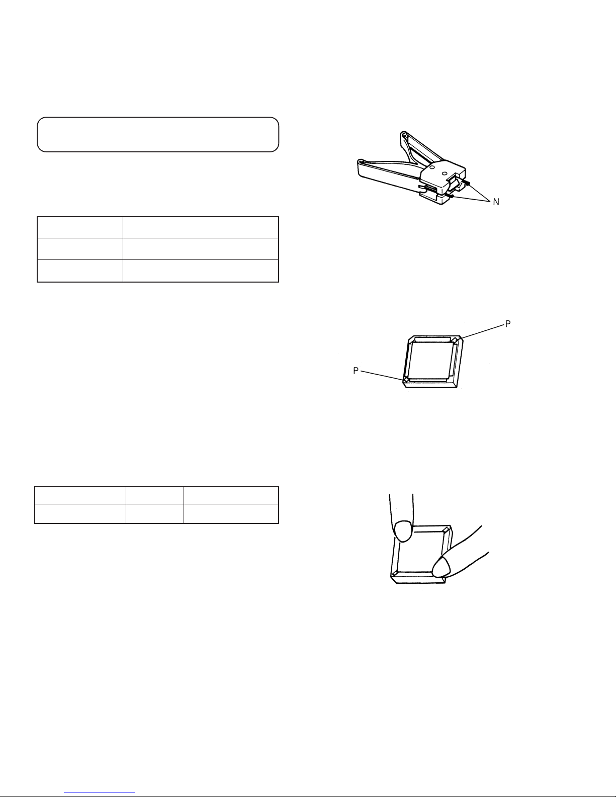
1.8 Replacement of IC ROM (IF board IC27, IC29)
(1) For removing the IC ROM, it is recommended to use a spe-
cial tool, however, two small screwdrivers are substitutable
for it.
Part Name Replacement Period
Pan/tilt assembly 1,000,000 times of operation
Lens assembly 400,000 times of operation
Table 1-2
1.7
REFFERENCE REPLACEMENT PERIODS OF PARTS
WHITCH REQUIRE MAINTENANCE AND INSPECTION
Periodical maintenance and inspection are required to maintain
the initial performance and reliability of the unit. Table 1-3 has
been complied assuming the use of the unit under room temperature, and the periods indicated in the table are greatly variable depending on the operating environment and conditions.
Lack of proper maintenance, inspection and servicing will result
in great reductions of the times indicated in the table and will
cause other effects as well.
Part Name Part No. Reference Period
POWER SUPPLY UNIT
Refer to Sec. 4.1
30,000 hours or 3 years
Fig. 1-19 Example of special tool
(2) Insert the portions N of the special tool into the notches P of
the IC socket to pick up the IC. When using small screwdrivers, insert their tips into the notches P respectively and pick
up the IC with the two screwdrivers.
Fig. 1-20
(3) When in a new IC for replacement, make sure of its orienta-
tion and insert it gently into the IC socket with fingers keeping the IC level with the board surface.
Table 1-3
The figures shown in Table 1-3 are accumulated operating hours
assuming that the unit is operated for 24 hours a day under
room temperature (approx. 25°C). The figures will be reduced
to 15,000 hours or 1.5 years if the unit is accommodated in a
camera housing or used outdoors.
1-6
Fig. 1-21
Page 9

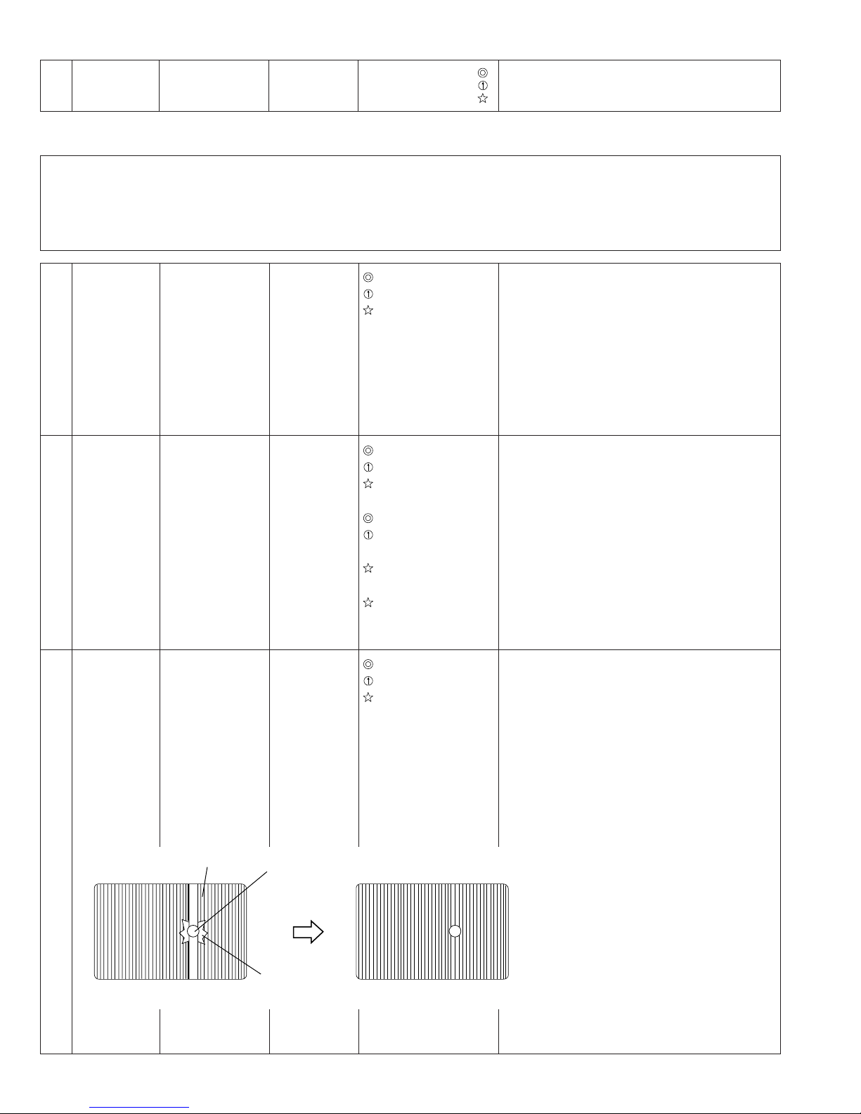
1.9 Positional adjustments to the sensor plate
Whenever the sensor plate has been replaced, carry out the
adjustments listed below.
(1) Loosen screw 1 .
(2) Adjust the sensor plate position so that b is less than half of
a (b
a/2).
(3) Tighten screw 1 .
(4) Make sure that the sensor plate is positioned so that c=d.
a
b
c
d
Camera cover (L)
Sensor plate
1
Photo
Interrupter IF board
Fig. 1-22
1.10 Care in Transportation
In order to prevent damage to the photo interrupter on the IF
board during transportation, a bracket has been added. Be sure
to remove the bracket before installation by referring to the diagram below. Also, be sure to reinstall the bracket at the time of
transportation by reversing the removal procedure.
Don't Forget! Be sure to remove the transportation bracket.
A bracket to reduce shock during transportation is mounted
when this unit is shipped from the factory.
Be sure to remove this bracket before installation.
1.
Turn the camera
body cover in a
counterclockwise
direction to set the
mark to "RELEASE".
RELEASE
LOCK
(5) If the sensor plate is not positioned so that c=d, use pliers
etc. to bend the sensor plate until e becomes equal to f.
e
f
Bend here.
Fig. 1-23
RELEASE
LOCK
Camera body cover
2.
Pull the camera body
cover upward.
Claw
LOCK
R
ELEASE
3.
Remove the
Claw
5.
screw.
Put the screw back
and tighten it.
Camera body
4.
Remove the
transportation bracket
6.
Install the camera body cover in the reverse order of
removing and set the mark to "Lock".
Check that the three claws on the cover are locked onto
the camera body and that there is no clearance
between the cover and the camera body.
.
1-7
Page 10
SECTION 2
ELECTRICAL ADJUSTMENTS
This unit is a camera incorporating an EVR (Electric Variable
Resistor) function. The EVR varies the resistance using a PC
and writes the varied resistance data in the memory of the camera.
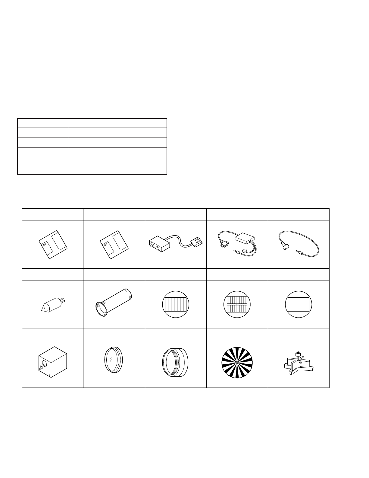
2.1 EQUIPMENT NECESSARY FOR ADJUSTMENT
Instrument
Oscilloscope
Vectorscope
Color video monitor
Digital voltmeter
Program disk
(Software for adjustment)
(IBM-PC) (Windows 95) (For IBM-PC)
Available for 100MHz or higher
A calibrated instrument.
A color type instrument with a 75 ohm
video input.
Input impedance of 10M ohm or higher
(Remote control software)
Condition
Program disk
Conversion cable Interface cable Conversion cable
2.2 COMPUTER AND PERIPHERAL EQUIPMENT
• IBM PC/AT or compatible with MS-DOS operating system (For
Adjustment)
• 3.5inch FDD
• Serial port (RS232C)
• CPU:80386 or higher microprocessor
• VGA monitor (color or monochrome)
• Mouse
• WINDOWS 95 operating system (For Remote Control)
• 3.5inch FDD
• Serial port (RS232C)
• VGA monitor
• Mouse
J
V
C
PLSC1209 * PLSC1210
Light box lamp
YQ20645-001
Light box
YTU93072
Infinity adjustment lens Color bar chart Gray scale chart Test chart (Portrait)
YTU92001B YTU92001-051 YTU92001-052 YTU92001-054
Color temp. Conversion filter
KODAK wratten gelatin filter
No. 80C (or equivalent) SC32125 YTU93079
SC32124 YTU93063 YTU94066
Lens mount tool Focus chart Camera Stand
(Included in Infirity adjustment lens.)
* When used with TK-C675BU/E, it does not display “Camera Model” and “Camera ID”.
(Not necessory for adjustment)
2-1
Page 11
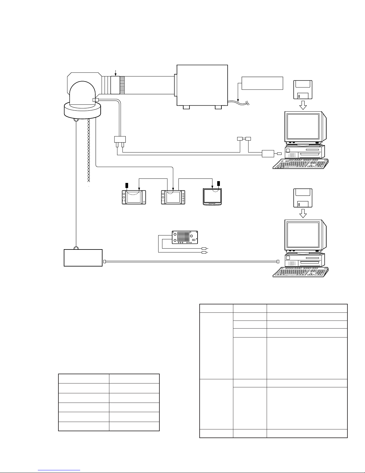
2.3 GENERAL SETUP
Connect the equipment as shown below. The Left camera cover should be removed for adjustments (see 1.1).
Lens mount tool
SC32125
POWER SUPPLY
DC 6V
To RS232C
port
(IBM PC/AT or compatible with MS-DOS)
TK-C675B
To RS422
port
IF board
CN5
AC 24V
Video out
75 Ω
terminator
Infinity adjustment lens
YTU92001B
Conversion cable
SC32124
Connect
Vectorscope
Light box
YTU93072
Connect
Conversion cable YTU94066
Interface cable YTU93063
75 Ω
terminator
Color monitorWaveform monitor
(WFM)
Adjustment
software
Computer
Remote control
software
Oscilloscope
RS422
RS232C
RS232C to RS422 conversion adapter
2.4 SWITCH SETTING FOR ADJUSTMENTS
(1) Set the camera functions by software (PLSC1210) as shown
in Table 2-1. (Note that S1 on the camera’s IF board should
be set to “IF”.)
(2) After the setting above, turn the power OFF, and set the
camera’s internal switches as shown in Table 2-2.
(3) Turn power ON again to start the adjustments.
Item Setting
AGC mode OFF
Shutter NORMAL
BLC mode OFF
Iris mode MANU
White balance ATW
Table 2-1 Function Setting
To RS232C
port
Computer
(Windows 95)
Board Switch Setting
IF S1 JIG
S2 OFF
S3-2 OFF (U Ver.) ON (E Ver.)
S3-1 OFF
S3-3
S3-4
S3-5
S3-6
MD S1-3 ON
S1-1 OFF
S1-2
S1-4
S1-5
S1-6
CN S1 ON
Table 2-2 Internal Switches
2-2
Page 12
2.5
HOW TO EXECUTE PROGRAM SOFTWARE (PLSC1209)
2.6 KEYBOARD OPERATION (PLSC1209)
1) Install the MS-DOS “MOUSE. COM”. (This program can also
be used without Mouse.)
2) At the MS-DOS command line, type as follows.
A>TK-C675 {/N or /P} [/BW] [/COM2] <Enter>
/N or /P Set type of TV system. The program cannot
start without specified.
N : NTSC (U Ver.)
P : PAL (E Ver.)
/BW Set if the monitor is Black & white.
/COM2 Set if a serial mouse is connected to the
COM1 serial port to allow camera data com-
municate via COM2. If not specified, COM1
becomes the main communication port auto-
matically.
3) At the “Welcome” message, click <OK> or press [ENTER]
key.
Follow the message appearing on the display to prepare and
execute each setting.
4) When the main window is displayed, data communication
begins. However, if due to faulty connection or other abnormality, the program stops. Observe the check indication at
the lower right of the screen. If indication is “NG”, check
the cable connections and camera power. When indication
is “OK”, the program operation starts. If communication is
abnormal, press the [Break] key to terminate the program.
5) When the program starts, check the TV system indication of
the main window. If this is incorrect, restart the program
and correct the TV system entry.
To terminate the program, click the EEPROM menu, then
click Quit (or press [Crtl] + [F4] keys).
NOTE
For Remote Control Software (PLSC1210), See instruction manual attached to the software. Not described on
this Service Manual.
Although a mouse is recommended for using this program, it
can also be operated from the keyboard in cases when a mouse
is not available.
The commonly use keys are as follows.
Key Function
[Alt] Menu selection
[Enter] Confirm
[Esc] Cancel
[Up] or [Shift] + [Up] Cursor shift
[Down] or [Shift] + [Down] Cursor shift
[Left] or [Shift] + [Left] Cursor shift
[Right] or [Shift] + [Right] Cursor shift
[Tab] or [Shift] + [Tab] Item select
[Insert] Insert or Overwrite text
[Delete] Delete text
[Back space] Cursor backspace during
text input
Short key operations are indicated on the screen.
2.7 MENUS
1) EEPROM Menu
Menu command Function
Read Readout EEPROM data (256 bytes) from camera.
Backup Backup EEPROM readout data to disk.
Restore Write disk backup data or EEPROM initial data of this disk into camera EEPROM.
Edit After EEPROM data readout, edit the data of a selected address (if using a mouse, double click
the desired address of the data table). Use care since editing rewrites the camera EEPROM
data.
Compare Compare EEPROM readout data with data in disk. Different data's color are change on the
screen.
Difference After comparing the data, data difference of a selected address is displayed.
(Double click the desired address data of the data table.)
Esc compare End comparison
Help Display “README. DOC” file.
Quit Terminate program.
2-3
Page 13

2) BUFF menu
2.8 CAMERA ADJUSTMENT
Menu command Function
Buffer 1
Buffer 2
Buffer 3
3) CAM. ADJ. menu
Menu command
PLL control voltage
Gain
OFD
Y setup
White clip
AGC set
Burst level
Color difference balance (1)
Carrier dot balance
Color difference balance (2)
Carrier balance
Display white balance data on
main window.
Burst phase (E Ver. only)
SC phase (E Ver. only)
Offset data
R-Y/B-Y low
R, B gain
Color difference gain
Color difference matrix
White level
Manual white balance
Auto iris level
Menu command
• Light source and object for adjustment
Use the specified light box and object when adjusting the
camera with this program.
• Adjustment
Prepare the equipment and fixtures required for adjustment
Before adjusting, it is recommended to backup the
EEPROM data. Refer to the screen messages and perform accordingly. Unless otherwise indicated, avoid operating other menus etc. while adjustment is in progress.
Caution
If the camera power supply is cut off during program operation, communication error is produced. The program
stops and operations are not recognized. Communication
and program operation resume when camera power is restored. However, if communication error occurs during
adjustment or EEPROM data editing, first terminate, and
then restart the program again.
No.
Measuring
Item Mode Adjustment procedure
instrument &
Input signals
Measuring point ( )
Adjustment parts ( )
Adjustment level ( )
2.9 BACK-FOCUS ADJUSTMENT
This unit is shipped from the factory after its back-focus has been adjusted. Therefore, back-focus adjustment is usually unnecessary. It should be performed only when required, for example after replacing the lens assembly.
1 Back-focus
adjustment
Monitor screen,
focusing chart.
The adjustment
software is not
used in this
adjustment.
Monitor screen
1) Attach the focus chart onto the INF adjustment tool.
2) Set the iris to fully open.
3) Adjust the illumination of the light box so that
the signal level is between 0.57 and 0.64 Vpp (80 and 90 IRE).
4) Adjust the back-focus by referring to the instruction manual of the remote control software (PLSC1210).
2-4
Page 14
No.
Measuring
Item Mode Adjustment procedure
instrument &
Input signals
Measuring point ( )
Adjustment parts ( )
Adjustment level ( )
2.10 EVR ADJUSTMENT
• After replacing the CCD image sensor or EEPROM, execute “Restore” in the EEPROM menu to write the initial value data
“TKC675_N.DAT”(U Ver.) or “TKC675_P.DAT”(E Ver.) in EEPROM before proceeding to the adjustment.
• Set the lens iris using the remote control software (refer to the instruction manual of the remote control software).
• To adjust items which require the adjustment software, select the required menu commands from the CAM. ADJ. menus using
the [Alt] key or mouse.
1 PLL control
voltage
adjustment
2 Gain
adjustment
3 OFD
adjustment
• Oscilloscope
(H-rate 10:1)
• It is not neces
sary to use the
infinity adjust
ment lens for
this adjustment.
• Gray scale chart
(just scan)
• Oscilloscope
(H-rate 10:1)
• It is not necessary to use the
infinity adjustment lens for
this adjustment.
• TV monitor
screen.
• Incandescent
lamp.
Shutter
<U Ver.>
1/100
<E Ver.>
1/60
TP1 (A-2B) [IF]
2Bh (PLL voltage)
2.75V DC
TP201 (B-1C) [PR]
LENS IRIS
0.7Vp-p
- - - - - - - - - - - - - - - - - - - - - - - - - - - - - - - - - - - - - - - - - - - - - - - - - - - - - - - - - - - VIDEO output
36h (Y gain)
<U Ver. >
0.714Vp-p [100 IRE]
<E Ver.>
0.7Vp-p
TV monitor screen
26h (V. sub)
Minimum blooming
1) Set S1-6 on the MD board to ON.
2) Adjust the PLL voltage data so that the voltage at TP1 [IF] is 2.75V DC.
3) Set S1-6 on the MD board to OFF.
1) Set lens iris so that the white level in the
center of the gray scale chart at TP201 [PR] is
0.7Vp-p.
2) Adjust the Y gain data so that the white level
in the center of the gray scale chart at VIDEO
output is 0.714 Vp-p [100 IRE] (U Ver.) or 0.7
Vp-p (E Ver.).
1) Set the shutter to “1/100” (U Ver.) or 1/60(E
Ver.).
2) Shoot an incandescent lamp and set the iris
to a position at which blooming becomes
most clear.
3) While observing the monitor screen, adjust
the V. sub data so that blooming disappears.
4) Set the shutter to “NORMAL”.
Smear
Incandescent lamp
Blooming
Monitor
2-5
Monitor
Page 15
No.
Measuring
Item Mode Adjustment procedure
instrument &
Input signals
Measuring point ( )
Adjustment parts ( )
Adjustment level ( )
4 Y setup
adjustment
5 White clip
adjustment
0.785 Vp-p
(U Ver.)
0.77 Vp-p
(E Ver.)
• Oscilloscope
(H-rate, 10:1)
• Gray scale chart
(Just scan)
• Oscilloscope
(H-rate, 10:1)
VIDEO output
22h (Y setup level)
30mVp-p
30 mVp-p
VIDEO output
37h (White clip level)
<U Ver.>
0.785Vp-p
<E Ver.>
0.77Vp-p
1) Close the lens iris.
2) Adjust the Y set up level data so that setup
level is 30mVp-p. (From the pedestal level)
1) Attach the infinity adjustment lens with gray
scale chart to the lens.
2) Open the lens iris.
3) Adjust the white clip level data so that the
white peak of gray scale chart is following
specified level at VIDEO output.
NOTE
When the carrier level of the white clip exceeds 100mVp-p, use the menu command
[Edit] after completing white clip adjustment
in order to move the 26(Vsub) data and bring
the carrier level to a minimum.
6 AGC set
adjustment
• Gray scale chart
(Just scan)
• Oscilloscope
(H-rate, 10:1)
0.678 Vp-p
(U Ver.)
0.665 Vp-p
(E Ver.)
VIDEO output
LENS IRIS
<U Ver.>
0.643Vp-p [90 IRE]
<E Ver.>
1) Set lens iris so that the white level in the
center of the gray scale chart at VIDEO output is 0.643Vp-p [90 IRE] or 0.63Vp-p (E Ver.).
2) Click “OK”. The camera’s AGC mode is
switched automatically to 20 dB.
0.63Vp-p
- - - - - - - - - - - - - - - - - - - - - - - - - - - - - - - - - - - - - - - - - - - - - - - - - - - - - - - - - - - VIDEO output
39h (AGC normal
reference)
<U Ver.>
0.678Vp-p [95 IRE]
<E Ver.>
3) Adjust the AGC normal reference data so that
the white level in the center of the gray scale
chart at VIDEO output is 0.678Vp-p [95 IRE]
(U Ver.) or 0.665Vp-p (E Ver.). (After this adjustment, the AGC mode is switched automatically to OFF.)
0.665Vp-p
NOTE
As the output has hysteresis, decrease the
white level to below -95 IRE before starting
the adjustments.
2-6
Page 16

No.
Measuring
Item Mode Adjustment procedure
instrument &
Input signals
Measuring point ( )
Adjustment parts ( )
Adjustment level ( )
7 Burst level
adjustment
8 Color
difference
balance(1)
adjustment
• Oscilloscope
(H-rate, 10:1)
• It is not necessary the infinity
adjustment lens
for this adjustment.
• Color bar chart
(Just scan)
•Oscilloscope
(H-rate, 10:1)
• Vectorscope
VIDEO output
25h (Burst level)
<U ver.>
0.286Vp-p [40 IRE]
1) Adjust the Burst level data so that the level
of the burst signal at the VIDEO output is
0.286 Vp-p [40 IRE] (U Ver.) or 0.300 Vp-p (E
Ver.).
<E ver.>
0.300Vp-p
VIDEO output
LENS IRIS
0.65Vp-p
1) Attach the infinity adjustment lens with color
bar chart to the lens.
2) Set lens iris so that white level of color bars
is 0.65Vp-p at VIDEO output.
- - - - - - - - - - - - - - - - - - - - - - - - - - - - - - - - - - - - - - - - - - - - - - - - - - - - - - - - - - - TP202 (B-1C) [PR]
30h [1H delay gain
(Yellow)]
3) Adjust the 1H delay gain (Yellow) data so that
the levels of the adjacent 1H signals at TP202
[PR] are identical.
Identical
0.65 Vp-p
9 Carrier dot
balance
adjustment
• Vectorscope
• It is not neces-
sary the infinity
adjustment lens
for this adjustment.
VIDEO output
34h (Carrier balance
dot adjustment)
Two dots are overlapped.
1) Close the lens iris.
2) Adjust the Carrier balance dot adjustment data
so that the two dots on the vectorscope are
overlapped.
(It is recommended to be easier to see that
the gain of vectorscope is boosted.)
2-7
Page 17

No.
Measuring
Item Mode Adjustment procedure
instrument &
Input signals
Measuring point ( )
Adjustment parts ( )
Adjustment level ( )
10 Color
difference
balance(2)
adjustment
0.65 Vp-p
11 Carrier
balance
adjustment
• Color bar chart
(just scan)
• Oscilloscope
(H-rate, 10:1)
• Vectorscope
• Vectorscope
• It is not neces-
sary the infinity
adjustment lens
for this adjustment.
VIDEO output
LENS IRIS
1) Set lens iris so that the white level of the color
bar chart is 0.65Vp-p.
0.65Vp-p
- - - - - - - - - - - - - - - - - - - - - - - - - - - - - - - - - - - - - - - - - - - - - - - - - - - - - - - - - - - VIDEO output
31h (1H delay gain
(Cyan))
2) Adjust the 1H delay gain (Cyan) data so that
the dots of different colors are superimposed
on the vectorscope.
Chroma (colored) dots
should be superimposed.
VIDEO output
27h
(Blue carrier balance)
28h
(Red carrier balance)
1) Close the lens iris.
2) Adjust the Blue carrier balance and Red carrier balance data alternately so that the dot
on the vectorscope is center.
(It is recommended to be easier to see that
the gain of vectorscope is boosted.)
12 Burst phase
adjustment
(E Ver. only)
R-Y
• Vectorscope
B-Y
R-Y
R-Y
B-Y
VIDEO output
2Ah (Burst phase)
Angle of burst phase
is 90 degrees.
B-Y
1) Close the lens iris.
2) Adjust the Burst phase data so that the angle
of burst phase is 90 degrees on the
vectorscope.
90°90°
2-8
Page 18

No.
Measuring
Item Mode Adjustment procedure
instrument &
Input signals
Measuring point ( )
Adjustment parts ( )
Adjustment level ( )
13 SC phase
adjustment
(E Ver. only)
14 Offset data
adjustment
• Color bar chart
(just scan)
• Oscilloscope
(H-rate, 10:1)
• Vectorscope
• It is not neces-
sary the infinity
adjustment lens
for this adjustment.
VIDEO output
LENS IRIS
0.65Vp-p
1) Attach the infinity adjustment lens with color
bar chart to the lens.
2) Set lens iris so that white level of color bar
chart is 0.65Vp-p at VIDEO output.
- - - - - - - - - - - - - - - - - - - - - - - - - - - - - - - - - - - - - - - - - - - - - - - - - - - - - - - - - - - VIDEO output
29h (SC phase)
3) Adjust the SC phase data so that the red dots
are superimposed on the vectorscope.
Red dots should be
superimposed.
66h (2R-G offset)
67h (2B-G offset)
6Ah (Y low offset)
1) Close the lens iris.
2) Press Enter key. The adjustment is preformed
automatically.
15 R-Y low, B-Y
low (indoor/
outdoor)
adjustment
(INDOOR)
• Color bar chart
(just scan)
•Oscilloscope
(H-rate, 10:1)
(OUTDOOR)
• Color bar chart
(just scan)
• Filter (80C+80C)
• Oscilloscope
(H-rate, 10:1)
VIDEO output
LENS IRIS
0.65Vp-p
1) Attach the infinity adjustment lens with color
bar chart to the lens.
2) Set lens iris so that white level of color bar
chart is 0.65Vp-p at VIDEO output.
- - - - - - - - - - - - - - - - - - - - - - - - - - - - - - - - - - - - - - - - - - - - - - - - - - - - - - - - - - - 62h (B/Y
63h (R/Y
L indoor data)
L indoor data)
VIDEO output
LENS IRIS
0.46Vp-p
3) Press Enter key. The adjustment is preformed
automatically.
1) Put the filters (80C+80C) to the lens.
2) Set lens iris so that white level of color bar
chart is 0.46Vp-p at VIDEO output.
- - - - - - - - - - - - - - - - - - - - - - - - - - - - - - - - - - - - - - - - - - - - - - - - - - - - - - - - - - - 64h
(B/YL outdoor data)
3) Press Enter key. The adjustment is preformed
automatically.
65h
(R/YL outdoor data)
2-9
Page 19

No.
Measuring
Item Mode Adjustment procedure
instrument &
Input signals
Measuring point ( )
Adjustment parts ( )
Adjustment level ( )
16 R, B gain
(indoor/
putdoor)
adjustment
(INDOOR)
• Color bar chart
(just scan)
• Oscilloscope
(H-rate, 10:1)
• Vectorscope
VIDEO output
LENS IRIS
1) Set lens iris so that white level of color bar
chart is 0.65Vp-p at VIDEO output.
0.65Vp-p
- - - - - - - - - - - - - - - - - - - - - - - - - - - - - - - - - - - - - - - - - - - - - - - - - - - - - - - - - - - -
VIDEO output
A0h [R gain (indoor)]
A1h [B gain (indoor)]
A white signal
2) Adjust the R gain (indoor) and B gain (indoor)
data alternately so that the dot of the white
signal component appears in the center of the
vectorscope.
component dot should
appear in the center of
the vectorscope.
(OUTDOOR)
• Color bar chart
(just scan)
• Filter (80C+80C)
• Oscilloscope
(H-rate, 10:1)
• Vectorscope
VIDEO output
LENS IRIS
0.46Vp-p
1) Put the filters (80C+80C) to the lens.
2) Set lens iris so that white level of color bar
chart is 0.46Vp-p at VIDEO output.
- - - - - - - - - - - - - - - - - - - - - - - - - - - - - - - - - - - - - - - - - - - - - - - - - - - - - - - - - - - VIDEO output
A4h [R gain (outdoor)]
A5h [B gain (outdoor)]
A white signal
3) Adjust the R gain (outdoor) and B gain (outdoor) data alternately so that the dot of the
white signal component appears in the center
of the vectorscope.
component dot should
appear in the center of
the vectorscope.
2-10
Page 20

No.
Measuring
Item Mode Adjustment procedure
instrument &
Input signals
Measuring point ( )
Adjustment parts ( )
Adjustment level ( )
17 Color differ-
ence gain
(indoor/
outdoor)
adjustment
(INDOOR)
• Color bar chart
(just scan)
• Oscilloscope
(H-rate, 10:1)
VIDEO output
LENS IRIS
1) Set lens iris so that the white level of color
bar chart is 0.65Vp-p at VIDEO output.
0.65Vp-p
- - - - - - - - - - - - - - - - - - - - - - - - - - - - - - - - - - - - - - - - - - - - - - - - - - - - - - - - - - - VIDEO output
A2h [R-Y gain(indoor)]
A3h [B-Y gain (indoor)]
Red signal level:
2) Adjust the R-Y gain (indoor) data so that the
Red signal level is 0.46Vp-p at video output.
3) Adjust the B-Y gain (indoor) data so that the
Blue signal level is 0.36Vp-p at video output.
0.46Vp-p
Blue signal level:
0.36Vp-p
Red
Blue
(OUTDOOR)
• Color bar chart
(just scan)
• Filter
(80C +80C)
• Oscilloscope (Hrate)
VIDEO output
LENS IRIS
0.46Vp-p
1) Attach the filters (80C + 80C) to the lens.
2) Set lens iris so that the white level of the color
bar chart at the output is 0.46Vp-p.
- - - - - - - - - - - - - - - - - - - - - - - - - - - - - - - - - - - - - - - - - - - - - - - - - - - - - - - - - - - VIDEO output
A6h [R-Y gain(outdoor)]
A7h [B-Y gain (outdoor)]
Red signal level:
0.32Vp-p
Blue signal level:
3) Adjust the R-Y gain(outdoor) data so that the
Red signal level in the color bar signal is
0.32Vp-p.
4) Adjust the B-Y gain(outdoor) data so that the
Blue signal level in the color bar signal is
0.23Vp-p.
0.23Vp-p
2-11
Page 21

No.
Measuring
Item Mode Adjustment procedure
instrument &
Input signals
Measuring point ( )
Adjustment parts ( )
Adjustment level ( )
18 Color differ-
ence matrix
(indoor/
outdoor)
adjustment
(INDOOR)
• Color bar chart
(just scan)
• Oscilloscope
(H-rate, 10:1)
• Vectorscope
Red signal dot: 105˚
VIDEO output
LENS IRIS
0.65Vp-p
VIDEO output
24h [B-Y matrix
(indoor)]
23h [R-Y matrix
(indoor)]
Red signal dot:
105 degrees
Blue signal dot:
350 degrees
Blue signal dot:
350˚
1) Adjust lens iris so that white level of color bar
chart is 0.65Vp-p at VIDEO output.
2) Adjust the SC phase data so that the red signal dot of the color bar signal appears in the
105 degrees position on the vectorscope.
3) Adjust the R-Y matrix data so that the blue
signal dot of the color bar signal appears in
the 350 degrees position on the vectorscope.
19 White level
adjustment
(OUTDOOR)
• Color bar chart
(just scan)
• Filter
(80C + 80C)
• Oscilloscope (Hrate)
• Vectorscope
• Gray scale chart
(just scan)
• Oscilloscope
(H-rate, 10:1)
VIDEO output
LENS IRIS
0.46Vp-p
1) Attach the filters (80C + 80C) to the lens.
2) Set lens iris so that the white level of the color
bar chart at VIDEO output is 0.46Vp-p.
3) Adjust the B-Y matrix data so that the red sig-
VIDEO output
6Dh [B-Y matrix
(outdoor)]
6Ch [R-Y matrix
(outdoor)]
nal dot of the color bar signal appears in the
105 degrees position on the vectorscope.
4) Adjust the R-Y matrix data so that the blue
signal dot of the color bar signal appears in
the 350 degrees position on the vectorscope.
Red signal dot:
105 degrees
Blue signal dot:
350 degrees
VIDEO output
LENS IRIS
<U Ver.>
0.714Vp-p [100 IRE]
<E Ver.>
1) Attach the infinity adjustment lens with gray
scale chart to the lens.
2) Set lens iris so that the white level of the gray
scale chart at VIDEO output is 0.714Vp-p (U
Ver.) or 0.7Vp-p (E Ver.).
0.7Vp-p
- - - - - - - - - - - - - - - - - - - - - - - - - - - - - - - - - - - - - - - - - - - - - - - - - - - - - - - - - - - 60h (B-Y offset)
61h (R-Y offset)
3) Press Enter key. The adjustment is performed
automatically.
2-12
Page 22

No.
Measuring
Item Mode Adjustment procedure
instrument &
Input signals
Measuring point ( )
Adjustment parts ( )
Adjustment level ( )
20 Manual
WHT. BAL
adjustment
• Gray scale chart
(just scan)
• Oscilloscope
(H-rate)
• Vectorscope
W.BAL is set
automatically
to
“MANUAL”.
VIDEO output
LENS IRIS
<U Ver.>
0.714Vp-p[100 IRE]
<E Ver.>
1) Attach the infinity adjustment lens with gray
scale chart to the lens.
2) Set lens iris so that the white level of the gray
scale chart at VIDEO output is 0.714Vp-p[100
IRE] (U Ver.) or 0.7Vp-p (E Ver.).
0.7Vp-p
- - - - - - - - - - - - - - - - - - - - - - - - - - - - - - - - - - - - - - - - - - - - - - - - - - - - - - - - - - - VIDEO output
DAh (MWB R gain)
DBh (MWB B gain)
3) Adjust the two data alternately so that the
dot of the VIDEO output appears in the center
of the vectorscope.
- - - - - - - - - - - - - - - - - - - - - - - - - - - - - - - - - - - - - - - - - - - - - - - - - - - - - - - - - - - - - - - - - - - - - - - - - - - - - - - - - - - - - - - -
• Filter(80C)
VIDEO output
LENS IRIS
<U Ver.>
0.714Vp-p[100 IRE]
4) Attach the filter (80C) to the lens.
5) Set lens iris so that the white level of the gray
scale chart at VIDEO output is 0.714Vp-p[100
IRE] (U Ver.) or 0.7Vp-p (E Ver.).
<E Ver.>
0.7Vp-p
- - - - - - - - - - - - - - - - - - - - - - - - - - - - - - - - - - - - - - - - - - - - - - - - - - - - - - - - - - - VIDEO output
DCh (C8 MWB R gain)
DDh (C8 MWB B gain)
6) Adjust the two data alternately so that the
dot of the VIDEO output appears in the center
of the vectorscope.
- - - - - - - - - - - - - - - - - - - - - - - - - - - - - - - - - - - - - - - - - - - - - - - - - - - - - - - - - - - - - - - - - - - - - - - - - - - - - - - - - - - - - - - -
• Filter(80C+80C)
VIDEO output
LENS IRIS
<U Ver.>
0.714Vp-p[100 IRE]
7) Attach the filters (80C + 80C) to the lens.
8) Set lens iris so that the white level of the gray
scale chart at VIDEO output is 0.714Vp-p[100
IRE] (U Ver.) or 0.7Vp-p (E Ver.).
<E Ver.>
0.7Vp-p
- - - - - - - - - - - - - - - - - - - - - - - - - - - - - - - - - - - - - - - - - - - - - - - - - - - - - - - - - - - VIDEO output
DEh(C16 MWB R gain)
DFh(C16 MWB B gain)
9) Adjust the two data alternately so that the
dot of the VIDEO output appears in the center
of the vectorscope.
2-13
Page 23

No.
Measuring
Item Mode Adjustment procedure
instrument &
Input signals
Measuring point ( )
Adjustment parts ( )
Adjustment level ( )
21 Auto iris level
adjustment
• Gray scale chart
(just scan)
• Oscilloscope
(H-rate)
LENS IRIS:
AUTO
VIDEO output
35h (Auto iris level)
<U Ver.>
0.714Vp-p[100 IRE]
<E Ver.>
0.7Vp-p
1) Set the iris to “AUTO”.
2) Adjustment the Auto Iris level data so that
the white level at the center of the gray scale
chart at VIDEO output is 0.714Vp-p[100 IRE]
(U Ver.) or 0.7Vp-p (E Ver.).
2-14
Page 24

VICTOR COMPANY OF JAPAN, LIMITED
Printed in Japan
Page 25

TK-C675B COMBINATION CAMERA
VICTOR COMPANY OF JAPAN, LIMITED
Printed in Japan
SC96837-001
© 1998 VICTOR COMPANY OF JAPAN, LIMITED
is a registered Trademark owned by VICTOR COMPANY OF JAPAN, LTD.
is a registered Trademark in JAPAN, the U.S.A., the U.K. and many other countries.
TK-C675B
COMBINATION CAMERA
INSTRUCTIONS
For Customer Use :
Enter below the Serial No. which
is located on the body.
Retain this information for future
reference.
Model No. TK-C675B
Serial No.
L
O
C
K
R
E
LE
A
S
E
Page 26

2
For USA and CANADA
RISK OF ELECTRIC SHOCK
DO NOT OPEN
CAUTION : TO REDUCE THE RISK OF ELECTRIC SHOCK,
DO NOT REMOVE COVER (OR BACK).
NO USER SERVICEABLE PARTS INSIDE.
REFER SERVICING TO QUALIFIED SERVICE PERSONNEL.
The exclamation point within an equilateral triangle is
intended to alert the user to the presence of important operating and maintenance (servicing) instructions in the literature accompanying the appliance.
The lightning flash with arrowhead symbol, within an
equilateral triangle is intended to alert the user to the
presence of uninsulated “dangerous voltage” within the
product's enclosure that may be of sufficient magnitude to constitute a risk of electric shock to persons.
Information for USA
This device complies with Part 15 of the FCC Rules.
Changes or modifications not approved by JVC could void
the user's authority to operate the equipment.
WARNING:
TO REDUCE THE RISK OF FIRE OR
ELECTRIC SHOCK, DO NOT EXPOSE THIS
APPLIANCE TO RAIN OR MOISTURE.
AVERTISSEMENT:
POUR EVITER LES RISQUES D'INCENDIE OU
D'ELECTROCUTION, NE PAS EXPOSER
L'APPAREIL A L'HUMIDITE OU A LA PLUIE.
FEATURES ...........................................................................2
OPERATING PRECAUTIONS ...............................................3
SAFETY PRECAUTIONS .....................................................3
CONTROLS, CONNECTORS AND INDICATORS................ 4
INSTALLATION ..................................................................... 5
CONNECTIONS.................................................................... 8
HOW TO USE THE FERRITE CORE ....................................9
TROUBLESHOOTING ........................................................10
SPECIFICATIONS...............................................................11
Due to design modifications, data given in this instruction
book are subject to possible change without prior notice.
CAUTION
INFORMATION (FOR CANADA)
RENSEIGNEMENT (POUR CANADA)
Cet appareil numénque de la classe [B] respecte toutes les
exigences du Réglement sur le mat
ér
iel brouilleur du Canada.
This Class [B] digital apparatus meets all requirements of
the canadian Interference-Causing Equipment Regulations.
FEATURES
䡵 Features large aperture lens with 16x zoom ratio (f=4.5 to
72mm, F1.2, at wide angle).
䡵 Wide coverage angle (Horizontal 3.8° to 56°, Vertical 2.9° to
44°).
䡵 64 preset positions.
䡵 360 degree endless panning.
䡵 Maximum 240 degree/sec. panning speed.
䡵 Maximum 2-second zoom speed.
䡵 One-push auto focus capability.
䡵 RS-485 (Maximum Number of Connections: 32) or RS-422A
control signal.
䡵 High-quality pictures by adopting dome cover with optical
distortion compensation and CCD with 380,000 (U: type)
or 440,000 (E: type) effective pixels.
䡵 Adopts large aperture lens, highly sensitive CCD.
(Minimum illumination : 2.8 lx, at wide angle)
䡵 Auto panning function.
䡵 Variable panning speed.
The panning speed is varied automatically according to
the zoom ratio of the lens. (The panning speed decreases
when the zoom lens is set near TELE and increases when
it is set near WIDE.)
䡵 Auto flip
When the camera reaches its tilting limit, it automatically
flips itself over by 180 degrees by panning around.
(This makes it possible for the camera to continue tilting
even after it has been tilted straight downward.)
䡵Auto patrol
Preset positions are activated in sequence.
䡵 Menu screen display
A built-in character generator provides an on-screen menu
display for easy selection and setting of various functions.
䡵 5-language on-screen display
Names or designations for camera, preset, area and alarm
can be displayed in English, German, French, Italian and
Spanish. (E type only)
䡵 Area title indication
The 360˚ panning angle (horizontal rotation) is divided into
16 sectors, allowing you to check the title in each area.
When the camera is manually panned, the preset area
designation is shown on the screen.
CONTENTS
Thank you for purchasing this product.
Caution during continuous use
Continuous use of the preset sequence or auto panning operation may make the service life much shorter than expected.
The guaranteed operation count for the zoom lens of this
camera is around 400,000 times.
(Example)
24 hours of operation per day with single zoom
operation per minute:
400,000 (times)/60 (minutes)/24 (hours) = 278 (days)
䡵 Before starting an important recording, be sure to per-
form a test recording in order to confirm that a normal
recording is possible.
䡵 We do not accept liability for the loss of a recording in
the case of it becoming impossible to record due to a
problem in the video camera, VCR or video tape.
䡵 We do not accept liability for any damage to the camera
in cases when it is dropped because of incomplete installation due to not observing the installation instructions correctly. Please be careful when installing the
camera.
3
Operating precautions
● To save energy, when it is not being used turn the system's
power off.
● This camera has been designed for indoor use. It cannot be
used outdoors.
● This camera has been designed exclusively to be hung from
the ceiling.It may malfunction if it is placed on a surface or if
it is tilted.
● Do not install or use the camera in the following places.
• In a place exposed to rain or moisture.
• In a place with vapor or oil soot, for example in a kitchen.
• In a temperature outside the operating temperature range
(-10°C to 50°C).
• Near a source of radiation, X-rays, strong radio waves or
magnetism.
• In a place subject to vibration.
• In a place with excessive dirt.
● Insufficient head ventilation of the camera may cause a malfunction.
Be careful not to block the ventilation to the camera.
● If this camera and the cables connected to this camera are
used where there are strong electromagnetic waves or where
there is magnetism present, for example near a radio or TV
transmitter, power transformer or an electric motor, the picture may produce noise and the colors may be affected.
● This camera incorporates an AGC circuit. As a result, when
it is used under low light conditions, the camera sensitivity
is automatically boosted and the picture may look uneven.
This is not a malfunction however.
● When the AGC is ON in the auto iris mode, varying the iris
with the IRIS control button may not change the picture
brightness due to the gain boost function. In this case, switch
the AGC OFF or set the iris mode to manual.
● In auto iris mode, the IRIS control buttons may not function
under certain brightness conditions (i.e. when a sufficient
amount of light cannot be obtained). In this case, set the iris
mode to manual.
● The white balance setting when used under a fluorescent
lamp should be ATW (Auto White). If it is set to MANU (Manual), the white balance may not be adjustable.
● When presetting this unit
’ s position, turn it on and wait until
it has warmed up sufficiently inside (about 30 minutes). This
is to avoid a change in the lens focus due to a rise in
temperature after installation.
● When this camera is used in the AUTO white balance mode,
the recorded colors may be slightly different from the actual
colors due to the operational principles of the auto-tracking
white balance circuit. This is however not a malfunction.
● If a high-intensity object (such as a lamp) is shot, the image
on the screen may have vertical lines (smear) or blur (blooming) at its periphery. This is a characteristic of the CCD, and
is not a defect.
● The electronic shutter of this camera has been set to 1/60(1/
50) sec. at the factory. When the camera is used under a
fluorescent lamp or in an area with a local power frequency
of 50/60 Hz, change the shutter speed to 1/100(1/60) on the
remote control unit. (The sensitivity deteriorates slightly with
a shutter speed of less than 1/100(1/60) sec.)
Utype (Etype)
● When the camera is used to monitor the same position continuously for 24 hours or more, the contact resistance of the
horizontal rotary parts may increase after long hours of use,
and the picture may be affected by noise interference or the
remote control operation may become unstable.
To prevent this, turn the system power off and on at least
once a week (to initialize) and also clean the contacts.
● Do not touch the dome cover of the lens directly with your
hand, contamination of this cover will lead to a deterioration
of the picture quality.
● Observe the following when carrying out camera maintenance.
• Turn the power OFF before proceeding to carry out main-
tenance.
• Clean the dome cover lens using a lens wiper cloth (or a
tissue).
If it is contaminated seriously, clean the contaminated part
with a cloth (or a tissue) which has been soaked in a solution of water and a neutral detergent.
● In order to reduce the generation of unnecessary signals,
be sure to install the provided ferrite cores when connecting the cables. (See
“How to use the ferrite core
” on page 9)
● Some subjects may not be brought into focus with the autofocus facility of this unit. Focusing will be made easier by
locating a subject with highly contrasted vertical stripes near
the center of the image.
● Optional controller is required to use the TK-C675B camera.
Please contact your local dealer or installer for more information about this controller.
Safety precautions
• As this unit contains parts which rotate at high speeds, it
should be installed in a place suitable to withstand the possible vibrations and to support the unit weight of 2 kg. If the
ceiling is made of dressed-face plywood, plaster board or
another material which is not strong enough to support the
unit, reinforce the installed surface by using a reinforcing
material (including plywood). If the reinforcement is insufficient, the monitor picture may be blurred due to vibrations
or in the worst case the unit may fall.
• Installation of this unit requires expertise. Please contact
your dealer for details.
• The ceiling to mount the TK-C675B has to be strong enough
to support ten times the weight of this product.
If the ceiling is not strong enough, make sure to apply reinforcement to the ceiling before installation.
• Be sure to tighten the screws and nuts securely, Insufficient
tightening may cause the unit to fall from its mount.
• The unit is to be powered by an AC24V.
Isolated power supply only. (E type)
Class 2 only (U type)
Page 27

4
Controls, connectors and indicators
■ Ceiling mount ■ Camera body
View when the camera body
cover is removed
11
15
14
16
15
13
12
Camera position
alignment mark
Dome cover lens
Dome cover
17
Ventilation
18
1
VIDEO OUTPUT terminal
Outputs composite video signals and is to be connected
to a monitor, etc. (Output impedance 75ohm)
2
Control signal terminals
The camera can be controlled by RS-422A or RS-485 signals.
3
AC 24V input terminals
Input the 24 V AC power.
Isolated power only (E type)
Class 2 only (U type)
4
Drop prevention wire
Engage this wire in the drop prevention wire hook
12
on
the camera.
5
Mounting holes (× 4)
Use these holes to attach the ceiling mount to the ceiling.
6
Camera connector (male)
Connects with the camera connector
13
on the camera.
7
Lock screw
Use this screw to fasten the camera clamp
14
to fix the
camera.
8
Camera position alignment mark
Align with the mark
17
when mounting the camera onto
the ceiling mount.
9
Safety wire hole
To prevent the camera from dropping accidentally, pass a
safety wire from the ceiling through these holes.
10
Terminal board cover
Protects the cable connection terminals against dirt, etc.
11
Control signal termination switch (TERM)
This is a termination ON/OFF switch for the input signals
to the control signal terminal
2
. When it is set to ON, the
“RX+” to “RX–” route is terminated.
12
Hook for attaching the drop prevention wire
Attach the drop prevention wire
4
to this hook.
13
Camera connector (female)
Connects with the camera connector
6
on the ceiling
mount.
14
Camera clamp
Fix the camera body to the ceiling mount by fastening the
lock screw
7
to this clamp.
15
Camera body cover
Remove this cover when using the setting switches
16
.
16
Setting switches
Set the PROTOCOL, etc.
Ref. “Switch settings” on page 6.
17
Camera positioning alignment mark
When mounting the camera onto the ceiling mount ,align it
with the mark
8
.
18
Ventilation
This is the ventilator for the internal cooling fan.
2
3
1
9
(Front)
(Back: Camera side)
4
5
6
5
7
8
10
Make sure that nothing interferes with the ventilator when
installing the camera.
CAUTION
5
1.
Make a hole (90 mm dia.) in the ceiling for passing through the
connection cables.
2.
Connect the cables to the terminal board.
Turn the power of all the connected equipment to OFF before
connecting the cables.
Remove the terminal board cover and connect the video signal
cable (coaxial cable),the control signal cables (x 4) and the 24 V
AC power cables (x 2).
●24 V AC power cables
Connect the 24 V AC power supply to the AC 24V terminals on
the terminal board. To prevent connection errors or a cable disconnection, we recommend the use of lug plates for the connections.
The following table shows the connection distances and connection cables provided that 2-conductor VVF cables (vinyl-insulated
vinyl sheath cables) are used.
Installation
●Control signal cables
These cables should be connected only when it is required to
control the camera using the RS-422A or RS-485 signals. The
use of 0.65 4-conductor twisted pair cables is recommended. With
these cables, the maximum extension distance is 1,200 m.
●Video signal cables
Connect the coaxial cables to the video signal output terminals.
Treat the tips of the coaxial cables as shown on the left before
connection.
After having connected all of the required cables, again attach
the terminal board cover.
3.
Attach the ceiling mount to the ceiling.
Attach the ceiling mount to the ceiling using 4 screws, while paying attention not to foul the connection cables.
Use M4 or No. 8-32 UNC screws and bolts for attaching the mount.
If using wood screws, use those with a diameter of 4.1 mm.
The screw head height should be no more
than 4 mm.
• If thin cables are used(i.e. with a high resistance), a significant
voltage drop will occur when the unit is at its maximum power
consumption (pan, tilt, zoom operated simultaneously). Either use
a thick cable to restrict the voltage drop at the camera side to
below 10%, or place the AC24V power supply near to the camera.
If voltage drop occurs during operation, the performance will be
unstable.
• Attach the cable conductors so that they do not come into contact with the drop prevention wire.
• Be sure to connect the 24 V AC cables correctly. Otherwise the
camera will be damaged.
CAUTION
The ceiling to mount the TK-C675B has to be strong enough to
support ten times the weight of this product.
If the ceiling is not strong enough, make sure to apply reinforcement to the ceiling before installation.
To prevent accidental dropping of the camera, connect the ceiling
plate or channel with the ceiling mount using a safety wire. Thread
the safety wire through the safety wire hole on the ceiling mount.
CAUTION
ø90mm
1.
VIDEO OUT
TX–
RX–
TX+
RX+
Drop prevention wire rail
2.
Remove the terminal board
cover by flipping it up while
pushing its top to the left.
(TX–)
(TX+)
(RX–)
(RX+)
6mm
12mm
To AC24Vg
RX+ RX–
To monitor, etc.
TX+
To controller
To controller
Meshed wire
TX–
Polyethylene
Fold the meshed wire back.
Lug plates
Core
conductor
3.
Screws
Ceiling mount
max.
4 mm
In order to reduce the generation of unnecessary signals, be sure to install the provided ferrite cores when
connecting the cables.
CAUTION
Maximum extension
100 m 260 m 410 m 500 m
Conductor diameter
1.0ømm
and more than
1.6ømm
and more than
2.0ømm
and more than
2.6ømm
and more than
(reference)
Page 28

6
Installation (continued)
4.
Turn the camera body cover to anti clockwise to set the word
"RELEASE" on the camera body cover over the mark, then pull
the camera body cover upward.
Transportation bracket is mounted when it is shipped from the
factory. Make sure to remove it before installation.
<How to remove the transportation bracket>
1
Remove the screw to remove the transportation bracket.
2
Then fasten the dome cover with the screw which was removed.
MANUAL SW3
Displayed OFF
Not displayed ON
(Initial set: OFF)
SW4PROTOCOL (1)
Point to point OFF
Multi drop ON
(Initial set: OFF)
PROTOCOL (2) SW5
Duplex OFF
Simplex ON
(Initial set: OFF)
SYNC SW6
INT OFF
LL ON
(Initial set: OFF)
LL mode
U type: 60 Hz area only
E type: 50 Hz area only
LO
C
K
R
E
L
E
A
S
E
LO
C
K
R
E
L
E
A
S
E
LOCK
RELEASE
Camera body
cover
Camera body
cover
Mark
Setting
switches
Board
4.
ON
123456
0
9
8
7
6
5
4
3
2
1
0
9
8
7
6
5
4
3
2
1
SW1
Reserved
*This switch must be set OFF.
DOUBLE
FIGURES
SINGLE
FIGURES
DISP
Machine ID
SW2
SW3
SW4
SW5
SW6
PROTOCOL (1)
PROTOCOL (2)
SYNC
5.
Transportation bracket
12
TERM switch
5.
0
9
8
7
6
5
4
3
2
1
0
9
8
7
6
5
4
3
2
1
(Initial set: 00)
ON OFF
RX TERM
(110 Ω)
SC46125-002
(Initial set: ON)
Ref. "Control signal connection" is on page 9.
●TERM switch
• When SW4 is set to ON in order to connect more
than one camera in series, set the TERM switch of
only the terminal camera to ON. The TERM switches of the other cameras should be set to OFF.
See “Connections” on page 8.
• When SW4 is set to OFF, this switch should be set to
ON.
●Machine ID
The machine ID should be set when using the camera in Multi drop.
Choose an ID in the 1 to 32 range.
●SYNC (SW6)
When this switch is set to ON, the vertical sync of the camera is
locked to the AC power line frequency.
• SW1 and SW2 are not in use for the present. Make sure that
they are set to OFF.
●PROTOCOL (2) (SW5)
Set according to the communication protocol used for controlling the cameras.
When set to Multi drop, be sure to set the Machine ID of each camera.
●PROTOCOL (1) (SW4)
Selects whether a single or multiple cameras are controlled in
the system.
Set PROTOCOL(1) to Multi drop when connecting multiple cameras in series.
If the power is supplied without removing the transportation
bracket, initialization won't be carried out properly, so that the
camera cannot be controlled with a remote control unit.
Make sure that it is removed.
CAUTION
5.
Check the switch settings and the communication protocol.
Read the controller specifications carefully before proceeding
to the switch settings.
■ Switch settings
DISP, PROTOCOL (1), (2), SYNC, Machine ID. Set these
switches as required.
●DISP (SW3)
Selects whether "MANUAL" is displayed or not when the camera's preset position is changed by the manual operation of the
remote control unit.
7
6.
Attach the camera body cover.
Align "RELEASE on the camera body cover with the indication mark on the camera body, fit the cover onto the camera body, then rotate the cover clockwise until "LOCK" is
indicated.
• Check that the three claws on the cover are locked onto
the camera body and that there is no clearance between
the cover and the camera body.
7.
Attaching the drop prevention wire.
As shown in the illustration, pull out the drop prevention
wire from the ceiling mount and engage it with the drop
prevention wire hook on the back of the camera.
Installation (continued)
Be sure to connect the drop prevention wire. Otherwise the
camera body may drop from the ceiling.
CAUTION
8.
Mount the camera body.
1) Ensure that the lock screw on the ceiling mount is loose.
2) Align the camera position alignment mark (^) on the ceiling mount with the camera position alignment mark (
q
) on
the camera body and fit the camera body into the mount.
3) Rotate the camera body clockwise until it is checked.
Then, check that the camera body clamp is located on the
lock screw on the ceiling mount.
4) Tighten the lock screw.
Be sure to tighten the lock screw fully. Otherwise the camera body may vibrate or drop from the ceiling.
CAUTION
For dismounting the camera from the ceiling, perform steps
1.
to
8.
in the reverse order.
L
O
C
K
RELEASE
LO
C
K
RELEASE
Cover
Camera body cover
Setting
switches
Claw
Claw
6.
Indication
mark
LOCK
RELEASE
LOCK
RELEASE
7.
Ceiling mount on the ceiling
Drop prevention
wire
Pull
out.
Hook for attaching
the Drop prevention
wire
8.
Ceiling mount
on the ceiling
Camera position
alignment mark
Camera position
alignment mark
Lock screw
Camera body Rotate the camera
body clockwise.
Tighten the lock screw.
Lock screw
Camera clamp
Page 29

8
Connections
■ When the system is composed of a single camera
■ When the system is composed of more than one camera
Controller*
Monitor
VIDEO OUT
CONTROL
PROTOCOL(1) SW4 :OFF
TERM : ON
24V AC
VIDEO
SWITCHER, etc.
CONTROLLER*
length of stub
length of stub
CONTROL Cable
CAM1 CAM2 CAM31 CAM32
PROTOCOL(1) : ON
MACHINE ID : 01
TERM : ON
PROTOCOL(1) : ON
MACHINE ID : 02
TERM : OFF
PROTOCOL(1) : ON
MACHINE ID : 31
TERM : OFF
PROTOCOL(1) : ON
MACHINE ID : 32
TERM : ON
length of stub
VIDEO
SWITCHER, etc.
CONTROLLER*
length of stub
CONTROL Cable
PROTOCOL(1) : ON
MACHINE ID : 01
TERM : ON
PROTOCOL(1) : ON
MACHINE ID : 02
TERM : OFF
PROTOCOL(1) : ON
MACHINE ID : 32
TERM : OFF
length of stub
CAM1 CAM2 CAM32
Terminate it
with 110ohm.
If this camera and the cables connected to this camera is used where there are strong electromagnetic waves or where there
is magnetism present, for example near a radio or TV transmitter, power transformer or an electric motor, the picture may
produce noise and the colors may be affected.
Optional controller is required to use the TK-C675 camera. Please contact your local dealer or installer for more information
about this controller.
CAUTION
Be sure to terminate the control signal cable at both ends. The cables (length of stub) connecting to non-terminated equipment
(camera or controller) must be as short as possible. If the length of stub is long, control may not be made correctly.
CAUTION
• Set the TERM switches of the cameras at both ends
(CAM1 and CAM32) to ON, and TERM switches of the
other cameras to OFF.
• Do not terminate at the controller.
• Set the TERM switch of CAM1 to ON, and also, terminate at the controller with 110 ohm.
Set the TERM switches of the other cameras to OFF.
● When the controller is located at the end.
● When the controller is not located at the end.
9
Connections (continued)
■ control signal connection
Use a twisted-pair cable for the connection.
●Duplex
When the camera is controlled with the full duplex protocol, set SW5 to OFF.
●Simplex
When the camera is controlled with the simplex transmission protocol, set SW5 to ON.
Camera Controller
RX+
RX–
TX+
TX–
TX+
TX–
RX+
RX–
Camera Controller
RX+
RX–
TX+
TX–
Four wires must be connected.
Two wires must be connected.
AC 24V`
AC 24V INPUT
terminals
Large ferrite core
Small ferrite core
Large ferrite core
TERMINAL BOARD
Control signal
terminals
VIDEO OUTPUT
terminals
Controller
Monitor, etc.
How to use the ferrite core
In order to reduce the generation of unnecessary signals, be sure to install the provided ferrite cores when connecting
the cables.
Install the ferrite cores within 100 mm of the camera-side connectors.
(Fasten the ferrite core with the provided wire clamp as the drawing
on the right.)
• For AC 24V INPUT terminals
Pass the AC 24V cable through the ferrite core twice and cconnect it to the camera.
• For Control signal terminals
Pass the Control signal cable through the ferrite core three times and cconnect it to the camera.
• For VIDEO OUTPUT terminals
Pass the VIDEO SIGNAL cable through the ferrite core and cconnect it to the camera.
Notes
Wire clamp
Page 30

10
Troubleshooting
Symptom Cause (Information) Remedy
Video is not
output.
• Is there a problem in the power cables connecting the camera to the power supply unit.
(If the power cables are too long or are of the
wrong size, the correct voltage may not be
supplied due to an increase in resistance.)
• Connect low resistance cables.
• Place the AC24V power supply near to the
camera.
(Check that the voltage supplied to the terminal
board is as rated when the camera is operating,
that is, when the rated current flows through it.)
Power cannot be
turned on.
• Are cables connected properly to the terminal
board on the ceiling mount?
• Was the 24 V AC power supply switched ON
and OFF repeatedly?
(The protection circuit may be activated when
the power is switched ON OFF ON within 5
sec.)
• Connect cables properly.
• Once the 24 V AC power is switched OFF, it
should be switched ON again only after a
lapse of more than 5 seconds.
The camera
moves from the
preset position.
• Has the panning been rotated manually for
cleaning, etc., while the power was on?
(The camera controls the panning position
based on the initial operation at the time the
power is turned on. If the camera position is
changed manually after the initial operation.
the preset camera position is displaced.)
• Switch the camera power supply OFF then ON
again.
Power can be
turned on, but it
later turns off
when the pan/tilt
unit is operated.
• Is there a problem with the power cables connecting the camera to the power supply unit.
(If the power cables are too long or are of the
wrong size, the voltage may drop due to an
increase in resistance during the panning
operation.)
• Change the power cables to ones of a lower
resistance
(i.e. thicker or shorter) cables.
• Place the AC24V power supply near to the
camera.
11
Specifications
■ External dimensions
[Unit : mm]
■ CAMERA
Signal system : U type Based on NTSC standard
E type Based on PAL standard
Image device : 1/3"IT CCD
Effective picture
: U type
380,000 pixels, 771(H) × 492(V)
element
E type
440,000 pixels, 753(H) × 582(V)
Sync system : Line lock/Internal
Video S/N : 48dB (Typ.)
Horizontal : 470 TV lines (Typ.)
resolution
Minimum : 3 lx (Typ. at F1.2)
illumination
Camera ID : 16 letters
White balance : ATW/Manual
■ LENS
Zoom ratio : ×16, f 4.5 to f72mm
Iris range : F1.2 to F272(suitable)
Zooming speed : Approx. 2 sec. (MAX)
Focus speed : Approx. 1 sec. (MAX)
9
0
˚
(
T
I
L
T
)
ø154
87
ø152
1
ø152
ø143
ø143
29
85
116
185
ø88
Ceiling
113
113
Screw
positions
Screw
positions
Mounting hole ø90
Ceiling mount hole
■ MOVING MECHANISM
Panning : 360 degree endless
Tilting : 0 to 90 degrees
Panning speed : 240 degree/sec, 80 degree/sec,
60 degree/sec, 40 degree/sec,
20 degree/sec, 12 degree/sec,
6 degree/sec, 4 degree/sec,
2 degree/sec
Tilting speed :
120 degree/sec, 60 degree/sec,
40 degree/sec, 30 degree/sec,
20 degree/sec, 10 degree/sec,
6 degree/sec, 2 degree/sec, 1 degree/sec,
■ GENERAL
Remote control input : RS-422A or RS-485 (non-isolated)
terminal
Power requirement :AC24Vg, 50/60Hz
Power consumption : U type Approx. 23W
E type Approx. 1.4A
Operation temperature
: –10°C to 50°C
range
(recommendation : 0
°C to 40°C)
Dimensions : Approx. 154mm diameter × 185mm
Mass : Approx. 2.0kg (with Ceiling mount)
Accessories : INSTRUCTIONS× 1
Ferrite core × 3
Ceiling mount × 1
Page 31

SECTION 3
DIAGRAMS AND CIRCUIT BOARDS
䡵 SCHEMATIC DIAGRAM NOTES
● Schematic safety precaution
! Parts are safety related parts.
When replacing them, be sure to use the specified parts.
Voltage and waveform measurements.
Voltage: Measured with digital voltmeter in DC range;
iris closed.
Waveform: Color bars illuminated at more than 4000 l ×
at 3200 K lighting.
● Terminal logic
Top bar of terminal name show input or output logic.
Top bar shows, the control circuit become active at negative (low) logic input for example.
• Resistor
NO UNITS: [Ω]
k: [kΩ]
• Capacitor
NO UNITS: [µF]
• Coil
NO UNITS: [µF]
p : [pF]
M: [MΩ]
m : [mH]
䡵 REPLACING SUBMINIATURE “CHIP” PARTS
• Some resistors, shorting jumpers (0 Ω resistance), ceramic
capacitors, transistors, and diodes are chip parts. These chip
parts cannot be reused after they are once removed.
• Soldering cautions:
1) Do not apply heat for more than 3 seconds.
2) Avoid using a rubbing stroke when soldering.
3) Discard removed chips; do not reuse them.
4) Supplementary cementing is not required.
5) Use care not to scratch or otherwise damage the chips.
• On Replacing Chip Parts
Use a soldering iron(rated temp: 260-300°C,17 W) which is
sharp in the tip and high in the insulation.
Notes:
• There are many mini flat ICs used in the camera. When
unsolder them and cutting off IC pins to remove them, do
the board damaged nor come off.
• When soldering is tried twice or more for the same chip
parts, carefully wipe flux dusts off with cloth moistened
with absolute alcohol, otherwise the IC may malfunction
owing to remaining dusts.
● Transistors and F.E.T.s are:
C
B
G
B
2SA1532
E
D
2SK662
S
C
E
C
B
G
S
2SC3930
E
D
2SJ84
S
G
D
3-1
Page 32

3.1 CCD/PR BOARD BLOCK DIAGRAMS
3-2 3-2
Page 33

3.2 IF BOARD BLOCK DIAGRAM
3-3 3-3
Page 34

0
10.0
-10.0
3.6
7.1
6.0
2.4
4.8
10.0
15.5
0
4.8
9.5 4.6
-4.6
15.5
0.2
0
4.8
15.5
-5.0
0
4.7
4.5 4.4 4.5
4.7
-10.0
15.3
-10.0
-10.0
-6.1
-5.7
0
-5.8
0.6
0.5
15.3
0.8
1.5
4.8
0.8
-10.0
-8.2
-7.5
15.3
7.6
8.3
2.6
8.3
5.0 6.0
0
0.5
-5.8
0.6
-5.7
-7.5
7.0
15.3
15.3
3.8
15.3
12.6
3.3
1.7
2.2
2.6
11.9
1.5
0.4
2.8
4.9
1.7
0
1.2
1.2
1.7
4.9
1.0
3.3 CCD BOARD SCHEMATIC DIAGRAM
3-4 3-4
3.4 CCD CIRCUIT BOARD
SK101
2
B
1
A
side A
A
B
12
side B
ADDRESS TABEL OF BOARD PARTS
Each address may have an address error by one interval.
Side
A-1C
Y axis
X axis
IC1 B-2A
A-2B
IC103 B-1B
IC104 B-2A
Q101 B-1A
Q102 B-2A
Q103 A-1B
Q104 A-1A
Q105 A-2A
Q106 A-2A
D101 B-1A
D102 B-1A
D103 A-1A
D104 A-1A
D105 B-1A
D106 A-1A
D107 A-1A
D108 A-1A
D109 A-1A
D114 A-1A
D118 A-1A
D119 B-1A
D120 A-2A
R101 A-1A
R102 A-2A
R103 A-2A
R104 A-1A
R105 B-2A
R106 B-2A
R107 B-2A
R110 B-1A
R111 B-1A
R112 A-1B
R113 A-1B
R114 A-1B
R115 A-1A
R116 A-1A
R117 A-1A
R118 A-1A
R119 A-2A
R120 A-2A
R121 A-2A
R122 A-2A
R123 A-2A
R124 A-2B
R125 B-2A
R126 B-2A
R127 B-2B
C1 B-2A
C2 B-2A
C3 A-2A
C4 A-2A
C101 A-1A
C102 A-2A
C103 A-2A
C104 B-2A
C105 A-2A
C106 B-2B
C110 B-1A
C111 B-1A
C112 B-1A
C113 A-1A
C114 B-1A
C115 B-2B
C116 B-1A
C117 A-1A
C118 A-1A
C119 B-1B
C120 B-1B
C121 A-1B
C122 A-1B
C123 B-1B
C124 A-1A
C125 A-2A
C126 A-1A
C127 B-1B
C128 B-1A
C129 A-2A
C130 A-1A
C131 B-1B
C132 B-1A
C133 B-1A
C134 A-1A
C135 B-2B
L1 B-2B
L4 B-2A
CN101 A-2B
CCD
FROM/TO PR CN201
93449
SK101
Page 35

3.5 PR CIRCUIT BOARD
3-5 3-5
A
1
B
C
23
2
D
234
4
1
5
8
30
29
2
1
4
85
588
14
169
81
7
1
3
1
5
3
14
2
4
A
1
24513
8
12 1
1
8
5
8
1
4
C
B
3
1
D
ADDRESS TABEL OF BOARD PARTS
Each address may have an address error by one interval.
Side
A-1C
Y axis
X axis
IC1 B-2A
IC2 B-3A
IC3 B-4D
IC4 B-3A
IC5 B-2A
IC6 B-2A
IC7 B-3D
IC8 B-2D
IC10 B-1C
IC100 A-3D
IC102 A-2B
IC104 B-2B
IC105 B-3B
IC110 B-2B
IC201 A-2C
IC202 B-1C
IC203 A-3C
IC204 B-3B
IC205 B-4C
IC206 B-4C
IC207 A-3B
IC208 B-3A
IC209 B-4C
IC211 A-3B
IC212 B-3B
IC213 B-3A
IC214 B-4C
IC220 B-4C
IC223 B-2D
IC224 B-3D
Q1 A-2D
Q2 B-3C
Q111 B-1B
Q201 B-1C
Q202 B-1C
Q203 A-2C
Q204 B-2C
Q205 B-2C
Q206 B-2C
Q209 B-4B
Q210 A-2C
Q211 A-2C
Q212 B-3C
Q213 A-2C
Q300 B-2D
Q301 B-2D
D110 B-1A
D111 B-1A
D112 B-2A
D150 B-2B
D201 B-3B
R1 B-2B
R2 B-2B
R3 B-2D
R4 B-3D
R7 A-1B
R8 A-1B
R9 A-4A
R10 B-4B
R11 B-4B
R12 B-3B
R13 B-3B
R14 B-3A
R15 B-4A
R16 B-4A
R17 B-4A
R18 A-3A
R19 B-3B
R20 B-3B
R21 B-3B
R22 B-3B
R23 B-3B
R24 B-3B
R25 B-3B
R26 B-3B
R27 A-4C
R28 A-4B
R29 A-4C
R30 A-4C
R31 B-2D
R32 A-3D
R33 B-2C
R34 A-2C
R35 A-2C
R36 A-3C
R37 B-3C
R38 A-3D
R39 A-3C
R40 A-3D
R41 A-3C
R42 A-3D
R43 A-3D
R44 A-3D
R45 B-4C
R46 B-4C
R47 B-3C
R48 B-3C
R49 A-3C
R50 A-3C
R51 A-3C
R52 B-3C
R53 B-3C
R54 B-3C
R55 A-3C
R56 A-3C
R57 A-3C
R58 A-3C
R59 A-3C
R60 A-4C
R61 A-4C
R62 A-4C
R63 A-4D
R64 A-4D
R65 A-3D
R66 A-4D
R67 A-4C
R68 A-4C
R69 A-3D
R70 A-3D
R71 A-3D
R72 A-3D
R73 B-3B
R74 A-3C
R75 B-4C
R76 B-4C
R77 B-4C
R78 B-4C
R79 B-4C
R80 B-2B
R81 B-3C
R82 A-3B
R83 B-3C
R84 A-1C
R128 A-2B
R129 B-1B
R130 A-2B
R131 A-2B
R132 A-2B
R136 B-1B
R140 A-1B
R141 A-1B
R143 B-2B
R144 B-2B
R145 B-2B
R148 B-1A
R150 B-1B
R152 B-2A
R153 B-2A
R154 B-1A
R155 B-2A
R157 B-1B
R158 B-2B
R159 A-2A
R160 B-2B
R162 B-2B
R164 B-2A
R165 B-2A
R170 A-2A
R172 A-1B
R173 A-1B
R174 B-2B
R175 A-2A
R176 A-2A
R199 B-2B
R201 B-1C
R202 B-1C
R203 B-1C
R204 B-1D
R205 B-1C
R206 B-1C
R207 B-1C
R208 B-1C
R209 A-2C
R210 A-2C
R211 B-2B
R212 B-2B
R213 B-2B
R214 B-2D
R215 B-2C
R216 B-2C
R217 B-2D
R218 B-2C
R219 B-2C
R220 A-3C
R221 B-1C
R222 A-3C
R223 A-3C
R224 A-3C
R225 B-2C
R226 B-3C
R227 A-3D
R228 A-3D
R229 B-2C
R230 B-2C
R231 A-2D
R232 A-2D
R233 B-2C
R234 A-2C
R235 A-2C
R236 B-2B
R237 B-2C
R238 A-2C
R240 B-2C
R241 B-2C
R242 A-3C
R243 B-3C
R244 B-2C
R245 A-1C
R246 A-1C
R247 B-2D
R248 B-4C
R249 B-4C
R250 B-4B
R251 B-4B
R252 B-4B
R253 A-4C
R254 B-4C
R255 B-4C
R256 B-4C
R257 B-4C
R258 B-4C
R259 B-4B
R260 A-4C
R261 A-4B
R262 A-4C
R264 B-4B
R265 A-4B
R266 B-4B
R267 A-3C
R268 A-3C
R269 A-3C
R270 B-4C
R271 B-4C
R272 A-4B
R273 B-4B
R274 B-4B
R275 B-4B
R276 A-4B
R277 B-3C
R278 A-4B
R279 B-3B
R282 B-3C
R283 B-4C
R284 B-4C
R285 B-4C
R286 A-4C
R287 B-4C
R288 B-4C
R291 B-2B
R292 A-2B
R293 B-3C
R302 A-2B
R303 B-2B
R304 A-2B
R305 B-3B
R314 A-2B
R320 B-3A
R321 A-4B
R322 A-4B
R329 B-3B
R330 B-3B
R331 B-4B
R332 B-4B
R333 B-4B
R349 B-3B
R350 B-2B
R351 B-2B
R352 A-2D
R354 B-3C
R355 A-2D
R356 A-4C
R357 A-4C
R360 A-2D
R361 A-2D
R362 A-2D
R363 A-2D
R364 A-2D
R366 B-3D
R368 B-2D
R369 B-2C
R375 A-4C
R376 A-3C
R377 A-3C
R378 A-3C
R380 B-2C
R381 A-2C
R382 A-1C
R383 A-2C
R384 A-2C
R385 A-2C
R386 A-2C
R389 A-2C
R390 A-2C
R391 A-2C
R392 B-2C
R393 B-3C
R401 A-3D
R402 A-3D
R403 B-3D
R404 B-3D
R407 A-3A
R460 B-4B
R502 B-3D
R503 B-2D
R504 B-2D
R505 B-2D
R506 B-2D
R507 B-2D
R508 B-2D
R509 B-2D
R510 A-2D
R513 B-2D
R514 A-3D
R515 B-3D
C1 A-3D
C2 B-2C
C3 A-2C
C4 B-2B
C5 B-2A
C6 A-4D
C7 B-4D
C8 B-4D
C9 A-4D
C10 B-2A
C11 B-2A
C12 A-4C
C13 A-4C
C14 B-4C
C15 B-2A
C16 B-3A
C17 B-1C
C18 B-3D
C19 B-3D
C20 A-1C
C21 B-1C
C22 A-1B
C23 B-1C
C24 B-2A
C25 B-4D
C26 B-4D
C29 A-1C
C30 A-3D
C31 A-2D
C32 A-2D
C140 B-1A
C141 B-1A
C142 B-1A
C143 B-2A
C144 B-2A
C145 B-2A
C146 B-2B
C147 B-2B
C148 A-2A
C149 A-2A
C150 B-2A
C151 B-1A
C152 A-2B
C153 B-2A
C154 B-2A
C155 B-2A
C156 B-1B
C157 A-1B
C158 A-1B
C159 B-1B
C160 B-1B
C201 A-2C
C202 B-3C
C203 A-3C
C204 B-3C
C205 B-2C
C206 B-2C
C207 B-2C
C208 B-2D
C209 B-2D
C210 B-2D
C211 B-2D
C212 A-2C
C213 B-2C
C214 A-2C
C215 A-2C
C216 A-2C
C217 A-2C
C218 B-2D
C219 B-2C
C220 B-2D
C221 B-2C
C222 B-2C
C223 B-1C
C224 B-1C
C225 A-2C
C226 B-2B
C227 B-2C
C228 A-1C
C229 B-1C
C230 A-1C
C232 A-1C
C233 B-4C
C234 A-4B
C235 B-3B
C236 A-4B
C237 B-3C
C238 A-3B
C239 A-3C
C240 A-3B
C241 A-3B
C242 B-3B
C243 B-3B
C244 A-3B
C245 B-3A
C246 A-4C
C247 A-4C
C248 A-4B
C249 B-3C
C251 B-4A
C252 A-4B
C253 A-4B
C254 B-3B
C255 B-3A
C256 B-3B
C257 B-4B
C258 B-3C
C259 B-4C
C260 B-3C
C261 B-3C
C262 B-3C
C264 B-4D
C265 B-4C
C266 B-2B
C267 B-2B
C268 B-2B
C269 A-2B
C270 B-1C
C271 A-1C
C272 A-1C
C273 A-2C
C274 A-2C
C275 A-1C
C277 B-2A
C285 A-3B
C289 A-1C
C290 A-1C
C292 B-1C
C293 B-1C
C294 B-1C
C295 B-3C
C296 A-4C
C297 B-4C
C300 A-2D
C301 B-2D
C302 B-1C
C306 B-2D
C307 A-2D
C308 B-3D
C309 B-3D
C310 A-3D
C400 A-4C
C401 A-3C
C501 B-3D
C502 A-2D
C503 A-3D
C504 A-2D
C505 A-2D
C506 A-2D
L2 A-2A
L10 B-1C
L11 B-2B
L12 B-3A
L13 B-3C
L14 B-1C
L15 A-4C
L16 B-4D
L101 B-2A
L201 B-2C
TP201 B-1B
TP202 B-1C
TP203 B-1A
TP204 B-3A
LC201 B-2C
LC203 B-1C
LC204 B-2C
CN201 A-1C
CN202 A-3D
X101 B-1B
X201 A-4B
side B
side A
41
41
85
14
8
1
16
9
Page 36

A3-J
AMP
SW/TCH
S/H
Y AGC
S/H
C ACC
CANERA
CCD V TRANSFER
PLUSE GEN.
CCD H DRIVE
PLUSE GEN.
H-rate
DEC.
V-rate
DEC.
GATE PLUSE
for VSUB
GATE PLUSE
for CHARGE
CP. HD
GEN.
COMPOSITE
DEC.
VSUB
GEN.
CH1, CH2
GEN.
UP/DOWN
COUNTER
VSUB
3.6
0.4
4.7
4.7
0.3
3.1
4.7
4.6
0.4
2.2
4.7
3.5
2.2
2.6
4.7
1.7
2.3
2.3
2.3
0
2.6
3.5
5.0
4.7
0.4
1.1
4.3
0.1
0.2
0.2
4.7
3.3
3.5
0.5
0.2
2.4
2.4
0
0
000
4.7
4.7
4.7
0.2
4.5
4.3
2.2
2.6
4.7
4.7
0
2.6
1.2
1.2
0.8
0.8
4.7
4.7
5.0 6.0
4.9
1.1
4.7
0
1.1
4.7
0
0
0
0.2
4.7
4.5
-2.8
4.9
3.1
3.1
1.8
0.5
2.6
2.6
1.7
1.0 1.0
1.7
4.7
1.4
2.1
1.8
2.4
1.8
2.4
1.4
4.7
2.1
3.5
1.0
1.6
3.6
1.0
4.3
1.0
0.8
0.5
1.1
1.8
2.7
1.7
1.8
1.8
1.8
1.2
1.8
1.8
2.9
2.9
1.8
2.1
0.9
2.1
1.1
1.7
1.8
0.9
2.3
1.7
2.0
1.7
1.8
1.8
1.8
2.6
4.3
2.5
2.6
1.8
1.8
1.8
1.8
2.5
1.8
1.8
1.8
1.8
1.8
1.8
1.8
2.0
1.8
1.8
1.8
1.6
2.0
2.1
1.7
1.8
2.4
0.5
2.1
2.3
1.9
1.7
1.8
1.6
1.4
0
1.8
1.8
1.8
4.7
2.5
1.9
2.8
4.7
2.9
2.3
0.4
2.2
4.7
0
0
2.7
2.6
0
1.6
4.7
1.0
3.4
2.8
3.2
2.6
3.2
5.0
2.5
2.3
5.9
2.3
2.0
2.0
1.1
1.1
3.7
0.5
4.3
4.3
4.9
0
3.0
3.0
3.0
0
1.1
1.6
1.7
1.7
1.7
1.7
1.7
1.3
1.3
0.9
2.9
3.0
0.2
0
2.4
2.4
4.9
0
4.9
0
1.0
1.6
0.9
1.7
2.8
1.1
2.7
2.0
1.7
1.0
0
5.0
3.7
3.0
0
2.5
2.9
1.5
1.4
3.3
1.6
5.0
2.7
0
2.6
1.8
1.8
1.8
0
2.9
2.7
1.5
2.6
2.7
1.8
1.8
1.8
1.8
1.5
0.4
3.2
1.1
4.9
0.2
5.0
6.0
2.9
0
2.9
1.8
1.8
1.8
1.8
2.0
2.9
0
0
4.9
2.9
1.9
1.9
3.5
4.9
2.9
2.9
2.8
2.9
2.9
4.9
1.8
1.8
1.8
1.8
1.8
4.9
4.9
4.9
2.8
2.9
0
5.0
0
0
0
4.8
0
0
4.9
0
0
2.4
5.0
0
4.9
4.9
0.5
2.0
1.6
4.9
4.9
2.6
0
0
2.7
2.7
0.2
0
0.5
0
0
0
4.9
0
0
4.9
4.9
3.5
0
0
0
0.5
4.9
0
4.9
0.3
0
A3-J
3.6 PR BOARD SCHEMATIC DIAGRAM
3-6
TP201 TP202
TP203
TP204
The components shown in are not actually mounted on the board.
FROM/TO
CCD CN101
FROM/TO
LENS
ASSEMBLY
91138
PLSC1183
R407
0
5MHz
U : 47k
E : 0
R38
OPEN
R366
75
C505
220p
R355
OPEN
R514
100
R508
22k
R506
27k
R507
1k
OPEN
R361
470
R360
470
U : 56p
E : 39p
C218
U : 120p
E : OPEN
C220
U : 120p
E : OPEN
IC211
U : EHDGA1533
E : EHDGA1534
R350
0
R351
OPEN
C144
56p
C153
U : 1p
E : 3p
C143
OPEN
R199
0
U : NAX0078-001X
E : NAX0051-001X
8fsc
U : 0
E : OPEN
U : OPEN
E : 0
OPEN
56
56
100
Page 37

A3-J
0.7
0
0
0
5.0
0
4.6
5.0
0
0
0
0.4
2.9
0.5
2.3
0.2
3.3
3.4
3.4
15.0
8.1
5.0
0
A3-J
3.7 IF BOARD SCHEMATIC DIAGRAM
3-7
SCV2732-1LL241
0
0
0
390k
0.027
820k
0
PAN MSTEP1
PAN MSTEP0
DIR MSTEP1
DIR MSTEP0
0
10k
0
are not actually mounted on the board.The components shown in
OPEN
OPEN
OPEN
OPEN
PLSC1247
OPEN
OPEN
OPEN
R26
OPEN
R12
OPEN
FROM/TO PR CN202
FROM/TO
MD CN10
FROM/TO SLIP RING
91153
Page 38

3.8 IF BOARD CIRCUIT BOARD
3-8 3-8
A
1
B
C
D
E
2345 54321
A
B
C
D
E
side A side B
ADDRESS TABEL OF BOARD PARTS
Each address may have an address error by one interval.
Side
A-1C
Y axis
X axis
IC1 B-1A
IC2 B-2A
IC3 A-1B
IC4 B-2B
IC6 A-1C
IC7 A-2B
IC9 B-2C
IC10 A-2C
IC12 B-5C
IC13 B-3C
IC16 B-4A
IC17 B-4C
IC21 B-4E
IC22 A-4D
IC24 A-3C
IC25 A-1D
IC26 A-3E
IC27 A-3D
IC28 B-3E
IC29 A-2D
IC30 B-2E
IC31 A-2E
IC32 B-2E
IC35 B-2A
IC36 B-5D
Q1 B-2A
Q2 B-1A
Q3 B-1A
Q4 B-1A
Q5 B-1B
Q6 B-1B
Q8 B-2B
Q9 B-4A
Q10 B-5A
Q11 B-5A
Q12 B-5B
Q13 B-5B
Q14 B-5B
Q15 B-3A
Q16 B-1C
Q17 B-1C
D1 B-1A
D2 B-2A
D3 B-4D
D4 B-5B
D5 B-5B
R1 A-2A
R2 B-1A
R3 B-1A
R9 B-1A
R11 A-1A
R12 B-2A
R14 A-2A
R15 B-2A
R16 A-2A
R17 A-2A
R18 A-2A
R19 A-2A
R20 A-2A
R21 A-2A
R22 A-2A
R23 A-2A
R24 A-2A
R25 A-2A
R26 A-1A
R27 B-1A
R28 B-1A
R29 B-1A
R30 B-1A
R31 B-1A
R32 B-1B
R33 B-1A
R34 B-1A
R35 B-1A
R36 B-1A
R37 B-1B
R38 B-1B
R39 B-1B
R40 B-1B
R41 B-2C
R42 B-1B
R44 A-1C
R46 A-2C
R47 B-1B
R48 B-1B
R49 B-1B
R50 B-1B
R51 B-1B
R52 B-2B
R53 B-2B
R54 A-1C
R55 A-1C
R56 B-1C
R57 B-1C
R58 B-1C
R59 A-2B
R60 B-2B
R61 B-2C
R63 B-5C
R64 A-5C
R65 A-5C
R66 B-5C
R67 B-4C
R68 B-4C
R69 B-4C
R70 A-4C
R71 A-4C
R72 A-4C
R73 A-4C
R74 B-4D
R75 B-4D
R76 B-5C
R77 B-5C
R78 B-4D
R79 B-3C
R80 B-5D
R81 B-5D
R82 B-5D
R83 B-5D
R84 B-4C
R85 B-5D
R86 B-5D
R87 B-5D
R88 B-5D
R89 B-4D
R90 B-4D
R91 B-4D
R92 B-5D
R93 B-1D
R94 B-1D
R95 A-5D
R96 A-5D
R97 B-4E
R98 B-4D
R99 B-4D
R100 A-3C
R101 A-3C
R102 B-4D
R103 B-4D
R104 B-4D
R105 B-4A
R106 B-4A
R107 B-5A
R108 B-4A
R109 B-5A
R110 B-5A
R111 B-5B
R112 B-5B
R113 B-5B
R114 B-5A
R115 B-5B
R116 B-5B
R118 A-2B
R119 A-2B
R120 A-2B
R121 A-2B
R124 B-1C
R125 A-5B
R126 A-5B
R127 A-4B
R128 A-4B
R129 A-4B
R130 A-4B
R131 A-4B
R132 A-4B
R133 A-4B
R134 A-4B
R135 A-4B
R136 A-4B
R137 A-4B
R138 A-4B
R139 A-4B
R140 A-4B
R141 B-3A
R142 A-2E
R143 A-3A
R144 B-1E
R145 B-3C
R151 B-5C
R152 A-2A
R153 B-3A
R154 B-4A
R155 B-4A
R156 B-4A
R157 B-4A
R158 B-5A
R159 B-5A
R160 B-5B
R161 B-5B
R162 B-5B
R163 B-5B
R164 B-5B
R165 B-5B
R166 B-5B
R167 A-5C
R168 B-1C
R169 B-2E
R170 B-2E
R171 B-3C
R172 B-2A
R173 B-2B
R174 B-2B
R175 B-5C
R200 A-2A
R201 A-4B
R202 A-4B
R203 B-2C
R204 B-5A
R205 B-5A
R206 B-5B
R207 B-5B
R208 B-4D
R209 A-3D
R210 B-4E
R211 B-3E
R212 A-2E
R213 B-3E
R214 B-3E
R216 A-2E
R217 A-2E
R218 B-3B
R219 B-5A
R220 B-5A
R221 A-4B
R222 A-4B
C1 B-2A
C2 B-1A
C5 A-1A
C7 A-2B
C8 B-2B
C9 B-2A
C10 A-1A
C11 A-2A
C12 A-2A
C13 A-1A
C14 A-1A
C15 B-1A
C16 B-1B
C17 B-1B
C18 B-2B
C19 A-1B
C20 B-1B
C21 B-1C
C22 B-1B
C25 A-2C
C26 B-2B
C28 A-2B
C31 A-1B
C32 B-1B
C33 B-1B
C34 B-1B
C35 B-2B
C36 A-2B
C37 B-2B
C38 B-1C
C39 B-1C
C40 B-2C
C41 B-2B
C42 A-1C
C45 B-1C
C47 B-1C
C51 B-5B
C52 B-3B
C53 A-3C
C54 B-3C
C55 A-3C
C56 B-5C
C57 B-4C
C58 B-1D
C59 B-4E
C60 A-5E
C61 A-5B
C63 B-4D
C64 B-3C
C66 B-3A
C67 B-5A
C69 B-4B
C70 B-5B
C71 A-4C
C78 B-2D
C80 A-2B
C81 A-5B
C82 B-5A
C83 A-4A
C84 A-4B
C85 A-3B
C86 B-3B
C87 A-3B
C88 B-1D
C89 B-1D
C90 A-3E
C91 B-4E
C93 B-2D
C94 A-3E
C95 A-1B
C97 B-1E
C98 A-3E
C99 A-3E
C100 A-4A
C102 B-3A
C103 A-1A
C107 B-3B
C108 B-2A
C109 A-1A
C110 B-2A
C121 B-2C
C122 B-2C
C123 B-2C
C124 A-2C
C125 A-2C
C126 A-2B
C200 A-2A
L1 B-2A
L2 A-1A
L3 B-1C
L4 B-1B
L5 B-2B
L6 B-1C
L8 B-3A
L9 B-5B
L10 A-5B
L12 A-4C
L14 A-2C
L15 B-1D
L17 B-2D
L200 B-2A
TP1 A-3A
TP2 A-1A
TP3 A-1A
TP4 A-1C
TP5 A-1C
TP8 A-1C
TP9 A-2C
TP10 A-2C
TP12 A-1D
TP13 A-3E
TP14 A-2E
TP15 A-3A
TP16 A-1A
TP17 A-3E
TB1 A-1B
TB2 A-5A
LD1 A-2E
LD2 A-2E
CN4 A-3B
CN5 A-5B
CN10 A-4A
CN202 A-2B
PC1 A-1C
S1 A-5C
S2 A-5D
S3 A-4C
X1 B-5E
X2 A-2E
2
32
33
1
1
9
2
10
33
34
23
22
44
1
12
11
Page 39

3.9 MD/MD SUB BOARD SCHEMATIC DIAGRAM
3-9 3-9
3.4
6.6
4.3
4.9
3.6
8.5
4.6
6.9
2.4
5.3
1.5
8.8
3.4
12.0
6.0
8.0
4.1
15.1
12.0
15.1
13.2
13.2
13.3
3.4
6.5
4.2
4.8
3.6
8.5
4.5
6.9
2.9
5.2
1.5
8.7
3.4
11.9
6.0
8.0
4.1
15.1 11.9
15.1
12.9
12.9
13.0
are not actually mounted on the board.The components shown in
FROM/TO IF CN10
FROM/TO PAN MOTOR
FROM/TO TILT MOTOR
FROM/TO MD CN504
MD SUB
FROM/TO MD SUB CN504
92585
94269
S1-1
RESERVED
RESERVED
S2
MACHINE ID
(
DOUBLE FIGURES
)
S3
MACHINE ID
S1-2
S1-3
S1-4
S1-5
S1-6
DISP
PROTOCOL(1
)
PROTOCOL(2
)
SYNC
(
SINGLE FIGURES
)
Page 40

3.10 MD BOARD CIRCUIT BOARD
3-10 3-10
2
A
1
B
C
D
1
1
12
12
34 4321
A
B
C
D
ADDRESS TABEL OF BOARD PARTS
Each address may have an address error by one interval.
Side
A-1C
Y axis
X axis
IC1 B-4B
IC2 A-1C
IC3 A-1C
IC4 A-1C
Q1 A-4C
Q2 A-4C
Q3 A-4C
Q4 A-4C
Q5 A-4C
Q9 B-1C
Q10 B-1C
Q13 B-2C
Q14 B-2C
Q17 B-2C
Q18 B-2C
Q21 B-1C
Q22 B-1C
Q25 B-1C
Q26 B-1C
Q29 B-2C
Q30 B-1C
Q33 B-3D
Q34 B-3D
Q36 B-3D
Q37 B-3D
Q39 B-3C
Q40 B-3C
Q42 B-3C
Q43 B-3C
Q45 A-2D
D1 B-4D
D2 B-4C
D5 B-1D
D8 B-1C
R1 B-4C
R2 B-4C
R3 B-4D
R4 B-4C
R5 B-4C
R6 B-4C
R7 B-4C
R8 B-4C
R9 B-4C
R10 B-4C
R11 B-3C
R12 B-3C
R13 B-4C
R14 B-4C
R15 B-4B
R16 B-4B
R17 B-4B
R18 B-4B
R19 B-4B
R20 B-4B
R21 B-4B
R22 B-3B
R23 B-4B
R24 B-4B
R25 B-4B
R26 B-4B
R27 A-4B
R28 A-4A
R29 B-4B
R30 B-1D
R32 B-1C
R33 B-1C
R38 B-2C
R39 B-1C
R44 B-2C
R45 B-2C
R48 B-1C
R50 B-1C
R51 B--1C
R56 B-1C
R57 B-1C
R62 B-2C
R63 B-1C
R67 B-3D
R68 B-3D
R69 B-3D
R70 B-3D
R71 B-3D
R72 B-3D
R73 B-3C
R74 B-3C
R75 B-3C
R76 B-3C
R77 B-3C
R78 B-3C
R80 B-1D
R81 B-2D
R82 B-4B
R83 B-4B
R89 A-4A
R90 B-2D
R500 B-3D
C1 B-3D
C2 A-3D
C3 A-4C
C4 A-4C
C5 A-4C
C6 A-4C
C7 B-4C
C8 A-4C
C9 A-4C
C10 A-4C
C11 A-4B
C12 A-4A
C13 A-2C
C14 B-1C
C15 A-1C
C21 B-1C
C22 A-1C
C23 B-1B
C24 A-1B
C25 B-1D
C26 B-2D
L1 A-4C
L2 A-4C
TP1 A-3D
K1 A-3D
LC1 A-2D
PC1 A-4B
S1 A-3D
S2 A-2D
S3 A-2D
TB1 A-4B
CN10 A-2D
CN11 A-1C
CN12 A-1C
CN504 A-4A
3.11 MD SUB CIRCUIT BOARD
side A side B
side B
Page 41

3.12 CN BOARD SCHEMATIC DIAGRAM
3-11 3-11
3.13 CN CIRCUIT BOARD
3.14
3.15 TM CIRCUIT BOARD
A
B
12C33
31
21
A
B
C
ADDRESS TABEL OF BOARD PARTS
Each address may have an address error by one interval.
Side
A-1C
Y axis
X axis
IC1 A-2C
IC2 A-2B
IC3 B-3B
D1 B-1A
D2 B-2A
D3 B-2A
D4 B-2A
D5 A-2A
D500 A-2C
D501 A-2C
R1 B-2C
R2 B-1C
R3 B-1B
R4 B-1B
R5 B-1B
R6 B-2B
R8 B-3B
R9 B-3A
R10 B-2C
R15 B-1C
R16 B-1C
R17 B-1C
R18 B-2B
R19 B-2B
R20 B-2B
R21 B-2B
R22 B-3A
R23 B-3A
R500 B-3C
R501 B-2B
C2 B-1C
C3 A-3B
C4 B-2B
C5 A-3B
C6 B-3B
C7 A-3A
C9 B-2B
C500 B-2C
C501 A-2C
L1 B-1B
L2 B-3B
L500 A-2C
S1 A-1C
CN1 A-1B
CN2 A-3A
CN3 A-1A
CN4 A-3B
CN503 A-2C
TB1 A-2C
LC500 A-3B
VA1 A-2A
VA2 A-2A
VA3 A-2A
VA4 A-2A
VA5 A-1A
VA6 A-1B
VA7 A-2B
11.9
5.0
5.0
15.2
5.0
5.0
1.2
1.2
0.8
5.8
side B
side B
side A
FROM/TO PS UNIT CN2
FROM/TO TN CN3
93450
FROM/TO CN CN3
93451
FROM/TO SLIP RING
FROM/TO PS UNIT CN1
TM BOARD SCHEMATIC DIAGRAM
Page 42

3.16 OVERALL WIRINGS
3-12 3-12
FFC CABLE
92586
Page 43

3-23-2
3.17 BLOCK DIAGRAMS of IC’s
䡵 AN2018S-W [MATSUSHITA]
(Correlated Double Sampling)
䡵 AN2147FHP [MATSUSHITA]
(Signal Processer)
䡵 AN2458SH-E1 [MATSUSHITA]
(Color Encoder)
3-133-13
Page 44

3-33-3
䡵 AN7705F [MATSUSHITA]
(3-Terminal Voltage Regulator)
䡵 BA10324AFV-X [ROHM]
(Quad Ground Sense Operational Amplifiers)
䡵 CXA1211M-X [SONY]
(Electric Volume)
䡵 CY62256LL70SN-X [CYPRESS]
(32k x 8 Static RAM)
䡵 EHDGA1533 [MATSUSHITA]
(SC Generator for NTSC)
䡵 EHDGA1534 [MATSUSHITA]
(SC Generator for PAL)
䡵 MAX489CPD [MAXIM]
(Low-Power,Slew-Rate-Limited RS-485/RS-422
Transceivers)
3-143-14
Page 45

3-43-4 3-153-15
䡵 M28C64-120K1 [MITSUBISHI]
(Parallel 64K(8K X 8)EEPROM with Software Data
Protection)
䡵 MB88345PF [FUJITSU]
(D/A Converter)
䡵 MB90T678BPF [MITSUBISHI]
(CPU)
Page 46

3-53-5 3-163-16
䡵 PLSC1247 [FUJITSU]
(2M Bit Flash Memory)
䡵 MC14046BF-X [MOTOROLA]
(Phase Locked Loop)
䡵 MC74AC373M-X [MOTOROLA]
(Octal Transparent Latch with 3-State Output)
䡵 MC74HC04AF-X [MOTOROLA]
(Hex Inverters)
䡵 MC74HC14AF-X [MOTOROLA]
(Hex Schmitt-Trigger Inverters)
䡵 MC74HC367F-X [MOTOROLA]
(Hex Bus Drivers With 3-State NON-Inverted Output)
䡵 MN12821-QR-X [MATSUSHITA]
(Voltage Detecter)
䡵 MN3864SA-W [MATSUSHITA]
(CCD Delay Line)
Page 47

3-63-6 3-173-17
䡵 MN3111H [MATSUSHITA]
(Vertical Driver)
䡵 MN5216-2 [MATSUSHITA]
(Timing Generator)
䡵 NJM2267V-W [JRC]
(Dual 6dB Video Amplifier including
75Ω Driver)
䡵 NJM2509V-W [JRC]
(Super Imposer including Y/C MIX Circuit)
Page 48

3-73-7 3-183-18
Page 49

3-83-8 3-193-19
Page 50

3-93-9 3-203-20
Page 51

3-103-10 3-213-21
䡵 NJM2904M-X [JRC]
(Dual Op.Amp.)
䡵 NJM319D [JRC]
(Voltage Comparator)
䡵 NM93C46EM8-X [NATIONAL SEMICON-
DUCTOR]
(1024-Bit Serial EEPROM)
䡵 P22V10D-15-002 [CYPRESS SEMICON-
DUCTOR]
(Programmable Logic Array)
䡵 S-2927AIF10G-W [SEIKO]
(CMOS 2K-bit Serial EE PROM)
䡵 S-8054HN-CB-X [SEIKO INSTRUMENTS]
(C-MOS Voltage Detector)
䡵 SMA5104 [SANKEN]
(Power MOS FET Array)
Page 52

3-113-11 3-223-22
䡵 SSS3M-001 [JAPAN SERVO]
(µ-Step Driver for Three Phase Stepping Motor)
䡵 TA75S01F-W [TOSHIBA]
(Single Op.Amp.)
䡵 TA75W558FU-X [TOSHIBA]
(Dual Low-Noise Op.Amp.)
䡵 TC4W53F-X [TOSHIBA]
(2-Channel Multiplexer)
䡵 TC74HC32AF-X [TOSHIBA]
(Quad 2-Input OR Gates)
䡵 TC74HC4053AFT-X [TOSHIBA]
(Triple 2-Channel Analog Multiplexer/
Demultiplexer)
䡵 TC7S04F-X [TOSHIBA]
(Invertor)
Page 53

3-123-12 3-233-23
䡵 TC74VHC153F-X [TOSHIBA]
(Dual 4-Channel Multiplexer)
䡵 TC7W00FU-X [TOSHIBA]
(2 Input Dual NAND Gate)
䡵 TC7W04F-X [TOSHIBA]
(Triple Inverter Gate)
䡵 TC7W08F-X [TOSHIBA]
(2 Input Dual AND Gate)
䡵 TK11650U-X [TOKO]
(3-Terminal Positive Voltage Regulator)
䡵 UPC842G2-W [NEC]
(Dual Op.Amp.)
䡵 UPD6461GS-936 [NEC]
(On Screen Charactor Display)
Page 54

3-133-13 3-243-24
䡵 PLSC1183 [NEC]
(8 Bit Single Chip Microcomputer with 32k Byte
One Time P-ROM)
䡵 Z84C4310FEC [ZILOG]
(Serial I/O Controller)
Page 55

SECTION 4
EXPLODED VIEW AND PARTS LIST
4-14-1
4.1 EXPLODED VIEW
M1
SAFETY PRECAUTIONS:
Parts identified by the ! symbol are critical for safety. Replace only with specified parts
number. For maximum reliability and performance, all other replacement parts should be
identical to those specified.
Page 56

4.1 ASSEMBLY PARTS LIST
Symbol
No.
1 SCV2843-00B LENS ASSEMBLY
2 SC32104-002 SENSOR BASE
3 QAJ0004-001 OP L.P.F
4 SC45648-002 SENSOR MASK
! 5 MN3718MFE CCD for U Ver.
! 5 MN3728MFE CCD for E Ver.
6 SC32105-001 SENSOR HOLDER
7 SCV2641-001 LUG WIRE
8 SC32107-002 BRACKET(1)
9 SC20657-00A CAMERE COVER(R)
10 SC20658-00B CAMERA COVER(L)
! 11 SCV2869-2403B FFC CABLE CCD-PR
! 12 SCV2827-001 FPC CABLE PR-IF
13 SC46125-002 SW LABEL
14 SC32099-00C CHASSIS ASSEMBLY
15 SC20656-002 BOTTOM COVER
! 16 SCV2845-N0A POWER UNIT for U Ver.
! 16 SCV2845-P0A POWER UNIT for E Ver.
17 SCV2844-00A PAN/TILT ASSEMBLY
18 SC46284-001 BLIND MASK
20 SC46126-005 DM SW LABEL
21 SC32228-00B DOME COVER ASSEMBLY
22 SC32098-001 SIDE COVER
23 SC32109-002 WIRE HOLDER
24 SC46113-001 IF BRACKET(R)
25 SC46112-001 IF BRACKET(L)
26 SSV1568-205 SPACER
27 SC32097-001 CONNECTOR COVER
28 SC46124-002 TERMINAL LABEL
29 SC46153-001 PROTECTOR
30 SC46105-001 COIL SPRING
31 SCV2856-001 WIRE ROPE
32 SC32095-00B C.BRACKET ASSEMBLY
33 SC46094-001 LEAF SPRING
34 SC32094-001 ROTARY PLATE
35 SC46165-001 MD.INSULATOR
36 SC46169-001 SPACER A
37 SC46283-001 LOCK BRACKET
38 SC32126-001 FAN HOLDER
! 39 QAR0074-001 DC FAN MOTOR
40 SC45432-002 CUSHION
41 SC46160-001 SENSOR PLATE
42 SC45834-006 HEAT SINK
43 SC45564-002 SHEET1
44 QYWSS327005N WASHER
45 SC46219-001 SHEET2
46 SC46219-002 SHEET3
47 SCV0518-008 WIRE CLAMP
48 QYWFM315425 WASHER
49 SS47383-001 LABEL U only
50 SC45456-001 LABEL U only
S1 QYSDSF2005M SCREW M2 x 5
S2 QYSDSF2010M SCREW M2 x 10
S3 QYSDSF2006Z SCREW M2 x 6
S4 QYSPSPT2040M SCREW M2 x 4.0
S5 QYSPSPD2006M SCREW M2 x 6
S6 QYSDSP2004M SCREW M2 x 4
S7 QYSPSPL3006Z SCREW M3 x 6
S8 QYSDSP3008Z SCREW M3 x 8
S9 QYSPSPL2606Z SCREW M2.6 x 6
S10 QYSDSP2604M SCREW M2.6 x 4
S11 QYSDSP2605Z SCREW M2.6 x 5
S12 QYSDSP3004M SCREW M3 x 4
S13 QYSPSPD3006Z SCREW M3 x 6
S14 SC46104-001 SCREW
S15 QYSSSF2606M SCREW M2.6 x 6
S16 QYSSSPT2640M SCREW M2.6 x 4.0
S17 QYSDSP3006N SCREW M3 x 6
M1
M1MM````
DescriptionPart No. Part Name
4-2
Page 57

SECTION 6
PACKING
Ceiling mount assembly
Carton
Instructions
SC96837
Carton
Carton
Camera
Carton
CLAMP FILTER
QQR0216-001
CLAMP FILTER
SCV2728-001
Caution sheet
SC96820-001
Carton
Carton Box
6-1
Page 58

SECTION 5
ELECTRICAL PARTS LIST
SAFETY PRECAUTION:
Parts identified by the ! symbol are criticaI for safety. Replace only with specified parts numbers.
For maximum reliability and performance, all other replacement parts should be identical to those specified.
NOTE:
● Parts not denoted by parts numbers are not supplied by JVC.
● Abbreviations in this list are as follows:
RESISTORS
In the “Description” column:
All resistance values are in ohms (Ω).
k expresses kilo-ohm (1 000 ohms, kΩ).
M expresses mega-ohm (10
6
ohms, MΩ).
CAPACITORS
In the “Description” column:
All capacitance values are in microfarad (
otherwise indicated.
p expresses picofarad (10
–12
farad,pF).
µ
F) unless
In the “Parts Name”column:
CAR.RESISTOR : Carbon Resistor
C.M.F.RESISTOR : Constant Metalized Film Resistor
COMP.RESISTOR : Composition Resistor
FUSI.RESISTOR : Fusible Resistor
M.F.RESISTOR : Metal Film Resistor
M.G.RESISTOR : Metal Graze Resistor
M.P.RESISTOR : Metal Plate Resistor
O.M.F.RESISTOR : Oxide Metalized Film Resistor
TRIM.RESISTOR : Trimerer Resistor
U.F.RESISTOR : Non-inflammable Resistor
VAL.RESISTOR : Valiable Resistor
W.W.RESISTOR : Wire Wound Resistor
ln the “Description” column of the parts list, (U) means the parts for the U version while
Note:
(E) is for the E version.
Symbol
No.
Part No. Part Name Description
In the “Parts Name” column:
CER.CAPACITOR : Ceramic Capacitor
E.CAPACITOR : Electrolytic Capacitor
FILM CAPACITOR : Film Capacitor
M.F.CAPACITOR : Metalized Film Capacitor
MICA CAPACITOR : Mica Capacitor
MPP CAPACITOR : Metalized PolyPropylene Capacitor
MPPS CAPACITOR : Metalized PolyPhenylene Sulfied film
Capacitor
M.M.CAPACITOR : Metalized Mylar Capacitor
MYLAR CAPACITOR
: Mylar Capacitor
N.P.CAPACITOR : Non-Poler electrolytic Capacitor
P.P.CAPACITOR : PolyPropylene Capacitor
PPS CAPACITOR : PolyPhenylene Sulfied film Capacitor
P.S.CAPACITOR : PolyStyrene Capacitor
TAN.CAPACITOR : Tantal Capacitor
TRIM.CAPACITOR : Trimer Capacitor
VAL.CAPACITOR : Valiable Capacitor
JVCIC1 SCV1585-064 I.C.(M) (U)
JVCSCV1585-067 I.C.(M) (E)
for U version
for E version
5-1
Page 59

5.1 CCD BOARD ASSEMBLY PARTS LIST
SCK2496-01-A0A
Symbol
No.
IC1 TK11650U-X I.C.(M) TOKO DENSHI
SK101 SCV2648-001 IC SOCKET for CCD
IC103 MN3111H I.C.(M) MATSUSHITA
IC104 AN2018S-W I.C.(M) MATSUSHITA
Q101 2SC4626/BC/-X TRANSISTOR MATSUSHITA
Q102 2SC4626/BC/-X TRANSISTOR MATSUSHITA
Q103 2SC4626/BC/-X TRANSISTOR MATSUSHITA
Q104 2SA1790/BC/-X TRANSISTOR MATSUSHITA
Q105 2SC4626/BC/-X TRANSISTOR MATSUSHITA
Q106 2SC4626/BC/-X TRANSISTOR MATSUSHITA
D101 MA8100/M/-X ZENER DIODE MATSUSHITA
D102 1SS357-X DIODE TOSHIBA
D103 1SS357-X DIODE TOSHIBA
D104 1SS357-X DIODE TOSHIBA
D105 1SS357-X DIODE TOSHIBA
D106 1SS357-X DIODE TOSHIBA
D107 1SS357-X DIODE TOSHIBA
D108 MA133-X DIODE MATSUSHITA
D109 MA133-X DIODE MATSUSHITA
D114 1SS357-X DIODE TOSHIBA
D118 1SS357-X DIODE TOSHIBA
D119 MA8150/H/-X ZENER DIODE MATSUSHITA
D120 MA111-X DIODE MATSUSHITA
Part No. Part Name Description
01
01``````
Symbol
No.
C118 NBE61VM-156X TAN.CAPACITOR 15 35V
C119 NCF31EZ-104X CER.CAPACITOR 0.1 25V
C120 NCF31EZ-104X CER.CAPACITOR 0.1 25V
C121 NCF31EZ-104X CER.CAPACITOR 0.1 25V
C122 NCF21CZ-105X CER.CAPACITOR 1 16V
C123 NCF21CZ-105X CER.CAPACITOR 1 16V
C124 NCF31EZ-104X CER.CAPACITOR 0.1 25V
C125 NCF31EZ-104X CER.CAPACITOR 0.1 25V
C126 NCF31EZ-104X CER.CAPACITOR 0.1 25V
C127 NBE61VM-156X TAN.CAPACITOR 15 35V
C128 NCF31EZ-104X CER.CAPACITOR 0.1 25V
C129 NCF31EZ-104X CER.CAPACITOR 0.1 25V
C130 NCF31EZ-104X CER.CAPACITOR 0.1 25V
C131 NBE71VM-106X TAN.CAPACITOR 10 35V
C132 NBE51AM-476X TAN.CAPACITOR 47 10V
C133 NBE71VM-106X TAN.CAPACITOR 10 35V
C134 NBE71VM-106X TAN.CAPACITOR 10 35V
C135 NBE41VM-225X TAN.CAPACITOR 2.2 35V
L1 NQL024J-220X COIL 22uH
L4 NQL024J-220X COIL 22uH
CN101 QGF0504C1-24X CONNECTOR 24PIN
Part No. Part Name Description
R101 NRSA63J-332X M.G.RESISTOR 3.3k 1/16W
R102 NRSA63J-104X M.G.RESISTOR 100k 1/16W
R103 NRSA63J-333X M.G.RESISTOR 33k 1/16W
R104 NRSA63J-105X M.G.RESISTOR 1M 1/16W
R105 NRSA63J-682X M.G.RESISTOR 6.8k 1/16W
R107 NRSA63J-222X M.G.RESISTOR 2.2k 1/16W
R110 NRSA63J-220X M.G.RESISTOR 22 1/16W
R111 NRSA63J-220X M.G.RESISTOR 22 1/16W
R112 NRSA63J-203X M.G.RESISTOR 20k 1/16W
R113 NRSA63J-393X M.G.RESISTOR 39k 1/16W
R114 NRSA63J-222X M.G.RESISTOR 2.2k 1/16W
R115 NRSA63J-272X M.G.RESISTOR 2.7k 1/16W
R116 NRSA63J-123X M.G.RESISTOR 12k 1/16W
R117 NRSA63J-153X M.G.RESISTOR 15k 1/16W
R118 NRSA63J-0R0X M.G.RESISTOR 0 1/16W
R119 NRSA63J-104X M.G.RESISTOR 100k 1/16W
R120 NRSA63J-103X M.G.RESISTOR 10k 1/16W
R121 NRSA63J-153X M.G.RESISTOR 15k 1/16W
R122 NRSA63J-432X M.G.RESISTOR 4.3k 1/16W
R123 NRSA63J-103X M.G.RESISTOR 10k 1/16W
R124 NRSA63J-562X M.G.RESISTOR 5.6k 1/16W
R126 NRSA63J-0R0X M.G.RESISTOR 0 1/16W
R127 NRSA63J-561X M.G.RESISTOR 560 1/16W
C1 NCB31HK-103X CER.CAPACITOR 0.01 50V
C2 NCB31HK-103X CER.CAPACITOR 0.01 50V
C3 NBE41AM-226X TAN.CAPACITOR 22 10V
C4 NBE51AM-476X TAN.CAPACITOR 47 10V
C101 NCF31EZ-104X CER.CAPACITOR 0.1 25V
C102 NCF31EZ-104X CER.CAPACITOR 0.1 25V
C103 NCF31EZ-104X CER.CAPACITOR 0.1 25V
C104 NBE21CM-105X TAN.CAPACITOR 1 16V
C105 NCF31EZ-104X CER.CAPACITOR 0.1 25V
C106 NBE41AM-226X TAN.CAPACITOR 22 10V
C110 NBE41EM-475X TAN.CAPACITOR 4.7 25V
C111 NBE61EM-226X TAN.CAPACITOR 22 25V
C112 NBE61VM-156X TAN.CAPACITOR 15 35V
C113 NBE61EM-226X TAN.CAPACITOR 22 25V
C114 NBE51CM-226X TAN.CAPACITOR 22 16V
C115 NBE51CM-226X TAN.CAPACITOR 22 16V
C116 NBE61EM-226X TAN.CAPACITOR 22 25V
C117 NBE41AM-226X TAN.CAPACITOR 22 10V
5-2
Page 60

5.2 PR BOARD ASSEMBLY PARTS LIST
02
SCK2496-02-N1A(U)
SCK2496-02-P1A(E)
Symbol
No.
IC1 TC74VHC153F-X I.C.(M) TOSHIBA
IC2 TC7W04F-X I.C.(M) TOSHIBA
IC3 TK11650U-X I.C.(M) TOKO DENSHI
IC4 TC74HC32AF-X I.C.(M) TOSHIBA
IC5 TC7S04F-X I.C.(M) TOSHIBA
IC6 UPD6461GS-936 I.C.(M) NEC
IC7 TC4W53F-X I.C.(M) TOSHIBA
IC8 CXA1211M-X I.C.(M) SONY
IC10 TK11650U-X I.C.(M) TOKO DENSHI
IC100 TC7W00FU-X I.C.(M) TOSHIBA
IC102 MN5216-2 I.C.(M) MATSUSHITA
IC110 TC7W00FU-X I.C.(M) TOSHIBA
IC201 AN2147FHP I.C.(M) MATSUSHITA
IC202 MN3864SA-W I.C.(M) MATSUSHITA
IC203 MB88345PF I.C.(M) FUJITSU
IC204 AN2458SH-E1 I.C.(M) MATSUSHITA
IC205 BA10324AFV-X I.C.(M) ROHM
IC206 TA75W558FU-X I.C.(M) TOSHIBA
IC207 PLSC1183 I.C.(M) UPD78P054GC-3B9
IC208 S-2927AIF10G-W I.C.(M) SEIKO
IC209 TA75W558FU-X I.C.(M) TOSHIBA
IC211 EHDGA1533 I.C.(M) MATSUSHITA (U)
IC212 TA75S01F-W I.C.(M) TOSHIBA
IC213 MN12821-QR-X I.C.(M) MATSUSHITA
IC214 UPC842G2-W I.C.(M) NEC
IC220 TC74HC4053AFT-X I.C.(M) TOSHIBA
IC223 NJM2509V-W I.C.(M) JRC
IC224 NJM2267V-W I.C.(M) JRC
Q1 2SC4626/BC/-X TRANSISTOR MATSUSHITA
Q111 2SC4626/BC/-X TRANSISTOR MATSUSHITA
Q201 2SA1790/BC/-X TRANSISTOR MATSUSHITA
Q202 2SA1790/BC/-X TRANSISTOR MATSUSHITA
Q203 2SA1790/BC/-X TRANSISTOR MATSUSHITA
Q204 2SA1790/BC/-X TRANSISTOR MATSUSHITA
Q205 2SC4626/BC/-X TRANSISTOR MATSUSHITA
Q206 2SC4626/BC/-X TRANSISTOR MATSUSHITA
Q209 XP1B301-W TRANSISTOR MATSUSHITA
Q210 2SA1790/BC/-X TRANSISTOR MATSUSHITA
Q211 2SA1790/BC/-X TRANSISTOR MATSUSHITA
Q212 2SC4626/BC/-X TRANSISTOR MATSUSHITA
Q213 2SC4626/BC/-X TRANSISTOR MATSUSHITA
Q300 XP6534-W TRANSISTOR MATSUSHITA
Q301 XP6401-W TRANSISTOR MATSUSHITA
D110 HVU306A5-W V.C.DIODE HITACHI
D111 HVU306A5-W V.C.DIODE HITACHI
D112 HVU306A5-W V.C.DIODE HITACHI
D201 MA111-X DIODE MATSUSHITA
R1 NRSA63J-101X M.G.RESISTOR 100 1/16W
R3 NRSA63J-392X M.G.RESISTOR 3.9k 1/16W
R4 NRSA63J-101X M.G.RESISTOR 100 1/16W
R7 NRSA63J-473X M.G.RESISTOR 47k 1/16W
R8 NRSA63J-473X M.G.RESISTOR 47k 1/16W
R9 NRSA63J-472X M.G.RESISTOR 4.7k 1/16W
R10 NRSA63J-473X M.G.RESISTOR 47k 1/16W
R11 NRSA63J-473X M.G.RESISTOR 47k 1/16W
R14 NRSA63J-473X M.G.RESISTOR 47k 1/16W
R15 NRSA63J-473X M.G.RESISTOR 47k 1/16W
R16 NRSA63J-473X M.G.RESISTOR 47k 1/16W
R17 NRSA63J-473X M.G.RESISTOR 47k 1/16W
R18 NRSA63J-102X M.G.RESISTOR 1k 1/16W
R19 NRSA63J-473X M.G.RESISTOR 47k 1/16W
R20 NRSA63J-473X M.G.RESISTOR 47k 1/16W
R21 NRSA63J-473X M.G.RESISTOR 47k 1/16W
R22 NRSA63J-102X M.G.RESISTOR 1k 1/16W
R23 NRSA63J-102X M.G.RESISTOR 1k 1/16W
R24 NRSA63J-102X M.G.RESISTOR 1k 1/16W
R25 NRSA63J-473X M.G.RESISTOR 47k 1/16W
R26 NRSA63J-473X M.G.RESISTOR 47k 1/16W
Part No. Part Name Description
EHDGA1534 I.C.(M) MATSUSHITA (E)
02``````
Symbol
No.
R27 NRSA63J-102X M.G.RESISTOR 1k 1/16W
R28 NRSA63J-102X M.G.RESISTOR 1k 1/16W
R29 NRSA63J-102X M.G.RESISTOR 1k 1/16W
R30 NRSA63J-102X M.G.RESISTOR 1k 1/16W
R32 NRSA63J-562X M.G.RESISTOR 5.6k 1/16W
R34 NRSA63J-0R0X M.G.RESISTOR 0 1/16W
R35 NRSA63J-223X M.G.RESISTOR 22k 1/16W
R39 NRSA63J-103X M.G.RESISTOR 10k 1/16W
R40 NRSA63J-103X M.G.RESISTOR 10k 1/16W
R41 NRSA63J-103X M.G.RESISTOR 10k 1/16W
R42 NRSA63J-103X M.G.RESISTOR 10k 1/16W
R43 NRSA63J-103X M.G.RESISTOR 10k 1/16W
R44 NRSA63J-103X M.G.RESISTOR 10k 1/16W
R45 NRSA63J-222X M.G.RESISTOR 2.2k 1/16W
R46 NRSA63J-123X M.G.RESISTOR 12k 1/16W
R47 NRSA63J-103X M.G.RESISTOR 10k 1/16W
R48 NRSA63J-103X M.G.RESISTOR 10k 1/16W
R49 NRSA63J-103X M.G.RESISTOR 10k 1/16W
R50 NRSA63J-103X M.G.RESISTOR 10k 1/16W
R51 NRSA63J-103X M.G.RESISTOR 10k 1/16W
R52 NRSA63J-103X M.G.RESISTOR 10k 1/16W
R53 NRSA63J-103X M.G.RESISTOR 10k 1/16W
R54 NRSA63J-103X M.G.RESISTOR 10k 1/16W
R55 NRSA63J-103X M.G.RESISTOR 10k 1/16W
R56 NRSA63J-103X M.G.RESISTOR 10k 1/16W
R57 NRSA63J-103X M.G.RESISTOR 10k 1/16W
R58 NRSA63J-103X M.G.RESISTOR 10k 1/16W
R59 NRSA63J-682X M.G.RESISTOR 6.8k 1/16W
R60 NRSA63J-682X M.G.RESISTOR 6.8k 1/16W
R61 NRSA63J-103X M.G.RESISTOR 10k 1/16W
R62 NRSA63J-103X M.G.RESISTOR 10k 1/16W
R63 NRSA63J-103X M.G.RESISTOR 10k 1/16W
R64 NRSA63J-103X M.G.RESISTOR 10k 1/16W
R65 NRSA63J-103X M.G.RESISTOR 10k 1/16W
R66 NRSA63J-103X M.G.RESISTOR 10k 1/16W
R67 NRSA63J-103X M.G.RESISTOR 10k 1/16W
R68 NRSA63J-103X M.G.RESISTOR 10k 1/16W
R69 NRSA63J-103X M.G.RESISTOR 10k 1/16W
R70 NRSA63J-103X M.G.RESISTOR 10k 1/16W
R71 NRSA63J-103X M.G.RESISTOR 10k 1/16W
R72 NRSA63J-103X M.G.RESISTOR 10k 1/16W
R74 NRSA63J-103X M.G.RESISTOR 10k 1/16W
R75 NRSA63J-562X M.G.RESISTOR 5.6k 1/16W
R76 NRSA63J-822X M.G.RESISTOR 8.2k 1/16W
R77 NRSA63J-392X M.G.RESISTOR 3.9k 1/16W
R78 NRSA63J-153X M.G.RESISTOR 15k 1/16W
R79 NRSA63J-472X M.G.RESISTOR 4.7k 1/16W
R80 NRSA63J-682X M.G.RESISTOR 6.8k 1/16W
R84 NRSA63J-682X M.G.RESISTOR 6.8k 1/16W
R128 NRSA63J-473X M.G.RESISTOR 47k 1/16W
R129 NRSA63J-332X M.G.RESISTOR 3.3k 1/16W
R130 NRSA63J-101X M.G.RESISTOR 100 1/16W
R131 NRSA63J-560X M.G.RESISTOR 56 1/16W
R132 NRSA63J-560X M.G.RESISTOR 56 1/16W
R136 NRSA63J-472X M.G.RESISTOR 4.7k 1/16W
R140 NRSA63J-0R0X M.G.RESISTOR 0 1/16W (E)
R141 NRSA63J-0R0X M.G.RESISTOR 0 1/16W (U)
R143 NRSA63J-220X M.G.RESISTOR 22 1/16W
R144 NRSA63J-183X M.G.RESISTOR 18k 1/16W
R145 NRSA63J-103X M.G.RESISTOR 10k 1/16W
R148 NRSA63J-104X M.G.RESISTOR 100k 1/16W
R152 NRSA63J-104X M.G.RESISTOR 100k 1/16W
R153 NRSA63J-105X M.G.RESISTOR 1M 1/16W
R154 NRSA63J-0R0X M.G.RESISTOR 0 1/16W
R155 NRSA63J-0R0X M.G.RESISTOR 0 1/16W
R157 NRSA63J-103X M.G.RESISTOR 10k 1/16W
R159 NRSA63J-0R0X M.G.RESISTOR 0 1/16W
R162 NRSA63J-473X M.G.RESISTOR 47k 1/16W
R172 NRSA63J-103X M.G.RESISTOR 10k 1/16W
R175 NRSA63J-473X M.G.RESISTOR 47k 1/16W (E)
R176 NRSA63J-473X M.G.RESISTOR 47k 1/16W (U)
R199 NRSA63J-0R0X M.G.RESISTOR 0 1/16W
R201 NRSA63J-472X M.G.RESISTOR 4.7k 1/16W
Part No. Part Name Description
5-3
Page 61

Symbol
No.
R202 NRSA63J-472X M.G.RESISTOR 4.7k 1/16W
R203 NRSA63J-472X M.G.RESISTOR 4.7k 1/16W
R204 NRSA63J-472X M.G.RESISTOR 4.7k 1/16W
R205 NRSA63J-332X M.G.RESISTOR 3.3k 1/16W
R206 NRSA63J-155X M.G.RESISTOR 1.5M 1/16W
R207 NRSA63J-332X M.G.RESISTOR 3.3k 1/16W
R208 NRSA63J-275X M.G.RESISTOR 2.7M 1/16W
R209 NRSA63J-102X M.G.RESISTOR 1k 1/16W
R210 NRSA63J-222X M.G.RESISTOR 2.2k 1/16W
R211 NRSA63J-102X M.G.RESISTOR 1k 1/16W
R212 NRSA63J-102X M.G.RESISTOR 1k 1/16W
R213 NRSA63J-222X M.G.RESISTOR 2.2k 1/16W
R214 NRSA63J-102X M.G.RESISTOR 1k 1/16W
R215 NRSA63J-152X M.G.RESISTOR 1.5k 1/16W
R216 NRSA63J-105X M.G.RESISTOR 1M 1/16W
R217 NRSA63J-102X M.G.RESISTOR 1k 1/16W
R218 NRSA63J-152X M.G.RESISTOR 1.5k 1/16W
R220 NRSA63J-682X M.G.RESISTOR 6.8k 1/16W
R222 NRSA63J-223X M.G.RESISTOR 22k 1/16W
R223 NRSA63J-223X M.G.RESISTOR 22k 1/16W
R224 NRSA63J-332X M.G.RESISTOR 3.3k 1/16W
R227 NRSA63J-303X M.G.RESISTOR 30k 1/16W
R228 NRSA63J-103X M.G.RESISTOR 10k 1/16W
R229 NRSA63J-122X M.G.RESISTOR 1.2k 1/16W
R230 NRSA63J-182X M.G.RESISTOR 1.8k 1/16W
R231 NRSA63J-102X M.G.RESISTOR 1k 1/16W
R232 NRSA63J-472X M.G.RESISTOR 4.7k 1/16W
R233 NRSA63J-472X M.G.RESISTOR 4.7k 1/16W
R234 NRSA63J-102X M.G.RESISTOR 1k 1/16W
R235 NRSA63J-203X M.G.RESISTOR 20k 1/16W
R236 NRSA63J-113X M.G.RESISTOR 11k 1/16W
R237 NRSA63J-183X M.G.RESISTOR 18k 1/16W
R240 NRSA63J-183X M.G.RESISTOR 18k 1/16W
R241 NRSA63J-102X M.G.RESISTOR 1k 1/16W
R243 NRSA63J-102X M.G.RESISTOR 1k 1/16W
R244 NRSA63J-103X M.G.RESISTOR 10k 1/16W
R245 NRSA63J-102X M.G.RESISTOR 1k 1/16W
R246 NRSA63J-102X M.G.RESISTOR 1k 1/16W
R247 NRSA63J-474X M.G.RESISTOR 470k 1/16W
R248 NRSA63J-103X M.G.RESISTOR 10k 1/16W
R249 NRSA63J-222X M.G.RESISTOR 2.2k 1/16W
R250 NRSA63J-822X M.G.RESISTOR 8.2k 1/16W
R251 NRSA63J-152X M.G.RESISTOR 1.5k 1/16W
R252 NRSA63J-103X M.G.RESISTOR 10k 1/16W
R253 NRSA63J-683X M.G.RESISTOR 68k 1/16W
R254 NRSA63J-682X M.G.RESISTOR 6.8k 1/16W
R255 NRSA63J-102X M.G.RESISTOR 1k 1/16W
R256 NRSA63J-102X M.G.RESISTOR 1k 1/16W
R257 NRSA63J-682X M.G.RESISTOR 6.8k 1/16W
R258 NRSA63J-682X M.G.RESISTOR 6.8k 1/16W
R259 NRSA63J-102X M.G.RESISTOR 1k 1/16W
R260 NRSA63J-102X M.G.RESISTOR 1k 1/16W
R261 NRSA63J-682X M.G.RESISTOR 6.8k 1/16W
R262 NRSA63J-683X M.G.RESISTOR 68k 1/16W
R264 NRSA63J-102X M.G.RESISTOR 1k 1/16W
R265 NRSA63J-512X M.G.RESISTOR 5.1k 1/16W
R266 NRSA63J-683X M.G.RESISTOR 68k 1/16W
R267 NRSA63J-393X M.G.RESISTOR 39k 1/16W
R268 NRSA63J-393X M.G.RESISTOR 39k 1/16W
R269 NRSA63J-102X M.G.RESISTOR 1k 1/16W
R270 NRSA63J-103X M.G.RESISTOR 10k 1/16W
R271 NRSA63J-222X M.G.RESISTOR 2.2k 1/16W
R272 NRSA63J-823X M.G.RESISTOR 82k 1/16W
R273 NRSA63J-153X M.G.RESISTOR 15k 1/16W
R274 NRSA63J-153X M.G.RESISTOR 15k 1/16W
R275 NRSA63J-823X M.G.RESISTOR 82k 1/16W
R276 NRSA63J-332X M.G.RESISTOR 3.3k 1/16W
R277 NRSA63J-332X M.G.RESISTOR 3.3k 1/16W
R278 NRSA63J-562X M.G.RESISTOR 5.6k 1/16W
R279 NRSA63J-562X M.G.RESISTOR 5.6k 1/16W
R282 NRSA63J-823X M.G.RESISTOR 82k 1/16W
R283 NRSA63J-124X M.G.RESISTOR 120k 1/16W
R284 NRSA63J-203X M.G.RESISTOR 20k 1/16W
Part No. Part Name Description
Symbol
No.
R285 NRSA63J-0R0X M.G.RESISTOR 0 1/16W (U)
R286 NRSA63J-103X M.G.RESISTOR 10k 1/16W
R287 NRSA63J-393X M.G.RESISTOR 39k 1/16W
R288 NRSA63J-393X M.G.RESISTOR 39k 1/16W
R291 NRSA63J-0R0X M.G.RESISTOR 0 1/16W
R293 NRSA63J-561X M.G.RESISTOR 560 1/16W
R302 NRSA63J-682X M.G.RESISTOR 6.8k 1/16W
R303 NRSA63J-122X M.G.RESISTOR 1.2k 1/16W
R304 NRSA63J-682X M.G.RESISTOR 6.8k 1/16W
R305 NRSA63J-122X M.G.RESISTOR 1.2k 1/16W
R314 NRSA63J-473X M.G.RESISTOR 47k 1/16W
R320 NRSA63J-473X M.G.RESISTOR 47k 1/16W
R321 NRSA63J-101X M.G.RESISTOR 100 1/16W
R322 NRSA63J-105X M.G.RESISTOR 1M 1/16W
R329 NRSA63J-472X M.G.RESISTOR 4.7k 1/16W
R330 NRSA63J-103X M.G.RESISTOR 10k 1/16W
R331 NRSA63J-104X M.G.RESISTOR 100k 1/16W
R332 NRSA63J-154X M.G.RESISTOR 150k 1/16W
R333 NRSA63J-334X M.G.RESISTOR 330k 1/16W
R349 NRSA63J-103X M.G.RESISTOR 10k 1/16W
R350 NRSA63J-0R0X M.G.RESISTOR 0 1/16W
R352 NRSA63J-101X M.G.RESISTOR 100 1/16W
R354 NRSA63J-682X M.G.RESISTOR 6.8k 1/16W
R356 NRSA63J-183X M.G.RESISTOR 18k 1/16W
R357 NRSA63J-273X M.G.RESISTOR 27k 1/16W
R360 NRSA63J-471X M.G.RESISTOR 470 1/16W
R361 NRSA63J-471X M.G.RESISTOR 470 1/16W
R362 NRSA63J-102X M.G.RESISTOR 1k 1/16W
R363 NRSA63J-152X M.G.RESISTOR 1.5k 1/16W
R366 NRSA63J-750X M.G.RESISTOR 75 1/16W
R368 NRSA63J-472X M.G.RESISTOR 4.7k 1/16W
R369 NRSA63J-472X M.G.RESISTOR 4.7k 1/16W
R375 NRSA63J-103X M.G.RESISTOR 10k 1/16W
R376 NRSA63J-393X M.G.RESISTOR 39k 1/16W
R377 NRSA63J-103X M.G.RESISTOR 10k 1/16W
R380 NRSA63J-102X M.G.RESISTOR 1k 1/16W
R381 NRSA63J-102X M.G.RESISTOR 1k 1/16W
R382 NRSA63J-471X M.G.RESISTOR 470 1/16W
R383 NRSA63J-681X M.G.RESISTOR 680 1/16W
R384 NRSA63J-102X M.G.RESISTOR 1k 1/16W
R385 NRSA63J-102X M.G.RESISTOR 1k 1/16W
R386 NRSA63J-102X M.G.RESISTOR 1k 1/16W
R389 NRSA63J-391X M.G.RESISTOR 390 1/16W
R390 NRSA63J-681X M.G.RESISTOR 680 1/16W
R391 NRSA63J-471X M.G.RESISTOR 470 1/16W
R392 NRSA63J-561X M.G.RESISTOR 560 1/16W
R393 NRSA63J-823X M.G.RESISTOR 82k 1/16W
R401 NRSA63J-560X M.G.RESISTOR 56 1/16W
R402 NRSA63J-560X M.G.RESISTOR 56 1/16W
R403 NRSA63J-331X M.G.RESISTOR 330 1/16W
R404 NRSA63J-331X M.G.RESISTOR 330 1/16W
R407 NRSA63J-0R0X M.G.RESISTOR 0 1/16W
R503 NRSA63J-105X M.G.RESISTOR 1M 1/16W
R504 NRSA63J-182X M.G.RESISTOR 1.8k 1/16W
R505 NRSA63J-222X M.G.RESISTOR 2.2k 1/16W
R506 NRSA63J-273X M.G.RESISTOR 27k 1/16W
R507 NRSA63J-102X M.G.RESISTOR 1k 1/16W
R508 NRSA63J-223X M.G.RESISTOR 22k 1/16W
R509 NRSA63J-222X M.G.RESISTOR 2.2k 1/16W
R510 NRSA63J-562X M.G.RESISTOR 5.6k 1/16W
R513 NRSA63J-101X M.G.RESISTOR 100 1/16W
R514 NRSA63J-101X M.G.RESISTOR 100 1/16W
C1 NDC31HJ-390X CER.CAPACITOR 39p 50V
C2 NCF31EZ-104X CER.CAPACITOR 0.1 25V
C3 NBE21CM-105X TAN.CAPACITOR 1 16V
C6 NEH91CM-106X E.CAPACITOR 10 16V
C7 NCB31HK-103X CER.CAPACITOR 0.01 50V
C8 NCB31HK-103X CER.CAPACITOR 0.01 50V
C9 NBE41CM-106X TAN.CAPACITOR 10 16V
C10 NCF31EZ-104X CER.CAPACITOR 0.1 25V
C11 NCF31EZ-104X CER.CAPACITOR 0.1 25V
Part No. Part Name Description
NRSA63J-203X M.G.RESISTOR 20k 1/16W (E)
5-4
Page 62

[PR]
Symbol
No.
C12 NBE21AM-335X TAN.CAPACITOR 3.3 10V
C13 NCF31EZ-104X CER.CAPACITOR 0.1 25V
C14 NCF31EZ-104X CER.CAPACITOR 0.1 25V
C15 NCF31EZ-104X CER.CAPACITOR 0.1 25V
C16 NCF31EZ-104X CER.CAPACITOR 0.1 25V
C17 NBE21CM-105X TAN.CAPACITOR 1 16V
C18 NDC31HJ-181X CER.CAPACITOR 180p 50V
C19 NDC31HJ-181X CER.CAPACITOR 180p 50V
C20 NBE41CM-106X TAN.CAPACITOR 10 16V
C21 NCF31EZ-104X CER.CAPACITOR 0.1 25V
C22 NEH91CM-106X E.CAPACITOR 10 16V
C23 NCF31EZ-104X CER.CAPACITOR 0.1 25V
C24 NCF31EZ-104X CER.CAPACITOR 0.1 25V
C25 NBE41CM-106X TAN.CAPACITOR 10 16V
C26 NBE21CM-105X TAN.CAPACITOR 1 16V
C29 NEH91CM-106X E.CAPACITOR 10 16V
C30 NCF31EZ-104X CER.CAPACITOR 0.1 25V
C31 NCF31EZ-104X CER.CAPACITOR 0.1 25V
C32 NCB31HK-103X CER.CAPACITOR 0.01 50V
C140 NCF31EZ-104X CER.CAPACITOR 0.1 25V
C141 NCB31HK-102X CER.CAPACITOR 1000p 50V
C142 NCB31HK-102X CER.CAPACITOR 1000p 50V
C144 NDU31HJ-560X CER.CAPACITOR 56p 50V
C145 NCB31HK-102X CER.CAPACITOR 1000p 50V
C148 NCB31HK-103X CER.CAPACITOR 0.01 50V
C149 NEH90JM-226X E.CAPACITOR 22 6.3V
C150 NDU31HJ-220X CER.CAPACITOR 22p 50V
C151 NCB31HK-102X CER.CAPACITOR 1000p 50V
C152 NCF31EZ-104X CER.CAPACITOR 0.1 25V
C153 NDU31HJ-1R0X CER.CAPACITOR 1p 50V (U)
C156 NDC31HJ-101X CER.CAPACITOR 100p 50V
C157 NCF31EZ-104X CER.CAPACITOR 0.1 25V
C158 NEH90JM-226X E.CAPACITOR 22 6.3V
C159 NDC31HJ-560X CER.CAPACITOR 56p 50V
C160 NCF31EZ-104X CER.CAPACITOR 0.1 25V
C201 NCF21CZ-105X CER.CAPACITOR 1 16V
C202 NCF21CZ-105X CER.CAPACITOR 1 16V
C203 NCF31EZ-104X CER.CAPACITOR 0.1 25V
C205 NDC31HJ-560X CER.CAPACITOR 56p 50V (U)
C206 NCB31HK-103X CER.CAPACITOR 0.01 50V
C207 NCF31EZ-104X CER.CAPACITOR 0.1 25V
C208 NCF31EZ-104X CER.CAPACITOR 0.1 25V
C209 NCF31EZ-104X CER.CAPACITOR 0.1 25V
C210 NCF31EZ-104X CER.CAPACITOR 0.1 25V
C211 NCF31EZ-104X CER.CAPACITOR 0.1 25V
C212 NCF21CZ-105X CER.CAPACITOR 1 16V
C213 NCF21CZ-105X CER.CAPACITOR 1 16V
C214 NCF31HZ-473X CER.CAPACITOR 0.047 50V
C215 NCF31HZ-473X CER.CAPACITOR 0.047 50V
C216 NCF31HZ-473X CER.CAPACITOR 0.047 50V
C217 NBE21AM-106X TAN.CAPACITOR 10 10V
C218 NDC31HJ-121X CER.CAPACITOR 120p 50V (U)
C219 NCF21CZ-105X CER.CAPACITOR 1 16V
C220 NDC31HJ-121X CER.CAPACITOR 120p 50V (U)
C221 NCF21CZ-105X CER.CAPACITOR 1 16V
C222 NCF31EZ-104X CER.CAPACITOR 0.1 25V
C223 NCF21CZ-105X CER.CAPACITOR 1 16V
C224 NCF21CZ-105X CER.CAPACITOR 1 16V
C225 NDC31HJ-100X CER.CAPACITOR 10p 50V
C226 NDC31HJ-330X CER.CAPACITOR 33p 50V
C227 NDC31HJ-270X CER.CAPACITOR 27p 50V
C228 NEH91CM-106X E.CAPACITOR 10 16V
C229 NCF31EZ-104X CER.CAPACITOR 0.1 25V
C230 NCF31EZ-104X CER.CAPACITOR 0.1 25V
C232 NCB31HK-103X CER.CAPACITOR 0.01 50V
C233 NBE21AM-335X TAN.CAPACITOR 3.3 10V
C234 NCF31EZ-104X CER.CAPACITOR 0.1 25V
C235 NBE21CM-105X TAN.CAPACITOR 1 16V
C236 NBE21CM-105X TAN.CAPACITOR 1 16V
C237 NCF31EZ-104X CER.CAPACITOR 0.1 25V
C238 NCB31HK-103X CER.CAPACITOR 0.01 50V
Part No. Part Name Description
NDU31HJ-3R0X CER.CAPACITOR 3p 50V (E)
NDC31HJ-390X CER.CAPACITOR 39p 50V (E)
Symbol
No.
C239 NDC31HJ-180X CER.CAPACITOR 18p 50V
C240 NCF31HZ-473X CER.CAPACITOR 0.047 50V
C241 NCF31EZ-104X CER.CAPACITOR 0.1 25V
C242 NCB31HK-103X CER.CAPACITOR 0.01 50V
C243 NCF31EZ-104X CER.CAPACITOR 0.1 25V
C244 NBE21AM-106X TAN.CAPACITOR 10 10V
C245 NCF31EZ-104X CER.CAPACITOR 0.1 25V
C246 NBE21AM-335X TAN.CAPACITOR 3.3 10V
C247 NBE21AM-335X TAN.CAPACITOR 3.3 10V
C248 NCF31EZ-104X CER.CAPACITOR 0.1 25V
C249 NCB31HK-103X CER.CAPACITOR 0.01 50V
C251 NCF31EZ-104X CER.CAPACITOR 0.1 25V
C252 NDC31HJ-100X CER.CAPACITOR 10p 50V
C253 NDC31HJ-100X CER.CAPACITOR 10p 50V
C254 NCF31EZ-104X CER.CAPACITOR 0.1 25V
C255 NCF31EZ-104X CER.CAPACITOR 0.1 25V
C256 NBE21AM-106X TAN.CAPACITOR 10 10V
C257 NCF31EZ-104X CER.CAPACITOR 0.1 25V
C258 NCB31HK-103X CER.CAPACITOR 0.01 50V
C259 NCB31HK-103X CER.CAPACITOR 0.01 50V
C260 NCB31HK-103X CER.CAPACITOR 0.01 50V
C261 NCB31HK-103X CER.CAPACITOR 0.01 50V
C262 NCB31HK-103X CER.CAPACITOR 0.01 50V
C264 NCB31HK-103X CER.CAPACITOR 0.01 50V
C265 NCB31HK-103X CER.CAPACITOR 0.01 50V
C266 NDC31HJ-220X CER.CAPACITOR 22p 50V
C267 NDC31HJ-220X CER.CAPACITOR 22p 50V
C268 NCF31EZ-104X CER.CAPACITOR 0.1 25V
C269 NEH91CM-106X E.CAPACITOR 10 16V
C270 NCB31HK-103X CER.CAPACITOR 0.01 50V
C271 NDC31HJ-330X CER.CAPACITOR 33p 50V
C272 NEH90JM-226X E.CAPACITOR 22 6.3V
C273 NDC31HJ-390X CER.CAPACITOR 39p 50V
C274 NDC31HJ-390X CER.CAPACITOR 39p 50V
C275 NDC31HJ-330X CER.CAPACITOR 33p 50V
C285 NEH91CM-106X E.CAPACITOR 10 16V
C289 NBE20GM-106X TAN.CAPACITOR 10
C290 NBE20GM-106X TAN.CAPACITOR 10
C293 NCF21CZ-105X CER.CAPACITOR 1 16V
C294 NCF21CZ-105X CER.CAPACITOR 1 16V
C295 NCF31EZ-104X CER.CAPACITOR 0.1 25V
C296 NCF31EZ-104X CER.CAPACITOR 0.1 25V
C300 NBE21CM-105X TAN.CAPACITOR 1 16V
C301 NCB31HK-103X CER.CAPACITOR 0.01 50V
C302 NCB31HK-103X CER.CAPACITOR 0.01 50V
C306 NBE20JM-475X TAN.CAPACITOR 4.7 6.3V
C307 NBE21CM-105X TAN.CAPACITOR 1 16V
C308 NBE40JM-226X TAN.CAPACITOR 22 6.3V
C309 NCF31EZ-104X CER.CAPACITOR 0.1 25V
C310 NEH90JM-107X E.CAPACITOR 100 6.3V
C400 NCF31EZ-104X CER.CAPACITOR 0.1 25V
C401 NCF31EZ-104X CER.CAPACITOR 0.1 25V
C501 NBE20JM-475X TAN.CAPACITOR 4.7 6.3V
C502 NEN71AM-106X N.P.CAPACITOR 10 10V
C503 NCF31EZ-104X CER.CAPACITOR 0.1 25V
C504 NEH91CM-106X E.CAPACITOR 10 16V
C505 NDC31HJ-221X CER.CAPACITOR 220p 50V
C506 NDC31HJ-181X CER.CAPACITOR 180p 50V
L2 NQL02BJ-101X COIL 100uH
L10 NQL024J-220X COIL 22uH
L11 NQL024J-220X COIL 22uH
L12 NQL024J-220X COIL 22uH
L13 NQL024J-220X COIL 22uH
L14 NQL024J-220X COIL 22uH
L15 NQL024J-220X COIL 22uH
L16 NQL024J-220X COIL 22uH
L101 NQL348G-2R2X COIL 2.2uH
L201 NQL054K-330X COIL 33uH
LC201 SCV2621-001Z LC FILTER
LC203 SCV2621-001Z LC FILTER
LC204 NQR0116-001X LC FILTER
Part No. Part Name Description
5-5
Page 63

Symbol
No.
X101 NAX0078-001X CRYSTAL 8fsc (U)
X201 PEVB0572-Z CRYSTAL 5MHz
CN201 QGF0504C1-24X CONNECTOR 24PIN
CN202 QGF0504C1-30X CONNECTOR 30PIN
TP NNZ0009-001X TEST POINT TP201-TP202
Part No. Part Name Description
NAX0051-001X CRYSTAL 8fsc (E)
5.3 IF BOARD ASSEMBLY PARTS LIST
03
SCK2496-03-N1A(U)
SCK2496-03-P1A(E)
Symbol
No.
IC1 MC14046BF-X I.C.(M) MOTOROLA
IC7 NJM2904M-X I.C.(M) JRC
IC12 MC74HC367F-X I.C.(M) MOTOROLA
IC13 TK11650U-X I.C.(M) TOKO DENSHI
IC16 SSS3M-001 I.C.(M) JAPAN SERVO
IC17 SSS3M-001 I.C.(M) JAPAN SERVO
IC21 S-8054HN-CB-X I.C.(M) SEIKO
IC22 MB90T678BPF I.C.(M) FUJITSU
IC24 MC74HC14AF-X I.C.(M) MOTOROLA
IC25 P22V10D-15-002 I.C.(M) JVC
IC26 MC74AC373M-X I.C.(M) MOTOROLA
IC27 PLSC1247 I.C.(M) MBM29F002T-70PD
SK27 SCV2768-001X IC SOCKET for IC27
IC28 CY62256LL70SN-X I.C.(M) CYPRESS
IC29 M28C64-120K1 I.C.(M) MITSUBISHI
SK29 SCV2768-001X IC SOCKET for IC29
IC30 TC7W08F-X I.C.(M) TOSHIBA
IC31 MC74HC04AF-X I.C.(M) MOTOROLA
IC32 Z84C4310FEC I.C.(M) ZILOG
IC36 NM93C46EM8-X I.C.(M) MATSUSHITA
Part No. Part Name Description
03``````
Q1 2SK662/QR/-X FET MATSUSHITA
Q9 MSD1819A/R/-X TRANSISTOR MOTOROLA
Q10 MSD1819A/R/-X TRANSISTOR MOTOROLA
Q11 MSD1819A/R/-X TRANSISTOR MOTOROLA
Q12 MSD1819A/R/-X TRANSISTOR MOTOROLA
Q13 MSD1819A/R/-X TRANSISTOR MOTOROLA
Q14 MSD1819A/R/-X TRANSISTOR MOTOROLA
Q15 DTC124EKA-X TRANSISTOR ROHM
D3 MA143A-X DIODE MATSUSHITA
D4 MA143A-X DIODE MATSUSHITA
D5 MA143A-X DIODE MATSUSHITA
LD1 SML-210MT/MN/-X L.E.D.
LD2 SML-210MT/MN/-X L.E.D.
PC1 GP1S24 I.C.(PH.INTER)
R1 NRSA63J-562X M.G.RESISTOR 5.6k 1/16W
R2 NRSA63J-824X M.G.RESISTOR 820k 1/16W
R3 NRSA63J-394X M.G.RESISTOR 390k 1/16W
R9 NRSA63J-0R0X M.G.RESISTOR 0 1/16W
R11 NRSA63J-0R0X M.G.RESISTOR 0 1/16W
R14 NRSA63J-562X M.G.RESISTOR 5.6k 1/16W
R60 NRSA63J-272X M.G.RESISTOR 2.7k 1/16W
R63 NRSA63J-103X M.G.RESISTOR 10k 1/16W
R66 NRSA63J-103X M.G.RESISTOR 10k 1/16W
R67 NRSA63J-103X M.G.RESISTOR 10k 1/16W
R68 NRSA63J-103X M.G.RESISTOR 10k 1/16W
R69 NRSA63J-103X M.G.RESISTOR 10k 1/16W
R70 NRSA63J-103X M.G.RESISTOR 10k 1/16W
R71 NRSA63J-103X M.G.RESISTOR 10k 1/16W
R72 NRSA63J-103X M.G.RESISTOR 10k 1/16W
R73 NRSA63J-103X M.G.RESISTOR 10k 1/16W
R74 NRSA63J-103X M.G.RESISTOR 10k 1/16W
R75 NRSA63J-103X M.G.RESISTOR 10k 1/16W
R76 NRSA63J-103X M.G.RESISTOR 10k 1/16W
R77 NRSA63J-103X M.G.RESISTOR 10k 1/16W
R78 NRSA63J-103X M.G.RESISTOR 10k 1/16W
R79 NRSA63J-220X M.G.RESISTOR 22 1/16W
R81 NRSA63J-103X M.G.RESISTOR 10k 1/16W
R84 NRSA63J-103X M.G.RESISTOR 10k 1/16W
R85 NRSA63J-103X M.G.RESISTOR 10k 1/16W
5-6
Page 64

[IF]
Symbol
No.
R86 NRSA63J-103X M.G.RESISTOR 10k 1/16W
R87 NRSA63J-103X M.G.RESISTOR 10k 1/16W
R88 NRSA63J-103X M.G.RESISTOR 10k 1/16W
R89 NRSA63J-103X M.G.RESISTOR 10k 1/16W
R90 NRSA63J-103X M.G.RESISTOR 10k 1/16W
R91 NRSA63J-103X M.G.RESISTOR 10k 1/16W
R92 NRSA63J-103X M.G.RESISTOR 10k 1/16W
R93 NRSA63J-121X M.G.RESISTOR 120 1/16W
R94 NRSA63J-103X M.G.RESISTOR 10k 1/16W
R95 NRSA63J-103X M.G.RESISTOR 10k 1/16W
R96 NRSA63J-101X M.G.RESISTOR 100 1/16W
R97 NRSA63J-332X M.G.RESISTOR 3.3k 1/16W
R98 NRSA63J-101X M.G.RESISTOR 100 1/16W
R99 NRSA63J-681X M.G.RESISTOR 680 1/16W
R100 NRSA63J-220X M.G.RESISTOR 22 1/16W
R101 NRSA63J-220X M.G.RESISTOR 22 1/16W
R102 NRSA63J-220X M.G.RESISTOR 22 1/16W
R103 NRSA63J-103X M.G.RESISTOR 10k 1/16W
R104 NRSA63J-103X M.G.RESISTOR 10k 1/16W
R105 NRSA63J-220X M.G.RESISTOR 22 1/16W
R106 NRSA63J-220X M.G.RESISTOR 22 1/16W
R107 NRSA63J-220X M.G.RESISTOR 22 1/16W
R108 NRSA63J-680X M.G.RESISTOR 68 1/16W
R109 NRSA63J-680X M.G.RESISTOR 68 1/16W
R110 NRSA63J-680X M.G.RESISTOR 68 1/16W
R111 NRSA63J-220X M.G.RESISTOR 22 1/16W
R112 NRSA63J-220X M.G.RESISTOR 22 1/16W
R113 NRSA63J-220X M.G.RESISTOR 22 1/16W
R114 NRSA63J-680X M.G.RESISTOR 68 1/16W
R115 NRSA63J-680X M.G.RESISTOR 68 1/16W
R116 NRSA63J-680X M.G.RESISTOR 68 1/16W
R118 NRSA63J-333X M.G.RESISTOR 33k 1/16W
R119 NRSA63J-333X M.G.RESISTOR 33k 1/16W
R120 NRSA63J-683X M.G.RESISTOR 68k 1/16W
R121 NRSA63J-473X M.G.RESISTOR 47k 1/16W
R125 NRSA63J-220X M.G.RESISTOR 22 1/16W
R126 NRSA63J-220X M.G.RESISTOR 22 1/16W
R127 NRSA63J-220X M.G.RESISTOR 22 1/16W
R128 NRSA63J-220X M.G.RESISTOR 22 1/16W
R129 NRSA63J-101X M.G.RESISTOR 100 1/16W
R130 NRSA63J-101X M.G.RESISTOR 100 1/16W
R131 NRSA63J-101X M.G.RESISTOR 100 1/16W
R132 NRSA63J-101X M.G.RESISTOR 100 1/16W
R133 NRSA63J-101X M.G.RESISTOR 100 1/16W
R134 NRSA63J-101X M.G.RESISTOR 100 1/16W
R135 NRSA63J-101X M.G.RESISTOR 100 1/16W
R136 NRSA63J-101X M.G.RESISTOR 100 1/16W
R137 NRSA63J-101X M.G.RESISTOR 100 1/16W
R138 NRSA63J-101X M.G.RESISTOR 100 1/16W
R139 NRSA63J-101X M.G.RESISTOR 100 1/16W
R140 NRSA63J-101X M.G.RESISTOR 100 1/16W
R141 NRSA63J-101X M.G.RESISTOR 100 1/16W
R143 SCV2732-1LL241 FERAITE BEAD
R144 NRSA63J-103X M.G.RESISTOR 10k 1/16W
R145 NRSA63J-220X M.G.RESISTOR 22 1/16W
R151 NRSA63J-220X M.G.RESISTOR 22 1/16W
R152 NRSA63J-153X M.G.RESISTOR 15k 1/16W
R153 NRSA63J-183X M.G.RESISTOR 18k 1/16W
R154 NRSA63J-472X M.G.RESISTOR 4.7k 1/16W
R155 NRSA63J-182X M.G.RESISTOR 1.8k 1/16W
R156 NRSA63J-472X M.G.RESISTOR 4.7k 1/16W
R157 NRSA63J-182X M.G.RESISTOR 1.8k 1/16W
R158 NRSA63J-472X M.G.RESISTOR 4.7k 1/16W
R159 NRSA63J-182X M.G.RESISTOR 1.8k 1/16W
R160 NRSA63J-472X M.G.RESISTOR 4.7k 1/16W
R161 NRSA63J-182X M.G.RESISTOR 1.8k 1/16W
R162 NRSA63J-472X M.G.RESISTOR 4.7k 1/16W
R163 NRSA63J-182X M.G.RESISTOR 1.8k 1/16W
R164 NRSA63J-472X M.G.RESISTOR 4.7k 1/16W
R165 NRSA63J-182X M.G.RESISTOR 1.8k 1/16W
R166 NRSA63J-103X M.G.RESISTOR 10k 1/16W
R167 NRSA63J-103X M.G.RESISTOR 10k 1/16W
R169 NRSA63J-220X M.G.RESISTOR 22 1/16W
Part No. Part Name Description
Symbol
No.
R170 NRSA63J-220X M.G.RESISTOR 22 1/16W
R171 NRSA63J-220X M.G.RESISTOR 22 1/16W
R172 NRSA63J-0R0X M.G.RESISTOR 0 1/16W
R173 NRSA63J-0R0X M.G.RESISTOR 0 1/16W
R174 NRSA63J-0R0X M.G.RESISTOR 0 1/16W
R175 NRSA63J-220X M.G.RESISTOR 22 1/16W
R200 NRSA63J-0R0X M.G.RESISTOR 0 1/16W
R201 NRSA63J-0R0X M.G.RESISTOR 0 1/16W
R202 NRSA63J-0R0X M.G.RESISTOR 0 1/16W
R204 NRSA63J-0R0X M.G.RESISTOR 0 1/16W
R206 NRSA63J-0R0X M.G.RESISTOR 0 1/16W
R208 NRSA63J-103X M.G.RESISTOR 10k 1/16W
R209 NRSA63J-220X M.G.RESISTOR 22 1/16W
R211 NRSA63J-103X M.G.RESISTOR 10k 1/16W
R212 NRSA63J-0R0X M.G.RESISTOR 0 1/16W
R214 NRSA63J-0R0X M.G.RESISTOR 0 1/16W
R216 NRSA63J-221X M.G.RESISTOR 220 1/16W
R217 NRSA63J-221X M.G.RESISTOR 220 1/16W
R220 NRSA63J-0R0X M.G.RESISTOR 0 1/16W
R222 NRSA63J-0R0X M.G.RESISTOR 0 1/16W
C1 NCB31CK-273X CER.CAPACITOR 0.027 16V
C2 NBE21CM-105X TAN.CAPACITOR 1 16V
C5 NCB11AK-475X CER.CAPACITOR 4.7 10V
C7 NEH91AM-336X E.CAPACITOR 33 10V
C8 NCB11AK-475X CER.CAPACITOR 4.7 10V
C10 NCF31EZ-104X CER.CAPACITOR 0.1 25V
C12 NCF31EZ-104X CER.CAPACITOR 0.1 25V
C17 NDC21HJ-102X CER.CAPACITOR 1000p 50V
C18 NDC31HJ-101X CER.CAPACITOR 100p 50V
C19 NCF31EZ-104X CER.CAPACITOR 0.1 25V
C20 NCF31EZ-104X CER.CAPACITOR 0.1 25V
C25 NCF31EZ-104X CER.CAPACITOR 0.1 25V
C26 NCF31EZ-104X CER.CAPACITOR 0.1 25V
C38 NCF31EZ-104X CER.CAPACITOR 0.1 25V
C39 NCF31EZ-104X CER.CAPACITOR 0.1 25V
C40 NCF31EZ-104X CER.CAPACITOR 0.1 25V
C41 NCF31EZ-104X CER.CAPACITOR 0.1 25V
C51 NCF31EZ-104X CER.CAPACITOR 0.1 25V
C52 NCF31EZ-104X CER.CAPACITOR 0.1 25V
C53 NBE41EM-475X TAN.CAPACITOR 4.7 25V
C54 NCF31EZ-104X CER.CAPACITOR 0.1 25V
C55 NEH91AM-336X E.CAPACITOR 33 10V
C56 NCF31EZ-104X CER.CAPACITOR 0.1 25V
C57 NCF31EZ-104X CER.CAPACITOR 0.1 25V
C58 NCF31EZ-104X CER.CAPACITOR 0.1 25V
C59 NCF31EZ-104X CER.CAPACITOR 0.1 25V
C60 NCF31EZ-104X CER.CAPACITOR 0.1 25V
C61 NCB11AK-475X CER.CAPACITOR 4.7 10V
C63 NCF31EZ-104X CER.CAPACITOR 0.1 25V
C64 NCF31EZ-104X CER.CAPACITOR 0.1 25V
C66 NCF31EZ-104X CER.CAPACITOR 0.1 25V
C67 NCF31EZ-104X CER.CAPACITOR 0.1 25V
C69 NCF31EZ-104X CER.CAPACITOR 0.1 25V
C70 NCF31EZ-104X CER.CAPACITOR 0.1 25V
C71 NCB11AK-475X CER.CAPACITOR 4.7 10V
C78 NCF31EZ-104X CER.CAPACITOR 0.1 25V
C80 NCF31EZ-104X CER.CAPACITOR 0.1 25V
C81 NEH91AM-336X E.CAPACITOR 33 10V
C82 NCB11AK-475X CER.CAPACITOR 4.7 10V
C83 NCB11CK-105X CER.CAPACITOR 1 16V
C84 NEH90JM-107X E.CAPACITOR 100 6.3V
C85 NEH91AM-336X E.CAPACITOR 33 10V
C86 NCF31EZ-104X CER.CAPACITOR 0.1 25V
C87 NEH91EM-336X E.CAPACITOR 33 25V
C88 NCF31EZ-104X CER.CAPACITOR 0.1 25V
C89 NCB11AK-475X CER.CAPACITOR 4.7 10V
C90 NCF31EZ-104X CER.CAPACITOR 0.1 25V
C91 NCF31EZ-104X CER.CAPACITOR 0.1 25V
C93 NCB11AK-475X CER.CAPACITOR 4.7 10V
C94 NCF31EZ-104X CER.CAPACITOR 0.1 25V
C97 NCF31EZ-104X CER.CAPACITOR 0.1 25V
Part No. Part Name Description
5-7
Page 65

Symbol
No.
C98 NCF31EZ-104X CER.CAPACITOR 0.1 25V
C99 NCF31EZ-104X CER.CAPACITOR 0.1 25V
C100 NEH91EM-336X E.CAPACITOR 33 25V
C102 NCF31EZ-104X CER.CAPACITOR 0.1 25V
C103 NCF31EZ-104X CER.CAPACITOR 0.1 25V
C107 NCF31EZ-104X CER.CAPACITOR 0.1 25V
C108 NCF31EZ-104X CER.CAPACITOR 0.1 25V
C109 NEH90JM-107X E.CAPACITOR 100 6.3V
C110 NCB11AK-475X CER.CAPACITOR 4.7 10V
L1 NQL114K-220X COIL 22uH
L8 NQL114K-100X COIL 10uH
L9 NQL114K-220X COIL 22uH
L10 NQL114K-220X COIL 22uH
L12 NQL114K-220X COIL 22uH
L14 NQL114K-220X COIL 22uH
L15 NQL114K-220X COIL 22uH
L17 NQL114K-220X COIL 22uH
X1 NAX0137-001X CRYSTAL 4MHz
S1 NSW0018-001X SLIDE SWITCH
S2 NSW0018-001X SLIDE SWITCH
S3 SCV2595-008W DIP SWITCH
CN4 QGA2004C2-10S CONNECTOR 10PIN
CN5 QGA1201F2-04X CONNECTOR 4PIN
CN10 QGB1209K1-52 CONNECTOR 52PIN
CN202 QGF0504C1-33X CONNECTOR 33PIN
Part No. Part Name Description
5.4 MD BOARD ASSEMBLY PARTS LIST
SCK2497-01-B0B
Symbol
No.
IC2 AN7705F I.C.(M) MATSUSHITA
IC3 SMA5104 I.C.(M) SANKEN
IC4 SMA5104 I.C.(M) SANKEN
Q9 MSD601/R/-X TRANSISTOR MOTOROLA
Q10 IMZ1A-W TRANSISTOR ROHM
Q13 MSD601/R/-X TRANSISTOR MOTOROLA
Q14 IMZ1A-W TRANSISTOR ROHM
Q17 MSD601/R/-X TRANSISTOR MOTOROLA
Q18 IMZ1A-W TRANSISTOR ROHM
Q21 MSD601/R/-X TRANSISTOR MOTOROLA
Q22 IMZ1A-W TRANSISTOR ROHM
Q25 MSD601/R/-X TRANSISTOR MOTOROLA
Q26 IMZ1A-W TRANSISTOR ROHM
Q29 MSD601/R/-X TRANSISTOR MOTOROLA
Q30 IMZ1A-W TRANSISTOR ROHM
Q33 DTC124EKA-X TRANSISTOR ROHM
Q34 DTC124EKA-X TRANSISTOR ROHM
Q36 2SJ244JY-W FET HITACHI
Q37 2SJ244JY-W FET HITACHI
Q39 2SJ244JY-W FET HITACHI
Q40 2SJ244JY-W FET HITACHI
Q42 DTC124EKA-X TRANSISTOR ROHM
Q43 DTC124EKA-X TRANSISTOR ROHM
D5 MA153-X DIODE MATSUSHITA
D8 MA153-X DIODE MATSUSHITA
PC1 GP1A53E I.C(PH.INTER)
Part No. Part Name Description
04
04``````
TP NNZ0009-001X TEST POINT TP1-TP17
TB1 PGZ02228 EARTH LUG
TB2 PGZ02228 EARTH LUG
R19 NRS12BJ-330X M.G.RESISTOR 33 1/2W
R20 NRS12BJ-330X M.G.RESISTOR 33 1/2W
R21 NRS12BJ-330X M.G.RESISTOR 33 1/2W
R22 NRS12BJ-330X M.G.RESISTOR 33 1/2W
R23 NRS12BJ-330X M.G.RESISTOR 33 1/2W
R24 NRS12BJ-330X M.G.RESISTOR 33 1/2W
R25 NRS12BJ-330X M.G.RESISTOR 33 1/2W
R26 NRS12BJ-330X M.G.RESISTOR 33 1/2W
R27 QRL017J-150 O.M.F.RESISTOR 15 1W
R28 QRL017J-150 O.M.F.RESISTOR 15 1W
R29 NRSA02J-331X M.G.RESISTOR 330 1/10W
R30 NRSA02J-471X M.G.RESISTOR 470 1/10W
R32 NRSA02J-681X M.G.RESISTOR 680 1/10W
R33 NRSA02J-102X M.G.RESISTOR 1k 1/10W
R38 NRSA02J-681X M.G.RESISTOR 680 1/10W
R39 NRSA02J-102X M.G.RESISTOR 1k 1/10W
R44 NRSA02J-681X M.G.RESISTOR 680 1/10W
R45 NRSA02J-102X M.G.RESISTOR 1k 1/10W
R48 NRSA02J-471X M.G.RESISTOR 470 1/10W
R50 NRSA02J-681X M.G.RESISTOR 680 1/10W
R51 NRSA02J-102X M.G.RESISTOR 1k 1/10W
R56 NRSA02J-681X M.G.RESISTOR 680 1/10W
R57 NRSA02J-102X M.G.RESISTOR 1k 1/10W
R62 NRSA02J-681X M.G.RESISTOR 680 1/10W
R63 NRSA02J-102X M.G.RESISTOR 1k 1/10W
R67 NRSA02J-103X M.G.RESISTOR 10k 1/10W
R68 NRSA02J-223X M.G.RESISTOR 22k 1/10W
R69 NRSA02J-103X M.G.RESISTOR 10k 1/10W
R70 NRSA02J-103X M.G.RESISTOR 10k 1/10W
R71 NRSA02J-103X M.G.RESISTOR 10k 1/10W
R72 NRSA02J-103X M.G.RESISTOR 10k 1/10W
R73 NRSA02J-103X M.G.RESISTOR 10k 1/10W
R74 NRSA02J-223X M.G.RESISTOR 22k 1/10W
R75 NRSA02J-103X M.G.RESISTOR 10k 1/10W
R76 NRSA02J-103X M.G.RESISTOR 10k 1/10W
R77 NRSA02J-103X M.G.RESISTOR 10k 1/10W
R78 NRSA02J-103X M.G.RESISTOR 10k 1/10W
R89 QRT027J-4R7 M.F.RESISTOR 4.7 2W
R500 NRSA02J-0R0X M.G.RESISTOR 0 1/10W
C13 QTMC1EM-107Z E.CAPACITOR 100 25V
5-8
Page 66

[MD]
Symbol
No.
C14 NCF21EZ-104X CER.CAPACITOR 0.1 25V
C15 QTMC1HM-106Z E.CAPACITOR 10 50V
C21 NCF21EZ-104X CER.CAPACITOR 0.1 25V
C22 QTMC1EM-107Z E.CAPACITOR 100 25V
C23 NCF21EZ-104X CER.CAPACITOR 0.1 25V
C24 QTMC1EM-107Z E.CAPACITOR 100 25V
C25 NCF21EZ-104X CER.CAPACITOR 0.1 25V
C26 NCF21EZ-104X CER.CAPACITOR 0.1 25V
S1 SCV1335-006 DIP SWITCH
S2 QSW0470-001 ROTARY SWITCH
S3 QSW0470-001 ROTARY SWITCH
CN10 QGB1209L1-52 CONNECTOR 52PIN
CN11 QGA2501C1-03 CONNECTOR 3PIN
CN12 QGA2501C1-04 CONNECTOR 4PIN
CN504 QGA2001C1-03 CONNECTOR 3PIN
TP1 QNZ0352-001Z TEST POINT
Part No. Part Name Description
5.6 CN BOARD ASSEMBLY PARTS LIST
SCK2497-02-B0B
Symbol
No.
IC1 NJM319D I.C.(M) JRC
IC2 MAX489CPD I.C.(M) MAXIM
IC3 TK11650U-X I.C.(M) TOKO DENSHI
D500 ERA15-02-T1 DIODE FUJI ELECTRIC
D501 ERA15-02-T1 DIODE FUJI ELECTRIC
R1 NRSA02J-472X M.G.RESISTOR 4.7k 1/10W
R2 NRSA02J-103X M.G.RESISTOR 10k 1/10W
R3 NRSA02J-222X M.G.RESISTOR 2.2k 1/10W
R4 NRSA02J-682X M.G.RESISTOR 6.8k 1/10W
R5 NRSA02J-472X M.G.RESISTOR 4.7k 1/10W
R6 NRSA02J-222X M.G.RESISTOR 2.2k 1/10W
R10 NRSA02J-100X M.G.RESISTOR 10 1/10W
R15 NRS181J-331X M.G.RESISTOR 330 1/8W
R16 NRS181J-331X M.G.RESISTOR 330 1/8W
R17 NRS181J-331X M.G.RESISTOR 330 1/8W
R20 NRSA02J-105X M.G.RESISTOR 1M 1/10W
R21 NRSA02J-105X M.G.RESISTOR 1M 1/10W
Part No. Part Name Description
06
06``````
K1 QRE141J-0R0 CARBON RESISTOR 0 1/4W
TB1 SQMX002-001Z TERMINAL
SP1 SC46121-002 SPACER
5.5 MD SUB BOARD ASSEMBLY PARTS LIST
SCK2497-04-A0B
Symbol
No.
R85 QRT027J-4R7 M.F.RESISTOR 4.7 2W
R86 QRT027J-4R7 M.F.RESISTOR 4.7 2W
R87 QRT027J-4R7 M.F.RESISTOR 4.7 2W
R88 QRT027J-4R7 M.F.RESISTOR 4.7 2W
Part No. Part Name Description
05
05``````
C2 NCF21EZ-104X CER.CAPACITOR 0.1 25V
C3 QTMC1HM-106Z E.CAPACITOR 10 50V
C4 NCF21EZ-104X CER.CAPACITOR 0.1 25V
C5 QTMC1HM-106Z E.CAPACITOR 10 50V
C6 NCF21EZ-104X CER.CAPACITOR 0.1 25V
C9 NCF21EZ-104X CER.CAPACITOR 0.1 25V
C500 NCF21EZ-104X CER.CAPACITOR 0.1 25V
C501 QTMC1EM-107Z E.CAPACITOR 100 25V
L1 NQL124K-150X COIL 15uH
L2 NQL124K-150X COIL 15uH
L500 SCV2314-220Z COIL 22uH
LC500 EXC-EMT102BT LC FILTER
S1 QSW0268-001 SLIDE SWITCH TERMINATION
CN1 QGA3901C1-05 CONNECTOR 5PIN
CN2 QGA2501C2-06Z CONNECTOR 6PIN
CN3 QGB1210K1-14 CONNECTOR 14PIN
CN4 QGA2501C1-09 CONNECTOR 9PIN
CN503 QGA2001C1-02 CONNECTOR 2PIN
TB1 SQMX002-001Z TERMINAL
VA5 QFVK2AJ-104Z CER.CAPACITOR 0.10 100V
VA6 QFVK2AJ-104Z CER.CAPACITOR 0.10 100V
CN504 QGA2001C1-03 CONNECTOR 3PIN
5-9
5.7 TM BOARD ASSEMBLY PARTS LIST
SCK2497-03-A0A
Symbol
No.
CN3 QGB1210J1-14 CONNECTOR 14PIN
TB1 SCV2841-002 TERMINAL
Part No. Part Name Description
07
07``````
 Loading...