

Page 1

SERVICE MANUAL
COLOR VIDEO CAMERA
TK-C400U/TK-C400E/TK-C401EG
TK-C400U/E
COPYRIGHT © 1997 VICTOR COMPANY OF JAPAN, LTD.
(Lens is optional)
TK-C401EG
No. 6675
November 1997
Page 2

TABLE OF CONTENTS
Section Title PageSection Title Page
IMPORTANT SAFETY PRECAUTIONS
INSTRUCTIONS
1. SERVICE CAUTIONS AND DISASSEMBLY
1.1 REPLACEMENT OF FUSE ......................................... 1-1
1.2 CARD FIT CABLE .......................................................1-1
1.3 REMOVAL OF CIRCUIT BOARDS ............................. 1-1
REPLACEMENT OF COLOR CCD IMAGE SENSOR ..........
1.4
1.4.1 Removing of CCD image sensor ....................... 1-3
1.4.2 Installing of CCD image sensor ......................... 1-4
2. ELECTRICAL ADJUSTMENTS
2.1 REQUIRED MEASURING INSTRUMENTS FOR
ADJUSTMENTS ......................................................... 2-1
2.1.1 Required measuring instruments for
adjustments ...................................................... 2-1
2.1.2 Applicable lens for adjustments ........................2-1
2.1.3 Required system for adjustments ..................... 2-2
2.1.4 Required instruments for adjustment ............... 2-2
2.2 STANDARD SETUP .................................................... 2-3
2.3 SWITCH SETTING FOR ADJUSTMENT ..................... 2-3
2.4 NOTES ....................................................................... 2-4
2.4.1 Installation ......................................................... 2-4
2.4.2 How to adjusting the EVR .................................2-4
2.4.3 What is “Initial Data” ........................................ 2-4
2.4.4 How to write adjusted data to EEPROM in
camera .............................................................. 2-4
2.5 INITIALIZE ..................................................................2-5
2.6 ADJUSTMENT OF SSG ............................................. 2-5
2.7 ADJUSTMENT OF CCD ............................................. 2-6
2.8 ADJUSTMENT OF VIDEO SIGNAL ............................2-7
2.9 ADJUSTMENT OF WHITE BALANCE ........................ 2-9
2.10 ADJUSTMENT OF CHROMA SIGNAL ..................... 2-12
2.11 WRITE DATA ...........................................................2-12
1-3
4. EXPLODED VIEW AND ASSEMBLY PARTS LIST
4.1 ASSEMBLY ................................................................ 4-1
5. ELECTRICAL PARTS LIST
5.1 CCD BOARD ASSEMBLY PARTS LIST 01 ................ 5-2
5.2 PRO BOARD ASSEMBLY PARTS LIST 02 ................ 5-2
5.3 EE BOARD ASSEMBLY PARTS LIST 03 ................... 5-5
5.4 TERMINAL BOARD ASSEMBLY PARTS LIST 04...... 5-5
5.5 PS BOARD ASSEMBLY PARTS LIST 05 ................... 5-6
5.6 POWER BOARD ASSEMBLY PARTS LIST 06 .......... 5-7
6. PACKING ........................................................................6-1
3. CHARTS AND DIAGRAMS
3.1 BLOCK DIAGRAM ..................................................... 3-2
3.2 CCD BOARD SCHEMATIC DIAGRAM ....................... 3-3
3.3 CCD CIRCUIT BOARD ............................................... 3-3
3.4 PRO BOARD SCHEMATIC DIAGRAM ....................... 3-4
3.5 PRO CIRCUIT BOARD ............................................... 3-5
3.6 EE BOARD SCHEMATIC DIAGRAM .......................... 3-6
3.7 EE CIRCUIT BOARD .................................................. 3-7
3.8 TERMINAL BOARD SCHEMATIC DIAGRAM ............ 3-7
3.9 TERMINAL CIRCUIT BOARD ..................................... 3-7
3.10 PS BOARD SCHEMATIC DIAGRAM
(TK-C400U/TK-C400E) ................................................ 3-8
3.11 PS CIRCUIT BOARD (TK-C400U/TK-C400E) .............. 3-8
3.12 POWER BOARD SCHEMATIC DIAGRAM
(TK-C401G) .................................................................3-8
3.13 POWER CIRCUIT BOARD (TK-C401G) ...................... 3-8
3.14 BLOCK DIAGRAM of IC’S
Page 3

Important Safety Precautions
Connector
Metal sleeve
Prior to shipment from the factory, JVC products are strictly inspected to conform with the recognized product safety and electrical codes
of the countries in which they are to be sold. However, in order to maintain such compliance, it is equally important to implement the
following precautions when a set is being serviced.
Precautions during Servicing
1. Locations requiring special caution are denoted by labels and
inscriptions on the cabinet, chassis and certain parts of the
product. When performing service, be sure to read and comply with these and other cautionary notices appearing in the
operation and service manuals.
2. Parts identified by the
critical for safety.
Replace only with specified part numbers.
Note: Parts in this category also include those specified to com-
ply with X-ray emission standards for products using
cathode ray tubes and those specified for compliance
with various regulations regarding spurious radiation
emission.
3. Fuse replacement caution notice.
Caution for continued protection against fire hazard.
Replace only with same type and rated fuse(s) as specified.
4. Use specified internal wiring. Note especially:
1) Wires covered with PVC tubing
2) Double insulated wires
3) High voltage leads
5. Use specified insulating materials for hazardous live parts.
Note especially:
1) Insulation Tape 3) Spacers 5) Barrier
2) PVC tubing 4) Insulation sheets for transistors
6. When replacing AC primary side components (transformers,
power cords, noise blocking capacitors, etc.) wrap ends of
wires securely about the terminals before soldering.
symbol and shaded ( ) parts are
12. Crimp type wire connector
In such cases as when replacing the power transformer in sets
where the connections between the power cord and power
transformer primary lead wires are performed using crimp type
connectors, if replacing the connectors is unavoidable, in order to prevent safety hazards, perform carefully and precisely
according to the following steps.
1) Connector part number : E03830-001
2) Required tool : Connector crimping tool of the proper type
which will not damage insulated parts.
3) Replacement procedure
(1) Remove the old connector by cutting the wires at a point
close to the connector.
Important : Do not reuse a connector (discard it).
cut close to connector
Fig.3
(2) Strip about 15 mm of the insulation from the ends of
the wires. If the wires are stranded, twist the strands to
avoid frayed conductors.
15 mm
7. Observe that wires do not contact heat producing parts
8. Check that replaced wires do not contact sharp edged or
9. When a power cord has been replaced, check that 10-15 kg of
10. Also check areas surrounding repaired locations.
11. Products using cathode ray tubes (CRTs)
Fig.1
(heatsinks, oxide metal film resistors, fusible resistors, etc.)
pointed parts.
force in any direction will not loosen it.
Power cord
Fig.2
In regard to such products, the cathode ray tubes themselves,
the high voltage circuits, and related circuits are specified for
compliance with recognized codes pertaining to X-ray emission.
Consequently, when servicing these products, replace the cathode ray tubes and other parts with only the specified parts.
Under no circumstances attempt to modify these circuits.
Unauthorized modification can increase the high voltage value
and cause X-ray emission from the cathode ray tube.
Fig.4
(3) Align the lengths of the wires to be connected. Insert
the wires fully into the connector.
Fig.5
(4) As shown in Fig.6, use the crimping tool to crimp the
metal sleeve at the center position. Be sure to crimp fully
to the complete closure of the tool.
1.25
2.0
5.5
Fig.6
(5) Check the four points noted in Fig.7.
Not easily pulled free
Wire insulation recessed
more than 4 mm
Fig.7
Crimping tool
Crimped at approx. center
of metal sleeve
Conductors extended
1
Page 4

p
Safety Check after Servicing
Examine the area surrounding the repaired location for damage or deterioration. Observe that screws, parts and wires have been
returned to original positions, Afterwards, perform the following tests and confirm the specified values in order to verify compliance with safety standards.
1. Insulation resistance test
Confirm the specified insulation resistance or greater between power cord plug prongs and
externally exposed parts of the set (RF terminals, antenna terminals, video and audio input
and output terminals, microphone jacks, earphone jacks, etc.). See table 1 below.
2. Dielectric strength test
Confirm specified dielectric strength or greater between power cord plug prongs and exposed
accessible parts of the set (RF terminals, antenna terminals, video and audio input and output
terminals, microphone jacks, earphone jacks, etc.). See table 1 below.
3. Clearance distance
When replacing primary circuit components, confirm specified clearance distance (d), (d’) between soldered terminals, and between terminals and surrounding metallic parts. See table 1
below.
Chassis
Fig. 8
4. Leakage current test
Confirm specified or lower leakage current between earth ground/power cord plug prongs
and externally exposed accessible parts (RF terminals, antenna terminals, video and audio
input and output terminals, microphone jacks, earphone jacks, etc.).
Measuring Method : (Power ON)
Insert load Z between earth ground/power cord plug prongs and externally exposed accessible parts. Use an AC voltmeter to measure across both terminals of load Z. See figure 9 and
following table 2.
5. Grounding (Class 1 model only)
Confirm specified or lower grounding impedance between earth pin in AC inlet and externally exposed accessible parts (Video in,
Video out, Audio in, Audio out or Fixing screw etc.).
Measuring Method:
Connect milli ohm meter between earth pin in AC inlet and exposed accessible parts. See figure 10 and grounding specifications.
AC inlet
Earth pin
Exposed accessible part
Grounding Specifications
Region
USA & Canada
Europe & Australia
Externally
exposed
accessible
Grounding Impedance (Z)
d
d'
art
≤
Z 0.1 ohm
≤
Z 0.5 ohm
Power cord,
primary wire
Z
V
Fig. 9
ab
c
A
Milli ohm meter
Fig. 10
AC Line Voltage
100 V
100 to 240 V
110 to 130 V
110 to 130 V
200 to 240 V
100 V
110 to 130 V
110 to 130 V
220 to 240 V
Note: These tables are unofficial and for reference only. Be sure to confirm the precise values for your particular country and locality.
Region
Japan R 1 MΩ/500 V DC
USA & Canada
Europe & Australia R 10 MΩ/500 V DC
Region Load Z
Japan
USA & Canada
Europe & Australia
Table 2 Leakage current specifications for each region
Insulation Resistance (R)
≤
–
≤
Table 1 Specifications for each region
1 kΩ
0.15 µF
1.5 kΩ
2 kΩ
50 kΩ
Dielectric Strength
AC 1 kV 1 minute
AC 1.5 kV 1 miute
AC 900 V 1 minute
AC 3 kV 1 minute
AC 1.5 kV 1 minute
i 1 mA rms Exposed accessible parts
i 0.5 mA rms
i 0.7 mA peak
i 2 mA dc
i 0.7 mA peak
i 2 mA dc
≤
≤
≤
≤
≤
≤
(Class 2)
(Class 1)
Clearance Distance (d), (d')
≤
d, d' 3 mm
≤
d, d' 4 mm
≤
d, d' 3.2 mm
≤
d 4 mm
≤
d' 8 mm (Power cord)
≤
d' 6 mm (Primary wire)
a, b, cLeakage Current (i)AC Line Voltage
Exposed accessible parts
Antenna earth terminals
Other terminals
2
Page 5

SECTION 1
B
B
2
2
TK-C401TK-C400
SERVICE CAUTIONS AND DISASSEMBLY
1.1 REPLACEMENT OF FUSE
Before replacing the fuse, the reason why it blew should be
investigated to prevent trouble from spreading. The malfunction should be repaired before replacing the fuse.
When replacing the fuse, make sure to disconnect the power
supply from the camera beforehand and to replace it with new
one of the specified part number for safety and protection of
the set.
1) Remove two screws 1, and then open the rear panel A and
escutcheon B.
1
1
2) Then, a fuse F1 on the PS/POWER board is exposed.
PS board
A
Fig. 1-1
F1
1
B
POWER board
1
TK-C401TK-C400
B
1.2 CARD FIT CABLE
Pay careful attention to the connecting side of the card fit cable. When connecting it, insert it so as to contact the copper
leaf on its edge to the connector's conductive surface as shown
in Fig. 1-3.
When disconnecting the card fit cable, pull the cable stoppers
in the direction of the arrows. To secure the connection, push
the cable stoppers in the reverse direction of the arrows after
inserting the cable.
A
Fig. 1-3
1.3 REMOVAL OF CIRCUIT BOARDS
1) Remove three screws 2 and then detach the bottom cover
B.
TK-C400
When replacing a fuse, make sure to use new one of the specified part number for safety and protection of the set.
Symbol
No.
!F1 1A-125V QMF51U1-1R0 TK-C400U
!F1 T1A-250V QMF51E2-1R0 TK-C400E
!F1 T2A-250V QMF51E2-2R0 TK-C401EG
Rating Parts No. Note
TK-C401
Fig. 1-2
Fig. 1-4
1-1
Page 6

2) Remove two screws 3.
5) Disconnect a connector F, then remove the EE board.
3
PRO board
D
C
Fig. 1-5 Removal of PRO board
3) Disconnect the connector C and D, and then remove the
PRO board.
F
Fig. 1-7
6) Remove a screw 5, then remove the TERMINAL board with
rear panel G.
In case of TK-C401, remove a screw 6 and connector H
before removing the TERMINAL board.
4) Remove a screw 4 and disconnect a connector E, then lift
the EE board.
EE board
E
4
Fig. 1-6 Removal of EE board
G
G
55
TK-C400 TK-C401
Fig. 1-8 Removal of TERMINAL board
TERMINAL board
6
G
1-2
H
Fig. 1-9 Removal of TERMINAL board (TK-C401)
Page 7

7) Remove a screw 7, then slide the PS/POWER board in the
direction of arrow to remove it.
7
Fig. 1-10 Removal of PS/POWER board (1)
8) Remove two screws 8, then remove the heat sink J and
chassis K.
1.4 REPLACEMENT OF COLOR CCD IMAGE SENSOR
䡵 The CCD image sensor is not interchangeable with any-
thing other than the specified one.
䡵 Be careful in handling a new image sensor neither to leave
fingerprints on the glass surface nor to make it stained with
grease.
To clean dust and greasy stain, breathe out to mist the glass
surface and gently wipe it with cotton swab, etc. (Do not
use alcohol and the like.)
䡵 After replacement of the CCD image sensor, the camera
needs to undergo electrical adjustment.
䡵 The image sensor has a weak characteristic in electrostatic
destruction. When replacing, make sure of electrostatic
shielding of the CCD image sensor.
䡵 For a while after removing the image sensor, there are elec-
tric charge remaining at the circuit terminals. If a new image sensor is set into the socket in such a condition, it may
damage it in a moment because of stored electric charge.
When replacing the image sensor, wait a few (2 to 3) minutes after removing it before setting new one into the
socket.
PS/POWER board
8
J
K
Fig. 1-11 Removal of PS/POWER board (2)
1.4.1 Removing of CCD image sensor
1) Remove the bottom cover.
(See the subsection 1.3.1))
2) Disconnect the connector L.
L
Fig. 1-12
1-3
Page 8

3) Remove two screws 9, then remove the front frame M.
9
1.4.2 Installing of CCD image sensor
Note:
Before installation, take notes of the code of the CCD
image sensor. It needs to refer to this code for adjustment.
1st. pin Index
V
RGL
code
V
SUB
code
M
Fig. 1-13
4) Remove two screws 10, and then the CCD board has removed with the CCD image sensor.
10
CCD board
Fig. 1-14
5) Detach the CCD image sensor and sensor holder N slowly
in the direction of the arrow.
ICX0**AK-
A
1) When installing the CCD image sensor, pay attention to its
orientation.
2) For installing a new CCD image sensor to the set, perform
reassembling parts in the reverse order of removing.
3) Adjust the V
SUB and VRGL voltage. (See subsection 2.7)
Fig. 1-15
1-4
N
CCD board
Page 9

SECTION 2
ELECTRICAL ADJUSTMENTS
To change the setting of adjustment items, use a computer with the adjustment software to change the set value of the EVR for each
adjustment item as well as to store the changed data into the memory of the camera. If any of the following parts is replaced or the
camera needs to adjust settings of itself such as auto white balance, etc., it requires adjustment of the EVR with a computer.
• CCD board
IC 200 CCD Image sensor ICX 054AK-A: for TK-C400U
ICX 055AK-A: for TK-C400E/TK-C401EG
• PRO board
IC205 EEPROM AK6420AM
2.1 REQUIRED MEASURING INSTRUMENTS FOR ADJUSTMENTS
2.1.1 Required measuring instruments for adjustments
Instrument
Oscilloscope
Frequency counter
2.1.2 Applicable lens for adjustments
• Manual zoom
• Manual iris
• Filter diameter
The infinity adjustment lens (YTU92001B) is provided with five kinds of screw-in adapters that make it attachable to camera
lenses of five different filter sizes (∅=37, 43, 46, 49 and 52 mm, pitch=0.75 mm each). Use a camera lens whose filter size is any
of the above-mentioned diameters. If is desirable to use a zoom lens that covers the focal length of 20-40 mm (for to the 2/3-inch
image size) or so as an intermediate focal length of its zoom ratio.
• Recommended lens (example)
Capable of measuring 100MHz or
higher bands and calibrated.
Readable in 8 or more digits. Constancy
of 0.1 ppm/1 x 10-7 or more at 0°C to
40°C.
Condition
Focal point
Lens
Flange-back
Instrument
Vectorscope
Digital voltmeter
Lens
C mount lens
CS mount lens
Condition
Must be calibrated.
Input impedance of 10 M ohm or more,
and calibrated.
Flange back
17.526 mm
12.5 mm
Dimension L
10 mm or less
5.5 mm or less
MODEL J6 x 11-
Manufacture CANON FUJINON
Focal length 11.5 - 69 mm 12.5 - 75 m
Zoom ratio 6:1 6:1
Zoom operation Manual Manual
Iris range F1.4 to close F1.2 to close
Iris control Manual Manual
Mount C mount C mount
Filter diameter ∅46 mm P = 0.75 mm ∅52 mm P = 0.75 mm
Note: Set the camera’s back focus adjustment ring to the position appropriate for the camera lens to be used. (Refer to the instruc-
tions.)
22
2 (HZ-H8061) H6 x 12.5R
22
2-1
Page 10

2.1.3 Required system for adjustments
Equipments Specifications
Computer 486DX4/100MHz or higher micro processor (Recommended Pentium Processor)
Operating system Windows 95 or Windows NT 3.51
Memory 16M Byte or more
FDD 3.5 inch (1.44 MB) floppy diskette drive
I/O port Serial port
Hard disk unit 1 MB hard disk space
2.1.4 Required instruments for adjustment
Program disk
(For IBM-PC)
PLSC1215
Infinity adjustment lens
YTU92001B
Light box
YTU93072
Lens*
(Ex: HZ-H8061)
Color bar chart
YTU92001-051
Interface cable
(For IBM-PC)
YTU93063
Gray scale chart
YTU92001-052
Color temp. Conversion filter* Waveform monitor (W.F.M.)*
(Example)
KODAK Wratten gelatin filter
• No. 80B + No. 80B (or equivalent)
• No. 80D + No. 82A (or equivalent)
• No. 81A + No. 81D (or equivalent)
Conversion cable
YTU94066
White balance chart
YTU92001-053
Note: Equipments marked with asterisk are not handled by parts department.
2-2
Page 11

2.2 STANDARD SETUP
Supply power
AC 24V/DC 12V
TK-C400
REAR
PANEL
DC output
Interface
terminal
TK-C401EG
REAR
PANEL
75 ohm
terminator
Supply power
AC230V
Vetorscope Waveform
monitor (WFM)
Color monitor
75 ohm
terminator
Oscilloscope
PLSC1215
Computer
Windows 95 or NT
2.3 SWITCH SETTING FOR ADJUSTMENT
REAR PANEL
SW100
• SW100 (TERMINAL BOARD)
PHASE/W.B
LL/INT.
ATW/MANU
BLC ON/OFF
AES ON/OFF
AGC ON/OFF
VR500S500
W.B
INT
ATW
OFF
OFF
ON
2-3
Page 12

2.4 NOTES
2.4.1 Installation
To install the adjustment program, perform the following procedure.
1) If you have any programs currently installed in the serial I/O
port, remove them.
2) Insert the adjustment program diskette into a floppy diskette
drive.
3) From Windows 95, select “Run” from the “Start” button
and type “a:\setup (or b:\setup)” depending on which drive
contains the diskette.
4) Follow the instructions on the screen.
2.4.2 How to adjusting the EVR
Click the “䊱” or “䊲” button to the right of the adjustment
items displayed on the screen to adjust EVR to the required
value.
2.4.3 What is “Initial Data”
The initial data loaded at “2.5 INITIALIZE” consists of preset
adjustment values. Therefore, once the adjustment procedure
is started, all adjustment should be done from beginning to the
end. Otherwise, the preset adjustment values would be written
as the adjustment data.
2.4.4 How to write adjusted data to EEPROM in camera
The adjustment values are written in the EEPROM of the camera when you click “YES” from the “Are you sure to write
EEPROM?” message box which is displayed at the end of the
adjustment.
These buttons
If you abort the adjustment in the middle, the adjustment
values in the camera are not changed (the adjustment values which have been set before the start of the adjustment
remain unchanged).
2-4
Page 13

No.
Item Mode Adjustment procedure
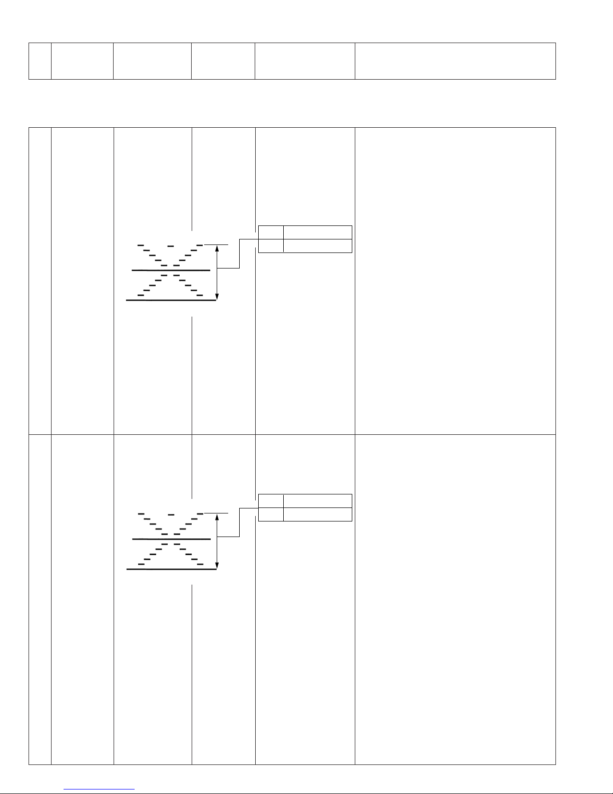
2.5 INITIALIZE
Measuring
instrument &
Input signals
Measuring point (*)
Adjustment parts (-)
Adjustment level (+)
1) Select either “TK-C400U.cor” for TK-C400U
or “TK-C400E.cor” for TK-C400E/401EG to on
Scenario file define adjustment.
2) Selecting either “NEXT” or “BACK” button
to be initialized the camera data.
All EVR are installed the initial data. (See 2.4.3)
2.6 ADJUSTMENT OF SSG
1 fsc
adjustment
Frequency
counter
*
TP207 [PRO]
-
EVRUSR
[CAT: CLAMP, Byte: 5]
+
U-ver. 3.579545MHz
E-ver. 4.43361875MHz
1) Select the “NEXT” button to display “fsc ad-
justment” on the title bar.
2) Adjust the EVRUSR with “䊱” and “䊲” buttons
to obtain the specified level at the measuring
point.
2-5
Page 14

Measuring
No.
Item Mode Adjustment procedure
instrument &
Input signals
2.7 ADJUSTMENT OF CCD
Measuring point (*)
Adjustment parts (-)
Adjustment level (+)
1 VSUB voltage
adjustment
2 Reset voltage
adjustment
Digital voltmeter *
Oscilloscope
(H-rate:10:1)
TP205 [PRO]
-
VSUB [CAT: DCREF,
Byte: 3]
+
Specified voltage on
the back of the CCD.
*
TP214 [PRO]
-
VRGL [CAT: DCREF,
Byte:4]
+
Specified voltage on
the back of the CCD.
1) Select the “NEXT” button to display “VSUB
voltage” on the title bar.
2) Adjust the VSUB with “䊱” and “䊲” buttons to
obtain the specified level at the measuring
point.
Note:
For the specified voltage, check on the VRGL
and VSUB codes shown on the back of the
CCD, and find out the proper value according to the correlation table of the “How to
Find Specified Voltage” as shown below.
1) Select the “NEXT” button to display “Reset
voltage” on the title bar.
2) Adjust the VRGL with “䊱” and “䊲 ” buttons to obtain the specified level at the measuring point.
How to Find Specified Voltage
Note:
For the specified voltage, check on the V
RGL
and VSUB codes shown on the back of the
CCD, and find out the proper value according to the correlation table of the “How to
Find Specified Voltage” appearing in the
lower part of this page.
2-6
Page 15

Measuring
No.
Item Mode Adjustment procedure
instrument &
Input signals
2.8 ADJUSTMENT OF VIDEO SIGNAL
Measuring point (*)
Adjustment parts (-)
Adjustment level (+)
1 White clip
adjustment
2 Contour level
adjustment
Oscilloscope
(H-rate: 10:1) or
W.F.M.
Gray scale chart
(Just scan size)
Oscilloscope
(H-rate: 10:1) or
W.F.M.
Gray scale chart
(Just scan size)
LENS OPEN
*
VIDEO OUT (75 ohm
Termination)
-
DAVREFY
[CAT: DCREF, Byte: 1]
+
U-ver.
0.79 Vp-p (110 IRE)
E-ver.
0.77 Vp-p (110%)
*
VIDEO OUT (75 ohm
Termination)
-
LENS IRIS
+
U-ver.
0.57 Vp-p (80IRE)
E-ver.
0.56 Vp-p (80%)
1) Select the “NEXT” button to display “White
clip” on the title bar.
2) Turn the lens iris so that the wavefrom of
grayscele is saturated as shown left figure.
3) Adjust the DAVREFY with “䊱” and “䊲” buttons to obtain the specified level at the measuring point.
1) Select the “NEXT” button to display “Con-
tour level” on the title bar.
2) Adjust the lens iris to obtain the specified level
at the measuring point.
*
VIDEO OUT (75 ohm
Termination)
-
VHAPGH
[CAT: FIELD, Byte: 3]
+
U-ver.
0.714 Vp-p (100IRE)
E-ver.
0.7 Vp-p (100%)
3) Adjust the VHAPGH with “䊱” and “䊲” buttons to obtain the specified level at the measuring point.
2-7
Page 16

No.
Measuring
Item Mode Adjustment procedure
instrument &
Input signals
Measuring point (*)
Adjustment parts (-)
Adjustment level (+)
3 Setup level
adjustment
4 Burst level
adjustment
Oscilloscope
(H-rate: 10:1) or
W.F.M.
Oscilloscope
(H-rate, 10:1) or
W.F.M.
*
VIDEO OUT
(75 ohm Termination)
-
SETUP
[CAT: Fix, Byte: 3]
50 mVp-p
+
*
VIDEO OUT
(75 ohm Termination)
-
DAVREFC
[CAT: DCREF, Byte: 2]
+
U-ver.
286 mVp-p (40IRE)
E-ver.
300 mVp-p
1) Select the “NEXT” button to display “Setup
level” on the title bar.
2) Turn the lens iris to be closed.
3) Adjust the SETUP with “䊱” and “䊲” buttons to obtain the specified level at the measuring point.
1) Select the “NEXT” button to display “Burst
level” on the title bar.
2) Adjust the DAVREFC with “䊱” and “䊲” buttons to obtain the specified level at the measuring point.
2-8
Page 17

Measuring
No.
Item Mode Adjustment procedure
instrument &
Input signals
2.9 ADJUSTMENT OF WHITE BALANCE
Measuring point (*)
Adjustment parts (-)
Adjustment level (+)
1 White
balance
adjustment(1)
Gray scale chart
Oscilloscope
(H-rate, 10:1) or
W.F.M
Auto-white balance (1)
Oscilloscope or Waveform monitor
*
VIDEO OUT
(75 ohm Termination)
-
LENS IRIS
+
U-ver.
E-ver.
MCRDIP = 1
MCRAE = 1
AWBCNT = &H8229
INTGR = &H4B6151
0.714 Vp-p (100IRE)
0.7 Vp-p (100%)
1) Select the “NEXT” button to display “White
balance (1)” on the title bar.
2) Adjust the lens iris to obtain the specified level
of white chip at the measuring point.
3) Press either “䊱” or “䊲” button of the
“AWBPRER”, then “AWBCNT” and “INTGR”
data are appeared in the “Show Controls”
box.
4) Press the “䊱” or “䊲” button of the
“AWBPRER” to be same data of AWB CNT’s
data. (last 2 digit)
5) Press the “䊱” or “䊲” button of the “WBR”
to be the same data of AWB CNT’s data. (last
2 digit)
6) Press the “䊱” or “䊲” button of the
AWBPREB to be the same data of INTGR’s
data. (last 2 digit)
7) Press the “䊱” or “䊲” button of the WBB to
be same data of INTGR’s data. (last 2 digit)
2 White
balance
adjustment(2)
AWBPRER WBR AWBPREB WBB
&H29 &H51 &H51&H29
*
Gray scale chart
filter
(No. 80B+80B)
VIDEO OUT
(75 ohm Termination)
-
LENS IRIS
Oscilloscope
(H-rate, 10:1) or
W.F.M.
+
U-ver.
E-ver.
0.714 Vp-p (100IRE)
0.7 Vp-p (100%)
1) Select the “NEXT” button to display “White
balance (2)” on the title bar.
2) Adjust the lens iris to obtain the specified level
of white chip at the measuring point.
3) Press the “䊱” or “䊲” button of the PRE2R,
then AWB CNT and INTGR data are appeared
in the Show Controls box.
4) Press the “䊱” or “䊲” button of the PRE2R
to be same data of AWB CNT’s data. (last 2
digit)
5) Press the “䊱” or “䊲” button of the PRE2B
to be same data of INTGR’s data. (last 2 digit)
2-9
Page 18
No.
Measuring
Item Mode Adjustment procedure
instrument &
Input signals
Measuring point (*)
Adjustment parts (-)
Adjustment level (+)
3 White
balance
adjustment(3)
Gray scale chart
filter
(No. 80D+82A)
Oscilloscope
(H-rate, 10:1) or
W.F.M
*
VIDEO OUT
(75 ohm Termination)
-
LENS IRIS
+
U-ver.
0.714 Vp-p (100IRE)
E-ver.
0.7 Vp-p (100%)
1) Select the “NEXT” button to display “White
balance (3)” on the title bar.
2) Adjust the lens iris to obtain the specified level
of white chip at the measuring point.
3) Press the “䊱” or “ 䊲” button of the
PRESETMWR, then AWBCNT and INTGR
data are appeared in the Show Controls box.
4) Press the “䊱” or “ 䊲” button of the
PRESETMWR to be same data of AWB CNT’s
data. (last 2 digit)
5) Press the “䊱” or “ 䊲” button of the
PRESETMWB to be same data of INTGR’s
data. (last 2 digit).
4 White
balance
adjustment (4)
Gray scale chart
filter
(No. 81A+81D)
*
VIDEO OUT
(75 ohm Termination)
-
LENS IRIS
+
U-ver.
0.714 Vp-p (100IRE)
E-ver.
0.7 Vp-p (100%)
1) Select the “NEXT” button to display “White
balance (4)” on the title bar.
2) Adjust the lens iris to obtain the specified
level of white chip at the measuring point.
3) Press the “䊱” or “䊲” button of the
RLOGAIN, then AWBCNT data are appeared
in the “Show Controls” box.
4) Press the “䊱” or “䊲” button of the
RLOGAIN to be same data of AWBCNT’s
data. (last 2 digit)
2-10
Page 19

No.
Measuring
Item Mode Adjustment procedure
instrument &
Input signals
Measuring point (*)
Adjustment parts (-)
Adjustment level (+)
5 White
balance
adjustment (5)
White balance
chart
filter
(No.80B+80B)
Oscilloscope
(H-rate, 10:1) or
W.F.M.
*
VIDEO OUT
(75 ohm Termination)
-
LENS IRIS
+
Center of carrier
U-ver.
0.357 Vp-p (50IRE)
E-ver.
0.35 Vp-p (50%)
1) Select the “NEXT” button to display “White
balance (5)” on the title bar.
2) Adjust the lens iris to obtain the specified level
of center of carrier at the measuring point.
3) Press the “䊱” or “䊲” button of the PRERBL,
then AWBCNT and INTGR data are appeared
in the “Show Controls” box.
4) Press the “䊱” or “䊲” button of the PRERBL
to be same data of AWBCNT’s data. (last 2
digit)
5) Press the “䊱” or “䊲” button of the PRERBM
to be same data of AWBCNT’s data. (Middle
2 digit)
6) Press the “䊱” or “䊲” button of the
PRERBGL to be same data of INTGR’s data
(last 2 digit)
7) Press the “䊱” or “䊲” button of the
PRERBGM to same data of INTGR’s data. (3rd
and 4th digit from right)
Auto-white balance (5)
Oscilloscope or Waveform monitor
PRERBL PRERBM PRERBGL PRERBGM
&H71 &HA7 &H0A&HE5
AWBCO = 2
AWBCNT = &HE571
INTGR = &H220AA7
2-11
Page 20

Measuring
No.
Item Mode Adjustment procedure
instrument &
Input signals
2.10 ADJUSTMENT OF CHROMA SIGNAL
Measuring point (*)
Adjustment parts (-)
Adjustment level (+)
1 Color level
and hue
adjustment
Yellow
Oscilloscope
(H-rote, 10:1) or
W.F.M.
Color bar chart
Red
Yellow
*
VIDEO OUT
(75 ohm Termination)
-
LENS IRIS
+
U-ver.
0.57 Vp-p (80IRE)
E-ver.
0.56 Vp-p (80%)
-
RY GAIN
[CAT: FIELD, Byte: 8]
-
RYHUE
[CAT: FIELD, Byte: 10]
-
BYGAIN
[CAT: FIELD, Byte: 9]
-
BYHUE
[CAT:FIELD, Byte:11]
Red
1) Select the “NEXT” button to display “Color
level and Hue” on the title bar.
2) Adjust the lens iris to obtain the specified level
of white part at the measuring point.
3) Adjust the RYGAIN, RYHUE, BYGAIN and
BYHUE with “䊱” and “䊲” buttons to obtain
the specified position at the measuring position.
2 Chroma
suppress
adjustment
2.11 WRITE DATA
1 Write data
[NTSC] [PAL]
Oscilloscope
(H-rate, 10:1) or
W.F.M
Gray scale chart
LENS OPEN
*
VIDEO OUT
(75 ohm Termination)
-
CSHLV
[CAT: FIELD, Byte: 4]
+
Minimum carrier
leakage.
1) Select the “NEXT” button to display “chroma
suppress at high light” on the title bar.
2) Turn the lens iris so that the wevefome of
gray scale is saturated as shown left figure.
3) Adjust the CSHLV with “䊱” and “䊲” buttons to minimize carrier leakage on saturated
signal.
1) Select the “NEXT” button to display “Write
data to the EEPROM” on the title bar.
2) Press the “NEXT” button, then message box
are appeared.”Are you sure to write EEPROM?”
3) Select the “YES” button to write all data just
adjusted to memory in camera.
2-12
Page 21

TK-C400U/TK-C400E/TK-C401EG
VICTOR COMPANY OF JAPAN, LIMITED
No. 6675
Printed in Japan
(S) T. A
Page 22

SECTION 3
CHARTS AND DIAGRAMS
䡵 REPLACING SUBMINIATURE “CHIP” PARTS
• Some resistors, shorting jumpers (0 ohm resistance), ceramic
capacitors, transistors, and diodes are chip parts. These chip
parts cannot be reused after they are once removed.
• Chip resistors used in some circuits are of high precision
type having little error in resistance.
To demonstrate the full capacity of this camera head, place
an order for proper parts referring to the diagrams and parts
lists in the sections 5.
• Soldering cautions:
1) Do not apply heat for more than 3 seconds.
2) Avoid using a rubbing stroke when soldering.
3) Discard removed chips; do not reuse them.
4) Supplementary cementing is not required.
5) Use care not to scratch or otherwise damage the chips.
• Definistion of the (A) and the (B) or circuit boards diagrams
(A) : Side on which discrete parts are assembled.
(B) : Side on which only chip parts are assembled.
• Transistors are:
䡵 SCHEMATIC DIAGRAM NOTES
• Schematic safety precaution
! Parts are safety related parts.
When replacing them, be sure to use the specified parts.
• Voltage and waveform measurements.
Voltage: Measured with digital voltmeter in DC range;
iris closed.
• Waveform: Color bars illuminated more than 4000lux at
3200K lighting.
• Terminal logic
Top bar of terminal name show input or output logic.
Top bar shows, the control circuit become active at negative (low) logic input for example.
B
C
E
2SA1576A
MSB1218A
B
C
E
2SC4681
MSD1819A
C
B
E
1
2
3
1
2
3
6
5
4
6
5
4
E
E
B
E
E
E
E
B
B
C
B
B
C
C
C
C
B
C
XP6401
XP6534
3-1
3-1
Page 23

BLC SW10
V11
V22
V33
V44
H25
H16
RG7
Vsub8
V1 16
V2 15
V3 14
V4 13
H2 12
H1 11
RG 10
Vsub 9
VIDEO IRIS11
DC IRIS16
VBS OUT7
Rxd4
Txd2
LL SW6
IC217
IC217
CP
15
10
9
4
P. BLK
SYNC
Drive
IC215
LPF
Q215/Q216
+
AMP
3
1
8
IC213
Y-Process
DL1
DL02
MCRCON
FSC
PRE
C-Process
VSPRS/HLSPRS
OPD
AE
Y-AE
C-WB
SYNC
SG
SCS
SW-IF
AWB
DOUT
D/AGAINGAM
1HDL
A/D
PG
1HDL
BLK
DADJ
APAC
GAIN
HLAPAC
GAIN
HL
APAC
VH
APAC
Y-INTG
(
5wind
)
HIST-CNT
HIST-INTG
(
2ch
)
RGB-CNT
RGB-INTG
LPF
CLMP
OB
DET
SYNC
GEN
SYNC
SEP
MASTER
HD GEN
REF
GATE
LPF
CLMP
LN
MTX
RGB
MTX
WB GAM
DOUT
ENC D/A
SYS
MAN
DIP
SW
EXT-SIF
・RS232C
・IICOM
DO
IC205
DI
DI
IC206
CAM-SIF
・TG・EVR
・EEPROM
YC
SPRS
INIT SG
AWBAE
CLMP
VH
PHASE
COMP
EXT
SYNC
DET
FSC
PHASE
COMP
WIND
GEN
+
INTERNAL BUS
10
XSHO
11
XSHP
30
Vss1
33
Vss2
22
Vss3
34
32
OSCO
31
26
MCK
16
PBLK
15
CLPDM
21
ID
25
WEN
19
SCK
17
SEN
18
SDAT
1
DCIN
12
XRS
13
ADCK
38
V2
37
V1
40
V3
44
VH
39
VM
42
VL
41
V4
7
RG
5
H1
4
H2
43
SUB
47
CPP1
48
CPP2
45
CPP3
48
DCOUT
983
VD
24
HD
23203528
RST
29
TEST1
36 27NC2
AMPAMP
XSHP
XSHD
XRS
ADCK
driver
RG driver
H driver
V driver
Timing Generator
1/2
SUB driver
Change
Pump
Mode Set
Latch
146
25
PIN
26
DIN
27
Vcc2
28
N.C.
29
LIN/CH
30
GND2
31
RFCONT
32
PBRFC
CAM/VIDEO
1
PB/REC
2
CH/CL
3PS4
VSHP
5
GND3
6
LOUTCLP
7DR8
16
AGCCLP
15
CLPOB
14
XRS
13
PBLK
12
OFFSET
11
VRT
10
VRB
9
Vcc3
CLPDM24GND123SHO22SHP21Vcc120CCDLEVEL19AGCCONT18Vcc4
17
SH1 SH2
SH3
COSCLP1
COSCLP2
LIN CLP
LIN/CH SW
V1 SW
C/V SW
OFFSET
SW
CENTER BIAS
CENTER BIAS
VISH
GCA
AMP
AGC LPF CAMSH
AGCCLP
BLK
DRV
CH/CL
DC
REF
BOTTOM
REF
TOP
MODE SWITCHING LOUTCLP
Fine
Comparate
&
Encode
Coarse
Correction
&
Latch
Calibration
Unit
Auto Calibration
Pulse Generator
Sense
Amp
Fine
Latch
Coarse
Comparate
&
Encode
DAC
Timing Gen
12
D8
11
D7
10
D6
9
D5
8
D4
5
D3
4
D2
3
D1
2
D0(LSB
)
21
MINV
20
LINV
19
TESTMODE
41
CAL
17
SEL
15
RESET
AVss AV
DD
362827
Sense
Amp
1826
39
V
IN
29
VRT
30
VRT
34
VRB
35
VRB
22
CLK
23
OE
24
CE
+
x8
Y
C
VCO
EVR
Vref Y/Vref C
<AGC CONT/OFFSET>
<V Sub>
14
12
IC208
LPF
LPF
CN200
IC200
CCD
Drive pulse
Vsub
Q201
1CCD OUT6
Vref C
Vref Y
IO C
IO Y
5
1
6
7
Sampling pulse
85 93
63
20
15
21
26
72
73
14
3
Voo1
Voo2
Voo3
AVss3
AVoo3
AVoo2
AVoo1
AVss1
Buffer
CCD BOARD
11
PRO BOARD
CN200
CK1
TEST2
OSCI
IC202
Shutter
Pulse
3
5
I
O
Buffer
1
2
I
O
Buffer
ON/OFF
Buffer
Filter
IC203
DRVOUT
IC204
O
I
IC207
4
EEPROM
INT/LL
+
-
+
PHASE-/WBR
PHASE+/WBB
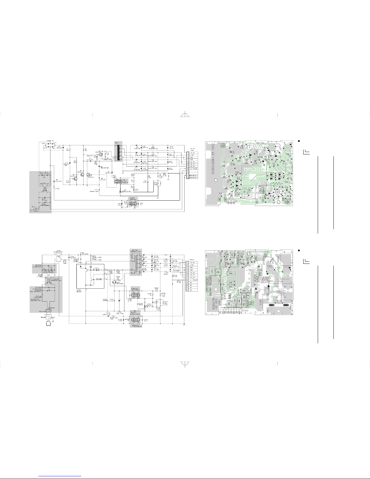
BLOCK DIAGRAM3.1
3-2 3-2
Page 24

8.5
15.0
9.2
12.5
-7.9
5.0
2.62.6
2.3
0000
CCD
3-3 3-3
CCD BOARD SCHEMATIC DIAGRAM
CCD CIRCUIT BOARD
. SIDE A .
. SIDE B .
Note : The parts in ( ) are not mounted on the board.
3.2
3.3
TP200
200mV/DIV, 10U/DIV
216
115
1
16
9
8
(
CN201
)
Page 25

-8.6
0
-7.9
19.2
15.1
0
0
0
0
0
-7.9
-7.9
15.2
22.3
14.0
21.0
12.6
2.9
4.9
0
2.3
0.7
4.9
4.9
3.9
3.3
3.2
0
3.3
1.4
0
1.7
1.5
0
3.3
3.3
0
0.7
3.2
2.9
0
1.6
3.3
2.7
3.2
0.6
3.1
0
3.0
2.9
0
3.0
3.3
0
2.1
3.3
3.4
3.4
2.9
2.8
3.1
3.2
2.7
1.2
4.1
2.0
4.9
4.9
0
0
0
0.9
0
1.5
1.1
1.4
1.5
0
2.1
2.3
1.7
3.0
2.4
0.6
0
0.1
1.1
1.1
1.7
1.7
1.4
1.1
7.9
2.1
0.4
0.4
0
0
0
0
3.3
0
0
2.4
2.3
1.8
2.9
2.5
1.2
4.9
0
0
0
1.3
3.3
1.5
1.5
3.2
0.3
1.0
1.1
8.5
10.2
0
0
0.8
0
0
0
3.3
0.402.9
2.9
0
00000
0
2.3
4.9
4.9
0.3
1.4
4.9
2.8
1.8
0
3.3
3.3
0
0
3.3
0
0
1.4
0
4.5
0
1.4
4.9
3.3
1.6
1.6
0
1.3
2.5
1.2
3.3
3.3
1.0
0
3.3
3.3
0
0.4
1.8
5.0
5.6
5.0
5.6
5.6
3.3
1.3
2.0
1.4
2.0
2.7
2.5
2.1
5.0
1.0
3.2
3.8
3.4
2.8
3.1
2.4
3.1
2.5
2.5
3.3
2.5
TG/V-DRV
CDS/AGC
A/D CONVERTER
D/A
DSP
1/2
V
DRIVER
TIMING
DRIVER
DRIVER
DRIVER
DRIVER
CHARGE
PUMP
LATCH
MODE
SET
CDS
CDS
LPF
S&H BLK
AGC
CLP
DAC
X8
FINE
LATCH
COMPARATE
ENCODE
&
LATCH
CORRECTION
COARSE
&
COMPARATE
&
FINE
ENCODE
DET
1H
DL
LPF
CLMP
SYNC
SEP
VH
PHASE
COMP
SYNC
GEN
HD
GEN
RGB
MTX
WB
GAIN
BLK
D/A
LN
MTX
ENC
D/A
1HDLLPF
CLMP
EEPROM
GENERATOR
XRS
+
-
OB
R
R
8.2
0
3.1
COARSE
3.4
3-4 3-4
U
E/EG
C327
33p
18p
L211
15u
8.2u
C333
33p
33p
FL200
NAX0147-001X
NAX0147-001X
R245
OPEN
33k
R246
33k
OPEN
R287
OPEN
OPEN
R288
33k
33k
X200
SCV2219-001W
CE42275-001Y
C221
56p
56p
C223
33p
33p
C225
56p
56p
L203
5.6u
5.6u
R311
OPEN
OPEN
R342
470
470
R219
47
47
R220
47
47
R221
47
47
C238
OPEN
OPEN
C248
OPEN
OPEN
SET
IC217.3
11
12
14
13
6
7
16
8
PRO BOARD SCHEMATIC DIAGRAM
TO CCD
TO EE
R233
2.7k
R240
330
D212
D211
0.33
0.22
to TP205
R314
R315
2.2M
2.2M
R295
OPEN
R297
33k
R372
560
R374
12k
C337
OPEN
The details of components marked by astarisk are shown below.
Note : The parts in ( ) are not mounted on the board.
Q201-204, 206
Page 26

D212
D212
PRO CIRCUIT BOARD3.5
3-5 3-5
. SIDE A .
. SIDE B .
IC200 B-2A
IC201 B-1A
IC202 B-2C
IC203 B-1D
IC204 B-2E
IC205 B-4C
IC206 B-4D
IC207 A-6C
IC208 B-6A
IC209 B-3A
IC210 B-4B
IC211 B-4B
IC212 B-3B
IC213 B-7D
IC214 B-6B
IC215 B-7A
IC216 B-5B
IC217 B-4E
IC218 B-5C
Q200 B-3B
Q201 B-3E
Q202 B-3D
Q203 B-3E
Q204 A-3B
Q205 A-3B
Q206 B-4D
Q207 B-6A
Q208 A-7B
Q209 B-7E
Q210 A-6A
Q211 B-5C
Q212 B-7F
Q213 B-7F
Q214 B-7F
Q215 B-7B
Q216 B-6B
Q217 B-3E
Q218 A-4A
Q219 A-4C
Q220 B-5D
D200 B-1B
D201 B-1B
D202 A-1E
D203 B-1B
D204 A-2F
D205 A-3C
D206 A-3C
D207 A-2A
D208 B-6C
D209 B-5C
D210 B-6D
R200 B-2A
R201 B-2A
R202 A-4A
R204 A-4A
R206 B-3E
R207 B-1B
R208 A-3E
R209 A-3E
R210 B-3B
R211 A-3C
R212 A-2C
R213 A-3D
R214 B-2D
R215 B-3C
R216 A-3D
R217 B-3C
R219 A-2E
R220 A-2D
R221 B-2B
R222 B-3A
R224 A-2D
R225 B-2E
R226 B-2D
R228 A-2A
R232 B-3D
R233 B-3E
R234 B-3D
R235 B-3D
R236 B-3E
R237 A-3B
R238 A-3B
R239 A-3B
R240 A-3B
R241 A-3B
R242 B-3E
R243 A-3C
R244 A-4C
R245 A-7B
R246 B-6E
R247 B-4D
R252 A-3D
R253 A-3D
R254 A-4D
R255 A-4C
R280 B-5C
R281 A-5D
R282 B-6B
R283 A-6D
R284 A-6D
R285 B-5D
R286 B-6C
R287 B-7D
R288 B-7D
R289 B-6E
R290 A-6D
R291 A-4B
R292 B-7D
R293 A-5A
R294 B-5E
R295 B-5F
R296 B-6E
R297 B-6F
R298 B-5E
R299 B-5F
R300 B-5D
R301 B-5E
R302 B-5E
R303 B-5E
R304 B-5E
R305 B-5F
R306 B-5D
R307 B-5E
R308 B-5E
R309 B-5E
R310 B-5B
R311 B-5F
R312 B-5C
R313 B-5C
R314 B-6E
R315 B-5E
R316 A-5D
R317 A-6E
R318 A-6E
R319 A-5F
R320 A-6F
R321 B-5A
R322 B-5A
R323 B-6A
R324 B-6B
R325 B-6B
R326 B-5C
R327 B-6D
R328 B-6D
R329 B-5D
R330 A-5D
R331 A-5D
R332 A-5E
R333 A-5E
R334 A-7D
R335 A-7D
R336 A-7D
R337 B-6D
R338 B-6E
R339 B-6B
R340 B-5A
R341 B-5A
R342 B-5A
R343 A-7A
R344 B-7E
R345 B-7E
R346 B-7E
R347 B-7E
R348 B-7E
R349 B-7D
R350 B-7D
R351 A-5D
R352 B-6F
R353 B-7F
R354 A-6A
R355 A-6A
R356 B-7E
R357 B-6F
R358 A-4D
R359 B-7F
R360 B-7F
R361 B-7F
R362 A-7A
R363 B-7F
R364 B-7F
R365 B-7F
R366 B-7F
R367 B-7F
R368 B-7E
R369 B-7B
R370 B-7B
R371 B-7B
R372 B-7B
R373 A-7E
R374 B-7B
R375 A-6E
R376 B-6C
R377 A-6E
R378 B-6A
R379 B-6A
R380 B-7B
R381 A-7F
R382 B-2D
R383 A-1B
R384 A-6A
R385 A-6A
R386 B-6E
R387 B-6E
R388 B-6F
R389 A-7B
R390 A-1B
R391 A-1B
R392 A-7D
R393 B-7C
R394 B-5E
R395 A-3A
R396 B-5C
R397 A-7C
R398 A-4C
R399 A-3E
C200 A-2F
C201 B-2A
C202 A-2F
C203 A-1E
C204 B-2A
C205 A-1F
C206 A-2E
C207 B-2B
C212 B-1B
C213 B-1C
C214 A-1E
C215 A-2E
C216 B-1C
C217 B-2B
C218 B-2B
C219 B-3B
C220 B-3B
C221 A-2D
C222 A-2C
C223 B-3C
C224 A-3C
C225 A-3C
C226 A-3D
C227 A-2D
C228 B-2C
C229 A-2D
C230 A-3D
C231 A-3E
C232 A-2D
C233 B-2B
C234 A-2E
C235 A-2D
C236 A-2D
C237 B-2B
C238 B-3A
C239 A-2E
C240 A-2E
C241 B-1E
C242 A-1C
C243 B-2E
C244 B-1E
C245 B-1E
C246 B-1E
C247 B-1E
C248 B-2E
C249 B-2D
C250 A-1C
C251 B-2D
C252 B-2C
C253 A-1C
C254 A-1D
C255 B-1E
C256 A-2A
C257 A-4C
C258 A-3A
C259 A-3C
C260 A-3B
C261 A-3C
C262 A-3B
C263 A-3A
C264 A-3B
C265 A-4D
C266 B-7C
C267 B-7C
C268 A-4C
C271 B-4B
C272 B-4C
C273 B-4B
C274 B-5D
C275 B-6F
C276 A-6A
C282 B-6C
C283 B-6C
C284 B-5D
C285 A-6D
C286 A-6E
C287 B-4B
C288 A-4D
C289 B-7E
C290 A-5A
C291 A-6A
C292 B-6E
C293 A-6A
C294 B-6F
C295 B-6E
C296 B-6E
C297 B-7E
C298 A-7B
C299 A-6F
C300 A-6E
C301 A-6F
C302 A-6F
C303 B-5A
C304 B-6B
C305 B-5A
C306 A-5F
C307 A-5E
C308 B-6C
C309 B-6C
C310 B-6D
C311 B-6D
C312 A-5E
C313 A-3F
C314 B-3A
C315 A-3F
C316 A-5E
C317 B-4B
C318 A-5E
C319 A-4E
C320 B-4B
C321 A-4E
C322 A-3E
C323 B-3B
C324 A-3E
C325 A-7A
C326 B-7E
C327 A-7B
C328 B-7E
C329 A-7C
C330 A-7C
C331 A-7B
C332 B-6F
C333 A-6A
C334 B-7C
C335 A-7D
C336 A-6E
C337 B-6B
C338 B-6B
C339 A-6E
C340 B-7A
C341 B-6A
C342 B-6C
C343 B-7A
C344 A-7E
C345 B-7B
C346 B-2D
C347 A-2B
C348 A-3B
C349 A-1C
C350 A-2A
C351 B-3F
C352 B-3E
C353 B-1D
C354 A-4A
C355 B-4E
C356 B-5E
L203 B-3D
L205 B-1E
L211 A-7B
L212 A-7C
L213 A-3A
DL200 A-7A
TP200 B-1A
TP201 B-3A
TP202 B-1E
TP203 B-1C
TP204 B-3E
TP205 B-6C
TP206 B-5D
TP207 B-7D
TP208 B-6E
TP209 B-7E
TP210 B-7D
TP211 B-6F
TP212 B-4A
TP213 B-4A
TP214 B-2B
TP215 B-1B
TP216 B-3B
TP217 B-3C
TP218 B-6A
TP219 B-5B
CN200 A-2C
CN201 A-4F
CN202 A-1B
X200 B-6D
TC200 B-3D
FL200 A-6A
Each address may have an address error by one interval.
Side Y axis
X axis
A-1C
TP202 TP211 TP209 TP218
200mV/DIV,10U/DIV 500mV/DIV,10U/DIV 200mV/DIV,10U/DIV 200mV/DIV,10U/DIV
ADDRESS TABEL OF PRO BOARD PARTS
TP215
10V/DIV,5ms/DIV
SHUTTER ON
(
AGC ON, AES ON
)
C
115
13
31
14
85
85
41
41
85
169
18
112
13 24
25 36
37 48
37 48
3625
112
2413
81
169
8
5
41
216
13
3
3
1
1
Page 27

1.5
2.2
2.2
1.6
9.0
1.6
0.2
0
5.7
1.4
0
0
0
1.5
0
2.1
0
0
3.3
0
0
2.2
0
3.3
LEVEL
VIDEO/DC
3.6
3-6 3-6
R507
27K
C521
22/10
(
R522
)
C520
1/25
C500
0.047
MA152WK
C515
0.01
GND(PRIMARY
)
GND(PRIMARY
)
PHASE/W.B
+8.5V
Vref
VIDEO IRIS
+5.7V
ATW/MANU
DC IRIS
PHASE-/WB R
+5.7V
LL PULSE
EE BOARD SCHEMATIC DIAGRAM
C509
0.01
C522
22/10
LL SW
PHASE+/WB B
MA152WK
TO POWER (TK-C401EG
)
TO PS (TK-C400U/E
)
Note : The parts in ( ) are not mounted on the board.
D500-D503 : MA3240(M)-W
Page 28

0
0
0
3.3
3.3
3.3
3.3
3.3
3.3
0
0
EE CIRCUIT BOARD TERMINAL BOARD SCHEMATIC DIAGRAM
TERMINAL CIRCUIT BOARD
3.7 3.8
3.9
3-7 3-7
. SIDE A .
. SIDE B .
.. SIDE B
+5.7V
TK-C400U/E only
TK-C400E only
IC501 B-3A
IC502 B-1A
Q500 B-1A
Q501 A-3A
Q502 A-3A
Q503 B-2A
D500 B-3B
D501 B-2B
D502 B-3B
D503 B-3B
D504 B-1B
D505 B-1A
R500 B-3A
R501 B-2A
R502 B-2B
R503 B-2B
R504 B-2B
R505 B-1A
R506 B-1B
R507 B-1B
R508 A-3A
R509 A-3A
R510 A-3A
R511 B-3A
R512 A-3A
R514 B-3A
R515 A-3A
R516 B-3A
R517 B-3A
R518 B-3A
R519 B-3A
R520 B-2A
R521 B-2A
R522 B-3A
R530 B-1B
R531 B-1B
R533 B-1A
R534 B-1A
VR500 A-3B
C500 B-1A
C501 A-1B
C502 B-1B
C503 B-1A
C504 A-3A
C505 B-2B
C506 B-2B
C507 B-2B
C508 B-3A
C509 B-3A
C511 B-1B
C513 B-2A
C514 A-1A
C515 B-1A
C517 A-3A
C518 A-3A
C519 A-3A
C520 B-3B
C521 B-3A
C522 A-2A
CN500 A-1A
CN501 A-2B
CN502 A-2A
S500 A-2B
TB500 A-3B
Each address may have an address error by one interval.
Side Y axis
X axis
A-1C
ADDRESS TABEL OF EE BOARD PARTS
123
A
B
B
A
213
TB100
AC24V/DC12V
VBS
out
RS232C
5V
D104-107
MA3270-M
TK-C400U and
S101-103
Page 29
2.5
4.3
5.4
-0.8
-0.6
0
2.2
0.7
0
2.8
-0.2
2.8
11.6
5.4
4.4
2.5
3.4
12.4
3.10 3.11
3.12 3.13
3-8 3-8
TO EE
GND(PRIMARY
)
GND(PRIMARY
)
R22
12K
R5
1K
!
!
!
!
!
!
!
!
!
!
!
!
!
!
!
!
!
!
!
!
R12
3.9k
R24
5.6K
L703
0
C717
OPEN
R714
5.6k
PS BOARD SCHEMATIC DIAGRAM (TK-C400U/TK-C400E
)
POWER BOARD SCHEMATIC DIAGRAM (TK-C401EG
)
PS CIRCUIT BOARD (TK-C400U/TK-C400E
)
POWER CIRCUIT BOARD (TK-C401EG
)
ADDRESS TABEL OF PS BOARD PARTS
Each address may have an address error
by one interval.
IC1 4E
Q1 3F
Q2 7F
Q3 8F
Q4 7E
D2 7E
D3 7F
D4 7B
D5 6B
D7 5B
D9 7F
D10 8E
D11 8D
D12 7D
D13 7D
D14 8D
D15 4E
D17 4D
R1 6E
R2 6E
R3 8F
R4 6E
R5 6F
R6 4F
R7 5E
R8 3F
R9 3F
R10 2F
R12 6C
R15 6B
R16 8E
R17 6E
R18 8F
R21 5F
R22 2F
R23 2A
R24 2A
C1 8B
C2 8D
C3 7B
C5 7C
C6 8D
C7 8E
C8 6F
C10 4F
C12 2F
C13 5E
C15 7B
C16 5B
C18 4A
C19 3C
C21 3A
C22 4D
C24 4B
C25 4E
C27 3D
C28 5B
L1 8C
L2 4B
L3 2C
L5 2D
L6 2E
CN4 5A
FC1 7A
FC2 7A
PC1 5F
PC2 6B
T1 6D
VA1 8B
by one interval.
Each address may have an address error
X axis
Y axis
IC700 2F
IC701 2C
D700 6D
D701 4E
D702 4D
D703 5D
D704 3C
D706 3D
D708 3D
D710 2D
R700 3F
R701 3E
R702 4E
R703 4E
R704 4F
R705 5D
R706 6C
R707 1D
R708 1D
R709 1C
R710 1D
R711 1C
R712 4A
R713 4B
R714 4A
R715 3F
R716 8F
R717 6C
C700 7C
C701 6F
C702 8F
C703 6F
C704 5E
C705 4E
C706 4F
C707 4E
C708 3E
C709 6B
C710 3B
C711 3A
C712 3B
C713 4B
C714 4A
C715 5B
C716 2A
C717 1C
C718 1E
C719 1D
C720 5A
C721 3F
L700 3A
L701 3A
L702 5B
L703 2A
CN700 7A
CN701 5A
FC700 7C
FC701 7C
LF700 8E
PC700 2E
PC701 6B
T700 5B
VA700 7B
1C
X axis
Y axis
1C
ADDRESS TABEL OF POWER BOARD PARTS
Page 30
5-15-1
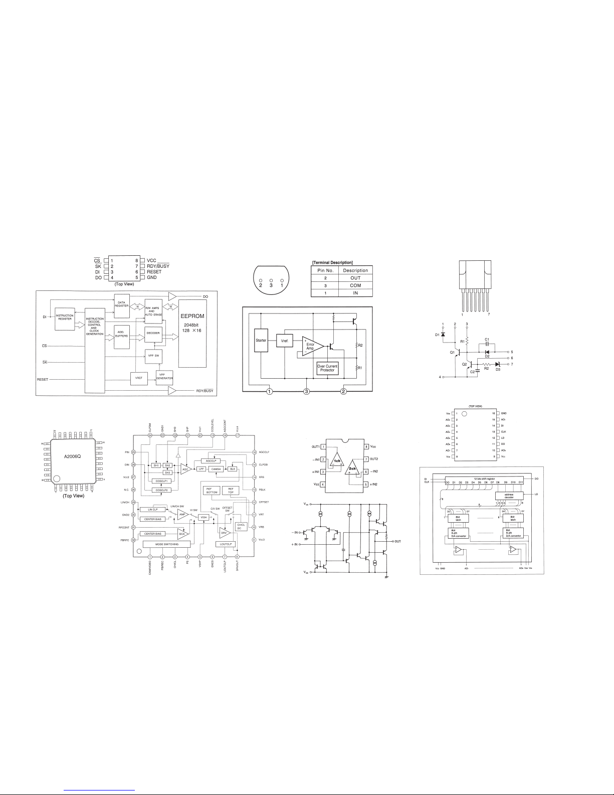
䡵 AN8085M-X [MATSUSHITA]
(REG Servo)
䡵 AK6420AM-W [ASAHIKASEI]
(2048 bits (128 Words X 16 bits) EEPROM)
䡵 CXA2006Q [SONY]
(CDS and AGC)
䡵 BA10358F-E2 [ROHM]
(Dual Ground Sense Op.Amp.)
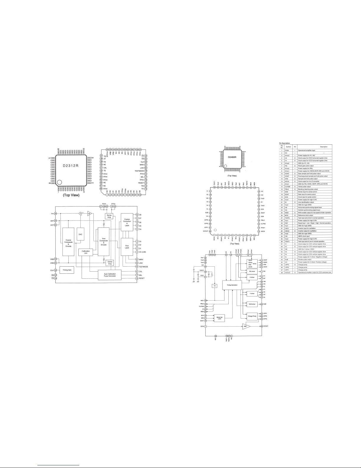
3.14 BLOCK DIAGRAMS of IC'S
3-9
3-9
䡵 MA1040P(4100) [SHINDENGEN]
(Power Modul)
䡵 MB88347PFV [FUJITSU]
(D/A Convertor)
Page 31
4-2 4-2
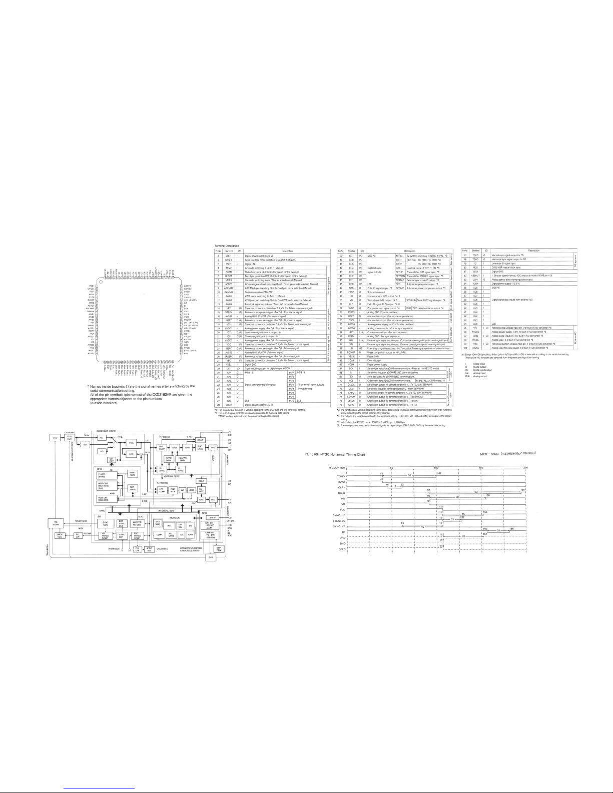
䡵 CXD2163AR [SONY]
(Digital signal processor for single chip CCD color video camera)
3-10
3-10
Page 32

5-35-3
3-113-11
Page 33
4-4 4-4
3-12
3-12
䡵 CXD2312R [SONY]
(9 bit 20 MSPS Video A/D Converter)
䡵 CXD2480R [SONY]
(Timing Control with CCD Drivers)
Page 34

5-55-5
3-13
3-13
Page 35
4-6 4-6
3-14
3-14
Page 36

5-75-7
3-15
3-15
䡵 ICX054AK-A [SONY]
(1/3 inch CCD image sensor for NTSC color camera)
Page 37

4-8 4-8
3-16
3-16
䡵 ICX055AK-A [SONY]
(1/3 inch CCD image sensor for PAL color camera)
Page 38

5-95-9
3-17
3-17
䡵 NJM2509V-W [JRC]
(Super Imposer including Y/C MIX Circuit)
䡵 NJM2267V-W [JRC]
(Dual 6dB Video Amplifier including 75OHM Driver)
䡵 NJM431U-X [JRC]
(Adjustable Precision Shunt Regulator)
䡵 NJM431U-XE [JRC]
(Refer to NJM431U-X.)
䡵 NJM79L08UA-X [JRC]
(3-Terminal Negative Voltage Regulator (-8V))
䡵 NJM78L15UA-X [JRC]
(3-Terminal Positive Voltage Regulator (+15V))
Page 39

4-10 4-10
3-18
3-18
䡵 TC74HC08AF-X [TOSHIBA]
(Quad 2-Input AND Gates)
䡵 TC4W53F-X [TOSHIBA]
(2-Channel Multiplexer)
䡵 UPC358G2-X [NEC]
(Refer to UPC358G2-W.)
䡵 UPC358G2-W [NEC]
(Dual Op.Amp.)
䡵 TK11333BMC-X [TOKO]
(Regulator)
䡵 TC7W02F-X [TOSHIBA]
(2 Input Dual NOR Gate)
䡵 TC7S08F-X [TOSHIBA]
(2 Input Single AND Gate)
䡵 PST9120N-X [MITSUMI]
(System Reset(+2V))
䡵 TC4053BF-X [TOSHIBA]
(Triple 2 Channel Analog Multiplexers/Demultiplexers)
Page 40

5-115-113-19
3-19
䡵 TK11650U-X [TOKO]
(3-Terminal Positive Voltage Regulator)
䡵 UPD5556G-W [NEC]
(CMOS Dual Timer)
Page 41

4-12 4-12
4-1
4-1
SECTION 4
EXPLODED VIEW AND ASSEMBLY PARTS LIST
4.1 ASSEMBLY
M1
䢇 SAFETY PRECATION
Parts identified by the ! symbol are critical for safety.
Replace only with specified parts numbers.
䢇 NOTE
Parts not denoted by parts numbers are not supplied by JVC.
25
24
for EG-Ver.
PRO BOARD
PS/POWER
BOARD
EE BOARD
FUSE
See SECTION1.
CCD BOARD
for E and EG-Ver.
TERMINAL
BOARD
for U and E-Ver.
for EG-Ver.
TERMINAL BOARD
for U-Ver.
Page 42

ASSEMBLY PARTS LIST
Symbol
No.
1 SC32036H-001 CAP
2 SC40286H-001 SHEET
3 SC20489H-002 FRONT FRAME
4 SC45590H-001 SPRING
5 SC20553H-001 SENSOR BASE
6 SC31647H-001 ADJ.RING
7 SC45335-002 LEAF SPRING
8 SC46173H-001 HOLDER PLATE
9 SCV2511-001 OP L.P.F. for TK-C400U/TK-C400E/TK-C401EG
10 SC45592H-001 SENSOR MASK
11 ICX054AK-A CCD SONY for TK-C400U
11 ICX055AK-A CCD SONY for TK-C400E/TK-C401EG
12 SC31797H-001 SENSOR HOLDER
! 13 SCV2337-1605BD FFC CABLE (1) CCD to PRO
! 14 SCV1902H-1805K FFC CABLE (2) TERMINAL to EE
! 15 SCV1902H-1206K FFC CABLE (3) PS/POWER to EE
16 SC46170H-001 HEAT SINK
17 SC32127H-00A CHASSIS for U and E-Ver.
17 SC32127H-00B CHASSIS for EG-Ver.
18 SC45456H-001 F. CAUTION LABEL for U-Ver.
19 SC45396H-002 UL LABEL for U-Ver.
20 SC46066H-001 CAUTION LABEL for U-Ver.
20 SC46171H-001 WARNING LABEL for EG-Ver.
21 SC32129H-001 UPPER COVER
22 SC32128H-001 BOTTOM COVER
23 SC20601H-00A TRIPOD BASE
24 SC31650H-002 ESCUTCHEON
25 SC32130H-001 REAR PANEL for U and E-Ver.
25 SC32130H-002 REAR PANEL for EG-Ver.
! 26 QMPK068-250-K POWER CORD for EG-Ver.
27 QHS6374-162 STRAIN RELIEF for EG-Ver.
28 QXT3820-035 UL TUBE for EG-Ver.
29 SCV1731-003 VH HOUSING for EG-Ver.
S1 SPSP2611N SCREW M2.6x11
S2 SDSF2008M SCREW M2x8, x2
S3 SPSK2040R SCREW M2x4, x12
S4 SPSP2605N SCREW M2.6x5, x7
S5 SDSF2606M SCREW M2.6x6, x2
S6 DPSP4006Z SCREW M4x6, for EG-Ver.
M1
M1MM````
DescriptionPart No. Part Name
4-2
Page 43

SECTION 6
PACKING
Instructions SC96795H (TK-C400U/E)
(English, French, Spanish)
Instructions SC96796H (TK-C400E only)
(Germany, Italian, Chinese)
4P Plug SCV2859-001
Instructions SC96795H
(English, French, Spanish)
Instructions SC96796H
(Germany, Italian, Chinese)
Power Cord
Carton
Carton
Carton
TK-C401EG only
Carton Box
6-1
Page 44
SECTION 5
ELECTRICAL PARTS LIST
SAFETY PRECAUTION:
Parts identified by the ! symbol are criticaI for safety. Replace only with specified parts numbers.
For maximum reliability and performance, all other replacement parts should be identical to those specified.
NOTE:
● Parts not denoted by parts numbers are not supplied by JVC.
● Abbreviations in this list are as follows:
RESISTORS
In the “Description” column:
All resistance values are in ohms (Ω).
k expresses kilo-ohm (1 000 ohms, kΩ).
M expresses mega-ohm (10
6
ohms, MΩ).
CAPACITORS
In the “Description” column:
All capacitance values are in microfarad (
otherwise indicated.
p expresses picofarad (10
–12
farad,pF).
µ
F) unless
In the “Parts Name”column:
CAR.RESISTOR : Carbon Resistor
C.M.F.RESISTOR : Constant Metalized Film Resistor
COMP.RESISTOR : Composition Resistor
FUSI.RESISTOR : Fusible Resistor
M.F.RESISTOR : Metal Film Resistor
M.G.RESISTOR : Metal Graze Resistor
M.P.RESISTOR : Metal Plate Resistor
O.M.F.RESISTOR : Oxide Metalized Film Resistor
TRIM.RESISTOR : Trimerer Resistor
U.F.RESISTOR : Non-inflammable Resistor
VAL.RESISTOR : Valiable Resistor
W.W.RESISTOR : Wire Wound Resistor
ln the “Description” column of the parts list, (U) means the parts for the U version while
Note:
(E) is for the E version.
Symbol
No.
Part No. Part Name Description
In the “Parts Name” column:
CER.CAPACITOR : Ceramic Capacitor
E.CAPACITOR : Electrolytic Capacitor
FILM CAPACITOR : Film Capacitor
M.F.CAPACITOR : Metalized Film Capacitor
MICA CAPACITOR : Mica Capacitor
MPP CAPACITOR : Metalized PolyPropylene Capacitor
MPPS CAPACITOR : Metalized PolyPhenylene Sulfied film
Capacitor
M.M.CAPACITOR : Metalized Mylar Capacitor
MYLAR CAPACITOR
: Mylar Capacitor
N.P.CAPACITOR : Non-Poler electrolytic Capacitor
P.P.CAPACITOR : PolyPropylene Capacitor
PPS CAPACITOR : PolyPhenylene Sulfied film Capacitor
P.S.CAPACITOR : PolyStyrene Capacitor
TAN.CAPACITOR : Tantal Capacitor
TRIM.CAPACITOR : Trimer Capacitor
VAL.CAPACITOR : Valiable Capacitor
JVCIC1 SCV1585-064 I.C.(M) (U)
JVCSCV1585-067 I.C.(M) (E)
for U version
for E version
5-1
Page 45

5.1 CCD BOARD ASSEMBLY PARTS LIST
01
SCK2467-01-N0A (TK-C400U)
SCK2467-01-P0A (TK-C400E/401EG)
Symbol
No.
SK200 SCV2154-001 IC SOCKET 16PIN
Q201 2SC4618(PQ)-X TRANSISTOR ROHM
R200 NRSA63J-184X M.G.RESISTOR 180k 1/16W
R202 NRSA63J-101X M.G.RESISTOR 100 1/16W
R203 NRSA63J-273X M.G.RESISTOR 27k 1/16W
R204 NRSA63J-0R0X M.G.RESISTOR 0 1/16W
R206 NRSA63J-472X M.G.RESISTOR 4.7k 1/16W
R207 NRSA63J-681X M.G.RESISTOR 680 1/16W
R208 NRSA63J-0R0X M.G.RESISTOR 0 1/16W
R209 NRSA63J-0R0X M.G.RESISTOR 0 1/16W
R210 NRSA63J-0R0X M.G.RESISTOR 0 1/16W
R211 NRSA63J-105X M.G.RESISTOR 1M 1/16W
C200 NEH91EM-106X E.CAPACITOR 10 25V
C201 NBH21CM-105X TAN.CAPACITOR 1 16V
C202 NEH90JM-476X E.CAPACITOR 47 6.3V
C205 NCF31EZ-104X CER.CAPACITOR 0.1 25V
C207 NCF31EZ-104X CER.CAPACITOR 0.1 25V
C211 NEH91HM-335X E.CAPACITOR 3.3 50V
C212 NCB31HK-152X CER.CAPACITOR 1500p 50V
C213 NEH91HM-335X E.CAPACITOR 3.3 50V
CN200 SCV2477-016 CONNECTOR 16PIN
TP SSV1096-001 TEST POINT TP200-TP201
Part No. Part Name Description
5.2 PRO BOARD ASSEMBLY PARTS LIST
01``````
02
SCK2467-02-N0A (TK-C400U)
SCK2467-02-P0A (TK-C400E/401EG)
Symbol
No.
IC200 NJM79L08UA-X I.C.(M) JRC
IC201 NJM78L15UA-X I.C.(M) JRC
IC202 CXD2480R I.C.(M) SONY
IC203 CXA2006Q I.C.(M) SONY
IC204 CXD2312R I.C.(M) SONY
IC205 AK6420AM-W I.C.(M) ASAHIKASEI
IC206 MB88347PFV-X I.C.(M) FUJITSU
IC207 CXD2163AR I.C.(M) SONY
IC208 TC4W53F-X I.C.(M) TOSHIBA
IC209 AN8085M-X I.C.(M) MATSUSHITA
IC210 TK11650U-X I.C.(M) TOKO DENSHI
IC211 TK11650U-X I.C.(M) TOKO DENSHI
IC212 TK11333BMC-X I.C.(M) TOKO DENSHI
IC213 NJM2509V-W I.C.(M) JRC
IC214 TC7S08F-X I.C.(M) TOSHIBA
IC215 NJM2267V-W I.C.(M) JRC
IC216 BA10358F-E2 I.C.(M) ROHM
IC217 TC4053BF-X I.C.(M) TOSHIBA
IC218 PST9120N-X I.C.(M)
Q200 MSB1218A/R/-X TRANSISTOR MOTOROLA
Q201 MSD1819A/R/-X TRANSISTOR MOTOROLA
Q202 MSD1819A/R/-X TRANSISTOR MOTOROLA
Q203 MSD1819A/R/-X TRANSISTOR MOTOROLA
Q204 MSD1819A/R/-X TRANSISTOR MOTOROLA
Q205 XP6401-W TRANSISTOR MATSUSHITA
Q206 MSD1819A/R/-X TRANSISTOR MOTOROLA
Q207 MSD1819A/R/-X TRANSISTOR MOTOROLA
Q208 MSB1218A/R/-X TRANSISTOR MOTOROLA
Q209 MSB1218A/R/-X TRANSISTOR MOTOROLA
Q210 MSB1218A/R/-X TRANSISTOR MOTOROLA
Q211 MSD1819A/R/-X TRANSISTOR MOTOROLA
Part No. Part Name Description
02``````
Symbol
No.
Q214 MSB1218A/R/-X TRANSISTOR MOTOROLA
Q215 XP6401-W TRANSISTOR MATSUSHITA
Q216 XP6534-W TRANSISTOR MATSUSHITA
Q217 MSB1218A/R/-X TRANSISTOR MOTOROLA
Q218 MSD1819A/R/-X TRANSISTOR MOTOROLA
Q219 MSB1218A/R/-X TRANSISTOR MOTOROLA
Q220 MSD1819A/R/-X TRANSISTOR MOTOROLA
D200 1SS357-X DIODE TOSHIBA
D201 1SS357-X DIODE TOSHIBA
D202 1SS357-X DIODE TOSHIBA
D203 1SS357-X DIODE TOSHIBA
D204 1SS357-X DIODE TOSHIBA
D205 HVU306A5-W V.C.DIODE HITACHI
D206 HVU306A5-W V.C.DIODE HITACHI
D207 1SS357-X DIODE TOSHIBA
D209 HVU306A5-W V.C.DIODE HITACHI
D210 HVU306A5-W V.C.DIODE HITACHI
D211 MA165 DIODE MATSUSHITA
D212 MA165 DIODE MATSUSHITA
R200 NRSA63F-822X-T M.G.RESISTOR 8.2k 1/16W
R201 NRSA63F-820X-T M.G.RESISTOR 82 1/16W
R202 NRSA63J-682X M.G.RESISTOR 6.8k 1/16W
R204 NRSA63J-472X M.G.RESISTOR 4.7k 1/16W
R206 NRSA63J-332X M.G.RESISTOR 3.3k 1/16W
R207 NRSA63J-104X M.G.RESISTOR 100k 1/16W
R208 NRSA63J-104X M.G.RESISTOR 100k 1/16W
R209 NRSA63J-472X M.G.RESISTOR 4.7k 1/16W
R210 NRSA63J-473X M.G.RESISTOR 47k 1/16W
R213 NRSA63J-104X M.G.RESISTOR 100k 1/16W
R214 NRSA63J-0R0X M.G.RESISTOR 0 1/16W
R215 NRSA63J-105X M.G.RESISTOR 1M 1/16W
R216 NRSA63J-104X M.G.RESISTOR 100k 1/16W
R217 NRSA63J-333X M.G.RESISTOR 33k 1/16W
R219 NRSA63J-470X M.G.RESISTOR 47 1/16W
R220 NRSA63J-470X M.G.RESISTOR 47 1/16W
R221 NRSA63J-470X M.G.RESISTOR 47 1/16W
R222 NRSA63J-0R0X M.G.RESISTOR 0 1/16W
R224 NRSA63J-0R0X M.G.RESISTOR 0 1/16W
R225 NRSA63J-0R0X M.G.RESISTOR 0 1/16W
R226 NRSA63J-100X M.G.RESISTOR 10 1/16W
R228 NRSA63J-104X M.G.RESISTOR 100k 1/16W
R232 NRSA63J-222X M.G.RESISTOR 2.2k 1/16W
R233 NRSA63J-272X M.G.RESISTOR 2.7k 1/16W
R234 NRSA63J-122X M.G.RESISTOR 1.2k 1/16W
R235 NRSA63J-272X M.G.RESISTOR 2.7k 1/16W
R236 NRSA63J-103X M.G.RESISTOR 10k 1/16W
R237 NRSA63J-821X M.G.RESISTOR 820 1/16W
R238 NRSA63J-221X M.G.RESISTOR 220 1/16W
R239 NRSA63J-332X M.G.RESISTOR 3.3k 1/16W
R240 NRSA63J-331X M.G.RESISTOR 330 1/16W
R241 NRSA63J-102X M.G.RESISTOR 1k 1/16W
R242 NRSA63J-222X M.G.RESISTOR 2.2k 1/16W
R243 NRSA63J-331X M.G.RESISTOR 330 1/16W
R244 NRSA63J-331X M.G.RESISTOR 330 1/16W
R245 NRSA63J-333X M.G.RESISTOR 33k 1/16W (E)
R246 NRSA63J-333X M.G.RESISTOR 33k 1/16W (U)
R247 NRSA63J-333X M.G.RESISTOR 33k 1/16W
R252 NRSA63J-0R0X M.G.RESISTOR 0 1/16W
R253 NRSA63J-0R0X M.G.RESISTOR 0 1/16W
R254 NRSA63J-0R0X M.G.RESISTOR 0 1/16W
R255 NRSA63J-0R0X M.G.RESISTOR 0 1/16W
R280 NRSA63J-333X M.G.RESISTOR 33k 1/16W
R281 NRSA63J-333X M.G.RESISTOR 33k 1/16W
R282 NRSA63J-472X M.G.RESISTOR 4.7k 1/16W
R283 NRSA63J-333X M.G.RESISTOR 33k 1/16W
R284 NRSA63J-333X M.G.RESISTOR 33k 1/16W
R285 NRSA63J-122X M.G.RESISTOR 1.2k 1/16W
R286 NRSA63J-0R0X M.G.RESISTOR 0 1/16W
R288 NRSA63J-333X M.G.RESISTOR 33k 1/16W
R290 NRSA63J-0R0X M.G.RESISTOR 0 1/16W
Part No. Part Name Description
5-2
Page 46

[PRO BOARD]
Symbol
No.
R292 NRSA63J-472X M.G.RESISTOR 4.7k 1/16W
R293 NRSA63J-0R0X M.G.RESISTOR 0 1/16W
R296 NRSA63J-333X M.G.RESISTOR 33k 1/16W
R297 NRSA63J-333X M.G.RESISTOR 33k 1/16W
R298 NRSA63J-332X M.G.RESISTOR 3.3k 1/16W
R301 NRSA63J-332X M.G.RESISTOR 3.3k 1/16W
R304 NRSA63J-333X M.G.RESISTOR 33k 1/16W
R305 NRSA63J-333X M.G.RESISTOR 33k 1/16W
R306 NRSA63J-333X M.G.RESISTOR 33k 1/16W
R307 NRSA63J-333X M.G.RESISTOR 33k 1/16W
R308 QEJ61VM-334 TAN.CAPACITOR 0.33u 35V
R309 NCF31CZ-224 CER.CAPACITOR 0.22u
R310 NRSA63J-471X M.G.RESISTOR 470 1/16W
R312 NRSA63J-332X M.G.RESISTOR 3.3k 1/16W
R313 NRSA63J-471X M.G.RESISTOR 470 1/16W
R314 NRSA63J-225X M.G.RESISTOR 2.2M 1/16W
R315 NRSA63J-225X M.G.RESISTOR 2.2M 1/16W
R316 NRSA63J-823X M.G.RESISTOR 82k 1/16W
R317 NRSA63J-333X M.G.RESISTOR 33k 1/16W
R318 NRSA63J-105X M.G.RESISTOR 1M 1/16W
R320 NRSA63J-105X M.G.RESISTOR 1M 1/16W
R321 NRSA63J-822X M.G.RESISTOR 8.2k 1/16W
R322 NRSA63J-182X M.G.RESISTOR 1.8k 1/16W
R323 NRSA63J-332X M.G.RESISTOR 3.3k 1/16W
R324 NRSA63J-392X M.G.RESISTOR 3.9k 1/16W
R325 NRSA63J-182X M.G.RESISTOR 1.8k 1/16W
R326 NRSA63J-104X M.G.RESISTOR 100k 1/16W
R327 NRSA63J-105X M.G.RESISTOR 1M 1/16W
R328 NRSA63J-221X M.G.RESISTOR 220 1/16W
R329 NRSA63J-104X M.G.RESISTOR 100k 1/16W
R332 NRSA63J-331X M.G.RESISTOR 330 1/16W
R333 NRSA63J-331X M.G.RESISTOR 330 1/16W
R334 NRSA63J-333X M.G.RESISTOR 33k 1/16W
R335 NRSA63J-333X M.G.RESISTOR 33k 1/16W
R336 NRSA63J-102X M.G.RESISTOR 1k 1/16W
R339 NRSA63J-333X M.G.RESISTOR 33k 1/16W
R340 NRSA63J-471X M.G.RESISTOR 470 1/16W
R341 NRSA63J-471X M.G.RESISTOR 470 1/16W
R342 NRSA63J-471X M.G.RESISTOR 470 1/16W
R343 NRSA63J-201X M.G.RESISTOR 200 1/16W
R344 NRSA63J-392X M.G.RESISTOR 3.9k 1/16W
R345 NRSA63J-102X M.G.RESISTOR 1k 1/16W
R346 NRSA63J-392X M.G.RESISTOR 3.9k 1/16W
R347 NRSA63J-152X M.G.RESISTOR 1.5k 1/16W
R349 NRSA63J-0R0X M.G.RESISTOR 0 1/16W
R350 NRSA63J-272X M.G.RESISTOR 2.7k 1/16W
R351 NRSA63J-393X M.G.RESISTOR 39k 1/16W
R352 NRSA63J-201X M.G.RESISTOR 200 1/16W
R353 NRSA63J-392X M.G.RESISTOR 3.9k 1/16W
R354 NRSA63J-222X M.G.RESISTOR 2.2k 1/16W
R355 NRSA63J-102X M.G.RESISTOR 1k 1/16W
R356 NRSA63J-102X M.G.RESISTOR 1k 1/16W
R358 NRSA63J-393X M.G.RESISTOR 39k 1/16W
R363 NRSA63J-0R0X M.G.RESISTOR 0 1/16W
R367 NRSA63J-122X M.G.RESISTOR 1.2k 1/16W
R368 NRSA63J-102X M.G.RESISTOR 1k 1/16W
R369 NRSA63J-182X M.G.RESISTOR 1.8k 1/16W
R370 NRSA63J-222X M.G.RESISTOR 2.2k 1/16W
R371 NRSA63J-105X M.G.RESISTOR 1M 1/16W
R372 NRSA63J-561X M.G.RESISTOR 560 1/16W
R373 NRSA63J-222X M.G.RESISTOR 2.2k 1/16W
R374 NRSA63J-123X M.G.RESISTOR 12k 1/16W
R375 NRSA63J-223X M.G.RESISTOR 22k 1/16W
R376 NRSA63J-562X M.G.RESISTOR 5.6k 1/16W
R377 NRSA63J-101X M.G.RESISTOR 100 1/16W
R378 NRSA63J-101X M.G.RESISTOR 100 1/16W
R379 NRSA63J-392X M.G.RESISTOR 3.9k 1/16W
R380 NRSA63J-101X M.G.RESISTOR 100 1/16W
R381 NRSA63J-750X M.G.RESISTOR 75 1/16W
R382 NRSA63J-0R0X M.G.RESISTOR 0 1/16W
R383 NRSA63J-680X M.G.RESISTOR 68 1/16W
R384 NRSA63J-333X M.G.RESISTOR 33k 1/16W
R385 NRSA63J-333X M.G.RESISTOR 33k 1/16W
Part No. Part Name Description
Symbol
No.
R386 NRSA63J-332X M.G.RESISTOR 3.3k 1/16W
R387 NRSA63J-100X M.G.RESISTOR 10 1/16W
R388 NRSA63J-100X M.G.RESISTOR 10 1/16W
R389 NRSA63J-332X M.G.RESISTOR 3.3k 1/16W
R394 NRSA63J-0R0X M.G.RESISTOR 0 1/16W
R395 NRSA63J-333X M.G.RESISTOR 33k 1/16W
R397 NRSA63J-333X M.G.RESISTOR 33k 1/16W
R398 NRSA63J-333X M.G.RESISTOR 33k 1/16W
R399 NRSA63J-0R0X M.G.RESISTOR 0 1/16W
C200 NEH91CM-106X E.CAPACITOR 10 16V
C201 NCF31CZ-104X CER.CAPACITOR 0.1 16V
C202 NBE41CM-106X TAN.CAPACITOR 10 16V
C203 NBE71VM-106X TAN.CAPACITOR 10 35V
C204 NCF31HZ-473X CER.CAPACITOR 0.047 50V
C205 NEE51VM-335NY E.CAPACITOR 3.3 35V
C206 NEH90JM-336X E.CAPACITOR 33 6.3V
C207 NCF31CZ-104X CER.CAPACITOR 0.1 16V
C212 NCF31CZ-104X CER.CAPACITOR 0.1 16V
C213 NCF31CZ-104X CER.CAPACITOR 0.1 16V
C214 NCF31CZ-104X CER.CAPACITOR 0.1 16V
C215 NEH91HM-105X E.CAPACITOR 1 50V
C216 NCF31HZ-473X CER.CAPACITOR 0.047 50V
C217 NCF31CZ-104X CER.CAPACITOR 0.1 16V
C218 NCB31HK-103X CER.CAPACITOR 0.01 50V
C219 NCF31HZ-473X CER.CAPACITOR 0.047 50V
C220 NCF31CZ-104X CER.CAPACITOR 0.1 16V
C221 NDC31HJ-560X CER.CAPACITOR 56p 50V
C223 NDC31HJ-330X CER.CAPACITOR 33p 50V
C225 NDC31HJ-560X CER.CAPACITOR 56p 50V
C227 NCF31CZ-104X CER.CAPACITOR 0.1 16V
C228 NCB31HK-102X CER.CAPACITOR 1000p 50V
C229 NCF31CZ-104X CER.CAPACITOR 0.1 16V
C230 NCF31CZ-104X CER.CAPACITOR 0.1 16V
C231 NEH90JM-336X E.CAPACITOR 33 6.3V
C232 NCF31CZ-104X CER.CAPACITOR 0.1 16V
C233 NCF31CZ-104X CER.CAPACITOR 0.1 16V
C234 NCF31CZ-104X CER.CAPACITOR 0.1 16V
C235 NDC31HJ-220X CER.CAPACITOR 22p 50V
C236 NDC31HJ-220X CER.CAPACITOR 22p 50V
C237 NDC31HJ-220X CER.CAPACITOR 22p 50V
C239 NCF31CZ-104X CER.CAPACITOR 0.1 16V
C240 NCF31CZ-104X CER.CAPACITOR 0.1 16V
C241 NCF31CZ-104X CER.CAPACITOR 0.1 16V
C242 NEH90JM-336X E.CAPACITOR 33 6.3V
C243 NBH21CM-105X TAN.CAPACITOR 1 16V
C244 NBH21CM-105X TAN.CAPACITOR 1 16V
C245 NCF31CZ-104X CER.CAPACITOR 0.1 16V
C246 NCF31CZ-104X CER.CAPACITOR 0.1 16V
C247 NCF31HZ-473X CER.CAPACITOR 0.047 50V
C249 NDC31HJ-390X CER.CAPACITOR 39p 50V
C250 NCF31CZ-104X CER.CAPACITOR 0.1 16V
C251 NCF31CZ-104X CER.CAPACITOR 0.1 16V
C252 NBH21CM-105X TAN.CAPACITOR 1 16V
C253 NBE21AM-106X TAN.CAPACITOR 10 10V
C254 NBE21AM-106X TAN.CAPACITOR 10 10V
C255 NCF31CZ-104X CER.CAPACITOR 0.1 16V
C256 NCF31CZ-104X CER.CAPACITOR 0.1 16V
C257 NDC31HJ-101X CER.CAPACITOR 100p 50V
C258 NBH21CM-105X TAN.CAPACITOR 1 16V
C259 NEH91CM-106X E.CAPACITOR 10 16V
C260 NCF31CZ-104X CER.CAPACITOR 0.1 16V
C261 NBH21CM-105X TAN.CAPACITOR 1 16V
C262 NCF31CZ-104X CER.CAPACITOR 0.1 16V
C263 NEH90JM-336X E.CAPACITOR 33 6.3V
C264 NCF31CZ-104X CER.CAPACITOR 0.1 16V
C265 NCF31CZ-104X CER.CAPACITOR 0.1 16V
C266 NCF21HZ-104X CER.CAPACITOR 0.1 50V
C267 NCF21HZ-104X CER.CAPACITOR 0.1 50V
C268 NCF31CZ-104X CER.CAPACITOR 0.1 16V
C273 NDC31HJ-220X CER.CAPACITOR 22p 50V
C274 NCF31CZ-104X CER.CAPACITOR 0.1 16V
Part No. Part Name Description
5-3
Page 47

Symbol
No.
C275 NCF31CZ-104X CER.CAPACITOR 0.1 16V
C276 NEH90JM-336X E.CAPACITOR 33 6.3V
C282 NCF31CZ-104X CER.CAPACITOR 0.1 16V
C283 NDC31HJ-101X CER.CAPACITOR 100p 50V
C284 NCF31CZ-104X CER.CAPACITOR 0.1 16V
C285 NEH90JM-336X E.CAPACITOR 33 6.3V
C286 NCF31CZ-104X CER.CAPACITOR 0.1 16V
C287 NCF31CZ-104X CER.CAPACITOR 0.1 16V
C288 NEH90JM-336X E.CAPACITOR 33 6.3V
C289 NCF31CZ-104X CER.CAPACITOR 0.1 16V
C290 NCF31CZ-104X CER.CAPACITOR 0.1 16V
C291 NCF31CZ-104X CER.CAPACITOR 0.1 16V
C292 NCB31HK-103X CER.CAPACITOR 0.01 50V
C293 NCF31CZ-104X CER.CAPACITOR 0.1 16V
C294 NCF31CZ-104X CER.CAPACITOR 0.1 16V
C295 NCF31CZ-104X CER.CAPACITOR 0.1 16V
C296 NCF31CZ-104X CER.CAPACITOR 0.1 16V
C297 NCB31HK-103X CER.CAPACITOR 0.01 50V
C298 NCF31CZ-104X CER.CAPACITOR 0.1 16V
C299 NCB21EK-104X CER.CAPACITOR 0.1 25V
C300 NCB21EK-104X CER.CAPACITOR 0.1 25V
C301 NEN21HM-334X N.P.CAPACITOR 0.33 50V
C302 NEN21HM-224X N.P.CAPACITOR 0.22 50V
C303 NCF31CZ-104X CER.CAPACITOR 0.1 16V
C304 NCF31CZ-104X CER.CAPACITOR 0.1 16V
C305 NCF31CZ-104X CER.CAPACITOR 0.1 16V
C306 NCF31CZ-104X CER.CAPACITOR 0.1 16V
C307 NEH91CM-106X E.CAPACITOR 10 16V
C308 NDC31HJ-470X CER.CAPACITOR 47p 50V
C311 NDC31HJ-470X CER.CAPACITOR 47p 50V
C313 NBE41CM-106X TAN.CAPACITOR 10 16V
C314 NCF31CZ-104X CER.CAPACITOR 0.1 16V
C315 NEH91CM-106X E.CAPACITOR 10 16V
C316 NBE21AM-106X TAN.CAPACITOR 10 10V
C317 NCF31CZ-104X CER.CAPACITOR 0.1 16V
C318 NEH91CM-106X E.CAPACITOR 10 16V
C319 NBE21AM-106X TAN.CAPACITOR 10 10V
C320 NCF31CZ-104X CER.CAPACITOR 0.1 16V
C321 NEH91CM-106X E.CAPACITOR 10 16V
C322 NBE20JM-106X TAN.CAPACITOR 10 6.3V
C323 NCF31CZ-104X CER.CAPACITOR 0.1 16V
C324 NEH91CM-106X E.CAPACITOR 10 16V
C326 NDC31HJ-151X CER.CAPACITOR 150p 50V
C327 NDC31HJ-330X CER.CAPACITOR 33p 50V (U)
C328 NBH21CM-105X TAN.CAPACITOR 1 16V
C329 NBH21CM-105X TAN.CAPACITOR 1 16V
C330 NCF31CZ-104X CER.CAPACITOR 0.1 16V
C331 NEH90JM-336X E.CAPACITOR 33 6.3V
C333 NDC31HJ-330X CER.CAPACITOR 33p 50V
C334 NBE20JM-475X TAN.CAPACITOR 4.7 6.3V
C335 NEH91CM-106X E.CAPACITOR 10 16V
C336 NEH91CM-106X E.CAPACITOR 10 16V
C338 NBH21CM-105X TAN.CAPACITOR 1 16V
C339 NDC31HJ-221X CER.CAPACITOR 220p 50V
C340 NCF31CZ-104X CER.CAPACITOR 0.1 16V
C341 NCF31CZ-104X CER.CAPACITOR 0.1 16V
C342 NCF21HZ-104X CER.CAPACITOR 0.1 50V
C343 NBE40JM-226X TAN.CAPACITOR 22 6.3V
C344 NEH90JM-107X E.CAPACITOR 100 6.3V
C345 NBE20JM-475X TAN.CAPACITOR 4.7 6.3V
C347 NEH90JM-336X E.CAPACITOR 33 6.3V
C348 NCF31CZ-104X CER.CAPACITOR 0.1 16V
C349 NCF31CZ-104X CER.CAPACITOR 0.1 16V
C350 NDC31HJ-270X CER.CAPACITOR 27p 50V
C351 NCF31CZ-104X CER.CAPACITOR 0.1 16V
C352 NCF31CZ-104X CER.CAPACITOR 0.1 16V
C353 NCF31CZ-104X CER.CAPACITOR 0.1 16V
C354 NDC31HJ-561X CER.CAPACITOR 560p 50V
C355 NDC31HJ-101X CER.CAPACITOR 100p 50V
C356 NCF31CZ-104X CER.CAPACITOR 0.1 16V
Part No. Part Name Description
NDC31HJ-180X CER.CAPACITOR 18p 50V (E)
Symbol
No.
L203 NQL054J-5R6X COIL 5.6uH
L205 NRS181J-0R0X SW.TRANSFORMER 0uH 1/8W
L211 NQL02BJ-150X COIL 15uH (U)
L212 NQL02BJ-680X COIL 68uH
L213 NRS181J-0R0X SW.TRANSFORMER 0uH 1/8W
X200 SCV2219-001W CRYSTAL 14.31818MHz (U)
CN200 SCV2477-016 CONNECTOR 16PIN
CN201 QGB1215K1-24W CONNECTOR 24PIN
TP200 SSV1096-001 TEST POINT +18V
TP201 SSV1096-001 TEST POINT -9.5V
TP202 SSV1096-001 TEST POINT DRV OUT
TP203 SSV1096-001 TEST POINT CDS GND
TP204 SSV1096-001 TEST POINT A/D RESET
TP205 SSV1096-001 TEST POINT DSP RESET
TP206 SSV1096-001 TEST POINT DISP
TP207 SSV1096-001 TEST POINT FSC
TP208 SSV1096-001 TEST POINT DSP GND
TP209 SSV1096-001 TEST POINT C
TP210 SSV1096-001 TEST POINT C GND
TP211 SSV1096-001 TEST POINT Y
TP212 SSV1096-001 TEST POINT +9.5V
TP213 SSV1096-001 TEST POINT +5.7V
TP214 SSV1096-001 TEST POINT RG
TP215 SSV1096-001 TEST POINT VSUB
TP216 SSV1096-001 TEST POINT FH/FV CTL
TP217 SSV1096-001 TEST POINT ID
TP218 SSV1096-001 TEST POINT VBS
TP219 SSV1096-001 TEST POINT ROM RESET
FL200 NAX0147-001X FL FILTER
Part No. Part Name Description
NQL02BJ-8R2X COIL 8.2uH (E)
CE42275-001Y CRYSTAL 17.734475MHz (E)
5-4
Page 48

5.3 EE BOARD ASSEMBLY PARTS LIST
SCK2467-03-N0A (TK-C400U)
SCK2467-03-P0A (TK-C400E/401EG)
Symbol
No.
IC501 BA10358F-E2 I.C.(M) ROHM
IC502 UPD5556G-WE I.C.(M) NEC
Part No. Part Name Description
03
03``````
5.4 TERMINAL BOARD ASSEMBLY PARTS LIST
SCK2468-02-N0A (TK-C400U)
SCK2468-02-P0A (TK-C400E)
SCK2468-02-E0A (TK-C401EG)
Symbol
No.
IC100 TC74HC08AF-X I.C.(M) TOSHIBA
IC101 TC7W02F-X I.C.(M) TOSHIBA
Part No. Part Name Description
04``````
04
Q500 2SA1576A(RS)-X TRANSISTOR ROHM
Q501 2SC4618(PQ)-X TRANSISTOR ROHM
Q502 2SC4618(PQ)-X TRANSISTOR ROHM
Q503 2SC4618(PQ)-X TRANSISTOR ROHM
D500 MA3240(M)-W ZENER DIODE MATSUSHITA
D501 MA3240(M)-W ZENER DIODE MATSUSHITA
D502 MA3240(M)-W ZENER DIODE MATSUSHITA
D503 MA3240(M)-W ZENER DIODE MATSUSHITA
D504 MA152WK-X DIODE MATSUSHITA
D505 MA152WK-X DIODE MATSUSHITA
R500 NRSA63J-471X M.G.RESISTOR 470 1/16W
R501 NRSA63J-471X M.G.RESISTOR 470 1/16W
R502 NRSA63J-820X M.G.RESISTOR 82 1/16W
R503 NRSA63J-471X M.G.RESISTOR 470 1/16W
R504 NRSA63J-102X M.G.RESISTOR 1k 1/16W
R505 NRSA63J-102X M.G.RESISTOR 1k 1/16W
R506 NRSA63J-470X M.G.RESISTOR 47 1/16W
R507 NRSA63J-273X M.G.RESISTOR 27k 1/16W
R508 NRSA63J-223X M.G.RESISTOR 22k 1/16W
R509 NRSA63J-823X M.G.RESISTOR 82k 1/16W
R510 NRSA63J-223X M.G.RESISTOR 22k 1/16W
R511 NRSA63J-823X M.G.RESISTOR 82k 1/16W
R512 NRSA63J-102X M.G.RESISTOR 1k 1/16W
R514 NRSA63J-392X M.G.RESISTOR 3.9k 1/16W
R515 NRSA63J-103X M.G.RESISTOR 10k 1/16W
R516 NRSA63J-104X M.G.RESISTOR 100k 1/16W
R517 NRSA63J-393X M.G.RESISTOR 39k 1/16W
R518 NRSA63J-221X M.G.RESISTOR 220 1/16W
R519 NRSA63J-392X M.G.RESISTOR 3.9k 1/16W
R520 NRSA63J-101X M.G.RESISTOR 100 1/16W
R521 NRSA63J-223X M.G.RESISTOR 22k 1/16W
R530 NRSA63J-563X M.G.RESISTOR 56k 1/16W
R531 NRSA63J-823X M.G.RESISTOR 82k 1/16W
R533 NRSA63J-823X M.G.RESISTOR 82k 1/16W
R534 NRSA63J-153X M.G.RESISTOR 15k 1/16W
VR500 QVP0016-103 TRIM.RESISTOR 10k LEVEL
C500 NCF31CZ-473X CER.CAPACITOR 0.047 16V
C501 QFV41HJ-104 M.F.CAPACITOR 0.1 50V
C502 NCF31CZ-103X CER.CAPACITOR 0.01 16V
C503 NCF31CZ-473X CER.CAPACITOR 0.047 16V
C504 NCB31HK-102X CER.CAPACITOR 1000p 50V
C505 NDC31HJ-470X CER.CAPACITOR 47p 50V
C506 NDC31HJ-470X CER.CAPACITOR 47p 50V
C507 NDC31HJ-470X CER.CAPACITOR 47p 50V
C508 NCF31CZ-104X CER.CAPACITOR 0.1 16V
C509 NCF31CZ-103X CER.CAPACITOR 0.01 16V
C511 NCF31CZ-104X CER.CAPACITOR 0.1 16V
C513 NCF31CZ-104X CER.CAPACITOR 0.1 16V
C514 QFV41HJ-104 M.F.CAPACITOR 0.1 50V
C515 NCF31CZ-103X CER.CAPACITOR 0.01 16V
C517 NCF11HZ-104AY CER.CAPACITOR 0.1 50V
C518 NCF31CZ-104X CER.CAPACITOR 0.1 16V
C519 NCF31CZ-104X CER.CAPACITOR 0.1 16V
C520 NBE21EM-105X TAN.CAPACITOR 1 25V
C521 NBE41AM-226X TAN.CAPACITOR 22 10V
C522 NBE41AM-226X TAN.CAPACITOR 22 10V
S500 QSW0608-001 SW
CN500 SSV1321-018 CONNECTOR 18PIN
CN501 SSV1321-012 CONNECTOR 12PIN
CN502 QGB1215J1-24W CONNECTOR 24PIN
TB500 CEMD010-001 PIN CONNECTOR
D100 MA3240(M)-W ZENER DIODE MATSUSHITA
D101 MA3240(M)-W ZENER DIODE MATSUSHITA
D102 MA3240(M)-W ZENER DIODE MATSUSHITA
D103 MA3240(M)-W ZENER DIODE MATSUSHITA
D104 MA3240(M)-W ZENER DIODE MATSUSHITA
D105 MA3240(M)-W ZENER DIODE MATSUSHITA
D106 MA3240(M)-W ZENER DIODE MATSUSHITA
D107 MA3240(M)-W ZENER DIODE MATSUSHITA
LD100 SLR-342MGTB7 L.E.D.(GREEN)
R100 QNZ0091-001Z TEST POINT 0 TK-C400U/E only
R101 QNZ0091-001Z TEST POINT 0 TK-C400U/E only
R102 QNZ0091-001Z TEST POINT 0 TK-C400U/E only
R103 NRSA02J-102X M.G.RESISTOR 1k 1/10W
R104 NRSA02J-102X M.G.RESISTOR 1k 1/10W
R105 NRSA02J-102X M.G.RESISTOR 1k 1/10W
R106 NRSA02J-102X M.G.RESISTOR 1k 1/10W
R107 NRSA02J-102X M.G.RESISTOR 1k 1/10W
R108 NRSA02J-102X M.G.RESISTOR 1k 1/10W
C100 QCZ0206-104Z CER.CAPACITOR 0.1
C101 QCZ0206-104Z CER.CAPACITOR 0.1
LC1 EXC-EMT222DC LC FILTER TK-C400U/E only
LC2 EXC-EMT222DC LC FILTER TK-C400U/E only
S100 SCV2521-001 DIP SWITCH
S101 QSW0456-001Z TACTIL PUSH SW RESET
S102 QSW0456-001Z TACTIL PUSH SW LL/PHASE+,MANU WB B
S103 QSW0456-001Z TACTIL PUSH SW LL/PHASE–,MANU WB R
CN100 SCV2447-018 CONNECTOR 18PIN
TB100 SCV2861-001 JACK BOARD ASS’Y
VA100 ERZV05D820 ZNR TK-C400U/E only
VA101 ERZV05D820 ZNR TK-C400U/E only
5-5
Page 49

5.5 PS BOARD ASSEMBLY PARTS LIST
SCK2468-01-N0A (TK-C400U)
SCK2468-01-P0A (TK-C400E)
Symbol
No.
IC1 NJM431U-XE I.C.(M) JRC
Part No. Part Name Description
05
05``````
Symbol
No.
CN4 SCV2446-012 CONNECTOR 12PIN
Part No. Part Name Description
Q1 2SK2490 FET SHINDENGEN
Q2 2SC3311A/RS/-T TRANSISTOR MATSUSHITA
Q3 2SC3311A/RS/-T TRANSISTOR MATSUSHITA
Q4 2SC3311A/RS/-T TRANSISTOR MATSUSHITA
D2 MA151K-W DIODE MATSUSHITA
D3 RD27ES/B2/-T1 ZENER DIODE NEC
D4 D1NL20U-T1 DIODE SINDENGEN
D5 D1NL20U-T1 DIODE SINDENGEN
D7 D1NL20U-T1 DIODE SINDENGEN
D9 RD3.9E/B2/-T5 ZENER DIODE NEC
D10 RD2.7E/B2/-T5 ZENER DIODE NEC
D11 D1NS6-T1 DIODE SINDENGEN
D12 D1NS6-T1 DIODE SINDENGEN
D13 D1NS6-T1 DIODE SINDENGEN
D14 D1NS6-T1 DIODE SINDENGEN
D15 D1NL20U-T1 DIODE SINDENGEN
D17 D1NL20U-T1 DIODE SINDENGEN
!PC1 PC817A PHOTO COUPLER SHARP
!PC2 PC817A PHOTO COUPLER SHARP
R1 NRSA02J-223X M.G.RESISTOR 22k 1/10W
R2 NRSA02J-183X M.G.RESISTOR 18k 1/10W
R3 NRSA02J-223X M.G.RESISTOR 22k 1/10W
R4 NRS12BJ-821X M.G.RESISTOR 820 1/2W
R5 NRSA02J-102X M.G.RESISTOR 1k 1/10W
R6 NRSA02J-121X M.G.RESISTOR 120 1/10W
R7 NRSA02J-102X M.G.RESISTOR 1k 1/10W
R8 NRSA02J-103X M.G.RESISTOR 10k 1/10W
R9 NRSA02J-332X M.G.RESISTOR 3.3k 1/10W
R10 NRSA02J-332X M.G.RESISTOR 3.3k 1/10W
R12 NRS181J-392X M.G.RESISTOR 3.9k 1/8W
R15 NRSA02J-102X M.G.RESISTOR 1k 1/10W
R16 QRL017J-330 O.M.F.RESISTOR 33 1W
R17 NRSA02J-101X M.G.RESISTOR 100 1/10W
R18 NRSA02J-103X M.G.RESISTOR 10k 1/10W
R21 NRSA02J-103X M.G.RESISTOR 10k 1/10W
R22 NRSA02J-123X M.G.RESISTOR 12k 1/10W
R23 NRSA02J-222X M.G.RESISTOR 2.2k 1/10W
R24 NRSA02J-562X M.G.RESISTOR 5.6k 1/10W
FC1 SSV2497-001Z FUSE HOLDER
FC2 SSV2497-001Z FUSE HOLDER
!T1 QQS0018-001 SW TRANS
!VA1 ERZV05D820 ZNR
!C1 QFVK2AJ-104Z M.F.CAPACITOR 0.1 100V
!C2 QFVK2AJ-473Z M.F.CAPACITOR 0.047 100V
!C3 QFVK2AJ-473Z M.F.CAPACITOR 0.047 100V
C5 QTMA1JM-477-R E.CAPACITOR 470 63V
C6 QCB32HK-122Z CER.CAPACITOR 1200p 500V
C7 QFN31HJ-103ZD M.F.CAPACITOR 0.01 50V
C8 QFN31HJ-103ZD M.F.CAPACITOR 0.01 50V
C10 QCZ0206-104Z CER.CAPACITOR 0.1
C12 QFN31HJ-103ZD M.F.CAPACITOR 0.01 50V
C13 QCB32HK-222Z CER.CAPACITOR 2200p 500V
C15 QTMC1HM-105Z-R E.CAPACITOR 1 50V
C16 QTMC1CM-337Z-R E.CAPACITOR 330 16V
C18 QTMC1CM-476Z-R E CAPACITOR 47 16V
C19 QTMA1CM-108-R E.CAPACITOR 1000 16V
C21 QTMC1CM-477Z-R E CAPACITOR 470 16V
C22 QTMC1CM-337Z-R E.CAPACITOR 330 16V
C24 QTMC1CM-476Z-R E CAPACITOR 47 16V
C25 QTMC1EM-476Z-R E CAPACITOR 47 25V
C27 QTMC1EM-476Z-R E CAPACITOR 47 25V
C28 NCF21HZ-104X CER.CAPACITOR 0.1 50V
!L1 QQR0709-001 COIL
L2 SCV2785-001 COIL 64uH
L3 SCV2785-001 COIL 64uH
L5 SCV2785-001 COIL 64uH
L6 SCV2785-001 COIL 64uH
5-6
Page 50

5.6 POWER BOARD ASSEMBLY PARTS LIST
SCK2476-01-E0A (TK-C401EG)
Symbol
No.
IC700 MA1040P(4100) I.C.(M) MAXIM
IC701 NJM431U-X I.C.(M) JRC
D700 S1WB/A/60 DIODE SINDENGEN
D701 MA152WK-X DIODE MATSUSHITA
D702 RD4.7FM-X ZENER DIODE NEC
D703 ERA15-06-T1 DIODE FUJI ELECTRIC
D704 MA739-X DIODE MATSUSHITA
D706 MA738-X DIODE MATSUSHITA
D708 MA739-X DIODE MATSUSHITA
D710 MA739-X DIODE MATSUSHITA
!PC700 PC123FY2 PHOTO COUPLER SHARP
!PC701 PC123FY2 PHOTO COUPLER SHARP
R700 QRE122J-564 CAR.RESISTOR 560k 1/2W
R701 NRS12BJ-754X M.G.RESISTOR 750k 1/2W
R702 NRS12BJ-151X M.G.RESISTOR 150 1/2W
R703 NRS12BJ-151X M.G.RESISTOR 150 1/2W
R704 NRS12BJ-330X M.G.RESISTOR 33 1/2W
R705 QRL017J-683 O.M.F.RESISTOR 68k 1W
R706 NRSA02J-102X M.G.RESISTOR 1k 1/10W
R707 NRSA02J-101X M.G.RESISTOR 100 1/10W
R708 NRSA02J-102X M.G.RESISTOR 1k 1/10W
R709 NRSA02F-332X M.G.RESISTOR 3.3k 1/10W
R710 NRSA02F-272X M.G.RESISTOR 2.7k 1/10W
R711 NRSA02F-393X M.G.RESISTOR 39k 1/10W
R712 NRSA02J-222X M.G.RESISTOR 2.2k 1/10W
R713 NRSA02J-222X M.G.RESISTOR 2.2k 1/10W
R714 NRSA02J-562X M.G.RESISTOR 5.6k 1/10W
R715 NRS12BJ-754X M.G.RESISTOR 750k 1/2W
R716 QRE122J-474 CAR.RESISTOR 470k 1/2W
R717 QRZ0086-2R2 MP RESISTOR 2.2
Part No. Part Name Description
06
06``````
Symbol
No.
Part No. Part Name Description
!C700 QFZ9071-333 FILM CAPACITOR 0.033
!C701 QCZ9033-222 CER.CAPACITOR 2200p
!C702 QCZ9033-222 CER.CAPACITOR 2200p
!C703 QFZ9071-563 FILM CAPACITOR 0.056
C704 QEZ0370-226 E.CAPACITOR 22
C705 QFKA2JK-103 M.M.CAPACITOR 0.01 630V
C707 NCF21HZ-103X CER.CAPACITOR 0.01 50V
C708 NCF21HZ-103X CER.CAPACITOR 0.01 50V
C709 QTMC1HM-105-R E.CAPACITOR 1 50V
C710 QTMC1EM-476Z-R E CAPACITOR 47 25V
C711 NBE41DM-106X TAN.CAPACITOR 10 20V
C712 QEXA1AM-686 E.CAPACITOR 68 10V
C713 QTMC1AM-107Z-R E.CAPACITOR 100 10V
C714 QEXA1CM-476 E.CAPACITOR 47 16V
C715 QTMC1EM-476Z-R E CAPACITOR 47 25V
C716 QTMA1EM-476-R E.CAPACITOR 47 25V
C719 NCF21HZ-104X CER.CAPACITOR 0.1 50V
C720 NCF21HZ-104X CER.CAPACITOR 0.1 50V
!C721 QCZ9045-222 CER.CAPACITOR 2200p
L700 SCV2314-220Z COIL 22uH
L701 SCV2352-220 COIL 22uH
L702 SCV2314-220Z COIL 22uH
L703 NRSA63J0R0X M.G.RESISTOR 0
!CN700 SSV1672 CONNECTOR 2PIN
CN701 SCV2446-012 CONNECTOR 12PIN
FC700 SSV2497-001Z FUSE HOLDER
FC701 SSV2497-001Z FUSE HOLDER
!LF700 QQR0532-001 LINE FILTER
!T700 QQS0015-001 SW TRANS
VA700 ERZ-V07DK471 ZNR
5-7
Page 51

5-135-13
TK-C400/
TK-C401
For EG Version
WARNING-THIS APPLIANCE MUST BE EARTHED IMPORTANT
The wires in this mains lead are coloured in accordance with the following code:
GREEN-AND-YELLOW: EARTH
BLUE: NEUTRAL
BROWN: LIVE
As the colours of the wires in the mains lead of this apparatus may not correspond with the coloured markings identifying
the terminals in your plug, proceed as follows. The wire which is coloured GREEN-AND-YELLOW must be connected to the
terminal in the plug which is marked with the letter E or by the safety earth symbol G or coloured GREEN or GREEN-ANDYELLOW. The wire which is coloured BLUE must be connected to the terminal which is marked with the letter N or coloured
BLACK. The wire which is coloured BROWN must be connected to the terminal which is marked with the letter L or
coloured RED.
The lightning flash with arrowhead symbol, within an equi-lateral triangle, is intended to alert the
user to the presence of uninsulated “dangerous voltage” within the product’s enclosure that may
be of sufficient magnitude to constitute a risk of electric shock to persons.
The exclamation point within an equilateral triangle is intended to alert the user to the presence of
important operating and maintenance (servicing) instructions in the literature accompanying the
appliance.
For USA and CANADA
CAUTION: TO REDUCE THE RISK OF ELECTRIC SHOCK.
DO NOT REMOVE COVER (OR BACK).
NO USER SERVICEABLE PARTS INSIDE.
REFER SERVICING TO QUALIFIED SERVICE PERSONNEL.
CAUTION
RISK OF ELECTRIC SHOCK
DO NOT OPEN
For Customer Use:
Enter below the Serial No. which is located on the top of the body.
Retain this information for future reference.
Model No. TK-C400 or TK-C401
Serial No.
INFORMATION (FOR CANADA) RENSEIGNEMENT (POUR LE CANADA)
This Class [B] digital apparatus meets all requirements of the Canadian Interference-Causing Equipment Regulations.
Cet appareil numérique de la classe [B] respecte toutes les exigences du Règlement sur le matériel brouilleur du Canada.
Information for USA
This device complies with Part 15 of the FCC Rules.
Changes or modifications not approved by JVC could void the user’s authority to operate the equipment.
Lens Flange back (c) Dimension (b)
C mount lens 17.526mm 10mm or less
CS mount lens 12.5mm 5.5mm or less
Lens DC IRIS VIDEO IRIS
Pin No. (does not contain EE amprifire) (contain EE amprifire)
1 Brake
–
9.5V [max 50mA]
2 Brake
+
NC
3 Drive
+
VIDEO
4 Drive
–
GND
COLOR VIDEO CAMERA Instructions
Thank you for purchasing the JVC color video camera.
To obtain the best results from your new camera, read these instructions carefully before use;
retain the manual for future reference.
WARNING:
TO PREVENT FIRE OR SHOCK HAZARD, DO NOT EXPOSE THIS UNIT TO RAIN OR MOISTURE.
Due to design modification, data given in this instruction book are subject to possible change
without prior notice.
PRECAUTIONS
• If an AGC switch is turned on, the sensitivity increases automatically in dark places. It is not a
failure when the image looks grainy.
• If a zoom lens is used, check the back focus before mounting the camera. This also applies to
lens ALC and LEVEL. (See the instructions on lenses for details.)
• If a high-intensity object (such as a lamp) is shot, the image on the screen may have vertical
lines (smear) or blur (blooming) at its periphery (especially in AES mode). This is a characteristic of the CCD, and is not a defect.
• If an EE lens is used, set the automatic electronic shutter switch (AES) to OFF. If set to ON,
flickering may occur. If a manual iris lens is used, set the AES to ON.
• When used in hot places, vertical lines may appear on the screen of this camera. This is a
characteristic of the CCD and not a failure of the camera.
• The automatic tracking system may not function properly when shooting with non-standard
lighting or lighting with a color temperature which exceeds the capability of the camera. In
such a case, set to the
“MANU” position.
• If the camera subject is a single solid color (other than white), the auto white circuit will nor-
mally attempt to change this color to white. In the case of this camera, if it cannot make a
correct prediction, the previous white balance setting will be maintained until the subject colors
become more varied.
• Where there are strong electromagnetic waves or magnetism, for example near a radio or TV
transmitter, transformer, motor, etc., the picture may contain noise and the colors may be
incorrect.
MOUNTING A LENS
1. Before mounting a lens, check whether it is a C-mount or CS-mount lens.
If a C-Mount lens is used, loosen the back focus locking screw (a), and then turn the
back focus adjustment ring with a screw driver or other tool with a tapered tip in the
direction indicated by the arrow to change the mounting method.
2. Dimension (b) of the lens shown in the illustration must be as shown in the table
below. If (b) exceeds the value in the table, it may damage the inside of the camera or
correct mounting may be impossible; never use such lenses. Do not attach the Cmount lens when using a CS-mount.
The F mark indicates a focal point.
3. Mount the lens on the camera by turning the lens clockwise. Adjust its posiiton.
4. When using an auto-iris lens with an EE amplifier, turn the switch to the
“VIDEO”
side. When no EE amplifier is equipped, turn the switch to the
“DC” side.
5. If the lens has an auto-iris mechanism,
Connect the lens cable after checking the pin arrangement.
If the lens cable has a different type of plug, use the 4-pin plug supplied.
6. If the cable is too long, house it in the camera mounting bracket.
CONNECTION
1. When the camera is powered, the POWER LED lights up.
TK-C400U/E only
• Never connect the DC 12V and AC 24V power inputs simultaneously.
• Be sure to observe the correct +,
– polarity when connecting a DC 12V power input.
TK-C401EG only
When you use this camera, the socket-outlet must be installed near the equipment to make
disconnect on easily.
2. Connect to a video monitor, etc. (75Ω)
3. To install the camera onto a tripod, fixing unit, or pan/tilt unit, use the fall-preventive
socket (d) shown in the illustration.
Special precautions must be taken for mounting the camera on a wall or a ceiling.
We are not liable for any damage caused by improper installation.
4. Installation of camera
U type
• Mounting from the bottom
This camera is originally designed to be mounted from the bottom, as shown 1. The hole is
standard photographic pan-head screw size (1/4"-20). Example the Fixing unit or Pan/Tilt unit.
• Mounting from the top
Remove the CAMERA MOUNTING BRACKET (e) from the bottom of the camera by removing
three fixing screws as shown 2. Attach the CAMERA MOUNTING BRACKET (e) to the top,
then mount the camera on the Fixing Unit as shown 3. Make sure that three original screws
are used when mounting the CAMERA MOUNTING BRACKET (e); longer type screws (over
5mm) may damage inner components.
(This camera is used indoor and under similar conditions.)
E type
The E/EG type has been factory-shipped as shown in 3, and so follow the procedure in reverse
order when the CAMERA MOUNTING BRACKET is to be replaced.
A
(a)
(b)
(c)
F
C
COLOR VIDEO CAMERA
B
D
E
F
(d)
w
q
e
CAMERA type power
TK-C400U AC 24V
~
(class 2 only) or DC 12V
TK-C400E AC 24V
~
(isolated power only) or DC12V
TK-C401EG AC 220-240V
~
(e)
2
1
4 3
∆A
∆B
∆C
∆D
∆E
∆F
Page 52

4-14 4-14
VICTOR COMPANY OF JAPAN, LIMITED
LENS ADJUSTMENT
Video adjust
Connect the camera according to the connection method, turn it on, display an image on the
monitor, and check the image. The camera has been factory-adjusted to the best position, but it
may need to be adjusted according to the object conditions or combination of lenses. If the image
is unnatural, adjust it as follows:
• LEVEL adjustment
• ALC adjustment
• If the sensitivity adjustment LEVEL is turned excessively to L, the sensitivity increases because of the AGC function of the camera, and the image looks grainy.
• If the video iris lens is set to too low a level, malfunction such as the hunting phenomenon, in
which the iris opens or closes unintentionally, may occur.
In such a case, first set LEVEL potentiometer on the lens to the H (iris open) position then
adjust it to the optimum level.
Back focus adjustment
The back focus has been factory-adjusted to the best point for CS-mount lens, but it
may need to be re-adjusted if the mount is changed to the C-mount or if a different lens
is used. If required, adjust it as follows:
• With a fixed-focus lens
If the focus can not be adjusted correctly by rotating the lens focus ring, adjust the back focus as
follows.
1. Loosen the back focus locking screw by turning it counterclocckwise (
) with a screwdriver.
2. Turn the back focus adjustment ring to focus at the best point.
3. Tighten the back focus locking screw by turning it clockwise (
).
• With a zoom lens
If the image is out of focus when zooming (wide-angle telephoto), adjust the camera as follows:
1. Shoot a comparatively dark scene with thin lines about three meters away from the camera.
2. Set the lens to the maximum telephoto position, and adjust the lens focus.
3. Set the lens to the maximum wide-angle position, and adjust the focus.
4. Repeat steps 2 and 3 two or three times.
SETTING SWITCH
Line Lock
To set the camera in LL mode for synchronization with the power supply frequency, take the following steps:
1. Turn switch 4 to “LL”;
2. Turn switch 3 to “PHASE”;
3. Press the + or
– button
2 to make the phase variable.
Adjust with the button 2 so that the vertical phase of the camera matches the vertical phase of
another camera (or system) with a multi-channel oscilloscope.
For initial setting, press RESET button 1.
U type: 60Hz power region only
E/EG type: 50Hz power region only
White Balance
White balance can be adjusted within the scope of 2900 - 8000K color temperature. When switch
5 is at “AUTO”, the white balance is adjusted automatically.
For manual adjustment, take the following steps:
1. Turn switch 5 to “MANUAL”;
2. Turn switch 3 to “W.B.”;
3. Pressing “R” button
2 increases redness while pressing
“B” increases blueness. For initial
setting, press RESET button 1.
BLC (Back Light Compensation)
The switch 6 improves an image that is darkened because of backlighting.
Set this switch to ON for backlight subjects.
AES (Automatic Electronic Shutter)
Turning this switch 7 "ON" when a lens with a manual iris diaphragm is used enables the automatic adjustment of image brightness. In this case the shutter speed changes according to the
brightness of the subject. AES functions only when AGC switch 8 is turned on.
Hunting may occur at a certain object brightness due to the mechanism of the AES circuit, but
this is not a fault.
AGC (Automatic Gain Control)
The switch 8 automatically increases the camera
’
s sensitivity when the level of ambient light
drops.
ON: AGC is activated.
OFF: AGC is not activated.
For Service
Interface Connector 9 is used for service.
SPECIFICATIONS
Image pickup device : 1/3-inch interline-transfer CCD
Number of effective pixels : U type: 250 000 (510(H) × 492(V))
E/EG type: 300 000 (500(H) × 582(V))
Synchronization method : Internal
Line lock synchronization (U type 60Hz, E/EG type 50Hz
regions only)
Scanning frequency : U type: (H) 15.734kHz (V) 59.94Hz
E/EG type: (H) 15.625kHz (V) 50Hz
Resolution : 330 TV lines (H)
Video output : Composite video signal 1V(p-p), 75Ω, unbalanced
Video S/N ratio : 48 dB (50%, AGC OFF)
Minimum required illumination : 0.9 lx (25%, F1.2, AGC ON)
Lens mount : C/CS mount
Power supply : AC24V
~
60Hz DC12V
(TK-C400U)
AC24V
~
50/60Hz DC12V
(TK-C400E)
AC220-240V
~
50/60Hz (TK-C401EG)
Power consumption : 4W (TK-C400U), 300mA (TK-C400E), 42mA (TK-C401EG)
Ambient temperature : –10˚C to 50˚C (operation)
0˚C to 40˚C (recommended)
Mass : 500g (TK-C400U/E), 750g (TK-C401EG)
Provided accessory : 4P Plug ... ×1
DIMENSIONS (mm)
Monitor screen ALC turning direction
Part (high-intensity part) of the screen halates. Clockwise (Toward Pk)
Other part of screen (except high-intensity part) darkens. Counterclockwise (Toward Av)
Monitor screen LEVEL turning direction
Too bright Counterclockwise (Toward L)
Too dark Clockwise (Toward H)
∆F
∆G
∆H
∆I
F
o
w
q
i
u
y
t
r
e
70
Ul-32
55
65
1/4-20UNC
23.5
55.3
115
(126)
I
H
G
1
•
3
2
SC96795
©1997 VICTOR COMPANY OF JAPAN, LIMITED
 Loading...