

Page 1

SCHEMATIC DIAGRAMS
DVD DIGITAL CINEMA SYSTEM
TH-S5, TH-S51
CD-ROM No.SML200408
TH-S5
SP-THS5C
SP-THS5F SP-THS5F
Supplementary
B ------------------------------ U.K.
E ---------- Continental Europe
EN ----------- Northern Europe
EV ------------- Eastern Europe
B ------------------------------ U.K.
SP-PWS5
SP-THM303C
SP-THM303F SP-THM303F
Area suffix
TH-S51
Area suffix
SP-PWS51
SP-THS5S
XV-THS5
DVD Module FMU-DE3-1 (Symbol No: ****) has been changed to FMU-DE3-2 within
Serial No. 109***** production.
You can see the difference with 10 digits number (printed in white) located at the side of
the mechanism.
10 digits on the mechanism Parts No of DVD Module
301 FMU-DE3-1
302 FMU-DE3-2
As for FMU-DE3-2, please refer to this supplement manual.
Contents
Block diagrams
Standard schematic diagrams
Printed circuit boards
SP-THM303S
XV-THS51
*******
*******
2-1
2-2
2-4
COPYRIGHT 2004 Victor Company of Japan, Limited.
No.MB180BSCH
2004/8
Page 2

In regard with component parts appearing on the silk-screen printed side (parts side) of
the PWB diagrams, the parts that are printed over with black such as the resistor ( ),
diode ( ) and ICP ( ) or identified by the " " mark nearby are critical for safety.
Page 3
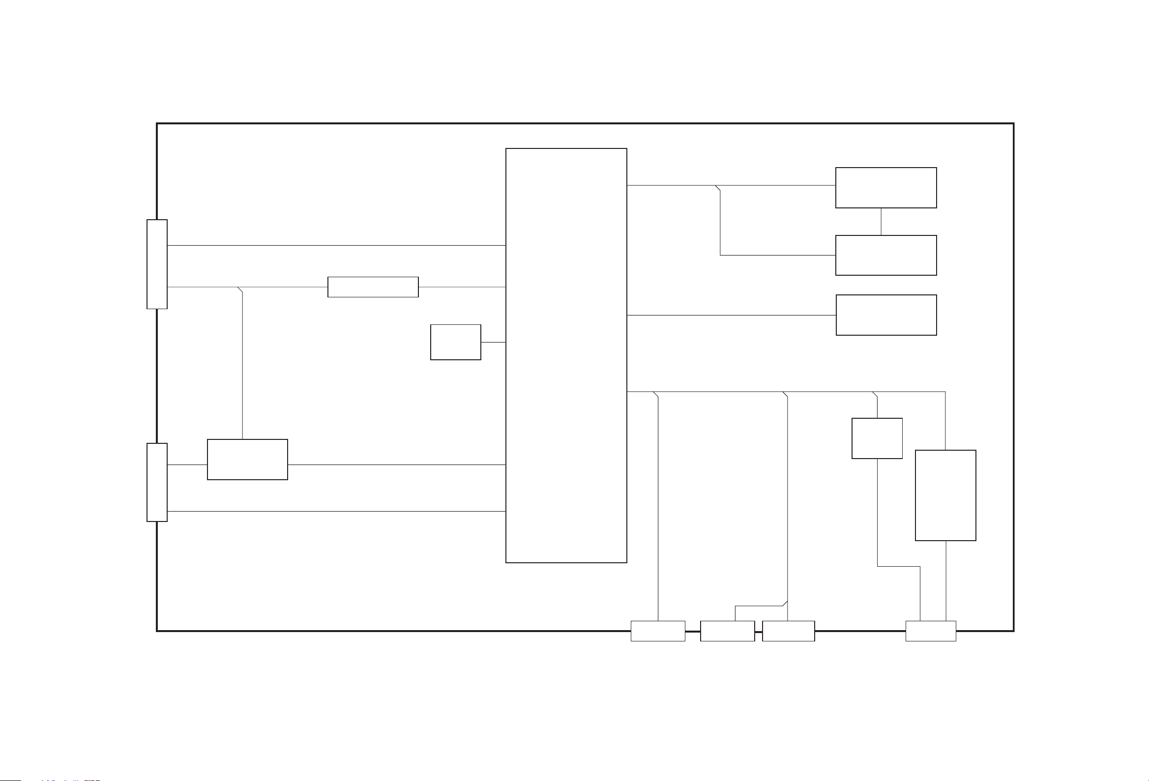
Block diagram
EXADT0 to 15, EXADR16 to 20
NEXCE, NEXOE, NEXWE
IC509
FLASH ROM
LADD0 to 15
DVD traverse
mechanism
DVD traverse
mechanism
A, B, C, D, E, F, RF+, PD(CD), PD(DVD)
CN101
LD(CD), LD(DVD)
FM+/WOUT
VOUT
UOUT
COM
CN201
F+/T+/-
IC201
DRVER
LPCO1, LPCO2
Q101 to Q104
CDLDCUR
DVDLDCUR
X351
27MHz
SPDRV, TRSDRV, FODRV, TRDRV
/DRVMUTE, /SPMUTE, FG, VHALF
TRVSW
IC301
DV2.2
EXADT0 to 15
NEXCE
MA0 to 10, BA0, BA1
MDQ0 to 31, DQM0 to 3
NCSM,NRAS, NCAS, NWE
AIN, AOUT 0 to 2, BCK, LRCLK
DACPDN, DCLK, DDATA
DAC0CS, DAC1CS, DAC2CS
S2UDT
U2SDT
SCLK
SCS
CPURST
UCS
LRMUTE
SWMUTE
RX
COMPOUT
COUT
YOUT
CrOUT
CbOUT
RX
IC512, IC513
LATCH
IC505
SDRAM
IC704
ADC
AINL
AINR
IC701
to
IC703
DAC
FAOUTL
FAOUTR
RAOUTL
RAOUTR
CAOUT
SWAOUT
CN501
CN503 CN502 CN504
2-1
Page 4

Standard schematic diagrams
DVD servo section (1/2)
LPC2
TP20
C103
C104
CN101
QGF0523F1-24W
TP1
CN201
QGF1037F1-08W
TP28
TP980
DGND
TP990
R990
DGND
LPC1
TP12
TP13
TP14
TP15
TP16
TP17
TP18
TP19
C101
0.1/16
VREFH
K101
0
C102
0.1/16
E
F
C109
D
A
B
R124
C
RF+
R122
C107
0.1/16
TP4
TP3
TP2
TP24
TP25
TP26
TP27
C980
NI
0
R101
0.1/16
R102
F+
F-
T+
T-
TP8
TP9
TP7
TP6
TP5
TP10 TP11
FM+
FM-
WOUT
VOUT
UOUT
COM
TP22
TP23
TP21
0
100
K102
0
C111
1000.1/16
MGND
NI
R126
180
TP03
COM
C260
C261
NI
C263
0.1/16
M9V
C217
R256
NI
R257
TP220
R255
NI
SPDRV
CDLDCUR
NI
NI
C110
NI
NI
R121
R120
R123
0
R119
NI
D101
0.022
0.022
C262
0.022
R251
0.47
R259
0
10k
C256
0.1/16
TP221
R215
27
R113
R112
0
30k
KTA1001/Y/-X
2SC4617/R/-X
24k
R111
UN2119-X
Q105
FM+
WOUT
VOUT
UOUT
R252
2.2
6.8k
R221
R213
10k
C211
0.022
10k
R214
NI
TRSDRV
LPCO2
DVDLDCUR
C108
47/6.3
0
2.2
R114
R115
Q104
FM-
IC201
LA6502-X
0.0082
C257
C251
0.47/10
TP226
R104
470
R116
R118
30k
24k
330
R117
R103
T-
T+
F+
F-
C204
0.1/16
24k
R220
R207
47k
C206
150p
C258
C259
TP231
0.015/16
0.015/16
R205
NI
R254
FG
FODRV
R105
KTA1001/Y/-X
27k
27
Q101Q103
C264
C205
270p
R206
30k
/SPMUTE
/DRVMUTE
C106
R106
2SC4617/R/-X
NI
R219
18k
MDQ6
DQM1
C307
0.1/16
LPCO1
S5V
1
R125
47/6.3
0
470
2.2
R110
R108
R107
100100
Q102
R109
M5V
R204
27k
R208
TP227
1/6.3
C371
TP09
NI
R201
VHALF
33k
R127
AD4
R128
C105
470
16k
47/6.3
/HFMON
TRVSW
TP310
TRDRV
NI
R384
1k
1k
R385
UCS
MDQ9
MDQ5
MDQ10
MDQ4
MDQ11
MDQ3
MDQ12
MDQ2
MDQ13
MDQ1
MDQ14
MDQ0
MDQ15
C328
0.1/16
EXADR20
NEXWE
EXADT0
EXADT4
EXADT8
EXADT12
EXADR16
EXADR18
EXADT14
EXADT10
C300
0.1/16
EXADT6
EXADT2
NEXCE
EXADT1
EXADT5
EXADT9
EXADT13
EXADR17
C329
EXADR19
0.1/16
EXADT15
EXADT11
EXADT7
EXADT3
NEXOE
R/B
SDMODE
DAC0CS
TP0
DCLK
DDATA
DACPDN
/FL_RST
NI
R419
330
R368
R356
330
R355
330
R369
330
100
100
/TALK
TP304
R353
R354
C308
0.1/16
100k
R309
C310
1/6.3
S2UDT
U2SDT
SCLK
SCS
SWMUTE
LRMUTE
R458
1k
C455
0.01/16
R320
NI
R381
R457
DQM0
10k
R452
CPURST
FG
0
IC453
NCAS
R372
10k
1k
SPDRV
TRSDRV
S-80830CNNB-G-W
NRAS
27
R303
TP327
HAGUP
22k
R308
10k
R373
C351
0.01/16
C352
0.015/16
NWE
MDQ7
MDQ8
BA0
BA1
/SPMUTE
C306
0.1/16
NI
R383
/DRVMUTE
NI
NI
NI
NI
NI
NI
NI
NI
NI
NI
R417
SDCMD
MA10
IC301
MN2DS0004AA-H
C309
0.1/16
NININI
R416
SDCLK
R415
R418
SDWP
SDCD
C331
0
R399
0
R314
NININI
NI
R414
R413
R412
R411
SDDATA1
SDDATA2
SDDATA3
SDDATA4
NCSM
TP328
TP329
/HFMON
TRVSW
R429
R428
R421
R422
R423
R424
R425
R426
R427
0.033/16
DQM2
DQM3
TP315
C337
C333
C332
0.1/16
0.018/16
0.1/16
0.1/16
C334
C330
C338
0.0056
C335
0.1/16
0
R313
MDQ16
0.1/16
MDQ29
MDQ18
MDQ30
MDQ17
MDQ31
TP314
0.1/16
0.1/16
0.1/16
C320
C321
C348
C350
0.1/16
150
R363
RF+
MDQ27
MDQ21
MDQ26
MDQ22
MDQ25
MDQ20
MDQ28
MDQ19
C305
0.1/16
0.1/16
0.1/16
0.1/16
0.1/16
0.1/16
C322
C323
C319
C347
C314
C349
0.1/16
0
R312
LPCO2
VREFH
LPC2
LPCO1
LPC1
MDQ23
VHALF
MDQ24
IC302
LM1117MP-ADJ-X
P3.3V
D1.2V
R301
NI
R302
C303
NAX0550-001X
680
1M
R345
220
R316
C318
20k
22k
C354
TH301
47/4
330
330
330
NI
330
TX
220
AOUT0
220
AOUT1
220
AOUT2
AIN
220
BCK
220
LRCLK
100
RX
C325
18p
X351
15p
C326
PCMCLK
R315
0
DAC5OUT
R343
DAC4OUT
0
6.8
R341
3.6k
DAC3OUT
DAC2OUT
R317
0
DAC1OUT
FODRV
TRDRV
C353
560p
560p
AD4
DVDLDCUR
R319
CDLDCUR
A
B
C
D
E
F
R392
TP305
S3.3V
NQR0502-001X
C301
C302
47/4
TP325
TP320
TP319
TP317
C315
0.1/16
C311
0.1/16
C341
R340
C356
C316
000
R393
R394
1/6.3
1/6.3
C340
C324
DGND
R330
R331
R332
R333
R307
1k
R306
1k
R362
R357
R360
R359
R358
R367
R562
NI
R351
R366
R352
0.1/16
C313
C339
0.1/16
1/10
R342
C327
C317
R334
R335
R336
R337
R338
R339
C391
2.2k 0.1/16
C312
0.1/16
R347
R346
NI
R395
4.7k
0.1/16
150
150
150
150
0
0
0.1/16
NAD0025-103X
30k
1/16
0.1/16
D2V
24
C304
1/6.3
ADCRST
DAC1CS
DAC2CS
DEMP
TP316
TP318
DGND
0
10k
K352
220/4
NI
CN301
MA3
MA4
MA2
MA5
MA1
MA6
MA0
MA7
MA8
MA9
MCK
2-2
Page 5

DVD servo section (2/2)
IC509
AT49BV322AT70TI
LADD15
LADD14
LADD13
LADD12
LADD11
LADD10
LADD9
LADD8
EXADR19
EXADR20
NEXWE
/FL_RST
0
R533
10k
R534
R/B
NI
R535
EXADR18
EXADR17
LADD7
LADD6
LADD5
LADD4
LADD3
LADD2
LADD1
LADD0
IC508
NI
R502
IC507
NI
C552
0.1/16
IC512
EXADR16
10k
R531
C554
EXADT15
EXADT0
0.1/16
EXADT7
EXADT1
EXADT14 MDQ3
EXADT13
EXADT2
EXADT5
EXADT3
EXADT12
EXADT4
EXADT11
EXADT3
EXADT10
EXADT2
EXADT9
EXADT1
EXADT8
EXADT0
EXADT8
EXADT9
EXADT10
EXADT11
0
R501
NEXCE
NEXOE
NI
C559
0
10k
R530
NEXCE
LADD0
LADD1
LADD2
LADD3
LADD8
LADD9
LADD10
LADD11
SN74LVC373APW-X
0.1/16
C553
IC513
SN74LVC373APW-X
LADD7
EXADT7
EXADT6
LADD6
LADD5
EXADT5
EXADT4
LADD4
NEXCE
LADD15
EXADT15
EXADT14
LADD14
LADD13
EXADT13
EXADT12
LADD12
NEXCE
MDQ0
MDQ1
MDQ2
MDQ4EXADT6
MDQ5
MDQ6
MDQ7
DQM0
NWE
NCAS
NRAS
NCSM
BA0
BA1
MA10
MA0
MA1
MA2
DQM2
MDQ16
MDQ17
MDQ18
MDQ19
MDQ20
MDQ21
MDQ22
SDCLK
IC711
IC505
K4S643232F-TC60
0.1/16
C551
C555
0.1/16
MDQ15
MDQ14
MDQ13
MDQ12
MDQ11
MDQ10
MDQ9
MDQ8
C557
0.1/16
DQM1
MCK
MA9
MA8
MA7
MA6
MA5
MA4
MA3
DQM3
MDQ31
MDQ30
MDQ29
MDQ28
MDQ27
C556
1/10
MDQ26
MDQ25
MDQ24MDQ23
C558
47/4
PCMCLK
AIN
BCK
LRCLK
ADCRST
IC707
IC706
NI
NI
K757
K710
K766
K767
P3.3V
DGND
NI
NI
NI
NQR0129-002X
K350
NQR0502-001X
S3.3V
IC305
MM1563DF-X
C381
2.2/10
470p
C382
TP02
NI
C751
NI
NI
R755
NI
K752
R751
R759
K759
NI
NI
K758
NI NI
R758
R711
TP753
R716
220
NI
C761
NI
0.1/16
R754
R761
NI
CN505
TP751
TP752
C743
2.2/16
R745
10k
C742
2.2/16
10k
R388
1/16
C380
4.7
4.7
R743
R744
IC704
CS5342-CZZ-X
C748
2.2/16
C749
2.2/16
R749
5.1
R742
47k
R793
NI
R792
NI
R715
R714
NI
NI
C741
2.2/16
C714
C715
NI
C793
NI
C791
220
220
TP01
SDMODE
K591
SDCD
K592
SDWP
R794
NI
NI
C794
K593
SDCMD
K594
NI
K595
SDDATA4
K596
SDDATA3
K597
SDDATA2
K598
SDDATA1
K599
CPURST
S2UDT
U2SDT
SCLK
SCS
UCS
LRMUTE
SWMUTE
DAC5OUT
DAC4OUT
DAC3OUT
DGND
DAC2OUT
DAC1OUT
RX
K555
TX
NQR0022-005X
S3.3V
TP97
TP95
TP96
TP94
TP93
TP92
TP91
TP99
TP98
K791
NI
NI
NI
NI
NI
NI
NI
NI
NI
DGND
TP38
K561
NI
K562
NI
K563
NI
K564
NI
NI
K565
K566
NI
K567
NI
NI
K568
TP46
NQR0129-002X
K552
K556
NQR0129-002X
NQR0129-002X
K553
NQR0129-002X
K554
NQR0129-002X
K551
S5V D2V
M9V
M5V
TP56TP76
TP90
NI
CN511
TP37
TP32
TP35
TP31
TP34
TP33
QGF1016F2-08W
CN501
TP41
TP42
TP44
TP45
TP43
QGF1016F2-09W
CN502
TP51
TP52
TP53
TP54
TP55
MGND
TP61
TP60
TP58
TP59
K732
DAC0CS
TP57
TP74
TP75
TP73 TP36
TP71
TP72
QGF1016F2-15W QGF1016F2-17W
CN504 CN503
K729
NI
TP82
TP78
TP81
TP79
TP77
TP80
NININI
K735
K734
K736
K733
DCLK
DAC1CS
DDATA
DAC2CS
IC701
AK4384VT-X
AOUT0
DACPDN
DAC0CS
DCLK
DDATA
IC702
AK4384VT-X
AOUT1
DAC1CS
IC703
AK4384VT-X
AOUT2
DAC2CS
47k
R718
C707
0.1/16
C706
10/10
C708
0.1/16
C702
0.1/16
C705
NI
C709
0.1/16
R741
0
R701
0
C701
0.1/16
C704
47/6.3
C703
0.1/16
MM1615AN-X
IC705
1/16
C711
C712
1/16
C713
0.01/16
R731
R703
0
470
R732
R704
0
470
R705
470
R733
R706
0
470
R734
R707
0
470
R735
R708
0
470
NI
NININI
NI
NININI
K721
K723
K722
K724
K725
R728
R729
NININININI
K731
K730
DACPDN
AIN
DEMP
LRCLK
AOUT2
AOUT1
AOUT0
BCK
DGND
2-3
Page 6

Printed circuit boards
DVD servo board
K791
K594
K592 K593
R332
R333
R331
R362
C791
C551
K591
R366
R357
R330
R729
R715
C715
K595
R794
IC711
C793
C558
C302 C303
C555
IC302
R359
R360
R732
K729
R714
C714
K731 K732
K735
C741
C748
C743
R302
R731
R749
R792
R793
C794
K752
R751
C751
K724
K725
R728
K730
K733
K734
K736
X351
R301
C704
K599
K596
K759
C761
R759
C705
IC704
forward side reverse side
K597
K598
R761
R741
R701
IC505
C325
C326
R351
R352
R755 K757
IC707
C749
IC509
C557
R533
C556
C315
R345
K758
R758
K767
C706
R745
R534
IC512
C311
R358
K710
K766
C742
R716
C552
R367
C339
C313
R711
IC706
R742
R452
R530
R315
R306
R307
R340
R342
R125
R111 R112
R501
C455
R317
R319
C217
R256
R392
C312
C301
C106
R457
IC453
C204
IC508
C559
C553
IC513
R316
R341
C341
R104 R105
R127 R128
R103
K352
C318
C105
R113
C263 C264
R251
R531
R502
C322
C323
C316
C317
R334
R458
IC507
C320
C321
R339
R338
R337
R336
R335
Q101
K102
R107
C108
R252
C310
R309
C308
C554
C309
R314
R313
C350
C348
TH301
Q103
R381
R383
R395
C103
R106
C102
R424
R428
R429
R320
R372
C351
C335
C330
R312
C349
R363
C107
R115
R373
C352
R122
R102
R101
C101
R114
K101
R421
R422
R423
C109
C110
R123 R124
R119 R120 R121
CN201
R425
R414
R308
TP25
C332
C337
C338
C319
R427
R426
R415
R416
R418
R411
R412
C333
R399
C331
TP26
TP314
C347
C314
CN101
TP3
TP980
TP226
TP329
R413
TP328
C324
Q105
TP4
TP2
TP28
TP24
TP990
C334
TP27
R990
R417
D101
C104
C111
TP8
TP10
TP20
TP03
TP1
TP21
R354
TP327
TP315
C340
R126
TP5
TP19
R208
R204
R206
C980
TP304
R353
R393
TP6
TP7
TP9
TP11
TP12
TP13
TP14
TP15
TP16
TP17
TP18
TP227
C205
TP22
TP23
R219
R369
IC301
TP305
R394
C391
R109
C260
C261
C262
R356
R355
TP0
C327
Q102
Q104
IC201
R368
C356
R110
C354
R213
C256
C329
R346
R108
R117
R118
R116
R201
R419
R347
C353
C371
R385
TP09
C211
R221
TP310
C300
R343
TP318
TP316
R220
R205
C259
C258
C257
R259
R535
K350
R754
R384
TP231
R254
C251
C328
TP751
C382
CN301
C206
IC702
TP221
R718
TP220
R255 R257
TP752
C381
R207
IC703
R215
R214
TP31
TP33
TP35
TP38
IC305
C712
CN505
IC701
TP97
TP99
TP96
TP98
TP32
TP34
TP37
TP36
TP319
TP320
TP325
TP753
TP72
TP93
TP95
TP94
C306
TP42
TP41
C305
K552
TP53
TP51
TP52
TP54
TP55
TP56
TP57
TP58
TP59
TP61
TP60
TP317
C380
C713
TP01
TP71
C707
C702
C708
C709
R706
R734
R707
R735
R708
R303
C307
K561
K562
K563
K564
K565
K567
K568
K566
TP43
TP44
TP45
K556
TP02
K721
K722
IC705
K723
R703
C701
R704
R705
R733
C703
TP46
K553
R743
R744
TP73
TP74
TP75
TP76
TP77
TP78
TP79
K551
K554
R562
TP81
CN502
C304
CN503
C711
TP82
CN501
CN504
TP80
CN511
TP92
TP91
TP90
R388
K555
DVD loading switch board
2-4
Page 7

< MEMO >
Page 8

Victor Company of Japan, Limited
AV & MULTIMEDIA COMPANY AUDIO/VIDEO SYSTEMS CATEGORY 10-1,1chome,Ohwatari-machi,Maebashi-city,371-8543,Japan
(No.MB180BSCH)
Printed in Japan
WPC
 Loading...