

Page 1
SERVICE MANUAL
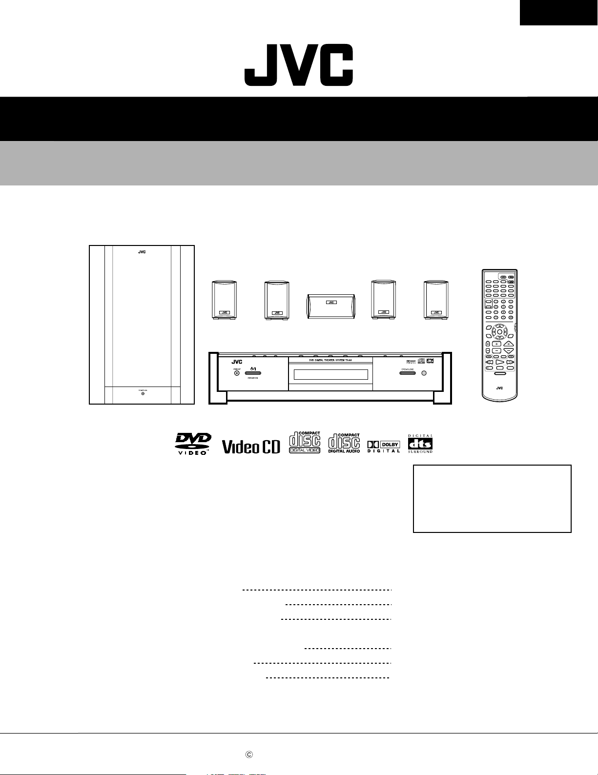
DVD DIGITAL CINEMA SYSTEM
TH-A9R
SP-XSA9
SP-XCA9
SP-XSA9
AUX
TITLE
ZOOM
CONTROL
VCR
TV
SLEEP
SETTING
TV RETURN FM MODE
PLAY
MODE
THEATER
POSITION
CHANNELTV VOL VOLUME
/REW
REC
TH-A9RTH-A9R
STANDBY/ON
AUDIOTV/CATV/DBS
VCR
DVD
FM/AM
DECODE
SUBTITLE
AUDIO
TIME
DIGEST
DISPLAY
CHOICEANGLERETURN
SOUND
SUBWOOFER
EFFECT
CENTER
TEST
REAR-L
REAR-R
100+
AUDIO/
TV/VCR
CAT/DBS
ENTER
DSP
MODE
TV/VIDEO
MUTING
F.SEARCHB.SEARCH
FF
PLAY
UPDOWN
TUNING
PAUSE
STOP
STROBEMEMORY
DVD MENU
SP-PWA9
Contents
Safety precautions
Important for laser products
Preventing static electricity
Dismantling and assembling
the treverse unit
Disassembly method
Discription of major IC's
XV-THA9R
RM-STHA9J
DVD THEATER SYSTEM
Areas suffix
B --------------------------- U.K
E ------- Continental Europe
EN -------- Northern Europe
1-2
1-3
1-4
1-5
1-6
1-20
COPYRIGHT 2001 VICTOR COMPANY OF JAPAN, LTD.
No.20944
Apr. 2001
Page 2
TH-A9R
1. This design of this product contains special hardware and many circuits and components specially for safety
purposes. For continued protection, no changes should be made to the original design unless authorized in
writing by the manufacturer. Replacement parts must be identical to those used in the original circuits. Services
should be performed by qualified personnel only.
2. Alterations of the design or circuitry of the product should not be made. Any design alterations of the product
should not be made. Any design alterations or additions will void the manufacturer`s warranty and will further
relieve the manufacture of responsibility for personal injury or property damage resulting therefrom.
3. Many electrical and mechanical parts in the products have special safety-related characteristics. These
characteristics are often not evident from visual inspection nor can the protection afforded by them necessarily
be obtained by using replacement components rated for higher voltage, wattage, etc. Replacement parts which
have these special safety characteristics are identified in the Parts List of Service Manual. Electrical
components having such features are identified by shading on the schematics and by ( ) on the Parts List in
the Service Manual. The use of a substitute replacement which does not have the same safety characteristics
as the recommended replacement parts shown in the Parts List of Service Manual may create shock, fire, or
other hazards.
4. The leads in the products are routed and dressed with ties, clamps, tubings, barriers and the like to be
separated from live parts, high temperature parts, moving parts and/or sharp edges for the prevention of
electric shock and fire hazard. When service is required, the original lead routing and dress should be
observed, and it should be confirmed that they have been returned to normal, after re-assembling.
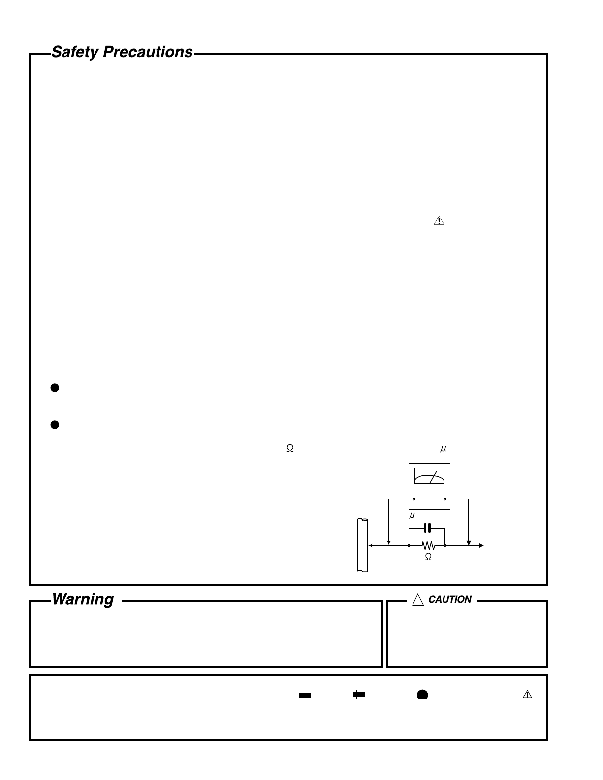
5. Leakage currnet check (Electrical shock hazard testing)
After re-assembling the product, always perform an isolation check on the exposed metal parts of the product
(antenna terminals, knobs, metal cabinet, screw heads, headphone jack, control shafts, etc.) to be sure the
product is safe to operate without danger of electrical shock.
Do not use a line isolation transformer during this check.
Plug the AC line cord directly into the AC outlet. Using a "Leakage Current Tester", measure the leakage
current from each exposed metal parts of the cabinet, particularly any exposed metal part having a return
path to the chassis, to a known good earth ground. Any leakage current must not exceed 0.5mA AC (r.m.s.).
Alternate check method
Plug the AC line cord directly into the AC outlet. Use an AC voltmeter having, 1,000 ohms per volt or more
sensitivity in the following manner. Connect a 1,500 10W resistor paralleled by a 0.15 F AC-type capacitor
between an exposed metal part and a known good earth ground.
Measure the AC voltage across the resistor with the AC
voltmeter.
Move the resistor connection to eachexposed metal part,
particularly any exposed metal part having a return path to
the chassis, and meausre the AC voltage across the resistor.
Now, reverse the plug in the AC outlet and repeat each
measurement. voltage measured Any must not exceed 0.75 V
AC (r.m.s.). This corresponds to 0.5 mA AC (r.m.s.).
0.15 F AC TYPE
1500 10W
Good earth ground
AC VOLTMETER
(Having 1000
ohms/volts,
or more sensitivity)
Place this
probe on
each exposed
metal part.
!
1. This equipment has been designed and manufactured to meet international safety standards.
2. It is the legal responsibility of the repairer to ensure that these safety standards are maintained.
3. Repairs must be made in accordance with the relevant safety standards.
4. It is essential that safety critical components are replaced by approved parts.
5. If mains voltage selector is provided, check setting for local voltage.
Burrs formed during molding may
be left over on some parts of the
chassis. Therefore, pay attention to
such burrs in the case of
preforming repair of this system.
In regard with component parts appearing on the silk-screen printed side (parts side) of the PWB diagrams, the
parts that are printed over with black such as the resistor ( ), diode ( ) and ICP ( ) or identified by the " "
mark nearby are critical for safety.
When replacing them, be sure to use the parts of the same type and rating as specified by the manufacturer.
(Except the JC version)
1-2
Page 3
Important for Laser Products
TH-A9R
1.CLASS a LASER PRODUCT
2.DANGER : Invisible laser radiation when open and inter
lock failed or defeated. Avoid direct exposure to beam.
3.CAUTION : There are no serviceable parts inside the
Laser Unit. Do not disassemble the Laser Unit. Replace
the complete Laser Unit if it malfunctions.
4.CAUTION : The compact disc player uses invisible
laserradiation and is equipped with safety switches
whichprevent emission of radiation when the drawer is
open and the safety interlocks have failed or are de
feated. It is dangerous to defeat the safety switches.
5.CAUTION : If safety switches malfunction, the laser is able
to function.
6.CAUTION : Use of controls, adjustments or performance of
procedures other than those specified herein may result in
hazardous radiation exposure.
CAUTION
!
Please use enough caution not to
see the beam directly or touch it
in case of an adjustment or operation
check.
1-3
Page 4
TH-A9R
Preventing static electricity
Electrostatic discharge (ESD), which occurs when static electricity stored in the body, fabric, etc. is discharged,
can destroy the laser diode in the traverse unit (optical pickup). Take care to prevent this when performing repairs.
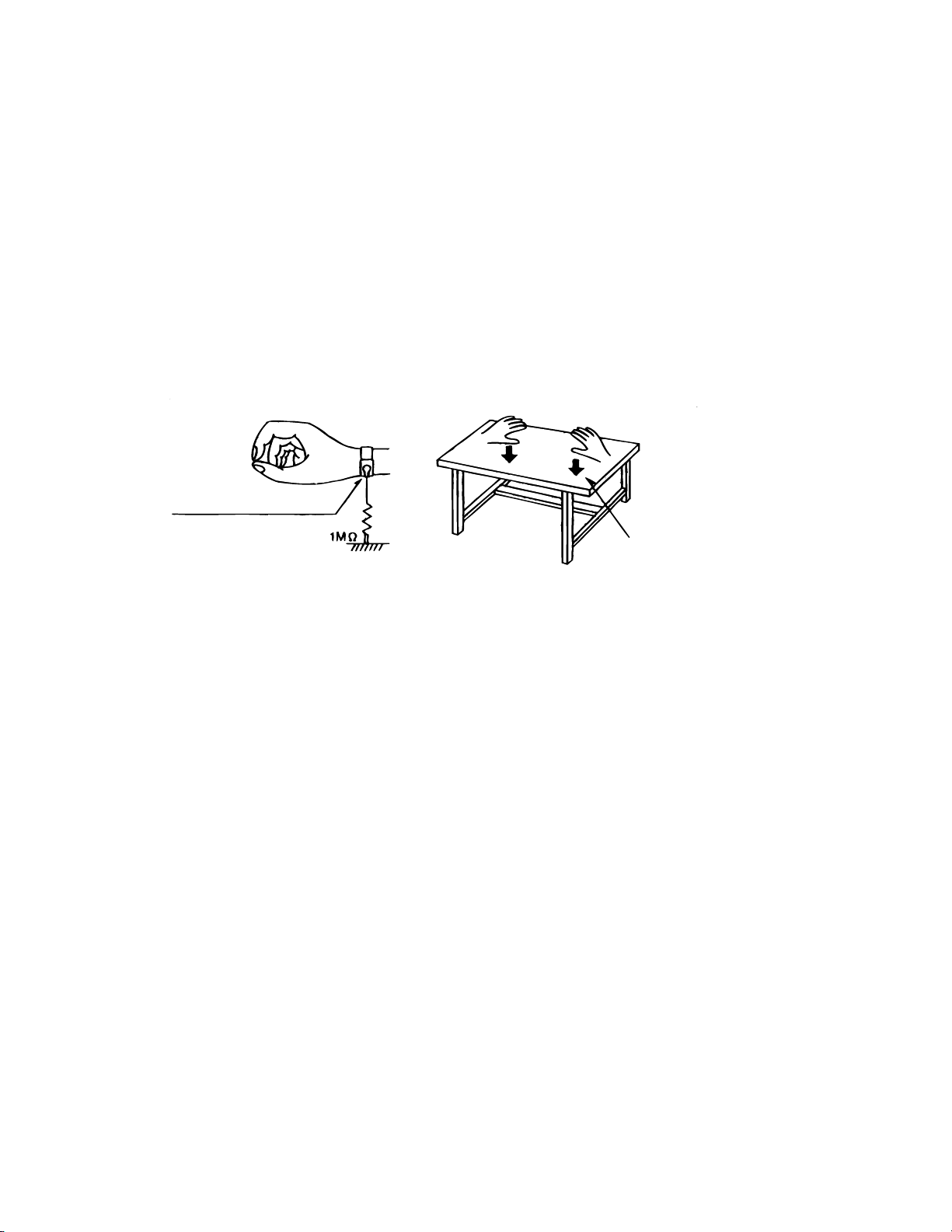
1.1. Grounding to prevent damage by static electricity
Static electricity in the work area can destroy the optical pickup (laser diode) in devices such as DVD players.
Be careful to use proper grounding in the area where repairs are being performed.
1.1.1. Ground the workbench
1. Ground the workbench by laying conductive material (such as a conductive sheet) or an iron plate over
it before placing the traverse unit (optical pickup) on it.
1.1.2. Ground yourself
1. Use an anti-static wrist strap to release any static electricity built up in your body.
(caption)
Anti-static wrist strap
Conductive material
(conductive sheet) or iron plate
1.1.3. Handling the optical pickup
1. In order to maintain quality during transport and before installation, both sides of the laser diode on the
replacement optical pickup are shorted. After replacement, return the shorted parts to their original condition.
(Refer to the text.)
2. Do not use a tester to check the condition of the laser diode in the optical pickup. The tester's internal power
source can easily destroy the laser diode.
1.2. Handling the traverse unit (optical pickup)
1. Do not subject the traverse unit (optical pickup) to strong shocks, as it is a sensitive, complex unit.
2. Cut off the shorted part of the flexible cable using nippers, etc. after replacing the optical pickup. For specific
details, refer to the replacement procedure in the text. Remove the anti-static pin when replacing the traverse
unit. Be careful not to take too long a time when attaching it to the connector.
3. Handle the flexible cable carefully as it may break when subjected to strong force.
4. It is not possible to adjust the semi-fixed resistor that adjusts the laser power. Do not turn it
1-4
Page 5

Dismantling and assembling the traverse unit
1. Notice regarding replacement of optical pickup
Electrostatic discharge (ESD), which occurs when static electricity stored in the body, fabric, etc. is discharged,
can destroy the laser diode in the traverse unit (optical pickup). Take care to prevent this when performing
repairs to the optical pickup or connected devices.
(Refer to the section regarding anti-static measures.)
1. Do not touch the area around the laser diode and actuator.
2. Do not check the laser diode using a tester, as the diode may easily be destroyed.
3. It is recommended that you use a grounded soldering iron when shorting or removing the laser diode.
Recommended soldering iron: HAKKO ESD-compatible product
4. Solder the land on the optical pickup's flexible cable.
Note : Short the land after shorting the terminal on the flexible cable using a clip, etc., when using an
ungrounded soldering iron.
Note : After shorting the laser diode according to the procedure above, remove the solder according
to the text explanation.
TH-A9R
Shorting
Shorting
1-5
Page 6

TH-A9R
Disassembly method
<Main unit>
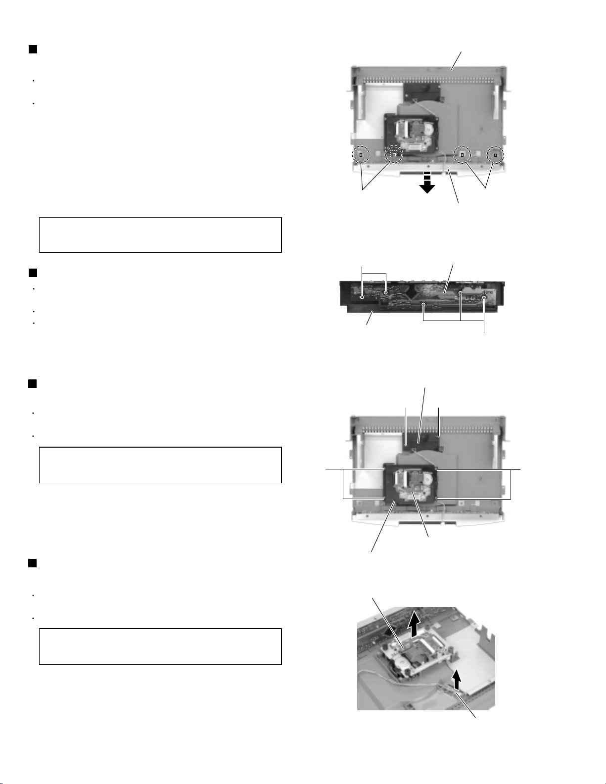
Removing the DVD door (See Fig.1)
1.
Remove the four screws A that retain the DVD door
from the top of the unit.
Removing the right and left side covers
(See Fig.2)
A
A
DVD door
Fig.1
Right side cover
Prior to performing the following procedure, remove
the DVD door.
1.
Remove the four screws (B) that attach the left and
right side covers of the unit, from the bottom panel.
2.
Remove the left and right side covers by moving
each of them in the direction of the corresponding
arrow.
B
Left side cover
B
Bottom panel
Fig.2
1-6
Page 7

TH-A9R
Removing the front panel assembly and
the DVD mechanism base
(See Figs.3 to 7)
Prior to performing the following procedure, remove the
left and right side covers.
Also remove the DVD door.
(Note)
The mechanism slide switch for pickup protection
should be set to the SHORTED position.
1.
Remove the three screws (C) that retain the front
panel assembly, from the bottom panel of the unit.
2.
Remove four screws (D) that retain the DVD mechanism
base, from the top of the unit.
3.
Remove the three screws (E) from the rear panel of
the unit that retain the DVD mechanism base.
4.
Remove the DVD mechanism together with the front
panel assembly by lifting them upward from the
main unit and moving them toward the front.
5.
Disconnect the card wire of the DVD mechanism
from the connector CN101 on the DVD servo board.
Disconnect the wire of the LED board from the
connector CN812 on the analog input/output board.
Remove the front panel assembly and the
DVD mechanism together, just as they were
assembled.
C
Bottom panel
Front panel assembly
Fig.3
DVD mechanism base
DD
Front panel assembly
Fig.4
Front panel assembly
DVD mechanism base
E
DVD servo board
CN101
DVD mechanism assembly
Analog I/O board
Fig.7
CN812
LED board
E
Front panel assembly
DVD servo board
CN101
Fig.6
Rear panel
Fig.5
E
DVD mechanism base
Analog I/O board
CN812
1-7
Page 8
TH-A9R
Separating the front panel assembly and
the DVD mechanism base (See Fig.8)
Prior to performing the following procedure, remove the
left and right side covers.
Also remove the DVD door.
1.
Remove the front panel assembly and the DVD mechanism
base together from the main unit. (See Figs. 3 to 7.)
2.
On the back of the DVD mechanism base, disengage the
four claws at the engaging points (a) that attach the front
panel assembly to the DVD mechanism base, and then
pull out the front panel assembly in the direction of the
arrow to separate it from the DVD mechanism base.
(Note)
It is at this stage that the front panel assembly
and the DVD mechanism base are separated
from each other.
Removing the display board (See Fig.9)
Prior to performing the following procedure, remove the
left and right side covers.
Also remove the DVD door.
Also separate the front panel assembly from the DVD
mechanism base.
1.
Remove the five screws (F) that retain the display board.
Engaging points (a)
F
Front panel assembly
DVD mechanism base
Engaging points (a)
Front panel assembly
Fig.8
Display board
Fig.9
F
Removing the DVD mechanism assembly
(See Figs.10 and 11)
Prior to performing the following procedure, remove the
left and right side covers.
Also remove the DVD door.
(Note)
1.
Remove the four screws (G) from the back of the DVD
mechanism base that retain the DVD mechanism cover.
2.
Remove the DVD mechanism assembly from the DVD
mechanism base.
This work is possible even when the front
panel assembly is attached to the DVD
mechanism base.
Removing the LED board
(See Figs.10 and 11)
Prior to performing the following procedure, remove the
left and right side covers.
Also remove the DVD door.
(Note)
This work is possible even when the front
panel assembly is attached to the DVD
mechanism base.
LED board cover
G
DVD mechanism cover
DVD mechanism assembly
HH
G
DVD mechanism assembly
Fig.10
1.
Remove two screws (H) that retain the LED board
cover, from the back of the DVD mechanism base.
2.
Remove the LED board by pulling it away from the
DVD mechanism base.
1-8
Fig.11
LED board
Page 9
TH-A9R
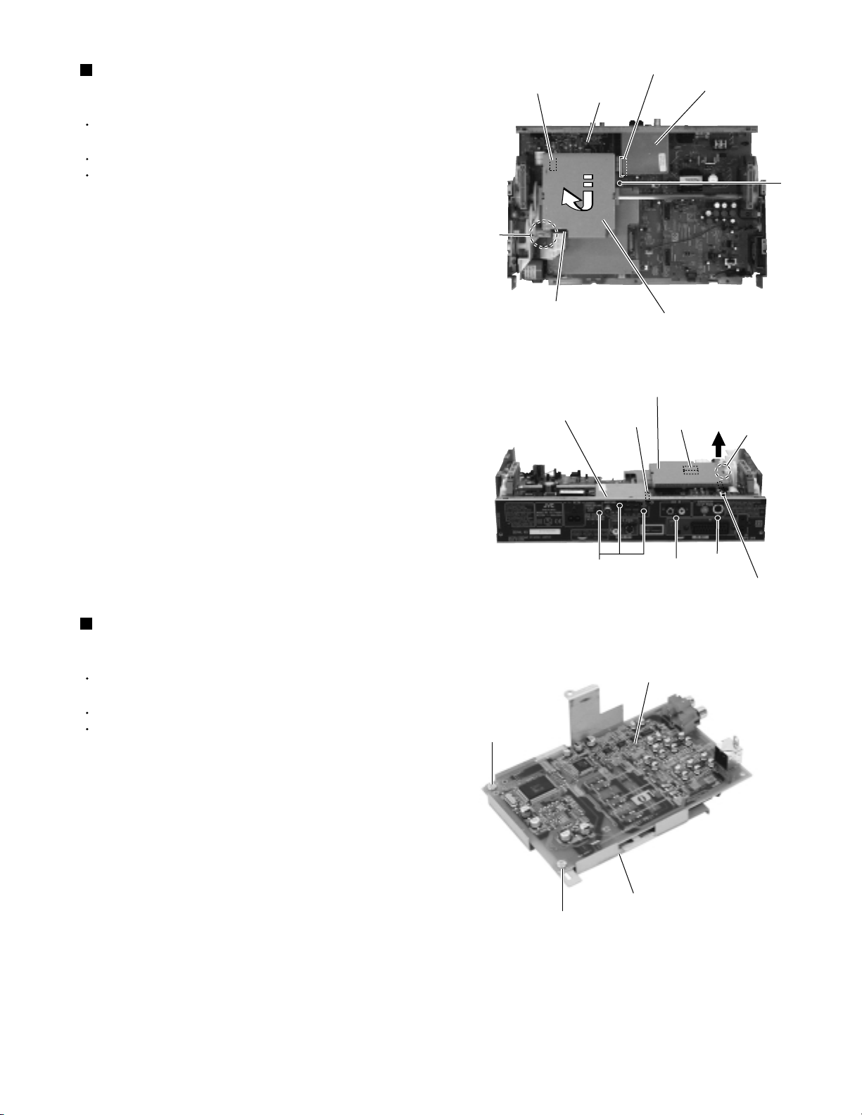
Removing the analog board
(See Figs.12 to 14)
Prior to performing the following procedure, remove
the left and right side covers.
Also remove the DVD door.
Also remove the front panel assembly and DVD
mechanism base.
1.
Disconnect the card wires from the connectors
CN401 and CN402 on the analog board.
2.
Remove the screw (I) that retains the analog board
bracket from the top of the unit.
3.
Remove the screw (J) and the screw (K) that retain
the analog board from the rear panel of the unit.
4.
Disengage the analog board bracket and the gear
motor assembly by moving the engaged part (b)
upward. Then move the analog board in the direction
of the arrow, and remove it as if pulling it out of the
rear panel.
Engaging
point (b)
Analog board
CN401
Analog board
Tuner assembly
Analog board
CN402
CN1
Tuner assembly
Analog board bracket
Fig.12
Analog board bracket
CN1
CN402
I
Engaging point (b)
5.
Remove two screws (L) that attach the analog board
to the analog board bracket.
Removing the tuner assembly
(See Figs.12 and 13)
Prior to performing the following procedure, remove
the left and right side covers.
Also remove the DVD door.
Also remove the front panel assembly and the DVD
mechanism base.
1.
Remove the three screws (M) that retain the tuner
assembly, from the rear panel of the unit.
2.
Disconnect the card wire from the connector CN1 on
the tuner assembly.
J
M
Fig.13
Analog board
K
Analog board
CN401
L
Analog board bracket
L
Fig.14
1-9
Page 10
TH-A9R
Removing the fan motor assembly
(See Figs.15 and 16)
Prior to performing the following procedure, remove the
left and right side covers.
Also remove the DVD door.
Also remove the front panel assembly and the DVD
mechanism base.
1.
Disconnect the wire from the connector CN972 on
the power supply board.
2.
Remove the two screws (N) that retain the fan motor
assembly, from the right side of the unit.
Power supply board
CN972
N
Fan motor assembly
N
Fig.15
3.
Remove the two screws (O) that attach the fan motor
assembly to the fan bracket.
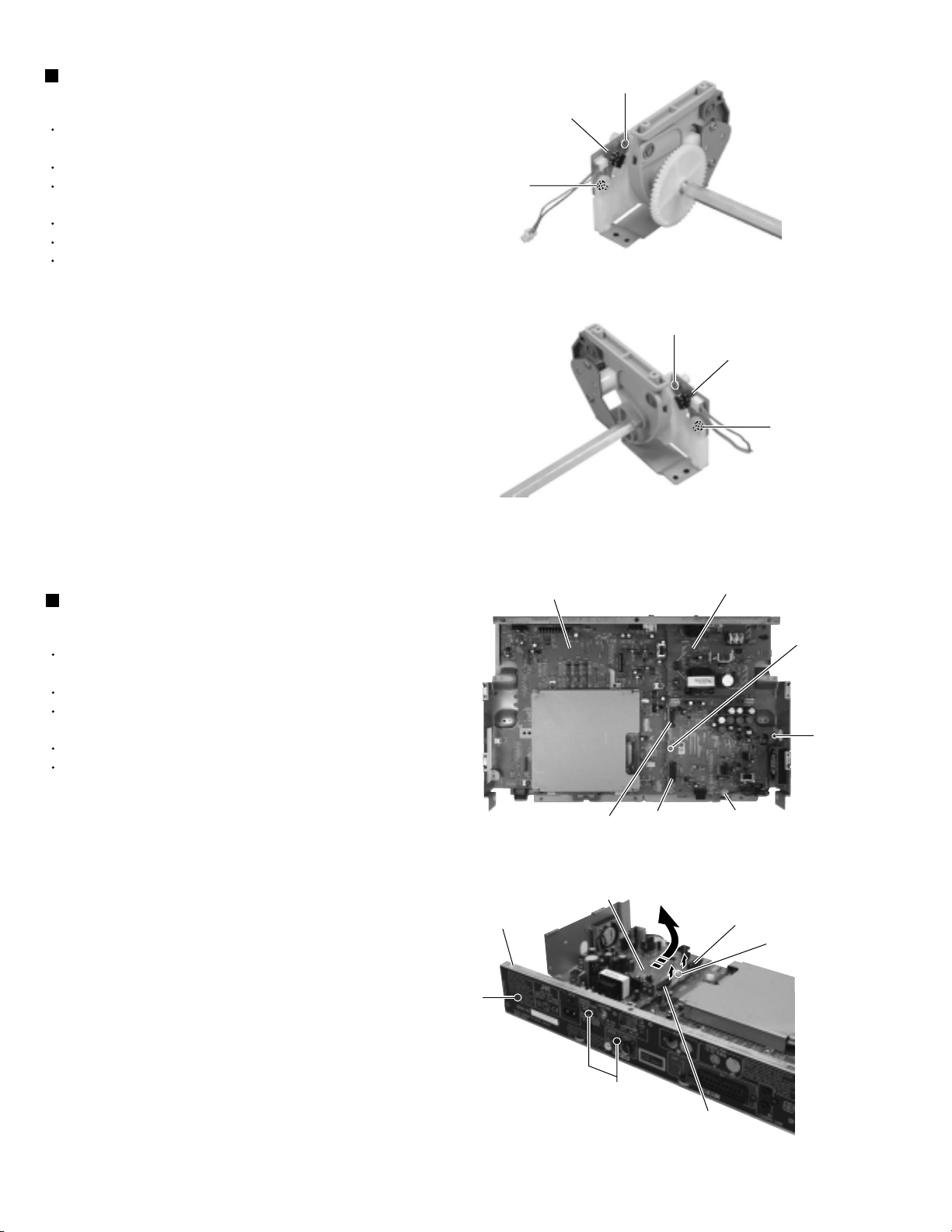
Removing the gear motor assembly
(See Figs.17 to 19)
Prior to performing the following procedure, remove the
left and right side covers.
Also remove the DVD door.
Also remove the front panel assembly and the DVD
mechanism base.
Also remove the analog board.
1.
Disconnect the wire from the connector CN106 on
the analog input/output board.
2.
Remove the two screws (P) that retain the gear
motor assembly and remove the assembly in the
direction of the arrow.
(Note)
3.
Remove the belt from the gear motor assembly.
4.
Remove two screws Q that retain the gear motor.
When reassembling, check that the gear motor
assembly is engaged properly with the door arm
assembly at the engaging points (c) and (d).
P
O
Fan motor
O
Fan bracket
Fig.16
Gear motor assembly
Analog I/O board
CN106
Fig.17
1-10
Fig.19
Belt
Gear motor
Q
Engaging
point (c)
Engaging
point (d)
P
P
Gear motor assembly
Analog I/O board
CN106
Fig.18
Page 11
Removing the door arm assembly
(See Figs.20 to 23)
Prior to performing the following procedure, remove
the left and right side covers.
Also remove the DVD door.
Also remove the front panel assembly and the DVD
mechanism base.
Also remove the analog board.
Also remove the gear motor assembly.
1.
Disconnect the wires from the connectors CN810
and CN811 on the analog input/output board.
2.
Remove the four screws (R) that retain the door arm
assembly, from the top of the unit.
3.
Remove the two screws (S) that retain the door arm
assembly, from the left and right sides of the unit.
TH-A9R
Door arm assembly
R
Analog I/O board
CN811
Fig.20
Door arm assembly
Door arm assembly
S
R
Analog I/O board
CN810
R
Analog I/O board
CN810
Power supply
board
Fig.21
Door arm assembly
S
R
Fig.23
Fig.22
1-11
Page 12
TH-A9R
Removing the door arm boards (L) and (R)
(See Figs.24 and 25)
Prior to performing the following procedure, remove
the left and right side covers.
Also remove the DVD door.
Also remove the front panel assembly and the DVD
mechanism base.
Also remove the analog board.
Also remove the gear motor assembly.
Also remove the door arm assembly.
1.
Remove the two screws (U) that retain the door arm
board (L).
2.
Remove two screws (U) that retain the door arm
board (R).
U
Door arm board (L)
U
Fig.24
U
Door arm board (R)
U
Fig.25
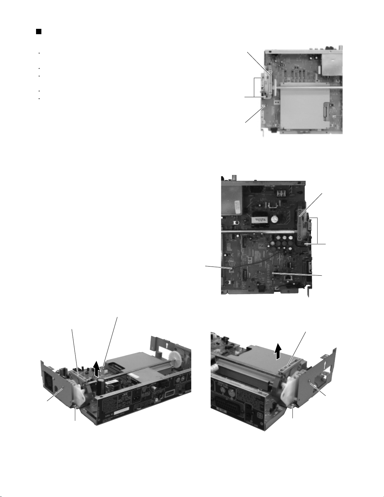
Removing the power supply board
(See Figs.26 and 27)
Prior to performing the following procedure, remove
the left and right side covers.
Also remove the DVD door.
Also remove the front panel assembly and the DVD
mechanism base.
Also remove the analog board.
Also remove the gear motor assembly.
Also remove the door arm assembly.
1.
Remove the screw (V) that retains the power supply
board, from the top of the unit.
2.
Remove three screws (W) that retain the power
supply board, from the rear panel of the unit.
3.
Pull out the power supply board from clamp a.
4.
Disconnect the wire from the connector CN972 on
the power supply board, and then remove the power
supply board in the direction of the arrow while
unplugging the connectors CN951 and CN961 from
the analog input/output board.
Rear panel
W
Analog I/O board
CN951
Power supply board
Power supply board
CN961
Fig.26
Clamp a
V
Power supply board
CN972
CN961
Clamp a
1-12
W
CN951
Fig.27
Page 13

TH-A9R
Removing the AV decoder board and
analog input/output board
(See Figs.28 to 30)
Prior to performing the following procedure, remove the
left and right side covers.
Also remove the DVD door.
Also remove the front panel assembly and DVD
mechanism base.
Also remove the analog board.
Also remove the gear motor assembly.
Also remove the door arm assembly.
1.
Remove the three screws (X) that retain the AV
decoder board cover, from the top of the unit and
remove the screw (X) that retains the analog
input/output board.
2.
IF it is required to separate the AV decoder board
from the analog input/output board, unplug the
connectors CN501, CN502 and CN503 on the AV
decoder board from the analog input/output board.
(Note)
The analog input/output board can be removed
even when it is engaged with the AV decoder
board.
Analog I/O board
X
AV decoder board cover
X
X
X
Fig.28
Analog I/O board
AV decoder board cover
X
X
3.
Remove the five screws (Y) that retain the analog
input/output board, from the rear panel of the unit.
This procedure also detaches the rear panel.
Y
Fig.29
CN503
CN501
AV decoder board
Y
CN502
CN101
X
Analog I/O board
Fig.30
1-13
Page 14

TH-A9R
Disassembly method
<Speaker>
Removing the heat sink cover (See Fig.1)
1.
Remove the four screws A attaching the heat sink
cover.
Removing the amplifier assembly and
the amplifier cover (See Figs.2 and 3)
Prior to performing the following procedure, remove
the heat sink.
1.
Remove the eigth screws B attaching the amplifier
assembly on the back of the body.
2.
Move the amplifier assembly backward and disconnect the harness from connector CN109 in the lower
part of the amplifier assembly.
Volume knob
Heat sink
cover
A
Amplifier
assembly
3.
Pull out the volume knob.
4.
Remove the ten screws C attaching the amplifier
cover.
5.
Remove the ten screws D and the one screw E attaching the amplifier cover.
Amplifier
assembly
C
C
CC
D
E
D
C
D
C
D
Amplifier
cover
B
B
Fig.1
A
Amplifier
assembly
B
1-14
D
C
D
Amplifier
cover
Amplifier
cover
C
CC
Fig.2Fig.3
B
Page 15

Removing the preamplifier board
(See Figs.4 to 6)
Prior to performing the following procedure, remove
the heat sink cover, the amplifier assembly and the
amplifier cover.
1.
Remove the two screws F attaching the preamplifier
board to the bracket.
2.
Disconnect connector CN101 on the preamplifier
board from the main amplifier board.
Braket
Preamplifier
board
F
F
Main amplifier board
TH-A9R
3.
Pull out the switch knob.
4.
Remove the nut and the two screws G attaching the
bracket.
Removing the power supply & SP terminal
board (See Figs.4 and 5)
Prior to performing the following procedure, remove
the heat sink cover, amplifier assembly and the
amplifier cover.
1.
Disconnect the wire from the connectors CN107 and
CN108 on the power supply & SP terminal board.
2.
Unplug the connectors CN110 and CN111 on the
power supply & SP terminal board from the main
amplifier board.
Power supply &
SP terminal
board
CN108
CN107
Preamplifier
board
Power supply &
SP terminal
board
CN108
Fig.4
CN101
Main amplifier
board
CN111
CN110
CN107
G
Switch knob
Nut
G
Braket
Fig.5
Preamplifier
board
Fig.6
CN101
1-15
Page 16

TH-A9R
Removing the Main amplifier Board
(See Figs.7 and 8)
Prior to performing the following procedure, remove the
heat sink cover, the amplifier board, the amplifier
cover, the preamplifier board and the power supply &
SP terminal board.
1.
Disconnect the harness from connector CN104 on
the main amplifier board.
2.
Remove the seven screws H and the main amplifier
board with the heat sink.
3.
Remove the two screws I attaching the power
amplifier board (A) and the two screws J attaching
the power amplifier board (B) on the underside of the
main amplifier board.
4.
Disconnect connector CN102 and CN103 on the
power amplifier board (A) and CN105 and CN106 on
the power amplifier board (B) from the main amplifier
board respectively.
Main amplifier
board
H
CN104
H
H
Power
transformer
H
Fig.7
I
J
Removing the power amplifier board (A)
(See Figs.9 and 10)
Prior to performing the following procedure, remove the
heat sink cover, amplifier assembly, the amplifier cover,
the preamplifier board, the power supply & SP terminal
board, the main amplifier board.
1.
Remove the four screws K attaching the power
amplifier board (A) to the heat sink.
2.
Release the four joint hooks a bent and attached to
the outside of the power amplifier board (A).
3.
Move the power amplifier board (A) in the direction of
the arrow to release joint b and remove the power
amplifier board (A) from the bracket (A).
Joint a
CN102
CN103
Hooks
Power amplifier
board (A)
CN102
CN103
CN102
CN103
I
J
Fig.8
CN106
CN105
LK
Power amplifier
board (B)
Main amplifier
board
CN106
Heat sink
Braket (B)
Power amplifier
board (A)
1-16
Joint a
Fig.10
Joint b
Braket (A)
Braket(A)
K
Power amplifier
board (A)
K
K
Fig.9
L
CN105
Power amplifier
board (B)
L
Page 17

TH-A9R
Removing the power amplifier board (B)
(See Figs.9 and 11)
Prior to performing the following procedure, remove the
heat sink cover, the amplifier assembly, the amplifier
cover, the preamplifier board, the power supply & SP
terminal board, the main amplifier board and power
amplifier board (A).
1.
Remove the four screws L attaching the power
amplifier board (B) to the heat sink.
2.
Release the four joint hooks c bent and attached to
the outside of the power amplifier board (B).
3.
Move the power amplifier board (B) in the direction of
the arrow to release joint d and remove the power
amplifier board (B) from the bracket (B).
Removing the power transformer
(See Figs.12 and 13)
Prior to performing the following procedure, remove
the heat sink cover, the amplifier assembly, the
amplifier cover, the preamplifier board, the power
supply & SP terminal board, the main amplifier
board, the power amplifier board (A) and power
amplifier board (B).
Hooks
Braket (B)
Power supply
& SP terminal
board
Joint c
CN106
Power amplifier
board (B)
CN105
Joint d
Joint c
Fig.11
Main amplifier
board
M
1.
Disconnect the harness from connector CN104 on
the main amplifier board.
2.
Disconnect the wire from connector CN107 on the
power supply & SP terminal board.
3.
Remove the four screws M attaching the power
transformer.
Removing the AC power cord
(See Fig.12)
Prior to performing the following procedure, remove
the heat sink cover, the amplifier assembly, the
amplifier cover, the preamplifier board, the power
supply & SP terminal board, the main amplidier
board, the power amplifier board (A), the power
amplifier board (B) and power transformer.
1.
Disconnect the wire from connector CN108 on the
power supply & SP terminal board.
2.
Remove the two screws N attaching the AC power
cord.
CN104
CN108
CN107
N
Cord stopper
braket
Preamplifier
board
Power supply
& SP terminal
board
CN108
CN107
AC cord
N
Power
transformer
M
M
Fig.12
CN101
Main amplifier
board
CN111
CN110
Fig.13
1-17
Page 18

TH-A9R
Initialization of EEPROM
1.
Make sure that no disc is present on the tray.
2.
At first push the power switch to be on. Then the door slides to the position to be able to push the stop button.
After that pull AC plug out.
3.
While holding the STOP and OPEN/CLOSE keys on the main unit depressed, turn on the primary power
supply.
4.
The FL display should show "TEST JC 1".
5.
Press the ENTER key on the remote controller.
Initialization of the EEPROM starts (and lasts for about 3 seconds). The initialization has completed when the
FL display shows "EEPROM" at the center.
6.
Now the EEPROM initialization is complete.
No key is accepted during the EEPROM initialization.
To exit from the test mode, press the POWER key to enter the STAND-BY mode.
Display of the laser current value
1.
While holding the STOP and OPEN/CLOSE keys on the main unit depressed, plug the AC power cord into the
power outlet.
2.
The FL display should show "TEST".
Note:
When the power is in the STAND-BY mode or OFF, the stop key is hidden behind the door.
Therefore, to facilitate the entry in the test mode, slide the door in advance so that the STOP key can
be pressed even when the AC power is turned off by unplugging the AC power cord.
3.
Press the "5" key on the remote controller in the test mode. The DVD laser will turn on and the FL display will
show a message such as "03EXXXX". As the FL display shows a hexadecimal value, check the actual current
value by referring to the conversion table to see if it is OK or not. (The actual laser current value is calculated
by subtracting 15 mA from the value obtained with the conversion table.)
4.
To exit from the test mode, press the POWER key to enter the STAND-BY (power off) mode.
1-18
Page 19

FL Display conversion table
1.Current
TH-A9R
FL Display Current(mA)
001c,001b
001A
0019,0018
0017
0016,0015
0014,0013
0012
0011,0010
000f
000e,000d
000c,000b
000A
0009,0008
0007
0006,0005
25
26
27
28
29
30
31
32 OK
33
34
35
36
37
38
39
Evalution
OK
OK
OK
OK
OK
OK
OK
OK
OK
OK
OK
OK
OK
OK
FL Display Current(mA)
03E5
03E4,03E3
03E2
03E1,03E0
03dF,03dE,
03dd
03dc,03db
03dA
03d9,03d8
03d7,03d6
03d5
03d4,03d3
03d2
03d1,03d0
03cF,03cE
59
60 OK
61
62
63
64
65
66
67 NG
68
69
70
71
72
73
Evalution
OK
OK
OK
OK
OK
NG
NG
NG
NG
NG
NG
NG
NG
FL Display Current(mA)
03AF,03AE
03Ad
03Ac,03Ab
03AA,03A9
03A8
03A7,03A6
03A5
03A4,03A3
03A2,03A1
03A0
039F,039E
039d,039c
039b
039A,0399
0398
93
94
95
96
97
98
99
100
101
102
103
104
105
106
107
Evalution
NG
NG
NG
NG
NG
NG
NG
NG
NG
NG
NG
NG
NG
NG
NG
0004,0003 40 OK
0002 41 OK
0001,0000 42 OK
03FF
03FE,03Fd
03Fc,03Fb
03FA
03F7
03F6,03F5
03F4,03F3
03F2
03F1,03F0
03EF,03EE
03Ed
03Ec,03Eb
43
44
45
46
47 OK03F9,03F8
48
49
50
51
52 OK
53
54
55
OK
OK
OK
OK
OK
OK
OK
OK
OK
OK
OK
03cd
03cc,03cb7475
03cA,03c9
03c8
03c7,03c6
03c5
03c4,03c3
03c2,03c1
03c0
03bF,03bE
03bd
03bc,03bb
03bA,03b9
03b8
03b7,03b6
03b5
76
77
78
79
80
81
82
83
84
85
86
87
88
89
NG
NG
NG
NG
NG
NG
NG
NG
NG
NG
NG
NG
NG
NG
NG
NG
0397
108
NG
03EA
03E9,03E8
03E7,03E6
56
57
58
OK
OK
OK
03b4,03b3
03b2,03b1
03b0
90
91
92
NG
NG
NG
1-19
Page 20

TH-A9R
Discription of major IC's
AK93C65AF-X(IC403) : EEPROM
1.Terminal layout
PE
VCC
CS
SK
2.Block diagram
DI
1
2
3
4
8 pin SOP
INSTRUCTION
REGISTER
8
7
6
5
NC
GND
DO
DI
INSTRUCTION
DECODE,
CONTROL
AND
CLOCK
GENERATION
DATA
REGISTER
ADD.
BUFFERS
16
R/W AMPS
AND
AUTO ERASE
DECODER
DO
16
EEPROM
4096bit
256 x 16
CS
SK
3.Pin function
Pin No.
Symbol
1
2
3
4
5
6
7
8
PE
VCC
CS
SK
DI
DO
GND
NC
Program enable (With built-in pull up resistor)
Power supply
Chip selection
Serial clock input
Serial data input
Serial data output
Ground
No connection
Function
Note : The pull-up resistor of the PE pin is about 2.5 M Ω (VCC=5V)
VREF
VPP SW
VPP
GENERATOR
1-20
Page 21

AN8702FH (IC101) : Frontend processor
1.Pin layout
HDTYPE
VIN12
VIN11
GND1
VIN4
646362616059585756555453525150
VIN3
VIN2
VIN1
VREF1
VCC1
VIN10
VIN9
VIN8
VIN7
VIN6
TH-A9R
VIN5
49
2. Pin function
Pin No.
Symbol I/O Function
1
PC1
2
PC01
3
PC2
4
PC02
I
5
6
7
8
9
10
11
12
13
14
15
16
17
18
19
20
21
22
23
24
25
26
27
28
29
30
31
32
TGBAL
TBAL
FBAL
POFLT
DTRD
IDGT
STANDBY
SEN
SCK
STDI
RSEL
JLINE
TEN
TEOUT
ASN
ASOUT
FEN
FEOUT
VSS
TG
VDD
GND2
VREF2
VCC2
VHALF
DFLTON
DFLTOP
DSFLT
Tangential phase balance control terminal
I
Tracking balance control terminal
I
Focus balance control terminal
O
Track detection threshold value level terminal
Data slice data read signal input terminal (For RAM)
I
Data slice part address part gate signal input terminal (For RAM)
I
Standby mode control terminal
I
SEN(Sereal data input terminal)
I
SCK(Sereal data input terminal)
I
STDI(Sereal data input terminal)
I
Tracking error signal output terminal
O
Focus error output amplifier reversing input terminal
I
Focus error signal output terminal
O
Earth terminal
-
Tangential phase error signal output terminal
O
Power terminal (3V)
-
Earth terminal 2
-
VREF2 voltage output terminal
O
Power terminal (5V)
-
VHALF voltage output terminal
O
PC1
PC01
PC2
PC02
TGBAL
TBAL
FBAL
POFLT
DTRD
IDGT
STANDBY
SEN
SCK
STDI
RSEL
JLINE
1
2
3
4
5
6
7
8
9
10
11
12
13
14
15
16
171819202122232425262728293031
TEN
TEOUT
AN8702FH
FEN
ASN
ASOUT
TG
VSS
FEOUT
Pin No.
VDD
Symbol I/O Function
33
GND3
34
RFDIFO
35
RFOUT
36
VCC3
37
RFC
38
DCRF
39
OFTR
40
BDO
41
RFENV
42
BOTTOM
43
PEAK
44
AGCG
45
AGCO
46
TESTSG
47
RFINP
48
RFINN
49
VIN5
50
VIN6
51
VIN7
52
VIN8
53
VIN9
54
VIN10
55
VCC1
56
VREF1
57
VIN1
58
VIN2
59
VIN3
60
VIN4
61
GND1
62
VIN11
63
VIN12
64
HDTYPE
GND2
VCC2
VREF2
VHALF
DFLTOP
DFLTON
Earth terminal 3
-
Power terminal 3 (5V)
-
BDO output terminal
O
OFTR output terminal
O
BDO output terminal
O
RF enve output terminal
O
Bottom enve detection filter terminal
O
Peak enve detection filter terminal
O
AGC amplifier gain control terminal
O
TEST signal input terminal
I
RF signal positive moving input terminal
I
RF signal reversing input terminal
I
Focus input of external division into two terminal
I
Focus input of external division into two terminal
I
I
I
I
I
Power terminal 1
-
VREF1 voltage output terminal
O
External division into four (DVD/CD) RF input terminal 1
I
External division into four (DVD/CD) RF input terminal 2
I
External division into four (DVD/CD) RF input terminal 3
I
External division into four (DVD/CD) RF input terminal 4
I
Earth terminal 1
-
I
I
32
DSFLT
48
47
46
45
44
43
42
41
40
39
38
37
36
35
34
33
RFINN
RFINP
TESTSG
AGCO
AGCG
PEAK
BOTTOM
RFENV
BDO
OFTR
DCRF
RFC
VCC3
RFOUT
RFDIFO
GND3
AN8702FH
1-21
Page 22

TH-A9R
HY57V161610DTC8 or W981616AH-7 or K4S161622D-TC80 (IC504,IC505) : 16MB SDRAM
1.Block diagram
CLK
CKE
Address
CS
RAS
CAS
WE
Clock
Generator
Mode
register
Command decoder
Control logic
Row
address
buffer &
Refresh
counter
Column
address
buffer &
burst
counter
Bank B
Bank A
Row decoder
Sense amplifier
Column decoder
& latch circuit
Data counter
Input & output
Latch circuit
DQM
DQ
buffer
2.Pin function
Pin No. Symbol Description Pin No. Symbol Description
1
2,3
4
5,6
7
8,9
10
11,12
13
14
15
16
17
18
19,20
21~24
25
VCC
DQ0,1
VSS
DQ2,3
VDD
DQ4,5
VSS
DQ6,7
VCC
LDQM
WE
CAS
RAS
CS
A11,10
A0~3
VCC
Power supply
Data input/output
Connect to GND
Data input/output
Power supply
Data input/output
Connect to GND
Data input/output
Power supply
Lower DQ mask enable
Write enable
Column address strobe
Row address strobe
Chip enable
Address inputs
Address inputs
Power supply
26
27~32
33
34
35
36
37
38
39,40
41
42,43
44
45,46
47
48,49
50
VSS
A4~9
NC
CKE
CLK
UDQM
NC
VCC
DQ8,9
VSS
DQ10,11
VDD
DQ12,13
VSS
DQ14,15
VSS
Connect to GND
Address inputs
Non connect
Clock enable
System clock input
Upper DQ mask enable
Non connect
Power supply
Data input/output
Connect to GND
Data input/output
Power supply
Data input/output
Connect to GND
Data input/output
Connect to GND
1-22
Page 23

M56788FP-W(IC271) : Traverse mechanism driver
1.Pin layout
TH-A9R
CH3IN
OUT3
IN3-
VBS2
Vm2
N.C
GND
IN3+
VM3-
VM3+
GND
VM4+
VM4-
VM5+
VM5-
OUT5
IN5-
IN5+
IN4+
IN4-
OUT4
10
11
12
13
14
15
16
17
18
19
20
21
REG+
1
2
3
4
5
6
7
8
9
42
41
40
39
38
37
36
35
34
33
32
31
30
29
28
27
26
25
24
23
22
REGB
IN1+
VBS1
Vm1
IN1-
OUT1
VM1-
VM1+
GND
VM2+
VM2-
OUT2
GND
IN2-
IN2+
MUTE1
MUTE2
SS.GND
VREF
VERFO
2.Block diagram
Vm1
IN1+
IN1-
OUT1
VM1(+)
VM1(-)
VM2(+)
VM2(-)
OUT2
IN2-
IN2+
VREF0
VREF
REGB
REG+
VREG
VBS2
CH1
X5
CH2
X5
VBS1
VREF
E1
E2
VBS1
VBS1
VBS1
VBS1
VBS1 VBS2
R
RR
Vrefm1 Vrefm2
BIAS
Vm1 Vm2
Low, Open
MUTE ON
1~4
CH
VBS1
1.25V
VREF0
Hi:Sleep
SLEEP
5CH
TSD
Vm2
VBS2
R
E3
VBS2
CH3
X8
VBS2
CH4
X8
VBS2
E4
VBS2
CH5
X8
VBS2
E5
IN3IN3+
OUT3
CH3IN
VM3(+)
VM3(-)
VM4(+)
VM4(-)
IN4IN4+
OUT4
VM5(+)
VM5(-)
IN5IN5+
OUT5
SS.GND
MUTE1 MUTE2
GND (4PIN)
1-23
Page 24

TH-A9R
Discription of major IC's
AK93C65AF-X(IC403) : EEPROM
1.Terminal layout
PE
VCC
CS
SK
2.Block diagram
DI
1
2
3
4
8 pin SOP
INSTRUCTION
REGISTER
8
7
6
5
NC
GND
DO
DI
INSTRUCTION
DECODE,
CONTROL
AND
CLOCK
GENERATION
DATA
REGISTER
ADD.
BUFFERS
16
R/W AMPS
AND
AUTO ERASE
DECODER
DO
16
EEPROM
4096bit
256 x 16
CS
SK
3.Pin function
Pin No.
Symbol
1
2
3
4
5
6
7
8
PE
VCC
CS
SK
DI
DO
GND
NC
Program enable (With built-in pull up resistor)
Power supply
Chip selection
Serial clock input
Serial data input
Serial data output
Ground
No connection
Function
Note : The pull-up resistor of the PE pin is about 2.5 M Ω (VCC=5V)
VREF
VPP SW
VPP
GENERATOR
1-24
Page 25

MN102L25GHW1(IC401) : UNIT CPU
1. Pin layout
NMI--
SDOUT
SDIN
CPSCK
75747372717069686766656463626160595857565554535251
76
77
78
79
80
81
82
83
84
85
86
87
88
89
90
91
92
93
94
95
96
97
98
99
100
123456789
RE
CS0
CS1
WEN
WAIT
SPMUTE
2.Pin function
ADSCIRQ
ODCIRQ
DECIRQ
WAKEUP
ODCIRQ2
ADSEP
RST
VDD
TEST1
TEST2
TEST3
TEST4
TEST5
TEST6
TEST7
TEST8
VSS
D0
D1
D2
D3
D4
D5
D6
D7
U2SDT
S2UDT
SCLKO
VDD
EPDO
DPDI
EPSK
EPCS
VSS
HSSEEK
CIRCEN
MN102L25GHW
101112131415161718192021222324
A0A1A2
CS2
CS3
LSIRST
SPKICK
DRVMUTE
WORD
A3
VDD
SYSCLK
REQ
BUSY
SLEEP
XI
VSS
VDD
FEPEN
XO
VDD
ADSCEN
TRS
FGIN
25
OSCI
OSCO
MODE
50
49
48
47
46
45
44
43
42
41
40
39
38
37
36
35
34
33
32
31
30
29
28
27
26
TRVSW
HMFON
CD/DVD
/ADPD
HAGUP
TXSEL
A20
VSS
A19
A18
A17
A16
A15
A14
A13
A12
VDD
A11
A10
A9
A8
A7
A6
A5
A4
TH-A9R
Pin No. Pin No.
Symbol SymbolI/O I/OFunction Function
1
2
3
4
5
6
7
8
9
10
11
12
13
14
15
16
17
18
19
20
21
22
23
24
25
26
27
28
29
30
31
32
33
34
35
36
37
38
39
40
41
42
43
44
45
46
47
48
49
50
WAIT
RE
SPMUTE
WEN
CS0
CS1
CS2
CS3
DRVMUTE
SPKICK
LSIRST
WORD
A0
A1
A2
A3
VDD
SYSCLK
VSS
XI
XO
VDD
OSCI
OSCO
MODE
A4
A5
A6
A7
A8
A9
A10
A11
VDD
A12
A13
A14
A15
A16
A17
A18
A19
VSS
A20
TXSEL
HAGUP
/ADPD
CD/DVD
HMFON
TRVSW
Micon wait signal input
I
Read enable
O
O
Write enable
O
Non connect
O
Chip select for ODC
O
Chip select for ZIVA
O
Chip select for outer ROM
O
Driver mute
O
Non connect (Spin kick output)
O
LSI reset
O
Bus selection input
O
Address bus 0 for CPU
O
Address bus 1 for CPU
O
Address bus 2 for CPU
O
Address bus 3 for CPU
O
Power supply
System clock signal output
O
GND
Non connect (Connect to VSS)
Non connect
Power supply
Clock signal input (13.5MHz)
I
Clock signal output (13.5MHz)
O
CPU Mode selection input
I
Address bus 4 for CPU
O
Address bus 5 for CPU
O
Address bus 6 for CPU
O
Address bus 7 for CPU
O
Address bus 8 for CPU
O
Address bus 9 for CPU
O
Address bus 10 for CPU
O
Address bus 11 for CPU
O
Power supply
Address bus 12 for CPU
O
Address bus 13 for CPU
O
Address bus 14 for CPU
O
Address bus 15 for CPU
O
Address bus 16 for CPU
O
Address bus 17 for CPU
O
Address bus 18 for CPU
O
Address bus 19 for CPU
O
GND
Address bus 20 for CPU
O
TX select
O
O
O
Detection switch of traverse inside
I
51
52
53
54
55
56
57
58
59
60
61
62
63
64
65
66
67
68
69
70
71
72
73
74
75
76
77
78
79
80
81
82
83
84
85
86
87
88
89
90
91
92
93
94
95
96
97
98
99
100
FGIN
TRS
ADSCEN
VDD
FEPEN
SLEEP
BUSY
REQ
CIRCEN
HSSEEK
VSS
EPCS
EPSK
DPDI
EPDO
VDD
SCLKO
S2UDT
U2SDT
CPSCK
SDIN
SDOUT
-
NMI
ADSCIRQ
ODCIRQ
DECIRQ
WAKEUP
ODCIRQ2
ADSEP
RST
VDD
TEST1
TEST2
TEST3
TEST4
TEST5
TEST6
TEST7
TEST8
VSS
D0
D1
D2
D3
D4
D5
D6
D7
Photo input
I
Serial enable signal for ADSC
O
Power supply
Serial enable signal for FEP
O
Standby signal for FEP
O
Communication busy
I
Communication request
O
CIRC command select
O
Seek select
O
GND
Chip select signal for EEPROM
O
Clock signal for EEPROM
O
Input data for EEPROM
I
Output data for EEPROM
O
Power supply
Communication clock
I
Communication input data
I
Communication output data
O
Clock for ADSC serial
O
ADSC serial data input
I
ADSC serial data output
O
Non connect
Non connect
Non connect
Interrupt input of ADSC
I
Interrupt input of ODC
I
Interrupt input of ZIVA
I
Non connect
O
I
Address data selection input
I
Reset input
I
Power supply
Test signal 1 input
I
Test signal 2 input
I
Test signal 3 input
I
Test signal 4 input
I
Test signal 5 input
I
Test signal 6 input
I
Test signal 7 input
I
Test signal 8 input
I
GND
Data bus 0 of CPU
I/O
Data bus 1 of CPU
I/O
Data bus 2 of CPU
I/O
Data bus 3 of CPU
I/O
Data bus 4 of CPU
I/O
Data bus 5 of CPU
I/O
Data bus 6 of CPU
I/O
Data bus 7 of CPU
I/O
1-25
Page 26

TH-A9R
MN103S13BDA(IC301) : Optical disc controller
1. Pin layout
DMARQ
NIOWR
VSS
NIORD
IORDY
NDMACK
VDD
INTRQ
NIOCS16
DA1
VSS
NPDIAG
DA0
144
143
142
141
140
139
138
137
136
135
134
133
HDD15
HDD0
HDD14
VDD
HDD1
HDD13
HDD2
VSS
HDD12
VDD
HDD3
HDD11
HDD4
HDD10
VDD
HDD5
HDD9
VSS
HDD6
HDD8
HDD7
VDDH
NRESET
MASTER
NINT0
NINT1
WAITDOC
NMRST
DASPST
VDD
OSCO2
OSCI2
UATASEL
VSS
PVSSDRAM
PVDDDRAM
1
2
3
4
5
6
7
8
9
10
11
12
13
14
15
16
17
18
19
20
21
22
23
24
25
26
27
28
29
30
31
32
33
34
35
36
3738394041424344454647484950515253545556575859606162636465666768697071
132
MN103S13BDA
DA2
131
VDD
130
NCS1FX
NCS3FX
NDASP
129
128
127
NTRYCL
126
VDD
125
NEJECT
VSS
MONI0
124
123
122
MONI1
MONI2
121
120
MONI3
SDATA
119
118
SCLOCK
VDD
DAT0
117
116
115
DAT1
114
DAT2
113
DAT3
112
CHCK40
NCLDCK
SUBC
111
110
109
108
107
106
105
104
103
102
101
100
99
98
97
96
95
94
93
92
91
90
89
88
87
86
85
84
83
82
81
80
79
78
77
76
75
74
73
72
SBCK
VSS
P0
P1
PVDD
PVSS
VDD
OSCO1
OSCI1
VSS
LRCK
BLKCK
IPFLAG
DACCLK
DACLRCK
DA C DATA
NTRON
LG
JMPINH
IDHOLD
SBCK/PLLOK
CLKOUT2
VDD
NRST
MMOD
VSS
CPDET1
CPDET2
BDO
IDGT
DTRD
TEHLD
VDD
CLKOUT1
CPUDT0
CPUDT1
2.Block diagram
DVD-ROM
Formatter
CGEN
MODE
VSS
CPUADR17
CPUADR16
DATA MEMORY
CPUADR15
CPUADR14
CD-PRE
Instruction
memory
(40KB)
(6KB)
CPUADR13
CPUADR12
VDD
CPUADR11
CPUADR10
CPUADR9
CPUADR8
Formatter
CPUADR7
CPUADR6
CPUADR5
CPUADR4
i /t
High speed IO bus
VSS
CPUADR3
CPUADR2
CPUADR1
32 bit
CPU core
GCAL
CPUADR0
NCS
ECC
NWR
NRD
VDD
CPUDT7
CPUDT6
PVPPDRAM
PTESTDRAM
DRAMC
CPUDT5
PVSSDRAM
PVDDDRAM
Host i / f
MPEG i / t
DMA
BCU
VSS
CPUDT4
CPUDT3
CPUDT2
ATAPI
4Mbit
DRAM
1-26
WDT
General purpose IO bus
16 bit
timer x 2
SYSTEM i / f
INTC
Page 27

3.Pin function
TH-A9R
Pin No. Pin No.
10
11
12
13
14
15
16
17
18
19
20
21
22
23
24
25
26
27
28
29
30
31
32
33
34
35
36
37
38
39
40
41
42
43
44
45
46
47
48
49
50
51
52
53
54
55
56
57
58
59
60
61
62
63
64
65
66
67
68
69
70
71
72
Symbol SymbolI/O I/OFunction Function
1
2
3
4
5
6
7
8
9
HDD15
HDD0
HDD14
VDD
HDD1
HDD13
HDD2
VSS
HDD12
VDD
HDD3
HDD11
HDD4
HDD10
VDD
HDD5
HDD9
VSS
HDD6
HDD8
HDD7
VDDH
NRESET
MASTER
NINT0
NINT1
WAITDOC
NMRST
DASPST
VDD
OSCO2
OSCI2
UATASEL
VSS
PVSSDRAM
PVDDDRAM
CPUADR17
CPUADR18
VSS
CPUADR15
CPUADR14
CPUADR13
CPUADR12
VDD
CPUADR11
CPUADR10
CPUADR9
CPUADR8
CPUADR7
CPUADR6
CPUADR5
CPUADR4
CPUADR3
CPUADR2
CPUADR1
VSS
CPUADR0
NCS
NWR
NRD
VDD
CPUDT7
CPUDT6
PVPPDRAM
PTESTDRAM
PVDDDRAM
PVSSDRAM
CPUDT5
CPUDT4
CPUDT3
VSS
CPUDT2
I/O
ATAPI data
I/O
ATAPI data
I/O
ATAPI data
-
Power supply (3V)
I/O
ATAPI data
I/O
ATAPI data
I/O
ATAPI data
-
GND
I/O
ATAPI data
-
Power supply (2.7V)
I/O
ATAPI data
I/O
ATAPI data
I/O
ATAPI data
I/O
ATAPI data
-
Power supply (3V)
I/O
ATAPI data
I/O
ATAPI data
-
GND
I/O
ATAPI data
I/O
ATAPI data
I/O
ATAPI data
I
ATAPI reset
I/O
ATAPI master / slave selection
O
System control interruption 0
O
System control interruption 1
O
System control wait control
O
System control reset (
DASP signal initializing
I
Power supply (3V)
Not used (Connect with TP140)
O
Not used (Connect with TP303)
I
VSS connection
I
GND
VSS connection
Connect with 2.7V VDD
System control address
I
System control address
I
GND
System control address
I
System control address
I
System control address
I
System control address
I
Power supply (2.7V)
System control address
I
System control address
I
System control address
I
System control address
I
System control address
I
System control address
I
System control address
I
System control address
I
System control address
I
System control address
I
System control address
I
GND
System control address
I
System control chip selection
I
System control write
I
System control read
I
Power supply (3V)
System control data
I/O
System control data
I/O
Connect with VSS
O
Connect with VSS
I
Connect with VDD (2.7V)
Connect with VSS
System control data
I/O
System control data
I/O
System control data
I/O
GND
System control data
I/O
Connect with TP302
73
74
75
76
77
78
79
80
81
82
83
84
85
86
87
88
89
90
91
92
93
94
95
96
97
98
99
)
100
101
102
103
104
105
106
107
108
109
110
111
112
113
114
115
116
117
118
119
120
121
122
123
124
125
126
127
128
129
130
131
132
133
134
135
136
137
138
139
140
141
142
143
144
CPUDT1
CPUDT0
CLKOUT1
VDD
TEHLD
DTRD
IDGT
BDO
CPDET2
CPDET1
VSS
MMOD
NRST
VDD
CLKOUT2
SBCK/PLLOK
IDOHOLD
JMPINH
LG
NTRON
DA C DATA
DACLRCK
DACCLK
IPFLAG
BLKCK
LRCK
VSS
OSCI1
OSCO1
VDD
PVSS
PVDD
P1
P0
VSS
SBCK
SUBC
NCLDCK
CHCK40
DAT3
DAT2
DAT1
DAT0
VDD
SCLOCK
S DATA
MONI3
MONI2
MONI1
MONI0
VSS
NEJECT
VDD
NTRYCL
NDASP
NCS3FX
NCS1FX
VDD
DA2
DA0
NPDIAG
VSS
DA1
NIOCS16
INTRQ
VDD
NDMACK
IORDY
NIORD
VSS
NIOWR
DMARQ
System control data
I/O
System control data
I/O
16.9/11.2/8.45MHz clock
O
Power supply (3V)
Mirror gate (Connect with TP141)
O
Frequency control switch for data (
O
Part CAPA switch
O
RF dropout / BCA data
I
Outer side CAPA detection
I
Inner side CAPA detection
I
GND
Connect with VSS
I
System reset
I
Power supply (3V)
-
16.9MHz clock
O
Frame mark detection
O
ID gate for holding tracking
O
Jump prohibition
O
Land / group switch
O
Tracking ON
I
Serial output
O
L and R identification output
O
Clock for serial output
I
IP flag input
I
Clock for sub-code and block input
I
L and R identification signal output
I
GND
-
16.9MHz oscillation
I
16.9MHz oscillation
O
Power supply (3V)
GND
Power supply (3V)
Terminal MASTER polarity switch input
I/O
CIRC-RAM OVER/UNDER Interruption signal input
I/O
GND
Sub-code and Clock output for serial input
O
Sub-code and serial input
I
Sub-code and Frame clock input
I
Read clock to DAT3~0 (Output of dividing frequency four from ADSC
I
Read data from DISC (Parallel output from ADSC)
I
Read data from DISC (Parallel output from ADSC)
I
Read data from DISC (Parallel output from ADSC)
I
Read data from DISC (Parallel output from ADSC)
I
Power supply (3V)
Debugging serial clock (270 Ω pull up)
I/O
Debugging serial data (270 Ω pull up)
I/O
Internal goods title monitor (Connect to TP150)
O
Internal goods title monitor (Connect to TP151)
O
Internal goods title monitor (Connect to TP152)
O
Internal goods title monitor (Connect to TP153)
O
GND
Eject detection
I
Power supply (2.7V)
Tray close detection
I
ATAPI Drive active/Slave connection I/O
I/O
Not used (ATAPI host chip selection)
I
Not used (ATAPI host chip selection)
I
Power supply (3V)
ATAPI host address
I/O
Not used (ATAPI host address)
I/O
ATAPI slave/master diagnosis input
I/O
GND
Not used (ATAPI host address)
I/O
ATAPI output for selecting width of host data bus
O
ATAPI host interruption output
O
Power supply (3V)
Not used (ATAPI host DMA response)
I
ATAPI host ready output (Connect to TP157)
O
Not used (ATAPI host read)
I
GND
ATAPI host writes
I/O
ATAPI host DMA demand (Connect to TP159)
O
Connect with TP304
)
)
1-27
Page 28

TH-A9R
MN67706ZY(IC201) : ADSC
1.Pin layout
33VDD
33VSS
TEST
MINTEST
NCLDCK/JUMP
SUBC
IPFLAG
DACCLK
NTRON
DACDATA/LG
DACLRCK/JMPINH
IDHOLD
SBCK/PLLOK
BLKCK/CPDET1
LRCK/CPDET2
IDGT/TEMUTE
DTRD
25VDD
25VSS
TILTN
TILT
TILTPFGSPDRV
TRSDRV
CHCK40
DAT3
DAT2
DAT1
DAT0
33VSS
33VDD
XRESET
ENS
ENC
CPUIRQ
CPUCLK
CPUDTIN
CPUDTOUT
MONA
MONB
MONC
25VSS
25VDD
LDCUR(AD6)
TDOFS(AD5)
TG(AD4)
RFENV(AD3)
TX
NC
75747372717069686766656463626160595857565554535251
76
77
78
79
80
81
82
83
84
85
86
87
88
89
90
91
92
93
94
95
96
97
98
99
100
123456789
AS(AD2)
TE(AD1)
FE(AD0)
AVDD
MN67706ZY
101112131415161718192021222324
ARF
AVSS
NARF
IREF1
IREF2
DSLF1
TRDRV(DA0)
FODRV(DA1)
AVDD
DSLF2
PLPG
VHALF
2.Pin function
Pin No. Pin No.
1
2
3
4
5
6
7
8
9
10
11
12
13
14
15
16
17
18
19
20
21
22
23
24
25
26
27
28
29
30
31
32
33
34
35
36
37
38
39
40
41
42
43
44
45
46
47
48
49
50
Symbol SymbolI/O I/OFunction Function
AS(AD2)
TE(AD1)
FE(AD0)
AVDD
FODRV(DA1)
TRDRV(DA0)
AVSS
ARF
NARF
IREF1
IREF2
DSLF1
DSLF2
AVDD
VHALF
PLPG
PLFG
VREFH
RVI
AVSS
PLFLT1
PLFLT2
JITOUT
RFDIF
CSLFL1
VFOSHORT
AVDD
HPFIN
HPFOUT
AVSS
LPFIN
LPFOUT
CMPIN
TRCRS
VCOF
DBALO
JLINE
AVDD
LOUT
ROUT
AVSS
TGBAL
TBAL
FBAL
33VSS
33VDD
OFTR
SYSCLK
BDO
TSTSG
AS : All added signal (FEP)
I
Tracking error (FEP)
I
Focus error (FEP)
I
Power supply for analog circuit (3.3V)
Focus drive (DRVIC)
O
Tracking drive (DRVIC)
O
Ground for analog circuit
Equalized RF+(FEP)
I
Equalized RF–(FEP)
I
Reference power supply 1 for DBAL
I
Reference power supply 2 for DBAL
I
Capacitor 1 for DSL
I/O
Capacitor 2 for DSL
I/O
Power supply for analog circuit (3.3V)
Reference voltage 1.65±0.1V(FEP)
I
Not used
Not used
Reference voltage 2.2V±0.1V(FEP)
I
VREFH reference power supply for resistor
I/O
Ground for analog circuit
Capacitor 1 for PLL
O
Capacitor 2 for PLL
O
Detection signal output of jitter
I/O
Not used
I
Pull up for VHALF
I/O
VFO short output
O
Power supply for analog circuit (3.3V)
Pull up for VHALF
I
Connect woth TP208
O
Ground for analog circuit
Pull up for VHALF
I
Not used
O
Connect with TP210
I
Track crossing signal (FEP)
I
JFVCO control voltage
I/O
DSL balance adjustment output
O
J-line preset output (FEP)
O
Power supply for analog circuit (3.3V)
Connect with TP203 (
O
Connect with TP204 (
O
Ground for analog circuit
Tangential balance (FEP)
O
Tracking balance (FEP)
O
Focus balance (FEP)
O
For I/O GND
Power supply for I/O (3.3V)
Off-track error signal (FEP)
I
16.9344MHz system clock input (ODC)
I
BDO + BCA (FEP)
I
Self calibration signal (FEP)
O
analog audio L out
analog audio R out
51
52
53
54
55
56
57
58
59
60
61
62
63
64
65
66
67
68
69
70
71
72
73
74
75
76
77
78
79
80
81
82
83
84
85
86
87
88
)
89
)
90
91
92
93
94
95
96
97
98
99
100
RVI
PLFG
AVSS
VREFH
JITOUT
PLFLT1
PLFLT2
TRSDRV
SPDRV
FG
TILTP
TILT
TILTN
25VSS
25VDD
DTRD
IDGT/TEMUTE
LRCK/CPDET2
BLKCK/CPDET1
SBCK/PLLOK
IDHOLD
DACLRCK/JMPINH
DACDATA/LG
NTRON
DACCLK
IPFLAG
SUBC
NCLDCK/JUMP
MINTEST
TEST
33VSS
33VDD
CHCK40
DAT3
DAT2
DAT1
DAT0
33VSS
33VDD
TX
XRESET
ENS
ENC
CPUIRQ
CPUCLK
CPUDTIN
CPUDTOUT
MONA
MONB
MONC
NC
25VSS
25VDD
LDCUR(AD6)
TDOFS(AD5)
TG(AD4)
RFENV(AD3)
RFDIF
50
49
48
47
46
45
44
43
42
41
40
39
38
37
36
35
34
33
32
31
30
29
28
27
26
25
CSLFL1
TSTSG
BDO
SYSCLK
OFTR
33VDD
33VSS
FBAL
TBAL
TGBAL
AVSS
ROUT
LOUT
AVDD
JLINE
DBALO
VCOF
TRCRS
CMPIN
LPFOUT
LPFIN
AVSS
HPFOUT
HPFIN
AVDD
VFOSHORT
O
O
I
O
O
O
-
-
I
I
O
O
I
I
I
I
O
O
O
O
O
I
I
-
O
O
O
O
O
-
O
I
I
I
O
I
I
O
O
O
O
O
-
-
I
I
I
I
Traverse drive (DRVIC)
Spindle drive output (DRVIC)
FG signal input (spindle motor driver)
Connect with TP205
Connect with TP206
Connect with TP207
For internal core GND
Power supply for internal core (2.5V)
Data read control signal (ODC)
Pull down for GND
LR channel data strobe (ODC)/
CD sub code synchronize signal (ODC)/
CD sub-code data shift clock (ODC)/SYNC detection
Pull down for GND
1 bit DAC-LR channel data strobe (ODC)/
CD1 bit DAC channel data (ODC)
L:tracking ON (ODC)
1 bit DAC channel data shift clock (ODC)
CIRC error flag (ODC)
CD sub code (ODC)
CD sub code data frame clock (ODC)/DVD JUMP signal (ODC
Connects with DVSS (for MINTEST)
Connects with DVSS (for TEST)
For I/O GND
Power supply for I/O (3.3V)
For SRDATA clock (ODC)
SRDATA3(ODC)
SRDATA2(ODC)
SRDATA1(ODC)
SRDATA0(ODC)
For I/O GND
Power supply for I/O (3.3V)
Digital audio interface
Reset L : Reset
Servo DSC sereal I/F chip select (SYSCON)
CIRC sereal I/F chip select (SYSCON)
Interrupt request to silicon (SYSCON)
Silicon cereal I/F clock (SYSCON)
Silicon cereal I/F data input (SYSCON)
Silicon cereal I/F data output (SYSCON)
Monitor terminal A (connect with TP226)
Monitor terminal B (connect with TP225)
Monitor terminal C (connect with TP224)
Not used (connect with TP211)
For internal core GND
Power supply for internal core (2.5V)
Tangential Phase difference (FEP)
RFENV (FEP)
)
1-28
Page 29

K3N5C1000D-J007(IC402) : 1M x 16Bit/2M x 8Bit change enable ROM
TH-A9R
1.Pin layout
NC
A18
A17
A7
A6
A5
A4
A3
A2
A1
A0
CE
V
SS
OE
D0
D8
D1
D9
D2
D10
D3
D11
10
11
12
13
14
15
16
17
18
19
20
21
3.Pin function
NC
1
2
3
4
5
6
7
8
9
44
43
42
41
40
39
38
37
36
35
34
33
32
31
30
29
28
27
26
25
24
2322
A19
A8
A9
A10
A11
A12
A13
A14
A15
A16
BYTE
V
SS
D15/A-1
D7
D14
D6
D13
D5
D12
D4
V
CC
Symbol Function
D15/A-1 Address input (For 8bit output)
A0~A19 Address input
D0~D15 Data output
CE
OE
BYTE
, V
V
CC
SS
NC No connection
Chip enable
Chip enable
Output 16/8bit select
L : 8bit output + H : 16bit output
Power supply
2.Block diagram
44 pin SOP
VCCV
A0
A1
A2
A3
A4
A5
A6
A7
A8
A9
A10
A11
A12
A13
A14
A15
A16
A17
A18
A19
SS
Address
Buffer
A-1
Output 16/8bit switch
CE OE
CE ControlOE
X
Decoder
Y
Decoder
1,048,576–Word x16 or 2,097,152 x 8
D0
D1D2D3D4D5D6D7D8D9
BYTE
Memory Cell
Matrix
Multiplexer
Output Buffer
D10
D11
D12
D13
D14
D15
1-29
Page 30

TH-A9R
RN5RZ33BA-X(IC1, IC102) : High cycle module
1.Terminal layout
CE
54
123
GND
2.Block diagram
2
VDD
NC
VOUT
VOUT
3
CE
5
3.Pin function
Pin No. Pin name Function
Vref
Current Limit
GND
1
1
2
3
4
5
GND
DD
V
V
OUT
NC
CE
Ground terminal
Input terminal
Output terminal
No connection
Chip enable terminal
1-30
Page 31

STK404-130(IC105) : Power amp
1.Terminal layout
STK404-130
113
2.Block diagram
TH-A9R
TR7
PT1
1 2 3 4 5 6 7 8 9 10 11 12 13
GND IN1 NF GND BIAS +12V PRE-Vcc NC –Vcc +Vcc –OUT +OUT
STK402-230(IC107) : Power amp
1. Terminal layout
STK402-230
119
2.Block daiagram
PRE+Vcc
PRE–Vcc
CH1IN
CH1NF
BIAS
–Vcc
GND
4
R1
TR4
C1
TR2
TR1
1
2
TR3
D1
R2
12
5
9
13
SUB
R6
R3
R4
TR5
R5
TR6
R7
TR7
TR8
TR1 TR2
TR3
R1
C1
R2
TR4
SUB
7 6 10 14 15 16 17 19 1811
CH1–VE
CH1+VE
D1
CH2–VE
CH2+VE
R4
R5
C2
R3 R6
TR9
TR10
TR13
R8
TR12
R10
R9
TR5
TR11
TR6
R11
R12
C2
TR14
TR16
R14
TR8
C3
R13 R20
TR15
TR23
CH2IN
CH3IN
CH2NF
TR24
CH3NF
C3
R18
TR22
R19
TR21
R17
R15
TR19
R16R21
TR17
TR18
TR20
8 +Vcc
CH3–VE
CH3+VE
1-31
Page 32

TH-A9R
TC74VHC00FT-X(IC322,IC503)
:
Write timing control
1.Pin layout /Block diagram
Vcc 4B 4A 4Y 3B 3A 3Y
14 13
1
1A 1B 1Y 2A 2B 2Y GND
12
11 10 9 8
2
543
TC7WH74FU-X(IC321) : Clock buffer
1.Terminal layout
1
CK
2
D
3
Q
GND
6
7
4
8
VCC
7
PR
6
CLR
5
Q
TC7SH32FU-X(IC312)
: Timing control
1.Terminal layout
IN B
IN A
GND
1
2
3
5
4
VCC
OUT Y
TC7SH08FU-X(IC311) : Timing control
1.Terminal layout
IN B
IN A
GND
1
2
3
5
4
VCC
OUT Y
1-32
Page 33

TC7W125FU-X(IC202) : Buffer
1.Terminal layout
2.Block diagram
TH-A9R
G1
A1
Y2
GND
1
2
3
4
8
Vcc
7
C2
6
Y1
5
A2
BA15218N(IC104,IC108,IC109,IC110) : OP AMP
1.Pin layout / Block diagram
BA15218N
+
+
12
–
–
1
2
OUT1 –IN1
34
+IN1
VEE
5678
+IN2 –IN2
OUT2
Vcc
1-33
Page 34

TH-A9R
ZIVA3-PE0 (IC501) : AV Decoder
1. Terminal Description
Pin No.
10
11
12
13
14
15
16
17
18
19
20
21
22
23
24
25
26
27
28
29
30
31
32
33
34
35
36
37
38
39
40
41
42
1
2
3
4
5
6
7
8
9
Symbol
PIO0
H DATA 0
H DATA 1
H DATA 2
VDD-3.3
H DATA 3
VSS
H DATA 4
H DATA 5
H DATA 6
H DATA 7
VDD-2.5
RESET
VSS
WAIT/DTACK
INT
VDD-3.3
NC
VSS
NC
PIO11
PIO12
PIO13
PIO14
PIO15
PIO16
VDD-3.3
PIO17
VSS
PIO18
PIO19
PIO20
PIO21
PIO22
PIO23
VDD-3.3
PIO24
VSS
PIO25
VDD-2.5
PIO26
VSS
I/O Function
I/O
I/O
-
I/O
-
I/O
I
-
O
O
-
O
-
O
I/O
-
I/O
-
I/O
I/O
-
I/O
-
I/O
-
I/O
-
ZIVA3-PEO (1/5)
Programmable I/O pin, which enters input mode after resetting.
8-bit, bi-directional host data bus. Write data in decoder Code FIFO via HDATA.
The 32-bit word MSB is written first. The host reads and writes the internal register of
the decoder and local SRAM via HDATA.
3.3 V supply voltage for I/O signals.
8-bit, bi-directional host data bus. Writes data in decoder Code FIFO via HDATA.
The 32-bit word MSB is written first. The host reads and writes the internal register of
the decoder and local SRAM via HDATA.
Core logic and I/O signal grounding.
8-bit, bi-directional host data bus. Write data in decoder Code FIFO via HDATA.
The 32-bit word MSB is written first. The host reads and writes the internal register of
the decoder and local SRAM via HDATA.
2.5 V supply voltage for the core logic.
Hardware reset. An external device expresses RESET (Active Low) to execute hardware
resetting of the decoder. RESET is expressed for at least 20 ms to guarantee optimum
initialization to occur after power has stabilized.
Core logic and I/O signal grounding.
Transfer incomplete/data acknowledgement, which is an Active Low signal indicating that
transfer started by the host is not completed. WAIT is expressed after negative going edge
of CS, and expressed again when the decoder is ready for completing the transfer cycle.
As the signal for opening the drain should be pulled up from 1 V to 3.3 V, it is driven at
high speed for 10 ns before the tri-state condition is entered.
Host interrupt. As the signal for opening the drain should be pulled up from 4.7 V to 3.3 V,
it is driven at high speed for 10 ns before the tri-state condition is entered.
3.3 V supply voltage for I/O signals.
No connection.
Core logic and I/O signal grounding.
No connection.
Programmable I/O pins, which enter input mode. after resetting.
3.3 V supply voltage for I/O signals.
Programmable I/O pin, which enters input mode after resetting.
Core logic and I/O signal grounding.
Programmable I/O pin, which enters input mode after
Programmable I/O pins, which enter output mode after resetting.
3.3 V supply voltage for I/O signals.
Programmable I/O pin, which enters output mode after resetting.
Core logic and I/O signal grounding.
Programmable I/O pin, which enters output mode after resetting.
2.5 V supply voltage for the core logic.
Programmable I/O pin, which enters output mode after resetting.
Core logic and I/O signal grounding.
1-34
Page 35

Pin No.
44
45
46
47
48
49
50
51
52
53
54
55
56
57
58
59
60
61
62
63
64
65
66
67
68
69
70
71
72
73
74
75
76
77
78
79
80
81
82
83
84
85
86
87
88
89
90
91
92
93
94
95
96
97
98
Symbol I/O Function
PIO28
PIO29
I/O
Programmable I/O pins, which enter output mode after resetting.
PIO30
VDD-3.3
PIO31
VSS
NC
PIO1
MDATA15
M DATA 0
VDD-3.3
MDATA14
VSS
-
3.3 V supply voltage for I/O signals.
I/O
Programmable I/O pin, which enters output mode after resetting.
-
Core logic and I/O signal grounding.
O
No connection.
Programmable I/O pin, which enters input mode after resetting.
I/O
Memory data.
I/O
Memory data.
I/O
3.3 V supply voltage for I/O signals.
Memory data.
I/O
Core logic and I/O signal grounding.
-
M DATA 1
Memory data.
MDATA13
I/O
M DATA 2
3.3 V supply voltage for I/O signals.
VDD-3.3
MDATA12
VSS
M DATA 3
VDD-2.5
MDATA11
VSS
M DATA 4
VDD-3.3
MDATA10
VSS
Memory data.
I/O
Core logic and I/O signal grounding.
Memory data.
I/O
2.5 V supply voltage for the core logic.
Memory data.
I/O
Core logic and I/O signal grounding
Memory data.
I/O
3.3 V supply voltage for I/O signals.
Memory data.
I/O
Core logic and I/O signal grounding.
-
M DATA 5
Memory data.
M DATA 9
I/O
M DATA 6
3.3 V supply voltage for I/O signals.
VDD-3.3
M DATA 8
VSS
M DATA 7
LDQM
UDQM
VDD-3.3
MWE
Memory data.
I/O
Core logic and I/O signal grounding.
Memory data.
I/O
SDRAM LDQM.
O
SDRAM UDQM.
O
3.3 V supply voltage for I/O signals.
SDRAM write enable. The decoder expresses Active Low to request write operation of the
O
SDRAM array.
Core logic and I/O signal grounding.
VSS
SD-CLK
SD-CAS
SD-RAS
VDD-3.3
SD-CS1
VSS
SD-CS0
VDD-2.5
NC
VSS
NC
VDD-3.3
MADDR9
VSS
MADDR11
SDRAM system clock.
O
Active Low, SDRAM column address.
O
Active Low, SDRAM row address.
O
3.3 V supply voltage for I/O signals.
Active Low SDRAM bank selection.
O
Core logic and I/O signal grounding.
Active Low SDRAM bank selection.
O
2.5 V supply voltage for the core logic.
No connection.
O
Core logic and I/O signal grounding.
No connection.
O
3.3 V supply voltage for I/O signals.
Memory address.
O
Core logic and I/O signal grounding.
Memory address.
O
TH-A9R
ZIVA3-PEO (2/5)
1-35
Page 36

TH-A9R
Pin No.
99
100
101
102
103
104
105
106
107
108
109
110
111
112
113
114
115
116
117
118
119
120
121
122
123
124
125
126
127
128
129
130
131
132
133
134
135
136
137
138
139
140
141
142
143
144
145
146
147
148
Symbol I/O Function
Memory address.
MADDR8
O
MADDR10
3.3 V supply voltage for I/O signals.
VDD-3.3
MADDR7
VSS
Memory address.
O
Core logic and I/O signal grounding.
-
MADDR0
Memory address.
MADDR6
O
MADDR1
3.3 V supply voltage for I/O signals.
VDD-3.3
MADDR5
VSS
Memory address.
O
Core logic and I/O signal grounding.
-
MADDR2
Memory address.
MADDR4
O
MADDR3
3.3 V supply voltage for I/O signals.
VDD-3.3
NC
VSS
NC
VDD-2.5
NC
VSS
NC
VDD-3.3
NC
VSS
NC
RESERVED
PIO2
NC
RESERVED
PIO3
VDD-3.3
RESERVED
VSS
RESERVED
PIO4
RESERVED
PIO5
V DATA 0
V DATA 1
No connection.
O
Core logic and I/O signal grounding.
No connection.
O
2.5 V supply voltage for the core logic.
No connection.
O
Core logic and I/O signal grounding.
-
No connection.
O
3.3 V supply voltage for I/O signals.
No connection.
O
Core logic and I/O signal grounding.
No connection.
O
The signal for opening the drain should be pulled up from 4.7 V to 3.3 V.
O
Programmable I/O pin. Enters input mode after resetting.
I/O
No connection.
O
Coupled with VSS or VDD-3.3.
I
Programmable I/O pin, which enters input mode after resetting
I/O
3.3 V supply voltage for I/O signals.
Coupled with VSS or VDD-3.3.
I
Core logic and I/O signal grounding.
Coupled with VSS or VDD-3.3.
I
Programmable I/O pin, which enters input mode after resetting.
I/O
Coupled with VSS or VDD-3.3.
I
Programmable I/O pin, which enters input mode after resetting.
I/O
Video data bus for byte-serial CbYCrY data in sync with VCLK. In power up, the decoder
O
does not drive VDATA. In boot-up, the decoder uses the configuration parameters for drive
or tri-state VDATA.
2.5 V supply voltage for the core logic.
VDD-2.5
V DATA 2
Video data bus for byte-serial CbYCrY data in sync with VCLK. In power up, the decoder
O
does not drive VDATA. In boot-up, the decoder uses the configuration parameters for drive
or tri-state VDATA.
Core logic and I/O signal grounding.
VSS
PIO6
V DATA 3
Programmable I/O pin, which enters input mode after resetting.
I/O
Video data bus for byte-serial CbYCrY data in sync with VCLK. In power up, the decoder
O
does not drive VDATA. In boot-up, the decoder uses the configuration parameters for drive
or tri-state VDATA.
ZIVA3-PEO (3/5)
1-36
Page 37

Pin No.
149
150
151
152
153
154
155
156
157
158
159
160
161
162
163
164
165
166
167
168
169
170
171
172
173
174
175
176
177
178
179
180
181
182
183
184
185
Symbol I/O Function
3.3 V supply voltage for I/O signals.
VDD-3.3
V DATA 4
Video data bus for byte-serial CbYCrY data.
O
In power up, the decoder does not drive VDATA. In boot-up, the decoder uses the operation
configuration parameters or tri-state VDATA.
Core logic and I/O signal grounding.
VSS
V DATA 5
Video data bus for byte-serial CbYCrY data.
O
In power up, the decoder does not drive VDATA. In boot-up, the decoder uses the operation
configuration parameters or tri-state VDATA.
Programmable I/O pin, which enters input mode after resetting.
PIO7
V DATA 6
V DATA 7
I/O
Video data bus for byte-serial CbYCrY data.
O
In power up, the decoder does not drive VDATA.
In boot-up, the decoder uses the operation configuration parameters or tri-state VDATA.
Programmable I/O pin, which enters input mode after resetting.
PIO8
HSYNC
I/O
Horizontal sync. After the negative-going edge of VSYNC, the decoder starts pixel data
I/O
output for the new horizontal line.
Vertical sync, which is bi-directional. After the negative-going edge of VSYNC, the decoder
VSYNC
I/O
outputs the highest border of the new field for the first SYNC. VSYNC can receive either V
sync or upper/lower field notification from an external source.
ICE-1937 bitstream output or IEO-958 format PCM data output.
DA-IEC
VDD-3.3
DA-DATA0
VSS
DA-DATA1
DA-DATA2
O
3.3 V supply voltage for I/O signals.
PCM data output in 8 channels. Serial audio sample relative to the DA-BCK clock.
O
Core logic and I/O signal grounding.
PCM data output in 8 channels.
O
Serial audio sample relative to the DA-BCK clock.
DA-DATA3
PCM left/right clock. Identifies the channel for each audio sample. The polarity is
DA-LRCK
O
programmable.
PCM bit clock. Obtained by dividing DA-XCK by 8. DA-BCK takes a value of 48 or 32 times
DA-BCK
O
the sampling clock.
2.5 V supply voltage for the core logic.
VDD-2.5
DA-XCK
Audio master frequency clock, which is used to generate DA-BCK and DALRCK. DA-XCK
I/O
takes a value of 384 or 256 times the sampling frequency.
Core logic and I/O signal grounding.
VSS
DAI-DATA
DAI-LRCK
DAI-BCK
PIO9
CLKSEL
A-VDD
VCLK
SYSCLK
PCM input data with 2 channels. Serial audio sample relative to the DA-BCK clock.
I
PCM input left/right clock.
I
PCM input bit clock.
I
Programmable I/O pin, which enters input mode after resetting.
I/O
Input selection: Internal = VDD. External = VSS.
I
3.3 V analog supply voltage.
Video clock. Data is recorded at input.
I
System clock. The decoder requires an external 27 MHz TTL oscillator. Same drive
I
frequency as the VCK of 27 MHz.
Analog grounding of the PLL.
A-VSS
DVD-DATA0
/
CD-DATA
VDD-3.3
DVD-DATA1
/
CD-LRCK
VSS
DVD-DATA2
/
CD-BCK
DVD-DATA3
/
CD-C2PO
Serial CD data. This pin is also used as a DVD compression data pin DVD-DATA0.
I
3.3 V supply voltage for I/O signals.
16-bit word sync with programmable polarity for the decoder (right channel High).
I
This pin is also used as a DVD compression data pin DVD-DATA1.
Core logic and I/O signal grounding.
CD bit clock. The decoder accepts multiple BCK rates. This pin is also used as a DVD
I
compression data pin DVD-DATA2.
Performs High expression by indicating the damaged byte. The decoder holds the effective
I
pixels in the last image until the next effective image is decoded.
DVD compression data pin DVD-DATA3.
TH-A9R
ZIVA3-PEO (4/5)
1-37
Page 38

TH-A9R
Pin No.
186
187
188
189
190
191
192
193
194
195
196
197
198
199
200
201
202
203
204
205
206
207
208
Symbol I/O Function
DVD-DATA7
/CDG-SCLK
DVD-DATA6
/CDG-SOS1
DVD-DATA5
/CDG-VFSY
DVD-DATA4
/CDG-SDATA
PIO10
VREQUEST
I
DVD parallel compression data from the DVD DSP. When the DVD DSP transmits a 32-bit
word, it should first describe the WSB.
CDG-SDTA: CD+G (subcode) data, which indicates a serial subcode data input.
CDG-VSFY: CD+G (subcode) frame sync, which indicates the start of a frame or a
composite sync input.
CDG-SOS1: CD+G (subcode) block sync, which indicates a block start sync input.
CDG-SCLK: CD+G (subcode) clock, which indicates the input or output of the subcode
data clock.
I/O
Programmable I/O pin, which enters the input mode after resetting.
O
Video request. The decoder expresses VREQUEST to indicate that the video input buffer
has available space. The polarity is programmable.
VSTROBE
I
Video strobe, which is a programmable, dual-mode pulse and either async or sync. In the
async mode, the external source sends VSTROBE to indicate that it is ready for data
transfer. In the sync mode, the signal becomes the VSTROBE clock data.
VDD-3.3
NC
VSS
V-DACK
-
3.3 V supply voltage for I/O signals.
O
No connection.
-
Core logic and I/O signal grounding.
I
Video data acknowledgement in the case of the sync mode. Expressed when the DVD data
is valid. The polarity is programmable.
VDD-2.5
RESERVED
VSS
ERROR
HOST8SEL
HADDR0
HADDR1
-
2.5 V supply voltage for the core logic.
I
Coupled with VSS or VDD-3.3.
-
Core logic and I/O signal grounding.
I
Input data error. If the ERROR signal from the DSP is unusable, grounding should be performed.
I
Permanently coupled with VDD-3.3.
Host address bus. This 3-bit address bus selects one of the six hosts interface registers.
I
HADDR2
DTACKSEL
I
Coupled with High to select the WAIT signal or with Low to select the DTACK signal.
(Motorola 68K mode)
CS
I
Host chip selection. The host expresses CS to select the decoder for use in read/write.
The read or write operation starts at the negative-going edge of this signal.
R/W
I
Performs strobe read/write in the M mode and strobe write in the I mode. The host expresses
R/W LOW to select write or LOW to select read.
RD
I
Performs strobe read in the I mode. Should be kept HIGH in the M mode.
ZIVA3-PEO (5/5)
1-38
Page 39

VICTOR COMPANY OF JAPAN, LIMITED
AUDIO & COMMUNICATION BUSINESS DIVISION
PERSONAL & MOBILE NETWORK B.U. 10-1,1Chome,Ohwatari-machi,maebashi-city,371-8543,Japan
No.20944
Printed in Japan
200104(S)
 Loading...