

Page 1
21189200302
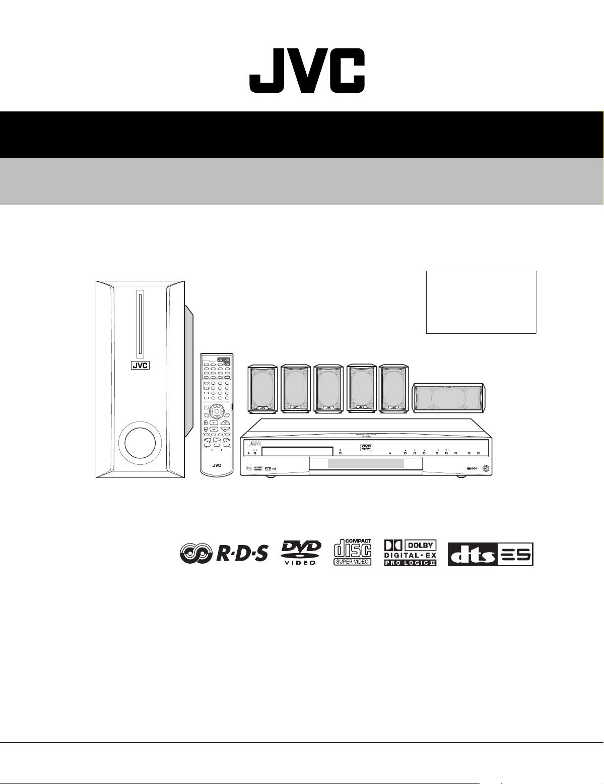
TH-A75R
SERVICE MANUAL
DVD DIGITAL CINEMA SYSTEM
TH-A75R
Area Suffix
B ---------------------- U.K.
E ---- Continentl Europe
EN --- Northern Europe
EV ----- Eastern Europe
SP-XSA75 and SP-XCA75
DVD DIGITAL CINEMA SYSTEM
XV-THA75R
RGB
VOLUME
SOURCE
PHONES
SP-WA75
VIDEO/
FM/AM
TV SOUND
AUDIO
ANGLE
TOP MENU
MENU
DSP
SURROUND
CONTROL
VCR
123
+
S.WFR
Ð
TV
456
SLEEP
789
+
SURR-L
SETTING
Ð
10
TV RETURN
ADJUST
TA/NEWS/INFO
ON
SCREEN
PTY PTY
ENTER
CHOICE
RDS DISPLAY
CHANNEL/ZOOM
TV/VIDEO MUTING
/REW
PLAY
TUNING
DOWN UP
O.T.
STOP
REPLAY
REC
MEMORY
DIMMER
RMÐSTHA75R
DVD CINEMA SYSTEM
TV AUDIO
DVD
SUBTITLE
RETURN DIGEST
OFF
CENTER
S-BACK
0
FM MODE
PTY SEARCH
VCR 1
VCR
DECODE
SOUND
EFFECT
+
TEST
Ð
+
+
SURR-R
Ð
Ð
+10
100+
DVD
RDS
VFP
VOLUMETV VOL
FF/
PAUSE
STROBE
STANDBY
COMPACT
DIGITAL¥EX
SUPER VIDEO
PRO LOGIC
TABLE OF CONTENTS
1 Important Safety Precautions . . . . . . . . . . . . . . . . . . . . . . . . . . . . . . . . . . . . . . . . . . . . . . . . . . . . . . . . . . . 1-2
2 Disassembly method . . . . . . . . . . . . . . . . . . . . . . . . . . . . . . . . . . . . . . . . . . . . . . . . . . . . . . . . . . . . . . . . . . 1-6
3 Adjustment. . . . . . . . . . . . . . . . . . . . . . . . . . . . . . . . . . . . . . . . . . . . . . . . . . . . . . . . . . . . . . . . . . . . . . . . . . 1-16
4 Description of major ICs. . . . . . . . . . . . . . . . . . . . . . . . . . . . . . . . . . . . . . . . . . . . . . . . . . . . . . . . . . . . . . . 1-17
COPYRIGHT © 2003 VICTOR COMPANY OF JAPAN, LTD.
No.21189
2003/02
Page 2
TH-A75R
Important Safety Precautions
1.1 Safety Precautions
(1) This design of this product contains special hardware and
many circuits and components specially for safety purposes.
For continued protection, no changes should be made to the
original design unless authorized in writing by the manufacturer. Replacement parts must be identical to those
used in the original circuits. Services should be performed by qualified personnel only.
(2) Alterations of the design or circuitry of the product should
not be made. Any design alterations of the product should
not be made. Any design alterations or additions will void
the manufacturers warranty and will further relieve the
manufacture of responsibility for personal injury or property
damage resulting therefrom.
(3) Many electrical and mechanical parts in the products have
special safety-related characteristics. These characteristics are often not evident from visual inspection nor can the
protection afforded by them necessarily be obtained by using replacement components rated for higher voltage, wattage, etc. Replacement parts which have these special safety
characteristics are identified in the Parts List of Service Manual. Electrical components having such features are identified by shading on the schematics and by ( ) on the
Parts List in the Service Manual. The use of a substitute replacement which does not have the same safety characteristics as the recommended replacement parts shown in the
Parts List of Service Manual may create shock, fire, or other hazards.
(4) The leads in the products are routed and dressed with ties,
clamps, tubings, barriers and the like to be separated from
live parts, high temperature parts, moving parts and/or
sharp edges for the prevention of electric shock and fire
hazard. When service is required, the original lead routing
and dress should be observed, and it should be confirmed
that they have been returned to normal, after reassembling.
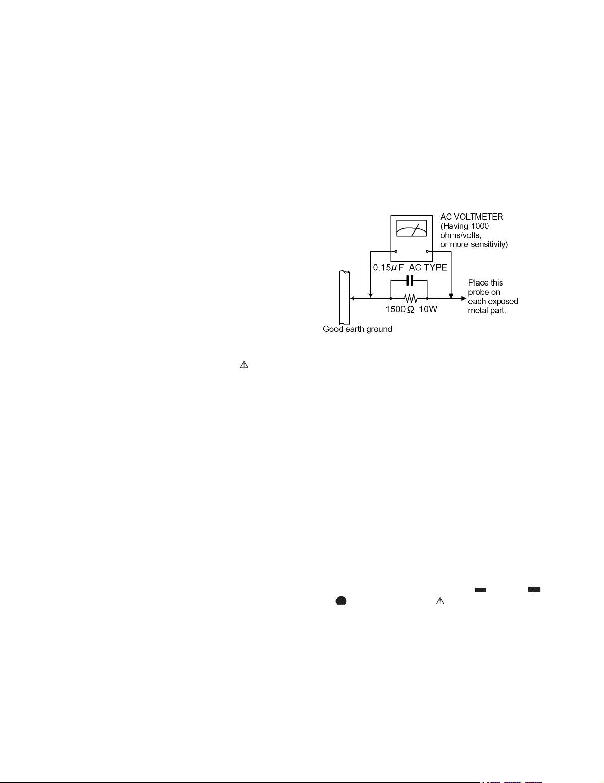
(5) Leakage shock hazard testing)
After reassembling the product, always perform an isolation
check on the exposed metal parts of the product (antenna
terminals, knobs, metal cabinet, screw heads, headphone
jack, control shafts, etc.) to be sure the product is safe to
operate without danger of electrical shock.
Do not use a line isolation transformer during this check.
• Plug the AC line cord directly into the AC outlet. Using a
"Leakage Current Tester", measure the leakage current
from each exposed metal parts of the cabinet, particularly any exposed metal part having a return path to the
chassis, to a known good earth ground. Any leakage current must not exceed 0.5mA AC (r.m.s.).
• Alternate check method
Plug the AC line cord directly into the AC outlet. Use an AC
voltmeter having, 1,000 ohms per volt or more sensitivity in
the following manner. Connect a 1,500 ohm 10W resistor
paralleled by a 0.15 µF AC-type capacitor between an
SECTION 1
exposed metal part and a known good earth ground.
Measure the AC voltage across the resistor with the AC
voltmeter.
Move the resistor connection to each exposed metal part,
particularly any exposed metal part having a return path to
the chassis, and measure the AC voltage across the resistor.
Now, reverse the plug in the AC outlet and repeat each
measurement. Voltage measured any must not exceed 0.75
V AC (r.m.s.). This corresponds to 0.5 mA AC (r.m.s.).
1.2 Warning
(1) This equipment has been designed and manufactured to
meet international safety standards.
(2) It is the legal responsibility of the repairer to ensure that
these safety standards are maintained.
(3) Repairs must be made in accordance with the relevant
safety standards.
(4) It is essential that safety critical components are replaced
by approved parts.
(5) If mains voltage selector is provided, check setting for local
voltage.
1.3 Caution
Burrs formed during molding may be left over on some parts
of the chassis.
Therefore, pay attention to such burrs in the case of preforming repair of this system.
1.4 Critical parts for safety
In regard with component parts appearing on the silk-screen
printed side (parts side) of the PWB diagrams, the parts that are
printed over with black such as the resistor ( ), diode ( )
and ICP ( ) or identified by the " " mark nearby are critical
for safety.
When replacing them, be sure to use the parts of the same type
and rating as specified by the manufacturer. (Except the JC version)
1-2 (No.21189)
Page 3

1.5 Safety Precautions (U.K only)
(1) This design of this product contains special hardware and many circuits and components specially for safety purposes. For con-
tinued protection, no changes should be made to the original design unless authorized in writing by the manufacturer. Replacement parts must be identical to those used in the original circuits.
(2) Any unauthorised design alterations or additions will void the manufacturer's guarantee; furthermore the manufacturer cannot
accept responsibility for personal injury or property damage resulting therefrom.
(3) Essential safety critical components are identified by ( ) on the Parts List and by shading on the schematics, and must never
be replaced by parts other than those listed in the manual. Please note however that many electrical and mechanical parts in
the product have special safety related characteristics. These characteristics are often not evident from visual inspection. Parts
other than specified by the manufacturer may not have the same safety characteristics as the recommended replacement parts
shown in the Parts List of the Service Manual and may create shock, fire, or other hazards.
(4) The leads in the products are routed and dressed with ties, clamps, tubings, barriers and the like to be separated from live parts,
high temperature parts, moving parts and/or sharp edges for the prevention of electric shock and fire hazard. When service is
required, the original lead routing and dress should be observed, and it should be confirmed that they have been returned to
normal, after re-assembling.
1.5.1 Warning
(1) Service should be performed by qualified personnel only.
(2) This equipment has been designed and manufactured to meet international safety standards.
(3) It is the legal responsibility of the repairer to ensure that these safety standards are maintained.
(4) Repairs must be made in accordance with the relevant safety standards.
(5) It is essential that safety critical components are replaced by approved parts.
(6) If mains voltage selector is provided, check setting for local voltage.
TH-A75R
Burrs formed during molding may be left over on some parts of the chassis. Therefore,
pay attention to such burrs in the case of preforming repair of this system.
(No.21189)1-3
Page 4
TH-A75R
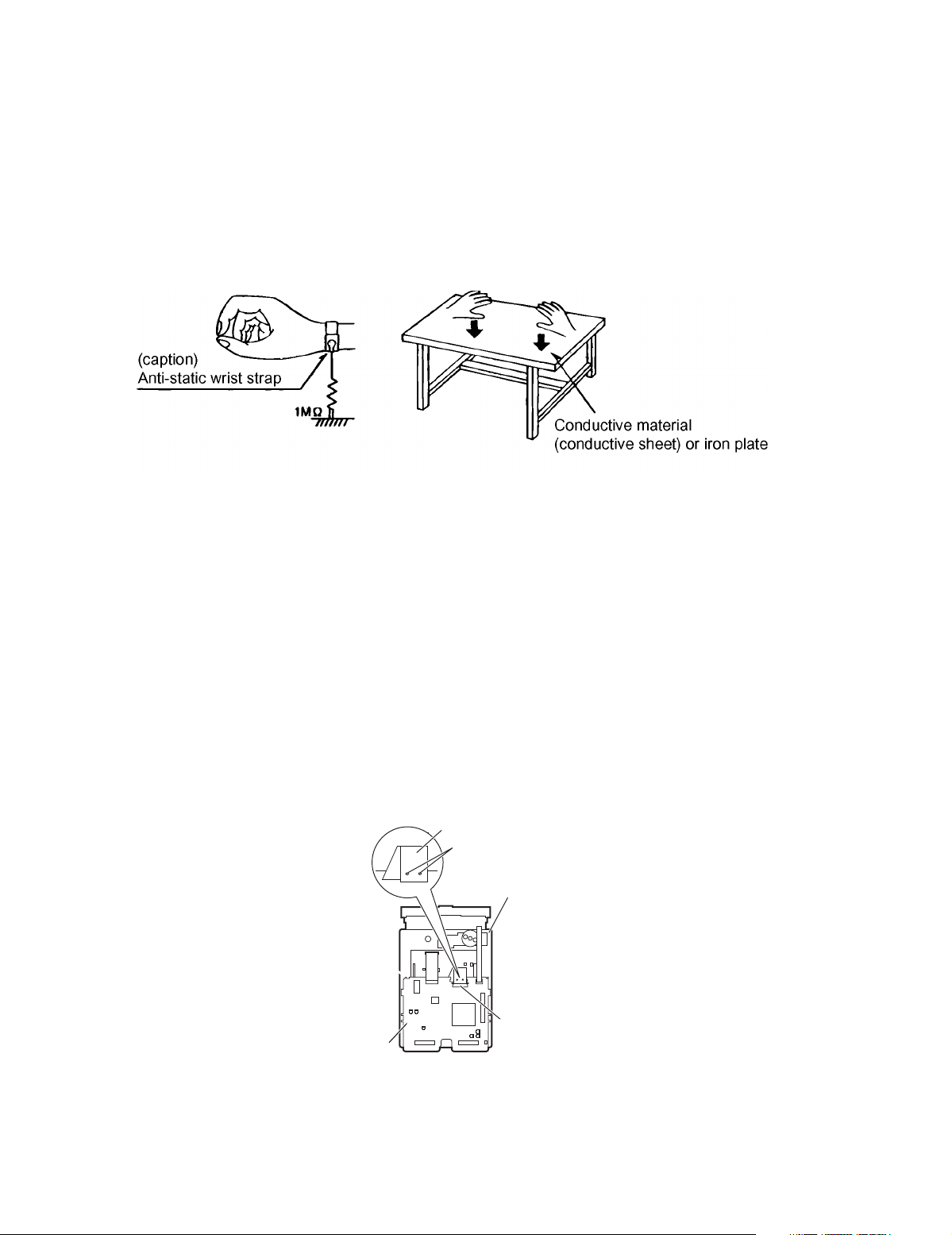
1.6 Preventing static electricity
Electrostatic discharge (ESD), which occurs when static electricity stored in the body, fabric, etc. is discharged,
can destroy the laser diode in the traverse unit (optical pickup). Take care to prevent this when performing repairs.
1.6.1 Grounding to prevent damage by static electricity
Static electricity in the work area can destroy the optical pickup (laser diode) in devices such as DVD players.
Be careful to use proper grounding in the area where repairs are being performed.
(1) Ground the workbench
Ground the workbench by laying conductive material (such as a conductive sheet) or an iron plate over it before placing the
traverse unit (optical pickup) on it.
(2) Ground yourself
Use an anti-static wrist strap to release any static electricity built up in your body.
(3) Handling the optical pickup
• In order to maintain quality during transport and before installation, both sides of the laser diode on the replacement optical
pickup are shorted. After replacement, return the shorted parts to their original condition.
(Refer to the text.)
• Do not use a tester to check the condition of the laser diode in the optical pickup. The tester's internal power source can easily
destroy the laser diode.
1.7 Handling the traverse unit (optical pickup)
(1) Do not subject the traverse unit (optical pickup) to strong shocks, as it is a sensitive, complex unit.
(2) Cut off the shorted part of the flexible cable using nippers, etc. after replacing the optical pickup. For specific details, refer to the replace-
ment procedure in the text. Remove the anti-static pin when replacing the traverse unit. Be careful not to take too long a time
when attaching it to the connector.
(3) Handle the flexible cable carefully as it may break when subjected to strong force.
(4) I t is not possible to adjust the semi-fixed resistor that adjusts the laser power. Do not turn it.
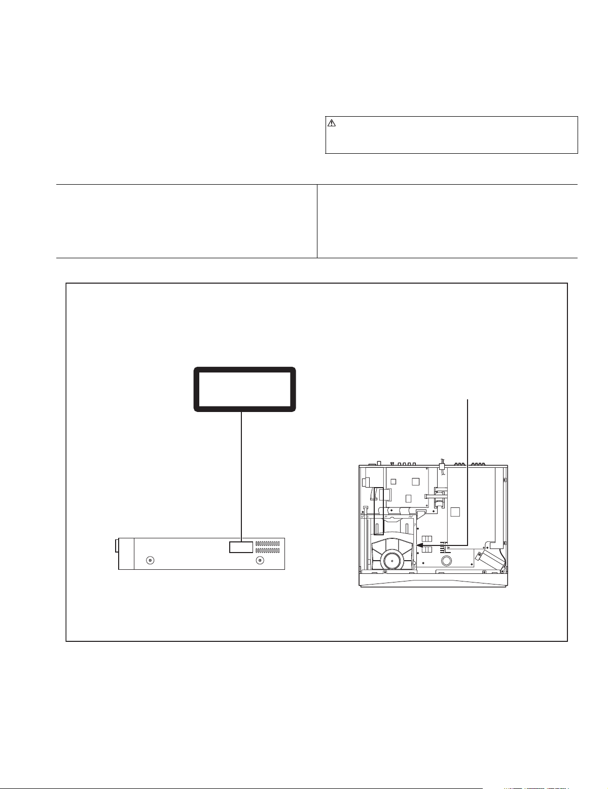
1.8 Attention when traverse unit is decomposed
*Please refer to "Disassembly method" in the text for the DVD pickup unit.
• Apply solder to the short land sections before the flexible wire is disconnected from the connector CN101 on the DVD servo board.
(If the flexible wire is disconnected without applying solder, the DVD pickup may be destroyed by static electricity.)
• In the assembly, be sure to remove solder from the short land sections after connecting the flexible wire.
1-4 (No.21189)
Flexible wire
Short land sections
DVD mechanism assembly
CN101
DVD servo board
Page 5
1.9 Important for laser products
(1) CLASS 1 LASER PRODUCT
(2) DANGER : Invisible laser radiation when open and inter
lock failed or defeated. Avoid direct exposure to beam.
(3) CAUTION : There are no serviceable parts inside the
Laser Unit. Do not disassemble the Laser Unit. Replace the
complete Laser Unit if it malfunctions.
(4) CAUTION : The compact disc player uses invisible laser
radiation and is equipped with safety switches which
prevent emission of radiation when the drawer is open and
the safety interlocks have failed or are de feated.
It is dangerous to defeat the safety switches.
TH-A75R
(5) CAUTION : If safety switches malfunction, the laser is able
to function.
(6) CAUTION : Use of controls, adjustments or performance of
procedures other than those specified herein may result in
hazardous radiation exposure.
CAUTION
Please use enough caution not to see the beam directly
or touch it in case of anadjustment or operation check.
VARNING
Osynlig laserstrålning är denna del är öppnad och spårren är
urkopplad. Betrakta ej strålen.
VARO
Avattaessa ja suojalukitus ohitettaessa olet alttiina näkymättömälle lasersäteilylle. Älä katso säteeseen.
REPRODUCTION AND POSITION OF LABELS
CLASS 1
LASER PRODUCT
ADVARSEL
Usynlig laserstråling ved åbning, når sikkerhedsafbrydere er
ude af funktion. Undgå udsasttelse for stråling.
ADVARSEL
Usynlig laserstråling ved åpning, når sikkerhetsbryteren er avslott. unngå utsettelse for stråling.
WARNING LABEL
(No.21189)1-5
Page 6
TH-A75R
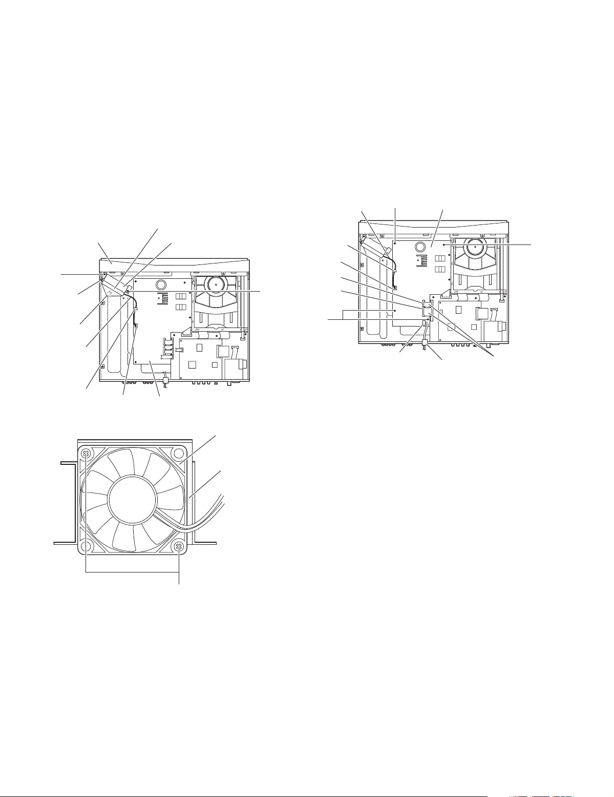
r
2.1 Main body section
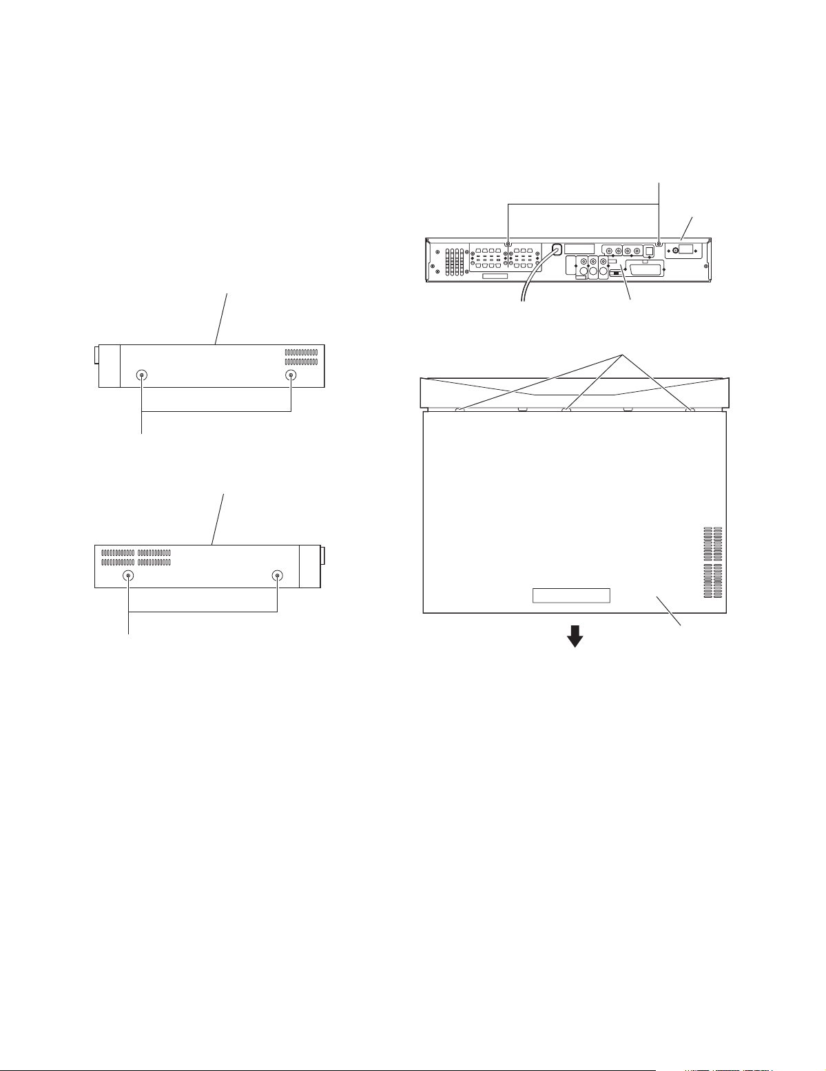
2.1.1 Removing the top cover (See Figs.1 to 4.)
(1) From the right and left sides of the main body, remove the
four screws A attaching the top cover. (See Figs.1 and 2.)
(2) From the back side of the main body, remove the two
screws B attaching the top cover. (See Fig.3.)
(3) Lift the rear section of the top cover, slide the top cover
slightly in the direction of the arrow. (See Fig.4.)
(4) Disengage the engagement sections a of the top cover
from the main body. (See Fig.4.)
Top cover
SECTION 2
Disassembly method
B
Top cove
Rear panel
Fig.3
a
A
A
Fig.1
Top cover
Top cover
Fig.4
Fig.2
1-6 (No.21189)
Page 7
2.1.2 Removing the front panel assembly (See Figs.5 to 8.)
• Remove the top cover.
(1) From the left side of the main body, push the section b of
the slide cam using the screw driver, etc. (See Fig.5.)
(2) Pull out the tray. (See Fig.5.)
(3) Push the tray fitting assembly of the tray in the direction of
the arrow and then remove the tray fitting assembly. (See
Fig.6.)
(4) Return the tray into the DVD mechanism assembly.
(5) From the bottom side of the main body, remove the four
screws C attaching the front panel assembly. (See Fig.7.)
(6) From the top side of the main body, remove the two screws
D attaching the front panel assembly. (See Fig.8.)
(7) Disconnect the card wires from the connectors CN206 and
CN207 on the main board. (See Fig.8.)
(8) Remove the screw E attaching the lug wire. (See Fig.8.)
(9) While opening the hooks c to the right and left sides of the
front panel assembly in the direction of the arrow 1, remove
the front panel assembly in the direction of the arrow 2.
(See Fig.8.)
Reference:
then hold the card wire to the sections d of the barrier.
(See Fig.8.)
Front panel assembly
Tray
C
Barrier
TH-A75R
Chassis base
Front panel assembly
Fig.7
Main board
CN207
Slide cam
Front panel assembly
Tray
Fig.5
Fig.6
b
Tray fitting assembly
CN206
d
1
Hook c
Front panel assembly
2
Fig.8
Lug wire
1
Hook c
D E
(No.21189)1-7
Page 8
TH-A75R
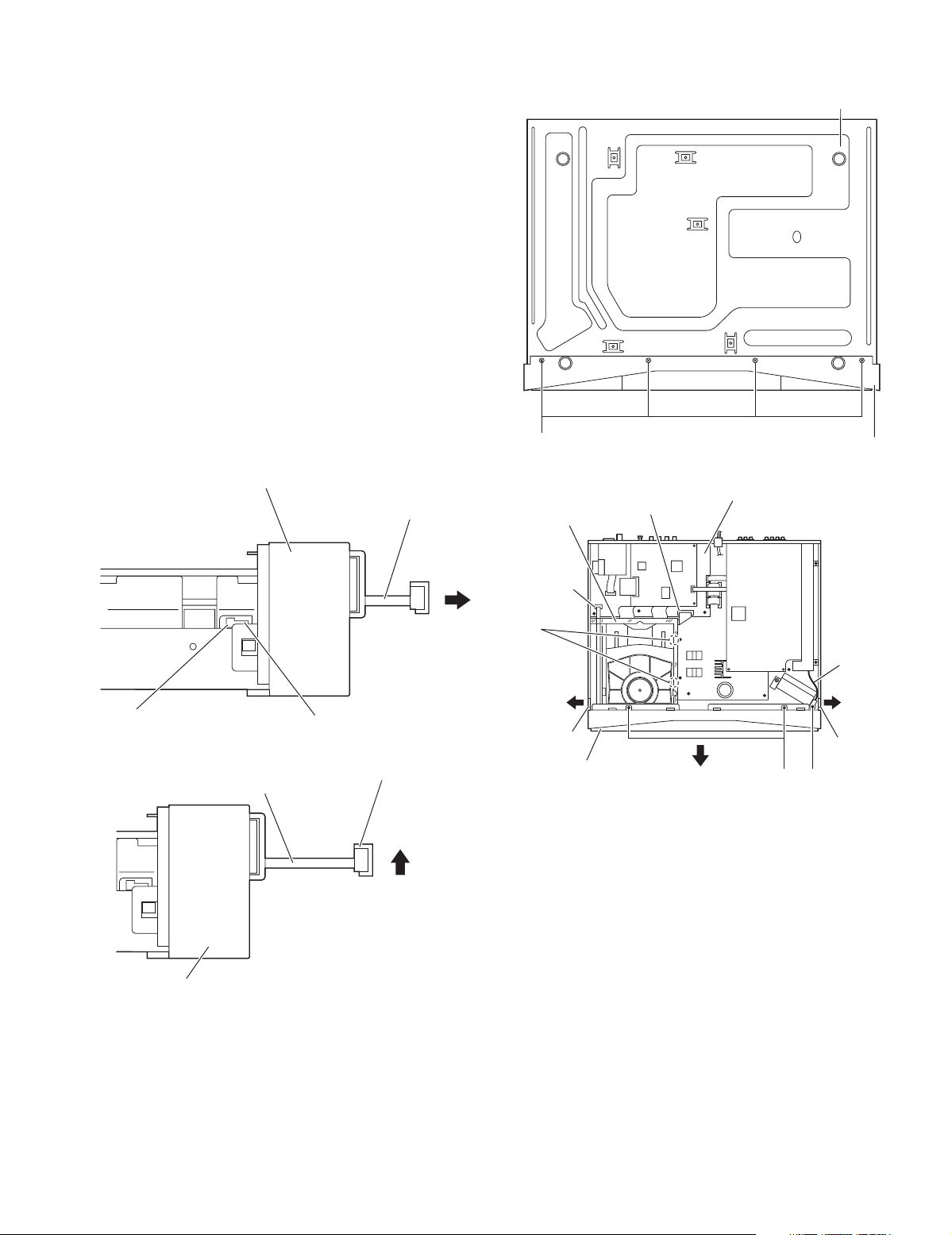
2.1.3 Removing the DVD mechanism assembly (See Fig.9.)
• Remove the top cover.
• Remove the front panel assembly.
(1) From the top side of the main body, remove the barrier.
(2) Disconnect the card wires from the connectors CN208 and
CN209 on the main board.
(3) Remove the three screws F attaching the DVD mechanism
assembly.
(4) Take out the DVD mechanism assembly from the chassis
base.
Main board
Card wire
F
CN209 CN208
Card wire
Barrier
DVD
mechanism
assembly
F
Chassis base
Fig.9
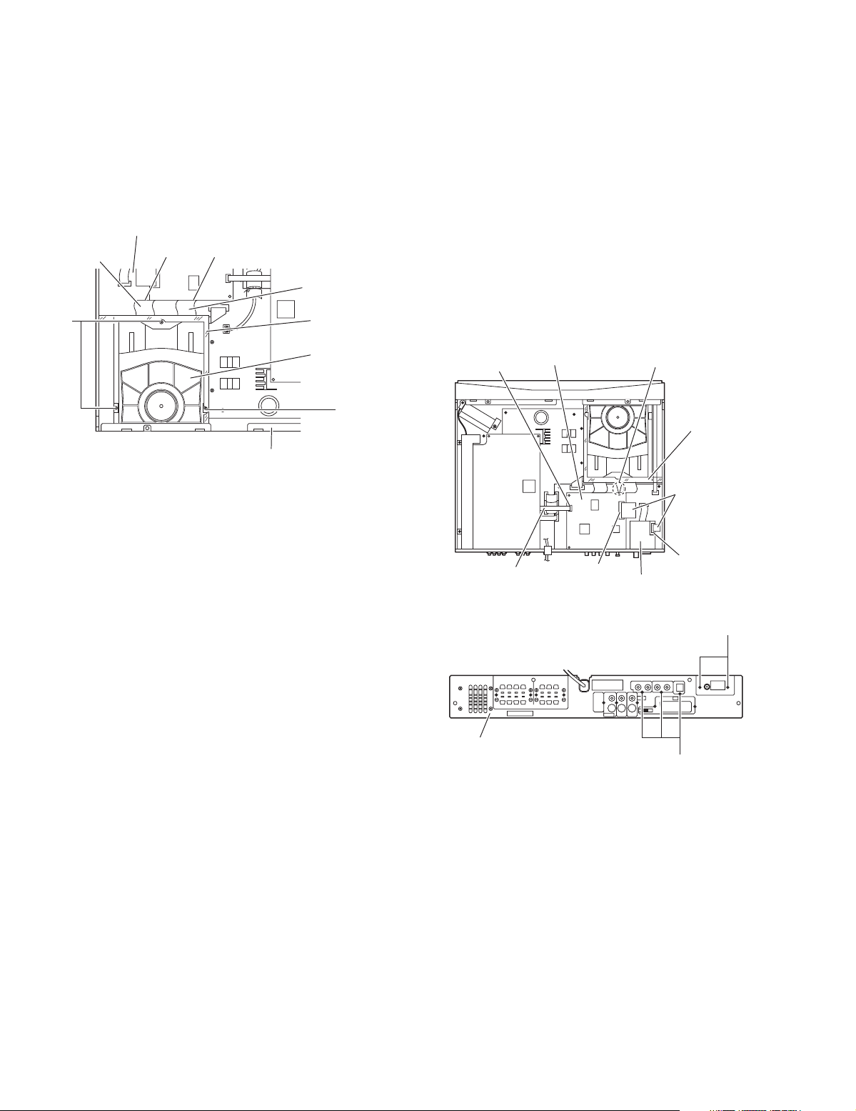
2.1.4 Removing the DSP board (See Figs.10 and 11.)
• Remove the top cover.
(1) From the top side of the main body, disconnect the card
wires from the connectors CN591 and CN592 on the DSP
board. (See Fig.10.)
(2) From the back side of the main body, remove the three
screws G attaching the DSP board. (See Fig.11.)
(3) Remove the DSP board from the section e of the barrier,
take out the DSP board. (See Fig.10.)
Reference:
When attaching the DSP board, hang the DSP board to
the section e of the barrier. (See Fig.10.)
2.1.5 Removing the tuner (See Figs.10 and 11.)
• Remove the top cover.
(1) From the top side of the main body, disconnect the card
wire from the connector CN1 on the tuner. (See Fig.10.)
(2) From the back side of the main body, remove the two
screws H attaching the tuner. (See Fig.11.)
CN592
DSP board
e
Barrier
Card wires
Card wire
Rear panel
CN591
Fig.10
Fig.11
CN1
Tuner
H
G
1-8 (No.21189)
Page 9
TH-A75R
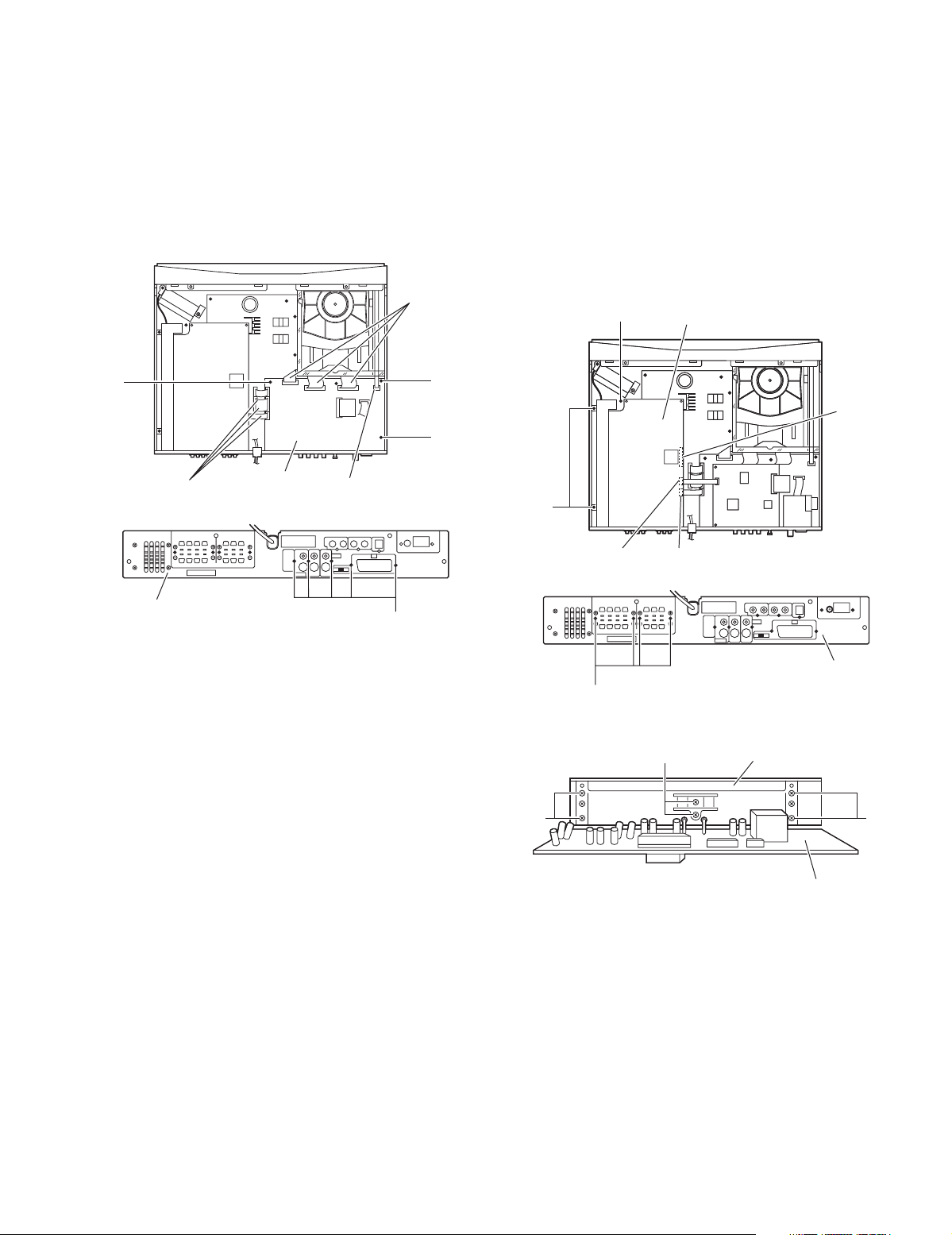
2.1.6 Removing the main board (See Figs.12 and 13.)
• Remove the top cover.
• Remove the DSP board.
• Remove the tuner.
(1) From the top side of the main body, disconnect the card
wires from the connectors (CN201, CN202, CN204,
CN206-CN209) on the main board. (See Fig.12.)
(2) Remove the screw J and two screws K attaching the main
board. (See Fig.12.)
(3) From the back side of the main body, remove the five
screws L attaching the main board. (See Fig.13.)
Card wires
J
CN207
CN202
CN201
CN204
CN208
CN209
K
K
Card wires
Main board
Fig.12
CN206
2.1.7 Removing the amplifier board (See Figs.13 to 16.)
• Remove the top cover.
(1) From the top side of the main body, disconnect the card
wires from the connectors CN701 and CN702 on the amplifier board (See Fig.14.)
(2) Remove the three screws M attaching the amplifier board.
(See Fig.13.)
(3) From the back side of the main body, remove the four
screws N attaching the amplifier board. (See Fig.15.)
(4) Disconnect the connector CN703 on the amplifier board,
take out the amplifier board. (See Fig.14.)
(5) Remove the six screws P attaching the heat sink to the am-
plifier board. (See Fig.16.)
M
Amplifier board
CN703
M
Rear panel
Fig.13
L
N
P
CN702CN701
Fig.14
Rear panel
Fig.15
Heat sink
PP
Amplifier board
Fig.16
(No.21189)1-9
Page 10
TH-A75R
t
2.1.8 Removing the fan motor (See Figs.17 and 18.)
• Remove the top cover.
• Remove the amplifier board.
(1) From the top side of the main body, remove the fan cover.
(See Fig.17.)
(2) Remove the tie band banding the fan motor wire and then
disconnect the fan motor wire from the connector CN174
on the power board. (See Fig.17.)
(3) Remove the screw Q and screw R attaching the fan brack-
et. (See Fig.17.)
(4) Remove the two screws S attaching the fan motor to the
fan bracket. (See Fig.18.)
Reference:
When attaching the screw Q, attach the lug wire of the
front panel assembly at the same time.
Fan motor
Front panel assembly
Fan bracket
Q
Lug wire
Fan cover
R
2.1.9 Removing the power board (See Fig.19.)
• Remove the top cover.
• Remove the amplifier board.
(1) From the top side of the main body, disconnect the card
wires from the connectors CN172 and CN173 on the power
board.
(2) Remove the tie band banding the fan motor wire and then
disconnect the fan motor wire from the connector CN174
on the power board.
(3) Disconnect the power cord from the connector CN101 on
the power board.
(4) Remove the screw T and three screws U attaching the
power board.
Fan motor wire
Tie band
CN174
CN173
CN172
T
Power board
U
U
Fan motor wire
Tie band
CN174
Power board
Fig.17
S
Fig.18
Fan motor
Fan bracke
CN101
Power cord
Fig.19
Card wires
1-10 (No.21189)
Page 11
TH-A75R
V
2.2 Front panel assembly section
• Remove the top cover.
• Remove the front panel assembly.
2.2.1 Removing the jack board (See Fig.1.)
(1) From the inside of the front panel assembly, disconnect the
wire from the connector CN403 on the switch board.
(2) Remove the two screws V attaching the jack holder, take
out the jack board together the jack holder.
Jack board
Wire
Jack holder
2.2.2 Removing the switch board (See Figs.2 and 3.)
(1) From the inside of the front panel assembly, disconnect the
wire from the connector CN403 on the switch board. (See
Fig.2.)
(2) Remove the eight screws W attaching the switch board,
take out the switch board. (See Fig.2.)
Reference:
In the assembly, attach the switch board after attaching
the push buttons and light lens as before. (See Fig.3.)
CN403
W
Switch board
Front panel assembly
Fig.1
Switch board
2.3 DVD mechanism section
• Remove the top cover.
• Remove the DVD mechanism assembly.
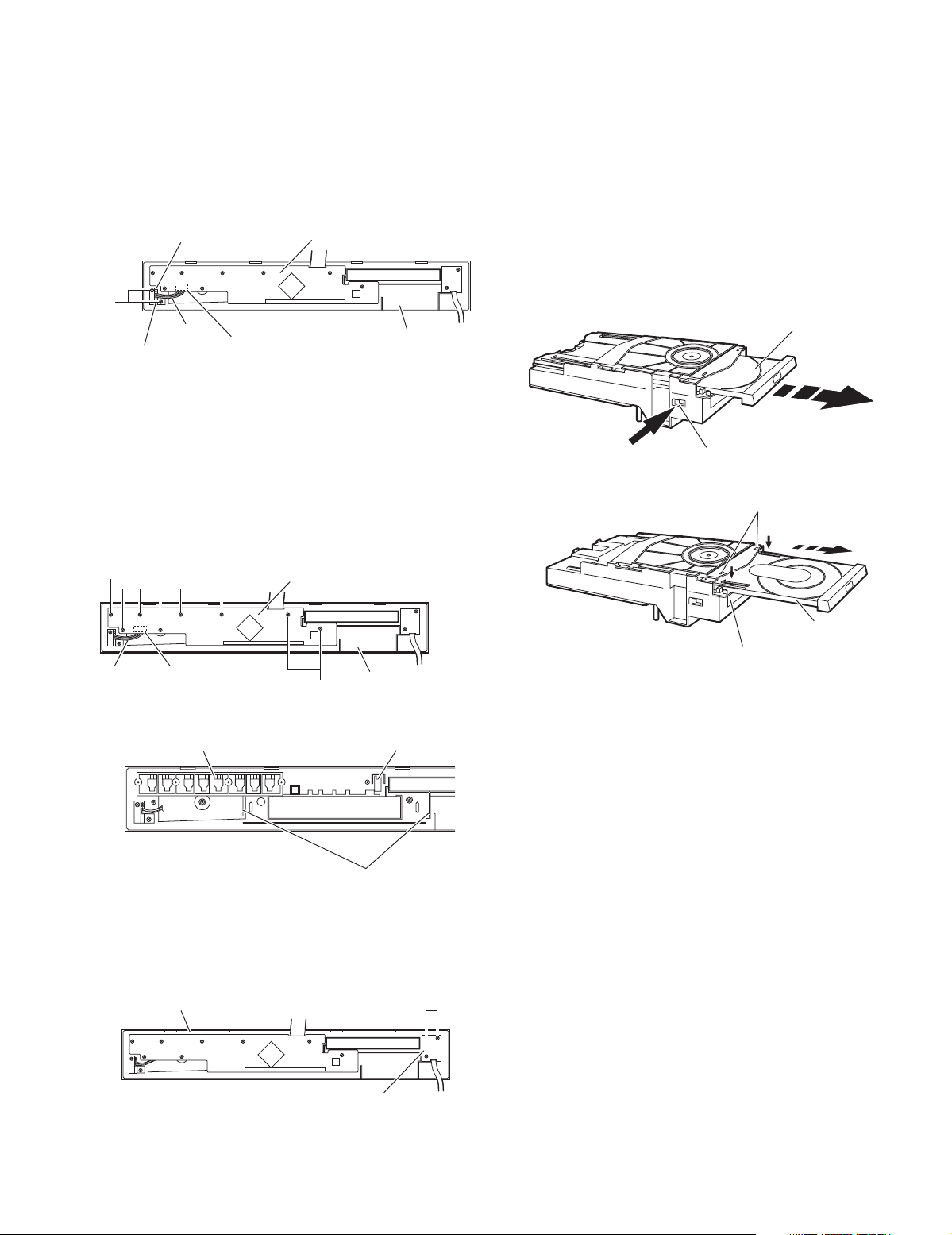
2.3.1 Removing the tray (See Figs.1 and 2.)
(1) From the left side of the DVD mechanism assembly, push
the slide cam in the direction of the arrow 1 and then pull
out the tray in the direction of the arrow 2. (See Fig.1.)
(2) Push the tray stoppers a in the direction of the arrow 3, pull
out the tray in the direction of the arrow 4. (See Fig.2.)
2.3.2 Attaching the tray (See Fig.2.)
When attaching the tray, insert the tray to the rail of the DVD
mechanism assembly and then push the tray in the DVD mechanism assembly.
Tray
2
1
Slide cam
Fig.1
Tray stoppers a
3
4
Wire
CN403
Front panel assembly
W
Fig.2
Push button Push button
Light lens
Fig.3
2.2.3 Removing the standby board (See Fig.4.)
From the inside of the front panel assembly, remove the two
screws X attaching the standby board.
X
Front panel assembly
Tray
DVD mechanism assembly
Fig.2
Standby board
Fig.4
(No.21189)1-11
Page 12
TH-A75R
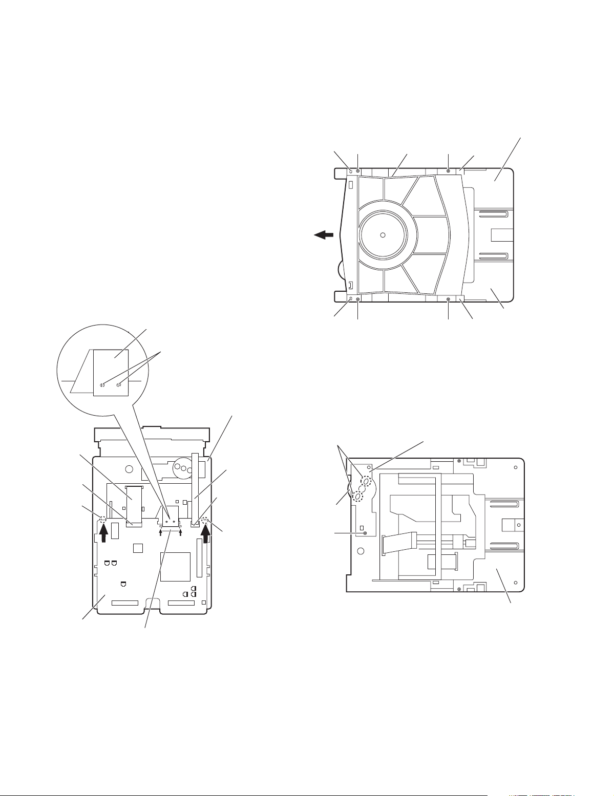
2.3.3 Removing the tray (See Fig.3.)
(1) From the bottom side of the DVD mechanism assembly,
disconnect the card wires from the connectors CN201 and
CN202 on the DVD servo board.
Caution:
Be sure to solder the short land sections b on the flexible
wire before disconnecting the flexible wire from connector CN101 on the DVD servo board.
If the flexible wire is disconnected without attaching solder, the DVD pickup unit may be destroyed by static
electricity.
(2) Release the locks of the connector CN101 (in the direction
of the arrow 1) on the DVD servo board, disconnect the
flexible wire.
(3) Release the locks of the connector CN101 on the DVD ser-
vo board in the direction of the arrow 1, disconnect the flexible wire.
Caution:
In the assembly, be sure to remove solders from the
short land sections b after connecting the flexible wire to
the connector CN101 on the DVD servo board.
(4) While pushing the claw c of the DVD mechanism assembly
in the direction of the arrow 2, remove the DVD servo board
in an upward direction.
Flexible wire
Short land sections b
DVD mechanism assembly
Card wire
2.3.4 Removing the clamper base (See Fig.4.)
(1) From the top side of the DVD mechanism assembly, re-
move the four screws A attaching the clamper base.
(2) Remove the clamper base from the bosses d of the loading
base in an upward direction, remove the clamper base
from the sections e while sliding it in the direction of the arrow.
DVD mechanism assembly
Boss d
Boss d
2.3.5 Removing the tray drive board (See Fig.5.)
• Remove the clamper base.
(1) From the bottom side of the DVD mechanism assembly, re-
move the solders from the soldered sections f on the tray
drive board.
(2) Remove the screw B attaching the tray drive board to the
DVD mechanism assembly.
Soldered sections f
Clamper base
AA
A A
Fig.4
Tray drive board
Section e
Loading base
Section e
CN201
Claw c
DVD servo board
2 22
11
CN101
Fig.3
Card wire
CN202
Claw c
Motor
B
DVD mechanism assembly
Fig.5
1-12 (No.21189)
Page 13
TH-A75R
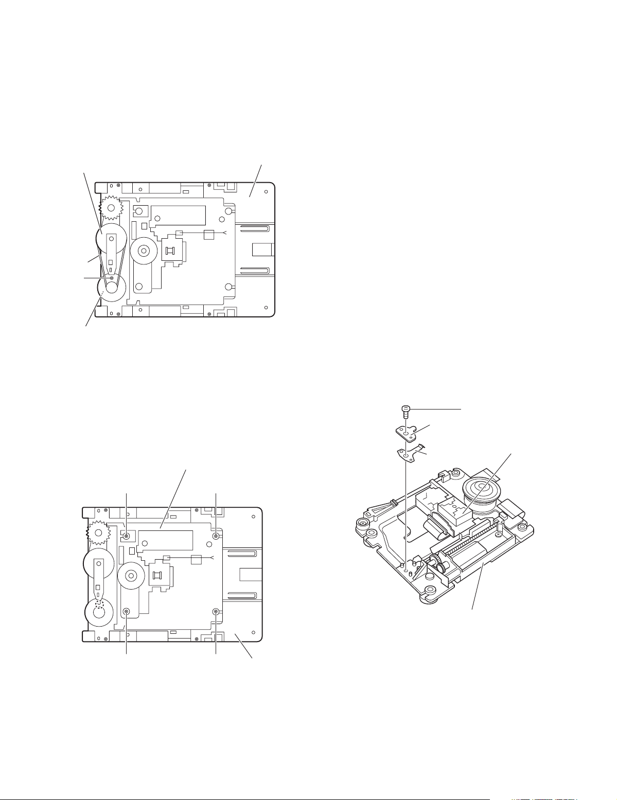
2.3.6 Removing the motor (See Fig.6.)
• Remove the clamper base.
• Remove the tray drive board.
(1) From the top side of the DVD mechanism assembly, re-
move the belt of the pulley gear.
Note:
Take care not to attach grease on the belt.
(2) Remove the screw C attaching the motor to the DVD mech-
anism assembly.
DVD mechanism assembly
Pulley gear
Belt
C
Motor
Fig.6
2.3.7 Removing the DVD traverse mechanism assembly
(See Figs.7.)
• Remove the DVD servo board.
• Remove the clamper base.
(1) From the top side of the DVD mechanism assembly, re-
move the four screws D attaching the DVD traverse mechanism assembly to the loading base.
(2) Take out the DVD traverse mechanism assembly from the
loading base.
DVD traverse mechanism assembly
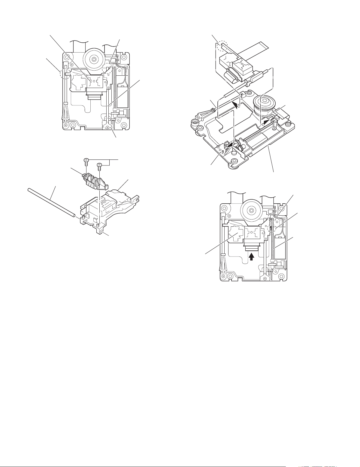
2.3.8 Removing the DVD pickup unit (See Figs.8 to 10.)
• Remove the DVD servo board.
• Remove the clamper base.
• Remove the DVD traverse mechanism assembly.
(1) From the top side of the DVD traverse mechanism assem-
bly, remove the screw E attaching the plate and torsion
spring. (See Fig.8.)
(2) Remove the shaft from the section g and then remove the
shaft from the section h. (See Fig.9.)
(3) Disengage the section i of the DVD pickup unit and then re-
move the DVD pickup unit with the shaft.
(4) Pull the shaft out of the DVD pickup unit.
(5) Remove the two screws F attaching the SW. actuator.
2.3.9 Attaching the DVD pickup unit (See Figs.8,10 to 12)
Reference:
Refer to the explanation of "Removing the DVD pickup unit" on
the preceding page.
(1) Attach the SW. actuator and shaft to the DVD pickup unit.
(See Fig.10.)
(2) Engage the section i of the DVD pickup unit to the shaft of
the DVD traverse mechanism assembly first, and set the
both ends of the shaft of the DVD pickup unit in the sections
g and h of the DVD traverse mechanism assembly. (See
Fig.11.)
(3) Slide the DVD pickup unit all the way in the direction of the
arrow. (See Fig.12.)
(4) Mesh the lead screw to the section j of DVD pickup unit and
then set the end of the lead screw to the section k. (See
Fig.12.)
(5) Attach the torsion spring. (See Fig.8.)
(6) Attach the plate. (See Fig.8.)
E
Plate
Torsion spring
DVD pickup unit
D D
DD
Fig.7
Loading base
DVD traverse mechanism assembly
Fig.8
(No.21189)1-13
Page 14
TH-A75R
t
w
DVD pickup unit
Section i
SW. actuator
Shaft
Fig.9
Section h
Section g
F
DVD pickup unit
Shaf
Section
Shaft
Section
i
Section h
DVD traverse mechanism assembly
Fig.11
Section k
Fig.10
Section j
Lead scre
DVD pickup unit
Fig.12
1-14 (No.21189)
Page 15

TH-A75R
r
2.3.10 Removing the spindle motor board (See Figs.13 and
14.)
• Remove the DVD servo board.
• Remove the clamper base.
• Remove the DVD traverse mechanism assembly.
(1) From the top side of the DVD traverse mechanism assem-
bly, remove the feed motor wire that is soldered to the spindle motor board. (See Fig.13.)
(2) From the bottom side of the DVD traverse mechanism as-
sembly, remove the three screws G attaching the spindle
motor board. (See Fig.14.)
Spindle motor board
Remove the solders.
Feed moto
wire
2.3.11 Removing the feed motor (See Figs.15 to 17.)
• Remove the DVD servo board.
• Remove the clamper base.
• Remove the DVD traverse mechanism assembly.
(1) From the top side of the DVD traverse mechanism assem-
bly, remove the feed motor wire that is soldered to the spindle motor board. (See Fig.15.)
(2) Remove the screws H attaching the feed holder assembly
and then take out the feed holder assembly. (See Fig.15.)
(3) Remove the screw J attaching the thrust spring. (See
Fig.16.)
(4) Remove the feed gear and lead screw in the direction of the
arrow. (See Fig.16.)
(5) Remove the two screws K attaching the feed motor. (See
Fig.17.)
Spindle motor board
Remove the solders.
Feed holder assembly
H
Feed motor
wire
Feed motor
DVD traverse mechanism assembly
Fig.13
G
DVD traverse mechanism assembly
Fig.14
H
DVD traverse mechanism assembly
Fig.15
G
Feed holder assembly
Lead screw
Feed motor
Feed gear
Thrust spring
J
Fig.16
Feed holder assembly
K
Fig.17
(No.21189)1-15
Page 16

TH-A75R
SECTION 3
Adjustment
3.1 Test mode
(1) The AC cord is connected after pushing the STOP key and the EJECT key of a main body.
(2) Change to test mode, FL indicate "TEST ??". (?? is version)
At this time, TV monitor indicate the firm number " ".
(3) Press PAUSE key of the main body, EEPROM initialize is start.
FL indicate "RDS", EEPROM initialize is complete.
(4) Release the test mode by power to off.
3.2 Up grade
3.2.1 How to UPGRADE
(1) Power to on then mode to DVD.
(2) Set the recorded disc.
(Down loaded the up grade program "TH-A75 -Firmware Update Procedure" from Audio Products DIV.
Technological Material of JS-Net .)
(3) FL indicate "UPGRADE", press cursol key of the remote controller.
(4) TV monitor indication the UPGRADE condition.
(5) Upgrade is complete, disc is automatically eject then finish the upgrade.
3.2.2 After UPGRADE
After upgrade, it is should done the EEPROM initialize and confirm the firm number.
(1) Tray close then release the AC cord.
(2) The AC cord is connected after pushing the STOP key and the EJECT key of a main body.
(3) Change to test mode, FL indicate "TEST ??". (?? is version)
In this time, confrim the TV monitor indicate the firm number "114".
(4) EEPROM initialize start by press the PAUSE key of main body.
FL indicate "RDS", EEPROM initialize is complete.
(5) Release the test mode by power to off.
1-16 (No.21189)
Page 17
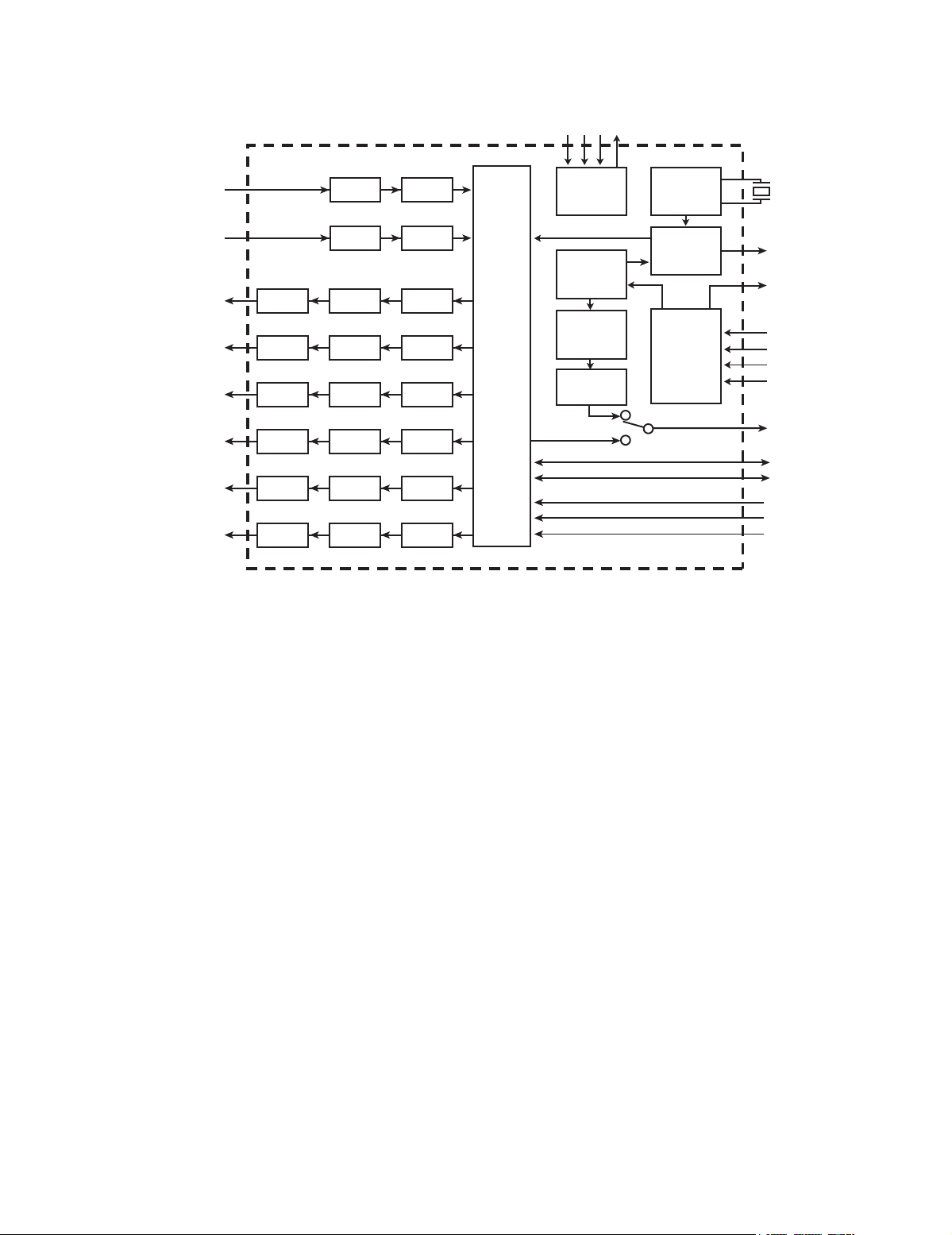
4.1 UPD784215AGC194 (IC531) : CPU
• Pin layout
75 ~ 51
TH-A75R
SECTION 4
Description of major ICs
76
~
100
1 ~ 25
• Pin function
Pin No. Symbol I/O Function
1~8 - - Not use
9VDD-+3.0V
10 X2 I Main system clock input
11 X1 I Main system clock input
12 VSS - GND
13 XT2 - OPEN
14 XT1 I Connect to VSS
15 RESET I Reset for Flash write
16 - - Not use
17 INT0 I Error input0 (detect UNLOCK)
18 INT1 I Error input1 (detect Non Audio)
19 DZF I GND
20~22 - - Not use
23 AVDD - The same potential as VDD
24 AV REF0 - The same potential as VSS
25 - - Not use
26 CS1 I Chip select input port
27 CS2 I Chip select input port
28 CS3 I Chip select input port
29 CS4 I Chip select input port
30~32 - - Not use
33 AVSS - The same potential as VSS
34, 35 - - Not use
36 AV REF1 - The same potential as VDD
37 RX O For flash write
38 TX O For flash write
39 - - Not use
40 DSP_COM I Command (serial 1)
41 DSP_STS O Status (Serial 1)
42 DSP_CLK I Clock (Serial 1)
43 DSP_RDY I Ready
44 - - Not use
45 MIDIO_IN I Data in (Serial 0)
46 MIDIO_OUT O Data out (Serial 0)
47 MICK O Clock (Serial 0)
50
~
26
Pin No. Symbol I/O Function
48 HREQ I HREQ
49 SS O Slave select
50,51 - - Not use
52 DSP_RST O DSP RESET
53 - - Not use
54 DA_CS O Chip select output
55 - - Not use
56 PD/DA O Power down output (RESET)
57 PD O Power down output (RESET)
58~63 - - Not use
64 CODEC_D-OUT O Data out
65 CODEC_D-IN I Data in
66 CODEC_CLK O Clock
67 CODEC_CS O Chip select output
68 DEBUG1 O Debug out port
69 DEBUG2 O Debug out port
70 DEBUG3 O Debug out port
71 GEBUG4 O Debug out port
72 GND - GND
73~75 - - Not use
76 EQ O EQ
77 CTR_TONE O Center tone
78 3D O 3D-Phonic
79, 80 - - Not use
81 VDD - +3.0V
82, 83 - - Not use
84 ANA/T.TUNE O ANALOG./T.TONE
85 LFE.MIX O LFE MIX CONTROL
86 LEF_OUT O LFE OUT CONTROL
87 - - Not use
88 S.MUTE O S.MUTE
89~93 - - Not use
94 TEST O Usual "VSS"
95~100 - - Not use
(No.21189)1-17
Page 18
TH-A75R
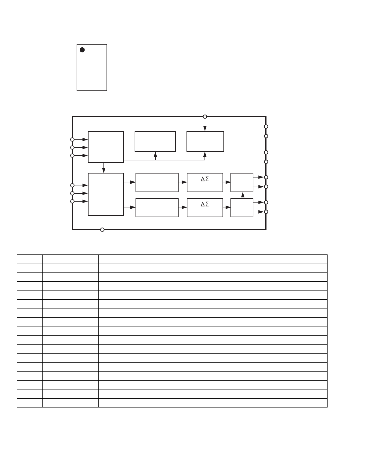
4.2 39VF0207CWHQ01 (IC524) : 2 Mbit multi-purpose flash memory
• Pin layout • Block diagram
A11
A9
A8
A13
A14
A17
WE#
V
DD
NC
A16
A15
A12
A7
A6
A5
A4
1
2
3
4
5
6
7
8
9
10
11
12
13
14
15
16
Top view
32
31
30
29
28
27
26
25
24
23
22
21
20
19
18
17
OE#
A10
CE#
DQ7
DQ6
DQ5
DQ4
DQ3
V
SS
DQ2
DQ1
DQ0
A0
A1
A2
A3
Memory Address
• Pin function
Pin No. Symbol Function
1 - 6 A11,A9,A8
Address inputs
A13,A14,A17
7 WE# Write enable
8 VDD Power supply
9 NC Not connect
10 - 20 A16,A15,A12
Address inputs
A7 - A0
21 - 23 DQ0 - DQ2 Data inputs/outputs
24 VSS Ground
25 - 29 DQ3 - DQ7 Data inputs/outputs
30 CE# Chip enable
31 A10 Address input
32 OE# Output enable
CE#
OE#
WE#
X-Decoder
Address Buffers
and
Latches
Control Logic
SuperFlash
Memory
Y-Decoder
I/O Buffers
and
Data Latches
DQ7 - DQ0
1-18 (No.21189)
Page 19
4.3 MM74HCT32MTC-X (IC521) : Quad 2 input OR gate
• Pin layout & Block diagram
• Truth table
11A
21B
31Y
42A
52B
62Y
7
(TOP VIEW)
14
13
12
11
10
9
8GND
V
4B
4A
4Y
3B
3A
3Y
CC
INPUTS OUTPUT
ABY
LLL
LHH
HLH
HHH
4.4 74LCX373MTC-X (IC512,IC513) : Octal D-type latch
• Pin layout • Truth table
20
19
18
17
16
15
14D2
13
12
11
VCC
Q7
D7
D6
Q6
Q5
D5
D4
Q4
LE
OE
HXXZ
LLXQn
LHLL
LHHH
X: Don't care
Z: High impedance
Qn: Q outputs are latched at the time when the LE input is tak-
1OE
2Q0
3D0
4D1
5Q1
6Q2
7
8D3
9Q3
10GND
(TOP VIEW)
en to a low logic level.
TH-A75R
INPUTS OUTPUT
LE D Y
• Block diagram
D0
3
D
Q
L
OE
11
LE
1
D1
4
2
Q0
D2
7
D
Q
L
5
Q1
D3
8
D
Q
L
6
Q2
D4
13
D
Q
L
9
Q3
D5
14
D
Q
L
12
Q4
D6
17
D
Q
L
15
Q5
D7
18
D
D
Q
L
16
Q
L
19
Q6
Q7
(No.21189)1-19
Page 20
TH-A75R
4.5 AK4586VQ (IC511) : A/D, D/A Converter
• Pin layout
44 - 34
11 - 1
12 - 22
23 - 33
• Pin function
Pin No. Symbol I/O Function
1 XTO O X'tal output pin
2 XTI I X'tal input pin
EXTCLK I External master clock input pin
3 TVDD - Output buffer power supply pin, 2.7V~5.5V
4 VDSS - Digital Ground pin, 0V
5 DVDD - Digital power supply pin, 4.5V~5.5V
6 TX O Transmit channel (through data) output pin
7 MCKO O Master clock output pin
8 LRCK I/O Input/Output channel clock pin
9 BICK I/O Audio serial data clock pin
10 SDTO O Audio serial data output pin
11 SDTI1 I DAC1 audio serial data input pin
12 SDTI2 I DAC2 audio serial data input pin
13 SDTI3 I DAC3 audio serial data input pin
14 INT0 O Interrupt 0 pin
15 INT2 O Interrupt 1 pin
16 CDTO O Control data output pin in 4-wire serial control mode
CAD1 I Chip address 1 pin in I2C bus control mode
17 CDTI I Control data input pin in 4-wire serial control mode
SDA I/O Control data input/output pin in I2C bus control mode
18 CCLK I Control data clock pin in 4-wire serial control mode
SCL I Control data clock pin in I2C bus control mode
19 CSN I Chip select pin in 4-wire serial control mode
CAD0 I Chip address 0 pin in I2C bus control mode
20 DZF2 O Zero input detect 2 pin
OVF O Analog input overflow detect pin
21 AVSS - Analog ground pin, 0V
22 AVDD - Analog power supply pin, 4.5V~5.5V
23 VREFH I Positive voltage reference input pin, AVDD
24 VCOM O Common voltage output pin, AVDD/2
25 DZF1 O Zero input detect 1 pin
26 LOUT3 O DAC3 Lch analog output pin
27 ROUT3 O DAC3 Rch analog output pin
28 LOUT2 O DAC2 Lch analog output
29 ROUT2 O DAC2 Rch analog output pin
30 LOUT1 O DAC1 Lch analog output pin
31 ROUT1 O DAC1 Rch analog output pin
32 LIN I Lch analog input pin
33 RIN I Rch analog input pin
34 PCDD - PLL power supply pin, 4.5V~5.5V
35 R - External resistor pin
36 PVSS - Pll ground pin, 0V
37 RX4 I Receiver channel 4 pin (internal biased pin)
38 SLAVE I Slave mode pin
39 RX3 I Receiver channel 3 pin (internal biased pin)
40 TST I Test pin
41 RX2 I Receiver channel 2 pin (internal biased pin)
42 I2C I Control mode select pin
43 RX1 I Receiver channel 1 pin (internal biased pin)
44 PDN I Power-Down & Reset pin
1-20 (No.21189)
Page 21
• Block diagram
CSN
CCLK
CDTI
TH-A75R
CDTO
LIN
RIN
LOUT1
ROUT1
LOUT2
ROUT2
LOUT3
ROUT3
ADC HPF
ADC HPF
DAC DATTLPF
DAC DATTLPF
DAC DATTLPF
DAC DATTLPF
DAC DATTLPF
DAC DATTLPF
Audio
I/F
MCLK
SDOUT
BICK
LRCK
SDIN1
SDIN2
SDIN3
uP I/F
Clock
Recovery
DAIF
Decoder
DEM
X'tal
Oscillator
Clock
Generator
Input
Selector
XTI
XTO
MCKO
TX
RX1
RX2
RX3
RX4
SDOUT
BICK
LRCK
SDIN1
SDIN2
SDIN3
(No.21189)1-21
Page 22
TH-A75R
4.6 AK4382AVT-X (IC512) : D/A Converter
• Pin layout
1
2
3
4
5
6
7
8
•Block diagram
CSN
CCLK
Interface
CDTI
uP
16
15
14
13
12
11
10
9
De-empahsis
Control
MCLK
Clock
Divider
VDD
VSS
DZFL
DZFR
8X
LRCK
BICK
SDTI
Audio
Data
Interface
Interpolator
8X
Interpolator
Modulator
Modulator
PDN
• Pin function
Pin No. Symbol I/O Function
1 MCLK I Master Clock Input Pin
2 BICK I Audio Serial Data Clock Pin
3 SDTI I Audio Serial Data Input Pin
4 LRCK I L/R Clock Pin
5 PDN I Power-Down Mode Pin
6 CSN I Chip Select Pin
7 CCLK I Control Data Input Pin
8 CDTI I Control Data Input Pin
9 AOUTR- O Rch Negative Analog Output Pin
10 AOUTR+ O Rch Positive Analog Output Pin
11 AOUTL- O Lch Negative Analog Output Pin
12 AOUTL+ O Lch Positive Analog Output Pin
13 VSS - Ground Pin
14 VDD - Power Supply Pin
15 DZFR O Rch Data Zero Input Detect Pin
16 DZFL O Lch Data Zero Input Detect Pin
SCF
SCF
AOUTL+
AOUTL-
AOUTR+
AOUTR-
1-22 (No.21189)
Page 23
4.7 AK93C65AF-X (IC510) : EEPROM
• Pin layout
TH-A75R
• Block diagram
DI
CS
PE
VCC
CS
SK
1
2
3
4
8 PIN SOP
INSTRUCTION
REGISTER
NC
8
GND
7
DO
6
DI
5
INSTRUCTION
DECODE,
CONTROL
AND
CLOCK
GENERATION
DATA
REGISTER
ADD.
BUFFERS
16
R/W AMPS
AND
AUTO ERASE
DECODER
DO
16
EEPROM
4096bit
256 x 16
SK
PE
• Pin function
Pin no. Symbol Function
1 PE Program enable (With built-in pull-up resistor)
2 VCC Power supply
3 CS Chip selection
4 SK Cereal clock input
5 DI Cereal data input
6 DO Cereal data output
7 GND Ground
8 NC No connection
NOTE :
The pull-up resistor of the PE pin is about 2.5Mohm (VCC=5V)
VREF
VPP SW
VPP
GENERATOR
(No.21189)1-23
Page 24

TH-A75R
4.8 AN8703FH-V (IC101) : Frontend processor for DVD
• Pin layout
64 49
1
48
16
33
17 32
• Pin function
Pin No.
Symbol I/O Description
1 LPC1 I Laser input terminal (DVD)
2 LPC01 O Laser drive signal output terminal (DVD)
3 LPC2 I Laser input terminal (CD)
4 LPC02 O Laser drive signal output terminal (CD)
5
VFOSHORT
6 TBAL I Tracking balance control terminal
7 FBAL I Focus balance control terminal
8 POFLT O Track detection threshold level terminal
9 DTRD I Data slice part data read signal input ter-
10 IDGT I Data slice part address part gate signal
11 STANDBY I Standby mode control terminal
12 SEN I SEN(Serial data input terminal)
13 SCK I SCK(Serial data input terminal)
14 STDI I STDI(Serial data input terminal)
15 RSCL I Standard electric current terminal
16 JLINE I Electric current setting terminal of JLine
17 TEN I Reversing input terminal of tracking error
18 TEOUT O Tracking error signal output terminal
19 AGCBAL I Offset adjusting terminal 1
20 ASOUT O Full adder signal output terminal
21 FEN I Focus error output amplifier reversing in-
22 FEOUT O Focus error signal output terminal
23 AGCOFST I Offset adjusting terminal 2
24 MON - Non connect
25 AGCLVL O Output amplitude adjustment for DRC
26 GND2 - Connect to GND
27 VREF2 O VREF2 voltage output terminal
28 VCC2 - Power supply terminal 5V
29 VHALF O VHALF voltage output terminal
30 DFLTON O Reversing output terminal of filter AMP.
31 DFLTOP O Filter AMP. output terminal
32 DCFLT I Capacity connection terminal for filter
I VFOSHORT control terminal
minal(For RAM)
input terminal( For RAM)
output AMP.
put terminal
output
Pin No.
Symbol I/O Description
33 GND3 - Connect to GND
34 RFDIFO - Non connect
35 RFOUT - Connect to TP103
36 VCC3 - Power supply terminal 3.3V
37 RFC O Filter for RF delay correction AMP.
38 DCRF O All addition amplifier capacitor terminal
39 OFTR O OFTR output terminal
40 BDO O BDO output terminal
41 RFENV O RF envelope output terminal
42 BOTTOM O Bottom envelope detection filter terminal
43 PEAK O Peak envelope detection filter terminal
44 AGCG O AGC amplifier gain control terminal
45 AGCO O AGC amplifier level control terminal
46 TESTSG I TEST signal input terminal
47 RFINP I RF signal positive input terminal
48 RFINN I RF signal negative input terminal
49 VIN5 I Internal four-partition (CD) RF input 1
50 VIN6 I Internal four-partition (CD) RF input 2
51 VIN7 - Internal four-partition (CD) RF input 3
52 VIN8 - Internal four-partition (CD) RF input 4
53 VIN9 I External two-partition (DVD) RF input 2
54 VIN10 I External two-partition (DVD) RF input 1
55 VCC1 - Power supply terminal 5V
56 VREF1 O VREF1 voltage output terminal
57 VIN1 I Internal four-partition (DVD) RF input 1
58 VIN2 I Internal four-partition (DVD) RF input 2
59 VIN3 I Internal four-partition (DVD) RF input 3
60 VIN4 I Internal four-partition (DVD) RF input 4
61 GND1 - Connect to GND
62 VIN11 I 3 beam sub input terminal 2 (CD)
63 VIN12 I 3 beam sub input terminal 1 (CD)
64 HDTYPE O HD Type selection
1-24 (No.21189)
Page 25
TH-A75R
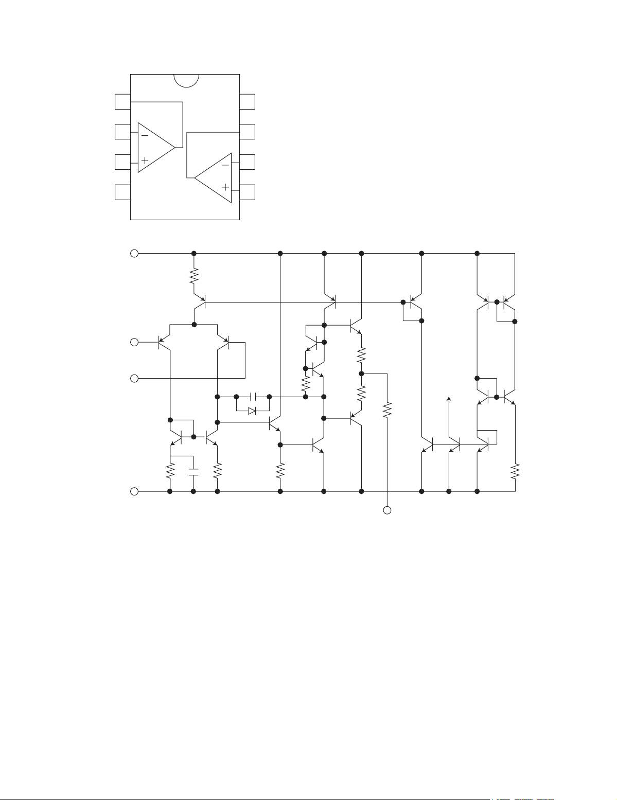
4.9 BA15218F-XE (IC251/IC540/IC544/IC546/IC548/IC557/IC560/IC562/IC564/IC566/IC711/IC712) : Dual operational amplifier
• Pin layout
OUT1 1
-IN1 2
+IN1 3
VEE 4
• Block diagram
Vcc
-IN
+IN
1
2
R1
Q5
Q1
Q2
D1
Q3 Q4
8 Vcc
7 OUT2
6 -IN2
5 +IN2
C2
R5
Q6
Q9
Q8
Q10
Q7
R7
Q11
R6
Q12
R8
Q18Q13
OTHER
CH
Q19
Q17Q16
VEE
C1
R3R2
R4
Q14 Q15Q114
R9
OUTPUT
(No.21189)1-25
Page 26
TH-A75R
4.10 BA6664FM-X (IC251) : Motor driver
• Pin layout
1
NC
2
A3
3
NC
4
A2
5
NC
6
NC
7
A1
29 30
8
GND
9
H1+
10
H1-
11
H2+
12
H2-
13
H3+
14
H3-
•Block diagram
RNF
28
VM
27
GSW
26
Vcc
25
FG
24
PS
23
EC
22
ECR
21
FR
20
FG2
19
SB
18
CNF
17
BR
16
VH-
15
GND
H1+
H1-
H2+
H2-
H3+
H3-
R
NF
28
VM
VCC
27
26
25
24
23
22
21
20
19
18
17
16
15
GSW
VCC
FG
PS
EC
ECR
FR
FG2
SB
CNF
BR
VH
A3
2
A2
DRIVER
GAIN
CONTROL
TSD
GAIN
SWITCH
4
CURRENT
A1
TL
SENSE AMP
+ -
7
8
9
10
11
12
13
HALL AMP
+
-
+
-
+
-
+
-
+
-
+
-
R
D Q
CK Q
PS
TOROUE
SENSE AMP
+
-
VCC
VCC
SHORT BRAKE
BRAKE MODE
14
Hall Bias
1-26 (No.21189)
Page 27

• Pin function
Pin No. Symbol I/O Description
1 NC - Non connect
2 A3 O Output 3 for spindle motor
3 NC - Non connect
4 A2 O Output 2 for spindle motor
5 NC - Non connect
6 NC - Non connect
7 A1 O Output 1 for spindle motor
8 GND - Connect to ground
9 H1+ I Positive input for hall input AMP 1
10 H1- I Negative input for hall input AMP 1
11 H2+ I Positive input for hall input AMP 2
12 H2- I Negative input for hall input AMP 2
13 H3+ I Positive input for hall input AMP 3
14 H3- I Negative input for hall input AMP 3
15 VH I Hall bias terminal
16 BR - Non connect
17 CNF - Capacitor connection pin for phase compensation
18 SB I Short brake terminal
19 FG2 - Non connect
20 FR - Non connect
21 ECR I Torque control standard voltage input terminal
22 EC I Torque control voltage input terminal
23 PS O Start/stop switch (power save terminal)
24 FG O FG signal output terminal
25 VCC - Power supply for signal division
26 GSW O Gain switch
27 VM - Power supply for driver division
28 RNF O Resistance connection pin for output current sense
29 - Connect to ground
30 - Connect to ground
TH-A75R
(No.21189)1-27
Page 28
TH-A75R
4.11BA5983FM-X (IC201) : 4-channel driver
•Block diagram
27
28
Vcc
26
10k
25
20k
23 22 30
24
10k
20k
21
STAND BY
CH4
20
Vcc
19
18
10k
10k
17 16
10k
Level Shift
10k
10k
10k
15
10k
10k
Level Shift
10k
10k
1
2
3
5
4
10k
6
• Pin function
Pin No. Symbol I/O Description
1 BIAS IN I Input for Bias-amplifier
2 OPIN1(+) I Non inverting input for CH1 OP-AMP
3 OPIN1(-) I Inverting input for CH1 OP-AMP
4 OPOUT1 O Output for CH1 OP-AMP
5 OPIN2(+) I Non inverting input for CH2 OP-AMP
6 OPIN2(-) I Inverting input for CH2 OP-AMP
7 OPOUT2 O Output for CH2 OP-AMP
8 GND - Substrate ground
9 STBY1 I Input for CH1/2/3 stand by control
10 PowVcc1 - Vcc for CH1/2 power block
11 VO2(-) O Inverted output of CH2
12 VO2(+) O Non inverted output of CH2
13 VO1(-) O Inverted output of CH1
14 VO1(+) O Non inverted output of CH1
15 VO4(+) O Non inverted output of CH4
Level Shift
10k
10k
Level Shift
10k
10k
10k
10k
10k
10k
10k
STAND BY
CH1/2/3
729 891011121314
Vcc
Pin No. Symbol I/O Description
16 VO4(-) O Inverted output of CH4
17 VO3(+) O Non inverted output of CH3
18 VO3(-) O Inverted output of CH3
19 PowVcc2 - Vcc for CH3/4 power block
20 STBY2 I Input for Ch4 stand by control
21 GND - Substrate ground
22 OPOUT3 O Output for CH3 OP-AMP
23 OPIN3(-) I Inverting input for CH3 OP-AMP
24 OPIN3(+) I Non inverting input for CH3 OP-AMP
25 OPOUT4 O Output for CH4 OP-AMP
26 OPIN4(-) I Inverting input for CH4 OP-AMP
27 OPIN4(+) I Non inverting input for CH4 OP-AMP
28 PreVcc - Vcc for pre block
29 - Connect to ground
30 - Connect to ground
1-28 (No.21189)
Page 29
4.12BA7603F-X (IC211/IC221) : Video signal switcher
• Pin layout & Block diagram
IN1a
GND
IN2b
Vcc
OUTb
IN1b
GND
IN1c
16 15 14 13 12 11 10 9
SWa
SWb
12345678
SWc
TH-A75R
CTL OUTPUT
HIN2
LIN1
SWa,SWb,SWc: Clamp inputs
IN2a
CTLa
GND
OUTa
OUTb
OUTc
CTLc
IN2c
4.13 BD4740G-W (IC272) : Reset
• Pin layout • Block diagram
54
Vcc Vout
NC SUB GND
123
Vref
Vcc
5
3
GND
4
Vout
(No.21189)1-29
Page 30
TH-A75R
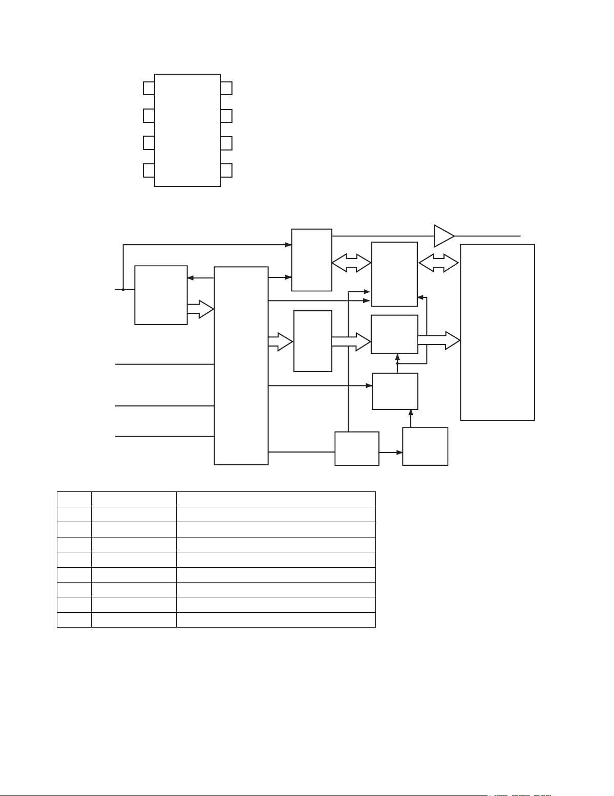
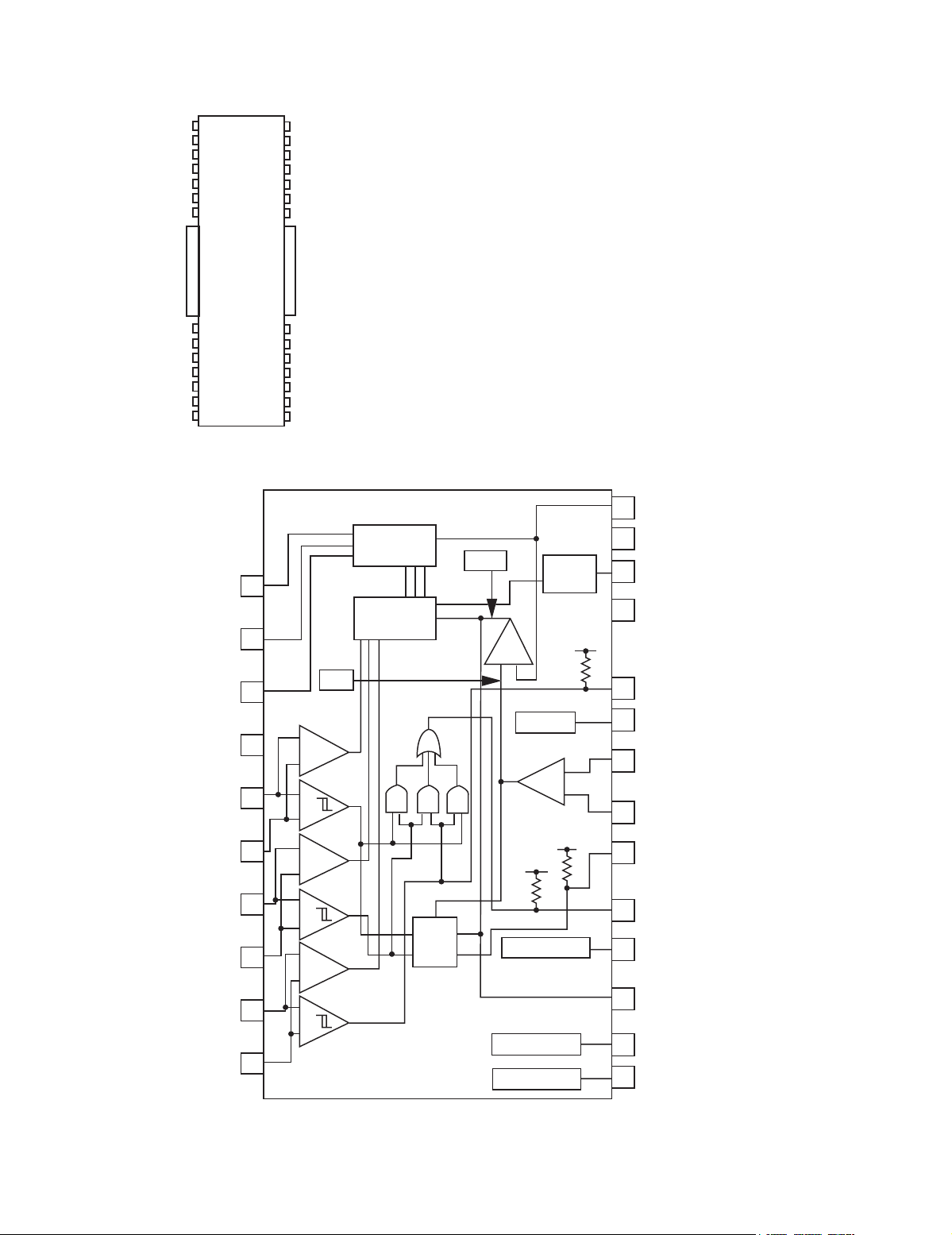
4.14 DSPC56367PV150 (IC521) : DSP
• Pin layout
144 109~
1~36
37 72~
•Block diagram
1
TRIPLE
TMER
(SPDIF Tx)
INTER-FA
INTERNAL
2
DAX
CE
ADDRESS
GENERATION
SIX CHANNELS
DATA
BUS
UNIT
DMA UNIT
HOST
INTER-
FACE
108 ~ 73
8
16
ESAI
INTER-
FACE
ESAI_1
EXPANSION AREA
PIO_EB
4
6
INTER-
PERIPHERAL
24-BIT
DSP56300
Core
SHI
FACE
5
MEMORY EXPANSION AREA
PROGRAM
RAM
/INSTR.
CACHE
3K x 24
PROGRAM
ROM
40K x 24
Bootstrap
DDB
YDB
XDB
PDB
GDB
PM_EB
YAB
XAB
PAB
DAB
X MEMORY
RAM
13K x 24
ROM
32K x 24
XM_EB
Y MEMORY
RAM
7K x 24
ROM
8K x 24
YM_EB
EXTERNAL
ADDRESS
SWITCH
DRAM &
SRAM BUS
INTERFACE
I-CACHE
EXTERNAL
DATA BUS
SWITCH
BUS
&
18
ADDRESS
10
CONTROL
24
DATA
1-30 (No.21189)
PLL
CLOCL
GENERAT
EXTAL
RESET
PINT/NMT
PROGRAM
INTERRUPT
CONTOROLLER
PROGRAM
DECODE
CONTOROLLE
MODA/IRQA
MODB/IRQB
MODC/IRQC
MODD/IRQD
PROGRAM
ADDRESS
GEBERATOR
DATA ALU
24X24+56>56BIBT MAC
TWO 56BIT ACCUMULATORS
BARREL SHIFTER
24 BITS BUS
POWER
GNGMNT
JTAG
OnCE
4
TW
Page 31

• Pin function
Pin No Symbol I/O Function
1 SCK/SCL I/O SPI serial clock / I2C serial clock
2SS
3 HREQ
4 SDO0/SDO0_1 O Serial data output 0
5 SDO1/SDO1_1 O Serial data output 1
6 SDO2/SDI3/SDO2_1/SDI3_1 O Serial data output 2 / Serial data input 3
7 SDO3/SDI2/SDO3_1/SDI2_1 O Serial data output 3 / Serial data input 2
8 VCCS - SHI,ESAI,ESAI_1,DAX and Timer power
9 GNDS - SHI,ESAI,ESAI_1,DAX and Timer ground
10 SDO4/SDI1 O Serial data output 4 / Serial data input 1
11 SDO5/SDI0 O Serial data output 5 / Serial data input 0
12 FST I/O Frame sync for transmitter
13 FSR I/O Frame sync for receiver
14 SCKT I/O Transmitter serial clock
15 SCKR I/O Receiver serial clock
16 HCKT I/O High frequency clock for transmitter
17 HCKR I/O High frequency clock for receiver
18 VCCQL - Quite core (Low) power
19 GNDQ - Quite ground
20 VCCQH - Quite external (High) power
21 HDS/HWR I Host data strobe / Host write data
22 HRW/HRD I Host read write / Host read data
23 HACK/HRRQ I Host acknowledge / Receive host request
24 HOREQ/HTRQ O Host request / Transmit host request
25 VCCS - SHI,ESAI,ESAI_1,DAX and Timer power
26 GNDS - SHI,ESAI,ESAI_1,DAX and Timer ground
27 ADO O Digital audio data output
28 ACI I Audio clock input
29 TIO0 I/O Timer 0 schmitt-trigger input/output
30 HCS/HA10 I Host chip select / Host address 10
31 HA9/HA2 I Host address 9 / Host address input 2
32 HA8/HA1 I Host address 8 / Host address input 1
33 HAS/HA0 I Host address strobe / Host address input 0
34~37 HAD7~HAD4 I/O Host address/Data
38 VCCH - Host power
39 GNDH - Host ground
40~43 HAD3~HAD0 I/O Host address/Data
44 RESET
45 VCCP - PLL power
46 PCAP I PLL capacitor
47 GNDP - PLL ground
48 SDO5_1/SDI0_1 I/O Serial data output 5_1 / Serial data input 0_1
49 VCCQH - Quite external (High) power
50 FST_1 I/O Frame sync for transmitter
51 AA2 O Address attribute or Row address strobe
52 CAS
53 SCKT_1 I/O Transmitter serial clock_1
54 GNDQ - Quite ground
55 EXTAL I External clock input
56 VCCQL - Quite core (Low) power
57 VCCC - Bus control power
58 GNDC - Bus control ground
/HA2 I SPI slave select / I2C slave address 2
I/O Host request
I Reset
O Column address strobe
TH-A75R
(No.21189)1-31
Page 32

TH-A75R
Pin No Symbol I/O Function
59 FSR_1 I/O Frame sync for receiver
60 SCKR_1 I/O Receiver serial clock_1
61 PINIT/NMI
62 TA
63 BR
64 BB
65 VCCC - Bus control power
66 GNDC - Bus control ground
67 WR O Write enable
68 RD
69,70 AA1,AA0 O Address attribute or row address strobe
71 BG
72,73 A0,A1 O Data bus
74 VCCA - Address bus power
75 GNDA - Address bus ground
76~79 A2~A5 O Data bus
80 VCCA - Address bus power
81 GNDA - Address bus ground
82~85 A6~A9 O Data bus
86 VCCA - Address bus power
87 GNDA - Address bus ground
88,89 A10,A11 O Data bus
90 GNDQ - Quite ground
91 VCCQL - Quite core (Low) power
92~94 A12~A14 O Data bus
95 VCCQH - Quite core (High) power
96 GNDA - Address bus ground
97~99 A15~A17 O Data bus
100~102 D0~D2 I/O Data bus
103 VCCD - Data bus power
104 GNDD - Data bus ground
105~110 D3,D8 I/O Data bus
111 VCCD - Data bus power
112 GNDD - Data bus ground
113~118 D9~D14 I/O Data bus
119 VCCD - Data bus power
120 GNDD - Data bus ground
121~125 D15~D19 I/O Data bus
126 VCCQL - Quite core (Low) power
127 GNDQL - Quite core (Low) ground
128 D20 I/O Data bus
129 VCCD - Data bus power
130 GNDD - Data bus ground
131~133 D21~D23 I/O Data bus
134 MODD/IRQD
135 MODC/IRQC
136 MODB/IRQB
137 MODA/IRQA
138 SDO4_1/SDI1_1 I/O Serial data output 4_1 / Serial data input 1_1
139~142 TDO,TDI,TCK,TMS O/I Test data output,Test data input,Test clock,Test mode select
143 MOSI/HA0 I/O SPI master-out-sleve-in / I2C slave address 0
144 MISO/SDA I/O SPI master-in-slave-out / I2C data and acknowkedge
I PLL initial / Nonmaskable interrupt
I Transfer acknowledge
O Bus request
I/O Bus busy
O Read enable
I Bus grant
I Mode select D / External interrupt request D
I Mode select C / External interrupt request C
I Mode select B / External interrupt request B
I Mode select A / External interrupt request A
1-32 (No.21189)
Page 33

4.15 GP1FA351RZ (J5521) : Fiber optic receiver
• Pin layout
4.16 GP1UM271XK (IC402) : IR detecting unit for remote control
• Block diagram
AMP
AMP
AMP
AMP
Comp & Output circuit
R
TH-A75R
V
CC
V
OUT
GND
L
Amp
B.P.FLimiter
Demodulator
4.17 IS63LV102410K-X (IC525/IC526/IC527) : SRAM
• Pin layout • Block diagram
32
31
30
29
28
27
26
25
24
23
22
21
20
19
18
17
A16
A15
A14
A13
OE
I/O7
I/O6
GND
Vcc
I/O5
I/O4
A12
A11
A10
A9
A8
A0-A16
VCC
GND
I/O0-I/O7
CE
OE
WE
A0
A1
A2
A3
CE
I/O0
I/O1
Vcc
GND
I/O2
I/O3
WE
A4
A5
A6
A7
1
2
3
4
5
6
7
8
9
10
11
12
13
14
15
16
• Pin function
Pin No. Symbol I/O Function
1-4 A0-A3 I Address inputs
5CE
I Chip enable input
6,7 I/O0,I/O1 I/O Bidirectional ports
8Vcc-Power
9GND-Ground
10,11 I/O2,I/O3 I/O Bidirectional ports
12 WE
I Write enable input
Pin No. Symbol I/O Function
13-21 A4-A12 I Address inputs
22,23 I/O4,I/O5 I/O Bidirectional ports
24 Vcc - Power
25 GND - Ground
26,27 I/O6,I/O7 I/O Bidirectional ports
28 OE
29-32 A13-A16 I Address inputs
Integrator
Comparator
GND Vcc Vout
DECODER
I/O
DATA
CIRCUIT
CONTROL
CIRCUIT
128K X 8
MEMORY ARRAY
COLUMN I/O
I Output enable input
(No.21189)1-33
Page 34

TH-A75R
A
4.18 K4S643232E-TC60 (IC505) : 512K x 32 bit x 4 banks synchronous DRAM
• Pin layout
1
86
•Block diagram
43
CLK
DD
Address Register
LCKE
44
Bank Select
Row Buffer
Refresh Counter
LRAS
LCBR
LRAS LCBR LWE
CLK CKE CS
LCAS
Row Decoder
Col. Buffer
Timing Register
RAS CAS
Data Input Register
512K x 32
512K x 32
512K x 32
512K x 32
Column Decoder
Latency & Burst Length
Programming Register
LWCBR
WE DQM
Sense AMP
LDQM
LWE
LDQM
I/O Control
DQi
Output Buffer
1-34 (No.21189)
Page 35

• Pin function
Pin No. Symbol Function
1 VDD Power for the input buffers and core logic.
2 DQ0 Data input/output are multiplexed on the same pin.
3 VDDQ Isolated power supply for the output buffers to provide improved noise immunity.
4,5 DQ1,DQ2 Data inputs/outputs are multiplexed on the same pins.
6 VSSQ Isolated ground for the output buffers to provide improved noise immunity.
7,8 DQ3,DQ4 Data inputs/outputs are multiplexed on the same pins.
9 VDDQ Isolated power supply for the output buffers to provide improved noise immunity.
10,11 DQ5,DQ6 Data inputs/outputs are multiplexed on the same pins.
12 VSSQ Isolated ground for the output buffers to provide improved noise immunity.
13 DQ7 Data input/output are multiplexed on the same pin.
14 N.C This pin is recommended to be left no connection on the device.
15 VDD Power for the input buffers and core logic.
16 DQM0 Makes data output Hi-Z, tSHZ after the clock and masks the output.
Blocks data input when DQM active.
17 WE
18 CAS
19 RAS
20 CS
21 N.C This pin is recommended to be left no connection on the device.
22,23 BA0,BA1 Selects bank to be activated during row address latch time.
24,25~27 A10,A0 - A2 Row/column addresses are multiplexed on the same pins.
28 DQM2 Makes data output Hi-Z, tSHZ after the clock and masks the output.
29 VDD Power for the input buffers and core logic.
30 N.C This pin is recommended to be left no connection on the device.
31 DQ16 Data input/output are multiplexed on the same pin.
32 VSSQ Isolated ground for the output buffers to provide improved noise immunity.
33,34 DQ17,DQ18 Data inputs/outputs are multiplexed on the same pins.
35 VDDQ Isolated power supply for the output buffers to provide improved noise immunity.
36,37 DQ19,DQ20 Data inputs/outputs are multiplexed on the same pins.
38 VSSQ Isolated ground for the output buffers to provide improved noise immunity.
39,40 DQ21,DQ22 Data inputs/outputs are multiplexed on the same pins.
41 VDDQ Isolated power supply for the output buffers to provide improved noise immunity.
42 DQ23 Data input/output are multiplexed on the same pin.
43 VDD Power for the input buffers and core logic.
44 VSS Ground for the input buffers and core logic.
45 DQ24 Data input/output are multiplexed on the same pin.
46 VSSQ Isolated ground for the output buffers to provide improved noise immunity.
47,48 DQ25,DQ26 Data inputs/outputs are multiplexed on the same pins.
49 VDDQ Isolated power supply for the output buffers to provide improved noise immunity.
50,51 DQ27,DQ28 Data inputs/outputs are multiplexed on the same pins.
52 VSSQ Isolated ground for the output buffers to provide improved noise immunity.
Enables write operation and row precharge.
Latches data in starting from CAS, WE active.
Latches column addresses on the positive going edge of the CLK with CAS low.
Enables column access.
Latches row addresses on the positive going edge of the CLK with RAS low.
Enables row access & precharge.
Disables or enables device operation by masking or enabling all inputs except CLK, CKE and DQM.
Selects bank for read/write during column address latch time.
Row address : RA0 ~ RA10, Column address : CA0 ~ CA7
Blocks data input when DQM active.
TH-A75R
(No.21189)1-35
Page 36

TH-A75R
Pin No. Symbol Function
53,54 DQ29,DQ30 Data inputs/outputs are multiplexed on the same pins.
55 VDDQ Isolated power supply for the output buffers to provide improved noise immunity.
56 DQ31 Data input/output are multiplexed on the same pin.
57 N.C This pin is recommended to be left no connection on the device.
58 VSS Ground for the input buffers and core logic.
59 DQM3 Makes data output Hi-Z, tSHZ after the clock and masks the output.
Blocks data input when DQM active.
60~66 A3 - A9 Row/column addresses are multiplexed on the same pins.
Row address : RA0 - RA10, Column address : CA0 - CA7
67 CKE Masks system clock to freeze operation from the next clock cycle.
CKE should be enabled at least one cycle prior to new command.
Disables input buffers for power down mode.
68 CLK Active on the positive going edge to sample all inputs.
69,70 N.C This pin is recommended to be left no connection on the device.
71 DQM1 Makes data output Hi-Z, tSHZ after the clock and masks the output.
Blocks data input when DQM active.
72 VSS Ground for the input buffers and core logic.
73 N.C This pin is recommended to be left no connection on the device.
74 DQ8 Data input/output are multiplexed on the same pin.
75 VDDQ Isolated power supply for the output buffers to provide improved noise immunity.
76,77 DQ9,DQ10 Data inputs/outputs are multiplexed on the same pins.
78 VSSQ Isolated ground for the output buffers to provide improved noise immunity.
79,80 DQ11,DQ12 Data inputs/outputs are multiplexed on the same pins.
81 VDDQ Isolated power supply for the output buffers to provide improved noise immunity.
82,83 DQ13,DQ14 Data inputs/outputs are multiplexed on the same pins.
84 VSSQ Isolated ground for the output buffers to provide improved noise immunity.
85 DQ15 Data input/output are multiplexed on the same pin.
86 VSS Ground for the input buffers and core logic.
1-36 (No.21189)
Page 37

4.19 K4S643232E-TC70 (IC505) : 512K x 32 bit x 4 banks synchronous DRAM
A
• Pin layout
1
86
TH-A75R
• Block diagram
43
CLK
DD
Address Register
LCKE
44
Bank Select
Row Buffer
Refresh Counter
LRAS
LCBR
LRAS LCBR LWE
CLK CKE CS
LCAS
Row Decoder
Col. Buffer
Timing Register
RAS CAS
Data Input Register
512K x 32
512K x 32
512K x 32
512K x 32
Column Decoder
Latency & Burst Length
Programming Register
LWCBR
WE DQM
Sense AMP
LDQM
LWE
LDQM
I/O Control
DQi
Output Buffer
(No.21189)1-37
Page 38

TH-A75R
• Pin function
Pin No. Symbol Function
1 VDD Power for the input buffers and core logic.
2 DQ0 Data input/output are multiplexed on the same pin.
3 VDDQ Isolated power supply for the output buffers to provide improved noise immunity.
4,5 DQ1,DQ2 Data inputs/outputs are multiplexed on the same pins.
6 VSSQ Isolated ground for the output buffers to provide improved noise immunity.
7,8 DQ3,DQ4 Data inputs/outputs are multiplexed on the same pins.
9 VDDQ Isolated power supply for the output buffers to provide improved noise immunity.
10,11 DQ5,DQ6 Data inputs/outputs are multiplexed on the same pins.
12 VSSQ Isolated ground for the output buffers to provide improved noise immunity.
13 DQ7 Data input/output are multiplexed on the same pin.
14 N.C This pin is recommended to be left no connection on the device.
15 VDD Power for the input buffers and core logic.
16 DQM0 Makes data output Hi-Z, tSHZ after the clock and masks the output.
Blocks data input when DQM active.
17 WE
18 CAS
19 RAS
20 CS
21 N.C This pin is recommended to be left no connection on the device.
22,23 BA0,BA1 Selects bank to be activated during row address latch time.
24,25~27 A10,A0 - A2 Row/column addresses are multiplexed on the same pins.
28 DQM2 Makes data output Hi-Z, tSHZ after the clock and masks the output.
29 VDD Power for the input buffers and core logic.
30 N.C This pin is recommended to be left no connection on the device.
31 DQ16 Data input/output are multiplexed on the same pin.
32 VSSQ Isolated ground for the output buffers to provide improved noise immunity.
33,34 DQ17,DQ18 Data inputs/outputs are multiplexed on the same pins.
35 VDDQ Isolated power supply for the output buffers to provide improved noise immunity.
36,37 DQ19,DQ20 Data inputs/outputs are multiplexed on the same pins.
38 VSSQ Isolated ground for the output buffers to provide improved noise immunity.
39,40 DQ21,DQ22 Data inputs/outputs are multiplexed on the same pins.
41 VDDQ Isolated power supply for the output buffers to provide improved noise immunity.
42 DQ23 Data input/output are multiplexed on the same pin.
43 VDD Power for the input buffers and core logic.
44 VSS Ground for the input buffers and core logic.
45 DQ24 Data input/output are multiplexed on the same pin.
46 VSSQ Isolated ground for the output buffers to provide improved noise immunity.
47,48 DQ25,DQ26 Data inputs/outputs are multiplexed on the same pins.
49 VDDQ Isolated power supply for the output buffers to provide improved noise immunity.
50,51 DQ27,DQ28 Data inputs/outputs are multiplexed on the same pins.
52 VSSQ Isolated ground for the output buffers to provide improved noise immunity.
Enables write operation and row precharge.
Latches data in starting from CAS, WE active.
Latches column addresses on the positive going edge of the CLK with CAS low.
Enables column access.
Latches row addresses on the positive going edge of the CLK with RAS low.
Enables row access & precharge.
Disables or enables device operation by masking or enabling all inputs except CLK, CKE and DQM.
Selects bank for read/write during column address latch time.
Row address : RA0 ~ RA10, Column address : CA0 ~ CA7
Blocks data input when DQM active.
1-38 (No.21189)
Page 39

Pin No. Symbol Function
53,54 DQ29,DQ30 Data inputs/outputs are multiplexed on the same pins.
55 VDDQ Isolated power supply for the output buffers to provide improved noise immunity.
56 DQ31 Data input/output are multiplexed on the same pin.
57 N.C This pin is recommended to be left no connection on the device.
58 VSS Ground for the input buffers and core logic.
59 DQM3 Makes data output Hi-Z, tSHZ after the clock and masks the output.
Blocks data input when DQM active.
60~66 A3 - A9 Row/column addresses are multiplexed on the same pins.
Row address : RA0 - RA10, Column address : CA0 - CA7
67 CKE Masks system clock to freeze operation from the next clock cycle.
CKE should be enabled at least one cycle prior to new command.
Disables input buffers for power down mode.
68 CLK Active on the positive going edge to sample all inputs.
69,70 N.C This pin is recommended to be left no connection on the device.
71 DQM1 Makes data output Hi-Z, tSHZ after the clock and masks the output.
Blocks data input when DQM active.
72 VSS Ground for the input buffers and core logic.
73 N.C This pin is recommended to be left no connection on the device.
74 DQ8 Data input/output are multiplexed on the same pin.
75 VDDQ Isolated power supply for the output buffers to provide improved noise immunity.
76,77 DQ9,DQ10 Data inputs/outputs are multiplexed on the same pins.
78 VSSQ Isolated ground for the output buffers to provide improved noise immunity.
79,80 DQ11,DQ12 Data inputs/outputs are multiplexed on the same pins.
81 VDDQ Isolated power supply for the output buffers to provide improved noise immunity.
82,83 DQ13,DQ14 Data inputs/outputs are multiplexed on the same pins.
84 VSSQ Isolated ground for the output buffers to provide improved noise immunity.
85 DQ15 Data input/output are multiplexed on the same pin.
86 VSS Ground for the input buffers and core logic.
TH-A75R
(No.21189)1-39
Page 40

TH-A75R
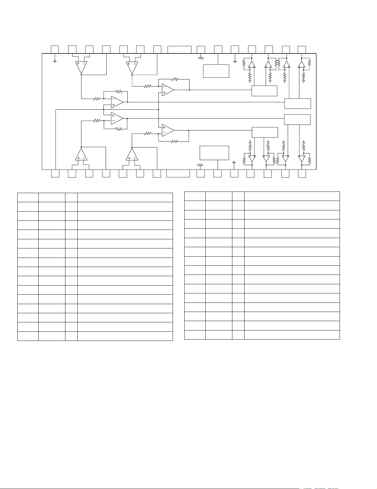
4.20 LA73054-X (IC231) : Video driver
• Pin layout & Block diagram
36 35 34 33 32 31 30 29 28 27 26 25 24 23 22 21 20 19
75
DRIVER
LPF
2Step
Amp1
C_OFFSET
DC_CTL
CLAMP
1 2 3 4 5 6 7 8 9 10 11 12 13 14 15 16 17 18
75
DRIVER
LPF1
2Step
Amp2
Y/C
MIX
75
DRIVER
LPF1
2Step
Amp3
CLAMP
SYNC
SEP
PEDESTAL
CLAMP
• Pin function
Pin No. Symbol I/O Function
1 VCC1 - VCC except for 75ohm driver
2 COMPOSITE.IN I Input composite
3 SQUEEZE.SW I Selecting squeeze mode
4 LETTER-BOX.SW I Selecting letter-box mode
5 MUTE-SW-1 I Composite/S signal mute selection
6 C-IN I Input Chroma signal
7 GND11 - Composite/S GND except for 75ohm driver
8 Y-IN-1 I Input Y signal
9 YC-MIX.SW I Selecting of doing Y/C-MIX or not
10 SIGNAL-IN.SW I Selection of a kind of signal
11 Y-IN-2 I Input component Y or baseband signal
12 MUTE-SW-2 I Component signal mute selection
13 LPF.SW I Selection of a kind of component LPF
14 CB.IN I Input component or baseband signal
15 AMP.SW-2 I Selecting amplifier gain for component signal
16 CR.IN I Input component or baseband signal
17 GND12 - Component GND except for 75ohm driver
18 REG O Capacitor terminal for regulator
19 DRIVE.SW-2 I 2drive/1drive select for component signal
20 GND26 - CR-GND for 75ohm driver
21 CR.OUT O 75ohm driver output of pin16 input
22 GND25 - CB-OUT for 75ohm driver
23 CB.OUT O 75ohm driver output of pin14 input
24 VCC22 - Component Vcc for 75ohm driver
25 Y-OUT-2 O 75ohm driver output of pin11 input
26 GND24 - Component Y out for 75ohm driver
27 GND23 - Y out for 75ohm driver
28 Y-OUT-1 O 75ohm driver output of pin8 input
29 GND22 - Chroma out for 75ohm driver
30 C-DC.OUT O DC voltage output for S1,S2
31 C-OUT O 75ohm driver output of pin6 input
32 GND21 - Composite out for 75ohm driver
33 COMPOSITE-OUT O 75ohm driver output of pin2 input
34 VCC21 - Composite/S Vcc for 75ohm driver
35 DRIVE.SW-1 I 2drive/1drive select for composite/S signal
36 AMP.SW-1 I Selecting amplifier gain for composite/S signal
75
DRIVER
2Step
Amp4
LPF1LPF2
CLAMP
75
DRIVER
LPF1LPF2 LPF1LPF2
2Step
Amp5
PEDESTAL
CLAMP
75
DRIVER
2Step
Amp6
PEDESTAL
CLAMP
VCC
REG
1-40 (No.21189)
Page 41

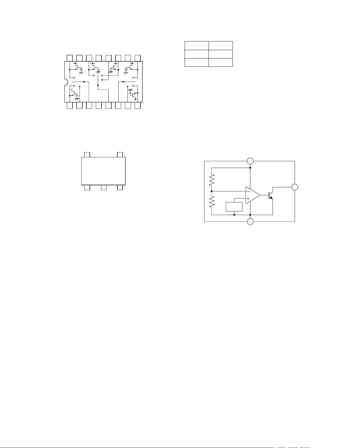
4.21 LM1117MP1.8-X (IC511) : Regulator
A
• Pin layout • Block diagram
Top view
TH-A75R
VIN
DJ/GND
OUTPUT
INPUT
Thermal
Limit
Current
Limit
GND (FIXED OUTPUT)
ADJ.(ADJUSTABLE OUTPUT)
VOUT
Substrate
(No.21189)1-41
Page 42

TH-A75R
A
4.22 M61516FP (IC551) : Sound controller
• Pin layout & Block diagram
TONEOUT R
FRVIN FROUT
40
39
FROUT
SROUT
38
37
SBOUT
SWOUT
36
35
COUT
34
SBLOUT
SLOUT
33
32
FLOUT
OUTGND
31
30
AVC C
29
DGND
CLOCK
28
27
DATA
26
LATCH
25
TRE R
BASS R2
BASS R1
FRIN2
SRIN2
SBRIN2
SWIN2
CIN2
SBLIN2
SLIN2
FLIN2
VOLGND3
VOLGND4
BALANCE L/+
BALANCE L/-/LOUD L
INGND
BALANCE R/-/LOUD R
BALANCE R/+
REC R4
REC R3
REC R2
REC R1
41
42
43
44
45
46
47
48
49
50
51
52
53
54
55
56
57
BALNCE/LOUDNESS
58
50K 50K 50K 50K
59
60
61
62
TONE OUTPUT
SELECTOR
FRONT INPUT
SELECTOR
BALNCE/LOUDNESS
CHANGE SW
A
LOUDNESS TAP
B
CHANGE SW
REC SW
REC SW
REC SW
REC SW
OUTPUT GAIN
+
TONE
BASS/TRE
10K
+
-
Lch
10K
BALANCE OUTPUT
Rch
10K
+
10K
INPUT GAIN
CONTROL
CONTROL
50K
-
-
50K
FL VOL
LOUDNESS
TAP B
-
+
50K
SR VOL
SBR VOL SBL VOL SL VOLSW VOL C VOL
+
50K
+
50K
LOUDNESS
TAP A
+-+-+-+-+
50K 50K 50K 50K 50K
-
+
INPUT
SELECTOR
SELECTOR
OUTPUT GAIN
CONTROL
50K
+
-
FL VOL
INPUT
ZERO CROSS
DETECTOR &
TIMER DETECTOR
+
-
-
INPUT GAIN
CONTROL
-
+
50K
+
-
MCU
I/F
TONE OUTPUT
SELECTOR
TONE
BASS/TRE
FRONT INPUT
SELECTOR
REC SW
REC SW
REC SW
REC SW
50K 50K 50K 50K
24
23
22
21
20
19
18
17
16
15
14
13
12
11
10
9
8
7
6
5
4
3
DVDD
TINT
VOLGND2
FLVIN
TNEOUT
TREL
BASS L2
BASS L1
FRIN1
SRIN1
SBRIN1
SWIN1
CIN1
SBLIN1
SLIN1
FLIN1
VOLGND1
REC L4
REC L3
REC L2
REC L1
INLJ
1-42 (No.21189)
INRJ
INRI
63
64
65
INRH
66
INRG
67
INRF
68
INRE
69
INRD
70
INRC
71
INRB
72
INRA
73
VEE
74
INLA
75
INLB
76
INLC
77
INLD
78
INLE
79
INLF
80
INLG
2
INLI
1
INLH
Page 43

• Pin function
Pin No. Symbol Function
1~3 INLH,INLI,INLJ Lch input
4~7 REC L1,REC L2,REC L3,REC L4 REC output
8 VOLGND1 Analog GND for vol.
9~12 FLIN1,SLIN1,SBLIN1,CIN1 FLch,SLch,SBLch,Cch input
13~16 SWIN1,SBRIN1,SRIN1,FRIN1 SWch,SBRch,SRch,FRch input
17,18 BASS L1,BASS L2 Tone path frequency characteristic setup
19 TRE L Treble frequency characteristic setup
20 TONEOUT L Tone output
21 FLVIN FL vol. input
22 VOLGND2 Analog GND for vol.
23 TIM1 Timer setup
24 DVDD Internal logic circuit Power supply terminal
25,26,27 LATCH,DATA,CLOCK Latch,Data,Clock input for serial data transmission
28 DGND Internal logic circuit GND terminal
29 AVCC Internal analog cicuit power supply terminal (+)
30 OUTGND analog GND
31~34 FLOUT,SLOUT,SBLOUT,COUT FLch,SLch,SBLch,Cch output
35~38 SWOUT,SBROUT,SROUT,FROUT SWch,SBRch,SRch,FRch output
39 FRVIN FR vol.input
40 TONEOUT R Tone output
41 TRE R Treble frequency characteristic setup
42,43 BASS R1,BASS R2 Tone path frequency characteristic setup
44~47 FRIN2,SRIN2,SBRIN2,SWIN2 FRch,SRch,SBRch,SWch input
48~51 CIN2,SBLIN2,SLIN2,FLIN2 Cch,SBLch,SLch,FLch input
52,53 VOLGND3,VOLGND4 Analog GND for vol.
54 BALANCE L/+ Lch balance output for ADC
55 BALANCE L/- LOUD L Lch loudness frequency setup
56 INGND Analog GND
57 BALANCE R/+ Rch balance output for ADC
58 BALANCE R/- LOUD R Rch loudness frequency setup
59~62 REC R1,REC R2,REC R3,REC R4 REC input
63~66 INRJ,INRI,INRH,INRG Rch input
67~70 INRF,INRE,INRD,INRC Rch input
71,72 INRB,INRA Rch input
73 AVEE Internal analog circuit power supply terminal (-)
74~77 INLA,INLB,INLC,INLD Lch input
78~80 INLE,INLF,INLG Lch input
TH-A75R
(No.21189)1-43
Page 44

TH-A75R
4.23 MM1561KF-X (IC593) : Regulator
• Pin layout
756
(TOP VIEW)
1
234
•Block diagram
VIN
7
Cont
5
GND
3
• Pin function
Pin No. Symbol Function
1 Vo Output pin
2 NC Not connect
3 GND Ground
4 Cn Noise decrease pin
5 CONT Control pin
Bias
Thermal
shutdown
Driver
Current
limiter
Cn
Vo
1
Reference
4
CONT
H
L
Output
ON
OFF
6 Sub Substrate pin, The 6pin must be connected to GND.
7 VIN Input pin
1-44 (No.21189)
Page 45

4.24 MM1563DF-X (IC592) : Regulator
• Pin layout
756
(TOP VIEW)
1
234
• Block diagram
VIN
7
Bias
Cont
5
Thermal
shutdown
GND
3
• Pin function
Pin No. Symbol Function
1 Vo Output pin
2 NC Not connect
3 GND Ground
4 Cn Noise decrease pin
5 CONT Control pin
Driver
Current
limiter
Cn
TH-A75R
Vo
1
Reference
4
CONT
H
L
Output
ON
OFF
6 Sub Substrate pin, The 6pin must be connected to GND.
7 VIN Input pin
(No.21189)1-45
Page 46

TH-A75R
4.25 MN101C49GKR (IC271) : System micom
• Pin layout
100 76
1
75
25
51
26 50
• Pin function
Pin No. Symbol I/O Function
1 VREF- - Connect to ground
2 NTSEL(RGB--SEL) I NTSC/PAL discrimination (RGB/YC switching discrimination) signal
3 VCR-S/C I VCR S/Composite detection signal
4 DBS-S/C I DBS S/Composite detection signal
5 TH-DET I Heat sink temp. detection
6 SAFETY1 I Short detection signal
7 VERSION I Version select switch signal
8 KEY-IN1 I Key input1 (AD)
9 KEY-IN2 I Key input2 (AD)
10 VREF+ - Reference power supply
11 VDD - Power supply
12 OSC2 O Oscillator output (8MHz)
13 OSC1 I Oscillator input (8MHz)
14 GND - Ground
15,16 NC - Not used
17 GND - Ground
18 DI-DO O Panel serial communication data output
19 NC - Not used
20 DI-CK O Panel serial communication clock output
21 S2UDT/TX (DATA OUT) O Serial communication data output for PANTERA
22 S2UDT/RX (DATA IN) I Serial communication data input for PANTERA
23 SCLK/CLK I Serial communication clock for PANTERA
24 INTP O Transmit request for PANTERA communication
25 CPU-RESET O Reset signal for PANTERA
26 CS I Receive request for PANTERA communication (Interruption)
27 REMOCON I Remote control signal input (interruption)
28 PROTECT I Speaker protect detection
29 RDS ST I RDS communication strobe (Interruption)
30 NC - Not used
31 GND - Ground
32 VDD2/FLASH-VDD - VDD for Flash write
33 RESET-IN/RST I System control micom reset input
34 DSP-RST O DSP micom reset signal output
35 DSP-RDY O DSP micom ready signal
36 AVC-OUT O AV compulink signal output
37 AVC-IN I AV compulink signal input
38~40 NC - Not used
41 VPP/FLASH-VSS - VPP for Flash write
42 DSP-COM O DSP serial communication data output
43 DSP-STAT I DSP serial communication data input
44 DSP-CLK O DSP serial communication clock
45 VOL-DATA O VOLUME serial communication data output
46 VOL-LATCH O VOLUME serial communication strobe
47 VOL-CLK O VOLUME serial communication clock
1-46 (No.21189)
Page 47

Pin No. Symbol I/O Function
48 NC - Not used
49 INT/PROG O Video driver filter select
50 RELAT-CTL O Speaker control
51 BASS O Bass boost control
52,53 NC - Not used
54 VIDEO-MUTE1 O Video driver mute1 control
55 VIDEO-MUTE2 O Video driver mute2 control
56 VIDEO-YCMIX O Video driver YCMIX control
57 VIDEO-RGB O Video driver RGB control
58 NC - Not used
59 INH I AC cut of detection
60 NC - Not used
61 HP I Headphone input detection
62 S-PON O System power supply control
63 AMP-PON O Power amp. power supply control
64 DVD-PON O DVD power supply control
65 TU-PON O TUNER power supply control
66 - - Not used
67 RDS-DATA O RDS communication data
68 RDS-CLK O RDS communication clock
69 NC - Not use
70 TU-DI I TUNER serial communication data input
71 NC - Not use
72 TU-DO O TUNER serial communication data output
73 TU-CLK O TUNER serial communication clock
74 TU-CE O TUNER serial communication CE
75 AM-BEAT O AM beat cut switching
76 S-MUTE O System mute
77,78 VS1,VS3 O E version SLOW switch control
79 FAN-ON/OFF O Fan ON/OFF control
80 FAN-CTL O Fan speed control
81 STBY-LED O STANDBY LED control
82 DISC-SET O Read start signal output for Frontend
83 DISC-STOP I Receive eject permission signal from Frontend
84 SAFETY2 I Short detection2
85,86 NC - Not used
87 VIDEO-SW1 O Video select output1
88 VIDEO-SW2 O Video select output2
89 VIDEO-SW3 O Video select output3
90 BLANK-CTL O E version BLANKING select
91 DI-RST O Panel micom reset output
92 DI-CS O Panel micom serial communication chip select
93 NC - Not used
94 TOPEN O Mechanism open output
95 DAVSS - Ground
96 TCLOSE O Mechanism close output
97 LMMUTE O Loader mute output
98 SWOPEN I Mechanism switch open detection
99 SWUPDN I Mechanism switch close detection
100 DAVDD - Power supply
TH-A75R
(No.21189)1-47
Page 48

TH-A75R
4.26 74LCX32MTC-X (IC522) : Quad 2 input OR gate
• Pin layout & Block diagram
11A
21B
31Y
42A
52B
62Y
7
14
13
12
11
10
9
8GND
V
4B
4A
4Y
3B
3A
3Y
CC
(TOP VIEW)
4.27 MN101C35DKW (IC401) : FL driver microcomputer
• Pin layout
100 76
1
75
• Truth table
INPUTS OUTPUT
ABY
LLL
LHH
HLH
HHH
25
51
26 50
• Pin function
Pin No. Symbol I/O Function
1 NC - Not connect
2 DATAIN I FL driver communication data input
3 CLOCK I FL driver communication clock input
4 NC - Not connect
5 INITIAL I FL driver communication CS(INITIAL)
6,7 NC - Not connect
8 B5V - VDD(B5V)
9 OSC2 O 8MHz main clock output
10 OSC1 I 8MHz main clock input
11,12 GND - Ground
13 NC - Not connect
14~23 GND - Ground
24 VREF+ - Reference voltage
25 NC - Not connect
26 RESET I FL reset input
27 PROG_LED O PROGRAM LED switching signal
28 NC O Not connect
29 ILUMI_LED O Illumi LED switching signal
30~32 NC - Not connect
33~38 GND - Ground
39 PROG_DM O Program LED dimmer select
40 ILUMI_DIM O Illumi LED dimmer select
41~46 NC - Not connect
47 G1 O Grid signal outputs
48~59 G2~G13 O Grid signal outputs
60 G14 O Grid signal outputs
61~64 NC - Not connect
65~99 S1~S35 O Segment signal outputs
100 -VPP - VPP
1-48 (No.21189)
Page 49

4.28MN102L62GLF3 (IC401) : Unit CPU
• Pin layout
100 76
1
75
TH-A75R
25
51
26 50
• Pin function
Pin No. Symbol I/O Function
1 WAIT I Micro computer wait signal input
2 RE O Read enable
3 /SPMUTE O Spindle muting output to IC251
4 WEN O Write enable
5 /LMMUTE - Not connect
6CS1OChip select for ODC
7 CS2 - Chip select for ZIVA
(Not connect.)
8 HDTYPE O HD TYPE selection
9 /DRVMUTE O Driver mute
10 SBRK O SP motor brake control
11 LSIRST O LSI reset
12 WOR0 O Bus selection input
13-16 A0-A3 O Address bus (0-3) for CPU
17 VDD - Power supply
18 SYSCLK - System clock signal output
(Not connect.)
19 VSS - Ground
20 XI - Not use (Connect to VSS)
21 XO - Not connect
22 VDD - Power supply
23 OSCI I Clock signal input (13.5MHz)
24 OSCO O Clock signal output (13.5MHz)
(Not connect.)
25 MODE I CPU mode selection input
26-33 A4-A11 O Address bus (4-11) for CPU
34 VDD - Power supply
35-40 A12-A17 O Address bus (12-17) for CPU
41 A18 - Address bus 18 for CPU
(Not connect.)
42 A19 - Address bus 19 for CPU
(Not connect.)
43 VSS - Ground
44 A20 - Address bus 20 for CPU
( Not connect.)
45 DISCSTP O DISC STOP control
46 HAGUP O H/A gain control
47 TCLOSE - Not connect.
48 WOBBLEFIL - Not connect.
49 /HFMON I HF monitor
50 TRVSW I Detection switch of traverse in-
side
Pin No. Symbol I/O Function
51 SWUPDN - Not connect.
52 MECHA_H/V I Disc detection
53 DISCSET O Serial enable signal for ADSC
54 VDD - Power supply
55 FEPEN O Serial enable signal for FEP
56 SLEEP O Standby signal for FEP
57 BUSY - Not connect.
58 REQ O Communication request
59 - Connect to TP405 (REQ)
60 - Not connect.
61 VSS - Ground
62 EPCS O EEPROM chip select
63 EPSK O EEPROM clock
64 EPDI I EEPROM data input
65 EPDO O EEPROM data output
66 VDD - Power supply
67 SCLKO I Communication clock
68 S2UTD I Communication input data
69 U2SDT O Communication output data
70 CPSCK O Clock for ADSC serial
71 P74/SBI1 - Connect to VSS
72 SDOUT O ADSC serial data output
73 - Not use.
(Pull-up to power supply)
74 - Not use.
(Pull-up to power supply)
75 NMI - Not use.
(Pull-up to power supply)
76 ADSCIRQ I Interrupt input of ADSC
77 ODCIRQ I Interrupt input of ODC
78 DECIRQ I Interrupt input of ZIVA
79 CSSIRQ I Interrupt input of SODC
80 ODCIRQ2 I Interruption of system control
81 ADSEP I Address data selection input
(Pull-up to power supply)
82 RST I Reset input
83 VDD - Power supply
84-91 TEST1-TEST 8 I Test signal (1-8) input
(Not connect.)
92 VSS - Ground
93-100 D0-7 I/O Data bus (0-7) of CPU
(No.21189)1-49
Page 50

TH-A75R
4.29 MN103S26EGA (IC301) : Optical disc controller
• Pin layout
176 133
1
132
44
89
45 88
• Pin function
Pin No. Symbol I/O Function
1 NINT0 O System control interruption 0
2 NINT1 O System control interruption 1
3 VDD3 - Power supply (3.3V)
4 VSS - Ground
5 NINT2 O System control interruption 2
6 WAITODC O System control wait control
7 NMRST - System control reset (Not connect.)
8 DASPST - DASP signal initializing
9~17 CPUADR17 - 9 I System control address
18 VDD18 - Power supply (1.8V)
19 VSS - Ground
20 DRAMVDD18 - Connect to VDD18
21 DRAMVSS - Connect to VSS
22~30 CPUADR8 - 0 I System control address
31 VDD3 - Power supply (3.3V)
32 VSS - Ground
33 DRAMVDD3 - Connect to VDD3
34 NCS I System control chip select
35 NWR I System control write
36 NRD I System control read
37~44 CPUDT7 - 0 I/O System control data
45 CLKOUT1 - Not connect.
46 MMOD I Connect to VSS
47 NRST I System reset
48 MSTPOL I Master terminal polarity switch input (Connect to VSS.)
49 SCLOCK - Not connect.
50 SDATA - Not connect.
51 OFTR I Off track signal input
52 BDO I RF dropout/BCA data of making to binary
53~56 PWM1 - 4 - Not connect.
57 VDD3 - Power supply (3.3V)
58 DRAMVDD18 - Connect to VDD18
59 DRAMVSS - Connect to VSS
60 VSS - Ground
61~64 PWM5 - 8 - Not connect.
65 TBAL O Tracking balance adjustment output
66 FBAL O Focus balance adjustment output
67 TRSDRV O Traverse drive output
68 SPDRV O Spindle drive output
69 FG I Motor FG input
70 TILTP - Not connect.
1-50 (No.21189)
Page 51

Pin No. Symbol I/O Function
71 TILT - Not connect.
72 TILTN - Not connect.
73 TX - Not connect.
74 DTRD - Not connect.
75 IDGT - Not connect.
76 VDD18 - Power supply (1.8V)
77 VSS - Ground
78 VDD3 - Power supply (1.8V)
79 OSCI1 I 16.9MHz clock input
80 OSCO1 - Not connect.
81 VSS - Ground
82 TSTSG O Calibration signal
83 VFOSHORT O VFO short output
84 JLINE O J-line setting output
85 AVSS - Analog ground
86 ROUT - Not connect.
87 LOUT - Not connect.
88 AVDD - Analog power supply
89 VCOF I JFVCO control voltage
90 TRCRS I Input signal for track cross formation
91 CMPIN - Not connect.
92 LPFOUT - Not connect.
93 LPFIN I Pull-up to VHALF
94 AVSS - Analog ground
95 HPFOUT - Not connect.
96 HPFIN I HPF input
97 CSLFLT I Pull-up to VHALF
98 RFOIF - Not connect.
99 AVDD - Analog power supply
100 PLFLT2 I Connect to capacitor 2 for PLL
101 PLFLT1 I Connect to capacitor 1 for PLL
102 AVSS - Analog ground
103 RVI I Connect to resistor for VREF reference current source
104 VREFH I Reference voltage input (2.2V)
105 PLPG - Not connect.
106 VHALF I Reference voltage input (1.65V)
107 DSLF2 I Connect to capacitor 2 for DSL
108 DSLF1 I Connect to capacitor 1 for DSL
109 AVDD - Analog power supply
110 NARF I Equivalence RF111 ARF I Equivalence RF+
112 JITOUT O Output for jitter signal monitor
113 AVSS - Analog ground
114 DAC0 O Tracking drive output
115 DAC1 O Focus drive output
116 AVDD - Analog power supply
117 AD0 I Focus error input
118 AD1 I Phase difference/3 beams tracking error
TH-A75R
(No.21189)1-51
Page 52

TH-A75R
Pin No. Symbol I/O Function
119 AD2 I AS: Full adder signal
120 AD3 I RF envelope input
121 AD4 I DVD laser current control terminal
122 AD5 I Tracking drive IC input offset
123 AD6 I CD laser current control terminal
124 TECAPA - Not connect.
125 VDD3 - Power supply (3.3V)
126 VSS - Ground
127~130 MONI0 - 3 O Internal goods title monitor (Connect to TP306 - TP309)
131 NEJECT I Eject detection
132 NTRYCTL I Tray close detection
133 NDASP I/O ATAPI drive active / Slave connection I/O
134 NCS3FX I ATAPI host chip select (Not connect.)
135 NCS1FX I ATAPI host chip select (Not connect.)
136 DA2 I/O ATAPI host address
137 DA0 I/O ATAPI host address (Not connect.)
138 NPDIAG I/O ATAPI slave master diagnosis input
139 DA1 I/O ATAPI host address (Not connect.)
140 NIOCS16 - ATAPI output of selection of host data bus width (Not connect.)
141 INTRQ O ATAPI host interruption output
142 NDMACK I ATAPI host DMA response (Not connect.)
143 VDD3 - Power supply (3.3V)
144 VSS - Ground
145 IORDI - ATAPI host ready output (Not connect.)
146 NIORD I ATAPI host read (Not connect.)
147 NIOWR I/O ATAPI host write
148 DMARQ - ATAPI host DMA request (Not connect.)
149~151 HDD15,HDD0,HDD14 I/O ATAPI host data 15,0,14
152 VDD18 - Power supply (1.8V)
153 PO - Connect to ground
154 UATASEL I Connect to VSS
155 VSS - Ground
156 VDD3 - Power supply (3.3V)
157~159 HDD1,HDD13,HDD2 I/O ATAPI data 1,13,2
160161 HDD12,HDD3 I/O ATAPI data 12,3
162 VDD3 - Power supply (3.3V)
163 VSS - Ground
164~166 HDD11,HDD4,HDD10 I/O ATAPI data 11,4,10
167168 HDD5,HDD9 I/O ATAPI data 5,9
169 VDD3 - Power supply (3.3V)
170 VSS - Ground
171~173 HDD6,HDD8,HDD7 I/O ATAPI data 6,8,7
174 VDDH - Reference power supply for ATAPI (5.0V)
175 NRESET I ATAPI host reset
176 MASTER I/O ATAPI master / Slave selection
1-52 (No.21189)
Page 53

4.30 NC7S04P5-X (IC533) : Invereter
• Pin layout & Block diagram • Truth table
Vcc Y
54
INPUT OUTPUT
AY
LH
HL
1
23
NC A GND
H : HIGH logic level
L : LOW logic level
4.31 NC7ST32P5-X (IC532) : 2-Input OR Gate
• Pin layout & Block diagram • Truth table
Vcc Y
54
INPUTS OUTPUT
ABY
LLL
LHH
1
23
A B GND
HLH
HHH
TH-A75R
H : HIGH logic level
L : LOW logic level
4.32 NC7SU04P5-X (IC522) : Invereter
• Pin layout & Block diagram • Truth table
Vcc Y
54
INPUT OUTPUT
AY
LH
HL
1
23
NC A GND
H : HIGH logic level
L : LOW logic level
4.33 NC7SZ125P5-X (IC523) : Bus buffer gate with 3-state output
• Pin layout & Block diagram • Truth table
VCC Y
54
INPUTS OUTPUT
OE
LHH
LLL
1
23
OE A GND
HXZ
X: Don't care
Z: High impedance
BY
(No.21189)1-53
Page 54

TH-A75R
4.34 NDV8601VWA-BB (IC501) : DVD on a chip processor
• Pin layout
240 181
1
180
60
61 120
121
• Pin function
Pin No. Symbol I/O Function
1 Vddio - Power supply (3.3V)
2,3 MD10,MD11 I/O SDRAM data bus
4 Vdd - Power supply (1.8V)
5 MD12 I/O SDRAM data bus
6 Vssio - Ground
7~9 MD13 - MD15 I/O SDRAM data bus
10 Vddio - Power supply (3.3V)
11 DQM1 O SDRAM data byte enable
12,13 MA9,MA8 O SDRAM address bus
14 Vssio - Ground
15,16 MA7,MA6 O SDRAM address bus
17 Vss - Ground
18 MA5 O SDRAM address bus
19 Vddio - Power supply (3.3V)
20,21 MA4,MA3 O SDRAM address bus
22 MCLK O SDRAM clock
23 Vssio - Ground
24 CKE O SDRAM clock enable
25,26 MA2,MA1 O SDRAM address bus
27 Vddio - Power supply (3.3V)
28,29 MA0,MA10 O SDRAM address bus
30 MA11 - Not connect. (SDRAM address bus)
31 Vssio - Ground
32,33 MA12,MA13 O SDRAM address bus, reserved for pin compatibility with 63-Mb SDRAM
34 Vdd - Power supply (1.8V)
35 CS0- O SDRAM primary bank chip select
36 Vddio - Power supply (3.3V)
37 RAS- O SDRAM command bit
38 CAS- O SDRAM command bit
39 WE- O SDRAM command bit
40 Vssio - Ground
41 DQM0 O SDRAM data byte enable
42 DQM2 O SDRAM data byte enable
43 MD16 I/O SDRAM data bus
44 Vddio - Power supply (3.3V)
45,46 MD17,MD18 I/O SDRAM data bus
47 Vss - Ground
48 MD19 I/O SDRAM data bus
49 Vssio - Ground
1-54 (No.21189)
Page 55

Pin No. Symbol I/O Function
50~52 MD20 - MD22 I/O SDRAM data bus
53 Vddio - Power supply (3.3V)
54~56 MD23 - MD25 I/O SDRAM data bus
57 Vssio - Ground
58~61 MD26 - MD29 I/O SDRAM data bus
62 Vddio - Power supply (3.3V)
63,64 MD30,MD31 I/O SDRAM data bus
65 DQM3 O SDRAM data byte enable
66 CS1- - Not connect. (SDRAM extension bank chip select)
67 Vsso - Ground
68 SPDIF O S/PDIF digital audio output
69 Vssio - Ground
70 AIN I Digital audio input for digital micro; can be used as GPIO
71 AOUT3 O Serial audio output data to audio DAC for left and right channels for down-mixed stereo; can be
used as GPIO
72 AOUT2 O Serial audio output data to audio DAC for surround left and right channels; can be used as GPIO
73 AOUT1 O Serial audio output data to audio DAC for center and LFE channels; can be used as GPIO
74 AOUT0 O Serial audio output data to audio DAC for left and right channels; can be used as GPIO
75 Vddio - Power supply (3.3V)
76 PCMCLK - Not connect. (Audio DAC PCM sampling clock frequency, common clock for DACs and ADC; can
be used as GPIO)
77 Vdd - Power supply (1.8V)
78 ACLK O Audio interface serial data clock, common clock for DACs and analog-to digital converter (ADC)
79 LRCLK O Left/Right channel clock, common clock for DACs and ADC
80 SRST O Active low RESET signal for peripheral reset
81 RSTP I RESET_Power from system, used to reset frequency synthesizer and rest of chip
82 Vssio - Ground
83 RXD1 I UART1 serial data input from external serial device, used for IR receive; can be used as GPIO
84 SSPIN1 I/O SSP1 data in or 16X clock for USART function in UART1; can be used as GPIO
85 Vss - Ground
86 SSPOUT1 I/O SSP1 data out or UART1 data-terminal-ready signal; can be used as GPIO
87 SSPCLK1 I/O SSP1 clock or UART1 clear-to-send signal; can be used as GPIO
88 SSPCLK0 I/O SSP0 clock or request-to-send function in UART1; can be used as GPIO
89 Vdd - Power supply (1.8V)
90 SSPIN0 I/O SSP0 data in or 16X clock for USART function in UART0; can be used as GPIO
91 Vddio - Power supply (3.3V)
92 SSPOUT0 I/O SSP0 data out or UART0 data-terminal-ready signal; can be used as GPIO
93 TXD0 I/O UART0 serial data output to an external serial device; can be used as GPIO
94 RXD0 I UART0 serial data input from external serial device; can be used as GPIO
95 CTS0- I/O UART0 clear-to-send signal; can be used as GPIO
96 RTS0- I/O UART0 request-to-send signal; can be used as GPIO
97 Vssio - Ground
98 CXI I Crystal input pin for on-chip oscillator or system input clock
99 CXO - Not connect. (Crystal output pin for on-chip oscillator)
100 OSCVss - Oscillator ground
101 OSCVdd - Oscillator power supply (1.8V)
102 MVCKVdd - Main and video clock PLL power supply (3.3V)
TH-A75R
(No.21189)1-55
Page 56

TH-A75R
Pin No. Symbol I/O Function
103 SCEN I Scan chain test enable
104 MVCKVss - Main and video clock PLL ground
105 ACLKVss - Audio clock PLL ground
106 SCMD I Scan chain test mode
107 ACLKVdd - Audio clock PLL power supply (3.3V)
108 Vdddac - DAC digital power supply (1.8V)
109 Vssdac - DAC digital ground
110 Cr/R O Video DAC3 output (A second composite video; Cr output for composite, Cr output for compo-
nent, Red output for SCART
111 IOM O Cascaded DAC differential output used to dump current into external resistor for power
112 C/Cb/B O Video DAC2 output (Chrominance output for NTSC/PAL S-Video; Cb output for component, Blue
output for SCART
113 Vaa3 - DAC analog power supply (3.3V)
114 Y/G O Video DAC1 output (Luminance for S-Video and component, G output for SCART)
115 Vssa - DAC analog ground
116 VREF - Not connect. (Input voltage reference (1.2V typical) for output DACs)
117 Vaa - Connect to power supply (1.8V)
118 CVBS/C O Video DAC output (Composite video; Chrominance output for S-Video)
119 RSET O Current setting resistor of output DACs
120 COMP O Compensation capacitor connection
121 Vss - Ground
122 VCLK - Not connect. (VCLK input/output for video I/O port function
123 VSYNC - Not connect. (Bi-directional HSYNC signal for devices that do not use end active video/start ac-
tive video (EAV/SAV) codes; can be used as GPIO)
124 HSYNC - Not connect. (Bi-directional VSYNC signal for devices that do not use end active video/start ac-
tive video (EAV/SAV) codes; can be used as GPIO)
125 Vddio - Power supply (3.3V)
126~131 VIO7 - VIO2 - Not connect. (Bi-directional digital video port data bus; can be used as GPIO)
132 Vssio - Ground
133,134 VIO1,VIO0 - Not connect. (Bi-directional digital video port data bus; can be used as GPIO)
135 Vdd - Power supply (1.8V)
136~139 AD31 - AD28 I/O uP multiplexed address/data bus
140 Vddio - Power supply (3.3V)
141~144 AD27 - AD24 I/O uP multiplexed address/data bus
145 PWE3- I/O Byte write enable for FLASH, EEPROM, SRAM or peripherals
146 AD23 I/O uP multiplexed address/data bus
147 Vssio - Ground
148~153 AD22 - AD17 I/O uP multiplexed address/data bus
154 Vddio - Power supply (3.3V)
155 AD16 I/O uP multiplexed address/data bus
156 PWE2- I/O Byte write enable for FLASH, EEPROM,SRAM or peripherals
157,158 AD15,AD14 I/O uP multiplexed address/data bus
159 Vdd - Power supply (1.8V)
160 SCLK O External bus clock used for programmable host bus peripherals
161 ACK I/O Programmable WAIT-/ACK-/RDY- control
162 Vssio - Ground
163~168 AD13 - AD8 I/O uP multiplexed address/data bus
169 Vddio - Power supply (3.3V)
1-56 (No.21189)
Page 57

TH-A75R
Pin No. Symbol I/O Function
170 PWE1- I/O Byte write enable for FLASH, EEPROM,SRAM or peripherals
171 Vss - Ground
172~176 AD7 - AD3 I/O uP multiplexed address/data bus
177 Vssio - Ground
178~180 AD2 - AD0 I/O uP multiplexed address/data bus
181 Vddio - Power supply (3.3V)
182 PWE0- I/O Byte write enable for FLASH, EEPROM,SRAM or peripherals
183 ALE I/O Address latch enable
184~187 LA0 - LA3 I/O Latched address [3:0]
188 Vssio - Ground
189 RD- I/O Read
190 LHLDA O Bus hold acknowledge in slave mode
191 LHLD I Bus hold request from external master in slave mode
192 Vdd - Power supply (1.8V)
193 PCS0 O Peripheral chip select 0, generally used for enabling the program store ROM/FLASH
194,195 XIO1,XIO2 I/O Programmable general purpose external input/output (XIO) also used as peripheral chip select,
interrupt, Pulse Width Modulator (PWM) output and other system signals
196 Vddio - Power supply (3.3V)
197~200 XIO3 - XIO6 I/O Programmable general purpose external input/output (XIO) also used as peripheral chip select,
interrupt, Pulse Width Modulator (PWM) output and other system signals
201 Vss - Ground
202,203 XIO7,XIO8 I/O Programmable general purpose external input/output (XIO) also used as peripheral chip select,
interrupt, Pulse Width Modulator (PWM) output and other system signals
204 Vssio - Ground
205~209 XIO9 - XIO13 I/O Programmable general purpose external input/output (XIO) also used as peripheral chip select,
interrupt, Pulse Width Modulator (PWM) output and other system signals
210 Vddio - Power supply (3.3V)
211 XIO14 I/O Programmable general purpose external input/output (XIO) also used as peripheral chip select,
interrupt, Pulse Width Modulator (PWM) output and other system signal
212 Vdd - Power supply (1.8V)
213 DSYNC I DVD parallel mode Sector Sync
214 DREQ O DVD parallel mode Data Request
215 DCLK I Data sampling clock
216 DSTB I Parallel mode Data Valid, serial mode left/right clock
217 DVD0 I DVD drive parallel data port
218 Vssio - Ground
219~223 DVD1 - DVD5 I DVD drive parallel data port
224 Vddio - Power supply (3.3V)
225,226 DVD6,DVD7 I DVD drive parallel data port
227 MD0 I/O SDRAM data bus
228 Vssio - Ground
229 MD1 I/O SDRAM data bus
230 Vss - Ground
231,232 MD2,MD3 I/O SDRAM data bus
233 Vddio - Power supply (3.3V)
234~236 MD4 - MD6 I/O SDRAM data bus
237 Vssio - Ground
238~240 MD7 - MD9 I/O SDRAM data bus
(No.21189)1-57
Page 58

TH-A75R
4.35 NDV8601VWA-BE (IC501) : DVD on a chip processor
• Pin layout
240 181
1
180
•Block diagram
digital audio
serial
peripherals
DVD data
60
61 120
Serial
controller
121
audio DAC
port
digital audio
Audio
output
processor
DVD,A/V
port
+
CSS
Audio
DSP
Demux
engine
MPEG
Video
decoder
SDRAM
controller
SDRAM
Video I/O port
Video
output
processor
RISC
uProcessor
+ cache
NTSC
PAL
SCART
encoder
XBUS
controller
Video
XBUS
• Pin function
Pin No. Symbol Description
1 VDDio - Power supply terminal 3.3V
2,3 MD10,11 I/O SDRAM Data bus terminal
4 VDD - Power supply terminal 1.8V
5 MD12 I/O SDRAM Data bus terminal
6 VSSio - Connect to ground
7~9 MD13~15 I/O SDRAM Data bus terminal
10 VDDio - Power supply terminal 3.3V
11 DQM1 O SDRAM Data byte enable
12,13 MA9,8 O SDRAM Address bus terminal
14 VSSio - Connect to ground
15,16 MA7,6 O SDRAM Address bus terminal
17 VSS - Connect to ground
18 MA5 O SDRAM Address bus terminal
19 VDDio - Power supply terminal 3.3V
20,21 MA4,3 O SDRAM Address bus terminal
22 MCLK O SDRAM Clock output
23 VSSio - Connect to ground
24 CKE O SDRAM Clock enable output
1-58 (No.21189)
Page 59

Pin No. Symbol Description
25,26 MA2,1 O SDRAM Address bus terminal
27 VDDio - Power supply terminal 3.3V
28 MA0 O SDRAM Address bus terminal
29 MA10 O SDRAM Address bus terminal
30 MA11 - Non connect
31 VSSio - Connect to ground
32,33 MA12,13 O SDRAM Address bus, reserved for terminal compatibility with 64Mb SDRAM
34 VDD - Power supply terminal 1.8V
35 CS0 O SDRAM Primary bank chip select
36 VDDio - Power supply terminal 3.3V
37 RAS O SDRAM Command bit
38 CAS O SDRAM Command bit
39 WE O SDRAM Command bit
40 VSSio - Connect to ground
41 DQM0 O SDRAM Data byte enable
42 DQM2 O SDRAM Data byte enable
43 MD16 I/O SDRAM Data bus terminal
44 VDDio - Power supply terminal 3.3V
45,46 MD17,18 I/O SDRAM Data bus terminal
47 VSS - Connect to ground
48 MD19 I/O SDRAM Data bus terminal
49 VSSio - Connect to ground
50~52 MD20~22 I/O SDRAM Data bus terminal
53 VDDio - Power supply terminal 3.3V
54~56 MD23~25 I/O SDRAM Data bus terminal
57 VSSio - Connect to ground
58~61 MD26~29 I/O SDRAM Data bus terminal
62 VDDio - Power supply terminal 3.3V
63,64 MD30,31 I/O SDRAM Data bus terminal
65 DQM3 O SDRAM Data byte enable
66 CS1 O SDRAM Extension bank chip select
67 VSSD - Connect to ground
68 SPDIF O S/PDIF Digital audio output terminal
69 VSSio - Connect to ground
70 AIN I Digital audio input for digital micro; can be used as GPIO
71 AOUT3 O Serial audio output data to audio DAC for left and right channels for down-mix
72 AOUT2 O Serial audio output data to audio DAC for surround left and right channels
73 AOUT1 O Serial audio output data to audio DAC for center and LFE channels
74 AOUT0 O Serial audio output data to audio DAC for left and right channels
75 VDDio - Power supply terminal 3.3V
76 PCMCLK O Audio DAC PCM sampling clock frequency, common clock for DACs and ADC
77 VDD - Power supply terminal 1.8V
78 ACLK O Audio interface serial data clock, common clock for DACs and AD converter
79 LRCLK O Left / right channel clock, common clock for DACs and ADC
80 SRST O Active low RESET signal for peripheral reset
81 RSTP I RESET_Power : from system, used to reset frequency synthesizer and rest of chip
TH-A75R
(No.21189)1-59
Page 60

TH-A75R
Pin No. Symbol Description
82 VSSio - Connect to ground
83 RXD1 I UART1 Serial data input from external serial device, used for IR receiver
84 SSPIN1 I/O SSP1 Data in or 16X clock for USART function in UART1
85 VSS - Connect to ground
86 SSPOUT1 I/O SSP1 Data out or UART1 data-terminal-ready signal
87 SSPCLK1 I/O SSP1 Clock or UART1 clear-to -send signal
88 SSPCLK0 I/O SSP0 Clock or request-to-send function in UART1
89 VDD - Power supply terminal 1.8V
90 SSPIN0 I/O SSP0 Data in or 16X clock for USART function in UART0
91 VDDio - Power supply terminal 3.3V
92 SSPOUT0 I/O SSP0 Data out or UART0 data-terminal-ready signal
93 TXD0 I/O UART0 Serial data output to an external serial device
94 RXD0 I UART0 Serial data input from external serial device
95 CTS0 I/O UART0 Clear-to-send signal
96 RTS0 I/O UART0 Request-to-send signal
97 VSSio - Connect to ground
98 CXI I Crystal input terminal for on-chip oscillator or system input clock
99 CXO O Crystal output terminal for on-chip oscillator
100 OSCVSS - Connect to ground for oscillator
101 OSCVDD - Power supply terminal for oscillator 1.8V
102 MVCKVDD - Power supply terminal for main and video clock PLL 3.3V
103 SCEN I Scan chain test enable
104 MVCKVSS - Connect to ground for main and video clock PLL
105 ACLKVSS - Connect to ground for audio clock PLL
106 SCMD I Scan chain test mode
107 ACLKVDD - Power supply terminal for audio clock PLL 3.3V
108 VDDDAK - Power supply terminal for DAC digital 1.8V
109 VSSDAC - Connect to ground for DAC digital
110 Cr/R O Video signal output (Cr output : composite/component Red output)
111 IOM O Cascaded DAC differential output used to dump current into external resistor for power
112 C/Cb/B O Video signal output (Chrominance output for NTSC/PAL S-Video
113 VAA3 - Cb output for component Blue output)
114 Y/G O Power supply terminal for DAC analog 3.3V
115 VSSA - Video signal output (Luminance for S-Video and component Green output)
116 VREF - Connect to ground for DAC analog
117 VAA - Non connect
118 CVBS/C O Video signal output (Composite video Chrominance output for S-Video)
119 RSET O Current setting resistor of output DACs
120 COMP O Compensation capacitor connection
121 VSS - Connect to ground
122 VCLK - Non connect
123 VSYNC - Non connect
124 HSYNC - Non connect
125 VDDio - Power supply terminal 3.3V
126~131 VI07~02 - Non connect
132 VSSio - Connect to ground
1-60 (No.21189)
Page 61

Pin No. Symbol Description
133,134 VI01,00 - Non connect
135 VDD - Power supply terminal 1.8V
136~139 AD31~28 I/O Multiplexed address / data bus terminal
140 VDDio - Power supply terminal
141~144 AD27~24 I/O Multiplexed address / data bus terminal
145 PWE3 I/O Byte write enable for FLASH,EEPROM,SRAM or peripherals terminal
146 AD23 I/O Multiplexed address / data bus terminal
147 VSSio - Connect to ground
148~153 AD22~17 I/O Multiplexed address / data bus terminal
154 VDDio - Power supply terminal 3.3V
155 AD16 I/O Multiplexed address / data bus terminal
156 PWE2 I/O Byte write enable for FLASH,EEPROM,SRAM or peripherals terminal
157,158 AD15,14 I/O Multiplexed address / data bus terminal
159 VDD - Power supply terminal 1.8V
160 SCLK O External bus clock used for programmable host peripherals
161 ACK I/O Programmable WAIT/ACK/RDY control
162 VSSio - Connect to ground
163~168 AD13~8 I/O Multiplexed address / data bus terminal
169 VDDio - Power supply terminal 3.3V
170 PWE1 I/O Byte write enable for FLASH,EEPROM,SRAM or peripherals terminal
171 VSS - Connect to ground
172~176 AD7~3 I/O Multiplexed address / data bus terminal
177 VSSio - Connect to ground
178~180 AD2~0 I/O Multiplexed address / data bus terminal
181 VDDio - Power supply terminal 3.3V
182 PWE0 I/O Byte write enable for FLASH,EEPROM,SRAM or peripherals terminal
183 ALE I/O Address latch enable
184~187 LA0~3 I/O Latched address 0~3
188 VSSio - Connect to ground
189 RD I/O Read terminal
190 LHLDA O Bus hold acknowledge in slave mode
191 LHLD I Bus hold request from external master in slave mode
192 VDD - Power supply terminal 1.8V
193 PCS0 O Peripheral chip select 0, generally used for enabling the program store ROM/FLASH
194,195 XI01,02 I/O Programmable general purpose external input/output
196 VDDio - Power supply terminal 3.3V
197~200 XI03~06 I/O Programmable general purpose external input/output
201 VSS - Connect to ground
202,203 XI07,08 I/O Programmable general purpose external input/output
204 VSSio - Connect to ground
205 XI09 I/O Programmable general purpose external input/output
206~209 XID10~13 I/O Programmable general purpose external input/output
210 VDDio - Power supply terminal 3.3V
211 XID14 I/O Programmable general purpose external input/output
212 VDD - Power supply terminal 1.8V
213 DSYNC I DVD Parallel mode sector sync
TH-A75R
(No.21189)1-61
Page 62

TH-A75R
Pin No. Symbol Description
214 DREQ O DVD Parallel mode data request
215 DCLK I Data sampling clock
216 DSTB I Parallel mode data valid, serial mode left/right clock
217 DVD0 I DVD Drive parallel data port
218 VSSio - Connect to ground
219~223 DVD1~5 I DVD Drive parallel data port
224 VDDio - Power supply terminal 3.3V
225,226 DVD6,7 I DVD Drive parallel data port
227 MD0 I/O SDRAM Data bus terminal
228 VSSio - Connect to ground
229 MD1 I/O SDRAM Data bus terminal
230 VSS - Connect to ground
231,232 MD2,3 I/O SDRAM Data bus terminal
233 VDDio - Power supply terminal 3.3V
234~236 MD4~6 I/O SDRAM Data bus terminal
237 VSSio - Connect to ground
238~240 MD7~9 I/O SDRAM Data bus terminal
1-62 (No.21189)
Page 63

4.36 NJM78M05FA (IC291) : Regulator
T
• Terminal layout
1.INPUT
2.GND
3.OUTPU
1 2 3
• Block diagram
TH-A75R
INPUT
OUTPUT
GND
(No.21189)1-63
Page 64

TH-A75R
r
4.37 PC123Y02 (IC102/IC103/IC104/IC122/IC123) : Photocoupler
• Pin layout • Block diagram
Anode mark
1
2
4
3
4.38 PQ05RD21 (IC171) : Regulator
• Terminal layout
•Block diagram
1
2
3
4
Anode
Cathode
Emitter
Collecto
1
2
4
3
PQ05RD21
Vin
GND
Vout
Vcontrol
4.39 S-93C66AFJ-X (IC451) : Serial EEPROM
• Pin layout
NC
1
Vcc
CS
SK
2
3
4
Top view
• Pin function
Pin No. Symbol Function
1 NC Not connect
2 Vcc Power supply
3 CS Chip select input
4 SK Serial clock input
5 DI Serial data input
6 DO Serial data output
7 GND Ground
8 TEST TEST pin:Open
TEST
8
GND
7
DO
6
DI
5
Vinput
1
•Block diagram
Memory array
Data register
DI
Mode decode
CS
SK
Clock generator
logic
circuit
3
GND
Address
decoder
Voutput
2
Vcontrol
4
VCC
GND
Output buffer
DO
1-64 (No.21189)
Page 65

4.40 SAA6588T/V2-X (IC201) : RDS decoder
• Pin layout
TH-A75R
LVIN
CIN
20 19 18 17 16 15 14 13 12 11
SCOUT
ref
V
MPX
SSAVDDA
V
AFIN
MAD
PSWN
SAA6588T
1
2345678910
MRO
MPTH
TCON
OSCO
OSCI
SSD
V
DDD
V
DAVN
SDA
SCL
• Pin function
Pin No. Symbol I/O Function
1 MRO O Multi-path rectifier output
2 MPTH O Multi-path detector output
3 TCON I Test control input pin
4 OSCO O Oscillator output
5 OSCI I Oscillator input
6 VSSD - Digital ground (0V)
7 VDDD - Digital supply voltage (5V)
8 DAVN O Data available output (active LOW)
2
9 SDA I/O I
10 SCL I I
C-bus serial data I/O
2
C-bus serial clock input
Pin No. Symbol I/O Function
11 PSWN O Pause switch output (active LOW)
12 MAD I Slave address (LSB) input
13 AFIN I Audio signal input
14 VDDA - Analog supply voltage (5V)
15 VSSA - Analog ground (0V)
16 MPX I Multiplex input signal
17 Vref O Reference voltage output
18 SCONT O Band-pass filter output
19 CIN I Comparator input
20 LVIN I Level input
• Block diagram
MPX
AFIN
LVIN
V
DDA
16
13
20
14
SCOUT CIN V
57kHz
8th ORDER
BAND-PASS
PAUSE
DETECTOR
POWER
SUPPLY
AND RESET
V
SSA
CLOCKED
COMPARATOR
SAA6588
MULTI-PATH
DETECTOR
TEST
CONTROL
1715
V
ref
3
TCON MRO
1
RDS/RDBS
DEMODULATOR
SIGNAL QUALITY
DETECTOR
4
OSCILLATOR
AND CLOCK
5
OSCI
4
5
4
OSCO
DDD
71918
RDS/RDBS
DECODER
INTERFACE
REGISTER
2
I C-BUS SLAVE
TRANSCEIVER
6
V
SSD
12
MAD
10
11
9
2
DAVN8
PSWN
MPTH
SDA
SCL
(No.21189)1-65
Page 66

TH-A75R
4.41 SST39VF160-7CEK (IC509) : 16 Mbit multi-purpose flash memory
• Pin layout
•Block diagram
A15
A14
A13
A12
A11
A10
A9
A8
A19
NC
WE#
NC
NC
NC
NC
A18
A17
A7
A6
A5
A4
A3
A2
A1
1
2
3
4
5
6
7
8
9
10
11
12
13
14
15
16
17
18
19
20
21
22
23
24
Top view
X-Decoder
48
47
46
45
44
43
42
41
40
39
38
37
36
35
34
33
32
31
30
29
28
27
26
25
A16
NC
V
SS
DQ15
DQ7
DQ14
DQ6
DQ13
DQ5
DQ12
DQ4
V
DD
DQ11
DQ3
DQ10
DQ2
DQ9
DQ1
DQ8
DQ0
OE#
V
SS
CE#
A0
Super flash memory
Memory Address
OE#
WE#
Address buffer & Latches
CE#
Control Logic
Y-Decoder
I/O Buffers and Data Latches
DQ15 - DQ
0
1-66 (No.21189)
Page 67

• Pin function
Pin
No.
1-9 A15-A8,A19 I Address inputs : To provide memory addresses.
10 NC - No connection : Unconnected pins
11 WE# I Write Enable : To control the Write operations
12-15 NC - No connection : Unconnected pins
16-25 A18,A17,A7-A0 I Address inputs : To provide memory addresses.
26 CE# I Chip Enable : To activate the device when CE# is low.
27 VSS - Ground
28 OE# I Output Enable : To gate the data output buffers
29-36 DQ0,DQ8,DQ1
37 VDD - Power supply : To provide power supply voltage (2.7-3.6V)
38-45 DQ4,DQ12,DQ5
46 VSS - Ground
47 NC - No connection : Unconnected pins
48 A16 I Address input : To provide memory address.
Symbol I/O Function
During Sector-Erase A19-A11 address lines will select the sector.
During Block-Erase, A19-A15 address line will select the block.
During Sector-Erase A19-A11 address lines will select the sector.
During Block-Erase, A19-A15 address line will select the block.
I/O Data input/output : To output data during Read cycles and receive input data during write cycles.
DQ9,DQ2,DQ10
DQ3,DQ11
DQ13,DQ6,DQ14
DQ7,DQ15
Data is internally latched during a write cycle.
The outputs are in tri-state when OE# or CE# is high.
I/O Data input/output : To output data during Read cycles and receive input data during write cycles.
Data is internally latched during a write cycle.
The outputs are in tri-state when OE# or CE# is high.
During Sector-Erase A19-A11 address lines will select the sector.
During Block-Erase, A19-A15 address line will select the block.
TH-A75R
(No.21189)1-67
Page 68

TH-A75R
4.42 SST39VF160-9CEK (IC509) : 16 Mbit multi-purpose flash memory
• Pin layout
•Block diagram
A15
A14
A13
A12
A11
A10
A9
A8
A19
NC
WE#
NC
NC
NC
NC
A18
A17
A7
A6
A5
A4
A3
A2
A1
1
2
3
4
5
6
7
8
9
10
11
12
13
14
15
16
17
18
19
20
21
22
23
24
Top view
X-Decoder
48
47
46
45
44
43
42
41
40
39
38
37
36
35
34
33
32
31
30
29
28
27
26
25
A16
NC
V
SS
DQ15
DQ7
DQ14
DQ6
DQ13
DQ5
DQ12
DQ4
V
DD
DQ11
DQ3
DQ10
DQ2
DQ9
DQ1
DQ8
DQ0
OE#
V
SS
CE#
A0
Super flash memory
Memory Address
OE#
WE#
Address buffer & Latches
CE#
Control Logic
Y-Decoder
I/O Buffers and Data Latches
DQ15 - DQ
0
1-68 (No.21189)
Page 69

• Pin function
Pin No. Symbol I/O Function
1~9 A15 - A8,A19 I Address inputs : To provide memory addresses.
During Sector-Erase A19 - A11 address lines will select the sector.
During Block-Erase, A19 - A15 address line will select the block.
10 NC - No connection : Unconnected pins
11 WE# I Write Enable : To control the Write operations
12~15 NC - No connection : Unconnected pins
16~25 A18,A17,A7 - A0 I Address inputs : To provide memory addresses.
During Sector-Erase A19 - A11 address lines will select the sector.
During Block-Erase, A19 - A15 address line will select the block.
26 CE# I Chip Enable : To activate the device when CE# is low.
27 VSS - Ground
28 OE# I Output Enable : To gate the data output buffers
29~36 DQ0,DQ8,DQ1
DQ9,DQ2,DQ10
DQ3,DQ11
37 VDD - Power supply : To provide power supply voltage (2.7 - 3.6V)
38~45 DQ4,DQ12,DQ5
DQ13,DQ6,DQ14
DQ7,DQ15
46 VSS - Ground
47 NC - No connection : Unconnected pins
48 A16 I Address input : To provide memory address.
I/O Data input/output : To output data during Read cycles and receive input data during write cycles.
Data is internally latched during a write cycle.
The outputs are in tri-state when OE# or CE# is high.
I/O Data input/output : To output data during Read cycles and receive input data during write cycles.
Data is internally latched during a write cycle.
The outputs are in tri-state when OE# or CE# is high.
During Sector-Erase A19 - A11 address lines will select the sector.
During Block-Erase, A19 - A15 address line will select the block.
TH-A75R
(No.21189)1-69
Page 70

TH-A75R
4.43 STK403-430 (IC721) : Power amplifier
• Pin layout
128
•Block diagram
1-70 (No.21189)
Page 71

4.44 STK404-130 (IC701) : Power amplifier
• Pin layout
113
• Block diagram
TH-A75R
R1
TR1 TR2
R2C1
PT1
IN1 NF GND BIAS +12V
TR3 TR4
SUB
1 2 3 4 5
PRE
-Vcc
TR7
TR8
C3
NC -VCC +VCC -OUT +OUT
D1
TR6
R4
R5
C2
TR5
R3 R6
6 7 8 9 10 11 12 13
(No.21189)1-71
Page 72

TH-A75R
4.45 STR-F6667B (IC101) : Switching regulator
• Pin layout • Pin function
Pin No Symbol Function
15
•Block diagram
Vin
4
1 O.C.P/F.B Over current/Feedback terminal
2 S Source terminal
3 D Drain terminal
4 VIN Power supply terminal
5 GND Ground terminal
- O.V.P Overvoltage protection circuit
- T.S.D Thermal shutdown circuit
START
REG.
T.S.D.
O.V.P
LATCH
O.S.C
C.amp 2
-
+
Vth(2)
5
GND
C.amp 1
DRIVE
Vth(1)
-
+
1const
R3
R1
R2
3
D
2
S
O0.C.P/F.B
1
1-72 (No.21189)
Page 73

4.46 STR-G6651 (IC121) : Switching regulator
• Block diagram
VIN
4
TH-A75R
1
D
START
REG
T.S.D
O.V.P
LATCH
O.S.C
Comp.2
Vth(2)
DRIVE
Comp.1
2
S
Vth(1)
5
O.C.P/F.B
3
GND
• Pin function
Pin No. Symbol Description Function
1 D Drain terminal MOS FET drain
2 S Source terminal MOS FET source
3 GND Ground terminal Ground
4 Vin Power supply terminal Input of power supply for control circuit
5 O.C.P/F.B Over current / Feedback terminal Input of over current detection signal and constant voltage control signal
(No.21189)1-73
Page 74

TH-A75R
VICTOR COMPANY OF JAPAN, LIMITED
AV & MULTIMEDIA COMPANY 10-1,1chome,Ohwatari-machi,Maebashi-city,371-8543,Japan
(No.21189)
Printed in Japan
200302WPC
Page 75

SCHEMATIC DIAGRAMS
DVD DIGITAL CINEMA SYSTEM
TH-A75R
CD-ROM No.SML200302
Area suffix
TH-A75R
SP-WA75
VIDEO/
FM/AM
TV SOUND
AUDIO
ANGLE
TOP MENU
MENU
DSP
SURROUND
CONTROL
VCR
123
+
S.WFR
Ð
TV
456
SLEEP
789
+
SURR-L
SETTING
Ð
10
TV RETURN
ADJUST
TA/NEWS/INFO
ON
SCREEN
PTY PTY
ENTER
CHOICE
RDS DISPLAY
CHANNEL/ZOOM
TV/VIDEO MUTING
/REW
PLAY
TUNING
DOWN UP
O.T.
STOP
REPLAY
REC
MEMORY
DIMMER
RMÐSTHA75R
DVD CINEMA SYSTEM
TV AUDIO
DVD
SUBTITLE
RETURN DIGEST
OFF
CENTER
S-BACK
0
FM MODE
PTY SEARCH
B ------------------------------- U.K.
E ----------- Continental Europe
EN ------------ Northern Europe
EV -------------- Eastern Europe
DVD DIGITAL CINEMA SYSTEM
SP-XSA75
SP-XCA75
RGB
SOURCE
VOLUME
PHONES
VCR 1
VCR
DECODE
SOUND
EFFECT
+
TEST
Ð
+
+
SURR-R
Ð
Ð
+10
100+
DVD
RDS
VFP
VOLUMETV VOL
FF/
PAUSE
STROBE
STANDBY
COMPACT
DIGITAL¥EX
SUPER VIDEO
PRO LOGIC
XV-THA75R
Contents
Block diagrams
Standard schematic diagrams
Printed circuit boards
COPYRIGHT 2003 VICTOR COMPANY OF JAPAN, LTD.
2-1
2-4
2-15~21
No.21189SCH
2003/02
Page 76

TH-A75R
In regard with component parts appearing on the silk-screen printed side (parts side) of the PWB diagrams, the
parts that are printed over with black such as the resistor ( ), diode ( ) and ICP ( ) or identified by the " "
mark nearby are critical for safety.
(This regulation does not correspond to J and C version.)
Page 77

Block diagrams
t
Overall block diagram
TH-A75R
System control section
TU-R
TU-L
RDS
FLINT
LVA10375-A1
CN205
8
6
10
4
3
2
1
CN208
14
16
17
18
19
21
23
25
27
28
X2701
OSC
8MHz
IC201
RDS DECODER
X2071
OSC
70,72-74
21-26
82,83
98,99
13
8,9,1016
29
67,68
IC271
SYSTEM MICOM
Q2801
Q2802
S-MUTE
DRIVER
76
34,35
42-47
51
87-89
90
49,56,57
J701
J702
FROM/TO
TUNER UNIT
5
&
LOW VOLTAGE
DSP
IC531
CN703
DETECTOR
CN702
IC540
IC544
MICOM
CN204
STB/DBS
J5531
IC546
IC548
IC557
IC511
IC512
CODEC
&VCR
L/R IN
AMP.
DAC
STB/DBS
DIGITAL IN
J5521
B/E/EN/EV
version
only
TU-DTO
TU-CKJ
TU-DTI
TU-CE
FROM/TO
CN503 OF
LVA10298-C1
(DVD servo)
SPDIF
DISKSTP
SSPCLK1B
SSPOUT1B
SSPIN1A
FLCS-
CPURST
SWUPDN
SWOPEN
AMP.
IC721
IC701
WOOFER
MAIN AMP.
CN701
LVA10379-A1
Amplifier board
DSP board
LVA10377-A1
CN592
IC525
IC524
IC526
IC527
F-ROM
IC560
SRAM
J2201
J2403
SCART
TERMINAL
B
G
4
R/C
J2401
S-VIDEO OUT
C
Y
J2401
COMPOSITE/Y
IC231
VIDEO
DRIVER
COMPOSITE VIDEO OUT
IC211
C
VIDEO
S-VIDEO IN1/IN2
J2201
COMPOSITE VIDEO IN1/IN2
Y
SW2
IC221
VIDEO
SW1
AV COMPULINK2
J2891
CN205
B/E/EN/EV
IC201
FROM/TO
version only
RDS
TUNER UNIT
IC562
IC564
IC551
DSP
IC521
CN591
CN203
AMP.
IC566
8CH
VOLUME
PROTECTOR
3
Main board
54
IC271
MICOM
SYSTEM
LVA10375-A1
Main board
IC509
FLASH
CN209
CN502
ROM
CN503
CN208
CN171 CN173 CN172
CN202 CN201
D5V
F1,F2
CN207
CN401
-VDISP
IC501
2
IC451
EEPROM
IC505
DRAM
IC401
UNIT CPU
PANTERA-2
IC301
SODC
CN101
LVB10378-A1
Power board
T101
REG.
T121
Trans.
CN174
Fan
motor
LVA10376-A1
Switch board
IC401
DISPLAY
IC402
REMOCON
MICOM
DI401
FL DISPLAY
AC IN
CN101
DVD servo board
LVA10298-C1
IC101
FRONT END
IC201
PROCESSOR
CN201
DRIVER
CN202
IC251
SPINDLE
MOTOR
DRIVER
CN403
CN206
CN402
LVA10378-A3
Power key board
W401
LVA10378-A4
Headphone board
switch
POWER
STANDBY
J401
HEADPHONE
LED
FROM/TO
CN401 OF
LVA10376-A1
(FL display)
DI-RESET
DI-CS
DI-DATA
DI-CLOCK
KEY1
KEY2
REMOCON
HP
HP-R
HP-L
CN207
19
18
17
16
15
14
13
10
9
7
LVA10378-A3
Power key board
POWER
STANDBY
8,9,18,20
61,91,92
27
81
Q2861
STBY
LED
CTL
CN206CN402
4
4
1
1
79
80
6
33
55
3
4
36
2
59 62-64
75
IC272
Q2702
RESET
HP AMP.
Q2701
BACKUP
Q2821
SAFETY1
DETECT
Q2703
IC251
CN203
TU-R
17
TU-L
18
S-MUTING
11
IEC958
29
12
HP-R
13
HP-L
16
SCART-L
15
SCART-R
BASS
9
VOL_CLK
8
VOL_LATCH
7
VOL_ DATA
6
DSP-CLK
5
DSP-STAT
4
DSP-COM
3
DSP-RDY
2
DSP-RST
1
D5V
26
D5V
25
SCART_RIN
SCART_LIN
SW1-SELECT1
SW1-SELECT2
SW1-SELECT
BLANK-CTL
VIDEO-LPF
VIDEO-YCMIX
VIDEO-RGB
VIDEO-MUTE1
VIDEO-MUTE2
VCR-S/C
DBS-S/C
AVVLR
PAL/NTSC
CN202
D5V
5
CN201
S-PON
6
DVD-PON
7
BEAT CUT
8
AMP-PON
9
2
B5V
+12V
17
12
-12V
FAN-ON/OFF
11
10
FAN-CTL
FROM/TO
CN591 OF
LVA10377-A1
(DSP)
FROM/TO
CN173 OF
LVB10378-A1
(Power supply)
FROM/TO
CN172 OF
LVB10378-A1
(Power supply)
TO
Video
input/outpu
1
DVD traverse
mechanism
mechanism
DVD loader
mechanism
DVD traverse
AB CD E F G
2-1
Page 78

TH-A75R
TH-A75R
Video input/output section
IC231
VIDEO
DRIVER
Main board
23
25
21
33
31
28
Q2483
Q2484
J2891
AV COMPULINK
J2403
B
7
G
11
R/C
15
BLANKING
16
19
COMPOSITE/Y
J2401
CV
S/COMPOSITE
VIDEO OUT
C
Y
LVA10375-A1
AVVLR
S2401
11
14
16
9
8
1
RGB/YC
SW
IC221
VIDEO
SW2
14
11
14
11
9
5
6
3
8
16
1
IC211
VIDEO
SW1
5
Q2311
6
3
Q2301
16
2
6
8
NTSEL
TO
5
System
control
S/COMPOSITE
VIDEO IN 1
B/CV
G/CV
R/C
CV/Y
J2201
C
Y
CV
4
C
TO
System
control
S/COMPOSITE
VIDEO IN 2
VIDEO-SW1/SW3
VIDEO-MUTE1/MUTE2
VIDEO-Y/C-MIX
Y
CV
VIDEO-SW2
VIDEO-RGB
VIDEO-LPF
BLANK-CTL
3
DVD servo section
M9V
D3.3V
D3.3V
FROM/TO
CN209 OF
LVA10375-A1
M9V
(System control)
4
3
CN502
DVD servo board
M9V
D5V
6
D5V
S5V
8
S5V
11
S3.3V
14
12
S3.3V
D3.3V
COUT
YOU T
151719
CbOUT
CrOUT
21
OSC
X571
OSC
X301
79
S1OUT(NC)
TOPE N
TCLOSE
/LMMUTE
24
272628
98
27MHz
16.9MHz
STD0-7
6
47
114
118
IC501
112
110
PANTERA-2
IC512
IC513
16M
IC505
FROM/TO
CN208 OF
LVA10375-A1
Latch
SDRAM
DDATA(NC)
DCLK(NC)
(System control)
25
27
CN503
IC521-2/4
ROM
IC509
FLASH
WAITDEC
LSI RST
M5V
DISCSTP
SPDIF
141312
15
M5V
IC521-4/4
IC522-4/4
1
11
SSPCLK1B
SSPOUT1B
10
IC522-3/4
IC521-3/4
23
DISCSET
SSPIN1A
FLINT
9
8
11
65
4
IC510
EEPROM
OSC
X401
FLCS-
CPURST
SWUPDN(SW3)
6
4
2
IC521-1/4
IC523
IC522-1/4
13.5MHz
SWOPEN(SW2)
1
IC522-2/4
FL display section
FROM/TO
CN207 OF
LVA10375-A1
(System control)
REMOCON
INITIAL
DATA IN
2
CLOCK
RESET
-VDISP
1
LVA10376-A1
CN401
7
Remocon
receiver
2
3
4
1
B5V
8
12V
14
D5V D5V
16
17
F2
18
F1
19
KEY1
5
KEY2
6
HP-R
11
HP-L
13
HP
10
IC402
B5V
12V
S402-S410
, , , , ,SOURCE
VOL-,VOL+,
X401
OSC
8MHz
2,3,5,26
100
9,10
1
62
IC401
DISPLAY MICOM
G1-G14
P1-P35
DI401
FL DISPLAY
27
39
29
40
CN403
PROG/RGB
LED&DIMMER
ILLUMI
LED&DIMMER
3
1
4
Switch board
Q403
Q405
Q404
Q406
LVA10378-A4
Headphone board
W401
3
1
4
D401
D402
D403
J401
HEADPHONE
IC101
49,50
53,54
57-60
LVA10298-C1
CN101
DVD traverse
mechanism
FRONT END
PROCESSOR
LD
62,63
11,12
T+/-
IC301
IC201
13,14
F+/-
SODC
DRIVER
17,18
15,16
CN201
DVD traverse
mechanism
FM+/-
CPUD0-7
CPUA0-17
H1+/-
H2+/-
H3+/-
IC251
SPINDEL
9-14
MOTOR
DRIVER
2,4,7
SM1-3
TRVSW
IC401
UNIT CPU
50
CN202
Loader
mechanism
LM+/-
IC451
EEPROM
2-2
HAB C DE FG
Page 79

TH-A75R
4
3
5
Audio input/output section
TO CN203 OF
LVA10375-A1
(System control)
S_MUTING
TUNER_L
SCART_L
TUNER_R
SCART_R
HP_L
HP_R
S_BASS
CN591
12
14
13
15
17
18
19
21
IC557
Amp.
IN_L
IN_R
OUT_L-
OUT_L+
OUT_R-
OUT_R+
IC540
Amp.
IC544
Amp.
OUT_SL
OUT_SR
IC546
FROM/TO
DSP
OUT_C
Amp.
OUT_SB
IC548
Amp.
OUT_LFE
MUTING
VOL_ DAT
VOL_STB
VOL_CLK
Q5701
Q5702
Mute control
DIGITAL_I/O
DSP section
Q5711
Mute control
Q5712
Mute control
Q5713
Mute control
Q5714
Mute control
4
62
9
16
IC551
10
8CH
15
VOLUME
12
11
13
26 25 27
74-77
69-72
31
38
32
37
34
33
35
DSP board
Q5731
Mute control
Q5732
Mute control
Q5733
Mute control
Q5734
Mute control
Q5661-Q5663
BASS BOOST
LVA10377-A1
IC560
Amp.
IC562
Amp.
IC564
Amp.
IC566
Amp.
CN592
J5531
7
8
4
3
6
2
1
J5521
OUT4_L
OUT4_R
OUT4_SL
OUT4_SR
OUT4_C
OUT4_SB
OUT4_LFE
STB/DBS
DUGITAL
IN
L
STB/DBS IN
R
L
VCR IN
R
TO CN701 OF
LVA10379-A1
(Power amplifier)
Power supply section
AC IN
Power board
CN101
2
1
F101
L103
D101
L101
L102
IC101
SWITCH
REG.
IC121
SWITCH
REG.
CN171
5
6
7
8
11
12
13
14
4
2
1
CN172
1
2
5
6
7
8
9
10
11
12
13
14
15
16
CN173
2
3
4
6
7
8
CN174
1
+37V
+37V
+22V
+22V
-22V
-22V
-37V
-37V
+12V
-12V
PROTECT
+12V
+7V
-7V
-12V
FAN-ON/OFF
FAN-CTL
AMP-PON
BEAT CUT
DVD-PON
SYS-PON
F2
F1
-VDSP
B5V
DVD3.3V
DVD3.3V
DVD 5V
D5V
M9V
M9V
TO CN703 OF
LVA10379-A1
(Power amplifier)
TO CN201 OF
LVA10375-A1
(System control)
TO CN202 OF
LVA10375-A1
(System control)
TO
FAN MOTOR
LVA10378-A1
T101
IC102
-IC104
T121
IC122
IC123
9
15
11
10
7
8
9
12
13
16
14
Q178
Q181,Q182
Q187
Q188
Q172
REG.
Q171
REG.
Q161
REG.
Q162
REG.
Q163
Q164
4
IC171
REG.
Q165
REG.
Q166
REG.
Q183
REG.
21
Q174
Q175
Q176
Q177
2
3
4
3
POWER
TRANS.
5
6
PHOTO
COUPLER
4
1
5
1
POWER
TRANS.
3
PHOTO
COUPLER
4
Q184-Q186
Q532
LVA10377-A1
IC532
2
1
4
FROM/TO
Audio
input/output
MUTING
OUT_SR
OUT_SL
OUT_LFE
OUT_C
OUT_SB
DIGITAL_I/O
IN_L
IN_R
OUT_L+
OUT_LOUT_R+
OUT_RVOL_ DAT
VOL_STB
VOL_CLK
Power amplifier section
TO CN592 OF
LVA10377-A1
(Audio input/output)
TO CN204 OF
LVA10375-A1
(System control)
PROTECT
RELAY_CTL
SAFETY
TO CN171 OF
LVA10378-A1
(Power supply)
PROTECT
LFE
SB
SR
CN701
SL
C
L
R
CN702
CN703
14
Amplifier board
1
2
3
4
6
7
8
1
2
6
LOW VOLTAGE DET.
Q761
3
WOOFER
26
25
21
7
3
6
IC701
AMP.
IC721
MAIN
AMP.
12
13
28
16
15
9
1
10
Q751,Q753-Q757
PROTECTOR
+12V
Q731,Q732
RELAY CTL.
RY701-RY704
LVA10379-A1
J702
8
6
4
2
J701
6
4
2
LFEOUT
FROUT
FLOUT
FCOUT
SROUT
SLOUT
SBOUT
2-3
41
15-19
44
DSP board
84
17
88
14
31
30
29
28
26
6,41
32
33
12
11
10
9
CN591
IEC958
D5V
D5V
29
28
27
26
25
1
4
5
24
23
22
X521
OSC
12.5MHZ
IC525-IC527
SDRAM
IC524
FLASH-ROM
IC592
REG
IC593
REG
55
4
A3.3V
D1.9V
IC521
DSP
2,3,44
143,144
1
5-7,10
12-16
45,46,48
X531
OSC
6.14MHZ
IC533
49,52
11
47
54,56,66
7-13
43
1,2,4
3
DSP_RST
DSP_REDY
DSP_COM
2
DSP_STAT
DSP_CLK
FROM/TO
CN203 OF
LVA10375-A1
(System control)
1
VOL_ DAT
VOL_STB
VOL_CLK
Q531
15,40
42,43
IC531
DSP MICOM
18,57
64-67
IC511
CODEC
IC512
DAC
5-8
AB CD E F G
Page 80

Standard schematic diagrams
System control section
To DSP section CN591
TH-A75R
To Power amplifier section CN702
TH-A75R
VIDEO-SW1
PROTECT
RELAY-CTL
DISC-STOP
DSP-COM
DSP-STAT
220
KRC102S-X
Q2703
TH-DT
DISC-SET
STBY-LED
DSP-CLK
VOL-DATA
VS3
FAN-CTL
FAN-ON/OFF
VOL-LATCH
VOL-CLK
QGF1205C1-06
CN204
VS1
TU-CE
TU-CLK
TU-DO
TU-DI
RDS-CLK
RDS-DATA
DVD-PON
AMP-PON
S-PON
VIDEO-RGB
VIDEO-YCMIX
VIDEO-MUTE2
VIDEO-MUTE1
BASS
RELAY-CTL
HP
VIDEO-LPF
BEAT-CUT
PROTECT
R2758
10K
AVVLR
RDS-ST
S-MUTING
680
R2594
680
680
R2593
R2592
HPOUT-L
HPOUT-R
R2591
QGF1205C1-11
1K
6.8K
Q2091
10/16
R2012
R2014
D2091
1SS355-X
Q2092
KTC3875/YG/-X
820
R2093
0.010.01
R2527
39
HP-L
HP-R
CN205
D2092C2092
MA3062/H/-X
100/16
10/16
C2071
C2602
C2601
0.1
C2073
X
X
560P
C2074
470K
82P
C2077
R2071
QAX0263-001Z
2.2/50
X2071
C2075
R2072
EP202
QNZ0136-001Z
330P
C2076
SAA6588T/V2-X
IC201
10K
10K
R2073
R2074
RDS-CLK
RDS-DATA
0.047
C2072
RDS-ST
SCART-AGND
V12V
VS3
VS1
AGND
DVD-118
DVD-114
DVD-112
DVD-110
VIDEO-SW3
VIDEO-SW1
VIDEO-SW2
NTSEL
VCR-S/C
DBS-S/C
VIDEO-MUTE1
VIDEO-MUTE2
VIDEO-YCMIX
VIDEO-RGB
VIDEO-LPF
BLANK-CTL
AVVLR
DGND
SCART-R
SCART-L
G
B
R
To Video input/output section
1K
47P
C2078
1K
R2011
TU-CE
TU-DO
TU-CLK
TU-DI
TU-R
TU-L
6.8K
R2013
KTA1271/OY/-T
X
X
X
X
10K
4.7K
R2092
R2091
47/16
C2513
C2523
47/16
R2516 R2517
33 39
47K47K
R2515R2525
R2526
33
C2091
C2514C2524
R2811
R2814
R2813
R2812
Q2811
X
KTA1504/YG/-X
Q2801
22K
R2801
680
C2511
4.7/50
47/1647/16
100K100K
C2591C2592
R2511R2521
C2521
4.7/50
R2802
R2512
10K
R2514R2524
R2522
10K
22K
Q2802
KRC102S-X
R2513
160K
C2512
18P
10K10K
18P
C2522
160K
R2523
C2801
0.22/50
IC251
BA15218F-XE
SCART-L
SCART-R
D2701
1SS355-X
S-MUTING
TX
RX
CLK
BASS
VOL-CLK
TH-DT
KEY1
KEY2
X2701
NAX0248-001X
10K
R2759
10K
R2761
INTP
CPURST
CS
VOL-LATCH
VOL-DATA
DSP-CLK
C2751
1/6.3
*
10K
10K
R2755
R2756
R2757
C2752
0.1/16
100/10
0.01
R2760
DSP-STAT
DSP-COM
47K
R2754
C2706
C2707
10K
DSP-RDY
DSP-RST
10K
R2751
R2771
0.1/16
C2753
1SS355-X
C2708
D2702
QGF1016C2-29W
CN203
10K
10K
R2752
R2753
*
680
680
R2708
R2701
C2701
47000/5.5
4.7K
R2704
0.01
IC272
BD4740G-W
C2702
NTSEL
VCR-S/C
DBS-S/C
DI-DO
DI-CK
R2702
220/6.3
10K
B2701
D2703
MA3043/H/-X
1K
2.2/50
C2703
1SS355-X
R2763
SWUPDN
SWOPEN
REMOCON
10K
R2703
Q2701
KRC111S-X
KRC107S-X
D2704
10K
R2762
LMMUTE
TCLOSE
0
Q2702
R2705
C2704
0.022
TOPEN
22K
DI-CS
DI-RST
IC271
MN101C49GKR
DSP-RST
DSP-RDY
R2772
0.001
C2705
BLANK-CTL
VIDEO-SW2
VIDEO-SW3
10K
1SS355-X
D2705 R2707
10K
R2706
TU-R
TU-L
NJM78M05FA
IC291
0.01
5
100/16
C2901
C2902
To Power supply section CN172
0.01
C2904
ICP-N5-T
100/16
C2903
CP
CP271
MA3062/M/-X4.7K
D2827
R2827
FAN-ON/OFF
FAN-CTL
AMP-PON
BEAT-CUT
DVD-PON
S-PON
D2826
D2821
22K15K
R2822R2821
D2828
KRC102S-X
Q2821
D2825
56K
R2823
39K
R2824
C2952
1000/6.3
1.5
R2952
4
section CN173
To Power supply
CN202CN208 CN209 CN201
QGF1205C1-10QGF1016C2-28W QGF1016C2-28W QGF1205C1-17
1SS355-X
D2822
R2825R2826
12K39K
CN210
3
G
DVD-114
DVD-118
B
DVD-112
R
DVD-110
To DVD servo section 3/4 CN502
220
R2831
R2832
R2833
R2834
2
R2835
R2836
R2837
R2838
R2839
R2840
R2841
R2842
R2843
TOPEN
220
TCLOSE
220
LMMUTE
220
SWOPEN
220
SWUPDN
220
CPURST
220
CS
220
TX
220
DISC-SET
220
RX
220
INTP
220
CLK
220
DISC-STOP
FR
22
To DVD servo section 3/4 CN503
1
R2951
C2951
470/6.3
QGF1016C2-19W
CN207
HP-L
HP-R
HP
KEY1
KEY2
REMOCON
DI-CK
DI-DO
1K1K1K
R2851
R2852
DI-CS
R2853
DI-RST
1K
R2854
To FL display section CN401
2-4
BGR
To FL display section CN402
STBY-LED
CN206
QGF1205C1-04
Q2861
KRC102S-X
C2603
X
EP201
QNZ0136-001Z
Digital (Audio) signal
Audio signal
Video (Composite) signal
R
Video (Red) signal
G
Video (Green) signal
B
Video (Blue) signal
HAB C DE FG
Page 81

TH-A75R
Video input/output section
J2403
C2444
C2434
C2454
C2424
NI
47P
C2423
QNZ0516-001
NI
NI
J2402
QNN0386-001
NI
C2453C2443C2433
J2402
NINI
J2402
J2402
J2402
J2401
QNN0434-001
NI
NI
NI
C2402
J2201
QNN0523-001
C2471
C2472
330P
R2472
R2478R2477
G
CR
R2485
R2486
C2422
470/6.3
S2401
QSW0454-001
75
R2421
R2411
75
75
R2401
75
47P
C2224
R2221
75
47P
R2222
C2225
330P
R2442
R2432
R2452
R2422
R2451
R2441
R2431
J2201
75
J2201
180K180K
75
75
75
75
75
75
75
75
R2211
R2201
75
R2212
Y
100
10K
47P
C2214
47P
C2215
150
R2471
150
NI
C2412
C2204
470
180K 180K
C
C2476
4.7/25
4.7/25
C2475
Q2483
KRA102S-X
C
R2474
R2473
B
C2474C2473
330P330P
470
Y
470/6.3
C2421
C
C2411
0.1/16
C2401
470/6.3
C2221
1/6.3
C2211
0.1/16
C2201
1/6.3
C2222
1/6.3
C2212
0.1/16
SCART-L
SCART-AGND
V12V
VS3
VS1
L2391
100P
C2312
Q2311
KTA1504/YG/-X
G
B
C
220
560
R2302
KTA1504/YG/-X
560
R2312
56P
C2313
C
R
Q2301
R2181
C2203
C2213
C2223
0
1/6.3
1/6.3
1/6.3
C2391
470/10
100P
C2302
C
Y
K2291
NQR0007-002X
C2392
0.1/16
47/10
C2301
R2381
10K
R2382
10K
VIDEO-MUTE1
C2311
1/6.3
C2321
1/6.3
VIDEO-YCMIX
VIDEO-RGB
C2331
1/6.3
VIDEO-MUTE2
VIDEO-LPF
C2341
1/6.3
C2351
1/6.3
C2393
470/10
C2291
47/16
LA73054-X
IC231
0
R2383
R2384
10K
C2394
0.1/16
C
G
C2395
0.1/16
B
R C
R2385
10K
0.01
C2292
C
C
Y
VIDEO-SW2
Y
IC221
BA7603F-X
5
V5V
AGND
75
R2101
75
R2102R2152 R2132R2142
C2101
1/6.3
DVD-118
R
75
VIDEO-SW3
VIDEO-SW1
VIDEO-SW2
NTSEL
VCR-S/C
DBS-S/C
VIDEO-RGB
VIDEO-LPF
BLANK-CTL
AVVLR
DGND
J2891
J2891
J2891
75
R2131R2141R2151
75
B2131
C2131
C2151
B2151
0
1/6.3
0
R2171
1/6.3
0
220P
C2891
C2892
4
DVD-114
To System control section
3
2
DVD-112
DVD-110
VIDEO-MUTE1
VIDEO-MUTE2
VIDEO-YCMIX
QNS0089-001
QNS0089-001
R2191
0
Y
C
G
0.01
C2191
C2192
47/16
R
0
0
R2173
R2183
R
C
1/6.3
C2182
R2172
0
IC211
BA7603F-X
Y
B2301
R2301
B2311
R2311
0
220
0
220
B
VIDEO-SW3
R2891
100
D2891
MA3062/H/-X
R2892
100
220P
VIDEO-SW1
Y
R2481
R2482
Q2481
KRC102S-X
NTSEL
BLANK-CTL
VCR-S/C
DBS-S/C
2K
2K
470/6.3
C2431
C2441
470/6.3
C2451
470/6.3
R2483
Y
820
R2484
Q2484
KRC102S-X
R2475R2476
12K
Q2482
KRC102S-X
Y
Y
C2202
1/6.3
NI
75
R2202
C2205
1
Video (Composite) signal
Audio signal
R
Video (Red) signal
G
Video (Green) signal
AB CD E F G
BC
Video (Blue) signal
Y
Video (Brightness) signal
Video (Chrominance) signal
2-5
Page 82

TH-A75R
TH-A75R
DSP section
To
Audio input/output
section
DIGITAL_I/O
D3.3V
READ
A10
RAS
D7
D6
D5
D4
D3
D2
D1
D0
A0
A1
A2
A3A4
A15
A13
A8
A9
READ
D7
D6
C5253
0.1
D5
D4
A11
A10
A2
A1
A0
A15
A13
A8
A9
READ
D15
D14
C5263
0.1
D13
D12
A11
A10
A2
A1
A0
A13
A8
A9
READ
D23
D22
C5273
0.1
D21
D20
A11
A10
A2
A1
A0
DAC_OUT
ADC_IN
D5V
DGND
VOL
A+12V
A-12V
A+7V
A-7V
AGND
AUDIO_IN
HP_OUT
MUTING
S_BASS
S_MUTING
To Audio input/output section
R5205
R5204
R5203
R5202
4.3k
4.3k
4.3k
R5312
10k
Q531
KRC107S-X
TP531
QMV5005-002K
R5301
0
10k
10k
10k
47k
D6A9D5D4D3D2D1D0A16
220
220
220
R5206
R5207
R5208
HREQ
D/A0
D/A1
D/A2
SS
SCKB
C5307
0.1
CN531
QGF1205F1-06
DSP_REDY
DSP_CLK
DSP_COM
DSP_STAT
C5301
100/4
DSP_RST
CDTO
INT1
INT0
CDTI
D/A3
CCLK
220
R5109
IC511
AK4586VQ
0
R5113
IC532
NC7ST32P5-X
X531
NAX0275-001X
220
R5108
RX2
220
R5107
R5114
100
TPDB4
D/A2
10P
C5115
TPDB3
TPDB2
C5302
R5124
R5123
R5122
R5121C5122
TPDB1
0.01
R5111
4.7
C5113
10/16
CDTI
CDTO
C_CS
CCLK
220
220
220
220
R5325
R5326
R5327
R5328
IC531
UPD784215AGC194
220
220
220
220
R5101
4.7
C5106
10/16
R5106
R5105
R5104
R5103
R5102
C5105
0.1
C5104
0.1
C5103
27p
X511
NAX0322-001X
C5102
27p
C5101
10/16
C5114
0.1
PD/DA
PD
220
220
R5324
R5323
INT0
INT1
C5303
TPMODD
TPMODC
TPMODB
TPMODA
TPTDO
TPTDI
TPTCK
TPTMS
R5321
220
8.2k
R5309
10k
10k
R5305
R5306
D7
D8
C5220
0.01
D9
D10
D11
D12
D13
D14
C5221
0.01
D15
D16
D17
D18
D19
C5222
0.01
D20
C5223
0.01
D21
D22
D23
R5227
47k
R5228
47k
R5229
47k
R5230
47k
R5231
10k
MOSI
MISO
IC533
100p
C5306
SCK
TPCS4
TPCS3
TPCS2
TPCS1
NC7S04P5-X
R5315
R5314
R5313
LC531
RST
220
SS
220
HREQ
220
SCK
220
MOSI
220
MISO
8.2k
8.2k
R5311
R5310
10k
10k
R5307
R5308
D/A1
220
220
BCK
LRCK
220
47
MCK
TX
CDTI
CCLK
DA_CS
PD/DA
LRCK
D/A0
BCK
MCK
DA_CS
220
R5322
R5320
R5319
R5318
R5317
R5316
C5305
0.01
R5304
4.3k
C5304
0.01
8.2k
100p
R5303
C_CS
0.1
C5108
C5107
10/16
5
4
3
CN591
QGF1016F2-29W
0
2
R5951
0
R5952
R5953
R5954
R5955
R5956
R5957
R5958
R5959
R5960
R5961
R5962
R5963
R5964
R5965
R5966
R5967
R5968
R5969
R5970
R5971
R5972
To System control section CN203
R5973
R5974
R5975
R5976
C5904
0
C5901
220/6.3
0
0
0
C5902
47/6.3
0
0
0
TUNER_L
0
TUNER_R
0
SCART_L
0
SCART_R
0
0
HP_L
0
HP_R
0
0
0
0
VOL_CLK
0
VOL_STB
0
VOL_DAT
0
DSP_CLK
0
DSP_STAT
0
DSP_COM
0
DSP_REDY
0
DSP_RST
X
C5109
0.1
C5110
0.1
C5111
2.2/50
C5903
0.1
OUT_SB
OUT_C
OUT_LFE
OUT_SL
OUT_SR
IN_L
IN_R
OUT_R-
OUT_R+
OUT_L-
OUT_L+
C5121
0.1
10/16
R5112
C5112
R5110
0.1
18k
IC512
AK4382AVT-X
C5308
0.1
R5329
1k
INT0
Q532
KRC107S-X
C5309
0.01
R5330
10k
TEST
C5219
0.01
220
R5209
D/A3
C5202
10k
R5210
A15
A14
A13
A12
A11
A17
C5218
10k
220
220
220
0.01
R5212
R5214
R5213
R5211
BCK
DATA
LRCK
D5901
A10A8A7A6A5A4A3A2A1
C5217
0.01
0.01
IC521
DSPC56367PV150
C5203
47k
0.01
C5204
R5232
R5216
0.01
C5932
470P
C5921
2.2
C5922
470P
C5911
220
R5215
MCK
C5216
0.01
0.01047k
C5205
R5233
R5217
TPPB14
IC593
MM1561KF-X
IC592
MM1563DF-X
IC591
220
R5218
MCK
C5215
0.01
R5219
C5912
47K
R5234
TPPB13
C5933C5931
C5923
C5913
R5235
TPHA9
12.2
1
R5911
R5236
TPHA8
0
TPHAD7
TPHAS
1SS355-X
D5902
C5214
0.47
TPHAD5
TPHAD6
1SS355-X
D5903
R5931
C5934
A0
R5226
47k
R5240
CE
R5239
RAS
0
0
0
R5238
READ
WRITE
0
R5237
R5225
C5213
0.01
47k
R5224
47k
R5223
47k
C5211
0.01
C5210
0.01
C5224
0.01
R5221
10k
C5209
C5208
0.012
0.01
C5207
0.01
C5206
0.01
R5220
47k
RST
0
LC591
C5935
0.1
220/4
C5212
0.01
C5201
220/4
TPHAD0
TPHAD1
TPHAD2
TPHAD3
TPHAD4
R5201
0
LC521
IC522
NC7SU04P5-X
R5222
X521
NAX0308-001X
1M
A11DATA
A9
A8
A13
A14
A17
WRITE
A16
A15
A12
A7
A6
A5
R5241
0
LC524
0.1
220/4
C5242
C5241
A16
A14
A12
A7
CE
D0
D1
C5252
0.1
D2
D3
WRITE
A6
A5
A4
A3
R5251
0
C5251
220/4
LC525
A16
A14
A12
A7
CE
D8
D9
C5262
0.1
D10
D11
WRITE
A6
A5
A4
A3
R5261
0
C5261
220/4
LC526
A16 A15
A14
A12
A7
CE
D16
D17
C5272
0.1
D18
D19
WRITE
A6
A5
A4
A3
R5271
0
C5271
220/4
LC527
IC524
39VF0207CWHQ01
IC525
IS63LV102410K-X
IC526
IS63LV102410K-X
IC527
IS63LV102410K-X
1
2-6
Digital (Audio) signal
Audio signal
HAB C DE FG
Page 83

Audio input/output section
TH-A75R
DIGITAL_I/O
D3.3V
DGND
To DSP section
C5573
680P
680P
IC544
BA15218F-XE
10K
22p
IC544
BA15218F-XE
IC546
BA15218F-XE
IC546
BA15218F-XE
IC548
BA15218F-XE
R5485
33k
R5575
10K
C5572
180P
C5582
180P
R5585
10K
C5405
0.1/16
C5425
0.1/16
C5443
0.1/16
C5453
0.1/16
C5463
0.1/16
C5473
0.1/16
C5483C5484
0.1/160.1/16
IN2_L
C5576
R5576
C5494
0.01
C5493
100/16
C5492
0.01
C5491
100/16
R5441
R5451
R5461
R5471
R5481
4.7/25
1K
IC557
C5575
BA15218F-XE
2700P
C5574C5584
0.1/160.1/16
IC557
C5585
BA15218F-XE
2700P
R5586
C5586
1K
4.7/25
IN2_R
C5583
R5406
5.6K
C5403
C5423
R5426
C5482
R5484
C5402
470P
C5422
470P
R5464
C5462
C5472
R5474
R5444
C5442
C5452
R5454
470P
IC540
BA15218F-XE
IC540
BA15218F-XE
470P
5.6K
22p
10K
10K
22p
22p
10K
56p
68K
L-
L+
R+
R-
1k
SL
SR
1k
1k
C
SB
1k
LFE
1k
R5402
9.1K
R5401
9.1K
R5421
9.1K
R5422
9.1K
C5441
1.0/50
C5451
1.0/50
C5461
1.0/50
C5471
1.0/50
C5481
10/16
R5405
4.7K
R5425
4.7K
R5442
100k
R5452
100k
R5462
100k
R5472
100k
R5482
100k
R5404
180
C5401
0.0018
R5403
180
R5423
180
C5421
0.0018
R5424
180
R5483
12K
R5443
3.9K
R5453
3.9K
R5463
3.9K
R5473
3.9K
IN_L
5
IN_R
OUT_L-
OUT_L+
4
3
OUT_R+
OUT_R-
OUT_SL
OUT_SR
OUT_C
OUT_SB
OUT_LFE
2
DAC_OUT
ADC_IN
VOL
A+12V
A-12V
A+7V
A-7V
AGND
D5V
1
DGND
AUDIO_IN
HP_OUT
MUTING
To DSP section
S_BASS
S_MUTING
R5486
33k
C5485
0.022
R5574
10K
R5584
10K
R5487
C5486
C5571
4.7/25
R5573
100K
R5583
100K
C5581
4.7/25
IC548
BA15218F-XE
33k
0.0047
R5701
2.2k
R5571
33K
R5572
27K
R5582
27K
R5581
33K
IN_L
IN_R
C5407
4.7/25
C5427
4.7/25
C5444
4.7/25
R5445
100k
R5455
100k
C5454
4.7/25
C5464
4.7/25
R5465
100k
R5475
100k
C5474
4.7/25
C5487
4.7/25
Q5701
KRA104S-X
R5410
1k
R5409
100k
R5429
100k
R5430
1k
R5446
1k
R5456
1k
R5466
1k
R5476
1k
R5489
1k
R5488
100k
R5702
10k
Q5702
KRC107S-X
C5408
0.001
C5428
0.001
C5445
0.001
C5455
0.001
C5465
0.001
C5475
0.001
R5703
1M
R5711
10k
IMX9-WIMX9-WIMX9-W
Q5711Q5712Q5713
R5712
10k
R5713
10k
R5714
10k
R5715
10k
R5716
10k
R5717
10k
Q5714
2SD2114K/VW/-X
C5409
4.7/25
C5429
4.7/25
C5446
4.7/25
C5456
4.7/25
C5466
4.7/25
C5476
4.7/25
C5488
4.7/25
R5411
100k
R5431
100k
R5447
100k
R5457
100k
R5467
100k
R5477
100k
R5490
100k
L2
OUT2_L
OUT2_R
R2
SL2
OUT2_SL
OUT2_SR
SR2
C2
OUT2_C
OUT2_SB
SB2
LFE2
OUT2_LFE
AUDIO2_R
AUDIO1_R
SCART_R
TUNER_R
TUNER_L
SCART_L
AUDIO1_L
AUDIO2_L
C5514
0.022
C5515
47/16
OUT2_L
IC551
M61516FP
OUT2_SL
OUT2_SB
OUT2_C
OUT2_LFE
OUT2_SR
OUT2_R
0.1
C5501
R5501
HP_L
C5601
4.7/25
R5602
OUT3_L
R5502
6.2k
C5512
0.1
C5511
3300P
C5513
0.1
C5510
47/16
OUT3_R
OUT3_SR
OUT3_LFE
OUT3_C
OUT3_SB
OUT3_SL
OUT3_L
C5509
0.022
R5505
1K
VOL_CLK
R5504
1K
VOL_DAT
R5503
1K
VOL_STB
220P
220P
220P
C5507
3300P
C5503
C5504
47/16
R5674
2.2k
C5505
C5506
Q5662
KRA104S-X
0.1
C5502
6.2K
0.022
47/16
R5673
10k
Q5663
KRC107S-X
LFE3
C5516
R5676
47K
R5672
470K
C5669
4.7/25
C5517
R5675
100K
C5518
C5508
47/16
IC566
BA15218F-XE
R5669
4.7K
C5667 C5668
0.22 0.22
C5670
1/50
OUT3_LFE
R5668
D
Q5661
2SK1103-X
L3
R3
OUT3_R
HP_R
OUT3_SL
SL3
SR3
OUT3_SR
OUT3_C
C3
SB3
OUT3_SB
33K
S
R5671
G
47K
R5670
4.7K
1k
R5601
100k
R5611
100k
R5612
C5611
4.7/25
1k
C5621
4.7/25
R5622 C5622
1k
R5621
100k
R5631
100k
R5632
C5631
4.7/25
1k
C5641
4.7/25
R5641
100k
R5651
100k
C5651
R5652
1k
4.7/25
C5661
4.7/25
R5662
470
R5661
100k
R5721
470k
IMX9-WIMX9-WIMX9-WIMX9-W
Q5731Q5732Q5733Q5734
R5663
R5737
R5738
R5731
3.3k
R5732
3.3k
R5733
3.3k
R5734
3.3k
R5735
3.3k
R5736
3.3k
C5671
X
C5672
X
C5721
0.47/50
C5602
4.7/25
C5612
4.7/25
4.7/25
C5632
4.7/25
C5642R5642
4.7/251k
C5652
4.7/25
C5662
4.7/25
470
4.7k
R5722
100k
4.7k
TX
RX2
AUDIO2_L
AUDIO2_R
AUDIO1_L
AUDIO1_R
IC560
BA15218F-XE
IC560
BA15218F-XE
IC562
BA15218F-XE
R5623R5643R5653 R5603R5613
100k100k100k 100k100k
R5633
100k
IC562
BA15218F-XE
IC564
BA15218F-XE
IC564
BA15218F-XE
IC566
BA15218F-XE
R5666
C5663
R5664
100k
R5606
R5605
C5603
R5604
4.7K
R5614
4.7K
C5613
R5615
R5616
R5625
C5623
R5624
3.3K
R5634
3.3K
C5633
R5635
R5645
C5643
R5644
3.3K
R5654
3.3K
C5653
R5655
R5665
10K
TX
RX2
IN_L2
IN_R2
IN_L1
IN_R1
R5552
180K
R5562
180K
R5532
180K
R5542
180K
120K
390P
39k
NI
47p
47p
NI
39k
39K
47p
47p
39K
47p
47p
39K
C5524
0.1
C5562 R5553R5561
4.7/25 0470
C5542
4.7/25
R5522
2.2K
R5521
470
R5551C5552
4704.7/25
R5531C5532
4704.7/25
R5541
470
C5666
0.01
C5604
C5634
C5664 C5624C5654 C5644 C5614
J5521
GP1FA351RZ
C5521
0.1
C5522
4.7/25
C5523
0.1
C5551
R5554
180K
330p
C5561
R5564
180K
330p
C5531
R5534
180K
330p
C5541
R5544
180K
330p
C5605
4.7/25
OUT4_L
R5607
C5615
4.7/25
C5625
4.7/25
C5635
4.7/25
C5645
4.7/25
C5655
4.7/25
C5665
4.7/25
100k
R5617
100k
OUT4_R
OUT4_SL
R5626
100k
R5636
100k39K
OUT4_SR
OUT4_C
R5646
100k
R5656
100k
OUT4_SB
OUT4_LFE
R5667
100k
0.01
0.01
0.01 0.010.01 0.01 0.01
L4
R4
SL4
SR4
C4
SB4
LFE4
R5533
0
OUT4_LFE
OUT4_SB
OUT4_SR
OUT4_SL
OUT4_C
OUT4_L
OUT4_R
J5531
QNN0540-001
R5987
R5986
R5984
R5983
R5988
R5985
R5981
R5982
CN592
QGF1016F2-08W
To
Power amplifier section
CN701
Digital (Audio) signal
Audio signal
AB CD E F G
2-7
Page 84

Power amplifier section
TH-A75R
IC701
!
STK404-130
TH-A75R
IC721
STK403-430
C7226
C7246
220P/50
10/50
1.8k
1.8K
R7226
C7224
C7222
470P
R7223
R7234
10/50
56K
R7225
R7222
3k
R7224
C7223
2.2K
2.2/50
680
3.3K
R7221
220P/50
2.2K
R7244
R7242
C7245
R7247
C7243
R7243
1.8k
C7242
R7254
10P
56k
56K
R7245
2.2/50
470P
680
3.3K
R7241
3k
1.8K
R7246
C7244
R7250
10/50
47K
R7249
15k
D7203
R7251
R7227
1k
L7241
C7247
0.1/50
R7253
C7248
C7225
Q723
10P
56k
R7248
MF
KTA1504/YG/-X
UNF
1u
4.7
R7252
8.2
0.1/50
R7228
0.22
R7232
0.22
MF
Q722
UNF
4.7
L7221
C7227
R7233
C7228
R7229
1k
Q724
KTA1504/YG/-X
15k
R7270
R7230
D7202
D7204
47K
1u
R7271
R7231
0.1/500.1/50
8.2
C7345
1k
R7269
KTA1504/YG/-X
15k
1u
47K
L7261
C7267
0.1/500.1/50
R7273
C7268
C7341
R7268
MF
UNF
8.2
1/50
0.22
4.7
R7272
100/25
C7342
C7346
R7287
C7285
0.22
R7288
R7289
MF
Q725
KTA1504/YG/-X
UNF
1u
4.7
L7281
R7292
0.1/500.1/50
C7287
8.2
R7293
C7288
100/25
1/50
1k
15k
R7290
D7205
47K
R7291
C7266
56K
C7344
100/25
R7267
10P
56K
C7265
10P
56K
R7265
R7262
C7206
220P/50
C7205
10P
56k
R7207
0.22
56K
R7205
KTA1504/YG/-X
C7203
1u
L7201
R7202
0.1/500.1/50
C7207C7208
R7201
8.2
R7213
2.2/50
R7203
1.8k
R7214
2.2K
R7204
C7202
470P
680
3.3K
3k
1.8K
R7206
C7204
5
22/100
10K
C7106
R7133
10K
0.1/16
R7131
22K
R7134
2SC3906K/RS/-X
4.7K
R7132
Q715
2SA1514K/RS/-X
R7151R7152
3.3K
Q713
R7146
R7147
47K47K
390K
R7121
D7108
220220
R7123R7124
R7122
D7109
IC711
BA15218F-XE
R7127
R7128
4.7M4.7M
R7129
R7130
10K 10K
BA15218F-XE
R7126 R7125
C7105
0.01/50
IC712
10K
10K
10K
D7106
SLR-325MG-T
R7119
56K56K
R7111
82K
R7113R7114R7117R7118
IC711
10K10K
10K
BA15218F-XE
R7120
330K
4
10K
R7115 R7112
R7116
IC712
82K
BA15218F-XE
D7107
SLR-325MG-T
D7111
R7142R7141
4.7K47K
MTZJ15C-T2
C7107
FR
Q716
KTC3875/YG/-X
R7153
D7112
10
220
10K
D7116
R7016
R7144
4.7K
0.01/50
MTZJ15C-T2
4.7K
FR
R7154
R7143C7108
R7145
10
4.7K
G
10K
G
56K
R7017
Q717
2SK2937
D
Q714
2SK2937
S
1N5402M-20
!
D
S
!
C7012
4.7/50
C7011
470P/50
!
!
D7113
D7117
1N5402M-20
R7018
56K
C7013
R7019 C7014
R7161
B7108
100/25
C7017
1.8K 33/50
R7027
10K
R7163
4.7K
!
R7020
C7015
100/50
R7023
4.7K
R7162
Q719
KRC111S-X
!
220
220
R7021
FR
FR
D7003
4.7K47/50
R7022
C7018
C7016
3P
56K
10K
4.7/50
C7019
4.7/50
R7024
C7021
1K
R7025
D7004
15K
R7028
0.1/50
8.2
C7020
R7026
0.1/50
47K
L7001
MR701
Q701
1
0.22
2SA1514K/RS/-X
R7029
4.7
UNF
!
R7209
R7210
1k15k
D7201
R7342
FR
47
R7208
MF
Q721
47K
R7211
4.7
R7212
UNF
220P/50
3k
R7274
0.1/25
C7348
1.8K
2.2K
R7266
R7264
C7263
C7264
10/50
2.2/50
R7263 R7283
1.8k
C7262
470P
680
3.3K
R7261
R7343
C7286
C7306
220P/50
220P/50
33k
1.8K
R7286
C7284
1.8k
C7282
470P
R7294
56K
R7285
10/50
R7282
3k
C7283
680
2.2K
R7284
2.2/50
3.3K
R7281
2.2K
R7304
C7303
R7302
3.3K
R7301
1.8k
R7314
2.2/50
R7303
C7302
680
56K
R7305
470P
3k
C7304
R7307
56K
C7305
10P
10/50
R7306
R7308
1.8K
R7312
UNF MF
0.22
Q726
4.7
C7307
C7308
R7313
R7309
KTA1504/YG/-X
15k
R7310
D7206
1u
47K
L7301
R7311
0.1/500.1/50
8.2
1k
3
CN701
QGF1016F3-08
To
Audio input/output section
CN582
CN702
QGF1205F1-06
CN703
QGB2510J1-14
TH701
QAD0146-103
C7702
10/50
R7902
OMF
390
C7902
220/25
C7901
220/25
R7901
OMF
390
D7541
To
System control section
CN204
2
To
Power supply section
CN171
R7541
R7542
47
R7036
FR
100K
R7521
R7526
100K
100K
R7527
100K
R7525
100K
R7523
4.7K
4.7K
R7518
4.7K
D7514
D7513
PRTCT
D7512
D7515
MTZJ15C-T2
MTZJ30C-T2
D7517
R7520
D7516
MTZJ15C-T2
R7522
R7524
100K
100K
KTC3875/YG/-X
C7512
10K
R7515
Q755
100K
C7513
R7516
47/35
R7517
10K
KTC3875/YG/-X
10/50
R7512
100KTC3875/YG/-X
R7513
KTC3875/YG/-X
R7514
100K
Q756 Q757
KTA1504/YG/-X
Q751
KRA104S-X
R7504
100K
15k10k
R7501R7502
R7505
4.7k
C7543
0.01/50
D7546
MTZJ15C-T2
D7544
10K
MTZJ6.2B-T2
D7547
D7545
R7545
R7546
C7544
0.01/50
10K
22K
R7547
10K
18K
R7543
D7542
Q761
2.2K
KTC3875/YG/-X
R7544
2.2K
22/50
C7511
KRA104S-X
D7511
Q753
R7511
100K
Q754
Q731
R7351
R7352
D7351
4.7k
10k
RY704
QSK0127-001
RY701
QSK0127-001
RY702
QSK0127-001
C7351
RY703
QSK0127-001
KTC3265/Y/-X
11ES2-T4
1/50
Q732
L7002
0.45
L7222
0.45
L7202
0.45
L7242
0.45
L7282
L7262
C7229
0.1/50
C7209
0.1/50
R7255
8.2
QQR0797-002
C7289
0.1/50
QQR0797-002
C7269
0.1/50
L7302
QQR0797-002
C7309
0.1/50
0.1/500.1/50
R7235
8.2
R7215
C7250 C7249
0.1/50
C7251
470P/50 470P/50
R7295
8.2
R7275
8.2
R7315
8.2
QNB0159-001
J702
R7030C7022C7023
8.2
C7230
0.1/50
C7210
0.1/50
8.2
0.1/50
C7252
C7290
0.1/50
C7270
0.1/50
C7310
0.1/50
J701
QNB0142-001
1
2-8
Audio signal
Parts are safety assurance parts.
When replacing those parts make
sure to use the specified one.
HAB C DE FG
Page 85

Power supply section
TH-A75R
T101
R1020
FR
22
R1010
FR
22
R1503
8.2k
R1507
Q151
2SC3906K/RS/-X
QQS0097-001
T121
C1202
100p/1000
27
R1710
220
UDZS5.1B-X
R1726
Q178
R1506
1k
D180
680
100k
R1508
D156
QQS0174-001
15k
R1712
R1713
IC104
PC123Y02
!
R1505
15k
MTZJ8.2C-T2
!
R1723
220
0
1M 10k
R1714
R1715
R1731
C1502
D171
ERA18-04-T1
C1702
D172
ERA18-04-T1
C1703
RK34-LFB2
C1704
EU2YX-LFH6K
C1602
220
C1501
QCZ0136-332Z
D151
FMN-G12S
QCZ0136-332Z
C1503
D153
FML-G22S
C1504
QCZ0136-332Z
D154
FML-G22S
QCZ0136-332Z
D152
FMN-G12S
C1701
100p/50
100p/1000
100p/50
D173
100p/50
D174
EU2YX-LFH6K
C1601
D161
EU2YX-LFH6K
D162
100p/50
C1507
1000/35
C1508
1000/35
CP171
ICP-N10-T
C1705
82/10
100p/50
C1505
1000/50
C1506
1000/50
R1703
FR
10
C1708
39/50
C1719
820/16
C1603 C1605
560/25 220/25
C1604
220/25
1000/10
L161
10
C1606
100/25
L162
10
C1706
1/16
L171
C1711
L173
0.22
C1709
22/50
L172
22
22
C1720
220/16
L151
L153
C1511
470/35
C1512
470/35
L154
L152
R1727
R1704
2.7k
C1710
0.022/25
C1712
1000/10
KTA1504/YG/-X
1SS133-T2
KTA1504/YG/-X
MTZJ36C-T2
C1713
0.1/16
C1721
1/16
Q161
KTA1271/OY/-T
R1601
1k
R1602
1k
Q163
D163
R1604
1k
R1605
1k
R1603
2.2k
Q162
KTC3203/OY/-T
Q171
1SS355-X
220/10
KRC103S-X
C1509
470/50
C1510
470/50
D185
D176
IC171
PQ05RD21
C1714
Q164
R1705
22k
C1715
0.1/16
R1606
C1707
22/50
1k
D175
MTZJ3.6B-T2
C1607
100/25
C1608
100/25
Q172
2SC3576-JVC-T
R1701
10k
R1702
22k
100k
R1706
R1707
10k
Q174
SI2305DS-X
R1708
1.2k
R1709
4.7k
C1716
D179 C1717
0.1/16
1SS133-T2 100/10
R1607
FR
10
R1608
2.2k
C1609
47/25
C1610
47/25
R1610
2.2k
R1609
FR
10
Q176
KTA1046/Y/
Q165
KTC3203/OY/-T
D164
1SS355-X
D165
MTZJ7.5C-T2
D167
MTZJ7.5C-T2
D166
1SS355-X
Q166
KTA1271/OY/-T
KRC103S-X
Q177
KTC3875/YG/-X
Q175
C1611
100/10
C1612
100/10
R1728
Q187
KTC3875/YG/-X
Q184
KRA103S-X
R1721
1k
R1722
100k
Q188
KTC3875/YG/-X
R1733
10k
R1730
4.7k
Q181
KRC103S-X
Q182
KRC103S-X
R1719
FR
10
D184
MTZJ11B-T2
R1732
4.7k
R1720
10k
C1722
10/25
Q185
R1718
4.7k
Q183
KTC3203/OY/-T
KRC103S-X
1SS355-X
D181
MTZJ9.1C-T2
D182
Q186
KRC103S-X
220/25
C1613
220/25
C1614
C1723
10/50
CN171
QGB2510J1-14
CN172
QGF1205C1-17
CN173
QGF1205C1-10
CN174
QGA2501C1-02
To
Power amplifier section
CN703
To
System control section
CN201
To
System control section
CN202
KTA1504/YG/-X
D101
!
D3SBA60
CN101
!
QGA7901C1-02
L103
C1019
!
5
0.33
QQR1334-002
W105
W106
EP101
QNZ0136-001Z
FC101
C1015
0.001
!
FC102
!!
!
0.33
C1017
QQR1334-002
C1016
0.001
!
!
L102
!
QQR1334-002
1M
R1015
L101
!
C1002
0.1
R1201
68k
OMF
!
IC101
STR-F6667B
R1023
R1024
560k
560k
4
!
FC121
!
IC121
STR-G6651
3
2
C1003
K101
FC122
QRD0141-4R0
TH101
C1005
470/400
C1004
R1002
82k
D110
D1NS4-T1
C1010
R1006
MP
0.1
680
D111
R1009
3.3k
D112
0.001/AC250V
C1018
EP103
QNZ0136-001Z
R1202
470k
R1203
470k
D126
K121
R1207
MF
0.47
680
R1208 R1008
UNF UNF OMF
C1206
470p/50
D127
ERA18-04-T1
R1209
3.3k
C1022
39/50
470p
NI
!
Q103
C1021
0.47
AG01Z-T1
C1011
47/35
R1013
C1012
D113
ERA18-04-T1
C1013
!
IC103
C1014
100p/1000
C1205
C1207
0.1/50
R1018
22k
C1023
R1016
2.2k
2SC5465-X
Q102
100k
R1017
D107
R1012
2.2k
47p
IC102
PC123Y02ERA18-04-T1
PC123Y02
0.0033/1000
C1203
220p/50
!
PC123Y02
!
PC123Y02
0.022
R1014
R1005
R1021
1.5M
100p/1000
680p/2000
MTZJ10B-T2
D106
KTC3203/OY/-T
C1201
ERA18-04-T1
ERA18-04-T1
IC122
IC123
R1019
4.7k
82k
68k
OMF OMF
R1022
1.2M
C1020
C1009
Q101
R1011
10k
D109
MTZJ20B-T2
!
D121
D122
ERA18-04-T1
D123
C1718
100p/50
0.0033/1000
D103
ERA18-04-T1
D104
ERA18-04-T1
D114
ERA18-04-T1
D105
ERA18-04-T1
R1504
1.8k
C1513
220p
R1729
220
68k
OMF
R1206
2.2k
C1727
0.47/50
R1711
KTC3875/YG/-X
C1008
R1204
R1205
D124C1204
ERA18-04-T139/50
D125
ERA18-04-T1
100
1
Parts are safety assurance parts.
When replacing those parts make
sure to use the specified one.
AB CD E F G
2-9
Page 86

TH-A75R
TH-A75R
DVD servo section 1/4
K301
K302
K303
C810
NI
NI
R816
NI
C809
Q802
NI
R801
NI
Q803
R810
NI
NI
C804
NI
C805
NI
C807
Q805
NI
D3.3V D1.8VS3.3V
To
DVD servo section
2/4
NI
R818
Q806
NI
R814
NI
Q808
NI
R808
NI
R811
NI
R812
NI
Q804
NI
C806
NI
NI
R813
NI
Q807
NI
TB
TA
TC
TD
T1CD
T2CD
10K
8.2K
R113
R112
C144
C110
IC201
BA5983FM-X
0.01/16
C145
NI
R130
24K
47P
C124
220P
R111
TE
/HFMON
C205
120P
C206
NI
R206
R207
30K
47K
24K
18K
R219
R220
R211
2.4K
R213
10K
C210
NI
R214
C211
10K
0.022
SM1
SM2
SM3
C260
C261
C262
TP10
TP11
TP12
TP13
TP15
TP16
TP21
TP22
TP23
TP25
TP27
TP28
CN101
QGF0522F1-30W
5
R114
R115
R116
R117
NQR0007-002X
K101
4
TP9
TP7
TP6
TP5
TP4
TP3
TP2
TP1
TP45
TP44
TP43
TP42
TP41
TP40
TP39
QGF1016F2-15W
CN201
3
TP31
TP32
TP33
TP34
TP35
TP36
TP37
TP38
TP46
TP47
TP48
TP49
TP50
CN202
QGF1016F2-06W
2
TP30
TP29
F2CD
D101
RB521S-30-X
VH
H3+
H3-
H2+
H2-
H1+
H1-
SM3
SM2
SM1
FM-
FM+
LM+
LM-
TP26
C141
0.1/16
C142
0.1/16
TP20
TP19
TP18
TP17
TP14
C143
0.1/16
C146
0.1/16
Q101
KTA1001/Y/-X
C102
NI
0.1/16
C138
C139
0.1/16
27
2.2
R119
R104
22K
R102
C105
22K
47/6.3 47/6.3
R103
S5V
33K
33K
R110
R101
DVDLDCUR
HAGUP
M9V
220200
R218R217
D202
1SS355-X
R201
C215
0.1/16
47
C203
0.1/16
MGND
T1CD
F1CD
0
TB
TC
TD
TA
0
0
F2DVD
F1DVD
RF-
RF+
0
T-
F-
F+
T+
TRVSW
SWOPEN
SWUPDN
HDTYPET2CD
TP24
R106
27K
TBAL
FBAL
R107
27K
SLEEP
FEPEN
CPSCK
SDOUT
Q102
KTA1001/Y/-X
R108 R109
JLINE
2.2
R120
M5V
R202
C201
22/6.3
DGND
Q103
DTA144EE-X
F-F+T+
1
C213 C214
NI NI
LM+
H3-
H3+
0.1/16
C257
2.2K 1.8K
T-
LM-
FM+
H2-
H2+
C258
C109
0.1/16
C204
0.1/16
C217
0.1/16
FM-
H1-
H1+
0.1/16
0.1/16
C259
IC251
BA6664FM-X
C103
NI
27
R105
C106
CDLDCUR
VH
0.1/16
C111
1.8K
IC101
AN8703FH-V
C125
270P
TP105TP104
FE
AS
R203
0
R204
27K
R205
27K
R221
6.8K
R222
10K
R212
10K
1
C216
C212
0.01/16
0.1/16
0.1/16
0.1/16
C263
0.1/16
F1CD
F2CD
F1DVD
F2DVD
0.1/16
C112
0.1/16
C115
0.1/16
C116
0.027/16
C118
2.2K 12P
R127
TP103
TP101
0.1/16
0.1/16
0.1/16
C129
C126
C207
390P
0.0047
C127
C128
ARF-
ARF+
NI
D201
TDOFS
R208
TRDRV
22K
R209
FODRV
22K
/DRVMUTE
NI
C208
390P
C209
R210
2.4K
R223
9.1K
C218
1
R216
9.1k
R215
TRSDRV
10K
TP311
TESTSG
C113
22/6.3
RF-
R124
NI
RF+
0.047/16
C117
560P
C119
1M
R125
RFENV
BDO
OFTR
1M
R126
560P
C120
0.1/16
C121
C122
0.1/16
C123
S3.3V
1
R128
47/4
47/6.3
C135
R129
C137
TP102
D5V
STD7
STD5
STD4
STD3
STD2
STD1
STD0
STEN
K304
ODCIRQ2
ODCIRQ
ADSCIRQ
CPUA17
CPUA16
CPUA15
CPUA14
CPUA13
CPUA12
CPUA11
CPUA10
CPUA9
CPUA8
CPUA7
CPUA6
CPUA5
CPUA4
CPUA3
CPUA2
CPUA1
1
S5V
SGND
CPUA0
SODCCS
/WR
/RD
CPUD7
CPUD6
CPUD5
CPUD4
CPUD3
CPUD2
CPUD1
CPUD0
/RD
/WR
SODCCS
LSIRST
CPUA0
CPUA1
CPUA2
CPUA3
X401
NAX0543-001X
R341
5.6K
C347
0.1/16
C346
0.1/16
C345
0.1/16
C344
0.1/16
C343
0.1/16
R413
4.7K
CK135
R416
NI
WAITDEC
C348
0.1/16
10K
47K
47K
R302
R301
R340
TP303
TP304
OFTR
BDO
CPUD5
CPUD6
CPUD7
HDTYPE
R411R412
4.7KNI
0.1/160.1/16
C403C404
0.1/16
C301
47K
47K
47K
47K
R303
CPUD3
CPUD4
R306
R305
R304
0.1/16
C341
C342
0.1/16
R338
4.7K
R339
4.7K
C340
0.1/16
C339
0.1/16
CPUD0
CPUD1
CPUD2
NI
R407
R408
R409
R410
IC401
MN102L62GLF3
STD6
AVRTM
C303
C302
0.1/16
47K
R307
R308
IC301
MN103S26EGA
27K
27K
R337
R336
TBAL
TRSDRV
SPDRV
FBAL
TP401
C402
0.1/16
NININININININI
R403
R404
R405
R406
NI
0.1/16
47K
0
R309
R310
C338
0.1/16
CK169
TP305
NAX0542-001X
4.7K
ODCIRQ2
DECIRQ
ODCIRQ
ADSCIRQ
X301
R425
NI
R428
4.7K
FG
R402
STCLK
STVALID
C304
C306
NI
R311
0.1/16
C337
R320
1M
R427
0
R424
R423
R422
R421
C407
0.1/16
TP405
C406
0.1/16
47K
NI
R317
R316
R315
R314
R313
R312
NI
R318
R319
47K
TP309
TP308
TP307
TP306
C310
C311
0.1/16
560P
R321
C312
560P
C313
560P
C314
R323
330P
C315
R324
470P
C316
R325
270P
C317
R326
120P
TP301
C318
0.1/16
TP302
C319
0.001
C320
0.001
C321
0.001
C322
0.0056
R327
1M
C324
0.1/16
C323
0.001
C349
0.1/16
C350
15K
R328
0.1/16
47P
C325
C351
C326
0.018/16
NI
0.001
C327
47K
R329
47K
R330
47K
R331
0.01/16
C329
C328
0.1/16
R332
C330
1K 0.1/16
C331
C332
1/16
1K
18K
R334
R333
C333
0.1/16
C334
0.1/16
TESTSG
JLINE
SRST
4.7K
4.7K
4.7K
0
SSPOUT0
SSPCLK0
SSPIN0
SDOUT
CPSCK
EPDO
EPDI
EPSK
EPCS
REQ
SLEEP
FEPEN
0.01/16
NININI
47K
C308
100/4
100/4
100/4
DGND
SGND
CDLDCUR
47K
47K
47K
12K
47K
0.1/16
TDOFS
DVDLDCUR
RFENV
RFDIFO
AS
TE
FE
FODRV
TRDRVRFDIFO
TP312
ARF+
ARF-
TP313
K401
C401
47/4
DGND
IC451
S-93C66AFJ-X
C450
EPCS
EPSK
C802
NI
TE
C808
NI
D3.3V
EPDO
EPDI
NINI
R815
Q801
NI
R806
NI
R817
NI
C801
SGND
R807
NI
NI
C803
R802
NI
R809
NI
R803
NI
R804
NI
NI
R805
R256
47
1
MGND
10K
R259
C256
0.1/16
SBRK
R258
M9V
D5V
TP310
0
/SPMUTE
R251
0.47
0
20K
R254
R253
R252
2.2
C251
C252
0.1/16
33/10
C253
0.1/16
R255
10K
C255
0.015/16
DGND
FG
4.7K
NI
R414
C264
0.01/16
TOPEN
SPDRV
/LMMUTE
TCLOSE
/SPMUTE
/DRVMUTE
SBRK
R415
CPUA4
CPUA11
CPUA5
CPUA6
CPUA7
CPUA8
CPUA9
CPUA10
CPUA12
CPUA17
CPUA13
CPUA14
CPUA15
CPUA16
C405
0.1/16
HAGUP
DISCSTP3V
/HFMON
TRVSW
R224
10K
To
DVD servo section
MECHA_H/V
DISCSET3V
2/4
Digital data signal
2-10
HAB C DE FG
Page 87

TH-A75R
DVD servo section 2/4
D3.3V
R998
R995
D3.3VD1.8V
BUSY
SWMUTE
TP913
STVALID
C507
STCLK
SSPOUT1
STEN
SSPCLK1
18P
AVRTM
SSPCLK0
R501
C534
C535
47
TP912
REQ
0
R740
C547
0.1/16
IC501
NDV8601VWA-BB
C545
0.1/16
SSPIN0
DECIRQ
0
R739
0.1/16
0.1/16
SSPOUT0
NI
R542
R541
TP865
TP863
TP864
K504
To
5
4
3
DVD servo section
1/4
C524
D3.3V
K501
NQR0007-002X
IC505
C501
0.1/16
MD0
MD1
MD2
MD3
MD4
MD5
MD6
MD7
DQM0
WE-
CAS-
RAS-
CS0-
MA12
MA13
MA10
MA0
MA1
MA2
DQM3
MD24
MD25
MD26
MD27
MD28
MD29
MD30
MD31
D3.3V
K4S643232E-TC70
LM1117MP1.8-X
C511
47/4
MD8
MD9
MD10
MD11
MD12
MD13
MD14
MD15
DQM1
CKE
MA9
MA8
MA7
MA6
MA5
MA4
MA3
DQM2
MD16
MD17
MD18
MD19
MD20
MD21
MD22
MD23
IC511
D1.8V
MD10
MD11
MD12
MD13
MD14
MD15
DQM1
MA9
MA8
MA7
MA6
MA5
MA4
MA3
CKE
MA2
MA1
MA0
MA10
MA12
MA13
CS0-
RAS-
CAS-
WE-
DQM0
DQM2
MD16
MD17
MD18
MD19
MD20
MD21
MD22
MD23
MD24
MD25
MD26
MD27
MD28
47/4
2
C550
0.1/16
47/4
C549
DGND
C557
0.1/16
220/4
C573
NQR0007-002X
C527
47/4
MD8
MD7
MD6
MD5
MD4
MD9
0.1/16
C512
0.1/16
C514
0.1/16
C515
0.1/16
C516
0.1/16
C517
0.1/16
C518
0.1/16
C519
0.1/16
C520
0.1/16
C523
0.1/16
C529
R583
MD29
MD30
MD31
DQM3
SPDIF
STD7
C528
0.1/16
MD1
MD0
MD2
MD3
C531
0.1/16
NI
470
470
470
470
R581
R580
R579
R578
192k
AOUT0
AOUT1
AOUT2
AOUT3
SRST
STD6
STD5
STD4
STD3
STD2
STD1
STD0
C533
0.1/16
C532
0.1/16
TP878
470
470
R576
R575
TP860
TP861
TP862
SMUTE
BCK
SSPIN1
LRCLK
R503
NI
X571
NAX0513-001X
15P
C506
1
To
DVD servo section
1/4
NI
FLINT
DACDENA
NI
0
470NINI0470
R543
R544
R997
TP911
TP866
S1OUT
LRMUTE
0.1/16
NI
X6
RGB
NTB
R545
R546
C540
C582
47/4
NI
R996
K507
NQR0007-002X
D1.8V
RCK
DAC2CS
DAC1CS
DAC0CS
FLCS3V
PCS0
LHLD
0
000
470
470
R553
R552
R551
R550
R547
R548
R549
C536
C548
0.1/16
0.1/16
1.6K
1.6K
R574
R573
R
CrOUT
C544
0.1/16
C543
C541
0.1/16
0.1/16
C602
K508
NQR0007-002X
47/4
C601
47/4
K509
K510
NQR0007-002X
NQR0007-002X
D3.3V
D1.8V
C571
47/4
D3.3V
LA0
LA3
LA2
LA1
LHLDA
C539
0.1/16
B
YOUT
CbOUT
10
L501
NI
R505
NI
R506
NI
R507
NI
R508
C993
0.1/16
C994
0.1/16
C995
0.1/16
C996
0.1/16
C997
0.1/16
TP867
TP868
TP869
TP870
TP871
TP872
TP873
TP874
C998
0.1/16
TP875
TP876
TP877
C542
0.1/16
R738
1.5K
6.2K
R565
1.3K
R566
NI
R567
NI
R568
NI
R569
10
R570
NI
R571
G
NI
R572
COUT
C572
0.1/16
C580
47/4
C578
0.1/16
C581
220/4
K513
NQR0007-002X
D1.8VD3.3V
CPURST
RD-
ALE
PWE0
AD0
AD1
R584
3.3K
R991
22
AD2
AD3
AD4
AD5
AD6
AD7
PWE1
AD8
AD9
AD10
AD11
AD12
AD13
ACK
SCLK
AD14
AD15
PWE2
AD16
AD17
AD18
AD19
AD20
AD21
AD22
AD23
PWE3
AD24
AD25
AD26
AD27
AD28
AD29
AD30
AD31
RGB
Digital data signal
Digital (Audio) signal
Video (Composite) signal
To
DVD servo section
3/4
To
DVD servo section
3/4
To
DVD servo section
3/4
To
DVD servo section
3/4
To
DVD servo section
3/4
R
Video (Red) signal
G
Video (Green) signal
B
Video (Blue) signal
AB CD E F G
2-11
Page 88

DVD servo section 3/4
TH-A75R
TH-A75R
To
DVD servo section
2/4
D5V
D3.3V
5
CN501
NI
NI
NI
C620
AD30
AD28
AD26
AD24
AD23
AD22
AD21
AD19
AD17
AD16
AD15
AD14
AD13
AD12
4
AD11
AD10
AD8
AD7
AD6
AD5
AD3
AD1
PWE0
LA0
LA2
RD-
LHLD
DAC0CS
DAC2CS
RGB
FLINT
SWMUTE
3
NI
SW501
To
DVD servo section
2/4
To
2
DVD servo section
2/4
To
DVD servo section
2/4
To
DVD servo section
2/4
BGR
C621
NI
R502
0
R655
FCS-
PCS0
R523
R522
NI
NI
DGND
FLCS-
FLCS3V
DISCSTP
DGND
MM74HCT32MTC-X
SRST
NQR0007-002X
IC521
LHLDA
FLCS3V
DAC1CS
DACDENA
CPURST
D3.3V
LADD16
LADD15
LADD14
LADD13
LADD12
LADD11
LADD10
LADD9
LADD8
LADD19
PWE0
AD31
AD29
AD27
AD25
PWE3
AD20
AD18
PWE2
SCLK
ACK
AD9
PWE1
AD4
AD2
AD0
ALE
LA1
LA3
PCS0
X6
NTB
D5V
K505
C618
0.1/16
SSPOUT1B
LA3
LA2
LA1
R524
SSPCLK1B
ACK
LADD18
LADD17
LADD7
LADD6
LADD5
LADD4
LA3
LA2
LA1
LADD16
LADD15
LADD14
LADD13
LADD12
LADD11
LADD10
LADD9
LADD8
LADD19
PWE0
ACK
LADD18
LADD17
LADD7
LADD6
LADD5
LADD4
R605
R606
R525
NI
NI
R602
R601
NI
NI
NI
SSPOUT1
IC509
SST39VF160-9CEK
R604
NI
C554
0.1/16
IC508
NI
NI
SSPIN1A
BUSY
SSPCLK1
IC523
NC7SZ125P5-X
R607
NI
R608
10K
C555
0.1/16
DGND
SSPIN1
LADD6
AD15
AD6
AD7
AD5
AD14
LADD5
AD6
LADD4
AD13
AD4
AD5
AD16
AD12
LADD16
AD4
AD11
AD3
AD10
AD2
AD9
AD1
LADD11
AD8
AD11
AD0
AD10
RD-
LADD10
LADD9
FCS-
AD9
LA0
AD8
LADD8
AD31
AD23
AD30
AD22
AD29
AD21
AD28
AD20
AD27
AD19
AD26
AD18
AD25
AD17
AD24
AD16
RD-
FCS-
LA0
10K
R521
DDATA
DCLK
DACDENA
IC522
74LCX32MTC-X
DGND
R536
1K
IC512
74LCX373MTC-X
IC513
74LCX373MTC-X
2SB1424/QR/-X
R535 R534 R531
33K 560 5.6K
Q502
2SC2412K/RS/-X
LADD19
AD19
AD18
LADD18
LADD17
AD17
AD7
LADD7
ALE
LADD15
AD15
AD14
LADD14
LADD13
AD13
AD12
LADD12
ALE
R537
NI
Q501
R533
1K
R532
3.9K
D3.3V
K520
NQR0007-002X
AK93C65AF-X
DISCSET
RCK
K519
NQR0007-002X
C992
0.1/16
C569
0.1/16
D3.3V
C558
1/16
C619
0.1/16
IC510
R512
3.3K
S5VD3.3V
D5V
S3.3V
M9V
NI
C910
0
B2
0.1/16
C904
0.1/16
C906
0
B1
0.1/16
C902
0.1/16
C908
C2
NI
MGND
EARTH
MECHA_H/V
TOPEN
TCLOSE
/LMMUTE
DAC0CS
DAC1CS
DAC2CS
DISCSTP
FLINT
DISCSET
SWMUTE
CPURST
SWOPEN
SWUPDN
NI 0
C911
NI
C912
NI
C913
NI
C914
SGND DGND
S1OUT
M5V
DDATA
BCK
DCLK
LRCLK
AOUT0
AOUT1
AOUT2
192k
AOUT3
SPDIF
SSPCLK1B
SSPOUT1B
SSPIN1A
LRMUTE
FLCS-
SMUTE
YOUT
TP914
TP915
COUT
TP916
CbOUT
TP917
CrOUT
TP829
NQR0007-002X
K573
NQR0007-002X
K567
NQR0007-002X
K577
NQR0007-002X
K569
NQR0007-002X
K575
NQR0007-002X
K571
NQR0007-002X
K576
NQR0007-002X
K570
NQR0007-002X
K572
NQR0007-002X
K574
NQR0007-002X
K564
NQR0007-002X
K568
0
K566
NQR0007-002X
K560
NQR0007-002X
K561
NQR0007-002X
K515
NQR0007-002X
K563
NQR0007-002X
K579
NQR0007-002X
K582
NQR0007-002X
K562
NQR0007-002X
K518
K578
NQR0007-002X
NQR0007-002X
K586
NQR0007-002X
K565
TP907
K556
K557
0
K558
0
K559
0
TP849
TP854
TP842
TP850
TP851
TP813
TP817
TP823
TP812
TP828
TP815
TP852
TP853
TP903
TP904
TP905
TP841
TP906
TP901
TP902
CN502
QGF1006F2-28W
To
G
System control section
CN209
B
R
C1
NI
TP844
TP846
TP847
TP845
TP848
DGND
EARTH
TP816
TP818
TP819
TP820
TP821
TP837
TP832
TP822
TP824
TP825
TP826
To
System control section
CN208
CN503
QGF1006F2-28W
TP836
TP830
TP831
TP835
TP833
TP827
TP811
TP814
DISCSTP3V
DISCSET3V
1
Digital (Audio) signal Video (Red) signalnal
Video (Composite) signal
R
G
Video (Green) signal
2-12
B
Video (Blue) signal
HAB C DE FG
Page 89

TH-A75R
DVD servo section 4/4 (Voltage value)
5
4
3
2
1
AB CD E F G
2-13
Page 90

TH-A75R
TH-A75R
FL display section
DI401
QLF0109-001
G14
P1
P2
P3
P4P5P6
P7
P8
P9
P10
P11
P12
P13
P14
P15
P16
P17
P18
P19
P20
P21
P22
P23
P24
P25
P26
P27
P28
P29
P30
P31
P32
P33
P35
P34
G13
G12
G11
G10G9G8G7G6G5G4G3G2
G1
5
C414
X
4
3
C412
X
X401
QAX0246-001Z
C427
470p
C426
470p
C424
0.01
R401
R402
R403
C413
X
P13
P14
P15
P16
P17
P18
P19
P20
P21
P22
P23
P24
P25
P26
P27
P28
P29
P30
P31
P32
P33
P34
P35
1K
1K
1K
C425
0.01
DATAIN
CLOCK
INITIAL
R404
1K
RESET
PROG_LED
ILUMI_LED
IC401
MN101C35DKW
PROG_DIM
ILUMI_DIM
G2G3G4 P12
C411
X
P11
P10
P9
P8
P7
P6
P5
P4
P3
P2
P1
G13
G12
G11
G10
G9
G8
G7
G6
G5
Q402
G14
C421
0.01/16
Q401
IC402
GP1UM271XK
REMOCON
To
C401
100/6.3
REMOCON
G1
C402
100/6.3
KEY2
KEY1
CLOCK
DATAIN
INITIAL
RESET
System control section
CN207
CN401
QGF1036F1-19
2
R431R432R433R434
3.3k3.9k6.8k15k
S402S403S404S405
R414
To
System control section
CN206
1
D404
QGF1205F1-04
S401
CN402
220
R438 R437 R436 R435
15k 6.8k 3.9k 3.3k
S410 S409 S408 S407 S406
KEY1
KEY2
R424
100k
R425
100k
ILUMI_DIM
ILUMI_LED
C422
0.01
C423
0.01
Q406
D402
R413
820
R422
820
Q404
R412
820
PROG_DIM
Q405
R411
220
D401
R421
390
Q403
PROG_LED
W402
QUB230-12XLHP
CN403
W401
C434
0.1
C432
0.022
C431
0.022
C433
0.01
QGA2001F1-05
QJK018-050602
K433
K431
K432
R451
1k
J401D403
2-14
Audio signal
HAB C DE FG
Page 91

Printed circuit boards
Main board
5
EP202
4
C2072
R2073
R2074
X2071
C2606
IC201
3
C2074
R2071
C2073
C2476
C2475
J2403
R2821
R2822
C2393
D2826
D2821
D2828
R2823
R2824
Q2821
R2827
C2441
D2827
D2825
C2301
Forward side
C2431
C2451
L2391
C2391
B2311
R2181
C2302
R2302
R2312
R2311
C2312
C2314
C2313
Q2311
C2422
B2301
C2303
R2301
Q2301
R2102
R2131
R2132
C2421
R2101
R2172
C2101
R2141
R2142
C2131
C2401
R2171
R2151
R2152
R2173
R2183
C2151
S2401
IC211
R2772
J2401 J2402
C2191
B2701
C2192
C2702
C2706
C2291
C2203
C2213
C2223
C2701
IC221
R2701
D2702
R2708
C2292
D2704
C2704
Q2702
C2705
R2703
R2705
R2704
D2703
IC272
C2903
B2704
R2702
C2708
J2201
B2703
IC291
Q2701
C2901
HS291
Q2482
R2485
R2486
J2891
R2484
Q2483
R2483
Q2481
Q2484
R2481
R2482
CN204
TH-A75R
C2071
Q2091
C2092
2
C2091
CN206
EP201
1
C2591 C2592
CN205
C2521
C2511
C2075
R2515
R2516
R2517
C2523
C2513
C2514
B2702
R2525
R2526
R2593
C2607
R2591
R2592
C2524
R2594
R2527
CN203
C2831
R2832
R2831
R2833
C2952
CN209
R2811
R2812
R2813
R2814
R2826
D2822
C2832
R2801
R2825
Q2801
Q2811
Q2802
R2802
R2707
Q2703
D2705
R2706
R2834
R2835
C2801
R2836
R2837
R2838
R2839
IC271
R2840
R2841
R2842
R2843
CN208
R2763
R2762
R2759
R2760
R2771
R2761
X2701
R2758
C2753
C2752
R2751
R2755
CN210
R2854
R2853
R2852
R2851
CN207
C2703
R2756
C2751
R2752
R2754
R2753
R2757
R2951
D2701
CP271
C2951
CN201
CN202
EP203
AB CD E F G
2-15
Page 92

Main board
TH-A75R
Reverse side
TH-A75R
R2441
R2013
J2402
R2014
C2521
C2511
R2523
C2522
R2521
R2511
R2012
R2011
C2076
C2433
R2431
C2077
C2075
Q2091
R2093
R2524
R2072
D2092
C2591
R2522
X2071
R2092
EP202 R2477
C2078
C2071
C2092
C2091
C2603
CN206
C2606
C2601
C2604
D2091
R2091
Q2092
C2602
J2891
J2201
J2401
S2401
5
C2891
C2892
C2291
K2291
C2423
C2706
C2707
R2421
C2411
R2401
R2191
C2191
R2892
4
CN204
3
CN202
D2891
R2891
B2705
B2706
CN201
C2901
R2211
C2902
C2214
C2204
R2201
HS291
CP271
C2211
C2201
IC291
C2904
C2224
C2221
R2212
C2215
R2221
C2212
C2205
R2202
C2903
C2202
C2703
C2225
C2222
R2222
C2402
C2412
R2411
C2701
C2702
CN210
C2401
C2182
C2424
C2421
R2383
L2391
C2311
R2382
R2381
R2422
C2422
C2801
C2454
R2384
C2321
C2341
R2452
C2451
C2391
C2392
C2301
2
C2951
C2434
R2432
C2394
IC231
C2431
C2331
J2403
R2442
C2441
C2395
C2832
C2444
C2351
C2473
R2952
R2473
R2385
C2393
C2952
R2471
C2471
R2478
C2474
R2472
C2472
R2474
C2475
R2476
R2451
R2475
C2453
C2607
C2443
C2476
CN205
C2523
R2951
C2831
EP203
C2513
IC251
C2512
R2513
Q2861
C2592
R2514
R2512
EP201
1
2-16
HAB C DE FG
Page 93

Amplifier board
TH-A75R
Reverse side
C7265
C7285
R7287
B7001 B7002
R7291
D7205
D7513
D7546
D7547
C7543
C7544
R7269
R7268
L7261
R7272
R7267
C7348
C7349
R7271
R7290
C7228
D7501
R7545
R7229
Q724
R7228
D7204
L7221
C7227
R7546
D7544
R7231
R7270
R7547
Q761
D7545
5
C7018
RY701 RY702
RY703
R7022
R7023
R7505
IC701
R7021
R7020
R7028
R7502
C7015
D7515
D7517
D7516
R7019
Q719
C7701
B7003
R7501
C7014
R7162
R7161
R7520
R7018
C7011
R7017
C7012
R7016
R7518
R7120
R7118
R7116
CN701
D7116
Q716
C7107
R7163
R7117
R7115
C7013
R7152
R7146
IC712
R7122
R7351
C7017
RY704
R7352
Q732
D7004
Q701
R7521
C7902
C7901
MR701
R7026
R7029
Q731
R7025
R7027
L7001
C7351
D7003
R7024
C7019
C7016
C7020 C7021
R7523 R7524 R7525 R7526 R7527
R7522
D7351
CN702
C7024
J702
4
C7210
3
C7252
C7270
2
J701
C7951
C7025
C7230
R7215
R7255
C7290
R7275
C7310
R7031
R7235
C7251
R7295
R7315
R7030
C7022
C7023
C7229
C7209
C7250
C7249
C7289
L7222
C7269
C7309
L7002 L7003
L7202
L7242
L7282
L7262
L7302
R7147
C7105
R7151
Q715
R7902
R7124
C7104
R7126
D7107
R7145
R7133
R7130
Q717
D7109
R7134
C7106
R7129
TH701
R7143 R7144
D7112
R7153
R7154
D7111
C7103
R7132
R7125
R7123
R7127
IC711
D7117
D7106
R7112
R7119
R7114
R7111
R7113
Q714
R7128
R7121
D7108
D7113
R7142
R7141
Q713
R7131
C7108
R7313
R7901
D7206
Q726
R7311
R7312
C7307
R7303
C7302
R7302
C7301
R7301
CN703
C7305
R7307
R7306
R7309
C7308
R7305
L7301
R7283
C7282
R7282
C7281
R7281
R7310
R7308
C7287
C7288
R7314
R7304
C7303
R7293
R7263
C7262
R7262
C7261
R7261
C7306
R7286
R7284
C7304
C7286
R7294
R7285
R7543
R7274
R7265
C7264
C7283 C7284
L7281
D7542
R7544
C7266
R7266
R7292
C7268
R7343
R7264
C7263
C7267
D7541
R7541
R7289
Q725
R7288
R7273
R7542
C7225
R7227
R7249
Q722
D7202
R7233
R7230
R7251
C7248
C7512
R7247
C7245
Q723
R7248
R7250
D7203
R7232
Q755
R7513
Q756 Q757
R7515
R7246
C7246
R7254
C7244
L7241
R7234
R7224
C7243
R7252
R7253
R7516
R7514
C7513
R7245
R7243
C7242
R7242
C7241
R7241
C7247
R7244
C7226
C7223
R7506
R7504
R7214
C7206
R7225
C7224
R7223
C7222
R7222
R7221
C7221
Q751
Q752
D7512
R7204
R7226
C7204
IC721
C7203
C7202
R7203
R7202
C7201
R7201
R7503
Q754
R7205
R7206
R7211
D7514
Q758
R7207
C7205
R7208
Q753
R7209
Q721
R7210
L7201
C7207
C7511
C7345
D7201
C7208
R7517
D7511
R7519
R7511
R7512
C7344
R7342
C7346
C7342
R7212
C7341
R7213
1
AB CD E F G
2-17
Page 94

TH-A75R
TH-A75R
Power board
Reverse side
(Suport board 1)
5
(Jack board)
J401
K431
C434
C433
K433
W402
(Standby board)
4
S401
D404
R414
CN402
R451
W401
3
CN101
C1024
C1019
W106
2
L103
W105
Q165
R1608
Q166
D167
C1610
C1722
C432
K432
EP151
D166
R1721
D164
Q184
R1722
R1607
C1612
R1609
D184
R1719
C431
W103
C1609
D181
C1611
D165
R1610
(Suport board 2)
C1613
C1614
Q185
R1720
Q186
D182
D179
R1709
R1708
Q183
CN172
C1716
C1717
Q177
HS176
R1718
Q174
Q176
Q164
R1606
D163
Q175
Q163
R1604
Q182
C1607
R1707
R1732
R1602
R1706
C1714
C1723
1
(Connection board)
CN181
B1507
R1731
CN173
B1505
CN171
C1509
C1608
R1728
W103
L151
R1605
C1715
C1510
Q162
R1603
C1720
IC171
B1501
Q172
R1601
Q161
C1512
C1505
R1701 R1702
C1511
L173
C1721
C1713
D175
L152
C1712
C1707
D185
L154
Q171
CN182
L153
C1606
R1705
C1719
C1506
C1605
L162
L172
C1710
L161
C1711
C1709
R1704
D176
C1507
C1508
L171
R1723
W105
FC101
D153
HS153
C1503
HS154
C1504
HS152
C1502
HS151
C1501
R1506
R1505
Q181
C1603
C1604
D173
C1708
R1727
C1705
R1710
CN174
(Power board)
D154
D152
C1602
D174
C1706
CP171
R1503
R1703
C1701
C1727
W106
D151
D156
C1601
D161
D162
C1704
C1703
C1702
D172
D171
R1507
R1508
FC102
R1733
Q188
D180
C1015
C1016
C1014
IC102
IC103
R1729
T121
C1513
Q151
Q187
R1730
R1714 R1715
B1504
T101
B1002
B1506
C1718
Q178
R1504
R1711 R1712 R1713
R1726
IC104
C1017
C1013
B1001
C1022
D114
R1019
R1018
L102
Q103
R1016
R1020
R1205
C1207
D104
C1009
R1010
C1023
D112
C1202
R1017
R1009
C1203
IC122 IC123
R1014
C1020
R1021
D106
D105
R1011
C1201
D103
R1022
C1021
D123
R1209
R1015
Q101
D111
D121 D122
R1204
D124
R1005
Q102
R1012
D107
R1206
D109
C1008
HS101
C1204
D127
L101
IC101
D125
C1205
C1012
R1013
D113
C1010
K101
R1207
D110
R1002
R1008
D126
K121
C1011
R1006
FC122
R1201
R1023 R1024
C1206
IC121
R1208
C1002
TH101
FC121
HS121
EP101
C1005
C1004
D101
R1202
R1203
C1003
C1018
EP102
EP103
2-18
HAB C DE FG
Page 95

DSP board
TH-A75R
Forward side Reverse side
CN531
5
TP531
J5521
C5301
LC531
C5108
C5111
C5122
R5301
TX
4
C5121
IC512
R5121
R5122
R5123
R5124
J5531
D5901
R5911
3
R5201
C5913
C5201
LC521
C5912
IC591
C5911
IC527
IC526
IC525
C5106
C5262
2
R5328
R5325
R5101
R5326
R5111
C5273
C5252
X531
R5327
R5322
C5113
C5101
C5253
R5323
R5324
R5114
C5272
C5263
R5318
R5317
R5316
R5320
R5319
R5321
R5261
LC526
C5922
C5921
LC527
R5251
LC525
D5902
R5271
R5974
R5486
R5487
C5487
C5261
C5251
R5489
IC592
C5271
C5662
R5971
C5494
R5485
C5488
C5923
R5738
R5663
R5664
R5665 R5666
C5663
C5664
R5970
R5972
C5485
C5486
R5455
SW2
C5672
R5661
R5662
Q5734
IC566
C5665
SW4
R5987
R5969
R5968
R5481
R5488
R5490
C5671
R5737
C5666
R5675
R5669
C5668
R5668
R5671
IC548
R5966
C5484
C5483
R5717
R5702
R5714
C5455
Q5712
R5457
R5674
Q5663
R5672
R5676
Q5662
R5673
R5965
R5962
SW
Q5714
R5701
R5713
R5667
R5964
Q5701
R5445
C5445
R5447
R5721
R5957
C5481
R5451
Q5702
R5960
C5492
SR
R5482
C5482
R5703
C5515
C5721
SW3
R5483 R5484
R5456
C5456
Q5661
R5983
R5955
C5451
C5454
SR2
C5669
R5632
C5661
R5670
C5510
C5631
C5632
C5667
C5635
C5670
R5452
R5453
R5454
C5452
C5504
SR4
R5441
C5453
IC544
C5443
SR3
R5631
R5984
R5633
R5634 R5635
C5633
Q5732
R5734
R5636
IC562
C5624
SL
R5621
R5733
C5634
R5626
SL4
SL2
SL3
C5441
C5444
R5446
C5446
C5506
C5621
R5622
C5622
C5625
R5442
C5442
C5508
R5623
C5623
R5443
R5444
R5624
R5625
R5421
R5425
R5423
R5424
R5422
C5421
R5426
C5507
R5503
R5504
R5505
C5611
R5612
C5612
R5614
R5615
R5616
R-
C5518
R5613
C5613
C5427
R5429
R5430
R3
C5604
C5615
R4
R5951
R5405
C5402 C5403
R5403
R5404
R5406
C5422 C5423
R+
C5429
R2
C5505
C5517
C5516
C5509
R5953
R5952
R5954
R5958
R5956
R5963
R5959
R5961
R5401
R5402
C5401
C5901
C5904
R5501
C5502
C5503
C5511
C5614
R5431
C5501
C5512
C5513
R5611
R5732
R5617
R5603
R5604
R5606
C5603
C5903
C5425
IC540
C5405
R5409
C5408
R5411
R5711
R5712
Q5711
C5428
L3
Q5731
R5731
IC560 IC564
R5607
R5605
R5502
R5601
R5653
R5654 R5655
C5653
L4
R5982
L2
C5601
R5652
R5602
C5602
C5652
C5605
C5409
R5981
C5491
C5471
L+
R5474
C5474
C5407
R5410
C5651
SB3
C5655
R5988
L-
C5472
R5475
R5476
C5644
C5476
SB2
C5654
R5986
C5902
R5472 R5473
R5477
R5651
R5736
SB4
SB
IC546
C5463
R5716
C5475
C5514
IC551
R5735
Q5733
R5656
R5646
CN592
R5967
R5471
C5473
R5715
Q5713
C3
R5641
R5985
R5973
R5465
C5465
R5467
C5641
C4
R5976
R5975
C5493
C5461
R5462
R5463 R5464
C5462
C2
R5220
R5221
R5642
C5642
R5643
C5643
C5645
IN-L
C5466
IN-R
C5207
C5209
R5644 R5645
C5464
IC557
C5581
X521
CN591
CS1
CS2
CS3
CS4
R5313
R5312
Q531
R5314
R5315
C
R5461
C5571
R5466
R5571
R5572 R5573
R5582 R5583
R5581
C5582
R5585
R5584
C5583
R5586
R5234
R5235
R5236
R5218
R5219
HAD4
HAD3
HAD2
HAD1
C5208
HAD0
C5224
C5210
IC522
R5222
R5223
C5213
R5224
R5225
R5240
R5226
R5239
R5238
R5237
C5241
R5308
R5307
R5306
R5305
R5309
R5310
R5311
C5306
HAD5
C5204
C5205
C5206
C5211
C5212
R5241
LC524
R5574
R5575
C5572
C5584
HAD6
HAD7
C5203
C5214
TP531
C5304
IN2-R
HA8
HAS
C5305
C5573
R5576
C5575
HA9
PB13
C5215
R5304
R5303
C5303
IN2_L
C5576
C5574
C5586
PB14
C5216
TPDB1
C5585
C5115
X511
R5217
R5216
R5233
C5217
IC524
R5232
C5302
TPDB2 TPDB3
R5110
C5112
R5112
R5113
C5102
C5103
C5104
C5105
R5210
R5209
R5211
R5212
R5214
C5218
C5219
IC531
R5330
C5309
TPDB4
R5207
R5208
IC521
Q532
R5206
R5231
R5230
C5242
C5110
IC511
R5213
R5215
C5223
R5229
R5228
R5227
C5222
C5221
C5220
CN531
R5329
IC532
C5109
C5107
R5102
R5103
R5205
C5202
IC533
C5307
TMS
C5308
IN-L2
R5109
R5108
R5107
IN-R2
R5104
R5105
R5203
R5204
IN-L1
TCK
TDO
MODB
MODD
C5552
C5562
R5106
C5532
R5202
TDI
MODA
MODC
C5935
LC591
C5933
R5552
IN-R1
C5542
C5524
RX2
R5562
R5532
R5542
C5114
C5522
R5931
D5903
IC593
C5523
R5551
C5551
R5554
R5553
R5561
C5561
R5564
R5531
C5531
R5534
R5533
R5541
C5541
R5544
C5521
R5522
R5521
C5934
C5931 C5932
J5521
J5531
1
AB CD E F G
2-19
Page 96

TH-A75R
TH-A75R
DVD servo board
Forward side Reverse side
5
L501
K574
C542
C554
R505
R655
R502
C912
K570
C581
R531
R604
C555
K571
R532
R565
R566
R607
K567
K569
C620
SW501
C911
R535
R536
Q502
C558
Q501
C621
R533
R537
R534
TP876
TP877
TP873
TP872
TP874 TP875
TP868 TP869
TP870 TP871
TP867
CN501
TP914
CN503
TP816
TP818
C578
C572
C571
K508
K510
C602
UD/DET
OC/DET
C998
C997
C996
C995
C994
R991
C993
R584
R553
R551
R549
R547
SWGND
CN202
TP822
TP826
C541
C543
C544
TP824
C569
TP825
R552
R550
R548
LM-
TP819
TP821
C582
C540
K507
R574
R573
C536
GND.DVD
LD+.DVD
LM+
GND.DVD
TP813
TP815
TP817
TP823
R503
R501
C548
C992
TB
TD
FE2.DVD
SGND
TP812
R998
HFM
TP832
R545
R546
R995
TP836
TP830
TP864
TP866
TP911
RFP
TP811
TP827
TP831
TP833
TP865
TP837
RFN
FE1.DVD
TP814
TP835
TP912
R739
TA
TC
CN101
TP853
TP913
R740
VCC
C535
C545
TP861 TP862
IC501
C115 C116
FE1.CD
R524
TP860
R525
TP878
TP14
T1CD
TP848
C523
C520
C519
C516
C515
F2CD
T2CD
GND.CD
VREF.CD
TP843
IC510
C518
C517
C514
C512
PIN.DVD
PIN.CD
R116
LD+.CD
GND.CD
VREF.DVD
TP855
C106
C105
T-
TP852
IC511
R423
R424
R422
C406
C450
F-
F+
IC451
R103
R101
CN502
R425
R402
R421
C407
TP405
R110
T+
C405
IC101
R102
H3+
VC-
C401
R415
R414
TP409
H2+
H3-
R412
TP408
H2-
H1+
X401
H1-
TP854
TP851
K401
R413
TP103
R201
VC+
CN201
TP842
TP850
TP849
C343
C344
R411
C403
C404
R416
D101
SPDM1
SPDM2
SPDM3
TP847
TP904
R337
C340
K303
C348
C347
R340
R341
K304
C139
DGND
TRVSW
TP846
R336
R338
R304
TP828
R202
C201
FM-
TP845
B1
R339
C346
R306
C301
R128
C260
FM+
C339
R331
R330
C302
C311
C313
C262
C261
C263
TP844
TP902
C342
C330
C345
C331
R329
C327
R309
C303
C315
C259
C258
C257
TP841
C308
R301
R302
K302
C306
C341
R332
R303
TP406
TP407
IC251
TP905
TP901
B2
R305
R307
C338
R308
C312
C314
C316
C317
TP906
R334
C337
K301
TP903
C334
C332
C329
C304
R251
R259
TP907
R255
C319
C326
C325
C323
C322
C328
C318
R310
C351
R327
C218
C255
TP310
R313
R311
R312
R328
C350
C349
C324
X301
TP305
R317
R318
R314
R315
R252
C217
R253
C253
C264
R254
R258
C320
C321
C310
R319
R316
K577
K509
K513
C580
R608
C539
IC513
K573
R570
R508
C601
R571
R507
C568
K568
R506
C903
C215
D202
D201
R324
C251
C204
C208
R204
K556
R217
R203
R568
R218
C209
C901
C137
TP101
C205
R206
R219
K557
TP105
TP104
C213
C214
R567
R569
K558
K559
Q103
R108
R572
C123
C129
R109
C109
C121
R127
C122
C125
C124
R409
R410
R126
R111
R408
C120
R124
C110
R107
R407
C117
R106
R129
R406
IC401
R104
R105
C1
R405
R404
C112
C111
C135
C2
R403
R224
C573
C551
C126
R428
C402
C550
C127
C128
C113
R427
TP401
IC522
IC523
C549
C557
C119
R125
K520
C118
R120
C103
R119
C102
R512
C618
R522 R523
R521
C619
C509 C510
C513
C502
K501
C511
Q102
R130
Q101
R738
R581
K505
C529
R112
C143
K518
K586
R579
R580
IC521
C1005
C503
C1004
C1003
C1002
C1001
C1000
C501
IC505
K504
C144
R586
K582
R578
R575
R113
C145
R587
R576
C528
C527
R114
C910
C907
C914
TPFG4
C908
R221
C216
C256
R256
C906
C211
R214
C212
R320
R321
R323
R325
R326
R213
C902
C904
C905
Q805
C808
TP311
R215
IC301
C333
R333
C805
C807
4
3
R804
R803
C804
C806
R812
R805
TP301
TP302
C210
R211
R210
C203
R222
R212
R216
R223
Q804
C252
C913
R209
R208
IC201
R220
R207
C206
R205
C207
K565
C531
C533
C142
R115
R117
R585
C532
C146
K562
X571
C526
C138
C141
R605
R606
R601
C534
R582
R588
K515
C506 C507
IC509
R602
C547
C525
C524
R996
R997
R541
R542
R543
R544
K101
K566
K564
R583
TP863
IC508
K572
IC512
K519
K576
K575
2
1
2-20
HAB C DE FG
Page 97

TH-A75R
Switch board
Reverse side
S409
Spindle motor board
Reverse side
S2
5
CN403
4
IC402
R425
D403
3
Q402
C423
Q406
Q401
Q405
IC401
R422
C402
Q404
R421
Q403
R433
C413
R404
B4007
R432
R434
C411
D401
R435 R436 R437
R431
B4001
S408
S407
S406
S402
S403
S404
S405
S1
B4008
R411
C425
C421
X401
C427
C401
C422
R424
R413
R412
R402
R401
C424
C426
B4005
R403
C412
C414
CN401
S410
B4006
B4004
B4003
B4002
R438
2-21
2
DI401
D402
1
AB C
Page 98

TH-A75R
VICTOR COMPANY OF JAPAN, LIMITED
AV & MULTIMEDIA COMPANY 10-1,1Chome,Ohwatari-machi,Maebashi-city,371-8543,Japan
(No.21189SCH)
Printed in Japan
2003/02
Page 99

PARTS LIST
[ TH-A75R ]
* All printed circuit boards and its assemblies are not available as service parts.
TH-A75R
Area suffix
B ------------------------------- U.K.
E ----------- Continental Europe
EN ------------ Northern Europe
EV -------------- Eastern Europe
- Contents -
Exploded view of general assembly and parts list (Block No.M1)
Speaker assembly and parts list (SP-WA75)(Block No.M2)
DVD mechanism assembly and parts list (Block No.MJ)
DVD loading base assembly and parts list (Block No.MN)
Electrical parts list (Block No.01~07)
Packing materials and accessories parts list (Block No.M3,M5)
3- 3
3- 5
3- 6
3- 8
3-10
3-28
3-1
Page 100

TH-A75R
< MEMO >
3-2
 Loading...