

Page 1
SERVICE MANUAL
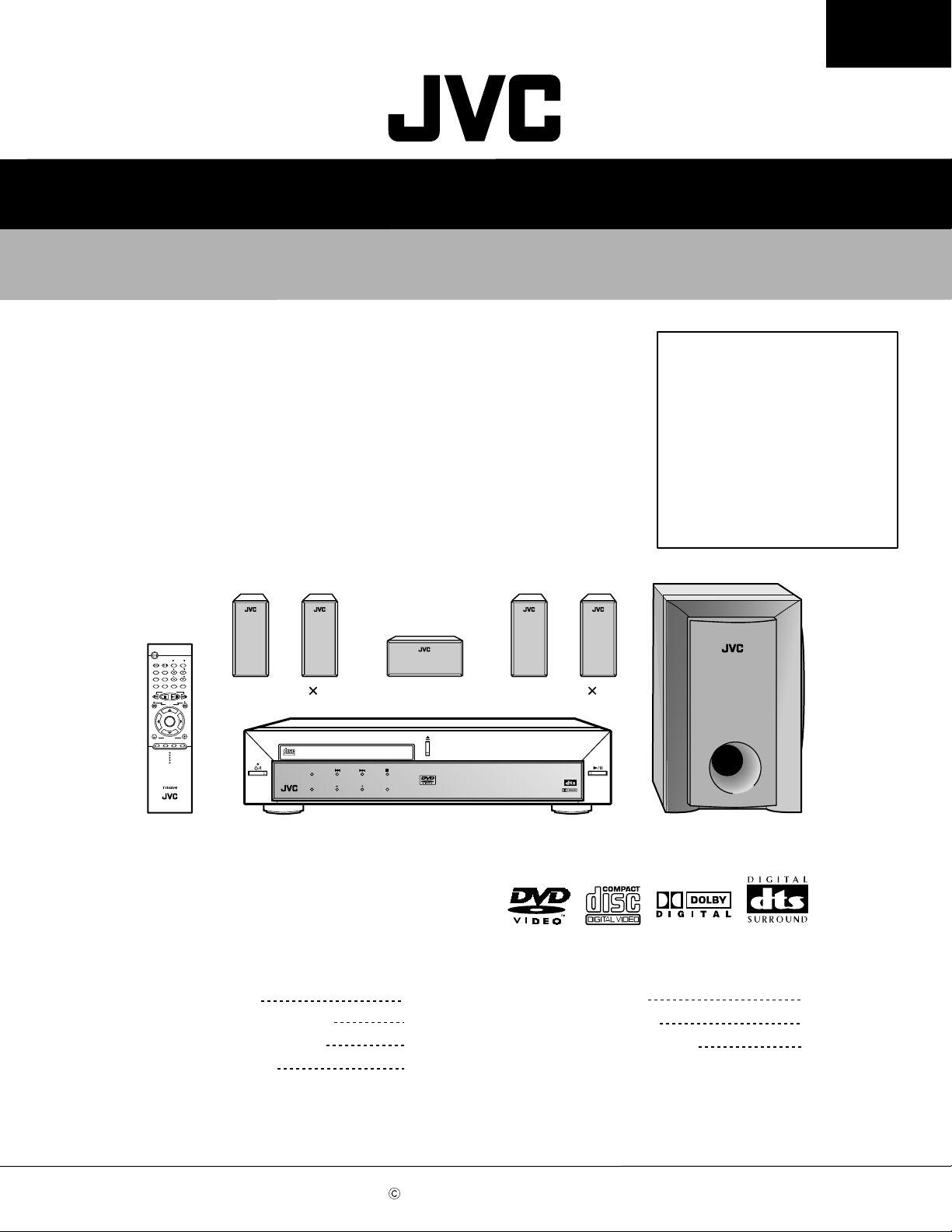
DVD DIGITAL CINEMA SYSTEM
Area suffix
TH-A5
A ------------------ Australia
US -------------- Singapore
UB ------------- Hong Kong
UW -- Brazil,Mexico,Peru
UY --------------- Argentina
UJ ------------- U.S.Military
UG ------------------ Turkey,
South Africa,Egypt
TH-A5
STANDBY/ON
AUDIO
VCR
CONTROL
ON
VCR
TV
OFF
TV CHANNEL
MENU
TOP MENU
AUDIO/
SUBTITLE
TV VOLUME
FM MODE
STEP
TV/VIDEO
DISPLAY
RETURN
TUNER PRESET
DOWN UP
REW FF
VCR CHANNEL
TUNING
B.SEARCH F.SEARCH
ENTER
VOLUME
DVD FM/AM AUX MUTING
RM-STHA5U
DVD CINEMA SYSTEM
SP-XSA5 2
COMPACT
DIGITAL VIDEO
STANDBY
STANDBY/ON
AUDIO/FM MODE
DSP
Contents
Safety precautions
Important for laser products
Preventing static electricity
Disassembly method
VOLUME SOURCE
SP-XCA5 SP-XSA5 2
DIGITAL
DVD DIGITAL CINEMA SYSTEM TH-A5
SURROUND
DIGITAL
XV-THA5 SP-WA5
1-2
1-3
1-4
Wiring connection
Adjustment method
Description of major ICs
1-5
1-12
1-13
1-15~33
COPYRIGHT 2002 VICTOR COMPANY OF JAPAN, LTD.
No.21062
Jan. 2002
Page 2
TH-A5
1. This design of this product contains special hardware and many circuits and components specially for safety
purposes. For continued protection, no changes should be made to the original design unless authorized in
writing by the manufacturer. Replacement parts must be identical to those used in the original circuits. Services
should be performed by qualified personnel only.
2. Alterations of the design or circuitry of the product should not be made. Any design alterations of the product
should not be made. Any design alterations or additions will void the manufacturer`s warranty and will further
relieve the manufacture of responsibility for personal injury or property damage resulting therefrom.
3. Many electrical and mechanical parts in the products have special safety-related characteristics. These
characteristics are often not evident from visual inspection nor can the protection afforded by them necessarily
be obtained by using replacement components rated for higher voltage, wattage, etc. Replacement parts which
have these special safety characteristics are identified in the Parts List of Service Manual. Electrical
components having such features are identified by shading on the schematics and by ( ) on the Parts List in
the Service Manual. The use of a substitute replacement which does not have the same safety characteristics
as the recommended replacement parts shown in the Parts List of Service Manual may create shock, fire, or
other hazards.
4. The leads in the products are routed and dressed with ties, clamps, tubings, barriers and the like to be
separated from live parts, high temperature parts, moving parts and/or sharp edges for the prevention of
electric shock and fire hazard. When service is required, the original lead routing and dress should be
observed, and it should be confirmed that they have been returned to normal, after re-assembling.
5. Leakage currnet check (Electrical shock hazard testing)
After re-assembling the product, always perform an isolation check on the exposed metal parts of the product
(antenna terminals, knobs, metal cabinet, screw heads, headphone jack, control shafts, etc.) to be sure the
product is safe to operate without danger of electrical shock.
Do not use a line isolation transformer during this check.
Plug the AC line cord directly into the AC outlet. Using a "Leakage Current Tester", measure the leakage
current from each exposed metal parts of the cabinet, particularly any exposed metal part having a return
path to the chassis, to a known good earth ground. Any leakage current must not exceed 0.5mA AC (r.m.s.).
Alternate check method
Plug the AC line cord directly into the AC outlet. Use an AC voltmeter having, 1,000 ohms per volt or more
sensitivity in the following manner. Connect a 1,500 10W resistor paralleled by a 0.15 F AC-type capacitor
between an exposed metal part and a known good earth ground.
Measure the AC voltage across the resistor with the AC
voltmeter.
Move the resistor connection to each exposed metal part,
particularly any exposed metal part having a return path to
the chassis, and meausre the AC voltage across the resistor.
Now, reverse the plug in the AC outlet and repeat each
measurement. Voltage measured any must not exceed 0.75 V
AC (r.m.s.). This corresponds to 0.5 mA AC (r.m.s.).
0.15 F AC TYPE
1500 10W
Good earth ground
AC VOLTMETER
(Having 1000
ohms/volts,
or more sensitivity)
Place this
probe on
each exposed
metal part.
!
1. This equipment has been designed and manufactured to meet international safety standards.
2. It is the legal responsibility of the repairer to ensure that these safety standards are maintained.
3. Repairs m ust be made in accordance with the relevant safety standards .
4. It is essential that safety critical components are replaced by approved parts.
5. If mains voltage selector is provided, check setting for local voltage.
Burrs formed during molding may
be left over on some parts of the
chassis. Therefore, pay attention to
such burrs in the case of
preforming repair of this system.
In regard with component parts appearing on the silk-screen pr inted side (parts side) of the PWB diagrams, the
parts that are printed over with black such as the resistor ( ), diode ( ) and ICP ( ) or identified by the " "
mark nearby are critical for safety.
(This regulation does not correspond to J and C version.)
1-2
Page 3
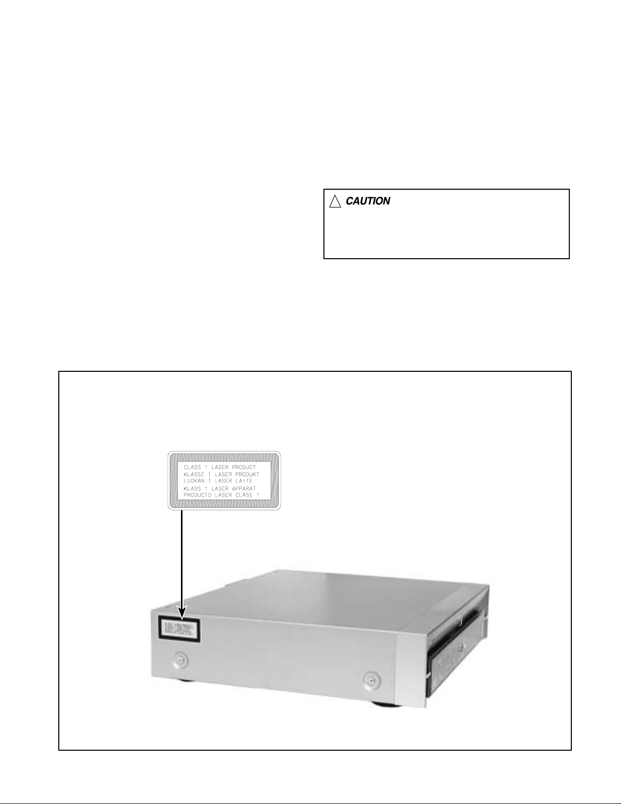
Important for laser products
TH-A5
1.CLASS 1 LASER PRODUCT
2.DANGER : Invisible laser radiation when open and inter
lock failed or defeated. Avoid direct exposure to beam.
3.CAUTION : There are no serviceable parts inside the
Laser Unit. Do not disassemble the Laser Unit. Replace
the complete Laser Unit if it malfunctions.
4.CAUTION : The compact disc player uses invisible
laserradiation and is equipped with safety switches
whichprevent emission of radiation when the drawer is
open and the safety interlocks have failed or are de
feated. It is dangerous to defeat the safety switches.
REPRODUCTION AND POSITION OF LABELS
5.CAUTION : If safety switches malfunction, the laser is able
to function.
6.CAUTION : Use of controls, adjustments or performance of
procedures other than those specified herein may result in
hazardous radiation exposure.
!
Please use enough caution not to
see the beam directly or touch it
in case of an adjustment or operation
check.
CLASS 1
LASER PRODUCT
1-3
Page 4
TH-A5
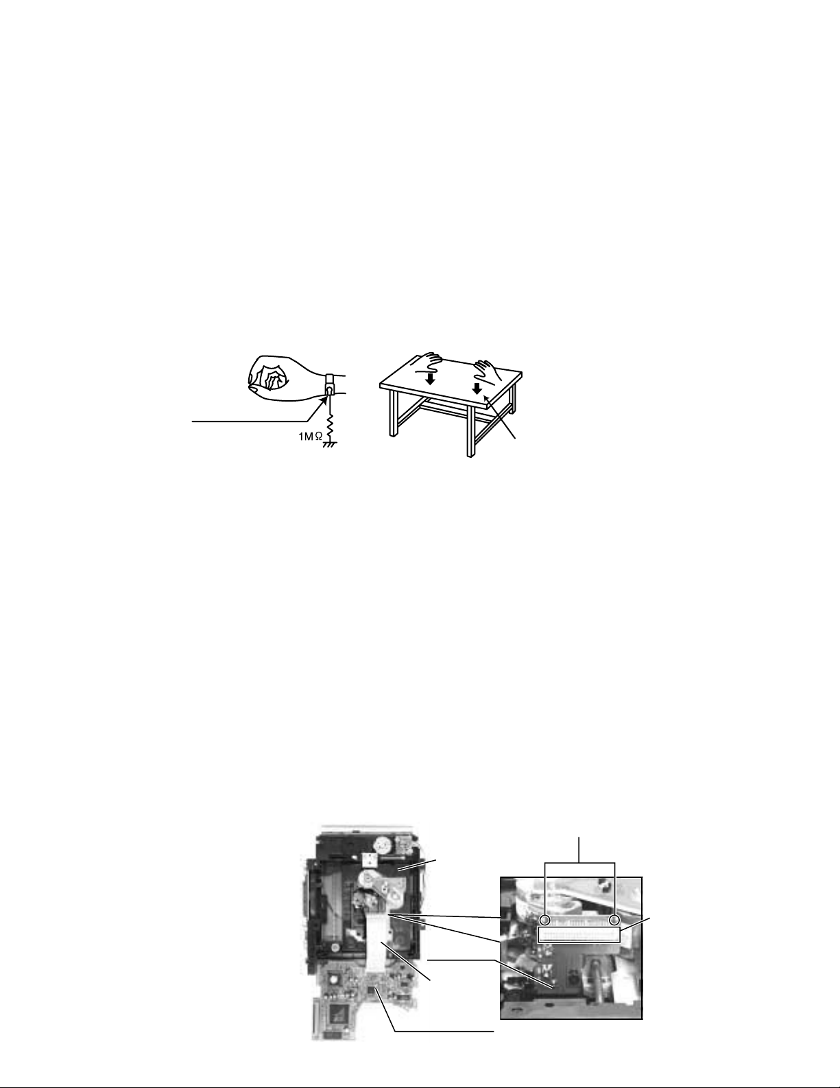
Preventing static electricity
1.Grounding to prevent damage by static electricity
Electrostatic discharge (ESD), which occurs when static electricity stored in the body, fabric, etc. is discharged,
can destroy the laser diode in the traverse unit (optical pickup). Take care to prevent this when performing repairs.
2.About the earth processing for the destruction prevention by static electricity
Static electricity in the work area can destroy the optical pickup (laser diode) in devices such as CD players.
Be careful to use proper grounding in the area where repairs are being performed.
2-1 Ground the workbench
Ground the workbench by laying conductive material (such as a conductive sheet) or an iron plate over
it before placing the traverse unit (optical pickup) on it.
2-2 Ground yourself
Use an anti-static wrist strap to release any static electricity built up in your body.
(caption)
Anti-static wrist strap
Conductive material
(conductive sheet) or iron plate
3. Handling the optical pickup
1. In order to maintain quality during transport and before installation, both sides of the laser diode on the
replacement optical pickup are shorted. After replacement, return the shorted parts to their original condition.
(Refer to the text.)
2. Do not use a tester to check the condition of the laser diode in the optical pickup. The tester's internal power
source can easily destroy the laser diode.
4.Handling the traverse unit (optical pickup)
1. Do not subject the traverse unit (optical pickup) to strong shocks, as it is a sensitive, complex unit.
2. Cut off the shorted part of the flexible cable using nippers, etc. after replacing the optical pickup. For specific
details, refer to the replacement procedure in the text. Remove the anti-static pin when replacing the traverse
unit. Be careful not to take too long a time when attaching it to the connector.
3. Handle the flexible cable carefully as it may break when subjected to strong force.
4. It is not possible to adjust the semi-fixed resistor that adjusts the laser power. Do not turn it.
Attention when traverse unit is decomposed
*Please refer to "Disassembly method" in the text for pick-up and how to detach the substrate.
Solder is put up before the card
1.
wire is removed from connector
on the pick up board as shown in
Figure.
(When the wire is removed
without putting up solder, the CD
pick-up assembly might destroy.)
Please remove solder after
2.
connecting the card wire with
when you install picking up
in the substrate.
DVD mechanism assembly (bottom side)
DVD loading
mechanism
Pick up board
Card wire
Short land
(These two points are
soldered respectively,
and are made to
short-circuit)
Connector
1-4
DVD loader board
Page 5
TH-A5
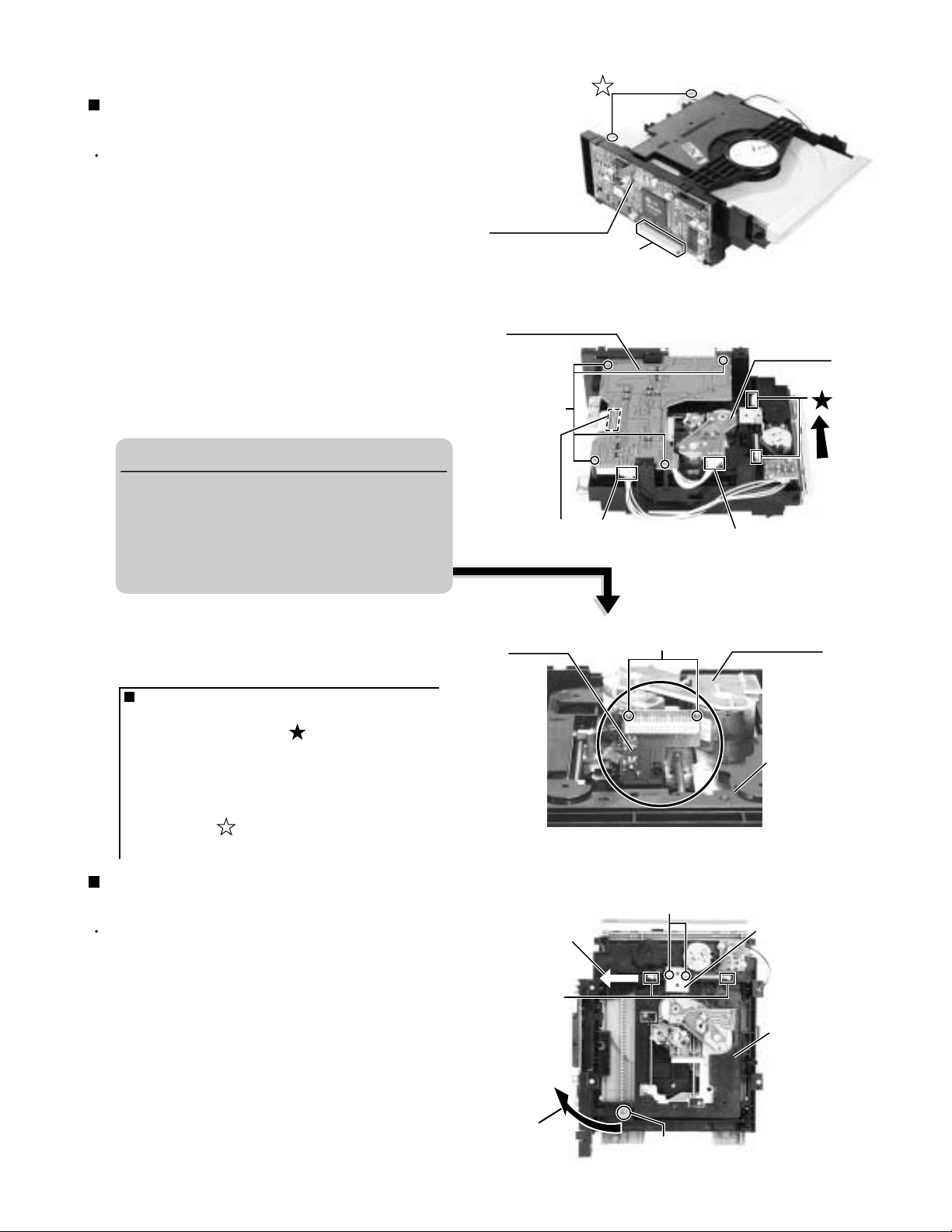
Disassembly method
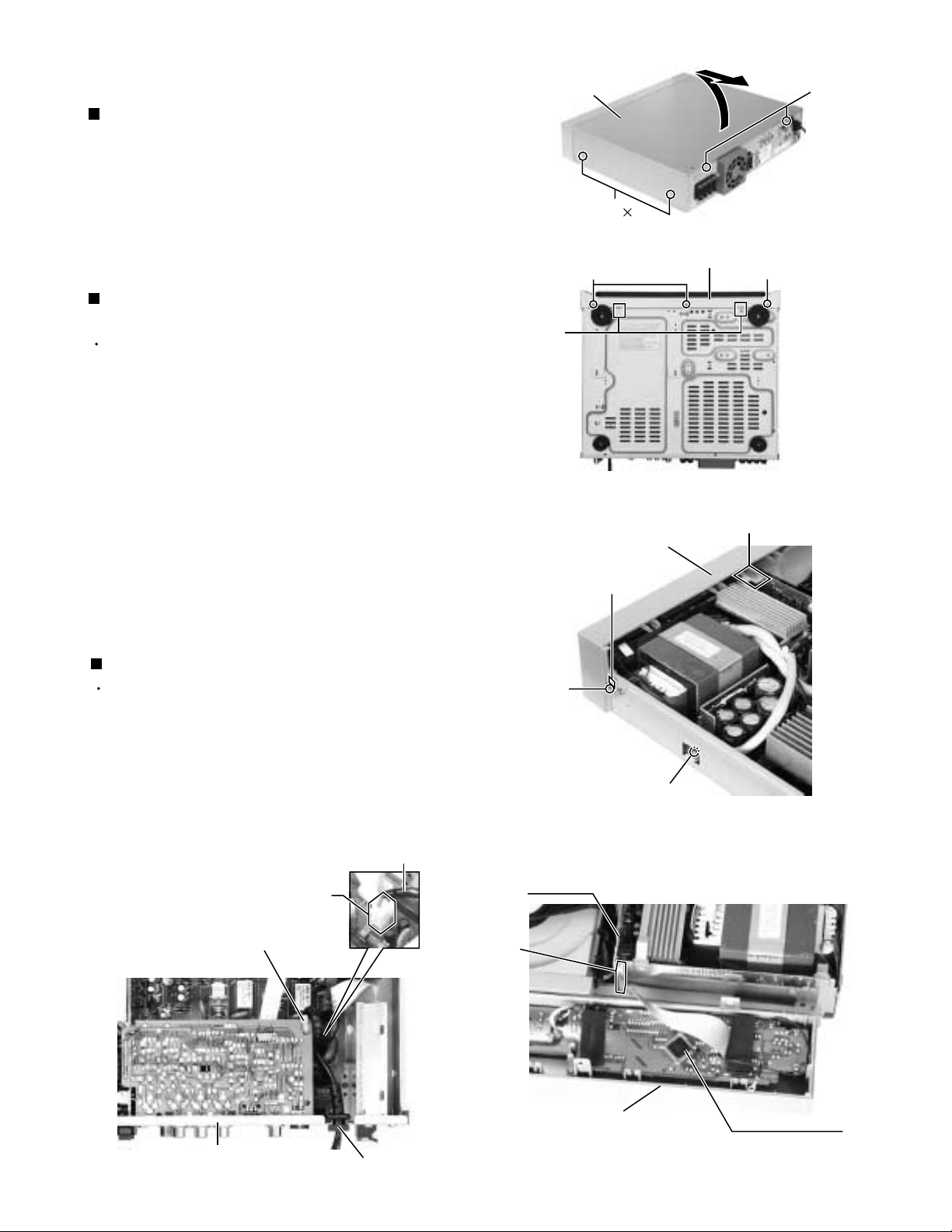
Removing the top cover (See Fig.1)
1.
Remove the four screws A attaching the top cover
on the both sides of the body.
2.
Remove the two screws B on the back of the body.
3.
Remove the top cover from behind in the direction of
the arrow while pulling both sides outward.
Removing the front panel assembly
(See Fig.2A, 2B and 3)
Prior to performing the following procedure, remove
the top cover.
1.
Remove the one screw a and remove the earth wier.
2.
Remove the three screws C attaching the front panel
assembly on the bottom of the body.
3.
Remove the two screws D attaching the front panel
assembly on the both sides of the body.
4.
Remove the claw1, claw2 and claw3, and detach the
front panel assembly toward the front.
5.
Disconnect the card wire from the connector DW20
on the DSP board.
Top cover
Claw1
(bottom side)
Claw2 (both side)
B
A
2
Fig.1
Front panel assembly
CC
Fig.2A
Front panel
assembly
Claw3
Removing the power cord (See Fig.4)
Prior to performing the following procedure, remove
the top cover.
1.
Disconnect the power cord from the connector CW1
on the main board and pull up the cord stopper
upward.
Notes : The power cord is exchangeable.
Power cord
CW1
Tie band
D
(both side)
a
(fixing the earth wire)
Fig.2B
DSP board
DW20
Rear panel
Fig.4
Power cord
stopper
Front panel assembly
(Inner side)
Display board
Fig.3
1-5
Page 6
TH-A5
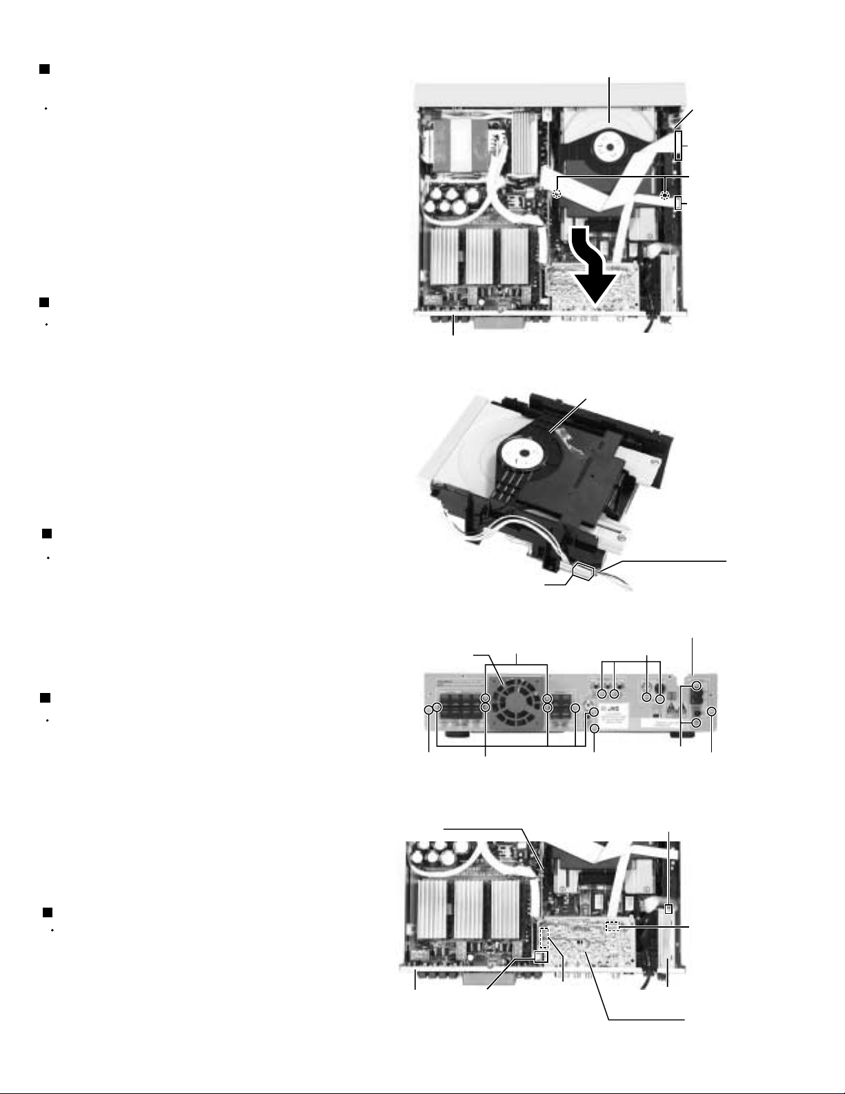
Removing the DVD mechanism assembly
(See Fig.5 and 6)
Prior to performing the following procedure, remove
the top cover.
1.
Disconnect the card wire from the connector J14 and
J21 on the DVD MPEG board.
2.
Remove the two screws E attaching the DVD
mechanism assembly and pull up with drawing out.
3.
Disconnect the harness from the connector J2 on the
DVD loader board.
Removing the rear panel (See Fig.7 and 8)
Prior to performing the following procedure, remove
the top cover and power cord.
1.
Disconnect the harness from the connector NW11 on
the DSP board.
2.
Remove the two screws F, four screws G, five
screws I attaching the each boards to the rear panel.
Rear panel
DVD mechanism assembly
DVD
MPEG
board
J14
E
J21
Fig.5
DVD mechanism
assembly
3.
Remove the three screws J attaching the rear panel
on the back of the body.
Removing the tuner pack (See Fig.7 and 8)
Prior to performing the following procedure, remove
the top cover.
1.
Disconnect the card wire from the connector CON01
on the tuner pack.
2.
Remove the two screws F attaching the tuner pack
to the rear panel.
Removing the jack board (See Fig.7 and 8)
Prior to performing the following procedure, remove
the top cover.
1.
Disconnect the card wire from the connector VW2 on
the jack board.
2.
Remove the four screws G attaching the jack board
to the rear panel.
3.
Disconnect the connector VW1 on the jack board
and pull up the jack board.
DVD loader board
J2
Fig.6
Rear panel
Fan motor
JJJ
DSP board
H
I
Fig.7
G
F
CON01
Removing the fan motor (See Fig.7 and 8)
Prior to performing the following procedures, remove
the top cover .
1.
Disconnect the harness from the connector NW11 on
the DSP board .
2.
Removing the two screws H attaching the fan motor
on the rear panel.
1-6
Rear panel
NW11
(on the
DSP board)
VW1
Fig.8
VW2
Tuner pack
Jack board
Page 7
TH-A5
Removing the DSP board (See Fig.9)
Prior to performing the following procedure, remove
the top cover, the front panel assembly and jack
board.
1.
Untied the harness band and disconnect the harness
from the connector CW2 on the main board.
2.
Disconnect the harness from the connector NW11 on
the DSP board.
3.
Disconnect the card wire from the connector VW12
on the DSP board.
4.
Pull up the DSP board from the front side upwards
disconnecting the connector DW10, DW13, DW14
and DW15.
Removing the main board (See Fig.10)
Prior to performing the following procedure, remove
the top cover, front panel assembly, DVD
mechanism assembly, jack board and DSP board.
1.
Disconnect the card wire from the connector CW4
and CW8 on the main board.
2.
Disconnect the harness from the connector CW3 on
the main board.
DSP board
(Front panel side)
Main board
CW8
K2
VW12
DW14DW15
Harness band
Fig.9
K1
Main board
CW2
NW11
(Rear panel side)
DW10DW13
Heat sink
(to which
power
transistor
is attached)
K1
3.
Remove the five screws I attaching the speaker
terminals and jack to the rear panel (see fig.7).
4.
Remove the six screws K1 (short) and one screw K2
(long) attaching the main board.
5.
When the rear panel is not removed, pull up the
main board from front side.
Removing the power transistor & power IC
(See Fig.10 and 11)
Prior to performing the following procedure, remove
the top cover, front panel assembly, DVD
mechanism assembly, jack board, DSP board and
main board.
1.
After removing the solder part soldered to the main
board, remove each screw and remove the heat sink
from Power transistor.
2.
After removing the solder part soldered to the main
board, remove each screw and remove the heat sink
from Power IC.
CW4
Fig.10
(Each power transistor is fixed)
Solder part
Solder part Solder part
Heat sink
(to which power IC is attached)
Fig.11
CW3
Power ICs
Main board
(Reverse side )
Solder part
(Power IC is fixed)
1-7
Page 8
TH-A5
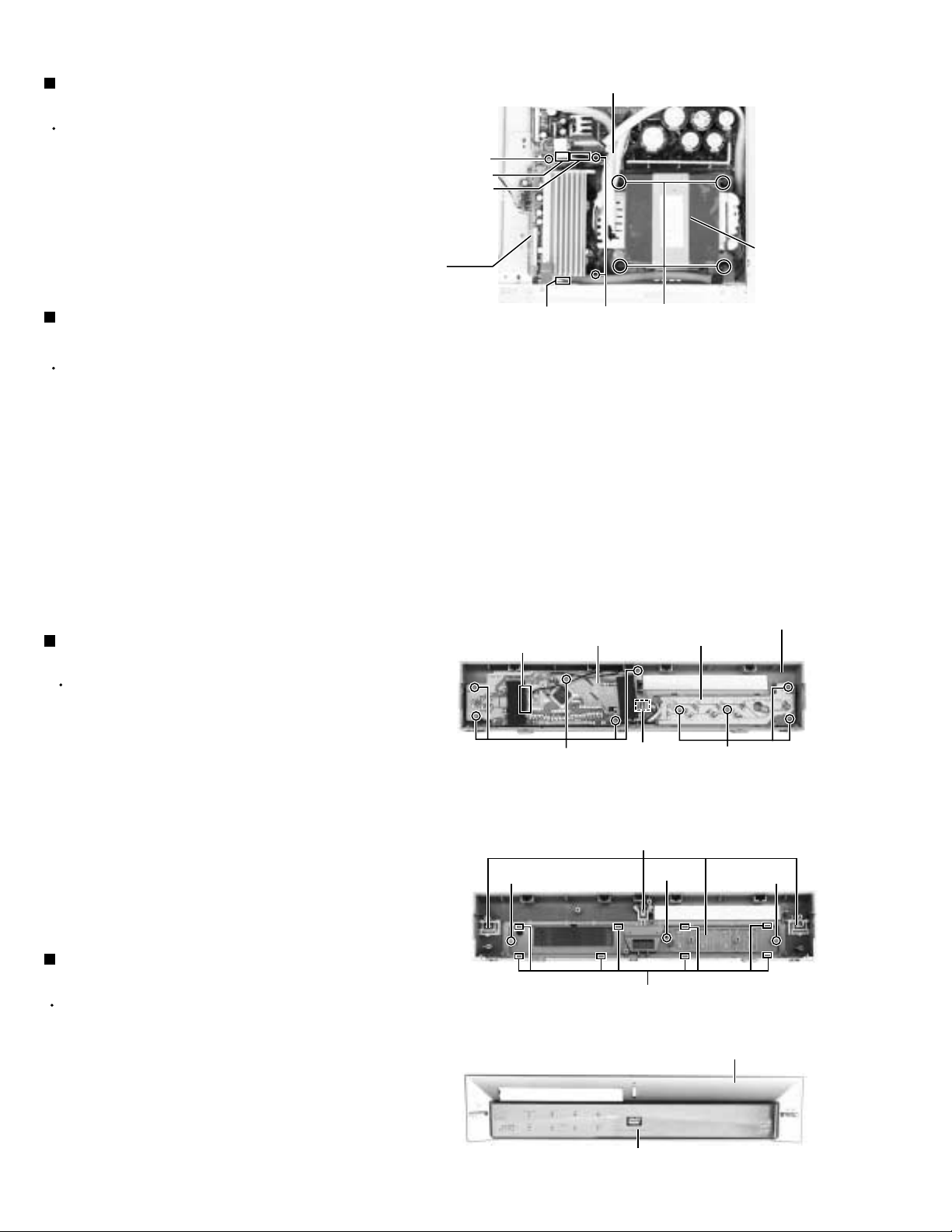
Removing the DVD power board
(See Fig.12)
Prior to performing the following procedure, remove
the top cover, front panel assembly and DSP board.
1.
Disconnect the harness and card wire from the
connector PW1, PW2 and PW5 on the DVD power
board.
2.
Remove the one screw L1 (short) and two screws L2
(long) attaching the DVD power board.
L1
PW5
PW2
DVD
power
board
Removing the power transformer
(See Fig.12)
Prior to performing the following procedure, remove
the top cover.
1.
Cut off the tie band fixing the harness, if needed.
2.
Disconnect the harness from the connector CW2 on
the main board (see fig.9) and PW1, PW2 on the
DVD power board.
3.
Remove the four screws M attaching the power
transformer.
PW1
Tie band
L2
Power
transformer
M
Fig.12
<Front panel assembly section>
Removing the display board & switch
board (See Fig.1 and 2)
Prior to performing the following procedure, remove
the top cover and the front panel assembly.
1.
Disconnect the card wire from the connector FW1 on
the display board.
2.
Remove the five screws A attaching the display
board on the inner of the front panel assembly.
3.
Remove the four screws B attaching the switch
board on the inner of the front panel assembly.
4.
Disconnect the harness from connector FW2 on the
display board, if needed.
Removing the front window
(See Fig.2 and 3)
Prior to performing the following procedure, remove
the top cover, front panel assembly, display board
and switch board.
FW1
Display board
A
Switch button
Front panel assembly
Switch board
FW2
Fig.1
(inner side)
B
CCC
Claw
Fig.2
Front panel assembly (front side)
Remove the switch buttons, if needed.
1.
Remove the three screws C attaching the front
2.
window on the front panel.
Remove the eight claws fixing the front window on
3.
the front panel.
1-8
Front window
Fig.3
Page 9
TH-A5
<DVD mechanism assembly section>
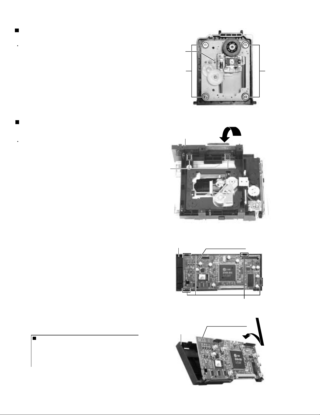
Removing the DVD loader board
(See Fig.1 to 3)
Prior to performing the following procedure, remove
the top cover and DVD mechanism assembly.
1.
Disconnect the card wire from the connector J6 on
the DVD MPEG board.
2.
Disconnect the harness from the connector on the
motor board.
3.
Disconnect the harness from the connector J5 on the
DVD loader board.
4.
Remove the four screws A attaching the DVD loader
board to DVD mechanism assembly.
CAUTION!! (see fig.3)
Before removing the card wire which
connects the pickup board and DVD loader
board, solder the two soldering parts and
make it short-circuit.
Moreover, while having removed the card
wire, don't remove these solder.
DVD MPEG board
DVD loader board
A
U9
J5
DVD mechanism assembly
(top side)
J6
Fig.1
DVD mechanism assembly
(bottom side)
Motor board
Connector
Fig.2
5.
Disconnect the card wire from the connector U9 on
the DVD loader board.
ONE POINT
How to eject the DVD tray manually
(see fig.2)
The white lever of the mark is moved in
the direction of the arrow. Then, the tray will
be opened.
Moreover, the tray is separable from a DVD
mechanism assembly by removing two
screws of the mark (see fig.1) and drawing
out the tray.
Removing the DVD loading mechanism
(See Fig.4)
Prior to performing the following procedure, remove
the top cover, DVD mechanism assembly and DVD
loader board.
1.
Remove the two screws B and remove the bracket.
2.
Remove the one screw C fixing the DVD loading
mechanism.
Pick up
board
Lever
Soldering parts
X
Motor board
Fig.3
DVD mechanism assembly
B
Bracket
DVD loading
mechanism
(bottom side)
DVD loading
mechanism
3.
Move the lever in the direction of the arrow X.
4.
Remove the DVD loading mechanism from the DVD
mechanism assembly by moving it in the direction of
the arrow Y.
Y
C
Fig.4
1-9
Page 10
TH-A5
m
)
Removing the DVD traverse mechanism
(See Fig.5)
Prior to performing the following procedure, remove
the top cover, DVD mechanism assembly, DVD
loader board and DVD loading mechanism.
1.
Remove the four screws D attaching the DVD
traverse mechanism to DVD loading mechanism.
Removing the holder & DVD MPEG board
(See Fig.6 and 7)
Prior to performing the following procedure, remove
the top cover, DVD mechanism assembly and DVD
loader board.
1.
Remove the two claws1, and remove the holder from
the DVD mechanism assembly as it is pushed down.
DVD traverse
mechanism
Claw1
D
Holder
DVD loading mechanis
(top side
D
Fig.5
Note: When removing only the DVD MPEG board, it is not
necessary to remove this holder.
2.
Remove the four claws2 and remove the DVD
MPEG board from the holder.
ONE POINT
When inserting DVD MPEG board in
holder. (see fig.8)
Holder
Holder
DVD mechanism assembly
Fig.6
DVD MPEG board
Fig.7
DVD MPEG board
(bottom side)
Claw2
1-10
Insert in after uniting with a lower claws,
when inserting DVD MPEG board in holder.
Fig.8
Page 11
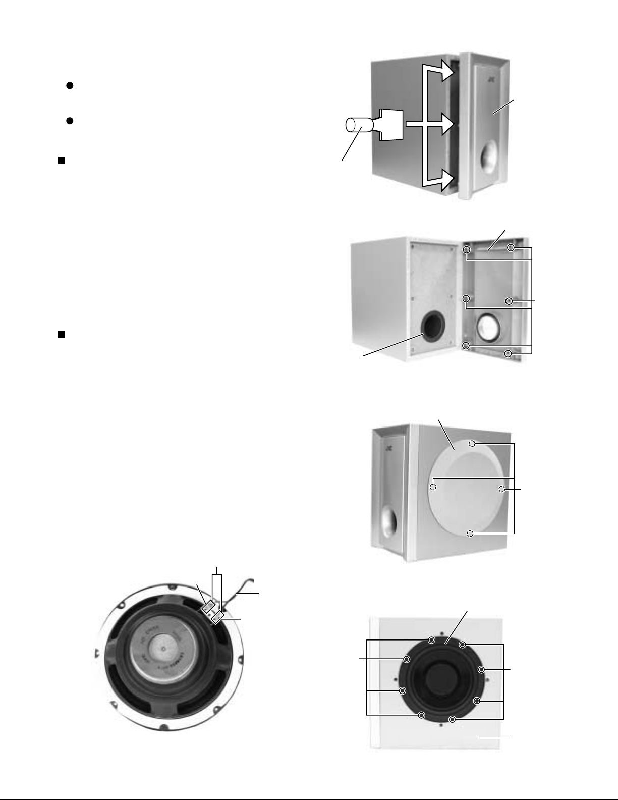
<Speaker section>
[SP-XSA5 / Satellite speaker]
It is exchange in a unit.
[SP-XCA5 / Center speaker]
It is exchange in a unit.
[SP-WA5 / Woofer]
Removing the front panel
(See Fig.1 and 2)
1.
Remove the six bosses and remove the front panel.
TH-A5
Front panel
The tool with
a flat tip
Notes: It will be good to use the tool with a flat tip, since it
is hard to remove. Please take care not to damage the
cabinet at this time.
2.
The packing separates. It removes if needed.
Removing the speaker unit
(See Fig.3 to 5)
1.
Remove the four bosses and remove the net
assembly.
Notes: It will be good to use the tool with a flat tip, since it
is hard to remove. Please take care not to damage the
cabinet at this time.
2.
Remove the eight screws A attaching the speaker
unit to cabinet.
3.
Disconnect the code from the two terminals of the
speaker unit.
Packing
Fig.1
Fig.2
Net assembly
Front panel
(inner side)
Boss
Boss
Terminals
red
Speaker unit (reverse side)
Fig.5
Fig.3
Code
Speaker unit
black
A
A
Cabinet
Fig.4
1-11
Page 12
TH-A5
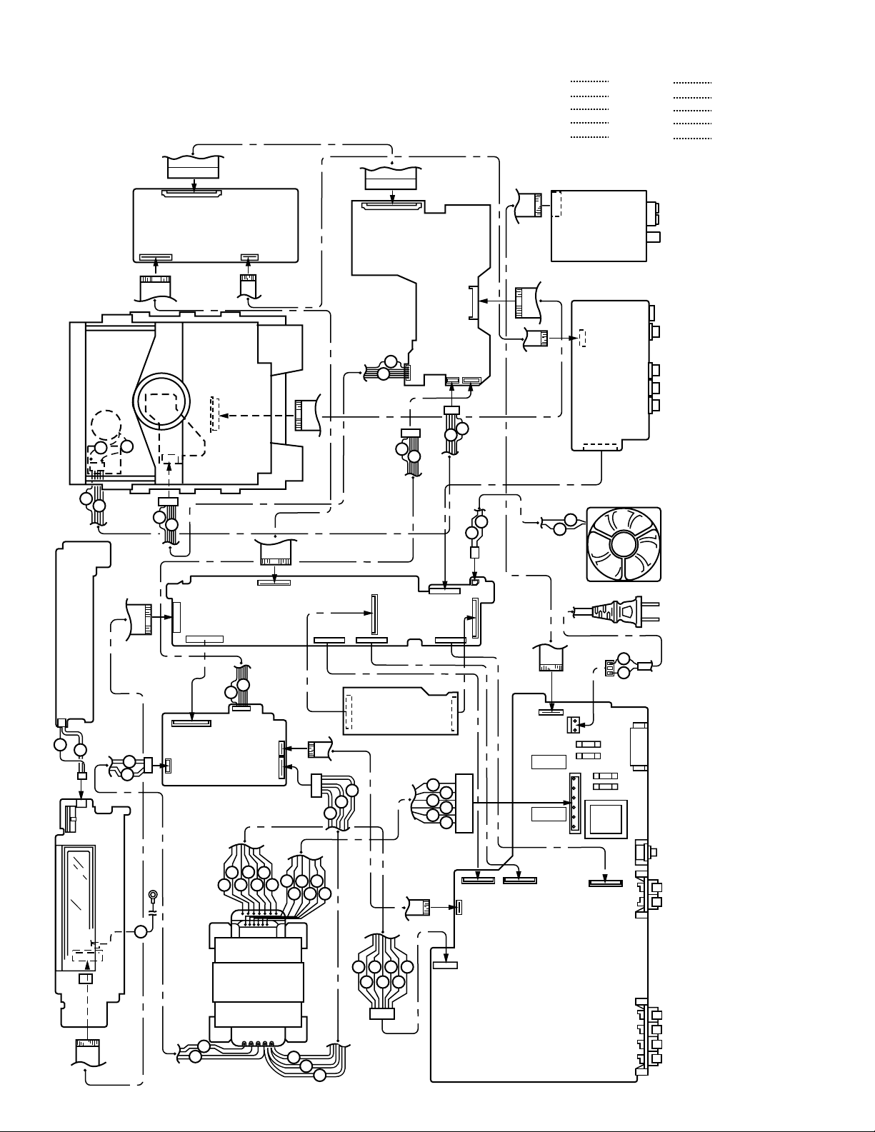
Wiring connection
J6
J14
2
0
J21
3809-001273
DVD MPEG
BOARD
3809-001295
9
AH39-00368A
0
J3
J4
0
9
3809-001294
DVD LOADER BOARD
U9
J5
J2
0
9
Color codes are shown below.
1 Brown
2 Red
3 Orange
4 Yellow
5 Green
3809-001274
3809-001224
CON01
VW2
VW1
6 Blue
7 Violet
8Gray
9 White
0 Black
TUNER PACK
JACK BOARD (V-OUT)
0
9
SWITCH BOARD
FW3
AH39-00176A
0
9
FW2
DISPLAY BOARD
3809-001296
6
1
AH39-50001K
0
9
DW20
PW1
PW3
BOARD
3
DW15
0
DVD
POWER
4
9
5
PW4
0
6
PW5
PW2
1
VW11
9
2
AH39-00104A
AH39-00291A
DSP1 BOARD
9
4
2
8
0
3
DW14
DW32
0
2
DW12
DW23
DW13
DSP2 BOARD
3809-001283
9
2
4
DW10
DW31
8
3
0
NW11
DW11
CW4
0
2
CW7
RE3
RE4
CW6
CW8
0
2
CW1
CW2
1
C
FU1
FU2
FU4
FU3
PT1
CW5
1-12
FW1
0
POWER TRANCE
6
1
2
6
3
5
1
4
0
9
2
0
CW3
MAIN BOARD
Page 13
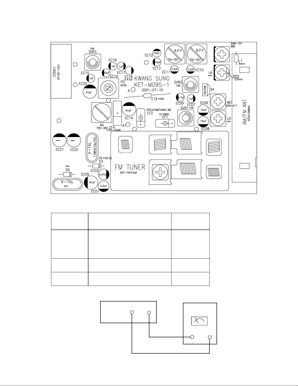
Adjustment method
1. Tuner
TH-A5
*Adjustment Location of Tuner PCB
ITEM
Received FREQ.
Adjustment
point
Output 1~7.0V
AM(MW) OSC Adjustment
: 522~1629KHz (9k step)
A
US/UB/
UW/UJ
: 531~1602KHz (9k step)
530~1600KHz (10k step)
MAIN
PCB
MO
VT GND
AM(MW) RF
Adjustment
603 KHz
MA
Maximum
Output(Fig1-1)
TESTER
Fig 1-1 OSC Voltage
1-13
Page 14
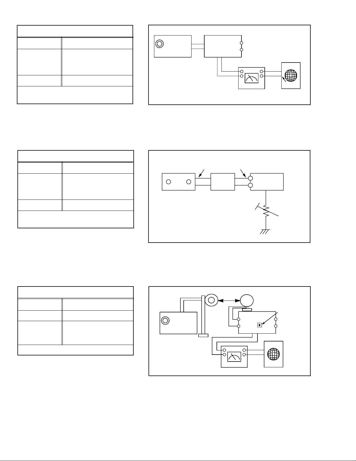
TH-A5
FM THD Adjustment
SSG FREQ.
Adjustment
point
(FD)
Output
Minimum Distortion (0.4% below)
(Figure 1-2)
FM Search Level Adjustment
SSG FREQ.
FM DETECTOR COIL
60 dB
98 MHz
98 MHz
Output
Output
Output
Output
GND
GND
GND
GND
FM S.S.G
FM
Antenna
Terminal
Te
T
Speaker
Terminal
Te
T
SET
SET
SET
SET
Input
output
output
output
output
Distortion Meter
Figure1-2 IF CENTER and THD Adjustment
28 dB
FM Antenna
Oscilloscope
Input
Input
Input
Input
Adjustment
point
(SVR3)
Output
BEACON
SENSITIVITY
SEMI-VR(20K )
28 dB(
dB)
Adjust SVR1 so that “TUNED” of FL T
is lighted (Figure 1-3)
*Adjust FM S.S.G level to 28dB
AM(MW) I.F Adjustment
SSG FREQ.
Frequency
450 kHz
522 kHz
Adjustment
point
AA
Maximum output (Figure 1-4)
SET
GND
GND
GND
FM S.S.G
GND
FM IN
Figure1-3 FM Auto Search Level Adjustment
60cm
OUTPUT
AM SSG
450KHZ
INPUT
AM ANT
IN
Speaker Terminal
OUTPUT
20 k
AM IF
VTVM Oscilloscope
Figure1-4 AM I.F Adjustment
Notes: This set is a non-adjusted set fundamentally. It is adjusted when the tuner pack is exchanged.
1-14
Page 15
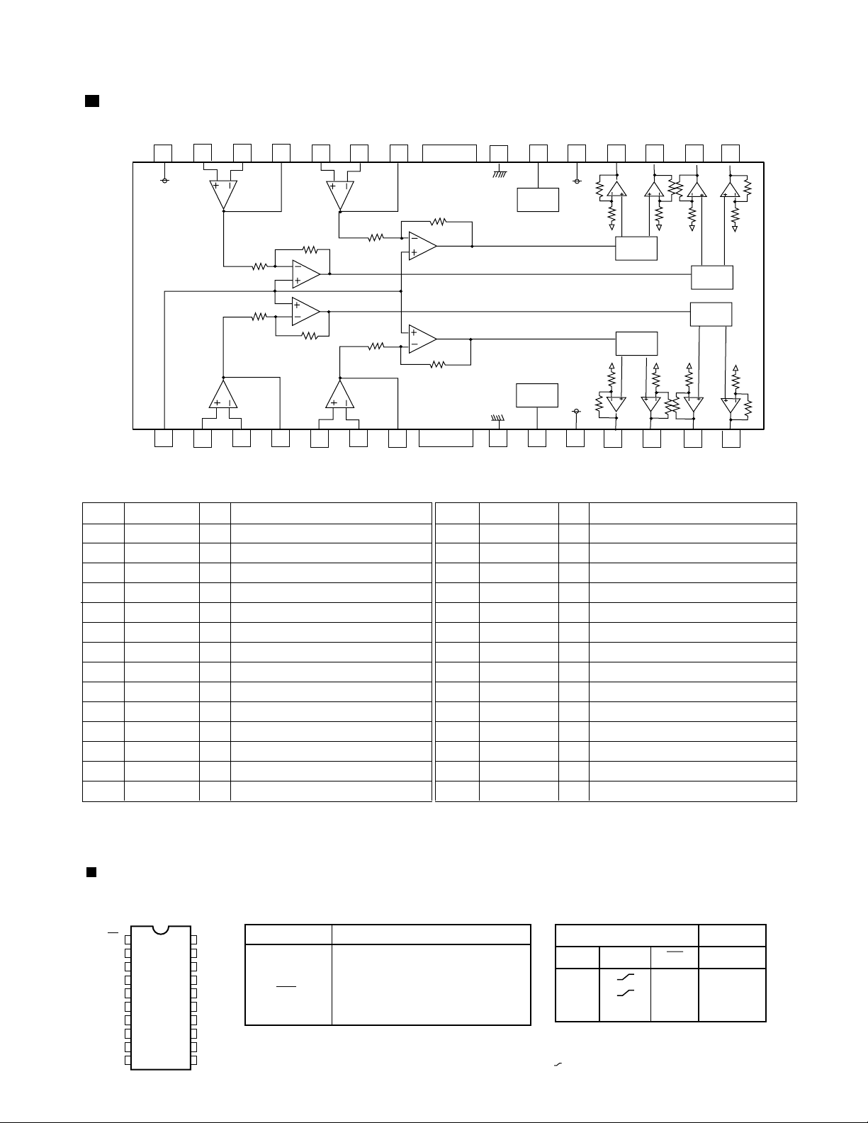
Description of major ICs
BA5983FM (U6) : 4CH driver
1.Block diagram
TH-A5
27
28
Vcc
1
2
25
26
10k
10k
3
20k
10k
4
24
5
23 22
10k
10k
6
20k
10k
7
2.Pin function
Pin No. Pin No.
Symbol Symbol
1
BLAS IN
2
OPIN1(+)
3
OPIN1(-)
4
OPOUT1
5
OPIN2(+)
6
OPIN2(-)
7
OPOUT2
8
9
10
11
12
13
14
GND
STBY1
PowVcc1
VO2(-)
VO2(+)
VO1(-)
VO1(+)
I/O I/O
Input for Bias-amplifier
I
Non inverting input for CH1 OP-AMP
I
Inverting input for CH1 OP-AMP
I
Output for CH1 OP-AMP
O
Non inverting input for CH2 OP-AMP
I
Inverting input for CH2 OP-AMP
I
Output for CH2 OP-AMP
O
Substrate ground
Input for CH1/2/3 stand by control
I
Vcc for CH1/2 power block
Inverted output of CH2
O
Non inverted output of CH2
O
Inverted output of CH1
O
Non inverted output of CH1
O
Function
15
16
17
18
19
20
21
22
23
24
25
26
27
28
21
20
STAND BY
CH4
STAND BY
CH1/2/3
89
VO4(+)
VO4(-)
VO3(+)
VO3(-)
PowVcc2
STBY2
GND
OPOUT3
OPIN3(-)
OPIN3(+)
OPOUT4
OPIN4(-)
OPIN4(+)
PreVcc
17 16
18
19
Vcc
Vcc
10
10k
10k
10k
10k
11
Level Shift
Level Shift
10k
10k
10k
10k
Level Shift
Level Shift
10k
10k
10k
10k
12
13
Function
O
Non inverted output of CH4
O
Inverted output of CH4
O
Non inverted output of CH3
O
Inverted output of CH3
-
Vcc for CH3/4 power block
I
Input for Ch4 stand by control
-
Substrate ground
O
Output for CH3 OP-AMP
I
Inverting input for CH3 OP-AMP
I
Non inverting input for CH3 OP-AMP
O
Output for CH4 OP-AMP
I
Inverting input for CH4 OP-AMP
I
Non inverting input for CH4 OP-AMP
-
Vcc for pre block
15
10k
10k
10k
10k
14
74VHC574 (DIC16, DIC17) : Flip flop
OE
D0
D1
D2
D3
D4
D5
D6
D7
GND
1
2
3
4
5
6
7
8
9
10
20
19
18
17
16
15
14
13
12
11
Vcc
O0
O1
O2
O3
O4
O5
O6
O7
CP
Symbol
D0-D7
CP
OE
O0-O7
Function
Data Inputs
Clock Pulse Input
3-STATE Output Enable Input
3-STATE Outputs
3. Truth table2. Pin function1. Pin layout
Inputs Outputs
Dn
CP
H
L
X
H:HIGH Voltage Level
L:LOW Voltage Level
X:Immaterial
Z:High Impedance
:HIGH to LOW transition
X
OE
L
L
H
On
H
L
Z
1-15
Page 16
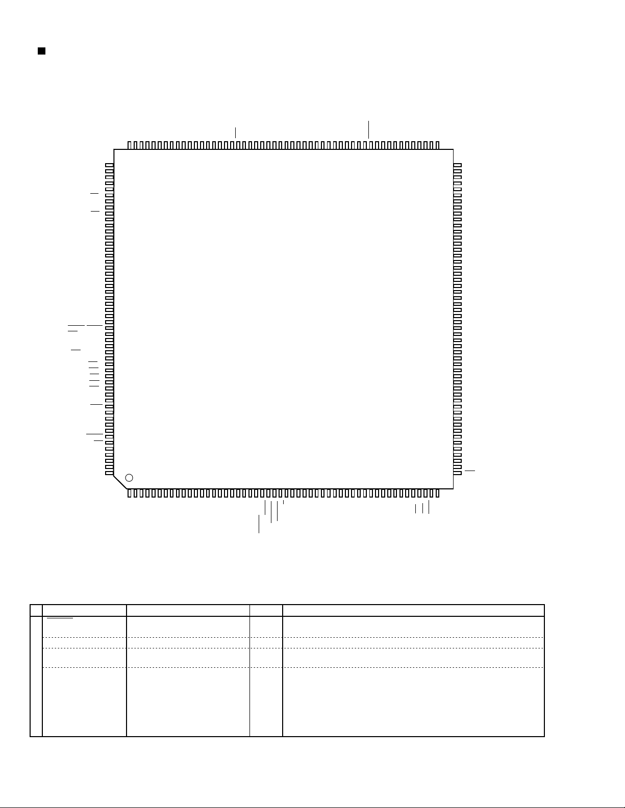
TH-A5
ZiVA-5 (U8) : DVD controller
1. Pin layout
DA-IEC958
DA-DATA3
DA-DATA2
VSS
156
155
154
153
DAI-DATA
DAI-BCK/SYSCLKBP
DAI-LRCK/IEC958BP
2
C_CL
I
I
2
C_DA
RTS1
RXD1
TXD1
CTS1
VSS
VDD_3.3
SD-DATA7
SD-DATA6
SD-DATA5
SD-DATA4
VSS
VDDC
SD-DATA3
SD-DATA2
SD-DATA1
SD-DATA0
SD-REQ
SD-EN
VSS
VDD_3.3
SD-ERROR
SD-CLK
VSYNC/HIRQ1
RTS2/SPI_CLK
RXD2/SPI_MISO
TXD2/SPI_MOSI
CTS2/SPI_CS
VDD_5
HCS4
HCS3
HCS2
HCS1
HCS0
VSS
VDD_3.3
TRST
TDO
TMS
TCK
RESET
ALE
VSS
VDDC
HAD3
HAD2
VSS
157
158
159
160
161
162
163
164
165
166
167
168
169
170
171
172
173
174
175
176
177
178
179
180
181
182
183
184
185
186
187
188
189
190
191
192
193
194
195
196
197
198
199
TDI
200
201
202
203
204
205
206
207
208
152
123456789101112131415161718192021222324252627282930313233343536373839404142434445464748495051
VDD_3.3
DA-DATA1
DA-DATA0
151
150
DA-BCK
DA-LRCK
149
148
DA-XCK
VSS
147
146
VDDC
145
A_VSS1
A_VDD1
144
143
A_VDD2
A_VSS2
142
141
XVDD
140
XTAL/VCLK216BP
XTAL
XVSS
VSS_RREF
VDAC_RREF
VDD_RREF
139
138
137
136
135
134
VDAC_DVDD
VDAC_DVSS
VDAC_0
VDAC_VDD0
133
132
131
130
VDAC_0B
VDAC_1
VDAC_VDD1
129
128
127
VDAC_1B
VDAC_2
VDAC_VDD2
126
125
124
VDAC_2B
VDAC_3
VDAC_VDD3
123
122
121
VDAC_3B
VDAC_4
VDAC_VDD4
120
119
118
VDAC_4B
HSYNC/IRQ2
VDATA0
117
116
115
VDATA1
VDATA2
114
113
VSS
VDD_3.3
112
111
VDATA3
VDATA4
110
109
VDATA5
VDATA6
VDATA7
108
107
106
VCLK
105
104
103
102
101
100
52
VDD_3.3
VSS
MDATA31
MDATA30
MDATA29
MDATA28
99
VDD_3.3
98
MDQM3
97
VSS
96
MDATA27
95
MDATA26
94
MDATA25
93
MDATA24
92
MDATA23
91
MDATA22
90
MDATA21
89
MDATA20
88
VDD_3.3
87
MDQM2
86
VSS
85
MDATA19
84
MDATA18
83
MDATA17
82
MDATA16
81
VDDC
80
VSS
79
MDATA15
78
MDATA14
77
MDATA13
76
MDATA12
75
VDD_3.3
74
MDQM1
73
VSS
72
MDATA11
71
MDATA10
70
MDATA9
69
MDATA8
68
MDATA7
67
MDATA6
66
MDATA5
65
MDATA4
64
VDD_3.3
63
MDQM0
62
VSS
61
MDATA3
60
MDATA2
59
MDATA1
58
MDATA0
57
MCLK
56
VDD_3.3
55
VSS
54
MWE
53
BA1
HA1
VDD_3.3
HAD15
HAD14
HAD13
HAD12
HAD11
HAD10
HAD9
HAD8
HAD7
VDD_3.3
VSS
HAD6
HAD5
HAD4
HAD3
HAD2
HAD1
VDD_3.3
VSS
HAD0
HDTACK/WAIT
HIRQ0
UDS/UWE
R/W
IRRX1
LDS/LWE
VSS
VDDC
VSS
VDD_3.3
MADDR9
MADDR8
MADDR7
MADDR6
MADDR5
MADDR4
MADDR3
MADDR2
MADDR1
MADDR0
VSS
VDD_3.3
MADDR10
MADDR11
BA0
MCS0
MCS1
MRAS
MCAS
2. Pin function (1/4)
1
Name
RESET
Pin No.
202
Description
Type
Active Low Reset. Assert for at least 5-milliseconds in the presence of
I
clock to reset the entire chip.
VCLK
XOUT
105
138
Video clock that outputs 27 MHz.
I/O
Crystal output. When the internal DCXO is used, a 13.5 MHz crystal
O
should be con-nected between this pin and the XIN pin.
XIN/bypass clk_216
139
Crystal input. When the internal DCXO is used, a 13.5 MHz crystal should
I
be con-nected between this pin and the XOUT pin. When an external
oscillator or VCXO is used, its output should be connected to this pin.
System Services
When configured for an external bypass clock, a 216 MHz clock should be
connected to this pin. The frequency of an external VCXO can be either 27
or 13.5 MHz.
1. I - input, O - output, OD - open drain, PU - requires external pull-up resistor.
1-16
Page 17
2. Pin function (2/4)
Name
VNW
VDDP
VDD25
XVDD
VDD
VDD_VDAC[4:0]
VDAC_DVDD
A_VDD[2:1]
VDAC_REFVDD
GNDP
GND
Power and GroundHost Interface
GND25
VDAC_DVSS
AVSS[2:1]
VDAC_REFVSS
XVSS
HCS[4:2]/GPIO[41:43]
HCS[1:0]
HA[3:1]
HA[15:0]
HDTACK/WAIT
HIRQ0
HUDS/UWE
HLDS/LWE
HREAD
ALE
MCS[1:0]
MCAS
MRAS
MDQM[3:0]
MA[11:0]
MD[31:0]
MWE
SDRAM Interface
MCLK
BA[1:0]
HSYNC/HIRQ2/
GPIO1[9]
VCLK
VDATA[7:0]/GPIO[1:7]
VSYNC/HIRQ1/
GPIO36
Digital Video Input/Output
1. I - input, O - output, OD - open drain, PU - requires external pull-up resistor.
12, 20, 111, 152, 167, 181, 196
32, 44, 55, 63, 74, 87, 98, 104
13, 21, 112, 153, 166, 180, 195, 208
31, 43, 54, 61, 72, 85, 96, 103
Pin No.
189
140
30, 80, 145, 173, 205
118, 121, 124, 127, 130
133
142, 143
134
29, 79, 146, 172, 204
132
141, 144
136
137
190-192
193, 192
206, 207, 2
3-11, 14-19, 22
23
24
25
26
27
203
50, 49
52
51
97, 86, 73, 62
46, 45, 33-42
102-99, 95-88, 84-81,
78-75, 71-64, 60-57
53
56
47, 48
116
105
106-110, 113-115
184
Type
Power
Power
Power
Power
Power
Power
Power
Ground
Ground
Ground
Ground
Ground
Ground
Ground
O
I
I/O
I/O
I/OD
I/O
I/O
I/O
I/O
I/O
O
O
O
O
O
I/O
O
O
O
I/O
I/O
I/O
I/O
1
Description
5-V supply voltage for 5V-tolerant I/O signals.
3.3-V supply voltage for I/O signals
3.3-V supply voltage for SDRAM I/O signals
3.3V Crystal interface power
1.8-V supply voltage for core logic
Analog Video DAC Power
3.3V Digital supply for 5 DACs
3.3-V Analog PLL Power
3.3V Analog Video Reference Voltage
Ground for I/O signals
Ground for core logic
Ground for SDRAM I/O signals
Digital VSS for DACs
Analog PLL Ground
Video Analog Ground
Crystal interface ground
Host chip select. Host asserts HCS to select the controller for a read or
write operation. The falling edge of this signal triggers the read or write
operation. General Purpose I/Os 41, 42, and 43, respectively.
Host chip select. Host asserts HCS to select the contr ol le r fo r a re ad or
write operation. The falling edge of this signal triggers the read or write
operation.
Host (muxed address) address bus. 3-bit address bus selects one of eight
host inter-face registers. These signals are not muxed in ATAPI master
mode.
HA[15:0] is the 16-bit (muxed address and data) bi-directional host data
bus through which the host writes data to the decoder Code FIFO. MSB of
the 32-bit word is writ-ten first. The host also reads and writes the decoder
internal registers and local SDRAM/ROM via HA[7:0]. These signals are
not muxed for ATAPI master mode.
Host Data Transfer Acknowledge.
Host interrupt. Open drain signal, must be pulled-up via 4.7k to 3.3 volts.
Driven high for 10 ns before tristate.
Host Upper Data Strobe. Host high byte data, HA[15:8], is valid when this
pin is active.
Host Lower Data Strobe. Host low byte data, HA[7:0], is valid when this pin
is active.
Read/write strobe
Address latch enable
Memory chip select.
Active LOW SDRAM Column Address Strobe.
Active LOW SDRAM Row Address Strobe.
These pins are the bytes masks corresponding to MD[7:0], [15:8], [23:16]
and [31:24]. They allow for byte reads/writes to SDRAM.
SDRAM Address
SDRAM Data
SDRAM Write Enable. Specifies transaction to SDRAM: read (=1) or
write (=0)
SDRAM Clock
SDRAM bank select
Horizontal sync. The decoder begins outputting pixel data for a new
horizontal line after the falling (active) edge of HSYNC.
Host Interrupt Request 2
General Purpose I/O 9
Video clock. Clocks out data on input. VDATA[7:0].
Clock is typically 27 MHz.
Video data bus. Byte serial CbYCrY data synchronous with VCLK. At
powerup, the decoder does not drive VDATA. During boot-up, the
decoder uses configuration parameters to drive or 3-state VDATA.
General Purpose I/Os [1:7]
Vertical sync. Bi-directional, the decoder outputs the top border of a new
field on the first HSYNC after the falling edge of VSYNC. VSYNC can
accept vertical synchroni-zation or top/bottom field notification from an
external source. (VSYNC HIGH = bot-tom field. VSYNC LOW = Top field)
Active Low Host Interrupt Pin
General Purpose I/O 36
TH-A5
1-17
Page 18
TH-A5
2. Pin function (3/4)
Name
SDDATA[7]/VDATA2[7]
/HDMARQ/GPIO24
SDDATA6/VDATA2[6]
/HXCVR_EN/GPIO25
SDDATA5/VDATA2[5]
HDMACK/GPIO26
SDDATA4/VDATA2[4]/
GPIO27
SDDATA3/
VDATA2[3]/GPIO28
SDDATA2/
VDATA2[2]/GPIO29
SDDATA1/
Parallel DVD/CD or Serial CD Interface
VDATA2[1]/GPIO30
SDDATA0/
VDATA2[0]/GPIO31
SDCLK
SDERROR
SDEN/GPIO33
SDREQ/GPIO32
VDAC_[4B:0B]
VDAC_4
VDAC_3V
DAC_2
VDAC_1
VDAC_0
VDAC_REF
VCLK
Analog Video OutputAudio InterfaceDigital Mic In
ADATA[3:0]/GPIO[4:1]
BCK
LRCK
XCK
IEC958/GPIO14
DAI_DATA/GPIO15
DAI_BCK/
BYPASS_SYSCLK/
GPIO16
DAI_LRCK/
IEC958BP/GPIO17
Pin No.
168
169
170
171
174
175
176
177
183
182
179
178
117, 120, 123, 126, 129
119
122
125
128
131
135
105
155, 154, 151, 150
149
148
147
156
157
158
159
Type
I
I
I
I
O
Analog O
Analog O
Analog O
Analog O
Analog O
Analog O
Analog I
I/O
O
O
O
I/O
O
I
I
I
1
Description
Compressed data from DVD DSP. Bit 7. In parallel mode, bit 7 is the first
(earliest in time) bit in the bitstream, while bit 0 is the last bit.
Video Data Bus 2, Bit 7
Host DMA Request
General Purpose I/O 24
Compressed data from DVD DSP. Bit 6.
Video Data Bus 2, Bit 6
ATAPI Transceiver Enable
General Purpose I/O 25
Compressed data from DVD DSP. Bit 5.
Video Data Bus 2, Bit 5
Host DMA Acknowledge
General Purpose I/O 26
Compressed data from DVD DSP. Bit 4.
Video Data Bus 2, Bit 4
General Purpose I/O 27
Compressed data from DVD DSP. Bit 3.
Video Data Bus 2, Bit 3
General Purpose I/O 28
Compressed data from DVD DSP. Bit 2.
Video Data Bus 2, Bit 2
General Purpose I/O 29
Compressed data from DVD DSP. Bit 1.
Video Data Bus 2, Bit 1
General Purpose I/O 30
In serial mode, bit 0 should be used as the input, with the unused bits
either used as GPIOs or tied to ground.
Video Data Bus 2, Bit 0
General Purpose I/O 31
Data clock. The maximum frequency is 25 MHz for parallel mode, and
???? MHz for serial mode. The polarity of this signal is programmable.
Error in input data. This signal carries the error bit associated with the
channel data type (if set, the byte is corrupted).
Data enable. Assertion indicates that data on SDDATA[7:0] is valid.
The polarity of this signal is programmable.
General Purpose I/O [33]
Bitstream request. controller asserts SDREQ to indicate that the bitstream
input buffer has available space.
General Purpose I/O 32
Video DAC Bias Bits[4:0]
DAC video output format: R, V, C, or CVBS. Macrovision encoded.
DAC video output format: B, U, C, or CVBS. Macrovision encoded.
DAC video output format: G or Y. Macrovision encoded.
DAC video output format: C. Macrovision encoded.
DAC video output format: CVBS or Y. Macrovision encoded.
Video DACs Reference Resistor. Connecting to pin 136 through
a 1.18K+/- 1% resis-tor is required.
System clock that drives internal PLLs. ZiVA-5 27-MHz TTL oscillator.
(See descrip-tion of VCLK for Digital Video Output.) Also optional video
clock for internal PLLs or external encoder.
PCM Data Out. Eight channels. Serial audio samples relative to BCK
and LRCK. General Purpose I/Os [4:1]
PCM Bit Clock. BCK can be either 48 or 32 times the sampling frequency
PCM Left Clock. Identifies the channel for each sample. The polarity is
programma-ble.
Audio External Frequency clock input or output. BCK and LRCK are
derived from this clock.
PCM data out (IEC-958 format ) or compressed data out
(IEC-1937 format). General Purpose I/O [14]
PCM data input.
General Purpose I/O [15]
PCM input bit clock.
BYPASS_SYSCLK: Alternate function TBS.
General Purpose I/O [16]
PCM left/right clock.
IEC958 input bypass
General Purpose I/O [17]
1. I - input, O - output, OD - open drain, PU - requires external pull-up resistor.
1-18
Page 19
2. Pin function (4/4)
1
Name
IRRX1/GPIO0
IR
IDC_CL/GPIO18
IDC
IDC_DA/GPIO19
RTS1/GPIO20
RXD1/GPIO21
TXD1/GPIO22
UART1UART2JTAG
CTS1/GPIO23
RTS2/SPI_CLK/
GPIO37
RXD2/SPI_MISO/
GPIO38
TXD2/SPI_MOSI/
GPIO39
CTS2/SPI_CS/
GPIO40
TRST
TDO
TDI/GPI0
TMS/GPI1
TCK
1. I - input, O - output, OD - open drain, PU - requires external pull-up resistor.
Pin No.
28
160
161
162
163
164
165
185
186
187
188
197
198
199
200
201
Description
Type
IR Remote Receive. This input connects to an integrated (photo diode,
I
band pass, demodulator) IR receiver. General Purpose I/O 0
Serial clock signal for IDC data transfer. It should be pulled up to the
I/O
positive supply voltage, depending on the device) using an external
pull-up resistor. General Purpose I/O [18]
Serial data signal for IDC data transfer. It should be pulled up to the supply
voltage using an external pull-up resistor. General Purpose I/O [19]
Ready to send, UART1
O
General Purpose I/O [20]
Receive data, UART1
I
General Purpose I/O [21]
Transmit data, UART1
O
General Purpose I/O [22]
Clear to send, UART1
I
General Purpose I/O [23]
Ready to send, UART2
O
Serial Peripheral Interface Clock
General Purpose I/O [37]
Receive data, UART2
I
Serial Peripheral Interface - Master Input/Slave Output
General Purpose I/O [38]
Transmit data, UART2
O
Serial Peripheral Interface - Master Output/Slave Input
General Purpose I/O [39]
Clear to send, UART2
I
Serial Peripheral Interface ????
General Purpose I/O [40]
Test reset. BST reset - resets the TAP controller.
I
This signal must be pulled low.
Test data Out. BST serial data output.
O
Test data In. BST serial data chain input.
I
General Purpose Input pin 0.
Test mode select. Controls state of test access port (TAP) controller.
I
General Purpose Input pin 1.
Test clock. Boundary scan test (BST) serial data clock.
I
TH-A5
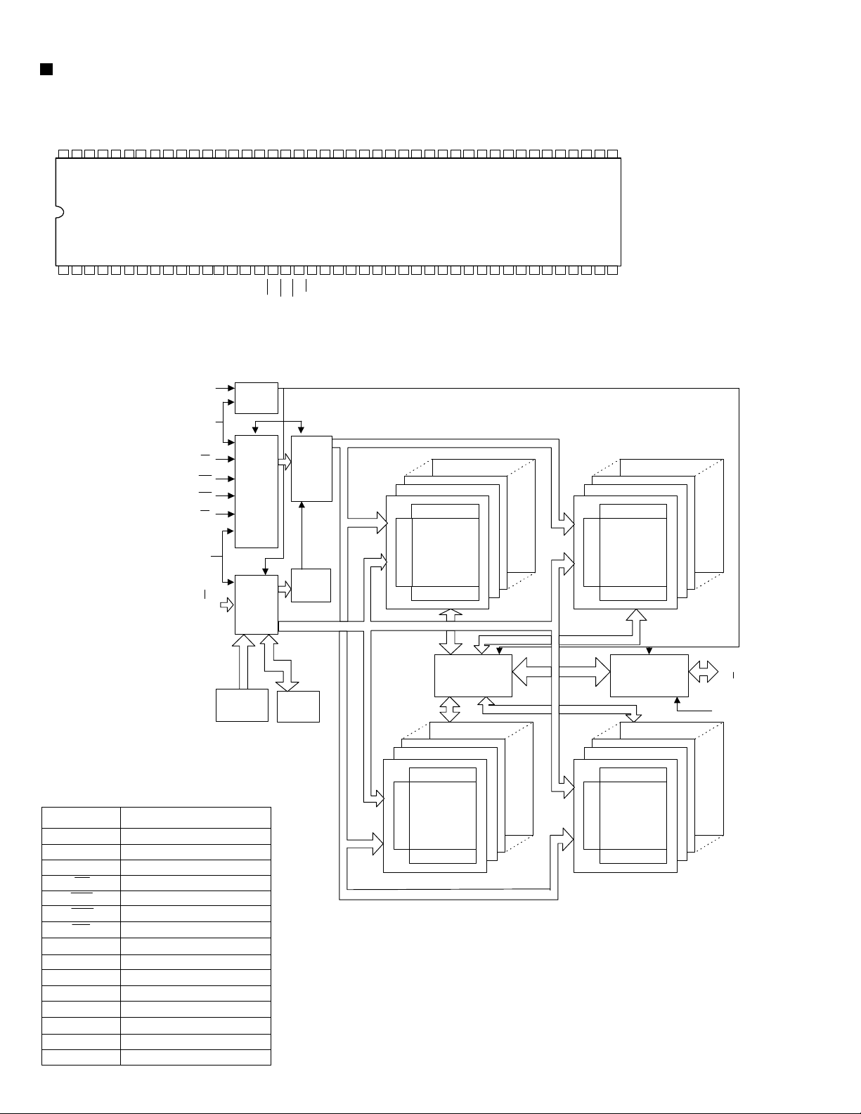
3. Block diagram
Parallel/serial
DVD Interface
I2S Stereo In
32-128Mbit
SDRAM
SDRAM Controller
Track Buffer
Processor
Audio
Decryption
ZiVA
A/V Core
Graphics
Engine
Input Unit
System Control Bus
Bus Interface Unit
IR GPIO SPI UART1&2ASYNC BUS IDC
ATAPI
Interlaced/
Progressive
Encoder
SPARC
Microprocessor
Phase
Lock
Loop
Video
JTAG Interface
Five 10-bit
Audio
Output
Unit
Video
DACs
CCIR 656
Digital Video
Composite
Y/R
C
Cr/Pr/G
Cb/Pb/B
IEC 958/1937
Downmix
Left/right
Center/subwoofer
Left/ right/surround
Remote Control
13.5 MHz Crystal
1-19
Page 20
TH-A5
CS493292 (DIC11) : Audio decoder
1. Pin layout
A1,SCDIN
RD,R/W,EMOE,GPIO11
WR,DS,EMWR,GPIO10
AUDATA3,XMT958
DGND1
VD1
MCLK
SCLK
LRCLK
AUDATA0
AUDATA1
A0,SCCLK
DATA7,EMAD7,GPIO7
DATA6,ENAD6,GPIO6
DATA5,EMAD5,GPIO5
DATA4,EMAD4,GPIO4
VD2
DGND2
DATA3,EMAD3,GPIO3
DATA2,EMAD2,GPIO2
DATA1,EMAD1,GPIO1
DATA0,EMAD0,GPIO0
2. Block diagram
65432144 43 42 41 40
7
8
9
10
11
12
13
14
15
16
17
18 19 20 21 22 23 24 25 26 27 28
CS
VD3
DGND3
SDATAN1
ABOOT,INTERQ
EXTMEM,GPIO8
SCLKN1,STCCLK2
SCDIO,SCDOUT,PSEL,GPIO9
AUDATA2
39
DC
38
DD
37
RESET
36
AGND
35
VA
34
FILT1
33
FILT2
32
CLKSEL
31
CLKIN
30
CMPREQ,LRCLKN2
29
LRCLKN1
CMPCLK,SCLKN2
CMPDAT,SDATAN2,RCV958
1-20
CMPDAT
SDATAN2
CMPCLK
SCLKN2
CMPREQ
LRCLKN2
SCLKN1
STCCLK2
LRCLKN1
SDATAN1
CLKIN
CLKSEL
RESET
Compressed
Data Input
Interface
Digital
Audio
Input
Interface
PLL
Clock Manager
DATA7:0
EMAD7:0
GPIO7:0
Framer
Shifter
Input
Buffer
Controller
RAM Input
Buffer
CS
RD
R/W
EMOE
GPIO11
SCDIO
WR
SCDOUT
DS
EMWR
GPIO10
Parallel or Serial Host Interface
DPS Processing
RAM
Program
Memory
ROM
Program
Memory
PSEL
GPIO9A0SCCLKA1SCDIN
24-Bit
RAM
Data
Memory
ROM
Data
Memory
STC
VD[3:1]DGND[3:1]AGNDVAFILT1 FILT2
RAM
Output
Buffer
ABOOT
INTERQ
EXTMEM
GPIO8
Output
Formatter
DC
DD
MCLK
SCLK
LRCLK
AUDATA[2.0]
XMT958
/AUDATA3
Page 21
3. Pin function
TH-A5
Pin No.
1,12,23
2,13,24
3
4
5
6
7
8
9
10
11
14
15
16
17
18
19
20
21
22
25
26
27
28
29
30
31
32
33
34
35
36
37
38
39
40
41
42
43
44
Symbol
VD1,VD2,VD3
DGND1,DGND2,DGND3
AUDATA3,XMT958
WR,DS,EMWR,GPIO10
RD,R/W,EMOE,GPIO11
A1,SCDIN
A0,SCCLK
DATA7,EMAD7,GPIO7
DATA6,ENAD6,GPIO6
DATA5,EMAD5,GPIO5
DATA4,EMAD4,GPIO4
DATA3,EMAD3,GPIO3
DATA2,EMAD2,GPIO2
DATA1,EMAD1,GPIO1
DATA0,EMAD0,GPIO0
CS
SCDIO,SCDOUT,PSEL,GPIO9
ABOOT,INTERQ
EXTMEM,GPIO8
SDATAN1
SCLKN1,STCCLK2
LRCLKN1
CMPDAT,SDATAN2
CMPCLK,SCLKN2
CMPREQ,LRCLKM2
CLKIN
CLKSEL
FILT1
TILT2
VA
AGND
RESET
DC
DD
AUDATA2
AUDATA1
AUDATA0
LRCLK
SCLK
MCLK
Function
Digital Positive Supply
Digital Supply Ground
SPDIF Transmitter Output, Digital Audio Output 3
Host write strobe or Host data strobe or External Memory write enable or
General purpose input& output Number 10
Host Parallel Output Enable or Host Parallel R/W or External Memory Output
Enable or General Purpose Input & Output Number11
Host Address Bit One or SPI Serial Control Data Input
Host Parallel Address Bit Zero or Serial Control Port Clock
Data Bus
Data Bus
Data Bus
Data Bus
Data Bus
Data Bus
Data Bus
Data Bus
Host Parallel Chip Select, Host Serial SPI Chip Select
Serial Control Port Data Input and Output, Parallel Port Type Select
Control Port Interrupt Request, Automatic Boot Enable
External Memory Chip Select or General Purpose Input & Output Number 8
PCM Audio Data Input Number One
PCM Audio Input Bit Clock
PCM Audio Input Sample Rata Clock
PCM Audio Data Input Number Tow
PCM Audio Input bit Clock
PCM Audio Input Sample Rate Clock
Master Clock Input
DSP Clock Select
Phase Locked Loop Filter
Phase-Locked Loop Filter
Analog Positive Supply
Analog Supply Ground
Master Reset Input
Reserved
Reserved
Digital Audio Output 2
Digital Audio Output 1
Digital Audio Output 0
Audio Output Sample Rate Clock
Audio Output Bit Clock
Audio Master Clock
BA4560 (IC2, IC5, IC6, IC7, CIC11, CIC13, FIC2, FIC4, FIC5, FIC6, FIC11, RIC11, RIC13)
: Dual op amp.
1.Pin layout
V
OUT1
– IN1
+ IN1
V
1
2
1ch
+
–
3
EE
4
2ch
+
–
CC
8
OUT2
7
– IN2
6
+ IN2
5
1-21
Page 22
TH-A5
SP3721A (U7) : DVD driver
1.Pin layout
1
16
2.Pin function (1/2)
Pin No.
2
3,4
5~6
7~ 8
11~14
15~16
Symbol I/O Function
1
DVDRFP
DVDRFN
PD1,PD2
A2,B2
C2,D2
9
10
17
18
19
20
21
22
23
24
25
26
27
28
29
30
31
32
33
CP
CN
A,B,C,D
E,F
CDTE
VCI2
NC
VNB
DVDPD
DVDLD
CDPD
CDLD
LDON#
VC
VCI
VPB
MIRR
MP
MB
FDCHG#
MLPF
I/O
I/O
64 ~ 49
48
~
17 ~ 32
RF Signal Inputs. Differential RF signal attenuator input pins.
I
CD Photo detector Interface Inputs. Inputs from the CD photo detector error outputs.
I
Photo Detector Interface Inputs. AC coupled inputs for the DPD from
I
the main beam Photo detector matrix outputs.
Differential Phase tracking LPF pin. An external capacitance is
connected between this pin and the CN pin.
Differential Phase tracking LPF pin. An external capacitance is
connected between this pin and the CP pin.
Photo Detector Interface Inputs. Inputs from the main beam Photo
I
detector matrix outputs.
CD tracking Error Inputs. Inputs from the CD photo detector error outputs.
I
CD Tracking. E-F Opamp output for feedback.
Reference Voltage input. DC bias voltage input for the servo input reference.
No Connect.
Ground. Ground pin for the servo block.
APC Input. DVD APC input pin from the monitor photo diode.
I
APC output. DVD APC output pin to control the laser power.
O
APC Input. DVD APC input pin from the monitor photo diode.
I
APC output. DVD APC output pin to control the laser power.
O
APC output. on/off. APC output control pin. A low level activates the
I
LD output. (open high)
Reference Voltage output. This pin provides the internal DC bias
reference voltage (+2.5+ fix). Output impedance is less than 50 ohms.
Reference Voltage input. DC bias voltage input for the servo input reference.
Power. Power supply pin for the servo block.
Mirror Detect Output. Mirror Detect comparator output. Pseudo CMOS output.
O
MIRR signal Peak hold pin. An external capacitance is connected to
between this pin and VPB.
MIRR signal Bottom hold pin. An external capacitance is connected to
between this pin and VPB.
Low Impedance Enable. A TTL compatible input pin that activates the FDCHG switches.
I
A low level activates the switches and the falling edge of the internal FDCHG triggers
the fast decay for the NIRR bottom hold circuit. (open high)
MIRR signal LPF pin. An external capacitance is connected between this pin and VPB.
-
~
33
1-22
Page 23

2.Pin function (2/2)
Pin No.
34
35
36
37
38
39
40
41
42
43
44
45
46
47
48
49
50
51
52
53
54
55
56
57
58
59
60
61
62
63
64
Symbol
MEVO
MIN
PI
DFT
TPH
MEV
MEI
TE
FE
CE
LCN
LCP
SCLK
SDATA
SDEN
HOLD1
VNA
FNN
FNP
DIP
DIN
RX
BYP
SIGO
VPA
AIP
AIN
ATON
ATOP
CDRF
CDRFDC
I/O
SIGO Bottom Envelope Output. Bottom envelope for Mirror detection.
O
RF signal Input for Mirror. AC coupled inputs for the mirror detection
I
circuit from the pull-in signal output. (PI)
Pull-in Signal Output. The summing signal output of A,B,C,D or PD1,
O
PD2 for mirror detection. Reference to VCI.
Defect Output. Pseudo CMOS output. When a defect is detected, the
O
DFT output goes high. Also the servo AGC output can be monitored at
this pin, When CAR bits 7-4 are '0011'.
PI Top Hold pin. An external capacitance is connected between this pin and VPB.
SIGO Bottom Envelope pin. An external capacitance is connected
between this pin and VPB.
Mirror Envelope Input. The SIGO envelope input pin.
I
Tracking Error Signal Output. Tracking error output reference to VCI.
O
Focusing Error Signal Output. Focus error output reference to VCI.
O
Center Error Signal Output. Center error out put reference to VCI.
O
Center Error LPF pin. An external capacitance is connected between
this pin and the LCP pin.
Center Error LPF pin. An external capacitance is connected between
this pin and the LCN pin.
Serial Clock. Serial Clock CMOS input. The clock applied to this pin
I
is synchronized with the data applied to SDATA. (Not to be left open).
Serial Data. Serial data bi-directional CMOS pin. NRZ programming
I/O
data for the internal registers is applied to this input. (Not to be left open)
Serial Data Enable. Serial enable CMOS input. A high level input
I
enables the serial port. (Not to be left open)
Hold Control. ATTL compatible control pin which, when pulled high, disables the RF AFC
I
charge pump and holds the RE AGC amplifier gain at its present value. (open high)
Ground. Ground pin for the RF block and serial port.
Differential Normal Output. Filter normal outputs.
O
Differential Normal Output. Filter normal outputs.
O
Analog inputs for RF Single Buffer. Differential analog inputs to the RF single-ended
I
output buffer and full wave rectifier.
Analog inputs for RF Single Buffer. Differential analog inputs to the RF single-ended
I
output buffer and full wave rectifier.
Reference Resistor Input. An external 8.2 kohm, 1% resistor is
connected from this pin to ground to establish a precise PTAT
(proportional to absolute temperature) reference current for the filter.
The RF AGC integration capacitor CBYP, is connected between BYP and VPA.
I/O
Single Ended Normal Output. SIngle-ended RF output.
O
Power. Power supply pin for the RF block and serial port.
AGC Amplifier Inputs. Differential AGC amplifier input pins.
I
AGC Amplifier Inputs. Differential AGC amplifier input pins.
I
Differential Attenuator Output. Attenuator outputs.
O
Differential Attenuator Output. Attenuator outputs.
O
RF Signal Input. Single-ended RF signal attenuator input pin.
I
CD RF Signal Output. Single ended CD RF summing output.
O
Function
TH-A5
1-23
Page 24
TH-A5
W986432DH (U5) : SDRAM
1. Pin layout
Q
CC
DQ12
VssDQ15
VSSQDQ14
86858483828180797877767574737271706968676665646362616059585756555453525150494847464544
12345678910111213141516171819202122232425262728293031323334353637383940414243
Q
DQ0
DQ1
VCC
CC
V
DQ13
DQ2
V
Q
SS
V
DQ3
DQ11
DQ4
Q
SS
V
Q
CC
V
DQ10
DQ5
DQ9
DQ6
Q
CC
DQ8NCV
V
VSSQ
DQ7
NC
SS
DQM1NCNC
VCC
WE
DQM0
CLK
CKEA9A8A7A6A5A4A3DQM3
CAS
RAS
CS
NC
BS0
BS1
A0A1A2
A10/AP
VSSNC
CC
V
DQM2
NC
DQ31
DQ16
Q
CC
V
Q
SS
V
DQ30
DQ17
DQ29
DQ18
Q
SS
V
Q
CC
V
DQ28
DQ19
DQ27
DQ20
Q
CC
V
Q
SS
V
DQ26
DQ21
DQ25
DQ22
Q
SS
V
Q
CC
V
DQ24
DQ23
2. Block diagram
CLK
CKE
CS
RAS
CAS
WE
CLOCK
BUFFER
COMMAND
DECODER
CONTROL
SIGNAL
GENERATOR
COLUMN DECODER
COLUMN DECODER
SS
V
CC
V
3. Pin function
Symbol
A0-A10
BS0, BS1
DQ0-DQ31
CS
RAS
CAS
WE
DQM0-DQM3
CLK
CKE
VCC
VSS
VCCQ
VSSQ
NC
A10
A0
ADDRESS
BS0
BS1
A9
REFRESH
COUNTER
BUFFER
Function
Address
Bank Select
Data Input/Output
Chip Select
Row Address Strobe
Column Address Strobe
Write Enable
Input/output mask
Clock Inputs
Clock Enable
Power(+3.3V)
Ground
Power(+3.3V) for I/O buffer
Ground for I/O buffer
No Connection
MODE
REGISTER
COLUMN
COUNTER
CELL ARRAY
BANK #0
ROW DECODER
SENSE AMPLIFIER
COLUMN DECODER
CELL ARRAY
BANK #2
ROW DECODER
SENSE AMPLIFIER
DATA CONTROL
CIRCUIT
CELL ARRAY
BANK #1
ROW DECODERROW DECODER
SENSE AMPLIFIER
COLUMN DECODER
CELL ARRAY
BANK #3
SENSE AMPLIFIER
DQ
BUFFER
DQ0
DQ31
DQM0~3
1-24
Page 25
LC86P6548 (UIC1) : Microcontroller
1.Pin layout
S47/PF7
S46/PF6
S45/PF5
S44/PF4
S43/PF3
S42/PF2
S41/PF1
S40/PF0
VDD4
S39/PE7
S38/PE6
S37/PE5
S36/PE4
S35/PE3
S34/PE2
S33/PE1
S32/PE0
S31/PD7
S30/PD6
S29/PD5
S28/PD4
S27/PD3
S26/PD2
S25/PD1
S24/PD0
S23/PC7
S22/PC6
S21/PC5
S20/PC4
VP
TH-A5
2.Block diagram
S48/PG0
S49/PG1
S50/PG2
S51/PG3
P00
P01
P02
P03
VSS2
VDD2
P04
P05
P06
P07
P10/SO0
P11/SI0/SB0
P12/SCK0
P13/SO1
P14/SI1/SB1
P15/SCK1
81
82
83
84
85
86
87
88
89
90
91
92
93
94
95
96
97
98
99
100
Interrupt Control
Standby Control
CF
RC
X’tal
8079787776757473727170696867666564636261605958575655545352
1234567891011121314151617181920212223242526272829
P30
P31
P32
P33
P34
P35
P36
P16/BUZ
P17/PWM0
Clock
Generator
P37
P70/INT0
RES
XT1/P74
CF1
VSS1
XT2/P75
CF2
VDD1
P80/AN0
P81/AN1
P82/AN2
IR PLA
PROM
Control
PROM(48KB)
PC
P83/AN3
P84/AN4
P85/AN5
A15-A0
D7-D0
TA
CE
OE
DASEC
P86/AN6
P87/AN7
P71/INT1
P72/INT2/T0I
51
50
49
48
47
46
45
44
43
42
41
40
39
38
37
36
35
34
33
32
31
30
S0/T0
P72/INT3/T0I
S19/PC3
S18/PC2
S17/PC1
S16/PC0
VDD3
S15/T15
S14/T14
S13/T13
S12/T12
S11/T11
S10/T10
S9/T9
S8/T8
S7/T7
S6/T6
S5/T5
S4/T4
S3/T3
S2/T2
S1/T1
Base Time
r
SIO0
SIO1
Timer 0
er 1
Tim
ADC
INT0-3
Noise Filter
SIO Auto
matic
transmission
RAM
128 by
s
te
VFD
Controller
High voltage Output
Bus Interface
Port 1
Port 3
Port 7
Port 8
ACC
B Register
C Register
A
PSW
RAR
RAM
Stack Poi nter
Port 0
Watchdog Timer
1-25
Page 26

TH-A5
M11B416256A (U1) : DRAM
1. Pin layout
Vcc
1
I/O0
2
I/O1
3
I/O2
4
I/O3
5
Vcc
6
I/O4
7
I/O5
8
I/O6
9
I/O7
10
NC
11
NC
12
WE
13
RAS
14
NC
15
A0
16
A1
17
A2
18
A3
19
Vcc
20
3. Block diagram
40
39
38
37
36
35
34
33
32
31
30
29
28
27
26
25
24
23
22
21
Vss
I/O15
I/O14
I/O13
I/O12
Vss
I/O11
I/O10
I/O9
I/O8
NC
CASL
CASH
OE
A8
A7
A6
A5
A4
Vss
2. Pin function
Pin No.
16~19,22~26
14
28
29
13
27
2~5,7~10,31~34,36~39
1,6,20
21,35,40
11,12,15,30
Symbol
A0~A10
RAS
CASH
CASL
WE
OE
I/O0~I/O15
Vcc
Vss
NC
I/O
I
I
I
I
I
I
I/O
Supply
Ground
-
Function
Address Input
Row Address Strobe
Column Address Strobe/Upper Byte Control
Column Address Strobe/Lower Byte Control
Write Enable
Output Enable
Data Input/ Output
Power, 5V
Ground
No Connect
A0
A1
A2
A3
A4
A5
A6
A7
A8
WE
CASL
CASH
NO.2 CLOCK
GENERATOR
COLUMN
ADDRESS
9
BUFFER
REFRESH
CONTROLLER
REFRESH
COUNTER
ROW
ADDRESS
9
BUFFERS(9)
CAS
9
CONTROL
LOGIC
ROW
9
9
512
DECODER
DATA-IN BUFFER
COLUMN
DECODER
8
512
8
SENSE AMPLIFIERS
I/O RATING
512 x 16
512 x 512 x 16
MEMORY
ARRAY
DATA-OUT
BUFFER
16
I/O0
.
16
.
I/O15
CE
1-26
RAS
NO.1 CLOCK
GENERATOR
Vcc
Vss
Page 27

M6759 (U3) : MTP microcontroller
TH-A5
1. Pin layout
4443424140393837363534
1
2
3
4
5
6
7
8
9
10
11
1213141516171819202122
3. Block diagram
2. Pin function
Pin No.
44
33
32
31
30
29
28
27
26
25
24
23
22
36,37,38,39,
40,41,42,43,
10
21
20
32
33
9,8,7,6,
5,4,3,2
31,30,29,28,
27,26,25,24
19,18,17,16,
15,14,13,11
35
1,12,23,34
Symbol
VDD
GND
P0.7-P0.0
AD7-0
RST
XTAL1
XTAL2
/PSEN
ALE
P1.7-P1.0
T2EX(P1.1)
T2(P1.0)
P2.7
A15-A8
P3.7-P3.0
/RD(P3.7)
/WR(P3.6)
T1(P3.5)
T0(P3.4)
/INT1(P3.3)
/INT0(P3.2)
TXD(P3.1)
RXD(P3.0)
/EAVPP
NC
I/O
I
Power supply for internal operation, 5V input
I
Ground
I/O
8 bits bi-directional I/O port
I/O
Multiplexed address/data bus
I
Reset signal
I
Crystal In
O
Crystal out
O
Program Store Enable Output
O
Address Latch Enable
I/O
8 bits bi-directional I/O port
I
External timer/counter 2 trigger
I
External timer/counter 2.
I/O
8 bits bi-directional I/O port
Description
O
I/O
8-bit bi-directional I/O port
O
External data memory read strobe
O
External data memory write strobe
I
External timer/counter 1
I
External timer/counter .
I
External interrupt 1 (Negative Edge Detect)
I
External interrupt 0 (Negative Edge Detect)
O
Serial port output
I
Serial port input
I
-
P0.7:0 P2.7:0 P1.7:0 P3.7:0
Port 0
Drivers
Data Bus
Program Address
Register
Port 2
Drivers
Port Latch
Port 1
Drivers
Serial Port
Timer
Port Latch Port Latch
Interrupt Logic
Port 3
Drivers
Data Bus
ACC
B Register
ALU REG1 ALU REG2
64K bytes
MTP Memory
Program Counter
Incrementer
Data Bus
PSW
ALU
Data Bus
Stack
Pointer
Buffer
DPTR
512 Bytes
RAM
RAM Addr.
Register
Instruction
Register
OSC
XTAL2
XTAL1
Clock and Control
RST
/EAVPP
ALE
/PSEN
1-27
Page 28

TH-A5
SST39VF800A (U6) : 8M Flash memory
1. Pin layout
A15
A14
A13
A12
A11
A10
A9
A8
NC
NC
WE#
NC
NC
NC
NC
A18
A17
A7
A6
A5
A4
A3
A2
A1
1
2
3
4
5
6
7
8
9
10
11
12
13
14
15
16
17
18
19
20
21
22
23
24
2. Block diagram
48
47
46
45
44
43
42
41
40
39
38
37
36
35
34
33
32
31
30
29
28
27
26
25
X-Decoder
A16
NC
Vss
DQ15
DQ7
DQ14
DQ6
DQ13
DQ5
DQ12
DQ4
VDD
DQ11
DQ3
DQ10
DQ2
DQ9
DQ1
DQ8
DQ0
OE#
Vss
CE#
A0
EEPROM
Cell Array
Memory Address
3. Pin function
Symbol
AMS- A0
DQ15- DQ0
Data Input/Output
CE#
OE#
WE#
VDD
Vss
NC
Address Buffer & Latches
CE#
OE#
WE#
Pin name
Address Inputs
Chip Enable
Output Enable
Write Enable
Power Supply
Ground
No Connection
Y-Decoder
Control Logic
I/O Buffers & Data Latches
DQ15-DQ0
Function
To provide memory addresses. During Sector-Erase AMS-A11 address lines will
select the sector. During Block-Erase AMS-A15 address lines will select the block.
To output data during Read cycles and receive input data during Write cycles. Data is
internally latched during a Write cycle. The outputs are in tri-state when OE# or CE# is
high.
To activate the device when CE# is low.
To gate the data output buffers.
To control the Write operations.
To provide power supply voltage: 2.7-3.6V
Unconnected pins.
1-28
Page 29

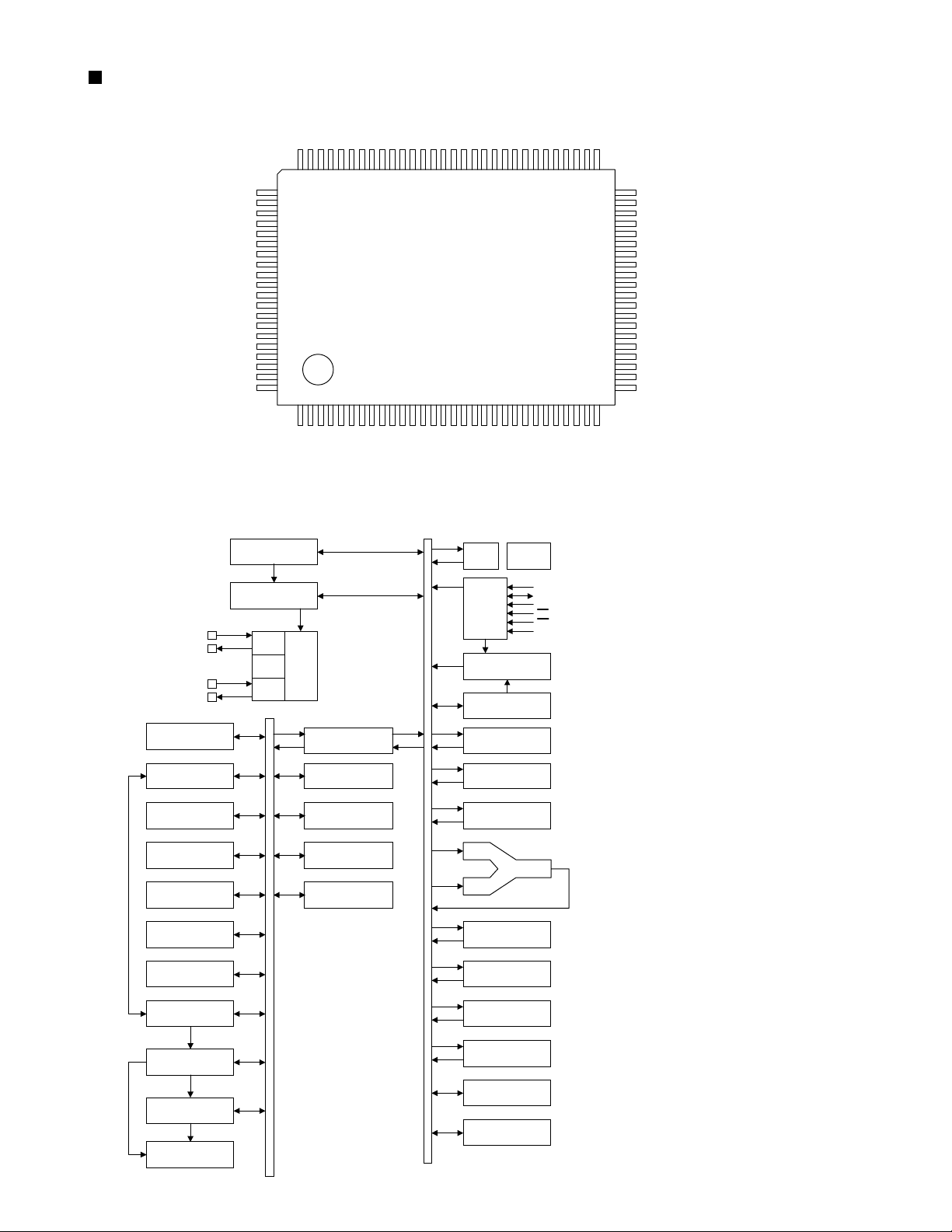
LC75725E (UIC10) : VFD driver
1. Pin layout
S9
S10
S11
S12
S13
S14
S15
S16
S17
S18
S19
48 47 46 45 44 43 42 41 40 39 38 37 36 35 34 33
49
S8
50
S7
51
S6
52
S5
53
S4
54
S3
55
S2
56
S1
57
Vss
VDD
BLK
CE
CL
DI
58
59
60
61
62
63
64
1 2 3 4 5 6 7 8 9 10 11 12 13 14 15 16
G1G2G3G4G5G6G7G8G9
VFL
G10
OSCO
OSCI
S20
G11
S21
VFL
S22
S43
S23
S42
S24
32
31
30
29
28
27
26
25
24
23
22
21
20
19
18
17
S41
S25
S26
S27
S28
S29
S30
S31
S32
S33
S34
S35
S36
S37
S38
S39
S40
2. Block diagram
G11
BLK
VFL
TIMING
GENERATOR
DRIVER
OSCI
OSCO
CLOCK
GENERATOR
G10
DIGIT
DRIVER
G2
G1
CONTROL
GRID
S43
S42
SEGMENT DRIVER
LATCH
DIMMRE
TIMING
GENERATOR
SHIFT REGISTER
ADDRESS
DETECTOR
MPX
S2
TH-A5
S1
3. Pin function
Pin No.
1,13
60
57
59
58
61
63
64
62
2-12
56-14
Symbol
VFL
VDD
Vss
OSCI
OSCO
BLK
CL
DI
CE
G1-G11
S1-S43
I/O
Driver block power supply connection. (Both pins must be connected.)
-
Logic block power supply connection. Provide a voltage between 4.5 and 5.5V.
-
Power supply connection. Connect to the ground.
-
Oscillator connection. An oscillator circuit is formed by connecting an external resistor
I
and capacitor to these pins.
O
Display off contort input.
BLK = Low (Vss)...Display off.(S1 toS43 and G1 to G11 at VFL level.)
I
BLK = High (VDD)...Display on.
Note that serial data can be transferred while the display is turned off.
Serial data transfer inputs. These pins must be connected to the system microcontroller.
CL: Synchronization clock
I
DI: Transfer data
CE: Chip enable
Digit outputs. These pins are P-channel open drain outputs with pull-down resistors.
O
Segment outputs for displaying the display data transferred by serial data input. These pin
O
are P-channel open drain outputs with pull-down resistors.
W27L010 (DIC21) : EPROM
Vpp
A16
A15
A12
A7
A6
A5
A4
A3
A2
A1
A0
Q0
Q1
Q2
GND
1
2
3
4
5
6
7
8
9
10
11
12
13
14
15
16
32
31
30
29
28
27
26
25
24
23
22
21
20
19
18
17
Vcc
PGM
NC
A14
A13
A8
A9
A11
OE
A10
CE
Q7
Q6
Q5
Q4
Q3
2. Block diagram 3. Pin function1. Pin layout
PGM
CE
OE
A0
A16
Vcc
GND
V
PP
CONTROL
DECODER
Function
OUTPUT
BUFFER
CORE
ARRAY
Q0
Q7
DI
CL
CE
Symbol Function
A0~A16
Q0~Q7
PGM
GND
Address Inputs
Data Inputs/Outputs
Chip Enable
CE
Output Enable
OE
Program Enable
Program/Erase Supply Voltage
PP
V
Vcc
Power Supply
Ground
NC
No connection
Vss
VDD
1-29
Page 30

TH-A5
74VHCT244A (DIC12) : Buffer/Line driver
1. Pin layout
1
OE1
I0
O4
I1
O5
I2
O6
I3
O7
GND
2
3
4
5
6
7
8
9
10
20
19
18
17
16
15
14
13
12
11
Vcc
OE2
O0
I4
O1
I5
O2
I6
O3
I7
74LVT573 (U10, U11, U12) : Latch
2. Pin function
Symbol
OE1,OE2
I0-I7
O0-O7
Function
3-STATE Output Enable Inputs
Inputs
3-STATE Outputs
3. Truth table
Inputs
OE1
L
L
H
Inputs
OE2
L
L
H
H:HIGH Voltage Level
L:LOW Voltage Level
I:Immaterial
Z:High Impedance
Outputs
L
L
(Pins12,14,16,18)
L
H
Z
Outputs
(Pins3,5,7,9)
L
H
Z
In
H
X
In
H
X
1. Pin layout 2. Pin function
OE
D0
D1
D2
D3
D4
D5
D6
D7
GND
1
2
3
4
5
6
7
8
9
10
20
19
18
17
16
15
14
13
12
11
Vcc
O0
O1
O2
O3
O4
O5
O6
O7
LE
Symbol
D0-D7
LE
OE
O0-O7
MM74HCT245 (U15) : Transceiver
1. Pin layout
ENABLE
Vcc G B1 B2 B3 B4 B5 B6 B7 B8
20 19 18 17 16 15 14 13 12 11
Function
Data Inputs
Latch Enable Input
Output Enable Input
3-STATE Latch Outputs
2. Truth table
Control
Inputs
G
DIR
L
L
H
H=HIGH Level
L=LOW Level
X=Irrelevant
Operation
L
B data to A bus
H
A data to B bus
X
245
isolation
3. Truth table
Inputs Outputs
LE
X
H
H
L
H:HIGH Voltage Level
L:LOW Voltage Level
Z:High Impedance
X:Immaterial
O0:Previous O0 before HIGH to LOW transition of Latch Enable
OE
H
L
L
L
Dn
X
L
H
X
On
Z
L
H
O0
1 2 3 4 5 6 7 8 9 10
DIR A1 A2 A3 A4 A5 A6 A7 A8 GND
1-30
Page 31

CS8415A (DIC14) : Digital audio receiver
TH-A5
1. Pin layout
SDA/CDOUT
AD0/CS
EMPH
RXP0
RXN0
VA+
AGND
FILT
RST
RMCK
RERR
RXP1
RXP2
RXP3
1
2
3
4
5
6
7
8
9
10
11
12
13
14
28
27
26
25
24
23
22
21
20
19
18
17
16
15
SCL/CCLK
AD1/CDIN
RXP6
RXP5
H/S
VD+
DGND
OMCK
U
INT
SDOUT
OLRCK
OSCLK
RXP4
2. Pin function
Pin No.
1
2
3
4
5
6
7
8
9
10
11
12,13
14,15
25,26
16
17
18
19
20
21
22
23
24
27
28
Symbol
SDA/CDOUT
AD0/CS
EMPH
AGND
RMCK
RERR
RXP1,RXP2
RXP3,RXP4
RXP5,RXP6
OSCLK
OLRCK
SDOUT
OMCK
DGND
AD1/CDIN
SCL/CCLK
RXP0
RXN0
VA+
FILT
RST
INT
U
VD+
H/S
I/O
Serial Control Data I/O(I2C) / Data Out(SPI)
I/O
Address Bit 0(I2C) / Control Port Chip Select(SPI)
I/O
Pre-Emphasis
O
AES3/SPDIF Receiver Power
I
Positive Analog Power
I
Analog Ground
I
PLL Loop Filter
O
Reset
O
Input Section Recovered Master Clock
I/O
Receiver Error
O
Additional AES3/SPDIF Receiver Port
I
Serial Audio Output Bit Clock
I/O
Serial Audio Output Left/Right Clock
I/O
Serial Audio Output Data
O
Interrupt
O
User Data
O
System Clock
I
Digital Ground
I
Positive Digital Power
I
Hardware/Sofrware Mode Control
I
Address Bit 1(I2C) / serial Control Data in (SPI)
I
Control Port Clock
I
Function
3. Block diagram
RSN0
RXP6
RXP5
RXP4
RXP3
RXP2
RXP1
RXP0
7:1
MUX
VA+ VD+AGND
Receiver
H/S
FILT RERR RMCK OMCK
Misc.
Control
Clock &
Data
Recovery
RST
EMPH
U
AES
S/PDIF
Decoder
SDA/
CDOUT
SCL/
CCLK
DGND
C&U bit
Data
Buffer
Control
Port &
Registers
AD1/
CDIN
AD0/
CS
INT
Serial
Audio
Output
OLRCK
OSCLK
SDOUT
1-31
Page 32

TH-A5
FAN8082 (U10) : DC motor driver
1.Pin layout
2. Block diagram
V
GND
V
V
CTL
V
IN1
O1
1
2
3
4
O2
8
PV
CC
7
SV
CC
5
V
IN2
6
3. Pin function
I/O
12V
3V
4V
5V
6SV
7PV
8V
GND
O1
CTL
IN1
IN2
CC
CC
O2
Ground
O Output 1
I Motor speed control
I Input 1
I Input 2
- Supply voltage (Signal)
- Supply voltage (Power)
O Output 2
GND
V
O1
1
2
DRIVER OUT
8
V
O2
7
PV
CC
PRE DRIVER
V
CTL
V
IN1
3
4
TSD
LOGIC SWITCH
BIAS
6
SV
CC
5
V
IN2
FunctionPin No. Symbol
KA78R05 (PQ2,PQ6)/ KA78R08 (PQ5)/ KA278R05 (PQ1)/ KA278R33 (PQ4) : Regulator
1. Block diagram
1-32
Vin
1
THERMAL SHUTDOWN
BANDGAP REFERENCE
HIGH / LOW OUTPUT
4
Vdis
1.4V
+
ON / OFF
OVERVOLTAGE
PROTECTION
+
SOA PROTECTION
SHORT-CIRCUIT
SHORTCIRCUIT
PROTECTION
3
GND
Q1
R1
R2
2
Vo
Page 33

CS4228A (DIC15) : D/A converter
TH-A5
1. Pin layout
SDIN3
SDIN2
SDIN1
SDOUT
SCLK
LRCK
DGND
VD
VL
MCLK
SCL/CCLK
SDA/CDIN
AD0/CS
RST
1
2
3
4
5
6
7
8
9
10
11
12
13
14
28
27
26
25
24
23
22
21
20
19
18
17
16
15
SUB
CENTER
SR
SL
FR
FL
AGND
VA
AINL+
AINLFILT
AINRAINR+
MUTEC
2. Pin function
Pin No.
1,2,3
4
5
6
7
8
9
10
11
12
13
14
15
16,17
19,20
18
21
22
23,24,25
26,27,28
SUB,CENTER
Symbol
SDIN1
SDIN2
SDIN3
SDOUT
SCLK
LRCK
DGND
VD
VL
MCLK
SCL/CCLK
SDA/CDIN
ADO/CS
RST
MUTEC
AINR+,AINR-
AINL+,AINL-
FILT
VA
AGND
FR,FL,SR,SL
Function
Serial Audio Data In
Serial Audio Data Out
Serial Clock
Left/Right Clock
Digital Ground
Digital Power
Digital Interface Power
Master Clock
Serial Control Interface Clock
Serial Control Data I/O
Address Bit 0/ Chip Select
Reset
Mute Control
Differential Analog Inputs
Internal Voltage Filter
Analog Power
Analog Ground
Analog Outputs
74LCX244 (DIC13) : Bus buffer
1. Pin layout
20
19
18
17
16
15
14
13
12
11
Vcc
2G
1Y
2A
1Y
2A
1Y
2A
1Y
2A
Yn
1
4
2
3
3
2
4
1
L
H
Z
1
1G
1
2
1A
2Y
4
3
1A
2
4
2Y
3
5
1A
3
6
2Y
2
7
1A
4
8
2Y
1
9
GND
10
3. Truth table
INPUT OUTPUT
G
L
L
H
X:"H"or"L"
Z:High impedance
An
L
H
X
2. Pin function
Pin No.
1
2,4,6,8
9,7,5,3
11,13,15
17
18,16,14
12
19
10
20
Symbol
1G
1A1 to 1A4
2Y1 to 2Y4
2A1 to 2A4
1Y1 to 1Y4
2G
GND
Vcc
Function
Output Enable Input
Data Inputs
Data Outputs
Data Inputs
Data Outputs
Outputs Enable Input
Ground(0V)
Positive Supply Voltage
1-33
Page 34

TH-A5
VICTOR COMPANY OF JAPAN, LIMITED
AUDIO & COMMUNICATION BUSINESS DIVISION
PERSONAL & MOBILE NETWORK BUSINESS UNIT. 10-1,1chome,Ohwatari-machi,Maebashi-city,371-8543,Japan
(No.21062)
200201(V)
Page 35

SCHEMATIC DIAGRAMS
DVD DIGITAL CINEMA SYSTEM
Area suffix
TH-A5
CD-ROM No.SML200212
Supplement
A ------------------ Australia
US -------------- Singapore
UB ------------- Hong Kong
UW -- Brazil,Mexico,Peru
UY --------------- Argentina
UJ ------------- U.S.Military
UG ------------------ Turkey,
South Africa,Egypt
TH-A5
STANDBY/ON
AUDIO
VCR
CONTROL
ON
VCR
TV
OFF
TV CHANNEL
TOP MENU
MENU
AUDIO/
SUBTITLE
TV VOLUME
FM MODE
TV/VIDEO
STEP
DISPLAY
RETURN
TUNER PRESET
DOWN UP
REW FF
VCR CHANNEL
TUNING
B.SEARCH F.SEARCH
ENTER
VOLUME
DVD FM/AM AUX MUTING
RM-STHA5U
DVD CINEMA SYSTEM
STANDBY/ON
COMPACT
DIGITAL VIDEO
STANDB
Y
AUDIO/FM MOD
E
D
SP
OLUMESOURC
V
SP-XCA5SP-XSA5 2
E
DVD DIGITAL CINEMA
SYSTEM TH-A
5
SP-XSA5 2
DIGITAL
SURROUND
DIGITAL
XV-THA5 SP-WA5
In No.21062BSCH, change of the schematic diagram & circuit board of MPEG
section were missing. Please add this supplement to No.21062BSCH.
Page
2-8
2-12
Contents
Standard schematic diagrams
Items
DVD MPEG section
DVD MPEG board (Forward side)
Printed circuit boards
2-13
DVD MPEG board (Reverse side)
Contents
Standard schematic diagram
Printed circuit boards
COPYRIGHT 2002 VICTOR COMPANY OF JAPAN, LTD.
2-1
2-2
No.21062CSCH
Dec. 2002
Page 36

TH-A5
In regard with component parts appearing on the silk-screen pr inted side (par ts side) of
the PWB diagrams, the parts that are printed over with black such as the resistor ( ),
diode ( ) and ICP ( ) or identified by the " " mark nearby are critical for safety.
(This regulation does not correspond to J and C version.)
Page 37

Standard schematic diagram
DVD MPEG section
+5V_VID
5
VID_C
4
3
2
1
VR1
150
C
VR3
S_VIDEO_C
000
1
23
Q3
1
KSA812
VR2
82
VOGND
+5V_VID
VR10
U
150
VR11
1
R(OPEN)
C
VIDEO_U
23
000
Q6
KSA812
3.3V_FLASH
AR2
R31
4.7K
4.7K
UDS1
2
A14
3
A13
4
A12
5
A11
6
A10
7
A9
841
A8 DQ13
0ohm
9
A21
10
A20
11
WE
12
RESET
13
ACC
14
WP
15
A19
16
A18
17
A17
18
A7
19
A6
20
A5
21
A4
22
A3
23
A2
24
A1
R32
4.7K
3
C
3
C
8M FLASH MEMORY
3.3V
C75
0.1u
3.3V
C64
0.1u
VDD
C89
0.1u
3.3V
C62
0.1u
3.3V
C61
0.1u
3.3V
C59
0.1u
GND
3
C
BE
12
R1103
3
C
BE
12
KSA812
0.1u
BB
12
DAP202K
BA
12
DAN202K
1
VID_U
VR9
82
VOGND
UPA17
UPA16
UPA15
UPA14
UPA13
UPA12
UPA11
UPA10
UPA9
UPA22
R34
UPA21
R33
UPA20
R10 0ohm
UPA19
UPA18
UPA8
UPA7
UPA6
UPA5
UPA4
UPA3
UPA2
3.3V
U8/12PIN U8/145PIN
C80
0.1u
VDD
U8/30PIN
C90
0.1u
3.3V
U8/32PIN
C106
0.1u
3.3V
U8/44PIN
C77
0.1u
GND
3
BE
12
2SB1197
3
IN
OUT GND
21
XC61AN1902MR
TR/ DIODE MODEL DRAWING
+5V_VID
VR5
150
Y
1
23
VID_ Y
1
VR4
82
+5V_VID
VR7
150
23
1
Q5
KSA812
I_SAT_OPT(DEL)
VDD
/SYS_RST
U6
SST39VF800A
U8/63PIN
U8/74PIN
U8/80PIN
U8/87PIN
U8/98PIN
U8/104PIN
3
C
BE
12
2SC1623
3
C
BE
12
R2101
VR6
S_VIDEO_Y
000
Q4
KSA812
VR8
VIDEO_Y1
000
AMS317
R60:220OHM
R61:120OHM
IC-VOLTAGE REGULATOR
U9
AMS317
2
OUT
ADJ
R60
220
1
ADJ_2.5V
481
A16A15
47
Vi/o
46
VSS
45
DQ15
44
DQ7
43
DQ14
42
DQ6
40
DQ5
39
DQ12
38
DQ4
37
VCC
36
DQ11
35
DQ3
34
DQ10
33
DQ2
32
DQ9
31
DQ1
30
DQ8
29
DQ0
28
OE
27
VSS
26
CE
25
A0
GND
VDD
C88
0.1u
VDD
U8/173PIN
C87
0.1u
3.3V
U8/181PIN
C79
0.1u
3.3V
U8/196PIN
C107
0.1u
VDD
U8/205PIN
C86
0.1u
GND
COMP
VID_COMP
R(OPEN)
VR15A
VID_V
3
IN
C83
0.1u(DEL)
R61 120ohm
+
C84
10u/16
UPA[22:1]
FUPR1
UPD15
UPD7
UPD14
UPD6
UPD13
UPD5
UPD12
UPD4
UPD11
UPD3
UPD10
UPD2
UPD9
UP D1
UPD8
UPD0
R/W
/FLASH_CS
UPA1
+5V_VID
VR16
150
1
23
1
VR15 56
+5V_VID
V
23
1
1
VR12
82
VOGND
LM1117DT_1.8
R60:DEL
R61:22OHM
+
GND
UDS
R(0ohm_2012, OPEN)
Q8
KSA812
VR13
150
Q7
KSA812
3.3V
VR17
000
VR14
000
C82
47u/6
C100 0.1u(OPEN)
UPD[15:0]
COMP_OUT
VIDEO_V
DEL
VL1
FBSMT
/SYS_RST
R36
+5_VID
VC10
0.1u
L57
0ohm(2012_DEL)
0ohm
GND
GND
C32
0.1u
VOGND
R5V
+5V_VID
+
0ohm
C30
220u/16
VOGND
3.3V_FLASH
VJL1
000(2012)
FBSMT(DEL)
COMP_OU T
S_ VIDEO_C
S_ VIDEO_Y
VIDEO_Y1
VIDEO_U
VIDEO_V
OPT_OUT
/FLASH_CS
IL1
OL1
FBSMT
3.3V
+5V
/FLASH_CS
1
+5V_VID
CON_WAFER_1m/m_SMD_ST
1
2
3
4
5
6
7
8
9
10
OL2
FBSMT
J21
T o VW2
VDD
C85
+
47u/16
GND
HDMARQ
HDMACK
/LDRRST
R110 4.7K
/IDE_CS1
/IDE_CS0
UPA_3
UPA_2
R52 4.7K(OPEN)
HIRQ1
3.3V_FLASH
UPA20
UPA21
UPA22
UPA12
UPA13
UPA14
UPA15
UPA16
UPA17
UPA18
UPA19
UPA4
UPA5
UPA6
UPA7
UPA8
UPA9
UPA10
UPA11
R53 4.7K(OPEN)
C76
0.1u
R54 R
(OPEN)
+5V
R6 33 ohm
R8 33 ohm
19
18
17
16
15
14
13
12
19
18
17
16
15
14
13
12
19
18
17
16
15
14
13
12
U12
74LVT573
C98
0.1u
C66
0.1u
Q1
Q2
Q3
Q4
Q5
Q6
Q7
Q8
Q1
Q2
Q3
Q4
Q5
Q6
Q7
Q8
Q1
Q2
Q3
Q4
Q5
Q6
Q7
Q8
TPN3
VGND
1
DA_DATA1
DA_DATA0
I2C_CL
NO CONNECT
I2C_DA
NO CONNECT
D_MUTE
PWR_CNTL
/SYS_RST
U10
20
74LVT573
UPA1
2
D1
UPA2
3
D2
VCCGND
UPA3
4
D3
5
D4
6
D5
7
D6
IC-BICMOS LOGIC
8
D7
9
D8
11
C
1
OC
10
IC-BICMOS LOGIC
20
UPD8
2
D1
UPD9
3
D2
VCCGND
UPD10
4
D3
UPD11
5
D4
UPD12
6
D5
UPD13
7
D6
UPD14
8
D7
UPD15
9
D8
11
C
1
OC
IC-BICMOS LOGIC
10
U11
74LVT573
20
UPD0
2
D1
UPD1
3
D2
VCCGND
UPD2
4
D3
UPD3
5
D4
UPD4
6
D5
UPD5
7
D6
UPD6
8
D7
UPD7
9
D8
11
C
1
OC
10
L56
CIS21
C99
0.1u
PLL_GND
REF_GND
DVSS
C65
0.1u(OPEN)
R114 0ohm
R109 4.7K
R107 5.6K
NO CONNECT
NO CONNECT
R112 4.7K
R111 4.7K
NO CONNECT
UPA3
UPA2
UPA1
L52
FBSMT
L54
FBSMT
L53
FBSMT
L55
VGND
FBSMT
VID_V
VID_U
VID_Y
VID_C
VID_COMP
3.3V
R56
4.7K
ALE
/MEDUSA_CS
/FLASH_CS
R57 33 ohm
R59 33 ohm
ALE
1
TH-A5
CLK
RRQ
SRQ
IEC_958
TXD
1
1
1
1
DR7
100
12
L38
F/B_CIC21J121NE
L39
F/B_CIC21J121NE
3.3V
54
53
52
51
50
49
48
47
46
45
44
43
42
41
40
39
38
37
36
35
34
33
32
31
30
29
3.3V
54
53
52
51
50
49
48
47
46
45
44
43
42
41
40
39
38
37
36
35
34
33
32
31
30
29
GND
3.3V
GND
L40FBSMT
MDATA31
MDATA30
MDATA29
MDATA28
MDATA27
MDATA26
MDATA25
MDATA24
MDQM3
SD_CLK
MADDR11
MADDR9
MADDR8
MADDR7
MADDR6
MADDR5
MADDR4
C105
0.1u
MDATA15
MDATA14
MDATA13
MDATA12
MDATA11
MDATA10
MDATA9
MDATA8
MDQ M1
SD_CLK
MADDR11
MADDR9
MADDR8
MADDR7
MADDR6
MADDR5
MADDR4
1
L43
FBSMT
3.3V
GND
AC2
0.1u
L42
L41
FBSMT
FBSMT
FPC_CON24P_SMD
WAFER_1m/m
MGND
U14/49PINU14/37PIN
3.3V
U13/37PINU13/1PIN U13/27PIN U13/43PIN
GND
RRQ(MCE)
CLK(MCK)
TXD(SDATA)
RXD(MDATA)
SRQ(SCE)
To J3
12
GNDGND
68ohm
AC9
47P
J14
1
2
3
4
5
6
7
8
9
10
11
12
13
14
15
16
17
18
19
20
21
22
23
24
AR1
CON_WAFER_24P_1M/M_SMD_ST
XOUT
HD1
137
UPD_7
C97
20pF
C54
0.1u
R55
136
XVSS
VDDP
R9
000ohm
VDAC_RefVSS
GNDP
VDAC_VDD
REF_VDD
1.2K/1%
DVDD
133
134
135
VDAC_Ref
VDAC_RefVDD
HD0
HDTACK
UPD0
/MEDUSAINT
/DTACK
UPA1
47u/6
3.3V
DVSS
132
129
130
131
VDAC_0
VDAC_0B
VDAC_VDD0
VDAC_DVSS
VDAC_DVDD
U8
HIRQ0
HUDS
HLDS
HREAD
IRRX1
IR
1
IR
NO CONNECT
LDS
UDS
AT_GND
L48
FBSMT
L49
FBSMT
L47
FBSMT
L50
CIC21C
C50
C48
+
0.1u
R108
122
123
121
124
125
126
127
128
VDAC_3
VDAC_2
VDAC_1
VDAC_2B
VDAC_1B
VDAC_VDD2
VDAC_VDD1
GND
VDD
GND25
VDD25
MA9
MA8
MA7
30
31
32
333435363738394041
RESET
DD6UPD14
DD4UPD12
DD1UPD9
DD0UPD8
DMARQ
/IORDY
DMACK
INTRQ
DA1
DA0
/CS0
FPC/FFC_40P_1M/M_SMD
3.3V
C51
0.1u
VGND
4.7K
115
114
113
112
116
117
118
119
120
VDATA0
VDATA1
VDATA2
VDAC_4
VDAC_4B
VDAC_3B
VDAC_VDD4
VDAC_VDD3
HSYNC / IRQ2
VDD25
GND25
MA6
MA5
MA4
MA3
MA2
MA1
MA0
43
42
12
DD8 UPD0
34
56
DD10 UPD2
78
910
DD12 UPD4
11 12
DD13 UPD5
13 14
15 16
DD15 UPD_7
17 18
19 20
21 22
23 24
25 26
27 28
29 30
31 32
33 34
DA2
35 36
/CS1
37 38
39 40
J6
AT_GND
ATN_FM
1
ATN_FM
RDY_FM
SCK
D_FM
D_HOST
DAI_DATA
1
110
109
111
108
107
106
VDDP
GNDP
VDATA3
VDATA4
VDATA5
VDATA6
MCS0
MCS1
BA0
BA1
MA11
MA10
ATAPI
CONNECTOR
DATA3
105
VDATA7
MDQM3
MDQM2
MDQM1
MDQM0
MRAS
525149504847464544
FMSMT
VCLK
VDD25
GND25
VDD25
GND25
VDD25
GND25
VDD25
GND25
VDD25
GND25
VDD25
GND25
MCAS
L30
1
1
MD31
MD30
MD29
MD28
MD27
MD26
MD25
MD24
MD23
MD22
MD21
MD20
MD19
MD18
MD17
MD16
MD15
MD14
MD13
MD12
MD11
MD10
MCLK
RDY_FM
TUNE_CLK
VDD
GND
MD9
MD8
MD7
MD6
MD5
MD4
MD3
MD2
MD1
MD0
MWE
1
DATA2
DATA1
1
1
TPN1
104
103
102
101
100
99
98
97
96
95
94
93
92
91
90
89
88
87
86
85
84
83
82
81
80
79
78
77
76
75
74
73
72
71
70
69
68
67
66
65
64
63
62
61
60
59
58
57
56
55
54
53
R66 33 ohm
R68 33 ohm
R71 33 ohm
R73 33 ohm
R75 33 ohm
R69 33 ohm
R78 33 ohm
R79 33 ohm
R80 33 ohm
R81 33 ohm
R82 33 ohm
R83 33 ohm
R84 33 ohm
R85 33 ohm
R86 33 ohm
R88 33 ohm
R90 33 ohm
UPD1DD9
UPD3DD11
UPD6DD14
UPA_3
/IDE_CS1
SCK
1
DATA0
R64
1
3.3V
33 ohm
D_FM
BCK
1
GND
MDATA31
MDATA30
MDATA29
MDATA28
MDQM3
MDATA27
MDATA26
MDATA25
MDATA24
MDATA23
MDATA22
MDATA21
MDATA20
MDQM2
MDATA19
MDATA18
MDATA17
MDATA16
MDATA15
MDATA14
MDATA13
MDATA12
MDQM1
MDATA11
MDATA10
MDATA9
MDATA8
MDATA7
MDATA6
MDATA5
MDATA4
MDQM0
MDATA3
MDATA2
MDATA1
MDATA0
GND
VDD
1
LRCK
MADDR11
MADDR10
MADDR0
MADDR1
MADDR2
MADDR3
MADDR4
MADDR5
MADDR6
MADDR7
MADDR8
MADDR9
Front Panel Board
Connector
D_HOST
1
RRQ_MCE
SRQ_SCE
CLK_MCK
TXD_SDATA
RXD_MDATA
XCK
1
NO CONNECT
DAI_DATA
1
IEC_958
DA_DATA3
DA_DATA2
DA_DATA1
DA_DATA0
DA_
DA_LRCK
DA_XCK
MDATA[31..1]
R58 33 ohm
/MWE
/MCAS
/MRAS
/MCS0
BA0
BA1
GND
BCK
SD_CLK
MADDR[11..0]
PLL_VDD
C71
REF_VDD
0.1u
+
C68
PLL_GND
PLL_GND
MGND
VDD
155
DEMPH
JTAG
157
158
159
160
161
162
163
164
165
166
167
168
169
170
171
172
173
174
175
176
177
178
179
180
181
182
183
184
185
186
187
188
189
190
191
192
193
194
195
196
197
198
199
200
201
202
203
204
205
206
207
208
R/W
R63
156
IEC958
DAI_DATA
DAI_BCK/SYSCLKBP
DAI_LRCK/IEC958BP
I2C_CL
I2C_DA
RTS1
RXD1
TXD1
CTS1
GNDP
VDDP
SDDATA7
SDDATA6
SDDATA5
SDDATA4
GND
VDD
SDDATA3
SDDATA2
SDDATA1
SDDATA0
SDREQ
SDEN
GNDP
VDDP
SDERROR
SDCLK
VSYNC / HIRQ1
RTS2
RXD2
TXD2
CTS2
VNW
ALE
HCS4
HCS3
HCS2
HCS1
HCS0
VDDP
TRST
TDO
TDI
TMS
TCK
RESET
BUSCLK
GND
VDD
HA3
HA2
GNDP
VDDP
234
1
33 ohm
R98
C55
0.1u
4.7K
CTS2
3.3V
VDD
C73
+
47u/16
DVDD
47u/6
PLL_GND
152
151
VDDP
GNDP
150
ADATA1
149
ADATA0
148
BCK
C67
0.1u
DVSS
13.5MHz Fundamental
C96
15pF
145
146
147
142
143
144
XCK
VDD
GND
LRCK
AVSS1
AVDD1
3
1
2
X1
139
138
140
141
XVDD
AVSS2
AVDD2
XIN / VCLK216BP
REF_GND
153
154
ADATA2
ADATA3
ZiVA-5P MPEG DECODER
IC-DECODER
HD13
HD12
HD11
HD10
HD9
HD8
HD7
GNDP
VDDP
HD6
HD5
HD4
HD3
UPD9
UPD8
UPD7
UPD6
UPD5
UPD4
UPD3
UPD2
HD2
UPD1
HA1
HD15
HD14
567891011131214151617181922202123242526272829
UPD13
UPD12
UPD11
UPD14
UPD15
UPD10
(UPD0-15)
PL3
FBSMT(3216)
UPD[15:0]
HDMARQ
HDMACK
HIRQ1
UPA_2
/IDE_CS0
/IDE_CS1
UPA_3
/LDRRST
UPD15 DD7
3.3V
UPD13 DD5
UPD11 DD3
UPD10 DD2
R99
1K
/DTACK
L32
FBSMT
(UPD0-15)
GND
AC8
47P(DEL)
MADDR[11..0]
3.3V
C37
0.1u
RXD_MDATA
RRQ_MCE
SRQ_SCE
CLK_MCK
TXD_SDATA
IEC_958
DA_LRCK
DA_BCK
DA_DATA3
DA_DATA2
DA_DATA1
DA_DATA0
DA_XCK
/SYS_RST
MDATA[31..1]
/MWE
/MRAS
/MCS0
BA0
BA1
MADDR[11..0]
MDATA[31..1]
/MCAS
/MCS0
BA0
BA1
AR4
68(DEL)
C102
+5V
DC1
104(DEL)
/SYS_RST
1
12
103
GND
MDATA16
MDATA17
MDATA18
MDATA19
MDATA20
MDATA21
MDATA22
MDATA23
MDQ M2
/MCAS
MADDR10
MADDR0
MADDR1
MADDR2
MADDR3
3.3V
3.3V
+
C46
0.1u
GND
MDATA0
3.3V
MDATA1
MDATA2
AR3 1K(OPEN )
MDATA3
MDATA4
MDATA5
MDATA6
MDATA7
MDQM0
/MWE
/MRAS
MADDR10
MADDR0
MADDR1
MADDR2
MADDR3
12
GND
+
C38
47u/6
GND
2
3
4
5
6
7
8
9
1
19
20
CMOS LOGIC/TRANSCEIVER
+5V_VID
L1
F/B_CIC21J121NE
3.3V
RRQ_MCE
18
B1
A1
17
A2
B2
16
B3
A3
RXD_MDATA
15
B4
A4
14
B5
A5
OPT_OUT
13
B6
A6
12
B7
A7
11
B8
A8
DIR
OE
10
VCC
GND
U15
74HCT245
GND
L44 FBSMT
DR1 100
DR2 100
DR3 100
DR4 100
DR5 100
DR6 100
DR8 100
DR9 100
+5V
C29
104
GND
1
VDD
2
DQ0
3
VDDQ
4
DQ1
5
DQ2
6
VSSQ
7
DQ3
8
DQ4
9
VDDQ
10
DQ5
11
DQ6
12
VSSQ
13
DQ7
14
VDD
AU14
15
DQML
16
WE
64Mb_SDRAM
17
CAS
18
RAS
19
CS
20
BA0
21
BA1
22
A10
23
A0
24
A1
25
A2
26
A3
27 28
VDD VSS
IC-DRAM
3.3V
C103
C33
0.1u
47u/6C101
GND
3.3V
3.3V
U14/1PIN
C36
0.1u
GND
1
VDD
2
DQ0
3
VDDQ
4
DQ1
5
DQ2
6
VSSQ
7
DQ3
8
DQ4
9
VDDQ
10
DQ5
11
DQ6
12
VSSQ
13
AU13
DQ7
14
VDD
15
DQML
64Mb_SDRAM
16
WE
17
CAS
18
RAS
19
CS
20
BA0
21
BA1
22
A10
23
A0
24
A1
25
A2
26
A3
27 28
VDD VSS
IC-DRAM
GND
3.3V
AC3
0.1u
GND
3.3V
U13/14PIN
AC5
0.1u
12
12
12
12
12
12
12
12
+
C28
220u/16
U14/14PIN
C104
0.1u
3.3V3.3V
AC4
0.1u
GNDGND
VDDQ
VDDQ
DQMH
VDDQ
VDDQ
DQMH
DQ15
VSSQ
DQ14
DQ13
DQ12
DQ11
VSSQ
DQ10
DQ15
VSSQ
DQ14
DQ13
DQ12
DQ11
VSSQ
DQ10
VSS
DQ9
DQ8
VSS
CLK
CKE
VSS
DQ9
DQ8
VSS
CLK
CKE
PL1
FBSMT
NC
NC
A11
A9
A8
A7
A6
A5
A4
3.3V
GND
NC
NC
A11
A9
A8
A7
A6
A5
A4
3.3V
AC1
0.1u
To DJ3
Digital audio signalDigital data signal Video signal
ABCD E F G
2-1
Page 38

Printed circuit boards
DVD MPEG board
TH-A5 TH-A5
(Forward side)
5
4
(Reverse side)
3
2
1
2-2
HABC DEFG
Page 39

< MEMO >
TH-A5
Page 40

TH-A5
VICTOR COMPANY OF JAPAN, LIMITED
AUDIO & COMMUNICATION BUSINESS DIVISION
PERSONAL & MOBILE NETWORK BUSINESS UNIT. 10-1,1chome,Ohwatari-machi,Maebashi-city,371-8543,Japan
No.21062CSCH
Printed in Japan
200212
Page 41

TH-A5
Block diagrams
Main section
AUX
L R
5
TUNER
VFD
DI
CE
CL
CL CE DI
UIC10
VFD DRIVER
FIC6
LPF
UIC1
MICROCONTROLLER
CLK
KEY
GND
4
FIC5
LPF
AUX L
TUN L
IC5
AUX R
TUN R
DIC11
DPS
27
39-41
3
3
A/D IN
18
DIC14
DIR
2
DIGI IN
DVD
12
CODEC
1-3
DIC15
19,20
A/D IN
FL
16,17
FR
RL
RR
C
W
23
24
25
26
27
28
LPF
(1/2)
FIC4
LPF
(2/2)
LPF
(1/2)
RIC11
LPF
(2/2)
LPF
(1/2)
CIC11
LPF
(2/2)
FIC12
RIC12
FIC11
RIC13
POWER
AMP
IC6
POWER
AMP
6ohm
(35W)
6ohm
(35W)
6ohm
(35W)
6ohm
(35W)
6ohm
(35W)
IC7
F_C_R_S/W
CIC12
CIC13
POWER
AMP
U15 U8 U2 U7
PICK UP
1
DVD PACK
(Next page section)
FIC2
LPF
ABCD E F G
3ohm
(60W)
2-1
Page 42

TH-A5 TH-A5
DVD mecha block section
RF AGC
DECK ASS’Y
5
&EQ
CONTROL
FOCUS OK
DETECT DEFECT
DETECT MIRROR
GEN
PICK UP
& I/V AMP
FOCUS
SERVO
LOOP
DISC
MOTOR
FEED
MOTOR
4
DISC
MOTOR
DRIVER
ACTUATOR
MOTOR
DRIVER
MICOM DATA INTERFACE
LOGIC DECODER
U7 RF AMP SP3721
TRACKING
ERROR
I/V AMP
APC.LASER
CONTROL&
LPC
TRACKING
SERVO
LOOP
HARDWARE
LOGIC
EFM
COMPARATOR
RF&FOCUS
ERROR
I/V AMP
SPINDLE
SERVO LPF
U3
MICOM
DATA
SEPARATOR
DIGITAL
SERVO
U2
M5701
DVD ROM
CONTROLLER
BCA
DVD-DSP
CD-DSP
U1
4M DRAM
RAM
ARBITER
TARGET
SEARCH
Parallel/serial
DVD Interface
ATAPI 40PIN
ATAPI
&
MPEG
I/F
C3 ECC
EDP
MCU I/F
3
U6
HOST
SDRAM CONTROLLER
U5
64M SDRAM
MEMORY
Track Buffer
Processor
Audio
Input Unit
Decryption
-------ZIVA
A/V CORE
Graphics
Engine
Interlaced/
Progressive
Video
Encoder
Digital Video
Five 10-bit
Video
DACs
Analog
Video
Output
BUFFER
SIGNAL
KSA812
VIC4
SWITCHING
BUFFER
VIDEO OUT
2
System Control Bus
U15
SPARC
Microprocessor
Audio
Output
Audio
Output
System Control Bus
Phase
Lock
1
ASYNC BUS/IR/GPIO/SPI/UART1&2/ATAPI/IDC
Loop
JTAG
Interface
U8
MPEG
IC LOGIC
AMP PARTS
Parallel/serial
DVD Interface
ATAPI 40PIN
13.5MHZ Crystal
2-2
DECODER
ZIVA5
HABC DE FG
Page 43

TH-A5
Standard schematic diagrams
FL display & System control section / Power supply section
5
Sheet 2/6
Sheet 5/6
4
TP1
Sheet 4/6
Sheet 4/6
3
2
SHEET
NUMBER
1
CIRCUIT DESCRIPTION
FL display & System control / Power supply
1/6
Main
2/6
Video signal output
3/6
DSP
4/6
DVD loader
5/6
DVD MPEG
6/6
Parts are safety assurance parts.
When replacing those parts, make
sure to use the specified parts.
SHEET 1/6
ABCD E F G
2-3
Page 44

TH-A5 TH-A5
Main section
To Tuner Pack
5
To DW14
Sheet 4/6
4
3
To DW10
Sheet 4/6
2
To PW5
Sheet 1/6
To DW13
Sheet 4/6
1
Tuner signal
Front signal
2-4
Center signal
Rear signal
SHEET 2/6
HABC DE FG
Page 45

Video signal output section
TH-A5
VW2
5
to J21
Sheet 6/6
1
2
3
4
5
6
7
8
9
10
CON10_1m/m_S_TYPE
VIDEO_COMPO
S_VIDEO_C
S_VIDEO_Y
VIDEO_Y
VIDEO_Pb
VIDEO_Pr
VR26 75
VR25 75
4
+
VC18 330/16
VC19
+
330/16
VC20
+
3
VFB1
FBSMT
330/16
VC1
104
VC2
+
330/16V
VR3
68
VR10
68
VR14
68
SUPER_VIDEO
VJ5
Y
Pb
Pr
1
4
VJ2
2
2
2
23
1
1
Y,Pb,Pr_ VIDEO_OUT
1
VC9
47u/16
2
to DW23
Sheet 4/6
VW1
1
1
2
2
3
3
4
4
5
5
6
6
7
7
8
8
9
9
10
10
11
11
12
12
CONN TRBLK 12
+5V
GND
GND
CONTA
CONTB
AV_SW2
1
AV_SW1
1
1
+
+12V
1
VC10
0.1u
VR18 470
VR22
47K
VR23
47K
VC14
4.7/25V
VR20
2.2K
VR32
330K
+
VJ4
1
VIDEO_OUT
2
1
2
3
4
VIC4
IN1
CTLA
CTLB
IN2
BA7612AF
Vout
Vcc
IN3
GND
VC15
8
7
6
5
+
330/16
VR19
56
Video signal
ABCD E F G
SHEET 3/6
2-5
Page 46

TH-A5 TH-A5
DSP section
Sheet 1/6
Sheet 6/6
Sheet 2/6
Sheet 3/6
5
Sheet 2/6
4
3
FIC1
FIC12
Sheet 2/6 Sheet 1/6
2
1
2-6
Digital audio signal
Front signal
Center signal
Rear signalTuner signal
SHEET 4/6
HABC DE FG
Page 47

TH-A5
DVD loader section
5
RFGND
R4 4.7K
208
207
206
XSVREFO
XSPDOFTR2
XSAWRCVCO
VC
205
204
203
XSVR_PLL
XSPDOFTR1
R5 10K
202
201
XSFDO
XSFTROPI
RFVCC
TR
200
AVSS_PL
XSPLLFTR2
RFVCC
199
198
XSPLLFTR1
RFGND
R18 100K
R17 100K
XSPD
XSFD
197
196
XSFDIREF
AVDD5_PL
195
194
GND
XSPDIREF
XTSLRF
193
XTPLCK
RA8
RA6
RA0
RA7
RA5
RA2
RA4
RA3
RA1
R2
R
R3
2.2K
R6
2.2K
R8
R
R9
R
R10
R
R11
2.2K
192
191
190
189
188
187
186
185
184
183
182
181
180
179
178
177
176
175
174
173
172
171
170
169
VDD
XRA3
XRA2
XRA1
XRA0
XRA4
DVSSO
VDD
GND
XRA5
XRA6
XRA7
GND
XRA8
XRA9
XRA10
XRA11
XROEJ
XRCASJ
XRRASJ
VDDO_R
XRHCASJ
XRSDCLK
U2
M5701/ SERVO IC
XGPIO12
XGPIO5
XGPIO11
XGPIO4
XGPIO10
XGPIO3
XGPIO9
DVDD05
XGPIO2
XGPIO8
XGPIO1
XGPIO7
XGPIO0
GND
XCRSTJ
XMRSTJ
VDD
XMALE
XMCK
DVDD_CLK
XOSC1
XOSC2
DVSS_CLK
XMD0
XMD1
XMD2
XMD3
XMD4
XMD5
XMD6
XMD7
XMCSJ
XMRDJ
XMWRJ
XMINT1J
XMINT2J
XMIWAITJ
VDD
5354555657585960616263646566676869707172737475767778798081828384858687888990919293949596979899
R38
C32 47P
33
R39
33
L1 L
C34 12P
C33 C
C35 12P
J3
2
GND
4
HD8
6
HD9
8
HD10
10
HD11
12
HD12
14
HD13
16
HD14
18
HD15
20
NC
22
GND
24
GND
26
GND
28
28
30
GND
32
HCS16J
34
HPDIAGJ
36
THA2
38
HCS3J
40
GND
MD0
MD1
MD2
MD3
MD4
X1
33.8688MHz
R40 1M
VCC
R7610K
R7710K
R7110K
R7510K
R7210K
R7910K
R7810K
R8010K
R7310K
R7010K
R7410K
R83 100
R85 100
R87 100
R89 100
R91 100
R93 100
R95 100
R97 100
R104 33
R106 33
R108 33
R110 33
XMA9
MCS
MA8
MWRJ
MRDJ
MA9
MINT1J
MD5
MD6
MD7
XHD8
XHD9
XHD10
XHD11
XHD12
XHD13
XHD14
XHD15
HCS16J
HPDIAGJ
HA2
HCS3J
R55 R
R12
33
R13
33
R14
33
R15
33
R16
33
RD10
RD8
RD7
RD6
RD9
RD5
168
167
166
165
164
163
162
XRD7
XRD8
XRD6
XRD9
XRD5
XRD10
DVSS0
XRWEJ
XMA8
XMA7
GND
XMA6
XMA5
XMA4
DVDDP5
XMA3
VCC 3.3V
C1 104
C6 104
DGND
ROEJ
RHCASJ
RCASJ
RRASJ
RWEJ
RD4
161
160
AVSS_VCO
XMA2
100
101
CE2
RD11
159
XRD4
XRD11
AVDD_VCO
DVSSO
XMA1
102
+
RD12
RD3
158
157
XRD3
XRD12
XRD13
XRD14
XRD15
XHRSTJ
DVDDP5
DVSSO
XHD10
XHD11
XHD12
XHD13
DVSSO
XHD14
XHD15
DVDDO5
XHDRQ
XHIOWJ
XHIORJ
XHIORDY
XHDACKJ
XHCS16J
XHPDIAGJ
DVSSO
XHCS1J
XHCS3J
XHDASPJ
XADAOT
XAMCLK
XAEMC2F
XADATA
XALRCK
XMA0
XABCK
103
104
47U/16V
VCC
C2 104
U1
1
RD0
2
RD1
3
RD2
4
RD3
5
6
RD4
7
RD5
8
RD6
9
RD7
10
11
12
RWEJ
13
RRASJ
14
15
RA0
16
RA1
17
RA2
18
RA3
19
20
RFVCC
156
GND
155
XRD2
154
153
XRD1
152
151
150
XRD0
149
148
147
XHD7
146
145
XHD8
144
XHD6
143
XHD9
142
XHD5
141
140
139
XHD4
138
137
VDD
136
XHD3
135
134
XHD2
133
132
131
XHD1
130
129
XHD0
128
127
126
125
124
123
122
121
GND
120
XHINT
119
118
XHA1
117
116
XHA0
115
XHA2
114
113
112
111
110
109
108
107
106
105
GND
+
47U/16V
C5 104
CE1
DGND
3.3V
RD2
RD13
RD1
RD14
RD0
RD15
C26 12P
C27 12P
C28 12P
C29 12P
NO CONNECT
R23
33
C30 12P
C31 12P
ABCK
VCC
DQ0
DQ1
DQ2
DQ3
VCC
DQ4
DQ5
DQ6
DQ7
NC
NC
WE
RAS
NC
A0
A1
A2
A3
VCC
IDERST
XHD7
XHD8
XHD6
XHD9
XHD5
XHD10
XHD4
XHD11
XHD3
XHD12
XHD2
XHD13
XHD1
XHD14
XHD0
XHD15
HDRQ
IOWJ
IORJ
IORDY
HDACKJ
HINTJ
HCS16J
HA1
HPDIAGJ
HA0
HA2
HCS1J
HCS3J
HDASPJ
VSS
DQ15
DQ14
DQ13
DQ12
VSS
DQ11
DQ10
DQ9
DQ8
VSS
LCAS
UCAS
OE
A8
A7
416C254_(4M_DRAM)
A6
A5
A4
VSS
40
RD15
39
RD14
38
RD13
37
RD12
36
35
RD11
34
RD10
33
RD9
32
RD8
31
30
RCASJ
29
RHCASJ
28
ROEJ
27
RA8
26
RA7
25
RA6
24
RA5
23
RA4
22
21
SPINDLE
C18 473
IDERST
XHD7
XHD6
XHD5
XHD4
XHD3
XHD2
XHD1
XHD0
HDRQ
IOWJ
IORJ
IORDY
HDACKJ
HINTJ
HA1
HA0
HCS1J
HDASPJ
C20 470P
C19 470P
R30 47K
R34 33
R35 33
R36 33
RFVCC
C8 104
RFGND
R20 47K
R24 100
R25 10K
R26 3.3K
R27 3.3K
R28 10K
C24 102
C25 102
R81 R
R82 100
R84 100
R86 100
R88 100
R90 100
R92 100
R94 100
R96 100
R98 33
R99 33
R100 33
R101 33
R102 33
R103 47
R105 47
R107 47
R109 33
R111 47
+
CE4
C21 682
R22 22K
C23 102
C1 CAP
R1 R
3.3V
SLEG
MOTOR
SBAD
DFCT
R6110K
R6010K
R7 1K
VCC
DGND
R6210K
C14 104
R19 4.7K
VC
C3 104
CRSTJ
MALE
MCLKO
R6810K
R6310K
R6510K
R6710K
R6610K
R6410K
C3 CAP
C4 473
C9 12P
C10 104
C11 104
C12 47P
C13 47P
1
AVSS_DS
2
XSRFIN
3
XSIPIN
4
AVDD5_DS
5
XSDSSLV
6
XSRSLINT
7
AVDDP3
8
XSAWRC
9
XSRFGC
10
XSEFGC
11
XSFOCUS
12
XSTRACK
13
XSSLEG
14
AVDD5_DA
15
XSMOTOR
16
XSTESTDA1
17
XSTESTDA2
18
AVSS_DA
19
XSRFRPCTR
20
XSONTRCK
21
XSRFRPLP
22
XSTELP
23
XSVREF3
24
XSVREF2
25
XSVREF1
26
XSRFRP
27
XSTEXI
28
AVSS_AD
29
XSTEI
30
XSFEI
31
XSAEI
32
AVDD5_AD
33
XSSBAD
34
XSTESTAD
35
GND
36
XSDFCT
37
XSWBL
38
XSCSJ
39
XSCLK
40
XSDATA
41
DVDDP5
42
XSLDC
43
XSFGIN
44
XSSPDON
45
XSFLAG3
46
XSFLAG2
47
DVSSO
48
XSFLAG1
49
XSFLAG0
50
XGPIO13
51
XGPIO6
52
GND
FPC/FFC_ZIF_VER_1M/M_40P_SMD
R6910K
1
IDERST
3
HD7
5
HD6
7
HD5
9
HD4
11
HD3
13
HD2
15
HD1
17
HD0
19
GND
21
HDRQ
23
IOWJ
25
IORJ
27
IORDY
29
HDACKJ
31
HINTJ
33
HA1
35
HA0
37
HCS1J
39
HDASPJ
47U/16V
RFVCC
C22 CAP
3.3V
L2
FBSMT
VCC
R5910K
R5610K
R5710K
R5810K
RFVCC
R132 8.2K
49
FNP
VNA
FNN
HOLD1
SDEN
SDATA
SCLK
MEVO
MLPF
MIRRMPMB
FDCHG#
32
+
CE14
40
P0.2
P0.3
P0.4
P0.5
P0.6
P0.7
EA/VP
NC
ALE/P
PSEN
P2.7
P2.6
P2.5
P2.3
P2.4
MICRO
CONTROLLER
LCP
LCN
MEI
MEV
TPH
DFT
MIN
47U/16V
39
38
37
36
35
34
3313
32
31
30
29
+
C47 104
CE9
C55 104
48
47
46
45
44
43
CE
42
FE
41
TE
40
39
38
37
36
PI
C67 474
35
34
C68 100P
33
C71 682
C72 102
+
47U/16V
C79 104
CE15
A15 MCS
MGND
C75 104
C74 104
C76 104
To PW4
MUTEJ
To Pickup board
U9
VCC
CDPD
VR
CDLD
GND
DVDPD
VR
DVDLD
GND
GND
FF+
T+
T-
GND
VREF
VCC
E
A
B
RF
C
D
F
CON_24P_DIP_L
R121 22K
R126 22K
SP-
SP+
SLEDSLED+
24
23
22
21
20
19
18
17
16
15
14
13
12
11
10
9
8
7
6
5
4
3
2
1
SMOTOR
R131 0
SSLEG
RFVCC
C64 104
+
47U/16V
CE11
Sheet 1/6
CON_WAFER_4P_2.5m/m_S
J2
1
+8V
2
GND
3
A5V
4
AGND
5
D5V
6
DGND
RFVCC RFGND
104
+
47U/16V
C7
RF_GND
CE3
GND POWER
4
MVCC
J5
R160 100K
R161 100K
1
LOAD- LOAD-
2
3
4
5
CON_WIRE_5P_B.IN_S
OUTSW
UPSW
INSW
3
MGND
VC
VC
R120 3.3K
SFOCUS
R125 10K
STRACK
TRACK+
TRACKFOCUS+
FOCUS-
MVCC
2
R159 100K
J4
1
2
3
4
LMTSW
5
6
CON_WAFER_6P_S
+
104
C44
CE6
LOAD+LOAD+
R117 220
R118 4.7K
R119 4.7K
R122 10K
R127 10K
HOMESW
SLED+
SLED-
SVCC
U5
BA033FP
OUTIN
GND
2
220U/16V
3.3V REGULATOR IC
R172 R
ZD1
5.6V
MUTEJ
+
47U/16V
C53 104
CE10
SP+
SP-
RFVCC MVCC
31
+
+
100U/16V
CE7
C46 104
C45 104
OPENJ
TRAY OPEN/CLOSE MOTOR IC
1
BIASIN
2
OPIN1+
3
OPIN1-
4
OPOUT1
5
OPIN2+
6
OPIN2-
7
OPOUT2
BA5983FM
8
GND
9
MUTE
10
PVCC
11
Vo2-
12
Vo2+
13
Vo1-
14
Vo1+
R171 R
1
GND
2
V01
3
VCTL
4
VIN1
FAN8082
U6
U10
PREVCC
OPIN4+
OPIN4-
OPOUT4
OPIN3+
OPIN3-
OPOUT3
STN-BY
CE8
8
VO2
R173 0
7
PVCC
6
SVCC
5
VIN2
28
27
26
25
24
23
22
21
GND
20
19
PVCC
18
Vo3-
17
Vo3+
16
Vo4-
15
Vo4+
FEED MOTOR IC
100U/16V
CLOSEJ
R115 0
R129 10K
MGND
R116 22K
R123 22K
R128 22K
C73 104
1
R158
R156 1
R155 1
R157 1
CDPD
CDLD
DVDMDI
DVDLD
PATT 0.5m/m
FOCUSFOCUS+
TRACK+
TRACK-
VC
E
A
B
PUHRF
C
D
F
VC
VCC
R47 1K
R168 1K
R50 4.7K
2
3
IN
OUT
GND
1
C41 C
U4
XC61AN1902MR
VC
DVDMDI
DVDLD
CDPD
CDLD
C82 104
C81 104
R166 220
R162 470
RFGND
R138
10K
R137
CLOSE
22K
CLOSEJ
R143 10K
OPENJ
R135 22K
R144 R
PATT 0.8m/m
R142 0
SVCC
INSW
OUTSW
CRSTJ
OPEN
MVCC
IDERST
VCC
R49 22K
C40 105
DGND
(A,B,C,D,E,F)
C85 104
RFGND
R1103
10uH(3225)
1
Q2
L4
R45 1K
32
PUHRF
D
C
B
A
F
E
C77 104
2LD ONLY
USE
C84 104
R46 100
L7
10uH(3225)
R124 0
R145 3.3K
R147 3.3K
R150 10
23
Q3
1
2SB1197
C83 104
C38 103
RFVCC
C60 680P
C62 680P
+
100U/16V
CE12
R153 1K
D3
1
B
2
B
DAP202K
R167 10
23
Q4
2SB1197
OPEN
INSW
OUTSW
CLOSE
HOMESW
CPURST
MINT1J
MWRJ
MRDJ
MCLKO
RFGND
C61 680P
C63 680P
C65 100P
C
RFVCC
C54 680P
R141 R
C70 104
R151 10K
R152 10K
VC
DVDLDO
3
+
100U/16V
CE19
R170 1K
1
LED
M6759_A1_ALI_MICOM
C39 104
646362616059585756555453525150
1
DVDRFP
CDRDDC
2
DVDRFN
3
PD1
4
PD2
5
A2
6
B2
7
C2
8
D2
9
CP
10
CN
11
D
12
C
13
B
14
A
15
F
16
E
CDTE
171819202122232425262728293031
RFGND
CDLDO
1
TP
7
P1.5
8
P1.6
9
P1.7
10
RESET
11
RXD
12
NC
TXD
14
INT0
15
INT1
16
T0
17
T1
R52 1M
C49 104
C48 104
C51 104
C52 104
C50 104
RX
AIP
AIN
DIP
DIN
VPA
BYP
SIGO
ATOP
ATON
CDRF
U7
SP3721A/ RF AMP
ALI_RF_IC
VCI2NCVNB
DVDPD
DVDLD
CDPD
CDLD
LDON#VCVCI
VPB
C78 104
C80 104
VCC
LED
23456
434241
1
44
NC
P0.0
P0.1
P1.2
P1.3
P1.4
VCC
P1.0/T2
P1.1/T2X
U3
X1
X2
P2.0
P2.1
P2.2
RD
WR
NC
VSS
21
20
2425262728
19
18
23
22
X2
X1
A9
A8
DGND
47U/16V
R
R134
C66 102
R146 R
R43R
R4810K
R53 0
R54 0
C56 30P
C59
473
L3
CE5 47U/16V
C36 104
GND POWER
RFGND
RFO
RFO
EFGC
SFOCUS
STRACK
SSLED
SMOTOR
VC
MIRR
MVREF2
TEX1
TEI
FEI
SBAD
STESTAD
SDFCT
SCSJ
SCLK
SDATA
SLDC
D1 DAN202K
3
C
R29 33
RFGND
C15 104
C16 104
C17 474
2
B
1
B
R31 0
R32 3.3K
TE
R33 4.7K
FE
IDERST
C57 30P
C58 30P
SCSJ
SDATA
SCLK
STESTAD
FEI
TEI
SDFCT
SBAD
PI
C69 474
R148 0
R149 1M
EFGC
MVREF2
MIRR
SLDC
RFVCC
RFGND
VCC
FBSMT
MD0
MD1
MD2
MD3
+
MD4
MD5
MD6
MD7
MALE
MA9
MA8
GND POWER
MGND
GND POWER
RF_GND
DGND
To J6
Sheet 6/6
1
Digital data signal
SHEET 5/6
ABCD E F G
2-7
Page 48

DVD MPEG section
TH-A5 TH-A5
VDAC_VDD
C97
20pF
C54
0.1u
1.2K/1%
R55
REF_VDD
134
136
135
138
137
XVSS
XOUT
VDAC_Ref
VDAC_RefVSS
XIN / VCLK216BP
HD2
HD1
HD0
VDDP
GNDP
UPD0
UPD1
/DTACK
DVDD
DVSS
132
133
131
VDAC_0
VDAC_DVSS
VDAC_DVDD
VDAC_RefVDD
U8
HDTACK
HIRQ0
HUDS
HLDS
LDS
UDS
R/W
AT_GND
L48
FBSMT
L49
FBSMT
L47
FBSMT
L50
CIC21C
3.3V
C48
47u/16
+
VGND
126
127
128
129
130
VDAC_1
VDAC_0B
VDAC_VDD1
VDAC_VDD0
HREAD
IRRX1
GND
VDD
30
31
IR
1
IR
RESET
DD4UPD12
DD1UPD9
DD0UPD8
/DIOWLDS
/DIORUDS
/IORDY/DTACK
INTRQHIRQ1
DA0UPA1
/CS0
FPC/FFC_40P_1M/M_SMD
R108 4.7K
C50
0.1u
122
123
121
124
125
VDAC_3
VDAC_2
VDAC_2B
VDAC_1B
VDAC_VDD3
VDAC_VDD2
GND25
VDD25
MA9
MA8
MA7
MA6
32
333435363738394041
12
34
56
78
910
11 12
13 14
15 16
17 18
19 20
21 22
23 24
25 26
27 28
29 30
31 32
33 34
35 36
37 38
39 40
To J3
Sheet 5/6
3.3V
C51
0.1u
VGND
115
114
113
116
117
118
119
120
VDATA0
VDATA1
VDATA2
VDAC_4
VDAC_4B
VDAC_3B
VDAC_VDD4
HSYNC / IRQ2
VDD25
GND25
MA5
MA4
MA3
MA2
MA1
MA0
43
42
J6
DD8 UPD0
DD10 UPD2
DD12 UPD4
DD13 UPD5
DD15 UPD_7
DA2
/CS1
AT_GND
RDY_FM
112
GNDP
MA10
ATN_FM
111
VDDP
MA11
CLK
RRQ
SRQ
IEC_958
TXD
1
1
1
1
DR7
100
F/B_CIC21J121NE
C28
C38
47u/16
86
VSS
85
DQ15
84
VSSQ
83
DQ14
82
DQ13
81
VDDQ
80
DQ12
79
DQ11
78
VSSQ
77
DQ10
76
DQ9
75
VDDQ
74
DQ8
73
NC
72
VSS
71
DQM1
70
NC
69
NC
68
CLK
67
CKE
66
A9
65
A8
64
A7
63
A6
62
A5
61
A4
60
A3
59
DQM3
58
VSS
57
NC
56
DQ31
55
VDDQ
54
DQ30
53
DQ29
52
VSSQ
51
DQ28
50
DQ27
49
VDDQ
48
DQ26
47
DQ25
46
VSSQ
45
DQ24
L40FBSMT
1 2
L38
L39
PL1FBSMT
3.3V
+
+
1
L42FBSMT
L43FBSMT
L41FBSMT
RRQ(MCE)
CLK(MCK)
TXD(SDATA)
RXD(MDATA)
SRQ(SCE)
FPC_CON24P_SMD
WAFER_1m/m
MGND
MDATA24
MDATA25
MDATA26
MDATA27
MDATA28
MDATA29
MDATA30
MDATA31
MDQM3
MADDR9
MADDR8
MADDR7
MADDR6
MADDR5MADDR0
MADDR4
MADDR3
MDQM2
MDATA23
MDATA22
MDATA21
MDATA20
MDATA19
MDATA18
MDATA17
MDATA16
C33
47u/16
To VW12
Sheet 4/6
1
2
3
4
5
6
7
8
9
10
11
12
13
14
15
CON_WAFER_24P_1M/M_SMD_ST
16
17
18
J14
19
20
21
22
23
24
C105
0.1u
RXD_MDATA
RRQ_MCE
SRQ_SCE
CLK_MCK
TXD_SDATA
IEC_958
IEC_958
+5V
DC1
1000p
D_HOST
D_FM
1
1
3.3V
GND
3.3V
GND
VDD
33 ohm
MADDR10
MADDR0
MADDR1
MADDR2
MADDR3
MADDR4
MADDR5
MADDR6
MADDR7
MADDR8
MADDR9
ATAPI
CONNECTOR
Front Panel Board
Connector
MDATA31
MDATA30
MDATA29
MDATA28
MDATA27
MDATA26
MDATA25
MDATA24
MDATA23
MDATA22
MDATA21
MDATA20
MDATA19
MDATA18
MDATA17
MDATA16
MDATA15
MDATA14
MDATA13
MDATA12
MDATA11
MDATA10
MDATA9
MDATA8
MDATA7
MDATA6
MDATA5
MDATA4
MDATA3
MDATA2
MDATA1
MDATA0
R58 33 ohm
MDQM1
/MWE
/MCAS
/MRAS
/MCS0
BA0
BA1
SRQ_SCE
RRQ_MCE
CLK_MCK
TXD_SDATA
RXD_MDATA
MDQM3
MDQM2
MDQM0
SD_CLK
/SYS_RST
MDATA[31..0]
MADDR[10..0]
/SYS_RST
1
12
C102
103
GND
3.3V
3.3V
MDQM3
MDQM2
MDQM0
MDQM1
SCK
RDY_FM
ATN_FM
1
1
1
SCK
D_FM
D_HOST
VID_COMP
VID_C
VID_Y
VID_U
VID_V
1
TPN1
TUNE_CLK
110
109
108
107
106
105
VCLK
VDATA3
VDATA4
VDATA5
VDATA6
VDATA7
104
VDD25
103
GND25
102
MD31
101
MD30
100
MD29
99
MD28
98
VDD25
97
MDQM3
96
GND25
95
MD27
94
MD26
93
MD25
92
MD24
91
MD23
90
MD22
89
MD21
88
MD20
87
VDD25
86
MDQM2
85
GND25
84
MD19
83
MD18
82
MD17
81
MD16
80
VDD
79
GND
78
MD15
77
MD14
76
MD13
75
MD12
74
VDD25
73
MDQM1
72
GND25
71
MD11
70
MD10
69
MD9
68
MD8
67
MD7
66
MD6
65
MD5
64
MD4
63
VDD25
62
MDQM0
61
GND25
60
MD3
59
MD2
58
MD1
57
MD0
56
MCLK
55
VDD25
54
GND25
53
MWE
MCAS
MRAS
MCS0
MCS1
BA0
BA1
525149504847464544
R64
R66 33 ohm
R68 33 ohm
R71 33 ohm
R73 33 ohm
R75 33 ohmC75
R78 33 ohm
R79 33 ohm
R80 33 ohm
R81 33 ohm
R82 33 ohm
R83 33 ohm
R84 33 ohm
R85 33 ohm
R86 33 ohm
R88 33 ohm
R90 33 ohm
UPD1DD9DD6UPD14
UPD3DD11
UPD6DD14
UPA_3
/IDE_CS1
L30
FMSMT
GND
COMS LOGIC/TRANSCEIVER
+5V_VID
12
C70
+
1000p
U5/1PIN
C36
0.1u
U5/15PIN
C103
0.1u
SD_CLK
C69
220u/16V
3.3V
19
20
MDATA7
MDATA6
MDATA5
MDATA4
MDATA3
MDATA2
MDATA1
MDATA0
MADDR10
MADDR1
MADDR2
MDATA8
MDATA9
MDATA10
MDATA11
MDATA12
MDATA13
MDATA14
MDATA15
2
18
U15
A1
B1
3
17
A2
B2
4
16
B3
A3
5
15
A4
B4
6
14
A5
B5
7
13
B6
A6
8
12
A7
B7
9
11
A8
B8
1
DIR
OE
10
GND
VCC
74HCT245
DR1 100
1 2
DA_LRCK
DR4 100
1 2
DA_BCK
DR3 100
1 2
DA_DATA3
DR2 100
1 2
DA_DATA2
DR5 100
1 2
DA_DATA1
DR6 100
1 2
DA_DATA0
DR8 100
1 2
DA_XCK
DR9 100
1 2
+5V
L1
1
+3.3V
F/B_CIC21J121NE
1
C31
1000p
U5/3PIN
C104
0.1u
1
VDD
2
DQ0
3
VDDQ
4
DQ1
5
DQ2
6
VSSQ
7
DQ3
8
DQ4
9
VDDQ
10
DQ5
11
DQ6
12
VSSQ
13
DQ7
14
NC
15
VDD
MDQM0
16
DQM0
17
/WE
18
/CAS
19
/RAS
20
/CS
21
NC
BA0
22
BA0
BA1
23
BA1
24
A10/AP
25
A0
26
A1
27
A2
MDQM1
28
DQM2
29
VDD
30
NC
31
DQ16
32
VSSQ
33
DQ17
34
DQ18
35
VDDQ
36
DQ19
37
DQ20
38
VSSQ
39
DQ21
40
DQ22
41
VDDQ
42
DQ23
43 44
VDD VSS
C46
0.1u
GND
RRQ_MCE
RXD_MDATA
OPT_OUT
L44 FBSMT
+5V
3.3V
F/B_CIC21J121NE
C29
+
220u/16
1000p
GND
3.3V
C37
0.1u
U5
64Mb_SDRAM
SDRAM
MEMORY
WINBOND_W986432DH-7
Digital data signal
Digital audio signal
+5V_VID
VR5
150
Y
1
1
VR4
82
+5V_VID
VR7
150
23
Q5
1
KSA812
I_SAT_OPT(DEL)
VDD
DEL
U6
SST39VF800A
Y
U8/63PIN
U8/74PIN
U8/80PIN
U8/87PIN
U8/98PIN
U8/104PIN
DQ15
DQ7
DQ14
DQ6
DQ5
DQ12
DQ4
VCC
DQ11
DQ3
DQ10
DQ2
DQ9
DQ1
DQ8
DQ0
23
VR8
R60
220
ADJ_2.5V
A16A15
Vi/o
VSS
OE
VSS
CE
A0
+5V_VID
VR16
COMP
150
VR6
S_VIDEO_Y
000
Q4
KSA812
000
U9
LM1117DT-1.8
2
OUT
481
47
46
45
44
43
42
40
39
38
37
36
35
34
33
32
31
30
29
28
27
26
25
VDD
3.3V
3.3V
VDD
GND
VIDEO_Y1
ADJ
1
/SYS_RST
GND
C88
0.1u
C87
0.1u
C79
0.1u
C107
0.1u
C86
0.1u
VID_COMPVID_YVID_C
VID_V
3.3V
3
IN
C83
+
C82
0.1u
R61 22ohm
C84
10u/16
47u/16
+
GND
UPA[22:1]
HOST MEMORY
UPD15
C100
UPD7
UPD14
0.1u
UPD6
UPD13
UPD5
UPD12
UPD4
UPD11
UPD3
UPD10
UPD2
UPD9
UPD1
UPD8
UPD0
R/W R/W
/FLASH_CS
UPA1
U8/145PIN
U8/173PIN
U8/181PIN
U8/196PIN
U8/205PIN
VR17
1
VR12
82
0ohm(2012)
DEL
R36
COMP_OUT
23
000
Q8
KSA812
+5_VID
VC10
0.1u
+5V_VID
VR13
150
VR14
VIDEO_V
23
000
Q7
KSA812
VL1
FBSMT
VOGND
+5V +5V
R5V
C32
0ohm
UPD[15:0]
0ohm
0.1u
GND
1
1
VR15
56
V
1
L57
DEL
+5V_VID
C30
+
220u/16
VOGND
GND
(UPD0-15)
3.3V
VOGND
VJL1
000(2012)
IL1
FBSMT
CON_WAFER_1m/m_SMD_ST
DEL
COMP_OUT
S_VIDEO_C
S_VIDEO_Y
VIDEO_Y1
VIDEO_U
VIDEO_V
OPT_OUT
OL1
FBSMT
GND
DA_XCK
DA_LRCK
DA_BCK
DA_DATA0
DA_DATA1
DA_DATA2
DA_DATA3
DAI_DATA
IEC_958
HDMARQ
HDMACK
UDS
/LDRRST
HIRQ1
/IDE_CS1
/IDE_CS0
/FLASH_CS
UPA_3
UPA_2
OL2
FBSMT
NO CONNECT
R110 4.7K
3.3V_FLASH
UPA20
UPA21
UPA22
UPA12
UPA13
UPA14
UPA15
UPA16
UPA17
UPA18
UPA19
UPA4
UPA5
UPA6
UPA7
UPA8
UPA9
UPA10
UPA11
VDD
+
74LVT573
C85
47u/16
U10
J21
1
2
3
4
5
To VW2
6
7
8
Sheet 3/6
9
10
R53
4.7K
GND
3.3V
C76
0.1u
2010
19
Q1
18
VCCGND
Q2
17
Q3
16
Q4
15
Q5
14
Q6
13
Q7
12
Q8
BICMOS LOGIC
2010
19
Q1
18
VCCGND
Q2
17
Q3
16
Q4
15
Q5
14
Q6
13
Q7
12
Q8
2010
19
Q1
18
VCCGND
Q2
17
Q3
16
Q4
15
Q5
14
Q6
13
Q7
12
Q8
R54
R
C66
0.1u
D1
D2
D3
D4
D5
D6
D7
D8
C
OC
U11
74LVT573
D1
D2
D3
D4
D5
D6
D7
D8
C
OC
U12
74LVT573
D1
D2
D3
D4
D5
D6
D7
D8
C
OC
DAI_DATA
1
+5V
R111 4.7K
2
3
4
5
6
7
8
9
11
1
2
3
4
5
6
7
8
9
11
1
2
3
4
5
6
7
8
9
11
1
XCK
1
R114
000
R109 4.7K
/FLASH_CS
UPA1
UPA2
UPA3
UPD8
UPD9
UPD10
UPD11
UPD12
UPD13
UPD14
UPD15
UPD0
UPD1
UPD2
UPD3
UPD4
UPD5
UPD6
UPD7
TPN3
VGND
1
LRCK
1
I2C_CL
I2C_DA
DEMPH
D_MUTE
PWR_CNTL
R112 4.7K
1
UPA3
UPA2
UPA1
ALE
BCK
1
R107 5.6K
1
PLL_GND
REF_GND
DVSS
VGND
DATA0
1
3.3V
C55
0.1u
NO CONNECT
NO CONNECT
NO CONNECT
NO CONNECT
NO CONNECT
ALE
/FLASH_CS
R57 33 ohm
R59 33 ohm
(UPD0-15)
L52
FBSMT
L54
FBSMT
L53
FBSMT
L55
CIC21C
DATA1
R56
4.7K
R6 33 ohm
R8 33 ohm
(UPD0-15)
L56
FBSMT
C99
C98
0.1u
0.1u
VOGND
+5V_VID
VR1
150
C
VR9
82
1
VOGND
VR3
S_VIDEO_C
23
000
Q3
KSA812
1
VR2
82
+5V_VID
VR10
U
VR11
150
1
1
UPA17
UPA16
UPA15
UPA14
UPA13
UPA12
UPA11
UPA10
UPA9
UPA22
UPA21
UPA20
UPA19
UPA18
UPA8
UPA7
UPA6
UPA5
UPA4
UPA3
UPA2
VIDEO_U
23
000
Q6
KSA812
3.3V_FLASH
R31
4.7K
/SYS_RST
UDS
2
A14
3
A13
4
A12
5
A11
6
A10
7
A9
8 41
A8 DQ13
R34
9
A21
10
0ohm
DEL
R33
0ohm
3.3V
U8/12PIN
C80
0.1u
VDD
U8/30PIN
C90
0.1u
3.3V
U8/32PIN
C106
0.1u
3.3V
U8/44PIN
C77
0.1u
GND
A20
11
WE
12
RESET
13
ACC
14
WP
R10
15
A19
0ohm
16
A18
17
A17
18
A7
19
A6
20
A5
21
A4
22
A3
23
A2
8M FLASH MEMOR
24
A1
R32
C101
0.1u
4.7K
3.3V VDD
0.1u
3.3V
C64
0.1u
VDD
C89
0.1u
3.3V
C62
0.1u
3.3V
C61
0.1u
3.3V
C59
0.1u
GND
5
VID_U
4
3
2
PLL_VDD
C71
REF_VDD
0.1u
C68
+
PLL_GND
MGND
DATA3
DATA2
1
1
1
VDD
R98
4.7K
157
DAI_DATA
158
DAI_BCK/SYSCLKBP
159
DAI_LRCK/IEC958BP
160
I2C_CL
161
I2C_DA
162
RTS1
163
RXD1
164
TXD1
165
CTS1
166
GNDP
167
VDDP
168
SDDATA7
169
SDDATA6
170
SDDATA5
171
SDDATA4
172
GND
173
VDD
174
SDDATA3
175
SDDATA2
176
SDDATA1
177
SDDATA0
178
SDREQ
179
SDEN
180
GNDP
181
VDDP
182
SDERROR
183
SDCLK
184
VSYNC / HIRQ1
185
RTS2
186
RXD2
187
CTS2
3.3V
VDD
47u/16
TXD2
188
CTS2
189
VNW
190
ALE
191
HCS4
192
HCS3
193
HCS2
194
HCS1
195
HCS0
196
VDDP
197
TRST
198
TDO
199
TDI
200
TMS
201
TCK
202
RESET
203
BUSCLK
204
GND
205
VDD
206
HA3
207
HA2
208
GNDP
GND
R63 33 ohm
C73
+
GND
DVDD
47u/16
ADATA3
154
153
ADATA2
PLL_GND
152
GNDP
VDDP
151
PLL_GND
150
ADATA1
149
ADATA0
147
148
BCK
LRCK
C67
0.1u
DVSS
13.5MHz Fundamental
C96
15pF
1 2
X1
145
146
141
142
143
144
XCK
VDD
GND
AVSS1
AVDD2
AVDD1
3
139
140
XVDD
AVSS2
156
IEC958
REF_GND
155
ZiVA-5Xi MPEG DECODER
JTAG
HD13
HD12
HD11
HD10
HD9
HD8
HD7
GNDP
VDDP
HD6
HD5
HD4
HA1
HD15
HD14
VDDP
567891011131214151617181922202123242526272829
234
1
UPD14
UPD13
UPD15
UPD12
3.3V
HD3
R9
33 ohm
UPD3
UPD10
UPD9
UPD11
UPD7
UPD6
UPD2
UPD4
UPD5
UPD8
PL3
FBSMT
UPD[15:0]
/LDRRST
UPD15 DD7
UPD13 DD5
UPD11 DD3
UPD10 DD2
R99
1K
HDMARQ DMARQ
HDMACK DMACK
UPA_2 DA1
/IDE_CS0
L32
FBSMT
/IDE_CS1
UPA_3
UPD_7
1
Video signal
2-8
SHEET 6/6
HABC DE FG
Page 49

Printed circuit boards
Front board
TH-A5
5
4
3
Switch board
2
Display board
1
ABCD E F G
2-9
Page 50

TH-A5 TH-A5
Main board (Forward side)
5
4
3
2
1
2-10
HABC DE FG
Page 51

TH-A5
Main board (Reverse side)
5
4
3
2
1
ABCD E F G
2-11
Page 52

TH-A5 TH-A5
DVD loader board (Forward side)
DVD power board (Forward side)
5
4
3
DVD MPEG board (Forward side)
2
1
2-12
HABC DE FG
Page 53

TH-A5
DVD power board (Reverse side)
DVD loader board (Reverse side)
5
4
3
DVD MPEG board (Reverse side)
2
1
ABCD E F G
2-13
Page 54

TH-A5 TH-A5
DSP1 board (Forward side)
5
4
DSP1 board (Reverse side)
3
2
DSP2 board (Forward side)
DSP2 board (Reverse side)
1
2-14
HABC DE FG
Page 55

TH-A5
Jack board
5
4
3
2
1
A
BC D
2-15
Page 56

PARTS LIST
[ TH-A5 ]
* All printed circuit boards and its assemblies are not available as service parts.
TH-A5
Area suffix
US ---------------------- Singapore
UB --------------------- Hong Kong
UW ---------- Brazil,Mexico,Peru
UY ----------------------- Argentina
UJ --------------------- U.S.Military
UG - Turkey,South Africa,Egypt
A ------------------------- Australia
- Contents -
Exploded view of general assembly and parts list (Block No.M1)XV-THA5
Exploded view of general assembly and parts list (Block No.M2)SP-WA5
DVD mechanism assembly and parts list (Block No.MJ)
Electrical parts list (Block No.01~06)
Packing materials and accessories parts list (Block No.M3,M5)
3- 3
3- 5
3- 6
3- 8
3-26
3-1
Page 57

TH-A5
Exploded view of general assembly and parts list
(XV-THA5)
G
G
Block No.
M
M
1
M
25
24
L11
35
L9
L12
G
L10
32
Main board
34
29
B
B
28
27
DSP board
26
Jack board
B
G
B
a
F
F
D
D
D
D
F
26
B
B
25
DVD Boad
22
(DVDpower)
21
20
21
23
a
16
17
B
31
22
18
22
A
33
16
a
22
L5
Front board
B
E
17
15
B
19
G
14
E
E
11
E
E
G
14
15
B
E
E
13
12
A
C
8
C
B
3-2
10
C
B
G
7
G
6
5
A
B
B
9
4
G
3
1
2
G
Page 58

Item
Parts list (General assembly)
A
A 6002-000126
B 6003-000398
C 6003-000276
D AH60-10107A
E AH60-10020D
F 6003-000278
G AH60-00025A
1 AH64-01539A
2 AH64-01540C
3 AH61-00834A
4 AH64-01453B
5 AH64-01452A
6 AH67-00129A
7 AH64-01454A
8 AH64-01455A
9 AH67-00128A
10 AH64-01457A
11 AH61-00836A
12 AH64-01456A
13 AH61-00835A
14 AH61-00766A
15 AH69-00503A
16 AH61-00777A
17 AH69-00503B
18 AH64-01357A
19 AH64-01358C
20 AH63-00383A
21 AH63-00388B
22 AH61-00774A
23 AH64-01359E
24 AH63-00303A
25 AH62-00051C
26 AH62-00051D
27 AH62-00052A
28 AH61-00779A
29 AH62-00050A
31 AH26-00147A
32 AH39-00258C
33 AH40-00016A
34 3301-001525
35 AH31-00029A
L 5 AH68-00967A
Parts number Parts name Area
AH64-01359E
AH64-01359D
AH39-00258P
AH39-00257K
AH39-00257F
AH39-00257F
SCREW
SCREW
SCREW
SCREW
SCREW
SCREW
SCREW
DVD BADGE
FRONT WINDOW
FRONT CAP
TRAY DOOR
FRONT CABINET
POWER LENS
POWER BUTTON
OPEN BUTTON
FRONT LENS
FUNCTION BUTTON
LED HOLDER
PLAY BUTTON
VFD HOLDER
FOOT HOLDER
FOOT CUSHION
FOOT HOLDER
FOOT CUSHION
BOTTOM CABINET
T0P CABINET
SHIELD-FRONT
SHIELD-TOP
PCB HOLDER
REAR CABINET
REAR CABINET
REAR CABINET
FAN COVER
HEAT SINK D
HEAT SINK B
HEAT-SINK
IC HOLDER
HEAT SINK M
POWER TRANS.
POWER CORD
POWER CORD
POWER CORD
POWER CORD
POWER CORD
TUNER-PACK ASSY
FERRITE CORE
MOTOR FAN
LABEL-DTS
Q'ty
2
16
27
4
9
3
3
1
1
1
1
1
1
1
1
1
1
1
1
1
2
FRONT
2
FRONT
2
REAR
2
REAR
1
1
1
2
FOR F.SHIELD
4
1
2 VOLTAGE EXSEP
1
2 VOLTAGE EXSEP
1
1 VOLTAGE A ONL
1
1
1
1
DIODE
6
3
1
TP-1
1
1
1
1
250V,2.5A,1650M
1
250V,2.5A,1650M
1
1
AC,34.5
1
C161NK10B0110
1
TH-A5
Block No. M1MM
Description
US,UB,UJ
UY,UG,UW
A
UY
UB
A
US,UJ
UG,UW
3-3
Page 59

TH-A5
Parts list (General assembly)
Item
A
L 9 AH68-00989H
L 10 AH68-00093L
L 11 AH68-50282D
L 12 AH68-00331F
Parts number Parts name Area
AH68-00989F
AH68-00989F
AH68-00093E
AH68-00093J
AH68-00093G
LABEL-RATING
LABEL-RATING
LABEL-RATING
LABEL-NO.4
LABEL-NO,1
LABEL-NO,3
LABEL-NO,2
LABEL-CAUTION
LABEL
Q'ty
Block No. M1MM
Description
1
1
1
1
1
1
1
1
1
A
US,UG,UB
UJ,UY,UW
A,UW,UY
UJ
US,UB
UG
US
A
3-4
Page 60

Exploded view of general assembly and parts list
(SP-WA5)
1
Block No.
M
7
2
TH-A5
M
2
M
4
5
Parts list (General assembly)SP-WA5
A
Item
1 AA000026-01
2 CR200027-01
3 70-059-416-02
4 29-100-086-01
5 53-000-158-11
6 99-200-019-01
7 60-001-856-01
Parts number Parts name Area
CABINET
SPEAKER
SCREW
PACKING RING
ORNAMENT
NET ASSY
RATING LABEL
Q'ty
1
1
8
1
1
1
1
3
6
Block No. M2MM
Description
LE10020-007A
LV21155-002A
LV33134-001A
3-5
Page 61

TH-A5
DVD mechanism assembly and parts list
DVD MPEG board
Block No.
M
J
M
M
24
2
22
14
18
7
6 5
1
17
21
4
12
18
19
13
18
11
8
19
10
9
15
12
20
16
4
3
5.75 0.1
DVD loader board
3-6
23
Page 62

Item
Parts list (DVD mechanism)
A
1 AH61-00746A
2 AH63-00294A
3 AH66-00159A
4 AH66-00160A
5 AH66-00161A
6 AH66-00162A
7 AH66-00163A
8 AH66-00164A
9 AH66-00165A
10 AH61-00747A
11 AH66-00166A
12 AH31-00030A
13 --------------14 AH66-00167A
15 3409-001119
16 AH59-00130A
17 6001-001257
18 AJ60-10001A
19 6003-001210
20 AH73-00025B
21 AH61-00958A
22 6003-000283
23 6003-000276
24 AH61-00828A
Block No. MJMM
Parts number Parts name Area
BASE-MAIN
TRAY-DISC
LEVER-LIFT
PULLEY-MOTOR
GEAR-PULLEY
GEAR-MIDDLE
GEAR-TRAY
CLAMPER-UPPER
CLAMPER-LOWER
BRACKET-CHUCK
SLIDE-CAM
MOTOR-DC
PCB-SWITCH
BELT-PULLEY
SWITCH-DETECTOR
DVD DECK
SCREW-MACHINE
SCREW-TAP
SCREW-TAP
RUBBER-CD
BRACKET-GUIDE
SCREW-TAP
SCREW-TAP
HOLDER-PCB
Q'ty
1
1
1
1
1
1
1
1
1
1
1
1
1
1
1
1
2
6
5
4
1
2
4
1
BLK
D/GRAY
BLK
UPPER
LOWER
T1.0
RF-300CA-11440
26.5 X 21.6
CR 1.5
JDS2200
CMS-S21MG6
1.7 X 3(W4.5)
2 X 5(W7)
2.6 X 6(W12)
BUTYL 15
SECC 1.0T
3 X 8
3 X 10
ABS BLK
Description
TH-A5
3-7
Page 63

TH-A5
e
e
Electrical parts list (Main board)
Item
A
AR48 2007-000097 CHIP RESISTOR
BD1 0402-001077 BRIDGE DIODE
A
BD2 0402-001258 BRIDGE DIODE
A
BD3 0402-001258 BRIDGE DIODE
A
BD4 0402-001258 BRIDGE DIODE
A
CW1 3711-000190 CONNECTOR
A
CW2 3711-004849 CONNECTOR
CW3 3711-001098 CONNECTOR
CW4 3708-001311 CONNECTOR
CW5 3711-004110 CONNECTOR
CW6 3711-004110 CONNECTOR
CW7 3711-004110 CONNECTOR
CW8 3708-001094 CONNECTOR
C1 2201-000546 C.CAPACITOR
A
C10 2401-001912 E.CAPACITOR
C11 2401-000795 E.CAPACITOR
C12 2401-001954 E.CAPACITOR
C13 2401-001912 E.CAPACITOR
C14 2201-000161 C.CAPACITOR
C15 2201-000161 C.CAPACITOR
C16 2201-000161 C.CAPACITOR
C17 2201-000161 C.CAPACITOR
C18 2401-002258 E.CAPACITOR
A
C19 2401-002258 E.CAPACITOR
A
C2 2201-000546 C.CAPACITOR
A
C20 2401-003116 E.CAPACITOR
A
C202L 2203-000783 CHIP CAPACITOR
C202R 2203-000783 CHIP CAPACITOR
C21 2401-003116 E.CAPACITOR
A
C22 2401-001959 E.CAPACITOR
A
C23 2401-001959 E.CAPACITOR
A
C25 2401-001895 E.CAPACITOR
C26 2401-001895 E.CAPACITOR
C27 2401-001895 E.CAPACITOR
C28 2401-000459 E.CAPACITOR
C29 2401-000459 E.CAPACITOR
C3 2201-000546 C.CAPACITOR
C30 2401-001969 E.CAPACITOR
C31 2401-001969 E.CAPACITOR
C32C 2201-000300 C.CAPACITOR
C32FL 2202-000796 C.CAPACITOR
C32FR 2202-000796 C.CAPACITOR
C32RL 2202-000796 C.CAPACITOR
C32RR 2202-000796 C.CAPACITOR
C32W 2201-000300 C.CAPACITOR
C33C 2203-000440 CHIP CAPACITOR
C33FL 2202-000796 C.CAPACITOR
C33FR 2203-000440 CHIP CAPACITOR
C33RL 2201-000300 C.CAPACITOR
C33RR 2201-000300 C.CAPACITOR
C33W 2203-000440 CHIP CAPACITOR
C34 2401-000385 E.CAPACITOR
C35 2401-001361 E.CAPACITOR
C37 2401-001975 E.CAPACITOR
C39 2401-001538 E.CAPACITOR
C4 2201-000546 C.CAPACITOR
C40C 2401-000407 E.CAPACITOR
C40FL 2401-000407 E.CAPACITOR
C40FR 2401-000407 E.CAPACITOR
C40RL 2401-000407 E.CAPACITOR
C40RR 2401-000407 E.CAPACITOR
C40W 2401-000407 E.CAPACITOR
C41C 2203-001554 CHIP CAPACITOR
Parts number Parts name Ar
Block No. 01
Remarks
Item
a
A
C41W 2203-000062 CHIP CAPACITOR
C43C 2401-000909 E.CAPACITOR
C43FL 2401-000909 E.CAPACITOR
C43FR 2401-000909 E.CAPACITOR
C43RL 2401-000909 E.CAPACITOR
C43RR 2401-000909 E.CAPACITOR
C43W 2401-001502 E.CAPACITOR
C44C 2203-000704 CHIP.CAPACITOR
C44FL 2203-000704 CHIP.CAPACITOR
C44FR 2203-000704 CHIP.CAPACITOR
C44RL 2203-000704 CHIP.CAPACITOR
C44RR 2203-000704 CHIP.CAPACITOR
C44W 2203-000280 CHIP.CAPACITOR
C47C 2301-000375 C-FILM,PEF
C47FL 2301-000375 C-FILM,PEF
C47FR 2301-000375 C-FILM,PEF
C47RL 2301-000375 C-FILM,PEF
C47RR 2301-000375 C-FILM,PEF
C47W 2301-000375 C-FILM,PEF
C5 2201-000546 C.CAPACITOR
C52 2401-001975 E.CAPACITOR
C54 2401-001975 E.CAPACITOR
C55 2401-001975 E.CAPACITOR
C6 2201-000546 C.CAPACITOR
C7 2401-001538 E.CAPACITOR
A
C8 2401-000438 E.CAPACITOR
C9 2401-001413 E.CAPACITOR
D1 0402-000127 DIODE
D10 0401-001090 DIODE
D11 0402-000127 DIODE
D12 0401-001090 DIODE
D13 0401-001090 DIODE
D14 0401-001090 DIODE
D15 0401-001090 DIODE
D16 0401-001090 DIODE
D17 0401-001090 DIODE
D2 0402-000127 DIODE
D20 0401-001090 DIODE
D201 0401-001090 DIODE
D202 0401-001090 DIODE
D203 0401-001090 DIODE
D204 0401-001090 DIODE
D205 0401-001090 DIODE
D206 0401-001090 DIODE
D207 0401-001090 DIODE
D208 0403-001376 ZENER DIODE
D209 0401-001090 DIODE
D21 0401-001090 DIODE
D210 0401-001090 DIODE
D211 0401-001090 DIODE
D212 0401-001090 DIODE
D213 0401-001090 DIODE
D214 0401-001090 DIODE
D215 0401-001090 DIODE
D216 0401-001090 DIODE
D217 0401-001090 DIODE
D218 0401-001090 DIODE
D22 0402-000309 DIODE
D23 0402-000309 DIODE
D24 0402-000309 DIODE
D28 0401-001090 DIODE
D29 0401-001090 DIODE
D3 0401-000101 DIODE
Parts number Parts name Ar
Remarks
a
3-8
Page 64

TH-A5
)
)
e
e
Electrical parts list (Main board)
Item
A
D30 0401-001090 DIODE
D31 0401-001090 DIODE
D32 0401-001090 DIODE
D33 0401-001090 DIODE
D34 0401-001090 DIODE
D35C 0401-001090 DIODE
D35FL 0401-001090 DIODE
D35FR 0401-001090 DIODE
D35RL 0401-001090 DIODE
D35RR 0401-001090 DIODE
D35W 0401-001090 DIODE
D36C 0401-001090 DIODE
D36FL 0401-001090 DIODE
D36FR 0401-001090 DIODE
D36RL 0401-001090 DIODE
D36RR 0401-001090 DIODE
D36W 0401-001090 DIODE
D37C 0401-001090 DIODE
D37FL 0401-001090 DIODE
D37FR 0401-001090 DIODE
D37RL 0401-001090 DIODE
D37RR 0401-001090 DIODE
D37W 0401-001090 DIODE
D38C 0401-001090 DIODE
D38FL 0401-001090 DIODE
D38FR 0401-001090 DIODE
D38RL 0401-001090 DIODE
D38RR 0401-001090 DIODE
D38W 0401-001090 DIODE
D39C 0402-000309 DIODE
D39FL 0402-000309 DIODE
D39FR 0402-000309 DIODE
D39RL 0402-000309 DIODE
D39RR 0402-000309 DIODE
D39W 0402-001484 DIODE
D4 0402-000127 DIODE
D40C 0402-000309 DIODE
D40FL 0402-000309 DIODE
D40FR 0402-000309 DIODE
D40RL 0402-000309 DIODE
D40RR 0402-000309 DIODE
D40W 0402-000309 DIODE
D41C 0402-000309 DIODE
D41FL 0402-000309 DIODE
D41FR 0402-000309 DIODE
D41RL 0402-000309 DIODE
D41RR 0402-000309 DIODE
D41W 0402-000309 DIODE
D42C 0402-000309 DIODE
D42FL 0402-000309 DIODE
D42FR 0402-000309 DIODE
D42RL 0402-000309 DIODE
D42RR 0402-000309 DIODE
D42W 0402-001484 DIODE
D5 0402-000127 DIODE
D51 0401-001090 DIODE
D52 0401-001090 DIODE
D53 0401-001090 DIODE
D54 0401-001090 DIODE
D55 0401-001090 DIODE
D6 0402-000127 DIODE
D65 0401-001090 DIODE
D7 0402-000127 DIODE
Parts number Parts name Ar
Block No. 01
Remarks
Item
a
A
D8 0402-000127 DIODE
D9 0401-001090 DIODE
FU1 3601-000216 FUSE
A
FU2 3601-000216 FUSE
A
FU3 3601-000319 FUSE
A
FU4 3601-000319 FUSE
A
HFU1 3602-000147 FUSE-CLIP
HFU2 3602-000147 FUSE-CLIP
HFU3 3602-000147 FUSE-CLIP
HFU4 3602-000147 FUSE-CLIP
HR2 2007-000129 CHIP RESISTOR
IC1 1203-000276 IC
IC2 1201-000163 IC
IC3 1203-000242 IC
IC4 1203-000110 IC
IC5 1201-000163 IC
IC6 1201-000163 IC
IC7 1201-000163 IC
IC8 1203-000242 IC
JW100 2007-000033 CHIP RESISTOR
JW102 2007-000033 CHIP RESISTOR
JW104 2007-000033 CHIP RESISTOR
JW106 2007-000033 CHIP RESISTOR
J1 3716-001173 TERMINAL BLOCK
J2 3716-001132 TERMINAL BLOCK
J3 3722-001727 AUX JACK
L1 AH27-10001F CHOKE COIL
A
L2 AH27-10001F CHOKE COIL
A
L3C AH27-90001A SPRING COIL
L3FL AH27-90001A SPRING COIL
L3FR AH27-90001A SPRING COIL
L3RL AH27-90001A SPRING COIL
L3RR AH27-90001A SPRING COIL
L3W AH27-90001A SPRING COIL
MR18 2007-000106 CHIP RESISTOR
MR19 2007-000090 CHIP RESISTOR
PBD1 0402-001258 BRIDGE DIODE
A
PBD2 0402-001408 BRIDGE DIODE
A
PC1 2401-000230 E.CAPACITOR
PC10 2401-000475 E.CAPACITOR
PC11 2401-001895 E.CAPACITOR
PC12 2401-001895 E.CAPACITOR
PC13 2401-000475 E.CAPACITOR
PC14 2401-001895 E.CAPACITOR
PC15 2401-001895 E.CAPACITOR
PC16 2401-001102 E.CAPACITOR
PC17 2401-001895 E.CAPACITOR
PC18 2401-001102 E.CAPACITOR
PC19 2201-000546 C.CAPACITOR
PC2 2401-000357 E.CAPACITOR
PC20 2201-000546 C.CAPACITOR
PC3 2401-001879 E.CAPACITOR
A
PC4 2401-001879 E.CAPACITOR
A
PC5 2401-001052 E.CAPACITOR
PC6 2401-000475 E.CAPACITOR
PC7 2401-001895 E.CAPACITOR
PC8 2401-000475 E.CAPACITOR
PC9 2401-001895 E.CAPACITOR
PD1 0402-000127 DIODE
PD10 0404-000156 DIODE-SCHOTTKY
PD2 0401-000101 DIODE
PD3 0401-000101 DIODE
PD4 0401-000101 DIODE
Parts number Parts name Ar
Remarks
80MA(15.5MM
80MA(15.5MM
a
3-9
Page 65

TH-A5
Q
Q
Q
Q
Q
Q
Q
Q
Q
Q
Q
Q
Q
Q
Q
Q
Q
Q
Q
Q
Q
Q
Q
Q
Q
Q
Q
Q
Q
Q
Q
Q
Q
Q
Q
Q
Q
Q
Q
Q
Q
Q
Q
Q
Q
Q
Q
Q
Q
Q
Q
Q
Q
Q
Q
Q
Q
Q
Q
Q
Q
Q
Q
Q
Q
Q
Q
Q
Q
Q
Q
Q
Q
Q
Q
Q
Q
Q
Q
Q
Q
Q
Q
Q
Q
Q
Q
Q
Q
Q
Q
Q
Q
Q
Q
Q
Q
e
e
Electrical parts list (Main board)
Item
A
PD5 0401-000101 DIODE
PD7 0401-000101 DIODE
PD8 0401-000101 DIODE
PD9 0401-000101 DIODE
PQ1 1203-001589 IC
PQ2 1203-001006 IC
PQ3 0502-000303 TRANSISTOR
PQ4 1203-001586 IC
PQ5 1203-001697 IC 78R08 T0-220 4P
PQ6 1203-001006 IC
PQ7 1203-002296 IC BA3254FP-E2
PR1 2003-000701 OMF RESISTOR
PR2 2007-000091 CHIP RESISTOR
PR21 2007-000091 CHIP RESISTOR
PR3 2007-000309 CHIP RESISTOR
PR4 2003-000471 OMF RESISTOR
PR5 2007-000309 CHIP RESISTOR
PR6 2007-000094 CHIP RESISTOR
PR7 2007-000129 CHIP RESISTOR
PR8 2007-000092 CHIP RESISTOR
PR9 2007-000094 CHIP RESISTOR
PT1 AH26-00143B POWER TRANS
A
PW1 3711-000963 CONNECTOR
PW2 3711-003111 CONNECTOR
PW3 3711-004109 CONNECTOR
PW4 AH39-00291A LEAD CONNECTOR
PW5 3708-001311 CONNECTOR
PZD1 0403-000564 ZENER DIODE
PZD2 0403-000564 ZENER DIODE
Parts number Parts name Ar
1 0504-000118 DEGI TRANSISTOR
10 0501-000398 TRANSISTOR
11 0501-000398 TRANSISTOR
12 0504-001003 DEGI TRANSISTOR
13 0501-000303 TRANSISTOR
14 0501-000398 TRANSISTOR
15 0501-000398 TRANSISTOR
16 0501-000303 TRANSISTOR
17C 0501-000341 TRANSISTOR
17FL 0501-000341 TRANSISTOR
17FR 0501-000341 TRANSISTOR
17RL 0501-000341 TRANSISTOR
17RR 0501-000341 TRANSISTOR
17W 0501-000341 TRANSISTOR
18C 0501-000341 TRANSISTOR
18FL 0501-000341 TRANSISTOR
18FR 0501-000341 TRANSISTOR
18RL 0501-000341 TRANSISTOR
18RR 0501-000341 TRANSISTOR
18W 0501-000341 TRANSISTOR
19C 0501-000398 TRANSISTOR
19FL 0501-000398 TRANSISTOR
19FR 0501-000398 TRANSISTOR
19RL 0501-000398 TRANSISTOR
19RR 0501-000398 TRANSISTOR
19W 0501-000398 TRANSISTOR
2 0501-000010 TRANSISTOR
20C 0501-000303 TRANSISTOR
20FL 0501-000303 TRANSISTOR
20FR 0501-000303 TRANSISTOR
20RL 0501-000303 TRANSISTOR
20RR 0501-000303 TRANSISTOR
20W 0501-000303 TRANSISTOR
21C 0501-000294 TRANSISTOR
Block No. 01
Remarks
Item
a
A
Parts number Parts name Ar
21FL 0501-000294 TRANSISTOR
21FR 0501-000294 TRANSISTOR
21RL 0501-000294 TRANSISTOR
21RR 0501-000294 TRANSISTOR
21W 0501-000294 TRANSISTOR
22C 0501-000010 TRANSISTOR
22FL 0501-000010 TRANSISTOR
22FR 0501-000010 TRANSISTOR
22RL 0501-000010 TRANSISTOR
22RR 0501-000010 TRANSISTOR
22W 0501-000010 TRANSISTOR
23C 0501-000010 TRANSISTOR
23FL 0501-000010 TRANSISTOR
23FR 0501-000010 TRANSISTOR
23RL 0501-000010 TRANSISTOR
23RR 0501-000010 TRANSISTOR
23W 0501-000010 TRANSISTOR
24C 0501-000010 TRANSISTOR
24FL 0501-000010 TRANSISTOR
24FR 0501-000010 TRANSISTOR
24RL 0501-000010 TRANSISTOR
24RR 0501-000010 TRANSISTOR
24W 0501-000010 TRANSISTOR
25C 0501-000010 TRANSISTOR
25FL 0501-000010 TRANSISTOR
25FR 0501-000010 TRANSISTOR
25RL 0501-000010 TRANSISTOR
25RR 0501-000010 TRANSISTOR
25W 0501-000010 TRANSISTOR
26C 0501-000294 TRANSISTOR
26FL 0501-000294 TRANSISTOR
26FR 0501-000294 TRANSISTOR
26RL 0501-000294 TRANSISTOR
26RR 0501-000294 TRANSISTOR
26W 0501-000294 TRANSISTOR
27C 0501-000294 TRANSISTOR
27FL 0501-000294 TRANSISTOR
27FR 0501-000294 TRANSISTOR
27RL 0501-000294 TRANSISTOR
27RR 0501-000294 TRANSISTOR
27W 0501-000294 TRANSISTOR
28C 0501-000294 TRANSISTOR
28FL 0501-000294 TRANSISTOR
28FR 0501-000294 TRANSISTOR
28RL 0501-000294 TRANSISTOR
28RR 0501-000294 TRANSISTOR
28W 0501-000294 TRANSISTOR
29C 0502-001048 TRANSISTOR
29FL 0502-001048 TRANSISTOR
29FR 0502-001048 TRANSISTOR
29RL 0502-001048 TRANSISTOR
29RR 0502-001048 TRANSISTOR
29W 0502-001048 TRANSISTOR
3 0501-000010 TRANSISTOR
30C 0502-001048 TRANSISTOR
30FL 0502-001048 TRANSISTOR
30FR 0502-001048 TRANSISTOR
30RL 0502-001048 TRANSISTOR
30RR 0502-001048 TRANSISTOR
30W 0502-001048 TRANSISTOR
31C 0502-001048 TRANSISTOR
31FL 0502-001048 TRANSISTOR
31FR 0502-001048 TRANSISTOR
Remarks
a
3-10
Page 66

TH-A5
Q
Q
Q
Q
Q
Q
Q
Q
Q
Q
Q
Q
Q
Q
Q
Q
Q
Q
Q
Q
Q
Q
Q
Q
Q
Q
Q
Q
Q
Q
Q
Q
Q
Q
Q
Q
Q
Q
Q
Q
Q
Q
Q
e
e
Electrical parts list (Main board)
Item
A
RE1 3501-001214 RELAY
RE2 3501-001214 RELAY
RE3 3501-001008 RELAY G2R-1 DC12
RE4 3501-001008 RELAY G2R-1 DC12
RE5 3501-001197 RELAY OSA-SS-212DM3
RE6 3501-001197 RELAY OSA-SS-212DM3
RE7 3501-001197 RELAY OSA-SS-212DM3
R10 2007-000102 CHIP RESISTOR
R100 2007-000124 CHIP RESISTOR
R101 2007-000090 CHIP RESISTOR
R102 2007-000078 CHIP RESISTOR
R103 2007-000075 CHIP RESISTOR
R104 2007-000075 CHIP RESISTOR
R105 2007-000077 CHIP RESISTOR
R106 2007-000124 CHIP RESISTOR
R107 2007-000090 CHIP RESISTOR
R108 2007-000097 CHIP RESISTOR
R109 2007-000075 CHIP RESISTOR
R11 2001-000864 CARBON RESISTOR
R110 2007-000075 CHIP RESISTOR
Parts number Parts name Ar
31RL 0502-001048 TRANSISTOR
31RR 0502-001048 TRANSISTOR
31W 0502-001048 TRANSISTOR
32C 0502-001210 TRANSISTOR
32FL 0502-001210 TRANSISTOR
32FR 0502-001210 TRANSISTOR
32RL 0502-001210 TRANSISTOR
32RR 0502-001210 TRANSISTOR
32W 0502-001210 TRANSISTOR
33C 0502-001210 TRANSISTOR
33FL 0502-001210 TRANSISTOR
33FR 0502-001210 TRANSISTOR
33RL 0502-001210 TRANSISTOR
33RR 0502-001210 TRANSISTOR
33W 0502-001210 TRANSISTOR
34C 0502-001210 TRANSISTOR
34FL 0502-001210 TRANSISTOR
34FR 0502-001210 TRANSISTOR
34RL 0502-001210 TRANSISTOR
34RR 0502-001210 TRANSISTOR
34W 0502-001210 TRANSISTOR
35C 0501-000398 TRANSISTOR
35FL 0501-000398 TRANSISTOR
35FR 0501-000398 TRANSISTOR
35RL 0501-000398 TRANSISTOR
35RR 0501-000398 TRANSISTOR
35W 0501-000398 TRANSISTOR
36C 0502-001048 TRANSISTOR
36FL 0502-001048 TRANSISTOR
36FR 0502-001048 TRANSISTOR
36RL 0502-001048 TRANSISTOR
36RR 0502-001048 TRANSISTOR
36W 0502-001048 TRANSISTOR
37 0504-000156 DEGI TRANSISTOR
38 0504-000156 DEGI TRANSISTOR
39 0504-000156 DEGI TRANSISTOR
4 0501-000294 TRANSISTOR
40 0502-000299 TRANSISTOR
5 0501-000398 TRANSISTOR
6 0501-000610 TRANSISTOR
7 0501-000314 TRANSISTOR
8 0501-000341 TRANSISTOR
9 0501-000010 TRANSISTOR
Block No. 01
Remarks
Item
a
A
R111 2007-000124 CHIP RESISTOR
R112 2007-000090 CHIP RESISTOR
R113 2007-000097 CHIP RESISTOR
R114 2007-000075 CHIP RESISTOR
R115 2007-000075 CHIP RESISTOR
R116 2007-000077 CHIP RESISTOR
R117 2007-000084 CHIP RESISTOR
R118 2007-000086 CHIP RESISTOR
R119 2007-000097 CHIP RESISTOR
R12 2007-000094 CHIP RESISTOR
R120 2007-000075 CHIP RESISTOR
R121 2007-000075 CHIP RESISTOR
R122 2007-000124 CHIP RESISTOR
R123 2007-000090 CHIP RESISTOR
R124 2007-000078 CHIP RESISTOR
R125 2007-000075 CHIP RESISTOR
R126 2007-000075 CHIP RESISTOR
R127 2007-000077 CHIP RESISTOR
R128 2007-000124 CHIP RESISTOR
R129 2007-000090 CHIP RESISTOR
R13 2007-000102 CHIP RESISTOR
R130 2007-000078 CHIP RESISTOR
R131 2007-000075 CHIP RESISTOR
R132 2007-000075 CHIP RESISTOR
R134 2007-000075 CHIP RESISTOR
R135 2007-000097 CHIP RESISTOR
R136 2007-000102 CHIP RESISTOR
R137C 2007-000070 CHIP RESISTOR
R137R 2007-000070 CHIP RESISTOR
R14 2007-000091 CHIP RESISTOR
R141 2003-000708 OMF RESISTOR
R142 2007-000090 CHIP RESISTOR
R143 2007-000090 CHIP RESISTOR
R144L 2007-000086 CHIP RESISTOR
R144R 2007-000086 CHIP RESISTOR
R145L 2007-000091 CHIP RESISTOR
R145R 2007-000091 CHIP RESISTOR
R146 2001-000850 CARBON RESISTOR
R15 2001-000702 CARBON RESISTOR
R16 2007-000081 CHIP RESISTOR
R17 2007-000098 CHIP RESISTOR
R18 2007-000098 CHIP RESISTOR
R19 2007-000134 CHIP RESISTOR
R2 2001-000890 CARBON RESISTOR
R20 2007-000134 CHIP RESISTOR
R200L 2007-000090 CHIP RESISTOR
R200R 2007-000090 CHIP RESISTOR
R201L 2007-000134 CHIP RESISTOR
R201R 2007-000134 CHIP RESISTOR
R21 2007-000094 CHIP RESISTOR
R22 2007-000094 CHIP RESISTOR
R25 2003-000767 OMF RESISTOR
R3 2007-000124 CHIP RESISTOR
R30 2003-000765 OMF RESISTOR
R31 2001-000110 CARBON RESISTOR
R32C 2007-000124 CHIP RESISTOR
R32FL 2007-000124 CHIP RESISTOR
R32FR 2007-000124 CHIP RESISTOR
R32RL 2007-000124 CHIP RESISTOR
R32RR 2007-000124 CHIP RESISTOR
R32W 2007-000124 CHIP RESISTOR
R33C 2007-000653 CHIP RESISTOR
R33FL 2007-000653 CHIP RESISTOR
Parts number Parts name Ar
Remarks
a
3-11
Page 67

TH-A5
e
e
Electrical parts list (Main board)
Item
A
R33FR 2007-000653 CHIP RESISTOR
R33RL 2007-000653 CHIP RESISTOR
R33RR 2007-000653 CHIP RESISTOR
R33W 2007-000653 CHIP RESISTOR
R34C 2007-000402 CHIP RESISTOR
R34FL 2007-000402 CHIP RESISTOR
R34FR 2007-000402 CHIP RESISTOR
R34RL 2007-000402 CHIP RESISTOR
R34RR 2007-000402 CHIP RESISTOR
R34W 2007-000402 CHIP RESISTOR
R35C 2007-000124 CHIP RESISTOR
R35FL 2007-000124 CHIP RESISTOR
R35FR 2007-000124 CHIP RESISTOR
R35RL 2007-000124 CHIP RESISTOR
R35RR 2007-000124 CHIP RESISTOR
R35W 2007-000124 CHIP RESISTOR
R36C 2007-000653 CHIP RESISTOR
R36FL 2007-000653 CHIP RESISTOR
R36FR 2007-000653 CHIP RESISTOR
R36RL 2007-000653 CHIP RESISTOR
R36RR 2007-000653 CHIP RESISTOR
R36W 2007-000653 CHIP RESISTOR
R37C 2007-000402 CHIP RESISTOR
R37FL 2007-000402 CHIP RESISTOR
R37FR 2007-000402 CHIP RESISTOR
R37RL 2007-000402 CHIP RESISTOR
R37RR 2007-000402 CHIP RESISTOR
R37W 2007-000402 CHIP RESISTOR
R38 2003-000710 OMF RESISTOR
R38C 2007-000098 CHIP RESISTOR
R38FL 2007-000098 CHIP RESISTOR
R38FR 2007-000098 CHIP RESISTOR
R38RL 2007-000098 CHIP RESISTOR
R38RR 2007-000098 CHIP RESISTOR
R38W 2007-000098 CHIP RESISTOR
R39 2003-000578 OMF RESISTOR
R39FL 2007-000097 CHIP RESISTOR
R39FR 2007-000097 CHIP RESISTOR
R4 2001-000050 CARBON RESISTOR
R40 2007-000094 CHIP RESISTOR
R401 2007-000102 CHIP RESISTOR
R41 2007-000084 CHIP RESISTOR
R41FL 2203-001554 CHIP CAPACITOR
R41FR 2203-001554 CHIP CAPACITOR
R41RL 2203-001554 CHIP CAPACITOR
R41RR 2203-001554 CHIP CAPACITOR
R42 2007-000094 CHIP RESISTOR
R43 2007-000134 CHIP RESISTOR
R44 2003-000674 OMF RESISTOR
R45 2003-000807 OMF RESISTOR
R47 2007-000084 CHIP RESISTOR
R48 2007-000097 CHIP RESISTOR
R49 2007-000097 CHIP RESISTOR
R5 2001-000660 CARBON RESISTOR
R50 2007-000090 CHIP RESISTOR
R500 2007-000468 CHIP RESISTOR
R51 2007-000090 CHIP RESISTOR
R52 2007-000076 CHIP RESISTOR
R53 2007-000116 CHIP RESISTOR
R54 2007-000090 CHIP RESISTOR
R55 2007-000094 CHIP RESISTOR
R56 2007-000090 CHIP RESISTOR
R57 2007-000094 CHIP RESISTOR
Parts number Parts name Ar
Block No. 01
Remarks
Item
a
A
R58 2007-000090 CHIP RESISTOR
R59 2007-000094 CHIP RESISTOR
R6 2001-000786 RESISTOR
R60 2007-000120 CHIP RESISTOR
R61 2007-000134 CHIP RESISTOR
R62 2007-000094 CHIP RESISTOR
R63 2007-000090 CHIP RESISTOR
R64 2007-000091 CHIP RESISTOR
R65 2007-000090 CHIP RESISTOR
R66 2007-000084 CHIP RESISTOR
R67 2007-000094 CHIP RESISTOR
R68 2007-000084 CHIP RESISTOR
R69 2007-000134 CHIP RESISTOR
R7 2001-001050 CARBON RESISTOR
R70 2007-000134 CHIP RESISTOR
R71 2007-000090 CHIP RESISTOR
R72 2007-001179 CHIP RESISTOR
R73 2007-000125 CHIP RESISTOR
R74 2007-000090 CHIP RESISTOR
R75C 2007-000097 CHIP RESISTOR
R75FL 2007-000097 CHIP RESISTOR
R75FR 2007-000097 CHIP RESISTOR
R75RL 2007-000097 CHIP RESISTOR
R75RR 2007-000097 CHIP RESISTOR
R75W 2007-000097 CHIP RESISTOR
R76C 2007-000078 CHIP RESISTOR
R76FL 2007-000078 CHIP RESISTOR
R76FR 2007-000078 CHIP RESISTOR
R76RL 2007-000078 CHIP RESISTOR
R76RR 2007-000078 CHIP RESISTOR
R76W 2007-000124 CHIP RESISTOR
R77C 2007-000078 CHIP RESISTOR
R77FL 2007-000078 CHIP RESISTOR
R77FR 2007-000078 CHIP RESISTOR
R77RL 2007-000078 CHIP RESISTOR
R77RR 2007-000078 CHIP RESISTOR
R77W 2007-000124 CHIP RESISTOR
R78C 2007-001039 CHIP RESISTOR
R78FL 2007-001039 CHIP RESISTOR
R78FR 2007-001039 CHIP RESISTOR
R78RL 2007-001039 CHIP RESISTOR
R78RR 2007-001039 CHIP RESISTOR
R78W 2007-001039 CHIP RESISTOR
R79C 2007-000079 CHIP RESISTOR
R79FL 2007-000079 CHIP RESISTOR
R79FR 2007-000079 CHIP RESISTOR
R79RL 2007-000079 CHIP RESISTOR
R79RR 2007-000079 CHIP RESISTOR
R79W 2007-000079 CHIP RESISTOR
R8 2001-000773 CARBON RESISTOR
R80C 2007-000098 CHIP RESISTOR
R80FL 2007-000098 CHIP RESISTOR
R80FR 2007-000098 CHIP RESISTOR
R80RL 2007-000098 CHIP RESISTOR
R80RR 2007-000098 CHIP RESISTOR
R80W 2007-000098 CHIP RESISTOR
R81C 2007-000084 CHIP RESISTOR
R81FL 2007-000084 CHIP RESISTOR
R81FR 2007-000084 CHIP RESISTOR
R81RL 2007-000084 CHIP RESISTOR
R81RR 2007-000084 CHIP RESISTOR
R81W 2007-000090 CHIP RESISTOR
R82C 2007-000082 CHIP RESISTOR
Parts number Parts name Ar
Remarks
a
3-12
Page 68

TH-A5
e
e
Electrical parts list (Main board)
Item
A
R82FL 2007-000082 CHIP RESISTOR
R82FR 2007-000082 CHIP RESISTOR
R82RL 2007-000082 CHIP RESISTOR
R82RR 2007-000082 CHIP RESISTOR
R82W 2007-000082 CHIP RESISTOR
R83C 2007-000082 CHIP RESISTOR
R83FL 2007-000082 CHIP RESISTOR
R83FR 2007-000082 CHIP RESISTOR
R83RL 2007-000082 CHIP RESISTOR
R83RR 2007-000082 CHIP RESISTOR
R83W 2007-000082 CHIP RESISTOR
R84C 2007-000090 CHIP RESISTOR
R84FL 2007-000090 CHIP RESISTOR
R84FR 2007-000090 CHIP RESISTOR
R84RL 2007-000090 CHIP RESISTOR
R84RR 2007-000090 CHIP RESISTOR
R84W 2007-000129 CHIP RESISTOR
R85C 2007-000075 CHIP RESISTOR
R85FL 2007-000075 CHIP RESISTOR
R85FR 2007-000075 CHIP RESISTOR
R85RL 2007-000075 CHIP RESISTOR
R85RR 2007-000075 CHIP RESISTOR
R85W 2007-000075 CHIP RESISTOR
R86C 2007-000077 CHIP RESISTOR
R86FL 2007-000077 CHIP RESISTOR
R86FR 2007-000077 CHIP RESISTOR
R86RL 2007-000077 CHIP RESISTOR
R86RR 2007-000077 CHIP RESISTOR
R86W 2007-000077 CHIP RESISTOR
R87C 2007-000086 CHIP RESISTOR
R87FL 2007-000086 CHIP RESISTOR
R87FR 2007-000086 CHIP RESISTOR
R87RL 2007-000086 CHIP RESISTOR
R87RR 2007-000086 CHIP RESISTOR
R87W 2007-000086 CHIP RESISTOR
R88C 2007-000124 CHIP RESISTOR
R88FL 2007-000124 CHIP RESISTOR
R88FR 2007-000124 CHIP RESISTOR
R88RL 2007-000124 CHIP RESISTOR
R88RR 2007-000124 CHIP RESISTOR
R88W 2007-000081 CHIP RESISTOR
R89C 2007-000077 CHIP RESISTOR
R89FL 2007-000077 CHIP RESISTOR
R89FR 2007-000077 CHIP RESISTOR
R89RL 2007-000077 CHIP RESISTOR
R89RR 2007-000077 CHIP RESISTOR
R89W 2007-000077 CHIP RESISTOR
R9 2001-000591 CARBON RESISTOR
R90C 2007-000075 CHIP RESISTOR
R90FL 2007-000075 CHIP RESISTOR
R90FR 2007-000075 CHIP RESISTOR
R90RL 2007-000075 CHIP RESISTOR
R90RR 2007-000075 CHIP RESISTOR
R90W 2007-000075 CHIP RESISTOR
R91C 2007-000076 CHIP RESISTOR
R91FL 2007-000076 CHIP RESISTOR
R91FR 2007-000076 CHIP RESISTOR
R91RL 2007-000076 CHIP RESISTOR
R91RR 2007-000076 CHIP RESISTOR
R91W 2007-000076 CHIP RESISTOR
R92C 2007-000076 CHIP RESISTOR
R92FL 2007-000076 CHIP RESISTOR
R92FR 2007-000076 CHIP RESISTOR
Parts number Parts name Ar
Block No. 01
Remarks
Item
a
A
R92RL 2007-000076 CHIP RESISTOR
R92RR 2007-000076 CHIP RESISTOR
R92W 2007-000076 CHIP RESISTOR
R93C 2007-000076 CHIP RESISTOR
R93FL 2007-000076 CHIP RESISTOR
R93FR 2007-000076 CHIP RESISTOR
R93RL 2007-000076 CHIP RESISTOR
R93RR 2007-000076 CHIP RESISTOR
R93W 2007-000076 CHIP RESISTOR
R94C 2007-000076 CHIP RESISTOR
R94FL 2007-000076 CHIP RESISTOR
R94FR 2007-000076 CHIP RESISTOR
R94RL 2007-000076 CHIP RESISTOR
R94RR 2007-000076 CHIP RESISTOR
R94W 2007-000076 CHIP RESISTOR
R95C 2007-000076 CHIP RESISTOR
R95FL 2007-000076 CHIP RESISTOR
R95FR 2007-000076 CHIP RESISTOR
R95RL 2007-000076 CHIP RESISTOR
R95RR 2007-000076 CHIP RESISTOR
R95W 2007-000076 CHIP RESISTOR
R96C 2007-000076 CHIP RESISTOR
R96FL 2007-000076 CHIP RESISTOR
R96FR 2007-000076 CHIP RESISTOR
R96RL 2007-000076 CHIP RESISTOR
R96RR 2007-000076 CHIP RESISTOR
R96W 2007-000076 CHIP RESISTOR
R97C 2007-008317 CHIP RESISTOR
R97FL 2007-008317 CHIP RESISTOR
R97FR 2007-008317 CHIP RESISTOR
R97RL 2007-008317 CHIP RESISTOR
R97RR 2007-008317 CHIP RESISTOR
R97W 2009-000018 OMF RESISTOR
R98C 2007-008317 CHIP RESISTOR
R98FL 2007-008317 CHIP RESISTOR
R98FR 2007-008317 CHIP RESISTOR
R98RL 2007-008317 CHIP RESISTOR
R98RR 2007-008317 CHIP RESISTOR
R98W 2009-000018 OMF RESISTOR
R99C 2007-000310 CHIP RESISTOR
R99FL 2007-000310 CHIP RESISTOR
R99FR 2007-000310 CHIP RESISTOR
R99RL 2007-000310 CHIP RESISTOR
R99RR 2007-000310 CHIP RESISTOR
R99W 2007-000310 CHIP RESISTOR
VS1 3408-000177 SLIDE SWITCH 250V
ZD1 0403-000354 ZENER DIODE
ZD11 0403-000382 ZENER DIODE
ZD12 0403-000382 ZENER DIODE
ZD13 0403-000004 ZENER DIODE
ZD2 0403-000352 ZENER DIODE
ZD201 0403-001376 ZENER DIODE
ZD202 0403-001376 ZENER DIODE
ZD203 0403-001376 ZENER DIODE
ZD204 0403-001376 ZENER DIODE
ZD205 0401-001090 DIODE
ZD206 0403-001376 ZENER DIODE
ZD207 0403-001376 ZENER DIODE
ZD208 0403-001376 ZENER DIODE
ZD209 0403-001376 ZENER DIODE
ZD210 0403-001376 ZENER DIODE
ZD211 0403-001376 ZENER DIODE
ZD212 0403-001376 ZENER DIODE
Parts number Parts name Ar
Remarks
a
3-13
Page 69

TH-A5
Electrical parts list (Main board)
Item
A
ZD3 0403-000004 ZENER DIODE
ZD5C 0403-001079 ZENER DIODE
ZD5FL 0403-001079 ZENER DIODE
ZD5FR 0403-001079 ZENER DIODE
ZD5RL 0403-001079 ZENER DIODE
ZD5RR 0403-001079 ZENER DIODE
ZD5W 0403-001079 ZENER DIODE
ZD6C 0403-001079 ZENER DIODE
ZD6FL 0403-001079 ZENER DIODE
ZD6FR 0403-001079 ZENER DIODE
ZD6RL 0403-001079 ZENER DIODE
ZD6RR 0403-001079 ZENER DIODE
ZD6W 0403-001079 ZENER DIODE
Parts number Parts name Ar
Block No. 01
Remarks
a
3-14
Page 70

TH-A5
e
e
Electrical parts list (DSP board)
Item
A
CC11 2401-000407 E.CAPACITOR
CC12 2401-000650 E.CAPACITOR
CC13 2401-001238 E.CAPACITOR
CC14 2401-001238 E.CAPACITOR
CC15 2401-000407 E.CAPACITOR
CC16 2401-001502 E.CAPACITOR
CC17 2401-001502 E.CAPACITOR
CC18 2203-001554 CHIP CAPACITOR
CC19 2203-001554 CHIP CAPACITOR
CC20 2203-000440 CHIP CAPACITOR
CC21 2203-000783 CHIP CAPACITOR
CC22 2203-000783 CHIP CAPACITOR
CC23 2203-000783 CHIP CAPACITOR
CC24 2203-000531 CHIP CAPACITOR
CC27 2203-000531 CHIP CAPACITOR
CIC11 1201-000163 IC
CIC12 1204-001465 IC
CIC13 1201-000163 IC
CR11 2007-000082 CHIP RESISTOR
CR12 2007-000082 CHIP RESISTOR
CR13 2007-000082 CHIP RESISTOR
CR14 2007-000082 CHIP RESISTOR
CR15 2007-000086 CHIP RESISTOR
CR16 2007-000078 CHIP RESISTOR
CR17 2007-000097 CHIP RESISTOR
CR18 2007-000084 CHIP RESISTOR
CR19 2007-000120 CHIP RESISTOR
CR21 2007-007361 CHIP RESISTOR
CR30 2007-000074 CHIP RESISTOR
CR31 2007-000074 CHIP RESISTOR
CZD11 0403-001409 ZENER DIODE
DB13 3301-000353 BEAD BLM21A121
DB14 3301-000353 BEAD BLM21A121
DB16 3301-000353 BEAD BLM21A121
DB18 3301-000353 BEAD BLM21A121
DB19 3301-000353 BEAD BLM21A121
DB20 2007-000077 CHIP RESISTOR
DB22 3301-000353 BEAD BLM21A121
DB23 3301-000353 BEAD BLM21A121
DB24 3301-000353 BEAD BLM21A121
DB25 3301-000353 BEAD BLM21A121
DB26 3301-000353 BEAD BLM21A121
DB27 3301-000353 BEAD BLM21A121
DB28 3301-000353 BEAD BLM21A121
DB29 3301-000353 BEAD BLM21A121
DB30 3301-000353 BEAD BLM21A121
DC133 2203-005005 CHIP CAPACITOR
DC14 2203-005005 CHIP CAPACITOR
DC17 2203-005005 CHIP CAPACITOR
DC18 2203-005005 CHIP CAPACITOR
DC19 2203-005005 CHIP CAPACITOR
DC20 2401-000588 E.CAPACITOR
DC21 2401-000588 E.CAPACITOR
DC22 2203-005005 CHIP CAPACITOR
DC23 2203-005005 CHIP CAPACITOR
DC24 2401-000243 E.CAPACITOR
DC25 2401-000650 E.CAPACITOR
DC26 2203-005005 CHIP CAPACITOR
DC27 2401-000588 E.CAPACITOR
DC28 2401-001502 E.CAPACITOR
DC29 2203-000257 CHIP CAPACITOR
DC30 2203-001656 CHIP CAPACITOR
DC31 2401-000588 E.CAPACITOR
Parts number Parts name Ar
Block No. 02
Remarks
Item
a
A
DC32 2203-005005 CHIP CAPACITOR
DC33 2401-000588 E.CAPACITOR
DC34 2203-005005 CHIP CAPACITOR
DC36 2203-005005 CHIP CAPACITOR
DC37 2203-005005 CHIP CAPACITOR
DC38 2203-000257 CHIP CAPACITOR
DC39 2203-000491 CHIP CAPACITOR
DC40 2203-005005 CHIP CAPACITOR
DC41 2203-005005 CHIP CAPACITOR
DC42 2401-001502 E.CAPACITOR
DC43 2203-000257 CHIP CAPACITOR
DC44 2203-000257 CHIP CAPACITOR
DC45 2401-001502 E.CAPACITOR
DC46 2203-005005 CHIP CAPACITOR
DC48 2203-005005 CHIP CAPACITOR
DC49 2203-005005 CHIP CAPACITOR
DC51 2401-000588 E.CAPACITOR
DC71 2401-000588 E.CAPACITOR
DC72 2203-005005 CHIP CAPACITOR
DC73 2401-000588 E.CAPACITOR
DC74 2203-005005 CHIP CAPACITOR
DC86 2203-005005 CHIP CAPACITOR
DC87 2203-005005 CHIP CAPACITOR
DC88 2203-005005 CHIP CAPACITOR
DC89 2203-000257 CHIP CAPACITOR
DC91 2401-000588 E.CAPACITOR
DD11 2007-000070 CHIP RESISTOR
DIC11 1204-001841 IC
DIC12 0801-002564 IC
DIC13 0802-001007 IC
DIC14 1001-001170 IC CS8415A-CZ
DIC15 1204-001842 IC
DIC16 0801-002639 IC
DIC17 0801-002639 IC
DIC21 1103-001181 IC
DQ13 0501-000314 TRANSISTOR
DR12 2007-000113 CHIP RESISTOR
DR13 2007-000113 CHIP RESISTOR
DR14 2007-000113 CHIP RESISTOR
DR15 2007-000113 CHIP RESISTOR
DR16 2007-000084 CHIP RESISTOR
DR17 2007-000084 CHIP RESISTOR
DR18 2007-000090 CHIP RESISTOR
DR19 2007-000134 CHIP RESISTOR
DR21 2007-000084 CHIP RESISTOR
DR22 2007-000090 CHIP RESISTOR
DR23 2007-000090 CHIP RESISTOR
DR24 2007-000090 CHIP RESISTOR
DR25 2007-000090 CHIP RESISTOR
DR26 2007-000090 CHIP RESISTOR
DR27 2007-000090 CHIP RESISTOR
DR28 2007-000090 CHIP RESISTOR
DR29 2007-000090 CHIP RESISTOR
DR30 2007-000090 CHIP RESISTOR
DR32 2007-000084 CHIP RESISTOR
DR33 2007-000113 CHIP RESISTOR
DR34 2007-000082 CHIP RESISTOR
DR36 2007-000090 CHIP RESISTOR
DR37 2007-000074 CHIP RESISTOR
DR38 2007-000097 CHIP RESISTOR
DR39 2007-000124 CHIP RESISTOR
DR40 2007-000309 CHIP RESISTOR
DR41 2007-000074 CHIP RESISTOR
Parts number Parts name Ar
Remarks
a
3-15
Page 71

TH-A5
e
e
Electrical parts list (DSP board)
Item
A
DR42 2007-000113 CHIP RESISTOR
DR43 2007-000078 CHIP RESISTOR
DR44 2007-000078 CHIP RESISTOR
DR45 2007-000078 CHIP RESISTOR
DR46 2007-000078 CHIP RESISTOR
DR47 2007-000078 CHIP RESISTOR
DR501 2007-000090 CHIP RESISTOR
DR51 2007-000078 CHIP RESISTOR
DR52 2007-000074 CHIP RESISTOR
DR61 2007-001167 CHIP RESISTOR
DR62 2007-002425 CHIP RESISTOR
DR71 2007-000074 CHIP RESISTOR
DW10 3710-001422 CONNECTOR
DW11 3711-000426 CONNECTOR
DW12 3711-000426 CONNECTOR
DW13 3710-001422 CONNECTOR
DW14 3710-001422 CONNECTOR
DW15 3710-001421 CONNECTOR
DW20 3708-000178 CONNECTOR
DW23 3710-001422 CONNECTOR
DW31 3710-001734 CONNECTOR
DW32 3710-001734 CONNECTOR
DX11 2804-001446 OSCILLATOR 12.288MHZ
D134 2401-000407 E.CAPACITOR
FC1 2401-000213 E.CAPACITOR
FC10 2401-000407 E.CAPACITOR
FC11 2401-000407 E.CAPACITOR
FC12 2401-000407 E.CAPACITOR
FC13 2401-000407 E.CAPACITOR
FC15 2401-001502 E.CAPACITOR
FC16 2401-000407 E.CAPACITOR
FC17L 2401-001238 E.CAPACITOR
FC17R 2401-001238 E.CAPACITOR
FC19L 2401-000650 E.CAPACITOR
FC19R 2401-000650 E.CAPACITOR
FC2 2401-000213 E.CAPACITOR
FC20L 2401-000650 E.CAPACITOR
FC20R 2401-000650 E.CAPACITOR
FC23 2401-000650 E.CAPACITOR
FC24 2401-000650 E.CAPACITOR
FC25 2401-000650 E.CAPACITOR
FC26 2401-000650 E.CAPACITOR
FC27 2401-001502 E.CAPACITOR
FC28 2401-001502 E.CAPACITOR
FC3 2401-001324 E.CAPACITOR
FC41 2203-000888 CHIP CAPACITOR
FC42 2203-000604 CHIP CAPACITOR
FC47L 2203-001554 CHIP CAPACITOR
FC47R 2203-001554 CHIP CAPACITOR
FC48L 2203-001554 CHIP CAPACITOR
FC48R 2203-001554 CHIP CAPACITOR
FC49L 2203-000783 CHIP CAPACITOR
FC49R 2203-000783 CHIP CAPACITOR
FC50L 2203-000440 CHIP CAPACITOR
FC50R 2203-000440 CHIP CAPACITOR
FC51L 2203-000491 CHIP CAPACITOR
FC51R 2203-000491 CHIP CAPACITOR
FC52L 2203-000236 CHIP CAPACITOR
FC52R 2203-000236 CHIP CAPACITOR
FC53L 2203-000236 CHIP CAPACITOR
FC53R 2203-000236 CHIP CAPACITOR
FC55L 2203-000783 CHIP CAPACITOR
FC55R 2203-000783 CHIP CAPACITOR
Parts number Parts name Ar
Block No. 02
Remarks
Item
a
A
FC56 2203-001034 CHIP CAPACITOR
FC57 2203-001034 CHIP CAPACITOR
FC58L 2203-000531 CHIP CAPACITOR
FC58R 2203-000531 CHIP CAPACITOR
FC6 2401-000407 E.CAPACITOR
FC60L 2203-000531 CHIP CAPACITOR
FC60R 2203-000531 CHIP CAPACITOR
FC7 2401-000407 E.CAPACITOR
FC71 2401-001238 E.CAPACITOR
FC72 2401-001238 E.CAPACITOR
FC73 2401-001238 E.CAPACITOR
FC73L 2203-000783 CHIP CAPACITOR
FC73R 2203-000783 CHIP CAPACITOR
FC74 2401-001238 E.CAPACITOR
FC8 2401-000407 E.CAPACITOR
FC9 2401-000407 E.CAPACITOR
FC99 2401-000588 E.CAPACITOR
FIC1 1203-000276 IC
FIC11 1201-000163 IC
FIC12 1204-001465 IC
FIC2 1201-000163 IC
FIC4 1201-000163 IC
FIC5 1201-000163 IC
FIC6 1201-000163 IC
FR10 2007-000101 CHIP RESISTOR
FR11 2007-000075 CHIP RESISTOR
FR15L 2007-000086 CHIP RESISTOR
FR15R 2007-000086 CHIP RESISTOR
FR17L 2007-000082 CHIP RESISTOR
FR17R 2007-000082 CHIP RESISTOR
FR18L 2007-000082 CHIP RESISTOR
FR18R 2007-000082 CHIP RESISTOR
FR19L 2007-000082 CHIP RESISTOR
FR19R 2007-000082 CHIP RESISTOR
FR2 2007-007147 CHIP RESISTOR
FR20L 2007-000086 CHIP RESISTOR
FR20R 2007-000086 CHIP RESISTOR
FR21L 2007-000082 CHIP RESISTOR
FR21R 2007-000082 CHIP RESISTOR
FR22L 2007-000402 CHIP RESISTOR
FR22R 2007-000402 CHIP RESISTOR
FR23L 2007-000402 CHIP RESISTOR
FR23R 2007-000402 CHIP RESISTOR
FR24L 2007-000090 CHIP RESISTOR
FR24R 2007-000090 CHIP RESISTOR
FR25L 2007-000090 CHIP RESISTOR
FR25R 2007-000090 CHIP RESISTOR
FR26L 2007-000090 CHIP RESISTOR
FR26R 2007-000090 CHIP RESISTOR
FR28L 2007-000129 CHIP RESISTOR
FR28R 2007-000129 CHIP RESISTOR
FR31 2007-000074 CHIP RESISTOR
FR32 2007-000074 CHIP RESISTOR
FR34L 2007-000102 CHIP RESISTOR
FR34R 2007-000102 CHIP RESISTOR
FR35L 2007-000078 CHIP RESISTOR
FR35R 2007-000078 CHIP RESISTOR
FR36L 2007-000070 CHIP RESISTOR
FR36R 2007-000070 CHIP RESISTOR
FR4 2007-000101 CHIP RESISTOR
FR5 2007-000098 CHIP RESISTOR
FR51L 2007-000078 CHIP RESISTOR
FR51R 2007-000078 CHIP RESISTOR
Parts number Parts name Ar
Remarks
a
3-16
Page 72

TH-A5
e
e
Electrical parts list (DSP board)
Item
A
FR52L 2007-000097 CHIP RESISTOR
FR52R 2007-000097 CHIP RESISTOR
FR53L 2007-000084 CHIP RESISTOR
FR53R 2007-000084 CHIP RESISTOR
FR54L 2007-000123 CHIP RESISTOR
FR54R 2007-000123 CHIP RESISTOR
FR6 2007-000098 CHIP RESISTOR
FR7 2007-000129 CHIP RESISTOR
FZD1 0403-001387 ZENER DIODE UDZS5.1B
NC11 2401-001502 E.CAPACITOR
NW11 3711-000820 CONNECTOR
ODR11 2007-000070 CHIP RESISTOR
ODR20 2007-000090 CHIP RESISTOR
ODR31 2007-000090 CHIP RESISTOR
RC11 2401-000407 E.CAPACITOR
RC12 2401-000407 E.CAPACITOR
RC13 2401-000650 E.CAPACITOR
RC14 2401-000650 E.CAPACITOR
RC15 2401-001238 E.CAPACITOR
RC16 2401-001238 E.CAPACITOR
RC17 2401-000407 E.CAPACITOR
RC18 2401-001502 E.CAPACITOR
RC19 2401-001238 E.CAPACITOR
RC20 2401-001238 E.CAPACITOR
RC31L 2203-001554 CHIP CAPACITOR
RC31R 2203-001554 CHIP CAPACITOR
RC32L 2203-000440 CHIP CAPACITOR
RC32R 2203-000440 CHIP CAPACITOR
RC33L 2203-000783 CHIP CAPACITOR
RC33R 2203-000783 CHIP CAPACITOR
RC34L 2203-000783 CHIP CAPACITOR
RC34R 2203-000783 CHIP CAPACITOR
RC35L 2203-000783 CHIP CAPACITOR
RC35R 2203-000783 CHIP CAPACITOR
RC36L 2203-000531 CHIP CAPACITOR
RC36R 2203-000531 CHIP CAPACITOR
RC39L 2203-000531 CHIP CAPACITOR
RC39R 2203-000531 CHIP CAPACITOR
RC51L 2203-001554 CHIP CAPACITOR
RC51R 2203-001554 CHIP CAPACITOR
RIC11 1201-000163 IC
RIC12 1204-001465 IC
RIC13 1201-000163 IC
RR11L 2007-000082 CHIP RESISTOR
RR11R 2007-000082 CHIP RESISTOR
RR12L 2007-000082 CHIP RESISTOR
RR12R 2007-000082 CHIP RESISTOR
RR13L 2007-000082 CHIP RESISTOR
RR13R 2007-000082 CHIP RESISTOR
RR14L 2007-000082 CHIP RESISTOR
RR14R 2007-000082 CHIP RESISTOR
RR16L 2007-000078 CHIP RESISTOR
RR16R 2007-000078 CHIP RESISTOR
RR17L 2007-000097 CHIP RESISTOR
RR17R 2007-000097 CHIP RESISTOR
RR18L 2007-000084 CHIP RESISTOR
RR18R 2007-000084 CHIP RESISTOR
RR19L 2007-000120 CHIP RESISTOR
RR19R 2007-000120 CHIP RESISTOR
RR20 2007-000074 CHIP RESISTOR
RR21 2007-000074 CHIP RESISTOR
RR25L 2007-000078 CHIP RESISTOR
RR25R 2007-000078 CHIP RESISTOR
Parts number Parts name Ar
Block No. 02
Remarks
Item
a
A
SC11 2401-000407 E.CAPACITOR
SC12 2401-001238 E.CAPACITOR
SC13 2401-001238 E.CAPACITOR
SC14 2401-001238 E.CAPACITOR
SC18 2203-005221 CHIP CAPACITOR
SC19 2203-001389 CHIP CAPACITOR
SC20 2203-001211 CHIP CAPACITOR
SC22 2203-000783 CHIP CAPACITOR
SC23 2203-000604 CHIP CAPACITOR
SR11 2007-000094 CHIP RESISTOR
SR12 2007-000094 CHIP RESISTOR
SR13 2007-000094 CHIP RESISTOR
SR14 2007-000082 CHIP RESISTOR
SR15 2007-000086 CHIP RESISTOR
SR16 2007-000075 CHIP RESISTOR
SR17 2007-000097 CHIP RESISTOR
SR18 2007-000084 CHIP RESISTOR
SR19 2007-000402 CHIP RESISTOR
UC1 2409-000123 C-EDL
UC101 2401-000243 E.CAPACITOR
UC2 2401-001238 E.CAPACITOR
UC3 2401-000752 E.CAPACITOR
UC4 2401-000243 E.CAPACITOR
UC46 2203-000236 CHIP CAPACITOR
UC5 2203-000062 CHIP CAPACITOR
UC6 2203-005005 CHIP CAPACITOR
UC82 2203-000604 CHIP CAPACITOR
UD10 0402-000309 DIODE
UD4 0401-001110 DIODE
UD5 0401-001110 DIODE
UD6 0402-000309 DIODE
UD7 0401-001110 DIODE
UD8 0401-001110 DIODE
UD9 0401-001110 DIODE
UIC1 AH11-00049A IC HT-DL100 MASK
UQ3 0501-000398 TRANSISTOR
UR1 2007-000074 CHIP RESISTOR
UR101 2007-000090 CHIP RESISTOR
UR102 2007-000090 CHIP RESISTOR
UR11 2007-000074 CHIP RESISTOR
UR13 2007-000074 CHIP RESISTOR
UR14 2007-000074 CHIP RESISTOR
UR15 2007-000074 CHIP RESISTOR
UR16 2007-000082 CHIP RESISTOR
UR17 2007-000082 CHIP RESISTOR
UR18 2007-000074 CHIP RESISTOR
UR19 2007-000074 CHIP RESISTOR
UR2 2007-000074 CHIP RESISTOR
UR21 2007-000090 CHIP RESISTOR
UR22 2007-000090 CHIP RESISTOR
UR23 2007-000090 CHIP RESISTOR
UR24 2007-000090 CHIP RESISTOR
UR28 2007-000074 CHIP RESISTOR
UR29 2007-000090 CHIP RESISTOR
UR3 2007-000074 CHIP RESISTOR
UR30 2007-000090 CHIP RESISTOR
UR31 2007-000090 CHIP RESISTOR
UR32 2007-000074 CHIP RESISTOR
UR33 2007-000090 CHIP RESISTOR
UR34 2007-000074 CHIP RESISTOR
UR35 2007-000074 CHIP RESISTOR
UR36 2007-000074 CHIP RESISTOR
UR37 2007-000074 CHIP RESISTOR
Parts number Parts name Ar
Remarks
a
3-17
Page 73

TH-A5
Are
Are
Electrical parts list (DSP board)
Item
A
UR38 2007-000098 CHIP RESISTOR
UR39 2007-000074 CHIP RESISTOR
UR4 2007-000078 CHIP RESISTOR
UR40 2007-000074 CHIP RESISTOR
UR41 2007-000074 CHIP RESISTOR
UR42 2007-000074 CHIP RESISTOR
UR43 2007-000074 CHIP RESISTOR
UR44 2007-000090 CHIP RESISTOR
UR45 2007-000074 CHIP RESISTOR
UR46 2007-000074 CHIP RESISTOR
UR47 2007-000090 CHIP RESISTOR
UR48 2007-000074 CHIP RESISTOR
UR49 2007-000090 CHIP RESISTOR
UR5 2007-000078 CHIP RESISTOR
UR50 2007-000090 CHIP RESISTOR
UR51 2007-000090 CHIP RESISTOR
UR52 2007-000090 CHIP RESISTOR
UR53 2007-000074 CHIP RESISTOR
UR54 2007-000074 CHIP RESISTOR
UR55 2007-000074 CHIP RESISTOR
UR56 2007-000074 CHIP RESISTOR
UR57 2007-000074 CHIP RESISTOR
UR58 2007-000074 CHIP RESISTOR
UR59 2007-000074 CHIP RESISTOR
UR6 2007-000074 CHIP RESISTOR
UR60 2007-000090 CHIP RESISTOR
UR61 2007-000090 CHIP RESISTOR
UR62 2007-000074 CHIP RESISTOR
UR63 2007-000074 CHIP RESISTOR
UR64 2007-000074 CHIP RESISTOR
UR65 2007-000074 CHIP RESISTOR
UR66 2007-000074 CHIP RESISTOR
UR67 2007-000074 CHIP RESISTOR
UR68 2007-000074 CHIP RESISTOR
UR69 2007-000074 CHIP RESISTOR
UR7 2007-000074 CHIP RESISTOR
UR70 2007-000074 CHIP RESISTOR
UR72 2007-000106 CHIP RESISTOR
UR73 2007-000084 CHIP RESISTOR
UR74 2007-000124 CHIP RESISTOR
UR75 2007-000072 CHIP RESISTOR
UR76 2007-000070 CHIP RESISTOR
UR77 2007-000090 CHIP RESISTOR
UR78 2007-000090 CHIP RESISTOR
UR79 2007-000090 CHIP RESISTOR
UR8 2007-000078 CHIP RESISTOR
UR80 2007-000070 CHIP RESISTOR
UR81 2007-000090 CHIP RESISTOR
UR83 2007-000090 CHIP RESISTOR
UR84 2007-000130 CHIP RESISTOR
UR85 2007-000090 CHIP RESISTOR
UR86 2007-000074 CHIP RESISTOR
UR89 2007-000070 CHIP RESISTOR
UR9 2007-000078 CHIP RESISTOR
UR90 2007-000082 CHIP RESISTOR
UR91 2007-000082 CHIP RESISTOR
UR95 2007-000074 CHIP RESISTOR
UR96 2007-000074 CHIP RESISTOR
UR97 2007-000074 CHIP RESISTOR
UX2 2802-001157 RESONATOR
VW11 3708-001464 CONNECTOR
Parts number Parts name
Block No. 02
Remarks
Electrical parts list (Front board)
Item
a
A
FW1 3708-000451 CONNECTOR
FW2 3711-000906 CONNECTOR
FW3 AH39-00176A LEAD CONNECTOR 1061#26
SW1 3404-001182 TACT SWITCH
SW10 3404-001182 TACT SWITCH
SW11 3404-001182 TACT SWITCH
SW2 3404-001182 TACT SWITCH
SW3 3404-001182 TACT SWITCH
SW4 3404-001182 TACT SWITCH
SW5 3404-001182 TACT SWITCH
SW6 3404-001182 TACT SWITCH
SW7 3404-001182 TACT SWITCH
SW8 3404-001182 TACT SWITCH
SW9 3404-001182 TACT SWITCH
UC1 2201-000783 C.CAPACITOR
UC2 2201-000783 C.CAPACITOR
UC3 2401-000475 E.CAPACITOR
UC4 2201-000565 C.CAPACITOR
UC5 2201-000565 C.CAPACITOR
UC6 2401-001912 E.CAPACITOR
UC7 2202-000780 C.CAPACITOR
UC80 2202-000797 C.CAPACITOR
UC9 2201-000389 C.CAPACITOR
UD1 0402-000127 DIODE
UD10 0402-000127 DIODE
UD2 0402-000127 DIODE
UD3 0401-000101 DIODE
UD4 0401-000101 DIODE
UEYE AC59-60060A REMOCON EYE
UIC10 1003-001403 IC
ULD3 0601-001238 LED
ULD4 0601-001432 LED SLP340BL10F
UQ1 0504-001003 DEGI TRANSISTOR
UQ2 0504-001003 DEGI TRANSISTOR
UQ3 0504-000118 DEGI TRANSISTOR
UR31 2001-000023 CARBON RESISTOR
UR32 2001-000023 CARBON RESISTOR
UR35 2001-000281 CARBON RESISTOR
UR36 2001-000281 CARBON RESISTOR
UR37 2001-000281 CARBON RESISTOR
UR38 2001-000281 CARBON RESISTOR
UR39 2001-000290 CARBON RESISTOR
UR40 2001-000290 CARBON RESISTOR
UR41 2001-000802 CARBON RESISTOR
UR42 2001-000062 CARBON RESISTOR
UR43 2001-000554 CARBON RESISTOR
UR69 2001-000429 CARBON RESISTOR
UR70 2001-000221 CARBON RESISTOR
UR71 2001-000241 CARBON RESISTOR
UR72 2001-000258 CARBON RESISTOR
UR73 2001-000472 CARBON RESISTOR
UR74 2001-000613 CARBON RESISTOR
UR75 2001-000802 CARBON RESISTOR
UR76 2001-000290 CARBON RESISTOR
UR77 2001-000411 CARBON RESISTOR
UR78 2001-000864 CARBON RESISTOR
UR80 2001-000290 CARBON RESISTOR
UWIRE AH39-50001L LEAD FASTEN
UZD1 0403-000367 ZENER DIODE UZ7.5BSC
VFD AH07-00056A VFD HNV-11SS34T
Parts number Parts name
Block No. 03
Remarks
a
3-18
Page 74

TH-A5
e
Electrical parts list (Jack board)
Item
A
VC1 2201-000783 C.CAPACITOR
VC14 2401-001954 E.CAPACITOR
VC15 2401-001102 E.CAPACITOR
VC18 2401-001102 E.CAPACITOR
VC19 2401-001102 E.CAPACITOR
VC2 2401-001102 E.CAPACITOR
VC20 2401-001102 E.CAPACITOR
VC9 2401-001975 E CAPACITOR
VFB1 3301-000297 BEAD
VIC4 1001-001173 IC
VJ2 3722-001693 JACK-PIN
VJ4 AH37-00005A RCA-JACK S-440B YELLOW(W
VJ5 3722-001502 JACK-DIN
VR10 2001-000938 RESISTOR
VR14 2001-000938 RESISTOR
VR18 2001-000780 RESISTOR
VR19 2001-000869 RESISTOR
VR20 2001-000449 RESISTOR
VR22 2001-000786 RESISTOR
VR23 2001-000786 RESISTOR
VR25 2001-000969 RESISTOR
VR26 2001-000969 RESISTOR
VR3 2001-000938 RESISTOR
VR32 2001-000645 RESISTOR
VW1 3711-004110 CONNECTOR
VW2 3708-000347 CONNECTOR
Parts number Parts name Ar
Block No. 04
Remarks
a
3-19
Page 75

TH-A5
e
e
Q
Q
Q
Electrical parts list (DVD loarder board)
Item
A
CE1 2401-001975 E.CAPACITOR
CE10 2401-001975 E.CAPACITOR
CE11 2401-001975 E.CAPACITOR
CE12 2401-001895 E.CAPACITOR
CE14 2401-001975 E.CAPACITOR
CE15 2401-001975 E.CAPACITOR
CE19 2401-001895 E.CAPACITOR
CE2 2401-001975 E.CAPACITOR
CE3 2401-001975 E.CAPACITOR
CE4 2401-001502 E.CAPACITOR
CE5 2401-001975 E.CAPACITOR
CE6 2401-000778 E.CAPACITOR
CE7 2401-001895 E.CAPACITOR
CE8 2401-001895 E.CAPACITOR
CE9 2401-001975 E.CAPACITOR
C1 2203-005005 CHIP CAPACITOR
C10 2203-005005 CHIP CAPACITOR
C11 2203-005005 CHIP CAPACITOR
C12 2203-000998 CHIP CAPACITOR
C13 2203-000998 CHIP CAPACITOR
C14 2203-005005 CHIP CAPACITOR
C15 2203-005005 CHIP CAPACITOR
C16 2203-005005 CHIP CAPACITOR
C17 2203-002494 CHIP CAPACITOR
C18 2203-000972 CHIP CAPACITOR
C19 2203-001656 CHIP CAPACITOR
C2 2203-005005 CHIP CAPACITOR
C20 2203-001656 CHIP CAPACITOR
C21 2203-001103 CHIP CAPACITOR
C23 2203-000440 CHIP CAPACITOR
C24 2203-000440 CHIP CAPACITOR
C25 2203-000440 CHIP CAPACITOR
C26 2203-001573 CHIP CAPACITOR
C27 2203-001573 CHIP CAPACITOR
C28 2203-001573 CHIP CAPACITOR
C29 2203-001573 CHIP CAPACITOR
C3 2203-005005 CHIP CAPACITOR
C30 2203-001573 CHIP CAPACITOR
C31 2203-001573 CHIP CAPACITOR
C32 2203-000998 CHIP CAPACITOR
C34 2203-001573 CHIP CAPACITOR
C35 2203-001573 CHIP CAPACITOR
C36 2203-005005 CHIP CAPACITOR
C38 2203-000257 CHIP CAPACITOR
C39 2203-005005 CHIP CAPACITOR
C4 2203-000604 CHIP CAPACITOR
C40 2203-005261 CHIP CAPACITOR
C44 2203-005005 CHIP CAPACITOR
C45 2203-005005 CHIP CAPACITOR
C46 2203-005005 CHIP CAPACITOR
C47 2203-005005 CHIP CAPACITOR
C48 2203-005005 CHIP CAPACITOR
C49 2203-005005 CHIP CAPACITOR
C5 2203-005005 CHIP CAPACITOR
C50 2203-005005 CHIP CAPACITOR
C51 2203-005005 CHIP CAPACITOR
C52 2203-005005 CHIP CAPACITOR
C53 2203-005005 CHIP CAPACITOR
C54 2203-001126 CHIP CAPACITOR
C55 2203-005005 CHIP CAPACITOR
C56 2203-001628 CHIP CAPACITOR
C57 2203-001628 CHIP CAPACITOR
C58 2203-001628 CHIP CAPACITOR
Parts number Parts name Ar
Block No. 05
Remarks
Item
a
A
C59 2203-000972 CHIP CAPACITOR
C6 2203-005005 CHIP CAPACITOR
C60 2203-001126 CHIP CAPACITOR
C61 2203-001126 CHIP CAPACITOR
C62 2203-001126 CHIP CAPACITOR
C63 2203-001126 CHIP CAPACITOR
C64 2203-005005 CHIP CAPACITOR
C65 2203-000236 CHIP CAPACITOR
C66 2203-000440 CHIP CAPACITOR
C67 2203-002494 CHIP CAPACITOR
C68 2203-000236 CHIP CAPACITOR
C69 2203-002494 CHIP CAPACITOR
C7 2203-005005 CHIP CAPACITOR
C70 2203-005005 CHIP CAPACITOR
C71 2203-001103 CHIP CAPACITOR
C72 2203-000440 CHIP CAPACITOR
C73 2203-005005 CHIP CAPACITOR
C74 2203-005005 CHIP CAPACITOR
C75 2203-005005 CHIP CAPACITOR
C76 2203-005005 CHIP CAPACITOR
C77 2203-005005 CHIP CAPACITOR
C78 2203-005005 CHIP CAPACITOR
C79 2203-005005 CHIP CAPACITOR
C8 2203-005005 CHIP CAPACITOR
C80 2203-005005 CHIP CAPACITOR
C81 2203-005005 CHIP CAPACITOR
C82 2203-005005 CHIP CAPACITOR
C83 2203-005005 CHIP CAPACITOR
C84 2402-000176 E.CAPACITOR
C85 2203-005005 CHIP CAPACITOR
C86 2203-005005 CHIP CAPACITOR
C87 2203-005005 CHIP CAPACITOR
C88 2203-005005 CHIP CAPACITOR
C9 2203-001573 CHIP CAPACITOR
D1 0407-000114 DIODE-ARRAY
D3 0407-000116 DIODE-ARRAY
J2 3711-003111 CONNECTOR
J3 3708-001645 CONNECTOR
J4 AH39-00368A CONNECTOR
J5 3711-001018 CONNECTOR
L2 3301-001495 BEAD
L3 3301-001495 BEAD
L4 2703-000001 INDUCTOR
L7 2703-000001 INDUCTOR
R100 2007-000113 CHIP RESISTOR
R101 2007-000113 CHIP RESISTOR
R102 2007-000113 CHIP RESISTOR
R103 2007-000072 CHIP RESISTOR
R104 2007-000113 CHIP RESISTOR
R105 2007-000072 CHIP RESISTOR
R106 2007-000113 CHIP RESISTOR
R107 2007-000072 CHIP RESISTOR
R108 2007-000113 CHIP RESISTOR
R109 2007-000113 CHIP RESISTOR
R11 2007-000124 CHIP RESISTOR
R110 2007-000113 CHIP RESISTOR
R111 2007-000072 CHIP RESISTOR
R115 2007-000070 CHIP RESISTOR
R116 2007-000094 CHIP RESISTOR
R117 2007-000075 CHIP RESISTOR
Parts number Parts name Ar
2 0504-000128 DEGI-TRANSISTOR
3 0501-000632 TRANSISTOR
4 0501-000632 TRANSISTOR
Remarks
a
3-20
Page 76

TH-A5
e
e
Electrical parts list (DVD loarder board)
Item
A
R118 2007-000084 CHIP RESISTOR
R119 2007-000084 CHIP RESISTOR
R12 2007-000113 CHIP RESISTOR
R120 2007-000082 CHIP RESISTOR
R121 2007-000094 CHIP RESISTOR
R122 2007-000090 CHIP RESISTOR
R123 2007-000094 CHIP RESISTOR
R124 2007-000070 CHIP RESISTOR
R125 2007-000090 CHIP RESISTOR
R126 2007-000094 CHIP RESISTOR
R127 2007-000090 CHIP RESISTOR
R128 2007-000094 CHIP RESISTOR
R129 2007-000090 CHIP RESISTOR
R13 2007-000113 CHIP RESISTOR
R131 2007-000070 CHIP RESISTOR
R132 2007-001179 CHIP RESISTOR
R135 2007-000084 CHIP RESISTOR
R137 2007-000084 CHIP RESISTOR
R14 2007-000113 CHIP RESISTOR
R142 2007-000070 CHIP RESISTOR
R143 2007-000090 CHIP RESISTOR
R145 2007-000082 CHIP RESISTOR
R147 2007-000082 CHIP RESISTOR
R148 2007-000070 CHIP RESISTOR
R149 2007-000109 CHIP RESISTOR
R15 2007-000113 CHIP RESISTOR
R150 2007-000309 CHIP RESISTOR
R151 2007-000090 CHIP RESISTOR
R152 2007-000090 CHIP RESISTOR
R153 2007-000078 CHIP RESISTOR
R155 2007-002425 CHIP RESISTOR
R156 2007-002425 CHIP RESISTOR
R157 2007-002425 CHIP RESISTOR
R158 2007-002425 CHIP RESISTOR
R159 2007-000102 CHIP RESISTOR
R16 2007-000113 CHIP RESISTOR
R160 2007-000102 CHIP RESISTOR
R161 2007-000102 CHIP RESISTOR
R162 2007-000077 CHIP RESISTOR
R166 2007-000075 CHIP RESISTOR
R167 2007-000309 CHIP RESISTOR
R168 2007-000078 CHIP RESISTOR
R17 2007-000102 CHIP RESISTOR
R170 2007-000078 CHIP RESISTOR
R171 2007-000078 CHIP RESISTOR
R173 2007-000070 CHIP RESISTOR
R18 2007-000102 CHIP RESISTOR
R19 2007-000084 CHIP RESISTOR
R20 2007-000097 CHIP RESISTOR
R22 2007-000094 CHIP RESISTOR
R23 2007-000113 CHIP RESISTOR
R24 2007-000074 CHIP RESISTOR
R25 2007-000090 CHIP RESISTOR
R26 2007-000082 CHIP RESISTOR
R27 2007-000082 CHIP RESISTOR
R28 2007-000090 CHIP RESISTOR
R29 2007-000113 CHIP RESISTOR
R3 2007-000124 CHIP RESISTOR
R30 2007-000097 CHIP RESISTOR
R31 2007-000070 CHIP RESISTOR
R32 2007-000082 CHIP RESISTOR
R33 2007-000084 CHIP RESISTOR
R34 2007-000113 CHIP RESISTOR
Parts number Parts name Ar
Block No. 05
Remarks
Item
a
A
R35 2007-000113 CHIP RESISTOR
R36 2007-000113 CHIP RESISTOR
R38 2007-000113 CHIP RESISTOR
R39 2007-000113 CHIP RESISTOR
R4 2007-000084 CHIP RESISTOR
R45 2007-000078 CHIP RESISTOR
R46 2007-000074 CHIP RESISTOR
R47 2007-000078 CHIP RESISTOR
R48 2007-000090 CHIP RESISTOR
R49 2007-000094 CHIP RESISTOR
R5 2007-000090 CHIP RESISTOR
R50 2007-000084 CHIP RESISTOR
R52 2007-000109 CHIP RESISTOR
R53 2007-000070 CHIP RESISTOR
R54 2007-000070 CHIP RESISTOR
R56 2007-000090 CHIP RESISTOR
R57 2007-000090 CHIP RESISTOR
R58 2007-000090 CHIP RESISTOR
R59 2007-000090 CHIP RESISTOR
R6 2007-000124 CHIP RESISTOR
R60 2007-000090 CHIP RESISTOR
R61 2007-000090 CHIP RESISTOR
R62 2007-000090 CHIP RESISTOR
R63 2007-000090 CHIP RESISTOR
R64 2007-000090 CHIP RESISTOR
R65 2007-000090 CHIP RESISTOR
R66 2007-000090 CHIP RESISTOR
R67 2007-000090 CHIP RESISTOR
R68 2007-000090 CHIP RESISTOR
R69 2007-000090 CHIP RESISTOR
R7 2007-000078 CHIP RESISTOR
R70 2007-000090 CHIP RESISTOR
R71 2007-000090 CHIP RESISTOR
R72 2007-000090 CHIP RESISTOR
R73 2007-000090 CHIP RESISTOR
R74 2007-000090 CHIP RESISTOR
R75 2007-000090 CHIP RESISTOR
R76 2007-000090 CHIP RESISTOR
R77 2007-000090 CHIP RESISTOR
R78 2007-000090 CHIP RESISTOR
R79 2007-000090 CHIP RESISTOR
R80 2007-000090 CHIP RESISTOR
R82 2007-000074 CHIP RESISTOR
R83 2007-000074 CHIP RESISTOR
R84 2007-000074 CHIP RESISTOR
R85 2007-000074 CHIP RESISTOR
R86 2007-000074 CHIP RESISTOR
R87 2007-000074 CHIP RESISTOR
R88 2007-000074 CHIP RESISTOR
R89 2007-000074 CHIP RESISTOR
R90 2007-000074 CHIP RESISTOR
R91 2007-000074 CHIP RESISTOR
R92 2007-000074 CHIP RESISTOR
R93 2007-000074 CHIP RESISTOR
R94 2007-000074 CHIP RESISTOR
R95 2007-000074 CHIP RESISTOR
R96 2007-000074 CHIP RESISTOR
R97 2007-000074 CHIP RESISTOR
R98 2007-000113 CHIP RESISTOR
R99 2007-000113 CHIP RESISTOR
U1 1105-001372 IC
U10 1003-001418 IC
U2 1204-001871 IC
Parts number Parts name Ar
Remarks
a
3-21
Page 77

TH-A5
Electrical parts list (DVD loarder board)
Item
A
U3 0903-001246 IC
U4 1203-001369 IC
U5 1203-001293 IC
U6 1003-001305 IC
U7 1201-001790 IC
U9 3708-001574 CONNECTOR
X1 2801-000261 CRYSTAL
ZD1 0403-000357 ZENER DIODE
Parts number Parts name Ar
Block No. 05
Remarks
a
3-22
Page 78

TH-A5
e
e
Q
Q
Q
Q
Q
Q
Electrical parts list (DVD MPEG board)
Item
A
C101 2203-005005 CHIP CAPACITOR
C102 2203-000257 CHIP CAPACITOR
C103 2203-005005 CHIP CAPACITOR
C104 2203-005005 CHIP CAPACITOR
C105 2203-005005 CHIP CAPACITOR
C106 2203-005005 CHIP CAPACITOR
C107 2203-005005 CHIP CAPACITOR
C28 2402-001059 E.CAPACITOR
C29 2203-005005 CHIP CAPACITOR
C30 2402-001059 E.CAPACITOR
C31 2203-005005 CHIP CAPACITOR
C32 2203-005005 CHIP CAPACITOR
C33 2402-000179 E.CAPACITOR
C36 2203-005005 CHIP CAPACITOR
C37 2203-005005 CHIP CAPACITOR
C38 2402-000179 E.CAPACITOR
C46 2203-005005 CHIP CAPACITOR
C48 2402-000179 E.CAPACITOR
C50 2203-005005 CHIP CAPACITOR
C51 2203-005005 CHIP CAPACITOR
C54 2203-005005 CHIP CAPACITOR
C55 2203-005005 CHIP CAPACITOR
C59 2203-005005 CHIP CAPACITOR
C61 2203-005005 CHIP CAPACITOR
C62 2203-005005 CHIP CAPACITOR
C64 2203-005005 CHIP CAPACITOR
C66 2203-005005 CHIP CAPACITOR
C67 2203-005005 CHIP CAPACITOR
C68 2402-000179 E.CAPACITOR
C69 2402-001059 E.CAPACITOR
C70 2203-005005 CHIP CAPACITOR
C71 2203-005005 CHIP CAPACITOR
C73 2402-001059 E.CAPACITOR
C75 2203-005005 CHIP CAPACITOR
C76 2203-005005 CHIP CAPACITOR
C77 2203-005005 CHIP CAPACITOR
C79 2203-005005 CHIP CAPACITOR
C80 2203-005005 CHIP CAPACITOR
C82 2402-000179 E.CAPACITOR
C84 2402-000176 E.CAPACITOR
C85 2402-001059 E.CAPACITOR
C86 2203-005005 CHIP CAPACITOR
C87 2203-005005 CHIP CAPACITOR
C88 2203-005005 CHIP CAPACITOR
C89 2203-005005 CHIP CAPACITOR
C90 2203-005005 CHIP CAPACITOR
C96 2203-000384 CHIP CAPACITOR
C97 2203-000552 CHIP CAPACITOR
C98 2203-005005 CHIP CAPACITOR
C99 2203-005005 CHIP CAPACITOR
DC1 2203-005005 CHIP CAPACITOR
DR1 2007-000074 CHIP RESISTOR
DR2 2007-000074 CHIP RESISTOR
DR3 2007-000074 CHIP RESISTOR
DR4 2007-000074 CHIP RESISTOR
DR5 2007-000074 CHIP RESISTOR
DR6 2007-000074 CHIP RESISTOR
DR7 2007-000074 CHIP RESISTOR
DR8 2007-000074 CHIP RESISTOR
DR9 2007-000074 CHIP RESISTOR
J14 3708-001615 CONNECTOR
J21 3708-001646 CONNECTOR
J6 3708-001645 CONNECTOR
Parts number Parts name Ar
Block No. 06
Remarks
Item
a
A
L1 3301-001495 BEAD
L30 3301-000353 BEAD
L32 3301-000353 BEAD
L38 3301-001495 BEAD
L39 3301-001495 BEAD
L40 3301-000353 BEAD
L41 3301-000353 BEAD
L42 3301-000353 BEAD
L43 3301-000353 BEAD
L44 3301-000353 BEAD
L47 3301-000353 BEAD
L48 3301-000353 BEAD
L49 3301-000353 BEAD
L50 3301-001495 BEAD
L52 3301-000353 BEAD
L53 3301-000353 BEAD
L54 3301-000353 BEAD
L55 3301-001495 BEAD
L56 3301-001495 BEAD
OL1 3301-000353 BEAD
OL2 3301-000353 BEAD
PL1 3301-000353 BEAD
PL3 3301-000325 BEAD
R10 2007-000070 CHIP RESISTOR
R107 2007-000086 CHIP RESISTOR
R108 2007-000084 CHIP RESISTOR
R109 2007-000084 CHIP RESISTOR
R110 2007-000084 CHIP RESISTOR
R111 2007-000084 CHIP RESISTOR
R112 2007-000084 CHIP RESISTOR
R114 2007-000070 CHIP RESISTOR
R31 2007-000084 CHIP RESISTOR
R32 2007-000084 CHIP RESISTOR
R34 2007-000070 CHIP RESISTOR
R5V 2007-000070 CHIP RESISTOR
R53 2007-000084 CHIP RESISTOR
R55 2007-000122 CHIP RESISTOR
R56 2007-000084 CHIP RESISTOR
R57 2007-000113 CHIP RESISTOR
R58 2007-000113 CHIP RESISTOR
R59 2007-000113 CHIP RESISTOR
R6 2007-000113 CHIP RESISTOR
R60 2007-000116 CHIP RESISTOR
R61 2007-000075 CHIP RESISTOR
R63 2007-000113 CHIP RESISTOR
R64 2007-000113 CHIP RESISTOR
R66 2007-000113 CHIP RESISTOR
R68 2007-000113 CHIP RESISTOR
R71 2007-000113 CHIP RESISTOR
R73 2007-000113 CHIP RESISTOR
R75 2007-000113 CHIP RESISTOR
R78 2007-000113 CHIP RESISTOR
R79 2007-000113 CHIP RESISTOR
R8 2007-000113 CHIP RESISTOR
R80 2007-000113 CHIP RESISTOR
R81 2007-000113 CHIP RESISTOR
R82 2007-000113 CHIP RESISTOR
Parts number Parts name Ar
3 0501-000314 TRANSISTOR
4 0501-000314 TRANSISTOR
5 0501-000314 TRANSISTOR
6 0501-000314 TRANSISTOR
7 0501-000314 TRANSISTOR
8 0501-000314 TRANSISTOR
Remarks
a
3-23
Page 79

TH-A5
e
Electrical parts list (DVD MPEG board)
Item
A
R83 2007-000113 CHIP RESISTOR
R84 2007-000113 CHIP RESISTOR
R85 2007-000113 CHIP RESISTOR
R86 2007-000113 CHIP RESISTOR
R88 2007-000113 CHIP RESISTOR
R9 2007-000070 CHIP RESISTOR
R90 2007-000113 CHIP RESISTOR
R98 2007-000084 CHIP RESISTOR
R99 2007-000078 CHIP RESISTOR
U10 0802-001109 IC
U11 0802-001109 IC
U12 0802-001109 IC
U15 0801-002683 IC
U5 1105-001376 IC
U6 1107-001318 IC
U8 1204-001863 IC
U9 1203-002369 IC
VC10 2203-005005 CHIP CAPACITOR
VJL1 2007-000029 CHIP RESISTOR
VL1 3301-000353 BEAD
VR1 2007-000402 CHIP RESISTOR
VR10 2007-000402 CHIP RESISTOR
VR11 2007-000070 CHIP RESISTOR
VR12 2007-000115 CHIP RESISTOR
VR13 2007-000402 CHIP RESISTOR
VR14 2007-000070 CHIP RESISTOR
VR15 2007-001042 CHIP RESISTOR
VR16 2007-000402 CHIP RESISTOR
VR17 2007-000070 CHIP RESISTOR
VR2 2007-000115 CHIP RESISTOR
VR3 2007-000070 CHIP RESISTOR
VR4 2007-000115 CHIP RESISTOR
VR5 2007-000402 CHIP RESISTOR
VR6 2007-000070 CHIP RESISTOR
VR7 2007-000402 CHIP RESISTOR
VR8 2007-000070 CHIP RESISTOR
VR9 2007-000115 CHIP RESISTOR
X1 2801-004132 CRYSTAL
Parts number Parts name Ar
Block No. 06
Remarks
a
3-24
Page 80

< MEMO >
TH-A5
3-25
Page 81

TH-A5
Packing materials and accessories parts list
A8(Short)
A9(Long)
Block No.
Block No.
M
M
3
M
M
5
M
M
P14
P3
UB,UY,A only
P1
P13
A3
P12
XV-THA5
P5
P6
P3
UB,UY,A only
A1,A2,A4,A5,
A6,A7,A10,A11
A12
P2
A15
P10
A13
P9
A13
A14
P9
SP-WA5
P15
FRONT
P4
P7
A12
A12
P11
SP-XTHA5
3-26
P8
Page 82

A
Parts list (Packing)
Parts list (Accessories)
UB,UY,A
US,UJ,UG,UW
Item
P 1 AH69-00532A
P 2 AH69-00533A
P 3 AH69-00581A
P 4 AH69-00552E
P 5 AH69-10081H
P 6 AH69-00525B
P 7 AH69-00665A
P 8 AH69-00664A
P 9 85-000-327-71
P 10 80-000-474-01
P 11 80-000-474-11
P 12 85-000-353-51
P 13 85-000-434-01
P 14 80-000-475-01
P 15 80-000-475-11
Parts number Parts name Area
AH69-00552A
AH69-00664A
AH69-00664D
Q'ty
CUSHION 1
CUSHION 1
CUSHION
PACKING-CASE
PACKING CASE
POLY BAG
POLY BAG
PAD-ROLL 1
MASTER-CARTON
MASTER-CARTON
MASTER-CARTON
POLY BAG 5
TOP CUSHION 1
BOTTOM CUSHION 1
MIRROR MAT 1
POLY BAG 1
TOP CUSHION 1
BOTTOM CUSHION 1
Description
SIDE L
SIDE R
2
PAD
1
FOR SET
1
FOR SET
1
FOR SET
1
FOR INSTRUCT
1
1
1
SP-XSA5K.XCA5K
SP-XSA5K.XCA5K
SP-XSA5K.XCA5K
SP-WA5
SP-WA5
SP-WA5
SP-WA5
TH-A5
Block No. M3MM
UB,UY,A
UB,UY,A
US,UJ,UG,UW
UJ
US,UG,UW
Item
A
A 1 AH68-01011P
A 2 ---------------
A 3 AH59-00129D
A 4 3721-000117
A 5 AH38-10001A
A 6 AH42-20001P
A 7 AH39-40001V
A 8 AH39-00375A
A 9 AH39-00376A
A 10 AH68-00416E
A 11 AH68-00415E
A 12 SP-XSA5K
A 13 SP-XCA5K
A 14 90-000-053-01
A 15 90-000-053-11
Block No. M5MM
Parts number Parts name Area
INSTRUCTIONS
AH68-01011J
AH68-01011Q
AH68-01011B
AH68-01011BD
INSTRUCTIONS
INSTRUCTIONS
INSTRUCTIONS
INSTRUCTIONS
BATTERY 1
REMOCON ASS'Y 1
CONTI PLAG
FM ANTENNA 1
AM ANTENNA
RCA CABL 1
SPEAKER CORD 4
SPEAKER CORD 2
SVC NETWORK
WARRANTY CARD
SPK.BOX 4
SPK.BOX 1
FOOT
FOOT 12
Q'ty
1
1
1
1
1
1
1
1
1
3
ENG.ARA
ENG
ENG
ENG.CHI
ENG.SPA.POR
SHORT
LONG
SP-XCA5K
SP-XSA5K
Description
UG
A
UJ
US,UB
UY,UW
A
A
3-27
 Loading...