

Page 1
SERVICE MANUAL
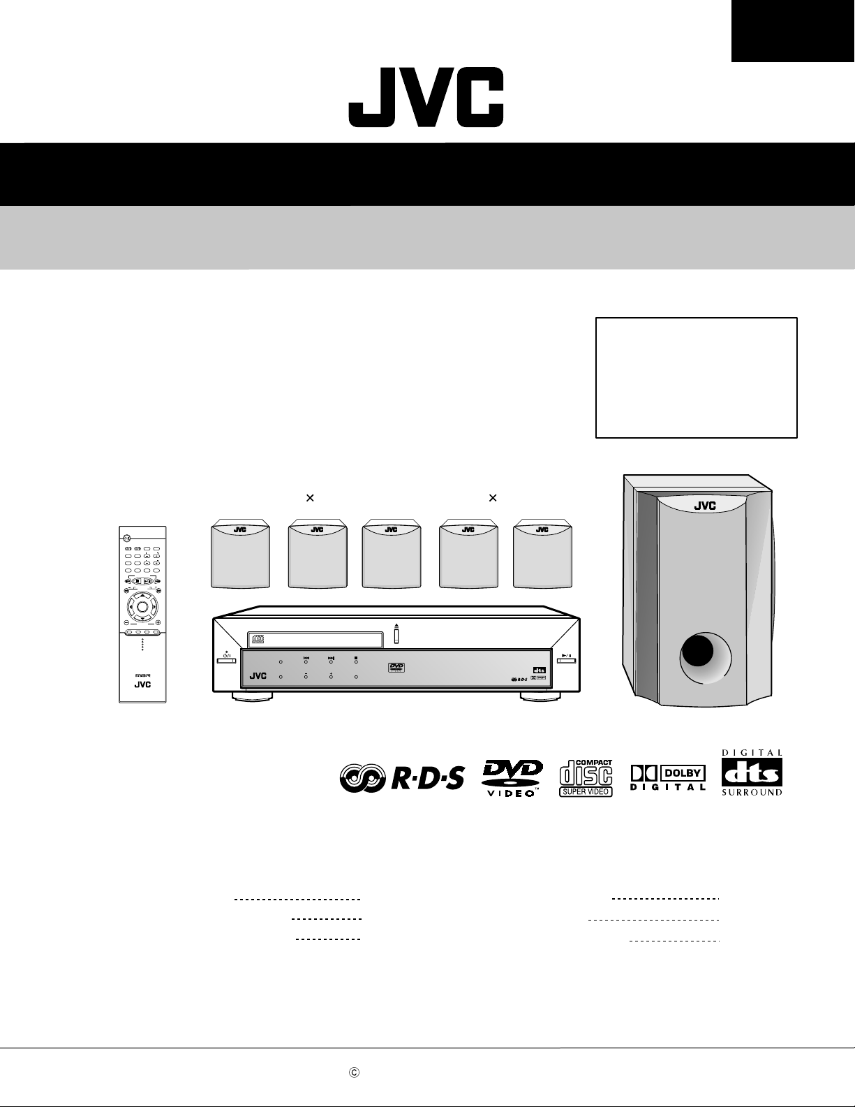
DVD DIGITAL CINEMA SYSTEM
TH-A30R
STAND BY/ON
AUDIO
TV/VIDEO
VCR
TV
TV CHANNE L
DISPLAY
STEP
AUDIO/
SUBTITL E
TV VOLUME
FM MOD E
DVD FM/AM AUX
TUNER PRESET
DOWN UP
REW
VCR CHANNE L
TUNING
B.SEARCH F.SEARCH
ENTER
VOLUM E
TOP MENU
MENU
RETURN
RM-STHA30R
DVD CI NEMA SYSTE M
TH-A30R
Area suffix
B -------------------------- U.K.
E ------ Continental Europe
EN ------- Northern Europe
EV --------- Eastern Europe
EE ---- Russian Federation
SP-XSA30 2
RDS
DISPLAY
VCR
CONT ROL
FF
MUTING
STANDBY
STANDBY/ON
AUDIO/FM MODE
DSP
VOLUME SOURCE
DVD DIGITAL CINEMA SYSTEM TH-A30R
XV-THA30R SP-WA30
SP-XA30 3
DIGITAL
SURROUN D
DIGITAL
Contents
Safety precautions
Preventing static electricity
Important for laser products
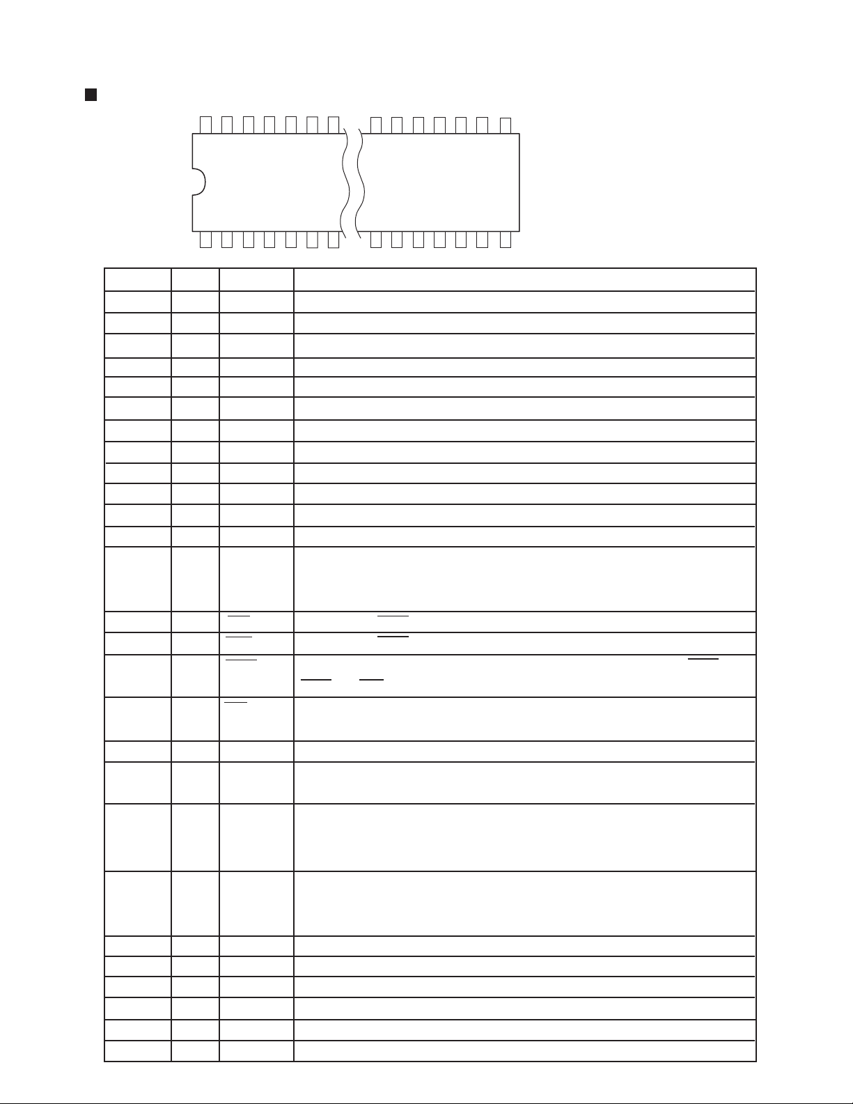
1-2
1-4
1-5
Disassembly method
Wiring connection
Description of major ICs
COPYRIGHT 2002 VICTOR COMPANY OF JAPAN, LTD.
1-6
1-12
1-13~30
No.21163
Dec. 2002
Page 2
TH-A30R
1. This design of this product contains special hardware and many circuits and components specially for safety
purposes. For continued protection, no changes should be made to the original design unless authorized in
writing by the manufacturer. Replacement parts must be identical to those used in the original circuits. Services
should be performed by qualified personnel only.
2. Alterations of the design or circuitry of the product should not be made. Any design alterations of the product
should not be made. Any design alterations or additions will void the manufacturer`s warranty and will further
relieve the manufacture of responsibility for personal injury or property damage resulting therefrom.
3. Many electrical and mechanical parts in the products have special safety-related characteristics. These
characteristics are often not evident from visual inspection nor can the protection afforded by them necessarily
be obtained by using replacement components rated for higher voltage, wattage, etc. Replacement parts which
have these special safety characteristics are identified in the Parts List of Service Manual. Electrical
components having such features are identified by shading on the schematics and by ( ) on the Parts List in
the Service Manual. The use of a substitute replacement which does not have the same safety characteristics
as the recommended replacement parts shown in the Parts List of Service Manual may create shock, fire, or
other hazards.
4. The leads in the products are routed and dressed with ties, clamps, tubings, barriers and the like to be
separated from live parts, high temperature parts, moving parts and/or sharp edges for the prevention of
electric shock and fire hazard. When service is required, the original lead routing and dress should be
observed, and it should be confirmed that they have been returned to normal, after re-assembling.
5. Leakage currnet check (Electrical shock hazard testing)
After re-assembling the product, always perform an isolation check on the exposed metal parts of the product
(antenna terminals, knobs, metal cabinet, screw heads, headphone jack, control shafts, etc.) to be sure the
product is safe to operate without danger of electrical shock.
Do not use a line isolation transformer during this check.
Plug the AC line cord directly into the AC outlet. Using a "Leakage Current Tester", measure the leakage
current from each exposed metal parts of the cabinet, particularly any exposed metal part having a return
path to the chassis, to a known good earth ground. Any leakage current must not exceed 0.5mA AC (r.m.s.).
Alternate check method
Plug the AC line cord directly into the AC outlet. Use an AC voltmeter having, 1,000 ohms per volt or more
sensitivity in the following manner. Connect a 1,500 10W resistor paralleled by a 0.15 F AC-type capacitor
between an exposed metal part and a known good earth ground.
Measure the AC voltage across the resistor with the AC
voltmeter.
Move the resistor connection to each exposed metal part,
particularly any exposed metal part having a return path to
the chassis, and meausre the AC voltage across the resistor.
Now, reverse the plug in the AC outlet and repeat each
measurement. Voltage measured any must not exceed 0.75 V
AC (r.m.s.). This corresponds to 0.5 mA AC (r.m.s.).
0.15 F AC TYPE
1500 10W
Good earth ground
AC VOLTMETER
(Having 1000
ohms/volts,
or more sensitivity)
Place this
probe on
each exposed
metal part.
!
1. This equipment has been designed and manufactured to meet international safety standards.
2. It is the legal responsibility of the repairer to ensure that these safety standards are maintained.
3. Repairs m ust be made in accordance with the relevant safety standards.
4. It is essential that safety critical components are replaced by approved parts.
5. If mains voltage selector is provided, check setting for local voltage.
Burrs formed during molding may
be left over on some parts of the
chassis. Therefore, pay attention to
such burrs in the case of
preforming repair of this system.
In regard with component parts appearing on the silk-screen pr inted side (parts side) of the PWB diagrams, the
parts that are printed over with black such as the resistor ( ), diode ( ) and ICP ( ) or identified by the " "
mark nearby are critical for safety.
(This regulation does not correspond to J and C version.)
1-2
Page 3
TH-A30R
(U.K only)
1. This design of this product contains special hardware and many circuits and components specially
for safety purposes. For continued protection, no changes should be made to the original
design unless authorized in writing by the manufacturer. Replacement parts must be identical to
those used in the original circuits.
2. Any unauthorised design alterations or additions will void the manufacturer's guarantee ; furthermore the
manufacturer cannot accept responsibility f or personal injury or property damage resulting therefrom.
3. Essential safety critical components are identified by ( ) on the Parts List and by shading on the
schematics, and must never be replaced by parts other than those listed in the manual. Please note
however that many electrical and mechanical parts in the product have special safety related
characteristics. These characteristics are often not evident from visual inspection. Parts other than
specified by the manufacturer may not have the same safety characteristics as the recommended
replacement parts shown in the Parts List of the Service Manual and may create shock, fire, or
other hazards.
4. The leads in the products are routed and dressed with ties, clamps, tubings, barriers and the
like to be separated from live parts, high temperature parts, moving parts and/or sharp edges
for the prevention of electric shock and fire hazard. When service is required, the original lead
routing and dress should be observed, and it should be confirmed that they have been returned
to normal, after re-assembling.
1. Service should be performed by qualified personnel only.
2. This equipment has been designed and manufactured to meet international safety standards.
3. It is the legal responsibility of the repairer to ensure that these safety standards are maintained.
4. Repairs must be made in accordance with the relevant safety standards.
5. It is essential that safety critical components are replaced by approved parts.
6. If mains voltage selector is provided, check setting for local voltage.
!
Burrs formed during molding may be left over on some parts of the chassis. Therefore,
pay attention to such burrs in the case of preforming repair of this system.
1-3
Page 4
TH-A30R
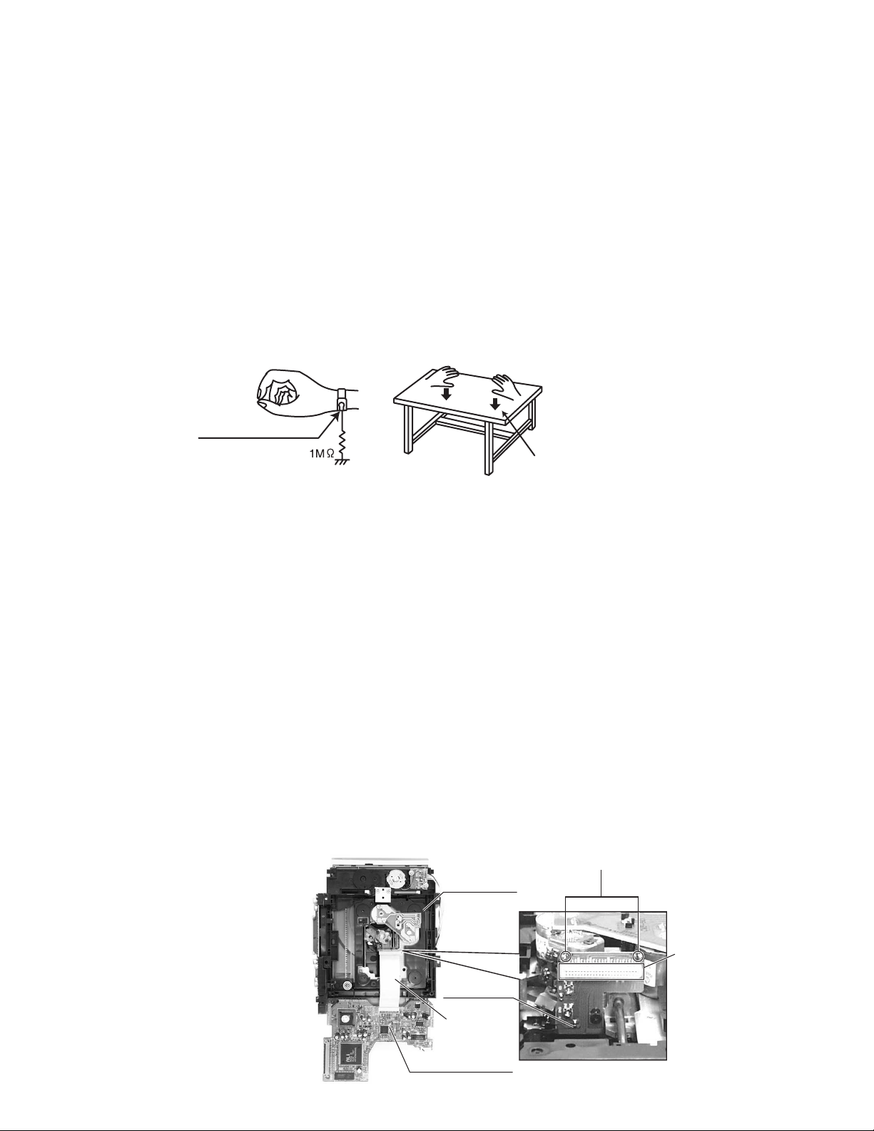
Preventing static electricity
1.Grounding to prevent damage by static electricity
Electrostatic discharge (ESD), which occurs when static electricity stored in the body, fabric, etc. is discharged,
can destroy the laser diode in the traverse unit (optical pickup). Take care to prevent this when performing repairs.
2.About the earth processing for the destruction prevention by static electricity
Static electricity in the work area can destroy the optical pickup (laser diode) in devices such as CD players.
Be careful to use proper grounding in the area where repairs are being performed.
2-1 Ground the workbench
Ground the workbench by laying conductive material (such as a conductive sheet) or an iron plate over
it before placing the traverse unit (optical pickup) on it.
2-2 Ground yourself
Use an anti-static wrist strap to release any static electricity built up in your body.
(caption)
Anti-static wrist strap
Conductive material
(conductive sheet) or iron plate
3. Handling the optical pickup
1. In order to maintain quality during transport and before installation, both sides of the laser diode on the
replacement optical pickup are shorted. After replacement, return the shorted parts to their original condition.
(Refer to the text.)
2. Do not use a tester to check the condition of the laser diode in the optical pickup. The tester's internal power
source can easily destroy the laser diode.
4.Handling the traverse unit (optical pickup)
1. Do not subject the traverse unit (optical pickup) to strong shocks, as it is a sensitive, complex unit.
2. Cut off the shorted part of the flexible cable using nippers, etc. after replacing the optical pickup. For specific
details, refer to the replacement procedure in the text. Remove the anti-static pin when replacing the traverse
unit. Be careful not to take too long a time when attaching it to the connector.
3. Handle the flexible cable carefully as it may break when subjected to strong force.
4. It is not possible to adjust the semi-fixed resistor that adjusts the laser power. Do not turn it.
Attention when traverse unit is decomposed
*Please refer to "Disassembly method" in the text for pick-up and how to detach the substrate.
Solder is put up before the card
1.
wire is removed from connector
on the pick up board as shown in
Figure.
(When the wire is removed
without putting up solder, the CD
pick-up assembly might destroy.)
Please remove solder after
2.
connecting the card wire with
when you install picking up
in the substrate.
DVD mechanism assembly (bottom side)
DVD loading
mechanism
Pick up board
Card wire
Short land
(These two points are
soldered respectively,
and are made to
short-circuit)
Connector
1-4
DVD loader board
Page 5
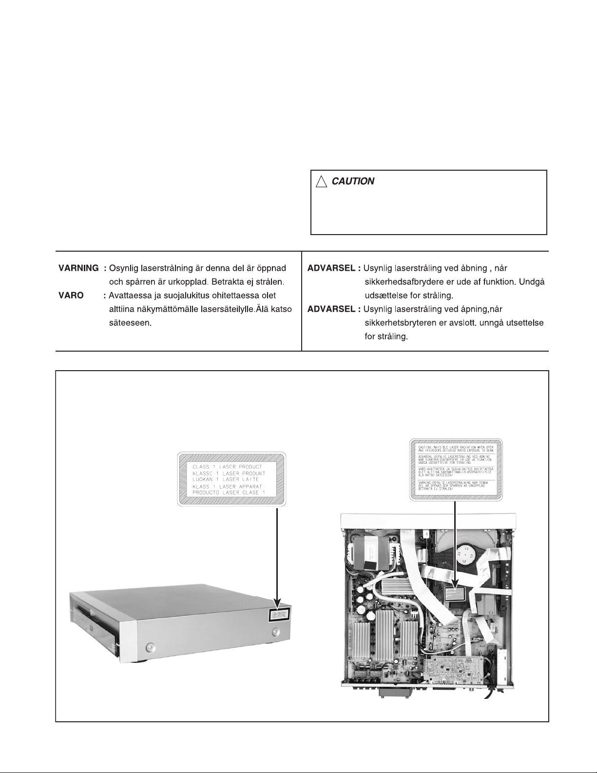
Important for laser products
TH-A30R
1.CLASS 1 LASER PRODUCT
2.DANGER : Invisible laser radiation when open and inter
lock failed or defeated. Avoid direct exposure to beam.
3.CAUTION : There are no serviceable parts inside the
Laser Unit. Do not disassemble the Laser Unit. Replace
the complete Laser Unit if it malfunctions.
4.CAUTION : The compact disc player uses invisible laser
radiation and is equipped with safety switches which
prevent emission of radiation when the drawer is open and
the safety interlocks have failed or are de
feated. It is dangerous to defeat the safety switches.
5.CAUTION : If safety switches malfunction, the laser is able
to function.
6.CAUTION : Use of controls, adjustments or performance of
procedures other than those specified herein may result in
hazardous radiation exposure.
!
Please use enough caution not to
see the beam directly or touch it
in case of an adjustment or operation
check.
REPRODUCTION AND POSITION OF LABELS
CLASS 1
LASER PRODUCT
WARNING LABEL
1-5
Page 6
TH-A30R
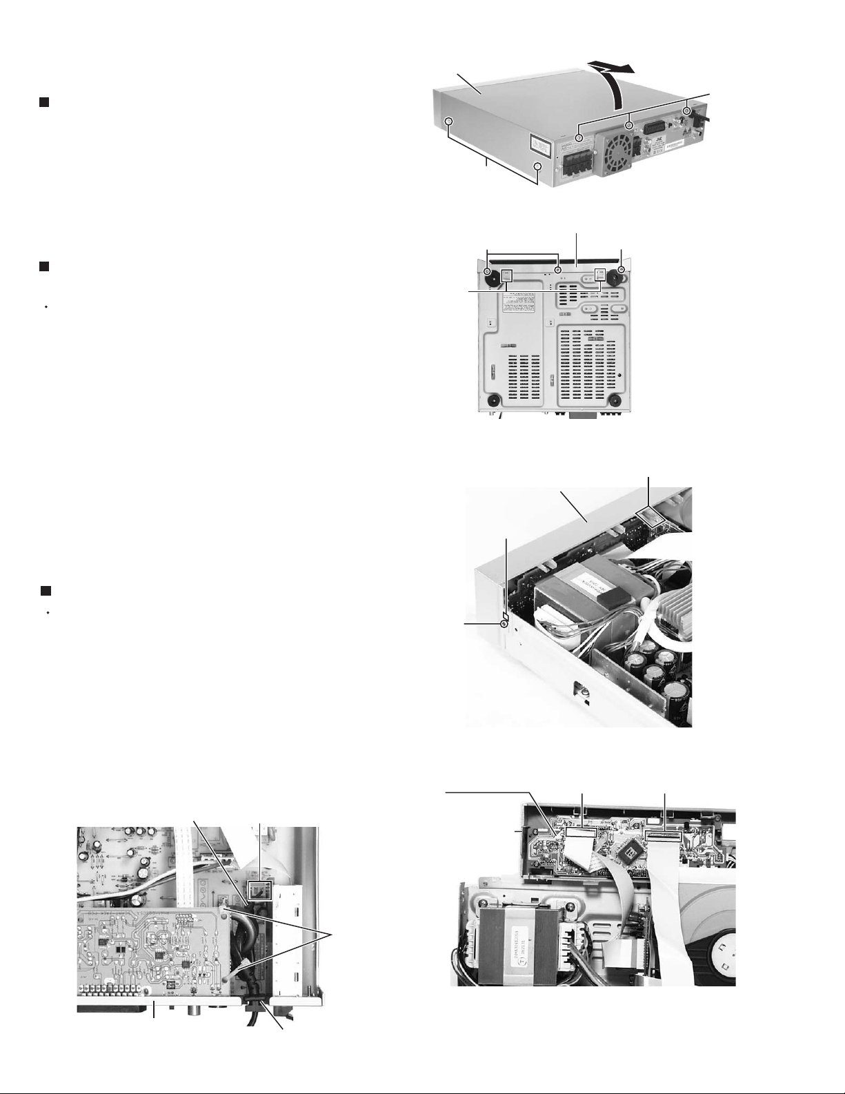
Disassembly method
Removing the top cover (See Fig.1)
1.
Remove the four screws A attaching the top cover
on both sides of the body.
2.
Remove the three screws B on back of the body.
3.
Remove the top cover from behind in the direction of
the arrow while pulling both sides outward.
Removing the front panel assembly
(See Fig.2A, 2B and 3)
Prior to performing the following procedure, remove
the top cover.
1.
Remove the three screws C attaching the front panel
assembly on bottom of the body.
2.
Remove the two screws D attaching the front panel
assembly on both sides of the body.
3.
Remove the claw1, claw2 and claw3, and detach the
front panel assembly toward the front.
4.
Disconnect the card wire from the connector FCW1
and FCW2 on the display board.
Top cover
(both sides)
Claw1
(bottom side)
B
A
Fig.1
Front panel assembly
CC
Fig.2A
Claw3
Front panel assembly
Claw2
(both sides)
Removing the power cord (See Fig.4)
Prior to performing the following procedure, remove
the top cover.
1.
Cut off the tie bands fixing the power cord.
2.
Disconnect the power cord from the connector
ACW1 on the main board and pull up the cord
stopper upward.
Notes : The power cord is exchangeable.
Power cord
ACW1
Tie band
D
(both sides)
Display board
Front panel assembly
(Inner side)
Fig.2B
FCW1FCW2
1-6
Rear panel
Fig.4
Power cord
stopper
Fig.3
Page 7
TH-A30R
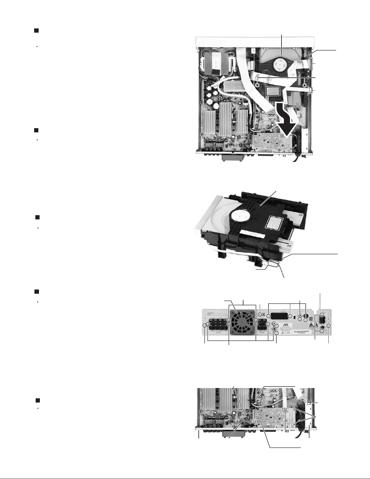
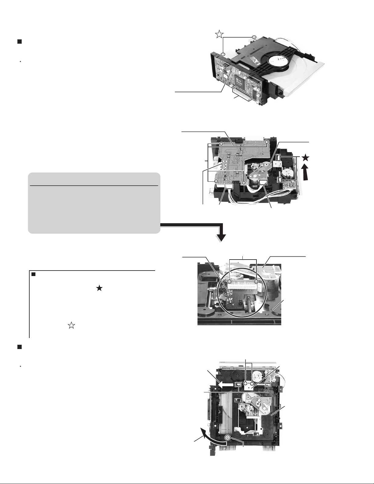
Removing the DVD mechanism assembly
(See Fig.5 and 6)
Prior to performing the following procedure, remove
the top cover.
1.
Disconnect the card wire from the connector J14 and
J21 on the DVD MPEG board.
2.
Remove the two screws E attaching the DVD
mechanism assembly and pull up with drawing out.
3.
Disconnect the harness from the connector DJ6 on
the DVD loader board.
Removing the rear panel (See Fig.7 and 8)
Prior to performing the following procedure, remove
the top cover and power cord stopper.
1.
Disconnect the harness from the connector J9 on the
DSP board.
2.
Remove the two screws F, four screws G, one screw
I and five screws J attaching the each board to the
rear panel. And remove the three screws K attaching
the rear panel on back of the body.
DVD mechanism assembly
DVD
MPEG
board
J14
E
J21
Fig.5
DVD mechanism
assembly
Removing the tuner pack (See Fig.7 and 8)
Prior to performing the following procedure, remove
the top cover.
1.
Disconnect the card wire from the connector CON01
on the tuner pack.
2.
Remove the two screws F attaching the tuner pack
to the rear panel.
Removing the jack board (See Fig.7 and 8)
Prior to performing the following procedure, remove
the top cover.
1.
Cut off the tie bands fixing the power cord.
2.
Disconnect the card wire from the connector JVW2
on the jack board.
3.
Remove the four screws G attaching the jack board
to the rear panel.
4.
Disconnect the connector VW1 and remove the DSP
board.
Fan motor
J
VW1
H
DJ6
Fig.6
I
Fig.7
DSP board
K
DVD loader board
Rear panel
G
F
KK
Removing the fan motor (See Fig.7 and 8)
Prior to performing the following procedures, remove
the top cover .
1.
Disconnect the harness from the connector J9 on the
DSP board .
2.
Removing the two screws H attaching the fan motor
to the rear panel.
Rear panel
J9(on the
DSP board)
Fig.8
JVW2
Jack board
CON01
Tie band
Tuner pack
1-7
Page 8
TH-A30R
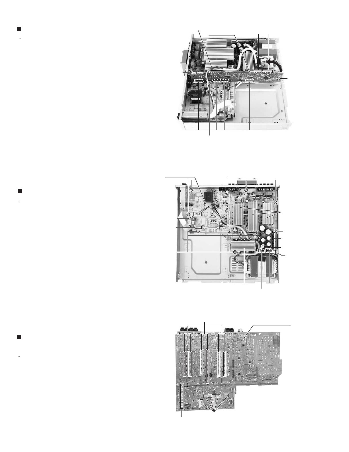
Removing the DSP board (See Fig.9)
Prior to performing the following procedure, remove
the top cover, front panel assembly, DVD
mechanism assembly and jack board.
1.
Remove the harness band fixing the harness.
2.
Disconnect the harness from the connector J9 on the
DSP board.
3.
Disconnect the card wire from the connector J1 and
J3 on the DSP board.
4.
Remove the one screw L attaching the DSP board.
5.
Remove the screw M1 and remove the earth wire.
6.
Remove the one screw I attaching the DSP board to
the rear panel (see fig.7).
7.
Pull up the DSP board from the front side upwards
disconnecting the connector J2, J5, J6 and J7.
Removing the main board (See Fig.10)
Prior to performing the following procedure, remove
the top cover, front panel assembly, power cord,
DVD mechanism assembly, jack board and DSP
board.
1.
Disconnect the card wire from the connector CW8 on
the main board.
2.
Disconnect the harness from the connector ACW2,
ACW3, ACW4 and ACW5 on the main board.
Harness band
J9
(Rear panel side)
Main board
ACW2
CW8
M2
DSP board
J6 J5 J7 J2
M1
(fixing the
earth wire)
Fig.9
M2
J1J3
L
(Front panel side)
Heat sink1
M2
Heat sink2
ACW3
M2
3.
Remove the five screws J attaching the speaker
terminals and jack to the rear panel (see fig.7).
4.
Remove the nine screws M2 attaching the main
board.
5.
When the rear panel is not removed, pull up the
main board from front side.
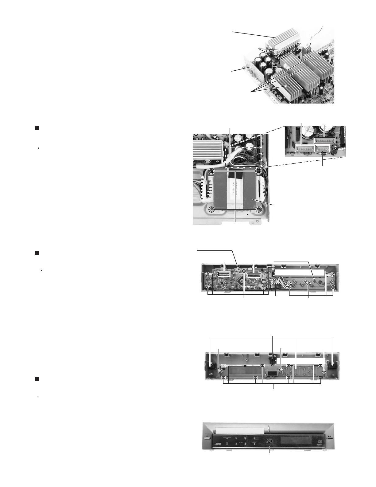
Removing the power transistor & power IC
(See Fig.10 to 12)
Prior to performing the following procedure, remove
the top cover, front panel assembly, DVD
mechanism assembly, jack board, DSP board and
main board.
1.
After removing the solder part 1 soldered to the main
board, remove each screw and remove the heat sink
from the power transistor.
2.
After removing the solder part 2 soldered to the main
board, remove each screw and remove the heat sink
from the power IC.
1-8
Heat sink3
Fig.10
(Each power transistor is fixed)
Solder part 1
Solder part 3
Solder part 2
(Power IC is fixed)
(Power IC is fixed)
Fig.11
ACW5
ACW4
Main board
(Reverse side )
Page 9
TH-A30R
3.
The power ICs fixed to the heat sink 3 can be
removed individually that it is easy to remove
screws (in meaning that a screw driver reaches). It is
not necessary to remove whole like abovementioned 1. and 2. .
After removing each screw which is fixing each
power IC to the heat sink 3, the solder part 3 to
which it corresponds on the main board is removed.
In addition, probably, the way after removing the
whole will be safe when a screw driver does not
reach too.
Removing the power transformer
(See Fig.13)
Prior to performing the following procedure, remove
the top cover.
1.
Cut off the tie band fixing the harness, if needed.
2.
Disconnect the harness from the connector ACW2
(see fig.10), ACW3, ACW4 and ACW5 on the main
board.
3.
Remove the four screws N attaching the power
transformer.
<Front panel assembly section>
Removing the display board & switch
board (See Fig.1 and 2)
Prior to performing the following procedure, remove
the top cover and the front panel assembly.
Heat sink 3
(to which power
IC is attached)
Heat sink 2
(to which power
IC is attached)
Heat sink 1
(to which power
transistor is attached)
Tie band
Display board
FCW2
N
Screws
FCW1
Fig.12
ACW4 ACW3
ACW5
Power
transformer
Fig.13
Front panel assembly
(inner side)
Switch board
1.
Disconnect the card wire from the connector FCW1
and FCW2 on the display board.
2.
Remove the five screws A attaching the display
board on the inner of the front panel assembly.
3.
Remove the four screws B attaching the switch
board on the inner of the front panel assembly.
4.
Disconnect the harness from connector FW2 on the
display board, if needed.
Removing the front window
(See Fig.2 and 3)
Prior to performing the following procedure, remove
the top cover, front panel assembly, display board
and switch board.
Remove the switch buttons, if needed.
1.
Remove the three screws C attaching the front
2.
window on the front panel.
Remove the eight claws fixing the front window on
3.
the front panel.
A
FW2
B
Fig.1
Front panel assembly
(inner side)
Switch button
CCC
Claw
Fig.2
Front panel assembly
Front window
Fig.3
(front side)
1-9
Page 10
TH-A30R
<DVD mechanism assembly section>
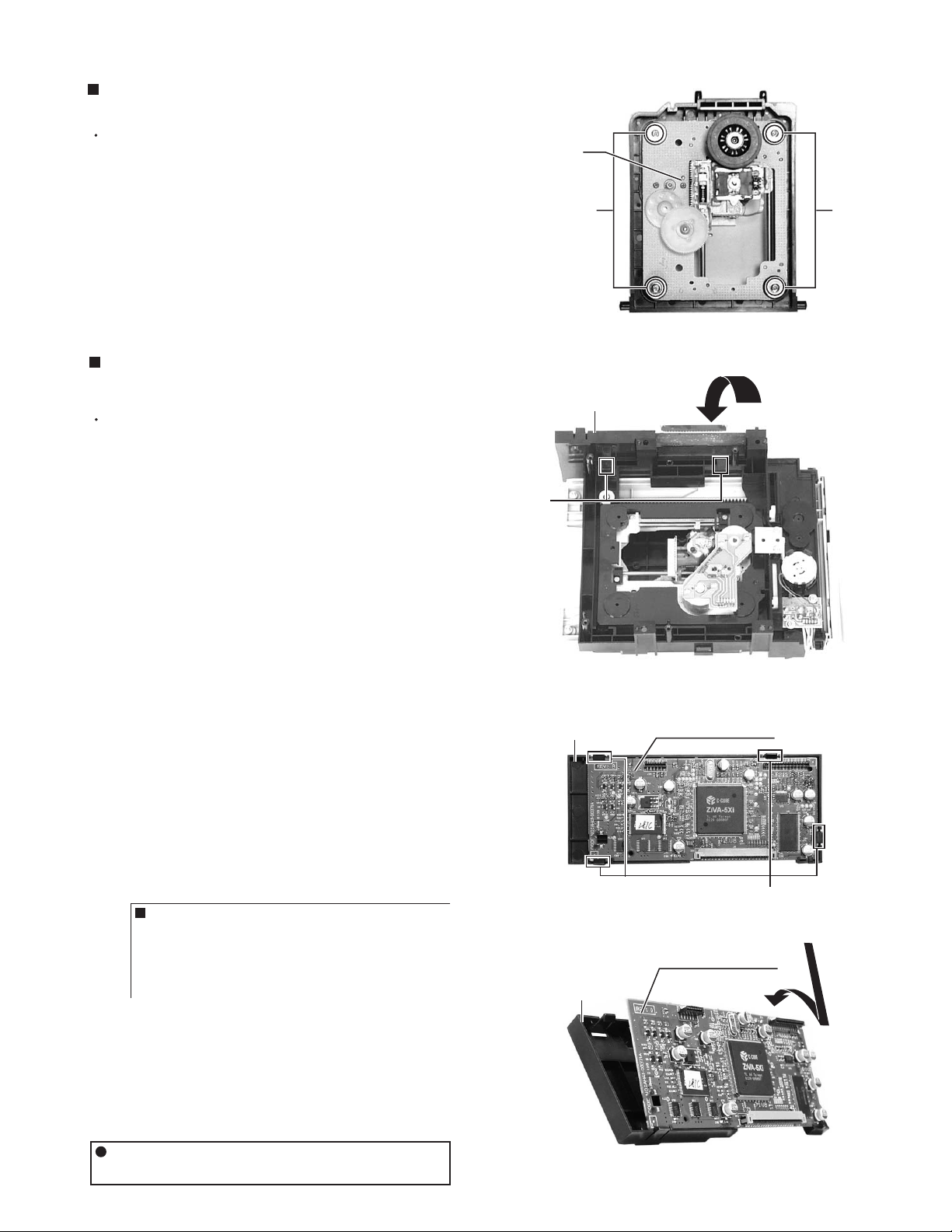
Removing the DVD loader board
(See Fig.1 to 3)
Prior to performing the following procedure, remove
the top cover and DVD mechanism assembly.
1.
Disconnect the card wire from the connector J6 on
the DVD MPEG board.
2.
Disconnect the harness from the connector on the
motor board.
3.
Disconnect the harness from the connector MJ5 on
the DVD loader board.
4.
Remove the four screws A attaching the DVD loader
board to DVD mechanism assembly.
CAUTION!! (see fig.3)
Before removing the card wire which
connects the pickup board and DVD loader
board, solder the two soldering parts and
make it short-circuit.
Moreover, while having removed the card
wire, don't remove these solder.
DVD MPEG board
DVD loader board
A
RCN1
MJ5
DVD mechanism assembly
(top side)
J6
Fig.1
DVD mechanism assembly
(bottom side)
Motor board
Connector
Fig.2
5.
Disconnect the card wire from the connector RCN1
on the DVD loader board.
ONE POINT
How to eject the DVD tray manually
(see fig.2)
The white lever of the mark is moved in
the direction of the arrow. Then, the tray will
be opened.
Moreover, the tray is separable from a DVD
mechanism assembly by removing two
screws of the mark (see fig.1) and drawing
out the tray.
Removing the DVD loading mechanism
(See Fig.4)
Prior to performing the following procedure, remove
the top cover, DVD mechanism assembly and DVD
loader board.
1.
Remove the two screws B and remove the bracket.
2.
Remove the one screw C fixing the DVD loading
mechanism.
Pick up
board
Lever
Soldering parts
X
Motor board
Fig.3
DVD mechanism assembly
B
Bracket
DVD loading
mechanism
(bottom side)
DVD loading
mechanism
3.
Move the lever in the direction of the arrow X.
4.
Remove the DVD loading mechanism from the DVD
mechanism assembly by moving it in the direction of
the arrow Y.
1-10
Y
C
Fig.4
Page 11
TH-A30R
m
)
Removing the DVD traverse mechanism
(See Fig.5)
Prior to performing the following procedure, remove
the top cover, DVD mechanism assembly, DVD
loader board and DVD loading mechanism.
1.
Remove the four screws D attaching the DVD
traverse mechanism to DVD loading mechanism.
Removing the holder & DVD MPEG board
(See Fig.6 and 7)
Prior to performing the following procedure, remove
the top cover, DVD mechanism assembly and DVD
loader board.
1.
Remove the two claws1, and remove the holder from
the DVD mechanism assembly as it is pushed down.
DVD traverse
mechanism
Claw1
D
Holder
DVD loading mechanis
(top side
D
Fig.5
Note: When removing only the DVD MPEG board, it is not
necessary to remove this holder.
2.
Remove the four claws2 and remove the DVD
MPEG board from the holder.
ONE POINT
When inserting DVD MPEG board in
holder. (see fig.8)
Insert in after uniting with a lower claws,
when inserting DVD MPEG board in holder.
Holder
Holder
DVD mechanism assembly
Fig.6
DVD MPEG board
Fig.7
DVD MPEG board
(bottom side)
Claw2
< Speaker section >
It is exchange in a unit.
Please do not decompose.
Fig.8
1-11
Page 12
TH-A30R
Wiring connection
J6
J14
J21
3809-001273
DVD MPEG
BOARD
3809-001295
DJ3
3809-001305
DVD LOADER BOARD
RCN1
Color codes are shown below.
1 Brown
2 Red
3 Orange
4 Yellow
5 Green
CON01
6 Blue
7 Violet
8 Gray
9 White
0 Black
TUNER PACK
JACK BOARD (V-OUT)
FW3
AH39-00176A
0
FW2
DISPLAY BOARD
0
9
0
9
SWITCH BOARD
FCW1
FCW2
2
0
9
3809-001335
0
2
4
POWER TRANCE
J1
53206
4
J3
3809-001334
1
DSP BOARD
J2
1
6
0
5 32
4
0
9
AH39-00368A
J5
J7
2
0
PW3
ACW4
MJ4
4
JVW2
VW1
1
6
AFU2
PT1
CW5
ACW2
CW6
3809-001274
0
2
AH39-00291A
ACW1
AFU3
0
2
CW7
3809-001234
9
MAIN BOARD
DJ6
MJ5
0
9
0
J8
J9
J6
CW8
FCW1-1
9
0
PW4
1-12
2
9
0
1
6
1
0
9
2
6
ACW3
ACW5
Page 13
Description of major ICs
W986432DH-7 (U5) : 32 Bits SDRAM
1.Pin layout
86
85
84
83
82
81
80
1
2
3
4
5
6
7
2.Pin function
Pin No.
1
2
3
4~5
6
7~8
9
10~11
12
13
14
15
16
17
18
19
20
21
22~23
24~27
28
29
30
31
32
33~34
35
I/O
I/O
I/O
I/O
I/O
I/O
I/O
I/O
I/O
I/O
-
I/O
-
-
-
-
-
-
-
-
I/O
-
I/O
I/O
I/O
I/O
Symbol
Vcc
DQ0
VccQ
DQ1~DQ2
VssQ
DQ3~DQ4
VccQ
DQ5~DQ6
VssQ
DQ7
NC
Vcc
DQM0
WE
CAS
RAS
CS
NC
BS0
BS1
A0~A10
DQM2
Vcc
NC
DQ16
VssQ
DQ17~18
VssQ
Power for input buffers and logic circuit inside DRAM. (+3.3V)
Multiplexed pins for data out put and input.
Separated power from VCC, to improve DQ noise immunity. (+3.3V)
Multiplexed pins for data out put and input.
Separated power from VSS, to improve DQ noise immunity.
Multiplexed pins for data out put and input.
Separated power from VCC, to improve DQ noise immunity.
Multiplexed pins for data out put and input.
Separated power from VSS, to improve DQ noise immunity.
Multiplexed pins for data out put and input.
No connection
Power for input buffers and logic circuit inside DRAM. (+3.3V)
The output buffer is placed at Hi-Z (with latency of 2) when DQM is
sampled high in read cycle. In write cycle, sampling DQM high will
block the write operation with zero latency.
Referred to RAS
Referred to RAS
Command input. When sampled at the rising edge of the clock RAS,
CAS and WE define the operation to be executed.
Disable or enable the command decoder. When command decoder is
disabled, new command is ignored and previous operation continues.
No connection
Select bank to activate dining row address latch time,
or bank to read / write during address latch time.
Multiplexed pins for row and column address. Row address: Ao-A10.
Column address:A0-A7.A10 is sampled during a recharge command to
determine if all banks are to be recharged or bank selected by BS0, BS1.
The output buffer is placed at Hi-Z (with latency of 2) when DQM is
sampled high in read cycle. In write cycle, sampling DQM high will
block the write operation with zero latency.
Power for input buffers and logic circuit inside DRAM. (+3.3V)
No connection
Multiplexed pins for data out put and input.
Separated power from VSS, to improve DQ noise immunity.
Multiplexed pins for data out put and input.
Separated power from VCC, to improve DQ noise immunity.
TH-A30R
50
49
48
47
46
45
44
37
38
39
40
41
42
43
Function
1-13
Page 14

TH-A30R
Pin No.
36~37
38
39~40
41
42
43
44
45
46
47~48
49
50~51
52
53~54
55
56
57
58
59
60~66
67
68
69~70
71
72
73
74
75
76~77
78
79~80
81
82~83
84
85
86
I/O
I/O
I/O
I/O
I/O
I/O
I/O
I/O
I/O
I/O
I/O
I/O
I/O
I/O
I/O
I/O
I/O
I/O
I/O
I/O
I/O
I/O
I/O
I/O
-
-
-
-
-
-
-
-
-
I
-
-
-
Symbol
DQ19~20
VssQ
DQ21~22
VccQ
DQ23
Vcc
Vss
DQ24
VssQ
DQ25~26
VccQ
DQ27~28
VssQ
DQ29~30
VccQ
DQ31
NC
Vss
DQM3
A3~A9
CKE
CLK
NC
DQM1
Vss
NC
DQ8
VccQ
DQ9~10
VssQ
DQ11~12
VccQ
DQ13~14
VssQ
DQ15
Vss
W986432DH-7
Function
Multiplexed pins for data out put and input.
Separated power from VSS, to improve DQ noise immunity.
Multiplexed pins for data out put and input.
Separated power from VCC, to improve DQ noise immunity. (+3.3V)
Multiplexed pins for data out put and input.
Power for input buffers and logic circuit inside DRAM. (+3.3V)
Ground for input buffers and logic circuit inside DRAM.
Multiplexed pins for data out put and input.
Separated power from VSS, to improve DQ noise immunity.
Multiplexed pins for data out put and input.
Separated power from VCC, to improve DQ noise immunity. (+3.3V)
Multiplexed pins for data out put and input.
Separated power from VSS, to improve DQ noise immunity.
Multiplexed pins for data out put and input.
Separated power from VCC, to improve DQ noise immunity. (+3.3V)
Multiplexed pins for data out put and input.
No connection
Ground for input buffers and logic circuit inside DRAM.
The output buffer is placed at Hi-Z (with latency of 2) when DQM is
sampled high in read cycle. In write cycle, sampling DQM high will
block the write operation with zero latency.
Multiplexed pins for row and column address. Row address: Ao-A10.
Column address:A0-A7.A10 is sampled during a recharge command to
determine if all banks are to be recharged or bank selected by BS0, BS1.
CKE controls the clock activation and deactivation.
When CKE is low, Power Down rising edge of clock.
System clock used to sample inputs on the rising edge of clock.
No connection
The output buffer is placed at Hi-Z (with latency of 2) when DQM is
sampled high in read cycle. In write cycle, sampling DQM high will
block the write operation with zero latency.
Ground for input buffers and logic circuit inside DRAM.
No connection
Multiplexed pins for data out put and input.
Separated power from VCC, to improve DQ noise immunity. (+3.3V)
Multiplexed pins for data out put and input.
Separated power from VSS, to improve DQ noise immunity.
Multiplexed pins for data out put and input.
Separated power from VCC, to improve DQ noise immunity. (+3.3V)
Multiplexed pins for data out put and input.
Separated power from VSS, to improve DQ noise immunity.
Multiplexed pins for data out put and input.
Ground for input buffers and logic circuit inside DRAM.
1-14
Page 15
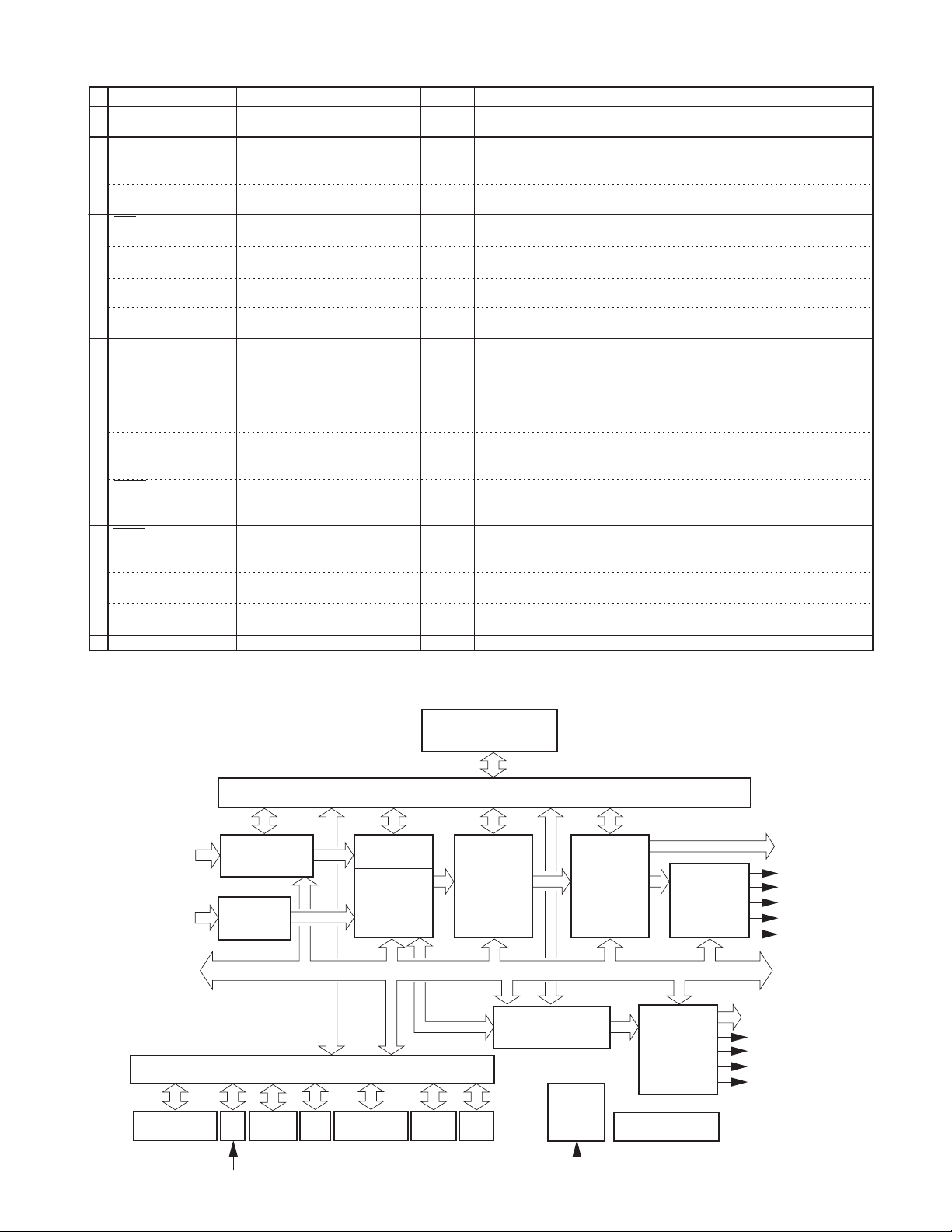
3. Block diagram
TH-A30R
CLK
CKE
CS
RAS
CAS
WE
A10
A0
A9
BS0
BS1
Clock
buffer
Command
buffer
Address
buffer
Control
signal
generator
Mode
register
Column decoder
Cell array
bank #0
Row decoder
Sense amplifier
Column decoder
Cell array
bank #1
Row decoder
Sense amplifier
Refresh
counter
Data control
circuit
Column
counter
Column decoder
Cell array
bank #2
Row decoder
Sense amplifier
NOTE:
The cell array configuration is 2048 * 256 * 32
DQ
buffer
Column decoder
Cell array
bank #3
Row decoder
Sense amplifier
DQ1
DQ31
DQM0~3
1-15
Page 16
TH-A30R
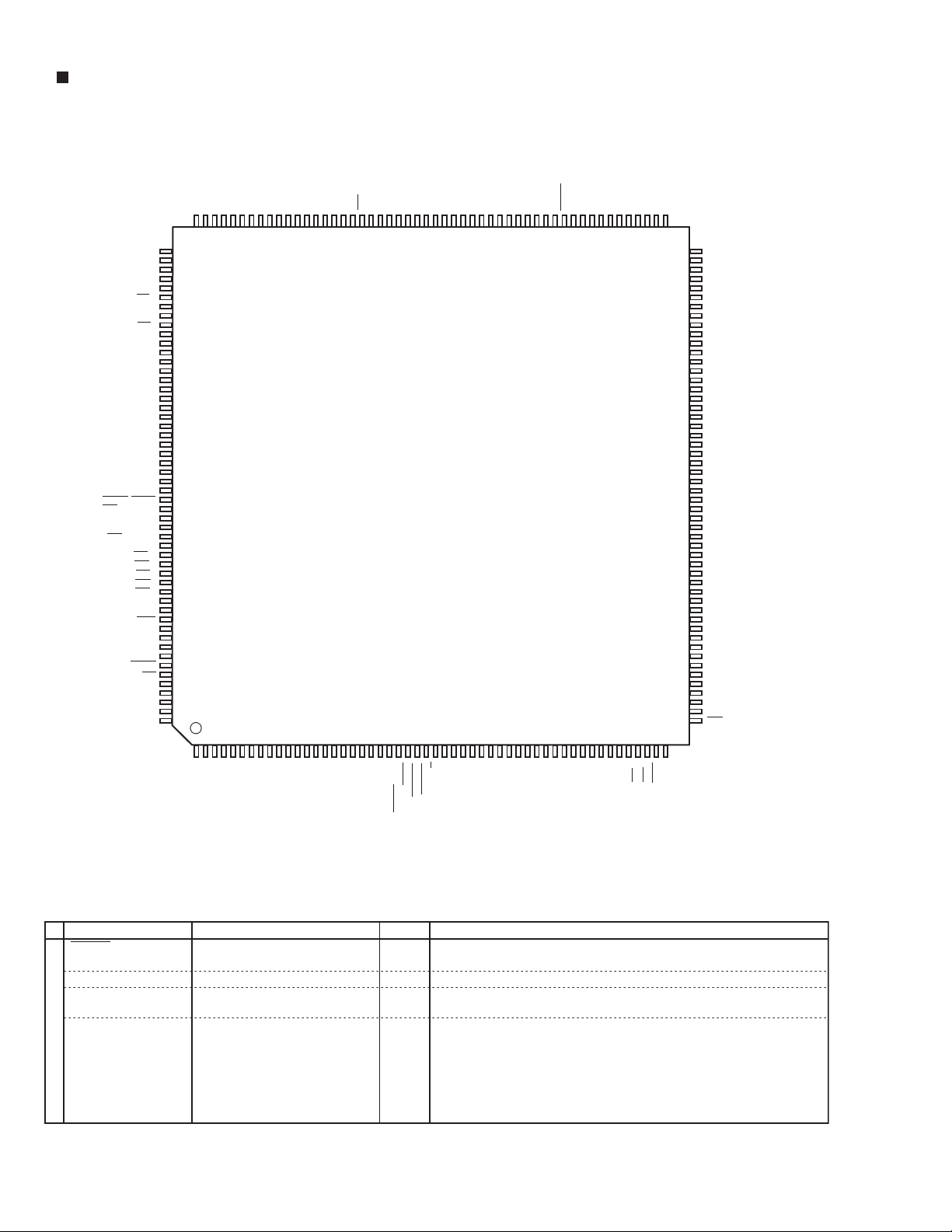
ZiVA-5 (U8) : DVD controller
1. Pin layout
DA-IEC958
DA-DATA3
DA-DATA2
156
155
154
2
C_CL
I
2
C_DA
RTS1
RXD1
TXD1
CTS1
VSS
VSS
VDDC
SD-EN
VSS
VDD_5
HCS4
HCS3
HCS2
HCS1
HCS0
VSS
TRST
TDO
TMS
TCK
ALE
VSS
VDDC
HAD3
HAD2
VSS
157
158
159
160
161
162
163
164
165
166
167
168
169
170
171
172
173
174
175
176
177
178
179
180
181
182
183
184
185
186
187
188
189
190
191
192
193
194
195
196
197
198
199
TDI
200
201
202
203
204
205
206
207
208
123456789101112131415161718192021222324252627282930313233343536373839404142434445464748495051
DAI-DATA
DAI-BCK/SYSCLKBP
DAI-LRCK/IEC958BP
I
VDD_3.3
SD-DATA7
SD-DATA6
SD-DATA5
SD-DATA4
SD-DATA3
SD-DATA2
SD-DATA1
SD-DATA0
SD-REQ
VDD_3.3
SD-ERROR
SD-CLK
VSYNC/HIRQ1
RTS2/SPI_CLK
RXD2/SPI_MISO
TXD2/SPI_MOSI
CTS2/SPI_CS
VDD_3.3
RESET
VSS
153
VDD_3.3
DA-DATA1
152
151
DA-DATA0
DA-BCK
DA-LRCK
150
149
148
DA-XCK
VSS
147
146
VDDC
145
A_VSS1
A_VDD1
144
143
A_VDD2
A_VSS2
142
141
XVDD
140
XTAL/VCLK216BP
XTAL
XVSS
VSS_RREF
VDAC_RREF
VDD_RREF
139
138
137
136
135
134
VDAC_DVDD
VDAC_DVSS
VDAC_0
VDAC_VDD0
133
132
131
130
VDAC_0B
VDAC_1
VDAC_VDD1
129
128
127
VDAC_1B
VDAC_2
VDAC_VDD2
126
125
124
VDAC_2B
VDAC_3
VDAC_VDD3
123
122
121
VDAC_3B
VDAC_4
VDAC_VDD4
120
119
118
VDAC_4B
HSYNC/IRQ2
VDATA0
117
116
115
VDATA1
VDATA2
VSS
114
113
112
VDD_3.3
VDATA3
111
110
VDATA4
VDATA5
VDATA6
109
108
107
VDATA7
VCLK
106
105
104
103
102
101
100
52
VDD_3.3
VSS
MDATA31
MDATA30
MDATA29
MDATA28
99
VDD_3.3
98
MDQM3
97
VSS
96
MDATA27
95
MDATA26
94
MDATA25
93
MDATA24
92
MDATA23
91
MDATA22
90
MDATA21
89
MDATA20
88
VDD_3.3
87
MDQM2
86
VSS
85
MDATA19
84
MDATA18
83
MDATA17
82
MDATA16
81
VDDC
80
VSS
79
MDATA15
78
MDATA14
77
MDATA13
76
MDATA12
75
VDD_3.3
74
MDQM1
73
VSS
72
MDATA11
71
MDATA10
70
MDATA9
69
MDATA8
68
MDATA7
67
MDATA6
66
MDATA5
65
MDATA4
64
VDD_3.3
63
MDQM0
62
VSS
61
MDATA3
60
MDATA2
59
MDATA1
58
MDATA0
57
MCLK
56
VDD_3.3
55
VSS
54
MWE
53
BA1
HA1
HAD15
VDD_3.3
HAD14
HAD13
HAD12
HAD11
HAD9
HAD10
HAD8
HAD7
VDD_3.3
VSS
HAD6
HAD5
HAD4
HAD3
HAD2
HAD1
VDD_3.3
VSS
HAD0
HDTACK/WAIT
HIRQ0
UDS/UWE
R/W
IRRX1
LDS/LWE
VSS
VSS
VDDC
VDD_3.3
MADDR9
MADDR8
MADDR7
MADDR6
MADDR5
MADDR4
MADDR3
MADDR2
MADDR1
MADDR0
VSS
VDD_3.3
MADDR10
MADDR11
BA0
MCS0
MCS1
MRAS
MCAS
2. Pin function (1/4)
1
Name
RESET
Pin No.
202
Description
Type
Active Low Reset. Assert for at least 5-milliseconds in the presence of
I
clock to reset the entire chip.
VCLK
XOUT
105
138
Video clock that outputs 27 MHz.
I/O
Crystal output. When the internal DCXO is used, a 13.5 MHz crystal
O
should be con-nected between this pin and the XIN pin.
XIN/bypass clk_216
139
Crystal input. When the internal DCXO is used, a 13.5 MHz crystal should
I
be con-nected between this pin and the XOUT pin. When an external
oscillator or VCXO is used, its output should be connected to this pin.
System Services
When configured for an external bypass clock, a 216 MHz clock should be
connected to this pin. The frequency of an external VCXO can be either 27
or 13.5 MHz.
1. I - input, O - output, OD - open drain, PU - requires external pull-up resistor.
1-16
Page 17
TH-A30R
2. Pin function (2/4)
Name
VNW
VDDP
VDD25
XVDD
VDD
VDD_VDAC[4:0]
VDAC_DVDD
A_VDD[2:1]
VDAC_REFVDD
GNDP
GND
Power and GroundHost Interface
GND25
VDAC_DVSS
AVSS[2:1]
VDAC_REFVSS
XVSS
HCS[4:2]/GPIO[41:43]
HCS[1:0]
HA[3:1]
HA[15:0]
HDTACK/WAIT
HIRQ0
HUDS/UWE
HLDS/LWE
HREAD
ALE
MCS[1:0]
MCAS
MRAS
MDQM[3:0]
MA[11:0]
MD[31:0]
MWE
SDRAM Interface
MCLK
BA[1:0]
HSYNC/HIRQ2/
GPIO1[9]
VCLK
VDATA[7:0]/GPIO[1:7]
VSYNC/HIRQ1/
GPIO36
Digital Video Input/Output
1. I - input, O - output, OD - open drain, PU - requires external pull-up resistor.
12, 20, 111, 152, 167, 181, 196
32, 44, 55, 63, 74, 87, 98, 104
13, 21, 112, 153, 166, 180, 195, 208
31, 43, 54, 61, 72, 85, 96, 103
Pin No.
189
140
30, 80, 145, 173, 205
118, 121, 124, 127, 130
133
142, 143
134
29, 79, 146, 172, 204
132
141, 144
136
137
190-192
193, 192
206, 207, 2
3-11, 14-19, 22
23
24
25
26
27
203
50, 49
52
51
97, 86, 73, 62
46, 45, 33-42
102-99, 95-88, 84-81,
78-75, 71-64, 60-57
53
56
47, 48
116
105
106-110, 113-115
184
Type
Power
Power
Power
Power
Power
Power
Power
Ground
Ground
Ground
Ground
Ground
Ground
Ground
O
I
I/O
I/O
I/OD
I/O
I/O
I/O
I/O
I/O
O
O
O
O
O
I/O
O
O
O
I/O
I/O
I/O
I/O
1
Description
5-V supply voltage for 5V-tolerant I/O signals.
3.3-V supply voltage for I/O signals
3.3-V supply voltage for SDRAM I/O signals
3.3V Crystal interface power
1.8-V supply voltage for core logic
Analog Video DAC Power
3.3V Digital supply for 5 DACs
3.3-V Analog PLL Power
3.3V Analog Video Reference Voltage
Ground for I/O signals
Ground for core logic
Ground for SDRAM I/O signals
Digital VSS for DACs
Analog PLL Ground
Video Analog Ground
Crystal interface ground
Host chip select. Host asserts HCS to select the controller for a read or
write operation. The falling edge of this signal triggers the read or write
operation. General Purpose I/Os 41, 42, and 43, respectively.
Host chip select. Host asserts HCS to select the controller for a read or
write operation. The falling edge of this signal triggers the read or write
operation.
Host (muxed address) address bus. 3-bit address bus selects one of eight
host inter-face registers. These signals are not muxed in ATAPI master
mode.
HA[15:0] is the 16-bit (muxed address and data) bi-directional host data
bus through which the host writes data to the decoder Code FIFO. MSB of
the 32-bit word is writ-ten first. The host also reads and writes the decoder
internal registers and local SDRAM/ROM via HA[7:0]. These signals are
not muxed for ATAPI master mode.
Host Data Transfer Acknowledge.
Host interrupt. Open drain signal, must be pulled-up via 4.7k to 3.3 volts.
Driven high for 10 ns before tristate.
Host Upper Data Strobe. Host high byte data, HA[15:8], is valid when this
pin is active.
Host Lower Data Strobe. Host low byte data, HA[7:0], is valid when this pin
is active.
Read/write strobe
Address latch enable
Memory chip select.
Active LOW SDRAM Column Address Strobe.
Active LOW SDRAM Row Address Strobe.
These pins are the bytes masks corresponding to MD[7:0], [15:8], [23:16]
and [31:24]. They allow for byte reads/writes to SDRAM.
SDRAM Address
SDRAM Data
SDRAM Write Enable. Specifies transaction to SDRAM: read (=1) or
write (=0)
SDRAM Clock
SDRAM bank select
Horizontal sync. The decoder begins outputting pixel data for a new
horizontal line after the falling (active) edge of HSYNC.
Host Interrupt Request 2
General Purpose I/O 9
Video clock. Clocks out data on input. VDATA[7:0].
Clock is typically 27 MHz.
Video data bus. Byte serial CbYCrY data synchronous with VCLK. At
powerup, the decoder does not drive VDATA. During boot-up, the
decoder uses configuration parameters to drive or 3-state VDATA.
General Purpose I/Os [1:7]
Vertical sync. Bi-directional, the decoder outputs the top border of a new
field on the first HSYNC after the falling edge of VSYNC. VSYNC can
accept vertical synchroni-zation or top/bottom field notification from an
external source. (VSYNC HIGH = bot-tom field. VSYNC LOW = Top field)
Active Low Host Interrupt Pin
General Purpose I/O 36
1-17
Page 18
TH-A30R
2. Pin function (3/4)
Name
SDDATA[7]/VDATA2[7]
/HDMARQ/GPIO24
SDDATA6/VDATA2[6]
/HXCVR_EN/GPIO25
SDDATA5/VDATA2[5]
HDMACK/GPIO26
SDDATA4/VDATA2[4]/
GPIO27
SDDATA3/
VDATA2[3]/GPIO28
SDDATA2/
VDATA2[2]/GPIO29
SDDATA1/
Parallel DVD/CD or Serial CD Interface
VDATA2[1]/GPIO30
SDDATA0/
VDATA2[0]/GPIO31
SDCLK
SDERROR
SDEN/GPIO33
SDREQ/GPIO32
VDAC_[4B:0B]
VDAC_4
VDAC_3V
DAC_2
VDAC_1
VDAC_0
VDAC_REF
VCLK
Analog Video OutputAudio InterfaceDigital Mic In
ADATA[3:0]/GPIO[4:1]
BCK
LRCK
XCK
IEC958/GPIO14
DAI_DATA/GPIO15
DAI_BCK/
BYPASS_SYSCLK/
GPIO16
DAI_LRCK/
IEC958BP/GPIO17
Pin No.
168
169
170
171
174
175
176
177
183
182
179
178
117, 120, 123, 126, 129
119
122
125
128
131
135
105
155, 154, 151, 150
149
148
147
156
157
158
159
Type
I
I
I
I
O
Analog O
Analog O
Analog O
Analog O
Analog O
Analog O
Analog I
I/O
O
O
O
I/O
O
I
I
I
1
Description
Compressed data from DVD DSP. Bit 7. In parallel mode, bit 7 is the first
(earliest in time) bit in the bitstream, while bit 0 is the last bit.
Video Data Bus 2, Bit 7
Host DMA Request
General Purpose I/O 24
Compressed data from DVD DSP. Bit 6.
Video Data Bus 2, Bit 6
ATAPI Transceiver Enable
General Purpose I/O 25
Compressed data from DVD DSP. Bit 5.
Video Data Bus 2, Bit 5
Host DMA Acknowledge
General Purpose I/O 26
Compressed data from DVD DSP. Bit 4.
Video Data Bus 2, Bit 4
General Purpose I/O 27
Compressed data from DVD DSP. Bit 3.
Video Data Bus 2, Bit 3
General Purpose I/O 28
Compressed data from DVD DSP. Bit 2.
Video Data Bus 2, Bit 2
General Purpose I/O 29
Compressed data from DVD DSP. Bit 1.
Video Data Bus 2, Bit 1
General Purpose I/O 30
In serial mode, bit 0 should be used as the input, with the unused bits
either used as GPIOs or tied to ground.
Video Data Bus 2, Bit 0
General Purpose I/O 31
Data clock. The maximum frequency is 25 MHz for parallel mode, and
???? MHz for serial mode. The polarity of this signal is programmable.
Error in input data. This signal carries the error bit associated with the
channel data type (if set, the byte is corrupted).
Data enable. Assertion indicates that data on SDDATA[7:0] is valid.
The polarity of this signal is programmable.
General Purpose I/O [33]
Bitstream request. controller asserts SDREQ to indicate that the bitstream
input buffer has available space.
General Purpose I/O 32
Video DAC Bias Bits[4:0]
DAC video output format: R, V, C, or CVBS. Macrovision encoded.
DAC video output format: B, U, C, or CVBS. Macrovision encoded.
DAC video output format: G or Y. Macrovision encoded.
DAC video output format: C. Macrovision encoded.
DAC video output format: CVBS or Y. Macrovision encoded.
Video DACs Reference Resistor. Connecting to pin 136 through
a 1.18K+/- 1% resis-tor is required.
System clock that drives internal PLLs. ZiVA-5 27-MHz TTL oscillator.
(See descrip-tion of VCLK for Digital Video Output.) Also optional video
clock for internal PLLs or external encoder.
PCM Data Out. Eight channels. Serial audio samples relative to BCK
and LRCK. General Purpose I/Os [4:1]
PCM Bit Clock. BCK can be either 48 or 32 times the sampling frequency
PCM Left Clock. Identifies the channel for each sample. The polarity is
programma-ble.
Audio External Frequency clock input or output. BCK and LRCK are
derived from this clock.
PCM data out (IEC-958 format ) or compressed data out
(IEC-1937 format). General Purpose I/O [14]
PCM data input.
General Purpose I/O [15]
PCM input bit clock.
BYPASS_SYSCLK: Alternate function TBS.
General Purpose I/O [16]
PCM left/right clock.
IEC958 input bypass
General Purpose I/O [17]
1. I - input, O - output, OD - open drain, PU - requires external pull-up resistor.
1-18
Page 19
2. Pin function (4/4)
Name
IRRX1/GPIO0
IR
IDC_CL/GPIO18
IDC
IDC_DA/GPIO19
RTS1/GPIO20
RXD1/GPIO21
TXD1/GPIO22
UART1UART2JTAG
CTS1/GPIO23
RTS2/SPI_CLK/
GPIO37
RXD2/SPI_MISO/
GPIO38
TXD2/SPI_MOSI/
GPIO39
CTS2/SPI_CS/
GPIO40
TRST
TDO
TDI/GPI0
TMS/GPI1
TCK
1. I - input, O - output, OD - open drain, PU - requires external pull-up resistor.
Pin No.
28
160
161
162
163
164
165
185
186
187
188
197
198
199
200
201
1
Type
Description
I
IR Remote Receive. This input connects to an integrated (photo diode,
band pass, demodulator) IR receiver. General Purpose I/O 0
I/O
Serial clock signal for IDC data transfer. It should be pulled up to the
positive supply voltage, depending on the device) using an external
pull-up resistor. General Purpose I/O [18]
Serial data signal for IDC data transfer. It should be pulled up to the supply
voltage using an external pull-up resistor. General Purpose I/O [19]
O
Ready to send, UART1
General Purpose I/O [20]
I
Receive data, UART1
General Purpose I/O [21]
O
Transmit data, UART1
General Purpose I/O [22]
I
Clear to send, UART1
General Purpose I/O [23]
O
Ready to send, UART2
Serial Peripheral Interface Clock
General Purpose I/O [37]
I
Receive data, UART2
Serial Peripheral Interface - Master Input/Slave Output
General Purpose I/O [38]
O
Transmit data, UART2
Serial Peripheral Interface - Master Output/Slave Input
General Purpose I/O [39]
I
Clear to send, UART2
Serial Peripheral Interface ????
General Purpose I/O [40]
I
Test reset. BST reset - resets the TAP controller.
This signal must be pulled low.
O
Test data Out. BST serial data output.
I
Test data In. BST serial data chain input.
General Purpose Input pin 0.
I
Test mode select. Controls state of test access port (TAP) controller.
General Purpose Input pin 1.
I
Test clock. Boundary scan test (BST) serial data clock.
TH-A30R
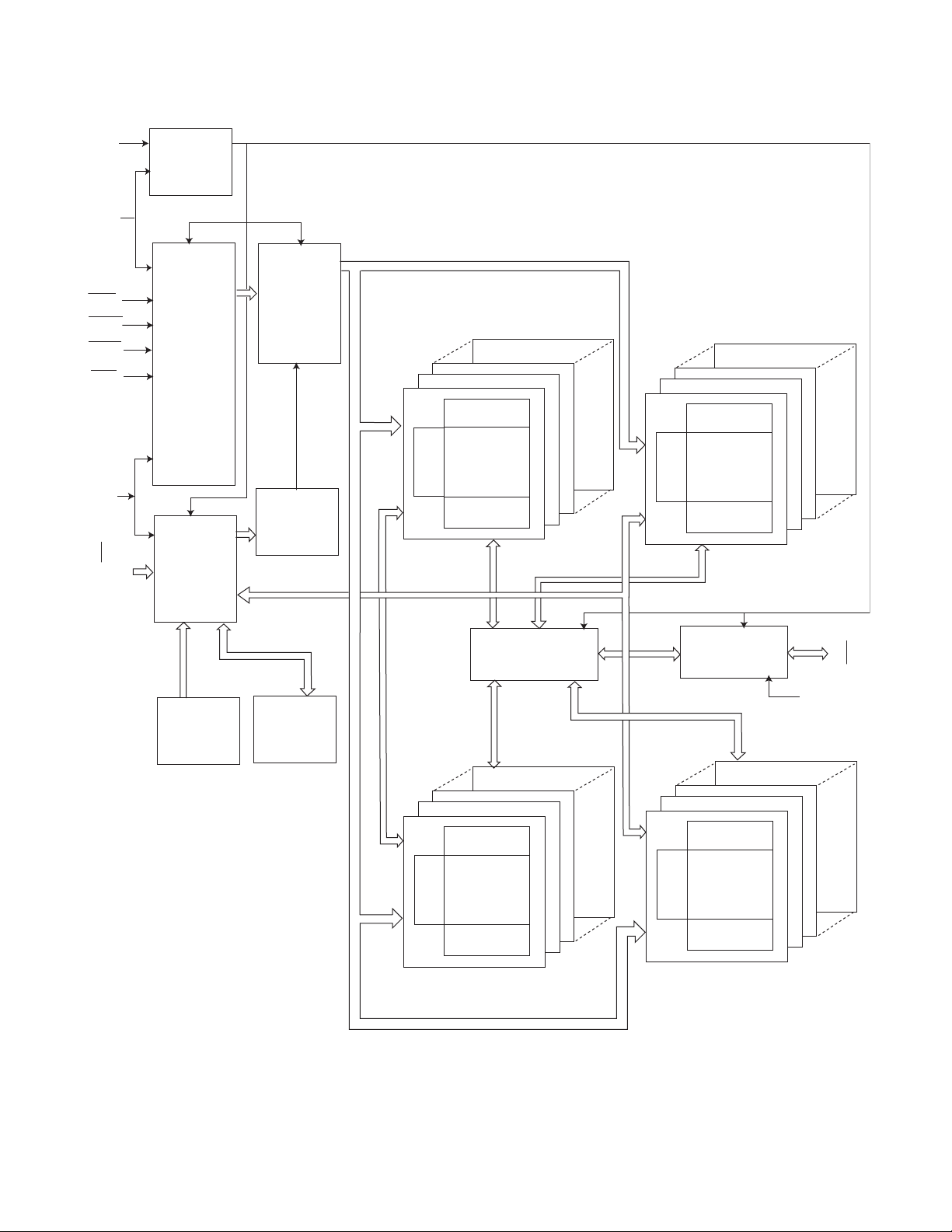
3. Block diagram
Parallel/serial
DVD Interface
I2S Stereo In
32-128Mbit
SDRAM
SDRAM Controller
Track Buffer
Processor
Audio
Decryption
ZiVA
A/V Core
Graphics
Engine
Input Unit
System Control Bus
Bus Interface Unit
IR GPIO SPI UART1&2ASYNC BUS IDC
ATAPI
Interlaced/
Progressive
SPARC
Microprocessor
Phase
Lock
Loop
Video
Encoder
JTAG Interface
Five 10-bit
Audio
Output
Unit
Video
DACs
CCIR 656
Digital Video
Composite
Y/R
C
Cr/Pr/G
Cb/Pb/B
IEC 958/1937
Downmix
Left/right
Center/subwoofer
Left/ right/surround
Remote Control
13.5 MHz Crystal
1-19
Page 20
TH-A30R
LC86P6548 (UIC1) : Microcontroller
1.Pin layout
S47/PF7
S46/PF6
S45/PF5
S44/PF4
S43/PF3
S42/PF2
S41/PF1
S40/PF0
VDD4
S39/PE7
S38/PE6
S37/PE5
S36/PE4
S35/PE3
S34/PE2
S33/PE1
S32/PE0
S31/PD7
S30/PD6
S29/PD5
S28/PD4
S27/PD3
S26/PD2
S25/PD1
S24/PD0
S23/PC7
S22/PC6
S21/PC5
S20/PC4
VP
2.Block diagram
S48/PG0
S49/PG1
S50/PG2
S51/PG3
P00
P01
P02
P03
VSS2
VDD2
P04
P05
P06
P07
P10/SO0
P11/SI0/SB0
P12/SCK0
P13/SO1
P14/SI1/SB1
P15/SCK1
81
82
83
84
85
86
87
88
89
90
91
92
93
94
95
96
97
98
99
100
Interrupt Control
Standby Control
CF
RC
X’ta
l
8079787776757473727170696867666564636261605958575655545352
1234567891011121314151617181920212223242526272829
P30
P31
P32
P33
P34
P35
P36
P16/BUZ
P17/PWM0
Clock
Generator
P37
P70/INT0
RES
XT1/P74
CF1
VSS1
XT2/P75
CF2
VDD1
P80/AN0
IR
PLA
PROM
Control
PROM(48KB)
P81/AN1
P82/AN2
P83/AN3
PC
P84/AN4
P85/AN5
P86/AN6
A15-A0
D7-D0
TA
CE
OE
DAS
EC
P87/AN7
P71/INT1
P72/INT2/T0I
51
50
49
48
47
46
45
44
43
42
41
40
39
38
37
36
35
34
33
32
31
30
S0/T0
P72/INT3/T0I
S19/PC3
S18/PC2
S17/PC1
S16/PC0
VDD3
S15/T15
S14/T14
S13/T13
S12/T12
S11/T11
S10/T10
S9/T9
S8/T8
S7/T7
S6/T6
S5/T5
S4/T4
S3/T3
S2/T2
S1/T1
Base Time
SI
O0
O1
SI
Timer 0
er 1
Tim
ADC
INT0-3
Noise Filter
SIO Auto
transmissio
RAM
128 by
VFD
Controller
High voltage O
r
matic
s
te
utput
Bus Interface
n
Port 1
Port 3
Port 7
Port 8
ACC
B Register
C Register
PSW
RAR
RAM
Stack Poi nter
Port 0
Watchdog Timer
1-20
Page 21
3. Pin function
Pin No.
1
2
3
to
10
11
12
13
14
15
16
17
18
19
to
22
23
to
26
27
28
29
30
to
36
37
to
45
46
47
to
50
51
52
to
63
64
to
71
72
73
to
80
81
to
84
85
86
87
88
89
90
91
92
93
94
95
96
97
98
99
100
P16/BUZ
P17/PWM0
P70/INT0
XT1/P74
XT2/P75
P80/AN0
P83/AN3
P84/AN4
P87/AN7
P71/INT1
P72/INT2/T0I
P72/INT3/T0I
S15/T15
S16/PC0
P19/PC3
S20/PC4
S31/PD7
S32/PE0
S39/PE7
S40/PF0
S47/PF7
S48/PG0
S51/PG3
P10/SO0
P11/SI0/SB0
P12/SCK0
P13/SO1
P14/SI1/SB1
P15/SCK1
Symbol
P30
to
P37
RES
VSS1
CF1
CF2
VDD1
to
to
S0/T0
to
S6/T6
S7/T7
to
VDD3
to
VP
to
to
VDD4
to
to
P00
P01
P02
P03
VSS2
VDD2
P04
P05
P06
P07
Function
I/O
Buzzer output
I/O
Timer 1 output (PWM0 output)
I/O
8bit input/output port
I/O
Input/output in bit unit
15V withstand at N-channel open drain output
INT0 input /HOLD release/N-channel Tr. ouptput forwatchdog timer
I/O
Reset pin
I
32.768kHz crystal oscillation terminal XT1
I
32.768kHz crystal oscillation terminal XT2
I
Power pin (-)
Input pin for the ceramic resonator oscillation
I
Output pin for the ceramic resonator oscillation
O
Power pin (+)
4-bit input port
I
Input /output in bit unit
O
INT1 input/HOLD release input
I
INT2 input/timer 0 event input
I
Output for VFD display controller segment/timing incommon
O
Output for VFD dis;lay controller segment/timing withinternal pull-down
O
resistor in common
Internal pull-down resistor output
Power pin (+)
Output for VFD display controller
I/O
High voltage input port PC0 to PC3
Power pin (+) for the VFD output pull-down resist
Output for VFD display controller
I/O
High voltage input port PC4 to PC7, PD0 to PD7
Output for VFD displaya controller segment
I/O
High voltage input port PE0 to PE7
Power pin (+)
Output for VFD displaya controller segment
I/O
High voltage input port PF0 to PF7
Output for VFD displaya controller segment
I/O
High voltage I/O port PG0 to PG3
8-bit input/output port. Input for port0 interrupt.
I/O
Input/output in nibble unit
Input for HOLD release
15V withstand at N-channel open drain output
Power pin (-)
Power pin (+)
8-bit input/output port. Input for port0 interrupt.
I/O
Input/output in nibble unit
Input for HOLD release
15V withstand at N-channel open drain output
SIO0 data output
I/O
SIO0 data input/bus input/output
SIO0 clock input/output
SIO1 data output
SIO1 data input/bus input/output
SIO1 clock input/output
8-bit input/output port
Input/output can be specified in a bit unit
TH-A30R
1-21
Page 22
TH-A30R
BA5954 (MU9) : Motor driver
1. Block diagram
STAND
SHUT DOWN
2. Pin function
Pin No.
1
2
3
4
5
6
7
8
9
10
11
12
13
14
15
16
17
18
19
20
21
22
23
24
25
26
27
28
-BY
THERMAL
-
+
28 2227 26
+
-
+
-
20k
7.5k
10k
1
Symbol
VINFC
CFCerr1
CFCerr2
VinSL +
VinSL -
VOSL
VNFFC
VCC
PVcc1
PGND
VOSL -
VOSL +
VOFC VOFC +
VOTK +
VOTK VOLD +
VOLD -
PGND
VNFTK
PVcc2
PreGND
VinLD
CTKerr2
CTKerr1
VinTK
BIAS
STBY
10k
20k
+
-
3
25 24 23
7.5k
7.5k
DET.AMP.
7.5k
-
+
4 5 6
PreGND
DET.AMP.
2
72
10k
2
10k 25k
21 1520 19
PVCC2
15k
+
-
CC
V
8 149 10
+
PVCC1
PGND
PGND
18 17 16
LOADING
DRIVER
SLED
DRIVER
11 12 13
ACTUATOR
DRIVER
ACTUATOR
DRIVER
Function
Focus driver input
Capacitor connection terminal for error amplifier filter
Capacitor connection terminal for error amplifier filter
Operational amplifier input for thread driver (+)
Operational amplifier input for thread driver (-)
Operational amplifier output for thread driver
Focal driver return terminal
Pre VCC, thread driver part power VCC
Power
Loading driver part power VCC
Thread driver part output (-)
Thread driver part output (+)
Focus driver part output (-)
Focus driver part output (+)
Tracking driver output (+)
Tracking driver output (-)
Loading driver output (+)
Loading driver output (-)
Power GND
Tracking driver return terminal
Actuator driver part power VCC
Pre GND
Loading driver input
Capacitor connection terminal for error amplifer filter
Capacitor connection terminal for error amplifer filter
Tracking driver input
Bias input
Standby terminal
PVCC1
PV
CC
V
CC
2
1-22
Page 23
SST39VF800A (U6) : 8M Flash memory
1. Pin layout
TH-A30R
A15
A14
A13
A12
A11
A10
A9
A8
NC
NC
WE#
NC
NC
NC
NC
A18
A17
A7
A6
A5
A4
A3
A2
A1
1
2
3
4
5
6
7
8
9
10
11
12
13
14
15
16
17
18
19
20
21
22
23
24
2. Block diagram
48
47
46
45
44
43
42
41
40
39
38
37
36
35
34
33
32
31
30
29
28
27
26
25
X-Decoder
A16
NC
Vss
DQ15
DQ7
DQ14
DQ6
DQ13
DQ5
DQ12
DQ4
VDD
DQ11
DQ3
DQ10
DQ2
DQ9
DQ1
DQ8
DQ0
OE#
Vss
CE#
A0
EEPROM
Cell Array
Memory Address
3. Pin function
Symbol
AMS- A0
DQ15- DQ0
Data Input/Output
CE#
OE#
WE#
VDD
Vss
NC
Address Buffer & Latches
CE#
OE#
WE#
Pin name
Address Inputs
Chip Enable
Output Enable
Write Enable
Power Supply
Ground
No Connection
Y-Decoder
Control Logic
I/O Buffers & Data Latches
DQ15-DQ0
Function
To provide memory addresses. During Sector-Erase AMS-A11 address lines will
select the sector. During Block-Erase AMS-A15 address lines will select the block.
To output data during Read cycles and receive input data during Write cycles. Data is
internally latched during a Write cycle. The outputs are in tri-state when OE# or CE# is
high.
To activate the device when CE# is low.
To gate the data output buffers.
To control the Write operations.
To provide power supply voltage: 2.7-3.6V
Unconnected pins.
1-23
Page 24
TH-A30R
3
AK4355 (U6) : DAC
1.Pin layout 2.Block diagram
1
2
3
4
5
6
7
8
9
10
11
12
13
14
28
27
26
25
24
23
22
21
20
19
18
17
16
15
DZF
LOUT1+
LOUT1-
ROUT1+
ROUT1-
LOUT2+
LOUT2-
ROUT2+
ROUT2-
LOUT3+
LOUT3-
ROUT3+
ROUT3-
SCF
SCF
SCF
SCF
SCF DAC
SCF DAC
3.Pin function
Pin No. Symbol I/O Function
1 VREF I Positive Voltage Reference Input Pin
2DZF OZ
3 PDN I Power-Down Mode Pin
4 MCLK I Master Clock Input Pin
5 BICK I
6 SDTI1 I
7 SDTI2 I
8 SDTI3 I
9 LRCK I
10 CSN I C
11 CCLK I
12 CDTI I
13 DVDD - D
14 DVSS - D
15 ROUT3- O
16 ROUT3+ O
17 LOUT3- O
18 LOUT3+ O
19 ROUT2- O
20 ROUT2+ O
21 LOUT2- O
22 LOUT2+ O
23 ROUT1- O
24 ROUT1+ O
25 LOUT1- O
26 LOUT1+ O
27 AVSS 28 AVDD -
Note: All input pins should not be left floating.
ero Input Detect Pin
When at “L”, the AK4355 is in the power-down mode and is held in reset.
The AK4355 should always be reset upon power-up.
An external TTL clock should be input on this pin.
Audio Serial Data Clock Pin
DAC1 Audio Serial Data Input Pin
DAC2 Audio Serial Data Input Pin
DAC3 Audio Serial Data Input Pin
L/R Clock Pin
hip Select Pin
Control Clock Pin
Control Data Input Pin
igital Power Supply Pin
igital Ground Pin
DAC3 Rch Negative Analog Output Pin
DAC3 Rch Positive Analog Output Pin
DAC3 Lch Negative Analog Output Pin
DAC3 Lch Positive Analog Output Pin
DAC2 Rch Negative Analog Output Pin
DAC2 Rch Positive Analog Output Pin
DAC2 Lch Negative Analog Output Pin
DAC2 Lch Positive Analog Output Pin
DAC1 Rch Negative Analog Output Pin
DAC1 Rch Positive Analog Output Pin
DAC1 Lch Negative Analog Output Pin
DAC1 Lch Positive Analog Output Pin
Analog Ground Pin
Analog Power Supply Pin
DAC
DAC
DAC
DAC
DATT
DATT
DATT
DATT
DATT
DATT
Audio
I/F
Control
Register
MCLK
LRCK
BICK
CSN
CCLK
CDTI
SDTI1
SDTI2
SDTI
1-24
Page 25
M62463FP (U11) : Surround decoder
1. Pin layout
RLC3
RLC7
RLC4
RLC1
RLC2
RLC5
PSC4
PSC1
PSC5
PSC2
PSC6
PSC3
48
47
46
45
44
43
42
41
40
39
38
37
DBC3
DBC2
36
35
DBC1
BNR IN
34
33
TH-A30R
49
RLC8
50
RLC6
LT
RT
LIN
RIN
AVcc
VREF
IREF
NGC3
NGC2
NGC1
51
52
53
54
55
56
57
58
59
60
61
62
63
64
LBPF2
LBPF1
RBPF2
RBPF1
2. Block diagram
1 2 3 4 5 6 7 8 9
LOUT
ROUT
CVOLOUT
COUT
CVOLIN
SOUT
SVOLIN
SVOLOUT
10
CMC
11
AGND
VREFD
12
13
DVdd
MICIN
14
15
SCK
DATA
16
REQ
32
FBIN
31
LPF2 OUT
30
LPF2 IN2
29
LOF2 IN1
28
DAINT OUT
27
DAINT IN
26
DACONT
25
ADCONT
24
ADINT OUT
23
ADINT IN
22
LPF1 OUT
21
LPF1 IN2
20
LPF1 IN1
19
DSEL OUT
18
MICOUT
17
DVss
LIN
RIN
MICIN
57
58
12
L+R
2
SW6
L-R
1
2
NOISE
SEQUENCER
INPUT
BALANCE
SW4
1
2
3
4
MICVOL
MICOUT
ADAPTICVE
MATRIX
SELECTOR
S'
Digital Delay
10Kbit SRAM
LPF
A/D
SW5
Logic
F.B.VOL
CENTER
MODE
CONTROL
WIDE
NORMAL
PHANTOM
OFF
D/A
LPF
L
R
C
Modified BNR
PROLOGIC
PROLOGIC
SW3
BY-PASS
SPACE
SURROUND
SPACE
SURROUND
+
MUTE
BY-PASS
+/-
MUTE
MASTER
VOLUME
1
2
MASTER
VOLUME
MCU
Interface
DATA SCK REQ
SW1
2
3
2
3
SW2
161514333132201918
1
LOUT
1
4
1
ROUT
2
4
5
4
CVOLOUT
3
SVOLOUT
8
7
6
1-25
Page 26
TH-A30R
SP3721A (RU1) : DVD anlog front end chip
1.Pin layout
64-49
16-1
17-32
33-48
2.Pin function
Pin No.
1,2
3,4
5-8
9
10
11-14
15,16
17
18
19
20
21
22
23
24
25
26
27
28
29
30
31
32
33
34
35
36
37
38
39
40
41
42
43
44
45
46
47
48
49
50
51,52
53,54
55
56
57
58
59,60
61,62
63
64
Symblo
DVDRFP,VDVDRFN
PD1,PD2
A2,B2,C2,D2
CP
CN
A,B,C,D
E,F
CDTE
VCI2
NC
VNB
DVDPD
DVDLD
CDPD
CDLD
LDON#
VC
VCI
VPB
MIRR
MP
MB
FDCHG#
MLPF
MEVO
MIN
PI
DFT
TPH
MEV
MEI
TE
FE
CE
LCN
LCP
SCLK
SDATA
SDEN
HOLD1
VNA
FNP,FNN
DIP,DIN
RX
BYP
SIGO
VPA
AIP,AIN
ATOP/ATON
CDRF
CDRFDC
I/O
I/O
I/O
-
-
-
O
O
-
-
O
-
-
O
O
O
-
O
O
O
-
-
I/O
O
-
I/O
O
O
O
Function
RF Signal Inputs
I
CD Photodetector Interface Inputs
I
Photo Detector Interface Inputs
I
Differential Phase tracking LPF pin
Differential Phase tracking LPF pin
Photo Detector Interface Inputs
I
CD trackin Error Inputs
I
CD Tracking
Reference Voltage Input
No Connct
Ground
APC Input
I
APC ouput
APC Input
I
APC output
APC Output On/Off
I
Reference Voltage output
Reference Voltage Input
Power
Mirror Detect Output
MIRR signal Peak hold pin
MIRR signal Bottom hold pin
Low Impedance Enalle
I
MIRR signal LPF pin
SIGO Bottom Envelope Output
RF signal Input for Mirror
I
Pull-in Signal Output
Defect Output
PI Top Hold pin
Sigo Bottom Envelope pin
Mirror Envelope Input
I
Tracking Error Signal Output
Focusing Error Signal Output
Center Error Signal Output
Center Error LPF pin
Center Error LPF pin
Serial Clock
I
Serial Data
Serial Data Enable
I
Hold Control
I
Ground
Differential Normal Output
Analog inputs for RF Single Buffer
I
Reference Resistor Input
Single Ended Normal Output
Power
AGC Amplifier Inputs
I
Differential Attenuator Output
RF Signal Input
I
CD RF signal Output
1-26
Page 27
TH-A30R
BA4560 (AIC2, IC5, IC6, IC7, U1, U3, U5, U9, U13)
1.Pin layout
OUT1
– IN1
+ IN1
V
1
2
1ch
+
–
3
EE
4
2ch
+
V
CC
8
OUT2
7
– IN2
6
–
+ IN2
5
74LVT573 (U10, U11, U12) : Latch
OE
D0
D1
D2
D3
D4
D5
D6
D7
GND
1
2
3
4
5
6
7
8
9
10
20
19
18
17
16
15
14
13
12
11
Vcc
O0
O1
O2
O3
O4
O5
O6
O7
LE
Symbol
D0-D7
LE
OE
O0-O7
Function
Data Inputs
Latch Enable Input
Output Enable Input
3-STATE Latch Outputs
: Dual op amp.
3. Truth table1. Pin layout 2. Pin function
H:HIGH Voltage Level
L:LOW Voltage Level
Z:High Impedance
X:Immaterial
O0:Previous O0 before HIGH to LOW transition of Latch Enable
Inputs Outputs
LE
X
H
H
L
OE
H
L
L
L
Dn
On
X
L
H
X
Z
L
H
O0
FAN8082 (MU10) : DC motor driver
1.Pin layout
V
GND
1
V
O1
2
V
CTL
3
V
IN1
4
3. Pin function
12V
3V
4V
5V
6SV
7PV
8V
GND
O1
CTL
IN1
IN2
CC
CC
O2
O2
8
PV
CC
7
SV
CC
5
V
IN2
6
I/O
O Output 1
I Motor speed control
I Input 1
I Input 2
- Supply voltage (Signal)
- Supply voltage (Power)
O Output 2
Ground
2. Block diagram
GND
V
V
CTL
V
O1
IN1
1
2
DRIVER OUT
PRE DRIVER
3
4
TSD
LOGIC SWITCH
BIAS
8
V
O2
7
PV
CC
6
SV
CC
5
V
IN2
FunctionPin No. Symbol
1-27
Page 28
TH-A30R
74HCT245 (U15) : Transceiver
1.Pin layout 2.Truth table
ENABLE
Vcc G B1 B2 B3 B4 B5 B6 B7 B8
20 19 18 17 16 15 14 13 12 11
1 2 3 4 5 6 7 8 9 10
DIR A1 A2 A3 A4 A5 A6 A7 A8 GND
Control
G
LL
LH
H
H = HIGH Level
L = LOW Level
X = Irrelevant
Inputs
DIR 245
X
Operation
B data to A bus
A data to B bus
isolation
M5705 (DU3) : DVD-ROM controller
1.Block diagram
M5703/M5707
RF
Amp
M
Motor
Driver
Data
Separator
Digital
Servo
DVD-DSP
CD-DSP
4M DRAM
RAM
Arbiter
Target
Search
ATAPI
&
MPEG
I/F
C3 ECC
EDC
MCU
ROM
PC
MPEG
DEC.
1-28
Page 29
BA7612F (JVIC1, JVIC2, JVIC3) : Video signal switcher
TH-A30R
1. Block diagram
1
IN1
CTLA
CTLB
IN2
MUTE
2
3
4
LOGIC
8
V
OUT
75Ω6dB
7
CC
V
6
IN3
5
GND
2. Truth table
CTL A CTL B
L (OPEN)
L (OPEN)
HIN3
H H MUTE
TDA7440D (U2) : Audio processor
1. Terminal layout 2. Block diagram
4
RIN3
RIN2
RIN1
MUXO-L
IN(L)
MUXO-R
IN(R)
BIN(R)
BOUT(R)
BIN(L)
1
2
3
4
LIN1
5
LIN2 VS
6
LIN3
LIN4
7
8
9
10
11
12
13
14
28
RIN4
LOUT
27
ROUT
26
25
AGND
24
CREF
23
SDA
22
SCL
21
DGND
20
TRE(R)
19
18
TRE(L)
PS1
17
LP
16
BOUT(L)
15
LIN1
LIN2
LIN3
LIN4
RIN1
RIN2
RIN3
RIN4
100K
5
100K
6
100K
7
100K
3
100K
2
100K
1
100K
28
100K
L (OPEN)
HIN2
L (OPEN)
MUXO-L IN(L)
8 9 18 14 15
G
0/30dB
2dB STEP
G
INPUT MULTIPLEXER
+ GAIN
VOLUME
VOLUME
10 11 19 12 13 23
MUXO-R IN(R)
OUT
IN1
TRE(L)
TREBLE
I2CBUS DECODER + LATCHES
TREBLE
TRE(R)
BIN(L)
BASS
BASS
R
B
R
B
BOUT(L)
BOUT(R)BIN(R)
SPKR ATT
LEFT
SPKR ATT
RIGHT
V
REF
SUPPLY
CREF
27
LOUT
21
SCL
22
SDA
20
DGND
26
ROUT
24
VS
25
AGND
W29EE512 (DU5) : Flash memory
1. Pin layout
A12
4 3 2 1 32 31 30
5
A7
6
A6
7
A5
8
A4
9
A3
10
A2
11
A1
12
A0
13
DQ0
14 15 16 17 18 19 20
A15NCNC
DQ1
DQ2
GND
VccWENC
DQ3
DQ4
DQ5
29
28
27
26
25
24
23
22
21
DQ6
A14
A13
A8
A9
A11
OE
A10
CE
DQ7
2. Block diagram
V
DD
Vss
CS
OE
WE
A0
A15
CONTROL
DECODER
OUTPUT
BUFFER
CORE
ARRY
DQ0
DQ7
3. Pin function
Symbol
A0~A15
DQ0~DQ7
CE
OE
WE
Vcc
GND
NC
Function
Address input
Data I/O
Chip enable
Output enable
Write enable
Power
Ground
No connect
1-29
Page 30
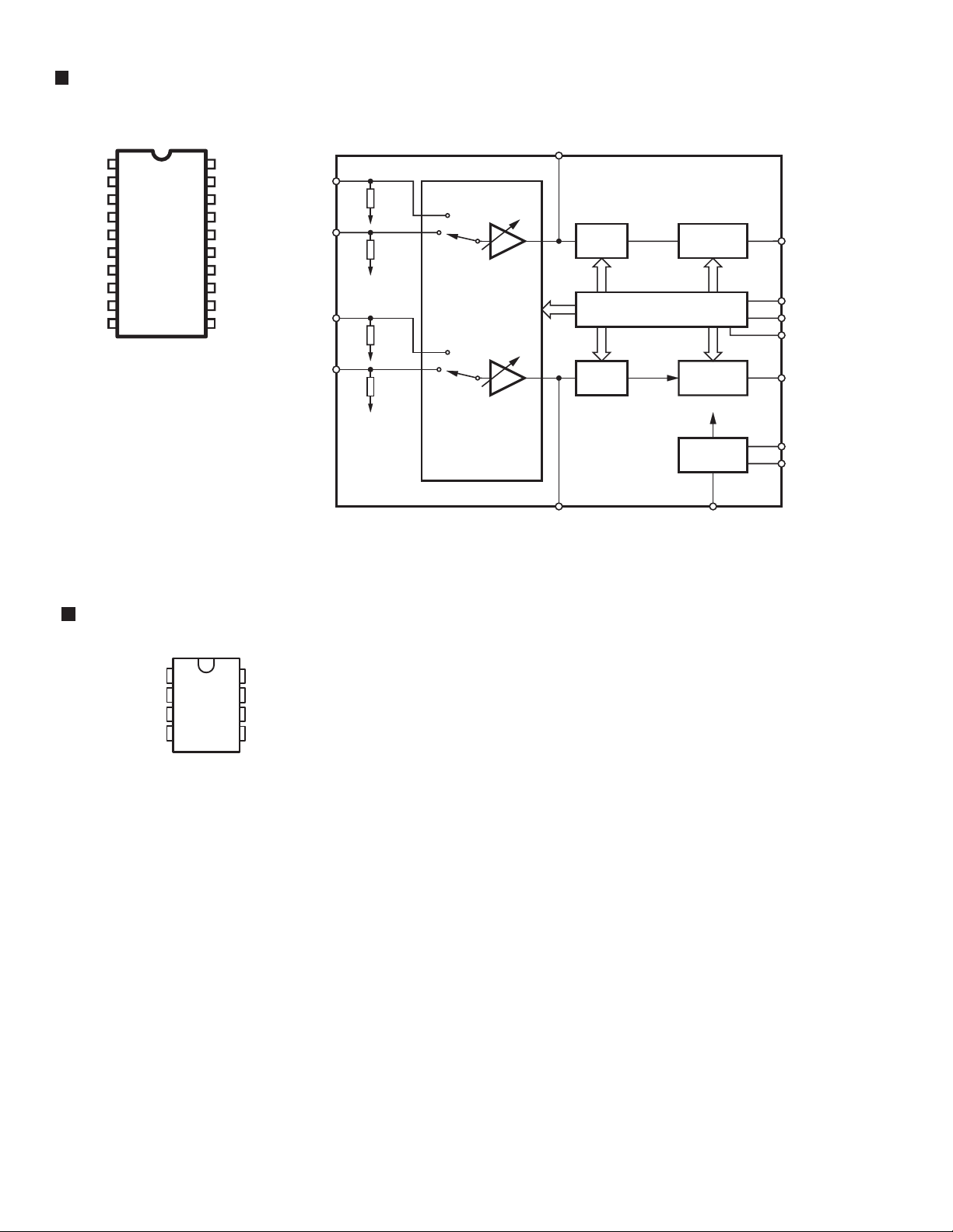
TH-A30R
TDA7449L (U7, U12) : Audio processor
1.Pin layout 2.Block diagram
CREF
PGND
ROUT
LOUT
R_IN2
R_IN1
L_IN1
L_IN2
MUXOUT(L) 10 MUXOUT(R)
1
2
V
S
3
4
5
6
7
8
9 N.C.
SDA20
SCL
19
DIG_GND
18
N.C.
17
N.C.
16
N.C.
15
N.C.
14
N.C.
13
12
11
L-IN1
L-IN2
R-IN1
R-IN2
8
100K
9
100K
7
100K
6
100K
G
0/30dB
2dB STEP
G
INPUT MULTIPLEXER
+ GAIN
MUXOUTL
10
VOLUME
I2CBUS DECODER + LATCHES
VOLUME
11 1
MUXOUTR
SPKR ATT
LEFT
SPKR ATT
RIGHT
V
REF
SUPPLY
CREF
5
19
20
18
4
2
3
LOUT
SCL
SDA
DIG_GND
ROUT
V
S
AGND
D98AU868
TL3472 (RU2) : Op. amp.
1.Pin layout
V
CC±
1OUT
1IN±
1IN+
/GND
1
2
3
4
8
7
6
5
V
CC+
2OUT
2IN±
2IN+
1-30
Page 31

< MEMO >
TH-A30R
1-31
Page 32

TH-A30R
VICTOR COMPANY OF JAPAN, LIMITED
AUDIO & COMMUNICATION BUSINESS DIVISION
PERSONAL & MOBILE NETWORK BUSINESS UNIT. 10-1,1chome,Ohwatari-machi,Maebashi-city,371-8543,Japan
(No.21163)
Printed in Japan
200212
Page 33

SCHEMATIC DIAGRAMS
DVD DIGITAL CINEMA SYSTEM
TH-A30R
STAND BY/ON
AUDIO
TV/VIDEO
VCR
TV
TV CHANNE L
DISPLAY
STEP
AUDIO/
SUBTITL E
TV VOLUME
FM MOD E
DVD FM/AM AUX
TUNER PRESET
DOWN UP
REW
VCR CHANNE L
TUNING
B.SEARCH F.SEARCH
ENTER
VOLUM E
TOP MENU
MENU
RETURN
RM-STHA30R
DVD CI NEMA SYSTE M
TH-A30R
Area suffix
CD-ROM No.SML200212
SP-XSA30 2
RDS
DISPLAY
VCR
CONT ROL
FF
MUTING
STANDBY
STANDBY/ON
AUDIO/FM MODE
DSP
VOLUME SOURCE
DVD DIGITAL CINEMA SYSTEM TH-A30R
SP-XA30 3
DIGITAL
SURROUN D
DIGITAL
XV-THA30R SP-WA30
B -------------------------- U.K.
E ------ Continental Europe
EN ------- Northern Europe
EV --------- Eastern Europe
EE ---- Russian Federation
Contents
Block diagrams
Standard schematic diagrams
Printed circuit boards
COPYRIGHT 2002 VICTOR COMPANY OF JAPAN, LTD.
2-1
2-3
2-8~12
No.21163SCH
Dec. 2002
Page 34

TH-A30R
In regard with component parts appearing on the silk-screen pr inted side (par ts side) of
the PWB diagrams, the parts that are printed over with black such as the resistor ( ),
diode ( ) and ICP ( ) or identified by the " " mark nearby are critical for safety.
(This regulation does not correspond to J and C version.)
Page 35

Block diagrams
r
Main section
5
S_VIDEO_C
VW2
S_VIDEO_Y
VIDEO_COMPO
JVIC1
VIDEO SW
JVIC2
VIDEO SW
JVIC3
VIDEO SW
S-VIDEO
SCART JACK
VIDEO
TH-A30R
VFD
UIC1
MICOM
TUNER
V Signal
Front
FCW2
J1
CW8
4
R
U11
PROLOGIC IC
J21
MUX-OUT R IN R
DVD PACK
(Refer to the following page
"DVD mecha block section")
3
J14
J3
DAC
D3
D2
D1
U6
FL
FR
C
W
RL
RR
2
LPF
(1/2)
U1
LPF
(2/2)
LPF
(1/2)
U5
LPF
AUX L
TUN L
AUX R
TUN R
FL
FUNCTION IC
FR
MUX-OUT L IN L
C
W
FUNCITON IC
U2
U12
U13
J6
IC5
POWER
AMP.
CW5
IC7
POWER
AMP.
(2/2)
U9
L
AUX1
6
(35W)
6
(35W)
6
(35W)
4
(110W)
Front L-ch
Front R-ch
Center
Sub Woofe
LPF
RL
(1/2)
U3
1
LPF
RR
U7
FUNCTION IC
J5
CW6
(2/2)
DSP
Main
IC6
POWER
AMP.
ABCD E F G
6
(35W)
6
(35W)
Rear L-ch
Rear R-ch
2-1
Page 36

TH-A30R TH-A30R
DVD mecha block section
RU1 RF AMP SP3721
RF AGC
& EQ
CONTROL
DECK ASS’Y
FOCUS OK
5
DETECT DEFECT
DETECT MIRROR
GEN
PICK UP
& I/V AMP
FOCUS
SERVO
DISC
MOTOR
FEED
MOTOR
LOOP
4
DISC
MOTOR
DRIVER
ACTUATOR
MOTOR
DRIVER
MICOM DATA INTERFACE
LOGIC DECODER
TRACKING
ERROR
I/V AMP
APC.LASER
CONTROL
&LPC
TRACKING
SERVO
LOOP
HARDWARE
COMPARATOR
LOGIC
EFM
RF&FOCUS
ERROR
I/V AMP
SPINDLE
SERVO LPF
MICOM
M6759
DATA
SEPARATOR
DIGITAL
SERVO
DU3
DVD ROM CONTROLLER
M5701/ M5705
BCA
DVD-D SP
CD-DSP
4M DRAM
416C256
RAM
ARBITER
TARGET
SEARCH
Parallel/Serial
DVD Interface
ATAPI
&
MPEG
I/F
C3 ECC
EDP
MCU I/F
3
HOST
MEMORY
SST39VF800A
Track Buffer
Processor
Audio
2
Input Unit
Decryption
A/V CORE
SDRAM CONTROLLER
--------ZIVA
Graphics
Engines
Interlace/
Progressive
Video
Encoder
Digital Video
Five 10-bit
Video
DACs
Analog
Video
Output
64M SDRAM
W986432DH-7
BUFFER
SIGNAL
KSA812
SWITCHING
BUFFER
BA7612
(Refer to "Main section.")
VIDEO OUT
System Control Bus
Audio
Output
AMP PARTS
System Control Bus
SPARC
Microprocessor
Audio
Output
Phase
1
ASYNC BUS/IR/GPIO/SPI/UART1&2/ATAPI/IDC
Lock
Loop
JTAG
Interface
U8
MPEG DECODER
ZIVA5
(Refer to "Main section.")
Parallel/Serial
DVD Interface
13.5MHZ Crystal
ATAPI 40PIN
2-2
HABC DEFG
Page 37

Standard schematic diagrams
Main section /Power supply section
5
4
To Tuner Pack
To J7
Sheet 2/5
To J2
Sheet 2/5
TH-A30R
To DJ6
Sheet 4/5
3
2
1
SHEET
NUMBER
CIRCUIT DESCRIPTION
Main /Power supply
1/5
FL display & System control /DSP
2/5
Video signal output
3/5
DVD loader
4/5
DVD MPEG
5/5
To J6 Sheet 2/5
To J5
Sheet 2/5
Tuner signal
To FCW1
Sheet 2/5
Front signal
Center signal
Rear signal
Parts are safety assurance parts.
When replacing those parts, make
sure to use the specified parts.
SHEET 1/5
ABCD E F G
2-3
Page 38

TH-A30R TH-A30R
FL display & System control section / DSP section
To J14
Sheet 5/5
To FCW1-1
Sheet 1/5
Front signal Center signal Rear signalTuner signal Digital audio signal
5
4
3
2
1
LOUT(PLL) MUX-OUT(L)
To PW3 Sheet 1/5
To VW1 Sheet 3/5
To CW7 Sheet 1/5
2-4
To CW6 Sheet 1/5
To FAN
To CW5 Sheet 1/5
SHEET 2/5
HABC DEFG
Page 39

5
To J21 Sheet 5/5
4
TH-A30R
Video signal output section
3
2
To J8 Sheet 2/5
1
Video signal
ABCD E F G
SHEET 3/5
2-5
Page 40

5
D
4
3
2
1
DVD loader section
To PW4
Sheet 1/5
DJ6
1
2
3
4
D5V
5
6
M
CON6_2.54M
M5V
MJ4
1
2
3
4
5
To Pickup ASSY
(sled, spindle control)
6
CON_WAFER_2m/m_S
MJ5
1
2
3
4
5
m
CON_2m
To Door Open
Close Motor
MJ6
FLOAD-
4
FLOAD+
3
FOUTSW
2
FINSW
1
CONNECTOR_HEADER_ST_4P
RCN1
BODY_GND
From Pickup ASSY(RF)
PU24PCON_DIP_L
EJECT OPTION
CONNECTOR_WAFER_2P_ST
EJCN1
1
2
VREF
DVDLD
DVDVR
DVDPD
CDLD
CDVR
CDPD
SP-
MR175 10K
MR174 100K
MR173 100K
SP+
SLED+
SLEDHOMESW
INSW
OUTSW
MR185 0
MR186 0
MR183 1K
MR184 1K
MGND
1
E
2
A
3
D
4
RF
5
C
6
B
7
F
8
VCC
9
10
GND
11
T-
12
T+
13
F+
14
F-
15
16
GND
17
18
19
20
GND
21
22
23
24
VCC
E
D
A
B
C
F
RFVCC
GND
TRACK+
TRACKFOCUS+
FOCUS-
DVDVR
DVDPD
CDVR
CDPD
RR20
RR21
220
560
RFGND
INSW
VCC
EJC2
EJR1
GND
10K
XMP1_1
EJC1
104
GND
MR179 R
MZD1
5.6V
OPEN
MR182 1K
CLOSE
104
RFVCC
TH-A30R TH-A30R
PLLVCC
DR146
0
R
RC5
RTC1
220U/16V
33
12
M5V
MEI-
C
680P
0.1U
RR18
MVREF2
MC82
BIAS
MR156
MR164 1 2012
MR167 1 2012
10 (2012)
DL7
CIC21(2012)
RR5 0
1
2
3
4
5
6
7
8
9
10
11
12
13
14
15
16
DVDPD
CDPD
RC32
0.1U
DVDFRP
DVDRFN
PD1
PD2
A2
B2
C2
D2
CP
CN
D
C
B
A
F
E
10K
220P
3.3K
RFVCC
MR151
MR154
MVCC
DC75
0.1U
PLLGND
RFVCC
DC77
0.1U
MGND
PAGND
RC1
0.1U
RC3
0.1U
RFO
646362616059585756555453525150
AIP
AIN
VPA
BYP
SIGO
ATOP
CDRF
ATON
CDRFDC
RU1
SP3721A
CDTE
VC12NCVNB
DVDPD
DVDLD
CDPD
CDLD
LDONVCVCI
171819202122232425262728293031
LDON
MVREF2
RTC4
RC27
0.1U
100U/16V
1
VINFC
47K
2
CFCERR1
3
CFCERR2
12K
4
VINSL+
5
VINSL-
MC84
6
VOSL
4700P
7
VNFFC
8
VCC
9
PVCC1
10
PGND
11
VOSL-
12
VOSL+
13
VOFC-
14
VOFC+
VC25
RX
DC72
0.1U
DIP
DIN
VPB
RR23
0
BA5954FM
FNP
MIRRMPMB
RR19 R
RC28
RC31
104
MU9
29
RC2
0.1U
RC4
0.1U
FNN
0.1U
GND
PAGND
RFGND
30
49
VNA
32
CTKERR1
CTKERR2
GND
DTC9
220U/16V
HOLD1
SDEN
SDATA
SCLK
LCP
LCN
MEI
MEV
TPH
DFT
MIN
MEVO
MLPF
FDCHG
RC33 C
STBY
BIAS
VINTK
VINLD
PREGND
PVCC2
VNFTK
PGND
VOLDVOLD+
VOTKVOTK+
RR6
8K2(1%)
DL4
CIC21(2012)
PLLGND
RC7
0.1U
48
47
46
45
44
43
CE
42
FE
41
TE
40
39
38
37
36
PI
35
34
33
RC24
C
RC25
C
No Connection
RTC5
100U/16V
1
2
3
45
RR25
8.2K
RFGND
28
27
26
25
24
23
22
21
20
19
18
17
16
15
MGND
GND
RFGND
RC16
0.047U
RC21
0.1U
RC22
RC23
C
RFGND
MIRR
MVREF2
RU2
AO
V+
A-
BO
A+
B-
V- B+
TL3472
MR149
10K
MR159
MR165 1 2012
MR168 1 2012
VCC
DU7
MVCC
91K
DR29 0
DR28
DR30
91K
DR31
DC33
1K2
0.047U
DC34
560P
DR35 5K1
DR38
4K7
XSFGIN
XSPDON
0.1U
BRIN
EJECT
LED
INSW
OUTSW
CLOSE
HOMESW
OPEN
DC36
0.1U
DC37
47P
DC39
0.1U
RFVCC
DR189 R
DR57 10
DR190 10K
DR191 10K
GPIO0
CRSTJ
MPSENJ
BRIN
MFSCSJ
GND
No Connection
CPURST
DR37 10K
PLLVCC
VC2
DC85
0.1U
1
AVSS_DS
2
XSRFIN
3
XSIPIN
4
AVDD5_DS
5
XSDSSLV
6
XSRSLINT
7
VDD_3.3
8
XSAWRC
9
XSRFGC
10
XSEFGC
11
XSFOCUS
12
XSTRACK
13
XSSLEG
14
AVDD5_DA
15
XSMOTOR
16
AVSS_DA
17
XSRFRPLP
18
XSTELP
19
XSVREF2
20
XSRFRP
21
XSTEXI
22
AVSS_AD
23
XSTEI
24
XSFEI
25
XSAEI
26
AVDD5_AD
27
XSSBAD
28
GND
29
XSDFCT
30
XSCSJ
31
XSCLK
32
XSDATA
33
XSLDC
34
XSFGIN
35
XSSPDON
36
XSFLAG3
37
XSFLAG2
38
XSFLAG1
39
XSFLAG0
40
XMP1_7
41
XMP1_6
42
GND
43
XMP1_5
44
XMP1_4
RFVCC
DL3
L
DC55
C
CPURST
168
169
170
171
172
173
174
175
176
XSFDO
AVSS_PL
XSVREFO
XSFTROPI
XSVR_PLL
XSPLLFTR2
XSPDOFTR1
XSAWRCVCO
XMP1_3
XMFSCSJ
XMP1_2
XGPIO3
XMP1_1
XHRSTJ
XGPIO1
XGPIO0
45464748495051525354555657585960616263646566676869707172737475767778798081828384858687
GPIO1
GPIO0
GPIO3
XMP1_0
MALE
TP
DC54
12P
DXT1
33.8688MHz
DC56
12P
CPUR4 R
CPUR6 33
CPUR7 33
CPUR8 33
CPUR9 33
CPUR11 33
CPUR17 33
CPUR13 33
CPUR18 33
DTC6
220U/16V
DC32
0.1U
PLLGND
RFO
DC40
1000P
DR39
20K
DC41
DC42
6800P
C
RFGND
SFOCUS
K
STRAC
G
SSLE
SMOTOR
DC43
0.47U(2012)
MVREF2
RFGND
RR7
TEXI TEXI
RC10
33P
RC11
33P
RC13
33P
SAE
FEI
TEI
MEIRC20
1000P
EFGC
8
7
6
RC34
0.1U
BIAS
MR155
3.9K
PIN
C
RFVCC
RC35
33P
RC36
0.47U
D1 1N4148
MR150 10K
MR152
33K
MC83
270P
MR158
R
0
SCSJ
SDATA
SCLK
DFCT
SBAD
MEVO
RFGND
RR26
R
RFRP
PI
MEVO
RR2856K
RR31
470K
RR29
7.5K
0
RR32
RR30
No Connection
R
0
CRSTJ
M5V
STRACK2
SMOTOR2
SPSP+
TRACKTRACK+
DR47
TEI
DR49 3K3
FEI
DR50 4K7
SAE
DR51 5K1
RFRP
DR188 0
DFCT
SCSJ
DR52
SCLK
DR53
SDATA
DR54
DC35
0.1U
DR80
DC62 105(3216)
GND
VCC
DR83
R
DLED1
LED
LED
TRAY_CNTL TP
XSEFGC TP
DC44
0.047U
DTC7
47U/16V
22K
XC61AN1902MR
CPUR19
R
CPUR20
R
RFGND
3
DC45
470P
33
33
33
33
DU6
IN
DR40 51K
TRAY_CNTL
DR42
DR43
DR44
DR45
DC46
470P
DR46 47K
DR48
DC51
1000P
DC52
0.1U
1
OUT
GND
2
PLLGND
SAEI
SSBADSBAD
XSCSJ
XSCLK
XSDATA
DR81
GND
DC38
0.1U
DR187
R
DC81
0.1U
3.3V
FOCUS
3K3
TRACK
3K3
SLEG
3K3
4K7
MOTOR
DC86
MIRR
0.1U
GND
DR1831K
DR1841K
No Connections
DR55 0
RFGND
LDON
FLAG3
FLAG2
FLAG1
FLAG0
VCC
VC2
RFRP
OPEN
HOMESW
OUTSW
DC87
INSW
LED
XMP1_1
BRIN
RFRP
SAEI
SSBAD
DFCT
XSCSJ
XSCLK
XSDATA
IDERST
DC48
0.1U
R
DC49
0.1U
DC50
1000P
RFRP
4.7K
DC63 C
RA0
RA2
RA3
RA5
RA4
RA1
DC84
0.1U
3.3V
No Connection
No Connection
PLCK
SLRF
156
157
158
159
160
161
162
163
164
165
166
167
GND
XRA5
XRA4
XRA0
XRA1
XRA2
XRA3
XTSLRF
XTPLCK
VDD_3.3
XSFDIREF
XSPDIREF
AVDD5_PL
DU3
ALi M5705 (176 pin)
XCRSTJ
XMPSENJ
VDD_3.3
XMALE
MCUP1.0
VDD_3.3
XOSC1
XOCS2
GND
XMD0
XMD1
XMD2
XMD3
3.3V
3.3V
MD3
MD1
MD0
MD2
DC82
0.1U
OSC
DR60
47K
XMP1_2
XMP1_3
XMP1_4
GPIO0
XMP1_6
XMP1_7
RA6
154
155
GND
XRA6
XMD4
XMD5
MD4
MD5
No Connection
No Connection
No Connection
No Connection
No Connection
RA7
153
XRA7
XMD6
MD6
XMP1_0
XMP1_1
RA9
RA8
3.3V
147
148
149
150
151
152
XRA9
XRA8
XRA11
XRA10
VDD_3.3
XMD7
XMCSJ
XMRDJ
XMWRJ
XMINT1J
MD7
MWRJ
RA[0..9]
DR138
2K2
DR139
2K2
DR140
R
DR141
R
DR142
R
DR143
R
DR144
R
DR145
R
DR185
R
DR186
R
DR32 33
DR33 33
DR34 33
0.1U
DR36 33
DC83
RD7
RD8
RD6
137
138
139
140
141
142
143
144
145
146
GND
XRD6
XRD8
XRD7
XROEJ
XRWEJ
XRRASJ
XRCASJ
VDD_3.3
XRSDCLK
XMA11
XMA10
VDD_3.3
XMA9
XMA8
XMA7
XMA6
XMA5
XMA4
XMA3
MA11
MA8
MA10
MA7
MA3
MA4
MA5
MA6
MA9
MINT1J
MCS
ROE
RCAS
RRAS
RWE
RD4
RD10
RD9
RD5
RD11
GND
133
134
135
136
XRD4
XRD5
XRD9
XRD11
XRD10
132
XRD3
131
XRD12
130
GND
129
XRD2
128
XRD13
127
XRD1
126
XRD14
125
XRD0
124
XRD15
123
XHD7
122
XHD8
121
XHD6
120
XHD9
119
XHD5
118
XHD10
117
XHD4
116
XHD11
115
VDD_3.3
114
XHD3
113
XHD12
112
XHD2
111
XHD13
110
GND
109
XHD1
108
XHD14
107
XHD0
106
XHD15
105
XHDRQJ
104
XHIOWJ
103
XHIORJ
102
XHIORDYJ
101
XHDACKJ
100
XHINTJ
99
XHCS16J
98
XHA1
97
XHPDIAGJ
96
XHA0
95
XHA2
94
XHCS1J
93
XHCS3J
92
XHDASPJ
91
XMA15
90
XMA14
89
XMA13
XMA2
XMA1
XMA0
XMA12
GND
88
MA1
MA12
MA2
MA0
GND
MINT1J
TP
MRDJ
TP
MCS
TP
RD3
RD12
RD2
RD13
RD1
RD14
RD0
RD15
XHD7
XHD8
XHD6
XHD9
XHD5
XHD10
DC80
3.3V
0.1U
MA14
MA15
MA13
MA[00..15]
XHD4
XHD11
GND
XHD3
XHD12
XHD2
XHD13
3.3V
XHD1
XHD14
XHD0
XHD15
DC6910P
DC7110P
DC6810P
DC7010P
DC6 10P
MA0
12
A0
MA1
11
A1
MA2
10
A2
MA3
9
A3
MA4
8
A4
MA5
7
A5
MA6
6
A6
MA7
5
A7
MA8
27
A8
MA9
26
A9
MA10
23
A10
MA11
25
A11
MA12
4
A12
MA13
28
A13
MA14
29
A14
MA15
3
A15
2
A16
MFSCSJ
22
CE
MPSENJ
24
OE
W29EE512P_32PLCC
RD0
RD1
RD2
RD3
RD4
RD5
RD6
RD7
XHD[0..15]
DR92 33
DR93 33
DR94 33
DR95 33
DR96 33
DR98 47
DR99 47
DR100 47
DR102 47
DR103 33
DC6610P
DU5
(XHD0-15)
O0
O1
O2
O3
O4
O5
O6
O7
VCC
PGM
VPP
NC
GND
DC89
0.01U
1
VCC
2
DQ0
3
DQ1
4
DQ2
5
DC91
0.1U
10K
10K
10K
10K
10K
DR90
DR91
DR88
DR89
DC88
0.1U
GND
DQ3
6
VCC
7
DQ4
8
DQ5
9
DQ6
10
DQ7
11
VSS
12
NC
13
WE
14
RAS
15
NC
16
A0
17
A1
18
A2
19 22
A3 A4
20
VCC
K4E151512D
XHD1
XHD14
XHD0
XHD15
XHD7
XHD8
XHD6
XHD9
XHD5
XHD10
XHD4
XHD11
XHD3
XHD12
XHD2
XHD13
HD7
HD6
HD5
HD4
HD3
HD2
HD1
HD0
DC65
C
VCC
DC90
0.01U
RWE
RRAS
RA0
RA1
RA2
RA3
VCC
10K
10K
10K
DR86
DR87
DR84
DR85
MD0
13
MD1
14
MD2
15
MD3
17
MD4
18
MD5
19
MD6
20
MD7
21
32
MWRJ
31
1
30
16
40
VSS
RD15
39
DQ15
RD14
38
DQ14
RD13
37
DQ13
RD12
36
DQ12
35
VSS
RD11
34
DQ11
RD10
33
DQ10
RD9
32
DQ9
RD8
31
DQ8
30
VSS
RCAS
29
LCAS
28
UCAS
ROE
27
OE
RA8
26
A8
RA7
25
A7
RA6
24
A6
RA5
23
A5
RA4
21
VSS
GND
10K
DR107
DR110 10K
DR113 10K
DR109 10K
DR114 10K
DR112 10K
DR111 10K
DR108 10K
DR122100
DR123100
DR124100
DR125100
DR126100
DR127100
DR128100
DR129100
DR130100
DR131100
DR132100
DR133100
DR134100
DR135100
DR136100
DR137100
HD7
HD8
HD9
HD10
HD11
DJ3
1
3
5
7
9
11
13
15
17
19
21
23
25
27
29
31
33
35
37
39
IDE40
IDERST
HD7
HD6
HD5
HD4
HD3
HD2
HD1
HD0
GND
HDRQ
IOWJ
IORJ
IORDY
HDACKJ
HINTJ
HA1
HA0
HCS1J
HDASPJ
To J6
HCS16J
HPDIAGJ
HCS3J
2
GND
4
HD8
6
HD9
8
HD10
10
HD11
12
HD12
14
HD13
16
HD14
18
HD15
20
NC
22
GND
24
GND
26
GND
28
28
30
GND
32
34
36
THA2
38
40
GND
Sheet 5/5
3
3
C
C
BB
BE
12
2SB1197
3
IN
OUT GND
21
XC61AN1902MR
TR/ DIODE MODEL DRAWING
12
DAP202K
3
C
BA
12
DAN202K
BE
12
R1103
BE
12
KSA812
RA9
No Connection
DR116 10K
DR117 10K
DR115 10K
THA2
HCS16J
HPDIAGJ
3
C
3
C
DR119 10K
DR118 10K
VCC
DR121 10K
DR120 10K
ADR121 10K
DR97 33
DR101
3
BE
12
2SC1623
3
BE
12
R2101
HD1
HD14
HD0
HD15
HD6
HD5
HD4
HD3
HD12
HD2
HD13
(HD0-15)
HD8
HD9
HD10
HD11
HD12
HD13
HD14
HD15
33
GN
C
A
C
DC76
0.1U
DL5
12
CIC21(2012)
DTC10
DC73
0.1U
DU8
1
PAGND
MR177 1K
1
2
3
4
MU10
GND
V01
VCTL
VIN1
FAN8082
PVCC
SVCC
IN
BA033T/F
VO2
VIN2
DC79
0.1U
LOAD+LOAD+
LOAD-LOAD-
220U/16V
DL6
12
CIC21(2012)
OUT
GND
2
8
7
6
MR180
5
1K
0.1U
DTC12
100U/16V
PAGND
VCC
DC74
3
DC78
0.1U
DTC11
100U/16V
M5V
3.3V
DTC13
100U/16V
GND
MR172
MR176
+
MCE1
MC87
47U/16V
104
MGND
RC26
0.1U
(A,B,C,D,E,F)
RC9
PUHRFPUHRF
RC12
RFGND
RC14
680P
RC15
DPD_A
680P
DPD_B
RC17
DPD_C
680P
DPD_D
RC18
680P
RC19
100P
RR13 1.2K
RR16 1.2K
RR17 10K
RR2
RTC3
10
100U/16V
E
RR4
B
DVDLDO
1K
RC8
1000P
RD1
1
B
3
C
2
B
RFGND
DAP202K
MR148
SFOCUS
33K
MC81
0.1U
MR153
MVREF3
MR157
SSLEG
SLEDSLED+
FOCUSFOCUS+
10K
M5V
MGND
MVREF2
2SB1197
RL1
10UH(3225)
DVDLD
(A,B,C,D,E,F)
RC29
0.1U
RFVCC
RR1
RTC2
10
100U/16V
E
C
RL2
10UH(3225)
RR3
2SB1197
B
RQ2
1K
RC6
1000P
C
RQ1
2-6
Digital data signal
SHEET 4/5
HABC DEFG
Page 41

DVD MPEG section
TH-A30R
+5V_VID
VR1
150
C
VID_C
5
VOGND
VID_U
VR9
82
VR3
000
23
Q3
KSA812
S_VIDEO_C
VID_Y
1
1
VR2
82
+5V_VID
U
VR10
VR11
150
000
23
Q6
KSA812
VIDEO_U
1
1
VOGND
+5V_VID
VR5
150
VR6
Y
000
1
23
Q4
1
KSA812
VR4
82
+5V_VID
VR7
VR8
150
000
23
Q5
1
KSA812
I_SAT_OPT(DEL)
S_VIDEO_Y
VIDEO_Y1
VID_COMP
VID_V
COMP
+5V_VID
VR16
150
VR17
000
23
Q8
KSA812
COMP_OUT
+5_VID
1
1
VR15
56
+5V_VID
VR13
VR14
150
V
000
VIDEO_V
23
1
Q7
1
KSA812
VR12
82
VOGND
+5V_VID
VJL1
000(2012)
C30
VC10
220u/16
0.1u
VOGND
VOGND
VL1
FBSMT
GND
4
AMS317
R60:220OHM
R61:120OHM
LM1117DT-1.8
VDD 3.3V
2
R60
220
3.3V_FLASH
R31
4.7K
/SYS_RST
UPA177
UPA16
UPA15
UPA14
UPA13
UPA12
UPA11
UPA10
UPA9
UPA22
3
UPA21
UPA20
UPA19
UPA18
UPA8
UPA7
UPA6
UPA5
UPA4
UPA3
UPA2
3.3V
2
VDD
3.3V
3.3V
GND
UDS
2
A14
3
A13
4
A12
5
A11
6
A10
7
A9
841
A8 DQ13
R34
9
A21
10
0ohm
R33
DEL
0ohm
U8/12PIN
C80
0.1u
U8/30PIN
C90
0.1u
U8/32PIN
C106
0.1u
C77
0.1u
A20
11
WE
12
RESET
13
SST39VF800A
ACC
14
WP
R10
15
A19
0ohm
16
A18
17
A17
18
A7
19
A6
20
A5
21
A4
22
A3
23
A2
24
A1
R32
8M FLASH MEMORY
4.7K
C101
0.1u
GND
3.3V
U8/63PIN
C75
0.1u
3.3V
U8/74PIN U8/173PIN
C64
0.1u
VDD
U8/80PIN
C89
0.1u
3.3V
U8/87PIN
C62
0.1u
3.3V
U8/98PIN
C61
0.1u
3.3V
U8/104PIN
C59
0.1u
GND
ADJ_2.5V
481
A16A15
47
Vi/o
46
VSS
45
DQ15
44
DQ7
43
DQ14
42
DQ6
40
DQ5
U6
39
DQ12
38
DQ4
37
VCC
36
DQ11
35
DQ3
34
DQ10
33
DQ2
32
DQ9
31
DQ1
30
DQ8
29
DQ0
28
OE
27
VSS
26
CE
25
A0
U9
OUT
VDD
VDD
3.3V
3.3V
VDD
GND
3
IN
ADJ
1
R61
+
C84
10u/16
HOST MEMORY
UPD15
UPD7
UPD14
UPD6
UPD13
UPD5
UPD12
UPD4
UPD11
UPD3
UPD10
UPD2
UPD9
UPD1
UPD8
UPD0
R/W
UPA1
U8/145PIN
C88
0.1u
C87
0.1u
U8/181PIN
C79
0.1u
U8/196PINU8/44PIN
C107
0.1u
U8/205PIN
C86
0.1u
LM1117
R60:DEL
R61:22OHM
C83
0.1u
22ohm
UPA[22:1]
/FLASH_CS
+
C82
47u/16
GND
/SYS_RST
UDS
6
0ohm
UPD[15:0]
+5V
R5V
2
C3
0.1u
3.3V_FLASH
0ohm
GND
L57
C100
0ohm(2012)
DEL
0.1u
R3
DEL
IL1
FBSMT
DEL
CON_WAFER_1m/m_SMD_ST
OL1
FBSMT
COMP_OUT
S_VIDEO_C
S_VIDEO_Y
VIDEO_Y1
VIDEO_U
VIDEO_V
J21
1
2
3
4
5
6
7
8
9
10
OL2
FBSMT
GND
T o VW2
Sheet 3/5
TPN3
VGND
1
PLL_GND
REF_GND
DVSS
VGND
VID_V
VID_U
VID_Y
VID_C
VID_COMP
L52
FBSMT
L54
FBSMT
L53
FBSMT
L55
CIC21C
VDD
I2C_CL
I2C_DA
DEMPH
3.3V
NO CONNECT
NO CONNECT
NO CONNECT
R56
C55
4.7K
0.1u
R54
R
R53
4.7K
+
C85
47u/16
R114
000
GND
HDMARQ
HDMACK
/LDRRST
HIRQ1
+5V
R110 4.7K
/IDE_CS1
/IDE_CS0
/FLASH_CS
UPA_3
UPA_2
R/W
3.3V_FLASH
UPA20
UPA21
UPA22
3.3V
C76
0.1u
C66
0.1u
+5V
19
Q1
18
Q2
17
Q3
16
Q4
15
Q5
14
Q6
13
Q7
12
Q8
BICMOS LOGIC/FLIP-FLOP
UPA12
19
Q1
18
Q2
17
Q3
16
Q4
15
Q5
14
Q6
13
Q7
12
Q8
19
Q1
18
Q2
17
Q3
16
Q4
15
Q5
14
Q6
13
Q7
12
Q8
C98
0.1u
UPA4
UPA5
UPA6
UPA7
UPA8
UPA9
UPA10
UPA11
UPA13
UPA14
UPA15
UPA16
UPA17
UPA18
UPA19
R109
4.7K
R107
5.6K
D_MUTE
NO CONNECT
PWR_CNTL
NO CONNECT
R112 4.7K
CTS2
R111 4.7K
ALE
/FLASH_CS
U10
74LVT573
20
10
20
2010
C99
0.1u
D1
D2
D3
D4
D5
D6
D7
D8
OC
U11
74LVT573
D1
D2
VCCGNDVCCGND
D3
D4
D5
D6
D7
D8
OC
10
74LVT573
D1
D2
D3
D4
D5
D6
D7
D8
OC
L56
UPA1
2
UPA2
3
UPA3
4
5
6
7
8
9
11
C
1
UPD8
2
UPD9
3
UPD10
4
UPD11
5
UPD12
6
UPD13
7
UPD14
8
UPD15
9
11
C
1
U12
UPD0
2
UPD1
3
UPD2
4
UPD3
5
UPD4
6
UPD5
7
UPD6
8
UPD7
9
11
C
1
FBSMT
/FLASH_CS
1
R6 33 ohm
R8 33 ohm
R57 33 ohm
UPA3
R59 33 ohm
UPA2
UPA1
ALE
1
PLL_VDD
C71
REF_VDD
0.1u
C68
+
DVDD
47u/16
PLL_GND
REF_GND
C67
0.1u
DVSS
13.5MHz Fundamental
MGND
PLL_GND
PLL_GND
C96
3
1
15pF
X1
VDD
R98
4.7K
157
158
159
160
161
162
163
164
165
166
167
168
169
170
171
172
173
174
175
176
177
178
179
180
181
182
183
184
185
186
187
188
189
190
191
192
193
194
195
196
197
198
199
200
201
202
203
204
205
206
207
208
GND
3.3V
VDD
R63
C73
+
47u/16
150
152
153
151
154
155
156
VDDP
GNDP
IEC958
ADATA1
ADATA2
ADATA3
ADATA0
DAI_DATA
DAI_BCK/SYSCLKBP
DAI_LRCK/IEC958BP
I2C_CL
I2C_DA
RTS1
RXD1
TXD1
CTS1
GNDP
VDDP
SDDATA7
SDDATA6
SDDATA5
SDDATA4
GND
VDD
SDDATA3
SDDATA2
SDDATA1
SDDATA0
SDREQ
SDEN
GNDP
VDDP
SDERROR
SDCLK
VSYNC / HIRQ1
RTS2
RXD2
TXD2
CTS2
VNW
ALE
HCS4
HCS3
HCS2
HCS1
HCS0
VDDP
TRST
TDO
JTAG
TDI
TMS
TCK
RESET
BUSCLK
GND
VDD
HA3
HA2
GNDP
HD13
HD12
HD11
HA1
HD15
HD14
VDDP
567891011131214151617181922202123242526272829
234
1
33 ohm
UPD15
UPD12
UPD10
UPD11
UPD14
UPD13
(UPD0-15)
139
145
146
147
148
149
140
141
142
143
144
XCK
BCK
VDD
GND
LRCK
XVDD
AVSS2
AVSS1
AVDD2
AVDD1
ZiVA-5Xi MPEG DECODER
HD10
HD9
HD8
HD7
GNDP
VDDP
HD6
HD5
HD4
HD3
UPD2
UPD9
UPD5
UPD8
UPD4
UPD7
UPD3
UPD6
R9
33 ohm
UPD_7
PL3
FBSMT
UPD[15:0]
(UPD0-15)
GND
/LDRRST
UPD15 DD7
3.3V
UPD13 DD5
UPD11 DD3
UPD10 DD2
R99
1K
HDMARQ DMARQ
UDS
/DTACK
HDMACK
HIRQ1
UPA_2
/IDE_CS0
L32
FBSMT
/IDE_CS1
UPA_3
UPD_7
1
XIN / VCLK216BP
HD2
2
138
UPD1
20pF
C54
0.1u
137
XVSS
XOUT
HD1
VDDP
VDAC_VDD
C97
1.2K/1%
R55
REF_VDD
134
136
135
VDAC_Ref
VDAC_RefVSS
HD0
GNDP
UPD0
/DTACK
UPA1
DVDD
DVSS
132
133
VDAC_DVSS
VDAC_DVDD
VDAC_RefVDD
HDTACK
HIRQ0
HUDS
UDS
AT_GND
L48
FBSMT
L49
FBSMT
L47
FBSMT
L50
CIC21C
3.3V
VGND
C48
47u/16
127
128
129
130
131
VDAC_1
VDAC_0
VDAC_0B
VDAC_VDD1
VDAC_VDD0
U8
HLDS
HREAD
IRRX1
GND
VDD
30
IR
1
IR
R/W
LDS
3.3V
4.7K
R108
C51
C50
+
0.1u
0.1u
VGND
117
118
119
120
122
123
121
124
125
126
VDAC_4
VDAC_3
VDAC_2
VDAC_4B
VDAC_3B
VDAC_2B
VDAC_1B
VDAC_VDD4
VDAC_VDD3
VDAC_VDD2
GND25
VDD25
MA9
MA8
MA7
MA6
MA5
MA4
MA3
MA2
31
32
333435363738394041
J6
RESET
12
34
DD6UPD14
56
78
DD4UPD12
10
9
11 12
13 14
DD1UPD9
15 16
DD0UPD8
17 18
19 20
21 22
/DIOWLDS
23 24
/DIOR
25 26
/IORDY
27 28
DMACK
29 30
INTRQ
31 32
DA1
33 34
DA0
35 36
/CS0
37 38
39 40
FPC/FFC_40P_1M/M_SMD
To DJ3
Sheet 4/5
ATN_FM
RDY_FM
1
RDY_FM
ATN_FM
SCK
D_FM
D_HOST
DAI_DATA
DATA3
1
1
115
116
VDATA0
HSYNC / IRQ2
MA1
MA0
42
1
114
113
110
109
111
112
108
107
106
105
VCLK
VDDP
GNDP
VDATA5
VDATA6
VDATA7
VDATA1
VDATA2
VDATA3
VDATA4
VDD25
GND25
MD31
MD30
MD29
MD28
VDD25
MDQM3
GND25
MD27
MD26
MD25
MD24
MD23
MD22
MD21
MD20
VDD25
MDQM2
GND25
MD19
MD18
MD17
MD16
MD15
MD14
MD13
MD12
VDD25
MDQM1
GND25
MD11
MD10
VDD25
MDQM0
GND25
MCLK
VDD25
GND25
MWE
MCAS
MRAS
MCS0
MCS1
BA0
BA1
MA11
MA10
VDD25
GND25
525149504847464544
43
DD8 UPD0
DD10 UPD2
DD12 UPD4
DD13 UPD5
DD15 UPD_7
DA2
/CS1
L30
FBSMT
AT_GND
1
DATA2
1
TPN1
TUNE_CLK
VDD
GND
MD9
MD8
MD7
MD6
MD5
MD4
MD3
MD2
MD1
MD0
R78
R79
R80
R81
R82
R83
R84
R85
R86
R88
R90
UPA_3
/IDE_CS1
GND
SCK
1
DATA0
DATA1
1
NO CONNECT
104
103
102
101
100
99
98
97
96
95
94
93
92
91
90
89
88
87
86
85
84
83
82
81
80
79
78
77
76
75
74
73
72
71
70
69
68
67
66
65
64
63
62
61
60
59
58
57
56
55
54
53
R66 33 ohm
R68 33 ohm
R71 33 ohm
R73 33 ohm
R75 33 ohm
33 ohm
33 ohm
33 ohm
33 ohm
33 ohm
33 ohm
33 ohm
33 ohm
33 ohm
33 ohm
33 ohm
UPD1DD9
UPD3DD11
UPD6DD14
D_HOST
D_FM
1
LRCK
BCK
1
1
3.3V
GND
3.3V
GND
VDD
R64
33 ohm
ATAPI
CONNECTOR
1
XCK
1
MDATA31
MDATA30
MDATA29
MDATA28
MDATA27
MDATA26
MDATA25
MDATA24
MDATA23
MDATA22
MDATA21
MDATA20
MDATA19
MDATA18
MDATA17
MDATA16
MDATA15
MDATA14
MDATA13
MDATA12
MDATA11
MDATA10
MDATA9
MDATA8
MDATA7
MDATA6
MDATA5
MDATA4
MDATA3
MDATA2
MDATA1
MDATA0
R58 33 ohm
MADDR10
MADDR0
MADDR1
MADDR2
MADDR3
MADDR4
MADDR5
MADDR6
MADDR7
MADDR8
MADDR9
SRQ_SCE
RRQ_MCE
CLK_MCK
TXD_SDATA
RXD_MDATA
1
DAI_DATA
DA_DATA3
DA_DATA1
DA_DATA0
DA_LRCK
DA_XCK
Front Panel Board
Connector
IEC_958
DA_DATA2
DA_BCK
MDQM1
/MWE
/MCAS
/MRAS
/MCS0
BA0
BA1
MDQM3
MDQM2
MDQM0
SD_CLK
MDATA[31..0]
MADDR[10..0]
/SYS_RST
C102
103
TXD
IEC_958
RXD_MDATA
RRQ_MCE
SRQ_SCE
CLK_MCK
TXD_SDATA
IEC_958
+5V
DC1
1000p
1
DA_LRCK
DA_BCK
DA_DATA3
DA_DATA2
DA_DATA1
12
DA_DATA0
DA_XCK
+5V_VID
12
C70
1000p
GND
3.3V
U5/1PIN
C36
0.1u
3.3V
U5/15PIN
C103
0.1u
MDQM3
MDQM2
MDQM0
MDQM1
MDATA15
U15
2
A1
3
A2
4
A3
5
A4
6
A5
7
A6
8
A7
9
A8
1
DIR
19
OE
20
VCC
74HCT245
COMS LOGIC/TRANSCEIVER
L1
F/B_CIC21J121NE
+
C69
220u/16V
C31
1000p
3.3V
U5/3PIN
C104
0.1u
SD_CLK
MDATA7
MDATA6
MDATA5
MDATA4
MDATA3
MDATA2
MDATA1
MDATA0
MDQM0
BA0
BA1
MADDR10
MADDR0
MADDR1
MADDR2
MDQM1
MDATA8
MDATA9
MDATA10
MDATA11
MDATA12
MDATA13
MDATA14
C46
0.1u
GND
RRQ_MCE
18
B1
17
B2
16
B3
RXD_MDATA
15
B4
14
B5
OPT_OUT
13
B6
12
B7
11
B8
10
GND
FBSMT
L44
DR1 100
12
DR4 100
12
DR3 100
12
DR2 100
12
DR5 100
12
DR6 100
12
100
DR8
100
12
DR9
12
+5V
+5V
1
+3.3V
3.3V
1
C29
1000p
GND
C37
0.1u
1
VDD
2
DQ0
3
VDDQ
4
DQ1
5
DQ2
6
VSSQ
7
DQ3
8
DQ4
9
VDDQ
10
DQ5
11
DQ6
12
VSSQ
13
DQ7
14
NC
15
VDD
16
DQM0
17
/WE
18
/CAS
19
/RAS
20
/CS
21
NC
22
BA0
23
BA1
24
A10/AP
25
A0
26
A1
27
A2
28
DQM2
29
VDD
30
NC
31
DQ16
32
VSSQ
33
DQ17
34
DQ18
35
VDDQ
36
DQ19
37
DQ20
38
VSSQ
39
DQ21
40
DQ22
41
VDDQ
42
DQ23
43 44
U5
VDD VSS
WINBOND_W986432DH-7
64Mb_SDRAM
3
C
BE
BB
12
12
2SB1197
DAP202K
3
IN
BA
OUT GND
12
21
DAN202K
XC61AN1902MR
TR/ DIODE MODEL
DR7
100
L38
F/B_CIC21J121NE
L39
F/B_CIC21J121NE
+
C28
220u/16
3.3V
VSS
DQ15
VSSQ
DQ14
DQ13
VDDQ
DQ12
DQ11
VSSQ
DQ10
DQ9
VDDQ
DQ8
NC
VSS
DQM1
NC
NC
CLK
CKE
A9
A8
A7
A6
A5
A4
A3
DQM3
VSS
NC
DQ31
VDDQ
DQ30
DQ29
VSSQ
DQ28
DQ27
VDDQ
DQ26
DQ25
VSSQ
DQ24
3
C
3
C
1
2
1
FBSMT
C38
47u/16
86
85
84
83
82
81
80
79
78
77
76
75
74
73
72
71
70
69
68
67
66
65
64
63
62
61
60
59
58
57
56
55
54
53
52
51
50
49
48
47
46
45
3
BE
12
R1103
3
BE
12
KSA812
SRQ
1
L40FBSMT
PL1
3.3V
+
C
C
CLK
1
1
L43
L42
FBSMT
FBSMT
FPC_CON24P_SMD
WAFER_1m/m
MGND
MDATA24
MDATA25
MDATA26
MDATA27
MDATA28
MDATA29
MDATA30
MDATA31
MDQM3
MADDR9
MADDR8
MADDR7
MADDR6
MADDR5
MADDR4
MADDR3
MDQM2
MDATA23
MDATA22
MDATA21
MDATA20
MDATA19
MDATA18
MDATA17
MDATA16
+
C33
47u/16
3
C
BE
12
2SC1623
3
C
BE
12
R2101
RRQ
1
L41
FBSMT
RRQ(MCE)
CLK(MCK)
TXD(SDATA)
RXD(MDATA)
SRQ(SCE)
To J3
Sheet 2/5
J14
1
2
3
4
5
6
7
8
9
10
11
12
13
14
15
16
17
18
19
20
CON_WAFER_24P_1M/M_SMD_ST
21
22
23
24
C105
0.1u
Digital data signal
Digital audio signal
Video signal
ABCD E F G
SHEET 5/5
2-7
Page 42

Printed circuit boards
Front board
TH-A30R TH-A30R
5
4
3
Switch board
2
Display board
1
2-8
HABC DEFG
Page 43

TH-A30R
Main board
5
4
3
2
1
Jack board
ABCD E F G
2-9
Page 44

TH-A30R TH-A30R
DVD loader board (Forward side)
5
DVD MPEG board (Forward side)
4
3
2
1
2-10
HABC DEFG
Page 45

TH-A30R
DVD loader board (Reverse side)
5
DVD MPEG board (Reverse side)
4
3
2
1
ABCD E F G
2-11
Page 46

TH-A30R TH-A30R
DSP board
(Forward side)
5
4
3
(Reverse side)
2
1
2-12
HABC DEFG
Page 47

< MEMO >
TH-A30R
Page 48

TH-A30R
VICTOR COMPANY OF JAPAN, LIMITED
AUDIO & COMMUNICATION BUSINESS DIVISION
PERSONAL & MOBILE NETWORK BUSINESS UNIT. 10-1,1chome,Ohwatari-machi,Maebashi-city,371-8543,Japan
No.21163SCH
Printed in Japan
200212
Page 49

PARTS LIST
[ TH-A30R ]
* All printed circuit boards and its assemblies are not available as service parts.
Area suffix
B ------------------------------- U.K.
E ----------- Continental Europe
EN ------------ Northern Europe
EV -------------- Eastern Europe
EE --------- Russian Federation
TH-A30R
- Contents -
Exploded view of general assembly and parts list (Block No.M1)
DVD mechanism assembly and parts list (Block No.MJ)
Electrical parts list (Block No.01~05)
Packing materials and accessories parts list (Block No.M3,M5)
3- 2
3- 4
3- 6
3-22
3-1
Page 50

TH-A30R
Exploded view of general assembly and parts list
Block No.
F
23
36
M
M
1
M
Main board
B
B
Jack board
B
40
B
39
B
B
30
29
B
31
B
29
28 x5
26
F
27
D
25
32
24
DSP board
B
34
B
F
F
F
35
22
37
38
F
F
11
E
F
16
33
10
7
Key board
6
17
B
18
15
14
B
E
B
Front board
12
A
C
13
B
5
C
8
B
C
9
B
3-2
A
F
19
F
4
3
2
1
Page 51

TH-A30R
Parts list (General assembly)
Item
A
A 6002-000126
B 6003-000398
C 6003-000276
D AH60-10107A
E AH60-10020D
F AH60-00025A
1 AH64-01539A
2 AH64-02066B
3 AH61-00834A
4 AH64-01453B
5 AH64-01452A
6 AH67-00129A
7 AH64-01454A
8 AH64-01455A
9 AH67-00128A
10 AH64-01457A
11 AH61-00836A
12 AH64-01456A
13 AH61-00835A
14 AH61-00766A
15 AH69-00503A
16 AH61-00777A
17 AH69-00503B
18 AH64-01586A
19 AH64-01587A
22 AH64-01813H
23 AH63-00303A
24 AH62-00051C
25 AH62-00051D
26 AH62-00052B
27 AH61-00855A
28 AH61-00779A
29 AH62-00050A
30 AH62-00050B
31 AH62-00062A
32 AH69-00188B
33 AH68-00967A
34 AH68-50275D
35 AH68-01158E
36 AH31-00029A
37 AH40-00021A
38 AH26-00202A
39 AH39-00257F
40 3301-001525
Parts number Parts name Area
AH68-01158D
AH39-00258P
SCREW
SCREW
SCREW
SCREW
SCREW
SCREW
DVD BADGE
WINDOW FRONT
FRONT CAP
TRAY DOOR
FRONT CABINET
POWER LENS
KNOB POWER
KNOB OPEN
LENS FRONT
KNOB FUNCTION
HOLDER LED
KNOB PLAY
VFD HOLDER
FOOT HOLDER
CUSHION FOOT
FOOT HOLDER
CUSHION FOOT
CABINET BOTTOM
CABINET TOP
CABINET REAR
COVER FAN
HEAT SINK D
HEAT SINK B
HEAT SINK
IC HOLDER
IC HOLDER
HEAT SINK
HEAT SINK M
HEAT SINK
POWER CUSHION
LABEL DTS
STICKER CD
LABEL RATING
LABEL RATING
MOTOR FAN
TUNER PACK
TRANS POWER
POWER CORD
POWER CORD
AC CORD RING
Q'ty
2
18
3
4
9
25
1
1
1
1
1
1
1
1
1
1
1
1
1
2
2
2
2
1
1
1
1
1
1
1
1
5
2
1
1
1
1
1
1
1
1
1
1
1
1
1
Description
FH 3X10 BLK
BH 2S 3X6 YEL
BH M3X10 YEL
M4X6 YEL
RH 2.6X8 YEL
BH 3X10 SILVER
FRONT
FRONT
REAR
REAR
TRANSISTOR
FM MW RDS
CP2 250V 2.5A 1
VP840 BS
Block No. M1MM
EE
B,E,EN,EV
E,EN,EV,EE
B
3-3
Page 52

TH-A30R
DVD mechanism assembly and parts list
CMSD100
DVD MPEG board
Block No.
M
J
M
M
24
2
22
14
18
7
6 5
1
17
21
4
12
18
19
13
18
11
8
19
10
9
15
12
20
16
4
3
5.75 0.1
DVD loader board
3-4
23
Page 53

TH-A30R
Parts list (DVD mechanism)
Item
A
1 AH61-00746A
2 AH63-00294A
3 AH66-00159A
4 AH66-00160A
5 AH66-00161A
6 AH66-00162A
7 AH66-00163A
8 AH66-00164A
9 AH66-00165A
10 AH61-00747A
11 AH66-00166A
12 AH31-00030A
13 --------------14 AH66-00167A
15 3409-001119
16 AH59-00130A
17 6001-001257
18 AJ60-10001A
19 6003-001210
20 AH73-00025B
21 AH61-00958A
22 6003-000283
23 6003-000276
24 AH61-00828A
Parts number Parts name Area
BASE-MAIN
TRAY-DISC
LEVER-LIFT
PULLEY-MOTOR
GEAR-PULLEY
GEAR-MIDDLE
GEAR-TRAY
CLAMPER-UPPER
CLAMPER-LOWER
BRACKET-CHUCK
SLIDE-CAM
MOTOR-DC
PCB-SWITCH
BELT-PULLEY
SWITCH-DETECTOR
DVD DECK
SCREW-MACHINE
SCREW-TAP
SCREW-TAP
RUBBER-CD
BRACKET-GUIDE
SCREW-TAP
SCREW-TAP
HOLDER-PCB
Q'ty
1
1
1
1
1
1
1
1
1
1
1
1
1
1
1
1
2
6
5
4
1
2
4
1
Block No. MJMM
Description
BLK
D/GRAY
BLK
UPPER
LOWER
T1.0
RF-300CA-11440
26.5 X 21.6
CR 1.5
JDS2200
CMS-S21MG6
1.7 X 3(W4.5)
2 X 5(W7)
2.6 X 6(W12)
BUTYL 15
SECC 1.0T
3 X 8
3 X 10
ABS BLK
3-5
Page 54

TH-A30R
ea
ea
Electrical parts list (Main board)
Item
A
ABD1 0402-001408 DIODE KBP005G 50V
ABD2 0402-001258 BRIDGE DIODE GBU606 600V
ABD4 0402-001258 BRIDGE DIODE GBU606 600V
ABD5 0402-001258 BRIDGE DIODE GBU606 600V
ACW1 3711-000190 CONNECTOR
A
ACW2 3711-004848 CONNECTOR 3P
ACW3 3711-001098 CONNECTOR 7P 2.5MM
ACW4 3711-003111 CONNECTOR 6P 2.5MM
ACW5 3711-000963 CONNECTOR 4P 2.5MM
AC1 2201-000546 CHIP CAPACITORA4.7NF 20% 400V
AC10 2401-001912 E.CAPACITOR 1UF 20% 50V
AC11 2401-000830 E.CAPACITOR 220UF 20% 25V
AC12 2401-001954 E.CAPACITOR 4.7UF 20% 50V
AC13 2401-001954 E.CAPACITOR 4.7UF 20% 50V
AC14 2201-000161 CHIP CAPACITOR 10NF +80-20% 500V
AC15 2201-000161 CHIP CAPACITOR 10NF +80-20% 500V
AC16 2201-000161 CHIP CAPACITOR 10NF +80-20% 500V
AC17 2201-000161 CHIP CAPACITOR 10NF +80-20% 500V
AC18 2401-003772 E.CAPACITOR 2200UF 20% 63V
AC19 2401-003116 E.CAPACITOR 4700UF 20% 35V
AC2 2201-000546 CHIP CAPACITORA4.7NF 20% 400V
AC20 2401-003116 E.CAPACITOR 4700UF 20% 35V
AC21 2401-003772 E.CAPACITOR 2200UF 20% 63V
AC22 2401-001959 E.CAPACITOR 4700UF 20% 25V
AC23 2401-001959 E.CAPACITOR 4700UF 20% 25V
AC3 2201-000546 CHIP CAPACITORA4.7NF 20% 400V
AC5 2201-000546 CHIP CAPACITORA4.7NF 20% 400V
AC8 2401-000475 E.CAPACITOR 10UF 20% 50V
AC9 2401-001413 E.CAPACITOR 470UF 20% 35V
AD1 0402-000127 DIODE
A
AD11 0402-000127 DIODE
A
AD2 0402-000127 DIODE
A
AD3 0402-000127 DIODE 1N4002 100V 1A
AD4 0401-000101 DIODE 1N4148 100V
AD6 0402-000127 DIODE
A
AD8 0402-000127 DIODE
A
AFU2 3601-000263 FUSE
A
AFU3 3601-000319 FUSE
A
AIC1 1203-000276 IC 7805 3P
AIC2 1201-000163 IC BA4560 8P
AL1 AH27-10001F CHOKE COIL
A
AL2 AH27-10001F CHOKE COIL
A
AL3C AH27-90001A SPRING COIL 2.2UH
AL3FL AH27-90001A SPRING COIL 2.2UH
AL3FR AH27-90001A SPRING COIL 2.2UH
AL3RL AH27-90001A SPRING COIL 2.2UH
AL3RR AH27-90001A SPRING COIL 2.2UH
AL3W AH27-90001A SPRING COIL 2.2UH
AQ2 0501-000010 TRANSISTOR KSC1008
AQ3 0501-000010 TRANSISTOR KSC1008
AR11 2001-000786 CARBON RESISTOR 47K 5% 1/8W
AR12 2001-000258 CARBON RESISTOR 1.8K 5% 1/8W
AR15 2001-000702 CARBON RESISTOR 39K 5% 1/8W
AR2 2001-000890 CARBON RESISTOR 6.8K 5% 1/8W
AR3 2001-000449 CARBON RESISTOR 2.2K 5% 1/8W
AR4 2001-000052 CARBON RESISTOR 3.3K 5% 1/2W
AR5 2007-000300 CHIP RESISTOR 10K 5% 1/10W
AR6 2007-000941 CHIP RESISTOR 47K 5% 1/10W
AR7 2001-001045 CARBON RESISTOR 1.2K 5% 1/2W
AR8 2001-000435 CARBON RESISTOR 1M 5% 1/8W
AR9 2001-000591 CARBON RESISTOR 3.3K 5% 1/8W
AUX1 3722-001727 PIN JACK 2P 8.3PI
AZD1 0403-000354 ZENER DIODE UZ5.1B 5.1V
Parts number Parts name Ar
Block No. 01
Remarks
2P
1N4002 100V 1A
1N4002 100V 1A
1N4002 100V 1A
1N4002 100V 1A
1N4002 100V 1A
250V 3.15A
80MA 250V
27UH
27UH
Item
A
AZD2 0403-000352 ZENER DIODE UZ4.7BM 4.7V
AZD3 0403-000379 ZENER DIODE UZP12B 12V
CE4FR 2201-000565 CHIP CAPACITOR 47NF 50V
CE5C 2203-000495 CHIP CAPACITOR 2.2NF 10% 50V
CE5FL 2203-000495 CHIP CAPACITOR 2.2NF 10% 50V
CE5FR 2203-000495 CHIP CAPACITOR 2.2NF 10% 50V
CE5RL 2203-000495 CHIP CAPACITOR 2.2NF 10% 50V
CE5RR 2203-000495 CHIP CAPACITOR 2.2NF 10% 50V
CE5W 2203-000495 CHIP CAPACITOR 2.2NF 10% 50V
CE6C 2203-000892 CHIP CAPACITOR 4.7NF 10% 50V
CE6FL 2203-000892 CHIP CAPACITOR 4.7NF 10% 50V
CE6FR 2203-000892 CHIP CAPACITOR 4.7NF 10% 50V
CE6RL 2203-000892 CHIP CAPACITOR 4.7NF 10% 50V
CE6RR 2203-000892 CHIP CAPACITOR 4.7NF 10% 50V
CE6W 2203-000892 CHIP CAPACITOR 4.7NF 10% 50V
CW5 3711-004110 CONNECTOR 12P 2MM
CW6 3711-004110 CONNECTOR 12P 2MM
CW7 3711-004110 CONNECTOR 12P 2MM
CW8 3708-001094 CONNECTOR 13P 1.25MM
C202L 2203-000787 CHIP CAPACITOR 0.33NF 5% 50V
C202R 2203-000787 CHIP CAPACITOR 0.33NF 5% 50V
C26 2401-000325 E.CAPACITOR 100UF 20% 35V
C27 2401-000325 E.CAPACITOR 100UF 20% 35V
C28 2401-000475 E.CAPACITOR 10UF 20% 50V
C29 2401-000475 E.CAPACITOR 10UF 20% 50V
C30 2401-001364 E.CAPACITOR 470UF 20% 16V
C31 2401-001364 E.CAPACITOR 470UF 20% 16V
C33C 2201-000282 CHIP CAPACITOR 1NF +80-20% 50V
C33FL 2201-000282 CHIP CAPACITOR 1NF +80-20% 50V
C33FR 2201-000282 CHIP CAPACITOR 1NF +80-20% 50V
C33RL 2201-000282 CHIP CAPACITOR 1NF +80-20% 50V
C33RR 2201-000282 CHIP CAPACITOR 1NF +80-20% 50V
C33W 2201-000282 CHIP CAPACITOR 1NF +80-20% 50V
C34 2401-000385 E.CAPACITOR 10UF 20% 100V
C35 2401-001361 E.CAPACITOR 470UF 20% 16V
C36 2401-001912 E.CAPACITOR 1UF 20% 50V
C37 2401-001975 E.CAPACITOR 47UF 20% 16V
C38 2401-001912 E.CAPACITOR 1UF 20% 50V
C39 2401-001538 E.CAPACITOR 47UF 20% 25V
C40C 2401-000438 E.CAPACITOR 10UF 20% 25V
C40FL 2401-001912 E.CAPACITOR 1UF 20% 50V
C40FR 2401-001912 E.CAPACITOR 1UF 20% 50V
C40RL 2401-000438 E.CAPACITOR 10UF 20% 25V
C40RR 2401-000438 E.CAPACITOR 10UF 20% 25V
C40W 2401-000407 E.CAPACITOR 10UF 20% 16V
C41C 2203-001214 CHIP CAPACITOR 8.2NF 10% 50V
C41FL 2203-001214 CHIP CAPACITOR 8.2NF 10% 50V
C41FR 2203-001214 CHIP CAPACITOR 8.2NF 10% 50V
C41RL 2203-001214 CHIP CAPACITOR 8.2NF 10% 50V
C41RR 2203-001214 CHIP CAPACITOR 8.2NF 10% 50V
C41W 2203-001214 CHIP CAPACITOR 8.2NF 10% 50V
C43C 2401-000759 E.CAPACITOR 220NF 20% 50V
C43FL 2401-001645 E.CAPACITOR 0.68UF 20% 50V
C43FR 2401-001645 E.CAPACITOR 0.68UF 20% 50V
C43RL 2401-000759 E.CAPACITOR 220NF 20% 50V
C43RR 2401-000759 E.CAPACITOR 220NF 20% 50V
C43W 2401-001625 E.CAPACITOR 6.8UF 20% 50V
C44C 2203-000710 CHIP CAPACITOR 2PF 0.25PF 50V
C44FL 2203-000710 CHIP CAPACITOR 2PF 0.25PF 50V
C44FR 2203-000710 CHIP CAPACITOR 2PF 0.25PF 50V
C44RL 2203-000710 CHIP CAPACITOR 2PF 0.25PF 50V
C44RR 2203-000710 CHIP CAPACITOR 2PF 0.25PF 50V
C44W 2203-000295 CHIP CAPACITOR 0.01NF 5% 50V
Parts number Parts name Ar
Remarks
3-6
Page 55

TH-A30R
ea
ea
Electrical parts list (Main board)
Item
A
C46W 2203-001611 CHIP CAPACITOR 0.022NF 5% 50V
C47C 2301-000375 M.CAPACITOR 100NF 10% 50V
C47FL 2301-000375 M.CAPACITOR 100NF 10% 50V
C47FR 2301-000375 M.CAPACITOR 100NF 10% 50V
C47RL 2301-000375 M.CAPACITOR 100NF 10% 50V
C47RR 2301-000375 M.CAPACITOR 100NF 10% 50V
C47W 2301-000375 M.CAPACITOR 100NF 10% 50V
C49C 2203-000295 CHIP CAPACITOR 0.01NF 5% 50V
C49FL 2203-000295 CHIP CAPACITOR 0.01NF 5% 50V
C49FR 2203-000295 CHIP CAPACITOR 0.01NF 5% 50V
C49RL 2203-000295 CHIP CAPACITOR 0.01NF 5% 50V
C49RR 2203-000295 CHIP CAPACITOR 0.01NF 5% 50V
C49W 2203-001525 CHIP CAPACITOR 56PF 5% 50V
C52 2401-001975 E.CAPACITOR 47UF 20% 16V
C53 2401-000475 E.CAPACITOR 10UF 20% 50V
C54RL 2401-001975 E.CAPACITOR 47UF 20% 16V
C54RR 2401-001975 E.CAPACITOR 47UF 20% 16V
C54W 2401-001975 E.CAPACITOR 47UF 20% 16V
C55 2401-001975 E.CAPACITOR 47UF 20% 16V
D01FL 0401-001090 DIODE 1SS355 80V
D01FR 0401-001090 DIODE 1SS355 80V
D01RL 0401-001090 DIODE 1SS355 80V
D01RR 0401-001090 DIODE 1SS355 80V
D010C 0401-001090 DIODE 1SS355 80V
D010W 0401-001090 DIODE 1SS355 80V
D02FL 0401-001090 DIODE 1SS355 80V
D02FR 0401-001090 DIODE 1SS355 80V
D02RL 0401-001090 DIODE 1SS355 80V
D02RR 0401-001090 DIODE 1SS355 80V
D020C 0401-001090 DIODE 1SS355 80V
D020W 0401-001090 DIODE 1SS355 80V
D03FL 0401-001090 DIODE 1SS355 80V
D03FR 0401-001090 DIODE 1SS355 80V
D03RL 0401-001090 DIODE 1SS355 80V
D03RR 0401-001090 DIODE 1SS355 80V
D030C 0401-001090 DIODE 1SS355 80V
D030W 0401-001090 DIODE 1SS355 80V
D12 0401-001090 DIODE 1SS355 80V
D13 0401-001090 DIODE 1SS355 80V
D14 0401-001090 DIODE 1SS355 80V
D15 0401-001090 DIODE 1SS355 80V
D16 0401-001090 DIODE 1SS355 80V
D17 0401-001090 DIODE 1SS355 80V
D20 0401-001090 DIODE 1SS355 80V
D21 0401-001090 DIODE 1SS355 80V
D22 0402-000127 DIODE 1N4002 100V 1A
D23 0402-000127 DIODE 1N4002 100V 1A
D24 0402-000127 DIODE 1N4002 100V 1A
D28 0401-001090 DIODE 1SS355 80V
D29 0401-000101 DIODE 1N4148 100V
D30 0401-001090 DIODE 1SS355 80V
D31 0401-001090 DIODE 1SS355 80V
D32 0401-001090 DIODE 1SS355 80V
D33 0401-001090 DIODE 1SS355 80V
D34 0401-001090 DIODE 1SS355 80V
D35C 0401-001090 DIODE 1SS355 80V
D35FL 0401-001090 DIODE 1SS355 80V
D35FR 0401-001090 DIODE 1SS355 80V
D35RL 0401-001090 DIODE 1SS355 80V
D35RR 0401-001090 DIODE 1SS355 80V
D35W 0401-001090 DIODE 1SS355 80V
D36W 0401-001090 DIODE 1SS355 80V
D37W 0401-001090 DIODE 1SS355 80V
Parts number Parts name Ar
Block No. 01
Remarks
Item
A
D38C 0401-001090 DIODE 1SS355 80V
D38FL 0401-001090 DIODE 1SS355 80V
D38FR 0401-001090 DIODE 1SS355 80V
D38RL 0401-001090 DIODE 1SS355 80V
D38RR 0401-001090 DIODE 1SS355 80V
D38W 0401-001090 DIODE 1SS355 80V
D39W 0402-001484 DIODE S2B 100V 1.5A
D40C 0402-000309 DIODE 1SR154-400 400V
D40FL 0402-000309 DIODE 1SR154-400 400V
D40FR 0402-000309 DIODE 1SR154-400 400V
D40RL 0402-000309 DIODE 1SR154-400 400V
D40RR 0402-000309 DIODE 1SR154-400 400V
D40W 0402-001484 DIODE S2B 100V 1.5A
D41C 0402-000309 DIODE 1SR154-400 400V
D41FL 0402-000309 DIODE 1SR154-400 400V
D41FR 0402-000309 DIODE 1SR154-400 400V
D41RL 0402-000309 DIODE 1SR154-400 400V
D41RR 0402-000309 DIODE 1SR154-400 400V
D41W 0402-001484 DIODE S2B 100V 1.5A
D42W 0402-001484 DIODE S2B 100V 1.5A
D5 2003-000603 OMF RESISTOR
A
D7 2003-000603 OMF RESISTOR
A
FCW11 3708-001033 CONNECTOR 22P 1.25MM
HAFU2 3602-000147 FUSE CLIP
HAFU3 3602-000147 FUSE CLIP
HR3 2007-000282 CHIP RESISTOR 100K 5% 1/10W
IC3 1203-000242 IC 7812 3P
IC4 1203-000110 IC 7912 3P
IC5 1201-000163 IC BA4560 8P
IC6 1201-000163 IC BA4560 8P
IC7 1201-000163 IC BA4560 8P
JVC1 2401-001952 E.CAPACITOR 4.7UF 20% 50V
JVC10 2201-000783 CHIP CAPACITOR 100NF +80-20% 50V
JVC11 2201-000783 CHIP CAPACITOR 100NF +80-20% 50V
JVC12 2401-001952 E.CAPACITOR 4.7UF 20% 50V
JVC13 2201-000783 CHIP CAPACITOR 100NF +80-20% 50V
JVC14 2201-000783 CHIP CAPACITOR 100NF +80-20% 50V
JVC2 2203-000761 CHIP CAPACITOR 330NF 10% 16V
JVC3 2401-001975 E.CAPACITOR 47UF 20% 16V
JVC4 2201-000783 CHIP CAPACITOR 100NF +80-20% 50V
JVC5 2401-001952 E.CAPACITOR 4.7UF 20% 50V
JVC6 2401-001952 E.CAPACITOR 4.7UF 20% 50V
JVC7 2203-000761 CHIP CAPACITOR 330NF 10% 16V
JVC8 2203-000761 CHIP CAPACITOR 330NF 10% 16V
JVC9 2203-000761 CHIP CAPACITOR 330NF 10% 16V
JVIC1 1001-001173 IC BA7612F 8P 173
JVIC2 1001-001173 IC BA7612F 8P 173
JVIC3 1001-001173 IC BA7612F 8P 173
JVJ2 3722-001682 JACK SCART 21P
JVQ1 0504-000118 DEGI TRANSISTOR KSR1003
JVQ2 0504-000118 DEGI TRANSISTOR KSR1003
JVQ3 0501-000637 TRANSISTOR 2SC1740S
JVQ4 0504-001003 DIGI TRANSISTOR KSR2003
JVQ5 0504-001003 DIGI TRANSISTOR KSR2003
JVR1 2001-000734 CARBON RESISTOR 4.7K 5% 1/8W
JVR10 3301-000353 BEAD AB 120 OHM
JVR11 2001-000290 CARBON RESISTOR 10K 5% 1/8W
JVR12 2001-000449 CARBON RESISTOR 2.2K 5% 1/8W
JVR13 2001-000780 CARBON RESISTOR 470 5% 1/8W
JVR14 2001-000221 CARBON RESISTOR 1.2K 5% 1/8W
JVR15 2001-000241 CARBON RESISTOR 1.5K 5% 1/8W
JVR16 2001-000869 CARBON RESISTOR 56 5% 1/8W
JVR17 2001-000969 CARBON RESISTOR 75 5% 1/8W
Parts number Parts name Ar
Remarks
270 5% 1W
270 5% 1W
3-7
Page 56

TH-A30R
ea
Q
Q
Q
Q
Q
Q
Q
Q
Q
Q
Q
Q
Q
Q
Q
Q
Q
Q
Q
Q
Q
Q
Q
Q
Q
Q
Q
Q
Q
Q
Q
Q
Q
ea
Electrical parts list (Main board)
Item
A
JVR18 2001-000969 CARBON RESISTOR 75 5% 1/8W
JVR19 2001-000869 CARBON RESISTOR 56 5% 1/8W
JVR2 2001-000857 CARBON RESISTOR 560 5% 1/8W
JVR20 2001-000273 CARBON RESISTOR 100K 5% 1/8W
JVR21 2001-000645 CARBON RESISTOR 330K 5% 1/8W
JVR22 2001-000273 CARBON RESISTOR 100K 5% 1/8W
JVR23 2001-000273 CARBON RESISTOR 100K 5% 1/8W
JVR24 2001-000645 CARBON RESISTOR 330K 5% 1/8W
JVR3 2001-000591 CARBON RESISTOR 3.3K 5% 1/8W
JVR4 2001-000515 CARBON RESISTOR 220 5% 1/8W
JVR6 2001-000938 CARBON RESISTOR 68 5% 1/8W
JVR7 2001-000429 CARBON RESISTOR 1K 5% 1/8W
JVR8 2001-000241 CARBON RESISTOR 1.5K 5% 1/8W
JVR9 2001-000429 CARBON RESISTOR 1K 5% 1/8W
JVW2 3708-000347 CONNECTOR 10P 1MM
JW001 2007-000029 CHIP RESISTOR 0 5% 1/10W
JW002 2007-000029 CHIP RESISTOR 0 5% 1/10W
JW003 2007-000029 CHIP RESISTOR 0 5% 1/10W
JW004 2007-000029 CHIP RESISTOR 0 5% 1/10W
JW005 2007-000029 CHIP RESISTOR 0 5% 1/10W
JW006 2007-000029 CHIP RESISTOR 0 5% 1/10W
JW007 2007-000029 CHIP RESISTOR 0 5% 1/10W
JW008 2007-000029 CHIP RESISTOR 0 5% 1/10W
JW009 2007-000029 CHIP RESISTOR 0 5% 1/10W
JW010 2007-000029 CHIP RESISTOR 0 5% 1/10W
JW011 2007-000029 CHIP RESISTOR 0 5% 1/10W
JW014 2007-000029 CHIP RESISTOR 0 5% 1/10W
JW017 2007-000029 CHIP RESISTOR 0 5% 1/10W
JW018 2007-000029 CHIP RESISTOR 0 5% 1/10W
JW019 2007-000029 CHIP RESISTOR 0 5% 1/10W
JW020 2007-000029 CHIP RESISTOR 0 5% 1/10W
JW021 2007-000029 CHIP RESISTOR 0 5% 1/10W
JW023 2007-000029 CHIP RESISTOR 0 5% 1/10W
JW024 2007-000029 CHIP RESISTOR 0 5% 1/10W
JW025 2007-000029 CHIP RESISTOR 0 5% 1/10W
JW030 2007-000029 CHIP RESISTOR 0 5% 1/10W
JW055 2007-000029 CHIP RESISTOR 0 5% 1/10W
JW122 2007-000029 CHIP RESISTOR 0 5% 1/10W
MJW88 2701-000298 INDUCTOR 470UH 10%
MW1 AH38-00008A MONO WIRE BLK 120MM
MW3 AH38-00008A MONO WIRE BLK 120MM
PBD1 0402-001258 BRIDGE DIODE GBU606 600V
PBD2 0402-001077 BRIDGE DIODE
A
PC 2401-000357 E.CAPACITOR 100UF 0.2 50V
PC-1 2401-000357 E.CAPACITOR 100UF 0.2 50V
PC13 2401-000475 E.CAPACITOR 10UF 20% 50V
PC14 2401-001893 E.CAPACITOR 100UF 20% 16V
PC15 2401-001893 E.CAPACITOR 100UF 20% 16V
PC16 2401-000475 E.CAPACITOR 10UF 20% 50V
PC17 2401-001893 E.CAPACITOR 100UF 20% 16V
PC18 2401-000475 E.CAPACITOR 10UF 20% 50V
PC19 2201-000161 CHIP CAPACITOR 10NF +80-20% 500V
PC2 2401-001572 E.CAPACITOR 47UF 20% 50V
PC20 2201-000161 CHIP CAPACITOR 10NF +80-20% 500V
PC3 2401-001879 E.CAPACITOR 10000UF 20% 16V
PC4 2401-001879 E.CAPACITOR 10000UF 20% 16V
PC5 2401-001052 E.CAPACITOR 3300UF 20% 25V
PC50 2401-003681 E.CAPACITOR 6800UF 20%
PC6 2401-000475 E.CAPACITOR 10UF 20% 50V
PC7 2401-001893 E.CAPACITOR 100UF 20% 16V
PC9 2401-001893 E.CAPACITOR 100UF 20% 16V
PD1 0402-000127 DIODE 1N4002 100V 1A
PD2 0401-000101 DIODE 1N4148 100V
Parts number Parts name Ar
Block No. 01
Remarks
KBP202G 200V
Item
A
PD3 0401-000101 DIODE 1N4148 100V
PQ1 1203-001589 IC 278R05 4P
PQ2 1203-001006 IC 78R05 4P
PQ3 0502-000303 POWER TRANSISTOR KSD882
PQ4 1203-001586 IC 278R33 4P
PQ5 1203-001697 IC 78R08 4P
PQ6 1203-000276 IC 7805 3P
PR002 2001-001153 CARBON RESISTOR 47 5% 1/2W
PR003 2001-001153 CARBON RESISTOR 47 5% 1/2W
PR004 2001-000019 CARBON RESISTOR 10 5% 1/2W
PR005 2003-000689 OMF RESISTOR 4.7 5% 1W
PR006 2003-000689 OMF RESISTOR 4.7 5% 1W
PR007 2007-000300 CHIP RESISTOR 10K 5% 1/10W
PR008 2001-000019 CARBON RESISTOR 10 5% 1/2W
PR010 2001-000019 CARBON RESISTOR 10 5% 1/2W
PR011 2001-001140 CARBON RESISTOR 39 5% 1/2W
PR012 2003-000708 OMF RESISTOR 47 5% 1W
PR013 2003-000689 OMF RESISTOR 4.7 5% 1W
PR1 2003-000603 OMF RESISTOR 270 5% 1W
PR21 2007-000355 CHIP RESISTOR 12K 5% 1/10W
PR6 2007-000586 CHIP RESISTOR 22K 5% 1/10W
PR7 2007-000653 CHIP RESISTOR 27K 5% 1/10W
PR8 2007-000409 CHIP RESISTOR 15K 5% 1/10W
PR9 2007-000586 CHIP RESISTOR 22K 5% 1/10W
PT1 AH26-00143C POWER TRANS
A
PW3 3711-004110 CONNECTOR 12P 2MM
PW4 AH39-00291A LEAD CONNECTOR RCA300 6P
PZD1 0403-000564 ZENER DIODE TZP16A 16V
PZD2 0403-000564 ZENER DIODE TZP16A 16V
PZD5 0403-000398 ZENER DIODE UZP8.2B 8.2V
Parts number Parts name Ar
6.276V 24V/9V 0
1 0504-000118 DEGI TRANSISTOR KSR1003
10 0501-000398 TRANSISTOR KSC945
11 0501-000398 TRANSISTOR KSC945
12 0504-001003 DIGI TRANSISTOR KSR2003
13 0501-000303 TRANSISTOR KSA733
14 0501-000398 TRANSISTOR KSC945
15 0501-000398 TRANSISTOR KSC945
16 0501-000303 TRANSISTOR KSA733
17C 0501-000341 TRANSISTOR KSC1623-L
17FL 0501-000341 TRANSISTOR KSC1623-L
17FR 0501-000341 TRANSISTOR KSC1623-L
17RL 0501-000341 TRANSISTOR KSC1623-L
17RR 0501-000341 TRANSISTOR KSC1623-L
17W 0501-000341 TRANSISTOR KSC1623-L
19C 0501-000398 TRANSISTOR KSC945
19FL 0501-000398 TRANSISTOR KSC945
19FR 0501-000398 TRANSISTOR KSC945
19RL 0501-000398 TRANSISTOR KSC945
19RR 0501-000398 TRANSISTOR KSC945
19W 0501-000354 TRANSISTOR KSC1845-F
20C 0501-000303 TRANSISTOR KSA733
20FL 0501-000303 TRANSISTOR KSA733
20FR 0501-000303 TRANSISTOR KSA733
20RL 0501-000303 TRANSISTOR KSA733
20RR 0501-000303 TRANSISTOR KSA733
20W 0501-002188 TRANSISTOR KSA992
21C 0501-000294 TRANSISTOR KSA708-Y
21FL 0501-000294 TRANSISTOR KSA708-Y
21FR 0501-000294 TRANSISTOR KSA708-Y
21RL 0501-000294 TRANSISTOR KSA708-Y
21RR 0501-000294 TRANSISTOR KSA708-Y
21W 0501-002332 TRANSISTOR KSA910
22C 0501-000010 TRANSISTOR KSC1008
Remarks
3-8
Page 57

TH-A30R
ea
Q
Q
Q
Q
Q
Q
Q
Q
Q
Q
Q
Q
Q
Q
Q
Q
Q
Q
Q
Q
Q
Q
Q
Q
Q
Q
Q
Q
Q
Q
Q
Q
Q
Q
Q
Q
Q
Q
Q
Q
Q
Q
Q
Q
Q
Q
Q
Q
Q
Q
Q
Q
Q
Q
Q
Q
Q
Q
Q
Q
Q
Q
Q
Q
Q
Q
Q
Q
Q
Q
Q
Q
Q
Q
Q
ea
Electrical parts list (Main board)
Item
A
Parts number Parts name Ar
22FL 0501-000010 TRANSISTOR KSC1008
22FR 0501-000010 TRANSISTOR KSC1008
22RL 0501-000010 TRANSISTOR KSC1008
22RR 0501-000010 TRANSISTOR KSC1008
22W 0501-000359 TRANSISTOR KSC2310-Y
23C 0501-000010 TRANSISTOR KSC1008
23FL 0501-000010 TRANSISTOR KSC1008
23FR 0501-000010 TRANSISTOR KSC1008
23RL 0501-000010 TRANSISTOR KSC1008
23RR 0501-000010 TRANSISTOR KSC1008
25C 0501-000010 TRANSISTOR KSC1008
25FL 0501-000010 TRANSISTOR KSC1008
25FR 0501-000010 TRANSISTOR KSC1008
25RL 0501-000010 TRANSISTOR KSC1008
25RR 0501-000010 TRANSISTOR KSC1008
26C 0501-000294 TRANSISTOR KSA708-Y
26FL 0501-000294 TRANSISTOR KSA708-Y
26FR 0501-000294 TRANSISTOR KSA708-Y
26RL 0501-000294 TRANSISTOR KSA708-Y
26RR 0501-000294 TRANSISTOR KSA708-Y
28C 0501-000294 TRANSISTOR KSA708-Y
28FL 0501-000294 TRANSISTOR KSA708-Y
28FR 0501-000294 TRANSISTOR KSA708-Y
28RL 0501-000294 TRANSISTOR KSA708-Y
28RR 0501-000294 TRANSISTOR KSA708-Y
29C 0502-001048 POWER TRANSISTOR KSD1691
29FL 0502-001048 POWER TRANSISTOR KSD1691
29FR 0502-001048 POWER TRANSISTOR KSD1691
29RL 0502-001048 POWER TRANSISTOR KSD1691
29RR 0502-001048 POWER TRANSISTOR KSD1691
29W 0503-001014 DRT TRANSISTOR 2SD2495-P
30W 0503-001014 DRT TRANSISTOR 2SD2495-P
31C 0502-001048 POWER TRANSISTOR KSD1691
31FL 0502-001048 POWER TRANSISTOR KSD1691
31FR 0502-001048 POWER TRANSISTOR KSD1691
31RL 0502-001048 POWER TRANSISTOR KSD1691
31RR 0502-001048 POWER TRANSISTOR KSD1691
31W 0503-001014 DRT TRANSISTOR 2SD2495-P
32C 0502-001210 POWER TRANSISTOR KSB1151
32FL 0502-001210 POWER TRANSISTOR KSB1151
32FR 0502-001210 POWER TRANSISTOR KSB1151
32RL 0502-001210 POWER TRANSISTOR KSB1151
32RR 0502-001210 POWER TRANSISTOR KSB1151
32W 0503-001016 DRT TRANSISTOR 2SB1626-P
33W 0503-001016 DRT TRANSISTOR 2SB1626-P
34C 0502-001210 POWER TRANSISTOR KSB1151
34FL 0502-001210 POWER TRANSISTOR KSB1151
34FR 0502-001210 POWER TRANSISTOR KSB1151
34RL 0502-001210 POWER TRANSISTOR KSB1151
34RR 0502-001210 POWER TRANSISTOR KSB1151
34W 0503-001016 DRT TRANSISTOR 2SB1626-P
35C 0501-000398 TRANSISTOR KSC945
35FL 0501-000398 TRANSISTOR KSC945
35FR 0501-000398 TRANSISTOR KSC945
35RL 0501-000398 TRANSISTOR KSC945
35RR 0501-000398 TRANSISTOR KSC945
35W 0501-000331 TRANSISTOR KSC1009-Y
36C 0502-001048 POWER TRANSISTOR KSD1691
36FL 0502-001048 POWER TRANSISTOR KSD1691
36FR 0502-001048 POWER TRANSISTOR KSD1691
36RL 0502-001048 POWER TRANSISTOR KSD1691
36RR 0502-001048 POWER TRANSISTOR KSD1691
36W 0502-001048 POWER TRANSISTOR KSD1691
Block No. 01
Remarks
Item
A
RCA1P AH37-00005A RCA JACK 1P S440B
RE1 3501-001214 REALY
A
RE3 3501-001008 REALY
A
RE5 3501-001197 RELAY 12VDC 0.54W
RE6 3501-001197 RELAY 12VDC 0.54W
RE7 3501-001197 RELAY 12VDC 0.54W
RS01W 2007-000300 CHIP RESISTOR 10K 5% 1/10W
RS02W 2007-000300 CHIP RESISTOR 10K 5% 1/10W
R10 2007-000282 CHIP RESISTOR 100K 5% 1/10W
R105 2007-000572 CHIP RESISTOR 220 5% 1/10W
R108 2007-000941 CHIP RESISTOR 47K 5% 1/10W
R113 2007-000941 CHIP RESISTOR 47K 5% 1/10W
R114C 2001-000515 CARBON RESISTOR 220 5% 1/8W
R114W 2001-000515 CARBON RESISTOR 220 5% 1/8W
R116W 2007-000572 CHIP RESISTOR 220 5% 1/10W
R117C 2007-000468 CHIP RESISTOR 1K 5% 1/10W
R117W 2007-000493 CHIP RESISTOR 2.2K 5% 1/10W
R118C 2007-000300 CHIP RESISTOR 10K 5% 1/10W
R118W 2007-000300 CHIP RESISTOR 10K 5% 1/10W
R119W 2007-000941 CHIP RESISTOR 47K 5% 1/10W
R12 2007-000586 CHIP RESISTOR 22K 5% 1/10W
R127 2007-000572 CHIP RESISTOR 220 5% 1/10W
R13 2007-000282 CHIP RESISTOR 100K 5% 1/10W
R131 2007-000572 CHIP RESISTOR 220 5% 1/10W
R134 2007-000572 CHIP RESISTOR 220 5% 1/10W
R135 2007-000941 CHIP RESISTOR 47K 5% 1/10W
R139C 2007-000468 CHIP RESISTOR 1K 5% 1/10W
R139W 2007-000468 CHIP RESISTOR 1K 5% 1/10W
R14 2007-000830 CHIP RESISTOR 39K 5% 1/10W
R142 2007-000586 CHIP RESISTOR 22K 5% 1/10W
R143 2007-000586 CHIP RESISTOR 22K 5% 1/10W
R15 2007-000941 CHIP RESISTOR 47K 5% 1/10W
R16 2007-000518 CHIP RESISTOR 2.7K 5% 1/10W
R17 2007-000941 CHIP RESISTOR 47K 5% 1/10W
R19 2007-000774 CHIP RESISTOR 33K 5% 1/10W
R20 2007-000774 CHIP RESISTOR 33K 5% 1/10W
R200L 2007-000686 CHIP RESISTOR 3.3K 5% 1/10W
R200R 2007-000686 CHIP RESISTOR 3.3K 5% 1/10W
R201L 2007-000774 CHIP RESISTOR 33K 5% 1/10W
R201R 2007-000774 CHIP RESISTOR 33K 5% 1/10W
R21 2007-000586 CHIP RESISTOR 22K 5% 1/10W
R22 2007-000586 CHIP RESISTOR 22K 5% 1/10W
R30W 2007-000941 CHIP RESISTOR 47K 5% 1/10W
R31W 2007-000686 CHIP RESISTOR 3.3K 5% 1/10W
R32C 2007-000493 CHIP RESISTOR 2.2K 5% 1/10W
R32FL 2007-000493 CHIP RESISTOR 2.2K 5% 1/10W
R32FR 2007-000493 CHIP RESISTOR 2.2K 5% 1/10W
R32RL 2007-000493 CHIP RESISTOR 2.2K 5% 1/10W
R32RR 2007-000493 CHIP RESISTOR 2.2K 5% 1/10W
R32W 2007-000241 CHIP RESISTOR 1.5K 5% 1/10W
R33C 2007-000586 CHIP RESISTOR 22K 5% 1/10W
Parts number Parts name Ar
37 0504-000156 DIGI TRANSISTOR KSR2103
38RL 0504-000156 DIGI TRANSISTOR KSR2103
38RR 0504-000156 DIGI TRANSISTOR KSR2103
38W 0504-000156 DIGI TRANSISTOR KSR2103
39 0504-000156 DIGI TRANSISTOR KSR2103
4 0501-000294 TRANSISTOR KSA708-Y
40 0502-000299 POWER TRANSISTOR KSD73
5 0501-000398 TRANSISTOR KSC945
6 0501-000610 TRANSISTOR KSA928A-Y
7 0501-000314 TRANSISTOR KSA812
8 0501-000341 TRANSISTOR KSC1623-L
9 0501-000010 TRANSISTOR KSC1008
12V 0.45W
12VDC 530MW 10A
Remarks
3-9
Page 58

TH-A30R
ea
ea
Electrical parts list (Main board)
Item
A
R33FL 2007-000586 CHIP RESISTOR 22K 5% 1/10W
R33FR 2007-000586 CHIP RESISTOR 22K 5% 1/10W
R33RL 2007-000586 CHIP RESISTOR 22K 5% 1/10W
R33RR 2007-000586 CHIP RESISTOR 22K 5% 1/10W
R33W 2007-000653 CHIP RESISTOR 27K 5% 1/10W
R34C 2007-000401 CHIP RESISTOR 150 5% 1/10W
R34FL 2007-000401 CHIP RESISTOR 150 5% 1/10W
R34FR 2007-000401 CHIP RESISTOR 150 5% 1/10W
R34RL 2007-000401 CHIP RESISTOR 150 5% 1/10W
R34RR 2007-000401 CHIP RESISTOR 150 5% 1/10W
R34W 2007-000290 CHIP RESISTOR 100 5% 1/10W
R35C 2007-000493 CHIP RESISTOR 2.2K 5% 1/10W
R35FL 2007-000493 CHIP RESISTOR 2.2K 5% 1/10W
R35FR 2007-000493 CHIP RESISTOR 2.2K 5% 1/10W
R35RL 2007-000493 CHIP RESISTOR 2.2K 5% 1/10W
R35RR 2007-000493 CHIP RESISTOR 2.2K 5% 1/10W
R35W 2007-000241 CHIP RESISTOR 1.5K 5% 1/10W
R36C 2001-000522 CARBON RESISTOR 22K 5% 1/8W
R36FL 2007-000586 CHIP RESISTOR 22K 5% 1/10W
R36FR 2001-000522 CARBON RESISTOR 22K 5% 1/8W
R36RL 2007-000586 CHIP RESISTOR 22K 5% 1/10W
R36RR 2001-000522 CARBON RESISTOR 22K 5% 1/8W
R36W 2007-000653 CHIP RESISTOR 27K 5% 1/10W
R37C 2007-000401 CHIP RESISTOR 150 5% 1/10W
R37FL 2007-000401 CHIP RESISTOR 150 5% 1/10W
R37FR 2007-000401 CHIP RESISTOR 150 5% 1/10W
R37RL 2007-000401 CHIP RESISTOR 150 5% 1/10W
R37RR 2007-000401 CHIP RESISTOR 150 5% 1/10W
R37W 2007-000290 CHIP RESISTOR 100 5% 1/10W
R38 2003-000710 OMF RESISTOR 47 5% 2W
R38C 2007-001039 CHIP RESISTOR 56K 5% 1/10W
R38FL 2007-001039 CHIP RESISTOR 56K 5% 1/10W
R38FR 2007-001039 CHIP RESISTOR 56K 5% 1/10W
R38RL 2007-001039 CHIP RESISTOR 56K 5% 1/10W
R38RR 2007-001039 CHIP RESISTOR 56K 5% 1/10W
R38W 2007-001039 CHIP RESISTOR 56K 5% 1/10W
R39 2003-000578 OMF RESISTOR 220 5% 2W
R39FL 2007-000941 CHIP RESISTOR 47K 5% 1/10W
R39FR 2007-000941 CHIP RESISTOR 47K 5% 1/10W
R40 2007-000586 CHIP RESISTOR 22K 5% 1/10W
R41 2001-000052 CARBON RESISTOR 3.3K 5% 1/2W
R43 2007-000774 CHIP RESISTOR 33K 5% 1/10W
R44 2003-000674 OMF RESISTOR 39 5% 1W
R45 2003-000807 OMF RESISTOR 82 5% 2W
R47 2007-000872 CHIP RESISTOR 4.7K 5% 1/10W
R48 2007-000941 CHIP RESISTOR 47K 5% 1/10W
R49 2007-000941 CHIP RESISTOR 47K 5% 1/10W
R50 2007-000300 CHIP RESISTOR 10K 5% 1/10W
R51 2007-000300 CHIP RESISTOR 10K 5% 1/10W
R52 2007-000766 CHIP RESISTOR 330 5% 1/10W
R53 2007-000023 CHIP RESISTOR 120 5% 1/10W
R54 2007-000300 CHIP RESISTOR 10K 5% 1/10W
R55 2007-000586 CHIP RESISTOR 22K 5% 1/10W
R56 2007-000300 CHIP RESISTOR 10K 5% 1/10W
R57 2007-000586 CHIP RESISTOR 22K 5% 1/10W
R58 2007-000300 CHIP RESISTOR 10K 5% 1/10W
R59 2007-000586 CHIP RESISTOR 22K 5% 1/10W
R60 2007-001118 CHIP RESISTOR 680 5% 1/10W
R61 2007-000774 CHIP RESISTOR 33K 5% 1/10W
R62 2007-000586 CHIP RESISTOR 22K 5% 1/10W
R63 2007-000300 CHIP RESISTOR 10K 5% 1/10W
R64 2007-000355 CHIP RESISTOR 12K 5% 1/10W
R65 2007-000300 CHIP RESISTOR 10K 5% 1/10W
Parts number Parts name Ar
Block No. 01
Remarks
Item
A
R66 2007-000872 CHIP RESISTOR 4.7K 5% 1/10W
R67 2007-000586 CHIP RESISTOR 22K 5% 1/10W
R68 2007-000872 CHIP RESISTOR 4.7K 5% 1/10W
R69 2007-000774 CHIP RESISTOR 33K 5% 1/10W
R70 2007-000774 CHIP RESISTOR 33K 5% 1/10W
R71 2007-000300 CHIP RESISTOR 10K 5% 1/10W
R72 2007-001177 CHIP RESISTOR 8.2K 5% 1/10W
R73 2007-000710 CHIP RESISTOR 3.9K 5% 1/10W
R74 2001-000290 CARBON RESISTOR 10K 5% 1/8W
R75C 2007-000941 CHIP RESISTOR 47K 5% 1/10W
R75FL 2007-000941 CHIP RESISTOR 47K 5% 1/10W
R75FR 2007-000941 CHIP RESISTOR 47K 5% 1/10W
R75RL 2007-000941 CHIP RESISTOR 47K 5% 1/10W
R75RR 2007-000941 CHIP RESISTOR 47K 5% 1/10W
R75W 2007-000941 CHIP RESISTOR 47K 5% 1/10W
R76C 2007-000468 CHIP RESISTOR 1K 5% 1/10W
R76FL 2007-000468 CHIP RESISTOR 1K 5% 1/10W
R76FR 2007-000468 CHIP RESISTOR 1K 5% 1/10W
R76RL 2007-000468 CHIP RESISTOR 1K 5% 1/10W
R76RR 2007-000468 CHIP RESISTOR 1K 5% 1/10W
R78C 2007-001039 CHIP RESISTOR 56K 5% 1/10W
R78FL 2007-001039 CHIP RESISTOR 56K 5% 1/10W
R78FR 2007-001039 CHIP RESISTOR 56K 5% 1/10W
R78RL 2007-001039 CHIP RESISTOR 56K 5% 1/10W
R78RR 2007-001039 CHIP RESISTOR 56K 5% 1/10W
R78W 2007-001039 CHIP RESISTOR 56K 5% 1/10W
R79FL 2007-000267 CHIP RESISTOR 1.8K 5% 1/10W
R79FR 2007-000267 CHIP RESISTOR 1.8K 5% 1/10W
R79RL 2007-000078 CHIP RESISTOR 1K 5% 1/16W
R79RR 2007-000078 CHIP RESISTOR 1K 5% 1/16W
R79W 2007-000267 CHIP RESISTOR 1.8K 5% 1/10W
R80C 2007-001039 CHIP RESISTOR 56K 5% 1/10W
R80FL 2007-001039 CHIP RESISTOR 56K 5% 1/10W
R80FR 2007-001039 CHIP RESISTOR 56K 5% 1/10W
R80RL 2007-001039 CHIP RESISTOR 56K 5% 1/10W
R80RR 2007-001039 CHIP RESISTOR 56K 5% 1/10W
R80W 2007-001039 CHIP RESISTOR 56K 5% 1/10W
R81C 2007-000872 CHIP RESISTOR 4.7K 5% 1/10W
R81FL 2007-000872 CHIP RESISTOR 4.7K 5% 1/10W
R81FR 2007-000872 CHIP RESISTOR 4.7K 5% 1/10W
R81RL 2007-000872 CHIP RESISTOR 4.7K 5% 1/10W
R81RR 2007-000872 CHIP RESISTOR 4.7K 5% 1/10W
R81W 2007-000300 CHIP RESISTOR 10K 5% 1/10W
R82C 2007-000686 CHIP RESISTOR 3.3K 5% 1/10W
R82FL 2007-000686 CHIP RESISTOR 3.3K 5% 1/10W
R82FR 2007-000686 CHIP RESISTOR 3.3K 5% 1/10W
R82RL 2007-000686 CHIP RESISTOR 3.3K 5% 1/10W
R82RR 2007-000686 CHIP RESISTOR 3.3K 5% 1/10W
R82W 2007-000686 CHIP RESISTOR 3.3K 5% 1/10W
R83C 2007-000686 CHIP RESISTOR 3.3K 5% 1/10W
R83FL 2007-000686 CHIP RESISTOR 3.3K 5% 1/10W
R83FR 2007-000686 CHIP RESISTOR 3.3K 5% 1/10W
R83RL 2007-000686 CHIP RESISTOR 3.3K 5% 1/10W
R83RR 2007-000686 CHIP RESISTOR 3.3K 5% 1/10W
R84C 2007-000300 CHIP RESISTOR 10K 5% 1/10W
R84FL 2007-000300 CHIP RESISTOR 10K 5% 1/10W
R84FR 2007-000300 CHIP RESISTOR 10K 5% 1/10W
R84RL 2007-000300 CHIP RESISTOR 10K 5% 1/10W
R84RR 2007-000300 CHIP RESISTOR 10K 5% 1/10W
R85W 2001-000515 CARBON RESISTOR 220 5% 1/8W
R86C 2007-000931 CHIP RESISTOR 470 5% 1/10W
R86FL 2007-000931 CHIP RESISTOR 470 5% 1/10W
R86FR 2007-000931 CHIP RESISTOR 470 5% 1/10W
Parts number Parts name Ar
Remarks
3-10
Page 59

TH-A30R
ea
ea
Electrical parts list (Main board)
Item
A
R86RL 2007-000931 CHIP RESISTOR 470 5% 1/10W
R86RR 2007-000931 CHIP RESISTOR 470 5% 1/10W
R86W 2001-000780 CARBON RESISTOR 470 5% 1/8W
R87C 2007-000981 CHIP RESISTOR 5.6K 5% 1/10W
R87FL 2007-000981 CHIP RESISTOR 5.6K 5% 1/10W
R87FR 2007-000981 CHIP RESISTOR 5.6K 5% 1/10W
R87RL 2007-000981 CHIP RESISTOR 5.6K 5% 1/10W
R87RR 2007-000981 CHIP RESISTOR 5.6K 5% 1/10W
R87W 2007-000981 CHIP RESISTOR 5.6K 5% 1/10W
R88C 2007-000493 CHIP RESISTOR 2.2K 5% 1/10W
R88FL 2007-000493 CHIP RESISTOR 2.2K 5% 1/10W
R88FR 2007-000493 CHIP RESISTOR 2.2K 5% 1/10W
R88RL 2007-000493 CHIP RESISTOR 2.2K 5% 1/10W
R88RR 2007-000493 CHIP RESISTOR 2.2K 5% 1/10W
R88W 2007-000493 CHIP RESISTOR 2.2K 5% 1/10W
R89C 2007-000931 CHIP RESISTOR 470 5% 1/10W
R89FL 2007-000931 CHIP RESISTOR 470 5% 1/10W
R89FR 2007-000931 CHIP RESISTOR 470 5% 1/10W
R89RL 2007-000931 CHIP RESISTOR 470 5% 1/10W
R89RR 2007-000931 CHIP RESISTOR 470 5% 1/10W
R89W 2001-000780 CARBON RESISTOR 470 5% 1/8W
R90W 2001-000515 CARBON RESISTOR 220 5% 1/8W
R91C 2007-000766 CHIP RESISTOR 330 5% 1/10W
R91FL 2007-000766 CHIP RESISTOR 330 5% 1/10W
R91FR 2007-000766 CHIP RESISTOR 330 5% 1/10W
R91RL 2007-000766 CHIP RESISTOR 330 5% 1/10W
R91RR 2007-000766 CHIP RESISTOR 330 5% 1/10W
R93C 2007-000766 CHIP RESISTOR 330 5% 1/10W
R93FL 2007-000766 CHIP RESISTOR 330 5% 1/10W
R93FR 2007-000766 CHIP RESISTOR 330 5% 1/10W
R93RL 2007-000766 CHIP RESISTOR 330 5% 1/10W
R93RR 2007-000766 CHIP RESISTOR 330 5% 1/10W
R94C 2007-000766 CHIP RESISTOR 330 5% 1/10W
R94FL 2007-000766 CHIP RESISTOR 330 5% 1/10W
R94FR 2007-000766 CHIP RESISTOR 330 5% 1/10W
R94RL 2007-000766 CHIP RESISTOR 330 5% 1/10W
R94RR 2007-000766 CHIP RESISTOR 330 5% 1/10W
R96C 2007-000766 CHIP RESISTOR 330 5% 1/10W
R96FL 2007-000766 CHIP RESISTOR 330 5% 1/10W
R96FR 2007-000766 CHIP RESISTOR 330 5% 1/10W
R96RL 2007-000766 CHIP RESISTOR 330 5% 1/10W
R96RR 2007-000766 CHIP RESISTOR 330 5% 1/10W
R97C 2007-008317 CHIP RESISTOR 0.15 5% 1W
R97FL 2007-008317 CHIP RESISTOR 0.15 5% 1W
R97FR 2007-008317 CHIP RESISTOR 0.15 5% 1W
R97RL 2007-008317 CHIP RESISTOR 0.15 5% 1W
R97RR 2007-008317 CHIP RESISTOR 0.15 5% 1W
R97W 2009-001117 PLATE RESISTOR 0.1 5% 5W
R98C 2007-008317 CHIP RESISTOR 0.15 5% 1W
R98FL 2007-008317 CHIP RESISTOR 0.15 5% 1W
R98FR 2007-008317 CHIP RESISTOR 0.15 5% 1W
R98RL 2007-008317 CHIP RESISTOR 0.15 5% 1W
R98RR 2007-008317 CHIP RESISTOR 0.15 5% 1W
R98W 2009-001117 PLATE RESISTOR 0.1 5% 5W
R98W0 2007-008317 CHIP RESISTOR 0.15 5% 1W
R99C 2001-000019 CARBON RESISTOR 10 5% 1/2W
R99FL 2001-000019 CARBON RESISTOR 10 5% 1/2W
R99FR 2001-000019 CARBON RESISTOR 10 5% 1/2W
R99RL 2001-000019 CARBON RESISTOR 10 5% 1/2W
R99RR 2001-000019 CARBON RESISTOR 10 5% 1/2W
R99W 2003-000471 OMF RESISTOR 10 5% 2W
SJACK 3722-001502 DIN JACK 4P
SPK1 3716-001132 BLOCK TERMINAL SOLDER 4P
Parts number Parts name Ar
Block No. 01
Remarks
Item
A
SPK2 3716-001173 BLOCK TERMINAL SOLDER 8P
STD1 0404-000156 SCHOTTKY DIODE RB441Q 10V
STR1 2007-000686 CHIP RESISTOR 3.3K 5% 1/10W
SW1 AH34-00015A SWITCH SLIDE KSA-2272AB
VC7 2401-001538 E.CAPACITOR 47UF 20% 25V
VR12 3301-001495 BEAD AB 120 OHM
VR14 2001-000969 CARBON RESISTOR 75 5% 1/8W
VR24 2001-000645 CARBON RESISTOR 330K 5% 1/8W
VR25 2001-000969 CARBON RESISTOR 75 5% 1/8W
VR3 2001-000969 CARBON RESISTOR 75 5% 1/8W
VR8 2001-000449 CARBON RESISTOR 2.2K 5% 1/8W
VR9 2001-000780 CARBON RESISTOR 470 5% 1/8W
VW1 3711-004110 CONNECTOR 12P 2MM
ZD13 0403-000004 ZENER DIODE UZ12BM 12V
ZD5C 0403-001079 ZENER DIODE UDZ3.9B 7%
ZD5FL 0403-001079 ZENER DIODE UDZ3.9B 7%
ZD5FR 0403-001079 ZENER DIODE UDZ3.9B 7%
ZD5RL 0403-001079 ZENER DIODE UDZ3.9B 7%
ZD5RR 0403-001079 ZENER DIODE UDZ3.9B 7%
ZD5W 0403-001079 ZENER DIODE UDZ3.9B 7%
ZD6C 0403-001079 ZENER DIODE UDZ3.9B 7%
ZD6FL 0403-001079 ZENER DIODE UDZ3.9B 7%
ZD6FR 0403-001079 ZENER DIODE UDZ3.9B 7%
ZD6RL 0403-001079 ZENER DIODE UDZ3.9B 7%
ZD6RR 0403-001079 ZENER DIODE UDZ3.9B 7%
ZD6W 0403-001079 ZENER DIODE UDZ3.9B 7%
ZD7C 0403-001376 ZENER DIODE UDZ3.6B
ZD7FL 0403-001376 ZENER DIODE UDZ3.6B
ZD7FR 0403-001376 ZENER DIODE UDZ3.6B
ZD7RL 0403-001376 ZENER DIODE UDZ3.6B
ZD7RR 0403-001376 ZENER DIODE UDZ3.6B
ZD7W 0403-001062 ZENER DIODE UDZ4.7B
ZD8C 0403-001376 ZENER DIODE UDZ3.6B
ZD8FL 0403-001376 ZENER DIODE UDZ3.6B
ZD8FR 0403-001376 ZENER DIODE UDZ3.6B
ZD8RL 0403-001376 ZENER DIODE UDZ3.6B
ZD8RR 0403-001376 ZENER DIODE UDZ3.6B
114FR 2007-000572 CHIP RESISTOR 220 5% 1/10W
114RL 2001-000515 CARBON RESISTOR 220 5% 1/8W
116RL 2001-000515 CARBON RESISTOR 220 5% 1/8W
116RR 2007-000572 CHIP RESISTOR 220 5% 1/10W
117FL 2007-000468 CHIP RESISTOR 1K 5% 1/10W
117FR 2007-000468 CHIP RESISTOR 1K 5% 1/10W
117RL 2007-000468 CHIP RESISTOR 1K 5% 1/10W
117RR 2007-000468 CHIP RESISTOR 1K 5% 1/10W
118FL 2007-000300 CHIP RESISTOR 10K 5% 1/10W
118FR 2007-000300 CHIP RESISTOR 10K 5% 1/10W
118RL 2007-000300 CHIP RESISTOR 10K 5% 1/10W
118RR 2007-000300 CHIP RESISTOR 10K 5% 1/10W
119RL 2007-000941 CHIP RESISTOR 47K 5% 1/10W
119RR 2007-000941 CHIP RESISTOR 47K 5% 1/10W
139FL 2007-000468 CHIP RESISTOR 1K 5% 1/10W
139FR 2007-000468 CHIP RESISTOR 1K 5% 1/10W
139RL 2007-000468 CHIP RESISTOR 1K 5% 1/10W
139RR 2007-000468 CHIP RESISTOR 1K 5% 1/10W
Parts number Parts name Ar
Remarks
3-11
Page 60

TH-A30R
ea
ea
Electrical parts list (Front board)
Item
A
FCW1 3708-000454 CONNECTOR 22P 1.25MM
FCW2 3708-000452 CONNECTOR 19P 1.25MM
FW2 3711-000906 CONNECTOR 3P 1R 2MM
FW3 AH39-00176A LEAD CONNECTOR
JW001 2007-000029 CHIP RESISTOR 0 5% 1/10W
JW005 2007-000029 CHIP RESISTOR 0 5% 1/10W
JW008 2007-000029 CHIP RESISTOR 0 5% 1/10W
R22 2007-000290 CHIP RESISTOR 100 5% 1/10W
SW1 3404-001182 TACT SWITCH DC12V 50MA
SW10 3404-001182 TACT SWITCH DC12V 50MA
SW11 3404-001182 TACT SWITCH DC12V 50MA
SW2 3404-001182 TACT SWITCH DC12V 50MA
SW3 3404-001182 TACT SWITCH DC12V 50MA
SW4 3404-001182 TACT SWITCH DC12V 50MA
SW5 3404-001182 TACT SWITCH DC12V 50MA
SW6 3404-001182 TACT SWITCH DC12V 50MA
SW7 3404-001182 TACT SWITCH DC12V 50MA
SW8 3404-001182 TACT SWITCH DC12V 50MA
SW9 3404-001182 TACT SWITCH DC12V 50MA
UC1 2201-000783 C.CAPASITOR 100NF +80-20% 50V
UC10 2401-001934 E.CAPACITOR 220UF 20% 6.3V
UC101 2401-001934 E.CAPACITOR 220UF 20% 6.3V
UC11 2203-000979 CHIP CAPACITOR 47NF 10% 50V
UC12 2401-001952 E.CAPACITOR 4.7UF 20% 50V
UC15 2201-000163 C.CAPASITOR 10NF +80-20% 50V
UC2 2201-000783 C.CAPASITOR 100NF +80-20% 50V
UC6 2203-000979 CHIP CAPACITOR 47NF 10% 50V
UC7 2401-000243 E.CAPACITOR 100UF 20% 10V
UC8 2201-000565 C.CAPASITOR 47NF +80-20% 50V
UD11 0401-001090 DIODE 1SS355 80V
UD17 0401-001090 DIODE 1SS355 80V
UD18 0401-001090 DIODE 1SS355 80V
UD19 0401-001090 DIODE 1SS355 80V
UD20 0401-001090 DIODE 1SS355 80V
UD21 0401-001090 DIODE 1SS355 80V
UD22 0401-001090 DIODE 1SS355 80V
UD3 0401-001090 DIODE 1SS355 80V
UD7 0401-001090 DIODE 1SS355 80V
UEYE AC59-60060A REMOCON EYE GP1U281R 38KHZ
UIC1 0903-001015 IC LC86P6548 100P
ULD1 0601-001238 LED RED 3.1MM 697NM
ULD2 0601-001490 LED BLUE 3MM
UQ2 0501-000341 TRANSISTOR KSC1623-L
UQ3 0504-001003 DIGI TRANSISTOR KSR2003
UQ5 0504-000118 DEGI TRANSISTOR KSR1003
UQ6 0504-000118 DEGI TRANSISTOR KSR1003
UR002 2007-001654 CHIP RESISTOR 10M 1% 1/10W
UR006 2001-000613 CARBON RESISTOR 3.9K 5% 1/8W
UR007 2001-000802 CARBON RESISTOR 5.6K 5% 1/8W
UR008 2001-000290 CARBON RESISTOR 10K 5% 1/8W
UR016 2007-000290 CHIP RESISTOR 100 5% 1/10W
UR017 2007-001039 CHIP RESISTOR 56K 5% 1/10W
UR050 2007-000300 CHIP RESISTOR 10K 5% 1/10W
UR051 2007-000300 CHIP RESISTOR 10K 5% 1/10W
UR1 2007-000941 CHIP RESISTOR 47K 5% 1/10W
UR10 2007-000941 CHIP RESISTOR 47K 5% 1/10W
UR11 2007-000941 CHIP RESISTOR 47K 5% 1/10W
UR12 2007-000941 CHIP RESISTOR 47K 5% 1/10W
UR13 2007-000941 CHIP RESISTOR 47K 5% 1/10W
UR180 2007-000029 CHIP RESISTOR 0 5% 1/10W
UR2 2007-000941 CHIP RESISTOR 47K 5% 1/10W
UR23 2007-000290 CHIP RESISTOR 100 5% 1/10W
UR28 2007-000290 CHIP RESISTOR 100 5% 1/10W
Parts number Parts name Ar
Block No. 02
Remarks
Item
A
UR3 2007-000941 CHIP RESISTOR 47K 5% 1/10W
UR30 2007-000290 CHIP RESISTOR 100 5% 1/10W
UR34 2007-000290 CHIP RESISTOR 100 5% 1/10W
UR36 2007-000290 CHIP RESISTOR 100 5% 1/10W
UR37 2007-000290 CHIP RESISTOR 100 5% 1/10W
UR38 2007-000290 CHIP RESISTOR 100 5% 1/10W
UR39 2007-000290 CHIP RESISTOR 100 5% 1/10W
UR4 2007-000941 CHIP RESISTOR 47K 5% 1/10W
UR40 2007-000290 CHIP RESISTOR 100 5% 1/10W
UR41 2007-000290 CHIP RESISTOR 100 5% 1/10W
UR42 2007-000290 CHIP RESISTOR 100 5% 1/10W
UR44 2007-000290 CHIP RESISTOR 100 5% 1/10W
UR45 2001-000429 CARBON RESISTOR 1K 5% 1/8W
UR5 2007-000941 CHIP RESISTOR 47K 5% 1/10W
UR50 2007-000290 CHIP RESISTOR 100 5% 1/10W
UR53 2001-000221 CARBON RESISTOR 1.2K 5% 1/8W
UR54 2007-000290 CHIP RESISTOR 100 5% 1/10W
UR551 2007-000290 CHIP RESISTOR 100 5% 1/10W
UR56 2007-000290 CHIP RESISTOR 100 5% 1/10W
UR57 2007-000290 CHIP RESISTOR 100 5% 1/10W
UR58 2007-000290 CHIP RESISTOR 100 5% 1/10W
UR59 2007-000290 CHIP RESISTOR 100 5% 1/10W
UR6 2007-000941 CHIP RESISTOR 47K 5% 1/10W
UR65 2007-000290 CHIP RESISTOR 100 5% 1/10W
UR67 2007-000290 CHIP RESISTOR 100 5% 1/10W
UR68 2001-000258 CARBON RESISTOR 1.8K 5% 1/8W
UR69 2007-000300 CHIP RESISTOR 10K 5% 1/10W
UR71 2001-000241 CARBON RESISTOR 1.5K 5% 1/8W
UR79 2007-000565 CHIP RESISTOR 220K 5% 1/10W
UR80 2001-000472 CARBON RESISTOR 2.7K 5% 1/8W
UR81 2007-000872 CHIP RESISTOR 4.7K 5% 1/10W
UR82 2007-000401 CHIP RESISTOR 150 5% 1/10W
UR83 2007-000872 CHIP RESISTOR 4.7K 5% 1/10W
UR84 2007-000493 CHIP RESISTOR 2.2K 5% 1/10W
UR9 2007-000941 CHIP RESISTOR 47K 5% 1/10W
UR91 2001-000411 CARBON RESISTOR 18K 5% 1/8W
UR92 2001-000864 CARBON RESISTOR 56K 5% 1/8W
UR93 2001-000554 CARBON RESISTOR 270 5% 1/8W
UR94 2001-000290 CARBON RESISTOR 10K 5% 1/8W
UR95 2001-000111 CARBON RESISTOR 150 5% 1/4W
UX1 2802-001157 RESONATOR 6MHZ
VFD AH07-00081A VFD HNV-11SS34T
Parts number Parts name Ar
Remarks
3-12
Page 61

TH-A30R
ea
ea
Electrical parts list (DSP board)
Item
A
BBC1 2401-001975 E.CAPACITOR 47UF 20% 16V
BC02 2203-000979 CHIP CAPACITOR 47NF 10% 50V
BC021 2203-000761 CHIP CAPACITOR 330NF 10% 16V
BC03 2401-000438 E.CAPACITOR 10UF 20% 25V
BC04 2203-000979 CHIP CAPACITOR 47NF 10% 50V
BC080 2401-001975 E.CAPACITOR 47UF 20% 16V
BC081 2401-002180 E.CAPACITOR 2.2UF 20% 50V
BC082 2401-002180 E.CAPACITOR 2.2UF 20% 50V
BC085 2203-000295 CHIP CAPACITOR 0.01NF 5% 50V
BC090 2203-000361 CHIP CAPACITOR 0.15NF 5% 50V
BC1 2203-001036 CHIP CAPACITOR 5.6NF 10% 50V
BC10 2301-000430 M.CAPACITOR 33NF 10% 50V
BC100 2203-000716 CHIP CAPACITOR 3.3NF 10% 50V
BC101 2401-000438 E.CAPACITOR 10UF 20% 25V
BC102 2203-001537 CHIP CAPACITOR 1NF 10% 50V
BC103 2203-000203 CHIP CAPACITOR 100NF 10% 16V
BC104 2203-000892 CHIP CAPACITOR 4.7NF 10% 50V
BC105 2401-001975 E.CAPACITOR 47UF 20% 16V
BC106 2203-000661 CHIP CAPACITOR 0.27NF 5% 50V
BC107 2203-000239 CHIP CAPACITOR 0.1NF 5% 50V
BC108 2401-001912 E.CAPACITOR 1UF 20% 50V
BC109 2203-000203 CHIP CAPACITOR 100NF 10% 16V
BC11 2401-002180 E.CAPACITOR 2.2UF 20% 50V
BC110 2203-000575 CHIP CAPACITOR 220NF 10% 25V
BC111 2401-002180 E.CAPACITOR 2.2UF 20% 50V
BC112 2203-000203 CHIP CAPACITOR 100NF 10% 16V
BC113 2203-000575 CHIP CAPACITOR 220NF 10% 25V
BC114 2401-002180 E.CAPACITOR 2.2UF 20% 50V
BC115 2401-000438 E.CAPACITOR 10UF 20% 25V
BC116 2401-002180 E.CAPACITOR 2.2UF 20% 50V
BC117 2401-000438 E.CAPACITOR 10UF 20% 25V
BC118 2203-000203 CHIP CAPACITOR 100NF 10% 16V
BC119 2203-001537 CHIP CAPACITOR 1NF 10% 50V
BC120 2203-000661 CHIP CAPACITOR 0.27NF 5% 50V
BC121 2203-001518 CHIP CAPACITOR 1.8NF 10% 50V
BC122 2203-000787 CHIP CAPACITOR 0.33NF 5% 50V
BC123 2203-000892 CHIP CAPACITOR 4.7NF 10% 50V
BC124 2203-000203 CHIP CAPACITOR 100NF 10% 16V
BC125 2401-000830 E.CAPACITOR 220UF 20% 25V
BC126 2203-000477 CHIP CAPACITOR 1UF +80-20% 16V
BC127 2401-001887 E.CAPACITOR 100NF 20% 50V
BC128 2401-000438 E.CAPACITOR 10UF 20% 25V
BC129 2203-000716 CHIP CAPACITOR 3.3NF 10% 50V
BC13 2401-002180 E.CAPACITOR 2.2UF 20% 50V
BC131 2203-000661 CHIP CAPACITOR 0.27NF 5% 50V
BC132 2203-001036 CHIP CAPACITOR 5.6NF 10% 50V
BC133 2401-001975 E.CAPACITOR 47UF 20% 16V
BC134 2401-000438 E.CAPACITOR 10UF 20% 25V
BC135 2401-000438 E.CAPACITOR 10UF 20% 25V
BC136 2203-000203 CHIP CAPACITOR 100NF 10% 16V
BC137 2401-000830 E.CAPACITOR 220UF 20% 25V
BC139 2401-001975 E.CAPACITOR 47UF 20% 16V
BC140 2203-000239 CHIP CAPACITOR 0.1NF 5% 50V
BC141 2203-000239 CHIP CAPACITOR 0.1NF 5% 50V
BC142 2203-000239 CHIP CAPACITOR 0.1NF 5% 50V
BC143 2201-000783 C.CAPASITOR 100NF +80-20% 50V
BC15 2401-002180 E.CAPACITOR 2.2UF 20% 50V
BC16 2401-001975 E.CAPACITOR 47UF 20% 16V
BC17 2401-001975 E.CAPACITOR 47UF 20% 16V
BC18 2203-001518 CHIP CAPACITOR 1.8NF 10% 50V
BC19 2401-002180 E.CAPACITOR 2.2UF 20% 50V
BC194 2203-000840 CHIP CAPACITOR 0.39NF 5% 50V
BC195 2203-000840 CHIP CAPACITOR 0.39NF 5% 50V
Parts number Parts name Ar
Block No. 03
Remarks
Item
A
BC196 2203-000840 CHIP CAPACITOR 0.39NF 5% 50V
BC197 2203-000840 CHIP CAPACITOR 0.39NF 5% 50V
BC198 2203-000840 CHIP CAPACITOR 0.39NF 5% 50V
BC199 2203-000840 CHIP CAPACITOR 0.39NF 5% 50V
BC20 2203-000661 CHIP CAPACITOR 0.27NF 5% 50V
BC210 2203-000840 CHIP CAPACITOR 0.39NF 5% 50V
BC211 2203-000840 CHIP CAPACITOR 0.39NF 5% 50V
BC213 2203-000840 CHIP CAPACITOR 0.39NF 5% 50V
BC214 2203-000840 CHIP CAPACITOR 0.39NF 5% 50V
BC216 2203-000840 CHIP CAPACITOR 0.39NF 5% 50V
BC217 2203-000840 CHIP CAPACITOR 0.39NF 5% 50V
BC23 2401-001975 E.CAPACITOR 47UF 20% 16V
BC25 2203-000203 CHIP CAPACITOR 100NF 10% 16V
BC26 2203-000716 CHIP CAPACITOR 3.3NF 10% 50V
BC27 2203-001518 CHIP CAPACITOR 1.8NF 10% 50V
BC28 2401-000438 E.CAPACITOR 10UF 20% 25V
BC29 2301-000430 M.CAPACITOR 33NF 10% 50V
BC3 2203-000203 CHIP CAPACITOR 100NF 10% 16V
BC33 2203-000661 CHIP CAPACITOR 0.27NF 5% 50V
BC34 2203-001036 CHIP CAPACITOR 5.6NF 10% 50V
BC36 2203-001518 CHIP CAPACITOR 1.8NF 10% 50V
BC37 2203-000661 CHIP CAPACITOR 0.27NF 5% 50V
BC38 2203-000203 CHIP CAPACITOR 100NF 10% 16V
BC39 2203-000203 CHIP CAPACITOR 100NF 10% 16V
BC4 2201-000783 C.CAPASITOR 100NF +80-20% 50V
BC40 2401-001975 E.CAPACITOR 47UF 20% 16V
BC43 2203-000716 CHIP CAPACITOR 3.3NF 10% 50V
BC44 2401-001975 E.CAPACITOR 47UF 20% 16V
BC45 2203-000661 CHIP CAPACITOR 0.27NF 5% 50V
BC46 2401-000438 E.CAPACITOR 10UF 20% 25V
BC49 2401-000438 E.CAPACITOR 10UF 20% 25V
BC50 2401-002180 E.CAPACITOR 2.2UF 20% 50V
BC501 2401-002180 E.CAPACITOR 2.2UF 20% 50V
BC502 2401-001919 E.CAPACITOR 2.2UF 20% 50V
BC503 2401-002180 E.CAPACITOR 2.2UF 20% 50V
BC51 2203-000661 CHIP CAPACITOR 0.27NF 5% 50V
BC52 2401-002180 E.CAPACITOR 2.2UF 20% 50V
BC53 2401-000438 E.CAPACITOR 10UF 20% 25V
BC54 2203-001518 CHIP CAPACITOR 1.8NF 10% 50V
BC55 2203-001518 CHIP CAPACITOR 1.8NF 10% 50V
BC57 2203-000979 CHIP CAPACITOR 47NF 10% 50V
BC58 2401-000438 E.CAPACITOR 10UF 20% 25V
BC60 2203-000716 CHIP CAPACITOR 3.3NF 10% 50V
BC61 2401-001975 E.CAPACITOR 47UF 20% 16V
BC62 2203-000661 CHIP CAPACITOR 0.27NF 5% 50V
BC63 2401-001975 E.CAPACITOR 47UF 20% 16V
BC67 2203-000661 CHIP CAPACITOR 0.27NF 5% 50V
BC68 2203-000417 CHIP CAPACITOR 18NF 10% 50V
BC69 2401-001238 E.CAPACITOR 4.7UF 20% 25V
BC7 2401-002180 E.CAPACITOR 2.2UF 20% 50V
BC70 2401-001238 E.CAPACITOR 4.7UF 20% 25V
BC71 2203-000761 CHIP CAPACITOR 330NF 10% 16V
BC72 2203-000716 CHIP CAPACITOR 3.3NF 10% 50V
BC73 2203-001137 CHIP CAPACITOR 68NF +80-20% 50V
BC74 2401-001975 E.CAPACITOR 47UF 20% 16V
BC75 2203-000239 CHIP CAPACITOR 0.1NF 5% 50V
BC76 2203-000609 CHIP CAPACITOR 22NF 10% 50V
BC77 2203-000661 CHIP CAPACITOR 0.27NF 5% 50V
BC78 2203-000203 CHIP CAPACITOR 100NF 10% 16V
BC79 2203-000609 CHIP CAPACITOR 22NF 10% 50V
BC8 2401-002180 E.CAPACITOR 2.2UF 20% 50V
BC80 2203-000203 CHIP CAPACITOR 100NF 10% 16V
BC81 2203-000203 CHIP CAPACITOR 100NF 10% 16V
Parts number Parts name Ar
Remarks
3-13
Page 62

TH-A30R
ea
ea
Electrical parts list (DSP board)
Item
A
BC82 2203-000979 CHIP CAPACITOR 47NF 10% 50V
BC83 2203-000979 CHIP CAPACITOR 47NF 10% 50V
BC84 2203-000203 CHIP CAPACITOR 100NF 10% 16V
BC85 2203-000575 CHIP CAPACITOR 220NF 10% 25V
BC86 2203-000575 CHIP CAPACITOR 220NF 10% 25V
BC87 2203-000575 CHIP CAPACITOR 220NF 10% 25V
BC88 2203-000575 CHIP CAPACITOR 220NF 10% 25V
BC89 2203-000979 CHIP CAPACITOR 47NF 10% 50V
BC9 2203-001518 CHIP CAPACITOR 1.8NF 10% 50V
BC90 2203-001036 CHIP CAPACITOR 5.6NF 10% 50V
BC91 2203-001132 CHIP CAPACITOR 0.68NF 5% 50V
BC92 2401-001912 E.CAPACITOR 1UF 20% 50V
BC93 2203-000787 CHIP CAPACITOR 0.33NF 5% 50V
BC94 2203-000661 CHIP CAPACITOR 0.27NF 5% 50V
BC95 2203-000495 CHIP CAPACITOR 2.2NF 10% 50V
BC96 2203-000203 CHIP CAPACITOR 100NF 10% 16V
BC97 2401-001975 E.CAPACITOR 47UF 20% 16V
BC98 2203-001132 CHIP CAPACITOR 0.68NF 5% 50V
BC99 2401-001912 E.CAPACITOR 1UF 20% 50V
BD090 0401-000101 DIODE 1N4148 100V
BD091 0401-000101 DIODE 1N4148 100V
BD1 0403-000399 ZENER DIODE UZP9.1B 1W
BD2 0403-000399 ZENER DIODE UZP9.1B 1W
BD5 0403-001284 ZENER DIODE RLZ3.3A
BD6 0403-001284 ZENER DIODE RLZ3.3A
BD7 0403-001284 ZENER DIODE RLZ3.3A
BD8 0403-001284 ZENER DIODE RLZ3.3A
BQ080 0504-000156 DIGI TRANSISTOR KSR2103
BQ081 0501-000341 TRANSISTOR KSC1623-L
BQ082 0501-000341 TRANSISTOR KSC1623-L
BR01 2007-000468 CHIP RESISTOR 1K 5% 1/10W
BR02 2007-000468 CHIP RESISTOR 1K 5% 1/10W
BR03 2007-000468 CHIP RESISTOR 1K 5% 1/10W
BR04 2001-001004 CARBON RESISTOR 82 5% 1/4W
BR080 2007-000395 CHIP RESISTOR 150K 5% 1/10W
BR081 2007-000565 CHIP RESISTOR 220K 5% 1/10W
BR082 2007-000774 CHIP RESISTOR 33K 5% 1/10W
BR083 2007-000774 CHIP RESISTOR 33K 5% 1/10W
BR086 2007-000572 CHIP RESISTOR 220 5% 1/10W
BR087 2007-000941 CHIP RESISTOR 47K 5% 1/10W
BR090 2007-000931 CHIP RESISTOR 470 5% 1/10W
BR10 2007-000586 CHIP RESISTOR 22K 5% 1/10W
BR100 2007-001177 CHIP RESISTOR 8.2K 5% 1/10W
BR109 2007-000029 CHIP RESISTOR 0 5% 1/10W
BR11 2007-001177 CHIP RESISTOR 8.2K 5% 1/10W
BR110 2007-000029 CHIP RESISTOR 0 5% 1/10W
BR111 2007-000941 CHIP RESISTOR 47K 5% 1/10W
BR112 2007-000941 CHIP RESISTOR 47K 5% 1/10W
BR12 2007-001177 CHIP RESISTOR 8.2K 5% 1/10W
BR13 2007-000449 CHIP RESISTOR 180 5% 1/10W
BR14 2007-001177 CHIP RESISTOR 8.2K 5% 1/10W
BR15 2007-000468 CHIP RESISTOR 1K 5% 1/10W
BR16 2007-000586 CHIP RESISTOR 22K 5% 1/10W
BR2 2007-001177 CHIP RESISTOR 8.2K 5% 1/10W
BR22 2007-001177 CHIP RESISTOR 8.2K 5% 1/10W
BR23 2007-000449 CHIP RESISTOR 180 5% 1/10W
BR24 2007-000468 CHIP RESISTOR 1K 5% 1/10W
BR25 2007-001177 CHIP RESISTOR 8.2K 5% 1/10W
BR26 2007-000586 CHIP RESISTOR 22K 5% 1/10W
BR27 2007-001177 CHIP RESISTOR 8.2K 5% 1/10W
BR28 2007-001177 CHIP RESISTOR 8.2K 5% 1/10W
BR29 2007-000449 CHIP RESISTOR 180 5% 1/10W
BR3 2007-000468 CHIP RESISTOR 1K 5% 1/10W
Parts number Parts name Ar
Block No. 03
Remarks
Item
A
BR30 2007-000290 CHIP RESISTOR 100 5% 1/10W
BR34 2007-000290 CHIP RESISTOR 100 5% 1/10W
BR35 2007-001177 CHIP RESISTOR 8.2K 5% 1/10W
BR36 2007-000449 CHIP RESISTOR 180 5% 1/10W
BR37 2007-000290 CHIP RESISTOR 100 5% 1/10W
BR4 2007-000586 CHIP RESISTOR 22K 5% 1/10W
BR40 2007-000290 CHIP RESISTOR 100 5% 1/10W
BR41 2007-001177 CHIP RESISTOR 8.2K 5% 1/10W
BR42 2007-000290 CHIP RESISTOR 100 5% 1/10W
BR43 2007-000290 CHIP RESISTOR 100 5% 1/10W
BR44 2007-000290 CHIP RESISTOR 100 5% 1/10W
BR45 2007-000290 CHIP RESISTOR 100 5% 1/10W
BR46 2007-001177 CHIP RESISTOR 8.2K 5% 1/10W
BR47 2007-000468 CHIP RESISTOR 1K 5% 1/10W
BR48 2007-000468 CHIP RESISTOR 1K 5% 1/10W
BR49 2007-001177 CHIP RESISTOR 8.2K 5% 1/10W
BR50 2007-000449 CHIP RESISTOR 180 5% 1/10W
BR501 2007-000444 CHIP RESISTOR 180K 5% 1/10W
BR502 2007-000444 CHIP RESISTOR 180K 5% 1/10W
BR503 2007-000444 CHIP RESISTOR 180K 5% 1/10W
BR51 2007-001177 CHIP RESISTOR 8.2K 5% 1/10W
BR52 2007-000449 CHIP RESISTOR 180 5% 1/10W
BR55 2007-001177 CHIP RESISTOR 8.2K 5% 1/10W
BR58 2007-000774 CHIP RESISTOR 33K 5% 1/10W
BR59 2007-000457 CHIP RESISTOR 18K 5% 1/10W
BR60 2007-001177 CHIP RESISTOR 8.2K 5% 1/10W
BR61 2007-001039 CHIP RESISTOR 56K 5% 1/10W
BR62 2007-001177 CHIP RESISTOR 8.2K 5% 1/10W
BR63 2007-000449 CHIP RESISTOR 180 5% 1/10W
BR64 2007-000778 CHIP RESISTOR 330K 5% 1/10W
BR65 2007-001039 CHIP RESISTOR 56K 5% 1/10W
BR66 2007-000653 CHIP RESISTOR 270 5% 1/10W
BR68 2007-000449 CHIP RESISTOR 180 5% 1/10W
BR69 2007-001177 CHIP RESISTOR 8.2K 5% 1/10W
BR70 2001-000028 CARBON RESISTOR 100 5% 1/2W
BR71 2007-000468 CHIP RESISTOR 1K 5% 1/10W
BR72 2007-000872 CHIP RESISTOR 4.7K 5% 1/10W
BR73 2007-000409 CHIP RESISTOR 15K 5% 1/10W
BR74 2007-000941 CHIP RESISTOR 47K 5% 1/10W
BR75 2007-001177 CHIP RESISTOR 8.2K 5% 1/10W
BR76 2007-000355 CHIP RESISTOR 12K 5% 1/10W
BR77 2007-000300 CHIP RESISTOR 10K 5% 1/10W
BR78 2007-000001 CHIP RESISTOR 68K 5% 1/10W
BR79 2007-001177 CHIP RESISTOR 8.2K 5% 1/10W
BR80 2007-000449 CHIP RESISTOR 180 5% 1/10W
BR81 2007-000409 CHIP RESISTOR 15K 5% 1/10W
BR82 2007-000941 CHIP RESISTOR 47K 5% 1/10W
BR83 2007-000001 CHIP RESISTOR 68K 5% 1/10W
BR84 2007-001177 CHIP RESISTOR 8.2K 5% 1/10W
BR85 2007-000449 CHIP RESISTOR 180 5% 1/10W
BR86 2007-001177 CHIP RESISTOR 8.2K 5% 1/10W
BR87 2007-000572 CHIP RESISTOR 220 5% 1/10W
BR88 2007-000572 CHIP RESISTOR 220 5% 1/10W
BR89 2007-000468 CHIP RESISTOR 1K 5% 1/10W
BR9 2007-000468 CHIP RESISTOR 1K 5% 1/10W
BR90 2007-000872 CHIP RESISTOR 4.7K 5% 1/10W
BR91 2007-001177 CHIP RESISTOR 8.2K 5% 1/10W
BR92 2007-000355 CHIP RESISTOR 12K 5% 1/10W
BR93 2007-000119 CHIP RESISTOR 560 5% 1/16W
BR93 2007-000642 CHIP RESISTOR 270 5% 1/10W
BR94 2007-001177 CHIP RESISTOR 8.2K 5% 1/10W
BR95 2007-000449 CHIP RESISTOR 180 5% 1/10W
BR96 2007-000282 CHIP RESISTOR 100K 5% 1/10W
Parts number Parts name Ar
Remarks
3-14
Page 63

TH-A30R
ea
Electrical parts list (DSP board)
Item
A
BR97 2007-000282 CHIP RESISTOR 100K 5% 1/10W
BR98 2007-001177 CHIP RESISTOR 8.2K 5% 1/10W
BR99 2007-000449 CHIP RESISTOR 180 5% 1/10W
DC01 2203-000979 CHIP CAPACITOR 47NF 10% 50V
J1 3708-001601 CONNECTOR 19P 1.25MM
J2 3710-001422 CONNECTOR 12P 1R 2MM
J3 3708-001464 CONNECTOR 24P 1MM
J5 3710-001422 CONNECTOR 12P 1R 2MM
J6 3710-001422 CONNECTOR 12P 1R 2MM
J7 3710-001422 CONNECTOR 12P 1R 2MM
J8 3710-001422 CONNECTOR 12P 1R 2MM
J9 3711-000820 CONNECTOR 2P 1R 2.5MM
R67 2007-001177 CHIP RESISTOR 8.2K 5% 1/10W
UR032 2007-000070 CHIP RESISTOR 0 5% 1/16W
U1 1201-000163 IC BA4560 8P
U11 1204-001472 IC M62463FP 64P
U12 1204-001454 IC TDA7449L 20P
U13 1201-000163 IC BA4560 8P
U2 1204-001465 IC TDA7440D 28P
U3 1201-000163 IC BA4560 8P
U5 1201-000163 IC BA4560 8P
U6 1002-001285 IC AK4355VF 28P
U7 1204-001454 IC TDA7449L 20P
U9 1201-000163 IC BA4560 8P
Parts number Parts name Ar
Block No. 03
Remarks
3-15
Page 64

TH-A30R
ea
ea
Electrical parts list (DVD loader board)
Item
A
CPUR6 2007-000113 CHIP RESISTOR 33 5% 1/16W
CPUR7 2007-000113 CHIP RESISTOR 33 5% 1/16W
CPUR8 2007-000113 CHIP RESISTOR 33 5% 1/16W
CPUR9 2007-000113 CHIP RESISTOR 33 5% 1/16W
CPU11 2007-000113 CHIP RESISTOR 33 5% 1/16W
CPU13 2007-000113 CHIP RESISTOR 33 5% 1/16W
CPU17 2007-000113 CHIP RESISTOR 33 5% 1/16W
CPU18 2007-000113 CHIP RESISTOR 33 5% 1/16W
DC32 2203-000178 CHIP CAPACITOR 100NF +80-20% 25V
DC33 2203-000972 CHIP CAPACITOR 47NF 10% 16V
DC34 2203-001052 CHIP CAPACITOR 0.56NF 10% 50V
DC35 2203-000178 CHIP CAPACITOR 100NF +80-20% 25V
DC36 2203-000178 CHIP CAPACITOR 100NF +80-20% 25V
DC37 2203-000998 CHIP CAPACITOR 0.047NF 5% 50V
DC38 2203-000178 CHIP CAPACITOR 100NF +80-20% 25V
DC39 2203-000178 CHIP CAPACITOR 100NF +80-20% 25V
DC40 2203-000440 CHIP CAPACITOR 1NF 10% 50V
DC42 2203-001103 CHIP CAPACITOR 6.8NF 10% 50V
DC43 2203-002494 CHIP CAPACITOR 470NF 10% 16V
DC44 2203-000972 CHIP CAPACITOR 47NF 10% 16V
DC45 2203-001656 CHIP CAPACITOR 0.47NF 5% 50V
DC46 2203-001656 CHIP CAPACITOR 0.47NF 5% 50V
DC48 2203-000178 CHIP CAPACITOR 100NF +80-20% 25V
DC49 2203-000178 CHIP CAPACITOR 100NF +80-20% 25V
DC50 2203-000440 CHIP CAPACITOR 1NF 10% 50V
DC51 2203-000440 CHIP CAPACITOR 1NF 10% 50V
DC52 2203-000178 CHIP CAPACITOR 100NF +80-20% 25V
DC54 2203-001573 CHIP CAPACITOR 0.012NF 5% 50V
DC56 2203-001573 CHIP CAPACITOR 0.012NF 5% 50V
DC62 2203-005261 CHIP CAPACITOR 1000NF 10% 25V
DC66 2203-000280 CHIP CAPACITOR 0.01NF 0.5PF 50V
DC67 2203-000280 CHIP CAPACITOR 0.01NF 0.5PF 50V
DC68 2203-000280 CHIP CAPACITOR 0.01NF 0.5PF 50V
DC69 2203-000280 CHIP CAPACITOR 0.01NF 0.5PF 50V
DC70 2203-000280 CHIP CAPACITOR 0.01NF 0.5PF 50V
DC71 2203-000280 CHIP CAPACITOR 0.01NF 0.5PF 50V
DC72 2203-000178 CHIP CAPACITOR 100NF +80-20% 25V
DC73 2203-000178 CHIP CAPACITOR 100NF +80-20% 25V
DC74 2203-000178 CHIP CAPACITOR 100NF +80-20% 25V
DC75 2203-000178 CHIP CAPACITOR 100NF +80-20% 25V
DC76 2203-000178 CHIP CAPACITOR 100NF +80-20% 25V
DC77 2203-000178 CHIP CAPACITOR 100NF +80-20% 25V
DC78 2203-000178 CHIP CAPACITOR 100NF +80-20% 25V
DC79 2203-000178 CHIP CAPACITOR 100NF +80-20% 25V
DC80 2203-000178 CHIP CAPACITOR 100NF +80-20% 25V
DC81 2203-000178 CHIP CAPACITOR 100NF +80-20% 25V
DC82 2203-000178 CHIP CAPACITOR 100NF +80-20% 25V
DC83 2203-000178 CHIP CAPACITOR 100NF +80-20% 25V
DC84 2203-000178 CHIP CAPACITOR 100NF +80-20% 25V
DC85 2203-000178 CHIP CAPACITOR 100NF +80-20% 25V
DC86 2203-000178 CHIP CAPACITOR 100NF +80-20% 25V
DC87 2203-000178 CHIP CAPACITOR 100NF +80-20% 25V
DC88 2203-000178 CHIP CAPACITOR 100NF +80-20% 25V
DC89 2203-000257 CHIP CAPACITOR 10NF 10% 50V
DC90 2203-000257 CHIP CAPACITOR 10NF 10% 50V
DC91 2203-000178 CHIP CAPACITOR 100NF +80-20% 25V
DJ3 3708-001645 CONNECTOR 40P 1MM
DJ6 3711-003111 CONNECTOR 6P 1R 2.5MM
DL4 3301-001495 BEAD AB 120OHM 2012
DL5 3301-001495 BEAD AB 120OHM 2012
DL6 3301-001495 BEAD AB 120OHM 2012
DL7 3301-001495 BEAD AB 120OHM 2012
DR100 2007-000072 CHIP RESISTOR 47 5% 1/16W
Parts number Parts name Ar
Block No. 04
Remarks
Item
A
DR101 2007-000113 CHIP RESISTOR 33 5% 1/16W
DR102 2007-000072 CHIP RESISTOR 47 5% 1/16W
DR103 2007-000113 CHIP RESISTOR 33 5% 1/16W
DR107 2007-000090 CHIP RESISTOR 10K 5% 1/16W
DR108 2007-000090 CHIP RESISTOR 10K 5% 1/16W
DR109 2007-000090 CHIP RESISTOR 10K 5% 1/16W
DR110 2007-000090 CHIP RESISTOR 10K 5% 1/16W
DR111 2007-000090 CHIP RESISTOR 10K 5% 1/16W
DR112 2007-000090 CHIP RESISTOR 10K 5% 1/16W
DR113 2007-000090 CHIP RESISTOR 10K 5% 1/16W
DR114 2007-000090 CHIP RESISTOR 10K 5% 1/16W
DR115 2007-000090 CHIP RESISTOR 10K 5% 1/16W
DR116 2007-000090 CHIP RESISTOR 10K 5% 1/16W
DR117 2007-000090 CHIP RESISTOR 10K 5% 1/16W
DR118 2007-000090 CHIP RESISTOR 10K 5% 1/16W
DR119 2007-000090 CHIP RESISTOR 10K 5% 1/16W
DR120 2007-000090 CHIP RESISTOR 10K 5% 1/16W
DR121 2007-000090 CHIP RESISTOR 10K 5% 1/16W
DR122 2007-000074 CHIP RESISTOR 100 5% 1/16W
DR123 2007-000074 CHIP RESISTOR 100 5% 1/16W
DR124 2007-000074 CHIP RESISTOR 100 5% 1/16W
DR125 2007-000074 CHIP RESISTOR 100 5% 1/16W
DR126 2007-000074 CHIP RESISTOR 100 5% 1/16W
DR127 2007-000074 CHIP RESISTOR 100 5% 1/16W
DR128 2007-000074 CHIP RESISTOR 100 5% 1/16W
DR129 2007-000074 CHIP RESISTOR 100 5% 1/16W
DR130 2007-000074 CHIP RESISTOR 100 5% 1/16W
DR131 2007-000074 CHIP RESISTOR 100 5% 1/16W
DR132 2007-000074 CHIP RESISTOR 100 5% 1/16W
DR133 2007-000074 CHIP RESISTOR 100 5% 1/16W
DR134 2007-000074 CHIP RESISTOR 100 5% 1/16W
DR135 2007-000074 CHIP RESISTOR 100 5% 1/16W
DR136 2007-000074 CHIP RESISTOR 100 5% 1/16W
DR137 2007-000074 CHIP RESISTOR 100 5% 1/16W
DR138 2007-000124 CHIP RESISTOR 2.2K 5% 1/16W
DR139 2007-000124 CHIP RESISTOR 2.2K 5% 1/16W
DR146 2007-000308 CHIP RESISTOR 10 5% 1/10W
DR183 2007-000078 CHIP RESISTOR 1K 5% 1/16W
DR184 2007-000078 CHIP RESISTOR 1K 5% 1/16W
DR188 2007-000070 CHIP RESISTOR 0 5% 1/16W
DR190 2007-000090 CHIP RESISTOR 10K 5% 1/16W
DR191 2007-000090 CHIP RESISTOR 10K 5% 1/16W
DR28 2007-001243 CHIP RESISTOR 91K 5% 1/10W
DR29 2007-000070 CHIP RESISTOR 0 5% 1/16W
DR30 2007-001243 CHIP RESISTOR 91K 5% 1/10W
DR31 2007-000122 CHIP RESISTOR 1.2K 5% 1/16W
DR32 2007-000113 CHIP RESISTOR 33 5% 1/16W
DR33 2007-000113 CHIP RESISTOR 33 5% 1/16W
DR34 2007-000113 CHIP RESISTOR 33 5% 1/16W
DR35 2007-000962 CHIP RESISTOR 5.1K 1% 1/16W
DR36 2007-000113 CHIP RESISTOR 33 5% 1/16W
DR37 2007-000090 CHIP RESISTOR 10K 5% 1/16W
DR38 2007-000084 CHIP RESISTOR 4.7K 5% 1/16W
DR39 2007-000093 CHIP RESISTOR 20K 5% 1/16W
DR40 2007-001010 CHIP RESISTOR 51K 5% 1/16W
DR42 2007-000082 CHIP RESISTOR 3.3K 5% 1/16W
DR43 2007-000082 CHIP RESISTOR 3.3K 5% 1/16W
DR44 2007-000082 CHIP RESISTOR 3.3K 5% 1/16W
DR45 2007-000084 CHIP RESISTOR 4.7K 5% 1/16W
DR46 2007-000097 CHIP RESISTOR 47K 5% 1/16W
DR47 2007-000113 CHIP RESISTOR 33 5% 1/16W
DR49 2007-000082 CHIP RESISTOR 3.3K 5% 1/16W
DR50 2007-000084 CHIP RESISTOR 4.7K 5% 1/16W
Parts number Parts name Ar
Remarks
3-16
Page 65

TH-A30R
ea
ea
Electrical parts list (DVD loader board)
Item
A
DR51 2007-000962 CHIP RESISTOR 5.1K 1% 1/16W
DR52 2007-000113 CHIP RESISTOR 33 5% 1/16W
DR53 2007-000113 CHIP RESISTOR 33 5% 1/16W
DR54 2007-000113 CHIP RESISTOR 33 5% 1/16W
DR55 2007-000070 CHIP RESISTOR 0 5% 1/16W
DR57 2007-000309 CHIP RESISTOR 10 5% 1/16W
DR60 2007-000097 CHIP RESISTOR 47K 5% 1/16W
DR80 2007-000094 CHIP RESISTOR 22K 5% 1/16W
DR81 2007-000084 CHIP RESISTOR 4.7K 5% 1/16W
DR84 2007-000090 CHIP RESISTOR 10K 5% 1/16W
DR85 2007-000090 CHIP RESISTOR 10K 5% 1/16W
DR86 2007-000090 CHIP RESISTOR 10K 5% 1/16W
DR87 2007-000090 CHIP RESISTOR 10K 5% 1/16W
DR88 2007-000090 CHIP RESISTOR 10K 5% 1/16W
DR89 2007-000090 CHIP RESISTOR 10K 5% 1/16W
DR90 2007-000090 CHIP RESISTOR 10K 5% 1/16W
DR91 2007-000090 CHIP RESISTOR 10K 5% 1/16W
DR92 2007-000113 CHIP RESISTOR 33 5% 1/16W
DR93 2007-000113 CHIP RESISTOR 33 5% 1/16W
DR94 2007-000113 CHIP RESISTOR 33 5% 1/16W
DR95 2007-000113 CHIP RESISTOR 33 5% 1/16W
DR96 2007-000113 CHIP RESISTOR 33 5% 1/16W
DR97 2007-000113 CHIP RESISTOR 33 5% 1/16W
DR98 2007-000072 CHIP RESISTOR 47 5% 1/16W
DR99 2007-000072 CHIP RESISTOR 47 5% 1/16W
DTC10 2401-000795 E.CAPACITOR 220UF 20% 16V
DTC11 2401-001893 E.CAPACITOR 100UF 20% 10V
DTC12 2401-001893 E.CAPACITOR 100UF 20% 10V
DTC13 2401-001893 E.CAPACITOR 100UF 20% 10V
DTC6 2401-000243 E.CAPACITOR 100UF 20% 10V
DTC7 2401-001975 E.CAPACITOR 47UF 20% 16V
DTC9 2401-000795 E.CAPACITOR 220UF 20% 16V
DU3 1204-001936 IC M5705 176P
DU5 1107-001203 IC W29EE512P 32P
DU6 1203-001369 IC 61AN1902 3P
DU7 1105-001372 IC K4E151512D
DU8 1203-001293 IC 033 T0-252 3P
DXT1 2801-000261 CRYSTAL 33.8688MHZ 50PPM
MCE1 2401-001975 E.CAPACITOR 47UF 20% 16V
MC81 2203-000178 CHIP CAPACITOR 100NF +80-20% 25V
MC82 2203-000592 CHIP CAPACITOR 0.22NF 5% 50V
MC83 2203-001408 CHIP CAPACITOR 0.27NF 5% 50V
MC84 2203-000888 CHIP CAPACITOR 4.7NF 10% 50V
MC87 2203-000178 CHIP CAPACITOR 100NF +80-20% 25V
MD1 0407-000116 DIODE DAP202K 80V
MJ4 AH39-00368A LEAD CONNECTOR 6P 50MM
MJ5 3711-001018 CONNECTOR 5P 1R 2MM
MR148 2007-000134 CHIP RESISTOR 33K 5% 1/16W
MR149 2007-000090 CHIP RESISTOR 10K 5% 1/16W
MR150 2007-000090 CHIP RESISTOR 10K 5% 1/16W
MR151 2007-000097 CHIP RESISTOR 47K 5% 1/16W
MR152 2007-000134 CHIP RESISTOR 33K 5% 1/16W
MR153 2007-000113 CHIP RESISTOR 33 5% 1/16W
MR154 2007-000091 CHIP RESISTOR 12K 5% 1/16W
MR155 2007-000125 CHIP RESISTOR 3.9K 5% 1/16W
MR156 2007-000082 CHIP RESISTOR 3.3K 5% 1/16W
MR157 2007-000090 CHIP RESISTOR 10K 5% 1/16W
MR158 2007-000070 CHIP RESISTOR 0 5% 1/16W
MR164 2007-000483 CHIP RESISTOR 1 5% 1/10W
MR165 2007-000483 CHIP RESISTOR 1 5% 1/10W
MR167 2007-000483 CHIP RESISTOR 1 5% 1/10W
MR168 2007-000483 CHIP RESISTOR 1 5% 1/10W
MR172 2007-000070 CHIP RESISTOR 0 5% 1/16W
Parts number Parts name Ar
Block No. 04
Remarks
Item
A
MR173 2007-000102 CHIP RESISTOR 100K 5% 1/16W
MR174 2007-000102 CHIP RESISTOR 100K 5% 1/16W
MR175 2007-000102 CHIP RESISTOR 100K 5% 1/16W
MR177 2007-000078 CHIP RESISTOR 1K 5% 1/16W
MR180 2007-000078 CHIP RESISTOR 1K 5% 1/16W
MR182 2007-000078 CHIP RESISTOR 1K 5% 1/16W
MU10 1003-001418 IC FAN8082 8P
MU9 1003-001450 IC BA5954FM 28P
MZD1 0403-000357 DIODE UZ5.6BM 5.6V
RC1 2203-000178 CHIP CAPACITOR 100NF +80-20% 25V
RC10 2203-001636 CHIP CAPACITOR 0.033NF 5% 50V
RC11 2203-001636 CHIP CAPACITOR 0.033NF 5% 50V
RC12 2203-000178 CHIP CAPACITOR 100NF +80-20% 25V
RC13 2203-001636 CHIP CAPACITOR 0.033NF 5% 50V
RC14 2203-001126 CHIP CAPACITOR 0.68NF 10% 50V
RC15 2203-001126 CHIP CAPACITOR 0.68NF 10% 50V
RC16 2203-000972 CHIP CAPACITOR 47NF 10% 16V
RC17 2203-001126 CHIP CAPACITOR 0.68NF 10% 50V
RC18 2203-001126 CHIP CAPACITOR 0.68NF 10% 50V
RC19 2203-000236 CHIP CAPACITOR 0.1NF 5% 50V
RC2 2203-000178 CHIP CAPACITOR 100NF +80-20% 25V
RC20 2203-000440 CHIP CAPACITOR 1NF 10% 50V
RC21 2203-000178 CHIP CAPACITOR 100NF +80-20% 25V
RC26 2203-000178 CHIP CAPACITOR 100NF +80-20% 25V
RC27 2203-000178 CHIP CAPACITOR 100NF +80-20% 25V
RC28 2203-000178 CHIP CAPACITOR 100NF +80-20% 25V
RC29 2203-000178 CHIP CAPACITOR 100NF +80-20% 25V
RC3 2203-000178 CHIP CAPACITOR 100NF +80-20% 25V
RC31 2203-000178 CHIP CAPACITOR 100NF +80-20% 25V
RC32 2203-000178 CHIP CAPACITOR 100NF +80-20% 25V
RC34 2203-000178 CHIP CAPACITOR 100NF +80-20% 25V
RC35 2203-001636 CHIP CAPACITOR 0.033NF 5% 50V
RC36 2203-002494 CHIP CAPACITOR 470NF 10% 16V
RC4 2203-000178 CHIP CAPACITOR 100NF +80-20% 25V
RC6 2203-000440 CHIP CAPACITOR 1NF 10% 50V
RC7 2203-000178 CHIP CAPACITOR 100NF +80-20% 25V
RC8 2203-000440 CHIP CAPACITOR 1NF 10% 50V
RC9 2203-001126 CHIP CAPACITOR 0.68NF 10% 50V
RD1 0407-000116 DIODE DAP202K 80V
RL1 2703-000001 INDUCTOR 10UH 10%
RL2 2703-000001 INDUCTOR 10UH 10%
RQ1 0501-000632 TRANSISTOR 2SB1197K
RQ2 0501-000632 TRANSISTOR 2SB1197K
RR1 2007-000309 CHIP RESISTOR 10 5% 1/16W
RR13 2007-000122 CHIP RESISTOR 1.2K 5% 1/16W
RR16 2007-000122 CHIP RESISTOR 1.2K 5% 1/16W
RR17 2007-000090 CHIP RESISTOR 10K 5% 1/16W
RR18 2007-000090 CHIP RESISTOR 10K 5% 1/16W
RR2 2007-000309 CHIP RESISTOR 10 5% 1/16W
RR20 2007-000075 CHIP RESISTOR 220 5% 1/16W
RR21 2007-000119 CHIP RESISTOR 560 5% 1/16W
RR23 2007-000070 CHIP RESISTOR 0 5% 1/16W
RR25 2007-001179 CHIP RESISTOR 8.2K 5% 1/16W
RR28 2007-000098 CHIP RESISTOR 56K 5% 1/16W
RR29 2007-000088 CHIP RESISTOR 7.5K 5% 1/16W
RR3 2007-000078 CHIP RESISTOR 1K 5% 1/16W
RR30 2007-000070 CHIP RESISTOR 0 5% 1/16W
RR31 2007-000107 CHIP RESISTOR 470K 5% 1/16W
RR4 2007-000078 CHIP RESISTOR 1K 5% 1/16W
RR5 2007-000070 CHIP RESISTOR 0 5% 1/16W
RR6 2007-001179 CHIP RESISTOR 8.2K 5% 1/16W
RR7 2007-000070 CHIP RESISTOR 0 5% 1/16W
RTC1 2401-000795 E.CAPACITOR 220UF 20% 16V
Parts number Parts name Ar
Remarks
3-17
Page 66

TH-A30R
Electrical parts list (DVD loader board)
Item
A
RTC2 2401-001893 E.CAPACITOR 100UF 20% 16V
RTC4 2401-001893 E.CAPACITOR 100UF 20% 16V
RTC5 2401-001893 E.CAPACITOR 100UF 20% 16V
RU1 1201-001790 IC SP3721A 64P
RU2 1201-001842 IC TL3472CD 8P
Parts number Parts name Ar
Block No. 04
Remarks
3-18
Page 67

TH-A30R
ea
Q
Q
Q
Q
Q
Q
ea
Electrical parts list (DVD MPEG board)
Item
A
C101 2203-000178 CHIP CAPACITOR 100NF +80-20%
C102 2203-000257 CHIP CAPACITOR 10NF 10% 1608
C103 2203-000178 CHIP CAPACITOR 100NF +80-20%
C104 2203-000178 CHIP CAPACITOR 100NF +80-20%
C105 2203-000178 CHIP CAPACITOR 100NF +80-20%
C106 2203-000178 CHIP CAPACITOR 100NF +80-20%
C107 2203-000178 CHIP CAPACITOR 100NF +80-20%
C28 2402-001059 E.CAPACITOR 220UF 20% 6.3V
C29 2203-000178 CHIP CAPACITOR 100NF +80-20%
C30 2402-001059 E.CAPACITOR 220UF 20% 6.3V
C31 2203-000178 CHIP CAPACITOR 100NF +80-20%
C32 2203-000178 CHIP CAPACITOR 100NF +80-20%
C33 2402-000179 E.CAPACITOR 47UF 20% 16V
C36 2203-000178 CHIP CAPACITOR 100NF +80-20%
C37 2203-000178 CHIP CAPACITOR 100NF +80-20%
C38 2402-000179 E.CAPACITOR 47UF 20% 16V
C46 2203-000178 CHIP CAPACITOR 100NF +80-20%
C48 2402-000179 E.CAPACITOR 47UF 20% 16V
C50 2203-000178 CHIP CAPACITOR 100NF +80-20%
C51 2203-000178 CHIP CAPACITOR 100NF +80-20%
C54 2203-000178 CHIP CAPACITOR 100NF +80-20%
C55 2203-000178 CHIP CAPACITOR 100NF +80-20%
C59 2203-000178 CHIP CAPACITOR 100NF +80-20%
C61 2203-000178 CHIP CAPACITOR 100NF +80-20%
C62 2203-000178 CHIP CAPACITOR 100NF +80-20%
C64 2203-000178 CHIP CAPACITOR 100NF +80-20%
C66 2203-000178 CHIP CAPACITOR 100NF +80-20%
C67 2203-000178 CHIP CAPACITOR 100NF +80-20%
C68 2402-000179 E.CAPACITOR 47UF 20% 16V
C69 2402-001059 E.CAPACITOR 220UF 20% 6.3V
C70 2203-000178 CHIP CAPACITOR 100NF +80-20%
C71 2203-000178 CHIP CAPACITOR 100NF +80-20%
C73 2402-001059 E.CAPACITOR 220UF 20% 6.3V
C75 2203-000178 CHIP CAPACITOR 100NF +80-20%
C76 2203-000178 CHIP CAPACITOR 100NF +80-20%
C77 2203-000178 CHIP CAPACITOR 100NF +80-20%
C79 2203-000178 CHIP CAPACITOR 100NF +80-20%
C80 2203-000178 CHIP CAPACITOR 100NF +80-20%
C82 2402-000179 E.CAPACITOR 47UF 20% 16V
C84 2402-000176 E.CAPACITOR 10UF 20% 16V
C85 2402-001059 E.CAPACITOR 220UF 20% 6.3V
C86 2203-000178 CHIP CAPACITOR 100NF +80-20%
C87 2203-000178 CHIP CAPACITOR 100NF +80-20%
C88 2203-000178 CHIP CAPACITOR 100NF +80-20%
C89 2203-000178 CHIP CAPACITOR 100NF +80-20%
C90 2203-000178 CHIP CAPACITOR 100NF +80-20%
C96 2203-000384 CHIP CAPACITOR 0.015NF 5% 1608
C97 2203-000552 CHIP CAPACITOR 0.02NF 5% 1608
C98 2203-000178 CHIP CAPACITOR 100NF +80-20%
C99 2203-000178 CHIP CAPACITOR 100NF +80-20%
DC1 2203-000178 CHIP CAPACITOR 100NF +80-20%
DR1 2007-000074 CHIP RESISTOR 100 5% 1608
DR2 2007-000074 CHIP RESISTOR 100 5% 1608
DR3 2007-000074 CHIP RESISTOR 100 5% 1608
DR4 2007-000074 CHIP RESISTOR 100 5% 1608
DR5 2007-000074 CHIP RESISTOR 100 5% 1608
DR6 2007-000074 CHIP RESISTOR 100 5% 1608
DR7 2007-000074 CHIP RESISTOR 100 5% 1608
DR8 2007-000074 CHIP RESISTOR 100 5% 1608
DR9 2007-000074 CHIP RESISTOR 100 5% 1608
J14 3708-001615 CONNECTOR 24P 1MM
J21 3708-001646 CONNECTOR 10P 1MM
J6 3708-001645 CONNECTOR 40P 1MM
Parts number Parts name Ar
Block No. 05
Remarks
Item
A
L1 3301-001495 BEAD AB 120OHM 2012
L30 3301-000353 BEAD AB 120OHM
L32 3301-000353 BEAD AB 120OHM
L38 3301-001495 BEAD AB 120OHM 2012
L39 3301-001495 BEAD AB 120OHM 2012
L40 3301-000353 BEAD AB 120OHM
L41 3301-000353 BEAD AB 120OHM
L42 3301-000353 BEAD AB 120OHM
L43 3301-000353 BEAD AB 120OHM
L44 3301-000353 BEAD AB 120OHM
L47 3301-000353 BEAD AB 120OHM
L48 3301-000353 BEAD AB 120OHM
L49 3301-000353 BEAD AB 120OHM
L50 3301-001495 BEAD AB 120OHM 2012
L52 3301-000353 BEAD AB 120OHM
L53 3301-000353 BEAD AB 120OHM
L54 3301-000353 BEAD AB 120OHM
L55 3301-001495 BEAD AB 120OHM 2012
L56 3301-001495 BEAD AB 120OHM 2012
OL1 3301-000353 BEAD AB 120OHM
OL2 3301-000353 BEAD AB 120OHM
PL1 3301-000353 BEAD AB 120OHM
PL3 3301-000325 BEAD
R10 2007-000070 CHIP RESISTOR 0 5% 1608
R107 2007-000086 CHIP RESISTOR 5.6K 5% 1608
R108 2007-000084 CHIP RESISTOR 4.7K 5% 1608
R109 2007-000084 CHIP RESISTOR 4.7K 5% 1608
R110 2007-000084 CHIP RESISTOR 4.7K 5% 1608
R111 2007-000084 CHIP RESISTOR 4.7K 5% 1608
R112 2007-000084 CHIP RESISTOR 4.7K 5% 1608
R114 2007-000070 CHIP RESISTOR 0 5% 1608
R31 2007-000084 CHIP RESISTOR 4.7K 5% 1608
R32 2007-000084 CHIP RESISTOR 4.7K 5% 1608
R34 2007-000070 CHIP RESISTOR 0 5% 1608
R5V 2007-000070 CHIP RESISTOR 0 5% 1608
R53 2007-000084 CHIP RESISTOR 4.7K 5% 1608
R55 2007-000122 CHIP RESISTOR 1.2K 5% 1608
R56 2007-000084 CHIP RESISTOR 4.7K 5% 1608
R57 2007-000113 CHIP RESISTOR 33 5% 1608
R58 2007-000113 CHIP RESISTOR 33 5% 1608
R59 2007-000113 CHIP RESISTOR 33 5% 1608
R6 2007-000113 CHIP RESISTOR 33 5% 1608
R60 2007-000075 CHIP RESISTOR 220 5% 1608
R61 2007-000116 CHIP RESISTOR 120 5% 1608
R63 2007-000113 CHIP RESISTOR 33 5% 1608
R64 2007-000113 CHIP RESISTOR 33 5% 1608
R66 2007-000113 CHIP RESISTOR 33 5% 1608
R68 2007-000113 CHIP RESISTOR 33 5% 1608
R71 2007-000113 CHIP RESISTOR 33 5% 1608
R73 2007-000113 CHIP RESISTOR 33 5% 1608
R75 2007-000113 CHIP RESISTOR 33 5% 1608
R78 2007-000113 CHIP RESISTOR 33 5% 1608
R79 2007-000113 CHIP RESISTOR 33 5% 1608
R8 2007-000113 CHIP RESISTOR 33 5% 1608
R80 2007-000113 CHIP RESISTOR 33 5% 1608
R81 2007-000113 CHIP RESISTOR 33 5% 1608
R82 2007-000113 CHIP RESISTOR 33 5% 1608
Parts number Parts name Ar
3 0501-000314 TRANSISTOR KSA812
4 0501-000314 TRANSISTOR KSA812
5 0501-000314 TRANSISTOR KSA812
6 0501-000314 TRANSISTOR KSA812
7 0501-000314 TRANSISTOR KSA812
8 0501-000314 TRANSISTOR KSA812
Remarks
3-19
Page 68

TH-A30R
ea
Electrical parts list (DVD MPEG board)
Item
A
R83 2007-000113 CHIP RESISTOR 33 5% 1608
R84 2007-000113 CHIP RESISTOR 33 5% 1608
R85 2007-000113 CHIP RESISTOR 33 5% 1608
R86 2007-000113 CHIP RESISTOR 33 5% 1608
R88 2007-000113 CHIP RESISTOR 33 5% 1608
R9 2007-000070 CHIP RESISTOR 0 5% 1608
R90 2007-000113 CHIP RESISTOR 33 5% 1608
R98 2007-000084 CHIP RESISTOR 4.7K 5% 1608
R99 2007-000078 CHIP RESISTOR 1K 5% 1608
U10 0802-001109 IC 74LVT573
U11 0802-001109 IC 74LVT573
U12 0802-001109 IC 74LVT573
U15 0801-002683 IC 74HCT245
U5 1105-001376 IC W986432DH-7
U6 1107-001318 IC SST39VF800A
U8 1204-001863 IC ZIVA-5XI 208P
U9 1203-002369 REGULATOR AMS317 3P
VC10 2203-000178 CHIP CAPACITOR 100NF +80-20%
VJL1 2007-000029 CHIP RESISTOR 0 5% 2012
VL1 3301-000353 BEAD AB 120OHM
VR1 2007-000402 CHIP RESISTOR 150 5% 1608
VR10 2007-000402 CHIP RESISTOR 150 5% 1608
VR11 2007-000070 CHIP RESISTOR 0 5% 1608
VR12 2007-000115 CHIP RESISTOR 82 5% 1608
VR13 2007-000402 CHIP RESISTOR 150 5% 1608
VR14 2007-000070 CHIP RESISTOR 0 5% 1608
VR15A 2007-001043 CHIP RESISTOR 56 5% 1/10W 2012
VR16 2007-000402 CHIP RESISTOR 150 5% 1608
VR17 2007-000070 CHIP RESISTOR 0 5% 1608
VR2A 2007-000115 CHIP RESISTOR 82 5% 1608
VR3 2007-000070 CHIP RESISTOR 0 5% 1608
VR4 2007-000115 CHIP RESISTOR 82 5% 1608
VR5 2007-000402 CHIP RESISTOR 150 5% 1608
VR6 2007-000070 CHIP RESISTOR 0 5% 1608
VR7 2007-000402 CHIP RESISTOR 150 5% 1608
VR8 2007-000070 CHIP RESISTOR 0 5% 1608
VR9 2007-000115 CHIP RESISTOR 82 5% 1608
X1 2801-004132 CRYSTAL 13.5MHZ 24P
Parts number Parts name Ar
Block No. 05
Remarks
3-20
Page 69

< MEMO >
TH-A30R
3-21
Page 70

TH-A30R
Packing materials and accessories parts list
A11~A15
A1
Block No.
Block No.
M
M
3
M
M
5
M
M
P 6
A9,A10
(Short cord)
FRONT L
FRONT R
CENTER
(Long cord)
REAR L
REAR R
A10
P11
A9
P 2
P 7
SP-XTHA30
P 5 A2~A8
P 4
P 3
P 9
3-22
P 8
SP-WA30
P10 A16,A17
P 1
Page 71

TH-A30R
Parts list (Packing)
Item
A
P 1 AH69-00761D
P 2 AH69-00740A
P 3 AH69-00741A
P 4 AH69-10081J
P 5 AH69-00525B
P 6 AH81-00841H
P 7 AH81-00841J
P 8 AH81-00843G
P 9 AH81-00843H
P10 AH81-00843F
P11 AH81-00841G
P12 AH81-00843M
Parts number Parts name Area
Parts list (Accessories)
Item
A
A 1 AH59-01096B
A 2 AH68-01150F
A 3 AH68-00415F
A 4 AH68-00415C
A 5 AH38-10001A
A 6 AH42-20001P
A 7 AH39-40001V
A 8 ---------------
A 9 AH81-00825P
A10 AH81-00825Q
A11 AH81-00842K
A12 AH81-00842L
A13 AH81-00842M
A14 AH81-00842N
A15 AH81-00842P
A16 AH81-00825R
A17 AH81-00842Q
Parts number Parts name Area
AH68-01150F
AH68-01150D
AH68-01150E
AH68-01150G
AH68-01150K
AH68-00415D
PACKING CASE
CUSHION L
CUSHION R
POLY BAG
POLY BAG
CUSHION TOP
CUSHION BOTTOM
CUSHION TOP
CUSHION BOTTOM
POLY BAG
POLY BAG
PACKING CASE
REMOCON ASSY
INSTRUCTIONS
INSTRUCTIONS
INSTRUCTIONS
INSTRUCTIONS
INSTRUCTIONS
INSTRUCTIONS
WARANTY CARD
WARANTY CARD
IMPORTANT CARD
FM ANT
AM ANT
RCA CABLE
BATTERY
SPEAKER BOX
SPEAKER BOX
SPK CORD LABEL
SPK CORD LABEL
SPK CORD LABEL
SPK CORD LABEL
SPK CORD LABEL
SPEAKER BOX
SPK CORD LABEL
Q'ty
1
SET
1
SET
1
SET
1
SET
1
INSTRUCTIONS
1
SPEAKER BOX
1
SPEAKER BOX
1
SPEAKER BOX
1
SPEAKER BOX
1
SPEAKER BOX
1
SPEAKER BOX
1
SPEAKER BOX
Q'ty
1
1
SWE,FIN,DAN
1
GER,FRE,SPA,ITA
1
ENG
1
FRE,FRE,DUT
1
POL,HUN,CZE
1
RUS
1
1
1
1
1
1
2
3
FRONT/CENTER
2
REAR
1
ERONT L
1
ERONT R
1
CENTER
1
REAR L
1
REAR R
1
SUBWOOFER
1
SUBWOOFER
Block No. M3MM
Description
Block No. M5MM
Description
EN
EN
B
E
EV
EE
EV,EE
B,E,EN
B
3-23
Page 72

PARTS LIST
[ TH-A30 ]
* All printed circuit boards and its assemblies are not available as service parts.
Area suffix
J ----------------------------- U.S.A.
C -------------------------- Canada
TH-A30
- Contents -
Exploded view of general assembly and parts list (Block No.M1)
DVD mechanism assembly and parts list (Block No.MJ)
Electrical parts list (Block No.01~05)
Packing materials and accessories parts list (Block No.M3,M5)
3- 2
3- 4
3- 6
3-22
3-1
Page 73

TH-A30
Exploded view of general assembly and parts list
Block No.
F
23
36
M
M
1
M
Main board
B
B
B
B
37
B
B
30
29
B
31
B
29
28 x5
26
F
27
D
25
32
24
35
DSP board
B
B
a
21
20
B
F
F
F
34
22
Jack board
38
F
F
11
E
F
16
18
33
10
7
Key board
6
17
B
B
a
B
8
C
15
14
B
E
Front board
12
A
C
13
B
5
C
B
9
B
3-2
A
F
19
F
4
3
2
1
Page 74

TH-A30
Parts list (General assembly)
Item
A
A 6002-000126
B 6003-000398
C 6003-000276
D AH60-10107A
E AH60-10020D
F AH60-00025A
1 AH64-01539A
2 AH64-02066B
3 AH61-00834A
4 AH64-01453B
5 AH64-01452A
6 AH67-00129A
7 AH64-01454A
8 AH64-01455A
9 AH67-00128A
10 AH64-01457A
11 AH61-00836A
12 AH64-01456A
13 AH61-00835A
14 AH61-00766A
15 AH69-00503A
16 AH61-00777A
17 AH69-00503B
18 AH64-01586A
19 AH64-01587A
20 AH63-00383A
21 AH63-00388B
22 AH64-01813F
23 AH63-00303A
24 AH62-00051C
25 AH62-00051D
26 AH62-00052B
27 AH61-00855A
28 AH61-00779A
29 AH62-00050A
30 AH62-00050B
31 AH62-00062A
32 AH69-00188B
33 AH68-00967A
34 AH68-01158B
35 AH26-00201A
36 AH31-00029A
37 AH39-00258U
38 AH40-00037A
Parts number Parts name Area
AH68-01158A
Q'ty
SCREW
SCREW
SCREW
SCREW
SCREW
SCREW
DVD BADGE
WINDOW FRONT
FRONT CAP
TRAY DOOR
FRONT CABINET
LENS POWER
KNOB POWER
KNOB OPEN
LENS FRONT
KNOB FUNCTION
HOLDER LED
KNOB PLAY
VFD HOLDER
FOOT HOLDER
CUSHION FOOT
FOOT HOLDER
CUSHION FOOT
CABINET BOTTOM
CABINET TOP
SHIELD FRONT
SHIELD TOP
CABINET REAR
COVER FAN 1
HEAT SINK D
HEAT SINK B 1
HEAT SINK
IC HOLDER
IC HOLDER
HEAT SINK
HEAT SINK M
HEAT SINK
POWER CUSHION
LABEL DTS
LABEL RATING
LABEL RATING
POWER TRANS
MOTOR FAN
POWER CORD
TUNER PACK
Description
2
FH 3X10 BLK
1
BH 2S 3X6 YEL
1
BH M3X10 YEL
1
M4X6 YEL
1
RH 2.6X8 YEL
1
BH 3X10 SILVER
1
1
1
1
1
1
1
1
1
1
1
1
1
2
FRONT
2
FRONT
2
REAR
2
REAR
1
1
1
2
1
1
1
1
5
2
1
1
TRANSISTOR
1
1
1
1
1
120V
1
C161NK10B0110
1
120V 7A
1
KST-MV014MA0-50
Block No. M1MM
C
J
3-3
Page 75

TH-A30
DVD mechanism assembly and parts list
CMSD100
DVD MPEG board
Block No.
M
J
M
M
24
2
22
14
18
7
6 5
1
17
21
4
12
18
19
13
18
11
8
19
10
9
15
12
20
16
4
3
5.75 0.1
DVD loader board
3-4
23
Page 76

TH-A30
Parts list (DVD mechanism)
Item
A
1 AH61-00746A
2 AH63-00294A
3 AH66-00159A
4 AH66-00160A
5 AH66-00161A
6 AH66-00162A
7 AH66-00163A
8 AH66-00164A
9 AH66-00165A
10 AH61-00747A
11 AH66-00166A
12 AH31-00030A
13 ---------------
14 AH66-00167A
15 3409-001119
16 AH59-00130A
17 6001-001257
18 AJ60-10001A
19 6003-001210
20 AH73-00025B
21 AH61-00958A
22 6003-000283
23 6003-000276
24 AH61-00828A
Parts number Parts name Area
BASE-MAIN
TRAY-DISC
LEVER-LIFT
PULLEY-MOTOR
GEAR-PULLEY
GEAR-MIDDLE
GEAR-TRAY
CLAMPER-UPPER
CLAMPER-LOWER
BRACKET-CHUCK
SLIDE-CAM
MOTOR-DC
PCB-SWITCH
BELT-PULLEY
SWITCH-DETECTOR
DVD DECK
SCREW-MACHINE
SCREW-TAP
SCREW-TAP
RUBBER-CD
BRACKET-GUIDE
SCREW-TAP
SCREW-TAP
HOLDER-PCB
Q'ty
1
1
1
1
1
1
1
1
1
1
1
1
1
1
1
1
2
6
5
4
1
2
4
1
Block No. MJMM
Description
BLK
D/GRAY
BLK
UPPER
LOWER
T1.0
RF-300CA-11440
26.5 X 21.6
CR 1.5
JDS2200
CMS-S21MG6
1.7 X 3(W4.5)
2 X 5(W7)
2.6 X 6(W12)
BUTYL 15
SECC 1.0T
3 X 8
3 X 10
ABS BLK
3-5
Page 77

TH-A30
ea
ea
Electrical parts list (Main&jack board)
Item
A
ABD1 0402-001408 BRIDGE DIODE KBP005G 50V 1.5A
ABD2 0402-001258 BRIDGE DIODE GBU606 600V 6A
ABD4 0402-001258 BRIDGE DIODE GBU606 600V 6A
ABD5 0402-001258 BRIDGE DIODE GBU606 600V 6A
ACW1 3711-000190 CONNECTOR
A
ACW2 3711-004848 CONNECTOR 3P 1R 7.92MM
ACW3 3711-001098 CONNECTOR 7P 1R 2.5MM
ACW4 3711-003111 CONNECTOR 6P 1R 2.5MM
ACW5 3711-000963 CONNECTOR 4P 1R 2.5MM
AC1 2201-000546 C.CAPACITOR
A
AC10 2401-001912 E.CAPACITOR 1UF 20% 50V
AC11 2401-000830 E.CAPACITOR 220UF 20% 25V
AC12 2401-001954 E.CAPACITOR 4.7UF 20% 50V
AC13 2401-001954 E.CAPACITOR 4.7UF 20% 50V
AC14 2201-000161 C.CAPACITOR 10NF +80-20% 500V
AC15 2201-000161 C.CAPACITOR 10NF +80-20% 500V
AC16 2201-000161 C.CAPACITOR 10NF +80-20% 500V
AC17 2201-000161 C.CAPACITOR 10NF +80-20% 500V
AC18 2401-003772 E.CAPACITOR 2200UF 20% 63V
AC19 2401-003116 E.CAPACITOR 4700UF 20% 35V
AC2 2201-000546 C.CAPACITOR
A
AC20 2401-003116 E.CAPACITOR 4700UF 20% 35V
AC21 2401-003772 E.CAPACITOR 2200UF 20% 63V
AC22 2401-001959 E.CAPACITOR 4700UF 20% 25V
AC23 2401-001959 E.CAPACITOR 4700UF 20% 25V
AC3 2201-000546 C.CAPACITOR
A
AC5 2201-000546 C.CAPACITOR
A
AC8 2401-000475 E.CAPACITOR 10UF 20% 50V
AC9 2401-001413 E.CAPACITOR 470UF 20% 35V
AD1 0402-000127 DIODE
A
AD11 0402-000127 DIODE
A
AD2 0402-000127 DIODE
A
AD3 0402-000127 DIODE 1N4002 100V 1A
AD4 0401-000101 DIODE 1N4148 100V
AD6 0402-000127 DIODE
A
AD8 0402-000127 DIODE
A
AFU2 3601-001285 FUSE
A
AFU3 3601-000184 FUSE
A
AIC1 1203-000276 IC 7805 TO-220 3P
AIC2 1201-000163 IC BA4560 SOP 8P
AL1 AH27-10001F CHOKE COIL
A
AL2 AH27-10001F CHOKE COIL
A
AL3C AH27-90001A SPRING COIL 2.2UH
AL3FL AH27-90001A SPRING COIL 2.2UH
AL3FR AH27-90001A SPRING COIL 2.2UH
AL3RL AH27-90001A SPRING COIL 2.2UH
AL3RR AH27-90001A SPRING COIL 2.2UH
AL3W AH27-90001A SPRING COIL 2.2UH
AQ2 0501-000010 TRANSISTOR KSC1008
AQ3 0501-000010 TRANSISTOR KSC1008
AR1 2002-000126 COMPO RESISTORA2.2M 10% 1/2W
AR11 2001-000786 CARBON RESISTOR 47K 5% 1/8W
AR12 2001-000258 CARBON RESISTOR 1.8K 5% 1/8W
AR15 2001-000702 CARBON RESISTOR 39K 5% 1/8W
AR2 2001-000890 CARBON RESISTOR 6.8K 5% 1/8W
AR3 2001-000449 CARBON RESISTOR 2.2K 5% 1/8W
AR4 2001-000587 CARBON RESISTOR 3.3K 5% 1/2W
AR5 2007-000300 CHIP RESISTOR 10K 5% 1/10W
AR6 2007-000941 CHIP RESISTOR 47K 5% 1/10W
AR7 2001-001045 CARBON RESISTOR 1.2K 5% 1/2W
AR8 2001-000989 CARBON RESISTOR 820K 5% 1/8W
AR9 2001-000591 CARBON RESISTOR 3.3K 5% 1/8W
AUX1 3722-001727 JACK 2P 8.3PI NI-P
Parts number Parts name Ar
Block No. 01
Remarks
2P 1R 7.92MM
4.7NF 20% 400V
4.7NF 20% 400V
4.7NF 20% 400V
4.7NF 20% 400V
1N4002 100V 1A
1N4002 100V 1A
1N4002 100V 1A
1N4002 100V 1A
1N4002 100V 1A
125V 6.3A
250V 160MA
27UH K Q30
27UH K Q30
Item
A
AZD1 0403-000354 ZENER D IODE UZ5.1B 5.1V
AZD2 0403-000352 ZENER D IODE UZ4.7BM 4.7V
AZD3 0403-000379 ZENER D IODE UZP12B 12V
CE4C 2203-000979 CHIP CAPACITOR 47NF 10% 50V
CE4FL 2203-000979 CHIP CAPACITOR 47NF 10% 50V
CE4FR 2201-000565 C.CAPASITOR 47NF +80-20% 50V
CE4RL 2203-000979 CHIP CAPACITOR 47NF 10% 50V
CE4RR 2203-000979 CHIP CAPACITOR 47NF 10% 50V
CE4W 2203-000979 CHIP CAPACITOR 47NF 10% 50V
CE5C 2203-000495 CHIP CAPACITOR 2.2NF 10% 50V
CE5FL 2203-000495 CHIP CAPACITOR 2.2NF 10% 50V
CE5FR 2203-000495 CHIP CAPACITOR 2.2NF 10% 50V
CE5RL 2203-000495 CHIP CAPACITOR 2.2NF 10% 50V
CE5RR 2203-000495 CHIP CAPACITOR 2.2NF 10% 50V
CE5W 2203-000495 CHIP CAPACITOR 2.2NF 10% 50V
CE6C 2203-000892 CHIP CAPACITOR 4.7NF 10% 50V
CE6FL 2203-000892 CHIP CAPACITOR 4.7NF 10% 50V
CE6FR 2203-000892 CHIP CAPACITOR 4.7NF 10% 50V
CE6RL 2203-000892 CHIP CAPACITOR 4.7NF 10% 50V
CE6RR 2203-000892 CHIP CAPACITOR 4.7NF 10% 50V
CE6W 2203-000892 CHIP CAPACITOR 4.7NF 10% 50V
CW5 3711-004110 CONNECTOR 12P 1R 2MM
CW6 3711-004110 CONNECTOR 12P 1R 2MM
CW7 3711-004110 CONNECTOR 12P 1R 2MM
CW8 3708-001094 CONNECTOR 13P 1.25MM
C202L 2203-000787 CHIP CAPACITOR 0.33NF 5% 50V
C202R 2203-000787 CHIP CAPACITOR 0.33NF 5% 50V
C26 2401-000325 E.CAPACITOR 100UF 20% 35V
C27 2401-000325 E.CAPACITOR 100UF 20% 35V
C28 2401-000475 E.CAPACITOR 10UF 20% 50V
C29 2401-000475 E.CAPACITOR 10UF 20% 50V
C30 2401-001364 E.CAPACITOR 470UF 20% 16V
C31 2401-001364 E.CAPACITOR 470UF 20% 16V
C33C 2201-000282 C.CAPACITOR 1NF +80-20% 50V
C33FL 2201-000282 C.CAPACITOR 1NF +80-20% 50V
C33FR 2201-000282 C.CAPACITOR 1NF +80-20% 50V
C33RL 2201-000282 C.CAPACITOR 1NF +80-20% 50V
C33RR 2201-000282 C.CAPACITOR 1NF +80-20% 50V
C33W 2201-000282 C.CAPACITOR 1NF +80-20% 50V
C34 2401-000385 E.CAPACITOR 10UF 20% 100V
C35 2401-001361 E.CAPACITOR 470UF 20% 16V
C36 2401-001912 E.CAPACITOR 1UF 20% 50V
C37 2401-001975 E.CAPACITOR 47UF 20% 16V
C38 2401-001912 E.CAPACITOR 1UF 20% 50V
C39 2401-001538 E.CAPACITOR 47UF 20% 25V
C40C 2401-000419 E.CAPACITOR 10UF 20% 16V
C40FL 2401-001912 E.CAPACITOR 1UF 20% 50V
C40FR 2401-001912 E.CAPACITOR 1UF 20% 50V
C40RL 2401-000419 E.CAPACITOR 10UF 20% 16V
C40RR 2401-000419 E.CAPACITOR 10UF 20% 16V
C40W 2401-000407 E.CAPACITOR 10UF 20% 16V
C41C 2203-001036 CHIP CAPACITOR 5.6NF 10% 50V
C41FL 2203-001036 CHIP CAPACITOR 5.6NF 10% 50V
C41FR 2203-001036 CHIP CAPACITOR 5.6NF 10% 50V
C41RL 2203-001036 CHIP CAPACITOR 5.6NF 10% 50V
C41RR 2203-001036 CHIP CAPACITOR 5.6NF 10% 50V
C41W 2203-001036 CHIP CAPACITOR 5.6NF 10% 50V
C43C 2401-000759 E.CAPACITOR 220NF 20% 50V
C43FL 2401-001645 E.CAPACITOR 0.68UF 20% 50V
C43FR 2401-001645 E.CAPACITOR 0.68UF 20% 50V
C43RL 2401-000759 E.CAPACITOR 220NF 20% 50V
C43RR 2401-000759 E.CAPACITOR 220NF 20% 50V
C43W 2401-001625 E.CAPACITOR 6.8UF 20% 50V
Parts number Parts name Ar
Remarks
3-6
Page 78

TH-A30
ea
ea
Electrical parts list (Main&jack board)
Item
A
C44C 2203-000710 CHIP CAPACITOR 2PF 0.25PF 50V
C44FL 2203-000710 CHIP CAPACITOR 2PF 0.25PF 50V
C44FR 2203-000710 CHIP CAPACITOR 2PF 0.25PF 50V
C44RL 2203-000710 CHIP CAPACITOR 2PF 0.25PF 50V
C44RR 2203-000710 CHIP CAPACITOR 2PF 0.25PF 50V
C44W 2203-000295 CHIP CAPACITOR 0.01NF 5% 50V
C46W 2203-001611 CHIP CAPACITOR 0.022NF 5% 50V
C47C 2301-000375 M.CAPACITOR 100NF 10% 50V
C47FL 2301-000375 M.CAPACITOR 100NF 10% 50V
C47FR 2301-000375 M.CAPACITOR 100NF 10% 50V
C47RL 2301-000375 M.CAPACITOR 100NF 10% 50V
C47RR 2301-000375 M.CAPACITOR 100NF 10% 50V
C47W 2301-000375 M.CAPACITOR 100NF 10% 50V
C49W 2203-001611 CHIP CAPACITOR 0.022NF 5% 50V
C52 2401-001975 E.CAPACITOR 47UF 20% 16V
C53 2401-000475 E.CAPACITOR 10UF 20% 50V
C54RL 2401-001975 E.CAPACITOR 47UF 20% 16V
C54RR 2401-001975 E.CAPACITOR 47UF 20% 16V
C54W 2401-001975 E.CAPACITOR 47UF 20% 16V
C55 2401-001975 E.CAPACITOR 47UF 20% 16V
D01FL 0401-001090 DIODE 1SS355 80V
D01FR 0401-001090 DIOD E 1SS355 80V
D01RL 0401-001090 DIODE 1SS355 80V
D01RR 0401-001090 DIODE 1SS355 80V
D010C 0401-001090 DIODE 1SS355 80V
D010W 0401-001090 DIODE 1SS355 80V
D02FL 0401-001090 DIODE 1SS355 80V
D02FR 0401-001090 DIOD E 1SS355 80V
D02RL 0401-001090 DIODE 1SS355 80V
D02RR 0401-001090 DIODE 1SS355 80V
D020C 0401-001090 DIODE 1SS355 80V
D020W 0401-001090 DIODE 1SS355 80V
D03FL 0401-001090 DIODE 1SS355 80V
D03FR 0401-001090 DIOD E 1SS355 80V
D03RL 0401-001090 DIODE 1SS355 80V
D03RR 0401-001090 DIODE 1SS355 80V
D030C 0401-001090 DIODE 1SS355 80V
D030W 0401-001090 DIODE 1SS355 80V
D12 0401-001090 DIODE 1SS355 80V
D13 0401-001090 DIODE 1SS355 80V
D14 0401-001090 DIODE 1SS355 80V
D15 0401-001090 DIODE 1SS355 80V
D16 0401-001090 DIODE 1SS355 80V
D17 0401-001090 DIODE 1SS355 80V
D20 0401-001090 DIODE 1SS355 80V
D21 0401-001090 DIODE 1SS355 80V
D22 0402-000127 DIODE 1N4002 100V 1A
D23 0402-000127 DIODE 1N4002 100V 1A
D24 0402-000127 DIODE 1N4002 100V 1A
D28 0401-001090 DIODE 1SS355 80V
D29 0401-000101 DIODE 1N4148 100V
D30 0401-001090 DIODE 1SS355 80V
D31 0401-001090 DIODE 1SS355 80V
D32 0401-001090 DIODE 1SS355 80V
D33 0401-001090 DIODE 1SS355 80V
D34 0401-001090 DIODE 1SS355 80V
D35C 0401-001090 DIODE 1SS355 80V
D35FL 0401-001090 DIODE 1SS355 80V
D35FR 0401-001090 DIOD E 1SS355 80V
D35RL 0401-001090 DIODE 1SS355 80V
D35RR 0401-001090 DIODE 1SS355 80V
D35W 0401-001090 DIODE 1SS355 80V
D36W 0401-001090 DIODE 1SS355 80V
Parts number Parts name Ar
Block No. 01
Remarks
Item
A
D37W 0401-001090 DIODE 1SS355 80V
D38C 0401-001090 DIO DE 1SS355 80V
D38FL 0401-001090 DIODE 1SS355 80V
D38FR 0401-001090 DIODE 1SS355 80V
D38RL 0401-001090 DIODE 1SS355 80V
D38RR 0401-001090 DIODE 1SS355 80V
D38W 0401-001090 DIODE 1SS355 80V
D39W 0402-001484 DIODE S2B 100V 1.5A
D40C 0402-000309 DIO DE 1SR154-400 400V
D40FL 0402-000309 DIODE 1SR154-400 400V
D40FR 0402-000309 DIODE 1SR154-400 400V
D40RL 0402-000309 DIODE 1SR154-400 400V
D40RR 0402-000309 DIODE 1SR154-400 400V
D40W 0402-001484 DIODE S2B 100V 1.5A
D41C 0402-000309 DIO DE 1SR154-400 400V
D41FL 0402-000309 DIODE 1SR154-400 400V
D41FR 0402-000309 DIODE 1SR154-400 400V
D41RL 0402-000309 DIODE 1SR154-400 400V
D41RR 0402-000309 DIODE 1SR154-400 400V
D41W 0402-001484 DIODE S2B 100V 1.5A
D42W 0402-001484 DIODE S2B 100V 1.5A
D5 2003-000603 OMF RESISTOR
A
D7 2003-000603 OMF RESISTOR
A
FC1-1 3708-001033 CONNECTOR 22P 1.25MM
HAFU2 3602-000147 FUSE CLIP
HAFU3 3602-000147 FUSE CLIP
HR3 2007-000282 CHIP RESISTOR 100K 5% 1/10W
IC3 1203-000242 IC 7812 TO-220 3P
IC4 1203-000110 IC 7912 TO-220 3P
IC5 1201-000163 IC BA4560 SOP 8P
IC6 1201-000163 IC BA4560 SOP 8P
IC7 1201-000163 IC BA4560 SOP 8P
JVC8 2401-001102 E.CAPACITOR 330UF 20% 16V
JVR25 2001-000869 CARBON RESISTOR 56 5% 1/8W
JW001 2007-000029 CHIP RESISTOR 0 5% 1/10W
JW002 2007-000029 CHIP RESISTOR 0 5% 1/10W
JW003 2007-000029 CHIP RESISTOR 0 5% 1/10W
JW004 2007-000029 CHIP RESISTOR 0 5% 1/10W
JW005 2007-000029 CHIP RESISTOR 0 5% 1/10W
JW006 2007-000029 CHIP RESISTOR 0 5% 1/10W
JW007 2007-000029 CHIP RESISTOR 0 5% 1/10W
JW008 2007-000029 CHIP RESISTOR 0 5% 1/10W
JW009 2007-000029 CHIP RESISTOR 0 5% 1/10W
JW010 2007-000029 CHIP RESISTOR 0 5% 1/10W
JW011 2007-000029 CHIP RESISTOR 0 5% 1/10W
JW014 2007-000029 CHIP RESISTOR 0 5% 1/10W
JW017 2007-000029 CHIP RESISTOR 0 5% 1/10W
JW018 2007-000029 CHIP RESISTOR 0 5% 1/10W
JW019 2007-000029 CHIP RESISTOR 0 5% 1/10W
JW020 2007-000029 CHIP RESISTOR 0 5% 1/10W
JW021 2007-000029 CHIP RESISTOR 0 5% 1/10W
JW023 2007-000029 CHIP RESISTOR 0 5% 1/10W
JW024 2007-000029 CHIP RESISTOR 0 5% 1/10W
JW025 2007-000029 CHIP RESISTOR 0 5% 1/10W
JW030 2007-000029 CHIP RESISTOR 0 5% 1/10W
JW055 2007-000029 CHIP RESISTOR 0 5% 1/10W
JW122 2007-000029 CHIP RESISTOR 0 5% 1/10W
J10-1 AH39-20008M LEAD CONNECTOR 2P 150MM
MJW88 2701-000298 INDUCTOR 470UH 10%
MW2 AH38-00008A MONO WIRE 120MM
MW3 AH38-00008A MONO WIRE 120MM
PBD1 0402-001258 BRIDGE DI ODE GBU606 600V 6A
PBD2 0402-001077 BRIDGE DI ODE
A
Parts number Parts name Ar
Remarks
270 5% 1W
270 5% 1W
KBP202G 200V
3-7
Page 79

TH-A30
ea
Q
Q
Q
Q
Q
Q
Q
Q
Q
Q
Q
Q
Q
Q
Q
Q
Q
Q
Q
Q
Q
Q
Q
Q
Q
Q
Q
Q
Q
Q
Q
Q
Q
Q
Q
Q
Q
Q
Q
Q
Q
Q
Q
Q
Q
Q
Q
Q
Q
Q
Q
Q
Q
Q
Q
Q
Q
Q
Q
Q
Q
Q
Q
Q
Q
Q
Q
Q
Q
Q
Q
Q
Q
Q
Q
Q
Q
ea
Electrical parts list (Main&jack board)
Item
A
PC1 2401-001572 E.CAPACITOR 47UF 20% 50V
PC13 2401-000475 E.CAPACITOR 10UF 20% 50V
PC14 2401-001893 E.CAPACITOR 100UF 20% 16V
PC15 2401-001893 E.CAPACITOR 100UF 20% 16V
PC16 2401-000475 E.CAPACITOR 10UF 20% 50V
PC17 2401-001893 E.CAPACITOR 100UF 20% 16V
PC18 2401-000475 E.CAPACITOR 10UF 20% 50V
PC19 2201-000161 C.CAPACITOR 10NF +80-20% 500V
PC2 2401-001572 E.CAPACITOR 47UF 20% 50V
PC20 2201-000161 C.CAPACITOR 10NF +80-20% 500V
PC3 2401-001879 E.CAPACITOR 10000UF 20% 16V
PC4 2401-001879 E.CAPACITOR 10000UF 20% 16V
PC5 2401-001052 E.CAPACITOR 3300UF 20% 25V
PC50 2401-003681 E.CAPACITOR 6800UF 20% 16V
PC6 2401-000475 E.CAPACITOR 10UF 20% 50V
PC7 2401-001893 E.CAPACITOR 100UF 20% 16V
PC9 2401-001893 E.CAPACITOR 100UF 20% 16V
PD1 0402-000127 DIODE 1N4002 100V 1A
PD2 0401-000101 DIODE 1N4148 100V
PD3 0401-000101 DIODE 1N4148 100V
PQ1 1203-001589 IC 278R05 TO-220F
PQ2 1203-001006 IC 78R05 TO-220F
PQ3 0502-000303 TRANSISTOR KSD882 1W
PQ4 1203-001586 IC 278R33 TO-220F
PQ5 1203-001697 IC 78R08 TO-220
PQ6 1203-000276 IC 7805 TO-220 3P
PR002 2001-001153 CARBON RESISTOR 47 5% 1/2W
PR003 2001-001153 CARBON RESISTOR 47 5% 1/2W
PR004 2001-000019 CARBON RESISTOR 10 5% 1/2W
PR005 2003-000689 OMF R ESISTOR 4.7 5% 1W
PR006 2003-000689 OMF R ESISTOR 4.7 5% 1W
PR007 2007-000300 CHIP RESISTOR 10K 5% 1/10W
PR008 2001-000019 CARBON RESISTOR 10 5% 1/2W
PR010 2001-000019 CARBON RESISTOR 10 5% 1/2W
PR011 2001-001140 CARBON RESISTOR 39 5% 1/2W
PR012 2003-000708 OMF R ESISTOR 47 5% 1W
PR013 2003-000689 OMF R ESISTOR 4.7 5% 1W
PR1 2003-000603 OMF RESISTOR 270 5% 1W
PR21 2007-000355 CHIP RESISTOR 12K 5% 1/10W
PR6 2007-000586 CHIP RESISTOR 22K 5% 1/10W
PR7 2007-000653 CHIP RESISTOR 27K 5% 1/10W
PR8 2007-000409 CHIP RESISTOR 15K 5% 1/10W
PR9 2007-000586 CHIP RESISTOR 22K 5% 1/10W
PT1 AH26-00143A POWER TRAN S
A
PW3 3711-004110 CONNECTOR 12P 1R 2MM
PW4 AH39-00291A LEAD CONNECTOR RCA300 6P
PZD1 0403-000564 ZENER DIODE TZP16A 16V
PZD2 0403-000564 ZENER DIODE TZP16A 16V
PZD5 0403-000398 ZENER DIODE UZP8.2B 8.2V
Parts number Parts name Ar
1 0504-000118 DIGI TRANSISTOR KSR1003
10 0501-000398 TRANSIS TOR KSC945
11 0501-000398 TRANSIS TOR KSC945
12 0504-001003 DIGI TRANSISTOR KSR2003
13 0501-000303 TRANSIS TOR KSA733
14 0501-000398 TRANSIS TOR KSC945
15 0501-000398 TRANSIS TOR KSC945
16 0501-000303 TRANSIS TOR KSA733
17C 0501-000341 TRANSISTOR KSC1623-L
17FL 0501-000341 TRANSISTOR KSC1623-L
17FR 0501-000341 TRANSISTOR KSC1623-L
17RL 0501-000341 TRANSISTOR KSC1623-L
17RR 0501-000341 TRAN SISTOR KSC1623-L
17W 0501-000341 TRANSISTOR KSC1623-L
Block No. 01
Remarks
6 144V 24V/9V 0
Item
A
Parts number Parts name Ar
19C 0501-000398 TRANSISTOR KSC945
19FL 0501-000398 TRANSISTO R KSC945
19FR 0501-000398 TRANSISTOR KSC945
19RL 0501-000398 T RANSISTOR KSC945
19RR 0501-000398 TRANS ISTOR KSC945
19W 0501-000354 TRANSISTOR KSC1845-F
20C 0501-000303 TRANSISTOR KSA733
20FL 0501-000303 TRANSISTO R KSA733
20FR 0501-000303 TRANSISTOR KSA733
20RL 0501-000303 T RANSISTOR KSA733
20RR 0501-000303 TRANS ISTOR KSA733
20W 0501-002188 TRANSISTOR KSA992
21C 0501-000294 TRANSISTOR KSA708-Y
21FL 0501-000294 TRANSISTO R KSA708-Y
21FR 0501-000294 TRANSISTOR KSA708-Y
21RL 0501-000294 T RANSISTOR KSA708-Y
21RR 0501-000294 TRANS ISTOR KSA708-Y
21W 0501-002332 TRANSISTOR KSA910
22C 0501-000010 TRANSISTOR KSC1008
22FL 0501-000010 TRANSISTO R KSC1008
22FR 0501-000010 TRANSISTOR KSC1008
22RL 0501-000010 T RANSISTOR KSC1008
22RR 0501-000010 TRANS ISTOR KSC1008
22W 0501-000359 TRANSISTOR KSC2310-Y
23C 0501-000010 TRANSISTOR KSC1008
23FL 0501-000010 TRANSISTO R KSC1008
23FR 0501-000010 TRANSISTOR KSC1008
23RL 0501-000010 T RANSISTOR KSC1008
23RR 0501-000010 TRANS ISTOR KSC1008
25C 0501-000010 TRANSISTOR KSC1008
25FL 0501-000010 TRANSISTO R KSC1008
25FR 0501-000010 TRANSISTOR KSC1008
25RL 0501-000010 T RANSISTOR KSC1008
25RR 0501-000010 TRANS ISTOR KSC1008
26C 0501-000294 TRANSISTOR KSA708-Y
26FL 0501-000294 TRANSISTO R KSA708-Y
26FR 0501-000294 TRANSISTOR KSA708-Y
26RL 0501-000294 T RANSISTOR KSA708-Y
26RR 0501-000294 TRANS ISTOR KSA708-Y
28C 0501-000294 TRANSISTOR KSA708-Y
28FL 0501-000294 TRANSISTO R KSA708-Y
28FR 0501-000294 TRANSISTOR KSA708-Y
28RL 0501-000294 T RANSISTOR KSA708-Y
28RR 0501-000294 TRANS ISTOR KSA708-Y
29C 0502-001048 TRANSISTOR KSD1691 1.3W
29FL 0502-001048 TRANSISTO R KSD1691 1.3W
29FR 0502-001048 TRANSISTOR KSD1691 1.3W
29RL 0502-001048 TRANSISTOR KSD1691 1.3W
29RR 0502-001048 TRANSISTOR KSD1691 1.3W
29W 0503-001014 TRANSISTOR 2SD2495-P 30W
30W 0503-001014 TRANSISTOR 2SD2495-P 30W
31C 0502-001048 TRANSISTOR KSD1691 1.3W
31FL 0502-001048 TRANSISTO R KSD1691 1.3W
31FR 0502-001048 TRANSISTOR KSD1691 1.3W
31RL 0502-001048 TRANSISTOR KSD1691 1.3W
31RR 0502-001048 TRANSISTOR KSD1691 1.3W
31W 0503-001014 TRANSISTOR 2SD2495-P 30W
32C 0502-001210 TRANSISTOR KSB1151 1.3W
32FL 0502-001210 TRANSISTO R KSB1151 1.3W
32FR 0502-001210 TRANSISTOR KSB1151 1.3W
32RL 0502-001210 TRANSISTOR KSB1151 1.3W
32RR 0502-001210 TRANSISTOR KSB1151 1.3W
32W 0503-001016 TRANSISTOR 2SD2495-P 30W
Remarks
3-8
Page 80

TH-A30
ea
Q
Q
Q
Q
Q
Q
Q
Q
Q
Q
Q
Q
Q
Q
Q
Q
Q
Q
Q
Q
Q
Q
Q
Q
Q
Q
Q
Q
Q
Q
Q
Electrical parts list (Main&jack board)
Item
A
RE1 3501-001159 RELAY
A
RE3 3501-001008 RELAY
A
RE5 3501-001197 RELAY 12VDC 0.54W 44.4MA
RE6 3501-001197 RELAY 12VDC 0.54W 44.4MA
RE7 3501-001197 RELAY 12VDC 0.54W 44.4MA
RS01W 2007-000300 CHIP RESISTOR 10K 5% 1/10W
RS02W 2007-000300 CHIP RESISTOR 10K 5% 1/10W
R10 2007-000282 CHIP RESISTOR 100K 5% 1/10W
R105 2007-000572 CHIP RESISTOR 220 5% 1/10W
R108 2007-000941 CHIP RESISTOR 47K 5% 1/10W
R113 2007-000941 CHIP RESISTOR 47K 5% 1/10W
R114C 2001-000515 CARBON RESISTOR 220 5% 1/8W
R114W 2001-000515 CARBON RESISTOR 220 5% 1/8W
R116W 2007-000572 CHIP RESISTOR 220 5% 1/10W
R117C 2007-000468 CHIP RESISTOR 1K 5% 1/10W
R117W 2007-000493 CHIP RESISTOR 2.2K 5% 1/10W
R118C 2007-000300 CHIP RESISTOR 10K 5% 1/10W
R118W 2007-000300 CHIP RESISTOR 10K 5% 1/10W
R119W 2007-000941 CHIP RESISTOR 47K 5% 1/10W
R12 2007-000586 CHIP RESISTOR 22K 5% 1/10W
R127 2007-000572 CHIP RESISTOR 220 5% 1/10W
R13 2007-000282 CHIP RESISTOR 100K 5% 1/10W
R131 2007-000572 CHIP RESISTOR 220 5% 1/10W
R134 2007-000572 CHIP RESISTOR 220 5% 1/10W
R135 2007-000941 CHIP RESISTOR 47K 5% 1/10W
R139C 2007-000468 CHIP RESISTOR 1K 5% 1/10W
R139W 2007-000468 CHIP RESISTOR 1K 5% 1/10W
R14 2007-000830 CHIP RESISTOR 39K 5% 1/10W
R142 2007-000586 CHIP RESISTOR 22K 5% 1/10W
R143 2007-000586 CHIP RESISTOR 22K 5% 1/10W
R15 2007-000941 CHIP RESISTOR 47K 5% 1/10W
R16 2007-000518 CHIP RESISTOR 2.7K 5% 1/10W
Parts number Parts name Ar
33W 0503-001016 TRANSISTOR 2SD2495-P 30W
34C 0502-001210 TRANSISTOR KSB1151 1.3W
34FL 0502-001210 TRANSISTOR KSB1151 1.3W
34FR 0502-001210 TRANSISTOR KSB1151 1.3W
34RL 0502-001210 TRANSISTOR KSB1151 1.3W
34RR 0502-001210 TRANSISTOR KSB1151 1.3W
34W 0503-001016 TRANSISTOR 2SD2495-P 30W
35C 0501-000398 TRANSISTOR KSC945
35FL 0501-000398 TRANSISTOR KSC945
35FR 0501-000398 TRANSISTOR KSC945
35RL 0501-000398 TRANSISTOR KSC945
35RR 0501-000398 TRANSISTOR KSC945
35W 0501-000331 TRANSISTOR KSC1009-Y
36C 0502-001048 TRANSISTOR KSD1691 1.3W
36FL 0502-001048 TRANSISTOR KSD1691 1.3W
36FR 0502-001048 TRANSISTOR KSD1691 1.3W
36RL 0502-001048 TRANSISTOR KSD1691 1.3W
36RR 0502-001048 TRANSISTOR KSD1691 1.3W
36W 0502-001048 TRANSISTOR KSD1691 1.3W
37 0504-000156 DIGI TRANSISTOR KSR2103
38RL 0504-000156 DIGI TRANSISTOR KSR2103
38RR 0504-000156 DIG I TRANSISTOR KSR2103
38W 0504-000156 DIGI TRANSISTOR KSR2103
39 0504-000156 DIGI TRANSISTOR KSR2103
4 0501-000294 TRANSISTOR KSA708-Y
40 0502-000299 TRANSISTOR KSD73 30W
5 0501-000398 TRANSISTOR KSC945
6 0501-000610 TRANSISTOR KSA928A-Y
7 0501-000314 TRANSISTOR KSA812
8 0501-000341 TRANSISTOR KSC1623-L
9 0501-000010 TRANSISTOR KSC1008
Block No. 01
Remarks
12VDC 0.54W 44.4MA
12VDC 530MW 10A
Item
A
R17 2007-000941 CHIP RESISTOR 47K 5% 1/10W
R19 2007-000774 CHIP RESISTOR 33K 5% 1/10W
R20 2007-000774 CHIP RESISTOR 33K 5% 1/10W
R200L 2007-000686 CHIP RESISTOR 3.3K 5% 1/10W
R200R 2007-000686 CHIP RESISTOR 3.3K 5% 1/10W
R201L 2007-000774 CHIP RESISTOR 33K 5% 1/10W
R201R 2007-000774 CHIP RESISTOR 33K 5% 1/10W
R21 2007-000586 CHIP RESISTOR 22K 5% 1/10W
R22 2007-000586 CHIP RESISTOR 22K 5% 1/10W
R30W 2007-000941 CHIP RESISTOR 47K 5% 1/10W
R31W 2007-000686 CHIP RESISTOR 3.3K 5% 1/10W
R32C 2007-000493 CHIP RESISTOR 2.2K 5% 1/10W
R32FL 2007-000493 CHIP RESISTOR 2.2K 5% 1/10W
R32FR 2007-000493 CHIP RESISTOR 2.2K 5% 1/10W
R32RL 2007-000493 CHIP RESISTOR 2.2K 5% 1/10W
R32RR 2007-000493 CHIP RESISTOR 2.2K 5% 1/10W
R32W 2007-000241 CHIP RESISTOR 1.5K 5% 1/10W
R33C 2007-000586 CHIP RESISTOR 22K 5% 1/10W
R33FL 2007-000586 CHIP RESISTOR 22K 5% 1/10W
R33FR 2007-000586 CHIP RESISTOR 22K 5% 1/10W
R33RL 2007-000586 CHIP RESISTOR 22K 5% 1/10W
R33RR 2007-000586 CHIP RESISTOR 22K 5% 1/10W
R33W 2007-000653 CHIP RESISTOR 27K 5% 1/10W
R34C 2007-000401 CHIP RESISTOR 150 5% 1/10W
R34FL 2007-000401 CHIP RESISTOR 150 5% 1/10W
R34FR 2007-000401 CHIP RESISTOR 150 5% 1/10W
R34RL 2007-000401 CHIP RESISTOR 150 5% 1/10W
R34RR 2007-000401 CHIP RESISTOR 150 5% 1/10W
R34W 2007-000290 CHIP RESISTOR 100 5% 1/10W
R35C 2007-000493 CHIP RESISTOR 2.2K 5% 1/10W
R35FL 2007-000493 CHIP RESISTOR 2.2K 5% 1/10W
R35FR 2007-000493 CHIP RESISTOR 2.2K 5% 1/10W
R35RL 2007-000493 CHIP RESISTOR 2.2K 5% 1/10W
R35RR 2007-000493 CHIP RESISTOR 2.2K 5% 1/10W
R35W 2007-000241 CHIP RESISTOR 1.5K 5% 1/10W
R36C 2001-000522 CARBO N RESISTOR 22K 5% 1/8W
R36FL 2007-000586 CHIP RESISTOR 22K 5% 1/10W
R36FR 2001-000522 CARBON RESISTOR 22K 5% 1/8W
R36RL 2007-000586 CHIP RESISTOR 22K 5% 1/10W
R36RR 2001-000522 CARBON RESISTOR 22K 5% 1/8W
R36W 2007-000653 CHIP RESISTOR 27K 5% 1/10W
R37C 2007-000401 CHIP RESISTOR 150 5% 1/10W
R37FL 2007-000401 CHIP RESISTOR 150 5% 1/10W
R37FR 2007-000401 CHIP RESISTOR 150 5% 1/10W
R37RL 2007-000401 CHIP RESISTOR 150 5% 1/10W
R37RR 2007-000401 CHIP RESISTOR 150 5% 1/10W
R37W 2007-000290 CHIP RESISTOR 100 5% 1/10W
R38 2003-000710 OMF RESISTOR 47 5% 2W
R38C 2007-001039 CHIP RESISTOR 56K 5% 1/10W
R38FL 2007-001039 CHIP RESISTOR 56K 5% 1/10W
R38FR 2007-001039 CHIP RESISTOR 56K 5% 1/10W
R38RL 2007-001039 CHIP RESISTOR 56K 5% 1/10W
R38RR 2007-001039 CHIP RESISTOR 56K 5% 1/10W
R38W 2007-001039 CHIP RESISTOR 56K 5% 1/10W
R39 2003-000578 OMF RESISTOR 220 5% 2W
R39FL 2007-000941 CHIP RESISTOR 47K 5% 1/10W
R39FR 2007-000941 CHIP RESISTOR 47K 5% 1/10W
R40 2007-000586 CHIP RESISTOR 22K 5% 1/10W
R41 2001-000052 CARBON RESISTOR 3.3K 5% 1/2W
R43 2007-000774 CHIP RESISTOR 33K 5% 1/10W
R44 2003-000674 OMF RESISTOR 39 5% 1W
R45 2003-000807 OMF RESISTOR 82 5% 2W
R47 2007-000872 CHIP RESISTOR 4.7K 5% 1/10W
Parts number Parts name Ar
Remarks
3-9
Page 81

TH-A30
ea
Electrical parts list (Main&jack board)
Item
A
R48 2007-000941 CHIP RESISTOR 47K 5% 1/10W
R49 2007-000941 CHIP RESISTOR 47K 5% 1/10W
R50 2007-000300 CHIP RESISTOR 10K 5% 1/10W
R51 2007-000300 CHIP RESISTOR 10K 5% 1/10W
R52 2007-000766 CHIP RESISTOR 330 5% 1/10W
R53 2007-000023 CHIP RESISTOR 120 5% 1/10W
R54 2007-000300 CHIP RESISTOR 10K 5% 1/10W
R55 2007-000586 CHIP RESISTOR 22K 5% 1/10W
R56 2007-000300 CHIP RESISTOR 10K 5% 1/10W
R57 2007-000586 CHIP RESISTOR 22K 5% 1/10W
R58 2007-000300 CHIP RESISTOR 10K 5% 1/10W
R59 2007-000586 CHIP RESISTOR 22K 5% 1/10W
R60 2007-001118 CHIP RESISTOR 680 5% 1/10W
R61 2007-000774 CHIP RESISTOR 33K 5% 1/10W
R62 2007-000586 CHIP RESISTOR 22K 5% 1/10W
R63 2007-000300 CHIP RESISTOR 10K 5% 1/10W
R64 2007-000355 CHIP RESISTOR 12K 5% 1/10W
R65 2007-000300 CHIP RESISTOR 10K 5% 1/10W
R66 2007-000872 CHIP RESISTOR 4.7K 5% 1/10W
R67 2007-000586 CHIP RESISTOR 22K 5% 1/10W
R68 2007-000872 CHIP RESISTOR 4.7K 5% 1/10W
R69 2007-000774 CHIP RESISTOR 33K 5% 1/10W
R70 2007-000774 CHIP RESISTOR 33K 5% 1/10W
R71 2007-000300 CHIP RESISTOR 10K 5% 1/10W
R72 2007-001177 CHIP RESISTOR 8.2K 5% 1/10W
R73 2007-000710 CHIP RESISTOR 3.9K 5% 1/10W
R74 2001-000290 CARBON RESISTOR 10K 5% 1/8W
R75C 2007-000941 CHIP RESISTOR 47K 5% 1/10W
R75FL 2007-000941 CHIP RESISTOR 47K 5% 1/10W
R75FR 2007-000941 CHIP RESISTOR 47K 5% 1/10W
R75RL 2007-000941 CHIP RESISTOR 47K 5% 1/10W
R75RR 2007-000941 CHIP RESISTOR 47K 5% 1/10W
R75W 2007-000941 CHIP RESISTOR 47K 5% 1/10W
R76C 2007-000468 CHIP RESISTOR 1K 5% 1/10W
R76FL 2007-000468 CHIP RESISTOR 1K 5% 1/10W
R76FR 2007-000468 CHIP RESISTOR 1K 5% 1/10W
R76RL 2007-000468 CHIP RESISTOR 1K 5% 1/10W
R76RR 2007-000468 CHIP RESISTOR 1K 5% 1/10W
R78C 2007-001039 CHIP RESISTOR 56K 5% 1/10W
R78FL 2007-001039 CHIP RESISTOR 56K 5% 1/10W
R78FR 2007-001039 CHIP RESISTOR 56K 5% 1/10W
R78RL 2007-001039 CHIP RESISTOR 56K 5% 1/10W
R78RR 2007-001039 CHIP RESISTOR 56K 5% 1/10W
R78W 2007-001039 CHIP RESISTOR 56K 5% 1/10W
R79FL 2007-000267 CHIP RESISTOR 1.8K 5% 1/10W
R79FR 2007-000267 CHIP RESISTOR 1.8K 5% 1/10W
R79RL 2007-000078 CHIP RESISTOR 1K 5% 1/16W
R79RR 2007-000078 CHIP RESISTOR 1K 5% 1/16W
R79W 2007-000267 CHIP RESISTOR 1.8K 5% 1/10W
R80C 2007-001039 CHIP RESISTOR 56K 5% 1/10W
R80FL 2007-001039 CHIP RESISTOR 56K 5% 1/10W
R80FR 2007-001039 CHIP RESISTOR 56K 5% 1/10W
R80RL 2007-001039 CHIP RESISTOR 56K 5% 1/10W
R80RR 2007-001039 CHIP RESISTOR 56K 5% 1/10W
R80W 2007-001039 CHIP RESISTOR 56K 5% 1/10W
R81C 2007-000872 CHIP RESISTOR 4.7K 5% 1/10W
R81FL 2007-000872 CHIP RESISTOR 4.7K 5% 1/10W
R81FR 2007-000872 CHIP RESISTOR 4.7K 5% 1/10W
R81RL 2007-000872 CHIP RESISTOR 4.7K 5% 1/10W
R81RR 2007-000872 CHIP RESISTOR 4.7K 5% 1/10W
R81W 2007-000300 CHIP RESISTOR 10K 5% 1/10W
R82C 2007-000686 CHIP RESISTOR 3.3K 5% 1/10W
R82FL 2007-000686 CHIP RESISTOR 3.3K 5% 1/10W
Parts number Parts name Ar
Block No. 01
Remarks
Item
A
R82FR 2007-000686 CHIP RESISTOR 3.3K 5% 1/10W
R82RL 2007-000686 CHIP RESISTOR 3.3K 5% 1/10W
R82RR 2007-000686 CHIP RESISTOR 3.3K 5% 1/10W
R82W 2007-000686 CHIP RESISTOR 3.3K 5% 1/10W
R83C 2007-000686 CHIP RESISTOR 3.3K 5% 1/10W
R83FL 2007-000686 CHIP RESISTOR 3.3K 5% 1/10W
R83FR 2007-000686 CHIP RESISTOR 3.3K 5% 1/10W
R83RL 2007-000686 CHIP RESISTOR 3.3K 5% 1/10W
R83RR 2007-000686 CHIP RESISTOR 3.3K 5% 1/10W
R84C 2007-000300 CHIP RESISTOR 10K 5% 1/10W
R84FL 2007-000300 CHIP RESISTOR 10K 5% 1/10W
R84FR 2007-000300 CHIP RESISTOR 10K 5% 1/10W
R84RL 2007-000300 CHIP RESISTOR 10K 5% 1/10W
R84RR 2007-000300 CHIP RESISTOR 10K 5% 1/10W
R85W 2001-000515 CARBON RESISTOR 220 5% 1/8W
R86C 2007-000931 CHIP RESISTOR 470 5% 1/10W
R86FL 2007-000931 CHIP RESISTOR 470 5% 1/10W
R86FR 2007-000931 CHIP RESISTOR 470 5% 1/10W
R86RL 2007-000931 CHIP RESISTOR 470 5% 1/10W
R86RR 2007-000931 CHIP RESISTOR 470 5% 1/10W
R86W 2001-000780 CARBON RESISTOR 470 5% 1/8W
R87C 2007-000981 CHIP RESISTOR 5.6K 5% 1/10W
R87FL 2007-000981 CHIP RESISTOR 5.6K 5% 1/10W
R87FR 2007-000981 CHIP RESISTOR 5.6K 5% 1/10W
R87RL 2007-000981 CHIP RESISTOR 5.6K 5% 1/10W
R87RR 2007-000981 CHIP RESISTOR 5.6K 5% 1/10W
R87W 2007-000981 CHIP RESISTOR 5.6K 5% 1/10W
R88C 2007-000493 CHIP RESISTOR 2.2K 5% 1/10W
R88FL 2007-000493 CHIP RESISTOR 2.2K 5% 1/10W
R88FR 2007-000493 CHIP RESISTOR 2.2K 5% 1/10W
R88RL 2007-000493 CHIP RESISTOR 2.2K 5% 1/10W
R88RR 2007-000493 CHIP RESISTOR 2.2K 5% 1/10W
R88W 2007-000493 CHIP RESISTOR 2.2K 5% 1/10W
R89C 2007-000931 CHIP RESISTOR 470 5% 1/10W
R89FL 2007-000931 CHIP RESISTOR 470 5% 1/10W
R89FR 2007-000931 CHIP RESISTOR 470 5% 1/10W
R89RL 2007-000931 CHIP RESISTOR 470 5% 1/10W
R89RR 2007-000931 CHIP RESISTOR 470 5% 1/10W
R89W 2001-000780 CARBON RESISTOR 470 5% 1/8W
R90W 2001-000515 CARBON RESISTOR 220 5% 1/8W
R91C 2007-000766 CHIP RESISTOR 330 5% 1/10W
R91FL 2007-000766 CHIP RESISTOR 330 5% 1/10W
R91FR 2007-000766 CHIP RESISTOR 330 5% 1/10W
R91RL 2007-000766 CHIP RESISTOR 330 5% 1/10W
R91RR 2007-000766 CHIP RESISTOR 330 5% 1/10W
R93C 2007-000766 CHIP RESISTOR 330 5% 1/10W
R93FL 2007-000766 CHIP RESISTOR 330 5% 1/10W
R93FR 2007-000766 CHIP RESISTOR 330 5% 1/10W
R93RL 2007-000766 CHIP RESISTOR 330 5% 1/10W
R93RR 2007-000766 CHIP RESISTOR 330 5% 1/10W
R94C 2007-000766 CHIP RESISTOR 330 5% 1/10W
R94FL 2007-000766 CHIP RESISTOR 330 5% 1/10W
R94FR 2007-000766 CHIP RESISTOR 330 5% 1/10W
R94RL 2007-000766 CHIP RESISTOR 330 5% 1/10W
R94RR 2007-000766 CHIP RESISTOR 330 5% 1/10W
R96C 2007-000766 CHIP RESISTOR 330 5% 1/10W
R96FL 2007-000766 CHIP RESISTOR 330 5% 1/10W
R96FR 2007-000766 CHIP RESISTOR 330 5% 1/10W
R96RL 2007-000766 CHIP RESISTOR 330 5% 1/10W
R96RR 2007-000766 CHIP RESISTOR 330 5% 1/10W
R97C 2007-008317 CHIP RESISTOR 0.15 5% 1W
R97FL 2007-008317 CHIP RESISTOR 0.15 5% 1W
R97FR 2007-008317 CHIP RESISTOR 0.15 5% 1W
Parts number Parts name Ar
Remarks
3-10
Page 82

TH-A30
ea
Electrical parts list (Main&jack board)
Item
A
R97RL 2007-008317 CHIP RESISTOR 0.15 5% 1W
R97RR 2007-008317 CHIP RESISTOR 0.15 5% 1W
R97W 2009-000018 OMF RESISTOR 0.22 10% 5W
R98C 2007-008317 CHIP RESISTOR 0.15 5% 1W
R98FL 2007-008317 CHIP RESISTOR 0.15 5% 1W
R98FR 2007-008317 CHIP RESISTOR 0.15 5% 1W
R98RL 2007-008317 CHIP RESISTOR 0.15 5% 1W
R98RR 2007-008317 CHIP RESISTOR 0.15 5% 1W
R98W 2009-000018 OMF RESISTOR 0.22 10% 5W
R98W0 2007-008317 CHIP RESISTOR 0.15 5% 1W
R99C 2001-000019 CARBO N RESISTOR 10 5% 1/2W
R99FL 2001-000019 CARBON RESISTOR 10 5% 1/2W
R99FR 2001-000019 CARBON RESISTOR 10 5% 1/2W
R99RL 2001-000019 CARBON RESISTOR 10 5% 1/2W
R99RR 2001-000019 CARBON RESISTOR 10 5% 1/2W
R99W 2003-000471 OMF RESISTOR 10 5% 2W
SPK1 3716-001132 SPK TERMINAL SOLDER 4P
SPK2 3716-001173 SPK TERMINAL SOLDER 8P
STD1 0404-000156 SCHOTTKY DIODE RB441Q 10V
STR1 2007-000300 CHIP RESISTOR 10K 5% 1/10W
STR2 2007-000947 CHIP RESISTOR 47 5% 1/10W
VC1 2401-001538 E.CAPACITOR 47UF 20% 25V
VC11 2201-000783 C.CAPACITOR 100NF +80-20% 50V
VC18 2401-001102 E.CAPACITOR 330UF 20% 16V
VC19 2401-001102 E.CAPACITOR 330UF 20% 16V
VC2 2401-001102 E.CAPACITOR 330UF 20% 16V
VC20 2401-001102 E.CAPACITOR 330UF 20% 16V
VC3 2401-001538 E.CAPACITOR 47UF 20% 25V
VC7 2401-001538 E.CAPACITOR 47UF 20% 25V
VD1 0401-000101 DIODE 1N4148 100V
VD2 0401-000101 DIODE 1N4148 100V
VIC3 1001-001173 IC BA7612F SO 8P
VJ2 3722-001693 JACK 3P 8.3PI NI-P
VJ4 AH37-00005A RCA JACK 1P S-440B
VJ5 3722-001502 DIN JACK 4P SN BLK
VR10 2001-000969 CARBON RESISTOR 75 5% 1/8W
VR12 3301-001495 BEAD 120OHM 2012
VR14 2001-000969 CARBON RESISTOR 75 5% 1/8W
VR24 2001-000645 CARBON RESISTOR 330K 5% 1/8W
VR25 2001-000969 CARBON RESISTOR 75 5% 1/8W
VR26 2001-000969 CARBON RESISTOR 75 5% 1/8W
VR3 2001-000969 CARBON RESISTOR 75 5% 1/8W
VR8 2001-000449 CARBON RESISTOR 2.2K 5% 1/8W
VR9 2001-000780 CARBON RESISTOR 470 5% 1/8W
VW2 3708-000347 CONNECTOR 10P 1MM
ZD13 0403-000004 ZENER DIODE UZ12BM 12V
ZD5C 0403-001079 ZENER DIODE UDZ3.9B 7% 200MW
ZD5FL 0403-001079 ZENER DIODE UDZ3.9B 7% 200MW
ZD5FR 0403-001079 ZENER DIODE UDZ3.9B 7% 200MW
ZD5RL 0403-001079 ZENER DIODE UDZ3.9B 7% 200MW
ZD5RR 0403-001079 ZENER DIODE UDZ3.9B 7% 200MW
ZD5W 0403-001079 ZENER DIODE UDZ3.9B 7% 200MW
ZD6C 0403-001079 ZENER DIODE UDZ3.9B 7% 200MW
ZD6FL 0403-001079 ZENER DIODE UDZ3.9B 7% 200MW
ZD6FR 0403-001079 ZENER DIODE UDZ3.9B 7% 200MW
ZD6RL 0403-001079 ZENER DIODE UDZ3.9B 7% 200MW
ZD6RR 0403-001079 ZENER DIODE UDZ3.9B 7% 200MW
ZD6W 0403-001079 ZENER DIODE UDZ3.9B 7% 200MW
ZD7C 0403-001376 ZENER DIODE UDZ3.6B
ZD7FL 0403-001376 ZENER DIODE UDZ3.6B
ZD7FR 0403-001376 ZENER DIODE UDZ3.6B
ZD7RL 0403-001376 ZENER DIODE UDZ3.6B
ZD7RR 0403-001376 ZENER DIODE UDZ3.6B
Parts number Parts name Ar
Block No. 01
Remarks
Item
A
ZD7W 0403-001062 ZENER DIODE UDZ4.7B
ZD8C 0403-001376 ZENER DIODE UDZ3.6B
ZD8FL 0403-001376 ZENER DIOD E UDZ3.6B
ZD8FR 0403-001376 ZENER DIODE UDZ3.6B
ZD8RL 0403-001376 ZENER DIODE UDZ3.6B
ZD8RR 0403-001376 ZE NER DIODE UDZ3.6B
114FR 2007-000572 CHIP RESISTOR 220 5% 1/10W
114RL 2001-000515 CARBON RESISTOR 220 5% 1/8W
116RL 2001-000515 CARBON RESISTOR 220 5% 1/8W
116RR 2007-000572 CHIP RESISTOR 220 5% 1/10W
117FL 2007-000468 CHIP RESISTOR 1K 5% 1/10W
117FR 2007-000468 CHIP RESISTOR 1K 5% 1/10W
117RL 2007-000468 CHIP RESISTOR 1K 5% 1/10W
117RR 2007-000468 CHIP RESISTOR 1K 5% 1/10W
118FL 2007-000300 CHIP RESISTOR 10K 5% 1/10W
118FR 2007-000300 CHIP RESISTOR 10K 5% 1/10W
118RL 2007-000300 CHIP RESISTOR 10K 5% 1/10W
118RR 2007-000300 CHIP RESISTOR 10K 5% 1/10W
119RL 2007-000941 CHIP RESISTOR 47K 5% 1/10W
119RR 2007-000941 CHIP RESISTOR 47K 5% 1/10W
139FL 2007-000468 CHIP RESISTOR 1K 5% 1/10W
139FR 2007-000468 CHIP RESISTOR 1K 5% 1/10W
139RL 2007-000468 CHIP RESISTOR 1K 5% 1/10W
139RR 2007-000468 CHIP RESISTOR 1K 5% 1/10W
Parts number Parts name Ar
Remarks
3-11
Page 83

TH-A30
ea
Electrical parts list (Front board)
Item
A
FCW1 3708-000454 CONNECTOR 22P 1.25MM
FCW2 3708-000452 CONNECTOR 19P 1.25MM
FW1 3811-000130 WIRE BCWA 300V 60MM
FW2 3711-000906 CONNECTOR 3P 1R 2MM
FW3 AH39-00176A LEAD C ONNECTOR
JW001 2007-000029 CHIP RESISTOR 0 5% 1/10W
JW005 2007-000029 CHIP RESISTOR 0 5% 1/10W
JW008 2007-000029 CHIP RESISTOR 0 5% 1/10W
R22 2007-000290 CHIP RESISTOR 100 5% 1/10W
SW1 3404-001182 TACT SWIT CH DC12V 50MA
SW10 3404-001182 TACT SWITCH DC12V 50MA
SW11 3404-001182 TACT SWITCH DC12V 50MA
SW2 3404-001182 TACT SWIT CH DC12V 50MA
SW3 3404-001182 TACT SWIT CH DC12V 50MA
SW4 3404-001182 TACT SWIT CH DC12V 50MA
SW5 3404-001182 TACT SWIT CH DC12V 50MA
SW6 3404-001182 TACT SWIT CH DC12V 50MA
SW7 3404-001182 TACT SWIT CH DC12V 50MA
SW8 3404-001182 TACT SWIT CH DC12V 50MA
SW9 3404-001182 TACT SWIT CH DC12V 50MA
UC1 2201-000783 C.CAPACITOR 100NF +80-20% 50V
UC10 2401-001934 E.CAPACITOR 220UF 20% 6.3V
UC101 2401-001934 E.CAPACITOR 220UF 20% 6.3V
UC11 2203-000979 CHIP CAPACITOR 47NF 10% 50V
UC12 2401-001952 E.CAPACITOR 4.7UF 20% 50V
UC15 2201-000163 C.CAPASITOR 10NF +80-20% 50V
UC2 2201-000783 C.CAPACITOR 100NF +80-20% 50V
UC6 2203-000979 CHIP CAPACITOR 47NF 10% 50V
UC7 2401-000243 E.CAPACITOR 100UF 20% 10V
UC8 2201-000565 C.CAPASITOR 47NF +80-20% 50V
UD11 0401-001090 DIODE 1SS355 80V
UD17 0401-001090 DIODE 1SS355 80V
UD18 0401-001090 DIODE 1SS355 80V
UD19 0401-001090 DIODE 1SS355 80V
UD20 0401-001090 DIODE 1SS355 80V
UD21 0401-001090 DIODE 1SS355 80V
UD22 0401-001090 DIODE 1SS355 80V
UD3 0401-001090 DIODE 1SS355 80V
UD7 0401-001090 DIODE 1SS355 80V
UEYE AC59-60060A REMOCON EYE GP1U281R
UIC1 0903-001273 IC LC87F67C8A 8BIT
ULD1 0601-001238 LED
ULD2 0601-001490 LED
UQ2 0501-000341 TRA NSISTOR KSC1623-L
UQ3 0504-001003 DIG I TRANSISTO R KSR2003
UQ5 0504-000118 DIG I TRANSISTO R KSR1003
UQ6 0504-000118 DIG I TRANSISTO R KSR1003
UR002 2007-001654 CHIP RESISTOR 10M 1% 1/10W
UR006 2001-000613 CARBON RESISTOR 3.9K 5% 1/8W
UR007 2001-000802 CARBON RESISTOR 5.6K 5% 1/8W
UR008 2001-000290 CARBON RESISTOR 10K 5% 1/8W
UR016 2007-000290 CHIP RESISTOR 100 5% 1/10W
UR017 2007-001039 CHIP RESISTOR 56K 5% 1/10W
UR050 2007-000300 CHIP RESISTOR 10K 5% 1/10W
UR051 2007-000300 CHIP RESISTOR 10K 5% 1/10W
UR1 2007-000941 CHIP RESISTOR 47K 5% 1/10W
UR10 2007-000941 CHIP RESISTOR 47K 5% 1/10W
UR101 2001-000290 CARBON RESISTOR 10K 5% 1/8W
UR11 2007-000941 CHIP RESISTOR 47K 5% 1/10W
UR12 2007-000941 CHIP RESISTOR 47K 5% 1/10W
UR13 2007-000941 CHIP RESISTOR 47K 5% 1/10W
UR180 2007-000029 CHIP RESISTOR 0 5% 1/10W
UR2 2007-000941 CHIP RESISTOR 47K 5% 1/10W
Parts number Parts name Ar
Block No. 02
Remarks
Item
A
UR23 2007-000290 CHIP RESISTOR 100 5% 1/10W
UR28 2007-000290 CHIP RESISTOR 100 5% 1/10W
UR3 2007-000941 CHIP RESISTOR 47K 5% 1/10W
UR30 2007-000290 CHIP RESISTOR 100 5% 1/10W
UR34 2007-000290 CHIP RESISTOR 100 5% 1/10W
UR36 2007-000290 CHIP RESISTOR 100 5% 1/10W
UR37 2007-000290 CHIP RESISTOR 100 5% 1/10W
UR38 2007-000290 CHIP RESISTOR 100 5% 1/10W
UR39 2007-000290 CHIP RESISTOR 100 5% 1/10W
UR4 2007-000941 CHIP RESISTOR 47K 5% 1/10W
UR40 2007-000290 CHIP RESISTOR 100 5% 1/10W
UR41 2007-000290 CHIP RESISTOR 100 5% 1/10W
UR42 2007-000290 CHIP RESISTOR 100 5% 1/10W
UR44 2007-000290 CHIP RESISTOR 100 5% 1/10W
UR45 2001-000429 CARBO N RESISTOR 1K 5% 1/8W
UR5 2007-000941 CHIP RESISTOR 47K 5% 1/10W
UR50 2007-000290 CHIP RESISTOR 100 5% 1/10W
UR53 2001-000221 CARBO N RESISTOR 1.2K 5% 1/8W
UR54 2007-000290 CHIP RESISTOR 100 5% 1/10W
UR551 2007-000290 CHIP RESISTOR 100 5% 1/10W
UR56 2007-000290 CHIP RESISTOR 100 5% 1/10W
UR57 2007-000290 CHIP RESISTOR 100 5% 1/10W
UR58 2007-000290 CHIP RESISTOR 100 5% 1/10W
UR59 2007-000290 CHIP RESISTOR 100 5% 1/10W
UR6 2007-000941 CHIP RESISTOR 47K 5% 1/10W
UR65 2007-000290 CHIP RESISTOR 100 5% 1/10W
UR67 2007-000290 CHIP RESISTOR 100 5% 1/10W
UR68 2001-000258 CARBO N RESISTOR 1.8K 5% 1/8W
UR69 2007-000300 CHIP RESISTOR 10K 5% 1/10W
UR71 2001-000241 CARBO N RESISTOR 1.5K 5% 1/8W
UR79 2007-000565 CHIP RESISTOR 220K 5% 1/10W
UR80 2001-000472 CARBO N RESISTOR 2.7K 5% 1/8W
UR81 2007-000872 CHIP RESISTOR 4.7K 5% 1/10W
UR82 2007-000401 CHIP RESISTOR 150 5% 1/10W
UR83 2007-000872 CHIP RESISTOR 4.7K 5% 1/10W
UR84 2007-000493 CHIP RESISTOR 2.2K 5% 1/10W
UR9 2007-000941 CHIP RESISTOR 47K 5% 1/10W
UR91 2001-000411 CARBO N RESISTOR 18K 5% 1/8W
UR92 2001-000864 CARBO N RESISTOR 56K 5% 1/8W
UR93 2001-000554 CARBO N RESISTOR 270 5% 1/8W
UR94 2001-000290 CARBO N RESISTOR 10K 5% 1/8W
UR95 2001-000111 CARBO N RESISTOR 150 5% 1/4W
UX1 2802-001157 RESONAT OR 6MHZ
VFD AH07-00056A VFD HNV-11SS34T
Parts number Parts name Ar
Remarks
3-12
Page 84

TH-A30
ea
Electrical parts list (DSP board)
Item
A
BBC1 2401-001975 E.CAPACITOR 47UF 20% 16V
BC01 2203-000979 CHIP CAPACITOR 47NF 10% 50V
BC02 2203-000979 CHIP CAPACITOR 47NF 10% 50V
BC021 2203-000761 CHIP CAPACITOR 330NF 10% 16V
BC03 2401-000438 E.CAPACITOR 10UF 20% 25V
BC04 2203-000979 CHIP CAPACITOR 47NF 10% 50V
BC080 2401-001975 E.CAPACITOR 47UF 20% 16V
BC081 2401-002180 E.CAPACITOR 2.2UF 20% 50V
BC082 2401-002180 E.CAPACITOR 2.2UF 20% 50V
BC085 2203-000295 CHIP CAPACITOR 0.01NF 5% 50V
BC090 2203-000361 CHIP CAPACITOR 0.15NF 5% 50V
BC1 2203-001036 CHIP CAPACITOR 5.6NF 10% 50V
BC10 2301-000430 M.CAPACITOR 33NF 10% 50V
BC100 2203-000716 CHIP CAPACITOR 3.3NF 10% 50V
BC101 2401-000438 E.CAPACITOR 10UF 20% 25V
BC102 2203-001537 CHIP CAPACITOR 1NF 10% 50V
BC103 2203-000203 CHIP CAPACITOR 100NF 10% 16V
BC104 2203-000892 CHIP CAPACITOR 4.7NF 10% 50V
BC105 2401-001975 E.CAPACITOR 47UF 20% 16V
BC106 2203-000661 CHIP CAPACITOR 0.27NF 5% 50V
BC107 2203-000239 CHIP CAPACITOR 0.1NF 5% 50V
BC108 2401-001912 E.CAPACITOR 1UF 20% 50V
BC109 2203-000203 CHIP CAPACITOR 100NF 10% 16V
BC11 2401-002180 E.CAPACITOR 2.2UF 20% 50V
BC110 2203-000575 CHIP CAPACITOR 220NF 10% 25V
BC111 2401-002180 E.CAPACITOR 2.2UF 20% 50V
BC112 2203-000203 CHIP CAPACITOR 100NF 10% 16V
BC113 2203-000575 CHIP CAPACITOR 220NF 10% 25V
BC114 2401-002180 E.CAPACITOR 2.2UF 20% 50V
BC115 2401-000438 E.CAPACITOR 10UF 20% 25V
BC116 2401-002180 E.CAPACITOR 2.2UF 20% 50V
BC117 2401-000438 E.CAPACITOR 10UF 20% 25V
BC118 2203-000203 CHIP CAPACITOR 100NF 10% 16V
BC119 2203-001537 CHIP CAPACITOR 1NF 10% 50V
BC120 2203-000661 CHIP CAPACITOR 0.27NF 5% 50V
BC121 2203-001518 CHIP CAPACITOR 1.8NF 10% 50V
BC122 2203-000787 CHIP CAPACITOR 0.33NF 5% 50V
BC123 2203-000892 CHIP CAPACITOR 4.7NF 10% 50V
BC124 2203-000495 CHIP CAPACITOR 2.2NF 10% 50V
BC125 2401-000830 E.CAPACITOR 220UF 20% 25V
BC126 2203-000477 CHIP CAPACITOR 1UF +80-20% 16V
BC127 2401-001887 E.CAPACITOR 100NF 20% 50V
BC128 2401-000438 E.CAPACITOR 10UF 20% 25V
BC129 2203-000716 CHIP CAPACITOR 3.3NF 10% 50V
BC13 2401-002180 E.CAPACITOR 2.2UF 20% 50V
BC131 2203-000661 CHIP CAPACITOR 0.27NF 5% 50V
BC132 2203-001036 CHIP CAPACITOR 5.6NF 10% 50V
BC133 2401-001975 E.CAPACITOR 47UF 20% 16V
BC134 2401-000438 E.CAPACITOR 10UF 20% 25V
BC135 2401-000438 E.CAPACITOR 10UF 20% 25V
BC136 2203-000203 CHIP CAPACITOR 100NF 10% 16V
BC137 2401-000830 E.CAPACITOR 220UF 20% 25V
BC139 2401-001975 E.CAPACITOR 47UF 20% 16V
BC140 2203-000239 CHIP CAPACITOR 0.1NF 5% 50V
BC141 2203-000239 CHIP CAPACITOR 0.1NF 5% 50V
BC142 2203-000239 CHIP CAPACITOR 0.1NF 5% 50V
BC143 2201-000783 C.CAPACITOR 100NF +80-20% 50V
BC15 2401-002180 E.CAPACITOR 2.2UF 20% 50V
BC16 2401-001975 E.CAPACITOR 47UF 20% 16V
BC17 2401-001975 E.CAPACITOR 47UF 20% 16V
BC18 2203-001518 CHIP CAPACITOR 1.8NF 10% 50V
BC19 2401-002180 E.CAPACITOR 2.2UF 20% 50V
BC194 2203-000840 CHIP CAPACITOR 0.39NF 5% 50V
Parts number Parts name Ar
Block No. 03
Remarks
Item
A
BC195 2203-000840 CHIP CAPACITOR 0.39NF 5% 50V
BC196 2203-000840 CHIP CAPACITOR 0.39NF 5% 50V
BC197 2203-000840 CHIP CAPACITOR 0.39NF 5% 50V
BC198 2203-000840 CHIP CAPACITOR 0.39NF 5% 50V
BC199 2203-000840 CHIP CAPACITOR 0.39NF 5% 50V
BC20 2203-000661 CHIP CAPACITOR 0.27NF 5% 50V
BC210 2203-000840 CHIP CAPACITOR 0.39NF 5% 50V
BC211 2203-000840 CHIP CAPACITOR 0.39NF 5% 50V
BC213 2203-000840 CHIP CAPACITOR 0.39NF 5% 50V
BC214 2203-000840 CHIP CAPACITOR 0.39NF 5% 50V
BC216 2203-000840 CHIP CAPACITOR 0.39NF 5% 50V
BC217 2203-000840 CHIP CAPACITOR 0.39NF 5% 50V
BC23 2401-001975 E.CAPACITOR 47UF 20% 16V
BC25 2203-000203 CHIP CAPACITOR 100NF 10% 16V
BC26 2203-000716 CHIP CAPACITOR 3.3NF 10% 50V
BC27 2203-001518 CHIP CAPACITOR 1.8NF 10% 50V
BC28 2401-000438 E.CAPACITOR 10UF 20% 25V
BC29 2301-000430 M.CAPACITOR 33NF 10% 50V
BC3 2203-000203 CHIP CAPACITOR 100NF 10% 16V
BC33 2203-000661 CHIP CAPACITOR 0.27NF 5% 50V
BC34 2203-001036 CHIP CAPACITOR 5.6NF 10% 50V
BC36 2203-001518 CHIP CAPACITOR 1.8NF 10% 50V
BC37 2203-000661 CHIP CAPACITOR 0.27NF 5% 50V
BC38 2203-000203 CHIP CAPACITOR 100NF 10% 16V
BC39 2203-000203 CHIP CAPACITOR 100NF 10% 16V
BC4 2201-000783 C.CAPACITOR 100NF +80-20% 50V
BC40 2401-001975 E.CAPACITOR 47UF 20% 16V
BC43 2203-000716 CHIP CAPACITOR 3.3NF 10% 50V
BC44 2401-001975 E.CAPACITOR 47UF 20% 16V
BC45 2203-000661 CHIP CAPACITOR 0.27NF 5% 50V
BC46 2401-000438 E.CAPACITOR 10UF 20% 25V
BC49 2401-000438 E.CAPACITOR 10UF 20% 25V
BC50 2401-002180 E.CAPACITOR 2.2UF 20% 50V
BC51 2203-000661 CHIP CAPACITOR 0.27NF 5% 50V
BC52 2401-002180 E.CAPACITOR 2.2UF 20% 50V
BC53 2401-000438 E.CAPACITOR 10UF 20% 25V
BC54 2203-001518 CHIP CAPACITOR 1.8NF 10% 50V
BC55 2203-001518 CHIP CAPACITOR 1.8NF 10% 50V
BC57 2203-000979 CHIP CAPACITOR 47NF 10% 50V
BC58 2401-000438 E.CAPACITOR 10UF 20% 25V
BC60 2203-000716 CHIP CAPACITOR 3.3NF 10% 50V
BC61 2401-001975 E.CAPACITOR 47UF 20% 16V
BC62 2203-000661 CHIP CAPACITOR 0.27NF 5% 50V
BC63 2401-001975 E.CAPACITOR 47UF 20% 16V
BC67 2203-000661 CHIP CAPACITOR 0.27NF 5% 50V
BC68 2203-000260 CHIP CAPACITOR 10NF 10% 50V
BC69 2401-001238 E.CAPACITOR 4.7UF 20% 25V
BC7 2401-002180 E.CAPACITOR 2.2UF 20% 50V
BC70 2401-001238 E.CAPACITOR 4.7UF 20% 25V
BC71 2203-000761 CHIP CAPACITOR 330NF 10% 16V
BC72 2203-000716 CHIP CAPACITOR 3.3NF 10% 50V
BC73 2203-000979 CHIP CAPACITOR 47NF 10% 50V
BC74 2401-001975 E.CAPACITOR 47UF 20% 16V
BC75 2203-000239 CHIP CAPACITOR 0.1NF 5% 50V
BC76 2203-000609 CHIP CAPACITOR 22NF 10% 50V
BC77 2203-000661 CHIP CAPACITOR 0.27NF 5% 50V
BC78 2203-000203 CHIP CAPACITOR 100NF 10% 16V
BC79 2203-000609 CHIP CAPACITOR 22NF 10% 50V
BC8 2401-002180 E.CAPACITOR 2.2UF 20% 50V
BC80 2203-000203 CHIP CAPACITOR 100NF 10% 16V
BC81 2203-000203 CHIP CAPACITOR 100NF 10% 16V
BC82 2203-000979 CHIP CAPACITOR 47NF 10% 50V
BC83 2203-000979 CHIP CAPACITOR 47NF 10% 50V
Parts number Parts name Ar
Remarks
3-13
Page 85

TH-A30
ea
Electrical parts list (DSP board)
Item
A
BC84 2203-000203 CHIP CAPACITOR 100NF 10% 16V
BC85 2203-000575 CHIP CAPACITOR 220NF 10% 25V
BC86 2203-000575 CHIP CAPACITOR 220NF 10% 25V
BC87 2203-000575 CHIP CAPACITOR 220NF 10% 25V
BC88 2203-000575 CHIP CAPACITOR 220NF 10% 25V
BC89 2203-000979 CHIP CAPACITOR 47NF 10% 50V
BC9 2203-001518 CHIP CAPACITOR 1.8NF 10% 50V
BC90 2203-001036 CHIP CAPACITOR 5.6NF 10% 50V
BC91 2203-001132 CHIP CAPACITOR 0.68NF 5% 50V
BC92 2401-001912 E.CAPACITOR 1UF 20% 50V
BC93 2203-000787 CHIP CAPACITOR 0.33NF 5% 50V
BC94 2203-000661 CHIP CAPACITOR 0.27NF 5% 50V
BC95 2203-000495 CHIP CAPACITOR 2.2NF 10% 50V
BC96 2203-000203 CHIP CAPACITOR 100NF 10% 16V
BC97 2401-001975 E.CAPACITOR 47UF 20% 16V
BC98 2203-001132 CHIP CAPACITOR 0.68NF 5% 50V
BC99 2401-001912 E.CAPACITOR 1UF 20% 50V
BD090 0401-000101 DIOD E 1N4148 100V
BD091 0401-000101 DIOD E 1N4148 100V
BD1 0403-000399 ZENER DIODE UZP9.1B 1W
BD2 0403-000399 ZENER DIODE UZP9.1B 1W
BQ080 0504-000156 DIGI TRANSISTOR KSR2103
BQ081 0501-000341 TRANSISTOR KSC1623-L
BQ082 0501-000341 TRANSISTOR KSC1623-L
BR01 2007-000468 CHIP RESISTOR 1K 5% 1/10W
BR02 2007-000468 CHIP RESISTOR 1K 5% 1/10W
BR03 2007-000468 CHIP RESISTOR 1K 5% 1/10W
BR04 2001-001004 CARBON RESISTOR 82 5% 1/4W
BR080 2007-000395 CHIP RESISTOR 150K 5% 1/10W
BR081 2007-000565 CHIP RESISTOR 220K 5% 1/10W
BR082 2007-000774 CHIP RESISTOR 33K 5% 1/10W
BR083 2007-000774 CHIP RESISTOR 33K 5% 1/10W
BR086 2007-000572 CHIP RESISTOR 220 5% 1/10W
BR087 2007-000941 CHIP RESISTOR 47K 5% 1/10W
BR090 2007-000931 CHIP RESISTOR 470 5% 1/10W
BR10 2007-000586 CHIP RESISTOR 22K 5% 1/10W
BR100 2007-001177 CHIP RESISTOR 8.2K 5% 1/10W
BR109 2007-000029 CHIP RESISTOR 0 5% 1/10W
BR11 2007-001177 CHIP RESISTOR 8.2K 5% 1/10W
BR110 2007-000029 CHIP RESISTOR 0 5% 1/10W
BR111 2007-000941 CHIP RESISTOR 47K 5% 1/10W
BR112 2007-000941 CHIP RESISTOR 47K 5% 1/10W
BR12 2007-001177 CHIP RESISTOR 8.2K 5% 1/10W
BR13 2007-000449 CHIP RESISTOR 180 5% 1/10W
BR14 2007-001177 CHIP RESISTOR 8.2K 5% 1/10W
BR15 2007-000468 CHIP RESISTOR 1K 5% 1/10W
BR16 2007-000586 CHIP RESISTOR 22K 5% 1/10W
BR2 2007-001177 CHIP RESISTOR 8.2K 5% 1/10W
BR22 2007-001177 CHIP RESISTOR 8.2K 5% 1/10W
BR23 2007-000449 CHIP RESISTOR 180 5% 1/10W
BR24 2007-000468 CHIP RESISTOR 1K 5% 1/10W
BR25 2007-001177 CHIP RESISTOR 8.2K 5% 1/10W
BR26 2007-000586 CHIP RESISTOR 22K 5% 1/10W
BR27 2007-001177 CHIP RESISTOR 8.2K 5% 1/10W
BR28 2007-001177 CHIP RESISTOR 8.2K 5% 1/10W
BR29 2007-000449 CHIP RESISTOR 180 5% 1/10W
BR3 2007-000468 CHIP RESISTOR 1K 5% 1/10W
BR30 2007-000290 CHIP RESISTOR 100 5% 1/10W
BR34 2007-000290 CHIP RESISTOR 100 5% 1/10W
BR35 2007-001177 CHIP RESISTOR 8.2K 5% 1/10W
BR36 2007-000449 CHIP RESISTOR 180 5% 1/10W
BR37 2007-000290 CHIP RESISTOR 100 5% 1/10W
BR4 2007-000586 CHIP RESISTOR 22K 5% 1/10W
Parts number Parts name Ar
Block No. 03
Remarks
Item
A
BR40 2007-000290 C HIP RESISTOR 100 5% 1/10W
BR41 2007-001177 CHIP RESISTOR 8.2K 5% 1/10W
BR42 2007-000290 C HIP RESISTOR 100 5% 1/10W
BR43 2007-000290 C HIP RESISTOR 100 5% 1/10W
BR44 2007-000290 C HIP RESISTOR 100 5% 1/10W
BR45 2007-000290 C HIP RESISTOR 100 5% 1/10W
BR46 2007-001177 CHIP RESISTOR 8.2K 5% 1/10W
BR47 2007-000468 CHIP RESISTOR 1K 5% 1/10W
BR48 2007-000468 CHIP RESISTOR 1K 5% 1/10W
BR49 2007-001177 CHIP RESISTOR 8.2K 5% 1/10W
BR50 2007-000449 CHIP RESISTOR 180 5% 1/10W
BR51 2007-001177 CHIP RESISTOR 8.2K 5% 1/10W
BR52 2007-000449 CHIP RESISTOR 180 5% 1/10W
BR55 2007-001177 CHIP RESISTOR 8.2K 5% 1/10W
BR58 2007-000774 CHIP RESISTOR 33K 5% 1/10W
BR59 2007-000457 CHIP RESISTOR 18K 5% 1/10W
BR60 2007-001177 CHIP RESISTOR 8.2K 5% 1/10W
BR61 2007-001039 CHIP RESISTOR 56K 5% 1/10W
BR62 2007-001177 CHIP RESISTOR 8.2K 5% 1/10W
BR63 2007-000449 CHIP RESISTOR 180 5% 1/10W
BR64 2007-000778 CHIP RESISTOR 330K 5% 1/10W
BR65 2007-001039 CHIP RESISTOR 56K 5% 1/10W
BR66 2007-000653 CHIP RESISTOR 27K 5% 1/10W
BR68 2007-000449 CHIP RESISTOR 180 5% 1/10W
BR69 2007-001177 CHIP RESISTOR 8.2K 5% 1/10W
BR70 2001-000028 CARBON RESISTOR 100 5% 1/2W
BR71 2007-000468 CHIP RESISTOR 1K 5% 1/10W
BR72 2007-000872 CHIP RESISTOR 4.7K 5% 1/10W
BR73 2007-000409 CHIP RESISTOR 15K 5% 1/10W
BR74 2007-000941 CHIP RESISTOR 47K 5% 1/10W
BR75 2007-001177 CHIP RESISTOR 8.2K 5% 1/10W
BR76 2007-000355 CHIP RESISTOR 12K 5% 1/10W
BR77 2007-000300 CHIP RESISTOR 10K 5% 1/10W
BR78 2007-001141 CHIP RESISTOR 7.5K 5% 1/10W
BR79 2007-001177 CHIP RESISTOR 8.2K 5% 1/10W
BR80 2007-000449 CHIP RESISTOR 180 5% 1/10W
BR81 2007-000409 CHIP RESISTOR 15K 5% 1/10W
BR82 2007-000941 CHIP RESISTOR 47K 5% 1/10W
BR83 2007-001141 CHIP RESISTOR 7.5K 5% 1/10W
BR84 2007-001177 CHIP RESISTOR 8.2K 5% 1/10W
BR85 2007-000449 CHIP RESISTOR 180 5% 1/10W
BR86 2007-001177 CHIP RESISTOR 8.2K 5% 1/10W
BR87 2007-000572 CHIP RESISTOR 220 5% 1/10W
BR88 2007-000572 CHIP RESISTOR 220 5% 1/10W
BR89 2007-000468 CHIP RESISTOR 1K 5% 1/10W
BR9 2007-000468 CHIP RESISTOR 1K 5% 1/10W
BR90 2007-000872 CHIP RESISTOR 4.7K 5% 1/10W
BR91 2007-001177 CHIP RESISTOR 8.2K 5% 1/10W
BR92 2007-000355 CHIP RESISTOR 12K 5% 1/10W
BR93 2007-000642 CHIP RESISTOR 270 5% 1/10W
BR94 2007-001177 CHIP RESISTOR 8.2K 5% 1/10W
BR95 2007-000449 CHIP RESISTOR 180 5% 1/10W
BR96 2007-000282 C HIP RESISTOR 100K 5% 1/10W
BR97 2007-000282 C HIP RESISTOR 100K 5% 1/10W
BR98 2007-001177 CHIP RESISTOR 8.2K 5% 1/10W
BR99 2007-000449 CHIP RESISTOR 180 5% 1/10W
J1 3708-001601 CONNECTOR 19P 1.25MM
J10 3711-000820 CONNECTOR 2P 1R 2.5MM
J2 3710-001422 CONNECTOR 12P 1R 2MM
J3 3708-001464 CONNECTOR 24P 1MM
J5 3710-001422 CONNECTOR 12P 1R 2MM
J6 3710-001422 CONNECTOR 12P 1R 2MM
J7 3710-001422 CONNECTOR 12P 1R 2MM
Parts number Parts name Ar
Remarks
3-14
Page 86

TH-A30
ea
Electrical parts list (DSP board)
Item
A
J9 3711-000820 CONNECTOR 2P 1R 2.5MM
R67 2007-001177 CHIP RESISTOR 8.2K 5% 1/10W
UR032 2007-000070 CHIP RESISTOR 0 5% 1/16W
U1 1201-000163 IC BA4560 SOP 8P
U11 1204-001472 IC M62463FP 64P
U12 1204-001454 IC TDA7449L 20P
U13 1201-000163 IC BA4560 SOP 8P
U2 1204-001465 IC TDA7440D 28P
U3 1201-000163 IC BA4560 SOP 8P
U5 1201-000163 IC BA4560 SOP 8P
U6 1002-001285 IC AK4355VF 28P
U7 1204-001454 IC TDA7449L 20P
U9 1201-000163 IC BA4560 SOP 8P
Parts number Parts name Ar
Block No. 03
Remarks
3-15
Page 87

TH-A30
ea
Electrical parts list (DVD loader board)
Item
A
CPUR6 2007-000113 CHIP RESISTOR 33 5% 1/16W
CPUR7 2007-000113 CHIP RESISTOR 33 5% 1/16W
CPUR8 2007-000113 CHIP RESISTOR 33 5% 1/16W
CPUR9 2007-000113 CHIP RESISTOR 33 5% 1/16W
CPU11 2007-000113 CHIP RESISTOR 33 5% 1/16W
CPU13 2007-000113 CHIP RESISTOR 33 5% 1/16W
CPU17 2007-000113 CHIP RESISTOR 33 5% 1/16W
CPU18 2007-000113 CHIP RESISTOR 33 5% 1/16W
DC32 2203-000178 CHIP CAPACITOR 100NF +80-20% 25V
DC33 2203-000972 CHIP CAPACITOR 47NF 10% 16V
DC34 2203-001052 CHIP CAPACITOR 0.56NF 10% 50V
DC35 2203-000178 CHIP CAPACITOR 100NF +80-20% 25V
DC36 2203-000178 CHIP CAPACITOR 100NF +80-20% 25V
DC37 2203-000998 CHIP CAPACITOR 0.047NF 5% 50V
DC38 2203-000178 CHIP CAPACITOR 100NF +80-20% 25V
DC39 2203-000178 CHIP CAPACITOR 100NF +80-20% 25V
DC40 2203-000440 CHIP CAPACITOR 1NF 10% 50V
DC42 2203-001103 CHIP CAPACITOR 6.8NF 10% 50V
DC43 2203-002494 CHIP CAPACITOR 470NF 10% 16V
DC44 2203-000972 CHIP CAPACITOR 47NF 10% 16V
DC45 2203-001656 CHIP CAPACITOR 0.47NF 5% 50V
DC46 2203-001656 CHIP CAPACITOR 0.47NF 5% 50V
DC48 2203-000178 CHIP CAPACITOR 100NF +80-20% 25V
DC49 2203-000178 CHIP CAPACITOR 100NF +80-20% 25V
DC50 2203-000440 CHIP CAPACITOR 1NF 10% 50V
DC51 2203-000440 CHIP CAPACITOR 1NF 10% 50V
DC52 2203-000178 CHIP CAPACITOR 100NF +80-20% 25V
DC54 2203-001573 CHIP CAPACITOR 0.012NF 5% 50V
DC56 2203-001573 CHIP CAPACITOR 0.012NF 5% 50V
DC62 2203-005261 CHIP CAPACITOR 1000NF 10% 25V
DC66 2203-000280 CHIP CAPACITOR 10PF 0.5PF 50V
DC67 2203-000280 CHIP CAPACITOR 10PF 0.5PF 50V
DC68 2203-000280 CHIP CAPACITOR 10PF 0.5PF 50V
DC69 2203-000280 CHIP CAPACITOR 10PF 0.5PF 50V
DC70 2203-000280 CHIP CAPACITOR 10PF 0.5PF 50V
DC71 2203-000280 CHIP CAPACITOR 10PF 0.5PF 50V
DC72 2203-000178 CHIP CAPACITOR 100NF +80-20% 25V
DC73 2203-000178 CHIP CAPACITOR 100NF +80-20% 25V
DC74 2203-000178 CHIP CAPACITOR 100NF +80-20% 25V
DC75 2203-000178 CHIP CAPACITOR 100NF +80-20% 25V
DC76 2203-000178 CHIP CAPACITOR 100NF +80-20% 25V
DC77 2203-000178 CHIP CAPACITOR 100NF +80-20% 25V
DC78 2203-000178 CHIP CAPACITOR 100NF +80-20% 25V
DC79 2203-000178 CHIP CAPACITOR 100NF +80-20% 25V
DC80 2203-000178 CHIP CAPACITOR 100NF +80-20% 25V
DC81 2203-000178 CHIP CAPACITOR 100NF +80-20% 25V
DC82 2203-000178 CHIP CAPACITOR 100NF +80-20% 25V
DC83 2203-000178 CHIP CAPACITOR 100NF +80-20% 25V
DC84 2203-000178 CHIP CAPACITOR 100NF +80-20% 25V
DC85 2203-000178 CHIP CAPACITOR 100NF +80-20% 25V
DC86 2203-000178 CHIP CAPACITOR 100NF +80-20% 25V
DC87 2203-000178 CHIP CAPACITOR 100NF +80-20% 25V
DC88 2203-000178 CHIP CAPACITOR 100NF +80-20% 25V
DC89 2203-000257 CHIP CAPACITOR 10NF 10% 50V
DC90 2203-000257 CHIP CAPACITOR 10NF 10% 50V
DC91 2203-000178 CHIP CAPACITOR 100NF +80-20% 25V
DJ3 3708-001645 CONNECTOR 40P 1MM
DJ6 3711-003111 CONNECTOR 6P 1R 2.5MM
DL4 3301-001495 BEAD AB 120OHM 2012
DL5 3301-001495 BEAD AB 120OHM 2012
DL6 3301-001495 BEAD AB 120OHM 2012
DL7 3301-001495 BEAD AB 120OHM 2012
DR100 2007-000072 CHIP RESISTOR 47 5% 1/16W
Parts number Parts name Ar
Block No. 04
Remarks
Item
A
DR101 2007-000113 CHIP RESISTOR 33 5% 1/16W
DR102 2007-000072 CHIP RESISTOR 47 5% 1/16W
DR103 2007-000113 CHIP RESISTOR 33 5% 1/16W
DR107 2007-000090 CHIP RESISTOR 10K 5% 1/16W
DR108 2007-000090 CHIP RESISTOR 10K 5% 1/16W
DR109 2007-000090 CHIP RESISTOR 10K 5% 1/16W
DR110 2007-000090 CHIP RESISTOR 10K 5% 1/16W
DR111 2007-000090 CHIP RESISTOR 10K 5% 1/16W
DR112 2007-000090 CHIP RESISTOR 10K 5% 1/16W
DR113 2007-000090 CHIP RESISTOR 10K 5% 1/16W
DR114 2007-000090 CHIP RESISTOR 10K 5% 1/16W
DR115 2007-000090 CHIP RESISTOR 10K 5% 1/16W
DR116 2007-000090 CHIP RESISTOR 10K 5% 1/16W
DR117 2007-000090 CHIP RESISTOR 10K 5% 1/16W
DR118 2007-000090 CHIP RESISTOR 10K 5% 1/16W
DR119 2007-000090 CHIP RESISTOR 10K 5% 1/16W
DR120 2007-000090 CHIP RESISTOR 10K 5% 1/16W
DR121 2007-000090 CHIP RESISTOR 10K 5% 1/16W
DR122 2007-000074 CHIP RESISTOR 100 5% 1/16W
DR123 2007-000074 CHIP RESISTOR 100 5% 1/16W
DR124 2007-000074 CHIP RESISTOR 100 5% 1/16W
DR125 2007-000074 CHIP RESISTOR 100 5% 1/16W
DR126 2007-000074 CHIP RESISTOR 100 5% 1/16W
DR127 2007-000074 CHIP RESISTOR 100 5% 1/16W
DR128 2007-000074 CHIP RESISTOR 100 5% 1/16W
DR129 2007-000074 CHIP RESISTOR 100 5% 1/16W
DR130 2007-000074 CHIP RESISTOR 100 5% 1/16W
DR131 2007-000074 CHIP RESISTOR 100 5% 1/16W
DR132 2007-000074 CHIP RESISTOR 100 5% 1/16W
DR133 2007-000074 CHIP RESISTOR 100 5% 1/16W
DR134 2007-000074 CHIP RESISTOR 100 5% 1/16W
DR135 2007-000074 CHIP RESISTOR 100 5% 1/16W
DR136 2007-000074 CHIP RESISTOR 100 5% 1/16W
DR137 2007-000074 CHIP RESISTOR 100 5% 1/16W
DR138 2007-000124 CHIP RESISTOR 2.2K 5% 1/16W
DR139 2007-000124 CHIP RESISTOR 2.2K 5% 1/16W
DR146 2007-000308 CHIP RESISTOR 10 5% 1/10W
DR183 2007-000078 CHIP RESISTOR 1K 5% 1/16W
DR184 2007-000078 CHIP RESISTOR 1K 5% 1/16W
DR188 2007-000070 CHIP RESISTOR 0 5% 1/16W
DR190 2007-000090 CHIP RESISTOR 10K 5% 1/16W
DR191 2007-000090 CHIP RESISTOR 10K 5% 1/16W
DR28 2007-001243 CHIP RESISTOR 91K 5% 1/10W
DR29 2007-000070 CHIP RESISTOR 0 5% 1/16W
DR30 2007-001243 CHIP RESISTOR 91K 5% 1/10W
DR31 2007-000122 CHIP RESISTOR 1.2K 5% 1/16W
DR32 2007-000113 CHIP RESISTOR 33 5% 1/16W
DR33 2007-000113 CHIP RESISTOR 33 5% 1/16W
DR34 2007-000113 CHIP RESISTOR 33 5% 1/16W
DR35 2007-000962 CHIP RESISTOR 5.1K 1% 1/16W
DR36 2007-000113 CHIP RESISTOR 33 5% 1/16W
DR37 2007-000090 CHIP RESISTOR 10K 5% 1/16W
DR38 2007-000084 CHIP RESISTOR 4.7K 5% 1/16W
DR39 2007-000093 CHIP RESISTOR 20K 5% 1/16W
DR40 2007-001010 CHIP RESISTOR 51K 5% 1/16W
DR42 2007-000082 CHIP RESISTOR 3.3K 5% 1/16W
DR43 2007-000082 CHIP RESISTOR 3.3K 5% 1/16W
DR44 2007-000082 CHIP RESISTOR 3.3K 5% 1/16W
DR45 2007-000084 CHIP RESISTOR 4.7K 5% 1/16W
DR46 2007-000097 CHIP RESISTOR 47K 5% 1/16W
DR47 2007-000113 CHIP RESISTOR 33 5% 1/16W
DR49 2007-000082 CHIP RESISTOR 3.3K 5% 1/16W
DR50 2007-000084 CHIP RESISTOR 4.7K 5% 1/16W
Parts number Parts name Ar
Remarks
3-16
Page 88

TH-A30
ea
Electrical parts list (DVD loader board)
Item
A
DR51 2007-000962 CHIP RESISTOR 5.1K 1% 1/16W
DR52 2007-000113 CHIP RESISTOR 33 5% 1/16W
DR53 2007-000113 CHIP RESISTOR 33 5% 1/16W
DR54 2007-000113 CHIP RESISTOR 33 5% 1/16W
DR55 2007-000070 CHIP RESISTOR 0 5% 1/16W
DR57 2007-000309 CHIP RESISTOR 10 5% 1/16W
DR60 2007-000097 CHIP RESISTOR 47K 5% 1/16W
DR80 2007-000094 CHIP RESISTOR 22K 5% 1/16W
DR81 2007-000084 CHIP RESISTOR 4.7K 5% 1/16W
DR84 2007-000090 CHIP RESISTOR 10K 5% 1/16W
DR85 2007-000090 CHIP RESISTOR 10K 5% 1/16W
DR86 2007-000090 CHIP RESISTOR 10K 5% 1/16W
DR87 2007-000090 CHIP RESISTOR 10K 5% 1/16W
DR88 2007-000090 CHIP RESISTOR 10K 5% 1/16W
DR89 2007-000090 CHIP RESISTOR 10K 5% 1/16W
DR90 2007-000090 CHIP RESISTOR 10K 5% 1/16W
DR91 2007-000090 CHIP RESISTOR 10K 5% 1/16W
DR92 2007-000113 CHIP RESISTOR 33 5% 1/16W
DR93 2007-000113 CHIP RESISTOR 33 5% 1/16W
DR94 2007-000113 CHIP RESISTOR 33 5% 1/16W
DR95 2007-000113 CHIP RESISTOR 33 5% 1/16W
DR96 2007-000113 CHIP RESISTOR 33 5% 1/16W
DR97 2007-000113 CHIP RESISTOR 33 5% 1/16W
DR98 2007-000072 CHIP RESISTOR 47 5% 1/16W
DR99 2007-000072 CHIP RESISTOR 47 5% 1/16W
DTC10 2401-000795 E.CAPACITOR 220UF 20% 16V
DTC11 2401-001893 E.CAPACITOR 100UF 20% 10V
DTC12 2401-001893 E.CAPACITOR 100UF 20% 10V
DTC13 2401-001893 E.CAPACITOR 100UF 20% 10V
DTC6 2401-000243 E.CAPACITOR 100UF 20% 10V
DTC7 2401-001975 E.CAPACITOR 47UF 20% 16V
DTC9 2401-000795 E.CAPACITOR 220UF 20% 16V
DU3 1204-001936 IC M5705 176P
DU5 1107-001203 IC 49F512 32P
DU6 1203-001369 IC XC61CN1902 3P
DU7 1105-001372 IC K4E151512D
DU8 1203-001293 IC 033 T0-252 3P
DXT1 2801-000261 CRYSTAL 33.8688MH 50PPM
MCE1 2401-001975 E.CAPACITOR 47UF 20% 16V
MC81 2203-000178 CHIP CAPACITOR 100NF +80-20% 25V
MC82 2203-000592 CHIP CAPACITOR 0.22NF 5% 50V
MC83 2203-001408 CHIP CAPACITOR 0.27NF 5% 50V
MC84 2203-000888 CHIP CAPACITOR 4.7NF 10% 50V
MC87 2203-000178 CHIP CAPACITOR 100NF +80-20% 25V
MD1 0407-000116 DIO DE DAP202K 80V
MJ4 AH39-00368A CONNECTOR 6P 50MM
MJ5 3711-001018 CONNECTOR 5P 1R 2MM
MR148 2007-000134 CHIP RESISTOR 33K 5% 1/16W
MR149 2007-000090 CHIP RESISTOR 10K 5% 1/16W
MR150 2007-000090 CHIP RESISTOR 10K 5% 1/16W
MR151 2007-000097 CHIP RESISTOR 47K 5% 1/16W
MR152 2007-000134 CHIP RESISTOR 33K 5% 1/16W
MR153 2007-000113 CHIP RESISTOR 33 5% 1/16W
MR154 2007-000091 CHIP RESISTOR 12K 5% 1/16W
MR155 2007-000125 CHIP RESISTOR 3.9K 5% 1/16W
MR156 2007-000082 CHIP RESISTOR 3.3K 5% 1/16W
MR157 2007-000090 CHIP RESISTOR 10K 5% 1/16W
MR158 2007-000070 CHIP RESISTOR 0 5% 1/16W
MR164 2007-000483 CHIP RESISTOR 1 5% 1/10W
MR165 2007-000483 CHIP RESISTOR 1 5% 1/10W
MR167 2007-000483 CHIP RESISTOR 1 5% 1/10W
MR168 2007-000483 CHIP RESISTOR 1 5% 1/10W
MR172 2007-000070 CHIP RESISTOR 0 5% 1/16W
Parts number Parts name Ar
Block No. 04
Remarks
Item
A
MR173 2007-000102 CHIP RESISTOR 100K 5% 1/16W
MR174 2007-000102 CHIP RESISTOR 100K 5% 1/16W
MR175 2007-000102 CHIP RESISTOR 100K 5% 1/16W
MR177 2007-000078 CHIP RESISTOR 1K 5% 1/16W
MR180 2007-000078 CHIP RESISTOR 1K 5% 1/16W
MR182 2007-000078 CHIP RESISTOR 1K 5% 1/16W
MU10 1003-001418 IC FAN8082 DIP 8P
MU9 1003-001450 IC BA5954FM 28P
MZD1 0403-000357 DIODE UZ5.6BM 5.6V
RC1 2203-000178 CHIP CAPACITOR 100NF +80-20% 25V
RC10 2203-001636 CHIP CAPACITOR 0.033NF 5% 50V
RC11 2203-001636 CHIP CAPACITOR 0.033NF 5% 50V
RC12 2203-000178 CHIP CAPACITOR 100NF +80-20% 25V
RC13 2203-001636 CHIP CAPACITOR 0.033NF 5% 50V
RC14 2203-001126 CHIP CAPACITOR 0.68NF 10% 50V
RC15 2203-001126 CHIP CAPACITOR 0.68NF 10% 50V
RC16 2203-000972 CHIP CAPACITOR 47NF 10% 16V
RC17 2203-001126 CHIP CAPACITOR 0.68NF 10% 50V
RC18 2203-001126 CHIP CAPACITOR 0.68NF 10% 50V
RC19 2203-000236 CHIP CAPACITOR 0.1NF 5% 50V
RC2 2203-000178 CHIP CAPACITOR 100NF +80-20% 25V
RC20 2203-000440 CHIP CAPACITOR 1NF 10% 50V
RC21 2203-000178 CHIP CAPACITOR 100NF +80-20% 25V
RC26 2203-000178 CHIP CAPACITOR 100NF +80-20% 25V
RC27 2203-000178 CHIP CAPACITOR 100NF +80-20% 25V
RC28 2203-000178 CHIP CAPACITOR 100NF +80-20% 25V
RC29 2203-000178 CHIP CAPACITOR 100NF +80-20% 25V
RC3 2203-000178 CHIP CAPACITOR 100NF +80-20% 25V
RC31 2203-000178 CHIP CAPACITOR 100NF +80-20% 25V
RC32 2203-000178 CHIP CAPACITOR 100NF +80-20% 25V
RC34 2203-000178 CHIP CAPACITOR 100NF +80-20% 25V
RC35 2203-001636 CHIP CAPACITOR 0.033NF 5% 50V
RC36 2203-002494 CHIP CAPACITOR 470NF 10% 16V
RC4 2203-000178 CHIP CAPACITOR 100NF +80-20% 25V
RC6 2203-000440 CHIP CAPACITOR 1NF 10% 50V
RC7 2203-000178 CHIP CAPACITOR 100NF +80-20% 25V
RC8 2203-000440 CHIP CAPACITOR 1NF 10% 50V
RC9 2203-001126 CHIP CAPACITOR 0.68NF 10% 50V
RD1 0407-000116 DIODE DAP202K 80V
RL1 2703-000001 INDUCTOR 10UH 10%
RL2 2703-000001 INDUCTOR 10UH 10%
RQ1 0501-000632 TRA NSISTOR 2SB1197K
RQ2 0501-000632 TRA NSISTOR 2SB1197K
RR1 2007-000309 CHIP RESISTOR 10 5% 1/16W
RR13 2007-000122 CHIP RESISTOR 1.2K 5% 1/16W
RR16 2007-000122 CHIP RESISTOR 1.2K 5% 1/16W
RR17 2007-000090 CHIP RESISTOR 10K 5% 1/16W
RR18 2007-000090 CHIP RESISTOR 10K 5% 1/16W
RR2 2007-000309 CHIP RESISTOR 10 5% 1/16W
RR20 2007-000075 CHIP RESISTOR 220 5% 1/16W
RR21 2007-000119 CHIP RESISTOR 560 5% 1/16W
RR23 2007-000070 CHIP RESISTOR 0 5% 1/16W
RR25 2007-001179 CHIP RESISTOR 8.2K 5% 1/16W
RR28 2007-000098 CHIP RESISTOR 56K 5% 1/16W
RR29 2007-000088 CHIP RESISTOR 7.5K 5% 1/16W
RR3 2007-000078 CHIP RESISTOR 1K 5% 1/16W
RR30 2007-000070 CHIP RESISTOR 0 5% 1/16W
RR31 2007-000107 CHIP RESISTOR 470K 5% 1/16W
RR4 2007-000078 CHIP RESISTOR 1K 5% 1/16W
RR5 2007-000070 CHIP RESISTOR 0 5% 1/16W
RR6 2007-001179 CHIP RESISTOR 8.2K 5% 1/16W
RR7 2007-000070 CHIP RESISTOR 0 5% 1/16W
RTC1 2401-000795 E.CAPACITOR 220UF 20% 16V
Parts number Parts name Ar
Remarks
3-17
Page 89

TH-A30
ea
Electrical parts list (DVD loader board)
Item
A
RTC2 2401-001893 E.CAPACITOR 100UF 20% 16V
RTC4 2401-001893 E.CAPACITOR 100UF 20% 16V
RTC5 2401-001893 E.CAPACITOR 100UF 20% 16V
RU1 1201-001790 IC SP3721A 64P
RU2 1201-001842 IC TL3472CD SO 8P
Parts number Parts name Ar
Block No. 04
Remarks
3-18
Page 90

TH-A30
ea
Q
Q
Q
Q
Q
Q
Electrical parts list (DVD MPEG board)
Item
A
AC1 2203-000178 CHIP CAPACITOR 100NF +80-20% 25V
AC2 2203-000178 CHIP CAPACITOR 100NF +80-20% 25V
AC3 2203-000178 CHIP CAPACITOR 100NF +80-20% 25V
AC4 2203-000178 CHIP CAPACITOR 100NF +80-20% 25V
AC5 2203-000178 CHIP CAPACITOR 100NF +80-20% 25V
AC9 2203-000998 CHIP CAPACITOR 0.047NF 5% 50V
AR1 2007-001134 CHIP RESISTOR 68 5% 1/16W
AU13 1105-001369 IC 4MX16BIT 54P
AU14 1105-001369 IC 4MX16BIT 54P
C101 2203-000178 CHIP CAPACITOR 100NF +80-20% 25V
C102 2203-000257 CHIP CAPACITOR 10NF 10% 50V
C103 2203-000178 CHIP CAPACITOR 100NF +80-20% 25V
C104 2203-000178 CHIP CAPACITOR 100NF +80-20% 25V
C105 2203-000178 CHIP CAPACITOR 100NF +80-20% 25V
C106 2203-000178 CHIP CAPACITOR 100NF +80-20% 25V
C107 2203-000178 CHIP CAPACITOR 100NF +80-20% 25V
C28 2402-001059 E.CAPACITOR 220UF 20% 6.3V
C29 2203-000178 CHIP CAPACITOR 100NF +80-20% 25V
C30 2402-001059 E.CAPACITOR 220UF 20% 6.3V
C32 2203-000178 CHIP CAPACITOR 100NF +80-20% 25V
C33 2402-000009 E.CAPACITOR 47UF 20% 6.3V
C36 2203-000178 CHIP CAPACITOR 100NF +80-20% 25V
C37 2203-000178 CHIP CAPACITOR 100NF +80-20% 25V
C38 2402-000009 E.CAPACITOR 47UF 20% 6.3V
C46 2203-000178 CHIP CAPACITOR 100NF +80-20% 25V
C48 2402-000009 E.CAPACITOR 47UF 20% 6.3V
C50 2203-000178 CHIP CAPACITOR 100NF +80-20% 25V
C51 2203-000178 CHIP CAPACITOR 100NF +80-20% 25V
C54 2203-000178 CHIP CAPACITOR 100NF +80-20% 25V
C55 2203-000178 CHIP CAPACITOR 100NF +80-20% 25V
C59 2203-000178 CHIP CAPACITOR 100NF +80-20% 25V
C61 2203-000178 CHIP CAPACITOR 100NF +80-20% 25V
C62 2203-000178 CHIP CAPACITOR 100NF +80-20% 25V
C64 2203-000178 CHIP CAPACITOR 100NF +80-20% 25V
C66 2203-000178 CHIP CAPACITOR 100NF +80-20% 25V
C67 2203-000178 CHIP CAPACITOR 100NF +80-20% 25V
C68 2402-000009 E.CAPACITOR 47UF 20% 6.3V
C71 2203-000178 CHIP CAPACITOR 100NF +80-20% 25V
C73 2402-001059 E.CAPACITOR 220UF 20% 6.3V
C75 2203-000178 CHIP CAPACITOR 100NF +80-20% 25V
C76 2203-000178 CHIP CAPACITOR 100NF +80-20% 25V
C77 2203-000178 CHIP CAPACITOR 100NF +80-20% 25V
C79 2203-000178 CHIP CAPACITOR 100NF +80-20% 25V
C80 2203-000178 CHIP CAPACITOR 100NF +80-20% 25V
C82 2402-000009 E.CAPACITOR 47UF 20% 6.3V
C84 2402-000176 E.CAPACITOR 10UF 20% 16V
C85 2402-001059 E.CAPACITOR 220UF 20% 6.3V
C86 2203-000178 CHIP CAPACITOR 100NF +80-20% 25V
C87 2203-000178 CHIP CAPACITOR 100NF +80-20% 25V
C88 2203-000178 CHIP CAPACITOR 100NF +80-20% 25V
C89 2203-000178 CHIP CAPACITOR 100NF +80-20% 25V
C90 2203-000178 CHIP CAPACITOR 100NF +80-20% 25V
C96 2203-000384 CHIP CAPACITOR 0.015NF 5% 50V
C97 2203-000552 CHIP CAPACITOR 0.02NF 5% 50V
C98 2203-000178 CHIP CAPACITOR 100NF +80-20% 25V
C99 2203-000178 CHIP CAPACITOR 100NF +80-20% 25V
DR1 2007-000074 CHIP RESISTOR 100 5% 1/16W
DR2 2007-000074 CHIP RESISTOR 100 5% 1/16W
DR3 2007-000074 CHIP RESISTOR 100 5% 1/16W
DR4 2007-000074 CHIP RESISTOR 100 5% 1/16W
DR5 2007-000074 CHIP RESISTOR 100 5% 1/16W
DR6 2007-000074 CHIP RESISTOR 100 5% 1/16W
DR7 2007-000074 CHIP RESISTOR 100 5% 1/16W
Parts number Parts name Ar
Block No. 05
Remarks
Item
A
DR8 2007-000074 CHIP RESISTOR 100 5% 1/16W
DR9 2007-000074 CHIP RESISTOR 100 5% 1/16W
J14 3708-001615 CONNECTOR 24P 1MM
J21 3708-001646 CONNECTOR 10P 1MM
J6 3708-001645 CONNECTOR 40P 1MM
L1 3301-001495 BEAD AB 120OHM 2012
L30 3301-000353 BEAD AB 120OHM
L32 3301-000353 BEAD AB 120OHM
L38 3301-001495 BEAD AB 120OHM 2012
L39 3301-001495 BEAD AB 120OHM 2012
L40 3301-000353 BEAD AB 120OHM
L41 3301-000353 BEAD AB 120OHM
L42 3301-000353 BEAD AB 120OHM
L43 3301-000353 BEAD AB 120OHM
L44 3301-000353 BEAD AB 120OHM
L47 3301-000353 BEAD AB 120OHM
L48 3301-000353 BEAD AB 120OHM
L49 3301-000353 BEAD AB 120OHM
L50 3301-001495 BEAD AB 120OHM 2012
L52 3301-000353 BEAD AB 120OHM
L53 3301-000353 BEAD AB 120OHM
L54 3301-000353 BEAD AB 120OHM
L55 3301-001495 BEAD AB 120OHM 2012
L56 3301-001495 BEAD AB 120OHM 2012
OL1 3301-000353 BEAD AB 120OHM
OL2 3301-000353 BEAD AB 120OHM
PL1 3301-000353 BEAD AB 120OHM
PL3 3301-000325 BEAD
RCN1 3708-001574 CONNECTOR 24P 1MM
RTC3 2401-001893 E.CAPACITOR 100UF 20% 16V
R10 2007-000070 CHIP RESISTOR 0 5% 1/16W
R107 2007-000086 CHIP RESISTOR 5.6K 5% 1/16W
R108 2007-000084 CHIP RESISTOR 4.7K 5% 1/16W
R109 2007-000084 CHIP RESISTOR 4.7K 5% 1/16W
R110 2007-000084 CHIP RESISTOR 4.7K 5% 1/16W
R111 2007-000084 CHIP RESISTOR 4.7K 5% 1/16W
R112 2007-000084 CHIP RESISTOR 4.7K 5% 1/16W
R114 2007-000070 CHIP RESISTOR 0 5% 1/16W
R31 2007-000084 CHIP RESISTOR 4.7K 5% 1/16W
R32 2007-000084 CHIP RESISTOR 4.7K 5% 1/16W
R34 2007-000070 CHIP RESISTOR 0 5% 1/16W
R5V 2007-000070 CHIP RESISTOR 0 5% 1/16W
R55 2007-000122 CHIP RESISTOR 1.2K 5% 1/16W
R56 2007-000084 CHIP RESISTOR 4.7K 5% 1/16W
R57 2007-000113 CHIP RESISTOR 33 5% 1/16W
R58 2007-000113 CHIP RESISTOR 33 5% 1/16W
R59 2007-000113 CHIP RESISTOR 33 5% 1/16W
R6 2007-000113 CHIP RESISTOR 33 5% 1/16W
R60 2007-000075 CHIP RESISTOR 220 5% 1/16W
R61 2007-000116 CHIP RESISTOR 120 5% 1/16W
R63 2007-000113 CHIP RESISTOR 33 5% 1/16W
R64 2007-000113 CHIP RESISTOR 33 5% 1/16W
R66 2007-000113 CHIP RESISTOR 33 5% 1/16W
R68 2007-000113 CHIP RESISTOR 33 5% 1/16W
R69 2007-000113 CHIP RESISTOR 33 5% 1/16W
R71 2007-000113 CHIP RESISTOR 33 5% 1/16W
R73 2007-000113 CHIP RESISTOR 33 5% 1/16W
Parts number Parts name Ar
3 0501-000314 TRANSISTOR KSA812
4 0501-000314 TRANSISTOR KSA812
5 0501-000314 TRANSISTOR KSA812
6 0501-000314 TRANSISTOR KSA812
7 0501-000314 TRANSISTOR KSA812
8 0501-000314 TRANSISTOR KSA812
Remarks
3-19
Page 91

TH-A30
ea
Electrical parts list (DVD MPEG board)
Item
A
R75 2007-000113 CHIP RESISTOR 33 5% 1/16W
R78 2007-000113 CHIP RESISTOR 33 5% 1/16W
R79 2007-000113 CHIP RESISTOR 33 5% 1/16W
R8 2007-000113 CHIP RESISTOR 33 5% 1/16W
R80 2007-000113 CHIP RESISTOR 33 5% 1/16W
R81 2007-000113 CHIP RESISTOR 33 5% 1/16W
R82 2007-000113 CHIP RESISTOR 33 5% 1/16W
R83 2007-000113 CHIP RESISTOR 33 5% 1/16W
R84 2007-000113 CHIP RESISTOR 33 5% 1/16W
R85 2007-000113 CHIP RESISTOR 33 5% 1/16W
R86 2007-000113 CHIP RESISTOR 33 5% 1/16W
R88 2007-000113 CHIP RESISTOR 33 5% 1/16W
R9 2007-000070 CHIP RESISTOR 0 5% 1/16W
R90 2007-000113 CHIP RESISTOR 33 5% 1/16W
R98 2007-000084 CHIP RESISTOR 4.7K 5% 1/16W
R99 2007-000078 CHIP RESISTOR 1K 5% 1/16W
U10 0802-001109 IC 74LVT573
U11 0802-001109 IC 74LVT573
U12 0802-001109 IC 74LVT573
U15 0801-002683 IC 74HCT245
U6 1107-001318 IC SST39VF800A
U8 1204-001981 IC ZIVA-5P 208P
U9 1203-002369 IC AMS317 3P
VC10 2203-000178 CHIP CAPACITOR 100NF +80-20% 25V
VJL1 2007-000029 CHIP RESISTOR 0 5% 1/10W
VL1 3301-000353 BEAD AB 120OHM
VR1 2007-000402 CHIP RESISTOR 150 5% 1/16W
VR10 2007-000402 CHIP RESISTOR 150 5% 1/16W
VR11 2007-000070 CHIP RESISTOR 0 5% 1/16W
VR12 2007-000115 CHIP RESISTOR 82 5% 1/16W
VR13 2007-000402 CHIP RESISTOR 150 5% 1/16W
VR14 2007-000070 CHIP RESISTOR 0 5% 1/16W
VR15 2007-001043 CHIP RESISTOR 56 5% 1/10W
VR16 2007-000402 CHIP RESISTOR 150 5% 1/16W
VR17 2007-000070 CHIP RESISTOR 0 5% 1/16W
VR2 2007-000115 CHIP RESISTOR 82 5% 1/16W
VR3 2007-000070 CHIP RESISTOR 0 5% 1/16W
VR4 2007-000115 CHIP RESISTOR 82 5% 1/16W
VR5 2007-000402 CHIP RESISTOR 150 5% 1/16W
VR6 2007-000070 CHIP RESISTOR 0 5% 1/16W
VR7 2007-000402 CHIP RESISTOR 150 5% 1/16W
VR8 2007-000070 CHIP RESISTOR 0 5% 1/16W
VR9 2007-000115 CHIP RESISTOR 82 5% 1/16W
X1 2801-004132 CRYSTAL 13.5MHZ 10PPM
Parts number Parts name Ar
Block No. 05
Remarks
3-20
Page 92

< MEMO >
TH-A30
3-21
Page 93

TH-A30
Packing materials and accessories parts list
A1
Block No.
Block No.
M
M
3
M
M
5
M
M
P 2
A11~A15
A9,A10
(Short cord)
FRONT L
FRONT R
CENTER
(Long cord)
REAR L
REAR R
A10
P 5 A2~A8
P 4
P 3
P11
P 6
P 7
SP-XTHA30
A9
P 9
3-22
SP-WA30
P 8
P10 A16,A17
P 1
Page 94

TH-A30
Parts list (Packing)
Item
A
P 1 AH69-00761B
P 2 AH69-00740A
P 3 AH69-00741A
P 4 AH69-00761B
P 5 AH69-00525B
P 6 AH81-00841H
P 7 AH81-00841J
P 8 AH81-00843G
P 9 AH81-00843H
P10 AH81-00843F
P11 AH81-00841G
Parts number Parts name Area
Parts list (Accessories)
Item
A
A 1 AH59-01096C
A 2 AH68-01150A
A 3 AH68-40415A
A 4 AH68-00415B
A 5 AH38-10001A
A 6 AH42-20001P
A 7 AH39-40001V
A 8 ---------------
A 9 AH81-00825P
A10 AH81-00825Q
A11 AH81-00842K
A12 AH81-00842L
A13 AH81-00842M
A14 AH81-00842N
A15 AH81-00842P
A16 AH81-00825R
A17 AH81-00842Q
Parts number Parts name Area
AH68-01151C
AH68-00415J
AH68-00416A
Q'ty
POLY BAG
CUSHION L
CUSHION R
POLY BAG
POLY BAG
CUSHION
CUSHION
CUSHION
CUSHION
POLY BAG
POLY BAG
Q'ty
REMOCON ASSY 1
INSTRUCTIONS
INSTRUCTIONS
WARANTY CARD
IMPORTANT CARD
IMPORTANT CARD
IMPORTANT CARD
FM ANTENNA
AM ANTENNA
RCA CABLE
BATTERY
SPEAKER BOX
SPEAKER BOX
SPK CORD LABEL
SPK CORD LABEL
SPK CORD LABEL
SPK CORD LABEL
SPK CORD LABEL 1
SPEAKER BOX
SPK CORD LABEL
1
1
1
1
SET
1
INSTRUCTIONS
1
TOP
1
BOTTOM
1
TOP
1
BOTTOM
1
SPEAKER BOX
5
SPEAKER BOX
1
ENG
1
ENG,FRE
1
1
1
1
1
1
1
2
3
FRONT/CENTER
2
REAR
1
ERONT L
1
ERONT R
1
CENTER
1
REAR L
REAR R
1
SUBWOOFER
1
SUBWOOFER
Block No. M3MM
Description
Block No. M5MM
Description
J
C
C
C
J
J
3-23
Page 95

SCHEMATIC DIAGRAMS
DVD DIGITAL THEATER SYSTEM
TH-A30
Area suffix
J ------------------- U.S.A.
C ---------------- Canada
TH-A30
STANDBY/ON
AUDIO
TV/VIDEO
PROGRESSIVE
VCR
TV
TV CHANNEL
DISPLAY
STEP
AUDIO/
SUBTITLE
TV VOLUME
FM MODE
VCR
DVD FM/AM AUX
CONTROL
TUNER PRESET
DOWN UP
FF
REW
VCR CHANNEL
TUNING
B.SEARCH F.SEARCH
ENTER
VOLUME
TOP MENU
MENU
RETURN
MUTING
RM-STHA30J
DVD THEATER SYSTEM
Contents
SP-XSA30 2
STANDB
Y
STANDBY/ON
AUDIO/FM MOD
D
SP
SP-XA30 3
E
V
OLUME
SOURCE
DVD DIGITAL THEATER SYSTEM TH-A
30
DIGITAL
SURROUND
DIGITAL
XV-THA30 SP-WA30
Block diagrams
Standard schematic diagrams
Printed circuit boards
COPYRIGHT 2002 VICTOR COMPANY OF JAPAN, LTD.
2-1
2-4
2-12~21
No.21128SCH
Aug. 2002
Page 96

TH-A30
In regard with component parts appearing on the silk-screen pr inted side (par ts side) of
the PWB diagrams, the parts that are printed over with black such as the resistor ( ),
diode ( ) and ICP ( ) or identified by the " " mark nearby are critical for safety.
(This regulation does not correspond to J and C version.)
Page 97

Block diagrams
Main section
TH-A30
AUX1
VFD
UIC1
MICOM
MUX-OUT R IN R
IC5
POWER
AMP.
IC6
POWER
AMP.
IC7
POWER
AMP.
U13
U2
FUNCTION IC
FL
AUX L
TUN L
AUX R
TUN R
MUX-OUT L IN L
FR
U7
FUNCTION IC
RL
RR
U12
FUNCITON IC
C
W
U9
TUNER
U11
PROLOGIC IC
LPF
FL
(1/2)
FR
U1
LPF
(2/2)
LPF
(1/2)
LPF
(2/2)U3LPF
C
RL
W
RR
U6
DAC
AK4355
D3D2D1
D0
(1/2)
U5
LPF
(2/2)
DVD PACK
(refer to next page)
2-1
Page 98

TH-A30
DVD mecha block section
&
ATAPI
MPEG
Parallel/ Serial
DVD Interfa ce
I/F
EDP
C3 ECC
MCU I/ F
VIDEO OUT
AMP PARTS
416C256
4M DRAM
DU3
DVD ROM CONTROLLER
M5701/ M5705
M6759
MICOM
ERROR
I/ V AMP
RF&FOCUS
ERROR
I/ V AMP
TRACKING
APC.LASER
RU1 RF AMP SP3721
Video
Progressive
Graphics
BUFFER
SWITCHING
SIGNAL
BUFFER
Output
Video
Five 10-bit
Video
Encoder
Engines
7612
KSA812
DACs
Audio
Output
Audio
Output
SPARC
Microp rocessor
U8
MPEG DECODER
JTAG
Interfa ce
Lock
Loop
Phase
ZIVA5
13.5MHZ Cry stal
RAM
ARBITER
BCA
DATA
&LPC
CONTROL
TRACKING
SEPARATOR
SERVO
DVD-D SP
LOGIC
HARDWARE
LOOP
TARGET
SEARCH
64M SDRAM
CD- DSP
TAL
SERVO
DIGI
SPINDLE
SERVO LPF
EFM
COMPARATOR
W986432DH-7
Analog
Digital Vide o
Interlac e/
2-2
SDRAM CONTROLLER
FOCUS OK
DETECT DEFECT
GEN
DETECT MIRROR
LOOP
SERVO
FOCUS
PICK UP
& I/V AMP
FEED
MOTOR
MICOM DATA INTERFACE
MOTOR
ACTUATOR
LOGIC DECODER
DRIVER
&EQ
RF AGC
CONTROL
Decryp tion
---------
Processo r
Track Buffer
ZIVA
A/ V CORE
Audio
Input Unit
System Co ntrol Bus
System Co ntrol Bus
ASYNC BUS/ IR/GP IO/S PI/ UART1&2/A TAPI/IDC
Parallel/ Serial
DVD Interfa ce
ATAPI 40PIN
DECK ASS’ Y
DISC
MOTOR
DISC
MOTOR
DRIVER
HOST
MEMORY
SST39VF800A
Page 99

TH-A30
s
Standard schematic diagrams
Main section /Power supply section /Video signal output section
5
4
To Tu ne r Pa c k
To J 7
Sheet 2/4
3
2
1
SHEET
NUMBER
CIRCUIT DESCRIPTION
Main /Power supply /Video signal output
1/4
FL display & System control /DSP
2/4
DVD loader
3/4
DVD MPEG
4/4
To J 6
Sheet 2/4
To J 5
Sheet 2/4
Tuner
Video
2-4
AB CD
Page 100

TH-A30
To J 2
Sheet 2/4
To DJ6
Sheet 3/4
uner signal
ideo signal
To FCW1
Sheet 2/4
Front signal
Center signal
Rear signal
Parts are safety assurance parts.
When replacing those parts, make
sure to use the specified parts.
To J21
Sheet 4/4
VW2
To J10
Sheet 2/4
SHEET 1/4
E F G
2-5
 Loading...