

Jvc SR-HD1500-US, SR-HD1500-KR, SR-HD1500-EU, SR-HD1500-AG, SR-HD1500-AC Service Manual
...Page 1
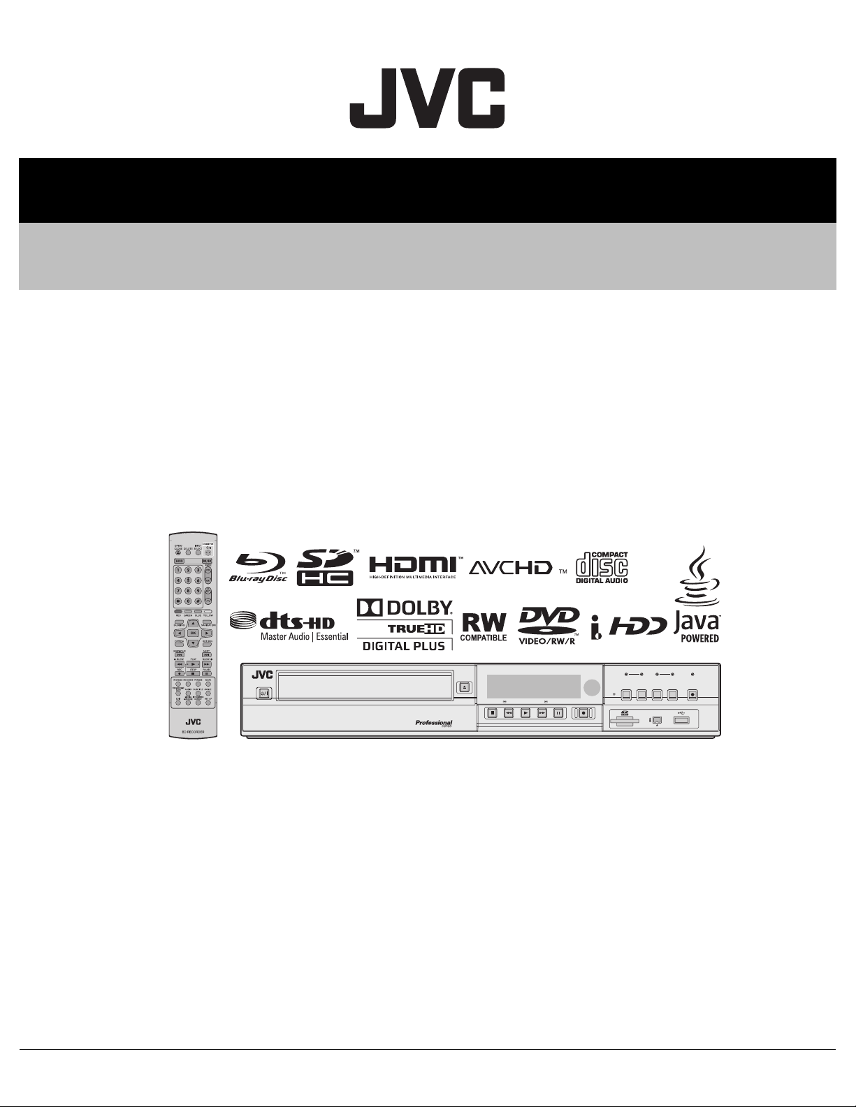
SERVICE MANUAL
BLU-RAY DISC & HDD RECORDER
YD125<Rev.001>20101SERVICE MANUAL
SR-HD1250US, SR-HD1500US,
SR-HD1500KR, SR-HD1250EU,
SR-HD1500EU, SR-HD1500ER,
SR-HD1500AG, SR-HD1500AC
OPEN/
STANDBY/ON
COPYRIGHT © 2010 Victor Company of Japan, Limited
1 PRECAUTION . . . . . . . . . . . . . . . . . . . . . . . . . . . . . . . . . . . . . . . . . . . . . . . . . . . . . . . . . . . . . . . . . . . . . . . . . . . . . . . . . . . . . . . . . . . . . . 1-3
1.1 SAFETY PRECAUTIONS. . . . . . . . . . . . . . . . . . . . . . . . . . . . . . . . . . . . . . . . . . . . . . . . . . . . . . . . . . . . . . . . . . . . . . . . . . . . . . . 1-3
2 SPECIFIC SERVICE INSTRUCTIONS. . . . . . . . . . . . . . . . . . . . . . . . . . . . . . . . . . . . . . . . . . . . . . . . . . . . . . . . . . . . . . . . . . . . . . . . . . . . 1-5
3 DISASSEMBLY . . . . . . . . . . . . . . . . . . . . . . . . . . . . . . . . . . . . . . . . . . . . . . . . . . . . . . . . . . . . . . . . . . . . . . . . . . . . . . . . . . . . . . . . . . . . . 1-5
3.1 Removing the top cover . . . . . . . . . . . . . . . . . . . . . . . . . . . . . . . . . . . . . . . . . . . . . . . . . . . . . . . . . . . . . . . . . . . . . . . . . . . . . . . . 1-5
3.2 Removing the front panel assembly . . . . . . . . . . . . . . . . . . . . . . . . . . . . . . . . . . . . . . . . . . . . . . . . . . . . . . . . . . . . . . . . . . . . . . 1-5
3.3 Removing the HDD. . . . . . . . . . . . . . . . . . . . . . . . . . . . . . . . . . . . . . . . . . . . . . . . . . . . . . . . . . . . . . . . . . . . . . . . . . . . . . . . . . . . 1-5
3.4 Removing the BD drive unit . . . . . . . . . . . . . . . . . . . . . . . . . . . . . . . . . . . . . . . . . . . . . . . . . . . . . . . . . . . . . . . . . . . . . . . . . . . . . 1-5
3.5 Removing the REG/SD board. . . . . . . . . . . . . . . . . . . . . . . . . . . . . . . . . . . . . . . . . . . . . . . . . . . . . . . . . . . . . . . . . . . . . . . . . . . . 1-6
3.6 Removing the BE-DIGITAL board . . . . . . . . . . . . . . . . . . . . . . . . . . . . . . . . . . . . . . . . . . . . . . . . . . . . . . . . . . . . . . . . . . . . . . . . 1-6
3.7 Removing the D-SUB/BNC board and TERMINAL board . . . . . . . . . . . . . . . . . . . . . . . . . . . . . . . . . . . . . . . . . . . . . . . . . . . . . . 1-6
3.8 Removing the DISPLAY board. . . . . . . . . . . . . . . . . . . . . . . . . . . . . . . . . . . . . . . . . . . . . . . . . . . . . . . . . . . . . . . . . . . . . . . . . . . 1-6
4 ADJUSTMENT . . . . . . . . . . . . . . . . . . . . . . . . . . . . . . . . . . . . . . . . . . . . . . . . . . . . . . . . . . . . . . . . . . . . . . . . . . . . . . . . . . . . . . . . . . . . . . 1-7
5 TROUBLE SHOOTING . . . . . . . . . . . . . . . . . . . . . . . . . . . . . . . . . . . . . . . . . . . . . . . . . . . . . . . . . . . . . . . . . . . . . . . . . . . . . . . . . . . . . . . 1-7
5.1 DISPLAYING TEST MODE . . . . . . . . . . . . . . . . . . . . . . . . . . . . . . . . . . . . . . . . . . . . . . . . . . . . . . . . . . . . . . . . . . . . . . . . . . . . . 1-7
5.2 UPDATING MAIN UNIT FIRMWARE . . . . . . . . . . . . . . . . . . . . . . . . . . . . . . . . . . . . . . . . . . . . . . . . . . . . . . . . . . . . . . . . . . . . . 1-7
5.3 UPDATING SYSCON FIRMWARE . . . . . . . . . . . . . . . . . . . . . . . . . . . . . . . . . . . . . . . . . . . . . . . . . . . . . . . . . . . . . . . . . . . . . . . 1-8
5.4 UPDATING DRIVE FIRMWARE . . . . . . . . . . . . . . . . . . . . . . . . . . . . . . . . . . . . . . . . . . . . . . . . . . . . . . . . . . . . . . . . . . . . . . . . . 1-8
5.5 INITIALIZING TO FACTORY SETTING . . . . . . . . . . . . . . . . . . . . . . . . . . . . . . . . . . . . . . . . . . . . . . . . . . . . . . . . . . . . . . . . . . . 1-9
5.6 REPLACING HDD . . . . . . . . . . . . . . . . . . . . . . . . . . . . . . . . . . . . . . . . . . . . . . . . . . . . . . . . . . . . . . . . . . . . . . . . . . . . . . . . . . .1-10
5.7 Exchanging the fitting . . . . . . . . . . . . . . . . . . . . . . . . . . . . . . . . . . . . . . . . . . . . . . . . . . . . . . . . . . . . . . . . . . . . . . . . . . . . . . . . .1-11
5.8 Taking out a disc. . . . . . . . . . . . . . . . . . . . . . . . . . . . . . . . . . . . . . . . . . . . . . . . . . . . . . . . . . . . . . . . . . . . . . . . . . . . . . . . . . . . .1-11
5.9 DISPLAYING MAINTENANCE MODE. . . . . . . . . . . . . . . . . . . . . . . . . . . . . . . . . . . . . . . . . . . . . . . . . . . . . . . . . . . . . . . . . . . .1-12
TABLE OF CONTENTS
CLOSE
STOP REV PLAY PAUSEFWD
REC
REC
INPUT
RESET
MODE
SELECT
COPYRIGHT © 2010 Victor Company of Japan, Limited
ONETOUCH
MIDIA SELECT
HDD
BD/SD
HDV/DVIN
No.YD125<Rev.001>
SDREC CERDDHBD
DUBBING
2010/1
Page 2
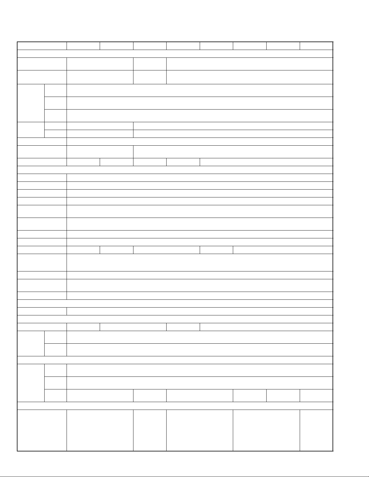
SPECIFICATION
SR-HD1250US SR-HD1500US SR-HD1500KR SR-HD1250EU SR-HD1500EU SR-HD1500ER SR-HD1500AG SR-HD1500AC
GENERAL
Power requirement AC 120 V~, 60 Hz AC 220-240V~,
Power consumption Power on: 34 W
Laser specifi-
cation
For DVD Wavelength: 656 to 663 nm
Temperature Operating 5°C to 35°C (41°F to 95°F) 5°C to 35°C
Operating position Horizontal only
Dimensions (WxHxD) 435 mm x 70 mm x 351 mm
Input/Output
Video input 1.0 Vp-p, 75Ω (BNC)
Video output 1.0 Vp-p, 75Ω (BNC)
Audio input Max 2 Vrms / 10 kΩ (pin jack)
Audio output 2 Vrms 10 kΩ terminated (pin jack)
S-video input Y: 1.0 Vp-p, 75Ω
S-video output Y: 1.0 Vp-p, 75 Ω
Remote Input 3.5 mm Jack
Serial Command - D-SUB 9-PIN - D-SUB 9-PIN -
Component video output Y: 1.0 Vp-p, 75 Ω
Digital audio output Optical : PCM, AAC, Dolby Digital and DTS
HDMI output 19-pin type A
USB terminal USB2.0
SD memory card
HDD Deck
Recording
compression
system
BD/DVD Deck
Recording
compression
system
ACCESSORIES
Provided accessories AC power cord,Audio/Video ca-
Power off: 3.0 W
For CD Wavelength: 779 to 789 nm
Output: 13.1 mW (Operating condition)
Output: 9.02 mW (Operating condition)
For BD Wavelength: 400 to 410 nm
Output: 17.3 mW (Operating condition)
Storage -20°C to 60°C (-4°F to 140°F) -20°C to 60°C
(17-1/10" x 2-6/8" x 13-13/16")
Weight 5.0 kg (11.0 lbs) 5.1 kg (11.2 lbs) 5.1 kg 5.0 kg 5.1 kg
C: 0.286 Vp-p, 75 Ω
C: 0.286 Vp-p, 75 Ω
DV 4-pin for HDV/DV IN
CB/CR, PB/PR: 0.7 Vp-p, 75 Ω
Corresponding to copy protection
(Deep Color, x.v.Color, Ver1.3)
SD, SDHC
250GB 500GB 250GB 500GB
Video MPEG2 (VBR)
H.264/AVC
Audio Dolby Digital (2 ch)
Linear PCM (2ch, XP mode only)
Video MPEG2 (CBR/VBR)
H.264/AVC
Audio Dolby Digital (2 ch)
Linear PCM (2ch, XP mode only)
Region
BD : Region A
code
DVD : #1
ble,BNC male to RCA female
adapter,Infrared remote control
unit,”AA” battery x 2,CD-ROM
60Hz
Power on: 34 W
Power off: 3.0 W
435 mm x 70 mm x 351 mm
BD : Region A
DVD : #3
AC power
cord,Audio/Video cable,BNC
male to RCA female adapter,Infrared remote
control unit,”AA”
battery x 2
AC 220-240V~, 50Hz/60Hz
Power on: 34 W
Standby: 0.5 W
BD : Region B
DVD : #2
AC power cord (for continental Europe, etc),AC power cord (for
U.K.),Audio/Video cable,Infrared
remote control unit,”AA” battery x
2,CD-ROM
BD : Region C
DVD : #5
AC power cord,Audio/Video cable,Infrared remote control
unit,”AA” battery x 2,CD-ROM
BD : Region A
DVD : #3
BD : Region C
DVD : #6
AC power
cord,Audio/Video cable,Infrared remote
control unit,”AA”
battery x 2
1-2 (No.YD125<Rev.001>)
Page 3
SECTION 1
r
PRECAUTION
1.1 SAFETY PRECAUTIONS
Prior to shipment from the factory, JVC products are strictly inspected to conform with the recognized product safety and electrical codes of the countries in which they are to be
sold.However,in order to maintain such compliance, it is equally
important to implement the following precautions when a set is
being serviced.
1.1.1 Precautions during Servicing
(1) Locations requiring special caution are denoted by labels
and inscriptions on the cabinet, chassis and certain parts of
the product.When performing service, be sure to read and
comply with these and other cautionary notices appearing
in the operation and service manuals.
(2) Parts identified by the symbol and shaded ( ) parts
are critical for safety.
Replace only with specified part numbers.
NOTE :
Parts in this category also include those specified to
comply with X-ray emission standards for products
using cathode ray tubes and those specified for
compliance with various regulations regarding spurious radiation emission.
(3) Fuse replacement caution notice.
Caution for continued protection against fire hazard.
Replace only with same type and rated fuse(s) as specified.
(4) Use specified internal wiring. Note especially:
• Wires covered with PVC tubing
• Double insulated wires
• High voltage leads
(5) Use specified insulating materials for hazardous live parts.
Note especially:
• Insulation Tape
• PVC tubing
•Spacers
• Insulation sheets for transistors
• Barrier
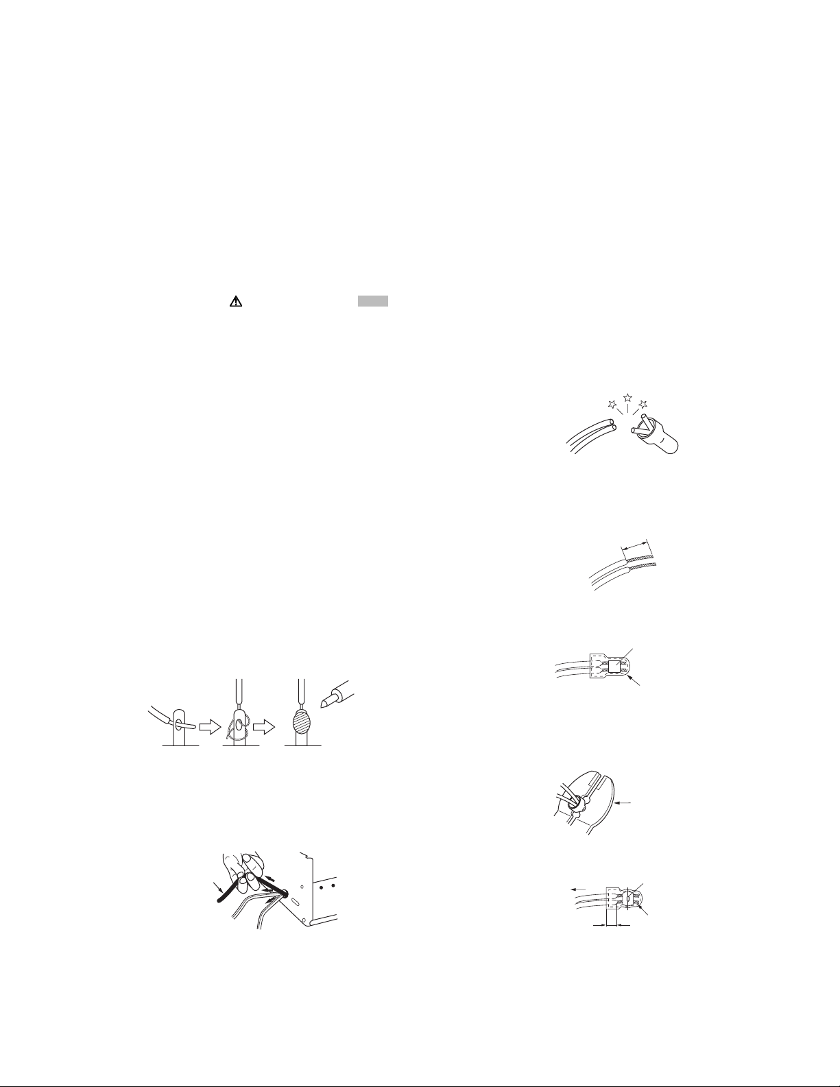
(6) When replacing AC primary side components (transformers,
power cords, noise blocking capacitors, etc.) wrap ends of
wires securely about the terminals before soldering.
Fig.1-1-1
(7) Observe that wires do not contact heat producing parts
(heatsinks, oxide metal film resistors, fusible resistors, etc.)
(8) Check that replaced wires do not contact sharp edged or
pointed parts.
(9) When a power cord has been replaced, check that 10-15
kg of force in any direction will not loosen it.
Power cord
cathode ray tubes and other parts with only the specified
parts. Under no circumstances attempt to modify these circuits.Unauthorized modification can increase the high voltage value and cause X-ray emission from the cathode ray
tube.
(12) Crimp type wire connector In such cases as when replac-
ing the power transformer in sets where the connections
between the power cord and power trans former primary
lead wires are performed using crimp type connectors, if
replacing the connectors is unavoidable, in order to prevent
safety hazards, perform carefully and precisely according
to the following steps.
• Connector part number :E03830-001
• Required tool : Connector crimping tool of the proper
type which will not damage insulated parts.
• Replacement procedure
a) Remove the old connector by cutting the wires at a
point close to the connector.Important : Do not reuse a connector (discard it).
cut close to connector
Fig.1-1-3
b) Strip about 15 mm of the insulation from the ends
of the wires. If the wires are stranded, twist the
strands to avoid frayed conductors.
15 mm
Fig.1-1-4
c) Align the lengths of the wires to be connected. In-
sert the wires fully into the connector.
Metal sleeve
Connector
Fig.1-1-5
d) As shown in Fig.1-1-6, use the crimping tool to
crimp the metal sleeve at the center position. Be
sure to crimp fully to the complete closure of the
tool.
1
.2
2.0
5.5
5
Crimping tool
Fig.1-1-6
e) Check the four points noted in Fig.1-1-7.
Not easily pulled free
Crimped at approx. cente
of metal sleeve
Fig.1-1-2
(10) Also check areas surrounding repaired locations.
(11) Products using cathode ray tubes (CRTs) In regard to such
products, the cathode ray tubes themselves, the high voltage circuits, and related circuits are specified for compliance with recognized codes pertaining to X-ray emission.
Consequently, when servicing these products, replace the
Conductors extended
Wire insulation recessed
more than 4 mm
Fig.1-1-7
(13) Battery replacement caution notice.
CAUTION RISK OF EXPLOSION IF BATTERY IS REPLACED BY AN INCORRECTIVE TYPE.
DISPOSE OF USED BATTERIES ACCORDING TO THE
INSTRUCTIONS.
(No.YD125<Rev.001>)1-3
Page 4
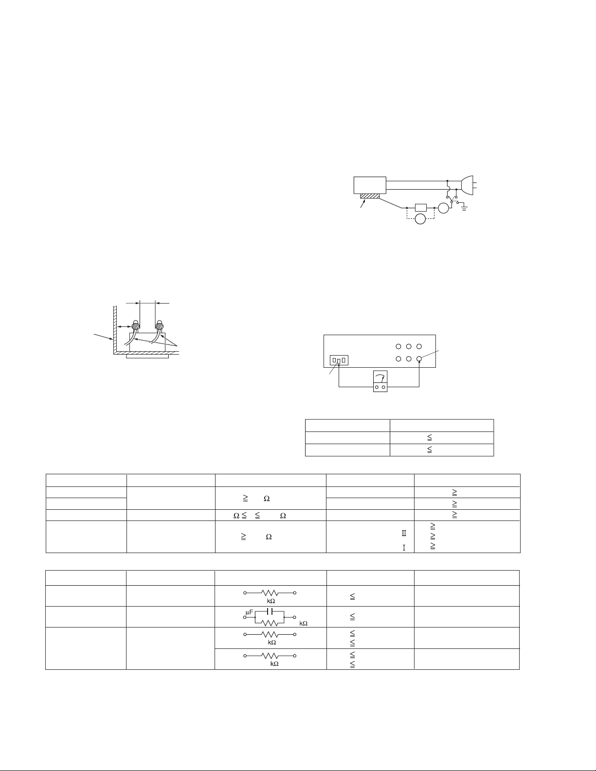
1.1.2 Safety Check after Servicing
Examine the area surrounding the repaired location for damage
or deterioration. Observe that screws, parts and wires have been
returned to original positions, Afterwards, perform the following
tests and confirm the specified values in order to verify compliance with safety standards.
(1) Insulation resistance test
Confirm the specified insulation resistance or greater between power cord plug prongs and externally exposed
parts of the set (RF terminals, antenna terminals, video and
audio input and output terminals, microphone jacks, earphone jacks, etc.).See table 1 below.
(2) Dielectric strength test
Confirm specified dielectric strength or greater between
power cord plug prongs and exposed accessible parts of
the set (RF terminals, antenna terminals, video and audio
input and output terminals, microphone jacks, earphone
jacks, etc.). See Fig.1-1-11 below.
(3) Clearance distance
When replacing primary circuit components, confirm specified clearance distance (d), (d') between soldered terminals, and between terminals and surrounding metallic
parts. See Fig.1-1-11 below.
d
Chassis
d'
Power cord
primary wire
Fig.1-1-8
(4) Leakage current test
Confirm specified or lower leakage current between earth
ground/power cord plug prongs and externally exposed accessible parts (RF terminals, antenna terminals, video and
audio input and output terminals, microphone jacks, earphone jacks, etc.).
Measuring Method : (Power ON) Insert load Z between
earth ground/power cord plug prongs and externally exposed accessible parts. Use an AC voltmeter to measure
across both terminals of load Z. See Fig.1-1-9 and following Fig.1-1-12.
ab
Externally
exposed
accessible part
Z
V
c
A
Fig.1-1-9
(5) Grounding (Class 1 model only)
Confirm specified or lower grounding impedance between
earth pin in AC inlet and externally exposed accessible
parts (Video in, Video out, Audio in, Audio out or Fixing
screw etc.).Measuring Method:
Connect milli ohm meter between earth pin in AC inlet and
exposed accessible parts. See Fig.1-1-10 and grounding
specifications.
AC inlet
Earth pin
Exposed accessible part
MIlli ohm meter
Grounding Specifications
Region
USA & Canada
Europe & Australia
Grounding Impedance (Z
Z 0.1 ohm
Z 0.5 ohm
)
Fig.1-1-10
AC Line Voltage
100 V
100 to 240 V
110 to 130 V
110 to 130 V
200 to 240 V
Region
Japan
USA & Canada
Europe & Australia
Insulation Resistance (R
R 1 M /500 V DC
1 M R 12 M /500 V DC
R 10 M /500 V DC
)
Dielectric Strength
AC 1 kV 1 minute
AC 1.5 kV 1 minute
AC 1 kV 1 minute
AC 3 kV 1 minute
AC 1.5 kV 1 minute
(
Class
(
Class
Clearance Distance (d), (d'
d, d' 3 mm
d, d' 4 mm
d, d' 3.2 mm
d 4 m m
)
d' 8 m m (Power cord
d' 6 m m (Primary wire
)
Fig.1-1-11
AC Line Voltage
100 V
110 to 130 V
110 to 130 V
220 to 240 V
Region
Japan
USA & Canada
Europe & Australia
Load Z
1
0.15
1.5
2
50
Leakage Current (i)
i 1 mA rms
i 0.5 mA rms
i 0.7 mA peak
i 2 mA dc
i 0.7 mA peak
i 2 mA dc
a, b, c
Exposed accessible parts
Exposed accessible parts
Antenna earth terminals
Other terminals
Fig.1-1-12
NOTE :
These tables are unofficial and for reference only. Be sure to confirm the precise values for your particular country and locality.
)
)
)
1-4 (No.YD125<Rev.001>)
Page 5
SECTION 2
Top cover
SPECIFIC SERVICE INSTRUCTIONS
This service manual does not describe SPECIFIC SERVICE INSTRUCTIONS.
SECTION 3
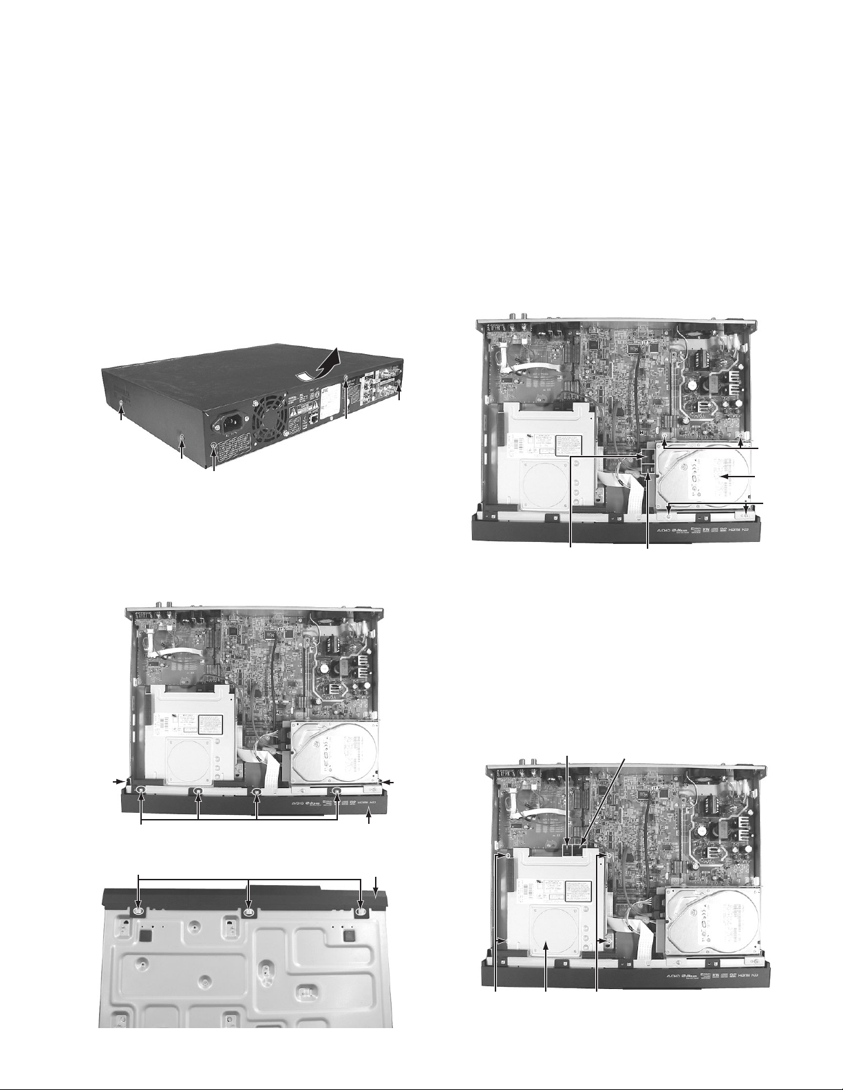
DISASSEMBLY
Before disassembly, be sure to turn OFF the power and unplug
the power cord.
3.1 Removing the top cover (See Figure 1)
(1) Remove the four screws A attaching the top cover from
both sides.
(2) Remove the three screws B attaching the top cover from
the back.
(3) Remove the top cover by sliding it backward.
Top cover
Top cover
B
A x 2
A x 2
B
Fig.1
3.2 Removing the front panel assembly (See Figure 2 and Figure 3)
• Remove the top cover.
(1) Remove the nine tabs on the front panel assembly, and
then remove the front panel assembly.
B
3.3 Removing the HDD (See Figure 4)
• Remove the top cover.
(1) Pull out the SATA cable and the HDD power cable con-
nected to the HDD.
(2) Remove the four screws C attaching the HDD bracket.
(3) HDD is removed from the HDD bracket.
C
HDD
C
HDD Power cable
SATA Cable
Fig.4
Tab
Tab
Tab
Fig.2
Fig.3
Tab
Front panel assembly
Front panel assembly
3.4 Removing the BD drive unit (See Figure 5)
• Remove the top cover.
(1) Pull out the SATA cable and the BD drive power cable con-
nected to the BD drive unit.
(2) Remove the four screws D attaching the drive bracket.
(3) The rear side of the BD drive unit is lifted a little and re-
moved.
(4) Drive bracket is removed from the BD drive unit.
SATA Cable
DD
BD Drive unit
BD Drive power cable
Fig.5
(No.YD125<Rev.001>)1-5
Page 6
3.5 Removing the REG/SD board (See Figure 6)
• Remove the top cover, front panel assembly and HDD.
(1) Pull out the each wire from the connectors CN5306
CN5001
, CN5303, CN801 and CN5305 on the REG/SD
board.
(2) Pull out the socket wires from the connectors CN2102
CN5501
and CN4002 on the BE-DIGITAL board.
(3) Remove the five screws E attaching the REG/SD board,
and then remove the REG/SD board.
BE-DIGITAL
Board CN5501
CN5305
E
CN5303ECN2102
E
CN5001
CN4002
REG/SD
Board
CN5306
CN801
E
Fig.6
3.6 Removing the BE-DIGITAL board (See Figure 7 and
Figure 8)
• Remove the top cover, HDD and BD drive unit.
(1) Pull out the each wire from the connectors CN1501
CN1502
CN2801
, CN4001, CN2102, CN5501, CN4002 and
on the BE-DIGITAL board.
CN1502 CN1501 CN2801
G
3.7 Removing the D-SUB/BNC board and TERMINAL board (See Figure 9 and Figure 10)
,
• Remove the top cover.
(1) Pull out the socket wires from the connectors CN1501
,
CN1502
(2) Pull out the each wire from the connectors CN401
on the BE-DIGITAL board.
and CN403 on the D-SUB/BNC board.
D-SUB/BNC
Board
CN401
TERMINAL
Board
CN402
CN403
CN1501
CN1502
BE-DIGITAL Board
Fig.9
(3) Remove the five screws H and the two nuts attaching the
each terminal from back of the main unit.
H
,
Fig.10
and
, CN402
Nut
H
G
BE-DIGITAL
Board
CN4002
G
CN4001
CN2102 CN5501
Fig.7
(2) Remove the two screws F attaching the terminal from back
of the main unit.
F
Fig.8
(3) Remove the four screws G attaching the BE-DIGITAL
board.
1-6 (No.YD125<Rev.001>)
3.8 Removing the DISPLAY board (See Figure 11)
• Remove the top cover and front panel assembly.
(1) Remove the three screws J attaching the DISPLAY board.
(2) Pull out the each wire from the connectors CN7401
CN7402
J
and CN7403 on the DISPLAY board.
CN7401 CN7402
CN7403
DISPLAY Board
J
Fig.11
,
J
Page 7
SECTION 4
ADJUSTMENT
This service manual does not describe ADJUSTMENT.
SECTION 5
TROUBLE SHOOTING
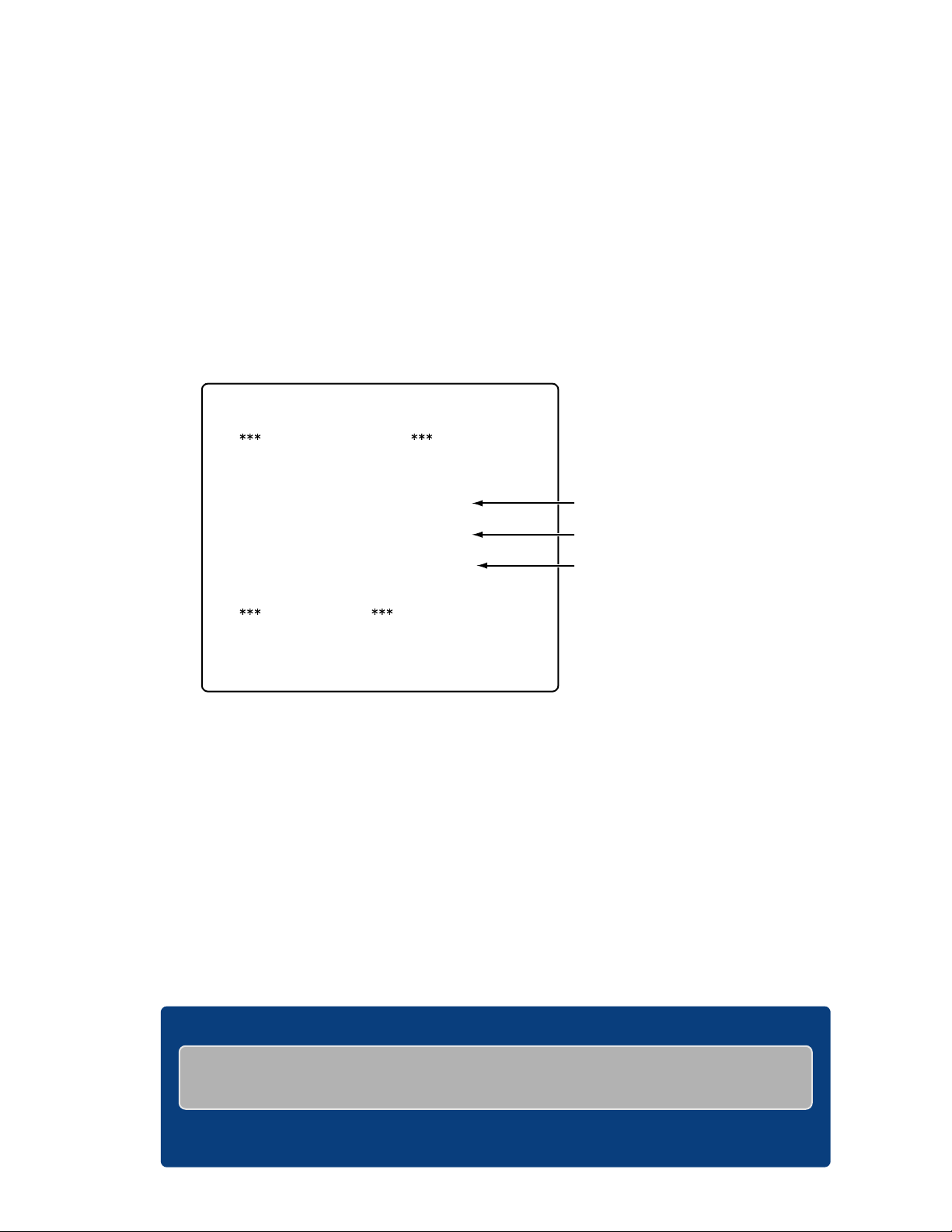
5.1 DISPLAYING TEST MODE
TEST MODE contains the firmware version information of the main unit and the drive unit.
(1) While pressing the [PLAY] button and the [STOP] button, plug in the power cord.
(2) “TEST” flashes in the display window on the main unit. In about one minute, the TEST MODE menu is displayed on the TV
screen.
TEST MODE
MODEL INFORMATION
MODEL NAME SR-HDxxxx
DESTINATION xx
TOTAL Ver. xxxx
APPLI Ver. xxxx
BOOT Ver. xxxx
DRIVE Ver. x.xx
SYSCON ROM CODE xxx
SYSCON Ver. xx.xx
REGION(DRIVE/DVD/BD/NUM) x/x/x/x
Firmware version of main unit.
Firmware version of drive unit.
Firmware version of system controller.
CHANGE MODE
VIDEO ADJ [VIDEO ADJ] KEY
TEST MODE OFF [POWER] KEY
(3) To exit the TEST MODE menu, press the POWER button on the main unit.
5.2 UPDATING MAIN UNIT FIRMWARE
• The firmware update disc supports CD-R.
• When firmware update is needed, information will be available from SMIS in JS-NET.
5.2.1 Creating an Update Disc
Refer to JS-NET for details of creating an update disc.
(1) Download the update file (#########.iso) from SMIS in JS-NET.
(2) Write the update file onto a CD-R in image writing using writing software.
• Be sure to write in “Disc-at-Once”.
• Refer to the instructions of the writing software for image writing settings.
5.2.2 Update Procedures
(1) Place an update disc on the tray and close the tray.
During disc reading, a warning “THERE IS NO PLAYABLE MEDIA INSERTED” is displayed once or twice. Ignore the warning.
CONFIRM
THERE IS NO PLAYABLE MEDIA INSERTED
(No.YD125<Rev.001>)1-7
Page 8

(2) When disc reading is completed, the following displays are repeated in the display window on the main unit. “APPLI FIRM” →
“START [PLAY]” → “CANCEL [FF]”. Press the [PLAY] button on the main unit to start update.
When update starts, the followings are displayed in the display window on the main unit.
“L 10” → “L 20” → *** → “L 100” →
“C 10” → *** → *** → “C 100” → “W 10” → *** → “W 100”
“R 10” → *** → “R 100” → “V 00” → “COMPLETED”
(3) After update disc reading, the tray is ejected. Remove the update disc.
(4) Press the POWER button on the main unit.
The main unit power is turned on, and then turned off. The update is completed.
(5) In the TEST MODE menu, check whether the main unit firmware is correctly updated.
5.3 UPDATING SYSCON FIRMWARE
• The SYSCON firmware update disc supports CD-R.
• When SYSCON firmware update is needed, information will be available from SMIS in JS-NET.
5.3.1 Creating an Update Disc
Refer to JS-NET for details of creating an update disc.
(1) Download the update file (#########.iso) from SMIS in JS-NET.
(2) Write the update file onto a CD-R in image writing using writing software.
• Be sure to write in “Disc-at-Once”.
• Refer to the instructions of the writing software for image writing settings.
5.3.2 Update Procedures
(1) Place an update disc on the tray and close the tray.
During disc reading, a warning “THERE IS NO PLAYABLE MEDIA INSERTED” is displayed once or twice. Ignore the warning.
CONFIRM
THERE IS NO PLAYABLE MEDIA INSERTED
(2) When disc reading is completed, the following displays are repeated in the display window on the main unit. “SYSCON FIRM”
→ “START [PLAY]” → “CANCEL [FF]”.
Press the [PLAY] button on the main unit to start update.
When update starts, “PLEASE WAIT” is displayed in the display window on the main unit.
(3) After update disc reading, the following is displayed on the TV screen and the tray is ejected. Remove the update disc.
SYSCON FIRM UPDATE COMPLETE!!
Take out the disc and turn off power.
(4) Press the POWER button on the main unit.
The main unit power is turned off and update is completed.
(5) In the TEST MODE menu, check whether the SYSCON firmware is correctly updated.
5.4 UPDATING DRIVE FIRMWARE
• The drive firmware update disc supports CD-R.
• When drive firmware update is needed, information will be available from SMIS in JS-NET.
5.4.1 Creating an Update Disc
Refer to JS-NET for details of creating an update disc.
(1) Download the update file (#########.iso) from SMIS in JS-NET.
(2) Write the update file onto a CD-R in image writing using writing software.
• Be sure to write in “Disc-at-Once”.
• Refer to the instructions of the writing software for image writing settings.
1-8 (No.YD125<Rev.001>)
Page 9
5.4.2 Update Procedures
(1) Place an update disc on the tray and close the tray.
During disc reading, a warning “THERE IS NO PLAYABLE MEDIA INSERTED” is displayed once or twice. Ignore the warning.
CONFIRM
THERE IS NO PLAYABLE MEDIA INSERTED
(2) When disc reading is completed, the following displays are repeated in the display window on the main unit. “DRIVE FIRM” →
“START [PLAY]” → “CANCEL [FF]”. Press the [PLAY] button on the main unit to start update.
When update starts, “PLEASE WAIT” is displayed in the display window on the main unit.
(3) After update disc reading, the following is displayed on the TV screen and the tray is ejected. Remove the update disc.
DRIVE FIRM UPDATE COMPLETE!!
Take out the disc and turn off power.
(4) Press the POWER button on the main unit.
The main unit power is turned off and update is completed.
(5) In the TEST MODE menu, check whether the drive firmware is correctly updated.
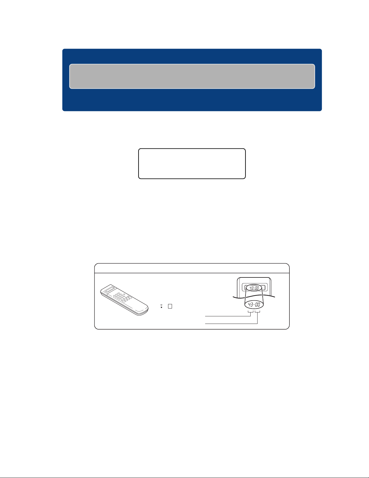
5.5 INITIALIZING TO FACTORY SETTING
Before starting initialization, always obtain permission from the user as initialization returns all the setting information to the initial settings, and the user content and the related information will all be erased.
(1) Set the main unit to the TEST MODE.
(2) Transmit “##
·6F” using the JIG remote control. (Set “##” as follows according to the main unit remote control code. Code setting
1: Set “##” to “43”. Code setting 2: Set “##” to “53”. Code setting 3: Set “##” to “6F”. Code setting 4: Set ““##” to “7F”).
JIG remote control
JIG remote control
(Part number : PTU94023B)
[Data transmission]
Set the data code,
and then press the
" " button.
3
Custom code
43:A(1) Code
53:B(2) Code
6F:C(3) Code
7F:D(4) Code
Data code
Initial
mode
“COLD SET” flashes in the display window on the main unit. The initialization completes in about 30 seconds and the power is
turned off.
(No.YD125<Rev.001>)1-9
Page 10

5.6 REPLACING HDD
After HDD replacement, initialize the HDD following the procedure below. (Without HDD initialization, HDD recording is impossible.)
(1) Turn on the power of the main unit.
(2) Press the [MEDIA MANAGE] button on the supplied remote control to display the MEDIA MANAGE menu on the TV screen.
MEDIA MANAGE
BD/DVD
FORMAT
FINALIZE
RENAME DISC
SD CARD
FORMAT
BD-VIDEO DATA ERASE
HDD
FORMAT
(3) Use the [Down] button on the remote control to move the highlight to HDD FORMAT, and then press the [OK] button on the
remote control.
MEDIA MANAGE
BD/DVD
FORMAT
FINALIZE
RENAME DISC
SD CARD
FORMAT
BD-VIDEO DATA ERASE
HDD
FORMAT
(4) The confirmation to execute HDD FORMAT is displayed on the TV screen. Move the highlight to “YES” using the [Left] button,
and then press the [OK] button on the remote control.
CONFIRM
THE HDD WILL BE FORMATTED
ALL RECORDED TITLES WILL BE ERASED
DO YOU WANT TO FORMAT?
YES NO
1-10 (No.YD125<Rev.001>)
Page 11
(5) Once again, the confirmation to execute HDD FORMAT is displayed. Perform the same procedure as step (4).
HDD FORMAT is executed.
CONFIRM
THE HDD WILL BE FORMATTED
ALL RECORDED TITLES WILL BE ERASED
DO YOU WANT TO FORMAT?
FORMAT DO NOT FORMAT
(6) When the HDD FORMAT is completed, the confirmation for the completion of HDD FORMAT is displayed on the TV screen.
Press the [OK] button on the remote control.
CONFIRM
THE HDD HAS BEEN FORMATTED
OK
5.7 Exchanging the fitting
As the fitting that comes with the service drive unit cannot be used, make sure to attach a service fitting when the drive unit is exchanged.
The fitting that is removed from the old drive unit can be attached to the new drive unit.
The fitting can be removed by pulling upwards while opening out the lower part of the fitting outwards.
Tray
Fitting
5.8 Taking out a disc
(1) Remove the top cover.
(2) Open the front door of the main unit manually.
(3) Insert a fine wire (e.g. a straightened paper clip) into the hole in the right side part of the drive unit.
(4) As the tray ejects a little, pull out the tray manually.
Tray
Front door
Hole
(No.YD125<Rev.001>)1-11
Page 12
5.9 DISPLAYING MAINTENANCE MODE
MAINTENANCE MODE contains information about the HDD and the drive unit.
(1) Displaying MAINTENANCE Top Menu
a) Turn off the power of the main unit.
b) Press the [REC] button and the [RESET] switch on the main unit at the same time.
c) “SERVICE” is displayed in the display window on the main unit. In about 30 seconds, the MAINTENANCE Top Menu is
displayed on the TV screen.
MAINTENANCE MODE
Press key
[1] key : Product Information
[2] key : Temperature Information
[3] key : Laser Diode Information
[4] key : HDD SMART Information
[5] key : REBOOT COUNT Information
[Power off] : Exit
d) To exit MAINTENANCE MODE, press the POWER button on the main unit.
(2) Displaying Product Information
Product Information contains the firmware version information of the main unit and the drive unit.
a) While the MAINTENANCE Top Menu is displayed, press the [1] button on the supplied remote control to display Product
Information on the TV screen.
MAINTENANCE MODE > Product Information
[Return] : Top Menu, [Power off] : Exit
<<<Reviesion>>>
Middle Ware Version : xxxx
NAND Version : xxxx
Application Version : xxxx
NOR Version : xxxx
Drive Version
ID : xxxx
Farm Version : xxxx
<<<Information>>>
Vendor Name : JVC
Model Name : SR-HDxxxx
1394 Serial Num : xxxxxxxxx
b) To go back to the MAINTENANCE Top Menu, press the [Return] button on the remote control.
To exit MAINTENANCE MODE, press the POWER button on the main unit.
1-12 (No.YD125<Rev.001>)
Page 13

(3) Displaying Temperature Information
Temperature Information records the temperatures around the drive unit measured in the past.
While the power is on, the temperature is recorded every 20 minutes. The temperature is also recorded if it changes drastically.
(Maximum recording: 2000 measurements)
Recording date/time and the elapsed time after the last recording are also recorded.
a) While the MAINTENANCE Top Menu is displayed, press the [2] button on the remote control to display Temperature In-
formation on the TV screen.
MAINTENANCE MODE > Temperature Information [Total Data]13 [Page]1/2
[Left] : Prev, [Right] : Next, [Return] : Top Menu, [Power off] : Exit
[no]xxxx [date]xxxx/ xx/ xx [time]xx:xx:xx [lenght]xxxx [type]xx
[no]xxxx [date]xxxx/ xx/ xx [time]xx:xx:xx [lenght]xxxx [type]xx
[no]xxxx [date]xxxx/ xx/ xx [time]xx:xx:xx [lenght]xxxx [type]xx
[no]xxxx [date]xxxx/ xx/ xx [time]xx:xx:xx [lenght]xxxx [type]xx
[no]xxxx [date]xxxx/ xx/ xx [time]xx:xx:xx [lenght]xxxx [type]xx
[no]xxxx [date]xxxx/ xx/ xx [time]xx:xx:xx [lenght]xxxx [type]xx
b) To display old records, press the [Right] button on the remote control.
To display new records, press the [Left] button on the remote control.
c) To go back to the MAINTENANCE Top Menu, press the [Return] button on the remote control.
To exit MAINTENANCE MODE, press the POWER button on the main unit.
(4) Displaying Laser Diode Information
Laser Diode Information records the past rates of diode current change in the drive unit.
The rate of diode current change in the drive unit at the time of power off is recorded.
(Maximum recording: 2000 measurements)
Recording date/time is recorded at the same time.
a) While the MAINTENANCE Top Menu is displayed, press the [3] button on the remote control to display Laser Diode Infor-
mation on the TV screen.
MAINTENANCE MODE > Laser Diode Information [Total Data]11 [Page]1/2
[Left] : Prev, [Right] : Next, [Return] : Top Menu, [Power off] : Exit
[No]xxxx [Date]xxxx/ xx/ xx [Time]xx:xx:xx [DVD]xxx [BD]xxx [CD]xxx
[No]xxxx [Date]xxxx/ xx/ xx [Time]xx:xx:xx [DVD]xxx [BD]xxx [CD]xxx
[No]xxxx [Date]xxxx/ xx/ xx [Time]xx:xx:xx [DVD]xxx [BD]xxx [CD]xxx
[No]xxxx [Date]xxxx/ xx/ xx [Time]xx:xx:xx [DVD]xxx [BD]xxx [CD]xxx
[No]xxxx [Date]xxxx/ xx/ xx [Time]xx:xx:xx [DVD]xxx [BD]xxx [CD]xxx
[No]xxxx [Date]xxxx/ xx/ xx [Time]xx:xx:xx [DVD]xxx [BD]xxx [CD]xxx
b) To display old records, press the [Right] button on the remote control.
To display new records, press the [Left] button on the remote control.
c) To go back to the MAINTENANCE Top Menu, press the [Return] button on the remote control.
To exit MAINTENANCE MODE, press the POWER button on the main unit.
(No.YD125<Rev.001>)1-13
Page 14

(5) Displaying HDD SMART Information
HDD SMART Information displays the total HDD operating time and SMART information obtained when starting MAINTENANCE
MODE.
a) While the MAINTENANCE Top Menu is displayed, press the [4] button on the remote control to display HDD SMART In-
formation on the TV screen.
First page
MAINTENANCE MODE > HDD SMART Information [Page]1/2
[Left] : Prev, [Right] : Next, [Return] : Top Menu, [Power off] : Exit
HDD total time : xxx hour
-----------------------------------------------------------------------------------Raw Read Error Rate xx xx xx xx xx xx xx xx xx xx xx xx
Throughput Performance xx xx xx xx xx xx xx xx xx xx xx xx
Spin Up Time xx xx xx xx xx xx xx xx xx xx xx xx
Start/Stop Count xx xx xx xx xx xx xx xx xx xx xx xx
Real located Sectors Count xx xx xx xx xx xx xx xx xx xx xx xx
Seek Error Rate xx xx xx xx xx xx xx xx xx xx xx xx
Seek Time Performance xx xx xx xx xx xx xx xx xx xx xx xx
Power-On Hours xx xx xx xx xx xx xx xx xx xx xx xx
Spin Retry Count xx xx xx xx xx xx xx xx xx xx xx xx
Device Power Cycle Count xx xx xx xx xx xx xx xx xx xx xx xx
Second page
MAINTENANCE MODE > HDD SMART Information [Page]2/2
[Left] : Prev, [Right] : Next, [Return] : Top Menu, [Power off] : Exit
Load/Unload Cycle Count xx xx xx xx xx xx xx xx xx xx xx xx
Temperature xx xx xx xx xx xx xx xx xx xx xx xx
Real location Event Count xx xx xx xx xx xx xx xx xx xx xx xx
Current Pending Sector Count xx xx xx xx xx xx xx xx xx xx xx xx
Off-Line Scan Uncorrectable Sector Count xx xx xx xx xx xx xx xx xx xx xx xx
UltraDMA CRC Error Count xx xx xx xx xx xx xx xx xx xx xx xx
b) To go to the next page, press the [Right] button on the remote control.
To go back to the previous page, press the [Left] button on the remote control.
c) To go back to the MAINTENANCE Top Menu, press the [Return] button on the remote control.
To exit MAINTENANCE MODE, press the POWER button on the main unit.
1-14 (No.YD125<Rev.001>)
Page 15

(6) REBOOT COUNT Information
REBOOT COUNT Information displays date/time of reboot occurred due to any reason.
a) While the MAINTENANCE Top Menu is displayed, press the [5] button on the remote control to display REBOOT COUNT
Information on the TV screen.
(Maximum recording: 100 occurrences)
MAINTENANCE MODE > REBOOT COUNT Information [TotalData]xxxx [Page]xxx/xxx
[Left] : Prev, [Right] : Next, [Return] : Top Menu, [Power off] : Exit
[No]xxxx [Date]xxxx/ xx/ xx [Time]xx:xx:xx
[No]xxxx [Date]xxxx/ xx/ xx [Time]xx:xx:xx
[No]xxxx [Date]xxxx/ xx/ xx [Time]xx:xx:xx
b) To display old records, press the [Right] button on the remote control.
To display new records, press the [Left] button on the remote control.
c) To go back to the MAINTENANCE Top Menu, press the [Return] button on the remote control.
To exit MAINTENANCE MODE, press the POWER button on the main unit.
(No.YD125<Rev.001>)1-15
Page 16

Victor Company of Japan, Limited
Business Solution Division
(No.YD125<Rev.001>)
Printed in Japan
VSE
Page 17

PARTS LIST
[SR-HD1250US, SR-HD1500US, SR-HD1500KR,
SR-HD1250EU, SR-HD1500EU, SR-HD1500ER,
SR-HD1500AG, SR-HD1500AC]
* SAFETY PRECAUTION
Parts identified by the symbol are critical for safety. Replace only with
specified part numbers.
* BEWARE OF BOGUS PARTS
Parts that do not meet specifications may cause trouble in regard to safety and
performance. We recommend that genuine JVC parts be used.
* (x_) in a description column shows the number of the used part.
- Contents -
Exploded view of general assembly and parts list
Electrical parts list
Packing materials and accessories parts list
3-2
3-4
3-8
(No.YD125<Rev.001>)3-1
Page 18

Exploded view of general assembly and parts list
32
6
13
11
4
OPE board assembly<07>
1B
REG/SD
board assembly<01>
29
a
d
25
12
13
5
6
m
WR11
m
1A
3
2
30
28
d
WR4
WR3
c
6
OPT DIGI
board assembly<08>
WR1
WR8
h
6
Terminal
board assembly<06>
6
p
10
31
h
j
Display
6
board assembly<05>
1
WR2
a
3
Block No.M1MM
3
36
6
6
j
WR9
e
e
6
b
WR5
3
27
6
f
D-SUB/BNC
board assembly<09>
6
33
n
WR12
35
19
19
6
f
g
WR7
Green/Yellow
16
13
20
23
19
22
Brown
Blue
18
WR6
26
17
19
WR10
10
k
n
34
k
6
p
WR13
9
21
7
g
15
8
24
c
b
6
15
8
17
16
14
3-2(No.YD125<Rev.001>)
Page 19

General assembly
Block No. [M][1][M][M]
Symbol No. Part No. Part Name Description Local
1 LS10265-005A FRONT PANEL ASSY 1250EU
1 LS10265-002B FRONT PANEL ASSY 1250US
1 LS10265-006A FRONT PANEL ASSY 1500AC
1 LS10265-004A FRONT PANEL ASSY 1500AG,1500ER,1500EU
1 LS10265-001B FRONT PANEL ASSY 1500KR,1500US
1A LS20429-001B DOOR(DVD)
1B LS42002-001A TORSION SPRING
2 LS10267-001B TOP COVER
3 LS31279-003A SPECIAL SCREW (x7)
4 LS20430-001A FITTING(P)
5 LS10268-001A BOTTOM CHASSIS
6 LS31279-001A SPECIAL SCREW (x25)
7 QYSPSP4008ZA SCREW M4 x 8mm
8 LS31280-002A FOOT (x4)
9 LS42015-001A COOLING SHEET
10 QZW0092-005 WIRE CLAMP (x3)
11 LS31281-001A BRACKET(DRIVE)(L)
12 LS31282-001A BRACKET(DRIVE)(R)
13 QYSDST3006NA TAP SCREW M3 x 6mm(x5)
14 LS20431-001A BRACKET(HDD)
15 LS42004-001A DAMPER (x4)
16 LS42005-001A SPRING (x2)
17 LS42006-001A SPECIAL SCREW (x4)
18 LS20432-006A REAR PANEL 1250EU
18 LS20432-002B REAR PANEL 1250US
18 LS20432-007A REAR PANEL 1500AC
18 LS20432-004B REAR PANEL 1500AG,1500KR
18 LS20432-005A REAR PANEL 1500ER,1500EU
18 LS20432-001B REAR PANEL 1500US
19 QYSDSF3008NA TAP SCREW M3 x 8mm(x9)
20 QYSPSPH4025NA SCREW M4 x 25mm(x2)
21 QYNFS4000NA NUT M4(x2)
22 QAR0505-001 FAN MOTOR
23 QNC0116-001 AC INLET
24 QAL1223-001 HDD 1250EU,1250US
24 QAL1222-001 HDD
25 QAL1229-001-1 DRIVE UNIT 1250US,1500US
25 QAL1229-001-2 DRIVE UNIT 1500EU,1250EU
25 QAL1229-001-3 DRIVE UNIT 1500AG,1500KR
25 QAL1229-001-5 DRIVE UNIT 1500ER
25 QAL1229-001-6 DRIVE UNIT 1500AC
26 QZW0001-001 WIRE CLAMP
27 QMF51V2-2R0-S FUSE 2A AC250V
28 QQR0490-001 NOISE FILTER
29 LS31422-001A-H GASKET (x2)
30 LS31422-002A-H GASKET
31 LS31422-003A-H GASKET
32 LS31422-004A-H GASKET
33 QNB0036-001 CONN ACCESSORY (x2)
34 LSU06907-01AEU2 BE DIGI BOARD ASSY 1250EU
34 LSU06907-01AUS2 BE DIGI BOARD ASSY 1250US
34 LSU06907-01AAC5 BE DIGI BOARD ASSY 1500AC
34 LSU06907-01AAG5 BE DIGI BOARD ASSY 1500AG
34 LSU06907-01AER5 BE DIGI BOARD ASSY 1500ER
34 LSU06907-01AEU5 BE DIGI BOARD ASSY 1500EU
34 LSU06907-01AKR5 BE DIGI BOARD ASSY 1500KR
34 LSU06907-01AUS5 BE DIGI BOARD ASSY 1500US
35 QYWAS326505NA WASHER 6.5mm/3.2mm x 0.5mm 1250EU
36 QZW0384-001 WIRE CLAMP
WR 1 QAM1049-002 SATA CABLE BE DIGI J4801-DRIVE UNIT
WR 2 QAM1049-002 SATA CABLE BE DIGI PWB J4901-HDD
WR 3 WJJ1064-001A-E WIRE REG/SD CN5304-HDD
WR 4 WJJ1064-002A-E WIRE REG/SD CN5305-DRIVE UNIT
WR 5 WJW0127-001A-E E-TWISTED ASSY DIGI CN2801-REG/SD CN801
WR 6 WJM0522-001A-E WIRE AC INLET-REG/SD CN5001
WR 7 WJV0146-001A-E E-PRIMARY WIRE AC INLET-BOTTOM CHASSIS
WR 8 QUR310-2122AC-E FFC WIRE BE DIGI CN4001-DISPLAY CN7401
WR 9 QUQ112-0724CG-E FFC WIRE DISPLAY CN7402-REG/SD CN5306
WR10 QUQ112-0516CG-E FFC WIRE D-SUB/BNC CN401-TERMINAL CN203
WR11 QJJ009-022612-E WIRE DISPLAY CN7403-OPE CN7404
WR12 QJJ009-021512-E WIRE D-SUB/BNC CN402-TERMINAL CN204
WR13 QJJ009-031313-E WIRE D-SUB/BNC CN403-TERMINAL CN205
1500AC,1500AG,1500ER,1500EU,1500KR,1500US
1500AC,1500AG,1500ER,1500EU,1500KR,1500US
1250EU,1500AC,1500AG,1500ER,1500EU,1500KR
1250US,1500AC,1500AG,1500ER,1500EU,1500KR,1500US
(No.YD125<Rev.001>)3-3
Page 20

Electrical parts list
REG/SD board
Symbol No.
Part No. Part Name Description Local
Block No. [0][1]
Symbol No.
PW1 LSA10109-01B1H
PW1 LSA10109-01A1H
IC5101 FSQ0565R IC(HYBRID)
IC5301 MM1431AT-T IC
IC5303 AOZ1016AI-X IC
IC5305
IC5306 AOZ1016AI-X IC
Q5303 2SC2412K/QR/-X TRANSISTOR
Q5304 2SB1184/QR/-X POW TRANSISTOR
Q5305 2SA1037AK/R/-X TRANSISTOR
Q5307 2SA1363/EF/-X TRANSISTOR
Q5308 2SC3928A/QR/-X TRANSISTOR
Q5309 ISA1530AC1/QR/X TRANSISTOR
Q5310 ISA1530AC1/QR/X TRANSISTOR
Q5311 RT1N144C-X DIGI TRANSISTOR
Q5312 2SC3928A/QR/-X TRANSISTOR
Q5313 ISA1530AC1/QR/X TRANSISTOR
Q5314 RT1N241C-X DIGI TRANSISTOR
Q5315 ISA1530AC1/QR/X TRANSISTOR
Q5316 2SC3928A/QR/-X TRANSISTOR
Q5317 ISA1530AC1/QR/X TRANSISTOR
Q5318 2SB1184/QR/-X POW TRANSISTOR
Q5319 2SA1947/E/-X TRANSISTOR
Q5320 2SC3928A/QR/-X TRANSISTOR
Q5321 ISA1530AC1/QR/X TRANSISTOR
Q5323 2SC3928A/QR/-X TRANSISTOR
Q5325 ISA1530AC1/QR/X TRANSISTOR
D5001 D3SBA60 BRIDGE DIODE
D5101 SARS01-T FR DIODE
D5102 FR104S-T5 FR DIODE
D5201 FMN-G12S SI DIODE
D5203 FMB-24M SB DIODE
D5205 FR104S-T5 FR DIODE
D5304 RB400VA-50-X SB DIODE
D5306 MA2SD31-X SB DIODE
D5310 MA111-X SI DIODE
D5311 RB160M-30-X SB DIODE
D5312 MA2SD31-X SB DIODE
D5314 SR24-X SB DIODE
D5315 MA2SD31-X SB DIODE
D5318 MA2SD31-X SB DIODE
PC5101 PC123Y22FZ PHOTO COUPLER
C811 NCB31CK-104X C CAPACITOR 0.1uF 16V K
C812 NCB20JK-106X C CAPACITOR 10uF 6.3V K
C813 NCB20JK-106X C CAPACITOR 10uF 6.3V K
C814 NCB31HK-103X C CAPACITOR 0.01uF 50V K
C815 NCB31HK-103X C CAPACITOR 0.01uF 50V K
C5001 QFZ9073-104 MM CAPACITOR 0.1uF AC250V M
C5002 QFZ9067-223 MM CAPACITOR 0.022uF
C5003 QETM2GM-107 E CAPACITOR 100uF 400V M
C5004 QCZ9079-101 C CAPACITOR 100pF AC250V K
C5101 QCZ0213-472 C CAPACITOR 4700pF 1kV K
C5102 NCB31HK-333X C CAPACITOR 0.033uF 50V K
C5103 NCB31HK-104X C CAPACITOR 0.1uF 50V K
C5104 QTMT1HM-476 E CAPACITOR 47uF 50V M
C5105 NCB31HK-331X C CAPACITOR 330pF 50V K
C5107 NCB31HK-104X C CAPACITOR 0.1uF 50V K
C5201 QTM91CM-128 E CAPACITOR 1200uF 16V M
C5202 QTM91AM-338 E CAPACITOR 3300uF 10V M
C5204 QTM91CM-477 E CAPACITOR 470uF 16V M
C5301 QETN1CM-107Z E CAPACITOR 100uF 16V M
C5304 QETN1CM-107Z E CAPACITOR 100uF 16V M
C5306 NCB31CK-104X C CAPACITOR 0.1uF 16V K
C5307 NCB31HK-103X C CAPACITOR 0.01uF 50V K
C5308 QETN1HM-226Z E CAPACITOR 22uF 50V M
C5309 NCB31HK-103X C CAPACITOR 0.01uF 50V K
C5311 NCB41CK-226X C CAPACITOR 22uF 16V K
Part No. Part Name Description Local
PQ6CU12X2APQ-X
REG/SD BOARD ASSY
REG/SD BOARD ASSY
IC
1250EU,1500AC,1500AG,1500ER,1500EU
1250US,1500KR,1500US
C5312 NCB41AK-226X C CAPACITOR 22uF 10V K
C5313 NCB41AK-226X C CAPACITOR 22uF 10V K
C5314 NCB31HK-102X C CAPACITOR 1000pF 50V K
C5315 NCB31CK-103X C CAPACITOR 0.01uF 16V K
C5316 NCB31CK-103X C CAPACITOR 0.01uF 16V K
C5326 NCB30JK-225X C CAPACITOR 2.2uF 6.3V K
C5327 NCB11HK-474X C CAPACITOR 0.47uF 50V K
C5328 NCB11HK-474X C CAPACITOR 0.47uF 50V K
C5329 NCB41AK-226X C CAPACITOR 22uF 10V K
C5330 NCB31CK-103X C CAPACITOR 0.01uF 16V K
C5331 NCB31HK-102X C CAPACITOR 1000pF 50V K
C5332 NCB41AK-226X C CAPACITOR 22uF 10V K
C5333 NCB41AK-226X C CAPACITOR 22uF 10V K
C5334 QETN1CM-107Z E CAPACITOR 100uF 16V M
C5335 QETN0JM-478Z E CAPACITOR 4700uF 6.3V M
C5336 QETN1HM-106Z E CAPACITOR 10uF 50V M
C5337 QCZ9079-102 C CAPACITOR 1000pF AC250V M
C5339 NCB31HK-333X C CAPACITOR 0.033uF 50V K
C5342 QETN1HM-106Z E CAPACITOR 10uF 50V M
C5343 NCB31AK-154X C CAPACITOR 0.15uF 10V K
C5344 NCB31HK-333X C CAPACITOR 0.033uF 50V K
C5348 QETN1CM-477Z E CAPACITOR 470uF 16V M
C5350 NCB21CK-105X C CAPACITOR 1uF 16V K
C5353 NCB31CK-104X C CAPACITOR 0.1uF 16V K
C5354 NCB31CK-104X C CAPACITOR 0.1uF 16V K
C5355 NCB31CK-103X C CAPACITOR 0.01uF 16V K
C5356 NCB31CK-103X C CAPACITOR 0.01uF 16V K
C5357 QETN1CM-107Z E CAPACITOR 100uF 16V M
C5358 QETN1CM-107Z E CAPACITOR 100uF 16V M
C5359 QETN1CM-107Z E CAPACITOR 100uF 16V M
Ω
R811 NRSA63J-473X MG RESISTOR 47k
R812 NRSA63J-473X MG RESISTOR 47k
R813 NRSA63J-123X MG RESISTOR 12k
R814 NRSA63J-220X MG RESISTOR 22
R815 NRSA63J-220X MG RESISTOR 22
R816 NRSA63J-220X MG RESISTOR 22
R817 NRSA63J-220X MG RESISTOR 22
R818 NRSA63J-0R0X MG RESISTOR 0
R819 NRSA63J-220X MG RESISTOR 22
R820 NRSA63J-123X MG RESISTOR 12k
R821 NRSA63J-123X MG RESISTOR 12k
R822 NRSA63J-123X MG RESISTOR 12k
R823 NRSA63J-123X MG RESISTOR 12k
R5101 QRL01DJ-683X OMF RESISTOR 68k
R5102 QRZ9005-470X FUSI RESISTOR 47
R5103 QRL01DJ-753X OMF RESISTOR 75kΩ 1W J
R5105 QRJ143J-223X
R5106 QRJ143J-333X
R5107 QRZ9051-4R7X FUSI RESISTOR 4.7
R5109 QRE141J-0R0Y C RESISTOR 0Ω 1/4W J
R5301 NRSA63J-0R0X MG RESISTOR 0
R5302 NRSA63J-683X MG RESISTOR 68k
R5303 NRSA63J-133X MG RESISTOR 13k
R5304 NRSA63J-223X MG RESISTOR 22k
R5309 NRSA63J-102X MG RESISTOR 1k
R5311 NRSA63D-103X MG RESISTOR 10k
R5312 NRSA63D-304X MG RESISTOR 300k
R5313 NRSA63J-124X MG RESISTOR 120k
R5314 NRSA63J-472X MG RESISTOR 4.7k
R5315 NRSA63J-472X MG RESISTOR 4.7k
R5317 NRSA63J-223X MG RESISTOR 22k
R5318 NRSA63J-563X MG RESISTOR 56k
R5319 NRSA63J-153X MG RESISTOR 15k
R5320 QRE141J-181Y C RESISTOR 180
R5321 NRSA63J-0R0X MG RESISTOR 0
R5322 NRSA63J-103X MG RESISTOR 10k
R5323 NRSA63J-102X MG RESISTOR 1k
R5324 QRE141J-331Y C RESISTOR 330
R5325 QRE141J-131Y C RESISTOR 130
R5328 QRE141J-104Y C RESISTOR 100k
R5329 NRSA63J-562X MG RESISTOR 5.6k
R5330 NRSA63J-223X MG RESISTOR 22k
R5331 NRSA63J-222X MG RESISTOR 2.2k
R5332 NRSA63J-102X MG RESISTOR 1k
R5333 NRSA63J-102X MG RESISTOR 1k
UNF C RESISTOR
UNF C RESISTOR
1/16W J
Ω
1/16W J
Ω
1/16W J
Ω
1/16W J
Ω
1/16W J
Ω
1/16W J
Ω
1/16W J
Ω
1/10W J
Ω
1/16W J
Ω
1/16W J
Ω
1/16W J
Ω
1/16W J
Ω
1/16W J
Ω
1W J
Ω
22kΩ 1/4W J
33kΩ 1/4W J
Ω
Ω
1/10W J
Ω
1/16W J
Ω
1/16W J
Ω
1/16W J
Ω
1/16W J
Ω
1/16W D
Ω
1/16W D
Ω
1/16W J
Ω
1/16W J
Ω
1/16W J
Ω
1/16W J
Ω
1/16W J
Ω
1/16W J
Ω
1/4W J
Ω
1/10W J
Ω
1/16W J
Ω
1/16W J
Ω
1/4W J
Ω
1/4W J
Ω
1/4W J
Ω
1/16W J
Ω
1/16W J
Ω
1/16W J
Ω
1/16W J
Ω
1/16W J
3-4(No.YD125<Rev.001>)
Page 21

Symbol No.
Part No. Part Name Description Local
Symbol No.
Part No. Part Name Description Local
R5334 NRSA63J-0R0X MG RESISTOR 0Ω 1/10W J
R5335 NRSA63D-472X MG RESISTOR 4.7k
R5336 NRSA63J-471X MG RESISTOR 470
R5338 NRSA63J-182X MG RESISTOR 1.8k
R5339 NRSA63J-152X MG RESISTOR 1.5k
R5340 NRSA63J-391X MG RESISTOR 390
R5341 NRSA63D-392X MG RESISTOR 3.9k
R5343 NRSA63J-242X MG RESISTOR 2.4k
R5345 NRSA63J-101X MG RESISTOR 100
R5346 NRSA63J-122X MG RESISTOR 1.2k
R5347 NRSA63J-222X MG RESISTOR 2.2k
R5348 NRSA63J-103X MG RESISTOR 10k
R5349 NRSA63J-562X MG RESISTOR 5.6k
R5350 NRSA63J-242X MG RESISTOR 2.4k
R5351 NRSA63J-222X MG RESISTOR 2.2k
R5352 NRSA63J-222X MG RESISTOR 2.2k
R5354 NRSA63J-102X MG RESISTOR 1k
R5355 NRSA63J-102X MG RESISTOR 1k
R5356 QRL01DJ-561X OMF RESISTOR 560
R5357 NRSA63J-102X MG RESISTOR 1k
R5358 NRSA63J-102X MG RESISTOR 1k
R5360 NRSA63J-103X MG RESISTOR 10k
R5361 NRSA63J-471X MG RESISTOR 470
R5364 NRSA63J-0R0X MG RESISTOR 0
R5365 NRSA63J-102X MG RESISTOR 1k
R5367 NRSA63J-103X MG RESISTOR 10k
R5369 QRZ9051-101X FUSI RESISTOR 100
R5370 QRZ9051-4R7X FUSI RESISTOR 4.7
R5371 NRSA63J-0R0X MG RESISTOR 0Ω 1/10W J
R5374 NRSA63J-562X MG RESISTOR 5.6k
R5375 NRSA63J-472X MG RESISTOR 4.7k
R5376 NRSA63J-102X MG RESISTOR 1k
R5377 NRSA63J-103X MG RESISTOR 10k
R5378 NRSA63J-223X MG RESISTOR 22k
R5379 NRSA63J-821X MG RESISTOR 820
R5380 NRSA63J-391X MG RESISTOR 390
R5381 NRSA63J-821X MG RESISTOR 820
R5382 NRSA63J-221X MG RESISTOR 220
R5383 NRSA63J-102X MG RESISTOR 1k
R5384 NRSA63J-103X MG RESISTOR 10k
R5385 NRSA63J-103X MG RESISTOR 10k
R5386 NRSA63J-103X MG RESISTOR 10k
R5387 NRSA63J-391X MG RESISTOR 390
R5388 NRSA63J-182X MG RESISTOR 1.8k
R5390 QRE141J-102Y C RESISTOR 1k
L5201 QQL26AK-100Z COIL 10uH K
L5202 QQL26AK-100Z COIL 10uH K
L5203 QQL26AK-100Z COIL 10uH K
L5301 NQLG2EN-4R3X COIL 4.3uH N
L5303 NQL52EM-470X COIL 47uH M
L5304 NQLZ018-4R7X COIL 4.7uH
T5001 QQS0452-001 SW TRANSF
CN801 QGA1217C2-05X CONNECTOR W-B (1-5)
CN811 QGB1231M1-23 CONNECTOR B-B (1-23)
CN813 QGF1208C1-05 CONNECTOR FFC/FPC (1-5)
CN5001 QGA7901C1-02 CONNECTOR W-B (1-2)
CN5301 QGB1231M1-23 CONNECTOR B-B (1-23)
CN5302 QGB1231M1-15 CONNECTOR B-B (1-15)
CN5303 QGA2001C1-03 CONNECTOR W-B (1-3)
CN5304 QGA2501C1-04 CONNECTOR W-B (1-4)
CN5305 QGA2501C1-04 CONNECTOR W-B (1-4)
CN5306 QGF1208C1-07 CONNECTOR FFC/FPC (1-7)
F5301
FC5001 QNG0003-001Z FUSE CLIP
FC5002 QNG0003-001Z FUSE CLIP
FL801 NQR0506-002X EMI FILTER
HS5101 QZW0197-002 HEAT SINK
HS5201 QZW0197-002 HEAT SINK
HS5203 QZW0197-002 HEAT SINK
J801 QNZ0851-001 USB CONNECTOR
J811 QNZ0954-001 SD CARD CONNE
J812 QNZ0715-001 D CONNECTOR
K811 NQR0360-004X FERRITE BEADS
K812 NQR0360-004X FERRITE BEADS
K813 NQR0360-004X FERRITE BEADS
QMFZ050-1R25X-E
FUSE 1.25A 125V
Ω
Ω
1/16W J
Ω
Ω
Ω
1/16W J
Ω
Ω
Ω
1/16W J
Ω
Ω
Ω
1/16W J
Ω
Ω
Ω
Ω
Ω
1/16W J
Ω
1/16W J
Ω
1W J
Ω
1/16W J
Ω
1/16W J
Ω
1/16W J
Ω
1/16W J
Ω
1/10W J
Ω
1/16W J
Ω
1/16W J
Ω
Ω
Ω
Ω
Ω
1/16W J
Ω
1/16W J
Ω
1/16W J
Ω
1/16W J
Ω
1/16W J
Ω
1/16W J
Ω
1/16W J
Ω
1/16W J
Ω
1/16W J
Ω
1/16W J
Ω
1/16W J
Ω
1/16W J
Ω
Ω
1/4W J
1/16W D
1/16W J
1/16W J
1/16W D
1/16W J
1/16W J
1/16W J
1/16W J
1/16W J
1/16W J
1/16W J
1/16W J
1/16W J
1/16W J
1250EU,1500AC,1500
AG,1500ER,1500EU
K814 NQR0360-004X FERRITE BEADS
K816 NQR0360-004X FERRITE BEADS
K817 NQR0360-004X FERRITE BEADS
K818 NQR0360-004X FERRITE BEADS
K5101 NQR0499-004X FERRITE BEADS
K5302 NQR0499-004X FERRITE BEADS
K5304 NQR0499-004X FERRITE BEADS
K5305 NQR0499-004X FERRITE BEADS
LF801 NQR0568-005X CHOKE COIL
LF5001 QQR1841-001 LINE FILTER
OT1 QYSDST3008NA TAP SCREW M3 x 8mm(x3)
SG5002 NAF0016-301X
VA5001 QAF0066-471
SURGE ABSORBER
SURGE ABSORBER
300V
470V
Display board
Symbol No.
PW1 LSA10110-01A1H DISPLAY BOARD ASSY
IC7401 GP1UE281RKC1 IR DETECT UNIT
Q7423 RT1N141C-X DIGI TRANSISTOR
Q7424 RT1N141C-X DIGI TRANSISTOR
Q7425 RT1N141C-X DIGI TRANSISTOR
Q7426 RT1N141C-X DIGI TRANSISTOR
Q7427 RT1N141C-X DIGI TRANSISTOR
D7401 MA8024-X Z DIODE
D7411 MA111-X SI DIODE
D7423 SLR-343VC-T LED
D7424 SLR-343VC-T LED
D7425 SLR-343MC-T LED
D7426 SLR-343MC-T LED
D7427 SLR-343MC-T LED
C7401 NEAF0JM-107X E CAPACITOR 100uF 6.3V M
C7402 NCB31HK-104X C CAPACITOR 0.1uF 50V K
C7403 NEAF0JM-476X E CAPACITOR 47uF 6.3V M
C7404 NCB31HK-104X C CAPACITOR 0.1uF 50V K
C7405 NEAF1HM-106X E CAPACITOR 10uF 50V M
C7406 NCB31HK-104X C CAPACITOR 0.1uF 50V K
C7407 NCB31HK-473X C CAPACITOR 0.047uF 50V K
C7408 NCB31HK-473X C CAPACITOR 0.047uF 50V K
C7409 NEAF0JM-476X E CAPACITOR 47uF 6.3V M
C7431 NCB31HK-103X C CAPACITOR 0.01uF 50V K
C7441 NCB31HK-103X C CAPACITOR 0.01uF 50V K
C7451 NCB31HK-103X C CAPACITOR 0.01uF 50V K
R7401 NRSA63J-100X MG RESISTOR 10
R7402 NRSA63J-100X MG RESISTOR 10
R7403 NRSA63J-100X MG RESISTOR 10
R7404 NRSA63J-103X MG RESISTOR 10k
R7406 NRSA63J-101X MG RESISTOR 100
R7407 NRSA63J-101X MG RESISTOR 100
R7408 NRSA63J-222X MG RESISTOR 2.2k
R7409 NRSA63J-222X MG RESISTOR 2.2k
R7410 NRSA63J-183X MG RESISTOR 18k
R7411 NRSA63J-0R0X MG RESISTOR 0
R7416 NRSA63J-0R0X MG RESISTOR 0
R7417 NRSA63J-102X MG RESISTOR 1k
R7423 NRSA63J-181X MG RESISTOR 180
R7424 NRSA63J-181X MG RESISTOR 180
R7425 NRSA63J-181X MG RESISTOR 180
R7426 NRSA63J-181X MG RESISTOR 180
R7427 NRSA63J-181X MG RESISTOR 180
R7431 NRSA63J-103X MG RESISTOR 10k
R7432 NRSA63J-222X MG RESISTOR 2.2k
R7433 NRSA63J-272X MG RESISTOR 2.7k
R7434 NRSA63J-472X MG RESISTOR 4.7k
R7435 NRSA63J-103X MG RESISTOR 10k
R7441 NRSA63J-103X MG RESISTOR 10k
Part No. Part Name Description Local
Ω
1/16W J
Ω
1/16W J
Ω
1/16W J
Ω
1/16W J
Ω
1/16W J
Ω
1/16W J
Ω
1/16W J
Ω
1/16W J
Ω
1/16W J
Ω
1/10W J
Ω
1/10W J
Ω
1/16W J
Ω
1/16W J
Ω
1/16W J
Ω
1/16W J
Ω
1/16W J
Ω
1/16W J
Ω
1/16W J
Ω
1/16W J
Ω
1/16W J
Ω
1/16W J
Ω
1/16W J
Ω
1/16W J
1250EU,1500AC,1500A
G,1500ER,1500EU
Block No. [0][5]
(No.YD125<Rev.001>)3-5
Page 22

Symbol No.
Part No. Part Name Description Local
Symbol No.
Part No. Part Name Description Local
R7442 NRSA63J-222X MG RESISTOR 2.2kΩ 1/16W J
R7443 NRSA63J-272X MG RESISTOR 2.7k
R7451 NRSA63J-103X MG RESISTOR 10k
R7452 NRSA63J-222X MG RESISTOR 2.2k
R7453 NRSA63J-272X MG RESISTOR 2.7k
R7454 NRSA63J-472X MG RESISTOR 4.7k
R7455 NRSA63J-103X MG RESISTOR 10k
R7456 NRSA63J-333X MG RESISTOR 33k
BZ7401 QAN0023-001Z BUZZER
CN7401 QGF1045F2-21X CONNECTOR FFC/FPC (1-21)
CN7402 QGF1208F1-07 CONNECTOR FFC/FPC (1-7)
CN7403 QGA2001C1-02 CONNECTOR W-B (1-2)
DI7401 QLF0200-001 FL TUBE
HD1 LS31285-001A FL HOLDER(L)
HD2 LS31286-001A FDP HOLDER(R)
S7432 QSW0683-001Z PUSH SWITCH
S7433 QSW0683-001Z PUSH SWITCH
S7434 QSW0683-001Z PUSH SWITCH
S7435 QSW0683-001Z PUSH SWITCH
S7441 QSW0683-001Z PUSH SWITCH
S7442 QSW0683-001Z PUSH SWITCH
S7443 QSW0683-001Z PUSH SWITCH
S7451 QSW0683-001Z PUSH SWITCH
S7452 QSW0683-001Z PUSH SWITCH
S7453 QSW0683-001Z PUSH SWITCH
S7454 QSW0683-001Z PUSH SWITCH
S7455 QSW0683-001Z PUSH SWITCH
S7456 QSW0683-001Z PUSH SWITCH
Ω
1/16W J
Ω
1/16W J
Ω
1/16W J
Ω
1/16W J
Ω
1/16W J
Ω
1/16W J
Ω
1/16W J
Terminal board
Symbol No.
PW1 LSA10109-01A2H TERMINAL BOARD ASSY
IC301 MM1757FH-X IC
Q301 RT1N44HC-X DIGI TRANSISTOR
Q302 RT1N44HC-X DIGI TRANSISTOR
Q1101
Q1102
Q1103 RT1P44HC-X DIGI TRANSISTOR
Q1104
Q1105
C201 NCB31HK-103X C CAPACITOR 0.01uF 50V K
C301 NCB31HK-103X C CAPACITOR 0.01uF 50V K
C302 NCB31HK-104X C CAPACITOR 0.1uF 50V K
C303 NCB31HK-104X C CAPACITOR 0.1uF 50V K
C304 NCB31AK-105X C CAPACITOR 1uF 10V K
C305 NCB31AK-105X C CAPACITOR 1uF 10V K
C306 NCB31AK-105X C CAPACITOR 1uF 10V K
C307 NCB31AK-105X C CAPACITOR 1uF 10V K
C308 NEHM0JM-107X E CAPACITOR 100uF 6.3V M
C309 QETN1AM-477Z E CAPACITOR 470uF 10V M
C310 QETN1AM-477Z E CAPACITOR 470uF 10V M
C312 QETN0JM-108Z E CAPACITOR 1000uF 6.3V M
C313 QETN0JM-108Z E CAPACITOR 1000uF 6.3V M
C315 QETN0JM-108Z E CAPACITOR 1000uF 6.3V M
C317 NCB31HK-104X C CAPACITOR 0.1uF 50V K
C318 NEHM0JM-226X E CAPACITOR 22uF 6.3V M
C322 NCB31AK-105X C CAPACITOR 1uF 10V K
C1111 NEHM1CM-226X E CAPACITOR 22uF 16V M
C1112 NEHM1CM-226X E CAPACITOR 22uF 16V M
C1113 NCB31HK-102X C CAPACITOR 1000pF 50V K
C1114 NCB31HK-102X C CAPACITOR 1000pF 50V K
C1117 NEHM1CM-226X E CAPACITOR 22uF 16V M
C1118 NEHM1CM-226X E CAPACITOR 22uF 16V M
C1119 NCB31HK-102X C CAPACITOR 1000pF 50V K
C1120 NCB31HK-102X C CAPACITOR 1000pF 50V K
C1123 NEHM1CM-106X E CAPACITOR 10uF 16V M
Part No. Part Name Description Local
2SC2412K/QRS/-X
2SC2412K/QRS/-X
2SC2412K/QRS/-X
2SC2412K/QRS/-X
TRANSISTOR
TRANSISTOR
TRANSISTOR
TRANSISTOR
Block No. [0][6]
C1124 NEHM1CM-106X E CAPACITOR 10uF 16V M
C1127 NCB31HK-103X C CAPACITOR 0.01uF 50V K
Ω
R201 NRSA63J-750X MG RESISTOR 75
R202 NRSA63J-750X MG RESISTOR 75
R205 NRSA63J-0R0X MG RESISTOR 0
R301 NRSA63D-750X MG RESISTOR 75
R302 NRSA63D-750X MG RESISTOR 75
R303 NRSA63J-122X MG RESISTOR 1.2k
R307 NRSA63J-0R0X MG RESISTOR 0
R308 NRSA63J-0R0X MG RESISTOR 0
R309 NRSA63J-0R0X MG RESISTOR 0
R314 NRSA63J-0R0X MG RESISTOR 0
R315 NRSA63J-103X MG RESISTOR 10k
R316 NRSA63J-103X MG RESISTOR 10k
R317 NRSA63J-101X MG RESISTOR 100
R318 NRSA63J-101X MG RESISTOR 100
R319 NRSA63J-0R0X MG RESISTOR 0
R320 NRSA63J-0R0X MG RESISTOR 0
R321 NRSA63D-750X MG RESISTOR 75
R322 NRSA63D-750X MG RESISTOR 75
R323 NRSA63D-750X MG RESISTOR 75
R324 NRSA63J-0R0X MG RESISTOR 0
R325 NRSA63D-472X MG RESISTOR 4.7k
R326 NRSA63D-472X MG RESISTOR 4.7k
R327 NRSA63D-512X MG RESISTOR 5.1k
R328 NRSA63D-512X MG RESISTOR 5.1k
R1125 NRSA63J-473X MG RESISTOR 47k
R1126 NRSA63J-473X MG RESISTOR 47k
R1127 NRSA63J-471X MG RESISTOR 470
R1128 NRSA63J-273X MG RESISTOR 27k
R1129 NRSA63J-273X MG RESISTOR 27k
R1130 NRSA63J-471X MG RESISTOR 470
R1131 NRSA63J-103X MG RESISTOR 10k
R1132 NRSA63J-103X MG RESISTOR 10k
R1133 NRSA63J-101X MG RESISTOR 100
R1134 NRSA63J-101X MG RESISTOR 100
R1137 NRSA63J-471X MG RESISTOR 470
R1138 NRSA63J-273X MG RESISTOR 27k
R1139 NRSA63J-273X MG RESISTOR 27k
R1140 NRSA63J-471X MG RESISTOR 470
R1141 NRSA63J-103X MG RESISTOR 10k
R1142 NRSA63J-103X MG RESISTOR 10k
R1143 NRSA63J-101X MG RESISTOR 100
R1144 NRSA63J-101X MG RESISTOR 100
R1145 NRSA63J-101X MG RESISTOR 100
R1146 NRSA63J-101X MG RESISTOR 100
R1147 NRSA63J-101X MG RESISTOR 100
L301 QQL342J-4R7Z COIL 4.7uH J
CN201 QGB1231M1-23 CONNECTOR B-B (1-23)
CN202 QGB1231M1-23 CONNECTOR B-B (1-23)
CN203 QGF1208C1-05 CONNECTOR FFC/FPC (1-5)
CN204 QGA2001C1-02 CONNECTOR W-B (1-2)
CN205 QGA2001C1-03 CONNECTOR W-B (1-3)
J302 QND0159-001 S JACK
J303 QNZ0154-001 BNC CONNECTOR
J304 QNS0258-001 3.5 JACK
J1101 QNN0854-001 PIN JACK
1/16W J
Ω
1/16W J
Ω
1/10W J
Ω
1/16W D
Ω
1/16W D
Ω
1/16W J
Ω
1/10W J
Ω
1/10W J
Ω
1/10W J
Ω
1/10W J
Ω
1/16W J
Ω
1/16W J
Ω
1/16W J
Ω
1/16W J
Ω
1/10W J
Ω
1/10W J
Ω
1/16W D
Ω
1/16W D
Ω
1/16W D
Ω
1/10W J
Ω
1/16W D
Ω
1/16W D
Ω
1/16W D
Ω
1/16W D
Ω
1/16W J
Ω
1/16W J
Ω
1/16W J
Ω
1/16W J
Ω
1/16W J
Ω
1/16W J
Ω
1/16W J
Ω
1/16W J
Ω
1/16W J
Ω
1/16W J
Ω
1/16W J
Ω
1/16W J
Ω
1/16W J
Ω
1/16W J
Ω
1/16W J
Ω
1/16W J
Ω
1/16W J
Ω
1/16W J
Ω
1/16W J
Ω
1/16W J
Ω
1/16W J
OPE board
Symbol No.
PW1 LSA10110-01A2H OPE BOARD ASSY
CN7404 QGA2001C1-02 CONNECTOR W-B (1-2)
S7431 QSW0683-001Z PUSH SWITCH
Part No. Part Name Description Local
Block No. [0][7]
3-6(No.YD125<Rev.001>)
Page 23

OPT DIGI board
Symbol No.
PW1 LSA10110-01A3H OPT DIGI BOARD ASSY
IC701 GP1FAV31TK0F OPT TRANSMITTER
C701 NEHM0JM-226X E CAPACITOR 22uF 6.3V M
C702 NCB31HK-104X C CAPACITOR 0.1uF 50V K
R701 NRSA63J-4R7X MG RESISTOR 4.7
R702 NRSA63J-0R0X MG RESISTOR 0
CN701 QGB1238J1-11 CONNECTOR B-B (1-11)
Part No. Part Name Description Local
Ω
Ω
1/10W J
D-SUB/BNC board
Symbol No.
Part No. Part Name Description Local
Block No. [0][8]
1/16W J
Block No. [0][9]
PW1 LSA10110-02A4H D-SUB/BNC BOARD ASSY 1250EU,1250US
PW1 LSA10110-01A4H D-SUB/BNC BOARD ASSY
IC401 MAX3221CAE-E-X IC
D401 MA8120-X Z DIODE
D402 MA8120-X Z DIODE
D403 MA8120-X Z DIODE
D404 MA8120-X Z DIODE
C401 NCB31EK-104X C CAPACITOR 0.1uF 25V K
C402 NCB31EK-104X C CAPACITOR 0.1uF 25V K
C403 NCB31EK-104X C CAPACITOR 0.1uF 25V K
C404 NCB31EK-104X C CAPACITOR 0.1uF 25V K
C405 NCB31EK-104X C CAPACITOR 0.1uF 25V K
R401 NRSA63J-0R0X MG RESISTOR 0Ω 1/10W J
R402 NRSA63J-103X MG RESISTOR 10kΩ 1/16W J
R403 NRSA63J-0R0X MG RESISTOR 0Ω 1/10W J
R404 NRSA63J-101X MG RESISTOR 100Ω 1/16W J
R405 NRSA63J-101X MG RESISTOR 100Ω 1/16W J
R406 NRSA63J-750X MG RESISTOR 75Ω 1/16W J
R407 NRSA63D-750X MG RESISTOR 75
R408 NRSA63J-0R0X MG RESISTOR 0
Ω
1/16W D
Ω
1/10W J
1500AC,1500AG,1500ER,
1500EU,1500KR,1500US
1500AC,1500AG,1500ER,
1500EU,1500KR,1500US
1500AC,1500AG,1500ER,
1500EU,1500KR,1500US
1500AC,1500AG,1500ER,
1500EU,1500KR,1500US
1500AC,1500AG,1500ER,
1500EU,1500KR,1500US
1500AC,1500AG,1500ER,
1500EU,1500KR,1500US
1500AC,1500AG,1500ER,
1500EU,1500KR,1500US
1500AC,1500AG,1500ER,
1500EU,1500KR,1500US
1500AC,1500AG,1500ER,
1500EU,1500KR,1500US
1500AC,1500AG,1500ER,
1500EU,1500KR,1500US
1500AC,1500AG,1500ER,
1500EU,1500KR,1500US
1500AC,1500AG,1500ER,
1500EU,1500KR,1500US
1500AC,1500AG,1500ER,
1500EU,1500KR,1500US
1500AC,1500AG,1500ER,
1500EU,1500KR,1500US
1500AC,1500AG,1500ER,
1500EU,1500KR,1500US
1500AC,1500AG,1500ER,
1500EU,1500KR,1500US
1500AC,1500AG,1500ER,
1500EU,1500KR,1500US
CN401 QGF1208F1-05 CONNECTOR FFC/FPC (1-5)
CN402 QGA2001C1-02 CONNECTOR W-B (1-2)
CN403 QGA2001F1-03 CONNECTOR W-B (1-3)
J401 QNZ0560-002 D CONNECTOR
J402 QNZ0540-001 BNC CONNECTOR
K401 NQR0499-001X FERRITE BEADS
1500AC,1500AG,1500ER,
1500EU,1500KR,1500US
1500AC,1500AG,1500ER,
1500EU,1500KR,1500US
1500AC,1500AG,1500ER,
1500EU,1500KR,1500US
(No.YD125<Rev.001>)3-7
Page 24

Packing materials and accessories parts list
4
5
8
7
9
6
Block No.M2MM
12
ADHESIVE TAPE
2
GENERAL ASSY<M1>
11
13
3
2
10
14
3-8(No.YD125<Rev.001>)
1
Page 25

Packing and accessories
Symbol No. Part No. Part Name Description Local
Block No. [M][2][M][M]
1 LS31283-002A PACKING CASE
1 LS31283-001A PACKING CASE 1250US,1500US
2 LS31284-001B CUSHION ASSY
3 LS31458-001A POLY BAG
4 ------------ BATTERY R6 TYPE(x2)
5 QAM0498-001 A/V CABLE
6 QAM0259-001 ADAPTOR PLUG
7 QMPP170-200-JC POWER CORD UK TYPE 2m BLACK 1250EU,1500AG,1500EU
7 QMPE470-200-JC POWER CORD(US/CA) 2m BLACK 1250US,1500US
7 QMPS210-200-JC POWER CORD 2m BLACK 1500AC
7 QMPS370-200-JC POWER CORD 2m BLACK 1500KR
8 QMPL040-200-JC POWER CORD EU TYPE 2m BLACK 1250EU,1500ER,1500EU
9 QPA01002503 POLY BAG 10cm x 25cm
10 LST0948-001A-H INST.BOOK (ENGLISH) 1250US,1500US
10 LST0964-001A-H INST.BOOK (KOREAN) 1500KR
10 LST0965-001A-H INST.BOOK (ENGLISH) 1500KR
11 QAM1273-001 CD ROM 1250US,1500US
12 ------------ WARRANTY CARD BT-51047-1H 1250US,1500US
12 ------------ WARRANTY CARD BT-59034-1 1500AC
13 QPA02503505PB POLY BAG 25cm x 35cm(x2) 1250EU,1500EU
13 QPA02503505PB POLY BAG 25cm x 35cm
13 QPA02503505PD POLY BAG 25cm x 35cm SR-HD1500AC
14 RM-SSR009E REMOTE CONTROL UNIT
14 RM-SSR008U REMOTE CONTROL UNIT 1250US,1500KR,1500US
1250EU,1500AC,1500AG,1500ER,1500EU,1500KR
1250US,1500AG,1500ER,1500KR,1500US
1250EU,1500AC,1500AG,1500ER,1500EU
(No.YD125<Rev.001>)3-9
Page 26

CHARTS AND DIAGRAMS
NOTES OF SCHEMATIC DIAGRAM
Safety precautions
The Components indentified by the symbol are
critical for safety. For continued safety, replace safety
critical components only with manufacturer's recommended parts.
1. Units of components on the schematic diagram
Unless otherwise specified.
1) All resistance values are in ohm. 1/6 W, 1/8 W (refer to
parts list).
Chip resistors are 1/16 W.
K: K (1000 ), M: M (1000K )
2) All capacitance values are in µF, (P: PF).
3) All inductance values are in µH, (m: mH).
4) All diodes are 1SS133, MA165 or 1N4148M (refer to parts
list).
Note: The Parts Number, value and rated voltage etc. in
the Schematic Diagram are for references only.
When replacing the parts, refer to the Parts List.
2. Indications of control voltage
AUX : Active at high.
AUX or AUX(L) : Active at low.
!
4. Voltage measurement
1) Regulator (DC/DC CONV) circuits
REC : Colour bar signal.
PB : Alignment tape (Colour bar).
— : Unmeasurable or unnecessary to measure.
2) Indication on schematic diagram
Voltage indications for REC and PB mode on the schematic diagram are as shown below.
REC mode
12 3
2.5
(5.0)
PB mode
1.8
PB and REC modes
(Voltage of PB and REC modes
are the same)
Note: If the voltages are not indicated on the schematic
diagram, refer to the voltage charts.
6. Indication of the parts for adjustments
The parts for the adjustments are surrounded with the circle
as shown below.
3. Interpreting Connector indications
1
2
Removable connector
3
1
2
Wire soldered directly on board
3
1
Non-removable Board connector
2
3
1
2
4
Board to Board
3
Connected pattern on board
The arrows indicate signal path
7. Indication of the parts not mounted on the circuit board
“OPEN” is indicated by the parts not mounted on the circuit
board.
R216
OPEN
(No.YD125<Rev.001>) 2-1 2-1 (No.YD125<Rev.001>)
Page 27

Wiring diagram
5
CN203
4
(
3
2
1
0 9 D-SUB/BNC
/VIDEO
CN401
QGF1208F1-05
QGF1208C1-05
0
5 GND
1GND
6
4 RS232C_RX
2RS232C_RX
1 GND
2 SYS3.3V
3 RS232C_TX
3RS232C_TX
4SYS3.3V
5GND
TERMINAL
VIDEO I/O,
AUDIO I/O,
TERMINAL
)
CN402
QGA2001C1-02
1 V_IN
1V_IN
CN204
QGA2001C1-02
2 GND
2GND
0
)RS232C(
CN403
QGA2001F1-03
1 GND
1GND
CN205
QGA2001C1-03
QGB1231M1-23
QGB1231M1-23
7
2 V_OUT
3 GND
2V_OUT
3GND
CN201
2AGND
4AGND
6AGND
8AGND
10AUDIO_PD_CTL
12I2C_SDA
14SW-9V
16AGND
18A5V
20AGND
22AGND
CN202
2GND
4Y_IN
6S_DET1
8GND
10R1_S1_DET
12SD_C_OUT
14SD_Y_OUT
16GND
18GND
20HD_Pr_OUT
22HD_V_MUTE_L
OPE
CN7404
QGA2001C1-02
POWER KEY
1AUDIO_OUT_R
3AUDIO_OUT_L
5AUDIO_R_IN
7AUDIO_L_IN
9AUDIO_MUTE
11I2C_SCL
13AGND
15SW+9V
17A5V
19TUNER_AUDIO_R
21TUNER_AUDIO_L
23TUNER_VIDEO
1V_IN
3S_DET2
5GND
7C_IN
9R2_S1_DET
11GND
13GND
15SD_V_MUTE_L
17HD_Y_OUT
19HD_Pb_OUT
21GND
23REMOTE_CTL
1 AUDIO_OUT[R]
3 AUDIO_OUT[L]
5 AUDIO_R_IN
7 AUDIO_L_IN
9 AUDIO_MUTE
11 I2C_SCL
13 AGND
15 SW+10V
17 A5V
19 TUNER_AUDIO_R
21 TUNER_AUDIO_L
23 TUNER_VIDEO
1 V_IN
3 S_DET2
5 GND
7 C_IN
9 F1_S1_DET
11 GND
13 GND
15 SD_VMUTE_L
17 HD_Y_OUT
19 HD_Pb_OUT
21 GND
23 D_PLUG_DET
1
2GND
CN1501
QGB1231L2-23W
2AGND
4AGND
6AGND
8AGND
10 AUDIO_PD_CTL
12 I2C_SDA
14 SW-10V
16 AGND
18 A5V
20 AGND
22 AGND
CN1502
QGB1231L2-23W
2 GND
4 Y_IN
6 S_DET1
8 GND
10 R1_S1_DET
12 SD_C_OUT
14 SD_Y_OUT
16 GND
18 GND
20 HD_Pr_OUT
22 HD_VMUTE_L
QGF1045F2-21X
CN7401
QGF1045F2-21X
CN7403
QGA2001C1-02
1 POWER KEY
2 GND
CN4001
1 FLRESET
21FLRESET
2 FLCS
20FLCS
0
2
BE DIGITAL
12 LED6
10LED6
25V
13 LED5
9LED5
5
3 GND
14 LED4
15 LED3
7LED3
8LED4
DISPLAY
4 GND
5 FL-
SYSCON,
16 LED2
17 LED1
18 BUZZER
19 IR_IN
3IR_IN
4BUZZER
5LED1
6LED2
6 -30V
7 FL+
BACKEND,
()
3 FLCLK
4 FLDATA
5 PGND
6 PGND
7 KEY3
8 KEY2
9 KEY1
10 DGND
11 LED7
11LED7
12DGND
13KEY1
14KEY2
15KEY3
16PGND
17PGND
18FLDATA
19FLCLK
0
CN7402
QGF1208F1-07
1 FL3.3V
##
CN4801
QGF0566C1-40X
20 DGND
21 SYS3.3V
1SYS3.3V
2DGND
10INTRQ
11GND
12DMACK
13CAB_SEL
14IORDY
15GND
16DIOR
17GND
18DIOW
19GND
20DMARQ
21
22GND
23DD[15]
24DD[0]
25DD[14]
26DD[1]
27DD[13]
28DD[2]
29DD[12]
30DD[3]
31DD[11]
32DD[4]
33DD[10]
34DD[5]
35DD[9]
36DD[6]
37DD[8]
38DD[7]
39GND
40RESET
1GND
2DASP
3CS1
4CS0
5DA2
6DA0
7PDIAG
8DA1
9
BD_DRIVE
TO REG
MGND
1 BD12V
2
3 MGND
GND
TXP
TXN
GND
RXN
RXP
GND
4 BD5V
M
FAN MOTOR
123
1FAN_VCC
2GND
3FAN_LOCK
CN5303
QGA2001C1-03
CN5001
CN3501
1 GND
2 /RESET
3 SYS_3.3V
4 TOOL_DATA
5 MMOD
6 TOOL_CLK
TO TOOL
5 SM_DET_N
6 SM_VCC
7 GND
5SM_DET_N
4SM_VCC
3GND
QGB1238K1-17
1 TU_VIDEO
2 A_GND
3 TU_L
4 A_GND
5 TU_R
6 A_GND
7 D1.8V
8 DGND
9 AL3.8V
10 DGND
11 AL5.6V
12 AGND
13 BT
14 AGND
15 15V_BS
16 AGND
17 TERR.ATT
CN3502
QGB1238K1-19
1 DTU_P.CTL
2 BS_LNB_SHORT
3 BS_ANT_SW
4 DGND
5 DTU2_SDO
6 DTU2_SCK
7 DTU2_PCK
8 DTU2_DEN
9 DGND
10 DTU1_SDO
11 DTU1_SCK
12 DTU1_PCK
13 DTU1_DEN
14 INTA
15 INTB
16 I2C_DATA
17 I2C_CLK
18 DGND
19 DTU1_RST
8 AL5.6V
9 TU_P.CTL
2AL5.6V
1TU_P.CTL
CN2103
QGA1201C2-05X
1 GND
2 RXD
3 TXD
4 VCC
5 GND
TO JIG
OPT DIGITAL
0
8
HDD12V
1
2 MGND
CN2901
QGB1238K1-11
1SPDIF
1 SPDIF
2D3.3V
2 D3.3V
3GND
3 GND
4MODEM_C2A
4 MODEM_C2A
5MODEM_C1A
5 MODEM_C1A
6GND
6 GND
71394_TPB0-
7 1394_TPB0-
81394_TPB0+
8 1394_TPB0+
9GND
9 GND
101394_TPA0-
10 1394_TPA0-
111394_TPA0+
11 1394_TPA0+
3 MGND
4 HDD5V
CN701
1394
(
/MODEM
/D-AUDIO
J4801
NNZ0209-001
1
2
3
4
5
6
7
1
GND
2
TXP
3
TXN
4
GND
5
RXN
6
RXP
7
GND
J4901
NNZ0209-001
HDD
QGB1238J1-11
)
GND2TXP3TXN4GND5RXN6RXP7GND
1
1
GND2TXP3TXN4GND5RXN6RXP7GND
##
CN2003
QGF1016F8-09W
##
0
4
D.TUNER
1 GND
9GND
CN3601
QGF1016F9-09
##
1
2 SM_RST
8SM_RST
0
CN4005
QGF1208C1-06
3 SM_DAT
4 SM_SEL0
7SM_DAT
6SM_SEL0
QGB1231L2-23W
CN4002
QGB1231L2-15W
CN2102
QGB1231L2-23W
CN2801
QGA1217C2-05X
2DD_GND
4DD5.6V
6DD_3.8V
8DGND
10DGND
12AL3.8V
14AL5.6V
16DGND
18BT
20TERR.ATT
22SW+10V
2FAN_SPEED_CTL1
4DRIVE_P.CTL
6FL_P.CTL1
8P.CTL
10HDD_P.CTL
12ANT15V_CTL
14GND
2WP
4GND
6DAT0
CLK
8
10CMD
12DAT3
14GND
161394_TPB1-
181394_TPA1-
20GND
22TXD
B-CAS CARD
1DD_GND
1 DD_GND
3DD_GND
3 DDGND
5DD5.6V
5 DD_5.6V
7DD_3.8V
7 DD_3.8V
9DGND
9 DGND
11DGND
11 DGND
13AL3.8V
13 AL3.8V
15AL5.6V
15 AL5.6V
17DGND
17 DGND
1915V_BS
19 15V_BS
21DGND
21 DGND
23SW-10V
23 SW-9V
1P_DET
1 POWER_DET
3FAN_SPEED_CTL2
3 FAN_SPEED_CTL2
5FAN_LOCK
5 FAN_LOCK
7FL_P.CTL2
7 FL_P.CTL2
9GND
9 GND
11ATT_CTL
11 ATT_CTL
13DR_P.GOOD
13 DR_P.GOOD
15BACKUP3.3V
15 BACKUP3.3V
1 GND
1GND
3CD
3CD
5 DAT1
5DAT1
7 GND
7GND
9 GND
9GND
11 3R3V
113R3V
13 DAT2
13DAT2
15 GND
15GND
17 1394_TPB1+
171394_TPB1+
19 1394_TPA1+
191394_TPA1+
21 RXD
21RXD
23 GND
23GND
1VBUS
2GND
3D-
4D+
5GND
CN5301
QGB1231M1-23
2 DD_GND
4 DD_5.6V
6 DD_3.8V
8 DGND
10 DGND
12 AL3.8V
14 AL5.6V
16 DGND
18 BT
20 TERR.ATT
22 SW+9V
CN5302
QGB1231M1-15
2 FAN_SPEED_CTL1
4 DRIVE_P.CTL
6 FL_P.CTL1
8 P.CTL
10 HDD_P.CTL
12 ANT15V_CTL
14 GND
CN811
QGB1231M1-23
2WP
4 GND
6 DAT0
8 CLK
10 CMD
12 DAT3
14 GND
16 1394_TPB1-
18 1394_TPA1-
20 GND
22 TXD
CN801
QGA1217C2-05X
1 VBUS
2 GND
3D-
4D+
5 GND
CN813
QGF1208C1-05
1 GND
2 RXD
3 TXD
4 VCC
5 GND
TO JIG
CN5304
QGA2536C1-04
1 HDD12V
2 MGND
0 1 REG/SD
(
US:
JP:
Only for
CREATIVE models
P.SUPPLY,
SD/1394
3 MGND
4 HDD5V
AC 220V-240VEU:
50Hz
AC 120V
60Hz
AC 100V
50/60Hz
QGA7901C3-02
)
CN5305
QGA2536C1-04
1 BD12V
CN5001
QGF1208C1-07
2 MGND
3 MGND
4 BD5V
1NEUTRAL
CN5306
2LIVE
7FL3.3V
65V
5GND
4GND
3FL-
230V
1FL+
##:NOT USED.
A
LSS10058
BCDEFG
(No.YD125<Rev.001>) 2-2 2-2 (No.YD125<Rev.001>)
Page 28

Standard schematic diagrams
REG/SD SCHEMATIC DIAGRAM <01> 1/2
F5001
QMF51V2-2R0-S
5
4
3
2
1
!
QGA7901C1-02
CN5001
GND
FOR HDD
CN5304
QGA2501C1-04
HDD12V 1
MGND 2
MGND 3
HDD5V 4
TO HDD
FOR BD
CN5305
QGA2501C1-04
BD12V 1
MGND 2
MGND 3
BD5V 4
TO BD
DRIVE
UNIT
FC5001
1
2
ST5001
QZW0007-001
12.3V
0V
0V
0V
5.0V
MGND
12.3V
0V
0V
0V
5.0V
MGND
OPEN
SG5001
VA5002
C5353
0.1
/16
C5354
0.1
/16
QAF0066-471
!
OPEN
OPEN
C5351
470/10
DGND
DGND
HDD12V
BD12V
FC5002
VA5001
!
C5004
100p
/250
OPEN
C5352
470/10
LF5001
!
QQR1841-001
27mH
4
!
C5001
0.1
/250
!
!
OPEN
C5005
32
!
!
C5002
0.022
R5001
/250
1
!
OPEN
C5006
1
OPEN
D5103
DRAIN
2
C5107
0.1
/50
OPEN
IC5101
FSQ0565R
Vcc3GND
1
C5102
4
3
With a HEAT SINK
QZW0197-002
5FB4
0.033/50
D5001
D3SBA60
HS5101
Vstr6Sync
NQR0499-004X
2
K5101
Parts are safety assurance parts.
When replacing those parts make
sure to use the specified one.
DR5V
OPEN
IC5307
B5307
470/16
PQ120RDC2SZF
B5.6V
B5308
C5348
OPEN
C5347
470/16
OPEN
C5346
22/50
B12V
NQR0499-004X
K5304
R5303
R5302
R5301
68k
0`
CNT4GND3Vout2Vin
2.8V
MGND
13k
1
0V
13.6V
12.0V
OPEN
D5308
MA111-X
C5350
1/16
OPEN
R5342
10k
OPEN
R5344
1k
AOZ1016AI-X
C5311
22
/16
1
PGND
2
Vin
3
AGND
FB4COMP
C5103
0.1/50
OPEN
C5349
100/16
IC5303
OPEN
D5307
MA111-X
LX
LX
EN
0.001/50
!
C5003
100/400
1W
R5103
75k
C5105
330p
B12V
NQLG2EN-4R3X
8
7
6
5
R5304
22k
C5314
C5334
100/16
D5102
FR104S-T5
C5104
47
/50
L5301
OPEN
D5104
C5313
22/10
C5315
TO
DISPLAY
OPEN
C5323
220
/16
DGND
3.3V
5.0V
0V
0V
2.3V
-31V
6.2V
0V
0V
0V
5.5V
5.5V
3.8V
3.8V
0V
0V
0V
0V
3.8V
3.8V
5.5V
5.5V
0V
0V
0V
0V
0V
0V
9.4V
-9.2V
6.4V
0V
CN7402
CN5306
QGF1208C1-07
FL3.3V7
5V6
GND5
GND4
3 FL-
FL_VH2
FL+1
CN5301
QGB1231M1-23
DD_GND1
DD_GND2
DDGND3
DD_5.6V4
DD_5.6V5
DD_3.8V6
DD_3.8V7
DGND8
DGND9
DGND10
DGND11
AL3.8V12
AL3.8V13
AL5.6V14
AL5.6V15
DGND16
DGND17
BT18
15V_BS19
TERR.ATT20
DGND21
SW+9V22
SW-9V23
TO
BE-DIGITAL
CN5501
CN5303
QGA2001C1-03
FAN_VCC1
GND2
FAN_LOCK3
TO
BE-DIGITAL
CN4002
CN5302
QGB1231M1-15
POWER_DET1
FAN_SPEED_CTL12
FAN_SPEED_CTL23
DRIVE_P.CTL4
FAN_LOCK5
FL_P.CTL16
FL_P.CTL27
P.CTL8
GND9
HDD_P.CTL10
ATT_CTL11
ANT15V_CTL12
DR_P.GOOD13
GND14
BACKUP3.3V15
FL-FL+ FL_VH FL3.3V
AL5.6V
6.2V
DD3.8V
AL5.6V
15V_BS
D5306
MA2SD31-X
1.8V
(2.5V)
0V
RSR025N03-X
0V
OPEN
OPEN
AL3.8V
R5328
100k
59k
5.36k
R5308
R5307
DD5.6V
R5348
OPEN
C5324
4.7
D5314
SR24-X
C5339
0.033
OPEN
C5340
BT
OPEN
C5341
DGND
2.4k
R5350
2.4k
R5343
C5342
10/50
R5340
10k
390
FAN ON
FAN HIGH
C5335
4700/6.3
15V_BS
OPEN
C5325
4.7
DGND
!
T5001
QQS0452-001
With a HEAT SINK
17
QZW0197-002HS5201
FMN-G12S
R5101
C5101
68k
4700p
/1k
1W
!
R5102
47
1/4W
D5101
FR
SARS01-T
R5105
22k
R5106
33k
!
R5107
4.7
1/4W
FR
R5109
0`
OPEN
R5108
OPEN
C5106
Q5304
2SB1184/QR/-X
R5320
180
R5324
330
Q5305
2SA1037AK/R/-X
R5321
0`
Q5303
C5312
22/10
2SC2412K/QR/-X
R5325
130
0.01
/16
2
3
5 1
64
!
C5337
1200p
/250V
PC5101
PC123Y22FZ
1
23
MM1431AT-T
OPEN
R5389
1k
R5323
1k
R5322
4
!
B12V
13.5V
10k
D5201
14
12 13
B5309
D5205
FR104S-T5
71110815
9 16
AGND
R5332
1k
R5333
1k
R5339
C5343
1.5k
0.15
C5344
0.033
3.8V
32
IC5301
2.5V
1
0V
AL5.6V
DGND
5.5V
R5319
56k
R5318
0`
R5364
C5201
1200
/16
D5203
FMB-24M
3
1
15W_LINE
R5335
4.7k
C5345
OPEN
R5341
3.9k
DGND
C5329
22
/10
15k
15W_LINE
15W_LINE
With a HEAT SINK
HS5203
2
K5302
NQR0499-004X
1
2
3
QZW0197-002
C5202
3300
/10
R5334
0`
R5337
OPEN
5.5V
IC5306
AOZ1016AI-X
PGND
Vin
AGND
FB4COMP
OPEN
D5301
C5204
470/16
AL5.6V
!
LX
LX
EN
0.001/50
R5317
C5331
L5201
R5314
4.7k
F5301
10u
C5301
100
/16
4.7k
R5315
C5326
2.2
1R25
L5304
NQLZ018-4R7X
8
7
6
5
22k
B12V
DD5.6V
OPEN
C5302
B5301
R5311
10k
OPEN
F5203
B5303
OPEN
C5303
ISA1530AC1/QR/X
R5354
1k
R5355
1k
9.8V
R5352
2.2k
2SC3928A/QR/-X
D5304
RB400VA-50-X
!
R5312
300k
AL5.6V
OPEN
Q5315
OPEN
B5304
OPEN
B5305
C5328
D5310
R5356
Q5312
0.47
F5202
C5306
0.1
/16
C5362
OPEN
31.5V
B5302
9.1V9.2V
8.3V
7.7V
Q5313
ISA1530AC1/QR/X
MA111-X
560
1W
-8.6V
-9.4V-9.4V
R5371
0`
AL5.6V
5.5V
0.1
DGND
R5385
10k
R5376
1k
C5327
0.47
2.9V
R5377
10k
R5357
1k
R5358
1k
31.5V
OPEN
IC5302
MM3275AN-X
1
VDD
2
GND
3
CE
B5.6V
!!
R5313
R5330
120k
22k
L5204
OPEN
L5202
L5203
C5333
22/10
C5330
10u
10u
0.01
/16
B5306
DGND
IC5305
PQ6CU12X2APQ-X
5
6
NQL52EM-470X
C5332
22/10
OPEN
F5201
OPEN
C5304
C5305
100
/16
B12V
!
R5369
100
FR
1/4W
MGND
!
R5370
4.7
1/4W
FR
3
ON/OFF4FB
2
VSC
GND
1
Vin
Vsw
DGND
L5303
47u
AL3.8V
DD3.8V B12V
K5305
NQR0499-004X
3.8V
D5318
MA2SD31-X
Q5317
ISA1530AC1/QR/X
29.0V
2.6V
R5375
4.7k
0V
0V
Q5314
RT1N241C-X
AGND
32V
VOUT
NC
31V
R5374
5.6k
C5307
2SC3928A/QR/-X
Q5316
R5387
390
OPEN
R5359
3.3V
22k
22k
OPEN
R5353
ATT5V
5.0V
5
4
3.6V
1k
D1
S3
OPEN
Q5326
INK0001AC1-X
MA2SD31-X
ISA1530AC1/QR/X
R5360
10k
R5361
470
3.3V
R5367
10k
AL5.6V
MTZJ3.9B-T2
OPEN
D5312
Q5321
0V
OPEN
R5326
1k
R5316
2
G
DGND
2.9V
0V
B12V
4.7k
3.5V
Q5323
2SC3928A/QR/-X
SW-9V
Q5307
2SA1363/EF/-X
12.8V
(3.3V)
1.8k
R5338
OPEN
Q5306
2SC4081/QRS/-X
OPEN
D5305
OPEN
L5302
NQLZ015-6R8X
OPEN
C5322
1
2.3V
R5336
OPEN
R5327
4.7k
FL3.3V
C5359
470
1.7V
2
100/16
ATT5V
SW+9V
6.4V13.5V
(10.7V)
Q5308
2SC3928A/QR/-X
C5336
10/50
OPEN
D5303
D1FS4-X
21
1
3
OPEN
Q5301
D5315
MA2SD31-X
Q5318
2SB1184/QR/-X
13.5V
10k
R5386
13.1V
22kR5378
C5357
C5358
C5007
OPEN
100/16
100/16
220
/16
R5383
1k
C5355
C5356
SW+9V
0.01
0.01
BD12V
SW-9V
2.9V
R5384
10k
R5329
5.6k
3.4V
R5331
2.2k
3.2V
OPEN
C5320
22/16
OPEN
C5321
1
2.3V
32V
OPEN
R5366
1k
0V
DGND
0.01
OPEN
C5361
0.1
6.2V
R5379
2SC3928A/QR/-X
Q5320
390
R5380
R5388
31.5V
3.3V
DR5V
R5346
1.2k
ISA1530AC1/QR/X
3.2V
Q5325
R5347
2.2k
OPEN
NRS144J-R10X
R5310
0.1
OPEN1R5305
C5316
0.01
110mA
820
0.01
C5309
1.8k
OPEN
D5313
MA2SD31-X
OPEN
Q5322
ISA1530AC1/QR/X
OPEN
10k
R5362
OPEN
R5363
27k
0V
OPEN
R5368
10k
DGND
3.2V
R5306
OPEN
OPEN
D5302
D1FS4-X
OPEN
30.3V
0V
OPEN
Q5309
200
R5381
820
2.3V
1.6V
D5316
R5382
220
30.5V
2SC3928A/QR/-X
Q5324
HDD12V
ISA1530AC1/QR/X
3.4V
OPEN
IC5304
SC2604-X
1
CS
2
Vin
3
GATE
4
GND
0V
R5349
5.6k
R5351
2.2k
3.2V
DRV
OCP
/Vref
R5373
C5360
22/50
/EN
FB
SS
OPEN
OPEN
Q5319
2SA1947/E/-X
C5308
22/50
0`
R5345
OPEN
Q5302
RSR025N03-X
8
7
6
5
OPEN
C5317
0.33
FL-FL+32V B12VFL_VH
DGND
BT
100
ISA1530AC1/QR/X
Q5310
0V0V0V
10k
Q5311
RT1N144C-X
321
OPEN
C5319
0.056
AL3.8V
D5311
RB160M-30-X
R5365
OPEN
D5317
3.3V
47k
0V
DGND
R5309
1k
OPEN
C5318
0.1
A
BCD EFG
(No.YD125<Rev.001>) 2-3
2-3 (No.YD125<Rev.001>)
Page 29

REG/SD SCHEMATIC DIAGRAM <01> 2/2
QGA1217C2-05X
TO BE-DIGITAL
5
CN2801
CN801
GND 5
D+ 4
D- 3
GND 2
VBUS 1
GND
FL801
NQR0506-002X
43
21
3
D801
RClamp0502B
J801
QNZ0851-001
4
GND
3
D+
2
D-
1
VBUS
2
1
65
USB CONNECTOR
GND
D3.3V
4
LF801
NQR0568-005X
1
2
3
GND 23
TXD 22
RXD 21
3
TO BE-DIGITAL
CN2102
2
QGB1231M1-23
GND 20
1394_TPA1+ 19
1394_TPA1- 18
1394_TPB1+ 17
1394_TPB1- 16
GND 15
GND 14
DAT2 13
DAT3 12
3R3V 11
CMD 10
GND 9
CLK 8
GND 7
DAT0 6
DAT1 5
GND 4
CD 3
WP 2
GND 1
CN811
NQR0360-004XK811
NQR0360-004XK812
NQR0360-004XK813
NQR0360-004XK814
NQR0360-004XK816
NQR0360-004XK817
NQR0360-004XK818
GND
D3.3V
12k
12k
R821
R820
22R816
22R817
22R819
0R818
22R814
22R815
R822
12k
R813
12k
R823
12k
R811
47k
R812
0.01/50
0.01/50
47k
C814
C815
8
7
6
54
C812
10
/6.3
GND
C813
10
/6.3
0.1/16
C811
1
CN813
QGF1208C1-05
GND1
RXD2
TXD3
VCC4
GND5
4
TPA+
3
TPA-
2
TPB+
1
TPB-
65
QNZ0715-001
J811
QNZ0954-001
9
1
2
3
4
5
6
7
8
J811
10
QNZ0954-001
J811
11
QNZ0954-001
J811
12
QNZ0954-001
J811
13
QNZ0954-001
J811
14
QNZ0954-001
3
2
1
LOG
1.25mm pitch FFC
IEEE1394
J812
EP811
QNZ0136-001Z
SD CARD
A
BCDEFG
(No.YD125<Rev.001>) 2-4 2-4 (No.YD125<Rev.001>)
Page 30

DISPLAY SCHEMATIC DIAGRAM <05>
IC7401
VCC
GND
GP1UE281RKC1
1
2
3
5
CN7401
QGF1045F2-21X
4
SYS3.3V 1
3
FLRESET 21
TO BE-DIGITAL
CN4001
2
V.OUT
DGND 2
IR_IN 3
BUZZER 4
LED1 5
LED2 6
LED3 7
LED4 8
LED5 9
LED6 10
LED7 11
DGND 12
KEY1 13
KEY2 14
KEY3 15
PGND 16
PGND 17
FLDATA 18
FLCLK 19
FLCS 20
C7404
0.1
R7416
C7403
47/6.3
0
R7423
180
D7423
BD REC
SLR-343VC-T
R7424
180
D7424
D7425
SLR-343VC-T
HDD REC
R7425
180
D7411
MA111-X
R7417
1k
SD
SLR-343MC-T
R7426
180
BZ
BZ7401
QAN0023-001Z
D7426
SLR-343MC-T
BD
R7427
180
D7427
HDD
SLR-343MC-T
FDP
DI7401
QLF0200-001
F+
1
TSA28DA29CP30-CS31-RESET
TSB
27
100
R7407
R7406
R7431
10k
0.01
C7431
R7441
10k
100
32
2.2k
R7408
R7409
R7432
2.2k
S7432
QSW0683-001Z
R7442
2.2k
2.2k
OSC
VDD34VH35PGND
33
18k
R7410
R7433
2.7k
QSW0683-001Z
R7443
2.7k
C7402
0.1
S7433
OPEN/CLOSE REC PLAYINPUT SEL
36
C7401
100/6.3
R7434
4.7k
S7434
QSW0683-001Z
LGND
37
R7435
10k
QSW0683-001Z
F-
40
C7407
R7403
0.047
S7435
R7411
0
L7401
NQL79GM-100X
C7405
10/50
OPEN
R7401
10
CN7402
QGF1208F1-07
FL3.3V1
5V2
GND3
GND4
FL-5
31V6
FL+7
TO REG/SD
R7402
10
10
C7406
0.1
C7408
0.047
D7401
R7404
10k
MA8024-X
C7409
47/6.3
CN5306
CN7403
QGA2001C1-02
POWER KEY1
GND2
TO OPE
CN7404
0.01
C7441
Q7423
RT1N141C-X
Q7424
RT1N141C-X
Q7425
RT1N141C-X
1
Q7426
RT1N141C-X
Q7427
RT1N141C-X
0.01
C7451
S7441
QSW0683-001Z
R7451
10k
S7451
QSW0683-001Z
0 5 DISPLAY
A
BCD EFG
(No.YD125<Rev.001>) 2-5
2-5 (No.YD125<Rev.001>)
S7442
QSW0683-001Z
R7452
2.2k
S7452
QSW0683-001Z
S7443
QSW0683-001Z
STOPRESET ONETOUCH
R7453
2.7k
S7453
QSW0683-001Z
HDDREC MODE PAUSEFFREWBD/SD
QSW0683-001Z
R7454
4.7k
S7454
R7455
10k
S7455
QSW0683-001Z
R7456
33k
S7456
QSW0683-001Z
NOTES:UNLESS OTHERWISE SPECIFIED
ALL RESISTANCE VALUES ARE IN OHMS.
ALL INDUCTANCE VALUES ARE IN H.
ALL CAPACITANCE VALUES ARE IN F.
ELECTROLYTICCERAMIC
Page 31

TERMINAL SCHEMATIC DIAGRAM <06>
CN201
QGB1231M1-23
AGND 2
AGND 4
AGND 6
AGND 8
I2C_SCL 11
I2C_SDA 12
AGND 13
SW-9V 14
SW+9V 15
AGND 16
A5V 17
A5V 18
SYS3.3V 19
AGND 20
AGND 22
RS232C_TX 23
CN203
QGF1208C1-05
GND 1
RS232C_RX 2
RS232C_TX 3
SYS3.3V 4
GND 5
CN205
QGA2001C1-03
GND 1
V_OUT 2
GND 3
CN204
QGA2001C1-02
V_IN 1
GND 2
CN202
QGB1231M1-23
V_IN 1
GND 2
S_DET2 3
Y_IN 4
GND 5
S_DET1 6
C_IN 7
GND 8
R2_S1_DET 9
R1_S1_DET 10
GND 11
SD_C_OUT 12
GND 13
SD_Y_OUT 14
GND 16
HD_Y_OUT 17
GND 18
GND 21
GND
5
4
3
2
1
AUDIO_OUT_R 1
AUDIO_OUT_L 3
AUDIO_R_IN 5
AUDIO_L_IN 7
AUDIO_MUTE 9
AUDIO_PD_CTL 10
TO BE-DIGITAL
CN1501
RS232C_RX 21
TO D-SUB/BNC
CN401
TO D-SUB/BNC
CN403
TO D-SUB/BNC
CN402
TO BE-DIGITAL
CN1502
SD_V_MUTE_L 15
HD_Pb_OUT 19
HD_Pr_OUT 20
HD_V_MUTE_L 22
REMOTE_CTL 23
SW-9V
OPEN
TP-AP
QNZ0353-001
SW+9V
OPEN
QNZ0353-001
Q301
RT1N44HC-X
TP-1
R317
R318
OPEN
TP-12
OPEN
TP-14
OPEN
TP-16
Q302
RT1N44HC-X
OPEN
TP-5
100
100
OPEN
TLHDM
C301
0.01
C302
0.1
C303
0.1
C304
1
C305
1
L301
4.7u
OPEN
TLSDM
R314
R319
C1111
22/16
R1127
470
Q1101
2SC2412K/QRS/-X
27k
R1128
27k
R1129
R1130
22/16
5.1k
5.1k
R326
4.7k
R325
4.7k
OPEN
TP-SI
470
R1137
470
27k
R1138
27k
R1139
R1140
470
C1112
SW-9V
47k
R306
OPEN
R305
OPEN
R304
OPEN
R1125
47k
R1126
C317
0.1
C315
1000
/6.3
C313
1000
/6.3
C312
1000/6.3
C316
OPEN
C314
OPEN
C311
OPEN
OPEN
R310
C1124
10/16C1123
10/16
OPEN
QNZ0353-001
TP-YI
R324
0`
Q1103
RT1P44HC-X
R315
C308
100/6.3
R311
C318
OPEN
22/6.3
R313
0`
R312
OPEN
0`
R316
GND
OPEN
C306
1
C322
1
R320
10k
0`
10k
1
C in
2
MUTE1
3
V in
4
YC MIX
5
Y in
6
D/Single
7
BIAS
8
SCL
9
SDA
VEE
37
Adrs
10
VCC1
11
CY in
12
Clamp/Bias
13
CB in
14
SD/HD
15
CR in
16
MUTE2
17
VEE1
18
IC301
MM1757FH-X
GND
S1/S2 out
C out
V SAG
V out
VEE2
Y SAG
Y out
VCC2
VEE
Line1 out
CY out
CY SAG
VEE2
Line2 out
CB out
VEE2
Line3 out
CR out
36
35
34
33
32
31
30
29
28
38
27
26
25
24
23
22
21
20
19
TP-G2
R309
0`
R308
0`
C307
1
R307
0`
470
C310
/10
C309
470
/10
OPEN
22/16
C1117
C1118
22/16
R328
R327
R1131
10k
Q1102
R1132
10k
2SC2412K/QRS/-X
Q1104
R1141
10k
2SC2412K/QRS/-X
Q1105
R1142
10k
2SC2412K/QRS/-X
OPEN
R203
OPEN
OPEN
C202
R204
OPEN
TP-CI
R301
R303
R302
75
R1133
100
C1113
1000p
C1114
1000p
100
R1134
R1143
100
C1119
1000p
C1120
1000p
100
R1144
R1145
100
C1125
OPEN
C1126
OPEN
100
R1146
R321
75
R322
75
R323
_0.5%
75
1.2k
OPEN
TP-G1
_0.5%
_0.5%
_0.5%75
_0.5%
C1115
OPEN
C1116
OPEN
C1121
OPEN
C1122
OPEN
C1128
OPEN
C1129
OPEN
OPEN
OPEN
TP-CO
TP-YO
TPRCU
0`R205
R202
C1127
7
8
3
1111
5
4
1
2222
6
3333
2
4444
11 8888
10 9
87
65
75
43
21
C201
0.01
GND
OPEN
TP-G3
C319
OPEN
C320
OPEN
C321
OPEN
OPEN
R1147
100
0.01
GND
J1101
J303
QNZ0154-001
5
CY Out
6
3
CB Out
4
1
CR Out
2
QNS0258-001
1
3
2
wired REMOCON_IN
QNN0854-001
AOUT1_L
AOUT1_R
AOUT2_L
AOUT2_R
AIN1_L
AIN1_R
REAR S OUT
J304
J302
QND0159-001
REAR1 S IN
R201
75
A
BCDEFG
(No.YD125<Rev.001>) 2-6 2-6 (No.YD125<Rev.001>)
Page 32

D-SUB/BNC SCHEMATIC DIAGRAM <09>
5
TO TERMINAL
CN203
4
CN401
QGF1208F1-05
GND 1
SYS3.3V 2
RS232C_TX 3
RS232C_RX 4
GND 5
FOR STRAIGHT CABLE
FOR CROSS CABLE
K401
NQR0499-001X
R404/R405
ON
OFF
0`R403
0`R401
0`R408
R409
OPEN
C401
0.1
R411/R412
OFF
ON
IC401
MAX3221CAE-E-X
9
R1OUT
INVALID
10
T1IN
11
FORCEON
12
T1OUT
13
GND
14
VCC
15
FORCEOFF
16
R1IN
C2-
C2+
C1-
C1+
V-
V+
EN
J401
5
9
4
8
3
7
2
6
1
11 10
QNZ0560-002
GND
RI
DTR
CTS
TxD
RTS
RxD
DSR
DCD
D-SUB/BNC0 9
R412
R411
8
7
6
5
4
3
2
1
0.1C405
0.1C404
0.1C403
0.1C402
10kR402
D402
D404
OPEN
100R405
100R404
OPEN
MA8120-XD401
MA8120-XD403
MA8120-X
MA8120-X
GND
CN402
QGA2001C1-02
TO TERMINAL
3
CN204
TO TERMINAL
CN205
QGA2001F1-03
V_IN 1
GND 2
CN403
GND 1
V_OUT 2
GND 3
2
OPE SCHEMATIC DIAGRAM <07>
CN7404
QGA2001C1-02
0 7 OPERATION
H:AUTO POWER DOWN DISABLEPIN12 (FORCEON)
L:AUTO POWER DOWN ENABLE
R406
75
R413
OPEN
_0.5%75R407
C406
OPEN
GND
J402
QNZ0540-001
1
2
3
4
V_IN
V_OUT
TO DISPLAY
CN7403
1
POWER KEY
GND
1
OPERATE
2
S7431
QSW0683-001Z
A
BCD EFG
(No.YD125<Rev.001>) 2-7
2-7 (No.YD125<Rev.001>)
Page 33

OPT DIGI SCHEMATIC DIAGRAM <08>
5
GP1FAV31TK0F
4
3
2
OPEN
QNZ0575-001
J702
IC701
0
R702
321
C702
0.1
3.5mm 3.5mm
TIP 4
RING 3
GND 7
GND 8
QNZ0841-001
OPEN
J701
3.5mm
5
4321
8
76
C701
22/6.3
3.5mm
OPEN
VA703
1
2
3
R701
4.7
DGND
QAF0059-272
DGND
OPEN
LF701
NQR0568-005X
D3.3V
OPEN
NAF0016-301X
VA701
OPEN
QAF0059-272
VA704
8
7
6
54
OPEN
K705
NRSA02J-0R0X
OPEN
K704
NRSA02J-0R0X
OPEN
C715
NCZ9001-681X
OPEN
K702
NQR0006-001X
OPEN
K701
NQR0006-001X
OPEN
C716
NCZ9001-681X
1
OPEN
D701
S1ZB60-X
OPEN
VA702
NAF0016-301X
C714
NCZ1024-103X
OPEN
3
4
OPEN
R717
NRZ0095-206X
R716
OPEN
NRZ0095-206X
OPEN
Q702
OPEN
Q704
2SA1812/Q/-W
OPEN
Q703
2SC3554/MLK/-X
2
OPEN
OPEN
R723
C713
OPEN
OPEN
Q705
2SC3554/MLK/-X
NRSA63F-3651X
R722
_1%
OPEN
PTZ18B-X
D702
2SC5734K/QR/-X
OPEN
NRSA63F-2491X
OPEN
R719
NRS125F-73R2X
2SC5734K/QR/-X
OPEN
R721
1%
OPEN
Q701
_1%R720
OPEN
C712
R718
OPEN
3.5mm
9
RNG2
VREG2
10
SC
11
QE2
12
QB
13
DCT3
14
IGND
15
DCT2
16
IC702
SI3010-FS/F-X
OPEN
RNG1
VREG
C2B
C1B
IB
RX
DCT
QE
8
7
C711
6
NRSA63F-104X
5
OPEN
4
R715
3
C710
2
1
NRSA63F-1071X
C709
NDC31HJ-272X
R713
NRSA63F-5360X
OPEN
OPEN
OPEN
OPEN
OPEN
_1%
_1%R714
_1%
3.5mm
OPEN
C707
14
2
3
NCZ9003-330X
D3.3V
TO BE-DIGITAL
CN2901
CN701
QGB1238J1-11
SPDIF1
D3.3V2
GND3
MODEM_C2A4
MODEM_C1A5
GND6
1394_TPB0-7
1394_TPB0+8
GND9
1394_TPA0-10
1394_TPA0+11
DGND
DGND
1
A
BCDEFG
(No.YD125<Rev.001>) 2-8 2-8 (No.YD125<Rev.001>)
Page 34

Printed circuit boards
REG/SD CIRCUIT BOARD <01>
-- SIDE A --
1
5
4
3
A
12
10
2
1
11
12
1
2
4
3
J812J812
LF801
13
J801J801
1
D801
4
14
2
3
4
5
6
7
8
9
B
11
EP811EP811
FL801
51
15
10
67
5
4
3
2
1
9
J811J811
C
D
E
F
G
H
1
2
K817
K818
K816
K813
K814
K812
K811
CN811CN811
22
23
2
1
CN5301CN5301
BD
C5341C5340C5339
CN5305
C5329
22
23
K5304
18
IC5303
C5312
C5313
Q5325
R5345
R5353R5353
B5305
R5352
R5356R5356
R5358
C5311
R5326
R5346
R5331
D5307
J
L5301
R5342
R5344
R5347
R5349
R5351
R5329
R5325R5325
R5323
C5346C5346
B5307B5307
B5308B5308
C5350
R5389
Q5303
C5361
R5348
C5334C5334
R5324R5324
D5305D5305
IC5302
IC5307IC5307
C5336C5336
R5320R5320
Q5304
R5321
C5348C5348
K
R5336
R5327
R5328R5328
Q5306
C5362
D5308
Q5308
Q5305
R5369R5369
R5322
C5349C5349
C5347C5347
L
1
2
C5342C5342
R5338
R5350
R5343
R5340
D5306
Q5307
IC5301IC5301
B5302B5302
F5202F5202
C5306
B5301B5301
F5201F5201
C5305
B5303B5303
F5203F5203
R5334
14
C5335C5335
R5109R5109
15
R5337
C5106C5106
R5108R5108
D5104D5104
C5105
R5332
C5304C5304
C5302C5302
M
CN5302CN5302
D5103D5103
PC5101PC5101
R5333
C5344
C5343
R5339
R5341
R5335
C5345
C5303C5303
N
R5103R5103
C5102
IC5101IC5101
C5107
HS5101HS5101
K5101
R5105R5105
L5203L5203
C5104C5104
C5103
C5204C5204
L5204L5204
R5370R5370
L5202L5202
R5102R5102
K5302
C5337C5337
R5106R5106
D5102D5102
D5101D5101
R5101R5101
C5202C5202
R5107R5107
O
C5101C5101
6
7
D5205D5205
8
C5003C5003
P
T5001T5001
D5203D5203 D5201D5201
Q
C5006C5006
PRIMARY
D5001D5001
1
17
16
HS5201HS5201
VA5001VA5001
A
R
1
CN5303CN5303
NEUTRAL
C5001C5001
R5001R5001
S
3
ST5001ST5001
C5005C5005
C5002C5002
LF5001LF5001
FC5002FC5002 FC5001FC5001
T2AL/250V
F5001
SG5001SG5001
LIVE
CN5001
VA5002VA5002
HS5203HS5203
R5330
C5301C5301
C5201C5201
C5004C5004
D5301D5301
L5201L5201
I
B5306B5306
R5302
R5301
R5303
4
C5314
R5304
5
C5315
ISOLATED
IC5306
8
L5304
C5007C5007
C5324
Q5315
B5309B5309
C5357C5357
R5359R5359
B5304
Q5313
C5325
C5333
C5332
K5305
C5320
R5310
Q5302
C5322
L5302
D5303
Q5314
D5310
C5323C5323
Q5311
C5358C5358
Q5312
R5354
R5355
Q5309
Q5310
C5356C5355
R5357
HDD
CN5304
C5353
C5352C5352
1
C5354
C5351C5351
41
4
PbF
R812
R811
C815
C814
LSA10109
R815
R818
R817
R819
R814
C811
R816
R820
8
R821
C813
C812
R822
R813
R823
R5377
R5376
R5387
R5374
R5375
Q5320
R5384
CN801
CN813CN813
R5383
R5388
R5380
4
2
1
5
REG/SD PWB ASSY
R5373
R5366
R5368
D5313
Q5324
R5363
Q5317
R5378
C5307
D5318
Q5316
Q5318
R5386
D5315
R5379
R5381
R5382
C5308C5308
1
Q5322
D5317D5317
R5314
43
R5315
C5309
Q5319
C5359C5359
CN5306CN5306
-01A1
-02A1
C5360C5360
R5312R5311
6
R5313
C5326
D5316D5316
Q5321
D5312
62
7
R5362
R5385
R5371
1
IC5305
F5301F5301
1.25A/125V
R5365
D5314
0 1
C5328
D5311
R5367
C5317
C5327
D5304
R5361R5360
Q5323
R5309
L5303
IC5304
C5319
R5364
C5318
R5318
R5319
4
C5331
R5317
5
C5330
R5306
C5316
R5305
C5321
D5302
4
1
8
Q5326
Q5301
R5308R5307
R5316
A
BCD EFG
(No.YD125<Rev.001>) 2-9
2-9 (No.YD125<Rev.001>)
Page 35

REG/SD CIRCUIT BOARD <01>
-- SIDE B --
H
1
2
G
F
E
D
C
1
5
CN811
23
22
2
3
1
2
4
CN5301
4
22
23
4
CN5305
C5351
1
14
5
6
CN5304
7
L5203
L5204
L5202
C5106
D5104
R5109
M
15
L
CN5302
C5335
PC5101
C5304
C5302
C5303
R5108
B5302
F5202
B5301
F5201
B5303
F5203
C5349
C5342
IC5301
R5328
R5369
C5347
K
1
214
C5336
D5305
C5346
IC5307
C5348
C5334
R5320
B5307
B5308
R5324
J
R5325
C5358
R5353
R5356
I
B5306
ISOLATED
B5309
C5357
R5359
C5323
MARK
UL
C5007
A
321321
12 6 112 6 1
15 10 5 13130 25
15 10 5 1
20
20
3130 25
C5360
F5301
C5359
D5317
6
7
D5001
Q
C5006
P
C5003
PRIMARY
16
17
T5001
16
D5203D5201
R
FC5002
SG5001
C5005
FC5001
S
3
ST5001
R5001
C5002
LF5001
F5001
1
CN5303
C5001
VA5001
3
2
CN5001
VA5002
1
C5004
C5201
D5301
L5201
HS5203HS5201
C5301
O
R5101
C5101
R5102
D5101
R5107
R5106
D5102
C5337
7
8
D5205
R5370
C5202
IC5101
C5204
R5103
C5104
N
HS5101
D5103
R5105
D5316
C5308
C5352
2
CN5306
1
4
5
CN813
8
9
A
12
10
J811
11
10
8
67
5
4
3
2
1
B
11
9
12
13
2
D801
4
J812J801
13
1
4
14
EP811
2
1
15
A
BCDEFG
(No.YD125<Rev.001>) 2-10 2-10 (No.YD125<Rev.001>)
Page 36

DISPLAY CIRCUIT BOARD <05>
-- SIDE A --
5
4
-- SIDE B --
S7433S7433
EJECT
CN7403CN7403
C7403
D7401
27
R7456
C7405
1
2
R7411
L7401
S7456S7456
R7402
C7401
R7410
-01A1
-02A1
C7402
C7406
R7403
37
R7416
40
C7407
CN7402CN7402
7
R7401
R7408
R7435
C7409
R7409
R7434
6
R7404
S7455S7455S7454S7454
R7433
R7432
LSA10110
0 5
DISPLAY PB ASS'Y
1
R7431
R7441
R7451
1
S7442S7442
21
STOP PLAY RECPAUSEFFREW
R7417
D7411
CN7401
C7431
C7441
C7451
DI7401DI7401
BZ7401BZ7401
21
C7408
R7407
R7406
S7435S7435 S7434S7434
R7455
PbF
3
C7404
IC7401IC7401
1
R7427
Q7427
S7441S7441
RESET REC MODE INPUT SEL HDD BD/SD ONETOUCH
D7427D7427 D7426D7426
HDD HDD REC BD BD REC
R7424
Q7424
D7424D7424 D7423D7423
R7426
Q7426
S7432S7432
R7452
R7423
Q7423
R7453
R7454
D7425D7425
SD
R7425
Q7425
S7453S7453S7452S7452S7451S7451 S7443S7443
R7443
R7442
3
SD
D7425
S7443
ONETOUCH
2
BD REC
D7423
S7453
BD/SD
D7426
S7452
HDD
BD
HDD REC
D7424
S7432
INPUT SEL
HDD
D7427
S7451
REC MODE
S7441
RESET
1
IC7401
3
40
37
PAUSEREC
S7434
S7456
CN7402
1
2
27
7
6
MARK
UL
DI7401
PLAYFF
S7435S7455
REW
S7454
BZ7401
N
S7433
EJECT
1
STOP
S7442
21
CN7403
1
A
BCD EFG
(No.YD125<Rev.001>) 2-11
2-11 (No.YD125<Rev.001>)
Page 37

TERMINAL CIRCUIT BOARD <06>
-- SIDE A -- -- SIDE B --
5
987
23
22
6
CN202CN202
0 6
PbF
LSA10109 -01A2
-02A2
1
C1114
C1116
R1134
22
23
2
3
21
4
2
C1118
CN201CN201
CN204CN204
1
5
TP-APTP-AP
C1123
C1124
C1117
2
TERMINAL P ASSY
2
CN203CN203
4
R328
R326
R327
R325
C1111
J1101J1101
7
6
5
8
1261
TP-SITP-SI
TP-YITP-YI
TP-CITP-CI
R201
11
10
6
4
8
2
5
1
321
20
151051
R1140
R1139
TP-YOTP-YO
J302J302
3
TP-G1TP-G1
R302
9
7
12
1
4
C1112
R1130
R1129
Q1102
R1132
R1125
Q1103
3
R1126
1
2
5342
R314
R313
R317
R318
C306
TP-5TP-5
C305
C304
R312
R319
R307
R304
C313C313
C318
C303
C307
1
2
C302
R311
1
R309
R308
R305
C315C315
C314
CN205CN205
C1127
R323
TP-G3TP-G3
C321
Q1105
R1142
C1120
C1122
TP-16TP-16
TP-14TP-14
TP-12TP-12
Q302
TLHDM
R316
18
L301L301
19
C308
C312C312
313025
R1138
R1137
Q1104
R1141
C1119
R1144
C1121
R1143
R301
TP-COTP-CO
R321
C319
5
6
C310C310
C309C309
C1126
R1128
R1127
C1129
Q1101
R1131
C1113
C1115
R1133
R204
C202
R203
R303
R202
C201
R205
J303J303
R1146
3
C311
C1125
R1145
C1128
R322
C320
4
1
TP-1TP-1
Q301
R320
TLSDM
C301
R315
C322
IC301
TP-G2TP-G2
36
R310
C317
R306
C316
R324
31
TPRCUTPRCU
R1147
J304J304
3
1
2
1
H
G
F
E
D
C
B
A
H
G
F
E
3
D
C
TPRCU
B
J304
3
1
A
2
2345
TP-16
TP-5
TP-1
TP-G2
C315
1
CN205
TP-G3
13
TP-14
TP-12
L301
C313
2
C312
J303
4
C309
C310
5
6
MARK
UL
321321
20
20
151051313025
151051
TP-SI
TP-YI
TP-G1
TP-YO
J302
9
3
7
6
12
152
7
12611261
313025
TP-CI
TP-CO
11
6
4
5
10
8
8
8
21
CN204
42
TP-AP
7
6132
J1101
1
5
CN203
4
9
23
22 2
CN202
1
23
22
CN201
2
1
1
A
BCDEFG
(No.YD125<Rev.001>) 2-12 2-12 (No.YD125<Rev.001>)
Page 38

OPE CIRCUIT BOARD <07>
OPT DIGI CIRCUIT BOARD <08>
-- SIDE A -- -- SIDE B --
LSA10110
-01A2
5
OPE PB
CN7404CN7404
ASS'Y
PbF
0 7
21
POWER
S7431S7431
POWER
S7431
D-SUB/BNC CIRCUIT BOARD <09>
-- SIDE A --
4
UL
MARK
CN7404
21
-- SIDE A -- -- SIDE B --
J702J702
21
K704
K701
C702
C701
PbF
0 8
R702
R701
IC701
IC701IC701
F
LF701
J701J701
VA703VA703
VA704VA704
E
VA701
C715
K705
C716
K702
D
D701
OPT DIGI PB ASS'Y
C
VA702
R723
C713
Q705
C714
Q704
3
1
4
J702
2
F
4
3
J701
VA703
VA704
E
N
D
UL
MARK
C
3
-- SIDE B --
2
1
J401J401
6
5
D402
D401
R412
R402
C402
C403
31
CN403
C404
4
C405
R405
1
8
CN401CN401
J402
13
R411
IC401
D404
D403
R404
2
1
16
9
CN402
C401
1
CN402CN402
R408
K401
R409
R401
R403
4
5
2
12
N
PbF
4
2
1
R406
CN401
J402J402
D-SUB/BNC
PB ASS'Y
21
0 9
LSA10110
-01A4
-02A4
-03A4
9
1
UL
2
15
13
J401
MARK
C711
C707
Q703
R721
R720
R719
CN701
Q702
9
R717
8
R716
-01A3
-02A3
LSA10110
3
4
4
3
2
C406
49
3
R413
CN403CN403
R407
11
B
1
2
R722
D702
CN701CN701
R713
C709
IC702
R715
R714
R718
Q701
C712
16
1
A
C710
1
6
5
2
10
11
B
2
1
A
1
A
BCD EFG
(No.YD125<Rev.001>) 2-13
2-13 (No.YD125<Rev.001>)
Page 39

(No.YD125<Rev.001>) 2-14
2-14 (No.YD125<Rev.001>)
 Loading...