

Page 1
SERVICE MANUAL
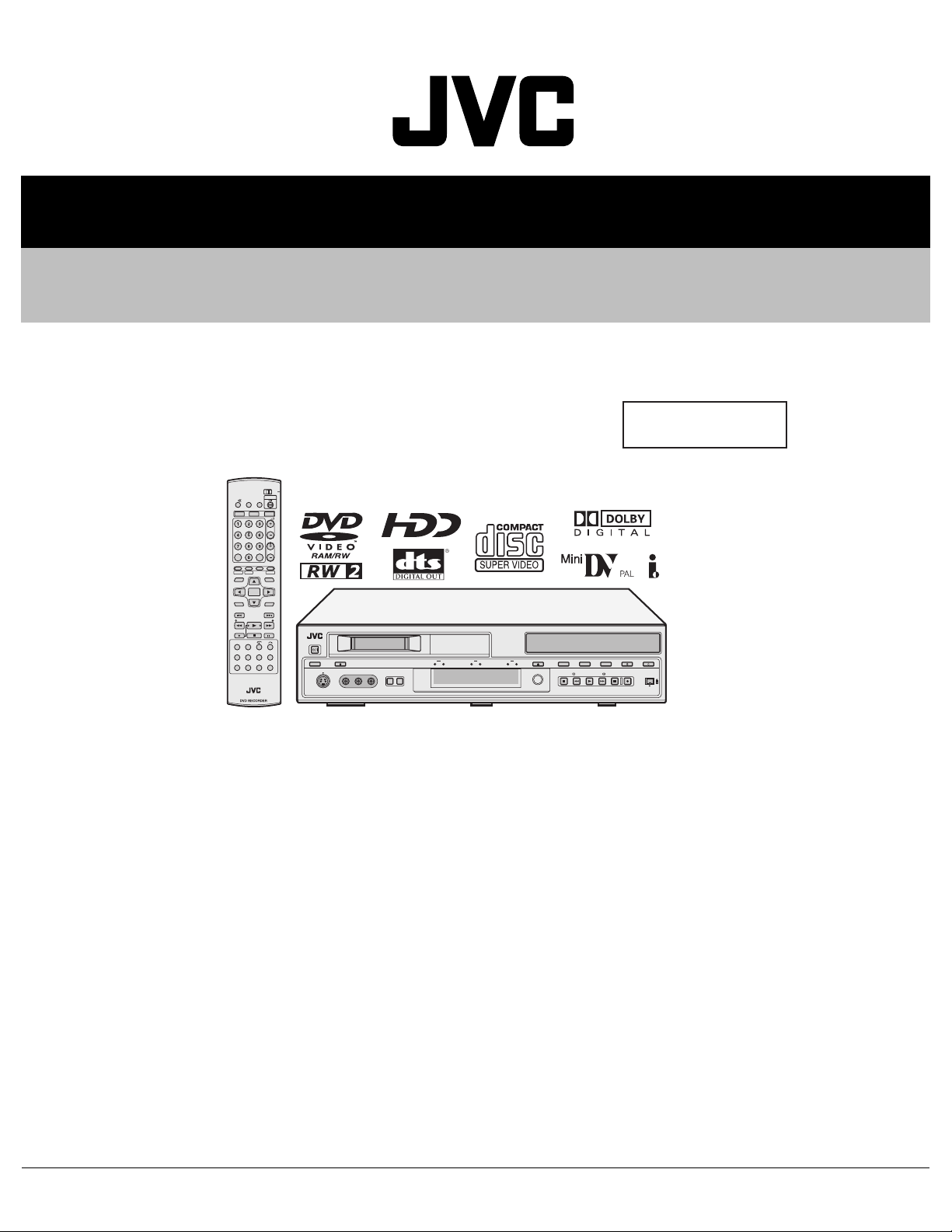
Mini DV & HDD & DVD VIDEO RECORDER
YD09120063
SR-DVM700EU
Area Suffix
EU -------- Western Europe
DVDTV
STANDBY/ON
OUTPUT
TV
/
TV
VIDEO
SELECT
DV HDD DVD
TV
PR/CH
CANCEL
MEMO/MARK
INPUTSELECT
EDIT
F2
PROG
F1
NAVIGATIONTOPMENU
ENTER
MENU
RETURN
NEXTPREVIOUS
SLOWSLOW PLAY
PAUSEREC
STOP/CLEAR
DISPLAY
ONSCREEN
RECMODE/
AUDIO
SUBTITLE
REMAIN
PROGRESSIVE
SCAN
STANDBY/ON
ANGLE/
EECHECK
SETUPDUBBINGEE
S-VIDEO
INF-1
VIDEO(MONO)L - AUDIO - R
INPUT
OUTPUT
SELECT
SELECT
EJECTEJECTDISPLAY
RECDVDRECHDDRECDV
DV/HDD/DVD RECMODE INSTANTREPLAY AUDIODUB. INSERT
RECPAUSEPLAY
FFREWSTOP
DVIN/ OUT
SR-DVM700EU [D5MC29]
Since the whole mechanism assembly unit is replaced, the DVD recorder
mechanism of this unit need not be adjusted.
TABLE OF CONTENTS
1 PRECAUTION. . . . . . . . . . . . . . . . . . . . . . . . . . . . . . . . . . . . . . . . . . . . . . . . . . . . . . . . . . . . . . . . . . . . . . . . . 1-3
2 SPECIFIC SERVICE INSTRUCTIONS . . . . . . . . . . . . . . . . . . . . . . . . . . . . . . . . . . . . . . . . . . . . . . . . . . . . . . 1-6
3 DISASSEMBLY . . . . . . . . . . . . . . . . . . . . . . . . . . . . . . . . . . . . . . . . . . . . . . . . . . . . . . . . . . . . . . . . . . . . . . . 1-8
4 ADJUSTMENT . . . . . . . . . . . . . . . . . . . . . . . . . . . . . . . . . . . . . . . . . . . . . . . . . . . . . . . . . . . . . . . . . . . . . . . 1-14
5 TROUBLESHOOTING . . . . . . . . . . . . . . . . . . . . . . . . . . . . . . . . . . . . . . . . . . . . . . . . . . . . . . . . . . . . . . . . . 1-38
COPYRIGHT © 2006 Victor Company of Japan, Limited
No.YD091
2006/3
Page 2

SPECIFICATION
GENERAL
Power requirement AC 220 V - 240 V~,50 Hz/60 Hz
Power consumption
Power on 42 W
Power off 5 W
Laser specification
For CD Wavelength: 770 to 810 nm
For DVD Wavelength: 653 to 663 nm
Temperature
Operating 5°C to 35°C
Storage -20°C to 60°C
Operating position Horizontal only
Dimensions (WxHxD) 435 mm × 96 mm × 372 mm
Weight 5.8 kg
Input/Output
Video input 0.5 - 2.0 Vp-p, 75 Ω (pin jack)
Video output 1 Vp-p, 75 Ω (BNC)
Audio input -8 dB, 50 kΩ (pin jack), Corresponding to mono (left)
Audio output -8 dB, 1 kΩ (pin jack)
S-video input Y: 0.8 - 1.2 Vp-p, 75 Ω, C: 0.2 - 0.4 Vp-p, 75 Ω
S-video output Y: 1.0 Vp-p, 75 Ω, C: 0.3 Vp-p, 75 Ω
DV 4-pin for DV IN/OUT
Remote Input Ø3.5 mm Jack
Serial Command D-SUB 9-PIN
Component video output Y: 1.0 Vp-p, 75 Ω, CB/CR, PB/PR: 0.7 Vp-p, 75 Ω
Digital audio output Optical, Coaxial
Corresponding to Dolby Digital and DTS Digital Surround
Bit stream Selectable in digital audio output setting menu
VIDEO/AUDIO (DVD deck)
Recording time Maximum 8 hours (with 4.7 GB disc)
(XP): Approx. 1 hour, (SP): Approx. 2 hours, (LP): Approx. 4 hours
(EP): Approx. 6 hours, (FR): Approx. 1 hour - 8 hours
Audio recording system Dolby Digital (2 ch), Linear PCM (XP mode only)
Video recording compression system MPEG2 (CBR/VBR)
VIDEO/AUDIO (HDD Deck)
Video recording compression system MPEG2 (VBR)
Audio recording system Dolby Digital (2 ch), Linear PCM (XP mode only)
Recording time Maximum 473 hours (with 250 GB HDD)
(DV): Approx. 18 hours,(XP): Approx. 53 hours,(SP): Approx. 109 hours,(LP): Approx. 218 hours,
(EP): Approx. 328 hours,(FR): Approx. 473 hours
VIDEO/AUDIO (DV Deck)
Signal system PAL colour signal, 625 lines/50 fields
Recording system Digital Component Recording
Format DV format (SD mode)
Cassette Mini DV Cassette
Maximum recording time
(SP) (SP): 80 min. with M-DV80ME cassette
(LP) (LP): 120 min. with M-DV80ME cassette
Audio recording system PCM 48 kHz, 16 bit (2 ch)/32 kHz, 12 bit (4 ch)
ACCESSORIES
Provided accessories Audio/Video cable,3-pin conversion plug (for UK use only),Infrared remote control unit,”R6” battery x 2
• Specifications shown are for SP mode unless otherwise specified.
• E.& O.E. Design and specifications subject to change without notice.
• Manufactured under license from Dolby Laboratories. "Dolby" and the double-D symbol are trademarks of Dolby Laboratories.
• "DTS" and "DTS Digital Out" are trademarks of Digital Theater Systems, Inc.
• This unit plays back and records PAL and SECAM signals in PAL format. NTSC signals can also be played back on the DVD deck.
• This product incorporates copyright protection technology that is protected by U.S. patents and other intellectual property rights. Use of this copyright protection technology must be authorized by Macrovision, and is intended for home and other limited viewing uses only unless otherwise
authorized by Macrovision. Reverse engineering or disassembly is prohibited.
Output: 0.4 mW
Output: 1.0 mW
Corresponding to copy protection
1-2 (No.YD091)
Page 3
SECTION 1
r
PRECAUTION
1.1 SAFTY PRECAUTIONS
Prior to shipment from the factory, JVC products are strictly inspected to conform with the recognized product safety and electrical codes of the countries in which they are to be
sold.However,in order to maintain such compliance, it is equally
important to implement the following precautions when a set is
being serviced.
1.1.1 Precautions during Servicing
(1) Locations requiring special caution are denoted by labels
and inscriptions on the cabinet, chassis and certain parts of
the product.When performing service, be sure to read and
comply with these and other cautionary notices appearing
in the operation and service manuals.
(2) Parts identified by the symbol and shaded ( ) parts
are critical for safety.
Replace only with specified part numbers.
NOTE :
Parts in this category also include those specified to
comply with X-ray emission standards for products
using cathode ray tubes and those specified for
compliance with various regulations regarding spurious radiation emission.
(3) Fuse replacement caution notice.
Caution for continued protection against fire hazard.
Replace only with same type and rated fuse(s) as specified.
(4) Use specified internal wiring. Note especially:
• Wires covered with PVC tubing
• Double insulated wires
• High voltage leads
(5) Use specified insulating materials for hazardous live parts.
Note especially:
• Insulation Tape
• PVC tubing
•Spacers
• Insulation sheets for transistors
•Barrier
(6) When replacing AC primary side components (transformers,
power cords, noise blocking capacitors, etc.) wrap ends of
wires securely about the terminals before soldering.
Consequently, when servicing these products, replace the
cathode ray tubes and other parts with only the specified
parts. Under no circumstances attempt to modify these circuits.Unauthorized modification can increase the high voltage value and cause X-ray emission from the cathode ray
tube.
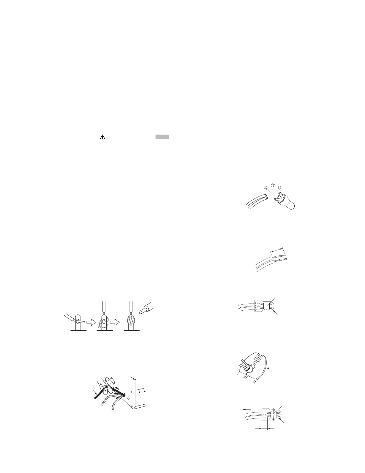
(12) Crimp type wire connectorIn such cases as when replacing
the power transformer in sets where the connections between the power cord and power trans former primary lead
wires are performed using crimp type connectors, if replacing the connectors is unavoidable, in order to prevent safety hazards, perform carefully and precisely according to the
following steps.
• Connector part number :E03830-001
• Required tool : Connector crimping tool of the proper
type which will not damage insulated parts.
• Replacement procedure
a) Remove the old connector by cutting the wires at a
point close to the connector.Important : Do not reuse a connector (discard it).
cut close to connector
Fig.1-1-3
b) Strip about 15 mm of the insulation from the ends
of the wires. If the wires are stranded, twist the
strands to avoid frayed conductors.
15 mm
Fig.1-1-4
c) Align the lengths of the wires to be connected. In-
sert the wires fully into the connector.
Metal sleeve
Fig.1-1-1
(7) Observe that wires do not contact heat producing parts
(heatsinks, oxide metal film resistors, fusible resistors, etc.)
(8) Check that replaced wires do not contact sharp edged or
pointed parts.
(9) When a power cord has been replaced, check that 10-15
kg of force in any direction will not loosen it.
Power cord
Fig.1-1-2
(10) Also check areas surrounding repaired locations.
(11) Products using cathode ray tubes (CRTs)In regard to such
products, the cathode ray tubes themselves, the high voltage circuits, and related circuits are specified for compliance with recognized codes pertaining to X-ray emission.
Connector
Fig.1-1-5
d) As shown in Fig.1-1-6, use the crimping tool to
crimp the metal sleeve at the center position. Be
sure to crimp fully to the complete closure of the
tool.
1.2
5
2.0
5.5
Crimping tool
Fig.1-1-6
e) Check the four points noted in Fig.1-1-7.
Not easily pulled free
Wire insulation recessed
more than 4 mm
Crimped at approx. cente
of metal sleeve
Conductors extended
Fig.1-1-7
(No.YD091)1-3
Page 4
1.1.2 Safety Check after Servicing
Examine the area surrounding the repaired location for damage
or deterioration. Observe that screws, parts and wires have been
returned to original positions, Afterwards, perform the following
tests and confirm the specified values in order to verify compliance with safety standards.
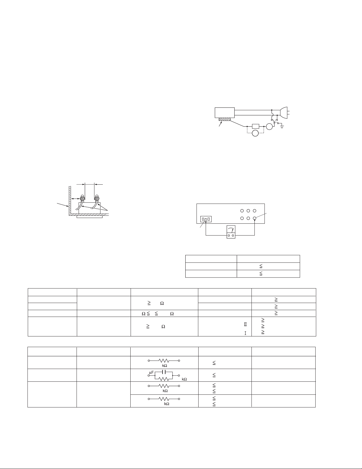
(1) Insulation resistance test
Confirm the specified insulation resistance or greater between power cord plug prongs and externally exposed
parts of the set (RF terminals, antenna terminals, video and
audio input and output terminals, microphone jacks, earphone jacks, etc.).See table 1 below.
(2) Dielectric strength test
Confirm specified dielectric strength or greater between
power cord plug prongs and exposed accessible parts of
the set (RF terminals, antenna terminals, video and audio
input and output terminals, microphone jacks, earphone
jacks, etc.). See Fig.1-1-11 below.
(3) Clearance distance
When replacing primary circuit components, confirm specified clearance distance (d), (d') between soldered terminals, and between terminals and surrounding metallic
parts. See Fig.1-1-11 below.
d
Chassis
d'
Power cord
primary wire
Fig.1-1-8
(4) Leakage current test
Confirm specified or lower leakage current between earth
ground/power cord plug prongs and externally exposed accessible parts (RF terminals, antenna terminals, video and
audio input and output terminals, microphone jacks, earphone jacks, etc.).
Measuring Method : (Power ON)Insert load Z between
earth ground/power cord plug prongs and externally exposed accessible parts. Use an AC voltmeter to measure
across both terminals of load Z. See Fig.1-1-9 and following Fig.1-1-12.
ab
Externally
exposed
accessible part
Z
V
c
A
Fig.1-1-9
(5) Grounding (Class 1 model only)
Confirm specified or lower grounding impedance between
earth pin in AC inlet and externally exposed accessible
parts (Video in, Video out, Audio in, Audio out or Fixing
screw etc.).Measuring Method:
Connect milli ohm meter between earth pin in AC inlet and
exposed accessible parts. See Fig.1-1-10 and grounding
specifications.
AC inlet
Earth pin
Exposed accessible part
MIlli ohm meter
Grounding Specifications
Region
USA & Canada
Europe & Australia
Grounding Impedance (Z
Z 0.1 ohm
Z 0.5 ohm
)
Fig.1-1-10
AC Line Voltage
100 V
100 to 240 V
110 to 130 V
110 to 130 V
200 to 240 V
Region
Japan
USA & Canada
Europe & Australia
Insulation Resistance (R
R 1 M /500 V DC
1 M R 12 M /500 V DC
R 10 M /500 V DC
)
Dielectric Strength
AC 1 kV 1 minute
AC 1.5 kV 1 minute
AC 1 kV 1 minute
AC 3 kV 1 minute
AC 1.5 kV 1 minute
(
Class
(
Class
Clearance Distance (d), (d'
d, d' 3 mm
d, d' 4 mm
d, d' 3.2 mm
d 4 m m
)
d' 8 m m (Power cord
d' 6 m m (Primary wire
)
Fig.1-1-11
AC Line Voltage
100 V
110 to 130 V
110 to 130 V
220 to 240 V
Region
Japan
USA & Canada
Europe & Australia
Load Z
1
0.15
1.5
2
50
Leakage Current (i)
i 1 mA rms
i 0.5 mA rms
i 0.7 mA peak
i 2 mA dc
i 0.7 mA peak
i 2 mA dc
a, b, c
Exposed accessible parts
Exposed accessible parts
Antenna earth terminals
Other terminals
Fig.1-1-12
NOTE :
These tables are unofficial and for reference only. Be sure to confirm the precise values for your particular country and locality.
)
)
)
1-4 (No.YD091)
Page 5
1.2 Hard Disk Drive (HDD) Handling Precautions
The HDD is a precision device for use in reading and writing a large amount of data on or from a disk rotating at a high speed. If it is
not handled carefully, either abnormal operation may result or it may not be possible to read data. The HDD is sensitive to the following
items and special care is required in safeguarding against them when handling an HDD. Also take care in handling a set incorporating
an HDD.
(1) Vibrations and impacts
(2) Static electricity
(3) Rough handling
1.2.1 Handling in transport, etc.
• Be sure to place the HDD in the manufacturer's specified package carton before transport.
• When receiving a package containing an HDD, check that the
package carton is not damaged (such as having holes in the
carton, crushed corners, etc.).
• Do not impact the packaging carton when loading or unloading
HDD
Do not throw or
drop packages.
it.
• It is not permitted to use the inner package carton only for
transporting an HDD.
• Do not stack package cartons one upon another.
Be sure to package and
transport the HDDs correctly.
1.2.2 Handling an HDD in the stand-alone status
• When handling an HDD on a hard workbench, place an antistatic mat (rubber sheet) or similar object on the hard surface
(to prevent any impacts occurring between the HDD and
bench).
• Do not stack the HDDs one upon another.
• Do not knock an HDD with a hard object (such as a screwdriver).
• Do not place an HDD on its side panel without using a support
(do not place an HDD in an unstable position).
1.2.3 Handling the installation of an HDD
• Place antistatic mats or similar sheets on all of the surfaces on which work is conducted or when the HDD is transported.
• Do not permit the HDD to knock against the set's brackets.
• When screwing the brackets, be careful not to knock the HDD. When using a power screwdriver, use a low-shock model and arrange
the tightening torque properly.
• When mounting an HDD in a main body, take care not to apply excessive force to the brackets.
(No.YD091)1-5
Page 6
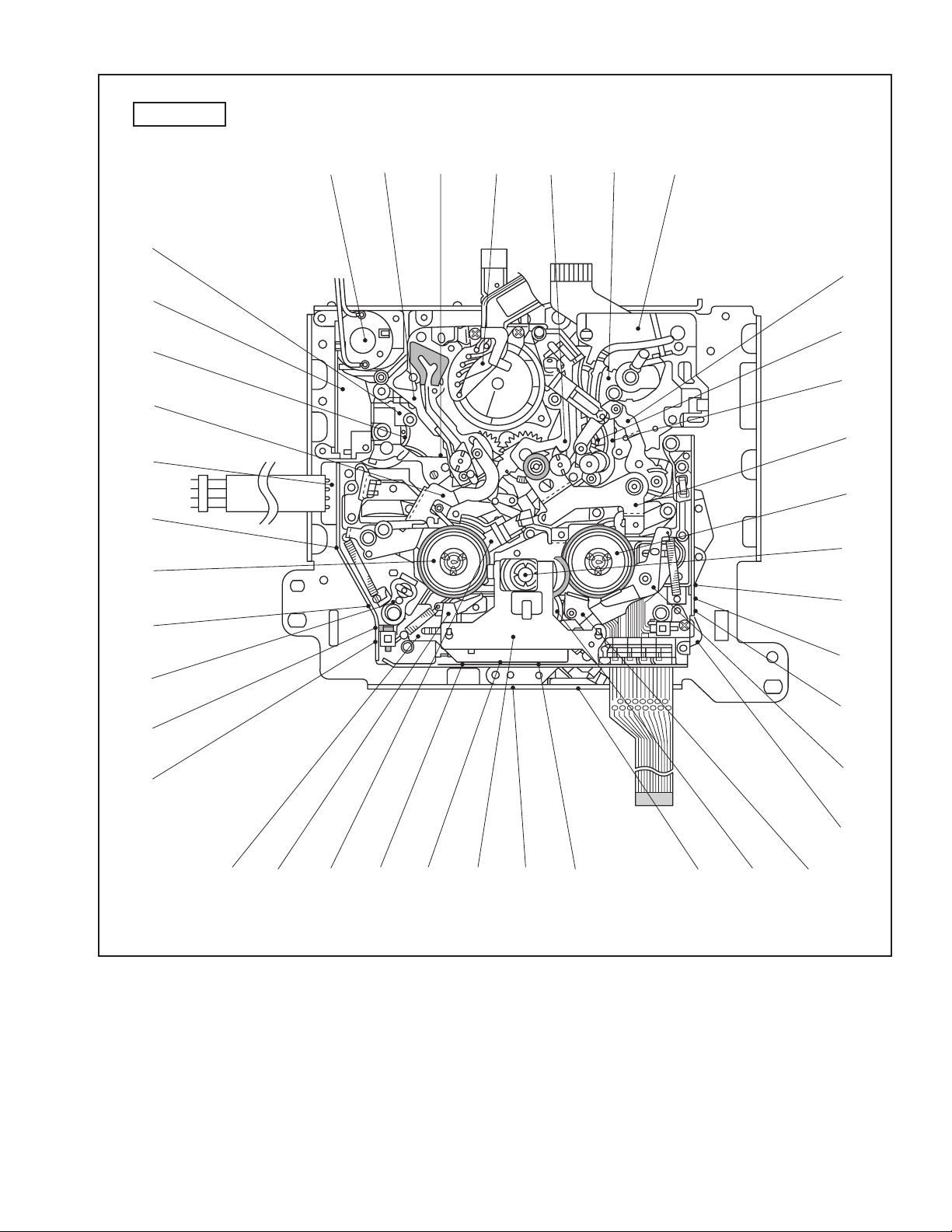
SECTION 2
SPECIFIC SERVICE INSTRUCTIONS
2.1 Service position
This unit has been designed so that the Mechanism and Main
board assemblies can be removed together from the bottom
chassis. Before diagnosing or servicing the circuit boards, take
out the major parts from the bottom chassis.
2.1.1 How to set the "Service position"
(1) Refer to the disassembly procedure and perform the disas-
sembly of the major parts before removing the Mechanism
assembly.
(2) Remove the screws that fix the Mechanism, Main board as-
sembly to the bottom chassis. If any other screws are used
to fix the boards, remove them also.
(3) Remove the combined Mechanism, HDD, DVD unit,
switching regulator, digital, DV jack, junction and Main
board assemblies.
(4) If any other major parts are used, remove them also.
(5) Connect the wires and connectors of the major parts that
have been removed in steps (1) to (4). (Refer to Fig. 2-1a.)
(6) Place the combined Mechanism, Main board and other
board assemblies upside down.
(7) Insert the power cord plug into the power outlet and then
proceed with the diagnostics and servicing of the board as-
sembly.
Notes:
• Before inserting the power cord plug into the power out-
let, make sure that none of the electrical parts are able
to short-circuit between the workbench and the board
assembly.
• For the disassembly procedure of the major parts and
details of the precautions to be taken, see "Removing
the major parts".
• If there are wire connections from the Main board and
Mechanism assemblies to the other major parts, be sure
to remove them (including wires connected to the major
parts) first before performing step (2).
• When carrying out diagnosis and repair of the Main
board assembly in the "Service position", be sure to
ground both the Main board and Mechanism assemblies. If they are improperly grounded, there may be
noise on the playback picture or FDP counter display
may move even when the mechanism is kept in an inoperative status.
• In order to diagnose the playback or recording of the
cassette tape, set the Mechanism assembly to the required mode before placing it upside down. If the mechanism mode is changed (including ejection) while it is in
an upside down position the tape inside may be damaged.
• For some models, the mechanism and board assem-
blies are attached by connectors only. When carrying
out a diagnosis or repair of the boards in the "Service
position", make sure that the connectors are not disconnected.
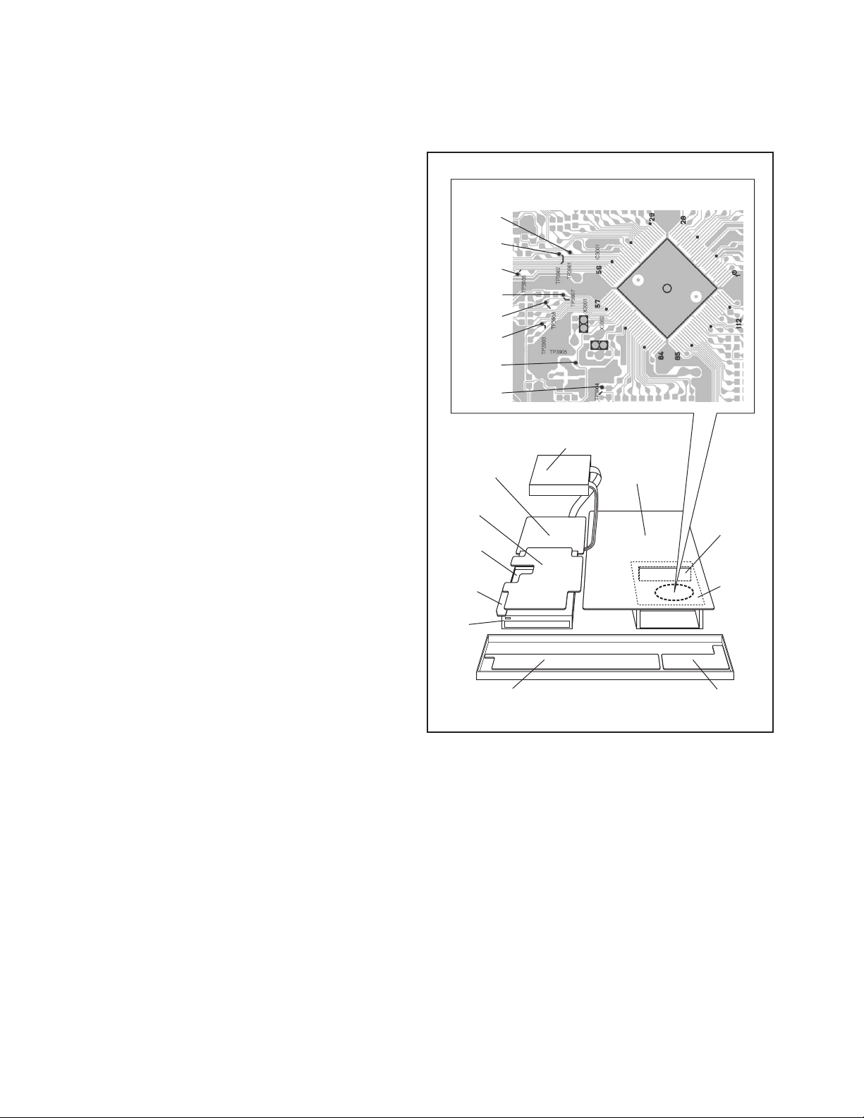
MAIN board assembly
TP3901
TP3902
TP3906
TP3907
TP3908
TP3903
TP3905
TP3904
SWITCHING
REGULATOR
board assembly
JUNCTION
board assembly
DIGITAL
board
assembly
DV JACK
board
assembly
DVD
DRIVE
UNIT
DISPLAY / SWITCH
board assembly
HDD
Fig.2-1a
MAIN
board
assembly
MDA
board
assembly
DV MAIN
board
assembly
OPERATION / JACK
board assembly
1-6 (No.YD091)
Page 7
2.2 Jig RCU mode
This unit uses the following two modes for receiving remote control codes.
(1) User RCU mode:Ordinary mode for use by the user.
(2) Jig RCU mode: Mode for use in production and servicing.
When using the Jig RCU, it is required to set the unit to the Jig
RCU mode (the mode in which codes from the Jig RCU can be
received). As both of the above two modes are stored in the EEPROM, it is required to set the unit back to the User RCU mode
each time that an adjustment is made or to check that the necessary operations have been completed.These modes can be set
by the operations described below.
Note:
• When the unit is set to Jig RCU mode and when the unit
is under Jig RCU mode, the remote control unit attached
to product operates only in "Remote Control Code 1".
Since the unit is in "Remote Control Code 3" when it is
shipped and just after its batteries are changed, "Remote Control Code 3" needs to be changed to "Remote
Control Code 1."
• Confirm the RCU mode when exchanged parts. Since
some SERVICE PARTS sets the unit to the Jig RCU
mode as initial setting. Therefore please set the unit to
the user RCU mode after replacing the EEPROM.
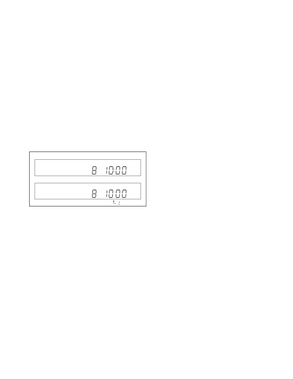
User RCU mode
CH
Jig RCU mode
CH
( blinked)
Fig.2-2a User/Jig RCU mode
2.2.1 Changing Remote Control Code
(1) Slide the TV/DVD switch to DVD.
(2) Press the number key "1" of the remote control unit while
pressing the "SET UP" button of the remote control unit.
Then,press the "ENTER" button, and then release the
"SET UP" button.
(3) Press the "POWER" button on the unit to turn off the unit.
(4) Press the "PLAY" button on the unit for over 5 seconds
while the unit is turned off. The code currently set appears
on the front display panel.
(5) Press the "STOP" button on the remote control to change
the unit’s code. When FDP indicator displays "DVD1," it
means that the Remote Control Code has been changed to
"1."
Note:
When "POWER SAVE" is set to "ON", it is not possible to
change the remote code.
2.2.2 Setting the Jig RCU mode
(1) Turn on the power.
(2) Press the "DV/HDD/DVD" select button repeatedly on the
unit so that the DVD lamp lights up on the unit.
(3) Press the following remocon keys continuously within 2
seconds " SET UP " → " 2 " → " 8 " → " ENTER ".
When the unit is set to the Jig RCU mode, the symbols
( " : " ) in the time display of the FDP are blinked.
(Refer to Fig.2-2a User/Jig RCU mode)
2.2.3 Setting the User RCU mode
(1) Turn off the power.
(2) Press the "REC" and "PAUSE" buttons of the unit simulta-
neously. Alternatively, transmit the code "43-9D" from the
Jig RCU.
(No.YD091)1-7
Page 8
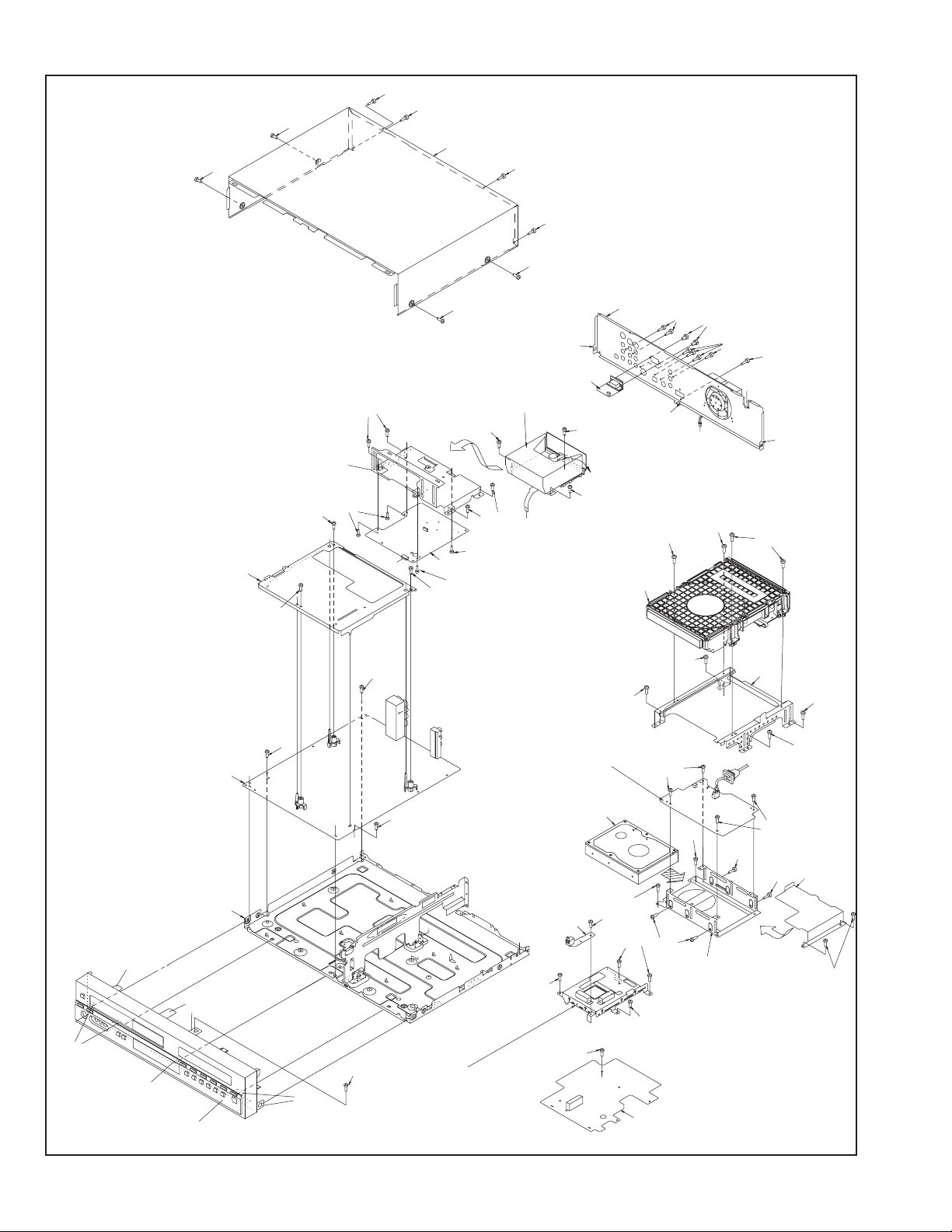
DISASSEMBLY
3.1 Removing the major parts
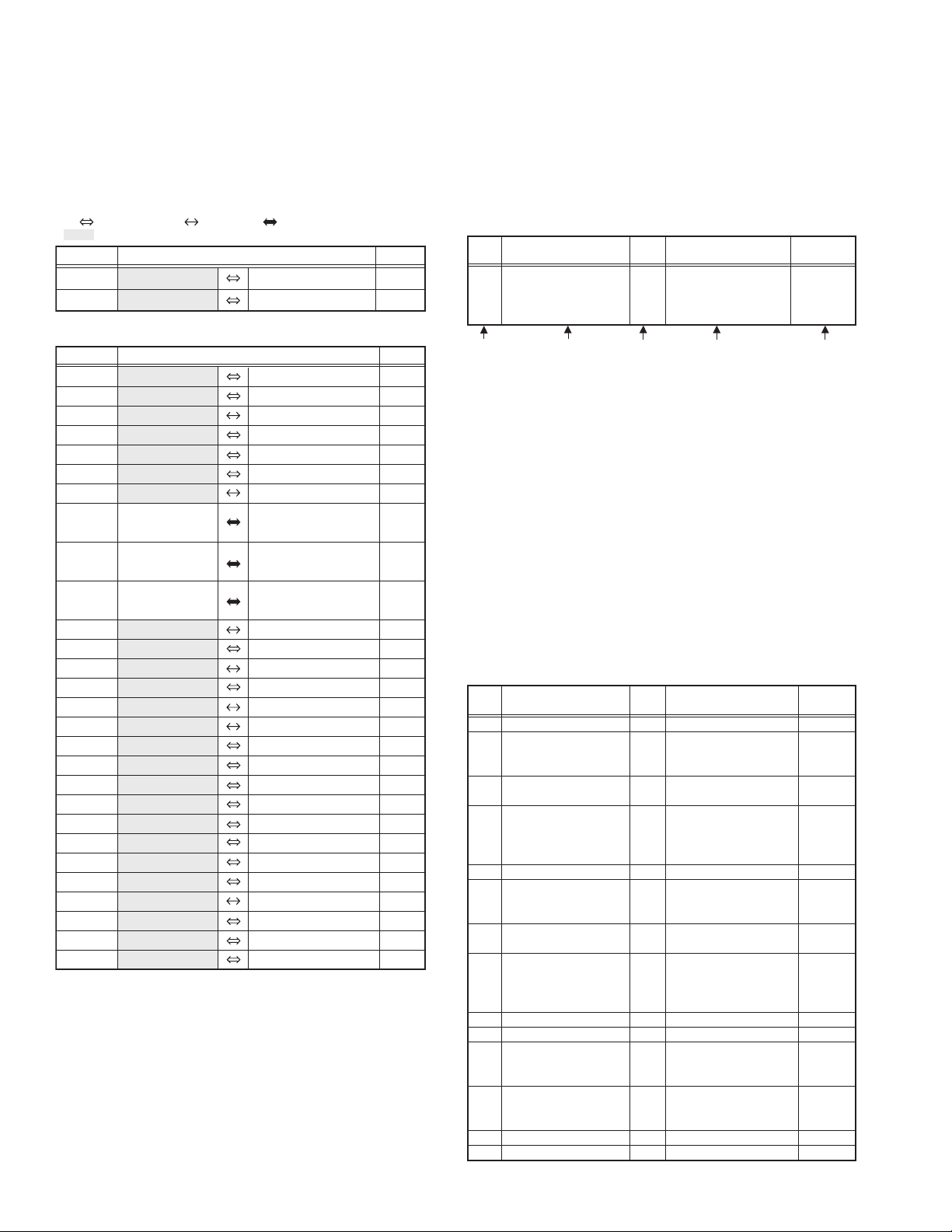
3.1.1 Destination of connectors
Two kinds of double-arrows in connection tables respectively
show kinds of connector/wires.
: The connector of the side to remove
CONN. No. PIN No.CONNECTOR
WR2a
WR2b
Main CN101
Main CN103
Destination of connectors
CONN. No. PIN No.CONNECTOR
WR2a
WR2b
WR3a
WR3b
WR4a
WR4b
WR4c
CN7108
(CN1001)
CN7109
(CN1002)
CN7121
(CN1802)
WR5a
WR6a
WR6b
WR6c
WR6d
WR8a
WR8b
WR8c
WR8d
WR8e
WR9a
WR11a
WR11b
WR11c
WR11d
WR12a
WR12b
WR12c
Main
Main
Junction
Digital
Digital
Digital
Junction
Junction
Junction
Junction
Junction
SW. REG
SW. REG
SW. REG
SW. REG
Junction
Main
Main
Main
Main
Main
DV Main
DV Main
DV Main
DV MDA
Main
Main
Main
: Wire: Flat wire : Board to board (B-B)
Digital CN761
Digital CN762
CN3104
CN3102
CN5503
CN2201
CN2101
CN1405
CN5502
CN7108
CN7109
CN7121
CN7126
CN5304
CN5303
CN5301
CN5302
CN7127
CN3103
CN2602
CN701
CN901
CN3104
CN1502
CN4001
CN1501
CN5501
CN5404
CN2601
CN501
Operation/jack
Display/switch
DVD unit
DVD unit
HDD
D-SUB
Digital
Digital
Digital
Digital
DV jack
Junction
HDD
Main
Fan motor
DV Main
Junction
Junction
Junction
Junction
DV Main
DV mechanism sensor
DV drum motor
DV MDA
Main
DV Main
DV Main
DV Main
CN7201
CN7001
CN701
CN101
CN7401
CN1003
CN1001
CN1002
CN1802
CN4104
CN5501
CN5402
CN2002
CN7102
CN8001
CN7123
CN7107
CN1505
CN5506
CN5403
CN1001
CN3701
CN3501
SECTION 3
3.1.2 How to read the procedure table
This table shows the steps for disassembly of the externally furnished parts and board assemblies. Reverse these steps when
re-assembling them.
Step/
Loc No.
40
10
15
15
8
40
40
4
6
28
20
14
6
19
4
15
2
6
19
11
4
13
7
15
8
20
5
8
8
7
[1] Top cover 3-1a
(1) (2) (3) (4) (5)
(1) Order of steps in Procedure
(2) Part name to be removed or installed.
(3) Fig. No. showing procedure or part location.
(4) Identification of part to be removed, unhooked, unlocked,
(5) Adjustment information for installation
3.1.3 Disassembly procedure
Step/
Loc No.
[1]
[2]
[3]
[4]
[5]
[6]
[7]
[8]
[9]
[10]
[11]
[12]
[13]
[14]
Part Name
Bracket 2(S1c)
Fig.
No.
----------------------------------------
Point Note
4(S1a),(S1b),3(L1a), <Note 1a>
2(SD1a),(P1a),(W1a),
CN1(WR1a),
When reassembling, perform the step(s) in the reverse order.
These numbers are also used as the identification (location) No. of parts Figures.
released, unplugged, unclamped or unsoldered.
P= Spring, W= Washer, S= Screw, L= Locking tab, SD=
Solder, CN**(WR**)= Remove the wire (WR**) from the
connector (CN**).
Note:
• The bracketed ( ) WR of the connector symbol are
assigned nos. in priority order and do not correspond to those on the spare parts list.
Part Name
Top cover
Front panel assembly
(Operation jack board assembly)
(Display/switch display board assembly)
DVD unit
(Bracket)
Digital board assembly
DV jack board assembly
Switching regulator board assembly
HDD
(Bracket),(Sheet)
Junction board assembly
D-SUB board assembly
Rear cover
DV mechanism assembly
DV main board assembly
(Bracket)
Bracket(DV MAIN)
Main board assembly
Fig.
No.
3-1b
3-1a
3-1b
3-1a
3-1b
3-1a
3-1b
3-1a,3-1b
3-1a
3-1b
3-1a
3-1b
3-1a
3-1b
3-1b
3-1b
3-1a
3-1b
3-1a
3-1b
3-1b
3-1a,3-1b
Point Note
8(S1a)
(S2a),3(L2a),5(L2b)
CN3104(WR2a),CN3102(WR2b
4(S3a),4(S3b)
CN5503(WR3a),CN2201(WR3b)
4(S4a),CN2101(WR4a)
CN1405(WR4b),CN5502(WR4c),
CN7108(CN1001),CN7109(CN1002)
CN7121(CN1802)
(S5a),CN7126(WR5a)
4(S6a),
CN5304(WR6a),CN5303(WR6b),
CN5301(WR6c),CN5302(WR6d)
4(S7a),4(S7b)
(S8a),CN7127(WR8a),
CN3103(WR8b),
CN2602(WR8c),
CN701(WR8d),CN901(WR8e)
2(S9a),CN7401(WR4b)
(S10a),6(S10b),3(L10a)
3(S11a),CN1502(WR11a),
CN4001(WR11b),
CN1501(WR11c),CN5501(WR11d)
4(S12a),4(S12b),CN5404(WR12a),
CN2601(WR12b),CN501(WR12c),
CN3104(WR9a)
3(S13a)
3(S14a)
<Note2a>
<Note2b>
)
<Note2a>
<Note2a>
<Note2a>
<Note2a>
<Note2a>
<Note3a>
<Note3b>
1-8 (No.YD091)
Page 9
< Note 2a >
• Be careful not to damage the connector and wire etc. during
connection and disconnection.
• When connecting the flat wire to the connector, be careful with
the flat wire direction.
< Note 2b >
• When attaching the Front panel assembly, make sure that the
door opener of DV deck is in the down position.
< Note 3a >
• When reattaching the bracket(DV MAIN), secure the screws
(S13a) in the order of 1,2,3.
< Note 3b >
• When reattaching the Main board assembly, secure the
screws (S14a) in the order of 1,2,3.
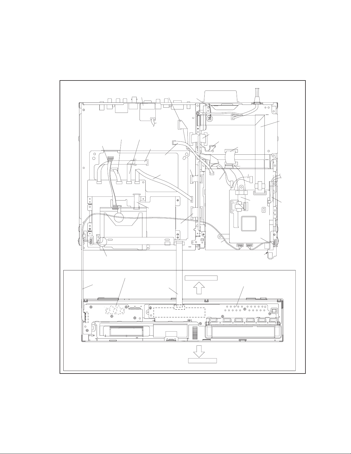
Main board assembly
(WR12a)
<Note 2a>
(WR11d)
CN5403
CN3501
DV
Main board assembly
CN5501
CN3104
CN2002
<Note 2b>
D-SUB board assembly
CN7401
(WR12b)
<Note 2a>
(WR12c)
<Note 2a>
CN2601
CN501
CN5404
CN3701
CN1001
CN1505
CN1501
CN4001
(WR11c)
<Note 2a>
(WR8e)
<Note 2a>
TO CN1405
ON DIGITAL
BOARD
CN701
(WR8d)
<Note 2a>
(WR9a)
<Note 2a>
CN901
(WR8c)
(WR8b)
CN3102
(WR6d)
CN5402
CN2602
CN3014
CN3103
CN5302
(WR6c)
<Note 2a>
CN5301
CN7107
CN7123
CN8001
(WR3a)
CN7102
DRIVE UNIT
(WR8a)
FAN
CN5001
Switching regulator
board assembly
(WR6b)
CN5303
(WR6a)
<Note 2a>
CN5304
CN5501
Junction board assembly
(WR4c)
CN5503
CN1003
(WR3b)
<Note 2a>
CN2201
Digital board
assembly
CN7127
DV jack board assembly
CN5502
CN2101
(WR5a)
CN7126
(WR4a)
<Note 2a>
TO CN7401
ON D-SUB
BOARD
CN1405
(WR4b)
<Note 2a>
CN4104
Operation/jack board assembly
(WR2a)
<Note 2a>
CN7201
NOTE) INSERT FFC WIRE
TO THE CONNECTOR BEFORE
ATTACHING TO FRONT PANEL.
(WR2b)
<Note 2a>
BOTTOM SIDE
Display/switch board assembly
CN7001
TOP SIDE
Fig.3-1a
(No.YD091)1-9
Page 10
(S1a)
(S1a)
(S1a)
(S1a)
[1]Top cover
(S1a)
(S1a)
(S1a)
[13]Bracket(DV MAIN)
[14]Main board assembly
Bottom chassis
(L2a)
(L2a)
(S13a)
(S14a)
1
[12]Bracket
(S13a)
(S12b)
1
3
j
(S12a)
(S14a)
3
2
a'
b
(S1a)
[9]D-SUB board assembly
[11]DV mechanism assembly
(S11a)
CN4001
CN1502
2
(S12a)
(S12b)
[12]DV main board assembly
(S12b)
(S13a)
J901
J903
(S14a)
[5]DV jack board
c
e
[10]Rear cover
(L10a)
(S11a)
(WR11b)
<Note 2a>
(S11a)
(WR11a)
<Note 2a>
[3]DVD unit
(S3a)
[6]Switching regulator
board assembly
[7]HDD
(S7a)
assembly
c
(S5a)
(S4a)
(S4a)
(S10b)
(L10a)
(S3b)
(S6a)
c
(S7b)
(S4a)
(S9a)
(S3b)
(S3a)
CN5302
CN5001
(S7a)
c
[7]Bracket(HDD)
(S10b)
f
(S7b)
(S10a)
(L10a)
(S3b)
[3]Bracket
(S6a)
(S7b)
(S3a)
(S3a)
[7]Sheet
(S7a)
(L2b)
(L2b)
1-10 (No.YD091)
[2]Front panel assembly
(L2b)
(S2a)
(S8a)
[4]Digital board
assembly
[8]Junction board assembly
Fig.3-1b
Page 11
3.2 DVD Drive unit section
3.2.1 Remove the top cover and tray (See figure 1, figure2, figure3, figure4)
(1) The part a on the reverse side of a DVD drive unit is made
to slide in the direction of an arrow. (A tray ejects a few.)
(2) Remove the four screws A attaching the top cover.
(3) Hooks b are removed, and the top cover is removed.
(4) The tray is drawn out forward.
(5) Remove the two screws B attaching the shaft guide, and
hook c is removed.
(6) It draws it out while lifting the tray in the direction of the ar-
row.
A
Part a
Hook b
A
A
Fig.2
Top cover
A
Hook b
Fig.1
Hook c
B
Fig.3
Shaft guide
B
Tray
Fig.4
(No.YD091)1-11
Page 12
3.2.2 Reassembly the tray (See figure 5)
(1) The slide cam is done in the slide in the direction of the ar-
row.
(2) The shaft guide is done in the slide in the direction in the
back.
(3) The left side of the tray is inserted in the rail of the loading
base, and the shaft guide is built in.
(4) Please push the tray, and confirm whether the tray is nor-
mally good to the close position at the slide by manual.
3.2.3 Remove the traverse mechanism assembly (See figure 6, figure 7)
• Prior to performing the following procedure, remove the top
cover, tray.
(1) Disconnect the FFC wire from connector on the pick-up
unit.
ATTENTION:
The laser diode of "pick-up" might be destroyed by static
electricity. Please work after installing the wristband. In
addition, please do not touch in each part, the terminal,
and the laser diode terminal on the substrate of the pickup unit. Never
(2) Disconnect the FFC wire from connector CN103
on the servo control board.
(3) Remove the four screws C attaching the traverse mecha-
nism assembly.
, CN104
CN105
Shaft guide
Slide cam
Fig.5
Servo control board
CN103
C
Traverse mechanism assembly
C
C
Hook d Hook d
CN102
CN104
D D
Fig.7
1-12 (No.YD091)
Pick-up unitConnector
Fig.6
Page 13
3.2.4 Remove the servo control board (See figure 7)
(1) Disconnect the FFC wire from connector CN102
, CN105 on the servo control board.
CN104
(2) Remove the two screws D attaching the servo control
board.
(3) Hooks d is removed, and the servo control board is re-
moved.
3.2.5 Remove the loading motor (See figure 8, figure 9)
• Prior to performing the following procedure, remove the top
cover, tray.
(1) Remove the solder part e soldered on the switch board.
(2) A belt is removed.
(3) Remove the two screws E attaching the loading motor.
, CN103,
Loading
motor
Part e
Switch board
Fig.8
E
Belt
Fig.9
(No.YD091)1-13
Page 14
SECTION 4
ADJUSTMENT
4.1 Before adjustment
4.1.1 Precautions
(1) Observe the specified screw tightening torque when
attaching parts. The torque should be 0.04 Nm (0.4 kgfcm)
unless otherwise specified.
(2) Always disconnect the power supply unit before proceed-
ing to solder or attach parts.
(3) When plugging or unplugging a wire, be careful not to
damage the connector.
(4) When replacing a part, be careful not to damage other
parts or to mistakenly attach parts.
4.1.2 Tools required for adjustments
TORQUE DRIVER
12
YTU94088
Tool for replacing tip IC
4
PTS40844-2
BIT
YTU94088-003
Tool for installing slit washer
3
YTU94121A
Table 4-1-1
4.1.3 Disassembly and assembly procedures
The following table shows the steps for assembling or disassembling the mechanism parts. Read the following descriptions carefully before actual assembly/disassembly operations.
(1) : Order of disassembly steps. Reverse this order when as-
sembling.
(2) : Name of the disassembled/assembled part.
Surface where the disassembled/assembled part is
(3) :
mounted. T = Top. B: Bottom.
(4) : Number of disassembly drawing.
(5) : Parts to be removed in disassembly/assembly, such as
screws, washers and springs, and the points.
Symbol Name & Point
SScrew
W Washer
PSpring
* Connector, lock(L), soldering(SD),
shield, etc.
[Example] • (W1) = Remove the washer W1.
• (P1) = Remove the spring P1.
(6) : Notes for disassembly/assembly.
(7) : For the phase alignment in disassembly/assembly and
the parts which require phase adjustments after assembly,
see "4.7 Mechanism phase check/adjustment".
4.1.4 Screws and washers used in disassembly/assembly
of the mechanism assembly
Table 4-1-2 shows the symbols and part numbers of the screws
and washers used in the mechanism assembly.
When disassembling or assembling the mechanism assembly,be sure to attach screws and washers correctly by referring
to the following table.
Symbol Part number
(S1) QYSDSP2005ZA
(S2) YQ43893
(S3) YQ43893-7
Symbol Part number
(W1) YQ44246
(W2) YQ44246-3
Table 4-1-2
Step/Loc No. Fig. No. Point Note Discription
1
2
3
4
[A] Cassette housing assembly/
[B] Mechanism assembly
[1]Drum assembly
[2]Motor bracket assembly
[3]Middle catcher assembly
Part Name
1
2
2
3
2(S1),(L1) (L5)
3(S2)
4(S2)
3(S2)
T
T
T
T
1
2,3
2,4
(1) (2) (3) (4) (5) (6) (7)
1-14 (No.YD091)
Page 15
4.2 Disassembly/assembly of the mechanism assembly
4.2.1 Introduction
The disassembly and assembly of the mechanism assembly should usually be performed in the ASSEMBLY mode.(Table 4-2-1)
Note that the mechanism is in the cassette in (C-IN) mode when the mechanism assembly is taken out of the set and that the C-IN
mode should be switched to the ASSEMBLY mode in this case.
To set the ASSEMBLY mode, apply 3 V DC to the electrodes on the upper part of the loading motor as shown in Fig. 4-2-7.
MODE
PARTS
[1]
ROTARY
ENCORDER
R. ENC -20
MAIN CAM GEAR 0
[2]
[3]
36
C-IN
ASSEMBLY
17
S. FF
30.33
36.33
87
0
15
33.33
40
LOADING END
169.66
166.66
140
PLAY REV STOP FF/REW
270.33
276.33
223.66
226.66
185
229.66
273.33
220
303.66
306.66
245
190.33
193.33
160
196.33
Table 4-2-1
4.2.2 Mechanism modes
The mechanism has 6 modes as shown in Table 4-3-1. The current mode can be confirmed by the positioning of the " " marking on
the sub-cam gear and the " " marking on the mechanism. See the following figures (Figs. 4-2-1 to -6) for details.
Note:
• This mechanism assembly has another ASSEMBLY mode. However, this mode cannot be identified from the markings
because it corresponds to an intermediate position between the C-IN ( C ) mode and S-FF ( H ) mode. This mode can be
confirmed by the rotary encoder phase. See Fig. 4-2-7.
1. Checking the mechanism mode
[H]
Fig.4-2-1
Fig.4-2-4
[H][C]
Fig.4-2-2
Fig.4-2-5
[P]
Fig.4-2-3
[F][S][R]
Fig.4-2-6
(No.YD091)1-15
Page 16
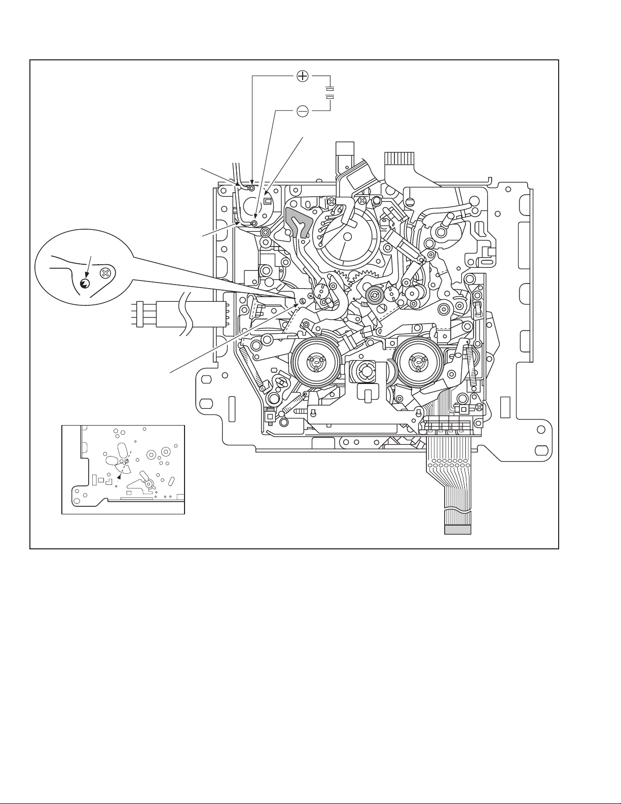
2. Setting/checking the ASSEMBLY mode
Wire (Brown)
DC 3 V
Motor bracket assembly (Loading Motor)
Marking
(Colored red)
Rotary encoder
< ASSEMBLY >
Wire (Red)
[C]
[H]
1-16 (No.YD091)
Fig.4-2-7
Page 17
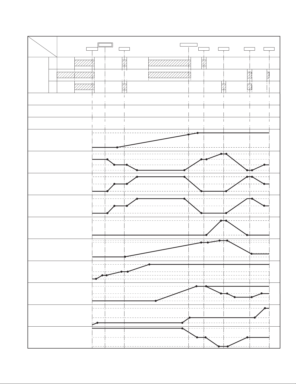
4.3 Mechanism timing chart
See following table (Table 4-3-1).
MODE
PARTS
36
[1]
ROTARY
ENCODER
[2]
[3]
ROTARY ENCODER
MAIN CAM 0
SUB CAM
POLE BASE
CTL PLATE
FF/REW
MAIN BRAKE(SUP)
MAIN BRAKE(TU)
SUB BRAKE
ON(REV MODE PRESS UP)
ON(PLAY MODE)
PINCH ROLLER
EXIT GUIDE ARM
HALF LOADING
TENSION ARM
BAND ARM PLATE
CLUTCH LOCK
SUP CENTRRING
OFF
S/REV
PLAY
ON 1
ON 2
OFF
ON 1
ON 2
OFF
OFF
OFF
ASSY
OFF
OFF 1
OFF 2
OFF
OFF 1
OFF 2
ASSEMBLY
C-IN
17
-20
0
15
0
ON
ON
ON
ON
ON
S. FF
30.33
33.33
40
4015
36.33
87
LOADING END
169.66
166.66
140
140
PLAY REV STOP FF/REW
270.33
276.33
223.66
226.66
185
185
229.66
273.33
220
220
303.66
306.66
245
245
190.33
193.33
160
160
196.33
CENTERRING ARM
S/REV
Table 4-3-1
(No.YD091)1-17
Page 18

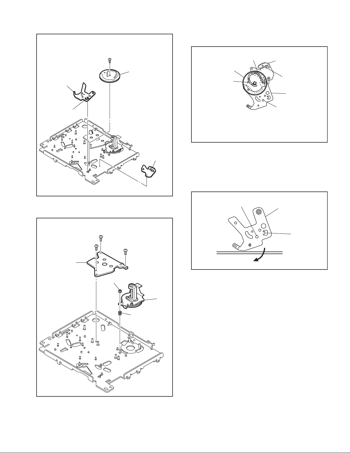
4.4 Mechanism assembly/disassembly procedure table
Step/Loc
No.
1 [A] Cassette housing assembly/ [B] Mechanism assembly T 4-5-1 2(S1),(L1) (L5) 1
2 [1] Drum assembly T 4-5-2 3(S2) 2,3
3 [2] Motor bracket assembly T 4-5-2 4(S2) 2,4
4 [3] Middle catcher assembly T 4-5-3 3(S2)
5 [4] Reel cover assembly T 4-5-3 (S2), 2(L6) 5
6 [5] Pinch roller arm assembly T 4-5-4 (W1), (L7) 6
7 [6] Sub brake assembly T 4-5-4 (P1), (W1), (L8)
8 [7] Band arm plate sub assembly T 4-5-4 (S3), (L9), (P2), (W2) 7,8
9 [8] Tension arm sub assembly T 4-5-4 (P3) 8
10 [9] Exit guide arm assembly T 4-5-5 (W1)
11 [10] Swing arm assembly T 4-5-5 Position alignment
12 [11] Sub deck assembly T 4-5-6 4(S2) 9 Position alignment
13 [12] Main brake (Supply) assembly T 4-5-6 (P4), (L10)
14 [13] Main brake (Take up) assembly T 4-5-6 (P5), (L11)
15 [14] Reel disk assembly (Supply) T 4-5-7
16 [15] Reel disk assembly (Take up) T 4-5-7
17 [16] Prism T 4-5-7 (S2)
18 [17] Control plate T 4-5-7 2(L12)
19 [18] Guide rail (Take up) assembly T 4-5-8 4(S2) 10 Position alignment
20 [19] Guide rail (Supply) assembly T 4-5-8 (S2), 2(L13) 10 Position alignment
21 [20] Base plate assembly T 4-5-8 (S2), 2(L14)
22 [21] Ent. guide base assembly T 4-5-9 (S2)
23 [22] Worm wheel 2 T 4-5-9 11 Phase alignment
24 [23] Timing belt T 4-5-9
25 [24] Center gear assembly T 4-5-9
26 [25] Reel drive pulley assembly T 4-5-10 (W1)
27 [26] Push plate T 4-5-10 (W1)
28 [27] Clutch lock gear (2) T 4-5-10
29 [28] Clutch lock gear (1) T 4-5-10 (P6)
30 [29] Tension control arm assembly T 4-5-11 (L15) 12 Position alignment
31 [30] Brake control arm assembly T 4-5-11 (W1), (L16) 12 Position alignment
32 [31] Charge arm assembly T 4-5-11 (L17) 13 Position alignment
33 [32] Connect gear 2 T 4-5-12 (S2) (Phase alignment)
34 [33] Connect gear 2 T 4-5-12 (S2) (Phase alignment)
35 [34] Rotary encoder assembly T 4-5-13 2(S2) 14 Phase alignment
36 [35] Main cam T 4-5-13 (W1) 15 Phase alignment
37 [36] Arm gear 1 assembly T 4-5-13 Collar 15,16 Position alignment
38 [37] Centering arm assembly T 4-5-13 (L18) 15 Position alignment
39 [38] Sub cam T 4-5-14 (S2) 17 Phase alignment
40 [39] Arm gear 2 assembly T 4-5-14 17 Position alignment
41 [40] Clutch lock lever assembly T 4-5-14 (L19) 17,18 Position alignment
42 [41] Capstan motor T 4-5-15 (P7), Adjust nut Vertical adjustment
43 [42] Drum base deck T 4-5-15 3(S2)
Part Name Fig. No.
Point Note Discription
1-18 (No.YD091)
Page 19
TOP VIEW
[21]
[11]
[22]
[8]
[34]
[35]
[14]
[37]
[2]
[19]
[42]
[1]
[18]
[41]
[3]
[9]
[23]
[25]
[5]
[15]
[10]
[38]
[7]
[29]
[30]
[17][12][16]
[36]
[20][4][32][26]
Fig.4-4-1
[39]
[31]
[6]
[40]
–
[33]
[24]
[13][28]
(No.YD091)1-19
Page 20
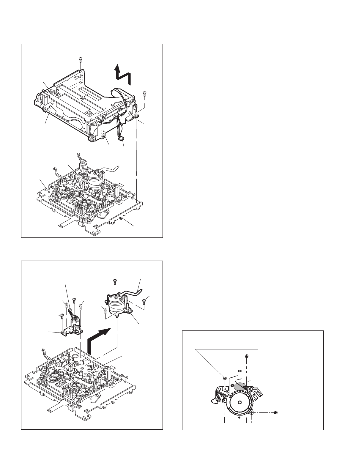
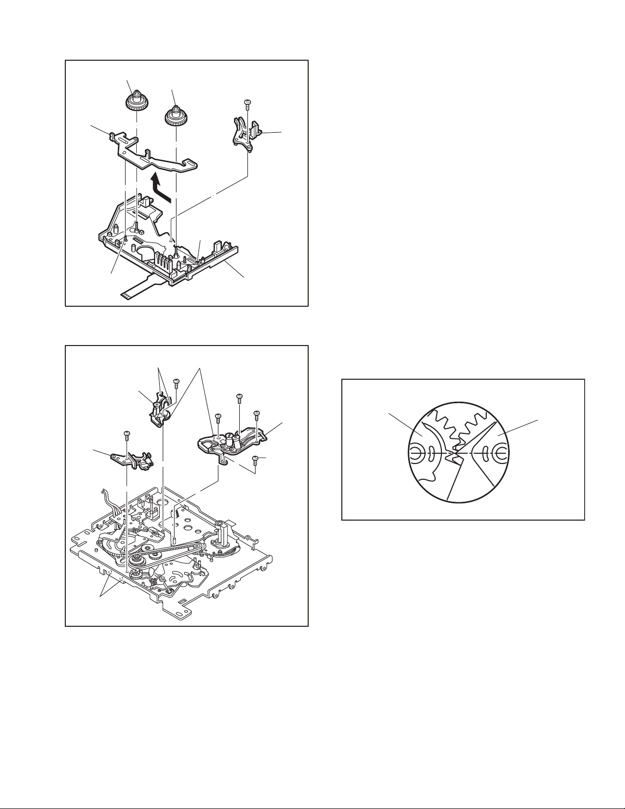
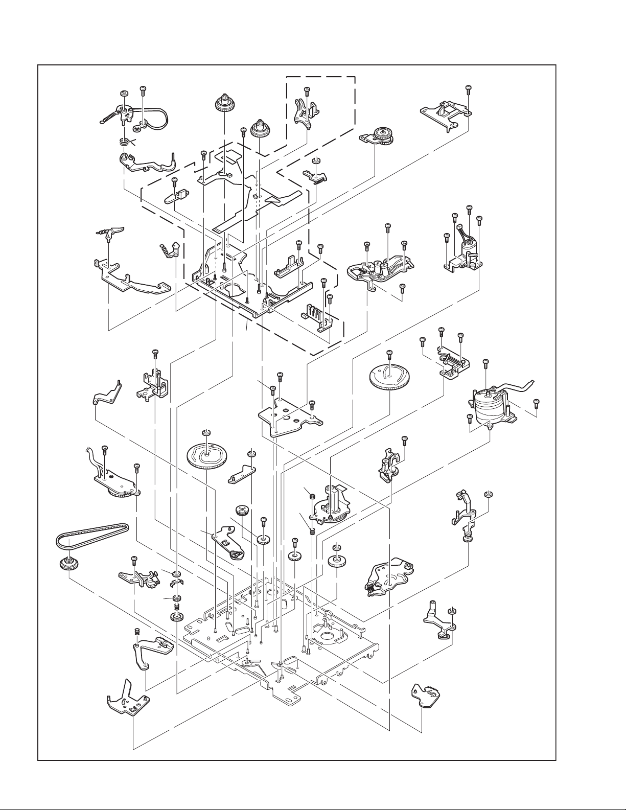
4.5 Disassembly/assembly
1. [A] Cassette housing assembly/ [B] Mechanism assembly
1
(S1)
Note 1a:
If the wires for the cassette housing motor are connected to the circuit board, remove them before disassembly.
[A]
(L3)
(L4)
(L1)
Fig.4-5-1
(L5)
<Note1a>
[B]
2
(S1)
(L2)
2. [1] Drum assembly / [2] Motor bracket assembly
3
<Note2a>
(S2)
8
(S2)
(S2)
6
(S2)
9
7
(S2)
(S2)
<Note2c>
4
<Note2a>
[2]
<Note2b>
[1]
5
(S2)
Note 2a:
If wires are connected to the circuit board, remove them
before disassembly.
Note 2b:
Be careful not to damage the drum assembly when removing it.
Note 2c:
The bracket (DV) may come in the way of removal of
screw (7). Be sure to remove the bracket before proceeding to the screw removal.
Note:Fasten screw in order
of [a] [b] [c] .
[c]
[a]
When Handling hold this part.
[b]
1-20 (No.YD091)
Fig.4-5-2
Fig.4-5-2a
Page 21
3. [3] Middle catcher assembly/ [4] Reel cover assembly
(b)
[4]
13
(S2)
(c)
12
<Note3b>
(S2)
<Note3b>
10
(S2)
(a)
11
(S2)
<Note3b>
Apply grease
Note 3a:
Once the reel cover assembly has been removed, the
parts located below it tend to slip out easily: Be careful.
Note 3b:
When attaching these screws, screwing order (a),(b),( c)
<Note3a>
[3]
(L6)
(L6)
Fig.4-5-3
4. [5] Pinch roller arm assembly/[6] Sub brake assembly/[7] Band arm plate sub assembly/ [8] Tension arm sub assembly
<Note 4c>:
How to install the spring
Step 1
Hook [a]
[8]
Step 2
Hook [b]
Fig.4-5-4a
(P2)
14
(S3)
(P3)
[7]
(W2)
<Note4b>
NOTE4c
(L9)
(W1)
[6]
(P1)
[5]
<Note4a>
Fig.4-5-4
(W1)
(L8)
Step 3
(L7)
sub brake (Take up)
spring hooked
reverse-side
OK NG
Fig.4-5-4b
Note 4a:
When attaching this part, fit it in the boss (L7) on the
charge arm assembly.
Note 4b:
When attaching or removing this part, take care of the
handling of the band section.
Note 4c:
After fitting the spring on the shaft, engage it with hook
[a] first then with hook [b] .
After attaching it, set it to the positioning shown in
"Step 3" and confirm that band arm plate sub assembly
[7] can be rotated in the direction of the arrow as shown
below.
(No.YD091)1-21
Page 22
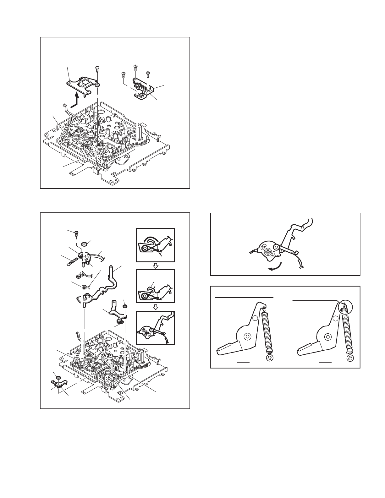
5. [9] Exit guide arm assembly/ [10] Swing arm assembly
[9]
[10]
<Note5a>
(W1)
Note 5a:
Exit guide arm assembly phase alignment.
Exit guide arm assembly
This protrusion is
combined to
the dent of Charge
arm assembly.
Charge arm assembly
Gear alignment
Exit guide arm
assembly
Arm gear 2
assembly
Fig.4-5-5a
Fig.4-5-5
6. [11] Sub deck assembly/ [12] Main brake (Supply) assembly/[13] Main brake (Take up) assembly
Note 6a:
When attaching the sub deck assembly, make sure to
adjust the phase of the control plate.
Main brake (Supply)
OK NG
Fig.4-5-6a
(P4)
(P5)
[13]
[12]
(
L10
15
(S2)
16
(S2)
)
(
)
L11
<Note6a>
18
(S2)
17
(S2)
[11]
Main brake (Take up)
spring hooked
reverse-side
Twisted spring
1-22 (No.YD091)
Fig.4-5-6
OK NG
Fig.4-5-6b
Page 23
7. [14] Reel disk assembly (Supply) / [15] Reel disk assembly (Take up) / [16] Prism / [17] Control plate
[14]
21
(S2)
[11]
20
(S2)
19
22
(S2)
[16]
Note 8a:
When attaching, set the alignment markings of the two
gears so that the markings face opposite to each other.
[19]
[18]
[15]
[17]
(
)
L12
(
)
L12
Fig.4-5-7
8. [18] Guide rail (Take up) assembly / [19] Guide rail (Supply) assembly / [20] Base plate assembly
(
)
L13
24
<Note8a>
(S2)
[19]
25
(S2)
(S2)
[18]
[20]
(
L14
23
(S2)
Fig.4-5-8a
)
Fig.4-5-8
(No.YD091)1-23
Page 24
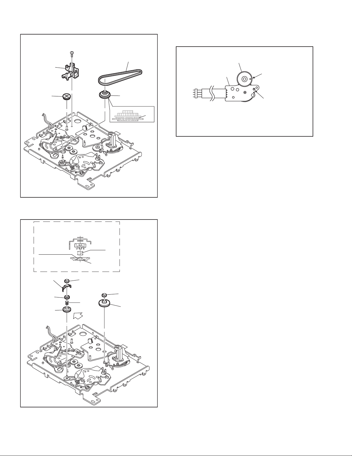
9. [21] Ent. guide base assembly / [22] Worm wheel 2 / [23] Timing belt / [24] Center gear assembly
Note 9a:
26
(S2)
How to attach the worm wheel 2 [22] .
[23]
[22]
[21]
[34]
<Note9a>
[22]
Fig.4-5-9
10. [25] Reel drive pulley assembly / [26] Push plate/ [27] Clutch lock gear (2) / [28] Clutch lock gear (1)
Detail "A"
<Note10b>
(P6)
Flange
[28]
[24]
[23]
Align the phase of the rotary encoder assembly [34],
then attach it by aligning the phase hole of the
mechanism assembly.
Fig.4-5-9a
Note 10a:
After attaching (W1), confirm that pushes [26] from the
top and hit to MAIN DECK. If there are a rattling or inclination in [26] , reconfirm the attachment of (P6). (Take
care to the oblique insertion of (P6).)
Note 10b:
Attach (P6) straight for it which does not get on on the
flange of [28]
Phase alignment
Mark (Red)
[26]
<Note10a>
[27]
[28]
1-24 (No.YD091)
(W1)
(P6)
"A"
Fig.4-5-10
(W1)
[25]
Page 25
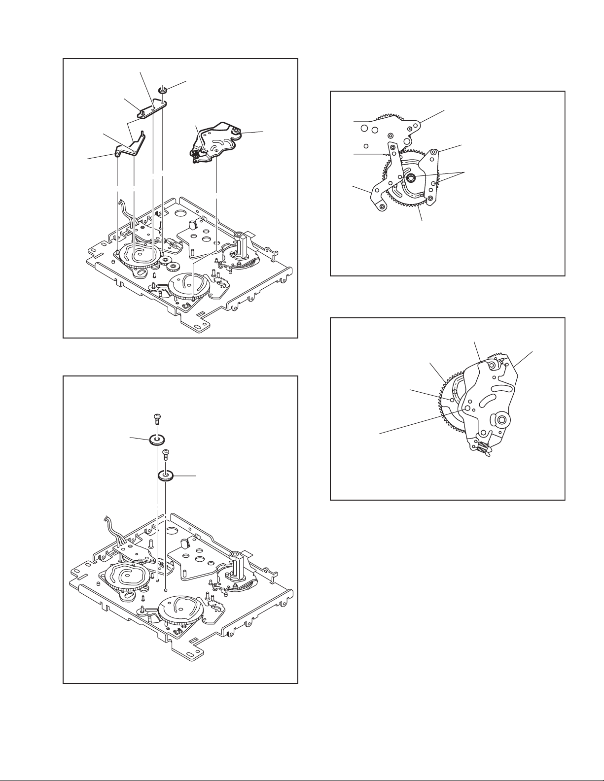
11. [29] Tension control arm assembly/ [30] Brake control arm assembly / [31] Charge arm assembly
(
L16
)
(W1)
Note 11a:
How to attach the tension control arm assembly [29] /
Brake control arm assembly [30] .
[30]
[34]
(
<Note11a>
(
)
L15
L17
)
[31]
<Note11b>
[30]
[29]
Boss
[29]
(Phase alignment)
[35]
Align the phase of the main cam [35], then attach it by
fitting the bosses into the cam slot.
Fig.4-5-11a
Note 11b:
How to attach the charge arm assembly [31]
[31]
Fig.4-5-11
[38]
12. [32] Connect gear 2 / [33] Connect gear 2
[39]
[32]
27
(S2)
28
(S2)
[33]
Phase alignment
Boss
(Phase alignment)
Align the phase of the sub cam [38], then attach it by
fitting the boss into the cam slot.
Fig.4-5-11b
Fig.4-5-12
(No.YD091)1-25
Page 26
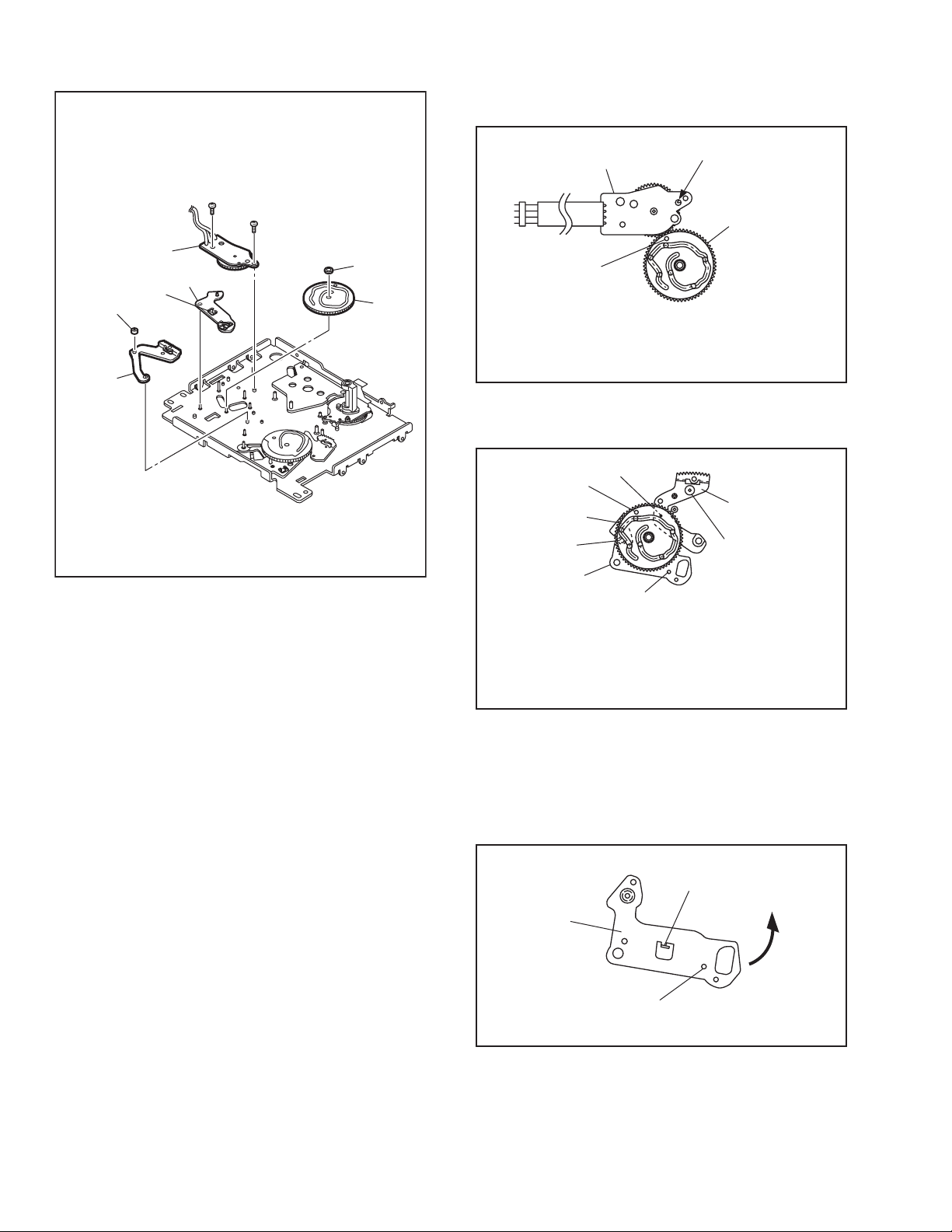
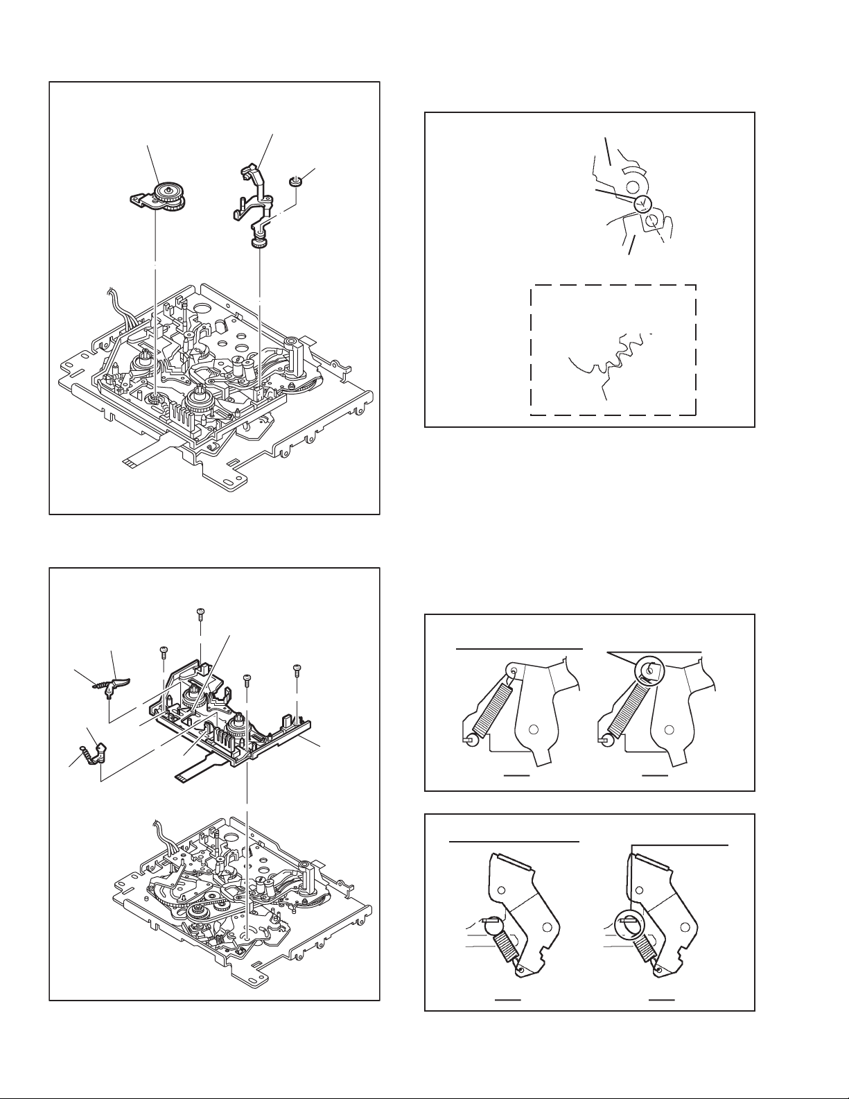
13. [34] Rotary encoder assembly / [35] Main cam / [36] Arm gear 1 assembly / [37] Centering arm assembly
Note 13a:
How to attach the rotary encoder assembly [34].
Collar
<Note13b>
[36]
<Note13a>
[34]
[37]
(
)
L18
<Note13c>
29
(S2)
(S2)
<Note13b>
Fig.4-5-13
[34]
30
Mark (colored : red)
[35]
(W1)
[35]
<Note13b>
Phase alignment
Align the phase of the main cam [35],then attach it by
placing the (red) coloured markings (on 2 gear teeth)
within the encircled area.
Fig.4-5-13a
Note 13b:
How to attach the main cam [35] .
Boss
Phase alignment
[35]
Boss
[36]
Phase alignment
[37]
Phase alignment
Align the phases of the arm gear 1 assembly [36] and
centering arm assembly [37],then attach the arm gear 1
assembly [36]/centering arm assembly [37] by fitting the
bosses into the lower cam slot,and fit the slit washer.
Fig.4-5-13b
Note 13c:
How to remove the centering arm assembly [37] The
center arm assembly is located behind the mechanism
assembly when the phase is aligned correctly. The center arm assembly can be removed by displacing it in the
direction of the arrow.
(L18)
[37]
Phase alignment
Fig.4-5-13c
1-26 (No.YD091)
Page 27
14. [38] Sub cam / [39] Arm gear 2 assembly / [40] Clutch lock lever assembly
Note 14a:
How to attach the sub cam [38].
31
(S2)
<Note14a>
<Note14a>
[38]
[40]
Phase alignment
[38]
Boss
[39]
Phase alignment
[40]
<Note14b>
(
)
L19
Fig.4-5-14
15. [41] Capstan motor / [42] Drum base deck
32
(S2)
33
(S2)
34
(S2)
[42]
<Note14a>
[39]
Phase alignment
Align the phases of the arm gear 2 assembly [39] and
clutch lock lever assembly [40],then attach them by fitting
the boss into the lower cam slot and tighiten the screws.
Fig.4-5-14a
Note 14b:
How to remove the clutch lock lever assembly [40] L19
is located behind the mechanism assembly when the
phase is aligned correctly. The clutch lock lever assembly can be removed by displacing it in the direction of
the arrow.
Phase alignment
[40]
(L19)
Adjust nut
Fig.4-5-15
Fig.4-5-14b
[41]
(P7)
(No.YD091)1-27
Page 28
4.6 List of procedures or disassembly
[24]
[23]
[17]
29
(S2)
[34]
[7]
(P3)
[12]
[29]
(W2)
[21]
30
(S2)
25
(S2)
[20]
Collar
14(S3)
[8]
26
(S2)
(W1)
[27]
[13]
[28]
(S2)
[35]
[37]
[26]
(P6)
16
[14]
(W1)
[32]
(S2)
[30]
[22]
15
[11]
33
(S2)
(W1)
[15]
27
(S2)
32
(S2)
Adj. nut
(P7)
28
(S2)
[33]
19
(S2)
[16]
34
(S2)
(W1)
[6]
17
(S2)
(S2)
[42]
[18]
18
(W1)
[25]
21
(S2)
31(S2)
[19]
[41]
[38]
[10]
20
(S2)
[4]
(S2)
23
(S2)
12
(S2)
(S2)
[31]
22
24
8(S2)
[5]
9(S2)
(S2)
10
4
(S2)
(W1)
(S2)
6(S2)
11
(S2)
[3]
[9]
13
7(S2)
[2]
3
(S2)
5
(S2)
[1]
(W1)
1-28 (No.YD091)
[40]
[36]
[B]
Fig.4-6-1
[39]
Page 29
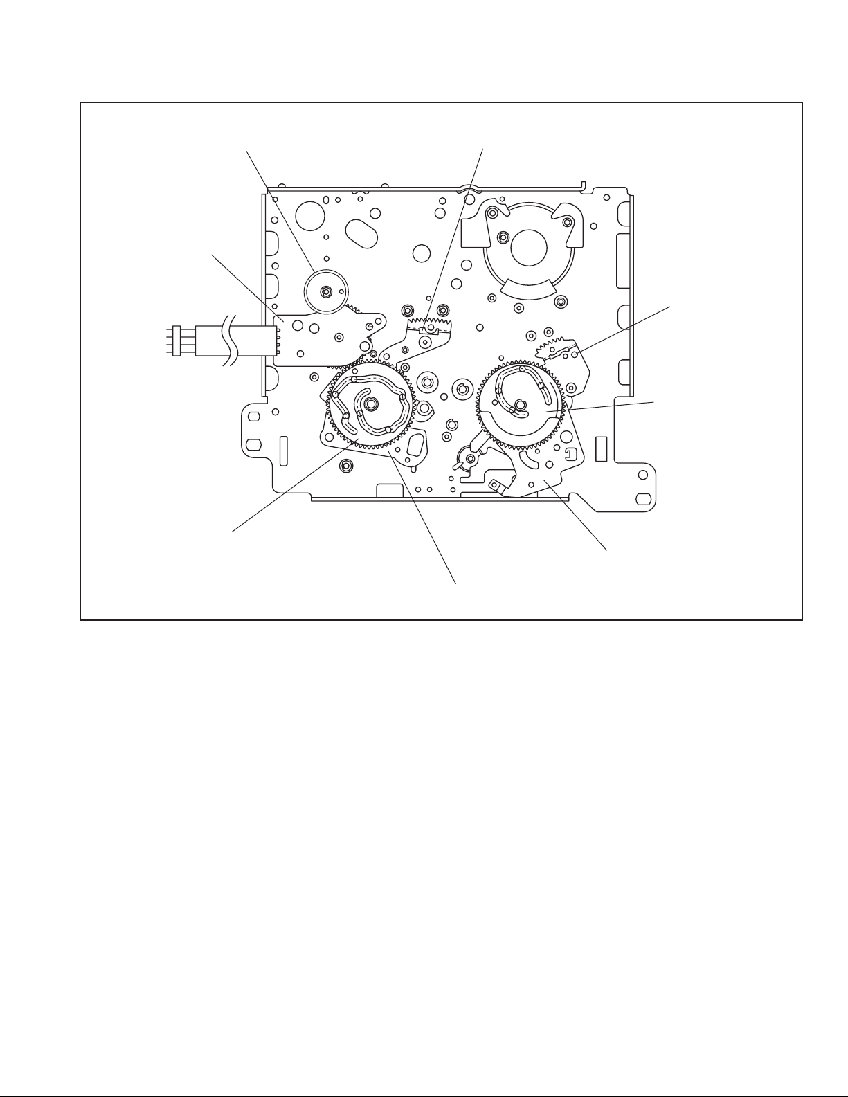
4.7 Mechanism phase check/adjustment
See Fig 4-7-1.
[22]
[34]
Rotary encoder assembly
See Figs. 4-5-9a and
4-5-13a.
Worm wheel 2
See Fig. 4-5-9a.
[36]
Arm gear 1 assembly
See Fig. 4-5-13b.
[39]
Arm gear 2 assembly
See Fig. 4-5-14a.
[38]
Sub cam
See Fig. 4-5-14a.
[35]
Main cam
See Figs. 4-5-13a and 4-5-13b.
[37]
Centering arm assembly
See Fig. 4-5-13b.
Fig.4-7-1
[40]
Clutch lock lever assembly
See Fig. 4-5-14a.
(No.YD091)1-29
Page 30
4.8 Mechanism disassembly/assembly sheet
Fig. No.
No.
Type
[A][
1 18234567891011121314151617
S1
Attachin
Ref. Fig.
Screw Management Table
4-5-1 4-5-2 4-5-3
[A] Cassette housing assembly
1
(S1)
(L4)
(L1)
(L3)
][
1
][
2
[1] Drum assembly
4
(S2)
2
(S1)
S2×3
[2] Motor bracket assembly
(L2)
(L5)
9
(S2)
8
(S2)
S2×4
[3] Middle catcher assembly
12
(S2)
][
3
3
(S2)
10
(S2)
6
(S2)
(S2)
7
(S2)
11
(S2)
][7][
4
11
]
S2 S2 S2
4-5-4
4-5-6
[4] Reel cover assembly
5
(S2)
S2, L6×2
[5]
Pinch roller arm assembly
(W1)
W1, L7
[6] Sub brake assembly
(W1)
S2S1 S2 S2 S2 S2 S2 S2 S2 S2 S2 S2 S2 S3
13
(P1)
S1×2, L1-L5
S2×3
P1, W1, L8
[17] Control plate [18] Guide rail (Take up) assembly [19] Guide rail (Supply)
assembly
(
)
L13
24
(S2)
21
(S2)
20
(S2)
22
(S2)
23
(S2)
L12×2 S2×4 S2, L13×2
[24] Center
gear
assembly
[25] Reel drive
pulley
assembly
(W1)
[26] Push
plate
(W1)
[27] Clutch
lock gear
(2)
(W3)
[28] Clutch
lock
gear (1)
(P6)
[29] Tension control arm
assembly
(
)
L15
[30]
Brake
control arm
assembly
(
L16
W1 W1 W3 P6 L15 W1, L16
[35] Main cam [36] Arm gear 1 assembly
(W1)
Collar
[37]
Centering arm assembly
(
)
L18
[38] Sub cam
31
(S2)
) (W1)
W1 Collar L18 S2
1-30 (No.YD091)
Fig.4-8-1a
Page 31

[16][
][
18
][20][21][32][33][34][38][
19
42
]
19 20 21 22 23 24 25 26 27 28 29 30 31 32 33 34
S2 S2 S2 S2 S2 S2 S2 S2 S2
S2 S2 S2 S2 S2 S2 S2
4-5-7 4-5-9
[7] Band arm plate sub
assembly
(P2)
14
(S3)
(W2)
[11] Sub deck assembly
S3, P2, L9, W2
[8] Tension arm sub
assembly
(P3)
P3
[9]
Exit guide arm assembly
(W1)
S2×4
[10] Swing arm assembly
16
(S2)
18
(S2)
4-5-14
17
(S2)
[12]
Main
Brake(Supply)
assembly
(P4)
[13]
Main
Brake(Take up)
assembly
(P5)
4-5-12 4-5-13 4-5-154-5-8
15
(S2)
P4, L10 P5, L11
[14]
Reel disk
assembly
(Supply)
[15]
Reel disk
assembly
(Take up)
[16] Prism
19
(S2)
W1
[20] Base plate assembly
[21] Ent. guide base
[22] Worm wheel 2 [23] Timing belt
S2
assembly
25
(S2)
26
(S2)
S2, L14×2 S2
[31] Charge arm assembly [32] Connect gear 2 [33] Connect gear 2 [34] Rotary encoder
assembly
33
(S2)
29
(S2)
(S2)
32
(S2)
(
L17
)
27
(S2)
L17 S2 S2
[39] Arm gear 2 assembly [40] Clutch lock lever
[41] Capstan motor [42] Drum base deck
assembly
(
)
L19
28
(S2)
S2×2
Adjust nut
(P7)
L19 S2×3Adjust nut, P7
Fig.4-8-1b
30
34
(S2)
(No.YD091)1-31
Page 32

4.9 Positioning the tension pole
See Fig.4-9-1.
Tension arm sub
assembly
[B] section
[C]
[D] section
4.9.1 Adjustment Method
Note:
• Remove the cassette housing assembly in advance.
(1) Set the mechanism mode to the PLAY mode. (See
4.2.2 Mechanism modes)
(2) Loosen a screw [A].
(3) Check the location of the tip (section [B]) of the ten-
sion arm assembly to make sure that it is within area
[C]. If it is located outside, turn part [D] to bring it
within the specified area.
(4) Tighten the screw [A].
Note :
Tightening torque for the screw [A] : 0.06 N.m (0.6kgf.cm)
screw [A]
Fig.4-9-1
1-32 (No.YD091)
Page 33

4.10 Compatibility and error rate adjustment
4.10.1 Preparation
Before disassembly and adjustment, back up the data stored in
the EEPROM (IC1504 on the DV MAIN board) using the Service
Support System Software (SSS software).
Table 4-10-1 shows the important service points for the compatibility and error rate adjustments.
Drum
replacement
Transport part
replacement
Transport part
(drum) repair
IC4001(PRE/REC
amp on DV MAIN
board) replacement
IC2001(PB. EQ on
DV MAIN board)
replacement
DV MAIN board
replacement
Note 2
Linearity
adjustment
Required
Note 1
Required
Note 1
Required
Note 1
PB Switching
point
adjustment
Required Required
Not Check
Not Check
Not Not Check
Not Not Required
Not Required Required
Error rate
adjustmenmt
Table 4-10-1
Note 1 :
• The linearity adjustment is required only after servicing
or replacing the drum or the take up/supply guide rail.
Note 2 :
• After replacing the DV MAIN board, write the original
data in the EEPROM of the new board. If write communication is not possible, mount the original EEPROM on
the new board.
When adjustments of more than one item are required, use the
following order for the adjustments.
4.10.3 Linearity adjustment
4.10.2.2 Procedure
(1) Take out the 8 screws, then remove the top cover. (See
SECTION 3 DISASSEMBLY)
(2) Connect the jig connector cable to CN2001 on the DV
MAIN board.
Jig Connector Cable
PTU94018B
CN1505
CN2001
B
CN3701
DV
MAIN PW
CN1501
Fig.4-10-2
4.10.2.3 Setup for computer adjustment
-Setup by extending the jig connector-
Connect the Jig Connector Cable and setup the SSS software. It
automatically becomes the TCCS mode and "TCCS" is displayed
on the FDP.
To cancel the TCCS mode, press the CANCEL button of the remote
control unit.
The "TCCS" display on the FDP disappears.
Service Support Software
4.10.4 PB switching point adjustment
4.10.5 Error rate adjustment
4.10.2 Adjustment
The actual adjustment requires the following preparation.
4.10.2.1 Tools required for adjustment
Alignment tape
US : MC-1
PAL : MC-2
SSS software
PTU94016-5
Guide driver
YTU94085
PC cable
US : QAM0099-002
PAL : QAM0099-005
Jig connector cable
PTU94018B
Jig RCU
PTU94023B
Fig.4-10-1
N
C
D
3701
MAIN PWB
V
RS-232C Port
PC Cable
<JLIP>
N1505
C
2001
N
C
1501
N
C
JVC
MENU
Personal Computer
Fig.4-10-3
(No.YD091)1-33
Page 34

4.10.3 Linearity adjustment
The following flowchart shows the linearity check/adjustment
procedure.
4.10.4 PB switching point adjustment
The following flowchart shows the PB switching point adjustment
procedure.
Connect an oscilloscope (CH: + Slope) and, while
triggering it with the HID signal, observe the ENV OUT
Play the alignment tape, then set “ATF” (Auto Tracking
Find) in “Deck Controller” of the SSS Software to ON.
(Note 3)
Ensure that the ENV OUT waveform is linear and parallel,
without a noticeable drop or variation in the overall level. If
the waveform linearity is poor or there is a noticeable drop
in level, adjust the guide roller by turning it with the roller
driver.
Set “ATF” (Auto Tracking Find) to OFF using “Deck
Controller” of the SSS Software (Note 4). Observe the ENV
OUT waveform to confirm that the overall waveform
balance and linearity levels vary in accordance with the
tracking variation as shown in Fig. 4-10-4.
Repeat above steps
as required.
No
Is the PB ENV waveform ideally
stable and does it vary ideally
according to the tracking variation?
Load the alignment tape.
The “PB Switching Point” in the Adjustment Utility of
the SSS software is adjusted automatically.
4.10.5 Error rate adjustment
The following flowchart shows the error rate adjustment procedure.
Record for about 5 minutes. (Note 6)
While playing the recorded signal, adjust “
” or “
Frequency (ME SP)
“Deck Section” of the Adjustment Utility.
To adjust VCO Center Frequency (ME SP) : Set Viterbi OFF.
To adjust VCO Center Frequency (ME LP) : Set Viterbi ON.
No
Is the obtained error rate minimum
(almost the typical value)?
VCO Center Frequency (ME LP)
VCO Center
” in
Yes
The linearity adjustment is complete if the PB ENV
waveform is ideally stable and varies ideally according to
the tracking variation. To close, play a prerecorded tape
and check the audio and video.
HID waveform
PB ENV
waveform
CH1
CH2
Adjust variation
in the parallelism
Fig.4-10-4
Note 3 :
• If ATF is turned off, the DV section performs tracking
only of the speed system. Therefore, as time passes, the
servo will be lost and the linearity adjustment will become difficult.
Note 4 :
• Since the speed servo function is active when ATF is
off, there will be no problem even if the DVC ATF function is off, provided that it is for a few minutes.
Yes
The error rate adjustment is complete when the minimum
error rate which is no higher than the typical value is
obtained. (Note 5)
Note 5 :
• The "typical value" refers to the following:CH1 or CH2:
< 498 ; with Viterbi OFF. Inter-channel difference: < 10
times between CH1 and CH2.
Note 6 :
• It is desirable to use a brand-new tape or an unused sec-
tion of tape. This is to assure the adjustment reliability
because using a damaged tape increases the error rate.
4.10.6 Error rate measuring method
It is not necessary to use the error rate jig (YTU93083) or a frequency counter. The Service Support System Software displays
the error rates of video CH1, CH2 and totals. When measuring
the error rate of a channel, be sure to total the values of the video
and the audio errors.
1-34 (No.YD091)
Page 35

4.11 Electrical adjustment (DV SECTION)
4.11.1 Precautions
(1) The DV section of this model is based on a special adjust-
ment method using a PC. However, ordinary adjustment is
required only when the part listed below has been replaced. In this case, the adjustment should be performed
by a service center equipped with the required facilities.
• E2 PROM (IC1504 on DV main board)
In case of trouble with the electrical circuitry, First identify
the faulty position with a measuring tool as described below. Proceed to repair, replacement and/or adjustment only
after the troubleshooting.
(2) When observing a chip TP, use an IC clip or similar tool to
protect the chip against stress. When replacing a chip part
(IC, particularly), remove solder completely before replacing. (This is to prevent separation of the pattern.)
(3) The connectors are fragile. Be careful when plugging or un-
plugging a wire.
4.11.2 Equipment required for adjustment
• Personal computer (Windows compatible)
• Color monitor
• Oscilloscope (2-CH, 100 MHz or more)
• Frequency counter
4.11.4 Setup
1. Setup for computer adjustment
- Setup by extending the jig connector -
-Setup by extending the jig connector-
Connect the Jig Connector Cable and setup the SSS software. It
automatically becomes the TCCS mode and "TCCS" is displayed on
the FDP.
To cancel the TCCS mode, press the CANCEL button of the remote
control unit.
The "TCCS" display on the FDP disappears.
Service Support Software
RS-232C Port
PC Cable
<JLIP>
JVC
MENU
Personal Computer
4.11.3 Tools required for adjustments
Alignment tape
US : MC-1
PAL : MC-2
SSS software
PTU94016-5
Guide driver
YTU94085
PC cable
US : QAM0099-002
PAL : QAM0099-005
Fig.4-11-1
Jig connector cable
PTU94018B
Jig RCU
PTU94023B
CN3701
DV MAIN PW
CN1505
B
CN2001
CN1501
Fig.4-11-2
(No.YD091)1-35
Page 36

4.12 Electrical adjustment (DVD SECTION)
Note:
The following adjustment procedures are not only necessary
after replacement of consumable mechanical parts or board
assemblies, but are also provided as references to be referred
to when servicing the electrical circuitry.
In case of trouble with the electrical circuitry, always begin a
service by identifying the defective points by using the measuring instruments as described in the following electrical adjustment procedures. After this, proceed to the repair,
replacement and/or adjustment. If the required measuring instruments are not available in the field, do not change the adjustment parts (variable resistor, etc.) carelessly.
4.12.1 DVD Video circuit
Note
• When perform these adjustments, set the unit to DVD
mode.(DVD lamp lights up)
4.12.1.1 EE Composite Y level
Signal (A) • Internal colour bar
Mode (B) • EE
Equipment (C) • Oscilloscope
Measuring point (D) • L-1 connector pin19
EVR mode
EVR address
Specified value (G) • 1.00 ± 0.02 Vp-p (terminated)
Adjustment tool (H) • Jig RCU [PTU94023B]
(F1)
• Jig code “43-95”
(F2)
• "ADJUST01 : **"
(F3)
• Jig code “43-21”
(F4)
• Jig code “43-18” or “43-19” (Channel +/-)
(F5)
• Jig code “43-3C”
(1) Observe the V OUT waveform at the measuring point (D).
(2) Set the VCR to the EVR mode by transmitting the code (F1)
from the Jig RCU.
(3) Set the EVR address to (F2) by transmitting the code (F3)
from the Jig RCU.
(4) Transmit the code (F4) from the Jig RCU to adjust so that
the Y level of the V OUT waveform becomes the specified
value (G).
(5) Release the EVR mode of the VCR by transmitting the
code (F5) from the Jig RCU again. (When the EVR mode
is released, the adjusted data is memorized.)
Specified
value (G)
H. rate
Fig.4-12-1 EE composite Y level
4.12.1.2 EE Y level
Signal (A1)
Mode (B) • EE
Equipment (C) • Oscilloscope
Measuring point (D) • L-1 connector pin19
EVR mode
EVR address
Specified value (G) • 1.00 ± 0.02 Vp-p (terminated)
Adjustment tool (H) • Jig RCU [PTU94023B]
• Ext. input
(A2)
• Color (colour) bar signal
• Jig code “43-95”
(F1)
• "ADJUST02 : **"
(F2)
• Jig code “43-22”
(F3)
• Jig code “43-18” or “43-19” (Channel +/-)
(F4)
• Jig code “43-3C”
(F5)
(1) Observe the V OUT waveform at the measuring point (D).
(2) Set the VCR to the EVR mode by transmitting the code (F1)
from the Jig RCU.
(3) Set the EVR address to (F2) by transmitting the code (F3)
from the Jig RCU.
(4) Transmit the code (F4) from the Jig RCU to adjust so that
the Y level of the V OUT waveform becomes the specified
value (G).
(5) Release the EVR mode of the VCR by transmitting the
code (F5) from the Jig RCU again. (When the EVR mode
is released, the adjusted data is memorized.)
Specified
value (G)
H. rate
Fig.4-12-2 EE Y level
4.12.1.3 EE composite burst level
Signal (A) • Internal colour bar
Mode (B) • EE
Equipment (C) • Oscilloscope
Measuring point (D) • L-1 connector pin19
EVR mode
EVR address
Specified value (G) • 0.30 ± 0.01 Vp-p (terminated)
Adjustment tool (H) • Jig RCU [PTU94023B]
• Jig code “43-95”
(F1)
• "ADJUST00 : **"
(F2)
• Jig code “43-20”
(F3)
• Jig code “43-18” or “43-19” (Channel +/-)
(F4)
• Jig code “43-3C”
(F5)
(1) Observe the V OUT waveform at the measuring point (D).
(2) Set the VCR to the EVR mode by transmitting the code (F1)
from the Jig RCU.
(3) Set the EVR address to (F2) by transmitting the code (F3)
from the Jig RCU.
(4) Transmit the code (F4) from the Jig RCU to adjust so that
the burst level of the V OUT waveform becomes the specified value (G).
(5) Release the EVR mode of the VCR by transmitting the
code (F5) from the Jig RCU again. (When the EVR mode
is released, the adjusted data is memorized.)
1-36 (No.YD091)
Page 37

Specified
value (G)
Fig.4-12-3 EE composite burst level
4.12.1.4 EE R/G/B level
Signal (A) • Internal colour bar
Mode (B) • EE
Equipment (C) • Oscilloscope
Measuring point (D1)
EVR mode
EVR address
Specified value (G) • 0.70 ± 0.02 Vp-p (terminated)
Adjustment tool (H) • Jig RCU [PTU94023B]
• L-1 connector pin15(R)
• L-1 connector pin11(G)
(D2)
• L-1 connector pin7(B)
(D3)
• Jig code “43-95”
(F1)
• "ADJUST05 : **"
(F2)
• Jig code “43-25”
(F3)
• Jig code “43-18” or “43-19” (Channel +/-)
(F4)
• Jig code “43-3C”
(F5)
(1) Observe the R OUT waveform at the measuring point (D1).
(2) Set the VCR to the EVR mode by transmitting the code (F1)
from the Jig RCU.
(3) Set the EVR address to (F2) by transmitting the code (F3)
from the Jig RCU.
(4) Transmit the code (F4) from the Jig RCU to adjust so that
the R level of the R OUT waveform becomes the specified
value (G).
(5) Release the EVR mode of the VCR by transmitting the
code (F5) from the Jig RCU again. (When the EVR mode
is released, the adjusted data is memorized.)
(6) Observe the G OUT waveform at the measuring point (D2).
(7) Repeat steps (2) to (5) above.
(8) Observe the B OUT waveform at the measuring point (D3).
(9) Repeat steps (2) to (5) above.
Fig.4-12-4 EE R/G/B level
4.12.1.5 EE COMPONENT PB/CB level
Signal (A) • Internal colour bar
Mode (B) • EE
Equipment (C) • Oscilloscope
Measuring point (D) • COMPONENT PB/CB terminal
EVR mode
EVR address
Specified value (G) • 0.70 ± 0.02 Vp-p (terminated)
Adjustment tool (H) • Jig RCU [PTU94023B]
• Jig code “43-95”
(F1)
• "ADJUST06 : **"
(F2)
• Jig code “43-26”
(F3)
• Jig code “43-18” or “43-19” (Channel +/-)
(F4)
(F5)
• Jig code “43-3C”
(1) Observe the CB OUT waveform at the measuring point (D).
(2) Set the VCR to the EVR mode by transmitting the code (F1)
from the Jig RCU.
(3) Set the EVR address to (F2) by transmitting the code (F3)
from the Jig RCU.
(4) Transmit the code (F4) from the Jig RCU to adjust so that
the CB level of the CB OUT waveform becomes the specified value (G).
(5) Release the EVR mode of the VCR by transmitting the
code (F5) from the Jig RCU again. (When the EVR mode
is released, the adjusted data is memorized.)
PB/CB level
Fig.4-12-5 EE component PB/CB level
4.12.2 Syscon circuit
Notes:
• When perform this adjustment, remove the Mechanism
assembly.
4.12.2.1 Timer clock
Signal (A) • No signal
Mode (B) • EE
Equipment (C) • Frequency counter
Measuring point (D1)
Adjustment part (F) • C3025 (TIMER CLOCK)
Specified value (G) • 1024.008 ± 0.001 Hz
• IC3001 pin 61
• IC3001 pin 17
(D2)
• C3026 + and -
(D3)
(976.5549 ± 0.0010 usec)
(1) Connect the frequency counter to the measuring point
(D1).
(2) Connect the short wire between the short point (D2) and
Vcc (5V).
(3) Short the leads of capacitor (D3) once in order to reset
the microprocessor of the Syscon.
(4) Disconnect the short wire between the short point (D2)
and Vcc then connect it again.
(5) Adjust the Adjustment part (F) so that the output frequency
becomes the specified value (G).
(No.YD091)1-37
Page 38

SECTION 5
TROUBLESHOOTING
5.1 Manually removing the cassette tape
If a loaded cassette tape cannot be ejected due to a failure in the
electrical circuitry, take the cassette tape out using the following
procedure. However, this method consists of a forced driving of
the loading motor. Therefore, the following description assumes
that there is no trouble in the mechanism operations.
(1) Unplug the power plug from the power outlet, then remove
the top cover.
(2) Apply 3 V DC to the electrodes (Red wire: + pole. Brown
wire: - pole) on the upper part of the loading motor to perform the unloading operation so that the pole base assemblies are returned on the inner side of the tape. At this time,
the exit guide arm assembly should return toward the drum
assembly and the mechanism should enter the C-IN mode.
As the tape is left without winding, be careful not to damage
the tape or leave grease on it.
–
DC 3 V
+
Motor bracket assembly (Loading motor)
(3) If the tape is slack, wind it up by turning the shaft on the top-
side of the capstan motor in the direction of the arrow using
a pointed tool (chip IC replacement jig).This operation may
be difficult because the shaft is located below the housing
motor of the cassette housing assembly. Be careful not to
damage parts during it.
(4) After confirming that the tape is fully wound up, take out the
cassette tape by turning the gear of the cassette housing
assembly in the direction of the arrow.
Note :
• After ejecting the tape, check that grease or similar for-
eign material is not attached to the wound tape. Also
perform similar checking for the mechanism assembly,
particularly the tape transport system.
Wire (Brown)
Wire (Red)
Pole base assembly (Supply)
Rotary encoder assembly
[3] Tape winding [4] Tape ejection
[A]
Capstan motor Cassette housing assembly, side view
Exit guide arm assembly
Cassette housing motor
[A]
Pole base assembly (Take up)
[B]
Cassette housing assembly
[B]
1-38 (No.YD091)
Chip IC replacement jig
Shaft
Capstan motor
Gear
Ejection direction
Fig.5-1a
Page 39

5.2 Manually removing the disk(DVD/CD)
If you cannot remove the disk which is loaded because of any electrical or mechanical failures, manually remove it by taking the following steps.
5.2.1 Method 1
(1) AC Plug is pulled out at once and inserted again.
(2) It is displayed on FDP as "PLEASE" and "WAIT" alternately, and while it blinks, pushing the OPEN/CLOSE button is continued.
(3) After a while, a tray opens (About 20 seconds).
(4) After removed a disk, press the OPEN/CLOSE button again to close the tray.
(5) The "PLEASE" and "WAIT" alternately blink display of FDP disappears and it will be in a standby mode.
(6) If the POWER button is pushed, it will usually be operating.
5.2.2 Method 2
When < Method 1 > can not remove the disc, the tray can be ejected mechanically without turning the power on.
(1) The DVD drive unit is detached from the main body.
(2) The part a on the reverse side of a drive unit is made to slide in the direction of an arrow with a screw driver etc.
(3) As the tray ejects a little, pull out the tray manually.
Part a
5.3 Emergency display function (DV SECTION)
This unit saves details of the last emergency as the EMG history
and allows the status of the unit and the mechanism each emergency to be shown both on the display and as OSD information.
When using the emergency function, it is required to set the unit
to the Jig RCU mode.
Jig RCU
[Data transmitting method]
Depress the " " ( 3 ) button
after the data code is set.
CUSTOM CODE
43: A CODE
DATA CODE
INITIAL MODE
Fig.5-3a Jig RCU [PTU94023B]
5.3.1 Displaying the EMG information
The EMG detail of information can be displayed by transmitting
the code "43-59" from the Jig RCU.
Note:
• Press DV/HDD/DVD on the unit repeatedly or DV on the
remote so that the DV lamp lights up on the unit.
• The EMG detail information < 1 >< 2 > show the informa-
tion on the latest EMG.
It becomes " - - : - - : - - " when there is no latest EMG
record.
00:00 Normal display
E:BB:CC
EMG content display<2> See5.3.4
EMG content display<1> See5.3.4
M:DD:EE EMG detail information<1> See5.3.5
[DV mechanism position]
[DV deck operation mode]
S:FF:GG EMG detail information<2> See5.3.6
[Type of the DV cassette tape]
[DV mechanism sensor information]
C:HH:II EMG detail information<3> See5.3.7
[DV doctor check-sum]
[DV CPU version]
EMG display of FDP display mode
(1) Transmit the code “43-59” from the Jig RCU.
The FDP shows the EMG content in the form of “E:**:**”.
(No.YD091)1-39
Page 40

<Example 1> E : 00 : 80
EMG content display(2)
EMG content display(1)
<Example 2> E : - - : - -
No EMG record
(2) Transmit the code "43-59" from the Jig RCU again.
The FDP shows the EMG detail information < 1 > in the
form of "DD" and "EE".
DD : DV deck operation mode at the moment of EMG
EE : DV mechanism mode position at the moment of EMG
(3) Transmit the code "43-59" from the Jig RCU once again.
The FDP shows the EMG detail information < 2 > in the
form of "FF" and "GG".
FF : DV mechanism sensor information
GG: Type of the DV cassette tape
(4) Transmit the code "43-59" from the Jig RCU once again.
The FDP shows the EMG detail information < 3 > in the
form of "HH" and "II".
HH : DV CPU version information
II : DV doctor check-sum
(5) Transmit the code “43-59” from the Jig RCU once again to
reset the display.
5.3.2 Clearing the EMG history
(1) Display the EMG history.
(2) Transmit the code “43-36” from the Jig RCU.
(3) Reset the EMG display.
5.3.3 Details of the OSD display in the EMG display mode
During the EMG display, the OSD shows the data on the deck
mode, etc. The details of the display contents are as follows.
Notes:
• The sensor information in the OSD display contents is
partially different from the mechanism sensor information in EMG detail information < 1 >.
AA BB CC
DD EE
FF
HH
GG
II
KKKK LLLL MMMM
ROM No.
AA : Key code (JVC code)
BB : EMG content display < 1 >
CC : EMG content display < 2 >
DD : DV deck operation mode (See EMG detail information
< 1 >)
EE : DV mechanism position (See EMG detail information <
1 >)
FF : Dv mechanism sensor information (See EMG detail in-
formation < 2 >)
GG : Type of DV cassette tape (See EMG detail information
< 2 >)
HH : DV CPU version
I I : DV doctor check-sum
KKKK : General data display area
LLLL : General data display area
MMMM : General data display area
5.3.4 EMG content description
5.3.4.1 EMG content display < 1 >(BB)
FDP DISPLAY
E : 41 : 00 Mechanism Mode
E : 42 : 00 Mechanism Mode
E : 04 : 00 Take Up Reel FG
E : 08 : 00 Supply Reel FG
E : 10 : 00 Drum FG
E : 20 : 00 Capstan FG
EMG MODE CONTENT CAUSE
If the mechanism mode does not change to the next mode
Transition Failure
(Loading)
Transition Failure
(Unloading)
within 4 seconds after the loading motor starts rotating in
the loading direction, [E : 41 : 00] is identified and the
power is switched OFF.
If the mechanism mode does not change to the next mode
within 4 seconds after the loading motor starts rotating in
the unloading direction, [E : 42 : 00] is identified and the
power is switched OFF.
When the take-up reel pulse has not been generated for
more than 3 seconds in the capstan rotating mode,[E : 04 :
00] is identified, the pinch rollers are turned off and
stopped, and the power is turned off.
When the supply reel pulse has not been generated for
more than 3 seconds in the capstan rotating mode, [E : 08 :
00] is identified and the pinch rollers are turned off and
stopped, and the power is turned off.
When the drum FG pulse has not been input for more than
4 seconds in the drum rotating mode, [E : 10 : 00] is
identified, the pinch rollers are turned off and stopped, and
the power is turned off.
When the capstan FG pulse has not been generated for
more than 2 seconds in the capstan rotating mode, [E : 20 :
00] is identified, the pinch rollers are turned off and
stopped.
5.3.4.2 EMG content display < 2 >(CC)
FDP DISPLAY
E : 00 : A0 Housing Motor
E : 00 : C0 Housing Motor
EMG MODE CONTENT CAUSE
If the operation has not been completed 3 seconds after the
Operation Failure
(Cassette ejection)
Operation Failure
(Cassette insertion)
cassette housing started the cassette ejection operation, [E
: 00 : A0] is identified, the cassette is taken in, and the
mode is switched to STOP the pinch roller OFF.
If the operation has not been completed 3 seconds after the
cassette insertion, [E : 00 : C0]n is identified, and the
cassette is ejected.
1. The mechanism is locked in the middle of the mode transition.
2. The mechanism overruns the encoder position during the mode transition, and is locked at the
mechanism loading end.
3. Power is not supplied to the loading MDA.
1. The mechanism is locked in the middle of the mode transition.
2. The mechanism overruns the encoder position during the mode transition, and is locked at the
mechanism loading end.
3. Power is not supplied to the loading MDA.
1. The take-up reel pulse is not generated in the FWD transport modes (PLAY/FWD SEARCH/FF,
etc.) because;
1) The idler gear is not meshed with the take-up reel gear.
2) The idler gear is meshed with the take-up reel gear, but incapable of winding due to t
1. The supply reel pulse is not generated in the FWD transport mode (PLAY/FWD SEARCH/FF,etc.)
because;
1) A cassette with broken tape is inserted, and PLAY/FWD SEARCH/FF are carried out.
2) A mechanical factor caused tape slack inside/ outside the supply
1. The drum could not start or the drum rotation has stopped due to too large load on the tape,
because;
1) The tape tension is abnormally high. 2) The tape is damaged or a foreign object (grease,
etc.) adheres to the tape.
2. The drum FG pulse did not re
1. The capstan could not start or the capstan rotation has stopped due to too large load on the
tape, because;
1) The tape tension is abnormally high (mechanical lock);
2) The tape is damaged or a foreign object (grease, etc.) is adhered to the tape (occu
1. The cassette cannot be ejected due to a failure in the drive mechanism of the housing.
2. When the housing load increases during ejection, the loading motor is stopped because of lack
of headroom in its drive torque.
Housing load increasing facto
1. The cassette cannot be ejected due to a failure in the drive mechanism of the housing.
2. When the housing load increases during ejection, the loading motor is stopped because of lack
of headroom in its drive torque.
Housing load increasing facto
1-40 (No.YD091)
Page 41

5.3.5 EMG detail information < 1 >
The status (electrical operation mode) of the unit and the status
(mechanism operation mode/mechanism position) of the mechanism in the latest EMG can be confirmed based on the figure in
EMG detail information < 1 > .
[FDP/OSD display] (DD, EE)
DD : DV deck operation mode at the moment of EMG
EE : DV mechanism position at the moment of EMG
5.3.6 EMG detail information < 2 >
FF : DV mechanism sensor information
Display
DV mechanism sensor information DV mechanism sensor information
bit7
Tape end
bit6
Tape start
bit5
Rec safety switch
Display
bit3
bit2
Tape ID detect
Tape exist
Note:
The display of DV mechanism sensor information differs according to the operation mode.
DD : DV deck operation mode
Display
Deck operation mode Deck operation mode
00
UNLOADING STOP
01
CASSETTE EJECT
02
LOADING STOP
03
PLAY (Normal playback)
04
STILL
05
FF
06
REW
07
SEARCH FWD
08
SEARCH REWIND
09
FWD SLOW
0a
REV SLOW
0b
AUDIO DUB
0c
AUDIO DUB PAUSE
0d
RETAKE FF
0e
RETAKE REW
10
REHEARSAL UNLOADING STOP
11
REHEARSAL EJECT
12
REHEARSAL LOADING STOP
13
REC
14
REC PAUSE
15
DV REC
16
DV REC PAUSE
17
VIDEO INSERT
18
VIDEO INSERT PAUSE
19
SOFT PAUSE
EE : DV mechanism position
Display
DV mechanism position DV mechanism position
0
Cassette being inserted
1
Intermodal position
2
Short FF
3
Intermodal position
4
Loading end
5
Intermodal position
6
Capstan FWD
7
Intermodal position
Display
1a
POWER OFF
1b
REC LOCK
1c
1ST REC
1d
LOCK
1e
REC
3a
POWER OFF REQUEST
5a
POWER OFF REQUEST2
aa
WAIT
ba
NO DATA
7F
FWD SEARCH(high speed)
6F
FWD SEARCH(middle speed)
5F
FWD SEARCH(low speed)
4F
FWD PLAY
3F
FWD LINEAR SLOW
2F
FWD INTERMITTENT SLOW
1F
FWD FRAME ADVANCE
0F
STILL
FF
REV FRAME ADVANCE
EF
REV INTERMITTENT SLOW
DF
REV LINEAR SLOW
CF
REV PLAY
BF
REV SEARCH(low speed)
AF
REV SEARCH(middle speed)
9F
REV SEARCH(high speed)
Display
8
Capstan REV
9
Intermodal position
0A
Stop
0B
Intermodal position
0C
FF/REW
0D
Intermodal position
0E
Mechanism being initialized
GG : Type of DV cassette tape (bit3, bit2)
Display
DV mechanism sensor information DV mechanism sensor information
00
MP type
01
Cleaning tape
Display
10
11
Not used
ME type
5.3.7 EMG detail information < 3 >
HH : DV CPU version
DV SYSCON CPU version is displayed.
II : DV doctor check-sum
It is not usually used.
(No.YD091)1-41
Page 42

5.4 Display function of DVD section
5.4.1 Displaying SYSTEM INFO
SYSTEM INFO contains information on firmware version of the unit and the mechanism drive, and an initialize execution menu.
(1) Set the unit to the Jig RCU mode.
(2) Press DV/HDD/DVD SELECT button on the unit repeatedly so that the HDD lamp lights up on the unit.
(3) Transmit "43-8b" from the Jig RCU.
(4) SYSTEM INFORMATION menu is displayed in the screen.
(5) To move cursor in SYSTEM INFO, use the " ", " ", " ", and " " buttons of a remote control unit attached to product.
(6) To quit the SYSTEM INFO menu, transmit "43-8b" from the Jig RCU..
(7) Cancel Jig RCU mode.
The example of a display < Version Info 1 >
System Info
Version Info 1
Version Info 2 NAVI Info Initialize
Application Software Version
Boot Loader Software Version
DVD Drive Firmware Version
0.12
1.2/276
J014
Firmware version of the main body.
When the firmware of the main body is updated,
this part is changed.
Firmware version of the drive unit.
Region
CPRM Key DownLoad
OK
EXIT
SELECT
SELECT WITH [ ] THEN PRESS [ENTER]
PRESS [ "8b" ] TO EXIT
2
Done
When the firmware of the main body is updated,
this part is changed.
NOTE:
Items other than the ones described above are not used in service work.
5.4.2 Displaying the firmware version of the main body in the user mode
The version information of the main body firmware can be displayed in the normal mode (user mode) without using the Jig mode.
The version can be checked by the user operation when it is required to check the version when there are failure inquiries from the
users.
(1) Turn the power of the main body ON.
(2) Press the “SET UP” button of the supplied remote control unit to display the setting menu screen.
(3) Move the arrow to the “INITIAL SET UP” tab, keep pressing the “STOP” button of the main body for 10 seconds in that condition.
(4) The screen changes to the display shown in the below diagram, and the firmware version of the main body is indicated.
DVD VIDEO SET UP
MENU BACKGROUND
HDD/DVD SET UP
CLOCK SET
FUNCTION SET UP
INITIAL SET UP
1-42 (No.YD091)
VERSION : 0.11
O K
Page 43

5.4.3 Updating the firmware of the unit
• Firmware update disc supports CD-R media.
• When firmware update is necessary, information is available from the website of DIGITAL VIDEO STORAGE CATEGORY, CS
group.
5.4.3.1 Creating an update disc
Please check the details of the update disc creation method by JS-NET.
(1) Down load the update file from JS-NET.
(2) Write the update file into CD-R. Pay attention in the following points when writing the update disc.
• Make sure to write in “Disc at Once”.
• Set the file compatibility to “ISO9660 format”. (ROMEO, JOLIET are disapproved.)
If the writing method is not correct, the update results in an error.
5.4.3.2 Update procedure
• There are two methods of updating firmware, using JIG RCU mode < method 1 > or not using JIG mode(User update mode) < method 2 >.
Both methods can be used to update the firmware.
< Method 1 >
(1) Set to the Jig RCU mode.
(2) Press DV/HDD/DVD SELECT button on the unit repeatedly so that the DVD lamp lights up on the unit.
(3) Load the update disc on the tray, and then close the tray.
(4) When the disc reading operation is completed, transmit “43-70” with the Jig remote control unit.
If the update disc is not correct, FDP indicator displays an “ERROR” after transmitting “43-70”. Transmit “43-70” once and
make the FDP indicator to normal display, and then reload the disc then transmit “43-70” again.
(5) “UPDATE” is displayed in the FDP indicator, and the FDP indicator changes to “FW UPDATE” afterwards. It takes approx. 2
minutes for the change.
(6) Remove the disc as the tray is ejected, and then transmit “43-70” with the Jig remote control unit. Then the FDP indicator
changes from “UPDATE” to the normal display.
(7) Close the tray and turn the unit OFF. Pull out the power code from the wall socket, then plug the power cord into the wall socket
again.
(8) "PLEASE" and "WAIT" blink alternately and it is displayed in FDP indicator. Then, turn the main body ON.
(9) Check the version of the firmware.
(10) Cancel the Jig RCU mode.
< Method 2 >
(1) Turn the power ON. Load the update disc on the tray and close the tray.
(2) Press DV/HDD/DVD SELECT button on the unit repeatedly so that the DVD lamp lights up on the unit.
(3) When the disc reading operation is completed, Check “CD” or “DVD-R” display in the FDP indicator .
(4) When keep pressing the “STOP” button of the main body for 5 seconds,“UPDATE” is displayed in the FDP indicator and the
update is started.
(5) In approx. 2 minutes the tray is ejected. Remove the disc. The tray is automatically closed.
(6) Reset operation is carried out automatically, and it becomes standby condition.
(7) Check the version of the firmware.
5.4.4 Updating the firmware of the drive unit
• Firmware update disc supports only DVD-RAM media.
• When firmware update is necessary, written discs are distributed by DIGITAL VIDEO STORAGE CATEGORY, CS group.
(1) Turn the unit ON.
(2) Press DV/HDD/DVD SELECT button on the unit repeatedly so that the DVD lamp lights up on the unit.
(3) Load the update DVD-RAM disc on the tray and close the tray.
(4) “READING” is displayed in the FDP indicator and the update is started.
(5) In a short while “READING” in the FDP indicator disappears, open the tray to remove the disc and close the tray.
(6) Turn the power OFF and pull out the power code from the wall socket, then plug the power cord into the wall socket again.
(7) Set to the Jig RCU mode and check the firmware version of the drive.
(No.YD091)1-43
Page 44

5.4.5 Initialization to the factory shipment state
When the initialization is operated, internal information changes as follows. It is essential to obtain the client’s permission before the
operation.
• All DVD library is all deleted.
• All the DVD initial settings go back to the initial status.
(1) Set to the Jig RCU mode.
(2) Press DV/HDD/DVD SELECT button on the unit repeatedly so that the DVD lamp lights up on the unit.
(3) Transmit “43-6F” with the Jig remote control unit.
(4) FDP indicator displays “FACTORY”, and changes to “CHECK OK” after blinking for a short while.
(5) Pull out the power code from the wall socket.
(6) The Jig RCU mode is forced to cancel at the same time with the initialization, check whether the Jig RCU mode is canceled by
plugging the power code into the wall socket again. (The colon “:” in time display should be continuously ON, not blinking.)
If the Jig RCU mode is not canceled, transmit “43-9D” with Jig remote control unit to cancel the Jig RCU mode.
5.4.6 Setting after the drive unit replacement
When the drive unit is replaced, it is necessary to set a region code. Service drive units for replacement are not set for any region
code, and they are in an indefinite condition.
Make sure to set region code after attaching the drive unit to the unit.
Without the setting of the region code, discs that have regions cannot be played back.
5.4.6.1 Creating a region setting disc.
Please check the details of the region setting disc creation method by JS-NET.
(1) Download the region setting file from JS-NET.
(2) Write the region setting file into CD-R. Pay attention in the following points when writing the file into CD-R.
• Make sure to write in “Disc at Once”.
• Set the file compatibility to “ISO9660 format”. (ROMEO, JOLIET are disapproved).
If the writing method is not correct, the normal setting cannot be performed.
5.4.6.2 Setting the region
(1) Set for the Jig RCU mode.
(2) Press DV/HDD/DVD SELECT button on the unit repeatedly so that the DVD lamp lights up on the unit.
(3) Load the region setting disc on the tray, and then close the tray.
(4) When the disc reading operation is completed, transmit “43-70” with the Jig remote control unit.
(5) FDP indicator changes to “UPDATE”. Remove the disc as the tray will open for a few seconds.
(6) Then, check whether the FDP indicator is “REGION 2 (or 3)”.
(7) Transmit “43-70” with the Jig remote control unit. When FDP indicator changes to “OPEN”, close the tray.
(8) Turn the power OFF, and pull out the power code, and then plug the power code in again.
(9) Cancel the Jig RCU mode.
1-44 (No.YD091)
Page 45

(No.YD091)1-45
Page 46

Victor Company of Japan, Limited
DIGITAL VIDEO STORAGE CATEGORY 12, 3-chome, Moriya-cho, kanagawa-ku, Yokohama, kanagawa-prefecture, 221-8528, Japan
(No.YD091)
Printed in Japan
VPT
Page 47

SCHEMATIC DIAGRAMS
Mini DV & HDD & DVD VIDEO RECORDER
SR-DVM700EU
CD-ROM No.SML200603
Area Suffix
EU -------- Western Europe
DVDTV
STANDBY/ON
TV
/
OUTPUT
TV
VIDEO
SELECT
DV HDD DVD
TV
PR/CH
CANCEL
MEMO/MARK
INPUTSELECT
EDIT
F2
PROG
F1
NAVIGATIONTOPMENU
ENTER
MENU
RETURN
NEXTPREVIOUS
SLOWSLOW PLAY
PAUSEREC
STOP/CLEAR
DISPLAY
ONSCREEN
RECMODE/
AUDIO
SUBTITLE
REMAIN
PROGRESSIVE
SCAN
STANDBY/ON
ANGLE/
EECHECK
SETUPDUBBINGEE
S-VIDEO
INF-1
VIDEO(MONO)L - AUDIO - R
INPUT
OUTPUT
SELECT
SELECT
EJECTEJECTDISPLAY
RECDVDRECHDDRECDV
DV/HDD/DVD REC MODE INSTANT REPLAY AUDIODUB. INSERT
RECPAUSEPLAY
FFREWSTOP
DVIN/ OUT
SR-DVM700EU [D5MC29]
Since the whole mechanism assembly unit is replaced, the DVD recorder
mechanism of this unit need not be adjusted.
COPYRIGHT 2006 Victor Company of Japan, Limited
No.YD091SCH
2006/3
Page 48

Page 49

CHARTS AND DIAGRAMS
NOTES OF SCHEMATIC DIAGRAM
Safety precautions
The Components indentified by the symbol are
critical for safety. For continued safety, replace safety
critical components only with manufacturer's recommended parts.
1. Units of components on the schematic diagram
Unless otherwise specified.
1) All resistance values are in ohm. 1/6 W, 1/8 W (refer to
parts list).
Chip resistors are 1/16 W.
K: KΩ(1000Ω), M: MΩ (1000KΩ)
2) All capacitance values are in µF, (P: PF).
3) All inductance values are in µH, (m: mH).
4) All diodes are 1SS133, MA165 or 1N4148M (refer to parts
list).
Note: The Parts Number, value and rated voltage etc. in
the Schematic Diagram are for references only.
When replacing the parts, refer to the Parts List.
2. Indications of control voltage
AUX : Active at high.
AUX or AUX(L) : Active at low.
!
4. Voltage measurement
1) Regulator (DC/DC CONV) circuits
REC : Colour bar signal.
PB : Alignment tape (Colour bar).
— : Unmeasurable or unnecessary to measure.
2) Indication on schematic diagram
Voltage indications for REC and PB mode on the schematic diagram are as shown below.
REC mode
12 3
2.5
(5.0)
PB mode
1.8
PB and REC modes
(Voltage of PB and REC modes
are the same)
Note: If the voltages are not indicated on the schematic
diagram, refer to the voltage charts.
6. Indication of the parts for adjustments
The parts for the adjustments are surrounded with the circle
as shown below.
CIRCUIT BOARD NOTES
1. Foil and Component sides
1) Foil side (B side) :
Parts on the foil side seen from foil face (pattern face)
are indicated.
2) Component side (A side) :
Parts on the component side seen from component face
(parts face) indicated.
Parts location are indicated by guide scale on the circuit board.
2. Parts location guides
Parts location are indicated by guide scale on the circuit board.
LOCATION
IC
Category : IC
Horizontal “A” zone
Vertical “6” zone
(A : Component side)
D : Discrete component)
B : Foil side
C : Chip component
REF No.
IC101 B C 6 A
3. Interpreting Connector indications
1
2
Removable connector
3
1
2
Wire soldered directly on board
3
1
Non-removable Board connector
2
3
1
2
4
Board to Board
3
Connected pattern on board
The arrows indicate signal path
7. Indication of the parts not mounted on the circuit board
“OPEN” is indicated by the parts not mounted on the circuit
board.
R216
OPEN
2-1 2-2
Page 50

Wiring diagram
5
9
CN7401
QGF1016C3-041RX
4
3
2
1
SENSOR
M
DV
HOUSING MOTOR
432
DV
ENCORDER
97 D-SUB CONN
94
92
50
36
28
27
16
11 DC/DC CONV
03
02
01 SW REGULATOR
NO NAME
1
R.JACK
JUNCTION
DV MAIN
DV JACK
SW/DISPLAY
SW/JACK
MDA
MAIN
DIGITAL
1
15 CASSETTE SW
2
14 MIC 1
3
13 GND
4
12 TU REEL LED
5
11 TU REEL SENSOR
6
10 MIC 2
7
9 SUP REEL LED
8
8 SUP REEL SENSOR
9
7 END SENSOR
10
6 MIC 3
11
5 LED
12
4 GND
13
3 START SENSOR
14
2 GND
15
1 REC SAFETY SW
1
2
3
4
7
D-SUB CONN
2 GND
3TX
4 D3.3V
CN1502
QGF0505F2-15X
CN1501
1 4.5V(M)
2 FF/REW_6V
3 MDA_6V
4 AL5V(DV)
5 GND(M)
1 GND
2 HOUSING SW
3 HOUSING MOTOR+
4 HOUSING MOTOR-
1 R.ENC3
2 R.ENC2
3 R.ENC1
4 GND
QGF0503C1-20X
##:NOT USED.
CN5404
QGF1207C1-08
7 SW_5V
8 SW_7V[-]
1234567
CN1001
QGF1211F1-08W
CN7301
##
QGF1016C3-05
6 GND
5 SW_3V
5GND
0
4 GND
##
CN1505
##
CN7402
1 D3.3V
4RX
QGF1016C2-04W
5
QGA2001C1-05
CN5403
1 4.5V(M)
2 FF/REW_6V
3 MDA_6V
4 SW5V(DV)
5 GND(M)
2TX
3 GND
4RX
1D3.3V
2TX3GND
0
DV MAIN
(MSD CPU,DV I/O,AUDIO AD/DA,VIDEO OUT,
DV MAIN,REG,PRE/REC,MSD,DV I/O, AUDIO)
1 GND
2 DRUM PG
3 DRUM FG
4 CAP FG
5 LD ON
6 CAP BAK
7 MDA CS
8 MDA CLK
9 MDA IN
10 MDA OUT
11 MOTOR GND
12 DRUM REF
13 CAP REF
14 HOUSING IN
15 HOUSING OUT
16 HOUSING SW
17 GND
18 CAM SW1
19 CAM SW2
20 CAM SW3
987654321
COIL U
14
13 COIL U
12 MR VCC
121110
13
1 6 MDA
8 HG U+
9 HG V-
10 HG V+
11 HG IN+
987654321
7 HG IN-
6 HG W-
5 HG W+
DV VIDEO HEAD
1 FG2
2 MR GND
3 FG1
4 HG U-
181716151413121110
1 GND(M)
2 COIL COMMON
DV DRUM MOTOR
20191817161514
15 COIL W
16 COIL W
17 COIL V
18 COIL V
DV CAPSTAN MOTOR
1GND
2G_TX
3IRTX
4G_RX
3
MAIN
(
VIDEO SW DVD, REG,
VIDEO SW DVC,
TERMINAL,
)
CN3501
QGF1016F2-07W
CN3701
QGF1016F2-08W
CN1503
QGF1211F1-07F
CN2002
QGA2001C6-06X
62F
72S
8 GND
1 TPA1+
2 TPA1-
3 GND
4 TPB1+
5 TPB1-
6 GND
8
4
1 LOAD.MOTOR+
10 PG OUT
10
2 LOAD.MOTOR-
11 FG OUT11
1 MDA_CTL
2 GND
3 SW_3V
8
CN4001
QGF0503C1-08X
1 GND
21F
1234567
3 PG/FG COMMON
4 COIL W
5 COIL W
6 COIL V
ON SCREEN,
31S
4 GND
5 GND
123
9 COIL U
7 COIL V
8 COIL U
987654321
M
LOADING MOTOR
SYSCON,AUDIO I/O,
7
6
5
4
3
2
1
8GND
7DV_A_PB[R]
6GND
5DV_A_PB[L]
4GND
3DV_A_REC[R]
2GND
1DV_A_REC[L]
7
6
5
4
3
2
1
CN3104
QGF1207C1-15
CN7201
QGF1209F1-15
2
1 GND
2 V_IN
15
7
CN501
QGF1016C3-07
1 D_C_IN
2 GND
3 D_Y/V_IN
4 GND
5 D_C_OUT
6 GND
7 D_Y_OUT
CN2601
QGF1016C3-08
1 GND
2 DV_A_PB[R]
3 GND
4 DV_A_PB[L]
5 GND
6 DV_A_REC[R]
7 GND
8 DV_A_REC[L]
CN3014
QGF1016C3-07
1 MSD_RESET
2 MSELECT
3 S.CLK2
4 S.DATA_TOSYS
5 S.DATA_FRSYS
6 MSD_READY
7 DV_H.SW
3 GND
4 Y_IN
5 GND
6 C_IN
1011121314
SW/JACK
CN5001
HD_AT[5]
HD_AT[13]
ATA_A2
HD_AT[6]
HD_AT[15]
3 IRTX
4 G_RX
CN2101
DMARQ
IORDY
DASP-
CN2201
IORDY
GND
5 GND
QGA2501C1-04
CN5303
1 DV12V
40RSTSTA 1
39GND
38HD_AT[7]
37HD_AT[8]
36HD_AT[6]
35HD_AT[9]
34
33HD_AT[10]
32HD_AT[4]
31HD_AT[11]
30HD_AT[3]
29HD_AT[12]
28HD_AT[2]
27
26HD_AT[1]
25HD_AT[14]
24HD_AT[0]
23HD_AT[15]
22GND
21KEY
20
19GND
18DIOW
17GND
16DIOR
15GND
14
13CAB_SEL
12DMACK
11GND
10INT_ATA
9IOCSI6-
8ATA_A1
7PDIAG-
6ATA_A0
5
4CS1FX
3CS3FX
2
1GND
40RSTSTA
39GND
38HD_AT[7]
37HD_AT[8]
36
35HD_AT[9]
34HD_AT[5]
33HD_AT[10]
32HD_AT[4]
31HD_AT[11]
30HD_AT[3]
29HD_AT[12]
28HD_AT[2]
27HD_AT[13]
26HD_AT[1]
25HD_AT[14]
24HD_AT[0]
23
22GND
21KEY
20DMARQ
19GND
18DIOW
17
16DIOR
15GND
14
13CAB_SEL
12DMACK
11GND
10INT_ATA
9IOCSI6-
8ATA_A1
7PDIAG-
6ATA_A0
5ATA_A2
4CS1FX
3CS3FX
2DASP-
1GND
QGA7901C3-02
QGA2001C1-02
2 GND
3 GND
2
3
4
5
6
7
8
9
10
11
12
13
14
15
16
17
18
19
20
21
22
23
24
25
26
27
28
29
30
31
32
33
34
35
36
37
38
39
40
1
2
3
4
5
6
7
8
9
10
11
12
13
14
15
16
17
18
19
20
21
22
23
24
25
26
27
28
29
30
31
32
33
34
35
36
37
38
39
40
2LIVE
1NEUTRAL
Only for SR-DVM***US
CN5302
1FAN12V
2GND
4 DC5V
1DV12V
2GND
DVD_DRIVE
3GND
4DC5V
HDD
1DV12V
2GND
3DV12V
4GND
5GND
6DV5V
7DV5V/3.3V
8GND
##
CN5305
117V
2 GND
9 GND
7 GND
8 F.AUDIO[L]
10 F.AUDIO[R]
11 GND
12 KEYIN1
13 KEYIN2
CN5301
QGF1207C1-15
CN5402
QGF1207C1-15
14 BLUE_LED
15 AL5V
123456789
1 SW5V
2 SW12V
3 BT2
19
0 1 SW REGULATOR
4 45V
5 FAN_CTL[H]
6 SW-7V
7 GND
8 GND
9 P.SAVE[L]
10 AL5.8V
11 P.CTL[H]
12 M12V
13 GND[M]
101112131415161718
FOR JIG
CN3901
##
QGF1207C1-06
1
2
3
4
5
6
CN3102
QGF1207C1-15
1NC
2 DC+3.5V
3 -29V
4 DC-3.5V
5 STB
6 S.DATA_FRSYS
7 S.DATA_TOSYS
8 S.CLK
9
10
8
SW/DISPLAY
8
1514131211
CN7001
QGF1209F2-15
2
14 M26V
15 GND[M]
56789
QGF1207C1-04
QGF1207C1-13
QGB1231L1-11
QGB1231L1-19
9 RC_IN
10 AL5V
11 GND
12 B.UP_GND
13 BLUE_LED
7654321
QGF1209F1-04
CN701
4
3
2
1
CN901
13
12
11
10
9
8
7
6
5
4
3
2
1
CN2602
11
10
9
8
7
6
5
4
3
2
1
CN3103
19
18
17
16
15
14
13
12
11
10
9
8
7
6
5
4
3
2
1
14 LED9[DVD_TIMER]
15 LED10[DVD]
##
CN7002
4DC3.5[-]
3-29V
2DC3.5[+]
1GND
CN7123
QGF1207C1-04
1 YTODIGI
2 GND
3 CTODIGI
4 GND
CN7107
QGF1207C1-13
1 VDR_V
2 VDR_V
3 GND
4 VDR_Y
5 GND
6 VDR_C
7 GND
8 GND
9 VDR_DY
10 GND
11 VDR_PB
12 GND
13 VDR_PR
CN8001
QGB1231M1-11
11 AD_IEC958
10 V3.3V
9 GND
8 GND[A]
7 DD_IN[L]
6 GND
5 DVD_IN[R]
4 GND
3 DVD_OUT[L]
2 GND
1 DVD_OUT[R]
CN7102
QGB1231M1-19
19 P.SAVE[L]
18 SW5V
17 -29V
16 DC-3.5V
15 DC+3.5V
14 HDD_P.SAVE[L]
13 ADC_RESET[L]
12 A.MUTE_VDR[H]
11 GND
10 SYNC_DET_VDR[L]
9 P.CTL[H]
8 P.MUTE_VDR[H]
7 KBUS_DATA_TOSYS
6 KBUS_DATA_FRSYS
5 KBUS_REQ
4 KBUS_CLK
3 SYS_RESET[L]
2 P.MUTE_VDR[L]
1 I.MUTE[L]
##
CN5507
1 FAN2
2 GND
##
CN7103
QGF1207C1-04
1 DC-3.5V
2 -29V
3 DC+3.5V
4 GND
CN7127
QGA2001C1-06
1 TPA1+
2 TPA1-
CN5304
QGF1207C1-19
1 SW12V
2 12V
3 SW-7V
4 12V
5 P.CTL(H)
6 DVD_P.CTL(H)
7 HDD_P.S(L)
8 DDGND
9 DDGND
10 DD6V
11 GND
12 GND
13 GND
14 GND
15 DC(+)
16 DV6V
17 DC(-)
18 AL5.8V
19 -29V
CN5506
CN5505
6 DV5V
123456789
CN5502
QGA2001C1-06
TO JIG
## CN7125
CN7106
QGF1016C1-04
QGB2027M3-28S
QGB2027M4-20S
QGB2027M9-14
1 DV12V
2 GND
3 DV12V
4 GND
5 GND
CN7108
CN7109
CN7121
CN1003
QGA2001F6-06X
1 GND
1GND
2 GND
2GND
3 D3.3V
3D3.3V
4 D2.5V
4D2.5V
5 D1.8V
5D1.8V
6 D1.8V
6D1.8V
4JLIP_RX
3GND
2JLIP_TX
1D3.3V
1D3.3V
2JLIP_TX
3GND
4JLIP_RX
1 JLIP_RX
2 GND
3 JLIP_TX
4 D3.3V
4 D3.3V
3 JLIP_TX
2 GND
1 JLIP_RX
1DAC_PR_OUT
1
3DAC_PB_OUT
3
5DAC_Y_OUT
5
7GND
7
9RCOUT
9
11COUT
11
13480I[H]
13
15GND
15
17GND
17
19AO_FSYNC
19
21DAC_RST[L]
21
23A_DAC_CS
23
25DAC_SDA
25
27DAC_SCL
27
1
1VD
3
3A_MUTE2[H]
5
5AI_D[0]
7
7P_CTL[H]
9
9PMUTE[H]
11
11K_BUS_IN
13
13K_BUS_OUT
15
15GND
17
17GND
19
19A0_IEC958
1
1GND
3
3TPB-
5
5GND
7
7TPA+
9
9GND
11
11TPB-
13
13TPA-
2RYOUT
2
4GND
4
6YVOUT
6
8GND
8
10CROUT
10
12GND
12
14CBOUT
14
16GND
16
18VYIN
18
20CIN
20
22GND
22
24AO_MCLK
24
26AO_SCLK
26
28AO_D[0]
28
2
2K_BUS_CLK
4
4K_BUS_REQ
6
6SYS_RESET[L]
8
8SYNCDET
10
10SW5V
12
12GND
14
14D5.0V
16
16V3.3V
18
18GND
20
20GND
2
2GND
4
4TPB+
6
6TPA-
8
8GND
10
10GND
12
12TPB+
14
14TPA+
ASSETSU
CN1403
QGF1016C6-04W
CN1001
QGB2027L5-28X
CN1002
QGB2027L5-20X
CN1802
QGB2027L1-14X
0
CN1405
QGF1016F8-04W
FOR JIG
2
123
##CN1402 [MH30]
DIGITAL
4
CN1401
QGF1016C2-05W
##
QGF0508C2-40W
QGF0508C2-40W
1 GND
2 G_TX
19
CN5501
QGF1207C1-19
1
101112131415161718
TO JIG [FOR_JVC]
##
CN7124
QGF1207C1-04
1 JLIP_RX
2 GND
3 JLIP_TX
4 D3.3V
TO JIG
[FOR_LG]
CN7105##
1 JLIP_RX
2 GND
3 JLIP_TX
4 D3.3V
TO JIG
CN7106
QGF1040C1-04
1 D3.3V
2 JLIP_TX
3 GND
4 JLIP_RX
CN5702
1
1DGND
2
2DGND
3
3DGND
CN5701
1
1COUT
2
2D1.8V
3
3D1.8V
4
4VAR1.8V
5
5DGND
6
6DGND
7
7Vin
8
8DGND
9
9VAR2.5V
10
10D2.5V
11
11DGND
12
12Vin
13
1
13DGND
DC DC CONV
9
2
JUNCTION
(VIDEO,AUDIO AD/DA,REG)
CN7126
QGA2001C1-06
CN4104
QGA2001C1-06
DV JACK
3 GND
4 TPB1+
5 TPB1-
6 GND
1 TPA-
2 TPA+
3 GND
4 TPB+
5 TPB-
6 GND
12345
6
3
6
CN5503[Y42]
7 DV5V/3.3V
8 GND
OVER ALL WIRING
AC 220V-240VEU:
50Hz
US:
AC 120V
60Hz
AC 100V
JP:
50/60Hz
M
FAN MOTOR
1
2
p10810001a_rev0
A
BCDEFG
2-3 2-4
Page 51

Standard schematic diagrams
Switching regulator section
01
SW.REG MAIN(REG)
5
LIVE
BLK
BRN
CN5001
2
1
NEUTRAL
WHT
BLU
4
3
##
R5001
4.7M
1/2W
DANGEROUS VOLTAGE
100p/250
470p/50
##
C5001
0.068/250
C5105
SG5001
(GAP)
VA5003
OCP/
FB
5
R5107
QQR1031-001
680
LF5002
1
4
32
0.022/250
IC5101
STR-G6653-F9
2S1D4
C5104
220p
1k
R5106
3.9k
R5108
0.33
1W
##
C5006
GAP
C5002
D5104
1SS133
1SS270A
4
Vcc3GND
32
4
1
3
2
0.1/50
C5106
0.01/50
R5301
220
R5302
4.7k
1
IC5301
L5431
MM1431AT
UTCTL431
GND
F5001
T2AL/250
VA5001
##
QAF0023-431
B5001##
C5005
QAF0023-431
D5001
KBJ4J
GBJ4J
2
3
C5003
100/400
C5108
PC5101
PC123Y82
PC123Y22
PS2581AL1/QW/
C5301
0.15/50
MY
MY
1
R5101
C5302
0.033/50
R5303
T5001
QQS0367-001
7
C5103
82/35
FR
D5103
1F4G-G
1F4G
10ERB20
R5304
R5305
R5109
47
1/4W
D5101
SARS01
6.8k
20k
2SB709A/QR/
2SA1037AK/QR/
2SA1530A/QR/
D5105
1F4G-G
1F4G
10ERB20
R5102
820
R5104
C5102
4700p
1k
100p/1k
1k
Q5319
6
C5101##
5
R5105
18
3
2
C5004
2200p/250
R5335
10k
R5334
10k
R5103
680k
1/4W
150k
2W
D5106
SBO40
1S4
C5107
330p/50
1.5k
R5306
3.9k
D5213
HER202G-B322-3
UF-202G-F26
11
D5301
##
14
12
9
10
15
13
16
17
18
MTZJ15A
D5310
1SS355
D5205
SB240-B322-3
SB240-F26
D5204
SX34
D5207
SX34
D5212
SX34
C5205
2200/10
D5209
SB240-B322-3
SB240-F26
C5208
1200/10
L5207
10u
##
C5307
100/16
2
3
D5308
DAP202U
1
2
Parts are safety assurance parts.
When replacing those parts make
sure to use the specified one.
ALL RESISTANCE VALUES ARE IN OHMS.
ALL INDUCTANCE VALUES ARE IN H.
ALL CAPACITANCE VALUES ARE IN F.
ELECTROLYTIC
CERAMIC
MY
1
N
MYLER
NON POLAR
.NOTES:UNLESS OTHERWISE SPECIFIED
C5204
1500/16
D5202
1F4G-G
10ERB20
L5203
10u
C5309
47/25
L5201
10u
B5312
C5303
100/16
##
C5304
100/16
1F4G
C5202
4.7/100
L5204
10u
L5205
10u
L5301
SHORT
C5206
C5306
3300/10
220/10
D5214
C5211
1F4G-G
18/50
1F4G
10ERB20
D5307
MTZJ7.5B
Q5317
RT1P141C
UN2111
2
3
D5309
1
DAP202U
D5211
RS1G
R5332
C5305
220/10
56
##
R5331
D5306
2SC3928A/QRS/
2SD601A/QRS/
R5330
CP5301
1.5A/125
CP
D5210
1F4G-G
1F4G
10ERB20
56
220/6.3
C5210
Q5306
2SC6007/F/
R5314
D5304
MTZJ5.6C
Q5316
5.6k
C5209
18/50
MTZJ12B
##
C5310
2.2/50
120
Q5318
RT1N141C
UN2211
C5333##
0.1/16
HER202G-B322-3
Q5305
2SC3576-JVC
2SD2144S/VW/
D5303
R5315
1/2W
390
C5312
220/10
##
C5335
0.1/16
D5305
##
UF202G-F26
B5308
0.1/16
C5311
100/16
##
C5334
0.1/16
##
C5336
R5313
10k
Q5307
2SA1585S/QR/
R5316
10k
R5317
1k
Q5308
RT1N141C
UN2211
Not used
TO
SHEET 23
1 SW12V
2 12V
3 SW-7V
4 12V
5
6
7
8 DDGND
9 DDGND
10 DD6V
11 GND
12 GND
13 GND
14 GND
15 DC[+]
16 AL6V
17 DC[-]
18 AL5.8V
19 -29V
CN5304
FROM/TO
JUNCTION
Q5303
RT1P44HC
UN211E
RT1N141C
UN2211
R5333
18k
FROM JUNCTION
P.SAVE_L
HDD_P.SAVE_L
FROM/TO REG
P.CTL[H]
DVD_P.CTL[H]
HDD_P.S[L]
Q5304
TO FAN2
CN5507##
CN5501
FAN2
GND
Q5313
2SA1585S/QR/
R5327
10k
R5328 R5329
820
820
Q5315
RT1N141C
UN2211
R5308##R5309##
1.2k 1k
PHILIPS_PBLS4004D
IC5303
##
1
Vin
Vout
2
TR1_b
CTL
3
TR2_c
GND
MM1665AHIC5302
C5323
5
Cout4Cn
6
GND
7
GND
8
Vin
C5321 C5322
1/10
0.01/50
3
GND
2
NC
1
Vout
C5324
470/10
1/6.3
9 2 JUNCTION(REG)
##
##
R5521
0.1/16
C5530##
CP5502
CP5503
B5521
Q5508
2SA1585S/QR/
##
B5522
R5511
10k
R5512
820
Q5509
RT1N141C
UN2211
R5504
4.7k
Q5505
RT1P441C
UN2113
R5505
C5531
##
0.1/16
##
B5511
CP
3A/125
CP
2A/125
C5526
0.01/50
1
2
19
18
17
16
15
14
13
12
11
10
9
8
7
6
5
4
3
2
1
GND
6
5
4
##
C5532
0.1/16
10k
R5513
820
Q5504
2SC3576-JVC
2SD2144S/VW/
##
R5515
0
FR
R5516
68
FROM/TO MAIN
CN5301
15 NC
14 DV6V
13 GND[M]
12 GND
11 P.CTL[H]
10 AL5.8V
9 DVD_P.CTL[H]
C5330##
##
B5311
R5322
##
1/2W
R5321
##
1/2W
C5325
470/16
D5515
D5516
1S4
RS1G
SBO04
L5501
SHORT
R5514
10
C5508
1/4W
8 GND
0.1/16
7 GND
6 SW-7V
5 FAN CTL[H]
B5310
4 45V
3 BT2
2 SW12V
1 SW5V
CN5402
FROM/TO
TO FAN1
CN5302
1
FAN1
2
GND
TO FAN
TO HDD
CN5303
1
12V
2
GND
3
GND
4
5V
TO HDD
C5502
1/6.3
C5501
1/10
B5503
##
B5504
D5512
D5513
1G3
1G3
1A3G
1A3G
IC5503
R1171S501B
DV5.0V
NC
4
5
GND
GND
Vin
6
Vout
SW. REG
SW
C5331##
0.1/16
120
120
C5326##
0.1/16
GND
D5517
RS1G
D5510
1S4
SBO40
1/10
##MARK ELEMENTS ARE NOT MOUNTED.
C5504
3
2
1
03
1
2
3
4
5
6
7
8
9
10
11
12
13
14
15
1.5A/125
10EDB20
R5404
10k
R5405
10k
RT9167A-33PS
1
Cout
2
Vin
3
Vout
DV3.3V
C5510
470p/50
MM1689BH
1
SW2
2
SW1
3
Vin2
5V/3.3V
C5505
1/10
1/10
C5509
2.2/6.3
C5511
470/10
CP5402
D5403
1G3
1A3G
D5402
1G3
1A3G
10EDB20
##
B5402
C5403
IC5501
IC5502
##
R5506
1/10
GND
GND
GND
GND4Cn
NC
GND
Vo2
Vo14Vin1
Q5507
##
2SD1858/QR/
470
CP
CP5401
1.5A/125
D5401
1G3
C5506
1/6.3
##
R5403
470
8
7
6
5
8
7
6
5
##
D5504
MTZJ5.6B
100/10
##
C5516
IC5401
MM1663DH
5
Cout4Cn
6
GND
7
GND
8
Vin
B5506
C5507
1/6.3
1A3G
10EDB20
##
2A/125
B5507
Vout
B5514
CP5501
470
GND
CP
D5502
SHORT
10k
C5405
100/10
C5524
10/10
##
Q5502
RT1P141C
UN2111
##
Q5501
2SC3928A/QRS/
2SD601A/QRS/
##
B5508
Q5401
2SB709A/QR/
2SA1037AK/QR/
2SA1530A/QR/
R5402
2.2k
Q5402
UN2211
DTC114EKA
RT1N141C
##
C5525
1/10
##
C5535
0.1/16
B5401
##
B5404
B5403
R5510
R5509
39k
33k
10/6.3
C5521
##
C5522
1/6.3
R5508
R5507
39k
68k
10/6.3
C5519
##
C5520
1/6.3
##
B5512
B5502
B5501
##
##
C5536
0.1/16
C5533
470/16
C5534
##
0.1/16
R5401
C5401
100/10
Q5403
##
2SD601A/QRS/
2SC2412K/QRS/
2SC3928A/QRS
##
C5402
##
100/10
D5404
MTZJ5.6C
C5404
470p/50
3
2
NC
1
C5515
220/10
Q5503##
RT1N141C
UN2211
R5503
##
5.6k
##
D5514
R5502
##
1/2W
470
R5501##
1/2W
D5501
##
MTZJ7.5B
D5503
MTZJ27D
CP
B5513
GND
P.CTL_H
AL5.8V
DVD_P.CTL_H
SW-7V
FAN_CTL_H
45V
BT2
SW12V
SW5V
CN5403
1 4.5V[M]
2 FF/REW_6V
3 6V[DV]
4 SW5V[DV]
5 GND[M]
CN5404
8 SW-7V
7 SW5V[DV]
6 GND
5 SW_3V
4 GND
3 SW_3V
2 GND
1 MDA_CTL
FROM/TO
D/D CONV
CN5505
1
Cout
2
D1.8V
3
D1.8V
4
VAR1.8V
5
DGND
6
DGND
7
Vin
8
DGND
9
VAR2.5V
10
D2.5V
11
DGND
12
Vin
13
DGND
FROM/TO
D/D CONV
CN5506
1
DGND
2
DGND
3
DGND
SW5V[2]
D5V
AL5V
CN5502
1
GND
2
GND
3
D3.3V
4
D2.5V
5
D1.8V
6
D1.8V
D3.3V
V3.3V
TO Y42
CN5503
1
DV12V
2
GND
3
DV12V
4
GND
5
GND
6
DV5V
7
DV3.3V
8
GND
GND
DC_+
SW12V
SW-7V
DC_-
-29V
TO
SHEET
13
TO
DV MDA
BOARD
TO
CN1001
SHEET 16
TO
CN5701
SHEET 14
TO
CN5702
SHEET 14
TO
EACH
SHEET
TO
CN1003
SHEET 2
TO
EACH
SHEET
TO
DVD
DRIVE
UNIT
TO
EACH
SHEET
SW.REG
p10809001a_rev0
SHEET 1
A
BCD EFG
2-5 2-6
Page 52

Video interface section
VDDI1.8
DIGI3.3V
D2.5V
TO SHEET 4
TO SHEET 7
5
TO SHEET 4
TO CN7109
SHEET 23
4
3
TO CN7108
SHEET 23
2
TO
SHEET 4
1
TO SHEET 3
TO
SHEET 4
D1.8V
K_BUS_OUT
K_BUS_IN
P_CTL[H]
SYS_RESET[L]
AI_D[0]
K_BUS_REQ
A_MUTE2[H]
K_BUS_CLK
CN1002
D5.0V
AO_IEC958
V3.3V
CN1001
AO_D[0]
SPI_CLK
AO_SCLK
SPI_MOSI
AO_MCLKO
A_DAC_CS
DAC_RST[L]
AO_FSYNC
DAC_CVBS_OUT
DAC_SY_OUT
DAC_SC_OUT
DAC_Y_OUT
DAC_PB_OUT
DAC_PR_OUT
D3.3V
EPG_V_IN
GND
K1002
K1003
K1004
K1005
K1006
K1007
K1008
K1009
K1010
GND
K1018
LC1004
TO CN5502 SHEET 1
CN1003
R1015
R1014
R1029
IC1002
C1005
R1012
C1041
TL1091
C1007 C1008 C1009
R1060 R1002
TL1092
IC1001
C1017
C1019
C1018
R1033
C1047
C1088
R1032
C1046
R1001
R1061
C1026C1030
TL1093
C1022
R1009
D1001
RA1005RA1003
RA1006
D1002
R1018
R1072
R1020 C1023
R1010
R1006
R1004
R1003
TL1035
TL1031
TL1032
TL1033
TL1034
C1020
R1007
R1005
C1014
C1012
C1015
R1019
R1017
RA1001
RA1002
VI_D[2-9]
VO_D[0-15]
VIDEO_27M
VIDEO_MUTE[H]
VIDEO_RXD
VIDEO_RST[L]
SPI_MOSI
VIDEO_CS
SPI_CLK
480I[H]
TO
SHEET 4
C1042
R1036
R1035
Q1002
R1037
C1093
C1094
B1001
LC1003
R1021
R1054
C1001
RA1004
C1058
R1024
C1034
C1035
R1046
C1070
R1039
R1038
Q1003
Q1008
R1059
C1073
C1074
C1075
R1062
R1065
C1071
Q1009
C1072
TL1098
R1040
R1043
R1047
R1051
R1055
TL1097
TL1099
K1019
C1095
C1096
C1036
C1032
R1022
C1038
C1039
C1060
C1090
R1050
C1091
C1092
R1071
K1020
B1008
LC1001
C1066
C1067
C1082
C1080
C1078
K1001
C1069
Q1001
R1034
C1083
B1004
L1004
C1052
C1051
C1063
C1077
R1068
R1069
C1098C1097
C1079
K1011
K1012
K1013
K1014
K1015
K1016
K1017
C1053
C1049
C1048
B1007
LC1002
C1050
C1065
R1041
R1044
R1048
R1052
C1076
R1070
R1042
Q1004
R1045
Q1005
R1049
Q1006
R1053
Q1007
R1056
R1057
R1066
Q1010
Q1011
R1067
C1062
R1028
R1027
C1004
C1033
C1002
C1043
C1044
R1030
R1031
C1045
R1013
C1003
p10657001a_rev0
SHEET 2
A
BCDEFG
2-7 2-8
Page 53

Flash-ROM section
C1207
IC1203
IC1201
5
R1216
B1203
B1202
B1204
R1225
R1222
R1223
R1224
4
GND
D3.3V
MADD[22]
UART2_RX
UART2_TX
E5_RESET[L]
MADD[1-5]
MADD[6-21]
CS[0]
CS[1]
ALE
R1217
R1218
R1219
R1220
R1221
TO SHEET 4
R1226
RA1201
RA1202
K1201
C1203
C1204
C1206
IC1202
B1205
R1227
R1228
B1206
TL1215
TL1216
CN1202
NOT USED
3
DTACK[L]
WAIT[L]
ELINK_INT[L]
OE[L]/LDS[L]
TO SHEET 4
UWE[L]/UDS[L]
RD/WR[L]
EPG_INT[L]
CS[3]
RA1203
RA1204
R1229
R1230
R1231
C1208
TL1217
B1207
B1208
2
D5.0V
TO SHEET 2
EPG_V_IN
1
GND
K1241
C1241
C1242
Q1241
R1243
R1241
R1242
Q1242
R1248R1247
R1258
Q1243
C1245
R1246R1245 C1244C1243R1244
Q1244
K1242
K1243
R1259
R1260
C1259 C1254
C1260
C1261
R1261
C1246
C1247
RA1243
C1262
C1248
C1250
C1249
RA1242
IC1241
C1251
C1252
C1258
C1253
RA1241
TL1241
R1253
R1257
R1256
R1251
R1255
R1250
R1252
R1249
X1241
R1254
C1256
C1255
C1257
p10659001a_rev0
SHEET 3
A
BCD EFG
2-9 2-10
Page 54
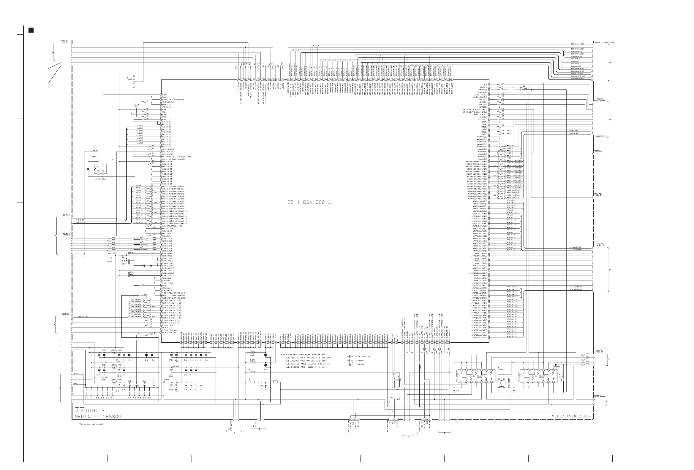
Media processor section
TO
SHEET 2
TO
SHEET 6
5
TO
SHEET 2
4
TO SHEET 2
3
TO SHEET 6
2
TO SHEET 2
1
TO EACH
SHEET
AO_D[0]
AO_SCLK
AO_FSYNC
AO_IEC958
AO_MCLKO
AI_D[0]
VIDEO_MUTE[H]
PHY_CNA
480I[H]
B1404
B1405
TL1402
TL1437
R1408
TL1403
TL1404
R1409
R1410
TL1407
R1411
R1412
R1413
R1414
R1415
R1416
K1407
C1450
VIDEO_27M
VI_D[2-9]
VO_D[0-15]
DAC_CVBS_OUT
DAC_SY_OUT
DAC_SC_OUT
DAC_Y_OUT
DAC_PB_OUT
DAC_PR_OUT
V3.3V
PHY_DATA[0-7]
PHY_CTL[1]
PHY_CTL[0]
PHY_LREQ
PHY_LPS
PHY_LINK_ON
PHY_CLK
DIGI3.3V
D2.5V
D1.8V
GND
D5.0V
D1.8V
D2.5V K1405
DIGI3.3V
GND
D3.3V
VDDI1.8
GND
R1402
X1401
R1421
R1422
R1423
R1424
R1425
R1426
B1401
C1401
B1402
C1408
B1403
C1402
C1409
K1408
LC1401
LC1402
LC1403
R1493
C1453
C1454 D1402D1401
C1455
C1456
C1405
C1411
C1412
C1413 C1414
R1417
TL1489
R1494
R1495
TL1452
TL1453
TL1454
TL1455
TL1456
TL1457
TL1458
TL1459
RA1401
RA1402
RA1403
RA1404
R1419
TL1412
TL1490
TL1491
R1420
R1485
R1486
R1487
R1488
R1489
C1452
C1406
C1415
R1490
TL1413
TL1414
TL1415
R1491
TL1417
TL1418
TL1419
R1427
TL1420
RA1405
RA1406
R1428
R1429
R1430
R1431
R1432
C1417
C1418
C1461
C1416
C1474
C1473C1472C1471C1469C1468C1467C1466C1465C1464 C1470
C1419
C1421
C1420C1404
K1401
C1463
C1425C1424C1423
C1422
C1430C1429C1428C1427
C1439
C1438C1437C1436C1434 C1435
TO SHEET 5
R1483
R1482
R1481
GND
D3.3V
SSTL2_VDD
R1477
TL1433
TL1434
R1478
R1479
R1476
R1480
K1402
C1442
K1403
C1444
K1404
C1445
C1446
GND
D3.3V
D5.0V
TO SHEET 7
SDRAM_A[14-17]
SDRAM_VREF
SDRAM_CLK_L[1]
SDRAM_CLK[1]
SDRAM_CLK_L[0]
SDRAM_CLK[0]
SDRAM_WE_L
SDRAM_CKE
TO SHEET 5
SDRAM_RAS_L
SDRAM_CAS_L
SDRAM_DQM[0-3]
TL1432
TL1438
TL1439
TL1440
R1474
R1475
R1473
R1471
R1469
R1468
R1467
R1466
R1465
R1464
TL1485
R1462
R1461
R1460
R1459
R1458
TL1484
TL1483
R1455
TL1481
R1453
R1452
TL1480
TL1479
TL1478
TL1477
R1451
R1450
RA1411
RA1410
RA1409
RA1408
IC1401
R1438
R1437
TL1441
TL1442
TL1423
TL1422
TL1436
R1434
R1435
R1492
K1406
C1447
C1448
R1401
TL1492
TL1493
TL1494
TL1495
SPI_CLK
SPI_MOSI
CN1405
TO CN7401
SHEET 25
CN1403
NOT
USED
A_MUTE2[H]
VIDEO_RST[L]
TO
SHEET 2
CN1402
NOT
USED
R1440
R1436
TL1425
TL1424
R1439
TL1448
A_DAC_CS
VIDEO_CS
SPI_MOSI
VIDEO_RXD
TO SHEET 2
IC1404
SPI_CLK
RA1407
R1472R1470
C1459
R1445
R1446
R1447
R1441
IC1405
S1401
C1458C1457
D1403
R1448
R1449
R1443
R1444
SDRAM_DQS[0-3]
SDRAM_A[0-13]
SDRAM_DQ[16-31]
SDRAM_DQ[0-15]
ALE
OE[L]/LDS[L]
UWE[L]/UDS[L]
ELINK_INT[L]
EPG_INT[L]
RD/WR[L]
WAIT[L]
DTACK[L]
TO SHEET 3
CS[3]
CS[1]
CS[0]
MADD[22]
MADD[1-5]
MADD[6-21]
PHY_RESET[L]
TO SHEET 6
DAC_RST[L]
TO SHEET 2
ATA_ADD[0-4]
ATA_DAT[0-15]
ATA_RESET
ATA_DMAACK[L]
ATA_DMARQ
ATA_IORDY
ATA_INTRQ
ATA_DIOR[L]
ATA_DIOW[L]
ATA2_RESET
ATA2_DMAACK[L]
ATA2_DMARQ
ATA2_IORDY
ATA2_INTRQ
ATA2_DIOR[L]
ATA2_DIOW[L]
ATA2_ADD[0-4]
ATA2_DAT[0-15]
K_BUS_CLK
K_BUS_REQ
SYS_RESET[L]
TO SHEET 2
K_BUS_OUT
K_BUS_IN
E5_RESET[L]
UART2_TX
TO SHEET 3
UART2_RX
p10658001a_rev0
TO SHEET 7
SHEET 4
A
BCDEFG
2-11 2-12
Page 55

DDR-SDRAM Section
C1604
IC1604IC1604
IC1602
IC1602IC1602IC1602
C1633
C1632
C1617
C1616
C1661
C1662
C1657
C1658
R1628
R1627
R1631
R1632
IC1603IC1603 IC1604IC1603
5
4
3
0 2
DIGITAL(DDR_SDRAM)
IC1701
K1702
C1703 C1704
K1701
C1701
C1702
R1701 R1702
C1708
C1707
R1703
R1704
R1705
C1710
C1705
C1706
C1709
C1645
C1646
RA1629
RA1630
RA1631
RA1632
RA1609
RA1610
RA1611
RA1612
RA1613
RA1614
RA1615
RA1616
RA1625
RA1626
RA1627
RA1628
R1641
R1642
R1601
R1602
R1603
R1604
RA1617
RA1618
RA1619
RA1620
C1641 C1650
C1642
C1626
C1621
C1622
C1623
R1619
C1649 C1651 C1643
R1620
R1618
R1617
C1627
C1628
C1610
C1605
C1606
C1607
C1611
IC1603 IC1604
C1603
IC1601
IC1601IC1601
IC1601
C1625
C1624
C1609
C1608
C1659
C1660
C1655
C1656
R1622
R1621
R1629
R1630
RA1621
RA1622
RA1623
RA1624
C1644
C1652
R1626
R1624
R1625
R1623
C1634
C1629
C1630
C1631
C1635
C1636
C1618
C1613
C1614
C1615
C1619
2
TO SHEET 4
1
SSTL2_VDD
SDRAM_DQ[0-15]
SDRAM_DQ[16-31]
SDRAM_A[0-17]
SDRAM_CKE
SDRAM_RAS_L
SDRAM_CAS_L
SDRAM_WE_L
SDRAM_DQM[0]
SDRAM_DQM[1]
SDRAM_DQM[2]
SDRAM_DQM[3]
SDRAM_DQS[0]
SDRAM_DQS[1]
SDRAM_DQS[2]
SDRAM_DQS[3]
SDRAM_CLK[0]
SDRAM_CLK[1]
SDRAM_CLK_L[0]
SDRAM_CLK_L[1]
SDRAM_VREF
A
D3.3V
R1643
R1644
R1605
R1606
R1607
GND
C1653
C1654
R1608
R1653
R1654
R1655
R1656
R1657
R1658
R1659
R1660
R1613
R1614
R1615
R1616
C1612
C1620
C1601 C1602
p10614001a_rev0
SHEET 5
BCD EFG
2-13 2-14
Page 56

IEEE1394 section
5
B1801B1802
4
3
TO SHEET 4
D3.3V
PHY_RESET[L]
PHY_LREQ
PHY_CLK
PHY_CNA
PHY_CTL[0]
PHY_CTL[1]
PHY_DATA[0-7]
PHY_LPS
PHY_LINK_ON
GND
R1801
R1802
X1801
C1813
C1809
C1808
C1805
IC1801
C1810
K1801
C1807
L1801L1802 C1804
R1820
R1822
C1803C1806
C1814
T1804T1804
T1804T1804
CN1802
TO CN7121
SHEET 23
T1803T1803
T1803T1803
R1826
R1825
R1824
R1823
R1827
C1815
R1819
R1818
C1816
T1802T1802
T1802T1802
CN1801
NOT USED
2
RA1801
RA1802
R1803
R1804
R1805
R1806
R1808 R1807
R1809
R1810
C1811
R1812
R1811
R1821
C1812
R1813
C1801
R1814
R1815
C1802
R1816R1817
T1801T1801
T1801T1801
1
p30128001a_rev0
SHEET 6
A
BCDEFG
2-15 2-16
Page 57

ATAPI Interface section
5
TO SHEET 4
4
3
TO SHEET 2
TO SHEET 4
2
TO SHEET 4
ATA2_RESET
ATA2_DAT[0-15]
ATA2_DMARQ
ATA2_DIOW[L]
ATA2_DIOR[L]
ATA2_IORDY
ATA2_DMAACK[L]
ATA2_INTRQ
ATA2_ADD[0-4]
D5.0V
D3.3V
GND
P_CTL[H]
ATA_RESET
ATA_DAT[0-15]
ATA_DMARQ
ATA_IORDY
ATA_INTRQ
ATA_DIOW[L]
ATA_DIOR[L]
ATA_DMAACK[L]
ATA_ADD[0-4]
R2203
R2201
C2201
R2202
IC2201
IC2202
C2202
RA2201
RA2202
RA2203
RA2204
RA2205
Q2201
R2217
RA2206
RA2207
R2101 R2102 R2103
R2205
R2206
R2207
R2208
R2209
R2210
R2211
R2212
R2213
R2214
R2215
R2204
R2104
R2105
R2106
R2107
R2108
R2109
R2110
R2111
R2112
R2113
R2114
R2115
RA2101
RA2102
RA2103
RA2104
RA2208
RA2209
RA2210
RA2211
R2116
K2101
K2102
K2103
K2104
K2105
K2106
K2107
K2108
K2109
K2110
K2111
K2112
K2113
K2114
K2115
K2116
K2117
K2118
K2119
K2120
K2121
K2201
K2202
K2203
K2204
K2205
K2206
K2207
K2208
K2209
K2210
K2211
K2212
K2213
K2214
K2215
K2216
K2217
K2218
K2219
K2220
K2221
D2101
CN2101
TO HDD
CN2201
TO DVD
DRIVE
UNIT
D2201
1
R2216
p20437001a_rev0
SHEET 7
A
BCD EFG
2-17 2-18
Page 58

On screen section
5
R201
Q201
B201
Q202
R204
R205
R202
TO SHEET 11
V_FROM_OSD
L201
4
C201
C202
C203
R207 L202
R206
R208
B206
R209
R210
B202
V_FROM_OSD
TO SHEET 9
CHARA_DATA
R203
R211
C204
B203
B204
C205
C208
C207
B205
V_TO_OSD
TO SHEET 9, 10
3
TO SHEET 9
fsc
SW5V
GND
C209
C210
C219
IC201
R212
S.DATA_TOSYS
EDS_CS[L]
2
TO SHEET 13
P.MUTE_DV[L]
SYNC_DET[H]
OSD_CS
S.CLK
S.DATA_FRSYS
D201
D202
D203
D204
JUST/EDS[H]
R213
R214
R215
R216
R217
C211L205
L206
R218
L211
R221
B211
C221
C216C215C214C213C212
C222
Q211
C223 C224
L212
Q212
R223
R224R222
R225
C225
C226
X201
R226
1
p30135001a_rev0
SHEET 8
A
BCDEFG
2-19 2-20
Page 59

DV video switch section
5
4
TO CN3501
SHEET 20
3
CN501
L502
R542
Q505
C547
C548
R518
C549
L504
R521
L503
C550
R519
Q503
C555
R526
C557
R527
C556
R529
R528
C536
R513
C552
C537
R514
C538
C539
B501
C540
C541
R515
C543
C544
R516
C545
C546
C534
C535
C551
R511
R512
C531
C532
C533
C528
C530
C529
R510
C527
C562
L501
R533
Q513
R531
C561
R532
TO
DV_Y_OUT
DV_C_OUT
SHEET 10
fsc
TO SHEET 8
C526
C525
C524
C523
C522
C521
SW5V
I2C_DATA2
I2C_CLK2
FRONT_C_IN
FRONT_Y_IN
FRONT_V_IN
WIDE_DET_DV
P.MUTE_DV[L]
V_FROM_OSD
CHARA_DATA
V_TO_OSD
TO
SHEET 8
TO
SHEET 13
TO
SHEET 8
IC501
D502
D501
2
R503
R501
C504
C506
C503
R502
C505
C520
R504
C507
C508
C510 C515
R505
C509
C512
R509
R507
C514
C516
C517
C518 C519
R508
C511
C513
C501
C502
R557
C567
R559
R558
R556
Q512
R560
B503
C566
R552
R554
R553
R551
Q511
R555
TU_VIDEO
C_OUT_BIAS
DV_C_OUT
DV_Y_OUT
REAR_V_IN
REAR_C_IN
REAR_Y_IN
B502
TO_DV_DUB_C
TO_DV_DUB_Y
GND
TO
SHEET 11
1
p10724001a_rev0
SHEET 9
A
BCD EFG
2-21 2-22
Page 60

Video switch section
TO
5
SHEET 1
TO SHEET 13
4
TO CN7123
3
SHEET 23
SW5V
I2C_DATA_A/V
I2C_CLK_A/V
CN701
GND
R711
GND
L702
R717
C747
Q701
C748
R718
L703
R719
C755
C751
C749
L704 R721
Q703
R726
C750
C765
C737
R727
R729
C756
R728
B701
R712
Q705
C734
C731
C732
C733
C736
C735
C738
C739
C740
C741
C743
C730
L706
R742
Q706
B702
R744
R745
R743C767L707
C728
C729
R710
C727
R746
R748
C771
X701
C769
C768
R747
C772
R733
R731
Q713
C775
R732
C726
C725
C724
C723
C722
L701
FRONT_V_IN
FRONT_C_IN
FRONT_Y_IN
WIDE_DET_VDR
TO SHEET 13
C745
C746
C721
IC701
D701
D702
2
R703
R701
C704
C707
C706
C703
R702 R708
C705
R704
C708
R706
R707
C711
C714 C717C709
C712
C713
C710 C715
R709
C716
C718 C719
C701
C702
R757
C720
C778 C777
R759
R758
R756 R751
Q712
B704
R752
R754
R753
R755R760
Q711
B703
fsc
DV_C_OUT
DV_Y_OUT
TO SHEET 9
fsc
TO SHEET 8
VDR_C_OUT_BIAS
TU_VIDEO
REAR_V_IN
REAR_C_IN
REAR_Y_IN
GND
TO SHEET 11
1
p10723001a_rev0
SHEET 10
A
BCDEFG
2-23 2-24
Page 61

Terminal section
TO SHEET 9
5
TO SHEET 10
NOT USED
TO SHEET 8
4
TO CN7107
SHEET 23
3
TO SHEET 13
2
NOT USED
REAR_Y_IN
REAR_C_IN
REAR_V_IN
C_OUT_BIAS
DV_Y_OUT
DV_C_OUT
TO_DV_DUB_C
TO_DV_DUB_Y
TU_VIDEO
REAR_Y_IN
REAR_C_IN
REAR_V_IN
VDR_C_OUT_BIAS
TU_VIDEO
TU_VIDEO
V_FROM_OSD
LINE2INFO
BS_REC_LINK
J906
GND
CN901
AL5.8V
SW5V
VDR[H]
SW12V
C_BIAS1
C_BIAS2
CN7301
R942
R941
C929
R943
R961
C981
R962
L902
C903 C904
GND
L901
R902
R905
C901
C902
GND
B991
R993
Q991
R991
B992
K7301
K7302
K7303
K7304
R992
Q992
C991
R903
Q901
R901
R906
Q902
R904
IC901
B901
C953
L904
L903
C975 C976
C905
R907
B911
B912
B913
R972
C906
Q907
R913
B914
B915
B916
Q904
Q911
R916
Q908
R914
L906
R910
Q905
R908
R971
R974
R917
Q909
R915
C972 C973
Q912
R912
R911
C918
Q906
R909
R973
R976
R918
C919
C920
C921
R981
Q915
C917
R988
C939
R975
C915
C938
Q913
R932
R934
R935
R937
R982
R922
R923
R965
R966
R948
R920
C916
R921
R944
R929
R919
R963
R964
R936
R938
R939
R940
C971
C982
R928
C987
C988
B905
C985
C986
R933
J904J904J904J904J904J904J904J904J904J904J904J904
R953
J901
J902
J902J902J902
J903
J953
TO SHEET 12
J7301
A.IN1[L]
A.IN1[R]
DVD_OUT[L]
DVD_OUT[R]
LINE_OUT[L]
LINE_OUT[R]
A.GND
AD_IEC958
V3.3V
C7305 C7306
C7301
GND
C7307
C7303 C7304
C7302
R851
K851
K852
L841
C843
C852C851
C841
C842
IC851
R852
C853
R853
R857
R855
L851
C855
C854R854
R856
C856
K853
J841
J852
J852
1
p10722001a_rev0
SHEET 11
A
BCD EFG
2-25 2-26
Page 62

Audio input/output section
5
TO SHEET 11
4
NOT USED
3
A.IN1[R]
A.IN1[L]
GND
DEMOD[R]
DEMOD[L]
R2662
R2663
R2666
R2667
R2202 R2203
R2201
R2612
IC2201
IC2603
R2615
IC2202
IC2604
R2204
R2205
Q2204
R2210
Q2203
Q2202
R2208
R2209
Q2201
R2207
C2201
C2202
R2206
CN2601
CN2602
TO CN3701
SHEET 21
TO CN8001
SHEET 24
TO SHEET 1
2
TO
SHEET 13
1
AL5.8V
SW12V
SW-7V
SW5V
GND
DVD_A_INSEL1
DVD_A_INSEL2
DVC_A_INSEL1
DVC_A_INSEL2
A.OUTSEL1
A.OUTSEL2
A.MUTE_DVC[H]
A.MUTE[L]
F.AUDIO[R]
F.AUDIO[L]
R2651
R2652
R2655
R2656
R2658
R2659
C2651
R2660
R2661
C2652
C2653
C2654
R2653
R2654
D2601
R2631
Q2605
R2632
R2613 R2614
Q2603
Q2604
R2622 R2623
R2621
R2616
IC2605
IC2606
R2624
R2625
C2603
R2627
R2628
C2604
Q2601
Q2602
R2629
R2630
AD_IEC958
V3.3V
A.GND
LINE_OUT[R]
LINE_OUT[L]
DVD_OUT[R]
DVD_OUT[L]
GND
TO
SHEET 11
p20478001a_rev0
SHEET 12
A
BCDEFG
2-27 2-28
Page 63
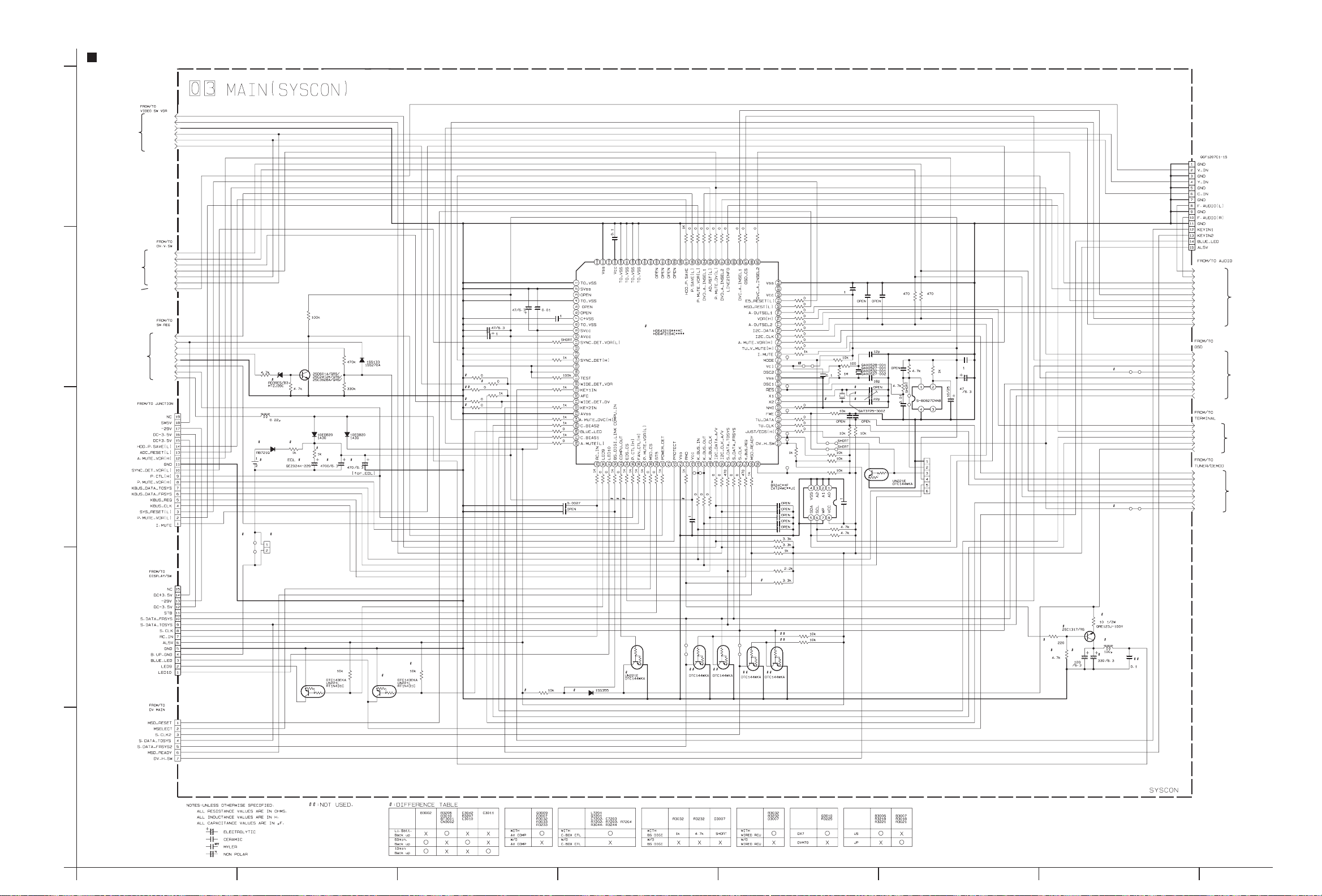
System controller section
I2C_DATA_A/V
TO
SHEET 10
5
I2C_CLK_A/V
GND
FRONT_Y_IN
FRONT_C_IN
WIDE_DET_VDR
CN3104
TO CN7201
SHEET 15
TO SHEET 9
TO SHEET 10
4
TO SHEET 1
TO CN7102
3
SHEET 23
I2C_DATA2
I2C_CLK2
WIDE_DET_DV
P.MUTE_DV[L]
FRONT_C_IN
FRONT_Y_IN
FRONT_V_IN
P.SAVE[L]
SW5V
SW12V
FAN_CTL[H]
P.CTL[H]
AL5.8V
CN3103
CN3102
C3033
C3039
R3018
R3020
C3038
C3007
R3011
R3014
R3017
R3019
R3024
R3025
R3026
R3027
R3028
C3049
C3051
R3029
R3030
R3031
R3032
R3033
R3034
R3035
R3036
R3037
IC3001
R3038
R3205
C3014
C3015
45V
GND
B3002
R3204
D3003
L3001
D3010
BT3001
CN3002
Q3004
R3203
R3206
C3010 C3011
R3201
R3202
D3004 D3005
R3207
C3042
D3002
R3218
R3220
R3021
R3221 R3022
R3039
R3040
R3097
R3044
R3096
C3016
R3095
TP3901
R3046
R3094
TP3902
R3047
R3093
R3048
R3092
R3049
R3091
R3050
R3090
R3051
R3052
R3088
R3053
R3087
R3054
R3055
R3085
R3251
R3249
R3250
R3255
R3244
C3017
C3018
C3021
C3020
C3019
IC3004
R3081
R3080
R3079
R3078
R3077
R3076
R3075
R3074
R3073
R3072
R3063
R3061
R3060
R3259
R3057
TP3906
TP3904
TP3905
TP3903
TP3908
TP3907
B3001
C3050
B3962
R3258
R3257
R3256
R3062
B3971
R3223
R3224
R3071
R3069
X3001
C3032
C3034
C3037
R3229
C3036
C3041
C3025
C3024
C3028 C3029
R3239
R3240
C3022
X3002
C3035
C3054
R3066
Q3901
C3026
R3275
B3966
R3266
IC3002
R3276
CN3901
R3267
C3027
C3031
C3030
B3006
B3007
F.AUDIO[L]
F.AUDIO[R]
DVD_A_INSEL1
DVD_A_INSEL2
DVC_A_INSEL1
DVC_A_INSEL2
A.OUTSEL1
A.OUTSEL2
A.MUTE_DVC[H]
A.MUTE[L]
P.MUTE_DV[L]
OSD_CS
EDS_CS[L]
JUST/EDS[H]
SYNC_DET[H]
S.CLK
S.DATA_FRSYS
S.DATA_TOSYS
VDR[H]
LINE2INFO
C_BIAS1
C_BIAS2
BS_REC_LINK
TU_V_MUTE[H]
TU_I2C_DATA
TU_I2C_CLK
I2C_DATA2
I2C_CLK2
AFC
JUST_CLK
TO
SHEET 12
TO
SHEET 8
TO
SHEET 11
NOT
USED
2
1
TO CN7001
SHEET 15
TO CN1503
SHEET 17
R7204
R7202
R7203
Q7201
C7203
C7202
L7201
C3055
CN3014
Q3008
R3230
Q3010
R3225
R3232
D3007
Q3009
B3011
Q3012
Q3011
B3012
Q3014
Q3013
R3247
R3248
p10726001a_rev0
SHEET 13
A
BCD EFG
2-29 2-30
Page 64

DC/DC Converter section
5
R5721
4
D5720
R5731
R5732
C5720R5720
C5721
Q5720
R5730
C5731
C5722
IC5701
C5730
C5712
C5727
C5710
R5711
R5710
D5710
C5732C5711
3
C5726 R5723
R5712
IC5710
R5722C5723
R5713 C5716
L5720K5720
C5724C5725
D5721
C5713
L5710 K5710
C5714 C5715
2
CN5701
CN5702
1
TO CN5506
TO CN5505
SHEET 1
SHEET 1
p30140001a_rev0
SHEET 14
A
BCDEFG
2-31 2-32
Page 65

Switch jack. Switch display and Jack section
CN7201
L7204
D7203D7202
TO CN3104
SHEET 13
L7202
C7203
C7205
L7203
D7204
R7202 J7201
C7202
L7201
C7204
R7206R7207
C7206
J7201
J7201
J7204
C7201
5
D7005
S7025
S7012
D7004
IC7002
R7009
R7015
R7005
R7007
R7006
R7013
D7034
D7033
D7032
D7035
R7003
C7005
C7004
S7023
S7004S7015
D7003
R7016
C7006
S7033 S7035S7034
S7014 S7013
4
3
D7012
D7013
D7014
C7001
IC7001
S7032
S7024
C7008
R7002
R7001 R7014
R7213
R7212
R7211
R7215
R7214
S7213
S7212
S7211
C7211
S7215
S7214
C7212
D7031
C7007
C7002
R7022
L7001
Q7001
R7021
CN7001
Q7003
Q7002
TO CN3102
SHEET 13
2
J4112
C7010
C7011
C7003
R7010
R7041
R7042
R7043
R7044
R7046
R7047
D7046
D7021
D7051
1
DI7001
DI7001DI7001DI7001DI7001
D7052
D7047D7043D7041 D7044D7042
D7053
TO CN7126
SHEET 23
CN7002
CN4104
K4105
K4106
TO CN7103
K4104
K4103
K4102
K4101
SHEET 23
p10711001a_rev0
SHEET 15
A
BCD EFG
2-33 2-34
Page 66

DV Regulator section
5
CN1001
TO CN5404
SHEET 1
4
ZP101-4
ZP101-5
ZP101-6
ZP101-8
ZP101-9
ZP101-10
ZP101-11
ZP101-12
ZP101-3
ZP101-2
ZP101-1
L1002
L1003
L1004
ZP101-7
L1001
LC1002
LC1003
LC1004
B1005
C1005 C1003 C1001C1006 C1004
B1001
C1002 IC1005
Q1001
R1001
Q1002
R1002
C1012
Q1003
R1003
Q1004
B1002
R1004
R1011
C1010
C1007
C1011
R1009
Q1005
R1005
Q1006
R1006
C1008
Q1007
R1007
Q1008
B1003 B1004
C1009
R1008
SW_3V
A_REG_3V
D_REG_3V
SW_5V[-]
SW_5V
A_REG_5V
REG_5V
TO EACH
SHEET
TO SHEET 17
3
2
FFREW_H
PWR_CTL
RESET
K1001
C1015
C1014
ZP11
ZP1-18 ZP1-25 ZP1-30 ZP1-29
C1016
IC1001
C1017
C1018
IC1002
C1019
C1020 C1021
IC1003
C1024 C1025
C1022
C1023
IC1004
C1026
ZP12
ZP13
ZP14
C1027
ZP15
ZP16
C1028
ZP17
C1029
ZP18
ZP19
ZP20
C1030
GND
TO EACH SHEET
REG_1.8V
REG_2.5V
REG_3V
REG_2.9V
TO EACH
SHEET
1
p30131001a_rev0
SHEET 16
A
BCDEFG
2-35 2-36
Page 67

DV MSD Section
TO SHEET 16
5
TO SHEET 18
4
NOT USED
TO SHEET 19
3
TO CN3014
SHEET 13
2
TO DV MDA
1
BOARD
SW_3V
REG_5V
DRWSEL
ADDT00
ADDT01
ADDT02
ADDT03
ADDT04
ADDT05
ADDT06
ADDT07
ADDT08
ADDT09
ADDT10
ADDT11
ADDT12
ADDT13
ADDT14
ADDT15
DV_WAIT
DV_RST
CLK27SEL
JLIP_TX
JLIP_RX
CN1505
DAC_CS
DAC_DATA
DAC_CLK
EXT_IN_L
TBC_RST
TBC_CS
TBC_SDO
TBC_SDI
TBC_CLK
TBC_VD
CLK27A
CN1503
CN1501
DALE
GND
DWE
DRE
VPP
R1601
R1602
R1553
R1552
R1551
Q1501
Q1502
ZP153-1
ZP153-2
ZP153-3
ZP153-4
ZP153-5
ZP153-6
ZP153-7
ZP151-20
ZP151-19
ZP151-18
ZP151-17
ZP151-16
ZP151-15
ZP151-14
ZP151-13
ZP151-12
ZP151-11
ZP151-10
ZP151-9
ZP151-8
ZP151-7
ZP151-6
ZP151-5
ZP151-4
ZP151-3
ZP151-2
ZP151-1
L1501
ZP152-1
ZP152-2
ZP152-3
Q1513
Q1512
TL1501
TL1502
TL1503
TL1504
TL1505
TL1506
TL1507
TL1508
TL1509
TL1510
TL1511
TL1512
TL1513
TL1514
TL1515
TL1516
TL1517
TL1518
TL1519
TL1520
TL1521
TL1522
TL1523
TL1524
TL1525
TL1526
TL1527
TL1528
TL1529
TL1530
TL1531
TL1532
TL1533
TL1534
TL1535
TL1536
TL1537
TL1538
TL1539
TL1540
TL1541
TL1542
TL1543
TL1544
R1592
R1593
TL1674
TL1547
TL1673
TL1548
TL1672
TL1549
TL1671
TL1550
TL1670
TL1551
R1502
TL1669
TL1552
R1505
TL1642
TL1643
TL1644
TL1645
TL1646
TL1647
TL1648
TL1649
TL1650
TL1651
TL1652
TL1653
TL1654
TL1655
TL1656
TL1657
TL1658
TL1659
TL1660
TL1661
TL1662
TL1663
TL1664
TL1665
TL1666
TL1667
TL1668
IC1501
TL1557
TL1558
TL1559
TL1555
TL1556
TL1560
TL1561
TL1562
TL1563
TL1564
TL1565
TL1566
TL1567
TL1568
TL1569
TL1572
TL1573
TL1574
TL1575
TL1576
TL1577
TL1578
C1517
C1518
R1534 R1533
C1515
C1516
R1532 R1531
R1509
D1504
R1510
R1511
R1506
R1591
R1544
C1531
X1501
C1532
TL1579
TL1553
R1622
TL1554
TL1641
TL1580
TL1640
TL1581
C1504
TL1639
TL1582
TL1638
TL1583
TL1637
TL1584
C1523
TL1636
TL1585
TL1635
TL1586
C1508
TL1634
TL1587
TL1588 TL1633
TL1632
TL1631
TL1630
TL1629
TL1628
TL1627
TL1626
TL1625
TL1624
TL1623
TL1622
TL1621
TL1620
TL1619
TL1618
TL1617
TL1616
TL1615
TL1614
TL1613
TL1612
TL1611
TL1610
TL1609
TL1608
TL1607
TL1606
TL1605
TL1604
TL1603
TL1602
TL1601
TL1600
TL1599
TL1598
TL1597
TL1596
TL1595
TL1594
TL1593
TL1592
TL1591
TL1590
TL1589
RA1505
R1571
R1541
R1542
R1543
R1634
R1594
R1595
TL1675
TL1676
TL1545
TL1546
Q1503
D1506
D1501
R1561
D1502
IC1504
C1520
R1583
R1621
R1582
R1585
R1584
IC1503
RA1510
R1512
R1596
R1631
R1535
R1555
R1554
C1501
R1501
R1526R1527
RA1509
C1502
R1632
D1503
R1613
R1612
R1611
R1520
IC1502
R1633
D1505
Q1511
L1502
C1509
C1510
R1516
R1517
R1518
R1519
R1614
R1615
R1617
R1616
C1522
ZP152-4
ZP152-5
ZP152-6
ZP152-7
ZP152-8
ZP152-9
ZP152-10
ZP152-11
ZP152-12
ZP152-13
ZP152-14
ZP152-15
CN1502
TSR
FRP
SPA
SRV_TRK
HID1
TO SHEET 22
ADC_PWD0
ADC_PWD1
ADC_DEM1
ADC_DEM0
ASPECT1
ASPECT2
TO SHEET 20
AGC_RST
PWR_CTL
TO SHEET 16
REC_H
PB_H
MONI_CHG
HID3
RESET
TO SHEET 16
FFREW_H
TO DV
TO SHEET 18
TO
SHEET 21
TO
SHEET 22
p10691001a_rev0
SHEET 17
A
BCD EFG
2-37 2-38
Page 68

DV Main section
5
TO SHEET 17
4
JLIP_RX
JLIP_TX
DAC_DATA
DAC_CLK
RESET
CN2001
ADDT15
C2031
C2086
IC2001
C2036
C2037
HID1
VPP
C2038
ZP201-1
ZP201-14
ZP201-2
ZP201-15
ZP201-3
ZP201-16
ZP201-4
ZP201-17
ZP201-5
ZP201-18
ZP201-6
ZP201-19
ZP201-7
ZP201-20
ZP201-8
ZP201-21
ZP201-9
ZP201-22
ZP201-10
ZP201-23
ZP201-11
ZP201-24
ZP201-12
ZP201-25
ZP201-13
ZP201-26
C2039
C2032
C2040
R2131
R2132
R2050
C2084
C2025
X2003R2043
C2024
ADDT14
ADDT13
ADDT12
ADDT11
ADDT10
ADDT09
ADDT08
ADDT07
ADDT06
ADDT05
TO SHEET 17
ADDT04
ADDT03
ADDT02
ADDT01
ADDT00
DV_WAIT
DRWSEL
DRE
DWE
DALE
INV
INH
OUTV
OUTH
DCO3
DCO2
DCO1
DCO0
DYO3
DYO2
DYO1
DYO0
DCI3
DCI2
DCI1
DCI0
DYI3
DYI2
DYI1
DYI0
FSPLLCTL
CLK27A
M_VCOCTL
PBVCOCTL
AODAT
AIDAT
AIMCK
TO SHEET 21
AIBCK
AILRCK
TO SHEET 19
3
2
MONI_CHG
PB_ENV
D_REG_3V
VREF_1.1
VRB_ATF
TO SHEET 22
TO SHEET 16
VRB_AGC
AGC_OUT
REC_DATA
REC_CLK
REC_CTL
ATF_IN
REF_CLK
SW_3V
REG_2.9V
D_REG_3V
REG_2.5V
REG_1.8V
L2007
1
GND
R2127
R2126
L2101
L2002
C2063
C2064
C2052
C2051
L2004
R2121
C2081
L2003
C2055
C2056 C2060
R2122
C2058
C2057
C2041
R2090
R2091
R2092
R2093
R2094
C2042
C2043
C2044
R2020
L2009
C2005
C2002
C2001
K2101
Q2102
L2102
C2082
L2005
L2006
C2059
C2071
C2079
C2072
C2062
C2061
R2104
R2102
R2105
R2106
R2107
Q2101
R2108
R2101
R2103
C2073
C2074
C2003
R2012
IC2101
R2110
C2075
C2076
R2109
R2111
C2006
R2014
R2113
C2077
IC2102
R2112
C2007
R2116
R2114
C2078
R2115
C2010
C2011
C2015
C2014
R2027
R2022
R2019
R2018
C2020
R2023
C2016
D2002
TL2101
R2035
C2018
C2017
R2033
R2034
R2036
R2071 R2073
C2021
C2085
R2040
C2019
R2038
R2039
R2037
C2023
C2022
R2042
C2048
C2047
C2046
R2031
R2046
R2041
R2051
R2052
R2053
L2011
C2027
C2026
C2028
R2047
D2003
C2083
R2001
R2002
R2003
R2004
R2048
D2004
R2098
L2015
ZP200-1
ZP200-2
ZP200-3
ZP200-4
ZP200-5
ZP200-6
CN2002
SRV_TRK
TSR
FRP
SPA
DV_RST
CLK27SEL
TO CN7127
SHEET 23
TO SHEET 17
p10692001a_rev0
SHEET 18
A
BCDEFG
2-39 2-40
Page 69

DV input/output section
Y_GCTL
TO
SHEET 20
5
C_GCTL
DV_Y
DV_C
Y/V_IN
C_IN
L3022
L3151
C3011
C3012
C3131
C3132
IC3151
AGC_GAIN
DUMP_CTL
ATF_GAIN
RECCADJ
TO
SHEET 22
4
3
TO
SHEET 16
2
REG_3V
A_REG_5V
A_REG_5V
D_REG_3V
L3101
C3102
C3103
C3112
C3111
C3121
L3021
ZP351-4
R3111
R3113
R3112
R3133
R3132
ZP351-6
R3131
ZP351-8
R3114
Q3111
R3134
Q3131
C3021
C3022
R3115
R3116
C3114 C3115
Q3115
R3135
R3136
C3124 C3125
Q3135
K3101LC3101
C3141
C3113
L3111
C3123
L3131
C3140
R3165
Q3101
L3112
C3116
L3132
C3126
R3102
C3117
R3118
R3117
R3103
R3119
C3127
R3137
R3120
C3118
R3138
R3139
R3122
R3121
Q3102
R3140
C3128
Q3112
R3123
R3142
R3141
R3161
R3105
Q3113
C3119
R3124
Q3132
R3106
R3143
R3125
Q3133
C3129
L3103
Q3114
IC3102
C3101
C3120
C3130
C3106
C3107
L3104
R3164
L3001
C3001
R3003
R3004
R3005
C3002
C3003
C3004
C3005
C3006
C3007
C3008
R3008
R3163
C3108
C3018
R3073
C3109
R3079
R3078
C3017
R3081
C3009
C3016
R3076
R3074
C3015
R3075
IC3001
C3010
C3014
C3013
R3048
R3049
R3050
R3054
EXT_IN_L
DAC_DATA
DAC_CLK
DAC_CS
TBC_VD
TBC_RST
TBC_CS
TBC_CLK
TBC_SDI
TBC_SDO
CLK27A
DYI3
DYI2
DYI1
DYI0
DCI3
DCI2
DCI1
DCI0
OUTV
OUTH
DYO3
DYO2
DYO1
DYO0
DCO3
FSPLLCTL
M_VCOCTL
DCO2
DCO1
DCO0
INV
INH
PBVCOCTL
TO
SHEET 17
TO SHEET 17
TO
SHEET 18
IC3101
1
GND
R3162
C3142
X3101
C3144
C3143
p20453001a_rev0
SHEET 19
A
BCD EFG
2-41 2-42
Page 70

DV Video output section
5
TO SHEET 16
4
3
TO SHEET 19
2
TO SHEET 17
A_REG_5V
REG_3V
GND
DV_C
DV_Y
C_GCTL
Y_GCTL
ASPECT1
ASPECT2
AGC_RST
R3526
R3521
C3537
R3527
L3533
C3532
R3522
L3531
L3521
C3521
R3529
L3534
C3538C3536
C3533C3531
C3539
L3532
C3534
Q3503
R3528
R3524
Q3502
R3523
C3540
C3535
IC3501
C3501
Q3501
C3515
R3502
L3522
C3502
C3513
C3523
C3514
C3503
R3516
R3501
C3511
C3510
R3514
R3533
C3504
R3515
R3513
R3534
C3505
C3506
R3503
R3507
R3506
R3504
R3505
C3507
C3508
R3556
R3555
B3502
R3552
R3551
R3549
B3501
R3548
R3546
Q3522
R3547
R3558
R3553
R3554
Q3521
R3557
ZP351-3
ZP351-5
R3544
C3552
C3551
ZP351-1
R3545
ZP351-7
ZP351-2
CN3501
C_IN
Y/V_IN
TO CN501
SHEET 9
TO SHEET 19
1
p20454001a_rev0
SHEET 20
A
BCDEFG
2-43 2-44
Page 71

Audio AD/DA section
5
L3702
L3701
SW_5V
A_REG_3V
SW_5V[-]
TO SHEET 16
GND
R3719
R3720
C3730
R3728
C3717
C3718
R3713
R3712
R3711
R3710
R3709
R3708
R3707
R3706
AIBCK
AIMCK
AILRCK
AODAT
AIDAT
TO SHEET 18
C3731
4
R3725
R3726
R3714
C3736C3737
CN3701
ZP371-1
ZP371-2
ZP371-3
3
TO CN2601
SHEET 12
ZP371-4
ZP371-5
ZP371-6
ZP371-7
ZP371-8
R3727
C3733
C3734
C3735
R3721
IC3703 IC3702
R3722
R3723
2
C3722
R3724
C3723
R3715
C3724
C3726
C3725
R3716
C3728
R3717
R3718
R3701
R3702
C3729
R3703
C3701
C3702
R3704
IC3701
C3713
C3712
C3705 C3708
C3714
C3703
R3705
ADC_PWD1
ADC_PWD0
ADC_DEM1
ADC_DEM0
TO SHEET 17
1
p30130001a_rev0
SHEET 21
A
BCD EFG
2-45 2-46
Page 72

DV PRE/REC section
L4005
5
4
TO SHEET 18
3
TO SHEET 19
TO
SHEET 17
HID3
PB_H
REC_H
HID1
REC_CTL
PB_ENV
VREF_1.1
AGC_OUT
VRB_AGC
VRB_ATF
ATF_IN
D_REG_3V
REF_CLK
REC_CLK
REC_DATA
ATF_GAIN
AGC_GAIN
DUMP_CTL
RECCADJ
Q4004
C4067
R4040
R4042
R4039
Q4003
C4066L4013
R4041
R4038
R4036
R4037
L4012
C4064
R4035
C4065
R4033
Q4002
R4034
R4031
C4062
C4063
R4032
L4011
C4061
C4013
R4025
C4054
C4052
C4032
R4026
C4053
C4051
R4024
R4043
C4036
C4038
C4041
C4033
C4039
C4015
R4022
Q4001
R4023
C4034
C4031
C4035
C4040
C4030 C4029 C4028
C4014
IC4001
C4027
R4010
C4026
R4009
R4008
R4007
R4006
R4005
R4004
ZP401-8
ZP401-7
ZP401-6
ZP401-5
ZP401-4
ZP401-3
ZP401-2
ZP401-1
CN4001
TO DV DRUM
2
TO
SHEET 17, 18
TO SHEET 16
1
MONI_CHG
REG_5V
A_REG_3V
REG_2.5V
GND
A
L4001
C4021
C4022 R4001
IC4002
C4024
C4023
L4003
C4005
L4002
R4002
C4025
R4003
C4046
K4001
R4021
C4047
C4001 C4007 C4010 C4011C4006C4003C4002 C4009
p20455001a_rev0
SHEET 22
BCDEFG
2-47 2-48
Page 73
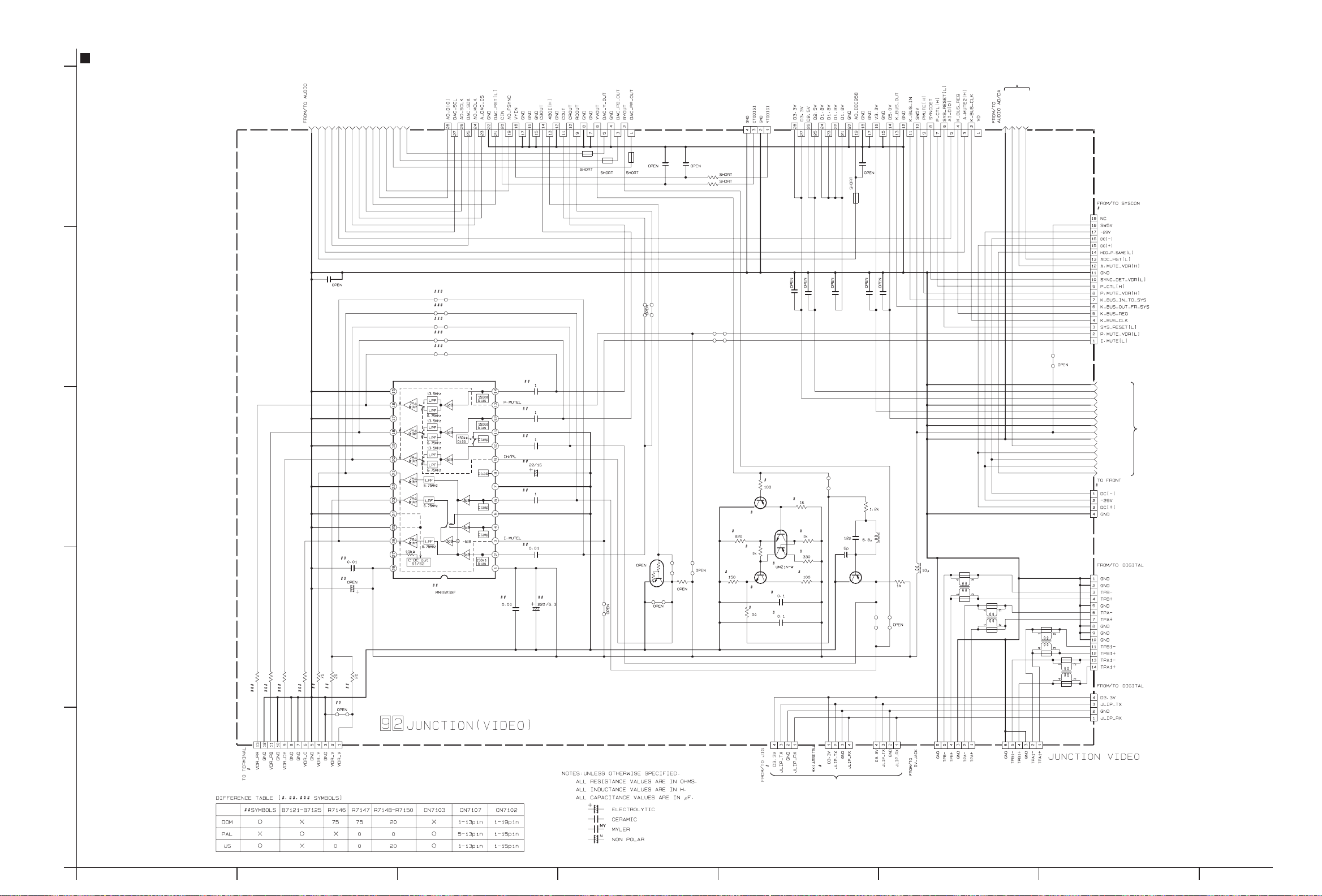
Junction (Video) section
TO SHEET 24 TO CN1001 SHEET 2 TO CN701
TO CN1002 SHEET 2
TO SHEET 24
SHEET 10
ADC_RST[L]
A.MUTE_VDR[H]
SW-7V
GND
AO_IEC958
DAC_SDA
A_MUTE2[H]
AI_D[0]
DAC_SCL
AO_MCLKO
A_DAC_CS
DAC_RST[L]
AO_SCLK
AO_D[0]
AO_FSYNC
AI_FSYNC
AI_SCLK
AI_MCLKO
CN7108
CN7123
CN7109
GND
5
C7131
K7101
C7143
C7134
R7101
C7135
B7131
CN7102
GND
D2.5V
D3.3V
GND
V3.3V
D5V
GND
SW5V[2]
GND
SW-7V
DC[+]
DC[-]
-29V
HDD_P.SAVE[L]
CN7103
TO CN3103
SHEET 13
TO SHEET 1
TO CN7002
SHEET 15
C7141
R7153
R7152
B7115
B7113
Q7103
R7109
C7133
C7132
B7112
R7108
B7107
C7142
B7108
K7104
K7103 K7102
C7137
4
3
B7121
B7122
B7123
B7124
B7125
C7107
C7106
C7105
C7104
C7103
Q7104
C7113
C7114
R7110
R7113
R7114
CN7125
NOT USED
C7123
C7124
Q7101
L7102
B7101
CN7124
R7102
B7111
L7101
CN7126
TO CN4104
SHEET 15
K4111
K4112
KA4111
KA4112
K4113
K4114
KA4113
CN7127
TO CN2002
SHEET 18
KA4114
K4115
K4118
K4116
CN7121
TO CN1802
SHEET 6
K4117
CN7106
NOT USED
R7111
C7109
C7108
IC7101
C7101
C7102
C7112
B7114
Q7107
B7117
B7118
B7116
R7117
R7112
R7115
Q7106
R7116
2
R7151
R7145
R7146
R7147
R7148
R7149
R7150
B7126
CN7107
CN7105
TO CN901 SHEET 11
1
p20456001a_rev0
SHEET 23
A
BCD EFG
2-49 2-50
Page 74

Junction (audio) section
TO SHEET 23
5
TO CN2602
SHEET 12
4
3
ADC_RST[L]
A.MUTE_VDR[H]
CN8001
K8201
C8232 C8231
Q8005
R8233
Q8003
R8212
Q8002
C8053C8052
R8232
R8231
Q8001
R8201
R8202
Q8004
C8208
R8211
IC8201
C8201
R8002
C8202
C8004 C8003
C8207
R8003
R8221R8222
R8210
R8209
R8208
C8205
C8203
R8205
R8204
R8203
R8001
C8001C8002
C8206
R8207
R8206
C8204
C8055 C8057
C8056
K8202
IC8202
C8210 C8209
R8213 R8214 R8215 R8216
R8018
R8019
R8017
R8016
R8220 R8219
R8015 R8014
R8013
R8218
R8217
A_MUTE2[H]
DAC_SDA
DAC_SCL
A_DAC_CS
DAC_RST[L]
AO_D[0]
AO_SCLK
AO_MCLKO
AO_FSYNC
AI_SCLK
AI_MCLKO
AI_FSYNC
AI_D[0]
AO_IEC958
TO
SHEET 23
R8004
R8005
R8006
C8006 C8007
R8008
C8005 C8008
2
R8007
B8001B8002
D3.3V
TO
1
SHEET 23
D5V
V3.3V
SW12V
SW-7V
GND
L8001
L8002
R8051
R8052
C8051
C8054
IC8001
R8009
R8011
IC8002
C8010
C8009
R8010 R8012
C8011
C8012
K8001
K8002
C8013
C8015
C8014
C8016
p20451001a_rev0
SHEET 24
A
BCDEFG
2-51 2-52
Page 75

RS232C Terminal section
5
IC7401
J7401
4
3
C7401
C7402
C7403
C7404
C7405
CN7401
TO CN1405
SHEET 4
2
1
p40054001a_rev0
SHEET 25
A
BCD EFG
2-53 2-54
Page 76

Printed circuit boards
Switching regulator board
ET12
C5106
PC5101
Q5319
R5302
C5301
R5303
IC5301
R5306
R5304
R5305
C5306
R5334
C5302
CP5301
CN5303
R5335
C5335
R5301
D5211
C5210
C5209
L5205
L5204
CN5304
C5336
C5334
C5333
C5324
C5326
Q5315
<01> LPB10314-001B
D5104
D5105
D5103
R5105
D5210
D5212
D5204
D5207
C5206
D5205
C5205
C5305
C5307
C5310
C5330
C5321
IC5302
R5327
C5322
C5325
C5323
R5321
W51
W52
R5104
C5107
R5328
DANGEROUS VOLTAGE
R5106
D5106
C5105
IC5101
C5104
R5102
R5107
C5108
Q5306
R5329
D5209
Q5313
L5301
D5304
C5103
L5207
D5309
D5308
Q5305
CN5301
C5303
B5308
C5208
D5301
D5310
D5305
D5303
C5311
R5314
D5101
R5309
D5213
B5310
L5201
R5331
D5307
Q5304
R5308
C5204
R5332
Q5303
C5101
L5203
T5001
D5214
D5202
C5211
R5313
C5331
C5312
B5311
R5109
C5202
Q5318
C5309
Q5308
R5333
C5304
R5315
R5317
IC5303
R5103
C5004
R5330
D5306
R5322
R5108
Q5317
Q5316
C5102
R5316
Q5307
CN5302
B5001
R5101
ST1
C5002
F5001
FC5001 FC5002
C5006
D5001
C5001
C5003
LF5002
VA5001
CN5001
C5005
VA5003
R5001
ET11
Junction board
CN7123
CN7107
W10
B7126
B5522
R5513
R5511
D5515
Q5509
D5516
C5525
D5517
R5507
C5519
B5513
CN5506
L5501
C5524
R5512
IC5503
B5503
R5508
C5505
C5504
WR8001
B5502
ST2
CN5501
C5526
R5516
CN7105
B5514
Q5502
Q5508
CP5501
Q5503
C5531
C5532
C5530
C5515
CP5502
CP5503
B5511
C5520
R5503
Q5501
<92> LPB10314-001B
CN8001
Q8001
R8202
C5533
D5501
W11
B5521
C5501
C5507
C5506
CN5505
B5512
CN7124
IC5501
B5504
R5510
W1
C5509
R8231
CN5502
R5509
CN7106
R8201
C5511
C5508
C5536
C5502
IC5502
C5522
C5510
D5513
CN7125
C5521
Q5505
R8052
C5535
D5512
W2
C8202
R8203
CN5503
R8204
B5508
CN5507
D5510
Q5507
R5504
R5502
ET3
C8204
C5534
R5505
D5514
R8205
B5501
C5516
R5501
ET1
D5504
R5515
Q5504
R8232
D5503
D5502
Q8002
R5521
C8052
R5506
C8201
R8004
R8003
C8003
C8004
W28
R8051
R8212
C8053
R8211
IC8201
R8007
C8005
R8006
R5514
C8006
B5507
B5506
C8208
R8008
R7150
R8210
C8207
IC8001
C8007
R7149
R7151
R7145
R8209
R8005
R7148
R8002
R7146
B7121
B7122
B7123
B7124
B7125
C8002
C8206
B8002
R7147
R8208
R8206
C8057
C8001
C7137
R8207
C8205
C8203
C8056
R8001
R8009
R8010
R8011
C8055
C8008
IC8202
B8001
C7107
R8012
B7101
W14
W13
W12
C8009
C8010
B7111
R8019
C8011
R8222
C7106
R8221
R8018
IC8002
C8012
R8220
C8013
C7105
K7103
R8017
C8014
IC7101
R8219
R8218
C7104
K8001
CN7102
C8209
C8231
C8232
C8015
C8016
C8054
C8051
K7102
K7104
C7103
C8210
C7102
K8202
R8213
R8214
R8215
R8216
R8217
R8013
R8014
R8015
Q8003
Q8005
R8016
Q8004
R8233
K8201
L8001
K8002
L8002
W8
W7
C7141
CN7108 CN7109
B7108
Q7107
B7117
C7112
C7101
C7108
C7109
R7117
B7107
R7101
L7101
B7118
R7116
R7115
R7153
L7102
R7152
C7142
C7123
B7112
ET4
R7109
Q7106
Q7103
R7102
Q7101
R7112
W6
R7111
R7108
W24
B7114
R7114
C7124
K4118
Q7104
R7113
K4117
C7135
K7101
B7116
KA4114
R7110
W23
C7134
C7113
C7114
K4116
KA4113
B7115
B7113
K4115
W22
C7143
C7132
C7131
W25
W9
W16
CN7121
C7133
CN7103
ET2
W26
CN7127
CN7126
W19
W15
KA4111
K4111
K4112
W18
KA4112
K4113
K4114
W17
COMPONENT PARTS LOCATION GUIDE <SWITCHING REGULATOR> LPB10314-001B
REF.NO. LOCATION REF.NO. LOCATION REF.NO. LOCATION REF.NO. LOCATION REF.NO. LOCATION REF.NO. LOCATION
CAPACITOR
C5001 A D 6G
C5002 A D 5F
C5003 A D 3F
C5004 A D 4E
C5005 A D 8G
C5006 A D 1F
C5101 A D 3E
C5102 A D 3E
C5103 A D 3D
C5104 A D 2E
C5105 B C 2D
C5106 B C 3B
C5107 B C 2C
C5108 B C 2D
C5202 A D 5E
C5204 A D 7E
C5205 A D 7C
C5206 A D 6C
C5208 A D 6D
C5209 A D 5B
C5210 A D 5B
C5211 A D 6E
C5301 A D 4A
C5302 A D 5A
C5303 A D 8D
C5304 A D 9E
C5305 A D 7B
C5306 A D 6B
C5307 A D 8B
C5309 A D 10E
C5310 A D 9C
C5311 A D 10D
C5312 A D 10D
C5321 B C 9B
C5322 B C 10B
C5323 B C 10B
C5324 A D 9B
C5325 A D 10B
C5326 B C 10B
C5330 B C 9C
C5331 B C 10D
C5333 B C 8B
C5334 B C 8B
C5335 B C 6A
C5336 B C 7B
CONNECTOR
CN5001 A D 7G
CN5301 A D 11D
CN5302 A D 11E
CN5303 A D 10A
CN5304 A D 8A
DIODE
D5001 A D 4F
D5101 A D 3D
D5103 A D 3B
D5104 A D 2B
D5105 A D 2B
D5106 A D 2C
D5202 A D 5E
D5204 B C 5B
D5205 A D 5C
D5207 B C 5B
D5209 A D 5C
D5210 A D 6B
D5211 B C 4B
D5212 B C 5C
D5213 A D 5D
D5214 A D 5E
D5301 A D 7D
D5303 A D 9D
D5304 A D 10C
D5305 A D 8D
D5306 A D 8E
D5307 A D 8E
D5308 B C 6D
D5309 B C 6D
D5310 B C 7D
FUSE
F5001 A D 8F
IC
IC5101 A D 2D
IC5301 A D 5A
IC5302 B C 10B
IC5303 B C 11E
COIL
L5201 A D 7D
L5203 A D 6D
L5204 A D 6B
L5205 A D 6B
L5207 A D 7C
L5301 A D 9C
TRANSISTOR
Q5303 B C 8D
Q5304 B C 8D
Q5305 A D 9D
Q5306 A D 10D
Q5307 A D 10E
Q5308 B C 11E
Q5313 A D 10C
Q5315 B C 11B
Q5316 B C 8E
Q5317 B C 7E
Q5318 B C 7E
Q5319 B C 4A
RESISTOR
R5001 A D 8G
R5101 A D 4E
R5102 B C 2C
R5103 A D 3E
R5104 B C 2C
R5105 A D 3C
R5106 A D 1D
R5107 B C 2D
R5108 A D 2E
R5109 A D 3E
R5301 B C 4B
R5302 B C 4A
R5303 B C 4A
R5304 B C 5A
R5305 B C 5A
R5306 B C 5A
R5308 B C 11D
R5309 B C 11D
R5313 A D 9D
R5314 A D 10D
R5315 A D 10E
R5316 B C 11E
R5317 B C 10E
R5321 A D 11B
R5322 A D 11E
R5327 B C 10C
R5328 A D 10C
R5329 A D 10C
R5330 B C 8E
R5331 A D 8E
R5332 A D 7E
R5333 A D 6E
R5334 B C 4A
R5335 B C 4A
OTHER
CP5301 A D 5A
FC5001 A D 8F
FC5002 A D 7F
LF5002 A D 6F
PC5101 A D 4B
SG5001 B C 10F
T5001 A D 3B
VA5001 A D 7G
VA5003 A D 9G
COMPONENT PARTS LOCATION GUIDE <JUNCTION> LPB10314-001B
REF.NO. LOCATION REF.NO. LOCATION REF.NO. LOCATION REF.NO. LOCATION REF.NO. LOCATION REF.NO. LOCATION REF.NO. LOCATION REF.NO. LOCATION REF.NO. LOCATION REF.NO. LOCATION
CAPACITOR
C5501 B C 3G
C5502 B C 3G
C5504 B C 3F
C5505 B C 3F
C5506 B C 3F
C5507 B C 3F
C5508 B C 3H
C5509 B C 3H
C5510 B C 3G
C5511 A D 3H
C5515 A D 1F
C5516 A D 4D
C5519 B C 2D
C5520 B C 2D
C5521 B C 3D
C5522 B C 3D
C5524 B C 2E
C5525 B C 2E
C5526 B C 1F
C5530 B C 2F
C5531 B C 1G
C5532 B C 2G
C5533 A D 3I
C5534 B C 4G
C5535 B C 4G
C5536 B C 3G
C7101 B C 9E
2-55 2-56
C7102 B C 8F
C7103 B C 8E
C7104 A D 7E
C7105 B C 7E
C7106 B C 7E
C7107 B C 7E
C7108 A D 9D
C7109 B C 8D
C7112 A D 8E
C7113 B C 11F
C7114 B C 11E
C7123 B C 10E
C7124 B C 10E
C7131 B C 12F
C7132 B C 12F
C7133 B C 12G
C7134 B C 11G
C7135 B C 11G
C7137 B C 6E
C7141 B C 9G
C7142 B C 9G
C7143 B C 11F
C8001 B C 6I
C8002 B C 6I
C8003 B C 6I
C8004 B C 6I
C8005 B C 6H
C8006 B C 6H
C8007 B C 6H
C8008 B C 6H
C8009 A D 7H
C8010 A D 7H
C8011 A D 7H
C8012 B C 7H
C8013 A D 7H
C8014 B C 7H
C8015 A D 8H
C8016 B C 8H
C8051 A D 8H
C8052 A D 5I
C8053 B C 5I
C8054 A D 8H
C8055 B C 7J
C8056 A D 7J
C8057 A D 7I
C8201 A D 5J
C8202 B C 6J
C8203 B C 6J
C8204 B C 6J
C8205 B C 6K
C8206 B C 6K
C8207 B C 6K
C8208 A D 5K
C8209 B C 8J
C8210 A D 8J
C8231 A D 8I
C8232 B C 8I
CONNECTOR
CN4104 A D 6A
CN5501 A D 1G
CN5502 A D 4E
CN5503 A D 4H
CN5505 A D 3E
CN5506 A D 2C
CN5507 A D 4G
CN7102 A D 9K
CN7103 A D 12I
CN7105 A D 1C
CN7106 A D 3C
CN7107 A D 1J
CN7108 A D 8F
CN7109 A D 10F
CN7121 A D 12C
CN7123 A D 3J
CN7124 A D 3A
CN7125 A D 4B
CN7126 A D 13D
CN7127 A D 13E
CN8001 A D 4K
DIODE
D5501 A D 3C
D5502 A D 4B
D5503 A D 4C
D5504 A D 4D
D5510 A D 4F
D5512 A D 4F
D5513 A D 3F
D5514 A D 4C
D5515 A D 2G
D5516 B C 2G
D5517 B C 2G
IC
IC5501 B C 3G
IC5502 B C 3F
IC5503 B C 3H
IC7101 B C 8E
IC8001 B C 6I
IC8002 B C 7I
IC8201 B C 6J
IC8202 B C 7J
COIL
L5501 A D 2E
L7101 A D 9D
L7102 A D 10E
L8001 A D 9H
L8002 A D 8G
TRANSISTOR
Q5501 B C 2C
Q5502 B C 1C
Q5503 B C 1C
Q5504 A D 4C
Q5505 B C 4C
Q5507 A D 4E
Q5508 A D 2H
Q5509 B C 2H
Q7101 B C 10E
Q7103 B C 10F
Q7104 B C 10E
Q7106 B C 10E
Q7107 B C 9E
Q8001 B C 5K
Q8002 B C 5K
Q8003 B C 8I
Q8004 B C 8I
Q8005 B C 8H
RESISTOR
R5501 A D 4C
R5502 A D 4B
R5503 B C 2C
R5504 B C 4C
R5505 B C 4C
R5506 A D 5E
R5507 B C 2D
R5508 B C 3D
R5509 B C 3D
R5510 B C 3D
R5511 B C 2H
R5512 A D 2H
R5513 A D 2H
R5514 A D 5D
R5515 A D 4C
R5516 A D 1F
R5521 A D 5H
R7101 B C 10E
R7102 B C 10D
R7108 B C 11F
R7109 B C 10E
R7110 B C 11E
R7111 B C 11F
R7112 B C 10F
R7113 B C 11E
R7114 B C 10E
R7115 B C 10E
R7116 B C 10E
R7117 A D 9E
R7145 B C 6D
R7146 B C 6F
R7147 B C 6F
R7148 B C 6F
R7149 B C 6F
R7150 B C 6E
R7151 B C 6E
R7152 B C 9G
R7153 B C 9G
R8001 B C 6I
R8002 B C 6I
R8003 B C 6I
R8004 B C 6I
R8005 B C 6H
R8006 B C 6H
R8007 B C 6H
R8008 B C 6H
R8009 B C 6I
R8010 B C 6I
R8011 B C 7H
R8012 B C 6H
R8013 B C 8I
R8014 B C 8I
R8015 B C 7I
R8016 B C 7I
R8017 B C 7I
R8018 B C 7I
R8019 B C 7I
R8051 B C 5I
R8052 B C 5J
R8201 B C 5J
R8202 B C 6J
R8203 B C 6J
R8204 B C 6J
R8205 B C 6J
R8206 B C 6J
R8207 B C 6K
R8208 B C 6K
R8209 B C 6K
R8210 B C 6K
R8211 B C 5K
R8212 B C 5K
R8213 B C 7J
R8214 B C 7J
R8215 B C 7J
R8216 B C 7J
R8217 B C 8J
R8218 B C 8J
R8219 B C 7K
R8220 B C 7K
R8221 B C 7K
R8222 B C 7K
R8231 B C 5J
R8232 B C 5K
R8233 B C 8I
OTHER
CP5501 A D 1F
CP5502 A D 2G
CP5503 A D 2F
J4112 A D 8A
K4101 B C 8A
K4102 B C 8A
K4103 B C 8A
K4104 B C 8B
K4105 B C 6A
K4106 B C 6A
K4111 B C 12C
K4112 B C 12C
K4113 B C 12C
K4114 B C 13C
K4115 B C 12C
K4116 B C 11C
K4117 B C 11C
K4118 B C 11C
K7101 B C 11F
K7102 B C 8F
K7103 B C 8F
K7104 B C 8F
K8001 B C 8H
K8002 B C 8H
K8201 B C 9H
K8202 B C 8J
KA4111 B C 12C
KA4112 B C 13C
KA4113 B C 12C
KA4114 B C 11C
Page 77

Main board
<03> LPB10277-001D
C3011
CN3102
CN3901
W51
B3002
R3207
W50
Q3014
D3010
C3010
ZZ4
R3206
R3248
GN3
D3005
D3004
Q3012
B3012
R3247
Q3013
R203
R3251
R3249
CN3002
ZZ1
W54
B3011
Q3011
W43
W40
R3250
R3041
R3205
L3001
CN3103
Q3004
D3003
D3002
R3202
R3203
R3201
R3204
R3209
R511
R512
R514
R513
R3208
C551
C552
C519
C518
C513
C521
R556
Q512
B503
R560
R532
R509
R531
C516
Q513
CN2602
W65
ZZ2
C771
C769
R747
R542
R526
R528
C547
C555
R748
W45
CN501
W42
C511
R505
C505
C507
R503
C510
C520
C509
R504
C567
C556
C549
C548
L504
C508
C550
L503
Q505
R519
R518
W41
Q503
C557
R529
R527
R508
W49
W53
C768
R745
C772
R746
L706
C703
X701
Q706
R742
W66
GN4
B702
Q705
R744
L707
D702
C706
R743
R702
D701
R703
R712
R701
C767
R729
C733
W67
R711
C739
Q701
B701
R751
C707
C749
C735
C750
C705
B703
C738
L704
R718
C732
R728
C734
C740
Q703
C745
CP5402
R727
C731
C737
C708
C748
R753
C736
C741
C730
R754
R719
R721
C756
C729
R752
R704
R755
L703
C751
R717
W60
C743
CN3014
W62
C528
C534
B501
W56
C540
C541
W46
C535
C537
C531
C539
R515
C532
C538
C545
C536
R501
C533
R502
C543
C530
C544
R521
C529
R516
C504
C546
R510
C503
D501
W61
D502
C527
R551
B502
C502
C526
C514
L501
C506
R554
R555
R553
C522
R552
C501
C515
IC501
C566
R533
C525
R558
C561
C562
C524
C523
C517
R507
C512
R559
Q511
W48
R557
D5403
R726
C728
C746
Q711
C777
CN701
W44
R756
B704
C747
C755
C727
C712
R710
C704
C765
R706
R758
CN5402
R759
C726
L702
R757
J7301
C843
C7305
R937
C854
L841
R855
R856
C7307
C7306
R939
W39
R981
R934
R936
K853
C842
C7302
C841
C7304
R940
J903
C7301
R938
C7303
C855
K852
C856
J904
J852
J841
K7302
R913
IC851
L904
Q909
B916
C851
B914
W57
IC901
K7304
K7301
W64
K7303
C906
C905
C921
R918
C920
R917
R935
R932 R933
C919
R916
R852
C853
R857
R853
C852
R851
K851
B901
R854
CN7301
D5402
CP5401
W59
C725
C724
C723
C722
C702
IC701
Q712
R760
C778
L701
C716
ZZ3
CN901
C701
C775
R733
W58
R732
Q713
C710
C711
C709
W52
C719
C720
C715
C714
R707
R709
R731
R905
R903
L901
R906
R902
C902
C901
ZZ6
C721
C717
C718
W55
C713
R915
W63
Q908
R914
B915
Q907
Q902
R904
W47
R901
C953
Q901
IC3004
W15
R3223
R3224
Q906
C917
R974
B911
R7204
R911
B913
Q904
R971
C972
C918
R962
R972
Q992
L902
R975
R992
R912
R941
C939
Q913
C991
R910
W29
R922
R982
Q915
R988
C929
R961
Q911
L6001
C904
C903
R923 R928
C989
R943
W22
L911
R942
C983
L912
C981
C982
C985
R921
C916
R976
R920
C938
B991
R991
Q991
C6007
K6001
C6008
TU6001
C971
W32
C986
L915
R929
C984
R953
J953
C988
C990
J901
L913
C987
L914
R965
R966
W21
W16
R964
L916
J902
C979C980
W10
R944
B992
J906
R993
GN1
R3050
R3256
R3239
C3025
TP3908
C3041
X3002
C3033
C3038
R3054
W38
R3255
R3240
TP3906
R3057
C3024
TP3907
X3001
C3039
C3042
W35
C3030
C3026
R3066
C3022
B3966
Q3901
C3034
R3275
R3276
C3035
R3085
R3087
W8
R3230
R3225
CN3104
C3031
R3072
R3076
R3088
R3073
R3074
R3075
R3077
R3090
TP3904
Q3008
B3962
R3078
R3079
R3080
R3081
W34
R3266
R3091
Q3010
W1
R3063
R3092
R3062
C3054
B3971
R3071
R3093
C3028
R3061
R3267
R3060
IC3002
C3037
R3259
C3027
B3001
C3032
R3094
R3258
R3069
R3095
C3029
TP3903
TP3905
C3036
C3050
R3096
R3229
R3097
R3055
R3257
R3053
TP3902
TP3901
C3007
R3011
R3051
R3052
R3044
R3047
IC3001
C3014
R3048
R3040
C3016
C3020
C3017
W37
C3018
R3049
C3021
R3046
C3019
R3039
R3031
R3030
R3025 R3026
R3024
R3022
C3015
R3014
R3017
R3218
GN2
R3244
R3037
R3029
R3019
W20
R3035
R3034
R3033
R3018
R3038
R3036
C3049
R3028
R3027
C3051
R3232
R3020
ZZ7
R3032
Q3009
D3007
R3220
R3221
R2655
R3021
R2656
R2659
R2658
R2661
R2666
R2667
R2623
R2622
Q2204
ZZ5
R2662
W33
R2615
R2612
IC2604
R2616
R2621
W14
R2632
Q2603
R2660
Q2604
R6650
R6654
IC2605
R6657
W12
R2614
Q2605
IC6650
R6653
C6652
R6652
R2613
R2663
R2631
D2601
B3007
W9
IC2606
R2630
R6655
IC2603
C2604
Q6650
Q2602
R6651
C6619
C6651
R2624
C6522
R6656
C6650
R2625
C6523
W5
C6501
W3
R2627
R2629
R2628
C6502
R6512
W11
R6511
IC6601
R2210
C2603
C6521
R6509
C6503
Q2601
R6508
C6504
C6520
C6505
Q2203
W25
R6510
IC6501
C6506
R2208
R2209
W24
CN5404
R6501
R6505
C6519
W2
R2201
R2202
C6510
C6507
R2203
R5403
Q2201
R6504
C6508
W7
C6517
C6518
C6516
C6511
R2206
Q2202
C6509
IC5401
C5405
W36
C2201
C5402
C6512
C5403
R6503
IC2201
L6501
C6515
R2207
ZZ8
W27
C5404
B5402
D5404
W13
Q5403
W6
R2654
R2204
R2653
R5405
R5404
CN2601
R2205
IC2202
R5402
Q5401
W4
W31
R5401
CN5403
B5401
C2651
B5403
C2652
C2654
Q5402
D5401
C2653
R2651
C5401
W30
R2652
B5404
C207
C216
C215
C214
C205
C208
C213
R211
R210
R6030
R6034
C204
B205
C203
Q6031
B206
B204
B202
C212
B6030
R206
Q6030
W26
C202
D204
C219
L202
C210
B201
R207
C201
C6033
D203
R6035
L6033
Q202
D202
C6034
R213
R215
CF6031
L6032
R214
R218
L206
R201
L6004
R205
Q201
B203
B3006
R217
R209
R204
L211
D6002
R212
D201
C211
R221
C221
R6031
W18
C222
C6022
R202
W28
R208
W17
C3055
Q211
K6004
R225
L7201
L201
C6514
ZZ9
R216
B211
C6005
C6006
C209
R224
R223
L212
C7202
C224
W23
C225
R6022
L205
R226
C223
R222
R948
R919
L903
R7202
R6021
C226
R963
C6021
C915
R973
C6020
R6020
X201
C227
Q905
R908
R907
Q212
C975
L906
C973
R909
B912
W19
Q912
C976
Q7201
C7203
R7203
2-57 2-58
Page 78

COMPONENT PARTS LOCATION GUIDE <MAIN> LPB10277-001D
VPS/PDC
FR
GRPLPCM TITLE TRK 3D RND
1
CHAP CH A-B
PRGM
LP
EP
XP
SP
VR
S
-
VHS
HDD
DVD
-
+
W
R
V
CD
-RAM
-
RAM CH
S-VHS HDD DVD
XP SP LP EP
+-RWVCD
VR
GRP TITLE TRKCHAP 3D
LPCM
VP S /PD C
RND PRGM
A-B
FR
1
DISC
DISC
REF.NO. LOCATION REF.NO. LOCATION REF.NO. LOCATION REF.NO. LOCATION REF.NO. LOCATION REF.NO. LOCATION REF.NO. LOCATION
CAPACITOR
C201 B C 18F
C202 B C 18F
C203 B C 17F
C204 A D 17G
C205 B C 17G
C207 B C 16F
C208 B C 17G
C209 A D 18G
C210 B C 18F
C211 B C 18F
C212 B C 17F
C213 B C 17F
C214 B C 17F
C215 B C 17F
C216 B C 17F
C219 B C 16F
C221 A D 18E
C222 B C 18E
C223 B C 19E
C224 B C 19F
C225 B C 19F
C226 B C 19F
C227 B C 19E
C501 A D 9M
C502 B C 9M
C503 B C 8K
C504 B C 9K
C505 B C 9K
C506 B C 9K
C507 B C 9K
C508 B C 9K
C509 B C 9K
C510 B C 9L
C511 B C 9K
C512 B C 10K
C513 B C 10K
C514 B C 10L
C515 B C 9L
C516 B C 10L
C517 B C 10L
C518 B C 10L
C519 B C 10L
C520 B C 9K
C521 A D 10L
C522 B C 9M
C523 A D 10M
C524 B C 10M
C525 B C 10M
C526 B C 9M
C527 B C 9N
C528 A D 8M
C529 A D 8M
C530 B C 8M
C531 B C 7M
C532 B C 7M
C533 B C 8M
C534 A D 8M
C535 B C 7M
C536 B C 8L
C537 B C 7L
C538 B C 8L
C539 B C 7L
C540 B C 7L
C541 B C 7L
C543 B C 8L
C544 B C 8K
C545 A D 8K
C546 B C 8K
C547 B C 13J
C548 B C 12J
C549 B C 12J
C550 B C 11I
C551 B C 7M
C552 B C 7M
C555 B C 13J
C556 B C 11J
C557 A D 12J
C561 B C 10M
C562 B C 10N
C566 B C 9J
C567 B C 10J
C701 A D 17M
C702 B C 17M
C703 B C 14K
C704 B C 16K
C705 B C 15K
C706 B C 14K
C707 B C 15K
C708 B C 15K
C709 B C 17K
C710 B C 17K
C711 B C 17K
C712 B C 16K
C713 B C 17K
C714 B C 17K
C715 B C 17K
C716 B C 17K
C717 B C 17L
C718 B C 17K
C719 B C 18L
C720 B C 17L
C721 B C 17M
C722 B C 17M
C723 B C 17M
C724 B C 17M
C725 B C 17M
C726 B C 16M
C727 B C 16M
C728 A D 16M
C729 A D 16M
C730 B C 15M
C731 B C 15M
C732 B C 15M
C733 B C 14M
C734 A D 15L
C735 B C 15L
C736 B C 15L
C737 B C 15L
C738 B C 15L
C739 B C 15K
C740 B C 15K
C741 B C 15K
C743 B C 16K
C745 A D 16K
C746 B C 16K
C747 B C 16N
C748 B C 15M
C749 B C 15M
C750 B C 15L
C751 B C 16N
C755 B C 16M
C756 B C 15L
C765 A D 16M
C767 B C 14L
C768 B C 14L
C769 B C 14L
C771 B C 14M
C772 A D 14M
C775 B C 18M
C777 B C 16J
C778 B C 17J
C841 A D 21K
C842 B C 21J
C843 B C 21K
C851 A D 20K
C852 B C 20K
C853 A D 20L
C854 B C 21L
C855 B C 21L
C856 B C 21L
C901 A D 19J
C902 B C 19J
C903 B C 21H
C904 A D 20H
C905 B C 20O
C906 A D 20O
C915 B C 19D
C916 A D 20D
C917 B C 20G
C918 A D 20F
C919 A D 20N
C920 A D 20N
C921 A D 20O
C929 B C 20F
C938 A D 20D
C939 A D 20G
C953 B C 20J
C971 A D 20I
C972 A D 20I
C973 B C 20H
C975 B C 19C
C976 A D 19D
C979 B C 21D
C980 B C 21E
C981 B C 21E
C982 B C 20E
C983 B C 21F
C984 B C 21E
C985 B C 21E
C986 B C 21E
C987 B C 21F
C988 B C 21G
C989 B C 21G
C990 B C 21G
C991 B C 20D
C2201 A D 13H
C2202 A D 13H
C2603 A D 11E
C2604 A D 10D
C2651 A D 14G
C2652 B C 14G
C2653 A D 15G
C2654 B C 14G
C3007 B C 5D
C3010 A D 3O
C3011 A D 2P
C3014 A D 5D
C3015 B C 5D
C3016 B C 5F
C3017 B C 5I
C3018 B C 5H
C3019 B C 5G
C3020 B C 5H
C3021 B C 5H
C3022 B C 2G
C3024 B C 4G
C3025 A D 3G
C3026 B C 3G
C3027 A D 3G
C3028 B C 3H
C3029 B C 3H
C3030 A D 3G
C3031 B C 3G
C3032 B C 3E
C3033 B C 4D
C3034 B C 2E
C3035 B C 2E
C3036 B C 3F
C3037 B C 3F
C3038 A D 4D
C3039 B C 4D
C3041 B C 4G
C3042 A D 3I
C3049 B C 6E
C3050 B C 3F
C3051 B C 6E
C3054 B C 3F
C3055 B C 18C
C5401 A D 14E
C5402 A D 13E
C5403 B C 13F
C5404 B C 13E
C5405 A D 13E
C6005 A D 18C
C6006 B C 18B
C6007 A D 21C
C6008 B C 21B
C6020 B C 19B
C6021 B C 19B
C6022 B C 18A
C6033 B C 16B
C6034 B C 17B
C6501 A D 11B
C6502 A D 11B
C6503 A D 11B
C6504 B C 11A
C6505 A D 11B
C6506 B C 12A
C6507 B C 12B
C6508 B C 12B
C6509 A D 12B
C6510 A D 12B
C6511 B C 12B
C6512 B C 12B
C6514 B C 18B
C6515 A D 12C
C6516 A D 12C
C6517 B C 12C
C6518 B C 12C
C6519 A D 12B
C6520 A D 11C
C6521 A D 11C
C6522 A D 11C
C6523 A D 11B
C6619 B C 10B
C6650 B C 11B
C6651 B C 10A
C6652 B C 10B
C7202 A D 19C
C7203 A D 19C
C7301 B C 21P
C7302 B C 21P
C7303 B C 21P
C7304 B C 21P
C7305 B C 21P
C7306 B C 21P
C7307 B C 21P
CONNECTOR
CN501 A D 13J
CN701 A D 16N
CN901 A D 19N
CN2601 A D 13H
CN2602 A D 10P
CN3002 A D 5P
CN3014 A D 8P
CN3102 A D 1N
CN3103 A D 5P
CN3104 A D 3A
CN3901 A D 2P
CN5402 A D 16P
CN5403 A D 14E
CN5404 A D 12E
CN7301 A D 20P
DIODE
D201 A D 18G
D202 A D 17F
D203 A D 16F
D204 A D 16F
D501 B C 9K
D502 B C 9K
D701 B C 14K
D702 B C 14K
D2601 A D 10D
D3002 A D 6M
D3003 A D 6M
D3004 A D 4I
D3005 A D 4I
D3007 B C 6E
D3010 A D 3P
D5401 A D 14E
D5402 A D 17O
D5403 A D 16P
D5404 A D 13E
D6002 A D 18B
IC
IC201 A D 18F
IC501 B C 8L
IC701 B C 16L
IC851 B C 20K
IC901 B C 20J
IC2201 B C 12G
IC2202 B C 13G
IC2603 B C 10G
IC2604 B C 9G
IC2605 B C 9E
IC2606 B C 10E
IC3001 B C 4E
IC3002 B C 3G
IC3004 B C 2F
IC5401 B C 13E
IC6501 B C 11B
IC6601 B C 11B
IC6650 B C 10B
COIL
L201 A D 18F
L202 A D 16G
L205 A D 18F
L206 A D 17F
L211 A D 17E
L212 A D 18E
L501 A D 9N
L502 A D 8N
L503 A D 12J
L504 A D 11I
L701 A D 17M
L702 A D 17M
L703 A D 15M
L704 A D 15M
L706 A D 14M
L707 A D 14L
L841 A D 21K
L851 A D 21L
L901 A D 19J
L902 A D 20H
L903 A D 19C
L904 A D 19O
L906 A D 19H
L911 B C 21F
L912 B C 21F
L913 B C 21F
L914 B C 21F
L915 B C 21E
L916 B C 21E
L3001 A D 5K
L6001 A D 20B
L6004 A D 18C
L6032 A D 17B
L6033 A D 16B
L6501 A D 13C
L7201 A D 18C
TRANSISTOR
Q201 B C 17G
Q202 B C 17G
Q211 B C 18E
Q212 B C 18F
Q503 B C 12J
Q505 B C 12J
Q511 B C 9K
Q512 B C 10J
Q513 B C 10M
Q701 B C 15M
Q703 B C 15N
Q705 B C 14M
Q706 B C 14M
Q711 B C 16K
Q712 B C 17J
Q713 B C 18L
Q901 B C 19J
Q902 B C 19K
Q904 B C 20G
Q905 B C 19G
Q906 B C 20H
Q907 B C 20N
Q908 B C 20N
Q909 B C 20O
Q911 B C 20E
Q912 B C 19D
Q913 B C 20D
Q915 B C 21H
Q991 B C 20C
Q992 B C 20C
Q2201 B C 12H
Q2202 B C 12H
Q2203 B C 11H
Q2204 B C 11H
Q2601 B C 11E
Q2602 B C 10D
Q2603 B C 9D
Q2604 B C 9D
Q2605 B C 9D
Q3004 B C 6M
Q3008 B C 2C
Q3009 B C 6F
Q3010 B C 2B
Q3011 B C 4J
Q3012 B C 3J
Q3013 B C 4J
Q3014 B C 3J
Q3901 B C 2F
Q5401 B C 13E
Q5402 B C 14E
Q5403 B C 13E
Q6030 B C 16B
Q6031 B C 16B
Q6650 B C 10C
Q7201 A D 20C
RESISTOR
R201 B C 17G
R202 B C 18G
R203 B C 4J
R204 B C 18G
R205 B C 17G
R206 B C 18F
R207 B C 16G
R208 B C 18G
R209 B C 17G
R210 B C 17F
R211 B C 17G
R212 B C 18F
R213 B C 17F
R214 B C 17E
R215 B C 17E
R216 B C 18F
R217 B C 17F
R218 B C 17E
R221 B C 18E
R222 B C 19E
R223 B C 19F
R224 B C 18F
R225 B C 18E
R226 B C 19E
R501 B C 9K
R502 B C 9K
R503 B C 9K
R504 B C 9K
R505 B C 10K
R507 B C 10L
R508 B C 10L
R509 B C 10L
R510 B C 8N
R511 B C 7M
R512 B C 7M
R513 B C 7L
R514 B C 7L
R515 B C 8K
R516 B C 8K
R518 B C 12J
R519 B C 12J
R521 B C 8J
R526 B C 12J
R527 B C 12I
R528 B C 13I
R529 B C 12I
R531 B C 10M
R532 B C 10M
R533 B C 10M
R542 B C 12J
R551 B C 9K
R552 B C 9J
R553 B C 9J
R554 B C 9J
R555 B C 9J
R556 B C 10K
R557 B C 10J
R558 B C 10K
R559 B C 10K
R560 B C 10J
R701 B C 15K
R702 B C 15K
R703 B C 15K
R704 B C 16K
R706 B C 16K
R707 B C 17K
R708 B C 17L
R709 B C 17K
R710 B C 16M
R711 B C 15M
R712 B C 14M
R717 B C 16N
R718 B C 15M
R719 B C 15M
R721 B C 15L
R726 B C 16N
R727 B C 15N
R728 B C 15N
R729 B C 15L
R731 B C 18L
R732 B C 18L
R733 B C 18M
R742 B C 14M
R743 B C 14L
R744 B C 14M
R745 B C 14L
R746 B C 14M
R747 B C 14L
R748 B C 14L
R751 B C 15J
R752 B C 16J
R753 B C 15J
R754 B C 15J
R755 B C 16J
R756 B C 16J
R757 B C 17J
R758 B C 16J
R759 B C 16J
R760 B C 17J
R851 B C 20K
R852 B C 20L
R853 B C 20L
R854 B C 20L
R855 B C 21L
R856 B C 21K
R857 B C 20L
R901 B C 19J
R902 B C 19K
R903 B C 19J
R904 B C 19J
R905 B C 19K
R906 B C 19K
R907 B C 19G
R908 B C 19G
R909 B C 19H
R910 A D 20G
R911 A D 20G
R912 A D 20H
R913 B C 20N
R914 B C 20N
R915 B C 19O
R916 A D 20M
R917 A D 20N
R918 A D 20O
R919 B C 19D
R920 B C 21D
R921 B C 21E
R922 B C 20G
R923 B C 20G
R928 B C 21G
R929 B C 21D
R932 B C 21N
R933 B C 21N
R934 B C 21O
R935 B C 21N
R936 B C 21O
R937 B C 21O
R938 B C 21M
R939 B C 21M
R940 B C 21M
R941 B C 20F
R942 B C 20F
R943 B C 21F
R944 B C 21D
R948 B C 19D
R953 B C 21H
R961 B C 20E
R962 B C 20E
R963 B C 19E
R964 B C 21E
R965 B C 21F
R966 B C 21F
R971 A D 20D
R972 B C 20E
R973 A D 19D
R974 B C 20E
R975 A D 20D
R976 B C 20D
R981 B C 21I
R982 A D 20H
R988 B C 20G
R991 B C 21D
R992 B C 20D
R993 B C 21C
R2201 B C 12G
R2202 B C 12F
R2203 B C 12F
R2204 B C 14H
R2205 B C 14H
R2206 B C 13H
R2207 B C 13H
R2208 B C 12H
R2209 B C 12H
R2210 B C 11H
R2612 B C 10G
R2613 B C 10G
R2614 B C 10F
R2615 B C 9G
R2616 B C 9F
R2621 B C 9E
R2622 B C 9E
R2623 B C 9E
R2624 B C 11E
R2625 B C 11D
R2627 B C 11E
R2628 B C 11D
R2629 B C 11E
R2630 B C 10D
R2631 B C 10D
R2632 B C 9D
R2651 B C 15F
R2652 B C 15G
R2653 B C 14G
R2654 B C 13F
R2655 B C 7A
R2656 B C 7A
R2658 B C 7A
R2659 B C 7A
R2660 B C 8C
R2661 B C 7A
R2662 B C 10H
R2663 B C 10F
R2666 B C 8F
R2667 B C 8F
R3011 B C 4C
R3014 B C 5D
R3017 B C 5D
R3018 B C 6D
R3019 B C 5D
R3020 B C 6D
R3021 B C 6D
R3022 B C 6D
R3024 B C 6D
R3025 B C 6E
R3026 B C 6E
R3027 B C 6E
R3028 B C 6E
R3029 B C 6E
R3030 B C 5F
R3031 B C 5F
R3032 B C 6F
R3033 B C 6F
R3034 B C 6F
R3035 B C 6F
R3036 B C 6G
R3037 B C 5G
R3038 B C 5G
R3039 B C 5G
R3040 B C 5G
R3041 A D 6P
R3044 B C 5G
R3046 B C 5G
R3047 B C 5G
R3048 B C 5H
R3049 B C 5H
R3050 B C 4H
R3051 B C 5H
R3052 B C 4H
R3053 B C 4H
R3054 B C 4H
R3055 B C 4H
R3057 B C 4G
R3060 B C 4G
R3061 B C 4G
R3062 B C 4G
R3063 B C 3G
R3066 B C 3G
R3069 B C 3F
R3071 B C 3F
R3072 B C 2F
R3073 B C 2F
R3074 B C 2F
R3075 B C 2F
R3076 B C 2E
R3077 B C 2E
R3078 B C 2E
R3079 B C 2E
R3080 B C 2E
R3081 B C 2E
R3085 B C 2D
R3087 B C 2D
R3088 B C 2D
R3090 B C 2D
R3091 B C 3D
R3092 B C 3D
R3093 B C 3D
R3094 B C 3D
R3095 B C 3D
R3096 B C 3D
R3097 B C 3D
R3201 B C 6I
R3202 B C 6M
R3203 B C 6M
R3204 B C 6N
R3205 B C 5L
R3206 B C 3P
R3207 B C 3P
R3208 B C 7N
R3209 B C 7N
R3218 B C 5D
R3220 B C 6D
R3221 B C 6D
R3223 B C 2F
R3224 B C 2F
R3225 B C 2B
R3229 B C 3F
R3230 B C 2C
R3232 B C 6E
R3239 B C 4H
R3240 B C 4H
R3244 B C 5H
R3247 B C 3J
R3248 B C 3J
R3249 B C 4I
R3250 B C 4I
R3251 B C 4J
R3255 B C 4H
R3256 B C 4H
R3257 B C 4G
R3258 B C 4G
R3259 B C 4G
R3266 B C 3F
R3267 B C 3F
R3275 B C 2E
R3276 B C 2E
R5401 B C 14E
R5402 B C 14E
R5403 B C 12D
R5404 B C 14F
R5405 B C 13E
R6020 B C 19B
R6021 B C 19B
R6022 B C 19B
R6030 B C 16B
R6031 B C 18B
R6034 B C 16B
R6035 B C 16B
R6501 B C 12A
R6503 B C 13B
R6504 B C 12C
R6505 B C 12C
R6508 B C 11C
R6509 B C 11C
R6510 B C 11C
R6511 B C 11C
R6512 B C 11C
R6650 B C 10B
R6651 B C 10B
R6652 B C 10A
R6653 B C 10B
R6654 B C 10B
R6655 B C 10C
R6656 B C 11B
R6657 B C 10C
R7202 B C 19C
R7203 B C 19C
R7204 A D 20D
OTHER
BT3001 A D 3N
CF6031 A D 17B
CP5401 A D 17N
CP5402 A D 15O
GN1 A D 21A
GN2 A D 4A
GN3 A D 3Q
GN4 A D 15Q
J841 A D 22J
J852 A D 22L
J901 A D 22F
J902 A D 22E
J903 A D 22M
J904 A D 22N
J906 A D 22C
J953 A D 22H
J7301 A D 22P
K851 B C 20J
K852 B C 21K
K853 B C 21L
K6001 B C 21B
K6004 B C 18B
K7301 B C 20P
K7302 B C 20P
K7303 B C 20P
K7304 B C 20P
PC016 B C 22P
PC01721 B C 3B
TP3901 B C 5G
TP3902 B C 5G
TP3903 B C 4G
TP3904 B C 3F
TP3905 B C 3G
TP3906 B C 4H
TP3907 B C 4G
TP3908 B C 4G
TU6001 A D 21B
X201 A D 19F
X701 A D 14L
X3001 A D 4G
X3002 A D 3F
FDP Grid assignment and anode connection
P1
P2
P3
P4
P5
P6
P7
P8
P9
P10
P11
P12
P13
P14
P15
P16
S6
S5
S4
S3
12G
11G 10G 9G 8G 7G 6G 5G 4G 3G 2G 1G
-
S1
S2
S3
S4
S5
S6
S7
S8
m
S8
S1
S7
S2
S9 Dp Dp
a
h
j
k
b
f
g
c
e
r
p
n
d
a
h
b
m
g
e
p
n
d
a
h
j
k
j
k
b
f
f
m
g
c
c
e
r
r
p
n
d
a
h
j
k
b
f
m
g
c
e
r
p
n
d
7G 5G 3G
a
bmkjhf
g
Col
cnpre
d
Dp
col
a
h
j
k
b
f
m
g
c
e
r
p
n
d
m
a
h
j
k
b
f
a
h
j
k
b
f
m
g
c
e
r
p
n
d
g
c
e
r
p
n
d
2G2G 4G6G7G8G9G10G11G12G 1G
2GS9
col
a
h
j
k
b
f
m
g
c
e
r
p
n
d
m
a
a
h
j
k
b
f
h
j
k
b
f
m
g
c
e
r
p
n
d
g
c
e
r
p
n
d
2-59 2-60
Page 79

Jack, Operation/Jack, Display/Switch and D-Sub board
<11>
DC/DC Converter board
LPB20041-002B
Forward side Reverse side
<27>OPERATION/JACK
LPB10314-001B
C7212
S7211
R7214
R7211
S7214
COMPONENT PARTS LOCATION GUIDE <OPERATION/JACK> LPB10314-001B
REF.NO. LOCATION REF.NO. LOCATION REF.NO. LOCATION REF.NO. LOCATION
CAPACITOR
C7202 B C 4A
C7203 B C 6B
C7204 B C 3A
C7205 B C 4B
C7206 B C 8B
C7211 B C 8C
C7212 B C 1B
L7203
C7204
CONNECTOR
CN7201 A D 9C
DIODE
D7204 A D 8B
COIL
L7201 A D 5A
L7202 A D 6B
L7203 A D 4B
J7201
C7205
RESISTOR
R7202 A D 6B
R7206 B C 7A
R7207 B C 7B
R7211 B C 2B
R7212 B C 8C
R7213 B C 8C
R7214 B C 2B
R7215 B C 6C
C7202
L7201
S7215
OTHER
J7201 A D 4A
J7204 A D 7A
S7211 A D 1B
S7212 A D 8D
S7213 A D 8C
S7214 A D 2B
S7215 A D 6C
L7202
C7203
R7212
R7215
C7206
J7204
R7207
R7202
R7206
C7211
S7213
D7204
S7212
R7213
CN7201
R5732
R5731
L5720
R5723
C5726
R5721
D5720
C5724
K5720
R5730
R5720
C5725
C5731
C5720
C5721
C5723
C5727
C5722
D5721
IC5701
R5722
L5710
R5713
Q5720
C5730
C5710
C5732
C5711
R5712
C5712
K5710
C5715
C5716
CN5702
R5710
IC5710
C5713
R5711
D5710
C5714
CN5701
CN5702
CN5701
<28>DISPLAY/SWITCH
LPB10314-001B
S7024
S7004
COMPONENT PARTS LOCATION GUIDE <DISPLAY/SWITCH> LPB10314-001B
REF.NO. LOCATION REF.NO. LOCATION REF.NO. LOCATION REF.NO. LOCATION REF.NO. LOCATION REF.NO. LOCATION REF.NO. LOCATION
CAPACITOR
C7001 B C 15B
C7002 A D 17A
C7003 A D 8A
C7004 B C 12B
C7005 A D 12B
C7006 A D 9B
C7007 A D 17A
C7008 A D 15B
C7010 B C 9A
C7011 B C 10A
S7025
S7014
CONNECTOR
CN7001 A D 14A
CN7002 A D 9A
DIODE
D7003 A D 12A
D7004 A D 12A
D7005 A D 12A
D7012 A D 15A
D7013 A D 15A
D7014 A D 15A
D7021 A D 9A
D7031 A D 18B
S7013
D7032 A D 12B
D7033 A D 12B
D7034 A D 12B
D7035 A D 12B
D7041 A D 18C
D7042 A D 17C
D7043 A D 14C
D7044 A D 11C
D7046 A D 15C
D7047 A D 12C
D7051 B C 17C
D7052 B C 15C
D7053 B C 12C
S7023
S7035
DI7001 A D 14B
IC
IC7001 B C 16B
IC7002 A D 10B
COIL
L7001 A D 18A
TRANSISTOR
Q7001 B C 17B
Q7002 B C 17B
Q7003 B C 11B
S7033S7034
RESISTOR
R7001 A D 14C
R7002 A D 14C
R7003 A D 17B
R7005 A D 13B
R7006 A D 12B
R7007 A D 13B
R7009 A D 13B
R7010 B C 8A
R7013 A D 12C
R7014 A D 13C
R7015 B C 12B
R7016 A D 11B
S7012
S7015
R7021 A D 18B
R7022 A D 17B
R7041 A D 17B
R7042 A D 17B
R7043 A D 17B
R7044 B C 11B
R7046 A D 17C
R7047 B C 12C
OTHER
S7004 A D 3B
S7012 A D 8B
S7013 A D 5B
R7010
C7003
S7014 A D 4B
S7015 A D 8B
S7023 A D 6B
S7024 A D 1B
S7025 A D 4B
S7032 A D 10B
S7033 A D 7B
S7034 A D 3B
S7035 A D 6B
C7006
C7010
D7021
S7032
CN7002
IC7002
C7011
<36>JACK
LPB10314-001B
W4106
D7044
R7044
R7016
Q7003
D7032
C7005
D7003
D7033
D7004
R7047
D7005
D7053
D7034
C7004
K4106
D7047
W4102
CN4104
R7013
D7035
R7015
R7014
R7006
R7009
CN7001
K4105
R7005
R7007
R7001
R7002
W42
W43
D7043
W44
W41
K4104
K4103
K4101
K4102
D7052
DI7001
C7008
D7046
D7012
W4104
C7001
D7014
D7013
W4105
IC7001
J4112
R7042
R7046
<97> D-SUB
LPB10314-001B
CN7401
CN7402
D7042
R7043
R7003
R7022
D7402
J7401
R7041
Q7002
C7002
Q7001
C7007
C7404
D7051
W7401
C7403
L7001
IC7401
D7041
R7021
C7401
D7031
D7401
C7402
C7405
2-61 2-62
Page 80

Digital board
Reverse side Forward side
F
TL1092TL1093
R1072
C1050
R1019
C1023
R1020
E
D
C
B
A
R1007
R1006
R1005
R1004
R1003
RA1001 RA1002
TL1034
TL1035
TL1032
TL1033
C1042
RA1003RA1004
C1043
C1044 C1046
R1030R1031
C1045
C1019
R1018
ZP142
ZP144
ZP146
ZP148
ZP150
TL1091
C1017C1018
R1060R1061
TL1031
IC1002
1
12.5
ZP141
ZP143
ZP145
ZP147
ZP149
ZP224
ZP226
<02>
ZP86
C1461
C1049
D1001
D1002
C1022
R1002
R1012
R1001
R1009
IC1001
144458889
133
132
176
13.52526
38.5
37.5
50
R1808
R1807
R1806
R1809
R1810
C1811
R1821
ZP223
R1811
R1812
ZP225
C1812
C1082
LPB10256-001B
ZP78
ZP84
ZP74
ZP210
ZP212
ZP88
ZP211
ZP87
C1463
TL1098
R1013
R1017
R1014
R1029
R1015
R1431
ZP70
ZP80
ZP82
ZP76
ZP72
ZP81
ZP77
ZP85
ZP73
ZP69
ZP79
ZP83
ZP75
ZP71
K1010
K1008
K1009
B1008
LC1001
C1067
TL1097TL1099
R1401
K1404
C1447
C1448
R1428
R1429
R1430
RA1005RA1006
C1088
C1047
R1033
R1032
TL1478
TL1484
RA1405 RA1406
TL1479
TL1477
TL1483
TL1480
RA1801 RA1802
R1805
49
64
33
48
17
32
IC1801116
R1818
R1819
ZP15 ZP17 ZP19
C1467
R1704
ZP11 ZP12
ZP6
ZP5
C1706
C1632
C1630
C1624
C1622
ZP22
CN2201
ZP18
ZP13
ZP8
ZP10
ZP14
ZP20
ZP16
ZP21
ZP7
ZP9
RA2206RA2207
R2201
R2202
R2203
R1626
R1631
R1632
C1661
C1662
50.5
66
34
49.5
17.5
33
IC1604116.5
R1623 R1624
R1625
R1643
C1631
C1635
R1620
C1659
C1660
R1629
R1630
50.5
66
34
49.5
17.5
33
IC1603116.5
R1617 R1618
R1619
C1623
C1627
C1472
ZP200
ZP199
ZP32
ZP36
ZP40
ZP151
ZP39
ZP30
ZP38
ZP34
ZP24
ZP26
ZP28 ZP29
ZP31
ZP23
R1605
ZP33
ZP25
ZP27
RA2201RA2202RA2203RA2204RA2205
RA1630RA1631
C1645
C1646
C1636
C1603 C1604
C1628
CN1402
CN1405
ZP152
ZP37
ZP153
ZP204
ZP35
ZP164
ZP196
ZP205
ZP154
C1409
ZP206
C1408
ZP155
LC1402
ZP156
B1402
C1708
C1710
C1707
R1705
IC1701
C1709
C1701
C1703
R1701
R1702
ZP202 ZP203
R2116
D2101
ZP157ZP158
ZP159ZP160
ZP161ZP162
ZP163
ZP165ZP166
ZP167ZP168
ZP169ZP170
ZP171ZP172
ZP173ZP174
ZP175ZP176
ZP177ZP178
CN2101
ZP179ZP180
ZP181ZP182
ZP183ZP184
ZP185ZP186
ZP187ZP188
ZP189ZP190
ZP191ZP192
ZP193ZP194
ZP195
ZP209
ZP67
ZP66
ZP68
C1048
K1002
K1004
K1006
R1034
Q1001
B1007
LC1002
C1069
K1003
K1005
K1007
K1001
C1079
L1004
B1004
R1485
R1486
R1487
R1488
R1489
R1469
C1464
R1490
R1421
R1422
R1423
R1424
R1425
R1426
IC1401
19798
194
R1450
R1451
R1462
R1801
R1802
R1803
R1804
TL1241
C1813
C1809
C1808
C1810
C1807
R1822
R1820
C1804
K1801
R1465
R1432
X1801
S1401
ZP61
ZP63
ZP65
ZP60
ZP62
ZP64
Q1005 Q1006 Q1007
C1073
R1045
R1047
C1051
RA1403 RA1404
195
292
291
388
R1472
R1452
R1453
R1460
R1471
C1459
R1227
R1228
B1205
TL1215TL1216
ZP201
ZP59
C1465
C1074
R1044
Q1003 Q1004
C1071
TL1459TL1489
TL1458
TL1481
R1470
TL1442
B1206
ZP207
ZP57
ZP53
ZP55
ZP52
ZP54
ZP56ZP58
R1048
C1075
R1049
R1051
R1055
R1038
C1072
R1039
R1040
R1043
R1415
TL1441
R1455
R1434
R1438
R1439
TL1217
R1218
R1219
R1220
R1221
CN1202
C1083
ZP2
ZP49
ZP51
D2201
ZP50
ZP1
ZP3
Q1002
R1052
C1070
R1036
R1037
R1053
R1041
Q2201
R1042
TL1438
TL1432TL1433
TL1434
TL1439TL1440
TL1424
R1492
R1437
R1435
R1436
TL1423
C1208
R1229
R1230 R1231
B1207
B1208
ZP4
R2216
R1035
ZP46
ZP48
ZP44
ZP42
ZP45
ZP47
ZP41
ZP43
ZP208
R2217
R1495
C1466
TL1454TL1455
B1404
B1405
TL1452
TL1456TL1457
TL1453
R1494
C1653
RA1609 RA1610 RA1611 RA1612 RA1613 RA1614 RA1615 RA1616
TL1422
TL1425
C1473
C1633
C1705
R1703
C1629
C1634
C1625
C1621
C1626
CN1403
ZP197
ZP198
C1080
C1468
C1470
CN1003
K1701
C1702
C1469
R2110 R2111
C1471
TM4
TM3
R2104
K2101 K2102
K2103 K2104
K2105 K2106
K2107 K2108
K2109 K2110
K2111 K2112
K2113 K2114
K2115 K2116
R2105
R2106
R2108
R2109
K2117
K2118
K2119
K2120
K2121
TM5TM6
K2201
K2203
K2205
K2207
K2209
K2211
K2213
K2215
K2217
K2218K2219
LC1403
B1403
C1402
B1401
LC1401
R2103
R2101
R2107
R2112
R2113
R2114
R2115
R2204
C1413
K1702
C1704
RA2101
RA2102
RA2103RA2104
K1201
R2102
RA2208 RA2209 RA2210 RA2211
C1418
C1412
C1601 C1602
RA1201
C1207
C1204 C1404
RA1203
C1206
C1401
C1411
R2205
K2202
K2204
K2206
K2208
K2210
37
48
25
36
13
24
IC2201112
C1620
R1606
R1607
R1644
C1651
C1652
C1612
C1641
C1649
C1650
R1217
R1226
IC1203
1
RA1202
10
11
20
IC1202
1
RA1204
10
11
20
TL1495
K2220K2221
R2206
R2207
R2208
R2209R2210
K2212
K2214
K2216
R2212
R2215
R2214
C2202
R2211
R2213
IC22021101120
C2201
RA1623 RA1624RA1629 RA1632
C1613
C1614
C1615
C1619
R1608
50.5
66
34
49.5
17.5
33
IC1602116.5
C1657
C1658
C1616
R1627
R1628
RA1619 RA1620
C1607
C1611
C1642
50.5
66
34
49.5
17.5
33
IC1601116.5
C1655
C1656
C1608
R1621
R1622
TL1492TL1493TL1494
C1618
RA1621RA1622
C1643
C1644
C1617
C1605
C1606
C1610
RA1617RA1618
C1609
IC1201
1121324253637
C1203
CN1001 CN1002
K1011
K1012
C1053
K1013
K1014
K1015
K1016
K1017
K1018
LC1004
C1063
C1052
R1056
R1057
Q1009
R1062
R1068
Q1008
C1076 C1077
R1066
C1065
C1417
R1601
R1641 R1642
48
R1660
R1656
R1613
R1615
R1655
R1659
R1658
R1654
R1614
R1616
R1653
R1657
R1604
R1602R1603
RA1627RA1628
RA1625 RA1626
RA1407 RA1408 RA1409
R1224
B1202
B1204
R1059
R1478
R1483
R1476
R1482
R1477
C1428
R1475
R1480
R1474
R1481
C1424
R1473
R1479
C1406
RA1410 RA1411
B1203
R1216
R1223
R1225
R1222
C1097
R1416
R1420
Q1010
R1414
C1654
R1417
C1430
C1429
R1402
R1419
R1069 R1070
C1423
C1438
Q1011
C1436
C1446
C1098
R1065
R1067
C1427
C1422
C1439
R1440
TL1436
TL1448
R1458
R1459
R1467
R1468
X1241
C1255
C1256
R1252
R1253
R1254
R1255
R1256
R1251
RA1241RA1242RA1243
C1258
IC1241
1111222233334
C1247
R1258
R1259
R1260
C1078
TL1407
RA1401RA1402
R1411
R1410
TL1412
TL1491
R1409
TL1404
R1412
TL1403
C1420
C1435
C1456
C1414
C1434
C1416
R1464
R1466
C1254
R1250
44
C1259
C1260
X1401
D1401 D1402
TL1490
C1442
C1452
C1454
C1453
R1493
K1402
K1408
C1455
C1425
C1415
K1401
C1419
C1437
C1405
C1421
C1457
R1445
K1405
K1406
C1445
IC140417814
TL1485
R1461
R1449
B1802
C1474
L1802
K1243
R1257
C1806
C1257
C1805
C1814
B1801
R1249
C1253
L1801
C1252
C1251
C1250
C1249
C1803
C1248
C1246
R1261
K1242
R1247
C1261
C1262
C1066
K1407
TL1402
C1450
C1444
C1092
R1027
R1054
R1071
K1403
C1062
C1093 C1094
R1028
R1046
R1050
C1060
TL1414TL1417
R1413
R1408
K1020
R1446
C1035 C1036 C1038
TL1413
TL1418
R1427
R1491
TL1415
TL1437
C1003
C1002
C1458
R1441
R1447
IC140517814
Q1242
Q1243
C1058
C1033
C1039
R1024
TL1419TL1420
B1001
LC1003
D1403
R1444
R1443
R1448
C1244
R1242 R1243
R1245
C1245
R1246
Q1244
R1248
C1243
R1244
C1802
R1816
T1801
R1815
R1817
C1801
R1814
T1802
R1813
C1816
R1826
T1803
R1825
R1827
R1824
C1815
T1804
R1823
TM8
TM1
TM2
F
E
C1005
C1009
C1012
C1090
C1091
C1007
C1008
C1015
C1014
C1020
C1034
C1026
C1030
C1032
R1010
R1021
R1022
C1004
C1001
C1096
C1041
C1095
K1019
D
C
K1241
C1241
Q1241
R1241
C1242
CN1801
CN1802
TM7
B
A
1
5678234
5678234
1
COMPONENT PARTS LOCATION GUIDE <DIGITAL> LPB10256-001B
REF.NO. LOCATION REF.NO. LOCATION REF.NO. LOCATION REF.NO. LOCATION REF.NO. LOCATION REF.NO. LOCATION REF.NO. LOCATION REF.NO. LOCATION REF.NO. LOCATION REF.NO. LOCATION REF.NO. LOCATION REF.NO. LOCATION REF.NO. LOCATION REF.NO. LOCATION REF.NO. LOCATION REF.NO. LOCATION REF.NO. LOCATION REF.NO. LOCATION REF.NO. LOCATION REF.NO. LOCATION
CAPACITOR
C1001 A C 1D
C1002 A C 2D
C1003 A C 2D
C1004 A C 1D
C1005 A C 1E
C1007 A C 1E
C1008 A C 1E
C1009 A C 1E
C1012 A C 1E
C1014 A C 1D
C1015 A C 1E
C1017 B C 1E
C1018 B C 1E
C1019 B C 1E
C1020 A C 1D
C1022 B C 1E
C1023 B C 1E
C1026 A C 1D
C1030 A C 1D
C1032 A C 1D
C1033 A C 2D
C1034 A C 1D
C1035 A C 2D
C1036 A C 2D
C1038 A C 1D
C1039 A C 2D
C1041 A C 1D
C1042 B C 1D
C1043 B C 1C
C1044 B C 1C
C1045 B C 1B
C1046 B C 2C
C1047 B C 2C
C1048 B C 3F
C1049 B C 1F
C1050 B C 1E
C1051 B C 3F
C1052 A C 4E
C1053 A C 4E
C1058 A C 2D
C1060 A C 2D
C1062 A C 2E
C1063 A C 3E
C1065 A C 4E
C1066 A C 2E
C1067 B C 2F
C1069 B C 3F
C1070 B C 4F
C1071 B C 4E
C1072 B C 4E
C1073 B C 3F
C1074 B C 4F
C1075 B C 4F
C1076 A C 4E
C1077 A C 4E
C1078 A C 2E
C1079 B C 2F
C1080 B C 5A
C1082 B C 1A
C1083 B C 4A
C1088 B C 2C
C1090 A C 1E
C1091 A C 1E
C1092 A C 2E
C1093 A C 2E
C1094 A C 2E
C1095 A C 1C
C1096 A C 1D
C1097 A C 3E
C1098 A C 3D
C1203 A C 5A
C1204 A C 7B
C1206 A C 7A
C1207 A C 7B
C1208 B C 4B
C1241 A C 1C
C1242 A C 1C
C1243 A C 2B
C1244 A C 2C
C1245 A C 2C
C1246 A C 3A
C1247 A C 4A
C1248 A C 3A
C1249 A C 3A
C1250 A C 3A
C1251 A C 3A
C1252 A C 3B
C1253 A C 3B
C1254 A C 3B
C1255 A C 3B
C1256 A C 3B
C1257 A C 3B
C1258 A C 4B
C1259 A C 3A
C1260 A C 3A
C1261 A C 3A
C1262 A C 3A
C1401 A C 7F
C1402 A C 7F
C1404 A C 7E
C1405 A C 2D
C1406 A C 4C
C1408 B C 7F
C1409 B C 7F
C1411 A C 7D
C1412 A C 7E
C1413 A C 7F
C1414 A C 3D
C1415 A C 2D
C1416 A C 3C
C1417 A C 5E
C1418 A C 7E
C1419 A C 3D
C1420 A C 3D
C1421 A C 2C
C1422 A C 4C
C1423 A C 3E
C1424 A C 4D
C1425 A C 3D
C1427 A C 4C
C1428 A C 4E
C1429 A C 4D
C1430 A C 4D
C1434 A C 3D
C1435 A C 3D
C1436 A C 3D
C1437 A C 3D
C1438 A C 3D
C1439 A C 3C
C1442 A C 2D
C1444 A C 2E
C1445 A C 3C
C1446 A C 4D
C1447 B C 2E
C1448 B C 2E
C1450 A C 2E
C1452 A C 3D
C1453 A C 3D
C1454 A C 3D
C1455 A C 2D
C1456 A C 3D
C1457 A C 3C
C1458 A C 2C
C1459 B C 4B
C1461 B C 1F
C1463 B C 2F
C1464 B C 3E
C1465 B C 4F
C1466 B C 5E
C1467 B C 5F
C1468 A C 8E
C1469 A C 8C
C1470 A C 8C
C1471 A C 8B
C1472 B C 6B
C1473 B C 5B
C1474 A C 3B
C1601 A C 7C
C1602 A C 7D
C1603 B C 7C
C1604 B C 7D
C1605 A C 5D
C1606 A C 5D
C1607 A C 6D
C1608 A C 6C
C1609 A C 5C
C1610 A C 5D
C1611 A C 6D
C1612 A C 6D
C1613 A C 5E
C1614 A C 5E
C1615 A C 6E
C1616 A C 6D
C1617 A C 5D
C1618 A C 5E
C1619 A C 6E
C1620 A C 6E
C1621 B C 5C
C1622 B C 5C
C1623 B C 6C
C1624 B C 5D
C1625 B C 5D
C1626 B C 5C
C1627 B C 6C
C1628 B C 6C
C1629 B C 5D
C1630 B C 5D
C1631 B C 6D
C1632 B C 5E
C1633 B C 5E
C1634 B C 5D
C1635 B C 6D
C1636 B C 6D
C1641 A C 6D
C1642 A C 6D
C1643 A C 5D
C1644 A C 5D
C1645 B C 7E
C1646 B C 7E
C1649 A C 6C
C1650 A C 6C
C1651 A C 6D
C1652 A C 6D
C1653 B C 5E
C1654 A C 4E
C1655 A C 6C
C1656 A C 6C
C1657 A C 6D
C1658 A C 6D
C1659 B C 6D
C1660 B C 6D
C1661 B C 6E
C1662 B C 6E
C1701 B C 7D
C1702 A C 8D
C1703 B C 7D
C1704 A C 7D
C1705 B C 5E
C1706 B C 5E
C1707 B C 7E
C1708 B C 7E
C1709 B C 7D
C1710 B C 7E
C1801 A C 2B
C1802 A C 2B
C1803 A C 2A
C1804 B C 3A
C1805 A C 2B
C1806 A C 2B
C1807 B C 3B
C1808 B C 3B
C1809 B C 3B
C1810 B C 3B
C1811 B C 1B
C1812 B C 1A
C1813 B C 3B
C1814 A C 2B
C1815 A C 2A
C1816 A C 2B
C2201 A C 6E
C2202 A C 6F
CONNECTOR
CN1001 A C 4F
CN1002 A C 2F
CN1003 A C 8F
CN1202 B C 4B
CN1402 B C 7B
CN1403 B C 5B
CN1405 B C 6A
CN1801 A C 1B
CN1802 A C 1B
CN2101 B C 8B
CN2201 B C 6F
DIODE
D1001 B C 1F
D1002 B C 1F
D1401 A C 3E
D1402 A C 3E
D1403 A C 2C
D2101 B C 8C
D2201 B C 5F
IC
IC1001 B C 1D
IC1002 B C 1C
IC1201 A C 5B
IC1202 A C 6A
IC1203 A C 6B
IC1241 A C 3B
IC1401 B C 3D
IC1404 A C 3C
IC1405 A C 2C
IC1601 A C 6C
IC1602 A C 6D
IC1603 B C 6C
IC1604 B C 6D
IC1701 B C 7D
IC1801 B C 2B
IC2201 A C 6E
IC2202 A C 5E
COIL
L1004 B C 3F
L1801 A C 2B
L1802 A C 2B
TRANSISTOR
Q1001 B C 3F
Q1002 B C 4F
Q1003 B C 4E
Q1004 B C 4E
Q1005 B C 4F
Q1006 B C 4F
Q1007 B C 4F
Q1008 A C 4E
Q1009 A C 4E
Q1010 A C 3E
Q1011 A C 3D
Q1241 A C 1C
Q1242 A C 2B
Q1243 A C 2B
Q1244 A C 2B
Q2201 B C 4E
RESISTOR
R1001 B C 1E
R1002 B C 1E
R1003 B C 1E
R1004 B C 1E
R1005 B C 1E
R1006 B C 1E
R1007 B C 1E
R1009 B C 1E
R1010 A C 1D
R1012 B C 1E
R1013 B C 2E
R1014 B C 2E
R1015 B C 2E
R1017 B C 2E
R1018 B C 1E
R1019 B C 1E
R1020 B C 1E
R1021 A C 1D
R1022 A C 1D
R1024 A C 2D
R1027 A C 2E
R1028 A C 2E
R1029 B C 2E
R1030 B C 1C
R1031 B C 1C
R1032 B C 2C
R1033 B C 2C
R1034 B C 3F
R1035 B C 5F
R1036 B C 5F
R1037 B C 4F
R1038 B C 4E
R1039 B C 4E
R1040 B C 4E
R1041 B C 4E
R1042 B C 4E
R1043 B C 4E
R1044 B C 4F
R1045 B C 4F
R1046 A C 2E
R1047 B C 4F
R1048 B C 4F
R1049 B C 4F
R1050 A C 2E
R1051 B C 4F
R1052 B C 4F
R1053 B C 4F
R1054 A C 2E
R1055 B C 4F
R1056 A C 4E
R1057 A C 4E
R1059 A C 4E
R1060 B C 1E
R1061 B C 1E
R1062 A C 3E
R1065 A C 3D
R1066 A C 3E
R1067 A C 3D
R1068 A C 3E
R1069 A C 4E
R1070 A C 3E
R1071 A C 2E
R1072 B C 1E
R1216 A C 4A
R1217 A C 6B
R1218 B C 4B
R1219 B C 4B
R1220 B C 4B
R1221 B C 4B
R1222 A C 4A
R1223 A C 4A
R1224 A C 4A
R1225 A C 4A
R1226 A C 6B
R1227 B C 4B
R1228 B C 4B
R1229 B C 4B
R1230 B C 5B
R1231 B C 5B
R1241 A C 1C
R1242 A C 2C
R1243 A C 2C
R1244 A C 2B
R1245 A C 2C
R1246 A C 2C
R1247 A C 3A
R1248 A C 2B
R1249 A C 3B
R1250 A C 3B
R1251 A C 3B
R1252 A C 3B
R1253 A C 4B
R1254 A C 4B
R1255 A C 3B
R1256 A C 4B
R1257 A C 3B
R1258 A C 3A
R1259 A C 3A
R1260 A C 3A
R1261 A C 3A
R1401 B C 2E
R1402 A C 3E
R1408 A C 2D
R1409 A C 3E
R1410 A C 3E
R1411 A C 3E
R1412 A C 3E
R1413 A C 2D
R1414 A C 4E
R1415 B C 4E
R1416 A C 4E
R1417 A C 4D
R1419 A C 3E
R1420 A C 3E
R1421 B C 2E
R1422 B C 2E
R1423 B C 2E
R1424 B C 3E
R1425 B C 3E
R1426 B C 3E
R1427 A C 2D
R1428 B C 2D
R1429 B C 2D
R1430 B C 2D
R1431 B C 2D
R1432 B C 3B
R1434 B C 4B
R1435 B C 5B
R1436 B C 4B
R1437 B C 4B
R1438 B C 4B
R1439 B C 4B
R1440 A C 4C
R1441 A C 2C
R1443 A C 2C
R1444 A C 2C
R1445 A C 3C
R1446 A C 2C
R1447 A C 2C
R1448 A C 2C
R1449 A C 2C
R1450 B C 3B
R1451 B C 2B
R1452 B C 3B
R1453 B C 4B
R1455 B C 4B
R1458 A C 3C
R1459 A C 3C
R1460 B C 3B
R1461 A C 3C
R1462 B C 3B
R1464 A C 3C
R1465 B C 3B
R1466 A C 3C
R1467 A C 3C
R1468 A C 3C
R1469 B C 3E
R1470 B C 4B
R1471 B C 3B
R1472 B C 4B
R1473 A C 4D
R1474 A C 4E
R1475 A C 4E
R1476 A C 4E
R1477 A C 4E
R1478 A C 4E
R1479 A C 4D
R1480 A C 4E
R1481 A C 4D
R1482 A C 4E
R1483 A C 4E
R1485 B C 2E
R1486 B C 2E
R1487 B C 2E
R1488 B C 3E
R1489 B C 3E
R1490 B C 3E
R1491 A C 2D
R1492 B C 4B
R1493 A C 3D
R1494 B C 5E
R1495 B C 5E
R1601 A C 5C
R1602 A C 4C
R1603 A C 5C
R1604 A C 4C
R1605 B C 6E
R1606 A C 6E
R1607 A C 6E
R1608 A C 6E
R1613 A C 5D
R1614 A C 5D
R1615 A C 5D
R1616 A C 5D
R1617 B C 6C
R1618 B C 6D
R1619 B C 6C
R1620 B C 6D
R1621 A C 6C
R1622 A C 6C
R1623 B C 6D
R1624 B C 6E
R1625 B C 6D
R1626 B C 6E
R1627 A C 6D
R1628 A C 6D
R1629 B C 6D
R1630 B C 6D
R1631 B C 6E
R1632 B C 6E
R1641 A C 5C
R1642 A C 4C
R1643 B C 6D
R1644 A C 6E
R1653 A C 5D
R1654 A C 5D
R1655 A C 5D
R1656 A C 5D
R1657 A C 5D
R1658 A C 5D
R1659 A C 5D
R1660 A C 5D
R1701 B C 8D
R1702 B C 8D
R1703 B C 5E
R1704 B C 5E
R1705 B C 8E
R1801 B C 3B
R1802 B C 3B
R1803 B C 2B
R1804 B C 2B
R1805 B C 2B
R1806 B C 1B
R1807 B C 1B
R1808 B C 1B
R1809 B C 1B
R1810 B C 1B
R1811 B C 1A
R1812 B C 1A
R1813 A C 2B
R1814 A C 2B
R1815 A C 2B
R1816 A C 2B
R1817 A C 2B
R1818 B C 2A
R1819 B C 2A
R1820 B C 3A
R1821 B C 1A
R1822 B C 3B
R1823 A C 2A
R1824 A C 2A
R1825 A C 2A
R1826 A C 2B
R1827 A C 2A
R2101 A C 7B
R2102 A C 7B
R2103 A C 7B
R2104 A C 7C
R2105 A C 7B
R2106 A C 7B
R2107 A C 7B
R2108 A C 7B
R2109 A C 7B
R2110 A C 8B
R2111 A C 7B
R2112 A C 7B
R2113 A C 7B
R2114 A C 7B
R2115 A C 7B
R2116 B C 7C
R2201 B C 6E
R2202 B C 6E
R2203 B C 6E
R2204 A C 7F
R2205 A C 6F
R2206 A C 6F
R2207 A C 6F
R2208 A C 6F
R2209 A C 6F
R2210 A C 6F
R2211 A C 6F
R2212 A C 6F
R2213 A C 5F
R2214 A C 5F
R2215 A C 5F
R2216 B C 5F
R2217 B C 5E
OTHER
K1001 B C 2F
K1002 B C 3F
K1003 B C 3F
K1004 B C 3F
K1005 B C 3F
K1006 B C 2F
K1007 B C 3F
K1008 B C 2F
K1009 B C 2F
K1010 B C 2F
K1011 A C 4E
K1012 A C 4E
K1013 A C 4E
K1014 A C 4E
K1015 A C 3E
K1016 A C 4E
K1017 A C 3E
K1018 A C 3E
K1019 A C 1C
K1020 A C 2D
K1201 A C 7B
K1241 A C 1C
K1242 A C 3A
K1243 A C 3B
K1401 A C 3D
K1402 A C 2D
K1403 A C 2E
K1404 B C 2E
K1405 A C 3C
K1406 A C 3C
K1407 A C 2E
K1408 A C 3D
K1701 A C 8D
K1702 A C 7D
K1801 B C 3A
K2101 A C 7C
K2102 A C 7C
K2103 A C 7C
K2104 A C 7C
K2105 A C 7C
K2106 A C 7C
K2107 A C 7C
K2108 A C 7C
K2109 A C 7C
K2110 A C 7C
K2111 A C 7C
K2112 A C 7C
K2113 A C 7B
K2114 A C 7B
K2115 A C 7B
K2116 A C 7B
K2117 A C 7B
K2118 A C 7B
K2119 A C 7B
K2120 A C 7B
K2121 A C 7B
K2201 A C 7F
K2202 A C 6F
K2203 A C 6F
K2204 A C 6F
K2205 A C 6F
K2206 A C 6F
K2207 A C 6F
K2208 A C 6F
K2209 A C 6F
K2210 A C 6F
K2211 A C 6F
K2212 A C 6F
K2213 A C 6F
K2214 A C 6F
K2215 A C 6F
K2216 A C 6F
K2217 A C 6F
K2218 A C 5F
K2219 A C 5F
K2220 A C 5F
K2221 A C 5F
LC1001 B C 2F
LC1002 B C 3F
LC1003 A C 2D
LC1004 A C 4E
LC1401 A C 7E
LC1402 B C 7E
LC1403 A C 7F
RA1001 B C 1D
RA1002 B C 1D
RA1003 B C 1D
RA1004 B C 1C
RA1005 B C 2D
RA1006 B C 2C
RA1201 A C 7B
RA1202 A C 6B
RA1203 A C 7A
RA1204 A C 6A
RA1241 A C 4B
RA1242 A C 4A
RA1243 A C 4A
RA1401 A C 3E
RA1402 A C 3E
RA1403 B C 3E
RA1404 B C 4E
RA1405 B C 2B
RA1406 B C 2B
RA1407 A C 4C
RA1408 A C 4C
RA1409 A C 4C
RA1410 A C 4C
RA1411 A C 4C
RA1609 B C 5C
RA1610 B C 5C
RA1611 B C 5C
RA1612 B C 5D
RA1613 B C 5D
RA1614 B C 5D
RA1615 B C 5D
RA1616 B C 5E
RA1617 A C 5C
RA1618 A C 5C
RA1619 A C 6D
RA1620 A C 5D
RA1621 A C 5D
RA1622 A C 5D
RA1623 A C 6E
RA1624 A C 5E
RA1625 A C 4C
RA1626 A C 4C
RA1627 A C 5C
RA1628 A C 5C
RA1629 A C 7E
RA1630 B C 6E
RA1631 B C 6E
RA1632 A C 6E
RA1801 B C 2B
RA1802 B C 2B
RA2101 A C 7C
RA2102 A C 7C
RA2103 A C 7B
RA2104 A C 7B
RA2201 B C 7E
RA2202 B C 7E
RA2203 B C 6E
RA2204 B C 6E
RA2205 B C 6E
RA2206 B C 6E
RA2207 B C 5E
RA2208 A C 7F
RA2209 A C 6F
RA2210 A C 6F
RA2211 A C 6F
S1401 B C 3A
T1801 A C 1B
T1802 A C 1B
T1803 A C 1A
T1804 A C 1A
TM1 A C 1F
TM2 A C 1F
TM3 A C 8A
TM4 A C 7A
TM5 A C 7F
TM6 A C 7F
TM7 A C 1A
TM8 A C 2A
X1241 A C 3B
X1401 A C 2E
X1801 B C 3B
2-63 2-64
Page 81

DV Main board
Reverse side Forward side
H
ZP351-4 ZP351-6
R3544
ZP351-7
ZP351-5
ZP351-3
G
F
E
D
C
B
A
ZP351-2
ZP351-1
C1006
C1015
C1011
ZP11
ZP12
ZP101-9
ZP101-8
ZP101-6
ZP101-7
ZP101-5
ZP101-10
ZP101-4
ZP101-3
ZP101-11
ZP101-2
ZP101-12
ZP101-1
ZP371-8
ZP371-7
ZP371-6
ZP371-5
ZP371-4
ZP371-3
ZP371-1
ZP371-2
R2127
ZP201-25
ZP153-7
ZP201-23
ZP153-5ZP153-6
ZP201-21
ZP201-19
ZP153-3
ZP153-4
ZP201-17
ZP153-1
ZP153-2
ZP201-15
K1001
ZP13
ZP351-8
R3560
R2126
R3546
R3547
R3545
ZP1-18
C1021
C1020
R1009
R1011
C1010
ZP14
C1002
C1024
ZP201-26
ZP201-24
ZP201-22
ZP201-20
ZP201-16
LPB10270-001C
<50>
R3111
R3112
R3113
Q3111
C3111
R3548
C3121
R3549
R3513
R3514
R3534
R3561
R3505
R3503
C1014
C1017
ZP1-25
C1018
C1008
C1035
R1005
R1006
C1025
ZP1-30
ZP201-10
ZP201-18
ZP201-6
ZP201-3
ZP201-14
ZP201-4
R3114
R3131
R3132
R3133
R3134
Q3131
L3521
R3516
C3513
C3540
C3510
C3539
R3515
C3511
R3529
C3514
R3528
C3502
R3501
C3503
C3534
C3535
R3523
R3502
R3524
R3533
Q3502 Q3503
C3501
Q3501
C1016
C1012
R1002
Q1002
R1001
ZP17
Q4004
C4066
R4041
R4042
C4067
C4063
R4037
R4031
R4032
ZP16
L4012
R4034
R4035
C4064
L4011
C4061
C4062
C1009
R1007
R1008
Q1006
Q1008
C1027
C1029
C1023
C1030
ZP1-29
ZP151-4
ZP151-12
ZP151-14
ZP201-11 ZP201-12 ZP201-13
ZP151-18
ZP151-16
ZP151-20
ZP201-7ZP201-8 ZP201-9
ZP151-8
ZP151-2
ZP201-5
ZP201-2
ZP151-6
ZP201-1
ZP200-3
ZP200-1ZP200-2
ZP200-5ZP200-6
Q3115Q3135
R3116
R3115
C3113
L3111
C3114
R3117
R3119
C3115
R3136
R3135
L3522
C3538
C3533
L3532 L3534
R1003
R1004
C1007
R4040
R4039
L4013
R4038
Q4003
R4036
R4033
C4065
Q4002
IC31511101120
ZP151-10
ZP151-3
ZP151-9
ZP151-17
ZP151-19
C3116
L3112
C3117
C3123
R3527
C3537
L3533
C3536
C3531
L3531
R3522
C3532
Q1004
L3702
ZP151-1
ZP151-5
ZP151-7
ZP151-13
ZP151-15
R3118
L3131
R3103
R3526
R3102
R3106
R3521
R3105
ZP20
R3728
L3701
Q3112
C3124
R3137
R3139
C3125
C3126
R3120
L3132
R3138
C3127
Q3101Q3102
Q3132
R3140
ZP15
ZP18
ZP19
C4014
C3728
R3712
R3713
R3710
C3731
ZP151-11
R3711
IC3701
1
C3703
8
9
16
R3003
C3120
R3121
R3122
C3118
R3004
R3124
R3005
Q3114
C3002
Q3113
R3123
C3119
C3003
R3125
R3008
R3141
R3142
C3128
ZP401-2
ZP401-4
ZP401-6
ZP401-8
R3073
Q3133
R3143
C3129
C3130
C3008
C3007
C3006
ZP401-1
ZP401-3
ZP401-5
ZP401-7
R3709
R3708
R3707
R3706
R3705
R3074
R3075
R3076
R3078
R3079
R3081
C3015
C3016
C3017
R3049R3050
IC3001
1202140416061
80
C2060
L2006
C2057
L2003
L2005
L2002
L2004
C2056
R1535
R1555
D1501 D1502
R1631
TL1673
TL1674
TL1669
TL1670
TL1665
TL1666
TL1661
TL1662
TL1657
TL1658
TL1653
TL1654
TL1649
TL1650
TL1645
TL1646
TL1641
TL1642
TL1637
TL1638
TL1633
TL1634
C2032
C2065
C2040
C2061
C2052
R1583
R1585
Q1501
R1582
TL1501TL1502TL1503TL1504
TL1505TL1506TL1507TL1508
TL1509TL1510TL1511TL1512
TL1513TL1514TL1515TL1516
TL1675
TL1676
TL1671
TL1672
TL1667
TL1668
TL1663
TL1664
TL1659
TL1660
TL1655
TL1656
TL1651
TL1652
TL1647
TL1648
TL1643
TL1644
TL1639
TL1640
TL1617 TL1618 TL1619 TL1620
TL1621 TL1622 TL1623 TL1624
TL1625 TL1626 TL1627 TL1628
TL1629 TL1630 TL1631 TL1632
TL1635
TL1636
RA1505
R1634
R2031
R2041 R2046
R2047
C2022
C2085
D2003
D2004
C2026 C2027
R2051
R2052
R3054
L2011
R2053
C2042
C2003
C2016
C2031
R1584
IC2001
17273
R2038
R2039
R2035
R2033
R2034
R2040
C2018
C2019
C2021
RA1510
Q1502
RA1509
TL1517TL1518TL1519TL1520
TL1521TL1522TL1523TL1524
TL1525TL1526TL1527TL1528
TL1529TL1530TL1531TL1532
TL1533TL1534TL1535TL1536
TL1537TL1538TL1539TL1540
TL1593 TL1594 TL1595 TL1596
TL1597 TL1598 TL1599 TL1600
TL1601 TL1602 TL1603 TL1604
TL1605 TL1606 TL1607 TL1608
TL1609 TL1610 TL1611 TL1612
TL1613 TL1614 TL1615 TL1616
C2020
R2042
R2048
C2028
C2007
145
217
144
216
288
R2093
TL1541TL1542TL1543TL1544
TL1589 TL1590 TL1591 TL1592
D2002
R2027
C2024C2025
C2015
C2014
R2023
R2022
L2009
R2043
X2003
C2084
TL2101
R2050
R2116
C2006
R2037
C2017
R2090
R2092
R2094
R2036
D1503
TL1545
TL1546
TL1547
TL1548
TL1552
TL1556
TL1560
TL1564
TL1568
TL1572
TL1576
TL1580
TL1584
TL1588
R1502
R1632
R1622
TL1549
TL1550
TL1551
TL1555
TL1559
TL1563
TL1567
TL1575
TL1579
TL1583
TL1587
C1518
TL1553
TL1554
R1533
C1517
TL1557
TL1558
R1531
C1515
C1516
R1532 R1534
TL1561
TL1562
R1544
R1506
TL1565
TL1566
TL1574
TL1578
TL1582
TL1586
D1504
R1511
TL1569
R1510
R1509
TL1573
TL1577
TL1581
TL1585
ZP200-4
R2109
C2073
C2074
C2075
R2111
C2078
R1512
R2102
C2076
R2103
R2108
IC2101
R2107
Q2101
1
R2112
4
5
R2110
8
C2077
R2114
R2115
R2113
Q1511
Q1512Q1513
R1612R1613
IC2102
ZP152-13 ZP152-14
R1611
C2072
R2106
R2101
R2104
C2071
R2105
R2121
C2079
Q2102
C2081
K2101
C2082
L2102
R2122
L2101
ZP152-15
ZP152-11ZP152-12
ZP152-9ZP152-10
ZP152-7ZP152-8
CN1502
ZP152-5ZP152-6
ZP152-3ZP152-4
ZP152-1ZP152-2
CN2002
TM5
TM6
R2098
R2001
R2002
R2003
R2004
L2015
C3014
C3107
C2038
R2020
R2018R2019
C2005
C2063
C2064
L2007
R3164
C3146
IC3102
C3144
R3165
C3143
C3140
IC3101
R3161R3162 R3163
X3101
K3101
C3141 C3142
LC3101
C1510
L1502
L1501
C1509
TM4
TM3
C2023
C2001
R2012
C2036
C2002
C2011
C2048
C2039
R2071
R2073
R2091
C2046
C2047
C2041
C2043
C2044
C1531C1532
X1501
R1591
C1504
D1505
C2086
C2037
R2014
C2010
R2132
R2131
R1551
R1526
R1527
R1552
IC1501144
R1571
IC1502
1
R1633
R1543
R1542
4
5
C1522
8
R1614
R1615
R1616
R1617
C3013
C3109
R3048
C2059
C2062
C2051
C2083
R1561
R1621
IC15031458
IC15041458
R1554
C1520
R1501
R1553
C1501C1502
133
176
89
132
45
88
R1541
R1516
R1517
R1518
R1519
R1520
C3012
C3001C3004C3005
C3106C3108
L3103L3104
C3009C3010
R1596
R1505
C1523
C1508
R1595
Q1503
R1594
R1592
R1593
L3022
C3011C3018
IC37021458
R3714
R3725 R3726
C3101
C4009
L4003
C4010
C4011
C4005
C4006
R4002
R4003
C4025
R4004R4005R4006R4007
IC4001116
R4008
R4009
R4010
C4026
C4027
C4015
R3723R3724
C3723
R3715
C3722C3724
R3722
R3727
IC37031458
C3705
C3736
C3702
C3713
C3712
C3701
C3708
L3001
C2058
C2055
CN4001
R3717
C3726
R3716
R3718
C3725
R3719
C3733
C3735 C3737
R3720
R3721
C3734
C3718
D1506
C3717
C3523
L3021
C3021
C3022
C4001
L4001
L4002
C4002
C4003C4007
IC4002
R4001
R4021
C4024
C4022
C4021
C4023
C4041
C4040
C4039
49
64
33
48
C4038
17
32
C4036
R4043
C4035
C4034
R4025
R4026
C4033
C4031
C4052
Q4001
R4023
C4028
C4029
C4030
C4051
C4053
R4022
R4024
C4054
C3132
L4005
C4013
C3131
C3729
L3151
C3730
R3702
R3704
C3714
R3703
R3701
C3102
C3103
C3112
L3101
C3521
C3515
C3504
B1002
C4046
C4047
K4001
C4032
Q1007
C1026
C1028
R3556
C3552
Q3522
IC35011101120
R3507
R3506
R3504
C3505
C3506
B1001
IC1001
Q1001Q1003
IC1002
C1003
C1004
LC1003
L1003
L1002
B1003B1004
Q1005
C1022
IC1003IC1004
TM1
TM2
R3555
R3557
R3558
B3502
C3508
C3507
B3501
R3554
R3553
Q3521
R3551
R3552
C3551
C1005
LC1004
C1019
B1005
IC1005
L1004
H
G
F
E
CN1001
L1001
LC1002
D
C
C1001
B
CN1501
CN2001
CN1503 CN3501CN3701
R1601
R1602
CN1505
TM7
TM8
A
1
5678
910234 1
910 234
5678
COMPONENT PARTS LOCATION GUIDE <DV MAIN> LPB10270-001C
REF.NO. LOCATION REF.NO. LOCATION REF.NO. LOCATION REF.NO. LOCATION REF.NO. LOCATION REF.NO. LOCATION REF.NO. LOCATION REF.NO. LOCATION REF.NO. LOCATION REF.NO. LOCATION REF.NO. LOCATION REF.NO. LOCATION REF.NO. LOCATION REF.NO. LOCATION REF.NO. LOCATION REF.NO. LOCATION REF.NO. LOCATION REF.NO. LOCATION REF.NO. LOCATION REF.NO. LOCATION
CAPACITOR
C1001 A C 1C
C1002 B C 1C
C1003 A C 2E
C1004 A C 2E
C1005 A C 1F
C1006 B C 1F
C1007 B C 2F
C1008 B C 2D
C1009 B C 2C
C1010 B C 1E
C1011 B C 1E
C1012 B C 2F
C1014 B C 2F
C1015 B C 1F
C1016 B C 2F
C1017 B C 2F
C1018 B C 2E
C1019 A C 1E
C1020 B C 2E
C1021 B C 2F
C1022 A C 2C
C1023 B C 2C
C1024 B C 1C
C1025 B C 2C
C1026 A C 2C
C1027 B C 2C
C1028 A C 2B
C1029 B C 2C
C1030 B C 2B
C1035 B C 2C
C1501 A C 6C
C1502 A C 7C
C1504 A C 8B
C1508 A C 6B
C1509 A C 9C
C1510 A C 9C
C1515 B C 8C
C1516 B C 8C
C1517 B C 8C
C1518 B C 8C
C1520 A C 6D
C1522 A C 7A
C1523 A C 6B
C1531 A C 8B
C1532 A C 8B
C2001 A C 8F
C2002 A C 8F
C2003 B C 7G
C2005 A C 9F
C2006 B C 8F
C2007 B C 7G
C2010 A C 7F
C2011 A C 8F
C2014 B C 8G
C2015 B C 8G
C2016 B C 6F
C2017 B C 7E
C2018 B C 7E
C2019 B C 7E
C2020 B C 8H
C2021 B C 7E
C2022 B C 7G
C2023 A C 8F
C2024 B C 7G
C2025 B C 7G
C2026 B C 7G
C2027 B C 7G
C2028 B C 7G
C2031 B C 6F
C2032 B C 6F
C2036 A C 8F
C2037 A C 7F
C2038 A C 7G
C2039 A C 8E
C2040 B C 6F
C2041 A C 7E
C2042 B C 7G
C2043 A C 8E
C2044 A C 8E
C2046 A C 8E
C2047 A C 8E
C2048 A C 8E
C2051 A C 6E
C2052 B C 6E
C2055 A C 5E
C2056 B C 5E
C2057 B C 5F
C2058 A C 5F
C2059 A C 6F
C2060 B C 6F
C2061 B C 6F
C2062 A C 6F
C2063 A C 9E
C2064 A C 9E
C2065 B C 6F
C2071 B C 10E
C2072 B C 10F
C2073 B C 9F
C2074 B C 9F
C2075 B C 9F
C2076 B C 9F
C2077 B C 9E
C2078 B C 9E
C2079 B C 10E
C2081 B C 9E
C2082 B C 10E
C2083 A C 6E
C2084 B C 8G
C2085 B C 7G
C2086 A C 7F
C3001 A C 5G
C3002 B C 5G
C3003 B C 5G
C3004 A C 5G
C3005 A C 5G
C3006 B C 5F
C3007 B C 5F
C3008 B C 5G
C3009 A C 5F
C3010 A C 6F
C3011 A C 5G
C3012 A C 5G
C3013 A C 6G
C3014 A C 6G
C3015 B C 6H
C3016 B C 5H
C3017 B C 5H
C3018 A C 5G
C3021 A C 3G
C3022 A C 3G
C3101 A C 3G
C3102 A C 2H
C3103 A C 2H
C3106 A C 6G
C3107 A C 6G
C3108 A C 6G
C3109 A C 6G
C3111 B C 2H
C3112 A C 2H
C3113 B C 3H
C3114 B C 3H
C3115 B C 3H
C3116 B C 3H
C3117 B C 4H
C3118 B C 4G
C3119 B C 4G
C3120 B C 5G
C3121 B C 2H
C3123 B C 3G
C3124 B C 3G
C3125 B C 3G
C3126 B C 4G
C3127 B C 4G
C3128 B C 4G
C3129 B C 5G
C3130 B C 4G
C3131 A C 3C
C3132 A C 3C
C3140 A C 9D
C3141 A C 9D
C3142 A C 9D
C3143 A C 9D
C3144 A C 9D
C3146 A C 9D
C3501 B C 2G
C3502 B C 2G
C3503 B C 2G
C3504 A C 2F
C3505 A C 2F
C3506 A C 2F
C3507 A C 1G
C3508 A C 1G
C3510 B C 2G
C3511 B C 2G
C3513 B C 2G
C3514 B C 2G
C3515 A C 2G
C3521 A C 2H
C3523 A C 3H
C3531 B C 3G
C3532 B C 3F
C3533 B C 3G
C3534 B C 2G
C3535 B C 2G
C3536 B C 3G
C3537 B C 3G
C3538 B C 3G
C3539 B C 2G
C3540 B C 2G
C3551 A C 1G
C3552 A C 2G
C3701 A C 3B
C3702 A C 3B
C3703 B C 3B
C3705 A C 3B
C3708 A C 4B
C3712 A C 4B
C3713 A C 4B
C3714 A C 3B
C3717 A C 4B
C3718 A C 4B
C3722 A C 4C
C3723 A C 4C
C3724 A C 4C
C3725 A C 4C
C3726 A C 4C
C3728 B C 3C
C3729 A C 3C
C3730 A C 3B
C3731 B C 3B
C3733 A C 4B
C3734 A C 4B
C3735 A C 4B
C3736 A C 4B
C3737 A C 4B
C4001 A C 3F
C4002 A C 3F
C4003 A C 3F
C4005 A C 4F
C4006 A C 4F
C4007 A C 3F
C4009 A C 4F
C4010 A C 4F
C4011 A C 4F
C4013 A C 3C
C4014 B C 4C
C4015 A C 4C
C4021 A C 3E
C4022 A C 3E
C4023 A C 3E
C4024 A C 3E
C4025 A C 4E
C4026 A C 4D
C4027 A C 4D
C4028 A C 3D
C4029 A C 3D
C4030 A C 3D
C4031 A C 3D
C4032 A C 3D
C4033 A C 3D
C4034 A C 3D
C4035 A C 3D
C4036 A C 3D
C4038 A C 3D
C4039 A C 3E
C4040 A C 3E
C4041 A C 3E
C4046 A C 2E
C4047 A C 3E
C4051 A C 3D
C4052 A C 3D
C4053 A C 3D
C4054 A C 3D
C4061 B C 3D
C4062 B C 2D
C4063 B C 2D
C4064 B C 3D
C4065 B C 3D
C4066 B C 2D
C4067 B C 2D
CONNECTOR
CN1001 A C 1D
CN1501 A C 3B
CN1502 B C 10B
CN1503 A C 1B
CN1505 A C 1A
CN2001 A C 2A
CN2002 A C 10H
CN3501 A C 1G
CN3701 A C 1C
CN4001 A C 4D
DIODE
D1501 B C 5C
D1502 B C 5D
D1503 B C 8C
D1504 B C 8B
D1505 A C 8A
D1506 A C 5A
D2002 B C 8G
D2003 B C 7G
D2004 B C 7G
IC
IC1001 A C 2F
IC1002 A C 2E
IC1003 A C 2C
IC1004 A C 2C
IC1005 A C 1E
IC1501 A C 7B
IC1502 A C 7A
IC1503 A C 6D
IC1504 A C 6D
IC2001 B C 7F
IC2101 B C 9F
IC2102 B C 9E
IC3001 B C 6G
IC3101 A C 9D
IC3102 A C 9D
IC3151 B C 3C
IC3501 A C 2G
IC3701 B C 4B
IC3702 A C 4C
IC3703 A C 4C
IC4001 A C 3D
IC4002 A C 3E
COIL
L1001 A C 1D
L1002 A C 1D
L1003 A C 1D
L1004 A C 1E
L1501 A C 8C
L1502 A C 9C
L2002 B C 6E
L2003 B C 5F
L2004 B C 5E
L2005 B C 6F
L2006 B C 6F
L2007 A C 9E
L2009 B C 8G
L2011 B C 7G
L2015 A C 9G
L2101 B C 10E
L2102 B C 9E
L3001 A C 5G
L3021 A C 3G
L3022 A C 5G
L3101 A C 2H
L3103 A C 5G
L3104 A C 5G
L3111 B C 3H
L3112 B C 3H
L3131 B C 3G
L3132 B C 4G
L3151 A C 3C
L3521 B C 2G
L3522 B C 3G
L3531 B C 3G
L3532 B C 3G
L3533 B C 3G
L3534 B C 3G
L3701 B C 3B
L3702 B C 3B
L4001 A C 3F
L4002 A C 3F
L4003 A C 4F
L4005 A C 3C
L4011 B C 2D
L4012 B C 2D
L4013 B C 3E
TRANSISTOR
Q1001 A C 2F
Q1002 B C 2F
Q1003 A C 2F
Q1004 B C 3F
Q1005 A C 2C
Q1006 B C 2C
Q1007 A C 2C
Q1008 B C 2C
Q1501 B C 6D
Q1502 B C 7D
Q1503 A C 6A
Q1511 B C 9C
Q1512 B C 9C
Q1513 B C 9C
Q2101 B C 10F
Q2102 B C 9E
Q3101 B C 3G
Q3102 B C 3G
Q3111 B C 2H
Q3112 B C 4G
Q3113 B C 4G
Q3114 B C 5G
Q3115 B C 3H
Q3131 B C 2H
Q3132 B C 4G
Q3133 B C 4G
Q3135 B C 3H
Q3501 B C 2F
Q3502 B C 2G
Q3503 B C 2G
Q3521 A C 1G
Q3522 A C 1G
Q4001 A C 3D
Q4002 B C 3D
Q4003 B C 3D
Q4004 B C 2E
RESISTOR
R1001 B C 2F
R1002 B C 2F
R1003 B C 3F
R1004 B C 3F
R1005 B C 2C
R1006 B C 2C
R1007 B C 2C
R1008 B C 2C
R1009 B C 2E
R1011 B C 2E
R1501 A C 7D
R1502 B C 8C
R1505 A C 5C
R1506 B C 8B
R1509 B C 8B
R1510 B C 8B
R1511 B C 8B
R1512 B C 9C
R1516 A C 6A
R1517 A C 6A
R1518 A C 6A
R1519 A C 6A
R1520 A C 6A
R1526 A C 7D
R1527 A C 7D
R1531 B C 8C
R1532 B C 8C
R1533 B C 8C
R1534 B C 8C
R1535 B C 5D
R1541 A C 7A
R1542 A C 7A
R1543 A C 7A
R1544 B C 8C
R1551 A C 7D
R1552 A C 7D
R1553 A C 6D
R1554 A C 6D
R1555 B C 5D
R1561 A C 6D
R1571 A C 7A
R1582 B C 6D
R1583 B C 6D
R1584 B C 6D
R1585 B C 6D
R1591 A C 8B
R1592 A C 6A
R1593 A C 6A
R1594 A C 5A
R1595 A C 5B
R1596 A C 6C
R1601 A C 1B
R1602 A C 1B
R1611 B C 9C
R1612 B C 9C
R1613 B C 9C
R1614 A C 7A
R1615 A C 7A
R1616 A C 7A
R1617 A C 7A
R1621 A C 6D
R1622 B C 8C
R1631 B C 5C
R1632 B C 8C
R1633 A C 7A
R1634 B C 6A
R2001 A C 9G
R2002 A C 9G
R2003 A C 9G
R2004 A C 9G
R2012 A C 8F
R2014 A C 7F
R2018 A C 8F
R2019 A C 9F
R2020 A C 8F
R2022 B C 8G
R2023 B C 8G
R2027 B C 8G
R2031 B C 7G
R2033 B C 7E
R2034 B C 7E
R2035 B C 7E
R2036 B C 8E
R2037 B C 7E
R2038 B C 7E
R2039 B C 7E
R2040 B C 7E
R2041 B C 7G
R2042 B C 7G
R2043 B C 7G
R2046 B C 7G
R2047 B C 7G
R2048 B C 7G
R2050 B C 8G
R2051 B C 7G
R2052 B C 7G
R2053 B C 7G
R2071 A C 8E
R2073 A C 8E
R2090 B C 8E
R2091 A C 8E
R2092 B C 8E
R2093 B C 7E
R2094 B C 8E
R2098 A C 9H
R2101 B C 10F
R2102 B C 10F
R2103 B C 9F
R2104 B C 9E
R2105 B C 9E
R2106 B C 9F
R2107 B C 9F
R2108 B C 9F
R2109 B C 9F
R2110 B C 9E
R2111 B C 9F
R2112 B C 9F
R2113 B C 9E
R2114 B C 9E
R2115 B C 9E
R2116 B C 8G
R2121 B C 9E
R2122 B C 10E
R2126 B C 1B
R2127 B C 1B
R2131 A C 7E
R2132 A C 7E
R3003 B C 5G
R3004 B C 5G
R3005 B C 5G
R3008 B C 5G
R3048 A C 6G
R3049 B C 6G
R3050 B C 6G
R3054 B C 6G
R3073 B C 5G
R3074 B C 6H
R3075 B C 6H
R3076 B C 5H
R3078 B C 5H
R3079 B C 5H
R3081 B C 5H
R3102 B C 3G
R3103 B C 3G
R3105 B C 3F
R3106 B C 3G
R3111 B C 2H
R3112 B C 2H
R3113 B C 2H
R3114 B C 2H
R3115 B C 3H
R3116 B C 3H
R3117 B C 4H
R3118 B C 4G
R3119 B C 4H
R3120 B C 4G
R3121 B C 4G
R3122 B C 4G
R3123 B C 4G
R3124 B C 4G
R3125 B C 5G
R3131 B C 2H
R3132 B C 2H
R3133 B C 2H
R3134 B C 2H
R3135 B C 3H
R3136 B C 3H
R3137 B C 4G
R3138 B C 4G
R3139 B C 4G
R3140 B C 4G
R3141 B C 4G
R3142 B C 4G
R3143 B C 4G
R3161 A C 9D
R3162 A C 9D
R3163 A C 9D
R3164 A C 9D
R3165 A C 9D
R3501 B C 2G
R3502 B C 2G
R3503 B C 2F
R3504 A C 2G
R3505 B C 2F
R3506 A C 2G
R3507 A C 2G
R3513 B C 2G
R3514 B C 2G
R3515 B C 2G
R3516 B C 2G
R3521 B C 3G
R3522 B C 3F
R3523 B C 2G
R3524 B C 2G
R3526 B C 3G
R3527 B C 3G
R3528 B C 2G
R3529 B C 2G
R3533 B C 2G
R3534 B C 2G
R3544 B C 1H
R3545 B C 2G
R3546 B C 1H
R3547 B C 2H
R3548 B C 2H
R3549 B C 2H
R3551 A C 1G
R3552 A C 1G
R3553 A C 1G
R3554 A C 1G
R3555 A C 1G
R3556 A C 1G
R3557 A C 1G
R3558 A C 1G
R3560 B C 1G
R3561 B C 2G
R3701 A C 3B
R3702 A C 3B
R3703 A C 3B
R3704 A C 3B
R3705 B C 5B
R3706 B C 5B
R3707 B C 5B
R3708 B C 5B
R3709 B C 5B
R3710 B C 4B
R3711 B C 4B
R3712 B C 4B
R3713 B C 4B
R3714 A C 4B
R3715 A C 4C
R3716 A C 4C
R3717 A C 4C
R3718 A C 4C
R3719 A C 4B
R3720 A C 4B
R3721 A C 4B
R3722 A C 3C
R3723 A C 4C
R3724 A C 4C
R3725 A C 4B
R3726 A C 4B
R3727 A C 3B
R3728 B C 3C
R4001 A C 3E
R4002 A C 3E
R4003 A C 4E
R4004 A C 4E
R4005 A C 4E
R4006 A C 4D
R4007 A C 4D
R4008 A C 4D
R4009 A C 4D
R4010 A C 4D
R4021 A C 3E
R4022 A C 3D
R4023 A C 3D
R4024 A C 3D
R4025 A C 3D
R4026 A C 3D
R4031 B C 2D
R4032 B C 2D
R4033 B C 3D
R4034 B C 2D
R4035 B C 2D
R4036 B C 3D
R4037 B C 2D
R4038 B C 3E
R4039 B C 3E
R4040 B C 3E
R4041 B C 2D
R4042 B C 2D
R4043 A C 3D
OTHER
K1001 B C 1E
K2101 B C 10E
K3101 A C 9D
K4001 A C 2E
LC1002 A C 1C
LC1003 A C 1E
LC1004 A C 1F
LC3101 A C 9D
RA1505 B C 6A
RA1509 B C 7D
RA1510 B C 7D
TM1 A C 1H
TM2 A C 1H
TM3 A C 10A
TM4 A C 10B
TM5 A C 10H
TM6 A C 10H
TM7 A C 1A
TM8 A C 1A
X1501 A C 8B
X2003 B C 8G
X3101 A C 9D
2-65 2-66
Page 82
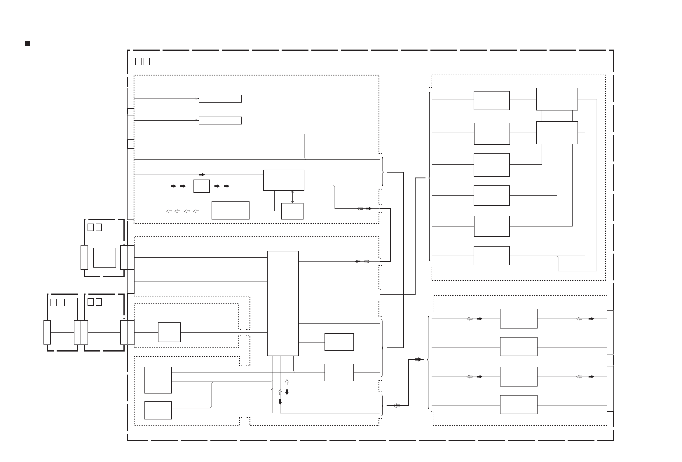
r
Block diagrams
Digital section
0
2
DIGITAL
1394
J4112
6
3
JACK
RS232C
J7401
CN4104
J7126
TO
SW. REG
CN5502
TO
JUNCTION
(VIDEO)
CN7109
TO
JUNCTION
(VIDEO)
CN7108
7
9
BNC
IC7401
RS232C
DRIVER
OPEN
2
9
JUNCTION
(VIDEO)
VIDEO IF
CN1003
CN1002
AO_IEC958, AI_D[0], A_MUTE2[H], K_BUS_CLK
K_BUS_REQ, SYS_RESET[L], K_BUS_IN/OUT
AO_SCLK, AO_MCLKO, AO_FSYNC, DAC_RST[L]
DAC_SCL, DAC_SDA, AO_D[0], A_DAC_CS, 480I[H]
CIN
CN1001
VYIN
YV_OUT
C_OUT
CB_OUT
CR_OUT
Y
MEDIA PROCESSOR
CN1405
JLIP_TX
JLIP_RX
CN1403
UART2_TX
UART2_RX
1394PHY
TPA1+
TPA1-
CN1802
CN7121CN7401
TPB1+
TPB1-
IC1801
IEEE1394
Controller
FLASH MEMORY
IC1201
Flash
memory
LH_AR[6] to LH_AR[21]
IC1202
IC1203
Transparent
Y
Q1008
SW
C
PrPb
PHY_RESET[L], PHY_LREQ
PHY_CLK, PHY_CNA
PHY_CTL[0], PHY_CTL[1]
PHY_DATA[0-7], PHY_LPS
PHY_LINK_ON
E5_RESET[L]
MADD[1-5]
MADD[6-22]
RD/WR[L], OE[L]/LDS[L]
CS[0]
MADD[6-21]
ALE
D2.5V, D1.8V, D3.3V
SW5V, D5V, V3.3V
C
Y
Q1002 to Q1005
BUF
IC1001
Video
Controller
IC1002
SDRAM
IC1401
Media
Processor
VI_D[2-9], VIDEO_RST[L]
VO_D[0-15], SPI_MOSI
VIDEO_27M, VIDEO_CS
VIDEO_MUTE[H], SPI_CLK
VIDEO_RXD
AP, A0 to A9,DQ0 to DQ15
UDQM, WE,CAS, RAS
VI_D[2-9], VO_D[0-15]
SDRAM_DQ[0- 31]
SDRAM_A[0-12]
SDRAM_A[14-17]
SDRAM_DQS[0] to [3]
SDRAM_DQM[0] to [3]
SDRAM_CLK[0], SDRAM_CLK[1]
SDRAM_CLK_L[0], SDRAM_CLK_L[1]
SDRAM_CKE, SDRAM_RAS_L
SDRAM_CAS_L, SDRAM_WE_L
VIDEO_RXD, VIDEO_CS, 480I[H]
VIDEO_27M, AO_SCLK, AO_FSYNC
AO_MCLKO, AO_IEC958, AO_D[0]
AI_D[0], SPI_MOSI, SPI_CLK
DAC_SCL, DAC_SDA, A_DAC_CS
DAC_RST[L], VIDEO_RST[L], VIDEO_MUTE[H]
VI_D[2-9]
VO_D[0-15]
IC1404
3.3V --> 5.0V
IC1405
5.0V --> 3.3V
ATA2_RESET, ATA2_DAT[0-15], ATA2_DMARQ
ATA2_IORDY, ATA2_INTRQ, ATA2_DIOW[L]
ATA2_DIOR[L], ATA2_DMAACK[L], ATA2_ADD[0] to [4]
ATA_RESET, ATA_DAT[0-15], ATA_DMARQ
ATA_IORDY, ATA_INTRQ, ATA_DIOW[L]
ATA_DIOR[L], ATA_DMAACK[L], ATA_ADD[0] to [4]
A_MUTE2[H]
K_BUS_CLK
K_BUS_REQ
K_BUS_IN
SYS_RESET[L]
K_BUS_OUT
DDR SDRAM
SDRAM_DQ[16-31]
SDRAM_A[0-12]
SDRAM_A[14-17]
SDRAM_CKE
SDRAM_RAS_L
SDRAM_CAS_L
SDRAM_WE_L
SDRAM_CLK[0]
SDRAM_CLK[1]
SDRAM_CLK_L[0]
SDRAM_CLK_L[1]
SDRAM_DQM[0] to [3]
SDRAM_DQS[0] to [3]
ATAPI IF
ATA2_RESET
ATA2_DAT[0-15]
ATA2_DIOW[L]
ATA2_DIOR[L]
ATA2_DMAACK[L]
ATA2_ADD[0] to [4]
ATA2_DMARQ
ATA2_IORDY
ATA2_INTRQ
ATA_RESET
ATA_DAT[0-15]
ATA_DIOW[L]
ATA_DIOR[L]
ATA_DMAACK[L]
ATA_ADD[0] to [4]
ATA_DMARQ
ATA_IORDY
ATA_INTRQ
RA1609
to
RA1612
RA1613
to
RA1616
RA1625
to
RA1628
R1641, R1642
R1601
to
R1604
R1613
to
R1616
R1653
to
R1660
DDR_DQ[0-15]SDRAM_DQ[0-15]
DDR_DQ[16-31]
DDR_A[0-12]
DDR_BA[0]
DDR_BA[1]
DDR_CS[0]
DDR_CS[1]
RA2101
to
RA2104
RA2105
to
RA2115
RA2208
to
RA2211
RA2205
to
RA2215
IC1601
IC1603
DDR SDRAM
IC1602
IC1604
DDR SDRAM
DDR_CKE
DDR_RAS_L
DDR_CAS_L
DDR_WE_L
DDR_CLK[0]
DDR_CLK[1]
DDR_CLK_L[0]
DDR_CLK_L[1]
HD_AT[0] to [15]
RSTATA
DMARQ, DIOW, DIOR
IORDY, DMACK, INT_ATA
ATA_A0, ATA_A1,ATA_A2
CS1FX, CS3FX
HD_AT[0] to [15]
RSTATA
DMARQ, DIOW, DIOR
IORDY, DMACK, INT_ATA
ATA_A0, ATA_A1,ATA_A2
CS1FX, CS3FX
DDR_DQM[2],[3]
DDR_DQS[2],[3]
DDR_DQM[0],[1]
DDR_DQS[0],[1]
CN2101
CN2201
TO
HDD
Unit
TO
DVD
Recorde
Unit
2-67 2-68
Page 83

VIDEO (1) Section
TO DIGITAL
(VIDEO IF)
CN1001
VYIN
CIN
COUT
YVOUT
CBOUT
CROUT
J903
COMPONENT
VIDEO OUT
J902
LINE OUT
J953
V OUT
CN7108
20
6
10
Pr
Pb
Y
Y
SP/EP
S-VHS
REC
EQ
NOT
USED
VHS
A12
PB
A13
A14
ATT8
CHARADATA
V MUTE
C MUTE
D16
Y FBC
Y MUTE
ATT5
C
Y
C
Y
C
REC
28
NOT
PB
A10
A11
USED
27
CL4
25
CL5
24
NOT
USED
23
22
21
CL6
20
19
A1
D7&D8
18
BIAS
A2
NOT
USED
17
16
15
A3
NOT
USED
14
WF5
2
9
JUNCTION (VIDEO)
YTODIGI
CTODIGI
CN701
4
2
3
0
MAIN (TERMINAL, VDR V SW)
Y
Y
Y
C
Y
C
C
C
IC701
( Y/C SWITCH VDR )
Q701
BUF
+
42
Pre LPF2
43
CL2
A7
Pre LPF1
Pre LPF1
WF6
Y
45
41
CR
ADJ
40 39 38
DATA
CLK
LOGIC
IIC
A9
REC
A8
ATT9
DIGI/PB
EXT PB Y
DIGI
EXT PB Y
Y
NOT
USED
36
DIGI/PB
CONV
BF2
CONV
DIGI
REC
PB*CONV
PB
NOT
USED
34 33 32 30 2931
EE/PB
CL3
BF1
PB
REC
N/S-LPF
PB
REC
Y
C
6dB
6dB
6dB
6dB
6dB
6dB
-6dB
+
IC7101
6dB
LPF
LPF
LPF
LPF
LPF
LPF
75 DRV
75 DRV
75 DRV
75 DRV
75 DRV
75 DRV
26
C
23
21
Y
20
Y
18
1614
18
Q7101
NOT
USED
2
4
5
6
Y
10
Y
11
14
C
Y
FILTER
Pb
Pr
BUF
12
CN7123
1
3
Pb
Pr
13 11 9 4 6 2
CN7107
1
WF7
C.K.
V4
V3
CONV
CONV
REC
PB*CONV
N.C.
REC
PB
TRAP
A4
A5
V FBC
BB
BB
BB
BB
ATT3
97
Y
ATT4
11
12
10
WF4
C
Q703
C
VDR_Y
VDR_V
VDR_V
VDR_DY
VDR_C
13
C
Y
VDR_PB
VDR_PR
1 3 5 10 8 12
CN901
4
3
2
Pr
Pb
Y
BUF
1
IC901
3
7
Y
Y
C
8
5
6
4
15
C
14
1
4
Y
5
1
2
13
Y
C
C
12
Q901
Y
BUF
Q902
C
BUF
Y
C
Y
C
2
1
C
Y
Y
C
Q711
BUF
47
A6
Pre LPF2
48
49
VPULSE
EXT PB C
EXT PB C
C
REC
PB
VCA
50
51
ATT7CL1
C
52
53
54
55
56
REC
ATT6
PB
GCL
AGC
AGC DET
S. SEP
ATT1
Y
COMP IN
Y/C IN
21
Y
V5
V3/V4
Y
Y1 Y3
Y2
ATT2
3
C
6
Y
WF1
WF2
PB*D15
C3
C1
C2
S1/S2 DET
85
NOT
USED
C
WF3
Y
Y
TO_DV_DUB_Y
TO_DV_DUB_C
V_FROM_OSD
C
C
REAR_Y_IN
REAR_C_IN
REAR_V_IN
DV_Y_OUT
DV_C_OUT
fsc
FRONT_C_IN
FRONT_Y_IN
FRONT_V_IN
I2C_CLK_A/V
12C_DATA_A/V
TU_VIDEO
1
2
3
4
5
6
7
8
9
10
11
12
TO
SYSCON
TO
TUNER
Y
C
J901
VDR OUT
J901
LINE IN
10
Y
C
9
11
12
Y
C
C
Y
4
1
7
2
13
Y
C
14
16
15
Y
C
Y
C
CN3104
2
FRONT_V_IN
CN7201
14
8
5
Y
C
4
6
FRONT_Y_IN
FRONT_C_IN
12
10
SW/JACK
Y
C
2
1
1
3
4
2
J7201
FRONT
VIDEO IN
J7204
Y
FRONT
C
S IN
2-69 2-70
Page 84
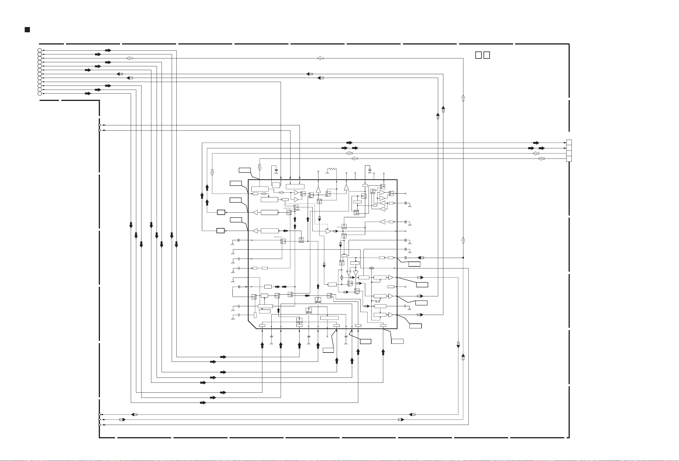
VIDEO (2) Section
1
2
3
4
5
6
7
8
9
10
11
12
TO_DV_DUB_Y
TO_DV_DUB_C
V_FROM_OSD
REAR_Y_IN
REAR_C_IN
REAR_V_IN
DV_Y_OUT
DV_C_OUT
fsc
FRONT_C_IN
FRONT_Y_IN
FRONT_V_IN
TO
SYSCON
I2C_DATA2
I2C_CLK2
Y
C
Y
C
Y
C
C
Y
Y
C
3
0
MAIN (VIDEO SW VDR)
Y
C
CN501
C
Y
Y
C
Y
Y
C
WF16
Pre LPF2
43
CL2
WF17
WF15
Q505
BUF
45
A7
C
42
Pre LPF1
Pre LPF1
Y
+
41
CR
ADJ
40 39 38
DATA
CLK
LOGIC
IIC
C
A9
REC
A8
ATT9
DIGI/PB
EXT PB Y
DIGI
EXT PB Y
Y
WF18
Q503
BUF
Y
C
C
Y
C
Y
47
A6
Pre LPF2
48
49
VPULSE
EXT PB C
EXT PB C
C
PB
NOT
USED
36
DIGI/PB
DIGI
C
CONV
BF2
CONV
REC
PB*CONV
C
VCA
PB
REC
50
51
ATT7CL1
C
52
PB*D15
53
54
55
56
IC501
( Y/C SWITCH DV )
Y
REC
PB
ATT6
GCL
AGC
AGC DET
S. SEP
ATT1
Y
COMP IN
Y/C IN
21
Y
V5
V3/V4
Y
Y1 Y3
ATT2
3
C
Y
C
C.K.
V4
V3
C3
C1
C2
S1/S2 DET
Y2
6
85
NOT
C
USED
WF8
C
NOT
USED
34 33 32 30 2931
EE/PB
BF1
N/S-LPF
PB
REC
CONV
CONV
Y
REC
PB*CONV
Y
N.C.
REC
PB
TRAP
A4
A5
BB
BB
BB
Y
BB
ATT3
97
Y
ATT4
1110
C
REC
V FBC
C
12
CL3
PB
WF9
Y
SP/EP
REC
NOT
USED
VHS
S-VHS
PB
EQ
CHARADATA
V MUTE
C MUTE
Y FBC
Y MUTE
REC
A12
A13
A10
A11
A14
28
NOT
PB
USED
27
CL4
25
CL5
24
NOT
USED
23
22
21
CL6
ATT8
WF14
20
19
A1
D7&D8
18
NOT
BIAS
17
A2
D16
ATT5
16
15
A3
USED
WF13
C
WF12
Y
WF11
14
WF10
C
Y
Y
C
1
3
7
5
D_C_IN
D_Y/V_IN
D_Y_OUT
D_C_OUT
TO
DV ( VIDEO OUT )
CN3501
TO
ON SCREEN
V_TO_OSD
DV_V_OUT
CHARADATA
Y
C
Y
C
2-71 2-72
Page 85

AUDIO Section
2
7
SW/JACK
3
MAIN (AUDIO I/O, TERMINAL I/O, TUNER)
0
J7201
AUDIO IN
AUDIO IN
TO DIGITAL
(VIDEO IF)
CN1002
TO DIGITAL
(VIDEO IF)
CN1001
DAC_RST(L)
(L)
(R)
AI_D(0)
AO_IEC958
AO_D(0)
AO_FSYNC
AO_SCLK
AO_MCLK
DAC_SDA
DAC_SCL
A_DAC_CS
CN7109
5
19
CN7108
28
19
26
24
25
27
23
21
4
3
6
7
5
JUNCTION (AUDIO AD/DA, VIDEO)
2
9
IC8002
A/D
SDTO
IC8202
LRCK
BICK
MCLK
CDTI
CCLK
CSN
PDN
D/A
AOUTL+SDTI
AOUTL-
AOUTR+
AOUTR-
AINL
AINR
9
3
4
2
1
8
7
6
5
L
R
IC8001
2
7
1
1
IC8201
3
12
11
10
AMP
2
5
AMP
6
9
AMP
AMP
CN7201
DVD_IN[L]
5
DVD_IN[R]
3
DVD_OUT[L]
1
DVD_OUT[R]
7
AD_IEC958
F.AUDIO[L]
8
F.AUDIO[R]
6
CN3104
8
10
L
R
F.AUDIO[L]
F.AUDIO[R]
DVC_A_INSEL1
DVC_A_INSEL2
DVD_A_INSEL1
DVD_A_INSEL2
A.OUTSEL1
A.OUTSEL2
A.MUTE_DVC(H)
TO
SYSCON
IC2201
IC2202
5
L
3
R
AMP
AMP
7
1
CN2601
L
8
DV_A_REC[L]
R
6
DV_A_REC[R]
TO DV MAIN
(AUDIO AD/DA)
CN3701
Q2201
to
L
4
DV_A_PB[L]
Q2204
MUTE
CONTROL
R
2
DV_A_PB[R]
CN8001
7
5
3
1
11
CN2602
7
5
3
1
11
L
L
R
R
IC2603
11
L
IC2604
L
R
7
AMP
1
AMP
5
3
13
3
DVD_A_INSEL1
DVD_A_INSEL2
L
R
12
15
14
4
1
2
5
9,10
L
L
L
R
R
R
R
DVD_OUT[L]
DVD_OUT[R]
12
11
L
14
15
L
1
4
R
5
2
R
DVC_A_INSEL1
DVC_A_INSEL2
L
R
13
3
9,10
J901
LINE_IN
J901
VDR_OUT
J902
LINE_OUT
J841
OPTICAL OUT
J852
COAX_OUT
(L)
AUDIO
(R)
AUDIO
(L)
AUDIO
(R)
AUDIO
(L)
AUDIO
(R)
AUDIO
TO
SYSCON
A.MUTE(L)
1
2
1
7
6
5
3
2
1
3
L
2
R
1
IC851
3, 8, 11
(Q2601,Q2602,Q2605)
2, 9, 12
MUTE
CONTROL
L
R
L
R
LINE_OUT[L]
LINE_OUT[L]
7
1
IC2606
AMP
AMP
IC2605
11
L
13
5
3
3
9,10
A.OUTSEL1
A.OUTSEL2
12
15
4
1
2
L
R
R
2-73 2-74
Page 86

System control section
LOADING
MOTOR
DV DRUM
MOTOR
DV
CAPSTAN
MOTOR
DV
HOUSING
MOTOR
LOAD.MOTOR+
LOAD.MOTOR-
COIL_COMMON
3
PG_OUT
10
FG_OUT
11
FG1
16
FG2
18
HOUSING.MOTOR+
4
HOUSING.MOTOR-
3
HOUSING_SW
2
6
1
MDA
1
2
MDA_CS
14
MDA_CLK
13
MDA_IN
12
3
10
11
3
1
4
3
2
19
18
17
16
7
6
5
DRUM_PG
DRUM_FG
CAP_FG
LD_ON
HOUSING_IN
HOUSING_OUT
HOUSING_SW
CN1501
7
8
9
2
3
4
5
14
15
16
DV MAIN (MSD)
05
WF1
WF2
WF3
IC1504
SO
SI
SCK
2
5
6
94
93
111
112
27
50
49
51
18
8
9
10
EEP_OUT
EEP_IN
EEP_CLK
MDA_CS
DRUM_PG
DRUM_FG
DRUM_FG
CAP_FG
LD_ON
HOUSING_IN
HOUSING_OUT
HOUSING_SW
IC1501
(DV MSD)
ADM0 - ADM15
START_SENS
CASSETTE_SW
DAC_CS
TBC_IN
TBC_CLK
TBC_CS
TBC_OUT
TBC_RST
VD
TBC_VD
OSCI
OSCO
AS
CLK27SEL
DWE
RE
RST
REC_SAFE
END_SENS
S_REEL
T_REEL
REEL_LED
17
24
25
22
23
21
15
96
71
70
145 - 152
155 - 162
142
46
138
141
66
34
117
118
102
101
41
52
7
5
Q1512
X1501
DV SYSTEM CLOCK
(
16kHz
IC1502
ES
DAC_DATA
DAC_CLK
DAC_CS
TBC_SDI
TBC_CLK
TBC_CS
TBC_SDO
TBC_RST
TBC_VD
CLK27A
TO
DV I/O
)
16
1
3
ADM0 - ADM15
DALE
CLK27SEL
DWE
DRE
RESET
CN1502
1
3
7
SUP_REEL_SENSOR
8
9
11
12
15
REC_SAFETY_SW
START_SENSOR
E_SENSOR
SUP_REEL_LED
TU_REEL_SENSOR
TU_REEL_LED
CASSETTE_SW
TO
DV MAIN
SENSOR
15
13
9
8
7
5
4
1
MAIN(SYSCON, ON SCREEN
30
IC3001
(
SYSTEM CONTROL MICRO PROCESSOR
OSC1(IN)
X1
X2
A.MUTE(L)
TU_CLK
TU_DATA
69
67
65
64
28
24
79
77
88
85
94
91
50
49
60
61
OSC2(OUT)
A.MUTE_DVC(H)
A.OUTSEL1
A.OUTSEL2
DVC_A_INSEL1
DVC_A_INSEL2
DVD_A_INSEL1
DVD_A_INSEL2
I2C_CLK_A/V
I2C_DATA_A/V
)
)
X3002
MAIN SYSTEM
CLOCK
(10MHz)
X3001
TIMER CLOCK
(
)
32kHz
C3025
TIMER CLOCK
A.MUTE(L)
A,MUTE_DVC(H)
A.OUTSEL1
A.OUTSEL2
DVC_A_INSEL1
DVC_A_INSEL2
DVD_A_INSEL1
DVD_A_INSEL2
I2C_CLK_A/V
I2C_DATA_A/V
TU_I2C_CLK
TU_I2C_DATA
I2C_CLK2
I2C_DATA2
TO
AUDIO I/O
TO
AUDIO I/O
TO
VDR V SW
TO
TUNER
DV
ENCODER
CN3014
3
4
5
7
53
S_CLK
51
S_DATA_TOSYS
52
S_DATA_FRSYS
57
DV_H_SW
I2C_CLK
I2C_DATA
OSD_CS
S.CLK
S.DATA_FRSYS
SYNC_DET(H)
75
76
87
53
52
14
Q1502
BUF
CN1503
5
4
3
1
PWR_CTL
A
GC_RST
ASPECT1
ASPECT2
SYS_CLOCK
SYS_IN
SYS_OUT
DV_H.SW
TO
REG
TO
DV VIDEO OUT
1
SYS_CLK
R.ENC1
3
R.ENC2
2
R.ENC3
1
3
2
1
CAM_SW1
3
CAM_SW2
2
CAM_SW3
1
18
19
20
31
CAM0
32
CAM1
33
CAM2
SYS_OUT
175
D1501
D1506
IC1503
71
5
TO
AUDIO AD/DA
ADC_DEM0
ADC_DEM1
ADC_PWD0
ADC_PWD1
83
84
86
85
ADC_DEM0
ADC_DEM1
ADC_PWD0
ADC_PWD1
SYS_IN
POWER_CTL
AGC_RST
ASPECT1
ASPECT2
176
16
88
89
90
3
IC3004
(
SERIAL MEMORY
6
SCL
5
SDA
IC201
(
ON_SCREEN
9
CS
10
SCLK
11
SDATA
8
SYNC_DET
CHABLK
CV_IN
SYNC_IN
CVOUT
)
I2C_CLK2
I2C_DATA2
TO
VIDEO SW VDR
)
WF4
4
15
18
13
WF5
CHARADATA
V_TO_OSD
V_FROM_OSD
V_FROM_OSD
TO
VIDEO SW VDR
TO
TERMINAL
2-75 2-76
Page 87

VIDEO (DV) Section
5
DAC_CS
DAC_CLK
DAC_DATA
TO
DV MSD
TO
MAIN
(VIDEO SW VDR)
CN501
TO
MAIN
(AUDIO I/O)
CN2601
TBC_CLK
TBC_SDI
TBC_CS
TBC_RST
TBC_SDO
TBC_VD
CLK27A
D_Y_OUT
D_C_OUT
D_Y/V_IN
D_C_IN
DV_A_REC(L)
DV_A_REC(R)
DV_A_PB(L)
DV_A_PB(R)
CN3501
1
3
5
7
CN3701
1
3
5
7
Y
C
L
R
0
DV MAIN (DV MAIN, DV I/O, DV VVIDEO OUT, AUDIO AD/DA, DV PRE/REC)
IC3501
VIDEO AMP
2
18
Y_GCTL
C_GCTL
IC3001
49 - 51,
55
SDIN, SCLK,
CS, RST
48, 58
WF1
Q3521
BUF
Q3522
BUF
WF2
Q3102
Y
BUF
Q3101
C
BUF
WF3
9
14
CLAMP
LPF
BPF ATT
ATT
1
19
WF4
Y
C
Q3111~Q3114
BUF
Q3131~Q3133
BUF
Y
WF5
C
SDOUT, CSYNC
7
YSOUT
80
COUT
12
VYIN
18
CIN
8 bit 2ch
AD/DA CONV.
WF6
IC3701
L
R
IC3702
IC3703
AMP
L
R
WF7
WF8
3
AINL
2
15
16
A/D
AINR
AOUTL
D/A
AOUTR
SDTO
SDTI
8
9
16 bit
ADC&DAC
A07
A08
CLK
CSO0 - CSO3
YSO0 - YSO3
CSI0 - CSI3
YSI0 - YSI3
6
7
54
26 - 29
32 - 35
38 - 41
42 - 45
Y_GCTL
C_GCTL
C
Y
C
Y
VCO
4
DCO0 - DCO3
4
DYO0 - DYO3
4
DCI0 - DCI3
4
DYI0 - DYI3
IC3101
IC3102
X3101
(27kHz)
190,191
255, 256
116, 117
189, 254
41, 42
193, 194
120, 192
257, 258
185
112
248
Y_GCTL
C_GCTL
38
CLK27I
BRSI0 - BRSI3
YSI0 - YSI3
BRSO0 - BRSO3
YSO0 - YSCO3
AIDAT0
AIDAT1
AODATA
IC3151
15
LD
16
17
6
7
CLK
LI
A07
A08
AD CONV.
A05
A06
A02
A01
A03
A04
4
5
19
18
2
3
DUMP_CTL
AGC_GAIN
ATF_GAIN
RECCADJ
M_VCOCTL
FSPLLCTL
0
5
D-SUB
CONN.
CN1505
IC2001
OSC24I
OSC24O
ADVIN0
RECCLK
RECDATA
PHYTPA
PHYXTPA
PHYTPB
PHYXTPB
23
253
251
30
168
174
100
82
226
156
286
M_VCOCTL
FSPLLCTL
X2003
(24.576MHz)
1
2
IC4002
DUMP_CTL
AGC_GAIN
ATF_GAIN
RECCADJ
4
2
51
60
10
57
9
7
TPA+
TPA-
TPB+
TPB-
IC4001
REC/PB AMP
MUSIN_EVR
AGC_CTL
ATF_GAIN
REC_GAIN
AGC_BUFF_OUT
REC_CLK
REC_DATA
CN7401
1
4
3
2
25
X2
24
Y2
20
X1
19
Y1
CN4001
7
6
3
2
CN2002
1
2
4
5
DV Drum
2S
7
2F
6
1S
3
1F
2
TO
JUNCTION
(VIDEO)
CN7127
J7401
D-SUB
CONNECTOR
4
3
2
1
2-77 2-78
Page 88

CPU PIN FUNCTION
<SYSCON IC3001>
PIN NO.
1 TO_VSS - GND
2 SVss - GND
3 OPEN - NOT CONNECTED
4 TO_VSS - GND
5 OPEN - NOT CONNECTED
6 OPEN - NOT CONNECTED
7 C+VSS - NOT USED
8 TO_VSS - GND
9 SVcc - SYSTEM POWER
10 Avcc - SYSTEM POWER
11 SYNC_DET_VDR[L] IN
12 - GND
13 - GND
14 SYNC_DET[H] IN
15 - GND
16 - GND
17 TEST - NOT USED
18 WIDE_DET_VDR IN S1/S2 DETECT FOR VDR
19 KEY1IN IN OPERATION CONTROL SIGNAL
20 AFC IN TUNING CHECK
21 WIDE_DET_DV IN S1/S2 DETECT FOR DVC
22 KEY2IN IN OPERATION CONTROL SIGNAL
23 Avss - GND
24 A.MUTE_DVC[H] OUT AUDIO MUTE CONTROL FOR DVC(MUTE:H)
25 C_BIAS2 OUT ADD THE DC BIAS TO COLOR SIGNAL
26 BLUE_LED - NOT USED
27 C_BIAS1 OUT ADD THE DC BIAS TO COLOR SIGNAL
28 A.MUTE[L] OUT AUDIO MUTE CONTROL(MUTE ON : L)
29 RC_IN IN REMOTE CONTROL DATA INPUT
30 LED9 OUT DVD REC LED ON/OFF CONTROL (LED ON : H)
31 LED10 OUT DVD LED ON/OFF CONTROL (LED ON : H)
32 BS_DIGI_LINK/COMPU_IN - NOT USED
33 COMP_OUT OUT AV COMPULINK OUTPUT
34 EDS_CS OUT EDS CHIP SELECT
35 P.CTL[H] OUT CONTROL SIGNAL FOR SWITCHING POWER SUPPLY
36 FAN_CTL[H] OUT FAN MOTOR ON/OFF CONTROL
37 P.MUTE_VDR[L] OUT PICTURE MUTE CONTROL FOR DVD (MUTE : H)
38 MSD_CS OUT CHIP SELECT OF DVC CPU
39 STB OUT STROBE SIGNAL
40 POWER_DET IN
41 - NOT CONNECTED
42 PROTECT IN DETECTION SIGNAL FOR SWITCHING POWERSUPPLY
43 Vss - GND
44 RMO OUT REMOTE CONTROL OUTPUT FOR SATELLITE RECEIVER
45 Vcc - SYSTEM POWER
46 K.BUS_IN IN SERIAL DATA TRANSFERMER INPUT FROM DVD CPU
47 K.BUS_OUT OUT SERIAL DATA TRANSFERMER OUTPUT TO DVD CPU
48 K.BUS_CLK OUT SERIAL DATA TRANSFERMER CLOCK FOR DVD CPU
49 12C_DATA_AV IN/OUT SERIAL DATA TRANSFER OUTPUT FOR A/V IC
50 12C_CLK_AV OUT SERIAL DATA TRANSFER CLOCK FOR A/V IC
51 S_DATA_TOSYS OUT
52 S_DATA_FRSYS OUT
53 S_CLK OUT SERIAL DATA TRANSFERMER CLOCK FOR ONSCREEN IC
54 K_BUS_REQ OUT SERIAL DATA TRANSFER REQUEST TO DVD CPU
55 MSD_READY IN PREPARATION OF COMMUNICATION OF DVC CPU
56 - CONNECTED Vcc
LABEL IN/OUT FUNCTION
DETECTION OF VIDEO SYNC SIGNAL FOR DVD (DETECTED : H)
DETECTION OF VIDEO SYNC SIGNAL FOR DVC (DETECTED : H)
DETECTION SIGNAL FOR POWER DOWN OF AC POWER SUPPLY
SERIAL DATA TRANSFER OUTPUT FROM THE FDP DRIVER TO
SERIAL DATA TRANSFER OUTPUT FROM THE FDP DRIVER TO
PIN NO.
57 DV_H_SW IN DETECTION OF DVC CASSETTE
58 - CONNECTED Vcc
59 JUST/EDS[H] IN VIDEO SIGNAL FIELD DETECT
60 TU_CLK OUT SERIAL DATA TRANSFERMER CLOCK TO TUNER
61 TU_DATA OUT SERIAL DATA TRANSFERMER DATA TO TUNER
62 FWE - FLASH WRITE ENABLE
63 NMI - NOT USED
64 X2 - TIMER CLOCK(32kHz)
65 X1 - TIMER CLOCK(32kHz)
66 RES OUT RESET TERMINAL(RESET ON:L)
67 OSC1 IN MAIN SYSTEM CLOCK(10MHz)
68 Vss - GND
69 OSC2 OUT MAIN SYSTEM CLOCK(10MHz)
70 Vcl - SYSTEM POWER
71 MODE - NOT USED
72 I.MUTE OUT INTERFACE VIDEO SIGNAL MUTING CONTROL OUTPUT
73 TU_V.MUTE[H] OUT TUNER VIDEO SIGNAL MUTE : H
74 A.MUTE_VDR[H] OUT AUDIO MUTE CONTROL FOR DVD(MUTE:H)
75 12C_CLK2 OUT SERIAL DATA TRANSFER CLOCK FOR MEMORY IC
76 12C_DATA IN/OUT SERIAL DATA TRANSFER OUTPUT FOR MEMORY IC
77 A.OUTSEL2 OUT AUDIO OUTPUT SIGNAL SELECT-2
78 VDR[H] OUT VDR MODE : H
79 A.OUTSEL1 OUT AUDIO OUTPUT SIGNAL SELECT-1
80 MSD_RESET[L] OUT RESET OUTPUT TO DVD CPU
81 E5_RESET[L] OUT RESET OUTPUT TO DVD CPU
82 Vcc - SYSTEM POWER
83 - NOT CONNECTED
84 Vss - GND
85 DVC_A_INSEL2 OUT DVC AUDIO INPUT SIGNAL SELECT-2
86 - NOT CONNECTED
87 OSD_CS OUT CHIP SELECT FOR THE ONSCREEN IC
88 DVC_A_INSEL1 OUT DVC AUDIO INPUT SIGNAL SELECT-1
89 - NOT CONNECTED
90 LINE2INFO - NOT USED
91 DVD_A_INSEL2 OUT DVD AUDIO INPUT SIGNAL SELECT-2
92 P.MUTE_DV[L] OUT PICTURE MUTE CONTROL FOR DV (MUTE ON : H)
93 AD_RST[L] OUT A/D CONVERTER RESET PULSE OUTPUT
94 DVD_A_INSEL1 OUT DVD AUDIO INPUT SIGNAL SELECT-1
95 P.MUTE_VDR[L] OUT PICTURE MUTE CONTROL FOR VDR (MUTE ON : L)
96 P.SAVE[L] OUT POWER SAVE MODE:H
97 HDD_P.SAVE OUT POWER SAVE FOR HDD
98 - GND
99 OPEN - NOT CONNECTED
100 OPEN - NOT CONNECTED
101 OPEN - NOT CONNECTED
102 OPEN - NOT CONNECTED
103 - NOT CONNECTED
104 - NOT CONNECTED
105 TO_VSS - GND
106 TO_VSS - GND
107 TO_VSS - GND
108 TO_VSS - GND
109 Vcc - SYSTEM POWER
110 - NOT CONNECTED
111 Vss - GND
112 - NOT CONNECTED
LABEL IN/OUT FUNCTION
WAVEFORMS
VIDEO BLOCK DIAGRAM(1)
WF1 IC701-9
0.5V/20µsec/DIV
IC701-5
REC 1.0Vp-p
WF2
REC 0.8Vp-p
0.2V/20µsec/DIV
WF3 IC701-11
IC701-7
REC 0.9Vp-p
0.5V/20µsec/DIV
WF4 IC701-45
REC 0.7Vp-p
0.2V/20µsec/DIV
WF5
REC 1.1Vp-p
0.5V/20µsec/DIV
IC701-14
WF6 IC701-47
REC/PB 1.8Vp-p
1.0V/20µsec/DIV
VIDEO BLOCK DIAGRAM(2)
WF8 IC501-9 IC501-11 IC501-14 IC501-17 IC501-19 IC501-21
REC 0.9Vp-p
0.5V/20µsec/DIV
WF15 IC501-42 IC501-43 IC501-45 IC501-47
PB 0.6Vp-p
0.2V/20µsec/DIV
WF9 WF10 WF12 WF13 WF14
REC 0.7Vp-p
0.2V/20µsec/DIV
REC 1.1Vp-p
0.5V/20µsec/DIV
WF11 IC501-15
REC/PB 1.8Vp-p
1.0V/20µsec/DIV
REC/PB 1.7Vp-p
0.5V/20µsec/DIV
REC/PB 2.0Vp-p
1.0V/20µsec/DIV
WF16 WF17 WF18
PB 0.7Vp-p
0.5V/20µsec/DIV
REC 1.8Vp-p
0.5V/20µsec/DIV
REC 3.0Vp-p
1.0V/20µsec/DIV
VIDEO (DV) BLOCK DIAGRAM
WF1 IC3501-9 IC3501-14 IC3001-7 IC3001-80 IC3001-12 IC3001-18
PB 1.5Vp-p
0.5V/20µsec/DIV
IC3701-15WF8
PB 0.1Vp-p
50mV/1.0msec/DIV
WF2 WF3 WF4 WF5 WF6
PB 1.2Vp-p
0.5V/20µsec/DIV
PB 0.8Vp-p
0.5V/20µsec/DIV
PB 0.7Vp-p
0.5V/20µsec/DIV
REC 1.3Vp-p
0.5V/20µsec/DIV
REC 1.7Vp-p
1.0V/20µsec/DIV
SYSTEM CONTROL BLOCK DIAGRAM
WF1
DRUM_PG
REC/PB 3.4Vp-p
1.0V/2.0msec/DIV
CN1501-2
WF2
DRUM_FG
REC/PB 3.4Vp-p
1.0V/0.5msec/DIV
CN1501-3
WF3
CN1501-4
CAP_FG
REC/PB 3.4Vp-p
1.0V/0.5msec/DIV
WF4
REC/PB 2.0Vp-p
1.0V/20µsec/DIV
IC201-15
WF5
REC/PB 2.0Vp-p
1.0V/20µsec/DIV
IC201-13
WF7
REC/PB 2.8Vp-p
1.0V/20µsec/DIV
REC/PB 2.0Vp-p
1.0V/20µsec/DIV
WF7 IC3701-3
REC 0.1Vp-p
50mV/1.0msec/DIV
2-79 2-80
Page 89

VOLTAGE CHARTS
<SW.REG>
MODE
REC PLAY
PIN NO.
IC5101
1 303.9 303.4
2 0 0
3 0 0
4 18.3 18.2
5 3.6 3.6
IC5301
1 2.4 2.4
2 0 0
3 4.6 4.6
IC5302
1 5.0 5.0
2 0 0
3 0 0
4 3.3 3.3
5 4.4 4.4
6 0 0
7 0 0
8 5.6 5.7
Q5303
E 50.8 50.7
C 50.0 50.8
B 0 0
Q5304
E 0 0
C 0 0
B 4.0 4.0
Q5305
E 11.0 11.0
C 11.6 11.6
B 11.7 11.7
Q5306
E 5.1 5.1
C 5.7 5.7
B 5.8 5.8
Q5307
E 10.8 10.8
C 10.8 10.8
B 10.1 10.1
Q5308
E 0 0
C 0 0
B 4.4 4.4
Q5313
E 11.6 11.6
C 11.6 11.6
B 10.9 10.9
Q5315
E 0 0
C 0 0
B 4.3 4.4
Q5316
E -7.5 -7.5
C -7.4 -7.4
B 0 0
Q5317
E 5.7 5.7
C 5.7 5.7
B 0 0
Q5318
E 0 0
C 0 0
B 4.0 4.0
Q5319
E 2.4 2.4
C 0 0
B 2.8 2.8
CN5301
1 5.0 5.1
2 0 0
3 0 0
4 0 0
5 4.4 4.4
6 0 -7.4
7 0 0
8 0 0
9 4.8 4.8
10 5.6 5.6
11 4.0 4.0
12 0 0
13 0 0
14 5.7 5.7
15 0 0
16 0 0
17 0 0
18 0 0
19 0 0
CN5302
1 10.8 10.8
2 0 0
CN5303
1 11.6 11.5
2 0 0
3 0 0
4 5.0 5.0
CN5304
1 11.0 11.0
MODE
PIN NO.
2 11.6 11.6
3 -7.4 -7.4
4 11.6 11.6
5 4.0 4.0
6 4.8 4.8
7 4.4 4.4
8 0 0
9 0 0
10 5.5 5.6
11 0 0
12 0 0
13 0 0
14 0 0
15 -16.6 -16.6
16 5.6 5.6
17 -22.1 -22.1
18 5.7 5.7
19 -33.2 -33.2
REC PLAY
<MAIN>
MODE
REC PLAY
PIN NO.
IC201
1 0 0
2 2.6 2.6
3 5.0 5.0
4 0 0
5 0.3 0.2
6 2.4 2.4
7 2.4 2.4
8 3.0 3.0
9 3.0 3.1
10 4.0 4.1
11 2.0 2.2
12 5.0 5.0
13 2.3 2.4
14 0 0
15 2.3 2.3
16 0 0.1
17 5.0 5.0
18 4.8 4.8
19 0 0
20 5.0 5.0
21 5.0 5.1
22 0.0 0.0
23 0.0 0.0
24 5.0 5.0
IC501
1 2.7 2.8
2 0.1 0.1
3 2.1 2.1
4 5.0 5.0
5 2.7 2.8
6 0.1 0.0
7 2.1 2.0
8 0 0
9 2.7 2.8
10 0.1 0.2
11 2.1 2.1
12 2.7 2.8
13 0 0
14 2.8 2.8
15 2.2 2.2
16 2.7 2.7
17 2.4 2.1
18 0 0
19 2.3 2.3
20 0 0
21 3.5 3.5
22 2.7 0.1
23 3.0 3.0
24 3.1 3.1
25 2.8 0
26 5.0 5.0
27 2.8 2.8
28 2.3 2.4
29 2.4 2.4
30 0 0.1
31 2.7 2.7
32 0 0
33 2.8 2.8
34 0.2 0.3
35 2.8 2.8
36 0 3.3
37 0 0
38 0 3.4
39 3.9 3.9
40 2.8 2.8
41 2.6 2.6
42 2.8 2.8
43 3.2 3.3
44 1.6 1.6
45 2.1 1.3
46 5.0 5.0
47 0.6 0.6
48 2.8 2.8
49 0 0
50 1.0 2.8
51 2.8 2.9
52 0 0
53 3.2 2.9
54 2.2 2.0
55 1.9 1.1
56 2.5 2.6
IC701
1 2.8 2.8
2 0.1 0.2
3 2.1 2.0
4 5.0 5.0
5 2.8 2.8
6 0 0.2
7 2.1 2.1
8 0 0
9 2.7 2.8
10 0.2 0.2
11 2.1 2.1
12 2.6 2.8
13 0 0
14 2.8 2.8
MODE
REC PLAY
PIN NO.
15 1.4 1.4
16 2.7 2.7
17 2.4 2.4
18 0 0
19 1.5 0
20 0 0
21 2.6 2.6
22 2.7 2.7
23 3.0 3.0
24 2.7 2.8
25 2.8 2.8
26 5.0 5.0
27 2.8 2.8
28 2.2 2.2
29 0 2.2
30 0 0.1
31 3.2 3.1
32 0 0
33 2.8 2.8
34 0.3 0.3
35 2.8 2.8
36 3.0 3.1
37 0 0
38 4.9 5.0
39 4.9 5.0
40 2.8 2.8
41 2.7 2.6
42 2.8 2.8
43 3.0 3.0
44 1.6 1.2
45 2.6 2.6
46 5.0 5.0
47 0.7 0.8
48 2.8 2.8
49 0 0
50 2.8 2.8
51 2.9 2.9
52 0 0
53 3.3 3.3
54 2.8 2.9
55 2.0 2.0
56 2.5 2.5
IC851
1 3.2 3.2
2 1.6 1.6
3 1.6 1.6
4 0 0
5 0 0.1
6 0 0
7 0 0
8 1.6 1.6
9 1.6 0
10 3.2 3.2
11 1.6 1.6
12 1.6 1.6
13 3.2 3.2
14 3.2 3.2
IC901
1 2.4 2.5
2 2.4 2.4
3 1.8 1.8
4 2.2 2.2
5 2.2 2.2
6 0 0
7 0 0
8 0 0
9 0 0
10 0 0
11 0 0
12 2.3 2.3
13 1.8 1.8
14 2.3 2.3
15 2.4 2.4
16 5.6 5.8
IC2201
1 0 0
2 0 0
3 0 0
4 0 0
5 0 0
6 0 0
7 -7.4 -7.4
8 5.0 0.0
9 5.0 0
10 5.0 5.0
11 0 0
12 0 0
13 0 0
14 0 0
15 0 0
16 6.6 6.7
IC2202
1 0 0
2 0 0
3 0 0
4 -7.4 -7.4
5 0 0
MODE
REC PLAY
PIN NO.
6 0 0
7 0 0
8 11.3 11.3
IC2603
1 0 0
2 0 0
3 0 0
4 0 0
5 0 0
6 0 0
7 -7.4 -7.4
8 0 0
9 0 0
10 0 0
11 0 0
12 0 0
13 0 0
14 0 0
15 0 0
16 6.6 6.6
IC2604
1 0 0
2 0 0
3 0 0
4 -7.4 -7.4
5 0 0
6 0 0
7 0 0
8 11.2 11.3
IC2605
1 0 0
2 0 0
3 0 0
4 0 0
5 0 0
6 0 0
7 -7.4 -7.4
8 0 0
9 5.0 5.0
10 0 0
11 0 0
12 0 0
13 0 0
14 0 0
15 0 0
16 6.6 6.7
IC2606
1 0 0
2 0 0
3 0 0
4 -7.4 -7.4
5 0 0
6 0 0
7 0 0
8 11.1 11.3
IC3001
1 0 0
2 0 0
3 1.6 1.6
4 0 0
5 0 0
6 2.4 1.5
7 4.1 4.1
8 0 0
9 5.0 5.0
10 5.0 5.0
11 5.1 5.1
12 0 0
13 0 0
14 2.6 2.7
15 0 0
16 0.0 0.0
17 0.0 0.0
18 0.0 0.0
19 5.0 5.0
20 4.6 4.6
21 0 0
22 5.0 5.0
23 0 0
24 0 0
25 0 0
26 5.0 5.0
27 0 0
28 5.0 5.0
29 4.9 5.0
30 0 0
31 0 0
32 0.6 0.6
33 0 0
34 0 0
35 4.9 4.9
36 4.9 4.9
37 0 0
38 0.4 0.4
39 3.0 2.9
40 0 0
41 0 0
MODE
REC PLAY
PIN NO.
42 4.5 4.5
43 0 0
44 0 0
45 5.0 5.1
46 0.1 0.1
47 0 0.3
48 4.2 4.2
49 4.9 5.0
50 4.9 4.9
51 4.6 4.6
52 1.8 1.9
53 4.1 4.1
54 2.0 2.2
55 4.7 4.7
56 0 0
57 0 0
58 0 0
59 0.3 0.3
60 4.2 4.4
61 4.2 4.3
62 0 0
63 0 0
64 1.3 1.4
65 0.6 0.6
66 5.0 5.0
67 2.5 2.5
68 0 0
69 2.5 2.5
70 5.0 5.0
71 5.0 5.1
72 5.0 5.0
73 5.0 5.0
74 5.0 5.0
75 4.4 4.1
76 3.9 4.0
77 5.0 5.0
78 0 0
79 0 0
80 5.0 5.0
81 5.0 5.1
82 5.0 5.0
83 0.0 0.0
84 0.0 0.0
85 5.0 0.0
86 0.0 0.0
87 2.8 2.7
88 5.0 5.0
89 0.0 0.0
90 0.0 0.0
91 0.0 0.0
92 5.0 5.0
93 5.0 5.0
94 0.0 0.0
95 5.0 5.0
96 4.9 4.9
97 4.9 5.0
98 0.0 0.0
99 0.0 0.0
100 0.0 0.1
101 0.0 0.0
102 0.0 0.0
103 0.0 0.1
104 0.0 0.0
105 0.0 0.0
106 0.0 0.0
107 0.0 0.0
108 0.0 0.0
109 5.0 5.0
110 0.0 0.1
111 0.0 0.0
112 1.6 1.6
IC3002
1 5.0 5.1
2 5.0 5.0
3 0.0 0.0
4 0.0 0.0
IC3004
1 0.0 0.0
2 0.0 0.0
3 0.0 0.0
4 0.0 0.0
5 4.1 4.0
6 4.1 4.2
7 0.0 0.0
8 5.0 5.0
IC5401
1 3.3 3.3
2 0.0 0.0
3 0.0 0.0
4 1.9 1.9
5 4.1 4.1
6 0.0 0.0
7 0.0 0.0
8 4.1 4.1
Q212
E 3.1 3.1
C 5.0 5.0
MODE
REC PLAY
PIN NO.
B 3.7 3.6
Q503
E 1.8 1.9
C 5.0 5.0
B 2.5 2.5
Q505
E 2.5 1.8
C 0 0.1
B 1.8 1.2
Q701
E 2.9 2.8
C 0 0
B 2.2 2.3
Q703
E 1.8 1.9
C 5.0 5.0
B 2.5 2.5
Q706
E 3.2 3.2
C 5.0 5.1
B 3.6 3.6
Q711
E 2.9 2.9
C 0 0
B 2.2 2.2
Q713
E 1.5 1.5
C 0 0
B 0.9 0.9
Q901
E 2.5 2.5
C 0 0
B 1.8 1.8
Q902
E 3.1 3.1
C 0.0 0.0
B 2.5 2.4
Q911
E 2.9 2.9
C 0 0
B 2.3 2.2
Q912
E 3.1 3.1
C 0 0
B 2.4 2.4
Q913
E 2.9 3.0
C 0 0
B 2.4 2.3
Q915
E 3.0 3.0
C 0.0 0.0
B 2.3 2.3
Q2201
E 0 0
C 0 0
B -0.1 -0.1
Q2202
E 0 0
C 0 0
B -0.1 -0.1
Q2203
E 5.8 5.8
C -0.1 -0.1
B 5.8 5.8
Q2204
E 0 0
C 5.7 5.7
B 0 0
Q2601
E 0 0
C 0 0
B -0.1 -0.1
Q2602
E 0 0
C 0 0
B -0.1 -0.1
Q2603
E 0 0
C 5.0 5.0
B -0.1 -0.1
Q2604
E 0 0
C 0 0
B -0.1 -0.1
Q2605
E 5.2 5.3
C -0.1 -0.1
B 5.0 5.0
Q3004
E 0 0
C 0 0
B 0.7 0.7
Q3008
E 0 0
C 3.7 3.8
B 0 0
MODE
REC PLAY
PIN NO.
Q3901
E 0 0
C 5.0 5.1
B 0 0
Q5401
E 5.7 5.7
C 0 0
B 5.7 5.7
Q5402
E 0 0
C 5.7 5.7
B 0 0
CN501
1 1.8 1.9
2 0 0
3 2.3 2.4
4 0 0
5 1.6 1.7
6 0 0
7 3.9 3.9
CN701
1 0 0
2 1.8 1.8
3 0 0
4 2.4 2.4
CN901
1 2.5 2.5
2 0 0
3 2.5 2.5
4 0 0
5 2.1 2.1
6 0 0
7 0 0
8 2.4 2.5
9 0 0
10 2.1 2.1
11 0 0
12 2.1 2.1
13 2.1 2.1
CN2601
1 0 0
2 0 0
3 0 0
4 0 0
5 0 0
6 0 0
7 0 0
8 0 0
CN2602
1 0 0
2 0 0
3 0 0
4 0 0
5 0 0
6 0 0
7 0 0
8 0 0
9 0 0
10 3.2 0
11 1.6 1.6
CN3014
1 4.9 4.9
2 0.1 0.3
3 4.0 4.0
4 4.6 1.7
5 1.7 1.6
6 4.7 4.7
7 0 0
CN3102
1 0 0
2 3.7 3.9
3 0 0
4 0 0
5 0 0
6 4.9 4.9
7 4.8 4.8
8 4.0 0
9 4.6 4.6
10 0 0
11 3.0 3.1
12 -21.8 -22.0
13 -30.7 -30.9
14 -16.7 -16.9
15 0 0
CN3103
1 4.7 4.7
2 4.8 4.9
3 4.9 4.9
4 4.3 4.2
5 - 6 0.5 0
7 0.3 0.3
8 0 0
9 4.0 0
10 0 0
11 0 0
12 0 0
MODE
REC PLAY
PIN NO.
13 4.9 4.9
14 0 0
15 0 0
16 -21.8 -22.0
17 -30.7 0
18 5.0 5.1
19 0 4.8
CN3104
1 0 0
2 0 0
3 0 0
4 0 0
5 0 0
6 0 0
7 0 0
8 0 0
9 0 0
10 0 0
11 0 0
12 4.9 4.9
13 4.9 4.9
14 0 0
15 4.9 4.9
CN3901
1 0 0
2 4.9 4.9
3 0 0
4 4.9 4.9
5 0.5 0.6
6 0.3 0.3
CN5402
1 0 0
2 0 0
3 0 0
4 0 0
5 0 0
6 5.7 5.7
7 0 0
8 0 0
9 4.0 4.0
10 5.6 5.6
11 4.8 4.8
12 0 0
13 0 0
14 0 -7.4
15 4.4 4.4
16 0 0
17 0 0
18 0 0
19 5.0 5.1
CN5403
1 0 5.5
2 0 0
3 5.7 5.7
4 5.1 5.1
5 0 0
CN5404
1 0 0
2 0 0
3 3.3 3.3
4 0 0
5 3.3 3.3
6 0 0
7 4.9 5.1
8 -7.4 -7.4
<OPERATION/JACK>
MODE
REC PLAY
PIN NO.
CN7201
1 4.9 4.9
2 0 0
3 4.9 4.9
4 4.9 4.9
5 0 0
6 0 0
7 0 0
8 0 0
9 0 0
10 0 0
11 0 0
12 0 0
13 0 0
14 0 0
15 0 0
<SWITCH/DISPLAY>
MODE
REC PLAY
PIN NO.
IC7001
1 0 0
2 4.9 4.9
3 0 4.9
4 4.8 4.8
5 2.8 2.8
6 4.5 4.6
7 1.7 1.5
8 4.0 4.0
9 3.0 3.0
10 0 0
11 0 0
12 0 0
13 0 4.9
14 -25.3 -25.4
15 0 -30.3
16 -20.4 -20.6
17 -30.1 -30.2
18 -30.1 -30.2
19 -27.7 -27.8
20 -15.4 -18.0
21 -22.7 -25.4
22 -17.8 -20.5
23 -17.9 -20.4
24 -15.4 -20.4
25 -20.3 -22.9
26 -30.2 -30.3
27 0 -30.3
28 -30.1 -30.3
29 0 -20.5
30 -30.8 -30.9
31 -28.1 -28.2
32 -28.0 -28.2
33 -28.0 -28.2
34 -28.0 -28.1
35 -28.0 -28.1
36 -28.0 -28.1
37 -28.0 -28.2
38 -28.0 -28.1
39 -28.0 -28.2
40 -28.0 -28.2
41 -28.0 -28.1
42 -28.0 -28.1
43 4.9 4.9
44 0 0
IC7002
1 4.8 4.9
2 4.9 4.9
3 0 0
Q7001
E 0 0
C 0 3.7
B 4.8 0
Q7002
E 0 0
C 3.7 0
B 0 4.8
Q7003
E 0 0
C 3.7 3.8
B 0 0
CN7001
1 0 0
2 3.7 3.9
3 0 0
4 0 0
5 0 0
6 4.9 4.9
7 4.8 4.8
8 4.0 0
9 4.6 4.6
10 0 0
11 3.0 3.1
12 -21.8 -22.0
13 -30.7 -30.9
14 -16.7 -16.9
15 0 0
<JACK>
MODE
REC PLAY
PIN NO.
CN4104
1 3.2 3.2
2 3.2 3.2
3 0 0
4 0 0
5 0 0
6 0 0
<DV MAIN>
MODE
REC PLAY
PIN NO.
IC1001
1 1.8 1.8
2 0 0
3 0 0
4 0.5 0.5
5 3.2 3.2
6 0 0
7 0 0
8 3.3 3.2
IC1002
1 3.3 3.3
2 0 0
3 3.2 3.2
4 1.3 1.2
5 2.4 2.4
IC1003
1 4.9 4.9
2 0 0
3 3.2 3.2
4 1.3 1.3
5 3.0 3.0
IC1004
1 4.9 4.9
2 0 0
3 3.2 3.2
4 1.3 1.2
5 3.0 2.9
IC1005
1 3.2 3.3
2 0.6 0.5
3 0 0
4 0 0
IC1501 - IC1502 - IC1503 - IC1504 - IC2001 - IC2101
1 0 0.3
2 0 0.4
3 0 0
4 2.1 2.2
5 1.2 1.3
6 1.4 1.6
7 2.9 3.2
8 1.4 1.5
IC2102
1 1.5 1.5
2 1.5 1.5
3 0 0
4 0.4 0.5
5 3.3 3.2
IC3001
1 0 0
2 2.9 3.0
3 1.0 1.1
4 0.3 0.4
5 0.7 0.7
6 1.6 1.6
7 0.4 0.4
8 1.0 1.0
9 0 0
10 2.9 2.9
11 1.6 1.1
12 1.0 0.5
13 0 0
14 0 3.0
15 1.2 1.3
16 0.2 0.4
17 2.3 2.3
18 1.3 1.3
19 0 0
20 0 0
21 0 0
22 0 0
23 3.2 3.2
24 3.2 3.3
25 1.6 1.6
26 1.2 0
27 1.2 0
28 1.1 0
29 1.5 1.4
30 0 0
31 3.3 3.3
32 1.9 0
33 1.0 0
34 0.7 0
35 0.6 0
36 3.2 3.2
37 1.7 1.7
38 1.2 1.1
39 1.2 1.2
40 1.0 1.1
41 1.5 1.5
42 1.9 1.6
43 1.0 1.0
44 0.8 0.8
MODE
REC PLAY
PIN NO.
45 0.6 0.7
46 0 0
47 0 0
48 0 0
49 0.2 0.2
50 3.2 3.2
51 2.3 2.0
52 0 0
53 3.2 3.3
54 1.4 1.5
55 3.2 3.3
56 3.3 3.3
57 0 0
58 0 0
59 3.0 3.0
60 3.2 3.3
61 1.5 1.5
62 0 0
63 3.2 3.2
64 0 0
65 0 0
66 0 0
67 0 0
68 0 0
69 0 0
70 0 0
71 0 0
72 0 0
73 3.0 3.0
74 1.0 1.1
75 0.5 0.5
76 0.7 0.8
77 1.6 1.7
78 0.5 0.6
79 1.0 1.1
80 0.8 0.8
IC3101 - IC3102 - IC3151
1 0 0
2 1.2 1.3
3 2.0 2.0
4 0.7 0.5
5 1.4 1.5
6 1.3 1.3
7 1.4 1.5
8 1.0 1.0
9 0 0
10 3.0 3.0
11 2.9 3.0
12 0 0
13 0 0
14 1.3 1.1
15 0 0
16 3.2 3.2
17 - 18 1.6 1.6
19 1.2 1.2
20 0 0
IC3501
1 0 1.7
2 0 1.3
3 1.3 1.3
4 1.1 1.1
5 0 0
6 0 0
7 0 0
8 0 0
9 2.3 2.3
10 2.1 2.1
11 1.6 1.6
12 1.7 1.7
13 0 0.1
14 2.0 2.0
15 4.9 4.9
16 0 2.9
17 0 0
18 0 1.6
19 0 1.8
20 1.8 1.8
IC3701
1 1.4 1.4
2 1.4 1.4
3 1.4 1.4
4 0 0
5 3.2 3.2
6 3.2 3.2
7 0 0
8 1.6 1.6
9 0 1.6
10 0.1 1.6
11 1.4 1.4
12 1.6 1.6
13 3.3 3.2
14 3.2 3.2
15 1.2 1.2
16 1.3 1.4
MODE
REC PLAY
PIN NO.
IC3702 - IC3703 - IC4001 - IC4002 - Q1001
E 2.6 2.5
C 3.3 3.3
B 3.3 3.3
Q1002
E 0 0
C 0 0
B 3.2 3.2
Q1003
E 2.6 2.6
C 3.2 2.9
B 3.3 3.3
Q1004
E 0 0
C 0 0
B 3.2 3.2
Q1005
E 4.2 4.2
C 4.9 4.9
B 4.9 4.8
Q1006
E 0 0
C 0.4 0.3
B 3.2 3.2
Q1007
E 4.2 4.2
C 4.9 4.9
B 4.9 4.9
Q1008
E 0 0
C 0.3 0.3
B 3.2 3.2
Q1501
E 0 0
C 0.8 0.5
B 0 0
Q1502
E 0 0
C 4.7 4.7
B 0 0
Q1503 - Q1511
E 3.2 3.3
C 3.2 3.2
B 3.2 3.2
Q1512
1 0 0
2 3.2 3.2
3 3.2 3.2
4 3.0 3.0
5 0 0
Q1513
1 0 0
2 0 0
3 3.2 3.1
4 0 -0.4
5 3.2 3.2
Q3101
E 1.5 1.5
C 0 0
B 0.8 0.8
Q3102
E 1.1 1.1
C 0 0
B 0.4 0.5
Q3111
E 3.0 0
C 0 0
B 2.4 2.2
Q3112
1 1.9 1.9
2 2.6 2.5
3 3.1 3.1
4 4.9 4.9
5 4.3 4.2
6 4.2 4.3
Q3113
E 2.5 2.5
C 4.9 4.9
B 3.1 3.1
Q3114
E 1.0 0.5
C 4.9 4.9
B 1.6 1.1
Q3115
E 0 0
C 3.0 0
B 0 3.2
Q3131
E 3.0 0
C 0 0
B 2.4 2.2
Q3132
MODE
REC PLAY
PIN NO.
1 1.6 1.6
2 2.1 2.0
3 2.7 2.6
4 4.9 4.9
5 4.2 4.3
6 4.2 4.2
Q3133
E 2.0 2.0
C 4.9 4.9
B 2.6 2.7
Q3135
E 0 0
C 3.0 0
B 0 3.3
Q3501
E 0 0
C 1.1 1.1
B 0 0
Q3502
E 1.6 1.7
C 0 0
B 1.0 1.0
Q3503
E 2.0 2.0
C 0 0
B 1.4 1.4
Q3521
E 2.9 2.9
C 0 0
B 2.1 2.3
Q3522
E 2.6 2.6
C 0 0
B 2.0 2.0
Q4002
E 0.6 0.6
C 4.2 4.3
B 1.3 1.3
Q4003
E 0.6 0.6
C 4.2 4.3
B 1.3 1.3
Q4004
E 3.5 3.5
C 4.9 4.9
B 4.2 4.2
CN1001
1 -7.4 -7.4
2 4.9 5.1
3 0 0
4 3.3 3.3
5 0 0
6 3.3 3.3
7 0 0
8 0 0
CN1501
1 0 0
2 2.9 2.9
3 1.6 1.6
4 1.7 1.7
5 3.3 3.2
6 0 0
7 0 0
8 3.2 3.2
9 1.1 1.3
10 4.9 4.9
11 0 0
12 1.7 1.7
13 1.4 1.5
14 0 0
15 0 0
16 0 0
17 0 0
18 0 0
19 3.2 3.2
20 3.3 3.2
CN1502
1 0 0
2 0 0
3 3.2 3.2
4 0 0
5 -0.4 -0.2
6 3.2 3.3
7 3.2 3.2
8 2.7 9 1.1 1.2
10 3.2 3.2
11 2.8 12 1.1 1.2
13 0 0
14 3.2 3.2
15 0 0
CN1503
1 0 0
2 4.7 4.7
3 1.7 1.6
4 4.6 1.7
MODE
REC PLAY
PIN NO.
5 4.0 4.0
6 0.1 0.3
7 4.9 4.9
CN2001 - CN2002
1 1.8 1.8
2 1.8 1.7
3 0 0
4 1.8 1.8
5 1.8 1.8
6 0 0
CN3501
1 3.9 3.9
2 0 0
3 1.6 1.7
4 0 0
5 2.3 2.4
6 0 0
7 1.8 1.9
CN3701
1 0 0
2 0 0
3 0 0
4 0 0
5 0 0
6 0 0
7 0 0
8 0 0
CN4001 - -
2-81 2-82
Page 90

VOLTAGE CHARTS
<JUNCTION>
MODE
REC PLAY
PIN NO.
IC5501
1 4.8 4.8
2 3.7 3.7
3 3.3 3.3
4 1.3 1.2
5 0 0
6 0 0
7 0 0
8 0 0
IC5502
1 4.5 4.8
2 0 4.8
3 5.3 5.3
4 3.7 0
5 3.1 3.3
6 5.2 5.2
7 0 0
8 0 0
IC5503
1 5.0 5.0
2 0 0
3 4.8 4.8
4 0 0
5 0 0
6 5.6 5.6
IC7101
1 5.1 5.1
2 2.4 2.4
3 4.7 4.7
4 1.3 1.6
5 0 0
6 1.6 0
7 0 0
8 2.7 2.5
9 3.2 3.2
10 1.6 1.7
11 0 0
12 2.4 2.4
13 4.9 4.9
14 2.5 2.4
15 0 0
16 2.5 2.5
17 0 0
18 2.5 2.5
19 0 0
20 2.1 2.1
21 2.1 2.1
22 0 0
23 2.1 2.1
24 0 0
25 0 0
26 0 2.4
27 0 0
28 0 5.1
IC8001
1 0 0
2 0 0
3 0 0
4 -7.4 -7.4
5 0 0
6 0 0
7 0 0
8 9.5 9.5
IC8002
1 2.6 2.6
2 2.6 2.5
3 0 0
4 0 2.6
5 0 0
6 5.3 0
7 0 0
8 0 0
9 1.0 1.2
10 1.6 1.6
11 1.6 1.7
12 0 1.6
13 3.2 3.1
14 3.2 3.3
15 0 0
16 0 0
IC8201
1 0 0
2 0 1.1
3 1.4 1.7
4 -7.4 -7.4
5 1.3 1.3
6 0 1.6
7 0 8 9.5 9.5
IC8202
1 1.6 1.6
2 1.6 1.6
3 1.6 1.7
4 1.6 1.6
5 0 3.2
6 3.3 3.2
7 0 2.6
MODE
REC PLAY
PIN NO.
8 0.2 0
9 2.5 2.5
10 0 0
11 2.5 2.6
12 2.5 2.6
13 0 0
14 0 0
15 0 0
16 0 0
Q5504
E -16.8 -16.8
C -16.7 -16.6
B -16.1 -16.0
Q5505
E 1.2 1.2
C -8.6 -8.5
B 0 0
Q5508
E 11.6 11.6
C 11.6 11.5
B 10.8 10.8
Q5509
E 0 0
C 0 0
B 4.8 4.8
Q7101
E 1.8 1.8
C 0 0
B 1.2 1.2
Q8001
E 0 0
C 0 0
B -1.9 -1.4
Q8002
E 0 0
C 0 0
B -1.8 -1.8
Q8003
E 0 0
C 5.2 5.2
B 0 0
Q8004
E 0 0
C 5.2 5.2
B 0 0
Q8005
E 5.2 5.3
C 0 -1.5
B 5.3 5.2
CN5501
1 -33.2 -33.2
2 5.7 5.7
3 -22.1 -22.1
4 5.6 5.6
5 -16.6 -16.6
6 0 0
7 0 0
8 0 0
9 0 0
10 5.5 5.6
11 0 0
12 0 0
13 4.4 4.4
14 4.8 4.8
15 4.0 4.0
16 11.6 11.6
17 -7.4 -7.4
18 11.6 11.6
19 11.0 11.0
CN5502
1 0 0
2 0 0
3 3.2 3.3
4 2.3 2.4
5 1.9 1.9
6 0 1.9
CN5503
1 11.6 11.5
2 0 0
3 11.6 11.5
4 0 0
5 0 0
6 5.0 5.0
7 3.3 3.3
8 0 0
CN5505
1 4.8 4.8
2 1.9 1.9
3 1.9 1.9
4 0.8 0.9
5 -0.1 0
6 -0.1 -0.1
7 5.5 5.5
8 -0.1 -0.1
9 0.8 0.9
10 0 2.4
11 0 0
MODE
REC PLAY
PIN NO.
12 5.5 5.5
13 0 0
CN7102
1 4.7 4.7
2 4.8 4.9
3 4.9 4.9
4 4.3 4.2
5 - 6 0.5 0
7 0.3 0.3
8 0 0
9 4.0 0
10 0 0
11 0 0
12 0 0
13 4.9 4.9
14 0 0
15 0 0
16 -21.8 -22.0
17 -30.7 0
18 5.0 5.1
19 0 4.8
CN7107
1 2.1 2.1
2 2.1 2.1
3 0 0
4 2.1 2.1
5 0 0
6 2.4 2.5
7 0 0
8 0 0
9 2.1 2.1
10 0 0
11 2.5 2.5
12 0 0
13 2.5 2.5
CN7108
1 1.6 1.6
2 1.1 1.1
3 1.6 1.6
4 0 0
5 1.7 1.7
6 1.2 1.1
7 0 0
8 0 0
9 1.0 1.0
10 1.1 1.1
11 1.1 1.1
12 0 0
13 3.3 3.2
14 1.1 1.1
15 0 0
16 0 0
17 0 0
18 2.4 2.4
19 1.6 1.6
20 1.9 1.9
21 3.2 3.3
22 0 0
23 3.3 3.2
24 1.6 1.6
25 0.2 0
26 1.6 1.6
27 2.7 2.7
28 1.6 1.6
CN7109
1 0 0
2 4.3 4.3
3 0 0
4 1.7 1.8
5 1.2 1.2
6 3.5 4.9
7 4.0 4.0
8 0 0
9 0 0
10 5.1 5.2
11 0 0.3
12 0 0
13 0.5 0.6
14 5.2 5.2
15 0 0
16 3.2 3.2
17 0 0
18 0 0
19 1.6 1.6
20 0 0
21 0 0
22 0 0
23 0 0
24 0 0
25 0 0
26 0 0
27 3.3 3.3
28 3.3 3.3
CN7121
1 0 0
2 0 0
MODE
REC PLAY
PIN NO.
3 0 0
4 0 0
5 0 0
6 3.2 3.2
7 3.2 3.2
8 0 0
9 0 0
10 0 0
11 0 0
12 0 0
13 0 0
14 0 0
CN7123
1 2.4 2.4
2 0 0
3 1.8 1.8
4 0 0
CN7126
1 3.2 3.2
2 3.2 3.2
3 0 0
4 0 0
5 0 0
6 0 0
CN7127
1 0 0
2 0 0
3 0 0
4 0 0
5 0 0
6 0 0
CN8001
1 0 0
2 0 0
3 0 0
4 0 0
5 0 0
6 0 0
7 0 0
8 0 0
9 0 0
10 3.2 0
11 1.6 1.6
<D-SUB>
MODE
REC PLAY
PIN NO.
IC7401
1 0 0
2 0 3.2
3 0 3.2
4 0 0
5 0 0
6 0 0
7 0 0
8 0 0
9 3.2 3.2
10 0 0
11 3.2 3.2
12 0 0
13 0 0
14 0 0
15 3.2 3.2
16 3.2 3.2
CN7401
1 3.2 3.3
2 0 0
3 3.2 3.3
4 3.2 3.2
2-83 2-84
Page 91

Page 92

Victor Company of Japan, Limited
Digital Video Storage Category 12, 3-chome, Moriya-cho, kanagawa-ku, Yokohama, kanagawa-prefecture, 221-8528, Japan
No.YD091SCH
Printed in Japan
VPT
Page 93

PARTS LIST
[SR-DVM700EU]
* SAFETY PRECAUTION
Parts identified by the symbol are critical for safety. Replace only with
specified part numbers.
* BEWARE OF BOGUS PARTS
Parts that do not meet specifications may cause trouble in regard to safety and
performance. We recommend that genuine JVC parts be used.
* (x_) in a description column shows the number of the used part.
- Contents -
Exploded view of general assembly and parts list
DVD mechanism assembly and parts list
DV mechanism assembly and parts list
Electrical parts list
Packing materials and accessories parts list
3-2
3-5
3-7
3-9
3-26
(No.YD091)3-1
Page 94

Exploded view of general assembly and parts list
MAIN BOARD ASSY<03>
1
!
1A
1B
j
j
11
6
5
5
20
u
j
h
h
18
21
1
17
18
3
h
h
h
16
1
!
11
CN1502
p
2
h
3
16
J901
16
2
a'
i
10
b
a
b
e
d
d
j
14
6
4
!
6
5
D-SUB BOARD ASSY<97>
DV MECHANISM ASSY<M2>
15
u
h
20
h
u
p
u
CN4001
19
u
j
n
21
DV MAIN BOARD ASSY<50>
21
18
47
UP
UP
48
SWITCHING REGULATOR
BOARD ASSY<01>
J903
13
13
j
a'
a
DV JACK BOARD
i
c
e
ASSY<36>
c
b
11
a
e
e
b
e
k
m
c
a
c
i
23
DIGITAL BOARD
ASSY<02>
6
37
5
i
!
15
u
n
39
43
44
i
s
26
59
15
7
27
D
27
D
34
30
12
T
T
35
57
E
24
T
T
36
33
32
m
e'
23
e'
22
e'
d
e
e'
e'
JUNCTION BOARD
e
ASSY<92>
d
31
e'
e'
23
e
e
e'
e
Block No.M1MM
38
!
s
s
s
t
43
42
s
f
s
26
i
26
58
25
D
!
45
H
0
%
0
%
34
33
32
31
E
T
T
33
31
T
T
E
E
E
29
46
E
34
40
41
40
41
27
D
27
33
56
!
E
35
E
3-2(No.YD091)
11
Page 95

CN3104
CN7201
50
D-SUB BOARD ASSY
MAIN BOARD ASSY
WR13
WR17
CN5403
CN5404
CN3501
CN1001
CN3701 CN1505
DV MAIN BOARD ASSY
CN4001
CN5506CN5501
CN3104
WR20
WR15
CN2601
CN1501
D-SUB
CN7401
WR16
CN501
WR18
WR2
WR14
C545
WR1
CN901
CN701
CN852
CN5402
CN3103
FW851
CN2602
CN3014
CN8001
CN7102
FAN
CN5302
WR10
CN5301
WR8
CN5303
CN7107
CN701
CN7123
WR9
51
52
53
DVD UNIT
CN5304
CN5501
WR6
CN1003
SWITCHING REGULATOR
CN5001
BOARD ASSY
WR11
55
CN5503
CN5502
CN2101
CN1405
WR5
CN2201
51
WR7
54
CN2002
OPERATION/JACK BOARD ASSY<27>
WR3
3
J7201
CN7201
3
49
3
NOTE) INSERT FFC WIRE
TO THE CONNECTOR BEFORE
ATTACHING TO FRONT PANEL.
WR12
CN7126
CN4104
CN3102
WR19
JUNCTION
BOARD ASSY
DIGITAL
BOARD ASSY
CN7127
DV JACK BOARD ASSY
BOTTOM SIDE
WR4
2
3
3
CN7001
DRIVE UNIT REAR SIDE
DISPLAY/SWITCH BOARD ASSY<28>
2
NOTE) WHEN YOU FIX ANY PWB
TOP SIDE
WITH THE SCREW,
PUT IT ON THE JIGS.
HDD REAR SIDE
54
60
2
2
55
53
52
NOTE) Lock the connector after inserting FFC WIRE
in the root of the connector.
Lock
(No.YD091)3-3
Page 96

General assembly
Block No. [M][1][M][M]
Symbol No. Part No. Part Name Description Local
1 LP10574-008A FRONT PANEL ASSY
1A LP30756-005A C.DOOR(DV)
1B LP40688-001A SPRING(DV)
2 QYTDSF2608ZA TAP SCREW M2.6 x 8mm DISPLAY/SWITCH(x5)
3 QYTDSF2608ZA TAP SCREW M2.6 x 8mm OPERATION/JACK(x5)
4 LP10460-022A TOP COVER (SERVICE)
5 QYSBSG3006MA TAP SCREW M3 x 6mm TOP SIDE(x4)
6 QYSBSG3006MA TAP SCREW M3 x 6mm TOP REAR(x4)
7 LP21424-001A FITTING(DVD)
10 LP10525-002B BOTTOM CHASSIS
11 LP31348-001A FOOT (x4)
12 LP21406-001B BRACKET(CENTER)
13 LP31391-001A SPECIAL SCREW BRACKET(CENTER)(x2)
14 LP31391-001A SPECIAL SCREW FRONT PANEL
15 QYTDST2608ZA TAP SCREW M2.6 x 8mm DV MECHA(x3)
16 LP31391-001A SPECIAL SCREW MAIN(x3)
17 LP21345-001A BRACKET(DV MAIN)
18 LP31391-002A SPECIAL SCREW BRACKET(DV MAIN)(x3)
19 LP21346-001A BRACKET(DV SUB)
20 QYTDST3006ZA TAP SCREW M3 x 6mm BRACKET(DV SUB)(x4)
21 QYTDST2608ZA TAP SCREW M2.6 x 8mm DV MAIN(x4)
22 LP31391-001A SPECIAL SCREW JUNCTION
23 LP31391-001A SPECIAL SCREW SHIELD FRAME(DIGITAL)(x4)
24 LP31391-001A SPECIAL SCREW DV JACK
25 LP21421-001B LOADER BKT
26 QYSBSG3012ZA TAP SCREW M3 x 12mm DVD DRIVE(x4)
27 LP31391-001A SPECIAL SCREW BRACKET(DVD)(x4)
29 LP21407-001C BRACKET(HDDREG)
30 LPH40278-013A HDD (SERVICE)
31 LP41257-001A DAMPER HDD(x4)
32 LP41279-001A SPRING HDDREG BKT(x2)
33 LP41220-001A SPECIAL SCREW HDD(x4)
34 LP31391-001A SPECIAL SCREW SWITCHING REGULATOR(x4)
35 QYTDST3006ZA TAP SCREW M3 x 6mm BRACKET(HDD/SWITCHING REGULATOR)(x4)
36 QZW0164-001 WIRE CLAMP FOR EMC
37 LP21295-016A REAR COVER
38 LP21296-001B COVER(FAN)
39 QAR0349-001 COOLING FAN
40 QYTDSF3010MA TAP SCREW M3 x 10mm FAN(x2)
41 QYSBSG3006MA TAP SCREW M3 x 6mm COVER(FAN)(x3)
42 QYSBSG3006NA TAP SCREW M3 x 6mm REAR COVER
43 QYTDSF3008MA TAP SCREW M3 x 8mm JACK(x6)
44 QNB0037-001 CONN ACCESSORY (x2)
45 QMP4A10-170-K POWER CORD 1.7m BLACK
46 QQR0918-001 CORE FILTER AC CORD
47 LP31345-001A EARTH PLATE FOR J901
48 LP31345-001A EARTH PLATE FOR J903
49 LP31566-001A EARTH PLATE FOR J7201
50 QQR1439-003 FERRITE CORE FRONT FFC
51 LP30002-0A9A SPACER FFC WIRE(x3)
52 QQR1439-003 FERRITE CORE DRIV ATAPI(x2)
53 LP30002-0A9A SPACER FERRITE(x2)
54 QQR1439-003 FERRITE CORE HDD ATAPI(x2)
55 LP30002-0A9A SPACER FERRITE(x2)
56 LP31556-001B SHEET(HDD)
57 LP30002-0A9A SPACER BKT(HDD)(x2)
58 LP30002-0A9A SPACER LOADER BRACKET
59 PMD0120A-C1 MECHA(D)F.ASSY
60 QGZ0025A1-40 CONNECTOR
WR 1 QUQ112-1318CG-E FFC WIRE JUNCTION CN7107-MAIN CN901
WR 2 QUQ212-0416CG-E FFC WIRE JUNCTION CN7123-MAIN CN701
WR 3 QUQ112-1510CG-E FFC WIRE OPERATON/JACK CN7201-MAIN CN3104
WR 4 QUQ112-1510CG-E FFC WIRE DISPLAY/SWITCH CN7001-MAIN CN3102
WR 5 QUQL05-4022BH-E FFC WIRE DRIVE UNIT-DIGITAL CN2201
WR 6 QJJ015-081413-E SIN CR C-C WIRE DRIVE UNIT-JUNCTION CN5503
WR 7 QUQL05-4032AH-E FFC WIRE HDD-DIGITAL CN2101
WR 8 QJJ032-041504-E SIN CR C-C WIRE HDD-SWITCHING REGULATOR CN5303
WR 9 QJJ015-060801-E SIN CR C-C WIRE DIGITAL CN1003-JUNCTION CN5502
WR10 QUQ212-1512CG-E FFC WIRE SWITCHING REGULATOR CN5301-MAIN CN5402
WR11 QUQ212-1912CG-E FFC WIRE SWITCHING REGULATOR CN5304-JUNCTION CN5501
WR12 WJN0085-003A-E E-SH C WIRE C-C DV JACK CN4104-JUNCTION CN7126
WR13 QUQ212-0807CG-E FFC WIRE DV MAIN CN1001-MAIN CN5404
WR14 QUQ210-0720CC-E FFC WIRE DV MAIN CN1505-MAIN CN3014
WR15 QUQ210-0808CC-E FFC WIRE DV MAIN CN3701-MAIN CN2601
WR16 QUQ210-0717CC-E FFC WIRE DV MAIN CN3501-MAIN CN501
WR17 QJA002-051800-E SIN ID C-C WIRE MDA-MAIN CN5403
WR18 QUQL05-2008AA-E FFC WIRE MDA-DV MAIN CN1501
WR19 WJN0085-004A-E E-SH C WIRE C-C JUNCTION CN7127-DV MAIN CN2002
WR20 QUQ210-0444CC-E FFC WIRE D-SUB CN7401-DIGITAL CN1405
3-4(No.YD091)
Page 97

DVD mechanism assembly and parts list
24
24
24
Block No.M2MM
24
25
19
25
19
25
25
17
21
15
18
22
16
23
CLAMPER SA
20
13
10
14
28
11
5
8
7
2
6
4
3
9
1
26
29
29
28
12
27
(No.YD091)3-5
Page 98

DVD mechanism
Symbol No. Part No. Part Name Description Local
1 LP10590-002B LOWER CASE
2 LP41183-001A MOTOR PULLEY
3 QAR0347-001 LOADING MOTOR
4 LP41117-001A SCREW (x2)
5 LP41290-001A BELT
6 LP31519-002A PULLEY GEAR
7 LP31521-001A MIDDLE GEAR
8 LP31523-001A MIDDLE GEAR 2
9 LP31520-001A DRIVE GEAR
10 LP21396-001A SLIDE CAM
11 LP21397-001A TRAVERSE HOLDER
12 QYSDSF2008ZA TAP SCREW M2 x 8mm
13 LP10591-002B TRAY
14 LP41287-001A CUSHION
15 LP41287-002A CUSHION
16 LE40898-001A SHAFT
17 LP31522-001A SHAFT HOLDER
18 QYSSSF2008ZA TAP SCREW M2 x 8mm
19 QYSDSF2608ZA TAP SCREW M2.6 x 8mm(x2)
20 LP10592-001C TOP COVER
21 LP31518-001A CLAMPER
22 LP41242-001A YOKE
23 LP41243-001A COVER SHEET
24 QYSDSF2608ZA TAP SCREW M2.6 x 8mm(x4)
25 LE40901-002A SPECIAL SCREW (x4)
26 QUQL05-45X7AA-E FFC WIRE 45pin 7.5cm
27 QUQ210-0516DJ-E FFC WIRE 5pin 16cm
28 LP41305-001A EARTH PLATE (x2)
29 QYSDSF2608ZA TAP SCREW M2.6 x 8mm(x2)
Block No. [M][2][M][M]
3-6(No.YD091)
Page 99

DV mechanism assembly and parts list
69
Block No. M3MM
71
70
71
58
57
56
53
49
52
AA
59
54
55
54
48
48
60
47B
47A
66
65
51
50
14
14
13
48
AA
14
77
77
75
76
75
74
8
8
CC
7
AA
47
48
19
6
5
32
24
23
10
10
9
40
36
35
39
21
20
26
AA
45
46
43
41
AA
AA
22
42
AA
72
3
34
33
4
31
30
AA
BB
BB
3
3
2
11
17
16
30
15
38
37
AA
28
AA
27
67
68
12
29
64
63
25
18
68
CC
CC
AA
CC
62
61
Classification drawing
Part No.
Grease KYODO-SH-P AA
or
KYODO-SH-JB
Oil YTU94027 BB
Symbol in
1
indicate lubrication and greasing areas.
(No.YD091)3-7
NOTE:The section marked in AA and BB
Page 100

DV mechanism
Symbol No. Part No. Part Name Description Local
1 PRD10428A MAIN DECK ASSY
2 LY30358-001B DRUM BASE DECK
3 YQ43893 MINI SCREW (x3)
4 LY30343-001A WORM WHEEL 2
5 LY40237-001C ENT.GUIDE BASE ASSY
6 YQ43893 MINI SCREW
7 LY30341-001B MOTOR BRACKET ASSY
8 YQ43893 MINI SCREW (x4)
9 LY41190-003A ROTARY ENCODER ASSY
10 YQ43893 MINI SCREW (x2)
11 YQ31873D-33 GUIDE RAIL(SUPPLY)ASSY
12 YQ43893 MINI SCREW
13 LY20097-003B GUIDE RAIL(TAKE UP) ASSY
14 YQ43893 MINI SCREW (x4)
15 QAR0012-003 CAPSTAN MOTOR
16 LY30002-003A COMPRESSION SPRING
17 LY41390-001B ADJUST NUT
18 LY30345-001A MIDDLE CATCHER ASSY
19 YQ43893 MINI SCREW (x3)
20 LY40223-001A ARM GEAR 1 ASSY
21 LY40224-001A COLLAR
22 LY40235-002B CENTERRING ARM ASSY
23 LY10060-003A MAIN CAM
24 YQ44246 SLIT WASHER
25 LY40279-001A ARM GEAR 2 ASSY
26 LY40228-001A CLUTCH LOCK LEVER ASSY
27 LY20102-001A SUB CAM
28 YQ43893 MINI SCREW
29 LY30347-001A CHARGE ARM ASSY
30 YQ44560-1-2 CONNECT GEAR 2 (x2)
31 YQ43893 MINI SCREW (x2)
32 LY40236-001A TENSION CONTROL ARM ASSY
33 LY40233-001A BRAKE CONTROL ARM ASSY
34 YQ44246 SLIT WASHER
35 LY40242-001C BASE PLATE ASSY
36 YQ43893 MINI SCREW
37 PRD45311 REEL DRIVE GEAR 1
38 YQ44246 SLIT WASHER
39 LY40239-003A CENTER GEAR ASSY
40 PRD45310 TIMING BELT
41 LY40246-001A CLUTCH LOCK GEAR(1)
42 LY30002-009A COMPRESSION SPRING
43 LY40247-001A CLUTCH LOCK GEAR(2)
45 LY40248-001A PUSH PLATE
46 YQ44246 SLIT WASHER
47 PRD31443B-03 SUB DECK ASSY(G)
47A LY20108-001B PRISM ASSY
47B YQ43893 MINI SCREW
48 YQ43893 MINI SCREW (x5)
49 LY20109-001B CONTROL PALTE
50 LY40257-001A SUB BRAKE ASSY
51 YQ44246 SLIT WASHER
52 LY40259-001A MAIN BRAKE(TAKE UP)
53 LY40260-003A MAIN BRAKE(SUPPLY)
54 LY40255-003A REEL DISK ASSY (x2)
55 LY41245-001B TENSION ARM SUB ASSY
56 LY41243-001A TORSION SPRING
57 LY41246-003B BAND ARM PLATE SUB ASSY
58 PRD45316 SLIT WASHER
59 YQ43893-7 MINI SCREW
60 LY30370-002C SWING ARM ASSY
61 LY30380-001D EXIT GUIDE ARM ASSY
62 YQ44246 SLIT WASHER
63 LY30374-001B PINCH ROLLER ARM ASSY
64 YQ44246 SLIT WASHER
65 LY40280-003A REEL COVER ASSY
66 YQ43893 MINI SCREW
67 YDV2100C DRUM ASSY
68 YQ43893 MINI SCREW (x3)
69 LL30228-3A-H DV MECHA UNIT
70 LY30428-005A CASSETTE HOUSING ASSY
71 QYSDSP2005ZA SCREW M2 x 5mm(x2)
72 PRD45370 ASSIST GUIDE
74 LL30210-001B-H BRACKET(MDA)
75 QYSDSP2002N SCREW M2 x 2mm(x2)
76 LK2119B0A-H2 DV MDA BOARD ASSY
77 QYSDST2605ZA TAP SCREW M2.6 x 5mm(x2)
Block No. [M][3][M][M]
3-8(No.YD091)
 Loading...