

Page 1
SCHEMATIC DIAGRAMS
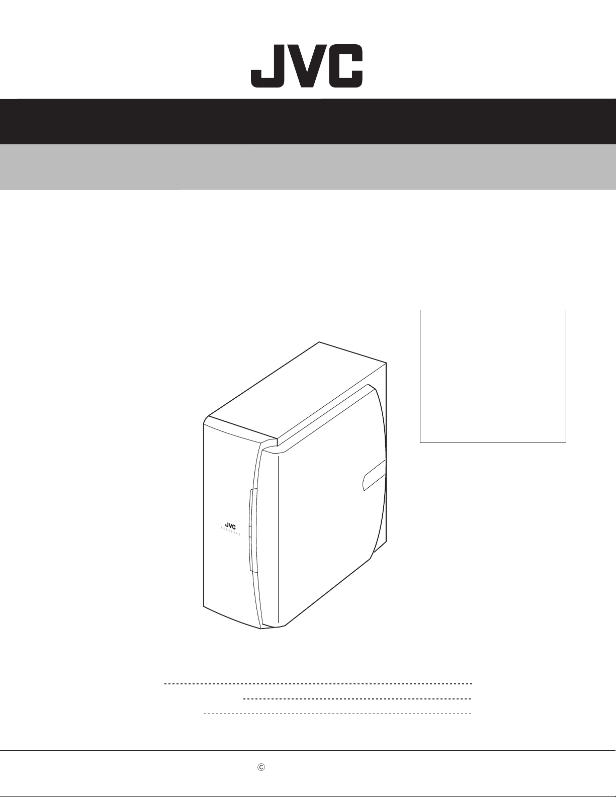
POWERED SUBWOOFER
SP-DWF10
CD-ROM No.SML200406
Area suffix
J ---------------------------- U.S.A.
A ------------------------ Australia
E ---------- Continental Europe
US ------------------------ Singapore
UF ------------------------------ China
UP ----------------------------- Korea
UT ---------------------------- Taiwan
UX -------------------- Saudi Arabia
UJ ---------------------- U.S.Military
Contents
Block diagram
Standard schematic diagram
Printed circuit boards
COPYRIGHT 2004 Victor Company of Japan, Limited.
2-1
2-2
2-3 to 4
No.MB251SCH
2004/6
Page 2

In regard with component parts appearing on the silk-screen printed side (parts side) of the PWB diagrams, the
parts that are printed over with black such as the resistor ( ), diode ( ) and ICP ( ) or identified by the " "
mark nearby are critical for safety.
(This regulation does not correspond to J and C version.)
Page 3
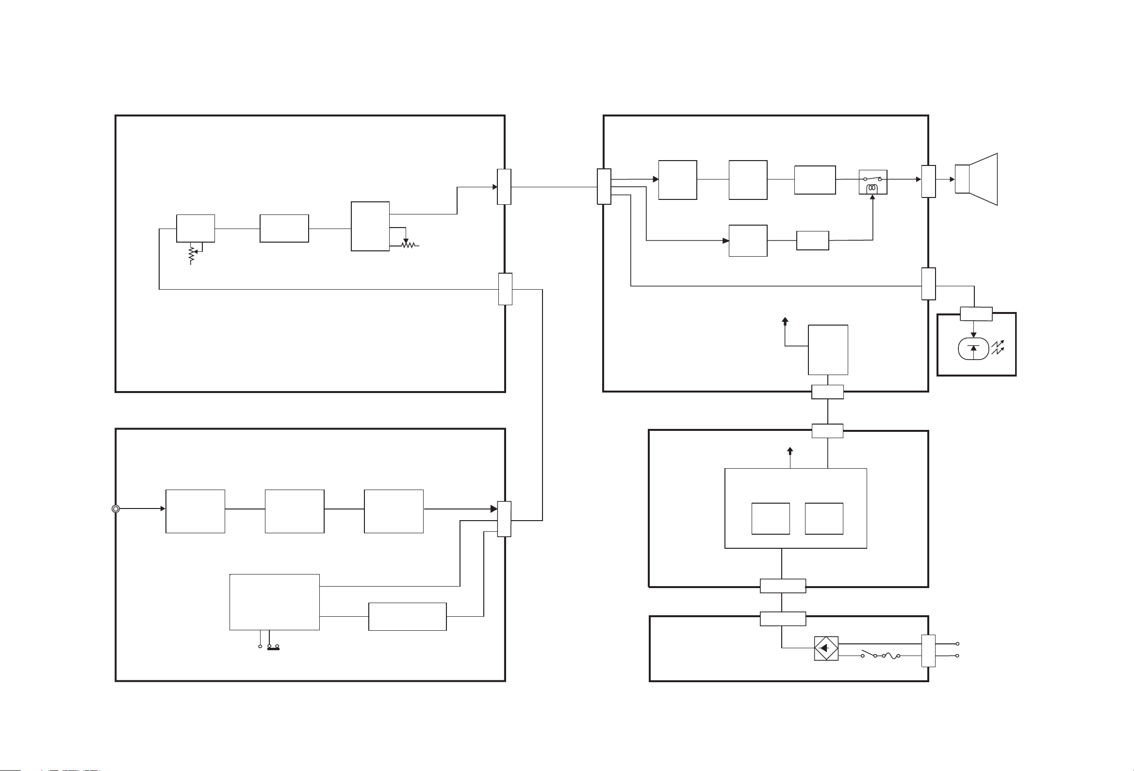
Block diagram
Volume board
IC501
Amp.
VR501
Off set
IC502
Comparator
IC503
IC504
Driver
VR502
Carrier Freq.
CN504
CN501
CN505
Amp board
IN
IC505
INV.
MUTE
LED
IC506
DRV.
IC571
INV.
+B
Q5006
Q5007
Q5706
REGULATOR
Q5902
Q5903
Q5904
Q5905
CN502
RY502
SPEAKER
OUT
CN503
CN102
CN861
RED GREEN
INDICATOR
J101
INPUT
Switch board
IC101
AMP
1/2
IC102
IC103
1/2
AMP
IC104 1/2
AUTO POWER ON
CANCEL / ON
MUTE
IC103
2/2
AMP
IC104 2/2
LED CONT.
CN101
Regulator board
POWER-SUPPLY
CIRCUIT
Power switch board
IC951
W9001 to 4
W9001 to 4
+B
CN951
T9501
TRANS
POWER
CN901
MAIN
PLUG
2-1
Page 4
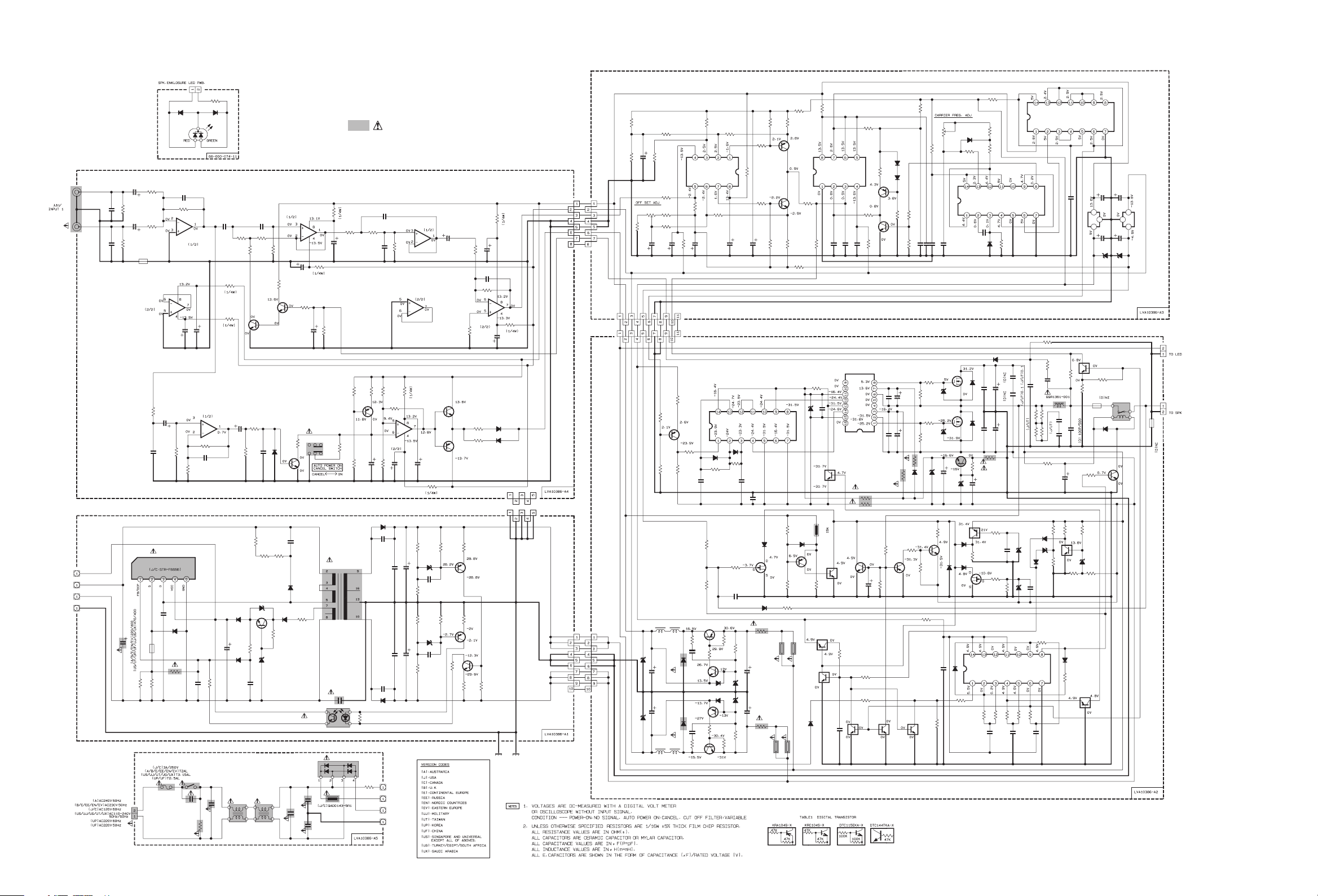
Standard schematic diagram
W9001
W9002
W9003
W9004
J1001
QNN0090-001
!
C1002 C1001
0.001 0.001
R1002 R1001
C9501
!
C1003
10/50
C1004
10/50
470k 470k
K1001
NQR0129-003X
HA17558AF-X
( J/C) 470/200
R9501
CN901
QGA7901F2-02
!
R1003
56k
R1004
56k
IC101
2.2k
R1049
C1028
4.7/50
0.01
C1027
!
IC951
STR-F6676
C9502
K9501
QQR0779-001Z
R9502
0.33/1W
0.33/1W
F9001
!!
D8601
SPR325MVW
C1005
0.01
R1005
22K
C1009
47k
R1050
0.001/2K
D9501
AW04
!
R9503
680
0.01/275
IC101
HA17558AF-X
C1008
100/16
100/16
HA17558AF-X
R1051
C1029
1.2K
R1052
C9503
S9001
QSW1001-001
!
C9005
R9002
!
CN861
R8601
220
D8602
C1010
0.15
R1015
R1017
IC104
1M
47p
C9504
3.3k
470P
R9504
C9001
!
0.22/275
QQR1360-001 QQR1360-001
3.3M
C1011
0.15
R1021R1020
4.7K3.9K
12K
R1022
47
47
Q1002
2SC2412K
C1030
R1053
4.7k
4.7/50
0.01
47k
R1066
C1031
R9528
75K/1/4W
R9529
75K/1/4W
D9504
MTZJ20B
Q9504
D9503
2SC2412K
AG01Z
100/35
2.2k
R9505
D9502
AG01Z
D9505
C9505
470P
!!
LF901 LF902
R1023
R1048
1SS133
D1001
R9510
75K/1/4W
R9506
MTZJ20B
IC102
HA17558AF-X
68K
1k
2SC2412K
Q1003
2SC2412K
D9507 C9506
D9506
AG01Z
10k
C9002
!
C1013
100/16
Q1001
R1054
0.01/630
SARS03
R9508
22/1W
0.1/275
R1047
100K
S1001
QSW0834-001
56
!
PC951
PC123Y22
C9003C9004
!!
R1028
!
0.001/2500.001/250
47
R1046C1023
47K1/50
!
QQS0172-001
!
0.0033/250
!
D9001
!
TH901
QAD0141-6R0
R1025
C1012
T9501
C9515
47
100/16
R1067
56
RBV-606
R1030 R1031
7.5K 7.5K
C1014 R1032
0.082 680K
1.5k
R1055
R1057
Q1004
2SA1037AK
470/16
10k
R1056
C1032
2.2k
R9527
R9001
100k/2W
Parts are safety assurance parts.
When replacing those parts make
sure to use the specified one.
C1015
0.22
IC103
HA17558AF-X
C1016
150K
R1059
220k
R1060
D9509
FML-G22S
C9507
0.0047/1K
C9508
0.0047/1K
D9510
FML-G22S
100k
R1062
R1061
1M
IC104
HA17558AF-X
C1034
10/16
C9511C9512
C9509
0.022/100
C9510
0.022/100
W9001
W9002
W9003
W9004
IC102
HA17558AF-X
47
C1033
R9516
MTZJ15A
2200/50
R9517
R9520
MTZJ15A
2200/50
R9521
10/16
R1064
13K
D9511
C9513
10k
13K10k
D9512
C9514
0.01
Q1007
2SC2412K
Q1006
2SA1037AK
47
R9518
0.01
R9522
10/50
2SA1514K
Q9509
2SA1514K
10K
Q9508
10k
R9524
4.7k
R9519
R9523
R9525
R1016
IC103
HA17558AF-X
22k
R1039
R1065
100
R1068
100
10k
1k
1k
15K
C1020
0.0022
R1040
68K
QGB2016J1-05
QGB2016K1-05
Q9510
2SC2412K
10k
R9526
EP951
C1022
CN103
CN952
R1041
C1021
100/16
47
100/16
D1002
1SS133
D1003
1SS133
R1044
47
EP952
CN101
CN501
QGB2016K1-08
CN951
CN502
QGB2510J1-10
QGB2016J1-08
QGB2510K1-10
R5034
D5901
D5706
D5707
1SS355-X
R5733
10K
D5003
1SS133
R5036
10k
C5015
D5011D5012
R5902
MTZJ16B
Q5712
1SS355-X
2.2
R5037
R5038
TC74HC14AF-X
47p
D5004
0.01/100
C5901
M1FL20UM1FL20U
C5902
0.01/100
R5901
!
10/1/4W
Q5901
6.8k
2SD2395/EF/
C5905
4.7/25
KRA104S
R5720
R5721
47k
220k
Q5713
2SK303/3-4/-X
470k
R5734
C5708
2.2k 12K
IC504
10K
R5039
1SS133
D5013
1SS355
C5903
220/50
C5904
220/50
2.2k
C5704
R5723
R5722
IC571
TC74HC14AF-X
10k
R5735
R5736
3.3/10
C5918
C5917
0.01
47k
C5709
470k
0.018
0.018
D5709
R5737
0.082
C5024
D5710
1SS355-X
D5712
D5708
MA3300/L/
MA3200/H/
C5705
MA3200/H/
10k
R5738
C5710
2.2/10
R5059
11k
R5058
C5023
!
( D) QQR1352-001
15
R5061
15
R5060
15
15
R5063
R5062
R5701
1k
D5711
1SS355-X
0.01
R5739
100K
2.2/10
TC74HC00AF-W
180k
2.2/50
L5001
C5027C5028
C5702
39K
R5724
R5726
Q5714
68K
DTC115EKA-X
R5725
10k
D5715
R5740
IC503
0.1
C5012
22K
R5057
R5744
270P270P
0.0039/100
C5022
220/35
100k
R5727
D5713
R5729 R5728
68K
1SS355-X
47k
Q5720
KRA104S
C5913
10/16
NJM78L05A
IC591
C5916
10/16
D5905
MTZJ6.8B
Q5722
DTC144TKA
R5743
2.2k
390
K5001
QQR1183-001Z
D5703
1SS133
Q5706
2SC2412K
R5702
10k
100k
MA3300/L/
33K
C5914
10/16
C5915
10/16
D5906
MTZJ6.8B
RY502
QSK0149-001
AN79L05
IC592
QQR1183-001Z
K5002
CN102
QGA2501C1-02
CN503
QGA3901C1-02
R5021
15K
R5003
10k
10k
10K
R5002 R5001
R5004
C5001
100/16
R5005
10k
VR501
R5007
5K
13K
R5008
7.5K
R5006
10k
C5002
100/16
C5003
100/16
+13V
-13V
LED
+5V
-5V
MTZJ16BMTZJ16B
D5907
D5908
AHB
5.6k 1k
R5041 R5040
L5903 L5901
NQL114K-471X
C5911
100/25
C5912
100/25
L5904
NQL114K-471X
R5042
R5043
D5909
D5910
L5902
R5009
4.7
R5020
QGB2016J1-11
CN504
CN505
QGB2016K1-11
1k
Q5005
2SA1514K
R5044
560
3.3K
R5911
C5907
Q5904
RB160L-40-XRB160L-40-X
2SC2412K
Q5905
2SA1037AK
C5908
R5912
R5010
IC501
HA17558AF-X
10k
C5004
100/16
C5016
R5748R5747
Q5902
2SA1037AK
12K12K
220P220P
R5909
R5910
Q5903
2SC2412K
D5005
1SS133
R5045
56P
D5911
1SS355
D5912
1SS355
10k
R5012
10k
8.2K
100K100K
1K
1K
R5913R5914
R5011
10k
C5005
2SK303/3-4/-X
R5749
100K
C5711
0.22/25
330330
R5905
MTZJ15A
D5903
D5904
MTZJ15A
R5906
R5019
100/16
BU4584BF-X
D5006
1SS133
R5046
8.2K
C5017
Q5723
47K
C5909
C5910
47K
C5006
IC505
56P
C5025
R5013
4.7
R5014
1SS355-X
!
22/1/4W
100/50
100/50
22/1/4W
4.7k
4.7k
0.1
D5717
R5915
!
R5916
100/16
D5718
2.2k2.2K/1/4W
R5015
Q5001
2SA1037AK
Q5002
2SC2412K
R5016
1SS355-X
TH591
!
!
TH593
1K1K
R5017R5018
R5022
15K
R5713R5714
1SS355-X
Q5707
2SA1037AK
R5746
100K
TH592
!
NAD0032-330X
!
TH594
NAD0032-330X
NAD0032-330X
4.7
R5025
4.7
IC502
NJM311M-XE
R5023
100
0
0.022
470p
0.1
C5008
C5009
C5007
R5024
4.7
IR2113S-X
R5048
10k
D5007
MTZJ16B
0.22
C5018
Q5721
KRC104S-X
!
TH501
D5704
QAD0015-153Z
Q5708
KRC104S
47k
4.7k
R5715
Q5715
KRA104S-X
100k
D5716
1SS133
R5730
C5706
Q5717 Q5718 Q5719
DTC115EKA-X DTC115EKA-X KRC104S-X
3.3/10
NAD0032-330X
Q5716
KRC104S-X 10k
2SA1037AK
IC506
!
R5049
2.2/1/2W
Q5709
2SC2412K
R5731
R5732
100K
R5028
1k
Q5003
R5027
2.2
4.7
R5026
22/1/4W
C5703
R5029
Q5004
2SC4452/3-4/-X
R5050
R5717
47/16
R5716
6.8k
C5021
0.68
C5019
100k
0.22/100
220k
D5001D5002
R5030
C5026
4.7/100
C5020
10/50
R5051
!
Q5710
2SA1037AK
6.8k
R5718
1SS133
1SS133
R5031
R5032
!
10/1/2W
47k
R5033
4.7k
2.2k
R5053R5054
R5052
D5008
R5719
2.2
0.1
0.1
C5010
C5011
R5055
6.8/1W
1M1M
D5009
MTZJ18B
R5056
6.8/1W
22/1/2W
D5902
M1FL20U
Q5711
2SC2412K
47k
R5742
2.2
R5750
220K
R5035
0.1
C5013
D5010
MTZJ18B
MTZJ18B
R5745
VR502
2.2
IRFI540N
IRFI540N
C5906
C5014
22K
0.1
C5707
20K
680p
Q5006
Q5007
D5705
47/25
1SS355-X
1SS355-X
D5714
2-2
Page 5
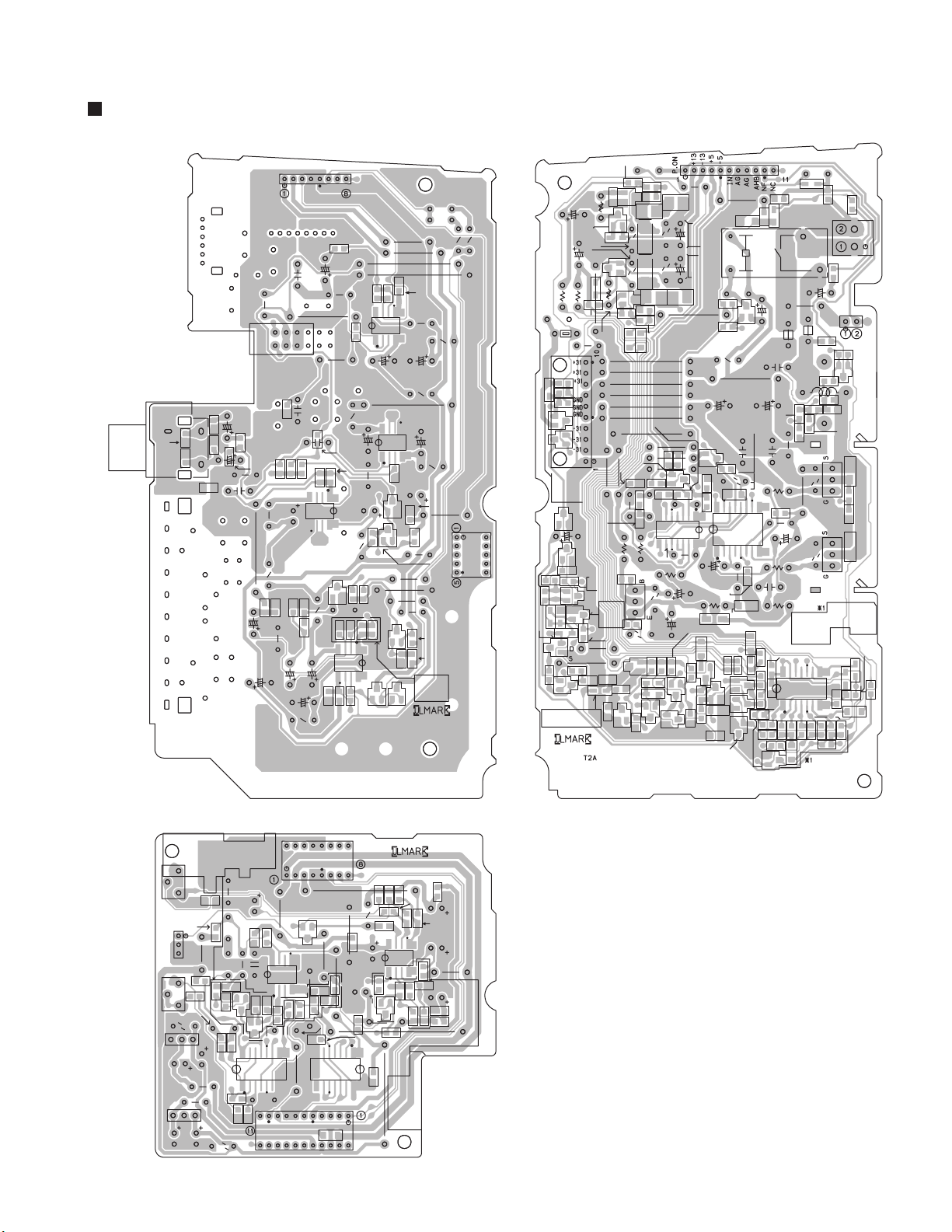
Printed circuit boards
Main board
(Switch board)
CN101
R1016
C1016
C1015
R1031
S1001
J1001
C1001
C1002
R1001
K1001
R1002
C1004
C1003
R1003
R1004
C1010
C1028
C1032
R1017
R1049
C1033
C1027
R1020
C1009
C1011
R1032
R1021
IC101
C1030
R1062
R1022
R1066
C1014
C1031
C1034
R1053
R1064
R1060
R1030
R1059
R1025
R1005
Q1003
R1061
C1012
C1005
C1008
R1015
R1054
D1001
R1067
IC104
IC103
Q1007
R1023
D1003
D1002
IC102
C1023
Q1006
C1021 C1022
R1044
R1040
R1047
R1050
C1020
C1013
Q1004
R1056
R1052
R1039
R1041
Q1002
R1048
R1057
R1055
R1051
R1028
R1046
Q1001
C1029
R1065
CN103
R1068
R5719
D5707
R5723
CN502
D5709
D5706
R5915
TH501
R5715
R5714
R5713
D5704
Q5707
Q5708
C5909
C5910
R5721 R5722
Q5904
D5911
R5916
R5914
Q5709
R5717
Q5713
R5720
D5912
C5703
Q5710
Q5711
C5705
D5904
R5718
D5903
Q5905
Q5903
R5045
C5016
R5745
R5749
R5909
R5906
D5005
D5718
C5704
R5905
R5913
R5910
B8110
C5017
D5006
R5901
R5902
D5705
D5708
Q5902
B8111
Q5005
C5025
R5042
Q5723
Q5712
L5901
R5040
R5050
D5902
R5725
D5716
R5046
R5041
B8106
D5710
D5711
(Amp. board)
R5911
C5907
L5903
D5907 D5908
D5909
D5910
L5904
L5902
C5908
R5912
IC505
R5049
D5901
C5905
Q5901
C5906
R5726
R5724
R5727
R5728
D5713
Q5714
R5729
D5712
C5911 C5912
R5043
C5020
R5051
C5706
R5730
B8102
R5731
Q5721
R5044
B8112
R5747
R5702
R5701
Q5715
Q5716
Q5719
Q5717
Q5718
C5711
R5048
D5007
C5902
R5054
C5019
D5008
TH591
TH592
D5703
C5018
B8113
CN505
RY502
Q5706
C5903 C5904
R5056
R5748
C5022
C5901
R5055
R5052
TH593
TH594
D5717
C5702
R5053
IC506
C5021
C5024
K5002
C5027
R5732
R5741
D5013
L5001
R5062
R5750
R5733
B8103
R5742
C5707
K5001
C5028
C5026
C5709
Q5720
IC571
C5023
R5744
D5009
D5010
R5057
C5708
R5059
CN102
Q5006
Q5007
R5734
B8105
R5058
R5743
R5060
R5063
R5735
D5714
R5061
D5011
B8104
C5710
Q5722
C5918
R5736
R5740
D5715
B8107
R5746
C5917
D5012
R5737
R5738
R5716
CN503
R5739
D5906
IC592
TP501 VR501 VR502
C5914
C5913
R5035
C5010
R5029
R5037
D5003
C5915
R5030
R5033
R5032
Q5003
R5006
IC591
C5007
Q5004
C5916
C5015
D5905
R5027
D5002
R5038
R5031
R5036
C5014
R5024
D5001
C5009
R5026
C5002
R5025
R5039
C5008
R5023
R5028
C5011
D5004
(Volume board)
CN501
IC504
Q5002
IC502
CN504
C5013
B5101
IC503
C5006
R5021
R5016
C5012
R5019
C5005
R5007
R5034
R5014
R5018
R5013
R5009
R5015
Q5001
R5008
R5011
R5003
R5017
IC501
R5020
R5010
R5022
R5012
R5004
R5005
C5004
C5003
C5001
R5002
R5001
2-3
Page 6
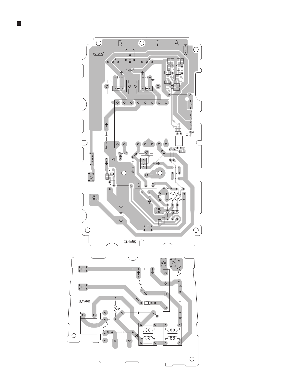
Main board
(Regulator board)
W9004
EP951
CN952
HS953 HS952
T9501
C9515
R9508
D9506
D9504
Q9504
R9506
C9509
C9510
C9502
HS954
D9509 D9510
C9511 C9512
C9507 C9508
IC951
D9507
R9518
Q9508
R9519
Q9510
C9506
R9503
C9513
R9516
R9524
R9527
R9517
R9510
R9529
R9528
C9514
D9511
R9520
R9526
R9525
R9504
EP952
R9521
R9522
Q9509
R9523
CN951
PC951
D9512
W9004
W9002
CN901
W9002
D9505
C9501
W9003
(Power switch board)
C9003
4
0
0
9
C
TH901
Z9001 Z9002
R9002
C9005
C9001
C9504
K9501
W9001
R9505
W9003
D9001
C9505
D9501
W9001
D9503
R9501
R9502
C9503
D9502
R9001
C9002
2-4
S9001
LF902
LF901
Page 7

< MEMO >
Page 8

Victor Company of Japan, Limited
AV & MULTIMEDIA COMPANY AUDIO/VIDEO SYSTEMS CATEGORY 10-1,1chome,Ohwatari-machi,Maebashi-city,371-8543,Japan
(No.MB251SCH)
Printed in Japan
WPC
 Loading...