

Page 1
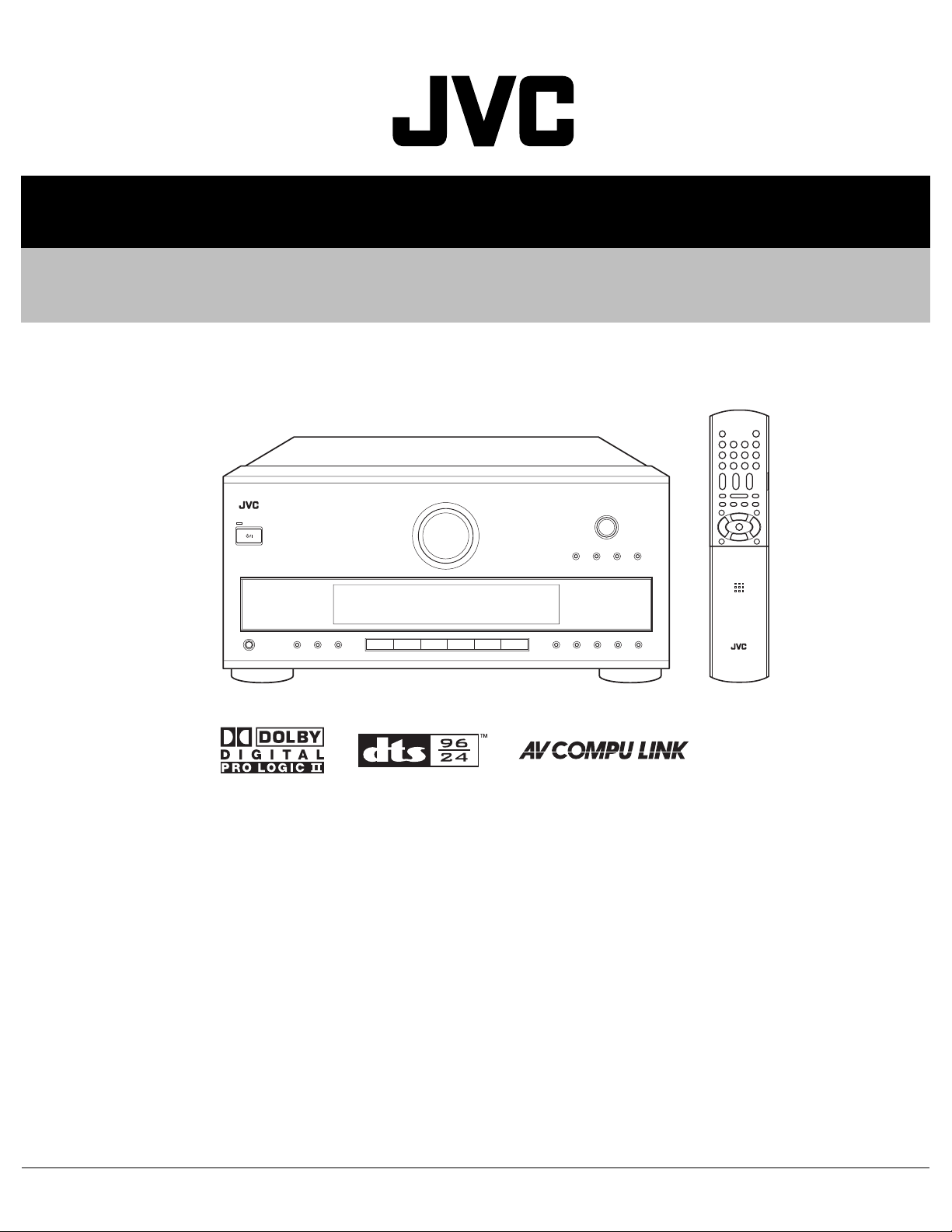
SERVICE MANUAL
AUDIO/VIDEO CONTROL RECEIVER
MB50220061
RX-V7000UF
Lead free solder used in the board (material : Sn-Ag-Cu, melting point : 219 Centigrade)
TABLE OF CONTENTS
1 PRECAUTION. . . . . . . . . . . . . . . . . . . . . . . . . . . . . . . . . . . . . . . . . . . . . . . . . . . . . . . . . . . . . . . . . . . . . . . . . 1-3
2 SPECIFIC SERVICE INSTRUCTIONS . . . . . . . . . . . . . . . . . . . . . . . . . . . . . . . . . . . . . . . . . . . . . . . . . . . . . . 1-4
3 DISASSEMBLY . . . . . . . . . . . . . . . . . . . . . . . . . . . . . . . . . . . . . . . . . . . . . . . . . . . . . . . . . . . . . . . . . . . . . . . 1-5
4 ADJUSTMENT . . . . . . . . . . . . . . . . . . . . . . . . . . . . . . . . . . . . . . . . . . . . . . . . . . . . . . . . . . . . . . . . . . . . . . . 1-14
5 TROUBLESHOOTING . . . . . . . . . . . . . . . . . . . . . . . . . . . . . . . . . . . . . . . . . . . . . . . . . . . . . . . . . . . . . . . . . 1-15
COPYRIGHT © 2006 Victor Company of Japan, Limited
No.MB502
2006/1
Page 2
SPECIFICATION
Amplifier
Output Power At Stereo operation Front channels 100 W per channel, min. RMS, driven into 8
with no more than 0.8% total harmonic distortion
(IEC268-3/DIN).
Front channels 100 W per channel, min. RMS, driven into 8
with no more than 0.8% total harmonic distortion.
At Surround operation Center channel 100 W, min. RMS, driven into 8
than 0.8% total harmonic distortion.
Surround channels 100 W per channel, min. RMS, driven into 8
with no more than 0.8% total harmonic distortion.
Audio Audio Input Sensitivity/Impedance (1 kHz) TAPE, VCR, TV SOUND/DBS, DVD:220 mV/47 k
Audio Input (DIGITAL IN)* Coaxial DIGITAL 1 (DVD):0.5 V(p-p)/75 Ω
Optical DIGITAL 2 (VCR), DIGITAL 3 (TV SOUND/DBS):-21
dBm to -15 dBm (660 nm ±30 nm)
Recording Output Level TAPE, VCR:220 mV
Signal-to-Noise Ratio ('66 IHF/DIN) TAPE, VCR, TV SOUND/DBS, DVD:96 dB/62 dB
Frequency Response (8
Bass Boost +4 dB ±1 dB at 100 Hz
Equalization (5 bands) 63 Hz, 250 Hz, 1 kHz, 4 kHz, 16 kHz:±8 dB (in 2 dB
Video Video Input Sensitivity/Impedance Composite video:DVD, VCR, DBS 1 V(p-p)/75
Video Output Level Composite video:VCR, MONITOR OUT 1 V(p-p)/75 Ω
Synchronization Negative
Signal-to-Noise Ratio 45 dB
Tuning Range 87.50 MHz to 108.00 MHz
Usable Sensitivity Monaural:12.8 dBf (1.2
50 dB Quieting Sensitivity Monaural:16.0 dBf (1.7
Stereo Separation at OUT (REC) 35 dB at 1 kHz
Ω) TAPE, VCR, TV SOUND/DBS, DVD:20 Hz to 50 kHz (+1
dB, -3 dB)
steps)
Ω
S-video:DVD, VCR,DBS (Y: luminance):1 V(p-p)/75 Ω
(C: chrominance, burst):0.3 V(p-p)/75 Ω
Component:DVD, VCR (Y: luminance):1 V(p-p)/75 Ω
(PB, PR):0.7 V(p-p)/75 Ω
S-video:VCR, MONITOR OUT (Y: luminance):1 V(p-p)/75 Ω
Component:MONITOR OUT (Y: luminance):1 V(p-p)/75 Ω
FM tuner (IHF)
(C: chrominance, burst)0.3 V(p-p)/75 Ω
(PB, PR):0.7 V(p-p)/75 Ω
Stereo:37.5 dBf (20.5
µV/75 Ω)
Ω, at 1 kHz with no more
µV/75 Ω)
µV/75 Ω)
Ω, at 1 kHz
Ω, at 1 kHz
Ω, at 1 kHz
Ω
AM tuner
Tuning Range 531 kHz to 1 710 kHz (at 9 kHz intervals)
General
Power Requirements AC 220 V, 50 Hz
Power Consumption 200 W (at operation)
Dimensions (W
Mass 11.4 kg
× H × D) 435 mm × 200 mm × 425 mm
530 kHz to 1 710 kHz (at 10 kHz intervals)
0.9 W (in standby mode)
* : Corresponding to Linear PCM, Dolby Digital, and DTS Digital Surround (with sampling frequency -32 kHz, 44.1 kHz, 48 kHz)
Designs and Specifications are subject to change without notice.
1-2 (No.MB502)
Page 3
SECTION 1
PRECAUTION
1.1 Safety Precautions
(1) This design of this product contains special hardware and
many circuits and components specially for safety purposes. For continued protection, no changes should be made
to the original design unless authorized in writing by the
manufacturer. Replacement parts must be identical to
those used in the original circuits. Services should be performed by qualified personnel only.
(2) Alterations of the design or circuitry of the product should
not be made. Any design alterations of the product should
not be made. Any design alterations or additions will void
the manufacturers warranty and will further relieve the
manufacture of responsibility for personal injury or property
damage resulting therefrom.
(3) Many electrical and mechanical parts in the products have
special safety-related characteristics. These characteristics are often not evident from visual inspection nor can the
protection afforded by them necessarily be obtained by using replacement components rated for higher voltage, wattage, etc. Replacement parts which have these special
safety characteristics are identified in the Parts List of Service Manual. Electrical components having such features
are identified by shading on the schematics and by ( ) on
the Parts List in the Service Manual. The use of a substitute
replacement which does not have the same safety characteristics as the recommended replacement parts shown in
the Parts List of Service Manual may create shock, fire, or
other hazards.
(4) The leads in the products are routed and dressed with ties,
clamps, tubings, barriers and the like to be separated from
live parts, high temperature parts, moving parts and/or
sharp edges for the prevention of electric shock and fire
hazard. When service is required, the original lead routing
and dress should be observed, and it should be confirmed
that they have been returned to normal, after reassembling.
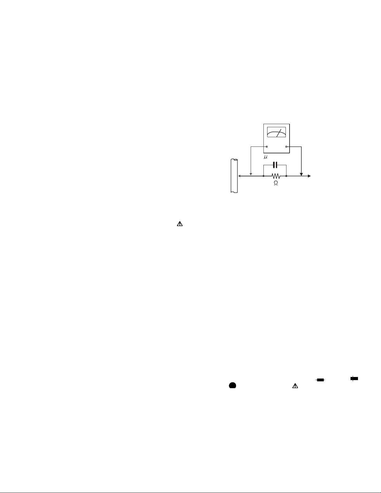
(5) Leakage shock hazard testing
After reassembling the product, always perform an isolation check on the exposed metal parts of the product (antenna terminals, knobs, metal cabinet, screw heads,
headphone jack, control shafts, etc.) to be sure the product
is safe to operate without danger of electrical shock.Do not
use a line isolation transformer during this check.
• Plug the AC line cord directly into the AC outlet. Using a
"Leakage Current Tester", measure the leakage current
from each exposed metal parts of the cabinet, particularly any exposed metal part having a return path to the
chassis, to a known good earth ground. Any leakage current must not exceed 0.5mA AC (r.m.s.).
• Alternate check method
Plug the AC line cord directly into the AC outlet. Use an
AC voltmeter having, 1,000Ω per volt or more sensitivity
in the following manner. Connect a 1,500Ω 10W resistor
paralleled by a 0.15µF AC-type capacitor between an ex-
posed metal part and a known good earth ground.
Measure the AC voltage across the resistor with the AC
voltmeter.
Move the resistor connection to each exposed metal
part, particularly any exposed metal part having a return
path to the chassis, and measure the AC voltage across
the resistor. Now, reverse the plug in the AC outlet and
repeat each measurement. Voltage measured any must
not exceed 0.75 V AC (r.m.s.). This corresponds to 0.5
mA AC (r.m.s.).
AC VOLTMETER
(Having 1000
ohms/volts,
or more sensitivity)
0.15 F AC TYPE
Place this
probe on
1500 10W
Good earth ground
1.2 Warning
(1) This equipment has been designed and manufactured to
meet international safety standards.
(2) It is the legal responsibility of the repairer to ensure that
these safety standards are maintained.
(3) Repairs must be made in accordance with the relevant
safety standards.
(4) It is essential that safety critical components are replaced
by approved parts.
(5) If mains voltage selector is provided, check setting for local
voltage.
1.3 Caution
Burrs formed during molding may be left over on some parts
of the chassis.
Therefore, pay attention to such burrs in the case of preforming repair of this system.
1.4 Critical parts for safety
In regard with component parts appearing on the silk-screen
printed side (parts side) of the PWB diagrams, the parts that are
printed over with black such as the resistor ( ), diode ( )
and ICP ( ) or identified by the " " mark nearby are critical
for safety. When replacing them, be sure to use the parts of the
same type and rating as specified by the manufacturer.
(This regulation dose not Except the J and C version)
each exposed
metal part.
(No.MB502)1-3
Page 4

SECTION 2
SPECIFIC SERVICE INSTRUCTIONS
This service manual does not describe SPECIFIC SERVICE INSTRUCTIONS.
1-4 (No.MB502)
Page 5
SECTION 3
DISASSEMBLY
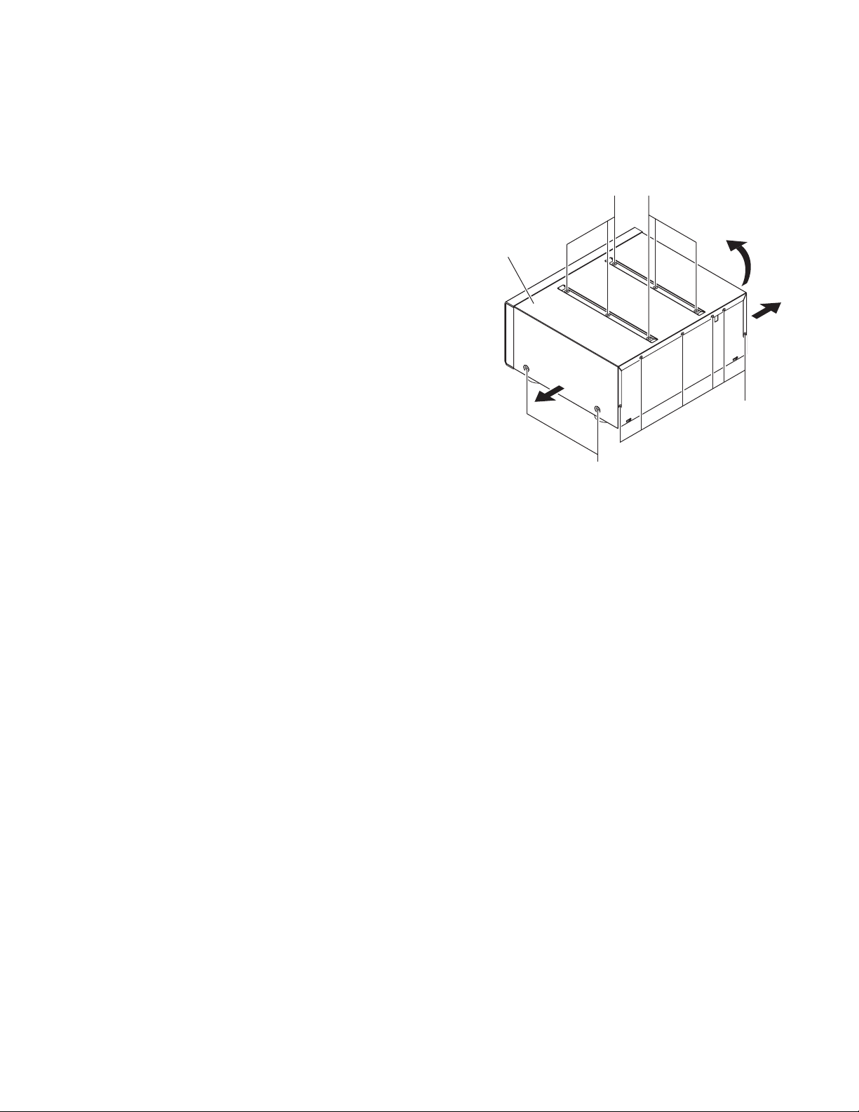
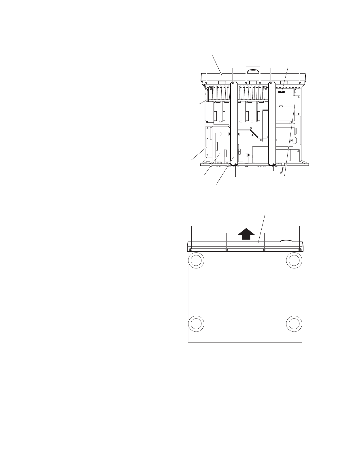
3.1 Removing the top cover (See Fig.1)
(1) From the right and left sides of the main body, remove the
four screws A attaching the top cover.
(2) From the top side of the main body, remove the six screws
A' attaching the top cover.
(3) From the back side of the main body, remove the six
screws B attaching the top cover.
(4) Remove the top cover in the direction of the arrow 2 while
extending the lower sections of the top cover in the direction of the arrow 1.
Top cover
A'
A'
2
1
1
B
A
Fig.1
(No.MB502)1-5
Page 6
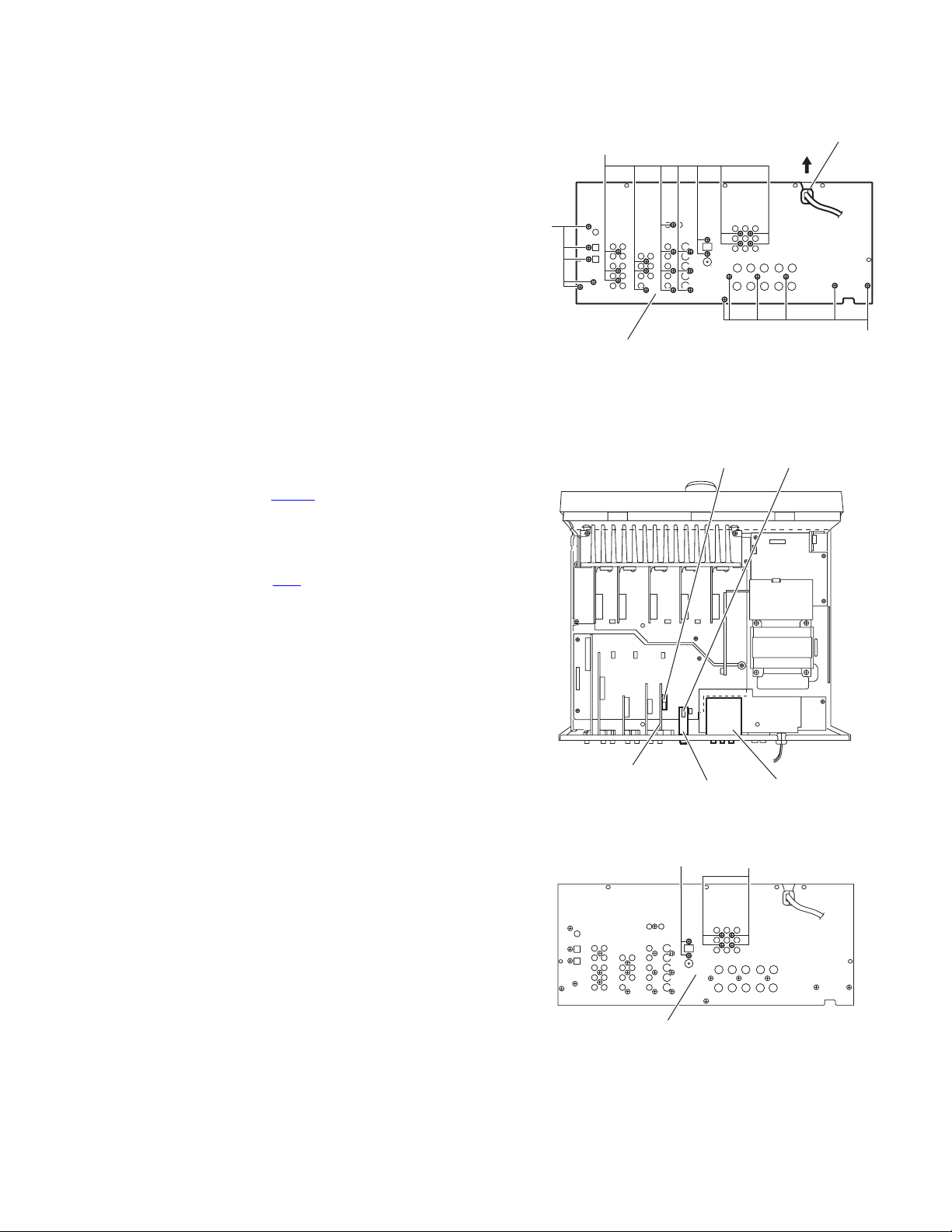
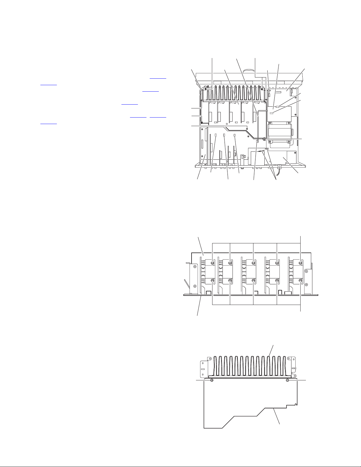
3.2 Removing the front panel assembly (See Figs.2 and 3)
• Prior to performing the following procedure, remove the top
cover.
(1) From the top side of the main body, disconnect the card
wire from the connector CN402
Fig.2)
(2) Disconnect the card wire from the connector CN201
power supply board. (See Fig.2)
(3) Remove the wire protection board fixing the card wire. (See
Fig.2)
(4) Remove the four screws C attaching the front panel as-
sembly. (See Fig.2)
(5) Remove the four screws D attaching the stay bracket. (See
Fig.2)
(6) From the bottom side of the main body, remove the four
screws E attaching the front panel assembly. (See Fig.3)
(7) Remove the front panel assembly in the direction of the ar-
row. (See Fig.3)
on the front board. (See
on the
Front panel assembly
CD D
Wire
protection
board
CN402
C
C
CN201
Front board
Stay bracket
E
D
Fig.2
Power supply board
Front panel assembly
E
1-6 (No.MB502)
Fig.3
Page 7
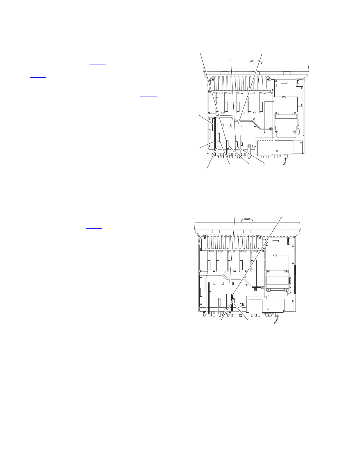
3.3 Removing the rear panel (See Fig.4)
• Prior to performing the following procedure, remove the top
cover and stay bracket.
(1) From the back side of the main body, remove the strain re-
lief from the rear panel in the direction of the arrow.
(2) Remove the thirty screws F attaching the rear panel.
F
Strain relief
F
3.4 Removing the component board and tuner unit (See Figs.5 and 6)
• Prior to performing the following procedure, remove the top
cover and stay bracket.
(1) From the top side of the main body, disconnect the parallel
wire from the connector CN511
Fig.5)
(2) From the back side of the main body, remove the four
screws G attaching the component board. (See Fig.6)
(3) From the top side of the main body, disconnect the card
wire from the connector CN1
(4) From the back side of the main body, remove the two
screws H attaching the tuner unit. (See Fig.6)
on the S-video board. (See
on the tuner unit. (See Fig.5)
Rear panel
S-Video board
Fig.4
CN511
Tuner
F
CN1
Component board
Fig.5
HG
Rear panel
Fig.6
(No.MB502)1-7
Page 8
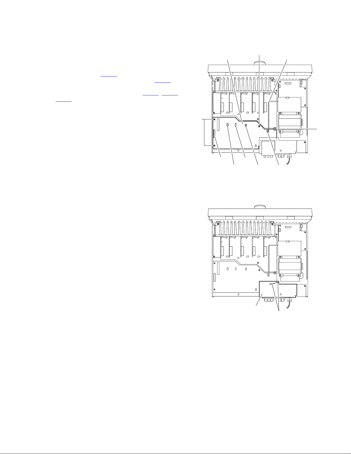
3.5 Removing the DSP board, audio input board, DVD board and video board (See Fig.7)
• Prior to performing the following procedure, remove the top
cover, stay bracket and rear panel.
(1) From the top side of the main body, disconnect the DSP
board from the connector CN481
(2) Disconnect the audio input board from the connector
on the front board.
CN421
(3) Disconnect the DVD board from the connector CN431 on
the front board.
(4) Disconnect the video board from the connector CN441
the front board.
on the front board.
on
CN481
DSP
board
Video board
Front boardDVD board
3.6 Removing the S-video board (See Fig.8)
• Prior to performing the following procedure, remove the top
cover, stay bracket and rear panel.
(1) From the top side of the main body, disconnect the parallel
wire from the connector CN511
(2) Disconnect the S-video board from the connector CN461
on the front board.
on the S-video board.
CN421
Audio input board
Front board
CN461
CN431
Fig.7
CN511
Fig.8
CN441
S-Video board
1-8 (No.MB502)
Page 9
3.7 Removing the front board (See Fig.9)
• Prior to performing the following procedure, remove the top
cover, rear panel, stay bracket, component video board, DSP
board, audio input board, DVD board, video board, S-video
board and tuner unit.
(1) From the top side of the main body, disconnect the card
wire from the connector CN402
(2) Disconnect the relay board from the connector CN491 on
the front board.
(3) Disconnect the wires from the connectors CN471
and CN473 on the front board.
(4) Remove the three screws J attaching the front board.
(5) Loosen the screw K attaching the front board.
on the front board.
, CN472
J
Front board
J
Reray board
K
3.8 Removing the speaker terminal board (See Fig.10)
• Prior to performing the following procedure, remove the top
cover, stay bracket, component board and rear panel.
(1) From the top side of the main body, remove the solders
from the soldered sections a on the speaker terminal
board.
CN402
Speaker terminal board
CN471
CN473
CN472 CN491
Fig.9
Fig.10
Soldered sections a
(No.MB502)1-9
Page 10
3.9 Removing the main board (See Fig.11)
• Prior to performing the following procedure, remove the top
cover and stay bracket.
(1) From the top side of the main body, remove the solders
from the soldered section b on the speaker terminal board
attaching the parallel wires.
(2) Disconnect the relay board from the connectors CN291
and CN491 on the power supply board and front board.
(3) Disconnect the parallel wire from the connector CN241
the power supply board.
(4) Disconnect the wire from the connector CN251
er transformer board 1.
(5) Disconnect the wires from the connectors CN471
and CN473 on the front board.
(6) Remove the screw M, two screws N and four screws P at-
taching the main board.
on the pow-
on
, CN472
Wire
protection
board
P
N
M
P
Main
board
Relay
board
P
Power
transformer
board 1
CN241
Power
supply
board
CN251
CN291
N
3.10 Removing the heat sink (See Figs.12 and 13)
• Prior to performing the following procedure, remove the top
cover, stay bracket and main board.
(1) Remove the ten screws Q attaching the heat sink of the
main board. (See Fig.12)
(2) From the reverse side of the main board, remove the two
screws R attaching the heat sink. (See Fig.13)
CN473
Front
board
Heat sink
Main board
CN472
CN471
CN491
Fig.11
Fig.12
Soldered
section b
Heat sink
Speaker
terminal
board
Q
Q
1-10 (No.MB502)
R
R
Main board
Fig.13
Page 11
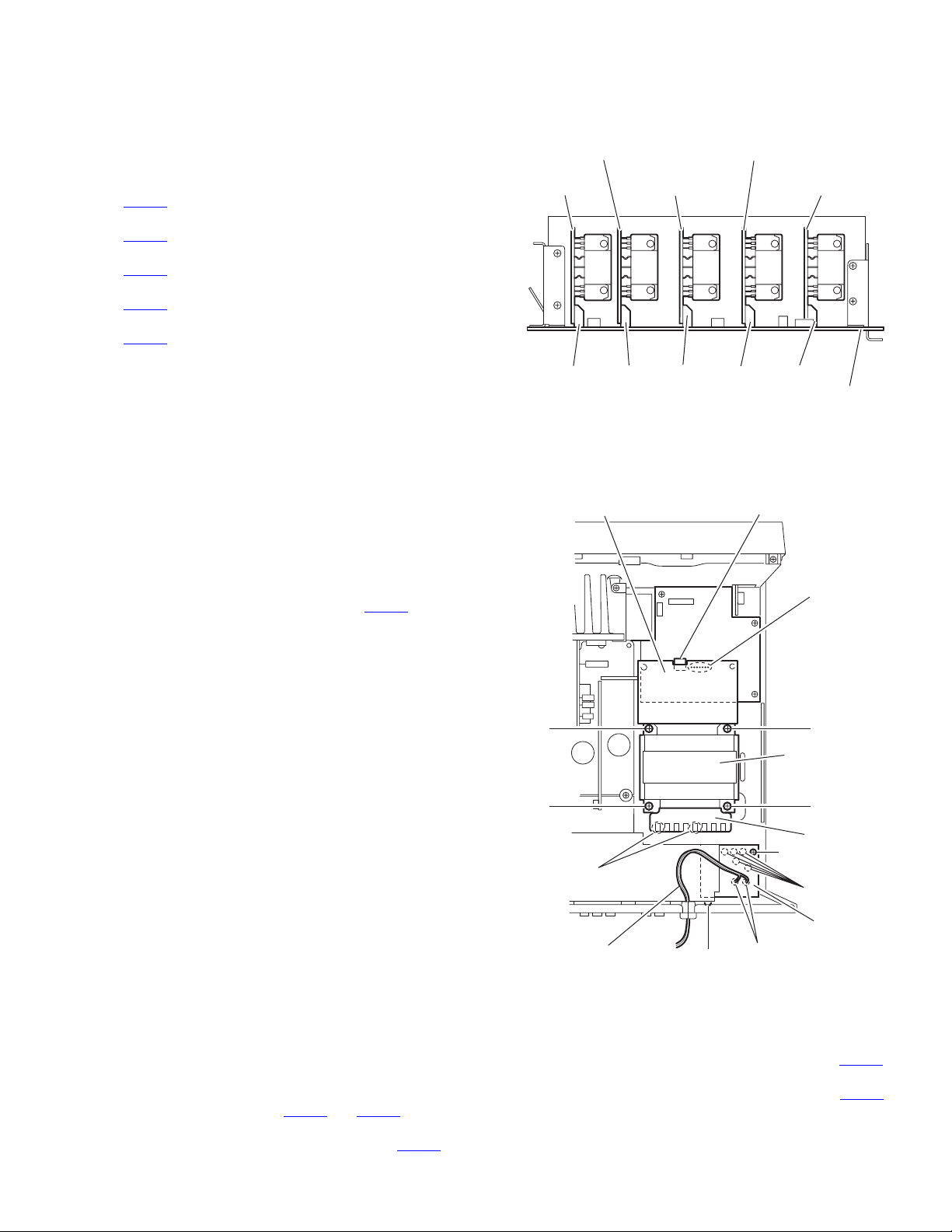
3.11 Removing the center amp. board, front amp. boards (L/R) and rear amp. boards (L/R)
r
(See Figs.12 and 14)
• Prior to performing the following procedure, remove the top
cover, stay bracket and main board.
(1) Remove the ten screws Q attaching the heat sink of the
main board. (See Fig.12)
(2) Disconnect the center amp. board from the connector
on the main board. (See Fig.14)
CN321
(3) Disconnect the front amp. board (L) from the connector
on the main board. (See Fig.14)
CN311
(4) Disconnect the front amp. board (R) from the connector
on the main board. (See Fig.14)
CN312
(5) Disconnect the rear amp. board (L) from the connector
on the main board. (See Fig.14)
CN331
(6) Disconnect the rear amp. board (R) from the connector
on the main board. (See Fig.14)
CN332
3.12 Removing the power transformer
(See Fig.15)
• Prior to performing the following procedure, remove the top
cover and stay bracket.
(1) From the top side of the main body, remove the solders
from the soldered section c on the power transformer
board 1.
(2) Remove the solders from the soldered sections d on the
power transformer board 2.
(3) Disconnect the wire from the connector CN251
er transformer board 1.
(4) Remove the four screws S attaching the power transform-
er.
on the pow-
Rear amp.
Power transformer board 1
Rear amp.
board (L)
Front amp.
board (R)
CN332 CN331 CN312 CN311 CN321
board (R)
Front amp.
board (L)
Center amp.
board
Main board
Fig.14
CN251
Soldered
section c
3.13 Removing the power/fuse board
(See Fig.15)
• Prior to performing the following procedure, remove the top
cover and stay bracket.
(1) From the back and top sides of the main body, remove the
screw T and screw U attaching the power/fuse board.
(2) Remove the solders from the soldered sections e attaching
the power cord.
(3) From the reverse side of the power/fuse board, remove the
solders from the soldered sections f attaching the wires.
3.14 Removing the power supply board
(See Fig.16)
• Prior to performing the following procedure, remove the top
cover and stay bracket.
(1) From the top side of the main body, disconnect the parallel
wires from the connectors CN203
supply board.
(2) Disconnect the card wire from the connector CN201
power supply board.
and CN241 on the power
on the
S
S
Soldered
sections d
Power cord
Fig.15
(3) Disconnect the relay board from the connector CN291
the power supply board.
(4) Disconnect the parallel wire from the connector CN101
the headphone jack board.
(5) Remove the solders from the soldered section c on the
power transformer board 1.
T
Soldered
sections e
S
Power
transformer
S
Power
transforme
U
board 2
Soldered
sections f
Power/Fuse
board
on
on
(No.MB502)1-11
Page 12
(6) Remove the two screws V and the screw W attaching the
power supply board.
(7) Remove the power supply board from the hook g of the
chassis base bracket in the direction of the arrow, take out
the power supply board.
(8) Turn over the power supply board, remove the solders from
the soldered sections h attaching the wires.
CN241
V
Power supply board
CN201
Headphone jack
board
CN101
3.15 Removing the headphone jack board (See Fig.17)
• Prior to performing the following procedure, remove the top
cover, stay bracket and front panel assembly.
(1) From the top side of the main body, disconnect the parallel
wire from the connector CN101
board.
(2) From the front side of the main body, remove the nut and
screw X attaching the bracket (phones) to the chassis
base.
on the headphone jack
CN203
CN291
Relay
board
Hook g of the
chassis base bracket
CN101
Nut
V
Soldered
section h
W
Soldered
section c
Power transformer board 1
Fig.16
Headphone jack board
H.P Bracket
1-12 (No.MB502)
X
X
Chassis base
Fig.17
Page 13
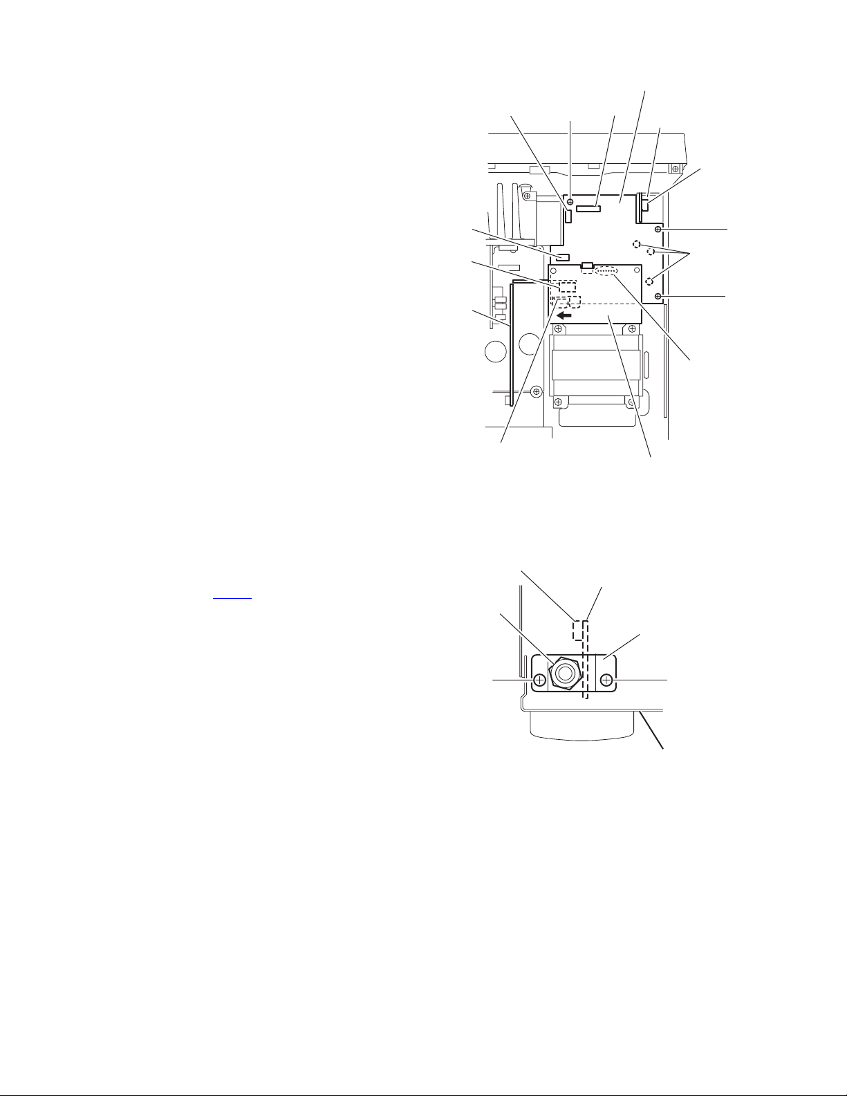
3.16 Removing the system control board (See Fig.18)
• Prior to performing the following procedure, remove the top
cover, stay bracket and front panel assembly.
(1) From the back side of the front panel assembly, remove the
seven screws Y attaching the system control board.
(2) Disconnect the parallel wires from the connectors CN705
and CN714 on the volume board, jog board and
CN707
power switch board.
(3) Disconnect the wire from the connector CN706
switch board.
on the
Volume board
AA
,
Jog board
CN705
Switch board
AB
CN706
CN714
Z
CN707
System control board
3.17 Removing the jog board, volume board, power switch board and switch board (See Figs. 18 and 19)
• Prior to performing the following procedure, remove the top
cover, stay bracket, front panel assembly and system control
board.
(1) From the back side of the front panel assembly, remove the
two screws Z attaching the power switch board. (See
Fig.18)
(2) Remove the four screws AA attaching the jog board. (See
Fig.18)
(3) Remove the three screws AB attaching the volume board.
(See Fig.18)
(4) Remove the two screws AC attaching the switch board.
(See Fig.18)
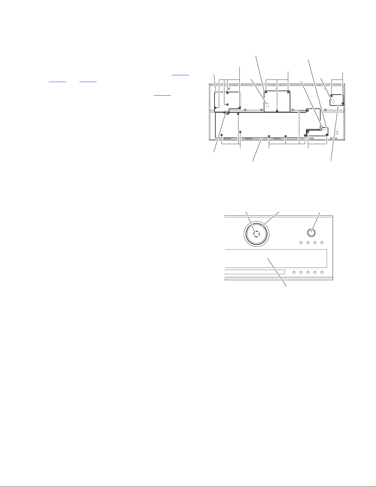
(5) Pull out the volume and jog knobs from the front side of the
front panel assembly, remove the nut attaching the front
panel assembly. (See Fig.19)
Nut Volume knob
YY
Fig.18
Front panel assembly
Fig.19
AC
Power switch board
Jog knob
(No.MB502)1-13
Page 14

SECTION 4
ADJUSTMENT
This service manual does not describe ADJUSTMENT.
1-14 (No.MB502)
Page 15

SECTION 5
TROUBLESHOOTING
This service manual does not describe TROUBLESHOOTING.
(No.MB502)1-15
Page 16

Victor Company of Japan, Limited
Audio/Video Systems Category 10-1,1chome,Ohwatari-machi,Maebashi-city,371-8543,Japan
(No.MB502)
Printed in Japan
VPT
Page 17

SCHEMATIC DIAGRAMS
AUDIO/VIDEO CONTROL RECEIVER
RX-V7000UF
CD-ROM No.SML200601
Lead free solder used in the board (material : Sn-Ag-Cu, melting point : 219 Centigrade)
Contents
Block diagrams
Standard schematic diagrams
Printed circuit boards
COPYRIGHT 2006 Victor Company of Japan, Limited.
2-1
2-2
2-10 to 14
No.MB502SCH
2006/1
Page 18

In regard with component parts appearing on the silk-screen printed side (parts side) of the PWB diagrams, the
parts that are printed over with black such as the resistor ( ), diode ( ) and ICP ( ) or identified by the " "
mark nearby are critical for safety.
Page 19

Block diagram
Tuner unit
FM
AM
CN1
Audio signal input terminal section
CD_L,CD_R
CD
TAPEIN_L
J402 J403
TAPE_PLAY
TAPE_REC
VCR_PLAY
TV_SOUND
VCR_REC
DIGITAL_IN1
DIGITAL_IN2
DIGITAL_IN3
TAPEIN_R
TAPEOUT_L
TAPEOUT_R
VCRIN_L
VCRIN_R
TV_L
TV_R
VCROUT_L
VCROUT_R
J681
RX0
UN682
RX1
with S/PIDF
UN683
RX2
D/A0 to D/A3
DATA,MCK,XTAL
S_BCK,S_LRCK
C_BLK,C_LRCK
Surround / Digital signal input terminal section
IC402
SOURCE
SELECTOR
IC667
CODEC
DSP
IC661
SUBWOOFER OUT
DVD_C/SW
J404
TUNER_L
TUNER_R
DVD_L
DVD_R
IC403
SIG_L
SIG_R
SW_DATA
SW_CLK
SW_STB
(Audio input)
CN683
DSP_IN_L
DSP_IN_R
LIN+/RIN+/-
IC601
IC602
FILTER
A1+/-,B1+/A2+/-,B2+/A3+/-,B3+/-
IC611,IC612
IC613,IC615
IC621,IC622
IC632,IC633
CDIN,CDOUT
CCLK,INT
D_RST,D_CS
DSP_RST
SS,HREQ
MOSI,MISO
GPIO1 to GPIO4
SCK
CONTROLLER
Audio signal input terminal section
J406
DVD_S
DVD_F
CN401
CN421
CN681
DSP.L/R
DSP.LS/RS
DSP.C
DSP.SW
SW_OUT
DVD_C
DVD_SW
DVD_SL
DVD_SR
DVD_L
DVD_R
IC634
FILTER
DSP, CODEC
IC671
MICK
IC673
(DVD)
MONITOR
DVD
IC451
VCR1
J503
DBS/TV SOUND
J591
CN451
Q1427
Q1428
Q1429
DSP_L,DSP_R
DSP_SL,DSP_SR
DSP_C,DSP_LFE
IN_L
IN_R
TUNER_L
TUNER_R
TU_MUTE
CN411
TU_CLK
TU_CE
TU_DATAIN
TU_DATAOUT
DSP_CLK,DSP_STATUS,DSP_COMMAND
DSP_READY,DSP_RESET
CN431
DVD_L
DVD_R
SW_DATA,SW_CLK,SW_STB
Q1421
Q1422
Q1433
CN481 CN482 CN402
CN707
JS702
S742,S743
S745,S750
W707
AN3
MULTI_JOG1
MULTI_JOG2
(Multi jog)
VOL_JOG1
CN705
W705
JS701
VOL_JOG2
D710
AV COMPULINK
SW_OUT
DVD_C
DVD_SW
DVD_SL
DVD_SR
VCROUT_L
VCROUT_R
SIG_L,SIG_R
INPUT_ATT
AVCOMPULINK
VCR_IN
VCR_OUT
IC423
SELECTOR
CN702
DSP_CLK
DSP_STATUS
DSP_READY
DSP_RESET
DSP_COMMAND
TU_DATAIN
Q704
TU_DATAOUT
TU_CLK,TU_CE
VOL_CLK,VOL_DATA
VCR,DVD
to
D712
(Volume)
S731
to
S733
CN706
W706
BLUE_LED
Q705
LED_DIMMER
AN1
IC701
SYSTEM
CONT.
S721 to S724
S726
(Function switch)
S734 to S739
SWITCH
S727
D719
FW704
CN714
AN0
AN6
to
Q711
AN1
STB_LED
FL DISPLAY
User control keys / System control
(Power switch)
FL display section
Video signal input terminal section
J501 J502
Q504
Q505
R
P
IN1
Q501
Q502
IN3
IN2
AVCOMPULINK
SELECTOR
OUT
IC501
CN501
IC427
Q1424
Q1425
Q1426
L,R
SL,SR
C,LFE
6CH MASTER
S_MUTE
SW_MUTE
IC428
CN441
VOLUME
VOL_CLK
VOL_DA
Volume / Regulator / Source select section
Audio amplifier section
Lch
Audio amplifier section
Rch
Audio amplifier section
Audio
amp.
Cch
Audio amplifier section
RLch
ROM_WP
ROM_SCL
ROM_SDA
Audio amplifier section
RRch
IC704
EEPROM
Primary section
RY_LR1, RY_C
RY_S,RY_HP
POWER
SEG1 to SEG15
GRID1 to GRID16
CN701
CN201
POWER
DI701
D206-D209
VIDEO1
VIDEO2
VIDEO1
VIDEO2
AVCOMPULINK
Q315
Q317
Q316
Q318
Q915
Q917
Q815
Q817
Q816
Q818
RY_HP
B+5V
Q203
T202
TRANS.
(Video)
(S Video)
VIDEO1
VIDEO2
VCR
DVD
RY_C,RY_S,RY_LR1
Q210
+B2
-B2
Q202
RY202
VIDEO1
VIDEO2
DVD_S/C
VCR_S/C
IC551
IC552
SELECTOR
CN551 CN511
CN461
CN473 CN472 CN471
SURR_L
SURR_R
CENTER
FL
FR
CN301
CN311
L_IN
L
CN302
CN312
R_IN
R
CN901
CN321
C_IN
C
CN801
CN331
RL_IN
RL
CN802
CN332
RR_IN
RR
D1301-D1304
CN351
Q206,Q208,Q209
F1,F2
D201-D204
FW201
FW201
Primary
section
S1
CN251
Audio section
CN372 CN371CN373
+56V
-56V
POWER
TRANS.
FW341
CN241
T201
J551 J552 J553
M.OUT
DVD
VCR REC
VCR PLAY
DBS/TV SOUND
FW501
FW301
FW301
FW302
FW302
FRONT_A
HP_LHP_R
CENTER,REAR
RY203
Primary
section
Video signal input
terminal section
IC581
IC582
IC583
SELECTOR
(Component)
Speaker terminal section
L
R
C
RL
RR
RY302
FRONT_A
RY303
CENTER
RY304
REAR
FW303
CN203
FW251
(Power/fuse)
Primary section
Primary section
(Headphone)
CN101
J1501
Y
PB
PR
Y
PB
PR
Y
PB
PR
ST305
Lch
Rch
ST304
Cch
SLch
SRch
Main
plug
MONITOR
DVD
DBS/VCR
Speaker 1
terminal
Speaker
terminal
J101
2-1
Page 20

Standard schematic diagrams
Primary section
LVA10209-6
CN201
CN292
QGF1205C1-14
1
2
3
4
5
6
7
8
9
10
11
12
13
14
1
3
RY_HP
RY_LR1
RY_C
RY_S
PROTECTOR_IN
POWER
BIAS
NC
F1
-VPP
F2
D.GND
B+5V
5.6V
1
2
3
4
-24.0V
-31.0V
-24.0V
4.9V
5.0V
QGB2510J1-04
CN291
+B2
A.GND
2
-B2
5.6V
4
0V
D219
D220
1A3G-T1
1A3G-T1
!!
R209
100K
to CN701
(LVA10464-2)
LVA10209-13
CN492
QGB2510K1-04
1
2
3
4
TO CN491
(LVA10464-1)
QGB2510K1-04
LVA10209-7
S1
1
COM
2
S1
3
CN251
QGA3901F2-03
S3
S2S2COM
1234567
1234567
Q205
KTC3200/GL/-T
D217
1/50
C218
MTZJ8.2C-T2
UNF
R208
10
S3
0.047C206
!
FW201
QUM217-14Z4Z4-E
FW201
QUM217-14Z4Z4-E
0.047C207
10DDA20-FD
10DDA20-FD
UNF
POWER
LVA10209-9
TRANSFORMER
QQT0507-001
T201
!
114
112
110
111
TH.FUSE
!
!
013
012
010
LVA10209-8
230V
220V
0V
PW307
PW302
C208
54
0.0047/100
!
D206
1A3G-T1
!
D208
1A3G-T1
1A3G-T1
470/25
D209
C209
!
1
!
T202
QQT0478-002
9
D207
1A3G-T1
!
F205
T100mAL
!
UNF
UNF
R221
1/4W
R203
1/4W
!
10
!
10
470/16
C212
!
C210
21
43
D210
1SS133-T2
Q203
KTC3203/OY/-T
!
R204
820
1/4W
UNF
PW203
PW204
PW205
0.0047
!
RY202
QSK0128-001
D211
MTZJ6.2C-T2
Q202
KRC105M-T
113
F202
T2AL
!
F203
!
T2AL
R201
2.2
!
1/4W
C202
0.1
(100V)
!
D201
!
D203
C204
2200/35
121
120
122
130
131
(100V)
C201
0.1
(100V)
C205
1000/35
C203
0.1
D202
1A3G-T1
D204
1A3G-T1
PW101
PW102
PW103
PW104
PW105
!
D212
1A3G-T1
GND
C213
2200/6.3
F201
T2.5AL
!
TA201
TA202
NC
EP1
E409182-001SM
MAINS
PLUG
AC220V 50Hz
Parts are safety assurance parts.
When replacing those parts make
sure to use the specified one.
to FW341
(LVA10323-1)
CN241
QGD2504C1-05Z
HP_L
1
2
HP_R
3
PROTECTOR_IN
4
FL-B
5
C221
470p
UNF
1SS133-T2
RY_HP
68
R210
(1/4W)
D218
Q210
KRC105M-T
EP201
CN203
QNZ0136-001Z
to FW303
(LVA10323-2)
1
+B2
2
FRONT_A
3
FRONT_B
4
REAR
5
CENTER
POWER
!
12 3
!
QSK0109-001
456
RY_C
LVA10464-6
RY203
HP_L
GND
HP_R
FW251
QUM213-08DGZ4-E
CN101
1
2
3
QGD2504C1-03Z
!
R101
OMF
OMF
470
2W
R102
!
470
2W
3
2
1
C101
330p
C102
330p
3
2
1
J101
QNS0022-001
Q209
KRC105M-T
RY_S
Q208
KRC105M-T
RY_LR1
Q206
KRC105M-T
QGD2504C1-05Z
HEAD PHONE
2-2
Page 21

Amp mother / Speaker terminal section
C1302
0.01/500
D1301
!
30PRA20-FC
!
D1304
D1302
!
30PRA20-FC
30PRA20-FC
0.01/500
C1303
QNZ0136-001Z
!
D1303
30PRA20-FC
GND
C1301
0.1/160
to CN251
(LVA10209-7)
S1
S1
COM
123
AC40.8V
AC0V
CN351
QJK012-032403-E
AC40.8V
LVA10323-1
LVA10323-2
EP301
SPK TERMINALS SECTION
to CN901
(LVA10209-5)
to CN301
(LVA10209-1)
to CN302
(LVA10209-2)
to CN801
(LVA10209-3)
to CN802
(LVA10209-4)
to CN473
(LVA10322-1)
to CN472
(LVA10322-1)
to CN471
(LVA10322-1)
PROTECTOR
PROTECTOR
PROTECTOR
RL_OUT
PROTECTOR
RR_OUT
PROTECTOR
C_OUT
pri_+B
pri_-B
L_OUT
pri_+B
pri_-B
R_OUT
pri_+B
pri_-B
pri_+B
pri_-B
RL_IN
pri_+B
pri_-B
RR_IN
REAR_R
REAR_L
CENTER
GND
GND
C_IN
GND
R_IN
A.GND
A.GND
A.GND
CN321
QGB2510J1-14
0V
1
0V
2
0V
3
0V
4
56.1V
5
+B
56.1V
6
-56.0V
7
-B
-56.0V
8
56.1V
9
-18.0V
10
-55.4V
11
0V
12
0V
13
0V
14
CN311
QGB2510J1-14
0V
1
0V
2
0V
3
GND
0V
4
56.1V
5
+B
56.1V
6
-56.0V
7
-B
-56.0V
8
56.1V
9
-18.0V
10
-55.4V
11
0V
12
GND
0V
13
L_IN
0V
14
GND
CN312
QGB2510J1-14
0V
1
0V
2
0V
3
GND
0V
4
56.1V
5
+B
56.1V
6
-56.0V
7
-B
-56.0V
8
56.1V
9
-18.0V
10
-55.4V
11
0V
12
GND
0V
13
0V
14
GND
CN331
QGB2510J1-14
0V
1
0V
2
0V
3
GND
0V
4
56.1V
5
+B
56.1V
6
-56.0V
7
-B
-56.0V
8
56.1V
9
-18.0V
10
-55.4V
11
0V
12
GND
0V
13
0V
14
GND
CN332
QGB2510J1-14
0V
1
0V
2
0V
3
GND
0V
4
56.1V
5
+B
56.1V
6
-56.0V
7
-B
-56.0V
8
56.1V
9
-18.0V
10
-55.4V
11
0V
12
GND
0V
13
0V
14
GND
CN373
QJP001-031201-E
0V
1
0V
2
0V
3
CN372
QJP002-021201-E
0V
1
0V
2
CN371
QJP001-031201-E
0V
1
FR
0V
2
0V
3
FL
47/25
C1306
MTZJ18C-T2
C1304
6800/68
!
R1301
OMF
3.3k
(2W)
D1305
AMP MOTHER SECTION
6800/68
-56.0V56.1V
C1305
L1351
QQLZ005-R45
22.0V
!
L1352
QQLZ005-R45
FW303
QUM215-28DGZ4-E
+B2
23.4V
1
to CN203
-31V
-31.0V
!
Q1301
KTA1046/Y/
-31.6V
C1308
47/50
C
100k
R1304
100k
R1305
L
82k
R1306
R
100k
R1307
RL
100k
R1308
RR
KTA1268/GL/-T
2SD2395/EF/
UNF
56.1V
R1313
!
10
!
R1314
UNF
10k
D1309
MTZJ20C-T2
!
R1302
FR
-56.0V
10
(1/4W)
!
R1303
UNF
5.6K
(1/4W)
D1306
MTZJ33C-T2
PROTECTOR
C1309
10/50
Q1305
19.0V
10k
R1309
-56.0V
-55.4V
Q1303
19.0V
100k
R1311
D1308
1SS133-T2
Q1302
KTC3200/GL/-T
R1310
5.1V
10k
UNF
0V
C1310
47/16
!
R1315
2.2
R1316
1k
!
KTC3200/GL/-T
0V
UNF
5.1V
Q1304
KTC3199/GL/-T
56.0V
Q1307
D1307
55.4V
UNF
0V
1SS133-T2
56.0V
Q1306
KTA1023/OY/-T
!
R1317
22k
0V
0.6V
FW302
QUM216-27Z4Z4-E
C
0V
1
GND
0V
2
RL
0V
3
GND
0V
4
RR
0V
5
GND
0V
6
FW301
QUM215-27Z4Z4-E
L
0V
1
GND
0V
2
R
0V
3
GND
0V
4
4.4V
5
FW341
QUM215-20DGZ4-E
0V
HP_L
1
0V
GND
2
to CN241
HP_R
0V
(LVA10209-6)
PROTECTOR_IN
-31.0V
3
4
FL-B
5
5.1V
R1318
22k
R1319
47k
-48.0V
0V
0V
100k
R1312
56.0V
22/50
C1311
(LVA10209-6)
FRONT_A
2
NC
3
REAR
4
CENTER
5
FW302
QUM216-27Z4Z4-E
C
1
GND
2
RL
3
GND
4
RR
5
GND
6
FW301
QUM215-27Z4Z4-E
L
1
GND
2
R
3
GND
4
5
0V
23.4V
23.4V
0V
0V
0V
0V
0V
0V
0V
0V
0V
0V
4.4V
!
RY304
QSK0109-001
!
RY303
QSK0109-001
68R1353
!
(1/4W)
UNF
UNF
23.4V
D1353
1SS133-T2
23.4V
23.4V
23.4V
RY302
QSK0109-001
Q1351
KRC109M-T
R1359
4.7k
4.4V
Q1352
0V
!
68R1354
(1/4W)
D1354
1SS133-T2
KRC109M-T
R1364
1SS133-T2
22k
R1365
6.8k
4.4V
0V
D1359
C1353
4.7/50
0V
1SS133-T2
D1357
1SS133-T2
D1358
4.4V
D1352
0V
0V
Q1353
KRC109M-T
0V
UNF
1SS133-T2
!
1SS133-T2
C1351
4.7/50
4.4V
0V
68R1352
D1355
0V
0V
R1362
Q1357
KRC109M-T
!
R1355
UNF
3.9k
R1356
4.7k
R1357
22k
R1358
6.8k
4.7k
R1360
Q1354
KRC109M-T
4.4V
4.7k
R1366
22k
R1367
6.8k
4.4V
Q1355
KRC109M-T
D1360
1SS133-T2
QQLZ005-R45
QQLZ005-R45
C1354
4.7/50
L1353
QQLZ005-R45
L1354
L1355
C1360
D1356
MTZJ5.1C-T2
0V
0V
0.022
C1359
5.2V
4.7k
R1361
Q1356
KRC109M-T
0V
4.4V
0V
C1361
0.022
C1352
4.7/50
4.7k
R1363
Q1358
KRC109M-T
!
R1372
!
R1374
!
C1369
R1373
C1373
0.022
0.022
!
2.7
R1370
UNF
!
2.7
R1371
UNF
0.022
C1363
4.4V
C1365
UNF
UNF
2.7
UNF
C1367
0.047
220p
C1366
2.7
0.022
220p
C1370
C1375
2.7
220p
C1374
C1376
Parts are safety assurance parts.
When replacing those parts make
sure to use the specified one.
ST305
QNB0106-001
220p
C1362
Lch
SPK 1
220p
C1364
Rch
ST304
QNB0102-001
220p
CchSLch
1000pC1368
220pC1371
220pC1372
220p
220p
SRch
SPEAKER
TERMINAL
2-3
Page 22

Power amplifier section
LVA10209-1
C301
10/50
R301
2.2k
FW
C303
270P
LVA10209-2
C304
R304
270p
62k
KTC3200/GL/-T
R302
C302
2.2k
10/50
FW
1SS133-T2
LVA10209-5
R901
2.2k
Q302
0V
C306
220P
D302
C903
270p
D301
1SS133-T2
C305
220p
0V
KTC3200/GL/-T
R303
62k
R306
12k
R308
2.7k
C901
10/50
Q301
54.1V
-18.0V
FW
R903
R307
2.7k
R305
12K
-18.0V
220/10
-0.6V
Q304
KTC3200/GL/-T
54.1V
R310
R364
2.7K
56.1V
62k
C310
UNF
R312
220
100
1SS133-T2
Q805
KTA1268/GL/-T
1.1V
54.1V
0V
UNF
100/25
(500V)
R811
390
10/100
C815
33p
R813
C809
SURR-L AMP
C819
56k
C811
10p
!
R821
UNF
10
(1/4W)
R829
220
MY
C813
0.01
R855
3.3k
R857
3.3k
C829
47/50
R859
3.3k
R861
3.3k
Q811
TH801
!
QAD0012-202
KTC3200/GL/-T
820
R827
1.1V
-0.5V
360
Q809
R825
2SD637/QR/
-1.1V
R823
!
10
(1/4W)
UNF
!
UNF
(1/4W)
1SS133-T2
0.6V
0V
0V
KTA1268/GL/-T
-0.6V
D807
1SS133-T2
UNF
!
C821
47p
56.1V
(500V)
R831
10
1.1V
D805
0V
R835
180
R837
180
0V
Q813
R833
10
(1/4W)
0V
C823
47p
R843
0.22
7Wx2
Q815
!
2
13
R845
1k
0V
Q817
!
-56.0V
R839
180
R841
180
-1.1V
(500V)
0V
2SD2390/OPY/-F6
D809
1SS133-T2
R847
18K
2SB1560/OPY/-F6
-55.4V
Q819
KTA1268/GL/-T
0V
UNF
QQLZ005-R45
R849
12k
to CN331
-56.0V
-56.0V
-18.0V
-55.4V
56.1V
56.1V
56.1V
CN801
QGB2510K1-14
0V
1
0V
0V
3
0V
5
7
9
11
0V
0V
13
0V
2
4
6
8
10
12
14
(LVA10323-1)
SL_OUT
GND
+B
-B
pri_+B
pri-B
PROTECTOR
GND
SL_IN
GND
R851
!
33
(1/2W)
L801
R853
!
10
(2W)
OMF
MY
C825
0.047
MY
C827
0.047
TP301
1
LCH
!
!
R321
VR301
UNF
(1/4W)
10
BIAS
1k
R327
470
-0.5V
R325
360
UNF
10
!
R323
(1/4W)
D305
1SS133-T2
R329
470
1.1V-1.1V
Q309
TH301
2SD637/QR/
QAD0012-202
!
-0.6V
0.6V
0V
0V
UNF
!
0V
Q311
KTC3200/GL/-T
Q313
KTA1268/GL/-T
0V
D307
1SS133-T2
UNF
!
(1/4W)
(1/4W)
R333
C321
(500V)
R331
10
10
56.1V
C319
R315
-54.6V
R319
100/63
!
C317
330
47/35
UNF
54.7V
Q305
KTA1268/GL/-T
1.1V
MY
C313
0.01
Q307
KTC3200/GL/-T
-1.1V
R317
-54.0V
UNF
D303
SLR-342MC-T
-56.0V
47k
(SE)
330
C307
0.0015
R363
2.7k
R309
100
54.1V
C315
22p
(500V)
54.1V
54.1V
10pC311
R313
0V
62k
R311
-0.6V
220
UNF
Q303
C309
220/10
PW
KTC3200/GL/-T
Q315
2SD2390/OPY/-F6
47p
1.1V
R339
180
R335
120
R337
0.22
120
7Wx2
R341
180
-1.1V
C323
47p
(500V)
!
Q317
2SB1560/OPY/-F6
2
56.1V
R349
0V
R343
2
0V
-56.0V
Q319
KTA1268/GL/-T
0V
31
R345
1k
R347
15k
D309
1SS133-T2
47k
-55.4V
to CN311
-56.0V
-56.0V
-18.0V
-55.4V
(LVA10323-1)
CN301
QGB2510K1-14
0V
1
0V
L_OUT
2
0V
3
0V
4
GND
56.1V
5
56.1V
6
+B
7
-B
8
56.1V
9
pri_+B
10
pri_-B
11
PROTECTOR
0V
12
GND
0V
13
L_IN
0V
14
GND
R351
!
33
(1/2W)
UNF
0V
L301
0.047
0.047
!
R353
10
(2W)
OMF
MY
C325
MY
C327
QQLZ005-R45
LVA10209-3
C801
R801
10/50
2.2k
C803
R803
56k
270p
D801
1SS133-T2
C805
220p
0V
56.1V
!
R815
UNF
330
C817
2.2/50
C807
0.0015
R807
R863
2.7K
54.1V
Q801
-0.6V
KTC3200/GL/-T
(1/4W)
54.7V
R809
100
2.7K
Q803
KTC3200/GL/-T
R805
12K
54.1V
-0.6V
RCH
-56.0V
UNF
R320
PW
-54.6V
R314
62k
0V
C312
10p
C316
22p
(500V)
54.1V
R316
C308
0.0015
D304
330
SLR-342MC-T
(SE)
-54.0V
R318
47k
Q308
-1.1V
KTC3200/GL/-T
MY
C314
0.01
1.1V
Q306
KTA1268/GL/-T
54.7V
!
C318
330
47/35
UNF
UNF
R324
!
10
2SD637/QR/
470
UNF
R322
!
10
TH302
!
1SS133-T2
-0.6V
QAD0012-202
0.6V
D306
R326
360
R328
470
C320
100/63
VR302
-1.1V
-0.5V
Q310
R330
1.1V
1k
BIAS
0V
0V
!
R334
UNF
(1/4W)
D308
1SS133-T2
0V
Q314
KTA1268/GL/-T
Q312
KTC3200/GL/-T
0V
(1/4W)
UNF
!
R332
10
10
C324
47p
-1.1V
!
Q318
2SB1560/OPY/-F6
1.1V
C322
47p
(500V)
(500V)
120
R336
120
R338
-56.0V
MY
L302
QQLZ005-R45
0.45
UNF
R352
!
33
(1/2W)
R350
47k
0.047
0.047
C328
MY
C326
!
R354
10
(2W)
OMF
-56.0V
-56.0V
-18.0V
-55.4V
56.1V
56.1V
56.1V
CN302
QGB2510K1-14
0V
0V
0V
0V
0V
0V
0V
to CN312
(LVA10323-1)
1
2
R_OUT
3
4
GND
5
6
+B
7
8
-B
9
pri_+B
10
pri_-B
11
PROTECTOR
12
GND
13
R_IN
14
GND
R802
2.2k
C804
270p
10/100
56.1V
!
C820
R816
330
UNF
(1/4W)
2.2/50
C818
C808
0.0015
2.7K
R864
2.7KR808
D802
54.1V
1SS133-T2
C802
C806
220P
10/50
0V
-0.6V
Q802
56k
R806
R804
12K
-18.0V
KTC3200/GL/-T
54.7V
R810
100
54.1V
-0.6V
0V
Q804
KTC3200/GL/-T
SURR-R AMP
Q806
KTA1268/GL/-T
1.1V
(500V)
C816
54.1V
C814
0.01
R814
56k
10p
C812
R812
390
UNF 1/4W
C810
100/25
R822
!
UNF
10
(1/4W)
R830
220
33p
MY
R858
3.3k
47/50
TH802
QAD0012-202
!
R856
3.3k
R828
820
C830
R860
3.3k
R862
3.3k
1.1V
-0.5V
KTA1268/GL/-T
Q810
360
-1.1V
2SD637/QR/
R826
!
R824
10
UNF
(1/4W)
!
UNF
1SS133-T2
0.6V
0V
0V
R832
(1/4W)
D806
Q812
Q814
-0.6V
D808
1SS133-T2
UNF
!
(1/4W)
10
0V
R836
180
KTC3200/GL/-T
R838
180
0V
R834
10
C822
47p
56.1V
(500V)
1.1V
0V
Q816
R842
180
47p
(500V)
R844
0.22
7Wx2
!
2
13
R846
1k
0V
Q818
-56.0V
!
R840
180
-1.1V
C824
0V
2SD2390/OPY/-F6
D810
1SS133-T2
R848
18k
2SB1560/OPY/-F6
R850
12k
-55.4V
Q820
0V
!
R852
(1/2W)
L802
QQLZ005-R45
0.047
0.047
KTA1268/GL/-T
33
UNF
R854
!
10
C826
C828
to CN332
(LVA10323-1)
CN802
QGB2510K1-14
0V
1
0V
2
SR_OUT
0V
3
0V
4
GND
56.1V
5
56.1V
6
+B
-56.0V
7
-56.0V
-B
8
56.1V
9
pri_+B
-18.0V
10
pri_-B
-55.4V
11
PROTECTOR
0V
12
GND
0V
13
SR_IN
0V
14
2W
OMF
MY
MY
GND
D310
1SS133-T2
R348
R346
1k
R344
0.22
7Wx2
Q316
2SD2390/OPY/-F6
!
2
13
Q320
KTA1268/GL/-T
1
TP302
15K
0V
0V
-55.4V
0V
R342
180
2
R340
180
0V
56.1V
CCH
C919
C907
!
0.0015
56.1V
R907
2.7K
D901
C905
220p
0V
Q901
KTC3200/GL/-T
R915
330
UNF
(1/4W)
2.7K
100
C917
R909
R963
2.2/50
R913
54.1V
54.1V
-0.6V
R905
12K
-18.0V
0V
Q903
KTC3200/GL/-T
C911
R911
300
UNF 1/4W
C909
100/25
Q905
KTA1268/GL/-T
54.7V
62k
10p
C929
47/50
10/100
UNF
R921
!
(1/4W)
1.1V
C915
33P
(500V)
54.1V
R955
3.3k
R923
!
(1/4W)
10
C913
0.01
R957
3.3k
R959
3.3k
R961
3.3k
10
UNF
R927
820
-0.5V
R925
360
-1.1V 1.1V
R929
Q909
2SD637/QR/
D905
1SS133-T2
220
TH901
-0.8V
!
QAD0012-202
D907
1SS133-T2
0.7V
0V
0V
UNF
R931
!
10
(1/4W)
0V
Q911
KTC3200/GL/-T
Q913
KTA1268/GL/-T
0V
UNF
R933
!
10
(1/4W)
(500V)
C921
47p
56.1V
!
-56.0V
0.22
7Wx2
2SD2390/OPY/-F6
0V
R943
2
0V
Q917
2SB1560/OPY/-F6
Q915
Q919
0V
31
R945
1k
!
1SS133-T2
R949
47k
-55.4V
KTA1268/GL/-T
0V
R951
!
33
(1/2W)
UNF
L901
QQLZ005-R45
0.45
R953
!
10
(2W)
OMF
MY
0.047
0.047
C925
MY
C927
D909
R947
18k
-56.0V
-56.0V
-18.0V
-55.4V
56.1V
56.1V
56.1V
CN901
QGB2510K1-14
0V
0V
0V
0V
11
0V
0V
13
0V
to CN321
(LVA10323-1)
1
C_OUT
2
3
4
GND
5
6
+B
7
8
-B
9
pri_+B
10
pri_-B
PROTECTOR
12
GND
C_IN
14
GND
-1.1V
R939
180
R935
180
R937
180
R941
180
-1.1V
C923
47p
(500V)
LVA10209-4
Parts are safety assurance parts.
When replacing those parts make
sure to use the specified one.
2-4
Page 23

Volume control section
123456789
A.GND
TU_CE
TU_CLK
TUNER_L
TU_DATAIN
TU_DATAOUT
9V
!!
Q1406
R1412
KTC3203/OY/-T
10
FR
!
R1413
1k
UNF
1/4W
D1406
MTZJ10C-T2
C1406
100/25
0.022
C1407
123456789
CN481
QGB2510J1-14
R1582
R1581
R1574
R1573
to CN681
(LVA10470-1)
1234567
CN482
QGB2510J1-07
D+5V
D.GND
DSP_CLK
DSP_RESET
DSP_READY
DSP_STATUS
DSP_COMMAND
1.6k
3.3k
1k
1k
123456789
DSP_RESET
DSP_READY
C1436
0.022
DSP_STATUS
DSP_COMMAND
to CN702
(FRONT)
(LVA10464-2)
1011121314151617181920212223242526
TU_CE
TU_DATAIN
DBS
S_MUTE
TU_CLK
DVD
6CH MASTER VOLUME
BD3814FV-X
INP1
INN1
OUT1
AGND1
INP2
INN2
OUT2
AGND2
SW IN
AGND3
SR IN
AGND4
SL IN
AGND5
C IN
AGND6
R IN
AGND7
L IN
VEE TN FR
2019181716151413121110987654321
TU_MUTE
SW_MUTE
IC428
AGND10
VCC
AGND9
CL
DA
MUTE
D.GND
AGND8
SW OUT
SR OUT
SL OUT
C OUT
R OUT
L OUT
BN F2L
BN F1L
BN F2R
BN F1R
TN FL
DSP_CLK
VCR
VOL_CLK
VOL_DA
27
CN402
QGF1205C2-27
INPUT_ATT
DCS
VIDEO2
TU_DATAOUT
SELF_DET
SW_STB
SW_CLK
SW_DATA
AVCOMPULINK
VIDEO1
C1425
Q1420
KRA104M-T
0V
0V
Q1419
2SC3576-JVC-T
0V
0V
Q1418
2SC3576-JVC-T
0V
0V
Q1417
2SC3576-JVC-T
0V
0V
0V
0V
10/25
3.4V
0V
3.3V
R1450
10k
0.7V
CN473
R1448
10k
0.7V
R1444
10k
0.7V
R1440
0.7V0.7V
10k
R1439
10k
QGA2501C1-03
0V
SURR R
to CN737
1
0V
(LVA10323-1)
A.GND
2
0V
SURR L
3
CN472
QGA2501C1-02
0V
CENTER
1
to CN372
0V
2
(LVA10323-1)
A.GND
CN471
QGA2501C1-03
0V
FR
1
to CN371
0V
A.GND
2
0V
C1465
N
10/50
(LVA10323-1)
3
R1453
1k
S_MUTE
C1423
C1424
C1432
VOL_CLK
VOL_DA
0.1/25
C1481
C1482
0.1/25
0.1/25
C1483
C1484
0.1/25
21 22 23 24 25 26 27 28 29 30 31 32 33 34 35 36 37 38 39 40
0.022
R1481
4.7K
R1482
4.7K
C1461
0.022
-12.5V
IC427
NJM4565M-WE
(1/2)
+
4
3
1
2
R1490
1k
13k
R1492
100k
R1480
0.8V
C1453
4.7/50
C1460
0.022
C1459
6
4.7/50
7
-
0.8V
5
11.2V
+
8
IC427
NJM4565M-WE
12.0V
100k
R1464
(1/2)
C1464
10/50
C1463
10/50
R1449
4.7/50
4.7/50
FW
FW
1k
R1452
100k
R1451
100k
R1447
1k
R1445
C1422
1k
4.7/50
FW
R1446
100k
R1438
1k
Q1414
R1436
2SC3576-JVC-T
100k
Q1413
R1435
2SC3576-JVC-T
100k
R1437
1k
to CN401
(AUDIO) (DSP)
(LVA10323-3)
10
11
CN411
QGF1205C2-11
+9V
A.GND
TUNER_R
R1517
R1518
8.2K
8.2K
TU_MUTE
C1433
10/16
Q1429
5.6K
R1485
KRA104M-T
5.6K
R1486
Q1428
R1488
2SC3576-JVC-T
10k
Q1427
R1487
2SC3576-JVC-T
10k
C1445
0.022
13.1V
30 29 28 27 26 25 24 23 22 21 20 19 18 17 16
VDDVSS
IC423
NJU7311AM-X
-13.3V
1011121314
A-12V
SIG_R
A+12V
SW_CLK
SW_STB
SW_DATA
0V0V0V0V0V0V0V0V0V0V0V
13.0V
5.0V
-13.0V
510
R1499
0V0V0V0V0V
0V
0V
0V
DSP_C
DSP_SL
DSP_LDSP_R
SIG_LSIG_RLRSLSR
DVD_SLSIG_SR
DVD_CSIG_LFE
DSP_SR
DSP_LFE
0V
0V0V0V
0V
0V
0V0V0V
A.GND
0V
CLFE
SIG_L
DVD_R
R1471
200
2SC3576-JVC-T
0V0V0V
VCROUT_L
0V0V0V
VCROUT_R
0V
123456789
CN421
QGB2510J1-14
DVD_L
TUNER_L
TUNER_R
VCROUT_L
VCROUT_R
INPUT_ATT
C1447
4.7/50
Q1423
KRA104M-T
R1473
0V
NCNC
SW_DATA
0V
R1472
10k
10k
0V
0V
0.4V0.4V
0V 0V
Q1421
Q1422
2SC3576-JVC-T
R1583
R1584
560
560
5.0V
SW_CLK
SW_STB
GND
151413121110987654321
R1465
1k
C1446
220p
1k
R1474
510
R1498
R490
100
200
R1470
R489
100
to CN683 (DSP)
(LVA10470-1)
1011121314
IN_L
IN_R
A+5V
DSP_R
DSP_L
A-12V
DSP_C
A.GND
DSP_SR
DSP_SL
DSP_LFE
0R0
0R0
0R0
0R0
300
0R0
R1571
R1572
R1580
R1575
R1576
R1579
to CN451
(LVA10323-5)
(AUDIO-DVD)
CN431
QGB2510J1-11
DVD_L
0V
1
0V
A.GND
2
DVD_R
0V
3
0V
DVD_C
4
DVD_SW
0V
5
DVD_SL
0V
6
0V
DVD_SR
7
0V
A.GND
8
0V
SW_OUT
9
A+12V
13.0V
10
A-12V
-13.3V
11
LVA10464-1
R492
R493
R494
R495
R1494
1k
0V
Q1426
2SC3576-JVC-T
0.7V 0.7V
0V
R1496
10k
! !
FR
0.022
FR
R1419
68
R1418
68
R1500
470k
C1444
!
R1459
FR
3.3k
1.6k
R496
R497
1.3k
1k
0
0
R1493
1k
0V
Q1425
2SC3576-JVC-T
R1495
0V
10k
D1409
Q1424
MA152WK-X
C1443
1.5
KRA104M-T
4.2V 4.2V
VIDEO2
VIDEO1
GND
+12V
0V
5.0V
4.8V
13.0V
1234567
to CN551
(LVA10323-4)
VCR
5.0V
0V
DBS
5.0V
(S-VIDEO)
1
2
-
3
DVD
4.7V
5.5V
CN461
QGB2510J1-08
8
68
(1/4W)
S_MUTE
SW_MUTE
Q1436
UN2119-X
R1476
10k
Q1437
UN2214-X
Q1438
UN2214-X
COMPONENT MUTING
!
R1460
FR
68
(1/4W)
-7V
D1408
MTZJ7.5C-T2
!
C1409
UNF
47/50
PW
-12V A+5V
!
!
Q1401
KTA1046/Y/
-25.7V
-13.3V
!
R1402
1.8k
-13.8V
UNF
1/4W
PW
D1401
47/50
MTZJ13C-T2
C1401
0V
5.8V
24.3V
-27.0V
5.6VFLA.GND
+B2
-B2
CN491
QGB2510J1-04
123
4
to CN492
(LVA10209-13)
!
-6.9V
Q1408
-7.5V
KTA1271/OY/-T
-11.8V
R1417
2.2k
1/4W
!
R1416
10
1/4W
FR
5.6V
!
R1401
1/4W
C1480
470/35
Q1402
KTC2026/Y/
FR
5.8V
5.6k
1SS355-X
24.5V
6.4V
!
UNF
D1402
MTZJ6.2C-T2
47k
R484
100/25
C1402
D1412
R483
Parts are safety assurance parts.
When replacing those parts make
sure to use the specified one.
13.3V
!
R1461
Q1434
2.2
KTC2026/Y/
!
!
R485
1SS355-X
Q1403
KTC2026/Y/
FR
5.4V
23.9V
!
2k
5.9V
R1406
6.8k
UNF
1/2W
D1403
47k
MTZJ5.6B-T2
R486
PW
100/25
C1403
D1413
!
R1403
12
FR
1/4W
R1404
2.7k
1/4W
UNF
R1405
12
UNF
1/4W
R1462
2.2
R487
2k
R488
47k
D1414
1SS355-X
!
21.5V
5.4V
Q1404
R1407
KTC2026/Y/
5.8V
C1404
4.7
FR
5.3V
1/4W
!
R1408
FR
24.3V
5.8V
4.7
1/4W
UNF
R1409
!
2.7k
1/4W
D1404
PW
MTZJ5.6C-T2
100/25
!
+12VD+5V
Q1435
KTC2026/Y/
R478
UNF
24.2V
2.2
!
Q1405
KTC2026/Y/10
R479
UNF
12.9V
2.2
R475
16k
D1415
1SS355-X
13.7V
10k
R476
MTZJ13C-T2
C1405
100/25
SELF_DET
R477
FR
4.7
1/4W
!
R1410
FR
24.2V
4.7
1/4W
UNF
R1411
!
1.8k
1/4W
D1405
MTZJ7.5C-T2
47/50
0V
3.3V
2.1V
12.9V
VIDEO1
VIDEO2
GND
+12V
1234567
to CN501
(LVA10209-11)
D1407
C1408
PW
0V
DCS
GND
(COMPOSITE)
5.0V
AVCOMPULINK
5.0V
+7V
!
KTC3203/OY/-T
!
UNF
CN441
QGB2510J1-07
Q1407
6.9V
7.5V
11.9V
R1415
2.2k
!
1/4W
R1414
10
1/4W
FR
1.5
C1437
EP401
QNZ0136-001Z
GND
2-5
Page 24

Audio input section
LVA10323-3
AUDIO
INPUT/OUTPUT
TAPE_REC
J402
QNN0556-001
TAPE_PLAY
VCR_REC
VCR_PLAY
J403
QNN0615-001
TV_SOUND
TAPEOUT_L
TAPEIN_L
VCROUT_L
VCRIN_L
TV_L
LVA10323-5
DVD MULTI
SOURCE SELECTOR
C451
C452
R451
470
C441
10/50
DVD_L
DVD_R
TUNER_L
TUNER_R
0V
TAPEOUT_L
TAPEOUT_R
0V
0V
0V
SW_DATA
STB DATA
0V
5.0V
SW_CLK
1413121110987654321
CLK
GND
R440
1k
C440
220P
C419
0.022
R425
C425
470
330p
C427
9
220p
10
R423
C423
470
6
330p
4
R431
C431
470
330p
C433
6
220p
4
R429
C429
470
330p
3
1
R435
C435
470
330p
9
7
R426
C426
470
330p
10
C424
330p
4
C432
330p
4
C430
330p
1
C436
330p
7
TAPEOUT_R
C428
8
220p
R424
470
TAPEIN_R
5
R432
470
VCROUT_R
C434
5
220p
R430
470
VCRIN_R
2
R436
470
TV_R
8
C420
0.022
0V0V0V0V0V0V0V0V0V0V0V
10.7V
TAPEIN_L
VCRIN_L
TV_L
28 27 26 25 24 23 22 21 20 19 18 17 16 15
VDDVSS
IC402
NJU7313AL
VCRIN_R
TV_R
TAPEIN_R
0V0V0V0V0V0V0V
0V
-11.0V
SW_STB
FW
51k
R443
51k
R444
C442
10/50
FW
-11.2V
0V
+
3
-
0V
2
IC403
NJM4580L-D
IC403
NJM4580L-D
6
0V
-
5
0V
+
C443
47/25
4
0V
1
FW
(1/2)
(2/2)
C444
47/25
7
0V
FW
8
10.8V
C445
R445
0.022
100k
C446
R446
0.022
100k
!
!
R449
R450
270
270
1/4W
1/4W
UNF
UNF
SW_OUT
QNN0555-001
J404
DVD_F
DVD_C/SW
DVD_S
J406
QNN0060-001
2
DVD_L
3
R453
470
DVD_C
3
R455
470
DVD_SL
6
1
C460
1.5
R452
330p
330p
470
DVD-R
2
1
1
R454
C453
C454
470
330p
1
C455
330p
4
DVD_SW
330p
2
1
C456
R456
330p
470
DVD_SR
5
4
R458
270
R459
270
C464
4.7/50
C463
C481
0.022
C482
0.022
RC4580IP
R462
100k
R463
R461
100k
100k
C462
4.7/50
8765
+
-
IC451
+
-
4321
C4614.7/50
4.7/50
R464
100k
CN401
QGB2510K1-14
0V
0V
0V
0V
TUNER_L
TUNER_R
VCROUT_L
VCROUT_R
DVD_L
123456789
to CN421
(LVA10464-1)
2-6
DVD_R
0V0V0V0V0V
0V
0V
5.0V
13.0V
-13.0V
A.GND
A-12V
A+12V
SIG_R
SW_STB
SIG_L
SW_DATA
SW_CLK
1011121314
CN451
QGB2510K1-11
0V0V0V0V0V0V0V
DVD_SR
DVD_SL
DVD_L
DVD_R
A.GND
DVD_SW
DVD_C
123456789
to CN431
(LVA10464-1)
0V
0V
13.0V
-13.3V
SW_OUT
A+12V
A-12V
A.GND
11
10
Parts are safety assurance parts.
When replacing those parts make
sure to use the specified one.
Page 25

Video section
LVA10209-11
MONITOR
J501
J501
J502
VCR1
J502
GND
J503 QNN0017-002
DBS/TV SOUND
AVCOMPU LINK
J591
*
to FW501
(LVA10464-4)
123
CN511
S-VIDEO
Q553
12.5V
KTC3199/GL/-T
Q572
KTC3199/GL/-T
KTC3199/GL/-T
4.8V
4.2V
12.3V
4.7V
Q554
4.1V
R565
R566
240
12.4V
0V
R572
240
560
Q571
KTC3199/GL/-T
12.4V
0V
0V
0V
R571
Q574
560
KRC107M-T
KRC107M-T
0V
0V
R573
750
Q573
5.1V
5.0V
5.0V
R574
750
4.7V
4.6V
4321
Vin2 Vin2
SW2 SW2
VDD VDD
Vin3
5.0V
11.6V
4.6V
4321
Vin3
5.0V
11.6V
Vin1 Vin1
SW1 SW1
IC551
NJM2245D
GND GND
Vout Vout
8765
0V
4.5V
5.0V
5.0V
8765
0V
4.4V
C581
C582
47/16
1.5
IC552
NJM2246D
C583
C584
47/16
1.5
R511
12.8V
4.3V
KTA1267/YG/-T
150
R516
4.9V
12.2V
4.3V
270
11.2V
Q501
0V
Q505
KTC3199/GL/-T
R515
11.2V
R512
270
R514
150
Q502
KTC3199/GL/-T
0V
0V
1.5k
IC501
R513
1.5k
Q503
KRC101M-T
0V
3.3V
0V
5.6V
5.1V
5.6V
5.0V
QGB2510K1-07
IN1
VIDEO1
IN2
4321
VIDEO2
CN501
NJM2246D
0V
8765
GND
5.1V
OUT
12.9V
VDD
5.6V
IN3
0V
3.5V
3.5V
12.0V
GND
+12V
VIDE01
VIDE02
1234567
to CN441
(LVA10464-1)
0V
0V
4.8V
D.GNDNCAVCOMULINK
1000/16C511
0.022C512
J551
J552
DBS/TV SOUND
QND0091-001
Q504
KTA1267/YG/-T
QNN0011-001
QNN0011-001
DVD
QNN0011-001
R
QNN0011-001
P
QNS0073-001
R509
3
C507
4
2
5
3
2
75
47p
1
R502
75
R505
6
75
C504
47p
4
R508
75
1
R504
75
4
5
*
R591
220
2
3
1
R510
47k
R506
47k
MTZJ6.2C-T2
C506
470/6.3
C501
R501
330
4.7/50
C503
470/6.3
C505
R507
330
4.7/50
C502
R503
330
4.7/50
D591
*
5.0V
COMPOSITE VIDEO SECTION
M.OUT
QND0091-001
DVD
VCR
REC
GND
QND0091-001
VCR
PLAY
J553
C563
47P
5
C564
47p
*
C557
47P
5
C558
47p
24
13
6
NC
79685
R555
R556
24
13
75
6
NC
79685
6
NC
79685
C561
R561
75
R562
75
75
0.047
47kR563
R564
47K
C562
470/6.3
C551
0.047
R551
75
R552
75
C552
4.7/50
C555
0.047
47kR557
R558
47k
C556
470/6.3
0.047C559
R559
75
R560
75
C560
4.7/50
0.047C553
R553
75
R554
75
C554
4.7/50
QGD2503F1-03
TO CN511
(LVA10323-4)
FW501
QUM213-10DGZ4-E
0V
3
5.6V
2
0V
1
CN551
R581UNF
6.8
FR(1/4W)
0V
5.0V
4.8V
5.0V
13.0V
A.GND
VIDEO1
VIDEO2
12V
VCR_S/C
1234567
to CN461
(LVA10464-1)
5.0V
DBS_S/C
4.7V
DVD_S/C
4.3V
5V
8
LVA10464-4
J1501
QNN0391-001
YPBPR
C1518
C1520
1.5
C1530
R1515
C1531
10P
KTA1504/YG/-X
47
Q1501
R1512
100
C1501
100/10
C1502
0.01
IC581
MM1504XN-X
SW
IN1 I N1 IN1
123
OUT OUT OUT
GND GND GND
Vcc Vcc Vcc
IN2 I N2 IN2
456
IC582
MM1506XN-X
SW SW
123
C1503
0.01
456
C1504
IC583 MM1506XN-X
123
456
0.01
6
10
100p
100p
75
75
R1509
R1507
C1517
C1519
470/6.3
100/10
C1506
C1508
47P
9
R1501
75
C1505
47/10
C1512
12
11
R1504
75
C1511
47/10
47P
5
R1502
75
C1507
4.7/50
8
C1514
7
47P
47P
R1505
75
C1513
4.7/50
COMPONENT
MONITOR
C1522
2
100p
75
R1511
C1521
100/10
DVD
C1510
47P
1
R1503
75
C1509
4.7/50
DBS/VCR
4
C1516
3
47P
R1506
75
C1515
4.7/50
GND
LVA10323-4
S-VIDEO SECTION
QGB2510K1-08
COMPONENT VIDEO SECTION
2-7
Page 26

DSP section
DSP_IN_L
R2001
R2002
DSP_IN_R
TP_13
R2103
1k
R2101
10k
C2101
0.0033
-11.8V
R2102
10k
0.0033
C2102
-11.8V
R2104
1k
TP_14
TP_15
R2203
R2201
10k
0.0018C2201
-11.8V
R2202
0.0018C2202
10k
-11.8V
DSP.RS
TP_16
TP_17
R2303
1k
R2301
10k
C2301
0.0027
-11.8V
R2401
10k
C2401
560p
-11.8V
R2403
1k
TP_18
2SD2114K/VW/-X
2SD2114K/VW/-X
2SD2114K/VW/-X
2SD2114K/VW/-X
2SD2114K/VW/-X
2SD2114K/VW/-X
DSP.L
0V
Q2101
0V
0V
Q2102
0V
DSP.R
DSP.LS
0V
Q2201
0V
0V
Q2202
0V
DSP.C
0V
Q2301
0V
0V
Q2401
0V
DSP.SW
12.9V
R2007
TP_11
C2001
4.7/25
100k
100k
C2002
4.7/25
TP_12
C2109
47/25
FW
33k
R2121
100k
R2109
33k
R2122
100k
C2129
R2110
4.7/50
C2110
47/25
FW
1k
R2204
1k
C2309
47/25
FW
R2309
100k
R2409
100k
C2409
22/50
22k
C2009
C2005
B601
R2003
22k
R2004
22k
C2113
0.001
C2111
0.1
C2112
24k
R2123
0V
C2114
0.001
C2411
0.1
47k
R2411
1
0V
0.1
IC611
NJM4565M-WE
(2/2)
7
10.3V
0V
0V
-12.8V
CN683
QGB2510K1-14
8
4
NJM4565M-WE
NJM4565M-WE
B602
0
-
+
+
-
R2209
100k
R2210
100k
0
(1/2)
2.5V
(2/2)
R2111
1k
R2113
0V
2
IC611
NJM4565M-WE
3
(1/2)
0V
0V
5
R2114
6
0V
R2112
1k
C2209
2.2/50
C2210
2.2/50
--
4321
NJM2120M-X
33p
0.1
6
2.5V
-
IC601
5
+
2.5V
3
IC601
2
2.5V
22kR2008
R2115
1k
1k
C2115
0.0082
C2116
0.0082
R2116
1k
1k
R2412
47k
IC631
++
DSP.SW
DSP.C
OF LVA10464-1
-12.8V
+
-
8765
TO CN481
12.9V
0V
0V
0V
DSP.RS
8
4
1011121314
7
2.5V
C2010
0.1
2.5V
1
33pC2006
C2131
IC612
NJM4565M-WE
(2/2)
0V
DSP.LS
DSP.R
0.1
0V
C2132
0.1
1
7
XB697
DSP.L
AG
B604
C2133
33p
R2131
33k
8
-
+
4
+
-
R2132
33k
C2134
33p
2SD2114K/VW/-X
R2423
C2412
0.1
DSP_IN_L
DSP_IN_R
0V
0V
10
A-12V
B603
0
0
0V
2
IC612
NJM4565M-WE
3
0V
5
6
R2433
10
A+12V
(1/2)
0V
0V
0V
0V
R2421
C2429
R2137
R2135
R2133
27k
R2134
R2136
R2138
R2221
8.2k
Q2221
Q2222
2SD2114K/VW/-X
R2222
2.2k
4.7/50
+5V
123456789
R2011
9.1k
33k
27k
33k
9.1k
0.6V
0.6V
8.2k
C2421
0V
IC632
(2/2)
22k
R2012
22k
0.1
0V
C2422
NJM4565M-WE
R2129
R2130
C2229
1/50
C2230
1/50
1
0.1
0V
0V
NJM4565M-WE
7
IC602
2.5V
2.5V
100k
100k
10kR2223
10kR2224
8
4
2SD2114K/VW/-X
2.5V
(1/2)
2.5V
R2128
0.6V
-
+
C2433
0.082
C2013
33p
100k
0V
+
3
NJM4565M-WE
2
0V
Q2421
0V
6
5
12.9V
R2013
22k
0.1C2019
6
8
7
-
2.5V
5
0.1
+
C2020
4
-12.8V
+
3
2.5V
1
IC602
2
NJM4565M-WE
(2/2)
22kR2014
33pC2014
C2143
R2141
C2141
C2139
10/50
FW
R2139
100k
R2140
100k
IC613
NJM4565M-WE
C2140
0V
10/50
FW
0.0056C2243
0.1C2241
0V0V0V
NJM4565M-WE
0.1C2242
NJM4565M-WE
7
0V
IC621
(2/2)
C2423
0.082
R2424
10k
IC632
(1/2)
C2425
0.033
R2422
10k
C2435
0.033
R2434
0V
10k
C2018
47/10
12.9V
33p
10k
IC613
NJM4565M-WE
0.1
(1/2)
+
8
0V
3
-
0V
0V
1
4
2
68k
5.6k
R2145
0V
C2142
R2143
0.1
-12.8V
(2/2)
7
R2142
10k
C2144
33p
12.9V
8
1
4
-12.8V
0.0056C2244
R2425
10k
R2435
10k
-8.7V
Q2141
2SC3928A/RS/-X
0V
-8.7V
Q2142
2SC3928A/RS/-X
0V
68k
R2144
5.6k
R2146
6
0V
5
0V
+
XB621
IC621
+
-
-
+
R2243
R2241
1k
(1/2)
3
2
C2245
0.0018
C2246
0.0018
6
0V
R2242
R2244
1k
5
0V
X
B622
0V
IC633
NJM4565M-WE
(1/2)
C2342
0.1
NJM4565M-WE
C2323
0.0056
330R2022
330R2021
R2018
4.7k
R2017
4.7k
330R2023
330R2024
C2149
100k
R2149
R2147
10k
R2148
10k
100k
R2150
C2150
1k
C2249
R2249
100k
R2250
100k
1k
C2250
12.9V
33pC2343
47kR2341
0.1C2341
0V
+
8
3
0V
1
4
2
R2345
R2347
30k
10k
0V
-8.7V
R2343
Q2341
75k
0V
2SC3928A/RS/-X
-12.8V
0V
C2325
IC633
0.0018
(2/2)
6
-
7
0V0V
R2321
R2323
5
+
1k
1k
LIN-
LIN+
0B695
10k
10k
10k
10k
TP_29
R2625
R2624
R2623
R2622
TP_28
TP_27
TP_26
XTAL
C2601
100/6.3
GND
VOUT1
VOUT2
1.1K
R2922
1.8K
R2921
0.1
C2921
C2924
C2923
100/6.3
100/6.3
DSP SECTION
XB696
XTAL
C2643
IC662
0.1
SN74LVC1GU04K-X
123
VDD
45
GND
1MR2626
X661
QAX0722-001Z
24.576MHz
100R2627
C2641
C2642
100p
100p
C2956
C2957
0.1
0.1
0.1
C2922
RIN+
RIN-
MCK
S_BCK
C_BCK
S_LRCK
C_LRCK
GPIO2
VDDIO
SS
DSPCLK
B674
DSPSTATUS
R2723
1k
GPIO1
10kR2640
10kR2639
10kR2638
61626364656667686970717273747576777879
FSRE
SCKTE
SCKRE
C2613
HREQ
0
R2637
10k
FSTE
R2636
10k
SDO5
R2635
10k
SDO4
R2634
10k
SDO3
R2633
10k
SDO2
R2632
10k
SDO1
R2631
10k
SDO0
GNDCO
C2623
VDDCO
MODA
MODB
MODC
MODD
RESET
EXTAL
VDDPL
GNDPL
GNDPL
VDDPL
VDDPL
GNDPL
40
0.001
C2614
0.1
TP_61
DSPREADY
0.1
10kR2621
R2628
1k
PINIT
C2622
0.1
41 42 43 44 45 46 47 48 49 50 51 52 53 54 55 56 57 58 59 60
C2621
0.1
B661
0
DSP_RST
IC691
BA3259HFP-W
ADJ
V1n
12345
0.1
C2925
GPIO3
GPIO4
0.1
C2632
HCKTC
DSPC56371AF180
GNDCO
0.1
C2612
C2731
0.1
8.2kR2724
FLASH
QGF1205C1-06
HCKRC
VDDCO
IC661
VDDCO
TDO
TP_21
SN74LVC1G04K-X
123
GND
8.2kR2726
Q2701
UN2214-X
FOR
0.1C2631
R2641
10k
R2642
10k
ACI
ADO
GNDIO
HCKTE
HCKRE
GNDCO
TDI
TCK
TMS
MOSI
MISO
SCKSSHREQ
TP_22
TP_23
TP_24
SCK
MOSI
MISO
R2728
220
IC673
3.3V
VDD
45
0V
R2727
4.3k
R2725
DSPCOMMAND
4.3k
100pC2721
Q2702
UN2214-X
B673
0
R2722
1k
0.1C2633
10k
R2647
R2605
R2606
DATA
C2606
0.1
D/A3
R2601
R2602
D/A2
R2603
D/A1
R2604
D_RST
220
R2739
3.3V
DIRCO_RST
0V0V0V0V3.3V
GPIO1
GPIO2
GPIO3
6.14MHz
D/A0
R2607
C2607
0.1
R2608
0.1C2608
D_CS
220
220
R2736
R2738
3.3V
2.9V
51525354555657585960616263646566676869707172737475
96K/48K
DSP_RST
DIRCO_CS
50
R2735
3.3V
SS
49
R2734
0V
HREQ
48
R2733
3.3V
MICK
47
R2732
0V
MIDIO_OUT
46
R2731
1.3V
MIDIO_IN
45
44
2.3V
DSP_RDY
43
2.9V
DSP_CLK
42
2.2V
DSP_STS
41
2.9V
DSP_COM
40
39
TX
38
3.3V
RX
37
3.3V
AV REF1
36
35
34
0V
AVSS
33
0V
32
0V
31
0V
30
0V
CS4
29
0V
CS3
28
0V
CS2
27
0V
CS1
26
AVDD
AV REF0
CS0
R2711
3.3V
10k
R2707
GPIO4
220
C2911
220/10
XB691
CN681
QGB2510K1-07
R2181
4.7k
C2183
C2181
R2183
0.1
680p
2
8
1
-
IC615
NJM4565M-WE
3
+
4
C2185
C2182
680p
0.1
C2186
680p
IC615
NJM4565M-WE
+
(2/2)
5
-
7
6
C2184
680p
C2283
C2281
0.1
470p
2
8
-
1
IC622
NJM4565M-WE
3
+
4
C2282
0.1
C2285
470p
C2286
470p
+
5
NJM4565M-WE
7
C2284
6
470p
R2282
7.5k
C2383
C2381
0.1
680p
2
8
-
1
IC634
C2349
R2349
100k
R2449
100k
C2449
NJM4565M-WE
3
+
4
C2382
0.1
C2385
680p
C2485
470p
+
5
NJM4565M-WE
7
C2483
6
470p
R2481
18k
R2185
180
4.7k
(1/2)
C2187
0.0068
R2189
R2187
4.7k
180
4.7k
R2191
R2188
R2190
4.7k
180
R2192
4.7k
C2188
0.0068
R2184
R2186
180
4.7k
R2182
4.7k
R2281
7.5k
R2283
R2285
4.7k
180
(1/2)
C2287
0.0068
R2287
R2289
180
4.7k
R2291
7.5k
R2292
7.5k
R2290
R2288
180
4.7k
(2/2)
IC622
C2288
0.0068
R2284
R2286
180
4.7k
R2381
4.7k
R2383
R2385
180
4.7k
(1/2)
C2387
0.0068
R2387
R2389
180
4.7k
R2391
4.7k
R2491
18k
R2487
R2489
180
4.7k
(2/2)
C2487
IC634
0.0033
R2485
R2483
4.7k
180
C2901
47/50
PW PW
A1-
A1+
C2678
4.7/25
C2679
0.1
B1+
C2680
B1-
100/6.3
C2681
0.1
C2682
0.1
B3-
B3+
A3+
A3-
A2-
B2-
B2+
A2+
A2+
C2683
0.022
C2671
220/10
PW
B2+
B2-
A3-
A3+
Q2706
UN2114-X
1MR2763
B3+
B3-
R2773
1M
C2951
C2902
C2903
47/50
220/10
PW
C2952
C2953
C2954
C2955
RIN-
RIN+
LIN+
LIN-
D_RST
220P
220p
C2677
C2676
RST
AINL-
AINR-
AINL+
AINR+
VQ
17
FILT+
18
REFGND
19
B4-
20
B4+
21
A4+
22
A4-
23
VA
24
AGND
25
B3-
26
B3+
27
A3+
28
A3-
29
B2-
30
B2+
31
A2+
32
A2-
B1-
B1+
A1+
A1-
33 34 35 36 37 38 39 40 41 42 43 44 45 46 47 48
R2671
3.3k
B1-
B1+
A1-
A1+
A2-
Q2704
UN2114-X
1MR2761
R2772
Q2709
1M
UN2114-X
Q2710
UN2214-X
Q2708
UN2114-X
1
1
1
1
1
0B651
0B652
0B653
0
B654
0B655
INT
INT
CS42518-CQZ-C-W
MUTEC
R2673
10K
C_BCK
CCLK
D_CS
CDIN
C_LRCK
0.1
CDOUT
C2674
220
R2688
VD
CS
VLC
CDIN
CCLK
DGND
CDOUT
C_LRCK
IC667
LPFLT
AGND
VARX
RXP7
RXP6
RXP5
RXP4
RXP3
RX2
0.1
0.01C2691
0.01C2692
0.01C2688
0.01C2689
0.01C2690
0.001C2684
C2685
Q2705
1M
UN2114-X
R2762
R2771
1k
C2771
47/10
C2673
C2675
10/16
0.1
D/A0
220
R2687
12345678910111213141516
C_IN1
C_BCK
C_IN2
64
C_IN3
63
C_IN4
62
S_BCK
61
S_LRCK
60
OMCK
59
R2684
ADCIN1
58
ADCIN2
57
C_OUT
56
RMCK
55
S_OUT
54
VLS
53
DGND
52
VD
51
TXP
50
RXP0
49
RXP2
RXP1
RX1
R2751
1k
0V
0V
0V
3.2V
3.3V
3.3V
0V
3.2V
3.3V
R2752
0V
10k
INT
D/A1
D/A2
D/A3
S_BCK
220R2686
S_LRCK
220R2685
XTAL
C2672
10k
10kR2683
10/16
MCK
330R2682
DATA
220R2681
C2687
RX0
3.3V
EQ
76
CTR_TONE
77
3D
78
3D
79
80
VDD
81
82
83
ANA/T.TONE
84
85
86
87
S.MUTE
88
LFE.MIX
89
LFE_CONT
90
91
92
93
TEST
94
95
96
97
98
99
100
0.1
C2686
0.1
C2751
0.1
0V
0V
3.3V
0V
5.1V
VDD
123
45
VSS
5.0V
CCLK
CDIN
IC672
SN74AHCT1G32K-X
Q2703
UN2214-X
32K
CC_DATA
12345678910111213141516171819202122232425
CDOUT
220R2743
220
220
TP_55
TP_56
TP_57
TP_58
R2745
R2744
0V
3.3V
0V0V0V
3.3V
1.6V
3.3V
0V
GND
DEBUG2
DEBUG3
DEBUG4
DEBUG1
DIRCO_CLK
DIRCO_DIN
DIRCO_DOUT
IC671
UPD784215AGC284
CC_CLK
CC_CS
CC_RST
X2
XT2
XT1
VDD
VSS
XI
3.3V
0V
0V
1.8V
1.4V
C2703
100p
R2705
8.2k
0.01
R2706
C2702
C2701
100/6.3
1.4V
0V
1.8V
2.9V
DSPRESET
123
RESET
B671
PD_DD
96/24DETECT
4.3k
0
RST_DD
INT
3.3V0V0V
192K/96K
INT
X671
QAX0719-001Z
80
1k
SDO5
1k
SDO4
1234567891011121314151617181920
GNDIO
VDDIO
220
SDO3
220
SDO2
220
SDO1
220
SDO0
VDDCO
1k
AMO
1k
PF6
PF7
GNDCO
PF2
PF3
PF4
PF5
VDDIO
PF1
PF0
GNDPL
PF9
21222324252627282930313233343536373839
TP_31
DSP_RST
SS
220
HREQ
220
220
MOSI
220
220
MISO
R2721
10k
B672
X
TP_54
TP_53
TP_52
TP_51
10kR2716
10kR2715
10kR2714
10kR2713
D+5V5.0V
4.5V
3.4V
4.5V
1.6V
4.4V
PW
0V
XB692
0.1C2912
DSPCLK
DSPRESET
DSPREADY
DSPCOMMAND
DSPSTATUS
DGND
1234567
TO CN482
OF LVA10464-1
FSTC
FSRC
VDDIO
GNDIO
SCKTC
SCKRC
SCAN
PF10
GNDIO
VDDIO
TIO0
TIO1
1kR2614
1kR2613
0.1C2611
10kR2611
TP_32
SCK
3.3V
0V
1
TX
2
RX
3
GND
CN671
4
VDD
5
RESET
6
TEST
TP_1
R2861
K2861
220
NQR0269-004X
RX0
C2881
0.01
C2861
100p
C2871
27p
TP_2
R2872
RX1
C2882
0.01
TP_3
R2873
RX2
C2883
0.01
DIGITAL IN1
1
J681
QNN0481-001
2
75R2871
C2862
0.1
1k
R2862
3.9k
C2863
0.1
1k
R2863
3.9k
IN2
DIGITAL
3.3V
123
VCC
UN682
0V
GP1FA553RZ0F
GND
2.6V
OUT
IN3
DIGITAL
3.3V
123
VCC
UN683
0V
GND
GP1FA553RZ0F
2.6V
OUT
EP681
B694
E409182-001SM
0
LVA10470
2-8
Page 27

FL & Key control section
LVA10649-1
C709
4.7/50
R684 47K
R683 47K
R666 100K
R651 100K
R652 100K
R681
R678
R682
R679
R680
R677
R670
R675
R676
R668
R671
R669
R672
R674
R673
C707
4.7/50
GRID16
GRID1
GRID2
-12.0V
UN2214-X
Q707
5.1V
-11.7V
Q708
UN2214-X
5.1V
-22.0V
Q709
UN2214-X
5.1V
-24.0V
F2
104
-26.0V
-25.5V
-25.5V
-22.0V
-25.5V
-22.0V
-26.0V
-28.0V
-26.0V
GRID11
GRID10
GRID12
GRID13
GRID15
GRID14
GRID16
6465
45
G10
G12
G15
G13
G11
G14
G16
-25.5V
-26.5V
-26.5V
-25.5V
-25.5V
-25.5V
-25.5V
-25.5V
-25.5V
GRID4
GRID8
GRID3
GRID7
GRID6
GRID2
GRID1
GRID5
GRID9
G7
G4
G9
G6
G5
G8
G1
G2
G3
NC
NC
NC
NC
DI701
QLF0172-001
-17.5V
-26.2V
-26.0V
-17.3V
-15.5V
SEG1
P1
NC
NC
NC
NC
NC
-22.5V
-22.5V
-26.3V
-28.0V
-22.5V
-24.5V
-17.5V
-15.5V
SEG4
SEG3
SEG2
P3
P4
P2
SEG11
SEG12
SEG13
SEG10
SEG5
SEG8
SEG6
SEG7
SEG9
P6
P5
P7
P8
P9
P12
P13
P10
P11
-24.0V
-24.5V
-19.0V
SEG14
SEG15
1
2
67891011121314151617181920212223242526272829303132333435363738394041424344
5
P14
P15
P16
F1
LVA10649-2
R746
1.2k
S742
1
2
ADJUST
R747
1.5k
S743
2
SET
2
2
390
R867
D711
D712
SELU2E10C-P
SELU2E10C-P
R732
2.2K
S731
1
SUBWFER OFF
R733
2.7K
S732
12
SPK ON/OFF
R734
3.9K
S733
1
ANALOG/DIGITAL
SLR-343VC/NPQ-T
STAND-BY
MULTI_JOG
2
2
D719
S727
12
JS702
QSW1185-001
12345
VOLUME
JS701
QSW1017-002
231
LVA10649-4
R719
390
POWER
C724
0.1
C723
0.1
QGA2001F1-05
QGA2001F1-04
QGA2001F1-02
SEG12
-28.0V
SEG13
-17.5V
SEG14
-19.0V
SEG15
VCC
SCL
SDA
AN2
AN2
WP
R737
1k
1
DVD_MULTI
R738
1k
1
R739
1.2k
1
R740
1.5k
1
SOUND/DBS
R741
2.2k
21
R742
2.7k
R745
3.9K
12
INPUT_ATT
VIDEO2
VIDEO1
S_MUTE
SW_MUTE
TU_MUTE
-VPP
8765
R736
10k
S734
S735
DVD
S736
VCR
S737
TV
S738
TAPE
S739
FM/AM
10kR703
10kR704
10KR751
2
2
2
2
-24.5V
0V
0V
0V
0V
5.0V
5.0V
5.0V
0V
5.0V
-31.0V
4.8V
5.0V
5.0V
5.0V
5.0V
3.3V
5.0V
5.0V
5.0V
0V
IC701
MN101C88GPA
R753
0
12345
SCLK
U2SDT
QGF1205C1-06
CN708
AN3
LED_DIMMER
R717
R705
Q706
KRA104M-T
10k
10k
10kR760
10k
R759
R874
AN0
R721
AN0
R722
1k
12
TUNING+
R723
1k
21
TUNING-
R724
1.2k
12
PRESET+
R725
1.5k
1
PRESET-
R726
2.2k
R727
2.7k
S726
1
MEMORY
4.2V
1
1
0V
2
2
4.7V
3
0V
4
4.7V
5
CN707
4.7V
1
C720
0.1
0V
2
C721
4.7V
0.1
3
4.6V
4
CN705
0V
1
4.1V
2
CN706
CN714
QGA2001F1-03
-0.6V
1
5.1V
2
0V
3
3
4
5
W707
WJS0076-001A-E
1
2
3
4
W705
WJS0077-001A-E
1
2
W706
QJK021-020502-E
FW704
WJS0020-002A-E
1
2
3
VOL_JOG1
VOL_JOG2
BLUE_LED
MULTI_JOG1
MULTI_JOG2
Q710
UN2214-X
R776
330
Q705
KRA104M-T
10k
R777
5.1V
Q711
UN2113-X
4.8V
10k
R878
10K
10k
R877
R876
10k
R779
10k
R716
10k
STB_LED
MULT_JOG2
MULT_JOG1
POWER
VOL_JOG1
VOL_JOG2
10k
R875
10k
S721
S722
S723
S724
2
2
TU_CE
TU_CLK
TU_DATAIN
SW_DATA
SW_CLK
SW_STB
TU_DATAOUT
VOL_DATA
VOL_CLK
IC704
BR24L02F-W-X
A0
A1
A2
4321
GND
C711
0.1
R728
10k
AN1 AN1
R729
1k
R730
2.2K
R731
1.5K
1
SETTING
R748
2.2k
R749
2.7k
S745
1
EXIT
R778
3.9K
S750
1
QUICK
NC
SETUP
PW502
390
390
R865
R866
D710
SELU2E10C-P
LVA10649-3
LVA10464-3
SEG9
SEG10
SEG11
-24.5V
-15.5V
-26.3V
SEG9
SEG10
SEG11
SEG12
76
SEG13
77
SEG14
78
SEG15
79
NC
80
LED_DIMMER
81
NC
82
NC
83
INPUT ATT
84
VIDEO2
85
VIDEO1
86
S_MUTE
87
SW_MUTE
88
TU_MUTE
89
VPP
90
STB_LED
91
CE(TU)
92
CLK(TU)
93
DATA_OUT(TU)
94
DATA(A.SW)
95
CLK(A.SW)
96
STB(A.SW)
97
TU_DATAIN
98
VOL_DATA
99
VOL_CLK
100
ROM_SDA
ROM_SCL
ROM_WP
12345678910111213141516171819202122232425
5.0V
5.0V
5.0V
6
VDD
GND
S2UDT
RESET
10KR752
10k
10K
R707
R754
R743
10k
R744
2K
SEG7
SEG8
-22.5V
-22.5V
SEG8
VOL_JOG_IN1
4.7V
4.7V
10kR872
10k
R871
VOL_JOG2
VOL_JOG1
AN4
SEG5
SEG6
-26.2V
-17.3V
SEG6
SEG7
VIDEO_S/C(DVD)
VOL_JOG_IN2
0V
5.0V
DVD
R750
SEG3
SEG4
-26.0V
-22.5V
SEG3
SEG4
SEG5
RESET
VIDEO_S/C(VCR)
VDD
5.0V
5.0V
QAX0246-001Z
10k
VCR
R708
10k
SEG2
SEG1
GRID6
GRID3
GRID2
GRID5
GRID1
-26.5V
-17.5V
-15.5V
SEG2
SEG1
GRID1
OSC1
VSS
OSC2
0V
0V
0V
321
X701
8MHz
AN5
AN5
-26.5V
GRID2
0V
C713-719
R762
1k
R763
1k
R764
1.2k
R765
1.5k
GRID8
GRID9
GRID7
GRID4
GRID10
GRID13
GRID11
GRID12
GRID14
-25.5V
-25.5V
-25.5V
-25.5V
-25.5V
GRID7
GRID6
GRID5
GRID4
GRID3
NC
AN2
AN1
AN0
0V
5.0V
5.0V
5.0V
C713
C714
C715
C716
C717
C718
C719
0.01
R761
10k
-25.5V
5.0V
-25.5V
GRID8
AN3
5.0V
-25.5V
GRID9
GRID10
CS1
AN4
5.0V
AN5
AN6
AN6
R769
2K
R770
1.2K
-26.0V
-25.5V
-25.5V
-26.0V
51525354555657585960616263646566676869707172737475
GRID13
GRID12
GRID14
GRID11
RELAY_HEADPHONE
RELAY_L/R1
MULT_JOG_2
MULT_JOG_1
RESET(DSP)
READY(DSP)
VIDEO_S/C(DBS)
VCR_OUT
CLK(DSP)
STATUS(DSP)
COMMAND(DSP)
PROTECTOR_IN
CS2
SELF_DET
VREF+
NC
5.0V
5.0V
5.0V
AN6
SELF_DET
100K
R755
R768
10k
GRID15
GRID16
RELAY_C
RELAY_S
VCR_IN
R718
D703
INH_IN
NC
NC
VDD3
VDD2
P.ON
RM_IN
NC
R757
10K
1SS355-X
C725
4.7/50
GRID16
GRID15
CN702
-26.0V
50
-28.0V
49
RY_HP
0V
48
RY_L/R
4.4V
47
0V
RY_C
46
RY_S
0V
45
4.7V
MULT_JOG2
44
MULT_JOG1
4.7V
43
5.0V
DSP_RESET
42
VCR_IN
5.0V
41
0V
40
5.0V
39
DSP_READY
3.3V
38
DBS
5.0V
37
5.0V
36
5.0V
35
POWER
5.1V
34
VCR_OUT
0V
33
5.0V
DSP_CLK
32
DSP_STATUS
0V
31
DSP_COMMAND
5.0V
30
PROTECTOR_IN
5.0V
29
5.0V
28
RM_IN
5.1V
27
26
R702
22k
10k
R715
C701
C702
1.5
100/6.3
D704
1SS133-T2
10k
R735
10k
R711
10k
R710
10k
R712
10k
R713
10k
R709
IC703
GP1UM281XKVF
5.1V
5.0V
0.1C730
B+5V
0V
3
1
C705
2
5.1V
100/6.3
C704
0.022
0V
Q701
UN2214-X
0V
D701
1SS355-X
C703
2.2/50
IC702
IC-PST9139-T
0V
5.1V
3
1
R701
2
4.7k
5.1V
VCR_IN
VCR_OUT
C710
0.1
R706
10k
D702
1SS355-X
5.0V
0V
Q704
UN2214-X
0V
AVCOMPULINK
C708
4.7/50
C722
1.5
5.6V
INPUT_ATT
SELF_DET
TU_DATAOUT
AVCOMPULINK
SW_DATA
SW_CLK
SW_STB
VIDEO2
VIDEO1
VOL_DATA
VOL_CLK
TU_MUTE
SW_MUTE
S_MUTE
TU_DATAIN
TU_CLK
TU_CE
DBS
DVD
VCR
DSP_CLK
DSP_STATUS
DSP_COMMAND
DSP_READY
DSP_RESET
RY_HP
RY_L/R
RY_C
RY_S
PROTECTOR_IN
POWER
0V
100R771
100R772
B+5.0V
QGF1205F2-27
27
0V
F1
F2
C731
0.1
220
220
220
220
220
220
220
220
220
220
220
220
220
220
220
220
220R884
220R881
220
220
220
220R879
BIAS
CN701
QGF1205F2-14
26
5.0V
25
5.0V
24
5.0V
23
0V
22
5.0V
21
3.3V
20
to CN402
5.0V
19
(LVA10464-1)
5.0V
18
5.0V
17
5.0V
16
0V
15
5.0V
14
0V
13
5.0V
12
5.0V
11
5.0V
10
5.0V
9
5.0V
8
5.0V
7
0V
6
5.0V
5
0V
4
5.0V
3
4.7V
2
5.0V
1
0V
1
4.4V
2
0V
3
0V
4
to CN201
5.1V
(LVA10209-6)
5
4.8V
6
7
NC
8
-24.0V
9
-31.0V
10
-24.0V
11
0V
12
4.9V
13
5.0V
14
PW501
NC
R793
R794
R792
R791
R790
R788
R787
R786
R785
R784
R783
R797
R796
R795
R798
R799
R880
R882
R883
-VPP
+5.0V
2-9
Page 28

Printed circuit boards
Main board
C1377
R1368
C1355
R1351
D1352
R1352
CN551
R553
R554
J553
Lead free solder used in the board (material : Sn-Ag-Cu, melting point : 219 Centigrade)
(Speaker terminal board)
ST302
R1373
302
R1353
R1364
D1359
C463
C464
C1370
D1353
ST303
C1371C1372
C1369
C474
C473
J404J405
D1351
C554
C1358
R1369
C1356
C1357
RY301
L1351
R581
IC552
Q572
Q574
R574
C556
C560
C559
C553
R559
R560
R556
R557
C558
J552
C1378
C1359
R1370
L1352
RY302
C584
C583
Q571
Q573
R571
R572
R558
C557
R573
C562
C555
R555
C551
C552
R551
R552
ST301
C1364
C1360
C1362
C1361
IC551
CN511
R566
Q554
C561
R563
R564
R562
C564
J551
R1371
C581
C582
R565
Q553
R561
C563
R1354
C460
FW303
J406
C1363
CN451
R1374
D1354
C1374C1375
RY304
C482
L1355
C1373
R458
R459
C1376
L1354
FW
FW301
R1365
C481
C459
R1357
R1372
R1355
RY303
C1368
D1355
IC451
IC471
C1366
Q1351
R1358
C1351
L1353
R1356
(Audio input board)
C1367
Q1356
Q1355
Q1353
Q1354
Q1352
J403
C435
C429C430
C431
C432
R429
R430
R435
C436
R436
C433
R431
C434
CN401
C420
R432
R1366
D1360
R1367
C1365
Q1358
R1363
C1354
D1356
C1352
R1361
R1360
D1357
D1358
R1359
C1353
Q1357
R1362
C462
R464
C461
R463
C472
R462 R461
R474
C471
R473
R451 R452R453 R454R455 R456
C451 C452C453 C454C455 C456
FW30
(DVD board)
R471 R472
1
J402
2
FW30
C424
C425C426
R423
C423
R424
R425
C427
C428
R426
(Main board)
C419
IC402
EP301
R440
C440
C1301
R449
R450
R445
CN351
R446
C1304
C444
C443
D1304
D1302
C446
C445
IC403
R443 R444
C442
R442
R441
C441
C1305
D1301
D1303
C1302
C1303
R1302
R1303
(S Video board)
R1307
R1306
R1305
R1308
R1304
Q1302
C1309
R1309
Q1304
R1311
R1310
Q1303
C1310
R1312
D1307
R1317
Q1307
R1319
R1318
CN332
CN373
CN331
2-10
CN312
D1308
R1316
Q1306
CN371
D1309
R1315
R1313
C1311
Q1305
R1314
CN311
D1305
CN372
R1301
C1306
D1306
C1308
CN321
Q1301
FW341
Page 29

Mother board
Lead free solder used in the board (material : Sn-Ag-Cu, melting point : 219 Centigrade)
J1501
R1507
C1518
C1522
C1508
C1510
R1502
C1520
R1503
R1511
C1516
R1506
R1509
C1506
R1501
R1504
C1505
C1515
R1505
C1514
C1513
C1521
C1517
C1512
C1519
C1511
C1507
C1509
IC582
R1512
Q1501
HS404
HS402
HS434
IC581
IC583
Q1404
Q1402
Q1434
R1515
C1531
C1503
C1502
R1407
R1409
CN714
C1504
FW501
C1501
S727
C1530
(Component board)
D1404
C1404
R1403
R1408
R1404
D1402
C1402
D1414
R1461
R1462
R487
R483
D719
R719
CN491
R488
TW301
R102
TW302
C1333
CN101
R1401
R1402
D1401
C1401
Q1401
HS401
D1403
C1403
C1480
R484
R485
D1413
D1412
D1415
(Power switch board)
Q1403
HS403
J101
C102
C101
R101
EP401
Q1435
HS435
D1405
C1405
R1406
R1411
R1405
R486
R476
R475
R1410
(Headphone jack board)
R1419
Q1406
R1418
R478
R1485
R479
HS405
Q1405
R1486
R477
CN411
R1518
C1433
R1416
Q1429
R1417
R1412
R1413
D1408
Q1428
Q1408
C1460
R1488
C1407
D1406
D1407
Q1407
C1408C1409
C1406
C1453
R1487
R1517
R1476
C1461
IC427
Q1427
R1492
R1415
R1480
C1459
(Front board)
R1444
R1445
C1422
Q1417
R1490
R1446
R1464
Q1437
Q1438
Q1436
R1414
C1443
CN472
CN461
C1463
C1464
C1432
IC428
CN441
C1436
C1437
C1481
C1482
R1481
R1482
C1483
C1484
IC423
R1435R1436
R1438
R1496
R1437
R1495
R1494
R1493
Q1413
CN471
Q1414
Q1425
R1439
R1440
C1446
R496
Q1426
R1447
R1451R1452
R1449
C1423
C1424
R493
R497
R495
Q1421
R1498
Q1422
C1444
R1499
R492
R494
CN431
CN473
C1445
C1465
Q1419
Q1418
R1500
R1448
R1450
R1470
R1465
R1584
R1471
R1453
R1472
R1583
C1425
R1473
Q1420
C1447
CN421
Q1423
R1474
CN481
R1582
R1580
R1581
R1579
R1576
R1575
R1572
R1574
R1571
R1573
R490
R489
R1459
R1460
CN402
CN482
D1409
Q1424
System control board
IC702
PW501
FW704
Q711
IC703
W706
Q701
C705
C708
C731
R771 R772
D701
CN701
D704
R735
R701
C703
R702
C704
C722
C710
R883
R879
R884
R881
R882
R880
Lead free solder used in the board (material : Sn-Ag-Cu, melting point : 219 Centigrade)
C709
BK702
S734 S735 S736
R737 R738 R739 R740
R683
R684
R731
R875
R874
R715
R711
DI701
S737
R728
R736
R729
R730
R714
R712
R710
Q709
R666
R742
S738
R741
C717
R750
C715
C718
C719
R709
R713
Q708
R652
R745
S739
S721S722 S723S724
R726 R727
R799
R795
R798
R797
R796
R783
R784
R785
R788
R787
R791
R792
R794
S726
CN702
R755
R793
R766
B705
R752 R751
R754
IC704
R725
C711
CN708
R753
R786
W707
X701
C713
R721
R744
R743
C714
IC701
Q707
R651
R757
C716
R718
C730
R708
R707
R676
R678
R679
R677
R680
R681
R682
C702
C706
R872
R871
R720
R716
R877
R674
R675
R673
R672
R671
BK701
R704
R703
R779
R876
R668
R669
R670
C701
C725
R761
R768
D703
R717
R878
R705
C707
W705
R723 R724
R722
R762
R763
R764
R765
R769
R770
B701
B702
B703
B704
R759
R777
Q705
Q706
R706
Q704
D702
Q710
R760 R790
R776
2-11
Page 30

Amplifier board
Lead free solder used in the board (material : Sn-Ag-Cu, melting point : 219 Centigrade)
(Power/Fuse board)
TA201
TA202
EP1
R1
FC211
FC212
PW102
PW104
PW105
PW103
PW101
(Power transformer board 2)
(Power supply board)
PW204
FC252
C210
PW203
FW251
RY202
RY203
Q203
D210
D218
C213
D211
C212
R204
R203
R221
CN201
D219
D212
R210
Q205
D217
C218
R209
Q202
Q208 Q209
EP201
C221
R208
CN241
Q210
D220
Q206
C204
CN203
(Rear amp. board L) (Rear amp. board R)
R833
C823
R845
R849
Q809
R825
R827
R829
TH801
R843
Q811 Q813
PW310
PW301
016
PW309
015
PW311
014
013
PW308
012
PW307
011
PW306
010
PW302
Q815 Q817
Q317
Q309
R327
R325
TH301
R329
Q315
(Video board)
C821
VR301
C323
R333
R337
R343
R335
Q311 Q313
C321
(Front amp. board L) (Front amp. board R)
R813
R811
C811
R835 R837
R839 R841
D805 D807
C825C827
R853
R851
L801
R831
Q319
R345
R349
D305 D307
R339 R341
R351
L301
R331
R347
C311
R313
C309
R311
C325C327
R353
R859
Q819
C829
D809
R815
R847
R861
C809
C819
Q801
R823
R821
R805
CN801
D309
R317
D303
R315
R319
C319
R321
R323
CN301
R807
R855
R857
C801
Q301
R305
C813
C817
R809
C807
C815
C805
Q803 Q805
Q307
Q305
R363
C301
D801
R863
B293
R801
R803
C803
C317
R307
C313
C315
C307
R309
B291
C305
D301
Q303
C303
R301
R303
Q818
Q810
R826
R828
R830
TH802
Q816
VR302
Q318
R344
Q310
TH302
R326
R328
R330
Q316
R834
C824
R858
R850
C812
R812
R844
Q812 Q814
C822
C324
R336 R338
Q312 Q314
C322
R332 R334
R814
R836 R838
R840 R842
D806 D808
C826
R854
R852
L802
R832
D306 D308
R340 R342
L302
C828
Q320
R346
R348
R350
R314
C312
R312
R352
R354
C830
C810
R816
R848
R862
Q806
C820
Q802
R824
CN802
D310
R318
C310
C326
C328
CN302
C802
R806
R822
D304
R316
R320
C320
R322
R324
R306
R860
D810
Q820
R846
C814
R856
C818
R808
R810
C808
C816
C806
D802
R864
B294
Q804
C804
R802
R804
R308
C318
C314
Q306 Q308
R310
C308
C316
B292
R364
Q304
D302
Q302
C306
C302
C304
R302
R304
FC251
PW205
D201
C209
C208
D206
T202
111112
114
130
110
D207
113
C202
D208
D209
121
120
122
FC222
D203
D204
C203
D202
C201
C207
FW
20
1
C206
131
FC232
C205
CN291
IC501
C511
CN501
C502
R503
J503
R504
C512
K501
R514
Q504
K502
C505
R507
Q503
C504
R505
R508
J502
R506
R513
Q501
Q502
R511
C501
C503
R501
R502
R512
J501
Q505
R516
R515
C506
C507
R509
R522
R510
J521 J 591
D591
C522
R521
C521
C523
R591
Q917
Q909
R925
R927
R929
TH901
Q915
R933
C923
R945
Q919
R949
C909
C911
R911
R913
D905 D907
R935 R937
R939 R941
R943
Q911 Q913
L901
C921
R931
C925C927
R951
R953
D909
R947
CN901
R957
R959
C929
R955
R961
R915
Q905
C919
Q901
R923
R921
R905
C913
C917
R907
R909
C907
C915
C905
Q903
C901
D901
R963
B295
C903
R901
R903
(Center amp. board)
FC231
CN251
RY201
D205
FW
201
(Power transformer board 1)
FC221
CN292
R201
CN492
(Relay board)
2-12
Page 31

DSP board
CN671
UN683
UN682
J681
Lead free solder used in the board (material : Sn-Ag-Cu, melting point : 219 Centigrade)
Forward side
C2902
C2903
C2187
C2955
R2185
IC667
R2489
R2485
C2771
C2671
Q2706
Q2705
R2687
R2688
C2674
R2762
C2485
C2487
R2763
C2675
R2487
R2491
C2483
R2483
C2683
C2684C2685
C2676
R2481
R2673
C2677
C2952
C2682
Q2710
Q2708
R2773
R2761
Q2704
R2671
R2672
C2679
C2681
R2017 R2018
C2018
C2245
R2250
R2345
R2349
IC633
R2190
R2186
R2285
R2289
R2242
R2343
C2343
R2341
R2290
R2286
C2673
R2249
IC621
C2678
C2182
C2285
R2385
R2389
R2243
R2241
C2243
C2244
C2385
C2383
R2189
R2191
C2185
IC615
C2186
C2188
C2287
R2287
R2387
C2680
R2244
C2286
C2288
R2187
C2183
R2188
R2192
R2291
C2283
R2288
R2292
R2383
IC634
C2013
R2023
R2183
R2283
C2387
IC602
C2184
R2184
C2284
C2014
R2284
R2281
R2391
R2181
R2381
C2019
R2182
C2282
R2282
R2021
C2382
R2014
C2008
C2901
R2013
R2022
R2012
R2024
C2149
C2250
C2150
C2249
C2281
C2381
B603
C2020
B604
C2142
R2150
R2144
C2181
IC622
R2347
C2449
Q2141
C2009
R2147
R2143
R2149
C2007
R2011
IC613
C2144
R2142
R2146
C2246
Q2341
C2006
R2008
R2145
R2141
C2143
C2242
C2349
C2342
R2007
C2005
C2325
B601
IC601
C2010
C2423
R2002
R2136
R2134
R2425
R2423
R2001
C2131
C2421
C2429
C2112
C2134
R2132
R2138
C2411
R2128
R2129
R2115
C2209
C2210
R2113
IC631
R2421
R2433
R2422
C2115
R2111
C2113
C2129
C2412
Q2421
IC611
C2409
C2309
C2109
R2412
R2411
R2133
R2137
R2131
R2135
C2133
C2139
R2139
IC612
C2141
C2132
R2140
C2140
C2229
C2241
C2230
R2424
C2425
C2422
C2341
IC632
R2321
C2435C2323
C2433
R2434
R2323
R2003
R2435
C2003
C2001
B602
C2004
C2002
R2004
EP681
C2701
C2951
TP31
TP32
TP21
TP22
TP23
TP24
C2922
C2921
R2723
IC673
B651
B652
Q2702
R2614
L2601
R2613
R2722
B661
R2728
C2911
R2715
R2716
B672
Q2701
C2614
R2713
R2714
C2601
R2612
C2613
C2621 C2622
C2923
R2611
C2924
R2731
C2611 C2612
R2732
R2724
R2725
R2727
R2726
R2733
R2721
C2721
TP53
TP54
R2734
IC661
R2735
C2608
C2925
R2711
TP51
TP52
R2628
R2621
B671
C2607
R2736
IC671
R2738
R2706
R2705
R2739
R2743
X661
C2606
R2744
IC691
R2745
C2623
R2631
C2702C2703
R2632
R2608
R2607
R2606
R2605
R2633
R2634
R2635
R2604
R2603
R2602
R2601
R2636
R2752
X671
B653
IC672
Q2703
R2685
R2686
R2647
C2751
R2642
R2641
R2681
R2682
R2683
R2684
C2632C2633
CN681
R2772
Q2709
R2771
C2672
R2751
C2686
C2687
C2688
C2689
C2690
C2691
C2692
C2631
R2640
R2639
R2638
R2637
B654
C2110
R2203
R2209
R2201
R2202
R2210
R2204
C2201
Q2301
R2309
R2303
Q2201
C2202
R2114
R2110
Q2202
CN683
R2109
R2123
C2102
R2104
C2114
R2112
C2116
R2116
R2130
R2403
R2409
C2301
R2103
C2101
R2301
R2101
R2102
R2224
Q2222
R2222
Q2221
R2221
C2111
C2401
Q2101
Q2102
R2223
Q2401
R2401
J681
UN682
UN683
CN671
EP681
Reverse side
R2626
C2643
IC662
R2627
TP1
R2861
C2871
C2881
R2871
C2861
K2861
C2957
TP2
TP3
C2882
R2872
R2862
C2862
R2873
R2863
C2873
C2883
R2622
TP27
R2624
C2601
TP26
C2956
C2641
X661
B655
C2642
TP61
R2625
TP29
R2623
TP28
C2954
C2731
C2863
B696
B674
B695
C2701
B673
TP56
R2707
TP55
TP58
TP57
X671
C2921
C2923
B692
B694
R2922
R2921
C2911
B691
CN681
C2912
C2672
C2953
C2671
C2771
C2018
C2673
C2680
C2678
C2901
C2903
C2449
C2349
C2250
C2150
C2149
R2449
C2249
C2902
B621
C2139
TP12
C2002
C2001
TP11
C2429
C2435
C2309
C2425
C2409
C2230
B622
C2229
C2140
Q2142
R2148
C2210
C2209
R2122
C2110
C2129
R2121
C2109
B697
CN683
TP18
TP16
TP17
TP15
TP13
TP14
2-13
Page 32

Switch board
Lead free solder used in the board (material : Sn-Ag-Cu, melting point : 219 Centigrade)
Jog board
S731
R732
CN706
S733
R734
S732
R733
Lead free solder used in the board (material : Sn-Ag-Cu, melting point : 219 Centigrade)
CN707
S743
R748
R778
R749
S750
C724
JS702
C723
S742
S745
R746
R747
Volume board
PW502
Lead free solder used in the board (material : Sn-Ag-Cu, melting point : 219 Centigrade)
CN705
R867
D712
C720
C721
JS701
D710
R865
R866
D711
2-14
Page 33

< MEMO >
Page 34

Victor Company of Japan, Limited
Audio/Video Systems Category 10-1,1chome,Ohwatari-machi,Maebashi-city,371-8543,Japan
(No.MB502SCH)
Printed in Japan
VPT
Page 35

PARTS LIST
RX-V7000UF
* All printed circuit boards and its assemblies are not available as service parts.
No.MB502
- Contents -
Exploded view of general assembly and parts list (Block No.M1)
Electrical parts list (Block No.01~05)
Packing materials and accessories parts list (Block No.M3)
3- 2
3- 6
3-18
3-1
Page 36

Exploded view of general assembly and parts list
P
7
70
68
69
71
B
81
Block No.
M
Power transformer
board 1
M
1
M
67
71
70
d
79
70
A
67
48
78
48
b
66
A
Headphone jack
board
50
48
71
66
G
48
Power supply board
26
28
G
Power switch board
13
27
29
18
9
g
7
4
Switch board
10
h
3
System control
Volume board
16
board
14
85
17
g
17
e
f
6
2
12
h
e
17
17
17
3-2
72
73
12
85
8
15
19
15
5
4
22
1
12
f
H
Jog board
11
75
74
76
21
Page 37

Power transformer
board 2
49
51
79
Power/Fuse
board
C
41
39
Speaker terminal board
77
43
40
80
b
Relay board
45
Front board
Main board
84
35
35
55
20
44
a
45
E
j
S Video
board
d
Video
board
84
52
Component
board
84
47
Front board
83
64
65
B
82
53
54
63
63
56
62
59
61
53
61
58
57
60
j
a
DVD
board
Audio input board
53
47
DSP board
30
C
37
47
46
31
31
F
E
Center amp.
D
H
board
Front amp.
board (L)
Front amp.
board (R)
34
40
24
41
43
42
35
Rear amp.
board (L)
35
Rear amp.
board (R)
F
35
Main board
36
D
38
30
A
Wire protection
board
23
25
32
32
33
A
33
3-3
Page 38

General Assembly
Symbol No. Part No. Part Name Description Local
1 LV11213-001A FRONT PANEL
2 LV30227-046A SPACER (x4)
3 LV11214-002A FRONT BASE
4 LV30227-047A SPACER (x2)
5 LV43855-001A JVC MARK
6 E60912-003 SPEED NUT
7 LV22254-002A FRONT LENS
8 LV44499-001A FL FILTER
9 LV36614-001A PUSH BUTTON(POW
10 LV42395-001A INDICATOR
11 LV22255-001A PUSH BUTTON
12 LV22256-001A PUSH BUTTON(FM)
13 QYSDSF2610ZA TAP SCREW M2.6 x 10mm(x2)
14 QYSDSF2610ZA TAP SCREW M2.6 x 10mm(x3)
15 QYSDSF2610ZA TAP SCREW M2.6 x 10mm(x4)
16 QYSDSF2610ZA TAP SCREW M2.6 x 10mm(x2)
17 QYSDSF2610ZA TAP SCREW M2.6 x 10mm(x10)
18 QUQQ12-1415CJ-E FFC WIRE 14pin 15cm
19 QUQQ12-2734CJ-E FFC WIRE 27pin 34cm
20 QUQQ12-1110CJ-E FFC WIRE 11pin 10cm
21 QYSBSG3008ZA TAP SCREW M3 x 8mm(x4)
22 QYSBSG3008ZA TAP SCREW M3 x 8mm(x4)
23 LV10019-003A CHASSIS BASE
24 LV11215-001A FRONT BRACKET
25 QYSBSG3008ZA TAP SCREW M3 x 8mm(x7)
26 LV30227-041A SPACER
27 LV44501-001A H.P BRACKET
28 QYSBSG3008ZA TAP SCREW M3 x 8mm(x2)
29 VKZ4150-001 SPECIAL NUT
30 E68587-223SM CB BKT (x3)
31 QYSBST3006ZA TAP SCREW M3 x 6mm(x3)
32 QZF6018-003 FOOT 60mm x 18mm(x4)
33 QYSBSG3010ZA TAP SCREW M3 x 10mm(x4)
34 LV20916-002A HEAT SINK
35 QYSBSG3012EA TAP SCREW M3 x 12mm(x10)
36 LV42098-001A C.B BKT
37 QYSBST3006ZA TAP SCREW M3 x 6mm
38 LV32433-001A H.S BRACKET(R)
39 LV32434-001A H.S BRACKET(L)
40 QYSBSG3008ZA TAP SCREW M3 x 8mm(x4)
41 QYSBST3006ZA TAP SCREW M3 x 6mm(x2)
42 QYSBSG3008ZA TAP SCREW M3 x 8mm(x2)
43 QYSBST3006ZA TAP SCREW M3 x 6mm(x2)
44 QYSBSG3008ZA TAP SCREW M3 x 8mm
45 E65923-009 TAPPING SCREW
46 E65923-009 TAPPING SCREW
47 QYSBSG3008ZA TAP SCREW M3 x 8mm(x3)
48 QYSBSG3008ZA TAP SCREW M3 x 8mm(x4)
49 QYSBSG3008ZA TAP SCREW M3 x 8mm
50 QQT0507-001 POWER TRANSF
51 QYSDSTL4008EA TAP SCREW M4 x 8mm(x4)
52 LV22258-001A REAR PANEL
53 QYSBSGY3008EA TAP SCREW M3 x 8mm(x3)
54 QYSBSGY3008EA TAP SCREW M3 x 8mm
55 QAU0412-001 TUNER
56 QYSBSGY3008EA TAP SCREW M3 x 8mm(x2)
57 QYSBSGY3008EA TAP SCREW M3 x 8mm(x3)
58 QYSBSGY3008EA TAP SCREW M3 x 8mm(x3)
59 QYSBSGY3008EA TAP SCREW M3 x 8mm(x3)
60 QYSBSGY3008EA TAP SCREW M3 x 8mm(x4)
61 QYSBSGY3008EA TAP SCREW M3 x 8mm(x4)
62 QYSBSGY3008EA TAP SCREW M3 x 8mm(x3)
63 QYSBSGY3008EA TAP SCREW M3 x 8mm(x4)
64 QMPR490-200-JC POWER CORD 2m BLACK
65 QZW0033-001 STRAIN RELIEF
66 LV22257-001A STAY BKT (x2)
67 QYSBSG3008ZA TAP SCREW M3 x 8mm(x4)
68 LV11216-001A TOP COVER
69 LV30227-047A SPACER (x3)
70 QYSBSGY3008EA TAP SCREW M3 x 8mm(x6)
71 E406308-007 SCREW (x10)
72 LV36615-003A VOL KNOB ASSY
73 LV36619-001A REFLECTOR
74 LV44500-001A VOLUME SHEET
Block No. [M][1][M][M]
3-4
Page 39

Symbol No. Part No. Part Name Description Local
75 LV36618-001A KNOB LENS
76 LV43458-002A JOG KNOB ASSY
77 QMF51W2-2R5-J8 FUSE F201 2.5A AC250V
78 QMF5AE2-R10-J1 FUSE F205 0.1A AC250V
79 QMF51W2-2R0-J8 FUSE F202 F203 2A AC250V(x2)
80 E307572-001 FASTENER
81 E409396-003 CAUTION LABEL
82 LV43268-001A CCC LABEL
83 LV30092-0H9A UF LABEL
84 QYSBSG3008EA TAP SCREW M3 x 8mm(x7)
85 VYSH101-009 SPACER (x4)
3-5
Page 40

Electrical parts list
Amplifier board
Symbol No.
PW101 QUB112-14PPPP-E SIN TWIST WIRE
PW102 QUB116-16PPPP-E PIN WIRE
PW103 QUB112-34PPPP-E SIN TWIST WIRE
PW104 QUB111-34PPPP-E SIN TWIST WORE
PW105 QUB116-26PPPP-E SIN TWIST WIRE
IC501 NJM2246D IC
Q202 KRC105M-T DIGI TRANSISTOR
Q203 KTC3203/OY/-T TRANSISTOR
Q205 KTC3200/GL/-T TRANSISTOR
Q206 KRC105M-T DIGI TRANSISTOR
Q208 KRC105M-T DIGI TRANSISTOR
Q209 KRC105M-T DIGI TRANSISTOR
Q210 KRC105M-T DIGI TRANSISTOR
Q301 KTC3200/GL/-T TRANSISTOR
Q302 KTC3200/GL/-T TRANSISTOR
Q303 KTC3200/GL/-T TRANSISTOR
Q304 KTC3200/GL/-T TRANSISTOR
Q305 KTA1268/GL/-T TRANSISTOR
Q306 KTA1268/GL/-T TRANSISTOR
Q307 KTC3200/GL/-T TRANSISTOR
Q308 KTC3200/GL/-T TRANSISTOR
Q309 2SD637/QR/ TRANSISTOR
Q310 2SD637/QR/ TRANSISTOR
Q311 KTC3200/GL/-T TRANSISTOR
Q312 KTC3200/GL/-T TRANSISTOR
Q313 KTA1268/GL/-T TRANSISTOR
Q314 KTA1268/GL/-T TRANSISTOR
Q315 2SD2390/OPY/-F6 TRANSISTOR
Q316 2SD2390/OPY/-F6 TRANSISTOR
Q317 2SB1560/OPY/-F6 TRANSISTOR
Q318 2SB1560/OPY/-F6 TRANSISTOR
Q319 KTA1268/GL/-T TRANSISTOR
Q320 KTA1268/GL/-T TRANSISTOR
Q501 KTA1267/YG/-T TRANSISTOR
Q502 KTC3199/GL/-T TRANSISTOR
Q503 KRC101M-T TRANSISTOR
Q504 KTA1267/YG/-T TRANSISTOR
Q505 KTC3199/GL/-T TRANSISTOR
Q801 KTC3200/GL/-T TRANSISTOR
Q802 KTC3200/GL/-T TRANSISTOR
Q803 KTC3200/GL/-T TRANSISTOR
Q804 KTC3200/GL/-T TRANSISTOR
Q805 KTA1268/GL/-T TRANSISTOR
Q806 KTA1268/GL/-T TRANSISTOR
Q809 2SD637/QR/ TRANSISTOR
Q810 2SD637/QR/ TRANSISTOR
Q811 KTC3200/GL/-T TRANSISTOR
Q812 KTC3200/GL/-T TRANSISTOR
Q813 KTA1268/GL/-T TRANSISTOR
Q814 KTA1268/GL/-T TRANSISTOR
Q815 2SD2390/OPY/-F6 TRANSISTOR
Q816 2SD2390/OPY/-F6 TRANSISTOR
Q817 2SB1560/OPY/-F6 TRANSISTOR
Q818 2SB1560/OPY/-F6 TRANSISTOR
Q819 KTA1268/GL/-T TRANSISTOR
Q820 KTA1268/GL/-T TRANSISTOR
Q901 KTC3200/GL/-T TRANSISTOR
Q903 KTC3200/GL/-T TRANSISTOR
Q905 KTA1268/GL/-T TRANSISTOR
Q909 2SD637/QR/ TRANSISTOR
Q911 KTC3200/GL/-T TRANSISTOR
Q913 KTA1268/GL/-T TRANSISTOR
Q915 2SD2390/OPY/-F6 TRANSISTOR
Q917 2SB1560/OPY/-F6 TRANSISTOR
Q919 KTA1268/GL/-T TRANSISTOR
D201 10DDA20-FD DIODE
D202 1A3G-T1 SI DIODE
D203 10DDA20-FD DIODE
D204 1A3G-T1 SI DIODE
Part No. Part Name Description Local
Block No. [0][1]
Symbol No.
D206 1A3G-T1 SI DIODE
D207 1A3G-T1 SI DIODE
D208 1A3G-T1 SI DIODE
D209 1A3G-T1 SI DIODE
D210 1SS133-T2 SI DIODE
D211 MTZJ6.2C-T2 Z DIODE
D212 1A3G-T1 SI DIODE
D217 MTZJ8.2C-T2 Z DIODE
D218 1SS133-T2 SI DIODE
D219 1A3G-T1 SI DIODE
D220 1A3G-T1 SI DIODE
D221 1SS133-T2 SI DIODE
D301 1SS133-T2 SI DIODE
D302 1SS133-T2 SI DIODE
D303 SLR-342MC-T LED
D304 SLR-342MC-T LED
D305 1SS133-T2 SI DIODE
D306 1SS133-T2 SI DIODE
D307 1SS133-T2 SI DIODE
D308 1SS133-T2 SI DIODE
D309 1SS133-T2 SI DIODE
D310 1SS133-T2 SI DIODE
D591 MTZJ6.2C-T2 Z DIODE
D801 1SS133-T2 SI DIODE
D802 1SS133-T2 SI DIODE
D805 1SS133-T2 SI DIODE
D806 1SS133-T2 SI DIODE
D807 1SS133-T2 SI DIODE
D808 1SS133-T2 SI DIODE
D809 1SS133-T2 SI DIODE
D810 1SS133-T2 SI DIODE
D901 1SS133-T2 SI DIODE
D905 1SS133-T2 SI DIODE
D907 1SS133-T2 SI DIODE
D909 1SS133-T2 SI DIODE
C201 QFLC2AJ-104Z M CAPACITOR 0.1uF 100V J
C202 QFLC2AJ-104Z M CAPACITOR 0.1uF 100V J
C203 QFLC2AJ-104Z M CAPACITOR 0.1uF 100V J
C204 QETM1VM-228 E CAPACITOR 2200uF 35V M
C205 QETM1VM-108 E CAPACITOR 1000uF 35V M
C206 QFLC1HJ-473Z M CAPACITOR 0.047uF 50V J
C207 QFLC1HJ-473Z M CAPACITOR 0.047uF 50V J
C208 QFLC2AJ-472Z M CAPACITOR 4700pF 100V J
C209 QETN1EM-477Z E CAPACITOR 470uF 25V M
C210 QCZ9104-472 C CAPACITOR 4700pF
C212 QETN1CM-477Z E CAPACITOR 470uF 16V M
C213 QETN0JM-228Z E CAPACITOR 2200uF 6.3V M
C218 QEKC1HM-105Z E CAPACITOR 1uF 50V M
C221 QCBB1HK-471Y C CAPACITOR 470pF 50V K
C301 QTE1H46-106Z E CAPACITOR 10uF 50V
C302 QTE1H46-106Z E CAPACITOR 10uF 50V
C303 QCS31HJ-271Z C CAPACITOR 270pF 50V J
C304 QCS31HJ-271Z C CAPACITOR 270pF 50V J
C305 QCS31HJ-221Z C CAPACITOR 220pF 50V J
C306 QCS31HJ-221Z C CAPACITOR 220pF 50V J
C307 QCB31HK-152Z C CAPACITOR 1500pF 50V K
C308 QCB31HK-152Z C CAPACITOR 1500pF 50V K
C309 QEZ0716-227Z E.CAPA.PW 220uF
C310 QEZ0716-227Z E.CAPA.PW 220uF
C311 QCS31HJ-100Z C CAPACITOR 10pF 50V J
C312 QCS31HJ-100Z C CAPACITOR 10pF 50V J
C313 QFLC1HJ-103Z M CAPACITOR 0.01uF 50V J
C314 QFLC1HJ-103Z M CAPACITOR 0.01uF 50V J
C315 QCS32HJ-220Z C CAPACITOR 22pF 500V J
C316 QCS32HJ-220Z C CAPACITOR 22pF 500V J
C317 QEHR1VM-476Z E CAPACITOR 47uF 35V M
C318 QEHR1VM-476Z E CAPACITOR 47uF 35V M
C319 QETN1JM-107Z E CAPACITOR 100uF 63V M
C320 QETN1JM-107Z E CAPACITOR 100uF 63V M
C321 QCS32HJ-470Z C CAPACITOR 47pF 500V J
C322 QCS32HJ-470Z C CAPACITOR 47pF 500V J
C323 QCS32HJ-470Z C CAPACITOR 47pF 500V J
C324 QCS32HJ-470Z C CAPACITOR 47pF 500V J
C325 QFLC1HJ-473Z M CAPACITOR 0.047uF 50V J
C326 QFLC1HJ-473Z M CAPACITOR 0.047uF 50V J
Part No. Part Name Description Local
3-6
Page 41

Symbol No.
Part No. Part Name Description Local
Symbol No.
Part No. Part Name Description Local
C327 QFLC1HJ-473Z M CAPACITOR 0.047uF 50V J
C328 QFLC1HJ-473Z M CAPACITOR 0.047uF 50V J
C501 QEKC1HM-475Z E CAPACITOR 4.7uF 50V M
C502 QEKC1HM-475Z E CAPACITOR 4.7uF 50V M
C503 QETN1AM-477Z E CAPACITOR 470uF 10V M
C504 QCS31HJ-470Z C CAPACITOR 47pF 50V J
C505 QEKC1HM-475Z E CAPACITOR 4.7uF 50V M
C506 QETN1AM-477Z E CAPACITOR 470uF 10V M
C507 QCS31HJ-470Z C CAPACITOR 47pF 50V J
C511 QETN1CM-108Z E CAPACITOR 1000uF 16V M
C512 QCBB1HK-223Y C CAPACITOR 0.022uF 50V K
C801 QEHR1HM-106Z E CAPACITOR 10uF 50V M
C802 QEHR1HM-106Z E CAPACITOR 10uF 50V M
C803 QCS31HJ-271Z C CAPACITOR 270pF 50V J
C804 QCS31HJ-271Z C CAPACITOR 270pF 50V J
C805 QCS31HJ-221Z C CAPACITOR 220pF 50V J
C806 QCS31HJ-221Z C CAPACITOR 220pF 50V J
C807 QCB31HK-152Z C CAPACITOR 1500pF 50V K
C808 QCB31HK-152Z C CAPACITOR 1500pF 50V K
C809 QETN1EM-107Z E CAPACITOR 100uF 25V M
C810 QETN1EM-107Z E CAPACITOR 100uF 25V M
C811 QCS31HJ-100Z C CAPACITOR 10pF 50V J
C812 QCS31HJ-100Z C CAPACITOR 10pF 50V J
C813 QFLC1HJ-103Z M CAPACITOR 0.01uF 50V J
C814 QFLC1HJ-103Z M CAPACITOR 0.01uF 50V J
C815 QCS32HJ-330Z C CAPACITOR 33pF 500V J
C816 QCS32HJ-330Z C CAPACITOR 33pF 500V J
C817 QEHR1HM-225Z E CAPACITOR 2.2uF 50V M
C818 QEHR1HM-225Z E CAPACITOR 2.2uF 50V M
C819 QEHR2AM-106Z E CAPACITOR 10uF 100V M
C820 QEHR2AM-106Z E CAPACITOR 10uF 100V M
C821 QCS32HJ-470Z C CAPACITOR 47pF 500V J
C822 QCS32HJ-470Z C CAPACITOR 47pF 500V J
C823 QCS32HJ-470Z C CAPACITOR 47pF 500V J
C824 QCS32HJ-470Z C CAPACITOR 47pF 500V J
C825 QFLC1HJ-473Z M CAPACITOR 0.047uF 50V J
C826 QFLC1HJ-473Z M CAPACITOR 0.047uF 50V J
C827 QFLC1HJ-473Z M CAPACITOR 0.047uF 50V J
C828 QFLC1HJ-473Z M CAPACITOR 0.047uF 50V J
C829 QETN1HM-476Z E CAPACITOR 47uF 50V M
C830 QETN1HM-476Z E CAPACITOR 47uF 50V M
C901 QTE1H46-106Z E CAPACITOR 10uF 50V
C903 QCS31HJ-271Z C CAPACITOR 270pF 50V J
C905 QCS31HJ-221Z C CAPACITOR 220pF 50V J
C907 QCB31HK-152Z C CAPACITOR 1500pF 50V K
C909 QETN1EM-107Z E CAPACITOR 100uF 25V M
C911 QCS31HJ-100Z C CAPACITOR 10pF 50V J
C913 QFLC1HJ-103Z M CAPACITOR 0.01uF 50V J
C915 QCS32HJ-330Z C CAPACITOR 33pF 500V J
C917 QEHR1HM-225Z E CAPACITOR 2.2uF 50V M
C919 QEHR2AM-106Z E CAPACITOR 10uF 100V M
C921 QCS32HJ-470Z C CAPACITOR 47pF 500V J
C923 QCS32HJ-470Z C CAPACITOR 47pF 500V J
C925 QFLC1HJ-473Z M CAPACITOR 0.047uF 50V J
C927 QFLC1HJ-473Z M CAPACITOR 0.047uF 50V J
C929 QETN1HM-476Z E CAPACITOR 47uF 50V M
R201 QRJ146J-2R2X UNF C RESISTOR 2.2Ω 1/4W J
R203 QRJ146J-100X UNF C RESISTOR 10Ω 1/4W J
R204 QRJ146J-821X UNF C RESISTOR 820Ω 1/4W J
R208 QRJ146J-100X UNF C RESISTOR 10Ω 1/4W J
R209 QRE141J-104Y C RESISTOR 100kΩ 1/4W J
R210 QRJ146J-680X UNF C RESISTOR 68Ω 1/4W J
R221 QRJ146J-100X UNF C RESISTOR 10Ω 1/4W J
R301 QRE141J-222Y C RESISTOR 2.2kΩ 1/4W J
R302 QRE141J-222Y C RESISTOR 2.2k
R303 QRE141J-623Y C RESISTOR 62k
R304 QRE141J-623Y C RESISTOR 62k
R305 QRE141J-123Y C RESISTOR 12k
R306 QRE141J-123Y C RESISTOR 12kΩ 1/4W J
R307 QRE141J-272Y C RESISTOR 2.7k
R308 QRE141J-272Y C RESISTOR 2.7k
R309 QRE141J-101Y C RESISTOR 100Ω 1/4W J
R310 QRE141J-101Y C RESISTOR 100
R311 QRJ146J-221X UNF C RESISTOR 220
R312 QRJ146J-221X UNF C RESISTOR 220Ω 1/4W J
R313 QRE141J-623Y C RESISTOR 62k
R314 QRE141J-623Y C RESISTOR 62k
Ω
1/4W J
Ω
1/4W J
Ω
1/4W J
Ω
1/4W J
Ω
1/4W J
Ω
1/4W J
Ω
1/4W J
Ω
1/4W J
Ω
1/4W J
Ω
1/4W J
R315 QRJ146J-331X UNF C RESISTOR 330Ω 1/4W J
R316 QRJ146J-331X UNF C RESISTOR 330Ω 1/4W J
R317 QRE141J-473Y C RESISTOR 47kΩ 1/4W J
R318 QRE141J-473Y C RESISTOR 47kΩ 1/4W J
R319 QRJ146J-331X UNF C RESISTOR 330Ω 1/4W J
R320 QRJ146J-331X UNF C RESISTOR 330
R321 QRJ146J-100X UNF C RESISTOR 10Ω 1/4W J
R322 QRJ146J-100X UNF C RESISTOR 10Ω 1/4W J
R323 QRJ146J-100X UNF C RESISTOR 10Ω 1/4W J
R324 QRJ146J-100X UNF C RESISTOR 10Ω 1/4W J
R325 QRE141J-361Y C RESISTOR 360Ω 1/4W J
R326 QRE141J-361Y C RESISTOR 360Ω 1/4W J
R327 QRE141J-471Y C RESISTOR 470Ω 1/4W J
R328 QRE141J-471Y C RESISTOR 470Ω 1/4W J
R329 QRE141J-471Y C RESISTOR 470Ω 1/4W J
R330 QRE141J-471Y C RESISTOR 470Ω 1/4W J
R331 QRJ146J-100X UNF C RESISTOR 10Ω 1/4W J
R332 QRJ146J-100X UNF C RESISTOR 10Ω 1/4W J
R333 QRJ146J-100X UNF C RESISTOR 10Ω 1/4W J
R334 QRJ146J-100X UNF C RESISTOR 10Ω 1/4W J
R335 QRE141J-121Y C RESISTOR 120
R336 QRE141J-121Y C RESISTOR 120
R337 QRE141J-121Y C RESISTOR 120Ω 1/4W J
R338 QRE141J-121Y C RESISTOR 120Ω 1/4W J
R339 QRE141J-181Y C RESISTOR 180Ω 1/4W J
R340 QRE141J-181Y C RESISTOR 180Ω 1/4W J
R341 QRE141J-181Y C RESISTOR 180Ω 1/4W J
R342 QRE141J-181Y C RESISTOR 180Ω 1/4W J
R343 QRZ0218-R22 EMIT RESISTOR 0.22
R344 QRZ0218-R22 EMIT RESISTOR 0.22
R345 QRE141J-102Y C RESISTOR 1kΩ 1/4W J
R346 QRE141J-102Y C RESISTOR 1kΩ 1/4W J
R347 QRE141J-153Y C RESISTOR 15kΩ 1/4W J
R348 QRE141J-153Y C RESISTOR 15kΩ 1/4W J
R349 QRE141J-473Y C RESISTOR 47kΩ 1/4W J
R350 QRE141J-473Y C RESISTOR 47kΩ 1/4W J
R351 QRJ125J-330 UNF C RESISTOR 33Ω 1/2W J
R352 QRJ125J-330 UNF C RESISTOR 33Ω 1/2W J
R353 QRL027J-100 OMF RESISTOR 10Ω 2W J
R354 QRL027J-100 OMF RESISTOR 10Ω 2W J
R363 QRE141J-272Y C RESISTOR 2.7kΩ 1/4W J
R364 QRE141J-272Y C RESISTOR 2.7kΩ 1/4W J
R501 QRE141J-331Y C RESISTOR 330Ω 1/4W J
R502 QRE141J-750Y C RESISTOR 75Ω 1/4W J
R503 QRE141J-331Y C RESISTOR 330Ω 1/4W J
R504 QRE141J-750Y C RESISTOR 75Ω 1/4W J
R505 QRE141J-750Y C RESISTOR 75Ω 1/4W J
R506 QRE141J-473Y C RESISTOR 47kΩ 1/4W J
R507 QRE141J-331Y C RESISTOR 330Ω 1/4W J
R508 QRE141J-750Y C RESISTOR 75
R509 QRE141J-750Y C RESISTOR 75Ω 1/4W J
R510 QRE141J-473Y C RESISTOR 47k
R511 QRE141J-151Y C RESISTOR 150
R512 QRE141J-271Y C RESISTOR 270Ω 1/4W J
R513 QRE141J-152Y C RESISTOR 1.5k
R514 QRE141J-151Y C RESISTOR 150
R515 QRE141J-271Y C RESISTOR 270Ω 1/4W J
R516 QRE141J-152Y C RESISTOR 1.5k
R591 QRE141J-221Y C RESISTOR 220Ω 1/4W J
R801 QRE141J-222Y C RESISTOR 2.2k
R802 QRE141J-222Y C RESISTOR 2.2k
R803 QRE141J-563Y C RESISTOR 56kΩ 1/4W J
R804 QRE141J-563Y C RESISTOR 56k
R805 QRE141J-123Y C RESISTOR 12k
R806 QRE141J-123Y C RESISTOR 12kΩ 1/4W J
R807 QRE141J-272Y C RESISTOR 2.7k
R808 QRE141J-272Y C RESISTOR 2.7k
R809 QRE141J-101Y C RESISTOR 100
R810 QRE141J-101Y C RESISTOR 100
R811 QRJ146J-391X UNF C RESISTOR 390Ω 1/4W J
R812 QRJ146J-391X UNF C RESISTOR 390
R813 QRE141J-563Y C RESISTOR 56k
R814 QRE141J-563Y C RESISTOR 56kΩ 1/4W J
R815 QRJ146J-331X UNF C RESISTOR 330Ω 1/4W J
R816 QRJ146J-331X UNF C RESISTOR 330Ω 1/4W J
R821 QRJ146J-100X UNF C RESISTOR 10Ω 1/4W J
R822 QRJ146J-100X UNF C RESISTOR 10Ω 1/4W J
R823 QRJ146J-100X UNF C RESISTOR 10Ω 1/4W J
Ω
1/4W J
Ω
1/4W J
Ω
1/4W J
Ω
Ω
Ω
1/4W J
Ω
1/4W J
Ω
1/4W J
Ω
Ω
1/4W J
Ω
Ω
Ω
Ω
1/4W J
Ω
1/4W J
Ω
Ω
Ω
1/4W J
Ω
1/4W J
Ω
1/4W J
Ω
1/4W J
1/4W J
1/4W J
1/4W J
1/4W J
1/4W J
1/4W J
3-7
Page 42

Symbol No.
R824 QRJ146J-100X UNF C RESISTOR 10Ω 1/4W J
R825 QRE141J-361Y C RESISTOR 360Ω 1/4W J
R826 QRE141J-361Y C RESISTOR 360Ω 1/4W J
R827 QRE141J-821Y C RESISTOR 820Ω 1/4W J
R828 QRE141J-821Y C RESISTOR 820Ω 1/4W J
R829 QRE141J-221Y C RESISTOR 220
R830 QRE141J-221Y C RESISTOR 220
R831 QRJ146J-100X UNF C RESISTOR 10Ω 1/4W J
R832 QRJ146J-100X UNF C RESISTOR 10Ω 1/4W J
R833 QRJ146J-100X UNF C RESISTOR 10Ω 1/4W J
R834 QRJ146J-100X UNF C RESISTOR 10Ω 1/4W J
R835 QRE141J-181Y C RESISTOR 180Ω 1/4W J
R836 QRE141J-181Y C RESISTOR 180Ω 1/4W J
R837 QRE141J-181Y C RESISTOR 180Ω 1/4W J
R838 QRE141J-181Y C RESISTOR 180Ω 1/4W J
R839 QRE141J-181Y C RESISTOR 180Ω 1/4W J
R840 QRE141J-181Y C RESISTOR 180Ω 1/4W J
R841 QRE141J-181Y C RESISTOR 180Ω 1/4W J
R842 QRE141J-181Y C RESISTOR 180Ω 1/4W J
R843 QRZ0218-R22 EMIT RESISTOR 0.22
R844 QRZ0218-R22 EMIT RESISTOR 0.22
R845 QRE141J-102Y C RESISTOR 1kΩ 1/4W J
R846 QRE141J-102Y C RESISTOR 1kΩ 1/4W J
R847 QRE141J-183Y C RESISTOR 18kΩ 1/4W J
R848 QRE141J-183Y C RESISTOR 18kΩ 1/4W J
R849 QRE141J-123Y C RESISTOR 12kΩ 1/4W J
R850 QRE141J-123Y C RESISTOR 12kΩ 1/4W J
R851 QRJ125J-330 UNF C RESISTOR 33Ω 1/2W J
R852 QRJ125J-330 UNF C RESISTOR 33Ω 1/2W J
R853 QRL027J-100 OMF RESISTOR 10Ω 2W J
R854 QRL027J-100 OMF RESISTOR 10Ω 2W J
R855 QRE141J-332Y C RESISTOR 3.3kΩ 1/4W J
R856 QRE141J-332Y C RESISTOR 3.3kΩ 1/4W J
R857 QRE141J-332Y C RESISTOR 3.3kΩ 1/4W J
R858 QRE141J-332Y C RESISTOR 3.3kΩ 1/4W J
R859 QRE141J-332Y C RESISTOR 3.3kΩ 1/4W J
R860 QRE141J-332Y C RESISTOR 3.3kΩ 1/4W J
R861 QRE141J-332Y C RESISTOR 3.3kΩ 1/4W J
R862 QRE141J-332Y C RESISTOR 3.3kΩ 1/4W J
R863 QRE141J-272Y C RESISTOR 2.7kΩ 1/4W J
R864 QRE141J-272Y C RESISTOR 2.7kΩ 1/4W J
R901 QRE141J-222Y C RESISTOR 2.2kΩ 1/4W J
R903 QRE141J-623Y C RESISTOR 62kΩ 1/4W J
R905 QRE141J-123Y C RESISTOR 12kΩ 1/4W J
R907 QRE141J-272Y C RESISTOR 2.7kΩ 1/4W J
R909 QRE141J-101Y C RESISTOR 100Ω 1/4W J
R911 QRJ146J-301X UNF C RESISTOR 300Ω 1/4W J
R913 QRE141J-623Y C RESISTOR 62kΩ 1/4W J
R915 QRJ146J-331X UNF C RESISTOR 330Ω 1/4W J
R921 QRJ146J-100X UNF C RESISTOR 10Ω 1/4W J
R923 QRJ146J-100X UNF C RESISTOR 10Ω 1/4W J
R925 QRE141J-361Y C RESISTOR 360
R927 QRE141J-821Y C RESISTOR 820
R929 QRE141J-221Y C RESISTOR 220Ω 1/4W J
R931 QRJ146J-100X UNF C RESISTOR 10Ω 1/4W J
R933 QRJ146J-100X UNF C RESISTOR 10Ω 1/4W J
R935 QRE141J-181Y C RESISTOR 180Ω 1/4W J
R937 QRE141J-181Y C RESISTOR 180
R939 QRE141J-181Y C RESISTOR 180Ω 1/4W J
R941 QRE141J-181Y C RESISTOR 180
R943 QRZ0218-R22 EMIT RESISTOR 0.22
R945 QRE141J-102Y C RESISTOR 1kΩ 1/4W J
R947 QRE141J-183Y C RESISTOR 18k
R949 QRE141J-473Y C RESISTOR 47k
R951 QRJ125J-330 UNF C RESISTOR 33Ω 1/2W J
R953 QRL027J-100 OMF RESISTOR 10Ω 2W J
R955 QRE141J-332Y C RESISTOR 3.3k
R957 QRE141J-332Y C RESISTOR 3.3k
R959 QRE141J-332Y C RESISTOR 3.3k
R961 QRE141J-332Y C RESISTOR 3.3kΩ 1/4W J
R963 QRE141J-272Y C RESISTOR 2.7k
VR301 QVP0008-102Z TRIM RESISTOR 1k
VR302 QVP0008-102Z TRIM RESISTOR 1k
L301 QQLZ005-R45 COIL 0.45uH
L302 QQLZ005-R45 COIL 0.45uH
L801 QQLZ005-R45 COIL 0.45uH
L802 QQLZ005-R45 COIL 0.45uH
Part No. Part Name Description Local
Ω
Ω
Ω
Ω
Ω
Ω
Ω
Ω
Ω
Ω
1/4W J
Ω
1/4W J
Ω
Ω
Ω
Ω
Ω
Ω
1/4W J
1/4W J
1/4W J
1/4W J
1/4W J
1/4W J
1/4W J
1/4W J
1/4W J
1/4W J
Symbol No.
L901 QQLZ005-R45 COIL 0.45uH
T202 QQT0478-002 POWER TRANSF
CN201 QGF1205C2-14 CONNECTOR FFC/FPC (1-14)
CN203 QGD2504C1-05Z CONNECTOR (1-5)
CN241 QGD2504C1-05Z CONNECTOR (1-5)
CN251 QGA3901F2-03 CONNECTOR W-B (1-3)
CN291 QGB2510J1-04 CONNECTOR B-B (1-4)
CN292 QGB2510K1-04 CONNECTOR B-B (1-4)
CN301 QGB2510K1-14 CONNECTOR B-B (1-14)
CN302 QGB2510K1-14 CONNECTOR B-B (1-14)
CN492 QGB2510K1-04 CONNECTOR B-B (1-4)
CN501 QGB2510K1-07 CONNECTOR B-B (1-7)
CN801 QGB2510K1-14 CONNECTOR B-B (1-14)
CN802 QGB2510K1-14 CONNECTOR B-B (1-14)
CN901 QGB2510K1-14 CONNECTOR B-B (1-14)
EP1 E409182-001SM GRAND TERMINAL
EP201 QNZ0136-001Z EARTH PLATE
FC211 QNG0020-001Z FUSE CLIP
FC212 QNG0020-001Z FUSE CLIP
FC221 QNG0020-001Z FUSE CLIP
FC222 QNG0020-001Z FUSE CLIP
FC231 QNG0020-001Z FUSE CLIP
FC232 QNG0020-001Z FUSE CLIP
FC251 QNG0020-001Z FUSE CLIP
FC252 QNG0020-001Z FUSE CLIP
FW201 QUM217-14Z4Z4-E PARA RIBON WIRE
FW251 QUM213-08DGZ4-E PARA RIBON WIRE
J501 QNN0011-001 PIN JACK
J502 QNN0011-001 PIN JACK
J503 QNN0017-002 PIN JACK
J591 QNS0073-001 JACK
RY202 QSK0128-001 RELAY
RY203 QSK0109-001 RELAY
TA201 QNZ0079-001Z TAB
TA202 QNZ0079-001Z TAB
TH301 QAD0012-202 THERMISTOR 2kΩ L
TH302 QAD0012-202 THERMISTOR 2kΩ L
TH801 QAD0012-202 THERMISTOR 2kΩ L
TH802 QAD0012-202 THERMISTOR 2kΩ L
TH901 QAD0012-202 THERMISTOR 2kΩ L
Part No. Part Name Description Local
Audio board
Block No. [0][2]
Symbol No.
IC402 NJU7313AL IC
IC403 NJM4580L-D IC
IC451 RC4580IP IC
IC551 NJM2245D IC
IC552 NJM2246D IC
Q553 KTC3199/GL/-T TRANSISTOR
Q554 KTC3199/GL/-T TRANSISTOR
Q571 KTC3199/GL/-T TRANSISTOR
Q572 KTC3199/GL/-T TRANSISTOR
Q573 KRC107M-T DIGI TRANSISTOR
Q574 KRC107M-T DIGI TRANSISTOR
Q1301 KTA1046/Y/ TRANSISTOR
Q1302 KTC3200/GL/-T TRANSISTOR
Q1303 KTA1268/GL/-T TRANSISTOR
Q1304 KTC3199/GL/-T TRANSISTOR
Q1305 2SD2395/EF/ TRANTRANSISTOR
Q1306 KTA1023/OY/-T TRANSISTOR
Q1307 KTC3200/GL/-T TRANSISTOR
Q1351 KRC109M-T DIGI TRANSISTOR
Q1352 KRC109M-T DIGI TRANSISTOR
Q1353 KRC109M-T DIGI TRANSISTOR
Q1354 KRC109M-T DIGI TRANSISTOR
Q1355 KRC109M-T DIGI TRANSISTOR
Q1356 KRC109M-T DIGI TRANSISTOR
Q1357 KRC109M-T DIGI TRANSISTOR
Q1358 KRC109M-T DIGI TRANSISTOR
Part No. Part Name Description Local
3-8
Page 43

Symbol No.
Part No. Part Name Description Local
Symbol No.
Part No. Part Name Description Local
D1301 30PRA20-FC SI DIODE
D1302 30PRA20-FC SI DIODE
D1303 30PRA20-FC SI DIODE
D1304 30PRA20-FC SI DIODE
D1305 MTZJ18C-T2 Z DIODE
D1306 MTZJ33C-T2 Z DIODE
D1307 1SS133-T2 SI DIODE
D1308 1SS133-T2 SI DIODE
D1309 MTZJ20C-T2 Z DIODE
D1352 1SS133-T2 SI DIODE
D1353 1SS133-T2 SI DIODE
D1354 1SS133-T2 SI DIODE
D1355 1SS133-T2 SI DIODE
D1356 MTZJ5.1C-T2 Z DIODE
D1357 1SS133-T2 SI DIODE
D1358 1SS133-T2 SI DIODE
D1359 1SS133-T2 SI DIODE
D1360 1SS133-T2 SI DIODE
C419 QCBB1HK-223Y C CAPACITOR 0.022uF 50V K
C420 QCBB1HK-223Y C CAPACITOR 0.022uF 50V K
C423 QCBB1HK-331Y C CAPACITOR 330pF 50V K
C424 QCBB1HK-331Y C CAPACITOR 330pF 50V K
C425 QCBB1HK-331Y C CAPACITOR 330pF 50V K
C426 QCBB1HK-331Y C CAPACITOR 330pF 50V K
C427 QCBB1HK-221Y C CAPACITOR 220pF 50V K
C428 QCBB1HK-221Y C CAPACITOR 220pF 50V K
C429 QCBB1HK-331Y C CAPACITOR 330pF 50V K
C430 QCBB1HK-331Y C CAPACITOR 330pF 50V K
C431 QCBB1HK-331Y C CAPACITOR 330pF 50V K
C432 QCBB1HK-331Y C CAPACITOR 330pF 50V K
C433 QCBB1HK-221Y C CAPACITOR 220pF 50V K
C434 QCBB1HK-221Y C CAPACITOR 220pF 50V K
C435 QCBB1HK-331Y C CAPACITOR 330pF 50V K
C436 QCBB1HK-331Y C CAPACITOR 330pF 50V K
C440 QCBB1HK-221Y C CAPACITOR 220pF 50V K
C441 QTE1H46-106Z E CAPACITOR 10uF 50V
C442 QTE1H46-106Z E CAPACITOR 10uF 50V
C443 QTE1E46-476Z E CAPACITOR 47uF 25V
C444 QTE1E46-476Z E CAPACITOR 47uF 25V
C445 QCBB1HK-223Y C CAPACITOR 0.022uF 50V K
C446 QCBB1HK-223Y C CAPACITOR 0.022uF 50V K
C451 QCBB1HK-331Y C CAPACITOR 330pF 50V K
C452 QCBB1HK-331Y C CAPACITOR 330pF 50V K
C453 QCBB1HK-331Y C CAPACITOR 330pF 50V K
C454 QCBB1HK-331Y C CAPACITOR 330pF 50V K
C455 QCBB1HK-331Y C CAPACITOR 330pF 50V K
C456 QCBB1HK-331Y C CAPACITOR 330pF 50V K
C460 QCZ0202-155Z C CAPACITOR 1.5uF 25V Z
C461 QEKC1HM-475Z E CAPACITOR 4.7uF 50V M
C462 QEKC1HM-475Z E CAPACITOR 4.7uF 50V M
C463 QEKC1HM-475Z E CAPACITOR 4.7uF 50V M
C464 QEKC1HM-475Z E CAPACITOR 4.7uF 50V M
C481 QCBB1HK-223Y C CAPACITOR 0.022uF 50V K
C482 QCBB1HK-223Y C CAPACITOR 0.022uF 50V K
C551 QDX31EM-473Z C CAPACITOR 0.047uF 25V M
C552 QEKC1HM-475Z E CAPACITOR 4.7uF 50V M
C553 QDX31EM-473Z C CAPACITOR 0.047uF 25V M
C554 QEKC1HM-475Z E CAPACITOR 4.7uF 50V M
C555 QDX31EM-473Z C CAPACITOR 0.047uF 25V M
C556 QETN1AM-477Z E CAPACITOR 470uF 10V M
C557 QCS31HJ-470Z C CAPACITOR 47pF 50V J
C558 QCS31HJ-470Z C CAPACITOR 47pF 50V J
C559 QDX31EM-473Z C CAPACITOR 0.047uF 25V M
C560 QEKC1HM-475Z E CAPACITOR 4.7uF 50V M
C561 QDX31EM-473Z C CAPACITOR 0.047uF 25V M
C562 QETN1AM-477Z E CAPACITOR 470uF 10V M
C563 QCS31HJ-470Z C CAPACITOR 47pF 50V J
C564 QCS31HJ-470Z C CAPACITOR 47pF 50V J
C581 QEKC1CM-476Z E CAPACITOR 47uF 16V M
C582 QCZ0202-155Z C CAPACITOR 1.5uF 25V Z
C583 QEKC1CM-476Z E CAPACITOR 47uF 16V M
C584 QCZ0202-155Z C CAPACITOR 1.5uF 25V Z
C1301 QFZ9076-104Z MM CAPACITOR 0.1uF
C1302 QCE22HP-103 C CAPACITOR 0.01uF 500V P
C1303 QCE22HP-103 C CAPACITOR 0.01uF 500V P
C1304 QEZ0741-688 E CAPACITOR 6800uF
C1305 QEZ0741-688 E CAPACITOR 6800uF
C1306 QETN1EM-476Z E CAPACITOR 47uF 25V M
C1308 QETN1HM-476Z E CAPACITOR 47uF 50V M
C1309 QEKC1HM-106Z E CAPACITOR 10uF 50V M
C1310 QEKC1CM-476Z E CAPACITOR 47uF 16V M
C1311 QEKC1HM-226Z E CAPACITOR 22uF 50V M
C1351 QEKC1HM-475Z E CAPACITOR 4.7uF 50V M
C1352 QEKC1HM-475Z E CAPACITOR 4.7uF 50V M
C1353 QEKC1HM-475Z E CAPACITOR 4.7uF 50V M
C1354 QEKC1HM-475Z E CAPACITOR 4.7uF 50V M
C1359 QFLC1HJ-223Z M CAPACITOR 0.022uF 50V J
C1360 QFLC1HJ-223Z M CAPACITOR 0.022uF 50V J
C1361 QFLC1HJ-223Z M CAPACITOR 0.022uF 50V J
C1362 QCS31HJ-221Z C CAPACITOR 220pF 50V J
C1363 QFLC1HJ-223Z M CAPACITOR 0.022uF 50V J
C1364 QCS31HJ-221Z C CAPACITOR 220pF 50V J
C1365 QFLC1HJ-473Z M CAPACITOR 0.047uF 50V J
C1366 QCS31HJ-221Z C CAPACITOR 220pF 50V J
C1367 QCBB1HK-221Y C CAPACITOR 220pF 50V K
C1368 QFLC1HJ-102Z M CAPACITOR 1000pF 50V J
C1369 QFLC1HJ-223Z M CAPACITOR 0.022uF 50V J
C1370 QCS31HJ-221Z C CAPACITOR 220pF 50V J
C1371 QCBB1HK-221Y C CAPACITOR 220pF 50V K
C1372 QCS31HJ-221Z C CAPACITOR 220pF 50V J
C1373 QFLC1HJ-223Z M CAPACITOR 0.022uF 50V J
C1374 QCS31HJ-221Z C CAPACITOR 220pF 50V J
C1375 QCS31HJ-221Z C CAPACITOR 220pF 50V J
C1376 QCBB1HK-221Y C CAPACITOR 220pF 50V K
R423 QRE141J-471Y C RESISTOR 470Ω 1/4W J
R424 QRE141J-471Y C RESISTOR 470Ω 1/4W J
R425 QRE141J-471Y C RESISTOR 470Ω 1/4W J
R426 QRE141J-471Y C RESISTOR 470Ω 1/4W J
R429 QRE141J-471Y C RESISTOR 470Ω 1/4W J
R430 QRE141J-471Y C RESISTOR 470Ω 1/4W J
R431 QRE141J-471Y C RESISTOR 470Ω 1/4W J
R432 QRE141J-471Y C RESISTOR 470Ω 1/4W J
R435 QRE141J-471Y C RESISTOR 470Ω 1/4W J
R436 QRE141J-471Y C RESISTOR 470Ω 1/4W J
R440 QRE141J-102Y C RESISTOR 1kΩ 1/4W J
R443 QRE141J-513Y C RESISTOR 51kΩ 1/4W J
R444 QRE141J-513Y C RESISTOR 51kΩ 1/4W J
R445 QRE141J-104Y C RESISTOR 100kΩ 1/4W J
R446 QRE141J-104Y C RESISTOR 100kΩ 1/4W J
R449 QRJ146J-271X UNF C RESISTOR 270Ω 1/4W J
R450 QRJ146J-271X UNF C RESISTOR 270Ω 1/4W J
R451 QRE141J-471Y C RESISTOR 470Ω 1/4W J
R452 QRE141J-471Y C RESISTOR 470Ω 1/4W J
R453 QRE141J-471Y C RESISTOR 470Ω 1/4W J
R454 QRE141J-471Y C RESISTOR 470
R455 QRE141J-471Y C RESISTOR 470Ω 1/4W J
R456 QRE141J-471Y C RESISTOR 470
R458 QRJ146J-271X UNF C RESISTOR 270
R459 QRJ146J-271X UNF C RESISTOR 270Ω 1/4W J
R461 QRE141J-104Y C RESISTOR 100k
R462 QRE141J-104Y C RESISTOR 100k
R463 QRE141J-104Y C RESISTOR 100kΩ 1/4W J
R464 QRE141J-104Y C RESISTOR 100k
R551 QRE141J-750Y C RESISTOR 75Ω 1/4W J
R552 QRE141J-750Y C RESISTOR 75
R553 QRE141J-750Y C RESISTOR 75
R554 QRE141J-750Y C RESISTOR 75Ω 1/4W J
R555 QRE141J-750Y C RESISTOR 75
R556 QRE141J-750Y C RESISTOR 75
R557 QRE141J-473Y C RESISTOR 47kΩ 1/4W J
R558 QRE141J-473Y C RESISTOR 47k
R559 QRE141J-750Y C RESISTOR 75
R560 QRE141J-750Y C RESISTOR 75
R561 QRE141J-750Y C RESISTOR 75
R562 QRE141J-750Y C RESISTOR 75Ω 1/4W J
R563 QRE141J-473Y C RESISTOR 47k
R564 QRE141J-473Y C RESISTOR 47k
R565 QRE141J-561Y C RESISTOR 560Ω 1/4W J
R566 QRE141J-241Y C RESISTOR 240
R571 QRE141J-561Y C RESISTOR 560
R572 QRE141J-241Y C RESISTOR 240Ω 1/4W J
R573 QRE141J-751Y C RESISTOR 750
R574 QRE141J-751Y C RESISTOR 750
Ω
1/4W J
Ω
1/4W J
Ω
1/4W J
Ω
Ω
Ω
Ω
1/4W J
Ω
1/4W J
Ω
1/4W J
Ω
1/4W J
Ω
1/4W J
Ω
1/4W J
Ω
1/4W J
Ω
1/4W J
Ω
1/4W J
Ω
1/4W J
Ω
1/4W J
Ω
1/4W J
Ω
1/4W J
Ω
1/4W J
1/4W J
1/4W J
1/4W J
3-9
Page 44

Symbol No.
R581 QRJ146J-6R8X UNF C RESISTOR 6.8Ω 1/4W J
R1301 QRL027J-332 OMF RESISTOR 3.3kΩ 2W J
R1302 QRZ9005-100X FUSI RESISTOR 10
R1303 QRJ146J-562X UNF C RESISTOR 5.6kΩ 1/4W J
R1304 QRE141J-104Y C RESISTOR 100kΩ 1/4W J
R1305 QRE141J-104Y C RESISTOR 100k
R1306 QRE141J-823Y C RESISTOR 82k
R1307 QRE141J-104Y C RESISTOR 100kΩ 1/4W J
R1308 QRE141J-104Y C RESISTOR 100kΩ 1/4W J
R1309 QRE141J-103Y C RESISTOR 10kΩ 1/4W J
R1310 QRE141J-103Y C RESISTOR 10kΩ 1/4W J
R1311 QRE141J-104Y C RESISTOR 100kΩ 1/4W J
R1312 QRE141J-104Y C RESISTOR 100kΩ 1/4W J
R1313 QRZ9005-100X FUSI RESISTOR 10
R1314 QRJ146J-103X UNF C RESISTOR 10kΩ 1/4W J
R1315 QRJ146J-2R2X UNF C RESISTOR 2.2Ω 1/4W J
R1316 QRJ146J-102X UNF C RESISTOR 1kΩ 1/4W J
R1317 QRJ146J-223X UNF C RESISTOR 22kΩ 1/4W J
R1318 QRE141J-223Y C RESISTOR 22kΩ 1/4W J
R1319 QRE141J-473Y C RESISTOR 47kΩ 1/4W J
R1352 QRJ146J-680X UNF C RESISTOR 68Ω 1/4W J
R1353 QRJ146J-680X UNF C RESISTOR 68Ω 1/4W J
R1354 QRJ146J-680X UNF C RESISTOR 68Ω 1/4W J
R1355 QRJ146J-392X UNF C RESISTOR 3.9kΩ 1/4W J
R1356 QRE141J-472Y C RESISTOR 4.7kΩ 1/4W J
R1357 QRE141J-223Y C RESISTOR 22kΩ 1/4W J
R1358 QRE141J-682Y C RESISTOR 6.8kΩ 1/4W J
R1359 QRE141J-472Y C RESISTOR 4.7kΩ 1/4W J
R1360 QRE141J-472Y C RESISTOR 4.7kΩ 1/4W J
R1361 QRE141J-472Y C RESISTOR 4.7kΩ 1/4W J
R1362 QRE141J-472Y C RESISTOR 4.7kΩ 1/4W J
R1363 QRE141J-472Y C RESISTOR 4.7kΩ 1/4W J
R1364 QRE141J-223Y C RESISTOR 22kΩ 1/4W J
R1365 QRE141J-682Y C RESISTOR 6.8kΩ 1/4W J
R1366 QRE141J-223Y C RESISTOR 22kΩ 1/4W J
R1367 QRE141J-682Y C RESISTOR 6.8kΩ 1/4W J
R1370 QRJ146J-2R7X UNF C RESISTOR 2.7Ω 1/4W J
R1371 QRJ146J-2R7X UNF C RESISTOR 2.7Ω 1/4W J
R1372 QRJ146J-2R7X UNF C RESISTOR 2.7Ω 1/4W J
R1373 QRJ146J-2R7X UNF C RESISTOR 2.7Ω 1/4W J
R1374 QRJ146J-2R7X UNF C RESISTOR 2.7Ω 1/4W J
L1351 QQLZ005-R45 COIL 0.45uH
L1352 QQLZ005-R45 COIL 0.45uH
L1353 QQLZ005-R45 COIL 0.45uH
L1354 QQLZ005-R45 COIL 0.45uH
L1355 QQLZ005-R45 COIL 0.45uH
CN311 QGB2510J1-14 CONNECTOR B-B (1-14)
CN312 QGB2510J1-14 CONNECTOR B-B (1-14)
CN321 QGB2510J1-14 CONNECTOR B-B (1-14)
CN331 QGB2510J1-14 CONNECTOR B-B (1-14)
CN332 QGB2510J1-14 CONNECTOR B-B (1-14)
CN351 QJK012-032403-E SKT WIRE ASSY
CN371 QJP001-031201-E SHI CR C-B WIRE
CN372 QJP002-021201-E SHI CR C-B WIRE
CN373 QJP001-031201-E SHI CR C-B WIRE
CN401 QGB2510K1-14 CONNECTOR B-B (1-14)
CN451 QGB2510K1-11 CONNECTOR B-B (1-11)
CN511 QGD2503F1-03 CONNECTOR (1-3)
CN551 QGB2510K1-08 CONNECTOR B-B (1-8)
EP301 QNZ0136-001Z EARTH PLATE
FW301 QUM215-27Z4Z4-E PARA RIBON WIRE
FW302 QUM216-27Z4Z4-E PARA RIBON WIRE
FW303 QUM215-28DGZ4-E PARA RIBON WIRE
FW341 QUM215-20DGZ4-E SOCKET I.M
J402 QNN0556-001 PIN JACK
J403 QNN0615-001 PIN JACK
J404 QNN0555-001 PIN JACK
J406 QNN0060-001 PIN JACK
J551 QND0091-001 S JACK
J552 QND0091-001 S JACK
J553 QND0092-001 S JACK
RY302 QSK0109-001 RELAY
RY303 QSK0109-001 RELAY
RY304 QSK0109-001 RELAY
ST301 QNB0293-001 SPK.TERMINAL
ST303 QNB0294-001 SPK TERMINAL
Part No. Part Name Description Local
Ω
Ω
Ω
1/4W J
Ω
1/4W J
Mother board
Block No. [0][3]
Symbol No.
IC423 NJU7311AM-X IC
IC427 NJM4565M-WE IC
IC428 BD3814FV-X IC
IC581 MM1504XN-X IC
IC582 MM1504XN-X IC
IC583 MM1506XN-X IC
Q1401 KTA1046/Y/ TRANSISTOR
Q1402 KTC2026/Y/ TRANSISTOR
Q1403 KTC2026/Y/ TRANSISTOR
Q1404 KTC2026/Y/ TRANSISTOR
Q1405 KTC2026/Y/ TRANSISTOR
Q1406 KTC3203/OY/-T TRANSISTOR
Q1407 KTC3203/OY/-T TRANSISTOR
Q1408 KTA1271/OY/-T TRANSISTOR
Q1413 2SC3576-JVC-T TRANSISTOR
Q1414 2SC3576-JVC-T TRANSISTOR
Q1417 2SC3576-JVC-T TRANSISTOR
Q1418 2SC3576-JVC-T TRANSISTOR
Q1419 2SC3576-JVC-T TRANSISTOR
Q1420 KRA104M-T DIGI TRANSISTOR
Q1421 2SC3576-JVC-T TRANSISTOR
Q1422 2SC3576-JVC-T TRANSISTOR
Q1423 KRA104M-T DIGI TRANSISTOR
Q1424 KRA104M-T DIGI TRANSISTOR
Q1425 2SC3576-JVC-T TRANSISTOR
Q1426 2SC3576-JVC-T TRANSISTOR
Q1427 2SC3576-JVC-T TRANSISTOR
Q1428 2SC3576-JVC-T TRANSISTOR
Q1429 KRA104M-T DIGI TRANSISTOR
Q1434 KTC2026/Y/ TRANSISTOR
Q1435 KTC2026/Y/ TRANSISTOR
Q1436 UN2119-X TRANSISTOR
Q1437 UN2214-X TRANSISTOR
Q1438 UN2214-X TRANSISTOR
Q1501 KTA1504/YG/-X SI TRANSISTOR
D719 SLR-343VC/NPQ-T LED
D1401 MTZJ13C-T2 Z DIODE
D1402 MTZJ6.2C-T2 Z DIODE
D1403 MTZJ5.6B-T2 Z DIODE
D1404 MTZJ5.6C-T2 Z DIODE
D1405 MTZJ13C-T2 Z DIODE
D1406 MTZJ10C-T2 Z DIODE
D1407 MTZJ7.5C-T2 Z DIODE
D1408 MTZJ7.5C-T2 Z DIODE
D1409 MA152WK-X SI DIODE
D1412 1SS355-X SI DIODE
D1413 1SS355-X SI DIODE
D1414 1SS355-X SI DIODE
D1415 1SS355-X SI DIODE
C101 QCBB1HK-331Y C CAPACITOR 330pF 50V K
C102 QCBB1HK-331Y C CAPACITOR 330pF 50V K
C1401 QEZ0717-476Z E.CAPA PW 47uF
C1402 QETN1EM-107Z E CAPACITOR 100uF 25V M
C1403 QEZ0807-107Z E CAPA I/M PW 100uF
C1404 QEZ0807-107Z E CAPA I/M PW 100uF
C1405 QEZ0807-107Z E CAPA I/M PW 100uF
C1406 QETN1EM-107Z E CAPACITOR 100uF 25V M
C1407 QCF31HZ-223Z C CAPACITOR 0.022uF 50V Z
C1408 QEZ0717-476Z E.CAPA PW 47uF
C1409 QEZ0717-476Z E.CAPA PW 47uF
C1422 QTE1H46-475Z E CAPACITOR 4.7uF 50V
C1423 QEKC1HM-475Z E CAPACITOR 4.7uF 50V M
C1424 QEKC1HM-475Z E CAPACITOR 4.7uF 50V M
C1425 QEKC1EM-106Z E CAPACITOR 10uF 25V M
C1432 NCB31CK-223X C CAPACITOR 0.022uF 16V K
C1433 QEKC1EM-106Z E CAPACITOR 10uF 25V M
C1436 NCB31CK-223X C CAPACITOR 0.022uF 16V K
C1437 QCZ0202-155Z C CAPACITOR 1.5uF 25V Z
C1443 QCZ0202-155Z C CAPACITOR 1.5uF 25V Z
C1444 NCB31CK-223X C CAPACITOR 0.022uF 16V K
C1445 NCB31CK-223X C CAPACITOR 0.022uF 16V K
Part No. Part Name Description Local
3-10
Page 45

Symbol No.
Part No. Part Name Description Local
Symbol No.
Part No. Part Name Description Local
C1446 NCB31HK-221X C CAPACITOR 220pF 50V K
C1447 QEKC1HM-475Z E CAPACITOR 4.7uF 50V M
C1453 QEKC1HM-475Z E CAPACITOR 4.7uF 50V M
C1459 QEKC1HM-475Z E CAPACITOR 4.7uF 50V M
C1460 NCB31CK-223X C CAPACITOR 0.022uF 16V K
C1461 NCB31CK-223X C CAPACITOR 0.022uF 16V K
C1463 QTE1H46-106Z E CAPACITOR 10uF 50V
C1464 QTE1H46-106Z E CAPACITOR 10uF 50V
C1465 QENC1HM-106Z BP E CAPACITOR 10uF 50V M
C1480 QETN1VM-477Z E CAPACITOR 470uF 35V M
C1481 NCB31EK-104X C CAPACITOR 0.1uF 25V K
C1482 NCB31EK-104X C CAPACITOR 0.1uF 25V K
C1483 NCB31EK-104X C CAPACITOR 0.1uF 25V K
C1484 NCB31EK-104X C CAPACITOR 0.1uF 25V K
C1501 QEKC1AM-107Z E CAPACITOR 100uF 10V M
C1502 NCB31HK-103X C CAPACITOR 0.01uF 50V K
C1503 NCB31HK-103X C CAPACITOR 0.01uF 50V K
C1504 NCB31HK-103X C CAPACITOR 0.01uF 50V K
C1505 QEKC1AM-476Z E CAPACITOR 47uF 10V M
C1506 NDC31HJ-470X C CAPACITOR 47pF 50V J
C1507 QEKC1HM-475Z E CAPACITOR 4.7uF 50V M
C1508 NDC31HJ-470X C CAPACITOR 47pF 50V J
C1509 QEKC1HM-475Z E CAPACITOR 4.7uF 50V M
C1510 NDC31HJ-470X C CAPACITOR 47pF 50V J
C1511 QEKC1AM-476Z E CAPACITOR 47uF 10V M
C1512 NDC31HJ-470X C CAPACITOR 47pF 50V J
C1513 QEKC1HM-475Z E CAPACITOR 4.7uF 50V M
C1514 NDC31HJ-470X C CAPACITOR 47pF 50V J
C1515 QEKC1HM-475Z E CAPACITOR 4.7uF 50V M
C1516 NDC31HJ-470X C CAPACITOR 47pF 50V J
C1517 QETN1AM-477Z E CAPACITOR 470uF 10V M
C1518 NDC31HJ-101X C CAPACITOR 100pF 50V J
C1519 QETN1CM-107Z E CAPACITOR 100uF 16V M
C1520 NDC31HJ-101X C CAPACITOR 100pF 50V J
C1521 QETN1CM-107Z E CAPACITOR 100uF 16V M
C1522 NDC31HJ-101X C CAPACITOR 100pF 50V J
C1530 QCZ0202-155Z C CAPACITOR 1.5uF 25V Z
C1531 NDC31HJ-100X C CAPACITOR 10pF 50V J
R101 QRL027J-471 OMF RESISTOR 470Ω 2W J
R102 QRL027J-471 OMF RESISTOR 470Ω 2W J
R475 NRSA63J-163X MG RESISTOR 16kΩ 1/16W J
R476 NRSA63J-103X MG RESISTOR 10kΩ 1/16W J
R477 QRZ9006-4R7X F.RESISTOR 4.7Ω 1/4W J
R478 QRJ146J-2R2X UNF C RESISTOR 2.2Ω 1/4W J
R479 QRJ146J-2R2X UNF C RESISTOR 2.2Ω 1/4W J
R483 NRSA63J-562X MG RESISTOR 5.6kΩ 1/16W J
R484 NRSA63J-473X MG RESISTOR 47kΩ 1/16W J
R485 NRSA63J-202X MG RESISTOR 2kΩ 1/16W J
R486 NRSA63J-473X MG RESISTOR 47k
R487 NRSA63J-202X MG RESISTOR 2kΩ 1/16W J
R488 NRSA63J-473X MG RESISTOR 47k
R489 NRSA63J-101X MG RESISTOR 100
R490 NRSA63J-101X MG RESISTOR 100Ω 1/16W J
R492 NRSA63J-132X MG RESISTOR 1.3k
R493 NRSA63J-102X MG RESISTOR 1k
R494 NRSA63J-0R0X MG RESISTOR 0Ω 1/16W J
R495 NRSA63J-0R0X MG RESISTOR 0
R496 NRSA63J-332X MG RESISTOR 3.3kΩ 1/16W J
R497 NRSA63J-162X MG RESISTOR 1.6k
R719 NRSA63J-391X MG RESISTOR 390
R1401 QRZ9005-100X FUSI RESISTOR 10
R1402 QRJ146J-182X UNF C RESISTOR 1.8kΩ 1/4W J
R1403 QRZ9005-120X FUSI RESISTOR 12
R1404 QRJ146J-272X UNF C RESISTOR 2.7kΩ 1/4W J
R1405 QRZ9005-120X FUSI RESISTOR 12
R1406 QRK126J-682X UNF C RESISTOR 6.8kΩ 1/2W J
R1407 QRZ9006-4R7X F.RESISTOR 4.7Ω 1/4W J
R1408 QRZ9006-4R7X F.RESISTOR 4.7Ω 1/4W J
R1409 QRJ146J-272X UNF C RESISTOR 2.7kΩ 1/4W J
R1410 QRZ9006-4R7X F.RESISTOR 4.7Ω 1/4W J
R1411 QRJ146J-182X UNF C RESISTOR 1.8kΩ 1/4W J
R1412 QRZ9005-100X FUSI RESISTOR 10
R1413 QRJ146J-102X UNF C RESISTOR 1kΩ 1/4W J
R1414 QRZ9005-100X FUSI RESISTOR 10
R1415 QRJ146J-222X UNF C RESISTOR 2.2kΩ 1/4W J
R1416 QRZ9005-100X FUSI RESISTOR 10
R1417 QRJ146J-222X UNF C RESISTOR 2.2kΩ 1/4W J
Ω
1/16W J
Ω
1/16W J
Ω
1/16W J
Ω
1/16W J
Ω
1/16W J
Ω
1/16W J
Ω
1/16W J
Ω
1/16W J
Ω
Ω
Ω
Ω
Ω
Ω
R1418 QRZ9005-680X F RESISTOR 68
R1419 QRZ9005-680X F RESISTOR 68
R1435 NRSA63J-104X MG RESISTOR 100kΩ 1/16W J
R1436 NRSA63J-104X MG RESISTOR 100kΩ 1/16W J
R1437 NRSA63J-102X MG RESISTOR 1kΩ 1/16W J
R1438 NRSA63J-102X MG RESISTOR 1k
R1439 NRSA63J-103X MG RESISTOR 10k
R1440 NRSA63J-103X MG RESISTOR 10kΩ 1/16W J
R1444 NRSA63J-103X MG RESISTOR 10kΩ 1/16W J
R1445 NRSA63J-102X MG RESISTOR 1kΩ 1/16W J
R1446 NRSA63J-104X MG RESISTOR 100kΩ 1/16W J
R1447 NRSA63J-102X MG RESISTOR 1kΩ 1/16W J
R1448 NRSA63J-103X MG RESISTOR 10kΩ 1/16W J
R1449 NRSA63J-102X MG RESISTOR 1kΩ 1/16W J
R1450 NRSA63J-103X MG RESISTOR 10kΩ 1/16W J
R1451 NRSA63J-104X MG RESISTOR 100kΩ 1/16W J
R1452 NRSA63J-104X MG RESISTOR 100kΩ 1/16W J
R1453 NRSA63J-102X MG RESISTOR 1kΩ 1/16W J
R1459 QRZ9005-680X F RESISTOR 68
R1460 QRZ9005-680X F RESISTOR 68
R1461 QRJ146J-2R2X UNF C RESISTOR 2.2Ω 1/4W J
R1462 QRJ146J-2R2X UNF C RESISTOR 2.2
R1464 NRSA63J-104X MG RESISTOR 100kΩ 1/16W J
R1465 NRSA63J-102X MG RESISTOR 1kΩ 1/16W J
R1470 NRSA63J-201X MG RESISTOR 200Ω 1/16W J
R1471 NRSA63J-201X MG RESISTOR 200Ω 1/16W J
R1472 NRSA63J-103X MG RESISTOR 10kΩ 1/16W J
R1473 NRSA63J-103X MG RESISTOR 10kΩ 1/16W J
R1474 NRSA63J-102X MG RESISTOR 1kΩ 1/16W J
R1476 NRSA63J-103X MG RESISTOR 10kΩ 1/16W J
R1480 NRSA63J-104X MG RESISTOR 100kΩ 1/16W J
R1481 NRSA63J-472X MG RESISTOR 4.7kΩ 1/16W J
R1482 NRSA63J-472X MG RESISTOR 4.7kΩ 1/16W J
R1485 NRSA63J-562X MG RESISTOR 5.6kΩ 1/16W J
R1486 NRSA63J-562X MG RESISTOR 5.6kΩ 1/16W J
R1487 NRSA63J-103X MG RESISTOR 10kΩ 1/16W J
R1488 NRSA63J-103X MG RESISTOR 10kΩ 1/16W J
R1490 NRSA63J-133X MG RESISTOR 13kΩ 1/16W J
R1492 NRSA63J-102X MG RESISTOR 1kΩ 1/16W J
R1493 NRSA63J-102X MG RESISTOR 1kΩ 1/16W J
R1494 NRSA63J-102X MG RESISTOR 1kΩ 1/16W J
R1495 NRSA63J-103X MG RESISTOR 10kΩ 1/16W J
R1496 NRSA63J-103X MG RESISTOR 10kΩ 1/16W J
R1498 NRSA63J-511X MG RESISTOR 510Ω 1/16W J
R1499 NRSA63J-511X MG RESISTOR 510Ω 1/16W J
R1500 NRSA63J-474X MG RESISTOR 470kΩ 1/16W J
R1501 NRSA63J-750X MG RESISTOR 75Ω 1/16W J
R1502 NRSA63J-750X MG RESISTOR 75Ω 1/16W J
R1503 NRSA63J-750X MG RESISTOR 75Ω 1/16W J
R1504 NRSA63J-750X MG RESISTOR 75
R1505 NRSA63J-750X MG RESISTOR 75Ω 1/16W J
R1506 NRSA63J-750X MG RESISTOR 75
R1507 NRSA63J-750X MG RESISTOR 75
R1509 NRSA63J-750X MG RESISTOR 75Ω 1/16W J
R1511 NRSA63J-750X MG RESISTOR 75
R1512 NRSA63J-101X MG RESISTOR 100
R1515 NRSA63J-470X MG RESISTOR 47Ω 1/16W J
R1517 NRSA63J-822X MG RESISTOR 8.2k
R1518 NRSA63J-822X MG RESISTOR 8.2kΩ 1/16W J
R1571 NRSA63J-0R0X MG RESISTOR 0
R1572 NRSA63J-0R0X MG RESISTOR 0
R1573 NRSA63J-102X MG RESISTOR 1kΩ 1/16W J
R1574 NRSA63J-102X MG RESISTOR 1k
R1575 NRSA63J-0R0X MG RESISTOR 0
R1576 NRSA63J-0R0X MG RESISTOR 0Ω 1/16W J
R1579 NRSA63J-301X MG RESISTOR 300
R1580 NRSA63J-0R0X MG RESISTOR 0
R1581 NRSA63J-332X MG RESISTOR 3.3k
R1582 NRSA63J-162X MG RESISTOR 1.6k
R1583 NRSA63J-561X MG RESISTOR 560Ω 1/16W J
R1584 NRSA63J-561X MG RESISTOR 560
CN101 QGD2504C1-03Z CONNECTOR (1-3)
CN402 QGF1205C2-27 CONNECTOR FFC/FPC (1-27)
CN411 QGF1205C2-11 CONNECTOR FFC/FPC (1-11)
CN421 QGB2510J1-14 CONNECTOR B-B (1-14)
CN431 QGB2510J1-11 CONNECTOR B-B (1-11)
CN441 QGB2510J1-07 CONNECTOR B-B (1-7)
Ω
Ω
Ω
1/16W J
Ω
1/16W J
Ω
Ω
Ω
1/4W J
Ω
1/16W J
Ω
1/16W J
Ω
1/16W J
Ω
1/16W J
Ω
1/16W J
Ω
1/16W J
Ω
1/16W J
Ω
1/16W J
Ω
1/16W J
Ω
1/16W J
Ω
1/16W J
Ω
1/16W J
Ω
1/16W J
Ω
1/16W J
Ω
1/16W J
3-11
Page 46

Symbol No.
Part No. Part Name Description Local
Symbol No.
Part No. Part Name Description Local
CN461 QGB2510J1-08 CONNECTOR B-B (1-8)
CN471 QGA2501C1-03 CONNECTOR W-B (1-3)
CN472 QGA2501C1-02 CONNECTOR W-B (1-2)
CN473 QGA2501C1-03 CONNECTOR W-B (1-3)
CN481 QGB2510J1-14 CONNECTOR B-B (1-14)
CN482 QGB2510J1-07 CONNECTOR B-B (1-7)
CN491 QGB2510J1-04 CONNECTOR B-B (1-4)
CN714 QGA2001F1-03 CONNECTOR W-B (1-3)
EP401 QNZ0136-001Z EARTH PLATE
FW501 QUM213-10DGZ4-E PARA RIBON WIRE
HS401 E70306-001 HEAT SINK HS 951
HS402 E70306-005 HEAT SINK
HS403 E70306-001 HEAT SINK HS 951
HS404 E70306-005 HEAT SINK
HS405 E70306-001 HEAT SINK HS 951
HS434 E70306-001 HEAT SINK HS 951
HS435 E70306-001 HEAT SINK HS 951
J101 QNS0022-001 JACK
J1501 QNN0391-001 PIN JACK
S727 QSW0683-001Z PUSH SW
DSP board
Block No. [0][4]
Symbol No.
IC601 NJM4565M-WE IC
IC602 NJM4565M-WE IC
IC611 NJM4565M-WE IC
IC612 NJM4565M-WE IC
IC613 NJM4565M-WE IC
IC615 NJM4565M-WE IC
IC621 NJM4565M-WE IC
IC622 NJM4565M-WE IC
IC631 NJM2120M-X IC
IC632 NJM4565M-WE IC
IC633 NJM4565M-WE IC
IC634 NJM4565M-WE IC
IC661 DSPC56371AF180 IC
IC662 SN74LVC1GU04K-X IC
IC667 CS42518-CQZ-C-W IC
IC671 UPD784215AGC284 IC
IC672 SN74AHCT1G32K-X IC
IC673 SN74LVC1G04K-X IC
IC691 BA3259HFP-W IC
Q2101 2SD2114K/VW/-X TRANSISTOR
Q2102 2SD2114K/VW/-X TRANSISTOR
Q2141 2SC3928A/RS/-X TRANSISTOR
Q2142 2SC3928A/RS/-X TRANSISTOR
Q2201 2SD2114K/VW/-X TRANSISTOR
Q2202 2SD2114K/VW/-X TRANSISTOR
Q2221 2SD2114K/VW/-X TRANSISTOR
Q2222 2SD2114K/VW/-X TRANSISTOR
Q2301 2SD2114K/VW/-X TRANSISTOR
Q2341 2SC3928A/RS/-X TRANSISTOR
Q2401 2SD2114K/VW/-X TRANSISTOR
Q2421 2SD2114K/VW/-X TRANSISTOR
Q2701 UN2214-X TRANSISTOR
Q2702 UN2214-X TRANSISTOR
Q2703 UN2214-X TRANSISTOR
Q2704 UN2114-X TRANSISTOR
Q2705 UN2114-X TRANSISTOR
Q2706 UN2114-X TRANSISTOR
Q2708 UN2114-X TRANSISTOR
Q2709 UN2114-X TRANSISTOR
Q2710 UN2214-X TRANSISTOR
C2001 QEKC1HM-475Z E CAPACITOR 4.7uF 50V M
C2002 QEKC1HM-475Z E CAPACITOR 4.7uF 50V M
C2005 NDC31HJ-330X C CAPACITOR 33pF 50V J
C2006 NDC31HJ-330X C CAPACITOR 33pF 50V J
C2009 NCF31CZ-104X C CAPACITOR 0.1uF 16V Z
C2010 NCF31CZ-104X C CAPACITOR 0.1uF 16V Z
Part No. Part Name Description Local
C2013 NDC31HJ-330X C CAPACITOR 33pF 50V J
C2014 NDC31HJ-330X C CAPACITOR 33pF 50V J
C2018 QETN1EM-476Z E CAPACITOR 47uF 25V M
C2019 NCF31CZ-104X C CAPACITOR 0.1uF 16V Z
C2020 NCF31CZ-104X C CAPACITOR 0.1uF 16V Z
C2101 NCB31HK-332X C CAPACITOR 3300pF 50V K
C2102 NCB31HK-332X C CAPACITOR 3300pF 50V K
C2109 QTE1E46-476Z E CAPACITOR 47uF 25V
C2110 QTE1E46-476Z E CAPACITOR 47uF 25V
C2111 NCF31CZ-104X C CAPACITOR 0.1uF 16V Z
C2112 NCF31CZ-104X C CAPACITOR 0.1uF 16V Z
C2113 NCB31HK-102X C CAPACITOR 1000pF 50V K
C2114 NCB31HK-102X C CAPACITOR 1000pF 50V K
C2115 NCB31HK-822X C CAPACITOR 8200pF 50V K
C2116 NCB31HK-822X C CAPACITOR 8200pF 50V K
C2129 QEKC1HM-475Z E CAPACITOR 4.7uF 50V M
C2131 NCF31CZ-104X C CAPACITOR 0.1uF 16V Z
C2132 NCF31CZ-104X C CAPACITOR 0.1uF 16V Z
C2133 NDC31HJ-330X C CAPACITOR 33pF 50V J
C2134 NDC31HJ-330X C CAPACITOR 33pF 50V J
C2139 QTE1H46-106Z E CAPACITOR 10uF 50V
C2140 QTE1H46-106Z E CAPACITOR 10uF 50V
C2141 NCF31CZ-104X C CAPACITOR 0.1uF 16V Z
C2142 NCF31CZ-104X C CAPACITOR 0.1uF 16V Z
C2143 NDC31HJ-330X C CAPACITOR 33pF 50V J
C2144 NDC31HJ-330X C CAPACITOR 33pF 50V J
C2181 NCF31CZ-104X C CAPACITOR 0.1uF 16V Z
C2182 NCF31CZ-104X C CAPACITOR 0.1uF 16V Z
C2183 NCB31HK-681X C CAPACITOR 680pF 50V K
C2184 NCB31HK-681X C CAPACITOR 680pF 50V K
C2185 NCB31HK-681X C CAPACITOR 680pF 50V K
C2186 NCB31HK-681X C CAPACITOR 680pF 50V K
C2187 NCB31HK-682X C CAPACITOR 6800pF 50V K
C2188 NCB31HK-682X C CAPACITOR 6800pF 50V K
C2201 NCB31HK-182X C CAPACITOR 1800pF 50V K
C2202 NCB31HK-182X C CAPACITOR 1800pF 50V K
C2209 QEKC1HM-225Z E CAPACITOR 2.2uF 50V M
C2210 QEKC1HM-225Z E CAPACITOR 2.2uF 50V M
C2229 QEKC1HM-105Z E CAPACITOR 1uF 50V M
C2230 QEKC1HM-105Z E CAPACITOR 1uF 50V M
C2241 NCF31CZ-104X C CAPACITOR 0.1uF 16V Z
C2242 NCF31CZ-104X C CAPACITOR 0.1uF 16V Z
C2243 NCB31HK-562X C CAPACITOR 5600pF 50V K
C2244 NCB31HK-562X C CAPACITOR 5600pF 50V K
C2245 NCB31HK-182X C CAPACITOR 1800pF 50V K
C2246 NCB31HK-182X C CAPACITOR 1800pF 50V K
C2281 NCF31CZ-104X C CAPACITOR 0.1uF 16V Z
C2282 NCF31CZ-104X C CAPACITOR 0.1uF 16V Z
C2283 NCB31HK-471X C CAPACITOR 470pF 50V K
C2284 NCB31HK-471X C CAPACITOR 470pF 50V K
C2285 NCB31HK-471X C CAPACITOR 470pF 50V K
C2286 NCB31HK-471X C CAPACITOR 470pF 50V K
C2287 NCB31HK-682X C CAPACITOR 6800pF 50V K
C2288 NCB31HK-682X C CAPACITOR 6800pF 50V K
C2301 NCB31HK-272X C CAPACITOR 2700pF 50V K
C2309 QTE1E46-476Z E CAPACITOR 47uF 25V
C2323 NCB31HK-562X C CAPACITOR 5600pF 50V K
C2325 NCB31HK-182X C CAPACITOR 1800pF 50V K
C2341 NCF31CZ-104X C CAPACITOR 0.1uF 16V Z
C2342 NCF31CZ-104X C CAPACITOR 0.1uF 16V Z
C2343 NDC31HJ-330X C CAPACITOR 33pF 50V J
C2381 NCF31CZ-104X C CAPACITOR 0.1uF 16V Z
C2382 NCF31CZ-104X C CAPACITOR 0.1uF 16V Z
C2383 NCB31HK-681X C CAPACITOR 680pF 50V K
C2385 NCB31HK-681X C CAPACITOR 680pF 50V K
C2387 NCB31HK-682X C CAPACITOR 6800pF 50V K
C2401 NCB31HK-561X C CAPACITOR 560pF 50V K
C2409 QETN1HM-226Z E CAPACITOR 22uF 50V M
C2411 NCF31CZ-104X C CAPACITOR 0.1uF 16V Z
C2412 NCF31CZ-104X C CAPACITOR 0.1uF 16V Z
C2421 NCF31CZ-104X C CAPACITOR 0.1uF 16V Z
C2422 NCF31CZ-104X C CAPACITOR 0.1uF 16V Z
C2423 NCB31CK-823X C CAPACITOR 0.082uF 16V K
C2425 QFN31HJ-333Z M CAPACITOR 0.033uF 50V J
C2429 QEKC1HM-475Z E CAPACITOR 4.7uF 50V M
C2433 NCB31CK-823X C CAPACITOR 0.082uF 16V K
C2435 QFN31HJ-333Z M CAPACITOR 0.033uF 50V J
C2483 NCB31HK-471X C CAPACITOR 470pF 50V K
3-12
Page 47

Symbol No.
Part No. Part Name Description Local
Symbol No.
Part No. Part Name Description Local
C2485 NCB31HK-471X C CAPACITOR 470pF 50V K
C2487 NCB31HK-332X C CAPACITOR 3300pF 50V K
C2601 QETN1CM-107Z E CAPACITOR 100uF 16V M
C2606 NCF31CZ-104X C CAPACITOR 0.1uF 16V Z
C2607 NCF31CZ-104X C CAPACITOR 0.1uF 16V Z
C2608 NCF31CZ-104X C CAPACITOR 0.1uF 16V Z
C2611 NCF31CZ-104X C CAPACITOR 0.1uF 16V Z
C2612 NCF31CZ-104X C CAPACITOR 0.1uF 16V Z
C2613 NCF31CZ-104X C CAPACITOR 0.1uF 16V Z
C2614 NCB31HK-102X C CAPACITOR 1000pF 50V K
C2621 NCF31CZ-104X C CAPACITOR 0.1uF 16V Z
C2622 NCF31CZ-104X C CAPACITOR 0.1uF 16V Z
C2623 NCF31CZ-104X C CAPACITOR 0.1uF 16V Z
C2631 NCF31CZ-104X C CAPACITOR 0.1uF 16V Z
C2632 NCF31CZ-104X C CAPACITOR 0.1uF 16V Z
C2633 NCF31CZ-104X C CAPACITOR 0.1uF 16V Z
C2641 NDC31HJ-101X C CAPACITOR 100pF 50V J
C2642 NDC31HJ-101X C CAPACITOR 100pF 50V J
C2643 NCF31CZ-104X C CAPACITOR 0.1uF 16V Z
C2671 QEZ0716-227Z E.CAPA.PW 220uF
C2672 QEKC1EM-106Z E CAPACITOR 10uF 25V M
C2673 QEKC1EM-106Z E CAPACITOR 10uF 25V M
C2674 NCF31CZ-104X C CAPACITOR 0.1uF 16V Z
C2675 NCF31CZ-104X C CAPACITOR 0.1uF 16V Z
C2676 NCB31HK-221X C CAPACITOR 220pF 50V K
C2677 NCB31HK-221X C CAPACITOR 220pF 50V K
C2678 QEKC1HM-475Z E CAPACITOR 4.7uF 50V M
C2679 NCF31CZ-104X C CAPACITOR 0.1uF 16V Z
C2680 QETN1CM-107Z E CAPACITOR 100uF 16V M
C2681 NCF31CZ-104X C CAPACITOR 0.1uF 16V Z
C2682 NCF31CZ-104X C CAPACITOR 0.1uF 16V Z
C2683 NCB31CK-223X C CAPACITOR 0.022uF 16V K
C2684 NCB31HK-102X C CAPACITOR 1000pF 50V K
C2685 NCF31CZ-104X C CAPACITOR 0.1uF 16V Z
C2686 NCF31CZ-104X C CAPACITOR 0.1uF 16V Z
C2687 NCF31CZ-104X C CAPACITOR 0.1uF 16V Z
C2688 NCB31HK-103X C CAPACITOR 0.01uF 50V K
C2689 NCB31HK-103X C CAPACITOR 0.01uF 50V K
C2690 NCB31HK-103X C CAPACITOR 0.01uF 50V K
C2691 NCB31HK-103X C CAPACITOR 0.01uF 50V K
C2692 NCB31HK-103X C CAPACITOR 0.01uF 50V K
C2701 QETN1CM-107Z E CAPACITOR 100uF 16V M
C2702 NCB31HK-103X C CAPACITOR 0.01uF 50V K
C2703 NDC31HJ-101X C CAPACITOR 100pF 50V J
C2721 NDC31HJ-101X C CAPACITOR 100pF 50V J
C2731 NCF31CZ-104X C CAPACITOR 0.1uF 16V Z
C2751 NCF31CZ-104X C CAPACITOR 0.1uF 16V Z
C2771 QETN1EM-476Z E CAPACITOR 47uF 25V M
C2861 NDC31HJ-101X C CAPACITOR 100pF 50V J
C2862 NCF31CZ-104X C CAPACITOR 0.1uF 16V Z
C2863 NCF31CZ-104X C CAPACITOR 0.1uF 16V Z
C2871 NDC31HJ-270X C CAPACITOR 27pF 50V J
C2881 NCB31HK-103X C CAPACITOR 0.01uF 50V K
C2882 NCB31HK-103X C CAPACITOR 0.01uF 50V K
C2883 NCB31HK-103X C CAPACITOR 0.01uF 50V K
C2901 QEZ0717-476Z E.CAPA PW 47uF
C2902 QEZ0717-476Z E.CAPA PW 47uF
C2903 QEZ0716-227Z E.CAPA.PW 220uF
C2911 QEZ0716-227Z E.CAPA.PW 220uF
C2912 NCF31CZ-104X C CAPACITOR 0.1uF 16V Z
C2921 QETN1CM-107Z E CAPACITOR 100uF 16V M
C2922 NCF31CZ-104X C CAPACITOR 0.1uF 16V Z
C2923 QETN1CM-107Z E CAPACITOR 100uF 16V M
C2924 NCF31CZ-104X C CAPACITOR 0.1uF 16V Z
C2925 NCF31CZ-104X C CAPACITOR 0.1uF 16V Z
C2951 NCF31AZ-105X C CAPACITOR 1uF 10V Z
C2952 NCF31AZ-105X C CAPACITOR 1uF 10V Z
C2953 NCF31AZ-105X C CAPACITOR 1uF 10V Z
C2954 NCF31AZ-105X C CAPACITOR 1uF 10V Z
C2955 NCF31AZ-105X C CAPACITOR 1uF 10V Z
C2956 NCF31CZ-104X C CAPACITOR 0.1uF 16V Z
C2957 NCF31CZ-104X C CAPACITOR 0.1uF 16V Z
Ω
R2001 NRSA63J-104X MG RESISTOR 100k
R2002 NRSA63J-104X MG RESISTOR 100k
R2003 NRSA63J-223X MG RESISTOR 22kΩ 1/16W J
R2004 NRSA63J-223X MG RESISTOR 22k
R2007 NRSA63J-223X MG RESISTOR 22k
1/16W J
Ω
1/16W J
Ω
1/16W J
Ω
1/16W J
R2008 NRSA63J-223X MG RESISTOR 22kΩ 1/16W J
R2011 NRSA63J-223X MG RESISTOR 22kΩ 1/16W J
R2012 NRSA63J-223X MG RESISTOR 22kΩ 1/16W J
R2013 NRSA63J-223X MG RESISTOR 22kΩ 1/16W J
R2014 NRSA63J-223X MG RESISTOR 22kΩ 1/16W J
R2017 NRSA63J-472X MG RESISTOR 4.7k
R2018 NRSA63J-472X MG RESISTOR 4.7k
R2021 NRSA63J-331X MG RESISTOR 330Ω 1/16W J
R2022 NRSA63J-331X MG RESISTOR 330Ω 1/16W J
R2023 NRSA63J-331X MG RESISTOR 330Ω 1/16W J
R2024 NRSA63J-331X MG RESISTOR 330Ω 1/16W J
R2101 NRSA63J-103X MG RESISTOR 10kΩ 1/16W J
R2102 NRSA63J-103X MG RESISTOR 10kΩ 1/16W J
R2103 NRSA63J-102X MG RESISTOR 1kΩ 1/16W J
R2104 NRSA63J-102X MG RESISTOR 1kΩ 1/16W J
R2109 NRSA63J-104X MG RESISTOR 100kΩ 1/16W J
R2110 NRSA63J-104X MG RESISTOR 100kΩ 1/16W J
R2111 NRSA63J-102X MG RESISTOR 1kΩ 1/16W J
R2112 NRSA63J-102X MG RESISTOR 1kΩ 1/16W J
R2113 NRSA63J-102X MG RESISTOR 1kΩ 1/16W J
R2114 NRSA63J-102X MG RESISTOR 1k
R2115 NRSA63J-102X MG RESISTOR 1k
R2116 NRSA63J-102X MG RESISTOR 1kΩ 1/16W J
R2121 NRSA63J-333X MG RESISTOR 33kΩ 1/16W J
R2122 NRSA63J-333X MG RESISTOR 33kΩ 1/16W J
R2123 NRSA63J-243X MG RESISTOR 24kΩ 1/16W J
R2128 NRSA63J-104X MG RESISTOR 100kΩ 1/16W J
R2129 NRSA63J-104X MG RESISTOR 100kΩ 1/16W J
R2130 NRSA63J-104X MG RESISTOR 100kΩ 1/16W J
R2131 NRSA63J-333X MG RESISTOR 33kΩ 1/16W J
R2132 NRSA63J-333X MG RESISTOR 33kΩ 1/16W J
R2133 NRSA63J-273X MG RESISTOR 27kΩ 1/16W J
R2134 NRSA63J-273X MG RESISTOR 27kΩ 1/16W J
R2135 NRSA63J-333X MG RESISTOR 33kΩ 1/16W J
R2136 NRSA63J-333X MG RESISTOR 33kΩ 1/16W J
R2137 NRSA63J-912X MG RESISTOR 9.1kΩ 1/16W J
R2138 NRSA63J-912X MG RESISTOR 9.1kΩ 1/16W J
R2139 NRSA63J-104X MG RESISTOR 100kΩ 1/16W J
R2140 NRSA63J-104X MG RESISTOR 100kΩ 1/16W J
R2141 NRSA63J-103X MG RESISTOR 10kΩ 1/16W J
R2142 NRSA63J-103X MG RESISTOR 10kΩ 1/16W J
R2143 NRSA63J-683X MG RESISTOR 68kΩ 1/16W J
R2144 NRSA63J-683X MG RESISTOR 68kΩ 1/16W J
R2145 NRSA63J-562X MG RESISTOR 5.6kΩ 1/16W J
R2146 NRSA63J-562X MG RESISTOR 5.6kΩ 1/16W J
R2147 NRSA63J-103X MG RESISTOR 10kΩ 1/16W J
R2148 NRSA63J-103X MG RESISTOR 10kΩ 1/16W J
R2149 NRSA63J-104X MG RESISTOR 100kΩ 1/16W J
R2150 NRSA63J-104X MG RESISTOR 100kΩ 1/16W J
R2181 NRSA63J-472X MG RESISTOR 4.7k
R2182 NRSA63J-472X MG RESISTOR 4.7kΩ 1/16W J
R2183 NRSA63J-181X MG RESISTOR 180
R2184 NRSA63J-181X MG RESISTOR 180
R2185 NRSA63J-472X MG RESISTOR 4.7kΩ 1/16W J
R2186 NRSA63J-472X MG RESISTOR 4.7k
R2187 NRSA63J-181X MG RESISTOR 180
R2188 NRSA63J-181X MG RESISTOR 180Ω 1/16W J
R2189 NRSA63J-472X MG RESISTOR 4.7k
R2190 NRSA63J-472X MG RESISTOR 4.7kΩ 1/16W J
R2191 NRSA63J-472X MG RESISTOR 4.7k
R2192 NRSA63J-472X MG RESISTOR 4.7k
R2201 NRSA63J-103X MG RESISTOR 10kΩ 1/16W J
R2202 NRSA63J-103X MG RESISTOR 10k
R2203 NRSA63J-102X MG RESISTOR 1k
R2204 NRSA63J-102X MG RESISTOR 1kΩ 1/16W J
R2209 NRSA63J-104X MG RESISTOR 100k
R2210 NRSA63J-104X MG RESISTOR 100k
R2221 NRSA63J-822X MG RESISTOR 8.2k
R2222 NRSA63J-822X MG RESISTOR 8.2k
R2223 NRSA63J-103X MG RESISTOR 10kΩ 1/16W J
R2224 NRSA63J-103X MG RESISTOR 10k
R2241 NRSA63J-102X MG RESISTOR 1k
R2242 NRSA63J-102X MG RESISTOR 1kΩ 1/16W J
R2243 NRSA63J-102X MG RESISTOR 1k
R2244 NRSA63J-102X MG RESISTOR 1k
R2249 NRSA63J-104X MG RESISTOR 100kΩ 1/16W J
R2250 NRSA63J-104X MG RESISTOR 100k
R2281 NRSA63J-752X MG RESISTOR 7.5k
Ω
1/16W J
Ω
1/16W J
Ω
1/16W J
Ω
1/16W J
Ω
1/16W J
Ω
1/16W J
Ω
1/16W J
Ω
1/16W J
Ω
1/16W J
Ω
1/16W J
Ω
1/16W J
Ω
1/16W J
Ω
1/16W J
Ω
1/16W J
Ω
1/16W J
Ω
1/16W J
Ω
1/16W J
Ω
1/16W J
Ω
1/16W J
Ω
1/16W J
Ω
1/16W J
Ω
1/16W J
Ω
1/16W J
Ω
1/16W J
3-13
Page 48

Symbol No.
Part No. Part Name Description Local
Symbol No.
Part No. Part Name Description Local
R2282 NRSA63J-752X MG RESISTOR 7.5kΩ 1/16W J
R2283 NRSA63J-181X MG RESISTOR 180Ω 1/16W J
R2284 NRSA63J-181X MG RESISTOR 180Ω 1/16W J
R2285 NRSA63J-472X MG RESISTOR 4.7kΩ 1/16W J
R2286 NRSA63J-472X MG RESISTOR 4.7kΩ 1/16W J
R2287 NRSA63J-181X MG RESISTOR 180
R2288 NRSA63J-181X MG RESISTOR 180
R2289 NRSA63J-472X MG RESISTOR 4.7kΩ 1/16W J
R2290 NRSA63J-472X MG RESISTOR 4.7kΩ 1/16W J
R2291 NRSA63J-752X MG RESISTOR 7.5kΩ 1/16W J
R2292 NRSA63J-752X MG RESISTOR 7.5kΩ 1/16W J
R2301 NRSA63J-103X MG RESISTOR 10kΩ 1/16W J
R2303 NRSA63J-102X MG RESISTOR 1kΩ 1/16W J
R2309 NRSA63J-104X MG RESISTOR 100kΩ 1/16W J
R2321 NRSA63J-102X MG RESISTOR 1kΩ 1/16W J
R2323 NRSA63J-102X MG RESISTOR 1kΩ 1/16W J
R2341 NRSA63J-473X MG RESISTOR 47kΩ 1/16W J
R2343 NRSA63J-753X MG RESISTOR 75kΩ 1/16W J
R2345 NRSA63J-303X MG RESISTOR 30kΩ 1/16W J
R2347 NRSA63J-103X MG RESISTOR 10kΩ 1/16W J
R2349 NRSA63J-104X MG RESISTOR 100k
R2381 NRSA63J-472X MG RESISTOR 4.7k
R2383 NRSA63J-181X MG RESISTOR 180Ω 1/16W J
R2385 NRSA63J-472X MG RESISTOR 4.7kΩ 1/16W J
R2387 NRSA63J-181X MG RESISTOR 180Ω 1/16W J
R2389 NRSA63J-472X MG RESISTOR 4.7kΩ 1/16W J
R2391 NRSA63J-472X MG RESISTOR 4.7kΩ 1/16W J
R2401 NRSA63J-103X MG RESISTOR 10kΩ 1/16W J
R2403 NRSA63J-102X MG RESISTOR 1kΩ 1/16W J
R2409 NRSA63J-104X MG RESISTOR 100kΩ 1/16W J
R2411 NRSA63J-473X MG RESISTOR 47kΩ 1/16W J
R2412 NRSA63J-473X MG RESISTOR 47kΩ 1/16W J
R2421 NRSA63J-222X MG RESISTOR 2.2kΩ 1/16W J
R2422 NRSA63J-103X MG RESISTOR 10kΩ 1/16W J
R2423 NRSA63J-100X MG RESISTOR 10Ω 1/16W J
R2424 NRSA63J-103X MG RESISTOR 10kΩ 1/16W J
R2425 NRSA63J-103X MG RESISTOR 10kΩ 1/16W J
R2433 NRSA63J-100X MG RESISTOR 10Ω 1/16W J
R2434 NRSA63J-103X MG RESISTOR 10kΩ 1/16W J
R2435 NRSA63J-103X MG RESISTOR 10kΩ 1/16W J
R2449 NRSA63J-104X MG RESISTOR 100kΩ 1/16W J
R2481 NRSA63J-183X MG RESISTOR 18kΩ 1/16W J
R2483 NRSA63J-181X MG RESISTOR 180Ω 1/16W J
R2485 NRSA63J-472X MG RESISTOR 4.7kΩ 1/16W J
R2487 NRSA63J-181X MG RESISTOR 180Ω 1/16W J
R2489 NRSA63J-472X MG RESISTOR 4.7kΩ 1/16W J
R2491 NRSA63J-183X MG RESISTOR 18kΩ 1/16W J
R2601 NRSA63J-221X MG RESISTOR 220Ω 1/16W J
R2602 NRSA63J-221X MG RESISTOR 220Ω 1/16W J
R2603 NRSA63J-221X MG RESISTOR 220
R2604 NRSA63J-221X MG RESISTOR 220Ω 1/16W J
R2605 NRSA63J-102X MG RESISTOR 1k
R2606 NRSA63J-102X MG RESISTOR 1k
R2607 NRSA63J-102X MG RESISTOR 1kΩ 1/16W J
R2608 NRSA63J-102X MG RESISTOR 1k
R2611 NRSA63J-103X MG RESISTOR 10k
R2613 NRSA63J-102X MG RESISTOR 1kΩ 1/16W J
R2614 NRSA63J-102X MG RESISTOR 1k
R2621 NRSA63J-103X MG RESISTOR 10kΩ 1/16W J
R2622 NRSA63J-103X MG RESISTOR 10k
R2623 NRSA63J-103X MG RESISTOR 10k
R2624 NRSA63J-103X MG RESISTOR 10kΩ 1/16W J
R2625 NRSA63J-103X MG RESISTOR 10k
R2626 NRSA63J-105X MG RESISTOR 1M
R2627 NRSA63J-101X MG RESISTOR 100Ω 1/16W J
R2628 NRSA63J-102X MG RESISTOR 1k
R2631 NRSA63J-103X MG RESISTOR 10k
R2632 NRSA63J-103X MG RESISTOR 10k
R2633 NRSA63J-103X MG RESISTOR 10k
R2634 NRSA63J-103X MG RESISTOR 10kΩ 1/16W J
R2635 NRSA63J-103X MG RESISTOR 10k
R2636 NRSA63J-103X MG RESISTOR 10k
R2637 NRSA63J-103X MG RESISTOR 10kΩ 1/16W J
R2638 NRSA63J-103X MG RESISTOR 10k
R2639 NRSA63J-103X MG RESISTOR 10k
R2640 NRSA63J-103X MG RESISTOR 10kΩ 1/16W J
R2641 NRSA63J-103X MG RESISTOR 10k
R2642 NRSA63J-103X MG RESISTOR 10k
Ω
1/16W J
Ω
1/16W J
Ω
1/16W J
Ω
1/16W J
Ω
1/16W J
Ω
1/16W J
Ω
1/16W J
Ω
1/16W J
Ω
1/16W J
Ω
1/16W J
Ω
1/16W J
Ω
1/16W J
Ω
1/16W J
Ω
1/16W J
Ω
1/16W J
Ω
1/16W J
Ω
1/16W J
Ω
1/16W J
Ω
1/16W J
Ω
1/16W J
Ω
1/16W J
Ω
1/16W J
Ω
1/16W J
Ω
1/16W J
R2647 NRSA63J-103X MG RESISTOR 10kΩ 1/16W J
R2671 NRSA63J-332X MG RESISTOR 3.3kΩ 1/16W J
R2673 NRSA63J-103X MG RESISTOR 10kΩ 1/16W J
R2681 NRSA63J-221X MG RESISTOR 220Ω 1/16W J
R2682 NRSA63J-331X MG RESISTOR 330Ω 1/16W J
R2683 NRSA63J-103X MG RESISTOR 10k
R2684 NRSA63J-103X MG RESISTOR 10k
R2685 NRSA63J-221X MG RESISTOR 220Ω 1/16W J
R2686 NRSA63J-221X MG RESISTOR 220Ω 1/16W J
R2687 NRSA63J-221X MG RESISTOR 220Ω 1/16W J
R2688 NRSA63J-221X MG RESISTOR 220Ω 1/16W J
R2705 NRSA63J-822X MG RESISTOR 8.2kΩ 1/16W J
R2706 NRSA63J-432X MG RESISTOR 4.3kΩ 1/16W J
R2707 NRSA63J-221X MG RESISTOR 220Ω 1/16W J
R2711 NRSA63J-103X MG RESISTOR 10kΩ 1/16W J
R2713 NRSA63J-103X MG RESISTOR 10kΩ 1/16W J
R2714 NRSA63J-103X MG RESISTOR 10kΩ 1/16W J
R2715 NRSA63J-103X MG RESISTOR 10kΩ 1/16W J
R2716 NRSA63J-103X MG RESISTOR 10kΩ 1/16W J
R2721 NRSA63J-103X MG RESISTOR 10kΩ 1/16W J
R2722 NRSA63J-102X MG RESISTOR 1k
R2723 NRSA63J-102X MG RESISTOR 1k
R2724 NRSA63J-822X MG RESISTOR 8.2kΩ 1/16W J
R2725 NRSA63J-432X MG RESISTOR 4.3kΩ 1/16W J
R2726 NRSA63J-822X MG RESISTOR 8.2kΩ 1/16W J
R2727 NRSA63J-432X MG RESISTOR 4.3kΩ 1/16W J
R2728 NRSA63J-221X MG RESISTOR 220Ω 1/16W J
R2731 NRSA63J-221X MG RESISTOR 220Ω 1/16W J
R2732 NRSA63J-221X MG RESISTOR 220Ω 1/16W J
R2733 NRSA63J-221X MG RESISTOR 220Ω 1/16W J
R2734 NRSA63J-221X MG RESISTOR 220Ω 1/16W J
R2735 NRSA63J-221X MG RESISTOR 220Ω 1/16W J
R2736 NRSA63J-221X MG RESISTOR 220Ω 1/16W J
R2738 NRSA63J-221X MG RESISTOR 220Ω 1/16W J
R2739 NRSA63J-221X MG RESISTOR 220Ω 1/16W J
R2743 NRSA63J-221X MG RESISTOR 220Ω 1/16W J
R2744 NRSA63J-221X MG RESISTOR 220Ω 1/16W J
R2745 NRSA63J-221X MG RESISTOR 220Ω 1/16W J
R2751 NRSA63J-102X MG RESISTOR 1kΩ 1/16W J
R2752 NRSA63J-103X MG RESISTOR 10kΩ 1/16W J
R2761 NRSA63J-105X MG RESISTOR 1MΩ 1/16W J
R2762 NRSA63J-105X MG RESISTOR 1MΩ 1/16W J
R2763 NRSA63J-105X MG RESISTOR 1MΩ 1/16W J
R2771 NRSA63J-102X MG RESISTOR 1kΩ 1/16W J
R2772 NRSA63J-105X MG RESISTOR 1MΩ 1/16W J
R2773 NRSA63J-105X MG RESISTOR 1MΩ 1/16W J
R2861 NRSA63J-221X MG RESISTOR 220Ω 1/16W J
R2862 NRSA63J-392X MG RESISTOR 3.9kΩ 1/16W J
R2863 NRSA63J-392X MG RESISTOR 3.9kΩ 1/16W J
R2871 NRSA63J-750X MG RESISTOR 75
R2872 NRSA63J-102X MG RESISTOR 1kΩ 1/16W J
R2873 NRSA63J-102X MG RESISTOR 1k
R2921 NRSA63J-182X MG RESISTOR 1.8k
R2922 NRSA63J-112X MG RESISTOR 1.1kΩ 1/16W J
CN681 QGB2510K1-07 CONNECTOR B-B (1-7)
CN683 QGB2510K1-14 CONNECTOR B-B (1-14)
EP681 E409182-001SM GRAND TERMINAL
J681 QNN0481-001 SURROUND JACK
K2861 NQR0269-004X FERRITE BEADS
UN682 GP1FA553RZ0F IC
UN683 GP1FA553RZ0F IC
X661 QAX0722-001Z CRYSTAL 24.576MHz
X671 QAX0719-001Z C RESONATOR 6.144MHz
Ω
1/16W J
Ω
1/16W J
Ω
1/16W J
Ω
1/16W J
Ω
1/16W J
Ω
1/16W J
Ω
1/16W J
Front board
Block No. [0][5]
Symbol No.
IC701 MN101C88GPA IC
IC702 IC-PST9139-T IC
IC703 GP1UM281XKVF IR DETECT UNIT
IC704 BR24L02F-W-X IC
Part No. Part Name Description Local
3-14
Page 49

Symbol No.
Part No. Part Name Description Local
Symbol No.
Part No. Part Name Description Local
Q701 UN2214-X TRANSISTOR
Q704 UN2214-X TRANSISTOR
Q705 KRA104M-T DIGI TRANSISTOR
Q706 KRA104M-T DIGI TRANSISTOR
Q707 UN2214-X TRANSISTOR
Q708 UN2214-X TRANSISTOR
Q709 UN2214-X TRANSISTOR
Q710 UN2214-X TRANSISTOR
Q711 UN2113-X TRANSISTOR
D701 1SS355-X SI DIODE
D702 1SS355-X SI DIODE
D703 1SS355-X SI DIODE
D704 1SS133-T2 SI DIODE
D710 SELU2E10C-P LED
D711 SELU2E10C-P LED
D712 SELU2E10C-P LED
C701 QEKC0JM-107Z E CAPACITOR 100uF 6.3V M
C702 QCZ0202-155Z C CAPACITOR 1.5uF 25V Z
C703 QEKC1HM-225Z E CAPACITOR 2.2uF 50V M
C704 NCB31CK-223X C CAPACITOR 0.022uF 16V K
C705 QEKC0JM-107Z E CAPACITOR 100uF 6.3V M
C707 QEKC1HM-475Z E CAPACITOR 4.7uF 50V M
C708 QEKC1HM-475Z E CAPACITOR 4.7uF 50V M
C709 QEKC1HM-475Z E CAPACITOR 4.7uF 50V M
C710 NCB21HK-104X C CAPACITOR 0.1uF 50V K
C711 NCB31CK-104X C CAPACITOR 0.1uF 16V K
C713 NCB21HK-103X C CAPACITOR 0.01uF 50V K
C714 NCB21HK-103X C CAPACITOR 0.01uF 50V K
C715 NCB21HK-103X C CAPACITOR 0.01uF 50V K
C716 NCB21HK-103X C CAPACITOR 0.01uF 50V K
C717 NCB21HK-103X C CAPACITOR 0.01uF 50V K
C718 NCB21HK-103X C CAPACITOR 0.01uF 50V K
C719 NCB21HK-103X C CAPACITOR 0.01uF 50V K
C720 NCB31CK-104X C CAPACITOR 0.1uF 16V K
C721 NCB31CK-104X C CAPACITOR 0.1uF 16V K
C722 QCZ0202-155Z C CAPACITOR 1.5uF 25V Z
C723 NCB31CK-104X C CAPACITOR 0.1uF 16V K
C724 NCB31CK-104X C CAPACITOR 0.1uF 16V K
C725 QEKC1HM-475Z E CAPACITOR 4.7uF 50V M
C730 NCB31CK-104X C CAPACITOR 0.1uF 16V K
C731 NCB21HK-104X C CAPACITOR 0.1uF 50V K
R651 NRSA63J-104X MG RESISTOR 100kΩ 1/16W J
R652 NRSA63J-104X MG RESISTOR 100kΩ 1/16W J
R666 NRSA63J-104X MG RESISTOR 100kΩ 1/16W J
R683 NRSA63J-473X MG RESISTOR 47kΩ 1/16W J
R684 NRSA63J-473X MG RESISTOR 47k
R701 NRSA63J-472X MG RESISTOR 4.7kΩ 1/16W J
R702 NRSA63J-223X MG RESISTOR 22k
R703 NRSA63J-103X MG RESISTOR 10k
R704 NRSA63J-103X MG RESISTOR 10kΩ 1/16W J
R705 NRSA63J-103X MG RESISTOR 10k
R706 NRSA63J-103X MG RESISTOR 10k
R707 NRSA63J-103X MG RESISTOR 10kΩ 1/16W J
R708 NRSA63J-103X MG RESISTOR 10k
R709 NRSA63J-103X MG RESISTOR 10kΩ 1/16W J
R710 NRSA63J-103X MG RESISTOR 10k
R711 NRSA63J-103X MG RESISTOR 10k
R712 NRSA63J-103X MG RESISTOR 10kΩ 1/16W J
R713 NRSA63J-103X MG RESISTOR 10k
R715 NRSA63J-103X MG RESISTOR 10k
R716 NRSA63J-103X MG RESISTOR 10kΩ 1/16W J
R717 NRSA63J-103X MG RESISTOR 10k
R721 NRSA63J-103X MG RESISTOR 10k
R722 NRSA63J-102X MG RESISTOR 1k
R723 NRSA63J-102X MG RESISTOR 1k
R724 NRSA63J-122X MG RESISTOR 1.2kΩ 1/16W J
R725 NRSA63J-152X MG RESISTOR 1.5k
R726 NRSA63J-222X MG RESISTOR 2.2k
R727 NRSA63J-272X MG RESISTOR 2.7kΩ 1/16W J
R728 NRSA63J-103X MG RESISTOR 10k
R729 NRSA63J-102X MG RESISTOR 1k
R730 NRSA63J-222X MG RESISTOR 2.2kΩ 1/16W J
R731 NRSA63J-152X MG RESISTOR 1.5k
R732 NRSA63J-222X MG RESISTOR 2.2k
Ω
1/16W J
Ω
1/16W J
Ω
1/16W J
Ω
1/16W J
Ω
1/16W J
Ω
1/16W J
Ω
1/16W J
Ω
1/16W J
Ω
1/16W J
Ω
1/16W J
Ω
1/16W J
Ω
1/16W J
Ω
1/16W J
Ω
1/16W J
Ω
1/16W J
Ω
1/16W J
Ω
1/16W J
Ω
1/16W J
Ω
1/16W J
Ω
1/16W J
R733 NRSA63J-272X MG RESISTOR 2.7kΩ 1/16W J
R734 NRSA63J-392X MG RESISTOR 3.9kΩ 1/16W J
R735 NRSA63J-103X MG RESISTOR 10kΩ 1/16W J
R736 NRSA63J-103X MG RESISTOR 10kΩ 1/16W J
R737 NRSA63J-102X MG RESISTOR 1kΩ 1/16W J
R738 NRSA63J-102X MG RESISTOR 1k
R739 NRSA63J-122X MG RESISTOR 1.2k
R740 NRSA63J-152X MG RESISTOR 1.5kΩ 1/16W J
R741 NRSA63J-222X MG RESISTOR 2.2kΩ 1/16W J
R742 NRSA63J-272X MG RESISTOR 2.7kΩ 1/16W J
R743 NRSA63J-103X MG RESISTOR 10kΩ 1/16W J
R744 NRSA63J-202X MG RESISTOR 2kΩ 1/16W J
R745 NRSA63J-392X MG RESISTOR 3.9kΩ 1/16W J
R746 NRSA63J-122X MG RESISTOR 1.2kΩ 1/16W J
R747 NRSA63J-152X MG RESISTOR 1.5kΩ 1/16W J
R748 NRSA63J-222X MG RESISTOR 2.2kΩ 1/16W J
R749 NRSA63J-272X MG RESISTOR 2.7kΩ 1/16W J
R750 NRSA63J-103X MG RESISTOR 10kΩ 1/16W J
R751 NRSA63J-103X MG RESISTOR 10kΩ 1/16W J
R752 NRSA63J-103X MG RESISTOR 10kΩ 1/16W J
R753 NRSA63J-0R0X MG RESISTOR 0
R754 NRSA63J-103X MG RESISTOR 10k
R755 NRSA63J-104X MG RESISTOR 100kΩ 1/16W J
R757 NRSA63J-103X MG RESISTOR 10kΩ 1/16W J
R759 NRSA63J-103X MG RESISTOR 10kΩ 1/16W J
R760 NRSA63J-103X MG RESISTOR 10kΩ 1/16W J
R761 NRSA63J-103X MG RESISTOR 10kΩ 1/16W J
R762 NRSA63J-102X MG RESISTOR 1kΩ 1/16W J
R763 NRSA63J-102X MG RESISTOR 1kΩ 1/16W J
R764 NRSA63J-122X MG RESISTOR 1.2kΩ 1/16W J
R765 NRSA63J-152X MG RESISTOR 1.5kΩ 1/16W J
R766 NRSA63J-222X MG RESISTOR 2.2kΩ 1/16W J
R768 NRSA63J-103X MG RESISTOR 10kΩ 1/16W J
R769 NRSA63J-202X MG RESISTOR 2kΩ 1/16W J
R770 NRSA63J-122X MG RESISTOR 1.2kΩ 1/16W J
R771 NRSA63J-101X MG RESISTOR 100Ω 1/16W J
R772 NRSA63J-101X MG RESISTOR 100Ω 1/16W J
R776 NRSA63J-331X MG RESISTOR 330Ω 1/16W J
R777 NRSA63J-103X MG RESISTOR 10kΩ 1/16W J
R778 NRSA63J-392X MG RESISTOR 3.9kΩ 1/16W J
R779 NRSA63J-103X MG RESISTOR 10kΩ 1/16W J
R783 NRSA63J-221X MG RESISTOR 220Ω 1/16W J
R784 NRSA63J-221X MG RESISTOR 220Ω 1/16W J
R785 NRSA63J-221X MG RESISTOR 220Ω 1/16W J
R786 NRSA63J-221X MG RESISTOR 220Ω 1/16W J
R787 NRSA63J-221X MG RESISTOR 220Ω 1/16W J
R788 NRSA63J-221X MG RESISTOR 220Ω 1/16W J
R790 NRSA63J-221X MG RESISTOR 220Ω 1/16W J
R791 NRSA63J-221X MG RESISTOR 220Ω 1/16W J
R792 NRSA63J-221X MG RESISTOR 220
R793 NRSA63J-221X MG RESISTOR 220Ω 1/16W J
R794 NRSA63J-221X MG RESISTOR 220
R795 NRSA63J-221X MG RESISTOR 220
R796 NRSA63J-221X MG RESISTOR 220Ω 1/16W J
R797 NRSA63J-221X MG RESISTOR 220
R798 NRSA63J-221X MG RESISTOR 220
R799 NRSA63J-221X MG RESISTOR 220Ω 1/16W J
R865 NRSA63J-391X MG RESISTOR 390
R866 NRSA63J-391X MG RESISTOR 390Ω 1/16W J
R867 NRSA63J-391X MG RESISTOR 390
R871 NRSA63J-103X MG RESISTOR 10k
R872 NRSA63J-103X MG RESISTOR 10kΩ 1/16W J
R874 NRSA63J-103X MG RESISTOR 10k
R875 NRSA63J-103X MG RESISTOR 10k
R876 NRSA63J-103X MG RESISTOR 10kΩ 1/16W J
R877 NRSA63J-103X MG RESISTOR 10k
R878 NRSA63J-103X MG RESISTOR 10k
R879 NRSA63J-221X MG RESISTOR 220
R880 NRSA63J-221X MG RESISTOR 220
R881 NRSA63J-221X MG RESISTOR 220Ω 1/16W J
R882 NRSA63J-221X MG RESISTOR 220
R883 NRSA63J-221X MG RESISTOR 220
R884 NRSA63J-221X MG RESISTOR 220Ω 1/16W J
BK701 LV36620-001A FL HOLDER
BK702 LV36620-001A FL HOLDER
CN701 QGF1205F2-14 CONNECTOR FFC/FPC (1-14)
CN702 QGF1205F2-27 CONNECTOR FFC/FPC (1-27)
Ω
1/16W J
Ω
1/16W J
Ω
1/16W J
Ω
1/16W J
Ω
1/16W J
Ω
1/16W J
Ω
1/16W J
Ω
1/16W J
Ω
1/16W J
Ω
1/16W J
Ω
1/16W J
Ω
1/16W J
Ω
1/16W J
Ω
1/16W J
Ω
1/16W J
Ω
1/16W J
Ω
1/16W J
Ω
1/16W J
Ω
1/16W J
Ω
1/16W J
3-15
Page 50

Symbol No.
CN705 QGA2001F1-04 CONNECTOR W-B (1-4)
CN706 QGA2001F1-02 CONNECTOR W-B (1-2)
CN707 QGA2001F1-05 CONNECTOR W-B (1-5)
DI701 QLF0172-001 FL TUBE
FW704 WJS0020-002A-E SKT.WIRE ASSY
JS701 QSW1017-002 JOG VOLUME
JS702 QSW1185-001 ROTARY ENCODER
S721 QSW0683-001Z PUSH SW
S722 QSW0683-001Z PUSH SW
S723 QSW0683-001Z PUSH SW
S724 QSW0683-001Z PUSH SW
S726 QSW0683-001Z PUSH SW
S731 QSW0683-001Z PUSH SW
S732 QSW0683-001Z PUSH SW
S733 QSW0683-001Z PUSH SW
S734 QSW0683-001Z PUSH SW
S735 QSW0683-001Z PUSH SW
S736 QSW0683-001Z PUSH SW
S737 QSW0683-001Z PUSH SW
S738 QSW0683-001Z PUSH SW
S739 QSW0683-001Z PUSH SW
S742 QSW0683-001Z PUSH SW
S743 QSW0683-001Z PUSH SW
S745 QSW0683-001Z PUSH SW
S750 QSW0683-001Z PUSH SW
X701 QAX0246-001Z C RESONATOR 8.00MHz
Part No. Part Name Description Local
3-16
Page 51

< MEMO >
3-17
Page 52

Packing materials and accessories parts list
No additional / supplemental order of WARRANTY CARDs are available.
P5
A1,A2, A3,
A4,A5, A7,
A8, A10
Block No.
M
3
M
M
P2
2/2
P4
A9
P3
2/2
1/2
P2
A4
A5
P3
1/2
3-18
A11
P1
Page 53

Packing and Accessories
Symbol No. Part No. Part Name Description Local
A 1 LVT1488-001A INST BOOK CHI(PEKIN)
A 2 QAL0595-001 ANTENNA
A 3 QAL0014-003 AM LOOP ANT
A 4 ----------------- WARRANTY CARD BT-59019-1
A 5 BT-59020-1 SEAL
A 7 E310162-001 CERTIFICATE TAG
A 8 GN30020-004A SURVEY CARD
A 9 RM-SRXV7000 REMOCON
A 10 ----------------- BATTERY (x2)
A 11 LV33572-053A UF CARTON LABEL
P 1 LV22279-001A CARTON BOX
P 2 LV11217-001A CUSHION(FRONT)
P 3 LV11218-001A CUSHION
P 4 QPC07508015P POLY BAG 75cm x 80cm
P 5 QPA02503505P POLY BAG 25cm x 35cm
Block No. [M][3][M][M]
3-19
 Loading...