

Page 1
SERVICE MANUAL
AUDIO/VIDEO CONTROL RECEIVER
RX-7001PGD
Area Suffix
RX-7001PGD
TV/CATV/DBS
DVD DVD MUILTI CD TAPE/MD
TV/DBS PHONO FM/AM
ANALOG/DIGITAL
VCR
SURROUND
CENTER
ON/OFF
123
TEST REAR-L
SURROUND
MODE
456
ENTERENTER
CD-DISC
EFFECT REAR-R
7
/P
89
SOUND
SEA MODE
SUBWOOFER
10
0
RETURN
MENU
SET
EXIT
CHANNEL VOLUMETV VOL
VCR
TV/VIDEO
TAPE/MD
CONTROL
PLAY
/REW
TUNING
DOWN UP
STOP PAUSE
REC
RM-SRX7001P REMOTE CONTROL
A
UF
US
VCR
SLEEP
MENUMENU
+10
100+FM MODE
AUDIO/
TV/VCR
CATV/DBS
TEXT
DISPLAY
MUTING
FF/
RX-7001P AUDIO/VIDEO CONTROL RECEIVER
STANDBY
STANDBY/ON
PHONES
COMPULINK
Remote
SPEAKERS
12
SURROUND ON/OFF
DSP MODE
BALANCE/SURROUND
ADJUST
SEA MODE
ANALOG/DIGITAL
SEA ADJUST SETTING
THEATER LIVE CLUB DANCE CLUB HALL PAVILION
INPUT
FM/AM TUNING TUNER PRESET
TUNER/SEA MEMORY FM MODE
SOUND SELECT
BASS BOOST ONE TOUCH OP ER AT IO N
SOURCE NAME
INPUT ATT.
MULTI JOG
DVD
TV SOUND/DBS PHONO
SOURCE SELECTOR
CD
TAPE/MDVCR
FM
AM
–
MASTER VOLUME
+
Australia
China
Singapore
Contents
Safety precautions --------------------------------------------------------1-2
Disassembly method -----------------------------------------------------1-3
Adjustment method -------------------------------------------------------1-9
Description of major ICs -------------------------------------------------1-10
COPYRIGHT 2000 VICTOR COMPANY OF JAPAN, LTD.
No.20881
Oct. 2000
Page 2
RX-7001PGD
Safety Precautions
1. This design of this product contains special hardware and many circuits and components specially
for safety purposes. For continued protection, no changes should be made to the original design
unless authorized in writing by the manufacturer. Replacement parts must be identical to those
used in the original circuits. Services should be performed by qualified personnel only.
2. Alterations of the design or circuitry of the product should not be made. Any design alterations of
the product should not be made. Any design alterations or additions will void the manufacturer`s
warranty and will further relieve the manufacture of responsibility for personal injury or proper ty
damage resulting therefrom.
3. Many electrical and mechanical par ts in the products have special safety-related characteristics.
These characteristics are often not evident from visual inspection nor can the protection afforded
by them necessarily be obtained by using replacement components rated for higher voltage,
wattage, etc. Replacement parts which have these special safety characteristics are identified in
the Parts List of Service Manual. Electrical components having such features are identified by
shading on the schematics and by ( ) on the Parts List in the Service Manual. The use of a
substitute replacement which does not have the same safety characteristics as the recommended
replacement parts shown in the Parts List of Service Manual may create shock, fire, or other
hazards.
4. The leads in the products are routed and dressed with ties, clamps, tubings, barriers and the
like to be separated from live parts, high temperature parts, moving parts and/or sharp edges
for the prevention of electric shock and fire hazard. When service is required, the or iginal lead
routing and dress should be observed, and it should be confirmed that they have been returned
to normal, after re-assembling.
http://getMANUAL.com
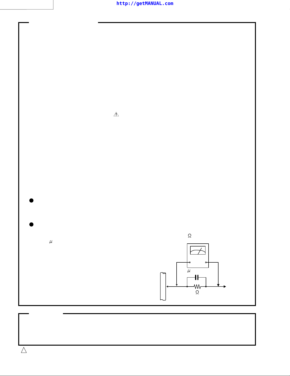
5. Leakage currnet check (Electrical shock hazard testing)
After re-assembling the product, always perform an isolation check on the exposed metal parts
of the product (antenna terminals, knobs, metal cabinet, screw heads, headphone jack, control
shafts, etc.) to be sure the product is safe to operate without danger of electrical shock.
Do not use a line isolation transformer during this check.
Plug the AC line cord directly into the AC outlet. Using a "Leakage Current Tester", measure
the leakage current from each exposed metal parts of the cabinet , particularly any exposed
metal part having a return path to the chassis, to a known good earth ground. Any leakage
current must not exceed 0.5mA AC (r.m.s.)
Alternate check method
Plug the AC line cord directly into the AC outlet. Use an AC voltmeter having, 1,000 ohms
per volt or more sensitivity in the following manner. Connect a 1,500 10W resistor paralleled by
a 0.15 F AC-type capacitor between an exposed
metal part and a known good earth ground.
Measure the AC voltage across the resistor with the
AC voltmeter.
Move the resistor connection to eachexposed metal
part, par ticularly any exposed metal part having a
return path to the chassis, and meausre the AC
voltage across the resistor. Now, reverse the plug in
the AC outlet and repeat each measurement. voltage
measured Any must not exceed 0.75 V AC (r.m.s.).
This corresponds to 0.5 mA AC (r.m.s.).
0.15 F AC TYPE
1500 10W
Good earth ground
AC VOLTMETER
(Having 1000
ohms/volts,
or more sensitivity)
Place this
probe on
each exposed
metal part.
Warning
1. This equipment has been designed and manufactured to meet international safety standards.
2. It is the legal responsibility of the repairer to ensure that these safety standards are maintained.
3. Repairs must be made in accordance with the relevant safety standards.
4. It is essential that safety critical components are replaced by approved parts.
5. If mains voltage selector is provided, check setting for local voltage.
Burrs formed during molding may be left over on some parts of the chassis. Therefore,
pay attention to such burrs in the case of preforming repair of this system.
1-2
CAUTION
!
Page 3
RX-7001PGD
Disassembly method
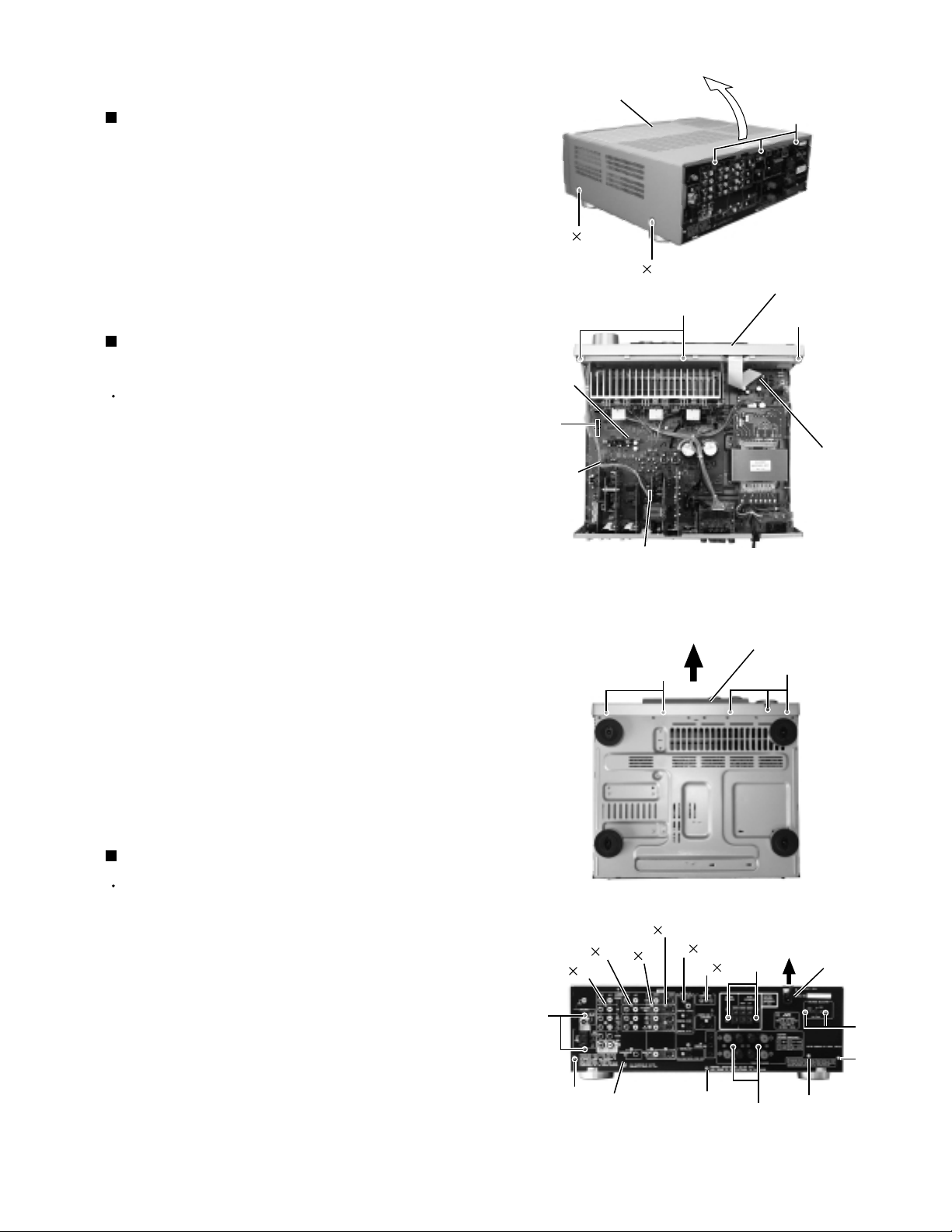
Removing the top cover (See Fig.1)
1.
Remove the four screws A attaching the top cover
on both sides of the body.
2.
Remove the three screws B on the back of the body.
3.
Remove the top cover from behind in the direction of
the arrow while pulling both sides outward.
Removing the front panel assembly
(See Fig.2 and 3)
Prior to performing the following procedure, remove
the top cover.
1.
Disconnect the card wire from connector CN400 on
the main board and CN402 on the power supply
board in the front panel assembly.
2.
Cut off the tie band fixing the harness.
3.
Disconnect the harness from connector CN202 on
the video board.
A 2
Main board
CN400
Tie band
Top cover
B
Fig.1
A 2
Front panel assembly
C
C
Power supply
board
CN402
Video board
CN202
Fig.2
4.
Remove the three screws C attaching the front
panel assembly.
5.
Remove the five screws D attaching the front panel
assembly on the bottom of the body. Detach the front
panel assembly toward the front.
Removing the rear panel (See Fig.4)
Prior to performing the following procedure, remove
the top cover.
1.
Remove the power cord stopper from the rear panel
by moving it in the direction of the arrow.
2.
Remove the twenty-eight screws E attaching the
each boards to the rear panel on the back of the
body.
3.
Remove the three screws F attaching the rear panel
on the back of the body.
E
E
F
E 3
E 3
3
Rear panel
D
E 3
Front panel assembly
Fig.3
E
5
E 2
E
F
E
Fig.4
D
Cord stopper
E
F
E
1-3
Page 4
RX-7001PGD
Fig.8
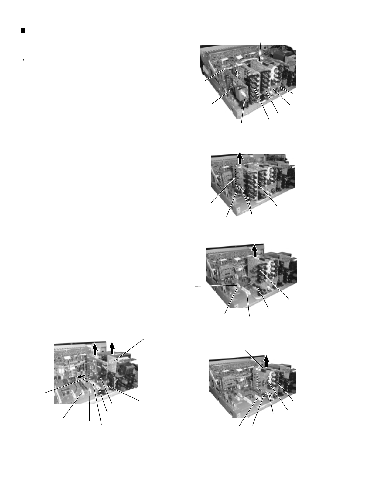
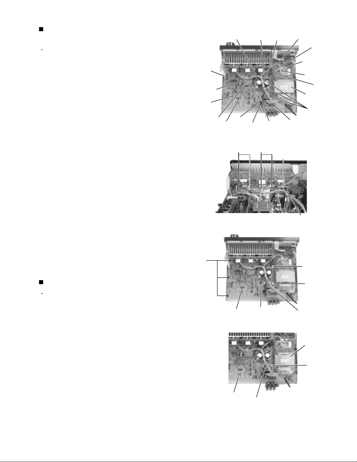
Removing each board connected to the
rear side of the main board
(See Fig.5 to 9)
Prior to performing the following procedure, remove
the top cover and the rear panel.
CN202
1.
Cut off the tie band fixing the harness.
2.
Disconnect the harness from connector CN202 on
the video board.
3.
Disconnect the tuner board from connector CN101
on the main board.
4.
Disconnect the SEA board and the audio board from
connector CN452, CN301and CN302 on the main
board.
5.
Disconnect the V-audio board from connector CN303
on the main board.
6.
Disconnect the relay board 4.Then, disconnect the
video board and the S-video board from connector
CN201 and CN241 on the main board.
7.
Disconnect the DSP board from connector CN501
and CN601 on the main board while removing the
DSP board from the bracket fixing the lower part of
the DSP board at the same time.
8.
Disconnect the compulink board from connector
CN255 on the main board.
Tie band
Main board
SEA board
CN101
Tuner board
Main board
CN452
S-video board
Video board
V-audio board
Audio board
Fig.5
Audio board
Main board
CN302,CN301
Fig.6
Bracket
CN201
CN241
Fig.9
DSP board
Main board
CN601
Main board
CN501
Compulink board
Main board
CN255
CN302
CN452
Relay board 4
CN303
CN301
Fig.7
Main board
CN201
Fig.8
Fig.8
Main board
CN303
Main board
CN241
V-audio board
S-video board
Video board
1-4
Page 5
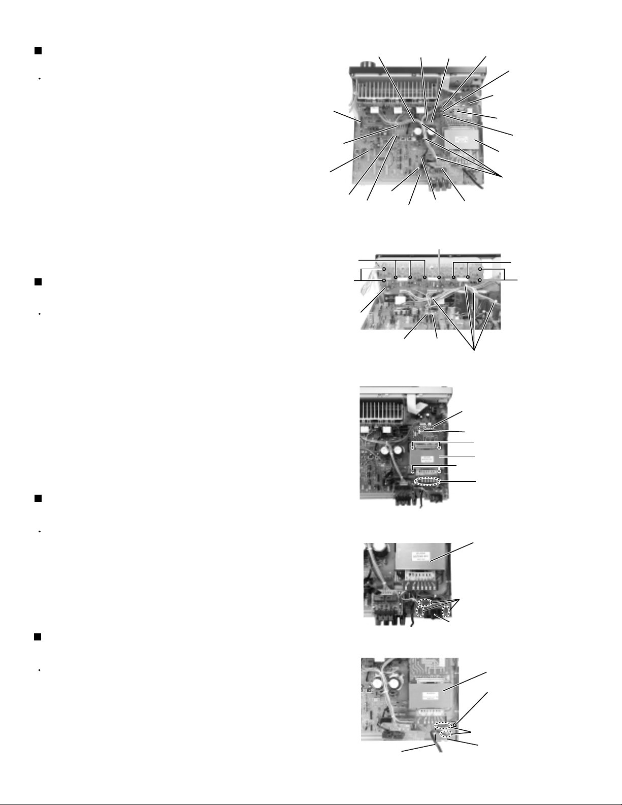
Prior to performing the following procedure, remove
the top cover and the rear panel.
Removing the main board / regulator
board (See Fig.10 to 12)
It is not necessary to remove the
boards connected to the back of the
main board. But to disassemble the
main board and the power supply
board efficiently, remove them.
ATTENTION:
Disconnect the card wire from connector CN400 on
the main board.
Cut off the three tie bands fixing the harnesses.
Disconnect the harness from connector CN811 on
the power transformer board.
Disconnect the relay board 1,2 and 3 from the main
board and the power supply board.
Disconnect the harness from connector CN704,
CN821, CN901, CN711, CN712, CN931 and CN932.
Remove the screw G attaching the regulator board
to the heat sink cover.
Remove the four screws H attaching the main board
to the heat sink cover.
Remove the five screws I and the screw J attaching
the main board to the chassis base (The resistor
board will come off at the same time).
1.
2.
3.
4.
5.
6.
7.
8.
Prior to performing the following procedure, remove
the top cover.
Disconnect the harness from connector CN881 on
the resistor board.
Remove the screw J attaching the resistor board.
1.
2.
Removing the resistor board (See Fig.13)
Fig.10
Fig.11
Fig.12
Fig.13
Power supply
board
Tie band
Relay board 1
Main board
CN400
Relay board 2
Tie band
Main board
Relay
board 3
CN811
CN932
CN961
CN931
CN712
CN711
CN901
CN821
CN704
HH
G
Regulator board
Resistor board
I
J
I
I
Main board
Power
transformer
Power
transformer
J
Resistor board
CN881
Main board
CN953
RX-7001PGD
1-5
Page 6
RX-7001PGD
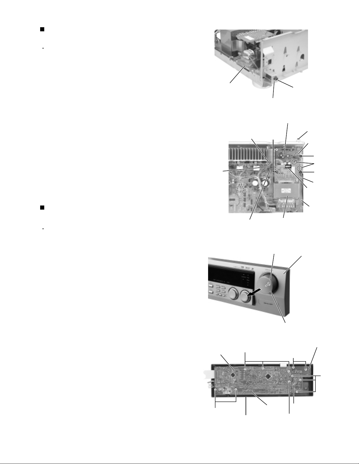
Removing the amplifier board
(See Fig.10 and 14)
Prior to performing the following procedure, remove
the top cover.
1.
Cut off the four tie bands fixing the harnesses.
2.
Disconnect the harnesses from connector CN711,
CN712, CN704 and CN901 on the main board
respectively.
3.
Disconnect the harnesses from connector CN953 on
the SP terminal board.
4.
Remove the four screws K and six screws L
attaching the amplifier board.
Removing the power transformer
(See Fig.15)
Prior to performing the following procedures, remove
the top cover.
1.
Unsolder the seven harnesses connected to the
power transformer.
Main board
CN400
Tie band
Main board
CN711
CN712
K
Amplifier board
CN901
L
CN931
CN932
CN711
CN821
CN961
Fig.10
Fig.14
CN704
L
CN712
Relay board 1
Relay board 2
Power supply
board
CN811
Relay
board 3
Power
transformer
Tie band
CN953
L
K
Tie band
2.
Disconnect the harness from connector CN811 and
the harnesses connected to connector CN55 and
CN56 on the power transformer board.
3.
Remove the four screws M attaching the power
transformer.
Removing the Voltage selector board
(See Fig.16)
Prior to performing the following procedure, remove
the top cover and the rear panel.
1.
Unsolder the six harnesses connected to the Voltage
selector board.
Removing the power / fuse board
(See Fig.17)
Prior to performing the following procedure, remove
the top cover and the rear panel.
1.
Remove the screw N attaching the power / fuse
board.
2.
Unsolder the power cord and other harnesses
connected to the power / fuse board.
1-6
Power cord
Fig.15
Fig.16
Fig.17
Solder
CN55
CN56
CN811
M
Power
transformer
M
Solder
Power
transformer
Solder
Voltage selector board
Power
transformer
N
Solder
Power / fuse board
Page 7
Prior to performing the following procedure, remove
the top cover and the front panel.
Remove the one nut attaching the headphone jack of
the power supply board on the front side of the body.
Disconnect the relay board 1, 2 and 3 from the
power supply board and the main board respectively.
Disconnect the harness connected to connector
CN55 and CN56 on the power transformer board (If
necessary, cut off the band fixing the harness on the
side of the base chassis).
Remove the four screws O attaching the power
supply board and pull out the power supply board
from the front bracket backward.
Unsolder the three harnesses connected to the
power supply board.
1.
2.
3.
4.
5.
Removing the power supply board
(See Fig.18 and 19)
Prior to performing the following procedure, remove
the top cover and the front panel assembly.
Pull out the volume knob on the front side of the front
panel and remove the nut attaching the system
control board.
Remove the six screws P attaching the system
control board on the back of the front panel and
disconnect the harness from connector CN422 on
the system control board.
Disconnect the harness from connector CN430 on
the power switch board.
Remove the five screws Q attaching the power
switch board.
1.
2.
3.
4.
Removing the system control board /
power switch board (See Fig.20 to 21)
Fig.18
Fig.19
Fig.20
Fig.21
Power supply board
Nut
Headphone jack
Tie band
Tie band
Relay board 1
Relay board 2
Relay board 3
Power transformer
Solder
O
O
O
Headphone jack
Solder
Power supply board
Front panel
Nut
Volume knob
System control board
Power switch board
Front panel assembly
P
Q
CN430
CN422
Q
P
P
CN55
CN56
RX-7001PGD
1-7
Page 8
RX-7001PGD
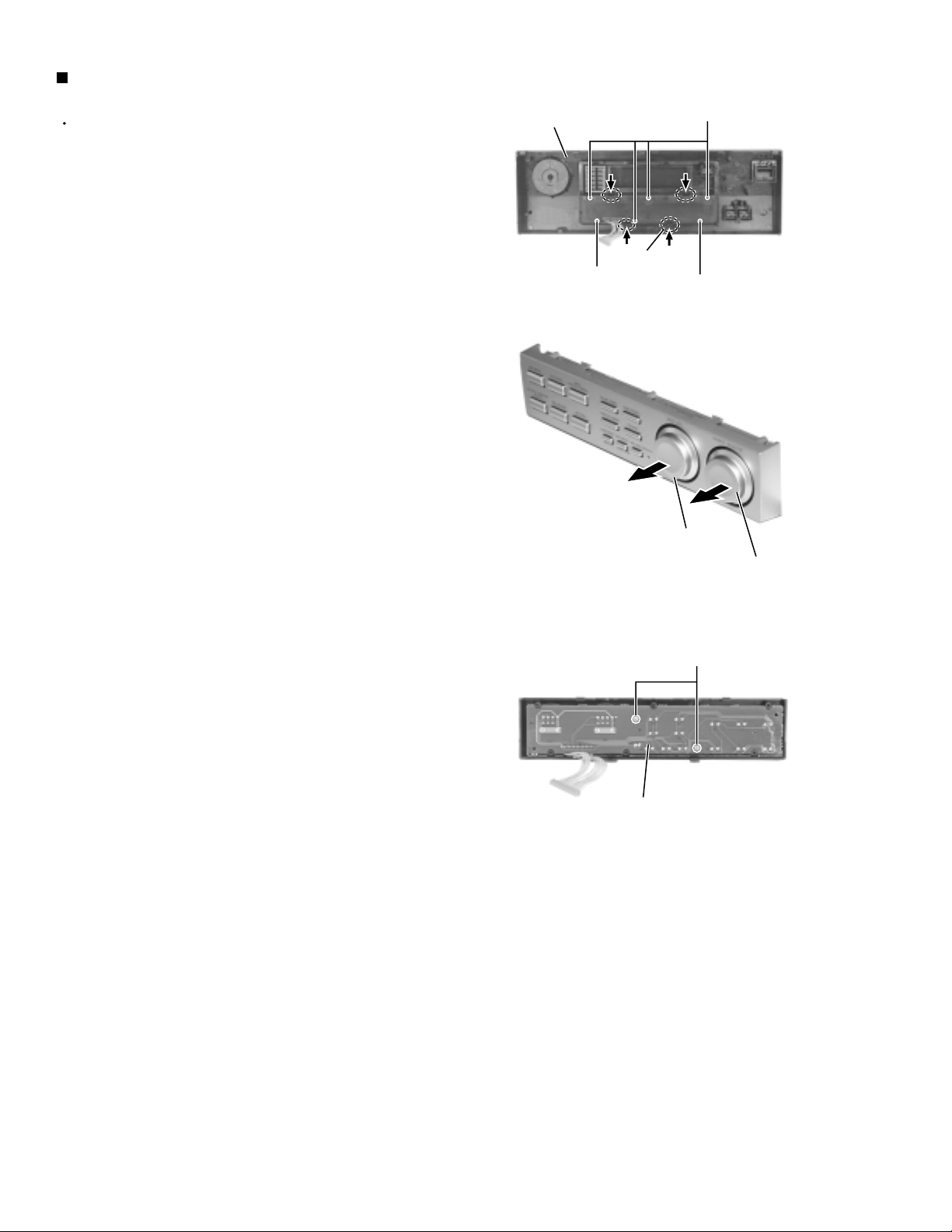
Removing the operation switch board
(See Fig.22 to 24)
Prior to performing the following procedure, remove
the top cover, the front panel assembly and the
system control board.
1.
Remove the six screws R attaching the operation
switch board on the back of the front panel.
2.
On the back of the front panel, release the four joints
by pushing the joint tabs inward. Remove the
operation switch board toward the front.
3.
Pull out the multi jog knob and the source selector
knob.
4.
Remove the two screws S attaching the operation
switch board.
Front panel
R
R
Joint
R
Fig.22
Multi jog knob
Source selector knob
Fig.23
S
Operation switch board
Fig.24
1-8
Page 9
Adjustment method
Tuner section
1.Tuner range
FM 87.5MHz~108.0MHz
AM(MW) 530kHz~1710kHz
Power amplifier section
Adjustment of idling current
Measurement location TP781
Adjustment part VR787(Lch) , VR788(Rch)
Attention
This adjustment does not obtain a correct adjustment value immediately after the amplifier is
used (state that an internal temperature has risen).
Please adjust immediately after using the amplifier after turning off the power supply of the
amplifier and falling an internal temperature.
<Adjustment method>
1.Set the volume control to minimum during this adjustment.(No signal & No load)
2.Set the surround mode OFF.
2.Turn VR787 and VR788 fully counterclockwise to warm up before adjustment.
If the heat sink is already warm from previous use the correct adjustment can not be made.
3.For L-ch,connect a DC voltmeter between TP781's pin1 and pin2 (Lch)
And,connect it between pin3 and pin4(Rch).
4.30 minutes later after power on, adjust VR787 for L-ch, or VR788 for R-ch so that the DC voltmeter
value has 1mV~10mV.
RX-7001PGD
* It is not abnormal though the idling current might not become 0mA even if it is finished to turn variable
resistance (VR787,VR788) in the direction of counterclockwise.
VR787 (Lch)
Rch
Lch
4321
TP781
VR788 (Rch)
Heat sink
Main board
1-9
Page 10
RX-7001PGD
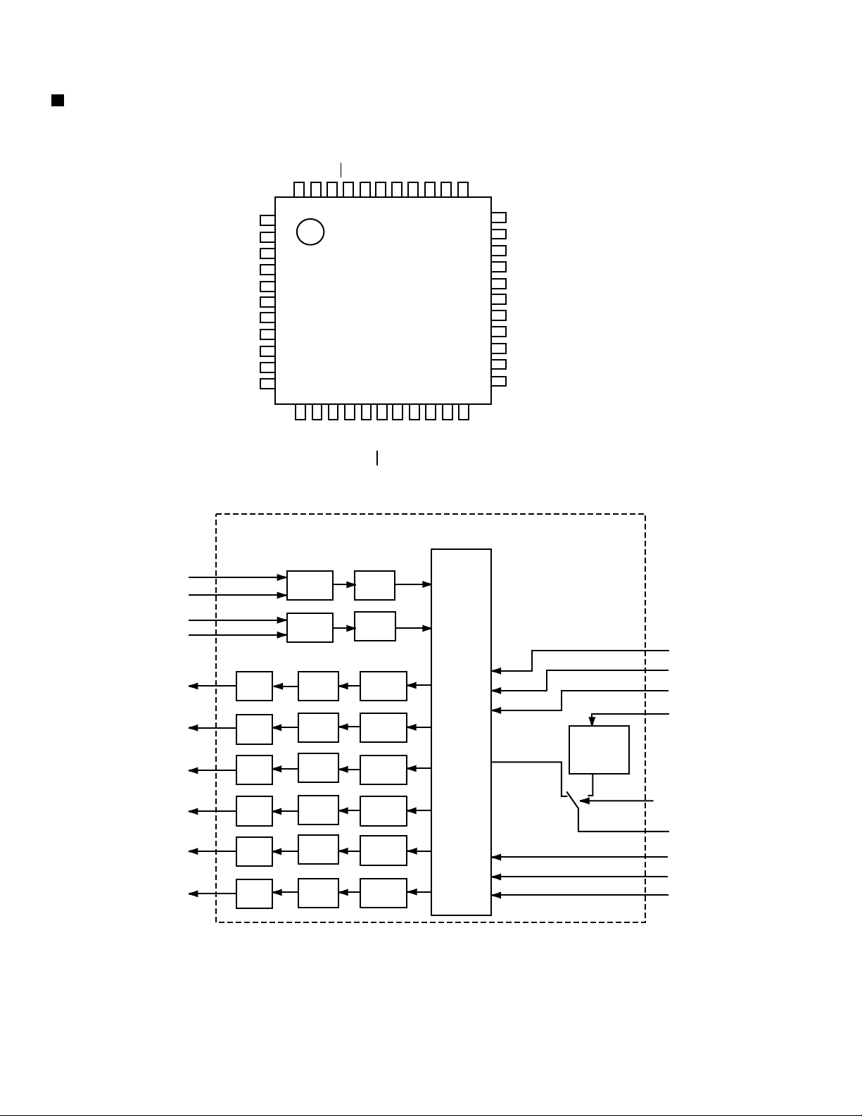
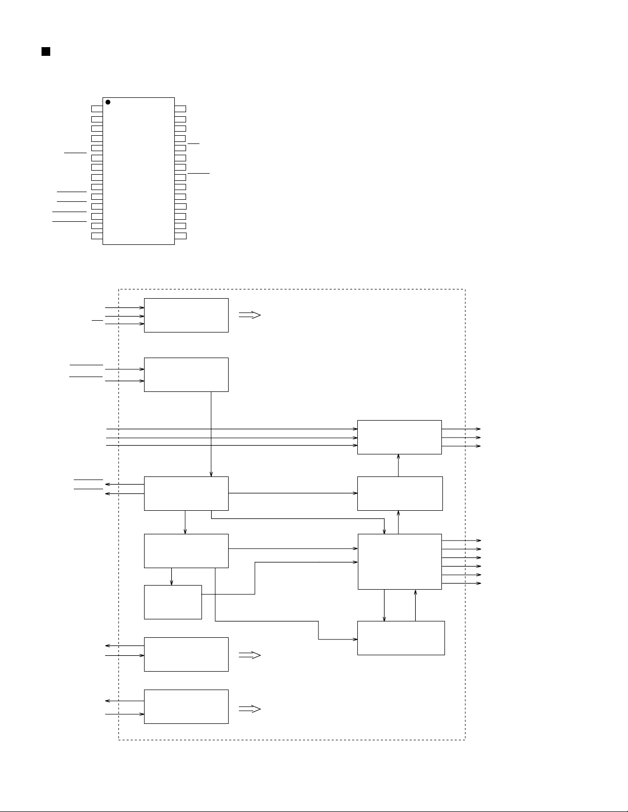
Description of major ICs
AK4527 (IC601) : A/D,D/A Converter
1.Pin layout
CDTO
CDTI
CCLKCSPIS
XTO
XTI
AVSS
AVDD
VREFH
VCOM
2.Block diagram
LIN+
LIN-
SDOS
OCKS
MIS
BCLK
LRCK
SDTI1
SDTI2
SDTI3
SDTO
DAUX
DFS
4443424140393837363534
1
2
3
4
5
6
7
8
9
10
11
1213141516171819202122
DEM1
DEM0
MCKO
DVDD
ADC
DVSSPDXTS
HPF
ICKS1
ICKS0
CAD1
Audio
I/F
33
32
31
30
29
28
27
26
25
24
23
CAD0
VREFL
RIN+
RINLIN+
LINROUT1
LOUT1
ROUT2
LOUT2
ROUT3
LOUT3
RIN+
RIN-
LOUT1
ROUT1
LOUT2
ROUT2
LOUT3
ROUT3
HPF
DA TT
DA TT
DA TT
DA TT
DA TT
DA TT
LRCK
BICK
MCLK
SDOUT
SDIN1
SDIN2
SDIN3
LPF
LPF
LPF
LPF
LPF
LPF
ADC
DAC
DAC
DAC
DAC
DAC
DAC
Block Diagram (DIR and AC-3) DSP are external parts)
DAUX
Format
Converter
SDOS
SDTO
SDTI1
SDTI2
SDTI3
1-10
Page 11
RX-7001PGD
3. Pin function (1/2)
No.
1
2
3
4
5
6
7
8
9
10
11
12
13
14
15
16
17
18
19
20
21
22
23
24
25
26
27
28
29
30
31
32
Pin name
SDOS
OCKS
MIS
BICK
LRCK
SDTI1
SDTI2
SDTI3
SDTO
DAUX
DFS
DEM1
DEM0
MCKO
DVDD
DVSS
PD
XTS
ICKS1
ICKS0
CAD1
CAD0
LOUT3
ROUT3
LOUT2
ROUT2
LOUT1
ROUT1
LINLIN+
RINRIN+
I/O
SDTO Source select pin
I
Function
"L" : Internal ADC output, "H" : DAUX input
ORed with serial control register if P/S="L".
MCKO Clock frequency select pin
I
"L" : MCLK, "H" : MCLK/2. ORed with serial control register if P/S= "L".
Connect to GND
I
Audio serial data clock pin
I
Input/Output channel clock pin
I/O
DAC1 Audio serial data input pin
I
DAC2 Audio serial data input pin
I
DAC3 Audio serial data input pin
I
Audio serial data output pin
O
AUX Audio serial data input pin
I
Double speed sampling mode pin
I
"L" : Normal speed, "H" : Double speed, the ADC is powered down.
ORed with serial control register if P/S="L".
De-emphasis pin
I
ORed with serial control register if P/S="L"
De-emphasis Pin
I
ORed with serial control register if P/S="L"
Master clock output pin
O
Digital power supply pin
Digital ground pin
Power-down & Reset pin
I
When "L", the AK4527 is powered-down and the control registers are reset
to default state. If the state of CAD0-1 changes, then the AK4527
must be reset by PDN.
X'tal oscillator Select/Test mode pin
I
"H" : X'tal Oscillator selected
"L" : External clock source selected
Input clock select 1 pin
I
Input clock select 0 pin
I
Chip address pin
I
Used during the serial control mode.
Chip address pin
I
Used during the serial control mode.
Lch #3 analog output pin
O
Rch #3 analog output pin
O
Lch #2 analog output pin
O
Rch #2 analog output pin
O
Lch #2 analog output pin
O
Rch #1 analog output pin
O
Lch analog negative Input Pin
I
Lch analog positive Input Pin
I
Rch analog negative Input Pin
I
Rch analog positive Input Pin
I
AK4527(1/2)
1-11
Page 12
RX-7001PGD
3.Pin function (2/2)
No.
33
34
35
36
37
38
39
Pin Name
VREFL
VCOM
VREFH
AVDD
AVSS
XTI
XTO
MCKI
40
41
P/S
DIF0
CS
42
DIF1
CCLK
43
LOOP0
CDTI
44
LOOP1
CDTO
I/O
I
O
I
-
I
O
I
I
I
I
I
I
I
I
I
O
AK4527(2/2)
Function
Negative voltage reference Input pin, AVSS
Common voltage output pin,AVDD/2
Large external capacitor around 2.2uF is used to reduce power-supply noise
Positive voltage reference input pin,AVDD
Analog power supply pin
Analog ground pin
X'tal input pin
X'tal output pin if XTS="H"
External master clock input pin if XTS="L"
Parallel/Serial select pin
"L" : Serial control mode, "H" : Parallel control mode
Audio data interface format pin in parallel mode
Chip select pin in serial mode
Audio data interface format pin in parallel mode
Control data clock pin in serial mode
Loop back mode pin in parallel mode
Enables digital loop-back from ADC to 3 DACs.
Control data input pin in serial mode
Loop back mode pin in parallel mode
Enable all 3 DAC channels to be input from SDTII.
Control data output pin in serial mode
1-12
Page 13
BA15218F(IC303):OP AMP.
RX-7001PGD
1OUT1
2-IN1
-
8
7
VCC
OUT2
1
3+IN1
+
-
-IN2
6
2
EE
4
+
5V
+IN2
BA15218N (IC501, IC510, IC511) : Dual Ope. Amp.
+
+
1
-
1 2 3 4 5 6 7 8
OUT1 +IN1 +IN1
+IN2 -IN2 OUT2
GND
2
-
Vcc
BA7625 (IC242,IC201) / BA7626 (IC241): Video selector
MONITOR OUT
GND
IN5
GND
IN4
CTL E
IN3
CTL D
1
2
3
4
5
6
7
8
logic
logic
16
15
14
13
12
11
10
11
IN1
CTL A
VOUT 1
V
CC
IN2
CTL B
VOUT 2
CTL C
A B E MONITOR OUT
LL
HL
LH
HHL IN4
HHH IN5
*
*
*
IN1
IN2
IN3
C D E VOUT1
LL
HL
LH
HHL IN4
HHH IN5
*
*
*
-IN2
IN3
C D E VOUT2
LL
HL
LH
HHL IN4
HHH IN5
*
*
*
IN1
--
IN3
1-13
Page 14
RX-7001PGD
BU2092(IC402,IC405):LED Controller
1.Terminal Layout
Vss
DATA
CLOCK
LCK
Q0
Q1
Q2
Q3
Q4
1
2
3
4
5
6
7
8
9
CONTROL
CIRCUIT
12BIT SHIFT RESISTER
12BIT STRAGE RESISTER
OUTPUT BUFFER(OPEN DRAIN)
18
17
16
15
14
13
12
11
10
Vdd
OE
Q11
Q10
Q9
Q8
Q7
Q6
Q5
2.Pin Function
Pin No.
1
2
3
4
5~16
17
18
Symbol
Vss
DATA
CLOCK
LCK
Q0~Q11
OE
Vdd
I/O
I
I
I
O
I
-
Function
Connect to GND
Serial Data input
Shift Clock of Data
Latch Clock of Data
Parallel Data Output
Latch Data L H
OUTPUT ON OFF
Output Enable
Power Supply
1-14
Page 15
BU4066BCF (IC602,IC611) : Switch
1.Pin Layout
14 13 12 11 10 9 8
1 2 3 4 5 6 7
2.Block Diagram
RX-7001PGD
VDD
C1
C4
I/O 4
O/I 4
O/I 3
I/O 3
14 13 12 11 10 9 8
1 2 3 4 5 6 7
I/O 1
O/I 1
O/I 2
I/O 2
C3
VSS
C2
W24L011AJ-15(IC641):SDRAM
1.Pin layout 2.Block diagram 3.Pin function
A0
A1
A2
A3
CS
I/O1
I/O2
VDD
VSS
I/O3
I/O4
WE
A4
A5
A6
A7
10
11
12
13
14
15
16
1
2
3
4
5
6
7
8
9
32
31
30
29
28
27
26
25
24
23
22
21
20
19
18
17
A16
A15
A14
A13
OE
I/O8
I/O7
VSS
VDD
I/O6
I/O5
A12
A11
A10
A9
A8
Vdd
Vss
A0
A16
CS
OE
WE
DECODER
CONTROL
CORE
ARRAY
I/O1
DATA I/O
I/O8
Symbol Description
A0~A16
I/O1~I/O8
CS
WE
OE
Vdd
Vss
Address inputs
Data inputs/outputs
Chip select inputs
Write enable input
Output enable input
Power supply
Ground
1-15
Page 16
RX-7001PGD
LA1838(IC102): FM AM IF AMP&detector, FM MPX Decoder
1. Block Diagram
30
ALC
BUFF
FM
S-METER
FM IF
1
2. Pin Function
Pin
Symbol
No.
FM IN
1
AM MIX
2
3
FM IF
AM IF
4
GND
5
6
TUNED
STEREO
7
8
VCC
9
FM DET
10
AM SD
FM VSM
11
AM VSM
12
13
MUTE
14
FM/AM
MONO/ST O
15
29
AM
OSC
SD
COMP
S-CLRVE
PM
DET
2
I/O
I
This is an input terminal of FM IF
28
REG
AM
MIX
AM/FM
IF-BUFF
3
27
FM
RF.AMP
AM IF
4
26
AGC
AM
S-METER
GND
Function
DET
5
signal.
This is an out put terminal for AM
O
mixer.
I
Bypass of FM IF
Input of AM IF Signal.
I
I
This is the device ground terminal.
When the set is tunning,this terminal
O
becomes "L".
O
Stereo indicator output. Stereo "L",
Mono: "H"
III
This is the power supply terminal.
I
FM detect transformer.
I
This is a terminal of AM ceramic filter.
O
Adjust FM SD sensitivity.
O
Adjust AM SD sensitivity.
I/O
When the signal of IF REQ of IC121(
LC72131) appear, the signal of FM/AM
IF output. //Muting control input.
Change over the FM/AM input.
I
"H" :FM, "L" : AM
Stereo : "H", Mono: "L"
25
TUNING
DRIVE
6
24
STEREO
DRIVE
7
22
23
P-DET
VCC
89
Pin
Symbol
No.
16
R OUT
17
L OUT
18
19
20
21
22
23
24
25
26
27
28
29
30
R IN
L IN
RO
LO
IF IN
FM OUT
AM DET
AM AGC
AFC
AM RF
REG
AM OSC
OSC BUFFER
21
DECODER
ANIT-BIRDIE
VCO
384KHz
10
20
STEREO
5N
SW
FF
38k
11
I/O
O
Right channel signal output.
O
Left channel signal output.
Input terminal of the Right channel post
I
18
19
MUTE
FF
/
19k
2
12 13
FF
19k
/LS
Function
17 16
PILOT
DET
14
AMP.
Input terminal of the Left channel
I
post AMP.
Mpx Right channel signal output.
O
O
Mpx Left channel signal output.
I
Mpx input terminal
FM detection output.
O
AM detection output.
O
This is an AGC voltage input terminal
I
for AM
I
This is an output terminal of voltage
for FM-AFC.
AM RF signal input.
I
Register value between pin 26 and pin28
O
besides the frequency width of the
input signal.
I
This is a terminal of AM Local
oscillation circuit.
AM Local oscillation Signal output.
O
15
1-16
Page 17
1. Pin layout
1
2
3
4
5
6
7
8
9
10
11
22
21
20
19
18
17
16
15
14
13
12
XT
FM/AM
CE
DI
CLOCK
DO
FM/ST/VCO
AM/FM
SDIN
XT
GND
LPFOUT
LPFIN
PD
VCC
FMIN
AMIN
IFCONT
IFIN
Pin
No.
1
2
3
4
5
6
7
8
9
10
11
Pin
No.
12
13
14
15
16
17
18
19
20
21
22
Symbol
XT
FM/AM
CE
DI
CLOCK
DO
FM/ST/VCO
AM/FM
LW
MW
SDIN
Symbol
IFIN
IFCONT
AMIN
FMIN
VCC
PD
LPFIN
LPFOUT
GND
XT
Function
X'tal oscillator connect (75kHz)
LOW:FM mode
When data output/input for 4pin(input) and
6pin(output): H
Input for receive the serial data from
controller
Sync signal input use
Data output for Controller
Output port
"Low": MW mode
Open state after the power on reset
Input/output port
Input/output port
Data input/output
Function
IF counter signal input
IF signal output
Not use
AM Local OSC signal output
FM Local OSC signal input
Power suplly(VDD=4.5-5.5V)
When power ON:Reset circuit move
PLL charge pump output(H: Local OSC
frequency Height than Reference frequency.
L: Low Agreement: Height impedance)
Input for active lowpassfilter of PLL
Output for active lowpassfilter of PLL
Connected to GND
X'tal oscillator(75KHz)
I/O
I
O
I
I
I
O
O
O
I/O
I/O
I/O
I/O
I
O
-
I
I
-
O
I
O
I
Reference
Driver
Phase
Detector
Charge Pump
Unlock
Detector
Universal
Counter
Swallow Counter
1/16,1/17 4bit
12bit
Programmable
DriverS
Swallow Counter
1/16,1/17 4bit
Data Shift Register & Latch
Power
on
Reset
C
2B
I/F
1/2
7821113
21
17
6
5
4
3
15
16
22
1
18
19
20
12
2. Block diagram
3. Pin function
LC72136N (IC121) : PLL Frequency synthesizer
RX-7001PGD
1-17
Page 18
RX-7001PGD
LC7522 (IC451) : SEA Control
1.Pin layout 2.Block diagram
1
28
2
27
3
26
4
25
5
24
6
23
7
22
8
21
9
20
10
19
11
18
12
17
13
16
14
15
D1
CLK
TEST1
10
f1
9
f2
8
f3
7
f4
6
f5
5
f6
4
f7
16
17
13
S
4
Control Shift Resistor
3.Pin function
Pin No. Symbol
1
18
14
15
2,27
3,26
VDD
VSS
VEE
VCC
IN 1
IN 2
16 D1 Data input terminal from CPU
17 CLK Clock input terminal from CPU
4~10
f1~f7 Joint terminal of B.P.F.
19~25
11
12
13
TEST1
TEST2
S
28 NC No use
Power Supply terminal for Audio signal +7V(typ)
Power Supply terminal 0V
Power Supply terminal for Audio signal. Single channel use, joint VSS.
Power Supply terminal +5V(typ)
Audio signal Input terminal
IN1 joint opposite input of Operation amp.
IN2 joint inapposite input of Operation amp.
It have Right and Left.
Shumit inverter style
Shumit inverter style
f1~f7 X Right, Left Total 14 terminal
Internal test terminal of IC
It can use open condition
Select terminal for 2 tip use
"1" input, key code 7C3 - VDD joint
"0" input, key code 7C2 - VEE joint
+
–
2IN1
3IN2 27 IN126 IN2
Network
Resistor
Latch Circuit
18
1
Vdd
Vss
14
Vee
Function
Network
Resistor
15
Vcc
+
–
19
f1
20
f2
21
f3
22
f4
23
f5
24
f6
25
f7
12
TEST2
1-18
Page 19
M5243AP12(IC452):S.E.A.Graphic equalizer
IN1-2 NF1-2 IN2-2 NF2-2 IN3-2 NF3-2 IN-2 IN-2 OUT-2 VDD
20 19 18 17 16 15 14 13 12 11
Vref.
Vref.
1 2 3 4 5 6 7 8 9 10
IN1-1 NF1-1 IN2-1 NF2-1 IN3-1 NF3-1 IN-1 IN-1 OUT-1 GND
NJM4580D (IC301, IC302, IC306) : LPF, Mic and H.phone Amp.
1.Terminal layout
RX-7001PGD
2.Block diagram
+
V
INPUT
+
A OUT
A -IN
A +IN
V
1
2
A
3
-
4
(TOP VIEW)
B
8
6
5
7
+
V
B OUT
B -IN
B +IN
OUTPUT
-
V
1-19
Page 20
RX-7001PGD
MN101C15FDE (IC401) : System control micon
1. Pin layout
80 61
1
60
20
21 40
2. Pin function
Pin
No
Symbol Symbol
1
2
3
4
5
6
DVD-S/C
VCR1-S/C
VIDEO-S/C
TV-S/C
4/8-IN
7
8
9
PROTECT
10
11
12
13
OSC 12
OSC 11
14
15
16
17
18
19
20
21
22
23
TEXT-OUT
TEXT-IN
MASTER
DSP-COMMAND
DSP-STATUS
DSP-CLK
24
25
26
27
RESET-IN
TUNER-CE
TUNER-CLK
28
TUNER-DATA
29
TUNER-MUTE
30
31
32
33
34
TUNER-IN
STEREO-IN
RDS-ST
M-BUSY
35
36
37
38
39
40
OSD-DATA
OSD-STB
OSD-CLK
VIDEO1
VIDEO2
GND
GND
GND
VDD
VSS
X1
X0
GND
INH
41
Functions Functions
Ground
DVD S/C signal select terminal
VCR1 S/C signal select terminal
VIDEO S/C signal select terminal
TV S/C select terminal
4 ohm / 8 ohm select signal terminal
Ground
Protect
Ground
Power supply
Oscillation terminal
Oscillation terminal
Ground
Ground
Ground
Ground
Text signal output terminal
Text signal input terminal
Master signal terminal
DSP control signal terminal
DSP control signal terminal
DSP control signal terminal
No use
Reset signal input terminal
Tuner chip enable
Tuner clock signal terminal
No use
Tuner control signal terminal
Tuner mute signal terminal
Tuner signal input terminal
Stereo signal input terminal
No use
Busy signal from IC400
No use
OSD data signal input terminal
OSD standby signal terminal
OSD clock signal terminal
VIDEO 1 signal terminal
VIDEO 2 signal terminal
Pin
No
41
42
43
44
45
46
47
48
49
50
51
52
53
54
55
56
57
58
59
60
61
62
63
64
65
66
67
68
69
70
71
72
73
74
75
76
77
78
79
80
VIDEO3
VIDEO4
S.MUTE
RDS-DATA
RDS-CLK
DSP-READY
DSP-RESET
M/CS
M-RESET
M-STATUS
M-COMMAND
M-CLK
SEA-CLK
SEA-DATA
VL/VH
4/8 OUT
SW-DATA
SW-CLK
VOL-STB
VOL-DATA
VOL-CLK
SW-STB
FR1-RELAY
FR2-RELAY
CNTR-RELAY
SUR-RELAY
SUB-MUTE
LED-LCK2
C.TONE3
C.TONE2
C.TONE1
LED-LCK1
LED-DATA
LED-CLK
VIDEO 3 signal terminal
VIDEO 4 signal terminal
Source mute control terminal
No use
No use
No use
RDS control signal terminal
No use
RDS control signal clock
DSP control signal clock
DSP reset signal terminal
Control signal from IC400
Reset signal from IC400
Status signal from IC400
Command signal from IC400
Clock signal from IC400
SEA clock signal from terminal
SEA data signal terminal
Connect to power supply board
4 ohm / 8 ohm select signal terminal
Switch data signal terminal
Switch clock signal terminal
Volume strobe signal terminal
Volume data signal terminal
Volume clock signal terminal
Switch strobe signal terminal
No use
No use
Relay 1 signal terminal
Relay 2 signal terminal
Center speaker relay terminal
Surround speaker relay terminal
SUB woofer out mute control
LED latch clock signal terminal
Center tone 3 signal terminal
Center tone 2 signal terminal
Center tone 1 signal terminal
LED latch clock signal terminal
LED data signal terminal
LED clock signal terminal
1-20
Page 21
1~22
23
24~39
40,41
42,43
44
45
46
47
48
49
50
51
52
53
54
55
56,57
58
59
60~63
64~67
68
69
70
71
72
73
74
75~84
S22~S1
VPP
G15~G1/KO0~5
JOG1,2
JOG3,4
M BUSY
M CLK
M COMMAND
M STATUS
M CS
RM
VCRI
DCSI
DCSO
VCRO
TVD
TVC
JOG5,6
POWER
KI3~KI0
S36~S33
RST
X1
X2
VSS
OSC2
OSC1
S32~S23
O
-
O
I
I
O
I/O
I
O
I
I
I
I
O
O
O
O
I
I
O
I
O
I
-
-
-
-
-
-
O
Pin No. I/O
84 64
22 42
1
21
63
43
KEY IN 0
KEY IN 1
KEY IN 2
KEY IN 3
KEY OUT 0
POWER
SURROUND
SPEAKER 1
SPEAKER 2
KEY OUT1
ANALOG/
DIGITAL
DSP MODE
LOUDNESS
SEA MODE
KEY OUT 2
SEA ADJUST
FM MODE
LEVEL ADJUST
SOUND SELECT
KEY OUT 3 KEY OUT 5
ONE TOUCH
OPERATION
FM/AM TUNING
TUNER PRESET
MEMORY
SETTING
MN173222DG(IC400):FL Display & Operation switch control
1.Pin layout
2.Key matrix
3.Pin function
Symbol Description
FL Segment control signal
Power supply terminal
FL grid control signal / Key matrix output
Source select JOG1,2
Volume JOG 3,4
BUSY Signal output to IC401
Clock signal to IC401
Command data input from IC401
Status signal output to IC401
Chip select signal input from IC401
Remote control signal input
AV Compu-link VCR input
AV Compu-link DCS input
AV Compu-link DCS output
AV Compu-link VCR output
AV Compu-link TV output
AV Compu-link TV control output
Multi JOG 5,6
Power ON control output
STANDBY LED control H:Lighting
Key matrix input
FL Segment control signal
Reset input
Connect to GND
Non connect
Connect to GND
Oscillation terminal 6MHz
Oscillation terminal 6MHz
Not use
FL Segment control signal
RX-7001PGD
1-21
Page 22
RX-7001PGD
MB90088 (IC203) : On screen display controller
1.Terminal layout
YIN
VIN
CIN
AVcc
FSCO
VBLK
Vcc
EXS
XS
HSYNC
VSYNC
EXHSYN
EXVSYN
Vss
2.Block diagram
SIN
SCLK
CS
EXHSYN
EXVSYN
1
2
3
4
5
6
7
8
9
10
11
12
13
14
28
AVss
27
YOUT
26
VOUT
25
COUT
24
CS
23
SIN
22
SCLK
21
TEST
20
VOC0
19
VOC1
18
VOC2
17
VOB
16
XD
15
EXD
Serial Input
Control
H/V Separate
Each Control, Data
VIN
YIN
CIN
HSYNC
VSYNC
XS
EXS
XD
EXD
NTSC/PAL
Signal OSC
Display Memory
Control
VRAM
4FSC CLK
OSC
Dot CLK
OSC
Each Block
Each Block
Analog SW
Video Signal
OSC
Output
Control
CGROM
VOUT
YOUT
COUT
BOUT
ROUT
GOUT
IOUT
VOC
VOB
1-22
Page 23
3.Pin functions (MB90088)
pin
Symbol I/O Function
no
YIN
1
2
3
4
5
6
7
8
9
10
11
12
13
14
15
16
17
18
19
20
21
22
23
24
25
26
27
28
VIN
CIN
AVcc
IOUT
VOC
Vcc
EXS
XS
HSYNC
VSYNC
EXHSYN
EXVSYN
Vss
EXD
XD
VOB
GOUT
ROUT
BOUT
TEST
SCLK
SIN
CS
COUT
VOUT
YOUT
AVss
Brightness signal Input terminal for Superinpause indication
I
I
Composite video signal input terminal for Superinpause indication
Contrast signal input terminal for Superinpause indication
I
-
Analog power supply terminal
O
Color (Brightness) signal output terminal
Character output terminal
O
Power supply terminal
Clock generater outside circuit terminal for color burst
I
O
O
Horizontal signal output terminal
O
Vertical signal output terminal
EXT horizontal signal input terminal
I
EXT vertical signal input terminal
I
GND
Dot clock generater outside circuit signal terminal for indication
I
O
Character & background signal output terminal
O
Color signal (Green, Red, Blue)
O
I
Test signal input terminal
Shift clock input terminal for serial transmission
I
Serial data input terminal
I
Chip select terminal
I
Contrast signal output terminal
O
Composite video signal output terminal
O
O
Brightness signal output terminal
Analog GND terminal
-
RX-7001PGD
1-23
Page 24
RX-7001PGD
NJM2285D (IC202) : Video switch
1.Terminal layout & Block diagram
GND 1 IN 2B
IN 1A
16 15 14 13 12 11 10 9
L
Bias Type
Clamp Type
CTL 2 IN 2A GND 3 IN 3B
V+
HL
Clamp Type
H
H
12345678
IN 1B
CTL 1
OUT 1
GND 2 OUT 2
OUT 3 CLT 3 IN 3A
TC9164AN (IC432): Analog switch
1.Function
Switch to On/Off of S1 to S8 by control of LSI.
2.Terminal Lay out & Block Diagram
TC9164AN
VSS
L-S1
S-2
S-3
S-4
COM-1
S-5
S-6
COM-2
S-7
S-8
COM3
ST
GND
1
2
3
4
SHIFT
5
RESISTOR
6
7
8
9
10
11
12
13
14
&
LATCH
SHIFT RESISTOR
SHIFT
RESISTOR
&
LATCH
28
27
26
25
24
23
22
21
20
19
18
17
16
15
VDD
R-S1
S-2
S-3
S-4
COM-1
S-5
S-6
COM-2
S-7
S-8
COM3
DATA
CK
L
PQ3DZ53 (IC661, IC663) : Regulator IC
DC INPUT(Vin)
1-24
1
CUSTOM IC
5
GND
3
DC OUTPUT(Vo)
ON/OFF CONTROL(Vc)
2
Page 25

DLCKS terminal
L
L
H
H
DLONterminal
L
H
L
H
DLL clock setting
SCKI input (DLL circuit OFF)
Four times XI clock
Three times XI clock
Six times XI clock
1
2
3
4
5
6
7
8~11
12
13
14
15
16~18
19
20
21
22
23
24
25
26
27,28
29~31
32,33
34
35
36
37
38,39
40
41
42
43
44
45
46
47
48
49
50
51
52
53
54~61
62
63~70
71
72~80
81
82~89
90
91
92,93
94
95
96
97
98,99
100
Pin No. Symbol I/O Function
RST
MIMD
MICS
MILP
MIDIO
MICK
MIACK
FI0~3
IRQ
VSS
LRCKA
BCKA
SDO0~2
SD03
LRCKB
BCKB
SDT0
SDT1
VDD
LRCKOA
BCKOA
TEST0,1
LRCKOB,BCKOB,TXO
TEST2,3
RX
VSS
TSTSUB0
FCONT
TSTSUB1,TSTSUB2
PDO
VDDA
PLON
AMPI
AMPO
CKI
VSSA
CKO
LOCK
VSS
WR
OE
CE
VDD
IO7~0
VSS
AD0~7
VDD
AD8~16
VSS
PO0~7
VDDDL
LPFO
DLON,DLCKS
SCKO
VSSDL
SCKI
VSSX
XO,XI
VDDX
I
I
I
I
I/O
I
O
I
I
I
I
O
I
I
I
I
-
O
O
I
I
I
I
O
I
O
I
I
O
I
-
O
O
-
O
O
O
-
I/O
-
O
-
O
-
O
-
O
I
-
I
-
I/O
-
Reset signal input terminal (L:reset H:Operation usually)
Microcomputer interface mode selection input terminal (L:serial H:IC bus)
Microcomputer interface chip select input terminal
Microcomputer interface latch pulse input
Microcomputer interface data I/O terminal
Microcomputer interface clock input terminal
Microcomputer interface acknowledge output terminal
Flag input terminal 0~3
Interrupt input terminal
Digital ground terminal
Audio interface LR clock input terminal A
Audio interface bit clock input terminal A
Audio interface data output terminal 0
Non connect
Audio interface LR clock input terminal B
Audio interface bit clock input terminal B
Audio interface data input terminal 0
Audio interface data input terminal 1
Power supply for digital circuit
Audio interface LR clock output terminal A
Audio interface bit clock output terminal A
Test input terminal 0/1 (L:test H:operation usually)
Non connect
Test input terminal (L:test H:operation usually)
SPDIF input terminal
Ground terminal for digital circuit
Test sub input terminal 0 (L:test H:operation usually)
VCO Frequency control output terminal
Test sub input terminal 1,2 (L:test H:operation usually)
Phase error signal output terminal
Power supply for analog circuit
Clock selection input terminal (L:external clock H:VCO clock)
AMP.input terminal for LPF
AMP.output terminal for LPF
External clock input terminal
Ground terminal for analog circuit
DIR Clock output terminal
VCO Lock detection output terminal
Ground terminal for digital circuit
External SRAM writing signal output terminal
External SRAM output enable signal output terminal
External SRAM chip enable signal output terminal
Power supply terminal for digital circuit
External SRAM data I/O terminal 7~0
Ground terminal for digital circuit
External SRAM address output terminal 0~7
Power supply terminal for digital circuit
External SRAM address output terminal 8~16
Ground terminal for digital circuit
General purpose output terminal 0~7
Power supply terminal for DLL
LPF output terminal for DLL
Refer to the undermentioned table
Non connect
Ground terminal for DLL
External system clock input terminal
Ground termonal for oscillation circuit
Oscillation I/O terminal
Power supply terminal for oscillation circuit
TC9446F-013(IC631):Digital signal processor for dolby digital
/ DTS audio decode
RX-7001PGD
1-25
Page 26
RX-7001PGD
TC9459F (IC331,IC332,IC333) : Electronic volume control
1.Pin layout
VSS
L-OUT
NC
L-ch
L-IN
L-LD1
L-LD2
L-A-GND
NC
CS1
NC
GND
CK
1
2
3
4
5
6
7
8
9
10
11
12
24
23
22
21
20
19
18
17
16
15
14
13
VDD
R-OUT
NC
R-IN
R-LD1
R-LD2
R-A-GND
NC
CS2
NC
STB
DATA
R-ch
2. Block diagram
2
L-OUT
3
NC
L-1N
L-LD1
L-LD2
L-A-GND
NC
CS1
NC
GND
CK
4
5
6
7
8
9
10
11
12
50k /
91 STEP
VR
VSS
1
L-ch 7 to 91
decoder
L-ch data
latch circuit
Shift register (24BIT)
Level shift circuit
VDD
24
R-ch 7 to 91
decoder
R-ch data
latch circuit
Same as L-ch
Circuit
23
22
21
20
19
18
17
16
15
14
13
R-OUT
NC
R-IN
R-LD1
R-LD2
R-A-GND
NC
CS2
NC
STB
DATA
3.Pin function
Pin No.
1
2
3
4
5
6
7
8
9
10
11
12
Symbol
VSS
L-OUT
NC
NC
L-LD1
L-LD2
L-A-GND
NC
CS1
NC
NC
CK
Function
Negative power supply pin
Volume output pin
No connection
No connection
Loudness tap output pin
Loudness tap output pin
Analog GND pin
No connection
Chip select input pin
No connection
No connection
Data transfer clock input
Pin No.
13
14
15
16
17
18
19
20
21
22
23
24
Symbol
DATA
STB
NC
CS2
NC
R-A-GND
R-LD2
R-LD1
R-IN
NC
R-OUT
VDD
Function
Volume setup serial data input
Data write strobe input
No connection
Chip select input pin
No connection
Analog GND pin
Loudness tap output pin
Loudness tap output pin
Volume input pin
No connection
Volume output pin
Positive power supply pin
1-26
Page 27
UPD78F4216AGC(IC671):UNIT CPU
1.Pin layout
75 ~ 51
76
~
50
~
RX-7001PGD
100
1 ~ 25
26
2.Pin function
Pin No. Symbol I/O Function
1~8
9
10
11
12
13
14
15
16
17
18
19
20
21
22
23
24
25~32
33
34,35
36
37,38
39
40
41
42
43
44
45,46
47
48
49
50
51,52
53
54~63
64,65
66
67
68
69,70
71
72
73~80
81
82
83
84
85
86
87
88
89
90~93
94
95~100
VDD
X2
X1
VSS
XT2
XT1
RESET
AUTODATA
LOCK
DIGITAL0
FORMAT
CHANNEL
ERR
RSTDET
AVDD
AVREF0
AVSS
RX,TX
DSPCOM
DSPSTS
DSPCLK
DSPRDY
MIDIO_IN/OUT
MICK
MICS
MILP
MIACK
DSPRST
CDTI/CDTO
CCLK
CS
XTS
PD
GND
VDD
3D-ON
3D-ON
ANA/T-TONE
REF-MIX
D.MUTE
S.MUTE
ASW1~4
TEST
Non connect
Power supply terminal
Connecting the crystal oscillator for system main clock
O
Connecting the crystal oscillator for system main clock
I
Connect to GND
Connecting the crystal oscillator for system sub clock
O
Connecting the crystal oscillator for system sub clock
I
System reset signal input
I
Output of DSP to general-purpose port
I
Output of DSP to general-purpose port
I
Output of DSP to general-purpose port
I
Output of DSP to general-purpose port
I
Output of DSP to general-purpose port
I
Output of DSP to general-purpose port
I
Reset signal input
I
Power supply terminal
Connect to GND
Connect to GND
Connect to GND
Non connect
Power supply terminal
Not use
Non connect
Communication port from IC401
I
Status communication port to IC401
O
Clock input from IC401
I
Ready signal input from IC401
I
Non connect
Interface I/O terminal with microcomputer
I/O
Interface I/O terminal with microcomputer of clock signal
O
Interface I/O terminal with microcomputer of chip select
O
Interface I/O termonal with microcomputer
O
Interface I/O termonal with microcomputer
O
Non connect
Reset signal output of DSP
O
Non connect
Interface I/O terminal with microcomputer
I/O
Interface I/O terminal with microcomputer of clock signal
O
Interface I/O terminal with microcomputer of chip select
O
OSC Select
O
Non connect
Reset signal output
O
Connect to GND
Non connect
Power supply
Non connect
Switch at output destination of surround channel
O
Test tone control
O
Control at output destination of LFE channel
O
Non connect
Mute of the digital out terminal is controlled
O
Mute of the audio signal is controlled
O
Non connect
Selection of digital input selector
O
Test terminal
Non connect
-
1-27
Page 28

2-1
Page 29
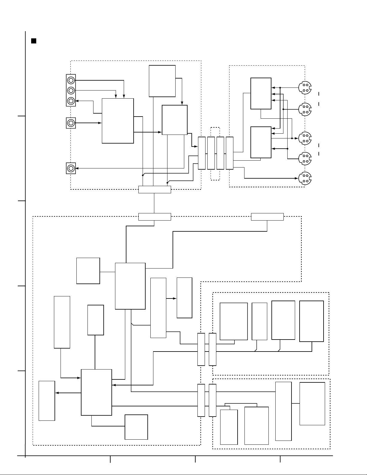
RX-7001PGD
Block diagrams
System control & Video I/O section
5
DVD
TV/BS
VCR1 OUT
J201
VCR1 IN
J202
4
MONITOR
J203
3
IN4
VOUT1
IN1
S401
8MHz
CLOCK
IN5
VIDEO
OSC11
OSC12
SELECTOR
IC201
OSDDATA
ON SCREEN
OSDCS
OSDCLK
OSDDATA
VIDEO1~3
CN202
CN450
OSDCLK
OSDSTB
VIDEO1~4
DISPLAY
CONTROL
MOUT
VIDEO4
IC203
VIDEO
SWITCH
OUT1~3
DSPCLK
YOUT
COUT
VOUT
IC202
OUT1,2
CN204
TUNERCD
DSPRESET
DSPREADY
DSPSTATUS
DSPCOMMAND
CN205
CN242
CN243
SEACLK
SEADATA
TUNERCLK
TUNERDATA
SWCLK
SWDATA
VIDEO
SELECTOR
MOUT C
VIDEO
SELECTOR
CN410
SWSTB
VOLDATA/CLK/STB
IC241
IC242
MOUT Y
TO POWER
AMP.
YMON1
CMON1
SECTION
CN400
DVD IN
J241
TV/BS IN
VCR1
OUT
J242
VCR1 IN
MONITOR
OUT
J243
2
1
2-2
DI400
FL DISPLAY
IC401
S407
SURROUND SW
JS400
VOLUME
SYSTEM
CONTROLLER
LEDCLK
LEDDATA
IC402
LED CONTROLLER
LEDLCK1
LED
D430~D440
OTO LED
OPERATION
ONE TOUCH
D442
JS401
MULTI JOG
JS402
SOURCE
SELECTOR
SWITCH
OPERATION
S408~S420
CN432
KI0~3
KO1~3,5
KI1
JOG3,4
KO0
MBUSY MCLK MSTATUS
MCOMMAND MCS MRESET
LEDDATA
LEDCLK
LEDLCK2
JOG5,6
JOG1,2
IC400
S1~S36
G1~G16
FL DISPLAY
CONTROLLER
OSC1,2
X400
6MHz
CLOCK
RM
KO0
KI0~3
CN420 CN422
CN430
IC404
REMOCON
OPERATION
SWITCH
S400~S402
IC405
LED CONTROLLER
LED
D486,D487
D481~D483
ABCD
Page 30
SEA
CONTROLLER
IC451,452
SOUCE
SELECTOR
IC321
SEADATA SEACLK
TUCE
TUCK
TUDATA
TU L/R
DSPOUT SL/SR
A.SWCLK A.SWDATA A.SWSTB
DSPCLK
DSPSTATUS
DSPCOMMAND
DSPREADY
DSPRESET
FRONT L/R
FRONT L/R
IC363
IC361
IC362
DSP OUT L/R
DSP OUT CENTER
SEA IN/OUT
VOLDATA
VOLCLK
VOLSTB
VOLDATA
VOLCLK
VOLSTB
VOLUME
CONTROL
IC332
VOLUME
CONTROL
IC333
VOLUME
CONTROL
IC331
C.TONE OUT
FRONT L/R
FRONT L/R
REAR L/R
RELAY
RY932
RELAY
RY931
RELAY
RY951
RELAY
RY952
Q751~Q758
Q761~Q764
SPEAKER B SPEAKER A
Q1751
Q1752
Q1851~1854
CENTER
REAR L/R
CN400 CN101 CN301 CN302 CN303
CN501 CN601
CN452
CN451
CN711
CN701
CN712
CN702
CN953
CN952
AUDIO SWITCH
IC304
AUDIO SWITCH
IC311
TU L/R
STB CLK DATA
FRONT L/R
PHONO
CD
PLAY
DVD IN
TV/DBS
IN
VCR1
PLAY
IC301
REAR L/R
DSP SL/SR
V.SIG
L/R
SW OUT
CN313
CN312CN311
TO TUNER SECTION
CN111
TO SYSTEM CONTROL
SECTION
CN410
TO DSP
SECTION
CN681
TO DSP
SECTION
CN687
J301
J302
J311
J312
J314
Main amplifier & Audio I/O section
IC391
SUB
WOOFER
TAPE
REC
VCR1
REC
IC305
RX-7001PGD
5
4
3
2
1
ABC
2-3
Page 31

RX-7001PGD
DSP Section
IC621
IC622
IC601
D/A,A/D
5
Converter
IN
L/R
LOUT2
ROUT2
CDTI
CDTO
CCLK
CS
IC501
IC511
SDTI0~3
LRCLK
BCLK
LOUT1 ROUT1
4
IC521
IC531
IC551
LOUT3 ROUT3
IC581
IC591
OUT C
OUT LFE
SURROUND
SWITCH
IC602
IC561
IC571
SELECT1~4
DSP
CONTROLLER
IC671
X1
X2
CLOCK
X671
SELECTOR
IC611
RX
AUTODATA LOCK
DIGITALO FORMAT
CHANNEL ERR
RST_DET DSPRST
CLOCK
X631
22.5792MHz
XI
TXO
XO
IC631
DSP
WR
OE
CE
I/O8~1
A0~16
DIGITAL
IN
J601
OPTICAL
IN 1,2
UN661
UN662
OPTICAL
OUT
UN663
6.14MHz
OUT SL/SR
OUT
L/R
3
CN681 CN687
TO V OLUME
CONTROL SECTION
CONTROL SECTION
CN501
DSPRESET
DSPREADY
DSPCOMMAND
DSPSTATUS
DSPCLK
TO V OLUME
CN601
IC641
SDRAM
2
1
2-4
Tuner section
TUNER
OUT L/R
MPX
DATA
CLOCK
CE
TO V OLUME
CONTROL
SECTION
CN111
CN101
FM
AM
FM FRONTEND
RF101
AM RF
AM OSC
VT
MW RF/MWOSC
COIL
T111
IF OUT
FM OSC
FM IF/DET/MPX
AM RF/IF/DET
IC102
AM/FM
AM OSC
OUT
PLL Synthesizer
IC121
ABCD
Page 32

Standard schematic diagrams
Power supply section
RX-7001PGD
0.0047/100
D51
1SR35-400A
D53
1SR35-400A
R91
470
R92
PW10
PW11
PW12
PW13
PW14
PW15
PW16
F2
T2
QQT0281-004
C1
D52
D54
1SR35-400A
15K
R51
C93C94
330P330P
D57
1SR35-400A
1SS133
0.0047
RY1
QSK0098-001
Q51
2SD1266( P,Q) 2SC2235( O,Y)
R53
3.3
820
R52
R54
C53
3.3K
0.0047
C54
D55
470/16
MTZ12JC
J91
Q52
Q53
KRC105M
C55
0.0047
EP51
D56
C51
C52
470/63
470
PW28
PW29
PW40
PW20
PW17PW27
PW26
PW18
PW19
PW30
0.1MY
C63
220/50
1SR139
D72
1SR139
D62
C70
D71
R68 R69
5.6K 8.2K
C62C61
0.1MY0.1MY
D64
1SR35-400A
TH71
QAD0095-4R7
131
132
113
112
111
123
122
121
134
133
D65
1SS133
C67
4.7/50
R70
10K
EP2
CN402
MASTER/SLAVE
TEXT
COMPULINK
AVCOMPUVCR
AVCOMPUTV
4/8IN
4/8OUT
PROTECT
HPRELAY
SRELAY
CRELAY
FBRELAY
(SHEET7/8)
FARELAY
VH/VL
POWER
F1
-VPP
F1
TA1
TA2
(SHEET3/8)
CN72
(SHEET3/8)
CN71
(SHEET3/8)
F2
B+5V
5V
CN53
CN63CN73
MASTER/SLAVE
TEXT
COMPULINK
AVCOMUVCR
AVCOMPUTV
CN52
CN62
4/8IN
4/8OUT
PROTECT
HPRELAY
SRELAY
CRELAY
FBRELAY
FARELAY
CN61
CN51
B2
-B2
SHUT
HPL
HPR
POWER
R74
100K
VH/VL
C74
1/50
Q61
KRC107M
2SC2240/GL
D75
MTZ6.2JC
Q74
CN811
(SHEET3/8)
CN55
C69
0.047MY
Q73
KRC102M
KRA104M
C68
Q72
12
R67
R55
0.047MY
R66
Q71
2SB1357/EF
C73
22/50
R73 D74 C72
MTZ33JC
22K
CN56
FW51
10E2-FD
1
10E2-FD
2.2
3.3k
R72
22/50
F61
F62
R61
1
R62
1
1SR35-400A
D61
D63
C65 C66
3300/35 2200/35
D73
1SR139
C71
220/63
C63
0.1MY
220/50
1SR139
D72
D62
C70
D71
1SR139
R68 R69
5.6K 8.2K
C62C61
0.1MY0.1MY
D64
1SR35-400A
TH71
QAD0095-4R7
131
132
113
112
111
123
122
121
134
133
D65
1SS133
C67
4.7/50
R70
10K
EP2
CN402
MASTER/SLAVE
TEXT
(SHEET7/8)
CN63CN73
CN62
CN61
HPGND
COMPULINK
AVCOMPUVCR
AVCOMPUTV
4/8IN
4/8OUT
PROTECT
HPRELAY
SRELAY
CRELAY
FBRELAY
FARELAY
VH/VL
POWER
F1
-VPP
F2
B+5V
5V
CN53
MASTER/SLAVE
TEXT
COMPULINK
AVCOMUVCR
AVCOMPUTV
CN52
4/8IN
4/8OUT
PROTECT
HPRELAY
SRELAY
CRELAY
FBRELAY
FARELAY
CN51
B2
-B2
SHUT
HPL
HPR
100K
POWER
CN811
F61
F62
R61
1
R62
1
12
R67
0.047MY
CN56
FW51
1SR35-400A
D61
10E2-FD
D63
1
R55
10E2-FD
C65 C66
3300/35 2200/35
R66
2.2
Q71
2SB1357/EF
D73
1SR139
3.3k
C73
22/50
R72
C71
D74 C72
220/63
22/50
R73
MTZ33JC
22K
CN55
Q61
KRC170M
VH/VL
C69
C68
0.047MY
Q74
Q72
KRC102M
2SC2240/GL
R74
1/50
C74
Q73
D75
KRA104M
MTZ6.2JC
5
(SHEET3/8)
4
CN72
(SHEET3/8)
CN71
(SHEET3/8)
0.0047/100
D51
1SR35-400A
D53
1SR35-400A
R91
470
R92
PW10
PW11
PW21
PW12
PW22
PW23
PW13
PW24
PW14
PW25
PW15
PW16
F2
T2
C1
0.0047
QQT0281-004
C51
C52
470/63
470
D52
D54
1SR35-400A
R51
15K
C93C94
330P330P
D57
1SR35-400A
1SS133
R52
RY1
2SD1266( P,Q)
R53
3.3
3.3K
D55
MTZ12JC
QSK0098-001
Q51
F4
VS1
QSW0812-001
Q53
KRC105M
Q52
2SC2235( O,Y)
C55
0.0047
820
R54
C53
0.0047
C54
470/16
D56
MTZ6.2JA
J91
EP51
PW20
PW26
F1
PW18
PW28
PW19
PW30
TA1
TA2
PW29
PW40
MTZ6.2JA
3
PW20
PW26
PW18
PW19
PW30
F1
TA1
TA2
PW28
PW29
PW40
MTZ6.2JA
0.0047/100
D51
1SR35-400A
D53
1SR35-400A
R91
R92
PW10
PW11
PW12
PW13
PW14
PW15
PW16
F2
T2
C1
0.0047
QQT0281-004
C51
C52
470/63
470
470
D54
R51
15K
C93C94
330P330P
D52
1SR35-400A
1SR35-400A
D57
1SS133
R53
3.3
R52
3.3K
MTZ12JC
RY1
QSK0098-001
Q51
2SD1266( P,Q)
C53
0.0047
D55
J91
820
R54
Q52
2SC2235( O,Y)
C54
470/16
Q53
KRC105M
C55
0.0047
EP51
D56
0.1MY
C63
220/50
C70
D72
D62
1SR139
D71
1SR139
R68 R69
5.6K 8.2K
C62C61
0.1MY0.1MY
D64
1SR35-400A
TH71
QAD0095-4R7
131
132
113
112
111
123
122
121
134
133
D65
1SS133
C67
4.7/50
R70
10K
EP2
CN402
MASTER/SLAVE
TEXT
COMPULINK
AVCOMPUVCR
AVCOMPUTV
4/8IN
4/8OUT
PROTECT
HPRELAY
SRELAY
CRELAY
FBRELAY
(SHEET7/8)
FARELAY
2
(SHEET3/8)
CN72
(SHEET3/8)
Parts are safety assurance parts.
When replacing those parts make
1
sure to use the specified one.
CN71
(SHEET3/8)
VH/VL
POWER
F1
-VPP
F2
B+5V
5V
CN53
CN63CN73
MASTER/SLAVE
TEXT
COMPULINK
AVCOMUVCR
AVCOMPUTV
CN62
CN52
4/8IN
4/8OUT
PROTECT
HPRELAY
SRELAY
CRELAY
FBRELAY
FARELAY
CN51
CN61
B2
-B2
SHUT
HPL
HPR
100K
POWER
R74
CN811
(SHEET3/8)
F61
F62
R61
1
R62
1
CN55
Q61
KRC107M
VH/VL
C69
C68
0.047MY
Q74
Q72
KRC102M
2SC2240/GL
C74
1/50
Q73
D75
KRA104M
MTZ6.2JC
12
R67
R55
0.047MY
R66
Q71
2SB1357/EF
C73
22/50
R73 D74 C72
MTZ33JC
22K
CN56
FW51
10E2-FD
1
10E2-FD
2.2
3.3k
R72
22/50
1SR35-400A
D61
D63
C65 C66
3300/35 2200/35
D73
1SR139
C71
220/63
ABCD E F G
2-5
Page 33

RX-7001PGD
Main amplifier section 1/2
CN400
DSP_CLK
DSP_STATUS
DSP_COMMAND
DSP_READY
DSP_RESET
A.SW_CLK
A.SW_DATA
VOL _D ATA
VOL_CLK
A.SW_STB
VOL_STB
S.MUTE
5
4
3
2
1
SEA_CLK
(SHEET7/8)
SEA_DATA
STEREO
TUNED
TUNER_MUTE
TUNER_CK
TUNER_CE
TUNER_DATA
RDS_CLK
RDS_DATA
RDS_ST
RDS_CLK
RDS_DATA
RDS_ST
TUNER_DATA
TUNER_CE
TUNER_CK
TUNER_MUTE
TUNED
STEREO
TU+9V
(SHEET END)
TUL
TUR
FRONT_L
FRONT_R
TUNER.L
TUGND
TUNER.R
DSP.L
DSP.R
V.SIG.L
(SHEET5/8)
V.SIG.R
A.SW_STB
A.SW_CLK
A.SW_DATA
REAR_R
REAR_L
DSP.SR
(SHEET5/8)
DSP.SL
MULTISW
MULTIC
SW_IN
V.SIG.L
V.SIG.R
(SHEET5/8)
A.SW_STB
A.SW_CLK
A.SW_DATA
DSP_IN_L
DSP_IN_R
DSP_OUT_L
DSP_OUT_R
(SHEET8/8)
DSP_OUT_SL
DSP_OUT_SR
DSP_OUT_C
DSP_OUT_LFE
DSP_ERR
DSP_CLK
DSP_STATUS
DSP_COMMAND
DSP_READY
DSP_RESET
(SHEET8/8)
D+5V
(SHEET6/8) (SHEET6/8)
CN102
CN501
CN601
CN201
CN241
CN101
CN301
CN302
FL391
QQR0590-001
FL392
QQR0590-001
C1392
0.0056
FRONT_L
FRONT_R
C1391
0.0056
R875
22
470/6.3
R1301
2.2K
R1303
2.7K
R1304
2.7K
R1302
CN452
C875
4.7K4.7K
R1391R1392
DSPIN.R
DSP.SW
DSP.R
FRONT_R
C1303
68
0.022
R1309
C1301
47/25
IC321
TC9162AN
C1302
47/25
C1304
68
0.022
R1310
FRONT_L
DSP.L
DSP.C
2.2K
IC361
NJM4580L( 2/2)
IC362
BA15218N( 2/2)
IC363
BA15218N( 2/2)
R1362R1364
R1372R1374
R1382R1384
DSPIN.L
10K10K
15K5.1K
10K10K
C1362
C1372
C1382
1/50
R1366
1/50
R1376
1/50
R1386
R1488
68
68
C1487
C1488
47/25
47/25
C1483
4.7/50
IC453
CN451
100K
100K
100K
R1485
100K
R1486
100K
R1306
750
750
R1305
NJM4580L( 1/2)
DSP.R
DSP.SR
BA15218N( 1/2)
BA15218N( 1/2)
BA15218N
R1451
10K
R1452
10K
C1484
4.7/50
IC361
C1361
1/50
R1361R1363
10K10K
IC362
C1371
1/50
R1371R1373
10K10K
IC363
C1381
1/50
R1381R1383
10K10K
CENTER Signal
SURROUND Signal
R1481
10K
R1453
R1482
10K
IC453
BA15218N
100K
R1365
100K
R1375
100K
R1385
R1483
5.6K
R1454
5.6K
R1484
R1472R1487
560
R1471
560
680
C1465
47/16
C1457
4.7/50
R1461
100K
5.6K
C1477
0.1TF
C1481
R1457
C1451
10K
4.7/50
C1452
4.7/50
R1458
10K
R1462
5.6K
100K
IC452
C1458
4.7/50
R1369
68
DSP.SL
R1370
C1390
47/25
C1370
47/25
C1380
47/25
47/25
C1369
47/25
C1379
47/25
C1389
R1379
R1380
R1389
R1390
68
68
68
68
68
DSP.L
C1473
C1471
0.033TF
M5243AP12
C1472
0.033TF
C1474
0.01
C1469
47P
1/50
C1476
1/50
C1475
0.0033MY
C1478
0.1TF
C1479
C1480
0.0033MY
C1482
C1453
100p
330P
330P
C1454
100p
C1470
0.01
47P
R1459
R1460
11K
11K
R1463 R1465 R1479
33K 120K 470K
C1459
4.7/50
C1455
4.7/50
IC451
LC7522
C1456
4.7/50
C1460
4.7/50
R1464
AUDIO Signal
C1464
C1461
C1462
D1451
0.022
47/16
MTZ6.8JC
C1463
0.022
33K
R1466
120K
R1480
R1477
470K
FRONT Signal
D1452
47/16
MTZ6.8JC
R1475
470K
470K
R1478
470K
R1476
470K
TUNER Signal
R1473
MTZ5.1JC
D1453
R1314
100K
4.7/50
0.0220.022
C1317C1318
C1315
REAR_R
REAR_L
R1311
R1312
R1331
R1332
47/25
68
IC331
TC9459F
68
C1316
47/25
R1313
100K
47/25
C1325
R1321
68
IC332
TC9459F
R1322
68
C1326
47/25
C1335
47/25
68
IC333
TC9459F
68
C1336
47/25
C1327C1328
C1338
0.0220.022
C1337
4.7/50
C1312
C1319
C1314
C1313
4.7/50
C1311
4.7/50
R1324
100K
4.7/50
C1324
4.7/50
C1323
R1323
100K
R1334
C1334
4.7/50
0.022
4.7/50
0.022
C1333
R1333
100K
220p
0.22
820P
C1310
C1308
820P
0.22
C1307
C1309
C1329
220p
C1322
4.7/50
C1321
4.7/50
100K
C1332
4.7/50
C1331
4.7/50
C1339
220p
SRCH
SLCH
Parts are safety assurance parts.
When replacing those parts make
sure to use the specified one.
SLCH
SRCH
R1401
1K
R1403
10K
Q1401
R1404
2SC2878/AB
SIG.L
SIG.R
10K
Q1402
2SC2878/AB
R1402
1K
CN711
SIG.C
(SHEET4/8)
CN712
SIG.SL
SIG.SR
(SHEET4/8)
PROTECT
C1406
10/50
C1405
22/16
R1405
1K
S.MUTE
Q1405
Q1435
2SA933S( R,S)
Q1411
2SC2878/AB
Q1421
2SC2878/AB
Q1422
2SC2878/AB
R1435
68K
KRA104M
D1437
MTZ4.7JB
R1406
470K
R1411
D1436
1SS133
D1438
1SS133
R1438
470K
R1437
470K
D1435
1SS133
R1436
100K
Q1438
KRA104M
R1412
R1421
R1423
R1424
R1422
1K
10K
1K
10K
10K
1K
CCH
2-6
HABC DEFG
Page 34

RX-7001PGD
Main amplifier section 2/2
Q841
2SD2061( E.F)
C842
100/25
0.0047
D842
1SS133
C841
D841
MTZ6.2JC
R765
12
Q755
2SD669A( B.C)
270
R769
Q758
270
R770
Q756
R736
2SB649A( B,C) 2SD669A( B.C)
2SA943/OY
1K
R761
4.7
R763
4.7
R767
12
R768
12
R764
4.7
R762
4.7
R766
12
Q743
Q744
2SC2240/GL/
Q761
R901
2.7K
R779
0.22( 7W)
R903
15K
Q763
D901
1SS133
D902
1SS133
Q764
15K
R904
R780
0.22( 7W)
R902
2.7K
Q902
2SC2389S/SE
Q762
22K
R988
R747
22K
47K
R748
R871
0.0047
D872
1SS133
D871
MTZ10JC
12
C872
R873
3.3K
2SD2061( E.F)
C851
100/25
Q851
Q871
2SD2061( E.F)
C871
100/25
5
TU+9V
5.6V
+15V
-15V
A+5V
D+5V
SUB_MUTE
4
R707R705
2K
2K
150
R721
C711
0.0015
100
R733
R717
Q703
2SC2240-BL/AB
R709
9.1K
R710
9.1K
Q704
R708
2K
0.0015
5.6K
10K
R719
R723
D703
D704
10K
R720
R718
5.6K
R734
100
C712
150
R722
D701
1SS133
R701 C701
10/50
2.2K
3
C703 R703
100P 100K
SIG.L
SIG.R
C704
100P
R702
2.2K
C702
10/50
C705
100P
Q701
2SC2240-BL/AB
R704
100K
Q702
2SC2240-BL/AB
2SC2240-BL/AB
C706
100P
D702
1SS133
2
R706
2K
PROTECT
390
1SS133
1SS133
R724
Q707
2SA933AS/RS
Q705
R725
1.5K
2SA1038S( S,E)
Q709
2SA1038S( S,E)
C713
68P
C717
22P( 500V)
C715
68P
33K
390
R727
R731
33K1.5K
390
R728
R732
390
C714 C716
68P 68P
C718
22P
Q710
2SA1038S( S,E)
Q706
R726
2SA1038S( S,E)
Q708
2SA933AS/RS
C709
10P
R715
R713
82K
18K
R711
620
Q711
2SC2389S( S,E)
390
C707
R729
C743
47/25
D743
390
R730
MTZ18JC
R743
5.6K
C708
100/16
R712
620
R714
18K 82K
C710
10P
NF_R
R716
C720
0.0047MY
Q712
2SC2389S( S,E)
R851
12
C852
0.0047
D852
1SS133
R853
2.2K
D851 D861
MTZ15JC
R785
1K
VR787
500
R783
470
C719
0.0047MY
Q781
2SD637( Q.R)
R781
390
NF_L
C741
47/100100/16
R742
12
C742
47/100
R782R784VR788
390470500
Q782
2SD637( Q.R)
R786
1K
C861
100/25
1SS133
Q861
2SB1187( E.F)
D862
R789
1K
TH783
QAD0012-202
TH784
QAD0012-202
R790
1K
R751
R753
10
R754
10
R752
10
MTZ15JC
10
C862
0.0047
Q771
2SC2389S/SE
Q773
2SA1038S/SE
Q774
2SA1038S/SE
Q772
2SC2389S/SE
C751
47P
D771
1SS133
D773
1SS133
C753
47P
C754
47P
D774
1SS133
D772
1SS133
2SC2389S/SE
C752
47P
R994
10
R995
10K
R861
R863
2.2K
2SC2389S/SE
2SA1038S/S
2SA1038S/S
R778
200 200
R776
2SD2061/EF/
12
Q751
R771
390
R775
200
R759
2.7K
R777
200
R773
390
Q753
Q757
2SB649A( B.C)
Q754
R774
390
R760
2.7K
R772
390
Q752
Q814
D751
1SS133
D752
MTZ20JC
R735
10
C745
22/50
1
Q831
2SD2061( E.F)
C832
0.0047
D832
1SS133
C831
100/25
R905
12K
Q901
2SC2389S/SE
R913
100K
R914
82K
R906
12K
R833R843
1.2K1.2K
D831
MTZ6.2JC
10K
C903
R909
22/50
Q903
2SA1038S/SE
R912
R915 C920
82K 22/16
CN704
CN901
(SHEET4/8) (SHEET4/8)
(SHEET4/8)
Parts are safety assurance parts.
When replacing those parts make
sure to use the specified one.
AUDIO Signal
Q821
2SD2061( E.F)
C822
0.0047
D822
1SS133
C821
100/25
R916
56K
R911
3.3K
47K
C906
C905
47/10
0.001
R823
1.2K
D821
MTZ6.8JC
R917
68K
IC901
TA7317P
R919
8.2K
0.01
C904
D921
MTZ4.7JB
D954
Q952
R921
47K
1SS133
KRC105M
FW821
R918
8.2K
R920
220K
R922
2.2K
R971
100
D971
1SS133
D972
1SS133
S_RELAY
CN961
C921
100/16
KTC3199/GL
D953
1SS133
Q951
KRC105M
Q921
RY971
QSK0109-001
C_RELAY
CN821
C801
0.1
30DF2-FC
D801
30DF2-FC
D803
100K
C807C808
R801R802
0.1
C802
100K
D802
30DF2-FC
D804
PROTECT
HPOUT_L
HP_L
HP_R
HPOUT_R
D934
D933
1SS133
1SS133
Q932
Q931
FA_RELAY
FB_RELAY
KRC105M
KRC105M
30DF2-FC
CN931
MASTER/SLAVE
TEXT
COMPULINK
AV_COMPU_VCR
AV_COMPU_TV
MASTER/SLAVE
TEXT
COMPULINK
AV_COMPU_VCR
AV_COMPU_TV
PROTECT
SUB_MUTE
S_RELAY
C_RELAY
FB_RELAY
FA_RELAY
+B2
GND
SHUT
HPOUT_R
HPOUT_L
0.1
C805
FW931
CN255
CN83
CN82
CN81
FW881
CN801
(SHEET1/8)
(SHEET1/8)
R791
33
L791
1
R793
10
C794
0.047
C792
0.047
R794
10
L792
1
R792
33
(SHEET5/8)
(SHEET1/8)
(SHEET1/8)
CN881
C791
0.047
C793
0.047
R884
3.3
R881 R882
3.3 3.3
RY932
QSK0109-001
RY931
QSK0109-001
R883
3.3
C937
0.022MY
R932
100
D932
1SS133
100
R931
D931
1SS133
R813
4.7K
D811
1SS133
Q801
C811
4.7/50
KRC109M
R937
0.022MY
C935
0.022MY
R935
R936
C936
0.022MY
R812
C943
220P
D814
C944
220P
C941
220P
C942
220P
MTZ5.1JC
L ch
R ch
L ch
R ch
C812
4.7/50
10
R938
10
C938
C939
0.022MY
C940
0.022MY
10
10
R817
3.9K
R811
22K
ABCD E F G
2-7
Page 35

RX-7001PGD
Center / Rear amplifier section
R1721
Q1703
C1811
C1812
33P
C1711
33P
33P
R1722
3.3K
R1723
3.3K
R1823
3.3K
R1825
3.3K
R1826
3.3K
R1824
3.3K
220
C1712
0.01MY
R1724
3.3K
R1725
3.3K
C1742
47/63
R1821
220
Q1805
2SA1038S/S
C1813
0.01MY
R1827
3.3K
R1829
3.3K
R1830
3.3K
R1828
3.3K
C1814
0.01MY
Q1806
2SA1038S/S
R1822
220
TH731
QAD0012-202
C1715
47/50
R1742
TH831
QAD0012-202
C1817
47/50
C1818
47/50
TH832
QAD0012-202
Q1731
2SD637( Q,R)
Q1831
2SD637( Q,R)
C1842
47/63
Q1832
2SD637( Q,R)
R1842
R1832 R1834
750390
R1731R1732
750390
R1831R1833
750 390
Q1771Q1772
2SC2389S( S,E) 2SA1038S( S,E)
Q1871Q1873
2SC2389S( S,E) 2SA1038S( S,E)
Q1872 Q1874
2SC2389S( S,E) 2SA1038S( S,E)
D1771
1SS133
D1772
1SS133
D1871
1SS133
D1873
1SS133
D1874
1SS133
D1872
1SS133
R1751
10
R1752
10
R1851
10
R1853
10
R1854
10
R1852
10
R1773
200
R1774
200
R1875
200
R1877
200
R1878
200
R1876
200
R1771
390
R1772
390
R1871
390
R1873
390
R1874
390
R1872
390
C1751
47P
C1752
47P
C1851
47P
C1853
47p
C1854
47P
C1852
47P
Q1751
2SD2390LD/OPY
R1791
2.7K
R1753
0.22
Q1752
2SB1560LD/OPY
Q1851
2SD2390LD/OPY
R1891
2.7K
R1855
0.22
Q1853
2SB1560LD/OPY
Q1854
2SB1560LD/OPY
R1856
0.22
R1892
2.7K
Q1852
2SD2390LD/OPY
C1791
0.022
D1791
1SS133
R1792
15K
C1891
0.022
D1891
1SS133
R1893
15K
R1894
15K
D1892
1SS133
C1892
0.022
R1793
12K
Q1791
2SC2389S( S,E)
R1761
33
L1761
0.45u
C1761
0.047MY
C1762
0.047MY
R1895
12K
Q1891
2SC2389S( S,E)
R1861
33
L1861
0.45u
L1862
0.45u
R1862
33
Q1892
2SC2389S( S,E)
R1896
12K
L1762
0.45u
R1762
10
L1863
0.45u
R1863
10
C1861
0.047MY
C1863
0.047MY
C1864
0.047MY
C1862
0.047MY
R1864
10
L1864
0.45u
C1741
47/63
R1794
100K
C1841
47/63
R1897
100K
R1898
100K
CN703
FW901
CN803
CN952
(SHEET3/8)
(SHEET3/8)(SHEET3/8)
(SHEET3/8)
FW962
CN953
RY981RY982
QSK0109-001QSK0109-001
100
R981
D981
100
R982
1SS133
1SS133
R993
D982
1SS133
D808
1SS133
KRC109M
Q811
R999
3.9K
R941 R943
22K 22K
R942
0.047MY
0.022MY
0.022MY
D807
4.7K
R944
KRC109M
Q808
R991
C814
4.7K
4.7/50
4.7K
R992
KRC109M
R945
Q805
KRC109M
4.7K
KRC109M
Q809
Q810
D805 D806
1SS133 1SS133
C813
4.7/50
C ch
C991
SL ch
220P
C981
1000P
C992
220P
C983
220P
C984
220P
C993
220P
R985R987
C985
C987
C988
R988
2.72.7
C986
220P
C989
220P
C990
220P
2.7
SR ch
CENTER Signal
SURROUND Signal
Parts are safety assurance parts.
When replacing those parts make
sure to use the specified one.
Q807
R946
Q806
KRC109M
KRC109M
4.7K
MTZ5.1JC
D809
4.7/50
C815
C1713
2.2/50
R1703
2K
5
D1701
1SS133
C1701
R1701
2.2K
R1801
2.2K
C1702
C1803
100P
4
3
CN701
CN702
2
C1804
100P
R1802
2.2K
1
10/50
C1801
10/50
C1802
10/50
C1703
Q1701
2SC2240-BL/AB
R1702
120K
C1743
47/25
D1801
1SS133
C1805
Q1801
2SC2240-BL/AB
R1803
120K
R1804
120K
Q1802
2SC2240-BL/AB
C1806
D1802
1SS133
R1805
2K
R1809
12K
C1843
10/25
R1810
12K
R1806
2K
Q1702
2SC2240-BL/AB
R1705
12K
Q1803
2SC2240-BL/AB
R1843
5.6K
Q1804
2SC2240-BL/AB
D1702
MTZ18JC
D1805
MTZ18JC
R1712
100K
C1705
R1711
C1704
47/16
R1813
100K
C1809
R1811
C1807
47/16
C1808
47/16
R1812
C1810
R1814
100K
2SA1038S/S
5P
R1743
5.6K
C1815
2.2/50
5P
5P
C1816
2.2/50
2-8
HABC DEFG
Page 36

Audio signal section
RX-7001PGD
REAR-R
REAR-L
R313
330
47/1647/16
C315C316
C377
R314
330
IC305
C351
C317
0.022
22/25
NJM4580D
C337
4.7/50
100K100K
R337R338
100K100K
R335R336
C338
4.7/50
NJM4580D
C352
C318
0.022
C358
560P
68
R316
68
R315
DSP.SL
DSP.SR
REAR-R
REAR-L
22/25
CN312
C339
22/25
100K 100K
R340 R339
C340
IC305
22/25
DVD.F- L
TV/DBS-L
VCR.REC-L
VCR.PLAY-L
J314
R357
470
R359
470
R361
470
C369
0.022
(SHEET2/8)
330P
C379 C380
330P
C381
330P
C383
330P
C378
R356R355
470470
330P
330P
C382
330P
C384
330P
DVD.F- R
R358
470
TV/DBS-R
R360
470
VCR.REC-R
R362
470
VCR.PLAY-R
Q302
2SC2878/AB
22/25
C363
C361
TC9163AN
C362
C364
R386
470
R388
10K
DVD.F-R
TV/DSB-R
TV/DBS-L
R383
VCR.REC-R
VCR.REC-L
C372
47/25
IC391
BA15218N
C371
47/25
IC391
C374
BA15218N
4.7/50
R381
18K
100K
R382
0.022
IC311
0.022
22/25
DVD.F- L
R385
470
Q301
2SC2878/AB
R387
10K
V.SIG.R
VCR.PLAY-RVCR.PLAY-L
C370
560P
V.SIG.L
4.7/50
C373
R384
100K
1k
CN313
68
68
R354
R353
V.SIG.R
V.SIG.L
(SHEET2/8)
R349R350
R302
2.2K
DVD.REAR-R
100K100K
470
470
470
470
DVD.SW
470
PLAY-R
C301
REC-R
4.7/50
C302
4.7/50
J301
CD-R
J302
J303
IC303
NJM4580L
4.7/50
4.7/50
IC303IC302
NJM4580L
R305
100P100P
47K47K
100P100P
C303C304
R303R304
C347
C349
C348
C350
C309C310
620
100/10
100/10
C314 C313
R306
620
REARIN-L
100K
R351
22/2522/25
REARIN-R
100K
R352
NJM4580D-D
22/25
C321
C319
0.022
IC304
TC9164AN
0.022
C320
22/25
C322
IC301
IC301
NJM4580D-D
0.0018MY 0.0068MY
C305 C307
39K 470K
R307 R309
0.0018MY 0.0068MY
C306 C308
39K 470K
R308 R310
CD-R
PLAY-R
TUNER-R
CD-L
PLAY-L
TUNER-L
TUNER-L
TUNER-R
D.SIG.L
D.SIG.R
V.SIG.L
C311
4.7/50
100K100K
R311R312
C312
4.7/50
REC-R
V.SIG.R
V.SIG.L
REC-L
V.SIG.R
DSP.SR
D.SIG.R
REARIN-R
DSP.SL
D.SIG.L
REARIN-L
CN311
(SHEET2/8)
2.2K
R301
5
C324
C323
330P
330P
470
470
470
470
470
IC302
NJM4580L
NJM4580L
C343
4.7/50
C344
4.7/50
C325 C326
330P
C327 C328
330P
C329
330P 330P
C331
470P 390P
C333 C334
390P 390P
C353
22/25
100K100K
R345R346
330P
330P
C354
22/25
C330
C332
DVD.REAR-L
C345
4.7/50
R347R348
C346
4.7/50
DVD.REAR-R
R326
R328
R330
R332
R334
100K100K
R325
CD-L
R327
REC-L
R329
PLAY-L
R331
DVD.C
4
DVD.C
R341R342
DVD.SW
DVD.REAR-L
C341
4.7/50
100K100K
C342
4.7/50
R333
R343R344
100K100K
3
J1250
J1251
2
J1252
J1253
J1254
C1250
220P220P
C1251C1252
220
R1255
220
R1256
220
R1257
R1252
R1253
R1254
D1252
MTZ6.2JC
D1251
MTZ6.2JC
220
470
220
CD / AUDIO Signal
TUNER Signal
Parts are safety assurance parts.
When replacing those parts make
sure to use the specified one.
SURROUND Signal
D1250
MTZ6.2JC
TEXT
AV_VCR
DCS
CN254
100
R1250
220
R1251
220P
(SHEET2/8)
1
ABCD E F G
2-9
Page 37

RX-7001PGD
Video signal section
R257
470
R264
10K
R265
10K
R225
3.3
5
C201
R207
330
R200
75
R201
75
R202
75
R203
75
4.7/50
C202
R208
330
4.7/50
C203
R209
470/6.3
47K
C204
R210
330
4.7/50
4
R206
75
C277
47P
C207
R213
470/6.3
47K
R214
150
Q200
KTA1267/YG
C208
C209
MOUT
GND A
IN5
IN4
D
IC201
BA7625
VOUT1
47/10
0.01
100
R219
IN1
Q204
KTA1267/YG
C211
100/50
560
560
C212
120
150
R220
R221
Q206
KTA1267/YG
Q205
KTA1267/YG
IC202
NJM2285D
IN1B
OUT1
OUT2
OUT3
CTL3
IN3A IN3B
47/10
C213
0.01
C215
470/10
4.7/50
C214
4.7/50
0.047
C216
C218
1.547P
MB90088PF-131
IC203
YOUT
VOUT
COUT
CS
SIN
SCLK
XD
EXD
IN2B
C217
C219
15P
X200
C220
10P
560
R222
R224
R223
OSDDATA
CN200
OSDCS
OSDCLK
CN202
(SHEET2/8)
(SHEET7/8)
J241
C269
47P
J242
R266
C268
47P
C271
100P
J243
R268
C270
100P
R240
75
R241
75
C242
4.7/50
R242
75
R243
75
C245
4.7/50
C246
R244
75
0.047
47K
R267
C247
470/6.3
75
R245
75
75
R246
4.7/50
C250
C251
R247
75
0.047
R269
47K
C252
470/6.3
75
R259
470
4.7K
R256
4.7K
R258
C241
0.047
C244
0.047
C249
0.047
Q240
KTA1267/YG
150
R248
IC241
BA7626
MOUT
VOUT1
IN4
C
D
BA7625
IC242
MOUT
IN5
VOUT1
Vcc
IN4
0.01
C256
C257
47/10
0.01
C259
C258
47/10
0.047
L200
22u
27P
0.001
270P
120P
C221
C223
C224
C225
C222
Q241
KTA1267/YG
120
R249
4.7/50
C261
C260
3
6.8
R271
CN204
CN205
CN242
CN243
CN240
(SHEET2/8)
2
Parts are safety assurance parts.
When replacing those parts make
sure to use the specified one.
1
2-10
HABC DEFG
Page 38

FL Display & System control section
RX-7001PGD
100K
100K
100K
100K
R498
R497
R496
R495
S23
S36
S35
S34
S33
4.7/50
C409
S32
S24
S25
S26
S22
S21
S20
S19
S18
S17
S16
S15
S14
S13
S12
S11
S27
S28
S29
S30
S31
S10S9S8S7S6S5S4S3S2
S1
G13
G12
G11
G14
G10G9G8G7G6G5G4G3G2
G16
G15
G1
C410
4.7/50
CN412
VL/VH
FR1_RELAY
FR2_RELAY
CNTR_RELAY
SUR_RELAY
PROTECT
4/8_OUT
SUB_MUTE
4/8_IN
DCS
TEXT
AV_TV
AV_VCR
MASTER
5
QLF0071-001
DI400
FR1_RELAY
M_BUSY
RDS_ST
STEREO_IN
C404
2.2/50
D404
1SS133
SW_STB
INH
VOL_CLK
OSD_DATA
DVD_LED
TV_LED
VCR1_LED
TAPE_LED
PHONO_LED
CD_LED
SURROUND_LED
VOL_STB
VOL_DATA
OSD_CLK
OSD_STB
IC-PST9139
1SR35-400A
1SR35-400A
4.7/50
D402
D401
1.5
S28
S27
G12
G11
S32
S31
S30
S29
IC400
MN173222DG
G10G9G8
G7G6G5G4G3G2G1
C407
X400
6MHz
OSC1
OSC2
Q413
KRA107M
S36
S26
S25
S24
Q414
KRA107M
S35
Q415
KRA107M
4
S34
Q416
KRA107M
S33
S22
S21
S20
S19
S18
S17
S16
S15
S14
S13
S12
S11
S10
S9
S8
S7
S6
S5
S4
S3
S2
S23
G14
S1
G13
3
1SS1331SS1331SS1331SS133
1SS133
D410
D411
D412
D413
D418
KO3
KO2
KO1
KO0
KO5
TVO
TVC
RM
DCSI
DCSO
1SS133
1SS133
Q402
Q403
KRC109M
KRC111M
Q488
KRA107M
470
R418
CN420
CN430
S402S401S400
2
IC404
GP1U271X
R499
10K
C499
1
100/6.3
R485
R487
D483
SPR-325MV
220
SLR-342VC
330
SLR-342VC
D481
D482
R488
330
D408
10K
330P
C406
R417
KI0
KI2
KI3
KO0
LED_LCK2
RM
KO0
KI3
KI2
KI0
LED_LCK2
IC405
BU2092
D407
LED_DATA
LED_CLK
LED_CLK
LED_DATA
Q405
KRC104M
D409
1SS133
10K
R416
D406
1SS133
Q404
KRC107M
Q406
KRC107M
10K
R415
C494
0.022
RST
SS36
SS35
SS34
SS33
JOG2
JOG1
JOG3
10K
R405
10K
R406
10K
R407
VCRI
VCRO
D405
1SS133
10K
R414
AV_VCR
AV_TV
DCS
R400
10K
KI0
KI1
KI2
KI3
JOG6
JOG5
TVC
TVD
VCRO
DCSO
DCSI
VCRI
RM
M_CS
M_STATUS
M_COMMAND
M_CLK
M_BUSY
JOG4
S412
S416
S420
100/6.3
C412
0.01
C413
R483
47K
R475
10K
R476
10K
R477
10K
R478
470P
C480
470P
C479
470P
C478
470P
C477
R479
1K
G15
10K
R404
1SS133
D419
1SS133
D415
S403
KI0
S410S409S408
S414
S413
S418
S417
1SS133
D417
S407
S404 S405
KI1
S411
S415
S419
G16
1SS133
D416
KI2
KRC107M
KRC107M
S406
R401
R402
Q407
Q408
KI3
KO5
SLR-342VC
KI0
D442
KO4
KO1
KI3
KI2
10K
10K
KO0
G5
KO2
KO3
KI1
JOG6
JS401 JS402
C414
0.01
Q442
KRA107M
330
R484
D493
JS400
JOG3
JOG4
OTO
JOG5
JOG1
JOG2
CN422
CN432
D400
R423
R424
R425
R426
R427
R440
R430
1SS133
22K
R408
1SR35-400A
C400
10K
10K
10K
10K
10K
470K
10K
330
1.5
100/6.3
R403
C402
C401
0.1F/5.5
C403
R431
X401
8MHz
10k
LED_DATA
LED_CLK
LED_LCK1
DVD_S/C
VCR1_S/C
VIDEO_S/C
TV_S/C
4/8_IN
PROTECT
R410
22K
TEXT_OUT
MASTER
C408
0.1
IC402
BU2092
OTO_LED
FR2_RELAY
CNTR_RELAY
SUR_RELAY
SUB_MUTE
C.TONE3
C.TONE2
C.TONE1
LED_LCK1
LED_DATA
LED_CLK
LED_LCK2
IC401
MN101C15FDE
OSC12
OSC11
RESET_IN
TUNER_MUTE
TUNER_DATA
TUNER_CLK
TUNER_CE
DSP_COMMAND
DSP_STATUS
DSP_CLK
C405
0.022
Q401
KRC107M
TUNED_IN
AM_LED
FM_LED
SW_CLK
VIDEO1
IC403
SW_DATA
VIDEO2
D430
D431
D432
D435
D436
D437
D438
D439
SLR-342VC 270
R411
4.7K
SLR-342VC
SLR-342VC
SLR-342VC
SLR-342VC
SLR-342VC
SLR-342VC
SLR-342VC10K
SLR-342VC
D440 R468
R412
4/8_OUT
VL/VH
SEA_DATA
SEA_CLK
M_CLK
M_COMMAND
M_STATUS
M_RESET
M_CS
DSP_RESET
DSP_READY
RDS_CLK
RDS_DATA
S.MUTE
VIDEO4
VIDEO3
180
OSD_STB
OSD_DATA
OSD_CLK
VIDEO1
VIDEO2
VIDEO3
VIDEO4
DVD_S/C
TV_S/C
VCR1_S/C
RDS_CLK
RDS_DATA
RDS_ST
TUNER_DATA
TUNER_CE
TUNER_CLK
TUNER_MUTE
TUNED_IN
STEREO_IN
C.TONE3
C.TONE2
C.TONE1
SEA_DATA
SEA_CLK
S.MUTE
VOL_STB
SW_STB
VOL_CLK
VOL_DATA
SW_DATA
SW_CLK
DSP_RESET
DSP_READY
DSP_COMMAND
DSP_STATUS
DSP_CLK
R433
220
R434
R435
R436
R437
R438
R439
470K
470K
470K
R443
R442
R441
R446
R445
R447
R448
R449
R450
R451
R452
R453
R454
R455
R456
R457
R458
R459
R465
R466
R460
R461
R462
R463
R464
C493
CN450
220
220
1K
1K
1K
1K
220
220
220
220
220
220
1K
1K
1K
1K
1K
1K
1K
1K
1K
1K
1K
220
220
1K
220
1K
270P
(SHEET6/8)(SHEET2/8)
CN410
ABCD E F G
2-11
Page 39

DSP Section
RX-7001PGD
C628
0.01
IC622IC621
TC7SU04FUTC7SU04FU
R627
SELECT1
A7
A7A6A5A4I/O4
NQR0321-001
D.MUTE
4.7K
IC611
BU4066BCF
C639
C638
0.01
47/6.3
R633
220
Q601
DTC114YE
C631
C632
100/4
0.01
DSP_RST
MICS
MICK
MIACK
MILP
MIDIO
A11
A12
A13
A14
A15
A8
C634C633
0.10.1
LC641
A16
A9
A10
C653
0.1
C654
100/4
R628
5
8.2K
11K
11K
C2540
R2532
R2542
8.2K
R2560
Q2501
C2517
5600P
C2512
0.47
C2518
5600P
R2508
C2539
0.1
0.1
11K
11K
C2561
1.0/50
R2561
R2562
100K
C2562
1.0/50
C2581
1.0/50
R2581
100K
R2582
100K
C2582
10/16
1M
C2507
56P
R2507 R2509
10K 10K
IC510
BA15218F
IC510
BA15218F
10K 10K
IC531
BA15218F
C2531
56P
R2533
10k
56p
C2532
R2534
R2536
10K
IC531
BA15218F
Q673
DTA144EKA
C2500
22/16
C681
0.01
R2519
C2555
0.1
1k
C2556
0.1
R2510
C2508
56P
C2533
R2535
4.7/25
10k
R2537
100k
R2538
100k
10k
C2534
4.7/25
R2500
1K
C684
100/6.3
C2553
5600p
C2554
5600p
R2520
1K
C2549
0.1
IC541
BA15218F
R2545
5.6k
C2541
56p
R2543
10K
0.1
C2550
56p
C2542
R2546
R2544
10K
5.6k
IC541
BA15218F
TP517
K561
NQR0269-007
TP518
K562
NQR0269-007
TP519
K581
NQR0269-007
TP520
K582
NQR0269-007
C682
0.01
C686
47/16
C685
C683
0.01
47/16
R2515
C2505 C2509
TP501
IN_L
TP502
IN_R
4
3
OUT_L
OUT_R
OUT_SL
OUT_SR
OUT_C
OUT_LFE
TP503
C691
1/50
R691
100K
R692
TP504
100K
C692
1/50
TP505
C695
1/50
R695
100K
R696
100K
TP506
C696
1/50
TP507
C697
1/50
R697
100K
R698
100K
TP508
C698
1/50
Q2521Q2522
Q2561Q2562Q2581Q2582
2SD1328/ST2SD1328/ST2SD1328/ST2SD1328/ST2SD1328/ST2SD1328/ST
C2503
4.7/25
R2501
100K
R2502
100K
C2504
4.7/25
R2529
10K
R2530
10K
R2567
10K
R2568
10K
R2587
10K
R2588
10K
56P
0.1
R2505
R2503
10K
18K
IC501
BA15218F
C2510
0.1
C2501 C2511
0.47 0.47
IC501
BA15218F
R2506
R2504
18K
10K
C2506
56P
C2529
0.1
C2527
R2525
2.2/50
1K
C2525
R2527
3900P
C2526
3900P
R2526
1K
R2575
2.2/50
1K
C2575
3900P
C2576
3900P
R2576
1K
R2595
1K
C2595
3900P
R2596
1K
IC521
100K
BA15218F
C2530
0.1
IC521
R2528
BA15218F
100K
C2528
2.2/50
C2579
0.1
C2577
IC571
R2577
BA15218F
C2580
100K
0.1
R2578
IC571
100K
BA15218F
C2578
2.2/50
C2599
0.1
C2597
2.2/50
IC591
BA15218F
C2600
R2597
0.1
100K
C2592
0.022
R2598
100K
C2598
4.7/25
R2590
33k
IC591
BA15218F
R2511 R2513
1K 1K
R2512 R2514
1K 1K
R2523
1K1K1K
C2523
2700P
C2524
2700P
R2524
R2573
1K1K1K
C2573
2700P
C2574
2700P
R2574
R2593
1K
C2593
2700P
R2594
33k
2
C2587
56P
R2558
22K
C2585
R2557
0.1
10K
IC592
BA15218F
IC592
BA15218F
C2586
0.1
1K
C2515
C2519
1800P
0.1
R2517
C2513
IC511
0.018
BA15218F
IC511
BA15218F
C2514
0.018
C2516
1800P
R2516
1K
C2559
0.1
C2521
0.01
R2521
C2560
0.1
R2522
IC551
1K
BA15218F
C2522
0.01
C2552
56P
C2569 C2563
0.1
C2571
0.01
R2571
C2570
0.1
R2572
1K
C2572
0.01
C2589
C2591
0.1
0.01
R2591
1K
C2590
0.1
C2594
0.1
R2584
22K
R2592
33k
R2550
2.7K
Q671
2SD1328/ST
R2589
100K
C2588
10/16
C2520
0.1
C2551
R2553
56P
15K
IC551
BA15218F
15K
R2554 R2556
22P
IC561
BA15218F
IC561
BA15218F
C2564
22P
C2583
22P
IC581
BA15218F
C2584
56P
R2586
3.3K
IC581
BA15218F
R671
10K
R672
1M
1K
R2518
1K
R2555
R2541
R2531
R2551
10k
R2552
10k
R2563
10k
R2565
3K3K100K
R2566
R2564
10k
R2583
10k
R2585
3K
DTA144EKA
1
A.-12V
IN_L
IN_R
OUT_L
OUT_R
OUT_SL
OUT_SR
OUT_C
OUT_LFE
A.+12V
CN681
SURROUND Signal
CENTER Signal
C608
0.1
R618R617
10K10K
C607
TP509
TP511
TP510
TP512
C2543
4.7/25
R2547
100K
R2548
100K
C2544
4.7/25
LOUT3
ROUT3
47/16
LIN+
K501
NQR0269-007
LIN-
K503
NQR0269-007
D.MUTE
C693
IC602
BU4066BCF
LOUT2
LOUT2
IC672
TC7SET32FU
Q672
DTC114YE
C671
0.01
C672
100/4
R651
0
R652
0
EP601
0.01
0.01
C694
RIN-
K504
NQR0269-007
RIN+
K502
NQR0269-007
TP513
K541
NQR0269-007
K531
TP515
NQR0269-007
TP514
K532
NQR0269-007
TP516
K542
NQR0269-007
10k
R612
R649
1
R650
1
DTC114YE
Q674
Q675
DTC114YE
R611
3.3k
SELECT1
SELECT2
SELECT3
SELECT4
TEST
10K
R682
0.01
C661
AUDIO Signal
FRONT Signal
LC601
C610
47/6.3
NQR0321-001
C609
0.1
R604
47K
R605
C611
47K
22/6.3
C612
0.01
ROUT2
ROUT2
NQR0269-007
PD
C673
0.01
R669
10K
CS
CCLK
CDTO
CDTI
220
220
220
220
R661
R662
R663
R664
IC671
uPD78F4216AGC
0
K618
C677
R683
100P
R677
8.2K
RESET
LC671
NQR0321-001
SDTO
BCLK
SDTI3A0LRCLK
SDTI1
SDTI2
220
220
220
220
220
220
47K
R603
R609
K601
ROUT3
LOUT3
LOUT2
D601D602
1SS3551SS355
R685
10K
D607
1SS355
D608
1SS355
K611
DSP_RST
AUTODATA
LOCK
DIGITAL0
FORMAT
CHANNEL
ERR
RST_DET
R673
4.3K
X671
6.14MHz
47K
47K
R602
R607
IC601
AK4527VQ
R686
R606
R619
C601
IC683
PQ3DZ53
NQR0321-001
150
R601
R620
RIN-
RIN+
LIN-
LIN+
C602
0.001
0.001
LC632
ERR
K612
K613
K614
K615
K616
K617
K619
K620
K621
Tx
Rx
K622
IC681
PQ3DZ53
10K
R681
R613
8.2K
R615
4.3K
CDTO
CDTI
CCLK
CS
C603
47/6.3
C605
0.1
C604
47/6.3
C606
0.1
TP607
R610
R642
0.47
C644
R645
R644
C645
R646
R657
10K
DSPSTATUS
R641
1K
R643
100
0.01
1K
56K
100P
10K
C688 C687
100/6.3 0.01
10K
R648
4.7K
C649
120P
LOCK
K687
NQR0319-001
C641
100/6.3
C642
0.01
C643
Q607
MIACK
MILP
MICS
MICK
MIDIO
MIDIO
8.2K
R680
DTA144EKA
R674
DSPREADY
4.3K
R675
DSPCLK
4.3K
R676
DSPCOMMAND
4.3K
8.2K
8.2K
100P
C679
R678
R679
Q670
DTC114YE
R670
10K
C690C689
100/6.30.01
TP606
LRCLK
BCLK
LOCK
WE
CE
OE
I/O6
I/O7
I/O8
A14
A15
A16A0
A1A2A3
RESET
DSPSTATUS
Tx
Rx
TEST
DSPCLK
DSPCOMMAND
DSPREADY
CN687
R608
ROUT2
Parts are safety assurance parts.
When replacing those parts make
sure to use the specified one.
18K
SELECT3
SELECT4
SELECT2
R639
4.7K
SDTI1
SDTI2
SDTI3
SDTO
IC631
TC9446F-014
A1
A2A3A4A5A6
I/O1
I/O2
I/O3
I/O4
I/O5
OE
I/O8
I/O7
I/O5
I/O6A8A9
A10
A11
A13
A12
IC641
W24L011AJ-15
CE
WE
I/O3
I/O2
I/O1
R621
220
AUTODATA
ERR
FORMAT
CHANNEL
DIGITAL0
PD
RST_DET
TP601
C621
1/50
TP603
R623
100
TP604
R625
100
TP605
C646
0.01
C647
22P
2.2M
X631
R647
24.576MHz
C648
18P
C636
0.1
0.1
C635
R622C622
75100P
L661
47
L662 C625
47 0.1
J601
C623
1
C624
0.1
UN661UN662
GP1FA550RZ
GP1FA550RZ
C637L663
0.147
UN663
GP1FA550TZ
2-12
HABC DEFG
Page 40

RX-7001PGD
Tuner section
5
4
3
2
FM/TUNER Signal
1
Parts are safety assurance parts.
When replacing those parts make
sure to use the specified one.
SHEET END
CN101
ABCD E F G
2-13
Page 41

Printed circuit boards
Main boad
5
FL391
C1391
FL392
C1392
D871
4
Q871
HS871
R873
3
C871
R871
B307
D872
C872
C1406
[]
C876
RX-7001PGD
B200
B234
B127
CN201
B301
B206
C1301
R1391R1392
B237
CN101
B174
R872
CN102
C875
R876
R1406
B139
R875
B515
B516
B517
B207
B208
B304
B305
B217
B115
B124
B114
C1309
C1307
C1319
IC331
C1310
C1308
B316
B317
B318
B306
CN452
B216
B513
B514
B901
C1313
C1311
B955
C1317 C1318
C1312
C1314
B315
R1402
Q1402
C1316
B113
R1309
CN301
B402
B506
B954
B852
B525
B215
CN302
R1401
R1311
B413
R701R702
B1007
B132
R1312
B313
B312
B314
R1313R1314
R1403R1404
Q1401
B705
C1315
B414
B415
CN342
C1302
C1303
C1304
B504
B505
B511
B512
B213
C1321
B704
IC332
C1329
B310
B311
B131
B130
B129
B136
R1310
IC321
B406
C1322
CN303
B501
B502
B503
R1301R1302
R1303R1304
B110
B111
C1326
B411
C1325
B403
C1339
R1321 R1322
R1412
B424
B952
B404
B347
B346
B348
C1331C1332
IC333
B703
R1411
B309
CN711 CN712
Q1411
B851
B953
B214 B205
B510
B405
C1323
R1323
C1328
C1327
B412
C1324
R1324
C741
R1334
R1306
R1333
R1305
B806
B356
B355
R1379
B104
R1370
R1390
B302
Q851
B308
R1369
R1389
R1380
R865
R855
CN601
CN501
B218
B219
B220
B353
C852
D852
C851
D851
R853
B140
CN241
C1379
B102
C862
D862
C861
D861
R863
R1332
C1380
B203
D865
C865
D855
C855
B105
B103
B518
B519
IC361 IC362IC363
C1370
B107
B508
B509
B120
C1390
B122
D1437
D1435
R1435
R1436
R1437
B121
B202
Q861
B106
C1369
C1389
Q1435
D1436
Q1438
R1438
B354
HS851
R851
R861
B119
C1371C1372
R1373
R1375R1376
Q1422
R1365
R1385
C1338
C1337
R1366
C1336
R1421R1422
C1361C1362
C1381C1382
C1335
R1371
R1372
R1374
B123
R1363
R1361
R1362
R1364
R1381R1382
R1383R1384
B702
R1331
HS861
Q1421
R1423
B128
B108
B805
B204
B112
B109
B116
R1386
C1333
C1334
R1424
B134
Q932
D934
D933
D936
D971
R971
B951
D953
B401
B339
R972
B101
D954
Q952
Q951
B303
B344
B345
C802
C808
B507
Q931
Q933
[]
D972
EP801
CN255
B169
B168
B153
B157
CN932
RY971
CN931
B971
B201
B706
B601
B701B209
B117
B210
B211
D1438
B126
B524
B240
CN961
B161
CN801
B160
C805
FW931
B341
C936
B722
R936
C938
R938
R940
B193
R934
B192
R801R802
D803D804
B528
D801D802
B158
B159
B324
C940
C944
B604
[]
B125
B156
C942
B606
C794
C792 C793
B180
[]
L792
R792
B151
B172
[]
R933
B191
B173
[]
R794
C801
C807
B167
B166
B152
B155
B154
B340
D932
R932
B526
RY932
CN791
C939
C943
R937
C937
ST931
B721
C935
C941
B235
RY931
D931
R931
R935
C791
[]
B179
L791
R791
B170
B171
R793
R811
D811
R817
C811
R813
C812
Q801
R812
D814
Q1405
R1405
C1405
B232
C1441
B135
Q1441
R1441
Q754
C754
B149
Q758
B184
R758
[]
Q764
C902
R908
R754
R764
[]
2
CN400
1
R906
D774
R712
C708
C710
C720
Q902
R902
R904
B226
R778
R774
Q774
B188
R768
R770
B960
D902
C704
R714
R704
R914
R784
CN706
R716
C721
C701
C702
VR788
B422
R782
CN792
B713
B714
B715
B148
R703
B802
R713
R715
B142
B229B230
B164
B165
R790
B138
C703
C707
R711
C743
D743
B137
B332
B333
B335
D772
Q770
B334
R752
B186
R762
R766
[]
R760
Q756
C719
C709
B421
Q772
R776
R772
B190
C770
[]
Q762 Q763
C742
R743
B803
C752
Q752
B182
R756
[]
B905
B804
R742
B904
B719
B322
B323
R785R786
R775
Q771
B189
C769
[]
Q769
B856
R771
TH781TH782
B141
VR787
B225
D781D782
B710
B228
B711
B712
B717B720
B162
B163
R779R780
B147
R783
TH783TH784
Q781Q782
D901
R903
R913
B419
R773
B227
R769
B959
B716
R789
R781
B330
B331
B603
B903
TP781
B718
B329
Q751
C751
B181
R755
[]
Q755
B327
B328
R751
R759
B185
R761
[]
B337B338
B326
B420
IC781IC782
D771
R765
Q761
2-14
R901
B233
R777
R988
Q903
R921
B319
B417
B320
B416
B902
C921
B224
CN704
B972
CN821
B178
B350
B423
B212
B349
B325
B523
FW881
B531
FW821
B723
R832
B236
R821
R822[][][]
R833
B410
D831
C831
D832
C832
R823
D821
C821
D822
C822
Q821Q831Q841
CN82
CN81
CN83
B529
R841
R842
R843
B169
R831
B199 B198 B197
D841
C841
D842
C842
B321
B801
Q743
R747
R748
Q744
B336
B231
C903
R909
R911
R919
D921
R916
R917
R918
CN901
B144
B853
B602
B709
B854
B118
FW811
Q753
B145
[]
R915
C906
C920
D752
R920
R995
C904
Q814
R994
IC901
C905
R922
B605
R736
R735
D751
C745
R912
Q921
B956
B957
Q901
C901
R905
R907
Q773
C753
D773
R753
B146
B183
B187
]
R763
[
R757
Q757
HABC DEFG
Page 42
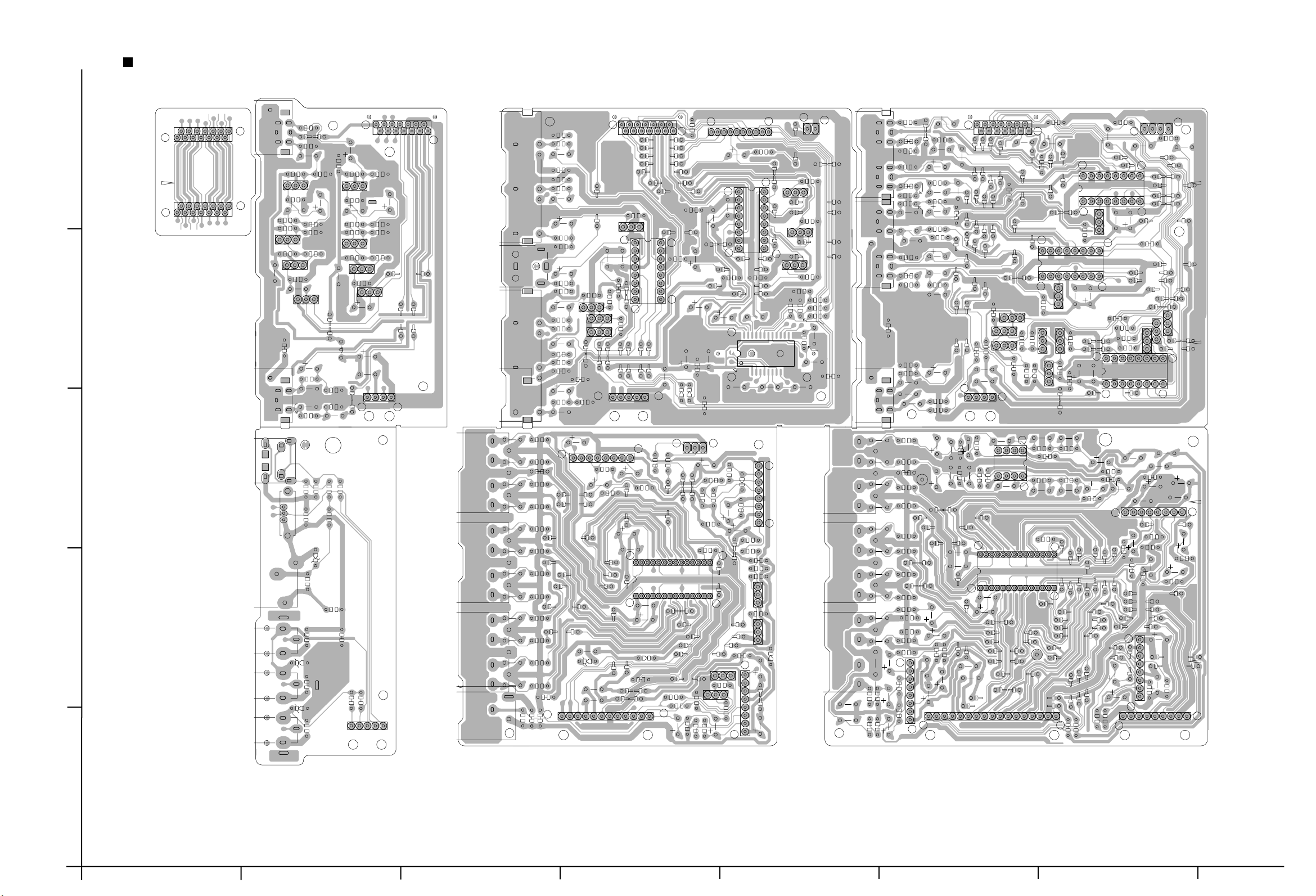
Input/output board
RX-7001PGD
C312
C262
R312
R345
C344
C257
IC242
1
9
R262
Q241
8
R261
16
C311
R335
C343
C253
C255
C258 C259
R260
IC243
R311
C316
C351
8
C337
R336
8
B312
R346
9
CN244
C317
R344
Q248
CN312
C353
R337
C338
C354
R253
1
C267
Q249
8
9
R313
R314
C318
C352
IC305
1
C339
R338
R339
C340
R340
R343
1
4
C254
8
9
Q247
C315
IC302
1
R1201
C205
R205
J203
12
R206
C367
C277
R211
C206
R203
C203
R212
R200
C201
R201
C202
Q201
Q202
R204
Q203
C207
R207
R208
C395
R210
C396
R202
R209
C204
R213
R399
R398
D394
R215
C208
R216
5
IC314
R389
R354
R353
R1217
R1225
CN250
Q1205
Q1207
C1209
R1222
CN252
J201
J202
R355
C377
C378
R356
J311 J312
J313
J314
C385
C384
C381
C380
C379
C382
C383
C386
C387
C388
C368
C367
B3135
R357
R358
R359
R360
R361
R362
R363
R364
R365
R366
C369
C1205
R1221
C1212
R1205
R1204
R1252
C1216
R1251
C1201
C1201
Q1203
R1218
C1210
R1219 R1220
Q1204
R1223 R1224
C1211
K1201
C1213
R1226
C1202
CN205
R1209
R1211
Q1201
R1213
J1201
R1208
C1206
C1208
R1206 R1207
5
CN243
4
J1202
R1202
Q1206
J1250
C1215
C1251
R1210
R1212
R1214
C1214
Q1200
Q1202
R1215
C1207
C1203
C1250
R1200
C1200
R1203
3
R1254
R1250
SW200
D1252
C1252
2
J1252
J1253
J1254
R1256
R1255
D1250
D1251
R1257
R1253
CN254
BK333
CN204
14
R214
Q200
18
C209
9
R217
C391
C362
1
28
CN200
C364
C363
D393
CN313
R390
1
8
IC201
R225
D200
1
31
R380
R379
IC311
C361
R387
R388
1
C373
C217
1
R384
CN416
R397
D201
C215
R392
R386
C211
R383
C370
R381R382
1
Q301
C374
C393
C212
C218
R391
15
Q302
C214
R394
C394
CN202
C210
16
C213
9
28
1
C219
R393
C392
14
R385
10
R218
1
IC202
C216
IC203
X200
D391
8
IC313
R395
1
R396
R370
R371
R372
Q370
R373
Q371
D392
1
C372
IC391
C371
8
2
1
CN206
R221
Q206
C220
R220
Q204
R219
C223
R222
R223
R224
C224
C221
L200
C222
14
J243
J301
J302
J303
R334
C334
R333
C333
Q205
8
C225
R241
B3137
J241
R240
R243
C243
B3138
C269
J242
R246
B3140
R245
R269
C251
C323
R301
C324
R302
C300
C325
B3130
R325
R326
C326
C327
R327
C328
R328
C329
C330
C331
R341
R342
C332
R352
C348
1
R350
C346
R348
R349
C345
R347
C246
C268
C240
C248
C242
R250
C241
C245
R242
R251
C244
R267
R266
C247
R244
R265
C250
C249
R252
C266
R268
C252
C271
C270
R247
R264
C301
R303
C303
C302
C304
C322
R329
R330
R331
C341
C342
R332
R351
C350
C347
C349
IC303
17
8
C265
C320
C264
R304
CN242
14
R263
Q246
Q245
R270
R271
4
C314
R316
1
CN240
C309
R305
IC301
C313
R306
C310
1
IC304
28
C319
C321
R315
CN311
Q250
C260
R259
1
C261
1
16
R249
1
IC241
16
C256
R248
Q240
R258
Q242
Q244
R256
R257
8
C305
R307
R308
1
C306
C358
PW301
Q243
R254
R255
C263
C307
R309
R310
C308
14
15
1
1
ABCD E F G
2-15
Page 43
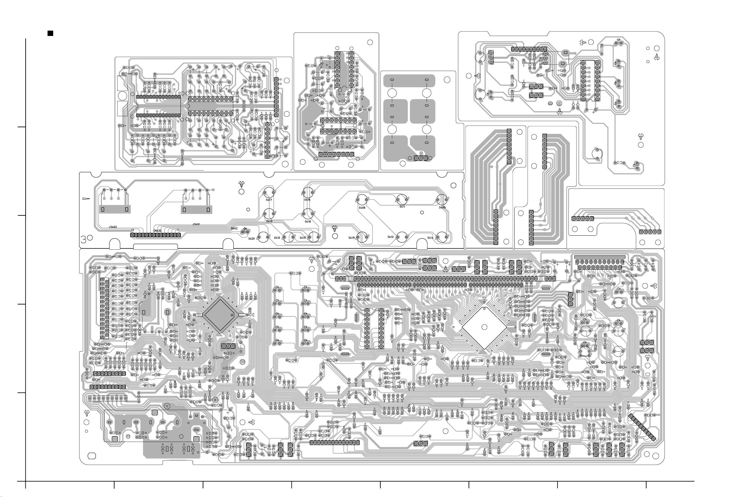
RX-7001PGD
FL display & system control boar
CN430
1
8
9
IC341
C1352
D1352
C1347
R1347
C1346
R1346
R1349
R1352
C1349
C1350
R1355
R1348
1
R1351
C1351
R1350
D1351
C1343
R1343
IC342
8
R1356
IC343
R1341
C1341
R1358
8
16
R1357
R1360
R1342
1
CN341
R1353 R1354
R1345
R883R884
C1342
R1344
C1355
R1359
C1356
1
R882
R881
CN881
C1458
C1484
R1482
C1456
R1457 R1458
C1452
C1451
R1484
R1483
R1454
R1453
R1462
R1461
C1483
R1451
R1452
R1481
R1486
R1485
IC453
CN451
R1488
C1488
R1487
C1487
R1476
C1465
R1475
C1466
C1474
C1472
IC452
C1471
C1473
R1478
R1480
R1464
R1466
5
D1451
R1471
IC451
C1461
R1463
C1463
D1452
R1472
R1465
C1462
R1479
C1464
R1477
D1453
R1473
C1475 C1476
C1477 C1478
C1479 C1480
C1481
C1469 C1470
C1460
C1459
R1459 R1460
C1453
C1454
C1455
C1457
C1482
S402
S401
D482
CN71
D483
R488R489
R487
10
IC404
R499
Q488Q489
19
CN62
18
R490
1018
IC405
C499
S400
D487
R485
D486
D484
D485
D481
4
18
CN63
Q457
Q458
D408
R416
D402
CN420
R492
CN73
D401
D400
R491
CN61
L491
3
C492
2
R482
R481
1
CN499
CN410
CN406
R420
CN450
C493
R421
R445
R494
R463
R461
R466
R459
R457
R455
R449
R447
R480
C472
R422
R419
R448
R443
R441
R442
R464
R462
R460
R465
R458
R456
R454
R452R453
R450R451
R433
R434
C471
C497
R435
R446
R436
R439
C473
R474
R437
JS400
R438
R429
BK499
R426
R412
R428
IC401
41
40
X401
C401
C405
C403
R410
C402
D489
Q401
C491
R440
R423
R424
D491
C498
C495
R403
C475
C476
R472
R471
J400
D404
C404
R425
D439
D438
D437
D436
R411
IC403
Q442
R404
D430
D431
D432
D433
D434D435
R405
R484
C408
R401
R402
DI400
C410
R406
R407
CN422
Q407
Q408
C412
IC402
R427R430
D421
Q412
D420
D419
Q459
R431
D414
R493
Q411
Q410
D413
D418
D412
Q413
Q409
RA402RA403
D410
D411
R483
Q414
R479
R476
R478
R475
IC400
RA401
C494
Q415
Q416
D493
R400
R498
C413
R477
R408
R497
CN72
C480
C414
R495R496
C478
R418
C477
C409
C479
Q402
R417
D417
C400
Q403
C407
D416
D459
CN412
R468
D440
X400
D458
S404
S452
S403
S451
D415
C406
D405
R414
Q404
D407
D409
R415
D406
S407
D457
S453
S405
S406
S454
Q405Q406
2-16
HABC DEFG
Page 44

Power AMP. & power supply board
RX-7001PGD
CN954
C960
PW30
FW961
FW963
R953
R951
D951
R955
C954
F1
C2
C955
C951
C956
R73
C73
C968C969 C970
Q74
D75
C74
CN402
PW19
PW26
PW18
PW17
PW20
J91
PW41
C54
R54
C94
R92
R74
C56
C53
D55
D56
C55
Q52
C93
R91
Q51
C3
C71
D73
D72
Q61
R51
R52
PW28
EP2
D74
Q71
C70
C68
C69
C52
D54
D52
R53
Q53
D57
RY1
R70
C67
R68
R69
D65
C72
R72
R66
D71
C66
R55
D53
C51
D51
PW29
PW31
C1
C65
PW32
FC4
CN52
CN51
D62
FC3
F2
CN53
C62
C63
D64
D61
D63
R67
C61
PW40
EP51
TH71
FW51
R957
C957
C959
CN951
B2321
R958
C958
ST951
B2173
B2174
R954
R952
B2175
5
C961
C962
R962
R964
R963
R961
C963
J961
R966
R965
B2129
C964
B2128
R968
R970
C967
R969
C966
R967
C965
B2322
D952
B2407
C953
4
PW16
PW23PW22
FC5
F4
3
VS1
PW25
FC6
PW21
PW24
PW27
PW15
PW14
PW13
PW12
PW11
PW10
TA1
TA2
R1
EP1
S1
R717
Q705
RY62
RY63
C717
R705
B2231
B2232
R727
R725
R733
R709
FC64
B2168
Q709
C711
R731
Q701 Q702Q703 Q704
C705 C706
D701 D702
CN705
2A-125V
F61
B2169
R721
R719
Q711 Q712
R723
C713
C715
R707
R729
D703
Q710
Q707
Q708
R726
C712
R732
R734
R710
F62
FC63
FC62
2A-125V
3
CN811
1
R61
R728
C718
R706
FC61
Q706
R718
R720
R722
R724
C714
C716
R708
D704
R730
R62
7
43
D66
CN55 CN56
1
B2102
D68 D67
R1826
C1852
R1852
R1824
C1892
R1810
R1896
PW42
R1872
R1892
Q1892
R1834
Q1872
R1898
R1876
R1856
R1882
L1862
Q1832
TH832
R1894
R1864
R1878
R1832
C806
Q1874
C1862
C1864
R1874
C1854
D1874
FW901
L1864
R1854
C1842
Q1854
C1816
R1843
R1822
R1842
R1821
R1829
CN803
R1827
C1813
Q1853
C1815
D1805
Q1805
C1811
R1825
R1835
C1841
C1853
R1853
CN702
C1843
R1893
R1823
D1873
C1861
C1863
C1817
R1873
D1891
R1897
Q1873
R1863
R1833
Q1831
R1877
R1855
CN952
TH831
L1861
L1863
R1875
R1805
R1831
R1871
R1861
C1891
R1851
Q1871
Q1891
R1891
C1851
D1871
R1895
L1762
C1807
R1809
R1817
C1803
R1813
Q1851
R1803
C1809
Q1803
C1801
C1805
C1705
Q1801
R1801
R1712
R1702
D1801
C1712
C1703
C1704
C1702
R1701
D1701
D1772
R1733
R1711
C1701
C1714
R1752
R1793
R1703
R1794
CN701
Q1731
C1752
R1731
Q1771
L1761
R1753
R1762
R1773
R1791
R1771
C1761
C1762
R1792
D1791
R1732
Q1772
R1772
Q1702Q1701
C1791
Q1791
R1761
CN703
R1774
TH731
C1715
R1723 R1724
R1722
R1705
C1751
D1702
R1751
Q1751Q1752
C1743
D1771
R1725
C1711
R1742
C1741
Q1703
R1743
C1742
C1713
R1721
2-17
2
Q1852
ST981
D981
R981
1
R983
C991
RY981
R985
FW962
C986
C985
C981
B2324
R988
C984
C988
C993
CN953
C990
C989
C987
R987
B2418
B2423
RY982
C992
C983
D982
R982
R984
C1812
R1812
C1806
C1808
Q1806
R1804
C1802
R1802
D1802
Q1802
C1814
C1804
C1810
R1814
D1872
R1806
R1828
R1830
Q1804
C1818
D1892
R1836
ABCD E F G
Page 45

5
Tuner board
1
AT101
C101
B189
C103
B195
C105
C107
C111
C112
L112
C117
C118
C121
C122
C123
C126
C128
C129
C130
C133
C135
C136
C137
C139
C140
C141
C143
C144
C146
C147
C148
C149
C150
C165
C157
C158
C161
C162
C163
C164
C168
C184
C185
C186
C191
C192
C193
B111
C195
C196
C197
C199
CF101
CF102
CF103
B173
CN112
D121
D123
D129
D131
CN111
B123
IC102
IC121
B175
L111
C138
Q102
Q103
Q111
Q112
Q113
Q121
R103
R104
R105
R106
R107
R108
R109
R111
R112
R114
R115
R119
R122
R124
R126
R127
R128
R129
R130
R132
R133
R134
R140
R141
R142
R143
R144
R145
R146
R147
R150
R157
R158
R161
R162
D124
D125
R182
R183
R184
R191
B174
B172
T111
T142
X121
X191
B171
B199
B104
B198
B197
B105
B196
B180
B124
B134
B103
B133
B188
C134
D127
B192
B193
B186
B190
B194
B182
B132
B122
B121
B181
B151
B187
B135
B178
B131
B106
B102
D126
B176
RF101
R193
B177
B191
IC191
R192
C194
B112
B113
R194
B183
C113
E
B
BE
16
151
30
[DOM]
E
[DOM]
B
[DOM]
[DOM]
E
B
EB
T2D
C981
C983
C984
C985
C986
C987
C988
C989
C990
C991
C992
C993
D981
D982
R993
R981
R982
R983
R984
R985
R987
R988
B2423
B2324
B2418
R941
RY981
RY982
R943
R942
R944
R945
R946
ST981
R991
R992
R999
D806
D805
D807
CN953
D808
D809
C815
FW962
C814
C813
Q806
Q805
Q807
Q811
Q809
Q810
Q808
B2421
B2420
B2425
B2426
T1A
SP terminal board
4
3
2
DSP board
RX-7001PGD
Reverse side
Forward side
1
2-18
HABC DEFG
Page 46
PARTS LIST
[ RX-7001PGD ]
* All printed circuit boards and its assemblies are not available as service parts.
RX-7001PGD
Area suffix
A ------------------------- Australia
UF --------------------------- China
US --------------------- Singapore
- Contents -
Exploded view of general assembly and parts list
Electrical parts list
Packing materials and accessories parts list
3-3
3-5
3-32
3-1
Page 47

RX-7001PGD
-MEMO-
3-2
Page 48

28
26
24
38
38
56
38
38
DSP board
S-Video
V-Audio
Audio
Pre AMP.
SEA board
Tuner
25
37
34
80
61
Exploded view of general assembly and parts list
Block No.
48
49
43
M
RX-7001PGD
M
1
M
43
43
52
83
53
42
5
43
V-Audio
board
38
80
80
75
35
25
44
Audio
board
31
30
Pre AMP.
board
31
25
SEA board
Tuner
board
38
32
38
29
37
Center tone
board
34
38
Rear / Center
AMP.board
38
33
32
50
43
89
90
82
38
86
56
Ver.US only
41
20
41
Vol.selector
board
40
41
84
SP.terminal
board
41
38
24
19
57
38
24
38
25
38
DSP board
60
81
25
24
S-Video
board
61
Main board
38
AC supply board
Video
board
38
18
43
88
4
Ver.UF only
3
2
33
43
87
53
53
25
53
38
18
39
18
18
1
Vol.Accessory
3
54
4
23
34
15
9
13
36
51
7
18
7
18
11
32
7
7
8
21
Front board
16
7
14
28
26
22
10
17
Operation switch
board
2
6
7
5
55
3-3
22
1
26
28
26
22
22
28
ABCD E F G
Page 49

RX-7001PGD
)
A
)
)
A
A
A
)
Parts list
Item Parts number Parts name Area
A
10 LV30069-003A P.BUTTON ASSY 1 SPK
11 LV30071-001A P.BUTTON ASSY 1 DOLBY
13 E308744-003 REMOTE LENS 1
14 LV30073-001A SOURCE INDICATO 1
15 QUQB12-2120CJ FLAT WIRE UF1
16 QUQC12-2722CJ FFC WIRE 1
17 QYSDSG3008N T.SCREW 5 FRONT D
18 QYSBSG3008E T.SCREW 8
19 LV10019-002A CHASSIS BASE 1
20 EXO150010H09S11 FELT SPACER 1 FOR C.BASE
21 LV10020-001A FRONT BRACKET 1
22 QYSDSG3008E T.SCREW 7 C.B-F.B
23 LE40139-001A H.P. BKT 1
24 E68587-223SM CB BKT 3
25 QYSBST3006E T.SCREW 7
26 QZF6018-001 FOOT 4
28 QYSBST3010Z T.SCREW 4 FOOT
29 LV30075-203A HEAT SINK 1
30 2SC3856/PY/-F1 TRANSISTOR
A
31 2SA1492/PY/-F1 TRANSISTOR
32 2SD2390LD/OPY/ TRANSISTOR 50
A
33 2SB1560LD/OPY/ TRANSISTOR 51
A
34 E73525-003SS SCREW 10 TR
35 LV41603-001A LEAF SPRING 1
36 LV20035-001A H.S BRACKET(R
37 LV20036-001A H.S BRACKET(L
38 QYSBSGG3008E T.SCREW 17
39 VKZ4150-001 SPECIAL NUT 1
40 QQT0301-001 POWER TRANS.
A
41 QYSDSTL4008E SPECIAL SCREW 4 P.TRANS
42 LV10021-066A REAR PANEL US1
43 QYSBSGY3008E SPECIAL SCREW 32 R.P-C.BASE
44 E302321-001 FASTNER 1 SPACER
( General assembly )
Q'ty Description
1 LV10018-037A FRONT PANEL A1
LV10018-034A FRONT PANEL 1
2 VJD5429-001SS JVC MARK 1
3 LV20031-022A LENS 1
4 LV20032-010A FRONT ESC 1
5 LV20034-004A PUSH BUTTON 1
6 LV40099-001A INDICATOR 1
7 QYSDSF2608Z SCREW 18
8 LV30068-005A P.BUTTON(POWER
9 FSJD4001-002 INDICATOR 1 POWER
QUQC12-2120CJ FFC WIRE 1
QUQB12-2722CJ FLAT WIRE UF1
E73525-003 SCREW UF10
LV10021-069A REAR PANEL A1
LV10021-070A REAR PANEL UF1
1
2
2
3
3
TR
1
1
1
Block No. M1MM
US,UF
A,US
A,US
Parts list
Item Parts number Parts name Area
A
48 E409257-001 GND TERMINAL 1
49 QMPR100-200-JC POWER CORD UF
50 QHS3771-108 CORD STOPPER
51 LV30076-001A PROTECTOR 1
52 LV20038-003A/S/ TOP COVER 1
53 E406308-004 SPECIAL SCREW 4
54 LV30480-006A VOL KNOB ASS'Y 1
55 LV30481-003A JOG KNOB ASS'Y 2
56 QMF51E2-6R3-J1 FUSE US
A
A
57 QMF51E2-2R0-J1 FUSE
A
60 E310243-002 PLASTIC RIVET 1
61 LV41240-002A BRACKET 1
75 QYSBSG3008E T.SCREW 1 TR(LEAF
80 QYSBSG3008E T.SCREW 3
81 QYSBSG3008E T.SCREW 1
82 QYSBSGY3008E SPECIAL SCREW US2 VOL SEL
83 LV30077-002A PROTECT SHEET 1
84 QMF51E2-R10-J1 FUSE
A
85 QMF51E2-3R15-J1 FUSE US
A
86 E307572-001 FASTENER 1
87 E409396-001 CAUTION LABEL 1
88 LV30092-095A UF LABEL UF1
89 LV41768-001A CCIB LABEL UF1
90 E409372-001 CCEE LABEL UF1
( General assembly )
Q'ty Description
1
QMPG040-244-JD POWER CORD A
QMP3900-200L POWER CORD US
QMF51E2-3R15-J1 FUSE
1
1
1
1 F1
1 F1
2
1 F2
1 F4
Block No. M1MM
A,UF
3-4
Page 50

Electrical parts list
Electrical parts list
Item
A
C 701 QETN1HM-106Z E CAPACITOR 10MF 20% 50V
C 702 QETN1HM-106Z E CAPACITOR 10MF 20% 50V
C 703 QCS11HJ-101 C CAPACITOR 100PF 5% 50V
C 704 QCS11HJ-101 C CAPACITOR 100PF 5% 50V
C 707 QETN1CM-107Z E CAPACITOR 100MF 20% 16V
C 708 QETN1CM-107Z E CAPACITOR 100MF 20% 16V
C 709 QCS11HJ-100 C CAPACITOR 10PF 5% 50V
C 710 QCS11HJ-100 C CAPACITOR 10PF 5% 50V
C 719 QFLC1HJ-472Z M CAPACITOR 4700PF 5% 50V
C 720 QFLC1HJ-472Z M CAPACITOR 4700PF 5% 50V
C 741 QETN2AM-476Z E CAPACITOR 47MF 20% 100V
C 742 QETN2AM-476Z E CAPACITOR 47MF 20% 100V
C 743 QETN1EM-476Z E CAPACITOR 47MF 20% 25V
C 745 QEKC1HM-226Z E CAPACITOR 22MF 20% 50V
C 751 QCS32HJ-470Z C CAPACITOR 47PF 5% 500V
C 752 QCS32HJ-470Z C CAPACITOR 47PF 5% 500V
C 753 QCS32HJ-470Z C CAPACITOR 47PF 5% 500V
C 754 QCS32HJ-470Z C CAPACITOR 47PF 5% 500V
C 791 QFLC1HJ-473Z M CAPACITOR .047MF 5% 50V
C 792 QFLC1HJ-473Z M CAPACITOR .047MF 5% 50V
C 793 QFLC1HJ-473Z M CAPACITOR .047MF 5% 50V
C 794 QFLC1HJ-473Z M CAPACITOR .047MF 5% 50V
C 801 QFN82CK-104 M CAPACITOR .10MF 10% 160V
C 802 QFN82CK-104 M CAPACITOR .10MF 10% 160V
C 805 QFN82CK-104 M CAPACITOR .10MF 10% 160V
C 807 QEZ0355-109 E CAPACITER
A
C 808 QEZ0355-109 E CAPACITER
A
C 811 QETN1HM-475Z E CAPACITOR 4.7MF 20% 50V
C 812 QETN1HM-475Z E CAPACITOR 4.7MF 20% 50V
C 821 QEHR1EM-107Z E CAPACITOR 100MF 20% 25V
C 822 QCF31HZ-472Z C CAPACITOR 4700PF +80:-20%
C 831 QEHR1EM-107Z E CAPACITOR 100MF 20% 25V
C 832 QCF31HZ-472Z C CAPACITOR 4700PF +80:-20%
C 841 QEHR1EM-107Z E CAPACITOR 100MF 20% 25V
C 842 QCF31HZ-472Z C CAPACITOR 4700PF +80:-20%
C 851 QEHR1EM-107Z E CAPACITOR 100MF 20% 25V
C 852 QCF31HZ-472Z C CAPACITOR 4700PF +80:-20%
C 861 QEHR1EM-107Z E CAPACITOR 100MF 20% 25V
C 862 QCF31HZ-472Z C CAPACITOR 4700PF +80:-20%
C 871 QEHR1EM-107Z E CAPACITOR 100MF 20% 25V
C 872 QCF31HZ-472Z C CAPACITOR 4700PF +80:-20%
C 875 QETN0JM-477Z E CAPACITOR 470MF 20% 6.3V
C 903 QER61HM-226Z E CAPACITOR 22MF 20% 50V
C 904 QCF11HZ-103 C CAPACITOR .010MF +80:-20%
C 905 QCB31HK-102Z C CAPACITOR 1000PF 10% 50V
C 906 QETN1EM-476Z E CAPACITOR 47MF 20% 25V
C 920 QETN1HM-226Z E CAPACITOR 22MF 20% 50V
C 921 QER61CM-107Z E CAPACITOR 100MF 20% 16V
C 935 QFLC1HJ-223Z M CAPACITOR .022MF 5% 50V
C 936 QFLC1HJ-223Z M CAPACITOR .022MF 5% 50V
C 937 QFLC1HJ-223Z M CAPACITOR .022MF 5% 50V
C 938 QFLC1HJ-223Z M CAPACITOR .022MF 5% 50V
C 939 QFLC1HJ-392Z M CAPACITOR 3900PF 5% 50V
C 940 QFLC1HJ-392Z M CAPACITOR 3900PF 5% 50V
C 941 QCS11HJ-221 C CAPACITOR 220PF 5% 50V
C 942 QCS11HJ-221 C CAPACITOR 220PF 5% 50V
C 943 QCS11HJ-221 C CAPACITOR 220PF 5% 50V
C 944 QCS11HJ-221 C CAPACITOR 220PF 5% 50V
CN 81 QGB2510J1-08 CONNEC T O R
CN 82 QGB2510J1-08 CONNEC T O R
CN 83 QGB2510J1-05 CONNEC T O R
CN101 QGB2501J1-12 CONNECTO R
CN201 QGB2510J1-05 CONNECTO R
Parts number Parts name Area
( Main board ) Ver.A/US
10000MF
10000MF
Block No. 01
Remarks
Item
A
CN241 QGB2510J1-04 CONNECTOR
CN255 QGB2510J1-05 CONNECTOR
CN301 QGB2510J1-17 CONNECTOR
CN302 QGB2510J1-09 CONNECTOR
CN303 QGB2510J1-12 CONNECTOR
CN400 QGF1205C1-27 CONNECTOR
CN452 QGB2510J1-09 CONNECTOR
CN501 QGB1214J3-18S CONNECTOR
CN601 QGB1214J3-12S CONNECTOR
CN704 QGA3901C1-08 8P CONNECTOR
CN706 QGB2510J1-12 CONNECTOR
CN711 QGA2501C1-02 2P CONNECTOR
CN712 QGA2501C1-03 3P CONNECTOR
CN801 QJK012-032803 SKT WIRE ASSY
CN821 QGD2501C1-05Z SOCKET
CN901 QGD2501C1-03Z SOCKET
CN931 QGD2501C1-04Z SOCKET
CN932 QGD2501C1-03Z SOCKET
CN961 QGD2501C1-05Z SOCKET
C1301 QETN1EM-476Z E CAPACITOR 47MF 20% 25V
C1302 QETN1EM-476Z E CAPACITOR 47MF 20% 25V
C1303 QDVB1EZ-223Y C CAPACITOR
C1304 QDVB1EZ-223Y C CAPACITOR
C1309 Q F V J 1 HJ-224Z MF CAPACITOR .22MF 5% 50V
C1310 Q F V J 1 HJ-224Z MF CAPACITOR .22MF 5% 50V
C1311 Q ET N1 H M-475Z E CAPACITOR 4.7MF 20% 50V
C1312 Q ET N1 H M-475Z E CAPACITOR 4.7MF 20% 50V
C1313 Q ET N1 H M-475Z E CAPACITOR 4.7MF 20% 50V
C1314 Q ET N1 H M-475Z E CAPACITOR 4.7MF 20% 50V
C1315 QETN1EM-476Z E CAPACITOR 47MF 20% 25V
C1316 QETN1EM-476Z E CAPACITOR 47MF 20% 25V
C1317 QDVB1EZ-223Y C CAPACITOR
C1318 QDVB1EZ-223Y C CAPACITOR
C1319 QCBB1HK-221Y C CAPACITOR 220PF 10% 50V
C1321 Q ET N1 H M-475Z E CAPACITOR 4.7MF 20% 50V
C1322 Q ET N1 H M-475Z E CAPACITOR 4.7MF 20% 50V
C1323 Q ET N1 H M-475Z E CAPACITOR 4.7MF 20% 50V
C1324 Q ET N1 H M-475Z E CAPACITOR 4.7MF 20% 50V
C1325 QETN1EM-476Z E CAPACITOR 47MF 20% 25V
C1326 QETN1EM-476Z E CAPACITOR 47MF 20% 25V
C1327 QDVB1EZ-223Y C CAPACITOR
C1328 QDVB1EZ-223Y C CAPACITOR
C1329 QCBB1HK-221Y C CAPACITOR 220PF 10% 50V
C1331 Q ET N1 H M-475Z E CAPACITOR 4.7MF 20% 50V
C1332 Q ET N1 H M-475Z E CAPACITOR 4.7MF 20% 50V
C1333 Q ET N1 H M-475Z E CAPACITOR 4.7MF 20% 50V
C1334 Q ET N1 H M-475Z E CAPACITOR 4.7MF 20% 50V
C1335 QETN1EM-476Z E CAPACITOR 47MF 20% 25V
C1336 QETN1EM-476Z E CAPACITOR 47MF 20% 25V
C1337 QDVB1EZ-223Y C CAPACITOR
C1338 QDVB1EZ-223Y C CAPACITOR
C1339 QCBB1HK-221Y C CAPACITOR 220PF 10% 50V
C1361 Q ET N1 H M-105Z E CAPACITOR 1.0MF 20% 50V
C1362 Q ET N1 H M-105Z E CAPACITOR 1.0MF 20% 50V
C1369 QETN1EM-476Z E CAPACITOR 47MF 20% 25V
C1370 QETN1EM-476Z E CAPACITOR 47MF 20% 25V
C1371 Q ET N1 H M-105Z E CAPACITOR 1.0MF 20% 50V
C1372 Q ET N1 H M-105Z E CAPACITOR 1.0MF 20% 50V
C1379 QETN1EM-476Z E CAPACITOR 47MF 20% 25V
C1380 QETN1EM-476Z E CAPACITOR 47MF 20% 25V
C1381 Q ET N1 H M-105Z E CAPACITOR 1.0MF 20% 50V
C1382 Q ET N1 H M-105Z E CAPACITOR 1.0MF 20% 50V
C1389 QETN1EM-476Z E CAPACITOR 47MF 20% 25V
Parts number Parts name Area
RX-7001PGD
Remarks
3-5
Page 51

RX-7001PGD
Q
Q
Q
Q
Q
Q
Q
Q
Q
Q
Q
Q
Q
Q
Q
Q
Q
Q
Q
Q
Q
Q
Q
Q
Q
Q
Q
Q
Q
Q
Q
Q
Q
Q
Q
Q
Q
Q
Q
Q
Electrical parts list
Item
A
C1390 QETN1EM-476Z E CAPACITOR 47MF 20% 25V
C1391 Q F L C 1 H J-562Z M CAPACITOR 5600PF 5% 50V
C1392 Q F L C 1 H J-562Z M CAPACITOR 5600PF 5% 50V
C1405 Q ET N1 C M-226Z E CAPACITOR 22MF 20% 16V
C1406 QENC1HM-106Z NP E CAPACITOR 10MF 20% 50V
D 743 MTZJ18C-T2 Z DIODE
A
D 751 1SS133-T2 SI DIODE
D 752 MTZJ20C-T2 Z DIODE
A
D 771 1SS133-T2 SI DIODE
D 772 1SS133-T2 SI DIODE
D 773 1SS133-T2 SI DIODE
D 774 1SS133-T2 SI DIODE
D 801 30DF2-FC DIODE
A
D 802 30DF2-FC DIODE
A
D 803 30DF2-FC DIODE
A
D 804 30DF2-FC DIODE
A
D 811 1SS133-T2 SI DIODE
D 814 MTZJ5.1C-T2 ZENER DIODE
A
D 821 MTZJ6.8C-T2 Z DIODE
A
D 822 1SS133-T2 SI DIODE
D 831 MTZJ6.2C-T2 Z DIODE
A
D 832 1SS133-T2 SI DIODE
D 841 MTZJ6.2C-T2 Z DIODE
A
D 842 1SS133-T2 SI DIODE
D 851 MTZJ15C-T2 Z DIODE
A
D 852 1SS133-T2 SI DIODE
D 861 MTZJ15C-T2 Z DIODE
A
D 862 1SS133-T2 SI DIODE
D 871 MTZJ10C-T2 Z DIODE
A
D 872 1SS133-T2 SI DIODE
D 901 1SS133-T2 SI DIODE
D 902 1SS133-T2 SI DIODE
D 921 MTZJ4.7B-T2 Z DIODE
A
D 931 1SS133-T2 SI DIODE
D 932 1SS133-T2 SI DIODE
D 933 1SS133-T2 SI DIODE
D 934 1SS133-T2 SI DIODE
D 953 1SS133-T2 SI DIODE
D 954 1SS133-T2 SI DIODE
D 971 1SS133-T2 SI DIODE
D 972 1SS133-T2 SI DIODE
D1435 1SS133-T2 SI DIODE
D1436 1SS133-T2 SI DIODE
D1437 M TZJ4.7B-T2 Z DIODE
A
D1438 1SS133-T2 SI DIODE
EP801 QNZ0136-001Z EARTH PLATE
FL391 QQR0590-001 FILTER
FL392 QQR0590-001 FILTER
FW811 QUM133-10Z4Z4 PARA RIBON WIRE
FW821 QUM135-08DGZ4 PARA RIBON WIRE
FW881 QUM133-26DGZ4 PARA RIBON WIRE
FW931 QUM137-16DGZ4 PARA RIBON WIRE
HL331 VYH7653-002 IC HOLDER
HL332 VYH7653-002 IC HOLDER
HL333 VYH7653-002 IC HOLDER
HS851 E70306-001 HEAT SINK
HS861 E70306-001 HEAT SINK
HS871 E70306-001 HEAT SINK
IC321 TC9162AN IC
IC331 TC9459F IC
IC332 TC9459F IC
IC333 TC9459F IC
IC361 NJM4580L IC
Parts number Parts name Area
( Main board ) Ver.A/US
Block No. 01
Remarks
Item
A
IC362 BA15218N IC
IC363 BA15218N IC
IC901 TA7317P IC
L 791 QQLZ003-1R0 INDUCTOR
L 792 QQLZ003-1R0 INDUCTOR
A
A
A
A
A
A
A
A
A
A
A
A
A
A
A
R 701 QRE141J-222Y C RESISTOR 2.2K 5% 1/4W
R 702 QRE141J-222Y C RESISTOR 2.2K 5% 1/4W
R 703 QRE141J-104Y C RESISTOR 100K 5% 1/4W
R 704 QRE141J-104Y C RESISTOR 100K 5% 1/4W
R 711 QRE141J-621Y C RESISTOR 620 5% 1/4W
R 712 QRE141J-621Y C RESISTOR 620 5% 1/4W
R 713 QRE141J-183Y C RESISTOR 18K 5% 1/4W
R 714 QRE141J-183Y C RESISTOR 18K 5% 1/4W
R 715 QRE141J-823Y C RESISTOR 82K 5% 1/4W
R 716 QRE141J-823Y C RESISTOR 82K 5% 1/4W
R 735 QRZ9005-100X F RESISTOR
A
R 736 QRJ146J-102X UNF C RESISTORA1.0K 5% 1/4W
R 742 QRJ146J-120X UNF C RESISTORA12 5% 1/4W
R 743 QRL022J-562 UNF OMF RES
A
R 747 QRE141J-223Y C RESISTOR 22K 5% 1/4W
R 748 QRE141J-473Y C RESISTOR 47K 5% 1/4W
R 751 QRJ146J-100X UNF C RESISTORA10 5% 1/4W
R 752 QRJ146J-100X UNF C RESISTORA10 5% 1/4W
Parts number Parts name Area
743 2SA965/OY/-T TRANSISTOR
744 2SC2240/GL/-T TRANSISTOR
751 2SC2389S/SE/-T TRANSISTOR
752 2SC2389S/SE/-T TRANSISTOR
753 2SA1038S/S/-T TRANSISTOR
754 2SA1038S/S/-T TRANSISTOR
755 2SD669A/BC/ TRANSISTOR
756 2SD669A/BC/ TRANSISTOR
757 2SB649A/BC/ TRANSISTOR
758 2SB649A/BC/ TRANSISTOR
771 2SC2389S/SE/-T TRANSISTOR
772 2SC2389S/SE/-T TRANSISTOR
773 2SA1038S/SE/-T TRANSISTOR
774 2SA1038S/SE/-T TRANSISTOR
781 2SD637/QR/ TRANSISTOR
782 2SD637/QR/ TRANSISTOR
801 KRC109M-T D TRANSISTOR
814 2SD2061/EF/ TRANSISTOR
821 2SD2061/EF/ TRANSISTOR
831 2SD2061/EF/ TRANSISTOR
841 2SD2061/EF/ TRANSISTOR
851 2SD2061/EF/ TRANSISTOR
861 2SB1187/EF/ TRANSISTOR
871 2SD2061/EF/ TRANSISTOR
901 2SC2389S/SE/-T TRANSISTOR
902 2SC2389S/SE/-T TRANSISTOR
903 2SA1038S/SE/-T TRANSISTOR
921 KTC3199/GL/-T TRANSISTOR
931 KRC105M-T D TRANSISTOR
932 KRC105M-T D TRANSISTOR
951 KRC105M-T D TRANSISTOR
952 KRC105M-T D TRANSISTOR
1401 2SC2878/AB/-T TRANSISTOR
1402 2SC2878/AB/-T TRANSISTOR
1405 KRA104M-T D TRANSISTOR
1411 2SC2878/AB/-T TRANSISTOR
1421 2SC2878/AB/-T TRANSISTOR
1422 2SC2878/AB/-T TRANSISTOR
1435 2SA933S/RS/-T TRANSISTOR
1438 KRA104M-T D TRANSISTOR
10 1/0W
5.6K 5% 1/2W
Remarks
3-6
Page 52

RX-7001PGD
Electrical parts list
Item
A
R 753 QRJ146J-100X UNF C RESISTORA10 5% 1/4W
R 754 QRJ146J-100X UNF C RESISTORA10 5% 1/4W
R 759 QRJ146J-272X UNF C RESISTORA2.7K 5% 1/4W
R 760 QRJ146J-272X UNF C RESISTORA2.7K 5% 1/4W
R 761 QRJ146J-4R7X UNF C RESISTORA4.7 5% 1/4W
R 762 QRJ146J-4R7X UNF C RESISTORA4.7 5% 1/4W
R 763 QRJ146J-4R7X UNF C RESISTORA4.7 5% 1/4W
R 764 QRJ146J-4R7X UNF C RESISTORA4.7 5% 1/4W
R 765 QRJ146J-120X UNF C RESISTORA12 5% 1/4W
R 766 QRJ146J-120X UNF C RESISTORA12 5% 1/4W
R 767 QRJ146J-120X UNF C RESISTORA12 5% 1/4W
R 768 QRJ146J-120X UNF C RESISTORA12 5% 1/4W
R 769 QRJ146J-271X UNF C RESISTORA270 5% 1/4W
R 770 QRJ146J-271X UNF C RESISTORA270 5% 1/4W
R 771 QRE141J-391Y C RESISTOR 390 5% 1/4W
R 772 QRE141J-391Y C RESISTOR 390 5% 1/4W
R 773 QRE141J-391Y C RESISTOR 390 5% 1/4W
R 774 QRE141J-391Y C RESISTOR 390 5% 1/4W
R 775 QRE141J-201Y C RESISTOR 200 5% 1/4W
R 776 QRE141J-201Y C RESISTOR 200 5% 1/4W
R 777 QRE141J-201Y C RESISTOR 200 5% 1/4W
R 778 QRE141J-201Y C RESISTOR 200 5% 1/4W
R 779 QRZ0196-R22 EMIT RESISTOR
A
R 780 QRZ0196-R22 EMIT RESISTOR
A
R 781 QRE141J-391Y C RESISTOR 390 5% 1/4W
R 782 QRE141J-391Y C RESISTOR 390 5% 1/4W
R 783 QRE141J-471Y C RESISTOR 470 5% 1/4W
R 784 QRE141J-471Y C RESISTOR 470 5% 1/4W
R 785 QRE141J-102Y C RESISTOR 1.0K 5% 1/4W
R 786 QRE141J-102Y C RESISTOR 1.0K 5% 1/4W
R 789 QRE141J-102Y C RESISTOR 1.0K 5% 1/4W
R 790 QRE141J-102Y C RESISTOR 1.0K 5% 1/4W
R 791 QRJ125J-330 UNF C RESISTORA33 5% 1/2W
R 792 QRJ125J-330 UNF C RESISTORA33 5% 1/2W
R 793 QRL022J-100 UNF OMF RES
A
R 794 QRL022J-100 UNF OMF RES
A
R 801 QRE141J-104Y C RESISTOR 100K 5% 1/4W
R 802 QRE141J-104Y C RESISTOR 100K 5% 1/4W
R 811 QRE141J-223Y C RESISTOR 22K 5% 1/4W
R 812 QRE141J-682Y C RESISTOR 6.8K 5% 1/4W
R 813 QRE141J-472Y C RESISTOR 4.7K 5% 1/4W
R 817 QRJ146J-392X UNF C RESISTORA3.9K 5% 1/4W
R 823 QRJ146J-122X UNF C RESISTORA1.2K 5% 1/4W
R 833 QRJ146J-122X UNF C RESISTORA1.2K 5% 1/4W
R 843 QRJ146J-122X UNF C RESISTORA1.2K 5% 1/4W
R 851 QRK126J-120X UNF C RESISTORA12 5% 1/2W
R 853 QRJ146J-222X UNF C RESISTORA2.2K 5% 1/4W
R 861 QRK126J-120X UNF C RESISTORA12 5% 1/2W
R 863 QRJ146J-222X UNF C RESISTORA2.2K 5% 1/4W
R 871 QRJ146J-120X UNF C RESISTORA12 5% 1/4W
R 873 QRJ146J-332X UNF C RESISTORA3.3K 5% 1/4W
R 875 QRZ9005-220X F RESISTOR
A
R 901 QRE141J-272Y C RESISTOR 2.7K 5% 1/4W
R 902 QRE141J-272Y C RESISTOR 2.7K 5% 1/4W
R 903 QRE141J-153Y C RESISTOR 15K 5% 1/4W
R 904 QRE141J-153Y C RESISTOR 15K 5% 1/4W
R 905 QRE141J-123Y C RESISTOR 12K 5% 1/4W
R 906 QRE141J-123Y C RESISTOR 12K 5% 1/4W
R 909 QRE141J-103Y C RESISTOR 10K 5% 1/4W
R 911 QRE141J-332Y C RESISTOR 3.3K 5% 1/4W
R 912 QRE141J-473Y C RESISTOR 47K 5% 1/4W
R 913 QRE141J-104Y C RESISTOR 100K 5% 1/4W
R 914 QRE141J-823Y C RESISTOR 82K 5% 1/4W
Parts number Parts name Area
( Main board ) Ver.A/US
1/1W
1/1W
10 5% 1/2W
10 5% 1/2W
22 1/0W
Block No. 01
Remarks
Item
A
R 915 QRE141J-823Y C RESISTOR 82K 5% 1/4W
R 916 QRE141J-563Y C RESISTOR 56K 5% 1/4W
R 917 QRE141J-683Y C RESISTOR 68K 5% 1/4W
R 918 QRE141J-822Y C RESISTOR 8.2K 5% 1/4W
R 919 QRE141J-822Y C RESISTOR 8.2K 5% 1/4W
R 920 QRE141J-224Y C RESISTOR 220K 5% 1/4W
R 921 QRE141J-473Y C RESISTOR 47K 5% 1/4W
R 922 QRE141J-222Y C RESISTOR 2.2K 5% 1/4W
R 931 QRJ146J-101X UNF C RESISTORA100 5% 1/4W
R 932 QRJ146J-101X UNF C RESISTORA100 5% 1/4W
R 935 QRZ9005-100X F RESISTOR
A
R 936 QRZ9005-100X F RESISTOR
A
R 937 QRZ9005-100X F RESISTOR
A
R 938 QRZ9005-100X F RESISTOR
A
R 971 QRJ146J-101X UNF C RESISTORA100 5% 1/4W
R 988 QRJ146J-223X UNF C RESISTORA22K 5% 1/4W
R 994 QRZ9005-100X F RESISTOR
A
R 995 QRJ146J-103X UNF C RESISTORA10K 5% 1/4W
RY931 QSK0109-001 RELAY
RY932 QSK0109-001 RELAY
RY971 QSK0109-001 RELAY
R1301 QRE141J-222Y C RESISTOR 2.2K 5% 1/4W
R1302 QRE141J-222Y C RESISTOR 2.2K 5% 1/4W
R1303 QRE141J-272Y C RESISTOR 2.7K 5% 1/4W
R1304 QRE141J-272Y C RESISTOR 2.7K 5% 1/4W
R1305 QRE141J-751Y C RESISTOR 750 5% 1/4W
R1306 QRE141J-751Y C RESISTOR 750 5% 1/4W
R1309 QRZ9005-680X F RESISTOR
A
R1310 QRZ9005-680X F RESISTOR
A
R1311 QRZ9005-680X F RESISTOR
A
R1312 QRZ9005-680X F RESISTOR
A
R1313 QRE141J-104Y C RESISTOR 100K 5% 1/4W
R1314 QRE141J-104Y C RESISTOR 100K 5% 1/4W
R1321 QRZ9005-680X F RESISTOR
A
R1322 QRZ9005-680X F RESISTOR
A
R1323 QRE141J-104Y C RESISTOR 100K 5% 1/4W
R1324 QRE141J-104Y C RESISTOR 100K 5% 1/4W
R1331 QRZ9005-680X F RESISTOR
A
R1332 QRZ9005-680X F RESISTOR
A
R1333 QRE141J-104Y C RESISTOR 100K 5% 1/4W
R1334 QRE141J-104Y C RESISTOR 100K 5% 1/4W
R1361 QRE141J-103Y C RESISTOR 10K 5% 1/4W
R1362 QRE141J-103Y C RESISTOR 10K 5% 1/4W
R1363 QRE141J-103Y C RESISTOR 10K 5% 1/4W
R1364 QRE141J-103Y C RESISTOR 10K 5% 1/4W
R1365 QRE141J-104Y C RESISTOR 100K 5% 1/4W
R1366 QRE141J-104Y C RESISTOR 100K 5% 1/4W
R1369 QRZ9005-680X F RESISTOR
A
R1370 QRZ9005-680X F RESISTOR
A
R1371 QRE141J-103Y C RESISTOR 10K 5% 1/4W
R1372 QRE141J-153Y C RESISTOR 15K 5% 1/4W
R1373 QRE141J-103Y C RESISTOR 10K 5% 1/4W
R1374 QRE141J-512Y C RESISTOR 5.1K 5% 1/4W
R1375 QRE141J-104Y C RESISTOR 100K 5% 1/4W
R1376 QRE141J-104Y C RESISTOR 100K 5% 1/4W
R1379 QRZ9005-680X F RESISTOR
A
R1380 QRZ9005-680X F RESISTOR
A
R1381 QRE141J-103Y C RESISTOR 10K 5% 1/4W
R1382 QRE141J-103Y C RESISTOR 10K 5% 1/4W
R1383 QRE141J-103Y C RESISTOR 10K 5% 1/4W
R1384 QRE141J-103Y C RESISTOR 10K 5% 1/4W
R1385 QRE141J-104Y C RESISTOR 100K 5% 1/4W
R1386 QRE141J-104Y C RESISTOR 100K 5% 1/4W
Parts number Parts name Area
10 1/0W
10 1/0W
10 1/0W
10 1/0W
10 1/0W
68 1/0W
68 1/0W
68 1/0W
68 1/0W
68 1/0W
68 1/0W
68 1/0W
68 1/0W
68 1/0W
68 1/0W
68 1/0W
68 1/0W
Remarks
3-7
Page 53

RX-7001PGD
Electrical parts list
Item
A
R1389 QRZ9005-680X F RESISTOR
A
R1390 QRZ9005-680X F RESISTOR
A
R1391 QRE141J-472Y C RESISTOR 4.7K 5% 1/4W
R1392 QRE141J-472Y C RESISTOR 4.7K 5% 1/4W
R1401 QRE141J-102Y C RESISTOR 1.0K 5% 1/4W
R1402 QRE141J-102Y C RESISTOR 1.0K 5% 1/4W
R1403 QRE141J-103Y C RESISTOR 10K 5% 1/4W
R1404 QRE141J-103Y C RESISTOR 10K 5% 1/4W
R1405 QRE141J-102Y C RESISTOR 1.0K 5% 1/4W
R1406 QRE141J-474Y C RESISTOR 470K 5% 1/4W
R1411 QRE141J-102Y C RESISTOR 1.0K 5% 1/4W
R1412 QRE141J-103Y C RESISTOR 10K 5% 1/4W
R1421 QRE141J-102Y C RESISTOR 1.0K 5% 1/4W
R1422 QRE141J-102Y C RESISTOR 1.0K 5% 1/4W
R1423 QRE141J-103Y C RESISTOR 10K 5% 1/4W
R1424 QRE141J-103Y C RESISTOR 10K 5% 1/4W
R1435 QRE141J-683Y C RESISTOR 68K 5% 1/4W
R1436 QRE141J-104Y C RESISTOR 100K 5% 1/4W
R1437 QRE141J-474Y C RESISTOR 470K 5% 1/4W
R1438 QRE141J-474Y C RESISTOR 470K 5% 1/4W
ST931 QNB0024-001 SPK TERMINAL
TH783 QAD0012-202 TH ER MISTOR
A
TH784 QAD0012-202 TH ER MISTOR
A
TP781 QMV5005-004K 4P PLUG ASSY
VR787 QVP0004-501Z SEMI V RESISTOR
VR788 QVP0004-501Z SEMI V RESISTOR
Parts number Parts name Area
( Main board ) Ver.A/US
68 1/0W
68 1/0W
Block No. 01
Remarks
3-8
Page 54

RX-7001PGD
Electrical parts list
Item
A
C 701 QETC1HM-106Z E CAPACITOR 10MF 20% 50V
C 702 QETC1HM-106Z E CAPACITOR 10MF 20% 50V
C 703 QCS11HJ-101 C CAPACITOR 100PF 5% 50V
C 704 QCS11HJ-101 C CAPACITOR 100PF 5% 50V
C 707 QETC1CM-107Z E CAPACITOR 100MF 20% 16V
C 708 QETC1CM-107Z E CAPACITOR 100MF 20% 16V
C 709 QCS11HJ-100 C CAPACITOR 10PF 5% 50V
C 710 QCS11HJ-100 C CAPACITOR 10PF 5% 50V
C 719 QFN31HJ-472Z M CAPACITOR 4700PF 5% 50V
C 720 QFN31HJ-472Z M CAPACITOR 4700PF 5% 50V
C 741 QETC2AM-476Z E CAPACITOR 47MF 20% 100V
C 742 QETC2AM-476Z E CAPACITOR 47MF 20% 100V
C 743 QETC1EM-476Z E CAPACITOR 47MF 20% 25V
C 745 QEKC1HM-226Z E CAPACITOR 22MF 20% 50V
C 751 QCS32HJ-470Z C CAPACITOR 47PF 5% 500V
C 752 QCS32HJ-470Z C CAPACITOR 47PF 5% 500V
C 753 QCS32HJ-470Z C CAPACITOR 47PF 5% 500V
C 754 QCS32HJ-470Z C CAPACITOR 47PF 5% 500V
C 791 QFLC1HJ-473Z M CAPACITOR .047MF 5% 50V
C 792 QFLC1HJ-473Z M CAPACITOR .047MF 5% 50V
C 793 QFLC1HJ-473Z M CAPACITOR .047MF 5% 50V
C 794 QFLC1HJ-473Z M CAPACITOR .047MF 5% 50V
C 801 QFN82CK-104 M CAPACITER .10MF 10% 160V
C 802 QFN82CK-104 M CAPACITER .10MF 10% 160V
C 805 QFN82CK-104 M CAPACITER .10MF 10% 160V
C 807 QEZ0355-109 E CAPACITER
A
C 808 QEZ0355-109 E CAPACITER
A
C 811 QETN1HM-475Z E CAPACITOR 4.7MF 20% 50V
C 812 QETN1HM-475Z E CAPACITOR 4.7MF 20% 50V
C 821 QEHR1EM-107Z E CAPACITOR 100MF 20% 25V
C 822 QCF31HZ-472Z C CAPACITOR 4700PF +80:-20%
C 831 QEHR1EM-107Z E CAPACITOR 100MF 20% 25V
C 832 QCF31HZ-472Z C CAPACITOR 4700PF +80:-20%
C 841 QEHR1EM-107Z E CAPACITOR 100MF 20% 25V
C 842 QCF31HZ-472Z C CAPACITOR 4700PF +80:-20%
C 851 QEHR1EM-107Z E CAPACITOR 100MF 20% 25V
C 852 QCF31HZ-472Z C CAPACITOR 4700PF +80:-20%
C 861 QEHR1EM-107Z E CAPACITOR 100MF 20% 25V
C 862 QCF31HZ-472Z C CAPACITOR 4700PF +80:-20%
C 871 QEHR1EM-107Z E CAPACITOR 100MF 20% 25V
C 872 QCF31HZ-472Z C CAPACITOR 4700PF +80:-20%
C 875 QETN0JM-477Z E CAPACITOR 470MF 20% 6.3V
C 903 QER61HM-226Z E CAPACITOR 22MF 20% 50V
C 904 QCF11HZ-103 C CAPACITOR .010MF +80:-20%
C 905 QCB31HK-102Z C CAPACITOR 1000PF 10% 50V
C 906 QETC1AM-476Z E CAPACITOR 47MF 20% 10V
C 920 QETC1CM-226Z E CAPACITOR 22MF 20% 16V
C 921 QER61CM-107Z E CAPACITOR 100MF 20% 16V
C 935 QFLC1HJ-223Z M CAPACITOR .022MF 5% 50V
C 936 QFLC1HJ-223Z M CAPACITOR .022MF 5% 50V
C 937 QFLC1HJ-223Z M CAPACITOR .022MF 5% 50V
C 938 QFLC1HJ-223Z M CAPACITOR .022MF 5% 50V
C 939 QFLC1HJ-392Z M CAPACITOR 3900PF 5% 50V
C 940 QFLC1HJ-392Z M CAPACITOR 3900PF 5% 50V
C 941 QCS11HJ-221 C CAPACITOR 220PF 5% 50V
C 942 QCS11HJ-221 C CAPACITOR 220PF 5% 50V
C 943 QCS11HJ-221 C CAPACITOR 220PF 5% 50V
C 944 QCS11HJ-221 C CAPACITOR 220PF 5% 50V
CN 81 QGB2510J1-08 CONNECTOR
CN 82 QGB2510J1-08 CONNECTOR
CN 83 QGB2510J1-05 CONNECTOR
CN101 QGB2501J1-12 CONNECTOR
CN201 QGB2510J1-05 CONNECTOR
Parts number Parts name Area
( Main board ) Ver.UF
Block No. 02
10000MF
10000MF
Remarks
Item
A
CN241 QGB2510J1-04 CONNECTOR
CN255 QGB2510J1-05 CONNECTOR
CN301 QGB2510J1-17 CONNECTOR
CN302 QGB2510J1-09 CONNECTOR
CN303 QGB2510J1-12 CONNECTOR
CN400 QGF1205C1-27 CONNECTOR
CN452 QGB2510J1-09 CONNECTOR
CN501 QGB1214J3-18S CONNECTOR
CN601 QGB1214J3-12S CONNECTOR
CN704 QGA3901C1-08 8P CONNECTOR
CN706 QGB2510J1-12 CONNECTOR
CN711 QGA2501C1-02 2P CONNECTOR
CN712 QGA2501C1-03 3P CONNECTOR
CN801 QJK012-032803 SKT WIRE ASSY
CN821 QGD2501C1-05Z SOCKET
CN901 QGD2501C1-03Z SOCKET
CN931 QGD2501C1-04Z SOCKET
CN932 QGD2501C1-03Z SOCKET
CN961 QGD2501C1-05Z SOCKET
C1301 QETC1EM-476Z E CAPACITOR 47MF 20% 25V
C1302 QETC1EM-476Z E CAPACITOR 47MF 20% 25V
C1303 QDVB1EZ-223Y C CAPACITOR
C1304 QDVB1EZ-223Y C CAPACITOR
C1309 Q F V J 1 HJ-224Z MF CAPACITOR .22MF 5% 50V
C1310 Q F V J 1 HJ-224Z MF CAPACITOR .22MF 5% 50V
C1311 Q ET C1 H M-475Z E CAPACITOR 4.7MF 20% 50V
C1312 Q ET C1 H M-475Z E CAPACITOR 4.7MF 20% 50V
C1313 Q ET C1 H M-475Z E CAPACITOR 4.7MF 20% 50V
C1314 Q ET C1 H M-475Z E CAPACITOR 4.7MF 20% 50V
C1315 QETC1EM-476Z E CAPACITOR 47MF 20% 25V
C1316 QETC1EM-476Z E CAPACITOR 47MF 20% 25V
C1317 QDVB1EZ-223Y C CAPACITOR
C1318 QDVB1EZ-223Y C CAPACITOR
C1319 QCBB1HK-221Y C CAPACITOR 220PF 10% 50V
C1321 Q ET C1 H M-475Z E CAPACITOR 4.7MF 20% 50V
C1322 Q ET C1 H M-475Z E CAPACITOR 4.7MF 20% 50V
C1323 Q ET C1 H M-475Z E CAPACITOR 4.7MF 20% 50V
C1324 Q ET C1 H M-475Z E CAPACITOR 4.7MF 20% 50V
C1325 QETC1EM-476Z E CAPACITOR 47MF 20% 25V
C1326 QETC1EM-476Z E CAPACITOR 47MF 20% 25V
C1327 QDVB1EZ-223Y C CAPACITOR
C1328 QDVB1EZ-223Y C CAPACITOR
C1329 QCBB1HK-221Y C CAPACITOR 220PF 10% 50V
C1331 Q ET C1 H M-475Z E CAPACITOR 4.7MF 20% 50V
C1332 Q ET C1 H M-475Z E CAPACITOR 4.7MF 20% 50V
C1333 Q ET C1 H M-475Z E CAPACITOR 4.7MF 20% 50V
C1334 Q ET C1 H M-475Z E CAPACITOR 4.7MF 20% 50V
C1335 QETC1EM-476Z E CAPACITOR 47MF 20% 25V
C1336 QETC1EM-476Z E CAPACITOR 47MF 20% 25V
C1337 QDVB1EZ-223Y C CAPACITOR
C1338 QDVB1EZ-223Y C CAPACITOR
C1339 QCBB1HK-221Y C CAPACITOR 220PF 10% 50V
C1361 Q ET C1 H M-105Z E CAPACITOR 1.0MF 20% 50V
C1362 Q ET C1 H M-105Z E CAPACITOR 1.0MF 20% 50V
C1369 QETC1EM-476Z E CAPACITOR 47MF 20% 25V
C1370 QETC1EM-476Z E CAPACITOR 47MF 20% 25V
C1371 Q ET C1 H M-105Z E CAPACITOR 1.0MF 20% 50V
C1372 Q ET C1 H M-105Z E CAPACITOR 1.0MF 20% 50V
C1379 QETC1EM-476Z E CAPACITOR 47MF 20% 25V
C1380 QETC1EM-476Z E CAPACITOR 47MF 20% 25V
C1381 Q ET C1 H M-105Z E CAPACITOR 1.0MF 20% 50V
C1382 Q ET C1 H M-105Z E CAPACITOR 1.0MF 20% 50V
C1389 QETC1EM-476Z E CAPACITOR 47MF 20% 25V
Parts number Parts name Area
Remarks
3-9
Page 55

RX-7001PGD
Q
Q
Q
Q
Q
Q
Q
Q
Q
Q
Q
Q
Q
Q
Q
Q
Q
Q
Q
Q
Q
Q
Q
Q
Q
Q
Q
Q
Q
Q
Q
Q
Q
Q
Q
Q
Q
Q
Q
Q
Electrical parts list
Item
A
C1390 QETC1EM-476Z E CAPACITOR 47MF 20% 25V
C1391 Q F L C 1 H J-562Z M CAPACITOR 5600PF 5% 50V
C1392 Q F L C 1 H J-562Z M CAPACITOR 5600PF 5% 50V
C1405 Q ET N1 C M-226Z E CAPACITOR 22MF 20% 16V
C1406 QENC1HM-106Z NP E CAPACITOR 10MF 20% 50V
D 743 MTZJ18C-T2 Z DIODE
A
D 751 1SS133-T2 SI DIODE
D 752 MTZJ20C-T2 Z DIODE
A
D 771 1SS133-T2 SI DIODE
D 772 1SS133-T2 SI DIODE
D 773 1SS133-T2 SI DIODE
D 774 1SS133-T2 SI DIODE
D 801 30DF2-FC DIODE
A
D 802 30DF2-FC DIODE
A
D 803 30DF2-FC DIODE
A
D 804 30DF2-FC DIODE
A
D 811 1SS133-T2 SI DIODE
D 814 MTZJ5.1C-T2 ZENER DIODE
A
D 821 MTZJ6.8C-T2 Z DIODE
A
D 822 1SS133-T2 SI DIODE
D 831 MTZJ6.2C-T2 Z DIODE
A
D 832 1SS133-T2 SI DIODE
D 841 MTZJ6.2C-T2 Z DIODE
A
D 842 1SS133-T2 SI DIODE
D 851 MTZJ15C-T2 Z DIODE
A
D 852 1SS133-T2 SI DIODE
D 861 MTZJ15C-T2 Z DIODE
A
D 862 1SS133-T2 SI DIODE
D 871 MTZJ10C-T2 Z DIODE
A
D 872 1SS133-T2 SI DIODE
D 901 1SS133-T2 SI DIODE
D 902 1SS133-T2 SI DIODE
D 921 MTZJ4.7B-T2 Z DIODE
A
D 931 1SS133-T2 SI DIODE
D 932 1SS133-T2 SI DIODE
D 933 1SS133-T2 SI DIODE
D 934 1SS133-T2 SI DIODE
D 953 1SS133-T2 SI DIODE
D 954 1SS133-T2 SI DIODE
D 971 1SS133-T2 SI DIODE
D 972 1SS133-T2 SI DIODE
D1435 1SS133-T2 SI DIODE
D1436 1SS133-T2 SI DIODE
D1437 M TZJ4.7B-T2 Z DIODE
A
D1438 1SS133-T2 SI DIODE
EP801 QNZ0136-001Z EARTH PLATE
FL391 QQR0590-001 FILTER
FL392 QQR0590-001 FILTER
FW811 QUM153-10Z4Z4 PARA RIBON WIRE
FW821 QUM155-08DGZ4 PARA RIBON WIRE
FW881 QUM153-26DGZ4 PARA RIBON WIRE
FW931 QUM157-16DGZ4 PARA RIBON WIRE
HL331 VYH7653-002 IC HOLDER
HL332 VYH7653-002 IC HOLDER
HL333 VYH7653-002 IC HOLDER
HS851 E70306-001 HEAT SINK
HS861 E70306-001 HEAT SINK
HS871 E70306-001 HEAT SINK
IC321 TC9162AN IC
IC331 TC9459F IC
IC332 TC9459F IC
IC333 TC9459F IC
IC361 NJM4580L IC
Parts number Parts name Area
( Main board ) Ver.UF
Block No. 02
Remarks
Item
A
IC362 BA15218N IC
IC363 BA15218N IC
IC901 TA7317P IC
L 791 QQLZ003-1R0 INDUCTOR
L 792 QQLZ003-1R0 INDUCTOR
A
A
A
A
A
A
A
A
A
A
A
A
A
A
A
R 701 QRE141J-222Y C RESISTOR 2.2K 5% 1/4W
R 702 QRE141J-222Y C RESISTOR 2.2K 5% 1/4W
R 703 QRE141J-104Y C RESISTOR 100K 5% 1/4W
R 704 QRE141J-104Y C RESISTOR 100K 5% 1/4W
R 711 QRE141J-621Y C RESISTOR 620 5% 1/4W
R 712 QRE141J-621Y C RESISTOR 620 5% 1/4W
R 713 QRE141J-183Y C RESISTOR 18K 5% 1/4W
R 714 QRE141J-183Y C RESISTOR 18K 5% 1/4W
R 715 QRE141J-823Y C RESISTOR 82K 5% 1/4W
R 716 QRE141J-823Y C RESISTOR 82K 5% 1/4W
R 735 QRZ9005-100X F RESISTOR
A
R 736 QRJ146J-102X UNF C RESISTORA1.0K 5% 1/4W
R 742 QRJ146J-120X UNF C RESISTORA12 5% 1/4W
R 743 QRL022J-562 UNF.OMF.RES.
A
R 747 QRE141J-223Y C RESISTOR 22K 5% 1/4W
R 748 QRE141J-473Y C RESISTOR 47K 5% 1/4W
R 751 QRJ146J-100X UNF C RESISTORA10 5% 1/4W
R 752 QRJ146J-100X UNF C RESISTORA10 5% 1/4W
Parts number Parts name Area
743 2SA965/OY/-T TRANSISTOR
744 2SC2240/GL/-T TRANSISTOR
751 2SC2389S/SE/-T TRANSISTOR
752 2SC2389S/SE/-T TRANSISTOR
753 2SA1038S/S/-T TRANSISTOR
754 2SA1038S/S/-T TRANSISTOR
755 2SD669A/BC/ TRANSISTOR
756 2SD669A/BC/ TRANSISTOR
757 2SB649A/BC/ TRANSISTOR
758 2SB649A/BC/ TRANSISTOR
771 2SC2389S/SE/-T TRANSISTOR
772 2SC2389S/SE/-T TRANSISTOR
773 2SA1038S/SE/-T TRANSISTOR
774 2SA1038S/SE/-T TRANSISTOR
781 2SD637/QR/ TRANSISTOR
782 2SD637/QR/ TRANSISTOR
801 KRC109M-T D TRANSISTOR
814 2SD2061/EF/ TRANSISTOR
821 2SD2061/EF/ TRANSISTOR
831 2SD2061/EF/ TRANSISTOR
841 2SD2061/EF/ TRANSISTOR
851 2SD2061/EF/ TRANSISTOR
861 2SB1187/EF/ TRANSISTOR
871 2SD2061/EF/ TRANSISTOR
901 2SC2389S/SE/-T TRANSISTOR
902 2SC2389S/SE/-T TRANSISTOR
903 2SA1038S/SE/-T TRANSISTOR
921 KTC3199/GL/-T TRANSISTOR
931 KRC105M-T D TRANSISTOR
932 KRC105M-T D TRANSISTOR
951 KRC105M-T D TRANSISTOR
952 KRC105M-T D TRANSISTOR
1401 2SC2878/AB/-T TRANSISTOR
1402 2SC2878/AB/-T TRANSISTOR
1405 KRA104M-T D TRANSISTOR
1411 2SC2878/AB/-T TRANSISTOR
1421 2SC2878/AB/-T TRANSISTOR
1422 2SC2878/AB/-T TRANSISTOR
1435 2SA933S/RS/-T TRANSISTOR
1438 KRA104M-T D TRANSISTOR
10 1/0W
5.6K 5% 1/2W
Remarks
3-10
Page 56

RX-7001PGD
Electrical parts list
Item
A
R 753 QRJ146J-100X UNF C RESISTORA10 5% 1/4W
R 754 QRJ146J-100X UNF C RESISTORA10 5% 1/4W
R 759 QRJ146J-272X UNF C RESISTORA2.7K 5% 1/4W
R 760 QRJ146J-272X UNF C RESISTORA2.7K 5% 1/4W
R 761 QRJ146J-4R7X UNF C RESISTORA4.7 5% 1/4W
R 762 QRJ146J-4R7X UNF C RESISTORA4.7 5% 1/4W
R 763 QRJ146J-4R7X UNF C RESISTORA4.7 5% 1/4W
R 764 QRJ146J-4R7X UNF C RESISTORA4.7 5% 1/4W
R 765 QRJ146J-120X UNF C RESISTORA12 5% 1/4W
R 766 QRJ146J-120X UNF C RESISTORA12 5% 1/4W
R 767 QRJ146J-120X UNF C RESISTORA12 5% 1/4W
R 768 QRJ146J-120X UNF C RESISTORA12 5% 1/4W
R 769 QRJ146J-271X UNF C RESISTORA270 5% 1/4W
R 770 QRJ146J-271X UNF C RESISTORA270 5% 1/4W
R 771 QRE141J-391Y C RESISTOR 390 5% 1/4W
R 772 QRE141J-391Y C RESISTOR 390 5% 1/4W
R 773 QRE141J-391Y C RESISTOR 390 5% 1/4W
R 774 QRE141J-391Y C RESISTOR 390 5% 1/4W
R 775 QRE141J-201Y C RESISTOR 200 5% 1/4W
R 776 QRE141J-201Y C RESISTOR 200 5% 1/4W
R 777 QRE141J-201Y C RESISTOR 200 5% 1/4W
R 778 QRE141J-201Y C RESISTOR 200 5% 1/4W
R 779 QRZ0196-R22 EMIT.RESISTOR
A
R 780 QRZ0196-R22 EMIT.RESISTOR
A
R 781 QRE141J-391Y C RESISTOR 390 5% 1/4W
R 782 QRE141J-391Y C RESISTOR 390 5% 1/4W
R 783 QRE141J-471Y C RESISTOR 470 5% 1/4W
R 784 QRE141J-471Y C RESISTOR 470 5% 1/4W
R 785 QRE141J-102Y C RESISTOR 1.0K 5% 1/4W
R 786 QRE141J-102Y C RESISTOR 1.0K 5% 1/4W
R 789 QRE141J-102Y C RESISTOR 1.0K 5% 1/4W
R 790 QRE141J-102Y C RESISTOR 1.0K 5% 1/4W
R 791 QRJ125J-330 UNF C RESISTORA33 5% 1/2W
R 792 QRJ125J-330 UNF C RESISTORA33 5% 1/2W
R 793 QRL022J-100 UNF OMF RES
A
R 794 QRL022J-100 UNF OMF RES
A
R 801 QRE141J-104Y C RESISTOR 100K 5% 1/4W
R 802 QRE141J-104Y C RESISTOR 100K 5% 1/4W
R 811 QRE141J-223Y C RESISTOR 22K 5% 1/4W
R 812 QRE141J-682Y C RESISTOR 6.8K 5% 1/4W
R 813 QRE141J-472Y C RESISTOR 4.7K 5% 1/4W
R 817 QRJ146J-392X UNF C RESISTORA3.9K 5% 1/4W
R 823 QRJ146J-122X UNF C RESISTORA1.2K 5% 1/4W
R 833 QRJ146J-122X UNF C RESISTORA1.2K 5% 1/4W
R 843 QRJ146J-122X UNF C RESISTORA1.2K 5% 1/4W
R 851 QRK126J-120X UNF C RESISTORA12 5% 1/2W
R 853 QRJ146J-222X UNF C RESISTORA2.2K 5% 1/4W
R 861 QRK126J-120X UNF C RESISTORA12 5% 1/2W
R 863 QRJ146J-222X UNF C RESISTORA2.2K 5% 1/4W
R 871 QRJ146J-120X UNF C RESISTORA12 5% 1/4W
R 873 QRJ146J-332X UNF C RESISTORA3.3K 5% 1/4W
R 875 QRZ9005-220X F RESISTOR
A
R 901 QRE141J-272Y C RESISTOR 2.7K 5% 1/4W
R 902 QRE141J-272Y C RESISTOR 2.7K 5% 1/4W
R 903 QRE141J-153Y C RESISTOR 15K 5% 1/4W
R 904 QRE141J-153Y C RESISTOR 15K 5% 1/4W
R 905 QRE141J-123Y C RESISTOR 12K 5% 1/4W
R 906 QRE141J-123Y C RESISTOR 12K 5% 1/4W
R 909 QRE141J-103Y C RESISTOR 10K 5% 1/4W
R 911 QRE141J-332Y C RESISTOR 3.3K 5% 1/4W
R 912 QRE141J-473Y C RESISTOR 47K 5% 1/4W
R 913 QRE141J-104Y C RESISTOR 100K 5% 1/4W
R 914 QRE141J-823Y C RESISTOR 82K 5% 1/4W
Parts number Parts name Area
( Main board ) Ver.UF
1/1W
1/1W
10 5% 1/2W
10 5% 1/2W
22 1/0W
Block No. 02
Remarks
Item
A
R 915 QRE141J-823Y C RESISTOR 82K 5% 1/4W
R 916 QRE141J-563Y C RESISTOR 56K 5% 1/4W
R 917 QRE141J-683Y C RESISTOR 68K 5% 1/4W
R 918 QRE141J-822Y C RESISTOR 8.2K 5% 1/4W
R 919 QRE141J-822Y C RESISTOR 8.2K 5% 1/4W
R 920 QRE141J-224Y C RESISTOR 220K 5% 1/4W
R 921 QRE141J-473Y C RESISTOR 47K 5% 1/4W
R 922 QRE141J-222Y C RESISTOR 2.2K 5% 1/4W
R 931 QRJ146J-101X UNF C RESISTORA100 5% 1/4W
R 932 QRJ146J-101X UNF C RESISTORA100 5% 1/4W
R 935 QRZ9005-100X F RESISTOR
A
R 936 QRZ9005-100X F RESISTOR
A
R 937 QRZ9005-100X F RESISTOR
A
R 938 QRZ9005-100X F RESISTOR
A
R 971 QRJ146J-101X UNF C RESISTORA100 5% 1/4W
R 988 QRJ146J-223X UNF C RESISTORA22K 5% 1/4W
R 994 QRZ9005-100X F RESISTOR
A
R 995 QRJ146J-103X UNF C RESISTORA10K 5% 1/4W
RY931 QSK0109-001 RELAY
RY932 QSK0109-001 RELAY
RY971 QSK0109-001 RELAY
R1301 QRE141J-222Y C RESISTOR 2.2K 5% 1/4W
R1302 QRE141J-222Y C RESISTOR 2.2K 5% 1/4W
R1303 QRE141J-272Y C RESISTOR 2.7K 5% 1/4W
R1304 QRE141J-272Y C RESISTOR 2.7K 5% 1/4W
R1305 QRE141J-751Y C RESISTOR 750 5% 1/4W
R1306 QRE141J-751Y C RESISTOR 750 5% 1/4W
R1309 QRZ9005-680X F RESISTOR
A
R1310 QRZ9005-680X F RESISTOR
A
R1311 QRZ9005-680X F RESISTOR
A
R1312 QRZ9005-680X F RESISTOR
A
R1313 QRE141J-104Y C RESISTOR 100K 5% 1/4W
R1314 QRE141J-104Y C RESISTOR 100K 5% 1/4W
R1321 QRZ9005-680X F RESISTOR
A
R1322 QRZ9005-680X F RESISTOR
A
R1323 QRE141J-104Y C RESISTOR 100K 5% 1/4W
R1324 QRE141J-104Y C RESISTOR 100K 5% 1/4W
R1331 QRZ9005-680X F RESISTOR
A
R1332 QRZ9005-680X F RESISTOR
A
R1333 QRE141J-104Y C RESISTOR 100K 5% 1/4W
R1334 QRE141J-104Y C RESISTOR 100K 5% 1/4W
R1361 QRE141J-103Y C RESISTOR 10K 5% 1/4W
R1362 QRE141J-103Y C RESISTOR 10K 5% 1/4W
R1363 QRE141J-103Y C RESISTOR 10K 5% 1/4W
R1364 QRE141J-103Y C RESISTOR 10K 5% 1/4W
R1365 QRE141J-104Y C RESISTOR 100K 5% 1/4W
R1366 QRE141J-104Y C RESISTOR 100K 5% 1/4W
R1369 QRZ9005-680X F RESISTOR
A
R1370 QRZ9005-680X F RESISTOR
A
R1371 QRE141J-103Y C RESISTOR 10K 5% 1/4W
R1372 QRE141J-153Y C RESISTOR 15K 5% 1/4W
R1373 QRE141J-103Y C RESISTOR 10K 5% 1/4W
R1374 QRE141J-512Y C RESISTOR 5.1K 5% 1/4W
R1375 QRE141J-104Y C RESISTOR 100K 5% 1/4W
R1376 QRE141J-104Y C RESISTOR 100K 5% 1/4W
R1379 QRZ9005-680X F RESISTOR
A
R1380 QRZ9005-680X F RESISTOR
A
R1381 QRE141J-103Y C RESISTOR 10K 5% 1/4W
R1382 QRE141J-103Y C RESISTOR 10K 5% 1/4W
R1383 QRE141J-103Y C RESISTOR 10K 5% 1/4W
R1384 QRE141J-103Y C RESISTOR 10K 5% 1/4W
R1385 QRE141J-104Y C RESISTOR 100K 5% 1/4W
R1386 QRE141J-104Y C RESISTOR 100K 5% 1/4W
Parts number Parts name Area
10 1/0W
10 1/0W
10 1/0W
10 1/0W
10 1/0W
68 1/0W
68 1/0W
68 1/0W
68 1/0W
68 1/0W
68 1/0W
68 1/0W
68 1/0W
68 1/0W
68 1/0W
68 1/0W
68 1/0W
Remarks
3-11
Page 57

RX-7001PGD
Electrical parts list
Item
A
R1389 QRZ9005-680X F RESISTOR
A
R1390 QRZ9005-680X F RESISTOR
A
R1391 QRE141J-472Y C RESISTOR 4.7K 5% 1/4W
R1392 QRE141J-472Y C RESISTOR 4.7K 5% 1/4W
R1401 QRE141J-102Y C RESISTOR 1.0K 5% 1/4W
R1402 QRE141J-102Y C RESISTOR 1.0K 5% 1/4W
R1403 QRE141J-103Y C RESISTOR 10K 5% 1/4W
R1404 QRE141J-103Y C RESISTOR 10K 5% 1/4W
R1405 QRE141J-102Y C RESISTOR 1.0K 5% 1/4W
R1406 QRE141J-474Y C RESISTOR 470K 5% 1/4W
R1411 QRE141J-102Y C RESISTOR 1.0K 5% 1/4W
R1412 QRE141J-103Y C RESISTOR 10K 5% 1/4W
R1421 QRE141J-102Y C RESISTOR 1.0K 5% 1/4W
R1422 QRE141J-102Y C RESISTOR 1.0K 5% 1/4W
R1423 QRE141J-103Y C RESISTOR 10K 5% 1/4W
R1424 QRE141J-103Y C RESISTOR 10K 5% 1/4W
R1435 QRE141J-683Y C RESISTOR 68K 5% 1/4W
R1436 QRE141J-104Y C RESISTOR 100K 5% 1/4W
R1437 QRE141J-474Y C RESISTOR 470K 5% 1/4W
R1438 QRE141J-474Y C RESISTOR 470K 5% 1/4W
ST931 QNB0024-001 SPK.TERMINAL
TH783 QAD0012-202 TH ER MISTOR
A
TH784 QAD0012-202 TH ER MISTOR
A
TP781 QMV5005-004K 4P PLUG ASSY
VR787 QVP0004-501Z SEMI.V.RESISTOR
VR788 QVP0004-501Z SEMI.V.RESISTOR
Parts number Parts name Area
( Main board ) Ver.UF
68 1/0W
68 1/0W
Block No. 02
Remarks
3-12
Page 58

Electrical parts list
(
)
(
)
)
(
)
(TV)
(
)
(AM)
(FM)
(
)
(
)
(CD)
(
)
(
)
(
)
(
)
(
)
( FL display & System control board)
Item
A
C 400 QEKC1HM-475Z E CAPACITOR 4.7MF 20% 50V
C 401 QEKC0JM-107Z E CAPACITOR 100MF 20% 6.3V
C 402 QCZ0202-155Z ML C CAPACITOR 1.5MF
C 403 QEZ0227-479Z EDL CAPACITOR 47000MF
C 404 QER61HM-225Z E CAPACITOR 2.2MF 20% 50V
C 405 QDVB1EZ-223Y C CAPACITOR
C 406 QCBB1HK-331Y C CAPACITOR 330PF 10% 50V
C 407 QCZ0202-155Z ML C CAPACITOR 1.5MF
C 408 QFVJ1HJ-104Z MF CAPACITOR .10MF 5% 50V
C 409 QEKC1HM-475Z E CAPACITOR 4.7MF 20% 50V
C 410 QEKC1HM-475Z E CAPACITOR 4.7MF 20% 50V
C 412 QEKC0JM-107Z E CAPACITOR 100MF 20% 6.3V
C 413 QDYB1CM-103Y C CAPACITOR
C 414 QDYB1CM-103Y C CAPACITOR
C 477 QCBB1HK-471Y C CAPACITOR 470PF 10% 50V
C 478 QCBB1HK-471Y C CAPACITOR 470PF 10% 50V
C 479 QCBB1HK-471Y C CAPACITOR 470PF 10% 50V
C 480 QCBB1HK-471Y C CAPACITOR 470PF 10% 50V
C 491 QCFB1HZ-104Y C CAPACITOR .10MF +80:-20%
C 492 QCBB1HK-101Y C CAPACITOR 100PF 10% 50V
C 493 QCBB1HK-271Y C CAPACITOR 270PF 10% 50V
C 494 QDVB1EZ-223Y C CAPACITOR
C 495 QCFB1HZ-104Y C CAPACITOR .10MF +80:-20%
C 499 QEKC0JM-107Z E CAPACITOR 100MF 20% 6.3V
CN 61 QGB2510K1-08 CONNECTOR
CN 62 QGB2510K1-08 CONNECTOR
CN 63 QGB2510K1-05 CONNECTOR
CN 71 QGB2510K1-08 CONNECTOR
CN 72 QGB2510K1-08 CONNECTOR
CN 73 QGB2510K1-05 CONNECTOR
CN410 QGF1205F1-27 CONNECTOR
CN412 QGF1210G1-21 CONNECTOR
CN420 QJK018-100800 SKT WIRE A,US
CN420 QJB002-100800 SOCKET WIRE ASS UF
CN422 QGA2001F1-14 14P PLUG ASSY
CN430 QGA2001F1-10 10P PLUG ASSY
CN432 QJK018-140804 SKT WIRE ASSY A,US
CN432 QJB002-140804 SOCKET WIRE ASS UF
CN450 QJB001-104000 SOCKET WIRE ASS UF
CN450 QJK021-104000 C-B WIRE ASSY A,US
CN451 QGB2510K1-09 CONNECTOR
CN881 QGD2501C1-03Z SOCKET
C1451 QER61HM-475Z E CAPACITOR 4.7MF 20% 50V
C1452 QER61HM-475Z E CAPACITOR 4.7MF 20% 50V
C1453 QCS11HJ-101 C CAPACITOR 100PF 5% 50V
C1454 QCS11HJ-101 C CAPACITOR 100PF 5% 50V
C1455 QER61HM-475Z E CAPACITOR 4.7MF 20% 50V
C1456 QER61HM-475Z E CAPACITOR 4.7MF 20% 50V
C1457 QER61HM-475Z E CAPACITOR 4.7MF 20% 50V
C1458 QER61HM-475Z E CAPACITOR 4.7MF 20% 50V
C1459 QER61HM-475Z E CAPACITOR 4.7MF 20% 50V
C1460 QER61HM-475Z E CAPACITOR 4.7MF 20% 50V
C1461 QETN1EM-476Z E CAPACITOR A,US47MF 20% 25V
C1461 Q ET C1 C M-476Z AL E CAPACITOR UF47MF 20% 16V
C1462 Q ET C1 C M-476Z AL E CAPACITOR UF47MF 20% 16V
C1462 QETN1EM-476Z E CAPACITOR A,US47MF 20% 25V
C1463 QDVB1EZ-223Y C CAPACITOR
C1464 QDVB1EZ-223Y C CAPACITOR
C1465 QETN1EM-476Z E CAPACITOR A,US47MF 20% 25V
C1465 Q ET C1 C M-476Z AL E CAPACITOR UF47MF 20% 16V
C1469 QCS11HJ-470 C CAPACITOR 47PF 5% 50V
C1470 QCS11HJ-470 C CAPACITOR 47PF 5% 50V
C1471 Q F V J 1 HJ-333Z MF CAPACITOR .033MF 5% 50V
Parts number Parts name Area
Block No. 03
Remarks
LEFT
VIDEO
RX-7001PGD
Item
A
C1472 Q F V J 1 HJ-333Z MF CAPACITOR .033MF 5% 50V
C1473 QER41HM-105 E CAPACITOR 1.0MF 20% 50V
C1474 QER41HM-105 E CAPACITOR 1.0MF 20% 50V
C1475 Q F L C 1 H J-332Z M CAPACITOR A,US3300PF 5% 50V
C1475 Q F N 3 1 H J-332Z M CAPACITOR UF3300PF 5% 50V
C1476 Q F N 3 1 H J-332Z M CAPACITOR UF3300PF 5% 50V
C1476 Q F L C 1 H J-332Z M CAPACITOR A,US3300PF 5% 50V
C1477 Q F V J 1 HJ-104Z MF CAPACITOR .10MF 5% 50V
C1478 Q F V J 1 HJ-104Z MF CAPACITOR .10MF 5% 50V
C1479 Q C S31HJ-331Z C CAPACITOR 330PF 5% 50V
C1480 Q C S31HJ-331Z C CAPACITOR 330PF 5% 50V
C1481 Q F V J 1 HJ-103Z MF CAPACITOR .010MF 5% 50V
C1482 Q F V J 1 HJ-103Z MF CAPACITOR .010MF 5% 50V
C1483 QER61HM-475Z E CAPACITOR 4.7MF 20% 50V
C1484 QER61HM-475Z E CAPACITOR 4.7MF 20% 50V
C1487 QETN1EM-476Z E CAPACITOR A,US47MF 20% 25V
C1487 QETC1EM-476Z E CAPACITOR U F47MF 20% 25V
C1488 QETC1EM-476Z E CAPACITOR U F47MF 20% 25V
C1488 QETN1EM-476Z E CAPACITOR A,US47MF 20% 25V
D 400 1SR35-400A-T5 DIODE
D 401 1SR35-400A-T5 DIODE
D 402 1SR35-400A-T5 DIODE
D 404 1SS133-T2 SI DIODE
D 405 1SS133-T2 SI DIODE US,UF
D 410 RB441Q-40-T2 S B DIODE
D 411 1SS133-T2 SI DIODE
D 412 1SS133-T2 SI DIODE
D 413 1SS133-T2 SI DIODE
D 415 1SS133-T2 SI DIODE A
D 416 1SS133-T2 SI DIODE BAND2(U
D 417 1SS133-T2 SI DIODE A
D 418 1SS133-T2 SI DIODE
D 419 1SS133-T2 SI DIODE PAL
D 430 SLR-342VC-T LED
D 431 SLR-342VC-T LED
D 432 SLR-342VC-T LED
D 435 SLR-342VC-T LED
D 436 SLR-342VC-T LED
D 437 SLR-342VC-T LED
D 438 SLR-342VC-T LED
D 439 SLR-342VC-T LED
D 440 SLR-342VC-T LED
D 442 SLR-342VC-T LED
D 481 SLR-342VC-T LED
D 482 SLR-342VC-T LED
D 483 SPR-325MVW/L/-T LED
D 491 1SS133-T2 SI DIODE
D 493 1SS133-T2 SI DIODE
DI400 QLF0071-001 FL TUBE
D1451 M TZJ6.8C-T2 Z DIODE
D1452 M TZJ6.8C-T2 Z DIODE
D1453 M TZJ5.1C-T2 ZENER DIODE
FS400 E3400-444 FELT SPACER
FS401 E3400-444 FELT SPACER
HL400 VYH7653-001 IC HOLDER
HL401 VYH7237-003 IC HOLDER A,US
HL401 VYH7237-003SC IC HOLDER UF
IC400 MN173222DG IC
IC401 MN101C15FDE IC
IC402 BU2092 IC
IC403 IC-PST9139-T IC
IC404 GP1U271X RM RECIVER
IC405 BU2092 IC
Parts number Parts name Area
Remarks
DVD
VCR1
TAPE
PHONO
SURROUND
OTO
STANDBY
SPK1
SPK2
3-13
Page 59

RX-7001PGD
)
)
Q
Q
Q
Q
Q
Q
Q
Q
Q
Q
Q
Q
(
)
(
)
(
)
(
)
Electrical parts list
( FL display & System control board)
Item
A
IC451 LC7522 IC
IC452 M5243AP12 IC
IC453 BA15218N IC
JS400 QSW0502-001 SWITCH
JS401 QSW0672-001 ROTARY ENCODER(MULTI
JS402 QSW0672-001 ROTARY ENCODER(SOURCE
R 400 QRE141J-103Y C RESISTOR 10K 5% 1/4W
R 401 QRE141J-103Y C RESISTOR 10K 5% 1/4W
R 402 QRE141J-103Y C RESISTOR 10K 5% 1/4W
R 403 QRE141J-331Y C RESISTOR 330 5% 1/4W
R 404 QRE141J-103Y C RESISTOR 10K 5% 1/4W
R 405 QRE141J-103Y C RESISTOR 10K 5% 1/4W
R 406 QRE141J-103Y C RESISTOR 10K 5% 1/4W
R 407 QRE141J-103Y C RESISTOR 10K 5% 1/4W
R 408 QRE141J-223Y C RESISTOR 22K 5% 1/4W
R 410 QRE141J-223Y C RESISTOR 22K 5% 1/4W
R 411 QRE141J-472Y C RESISTOR 4.7K 5% 1/4W
R 412 QRE141J-181Y C RESISTOR 180 5% 1/4W
R 414 QRE141J-103Y C RESISTOR US,UF10K 5% 1/4W
R 417 QRE141J-103Y C RESISTOR 10K 5% 1/4W
R 418 QRE141J-471Y C RESISTOR 470 5% 1/4W
R 423 QRE141J-103Y C RESISTOR 10K 5% 1/4W
R 424 QRE141J-103Y C RESISTOR 10K 5% 1/4W
R 425 QRE141J-103Y C RESISTOR 10K 5% 1/4W
R 426 QRE141J-103Y C RESISTOR 10K 5% 1/4W
R 427 QRE141J-103Y C RESISTOR 10K 5% 1/4W
R 430 QRE141J-103Y C RESISTOR 10K 5% 1/4W
R 431 QRE141J-103Y C RESISTOR 10K 5% 1/4W
R 433 QRE141J-221Y C RESISTOR 220 5% 1/4W
R 434 QRE141J-221Y C RESISTOR 220 5% 1/4W
R 435 QRE141J-221Y C RESISTOR 220 5% 1/4W
R 436 QRE141J-102Y C RESISTOR 1.0K 5% 1/4W
R 437 QRE141J-102Y C RESISTOR 1.0K 5% 1/4W
R 438 QRE141J-102Y C RESISTOR 1.0K 5% 1/4W
R 439 QRE141J-102Y C RESISTOR 1.0K 5% 1/4W
R 440 QRE141J-474Y C RESISTOR 470K 5% 1/4W
R 441 QRE141J-474Y C RESISTOR
R 442 QRE141J-474Y C RESISTOR
R 443 QRE141J-474Y C RESISTOR
R 445 QRE141J-221Y C RESISTOR 220 5% 1/4W
R 446 QRE141J-221Y C RESISTOR 220 5% 1/4W
R 447 QRE141J-221Y C RESISTOR 220 5% 1/4W
R 448 QRE141J-221Y C RESISTOR 220 5% 1/4W
R 449 QRE141J-221Y C RESISTOR 220 5% 1/4W
R 450 QRE141J-221Y C RESISTOR 220 5% 1/4W
R 451 QRE141J-102Y C RESISTOR 1.0K 5% 1/4W
R 452 QRE141J-102Y C RESISTOR 1.0K 5% 1/4W
R 453 QRE141J-102Y C RESISTOR 1.0K 5% 1/4W
R 454 QRE141J-102Y C RESISTOR 1.0K 5% 1/4W
R 455 QRE141J-102Y C RESISTOR 1.0K 5% 1/4W
R 456 QRE141J-102Y C RESISTOR 1.0K 5% 1/4W
Parts number Parts name Area
401 KRC107M-T D TRANSISTOR
402 KRC111M-T TRANSISTOR
403 KRC109M-T D TRANSISTOR
404 KRC107M-T D TRANSISTOR US,UF
407 KRC107M-T D TRANSISTOR
408 KRC107M-T D TRANSISTOR
413 KRA107M-T D TRANSISTOR
414 KRA107M-T D TRANSISTOR
415 KRA107M-T D TRANSISTOR
416 KRA107M-T D TRANSISTOR
442 KRA107M-T D TRANSISTOR
488 KRA107M-T D TRANSISTOR
Block No. 03
Remarks
PULLDOWN
PULLDOWN
PULLDOWN
Item
A
R 457 QRE141J-102Y C RESISTOR 1.0K 5% 1/4W
R 458 QRE141J-102Y C RESISTOR 1.0K 5% 1/4W
R 459 QRE141J-102Y C RESISTOR 1.0K 5% 1/4W
R 460 QRE141J-221Y C RESISTOR 220 5% 1/4W
R 461 QRE141J-221Y C RESISTOR 220 5% 1/4W
R 462 QRE141J-102Y C RESISTOR 1.0K 5% 1/4W
R 463 QRE141J-221Y C RESISTOR 220 5% 1/4W
R 464 QRE141J-102Y C RESISTOR 1.0K 5% 1/4W
R 465 QRE141J-102Y C RESISTOR 1.0K 5% 1/4W
R 466 QRE141J-102Y C RESISTOR 1.0K 5% 1/4W
R 468 QRE141J-271Y C RESISTOR 270 5% 1/4W
R 475 QRE141J-103Y C RESISTOR 10K 5% 1/4W
R 476 QRE141J-103Y C RESISTOR 10K 5% 1/4W
R 477 QRE141J-103Y C RESISTOR 10K 5% 1/4W
R 478 QRE141J-103Y C RESISTOR 10K 5% 1/4W
R 479 QRE141J-102Y C RESISTOR 1.0K 5% 1/4W
R 483 QRE141J-473Y C RESISTOR 47K 5% 1/4W
R 484 QRE141J-331Y C RESISTOR 330 5% 1/4W
R 485 QRE141J-221Y C RESISTOR 220 5% 1/4W
R 487 QRE141J-331Y C RESISTOR 330 5% 1/4W
R 488 QRE141J-331Y C RESISTOR 330 5% 1/4W
R 490 QRE141J-221Y C RESISTOR 220 5% 1/4W
R 495 QRE141J-104Y C RESISTOR 100K 5% 1/4W
R 496 QRE141J-104Y C RESISTOR 100K 5% 1/4W
R 497 QRE141J-104Y C RESISTOR 100K 5% 1/4W
R 498 QRE141J-104Y C RESISTOR 100K 5% 1/4W
R 499 QRE141J-103Y C RESISTOR 10K 5% 1/4W
R 881 QRZ0209-3R3 RESISTOR
A
R 882 QRZ0209-3R3 RESISTOR
A
R 883 QRZ0209-3R3 RESISTOR
A
R 884 QRZ0209-3R3 RESISTOR
A
R1451 QRE141J-103Y C RESISTOR 10K 5% 1/4W
R1452 QRE141J-103Y C RESISTOR 10K 5% 1/4W
R1453 QRE141J-562Y C RESISTOR 5.6K 5% 1/4W
R1454 QRE141J-562Y C RESISTOR 5.6K 5% 1/4W
R1457 QRE141J-103Y C RESISTOR 10K 5% 1/4W
R1458 QRE141J-103Y C RESISTOR 10K 5% 1/4W
R1459 QRE141J-113Y C RESISTOR 11K 5% 1/4W
R1460 QRE141J-113Y C RESISTOR 11K 5% 1/4W
R1461 QRE141J-104Y C RESISTOR 100K 5% 1/4W
R1462 QRE141J-104Y C RESISTOR 100K 5% 1/4W
R1463 QRE141J-333Y C RESISTOR 33K 5% 1/4W
R1464 QRE141J-333Y C RESISTOR 33K 5% 1/4W
R1465 QRE141J-124Y C RESISTOR 120K 5% 1/4W
R1466 QRE141J-124Y C RESISTOR 120K 5% 1/4W
R1471 Q RJ146J-561X UNF C RESISTORA560 5% 1/4W
R1472 Q RJ146J-561X UNF C RESISTORA560 5% 1/4W
R1473 Q RJ146J-681X UNF C RESISTORA680 5% 1/4W
R1475 QRE141J-474Y C RESISTOR 470K 5% 1/4W
R1476 QRE141J-474Y C RESISTOR 470K 5% 1/4W
R1477 QRE141J-474Y C RESISTOR 470K 5% 1/4W
R1478 QRE141J-474Y C RESISTOR 470K 5% 1/4W
R1479 QRE141J-474Y C RESISTOR 470K 5% 1/4W
R1480 QRE141J-474Y C RESISTOR 470K 5% 1/4W
R1481 QRE141J-103Y C RESISTOR 10K 5% 1/4W
R1482 QRE141J-103Y C RESISTOR 10K 5% 1/4W
R1483 QRE141J-562Y C RESISTOR 5.6K 5% 1/4W
R1484 QRE141J-562Y C RESISTOR 5.6K 5% 1/4W
R1485 QRE141J-104Y C RESISTOR 100K 5% 1/4W
R1486 QRE141J-104Y C RESISTOR 100K 5% 1/4W
R1487 QRZ9005-680X F RESISTOR
A
R1488 QRZ9005-680X F RESISTOR
A
S 400 QSW0683-001Z PUSH SWITCH
Parts number Parts name Area
3.3 1/2W
3.3 1/2W
3.3 1/2W
3.3 1/2W
68 1/0W
68 1/0W
POWER
Remarks
3-14
Page 60
(
)
(
)
(
)
(
)
(
)
(
)
(
)
(
)
(
)
(
)
(
)
(
)
(
)
(
)
(
)
(
)
Electrical parts list
( FL display & System control board)
Item
A
S 401 QSW0683-001Z PUSH SWITCH
S 402 QSW0683-001Z PUSH SWITCH
S 407 QSW0683-001Z PUSH SWITCH
S 408 QSW0683-001Z PUSH SWITCH
S 409 QSW0683-001Z PUSH SWITCH
S 410 QSW0683-001Z PUSH SWITCH
S 411 QSW0683-001Z PUSH SWITCH
S 412 QSW0683-001Z PUSH SWITCH
S 413 QSW0683-001Z PUSH SWITCH
S 414 QSW0683-001Z PUSH SWITCH
S 415 QSW0683-001Z PUSH SWITCH
S 416 QSW0683-001Z PUSH SWITCH
S 417 QSW0683-001Z PUSH SWITCH
S 418 QSW0683-001Z PUSH SWITCH
S 419 QSW0683-001Z PUSH SWITCH
S 420 QSW0683-001Z PUSH SWITCH
X 400 QAX0112-001Z RESO NA TO R
X 401 QAX0246-001Z RESO NA TO R
Parts number Parts name Area
RX-7001PGD
Block No. 03
Remarks
SPK1
SPK2
SURROUND
DIGITAL
DSP MODE
LOUDNESS
SEA MODE
SEA ADJ
FM MODE
ADJUST
S.SELECT
TUNING
PRESET
MEMORY
SETTING
OTO
3-15
Page 61
RX-7001PGD
(
)
Electrical parts list
( Power AMP & Power supply board) Ver.A/US
Item
A
C 1 QCZ9019-472 C CAPACITOR
A
C 51 QFN32AK-472Z M CAPACITOR 4700PF 10% 100V
C 52 QETM1JM-477 E CAPACITOR 470MF 20% 63V
C 53 QCF31HZ-472Z C CAPACITOR 4700PF +80:-20%
C 54 QETN1CM-477Z E CAPACITOR 470MF 20% 16V
C 55 QCF31HZ-472Z C CAPACITOR 4700PF +80:-20%
C 56 QCZ0202-155Z ML C CAPACITOR 1.5MF
C 61 QFN32AJ-104Z M CAPACITOR .10MF 5% 100V
C 62 QFN32AJ-104Z M CAPACITOR .10MF 5% 100V
C 63 QFN32AJ-104Z M CAPACITOR .10MF 5% 100V
C 65 QETM1VM-338 E CAPACITOR 3300MF 20% 35V
C 66 QETM1VM-108 E.CAPACITOR 1000MF 20% 35V
C 67 QETN1HM-475Z E CAPACITOR 4.7MF 20% 50V
C 68 QFLC1HJ-473Z M CAPACITOR .047MF 5% 50V
C 69 QFLC1HJ-473Z M CAPACITOR .047MF 5% 50V
C 70 QETN1HM-227Z E CAPACITOR 220MF 20% 50V
C 71 QETN1JM-107Z E CAPACITOR 100MF 20% 63V
C 72 QETN1HM-226Z E CAPACITOR 22MF 20% 50V
C 73 QETN1HM-226Z E CAPACITOR 22MF 20% 50V
C 74 QETN1HM-105Z E CAPACITOR 1.0MF 20% 50V
C 93 QCBB1HK-331Y C CAPACITOR 330PF 10% 50V
C 94 QCBB1HK-331Y C CAPACITOR 330PF 10% 50V
C 705 QCS11HJ-101 C CAPACITOR 100PF 5% 50V
C 706 QCS11HJ-101 C CAPACITOR 100PF 5% 50V
C 711 QFLC1HJ-152Z M CAPACITOR 1500PF 5% 50V
C 712 QFLC1HJ-152Z M CAPACITOR 1500PF 5% 50V
C 713 QCS11HJ-680 C CAPACITOR 68PF 5% 50V
C 714 QCS11HJ-680 C CAPACITOR 68PF 5% 50V
C 715 QCS11HJ-680 C CAPACITOR 68PF 5% 50V
C 716 QCS11HJ-680 C CAPACITOR 68PF 5% 50V
C 717 QCS32HJ-220Z C CAPACITOR 22PF 5% 500V
C 718 QCS32HJ-220Z C CAPACITOR 22PF 5% 500V
CN 51 QGB2510J1-08 CONNECTOR
CN 52 QGB2510J1-08 CONNECTOR
CN 53 QGB2510J1-05 CONNECTOR
CN 55 QGD2501C1-03Z SOCKET
CN 56 QGD2501C1-04Z SOCKET
CN402 QGF1205C1-21 CONNECTOR
CN701 QJP002-021401 SHI CR C-B WIRE
CN702 QJP001-031401 SHI CR C-B WIRE
CN703 WJK0034-001A SKT WIRE ASSY
CN705 QGB2510K1-12 CONNECTOR
CN811 QGA3901F2-03 CON NECTOR
CN952 QJK015-062801 SIN CR C-B WIRE
C1701 Q ET N1 H M-106Z E CAPACITOR 10MF 20% 50V
C1702 QCS11HJ-101 C CAPACITOR 100PF 5% 50V
C1703 QCS11HJ-101 C CAPACITOR 100PF 5% 50V
C1704 QETN1EM-476Z E CAPACITOR 47MF 20% 25V
C1705 Q C S31HJ-5R0Z C CAPACITOR 5.0PF 5% 50V
C1711 Q C S32HJ-330Z C CAPACITOR 33PF 5% 500V
C1712 Q F L C 1 H J-103Z M CAPACITOR .010MF 5% 50V
C1713 Q ET N1 H M-225Z E CAPACITOR 2.2MF 20% 50V
C1715 Q ET N1 H M-476Z E CAPACITOR 47MF 20% 50V
C1741 Q E T N1 J M -476Z E CAPACITOR 47MF 20% 63V
C1742 Q E T N1 J M -476Z E CAPACITOR 47MF 20% 63V
C1743 QETN1EM-476Z E CAPACITOR 47MF 20% 25V
C1751 Q C S32HJ-470Z C CAPACITOR 47PF 5% 500V
C1752 Q C S32HJ-470Z C CAPACITOR 47PF 5% 500V
C1761 Q F L C 1 H J-473Z M CAPACITOR .047MF 5% 50V
C1762 Q F L C 1 H J-473Z M CAPACITOR .047MF 5% 50V
C1791 Q C F31HZ-223Z C CAPACITOR .022MF +80:-20%
C1801 Q ET N1 H M-106Z E CAPACITOR 10MF 20% 50V
C1802 Q ET N1 H M-106Z E CAPACITOR 10MF 20% 50V
Parts number Parts name Area
4700PF
WITH CN803
Block No. 04
Remarks
Item
A
C1803 QCS11HJ-101 C CAPACITOR 100PF 5% 50V
C1804 QCS11HJ-101 C CAPACITOR 100PF 5% 50V
C1805 QCS11HJ-101 C CAPACITOR 100PF 5% 50V
C1806 QCS11HJ-101 C CAPACITOR 100PF 5% 50V
C1807 QETN1EM-476Z E CAPACITOR 47MF 20% 25V
C1808 QETN1EM-476Z E CAPACITOR 47MF 20% 25V
C1809 Q C S31HJ-5R0Z C CAPACITOR 5.0PF 5% 50V
C1810 Q C S31HJ-5R0Z C CAPACITOR 5.0PF 5% 50V
C1811 Q C S32HJ-330Z C CAPACITOR 33PF 5% 500V
C1812 Q C S32HJ-330Z C CAPACITOR 33PF 5% 500V
C1813 Q F L C 1 H J-103Z M CAPACITOR .010MF 5% 50V
C1814 Q F L C 1 H J-103Z M CAPACITOR .010MF 5% 50V
C1815 QEKC1HM-225Z E CAPACITOR 2.2MF 20% 50V
C1816 QEKC1HM-225Z E CAPACITOR 2.2MF 20% 50V
C1817 Q ET N1 H M-476Z E CAPACITOR 47MF 20% 50V
C1818 Q ET N1 H M-476Z E CAPACITOR 47MF 20% 50V
C1841 Q E T N1 J M -476Z E CAPACITOR 47MF 20% 63V
C1842 Q E T N1 J M -476Z E CAPACITOR 47MF 20% 63V
C1843 Q ET N1 H M-106Z E CAPACITOR 10MF 20% 50V
C1851 Q C S32HJ-470Z C CAPACITOR 47PF 5% 500V
C1852 Q C S32HJ-470Z C CAPACITOR 47PF 5% 500V
C1853 Q C S32HJ-470Z C CAPACITOR 47PF 5% 500V
C1854 Q C S32HJ-470Z C CAPACITOR 47PF 5% 500V
C1861 Q F L C 1 H J-473Z M CAPACITOR .047MF 5% 50V
C1862 Q F L C 1 H J-473Z M CAPACITOR .047MF 5% 50V
C1863 Q F L C 1 H J-473Z M CAPACITOR .047MF 5% 50V
C1864 Q F L C 1 H J-473Z M CAPACITOR .047MF 5% 50V
C1891 Q C F31HZ-223Z C CAPACITOR .022MF +80:-20%
C1892 Q C F31HZ-223Z C CAPACITOR .022MF +80:-20%
D 51 1SR35-400A-T5 DIODE
A
D 52 1SR35-400A-T5 DIODE
A
D 53 1SR35-400A-T5 DIODE
A
D 54 1SR35-400A-T5 DIODE
A
D 55 MTZJ12C-T2 ZENER DIODE
A
D 56 MTZJ6.2A-T2 Z DIODE
A
D 57 1SS133-T2 SI DIODE
D 61 10E2-FD DIODE
A
D 62 1SR35-400A-T5 DIODE
A
D 63 10E2-FD DIODE
A
D 64 1SR35-400A-T5 DIODE
A
D 65 1SS133-T2 SI DIODE
D 71 1SR35-400A-T5 DIODE
A
D 72 1SR35-400A-T5 DIODE
A
D 73 1SR35-400A-T5 DIODE
A
D 74 MTZJ33C-T2 Z DIODE
A
D 75 MTZJ6.2C-T2 Z DIODE
A
D 701 1SS133-T2 SI DIODE
D 702 1SS133-T2 SI DIODE
D 703 1SS133-T2 SI DIODE
D 704 1SS133-T2 SI DIODE
D1701 1SS133-T2 SI DIODE
D1702 M TZJ18C-T2 Z DIODE
A
D1771 1SS133-T2 SI DIODE
D1772 1SS133-T2 SI DIODE
D1791 1SS133-T2 SI DIODE
D1801 1SS133-T2 SI DIODE
D1802 1SS133-T2 SI DIODE
D1805 M TZJ18C-T2 Z DIODE
A
D1871 1SS133-T2 SI DIODE
D1872 1SS133-T2 SI DIODE
D1873 1SS133-T2 SI DIODE
D1874 1SS133-T2 SI DIODE
D1891 1SS133-T2 SI DIODE
Parts number Parts name Area
Remarks
3-16
Page 62
Q
Q
Q
Q
Q
Q
Q
Q
Q
Q
Q
Q
Q
Q
Q
Q
Q
Q
Q
Q
Q
Q
Q
Q
Q
Q
Q
Q
Q
Q
Q
Q
Q
Q
Q
Q
Q
Q
Q
Electrical parts list
( Power AMP & Power supply board) Ver.A/US
Item
A
D1892 1SS133-T2 SI DIODE
EP 1 E409182-001SM GRAND TERMINAL
EP 2 QNZ0136-001Z EARTH PLATE
EP 51 QNZ0136-001Z EARTH PLATE
FC 1 QNG0020-001Z FUSE CLIP F001
FC 2 QNG0020-001Z FUSE CLIP F001
FC 3 QNG0020-001Z FUSE CLIP F002
FC 4 QNG0020-001Z FUSE CLIP F002
FC 5 QNG0020-001Z FUSE CLIP USF004
FC 6 QNG0020-001Z FUSE CLIP USF004
FC 61 QNG0020-001Z FUSE CLIP F061
FC 62 QNG0020-001Z FUSE CLIP F061
FC 63 QNG0020-001Z FUSE CLIP F062
FC 64 QNG0020-001Z FUSE CLIP F062
FW 51 QUM137-10DGZ4 PARA RIBON WIRE
FW901 QUM133-08DGZ4 PARA RIBON WIRE
HS 51 E70945-H40B HEAT SINK
J 91 QNS0023-001 JACK
L1761 QQLZ005-R45 INDUCTOR
L1762 QQLZ005-R45 INDUCTOR
L1861 QQLZ005-R45 INDUCTOR
L1862 QQLZ005-R45 INDUCTOR
L1863 QQLZ005-R45 INDUCTOR
L1864 QQLZ005-R45 INDUCTOR
A
A
Parts number Parts name Area
51 2SD1266/QP/ TRANSISTOR
52 2SC2235/OY/-T TRANSISTOR
53 KRC105M-T D TRANSISTOR
61 KRC107M-T D TRANSISTOR
71 2SB1357/EF/-T TRANSISTOR
74 2SC2240/GL/-T TRANSISTOR
701 2SC2240-BL/AB/T TRANSISTOR
702 2SC2240-BL/AB/T TRANSISTOR
703 2SC2240-BL/AB/T TRANSISTOR
704 2SC2240-BL/AB/T TRANSISTOR
705 2SA1038S/SE/-T TRANSISTOR
706 2SA1038S/SE/-T TRANSISTOR
707 2SA933AS/RS/-T TRANSISTOR
708 2SA933AS/RS/-T TRANSISTOR
709 2SA1038S/SE/-T TRANSISTOR
710 2SA1038S/SE/-T TRANSISTOR
711 2SC2389S/SE/-T TRANSISTOR
712 2SC2389S/SE/-T TRANSISTOR
1701 2SC2240-BL/AB/T TRANSISTOR
1702 2SC2240-BL/AB/T TRANSISTOR
1703 2SA1038S/S/-T TRA N SISTOR
1731 2SD637/QR/ TRANSISTOR
1771 2SC2389S/SE/-T TRA N SISTOR
1772 2SA1038S/SE/-T TRANSISTOR
1791 2SC2389S/SE/-T TRA N SISTOR
1801 2SC2240-BL/AB/T TRANSISTOR
1802 2SC2240-BL/AB/T TRANSISTOR
1803 2SC2240-BL/AB/T TRANSISTOR
1804 2SC2240-BL/AB/T TRANSISTOR
1805 2SA1038S/S/-T TRA N SISTOR
1806 2SA1038S/S/-T TRA N SISTOR
1831 2SD637/QR/ TRANSISTOR
1832 2SD637/QR/ TRANSISTOR
1871 2SC2389S/SE/-T TRA N SISTOR
1872 2SC2389S/SE/-T TRA N SISTOR
1873 2SA1038S/SE/-T TRANSISTOR
1874 2SA1038S/SE/-T TRANSISTOR
1891 2SC2389S/SE/-T TRA N SISTOR
1892 2SC2389S/SE/-T TRA N SISTOR
Block No. 04
Remarks
Item
A
R 51 QRJ146J-153X UNF C RESISTORA15K 5% 1/4W
R 52 QRL012J-332 UNF OMF RES
A
R 53 QRZ9015-3R3 FUSI RESISTOR
A
R 54 QRE141J-821Y C RESISTOR 820 5% 1/4W
R 55 QRT022J-1R0 MF RESISTOR
A
R 61 QRT012J-1R0 UNF MF RESISTORA1.0 5% 1/1W
R 62 QRT012J-1R0 UNF MF RESISTORA1.0 5% 1/1W
R 66 QRJ146J-2R2X UNF C RESISTORA2.2 5% 1/4W
R 67 QRJ146J-120X UNF C RESISTORA12 5% 1/4W
R 68 QRE141J-562Y C RESISTOR 5.6K 5% 1/4W
R 69 QRE141J-822Y C RESISTOR 8.2K 5% 1/4W
R 70 QRE141J-103Y C RESISTOR 10K 5% 1/4W
R 72 QRJ146J-332X UNF C RESISTORA3.3K 5% 1/4W
R 73 QRE141J-223Y C RESISTOR 22K 5% 1/4W
R 74 QRE141J-104Y C RESISTOR 100K 5% 1/4W
R 91 QRL022J-471 UNF OMF RES
A
R 92 QRL022J-471 UNF OMF RES
A
R 705 QRE141J-202Y C RESISTOR 2.0K 5% 1/4W
R 706 QRE141J-202Y C RESISTOR 2.0K 5% 1/4W
R 707 QRE141J-202Y C RESISTOR 2.0K 5% 1/4W
R 708 QRE141J-202Y C RESISTOR 2.0K 5% 1/4W
R 709 QRE141J-912Y C RESISTOR 9.1K 5% 1/4W
R 710 QRE141J-912Y C RESISTOR 9.1K 5% 1/4W
R 717 QRJ146J-562X UNF C RESISTORA5.6K 5% 1/4W
R 718 QRJ146J-562X UNF C RESISTORA5.6K 5% 1/4W
R 719 QRK126J-103X UNF C RESISTORA10K 5% 1/2W
R 720 QRK126J-103X UNF C RESISTORA10K 5% 1/2W
R 721 QRJ146J-151X UNF C RESISTORA150 5% 1/4W
R 722 QRJ146J-151X UNF C RESISTORA150 5% 1/4W
R 723 QRE141J-391Y C RESISTOR 390 5% 1/4W
R 724 QRE141J-391Y C RESISTOR 390 5% 1/4W
R 725 QRE141J-152Y C RESISTOR 1.5K 5% 1/4W
R 726 QRE141J-152Y C RESISTOR 1.5K 5% 1/4W
R 727 QRE141J-333Y C RESISTOR 33K 5% 1/4W
R 728 QRE141J-333Y C RESISTOR 33K 5% 1/4W
R 729 QRE141J-391Y C RESISTOR 390 5% 1/4W
R 730 QRE141J-391Y C RESISTOR 390 5% 1/4W
R 731 QRE141J-391Y C RESISTOR 390 5% 1/4W
R 732 QRE141J-391Y C RESISTOR 390 5% 1/4W
R 733 QRE141J-101Y C RESISTOR 100 5% 1/4W
R 734 QRE141J-101Y C RESISTOR 100 5% 1/4W
RY 1 QSK0098-001 RELAY
A
R1701 QRE141J-222Y C RESISTOR 2.2K 5% 1/4W
R1702 QRE141J-124Y C RESISTOR 120K 5% 1/4W
R1703 QRE141J-202Y C RESISTOR 2.0K 5% 1/4W
R1705 QRE141J-123Y C RESISTOR 12K 5% 1/4W
R1711 QRE141J-621Y C RESISTOR 620 5% 1/4W
R1712 QRE141J-104Y C RESISTOR 100K 5% 1/4W
R1721 Q RJ146J-221X UNF C RESISTORA220 5% 1/4W
R1722 QRE141J-332Y C RESISTOR 3.3K 5% 1/4W
R1723 QRE141J-332Y C RESISTOR 3.3K 5% 1/4W
R1724 QRE141J-332Y C RESISTOR 3.3K 5% 1/4W
R1725 QRE141J-332Y C RESISTOR 3.3K 5% 1/4W
R1731 QRE141J-751Y C RESISTOR 750 5% 1/4W
R1732 QRE141J-391Y C RESISTOR 390 5% 1/4W
R1742 Q RJ146J-221X UNF C RESISTORA220 5% 1/4W
R1743 Q RL022J-562 UNF OMF RES
A
R1751 Q RJ146J-100X UNF C RESISTORA10 5% 1/4W
R1752 Q RJ146J-100X UNF C RESISTORA10 5% 1/4W
R1753 QRZ0196-R22 EMIT RESISTOR
A
R1761 Q R J125J-330 UNF C RESISTORA33 5% 1/2W
R1762 Q RL022J-100 UNF OMF RES
A
R1771 QRE141J-391Y C RESISTOR 390 5% 1/4W
Parts number Parts name Area
3.3K 5% 1/1W
3.3 1/0W
1.0 5% 1/2W
470 5% 1/2W
470 5% 1/2W
5.6K 5% 1/2W
1/1W
10 5% 1/2W
RX-7001PGD
Remarks
3-17
Page 63

RX-7001PGD
Electrical parts list
( Power AMP & Power supply board) Ver.A/US
Item
A
R1772 QRE141J-391Y C RESISTOR 390 5% 1/4W
R1773 QRE141J-201Y C RESISTOR 200 5% 1/4W
R1774 QRE141J-201Y C RESISTOR 200 5% 1/4W
R1791 QRE141J-272Y C RESISTOR 2.7K 5% 1/4W
R1792 QRE141J-153Y C RESISTOR 15K 5% 1/4W
R1793 QRE141J-123Y C RESISTOR 12K 5% 1/4W
R1794 QRE141J-104Y C RESISTOR 100K 5% 1/4W
R1801 QRE141J-222Y C RESISTOR 2.2K 5% 1/4W
R1802 QRE141J-222Y C RESISTOR 2.2K 5% 1/4W
R1803 QRE141J-124Y C RESISTOR 120K 5% 1/4W
R1804 QRE141J-124Y C RESISTOR 120K 5% 1/4W
R1805 QRE141J-202Y C RESISTOR 2.0K 5% 1/4W
R1806 QRE141J-202Y C RESISTOR 2.0K 5% 1/4W
R1809 QRE141J-123Y C RESISTOR 12K 5% 1/4W
R1810 QRE141J-123Y C RESISTOR 12K 5% 1/4W
R1811 QRE141J-621Y C RESISTOR 620 5% 1/4W
R1812 QRE141J-621Y C RESISTOR 620 5% 1/4W
R1813 QRE141J-104Y C RESISTOR 100K 5% 1/4W
R1814 QRE141J-104Y C RESISTOR 100K 5% 1/4W
R1821 Q RJ146J-221X UNF C RESISTORA220 5% 1/4W
R1822 Q RJ146J-221X UNF C RESISTORA220 5% 1/4W
R1823 QRE141J-332Y C RESISTOR 3.3K 5% 1/4W
R1824 QRE141J-332Y C RESISTOR 3.3K 5% 1/4W
R1825 QRE141J-332Y C RESISTOR 3.3K 5% 1/4W
R1826 QRE141J-332Y C RESISTOR 3.3K 5% 1/4W
R1827 QRE141J-332Y C RESISTOR 3.3K 5% 1/4W
R1828 QRE141J-332Y C RESISTOR 3.3K 5% 1/4W
R1829 QRE141J-332Y C RESISTOR 3.3K 5% 1/4W
R1830 QRE141J-332Y C RESISTOR 3.3K 5% 1/4W
R1831 QRE141J-751Y C RESISTOR 750 5% 1/4W
R1832 QRE141J-751Y C RESISTOR 750 5% 1/4W
R1833 QRE141J-391Y C RESISTOR 390 5% 1/4W
R1834 QRE141J-391Y C RESISTOR 390 5% 1/4W
R1842 Q RJ146J-221X UNF C RESISTORA220 5% 1/4W
R1843 Q RL022J-562 UNF OMF RES
A
R1851 Q RJ146J-100X UNF C RESISTORA10 5% 1/4W
R1852 Q RJ146J-100X UNF C RESISTORA10 5% 1/4W
R1853 Q RJ146J-100X UNF C RESISTORA10 5% 1/4W
R1854 Q RJ146J-100X UNF C RESISTORA10 5% 1/4W
R1855 QRZ0196-R22 EMIT RESISTOR
A
R1856 QRZ0196-R22 EMIT RESISTOR
A
R1861 Q R J125J-330 UNF C RESISTORA33 5% 1/2W
R1862 Q R J125J-330 UNF C RESISTORA33 5% 1/2W
R1863 Q RL022J-100 UNF OMF RES
A
R1864 Q RL022J-100 UNF OMF RES
A
R1871 QRE141J-391Y C RESISTOR 390 5% 1/4W
R1872 QRE141J-391Y C RESISTOR 390 5% 1/4W
R1873 QRE141J-391Y C RESISTOR 390 5% 1/4W
R1874 QRE141J-391Y C RESISTOR 390 5% 1/4W
R1875 QRE141J-201Y C RESISTOR 200 5% 1/4W
R1876 QRE141J-201Y C RESISTOR 200 5% 1/4W
R1877 QRE141J-201Y C RESISTOR 200 5% 1/4W
R1878 QRE141J-201Y C RESISTOR 200 5% 1/4W
R1891 QRE141J-272Y C RESISTOR 2.7K 5% 1/4W
R1892 QRE141J-272Y C RESISTOR 2.7K 5% 1/4W
R1893 QRE141J-153Y C RESISTOR 15K 5% 1/4W
R1894 QRE141J-153Y C RESISTOR 15K 5% 1/4W
R1895 QRE141J-123Y C RESISTOR 12K 5% 1/4W
R1896 QRE141J-123Y C RESISTOR 12K 5% 1/4W
R1897 QRE141J-104Y C RESISTOR 100K 5% 1/4W
R1898 QRE141J-104Y C RESISTOR 100K 5% 1/4W
T 2 QQT0281-004 POWER TRANSF
A
TA 1 QNZ0079-001Z TAB
Parts number Parts name Area
Block No. 04
Remarks
5.6K 5% 1/2W
1/1W
1/1W
10 5% 1/2W
10 5% 1/2W
Item
A
TA 2 QNZ0079-001Z TAB
TH 71 QAD0095-4R7Z POSISTOR
A
TH731 QAD0012-202 TH ER MISTOR
A
TH831 QAD0012-202 TH ER MISTOR
A
TH832 QAD0012-202 TH ER MISTOR
A
VS 1 QSW0812-001 VOLTAGE SWITCH US
A
Parts number Parts name Area
Remarks
3-18
Page 64

(
)
Electrical parts list
( Power AMP & Power supply board) Ver.UF
Item
A
C 1 QCZ9019-472 C CAPACITOR
A
C 51 QFN32AK-472Z M CAPACITOR 4700PF 10% 100V
C 52 QETM1JM-477 E CAPACITOR 470MF 20% 63V
C 53 QCF31HZ-472Z C CAPACITOR 4700PF +80:-20%
C 54 QETN1CM-477Z E CAPACITOR 470MF 20% 16V
C 55 QCF31HZ-472Z C CAPACITOR 4700PF +80:-20%
C 56 QCZ0202-155Z ML C CAPACITOR 1.5MF
C 61 QFN32AJ-104Z M CAPACITOR .10MF 5% 100V
C 62 QFN32AJ-104Z M CAPACITOR .10MF 5% 100V
C 63 QFN32AJ-104Z M CAPACITOR .10MF 5% 100V
C 65 QETM1VM-338 E CAPACITOR 3300MF 20% 35V
C 66 QETM1VM-108 E CAPACITOR 1000MF 20% 35V
C 67 QETC1HM-475Z E CAPACITOR 4.7MF 20% 50V
C 68 QFN31HJ-473Z M CAPACITOR .047MF 5% 50V
C 69 QFN31HJ-473Z M CAPACITOR .047MF 5% 50V
C 70 QETC1HM-227Z E CAPACITOR 220MF 20% 50V
C 71 QETN1JM-107Z E CAPACITOR 100MF 20% 63V
C 72 QETC1HM-226Z E CAPACITOR 22MF 20% 50V
C 73 QETC1HM-226Z E CAPACITOR 22MF 20% 50V
C 74 QETC1HM-105Z E CAPACITOR 1.0MF 20% 50V
C 93 QCBB1HK-331Y C CAPACITOR 330PF 10% 50V
C 94 QCBB1HK-331Y C CAPACITOR 330PF 10% 50V
C 705 QCS11HJ-101 C CAPACITOR 100PF 5% 50V
C 706 QCS11HJ-101 C CAPACITOR 100PF 5% 50V
C 711 QFN31HJ-152Z M CAPACITOR 1500PF 5% 50V
C 712 QFN31HJ-152Z M CAPACITOR 1500PF 5% 50V
C 713 QCS11HJ-680 C CAPACITOR 68PF 5% 50V
C 714 QCS11HJ-680 C CAPACITOR 68PF 5% 50V
C 715 QCS11HJ-680 C CAPACITOR 68PF 5% 50V
C 716 QCS11HJ-680 C CAPACITOR 68PF 5% 50V
C 717 QCS32HJ-220Z C CAPACITOR 22PF 5% 500V
C 718 QCS32HJ-220Z C CAPACITOR 22PF 5% 500V
CN 51 QGB2510J1-08 CONNECTOR
CN 52 QGB2510J1-08 CONNECTOR
CN 53 QGB2510J1-05 CONNECTOR
CN 55 QGD2501C1-03Z SOCKET
CN 56 QGD2501C1-04Z SOCKET
CN402 QGF1205C1-21 CONNECTOR
CN701 QJP002-021401 SHI CR C-B WIRE
CN702 QJP001-031401 SHI CR C-B WIRE
CN703 WJK0034-001A SKT WIRE ASSY
CN705 QGB2510K1-12 CONNECTOR
CN811 QGA3901F2-03 CON NECTOR
CN952 QJK015-062801 SIN CR C-B WIRE
C1701 Q ET C1 H M-106Z E CAPACITOR 10MF 20% 50V
C1702 QCS11HJ-101 C CAPACITOR 100PF 5% 50V
C1703 QCS11HJ-101 C CAPACITOR 100PF 5% 50V
C1704 Q ET C1 C M-476Z E CAPACITOR 47MF 20% 16V
C1705 Q C S31HJ-5R0Z C CAPACITOR 5.0PF 5% 50V
C1711 Q C S32HJ-330Z C CAPACITOR 33PF 5% 500V
C1712 Q F N 3 1 H J-103Z M CAPACITOR .010MF 5% 50V
C1713 Q ET C1 H M-225Z E CAPACITOR 2.2MF 20% 50V
C1715 Q ET C1 H M-476Z E CAPACITOR 47MF 20% 50V
C1741 Q E T N1 J M -476Z E CAPACITOR 47MF 20% 63V
C1742 Q E T N1 J M -476Z E CAPACITOR 47MF 20% 63V
C1743 QETC1EM-476Z E CAPACITOR 47MF 20% 25V
C1751 Q C S32HJ-470Z C CAPACITOR 47PF 5% 500V
C1752 Q C S32HJ-470Z C CAPACITOR 47PF 5% 500V
C1761 Q F N 3 1 H J-473Z M CAPACITOR .047MF 5% 50V
C1762 Q F N 3 1 H J-473Z M CAPACITOR .047MF 5% 50V
C1791 Q C F31HZ-223Z C CAPACITOR .022MF +80:-20%
C1801 Q ET C1 H M-106Z E CAPACITOR 10MF 20% 50V
C1802 Q ET C1 H M-106Z E CAPACITOR 10MF 20% 50V
Parts number Parts name Area
Block No. 05
4700PF
WITH CN803
Remarks
Item
A
C1803 QCS11HJ-101 C CAPACITOR 100PF 5% 50V
C1804 QCS11HJ-101 C CAPACITOR 100PF 5% 50V
C1805 QCS11HJ-101 C CAPACITOR 100PF 5% 50V
C1806 QCS11HJ-101 C CAPACITOR 100PF 5% 50V
C1807 Q ET C1 C M-476Z E CAPACITOR 47MF 20% 16V
C1808 Q ET C1 C M-476Z E CAPACITOR 47MF 20% 16V
C1809 Q C S31HJ-5R0Z C CAPACITOR 5.0PF 5% 50V
C1810 Q C S31HJ-5R0Z C CAPACITOR 5.0PF 5% 50V
C1811 Q C S32HJ-330Z C CAPACITOR 33PF 5% 500V
C1812 Q C S32HJ-330Z C CAPACITOR 33PF 5% 500V
C1813 Q F L C 1 H J-103Z M CAPACITOR .010MF 5% 50V
C1814 Q F L C 1 H J-103Z M CAPACITOR .010MF 5% 50V
C1815 QEKC1HM-225Z E CAPACITOR 2.2MF 20% 50V
C1816 QEKC1HM-225Z E CAPACITOR 2.2MF 20% 50V
C1817 Q ET C1 H M-476Z E CAPACITOR 47MF 20% 50V
C1818 Q ET C1 H M-476Z E CAPACITOR 47MF 20% 50V
C1841 Q E T N1 J M -476Z E CAPACITOR 47MF 20% 63V
C1842 Q E T N1 J M -476Z E CAPACITOR 47MF 20% 63V
C1843 QETC1EM-106Z E CAPACITOR 10MF 20% 25V
C1851 Q C S32HJ-470Z C CAPACITOR 47PF 5% 500V
C1852 Q C S32HJ-470Z C CAPACITOR 47PF 5% 500V
C1853 Q C S32HJ-470Z C CAPACITOR 47PF 5% 500V
C1854 Q C S32HJ-470Z C CAPACITOR 47PF 5% 500V
C1861 Q F L C 1 H J-473Z M CAPACITOR .047MF 5% 50V
C1862 Q F L C 1 H J-473Z M CAPACITOR .047MF 5% 50V
C1863 Q F L C 1 H J-473Z M CAPACITOR .047MF 5% 50V
C1864 Q F L C 1 H J-473Z M CAPACITOR .047MF 5% 50V
C1891 Q C F31HZ-223Z C CAPACITOR .022MF +80:-20%
C1892 Q C F31HZ-223Z C CAPACITOR .022MF +80:-20%
D 51 1SR35-400A-T5 DIODE
A
D 52 1SR35-400A-T5 DIODE
A
D 53 1SR35-400A-T5 DIODE
A
D 54 1SR35-400A-T5 DIODE
A
D 55 MTZJ12C-T2 ZENER DIODE
A
D 56 MTZJ6.2A-T2 Z DIODE IDM
A
D 57 1SS133-T2 SI DIODE
D 61 10E2-FD DIODE
A
D 62 1SR35-400A-T5 DIODE
A
D 63 10E2-FD DIODE
A
D 64 1SR35-400A-T5 DIODE
A
D 65 1SS133-T2 SI DIODE
D 71 1SR35-400A-T5 DIODE
A
D 72 1SR35-400A-T5 DIODE
A
D 73 1SR35-400A-T5 DIODE
A
D 74 MTZJ33C-T2 Z DIODE
A
D 75 MTZJ6.2C-T2 Z DIODE
A
D 701 1SS133-T2 SI DIODE
D 702 1SS133-T2 SI DIODE
D 703 1SS133-T2 SI DIODE
D 704 1SS133-T2 SI DIODE
D1701 1SS133-T2 SI DIODE
D1702 M TZJ18C-T2 Z DIODE
A
D1771 1SS133-T2 SI DIODE
D1772 1SS133-T2 SI DIODE
D1791 1SS133-T2 SI DIODE
D1801 1SS133-T2 SI DIODE
D1802 1SS133-T2 SI DIODE
D1805 M TZJ18C-T2 Z DIODE
A
D1871 1SS133-T2 SI DIODE
D1872 1SS133-T2 SI DIODE
D1873 1SS133-T2 SI DIODE
D1874 1SS133-T2 SI DIODE
D1891 1SS133-T2 SI DIODE
Parts number Parts name Area
RX-7001PGD
Remarks
3-19
Page 65

RX-7001PGD
Q
Q
Q
Q
Q
Q
Q
Q
Q
Q
Q
Q
Q
Q
Q
Q
Q
Q
Q
Q
Q
Q
Q
Q
Q
Q
Q
Q
Q
Q
Q
Q
Q
Q
Q
Q
Q
Q
Q
Electrical parts list
( Power AMP & Power supply board) Ver.UF
Item
A
D1892 1SS133-T2 SI DIODE
EP 1 E409182-001SM GRAND TERMINAL
EP 2 QNZ0136-001Z EARTH PLATE
EP 51 QNZ0136-001Z EARTH PLATE
FC 1 QNG0020-001Z FUSE CLIP F001
FC 2 QNG0020-001Z FUSE CLIP F001
FC 3 QNG0020-001Z FUSE CLIP F002
FC 4 QNG0020-001Z FUSE CLIP F002
FC 61 QNG0020-001Z FUSE CLIP F061
FC 62 QNG0020-001Z FUSE CLIP F061
FC 63 QNG0020-001Z FUSE CLIP F062
FC 64 QNG0020-001Z FUSE CLIP F062
FW 51 QUM157-10DGZ4 PARA RIBON WIRE
FW901 QUM153-08DGZ4 PARA RIBON WIRE
HS 51 E70945-H40B HEAT SINK
J 91 QNS0023-001 JACK
L1761 QQLZ005-R45 INDUCTOR
L1762 QQLZ005-R45 INDUCTOR
L1861 QQLZ005-R45 INDUCTOR
L1862 QQLZ005-R45 INDUCTOR
L1863 QQLZ005-R45 INDUCTOR
L1864 QQLZ005-R45 INDUCTOR
A
A
R 51 QRJ146J-153X UNF C RESISTORA15K 5% 1/4W
R 52 QRL012J-332 UNF OMF RES
A
Parts number Parts name Area
51 2SD1266/QP/ TRANSISTOR
52 2SC2235/OY/-T TRANSISTOR
53 KRC105M-T D TRANSISTOR
61 KRC107M-T D TRANSISOR
71 2SB1357/EF/-T TRANSISTOR
74 2SC2240/GL/-T TRANSISTOR
701 2SC2240-BL/AB/T TRANSISTOR
702 2SC2240-BL/AB/T TRANSISTOR
703 2SC2240-BL/AB/T TRANSISTOR
704 2SC2240-BL/AB/T TRANSISTOR
705 2SA1038S/SE/-T TRANSISTOR
706 2SA1038S/SE/-T TRANSISTOR
707 2SA933AS/RS/-T TRANSISTOR
708 2SA933AS/RS/-T TRANSISTOR
709 2SA1038S/SE/-T TRANSISTOR
710 2SA1038S/SE/-T TRANSISTOR
711 2SC2389S/SE/-T TRANSISTOR
712 2SC2389S/SE/-T TRANSISTOR
1701 2SC2240-BL/AB/T TRANSISTOR
1702 2SC2240-BL/AB/T TRANSISTOR
1703 2SA1038S/S/-T TRA N SISTOR
1731 2SD637/QR/ TRANSISTOR
1771 2SC2389S/SE/-T TRA N SISTOR
1772 2SA1038S/SE/-T TRANSISTOR
1791 2SC2389S/SE/-T TRA N SISTOR
1801 2SC2240-BL/AB/T TRANSISTOR
1802 2SC2240-BL/AB/T TRANSISTOR
1803 2SC2240-BL/AB/T TRANSISTOR
1804 2SC2240-BL/AB/T TRANSISTOR
1805 2SA1038S/S/-T TRA N SISTOR
1806 2SA1038S/S/-T TRA N SISTOR
1831 2SD637/QR/ TRANSISTOR
1832 2SD637/QR/ TRANSISTOR
1871 2SC2389S/SE/-T TRA N SISTOR
1872 2SC2389S/SE/-T TRA N SISTOR
1873 2SA1038S/SE/-T TRANSISTOR
1874 2SA1038S/SE/-T TRANSISTOR
1891 2SC2389S/SE/-T TRA N SISTOR
1892 2SC2389S/SE/-T TRA N SISTOR
Block No. 05
Remarks
3.3K 5% 1/1W
Item
A
R 53 QRZ9015-3R3 FUSI RESISTOR
A
R 54 QRE141J-821Y C RESISTOR 820 5% 1/4W
R 55 QRT022J-1R0 MF RESISTOR
A
R 61 QRT012J-1R0 UNF MF RESISTORA1.0 5% 1/1W
R 62 QRT012J-1R0 UNF MF RESISTORA1.0 5% 1/1W
R 66 QRJ146J-2R2X UNF C RESISTORA2.2 5% 1/4W
R 67 QRJ146J-120X UNF C RESISTORA12 5% 1/4W
R 68 QRE141J-562Y C RESISTOR 5.6K 5% 1/4W
R 69 QRE141J-822Y C RESISTOR 8.2K 5% 1/4W
R 70 QRE141J-103Y C RESISTOR 10K 5% 1/4W
R 72 QRJ146J-332X UNF C RESISTORA3.3K 5% 1/4W
R 73 QRE141J-223Y C RESISTOR 22K 5% 1/4W
R 74 QRE141J-104Y C RESISTOR 100K 5% 1/4W
R 91 QRL022J-471 UNF OMF RES
A
R 92 QRL022J-471 UNF OMF RES
A
R 705 QRE141J-202Y C RESISTOR 2.0K 5% 1/4W
R 706 QRE141J-202Y C RESISTOR 2.0K 5% 1/4W
R 707 QRE141J-202Y C RESISTOR 2.0K 5% 1/4W
R 708 QRE141J-202Y C RESISTOR 2.0K 5% 1/4W
R 709 QRE141J-912Y C RESISTOR 9.1K 5% 1/4W
R 710 QRE141J-912Y C RESISTOR 9.1K 5% 1/4W
R 717 QRJ146J-562X UNF C RESISTORA5.6K 5% 1/4W
R 718 QRJ146J-562X UNF C RESISTORA5.6K 5% 1/4W
R 719 QRK126J-103X UNF C RESISTORA10K 5% 1/2W
R 720 QRK126J-103X UNF C RESISTORA10K 5% 1/2W
R 721 QRJ146J-151X UNF C RESISTORA150 5% 1/4W
R 722 QRJ146J-151X UNF C RESISTORA150 5% 1/4W
R 723 QRE141J-391Y C RESISTOR 390 5% 1/4W
R 724 QRE141J-391Y C RESISTOR 390 5% 1/4W
R 725 QRE141J-152Y C RESISTOR 1.5K 5% 1/4W
R 726 QRE141J-152Y C RESISTOR 1.5K 5% 1/4W
R 727 QRE141J-333Y C RESISTOR 33K 5% 1/4W
R 728 QRE141J-333Y C RESISTOR 33K 5% 1/4W
R 729 QRE141J-391Y C RESISTOR 390 5% 1/4W
R 730 QRE141J-391Y C RESISTOR 390 5% 1/4W
R 731 QRE141J-391Y C RESISTOR 390 5% 1/4W
R 732 QRE141J-391Y C RESISTOR 390 5% 1/4W
R 733 QRE141J-101Y C RESISTOR 100 5% 1/4W
R 734 QRE141J-101Y C RESISTOR 100 5% 1/4W
RY 1 QSK0098-001 RELAY
A
R1701 QRE141J-222Y C RESISTOR 2.2K 5% 1/4W
R1702 QRE141J-124Y C RESISTOR 120K 5% 1/4W
R1703 QRE141J-202Y C RESISTOR 2.0K 5% 1/4W
R1705 QRE141J-123Y C RESISTOR 12K 5% 1/4W
R1711 QRE141J-621Y C RESISTOR 620 5% 1/4W
R1712 QRE141J-104Y C RESISTOR 100K 5% 1/4W
R1721 Q RJ146J-221X UNF C RESISTORA220 5% 1/4W
R1722 QRE141J-332Y C RESISTOR 3.3K 5% 1/4W
R1723 QRE141J-332Y C RESISTOR 3.3K 5% 1/4W
R1724 QRE141J-332Y C RESISTOR 3.3K 5% 1/4W
R1725 QRE141J-332Y C RESISTOR 3.3K 5% 1/4W
R1731 QRE141J-751Y C RESISTOR 750 5% 1/4W
R1732 QRE141J-391Y C RESISTOR 390 5% 1/4W
R1742 Q RJ146J-221X UNF C RESISTORA220 5% 1/4W
R1743 Q RL022J-562 UNF OMF RES
A
R1751 Q RJ146J-100X UNF C RESISTORA10 5% 1/4W
R1752 Q RJ146J-100X UNF C RESISTORA10 5% 1/4W
R1753 QRZ0196-R22 EMIT RESISTOR
A
R1761 Q R J125J-330 UNF C RESISTORA33 5% 1/2W
R1762 Q RL022J-100 UNF OMF RES
A
R1771 QRE141J-391Y C RESISTOR 390 5% 1/4W
R1772 QRE141J-391Y C RESISTOR 390 5% 1/4W
R1773 QRE141J-201Y C RESISTOR 200 5% 1/4W
Parts number Parts name Area
3.3 1/0W
1.0 5% 1/2W
470 5% 1/2W
470 5% 1/2W
5.6K 5% 1/2W
1/1W
10 5% 1/2W
Remarks
3-20
Page 66

Electrical parts list
( Power AMP & Power supply board) Ver.UF
Item
A
R1774 QRE141J-201Y C RESISTOR 200 5% 1/4W
R1791 QRE141J-272Y C RESISTOR 2.7K 5% 1/4W
R1792 QRE141J-153Y C RESISTOR 15K 5% 1/4W
R1793 QRE141J-123Y C RESISTOR 12K 5% 1/4W
R1794 QRE141J-104Y C RESISTOR 100K 5% 1/4W
R1801 QRE141J-222Y C RESISTOR 2.2K 5% 1/4W
R1802 QRE141J-222Y C RESISTOR 2.2K 5% 1/4W
R1803 QRE141J-124Y C RESISTOR 120K 5% 1/4W
R1804 QRE141J-124Y C RESISTOR 120K 5% 1/4W
R1805 QRE141J-202Y C RESISTOR 2.0K 5% 1/4W
R1806 QRE141J-202Y C RESISTOR 2.0K 5% 1/4W
R1809 QRE141J-123Y C RESISTOR 12K 5% 1/4W
R1810 QRE141J-123Y C RESISTOR 12K 5% 1/4W
R1811 QRE141J-621Y C RESISTOR 620 5% 1/4W
R1812 QRE141J-621Y C RESISTOR 620 5% 1/4W
R1813 QRE141J-104Y C RESISTOR 100K 5% 1/4W
R1814 QRE141J-104Y C RESISTOR 100K 5% 1/4W
R1821 Q RJ146J-221X UNF C RESISTORA220 5% 1/4W
R1822 Q RJ146J-221X UNF C RESISTORA220 5% 1/4W
R1823 QRE141J-332Y C RESISTOR 3.3K 5% 1/4W
R1824 QRE141J-332Y C RESISTOR 3.3K 5% 1/4W
R1825 QRE141J-332Y C RESISTOR 3.3K 5% 1/4W
R1826 QRE141J-332Y C RESISTOR 3.3K 5% 1/4W
R1827 QRE141J-332Y C RESISTOR 3.3K 5% 1/4W
R1828 QRE141J-332Y C RESISTOR 3.3K 5% 1/4W
R1829 QRE141J-332Y C RESISTOR 3.3K 5% 1/4W
R1830 QRE141J-332Y C RESISTOR 3.3K 5% 1/4W
R1831 QRE141J-751Y C RESISTOR 750 5% 1/4W
R1832 QRE141J-751Y C RESISTOR 750 5% 1/4W
R1833 QRE141J-391Y C RESISTOR 390 5% 1/4W
R1834 QRE141J-391Y C RESISTOR 390 5% 1/4W
R1842 Q RJ146J-221X UNF C RESISTORA220 5% 1/4W
R1843 Q RL022J-562 UNF OMF RES
A
R1851 Q RJ146J-100X UNF C RESISTORA10 5% 1/4W
R1852 Q RJ146J-100X UNF C RESISTORA10 5% 1/4W
R1853 Q RJ146J-100X UNF C RESISTORA10 5% 1/4W
R1854 Q RJ146J-100X UNF C RESISTORA10 5% 1/4W
R1855 QRZ0196-R22 EMIT RESISTOR
A
R1856 QRZ0196-R22 EMIT RESISTOR
A
R1861 Q R J125J-330 UNF C RESISTORA33 5% 1/2W
R1862 Q R J125J-330 UNF C RESISTORA33 5% 1/2W
R1863 Q RL022J-100 UNF OMF RES
A
R1864 Q RL022J-100 UNF OMF RES
A
R1871 QRE141J-391Y C RESISTOR 390 5% 1/4W
R1872 QRE141J-391Y C RESISTOR 390 5% 1/4W
R1873 QRE141J-391Y C RESISTOR 390 5% 1/4W
R1874 QRE141J-391Y C RESISTOR 390 5% 1/4W
R1875 QRE141J-201Y C RESISTOR 200 5% 1/4W
R1876 QRE141J-201Y C RESISTOR 200 5% 1/4W
R1877 QRE141J-201Y C RESISTOR 200 5% 1/4W
R1878 QRE141J-201Y C RESISTOR 200 5% 1/4W
R1891 QRE141J-272Y C RESISTOR 2.7K 5% 1/4W
R1892 QRE141J-272Y C RESISTOR 2.7K 5% 1/4W
R1893 QRE141J-153Y C RESISTOR 15K 5% 1/4W
R1894 QRE141J-153Y C RESISTOR 15K 5% 1/4W
R1895 QRE141J-123Y C RESISTOR 12K 5% 1/4W
R1896 QRE141J-123Y C RESISTOR 12K 5% 1/4W
R1897 QRE141J-104Y C RESISTOR 100K 5% 1/4W
R1898 QRE141J-104Y C RESISTOR 100K 5% 1/4W
T 2 QQT0281-004 POWER TRANSF
A
TA 1 QNZ0079-001Z TAB
TA 2 QNZ0079-001Z TAB
TH 71 QAD0095-4R7Z POSISTOR
A
Parts number Parts name Area
5.6K 5% 1/2W
1/1W
1/1W
10 5% 1/2W
10 5% 1/2W
Block No. 05
Remarks
Item
A
TH731 QAD0012-202 TH ER MISTOR
A
TH831 QAD0012-202 TH ER MISTOR
A
TH832 QAD0012-202 TH ER MISTOR
A
Parts number Parts name Area
RX-7001PGD
Remarks
3-21
Page 67

RX-7001PGD
Q
Q
Q
Q
Q
Q
Q
Electrical parts list
Item
A
C 813 QETN1HM-475Z E CAPACITOR 4.7MF 20% 50V
C 814 QETN1HM-475Z E CAPACITOR 4.7MF 20% 50V
C 815 QETN1HM-475Z E CAPACITOR 4.7MF 20% 50V
C 981 QFLC1HJ-102Z M CAPACITOR A,US1000PF 5% 50V
C 981 QFN31HJ-102Z M CAPACITOR UF1000PF 5% 50V
C 983 QCS11HJ-221 C CAPACITOR 220PF 5% 50V
C 984 QCS11HJ-221 C CAPACITOR 220PF 5% 50V
C 985 QFLC1HJ-473Z M CAPACITOR A,US.047MF 5% 50V
C 985 QFN31HJ-473Z M CAPACITOR UF.047MF 5% 50V
C 986 QCS11HJ-221 C CAPACITOR 220PF 5% 50V
C 987 QFLC1HJ-223Z M CAPACITOR A,US.022MF 5% 50V
C 987 QFN31HJ-223Z M CAPACITOR UF.022MF 5% 50V
C 988 QFN31HJ-223Z M CAPACITOR UF.022MF 5% 50V
C 988 QFLC1HJ-223Z M CAPACITOR A,US.022MF 5% 50V
C 989 QCS11HJ-221 C CAPACITOR 220PF 5% 50V
C 990 QCS11HJ-221 C CAPACITOR 220PF 5% 50V
C 991 QCBB1HK-221Y C CAPACITOR 220PF 10% 50V
C 992 QCBB1HK-221Y C CAPACITOR 220PF 10% 50V
C 993 QCBB1HK-221Y C CAPACITOR 220PF 10% 50V
CN953 QGA3901C1-06 6P PLUG ASSY
D 805 1SS133-T2 SI DIODE
D 806 1SS133-T2 SI DIODE
D 807 1SS133-T2 SI DIODE
D 808 1SS133-T2 SI DIODE
D 809 MTZJ5.1C-T2 ZENER DIODE
D 981 1SS133-T2 SI DIODE
D 982 1SS133-T2 SI DIODE
FW962 QUM155-15DGZ4 FLAT WIRE UF
FW962 QUM135-15DGZ4 PARA RIBON WIRE A,US
R 941 QRE141J-223Y C RESISTOR 22K 5% 1/4W
R 942 QRE141J-682Y C RESISTOR 6.8K 5% 1/4W
R 943 QRE141J-223Y C RESISTOR 22K 5% 1/4W
R 944 QRE141J-682Y C RESISTOR 6.8K 5% 1/4W
R 945 QRE141J-472Y C RESISTOR 4.7K 5% 1/4W
R 946 QRE141J-472Y C RESISTOR 4.7K 5% 1/4W
R 981 QRJ146J-101X UNF C RESISTORA100 5% 1/4W
R 982 QRJ146J-101X UNF C RESISTORA100 5% 1/4W
R 985 QRJ146J-2R7X UNF C RESISTORA2.7 5% 1/4W
R 987 QRJ146J-2R7X UNF C RESISTORA2.7 5% 1/4W
R 988 QRJ146J-2R7X UNF C RESISTORA2.7 5% 1/4W
R 991 QRE141J-472Y C RESISTOR 4.7K 5% 1/4W
R 992 QRE141J-472Y C RESISTOR 4.7K 5% 1/4W
R 993 QRE141J-472Y C RESISTOR 4.7K 5% 1/4W
R 999 QRJ146J-392X UNF C RESISTORA3.9K 5% 1/4W
RY981 QSK0109-001 RELAY
RY982 QSK0109-001 RELAY
ST981 QNB0016-001 SPK TERMINAL
Parts number Parts name Area
805 KRC109M-T D TRANSITOR
806 KRC109M-T D TRANSISTOR
807 KRC109M-T D TRANSISTOR
808 KRC109M-T D TRANSISTOR
809 KRC109M-T D TRANSISTOR
810 KRC109M-T D TRANSISTOR
811 KRC109M-T D TRANSISTOR
( SP terminal board )
Block No. 06
Remarks
3-22
Page 68
Electrical parts list
( Input / output board) Ver.A/US
Item
A
C 201 QETN1HM-475Z E CAPACITOR 4.7MF 20% 50V
C 202 QETN1HM-475Z E CAPACITOR 4.7MF 20% 50V
C 203 QETN0JM-477Z E CAPACITOR 470MF 20% 6.3V
C 204 QETN1HM-475Z E CAPACITOR 4.7MF 20% 50V
C 207 QETN0JM-477Z E CAPACITOR 470MF 20% 6.3V
C 208 QETN1EM-476Z E CAPACITOR 47MF 20% 25V
C 209 QCF11HZ-103 C CAPACITOR .010MF +80:-20%
C 211 QETN1HM-107Z E CAPACITOR 100MF 20% 50V
C 212 QETN1EM-476Z E CAPACITOR 47MF 20% 25V
C 213 QCF11HZ-103 C CAPACITOR .010MF +80:-20%
C 214 QETN1HM-475Z E CAPACITOR 4.7MF 20% 50V
C 215 QETN1HM-475Z E CAPACITOR 4.7MF 20% 50V
C 216 QDX31EM-473Z C CAPACITOR
C 217 QETN1AM-477Z E CAPACITOR 470MF 20% 10V
C 218 QCZ0202-155Z ML C CAPACITOR 1.5MF
C 219 QDC31HJ-150Z C CAPACITOR
C 220 QDC31HJ-100Z C CAPACITOR
C 221 QDC31HJ-470Z C CAPACITOR
C 222 QDC31HJ-270Z C CAPACITOR
C 223 QDGB1HK-102Y C CAPACITOR
C 224 QCBB1HK-271Y C CAPACITOR 270PF 10% 50V
C 225 QCBB1HK-121Y C CAPACITOR 120PF 10% 50V
C 241 QDX31EM-473Z C CAPACITOR
C 242 QETN1HM-475Z E CAPACITOR 4.7MF 20% 50V
C 244 QDX31EM-473Z C CAPACITOR
C 245 QETN1HM-475Z E CAPACITOR 4.7MF 20% 50V
C 246 QDX31EM-473Z C CAPACITOR
C 247 QETN0JM-477Z E CAPACITOR 470MF 20% 6.3V
C 249 QDX31EM-473Z C CAPACITOR
C 250 QETN1HM-475Z E CAPACITOR 4.7MF 20% 50V
C 251 QDX31EM-473Z C CAPACITOR
C 252 QETN0JM-477Z E CAPACITOR 470MF 20% 6.3V
C 254 QDX31EM-473Z C CAPACITOR
C 255 QETN1HM-475Z E CAPACITOR 4.7MF 20% 50V
C 256 QCF11HZ-103 C CAPACITOR .010MF +80:-20%
C 257 QETN1EM-476Z E CAPACITOR 47MF 20% 25V
C 258 QCF11HZ-103 C CAPACITOR .010MF +80:-20%
C 259 QETN1EM-476Z E CAPACITOR 47MF 20% 25V
C 260 QDX31EM-473Z C CAPACITOR
C 261 QETN1HM-475Z E CAPACITOR 4.7MF 20% 50V
C 268 QCS11HJ-470 C CAPACITOR 47PF 5% 50V
C 269 QCS11HJ-470 C CAPACITOR 47PF 5% 50V
C 270 QCS11HJ-101 C CAPACITOR 100PF 5% 50V
C 271 QCS11HJ-101 C CAPACITOR 100PF 5% 50V
C 277 QCS11HJ-470 C CAPACITOR 47PF 5% 50V
C 301 QETN1HM-475Z E CAPACITOR 4.7MF 20% 50V
C 302 QETN1HM-475Z E CAPACITOR 4.7MF 20% 50V
C 303 QCS11HJ-101 C CAPACITOR 100PF 5% 50V
C 304 QCS11HJ-101 C CAPACITOR 100PF 5% 50V
C 305 QFLC1HJ-182Z M CAPACITOR 1800PF 5% 50V
C 306 QFLC1HJ-182Z M CAPACITOR 1800PF 5% 50V
C 307 QFLC1HJ-682Z M CAPACITOR 6800PF 5% 50V
C 308 QFLC1HJ-682Z M CAPACITOR 6800PF 5% 50V
C 309 QCS11HJ-101 C CAPACITOR 100PF 5% 50V
C 310 QCS11HJ-101 C CAPACITOR 100PF 5% 50V
C 311 QETN1HM-475Z E CAPACITOR 4.7MF 20% 50V
C 312 QETN1HM-475Z E CAPACITOR 4.7MF 20% 50V
C 313 QETN1CM-107Z E CAPACITOR 100MF 20% 16V
C 314 QETN1CM-107Z E CAPACITOR 100MF 20% 16V
C 315 QETN1EM-476Z E CAPACITOR 47MF 20% 25V
C 316 QETN1EM-476Z E CAPACITOR 47MF 20% 25V
C 317 QETN1HM-226Z E CAPACITOR 22MF 20% 50V
C 318 QETN1HM-226Z E CAPACITOR 22MF 20% 50V
Parts number Parts name Area
Block No. 07
Remarks
Item
A
C 319 QCF31HZ-223Z C CAPACITOR .022MF +80:-20%
C 320 QCF31HZ-223Z C CAPACITOR .022MF +80:-20%
C 321 QETN1HM-226Z E CAPACITOR 22MF 20% 50V
C 322 QETN1HM-226Z E CAPACITOR 22MF 20% 50V
C 323 QCS31HJ-331Z C CAPACITOR 330PF 5% 50V
C 324 QCS31HJ-331Z C CAPACITOR 330PF 5% 50V
C 325 QCS31HJ-331Z C CAPACITOR 330PF 5% 50V
C 326 QCS31HJ-331Z C CAPACITOR 330PF 5% 50V
C 327 QCS31HJ-331Z C CAPACITOR 330PF 5% 50V
C 328 QCS31HJ-331Z C CAPACITOR 330PF 5% 50V
C 329 QCS31HJ-331Z C CAPACITOR 330PF 5% 50V
C 330 QCS31HJ-331Z C CAPACITOR 330PF 5% 50V
C 331 QCS11HJ-471 C CAPACITOR 470PF 5% 50V
C 332 QCS31HJ-391Z C CAPACITOR 390PF 5% 50V
C 333 QCS31HJ-391Z C CAPACITOR 390PF 5% 50V
C 334 QCS31HJ-391Z C CAPACITOR 390PF 5% 50V
C 337 QETN1HM-475Z E CAPACITOR 4.7MF 20% 50V
C 338 QETN1HM-475Z E CAPACITOR 4.7MF 20% 50V
C 339 QETN1HM-226Z E CAPACITOR 22MF 20% 50V
C 340 QETN1HM-226Z E CAPACITOR 22MF 20% 50V
C 341 QETN1HM-475Z E CAPACITOR 4.7MF 20% 50V
C 342 QETN1HM-475Z E CAPACITOR 4.7MF 20% 50V
C 343 QETN1HM-475Z E CAPACITOR 4.7MF 20% 50V
C 344 QETN1HM-475Z E CAPACITOR 4.7MF 20% 50V
C 345 QETN1HM-475Z E CAPACITOR 4.7MF 20% 50V
C 346 QETN1HM-475Z E CAPACITOR 4.7MF 20% 50V
C 347 QETN1HM-475Z E CAPACITOR 4.7MF 20% 50V
C 348 QETN1HM-475Z E CAPACITOR 4.7MF 20% 50V
C 349 QETN1HM-226Z E CAPACITOR 22MF 20% 50V
C 350 QETN1HM-226Z E CAPACITOR 22MF 20% 50V
C 351 QCF31HZ-223Z C CAPACITOR .022MF +80:-20%
C 352 QCF31HZ-223Z C CAPACITOR .022MF +80:-20%
C 353 QETN1HM-226Z E CAPACITOR 22MF 20% 50V
C 354 QETN1HM-226Z E CAPACITOR 22MF 20% 50V
C 358 QCBB1HK-561Y C CAPACITOR 560PF 10% 50V
C 361 QCF31HZ-223Z C CAPACITOR .022MF +80:-20%
C 362 QCF31HZ-223Z C CAPACITOR .022MF +80:-20%
C 363 QETN1HM-226Z E CAPACITOR 22MF 20% 50V
C 364 QETN1HM-226Z E CAPACITOR 22MF 20% 50V
C 369 QDVB1EZ-223Y C CAPACITOR
C 370 QCBB1HK-561Y C CAPACITOR 560PF 10% 50V
C 371 QETN1EM-476Z E CAPACITOR 47MF 20% 25V
C 372 QETN1EM-476Z E CAPACITOR 47MF 20% 25V
C 373 QETN1HM-475Z E CAPACITOR 4.7MF 20% 50V
C 374 QETN1HM-475Z E CAPACITOR 4.7MF 20% 50V
C 377 QCS31HJ-331Z C CAPACITOR 330PF 5% 50V
C 378 QCS31HJ-331Z C CAPACITOR 330PF 5% 50V
C 379 QCS31HJ-331Z C CAPACITOR 330PF 5% 50V
C 380 QCS31HJ-331Z C CAPACITOR 330PF 5% 50V
C 381 QCS31HJ-331Z C CAPACITOR 330PF 5% 50V
C 382 QCS31HJ-331Z C CAPACITOR 330PF 5% 50V
C 383 QCS31HJ-331Z C CAPACITOR 330PF 5% 50V
C 384 QCS31HJ-331Z C CAPACITOR 330PF 5% 50V
CN200 QGB2510K1-05 CONNECTOR
CN202 QGA2001F1-10 10P PLUG ASSY
CN204 QGB1214K1-14S CO N NECTOR
CN205 QGB1214J1-14S CONNECTOR
CN240 QGB2510K1-04 CONNECTOR
CN242 QGB1214K1-14S CO N NECTOR
CN243 QGB1214J1-14S CONNECTOR
CN254 QGB2510K1-05 CONNECTOR
CN311 QGB2510K1-17 CONNECTOR
CN312 QGB2510K1-09 CONNECTOR
Parts number Parts name Area
Remarks
RX-7001PGD
3-23
Page 69
RX-7001PGD
Electrical parts list
( Input / output board) Ver.A/US
Item
A
R 349 QRE141J-104Y C RESISTOR 100K 5% 1/4W
R 350 QRE141J-104Y C RESISTOR 100K 5% 1/4W
R 351 QRE141J-104Y C RESISTOR 100K 5% 1/4W
R 352 QRE141J-104Y C RESISTOR 100K 5% 1/4W
R 353 QRZ9005-680X F RESISTOR
A
R 354 QRZ9005-680X F RESISTOR
A
R 355 QRE141J-471Y C RESISTOR 470 5% 1/4W
R 356 QRE141J-471Y C RESISTOR 470 5% 1/4W
R 357 QRE141J-471Y C RESISTOR 470 5% 1/4W
R 358 QRE141J-471Y C RESISTOR 470 5% 1/4W
R 359 QRE141J-471Y C RESISTOR 470 5% 1/4W
R 360 QRE141J-471Y C RESISTOR 470 5% 1/4W
R 361 QRE141J-471Y C RESISTOR 470 5% 1/4W
R 362 QRE141J-471Y C RESISTOR 470 5% 1/4W
R 381 QRE141J-183Y C RESISTOR 18K 5% 1/4W
R 382 QRE141J-102Y C RESISTOR 1.0K 5% 1/4W
R 383 QRE141J-104Y C RESISTOR 100K 5% 1/4W
R 384 QRE141J-104Y C RESISTOR 100K 5% 1/4W
R 385 QRE141J-471Y C RESISTOR 470 5% 1/4W
R 386 QRE141J-471Y C RESISTOR 470 5% 1/4W
R 387 QRE141J-103Y C RESISTOR 10K 5% 1/4W
R 388 QRE141J-103Y C RESISTOR 10K 5% 1/4W
R1250 QRE141J-101Y C RESISTOR 100 5% 1/4W
R1251 QRE141J-221Y C RESISTOR 220 5% 1/4W
R1252 QRE141J-221Y C RESISTOR 220 5% 1/4W
R1253 QRE141J-471Y C RESISTOR 470 5% 1/4W
R1254 QRE141J-221Y C RESISTOR 220 5% 1/4W
R1255 QRE141J-221Y C RESISTOR US220 5% 1/4W
R1256 QRE141J-221Y C RESISTOR US220 5% 1/4W
R1257 QRE141J-221Y C RESISTOR US220 5% 1/4W
SP203 VYH7653-005 IC HOLDER
X 200 QAX0261-001Z CRYSTAL
Parts number Parts name Area
Block No. 07
Remarks
68 1/0W
68 1/0W
3-24
Page 70

Electrical parts list
( Input / output board) Ver.UF
Item
A
C 201 QETC1HM-475Z E CAPACITOR 4.7MF 20% 50V
C 202 QETC1HM-475Z E CAPACITOR 4.7MF 20% 50V
C 203 QETC0JM-477Z E CAPACITOR 470MF 20% 6.3V
C 204 QETC1HM-475Z E CAPACITOR 4.7MF 20% 50V
C 207 QETC0JM-477Z E CAPACITOR 470MF 20% 6.3V
C 208 QETC1AM-476Z E CAPACITOR 47MF 20% 10V
C 209 QCF11HZ-103 C CAPACITOR .010MF +80:-20%
C 211 QETC1HM-107Z E CAPACITOR 100MF 20% 50V
C 212 QETC1AM-476Z E CAPACITOR 47MF 20% 10V
C 213 QCF11HZ-103 C CAPACITOR .010MF +80:-20%
C 214 QETC1HM-475Z E CAPACITOR 4.7MF 20% 50V
C 215 QETC1HM-475Z E CAPACITOR 4.7MF 20% 50V
C 216 QDX31EM-473Z C CAPACITOR
C 217 QETC1AM-477Z E CAPACITOR 470MF 20% 10V
C 218 QCZ0202-155Z ML C CAPACITOR 1.5MF
C 219 QDC31HJ-150Z C CAPACITOR
C 220 QDC31HJ-100Z C CAPACITOR
C 221 QDC31HJ-470Z C CAPACITOR
C 222 QDC31HJ-270Z C CAPACITOR
C 223 QDGB1HK-102Y C CAPACITOR
C 224 QCBB1HK-271Y C CAPACITOR 270PF 10% 50V
C 225 QCBB1HK-121Y C CAPACITOR 120PF 10% 50V
C 241 QDX31EM-473Z C CAPACITOR
C 242 QETC1HM-475Z E CAPACITOR 4.7MF 20% 50V
C 244 QDX31EM-473Z C CAPACITOR
C 245 QETC1HM-475Z E CAPACITOR 4.7MF 20% 50V
C 246 QDX31EM-473Z C CAPACITOR
C 247 QETC0JM-477Z E CAPACITOR 470MF 20% 6.3V
C 249 QDX31EM-473Z C CAPACITOR
C 250 QETC1HM-475Z E CAPACITOR 4.7MF 20% 50V
C 251 QDX31EM-473Z C CAPACITOR
C 252 QETC0JM-477Z E CAPACITOR 470MF 20% 6.3V
C 254 QDX31EM-473Z C CAPACITOR
C 255 QETC1HM-475Z E CAPACITOR 4.7MF 20% 50V
C 256 QCF11HZ-103 C CAPACITOR .010MF +80:-20%
C 257 QETC1AM-476Z E CAPACITOR 47MF 20% 10V
C 258 QCF11HZ-103 C CAPACITOR .010MF +80:-20%
C 259 QETC1AM-476Z E CAPACITOR 47MF 20% 10V
C 260 QDX31EM-473Z C CAPACITOR
C 261 QETC1HM-475Z E CAPACITOR 4.7MF 20% 50V
C 268 QCS11HJ-470 C CAPACITOR 47PF 5% 50V
C 269 QCS11HJ-470 C CAPACITOR 47PF 5% 50V
C 270 QCS11HJ-101 C CAPACITOR 100PF 5% 50V
C 271 QCS11HJ-101 C CAPACITOR 100PF 5% 50V
C 277 QCS11HJ-470 C CAPACITOR 47PF 5% 50V
C 301 QETC1HM-475Z E CAPACITOR 4.7MF 20% 50V
C 302 QETC1HM-475Z E CAPACITOR 4.7MF 20% 50V
C 303 QCS11HJ-101 C CAPACITOR 100PF 5% 50V
C 304 QCS11HJ-101 C CAPACITOR 100PF 5% 50V
C 305 QFLC1HJ-182Z M CAPACITOR 1800PF 5% 50V
C 306 QFLC1HJ-182Z M CAPACITOR 1800PF 5% 50V
C 307 QFLC1HJ-682Z M CAPACITOR 6800PF 5% 50V
C 308 QFLC1HJ-682Z M CAPACITOR 6800PF 5% 50V
C 309 QCS11HJ-101 C CAPACITOR 100PF 5% 50V
C 310 QCS11HJ-101 C CAPACITOR 100PF 5% 50V
C 311 QETC1HM-475Z E CAPACITOR 4.7MF 20% 50V
C 312 QETC1HM-475Z E CAPACITOR 4.7MF 20% 50V
C 313 QETC1AM-107Z E CAPACITOR 100MF 20% 10V
C 314 QETC1AM-107Z E CAPACITOR 100MF 20% 10V
C 315 QETC1CM-476Z E CAPACITOR 47MF 20% 16V
C 316 QETC1CM-476Z E CAPACITOR 47MF 20% 16V
C 317 QETC1EM-226Z E CAPACITOR 22MF 20% 25V
C 318 QETC1EM-226Z E CAPACITOR 22MF 20% 25V
Parts number Parts name Area
Block No. 08
Remarks
Item
A
C 319 QCF31HZ-223Z C CAPACITOR .022MF +80:-20%
C 320 QCF31HZ-223Z C CAPACITOR .022MF +80:-20%
C 321 QETC1EM-226Z E CAPACITOR 22MF 20% 25V
C 322 QETC1EM-226Z E CAPACITOR 22MF 20% 25V
C 323 QCS31HJ-331Z C CAPACITOR 330PF 5% 50V
C 324 QCS31HJ-331Z C CAPACITOR 330PF 5% 50V
C 325 QCS31HJ-331Z C CAPACITOR 330PF 5% 50V
C 326 QCS31HJ-331Z C CAPACITOR 330PF 5% 50V
C 327 QCS31HJ-331Z C CAPACITOR 330PF 5% 50V
C 328 QCS31HJ-331Z C CAPACITOR 330PF 5% 50V
C 329 QCS31HJ-331Z C CAPACITOR 330PF 5% 50V
C 330 QCS31HJ-331Z C CAPACITOR 330PF 5% 50V
C 331 QCS11HJ-471 C CAPACITOR 470PF 5% 50V
C 332 QCS31HJ-391Z C CAPACITOR 390PF 5% 50V
C 333 QCS31HJ-391Z C CAPACITOR 390PF 5% 50V
C 334 QCS31HJ-391Z C CAPACITOR 390PF 5% 50V
C 337 QETC1HM-475Z E CAPACITOR 4.7MF 20% 50V
C 338 QETC1HM-475Z E CAPACITOR 4.7MF 20% 50V
C 339 QETC1EM-226Z E CAPACITOR 22MF 20% 25V
C 340 QETC1EM-226Z E CAPACITOR 22MF 20% 25V
C 341 QETC1HM-475Z E CAPACITOR 4.7MF 20% 50V
C 342 QETC1HM-475Z E CAPACITOR 4.7MF 20% 50V
C 343 QETC1HM-475Z E CAPACITOR 4.7MF 20% 50V
C 344 QETC1HM-475Z E CAPACITOR 4.7MF 20% 50V
C 345 QETC1HM-475Z E CAPACITOR 4.7MF 20% 50V
C 346 QETC1HM-475Z E CAPACITOR 4.7MF 20% 50V
C 347 QETC1HM-475Z E CAPACITOR 4.7MF 20% 50V
C 348 QETC1HM-475Z E CAPACITOR 4.7MF 20% 50V
C 349 QETC1EM-226Z E CAPACITOR 22MF 20% 25V
C 350 QETC1EM-226Z E CAPACITOR 22MF 20% 25V
C 351 QCF31HZ-223Z C CAPACITOR .022MF +80:-20%
C 352 QCF31HZ-223Z C CAPACITOR .022MF +80:-20%
C 353 QETC1EM-226Z E CAPACITOR 22MF 20% 25V
C 354 QETC1EM-226Z E CAPACITOR 22MF 20% 25V
C 358 QCBB1HK-561Y C CAPACITOR 560PF 10% 50V
C 361 QCF31HZ-223Z C CAPACITOR .022MF +80:-20%
C 362 QCF31HZ-223Z C CAPACITOR .022MF +80:-20%
C 363 QETC1EM-226Z E CAPACITOR 22MF 20% 25V
C 364 QETC1EM-226Z E CAPACITOR 22MF 20% 25V
C 369 QDVB1EZ-223Y C CAPACITOR
C 370 QCBB1HK-561Y C CAPACITOR 560PF 10% 50V
C 371 QETC1EM-476Z E CAPACITOR 47MF 20% 25V
C 372 QETC1EM-476Z E CAPACITOR 47MF 20% 25V
C 373 QETC1HM-475Z E CAPACITOR 4.7MF 20% 50V
C 374 QETC1HM-475Z E CAPACITOR 4.7MF 20% 50V
C 377 QCS31HJ-331Z C CAPACITOR 330PF 5% 50V
C 378 QCS31HJ-331Z C CAPACITOR 330PF 5% 50V
C 379 QCS31HJ-331Z C CAPACITOR 330PF 5% 50V
C 380 QCS31HJ-331Z C CAPACITOR 330PF 5% 50V
C 381 QCS31HJ-331Z C CAPACITOR 330PF 5% 50V
C 382 QCS31HJ-331Z C CAPACITOR 330PF 5% 50V
C 383 QCS31HJ-331Z C CAPACITOR 330PF 5% 50V
C 384 QCS31HJ-331Z C CAPACITOR 330PF 5% 50V
CN200 QGB2510K1-05 CONNECTOR
CN202 QGA2001F1-10 10P PLUG ASSY
CN204 QGB1214K1-14S CO N NECTOR
CN240 QGB2510K1-04 CONNECTOR
CN242 QGB1214K1-14S CO N NECTOR
CN254 QGB2510K1-05 CONNECTOR
CN311 QGB2510K1-17 CONNECTOR
CN312 QGB2510K1-09 CONNECTOR
CN313 QGB2510K1-12 CONNECTOR
C1250 QCBB1HK-221Y C CAPACITOR 220PF 10% 50V
Parts number Parts name Area
Remarks
RX-7001PGD
3-25
Page 71

RX-7001PGD
Q
Q
Q
Q
Q
Q
Q
Q
Electrical parts list
( Input / output board) Ver.UF
Item
A
C1251 QCBB1HK-221Y C CAPACITOR 220PF 10% 50V
C1252 QCBB1HK-221Y C CAPACITOR 220PF 10% 50V
D 200 1SS133-T2 SI DIODE
D 201 1SS133-T2 SI DIODE
D1250 M TZJ6.2C-T2 Z DIODE
D1251 M TZJ6.2C-T2 Z DIODE
D1252 M TZJ6.2C-T2 Z DIODE
IC201 BA7625 IC
IC202 NJM2285D IC
IC203 MB90088PF-131 IC
IC241 BA7626 IC
IC242 BA7625 IC
IC301 NJM4580D-D IC
IC302 NJM4580L IC
IC303 NJM4580L IC
IC304 TC9164AN IC
IC305 NJM4580L IC
IC311 TC9163AN IC
IC391 BA15218N IC
J 201 QNN0078-001 PIN JACK
J 202 QNN0067-001 PIN JACK
J 203 QNN0017-002 PIN JACK
J 241 QND0002-001 S - CONNECTOR
J 242 QND0028-001 D I N CONNECTOR
J 243 QND0024-001 S JACK
J 301 QNN0056-001 PIN JACK
J 302 QNN0056-001 PIN JACK
J 303 QNN0185-001 PIN JACK
J 311 QNN0056-001 PIN JACK
J 312 QNN0056-001 PIN JACK
J 314 QNN0107-001 PIN JACK
J1250 QNS0077-001 3.5 JACK
J1251 QNS0083-001 3.5 JACK
J1252 QNS0001-001 3.5 JACK(JES)
J1253 QNS0001-001 3.5 JACK(JES)
J1254 QNS0001-001 3.5 JACK(JES)
L 200 QQL231K-220Y I NDUCTOR
R 200 QRE141J-750Y C RESISTOR 75 5% 1/4W
R 201 QRE141J-750Y C RESISTOR 75 5% 1/4W
R 202 QRE141J-750Y C RESISTOR 75 5% 1/4W
R 203 QRE141J-750Y C RESISTOR 75 5% 1/4W
R 206 QRE141J-750Y C RESISTOR 75 5% 1/4W
R 207 QRE141J-331Y C RESISTOR 330 5% 1/4W
R 208 QRE141J-331Y C RESISTOR 330 5% 1/4W
R 209 QRE141J-473Y C RESISTOR 47K 5% 1/4W
R 210 QRE141J-331Y C RESISTOR 330 5% 1/4W
R 213 QRE141J-473Y C RESISTOR 47K 5% 1/4W
R 214 QRE141J-151Y C RESISTOR 150 5% 1/4W
R 219 QRE141J-101Y C RESISTOR 100 5% 1/4W
R 220 QRE141J-121Y C RESISTOR 120 5% 1/4W
R 221 QRE141J-151Y C RESISTOR 150 5% 1/4W
R 222 QRE141J-561Y C RESISTOR 560 5% 1/4W
R 223 QRE141J-561Y C RESISTOR 560 5% 1/4W
R 224 QRE141J-561Y C RESISTOR 560 5% 1/4W
R 225 QRJ146J-3R3X UNF C RESISTORA3.3 5% 1/4W
Parts number Parts name Area
200 KTA1267/YG/-T TRANSISTOR
204 KTA1267/YG/-T TRANSISTOR
205 KTA1267/YG/-T TRANSISTOR
206 KTA1267/YG/-T TRANSISTOR
240 KTA1267/YG/-T TRANSISTOR
241 KTA1267/YG/-T TRANSISTOR
301 2SC2878/AB/-T TRANSISTOR
302 2SC2878/AB/-T TRANSISTOR
Block No. 08
Remarks
Item
A
R 240 QRE141J-750Y C RESISTOR 75 5% 1/4W
R 241 QRE141J-750Y C RESISTOR 75 5% 1/4W
R 242 QRE141J-750Y C RESISTOR 75 5% 1/4W
R 243 QRE141J-750Y C RESISTOR 75 5% 1/4W
R 244 QRE141J-750Y C RESISTOR 75 5% 1/4W
R 245 QRE141J-750Y C RESISTOR 75 5% 1/4W
R 246 QRE141J-750Y C RESISTOR 75 5% 1/4W
R 247 QRE141J-750Y C RESISTOR 75 5% 1/4W
R 248 QRE141J-151Y C RESISTOR 150 5% 1/4W
R 249 QRE141J-121Y C RESISTOR 120 5% 1/4W
R 256 QRE141J-472Y C RESISTOR 4.7K 5% 1/4W
R 257 QRE141J-471Y C RESISTOR 470 5% 1/4W
R 258 QRE141J-472Y C RESISTOR 4.7K 5% 1/4W
R 259 QRE141J-471Y C RESISTOR 470 5% 1/4W
R 264 QRE141J-103Y C RESISTOR 10K 5% 1/4W
R 265 QRE141J-103Y C RESISTOR 10K 5% 1/4W
R 266 QRE141J-750Y C RESISTOR 75 5% 1/4W
R 267 QRE141J-473Y C RESISTOR 47K 5% 1/4W
R 268 QRE141J-750Y C RESISTOR 75 5% 1/4W
R 269 QRE141J-473Y C RESISTOR 47K 5% 1/4W
R 271 QRJ146J-6R8X UNF C RESISTORA6.8 5% 1/4W
R 301 QRE141J-222Y C RESISTOR 2.2K 5% 1/4W
R 302 QRE141J-222Y C RESISTOR 2.2K 5% 1/4W
R 303 QRE141J-473Y C RESISTOR 47K 5% 1/4W
R 304 QRE141J-473Y C RESISTOR 47K 5% 1/4W
R 305 QRE141J-621Y C RESISTOR 620 5% 1/4W
R 306 QRE141J-621Y C RESISTOR 620 5% 1/4W
R 307 QRE141J-393Y C RESISTOR 39K 5% 1/4W
R 308 QRE141J-393Y C RESISTOR 39K 5% 1/4W
R 309 QRE141J-474Y C RESISTOR 470K 5% 1/4W
R 310 QRE141J-474Y C RESISTOR 470K 5% 1/4W
R 311 QRE141J-104Y C RESISTOR 100K 5% 1/4W
R 312 QRE141J-104Y C RESISTOR 100K 5% 1/4W
R 313 QRJ146J-331X UNF C RESISTORA330 5% 1/4W
R 314 QRJ146J-331X UNF C RESISTORA330 5% 1/4W
R 315 QRZ9005-680X F RESISTOR
A
R 316 QRZ9005-680X F RESISTOR
A
R 325 QRE141J-471Y C RESISTOR 470 5% 1/4W
R 326 QRE141J-471Y C RESISTOR 470 5% 1/4W
R 327 QRE141J-471Y C RESISTOR 470 5% 1/4W
R 328 QRE141J-471Y C RESISTOR 470 5% 1/4W
R 329 QRE141J-471Y C RESISTOR 470 5% 1/4W
R 330 QRE141J-471Y C RESISTOR 470 5% 1/4W
R 331 QRE141J-471Y C RESISTOR 470 5% 1/4W
R 332 QRE141J-471Y C RESISTOR 470 5% 1/4W
R 333 QRE141J-471Y C RESISTOR 470 5% 1/4W
R 334 QRE141J-471Y C RESISTOR 470 5% 1/4W
R 335 QRE141J-104Y C RESISTOR 100K 5% 1/4W
R 336 QRE141J-104Y C RESISTOR 100K 5% 1/4W
R 337 QRE141J-104Y C RESISTOR 100K 5% 1/4W
R 338 QRE141J-104Y C RESISTOR 100K 5% 1/4W
R 339 QRE141J-104Y C RESISTOR 100K 5% 1/4W
R 340 QRE141J-104Y C RESISTOR 100K 5% 1/4W
R 341 QRE141J-104Y C RESISTOR 100K 5% 1/4W
R 342 QRE141J-104Y C RESISTOR 100K 5% 1/4W
R 343 QRE141J-104Y C RESISTOR 100K 5% 1/4W
R 344 QRE141J-104Y C RESISTOR 100K 5% 1/4W
R 345 QRE141J-104Y C RESISTOR 100K 5% 1/4W
R 346 QRE141J-104Y C RESISTOR 100K 5% 1/4W
R 347 QRE141J-104Y C RESISTOR 100K 5% 1/4W
R 348 QRE141J-104Y C RESISTOR 100K 5% 1/4W
R 349 QRE141J-104Y C RESISTOR 100K 5% 1/4W
R 350 QRE141J-104Y C RESISTOR 100K 5% 1/4W
Parts number Parts name Area
68 1/0W
68 1/0W
Remarks
3-26
Page 72

Electrical parts list
( Input / output board) Ver.UF
Item
A
R 351 QRE141J-104Y C RESISTOR 100K 5% 1/4W
R 352 QRE141J-104Y C RESISTOR 100K 5% 1/4W
R 353 QRZ9005-680X F RESISTOR
A
R 354 QRZ9005-680X F RESISTOR
A
R 355 QRE141J-471Y C RESISTOR 470 5% 1/4W
R 356 QRE141J-471Y C RESISTOR 470 5% 1/4W
R 357 QRE141J-471Y C RESISTOR 470 5% 1/4W
R 358 QRE141J-471Y C RESISTOR 470 5% 1/4W
R 359 QRE141J-471Y C RESISTOR 470 5% 1/4W
R 360 QRE141J-471Y C RESISTOR 470 5% 1/4W
R 361 QRE141J-471Y C RESISTOR 470 5% 1/4W
R 362 QRE141J-471Y C RESISTOR 470 5% 1/4W
R 381 QRE141J-183Y C RESISTOR 18K 5% 1/4W
R 382 QRE141J-102Y C RESISTOR 1.0K 5% 1/4W
R 383 QRE141J-104Y C RESISTOR 100K 5% 1/4W
R 384 QRE141J-104Y C RESISTOR 100K 5% 1/4W
R 385 QRE141J-471Y C RESISTOR 470 5% 1/4W
R 386 QRE141J-471Y C RESISTOR 470 5% 1/4W
R 387 QRE141J-103Y C RESISTOR 10K 5% 1/4W
R 388 QRE141J-103Y C RESISTOR 10K 5% 1/4W
R1250 QRE141J-101Y C RESISTOR 100 5% 1/4W
R1251 QRE141J-221Y C RESISTOR 220 5% 1/4W
R1252 QRE141J-221Y C RESISTOR 220 5% 1/4W
R1253 QRE141J-471Y C RESISTOR 470 5% 1/4W
R1254 QRE141J-221Y C RESISTOR 220 5% 1/4W
R1255 QRE141J-221Y C RESISTOR 220 5% 1/4W
R1256 QRE141J-221Y C RESISTOR 220 5% 1/4W
R1257 QRE141J-221Y C RESISTOR 220 5% 1/4W
SP203 VYH7653-005 IC HOLDER
X 200 QAX0261-001Z CRYSTAL
Parts number Parts name Area
68 1/0W
68 1/0W
RX-7001PGD
Block No. 08
Remarks
3-27
Page 73

RX-7001PGD
Electrical parts list
Item
A
C 601 NCB31HK-102X C CAPACITOR
C 602 NCB31HK-102X C CAPACITOR
C 603 NEA70JM-476X E CAPACITOR
C 604 NEA70JM-476X E CAPACITOR
C 605 NCB31CK-104X C CAPACITOR
C 606 NCB31CK-104X C CAPACITOR
C 607 NEA71CM-476X E CAPACITOR
C 608 NCF31CZ-104X C CAPACITOR
C 609 NCB31CK-104X C CAPACITOR
C 610 NEA70JM-476X E CAPACITOR
C 611 NEA70JM-226X E CAPACITOR
C 612 NCB31CK-103X C CAPACITOR
C 621 NEA71HM-105X E CAPACITOR
C 622 NDC31HK-101X C CAPACITOR A,US
C 622 NCB31HK-101X C CAPACITOR U F
C 623 NCB30JK-105X C CAPACITOR
C 624 NCB31CK-104X C CAPACITOR
C 625 NCB31CK-104X C CAPACITOR
C 628 NCB31CK-103X C CAPACITOR
C 631 NEA70GM-107X E CAPACITOR
C 632 NCB31CK-103X C CAPACITOR
C 633 NCB31CK-104X C CAPACITOR
C 634 NCB31CK-104X C CAPACITOR
C 635 NCB31CK-104X C CAPACITOR
C 636 NCB31CK-473X C CAPACITOR
C 637 NCB31CK-104X C CAPACITOR
C 638 NEA70JM-476X E CAPACITOR
C 639 NCB31CK-103X C CAPACITOR
C 641 NEA70JM-107X E CAPACITOR
C 642 NCB31CK-103X C CAPACITOR
C 643 NCB31AK-474X C CAPACITOR
C 644 NCB31CK-103X C CAPACITOR
C 645 NCS31HJ-101X C CAPACITOR
C 646 NCB31CK-103X C CAPACITOR
C 647 NCS31HJ-220X C CAPACITOR
C 648 NCS31HJ-180X C CAPACITOR
C 649 NCS31HJ-121X C CAPACITOR
C 653 NCB31CK-104X C CAPACITOR
C 654 NEA70GM-107X E CAPACITOR
C 661 NCB31CK-103X C CAPACITOR
C 671 NCB31CK-103X C CAPACITOR
C 672 NEA70GM-107X E CAPACITOR
C 673 NCB31CK-103X C CAPACITOR
C 677 NDC31HK-101X C CAPACITOR A,US
C 677 NCB31HK-101X C CAPASITOR UF
C 679 NCB31HK-101X C CAPACITOR U F
C 679 NDC31HK-101X C CAPACITOR A,US
C 681 NCB31CK-103X C CAPACITOR
C 682 NCB31CK-103X C CAPACITOR
C 683 NCB31CK-103X C CAPACITOR
C 684 NEA70JM-107X E CAPACITOR
C 685 NEA71CM-476X E CAPACITOR
C 686 NEA71CM-476X E CAPACITOR
C 687 NCB31CK-103X C CAPACITOR
C 688 NEA70JM-107X E CAPACITOR
C 689 NCB31CK-103X C CAPACITOR
C 690 NEA70JM-107X E CAPACITOR
C 691 NEA71HM-105X E CAPACITOR
C 692 NEA71HM-105X E CAPACITOR
C 693 NCB31CK-103X C CAPACITOR
C 694 NCB31CK-103X C CAPACITOR
C 695 NEA71HM-105X E CAPACITOR
C 696 NEA71HM-105X E CAPACITOR
Parts number Parts name Area
( DSP board )
Block No. 09
Remarks
Item
A
C 697 NEA71HM-105X E CAPACITOR
C 698 NEA71HM-105X E CAPACITOR
CN681 QGB1214K3-18W CONNECTOR
CN687 QGB1214K3-12W CONNECTOR
C2500 NEA71CM-226X E CAPAPCITOR
C2501 NCB31AK-474X C CAPACITOR
C2503 NEA71EM-475X E CAPACITOR
C2504 NEA71EM-475X E CAPACITOR
C2505 NCS31HJ-560X C CAPACITOR
C2506 NCS31HJ-560X C CAPACITOR
C2507 NCS31HJ-560X C CAPACITOR
C2508 NCS31HJ-560X C CAPACITOR
C2509 NCF31CZ-104X C CAPACITOR
C2510 NCF31CZ-104X C CAPACITOR
C2511 NCB31AK-474X C CAPACITOR
C2512 NCB31AK-474X C CAPACITOR
C2513 NCB31CK-183X C CAPACITOR
C2514 NCB31CK-183X C CAPACITOR
C2515 NCB31HK-182X C CAPACITOR
C2516 NCB31HK-182X C CAPACITOR
C2517 NCB31HK-562X C CAPACITOR
C2518 NCB31HK-562X C CAPACITOR
C2519 NCF31CZ-104X C CAPACITOR
C2520 NCF31CZ-104X C CAPACITOR
C2521 NCB31CK-103X C CAPACITOR
C2522 NCB31CK-103X C CAPACITOR
C2523 NCB31HK-272X C CAPACITOR
C2524 NCB31HK-272X C CAPACITOR
C2525 NCB31HK-392X C CAPACITOR
C2526 NCB31HK-392X C CAPACITOR
C2527 NEA71HM-225X E CAPACITOR
C2528 NEA71HM-225X E CAPACITOR
C2529 NCF31CZ-104X C CAPACITOR
C2530 NCF31CZ-104X C CAPACITOR
C2531 NCS31HJ-560X C CAPACITOR
C2532 NCS31HJ-560X C CAPACITOR
C2533 NEA71EM-475X E CAPACITOR
C2534 NEA71EM-475X E CAPACITOR
C2539 NCF31CZ-104X C CAPACITOR
C2540 NCF31CZ-104X C CAPACITOR
C2541 NCS31HJ-560X C CAPACITOR
C2542 NCS31HJ-560X C CAPACITOR
C2543 NEA71EM-475X E CAPACITOR
C2544 NEA71EM-475X E CAPACITOR
C2549 NCF31CZ-104X C CAPACITOR
C2550 NCF31CZ-104X C CAPACITOR
C2551 NCS31HJ-560X C CAPACITOR
C2552 NCS31HJ-560X C CAPACITOR
C2553 NCB31HK-562X C CAPACITOR
C2554 NCB31HK-562X C CAPACITOR
C2555 NCF31CZ-104X C CAPACITOR
C2556 NCF31CZ-104X C CAPACITOR
C2559 NCF31CZ-104X C CAPACITOR
C2560 NCF31CZ-104X C CAPACITOR
C2561 NEA71HM-105X E CAPACITOR
C2562 NEA71HM-105X E CAPACITOR
C2563 NCS31HJ-220X C CAPACITOR
C2564 NCS31HJ-220X C CAPACITOR
C2569 NCF31CZ-104X C CAPACITOR
C2570 NCF31CZ-104X C CAPACITOR
C2571 NCB31CK-103X C CAPACITOR
C2572 NCB31CK-103X C CAPACITOR
C2573 NCB31HK-272X C CAPACITOR
Parts number Parts name Area
Remarks
3-28
Page 74

RX-7001PGD
Q
Q
Q
Q
Q
Q
Q
Q
Q
Q
Q
Q
Q
Q
Q
Electrical parts list
Item
A
C2574 NCB31HK-272X C CAPACITOR
C2575 NCB31HK-392X C CAPACITOR
C2576 NCB31HK-392X C CAPACITOR
C2577 NEA71HM-225X E CAPACITOR
C2578 NEA71HM-225X E CAPACITOR
C2579 NCF31CZ-104X C CAPACITOR
C2580 NCF31CZ-104X C CAPACITOR
C2581 NEA71HM-105X E CAPACITOR
C2582 NEA71CM-106X E CAPACITOR
C2583 NCS31HJ-220X C CAPACITOR
C2584 NCS31HJ-560X C CAPACITOR
C2585 NCF31CZ-104X C CAPACITOR
C2586 NCF31CZ-104X C CAPACITOR
C2587 NCS31HJ-560X C CAPACITOR
C2588 NEA71CM-106X E CAPACITOR
C2589 NCF31CZ-104X C CAPACITOR
C2590 NCF31CZ-104X C CAPACITOR
C2591 NCB31CK-103X C CAPACITOR
C2592 NCB31HK-223X C CAPACITOR
C2593 NCB31HK-272X C CAPACITOR
C2594 NCB31CK-104X C CAPACITOR
C2595 NCB31HK-392X C CAPACITOR
C2597 NEA71HM-225X E CAPACITOR
C2598 NEA71EM-475X E CAPACITOR
C2599 NCF31CZ-104X C CAPACITOR
C2600 NCF31CZ-104X C CAPACITOR
D 602 1SS355-X DIODE
D 607 1SS355-X DIODE
D 608 1SS355-X DIODE
EP601 E409182-001SM GRAND TERMINAL
IC501 BA15218F-XE IC
IC510 BA15218F-XE IC
IC511 BA15218F-XE IC
IC521 BA15218F-XE IC
IC531 BA15218F-XE IC
IC541 BA15218F-XE IC
IC551 BA15218F-XE IC
IC561 BA15218F-XE IC
IC571 BA15218F-XE IC
IC581 BA15218F-XE IC
IC591 BA15218F-XE IC
IC592 BA15218F-XE IC
IC601 AK4527VQ IC
IC602 BU4066BCF-X IC
IC611 BU4066BCF-X IC
IC621 TC7SU04FU-X IC
IC622 TC7SU04FU-X IC
IC631 TC9446F-014 IC
IC641 AS7C31025-15TJX IC A,US
IC641 W24L011AJ-15-X IC(M) UF
IC671 UPD784215AGC103 IC
IC672 TC7SET32FU-X IC
IC681 PQ3DZ53-X IC
A
IC683 PQ3DZ53-X IC
A
J 601 EMN00TV-107A PIN JACK
L 663 NQL024J-470X INDUCTOR A,US
Parts number Parts name Area
601 DTC114YE-X TRANSISTOR
607 DTA144EKA-X TRANSISTOR
670 DTC114YE-X TRANSISTOR
671 2SD1328/ST/-X TRANSISTOR
672 DTC114YE-X TRANSISTOR
673 DTA144EKA-X TRANSISTOR
674 DTC114YE-X TRANSISTOR
( DSP board )
Block No. 09
Remarks
Item
A
R 600 NRSA63J-0R0X MG RESISTOR
R 601 NRSA63J-473X MG RESISTOR
R 602 NRSA63J-473X MG RESISTOR
R 603 NRSA63J-473X MG RESISTOR
R 604 NRSA63J-473X MG RESISTOR
R 605 NRSA63J-473X MG RESISTOR
R 606 NRSA63J-221X MG RESISTOR
R 607 NRSA63J-221X MG RESISTOR
R 608 NRSA63J-221X MG RESISTOR
R 609 NRSA63J-221X MG RESISTOR
R 610 NRSA63J-221X MG RESISTOR
R 611 NRSA63J-332X MG RESISTOR
R 612 NRSA63J-103X MG RESISTOR
R 613 NRSA63J-822X MG RESISTOR
R 615 NRSA63J-432X MG RESISTOR
R 617 NRSA63J-103X MG RESISTOR
R 618 NRSA63J-103X MG RESISTOR
R 619 NRSA63J-221X MG RESISTOR
R 620 NRSA63J-221X MG RESISTOR
R 621 NRSA63J-221X MG RESISTOR
R 622 NRSA63J-750X MG RESISTOR
R 623 NRSA63J-101X MG RESISTOR
R 625 NRSA63J-101X MG RESISTOR
R 627 NRSA63J-472X MG RESISTOR
R 628 NRSA63J-183X MG RESISTOR
R 632 NRSA63J-221X MG RESISTOR
R 633 NRSA63J-221X MG RESISTOR
R 634 NRSA63J-221X MG RESISTOR
R 635 NRSA63J-221X MG RESISTOR
R 636 NRSA63J-221X MG RESISTOR
R 637 NRSA63J-221X MG RESISTOR
R 638 NRSA63J-221X MG RESISTOR
R 639 NRSA63J-472X MG RESISTOR
R 640 NRSA63J-0R0X MG RESISTOR
R 641 NRSA63J-102X MG RESISTOR
R 642 NRSA63J-103X MG RESISTOR
R 643 NRSA63J-101X MG RESISTOR
R 644 NRSA63J-563X MG RESISTOR
R 645 NRSA63J-102X MG RESISTOR
R 646 NRSA63J-103X MG RESISTOR
R 647 NRSA63J-225X MG RESISTOR
R 648 NRSA63J-472X MG RESISTOR
R 649 NRSA63J-1R0X MG RESISTOR
R 650 NRSA63J-1R0X MG RESISTOR
R 651 NRSA63J-0R0X MG RESISTOR
R 652 NRSA63J-0R0X MG RESISTOR
R 657 NRSA63J-103X MG RESISTOR
R 661 NRSA63J-221X MG RESISTOR
R 662 NRSA63J-221X MG RESISTOR
R 663 NRSA63J-221X MG RESISTOR
R 664 NRSA63J-221X MG RESISTOR
R 669 NRSA63J-103X MG RESISTOR
R 670 NRSA63J-103X MG RESISTOR
R 671 NRSA63J-103X MG RESISTOR
R 672 NRSA63J-105X MG RESISTOR
Parts number Parts name Area
675 DTC114YE-X TRANSISTOR
2501 DTA144EKA-X TRANSISTOR
2521 2SD1328/ST/-X TRANSISTOR
2522 2SD1328/ST/-X TRANSISTOR
2561 2SD1328/ST/-X TRANSISTOR
2562 2SD1328/ST/-X TRANSISTOR
2581 2SD1328/ST/-X TRANSISTOR
2582 2SD1328/ST/-X TRANSISTOR
Remarks
3-29
Page 75

RX-7001PGD
Electrical parts list
Item
A
R 673 NRSA63J-432X MG RESISTOR
R 674 NRSA63J-432X MG RESISTOR
R 675 NRSA63J-432X MG RESISTOR
R 676 NRSA63J-432X MG RESISTOR
R 677 NRSA63J-822X MG RESISTOR
R 678 NRSA63J-822X MG RESISTOR
R 679 NRSA63J-822X MG RESISTOR
R 680 NRSA63J-822X MG RESISTOR
R 681 NRSA63J-103X MG RESISTOR
R 682 NRSA63J-103X MG RESISTOR
R 683 NRSA63J-0R0X MG RESISTOR
R 685 NRSA63J-103X MG RESISTOR
R 686 NRSA63J-151X MG RESISTOR
R 687 NRSA63J-0R0X MG RESISTOR
R 689 NRSA63J-0R0X MG RESISTOR
R 691 NRSA63J-104X MG RESISTOR
R 692 NRSA63J-104X MG RESISTOR
R 695 NRSA63J-104X MG RESISTOR
R 696 NRSA63J-104X MG RESISTOR
R 697 NRSA63J-104X MG RESISTOR
R 698 NRSA63J-104X MG RESISTOR
R2500 NRSA63J-102X MG RESISTOR
R2501 NRSA63J-104X MG RESISTOR
R2502 NRSA63J-104X MG RESISTOR
R2503 NRSA63J-183X MG RESISTOR
R2504 NRSA63J-183X MG RESISTOR
R2505 NRSA63J-103X MG RESISTOR
R2506 NRSA63J-103X MG RESISTOR
R2507 NRSA63J-103X MG RESISTOR
R2508 NRSA63J-103X MG RESISTOR
R2509 NRSA63J-103X MG RESISTOR
R2510 NRSA63J-103X MG RESISTOR
R2511 NRSA63J-102X MG RESISTOR
R2512 NRSA63J-102X MG RESISTOR
R2513 NRSA63J-102X MG RESISTOR
R2514 NRSA63J-102X MG RESISTOR
R2515 NRSA63J-102X MG RESISTOR
R2516 NRSA63J-102X MG RESISTOR
R2517 NRSA63J-102X MG RESISTOR
R2518 NRSA63J-102X MG RESISTOR
R2519 NRSA63J-102X MG RESISTOR
R2520 NRSA63J-102X MG RESISTOR
R2521 NRSA63J-102X MG RESISTOR
R2522 NRSA63J-102X MG RESISTOR
R2523 NRSA63J-102X MG RESISTOR
R2524 NRSA63J-102X MG RESISTOR
R2525 NRSA63J-102X MG RESISTOR
R2526 NRSA63J-102X MG RESISTOR
R2527 NRSA63J-104X MG RESISTOR
R2528 NRSA63J-104X MG RESISTOR
R2529 NRSA63J-103X MG RESISTOR
R2530 NRSA63J-103X MG RESISTOR
R2531 NRSA63J-113X MG RESISTOR
R2532 NRSA63J-113X MG RESISTOR
R2533 NRSA63J-103X MG RESISTOR
R2534 NRSA63J-103X MG RESISTOR
R2535 NRSA63J-103X MG RESISTOR
R2536 NRSA63J-103X MG RESISTOR
R2537 NRSA63J-104X MG RESISTOR
R2538 NRSA63J-104X MG RESISTOR
R2541 NRSA63J-113X MG RESISTOR
R2542 NRSA63J-113X MG RESISTOR
R2543 NRSA63J-103X MG RESISTOR
Parts number Parts name Area
( DSP board )
Block No. 09
Remarks
Item
A
R2544 NRSA63J-103X MG RESISTOR
R2545 NRSA63J-562X MG RESISTOR
R2546 NRSA63J-562X MG RESISTOR
R2547 NRSA63J-104X MG RESISTOR
R2548 NRSA63J-104X MG RESISTOR
R2550 NRSA63J-272X MG RESISTOR
R2551 NRSA63J-103X MG RESISTOR
R2552 NRSA63J-103X MG RESISTOR
R2553 NRSA63J-153X MG RESISTOR
R2554 NRSA63J-153X MG RESISTOR
R2555 NRSA63J-822X MG RESISTOR
R2556 NRSA63J-822X MG RESISTOR
R2557 NRSA63J-103X MG RESISTOR
R2558 NRSA63J-223X MG RESISTOR
R2560 NRSA63J-105X MG RESISTOR
R2561 NRSA63J-104X MG RESISTOR
R2562 NRSA63J-104X MG RESISTOR
R2563 NRSA63J-103X MG RESISTOR
R2564 NRSA63J-103X MG RESISTOR
R2565 NRSA63J-302X MG RESISTOR
R2566 NRSA63J-302X MG RESISTOR
R2567 NRSA63J-103X MG RESISTOR
R2568 NRSA63J-103X MG RESISTOR
R2571 NRSA63J-102X MG RESISTOR
R2572 NRSA63J-102X MG RESISTOR
R2573 NRSA63J-102X MG RESISTOR
R2574 NRSA63J-102X MG RESISTOR
R2575 NRSA63J-102X MG RESISTOR
R2576 NRSA63J-102X MG RESISTOR
R2577 NRSA63J-104X MG RESISTOR
R2578 NRSA63J-104X MG RESISTOR
R2581 NRSA63J-104X MG RESISTOR
R2582 NRSA63J-104X MG RESISTOR
R2583 NRSA63J-103X MG RESISTOR
R2584 NRSA63J-223X MG RESISTOR
R2585 NRSA63J-302X MG RESISTOR
R2586 NRSA63J-332X MG RESISTOR
R2587 NRSA63J-103X MG RESISTOR
R2588 NRSA63J-103X MG RESISTOR
R2589 NRSA63J-104X MG RESISTOR
R2590 NRSA63J-333X MG RESISTOR
R2591 NRSA63J-102X MG RESISTOR
R2592 NRSA63J-333X MG RESISTOR
R2593 NRSA63J-102X MG RESISTOR
R2594 NRSA63J-333X MG RESISTOR
R2595 NRSA63J-102X MG RESISTOR
R2596 NRSA63J-102X MG RESISTOR
R2597 NRSA63J-104X MG RESISTOR
R2598 NRSA63J-104X MG RESISTOR
UN661 GP1FA550RZ OPT RECEIVER
UN662 GP1FA550RZ OPT RECEIVER
UN663 GP1FA550TZ OPT TRANSMITTER
X 631 NAX0385-001X CRYSTAL
X 671 NAX0275-001X 1COSCIALLATOR
Parts number Parts name Area
Remarks
3-30
Page 76

RX-7001PGD
Q
Q
Q
Electrical parts list
Item
A
AT101 QNB0014-001 ANT TERMINAL
C 101 NCB21HK-103X C CAPACITOR
C 103 NCB21HK-223X C CAPACITOR
C 105 NCB21HK-223X C CAPACITOR
C 107 QEKC1CM-226Z E CAPACITOR 22MF 20% 16V
C 111 NCB21HK-473X C CAPACITOR
C 112 NDC21HJ-120X C CAPACITOR
C 121 NDC21HJ-120X C CAPACITOR
C 122 NDC21HJ-120X C CAPACITOR
C 123 NCB21HK-473X C CAPACITOR
C 126 NCS21HJ-101X C CAPACITOR
C 128 QENC1HM-474Z NP E CAPACITOR .47MF 20% 50V
C 129 NCB21HK-102X C CAPACITOR
C 130 QEKC1AM-107Z E CAPACITOR 100MF 20% 10V
C 133 QEKC1CM-226Z E CAPACITOR 22MF 20% 16V
C 134 NCB21HK-222X C CAPACITOR
C 135 NCB21HK-223X C CAPACITOR
C 136 QEKC1HM-105Z E CAPACITOR 1.0MF 20% 50V
C 137 NCB21HK-331X C CAPACITOR
C 138 NCB21HK-473X C CAPACITOR
C 139 NCB21HK-223X C CAPACITOR
C 140 NCB21HK-223X C CAPACITOR
C 141 NCB21HK-473X C CAPACITOR
C 143 NCB21HK-223X C CAPACITOR
C 144 NCB21HK-473X C CAPACITOR
C 146 QEKC1HM-105Z E CAPACITOR 1.0MF 20% 50V
C 147 QEKC1HM-105Z E CAPACITOR 1.0MF 20% 50V
C 148 QEKC1HM-224Z E CAPACITOR .22MF 20% 50V
C 149 QEKC1HM-105Z E CAPACITOR 1.0MF 20% 50V
C 150 QEKC1CM-226Z E CAPACITOR 22MF 20% 16V
C 156 QDGB1HK-102Y C CAPACITOR
C 157 NCB21HK-473X C CAPACITOR
C 158 QEKC1CM-226Z E CAPACITOR 22MF 20% 16V
C 161 QEK41CM-106 E CAPACITOR 10MF 20% 16V
C 162 QEK41CM-106 E CAPACITOR 10MF 20% 16V
C 163 NCB21HK-223X C CAPACITOR
C 164 NCB21HK-473X C CAPACITOR
C 168 QEKC1HM-105Z E CAPACITOR 1.0MF 20% 50V
C 184 QEKC1CM-107Z E CAPACITOR 100MF 20% 16V
C 185 QEK41CM-106 E CAPACITOR 10MF 20% 16V
C 186 QEK41CM-106 E CAPACITOR 10MF 20% 16V
CF101 QAX0419-001Z C FILTER
CF102 QAX0604-001Z C FILTER
CF103 QAX0519-001Z C FILTER
CN111 QGB2501K2-12 CONECTOR
D 121 1SS133-T2 SI DIODE
D 123 1SS133-T2 SI DIODE
D 129 1SS133-T2 SI DIODE
IC102 LA1838 IC
IC121 LC72136N IC
R 103 NRSA02J-221X MG RESISTOR
R 104 NRSA02J-272X MG RESISTOR
R 105 NRSA02J-391X MG RESISTOR
R 106 NRSA02J-102X MG RESISTOR
R 107 NRSA02J-391X MG RESISTOR
R 108 NRSA02J-332X MG RESISTOR
R 109 NRSA02J-221X MG RESISTOR
R 115 NRSA02J-104X MG RESISTOR
R 119 NRSA02J-103X MG RESISTOR
R 122 NRSA02J-472X MG RESISTOR
Parts number Parts name Area
102 2SC535/BC/-T TRANSISTOR
103 2SC461/BC/-T TRANSISTOR
121 KRA103M-T TRANSISTOR FM+B
( Tuner board )
Block No. 10
Remarks
Item
A
R 124 NRSA02J-222X MG RESISTOR
R 126 NRSA02J-562X MG RESISTOR
R 127 NRSA02J-822X MG RESISTOR
R 128 NRSA02J-472X MG RESISTOR
R 129 NRSA02J-222X MG RESISTOR
R 130 QRZ9005-680X F RESSITOR
A
R 132 NRSA02J-393X MG RESISTOR
R 133 NRSA02J-392X MG RESISTOR
R 134 NRSA02J-102X MG RESISTOR
R 140 NRSA02J-183X MG RESISTOR
R 141 NRSA02J-102X MG RESISTOR
R 142 NRSA02J-470X MG RESISTOR
R 143 NRSA02J-562X MG RESISTOR
R 144 NRSA02J-332X MG RESISTOR
R 145 NRSA02J-103X MG RESISTOR
R 146 NRSA02J-392X MG RESISTOR
R 147 NRSA02J-332X MG RESISTOR
R 150 NRSA02J-331X MG RESISTOR
R 157 NRSA02J-682X MG RESISTOR
R 158 NRSA02J-682X MG RESISTOR
R 161 NRSA02J-102X MG RESISTOR
R 162 NRSA02J-102X MG RESISTOR
R 182 NRSA02J-103X MG RESISTOR
R 183 NRSA02J-103X MG RESISTOR
R 184 NRSA02J-103X MG RESISTOR
RF101 QAU0124-002 F RONT END
T 111 QQR0796-001 COIL BLOCK
T 142 QQR0973-001 IFT
X 121 QAX0402-001 CRYSTAL
Parts number Parts name Area
Remarks
68 1/0W
3-31
Page 77

RX-7001PGD
Packing materials and accessories parts list
Block No.
Block No.
M
M
2
M
M
3
M
M
Ver.US/UF
P6
A6
P3
2/2
P5
P8
A1~A5
A7,A10,A11
1/2
P2
2/2
P6
P3
P2
1/2
P1
Ver.A
A6
P3
2/2
P7
P5
P8
A1,A3,A4
A7~A9
P2
1/2
2/2
P3
P2
1/2
P6
P1
3-32
Page 78

RX-7001PGD
Parts list
Item Parts number Parts name Area
A
P 1 LV20806-006A CARTON BOX UF1
P 2 LV20809-001A PACKING PAD UF1
P 3 LV20810-001A PACKING PAD UF1
P 5 LV40363-001A ENVELOPE 1 FOR SET
P 6 LV32034-004A SHEET A1
P 7 LV30385-004A PACKING SHEET A1
P 8 QPA02503505P POLY BAG 1 FOR INST
Parts list
Item Parts number Parts name Area
A
A 1 LVT0396-008A INST.BOOK US1
A 2 QAM0147-001 PLUG CORD ASSY UF1
A 3 EWP503-001C ANT.WIRE 1
A 4 QAL0014-001 LOOP ANTENNA UF1
A 5 QAM0112-001 AC PLUG ADAPTER US1
A 6 RM-SRX7001P REMOCON 1
A 7 ----------- BATTERY 1
A 8 BT-56001-2 WARRANTY CARD A1
A 9 BT-56002-2 SERVICE NETWORK A1
A 10 BT-59009-1 SERVICE NETWORK UF1
A 11 BT-59007-2 WARRANTY CARD UF1
( Packing )
Q'ty Description
LV30044-0D7A CARTON BOX A1
LV30044-0D4A CARTON BOX US1
LV20039-002A PACKING PAD 1
LV20040-001A PACKING PAD 1
LV32034-003A SHEET US2
( Accessories )
Q'ty Description
LVT0396-011A INST.BOOK UF1
LVT0396-010A INST.BOOK A1
QAL0204-001 AM LOOP ANT 1
Block No. M2MM
Block No. M3MM
A,US
A,US
A,US
3-33
Page 79

RX-7001PGD
VICTOR COMPANY OF JAPAN, LIMITED
AUDIO & COMMUNICATION BUSINESS DIVISION
PERSONAL & MOBILE NETWORK BUSINESS UNIT 10-1,1chome,Ohwatari-machi,Maebashi-city,371-8543,Japan
No.20881
Printed in Japan
200010(V)
Page 80

AUDIO/VIDEO CONTROL RECEIVER
RECEPTOR DE CONTROL DE AUDIO/VÍDEO
RECEPTOR DE COMANDO AUDIO/VÍDEO
RX-7001PGD
TV/CATV/DBS
ANALOG/DIGITAL
123
TEST REAR-L
456
EFFECT REAR-R
7
/P
SEA MODE
10
RETURN
SET
CHANNEL VOLUMETV VOL
TAPE/MD
VCR
CONTROL
PLAY
/REW
TUNING
STOP PAUSE
REC
RM-SRX7001P REMOTE CONTROL
VCR
SLEEP
CENTER
MENUMENU
ENTERENTER
89
SUBWOOFER
+10
0
100+FM MODE
AUDIO/
TV/VCR
CATV/DBS
TEXT
DISPLAY
MUTING
FF/
RX-7001P AUDIO/VIDEO CONTROL RECEIVER
STANDBY
STANDBY/ON
PHONES
COMPULINK
Remote
SPEAKERS
12
SURROUND ON/OFF
DSP MODE
BALANCE/SURROUND
ADJUST
SEA MODE
ANALOG/DIGITAL
SEA ADJUST SETTING
THEATER LIVE CLUB DANCE CLUB HALL PAVILION
INPUT
FM/AM TUNING TUNER PRESET
TUNER/SEA MEMORY FM MODE
SOUND SELECT
BASS BOOST ONE TOUCH OPERATION
SOURCE NAME
INPUT ATT.
MULTI JOG
DIGITAL
DVD
TV SOUND/DBS PHONO
SOURCE SELECTOR
MASTER VOLUME
CD
TAPE/MDVCR
FM
AM
–
+
DVD DVD MUILTI CD TAPE/MD
TV/DBS PHONO FM/AM
VCR
SURROUND
ON/OFF
SURROUND
MODE
CD-DISC
SOUND
MENU
EXIT
TV/VIDEO
DOWN UP
DIGITAL
INSTRUCTIONS
MANUAL DE INSTRUCCIONES
INSTRUÇÕES
For Customer Use:
Enter below the Model No. and Serial
No. which are located either on the rear,
bottom or side of the cabinet. Retain this
information for future reference.
Model No.
Serial No.
LVT0396-008A
[U, US]
Page 81

Warnings, Cautions and Others / Avisos, precauciones y otras notas /
Advertêcias, precauções e outras notas /
CAUTION
To reduce the risk of electrical shocks, fire, etc.:
1. Do not remove screws, covers or cabinet.
2. Do not expose this appliance to rain or moisture.
PRECAUCIÓN
Para reducir riesgos de choques eléctricos, incendio, etc.:
1. No extraiga los tornillos, los cubiertas ni la caja.
2. No exponga este aparato a la lluvia o a la humedad.
ATENÇÃO
Para reduzir riscos de choques eléctricos, incêndio, etc.:
1. Não retire parafusos nem desmonte as tampas ou o gabinete.
2. Não exponha este aparelho à chuva nem à umidade.
Caution –– STANDBY/ON switch!
Disconnect the mains plug to shut the power off completely. The
STANDBY/ON switch in any position does not disconnect the
mains line. The power can be remote controlled.
Precaución –– Interruptor STANDBY/ON !
Desconectar el cable de alimentación para desactivar la alimentación
totalmente. Cualquier que sea la posición de ajuste del interruptor
STANDBY/ON , la alimentación no es cortada completamente.
La alimentación puede ser controlada remotamente.
Precaução –– Interruptor STANDBY/ON !
Desconectar o cabo de alimentação para desligar a alimentação por
completo. Qualquer que seja a posição de ajuste do interruptor
STANDBY/ON , a alimentação não é completamente cortada. A
alimentação pode ser controlada remotamente.
G-1
Page 82
Caution: Proper Ventilation
To avoide risk of electric shock and fire and to protect from damage.
Locate the apparatus as follows:
Front: No obstructions open spacing.
Sides: No obstructions in 10 cm from the sides.
Top: No obstructions in 10 cm from the top.
Back: No obstructions in 15 cm from the back
Bottom: No obstructions, place on the level surface.
In addition, maintain the best possible air circulation as illustrated.
Precaución: Ventilación Adecuada
Para evitar el riesgo de choque eléctrico e incendio y para proteger el
aparato contra daños.
Ubique el aparato de la siguiente manera:
Frente: Espacio abierto sin obstrucciones
Lados: 10 cm sin obstrucciones a los lados
Parte superior: 10 cm sin obstrucciones en la parte superior
Parte trasera: 15 cm sin obstrucciones en la parte trasera
Fondo: Sin obstrucciones, colóquelo sobre una superficie
nivelada
Además, mantenga la mejor circulación de aire posible como se
ilustra.
Precaução: ventilação apropriada
Para prevenir o risco de choque elétrico ou incêndio e para proteger o
aparelho contra danos.
Localize-o da seguinte maneira:
Frente: Espaço aberto, sem obstruções
Lados: Espaço de 10 cm sem obstruções nos lados
Topo: Espaço de 10 cm sem obstruções acima
Atrás: Espaço de 15 cm sem obstruções atrás
Parte inferior: Sem obstruções. Coloque o aparelho em superfície
nivelada.
Mantenha, além disso, a maior circulação de ar possível, como indica
a ilustração.
EnglishPortuguês
Español
Wall or obstructions
Pared u obstrucciones
Parede ou obstáculo
Spacing 15 cm or more
Espacio de 15 cm o más
Espaço de 15 cm ou mais
RX-7001PGD
Floor
Piso
Piso
Front
Frente
Frente
Stand height 15 cm or more
Allura del soporte 15 cm o más
Base com altura de 15 cm ou mais
G-2
Page 83

Table of Contents
Parts Identification ...................................... 2
English
Getting Started ........................................... 3
Before Installation ...................................................................... 3
Checking the Supplied Accessories ........................................... 3
Setting the Voltage Selector Switch ........................................... 3
Connecting the FM and AM Antennas ....................................... 3
Connecting the Speakers ............................................................ 4
Connecting Audio/Video Components....................................... 5
Connecting the Power Cord ....................................................... 9
Putting Batteries in the Remote Control .................................... 9
Basic Operations ....................................... 10
Turning the Power On and Off (Standby) ................................ 10
Selecting the Source to Play..................................................... 10
Adjusting the Volume ............................................................... 11
Selecting the Front Speakers .................................................... 11
Muting the Sound ..................................................................... 12
Reinforcing the Bass ................................................................ 12
Attenuating the Input Signal .................................................... 12
Adjusting the Subwoofer Output Level.................................... 12
Basic Settings ........................................... 13
Recording a Source .................................................................. 13
Adjusting the Front Speaker Output Balance........................... 13
Changing the Source Name...................................................... 13
Setting the Subwoofer Information .......................................... 14
Setting the Speakers for the DSP Modes ................................. 14
Digital Input (DIGITAL IN) Terminal Setting......................... 16
Selecting the Analog or Digital Input Mode ............................ 16
Showing the Text Information on the Display ......................... 17
Setting the AM Tuner Interval Spacing.................................... 17
Storing the Basic Settings and Adjustments — One Touch
Operation ........................................................................... 17
Using the Sleep Timer.............................................................. 17
Using the DSP Modes ................................ 21
Available DSP Modes According to the Speaker Arrangement .. 23
Adjusting the 3D-PHONIC Modes .......................................... 24
Adjusting the DAP Modes ....................................................... 24
Adjusting the Surround Modes ................................................ 25
Activating the DSP Modes....................................................... 27
Using the DVD MULTI Playback Mode .......... 29
Activating the DVD MULTI Playback Mode .......................... 29
Using the On-Screen Menus ........................ 30
Selecting the Source to Play..................................................... 30
Selecting Different Sources for Picture and Sound.................. 30
Activating the DSP Modes....................................................... 30
Selecting the Analog or Digital Input Mode .............................. 30
Adjusting the Front Speaker Output Balance........................... 31
Reinforcing the Bass ................................................................ 31
Attenuating the Input Signal .................................................... 31
Adjusting the Subwoofer Output Level.................................... 31
Adjusting the DSP Modes ........................................................ 31
Adjusting the DVD MULTI Playback Mode ........................... 32
Selecting Your Favorite SEA Mode ......................................... 32
Creating Your Own SEA Mode ................................................ 32
Setting the Basic Setting Items ................................................ 33
Operating the Tuner.................................................................. 33
Storing the Preset Stations ....................................................... 34
Assigning Names to Preset Stations......................................... 34
COMPU LINK Remote Control System ......... 35
TEXT COMPU LINK Remote Control System .. 36
Showing the Disc Information on the TV Screen .................... 37
Searching for a Disc (Only for the CD player) ........................ 38
Entering the Disc Information.................................................. 39
Receiving Radio Broadcasts ........................ 18
Tuning in Stations Manually .................................................... 18
Using Preset T uning ................................................................. 18
Selecting the FM Reception Mode........................................... 19
Assigning Names to Preset Stations......................................... 19
Using the SEA Modes ................................ 20
Selecting Y our Favorite SEA Mode ........................................... 20
Creating Your Own SEA Mode ................................................ 20
AV COMPU LINK Remote Control System .... 41
Operating JVC’s Audio/Video Components ... 43
Operating Audio Components .................................................. 43
Operating Video Components .................................................. 45
Operating Other Manufacturers’ Video
Equipment ............................................ 46
Troubleshooting ......................................... 52
Specifications ............................................ 53
1
Page 84

Parts Identification
Become familiar with the buttons and controls on the receiver before use.
Refer to the pages in parentheses for details.
1
2
345 67 8 9 p
English
1
2
3
4
5
6
7
8
9
STANDBY
STANDBY/ON
PHONES
COMPULINK
Remote
AUDIO/VIDEO CONTROL RECEIVERRX-7001P
SPEAKERS
12
TV/CATV/DBS
DVD DVD MUILTI CD TAPE/MD
TV/DBS PHONO FM/AM
VCR
ANALOG/DIGITAL
SURROUND
ON/OFF
SURROUND
MODE
CD-DISC
SOUND
MENU
EXIT
TV/VIDEO
/REW
DOWN UP
REC
RM-SRX7001P REMOTE CONTROL
CENTER
123
MENUMENU
TEST REAR-L
456
ENTERENTER
EFFECT REAR-R
/P
89
7
SUBWOOFER
SEA MODE
10
0
RETURN FM MODE
SET
CHANNEL VOLUMETV VOL
TAPE/MD
VCR
CONTROL
FF/
PLAY
TUNING
STOP PAUSE
VCR
SLEEP
+10
100+
AUDIO/
TV/VCR
CATV/DBS
TEXT
DISPLAY
MUTING
SURROUND ON/OFF
DSP MODE
BALANCE/SURROUND
ADJUST
p
q
w
e
r
t
y
u
i
o
INPUT
ANALOG/DIGITAL
SEA MODE
SEA ADJUST SETTING
THEATER LIVE CLUB DANCE CLUB HALL PAVILION
FM/AM TUNING TUNER PRESET
TUNER/SEA MEMORY
SOUND SELECT
INPUT ATT.
FM MODE
BASS BOOST ONE TOUCH OPERATION
SOURCE NAME
MULTI JOG
Remote Control
1 TV/CATV/DBS button (45, 46)
2 Source selecting buttons (10)
DVD, DVD MULTI, CD, TAPE/MD, TV/DBS,
PHONO, FM/AM, VCR
3 SURROUND ON/OFF button (25, 27)
4 SURROUND MODE button (25, 26)
5 CD-DISC button (44)
6 SOUND button (20, 24, 29)
7 On-screen operation buttons (30, 37)
MENU, SET, EXIT, %, fi, @, #
8 TV VOL +/– buttons (45, 46)
9 Operating buttons for audio/video components
(43 – 47)
p AUDIO buttons
q VCR
w SLEEP button (17)
e ANALOG/DIGITAL button (16)
r • 10 keys for selecting preset channels (19)
• 10 keys for adjusting sound (20, 24 – 27, 29)
• 10 keys for operating audio/video components
(43 – 47)
t Remote control mode selector (10, 43, 46)
y TEXT DISPLAY button (37)
u CHANNEL +/– buttons (45 – 47)
i VOLUME +/– buttons (11)
o MUTING button (12)
, (10)
button (45, 47)
DIGITAL
DVD
TV SOUND/DBS PHONO
TAPE/MDVCR
SOURCE SELECTOR
CD
FM
AM
–
MASTER VOLUME
+
dsa;oiuytrewq
Front Panel
1 STANDBY/ON button and STANDBY
lamp (10)
2 Remote sensor (9)
3 SURROUND ON/OFF button and lamp (26, 27)
4 SEA MODE button (20)
5 INPUT ANALOG/DIGITAL button (16)
6 FM/AM TUNING button (18)*
7 FM MODE button (19)
8 Display (10)
9 Source lamps (10)
p MASTER VOLUME control (11)
q PHONES jack (12)
w SPEAKERS 1/2 buttons and lamps (11)
e DSP MODE button (24)
r BALANCE/SURROUND ADJUST button
(12, 13, 24)*
t SEA ADJUST button (20)*
y SETTING button (14 – 17)*
u TUNER/SEA MEMORY button (18 – 20)
i SOUND SELECT/INPUT ATT. button
(11, 12)
o BASS BOOST/SOURCE NAME button
(12, 13)
; ONE TOUCH OPERATION button and lamp
(17)
a TUNER PRESET button (19)*
s MULTI JOG control
What this control actually does depends on which
function you are trying to adjust. Before using
this control, select the function by pressing one
of the buttons marked with *.
d SOURCE SELECTOR control (10)
2
Page 85

Getting Started
This section explains how to connect audio/video components and speakers to the receiver, and how to connect the
power supply.
English
Before Installation
General
• Be sure your hands are dry.
• Turn the power off to all components.
• Read the manuals supplied with the components you are going to
connect.
Locations
• Install the receiver in a location that is level and protected from
moisture.
• The temperature around the receiver must be between –5˚C and
35˚C (23˚F and 95˚F).
• Make sure there is good ventilation around the receiver. Poor
ventilation could cause overheating and damage the receiver.
Handling the receiver
• Do not insert any metal object into the receiver.
• Do not disassemble the receiver or remove screws, covers, or
cabinet.
• Do not expose the receiver to rain or moisture.
Connecting the FM and AM
Antennas
FM Antenna Connections
A
ANTENNA
ANTENNA
L
IA
FM 75
X
A
O
C
AM
AM
EXT
LOOP
FM Antenna
Extend the supplied FM antenna horizontally.
FM 75
COAXIAL
B
AM
LOOP
ANTENNA
FM 75
O
C
L
IA
X
A
AM
EXT
Checking the Supplied Accessories
Check to be sure you have all of the following items, which are
supplied with the receiver.
The number in the parentheses indicates quantity of the pieces
supplied.
• Remote Control (1)
• Batteries (2)
• AM Loop Antenna (1)
• FM Antenna (1)
• AC Plug Adaptor (1)
If anything is missing, contact your dealer immediately.
Setting the Voltage Selector Switch
Before connections, always do the following first if necessary.
Set the correct voltage for your area with the voltage selector switch
on the rear panel. Use a screw driver to rotate the switch so the
number the arrow is pointing at is the same as the voltage where you
are plugging in the receiver.
AM
LOOP
AM
EXT
Outdoor FM Antenna Cable
A. Using the Supplied FM Antenna
The FM antenna provided can be connected to the FM 75 Ω
COAXIAL terminal as temporary measure.
B. Using the Standard Type Connector (Not Supplied)
A standard type connector should be connected to the FM 75 Ω
COAXIAL terminal.
Note:
If reception is poor, connect the outdoor antenna.
Before attaching a 75
going to an outdoor antenna), disconnect the supplied FM antenna.
Ω
coaxial cable (the kind with a round wire
Voltage Mark
3
VOLTAGE SELECTOR
110V
220V
127V
230 - 240V
Page 86

AM Antenna Connections
+
–+–
RIGHT LEFT
1
2
1
2
FRONT SPEAKERS
ANTENNA
FM 75
COAXIAL
Snap the tabs on the loop into the
slots of the base to assemble the
AM loop.
Basic connecting procedure
1
2
1
R
I
G
H
T
3
4
1
R
I
G
H
T
1
R
I
G
H
T
English
AM
LOOP
AM
EXT
1
AM Loop Antenna
2
3
Outdoor single vinyl-covered wire (not supplied)
Turn the loop until you have the best reception.
Notes:
• Make sure the antenna conductors do not touch any other
terminals, connecting cords and power cord. This could cause poor
reception.
• If reception is poor, connect an outdoor single vinyl-covered wire to
the AM EXT terminal. (Keep the AM loop antenna connected.)
1 Cut, twist and remove the insulation at the end of
each speaker signal cable (not supplied).
2 Turn the knob counterclockwise.
3 Insert the speaker signal cable.
4 Turn the knob clockwise.
Connecting the front speakers
You can connect two pairs of front speakers (one pair to the FRONT
SPEAKERS 1 terminals, and another pair to the FRONT
SPEAKERS 2 terminals).
Right speaker
FRONT SPEAKERS 1
Left speaker
Connecting the Speakers
You can connect the following speakers:
• Two pairs of front speakers to produce normal stereo sound.
• One pair of rear speakers to enjoy the surround effect.
• One center speaker to produce more effective surround effect (to
emphasize human voices).
• One subwoofer to enhance the bass.
IMPORTANT:
After connecting the speakers listed above, set the speaker
setting information properly to obtain the best possible DSP
effect. For details, see page 14.
For each speaker (except for a subwoofer), connect the (–) and (+)
terminals on the rear panel to the (–) and (+) terminals marked on
the speakers. For connecting a subwoofer, see page 5.
CAUTION:
Use speakers with the SPEAKER IMPEDANCE indicated by the
speaker terminals.
Right speaker
FRONT SPEAKERS 2
Left speaker
4
Page 87

About the speaker impedance
English
The required speaker impedance of the front speakers does differ
depending on whether both the FRONT SPEAKERS 1 and FRONT
SPEAKERS 2 terminals are used or only one of them is used.
CASE 1 When you connect only one set of front speakers
Front
speaker
1
Front
speaker
Connecting the subwoofer speaker
You can enhance the bass by connecting a subwoofer.
Connect the input jack of a powered subwoofer to the
SUBWOOFER OUT jack on the rear panel, using a cable with RCA
pin plugs (not supplied).
SUBWOOFER
OUT
1
Powered subwoofer
Connecting Audio/Video Components
Use front speakers with 8 Ω – 16 Ω impedance.
CASE 2 When you connect two sets of front speakers
Front
speaker
2
Front
speaker
1
Front
speaker
2
Front
speaker
1
Use front speakers 16 Ω – 32 Ω impedance.
Connecting the rear and center speakers
Connect rear speakers to the REAR SPEAKERS terminals and a
center speaker to the CENTER SPEAKER terminals.
You can connect the following audio/video components to this
receiver. Refer also to the manuals supplied with your components.
Audio Components Video Components
• Turntable • DVD player*
• CD player* • TV*
• Cassette deck • DBS tuner*
or MD recorder* • VCR
*
You can connect these components using the methods described in
“Analog connections” (below) or in “Digital connections” (see page
8).
Analog connections
Audio component connections
Use the cables with RCA pin plugs (not supplied).
Connect the white plug to the audio left jack, and the red plug to the
audio right jack.
CAUTION:
If you connect a sound-enhancing device such as a graphic equalizer
between the source components and this receiver, the sound output
through this receiver may be distorted.
1
Left rear
speaker
5
Center
speaker
Right rear
speaker
CENTER
SPEAKER
+
–
2
RIGHT LEFT
REAR
SPEAKERS
Turntable
If an earth cable is provided for your
turntable, connect the cable to the
screw marked (H) on the rear panel.
Turntable
RIGHT LEFT
+
To audio output
–
AUDIO
PHONO
CD
OUT
(REC)
TAPE
/MD
IN
(PLAY)
Note:
Any turntables incorporating a small-output cartridge such as an MC
(moving-coil) type must be connected to this receiver through a
commercial head amplifier or step-up transformer. Direct connection
may result in insufficient volume.
Page 88

CD player
CD player
To audio output
Cassette deck or MD recorder
Cassette deck
To audio input
MD recorder
RIGHT LEFT
To audio output
AUDIO
PHONO
CD
OUT
(REC)
TAPE
/MD
IN
(PLAY)
RIGHT LEFT
AUDIO
PHONO
CD
OUT
(REC)
TAPE
/MD
IN
(PLAY)
Video component connections
Use the cables with RCA pin plugs (not supplied).
Connect the white plug to the audio left jack, the red plug to the
audio right jack, and the yellow plug to the video jack.
If your video components have S-video (Y/C-separation) terminals,
connect them using S-video cables (not supplied). Connecting these
video components through the S-video input/output terminals will
give you better picture playback (or recording) quality.
IMPORTANT:
This receiver is equipped with both the composite video and S-video
input/output terminals for connecting video components.
You do not have to connect both the composite video and S-video
terminals.
However, remember that the video signals from the composite
video input terminals are output only through the composite
video output terminals, while the ones from the S-video input
terminals are output only through the S-video output terminals.
Therefore, if a recording video component and a playing video
component are connected to the receiver through the different video
terminals, you cannot record the picture from the playing component
on the recording component. In addition, if the TV and a playing video
component are connected to the receiver through the different video
terminals, you cannot view the playback picture from the playing
component on the TV .
VCR
A
S-VHS (or VHS) VCR
DC
English
To audio input
To audio output
Note:
You can connect either a cassette deck or an MD recorder to the
TAPE/MD jacks. When connecting an MD recorder to the TAPE/MD
jacks, change the source name, which will be shown on the display
when selected as the source, to “MD.” See page 13 for details.
If your audio components have a COMPU LINK-3 or TEXT
COMPU LINK jack
• See also page 35 for detailed information about the connection and
the COMPU LINK-3 remote control system.
• See also page 36 for detailed information about the connection and
the TEXT COMPU LINK remote control system.
B
AUDIO
DVD
TV SOUND
/DBS
OUT
(REC)
VCR
IN
(PLAY)
VIDEO S-VIDEORIGHT LEFT
Å To left/right channel audio output
ı To left/right channel audio input
Ç To S-video output
Î To composite video output
‰ To composite video input
Ï To S-video input
VIDEO
F
E
6
Page 89

English
DVD
VIDEO
VIDEO S-VIDEORIGHT LEFT
AUDIO
DVD
A
B
C
To audio
output
TV and/or DBS tuner
When connecting the TV, DO NOT connect the
TV’s video output to these video input terminals.
RIGHT
AUDIO
DVD
TV SOUND
/DBS
TV
(REC)
IN
(PLAY)
MONITOR
OUT
VCR
OUT
DVD player
• When you connect the DVD player with stereo output jacks:
DVD player
VIDEO
VIDEO S-VIDEORIGHT LEFT
Å To front left/right channel audio output (or to audio mixed
output if necessary)
ı To S-video output
Ç To composite video output
Connect the TV to the MONITOR
OUT jack to view the playback
picture from the other connected
video components.
To composite video input
To S-video input
Note:
Use a TV of the PAL- or multi-color system.
RIGHT
AUDIO
To audio
output
DBS tuner
DBS
To composite video output
To S-video output
DVD
TV SOUND
/DBS
OUT
(REC)
IN
(PLAY)
OUT
(REC)
VCR 2
IN
• When you connect the DVD player with its analog discrete output
(5.1 CH reproduction) jacks:
A
B
AUDIO
VIDEO
VIDEO S-VIDEORIGHT LEFT
SUB
WOOFER
CENTER
DVD
DVD player
DVD
ED
DVD
TV SOUND
/DBS
OUT
(REC)
VCR
IN
(PLAY)
VIDEO
VIDEO S-VIDEORIGHT LEFT
C
F
Å To center channel audio output
ı To subwoofer audio output
Ç To S-video output
Î To front left/right channel audio output
‰ To rear left/right channel audio output
Ï To composite video output
Note:
When connecting the DBS tuner to the TV SOUND/DBS jacks,
change the source name, which will be shown on the display when
selected as the source, to “DBS.” See page 13 for details.
7
Page 90
Digital connections
This receiver is equipped with three DIGITAL IN terminals — one
digital coaxial terminal and two digital optical terminals, and one
DIGITAL OUT terminal.
You can connect any digital equipment such as —
• DBS tuner,
• Digital TV broadcast tuner,
• DVD player,
• CD player,
• and MD recorder.
IMPORTANT:
• When connecting the DVD player, digital TV broadcast tuner or DBS
tuner using the digital terminals, you also need to connect it to the
video jack (either composite video terminal or S-video terminal) on
the rear. Without connecting it to the video jack, you can view no
playback picture.
• After connecting the components using the DIGITAL IN terminals,
set the following correctly if necessary.
– Set the digital input (DIGITAL IN) terminal setting correctly. For
details, see “Digital Input (DIGITAL IN) Terminal Setting” on page
16.
– Select the digital input mode correctly. For details, see “Selecting
the Analog or Digital Input Mode” on page 16.
Digital input terminals
Notes:
• When shipped from the factory, the DIGITAL IN terminals have
been set for use with the following components.
– DIGITAL 1 (coaxial): For DVD player
– DIGITAL 2 (optical): For CD player
– DIGITAL 3 (optical): For digital TV broadcast tuner
• When you want to operate the CD player or MD recorder using the
COMPU LINK remote control system, connect the target
component also as described in “Analog connections” (see pages 5
and 6).
• When you want to operate the DVD player using the AV COMPU
LINK remote control system, connect the DVD player also as
described in “Analog connections” (see page 7).
Digital output terminal
MD recorder, etc.
Digital optical cable (not supplied)
between digital optical terminals
English
DBS
CD player
Digital coaxial cable (not supplied)
between digital coaxial terminals
Digital optical cable (not supplied)
between digital optical terminals
When the component has a digital
coaxial output terminal, connect it to the
DIGITAL 1 (DVD) terminal, using the
digital coaxial cable (not supplied).
When the component has a digital
optical output terminal, connect it to the
DIGITAL 2 (CD), or DIGITAL 3 (TV)
terminal, using the digital optical cable
(not supplied).
DVD playerDBS tuner
DVD
MD recorder
DIGITAL IN
PCM / DOLBY DIGITAL
DIGITAL 1 (DVD)
DIGITAL 2 (CD)
MPEG/ DTS
When the digital recording
equipment such as an MD recorder
has a digital optical input terminal,
connecting it to the DIGITAL OUT
terminal enables you to perform
digital-to-digital recording.
DIGITAL OUT
PCM/DOLBY DIGITAL/MPEG/DTS
Before connecting a digital
optical cable, unplug the
protective plug.
DIGITAL 3 (TV)
8
Page 91

English
Connecting the Power Cord
Before plugging the receiver into an AC outlet, make sure that all
connections have been made.
Plug the power cord into an AC outlet.
Putting Batteries in the Remote Control
Before using the remote control, put two supplied batteries first.
When using the remote control, aim the remote control directly at
the remote sensor on the receiver.
Keep the power cord away from the connecting cables and the
antenna. The power cord may cause noise or screen interference. We
recommend that you use a coaxial cable to connect the antenna,
since it is well-shielded against interference.
Notes:
• The preset settings such as preset channels and sound adjustment
may be erased in a few days in the following cases:
–When you unplug the power cord.
–When a power failure occurs.
• If the wall outlet does not match the AC plug, use the supplied AC
plug adaptor.
CAUTIONS:
• Do not plug in before setting the voltage selector switch on the
rear of the unit and all connection procedures are complete.
• Do not touch the power cord with wet hands.
• Do not pull on the power cord to unplug the cord. When
unplugging the cord, always grasp the plug so as not to damage
the cord.
1
2
R6P(SUM-3)/AA(15F)
3
9
1. On the back of the remote control, remove the
battery cover.
2. Insert batteries. Make sure to match the polarity:
(+) to (+).
3. Replace the cover.
If the range or effectiveness of the remote control decreases, replace
the batteries. Use two R6P(SUM-3)/AA(15F) type dry-cell batteries.
CAUTION:
Follow these precautions to avoid leaking or cracking cells:
• Place batteries in the remote control so they match the polarity:
(+) to (+).
• Use the correct type of batteries. Batteries that look similar may
differ in voltage.
• Always replace both batteries at the same time.
• Do not expose batteries to heat or flame.
Page 92

Basic Operations
The following operations are commonly used when you play any sound source.
IMPORTANT:
When using the remote control, check to see if its
remote control mode selector is set to the correct
position:
To operate this receiver, set it to “AUDIO/TV/
VCR.”
AUDIO/
TV/VCR
CATV/DBS
Turning the Power On and Off (Standby)
On the front panel:
To turn on the power, press STANDBY/ON
. The STANDBY lamp goes off. The name
of the current source (or station frequency)
appears on the display.
Current source name appears
Current volume level is shown here
To turn off the power (into standby mode),
press STANDBY/ON again.
The STANDBY lamp lights up. A small amount
of power is consumed in standby mode. To turn
the power off completely, unplug the AC power
cord.
From the remote control:
To turn on the power, press AUDIO .
The STANDBY lamp goes off. The name of
the current source (or station frequency)
appears on the display.
To turn off the power (into standby mode),
press AUDIO . The STANDBY
lamp lights up.
STANDBY
STANDBY/ON
STANDBY
STANDBY/ON
From the remote control:
Press one of the source selecting buttons.
DVD DVD MUILTI CD TAPE/MD
TV/DBS PHONO FM/AM
VCR
Selected source name appears
DVD Select the DVD player.
DVD MUL TI Select the DVD player for viewing the digital video
disc using the analog discrete output mode (5.1CH
reproduction) on the DVD player.
To enjoy the DVD MULTI playback, see page 29.
CD* Select the CD player.
TAPE/MD* Select the cassette deck (or the MD recorder).
TV/DBS Select TV sounds (or the DBS tuner).
PHONO* Select the turntable.
FM/AM* Select an FM or AM broadcast.
• Each time you press the button, the band alternates
between FM and AM.
VCR Select the video component connected to the VCR
jacks.
Notes:
• When connecting an MD recorder (to the TAPE/MD jacks), and a
DBS tuner (to the TV SOUND/DBS jacks), change the source name
shown on the display. For details, see page 13.
• When you press one of the source selecting buttons on the remote
control marked above with an asterisk (*), the receiver
automatically turns on.
English
Selecting the Source to Play
On the front panel:
Turn SOURCE SELECTOR until the source
name you want appears on the display.
• As you turn the selector, the source changes as
follows:
CD O PHONO O TAPE (or MD) O FM O
AM O DVD O DVD MULTI O
TV SOUND (or DBS) O VCR O
(back to the beginning)
The selected source lamp also lights up.
• The DVD lamp lights up both for “DVD” and
“DVD MULTI.”
SOURCE SELECTOR
DVD
TV SOUND/DBS PHONO
CD
TAPE/MDVCR
FM
AM
10
Page 93

Signal and speaker indicators on the display
• The signal indicators light up to indicate the incoming channel
English
signals.
– Only the indicators for the incoming signals light up.
• The frame of the signal indicator (except for “LFE” and “S”)
lights up if the corresponding speaker is set to “LARGE” or
“SMALL” (for subwoofer, “YES”).
– The frames of “L” and “R” indicators always light up.
C
L
R
LFESUBWFR
Adjusting the Volume
On the front panel:
To increase the volume, turn MASTER
VOLUME clockwise.
To decrease the volume, turn it
counterclockwise.
• When you turn MASTER VOLUME rapidly,
the volume level also changes rapidly.
• When you turn MASTER VOLUME slowly,
the volume level also chang es slowly.
MASTER VOLUME
–
+
LS
S
RS
L:•When digital input is selected: Lights up when the left
channel signal comes in.
• When analog input is selected: Always lights up.
R:•When digital input is selected: Lights up when the right
channel signal comes in.
• When analog input is selected: Always lights up.
C: Lights up when the center channel signal comes in.
LS: Lights up when the left rear channel signal comes in.
RS: Lights up when the right rear channel signal comes in.
S: Lights up when the monaural rear channel signal comes in.
LFE: Lights up when the LFE channel signal comes in.
Notes:
• When “SUBWOOFER” is set to “YES,”
• When you select “DVD MULTI,” all the signal indicators except “S”
light up.
SUBWFR
lights up.
Selecting different sources for picture and
sound
You can watch picture from a video component while listening to
sound from another component.
On the front panel:
1. Press SOUND SELECT (INPUT
ATT.) briefly while viewing the
picture from a video component
SOUND SELECT
INPUT ATT.
such as the VCR or DVD player,
etc.
“SOUND SELECT” appears on the display.
From the remote control:
To increase the volume, press VOLUME +.
VOLUME
To decrease the volume, press VOLUME –.
CAUTION:
Always set the volume to the minimum before starting any source. If
the volume is set at its high level, the sudden blast of sound energy
can permanently damage your hearing and/or ruin your speakers.
Note:
The volume level can be adjusted within the range of “0” (minimum) to
“90” (maximum).
Selecting the Front Speakers
On the front panel ONLY:
When you have connected two pairs of the front speakers, you can
select which to use.
Press SPEAKERS 1 or SPEAKERS 2 to select
the speaker to use.
• Each time you press the button, the lamp on
the respective button turns on and off. When
the lamp on either button lights up, the
respective speakers are activated.
Note:
If you use any of the DSP modes other than the 3D-PHONIC modes
with both front speakers activated, the speakers connected to the
FRONT SPEAKERS 2 terminals are deactivated.
SPEAKERS
1
2
2. Turn SOURCE SELECTOR to
SOURCE SELECTOR
select the sound (except the TV
sound), while the indication of the
above step is still on the display.
From the remote control:
Press one of the audio source selecting buttons (CD, TAPE/MD,
PHONO, FM/AM, TV/DBS*), while viewing the picture from a
video component such as the VCR or DVD player, etc.
Notes:
• Once you have selected a video source, pictures of the selected
source are sent to the TV until you select another video source.
*
The TV/DBS button only works for selecting “DBS” as the source
but not for selecting “TV SOUND.” When you use the DBS tuner,
change the source name correctly (see page 13).
11
Page 94

Listening only with headphones
You can listen with the headphones without deactivating both pairs
of speakers; however, if you want to use the HEADPHONE mode
(see below), you must turn off both pairs of speakers.
1. Connect a pair of headphones to the PHONES jack on the front
panel.
2. Press SPEAKERS 1 and/or 2 so that no lamps on the buttons are
turned on.
This cancels the surround mode or DSP mode currently selected,
and activates the HEADPHONE mode (see below).
• The HEAD PHONE indicator lights up on the display.
HEADPHONE mode:
This mode can reproduce the LFE channel signals, mixing them
with the front channel signals. So you will not miss the
subwoofer sounds even if you listen to a source using the
headphones.
Notes:
• While in the HEADPHONE mode, you cannot use any other DSP
modes (see page 21.)
• Activating the speaker cancels the headphones mode and turns on
the DSP mode previously selected.
CAUTION:
Be sure to turn down the volume before connecting or putting on
headphones, as high volume can damage both the headphones and
your hearing.
Attenuating the Input Signal
When the input level of the playing source is too high, the sounds
will be distorted. If this happens, you need to attenuate the input
signal level to prevent the sound distortion.
On the front panel ONLY:
Press and hold INPUT ATT. (SOUND
SOUND SELECT
SELECT) so that the ATT indicator lights up
on the display.
INPUT ATT.
• Each time you press and hold the button, the
Input Attenuator mode turns on (“INPUT ATT
ON”) or off (“INPUT NORMAL”).
Notes:
• This function is available only for the sources connected using the
analog terminals.
• This function takes effect when the DSP mode is in use.
• When selecting “DVD MULTI” as the source, this effect does not
work.
Adjusting the Subwoofer Output Level
You can adjust the subwoofer output level if you have selected
“YES” for the “SUBWOOFER” (see page 14).
Once it has been adjusted, the receiver memorizes the adjustment.
English
Muting the Sound
From the remote control ONLY:
Press MUTING to mute the sound through all
MUTING
speakers and headphones connected.
“MUTING” appears on the display and the
volume turns off (the volume level indicator goes
off).
To restore the sound, press MUTING again so that “OFF” appears
on the display.
• Turning MASTER VOLUME on the front panel or pressing
VOLUME +/– on the remote control also restores the sound.
Reinforcing the Bass
You can boost the bass level.
On the front panel ONLY:
Press BASS BOOST (SOURCE NAME)
briefly to select the bass boost function.
• Each time you press the button, the bass boost
function turns on (“BASSBOOST ON”) and
off (“BASSBOOST OFF”).
– Select “BASSBOOST ON” to activate the bass boost function.
The BASS BOOST indicator lights up on the display.
– Select “BASSBOOST OFF” to cancel it.
The indicator goes off.
BASS BOOST
SOURCE NAME
Before you start, remember....
• There is a time limit in doing the following steps. If the setting is
canceled before you finish, start from step 1 again.
• When the front speakers are all deactivated, the subwoofer level
cannot be adjusted.
On the front panel:
1. Press (BALANCE/) SURROUND
BALANCE/SURROUND
ADJUST
ADJUST repeatedly until
“SUBWFR LEVEL” appears on
the display.
The display changes to show the current setting.
2. Turn MULTI JOG to adjust the
MULTI JOG
subwoofer output level (–10 dB to
+10 dB).
From the remote control:
1. Press SOUND.
SOUND
The 10 keys are activated for sound adjustments.
2. Press SUBWOOFER –/+ to adjust
the subwoofer output level (–10 dB
to +10 dB).
SUBWOOFER
0
+10
100+FM MODE
Note:
This function affects the front speaker sounds only.
12
Page 95

Basic Settings
Some of the following settings are required after connecting and positioning your speakers in your listening room, while
others will make operations easier.
English
IMPORTANT:
When using the remote control, check to see if its
remote control mode selector is set to the correct
position:
To operate this receiver, set it to “AUDIO/TV/
VCR.”
AUDIO/
TV/VCR
CATV/DBS
2. Turn MULTI JOG to adjust the
balance.
• Turning it clockwise decreases the left
channel output.
• Turning it counterclockwise decreases the
right channel output.
MULTI JOG
Recording a Source
For analog-to-analog recording
You can record any analog source through the receiver to —
• the cassette deck (or MD recorder) connected to the TAPE/MD
jacks, and
• the VCR connected to the VCR jacks
— at the same time.
For digital-to-digital recording
You can record the currently selected digital input through the
receiver to a digital recording device connected to the DIGITAL
OUT terminal.
Notes:
• Analog-to-digital and digital-to-analog recordings are not possible.
• The output volume level, bass boost (see page 12), SEA modes
(see page 20), and DSP modes (see page 21) cannot affect the
recording.
• The test tone signal (see page 25, 26) does not come out through
the DIGITAL OUT terminal.
Adjusting the Front Speaker Output
Balance
If the sounds you hear from the front right and left speakers are
unequal, you can adjust the speaker output balance.
Before you start, remember...
• There is a time limit in doing the following steps. If the setting is
canceled before you finish, start from step 1 again.
On the front panel ONLY:
1. Press BALANCE (/SURROUND)
ADJUST repeatedly until “L/R
BALANCE/SURROUND
ADJUST
BALANCE” appears on the
display.
The display changes to show the current setting.
Changing the Source Name
When you have connected an MD recorder to the TAPE/MD jacks
or the DBS tuner to the TV SOUND/DBS jacks on the rear panel,
change the source name which will be shown on the display when
you select the MD recorder or DBS tuner as the source.
On the front panel ONLY:
1. When changing the source name
SOURCE SELECTOR
from “TAPE” to “MD”:
• Turn SOURCE SELECTOR
until “TAPE” appears.
When changing the source name from “TV
SOUND” to “DBS”:
• Turn SOURCE SELECTOR until “TV
SOUND” appears.
2. Press and hold SOURCE NAME
(BASS BOOST) until “ASSGN.
MD” or “ASSGN. DBS” appears
BASS BOOST
SOURCE NAME
on the display.
To change the source name to “TAPE” or “TV SOUND,” repeat
the same procedure above — in step 1, select “MD” or “DBS” then
press and hold SOURCE NAME (BASS BOOST).
Note:
Without changing the source name, you can still use the connected
components. However, there may be some inconvenience.
– “TAPE” or “TV SOUND” will appear on the display when you select
the MD recorder or DBS tuner.
– You cannot use the digital input (see page 16) for the MD recorder.
– You cannot use the COMPU LINK remote control system (see page
35) to operate the MD recorder.
13
Page 96

Setting the Subwoofer Information
Register whether or not you have connected a subwoofer.
Before you start, remember...
• There is a time limit in doing the following steps. If the setting is
canceled before you finish, start from step 1 again.
On the front panel ONLY:
SETTING
1. Press SETTING repeatedly until
“SUBWOOFER” appears on the
display.
The display changes to show the current setting.
MULTI JOG
2. Turn MULTI JOG to register
whether you have connected a
subwoofer or not.
• As you turn it, the subwoofer setting alternates between
“YES” and “NO.”
YES: Select this when a subwoofer is used.
up on the display (see page 11).
NO: Select this when no subwoofer is used.
SUBWFR
lights
Setting the Speakers for the DSP Modes
To obtain the best possible surround sound of the DSP modes, you
have to register the information about the speakers arrangement after
all connections are completed.
Before you start, remember...
• There is a time limit in doing the following steps. If the setting is
canceled before you finish, start from step 1 again.
Front, Center, and Rear Speaker Setting
Register the sizes of all the connected speakers.
• When you change your speakers, you need to register the
information about the speakers again.
On the front panel ONLY:
1. Press SETTING repeatedly until
SETTING
“FRONT SPK” (Front Speaker),
“CENTER SPK” (Center
Speaker) or “REAR SPK” (Rear
Speaker) appears on the display.
The display changes to show the current setting.
MULTI JOG
2. Turn MULTI JOG to select the
appropriate item about the speaker
selected in the above step.
• As you turn it, the display changes to show the following:
LARGE SMALL NONE
LARGE: Select this when the speaker size is relatively large.
SMALL: Select this when the speaker size is relatively small.
NONE: Select this when you have not connected a speaker.
(Not selectable for the front speakers.)
3. Repeat steps 1 and 2 to select the appropriate
items for the other speakers.
Notes:
• Keep the following comment in mind as reference when adjusting.
– If the size of the cone speaker unit built in your speaker is greater
than 12 cm, select “LARGE,” and if it is smaller than 12 cm,
select “SMALL. ”
• If you have selected “NO” for the subwoofer setting, you can only
select “LARGE” for the front speaker setting.
• If you have selected “SMALL” for the front speaker setting, you
cannot select “LARGE” for the center and rear speaker settings.
Center Delay Time Setting
Register the delay time of the sound from the center speaker,
comparing to that of the sound from the front speakers.
If the distance from your listening point to the center speaker is
equal to that to the front speakers, select 0 msec. As the distance to
the center speaker becomes shorter, increase the delay time.
• 1 msec increase (or decrease) in delay time corresponds to 30 cm
decrease (or increase) in distance.
• When shipped from the factory, delay time is set to 0 msec.
On the front panel ONLY:
1. Press SETTING repeatedly until
SETTING
“CENTER DELAY” appears on
the display.
The display changes to show the current setting.
MULTI JOG
2. Turn MULTI JOG to select the
delay time of the center speaker
output.
• Turn it clockwise to increase the delay time from 0 msec (“C.
DELAY: 0ms”) to 5 msec (“C. DELAY: 5ms”).
• Turn it counterclockwise to decrease the delay time from
5 msec (“C. DELAY: 5ms”) to 0 msec (“C. DELAY: 0ms”).
Notes:
• Center delay time setting is not valid for the DVD MULTI playback
mode.
• You cannot adjust the center delay time when you have set
“CENTER SPK” to “NONE.”
Rear Delay Time Setting
Register the delay time of the sound from the rear speakers,
comparing to that of the sound from the front speakers.
If the distance from your listening point to the rear speakers is equal
to that to the front speakers, select 0 msec. As the distance to the
rear speakers becomes shorter, increase the delay time.
• 1 msec increase (or decrease) in delay time corresponds to 30 cm
decrease (or increase) in distance.
• Rear delay time for Dolby Digital, DTS Digital Surround and
MPEG Multichannel is to be set to 5 msec.
• When shipped from the factory, delay time is set to 5 msec.
On the front panel ONLY:
1. Press SETTING repeatedly until
SETTING
“REAR DELAY” appears on the
display.
The display changes to show the current setting.
English
14
Page 97

2. Turn MULTI JOG to select the
English
delay time of the rear speaker
output.
• Turn it clockwise to increase the delay time
from 0 msec (“R. DELAY: 0ms”) to
15 msec (“R. DELAY: 15ms”).
• Turn it counterclockwise to decrease the delay time from
15 msec (“R. DELAY: 15ms”) to 0 msec (“R. DELAY: 0ms”).
Notes:
• Rear delay time setting is not valid for the DVD MULTI playback
mode.
• You cannot adjust the rear delay time when you have set “REAR
SPK” to “NONE.”
Crossover Frequency Setting
Small speakers cannot reproduce the bass sound very well. So, if
you have used a small speaker for any of the front, center, and rear
channels, this receiver automatically reallocate the bass elements,
originally assigned to the channel for which you have connected the
small speaker, to another channel (for which you have connected the
large speaker).
To use this function properly, you need to set the crossover
frequency level according to the size of the small speaker connected.
• If you have selected “LARGE” for all speakers (see page 14), this
function is set to “OFF” and cannot be adjusted.
On the front panel ONLY:
1. Press SETTING repeatedly until
“CROSSOVER FRQ” (Crossover
Frequency) appears on the display.
The display changes to show the current setting.
2. Turn MULTI JOG to select the
crossover frequency level
according to the size of the small
speaker connected.
• As you turn it, the display changes to show the following:
80Hz 100Hz 120Hz
• Use the following comments as reference when adjusting.
80Hz: Select this when the cone speaker unit built in the
speaker is about 12 cm.
100Hz: Select this when the cone speaker unit built in the
speaker is about 10 cm.
120Hz: Select this when the cone speaker unit built in the
speaker is about 8 cm.
Note:
Crossover frequency setting is not valid for the DVD MULTI playback
mode, 3D-PHONIC mode, and HEADPHONE mode.
MULTI JOG
SETTING
MULTI JOG
Low Frequency Effect Attenuator Setting
If the bass sound is distorted while playing back a source using
Dolby Digital, DTS Digital Surround or MPEG Multichannel follow
the procedure below.
On the front panel ONLY:
1. Press SETTING repeatedly until
SETTING
“LFE ATT” (Low Frequency
Effect Attenuator) appears on the
display.
The display changes to show the current setting.
MULTI JOG
2. Turn MULTI JOG to select the
low frequency effect attenuator
level.
• As you turn it, the display changes to show the following:
0dB 10dB
0dB: Normally select this.
10dB: Select this when the bass sound is distorted.
Note:
Low frequency effect attenuator setting is not valid for the DVD MULTI
playback mode.
Dynamic Range Compression Setting
You can compress the dynamic range (difference between maximum
sound and minimum sound) of the reproduced sound. This is useful
when enjoying surround sound at night.
• This function takes effect only when playing back a source using
Dolby Digital.
On the front panel ONLY:
1. Press SETTING repeatedly until
SETTING
“D. RANGE COMP.” (Dynamic
Range Compression) appears on
the display.
The display changes to show the current setting.
MULTI JOG
2. Turn MULTI JOG to select the
appropriate item about the
compression level.
• As you turn it, the display changes to show the following:
OFF MID MAX
OFF: Select this when you want to enjoy surround with its
full dynamic range. (No effect applied.)
MID: Select this when you want to reduce the dynamic
range a little. (Factory setting.)
MAX: Select this when you want to apply the compression
effect fully. (Useful at night.)
15
Note:
Dynamic Range Compression setting is not valid for the DTS Digital
Surround, MPEG Multichannel and DVD MULTI playback mode.
Page 98

Digital Input (DIGITAL IN) Terminal
Setting
When you use the digital input terminals, you have to register what
components are connected to which terminals (DIGITAL IN 1/2/3).
Before you start, remember...
• There is a time limit in doing the following steps. If the setting is
canceled before you finish, start from step 1 again.
On the front panel ONLY:
1. Press SETTING repeatedly until
SETTING
“DIGITAL IN” appears on the
display.
The display changes to show the current setting.
DIGITAL 2 terminal setting
DIGITAL 1 terminal setting
DIGITAL 3 terminal setting
MULTI JOG
2. Turn MULTI JOG to select the
appropriate digital terminal
setting.
• As you turn it, the display changes to show the following:
1 DVD 2 CD 3 TV (or DBS*) “
1 DVD 2 CD 3 MD “
1 DVD 2 MD 3 TV (or DBS*) “
1 CD 2 DVD 3 TV (or DBS*) “
1 CD 2 DVD 3 MD “
1 CD 2 MD 3 TV (or DBS*) “
1 TV (or DBS*) 2 CD 3 DVD “
1 TV (or DBS*) 2 CD 3 MD “
1 TV (or DBS*) 2 DVD 3 MD “
1 MD 2 CD 3 TV (or DBS*) “
1 MD 2 CD 3 DVD “
1 MD 2 DVD 3 TV (or DBS*) “
(back to the beginning)
If you have changed the source name from “TV SOUND” to
*
“DBS,” “DBS” appears.
Note:
When shipped from the factory, the DIGITAL IN terminals can be used
as the digital input for the following components.
• DIGITAL 1 (coaxial): For DVD player
• DIGITAL 2 (optical): For CD player
• DIGITAL 3 (optical): For digital TV broadcast tuner
Selecting the Analog or Digital Input
Mode
When you have connected some digital source components using the
digital terminals (see page 8), you need to change the input mode for
these components to the appropriate digital input mode correctly —
AUTO/PCM, DOLBY DIGITAL, DTS, or MPEG.
Before you start, remember...
• The digital input (DIGITAL IN) terminal setting should be
correctly done for the sources you want to select the digital
input mode for. Without setting this digital input terminal
correctly, you cannot change the input mode from analog input to
digital input even if you follow the procedure below.
On the front panel:
1. Turn SOURCE SELECTOR until
SOURCE SELECTOR
the source (CD, MD, TV SOUND,
DBS, or DVD)* for which you
want to change the input mode
appears on the display.
Note:
*
Among the sources listed above, you can select the digital input
only for the sources which you have selected the digital input
terminals for. (See “Digital Input (DIGITAL IN) Terminal Setting.”)
2. Press INPUT ANALOG/DIGITAL
repeatedly until the digital input
INPUT
ANALOG/DIGITAL
mode you want appears on the
display.
• Each time you press the button, the input mode changes as
follows:
ANALOG
MPEG
(Digital)
DTS
(Digital)
AUTO/PCM
(Digital)
DOLBY DIGITAL
(Digital)
Normally select “AUTO/PCM,” so the receiver automatically
detects the incoming digital signal format. (The DIGITAL
AUTO indicator lights up on the display.)
– When the receiver can recognize the digital signal format
coming into the receiver, the frame of the digital signal
indicator for the detected signal lights up automatically.
– When the receiver cannot recognize the incoming signal
format correctly, the frame of the digital signal indicator
flashes.
If this happens, select the same digital input mode with the
incoming digital signal — either “DOLBY DIGITAL”, “DTS”
or “MPEG.”
To change the input mode back to analog input, select
“ANALOG.”
From the remote control:
1. Press the source selecting button
(CD, T APE/MD, TV/DBS, or
DVD)* f or which y ou want to
DVD DVD MUILTI CD TAPE/MD
TV/DBS PHONO FM/AM
VCR
change the input mode.
Note:
*
Among the sources listed above, you can select the digital input
only for the sources which you have selected the digital input
terminals for. (See “Digital Input (DIGITAL IN) Terminal Setting.”)
2. Press ANALOG/DIGIT AL to
ANALOG/DIGITAL
change the input mode.
• Each time you press the button, the
input mode changes as follows:
ANALOG
MPEG
(Digital)
DTS
(Digital)
Notes:
• Noise may come out of the speakers while searching or skipping a
multi-sound source encoded with Dolby Digital, DTS Digital
Surround or MPEG Multichannel. If this happens, select “DOLBY
DIGITAL” , “DTS” or “MPEG” for digital input mode.
• When you change the source, the digital input mode will be
automatically reset to “AUTO/PCM.”
AUTO/PCM
(Digital)
DOLBY DIGITAL
(Digital)
English
16
Page 99

English
2010 30 40 50 60 70 80 90
(Canceled)
00
Display
Showing the Text Information on the
Storing the Basic Settings and
Adjustments — One Touch Operation
When you have connected an MD recorder or CD player equipped
with TEXT COMPU LINK remote control system (see page 36),
you can show the text information, such as disc title or track title, on
the display of this receiver. To show it on the display, follow the
procedure below.
Before you start, remember...
• There is a time limit in doing the following steps. If the setting is
canceled before you finish, start from step 1 again.
On the front panel ONLY:
1. Press SETTING repeatedly until
SETTING
“FL DISPLAY” appears on the
display.
The display changes to show the current setting.
2. Turn MULTI JOG to select either
MULTI JOG
the source name or the text
information to be shown on the
display.
• As you turn it, the display changes to show the following:
NORMAL TEXT
NORMAL: Source name appears during play.
TEXT: Text information appears during play.
Note:
Though you have selected “TEXT,” the source name such as “CD” or
“MD” appears if a playing disc has no text information.
Setting the AM Tuner Interval Spacing
Some countries space AM stations 9 kHz apart, and other countries
use 10 kHz spacing.
On the front panel ONLY:
To select the 10 kHz interval:
Be sure the receiver is turned off, but is plugged into an AC outlet.
Hold down TUNER PRESET and press STANDBY/ON . Now
the 10 kHz interval is selected.
TUNER PRESET
and
To change back to the 9 kHz interval:
Be sure the receiver is turned off, but is plugged into an AC outlet.
Hold down FM MODE and press STANDBY/ON
9 kHz interval is selected.
FM MODE
and
STANDBY
STANDBY/ON
. Now the
STANDBY
STANDBY/ON
JVC’s One Touch Operation function is used to assign and store
different sound settings for each different playing source. By using
this function, you do not have to change the settings every time you
change the source. The stored settings for the newly selected source
are automatically recalled. The following can be stored for each
source:
• Volume level (see page 11)
• Bass boost (see page 12)
• Input attenuator mode (see page 12)
• Subwoofer output level (see page 12)
• Balance (see page 13)
• SEA modes (see page 20)
• DSP modes
– 3D-PHONIC mode settings (see page 24)
– DAP mode settings (see page 24)
– Surround mode settings (see page 25)
• DVD MULTI playback mode settings (see page 29)
On the front panel ONLY:
To store the sound settings
1. Press ONE TOUCH OPERATION.
ONE TOUCH OPERATION
The ONE TOUCH OPERATION lamp lights
up, then the previously memorized settings
are recalled.
2. Adjust the sound using the functions listed above.
The newly adjusted settings are memorized.
To recall the sound settings
With the ONE TOUCH OPERATION lamp lit, the settings for the
currently selected source are recalled when the source is selected.
To cancel the One Touch Operation function
Press ONE TOUCH OPERATION so that the lamp goes off.
(Even though the One Touch Operation function is canceled, the
recalled sound effects remain active.)
Notes:
• If the source is FM or AM, you can assign a different setting for
each band.
• The DSP modes and DVD MULTI playback mode cannot be used at
the same time.
Using the Sleep Timer
Using the Sleep Timer, you can fall asleep to music and know the
receiver will turn off by itself rather than play all night.
From the remote control ONLY:
Press SLEEP repeatedly.
The SLEEP indicator lights up on the display, and
the shut-off time changes as follows (in minutes):
When the shut-off time comes
The receiver turns off automatically.
To check or change the time remaining until the shut-off time
Press SLEEP once.
The remaining time until the shut-off time appears in minutes.
• To change the shut-off time, press SLEEP repeatedly.
To cancel the Sleep Timer
Press SLEEP repeatedly until “SLEEP 00min.” appears on the
display. (The SLEEP indicator goes off.)
• Turning off the power also cancels the Sleep Timer.
SLEEP
17
Page 100

Receiving Radio Broadcasts
You can browse through all the stations or use the preset function to go immediately to a particular station.
IMPORTANT:
When using the remote control, check to see if its
remote control mode selector is set to the correct
position:
To operate this receiver, set it to “AUDIO/TV/
VCR.”
AUDIO/
TV/VCR
CATV/DBS
Tuning in Stations Manually
Before you start, remember...
• Check the AM tuner interval spacing (9 kHz or 10 kHz) for your
area. (See page 17.)
On the front panel:
1. Turn SOURCE SELECTOR to
SOURCE SELECTOR
select the band (FM or AM).
The last received station of the selected band
is tuned in.
2. Press FM/AM TUNING.
3. Turn MULTI JOG until you find
FM/AM TUNING
MULTI JOG
the frequency you want.
• Turning it clockwise increases the
frequency.
• Turning it counterclockwise decreases the
frequency.
• When you turn MULTI JOG quickly, the
frequency keeps changing until a station is
tuned in.
From the remote control:
TUNING
/REW
DOWN
FM/AM
FF/
UP
TUNING
1. Press FM/AM to select the band.
• Each time you press the button, the band
alternates between FM and AM.
2. Press TUNING UP or TUNING
DOWN repeatedly until you find
the frequency you want.
• When you hold the button (and release it),
the frequency keeps changing until a
station is tuned in.
Using Preset Tuning
Once a station is assigned to a channel number, the station can be
quickly tuned. You can preset up to 30 FM and 15 AM stations.
To store the preset stations
Before you start, remember...
• There is a time limit in doing the following steps. If the setting is
canceled before you finish, start from step 1 again.
On the front panel ONLY:
1. Tune in the station you want to preset (see
“Tuning in Stations Manually”).
• If you want to store the FM reception mode for this station,
select the FM reception mode you want. See “Selecting the
FM Reception Mode” on page 19.
2. Press TUNER (/SEA) MEMORY.
TUNER/SEA MEMORY
“CH-” appears and the channel number
position starts flashing on the display for about
10 seconds.
3. Turn MULTI JOG to select a
MULTI JOG
channel number while the channel
number position is flashing.
Note:
You can use the 10 keys on the remote control to select the preset
number. When using the 10 keys, be sure that they are activated
for the tuner, not for the CD and others. (See page 43.)
4. Press TUNER (/SEA) MEMORY
TUNER/SEA MEMORY
again while the selected channel
number is flashing on the display.
The selected channel number stops flashing.
The station is assigned to the selected channel number.
English
Note:
When a station of sufficient signal strength is tuned in, the TUNED
indicator lights up on the display.
When an FM stereo program is received, the STEREO indicator also
lights up.
5. Repeat steps 1 to 4 until you store
all the stations you want.
To erase a stored preset station
Storing a new station on a used number erases the previously stored
one.
18
 Loading...