

Page 1
SERVICE MANUAL
POWERED WOOFER CD SYSTEM
MB723<Rev.003>20104SERVICE MANUAL
RV-NB50B, RV-NB50E, RV-NB50EN,
RV-NB50EV, RV-NB51WE, RV-NB51WEN,
RV-NB51WEV, RV-NB52BB, RV-NB52BE,
RV-NB52BEN, RV-NB52BEV, RV-NB50J,
RV-NB50C, RV-NB50US, RV-NB50A,
RV-NB52BJ
COPYRIGHT © 2010 Victor Company of Japan, Limited
Lead free solder used in the board (material : Sn-Ag-Cu, melting point : 219 Centigrade)
1 PRECAUTION. . . . . . . . . . . . . . . . . . . . . . . . . . . . . . . . . . . . . . . . . . . . . . . . . . . . . . . . . . . . . . . . . . . . . . . . . 1-3
2 SPECIFIC SERVICE INSTRUCTIONS . . . . . . . . . . . . . . . . . . . . . . . . . . . . . . . . . . . . . . . . . . . . . . . . . . . . . . 1-5
3 DISASSEMBLY . . . . . . . . . . . . . . . . . . . . . . . . . . . . . . . . . . . . . . . . . . . . . . . . . . . . . . . . . . . . . . . . . . . . . . . 1-5
4 ADJUSTMENT . . . . . . . . . . . . . . . . . . . . . . . . . . . . . . . . . . . . . . . . . . . . . . . . . . . . . . . . . . . . . . . . . . . . . . . . 1-9
5 TROUBLESHOOTING . . . . . . . . . . . . . . . . . . . . . . . . . . . . . . . . . . . . . . . . . . . . . . . . . . . . . . . . . . . . . . . . . . 1-9
COPYRIGHT © 2010 Victor Company of Japan, Limited
TABLE OF CONTENTS
No.MB723<Rev.003>
2010/4
Page 2
SPECIFICATION
Disc player
CD capacity 1CD
Signal-to-noise ratio 85 dB
Dynamic range 90 dB
Tuner
FM tuning range 87.50 MHz - 108.00 MHz
Antenna FM telescopic antenna
General
Speakers Full range 8 cm (3 3/16”) cone × 2
Speaker impedance 16 Ω
Super woofer 13 cm (5 1/8”) cone × 2
Speaker impedance 7 Ω
Output power 40 W
Input terminal USB Playable files MP3, WMA
Compatible device Mass storage class
Output power DC 5 V 500 mA
Dock for iPod DC 5 V 500 mA
DC IN DC 12 V
Output terminal PHONES (Ø3.5) × 1
Power supply AC 230 V , 50 Hz (Europe)
AC 120 V , 60 Hz (Northern America)
AC 240 V , 50 Hz (Australia)
AC 110 V - 240V , 50 Hz/60 Hz (Other area)
DC 15 V (R20 (SUM-1)/D (13D)-size batteries × 10)
External DC 12 V (Car battery via the optional car adapter)
Power consumption When using an AC outlet 28 W (at operation)
1 W (on standby)
External DC 12 V 2 A (power on mode)
Dimensions 666 mm (26 1/4”) × 231 mm (9 1/8”) × 240 mm (9 1/2”) (W/H/D)
Mass Approx. 6.8 kg (15.0 lds) (without batteries stored in the battery compartment)
Designs & specifications are subject to change without notice.
1-2 (No.MB723<Rev.003>)
Page 3
SECTION 1
PRECAUTION
1.1 Safety Precautions
(1) This design of this product contains special hardware and
many circuits and components specially for safety purposes. For continued protection, no changes should be made
to the original design unless authorized in writing by the
manufacturer. Replacement parts must be identical to
those used in the original circuits. Services should be performed by qualified personnel only.
(2) Alterations of the design or circuitry of the product should
not be made. Any design alterations of the product should
not be made. Any design alterations or additions will void
the manufacturers warranty and will further relieve the
manufacture of responsibility for personal injury or property
damage resulting therefrom.
(3) Many electrical and mechanical parts in the products have
special safety-related characteristics. These characteristics are often not evident from visual inspection nor can the
protection afforded by them necessarily be obtained by using replacement components rated for higher voltage, wattage, etc. Replacement parts which have these special
safety characteristics are identified in the Parts List of Service Manual. Electrical components having such features
are identified by shading on the schematics and by ( ) on
the Parts List in the Service Manual. The use of a substitute
replacement which does not have the same safety characteristics as the recommended replacement parts shown in
the Parts List of Service Manual may create shock, fire, or
other hazards.
(4) The leads in the products are routed and dressed with ties,
clamps, tubings, barriers and the like to be separated from
live parts, high temperature parts, moving parts and/or
sharp edges for the prevention of electric shock and fire
hazard. When service is required, the original lead routing
and dress should be observed, and it should be confirmed
that they have been returned to normal, after reassembling.
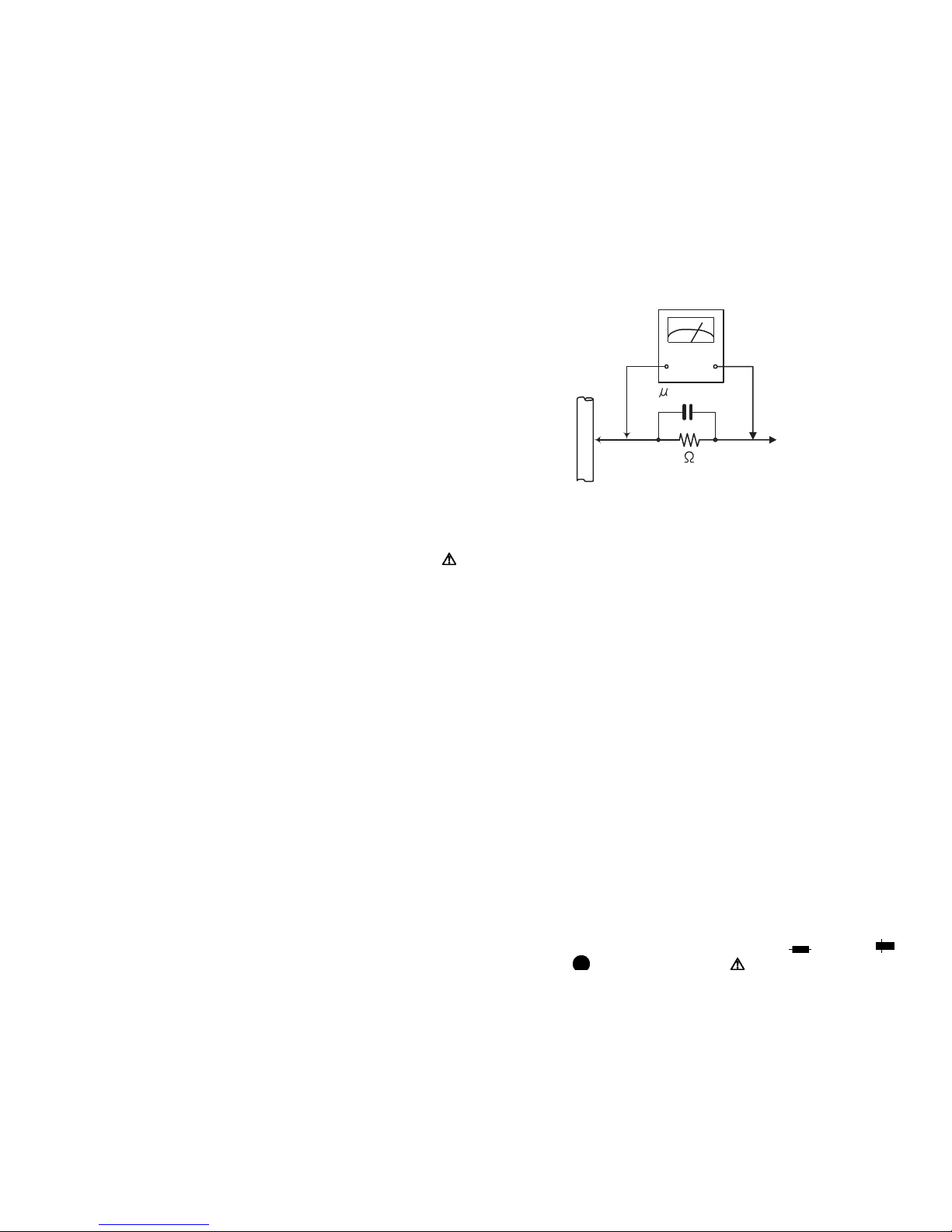
(5) Leakage shock hazard testing
After reassembling the product, always perform an isolation check on the exposed metal parts of the product (antenna terminals, knobs, metal cabinet, screw heads,
headphone jack, control shafts, etc.) to be sure the product
is safe to operate without danger of electrical shock.Do not
use a line isolation transformer during this check.
• Plug the AC line cord directly into the AC outlet. Using a
"Leakage Current Tester", measure the leakage current
from each exposed metal parts of the cabinet, particularly any exposed metal part having a return path to the
chassis, to a known good earth ground. Any leakage current must not exceed 0.5mA AC (r.m.s.).
• Alternate check method
Plug the AC line cord directly into the AC outlet. Use an
AC voltmeter having, 1,000Ω per volt or more sensitivity
in the following manner. Connect a 1,500Ω 10W resistor
paralleled by a 0.15µF AC-type capacitor between an ex-
posed metal part and a known good earth ground.
Measure the AC voltage across the resistor with the AC
voltmeter.
Move the resistor connection to each exposed metal
part, particularly any exposed metal part having a return
path to the chassis, and measure the AC voltage across
the resistor. Now, reverse the plug in the AC outlet and
repeat each measurement. Voltage measured any must
not exceed 0.75 V AC (r.m.s.). This corresponds to 0.5
mA AC (r.m.s.).
AC VOLTMETER
(Having 1000
ohms/volts,
or more sensitivity)
0.15 F AC TYPE
Place this
probe on
1500 10W
Good earth ground
1.2 Warning
(1) This equipment has been designed and manufactured to
meet international safety standards.
(2) It is the legal responsibility of the repairer to ensure that
these safety standards are maintained.
(3) Repairs must be made in accordance with the relevant
safety standards.
(4) It is essential that safety critical components are replaced
by approved parts.
(5) If mains voltage selector is provided, check setting for local
voltage.
1.3 Caution
Burrs formed during molding may be left over on some parts
of the chassis.
Therefore, pay attention to such burrs in the case of preforming repair of this system.
1.4 Critical parts for safety
In regard with component parts appearing on the silk-screen
printed side (parts side) of the PWB diagrams, the parts that are
printed over with black such as the resistor ( ), diode ( )
and ICP ( ) or identified by the " " mark nearby are critical
for safety. When replacing them, be sure to use the parts of the
same type and rating as specified by the manufacturer.
(This regulation dose not Except the J and C version)
each exposed
metal part.
(No.MB723<Rev.003>)1-3
Page 4
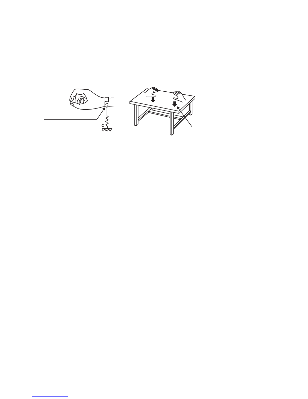
1.5 Preventing static electricity
Electrostatic discharge (ESD), which occurs when static electricity stored in the body, fabric, etc. is discharged, can destroy the laser
diode in the traverse unit (optical pickup). Take care to prevent this when performing repairs.
1.5.1 Grounding to prevent damage by static electricity
Static electricity in the work area can destroy the optical pickup (laser diode) in devices such as laser products.
Be careful to use proper grounding in the area where repairs are being performed.
(1) Ground the workbench
Ground the workbench by laying conductive material (such as a conductive sheet) or an iron plate over it before placing the
traverse unit (optical pickup) on it.
(2) Ground yourself
Use an anti-static wrist strap to release any static electricity built up in your body.
(caption)
Anti-static wrist strap
1M
Conductive material
(conductive sheet) or iron palate
(3) Handling the optical pickup
• In order to maintain quality during transport and before installation, both sides of the laser diode on the replacement optical
pickup are shorted. After replacement, return the shorted parts to their original condition.
(Refer to the text.)
• Do not use a tester to check the condition of the laser diode in the optical pickup. The tester's internal power source can easily
destroy the laser diode.
1.6 Handling the traverse unit (optical pickup)
(1) Do not subject the traverse unit (optical pickup) to strong shocks, as it is a sensitive, complex unit.
(2) Cut off the shorted part of the flexible cable using nippers, etc. after replacing the optical pickup. For specific details, refer to the
replacement procedure in the text. Remove the anti-static pin when replacing the traverse unit. Be careful not to take too long a
time when attaching it to the connector.
(3) Handle the flexible cable carefully as it may break when subjected to strong force.
(4) I t is not possible to adjust the semi-fixed resistor that adjusts the laser power. Do not turn it.
1-4 (No.MB723<Rev.003>)
Page 5
SECTION 2
SPECIFIC SERVICE INSTRUCTIONS
This service manual does not describe SPECIFIC SERVICE INSTRUCTIONS.
SECTION 3
DISASSEMBLY
3.1 Main body (Used figure were RV-NB50E)
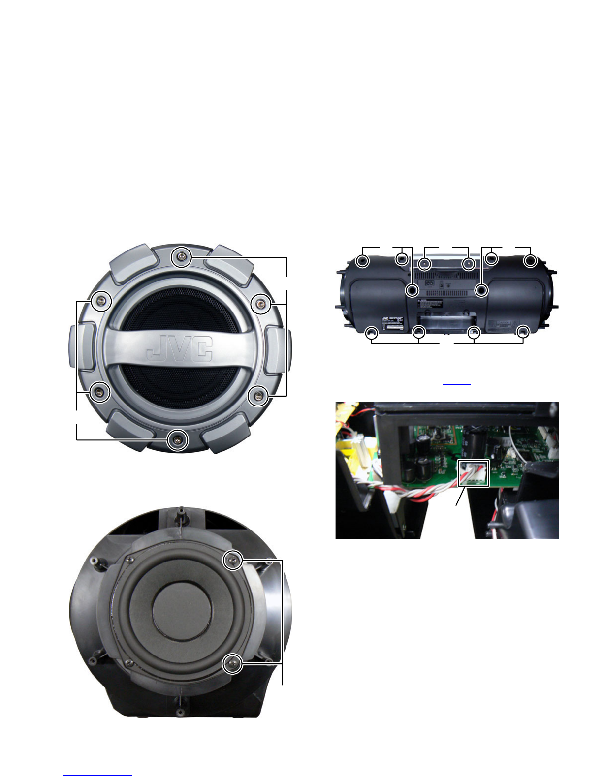
3.1.1 Removing the Punching panel (See Fig.1)
(1) Remove the twelve screws A attaching the both side of the
Punching panel.
A
Fig.1
3.1.2 Removing the Rear cabinet (See Fig.2, 3, 4, 5)
(1) Remove the four screws B attaching the both side of the
Subwoofer. (See Fig.2)
A
(2) Remove the ten screws C attaching the Rear cabinet. (See
Fig.3)
(3) Remove the two screws D attaching the CD mechanism.
(See Fig.3)
CCD
C
Fig.3
(4) Disconnect the connector wire from Power supply board
connected to connector CN101
Fig.4)
of the Main board. (See
Fig.2
CN101
Fig.4
B
(No.MB723<Rev.003>)1-5
Page 6
(5) Disconnect the connector wire from Power supply board
connected to connector CN301 of the Main board. (See
Fig.5)
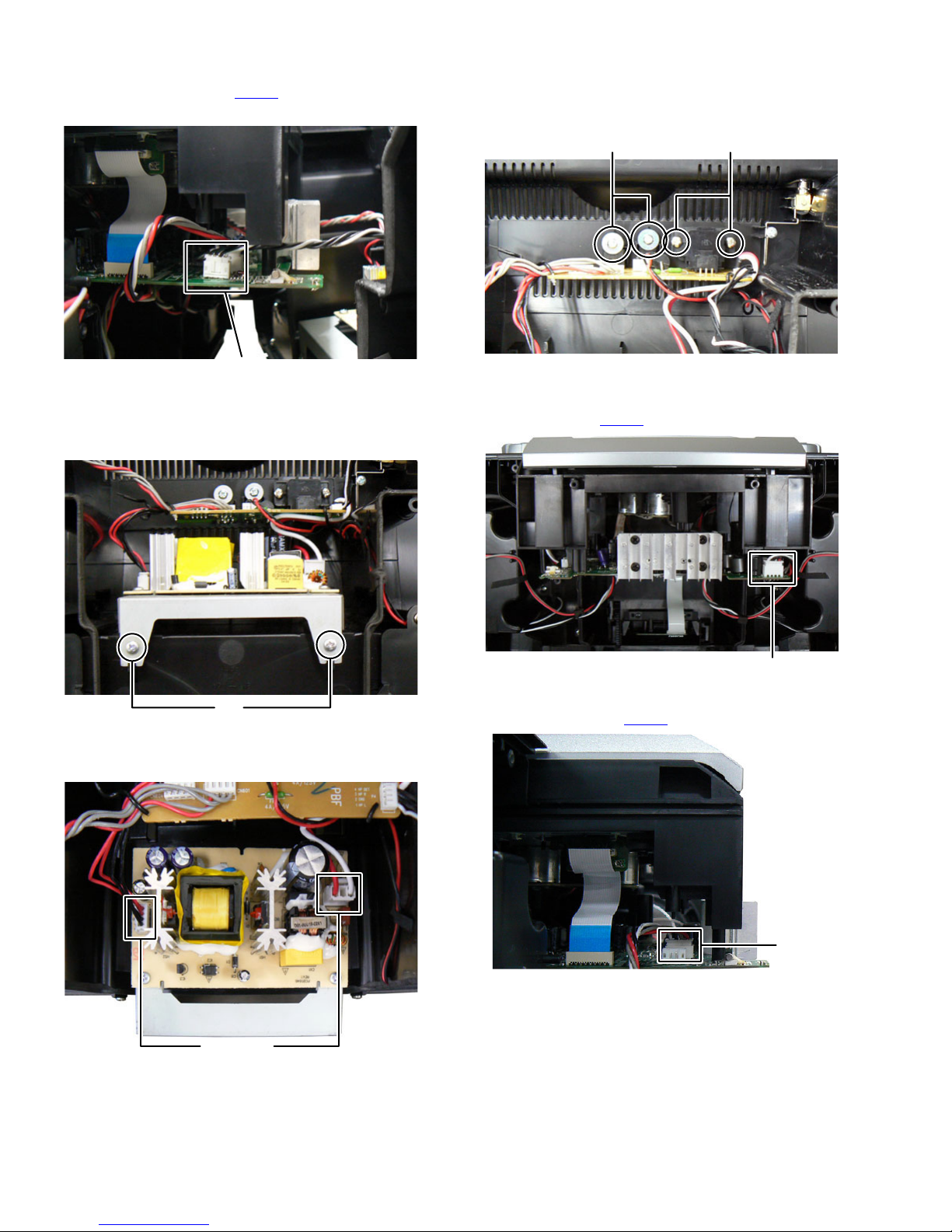
3.1.4 Removing the Power supply board (See Fig.8)
(1) Remove the two screws F and two screws G attaching the
Power supply board.
FG
CN301
Fig.5
3.1.3 Removing the SMPS board (See Fig.6, 7)
(1) Remove the two screws E attaching the SMPS board. (See
Fig.6)
E
Fig.6
(2) Disconnect the connector wires from Power supply board
connected to connectors of SMPS board. (See Fig.7)
Fig.8
3.1.5 Removing the CD mechanism (See Fig.9, 10, 11, 12)
(1) Disconnect the connector wire from Left speaker connect-
ed to connector CN102
(2) Disconnect the connector wire from Right speaker con-
nected to connector CN103
of the Main board. (See Fig.9)
CN102
Fig.9
of the Main board. (See Fig.10)
connector
Fig.7
1-6 (No.MB723<Rev.003>)
CN103
Fig.10
Page 7
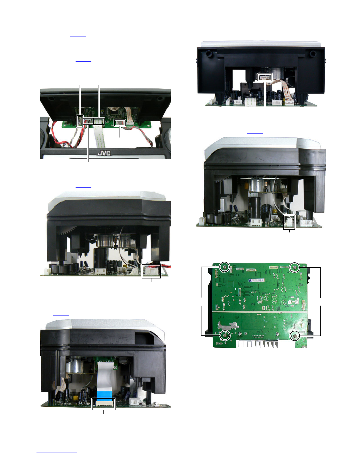
(3) Disconnect the card wire from Main board connected to
connector CN450
(4) Disconnect the connector wire from Right key board con-
nected to connector CN303 of the Main board. (See Fig.11)
(5) Disconnect the connector wire from USB board connected
to connector CN201
(6) Disconnect the connector wire from Left key board con-
nected to connector CN301
(7) Disconnect the connector wire from LCD board connected
to connector CN304
of the iPod board. (See Fig.11)
of the Main board. (See Fig.11)
of the Main board. (See Fig.11)
CN450CN301
CN303
CN201
Fig.11
of the Main board. (See Fig.12)
(2) Disconnect the connector wire from Main board connected
to connector of the Mechanism board. (See Fig.14)
connector
Fig.14
(3) Disconnect the connector wire from Door switch board con-
nected to connector CN305
of the Main board. (See Fig.15)
CN304
Fig.12
3.1.6 Removing the Main board (See Fig.13, 14, 15, 16)
(1) Disconnect the card wire from pickup connected to connec-
tor CN701
of the Main board. (See Fig.13)
CN305
Fig.15
(4) Remove the four screws H attaching the Main board. (See
Fig.16)
HH
Fig.16
CN701
Fig.13
(No.MB723<Rev.003>)1-7
Page 8
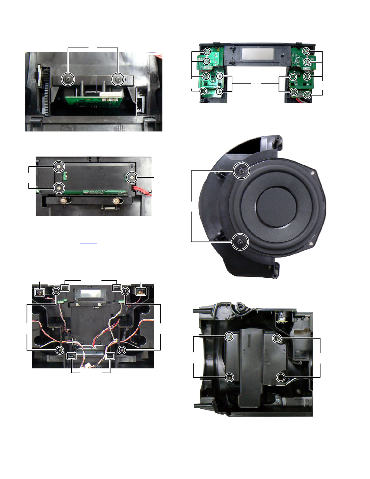
3.1.7 Removing the iPod board (See Fig.17)
(1) Remove the two screws J attaching the iPod board.
J
3.1.10 Removing the Key board (See Fig.20)
(1) Remove the twelve screws M attaching the Key boards.
Fig.17
3.1.8 Removing the LCD board (See Fig.18)
(1) Remove the three screws K attaching the LCD board.
K
Fig.18
3.1.9 Removing the Front panel (See Fig.19)
(1) Disconnect the connector wire from Right key board con-
nected to connector CN407
(2) Disconnect the connector wire from Left key board con-
nected to connector CN408 of the Volume board.
(3) Remove the four screws L attaching the Front panel.
(4) Disengage four hooks a engaged Front panel.
of the Volume board.
K
M
3.1.11 Removing the Right speakers (See Fig.21, 22, 23)
(1) Remove the two screws N attaching the Woofer, (See
Fig.21)
M
Fig.20
M
N
CN407 CN408
hook
a
(2) Remove the four screws P attaching the Speaker cover.
(See Fig.22)
Fig.21
LL
PP
hook
a
Fig.19
Fig.22
1-8 (No.MB723<Rev.003>)
Page 9
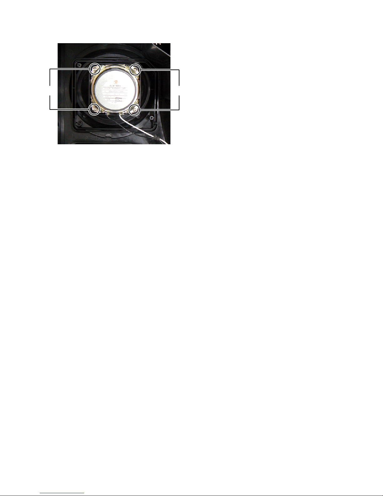
(3) Remove the four screws Q attaching the Main speaker.
(See Fig.23)
3.1.12 Removing the Left speaker
(1) Left speaker removing method as follow the 3.1.11 Re-
moving the Right speakers.
QQ
Fig.23
SECTION 4
ADJUSTMENT
This service manual does not describe ADJUSTMENT.
SECTION 5
TROUBLESHOOTING
This service manual does not describe TROUBLESHOOTING.
(No.MB723<Rev.003>)1-9
Page 10

Victor Company of Japan, Limited
Home Entertainment Business Division Personal AV Operation 10-1,1chome,Ohwatari-machi,Maebashi-city,371-8543,Japan
(No.MB723<Rev.003>)
Printed in Japan
VSE
Page 11
SCHEMATIC DIAGRAMS
POWERED WOOFER CD SYSTEM
RV-NB50B, RV-NB50E, RV-NB50EN,
RV-NB50EV, RV-NB51WE, RV-NB51WEN,
RV-NB51WEV, RV-NB52BB, RV-NB52BE,
RV-NB52BEN, RV-NB52BEV, RV-NB50J,
RV-NB50C, RV-NB50US, RV-NB50A,
RV-NB52BJ
Lead free solder used in the board (material : Sn-Ag-Cu, melting point : 219 Centigrade)
Contents
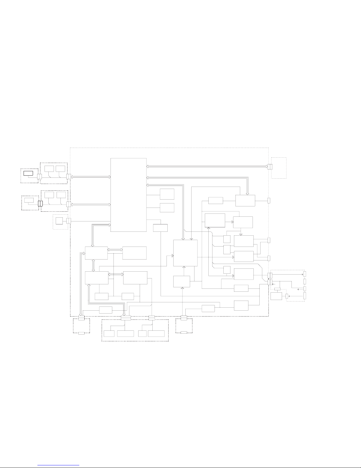
Block diagrams
Standard schematic diagrams
Printed circuit boards
COPYRIGHT 2010 Victor Company of Japan, Limited.
2-1
2-2
2-7 to 11
No.MB723SCH<Rev.003>
2010/4
Page 12

In regard with component parts appearing on the silk-screen printed side (parts side) of the PWB diagrams, the
parts that are printed over with black such as the resistor ( ), diode ( ) and ICP ( ) or identified by the " "
mark nearby are critical for safety.
Page 13
2-1
VR401
M VOLUME
S407
Operation
S411
Switch
KEY1
IC401
Remocon
RMC
CN407
CN406
CN402
CN303
VR402
W VOLUME
S401
Operation
S406
Switch
KEY2
D401
Standby
LED
CN409
CN408
CN401
CN301
LED
CN305
CD DOOR
SWITCH
CD DOOR SWITCH
IC302
T5CL8
SYSTEM
MICON
IC703
T5C3J-7D13
USB
Driver
IC707
SST39VF800A
FLASH
IC701
CD/USB RF DSP
TC94A92FG
IC702
Motor driver
BA5826HFP
USB CD L/R
5V
3.3V
1.5V
IC705
BH15FB1WG
Q702
KTC3205
Q207
KTA1273
USB 5V SW
CN201
CN430
JK430
TO USB
CN701
CN702
CD
PICK UP
Tracking &
Focus
Coil
RESET
SW
Spindle &
Fleed
motor
CN450
CN202
TO
iPod
JK450
iPod L/R
iPod 5V
SW
Q204
KTA1273
5V OUT
IC201
MP1842
DC/DC 5V
9V
OUT
Q105
2SD2394E
IC202
BA4510FV
Buffer
iPod
L/R
IC203
FUNCTION
BD3490FV
3.3V
IC301
HT7533
IC303
BD4827
RESET
IC304
AT2402
EEPROM
TUNER
L/R
HP MUTE
Q030
Q031
IC002
HP AMP
NJM4580
IC101
MAIN AMP
TDA7266SA
MUTE
L/R
Q102
WVOL1
WVOL2
WVOL3
Q109
Q110
Q111
IC102
WOOFER AMP
LV49152V
IC107
HPF & LPF
IC104 to IC106
INPUT AMP
PHASE AMP
COMP AMP
IC001
S4702S
TUNER
Section
Q001
2SC3052F
3.3V OUT
LCD
TO
FM
ANT
CN304
CN403
M L
+/-
W L
+/-
CN103
M R
+/-
W R
+/-
CN102
CN301
CN440
CN101
CN601
TO L
MAIN SPEAKER
TO L
WOOFER
SPEAKER
TO R
MAIN
SPEAKER
TO R
WOOFER
SPEAKER
Power supply
Section
AC
DET
VCC
CN606
CN604
SPS PCB
14V/4A
JK602
JK440
JK601
CN602
B+
HP OUT
BATTERY
IN
DC IN
AC IN
Block Diagram
Page 14

2-2
IC702
SP+
SPSD+
SD-
IN-SW
GND
C749
R755
L710
P[0:30]
JR706
JR707
JR703
CDUSBON
MGND
DGND
AMI
AMUTE_1
CD_RESET
USB_UPD
USB_RXD
USB_TXD
USB_RST
USBD-
USBD+
COM5V
CD_MUTE
BOOTOUT
P30 P30
R795
R756
BP3.3V
FB102
FB102
JR705
R779
R780
FB102
Q703
R715
R775
R712
R713
L712
L704
P28P28
P10
D701
DA3.3V
D3.3V
M1.5V
D1.5V
A3.3V
IC705
IN OUT
GND
STBY
NC
FB102
Q702
L701
L702
R761
R762
L703
R760
R759
R758
R757
FB102
FB102
L705
R764
R765
R767
R769
SDA
SCL
TP4
TP5
R768
R770
R766
R763
L706
FB102
FB102
FB102
CN702
16 14 12 10 8 6 4 2
13579111315
16 14 12 10 8 6 4 2
13579
Q701
R701
R702
80797877767574737271706968676665646362
61
2122232425262728293031
323334353637383940
C703
C737
R754
C748
R714
C760
C761
C752
C754
C756
C757
C758
C759
C759
C767
C768
C769
C770
C771
R777
B16
B6
B7
C772
C773
C774
C775
C776
R781
R782
R776
BP3.3V
R774
Q704
D702
C747
C738
C739
FE
TP1
C742
C785
C784
R745
R744
R743
R742
R741
R740
R739
C730
P28
P29
C732
C733
R734
X702
C781
R783
R792
R784
C780
A17
A16
A15
A14
B3B2B1
B0
A17
A16
A15
A14
A13
A12
5655545352
51
6261605958
6766656463
68737275747170
69
RC RESET
RC TESR
BUCK
WE
OE
DVCC3
DVSS
MODE4
BUS3
BUS2
BUS1
BUS0
X2
MODE0
X1
DVSS
BSIF_LRCK
BSIF_LRCK
AMI
CE
CCE
57
A13
A12
A16
A17
R785
R793
C734
C735
RN711
R778
R773
C766
X701
C765
RESET OUT
BOOT OUT
RN710
RN709
RN708
R737
R738
P30
P6
B4
B5
CCE
C731
FSMoNiT
RFZi
RFRP
TEi
AVDD3
Foo
TRo
VSS
FMo
FMoS
DMo
VDD1-3
Pio8
Pio9
Pio10
Pio11
Pio12
Pio13
Pio14
CDMoN3
DGND
111315
MECHA
Motor Driver
PICK UP
UNIT
CN701
R703
VREF
GND
LD
VR
PD
FE-
FE+
TE-
TE+
SVCC
E
D
A
B
C
F
C701 C702
SP-1
2
3
4
5
6
1
2
3
4
5
6
1
2
3
4
5
6
7
8
9
10
11
12
13
14
1
2
3
4
5
6
7
8
9
10
11
12
13
14
15
16
17
18
19
20
21
22
23
24
39
38
37
36
35
34
33
32
31
48
47
46
45
44
43
42
41
40
30
29
28
27
26
25
19
20
21
18
17
16
15
26
27
28
25
24
23
22
83
78
77
76
79
80
81
82
91
86
85
87
87
88
89
90
43
48
49
50
47
46
45
44
35
40
41
42
39
38
37
36
28
27
26
33
34
32
31
30
29
99
100
94
93
92
95
96
97
98
SP+
SPIN
RESET
REGB
REGGND
TIN
IN2
F_IN
VCC
VCC^
BIAS
SDIN
IN4
SD+
SD-
GND
VIN3
T+T-F+
FPWGND
OPOUT OPIN-
RESTT
REG0
MUTE
C750
R750
C743
JR701
P10
AMUTE
C764
R772
A3.3V
C763
R771
L707
DVCC3
AMUTE
USBPON
D+
D-
MODE1
TEST
DVSS
SD_DOUT
SD_DIN
SD CLK
TX
RX
SD CS
TEST
IC703
USB Driver
TEST
BSIF BCK
BSIFDATA
BSIF DATA
BSIF-REQ
MODE2
SD DET
MODE3
DVSS
DVCC3
R747
R746
C740
C741
C711
TP3
RF
A3.3V
C713
CD/USB DSP
C712
C710
C709
VCoi1
2
3
4
5
6
7
8
9
10
11
12
13
14
15
16
17
18
19
20
51
50
49
48
47
46
45
44
43
42
41
60
59
58
57
56
55
54
53
52
RVDD3
SLCo
RFi
RFRPi
SDCK Pio7
P7
P6
P5
D1.5V
CD_L
CD_R
AGND
FLASH
A11
BP3.3V
L708
FB102
C779
RN707
R798
C791
A10
A9
A8
A11
A10
A9
A8
A7
A7
DVCC3
DVSS
A6
A5
A4
A3
A6
A5
A4
A3
A2
B16
A1
A0
D15
D14
D13
D12
D15
D14
D13
D12
D11
D10
D9
D8
D0
D[0:30]
D8
D1
D9
D2
D3
D10
D11
D4
D12
D5
D13
D6
D7
D14
D15
D11
DVCC3
DVSS3
D10
D9
D8
A2
A1
A0
Q_REST
A15
A16
IC707
C783
C782
A14
A13
A12
A11
A10
A9
A8
A15 A16
A14
A13
A12
A11
A10
A18
A17
A17
A7
A6
A5
RN706
RN705
C778
C777
RN704
RN703
A4
A7
A6
A5
A4
A3
A2
A1
A3
A2
A1
A0
A0
A9
A8
NC
NC
WE
NC
VSS
VDD
DQ15
DQ7
DQ14
DQ6
DQ13
DQ5
DQ12
DQ4
DQ11
DQ3
DQ10
DQ2
DQ9
DQ1
DQ8
DQ0
OE
VSS
CE
NC
NC
NC
NC
L711
FB102
DA3.3V
R733
C726
C727
C729
R735
R736
C736
P4
P3
P2
P1
P29
R789
RESET
B[0:30]
R732
LRCK Pio6
BCK Pio5
DATA Pio4
SDCS Pio3
GATE Pio2
REQ Pio1
Pio0
VSS
VDD1-2
XVDD3
XVSS3
Lo
R0
DVSS
DVDD3L
DVDD3R
DVSS3L
Xo
Xi
RFEQo
IC701
DCoFC
AGCi
RFo
RVSS3
FNi2 C
FNi1 A
FPi2 D
FPi1 B
TPi F
TNi E
VRo
AVSS3
MDi
LDo
C708
C705
C706
C714
C715
C716
C717
R705
R
7
0
6
M1.5V
D1.5V
B16 RESET
R719
C707
R704
C704
R748
R749
C745
R753
C746
R751
C744
R752
C751
C788
C762
BSIF ST REQ
BSIF BCK
BSIF DATA
BSIF GATE
BPSDCS
BPSDCK
P1
P4
P3
P5
P7
P2
RN713
2021222324
25
1415161718
9
101112
13
8341256
7
19
RN701
RN702
D0
D7
D6
D5
D4
D3
D2
D1
D0
D7
D6
D5
D4
D3D2D1
RST
USB START
D-REQ
SBSY
INNER
DVCC3
TEST
TEST
TEST
DVSS
DVSS
DVCC1B
DVCC1A
RVOUT1
RVOUT2
RVIN
RVIN
JR0
R786
DGND
A[0:30]
BP3.3V
FB102
L709
R788
R794
DGND
Q705
R720
R725
R722
R723
R724
R721
B0
B5
B4
B3
B2
B1
D3.3V
C725
C724
B6
B7
DREQ
SBSY
R716
R718
R717
C723
B0
B5
B4B3B2
B1
C722
C721
RN712
R708
C720
C719
R711
R710
R709
R707
C718
VCoF
PVREF
LPFo
LPFN
TMAX
PDo
VDDM1
SRAMSTB
VSS
VDD1-1
TEST
RST
MS
CCE
BUCK
BUS3
BUS0
BUS1
BUS2
VDD3
C
755
C728
Standard schematic diagrams
<Main Section 1>
Page 15

2-3
To Key section
CN402
To Key section
(LCD PCB)
CN403
To Key section
CN401
C331
R279
Q301
D319
C332
R307
C303
C302
D318
R398
D303
CDM5V
Q314
TEST
VDD
RESET
RxD
TxD
GND
6
5
4
3
2
1
CN302
R390
GND
Q304
R312
D317
RESET IC
5
4
3
2
1
GND
NC
VCC
VO
NC
IC303
C28
R340
R393
R392
R300
R305
C322
2
1
2
1
2
1
SW401
CN404
CN305
CD DOOR
R361
R360
R359
R358
R285
C356
6
543
2
1
VCC
GND
BACKLIGHT
LCD DATA
LCD WR
LCD CS
CN304
R375
R376
R378
R377
M[00:20]
R371
R316
R317
R314
R315
R284
6
7
8
9
10
20
19
18
17
16
NC
NCNCNC
NC
NC
NCNCNC
NC
C305
C306
R319
R318
C304
R309
R310
R175
R362
R282
R304
R303
R372
R373
X302
X301
R338
R384
R339
R341
R342
W VOL-
6
5
4
3
2
1
7
8
9
10
16
11
12
13
14
15
VSS
XIN
XOUT
TEST
VDDI
P21
P22
/RESET
P20 HOLD
P00DOOR
P01 Rx1
P02 Tx1
P03 AC/DC
P04
P05
P06
P14
P13
P12
P11
P10
P47
P46
P45
P44
P43
P42
P41
P40
P77
P76
P75
48474645444342414039383736
353433
iPod DET
VOL+
VOL-
RDS
R394
IR
TU SDO
TU CLK
TU RST
iPhone det
USB UPT
iPod TX
iPod RX
LCD DATA
LCD WR
BCTL
LCD CS
A MUTE
R351
R355
R354
R353
R352
M04
M00
M01
M02
M03
C320
C321
L301
FB102
R344
R345
R346
R347
R385
R386
D314
D313
R289
R286
TURDS
TURST
TUSCLK
TUSDO
IPOD_CHG
5VS/W
IPOD_RX
IPOD_TX
IPHONE_DET
IPOD_DET
IPOD_RST
POWER_ON
SUB_VOL3
SUB_VOL2
SUB_VOL1
AMUTE
VOLSCL
VOLSDA
JR301
JR303
JR302
JR304
JR305
M00
M01
M04
M02
M03
R369
R368
R370
R364
R366
R365
R367
R322
R363
Q305
C323
C325
C324
47P
100P
100P
Q310
6
5
4
3
2
1
CN303
RMC
KEY1
VOL+
VOL-
GND
VCC
VCC15V
USBON
CDUSBON
D301
D302
R301
R391
Q315
Q308
R381
FOR FLASH
D305
R383
R382
5
4
3
2
1
GND
VCC
KEY2
W VOL+
W VOL-
LED
CN301
R388
R387
Q306
R379
R380
Q307
Q313
D316
R298
R299
R389
C330
C307
C309
C308
C314
R343
C310
C312
C313
C311
Q312
R397
D315
D307
CD_MUTE
BOOTOUT
RESET
AMI
AMUTE_1
CD_RESET
USB_UPD
USB_RXD
USB_RST
USB_TXD
USBON
CDUSBON
HP_MUTE
HP_DET
DC9V
UCBD+
R308
Q303
R306
AC/DC
D_GND
VCC15V
13
2
R311
IC301
IN OUT
IC304
1
3
2
4
8
6
7
5
EPROM
A0
A2
A1
GND
VCC
WP
SCL
SDA
R320
R290
R294
R297
R296
R295
R293
R292
R291
IC305
R313
5
4
3
2
1
NC
NC
NC
MODE1
RESET
VCC
MODE0
SDA
SCL
GND
C294
R323
R325
R336
R335
R334
R329
R327
R333
R331
R328
R324
R332
R326
R330
R337
R357
49
56
63
62
61
57
59
58
60
55
54
53
52
51
50
64
32
25
18
19
20
24
22
23
21
26
27
28
29
30
31
17
P74
P53
P52
P51
P50
P17
P16
P15
P07
P60
P61
P62
P63
P64
P65
P66
P67
P70
P71
P72
P73
AVDD
VAREF
IC302
MCU
PW ON
S VOL1
S VOL3
S VOL2
R350
R348
R356
R349
R399
R374
KEY1
KEY2
CD DOOR
OPTION1
OPTION2
P35
P34
P33
P32
P31
P30
P54
P37
P36
BACKLIGHT
BP RST
USB ON
SCL
SDA
CP RST
CP ON
NC
BUSO
CDUCB ON
iPod CHG
5VS/W
CD MUTE
HP MUTE
HP DET
RST
11
12
13
14
15
W VOL+
<Main Section 2>
Page 16

2-4
To Key section
Power board(2)
CN440
C501
C502
C503
R502
R504
R503
IC3
R507
R508
VR501-A VR-2T
R509
R513
C432
C433
C296
C201
C202
C276
C203
C204
R202
R203
R278
R204
R269
C205
C206
C295
C275
C207
C208
Q201
R031
R032
IC002
C031
C041
C027
C043
C042
C045
C040
C038
C039
C046
C047
C048
C049
DTC323TK
DTC323TK
Q030
Q031
CN031
C228
R257
C233 C234
C247
C273
R268
R267
C274
C235
C230
C229
C271
C272
C240
C243
C244
R265
R266
C239
C237
C221
C220
R230
R225
R228
C216
C217
C218
R226
R221
R223
C226
R013
R225
R212
R220
R219
IC202
C209
R217
C213
C215
C224
CN202
R456
R455
R454
R453
R452
R451
R450
JK450
1
1
CN450
RST
iPod 3.3V
iPod connection section
TX
RX
IPOD DET
AUDIO R
A GND
AUDIO L
GND
+5V
CGND
DC 5V
2
3
4
5
6
7
8
9
10
11
12
13
14
1
2
3
4
5
6
7
8
9
10
11
12
13
14
Q204
C210
D202
R231
R211
R201
IC201
L201
L204
L203
1
2
BS
IN
SW
GND
SYNC
EN
COMP
FB
3
4
8
7
6
5
R205
R206
L205
Q203
D210
C289
L206
C214
R218
C212
R216
C211
R215
R214
R222
R224
R227
iPod Buffer
R241
R260
R261
R244
R245
R246
R247
R240
IC203
C253
C254
C255
C256
R262
R263
C270
C280
C267
R250
C257
C258
C259
C260
C261
C262
L202
C277
L030
C044
R041
R016
Q002
C035
HP AMP
FUNCTION AMP
R034
R035
C036
C033
C030
C032
C050
C051
C037
R036
R037
R006
R015
R007
R008
L001
X001
R044
AUX section
TUNER MODULE
NM
CN203
R004
R005
1
2
3
1
2
3
AUX R
GND
AUX L
CN580
R580
7
6
3
2
5
4
1
R581
JK580
PJ350
PJ-310H
L580
C024
R014
C013
C012
L002
TP001
TP
TEST
C021
IC001
C022
15
GND
GND
NC
FMIP
RF GND
RST
GNDGND
VD
LOUT
ROUT
16 17 18 19 20 21
14
13
12
11
1
2
3
4
5
R009
R001
R002
Q001
R003
R248
R249
R253
R251
R252
R254
C266
C268
C269
1
2
3
4
C281
C282
C283
C265
C264
C263
C246
C245
C278
C279
C249
C250
C251
C252
2
3
4
5
6
7
8
9
10
11
12
13
14
15
16
17
18
19
20
21
Q450
22
23
24
25
26
27
28
29
30
31
F/W_GND
F/W_GND
TPA+
USB_0+
TPA-
USB_D-
TPB+
USB_PWR
TPB-
ACCESSORY_IDEN
F/W_PWR
F/W_PWR
ACCESSORY_PWR
RESERVED
USB_GND
DGND
RESERVED
TX
RX
ACCESSORY_DET
S_VIDEO_Y
S_VIDEO_C
COMPOSIT_VIDEO
REMOTE_SENSE
LINE_IN_L
LINE_IN_R
LINE_OUT_L
LINE_OUT_R
AUDIO_RETURN
CHASSIS
DGND
R213
C222
C219
C223
C238
C236
C248
R258
R256
R255
C227
C298
C297
R039
R040
R042
C026
C023
R043
R038
C034
R033
R030
C290
D201
C434
C431
D433
D432
D431
D434
JK430
USBD+
D_GND
CDM5V
USBON
DC9V
CD_R
AGND
5VS/W
D_GND
3.3V
IPOD_CHG
C_GND
AGND
IPHONE_DET
IPOD_RST
IPOD_TX
IPOD_RX
IPOD_DET
VOLSDA
VOLSCL
L
R
HP_DET
HP_MUTE
TURDS
TURST
TUSCLK
TUSDIO
VCC15V
CD_L
USBVCC
USBD-
USDB+
USBGND
R433
R432
USB PCB
56
L431
CN430
C507
C506
Q502
C505
R506
R505
C528
C504
C530
R501
4
3
2
1
R510
C512
Q501
NM
mic section
CN501
R528
C519
C518
R523
CN204
9V
1
2
3
1
2
3
GND
SG
C522
Q504
Q503
R525
C517
C524
R518
C516
C511
R511
JK501
PJ603
CN201
R287
C291
C286
R288
C288
Q208
D209
R281
Q207
1
2
3
4
1
2
3
4
4
1
2
3
USB-AF180DIP
R512
R514
C515
R515
R516
R517
R519
R524
D001
C001
C002
C003
C004
C005
C006
C007
C008
C010
C011
R010
R011
R012
C014
C015
C016
C017
C019
C018
C020
C580
C581
R582
R583
R280
R232
D205
C025
L003
C009
R527
R526
C520
C521
C523
IC502
R520
D503
D504
D501
D502
C514
C513
C525
C526
C508
C509
C529
C510
432
1
567
8
C527
432
1
567
8
432
1
567
8
4
321
5
6
7
8
1
A1 TU L FL
GND
SDA
SCL
VCC
OUT1
SB1
SR
SB2
OUT2
BCB1
BCA1
BCA2
BCB2
A2 TU R
B1 AUX L
B2 AUX R
C1 CD L
C2 CD R
D1 iPod L
D2 iPod R
SEL 2
SEL 1
VOL1
VOL2
TC2
TC1
2
3
4
5
6
7
8
9
10
11
12
13
14
28
27
26
25
24
23
22
21
20
19
18
17
16
15
10
987
6
VIO
VA
GPI03
GPI02NCGPI01
SCLK
SEN
RCLK
SDIO
<Main Section 3 and iPod section>
Page 17

2-5
To Key section
Power board(1)
CN601
R139
12K
R132
3.3K
R133
R130
C135
C136
C127
4.7/10
0.22uF
15nF
IC104
876
5
123
4
876
5
123
4
R116
D101
4.7/10
C194
R114
C121
C122
C123
C124 47P
100R115
C120
C193
C102
5.6K
L
R
AGND
AMUTE
5.6K
R101
R103
R104
R106
R109 R110
IC101
IC102
470u/25V
0.1uF
0.1uF
1uF
1uF
1uF
1uF
1uF
1uF
1uF
1uF
1uF
1uF
0.1uF
0.1uF
470u/25V
10u/10
10u/10
1uF
1uF
1uF
0.1uF
0.1uF
0.1uF
0.1uF
22uH
22uH
22uH
22uH
470u/25v
MUTE
C151
C150
12K
C152
C153
R187
C154
C155
C157
C156
C158
C166
C162
C160
C161
C167
L104
L103
L101
L102
C168
LV49152V
CN101
1
2
3
4
2T
L105
WOOFER AMP
5W/16ohm
5W/16ohm
15W/7ohm
15W/7ohm
2.0/4P
2.0/4P
STBY
VIN1+
VIN1PLC
BOOT1+
VDD1
BOOT1-
OUT1-
OUT1PGND1
PGND1
PGND2
PGND2
PVD1
441
2
3
4
5
2
15
14
69
7
12
1011 13
8
1
4
53
6
7
8
9
10
11
12
13
14
15
16
17
18
19
20
21
22
43
42
41
40
39
38
37
36
35
34
33
32
31
30
29
28
27
26
25
24
PVD1
OUT1+
OUT1+
OUT2OUT2-
BOOT2-
VDD2
BOOT2+
PVD2
PVD2
23
OUT2+
OUT2+
VIN2VIN2+
MUTECAP
VCC
BIASCAP
VBIAS
VREG5
GND
NC
NC
NC
NC
NC
NC
NC
NC
NC
TDA7266SA
10K10K
1uF
1uF
10u/10V
1uF
R105
C107
C108
R102
1K
1K
470
470
C104
C101
C103
R112
R113
47P
47P 47P
47P
47P
47P
C106 C105
47P 47P
47P
Q102
R107
C113
C114
C129
10u/10V
10u/10
C130
IC105
NJM4558
R124
47P
C115
R156
R154
R152
R155
R169
15K
1K
R153
R151
1K
1K
4.7K
1.8K
R150
12K
220K
C116
C118
C117
1000P
C29
C159
C192
C163
C178
47P
47P
47P
47P
C179
C175
C174
C180
47P
47P
47P
47P
CN103
CN102
1
2
3
4
1
2
3
4
1
2
3
4
1
2
3
4
C181
C177
C176
C165
C164
0.33
0.33
0.33
C170
C173
C172
C2
1000P
C171
C169
0.33
47P
C119
R123
R122
100
47P
180K
27K
R111
10K
10K
R108
10K
2SC3052F
47P
C110
C112 C111
C109
560P 560P
100K
100K
47P
47K
UZ4.7B
220K
NJM4558
C128
R121
R120
47P
100
10K
4.7/10
10u/10V
IC106
NJM4558
R131
R134
R145
R147
R146
2.2K
82K
IC107
NJM4558
C143
0.1uF
0.1uF
C141
C142
C149
C148
C147
100
47P
47P
47P
1uF
100K
100K
100K
10K
100K
R128
R127
D103
D102
1SS355
1SS355
C133
4.7/10
R125
C132
C144
R137
R138
C138
D107
1SS355
C139
4.7uF
C186
C185
D109
1SS355
220u/16V
220u/16V
0.1uF
0.1uF
C184
D110
10K
10K
1K
R163
R161
R162
R164
Q107
Q106
Q112
Q105
R143
R140
2SC3052F
2SC3052F
1SS355
1SS355
1SS355
Q104
Q103
D104
D106
R135 R136
47P
C190
24K
27K
24K
R148
R149
C146
C140
0.1uF
R144
C145
10u/10V0.018uF
180K
1K
R129
R117
R118
C126
0
NM
Q101
0.01UC131
R126
100K
Q108
DTC114EK
Q109
Q110
Q111
DTC114EK
DTC114EK
DTC114EK
R168
NM
820
NM
C125
NM
R119
33K
C134
4.7/10
1K
C137
4.7/10
D105
220
220K
2SA1235F
15K
R167
2SC3052F
2SC3052F
2SD2394E
DC 9V
R157
R158
R159
R160
10K
10K
R165
R166
10K
0
JR1
0
JR101
1K
1K
1K
1K
C183
UZ10B
R141
R142
5.6K
56K
33K
1K
15K
10K
JR2
C182
4700u/25V
JR102
JR103 JR105
JR104
0
0
0
0
0
MUTE
PGND
MAIN AMP
ST_BY
SGND
DC9V
D_GND
POWER_ON
WVOL1
WVOL2
WVOL3
VCC15V
C_GND
M_GND
AC/DC
876
5
123
4
876
5
123
4
<Main Section 4>
Page 18

2-6
NOTE)
With respect to risk of fire or
electrical shock.
Parts that are shaded are critical
Warning
<Key Section>
To Main section 2
CN303
To Main section 2
CN304
To Main section 2
CN301
To Main section 4
CN101
To Main section3
CN031
C411
C413
C414
C410
R420
R422
R423
R424
R421
1
653
2
478
9
/IRO
VLCD
VDD
OSCI
VSS
DATA
/WR
/RD
/CS
D402
BACKLIGHT
C412
VR402
1
2
43
5
C408
C407
VR401
1
2
43
5
C406 C405
CN407
CN406
3
2
1
3
2
1
R412 R411
R410
R409
R408
C402
R413
D401
C409
R407
R406
R405
R404
R403
6
5
4
3
2
1
CN402
RMC
KEY1
VOL+
VOL-
GND
VCC
R401
R402
IR
GNDVCCOUT
3
21
IC401
C401
iPod
S407
S411
S410
S409
S408
S412
CD
SKIP+
SKIP-
STOP
NC
C403
POWER
S401
S404
S403
S402
FM
SOUND
Preset Tu
S405
S406
FM MODE
3
2
1
3
2
1
CN409
CN408
LCD-9P
LCD401
6
5
4
3
2
1
CN403
LCD CS
LCD DATA
LCD WR
BACKLIGHT
GND
VCC
5
4
3
2
1
GND
VCC
KEY2
W VOL+
W VOL-
LED
CN401
CN604
R601
F601
CN601
1
2
3
4
2.0/4P
4A/125V
AC DETJ
BUP
GND
GND
BAT
SPS
Power board(1)
MAIN BT 15VOLT
BATTERY
BAT TERMINAL
2P/2.5
121
2
1
2
1
2
1
2
2P/2.5
CN602
CN603
VCC
10K
CN605
2P/2.0
CN606
JK602
AC IN
PROTECTOR
4A/125V
F602
2P/2.0
1N4005
GNDB-V+
123
1SS133
D601
JK601
DS222
R602
8.2K
D602
CN440
C440
JK440
L440
1
6
5
1
2
2
3
3
4
4
HP L
Power board(2)
HP JACK
GND
HP R
HP DET
C441
D440
D441
Page 19

2-7
CN102
C165
C164
C179
C163
C178
L101
C160
C161
C162
C166
C168
C167
C149
C100
Q111
Q110
Q109
Q108
R167
L105
C331
D319
L203
L204
C201
C302
C303
D318
D305
R305
R382
R279
C301
R289
R390
R286
C322
R391
JR304
R285
C356
JR303
JR302
R386
R385
D313
D314
R356
R399
R374
R350
R387
R388
R380
R379
Q305
R373
R372
Q308
R303
R304
R362
R375
R378
R354
R377
R376
R351
R355
R353
R352
R348
R349
R371
R337
R335
R333
R331
R329
R327
R325
R323
R336
R334
R332
R330
R328
R326
R324
C294
R322
Q312
Q304
C284
R398
R361
R360
R397
CN201
CN202
Q310
C180
C169
C171
L104
IC102
R107
C113
R109
R110
R108
C114
R111
C138
R136
R137
R135
R138
IC106
C135
R131
C136
D107
C134
R129
D106
R130
D105
D104
R142
R140
R141
C139
C190
Q103
R128
C133
IC105
Q101
C121
C122
D101
R116
C194
R114
C193
R256
R258
C269
R030
R255
R257
C268
R031
C228
C227
C277
C260
C248
C247
C262
C234
C233
Q030
Q031
C191
C112
C108
R104
C104
R102
C102
C197
C106
C196
R103
R101
C103
C105
C187
JR1
R205
Q201
IC201
C203
L201
C311
C310
C314
D317
R306
R307
C332
R389
R341
R393
R343
R342
Q303
R314
R316
R315
R317
R320
C305
R319
R313
C306
R318
R786
C791
C779
RN707
RN708
RN709
R783
C781
C780
D2
D1
C020
L002
R013
R012
C019
C016
R011
R004
R005
C003
C001
C002
R003
R001
R015
R006
P4
C021
C011
R010
C748
C6
21
15
28
IC702
7
TP12
C737
C742
TP11
C710
C709
C708
C705
C713
C711
TP13
C715
C719
C720
C714
C707
C706
C717
C716
C759
L703
R708
C723
C721
R716
R725
R722
R723
R724
RN712
R721
R720
D307
R733C728
R758
R759
R760
R761
R762
R766
R767
R769
R779
R780
R768
TP14TP15
R732
R736
C767
C770
R782
R738
R737
C741
C740
R718
C734
C733
C765
RN710
RN711
R756
X701
IC703
RN701
RN702
C760
C754
C769
L705
R781
RN713
L706
C758
C762
Q105
Q702
R163
R775
C288
R232
D205
D301
D302
D316
D303
R301
C208
R299
R298
C309
IC302
C330
C308
X301
R292
R297
R291
R295
R290
C290
C782
Q704
L709
C783
Q208
D202
R231
Q107
C297
C298
JR301
R162
D109
C257
C258
IC203
C254
C253
C244
C256
C255
P14
JK430
R034
C035
C036
C042
C041
R035
R041
R036
R037
C037
R038
C038
C039
R039
R033
C033
C050
C030
R032
C031
C032
C040
R044
C045
C044
R040
IC202
C222
C219
C292
C209
R213
C220
R225
C213
Q002
C226
C223
C293
C224
C215
R220
C027
Q001
P13
C236
C230
C235
C274
C273
R268
R267
R266
R265
C229
C272
C271 C237
C238
C239
C240
IC101
CN303
CN702
IC001
L003
Q102
IC104
IC002
Q701
R712
D209
R282
R788
R789
R794
CN304
C323
C324
C325
R346
R344
L301
R358
R359
R366
R363
R369
R357
R367
R364
R370
R368
R394
R365
CN301
E GND
GND
USBD+
USBD-
USB5V
R288
C286
R287
C291
14.CGND
13.CGND
12.iPod5V
9.GND
10.GND
11.iPod5V
8.iPod L
7.AGND
6.iPod R
1.iPod 3.3V
2.RST
3.TX
4.RX
5.iPod det
Q705
R793
R792
R798
R795
R784
R785
VCC3.3V
GND
VOL-
VOL+
KEY1
RMC
R778
R772
R773
C763
C764
C794
C793
R771
L707
C766
C755
C725
C724
C726
C727
R734
C722
R711
R710
R709
R719
IC701
R704
R705
R707
R706
C718
C704
GND
IN SW
SD-
SD+
SP-
SP+
PBF
C712
C738
C739
C732
R739
R740
R741
R742
C785
R746
R747
C784
R749
R743
R744
R745
C735
C731
R717
L702
X702
R763
R765
R764
C768
C730
R757
R776
C776
C774
C775
R777
C772
C771
C773
C788
L712
C752
L704
C756
R774
D110
IC705
C183
C757
C186
C184
C185
D701
Q106
R164
R161
C751
R715
L710
Q703
R714
R713
D702
C761
L708
C778
RN703
RN704
RN705
RN706
C777
P3
CN305
Q307
Q306
R347
R345
R392
C320
C321
R381
R383
R308
IC303
R284
C304
R310
R309
R312
R311
IC304
IC305
IC707
C743
R750
C744
R751
R753
C746
R752
C745
C703
R754
R755
R702
R701
R748
C749
C750
C736
L711
C729
R735
L701
C747
D315
R240
R241
R260
R261
R244
R245
R246
R247
C245
C246
C278
C279
C249
C250
C251
C252
C221
R217
R230
C212
C214
R216
R218
C225
R221
R222
R223
L030
R016
R224
C217
R226
C218
R228
R227
C285
C210
C211
R214
R215
C216
R219
R262
R263
CN203
C047
C049
R043
C046
C048
R042
C176
C177
CN103
D001
CN204
CN031
C10
C004
L001
R008
C005
C006
R009
C008
C010
C009
C026
C022
C025
R007
R014
C017
C012
C014
C018
C013
C015
X001
C024
C007
C023
C051
C034
C055
C043
C056
C243
C270
C261
R251
C263
C265
C264
C280
C281
C282
C283
C266
R253
C267
R254
R250
R252
L202
R249
C259
R248
R106
C110
C118
C117
C198
C199
C195
C189
C188
C116
C115
C109
R105
C111
C107
C101
C127
R119
C128
R122
R121
R143
R124
C130
C129
R123
C131
R126
R127
D103
R125
C132
D102
R112
R113
R120
R139
R133
R132
R144
R149
R147
C144
R148
C140
C146
C143
R145
C137
C126
R118
C125
R117
C120
C124
C123
R115
R168
COVER2
R157
R158
R159
R160
D210
C289
R211
R212
R280
C141
IC107
C142
R146
R134
C192
C170
C181
C2
C172
R187
C152
C153
C154
C155
C156
C157
C158
R154
R152
R156
R169
C145
R155
R153
R151
R150
Q112
R165
R166
R206
L205
L206
C207
D201
Q204
C205
C206
R204
R269
R202
C295
R278
R203
R201
C204
C202
C276
C296
C307
R340
R339
X302
R338
R384
Q314
R300
Q313
Q315
C275
C313
C312
CN302
R296
R293
R294
Q207
R281
IC301
CN101
Q301
C702
C701
CN701
R703
5V
D-
D+
GND
CN430
L103
C119
C174
C175
L102
C159
C1
C173
C150
C151
C148
C147
P1
3.SPL-
4.SPL+
1.WSPR+
2.WSPR-
R770
PBF
1.VCC
2.GND
3.GND
4.AC DET
C182
LCD DATA
LCD WR
LCD CS
BKLIGHT
GND
VCC
GND
KEY2
W VOL+
VCC
W VOL-
LED
Q104
Q203
271-ST0005-B10X1
1.AUX R
2.GND
3.AUX L
3 SG
2 GND
18.5V
3 HP R
2 GND
1 HP L
4 HP DET
2.WSPR-
4.SPR+
3.SPR-
1.WSPR+
JW1
JW2
13.FE+
16.FE-
15.TE+
14.TE-
11.VR
9.GND
10.LD
12.PD
7.C
3.E
1.VREF
2.SVCC
4.D
5.A
6.B
8.F
DIP
P2
14
Printed circuit boards
<Main board>
(Lead free solder used in the board (material : Sn-Ag-Cu, melting point : 219 Centigrade))
(forward side)
Page 20

2-8
D434 D433
L431
C433
C432
L430
R432
R433
D431 D432
C431 C434
<Main board>
(Lead free solder used in the board (material : Sn-Ag-Cu, melting point : 219 Centigrade))
(reverse side)
Page 21

2-9
PBF
270-ST0004-B10X1
RV-NB50
JW18
JW17
270-ST0004-B10X1
PBF
JW10
JW9
P2
P1
270-ST0004-B10X1
PBF
K
A
LCD401
CN403
PBF
PBF
PBF
PBF
PBF
PBF
PBF
PBFPBF
PBF
PBF
JW11
JW1
JW2
IC401
RV-NB50
STOP
S411
JK440
JW15
SKIP-
S410
SKIP+
S409
270-ST0004-B10X1
JW5
JW4
JW3
JW8
5 GND
6
VCC
CD
S408
1 RMC
2 KEY1
3
VOL+
4
VOL-
CN402
S407
iPod
JW14
CN406
CN407
VR401
CN606
JK602
VR402
CN408
JK601
D601
D602
CN602
CN601
F601
F4A
125V
F602
F4A
125V
R602
P4
CN440
4
HP DET
3
HP R
2
GND
1 HP
L
JW7
JW6
JW16
LED
4 W VOL-
3 W VOL+
2
KEY2
1 GND
S402
D401
S401
POWER
USB
CN409
CN401
FM
MODE
S406
S403
FM
SOUND
S404
S405
PRESET
TU
P7
CN430
JK430
E
GND
GND
P6
5V
DD+
SW801
BN802
AC
GND
GND
14V
GND
14V
14V
GND
P3
P5
CN604
<Key board>
(Lead free solder used in the board (material : Sn-Ag-Cu, melting point : 219 Centigrade))
(forward side)
Page 22

2-10
C401
R408
C405
R402
C406
C408
C407
C403
R403
R404
R413
R406
R405
R407
R433
L431
R432
C433
C432
R430
R431
L430
D430
D431
D603
R601
JR442
JR440
JR441
C441
C440
L440
D440
D441
C402
R401
R409
R410
R411
5
GND
6 VCC
4 BKLG
3 LCD DATA
2 LCD
WR
1
LCD CS
R425
R423
C410
JR401
JR402
JR404
C413
R424
R422
R421
R420
C411
C414
JR403
C412
<Key board>
(Lead free solder used in the board (material : Sn-Ag-Cu, melting point : 219 Centigrade))
(reverse side)
Page 23

<iPod board>
(Lead free solder used in the board (material : Sn-Ag-Cu, melting point : 219 Centigrade))
(forward side)
PBF
(reverse side)
CN450
(iPod PWB)
RV-NB50
2009-08-10
271-ST0006-B10X1
JK450
R451
R450
3.3V
R452
TX
RESET
R453
RX
DET
R
A GND
L
R454
GND
+5V
GND
Q450
C GND
+5V
C GND
R455
R456
30
2-11
Page 24

Victor Company of Japan, Limited
Home Entertainment Business Division Personal AV Operation
(No.MB723SCH<Rev.003>)
Printed in Japan
VSE
Page 25

PARTS LIST
RV-NB50B, RV-NB50E, RV-NB50EN
RV-NB50EV, RV-NB51WE, RV-NB51WEN
RV-NB51WEV, RV-NB52BB, RV-NB52BE
RV-NB52BEN, RV-NB52BEV, RV-NB50J
RV-NB50C, RV-NB50US, RV-NB50A
RV-NB52BJ
MODEL MARK
ARV-NB50B
BRV-NB50E
CRV-NB50EN
DRV-NB50EV
ERV-NB51WE
FRV-NB51WEN
* All printed circuit boards and its assemblies are not available as service parts.
MODEL MARK
GRV-NB51WEV
HRV-NB52BB
IRV-NB52BE
JRV-NB52BEN
KRV-NB52BEV
RV-NB50J
L
MODEL MARK
MRV-NB50C
NRV-NB50US
ORV-NB50A
PRV-NB52BJ
- Contents -
Exploded view of general assembly and parts list (Block No.M1)
Electrical parts list (Block No.01~03)
Packing materials and accessories parts list (Block No.M3)
MB723PAR<Rev.003>
3- 2
3- 6
3-13
3-1
Page 26

Exploded view of general assembly and parts list
A
2
Block No.
M MM1
62
62
74
73
71
72
70
69
68
61
37
60
58
57
59
3
8
38
39
40
63
35
56
55
W VOL board
41
54
23
64
53
DOOR SW board
8
47
77
78
BATTERY board
11
42
43
44
28
J
18
48
b
76
45
MAIN board
b
19
18
21
65
18
84
18
46
8
USB board
8
66
67
LCD board
52
8
50
49
a
18
51
17
83
81
18
KEY board
9
84
10
20
77
75
3
4
1
3-2
2
6
5
REMOCON board
8
7
11
12
13
16
iPod board
15
80
a
14
21
2
11
Page 27

62
61
60
59
3
58
57
56
55
54
53
DOOR SW board
8
77
8
board
50
51
47
49
17
18
37
36
8
38
39
35
40
VOL board
41
79
34
33
11
78
BATTERY board
32
42
43
44
18
28
82
18
JACK board
18
24
18
26
SMPS board
18
18
RV-NB50J
RV-NB50C
RV-NB52BJ
27
BATTERY board
25
28
11
29
RV-NB50J
RV-NB50C
RV-NB52BJ
31
30
48
b
18
46
83
81
a
76
45
MAIN board
b
18
19
76
76
SMPS board
20
84
16
80
12
13
15
iPod board
a
14
77
21
22
11
23
The parts without symbol number are not service.
3-3
Page 28

General Assembly
Block No. [M][1][M][M]
Symbol No. Part No. Part Name Description Local
1 BI300N00596000 iPod DOOR A,B,C,D,N,O
1 BI300N00596100 iPod DOOR E,F,G
1 BI300N00596200 iPod DOOR H,I,J,K,P
1 BI300N00596001 iPod DOOR L,M
2 BI300N00654000 LOCK KNOB
3 BI372U20060YTN SPECIAL SCREW 2x6mm(x2)
4 BI2036940101X1 DOOR SPRING R
5 BI300N00589000 iPod WINDOW
6 BI300N00656000 FRONT PANEL A,B,C,D,E,F,G,N,O
6 BI300N00656200 FRONT PANEL H,I,J,K
6 BI300N00656001 FRONT PANEL L,M
6 BI300N00656202 FRONT PANEL P
7 BI300N00650000 LENS A,B,C,D,E,F,G,L,M,N,O
7 BI300N00650100 LENS H,I,J,K,P
8 BI372B20060NTN SCREW 2x6mm(x19)
9 BI300N00605000 RIGHT BOTTON DOWN A,B,C,D,E,F,G,L,M,N,O
9 BI300N00605100 RIGHT BOTTON DOWN H,I,J,K
9 BI300N00605101 RIGHT BOTTON DOWN P
10 BI300N00607000 RIGHT BOTTON UP A,B,C,D,E,F,G,L,M,N,O
10 BI300N00607100 RIGHT BOTTON UP H,I,J,K
10 BI300N00607101 RIGHT BOTTON UP P
11 BI3033060101X1 FOOT (x4)
12 BI300N00593000 iPod HOLDER A,B,C,D,H,I,J,K,L,M,N,O,P
12 BI300N00593100 iPod HOLDER E,F,G
13 BI1002490101X1 LATCH BRACKET
14 BI372W20060BTN WASHER 2x6mm(x2)
15 BI372B26080BTN SCREW 2.6x8mm(x4)
16 BIG31NB50AA02B FRONT CABINET A,B,C,D,N,O
16 BIG31NB50AA02W FRONT CABINET E,F,G
16 BIG31NB52AA02B FRONT CABINET H,I,J,K
16 G31NB50AA05BX0 FRONT CABINET L,M
16 BIG31NB52AA05B FRONT CABINET P
17 BI3009240101X0 DAMPER A,B,C,D,E,F,G,L,M,N,O,P
17 BI3009240101X1 DAMPER H,I,J,K
18 BI372B30100NTN SCREW 3x10mm(x40) A,B,C,D,E,F,G,H,I,J,K,N,O
18 BI372B30100NTN SCREW 3x10mm(x36) L,M,P
19 BI377P26100BTN WASHER 2.6x10mm(x4)
20 BI300N00595000 SPEAKER COVER R
21 BI372B40120BTN SCREW 4x12mm(x8)
22 BIG31NB50AR02B SIDE PANEL R A,B,C,D,E,F,G,N,O
22 BIG31NB52AR02B SIDE PANEL R H,I,J,K
22 BIG31NB50AR05B SIDE PANEL R L,M
22 BIG31NB52AR05B SIDE PANEL R P
23 BI377S40350NTN SCREW 4x35mm(x12) A,B,C,D,E,F,G,L,M,N,O
23 BI377S40350BTN SCREW 4x35mm(x12) H,I,J,K,P
24 BI2036860101X1 HOLDER
25 BI300N00649000 BATTERY COVER R A,B,C,D,H,I,J,K,L,M,N,O,P
25 BI300N00649100 BATTERY COVER R E,F,G
26 BI377P30080YTN SCREW 3x8mm
27 BI2036960101X1 ANTENNA SPRING
28 BI2036920101X1 BATTERY CONTACT(-) (x2)
29 BI300N00582000 REAR CABINET A,B,C,D,H,I,J,K,N,O
29 BI300N00582100 REAR CABINET E,F,G
29 BI300S00059000 REAR CABINET L,M
29 BI300S00059001 REAR CABINET P
30 BI372B30350BTH SCREW 3x35mm(x10) A,B,C,D,H,I,J,K,N,O,P
30 BI372B30350NTH SCREW 3x35mm(x10) E,F,G,L,M
31 BI300N00608000 SHAFT A,B,C,D,H,I,J,K,L,M,N,O,P
31 BI300N00608100 SHAFT E,F,G
32 BI300N00587000 BATTERY LID A,B,C,D,H,I,J,K,L,M,N,O,P
32 BI300N00587100 BATTERY LID E,F,G
33 BI375B30080BMN SCREW 3x8mm
34 BI372B30100BTN SCREW 3x10mm(x2) A,B,C,D,E,F,G,H,I,J,K,N,O,P
34 BI372B30100NTN SCREW 3x10mm(x2) L,M
35 BI3033050101X1 VOLUME SHEET (x2)
36 BI300N00584000 VOLUME KNOB A,B,C,D,E,F,G,L,M,N,O
36 BI300N00584100 VOLUME KNOB H,I,J,K,P
37 BI2036890101X1 LID SPRING
38 BI2034630101X1 MAGNET PLATE
39 BI2035520101X1 CD DOOR MAGNET
40 BI300N00591000 CHUCK PLATE
41 BI300N00590000 CD COVER A,B,C,D,E,F,G,H,I,J,K,N,O
41 BI300N00590001 CD COVER L,M,P
42 BI300N00648000 BATTERY COVER L A,B,C,D,H,I,J,K,L,M,N,O,P
3-4
Page 29

Symbol No. Part No. Part Name Description Local
42 BI300N00648100 BATTERY COVER L E,F,G
43 BI377W30080YTN SCREW 3x8mm(x2)
44 BI2036070101X1 HEAT SINK B
45 BI2036060101X1 HEAT SINK A A,B,C,D,E,F,G,N,O,P
45 BI2036060102X1 HEAT SINK A H,I,J,K,L,M
46 BI375B30080BM N SCREW 3x8mm(x2) A,B,C,D,H,I,J,K,N,O
46 BI375B30080NMN SCREW 3x8mm(x2) E,F,G,L,M,P
47 BI3033080101X1 CD RUBBER BLACK(x2)
48 BI3033070101X1 CD RUBBER GRAY(x2)
49 BI300N00588000 LCD HOLDER A,B,C,D,E,F,G,N,O
49 BI300N00588001 LCD HOLDER H,I,J,K,L,M,P
50 BI300N00681000 iPod LOCK HOLDER
51 BI377P26080NTN SCREW 2.6x8mm(x2)
52 BI2036870101X1 iPod HOLDER SPRING
53 BI300N00602000 CD CHASSIS A,B,C,D,H,I,J,K,N ,O
53 BI300N00602100 CD CHASSIS E,F,G
53 BI300S00062000 CD CHASSIS L,M
53 BI300S00062001 CD CHASSIS P
54 BI300N00167000 DAMPER
55 BI2036910101X1 HOLDER SPRING A,B,C,D,E,F,G,N,O
55 BI2036910102X1 HOLDER SPRING H,I,J,K,L,M,P
56 BI2036900101X1 LEVER SPRING A,B,C,D,E,F,G,N,O
56 BI2036900102X1 LEVER SPRING H,I,J,K,L,M,P
57 BI377W20060BTN SCREW 2x6mm(x3)
58 BI2036840101X1 LOCK HOLDER A,B,C,D,E,F,G,H,I,J,K,L,M,N,O
58 BI2036840102X1 LOCK HOLDER P
59 BI300N00600000 KNOB HOLDER
60 BI300N00601000 LOCK LEVER
61 BI300N00599000 CD LID A,B,C,D,E,F,G,L,M,N,O
61 BI300N00599200 CD LID H,I,J,K,P
62 BI300N00585000 LOCK KNOB (x2) A,B,C,D,E,F,G,L,M,N,O
62 BI300N00585100 LOCK KNOB (x2) H,I,J,K,P
63 BI300N00592000 VOLUME KNOB A,B,C,D,E,F,G,L,M,N,O
63 BI300N00592100 VOLUME KNOB H,I,J,K,P
64 BIG31NB50AL02B SIDE PANEL L A,B,C,D,E,F,G,N,O
64 BIG31NB52AL02B SIDE PANEL L H,I,J,K
64 BIG31NB50AL05B SIDE PANEL L L,M
64 BIG31NB52AL05B SIDE PANEL L P
65 BI300N00594000 SPEAKER COVER L
66 BI300N00606000 LEFT UP BOTTON A,B,C,D,E,F,G,L,M,N,O
66 BI300N00606100 LEFT UP BOTTON H,I,J,K
66 BI300N00606101 LEFT UP BOTTON P
67 BI300N00651000 POWER LENS
68 BI300N00604000 LEFT DOWN BUTTON A,B,C,D,E,F,G,L,M,N,O
68 BI300N00604100 LEFT DOWN BUTTON H,I,J,K
68 BI300N00604101 LEFT DOWN BUTTON P
69 BI300N00691000 JVC BADGE
70 BI300N00657000 USB COVER A,B,C,D,E,F,G,L,M,N,O
70 BI300N00657100 USB COVER H,I,J,K,P
71 BI300N00583000 DISPLAY WINDOW A,B,C,D,E,F,G,L,M,N,O
71 BI300N00583100 DISPLAY WINDOW H,I,J,K,P
72 BI377W20060BTN SCREW 2x6mm(x2)
73 BI300N00655000 LOCK LEVER
74 BI2036930101X1 DOOR SPRING L
75 BI2036880101X1 LOCK LEVER SPRING A,B,C,D,E,F,G,N,O
75 BI2036880102X1 LOCK LEVER SPRING H,I,J,K,L,M,P
76 BI372B30100NTN SCREW 3x10mm(x4) A,B,C,D,E,F,G,N,O
76 BI372B30080BTD SCREW 3x8mm(x4) H,I,J,K
76 BI372B30080BTD SCREW 3x8mm(x8) L,M,P
77 BI200010046501 SUBWOOFER (x2)
78 BI251011026000 CD MECHANISM DA11VFGP
79 BIAN01571X FM ROD ANTENNA 4 SectionTotal=680+/-5mm
80 BI155S14130NM2 FF-CABLE 14P 130mm
81 BI1205181Y FF-CABLE 16P 95mm
82 BI215131007001 SWITCHING POWER AC:100-240V 50/60Hz DC:14V/4A
83 BI152040440NM6 WIRE 4P A=400mm B=440mm(x2)
84 BI200010045301 SPEAKER (x2)
3-5
Page 30

Electrical parts list
Main board
Block No. [0][1]
Symbol No.
IC001 BI100S14702000 IC SI4702-C19-GM
IC002 BI118801V IC NJM4580M
IC101 BI100TDA726000 IC TDA7266SA
IC102 BI100LV4915000 IC LV49152V
IC104 BI118801V IC NJM4580M
IC105 BI118801V IC NJM4580M
IC106 BI118801V IC NJM4580M
IC107 BI118801V IC NJM4580M
IC201 BI100MP1482000 IC MP1482
IC202 BI100BA4510000 IC BA4510FV
IC203 BI126361V IC BD3490FV
IC301 BI100HT7533000 IC HT7533-1
IC302 BI100T5CL80Y0X IC T5CL8
IC303 BI126421V IC BD4827G-TR
IC304 BI111731X IC AT24C02
IC701 BI100TC94A9000 IC TC94A92FG
IC702 BI126401V IC BA5826HFP-E2
IC703 BI100T5CJ3000X IC T5CJ3-7D13
IC705 BI116761X IC BH15FB1WG-TR
IC707 BI115441X IC SST39VF800A
Q001 BI2SC3052FA013 TRANSISTOR 2SC3052
Q002 BI2SC3052FA013 TRANSISTOR 2SC3052
Q030 DTC323TK TRANSISTOR BI2DTC323TKA01
Q031 DTC323TK TRANSISTOR BI2DTC323TKA01
Q102 BI2SC3052FA013 TRANSISTOR 2SC3052
Q103 BI2SC3052FA013 TRANSISTOR 2SC3052
Q104 BI2SC3052FA013 TRANSISTOR 2SC3052
Q105 BI22SD2394E7X TRANSISTOR 2SD2394E
Q106 BI2SA1235FA012 TRANSISTOR 2SA1235F
Q107 BI2SC3052FA013 TRANSISTOR 2SC3052
Q108 DTC114EKA TRANSISTOR BI2DTC114EKA01
Q109 DTC114EKA TRANSISTOR BI2DTC114EKA01
Q110 DTC114EKA TRANSISTOR BI2DTC114EKA01
Q111 DTC114EKA TRANSISTOR BI2DTC114EKA01
Q112 BI2SC3052FA013 TRANSISTOR 2SC3052
Q201 BI2SA1235FA012 TRANSISTOR 2SA1235F
Q203 BI2SC3052FA013 TRANSISTOR 2SC3052
Q204 BI2KTA1273YP00 TRANSISTOR KTA1273Y
Q207 BI2KTA1273YP00 TRANSISTOR KTA1273Y
Q208 BI2SC3052FA013 TRANSISTOR 2SC3052
Q301 BI2ME2306A019X TRANSISTOR ME2306
Q303 BI2SC3052FA013 TRANSISTOR 2SC3052
Q304 BI2SA1235FA012 TRANSISTOR 2SA1235F
Q305 DTC114YK TRANSISTOR BI2DTC114YKA01
Q306 BI2SA1235FA012 TRANSISTOR 2SA1235F
Q307 BI2SA1235FA012 TRANSISTOR 2SA1235F
Q308 BI2SA1235FA012 TRANSISTOR 2SA1235F
Q310 BI2SA1235FA012 TRANSISTOR 2SA1235F
Q312 BI2SC3052FA013 TRANSISTOR 2SC3052
Q313 DTA114YK TRANSISTOR BI2DTA114YKA01
Q314 DTC114YK TRANSISTOR BI2DTC114YKA01
Q315 DTA114YK TRANSISTOR BI2DTA114YKA01
Q701 BI2SA1576ATA00 TRANSISTOR 2SA1576AT106
Q702 BI2KTC3203YP00 TRANSISTOR KTC3203Y
Q703 BI2SA1235FA012 TRANSISTOR 2SA1235F
Q704 BI2SC3052FA013 TRANSISTOR 2SC3052
Q705 BI2SC3052FA013 TRANSISTOR 2SC3052
D001 BI3UZ39BSBM000 Z DIODE UZ3.9BSB
D101 BI3MTZJ47BM000 Z DIODE 4.7B
D102 BI31SS355A000X DIODE L1SS355T1G
D103 BI31SS355A000X DIODE L1SS355T1G
D104 BI31SS355A000X DIODE L1SS355T1G
D105 BI31SS355A000X DIODE L1SS355T1G
D106 BI31SS355A000X DIODE L1SS355T1G
D107 BI31SS355A000X DIODE L1SS355T1G
D109 BI31SS355A000X DIODE L1SS355T1G
D110 BI3MTZJ10BM000 Z DIODE 10B
D201 BI3RB081L20A02 DIODE RB081L-20
D202 BI31SS355A000X DIODE L1SS355T1G
D205 BI31SS355A000X DIODE L1SS355T1G
Part No. Part Name Description Local
Symbol No.
D209 BI31SS355A000X DIODE L1SS355T1G
D210 BI31SS355A000X DIODE L1SS355T1G
D301 BI31SS355A000X DIODE L1SS355T1G
D302 BI31SS355A000X DIODE L1SS355T1G
D303 RB160M-30 DIODE BI3RB160MA003X
D305 BI31SS355A000X DIODE L1SS355T1G
D307 BI31SS355A000X DIODE L1SS355T1G
D313 BI31SS355A000X DIODE L1SS355T1G
D314 BI31SS355A000X DIODE L1SS355T1G
D315 BI31SS355A000X DIODE L1SS355T1G
D316 BI31SS355A000X DIODE L1SS355T1G
D317 RB160M-30 DIODE BI3RB160MA003X
D318 RB160M-30 DIODE BI3RB160MA003X
D319 BI31SS355A000X DIODE L1SS355T1G
D431 BI3ESDA05A005X SCHOTTKY DIODE 0603ESDA-05
D432 BI3ESDA05A005X SCHOTTKY DIODE 0603ESDA-05
D433 BI3ESDA05A005X SCHOTTKY DIODE 0603ESDA-05
D434 BI3ESDA05A005X SCHOTTKY DIODE 0603ESDA-05
D701 BI31SS355A000X DIODE L1SS355T1G
D702 BI3UZ39BSBM000 Z DIODE UZ3.9BSB
C1 BICC102500KA04 C CAPACITOR 1000pF 50V
C2 BICC102500KA04 C CAPACITOR 1000pF 50V
C6 BICC104500KA04 C CAPACITOR 0.1uF 50V
C10 BICC102500KA04 C CAPACITOR 1000pF 50V
C001 BICC104500KA04 C CAPACITOR 0.1uF 50V
C002 BICC106063MA04 C CAPACITOR 10uF 6.3V
C003 BICC106063MA04 C CAPACITOR 10uF 6.3V
C004 BICC470500JA04 C CAPACITOR 47pF 50V
C005 BICC470500JA04 C CAPACITOR 47pF 50V
C006 BICC470500JA04 C CAPACITOR 47pF 50V
C007 BICC470500JA04 C CAPACITOR 47pF 50V
C008 BICC470500JA04 C CAPACITOR 47pF 50V
C009 BICC470500JA04 C CAPACITOR 47pF 50V
C010 BICC220500JA04 C CAPACITOR 22pF 50V
C011 BICC106100ZA02 C CAPACITOR 10uF
C012 BICC470500JA04 C CAPACITOR 47pF 50V
C013 BICC470500JA04 C CAPACITOR 47pF 50V
C014 BICC470500JA04 C CAPACITOR 47pF 50V
C015 BICC470500JA04 C CAPACITOR 47pF 50V
C016 BICC220500JA04 C CAPACITOR 22pF 50V
C017 BICC102500KA04 C CAPACITOR 1000pF 50V
C018 BICC470500JA04 C CAPACITOR 47pF 50V
C019 BICC470500JA04 C CAPACITOR 47pF 50V
C020 BICC220500JA04 C CAPACITOR 22pF 50V
C021 BICC102500KA04 C CAPACITOR 1000pF 50V
C022 BICC220500JA04 C CAPACITOR 22pF 50V
C023 BICC220500JA04 C CAPACITOR 22pF 50V
C024 BICC220500JA04 C CAPACITOR 22pF 50V
C025 BICC470500JA04 C CAPACITOR 47pF 50V
C026 BICC470500JA04 C CAPACITOR 47pF 50V
C027 BICE107160MP01 E CAPACITOR 100uF 16V
C030 BICC105250ZA04 C CAPACITOR 1uF
C031 BICC470500JA04 C CAPACITOR 47pF 50V
C032 BICC106100ZA02 C CAPACITOR 10uF
C033 BICC105250ZA04 C CAPACITOR 1uF
C034 BICC470500JA04 C CAPACITOR 47pF 50V
C035 BICC106100ZA02 C CAPACITOR 10uF
C036 BICC820500JA04 C CAPACITOR 820pF
C037 BICC820500JA04 C CAPACITOR 820pF
C038 BICC470500JA04 C CAPACITOR 47pF 50V
C039 BICC475100ZA02 C CAPACITOR 4.7uF 10V
C040 BICC470500JA04 C CAPACITOR 47pF 50V
C041 BICC475100ZA02 C CAPACITOR 4.7uF 10V
C042 BICC470500JA04 C CAPACITOR 47pF 50V
C043 BICC470500JA04 C CAPACITOR 47pF 50V
C044 BICE107160MP01 E CAPACITOR 100uF 16V
C045 BICE107160MP01 E CAPACITOR 100uF 16V
C046 BICC104500KA04 C CAPACITOR 0.1uF 50V
C047 BICC104500KA04 C CAPACITOR 0.1uF 50V
C048 BICC470500JA04 C CAPACITOR 47pF 50V
C049 BICC470500JA04 C CAPACITOR 47pF 50V
C050 BICC470500JA04 C CAPACITOR 47pF 50V
C051 BICC470500JA04 C CAPACITOR 47pF 50V
C055 BICC470500JA04 C CAPACITOR 47pF 50V
C056 BICC470500JA04 C CAPACITOR 47pF 50V
Part No. Part Name Description Local
3-6
Page 31

Symbol No.
Part No. Part Name Description Local
Symbol No.
Part No. Part Name Description Local
C100 BICC470500JA04 C CAPACITOR 47pF 50V
C101 BICC470500JA04 C CAPACITOR 47pF 50V
C102 BICC470500JA04 C CAPACITOR 47pF 50V
C103 BICC470500JA04 C CAPACITOR 47pF 50V
C104 BICC470500JA04 C CAPACITOR 47pF 50V
C105 BICC470500JA04 C CAPACITOR 47pF 50V
C106 BICC470500JA04 C CAPACITOR 47pF 50V
C107 BICC105250ZA04 C CAPACITOR 1uF
C108 BICC105250ZA04 C CAPACITOR 1uF
C109 BICC561500KA04 C CAPACITOR 560pF
C110 BICC561500KA04 C CAPACITOR 560pF
C111 BICC470500JA04 C CAPACITOR 47pF 50V
C112 BICC470500JA04 C CAPACITOR 47pF 50V
C113 BICC106100ZA02 C CAPACITOR 10uF
C114 BICC106100ZA02 C CAPACITOR 10uF
C115 BICC470500JA04 C CAPACITOR 47pF 50V
C116 BICC104250ZA04 C CAPACITOR 0.1uF 25V
C117 BICC470500JA04 C CAPACITOR 47pF 50V
C118 BICC104250ZA04 C CAPACITOR 0.1uF 25V
C119 BICE477250MP11 E CAPACITOR 470uF 25V
C120 BICC105250ZA04 C CAPACITOR 1uF
C121 BICC470500JA04 C CAPACITOR 47pF 50V
C122 BICC475100ZA02 C CAPACITOR 4.7uF 10V
C123 BICC106100ZA02 C CAPACITOR 10uF
C124 BICC470500JA04 C CAPACITOR 47pF 50V
C127 BICC475100ZA02 C CAPACITOR 4.7uF 10V
C128 BICC224160ZA04 C CAPACITOR 0.22uF
C129 BICC470500JA04 C CAPACITOR 47pF 50V
C130 BICC106100ZA02 C CAPACITOR 10uF
C131 BICC103500KA04 C CAPACITOR 0.01uF 50V
C132 BICC153500KA04 C CAPACITOR 0.015uF
C133 BICC475100ZA02 C CAPACITOR 4.7uF 10V
C134 BICC475100ZA02 C CAPACITOR 4.7uF 10V
C135 BICC106100ZA02 C CAPACITOR 10uF
C136 BICC470500JA04 C CAPACITOR 47pF 50V
C137 BICE475500MP01 E CAPACITOR 4.7uF 50V
C138 BICC475100ZA02 C CAPACITOR 4.7uF 10V
C139 BICC475100KA04 C CAPACITOR 4.7uF
C140 BICC104500KA04 C CAPACITOR 0.1uF 50V
C141 BICC106100ZA02 C CAPACITOR 10uF
C142 BICC470500JA04 C CAPACITOR 47pF 50V
C143 BICC104500KA04 C CAPACITOR 0.1uF 50V
C144 BICC104500KA04 C CAPACITOR 0.1uF 50V
C145 BICC106100ZA02 C CAPACITOR 10uF
C146 BICC183500KA04 C CAPACITOR 0.018uF
C147 BICC105250ZA04 C CAPACITOR 1uF
C148 BICC470500JA04 C CAPACITOR 47pF 50V
C149 BICC470500JA04 C CAPACITOR 47pF 50V
C150 BICC105250ZA04 C CAPACITOR 1uF
C151 BICC105250ZA04 C CAPACITOR 1uF
C152 BICC105250ZA04 C CAPACITOR 1uF
C153 BICC105250ZA04 C CAPACITOR 1uF
C154 BICC105250ZA04 C CAPACITOR 1uF
C155 BICC105250ZA04 C CAPACITOR 1uF
C156 BICC105250ZA04 C CAPACITOR 1uF
C157 BICC105250ZA04 C CAPACITOR 1uF
C158 BICC105250ZA04 C CAPACITOR 1uF
C159 BICC104500KA04 C CAPACITOR 0.1uF 50V
C160 BICC104500KA04 C CAPACITOR 0.1uF 50V
C161 BICC105250ZA04 C CAPACITOR 1uF
C162 BICC104500KA04 C CAPACITOR 0.1uF 50V
C163 BICC334160ZA04 C CAPACITOR 0.33uF
C164 BICC105250ZA04 C CAPACITOR 1uF
C165 BICC334160ZA04 C CAPACITOR 0.33uF
C166 BICC104500KA04 C CAPACITOR 0.1uF 50V
C167 BICC104500KA04 C CAPACITOR 0.1uF 50V
C168 BICC105250ZA04 C CAPACITOR 1uF
C169 BICC334160ZA04 C CAPACITOR 0.33uF
C170 BICC334160ZA04 C CAPACITOR 0.33uF
C171 BICC105250ZA04 C CAPACITOR 1uF
C172 BICC104500KA04 C CAPACITOR 0.1uF 50V
C173 BICE477250MP11 E CAPACITOR 470uF 25V
C174 BICC470500JA04 C CAPACITOR 47pF 50V
C175 BICC470500JA04 C CAPACITOR 47pF 50V
C176 BICC470500JA04 C CAPACITOR 47pF 50V
C177 BICC470500JA04 C CAPACITOR 47pF 50V
C178 BICC102500KA04 C CAPACITOR 1000pF 50V
C179 BICC102500KA04 C CAPACITOR 1000pF 50V
C180 BICC102500KA04 C CAPACITOR 1000pF 50V
C181 BICC102500KA04 C CAPACITOR 1000pF 50V
C182 BICE47825M6Y4 E CAPACITOR 4700uF 25V
C183 BICE227160MP01 E CAPACITOR 220uF 16V
C184 BICC104500KA04 C CAPACITOR 0.1uF 50V
C185 BICC104500KA04 C CAPACITOR 0.1uF 50V
C186 BICE227160MP01 E CAPACITOR 220uF 16V
C187 BICC470500JA04 C CAPACITOR 47pF 50V
C188 BICC470500JA04 C CAPACITOR 47pF 50V
C189 BICC470500JA04 C CAPACITOR 47pF 50V
C190 BICC470500JA04 C CAPACITOR 47pF 50V
C191 BICC470500JA04 C CAPACITOR 47pF 50V
C192 BICE477250MP11 E CAPACITOR 470uF 25V
C193 BICC470500JA04 C CAPACITOR 47pF 50V
C194 BICC470500JA04 C CAPACITOR 47pF 50V
C195 BICC470500JA04 C CAPACITOR 47pF 50V
C196 BICC470500JA04 C CAPACITOR 47pF 50V
C197 BICC470500JA04 C CAPACITOR 47pF 50V
C199 BICC470500JA04 C CAPACITOR 47pF 50V
C201 BICE476350MP61 E CAPACITOR 47uF 35V
C202 BICC104500KA04 C CAPACITOR 0.1uF 50V
C203 BICC103500KA04 C CAPACITOR 0.01uF 50V
C204 BICC104500KA04 C CAPACITOR 0.1uF 50V
C205 BICC222500KA04 C CAPACITOR 2200pF
C206 BICC222500KA04 C CAPACITOR 2200pF
C207 BICE477100MP61 E CAPACITOR 470uF 10V
C208 BICC104500KA04 C CAPACITOR 0.1uF 50V
C209 BICC102500KA04 C CAPACITOR 1000pF 50V
C210 BICC105250ZA04 C CAPACITOR 1uF
C211 BICC105250ZA04 C CAPACITOR 1uF
C212 BICC105250ZA04 C CAPACITOR 1uF
C213 BICC102500KA04 C CAPACITOR 1000pF 50V
C214 BICC105250ZA04 C CAPACITOR 1uF
C215 BICC470500JA04 C CAPACITOR 47pF 50V
C216 BICC470500JA04 C CAPACITOR 47pF 50V
C217 BICC470500JA04 C CAPACITOR 47pF 50V
C218 BICC470500JA04 C CAPACITOR 47pF 50V
C219 BICC470500JA04 C CAPACITOR 47pF 50V
C220 BICC470500JA04 C CAPACITOR 47pF 50V
C221 BICC106100ZA02 C CAPACITOR 10uF
C222 BICC475100ZA02 C CAPACITOR 4.7uF 10V
C223 BICC470500JA04 C CAPACITOR 47pF 50V
C224 BICC470500JA04 C CAPACITOR 47pF 50V
C225 BICC470500JA04 C CAPACITOR 47pF 50V
C226 BICC470500JA04 C CAPACITOR 47pF 50V
C227 BICC470500JA04 C CAPACITOR 47pF 50V
C228 BICC470500JA04 C CAPACITOR 47pF 50V
C229 BICC470500JA04 C CAPACITOR 47pF 50V
C230 BICC470500JA04 C CAPACITOR 47pF 50V
C233 BICC470500JA04 C CAPACITOR 47pF 50V
C234 BICC470500JA04 C CAPACITOR 47pF 50V
C235 BICC470500JA04 C CAPACITOR 47pF 50V
C236 BICC470500JA04 C CAPACITOR 47pF 50V
C237 BICC470500JA04 C CAPACITOR 47pF 50V
C238 BICC470500JA04 C CAPACITOR 47pF 50V
C239 BICC470500JA04 C CAPACITOR 47pF 50V
C240 BICC470500JA04 C CAPACITOR 47pF 50V
C243 BICC470500JA04 C CAPACITOR 47pF 50V
C244 BICC470500JA04 C CAPACITOR 47pF 50V
C245 BICC225160KA04 C CAPACITOR 2.2uF
C246 BICC225160KA04 C CAPACITOR 2.2uF
C247 BICC470500JA04 C CAPACITOR 47pF 50V
C248 BICC470500JA04 C CAPACITOR 47pF 50V
C249 BICC225160KA04 C CAPACITOR 2.2uF
C250 BICC225160KA04 C CAPACITOR 2.2uF
C251 BICC225160KA04 C CAPACITOR 2.2uF
C252 BICC225160KA04 C CAPACITOR 2.2uF
C253 BICC225160KA04 C CAPACITOR 2.2uF
C254 BICC225160KA04 C CAPACITOR 2.2uF
C255 BICC332500KA04 C CAPACITOR 3300pF
C256 BICC332500KA04 C CAPACITOR 3300pF
C257 BICC475100ZA02 C CAPACITOR 4.7uF 10V
C258 BICC475100ZA02 C CAPACITOR 4.7uF 10V
C259 BICC470500JA04 C CAPACITOR 47pF 50V
C260 BICC470500JA04 C CAPACITOR 47pF 50V
C261 BICC475100ZA02 C CAPACITOR 4.7uF 10V
C262 BICC470500JA04 C CAPACITOR 47pF 50V
C263 BICC225160KA04 C CAPACITOR 2.2uF
3-7
Page 32

Symbol No.
Part No. Part Name Description Local
Symbol No.
Part No. Part Name Description Local
C264 BICC472500KA04 C CAPACITOR 4700pF 50V
C265 BICC225160KA04 C CAPACITOR 2.2uF
C266 BICC470500JA04 C CAPACITOR 47pF 50V
C267 BICC470500JA04 C CAPACITOR 47pF 50V
C268 BICC470500JA04 C CAPACITOR 47pF 50V
C269 BICC470500JA04 C CAPACITOR 47pF 50V
C270 BICC470500JA04 C CAPACITOR 47pF 50V
C271 BICC470500JA04 C CAPACITOR 47pF 50V
C272 BICC470500JA04 C CAPACITOR 47pF 50V
C273 BICC470500JA04 C CAPACITOR 47pF 50V
C274 BICC470500JA04 C CAPACITOR 47pF 50V
C275 BICC102500KA04 C CAPACITOR 1000pF 50V
C276 BICC102500KA04 C CAPACITOR 1000pF 50V
C277 BICC470500JA04 C CAPACITOR 47pF 50V
C278 BICC225160KA04 C CAPACITOR 2.2uF
C279 BICC225160KA04 C CAPACITOR 2.2uF
C280 BICC224063KA04 C CAPACITOR 220nF
C281 BICC224063KA04 C CAPACITOR 220nF
C282 BICC224063KA04 C CAPACITOR 220nF
C283 BICC224063KA04 C CAPACITOR 220nF
C284 BICC103500KA04 C CAPACITOR 0.01uF 50V
C285 BICC470500JA04 C CAPACITOR 47pF 50V
C288 BICC105250ZA04 C CAPACITOR 1uF
C289 BICC105250ZA04 C CAPACITOR 1uF
C290 BICC102500KA04 C CAPACITOR 1000pF 50V
C292 BICC470500JA04 C CAPACITOR 47pF 50V
C293 BICC470500JA04 C CAPACITOR 47pF 50V
C294 BICC102500KA04 C CAPACITOR 1000pF 50V
C295 BICC103500KA04 C CAPACITOR 0.01uF 50V
C296 BICC102500KA04 C CAPACITOR 1000pF 50V
C297 BICC561500KA04 C CAPACITOR 560pF
C298 BICC561500KA04 C CAPACITOR 560pF
C301 BICE22A055ZYF E CAPACITOR 0.22F 5.5V
C302 BICE107100MP01 E CAPACITOR 100uF 10V
C303 BICC104500KA04 C CAPACITOR 0.1uF 50V
C304 BICC104500KA04 C CAPACITOR 0.1uF 50V
C307 BICC104250ZA04 C CAPACITOR 0.1uF 25V
C308 BICC104500KA04 C CAPACITOR 0.1uF 50V
C309 BICC106063MA04 C CAPACITOR 10uF 6.3V
C310 BICC220500JA04 C CAPACITOR 22pF 50V
C311 BICC200500JA04 C CAPACITOR 20pF 50V
C312 BICC220500JA04 C CAPACITOR 22pF 50V
C313 BICC220500JA04 C CAPACITOR 22pF 50V
C314 BICC104250ZA04 C CAPACITOR 0.1uF 25V
C320 BICC106063MA04 C CAPACITOR 10uF 6.3V
C321 BICC104500KA04 C CAPACITOR 0.1uF 50V
C322 BICC102500KA04 C CAPACITOR 1000pF 50V
C323 BICC470500JA04 C CAPACITOR 47pF 50V
C324 BICC101500JA04 C CAPACITOR 100pF 50V
C325 BICC101500JA04 C CAPACITOR 100pF 50V
C330 BICC103500KA04 C CAPACITOR 0.01uF 50V
C331 BICC104500KA04 C CAPACITOR 0.1uF 50V
C332 BICC102500KA04 C CAPACITOR 1000pF 50V
C356 BICC105063KA04 C CAPACITOR 1uF
C431 BICC470500JA04 C CAPACITOR 47pF 50V
C432 BICC101500JA04 C CAPACITOR 100pF 50V
C433 BICC106063MA04 C CAPACITOR 10uF 6.3V
C434 BICC470500JA04 C CAPACITOR 47pF 50V
C701 BICC104500KA04 C CAPACITOR 0.1uF 50V
C702 BICC104500KA04 C CAPACITOR 0.1uF 50V
C703 BICE107100MP01 E CAPACITOR 100uF 10V
C704 BICE107100MP01 E CAPACITOR 100uF 10V
C705 BICC104500KA04 C CAPACITOR 0.1uF 50V
C706 BICC104500KA04 C CAPACITOR 0.1uF 50V
C707 BICC222500KA04 C CAPACITOR 2200pF
C708 BICC103500KA04 C CAPACITOR 0.01uF 50V
C709 BICC472500KA04 C CAPACITOR 4700pF 50V
C710 BICC104500KA04 C CAPACITOR 0.1uF 50V
C711 BICC153500KA04 C CAPACITOR 0.015uF
C713 BICC104500KA04 C CAPACITOR 0.1uF 50V
C714 BICC104500KA04 C CAPACITOR 0.1uF 50V
C715 BICC103500KA04 C CAPACITOR 0.01uF 50V
C716 BICC104500KA04 C CAPACITOR 0.1uF 50V
C717 BICC470500JA04 C CAPACITOR 47pF 50V
C718 BICC153500KA04 C CAPACITOR 0.015uF
C719 BICC104500KA04 C CAPACITOR 0.1uF 50V
C720 BICC106063MA04 C CAPACITOR 10uF 6.3V
C721 BICC104500KA04 C CAPACITOR 0.1uF 50V
C722 BICE107100MP01 E CAPACITOR 100uF 10V
C723 BICC104500KA04 C CAPACITOR 0.1uF 50V
C724 BICC104250ZA04 C CAPACITOR 0.1uF 25V
C725 BICC106063MA04 C CAPACITOR 10uF 6.3V
C728 BICC104250ZA04 C CAPACITOR 0.1uF 25V
C729 BICC475100ZA02 C CAPACITOR 4.7uF 10V
C730 BICE107100MP01 E CAPACITOR 100uF 10V
C731 BICC104500KA04 C CAPACITOR 0.1uF 50V
C732 BICE107100MP01 E CAPACITOR 100uF 10V
C733 BICC104500KA04 C CAPACITOR 0.1uF 50V
C734 BICC681500KA04 C CAPACITOR 680pF
C735 BICC681500KA04 C CAPACITOR 680pF
C736 BICC475100ZA02 C CAPACITOR 4.7uF 10V
C737 BICC562500KA04 C CAPACITOR 5600pF
C738 BICC104500KA04 C CAPACITOR 0.1uF 50V
C739 BICE476100MP01 E CAPACITOR 47uF 10V
C740 BICC104500KA04 C CAPACITOR 0.1uF 50V
C741 BICC106063MA04 C CAPACITOR 10uF 6.3V
C742 BICC333500KA04 C CAPACITOR 0.033uF
C743 BICC473500KA04 C CAPACITOR 0.047uF
C744 BICC473500KA04 C CAPACITOR 0.047uF
C745 BICC471500KA04 C CAPACITOR 470pF
C746 BICC471500KA04 C CAPACITOR 470pF
C747 BICE108100MP01 E CAPACITOR 1000uF 10V
C748 BICC104500KA04 C CAPACITOR 0.1uF 50V
C749 BICC222500KA04 C CAPACITOR 2200pF
C750 BICC222500KA04 C CAPACITOR 2200pF
C751 BICC104500KA04 C CAPACITOR 0.1uF 50V
C752 BICC104500KA04 C CAPACITOR 0.1uF 50V
C754 BICE477100MP01 E CAPACITOR 470uF 10V
C755 BICC106063MA04 C CAPACITOR 10uF 6.3V
C756 BICC104500KA04 C CAPACITOR 0.1uF 50V
C757 BICC104500KA04 C CAPACITOR 0.1uF 50V
C758 BICE477100MP01 E CAPACITOR 470uF 10V
C759 BICE477100MP01 E CAPACITOR 470uF 10V
C760 BICE477100MP01 E CAPACITOR 470uF 10V
C761 BICC104500KA04 C CAPACITOR 0.1uF 50V
C762 BICE477100MP01 E CAPACITOR 470uF 10V
C763 BICC220500JA04 C CAPACITOR 22pF 50V
C764 BICC220500JA04 C CAPACITOR 22pF 50V
C765 BICC104500KA04 C CAPACITOR 0.1uF 50V
C766 BICE107100MP01 E CAPACITOR 100uF 10V
C767 BICE107100MP01 E CAPACITOR 100uF 10V
C768 BICC104500KA04 C CAPACITOR 0.1uF 50V
C769 BICE107100MP01 E CAPACITOR 100uF 10V
C770 BICC104500KA04 C CAPACITOR 0.1uF 50V
C771 BICC104500KA04 C CAPACITOR 0.1uF 50V
C772 BICC104500KA04 C CAPACITOR 0.1uF 50V
C773 BICC106063MA04 C CAPACITOR 10uF 6.3V
C774 BICC104500KA04 C CAPACITOR 0.1uF 50V
C775 BICC104500KA04 C CAPACITOR 0.1uF 50V
C776 BICC106063MA04 C CAPACITOR 10uF 6.3V
C777 BICC104500KA04 C CAPACITOR 0.1uF 50V
C778 BICC106063MA04 C CAPACITOR 10uF 6.3V
C779 BICC106063MA04 C CAPACITOR 10uF 6.3V
C780 BICC106063MA04 C CAPACITOR 10uF 6.3V
C781 BICC104500KA04 C CAPACITOR 0.1uF 50V
C782 BICE107100MP01 E CAPACITOR 100uF 10V
C783 BICC104500KA04 C CAPACITOR 0.1uF 50V
C784 BICC104500KA04 C CAPACITOR 0.1uF 50V
C785 BICC106063MA04 C CAPACITOR 10uF 6.3V
C788 BICC104500KA04 C CAPACITOR 0.1uF 50V
C791 BICC104500KA04 C CAPACITOR 0.1uF 50V
Ω
R001 BIRC0000105A00 C RESISTOR 0
R003 BIRC1520105A00 C RESISTOR 1.5K
R004 BIRC1030165A00 C RESISTOR 10K
R005 BIRC1030165A00 C RESISTOR 10K
R007 BIRC1020105A00 C RESISTOR 1K
R008 BIRC1020105A00 C RESISTOR 1K
R009 BIRC2200161A00 C RESISTOR 22
R010 BIRC1030045A00 C RESISTOR 10K
R011 BIRC1020105A00 C RESISTOR 1K
R012 BIRC1020105A00 C RESISTOR 1K
R013 BIRC1020105A00 C RESISTOR 1K
R014 BIRC1020105A00 C RESISTOR 1K
R016 BIRC4720105A00 C RESISTOR 4.7K
R030 BIRC2720165A00 C RESISTOR 3.3K
1/10W
Ω
1/10W
Ω
1/16W
Ω
1/16W
Ω
1/10W
Ω
1/10W
Ω
Ω
1/10W
Ω
1/10W
Ω
1/10W
Ω
1/10W
Ω
1/10W
3-8
Page 33

Symbol No.
Part No. Part Name Description Local
Symbol No.
Part No. Part Name Description Local
R031 BIRC2720165A00 C RESISTOR 3.3K
R032 BIRC1030165A00 C RESISTOR 10K
R033 BIRC1030165A00 C RESISTOR 10K
R034 BIRC4720165A00 C RESISTOR 4.7K
R035 BIRC1030165A00 C RESISTOR 10K
R036 BIRC4720165A00 C RESISTOR 4.7K
R037 BIRC1030165A00 C RESISTOR 10K
R038 BIRC4730105A00 C RESISTOR 47K
R039 BIRC4730105A00 C RESISTOR 47K
R040 BIRC1000105A00 C RESISTOR 10
R041 BIRC1000105A00 C RESISTOR 10
R042 BIRC1020105A00 C RESISTOR 1K
R043 BIRC1020105A00 C RESISTOR 1K
R044 BIRC2030105A00 C RESISTOR 20K
R101 BIRC1020165A00 C RESISTOR 1K
R102 BIRC1020165A00 C RESISTOR 1K
R103 BIRC1020165A00 C RESISTOR 1K
R104 BIRC1020165A00 C RESISTOR 1K
R105 BIRC4710165A00 C RESISTOR 470K
R106 BIRC4710165A00 C RESISTOR 470K
R107 BIRC1030105A00 C RESISTOR 10K
R108 BIRC1030105A00 C RESISTOR 10K
R109 BIRC1030105A00 C RESISTOR 10K
R110 BIRC1030105A00 C RESISTOR 10K
R111 BIRC1030105A00 C RESISTOR 10K
R112 BIRC1040165A00 C RESISTOR 100K
R113 BIRC1040165A00 C RESISTOR 100K
R114 BIRC4730165A00 C RESISTOR 47K
R115 BIRC1010105A00 C RESISTOR 100
R116 BIRC2240105A00 C RESISTOR 220K
R118 BIRC0000105A00 C RESISTOR 0
R119 BIRC3330105A00 C RESISTOR 33K
R120 BIRC1040105A00 C RESISTOR 100K
R121 BIRC1030105A00 C RESISTOR 10K
R122 BIRC2730105A00 C RESISTOR 27K
R123 BIRC1840105A00 C RESISTOR 180K
R124 BIRC1010105A00 C RESISTOR 100Ω 1/10W
R125 BIRC1040105A00 C RESISTOR 100K
R126 BIRC1040105A00 C RESISTOR 100K
R127 BIRC1040105A00 C RESISTOR 100K
R128 BIRC1040105A00 C RESISTOR 100K
R129 BIRC1020165A00 C RESISTOR 1K
R130 BIRC1030165A00 C RESISTOR 10K
R131 BIRC1010105A00 C RESISTOR 100
R132 BIRC3320105A00 C RESISTOR 3.3K
R133 BIRC1530105A00 C RESISTOR 15K
R134 BIRC1030165A00 C RESISTOR 10K
R135 BIRC1840105A00 C RESISTOR 180K
R136 BIRC1020105A00 C RESISTOR 1KΩ 1/10W
R137 BIRC5620105A00 C RESISTOR 5.6K
R138 BIRC1020105A00 C RESISTOR 1K
R139 BIRC1230105A00 C RESISTOR 12K
R140 BIRC2240105A00 C RESISTOR 220K
R141 BIRC5630105A00 C RESISTOR 56K
R142 BIRC3330105A00 C RESISTOR 33K
R143 BIRC2210105A00 C RESISTOR 220
R144 BIRC2730105A00 C RESISTOR 27K
R145 BIRC8230105A00 C RESISTOR 82K
R146 BIRC1010105A00 C RESISTOR 100
R147 BIRC2220105A00 C RESISTOR 2.2K
R148 BIRC2430105A00 C RESISTOR 24K
R149 BIRC2430105A00 C RESISTOR 24K
R150 BIRC1230105A00 C RESISTOR 12K
R151 BIRC1020165A00 C RESISTOR 1K
R152 BIRC1820105A00 C RESISTOR 1.8K
R153 BIRC1020165A00 C RESISTOR 1K
R154 BIRC4720105A00 C RESISTOR 4.7K
R155 BIRC1020165A00 C RESISTOR 1K
R156 BIRC1530105A00 C RESISTOR 15K
R157 BIRC1020105A00 C RESISTOR 1K
R158 BIRC1020105A00 C RESISTOR 1K
R159 BIRC1020105A00 C RESISTOR 1K
R160 BIRC1020105A00 C RESISTOR 1K
R161 BIRC1030105A00 C RESISTOR 10K
R162 BIRC1030105A00 C RESISTOR 10K
R163 BIRC1030105A00 C RESISTOR 10K
R164 BIRC1020105A00 C RESISTOR 1K
R165 BIRC1030165A00 C RESISTOR 10K
Ω
Ω
Ω
Ω
Ω
Ω
Ω
Ω
Ω
Ω
Ω
Ω
Ω
Ω
Ω
Ω
Ω
Ω
Ω
Ω
Ω
Ω
1/10W
Ω
Ω
Ω
Ω
Ω
Ω
Ω
Ω
Ω
Ω
Ω
Ω
Ω
Ω
Ω
Ω
Ω
Ω
Ω
Ω
Ω
Ω
Ω
Ω
Ω
Ω
1/16W
1/16W
Ω
1/16W
1/16W
Ω
1/16W
1/16W
1/10W
1/10W
1/10W
1/10W
1/10W
1/10W
1/16W
1/16W
1/16W
1/16W
Ω
1/16W
Ω
1/16W
1/10W
1/10W
1/10W
1/10W
1/10W
Ω
1/16W
Ω
1/16W
1/16W
1/10W
Ω
1/10W
1/10W
1/10W
Ω
Ω
1/10W
Ω
1/10W
Ω
1/10W
Ω
1/10W
1/16W
1/16W
1/10W
1/10W
1/16W
Ω
Ω
1/10W
1/10W
1/10W
1/10W
1/10W
1/10W
Ω
1/10W
1/10W
1/16W
Ω
1/10W
1/16W
Ω
1/10W
1/16W
1/10W
1/10W
1/10W
1/10W
1/10W
1/10W
1/10W
1/10W
1/10W
1/16W
R166 BIRC1030165A00 C RESISTOR 10KΩ 1/16W
R167 BIRC1530105A00 C RESISTOR 15K
R168 BIRC8210105A00 C RESISTOR 820
R169 BIRC2240105A00 C RESISTOR 220K
R187 BIRC1230105A00 C RESISTOR 12K
R201 BIRC4730165A00 C RESISTOR 47K
R202 BIRC1030101A00 C RESISTOR 10K
R203 BIRC1030165A00 C RESISTOR 10K
R204 BIRC4730101A00 C RESISTOR 47K
R205 BIRC4730165A00 C RESISTOR 47K
R206 BIRC1020165A00 C RESISTOR 1K
R211 BIRC1020105A00 C RESISTOR 1K
R212 BIRC1030105A00 C RESISTOR 10K
R213 BIRC1030165A00 C RESISTOR 10K
R214 BIRC1030105A00 C RESISTOR 10K
R215 BIRC1030105A00 C RESISTOR 10K
R216 BIRC1030105A00 C RESISTOR 10K
R217 BIRC1030165A00 C RESISTOR 10K
R218 BIRC1030105A00 C RESISTOR 10K
R219 BIRC1030165A00 C RESISTOR 10K
R220 BIRC1030165A00 C RESISTOR 10K
R221 BIRC1030165A00 C RESISTOR 10K
R222 BIRC1020165A00 C RESISTOR 1K
R223 BIRC1030165A00 C RESISTOR 10K
R224 BIRC1010105A00 C RESISTOR 100
R225 BIRC4730165A00 C RESISTOR 47K
R226 BIRC1030165A00 C RESISTOR 10K
R227 BIRC1020165A00 C RESISTOR 1K
R228 BIRC1030165A00 C RESISTOR 10K
R230 BIRC4730165A00 C RESISTOR 47K
R231 BIRC7510105A00 C RESISTOR 750
R232 BIRC7510105A00 C RESISTOR 750
R240 BIRC1020105A00 C RESISTOR 1KΩ 1/10W
R241 BIRC1020105A00 C RESISTOR 1K
R244 BIRC1020105A00 C RESISTOR 1K
R245 BIRC1020105A00 C RESISTOR 1K
R246 BIRC1020105A00 C RESISTOR 1K
R247 BIRC1020105A00 C RESISTOR 1K
R248 BIRC1020105A00 C RESISTOR 1K
R249 BIRC1020105A00 C RESISTOR 1K
R250 BIRC0000105A00 C RESISTOR 0
R251 BIRC2230165A00 C RESISTOR 22K
R252 BIRC0000105A00 C RESISTOR 0
R253 BIRC4720165A00 C RESISTOR 4.7K
R254 BIRC4720165A00 C RESISTOR 4.7K
R255 BIRC2230165A00 C RESISTOR 22K
R256 BIRC2230165A00 C RESISTOR 22K
R257 BIRC3320165A00 C RESISTOR 3.3K
R258 BIRC3320165A00 C RESISTOR 3.3K
R260 BIRC1020105A00 C RESISTOR 1K
R261 BIRC1020105A00 C RESISTOR 1K
R265 BIRC6820165A00 C RESISTOR 6.8K
R266 BIRC6820165A00 C RESISTOR 6.8K
R267 BIRC6820165A00 C RESISTOR 6.8K
R268 BIRC6820165A00 C RESISTOR 6.8K
R269 BIRC4750105A00 C RESISTOR 4.7M
R278 BIRC4740165A00 C RESISTOR 470K
R279 BIRC1030105A00 C RESISTOR 10K
R280 BIRC1030105A00 C RESISTOR 10K
R281 BIRC1020105A00 C RESISTOR 1K
R282 BIRC1030165A00 C RESISTOR 10K
R284 BIRC1030165A00 C RESISTOR 10K
R285 BIRC1040165A00 C RESISTOR 100K
R286 BIRC1040165A00 C RESISTOR 100K
R287 BIRC1530161A00 C RESISTOR 15K
R288 BIRC1530161A00 C RESISTOR 15K
R289 BIRC2240165A00 C RESISTOR 220K
R290 BIRC1030165A00 C RESISTOR 10K
R291 BIRC1030165A00 C RESISTOR 10K
R292 BIRC1030165A00 C RESISTOR 10K
R294 BIRC1030165A00 C RESISTOR 10K
R295 BIRC1030165A00 C RESISTOR 10K
R296 BIRC1030165A00 C RESISTOR 10K
R298 BIRC1030105A00 C RESISTOR 10K
R299 BIRC1030105A00 C RESISTOR 10K
R300 BIRC1530161A00 C RESISTOR 15K
R301 BIRC2210105A00 C RESISTOR 220
R303 BIRC1030105A00 C RESISTOR 10K
Ω
Ω
Ω
Ω
Ω
Ω
Ω
Ω
Ω
Ω
Ω
Ω
Ω
Ω
Ω
Ω
Ω
Ω
Ω
Ω
Ω
Ω
Ω
Ω
Ω
Ω
Ω
Ω
Ω
Ω
Ω
Ω
Ω
Ω
Ω
Ω
Ω
1/10W
Ω
Ω
1/10W
Ω
Ω
Ω
Ω
Ω
Ω
Ω
Ω
Ω
Ω
Ω
Ω
Ω
Ω
Ω
Ω
Ω
Ω
Ω
1/10W
1/10W
1/10W
1/16W
1/10W
1/16W
1/16W
1/16W
1/10W
1/10W
1/16W
1/10W
1/10W
1/10W
1/16W
1/10W
1/16W
1/16W
1/16W
1/16W
1/16W
1/10W
1/16W
1/16W
1/16W
1/16W
1/16W
1/10W
1/10W
1/10W
1/10W
1/10W
1/10W
1/10W
1/16W
Ω
1/16W
Ω
1/16W
1/16W
1/16W
1/10W
1/10W
1/10W
1/10W
1/10W
1/16W
1/16W
Ω
1/16W
Ω
1/16W
1/16W
1/16W
1/16W
1/16W
1/16W
1/16W
1/10W
1/10W
1/10W
1/10W
3-9
Page 34

Symbol No.
Part No. Part Name Description Local
Symbol No.
Part No. Part Name Description Local
R304 BIRC1030105A00 C RESISTOR 10KΩ 1/10W
R305 BIRC4730165A00 C RESISTOR 47K
R306 BIRC1030165A00 C RESISTOR 10K
R307 BIRC1030165A00 C RESISTOR 10K
R308 BIRC4730165A00 C RESISTOR 47K
R309 BIRC1030105A00 C RESISTOR 10K
R310 BIRC1030105A00 C RESISTOR 10K
R311 BIRC1020105A00 C RESISTOR 1K
R312 BIRC1030165A00 C RESISTOR 10K
R320 BIRC1030165A00 C RESISTOR 10K
R322 BIRC1010165A00 C RESISTOR 100
R323 BIRC1020165A00 C RESISTOR 1K
R324 BIRC1020165A00 C RESISTOR 1K
R325 BIRC1010165A00 C RESISTOR 100
R326 BIRC1010165A00 C RESISTOR 100
R327 BIRC1010165A00 C RESISTOR 100
R328 BIRC1010165A00 C RESISTOR 100
R329 BIRC1010165A00 C RESISTOR 100
R330 BIRC1010165A00 C RESISTOR 100
R331 BIRC1010165A00 C RESISTOR 100
R332 BIRC1010165A00 C RESISTOR 100
R333 BIRC1010165A00 C RESISTOR 100
R334 BIRC1010165A00 C RESISTOR 100
R335 BIRC1020165A00 C RESISTOR 1K
R336 BIRC1010165A00 C RESISTOR 100
R338 BIRC1010165A00 C RESISTOR 100
R339 BIRC1010165A00 C RESISTOR 100
R340 BIRC1020165A00 C RESISTOR 1K
R342 BIRC1010165A00 C RESISTOR 100
R343 BIRC1010165A00 C RESISTOR 100
R345 BIRC0000165A00 C RESISTOR 0
R346 BIRC1030165A00 C RESISTOR 10K
R348 BIRC1030165A00 C RESISTOR 10K
R349 BIRC1020165A00 C RESISTOR 1K
R350 BIRC1010165A00 C RESISTOR 100
R351 BIRC1020165A00 C RESISTOR 1K
R352 BIRC1020165A00 C RESISTOR 1K
R353 BIRC1020165A00 C RESISTOR 1K
R354 BIRC1020165A00 C RESISTOR 1K
R355 BIRC1020165A00 C RESISTOR 1K
R357 BIRC1020165A00 C RESISTOR 1K
R358 BIRC4730105A00 C RESISTOR 47K
R359 BIRC4730105A00 C RESISTOR 47K
R360 BIRC4730165A00 C RESISTOR 47K
R361 BIRC4730165A00 C RESISTOR 47K
R362 BIRC4730165A00 C RESISTOR 47K
R363 BIRC1010165A00 C RESISTOR 100
R364 BIRC1010165A00 C RESISTOR 100
R365 BIRC1010165A00 C RESISTOR 100
R366 BIRC1020165A00 C RESISTOR 1K
R367 BIRC1020165A00 C RESISTOR 1K
R368 BIRC1020165A00 C RESISTOR 1K
R369 BIRC1020165A00 C RESISTOR 1K
R370 BIRC1020165A00 C RESISTOR 1K
R371 BIRC2220165A00 C RESISTOR 2.2K
R373 BIRC1200105A00 C RESISTOR 12
R374 BIRC1020165A00 C RESISTOR 1KΩ 1/16W
R375 BIRC2220165A00 C RESISTOR 2.2K
R376 BIRC2220165A00 C RESISTOR 2.2K
R377 BIRC5620165A00 C RESISTOR 5.6K
R378 BIRC2220165A00 C RESISTOR 2.2K
R379 BIRC4740165A00 C RESISTOR 470K
R380 BIRC4740165A00 C RESISTOR 470K
R381 BIRC4730165A00 C RESISTOR 47K
R382 BIRC3930165A00 C RESISTOR 37K
R383 BIRC4730165A00 C RESISTOR 47K
R384 BIRC1010165A00 C RESISTOR 100
R385 BIRC4730165A00 C RESISTOR 47K
R386 BIRC4730165A00 C RESISTOR 47K
R387 BIRC1030165A00 C RESISTOR 10K
R388 BIRC1030165A00 C RESISTOR 10K
R389 BIRC4730165A00 C RESISTOR 47K
R390 BIRC1040165A00 C RESISTOR 100K
R391 BIRC2230105A00 C RESISTOR 22K
R392 BIRC4730165A00 C RESISTOR 47K
R393 BIRC1030165A00 C RESISTOR 10K
R394 BIRC2220165A00 C RESISTOR 2.2K
R397 BIRC1030165A00 C RESISTOR 10K
Ω
Ω
Ω
Ω
Ω
Ω
Ω
Ω
Ω
Ω
Ω
Ω
Ω
Ω
Ω
Ω
Ω
Ω
Ω
Ω
Ω
Ω
1/16W
Ω
Ω
Ω
Ω
Ω
Ω
Ω
Ω
Ω
Ω
Ω
Ω
Ω
Ω
Ω
Ω
Ω
Ω
Ω
1/16W
Ω
1/16W
Ω
1/16W
Ω
1/16W
Ω
1/10W
Ω
1/10W
1/10W
Ω
1/16W
Ω
1/16W
1/16W
1/16W
1/16W
1/16W
1/16W
1/16W
1/16W
1/16W
1/16W
1/16W
1/16W
1/16W
1/16W
1/16W
1/16W
1/16W
1/16W
1/16W
1/16W
1/16W
Ω
1/16W
Ω
1/16W
1/16W
1/16W
1/16W
1/16W
1/16W
1/16W
1/16W
1/16W
Ω
1/10W
Ω
1/10W
Ω
1/16W
Ω
1/16W
Ω
1/16W
1/16W
1/16W
1/16W
1/16W
1/16W
1/16W
1/16W
1/16W
Ω
1/16W
Ω
1/16W
Ω
1/16W
Ω
1/16W
Ω
1/16W
Ω
1/16W
Ω
1/16W
Ω
1/16W
1/16W
Ω
1/16W
Ω
1/16W
Ω
1/16W
Ω
1/16W
Ω
1/16W
Ω
1/16W
Ω
1/10W
Ω
1/16W
Ω
1/16W
Ω
1/16W
Ω
1/16W
R398 BIRC4730165A00 C RESISTOR 47KΩ 1/16W
R399 BIRC1020165A00 C RESISTOR 1K
R432 BIRC2700105A00 C RESISTOR 27
R433 BIRC2700105A00 C RESISTOR 27
R701 BIRC0470105A00 C RESISTOR 4.7
R702 BIRC1040105A00 C RESISTOR 100KΩ 1/10W
R703 BIRC0000105A00 C RESISTOR 0
R704 BIRC2210105A00 C RESISTOR 220
R705 BIRC4730105A00 C RESISTOR 47K
R706 BIRC1530105A00 C RESISTOR 15K
R707 BIRC3340101A00 C RESISTOR 330K
R708 BIRC1030105A00 C RESISTOR 10K
R709 BIRC1030165A00 C RESISTOR 10K
R710 BIRC1010165A00 C RESISTOR 100
R711 BIRC1010165A00 C RESISTOR 100
R712 BIRC1030105A00 C RESISTOR 10K
R713 BIRC1030105A00 C RESISTOR 10K
R714 BIRC1030105A00 C RESISTOR 10K
R715 BIRC1810105A00 C RESISTOR 180
R716 BIRC1030165A00 C RESISTOR 10KΩ 1/16W
R717 BIRC1010165A00 C RESISTOR 100
R718 BIRC1010105A00 C RESISTOR 100
R719 BIRC1010105A00 C RESISTOR 100
R720 BIRC1030165A00 C RESISTOR 10K
R721 BIRC1030165A00 C RESISTOR 10K
R722 BIRC1030165A00 C RESISTOR 10K
R723 BIRC1030165A00 C RESISTOR 10K
R724 BIRC1030165A00 C RESISTOR 10K
R725 BIRC1030165A00 C RESISTOR 10K
R732 BIRC1010165A00 C RESISTOR 100
R733 BIRC1010165A00 C RESISTOR 100
R734 BIRC1050165A00 C RESISTOR 1M
R735 BIRC2200105A00 C RESISTOR 22
R736 BIRC2200105A00 C RESISTOR 22
R737 BIRC1030105A00 C RESISTOR 10K
R738 BIRC1030105A00 C RESISTOR 10K
R739 BIRC1030165A00 C RESISTOR 10K
R740 BIRC1030165A00 C RESISTOR 10K
R741 BIRC1030165A00 C RESISTOR 10K
R742 BIRC1030165A00 C RESISTOR 10K
R743 BIRC1030165A00 C RESISTOR 10K
R744 BIRC1030165A00 C RESISTOR 10K
R745 BIRC1030165A00 C RESISTOR 10K
R746 BIRC0000105A00 C RESISTOR 0
R747 BIRC0000105A00 C RESISTOR 0
R748 BIRC0000105A00 C RESISTOR 0
R749 BIRC0000105A00 C RESISTOR 0
R750 BIRC2220105A00 C RESISTOR 2.2K
R751 BIRC222010A005 C RESISTOR 2.2K
R752 BIRC2220105A00 C RESISTOR 2.2K
R753 BIRC4730105A00 C RESISTOR 47K
R754 BIRC2220105A00 C RESISTOR 2.2K
R755 BIRC1030105A00 C RESISTOR 10K
R756 BIRC1030165A00 C RESISTOR 10K
R757 BIRC1010105A00 C RESISTOR 100
R758 BIRC1010165A00 C RESISTOR 100
R759 BIRC1010165A00 C RESISTOR 100
R760 BIRC1010165A00 C RESISTOR 100
R761 BIRC1010165A00 C RESISTOR 100
R762 BIRC1010165A00 C RESISTOR 100
R763 BIRC1030165A00 C RESISTOR 10K
R764 BIRC1030165A00 C RESISTOR 10K
R765 BIRC0000165A00 C RESISTOR 0
R766 BIRC5610165A00 C RESISTOR 560
R767 BIRC5610165A00 C RESISTOR 560
R768 BIRC1030165A00 C RESISTOR 10KΩ 1/16W
R769 BIRC1030165A00 C RESISTOR 10K
R771 BIRC1030165A00 C RESISTOR 10K
R772 BIRC2210105A00 C RESISTOR 220
R773 BIRC1050105A00 C RESISTOR 1M
R774 BIRC1020105A00 C RESISTOR 1K
R775 BIRC1020105A00 C RESISTOR 1K
R776 BIRC1030105A00 C RESISTOR 10K
R777 BIRC1030105A00 C RESISTOR 10K
R778 BIRC1010165A00 C RESISTOR 100
R779 BIRC0000105A00 C RESISTOR 0
R780 BIRC0000105A00 C RESISTOR 0
R781 BIRC1030165A00 C RESISTOR 10K
Ω
Ω
Ω
Ω
Ω
1/10W
Ω
Ω
Ω
Ω
Ω
Ω
Ω
Ω
Ω
Ω
Ω
Ω
Ω
Ω
Ω
Ω
Ω
Ω
Ω
Ω
Ω
Ω
Ω
Ω
Ω
Ω
Ω
Ω
Ω
Ω
Ω
Ω
Ω
Ω
Ω
1/10W
Ω
1/10W
Ω
1/10W
Ω
1/10W
Ω
Ω
Ω
Ω
Ω
Ω
Ω
Ω
Ω
Ω
Ω
Ω
1/16W
Ω
Ω
Ω
Ω
Ω
Ω
Ω
Ω
Ω
Ω
Ω
1/10W
Ω
1/10W
Ω
1/16W
1/10W
1/10W
1/10W
1/10W
1/16W
1/16W
1/16W
1/10W
1/10W
1/10W
1/16W
1/10W
1/10W
1/16W
1/16W
1/16W
1/16W
1/16W
1/16W
1/16W
1/16W
1/16W
1/10W
1/10W
1/10W
1/10W
1/16W
1/16W
1/16W
1/16W
1/16W
1/16W
1/16W
Ω
1/10W
Ω
1/10W
1/10W
Ω
1/10W
1/10W
1/16W
1/10W
1/16W
1/16W
1/16W
1/16W
1/16W
1/16W
1/16W
1/16W
1/16W
1/10W
1/10W
1/10W
1/10W
1/10W
1/16W
1/16W
3-10
Page 35

Symbol No.
Part No. Part Name Description Local
Symbol No.
Part No. Part Name Description Local
R782 BIRC1020105A00 C RESISTOR 1KΩ 1/10W
R783 BIRC1030165A00 C RESISTOR 10K
R784 BIRC1030165A00 C RESISTOR 10K
R785 BIRC1030165A00 C RESISTOR 10K
R786 BIRC1030165A00 C RESISTOR 10K
R788 BIRC1030165A00 C RESISTOR 10K
R789 BIRC1520161A00 C RESISTOR 1.5K
R792 BIRC1010165A00 C RESISTOR 100
R793 BIRC1010165A00 C RESISTOR 100
R794 BIRC1520161A00 C RESISTOR 1.5K
R795 BIRC1230161A00 C RESISTOR 12K
R798 BIRC1010165A00 C RESISTOR 100
L001 BI18CBW1608A00 FERRITE BEAD CBW160808U102T
L002 BI2633C0002A00 C-INDUCTORS 33nH
L003 BI2627BO15KA01 C-INDUCTORS 0.27uH
L030 BI18CBW1608A00 FERRITE BEAD CBW160808U102T
L101 BI2601571X INDUCTOR 22uH
L102 BI2601571X INDUCTOR 22uH
L103 BI2601571X INDUCTOR 22uH
L104 BI2601571X INDUCTOR 22uH
L105 BI26A00211V CHOKE R6H0610-2.0T
L201 BI2601571X INDUCTOR 22uH
L202 BI18CBW1608A00 FERRITE BEAD CBW160808U102T
L203 BI18APZ1608A00 FERRITE BEAD APZ1608
L204 BI18APZ1608A00 FERRITE BEAD APZ1608
L205 BI18APZ1608A00 FERRITE BEAD APZ1608
L206 BI18APZ1608A00 FERRITE BEAD APZ1608
L301 BI18CBW1608A00 FERRITE BEAD CBW160808U102T
L430 BIRC0000105A00 C RESISTOR 0
L431 BI18A601TRA002 FERRITE BEAD A601TR
L701 BI18CBW1608A00 FERRITE BEAD CBW160808U102T
L702 BI18CBW1608A00 FERRITE BEAD CBW160808U102T
L703 BI18CBW1608A00 FERRITE BEAD CBW160808U102T
L704 BI18CBW1608A00 FERRITE BEAD CBW160808U102T
L705 BI18CBW1608A00 FERRITE BEAD CBW160808U102T
L706 BI18CBW1608A00 FERRITE BEAD CBW160808U102T
L707 BI18CBW1608A00 FERRITE BEAD CBW160808U102T
L708 BI18CBW1608A00 FERRITE BEAD CBW160808U102T
L709 BI18CBW1608A00 FERRITE BEAD CBW160808U102T
L710 BI18CBW1608A00 FERRITE BEAD CBW160808U102T
L711 BI18CBW1608A00 FERRITE BEAD CBW160808U102T
L712 BI18CBW1608A00 FERRITE BEAD CBW160808U102T
CC198 BICC470500JA04 C CAPACITOR 47pF 50V
CN031 BI12S40026X CONNECTOR 4P
CN101 BI240V04250M01 CONNECTOR 4P
CN102 BI240V04250M01 CONNECTOR 4P
CN103 BI240V04250M01 CONNECTOR 4P
CN201 BI12S40026X CONNECTOR 4P
CN202 BI12S140029X CONNECTOR 14P
CN301 BI12S50013X CONNECTOR 5P
CN302 BI12S60127X CONNECTOR 6P
CN303 BI12S60127X CONNECTOR 6P
CN304 BI12S60127X CONNECTOR 6P
CN305 BI12S200161X CONNECTOR 2P
CN430 BI151040180NM1 WIRE 4P 180mm
CN701 BI12S160031V CONNECTOR 16P
CN702 BI152060075NM5 WIRE 6P 75mm
JK430 BI23B2631V1 USB SOCKET 4P
JR1 BIRC0000105A00 C RESISTOR 0
JR301 BIRC0000105A00 C RESISTOR 0
JR302 BIRC0000165A00 C RESISTOR 0
JR303 BIRC0000165A00 C RESISTOR 0
JR304 BIRC0000165A00 C RESISTOR 0
P2 BI2004770102X1 TERMINAL
RN701 BIRN1010165A40 C RESISTOR 100
RN702 BIRN1010165A40 C RESISTOR 100
RN703 BIRN1010165A40 C RESISTOR 100
RN704 BIRN1010165A40 C RESISTOR 100
RN705 BIRN1010165A40 C RESISTOR 100
RN706 BIRN1010165A40 C RESISTOR 100
RN707 BIRN1010165A40 C RESISTOR 100
RN708 BIRN1010165A40 C RESISTOR 100
RN709 BIRN1010165A40 C RESISTOR 100
RN710 BIRN1010165A40 C RESISTOR 100
RN711 BIRN1010165A40 C RESISTOR 100
RN712 BIRN1010165A40 C RESISTOR 100
Ω
Ω
Ω
Ω
Ω
Ω
Ω
Ω
Ω
1/10W
Ω
1/10W
Ω
1/10W
Ω
1/16W
Ω
1/16W
Ω
1/16W
Ω
Ω
Ω
Ω
Ω
Ω
Ω
Ω
Ω
Ω
Ω
Ω
1/16W
1/16W
1/16W
1/16W
1/16W
1/16W
1/16W
1/16W
RN713 BIRN1010165A40 C RESISTOR 100
X001 BI2103461X CRYSTAL 32.768KHz
X301 BI2103451X CRYSTAL 8.000MH
X302 BI2101012X CRYSTAL 32.768KHz
X701 BI2103501X CRYSTAL 9.000MHz
X702 BI29ZTT169P000 CERAMIC 16.93MHz
Ω
Key board
Block No. [0][2]
Symbol No.
IC401 BI100HM338S000 IC HM338-S3
D401 BI281L034XVP01 RED LED 1L034XV31COTTT
D440 BI31SS355A000X DIODE L1SS355T1G
D441 BI31SS355A000X DIODE L1SS355T1G
D601 BI36A11X DIODE 6A1
D602 1SS133 DIODE BI31SS133M000V
D603 BI3RB081L20A02 DIODE RB081L-20
C401 BICC104500KA04 C CAPACITOR 0.1uF 50V
C402 BICC104500KA04 C CAPACITOR 0.1uF 50V
C403 BICC104500KA04 C CAPACITOR 0.1uF 50V
C405 BICC103500KA04 C CAPACITOR 0.01uF 50V
C406 BICC103500KA04 C CAPACITOR 0.01uF 50V
C407 BICC103500KA04 C CAPACITOR 0.01uF 50V
C408 BICC103500KA04 C CAPACITOR 0.01uF 50V
C410 BICC104500KA04 C CAPACITOR 0.1uF 50V
C411 BICC470500JA04 C CAPACITOR 47pF 50V
C412 BICC103500KA04 C CAPACITOR 0.01uF 50V
C413 BICC101500JA04 C CAPACITOR 100pF 50V
C414 BICC101500JA04 C CAPACITOR 100pF 50V
C440 BICC104500KA04 C CAPACITOR 0.1uF 50V
C441 BICC104500KA04 C CAPACITOR 0.1uF 50V
R401 BIRC1020105A00 C RESISTOR 1K
R402 BIRC2200105A00 C RESISTOR 22
R403 BIRC2020105A00 C RESISTOR 2K
R404 BIRC2220105A00 C RESISTOR 2.2K
R405 BIRC2720105A00 C RESISTOR 2.7K
R406 BIRC3920105A00 C RESISTOR 3.9K
R407 BIRC6820105A00 C RESISTOR 6.8K
R408 BIRC2020105A00 C RESISTOR 2K
R409 BIRC2220105A00 C RESISTOR 2.2K
R410 BIRC2720105A00 C RESISTOR 2.7K
R411 BIRC3920105A00 C RESISTOR 3.9K
R413 BIRC2710105A00 C RESISTOR 27
R420 BIRC2240105A00 C RESISTOR 220K
R421 BIRC2240105A00 C RESISTOR 220K
R422 BIRC2240105A00 C RESISTOR 220K
R423 BIRC0000105A00 C RESISTOR 0
R424 BIRC2240105A00 C RESISTOR 220K
R425 BIRC2240105A00 C RESISTOR 220K
R601 BIRC1030105A00 C RESISTOR 10K
R602 BIRC8220085M00 C RESISTOR 8.2K
VR401 BI806011X ENCODER
VR402 BI806011X ENCODER
L440 BI18APZ1608A00 FERRITE BEAD APZ1608
AK BI167060021001 BACK LIGHT
BN802 BI152020090NM5 WIRE 2P 90mm
CN401 BI152050150NM5 WIRE 5P 150mm
CN402 BI152060140NM5 WIRE 6P 140mm
CN403 BI152060145NM5 WIRE 6P 145mm
CN406 BI152030130NM5 WIRE 3P 130mm
CN407 BI12S30081X CONNECTOR 3P
CN408 BI12S30081X CONNECTOR 3P
CN409 BI152030130NM5 WIRE 3P 130mm
CN440 BI152040130NM5 WIRE 4P 130mm
CN601 BI152040210NM6 WIRE 4P 210mm
CN602 BI152020350NM5 WIRE 2P 350mm
Part No. Part Name Description Local
03
Ω
1/10W
Ω
1/10W
Ω
1/10W
Ω
1/10W
Ω
1/10W
Ω
1/10W
Ω
1/10W
Ω
Ω
1/10W
Ω
1/10W
EC162102E1B-HA1-094
EC162102E1B-HA1-094
3-11
Page 36

Symbol No.
Part No. Part Name Description Local
CN604 BI152040090NM6 WIRE 4P 90mm
CN606 BI152020120NM7 WIRE 2P 120mm
F601 BI44001125N001 FUSE 0251004.NAT1L
F602 BI44001125N001 FUSE 0251004.NAT1L
JK440 BI23B2451V JACK CKX-3.5-31ABW
JK601 BI23A0901X JACK KM02022ABMP
JK602 BI23C0531X SOCKET HJC-020-P A,B,C,D,E,
JK602 BI23C0381X SOCKET HJC-020A-P L,M,P
JK602 BI23C0411X SOCKET HJC-020-P N,O
JR401 BIRC0000085A00 C RESISTOR 0
JR402 BIRC0000085A00 C RESISTOR 0
JR403 BIRC0000105A00 C RESISTOR 0
JR404 BIRC0000085A00 C RESISTOR 0
JR440 BI18APZ1608A00 FERRITE BEAD APZ1608
JR441 BI18APZ1608A00 FERRITE BEAD APZ1608
JR442 BI18APZ1608A00 FERRITE BEAD APZ1608
LCD401 BI2703101X LCD
S401 BI8SKRGAED0P01 TACT SWITCH SKRGAED010
S402 BI8SKRGAED0P01 TACT SWITCH SKRGAED010
S403 BI8SKRGAED0P01 TACT SWITCH SKRGAED010
S404 BI8SKRGAED0P01 TACT SWITCH SKRGAED010
S405 BI8SKRGAED0P01 TACT SWITCH SKRGAED010
S406 BI8SKRGAED0P01 TACT SWITCH SKRGAED010
S407 BI8SKRGAED0P01 TACT SWITCH SKRGAED010
S408 BI8SKRGAED0P01 TACT SWITCH SKRGAED010
S409 BI8SKRGAED0P01 TACT SWITCH SKRGAED010
S410 BI8SKRGAED0P01 TACT SWITCH SKRGAED010
S411 BI8SKRGAED0P01 TACT SWITCH SKRGAED010
SW801 BI805821V SWITCH SPPB512300
Ω
1/8W
Ω
1/8W
Ω
1/10W
Ω
1/8W
F, G, H, I, J, K
iPod board
Symbol No.
R450 BIRC4939101A00 C RESISTOR 49.9K
R451 BIRC4939101A00 C RESISTOR 49.9K
R452 BIRC7530105A00 C RESISTOR 75K
R453 BIRC7530105A00 C RESISTOR 75K
R454 BIRC5449101A00 C RESISTOR 549K
R455 BIRC4730105A00 C RESISTOR 47K
R456 BIRC1030105A00 C RESISTOR 10K
CN450 BI12S140028X FFC CONNECTOR
JK450 BI240V30050A13 iPod CONNECTOR 30P
Part No. Part Name Description Local
Block No. [0][3]
Ω
1/10W
Ω
1/10W
Ω
1/10W
Ω
1/10W
Ω
1/10W
Ω
1/10W
Ω
1/10W
3-12
Page 37

Packing materials and accessories parts list
No additional / supplemental order of WARRANTY CARDs are available.
RV-NB50J
RV-NB50C
RV-NB52BJ
A1,
A2
A7
A13
A1,A2,A3,
A5,A10
A4,
A19
P9
P9
A12
A8
P4
A6
A23
A17
P6
Block No.
A8,A9
P5
P7
M MM3
A7
P8
P2
P3
P1
The parts without symbol number are not service.
3-13
Page 38

Packing and Accessories
Block No. [M][3][M][M]
Symbol No. Part No. Part Name Description Local
A 1 BI440002312000 INST BOOK ENG(LVT2062-003A) A
A 1 BI440002304000 INST BOOK GER(LVT2062-004A) B,E
A 1 BI440002313000 INST BOOK SPA(LVT2062-008A) C,F,J
A 1 BI440002314000 INST BOOK RUS(LVT2062-013A) D,G,K
A 1 BI440002312001 INST BOOK ENG(LVT2062-003B) H
A 1 BI440002304001 INST BOOK GER(LVT2062-004B) I
A 1 BI440002278000 INST BOOK ENG(LVT2062-001A) L,M
A 1 BI440002316000 INST BOOK ENG(LVT2062-017A) N,O
A 1 BI440002278001 INST BOOK ENG(LVT2062-001B) P
A 2 BI440002329000 INST BOOK FRE(LVT2062-005A) B,E
A 2 BI440002336000 INST BOOK POR(LVT2062-009A) C,F,J
A 2 BI440002340000 INST BOOK POL(LVT2062-014A) D,G,K
A 2 BI440002329001 INST BOOK FRE(LVT2062-005B) I
A 2 BI440002315000 INST BOOK FRE(LVT2062-002A) M
A 2 BI440002318000 INST BOOK CHI(PEKIN)(LVT2062-018A) N
A 3 BI440002330000 INST BOOK DUT(LVT2062-006A) B,E
A 3 BI440002337000 INST BOOK SWE(LVT2062-010A) C,F,J
A 3 BI440002341000 INST BOOK HUN(LVT2062-015A) D,G,K
A 3 BI440002330001 INST BOOK DUT(LVT2062-006B) I
A 3 BI440002343000 INST BOOK SPA(LVT2062-019A) N
A 4 BI440002331000 INST BOOK ITA(LVT2062-007A) B,E
A 4 BI440002339000 INST BOOK DAN(LVT2062-012A) C,F,J
A 4 BI440002342000 INST BOOK CZE(LVT2062-016A) D,G,K
A 4 BI440002331001 INST BOOK ITA(LVT2062-007B) I
A 5 BI440002338000 INST BOOK FIN(LVT2062-011A) C,F,J
A 6 ------------ BATTERY (x2)
A 7 ------------ WARRANTY CARD BT-54039-1(0209) A,B,C,D,E,F,G,H,I,J,K
A 7 ------------ WARRANTY CARD M
A 8 BI400083291001 REGISTER CARD A,B,C,D,E,F,G,H,I,J,K
A 8 BI400053503001 REGISTER CARD L,P
A 8 BI400013526000 REGISTER CARD O
A 9 BI400013525000 REGISTER CARD O
A 10 BI23A0095X CONVERSION PLUG N
A 12 BI400023561000 SAFETY SHEET ENG/FRE(LVT2097-002A) L,M,P
A 13 BI400023523001 SAFETY GUIDE CARD L,M,P
A 17 BI482000021000 SHOULDER BELT A,B,C,D,H,I,J,K,L,M
A 17 BI482000022000 SHOULDER BELT E,F,G
A 17 BI482000021001 SHOULDER BELT N,O,P
A 19 BI1402121X POWER CORD A,H
A 19 BI1402151X POWER CORD B,C,D,N
A 19 BI1402271X POWER CORD E,F,G
A 19 BI1402152X POWER CORD I,J,K
A 19 BI1402031X POWER CORD L,M,P
A 19 BI1402131X POWER CORD O
A 23 BI600NB5002S REMOCON UNIT A,B,C,D,E,F,G,H,I,J,K
A 23 BI600NB5005S REMOCON UNIT L,M,N,O,P
P 1 BI430002675001 CARTON A,B,C,D
P 1 BI430002684001 CARTON E,F,G
P 1 BI430002702000 CARTON H,I,J,K
P 1 BI430002654000 CARTON L,M
P 1 BI430002675000 CARTON N,O
P 1 BI430002729000 CARTON P
P 2 BI450012181000 CUSHION BTM L
P 3 BI450012182000 CUSHION BTM R
P 4 BI450012183000 CUSHION UPPER L
P 5 BI450012184000 CUSHION UPPER R
P 6 BI470011926000 POLY BAG
P 7 BI450032025000 POLY SHEET
P 8 BI420011361000 CARTON SHEET
P 9 BI470011057005 POLY BAG
3-14
 Loading...