

Page 1
SERVICE MANUAL
POWERD WOOFER CD SYSTEM
RV-DP200BK
J
C
RV-DP200BK
Area Suffix
U.S.A.
Canada
(AC)
TIMER
CLOCK
TIMER
ON/OFF
POWER
SLEEP
DOWN
UP SET
PROGRAM
RANDOM
AUTO
PRESET
REPEAT
TUNER
AUX CD TAPE
BAND
FM MODE
REVERSE MODE
REW
MULTI CONTROL
FF
DISPLAY
MID /
TREBLE
SUPER WOOFER
VOLUME
VOLUME
RM-SRVDP100
REMOTE CONTROL
Contents
Preventing stasic electricity
Dismantling and assembling
the CD mechanism assembly
Safety Precautions
Important for laser products
Disassembly method
SUPER WOOFER
VOLUME
STANDBY
1-2
1-3
1-4
1-5
1-6
VOLUME
MID
TREBLE
/
PRESET
TUNING
POWER
BAND
ONE TOUCH
MID
/
REC
TREBLE
OPEN
CD TAPE
MULTI CONTROL
AUX
TUNER
REW STOP FF
Adjustment method
1-20
Flow of functional operetion
until TOC read
Maintenance of laser pickup
Replacement of laser pickup
Description of major ICs
1-24
1-25
1-25
1-26
37
COPYRIGHT 2001 VICTOR COMPANY OF JAPAN, LTD.
No.20915
Mar. 2001
Page 2
RV-DP200BK
Safety Precautions
1. This design of this product contains special hardware and many circuits and components specially
for safety purposes. For continued protection, no changes should be made to the original design
unless authorized in writing by the manufacturer. Replacement parts must be identical to those
used in the original circuits. Services should be performed by qualified personnel only.
2. Alter ations of the design or circuitry of the product should not be made. Any design alterations of
the product should not be made. Any design alterations or additions will void the manufacturer`s
warranty and will further relieve the manufacture of responsibility for personal injury or property
damage resulting therefrom.
3. Many electrical and mechanical parts in the products have special safety-related characteristics.
These characteristics are often not evident from visual inspection nor can the protection afforded
by them necessarily be obtained by using replacement components rated for higher voltage,
wattage, etc. Replacement parts which have these special safety characteristics are identified in
the Parts List of Service Manual. Electrical components having such features are identified by
shading on the schematics and by ( ) on the Parts List in the Service Manual. The use of a
substitute replacement which does not have the same safety characteristics as the recommended
replacement parts shown in the Parts List of Service Manual may create shock, fire, or other
hazards.
4. The leads in the products are routed and dressed with ties, clamps, tubings, barriers and the
like to be separated from live parts, high temperature parts, moving parts and/or sharp edges
for the prevention of electric shock and fire hazard. When service is required, the original lead
routing and dress should be observed, and it should be confirmed that they have been returned
to normal, after re-assembling.
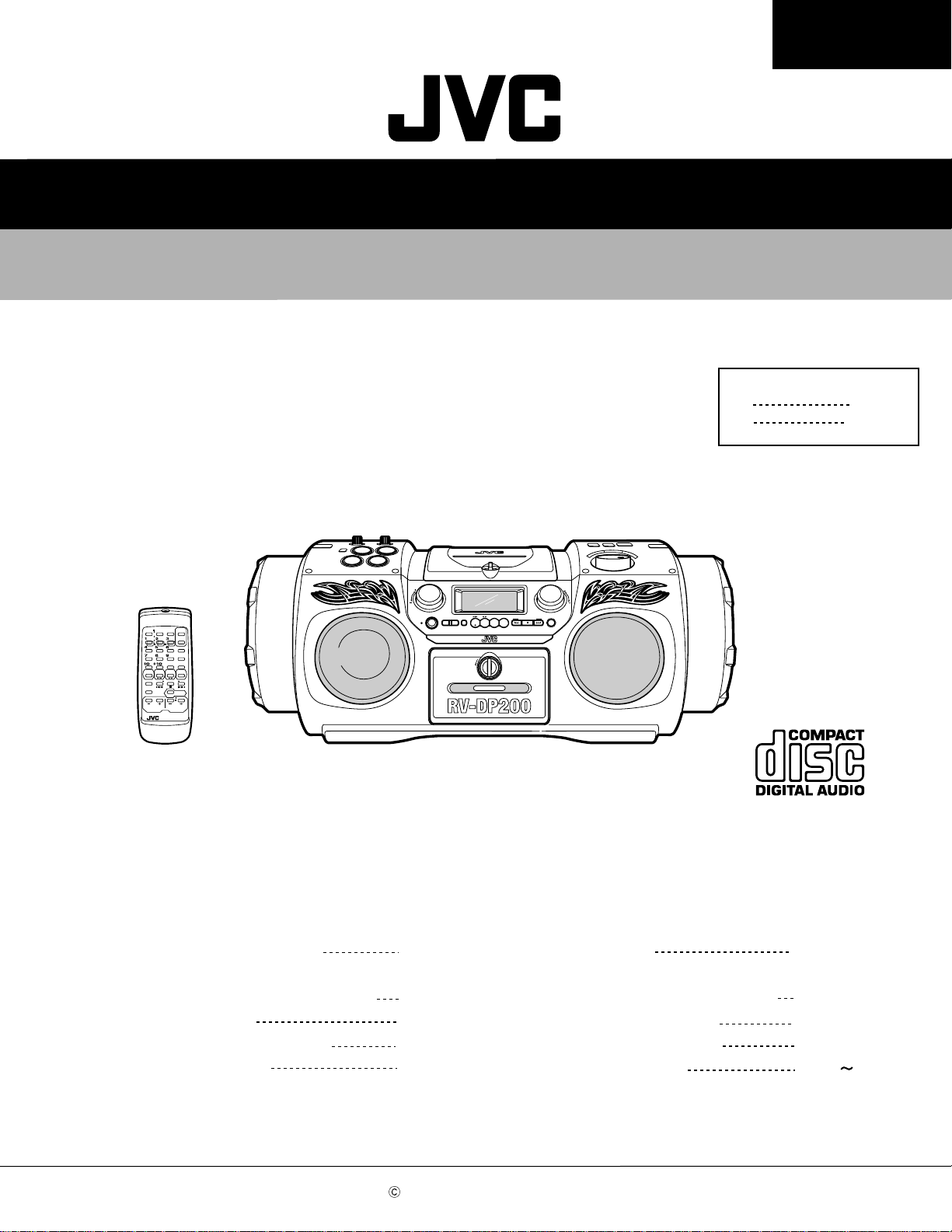
5. Leakage currnet check (Electrical shock hazard testing)
After re-assembling the product, always perform an isolation check on the exposed metal parts
of the product (antenna terminals, knobs, metal cabinet, screw heads, headphone jack, control
shafts, etc.) to be sure the product is safe to operate without danger of electrical shock.
Do not use a line isolation transformer during this check.
Plug the AC line cord directly into the AC outlet. Using a "Leakage Current Tester", measure
the leakage current from each exposed metal parts of the cabinet , particularly any exposed
metal part having a return path to the chassis, to a known good earth ground. Any leakage
current must not exceed 0.5mA AC (r.m.s.)
Alternate check method
Plug the AC line cord directly into the AC outlet. Use an AC voltmeter having, 1,000 ohms
per volt or more sensitivity in the following manner. Connect a 1,500 10W resistor paralleled by
a 0.15 F AC-type capacitor between an exposed
metal part and a known good earth ground.
Measure the AC voltage across the resistor with the
AC voltmeter.
Move the resistor connection to eachexposed metal
part, particularly any exposed metal part having a
return path to the chassis, and meausre the AC
voltage across the resistor. Now, reverse the plug in
the AC outlet and repeat each measurement. voltage
measured Any must not exceed 0.75 V AC (r.m.s.).
This corresponds to 0.5 mA AC (r.m.s.).
0.15 F AC TYPE
1500 10W
Good earth ground
AC VOLTMETER
(Having 1000
ohms/volts,
or more sensitivity)
Place this
probe on
each exposed
metal part.
Warning
1. This equipment has been designed and manufactured to meet international safety standards.
2. It is the legal responsibility of the repairer to ensure that these safety standards are maintained.
3. Repairs must be made in accordance with the relevant safety standards.
4. It is essential that safety critical components are replaced by approved parts.
5. If mains voltage selector is provided, check setting for local voltage.
Burrs formed during molding may be left over on some parts of the chassis. Therefore,
pay attention to such burrs in the case of preforming repair of this system.
2-2
CAUTION
!
Page 3
RV-DP200BK
Preventing static electricity
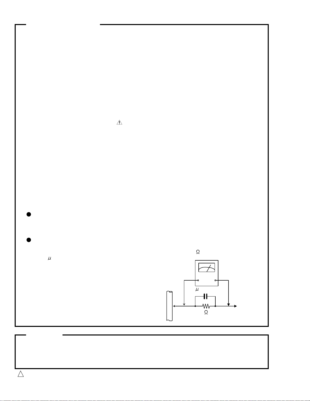
Electrostatic discharge (ESD), which occurs when static electricity stored in the body, fabric, etc. is discharged,
can destroy the laser diode in the traverse unit (optical pickup). Take care to prevent this when performing repairs.
1.1. Grounding to prevent damage by static electricity
Static electricity in the work area can destroy the optical pickup (laser diode) in devices such as DVD players.
Be careful to use proper grounding in the area where repairs are being performed.
1.1.1. Ground the workbench
1. Ground the workbench by laying conductive material (such as a conductive sheet) or an iron plate over
it before placing the traverse unit (optical pickup) on it.
1.1.2. Ground yourself
1. Use an anti-static wrist strap to release any static electricity built up in your body.
(caption)
Anti-static wrist strap
Conductive material
(conductive sheet) or iron plate
1.1.3. Handling the optical pickup
1. In order to maintain quality during transport and before installation, both sides of the laser diode on the
replacement optical pickup are shorted. After replacement, return the shorted parts to their original condition.
(Refer to the text.)
2. Do not use a tester to check the condition of the laser diode in the optical pickup. The tester's internal power
source can easily destroy the laser diode.
1.2. Handling the traverse unit (optical pickup)
1. Do not subject the traverse unit (optical pickup) to strong shocks, as it is a sensitive, complex unit.
2. Cut off the shorted part of the flexible cable using nippers, etc. after replacing the optical pickup. For specific
details, refer to the replacement procedure in the text. Remove the anti-static pin when replacing the traverse
unit. Be careful not to take too long a time when attaching it to the connector.
3. Handle the flexible cable carefully as it may break when subjected to strong force.
4. It is not possible to adjust the semi-fixed resistor that adjusts the laser power. Do not turn it
2-3
Page 4
RV-DP200BK
Dismantling and assembling the CD mechanism assembly
1. Notice regarding replacement of optical pickup
Electrostatic discharge (ESD), which occurs when static electricity stored in the body, fabric, etc. is discharged,
can destroy the laser diode in the traverse unit (optical pickup). Take care to prevent this when performing
repairs to the optical pickup or connected devices.
(Refer to the section regarding anti-static measures.)
1. Do not touch the area around the laser diode and actuator.
2. Do not check the laser diode using a tester, as the diode may easily be destroyed.
3. It is recommended that you use a grounded soldering iron when shorting or removing the laser diode.
Recommended soldering iron: HAKKO ESD-compatible product
4. Solder the short-circuit land on the optical pickup unit.
* In accordance with the following steps, solder the short-circuit land properly.
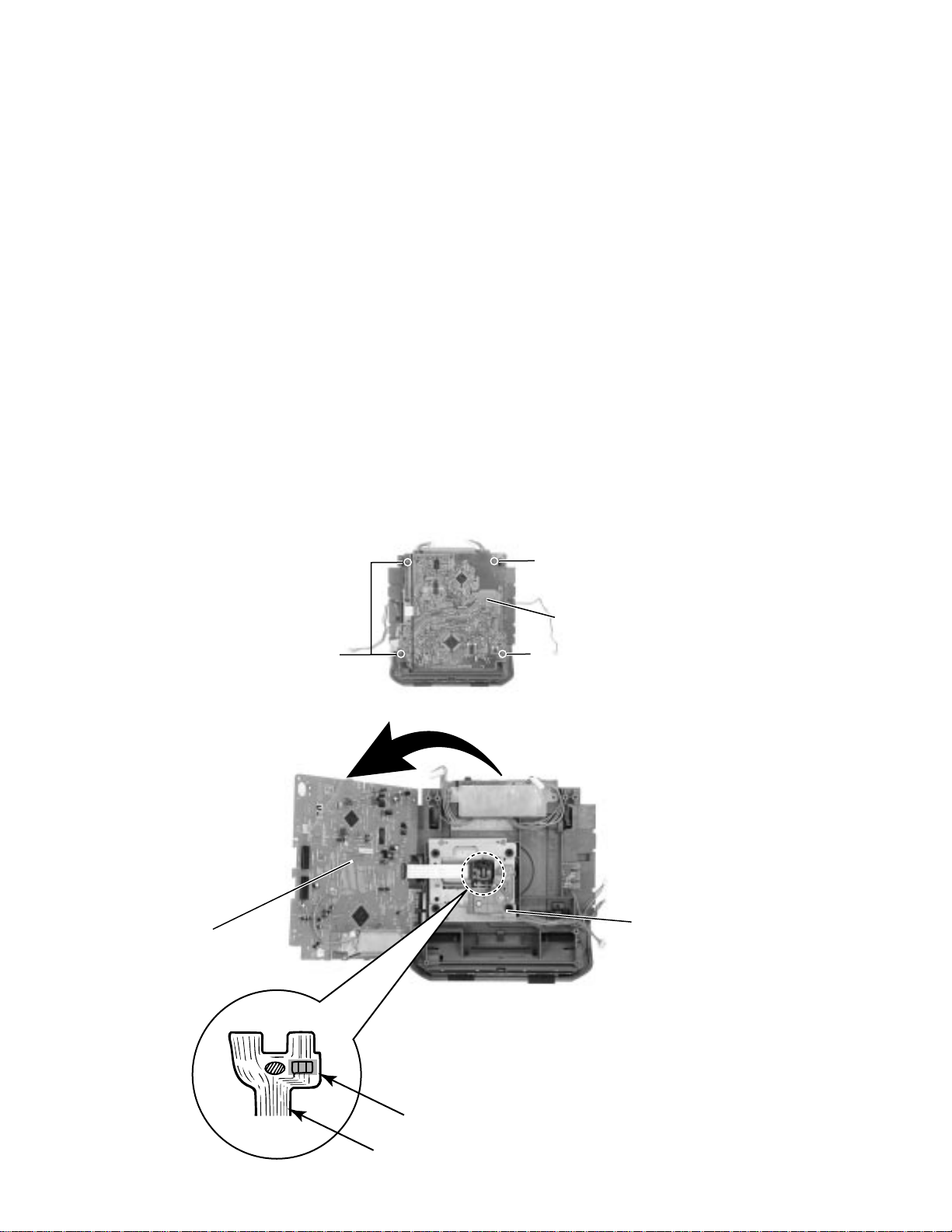
1. Remove the four screws attaching the micon board as shown in Fig1.
(Refer to "Disassembly method", page 2-8.)
2. Raise the micon board as shown in Fig. 2.
3. Prior to disconnecting the card wire from the connector CN601 on the micon board, solder the
short-circuit land on the pickup unit.
4. When reassembling, unsolder the short-circuit land on the pickup unit after connecting the card wire.
Micon board
Screw
Screw
Micon board
Screw
Fig.1
CD mechanism
assembly
2-4
Fig.2
Soldering
(Short-circuit land)
Flexible board
Page 5
Important for Laser Products
RV-DP200BK
1.CLASS 1 LASER PRODUCT
2.DANGER : Invisible laser radiation when open and inter
lock failed or defeated. Avoid direct exposure to beam.
3.CAUTION : There are no serviceable parts inside the
Laser Unit. Do not disassemble the Laser Unit. Replace
the complete Laser Unit if it malfunctions.
4.CAUTION : The compact disc player uses invisible
laserradiation and is equipped with safety switches
whichprevent emission of radiation when the drawer is
open and the safety interlocks have failed or are de
feated. It is dangerous to defeat the safety switches.
5.CAUTION : If safety switches malfunction, the laser is able
to function.
6.CAUTION : Use of controls, adjustments or performance of
procedures other than those specified herein may result in
hazardous radiation exposure.
!
Please use enough caution not to
see the beam directly or touch it
in case of an adjustment or operation
check.
2-5
Page 6
RV-DP200BK
Disassembly method
<How to disassemble>
Replacing the fuses Described at the
end of "Disassembly method".
Removing the cabin
1)
Remove the side grilles.
Remove the two screws on the front of each
speaker.
2)
Remove the mixing unit and the scratch & rhythm
unit on the upper right and left sides of the body.
3)
Remove the ten screws attaching the cabinet on the
back of the body.
4)
The front cabinet comes off.
Power amplifier board
1)
After disassembling the cabinet, remove the CD unit.
2)
Remove the three screws attaching the power
amplifier assembly
(Use an offset screwdriver to remove the screw on
the bottom).
<Main Body>
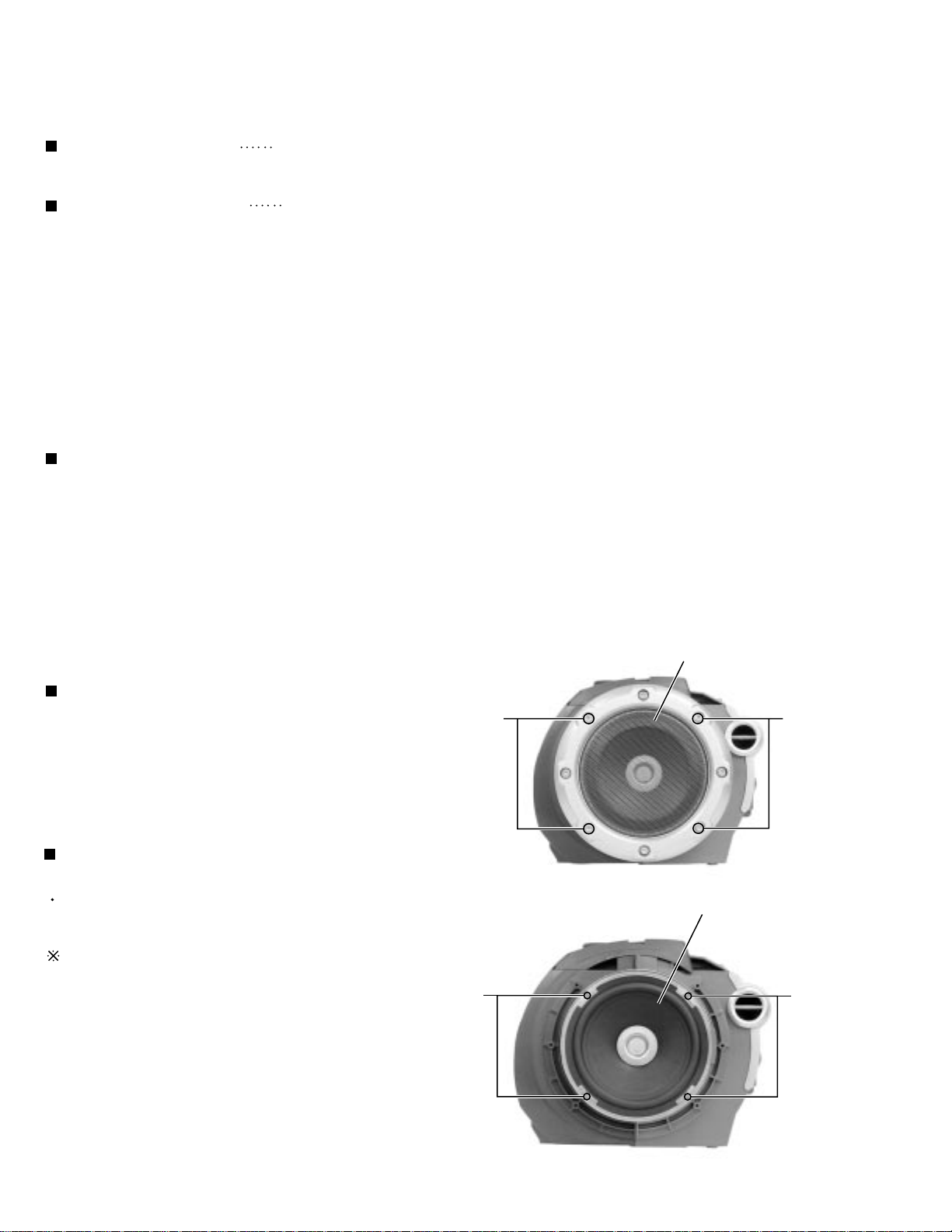
Removing the side grilles ( See Fig.1)
1.
Remove the four screws A attaching the side grille
on the left side of the body. Pull out the side grille
from the body outward.
2.
Remove the side grille on the right side in the same
way.
Removing the woofer speakers
(See Fig.2)
Prior to performing the following procedure, remove
the right and left side grilles.
When disassembling without removing the woofer
speaker, remove the two screws B on the front of
each speaker.
Front side
B
Side grille
AA
Fig.1
Woofer speaker
B
1.
Remove the four screws B attaching the woofer
speaker on the left side of the body.
2.
Disconnect the harness from the speaker terminal on
the back of the woofer speaker.
3.
Remove the woofer speaker on the right side in the
same way.
2-6
Fig.2
Page 7
RV-DP200BK
Removing the scratch & rhythm assembly
(See Fig.3 and 4)
Prior to performing the following procedure, remove
the left side grilles.
1.
Remove the four screws C attaching the scratch &
rhythm assembly
2.
Disconnect the harness from connector CN924 of
the scratch & rhythm board on the underside of the
scratch & rhythm assembly.
Scratch & rhythm
assembly
C
Fig.3
CN924
C
Scratch & rhythm
board
Removing the mixing assembly
(See Fig.5 and 6)
Prior to performing the following procedure, remove
the right side grilles.
1.
Remove the four screws D attaching the mixing
assembly.
2.
Disconnect the harness from connector CN424 on
the mic & guitar volume board and CN923 on the
drum key board on the underside of the mixing
assembly.
Mic & guitar volume board
Drum key board
CN923
CN424
Fig.4
Mixing assembly
D
D
Fig.6
Fig.5
2-7
Page 8
RV-DP200BK
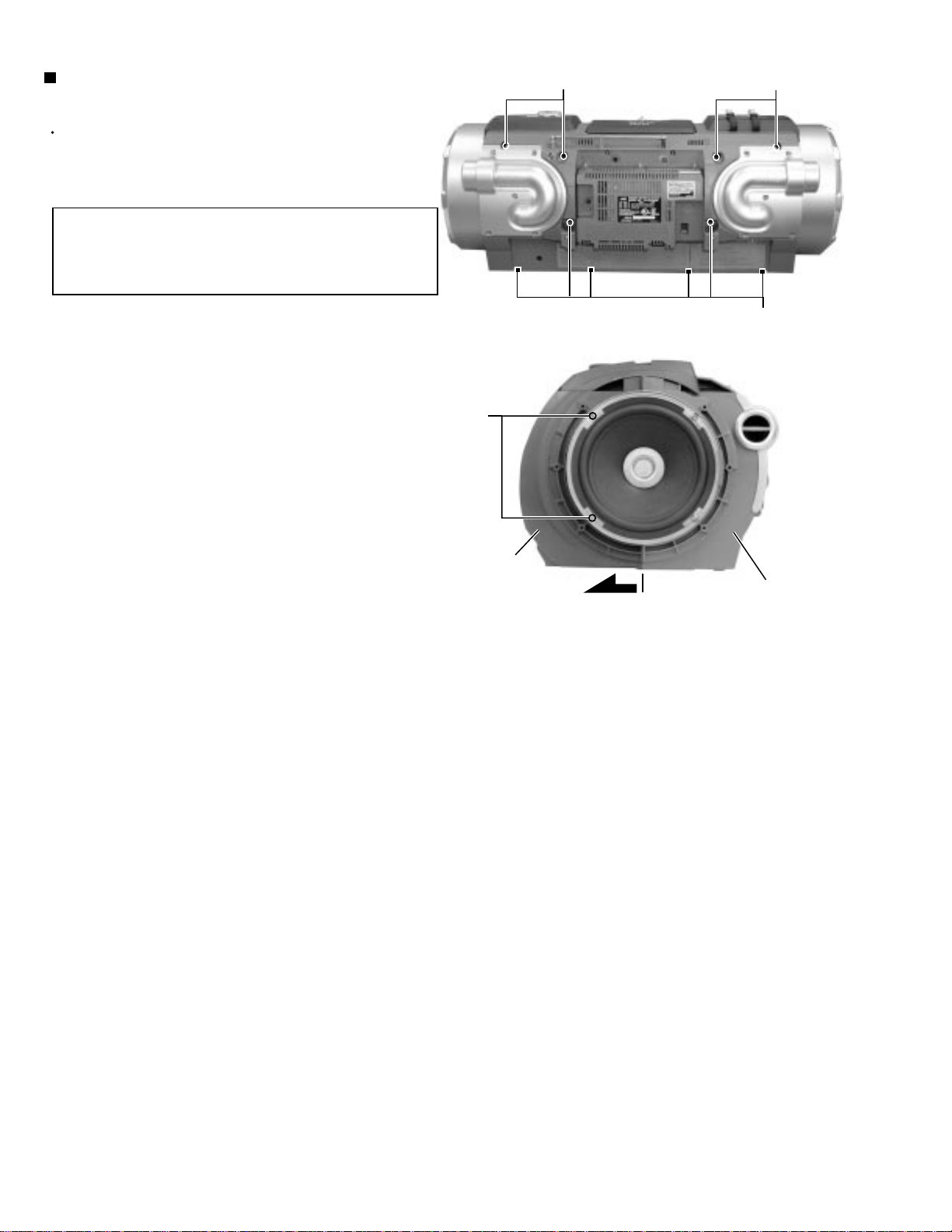
Removing the front cabinet and the rear
cabinet (See Fig.7 and 8)
Prior to performing the following procedure, remove
the side grilles, the woofer speakers, the scratch &
rhythm assembly and the mixing assembly.
ATTENTION:
ATTENTION:
1.
Remove the ten screws E attaching the rear cabinet
on the back of the body.
2.
Remove the front cabinet and the rear cabinet (The
speaker terminal inside the front cabinet comes off at
the same time).
ATTENTION:
The front cabinet can be removed on
The front cabinet can be removed on
condition that the front two screws B
condition that the front two screws B
attaching the woofer speakers are
attaching the woofer speakers are
removed.
removed.
When reassembling, make sure that
connector CN193 of the rear cabinet is
connected to the speaker terminal on
the front cabinet.
B
E
Rear side
Fig.7
E
E
Front cabinet
Front side
Rear cabinet
Fig.8
2-8
Page 9
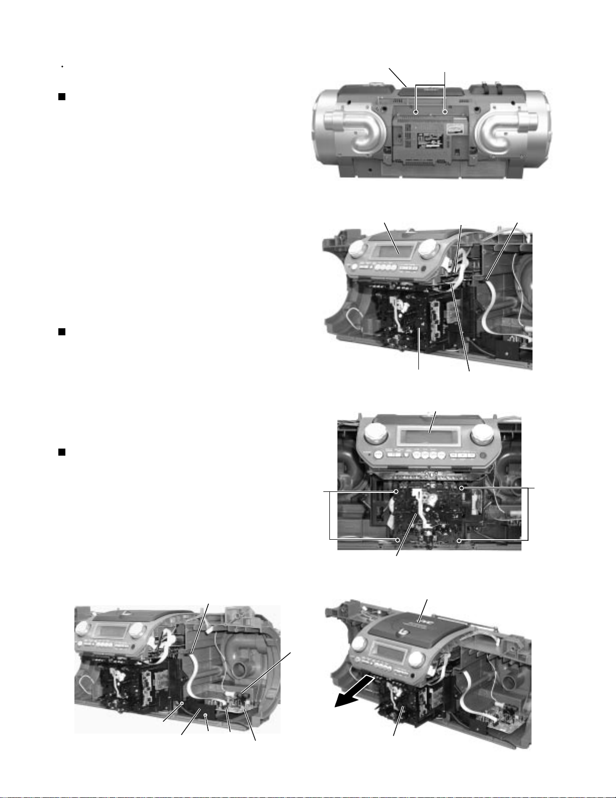
RV-DP200BK
<Rear cabinet>
Prior to performing the following procedure, remove
the front cabinet and the rear cabinet.
Removing the CD unit (See Fig.9 to 12)
1.
Remove the two screws F attaching the CD unit on
the back of the rear cabinet.
2.
Disconnect the card wires from connector CN916 on
the micom board and CN415 and CN413 on the
main switch board in the lower left part of the CD
unit.
3.
Pull out the CD unit toward the front. The connector
CN417 and CN418 of the micom board in the lower
rear part of the CD unit are disconnected from the
main switch board at the same time.
CAUTION:
When reassembling, make sure that
connector CN417 and CN418 of the CD
unit are connected to connector CN427
and CN428 on the power aboard
correctly.
Removing the cassette mechanism
assembly (See Fig.10 and 11)
1.
Disconnect the card wires from connector CN916 on
the micom board and CN415 on the main switch
board in the lower left part of the CD unit.
CD unit
Fig.9
CD unit
Cassette mechanism assembly
Micom board
Fig.10
F
CN916
Main switch board
CN415
CN413
2.
Remove the four screws G attaching the cassette
mechanism assembly. Detach the cassette
mechanism assembly toward the front.
Removing the tuner board (See Fig.13)
1.
Disconnect the card wire from connector CN1 on the
tuner board.
2.
Remove the antenna wire from TP1 on the tuner
board.
3.
Remove the two screws H attaching the tuner board
holder.
4.
Pull out the tuner board toward the front.
CN413
TP1
G
Cassette mechanism assembly
Fig.11
CD unit
CD unit
G
H
Tuner board holder
Fig.13
H
CN1
Tuner board
Cassette mechanism assembly
Fig.12
2-9
Page 10
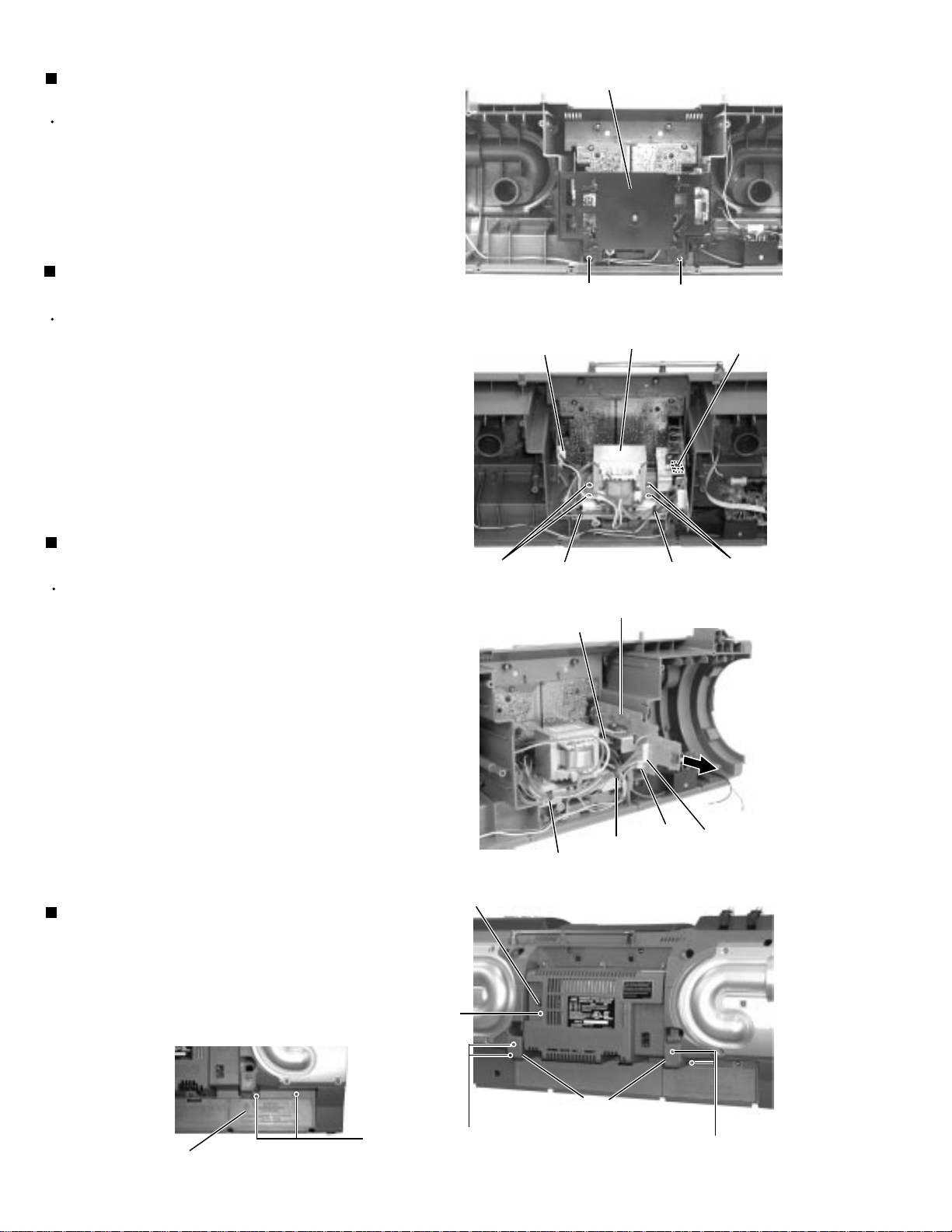
RV-DP200BK
Removing the cassette mechanism
holder (See Fig.14)
Prior to performing the following procedure, remove
the cassette mechanism.
1.
Remove the two screws I and the cassette
mechanism holder toward the front.
Removing the power transformer
(See Fig.15 and 16)
Prior to performing the following procedure, remove
the cassette mechanism assembly, the cassette
mechanism holder and the CD unit.
1.
Disconnect the harnesses from connector CN194 on
the AC input board and CN195 on the regulator
board respectively. Release the harness from the
clamp marked a.
2.
Remove the four screws J attaching the power
transformer.
Cassette mechanism holder
I
AC input board
CN194,CN191
Power transformer
Fig.14
I
Regulator board
CN195
Removing the regulator board
(See Fig.15, 16 and 17)
Prior to performing the following procedure, remove
the cassette mechanism assembly, the cassette
mechanism holder and the CD unit.
1.
Disconnect the harness from connector CN191 on
the AC input board. Release the harness from the
clamps marked a and b.
2.
Disconnect the harness from connector CN193,
CN195 and CN196 on the regulator board.
3.
Pull out the regulator board from the cabinet slot
under the regulator board toward the front.
4.
Remove the screw K attaching the DC input terminal
on the rear cabinet.
Removing the rear support and battery lid
(See Fig.17 and 18)
1.
Remove the two screws L & L' attaching the rear
support.
J
DC input terminal
Clamp b
Clamp b
Fig.15
Regulator board
CN195
Clamp a
Fig.16
Clamp a
CN193
J
CN196
2.
Remove the two screws M attaching the battery lid.
Battery lid
Fig.18
2-10
M
K
L'
Rear support
Fig.17
L
Page 11
RV-DP200BK
Removing the power amplifier board
(See Fig.19)
Prior to performing the following procedure, remove
the cassette mechanism assembly, the cassette
mechanism holder, the CD unit, the power
transformer, the regulator board.
1.
Release the harness from the clamps marked a, b
and the spacer marked c.
2.
Remove the three screws N attaching the power
amplifier board.
Removing the AC input board (See Fig.20)
Prior to performing the following procedure, remove
the cassette mechanism assembly, the cassette
mechanism holder, the CD unit, the power
transformer, the regulator board and the power
amplifier board .
CN194
CN427
N
Clamp b
Clamp a
Fig.19
Power amplifier board
CN428
Spacer c
1.
Remove the two screws O attaching the AC jack on
the AC input board.
Removing the battery board 1 and the
battery board 2 (See Fig.21)
Prior to performing the following procedure, remove
the cassette mechanism assembly, the cassette
mechanism holder and the tuner board holder.
1.
Disconnect the harness from connector CN193 of
the regulator board. Release the harness from the
spacer marked c.
2.
Pull out the battery board 1 toward the front.
3.
Remove the screw Q and pull out the battery board 2
toward the front.
CN191
Battery board 2
Q
Fig.20
Fig.21
O
AC input board
Regulator board
CN193
Battery board 1
Spacer c
2-11
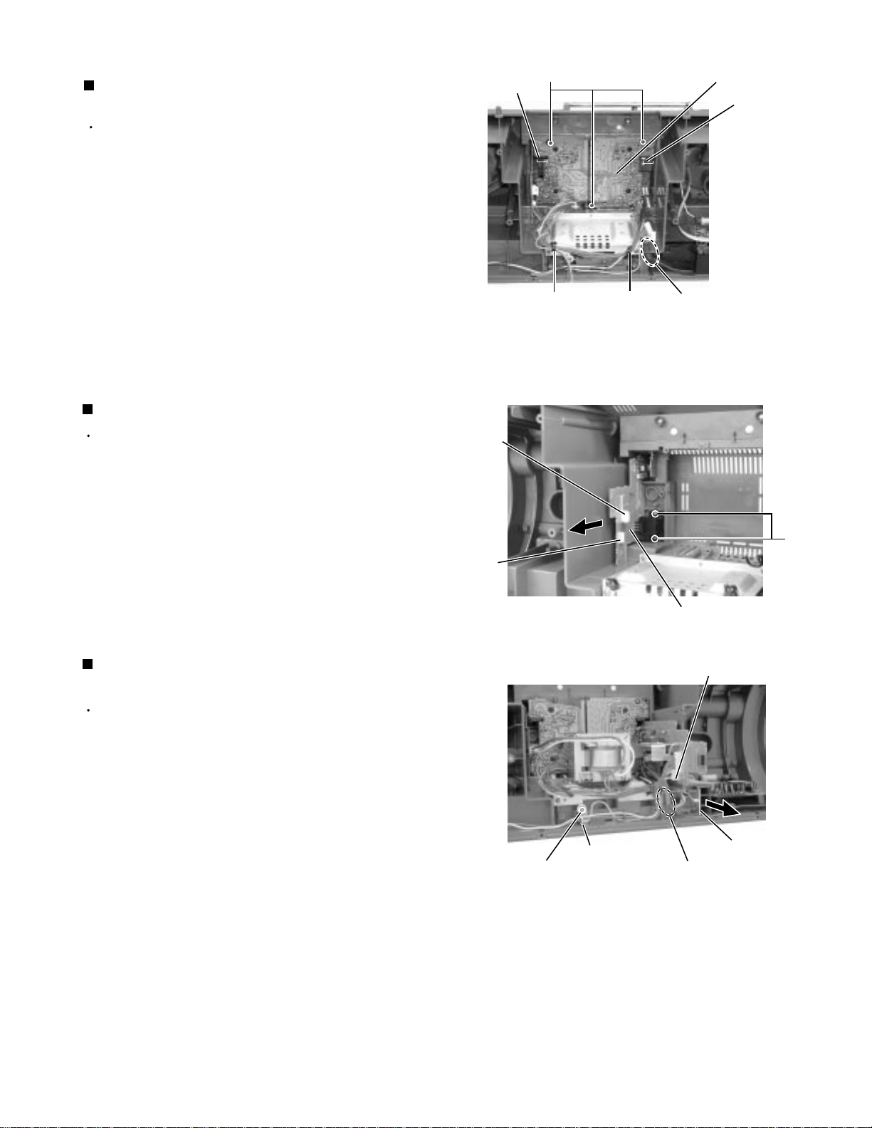
Page 12
RV-DP200BK
<CD Unit >
Prior to performing the following procedure, remove
the front cabinet, the rear cabinet and the CD unit.
CN418
CN419
Main Switch board
CN410
CN417
Removing the main switch board and
illumination boad. (See Fig.22)
1.
Disconnect the card wire from connector CN411 and
CN412, and the harness from CN401,CN419 and
CN410 of the main switch board on the underside of
the CD unit.
2.
Remove the four screws R attaching the main
switch board and illumination board.
Removing the micon board (See Fig.23)
Prior to performing the following procedure, remove
the main switch board.
CAUTION:
Prior to disconnecting the card wire from
connector CN601 on the micon board, solder the
short-circuit land on the pickup unit.
Disconnecting the card wire extending from the
pickup unit may cause damage to the pickup unit.
R
CN413
CN415
R
Illumination board
S
(Disconnect after soldering
the short-circuit land.)
CN601
d
CN911
CN916
S
CD unit
Fig.22
CN602
R
CN411
CN412
R
CN401
S
CN412
CN422
S
When reassembling, unsolder the short-circuit
land on the pickup unit after connecting the card
wire to connector CN601.
Fig.25 shows more detail about the short-circuit
land.
1.
Disconnect the card wires from connector CN601 and
CN911 on the micon board.
2.
Remove the spacer fixing the harnesses marked d.
3.
Remove the four screws S attaching the micon board.
4.
Disconnect the harness from connector CN912 and
CN602 on under side of the micon board respectively.
Micon board
CN912
Fig.23
2-12
Page 13

RV-DP200BK
Removing the CD door switch board
(See Fig.24 and 25)
Prior to performing the following procedure, remove
the main switch board and the micon board.
1.
Remove the CD door switch board by pushing the
two tabs e inward.
CD door switch board
Tabs e
Fig.24
Removing the CD mechanism assembly
(See Fig.25)
Prior to performing the following procedure, remove
the main switch board and the micon board.
CD mechanism
assembly
The short-circuit
land
T
T
Headphone / Aux board
UU
Operation panel assembly
Fig.25
CD door
switch board
1.
Remove the four screws T attaching the CD
mechanism holder on the underside of the CD case.
2.
Remove the CD mechanism holder and the CD
cushion from the CD mechanism assembly
respectively.
Removing the headphone / aux board
(See Fig.25)
Prior to performing the following procedure, remove
the main switch board and the micon board.
1.
Remove the two screws U attaching the headphone
/ aux board.
Removing the key switch board
(See Fig.26 to 28)
Prior to performing the following procedure, remove
the main switch board and the micon board.
1.
Extrude the operation panel assembly from the
underside of the CD unit toward the front while
pushing the four hooks f outward.
Hooks f
V
Operation panel assembly
Fig.26
Volume knob
Fig.27
Hooks f
Volume knob
V
Pull out the two volume knobs from the operation
panel assembly.
Remove the ten screws V attaching the key switch
board on the reverse side of the operation panel.
VV
Key switch board
Fig.28
2-13
Page 14

RV-DP200BK
<Scratch & rhythm unit>
Prior to performing the following procedure, remove
the left side grille and the scratch & rhythm unit.
Removing the scratch & rhithm board
(See Fig.29 and 30)
1.
Pull out the S & R jogdial knob.
2.
Remove the five screws W attaching the scratch &
rhythm board on the reverse side of the scratch &
rhythm unit.
<Mixing unit>
Prior to performing the following procedure, remove
the right side grille and the mixing unit.
Removing the mic & guitar volum board /
mic / guitar jack board / drum key board
(See Fig.31 to 35)
1.
Pull out the mic knob and the guitar knob. Remove
the covers from the mic jack and the guitar jack.
2.
Remove the four screws X attaching the mic & guitar
volum board and the three screws Y attaching the
bracket on the underside of the mixing unit. Remove
the mic & guitar volum board together with the mic /
guitar jack board.
3.
Disconnect the connector CN951 on the mic & guitar
volum board from the mic / guitar jack board.
S & R jogdial knob
Mic knob
W
Scratch & rhythm unit
Fig.29
Scratch & rhythm bosrd
Fig.30
W
Cover
Guitar knob
Fig.31
4.
Remove the two snap plates attaching the bracket to
the mic / guitar jack board by moving them outward.
5.
Remove the five screws Z attaching the drum key
board.
Mic & guitar volume board
Brackeet
Snap plate
CN951
Mic / Guitar jack board
Brackeet
Mic / Guitar jack board
Fig.34
Snap plate
Fig.33
Y
Brackeet
XX
Mic & guitar volume board
Z
Drum key board
Fig.32
Z
Fig.35
2-14
Page 15

RV-DP200BK
<Front cabinet assembly>
Prior to performing the following procedure, remove
the front cabinet and the rear cabinet.
Removing the front speakers
(See Fig.36 and 37)
1.
Remove the eight screws A attaching the speaker
covers on the inside of the front cabinet.
2.
Remove the eight screws B attaching the right and
left front speakers.
3.
Remove the screw C attaching the speaker terminal.
B
A
A
Speaker cover
Speaker terminal
Fig.36
Front speaker
C
A
A
B
<Replacing a fuse> (See Fig.38 and 39)
CAUTION:
1.
Remove the battery cover on the back of the body.
2.
Remove the five screws D attaching the power
amplifier cover on the back of the body.
3.
Replace the fuse F1901 of the AC input board and
F1902 and F1903 of the regulator board on the back
of the body respectively.
It is not necessary to remove the AC input
board and the power amplifier board.
Battery cover
B
Speaker terminal
Fig.37
D
D
D
Fig.38
B
Power amplifier cover
F1901
F1902
F1903
Fig.39
2-15
Page 16

RV-DP200BK
Removing the CD pickup unit
(See Fig.38)
1.
Move the cam gear in the arrow direction "f" . Then, the
CD pickup unit will be moved in the arrow direction "g" .
2.
According to the above step, shift the CD pickup unit to
the center position.
While pressing the stopper retaining the shaft in the
3.
arrow direction "h" , pull out the shaft in the arrow
direction "i".
After dismounting the shaft from the CD pickup unit,
4.
remove the CD pickup unit
h
Shaft
Stopper
CD Pickup unit
g
f
Shaft
i
Stopper
Fig.38
CD loading
mechanism
Shaft
Cam gear
2-16
Page 17

RV-DP200BK
<<Cassette mechanism section>>
Removing the playback/recording & eraser
head ( See Figs. 1 and 2 )
1. While shifting the trigger arms seen on the right
side of the head mount in the arrow direction,
turn the flywheel R in counterclockwise direction
until the head mount has gone out with a click
(See Fig. 1).
2. When the flywheel R is rotated in counterclockwise
direction, the playback/recording & eraser head
will be turned in counterclockwise direction from the
position in Fig. 2 to that in Fig. 3.
3. At this position, disconnect the flexible P.C. board
(outgoing from the playback/recording & eraser head)
from the connector CN31 on the head amplifier &
mechanism control P.C. board.
4. After dismounting the FPC holder, remove the flexible
P.C. board.
5. Remove the flexible P.C. board from the chassis base.
6. Remove the spring a from behind the playback/recording
& eraser head.
7. Loosen the reversing azimuth screw retaining the playback
/recording & eraser head.
8. Take out the playback/recording & eraser head from the
front of the head mount.
9. The playback/recoring & eraser head should also be
removed similarly according to Steps 1 ~ 8 above.
Cassette mechanism
Fig. 1
Playback/recording &
eraser head
Flexible
board
Head amplifier & mechanism
control P.C. board
Flywheel R
Trigger armHead mount
Spring a
Trigger arm
Flywheel R
Reassembling the playback/recording
& eraser head
1. Reassemble the playback head from the front of the head
mount to the position as shown in Fig. 3.
2. Fix the reversing azimuth screw.
3. Set the spring a from behind the Playback/Recording &
Eraser head.
4. Attach the flexible P.C. board to the chassis base, and fix
it with the FPC holder as shown in Fig. 3.
5. The playback/recording & eraser head should also be
reassembled similarly to Step 1 ~ 4 above.
Playback/recording &
eraser head
Spring "a"
FPC holder
Fig. 2
Reversing azimuth
screw
Head
mount
Flexible
board
Head amplifier &
mechanism control
P.C. board
Fig. 3
2-17
Page 18

RV-DP200BK
Removing the head amplifier & mechanism
control P.C. board (See Fig. 4)
1. Remove the cassette mechanism assembly.
2. After turning over th cassette mechanism assembly,
remove the three screws A retaining the head
amplifier & mechanism control P.C. board.
3. Disconnect the connector CN32 on the P.C. board
including the connector CN 1 on the reel pulse P.C.
board.
4. When necessary, remove the 4 pin parallel wire
soldered to the main motor.
Head amplifier &
mechanism control
P.C. board
Removing the main motor assembly
(See Fig. 4~6)
1. Remove the two screws B retaining the main
motor assembly (See Fig. 4, 4a).
2. While raising the main motor, remove the capstan
belt from the motor pulley (See Fig. 4a).
Caution 1: Be sure to handle the capstan belt so
carefully that this belt will not be
stained by grease and other foreign
matter. Moreover, this belt should be
hanged while referring to the capstan
belt hanging method in Fig. 5, 6.
A
Flexible P.C. board
Capstan belt
A
Fig. 4
Main motor
assembly
A
Belt
Main motor
assembly
B
B
4pin parallel wire
Main
motor
assembly
Motor
pulley
2-18
Capstan
belt
Fig. 5
Mechanism motor
assembly
Motor
pulley
Fig. 4a
Main motor
assembly
Flywheel
Motor pulleyCapstan belt
Fig. 6
Page 19

Removing the flywheel
(See Figs. 7 and 8)
1. Remove the head amplifier & mechanism control
P.C. board.
2. Remove the main motor assembly.
3. After turning over the cassette mechanism,
remove the slit washers b and c fixing the capstan
shafts R and L, and pull out the flywheel R and L
respectively from behind the cassette mechanism.
RV-DP200BK
Flywheel R Flywheel L
Capstan shaft R Capstan shaft L
Flywheel R Flywheel L
Fig. 8
Removing the reel pulse P.C. board and solenoid
(See Fig. 9)
1. Remove the five pawls d~h and screw C retaining the reel pulse
P.C. board.
2. From the surface of the reel pulse P.C. board parts, remove
the two pawls i and j retaining the solenoid.
hd
e
C
Slit
washer
f
b
Slit
washer
Fig.7
C
g
Reel pulse P.C. board
Solenoid
j
i
Fig. 9
2-19
Page 20

RV-DP200BK
Adjustment method
Measuring devices necessary for adjustment
1. Low-frequency oscillator
It must have the ability to output 600ohm from 0 dBs
at an oscillation frequency of 20 Hz-50 Hz.
2.Attenuator impedance: 600ohm
3.Electronic voltmeter
Tuner section
Voltage input to the tuner .......................... +B: DC 5.7 V
VT: DC 12 V
Standard measuring output ....... 26.1 mV (0.28 V)/3ohm
Input locations ..................... AM: standard loop antenna
FM: TP1 (hot) and TP2 (GND)
Standard settings for measuring volume
4.Distortion meter
5.Frequency counter
6.Wow and flutter meter
7.Test tapes
VT-712: tape speed and rotational distortion (3 kHz)
VT-724: standard level (1 kHz)
VT-703: head angle adjustment (10 kHz),
or use VT-73
VT-739: reproduction of frequency characteristics
(1 kHz, 63 Hz, 10 kHz)
8.Blank tape
Type I : AC-225 (TDK-AD)
Type II : AC-514 (TDK-SA)
9.Torque gauge: Tension gauge for playback,
fast-forward and rewind.
FWD (TW211A), REW (TW212A)
and FF/REW (TW2231A)
Sound ..................................................................... OFF
Effective hyper bass ............................................... OFF
Volume adjustment ........................................... VOL. 23
Precautions for measuring
1.Input 30 pF and 33 kohm to the IF sweeper output
2.Lower the output level of the IF sweeper as much as
3.The IF sweeper needs no adjustment as it is a fixed
4.It is not necessary to perform any kind of adjustment
and 0.082 F and 100 kohm to the sweeper input,
respectively.
possible in the adjustable range.
component.
on the MPX, as a ceramic oscillator is used for
measuring.
Specifications for measurement
Power supply voltage ................... AC 100 V (50/60 Hz)
Standard output ........................ Speaker: 0.775V/4ohm
Headphone:0.245V/32ohm
Standard frequency and input level
................... 1 kHz: AUX: -8 dBs
Input level for reproduction of recording characteristics
................... AUX: -28 dBs
Measuring output terminal ................... Speaker: CN633
Load resistance .................................................... 4ohm
Radio input signal
AM frequency ..................................................... 400 Hz
Degree of modulation in AM band .......................... 30%
FM frequency ...................................................... 400 Hz
Frequency deviation in FM band ..................... 22.5 kHz
5.FM tracking adjustment is not necessary as a fixed
coil is used.
6.The grounding circuit is separate from the input and
output. Therefore, be sure to connect to ground
carefully when measuring both the input and output
voltages simultaneously using 2 channels of the
electronic voltmeter.
7.The speaker's minus terminal cannot be connected to
ground when using a BTL format amplifier. Therefore,
do not connect any type of ground wire to this
terminal. The OTL format is used with this system.
8.Use a large wire to connect to the dummy impedance
generator when measuring the output.
9.Be sure to use a band pass filter (DV-12) when using
mixed tape.
2-20
Page 21

RV-DP200BK
Location of parts to be adjusted
Cassette handling mechanism Cassette handling mechanism (reverse side)
Head for recording, playing
and erasing the tape
Head azimuth
adjusting screw (fast-forward)
Head azimuth adjusting
screw (rewind)
Head azimuth adjusting
screw (fast-forward)
CN31
Head for recording,
playing and erasing the tape
Head azimuth adjusting
screw (rewind)
Location of parts to be adjusted
VR37
Motor speed
TP
Bias oscillation frequency (wide pattern)
L301
Bias oscillation frequency
VR31
Lch recording frequency (bias adjustment)
VR32
Rch recording frequency (bias adjustment)
2-21
Page 22

RV-DP200BK
Adjustment of cassette handling mechanism
Items Condition Method for adjustment
Confirmation
of head angle
Confirmation
of tape speed
Test tape: VT-703 (10 kHz)
Measuring output terminal:
Speaker terminal, speaker (R)
(Load resistance: 4ohm),
headphone terminal
Test tape: VT-712 (3 kHz)
Measuring output terminal:
Headphone terminal
(1) Play back the VT-703 test tape.
(2) Adjust the head azimuth screws so
that the tape playback mechanism
records the maximum output level in
both the fast-forward and rewind
direction.
(3) In all cases, both the fast-forward and
rewind direction should be adjusted
using head azimuth screws.
Adjust VR37 so that the frequency
counter records 3,015 Hz 15 Hz when
playing back the end of the VT-712 test
tape (3 kHz) in the fast-forward direction.
and confirmation
Items to be confirmed and standard values
Items Condition Method for adjustment
Difference in
speed
between fastforward and
rewind
Test tape: VT-712 (3 kHz)
Measuring output terminal:
Speaker terminal, speaker (R)
(Load resistance: 4 ),
headphone terminal
The difference between fast-forward and
rewind should be less than 60 Hz on the
frequency counter when playing back the
beginning of the VT-712 test tape (3 kHz)
in both directions.
and confirmation
Standard
value
Maximum
output
Tape speed
of cassette
deck: 3,015
Hz 15 Hz
Standard
value
Less than 60 HzShould be
Parts to be
adjusted
Adjust the
head
azimuth
screws
when
changing
the head.
VR37
Parts to be
adjusted
confirmed
when
changing
the motor.
Wow and
flutter
Test tape: VT-712 (3 kHz)
Measuring output terminal:
Headphone terminal
Wow and flutter should be recorded at
less than 0.25% (WRMS) when playing
back the VT-712 test tape (3 kHz) in the
fast-forward direction.
Electronic performance
Items Condition Method for adjustment
Confirmation
of output
Confirmation
of
reproduction
of frequency
characteristic
s
Recording
bias
frequency
Measuring output terminal:
CN34-5 or 7-terminal
preamp base
Test tape: VT-724
Measuring output terminal:
Headphone terminal
Test tape: VT-739
Fast-forward or rewind
direction:
Test tape: TYPE II (AC-
514)
Measuring terminal: Bias
TP on the base
Confirm that the output from the CN34-5
or 7-terminal preamp base connector is 25 dBs 3 dB when playing back the VT724 test tape.
Reference value: The output from the
headphone terminal is -7 dB 4 dB.
Confirm that the 10 kHz reproduction
level is -1 dB 5 dB compared to the 1
kHz reproduction level when playing back
the VT-739 test tape.
Switch the bias (beat cut switch) between
1 and 2 to confirm that the frequency
changes. Load the test tape (AC-514 for
TYPE II) into the mechanism and preset
it to the record-pause mode.
Confirm that the bias TP frequency on
the base is 100 kHz 6kHz.
and confirmation
Less than
0.25%
(WRMS)
Standard
value
Output of CN345 terminal: -25
dBs 3 dB
Difference
between Lch
and Rch: within
3 dB
Difference
between 10
kHz and 1 kHz
should be -1
dB 5 dB.
100 kHz 6 kHz
Parts to be
adjusted
2-22
Page 23

Standard values for confirmation of electronic performance
RV-DP200BK
Items Condition Method for adjustment
and confirmation
Erasing
current
(standard
and
reference
value)
Adjustment of
reproduction
of frequency
characteristic
s
Fast-forward and
rewind direction:
Recording mode
AC-514 for TYPE II,
AC-225 for TYPE I
Measuring terminal:
Both erase head terminals
Standard frequencies:
1 kHz and 10 kHz
(REF: -20 dB)
Test tape: TYPE II:
AC-514
Measuring input
terminal: OSC IN
Load the test tape (AC-514 for TYPE II,
AC-225 for TYPE I) into the tape
playback mechanism and preset it to the
record-pause mode.
After setting it to the recording mode,
send 1 M in series to the erase head and
measure the erasing current from both
erase head terminals.
Load the test tape (AC-514 for TYPE II,
AC-225 for TYPE I) into the tape
playback mechanism and preset it to the
record-pause mode.
Input the standard value of -20 dB and
the standard frequencies of 1 kHz and 10
kHz repeatedly to the microphone input
from the transmitter in the recording
mode. Adjust VR31 for Lch and VR32 for
Rch so that the difference in level
between 10kHz and 1 kHz is -1dB 5dB.
Repeat the above for TYPE I and confirm
that the difference in level is -XdB dB.
Standard
value
TYPE II: 110
mA
TYPE I: 75 mA
Difference in
output
between 1 kHz
and 10 kHz: -1
dB 5 dB
Parts to be
adjusted
Lch: VR31
Rch: VR32
2-23
Page 24

RV-DP200BK
Flow of functional operation until TOC read
Power ON
Play Key
Slider turns REST
SW ON.
Automatic tuning
of TE offset
Check Point
Confirm that the voltage at the pin5
of CN602 is "H"\"L"\"H".
Tracking error waveform at TOC reading
Approx.3sec
Tracking
servo
off states
Automatic measurement
of TE amplitude and
automatic tuning of
TE balance
VREF
pin 25 of
IC601(TE)
Approx
1.8V
Disc states
to rotate
Tracking
servo
on states
Disc to be
braked to stop
TOC reading
finishes
500mv/div
2ms/div
Fig.1
Laser ON
Detection of disc
Automatic tuning of
Focus offset
Automatic measurement of
Focus S-curve amplitude
Disc is rotated
Focus servo ON
(Tracking servo ON)
Automatic measurement of
Tracking error amplitude
Automatic tuning of
Tracking error balance
Check that the voltage at the
pin40 of IC603 is + 5V?
Confirm that the Focus error
S-cuve signal at the pin28 of
IC603 is approx.2Vp-p
Confirm that the signal from
pin24 IC603 is 0V as a
accelerated pulse during
approx.400ms.
Confirm the waveform of
the Tracking error signal.
at the pin 25 of IC601 (R609)
(See fig-1)
2-24
Automatic tuning of
Focus error balance
Automatic tuning of
Focus error gain
Automatic tuning of
Tracking error gain
TOC reading
Play a disc
Confirm the eye-pattern
at the lead of TP1
Page 25

RV-DP200BK
Maintenance of laser pickup
(1) Cleaning the pick up lens
Before you replace the pick up, please try to
clean the lens with a alcohol soaked cotton
swab.
(2) Life of the laser diode
When the life of the laser diode has expired,
the following symptoms will appear.
1. The level of RF output (EFM output : ampli tude of eye pattern) will below.
Is the level of
RFOUT under
1.25V 0.22Vp-p?
YES
O.K
NO
Replace it.
Replacement of laser pickup
Turn off the power switch and, disconnect the
power cord from the ac outlet.
Replace the pickup with a normal one. (Refer
to "Pickup Removal" on the previous page)
Plug the power cord in, and turn the power on.
At this time, check that the laser emits for
about 3 seconds and the objective lens moves
up and down.
Note: Do not observe the laser beam directly.
Play a disc.
Check the eye-pattern at TP1.
Finish.
(3) Semi-fixed resistor on the APC PC board
The semi-fixed resistor on the APC printed circuit board which is attached to the pickup is used to adjust the laser
power. Since this adjustment should be performed to match the characteristics of the whole optical block, do not
touch the semi-fixed resistor.
If the laser power is lower than the specified value, the laser diode is almost worn out, and the laser pickup should
be replaced.
If the semi-fixed resistor is adjusted while the pickup is functioning normally, the laser pickup may be damaged
due to excessive current.
2-25
Page 26

RV-DP200BK
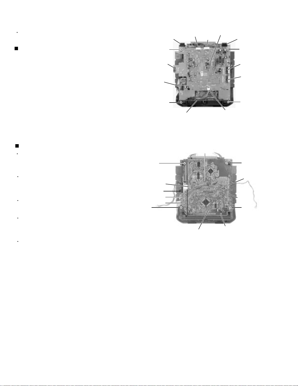
Description of major ICs
AN7317(IC32) : ALC & Pre Amplifier
Pre-in
16 15
Pre-NF
60k
Pre
112k
Pre-out
14
Rec-in12Rec-out11Rec-Mute10R.R.
13
30k
Rec
AN7317
1
Pre-in
60k
Pre-NF
Pre
112k
2
30k
3
Pre-out4Rec-in5Rec-out
Pin No. Pin Descriptions
1
2
3
4
5
6
7
8
9
10
11
12
13
14
15
16
Channel 1 Playback Amplifier Input
Channel 1 Playback Amplifier Negative Freed back
Channel 1 Playback Amplifier Output
Channel 1 Record Amplifier Input
Channel 1 Record Amplifier Output
ALC Low-Cut
ALC Time
Ground
Vcc
Ripple Filter
Record - Amplifier Mute
Channel 2 Record Amplifier Output
Channel 2 Record Amplifier Input
Channel 2 Playback Amplifier Output
Channel 2 Playback Amplifier Negative Freedback
Channel 2 Playback Amplifier Input
Rec
Mute R.R.
A L C
6
ALC
Low-cut
7
ALC
Time
Vcc
9
8
GND
2-26
Page 27

BA6897FP-W (IC602): 4channel driver
1.Pin layout & Block diagram
GND
CH4-OUTA
CH4-OUTB
CH4-INA
CH4-INB
BIAS IN
28 27 26 25 24 23 22
10K
D.BUF
D.BUF
13.3K
Vcc
Vcc
Vcc
CH3-INB
CH3-INA
CH3-OUTB
CH3-OUTA
OP IN(+)
21 20 19 18 17 16 15
Vcc
10K
D.BUF
13.3K
D.BUF
RV-DP200BK
OP IN(-)
D.BUF
1 2 3 4 5 6 7
CH1-OUTA
2.Pin function
Pin
Symbol
NO.
1
CH1-OUTA
T.S.D
10K
D.BUF
CH1-INA
CH1-OUTB
Driver CH1 - output
Level shift
10K
10K
Level shift
13.3K
Tr-B
CH1-INB
Function
REGULATOR
Vreg
OUT
MUTE
Pin
NO.
15
Level shift
50K
50K
8 9 10 11 12 13 14
DRIVER MUTE
13.3K
10K
Level shift
D.B U F
GND
CH2-INB
CH2-INA
CH2-OUTA
CH2-OUTB
T.S.D;Thermal shutdown
Symbol
OP IN(-)
Operation amplifier - input
Function
D.B U F
GND
OP-OUT
D.BUF:Drive buffer
2
3
4
5
6
7
8
9
10
11
12
13
14
CH1-OUTB
CH1-INA
CH1-INB
Tr-B
Vreg OUT
MUTE
GND
CH2-INB
CH2-INA
CH2-OUTB
CH2-OUTA
GND
OPOUT
Driver CH1 + output
Driver CH1 input
Driver CH1 gain adjustment Input terminal
Connect to the base of external Tr
Fixed voltage output
Mute control terminal
GND
Driver CH2 gain adjustment Input terminal
Driver CH2 input
Driver CH2 + output
Driver CH2 - output
Sub-slate GND
Operation amplifier output
16
17
18
19
20
21
22
23
24
25
26
27
28
OP IN(+)
CH3-OUTA
CH3-OUTB
CH3-INA
CH3-INB
Vcc
Vcc
BAIS IN
CH4-INB
CH4-INA
CH4-OUTB
CH4-OUTA
GND
Operation amplifier + output
Driver CH3 - output
Driver CH3 + output
Driver CH3 input
Driver CH3 gain adjustment Input terminal
Pow er supply terminal
Pow er supply terminal
Bias amplifier input terminal
Driver CH4 gain adjustment Input terminal
Driver CH4 input
Driver CH4 + output
Driver CH4 - output
Sub-slate GND
2-27
Page 28

RV-DP200BK
AN8806SB-W(IC601) :RF&SERVO AMP
1.Pin layout
PD 1
RF- 6
RF OUT 7
RF IN 8
ARF 10
C.ENV 11
C.EA 12
CS BDO 13
BDO 14
CS BRT 15
OFTR 16
/NRFDET 17
GND 18
2.Block diagram
LD 2
LDON 3
LDP 4
VCC 5
C.AGC 9
36 PDAC
35 PDBD
34 PDF
33 PDE
32 PDER
31 PDFR
30 TBAL
29 FBAL
28 EF27 EF OUT
26 TE25 TE OUT
24 CROSS
23 TE BPF
22 VDET
21 LD OFF
20 VREF
19 ENV
6
29
728
27
910 17
8
11
12 19
+
- +
+
EQ
AGC
RF
DET
ENV CURCUIT
36
+
35
+
31
34
-
+
VCBA
-
+
VCBA
-
-
VCBA
+
+
OFTR
BDO
+
13
14
15
16
20
+
- +
32
33
+
-
VCBA
+
+ -
+
- +
21
2
+
-
24 25
30
23
26
22
14
3
2-28
Page 29

RV-DP200BK
3. Pin function
Pin No.
1
2
3
4
5
6
7
8
9
10
11
12
13
14
15
16
17
18
19
20
21
22
23
24
25
26
27
28
29
30
31
32
33
34
35
36
symbol
PD
LD
LD ON
LDP
VCC
RF-
RF OUT
RF IN
C.AGC
ARF
C.ENV
C.EA
CS BDO
BDO
CS BRT
OFTR
/NRFDET
GND
ENV
VREF
LD OFF
VDET
TE BPF
CROSS
TE OUT
TE-
FE OUT
FEFBAL
TBAL
PDFR
PDER
PDF
PDE
PD BD
PD AC
I/O
I
APC amp . Input terminal
APC amp . Output terminal
O
LD ON/OFF control terminal
I
Connect to GND
-Power supply
-RF amp . Reversing input terminal
I
RFamp . Output terminal
O
AGC input terminal
I
AGC loop filter connection terminal
I/O
ARF output terminal
O
RF detection capacity connection terminal
I/O
HPF-amp capacity connection terminal
I/O
Capacity connection terminal for RF discernment side envelope detection
I/O
BDO output terminal
O
Capacity connection terminal for RF discernment side envelope detection
I/O
O
OFTR output terminal
RFDET output terminal
O
--
Connect to GND
O
3TENV output terminal
O
VREF output terminal
--
APC OFF control terminal
O
VDET output terminal
I
VDET input terminal
O
CROSS output terminal
O
TE amp . Output terminal
I
FE amp . Reversing input terminal
O
FE amp . output terminal
I
FE amp . Reversing input terminal
I
F.BAL control terminal
I
T.BAL control terminal
I/O
I-V amp conversion resistance adjustment terminal
I/O
I-V amp conversion resistance adjustment terminal
I
I-V amp input terminal
I-V amp input terminal
I
I
I-V amp input terminal
I
I-V amp input terminal
Function
AN8806SB
2-29
Page 30

RV-DP200BK
BH3852S (IC501) : E.Volume
1. Block diagrams
FILTER
IN2
NF2
24 23 22 21 20 19 18 17 16 15 14 13
BVN2
BIN2
BVO2
2K
(BASS) (TREBLE)
TONE CONTROL
20K
TIN2
TVO2
OOUT2VCTC
10M 10M 10M
BC
- +
Vcc
20K
+
20K
1 2 3 4 5 6 7 8 9 10 11 12
IN1
GND
+
47K
47K
+
-
20K
TONE CONTROL
(BASS) (TREBLE)
NF1
BVN1
MATRIX SURROUND SOUND
VOLUME VOLUME
2K
BVO1
TIN1
BIN1
TVO1
CONTROL
- +
Vcc
Vcc
OUT1
2. Pin function
Function
13
14
15
16
17.18
1
2
3
Symbol
GND
IN1
NF1
I/O
Connect to GND.
Terminal for 1ch volume input.
I
Terminal for gain adjustment of
I
Pin No. Pin No.
input step AMP.
4~6
BASS1
Terminal for connection of 1ch
low-frequency filter.
7.8
TRE1
Terminal for connection of 1ch
-
19~21
high-frequency filter.
9
10
11
12
OUT1
VCC
LIVE
VREF
Terminal for 1ch volume output.
O
Terminal for power supply.
Terminal for surround control.
Terminal for reference voltage
O
22
23
24
output.
VOLUMEVOLUME
10M
SC
Symbol
BASS
TRE
VOL
OUT2
TRE2
BASS2
NF2
IN2
VSET
Ref. Voltage
VREF
I/O
I
I
I
O
-
-
I
I
-
Function
Terminal for bass control.
Terminal for treble control.
Terminal for volume control.
Terminal for 2ch volume output.
Terminal for connection of 2ch
high-frequency filter.
Terminal for connection of 2ch
low-frequency filter.
Terminal for gain adjustment of
input step AMP.
Terminal for 2ch volume input.
Terminal for filter.
2-30
Page 31

LC72136N (IC2) : PLL Frequency Synthesizer
1. Pin layout
FM/AM
CLOCK
FM/ST/VCO
AM/FM
2. Block diagram
XT
CE
DI
DO
SDIN
1
2
3
4
5
6
7
8
9
10
11
22
21
20
19
18
17
16
15
14
13
12
XT
GND
LPFOUT
LPFIN
PD
VCC
FMIN
AMIN
IFCONT
IFIN
RV-DP200BK
1
22
16
15
3
4
5
6
17
21
3. Pin function
Pin
Symbol
No.
1
2
3
4
5
6
7
8
9
10
11
XT
FM/AM
CE
DI
CLOCK
DO
FM/ST/VCO
AM/FM
LW
MW
SDIN
Reference
Driver
Swallow Counter
1/2
C
2
B
I/F
Power
on
Reset
Function
I/O
X'tal oscillator connect (75kHz)
I
LOW:FM mode
O
When data output/input for 4pin(input) and
I
Swallow Counter
1/16,1/17 4bit
1/16,1/17 4bit
12bit
Programmable
DriverS
Data Shift Register & Latch
7821113
6pin(output): H
Input for receive the serial data from
I
controller
Sync signal input use
I
Data output for Controller
O
Output port
"Low": MW mode
O
Open state after the power on reset
O
Input/output port
I/O
Input/output port
I/O
Data input/output
I/O
Phase
Detector
Charge Pump
Unlock
Detector
Universal
Counter
Pin
Symbol
No.
12
IFCONT
13
14
15
16
17
18
19
LPFOUT
20
21
22
IFIN
AMIN
FMIN
VCC
PD
LPFIN
GND
XT
18
19
20
12
I/O
Function
IF counter signal input
I
IF signal output
O
Not use
-
AM Local OSC signal output
I
FM Local OSC signal input
I
Power suplly(VDD=4.5-5.5V)
When power ON:Reset circuit move
PLL charge pump output(H: Local OSC
O
frequency Height than Reference frequency.
L: Low Agreement: Height impedance)
Input for active lowpassfilter of PLL
I
Output for active lowpassfilter of PLL
O
Connected to GND
X'tal oscillator(75KHz)
I
2-31
Page 32

RV-DP200BK
MN35510(IC603):DIGITAL SERVO&DIGITAL SIGNAL PROCESSER
1. Terminal Layout
2.Block Diagram
LRCKIN(MSEL)
BCLK(SSEL)
SRDATAIN
(PSEL)
IOSEL
CLVS
CRC
BLKCK
CLDCK
SBCK
SUBC
DEMPH
RESY
FLAG6(RESY)
SSEL
SQCK
SUBQ
AVDD2
AVDD2
PCK
EFM
PLLF
DSLF
IREF
DRF
ARF
RSEL
PSEL
MLD
MCLK
MDATA
CK384(EFM)
VCOF
BYTCK
SMCK
FCLK
CSEL
MSEL
X2
X1
ÊSTAT
DIGITAL
DEEMPHSIS
SUB
CODE
BUFFER
DSL.
PLL
VCO
VCO
ITUNING
GENERATION
PITCH
CONTROL
20 ~ 1
21
~
40
41 ~ 60
8TIMES
OVER SAMPUNC
DIGITAL FILTER
EFM
DEMODULATION
SYNC
INTERPOLATION
SUBCODE
DEMODULATION
MICRO
COMPUTER
INTERFACE
COVERTER
A/D
80
~
61
CIRC
ERROR
CORRECTION
DEINTERLEVE
CLV
SERVO
1BIT
DAC
LOGIC
S
16k
SRAM
INPUT
PEM
(R)
PEM
(L)
D/A
CONVERTER
OUTPUT
DIGITAL
AUDIO
INTERFASE
DIGITAL
AUDIO
INTERFASE
INTER POLATION
SOFT MUTING DIGITAL
ATTENUATION
PEAK DETECTIVE
AUTO CUE
PORT
SERVO
TIMING GENERATOR
AVSS1
AVDD1
OUTR
OUTL
FLAG
IPFLAG
TX
ECM
PC
LRCK
SRDATA
BCLK
DMUTE
TRKV
KICK
VREF
TRVSTR
ECS
TVD
TRD
FOD
TBAL
FBAL
TOFS
TES
/TLOCK
/FLOCK
PLAY
LDON
WVEL
SENSE
2-32
D
/
D
V
V
V
R
V
S
D
D
S
S
S
D
D
T
S
1
1
F
/
E
T
E
S
T
R
T
F
E
E
N
V
T
R
C
R
S
B
V
D
D
O
E
T
/
R
F
D
E
O
F
T
Page 33

3. Description
Pin
No.
1
2
3
4
5
6
7
8
9
10
11
12
13
14
15
16
17
18
19
20
21
22
23
24
25
26
27
28
29
30
31
32
33
34
35
36
37
38
39
40
symbol
BCLK
LRCK
SRDATA
DVDD1
DVSS1
TX
MCLK
MDATA
MLD
SENSE
FLOCK
TLOCK
BLKCK
SQCK
SUBQ
DMUTE
STATUS
RST
SMCK
PMCK
TRV
TVD
PC
ECM
ECS
KICK
TRD
FOD
VREF
FBAL
TBAL
FE
TE
RF ENV
VDET
OFT
TRCRS
RFDET
BDO
LDON
I/O
O
O
O
O
O
O
O
O
Description
Not used
Not used
Not used
I
Power supply (Digital)
I
Connected to GND
Digital audio interface output
com command clock signal input
I
(Data is latched at signal's rising point)
com command data input
I
I
com command load signal input
Sence signal output
Focus lock signal output Active :Low
Tracking lock signal output Active :Low
sub-code - block - clock signal output
I
Outside clock for sub-code Q resister input
Sub-code Q -code output
O
I
Connected to GND
Status signal
O
(CRC,CUE,CLVS,TTSTOP,ECLV,SQOK)
Reset signal input (L:Reset)
I
I
Not used
I
Not used
O
Traverse enforced output
O
Traverse drive output
I
Not used
Spindle motor drive signal (Enforced
O
mode output) 3-State
Spindle motor drive signal (Servo error
O
signal output)
Kick pulse output
O
Tracking drive output
O
O
Focus drive output
Reference voltage input pin for D/A
I
output block (TVD,FOD,FBA,TBAL)
Focus Balance adjust signal output
O
O
Tracking Balance adjust signal output
Focus error signal input(Analog input)
I
Tracking error signal input(Analog input)
I
I
RF envelope signal input(Analog input)
Vibration detect signal input(H:detect)
I
Off track signal input(H:off track)
I
Track cross signal input
I
RF detect signal input(L:detect)
I
BDO input pin(L:detect)
I
Laser ON signal output(H:on)
O
Pin
No.
41
42
43
44
45
46
47
48
49
50
51
52
53
54
55
56
57
58
59
60
61
62
63
64
65
66
67
68
69
70
71
72
73
74
75
76
77
78
79
80
symbol
TES
PLAY
WVEL
ARF
IREF
DRF
DSLF
PLLF
VCOF
AVDD2
AVSS2
EFM
PCK
PDO
SUBC
SBCK
VSS
XI
X2
VDD
BYTCK
CLDCK
FLAG
IPPLAG
FLAG
CLVS
CRC
DEMPH
RESY
IOSEL
TEST
AVDD1
OUT L
AVSS1
OUT R
RSEL
CSEL
PSEL
MSEL
SSEL
I/O
Tracking error shunt signal output(H:shunt)
O
I
Not used
I
Not used
I
RF signal input
I
Reference current input pin
Bias pin for DSL
I
I/O
Loop filter pin for DSL
Loop filter pin for PLL
I/O
I
Not used
I
Power supply(Analog)
Connected to GND(Analog)
Not used
III
Not used
I
Not used
I
Not used
I
Not used
Connected to GND(for X'tal oscillation
I
circuit)
Input of 16.9344MHz X'tal oscillation circuit
I
Output of X'tal oscillation circuit
O
I
Power supply(for X'tal cscillation circuit)
I
Not used
I
Not used
I
Not used
I
Not used
I
Not used
I
Not used
I
Not used
Not used
I
Not used
III
pull up
pull up
Power supply(Digital)
Lch audio output
O
I
Connected to GND
Rch audio output
O
II
pull up
Connected to GND
I
Connected to GND
I
Connected to GND
I
Pull up
Description
RV-DP200BK
2-33
Page 34

RV-DP200BK
IC-PST9131-T(IC902) : Reset
CO1
RPM6938-SV4(IC251) : Remote Censor
VCC
2
OUT
1
OP1
GND
3
AGC
AMP
I/V
conversion
PD
magnetic shield
BPF
fo
trimming
circuit
Detector
TA78DL06S(IC390) : 6VOLTAGE REGULATOR
1
INPUT
Vcc
Comp
Vcc
22k
Rout
GND
2-34
OUTPUT
GND
SHORT
PROTECTION
2
3
OVER VOL T A GE /
THERMAL SHUT DOWN
PROTECTION
Page 35

TA2104AN(IC1) : Radio Tuner
RV-DP200BK
FM RFout RF V
AM RFin21FM OSC
CC
24 23
FMRF
1 2
RF GND FM RFin3AM
22
AM
MIX
LOW CUT
AM OSC
FM
OSC
FM
MIX
4
MIX OUT5V
OSC OUT18ST LED17IF REQ
20
AM
OSC
BUFF
BUFF
19
LEVEL
DET
AMIF FMIF
6
AM IF IN7FM IF IN8GND
CC
DET OUT
16
AF
BUFF
AGC
FM
DET
AF
IF
REQ
SW
ST
IF
BUFF
1 / 8
AM
DET
9
AGC
QUAD
LPF113LPF2
15 14
VCO
DIVIDE
ST /MO
FM / AM
10
R-OUT
11
DECODE
MUTE
12
L-OUT
BA3126N(IC31) : R/P Switch
S W
R E C
123456789
G
P / B
S W
C O N T .
G N D
V c c
P / B
S W
G
S W
R E C
2-35
Page 36

RV-DP200BK
TA8223K(IC631) : power amplifier
IN1
NF1
RIPPLE
IN2
NF2
11
10
13
14
V
CC2
V
CC1
8 4
B.S.1
6
Ch-1
45
30k
BAIS CIRCUIT
9
45
THERMAL SHUT
DOWN PROTECTION
CIRCUIT
Ch-2
30k
OUT1
5
Power-GND
7
OUT2
3
B.S.2
2
1512
Pre-GND2.Pre-GND1.
IN1
NF1
Ripple
IN2
NF2
Clip-Det. Short-Det.
1 9
2
3
Pre-Amp
8
7
6
Pre-Amp
5 4
V
CC2VCC1
10 17
FlatAmp
- PROTECTOR -
LOAD DUMP
THERMAL SHUT DOWN
SHORT CIRCUIT
Flat-Amp
Stand-By SWPre-GND
15
16
14
TAB
13
11
12
OUT2
OUT1
GND1
GND2
OUT4
OUT3
2-36
Page 37

BU4094B(IC33):Serial to parallel port extension
RV-DP200BK
1.Pin layout
STROBE
DATA
CLOCK
Q1
Q2
Q3
Q4
Vss
2.Block diagram
1
2
3
4
5
6
7
8
16
Vdd
15
OUTPUT ENABLE
14
Q5
13
Q6
12
Q7
11
Q8
10
Q's
9
Qs
DATA
CLOCK
STROBE
OUTPUT
ENABLE
15
2
8-STAGE
3
1
SHIFT REGISTER
8-BIT
10
9
Q's
Qs
SERIAL
OUTPUT
LATHES
3-STATE
OUTPUTS
Q1
Q8
PARALLEL OUTPUT
2-37
Page 38

RV-DP200BK
VICTOR COMPANY OF JAPAN, LIMITED
AUDIO & COMMUNICATION BUSINESS DIVISION
PERSONAL & MOBILE NETWORK BUSINESS UNIT. 10-1,1chome,Ohwatari-machi,Maebashi-city,371-8543,Japan
(No.20915)
Printed in Japan
200103(V)
 Loading...