

Page 1
SERVICE MANUAL
MB593200612SERVICE MANUAL
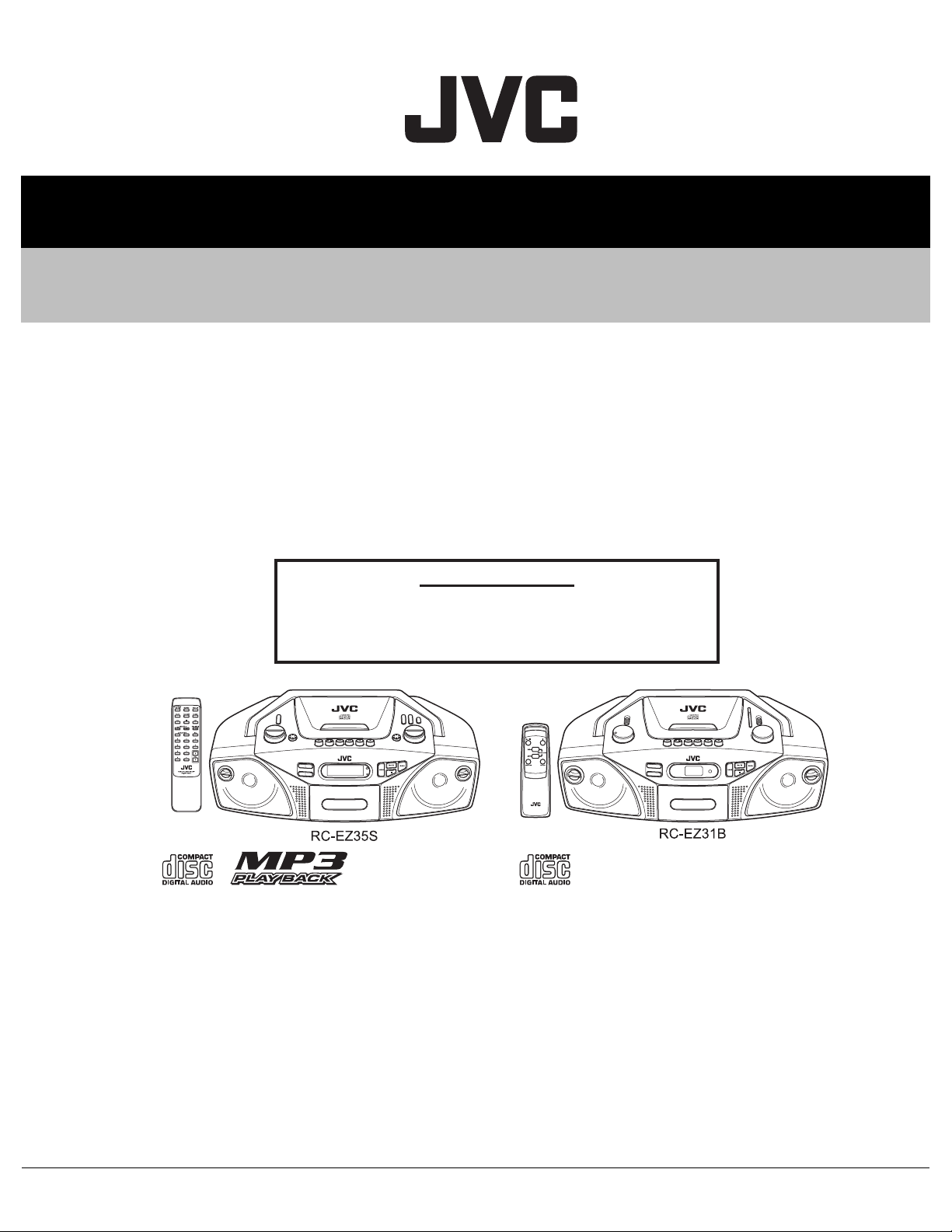
CD PORTABLE SYSTEM
RC-EZ35SB,RC-EZ35SE,
RC-EZ35SEN,RC-EZ35SEV,
RC-EZ31BB,RC-EZ31BE,
RC-EZ31BEN,RC-EZ31BEV
SERVICE POLICY
No service part is available for this model.
Exchange only.
COPYRIGHT © 2006 Victor Company of Japan, Limited
Lead free solder used in the board (material : Sn-Ag-Cu, melting point : 219 Centigrade)
TABLE OF CONTENTS
1 PRECAUTION. . . . . . . . . . . . . . . . . . . . . . . . . . . . . . . . . . . . . . . . . . . . . . . . . . . . . . . . . . . . . . . . . . . . . . . . . 1-3
2 SPECIFIC SERVICE INSTRUCTIONS . . . . . . . . . . . . . . . . . . . . . . . . . . . . . . . . . . . . . . . . . . . . . . . . . . . . . . 1-5
3 DISASSEMBLY . . . . . . . . . . . . . . . . . . . . . . . . . . . . . . . . . . . . . . . . . . . . . . . . . . . . . . . . . . . . . . . . . . . . . . . 1-6
4 ADJUSTMENT . . . . . . . . . . . . . . . . . . . . . . . . . . . . . . . . . . . . . . . . . . . . . . . . . . . . . . . . . . . . . . . . . . . . . . . 1-11
5 TROUBLESHOOTING . . . . . . . . . . . . . . . . . . . . . . . . . . . . . . . . . . . . . . . . . . . . . . . . . . . . . . . . . . . . . . . . . 1-12
COPYRIGHT © 2006 Victor Company of Japan, Limited
No.MB593
2006/12
Page 2

SPECIFICATION
RC-EZ35
Compact disc player section Type Compact disc player
Signal detection Non-contact optical pick-up (semicondicator lazer)
Number of channels 2 channels
Radio section Frequency ranges FM 87.5 MHz - 108.0 MHz
AM 522 kHz - 1 629 kHz
Antennas Telescopic antenna for FM
Ferrite core antenna for AM
Cassette deck section Track 4-track 2-channel stereo
Motor Electronic governor DC motor for capstan
Heads Hard permalloy head for recording/playback, magnetic head for erase
Fast wind time Approx. 120 sec. (C-60 cassette)
General Speaker 10 cm × 2 (4 Ω, 3 W)
Power output 4 W (2 W + 2 W) at 4 Ω (10% THD) (IEC268-3)
Output terminals PHONES × 1 (Ø 3.5 mm, stereo)
Power supply AC 230 V , 50 Hz
DC 12 V ("R20/D (13F)" cells × 8)
Power consumption 17 W (at operation)
1.5 W (at standby)
Dimentions 435 mm (W) × 156 mm (H) × 241 mm (D)
Mass Approx. 2.8 kg (without batteries)
RC-EZ31
Compact disc player section Type Compact disc player
Signal detection Non-contact optical pick-up (semicondicator lazer)
Number of channels 2 channels
Radio section Frequency ranges FM 88 MHz - 108.0 MHz
AM 530 kHz - 1 600 kHz
Antennas Telescopic antenna for FM
Ferrite core antenna for AM
Cassette deck section Track 4-track 2-channel stereo
Motor Electronic governor DC motor for capstan
Heads Hard permalloy head for recording/playback, magnetic head for erase
Fast wind time Approx. 120 sec. (C-60 cassette)
General Speaker 10 cm × 2 (4 Ω, 3 W)
Power output 4 W (2 W + 2 W) at 4 Ω (10% THD) (IEC268-3)
Output terminals PHONES × 1 (Ø 3.5 mm, stereo)
Power supply AC 230 V , 50 Hz
DC 12 V ("R20/D (13F)" cells × 8)
Power consumption 13 W (at operation)
1.5 W (at standby)
Dimentions 435 mm (W) × 156 mm (H) × 241 mm (D)
Mass Approx. 2.8 kg (without batteries)
Design and specifications are subject to change without notice.
1-2 (No.MB593)
Page 3
SECTION 1
PRECAUTION
1.1 Safety Precautions
(1) This design of this product contains special hardware and
many circuits and components specially for safety purposes. For continued protection, no changes should be made
to the original design unless authorized in writing by the
manufacturer. Replacement parts must be identical to
those used in the original circuits. Services should be performed by qualified personnel only.
(2) Alterations of the design or circuitry of the product should
not be made. Any design alterations of the product should
not be made. Any design alterations or additions will void
the manufacturers warranty and will further relieve the
manufacture of responsibility for personal injury or property
damage resulting therefrom.
(3) Many electrical and mechanical parts in the products have
special safety-related characteristics. These characteristics are often not evident from visual inspection nor can the
protection afforded by them necessarily be obtained by using replacement components rated for higher voltage, wattage, etc. Replacement parts which have these special
safety characteristics are identified in the Parts List of Service Manual. Electrical components having such features
are identified by shading on the schematics and by ( ) on
the Parts List in the Service Manual. The use of a substitute
replacement which does not have the same safety characteristics as the recommended replacement parts shown in
the Parts List of Service Manual may create shock, fire, or
other hazards.
(4) The leads in the products are routed and dressed with ties,
clamps, tubings, barriers and the like to be separated from
live parts, high temperature parts, moving parts and/or
sharp edges for the prevention of electric shock and fire
hazard. When service is required, the original lead routing
and dress should be observed, and it should be confirmed
that they have been returned to normal, after reassembling.
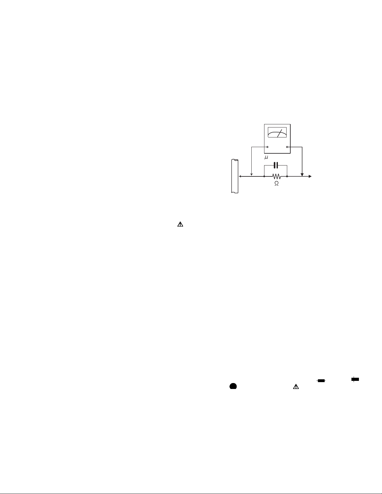
(5) Leakage shock hazard testing
After reassembling the product, always perform an isolation check on the exposed metal parts of the product (antenna terminals, knobs, metal cabinet, screw heads,
headphone jack, control shafts, etc.) to be sure the product
is safe to operate without danger of electrical shock.Do not
use a line isolation transformer during this check.
• Plug the AC line cord directly into the AC outlet. Using a
"Leakage Current Tester", measure the leakage current
from each exposed metal parts of the cabinet, particularly any exposed metal part having a return path to the
chassis, to a known good earth ground. Any leakage current must not exceed 0.5mA AC (r.m.s.).
• Alternate check method
Plug the AC line cord directly into the AC outlet. Use an
AC voltmeter having, 1,000Ω per volt or more sensitivity
in the following manner. Connect a 1,500Ω 10W resistor
paralleled by a 0.15µF AC-type capacitor between an ex-
posed metal part and a known good earth ground.
Measure the AC voltage across the resistor with the AC
voltmeter.
Move the resistor connection to each exposed metal
part, particularly any exposed metal part having a return
path to the chassis, and measure the AC voltage across
the resistor. Now, reverse the plug in the AC outlet and
repeat each measurement. Voltage measured any must
not exceed 0.75 V AC (r.m.s.). This corresponds to 0.5
mA AC (r.m.s.).
AC VOLTMETER
(Having 1000
ohms/volts,
or more sensitivity)
0.15 F AC TYPE
Place this
probe on
1500 10W
Good earth ground
1.2 Warning
(1) This equipment has been designed and manufactured to
meet international safety standards.
(2) It is the legal responsibility of the repairer to ensure that
these safety standards are maintained.
(3) Repairs must be made in accordance with the relevant
safety standards.
(4) It is essential that safety critical components are replaced
by approved parts.
(5) If mains voltage selector is provided, check setting for local
voltage.
1.3 Caution
Burrs formed during molding may be left over on some parts
of the chassis.
Therefore, pay attention to such burrs in the case of preforming repair of this system.
1.4 Critical parts for safety
In regard with component parts appearing on the silk-screen
printed side (parts side) of the PWB diagrams, the parts that are
printed over with black such as the resistor ( ), diode ( )
and ICP ( ) or identified by the " " mark nearby are critical
for safety. When replacing them, be sure to use the parts of the
same type and rating as specified by the manufacturer.
(This regulation dose not Except the J and C version)
each exposed
metal part.
(No.MB593)1-3
Page 4
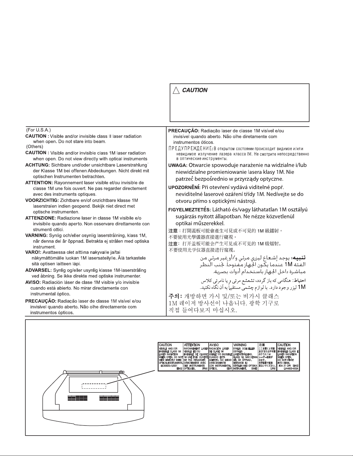
1.5 Important for laser products
1.CLASS 1 LASER PRODUCT
2.CAUTION :
(For U.S.A.) Visible and/or invisible class II laser radiation
when open. Do not stare into beam.
(Others) Visible and/or invisible class 1M laser radiation
when open. Do not view directly with optical instruments.
3.CAUTION : Visible and/or invisible laser radiation when
open and inter lock failed or defeated. Avoid direct
exposure to beam.
4.CAUTION : This laser product uses visible and/or invisible
laser radiation and is equipped with safety switches which
prevent emission of radiation when the drawer is open and
the safety interlocks have failed or are defeated. It is
dangerous to defeat the safety switches.
5.CAUTION : If safety switches malfunction, the laser is able
to function.
6.CAUTION : Use of controls, adjustments or performance of
procedures other than those specified here in may result in
hazardous radiation exposure.
!
Please use enough caution not to
see the beam directly or touch it
in case of an adjustment or operation
check.
REPRODUCTION AND POSITION OF LABELS and PRINT
WARNING LABEL and PRINT
1-4 (No.MB593)
Page 5

SECTION 2
SPECIFIC SERVICE INSTRUCTIONS
This service manual does not describe SPECIFIC SERVICE INSTRUCTIONS.
(No.MB593)1-5
Page 6
SECTION 3
DISASSEMBLY
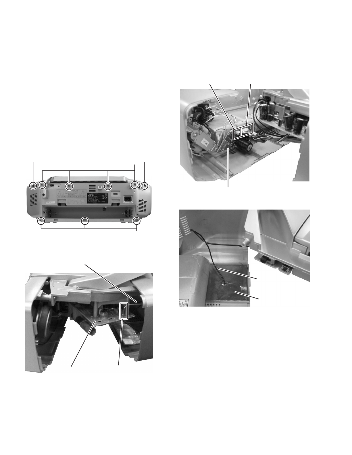
3.1 Main body
3.1.1 Removing the Rear cabinet assembly
(See Fig.1 to 4)
(1) Remove the four screws A and five screws B attaching the
Rear cabinet assembly. (See Fig.1)
(2) Disconnect the Rod antenna wire from post pin of the Tun-
er board assembly. (See Fig.2)
(3) Disconnect the connector wire from Amplifier board as-
sembly connected to connector CN101
former board assembly. (See Fig.3)
(4) Disconnect the connector wire from Capstan motor con-
nected to connector CN102
board assembly. (See Fig.3)
(5) Remove the solder the grand wire from Tuner board sol-
dered to shield plate. (See Fig.4)
of the Power transformer
of the Power trans-
BB
A
CN101CN102
Power transformer board
Fig.1
Rod antenna wire
Fig.3
B
Ground wire
Shield plate
Fig.4
1-6 (No.MB593)
Tuner board assembly Post pin
Fig.2
Page 7
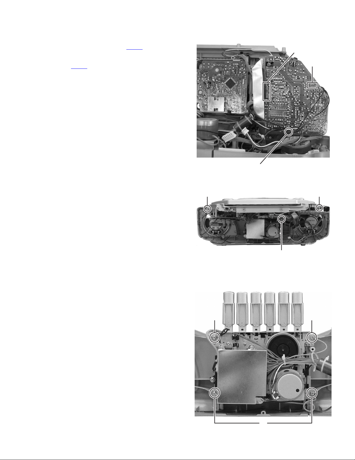
3.1.2 Removing the Top cabinet assembly
(See Fig.5, 6)
(1) Disconnect the connector wire from Cassette mechanism
assembly connected to connector CN205
board assembly. (See Fig.5)
(2) Disconnect the connector wire from speaker connected to
connector CN301
Fig.5)
(3) Remove the solder the grand wire from Cassette mecha-
nism assembly soldered to Amplifier board assembly. (See
Fig.5)
(4) Remove the three screws C attaching the Top cabinet as-
sembly. (See Fig.6)
of the Amplifier board assembly. (See
of the Amplifier
CN205
CN301
Ground wire
Fig.5
CC
3.1.3 Removing the Cassette mechanism assembly
(See Fig.7)
(1) Remove the four screws D attaching the Cassette mecha-
nism assembly.
C
Fig.6
DD
D
Fig.7
(No.MB593)1-7
Page 8
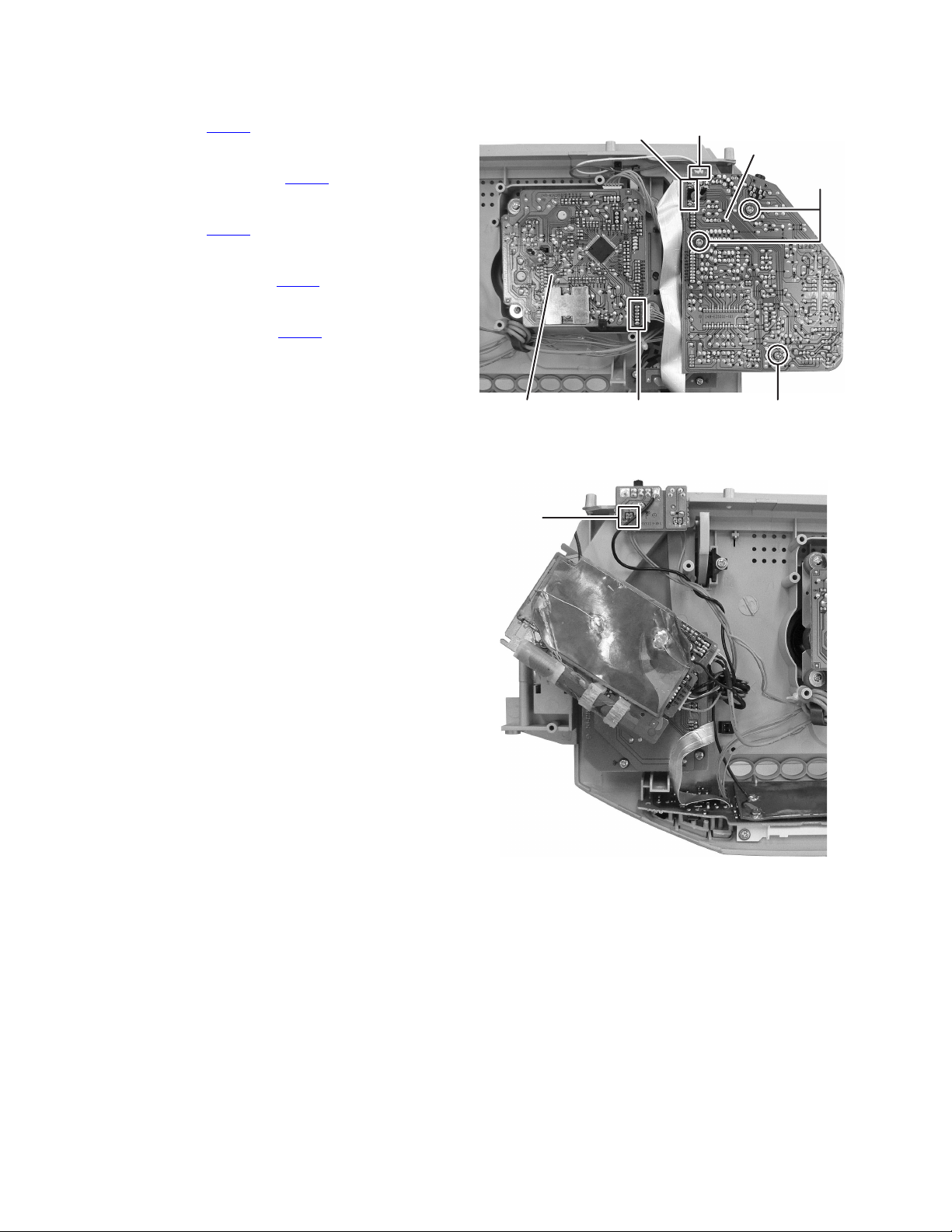
3.1.4 Removing the Amplifier board assembly
(See Fig.8, 9)
(1) Disconnect the card wire from LCD board assembly con-
nected to connector CN701 of the Amplifier board assembly. (See Fig.8)
(2) Disconnect the connector wire from Amplifier board as-
sembly connected to connector CN901
board assembly. (See Fig.8)
(3) Disconnect the connector wire from CD door switch con-
nected to connector CN906
bly. (See Fig.8)
(4) Disconnect the connector wire from Amplifier board as-
sembly connected to connector CN101
assembly. (See Fig.9)
(5) Disconnect the connector wire from Amplifier board as-
sembly connected to connector CN801
jack board assembly. (See Fig.9)
(6) Remove the three screws E attaching the Amplifier board
assembly. (See Fig.8)
of the Amplifier board assem-
of the CD servo
of the Tuner board
of the Headphone
CN701 CN906
Amplifier board
assembly
E
assembly
CN801
CN901CD servo board
Fig.8
E
1-8 (No.MB593)
Fig.9
Page 9

3.1.5 Removing the Headphone jack board assembly
(See Fig.10)
(1) Remove the solder the grand wire from LCD board assem-
bly soldered to Headphone jack board assembly.)
(2) Remove the one screw F attaching the Headphone jack
board assembly.)
(3) Disconnect the connector wire from Function board assem-
bly connected to connector CN707
board assembly.
3.1.6 Removing the Tuner board assembly
(See Fig.11)
(1) Remove the solder of the grand wire from Function board
assembly soldered to Tuner board assembly.
(2) Disconnect the connector wire from Function board assem-
bly connected to connector CN102
sembly.
(3) Remove the tree screws G attaching the Tuner board as-
sembly.
of the Headphone
of the Tuner board as-
G
F
Solder point
Ground wire
CN707
Fig.10
Fig.11
G
Solder point
CN102
(No.MB593)1-9
Page 10

3.1.7 Removing the Function board assembly
(See Fig.12)
(1) Disconnect the card wire from LCD board assembly con-
nected to connector CN103 of the Function board assembly.
(2) Remove the four screws H attaching the Function board
assembly.
HH
3.1.8 Removing the Power switch board assembly
(See Fig.13)
(1) Disconnect the connector wire from LCD board assembly
connected to connector CN709
assembly.
(2) Remove the three screws J attaching the Power switch
board assembly.
of the Power switch board
H
CN103
Fig.12
Fig.13
H
J
J
CN709
1-10 (No.MB593)
Page 11

3.1.9 Removing the LCD board assembly
(See Fig.14)
(1) Remove the two screws K attaching the LCD board assem-
bly.
3.1.10 Removing the CD mechanism assembly
(See Fig.15)
(1) Removing the four screws L attaching the CD mechanism
assembly.
KK
Fig.14
L
L
SECTION 4
ADJUSTMENT
L
L
Fig.15
This service manual does not describe ADJUSTMENT.
(No.MB593)1-11
Page 12

< MEMO >
Page 13

SECTION 5
TROUBLESHOOTING
5.1 BLOCK DIAGRAM
5.1.1 Block diagram for RC-EZ35
FM ANT.
AM ANT.
CD DOOR SW.
BPF
FM RF FM OSC
IC101
FM F/E, IF/DET/MPX
AM RF/IF/DET
AM OSC
IC102
PLL
+8V
TU SW.
IC501
FUNCTION SELECT
EQ/BASS/VOL CONTROL
RESET
PLAY OUT
REC IN
IC201
R/P AMP
+8V
TA SW.
DECK SW
BIAS OSC
R/P HEAD
+
M
-
TAPE MOTOR
DISC
PICKUP
+
M
-
SPINDLE MOTOR
+
M
-
SLED MOTOR
IC901
RF + D-SERVO +
MP3 DECODER+1M DRAM
IC902
SERVO DRIVER
Q902
+8V
CD SW.
+8V
Q401
D2061
IC701
MCU
P-CON
POWER
SW.
LCD
KEY
R.C.
+5V
Q411
L SPEAKER BOX
IC301
POWER AMP.
R SPEAKER BOX
RECTIFIER
AC IN
2-13
Page 14

5.1.2 Block diagram for RC-EZ31
R/P HEAD
IC201
FM ANT.
FM RF
BPF
AM ANT
IC501
SIGNAL SELECT SW.
FM OSC.
IC101
FM F/E, IF/DET/MPX
AM RF/IF/DET.
AM OSC
VOL
TU-5V
REG.
L SPEAKER
IC301
POWER AMP.
DISC
PICKUP
SPINDLE
MOTOR
SLED
MOTOR
CD DOOR
LEAF SW
R SPEAKER
M+
LCD
IC901
DSP
M
IC903
MOTOR/ACTUATOR
DRIVER
M
Q902
IC902
MCU
KEY
TU SW.
TA SW.
CD SW.
Q401
DC SUP
SW
M-
RECTIFIER
CASS MOTOR
AC INPUT
TRANSFORMER
2-14
Page 15

5.2 STANDARD SCHEMATIC DIAGRAMS for RC-EZ35
5.2.1 Primary and Amplifier section
CN906
Q412
9014
TO CD DOOR LEAF SW.
CN710
1
2
3
4
5
6
7
8
9
10
11
12
13
TO MCU BOARD CN701
14
15
CN105
4
3
2
1
TO TUNER BOARD CN101
TO CD BOARD CN901
R509
CN905
1
2
3
4
5
R523
15K
C534
OPEN
CN205
10
9
8
7
GND
6
5
4
TO P / R BOARD CN202
GND
3
2
1
CN206
TO CN801
4.7K
R418
10K
R421
10K
C523
R519
3.3K
153M
C533
OPEN
R522
2.7K
ZD404
R520
15K
R411
10K
5V6
R419
R413
R510
R517
R514
3.3K
150
10K
15K
4.7K
C529
C525
R521
2.7K
100P
Q406
9014
153M
R507
Q503
15K
9014
+
C518
C406
100P
Q403
8050
47U
R513
4. 7K
R410
330
Q50 2
9014
R412
470
C405
+
330U
R409
D405
IN4148
R515
1.2K
L SPEAKER
4
3
1
R SPEAKER
JK301
HEADPHONES JACK
ACINPUT
11
2
Q304
8550
B+
R402
22K
DC+
C1105
220U / 16V
R309
2.2
+
C312
1000U
12
1
C311
1000U
+
R308
2.2
403
C1104
403
+
C1102
6800U / 25V
D1104
IN4001
D1102
IN4001
BATT
C1103
C1101
D1103
IN4001
403
403
R310
D1101
R311
100
L302
FX1101
2A
IN4001
100
125V
L303
15UH
15UH
AC-IN1
AC-IN2
BT -
CN301
4
3
22
1
15UH
L301
POWER / TRANSFORMER
CW301
C310
IC301
C307
100U
+
13
14
+
C308
100U
C316
470U / 25V
R314
10K
Q402
9014
D401
IN4148
223
C401
0.1M
10
3
+
C309
0.1M
+
C404
C302
100U
+
C303
100U
R307
7
6
R306
+
+
+
33K
C403
470U / 16V
C306
100U
+
120
8
5
120
C407
1000U / 25V
Q303
9014
C315
470U / 25V
R401
330
Q401
D2061
+
8V2
ZD401
9
UTC8227
4
1 / 4W
C313
+
22
R405
Q404
9014
10K
R404
10K
Q408
9014
R414
470
Q409
8550
R425
Q407
8550
D404
IN4148
Q415
9014
SHORT
R508
68K
C520
R503
500P
3.9K
C507
+
C508
1U
+
13
15
14
R1
NC
R2
C521
1U
+
C504
9
+
C505
1U
8
RIN
LC75342
272M
0.1M
C503
7
RTRE
RBASS1
1U
C506
+
1U
10
12
11
R3
R4
RSEL0
IC501
R406
470
R415
10K
1 / 4W
9014
Q410
C402
22U
+
R408
10K
R407
47K
3V
ZD403
D402
IN4148
Q411
8050
R417
3.3K
R416
5.6
1 / 4W
6V2
ZD402
C408
100U
+
R302
1K
R303
1K
D302
15K
D406
IN4148
R501
15K
Q405
A928A
R301
+
100U
C409
8.2K
R427
1K
R304
18K
0.1M
+
C501
4.7U
C502
6
RBASS2
3
2
4
5
CE
VSS
TEST
ROUT
C532
102
C531
102
1
DI
R502
R315
IN4148
+
47K
C301
3.3U
Q301
1936
Q302
1936
CN401
LBASS1
25
0.1M
R506
3.9K
LBASS2
C511
LOUTNCVREF
27
26
+
C509
4.7U
0.1M
R305
18K
VDD
CL
29
30
28
C510
+
22U
+
C519
100U
R428
68K
R504
15K
C530
102
R505
100
CW1102
+
-
C410
220U / 25V
+
R317
+
47U
C412
4.7K
M
MOTOR
CASSETTE DECK
Q413
9014
R423
10K
D403
IN4148
R403
10K
C411
10UF
+
R420
5.6K
16
R518
4. 7K
NC
L2
L1
L3
17
R512
1.2K
+
C516
C517
Q501
9014
1U
1U
R516
22K
18 19
+
20
+
C515
1U
Q414
9014
R426
+
C528
22U
LIN
LESL0
L4
21
C527
1U
R511
1K
R422
2.2K
22
+
68K
R424
SHORT
C514
1U
C513
272M
C526
500P
LTRE
24
23
C512
1U
102
C304
102
C305
C314
+
1U
R316
4.7K
D301
R312
IN4148
10K
6
6
5
5
4
4
3
3
2
2
1
1
3
3
22
1
1
CN1102
R313
CN1101
CN801
TO AUDIO BOARD CN206
TO CONTROL BOARD CN707
1
2
CN711
R805
10
SW801- A
SW719
Rese t
2-15
Page 16

5.2.2 Front section
CN702
5
4
3
2
1
TO CD BOARD CN903
CN701
15
14
13
12
11
10
9
8
7
6
5
4
3
TO AUDIO BOARD CN710
2
1
B03
R722
R701
27K
R726
1K
R728
100
R710
R725
10K
100
R727
1K
R702
100
MP3MP3
TRACK
FOLDER
REPEAT
ALL
RANDOM
PROGRAM
INTRO
CLASSIC
4
5
6
S7
S6S5S4
1
2
3
4
5
6
7
8
9
10
1
2
CN704
SLEEP
kHz
MHz
2
3
S3
10
9
8
7
6
5
4
3
2
1
CN706
1
2
CN709
1
S1
S2
S[1: 34]
B01
B02
B03
B04
B05
B06
B[01:06]
R785 R783
2.2K
SW714
PRESER UP
REPEAT
SW709
STANDBY
CN708
TO TUNER BOARD CN102
3
2
5
4
B02
B03
B04
B01
R786
SW713
R781
1.2K
SW710
VOL UP
390
SW716
TUNER
3.9K
FM MODE
R782
3.3K
CN707
TO BEAT CUT BOARD CN711
R784
1.2K
SW717
TAP E
2
B06
R787
4.7K
SW718
PROGR
/CLK
1
B05
R780
4.7K
SW711
VOL DOWN
1
SW712
HBS
SW715
EQ
LCD701
USB
33
34
COM03
COM01
COM02
COM04
S23
47
48
S23
S22
OPT_SYS1(I, - )
IF_ RST(0,Nch)
14
13
102
C704
R705
R706
104
C703
S21
S22
464544
S21
KEY0( I,- )
15
56K
4.7K
R707
68K
D701
R720
S20
S20
KEY1( I,- )
16
4.7K
R708
C720
-
+
C714
2.2UF
IN4148
S19
S19
KEY2( I,- )
17
R711
4.7K
102
1K
D705
IN4148
S18
S17
42
43
S17
S18
VSS2
VDD2
IR(I,-)
ST(I,-)
V_GND(0,CM)
V_CHK( I,-)
SW_CD( I,-)
18
19
6.8K
R750
R714
10K
R718
S16
41
40
S16
39
38
S15
37
S14
36
S13
35
S12
34
S11
33
S10
32
S9
31
S8
30
S7
29
S6
28
S5
27
S4
26
S3
25
S2
24
S1
23
22
21
IF_REQ( I,-)
20
R751
5.6K
C707
47K
Q703
9015
R719
100K
L701
100UH
ZD701
102
C713
3.9V
R736
390
+
-
2200UF
Q704
9015
S26
IC701
8MHz
X702
C711
R715
51
S26
CF2( 0)
10
22P
S25
50 49
S25
VDD1
11
S24
OPT_CT (I, - )
12
C702
10K
S24
102
S30
S28
S27
S29
60
59 58
57
56
54
55
53 52
COM01
47K
47K
R753
R754
C701
100P
C724
102
680P
C716
R744
100
1K
47K
47K
47K
R745
R731
R732
D704
L702
IN4148
100UH
47K
R752
47K
R721
R735
R729
47K
COM02
COM03
COM[01:04]
COM04
1K
1K
R730
680P
C723
61
62
63
64
65
66
67
68
69
70
71
72
73
74
75
76
77
78
79
80
680P
C722
COM1
COM2
JOG-(I,ex-PU)
JOG+(I,ex-PU)
COM3
COM4
P_ PCON(0 ,CM)
VSS3
VDD3
AMUTE(0,CM)
P_ TU( 0 ,Nch)
P_ CD( 0 ,Nch)
IF_ IN(0 ,Nch)
TR_ M- ( 0 ,Nch)
TR_ M+ ( 0 ,Nch)
CD_ RST( 0 ,Nch)
CD_ CE( 0 ,Nch)
TUEV_ CE( 0 ,Nch)
CD_ CMD(0 ,CM)
CD_ DATA ( I,-)
CD_ CLK
IF_ CLK( 0 ,CM) / TX
(I, -) / RX
TUEV_DI(0,CM)
IF_OUT
2
1
100
100
R741
R742
680P
C721
S31
S32
SYN_REC(I,ex-PU)
/RES(I,ex- PU)
TUEV_CL(0,CM)
TUEV_D0( I, -)
5
4
3
100
X701
R743
32.768KHz
C709
15P
S30
XT1(I)
6
R723
4.7M
S29
S27
S28
LC877C64C-57K1
VSS1
XT2( 0)
CF1(I)
8
7
9
R724
680K
C710
15P
C708
22P
D702
IN4148
R717
100K
LED702
Amber Back Light
LED701
Standby
R733
10K
C715
102
Q702
9014
R716
47K
R734
3.3K
D703
IN4148
B02
B01
B04
32
S15
S14
S13
S12
S11
S10
S9
S8
S7
S6
S5
S4
S3
S2
S1
WMA
31
292827
30
S30
S29
S28
26
S27
STEREO
23
25
24
S26
S24
S23
S25
S12
POP
9
8
S10
7
S9
S8
11
10
S11
HBS
21
22
20
S22
S21
S20
ROCK
19
17
16
18
S17
S19
S18
S16
JAZZ
13
12
15
14
S14
S15
S13
B[ 01:06]
CN703
C712
104
REM701
B01
B02
B03
B04
B05
B06
R749
R747
SW707
F.B .
1.2K
B05
B06
R748
SW706
F.F.
470
R712
3.3K
Q701
9015
R713
47K
R704
C706
47K
JP1
C718
220UF
102
R703
3.9K
+
-
R737
R738
C705
820
US1
102
3.3K
SW701
PLAY
R791
4.7K
C719
104
R709R709
R792
6.8K 8.2K
US2
390
SW702
RANDOM
EU1
SW703
DISPLAY
R793
C717
3K
R740
R739
SW708 SW704
FOLDER+ FOLDER-
R794
10K
EU3
EU2
680P
1.2K
R795
12K
R746
AS
100
2K
SW705
STOP
2-16
Page 17

5.2.3 CD servo section
CN902
PICKUP
SW901
Limit Switch
MOTOR1
SLED
M
M
MOTOR2
SPINDLE
VC
VCC
GND
LD
VR
PD
F+
T-
T+
F-
C936
-
+
4.7UF
R938
33
R939
150
R941
150
78
77
79
SLC0
AVDD
RCH0
LRVSS
TD0
FD0
AVDD
SLD0
2324252627
22
15K
R907
R940
767574
LCH0
LRVDD
SPD0
VVSS1
6.8K
R908
-
C916
C939
C903
-
C908
103
+
R901
330
C907
10UF
+
C901
472
683
104
C914
104
80
1
EFMIN
2
RFOUT
3
LPF
45
PHLPF
AIN
6
CIN
7
BIN
8
DIN
9
FEC
10
RFMON
11
VEEF
12
JITTC
13
EIN
14
FIN
15
TEC
16
TE
17
TEIN
18
LDD
19
LDS
20
AVSS
21
C940
473
C945
104
1
2
E
3
D
4
A
5
B
6
C
7
F
8
9
10
R949
11
100
12
13
14
15
16
R946
33
L902
22uH
R903
R904
3.3
470
C909
104
-
+
C910
100UF
Q901
2SA608NF
C911
103
C912
104
+
C943
33UF
C944
-
R948
100
104
R925
8.2K
C906
102
C946
100UF
R947
100K
R902
+
C947
104
-
8.2K
C902
103
100UF
C905
C913
C904
473
103
47
R909
+
1UF
R910
C932
104
C933
-
+
330UF
R937
73
XIN
XVDD
PDOUT0
PDOUT1
282930
680
R911
2.2M
C935
-
+
4.7UF
16.9344MHz
220
72
XOUT
LC78690W
PCKIST
R912
680
C915
-
+
-
+
28 27 26 25
VIN4
VREF
VCC2
VG4
24 23
V04+
V04-
30
22
NC
GND
IC902
LA6548NH
21
NC
20
V03-
19
V03+
18
VIN3G
17
VIN3
16
C950
-
2.2UF
+
CD
15
RESET
X901
71
IC901
6.8K
C917
473
C934
104
XVSS
VVDD1
31
104
70
AMUTEB
DMUTEB
+
-
69
32
R942
100
DOUT
PUIN
C920
68
DVDD
DEFECT
33
100UF
C931
104
C930
67
DVSS
FSEQ
34
C918
104
R906
+
100UF
66
DVDD1.8
C2F
35
12K
R943
100
22K
R935
656463
VVSS2
VPDOUT2
DVDD
DVSS
373839
36
104
C949
R933
VCOC2
VPREF2
DVDD1.8
+
-
C921
100UF
62
VVDD2
DATACK
TEST1
STDATA
STREQ
TEST0
CONT0
CONT1
CONT2
INTB0
DVSS
DVDD
VVDD3
-
C948
3.3K
61
LRSY
DATA
STCK
INTB1
RESB
DO
DI
CL
CE
VVSS3
40
+
100UF
R936
150
C928
104
C927
60
59
58
5756
5554
53
52
51
50
49
48
47
4645
44
43
42
41
C919
104
L903
100uH
R926
150
104
C929
R924
10K
R950
10K
+
1UF
R934
22
C926
104
C938
102
C937
102
-
R932
0
R930
0
R928
0
C922
104
R922
27K
C925
104
R920
100K
C924
68P
R918
Open
R916
5.6K
R921
1K
R917
C923
R919
R913
1K
1K
1K
68P
R914
27K
R915
2.2K
CN903
1
2
3
4
5
TO MCU BOARD CN702
CN901
1
2
3
4
5
TO AUDIO BOARD CN905
Q902
B764
C942
104
+
-
C941
470UF
L901
26UH
VCC1
1
MUTE
2
VG1
VIN1
34
V01+
5
V01-
NC
67
GND
29
R905
10K
VIN2
V02+
NC
V02-
9
8
VG2
11
10
REG_G
REG_B
14
12
13
2-17
Page 18

5.2.4 Cassette mechanism section
L / CH.
L / CH
R / CH
AC / B
R / CH.
GND
1
2
3
4
CW201
1
2
3
4
CN201
L / CH
GND
R / CH
AC / B
SW201 - 1 - A
4
SW201-1 -B
10
C209
5
222M
6
11
12
R209
C211
SW201 - D - A
7
C201
222M
SW201- 5 -A
13
14
8K2
222M
8
9
C202
15
R225
IC201
BA3308
C216
7P
102M
3K9
R229
3K9
R211
C227
7P
5K6
1
C259
100P
C203
R210
R204
+
100U
27
8K2
C208
222M
2
R201
47K
3
R208
+
C204
6k8
4
4U7
C205
10U
R202
470K
+
5
Q201
9014
C217
7P
6
R216
C207
22K
R206
7
8
9
C258
100P
R203
47K
+
4U7
C206
+
100U
+
C226
7P
6K8
102M
C212
R205
C213
5K6
333M
C215
27
R207
1000U
C214
104
R219
100
Q801
9014
R804
15K
C219
103
C801
500P
SW201- 6- A
1
2
C210
333M
3
C806
103M
R803
10K
100
Q802
8050
R802
5.6
R214
1.5K
R220
10K
R215
1.5K
C220
+
10U
16
SW201- 5 - B
10K
R221
17
R222
10k
18
MUTE
Beat Cut
Mic Rec.
Rec.R In
R Out
GND
+8V
Rec. L In
L Out
SYNC
TO MAIN BD.CN305
10
9
8
7
6
5
4
3
2
1
CN202
C803
332M
T801
3630
223
C225
C260
223
+
C804
223M
220U
C805
R801
24 8 - STDS13- 108
BIAS =80 KHz
2-18
Q203
9014
Q202
9014
Page 19

5.2.5 Tuner section
FM-ANT
CT102
10P
VD103
SVC348
223
C151
R101
47K
R144
15p
IN4148
C159
D102
AM COIL ANT
C104
10U
10K
C150
BPF 87~108MHz
IN4148
D101
GND
65 : 25
+
-
104
GND
CF101
1K
R102
C148
223
C91
GND
18p
C101
C105
223
102
GND
L100
102
C145
3.5MM
4.5T
10
R122
C108
C132
18p
R140
R142
+
C152
-
100U
C138
104
C157
R128
10
C126
104
C122
102
L101
390P(P)
C107
56p
2K2
R141
4K7
2K7
C100
223
104
6p
C103
4.5MM
3.5T
C139
R145
C158
104
C154
20P
30p
R126
100K
CT101
102
C135
C147
C153
R125
10P
VD101
SVC201
IC101
LA1823
T101
612R
C137
102
220
+
R146
20P
100K
C134
VD102
SVC201
1U
2K2
7.2MHz
X101
6p
24
1
R139
R127
220
102
C133
23
FMRF1
AMRF
2
R117
10
C113
100U
2K7
20
XOUT
XIN
1
C94
GND2
REG
+
-
19
VSS
CE
2
102
5MM
L102
2T5
22
FMRF2
AMOSC
3
18
AOUT
IC102
DI
3
R124
220K
21
VCC2
VCC1
4
C163
104
103
C146
17
AIN
CL
4
Q107
9018H
103
820
20P
C131
R100
10
R121
20
FMOSC
FMIFOUT
5
10. 7MA5 - A
CF102
2K2
R138
16
PD
D0
5
C156
19
DETOUT
GND1
6
15
VDD
B01
6
R120
1K2
222
C130
TP16(H)
+
4U7
C129
181716
ROUT
MPXIN
ST
IFBUFF
7
8
27K
R104
R153
Q110
9018F
R154
22
100P
100P
C142
C143
13
14
FMIN
LC72131
B02
7
8
C96
9
R111
1M
AMIN
B03
12P
+
0.22U
-
C121
15
LOUT
AMIFOUT
FMIFIN
101112
150K
T103
2070
4.7k
R123
100K
12
NC
B04
9
10
11
FM / AM
IF
I01
+
-
0.22U
C120
3K3
R119
14
ST / MONO
AMIFIN
C160
104
R152
330
R151
C162
223
100P
C140
8p
C155
+
3U3
-
C118
13
DET
AGG
CF105
450KHz
C114
330
R103
C141
47P
CF104
10
R118
223
CF103
10.7MA5 - A
C149
104
R110
R143
10K
C164
104
CDA10.7MC1- A
+
47U
-
C144
680
C93
102
R150
C102
GND
10K
*
TP8 (E)
C117
4U7
100UH
L105
R109
R108
+
-
220U
+
-
C125
R135
18K
R134
18K
27K
33K
R107
100K
Q109
104
C165
C124
103
C123
103
8050
5V6
ZD101
FMVT: L=1.8+ - / 0.1V
AMVT:
C127
C128
TP12(L)
Q108
2SC3330U
R147
R106
680
+
C116
-
100U
103
C115
L=1.4+ - / 0.1V
L=1.0+ - / 0.1V
TP11(R)
104
104
102
C92
47
H=7. 2+ - / 0. 5V(ALL)
H=7. 2+ - / 0. 5V(XE / UK)
H=7. 2+ - / 0. 5V(CA / KR / AU)
1
2
3
4
TO AUDIO BOARD CN105
CN102
TO CONTROL BOARD CN708
100P
103
C99
C97
100P
C95
GND
CN101
ST
ST
D0
CE
DI
CL
TU- R
GND
TU- L
+8V
1K
R129
R130
1K
1K
R131
R132
10K
D104
IN4148
2-19
Page 20

5.3 STANDARD SCHEMATIC DIAGRAMS for RC-EZ31
5.3.1 Primary and Amplifier section
5
B/C
4
Rch
3
Lch
2
GND
1
+8V
CN201
(TO:CN101)
CN307 TO Rec BD CN202
10
0.01
C327
CD-L
AGND
CD-R
MUTE
CDGND
CD+8V
SYNC
SYNC
LED-
LED+
CN307
R374
9
8
7
6
5
4
3
2
1
Q371
S8050
100
3.3U
C392
3.3U
C391
4K7
R378
C372
47UF
R373
18K
R392
C371
C376
100UF
18K
R393
330
R372
3.3K
0.1UF
4K7
R398
R394
3.9K
5.1V
DZ301
R391
9014
Q391
C393
103M
3.9K
C326
47UF
47UF
C378
C377
47UF
C394
103M
R399
10K
B/C
TA
R/R
R/O
GND
+8V
R/L
L/O
SYNC
TO CN204
CN309
CN305
CN906
4K7
R368
4K7
R367
R389 10K
Q369
9014C
Q329
9014C
9014C
Q392
3.2k
C369
R369
R222
R381
R396
10K
R375
2K2
100U / 10V
R502
C501
102PF
1K
10K
1.2K
R331
1k
1K
1UF
R501
C508
16
15
X2
VDD
IC501 TC4052
Y0Y2Y
1
2
1UF
1UF
C507
C506
1.2K
R328
R333
1k
1UF
1UF
C502
C395
14
13
X
X1
Y3
3
4
C503 C510
1UF 1UF
500P
C374
12
5
X0
Y1
120K
R380
1UF
C509
11
6
X3
INH
500P
C373
10
A
VEE
7
120K
R379
9
B
VSS
8
10K
R503
D306
1UF
C504
10K
R504
IN4148
IN4148
D307
1UF
C505
C311
102M
R322
C312C322C321
R324R323R321
8.2K
R370
10K
R506
10K
102M
5.6K
473M473M
5.6K
10K
C317
100UF
C323
10K
R505
R327
VR301-B
50KA
VR301-A
50KA
R326
8.2K
R371
C318
15K
C325
15K
100UF
47UF
5K6
R312
CD
TAP E
TUN
SW301-B
C324
1UF
D1936
5K6
R311
1UF
Q302
D311
IN4148
D314
IN4148
Q301
D1936
C302
1UF
C316
5K6
R332
SW301-A
CD
TAP E
TUN
C301
1UF
1UF
R303
4.7K
R304
D310
IN4148
7.5K
R305
R301
4.7K
5.6K
R316
D309
IN4148
2.2K
67
2.2K
R302
7.5K
R306
100UF/10V
C329
+12V
TO CN303
DC+
+8V
GND
GND
C309
180K
R307
100uF
4
154M
R309
4.7K
C307
1413
3
152M
C303
C319
5
IC301 UTC8227
8
9
10
47uF
180K
R308
152M
C304
D301
IN4001
CN1101
LFSW
CN303
C305
100uF/16V
C306
R320
10K
R300
9015C
LFSW
DC+
+12V
+8V
GND
GND
TO CN1101
100uF
C308
C310
154M
100K
Q303
C403
2200UF / 25V
1. DISCONNECT POWER CORD BEFORE SERVING
2. RECOMMEND THE UNIT BE OPERATED BY DC 12V VOLTS DURING
TROUBLE SHOOTING
3. COMPONENTS MARKED WITH
CHARACTERISTICS.ONLY REPLACE WITH THE COMPONENT OF THE SAME
TYPE NEMBER.
4. SUBJECT TO CHANGE WITHOUT NOTICE
1K
R315
C315
220UF/25V
470uF/16V
100uF
D302
1
8550
Q306
12
C320
2200UF/25V
27k
Q401
2SD2061
IN4148
D401
C404
IN4001
10K
47UF
R328
R330
R401
C401
Q305
10K
C1105
330 1/2W
0.022
2
11
R310
IN4148
R319
8.2V
4.7K
D308
DZ401
C313
470uF/16V
C314
9014C
IN4148
D300
AC
3300UF / 25V
HAVE CRITICAL
R329
33K
120
120
C1
102P
C2
102P
L303
L302
L301
10T
CN332
CN1102
C4C3
102P102P
R313
R314
470uF/25V
C330
REMARK
JP
VERSION :F110 1 2A125V
XE
VERSION :F1101 T2AL250V
DC
C1102
0.04
D1102
IN4001
D1104
IN4001
0.04
C1104
IN4001
D1101
C1103
0.04
IN4001
D1103
C1101
0.04
10T
10T
JK301 HEAD
SP301
+
-
+
-
SP302
C402
220U/25V
+
MOTOR
-
LEAF-SW
*
AC LINE
CN1101
T1101
F1101
BATT 12V
R395
2.2K
D305
IN4148
2-20
Page 21

5.3.2 Front sction
REP
M
LCD701
1
2
3
4
5
6
7
8
9
R706
SW704SW706 REPEAT P/P
SW703SW701 MEMORY STOP
Q702
2.7K
9014
SW705 F.F
SW702 F.B
REM701
R702
1.5K
LED701
R703
CN702
2.7K
TO CN203
18PINS
CN701
1
REM
2
3
KEY02
KEY11
4
5
KEY12
6
KEY13
KEY14
7
COM1
8
COM2
9
101112
COM3
SEG1
SEG2
1314151617
SEG3
SEG4
+5V
SEG5
GND
18
S6
KEY01
2-21
Page 22

5.3.3 CD servo section
VREF
1
2
COM*
3
E
4
D
A
5
6
B
7
C
F
8
GND
9
LD
10
VR
11
MD
12
F+
13
14
T-
15
T+
16
F-
CN901
TO CD DECK
+
C934
10U 103
C935
C902
473M
R907
C938
C950
104 104
+
2SA1342
C936
Q903
1U
C949
100P
C940
104
X901
16.934MHz
C962
XIN
DRF
RES
XOUT
XVDD
PMTSL1
CLOSE
ROUT
IC902
LC78601RE
(DSP)
PLK
CLOCK
3.3VDD
CDIN
RWC
JP-
JP+
TGL
C924
104
R944
100K
C923
330P
R935
R936
10K
+
C939
100U
C944
680P
64 63 62 61 60 59 58 57 56 55 54 53 52 51 50 49
1
DEF1
2
4.2M
R937
3
PDO
470
4
VVSS
10K
5
ISET
6
VVDD
7
FR
VSS
8
9
EFMO
10
EFMIN
11
TMDO
12
CLV+
CLV-
13
14
HFL
TES
15
TOFF
16
10K
C937
104
C942
104
L/RVSS
SLO-
+
220U
L/RVDD
SLEO+
R957
LOUT
SLEO-
C951
103
220
RW
PUIN
C933
473M
1K5
R923
C912
+
C930
100U
PHI
FE-
153M
15K
LF2
LA9242M
AGND
C918
100U
+
VR2
IC901
(ASP)
SP
C959
+
C919
103
10U
C929
FSS
DRF
REFI
VCC2
SPO
SP-
SPG
SPI
C957
100P
56K
R929
R930
1K
332M
56K
R928
R924
+++
33K
C914
0.33U
R926
DE
SLEO
R958
10K
CL
DAT
CLK
DEF
NC
TBC
FSC
DGND
SLI
SLC
RFS
RFSM
CV+
CV-
RW
HFL
TES
TOFF
TGL
JP+
JP-
SL+
SL-
SLD
32313029282726252423222120191817
C958
332
R927
6K8
10K
C913
22U
C915
4U7
R943
270K
48
47
46
45
44
43
42
41
40
39
38
37
36
35
34
33
C926
R945
4K7
+
C927
2U2
333M
R942
R941
12K
10K
R940
22K
R933
R934
C961
15P(N)
C925
222M
150K
150K
R938
R939
330
1K
+
C953
C960
220U
100K
100K
100K
100K
104M
R959
10K
R917
R913
15K
R910
2K2
3K3
104p
R908
C906
330P
C903
C907
104M
R925
R946
10
Q901
2SA608NF
1
2
3
4
5
R909
150K
333M
C906
0.1U
R921
27K
3K3
C908
R914
R920
5K6
100K
6
7
8
9
+
10
11
332
12
13
14
15
16
22K
C911
104M
C956
332M
100
R901
R902
R903
R904
180K
R905
180K
R906
C901
R911
330
R916
27K
C928
103
C932
47U
+
C955
64 63 62 61 60 59 58 57 56 55 54 53 52 51 50 49
CC1
FIN2
FIN1
E
F
TB
TE-
TE
TESI
SCH
TH
TA
TD-
TD
JP
TO
FD-
FD
15K
R919
C910
333M
C941
682M
102
0.33U
C931
+
BHI
LDS
LDD
FE
FA-
FA
68K
R918
R922
MUTE
REMOTE
RANDOM/KEY02
KEYIN/KEY11
PROG/KEY12
DIG1/KEY13
DIG2/KEY14
SEG1/COM1
SEG2/COM2
SEG3/COM3
SEG5/S2
SEG6/S3
NC/S6
DOUT
SEG8/S5
D901
D902
C2F
DMUTE
FSEO
NC/KEY01
VSS
SEG4/S1
SEG7/S4
32313029282726252423222120191817
IN4148
10K
Q904
IN4148
VDD
48
47
46
45
44
43
42
41
40
NC
39
38
37
36
35
34
33
2SA1342
C964
+
R956
220
+
C945
3U3
3U3
R955
R960
5.6K
R961
5.6K
220
C968
104
C947
102M
C948
102M
CLOSE
GND
CN902
6
5
4
3
2
1
TO CN906
CN903
16 PINS
16
REM
15
RANDOM/KEY02
14
KEYIN/KEY11
13
PROG/KEY12
12
DIGI/KEY13
11
DIGI/KEY14
10
SEG1/COM1
9
SEG2/COM2
8
SEG3/COM3
7
SEG4/S1
6
SEG5/S2
5
SEG6/S3
4
SEG7/S4
3
SEG8/S5
2
GND
1
+5V
TO CN701
CN904
+8V
AGND
ROUT
AMUTE
GND
LOUT
SW902
CW904
CD DOOR SW
M
-+
SP
SL
-
+
M
C954
2U2
+
24 23 22 21 20 19 18 17 16 15 14 13
V08
VCC2
V01
VIN1
MUTE
VCC1
1
1
SPIN+
SPIN-
2
2
SL+
3
3
4
4
SL-
P-SW
5
5
GND
6
6
V01
IC903
CSC1469XH
V02
V07
VG4
VIN4
VREF
V06
V05
V03
V04
7123456 89
VG3
VG2
10 11 12
VUN3
VIN2
CD
REG-OUT
RES
REG-IN
R931
R932
10K
2K2
Q902
B764
C916C917
220U104
C963
++
C952
104
470U
L901
26uHX2
2-22
Page 23

5.3.4 Cassette mechanism section
1
2
3
4
CN201
L/CH.
R/CH.
L/CH.
AGND
R/CH
AC/B
AGND
R265
R264
L/CH.
AGND
R/CH
AC/B
1
2
3
4
CN203
820
820
C209
222M
S201-1-A
456
GND
S201-1-B
C202
102M
S201-D-A
789
222M
C201
7P
C216
GND
S201-5-A
13121110
14
15
C227
7P
R225
IC201
BA3308
R229
R211
3K9
C210
L204
15UH
3K9
C203
5K6
333M
100U
R210
1
C262
+
47P
L203
15UH
C208
222M
27
R204
8K2
R209
8K2
C211
222M
2
R201
47K
C259
100P
R208
1. DISCONNECT POWER CORD BEFORE SERVING
2. RECOMMEND THE UNIT BE OPERATED BY DC 12V
3
4
5
6
7
8
9
C205
+
10U
R202
470K
+
4U7
C204
6k8
Q201
9014
C207
4U7
R206
C261
47P
C258
100P
R203
47K
R205
333M
102M
+
C206
5K6
+
C213
L202
15UH
6K8
C212
L201
15UH
100U
C215
27
R207
+
C226
7P
1000U
C214
104
R219
100
VOLTS DURING TROUBLE SHOOTING
3. COMPONENTS MARKED WITH
HAVE CRITICAL
CHARACTERISICS. ONLY REPLACE WITH THE COMPONENT
OF THE SAME TYPE NUMBER
4. SUBJECT TO CHANGE WITHOUT NOTICE
R804
C219
Q801
9014
15K
103
C801
500P
S201-6-A
123
AGND
C803
C225
223
T801-A
3630
332M
C260
223
+
220U
C804
223M
C805
R801
100
C806
103M
R803
10K
Q802
8050
R802
5.6
R214
1.5K
R220
10K
R215
1.5K
R216
C220
22K
+
Q202
9014
10U
S201-5-B
16 17 18
10K
R221
R222
10K
Q203
9014
R224
10K
AGND
CN204
SYNC
B / C
TA
R / R
R / O
AGND
+8V
R / L
L / O
9
8
7
6
5
4
3
2
CN202
TO CN304
SYNC
1
2-23
Page 24

5.3.5 Tuner section
VC2
3.5T
L102
22P
C114
NC
L101
2.5T
VC1
15
R110
C115
2P
R117
47K
AM ANT
120T:15T
R109
10K
330P
C104
1010T103
120P
C118
VC4
680P
C106
R108
3.9K
C105
C103
1UF
473M
C111M
Q101
R107
12K
C113
823M
C112
0.22UF
R106
22K
AM
FM
SW102B
SW101
MONO
ST
FM ANT
473P
C127
IN4148
D102
IN4148
D101
VC3
102P
C117
473P
C109
IC101
2111A
473P
24
1
C125
23
22
AM RFIN
FMRF OUT
FM RFIN
RF GND
2
3
C119
21
20
RF VCC
FM OSC
AM LOW
MIX OUT
4
5
C120
0.47UF
473P
C126
19
AFC
AM OSC
VGC
VCC
6
22UF
10002
T101
DZ101
18
17
MPX IN
DET-OUT
AMIF IN
FMIF IN
7
8
5.6V
16
LPF2
GND
9
68P
C121
15
14
LPF1
L-OUT
TUN LED
ST LED
11
10
13
R-OUT
QUAD
12
CF101
465KHz
CF103
10.7M
C123
5P
10.7MHZ
R116
10
CF102
C108
153M
100K
R102
C111
100K
473P
220UF
R104
R101
C110
18K
C101
1UF
C102
1UF
R103
150
18K
R105
B / C
GND
Rch
Lch
+8V
C107
153M
SW102A
TO CN201
CN101
2-24
Page 25

< MEMO >
Page 26

Victor company of Japn, Limited
Audio/Video Systems category 10-1,1chome,Ohwatari-machi,Maebashi-city,Gumma-ken, 371-8543,Japan
(No.MB593)
Printed in Japan
VPT
 Loading...