

Page 1
SERVICE MANUAL
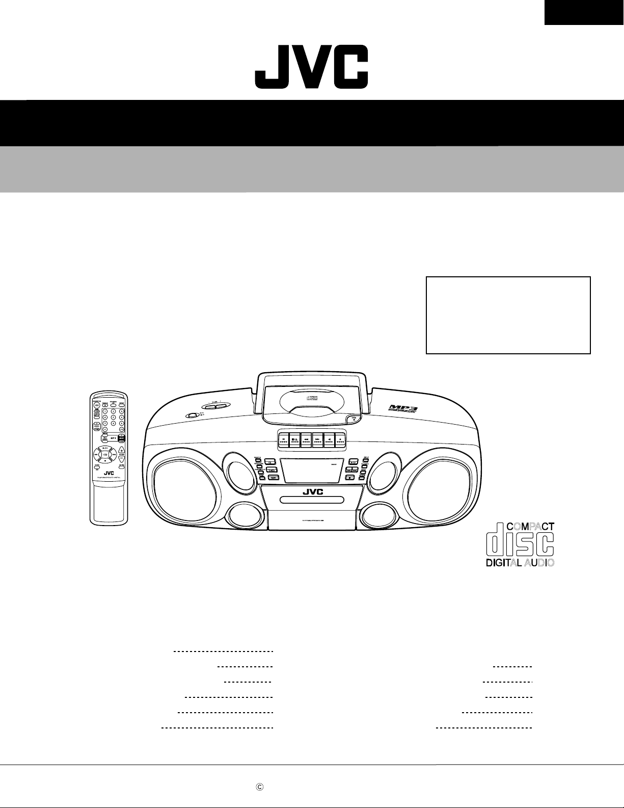
CD PORTABLE SYSTEM
RC-BM5
Area suffix
RC-BM5
A ------------------------------- Australia
US --------------------------- Singapore
UJ -------------------------- U.S.Military
Contents
Safety precautions
Preventing static electricity
Important for laser products
Disassembly method
Adjustment method
Trouble shooting
COPYRIGHT 2003 VICTOR COMPANY OF JAPAN, LTD.
1-2
1-3
1-4
1-5
1-16
1-19
Flow of functional operation
until TOC read
Maintenance of laser pickup
Replacement of laser pickup
Description of major ICs
Wiring connections
1-20
1-21
1-21
1-22
1-36,37
No.21132
Feb. 2003
Page 2
RC-BM5
1. This design of this product contains special hardware and many circuits and components specially for safety
purposes. For continued protection, no changes should be made to the original design unless authorized in
writing by the manufacturer. Replacement parts must be identical to those used in the original circuits. Services
should be performed by qualified personnel only.
2. Alterations of the design or circuitry of the product should not be made. Any design alterations of the product
should not be made. Any design alterations or additions will void the manufacturer`s warranty and will further
relieve the manufacture of responsibility for personal injury or property damage resulting therefrom.
3. Many electrical and mechanical parts in the products have special safety-related characteristics. These
characteristics are often not evident from visual inspection nor can the protection afforded by them necessarily
be obtained by using replacement components rated for higher voltage, wattage, etc. Replacement parts which
have these special safety characteristics are identified in the Parts List of Service Manual. Electrical
components having such features are identified by shading on the schematics and by ( ) on the Parts List in
the Service Manual. The use of a substitute replacement which does not have the same safety characteristics
as the recommended replacement parts shown in the Parts List of Service Manual may create shock, fire, or
other hazards.
4. The leads in the products are routed and dressed with ties, clamps, tubings, barriers and the like to be
separated from live parts, high temperature parts, moving parts and/or sharp edges for the prevention of
electric shock and fire hazard. When service is required, the original lead routing and dress should be
observed, and it should be confirmed that they have been returned to normal, after re-assembling.
5. Leakage currnet check (Electrical shock hazard testing)
After re-assembling the product, always perform an isolation check on the exposed metal parts of the product
(antenna terminals, knobs, metal cabinet, screw heads, headphone jack, control shafts, etc.) to be sure the
product is safe to operate without danger of electrical shock.
Do not use a line isolation transformer during this check.
Plug the AC line cord directly into the AC outlet. Using a "Leakage Current Tester", measure the leakage
current from each exposed metal parts of the cabinet, particularly any exposed metal part having a return
path to the chassis, to a known good earth ground. Any leakage current must not exceed 0.5mA AC (r.m.s.).
Alternate check method
Plug the AC line cord directly into the AC outlet. Use an AC voltmeter having, 1,000 ohms per volt or more
sensitivity in the following manner. Connect a 1,500 10W resistor paralleled by a 0.15 F AC-type capacitor
between an exposed metal part and a known good earth ground.
Measure the AC voltage across the resistor with the AC
voltmeter.
Move the resistor connection to each exposed metal part,
particularly any exposed metal part having a return path to
the chassis, and meausre the AC voltage across the resistor.
Now, reverse the plug in the AC outlet and repeat each
measurement. Voltage measured any must not exceed 0.75 V
AC (r.m.s.). This corresponds to 0.5 mA AC (r.m.s.).
0.15 F AC TYPE
1500 10W
Good earth ground
AC VOLTMETER
(Having 1000
ohms/volts,
or more sensitivity)
Place this
probe on
each exposed
metal part.
!
1. This equipment has been designed and manufactured to meet international safety standards.
2. It is the legal responsibility of the repairer to ensure that these safety standards are maintained.
3. Repairs must be made in accordance with the relevant safety standards.
4. It is essential that safety critical components are replaced by approved parts.
5. If mains voltage selector is provided, check setting for local voltage.
Burrs formed during molding may
be left over on some parts of the
chassis. Therefore, pay attention to
such burrs in the case of
preforming repair of this system.
In regard with component parts appearing on the silk-screen printed side (parts side) of the PWB diagrams, the
parts that are printed over with black such as the resistor ( ), diode ( ) and ICP ( ) or identified by the " "
mark nearby are critical for safety.
(This regulation does not correspond to J and C version.)
1-2
Page 3
RC-BM5
Preventing static electricity
1. Grounding to prevent damage by static electricity
Electrostatic discharge (ESD), which occurs when static electricity stored in the body, fabric, etc. is discharged,
can destroy the laser diode in the traverse unit (optical pickup). Take care to prevent this when performing repairs.
2. About the earth processing for the destruction prevention by static electricity
Static electricity in the work area can destroy the optical pickup (laser diode) in devices such as CD players.
Be careful to use proper grounding in the area where repairs are being performed.
2-1 Ground the workbench
Ground the workbench by laying conductive material (such as a conductive sheet) or an iron plate over it
before placing the traverse unit (optical pickup) on it.
2-2 Ground yourself
Use an anti-static wrist strap to release any static electricity built up in your body.
(caption)
Anti-static wrist strap
Conductive material
(conductive sheet) or iron plate
3. Handling the optical pickup
1.
In order to maintain quality during transport and before installation, both sides of the laser diode on the
replacement optical pickup are shorted. After replacement, return the shorted parts to their original condition.
(Refer to the text.)
2.
Do not use a tester to check the condition of the laser diode in the optical pickup. The tester's internal power
source can easily destroy the laser diode.
4. Handling the traverse unit (optical pickup)
1.
Do not subject the traverse unit (optical pickup) to strong shocks, as it is a sensitive, complex unit.
2.
Remove solder of the short land on the flexible wire after replacing the optical pickup. For specific details, refer
to the replacement procedure in the text. Remove the anti-static pin when replacing the traverse unit.
Be careful not to take too long a time when attaching it to the connector.
3.
Handle the flexible wire carefully as it may break when subjected to strong force.
4.
It is not possible to adjust the semi-fixed resistor that adjusts the laser power. Do not turn it.
5. Attention when traverse unit is decomposed
*Please refer to "Disassembly method" in the text for the CD pickup unit.
Apply solder to the short land before the card wire is disconnected
from the connector on the main board.
(If the flexible wire is disconnected without applying solder, the CD
pickup may be destroyed by static electricity.)
In the assembly, be sure to remove solder from the short land after
connecting the card wire.
Short land
CD/Cassette mechanism
assembly
Main board
CD pickup unit
Card wire
1-3
Page 4
RC-BM5
Important for laser products
1.CLASS 1 LASER PRODUCT
2.DANGER : Invisible laser radiation when open and inter
lock failed or defeated. Avoid direct exposure to beam.
3.CAUTION : There are no serviceable parts inside the
Laser Unit. Do not disassemble the Laser Unit. Replace
the complete Laser Unit if it malfunctions.
4.CAUTION : The compact disc player uses invisible
laserradiation and is equipped with safety switches
whichprevent emission of radiation when the drawer is
open and the safety interlocks have failed or are de
feated. It is dangerous to defeat the safety switches.
VARNING : Osynlig laserstrålning när denna del är öppnad
och spårren är urkopplad. Betrakta ej strålen.
VARO : Avattaessa ja suojalukitus ohitettaessa olet
alttiina näkymättömälle lasersäteilylle.Älä katso
säteeseen.
5.CAUTION : If safety switches malfunction, the laser is able
to function.
6.CAUTION : Use of controls, adjustments or performance of
procedures other than those specified herein may result in
hazardous radiation exposure.
CAUTION
!
Please use enough caution not to
see the beam directly or touch it
in case of an adjustment or operation
check.
ADVARSEL : Usynlig laserstråling ved åbning , når
sikkerhedsafbrydere er ude af funktion.
Undgåudsættelse for stråling.
ADVARSEL : Usynlig laserstråling ved åpning,når
sikkerhetsbryteren er avslott. unngå utsettelse
for stråling.
REPRODUCTION AND POSITION OF LABELS
CLASS 1
LASER PRODUCT
1-4
Page 5
Disassembly method
RC-BM5
<Main body section>
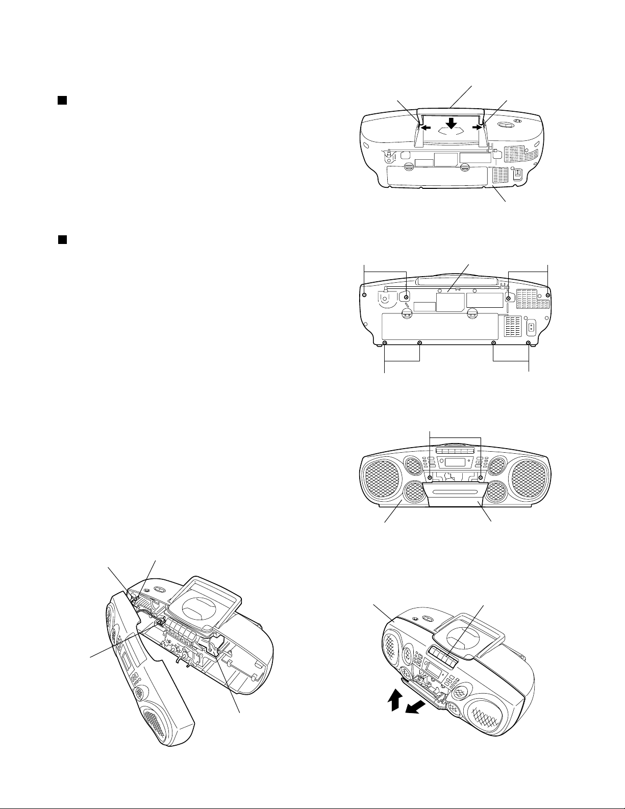
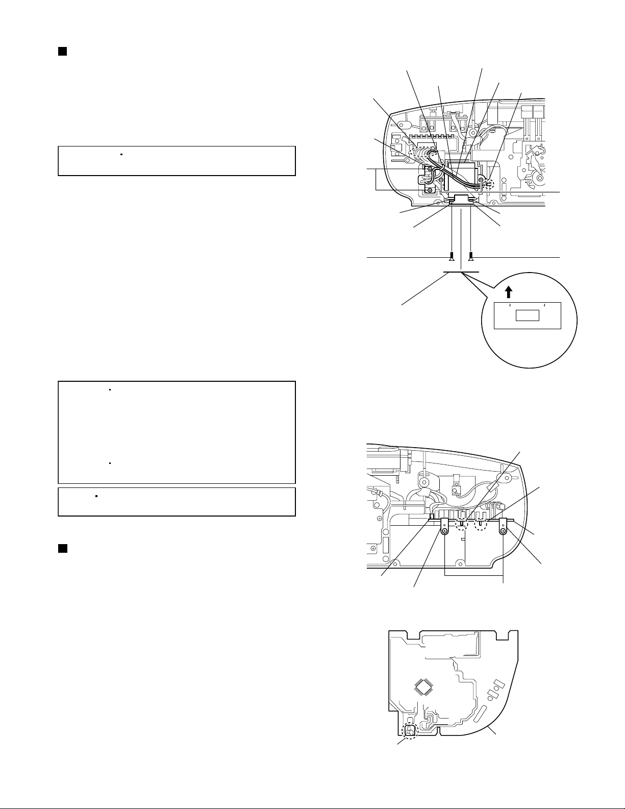
Removing the handle (See Fig. 1.)
Lift the handle slightly.
1.
While pressing the claws a of the rear cabinet
2.
assembly in the direction of the arrow 1, slide the
handle in the direction of the arrow 2.
Removing the front cabinet assembly
and rear cabinet assembly
(See Figs. 2 to 5.)
1.
Remove the eight screws A retaining the front
cabinet and rear cabinet assemblies from the rear
of the main body. (See Fig.2.)
2.
Open the cassette door. (See Fig.3.)
3.
Remove the two screws B retaining the front
cabinet assembly. (See Fig.3.)
4.
Slide the lower part of the front cabinet slightly in
the direction of the arrow 1. (See Fig.4.)
5.
While removing the front cabinet assembly from the
cassette knobs and remove it in the upward
direction 2. (See Fig.4.)
Handle
Claw aClaw a
2
Fig.1
1
Rear cabinet assembly
1
AA
Rear cabinet assembly
AA
Fig.2
B
6.
Disconnect the speaker wire from the connector
CN205 on the phone jack board. (See Fig.5.)
7.
Disconnect the parallel wire from the connector
CN302 on the main board. (See Fig.5.)
CN205
CN302
Phone jack board
Main board
Fig.5
Front cabinet assembly Cassette door
Fig.3
Front cabinet assembly
2
1
Fig.4
Cassette knobs
1-5
Page 6
RC-BM5
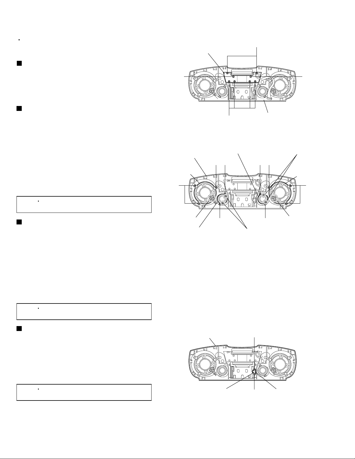
<Front cabinet section>
Prior to performing the following procedures,
remove the front cabinet assembly from the rear
cabinet assembly.
Removing the display board
(See Fig. 6.)
From the inside of the front cabinet assembly,
remove the eight screws C retaining the display
board and then take out the display board.
Removing the right and left main
speaker assemblies (See Fig. 7.)
1.
From the inside of the front cabinet assembly,
remove the six screws D retaining the right and left
main speaker assemblies.
2.
Remove the solders from the soldered sections b
and c of the right and left main speaker
assemblies, remove the wires.
3.
Take out the right and left main speaker
assemblies.
Display board
Front cabinet
assembly
Right main
speaker
C
Front cabinet assembly
Fig.6
Left sub speaker
C
Soldered sections e
EE
DD
CC
Left main
speaker
DD
[Note]
After assembly, apply a locking agent to
the screws D.
Removing the right and left sub
speaker assemblies (See Fig. 7.)
1.
From the inside of the front cabinet assembly,
remove the four screws E retaining the right and
left sub speaker assemblies.
2.
Remove the solders from the soldered sections d
and e of the right and left sub speaker assemblies,
remove the wires.
3.
Take out the right and left sub speaker assemblies.
[Note]
After assembly, apply a locking agent to
the screws E.
Removing the cassette door damper
(See Fig. 8.)
1.2.From the inside of the front cabinet assembly,
remove the two screws F retaining the bracket of
the cassette door damper.
Soldered
section b
Right sub speaker
Front cabinet assembly
EE
Soldered sections d
Fig.7
F
Soldered
section c
Take out the cassette door damper.
[Note]
1-6
After assembly, apply a locking agent to
the screws F.
Cassette door damper Bracket
F
Fig.8
Page 7
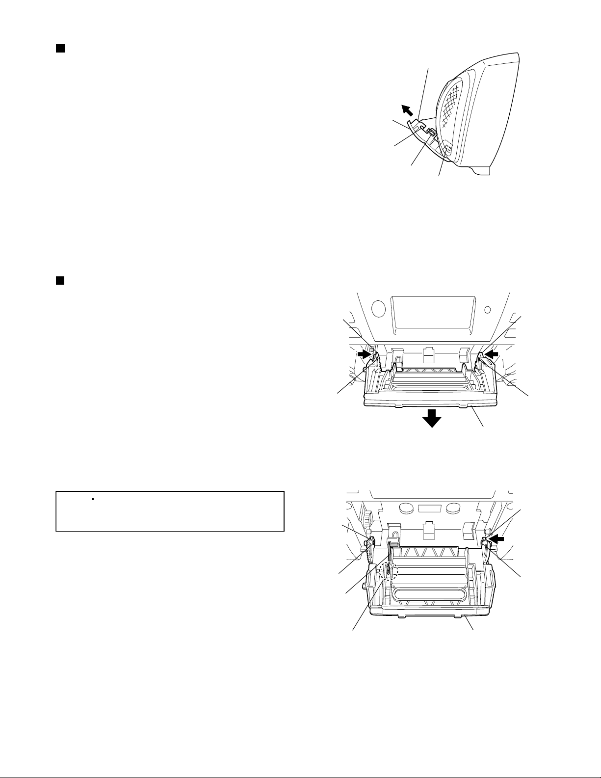
Removing the cassette door
(See Fig. 9.)
1.
Open the cassette.
2.
While pressing the claws f on the left and right of
the cassette door bracket, slide the cassette door.
3.
Disengage the hooks g and h on the left and right
of the cassette door bracket, and remove the
cassette door.
Removing the cassette door bracket
(See Figs. 10 and 11.)
1.
While pressing the sections i on the left and right of
the cassette door bracket in the direction of the
arrow 1, remove the cassette door bracket from the
bosses j of the front cabinet assembly and then
open the cassette door bracket in the direction of
the arrow 2. (See Fig.10.)
Section i
RC-BM5
Cassette door bracket
Cassette door
Hook h
Claw f
Hook g
Fig.9
Section i
11
2.
Press the section k of the cassette door bracket
and remove the cassette door bracket from the
boss m of the front cabinet assembly. (See Fig.11.)
3.
Disengage the section n of the cassette door
bracket from the boss p of the front cabinet
assembly and remove the cassette door bracket.
(See Fig.11.)
[Note]
Be sure to hang the spring to the
section q before attaching the cassette
door bracket. (See Fig.11.)
Boss j
Section n
Boss p
Spring
Section q
2
Fig.10
Fig.11
Boss j
Cassette door bracket
Section k
Boss m
Cassette door bracket
1-7
Page 8
RC-BM5
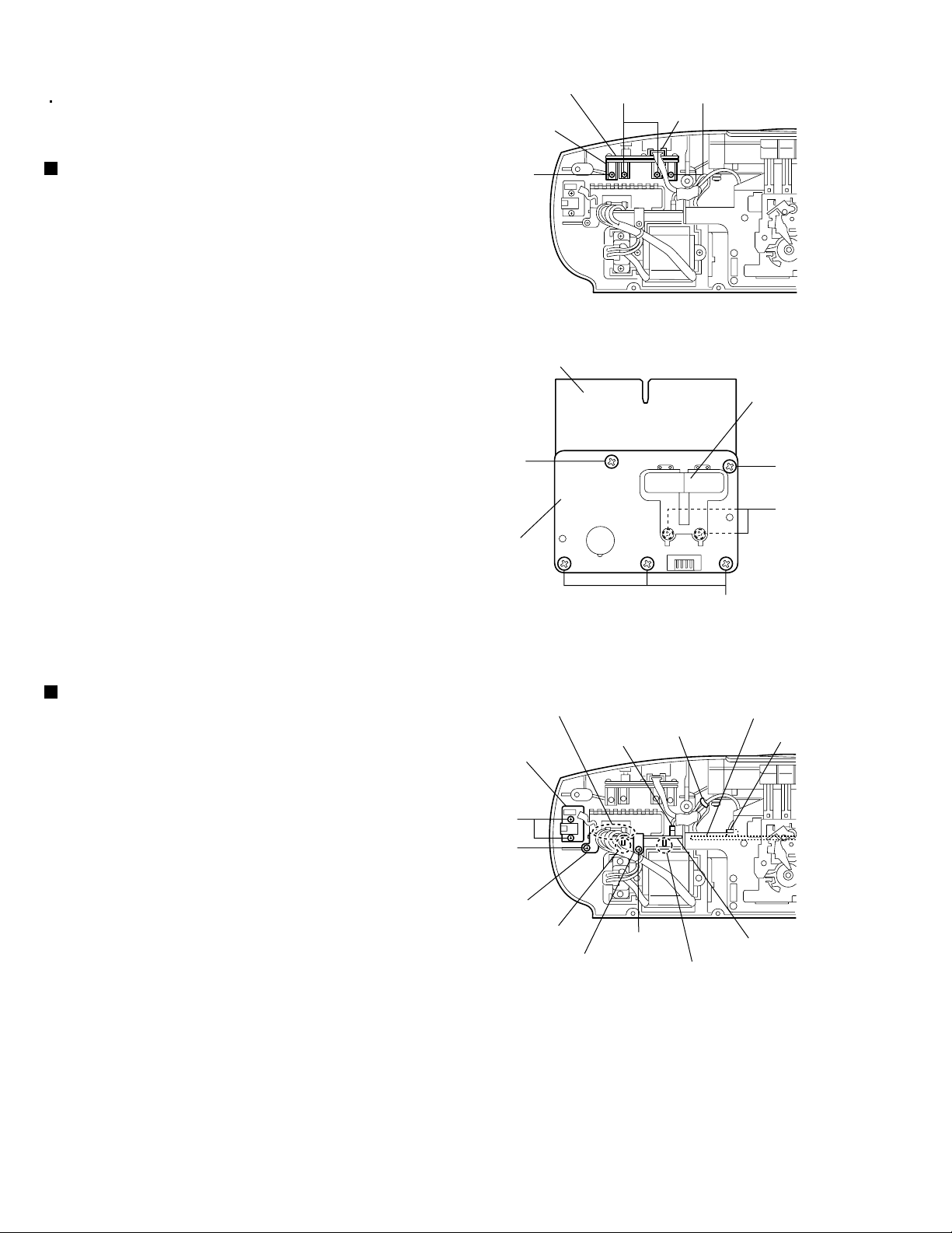
<Rear cabinet section>
Prior to performing the following procedures,
remove the front cabinet assembly from the rear
cabinet assembly.
Removing the volume switch board
(See Figs. 12 and 13.)
1.
Disconnect the wire from the connector H402 on
the volume switch board. (See Fig.12.)
2.
Remove the four screws G retaining the control
bracket of the volume switch board. (See Fig.12.)
3.
While pressing the power and volume buttons of
the volume switch board, take out the volume
switch board.
4.
From the forward side of the volume switch board,
remove the five screws H retaining the volume
switch board to the control bracket. (See Fig.13.)
5.
From the bottom side of the control bracket,
remove the two screws J retaining the volume
switch board and volume button to the control
bracket. (See Fig.13.)
Volume switch board
Control bracket
G
Control bracket
H
Volume switch
board
GG
H402
Fig.12
Volume button
H
J
(Bottom side)
Removing the power amplifier board
and phone jack board (See Fig. 14.)
1.
Remove the tie band bundling the wires from the
main board.
2.
Disconnect the wire from the connector CN206 on
the power amplifier board.
3.
Disconnect the wire from the connector CN801 on
the main board.
4.
Remove the wire from the soldered section r on the
power amplifier board.
5.
Remove the two screws K and board holders
(A)/(B) retaining the power amplifier board.
6.
Remove the two screws L retaining the phone jack
board.
Soldered section r
Phone jack
board
L
K
Board holder (A)
Notch s
Board holder (B)
CN206
Fig.13
Tie band
K
Fig.14
H
Main board
CN801
Power amplifier board
Notch t
7.
Pull out the power amplifier board from notches s
and t, and then take out the power amplifier board
together the phone jack board.
1-8
Page 9
RC-BM5
Removing the power transformer
(See Fig. 15.)
1.2.Remove the tie band bundling the wires from the
power transformer and battery plate.
Remove the wire from the soldered section u on
the power amplifier board.
[Reference]
3.
Remove the wire(blue) from the soldered section v
of the battery plate.
4.
Remove the two screws M retaining the power
transformer.
5.
Remove the two screws N retaining the AC jack.
6.
From the bottom side of the rear cabinet assembly,
remove the label and then remove the two screws
P retaining the voltage selector switch.
7.
Take out the power transformer together the AC
jack and voltage selector switch.
It is not necessary to remove the
wire(black) from the battery plate.
(Except for A version)
(Except for A version)
Tie band
Wire(blue)
Soldered section u
AC jack
Wire(black)
Power transformer
Soldered section v
N
Nut
Put a mark here.
Nut
[Caution]
Voltage selector switch
P P
[Caution]
Label
AC220-230V
Make sure direction
is correct.
Fig.15
Front side
AC110-127V
M
VOLTAGE SELECTOR
[Caution]
Before removing the voltage selector
switch, put a mark on the voltage
selector switch as shown in Fig.15.
When reinstalling, attach the voltage
selector switch in the same position
as marked before removing.
When affixing a label, make sure it is
in the correct direction.
[Note]
After assembly, apply a locking agent to
the screws M, N and nuts.
Removing the tuner board
(See Figs. 16 and 17.)
1.
Remove the wire from the connector H801 on the
tuner board. (See Fig.16.)
2.
Remove the two screws Q and board holders (B)
retaining the tuner board. (See Fig.16.)
3.
Pull out the tuner board from the notches w and x
of the rear cabinet assembly. (See Fig.16.)
H801
Board holder (B)
Notch w
Notch x
Tuner board
Board holder (B)
Q
Fig.16
4.
Remove the FM antenna wire from the soldered
section y on the reverse side of the tuner board.
(See Fig.17.)
Soldered section y
Tuner board
(Reverse side)
Fig.17
1-9
Page 10
RC-BM5
Removing the cassette deck
mechanism assembly and cassette
board (See Figs. 18 and 19.)
1.
Remove the three screws R and screw R' retaining
the cassette deck mechanism assembly.
(See Fig.18.)
Cassette deck mechanism assembly
Wire clamp
2.
Lift the cassette deck mechanism assembly slightly
and move it as shown in Fig.19.
3.
Remove the three screws S retaining the cassette
board. (See Fig.19.)
4.
Lift the cassette board slightly, remove the capstan
motor wire and REC/PB head wire from the
soldered sections z and aa on the cassette board.
(See Fig.19.)
5.
From the forward side of the cassette board,
disconnect the wire from the connector CN602 and
then remove the cassette deck mechanism
assembly. (See Fig.19.)
6.
From the forward side of the cassette board,
disconnect the wire from the connector H602 and
then remove the cassette board. (See Fig.19.)
[Notes]
When attaching the screw R', attach the
wire clamp at the same time.
(See Fig.18.)
After assembly, apply a locking agent to
the screws R and R'. (See Fig.18.)
Cassette deck mechanism
assembly
S
CN602 (Forward side)
Fig.18
H602 (Forward side)
S
R'
RR
Soldered section aa
S
Cassette board
Soldered section z
1-10
Fig.19
Page 11
RC-BM5
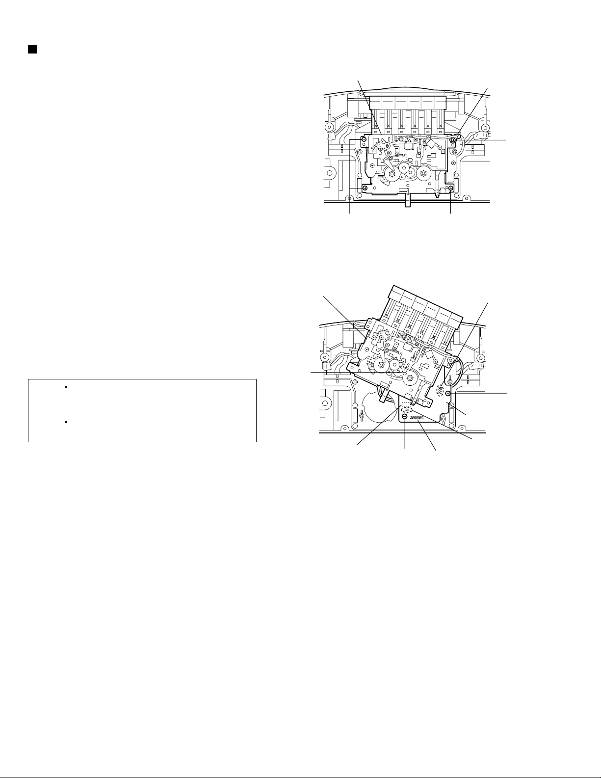
Removing the CD/Cassette mechanism
assembly
(See Figs. 12,14,16 and 20 to 22.)
[Reference]
1.
From the back side of the rear cabinet assembly,
remove the two screws T retaining the CD/Cassette
mechanism assembly. (See Fig.20.)
2.
Disconnect the wire from the connector H402 on
the volume switch board. (See Fig.12.)
3.
Disconnect the wire from the connector CN206 on
the power amplifier board. (See Fig.14.)
4.
Disconnect the wire from the connector CN801 on
the main board. (See Fig.14.)
5.
Disconnect the wire from the connector H801 on
the tuner board. (See Fig.16.)
6.
Remove the four screws U retaining the
CD/Cassette mechanism assembly. (See Fig.21.)
It is not necessary to remove the
cassette deck mechanism assembly
from the rear cabinet assembly.
Rear cabinet
assembly
T
Fig.20
7.
Slide the CD/Cassette mechanism assembly in the
direction of the arrow and take out it. (See Fig.22.)
UU
CD/Cassette mechanism assembly
Fig.21
Rear cabinet assembly
CD/Cassette mechanism
assembly
Fig.22
1-11
Page 12
RC-BM5
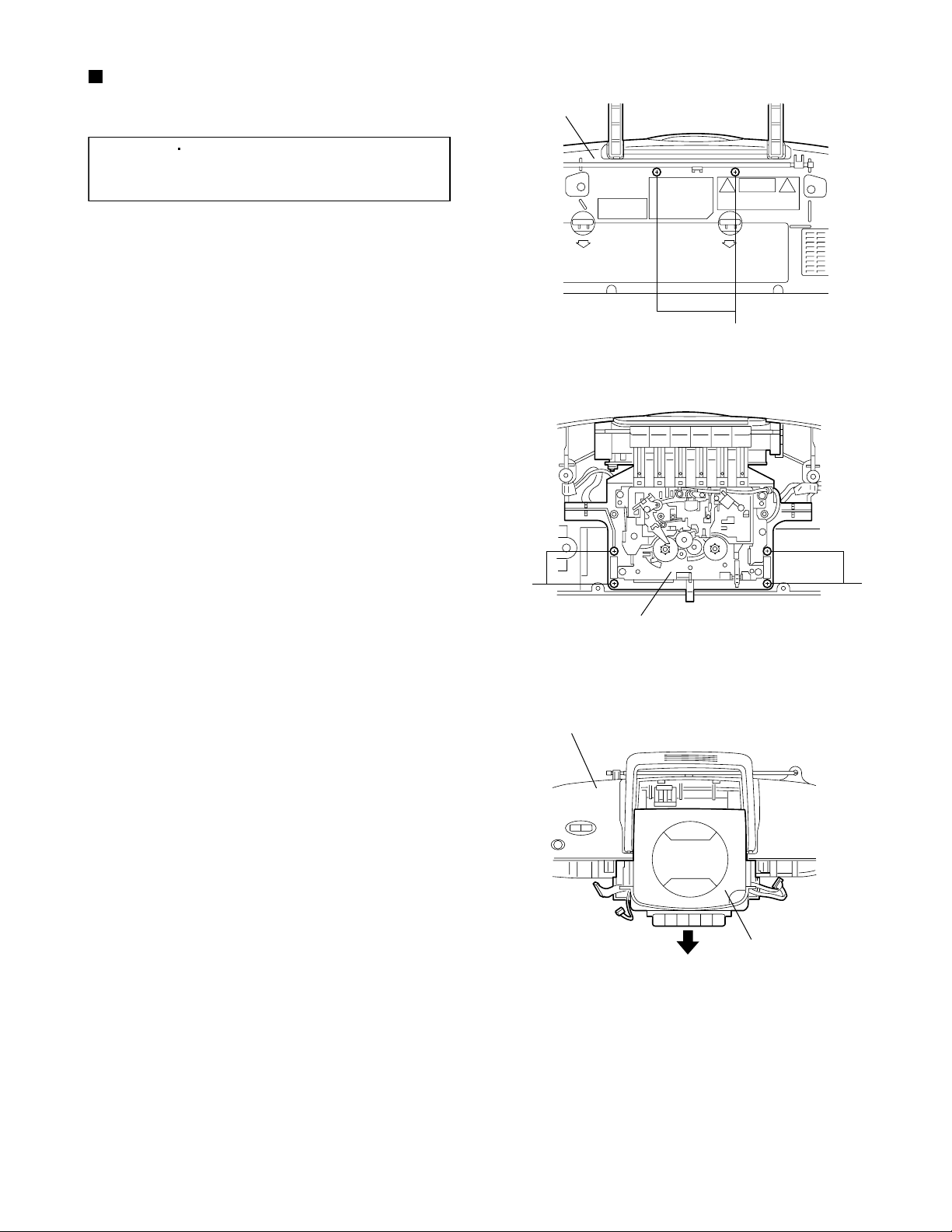
<CD/Cassette mechanism section>
Removing the main board
(See Figs. 23 to 25.)
[Caution]
1.
From the bottom side of the CD/Cassette
mechanism assembly, remove the screw V
retaining the main board. (See Fig.23.)
2.
Disconnect the wire from the connector H602 on
the cassette board. (See Fig.23.)
3.
Disconnect the wire from the connector H302 on
the main board. (See Fig.24.)
4.
From the top side of the CD/Cassette mechanism
assembly, remove the three screws W and screw
W' retaining the main board. (See Fig.24.)
[Note]
5.
Remove the main board from the CD/Cassette
mechanism assembly, lift the CD/Cassette
mechanism assembly as shown in Fig.25.
6.
Disconnect the wire from the connector H502 on
the main board. (See Fig.25.)
7.
Apply solder to the short land section ab on the CD
pickup unit. (See Fig.25.)
[Caution]
When removing the main board, be
careful not to scratch or damage the
CD door.
When attaching the screw W', attach the
wire clamp at the same time.
Be sure to solder the short land
section ab on the CD pickup unit
before disconnecting the card wire
from the CD pickup unit. (See Fig.25.)
If the card wire is disconnected
without applying solder, the CD
pickup may be destroyed by static
electricity.
Main board
W
CD/Cassette
mechanism assembly
CD/Cassette mechanism
assembly
V
H602Cassette board
Fig.23
Fig.24
Main board
CD/Cassette
mechanism assembly
Wire clamp
W'
W
H302
CD pickup unit
8.After soldering, disconnect the card wire from the
CD pickup unit and then remove the main board.
(See Fig.25.)
[Caution]
1-12
In the assembly, be sure to remove
solder from the short land section ab
on the CD pickup unit after
connecting the card wire.
Short land section ab
Card wire
H502
Fig.25
Page 13

RC-BM5
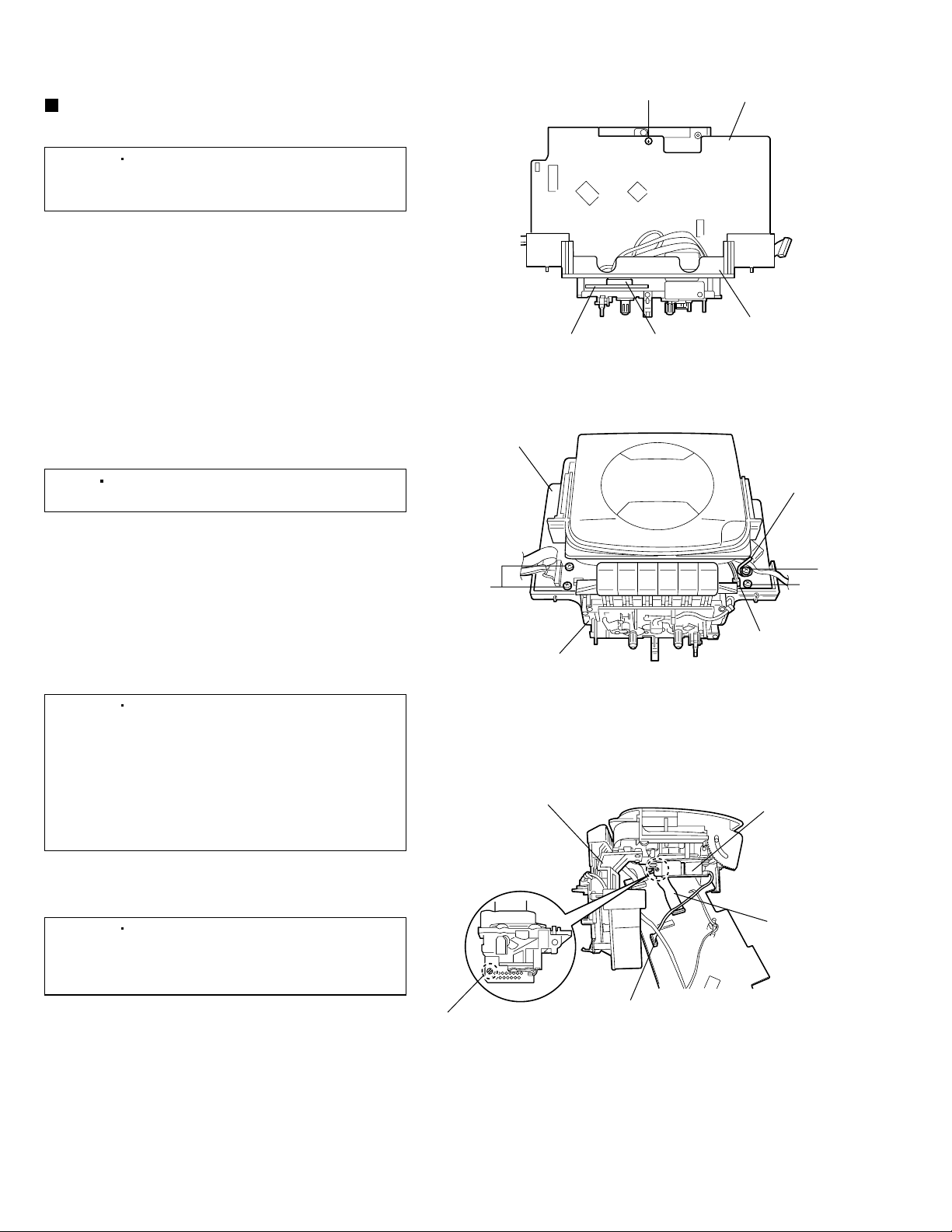
Removing the main board (See Fig. 26.)
Prior to performing the following procedures,
remove the main board from the CD/Cassette
mechanism assembly.
From the bottom side of the CD/Cassette
mechanism assembly, remove the four screws X
retaining the CD mechanism assembly.
[Note]
When attaching the CD mechanism
assembly, be sure not to mistake the
positions of the pink and orange rubbers.
Removing the CD door switch board
(See Fig. 27.)
From the bottom side of the CD/Cassette
mechanism assembly, remove the screw Y
retaining the CD door switch board.
Removing the hanger and CD door
button (See Fig. 27.)
1.
From the bottom side of the CD/Cassette
mechanism assembly, loosen the screw Z of the
spring plate holding the hanger and then move the
spring plate in the direction of the arrow 1.
2.
While pressing the claws ac of the hanger in the
direction of the arrow 2, remove the hanger from
the CD tray assembly.
3.
Press the claws ad of the CD open knob in the
direction of the arrow 3 and then take out the CD
open knob from the top side of the CD tray
assembly.
[Note]
After assembly, apply a locking agent to
the screw Z.
Removing the CD door damper
(See Fig. 27.)
1.2.From the bottom side of the CD/Cassette
mechanism assembly, remove the two screws AA
retaining the CD door damper holder.
Rubber (Orange)
X
Rubber (Orange)
Y
Cassette mechanism assembly
Rubber (Pink)
CD mechanism assembly
Fig.26
Z
(To be loosened)
Claw ad
1
3
2
CD door damper holder
AA
Fig.27
Rubber (Pink)
X
CD tray assembly
Hanger
Spring plate
3
2
Claw ad
Claws ac
CD door switch
board
CD door damper
Take out the CD door damper.
[Note]
After assembly, apply a locking agent to
the screws AA.
Removing the CD door (See Fig. 28.)
1.
Open the CD door.
2.
While pressing the arm section ae of the CD door
in the direction of the arrow, remove the arm
section.
3.
While pressing the arm section af of the CD door in
the direction of the arrow, remove the CD door.
[Note]
When attaching the CD door, hang the
spring to the section ag of the CD door.
CD door
Section ag
Arm af
Spring
Arm ae
Fig.28
1-13
Page 14

RC-BM5
<CD mechanism section>
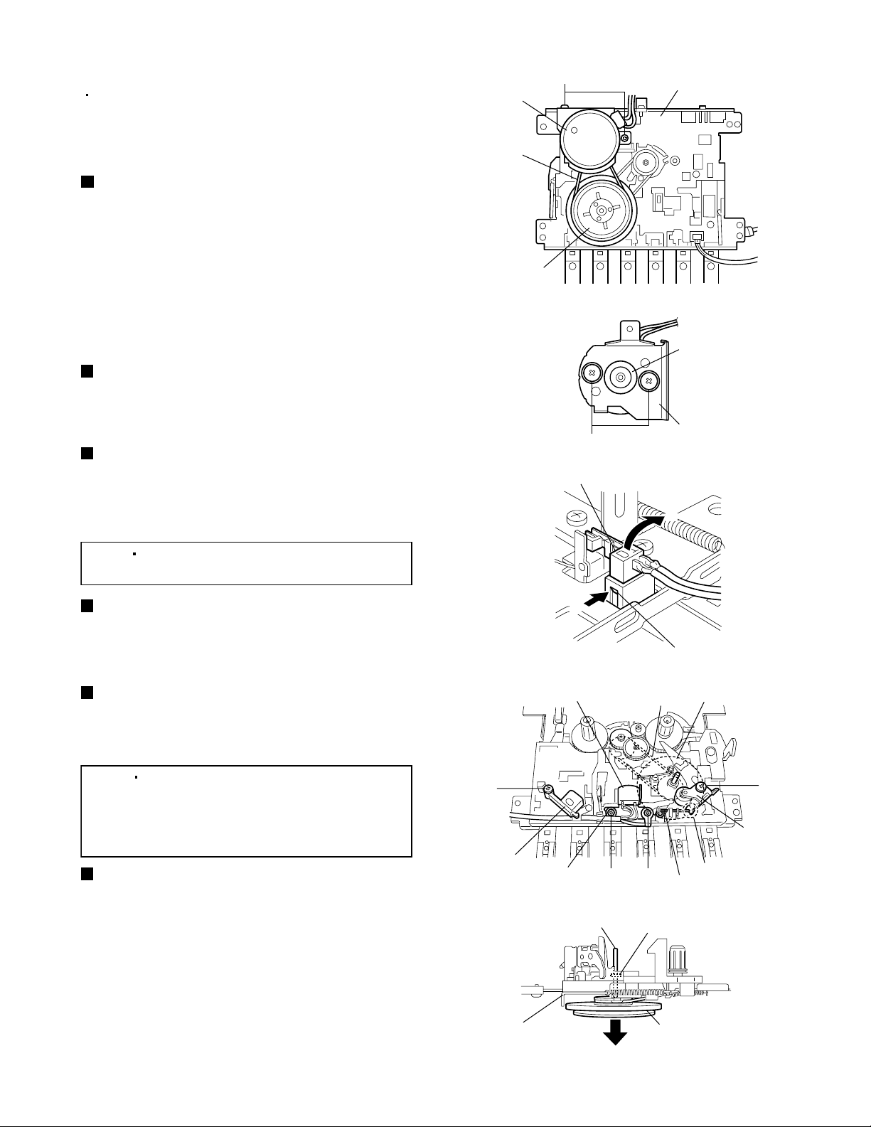
Removing the CD pickup unit
(See Figs. 1 to 2.)
Prior to performing the following procedures,
remove the CD mechanism assembly.
1.
Remove the three screws A retaining the CD
pickup cover. (See Fig.1.)
2.
Remove the slit washer retaining the feed middle
gear and take out the feed middle gear. (See Fig.2.)
3.
Loosen the two screws B retaining the shaft and
pull out the shaft in the direction of the arrow.
(See Fig.2.)
4.
Take out the CD pickup unit.
[Note]
In the assembly, be sure to attach the
sliding spring in the correct orientation
before attaching the CD pickup unit.
(See Fig.2.)
A
A
CD pickup cover
A
CD mechanism assembly
Fig.1
CD pickup unit
Sliding Spring
B
Feed middle gear
Fig.2
CD pickup unit
Slit washer
Shaft
B
1-14
Page 15
RC-BM5
<Cassette mechanism section>
Prior to performing the following procedures,
remove the cassette mechanism assembly from
the rear cabinet assembly.
(See Fig.17 and 18 of "Rear cabinet section" on
page 1-10.)
Removing the capstan motor
(See Figs.1 and 2.)
1.
Remove the capstan motor belt. (See Fig.1.)
2.
Remove the two screws A retaining the bracket of
the capstan motor from the cassette mechanism
assembly. (See Fig.1.)
3.
Remove the two screws B retaining the bracket
from the capstan motor. (See Fig.2.)
Removing the leaf switch (See Fig.3.)
Pressing the claw a of the leaf switch in the
direction of the arrow 1 and take out the leaf switch
in the direction of the arrow 2.
Removing the pinch roller arm
assembly (See Fig.4.)
Remove the screw C retaining the pinch roller arm
assembly and remove the pinch roller arm
assembly in an upward direction.
[Note]
In the assembly, hang the notch b of the
pinch roller arm assembly to the spring.
Capstan motor
Capstan motor
belt
Flywheel assembly
Leaf switch
A
Cassette mechanism assembly
Fig.1
Capstan motor
Bracket
B
Fig.2
2
Removing the erase head
(See Fig.4.)
Remove the screw D retaining the erase head and
remove the erase head in an upward direction.
Removing the REC/PB head
(See Fig.4.)
Remove the screw E, washer and screw F retaining
the REC/PB head and remove the REC/PB head.
[Notes]
When removing or replacing the
REC/PB head, perform the REC/PB head
adjustment. (See "Adjustment method".)
After adjusting the REC/PB head, apply
a locking agent to the screws F.
Removing the flywheel assembly
(See Figs. 4 and 5.)
1.
From the bottom side of the cassette mechanism
assembly, remove the main belt. (See Fig.4.)
2.
From the top side of the cassette mechanism
assembly, remove the slit washer retaining the
shaft of the flywheel assembly. (See Fig.5.)
D
Erase head
1
REC/PB head
Washer
Shaft
Fig.3
Main belt
FE
Fig.4
Slit washer
Claw a
Flywheel assembly
Notch b
Spring
C
Pinch roller
arm
assembly
3.
Pull out the flywheel assembly in the direction of
the arrow. (See Fig.5.)
Cassette mechanism
assembly
Flywheel assembly
Fig.5
1-15
Page 16

RC-BM5
Adjustment method
Measuring instructions required for
adjustment
1. AM signal generator
2. FM signal generator
3. Inter mediate frequency sweep generator
4. FM stereo signal generator
5. Low-frequency oscillator
(oscillation frequency 50Hz-20kHz, 0dB output
with 600 ohm impedance)
6. Attenuator (600 ohm impedance)
7. Electronic voltmeter
8. Distortion meter
9. Torque gauge (cassette for CTG-N)
10. Wow & flutter meter
11. Frequency counter meter
12. Test tape
VT712 : For tape speed and wow flutter
VT724 : For reference level
VT702 : For playback frequency
VT702 : For head azimuth adjustment
13. Blank tape
TAPE : AC-225
Measuring instruments
Radio section
FM 1kHz, 22.5kHz deviation
FM STEREO : 1kHz, 67.5kHz deviation
pilot signal 7.5kHz
AM : 1kHz, 30% modulation
Reference output :
Speaker output 0.5W(1.2V) 3.2 ohm
Standard mode of function knob :
Selects FM or AM in tuner mode
Bass boost: OFF
Preset EQ: Flat
Main volume: Reference output
Cassette amplifier section
Reference output :
Speaker output 0.5W(1.2V) 3.2 ohm
Standard mode of function knob :
Press TAPE knob of select TAPE mode
CD section
CD test disc : CTS-1000
Measurement conditions
Power supply voltage
AC230V(50Hz) : A version
AC220-230V(50Hz)/AC110-127V(60Hz) : US/UJ version
1-16
Page 17

Cassette amplifier section
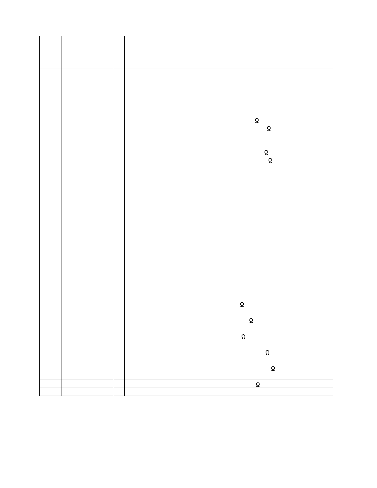
Item Measuring condition Check and adjustment procedure Standard value Adjusting part
Head azimuth
adjustment
Tape speed and
wow/flutter check
and adjustment
PB frequency
response check
Bias frequency
check
REC and PB
frequency
response
adjustment
Test tape:
VT702 (8kHz)
Signal output terminal:
SPEAKERS
Test tape:
VT712 (3kHz)
Signal output terminal:
SPEAKERS
Test tape: VT702
Signal output terminal:
PHONES
(with 32 ohm load)
Tape: Normal
Signal output terminal:
Cassette REC./PLAY
HEAD
Test tape: AC225
Signal input: FM22.5
DEV 60dBu with
emphasis
Signal output terminal:
SPEAKERS
Play back the test tape VT702 (8kHz).
1.
Adjust the head azimuth adjusting screw so that the
2.
phase difference between the R and L channels is
minimized at an output level that is within (+2dB-2dB)
of the maximum output level in the FWD and REV
operations. After this adjustment, lock the head
azimuth adjusting screw with screw sealant to cover
more than a half of the screw head.
When the head azimuth is maladjusted, correct it with
3.
the head azimuth adjusting screw in the FWD and
REV operations alternately.
Play back the test tape VT712 (3kHz) by the end
1.
portion.
Connect a frequency counter and check that it reads
2.
between 2940 and 3090Hz. If not, adjust the
frequency with the motor semifixed resistor.
Check that the wow/flutter is within 0.38%
3.
(unweighted).
Play back the test tape VT702 while con-firming that
deviation between the 1kHz signal and 8kHz signal
should be (0+3dB-6dB).
While recording, check to see if the frequency at the
measuring point is (75+2kHz-2kHz) if not adjust T605
until the frequency counter indicates (75+2kHz-2kHz).
In recording FM mode, and record the reference 1kHz
signal and 8kHz signal alternately repeatedly. While
playing back the recorded signal differ from that of the
1kHz signal by within (0+4dB-4dB).
Output level:
Within (+2dB-2dB) of
maximum output
level
Phase difference R
and L channels:
Minimum
2940 to 3090Hz
Within 0.38%
(unweighted)
Deviation between
1kHz and 8kHz:
(0+3dB-6dB)
Level difference
between REC and
PB:
Within (0+4dB-4dB)
Tuner section
Item Measuring condition Check and adjustment procedure Standard value Adjusting part
FM VT
adjustment
AM VT
adjustment
FM IF adjustment
AM IF adjustment
Signal input:
FM antenna
VT test point:
IC101 pin8
Signal input:
AM loop antenna
VT test point:
IC101 pin8
Signal input:
IC101 pin3
Voltage test point:
IC101 pin19 and pin20
Signal input:
IC101 pin2
Signal output:
IC101 pin10
Set the FM signal generator at 108MHz and output
1.
level at 60dBu.
Adjust L102, so that the VT is within (8V+0.2V-0.2V).
2.
Set the AM signal generator at 1710kHz and output
1.
level at 100dBu.
Adjust T102, so that the VT is with (8V+0.1V-0.1V).
2.
Set the FM signal generator at 10.7MHz with no
1.
signal deviation and output level at 90dBu.
Short IC101 pin21 to GND.
2.
Adjust T103 so that the voltage between IC101 pin19
3.
and pin20 is within (0V+3mV-3mV).
Set the intermediate frequency sweep generator to
1.
AM 450kHz.
Adjust T104 and T105 for maximum and center
2.
output.
Adjust T106 so that the voltage between IC101 pin19
3.
and pin20 is within (0V+2mV-2mV).
VT=8V+0.2V-0.2V
VT=8V+0.1V-0.1V
0V+3mV-3mV
0V+2mV-2mV
RC-BM5
Head azimuth
adjusting screw
(To be used only
after head
replacement)
See Fig.1 on
page 1-18.
Tape speed:
Motor semifixed
resistor
See Fig.2 on
page 1-18.
Check only
T605
See Fig.3 on
page 1-18.
L102
See Fig.4 on
page 1-18.
T102
See Fig.4 on
page 1-18.
T103
See Fig.4 on
page 1-18.
T104,T105
T106
See Fig.4 on
page 1-18.
1-17
Page 18

RC-BM5
Item Measuring condition Check and adjustment procedure Standard value Adjusting part
AM tracking
adjustment
Signal input:
AM ANT. COIL
antenna
Signal output:
IC101 pin14 or
IC101 pin15
FM tracking
adjustment
Signal input:
FM antenna
Signal output:
IC101 pin14 or
IC101 pin15
FM stereo
separation
adjustment
Signal input:
FM antenna
Signal output:
IC101 pin14 or
IC101 pin15
Location of adjusting parts
Cassette mechanism section
(Caution) For adjusting any head, be sure to use a screw driver degaussed.
Set the AM signal generator at 603kHz and the unit
1.
receiving 603kHz, adjust L105 for maximum output.
Set the AM signal generator at 1404kHz and the unit
2.
receiving 1404kHz, adjust TC101 for maximum output.
Set the FM signal generator at 90MHz and the unit
1.
receiving 90MHz, adjust L101 for maximum output.
Set the FM signal generator at 106MHz and the unit
2.
receiving 106MHz, adjust TC102 for maximum output.
Set the AM signal generator at 98MHz with stereo
1.
deviation and the unit receiving 98kHz.
Adjust VR101, so that the separation between the R
2.
and L channels for maximum.
L105
TC101
See Fig.4 on
page 1-18.
L101
TC102
See Fig.4 on
page 1-18.
VR101
See Fig.4 on
page 1-18.
max
Cassette board
T605
Head
Azimuth adjustment screw
Fig.1 Head output signal
Adjustment
Tuner board
T105
T106
CASSETTE MOTOR
T102
T104
1pin
IC101
15pin
T103
Tape Speed Adj.
L2
L101
TC1
TC102
VR101
14pin
TC10
TC101
L102
1
L
-
+
Fig.2
L105
(AM ANT. COIL)
1-18
Fig.3
Fig.4
Page 19

Trouble shooting
RC-BM5
Circuit Symptom Cause
General
AM
FM
Tape
No sound
No sound, weak
sound
(Low sensitivity)
No sound, weak
sound
(Low sensitivity)
No sound/recording,
unsteady tape sound,
weak sound
The unit is on STANDBY mode.
Defective volume control
The unit is on MUTE mode.
Adjust the set position for the best reception.
AM VT faulty
Intermediate frequency tuning faulty
RF tracking faulty
Defective IC101
Adjust FM antenna position for the best
reception.
Defective IC101
Intermediate frequency tuning faulty
Dirty capstan or head
Irregular cassette tape winding
Defective IC601
Remedy
Press STANDBY/ON button to turn on the
unit.
Set the volume control to a proper sound
level.
Press MUTE on the remote control.
Readjust (see "Adjustment method").
Readjust (see "Adjustment method").
Readjust (see "Adjustment method").
Check voltages. Replace if necessary.
Check voltages. Replace if necessary.
Readjust (see "Adjustment method").
Clean the capstan or head with alcohol.
Replace tape.
Check voltages. Replace if necessary.
CD
CD-R
CD-RW
MP3-CD
Cannot read the table
of content.
No display, no sound
Cassette erasure prevention tabs broken out
Disc is inserted upside down.
Disc is dirty.
Disc is scratched.
Disc is seriously warped.
A non-standard disc has been inserted.
Moisture has formed inside the CD deck.
Defect in the servo control board
Defect in the CD pickup mechanism
MP3 formats not supported.
Replace tape or cover tab openings with
adhesive tape.
Insert disc correctly.
Wipe clean with a soft cloth.
Use a new disc.
Use a new disc.
Use only a brand name disc.
Wait about 20 to 30 minutes.
Replace or repair as required.
Replace as required.
Use MP3-CD formats supported on this
unit
1-19
Page 20

RC-BM5
Flow of functional operation until TOC read
Power ON
Slider turns REST
SW ON.
Laser ON
Focus start
FOK
Turn on focus
servo
Confirm that the voltage at the pin5 of H502 is
"H"/"L"/"H"
Check that the voltage at the pin64(LD) of
IC501 is +3.3V.
Disc spinning
Radial_error
scaling
PLL Lock
Turn on radial
servo
Read TOC
Check that the voltage at the pin1 and pin2 of
H502 is +0.78V.
Confirm the eye-pattern at the "RF" test point.
1-20
Page 21

RC-BM5
Maintenance of laser pickup
(1) Cleaning the pick up lens
Before you replace the pick up, please try to
clean the lens with a alcohol soaked cotton
swab.
(2) Life of the laser diode
When the life of the laser diode has expired,
the following symptoms will appear.
The level of RF output (EFM output:ampli tude of eye pattern) will below.
Is the level of
RF OUT under
1.25V 0.22Vp-p?
YES
O.K
NO
Replace it.
Replacement of laser pickup
Turn off the power switch and,disconnect the
power cord from the AC OUTLET.
Replace the pickup with a normal one.(Refer
to "Removing the CD pickup" on the previous page)
Plug the power cord in,and turn the power on.
At this time,check that the laser emits for
about 3 seconds and the objective lens moves
up and down.
Note: Do not observe the laser beam directly.
Play a disc.
Check the eye-pattern at the "RF" test point.
Finish.
(3) Semi-fixed resistor on the APC PC board
The semi-fixed resistor on the APC printed circuit board which is attached to the pickup is used to adjust the laser
power.
Since this adjustment should be performed to match the characteristics of the whole optical block, do not touch the
semi-fixed resistor.
If the laser power is lower than the specified value,the laser diode is almost worn out, and the laser pickup should
be replaced.
If the semi-fixed resistor would be adjusted when the pickup operates normally,the laser pickup may be damaged
due to excessive current.
1-21
Page 22

RC-BM5
Description of major ICs
SAA7324H (IC501) : Digital servo processor & compact disc decoder
1. Terminal layout
1
HFREF
2
HFIN
3
ISLICE
4
V
SSA1
5
V
DDA1
6
I
ref
7
V
RIN
8
D1
9
D2
10
D3
11
D4
12
R1
13
R2
14
V
SSA2
15
CROUT
16
CRIN
2. Block diagram
12
R1
13
R2
SCL
SDA
RAB
SILD
HFIN
Iref
SUB
RCK
7
40
39
41
42
2
1
3
6
25
31
44
24
16
15
26
49
48
47
46
45
43
38
VRIN
HFREF
ISLICE
TEST1
TEST2
TEST3
SELPLL
CRIN
CROUT
CL16
CL11/4
SBSY
SFSY
STATUS
RESET
LDONV1V5V4MOTO2
646362616059585756555453525150
171819202122232425262728293021
LP
LN
DDA2
V
D1 D2 D3 D4
8 9 10 11
ADC
SSD3VDDD2(C)
MOTO1
V
SLFORA
SAA7324H
RP
RN
pos
neg
V
V
TEST1
SELPLL
SS
A2
V
VSSA1
4 14 5 17 33 50 58 52 57
PRE.
PROCESSING
CL16
V
DD1(P)
CFLG
V
DATA
SCLK
WCLK
DD
V
DD
A1
Vref
GENERATOR
MICROCONTROLLER
CONTROL
PART
INTERFACE
DIGITAL
FRONT-
END
PLL
EFM
DEMODULATOR
TEST
SRAM
RAM
ADDRESSER
TIMING
SUBCODE
PROCESSOR
DETECT
DECODER
MICRO-
CONTROLLER
INTERFACE
VERSATILE PINS
INTERFACE
63 34 61 62
V1 V2/V3 V4 V5 KILL
SSD2
DOBM
V
CL11/4
49
32
EF
KILL
TEST2
A2
V
SS
D1
CONTROL
FUNCTION
PROCESSOR
PEAK
KILL
48
47
46
45
44
43
42
41
40
39
38
37
36
35
34
33
SS
V
AUDIO
32
D2
SBSY
SFSY
SUB
RCK
TEST3
STATUS
SILD
RAB
SCL
SDA
RESET
SCLI
SDI
WCLI
V2/V3
V
SSD1
V
DDD1(P)
V
SS
D3
OUTPUT
STAGES
MOTOR
CONTROL
ERROR
CORRECTOR
FLAGS
EBU
INTERFACE
SERIAL DATA
INTERFACE
SERIAL DATA
(LOOPBACK)
INTERFACE
BITSTREAM
DAC
V
DDD2(C)
54
RA
55
FO
56
SL
64
LDON
59
MOTO1
60
MOTO2
53
CFLG
51
DOBM
30
EF
29
SCLK
28
WCLK
27
DATA
37
SCLI
35
WCLI
36
SDI
20
Vneg
21
VPOS
18
LN
19
LP
22
RN
23
RP
1-22
Page 23

RC-BM5
3. Pin function
Pin No. Symbol I/O Function
1
2
3
4
5
6
7
8
9
10
11
12
13
14
15
16
17
18
19
20
21
22
23
24
25
26
27
28
29
30
31
32
33
34
35
36
37
38
39
40
41
42
43
44
45
46
47
48
49
HFREF
HFIN
ISLICE
SSA1
V
V
DDA1
Iref
RIN
V
D1
D2
D3
D4
R1
R2
SSA2
V
CROUT
CRIN
V
DDA2
LN
LP
neg
V
V
pos
RN
RP
SELPLL
TEST1
CL16
DATA
WCLK
SCLK
EF
TEST2
KILL
SSD1
V
V2/V3
WCLI
SDI
SCLI
RESET
SDA
SCL
RAB
SILD
STATUS
TEST3
RCK
SUB
SFSY
SBSY
CL11/4
I
Comparator common mode input
I
Comparator signal input
O
Current feedback output from data slicer
-
Analog ground 1
-
Analog supply voltage 1
O
Reference current output
-
Reference voltage for servo ADCs
I
Unipolar current input 1 (central diode signal input)
I
Unipolar current input 2 (central diode signal input)
I
Unipolar current input 3 (central diode signal input)
I
Unipolar current input 4 (central diode signal input)
I
Unipolar current input 1 (satellite diode signal input)
I
Unipolar current input 2 (satellite diode signal input)
-
Analog ground 2
O
Crystal/resonator output
I
Crystal/resonator input
-
Analog supply voltage 2
O
DAC left channel differential negative output
O
DAC left channel differential positive output
I
DAC negative reference input
I
DAC positive reference input
O
DAC right channel differential negative output
O
DAC right channel differential positive output
-
Selects whether internal clock multiplier PLL is used
I
Test control input 1 (this pin should be tied LOW)
O
16.9344MHz system clock output
O
Serial d4(1) data output (3-state)
O
Word clock output (3-state)
O
Serial bit clock output (3-state)
O
C2 error flag output (3-state)
I
Test control input 2 (this pin should be tied LOW)
O
Kill output (programmable;open-drain)
-
Digital ground 1
I/O
Versatile I/O:versatile input 2 or versatile output 3 (open-drain)
I
Word clock input (for data loopback to DAC)
I
Serial data input (for data loopback to DAC)
I
Serial bit clock input (for data loopback to DAC)
I
Power-on reset input (active LOW)
I/O
Microcontroller interface data I/O line (IIC-bus;open-drain output)
I
Microcontroller interface clock line input (IIC-bus)
I
Microcontroller interface R/W and load control line input (4-wire bus mode)
I
Microcontroller interface R/W and load control line input (4-wire bus mode)
O
Servo interrupt request line/decoder status register output (open-drain)
I
Test control input 3 (this pin should be tied LOW)
I
Subcode clock input
O
P-to-W subcode bits output (3-states)
O
Subcode frame sync output (3-sates)
O
Subcode block sync output (3-sates)
O
11.2896 or 4.2336MHz (for microcontroller) clock output
SAA7324H (1/2)
1-23
Page 24

RC-BM5
Pin No. I/O FunctionSymbol
50
51
52
53
54
55
56
57
58
59
60
61
62
63
64
SSD2
V
DOBM
V
DDD1(P)
CFLG
RA
FO
SL
DDD2(C)
V
V
SSD3
MOTO1
MOTO2
V4
V5
V1
LDON
-
Digital ground 2
O
Bi-phase mark output (externally buffered;3-state)
-
Digital supply voltage 1 for periphery
O
Correction flag output (open-drain)
O
Radial actuator output
O
Focus actuator output
O
Sledge control output
-
Digital supply voltage 2 for core
-
Digital ground 3
O
Motor output 1;versatile (3-state)
O
Motor output 2;versatile (3-state)
O
Versatile output 4
O
Versatile output 5
I
Versatile input 1
O
Laser drive on output (open-drain)
SAA7324H (2/2)
AN7312 (IC601) : Dual recording/Playback pre-amplifier circuit with ALC
1. Terminal layout
14 8
17
~
~
3. Pin function
Pin No. Symbol Function
1
GND
2
ALC time constant
3
ALC input Ch.1
4
Output Ch.1
5
Phase compensation Ch.1
6
N.E.B. Ch.1
7
Input Ch.1
8
Input Ch.2
9
N.E.B. Ch.2
10
Phase compensation Ch.2
11
Output Ch.2
12
ALC input Ch.2
13
Ripple filter
14
Vcc
2. Block diagram
Vcc
14 13 12 11 10
Ripple Filter
ALC
1 2 3 4 5 6
GND
Amp.
Ch2
Amp.
Ch1
9
I/O
GND
ALC time constant by resistance and capacitor
Right channel ALC input
I
Right channel output
O
Not connect
Right channel negative feed back input
I
Right channel signal input
I
Left channel signal input
I
Left channel negative feed back input
I
Not connect
Left channel output
O
Left channel ALC input
I
Ripple filter
Power supply
-
8
7
1-24
Page 25

MX10FLCDPC (IC301) : MCU
1.Terminal layout
1
2
3
4
5
6
7
8
9
10
11
12
13
14
15
16
17
18
19
20
40
39
38
37
36
35
34
33
32
31
30
29
28
27
26
25
24
23
22
21
2. Block diagram
Vcc
Vss
REGISTER
RAM ADDR.
B
REGISTER
PSEN
ALE
RST
EA
TIMING
AND
CONTROL
P0.0-P0.7 P2.0-P2.7
PORT 0
DRIVERS
ALU
PSW
PORT1
LATCH
PORT 0
LATCH
RAM
ACC
TMP2 TMP1
REGISTER
INSTRUCTION
STACK
POINTER
T0/T1/T2
TIMERS
PORT2
DRIVERS
PORT 2
LATCH
WATCHDOG
SFRs
T3
TIMER
PORT1
LATCH
ROM
PROGRAM
REGISTER
INCREMENTER
PROGRAM
COUNTER
RC-BM5
ADDR.
BUFFER
PC
DPTR
3.Pin function
Pin No.
P1.0 to P1.7
P2.0 to P2.5,P3.4 to P3.5
P0.0 to P0.7
P3.3
P2.7
ALE
EA
P3.7,P3.1,P3.0
VDD
GND
A0 to A7
A8 to A13,A14 to A15
Q0 to Q7
CE
OE
WE
Vpp
MS2 to MS0
VDD
GND
Symbol I/O
NJM7805FA (IC505) : Regulator
1. Terminal layout
1.INPUT
2.OUTPUT
3.GND
2. Block diagram
INPUT
osc
I
I
I/O
I
I/O
I
-
-
-
-
1
THERMAL SHUTDOWN
BANDGAP REFERENCE
PORT1
DRIVERS
XTAL2XTAL1
PORT1
DRIVERS
P3.0-P3.7P1.0-P1.7
Function
Input low order address bits
Input high order address bits
Data input/output
Chip enable input
Output enable input
Write enable input
Program supply voltage, 12.5-13volts
Flash mode selection
Power supply voltage (+5V)
Ground pin
OVER VOLTAGE PROTECTION
Q1
R1
2
OUTPUT
123
SOA PROTECTION
SHORT CIRCUIT
PROTECTION
3
GND
R2
1-25
Page 26

RC-BM5
PT2314 (IC801) : 4ch input audio processor
1. Terminal layout
1 28
2
3
4
6
7
8
9
10
11
12
13
14
2. Block diagram
LOUT
LIN
LOUD_L
BOUT_L
BIN_L
27
26
25
245
23
22
21
20
19
18
17
16
15
LIN1
LIN2
LIN3
LIN4
RIN4
RIN3
RIN2
RIN1
LIN1
LIN2
LIN3
LIN4
RIN4
RIN3
RIN2
RIN1
Supply
Volume &
Loudness
Volume&
Loudness
RB
Bass Treble
Serial Bus Decoder & Latches
Bass Treble
RB
TREBLE_L
Speaker
ATT
OUT_L
CLK
DATA
DGND
OUT_R
Speaker
ATT
Mute
Mute
VDD
REF
AGND
ROUT
RIN
LOUD_R
BOUT_R
3. Pin function
Pin No. Symbol I/O Function
1
2
3
4
5
6
7
8
9
10
11
12
13
14
15
16
17
18
19
20
21
22
23
24
25
26
27
28
VDD
AGND
TREB_L
TREB_R
RIN
ROUT
LOUD_R
RIN4
RIN3
RIN2
RIN1
LOUD_L
LIN4
LIN3
LIN2
LIN1
LIN
LOUT
BIN_L
BOUT_L
BIN_R
BOUT_R
OUT_R
OUT_L
DGND
DATA
CLK
REF
-
Supply input voltage
-
Analog ground
I
Left channel input for treble controller
I
Right channel input for treble controller
I
Audio processor right channel input
O
Gain output and input selector for right channel
I
Right channel loudness input
I
Right channel input 4
I
Right channel input 3
I
Right channel input 2
I
Right channel input 1
I
Left channel loudness input
I
Left channel input 4
I
Left channel input 3
I
Left channel input 2
I
Left channel input 1
I
Audio processor left channel input
O
Gain output and input selector for left channel
I
Left channel input for bass controller
O
Left channel output for bass controller
I
Right channel input for bass controller
O
Right channel output for bass controller
O
Right speaker output
O
Left speaker output
-
Digital ground
I
Control data input
I
Clock input for serial data transmission
-
Analog reference voltage (1/2 VDD)
BIN_R
TREBLE_R
1-26
Page 27

AS4C256KEO (IC701) : DRAM
1. Termianl layout 2. Block diagram
WE
RAS
1
2
3
4
5
6
7
8
9
10
11
12
13
14
15
16
17
18
19
20
40
CASL
39
CASH
38
37
36
35
34
33
32
31
30
29
28
27
26
25
24
23
22
21
A0
A1
A2
A3
A4
A5
A6
A7
A8
CONTROL
LOGIC
CLOCK
GENERATOR
COLUMN
ADDRESS
BUFFER
REFRESH
CONTROLER
REFRESH
COUNTER
ROW.
ADDRESS
BUFFERS<9>
ROW
DECODER
3. Pin function
Pin No. Symbol Function
1
2 to 5
6
7 to 10
11,12
13
14
15
16 to 19
20
21
22 to 26
27
28
29
30
31 to 34
35
36 to 39
40
VCC
I/O0 to I/O3
Vcc
I/O4 to I/O7
NC
WE
RAS
NC
A0 to A3
Vcc
GND
A4 to A8
OE
UCAS
LCAS
NC
I/O8 to I/O11
GND
I/O12 to I/O15
GND
I/O
Power (5V 0.5V)
Input/output
I/O
Power (5V 0.5V)
Input/output
I/O
Not connect
Read/write control
Row address strobe
Not connect
Address inputs
I
Power (5V 0.5V)
Ground
Address inputs
I
Output enable
O
Column address strobe,upper byte
Column address strobe,lower byte
Not connect
Input/output
I/O
Ground
Input/output
I/O
Ground
-
RPM6938-V4 (IC402) : Remote control receiver
1. Block diagram
3
1
2
I/V
conversion
PD
AMP
for
trimming circuit
magnetic shield
BPF
AGC
Detector
Vcc
Comp
22k
ohm
VDD
OUT
GND
512
COLUMN
DECODER
512
SENSE AMPLIFIERS
I/O GATING
512 X 16
512 x 512 x 16
MEMORY
ARRAY
V
BB
GENERATOR
DATA-IN
BUFFER
DATA-OUT
BUFFER
CC
V
V
SS
OE
IO0
.
IO15
RC-BM5
1-27
Page 28

RC-BM5
LS188C (IC703) : VCD decoder
1. Terminal layout 2. Block diagram
102 65
103
128
1 38
3. Pin function
Pin No.
1 to 3,22
4 to 11
12 to15
16
17,18,20,21
19
23,24
25
26
27
28
29
30
31
32
33
34
35
36
37 to 42
43
44,45
46
47
48
49
50
51
52 to 55
56
57,58
59
60,61
EMI_A_9 to EMI_A_12
EMI_D_7 to EMI_D_0
EMI_A_0 to EMI_A_3
VDD_IO_00
EMI_A_4 to EMI_A_7
VSS_IO_00
EMI_A_15 to EMI_A_16
EMI_A_18
I2C_CLK
I2C_DAT
VSS_OSC_0
XTLCLK_I
XTLCLK_O
VDD_OSC_0
TEST_H
RESET_L
HSYNC_L
VSYNC_L
CLK27_O
VDAT_7 to VDAT_2
VSS_CORE_00
VDAT_1 to VDAT_0
VDD_CORE_00
AUD_XCK
AUD_BCK
AUD_LRCK
AUD_DOUT
AUD_DIN
GPIO_23 to GPIO_20
VDD_IO_10
GPIO_19,GPIO_18
VSS_CORE_10
GPIO_17,GPIO_16
DRAM
64
ROM/SRAM
Panel and
keypad
39
Symbol Function
Host
I/O
O
I
O
-
O
O
O
O
-
-
I
O
-
I
I
I
I
O
O
-
O
-
O
O
O
I
-
-
-
-
-
DRAM
Interface
EMI
Interface
Prog.I/O
Interface
CD
Host/CD
Interface
RISC
Processor
DSP
Core
EMI address bus
EMI data bus
EMI address bus
+3.3V
EMI address bus
+3.3V
EMI address bus
EMI address bus
I2C clock
I2C data
GND
Crystal input
Crystal output
+3.3V
Te st
Hardware reset
Horizontal sync
Vertical sync
CLK 27MHz output
Luminance output
GND
Luminance output
+2.5V
External audio clock
Audio bit clock
Audio left/right clock
Audio data output
Audio data input
Programmable I/O
+3.3V
Programmable I/O
GND
Programmable I/O
Video
Processor
On Screen
Display
Video
Decoder
Audio
Decoder
Audio
Interface
Register
Bank
NTSC/PAL
Encoder
Audio
DAC
Audio
ADC
LS188C (1/2)
1-28
Page 29

Pin No.
62
63,64
65
66 to 79
80
81
82
83
84
85
86
87
88
89
90,91
92
93
94
95
96
97
98
99
100
101
102
103,104
105
106
107
108
109
110
111
112
113
114
115
116
117
118
119,120
121
122,123
124
125
126
127
128
Symbol FunctionI/O
VDD_CORE_10
GPIO_15,GPIO_14
VSS_IO_10
GPIO_13 to GPIO_0
IR_IN
CD_DATA
CD_LRCK
CD_BCK
CD_C2P0
DR_D_0
DR_D_15
DR_D_1
DR_D_14
VDD_IO_20
DR_D_2,DR_D_13
VSS_IO_20
DR_D_3
DR_D_12
DR_D_4
DR_D_11
DR_D_5
DR_D_10
VSS_PLL_0
VDD_PLL_0
DR_D_6
DR_D_9
DR_D_7,DR_D_8
VSS_CORE_20
LCAS_L
DR_WE_L
VDD_IO_30
UCAS_L
URAS_L
VDD_CORE_20
LRAS_L
DR_A_8
DR_A_0
DR_A_7
DR_A_1
DR_A_6
VSS_IO_30
DR_A_2,DR_A_5
VSS_CORE_30
DR_A_3,DR_A_4
VDD_CORE_30
EMI_A_17
EMI_A_14
EMI_A_13
EMI_A_8
+2.5V
Programmable I/O
GND
Programmable I/O
IR input
I
CD serial data
I
CD left/right clock
I
CD bit clock
I
CD data error flag
I
DRAM data bus
DRAM data bus
DRAM data bus
DRAM data bus
+2.5V
DRAM data bus
GND
DRAM data bus
DRAM data bus
DRAM data bus
DRAM data bus
DRAM data bus
DRAM data bus
GND
+2.5V
DRAM data bus
DRAM data bus
DRAM data bus
GND
Lower column address strobe
O
Memory write enable
O
+3.3V
Upper column address strobe
O
Upper row address strobe
O
+2.5V
Lower row address strobe
O
DRAM address bus
O
DRAM address bus
O
DRAM address bus
O
DRAM address bus
O
DRAM address bus
O
GND
DRAM address bus
O
GND
DRAM address bus
O
+2.5V
EMI address bus
O
EMI address bus
O
EMI address bus
O
EMI address bus
O
RC-BM5
LS188C (2/2)
1-29
Page 30

RC-BM5
ST24C01 (IC302) : Serial access 1K(128x8) EEPROM
1. Terminal layout
A0
A1
A2
V
SS
1
2
3
4
V
8
CC
7
WC
6
SCL
5
SDA
2. Pin function
Pin No. Symbol I/O Function
1
2
3
4
5
6
7
8
A0
A1
A2
Vss
SDA
SCL
WC
VCC
TDA1308T (IC704) : Class AB stereo headphone driver
1. Terminal layout
I
Chip enable input
I
Chip enable input
I
Chip enable input
-
Ground
I/O
Serial data adress input/output
-
Serial clock
-
Write control (W version)
-
Supply voltage
3. Pin function2. Block diagram
OUTA
INA(neg)
INA(pos)
V
SS
1
2
3
4
TDA 1308
8
7
6
5
V
DD
OUTB
INB(neg)
INB(pos)
OUTA
INA(neg)
INA(pos)
V
SS
1
2
3
4
8
7
6
5
V
DD
OUTB
INB(neg)
INB(pos)
TDA7073 (IC502/IC503) : Dual BTL power driver
1. Terminal layout
IN1-
IN1+
n.c.
n.c.
Vp
IN2+
IN2-
n.c.
1
2
3
4
5
6
7
8
16
OUT1+
15
n.c.
14
GND1
13
OUT1-
12
OUT2-
11
n.c.
10
GND2
9
OUT2+
1
2
3
4
5
6
7
8
DISC MOTOR
VDD
SLIDE MOTOR
16
15
14
13
12
11
10
9
Pin No. Symbol I/O Function
OUTA
1
2
3
4
5
6
7
8
INA(neg)
INA(pos)
Vss
INB(pos)
INB(neg)
OUTB
VDD
Output A
O
Inverting input A
I
Non-inverting input A
I
Negative supply
Non-inverting input B
I
Inverting input B
I
Output B
O
Positive supply
-
3. Pin function2. Block diagram
Pin No. Symbol I/O Function
1
2
3
4
5
6
7
8
9
10
11
12
13
14
15
16
IN1IN1+
n.c.
n.c.
Vp
IN2+
IN2n.c.
OUT2+
GND2
n.c.
OUT2OUT1GND1
n.c.
OUT1+
Negative input 1
I
Positive input 1
I
Not connect
Not connect
Positive supply voltage
Positive input 2
I
Negative input 2
I
Not connect
Positive output 2
O
Ground 2
Not connect
Negative output 2
O
Negative output 1
O
Ground 1
Not connect
Positive output 1
O
1-30
Page 31

PT6553 (IC401) : LCD driver with key input function
1. Terminal layout
KO5
KO4
KO3
KO2/SG42
KO1/SG41
COM3
COM2
COM1
SG40
SG39
SG38
SG37
SG36
SG35
SG34
SG33
KO6
K11
K12
K13
K14
K15
TEST
VDD
VDD1
VDD2
VSS
OSC
CLK
DO
CE
484746454443424140393837363534
49
50
51
52
53
54
55
56
57
58
59
60
61
62
63
64
DI
33
SG32
32
SG31
31
SG30
30
SG29
29
SG28
28
SG27
27
SG26
26
SG25
25
SG24
24
SG23
23
SG22
22
SG21
21
SG20
20
SG19
19
SG18
18
SG17
17
2. Block diagram
COM1
COM2
DO
CE
DI
COMMON
DRIVER
CLOCK
GENERATOR
INTERFACE
VDET
TEST
OSC
CLK
VDD
VDD1
VDD2
VSS
COM3
SG40
SG5
SG4/P4
SG3/P3
SEGMENT DRIVER & LATCH
SHIFT REGISTER
CONTROL
REGISTER
KEY BUFFER
KEY SCAN
SG2/P2
RC-BM5
SG1/P1
1
234
P1/SG1
P2/SG2
P3/SG3
P4/SG4
56789
SG5
SG6
SG7
SG8
10111213141516
SG9
SG10
SG11
SG12
SG13
SG14
SG15
SG16
3. Pin function
Pin No. Symbol I/O Function
1 to 4
SG1/P1 to SG4/P4
O
Segment output general purpose output pins under serial data control
these pins may be used a general purpose output parts.
5 to 40
41,42,43
44
45
46 to 49
50 to 54
55
56
57
58
59
60
61
62
63
64
SG5 to SG40
COM1,COM2,COM3
KO1/SG41
KO2/SG42
KO3 to KO6
K11 to K15
Test
VDD
VDD1
VDD2
VSS
OSC
DO
CE
CLK
DI
O
Segment output pins
O
Common driver output pins
O
Key scan output segment output pin
O
Key scan output segment output pin
O
Key scan output pins
I
Key scan input pins
I
Test pin
-
Power supply
-
Power supply
-
Power supply
-
Ground
I/O
Oscillator pin
O
Data output pin
I
Chip enable pin
I
Synchronization clock input pin
I
Din transistor input pin
K15
K11
K05
K03
SG42/KO2
SG41/KO1
1-31
Page 32

RC-BM5
TEA5757H (IC101): Self tuner radio (STR)
1. Terminal layout
2. Block diagram
43
FM-RFI
DATA
STAB(A)
STAB(B)
V
CC1
V
DDD
XTAL
DGND
P1
P0
42
28
27
29
38
34
7
23
1
25
26
31
30
2
RFGND
BUS-CLOCK
WRITE-ENABLE
V
V
RIPPLE
AM-RFI
RIPPLE
1
2
AM-RFI
RFGND
FMOSC
V
CC1
TUNE
VCO
AFO
MPXI
3
3
4
5
6
7
8
9
10
11
OSCILLATOR
OSCILLATOR
FM-FRO
AM-OSC
FM-RFO FMOSC
FM
FRONT-END
STABILIZER
PRESCALER
MULTIPLEXER
CRYSTAL
OSCILLATOR
AM
FRONT-END
AGC
FM-RFI
44
43
12
13
LFI
MUTE
5
FM
SHIFT REGISTER
LAST-STATION
MEMORY
PROGRAMMABLE
COUNTER
WINSOW
DETECTOR
AM
RF GND
AM-IFI1
42
41
14
15
AFLO
AFRO
FM-MIXER
39 37
FM
MIXER
AM
MIXER
AM-MIXER
FM-MIXER
40
39
TEA5757H
16
17
PILFIL
IFGND
FM-IFI1
FM
IF1
STATUS
REGISTER
SEQUENTIAL
CIRCUIT
FM
AM
AM
IF
STAB(A)
V
38
18
FMFEM
FM-IFO1
35 33
FM-IFI1
37
19
(n)
AFC
FM-IFI2
Up
Down
Level
AGC
AM-IFI/O2
36
20
(p)
AFC
STAB(B)
FM-IFO1
V
35
34
33
32
31
30
29
28
27
26
25
24
23
21
22
FSI
CC2
V
IFGND
FMDEM
17 18
FM
IF2FMDETECTOR
AM/FM
INDICATOR
IN-LOCK
DETECTOR
CHARGE
PUMP
Hard mute
AFC
AM
DETECTOR
FM-IFI2
AFC
P1
P0
WRITE-ENABLE
DATA
BUS-CLOCK
DGND
XTAL
MO/ST
V
DDD
FSI
21
DETECTOR
19 kHz
38 kHz
DECODER
MATRIX
Stereo Mono
SDS
level
CONVERTER
PILOT
PLL
V/I
Stereo
MUTE
16
PILFIL
24
MO/ST
12
LFI
9
VCO
14
AFLO
AFRO
15
13
MUTE
19
AFC
AFC
AFC
(n)
(p)
20
32
1-32
6
AMOSC
AM-MIXER
AM-IFI/O2
AM-IFI1
AGC
AGC
TUNE
844364140
AFO
V
CC2
1122 10
4
RFGNDMPXI
Page 33
RC-BM5
3. Pin function
Pin No. Symbol I/O Function
RIPPLE
1
AM-RFI
2
FM-RFO
3
RFGND
4
FMOSC
5
AMOSC
6
V
7
8
9
10
11
12
13
14
15
16
17
18
19
20
21
22
23
24
25
26
27
28
29
30
31
32
33
34
35
36
37
38
39
40
41
42
43
44
CC1
TUNE
VCO
AFO
MPXI
LFI
MUTE
AFLO
AFRO
PILFIL
IFGND
FMDEM
AFC
AFC(p)
FSI
V
CC2
VDDD
MO/ST
XTAL
DGND
BUS-CLOCK
DATA
WRITE-ENABLE
P0
P1
AFC
FM-IFI2
V
STAB(B)
FM-IFO1
AM-IFI/O2
FM-IFI1
V
STAB(A)
FM-MIXER
AM-MIXER
AM-IFI1
RFGND
FM-RFI
AGC
(n)
Ripple capacitor input
I
AM-RF input
I
Parallel tuned FM-RF circuit to ground
RF ground and substrate
Parallel tuned FM-oscillator circuit to ground
Parallel tuned AM-oscillator circuit to ground
Supply voltage
Tuning current output
O
Voltage controlled oscillator input
I
AM/FM AF output (output impedance typical 5k )
O
Stereo decoder input (input impedance typical 150k )
I
Loop-filter input
I
Mute input
I
Left channel output (output impedance typical 4.3k )
O
Right channel output (output impedance typical 4.3k )
O
Pilot detector filter input
I
Grond of IF,detector and MPX stage
Ceramic discriminator input
I
AFC negative output
O
AFC positive output
O
Field-strength indicator
Supply voltage for tuning
Digital supply voltage
Mono/stereo and tunig indication output
O
Crystal input
I
Digital ground
Bus-clock input
I
Bus data input/output
I/O
Bus write-enable input
I
Programmable output port (P0)
O
Programmable output port (P1)
O
450kHz LC-input circuit
I
FM-IF input 2 (input impedanc typical 330 )
I
Internal stabilized supply voltage (B)
FM-IF output1 (output impedance typical 330 )
O
Input/output to IF-Tank (IFT);output:current souce
I/O
FM-IF input1 (input impedance typical 330 )
I
Internal stabilized supply voltage (A)
Ceramic filter output (output impedance typical 330 )
O
Open-collector output to IFT
O
IFT or ceramic filter input (input impedance typical 3k )
I
FM-RF ground
FM-RF aerial input (input impedance typical 40 )
I
AGC capacitor input
I
TEA5757H
1-33
Page 34

RC-BM5
TZA1024T (IC504) : Data amplifier and laser supply
1. Terminal Layout
2. Pin function
LD
1
V
2
DD(L)
3
CFIL
4
MON
DIN
GND
PWRON
TZA1024
5
6
7
3. Block diagram
DIN
11
5
CDRW
14
RGADJ
V
13
DD
12
EQSEL
11
CDRW
10
RFEQO
9
RFFB
8
CMFB
V
DD
13
1
4
Pin No. Symbol I/O Function
Current output to laser diode
1
2
3
4
5
6
7
8
9
10
11
12
13
14
LD
V
DD(L)
CFIL
MON
DIN
GND
PWRON
CMFB
RFFB
RFEQO
CDRW
EQSEL
DD
V
RGADJ
V
DD
O
Laser supply voltage
External filter capacitor
Laser monitor diode input
I
Central diode input
I
Ground
Power-on select input
I
Common mode feedback voltage input
I
External RF feedback resistor
RF amplifier output
O
Gain select input for CD-A/V, CD-R/W
I
Equalizer/speed select input (n=1,2 or 4)
I
Supply voltage
External laser supply gain adjust resistor
-
12
EQSEL
9
RFFB
10
RFEQO
MON
2
250
kHz
V/I
4
GND
V
GAP
(1)
V
DD(L)
V/I
V
26
DD
14
MGR517
8
CMFB
1
LD
RGADJ
3
CFIL
7
PWRON
1-34
Page 35

BA5417 (IC201) : Dual power amplifier
1. Terminal layout & Block diagram 2. Pin function
Pin No. Symbol I/O Function
1
T.S.D.
IN2
IN1
45
30K
RF2
30K
GND1
Pre
PRE GND1
30K
30K
BS
ST.BY
GND
Power
ST.BY
45
FILTERBS
FILTER
RF1
Vcc
1 2 3 4 5 6 7 8 9 10 11 12 13 14 15
N.C.
BS
OUT1
Vcc
OUT2BSPOWER GND
GND2
Pre
PRE GND2
2
3
OUT1
4
5
OUT2
6
7
8
9
ST.BY
FILTER
10
11
12
13
14
PRE GND1
15
PRE GND2
W27C020 (IC702) : EEPROM
1. Terminal layout
2. Block diagram
NC
BS
VCC
BS
GND
RF1
IN2
IN1
RF2
-
Not connect
-
BS
O
Output terminal
O
Power supply
O
Output terminal
O
BS
O
Power GND
I
ST.BY
I
Filter
-
RF1
-
Input terminal
-
Input terminal
-
RF2
I/O
PRE GND
O
PRE GND
RC-BM5
PGM
1 Vcc32Vpp
2 PGM31A16
3 A1730A15
4 A1429A12
5 A1328A7
6A827A6
7A926A5
8 A1125A4
9OE24A3
10 A1023A2
11 CE22A1
12 Q721A0
13 Q620Q0
14 Q519Q1
15 Q418Q2
16 Q317GND
CE
OE
A0
A17
Vcc
GND
Vpp
3. Pin function
Pin No. Symbol I/O Function
1
2 - 12
13 - 15
16
17 - 21
22
23
24
25 - 30
31
32
Vpp
A16,A15,A12,A7 - A0
Q0 - Q2
GND
Q3 - Q7
CE
A10
OE
A11,A9,A8,A13,A14,A17
PGM
Vcc
Program/Erase supply voltage
Address inputs
I
Data inputs/ outputs
I/O
Connect to GND
Data inputs/ outputs
I/O
Chip enable
Address input
I
Output enable
O
Address inputs
I
Program enable
Power supply
-
CONTROL
DECODER
OUTPUT
BUFFER
CORE
ARRAY
Q0
Q7
1-35
Page 36

RC-BM5
Wiring connections
OW31-60190-50
(A version)
(Forward side)
Tuner board
H801
OW25-94100-02
CASS DECK
CD MECH
OW20-41021-12
CN702
OW20-41022-29K
Cassette board
OW20-41101-20
H701H702
H302
Main board
(Forward side)
OW32-35160-28
OW25-61080-01
CN701
H502
H501
CN804
CN204
OW20-51061-13
CN302
CN303
CN803
CN802
CN801
OW20-42081-09
CN206
CN301
OW20-61033-00K
OW20-41062-17K
(Forward side)
OW32-30140-20
OW20-41112-20
CN401
CN601
Display board
SW2M-M+
SW1
CN602
CN603
LED41
(Forward side)
H602
OW20-41102-32
LCD1
1-36
BLUE
6 7 8 9 0
BROWN
12345
Color codes are shown below.
VIOLET
GREY
RED
ORANGE
WHITE
BLACK
YELLOW
GREEN
OW31-20190-56
OW31-20160-52
OW31-20160-54
OW31-20190-50
OW25-94060-03
CN202
H202
CN205
Phone jack board
OW20-42042-08
(Forward side)
Power amplifier board
CN203
OW31-60120-13T
OW31-60150-10
(Forward side)
OW31-60120-13T
OW31-60150-10
H402
(Forward side)
Volume switch board
OW31-60090-52
OW31-60080-54
OW31-60090-52
OW31-60080-54
Page 37

OW31-60190-50
(US/UJ version)
(Forward side)
Tuner board
H801
RC-BM5
OW25-94100-02
CASS DECK
CD MECH
OW20-41021-12
CN702
OW20-41022-29K
Cassette board
OW20-41101-22
H701H702
H302
Main board
(Forward side)
OW32-35160-28
OW25-61080-01
CN701
H502
H501
CN804
CN204
OW20-51061-13
CN302
CN303
CN803
CN802
CN801
OW20-42082-06
CN206
CN301
OW20-61033-00K
OW20-41062-17K
(Forward side)
OW32-30140-20
OW20-41112-20
CN401
Display board
SW2
SW1
CN602
CN601
LED41
(Forward side)
CN603
M+
M-
H602
OW20-41102-32
LCD1
BLUE
6 7 8 9 0
BROWN
12345
Color codes are shown below.
VIOLET
GREY
RED
ORANGE
WHITE
BLACK
YELLOW
GREEN
OW31-20190-56
OW16-10212-00
OW31-20160-52
OW31-20160-54
OW25-94060-03
OW31-20190-50
H202
CN202
CN205
(Forward side)
Phone jack board
OW20-42042-08
(Forward side)
Power amplifier board
CN203
OW31-60120-53
OW31-60150-50
OW31-60120-53
OW31-60150-50
H402
(Forward side)
Volume switch board
OW31-60090-52
OW31-60080-54
OW31-60090-52
OW31-60080-54
1-37
Page 38

RC-BM5
VICTOR COMPANY OF JAPAN, LIMITED
AUDIO & COMMUNICATION BUSINESS DIVISION
PERSONAL & MOBILE NETWORK BUSINESS UNIT. 10-1,1Chome,Ohwatari-machi,maebashi-city,371-8543,Japan
No.21132
200302
 Loading...