

Page 1
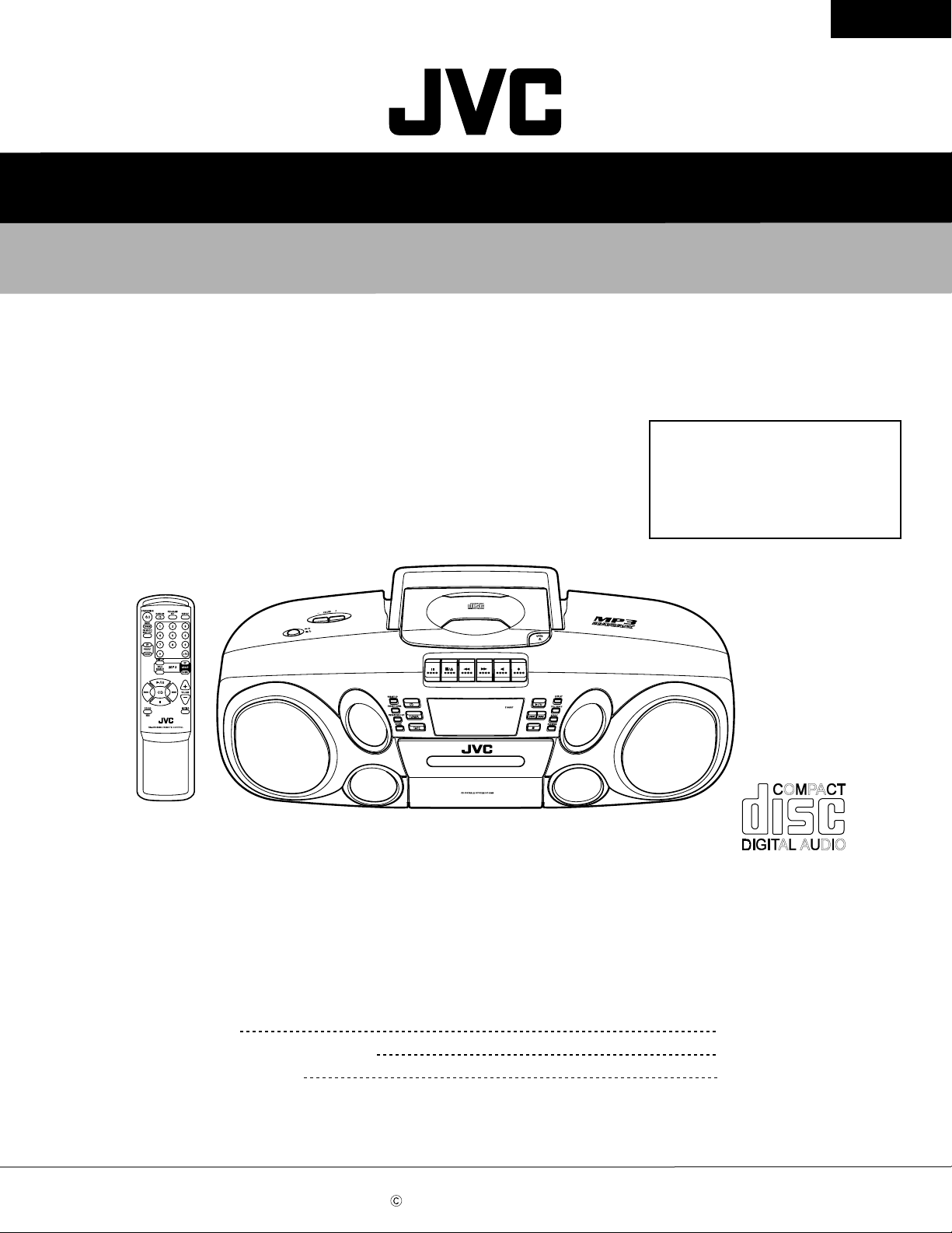
SCHEMATIC DIAGRAMS
CD PORTABLE SYSTEM
RC-BM5
CD-ROM No.SML200302
Area suffix
RC-BM5
A ------------------------------- Australia
US --------------------------- Singapore
UJ -------------------------- U.S.Military
Contents
Block diagram
Standard schematic diagrams
Printed circuit boards
COPYRIGHT 2003 VICTOR COMPANY OF JAPAN, LTD.
2-1
2-2
2-9~11
No.21132SCH
Feb. 2003
Page 2

RC-BM5
In regard with component parts appearing on the silk-screen printed side (parts side) of the PWB diagrams, the
parts that are printed over with black such as the resistor ( ), diode ( ) and ICP ( ) or identified by the " "
mark nearby are critical for safety.
(This regulation does not correspond to J and C version.)
1-2
Page 3
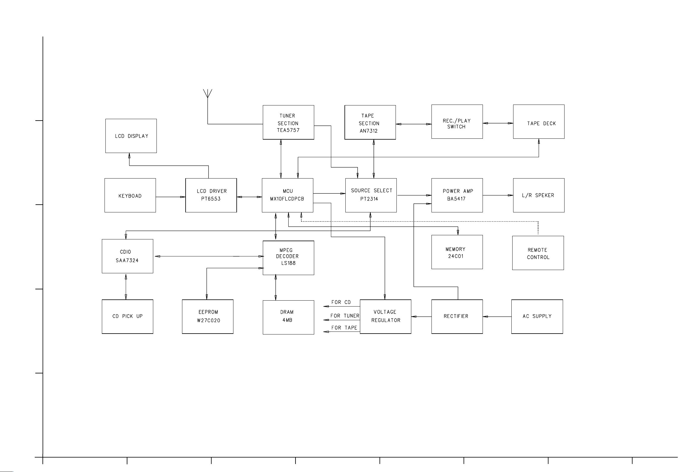
Block diagram
5
4
RC-BM5
3
2
1
AB CD E F G
2-1
Page 4
Standard schematic diagrams
Main and volume switch sections
RC-BM5
RC-BM5
5
FROM Main section CN301
H402
4
FROM CD control section CN702
CN701
3
FROM Cassette section H602
Volume switch board
TO Tuner section H801
CN802
TO CD control section
TO CD door
TO Tuner section H801
CN804
Voltage chart
Q301
Q302
C1383
4.84 V
5.48 V
11.33 V
945
0 V
0.6 V
0 V
E
B
C
FROM Display section CN401
CN302
TO Volume switch section H402
CN301
Q303
945
0 V
0 V
4.8 V
ST24C01
CN803
H302
TO Power amplifier
and
power supply sections CN204
CN801
2
CN303
NJM7805FA
Voltage chart
IC801 : PT2314
PIN1
7.15 V
PIN16
PIN2
PIN3
PIN4
PIN5,6
PIN7
PIN8 - 11
PIN12
PIN13 - 15
0 V
3.49 V
3.48 V
3.49 V
3.5 V
3.48 V
3.5 V
3.48 V
PIN17,18
PIN19 - 22
PIN23
PIN24
PIN25
PIN26
PIN27
PIN28
3.49 V
3.48 V
3.49 V
3.48 V
3.48 V
0 V
4.2 V
4.25 V
3.49 V
1
Voltage chart
Q801
1383
E
7.6 V
8.26 V
B
12.73 V
C
Voltage chart
IC301 : MX10FLCDPC
PIN1
4.69 V
4.78 V
PIN2
4.68 V
PIN3
PIN4
PIN5
PIN6
PIN7
PIN8
PIN9
PIN10
PIN11
PIN12
PIN13,14
PIN15
PIN16
PIN17
0 V
0.01 V
0.17 V
4.92 V
4.91 V
0.04 V
0.01 V
4.93 V
4.36 V
4.93 V
4.81 V
0.38 V
0.01 V
PIN18
PIN19
PIN20
PIN21,22
PIN23
PIN24
PIN25 - 28
PIN29
PIN30
PIN31
PIN32 - 34
PIN35,36
PIN37
PIN38
PIN39
PIN40
2.53 V
2.26 V
0 V
0.01 V
0.17 V
4.93 V
4.91 V
4.92 V
1.67 V
4.97 V
0.09 V
0.01 V
1.13 V
0.02 V
0.05 V
4.93 V
Voltage chart
IC302 : ST24C01
PIN1 - 4
PIN5,6
PIN7
PIN8
0 V
4.91 V
0 V
4.96 V
IC505 : NJM7805FA
PIN1
PIN2
PIN3
8.4 V
0 V
5 V
RADIO SIGNAL
TAPE PB SIGNAL
TAPE REC SIGNAL
TO CD control section
TO CD control section
CD SIGNAL
MAIN SIGNAL
Parts are safety assurance parts.
When replacing those parts make
sure to use the specified one.
FROM Power amplifier
and
power supply sections CN206
2-2
HAB C DE FG
Page 5
CD control section
RC-BM5
Voltage chart
Q501
Q502
Q503
8050
FROM Main section
E
B
C
3.51 V
4.1 V
5.06 V
8050
3.32 V
3.99 V
5.06 V
5
945
0 V
0 V
3.51 V
Q701
1383
3.36 V
4.06 V
5.04 V
DRAM-4MB (256K x 16)
TDA7073/N4
Voltage chart
PIN1
4.83 V
PIN2,3
PIN4
1.25 V
PIN5
PIN6
4.83 V
PIN7 - 9
1.25 V
PIN10
PIN11,12
PIN1
0.01 V
0.12 V
PIN2,3
1.67V
PIN4
1.35 V
PIN5
1.44 V
PIN6
1.38 V
PIN7
IC701 : DRAM-4MB (256K x 16)
PIN13
2.8 V
1.25 V
0 V
1.65 V
1.48 V
0 V
4.83 V
0 V
1.35 V
1.37 V
1.35 V
1.5 V
1.52 V
PIN22
PIN23,24
PIN25
PIN26
PIN27
PIN28,29
PIN30
PIN31
PIN16
PIN17
PIN18
PIN19
PIN20 - 32
PIN14
1.3 V
PIN15
PIN16
1.2 V
PIN17
PIN18,19
PIN20
0.9 V
PIN21
0 V
IC702 : W27C020-70
PIN8,9
PIN10
PIN11,12
PIN13
PIN14
PIN15
1.5 V
1.8 V
1.5 V
1.25 V
0 V
2.7 V
0 V
1.25 V
0 V
0.9 V
1.6 V
1.2 V
PIN32
PIN33,34
PIN35
PIN36
PIN37,38
PIN39
PIN40
1.4 V
1.25 V
0 V
0.19 V
1.25 V
0.8 V
0 V
W27C020-70
TDA7073/N4
4
LS188C
TZA1024T
FROM Main section
SAA7324H/T/M2B
3
FROM Main section
Voltage chart
PIN1
2.7 V
1.69 V
PIN2
2.89 V
PIN3
1.3 V
PIN4
PIN5
PIN6
PIN7
2
TDA1308T/N1
Voltage chart
IC502 : TDA7073
PIN1 - 4
PIN5
PIN6,7
PIN8
PIN9
PIN10,11
PIN12
PIN13
PIN14,15
PIN16
1
IC503 : TDA7073
0 V
PIN1,2
8.5 V
PIN3,4
1.65 V
PIN5
0 V
PIN6,7
PIN8
1.2 V
PIN9
0 V
PIN10,11
4.26 V
PIN12
4.25 V
PIN13
0 V
PIN14,15
4.24 V
PIN16
IC504 : TZA1024T
1.65 V
PIN1
0 V
PIN2
8.56 V
PIN3
1.65 V
PIN4
PIN5
0 V
PIN6
4.18 V
PIN7
0 V
PIN8
4.22 V
PIN9
4.19 V
PIN10
0 V
PIN11,12
4.18 V
PIN13
PIN14
1.79 V
3.08 V
0.76 V
0.15 V
0.67 V
0 V
3.04 V
1.53 V
0.79 V
1.68 V
0 V
3.09 V
0 V
Voltage chart
PIN1
1.4 V
1.55 V
PIN2,3
PIN4
3.1 V
PIN5
1.23 V
PIN6
1.53 V
PIN7
1.52 V
PIN8
1.53 V
PIN9
1.52 V
PIN10 - 13
PIN14
0 V
0 V
PIN15
PIN16
PIN17
PIN18 - 20
PIN21
PIN22,23
PIN24
PIN25
PIN26
PIN27
IC501 : SAA7324H
1.54 V
PIN28
1.52 V
PIN29
3.1 V
PIN30,31
0 V
PIN32
3.1 V
PIN33
0 V
PIN34
3.16 V
PIN35 - 37
0 V
PIN38
1.64 V
PIN39
1.6 V
PIN40
1.58 V
1.6 V
0 V
0.03 V
0 V
3.15 V
0 V
3.11 V
4.72 V
4.7 V
PIN41
PIN42
PIN43
PIN44 - 46
PIN47
PIN48 - 50
PIN51
PIN52
PIN53
PIN54
0 V
4.6 V
3.72 V
0 V
1.83 V
0 V
1.6 V
3.17 V
0.3 V
1.56 V
PIN55
PIN56
PIN57
PIN58
PIN59
PIN60
PIN61
PIN62
PIN63
PIN64
1.7 V
1.6 V
3.16 V
0 V
0.6 V
0 V
3.7 V
0 V
3.15 V
3.03 V
CD SIGNAL
TDA1308T/N1
Voltage chart
PIN1
PIN2
PIN3
Parts are safety assurance parts.
When replacing those parts make
CN702
TO Main section CN701
IC704 : TDA1308T
2.47 V
PIN4
1.93 V
PIN5 - 7
2.07 V
PIN8
0 V
1.92 V
4.81 V
PIN8
PIN9
PIN10
PIN11
PIN12
PIN13
PIN14
PIN15
PIN16
PIN17
PIN18
PIN19
PIN20
PIN21
PIN22
PIN23
PIN24
PIN25
PIN26
PIN27
PIN28
PIN29
PIN30
PIN31
1 V
1.2 V
1.23 V
0.9 V
1.5 V
1.5 V
1.4 V
1.3 V
1.3 V
1.3 V
1.4 V
3.29 V
1.35 V
1.35 V
0.01 V
1.4 V
1.35 V
1.65 V
0.12 V
0.13 V
0.01 V
4.47 V
4.4 V
0.01 V
1.54 V
3.29 V
0.01 V
sure to use the specified one.
PIN32
PIN33
PIN34
PIN35
PIN36
PIN37
PIN38
PIN39
PIN40
PIN41
PIN42
PIN43
PIN44
PIN45
PIN46
PIN47
PIN48
PIN49
PIN50
PIN51
PIN52
PIN53
PIN54
PIN55
PIN56
PIN57 - 61
PIN62
PIN63
PIN64
PIN65
PIN66
IC703 : LS188C
PIN67
3.29 V
PIN68
3.26 V
PIN69
3.27 V
PIN70
3.2 V
PIN71
1.7 V
PIN72
1.43 V
PIN73
1.2 V
PIN74
1.4 V
PIN75
1.2 V
PIN76
1.1 V
PIN77
0 V
PIN78
0.01 V
PIN79
1.2 V
PIN80
1.2 V
PIN81
2.46 V
PIN82
1.75 V
PIN83
1.62 V
PIN84
1.65 V
PIN85
1.65 V
PIN86
0.34 V
PIN87
3.45 V
PIN88
3.53 V
PIN89
4.82 V
PIN90
0.01 V
PIN91
3.29 V
PIN92
0.01 V
PIN93
2.46 V
PIN94
1.15 V
PIN95
3.74 V
PIN96
0.01 V
PIN97
3.13 V
4.82 V
3.17 V
3.17 V
4.65 V
3.2 V
4.7 V
4.7 V
4.7 V
0.01 V
0.03 V
5 V
5 V
5 V
4.83 V
1.58 V
1.58 V
1.57 V
0 V
1.4 V
1.2 V
1.5 V
0.7 V
3.29 V
1.2 V
1.16 V
0.01 V
1.34 V
1.2 V
1.1 V
0.7 V
0.7 V
PIN98
PIN99
PIN100
PIN101
PIN102
PIN103
PIN104
PIN105
PIN106
PIN107
PIN108
PIN109
PIN110
PIN111
PIN112
PIN113
PIN114
PIN115
PIN116
PIN117
PIN118
PIN119
PIN120
PIN121
PIN122
PIN123
PIN124
PIN125
PIN126
PIN127
PIN128
1.4 V
0.01 V
2.5 V
0.6 V
1.3 V
1.1 V
1.1 V
0 V
2.8 V
2.82 V
3.3 V
2.5 V
3.27 V
2.5 V
1.4 V
1.6 V
1.7 V
1.4 V
1.6 V
1.6 V
0 V
1.7 V
1.9 V
0 V
1.7 V
1.7 V
2.46 V
0.18 V
0.58 V
0.32 V
0.58 V
AB CD E F G
2-3
Page 6

RC-BM5
RC-BM5
Tuner section
Voltage chart
Q106
Q107
Q108
557B
0 V
5.44 V
4.82 V
547B
4.83 V
0.5 V
0 V
E
5
B
C
547B
4.86 V
0 V
0 V
Q109
547B
0 V
0 V
0.5 V
4
FROM Main section CN802/CN804
TEA5757H/V1
H801
3
Voltage chart
Q102
Q103
2SA733P
6.34 V
5.49 V
6.31 V
2SC945
0 V
0 V
0 V
E
B
2
C
Voltage chart
PIN1
PIN2 - 6
PIN7
PIN8
PIN9
PIN10
PIN11
PIN12
2.05 V
0 V
3.52 V
4.15 V
0.97 V
0.64 V
1.21 V
0.78 V
PIN13
PIN14
PIN15
PIN16
PIN17
PIN18
PIN19,20
PIN21
IC101 : TEA5757H
0.71 V
PIN22
PIN23
0.6 V
PIN24
0.64 V
PIN25
0.9 V
PIN26
0 V
PIN27
1 V
PIN28
1.11 V
PIN29
1.75 V
12.2 V
4.82 V
0.15 V
1.34 V
0 V
4.79 V
0.24 V
0.23 V
PIN30,31
PIN32
PIN33
PIN34
PIN35
PIN36
PIN37
PIN38
0 V
1.37 V
0.69 V
1.37 V
0.64 V
1.37 V
0.54 V
1.27 V
PIN39
PIN40,41
PIN42
PIN43
PIN44
0.99 V
1.27 V
0 V
0.75 V
0.21 V
AM SIGNAL
FM SIGNAL
RADIO SIGNAL
Parts are safety assurance parts.
When replacing those parts make
sure to use the specified one.
1
2-4
HAB C DE FG
Page 7
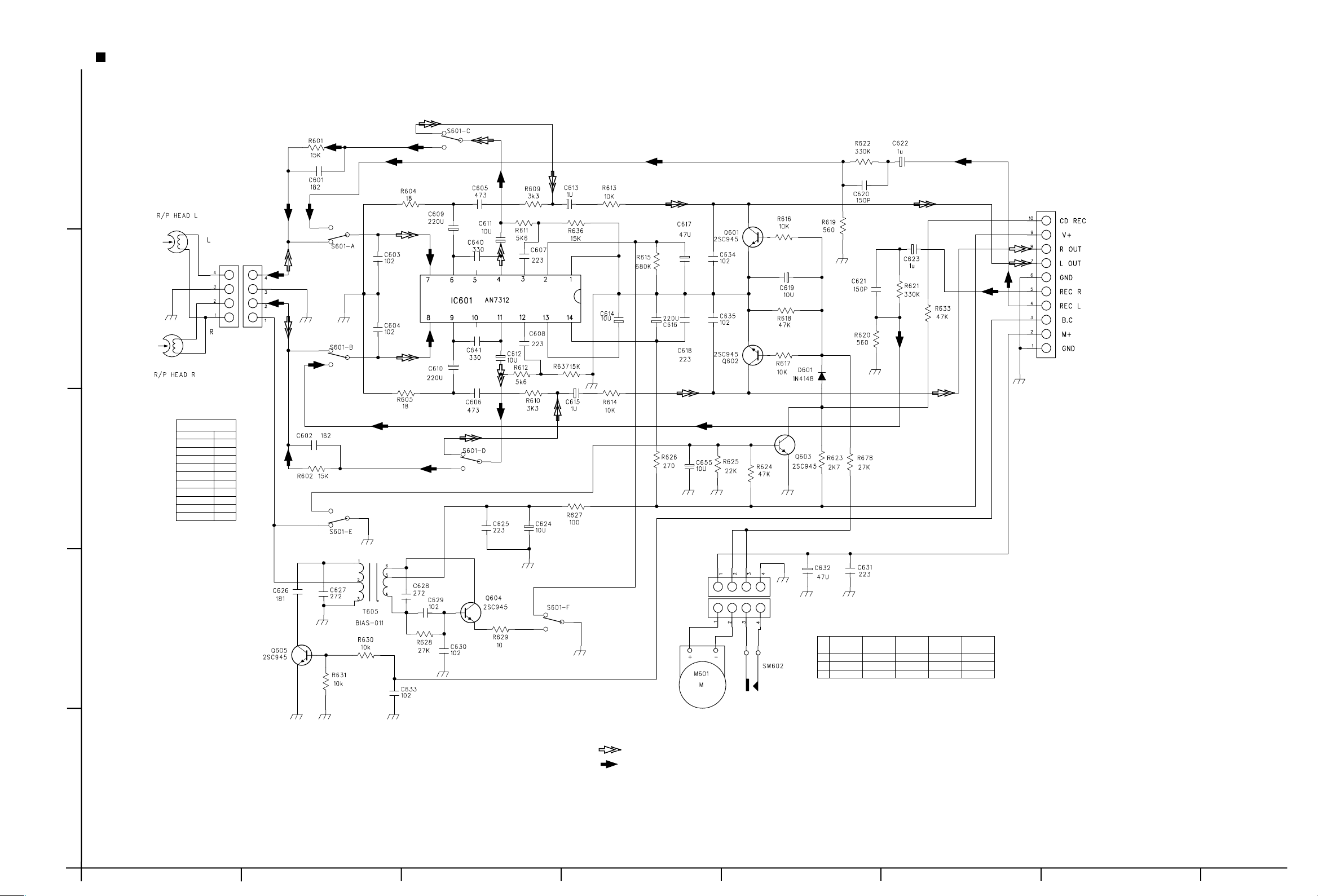
RC-BM5
Cassette section
5
TO Main section CN803
4
CON61 CN601
H602
Voltage chart
IC601 : AN7312
PIN1 - 3
PIN4
PIN5
PIN6
3
PIN7,8
PIN9
PIN10
PIN11
PIN12
PIN13
PIN14
0 V
3.41 V
1.35 V
1.24 V
0.01 V
1.24 V
1.35 V
3.4 V
0 V
6.78 V
6.82 V
CN603 CN602
2
Voltage chart
Q601
Q602
Q603
Q604
945
945
E
0 V
B
0 V
0 V
C
945
0 V
0 V
0 V
0.6 V
0 V
0 V
945
0 V
7.6 V
7.65 V
Q605
945
0 V
0 V
0 V
TAPE PB SIGNAL
TAPE REC SIGNAL
1
AB CD E F G
2-5
Page 8

Power amplifier and power supply section (A version)
RC-BM5
RC-BM5
FROM Main section CN801
CN204
5
CN206
TO Main section CN303
4
CN203
CN202 CN205
Voltage chart
IC201 : BA5417
PIN1 - 3
PIN4
PIN5
3
PIN6
PIN7,8
PIN9
PIN10 - 15
0 V
14.75 V
4.77 V
14.18 V
0 V
7.99 V
0 V
CN201
Voltage chart
Q201
Q202
Q203
Q204
Q205
Q206
8050D
8050D
E
0 V
B
0 V
0 V
C
2SC945
0 V
0 V
0 V
0.6 V
0 V
2.87 V
928
1.4 V
13.8 V
13.4 V
1913
13.52 V
12.5 V
0 V
8050D
0 V
13.8 V
12.5 V
Q207
2SC945
13.2 V
13.9 V
13.8 V
2
MAIN SIGNAL
Parts are safety assurance parts.
When replacing those parts make
sure to use the specified one.
1
2-6
HAB C DE FG
Page 9

RC-BM5
Power amplifier and power supply section (US/UJ version)
FROM Main section CN801
CN204
5
CN206
4
TO Main section CN303
CN203
CN202 CN205
CN201
Voltage chart
IC201 : BA5417
PIN1 - 3
PIN4
3
PIN5
PIN6
PIN7,8
PIN9
PIN10 - 15
0 V
14.75 V
4.77 V
14.18 V
0 V
7.99 V
0 V
Voltage chart
Q201
Q202
Q203
Q204
Q205
Q206
8050D
8050D
E
0 V
B
0 V
0 V
C
2SC945
0 V
0 V
0 V
0.6 V
0 V
2.87 V
928
1.4 V
13.8 V
13.4 V
1913
13.52 V
12.5 V
0 V
8050D
0 V
13.8 V
12.5 V
Q207
2SC945
13.2 V
13.9 V
13.8 V
2
MAIN SIGNAL
Parts are safety assurance parts.
When replacing those parts make
sure to use the specified one.
1
AB CD E F G
2-7
Page 10

RC-BM5
RC-BM5
Display section
5
4
Voltage chart
IC401 : PT6553
PIN1
PIN2 - 6
PIN7
PIN8
PIN9
PIN10
PIN11 - 13
PIN14
PIN15
PIN16 - 21
PIN22
3
PIN23 - 26
IC402 : RPM6938
PIN1,2
PIN3
FROM Main section CN302
2.4 V
2.41 V
2.4 V
2.45 V
2.41 V
2.45 V
2.41 V
2.45 V
0 V
2.41 V
2.42 V
2.41 V
4.6 V
0 V
PIN27
PIN28 - 45
PIN46 - 49
PIN50 - 55
PIN56
PIN57
PIN58,59
PIN60
PIN61
PIN62
PIN63
PIN64
2.45 V
2.41 V
4.87 V
0 V
4.87 V
2.31 V
0 V
3.89 V
4.85 V
0 V
4.83 V
0 V
LED41
2
CN401
RPM6938-V4
1
2-8
HAB C DE FG
Page 11

Printed circuit boards
Main board
5
4
RC-BM5
Reverse side
3
2
1
AB CD E F G
2-9
Page 12

Display board
Tuner board
Cassette board
Reverse side
Reverse side
5
4
LED41
Reverse side
RC-BM5
RC-BM5
Power amplifier board
3
2
Reverse side
1
2-10
HAB C DE FG
Page 13
RC-BM5
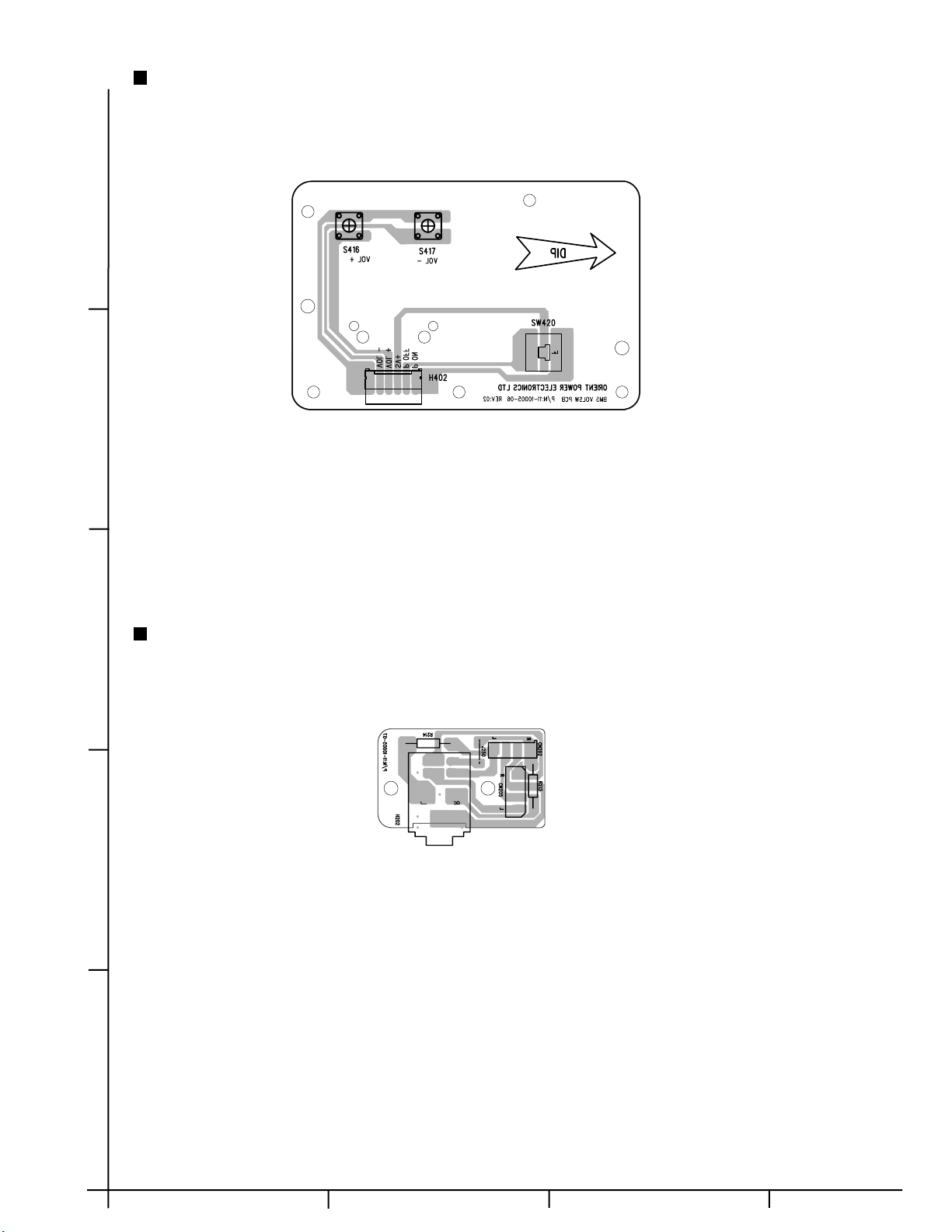
Volume switch board
Reverse side
5
4
3
Phone jack board
Reverse side
2
1
AB C
2-3
2-11
Page 14

RC-BM5
VICTOR COMPANY OF JAPAN, LIMITED
AUDIO & COMMUNICATION BUSINESS DIVISION
PERSONAL & MOBILE NETWORK BUSINESS UNIT. 10-1,1Chome,Ohwatari-machi,maebashi-city,371-8543,Japan
No.21132SCH
200302
 Loading...