

Page 1
SERVICE MANUAL
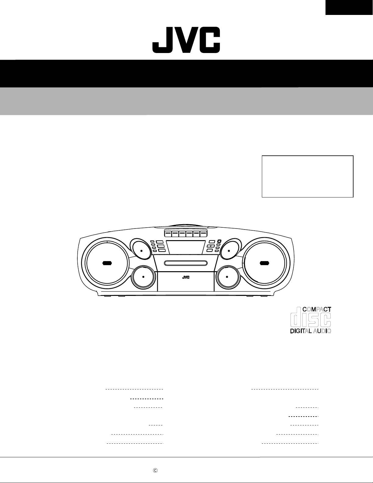
CD PORTABLE SYSTEM
RC-BM5
Area suffix
J ----------------------------- U.S.A.
C -------------------------- Canada
RC-BM5
Contents
Safety precautions
Preventing static electricity
Important for laser products
Importance administering point
on the safety
Disassembly method
Adjustment method
1-2
1-3
1-4
1-5
1-6
1-16
Trouble shooting
Flow of functional operation
until TOC read
Maintenance of laser pickup
Replacement of laser pickup
Description of major ICs
Wiring connection
1-19
1-20
1-21
1-21
1-22
1-37
COPYRIGHT 2002 VICTOR COMPANY OF JAPAN, LTD.
No.21129
Oct. 2002
Page 2
RC-BM5
1. This design of this product contains special hardware and many circuits and components specially for safety
purposes. For continued protection, no changes should be made to the original design unless authorized in
writing by the manufacturer. Replacement parts must be identical to those used in the original circuits. Services
should be performed by qualified personnel only.
2. Alterations of the design or circuitry of the product should not be made. Any design alterations of the product
should not be made. Any design alterations or additions will void the manufacturer`s warranty and will further
relieve the manufacture of responsibility for personal injury or property damage resulting therefrom.
3. Many electrical and mechanical parts in the products have special safety-related characteristics. These
characteristics are often not evident from visual inspection nor can the protection afforded by them necessarily
be obtained by using replacement components rated for higher voltage, wattage, etc. Replacement parts which
have these special safety characteristics are identified in the Parts List of Service Manual. Electrical
components having such features are identified by shading on the schematics and by ( ) on the Parts List in
the Service Manual. The use of a substitute replacement which does not have the same safety characteristics
as the recommended replacement parts shown in the Parts List of Service Manual may create shock, fire, or
other hazards.
4. The leads in the products are routed and dressed with ties, clamps, tubings, barriers and the like to be
separated from live parts, high temperature parts, moving parts and/or sharp edges for the prevention of
electric shock and fire hazard. When service is required, the original lead routing and dress should be
observed, and it should be confirmed that they have been returned to normal, after re-assembling.
5. Leakage currnet check (Electrical shock hazard testing)
After re-assembling the product, always perform an isolation check on the exposed metal parts of the product
(antenna terminals, knobs, metal cabinet, screw heads, headphone jack, control shafts, etc.) to be sure the
product is safe to operate without danger of electrical shock.
Do not use a line isolation transformer during this check.
Plug the AC line cord directly into the AC outlet. Using a "Leakage Current Tester", measure the leakage
current from each exposed metal parts of the cabinet, particularly any exposed metal part having a return
path to the chassis, to a known good earth ground. Any leakage current must not exceed 0.5mA AC (r.m.s.).
Alternate check method
Plug the AC line cord directly into the AC outlet. Use an AC voltmeter having, 1,000 ohms per volt or more
sensitivity in the following manner. Connect a 1,500 10W resistor paralleled by a 0.15 F AC-type capacitor
between an exposed metal part and a known good earth ground.
Measure the AC voltage across the resistor with the AC
voltmeter.
Move the resistor connection to each exposed metal part,
particularly any exposed metal part having a return path to
the chassis, and meausre the AC voltage across the resistor.
Now, reverse the plug in the AC outlet and repeat each
measurement. Voltage measured any must not exceed 0.75 V
AC (r.m.s.). This corresponds to 0.5 mA AC (r.m.s.).
0.15 F AC TYPE
1500 10W
Good earth ground
AC VOLTMETER
(Having 1000
ohms/volts,
or more sensitivity)
Place this
probe on
each exposed
metal part.
!
1. This equipment has been designed and manufactured to meet international safety standards.
2. It is the legal responsibility of the repairer to ensure that these safety standards are maintained.
3. Repairs must be made in accordance with the relevant safety standards.
4. It is essential that safety critical components are replaced by approved parts.
5. If mains voltage selector is provided, check setting for local voltage.
Burrs formed during molding may
be left over on some parts of the
chassis. Therefore, pay attention to
such burrs in the case of
preforming repair of this system.
In regard with component parts appearing on the silk-screen printed side (parts side) of the PWB diagrams, the
parts that are printed over with black such as the resistor ( ), diode ( ) and ICP ( ) or identified by the " "
mark nearby are critical for safety.
(This regulation does not correspond to J and C version.)
1-2
Page 3
RC-BM5
Preventing static electricity
1. Grounding to prevent damage by static electricity
Electrostatic discharge (ESD), which occurs when static electricity stored in the body, fabric, etc. is discharged,
can destroy the laser diode in the traverse unit (optical pickup). Take care to prevent this when performing repairs.
2. About the earth processing for the destruction prevention by static electricity
Static electricity in the work area can destroy the optical pickup (laser diode) in devices such as CD players.
Be careful to use proper grounding in the area where repairs are being performed.
2-1 Ground the workbench
Ground the workbench by laying conductive material (such as a conductive sheet) or an iron plate over it
before placing the traverse unit (optical pickup) on it.
2-2 Ground yourself
Use an anti-static wrist strap to release any static electricity built up in your body.
(caption)
Anti-static wrist strap
Conductive material
(conductive sheet) or iron plate
3. Handling the optical pickup
1.
In order to maintain quality during transport and before installation, both sides of the laser diode on the
replacement optical pickup are shorted. After replacement, return the shorted parts to their original condition.
(Refer to the text.)
2.
Do not use a tester to check the condition of the laser diode in the optical pickup. The tester's internal power
source can easily destroy the laser diode.
4. Handling the traverse unit (optical pickup)
1.
Do not subject the traverse unit (optical pickup) to strong shocks, as it is a sensitive, complex unit.
2.
Remove solder of the short land on the flexible wire after replacing the optical pickup. For specific details, refer
to the replacement procedure in the text. Remove the anti-static pin when replacing the traverse unit.
Be careful not to take too long a time when attaching it to the connector.
3.
Handle the flexible wire carefully as it may break when subjected to strong force.
4.
It is not possible to adjust the semi-fixed resistor that adjusts the laser power. Do not turn it.
5. Attention when traverse unit is decomposed
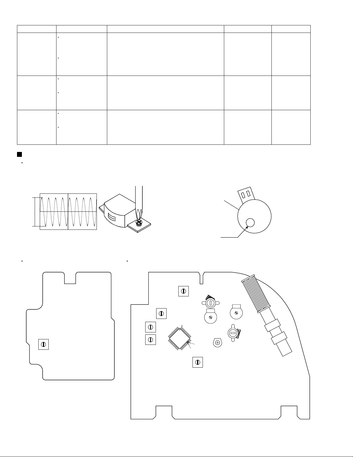
*Please refer to "Disassembly method" in the text for the CD pickup unit.
Apply solder to the short land before the card wire is disconnected
from the connector on the main board.
(If the flexible wire is disconnected without applying solder, the CD
pickup may be destroyed by static electricity.)
In the assembly, be sure to remove solder from the short land after
connecting the card wire.
Short land
CD/Cassette mechanism
assembly
Main board
CD pickup unit
Card wire
1-3
Page 4
RC-BM5
Important for laser products
1.CLASS 1 LASER PRODUCT
2.DANGER : Invisible laser radiation when open and inter
lock failed or defeated. Avoid direct exposure to beam.
3.CAUTION : There are no serviceable parts inside the
Laser Unit. Do not disassemble the Laser Unit. Replace
the complete Laser Unit if it malfunctions.
4.CAUTION : The compact disc player uses invisible
laserradiation and is equipped with safety switches
whichprevent emission of radiation when the drawer is
open and the safety interlocks have failed or are de
feated. It is dangerous to defeat the safety switches.
VARNING : Osynlig laserstrålning när denna del är öppnad
och spårren är urkopplad. Betrakta ej strålen.
VARO : Avattaessa ja suojalukitus ohitettaessa olet
alttiina näkymättömälle lasersäteilylle.Älä katso
säteeseen.
5.CAUTION : If safety switches malfunction, the laser is able
to function.
6.CAUTION : Use of controls, adjustments or performance of
procedures other than those specified herein may result in
hazardous radiation exposure.
CAUTION
!
Please use enough caution not to
see the beam directly or touch it
in case of an adjustment or operation
check.
ADVARSEL : Usynlig laserstråling ved åbning , når
sikkerhedsafbrydere er ude af funktion.
Undgåudsættelse for stråling.
ADVARSEL : Usynlig laserstråling ved åpning,når
sikkerhetsbryteren er avslott. unngå utsettelse
for stråling.
REPRODUCTION AND POSITION OF LABELS
CLASS 1
LASER PRODUCT
1-4
Page 5
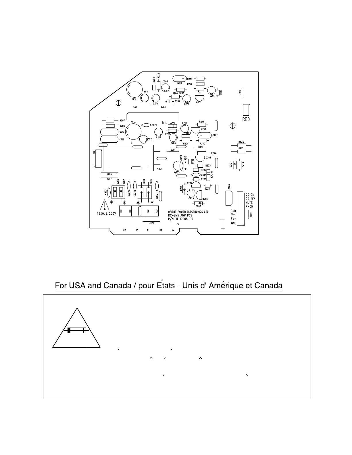
Importance administering point on the safety
CN204
CN203
RC-BM5
CN206
F201
Power amplifier board
Caution: For continued protection against risk of fire,
replace only with same type: 2.5A/250V for F201.
This symbol specifies type of fast operating fuse.
Precaution: Pour eviter les risques de feu, remplacez le
fusible de surete par le meme type: 2,5A/250V pour
F201.
Ce symbole specifie le type du fusible a fonctionnement
rapide.
1-5
Page 6
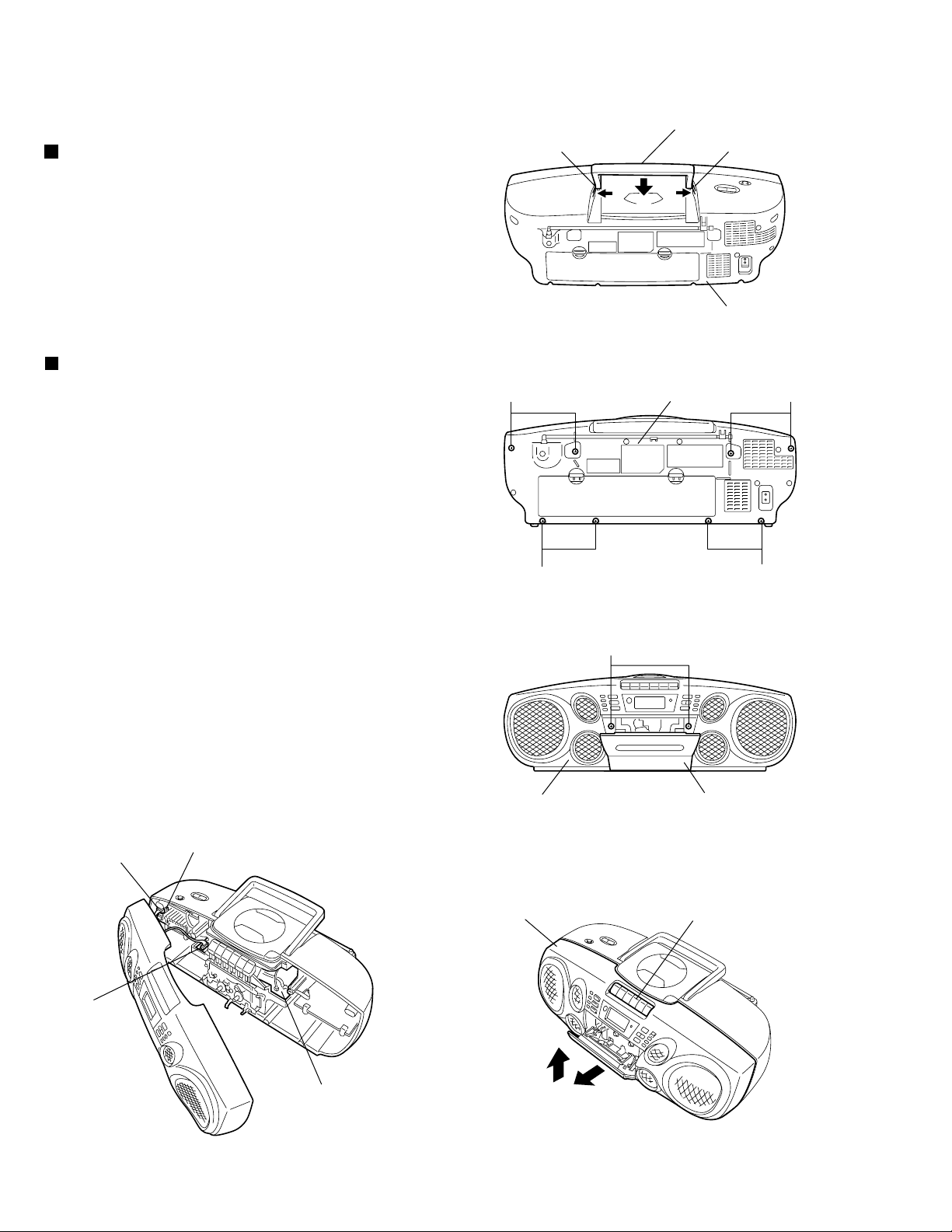
RC-BM5
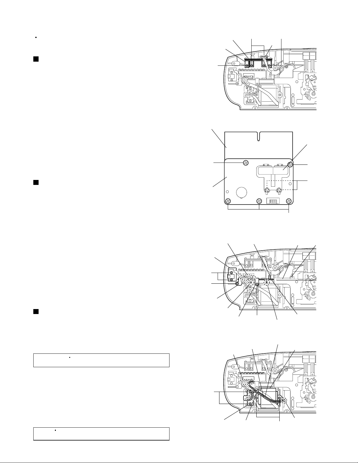
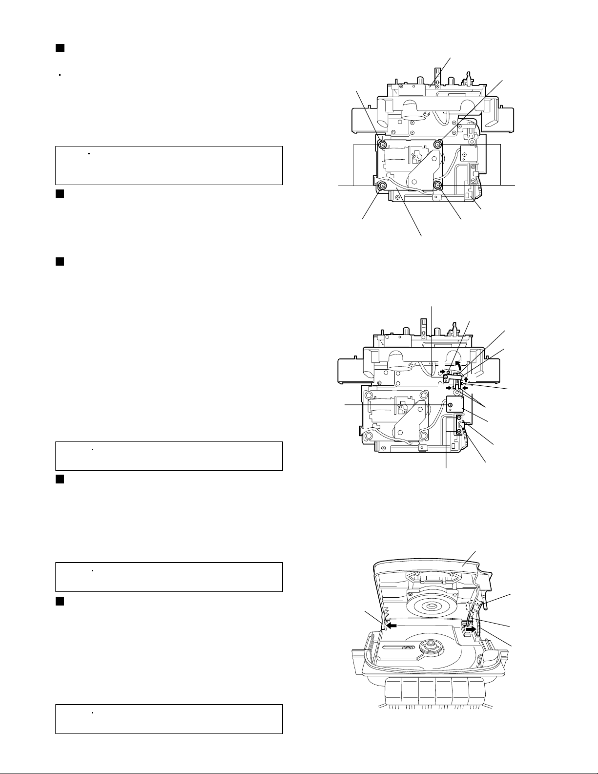
Disassembly method
<Main body section>
Removing the handle (See Fig. 1.)
Lift the handle slightly.
1.
While pressing the claws a of the rear cabinet
2.
assembly in the direction of the arrow 1, slide the
handle in the direction of the arrow 2.
Removing the front cabinet assembly
and rear cabinet assembly
(See Figs. 2 to 5.)
1.
Remove the eight screws A retaining the front
cabinet and rear cabinet assemblies from the rear
of the main body. (See Fig.2.)
2.
Open the cassette door. (See Fig.3.)
3.
Remove the two screws B retaining the front
cabinet assembly. (See Fig.3.)
4.
Slide the lower part of the front cabinet slightly in
the direction of the arrow 1. (See Fig.4.)
5.
While removing the front cabinet assembly from the
cassette knobs and remove it in the upward
direction 2. (See Fig.4.)
Handle
Claw aClaw a
2
Fig.1
1
Rear cabinet assembly
1
AA
Rear cabinet assembly
AA
Fig.2
B
6.
Disconnect the speaker wire from the connector
CN205 on the phone jack board. (See Fig.5.)
7.
Disconnect the parallel wire from the connector
CN302 on the main board. (See Fig.5.)
CN205
CN302
Phone jack board
Main board
Fig.5
Front cabinet assembly Cassette door
Fig.3
Front cabinet assembly
2
1
Fig.4
Cassette knobs
1-6
Page 7
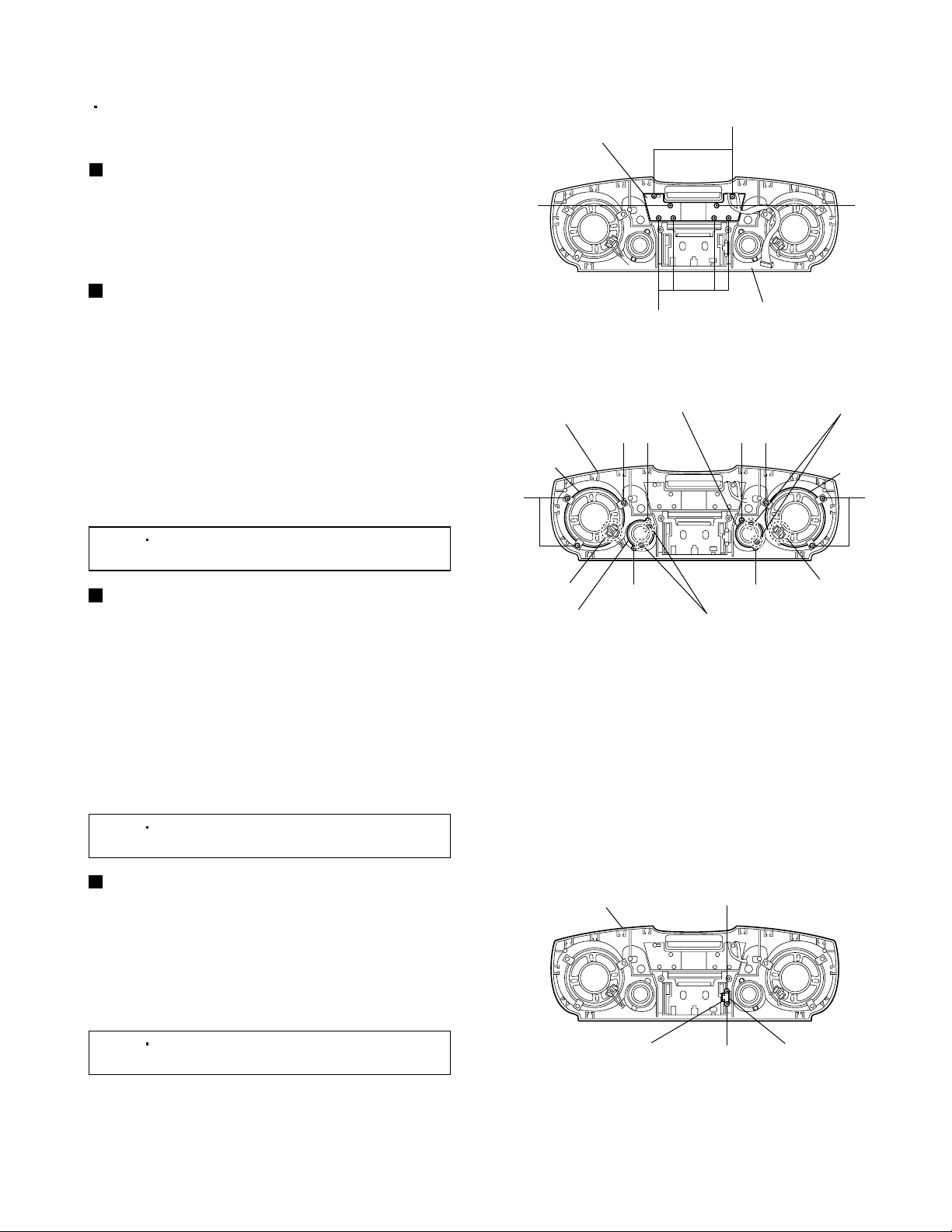
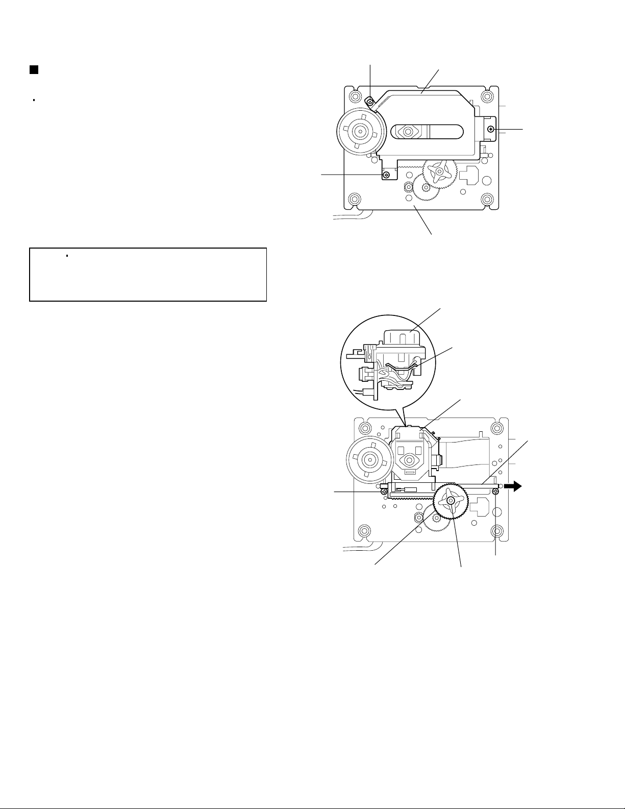
<Front cabinet section>
Prior to performing the following procedures,
remove the front cabinet assembly from the rear
cabinet assembly.
Removing the display board
(See Fig. 6.)
From the inside of the front cabinet assembly,
remove the eight screws C retaining the display
board and then take out the display board.
Removing the right and left main
speaker assemblies (See Fig. 7.)
1.
From the inside of the front cabinet assembly,
remove the six screws D retaining the right and left
main speaker assemblies.
2.
Remove the solders from the soldered sections b
and c of the right and left main speaker
assemblies, remove the wires.
3.
Take out the right and left main speaker
assemblies.
Display board
Front cabinet
assembly
Right main
speaker
C
Front cabinet assembly
Fig.6
Left sub speaker
C
Soldered sections e
EE
DD
RC-BM5
CC
Left main
speaker
DD
[Note]
After assembly, apply a locking agent to
the screws D.
Removing the right and left sub
speaker assemblies (See Fig. 7.)
1.
From the inside of the front cabinet assembly,
remove the four screws E retaining the right and
left sub speaker assemblies.
2.
Remove the solders from the soldered sections d
and e of the right and left sub speaker assemblies,
remove the wires.
3.
Take out the right and left sub speaker assemblies.
[Note]
After assembly, apply a locking agent to
the screws E.
Removing the cassette door damper
(See Fig. 8.)
1.2.From the inside of the front cabinet assembly,
remove the two screws F retaining the bracket of
the cassette door damper.
Soldered
section b
Right sub speaker
Front cabinet assembly
EE
Soldered sections d
Fig.7
F
Soldered
section c
Take out the cassette door damper.
[Note]
After assembly, apply a locking agent to
the screws F.
Cassette door damper Bracket
F
Fig.8
1-7
Page 8
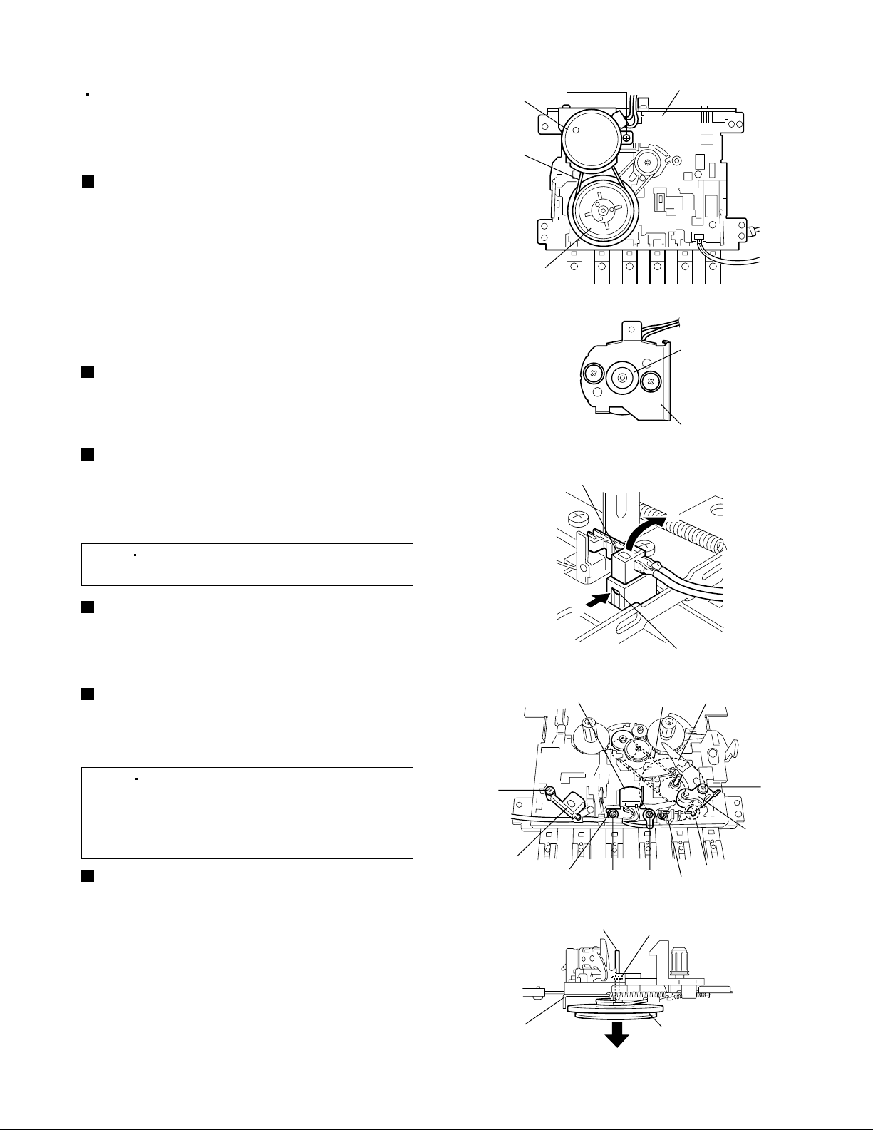
RC-BM5
Removing the cassette door
(See Fig. 9.)
1.
Open the cassette.
2.
While pressing the claws f on the left and right of
the cassette door bracket, slide the cassette door.
3.
Disengage the hooks g and h on the left and right
of the cassette door bracket, and remove the
cassette door.
Removing the cassette door bracket
(See Figs. 10 and 11.)
1.
While pressing the sections i on the left and right of
the cassette door bracket in the direction of the
arrow 1, remove the cassette door bracket from the
bosses j of the front cabinet assembly and then
open the cassette door bracket in the direction of
the arrow 2.
Section i
Cassette door bracket
Cassette door
Hook h
Claw f
Hook g
Fig.9
Section i
11
2.
Press the section k of the cassette door bracket
and remove the cassette door bracket from the
boss m of the front cabinet assembly.
3.
Disengage the section n of the cassette door
bracket from the boss p of the front cabinet
assembly and remove the cassette door bracket.
[Note]
Be sure to hang the spring to the
section q before attaching the cassette
door bracket.
Boss j
Section n
Boss p
Spring
Section q
2
Fig.10
Fig.11
Boss j
Cassette door bracket
Section k
Boss m
Cassette door bracket
1-8
Page 9
RC-BM5
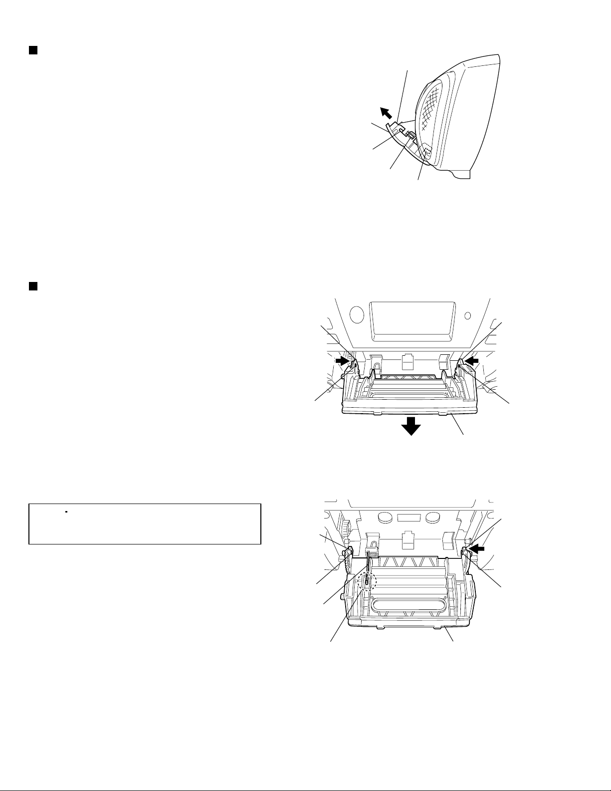
<Rear cabinet section>
Prior to performing the following procedures,
remove the front cabinet assembly from the rear
cabinet assembly.
Removing the volume switch board
(See Fig. 12 and 13.)
1.
Disconnect the wire from the connector H402 on
the volume switch board.
2.
Remove the four screws G retaining the control
bracket of the volume switch board.
3.
While pressing the power and volume buttons of
the volume switch board, take out the volume
switch board.
4.
From the forward side of the volume switch board,
remove the five screws H retaining the volume
switch board to the control bracket. (See Fig.13.)
5.
From the bottom side of the control bracket,
remove the two screws J retaining the volume
switch board and volume button to the control
bracket. (See Fig.13.)
Removing the power amplifier board
and phone jack board (See Fig. 14.)
1.
Disconnect the wire from the connector CN206 on
the power amplifier board.
Volume switch board
Control bracket
G
Control bracket
H
Volume switch
board
GG
H402
Fig.12
Volume switch
H
J
(Bottom side)
2.
Disconnect the wire from the connector CN801 on
the main board.
3.
Remove the wire from the soldered section r on the
power amplifier board.
4.
Remove the two screws K and board holders
(A)/(B) retaining the power amplifier board.
5.
Remove the two screws L retaining the phone jack
board.
6.
Pull out the power amplifier board from notches s
and t, and then take out the power amplifier board
together the phone jack board.
Removing the power transformer
(See Fig. 15.)
1.2.Remove the tie band bundling the wires from the
power transformer and battery plate.
Remove the wire from the soldered section u on
the power amplifier board.
[Reference]
3.
Remove the wire(blue) from the soldered section v
of the battery plate.
It is not necessary to remove the
wire(black) from the battery plate.
Soldered section r
Phone jack
board
L
K
Board holder (A)
Notch s
Board holder (B)
Soldered section u
Fig.13
CN206
K
Fig.14
Wire(blue)
H
Main board
Power amplifier board
Notch t
Wire(black)
Power transformer
CN801
4.
Remove the two screws M retaining the power
transformer.
5.
Remove the two screws N retaining the AC jack.
6.
Take out the power transformer together the AC
jack.
[Note]
After assembly, apply a locking agent to
the screws M.
N
AC jack
Tie band
Fig.15
Soldered section v
M
1-9
Page 10
RC-BM5
Removing the tuner board
(See Figs. 16 and 17.)
1.
Remove the wire from the connector H801 on the
tuner board.
2.
Remove the two screws P and board holders (B)
retaining the tuner board.
3.
Pull out the tuner board from the notches w and x
of the rear cabinet assembly.
4.
Remove the FM antenna wire from the soldered
section y on the reverse side of the tuner board.
(See Fig.17.)
Removing the cassette deck
mechanism assembly and cassette
board (See Figs. 18 and 19.)
1.
Remove the three screws Q and screw Q' retaining
the cassette deck mechanism assembly.
H801
Board holder (B)
Fig.16
Soldered section y
Fig.17
Cassette deck mechanism assembly
Notch w
Notch x
Tuner board
Board holder (B)
P
Tuner board
(Reverse side)
Wire clamp
2.
Lift the cassette deck mechanism assembly slightly
and move it as shown in Fig.19.
3.
Remove the three screws R retaining the cassette
board.
4.
Lift the cassette board slightly, remove the capstan
motor wire and REC/PB head wire from the
soldered sections z and aa on the cassette board.
5.
From the forward side of the cassette board,
disconnect the wire from the connector CN602 and
then remove the cassette deck mechanism
assembly.
6.
From the forward side of the cassette board,
disconnect the wire from the connector H602 and
then remove the cassette board.
[Notes]
When attaching the screw Q', attach the
wire at the same time.
After assembly, apply a locking agent to
the screws Q and Q'.
Cassette deck mechanism
assembly
R
CN602 (Forward side)
Fig.18
H602 (Forward side)
R
Fig.19
Q'
QQ
Soldered section aa
R
Cassette board
Soldered section z
1-10
Page 11
RC-BM5
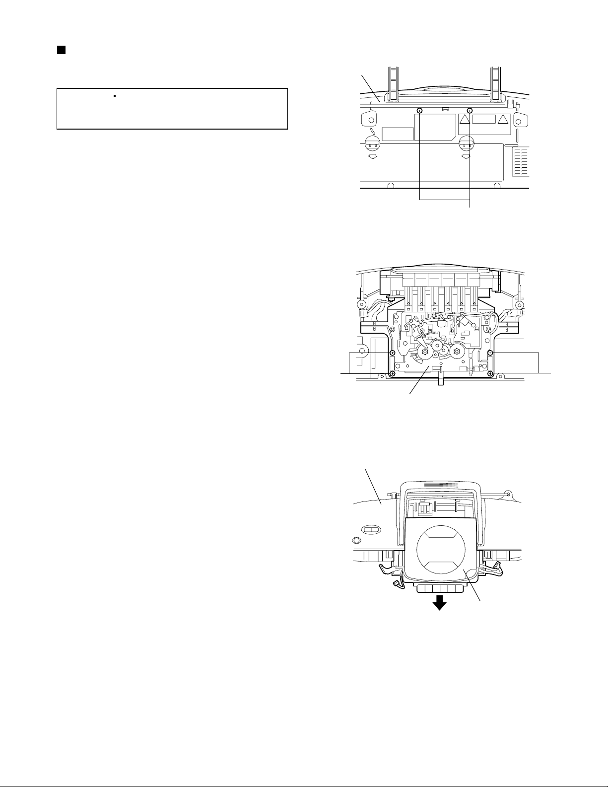
Removing the CD/Cassette mechanism
assembly
(See Figs. 12,14,16 and 20 to 22.)
[Reference]
1.
From the back side of the rear cabinet assembly,
remove the two screws S retaining the
CD/Cassette mechanism assembly. (See Fig.12.)
2.
Disconnect the wire from the connector H402 on
the volume switch board. (See Fig.12.)
3.
Disconnect the wire from the connector CN206 on
the power amplifier board. (See Fig.14.)
4.
Disconnect the wire from the connector CN801 on
the main board. (See Fig.14.)
5.
Disconnect the wire from the connector H801 on
the tuner board. (See Fig.16.)
6.
Remove the four screws T retaining the
CD/Cassette mechanism assembly. (See Fig.21.)
It is not necessary to remove the
cassette deck mechanism assembly
from the rear cabinet assembly.
Rear cabinet
assembly
S
Fig.20
7.
Slide the CD/Cassette mechanism assembly in the
direction of the arrow and take out it. (See Fig.22.)
TT
CD/Cassette mechanism assembly
Fig.21
Rear cabinet assembly
CD/Cassette mechanism
assembly
Fig.22
1-11
Page 12
RC-BM5
<CD/Cassette mechanism section>
Removing the main board
(See Figs. 23 to 25.)
[Caution]
1.
From the bottom side of the CD/Cassette
mechanism assembly, remove the screw U
retaining the main board.
2.
Disconnect the wire from the connector H602 on
the cassette board. (See Fig.23.)
3.
Disconnect the wire from the connector H302 on
the main board. (See Fig.24.)
4.
From the top side of the CD/Cassette mechanism
assembly, remove the three screws V and screw V'
retaining the main board. (See Fig.24.)
[Note]
5.
Remove the main board from the CD/Cassette
mechanism assembly, lift the CD/Cassette
mechanism assembly as shown in Fig.25.
6.
Disconnect the wire from the connector H502 on
the main board. (See Fig.25.)
7.
Apply solder to the short land section ab on the CD
pickup unit. (See Fig.25.)
[Caution]
When removing the main board, be
careful not to scratch or damage the
CD door.
When attaching the screw V', attach the
wire at the same time.
Be sure to solder the short land
section ab on the CD pickup unit
before disconnecting the card wire
from the CD pickup unit.
If the card wire is disconnected
without applying solder, the CD
pickup may be destroyed by static
electricity.
Main board
V
CD/Cassette
mechanism assembly
CD/Cassette mechanism
assembly
U
H602Cassette board
Fig.23
Fig.24
Main board
CD/Cassette
mechanism assembly
Wire clamp
V'
V
H302
CD pickup unit
8.After soldering, disconnect the card wire from the
CD pickup unit and then remove the main board.
(See Fig.25.)
[Caution]
1-12
In the assembly, be sure to remove
solder from the short land section ab
on the CD pickup unit after
connecting the card wire.
Short land section ab
Card wire
H502
Fig.25
Page 13
RC-BM5
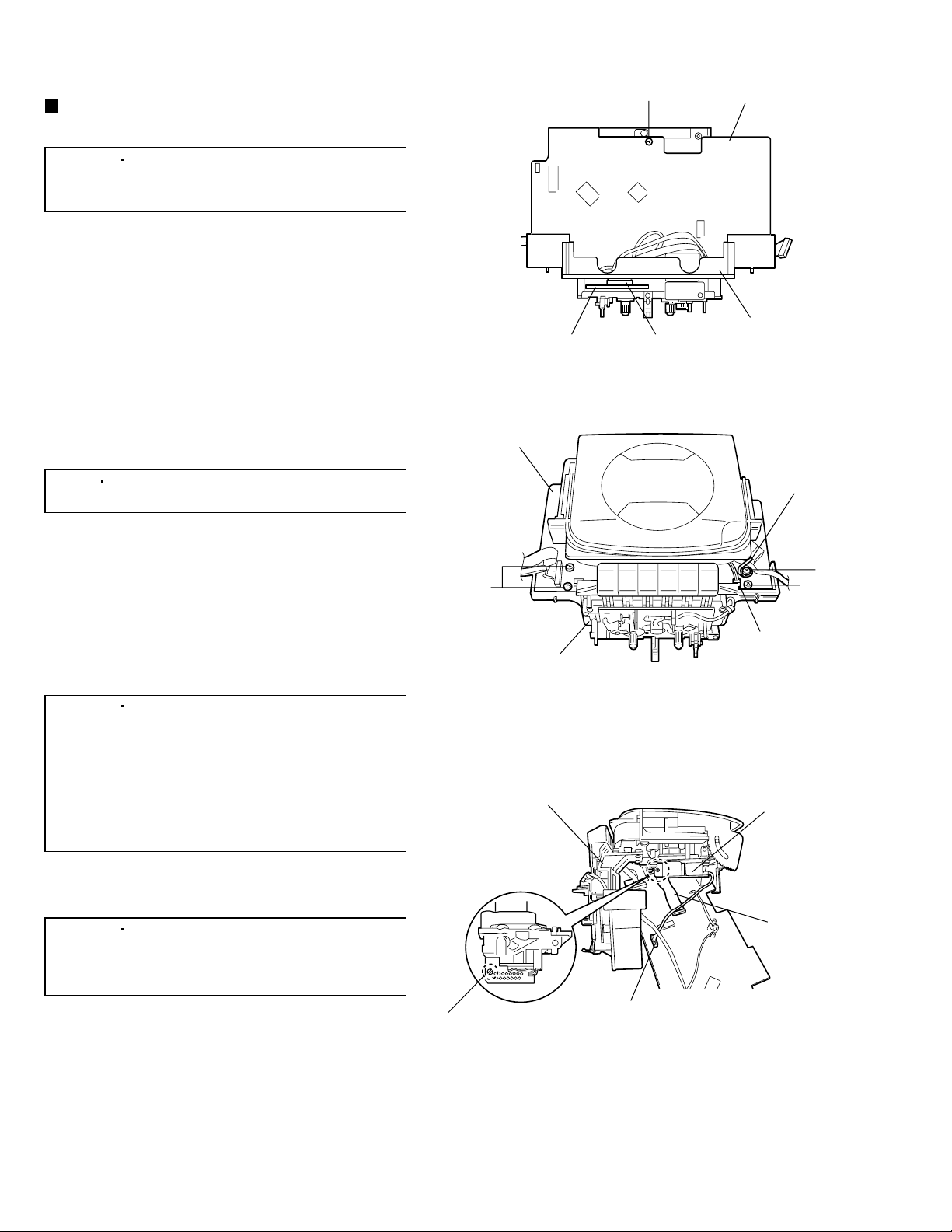
Removing the CD mechanism
assembly (See Fig. 26.)
Prior to performing the following procedures,
remove the main board from the CD/Cassette
mechanism assembly.
From the bottom side of the CD/Cassette
mechanism assembly, remove the four screws W
retaining the CD mechanism assembly.
[Note]
When attaching the CD mechanism
assembly, be sure not to mistake the
positions of the pink and orange rubbers.
Removing the CD door switch board
(See Fig. 27.)
From the bottom side of the CD/Cassette
mechanism assembly, remove the screw X
retaining the CD door switch board.
Removing the hanger and CD door
button (See Fig. 27.)
1.
From the bottom side of the CD/Cassette
mechanism assembly, loosen the screw Y of the
spring plate holding the hanger and then move the
spring plate in the direction of the arrow 1.
Rubber (Orange)
W
Rubber (Orange)
Cassette mechanism assembly
Rubber (Pink)
CD mechanism assembly
Fig.26
Y
(To be loosened)
Claw ad
Rubber (Pink)
W
CD tray assembly
Hanger
2.
While pressing the claws ac of the hanger in the
direction of the arrow 2, remove the hanger from
the CD tray assembly.
3.
Press the claws ad of the CD open knob in the
direction of the arrow 3 and then take out the CD
open knob from the top side of the CD tray
assembly.
[Note]
After assembly, apply a locking agent to
the screw Y.
Removing the CD door damper
(See Fig. 27.)
1.2.From the bottom side of the CD/Cassette
mechanism assembly, remove the two screws Z
retaining the CD door damper holder.
Take out the CD door damper.
[Note]
After assembly, apply a locking agent to
the screws Z.
Removing the CD door (See Fig. 28.)
1.
Open the CD door.
2.
While pressing the arm section ae of the CD door
in the direction of the arrow, remove the arm
section.
X
Arm af
Fig.27
1
3
3
2
2
Claws ac
CD door switch
board
CD door damper
CD door damper holder
Z
CD door
Spring plate
Claw ad
Section ag
Spring
Arm ae
3.
While pressing the arm section af of the CD door in
the direction of the arrow, remove the CD door.
[Note]
When attaching the CD door, hang the
spring to the section ag of the CD door.
Fig.28
1-13
Page 14
RC-BM5
<CD mechanism section>
Removing the CD pickup unit
(See Figs. 1 to 2.)
Prior to performing the following procedures,
remove the CD mechanism assembly.
1.
Remove the three screws A retaining the CD
pickup cover.
2.
Remove the slit washer retaining the feed middle
gear and take out the feed middle gear.
3.
Loosen the two screws B retaining the shaft and
pull out the shaft in the direction of the arrow.
4.
Take out the CD pickup unit.
[Note]
In the assembly, be sure to attach the
sliding spring in the correct orientation
before attaching the CD pickup unit.
(See Fig.2.)
A
A
CD pickup cover
A
CD mechanism assembly
Fig.1
CD pickup unit
Sliding Spring
B
Feed middle gear
Fig.2
CD pickup unit
Slit washer
Shaft
B
1-14
Page 15
RC-BM5
<Cassette mechanism section>
Prior to performing the following procedures,
remove the cassette mechanism assembly from
the rear cabinet assembly.
(See Fig.17 and 18 of "Rear cabinet section" on
page 1-10.)
Removing the capstan motor
(See Figs.1 and 2.)
1.
Remove the capstan motor belt.
2.
Remove the two screws A retaining the bracket of
the capstan motor from the cassette mechanism
assembly.
3.
Remove the two screws B retaining the bracket
from the capstan motor. (See Fig.2.)
Removing the leaf switch (See Fig.3.)
Pressing the claw a of the leaf switch in the
direction of the arrow 1 and take out the leaf switch
in the direction of the arrow 2.
Removing the pinch roller arm
assembly (See Fig.4.)
Remove the screw C retaining the pinch roller arm
assembly and remove the pinch roller arm
assembly in an upward direction.
[Note]
In the assembly, hang the notch b of the
pinch roller arm assembly to the spring.
Capstan motor
Capstan motor
belt
Flywheel assembly
Leaf switch
A
Cassette mechanism assembly
Fig.1
Capstan motor
Bracket
B
Fig.2
2
Removing the erase head
(See Fig.4.)
Remove the screw D retaining the erase head and
remove the erase head in an upward direction.
Removing the REC/PB head
(See Fig.4.)
Remove the screw E, washer and screw F retaining
the REC/PB head and remove the REC/PB head.
[Notes]
When removing or replacing the
REC/PB head, perform the REC/PB head
adjustment. (See "Adjustment method".)
After adjusting the REC/PB head, apply
a locking agent to the screws F.
Removing the flywheel assembly
(See Figs. 4 and 5.)
1.
From the bottom side of the cassette mechanism
assembly, remove the main belt.
2.
From the top side of the cassette mechanism
assembly, remove the slit washer retaining the
shaft of the flywheel assembly.
D
Erase head
1
REC/PB head
Washer
Shaft
Fig.3
Main belt
FE
Fig.4
Slit washer
Claw a
Flywheel assembly
Notch b
Spring
C
Pinch roller
arm
assembly
3.
Pull out the flywheel assembly in the direction of
the arrow. (See Fig.5.)
Cassette mechanism
assembly
Flywheel assembly
Fig.5
1-15
Page 16

RC-BM5
Adjustment method
Measuring instructions required for
adjustment
1. AM signal generator
2. FM signal generator
3. Inter mediate frequency sweep generator
4. FM stereo signal generator
5. Low-frequency oscillator
(oscillation frequency 50Hz-20kHz, 0dB output
with 600 ohm impedance)
6. Attenuator (600 ohm impedance)
7. Electronic voltmeter
8. Distortion meter
9. Torque gauge (cassette for CTG-N)
10. Wow & flutter meter
11. Frequency counter meter
12. Test tape
VT712 : For tape speed and wow flutter
VT724 : For reference level
VT702 : For playback frequency
VT702 : For head azimuth adjustment
13. Blank tape
TAPE : AC-225
Measuring instruments
Radio section
FM 1kHz, 22.5kHz deviation
FM STEREO : 1kHz, 67.5kHz deviation
pilot signal 7.5kHz
AM : 1kHz, 30% modulation
Reference output :
Speaker output 0.5W(1.2V) 3.2 ohm
Standard mode of function knob :
Selects FM or AM in tuner mode
Bass boost: OFF
Preset EQ: Flat
Main volume: Reference output
Cassette amplifier section
Reference output :
Speaker output 0.5W(1.2V) 3.2 ohm
Standard mode of function knob :
Press TAPE knob of select TAPE mode
CD section
CD test disc : CTS-1000
Measurement conditions
Power supply voltage
AC120V/60Hz
1-16
Page 17
Cassette amplifier section
Item Measuring condition Check and adjustment procedure Standard value Adjusting part
Head azimuth
adjustment
Tape speed and
wow/flutter check
and adjustment
PB frequency
response check
Bias frequency
check
REC and PB
frequency
response
adjustment
Test tape:
VT702 (8kHz)
Signal output terminal:
Speakers
Test tape:
VT712 (3kHz)
Signal output terminal:
Speakers
Test tape: VT702
Signal output terminal:
Speakers
Tape: Normal
Signal output terminal:
Cassette REC./PLAY
HEAD
Test tape: AC225
Signal input:
SG 1kHz -20dBs
with emphasis
Signal output terminal:
Speakers
Play back the test tape VT702 (8kHz).
1.
Adjust the head azimuth adjusting screw so that the
2.
phase difference between the R and L channels is
minimized at an output level that is within (+2dB-2dB)
of the maximum output level in the FWD and REV
operations. After this adjustment, lock the head
azimuth adjusting screw with screw sealant to cover
more than a half of the screw head.
When the head azimuth is maladjusted, correct it with
3.
the head azimuth adjusting screw in the FWD and
REV operations alternately.
Play back the test tape VT712 (3kHz) by the end
1.
portion.
Connect a frequency counter and check that it reads
2.
between 2940 and 3090Hz. If not, adjust the
frequency with the motor semifixed resistor.
Check that the wow/flutter is within 0.38%
3.
(unweighted).
Play back the test tape VT702 while con-firming that
deviation between the 1kHz signal and 8kHz signal
should be (0+3dB-6dB).
While recording, check to see if the frequency at the
measuring point is (75+2kHz-2kHz) if not adjust T605
until the frequency counter indicates (75+2kHz-2kHz).
In recording FM mode, and record the reference 1kHz
signal and 8kHz signal alternately repeatedly. While
playing back the recorded signal of the 1kHz signal
differ from that of the 8kHz signal by within (0+4dB4dB).
Output level:
Within (+2dB-2dB) of
maximum output
level
Phase difference R
and L channels:
Minimum
2940 to 3090Hz
Within 0.38%
(unweighted)
Deviation between
1kHz and 8kHz:
(0+3dB-6dB)
Level difference for
1kHz singnal: Within
(0+4dB-4dB)
RC-BM5
Head azimuth
adjusting screw
(To be used only
after head
replacement)
See Fig.1 on
page 1-18.
Tape speed:
Motor semifixed
resistor
See Fig.2 on
page 1-18.
Check only
T605
See Fig.3 on
page 1-18.
Tuner section
Item Measuring condition Check and adjustment procedure Standard value Adjusting part
FM VT
adjustment
AM VT
adjustment
FM IF adjustment
AM IF adjustment
Signal input:
FM antenna
VT test point:
IC101 pin8
Signal input:
AM loop antenna
VT test point:
IC101 pin8
Signal input:
IC101 pin3
Voltage test point:
IC101 pin19 and pin20
Signal input:
IC101 pin2
Signal output:
IC101 pin10
Set the FM signal generator at 108MHz and output
1.
level at 60dBu.
Adjust L102, so that the VT is within (8+0.2V-0.2V).
2.
Set the AM signal generator at 1710kHz and output
1.
level at 100dBu.
Adjust T102, so that the VT is within (8V+0.1V-0.1V).
2.
Set the FM signal generator at 10.7MHz with no
1.
signal deviation and output level at 90dBu.
Short IC101 pin21 to GND.
2.
Adjust T103 so that the voltage between IC101 pin19
3.
and pin20 is within (0+3mV-3mV).
Set the intermediate frequency sweep generator to
1.
AM 450kHz.
Adjust T104 and T105 for maximum and center
2.
output.
Adjust T106 so that the voltage between IC101 pin19
3.
and pin20 is within (0+2mV-2mV).
VT=8+0.2V-0.2V
VT=8+0.1V-0.1V
0+3mV-3mV
L102
See Fig.4 on
page 1-18.
T102
See Fig.4 on
page 1-18.
T103
See Fig.4 on
page 1-18.
T104
T105
T106
See Fig.4 on
page 1-18.
1-17
Page 18
RC-BM5
Item Measuring condition Check and adjustment procedure Standard value Adjusting part
AM tracking
adjustment
FM tracking
adjustment
FM stereo
separation
adjustment
Signal input:
AM ANT. COIL
antenna
Signal output:
IC101 pin14 or
IC101 pin15
Signal input:
FM antenna
Signal output:
IC101 pin14 or
IC101 pin15
Signal input:
FM antenna
Signal output:
IC101 pin14 or
IC101 pin15
Location of adjusting parts
Cassette mechanism section
(Caution) For adjusting any head, be sure to use a screw driver degaussed.
Set the AM signal generator at 600kHz and the unit
1.
receiving 600kHz, adjust L105(AM ANT. COIL) for
maximum output.
Set the AM signal generator at 1400kHz and the unit
2.
receiving 1400kHz, adjust TC101 for maximum output.
Set the FM signal generator at 90MHz and the unit
1.
receiving 90MHz, adjust L101 for maximum output.
Set the FM signal generator at 106MHz and the unit
2.
receiving 106MHz, adjust TC102 for maximum output.
Set the AM signal generator at 98MHz with stereo
1.
deviation and the unit receiving 98kHz.
Adjust VR101, so that the separation between the R
2.
and L channels for maximum.
L105
TC101
See Fig.4 on
page 1-18.
L101
TC102
See Fig.4 on
page 1-18.
VR101
See Fig.4 on
page 1-18.
max
Cassette board
T605
Head
Azimuth adjustment screw
Fig.1 Head output signal
Adjustment
Tuner board
T105
T106
CASSETTE MOTOR
T102
T104
1pin
IC101
15pin
T103
Tape Speed Adj.
L2
L101
TC1
TC102
VR101
14pin
TC10
TC101
L102
L1
-
+
Fig.2
L105
(AM ANT. COIL)
1-18
Fig.3
Fig.4
Page 19

Trouble shooting
RC-BM5
Circuit Symptom Cause
General
AM
FM
Tape
No sound
No sound, weak
sound
(Low sensitivity)
No sound, weak
sound
(Low sensitivity)
No sound/recording,
unsteady tape sound,
weak sound
The unit is on STANDBY mode.
Defective volume control
The unit is on MUTE mode.
Adjust the set position for the best reception.
AM VT faulty
Intermediate frequency tuning faulty
RF tracking faulty
Defective IC101
Adjust FM antenna position for the best
reception.
Defective IC101
Intermediate frequency tuning faulty
Dirty capstan or head
Irregular cassette tape winding
Defective IC202
Remedy
Press STANDBY/ON button to turn on the
unit.
Set the volume control to a proper sound
level.
Press MUTE on the remote control.
Readjust (see "Adjustment method").
Readjust (see "Adjustment method").
Readjust (see "Adjustment method").
Check voltages. Replace if necessary.
Check voltages. Replace if necessary.
Readjust (see "Adjustment method").
Clean the capstan or head with alcohol.
Replace tape.
Check voltages. Replace if necessary.
CD
CD-R
CD-RW
MP3-CD
Cannot read the table
of content.
No display, no sound
Cassette erasure prevention tabs broken out
Disc is inserted upside down.
Disc is dirty.
Disc is scratched.
Disc is seriously warped.
A non-standard disc has been inserted.
Moisture has formed inside the CD deck.
Defect in the servo control board
Defect in the CD pickup mechanism
MP3 formats not supported.
Replace tape or cover tab openings with
adhesive tape.
Insert disc correctly.
Wipe clean with a soft cloth.
Use a new disc.
Use a new disc.
Use only a brand name disc.
Wait about 20 to 30 minutes.
Replace or repair as required.
Replace as required.
Use MP3-CD formats supported on this
unit
1-19
Page 20
RC-BM5
Flow of functional operation until TOC read
Power ON
Slider turns REST
SW ON.
Laser ON
Focus start
FOK
Turn on focus
servo
Confirm that the voltage at the pin5 of CN502 is
"H"/"L"/"H"
Check that the voltage at the pin64(LD) of
IC501 is +3.3V.
Disc spinning
Radial_error
scaling
PLL Lock
Turn on radial
servo
Read TOC
Check that the voltage at the pin1 and pin2 of
CN502 is +0.78V.
Confirm the eye-pattern at the "RF" test point.
1-20
Page 21
RC-BM5
Maintenance of laser pickup
(1) Cleaning the pick up lens
Before you replace the pick up, please try to
clean the lens with a alcohol soaked cotton
swab.
(2) Life of the laser diode
When the life of the laser diode has expired,
the following symptoms will appear.
The level of RF output (EFM output:ampli tude of eye pattern) will below.
Is the level of
RF OUT under
1.25V 0.22Vp-p?
YES
O.K
NO
Replace it.
Replacement of laser pickup
Turn off the power switch and,disconnect the
power cord from the AC OUTLET.
Replace the pickup with a normal one.(Refer
to "Removing the CD pickup" on the previous page)
Plug the power cord in,and turn the power on.
At this time,check that the laser emits for
about 3 seconds and the objective lens moves
up and down.
Note: Do not observe the laser beam directly.
Play a disc.
Check the eye-pattern at the "RF" test point.
Finish.
(3) Semi-fixed resistor on the APC PC board
The semi-fixed resistor on the APC printed circuit board which is attached to the pickup is used to adjust the laser
power.
Since this adjustment should be performed to match the characteristics of the whole optical block, do not touch the
semi-fixed resistor.
If the laser power is lower than the specified value,the laser diode is almost worn out, and the laser pickup should
be replaced.
If the semi-fixed resistor would be adjusted when the pickup operates normally,the laser pickup may be damaged
due to excessive current.
1-21
Page 22
RC-BM5
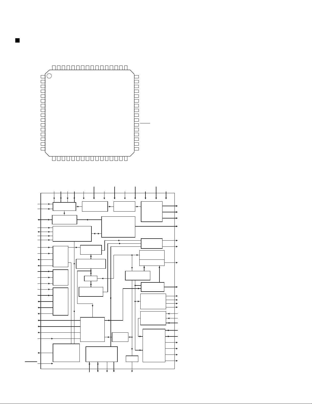
Description of major ICs
SAA7324 (IC501) : Digital servo processor & compact disc decoder
1. Terminal layout
1
HFREF
2
HFIN
3
ISLICE
4
V
SSA1
5
V
DDA1
6
I
ref
7
V
RIN
8
D1
9
D2
10
D3
11
D4
12
R1
13
R2
14
V
SSA2
15
CROUT
16
CRIN
2. Block diagram
12
R1
13
R2
SCL
SDA
RAB
SILD
HFIN
Iref
SUB
RCK
7
40
39
41
42
2
1
3
6
25
31
44
24
16
15
26
49
48
47
46
45
43
38
VRIN
HFREF
ISLICE
TEST1
TEST2
TEST3
SELPLL
CRIN
CROUT
CL16
CL11/4
SBSY
SFSY
STATUS
RESET
LDONV1V5V4MOTO2
646362616059585756555453525150
171819202122232425262728293021
LP
LN
V
DDA2
V
D1 D2 D3 D4
8 91011
ADC
SSD3VDDD2(C)
MOTO1
V
SLFORA
SAA7324H
RP
RN
pos
neg
V
TEST1
SELPLL
V
SS
A2
VSSA1
4 14 5 17 33 50 58 52 57
PRE.
PROCESSING
CL16
V
DD1(P)
CFLG
V
DATA
SCLK
WCLK
V
DD
DD
A1
Vref
GENERATOR
MICROCONTROLLER
CONTROL
PART
INTERFACE
DIGITAL
FRONT-
END
PLL
EFM
DEMODULATOR
TEST
SRAM
RAM
ADDRESSER
TIMING
SUBCODE
PROCESSOR
DETECT
DECODER
MICRO-
CONTROLLER
INTERFACE
VERSATILE PINS
INTERFACE
63 34 61 62
V1 V2/V3 V4 V5 KILL
SSD2
DOBM
V
CL11/4
49
32
EF
KILL
TEST2
A2
SS
D1
V
CONTROL
FUNCTION
PROCESSOR
PEAK
KILL
48
47
46
45
44
43
42
41
40
39
38
37
36
35
34
33
V
SS
AUDIO
32
D2
SBSY
SFSY
SUB
RCK
TEST3
STATUS
SILD
RAB
SCL
SDA
RESET
SCLI
SDI
WCLI
V2/V3
V
SSD1
DDD1(P)
V
SS
D3
V
OUTPUT
STAGES
MOTOR
CONTROL
ERROR
CORRECTOR
FLAGS
EBU
INTERFACE
SERIAL DATA
INTERFACE
SERIAL DATA
(LOOPBACK)
INTERFACE
BITSTREAM
DAC
V
DDD2(C)
54
RA
55
FO
56
SL
64
LDON
59
MOTO1
60
MOTO2
53
CFLG
51
DOBM
30
EF
29
SCLK
28
WCLK
27
DATA
37
SCLI
35
WCLI
36
SDI
20
Vneg
21
VPOS
18
LN
19
LP
22
RN
23
RP
1-22
Page 23

3. Pin function
Pin No. Symbol I/O Function
1
2
3
4
5
6
7
8
9
10
11
12
13
14
15
16
17
18
19
20
21
22
23
24
25
26
27
28
29
30
31
32
33
34
35
36
37
38
39
40
41
42
43
44
45
46
47
48
49
HFREF
HFIN
ISLICE
SSA1
V
V
DDA1
Iref
V
RIN
D1
D2
D3
D4
R1
R2
SSA2
V
CROUT
CRIN
V
DDA2
LN
LP
V
neg
V
pos
RN
RP
SELPLL
TEST1
CL16
DATA
WCLK
SCLK
EF
TEST2
KILL
V
SSD1
V2/V3
WCLI
SDI
SCLI
RESET
SDA
SCL
RAB
SILD
STATUS
TEST3
RCK
SUB
SFSY
SBSY
CL11/4
I
Comparator common mode input
I
Comparator signal input
O
Current feedback output from data slicer
-
Analog ground 1
-
Analog supply voltage 1
O
Reference current output
-
Reference voltage for servo ADCs
I
Unipolar current input 1 (central diode signal input)
I
Unipolar current input 2 (central diode signal input)
I
Unipolar current input 3 (central diode signal input)
I
Unipolar current input 4 (central diode signal input)
I
Unipolar current input 1 (satellite diode signal input)
I
Unipolar current input 2 (satellite diode signal input)
-
Analog ground 2
O
Crystal/resonator output
I
Crystal/resonator input
-
Analog supply voltage 2
O
DAC left channel differential negative output
O
DAC left channel differential positive output
I
DAC negative reference input
I
DAC positive reference input
O
DAC right channel differential negative output
O
DAC right channel differential positive output
-
Selects whether internal clock multiplier PLL is used
I
Test control input 1 (this pin should be tied LOW)
O
16.9344MHz system clock output
O
Serial d4(1) data output (3-state)
O
Word clock output (3-state)
O
Serial bit clock output (3-state)
O
C2 error flag output (3-state)
I
Test control input 2 (this pin should be tied LOW)
O
Kill output (programmable;open-drain)
-
Digital ground 1
I/O
Versatile I/O:versatile input 2 or versatile output 3 (open-drain)
I
Word clock input (for data loopback to DAC)
I
Serial data input (for data loopback to DAC)
I
Serial bit clock input (for data loopback to DAC)
I
Power-on reset input (active LOW)
I/O
Microcontroller interface data I/O line (IIC-bus;open-drain output)
I
Microcontroller interface clock line input (IIC-bus)
I
Microcontroller interface R/W and load control line input (4-wire bus mode)
I
Microcontroller interface R/W and load control line input (4-wire bus mode)
O
Servo interrupt request line/decoder status register output (open-drain)
I
Test control input 3 (this pin should be tied LOW)
I
Subcode clock input
O
P-to-W subcode bits output (3-states)
O
Subcode frame sync output (3-sates)
O
Subcode block sync output (3-sates)
O
11.2896 or 4.2336MHz (for microcontroller) clock output
RC-BM5
1-23
Page 24
RC-BM5
Pin No. I/O FunctionSymbol
50
51
52
53
54
55
56
57
58
59
60
61
62
63
64
AN7312 (IC601) : Dual recording/Playback pre-amplifier circuit with ALC
1. Terminal layout
14 8
SSD2
V
DOBM
V
DDD1(P)
CFLG
RA
FO
SL
V
DDD2(C)
V
SSD3
MOTO1
MOTO2
V4
V5
V1
LDON
~
-
Digital ground 2
O
Bi-phase mark output (externally buffered;3-state)
-
Digital supply voltage 1 for periphery
O
Correction flag output (open-drain)
O
Radial actuator output
O
Focus actuator output
O
Sledge control output
-
Digital supply voltage 2 for core
-
Digital ground 3
O
Motor output 1;versatile (3-state)
O
Motor output 2;versatile (3-state)
O
Versatile output 4
O
Versatile output 5
I
Versatile input 1
O
Laser drive on output (open-drain)
2. Block diagram
Vcc
14 13 12 11 10
8
9
Ripple Filter
17
~
1 2 3 4 5 6
GND
ALC
3. Pin function
Pin No. Symbol Function
1
GND
2
ALC time constant
3
ALC input Ch.1
4
Output Ch.1
5
Phase compensation Ch.1
6
N.E.B. Ch.1
7
Input Ch.1
8
Input Ch.2
9
N.E.B. Ch.2
10
Phase compensation Ch.2
11
Output Ch.2
12
ALC input Ch.2
13
Ripple filter
14
Vcc
I/O
GND
ALC time constant by resistance and capacitor
Right channel ALC input
I
Right channel output
O
Not connect
Right channel negative feed back input
I
Right channel signal input
I
Left channel signal input
I
Left channel negative feed back input
I
Not connect
Left channel output
O
Left channel ALC input
I
Ripple filter
Power supply
-
Amp.
Ch2
Amp.
Ch1
7
1-24
Page 25

MX10FLCDPC (IC301) : MCU
1.Terminal layout
1
2
3
4
5
6
7
8
9
10
11
12
13
14
15
16
17
18
19
20
40
39
38
37
36
35
34
33
32
31
30
29
28
27
26
25
24
23
22
21
2. Block diagram
Vcc
Vss
REGISTER
RAM ADDR.
B
REGISTER
PSEN
ALE
EA
RST
TIMING
AND
CONTROL
P0.0-P0.7 P2.0-P2.7
PORT 0
DRIVERS
ALU
PSW
PORT1
LATCH
PORT 0
LATCH
RAM
ACC
TMP2 TMP1
REGISTER
INSTRUCTION
STACK
POINTER
T0/T1/T2
TIMERS
PORT2
DRIVERS
PORT 2
LATCH
WATCHDOG
SFRs
T3
TIMER
PORT1
LATCH
ROM
PROGRAM
REGISTER
INCREMENTER
PROGRAM
COUNTER
RC-BM5
ADDR.
BUFFER
PC
DPTR
3.Pin function
Pin No.
P1.0 to P1.7
P2.0 to P2.5,P3.4 to P3.5
P0.0 to P0.7
P3.3
P2.7
ALE
EA
P3.7,P3.1,P3.0
VDD
GND
Symbol I/O
A0 to A7
A8 to A13,A14 to A15
Q0 to Q7
CE
OE
WE
Vpp
MS2 to MS0
VDD
GND
osc
XTAL2XTAL1
PORT1
DRIVERS
DRIVERS
P3.0-P3.7P1.0-P1.7
Function
I
Input low order address bits
I
Input high order address bits
I/O
Data input/output
I
Chip enable input
I/O
Output enable input
I
Write enable input
-
Program supply voltage, 12.5-13volts
-
Flash mode selection
-
Power supply voltage (+5V)
-
Ground pin
PORT1
1-25
Page 26

RC-BM5
PT2314 (IC801) : 4ch input audio processor
1. Terminal layout
1 28
2
3
4
6
7
8
9
10
11
12
13
14
2. Block diagram
LOUT
LIN
LOUD_L
BOUT_L
BIN_L
27
26
25
245
23
22
21
20
19
18
17
16
15
LIN1
LIN2
LIN3
LIN4
RIN4
RIN3
RIN2
RIN1
LIN1
LIN2
LIN3
LIN4
RIN4
RIN3
RIN2
RIN1
Supply
Volume &
Loudness
Volume&
Loudness
RB
Bass Treble
Serial Bus Decoder & Latches
Bass Treble
RB
TREBLE_L
Speaker
ATT
OUT_L
CLK
DATA
DGND
OUT_R
Speaker
ATT
Mute
Mute
VDD
REF
AGND
ROUT
RIN
LOUD_R
BOUT_R
3. Pin function
Pin No. Symbol I/O Function
1
2
3
4
5
6
7
8
9
10
11
12
13
14
15
16
17
18
19
20
21
22
23
24
25
26
27
28
VDD
AGND
TREB_L
TREB_R
RIN
ROUT
LOUD_R
RIN4
RIN3
RIN2
RIN1
LOUD_L
LIN4
LIN3
LIN2
LIN1
LIN
LOUT
BIN_L
BOUT_L
BIN_R
BOUT_R
OUT_R
OUT_L
DGND
DATA
CLK
REF
-
Supply input voltage
-
Analog ground
I
Left channel input for treble controller
I
Right channel input for treble controller
I
Audio processor right channel input
O
Gain output and input selector for right channel
I
Right channel loudness input
I
Right channel input 4
I
Right channel input 3
I
Right channel input 2
I
Right channel input 1
I
Left channel loudness input
I
Left channel input 4
I
Left channel input 3
I
Left channel input 2
I
Left channel input 1
I
Audio processor left channel input
O
Gain output and input selector for left channel
I
Left channel input for bass controller
O
Left channel output for bass controller
I
Right channel input for bass controller
O
Right channel output for bass controller
O
Right speaker output
O
Left speaker output
-
Digital ground
I
Control data input
I
Clock input for serial data transmission
-
Analog reference voltage (1/2 VDD)
BIN_R
TREBLE_R
1-26
Page 27

AS4C256KEO (IC701) : DRAM
1. Termianl layout
1
2
3
4
5
6
7
8
9
10
11
12
13
14
15
16
17
18
19
20
2. Block diagram
40
39
38
37
36
35
34
33
32
31
30
29
28
27
26
25
24
23
22
21
WE
RAS
CASL
CASH
A0
A1
A2
A3
A4
A5
A6
A7
A8
CONTROL
LOGIC
CLOCK
GENERATOR
COLUMN
ADDRESS
BUFFER
REFRESH
CONTROLER
REFRESH
COUNTER
ROW.
ADDRESS
BUFFERS<9>
ROW
DECODER
512
COLUMN
DECODER
512
SENSE AMPLIFIERS
I/O GATING
512 X 16
512 x 512 x 16
MEMORY
ARRAY
DATA-IN
BUFFER
DATA-OUT
BUFFER
OE
IO0
.
IO15
RC-BM5
3. Pin function
Pin No. Symbol Function
1
2 to 5
6
7 to 10
11,12
13
14
15
16 to 19
20
21
22 to 26
27
28
29
30
31 to 34
35
36 to 39
40
VCC
I/O0 to I/O3
Vcc
I/O4 to I/O7
NC
WE
RAS
NC
A0 to A3
Vcc
GND
A4 to A8
OE
UCAS
LCAS
NC
I/O8 to I/O11
GND
I/O12 to I/O15
GND
I/O
Power (5V 0.5V)
Input/output
I/O
Power (5V 0.5V)
Input/output
I/O
Not connect
Read/write control
Row address strobe
Not connect
Address inputs
I
Power (5V 0.5V)
Ground
Address inputs
I
Output enable
O
Column address strobe,upper byte
Column address strobe,lower byte
Not connect
Input/output
I/O
Ground
Input/output
I/O
Ground
-
V
BB
GENERATOR
V
CC
V
SS
1-27
Page 28

RC-BM5
LS188 (IC703) : VCD decoder
1. Terminal layout 2. Block diagram
102 65
103
128
1 38
3. Pin function
Pin No.
1 to 3,22
4 to 11
12 to15
16
17,18,20,21
19
23,24
25
26
27
28
29
30
31
32
33
34
35
36
37 to 42
43
44,45
46
47
48
49
50
51
52 to 55
56
57,58
59
60,61
EMI_A_9 to EMI_A_12
EMI_D_7 to EMI_D_0
EMI_A_0 to EMI_A_3
VDD_IO_00
EMI_A_4 to EMI_A_7
VSS_IO_00
EMI_A_15 to EMI_A_16
EMI_A_18
I2C_CLK
I2C_DAT
VSS_OSC_0
XTLCLK_I
XTLCLK_O
VDD_OSC_0
TEST_H
RESET_L
HSYNC_L
VSYNC_L
CLK27_O
VDAT_7 to VDAT_2
VSS_CORE_00
VDAT_1 to VDAT_0
VDD_CORE_00
AUD_XCK
AUD_BCK
AUD_LRCK
AUD_DOUT
AUD_DIN
GPIO_23 to GPIO_20
VDD_IO_10
GPIO_19,GPIO_18
VSS_CORE_10
GPIO_17,GPIO_16
DRAM
64
ROM/SRAM
Panel and
keypad
39
Symbol Function
Host
I/O
O
I
O
-
O
O
O
O
-
-
I
O
-
I
I
I
I
O
O
-
O
-
O
O
O
I
-
-
-
-
-
DRAM
Interface
EMI
Interface
Prog.I/O
Interface
CD
Host/CD
Interface
RISC
Processor
DSP
Core
EMI address bus
EMI data bus
EMI address bus
+3.3V
EMI address bus
+3.3V
EMI address bus
EMI address bus
I2C clock
I2C data
GND
Crystal input
Crystal output
+3.3V
Test
Hardware reset
Horizontal sync
Vertical sync
CLK 27MHz output
Luminance output
GND
Luminance output
+2.5V
External audio clock
Audio bit clock
Audio left/right clock
Audio data output
Audio data input
Programmable I/O
+3.3V
Programmable I/O
GND
Programmable I/O
Video
Processor
On Screen
Display
Video
Decoder
Audio
Decoder
Audio
Interface
Register
Bank
NTSC/PAL
Encoder
Audio
DAC
Audio
ADC
1-28
Page 29

RC-BM5
Pin No.
62
63,64
65
66 to 79
80
81
82
83
84
85
86
87
88
89
90,91
92
93
94
95
96
97
98
99
100
101
102
103,104
105
106
107
108
109
110
111
112
113
114
115
116
117
118
119,120
121
122,123
124
125
126
127
128
Symbol FunctionI/O
VDD_CORE_10
GPIO_15,GPIO_14
VSS_IO_10
GPIO_13 to GPIO_0
IR_IN
CD_DATA
CD_LRCK
CD_BCK
CD_C2P0
DR_D_0
DR_D_15
DR_D_1
DR_D_14
VDD_IO_20
DR_D_2,DR_D_13
VSS_IO_20
DR_D_3
DR_D_12
DR_D_4
DR_D_11
DR_D_5
DR_D_10
VSS_PLL_0
VDD_PLL_0
DR_D_6
DR_D_9
DR_D_7,DR_D_8
VSS_CORE_20
LCAS_L
DR_WE_L
VDD_IO_30
UCAS_L
URAS_L
VDD_CORE_20
LRAS_L
DR_A_8
DR_A_0
DR_A_7
DR_A_1
DR_A_6
VSS_IO_30
DR_A_2,DR_A_5
VSS_CORE_30
DR_A_3,DR_A_4
VDD_CORE_30
EMI_A_17
EMI_A_14
EMI_A_13
EMI_A_8
-
+2.5V
-
Programmable I/O
-
GND
-
Programmable I/O
I
IR input
I
CD serial data
I
CD left/right clock
I
CD bit clock
I
CD data error flag
-
DRAM data bus
-
DRAM data bus
-
DRAM data bus
-
DRAM data bus
-
+2.5V
-
DRAM data bus
-
GND
-
DRAM data bus
-
DRAM data bus
-
DRAM data bus
-
DRAM data bus
-
DRAM data bus
-
DRAM data bus
-
GND
-
+2.5V
-
DRAM data bus
-
DRAM data bus
-
DRAM data bus
-
GND
O
Lower column address strobe
O
Memory write enable
-
+3.3V
O
Upper column address strobe
O
Upper row address strobe
-
+2.5V
O
Lower row address strobe
O
DRAM address bus
O
DRAM address bus
O
DRAM address bus
O
DRAM address bus
O
DRAM address bus
-
GND
O
DRAM address bus
-
GND
O
DRAM address bus
-
+2.5V
O
EMI address bus
O
EMI address bus
O
EMI address bus
O
EMI address bus
1-29
Page 30

RC-BM5
BA5417 (IC201) : Dual power amplifier
1. Terminal layout & Block diagram 2. Pin function
Pin No. Symbol I/O Function
1
T.S.D.
30K
30K
2
3
4
5
RF2
30K
GND1
Pre
Pre
PRE GND1
PRE GND2
GND2
6
7
8
9
30K
BS
ST.BY
GND
Power
ST.BY
45
FILTERBS
FILTER
RF1
IN2
45
IN1
Vcc
1 2 3 4 5 6 7 8 9 10 11 12 13 14 15
N.C.
BS
OUT1
Vcc
OUT2BSPOWER GND
10
11
12
13
14
15
NJM7805FA (IC505) : Regulator
1. Terminal layout
2. Block diagram
1
INPUT
NC
BS
OUT1
VCC
OUT2
BS
GND
ST.BY
FILTER
RF1
IN2
IN1
RF2
PRE GND1
PRE GND2
-
Not connect
-
BS
O
Output terminal
O
Power supply
O
Output terminal
O
BS
O
Power GND
I
ST.BY
I
Filter
-
RF1
-
Input terminal
-
Input terminal
-
RF2
I/O
PRE GND
O
PRE GND
Q1
2
OUTPUT
THERMAL SHUTDOWN
1.INPUT
2.OUTPUT
3.GND
BANDGAP REFERENCE
123
RPM6938-V4 (IC402) : Remote control receiver
1. Block diagram
I/V
conversion
PD
AMP
for
trimming circuit
magnetic shield
BPF
AGC
Vcc
Comp
Detector
22k
ohm
3
1
2
OVER VOLTAGE PROTECTION
SOA PROTECTION
SHORT CIRCUIT
PROTECTION
VDD
OUT
GND
R1
R2
3
GND
1-30
Page 31

PT6553 (IC401) : LCD driver with key input function
1. Terminal layout
KO5
KO4
KO3
KO2/SG42
KO1/SG41
COM3
COM2
COM1
SG40
SG39
SG38
SG37
SG36
SG35
SG34
SG33
KO6
K11
K12
K13
K14
K15
TEST
VDD
VDD1
VDD2
VSS
OSC
CLK
DO
CE
484746454443424140393837363534
49
50
51
52
53
54
55
56
57
58
59
60
61
62
63
64
DI
33
SG32
32
SG31
31
SG30
30
SG29
29
SG28
28
SG27
27
SG26
26
SG25
25
SG24
24
SG23
23
SG22
22
SG21
21
SG20
20
SG19
19
SG18
18
SG17
17
2. Block diagram
COM1
COM2
COM3
DO
CE
DI
COMMON
DRIVER
CLOCK
GENERATOR
INTERFACE
VDET
TEST
OSC
CLK
VDD
VDD1
VDD2
VSS
SG40
SG5
SG4/P4
SG3/P3
SEGMENT DRIVER & LATCH
SHIFT REGISTER
CONTROL
REGISTER
KEY BUFFER
KEY SCAN
SG2/P2
RC-BM5
SG1/P1
1
2
3456789
P1/SG1
P2/SG2
P3/SG3
P4/SG4
SG5
SG6
SG7
10111213141516
SG8
SG9
SG10
SG11
SG12
SG13
SG14
SG15
SG16
3. Pin function
Pin No. Symbol I/O Function
1 to 4
SG1/P1 to SG4/P4
O
Segment output general purpose output pins under serial data control
these pins may be used a general purpose output parts.
5 to 40
41,42,43
44
45
46 to 49
50 to 54
55
56
57
58
59
60
61
62
63
64
SG5 to SG40
COM1,COM2,COM3
KO1/SG41
KO2/SG42
KO3 to KO6
K11 to K15
Test
VDD
VDD1
VDD2
VSS
OSC
DO
CE
CLK
DI
O
Segment output pins
O
Common driver output pins
O
Key scan output segment output pin
O
Key scan output segment output pin
O
Key scan output pins
I
Key scan input pins
I
Test pin
-
Power supply
-
Power supply
-
Power supply
-
Ground
I/O
Oscillator pin
O
Data output pin
I
Chip enable pin
I
Synchronization clock input pin
I
Din transistor input pin
K15
K11
K05
K03
SG42/KO2
SG41/KO1
1-31
Page 32

RC-BM5
ST24C01 (IC302) : Serial access 1K(128x8) EEPROM
1. Terminal layout
A0
A1
A2
V
SS
1
2
3
4
V
8
CC
7
WC
6
SCL
5
SDA
2. Pin function
Pin No. Symbol I/O Function
1
2
3
4
5
6
7
8
A0
A1
A2
Vss
SDA
SCL
WC
VCC
TDA1308 (IC704) : Class AB stereo headphone driver
1. Terminal layout
I
Chip enable input
I
Chip enable input
I
Chip enable input
-
Ground
I/O
Serial data adress input/output
-
Serial clock
-
Write control (W version)
-
Supply voltage
3. Pin function2. Block diagram
OUTA
INA(neg)
INA(pos)
V
SS
1
2
3
4
TDA 1308
8
7
6
5
V
DD
OUTB
INB(neg)
INB(pos)
OUTA
INA(neg)
INA(pos)
V
SS
1
2
3
4
8
7
6
5
V
DD
OUTB
INB(neg)
INB(pos)
TDA7073 (IC502/IC503) : Dual BTL power driver
1. Terminal layout
IN1-
IN1+
n.c.
n.c.
Vp
IN2+
IN2-
n.c.
1
2
3
4
5
6
7
8
OUT1+
16
n.c.
15
GND1
14
OUT1-
13
OUT2-
12
n.c.
11
GND2
10
OUT2+
9
1
2
3
4
5
6
7
8
DISC MOTOR
VDD
SLIDE MOTOR
16
15
14
13
12
11
10
9
Pin No. Symbol I/O Function
OUTA
1
2
3
4
5
6
7
8
INA(neg)
INA(pos)
Vss
INB(pos)
INB(neg)
OUTB
VDD
Output A
O
Inverting input A
I
Non-inverting input A
I
Negative supply
Non-inverting input B
I
Inverting input B
I
Output B
O
Positive supply
-
3. Pin function2. Block diagram
Pin No. Symbol I/O Function
1
2
3
4
5
6
7
8
9
10
11
12
13
14
15
16
IN1IN1+
n.c.
n.c.
Vp
IN2+
IN2n.c.
OUT2+
GND2
n.c.
OUT2OUT1GND1
n.c.
OUT1+
Negative input 1
I
Positive input 1
I
Not connect
Not connect
Positive supply voltage
Positive input 2
I
Negative input 2
I
Not connect
Positive output 2
O
Ground 2
Not connect
Negative output 2
O
Negative output 1
O
Ground 1
Not connect
Positive output 1
O
1-32
Page 33

TZA1024 (IC504) : Data amplifier and laser supply
1. Terminal Layout
2. Pin function
RC-BM5
LD
1
V
PWRON
DD(L)
CFIL
MON
DIN
GND
2
3
4
5
6
7
TZA1024
3. Block diagram
DIN
11
5
CDRW
14
RGADJ
V
13
DD
12
EQSEL
11
CDRW
10
RFEQO
9
RFFB
8
CMFB
V
DD
13
1
4
Pin No. Symbol I/O Function
LD
1
2
3
4
5
6
7
8
9
10
11
12
13
14
V
DD(L)
CFIL
MON
DIN
GND
PWRON
CMFB
RFFB
RFEQO
CDRW
EQSEL
V
DD
RGADJ
V
DD
Current output to laser diode
O
Laser supply voltage
External filter capacitor
Laser monitor diode input
I
Central diode input
I
Ground
Power-on select input
I
Common mode feedback voltage input
I
External RF feedback resistor
RF amplifier output
O
Gain select input for CD-A/V, CD-R/W
I
Equalizer/speed select input (n=1,2 or 4)
I
Supply voltage
External laser supply gain adjust resistor
-
12
EQSEL
9
RFFB
10
RFEQO
MON
2
250
kHz
V/I
4
GND
V
GAP
(1)
V
DD(L)
V/I
V
26
DD
14
MGR517
8
CMFB
1
LD
RGADJ
3
CFIL
7
PWRON
1-33
Page 34

RC-BM5
TEA5757(IC101): Self tuner radio (STR)
1. Terminal layout
2. Block diagram
DATA
STAB(A)
STAB(B)
V
CC1
V
DDD
XTAL
DGND
P1
P0
43
42
28
27
29
38
34
7
23
1
25
26
31
30
2
FM-RFI
RFGND
BUS-CLOCK
WRITE-ENABLE
V
V
RIPPLE
AM-RFI
RIPPLE
1
2
AM-RFI
RFGND
FMOSC
V
CC1
TUNE
VCO
AFO
MPXI
3
3
4
5
6
7
8
9
10
11
OSCILLATOR
OSCILLATOR
FM-FRO
AM-OSC
FM-RFO FMOSC
FM
FRONT-END
STABILIZER
PRESCALER
MULTIPLEXER
CRYSTAL
OSCILLATOR
AM
FRONT-END
AGC
FM-RFI
44
43
12
13
LFI
MUTE
5
FM
SHIFT REGISTER
LAST-STATION
MEMORY
PROGRAMMABLE
COUNTER
WINSOW
DETECTOR
AM
RF GND
AM-IFI1
42
41
14
15
AFLO
AFRO
FM-MIXER
39 37
FM
MIXER
AM
MIXER
AM-MIXER
40
TEA5757
16
PILFIL
FM-IFI1
REGISTER
SEQUENTIAL
FM
AM
STAB(A)
FM-MIXER
V
39
38
17
18
IFGND
FMFEM
FM-IFO1
35 33
FM
IF1
STATUS
CIRCUIT
AM
IF
FM-IFI1
37
19
(n)
AFC
FM-IFI2
Up
Down
Level
AGC
AM-IFI/O2
36
20
(p)
AFC
STAB(B)
FM-IFO1
V
35
34
33
32
31
30
29
28
27
26
25
24
23
21
22
FSI
CC2
V
IFGND
FMDEM
17 18
FM
IF2FMDETECTOR
AM/FM
INDICATOR
IN-LOCK
DETECTOR
CHARGE
PUMP
Hard mute
AFC
AM
DETECTOR
FM-IFI2
AFC
P1
P0
WRITE-ENABLE
DATA
BUS-CLOCK
DGND
XTAL
MO/ST
V
DDD
FSI
21
PILOT
DETECTOR
19 kHz
38 kHz
DECODER
MATRIX
Stereo Mono
SDS
level
CONVERTER
PLL
V/I
Stereo
MUTE
16
PILFIL
24
MO/ST
12
LFI
9
VCO
14
AFLO
AFRO
15
13
MUTE
19
AFC
AFC
AFC
(n)
(p)
20
32
1-34
6
AMOSC
AM-MIXER
AM-IFI/O2
AM-IFI1
AGC
AGC
TUNE
844364140
AFO
V
CC2
1122 10
4
RFGNDMPXI
Page 35

3. Pin function
Pin No. Symbol I/O Function
RIPPLE
1
AM-RFI
2
FM-RFO
3
RFGND
4
FMOSC
5
AMOSC
6
V
7
8
9
10
11
12
13
14
15
16
17
18
19
20
21
22
23
24
25
26
27
28
29
30
31
32
33
34
35
36
37
38
39
40
41
42
43
44
CC1
TUNE
VCO
AFO
MPXI
LFI
MUTE
AFLO
AFRO
PILFIL
IFGND
FMDEM
AFC
AFC
FSI
V
CC2
V
DDD
MO/ST
XTAL
DGND
BUS-CLOCK
DATA
WRITE-ENABLE
P0
P1
AFC
FM-IFI2
V
STAB(B)
FM-IFO1
AM-IFI/O2
FM-IFI1
V
STAB(A)
FM-MIXER
AM-MIXER
AM-IFI1
RFGND
FM-RFI
AGC
(n)
(p)
Ripple capacitor input
I
AM-RF input
I
Parallel tuned FM-RF circuit to ground
RF ground and substrate
Parallel tuned FM-oscillator circuit to ground
Parallel tuned AM-oscillator circuit to ground
Supply voltage
Tuning current output
O
Voltage controlled oscillator input
I
AM/FM AF output (output impedance typical 5k )
O
Stereo decoder input (input impedance typical 150k )
I
Loop-filter input
I
Mute input
I
Left channel output (output impedance typical 4.3k )
O
Right channel output (output impedance typical 4.3k )
O
Pilot detector filter input
I
Grond of IF,detector and MPX stage
Ceramic discriminator input
I
AFC negative output
O
AFC positive output
O
Field-strength indicator
Supply voltage for tuning
Digital supply voltage
Mono/stereo and tunig indication output
O
Crystal input
I
Digital ground
Bus-clock input
I
Bus data input/output
I/O
Bus write-enable input
I
Programmable output port (P0)
O
Programmable output port (P1)
O
450kHz LC-input circuit
I
FM-IF input 2 (input impedanc typical 330 )
I
Internal stabilized supply voltage (B)
FM-IF output1 (output impedance typical 330 )
O
Input/output to IF-Tank (IFT);output:current souce
I/O
FM-IF input1 (input impedance typical 330 )
I
Internal stabilized supply voltage (A)
Ceramic filter output (output impedance typical 330 )
O
Open-collector output to IFT
O
IFT or ceramic filter input (input impedance typical 3k )
I
FM-RF ground
FM-RF aerial input (input impedance typical 40 )
I
AGC capacitor input
I
RC-BM5
1-35
Page 36

RC-BM5
W27C020 (IC702) : EEPROM
1. Terminal layout
2. Block diagram
1Vcc32Vpp
2 PGM31A16
3 A1730A15
4 A1429A12
5 A1328A7
6A827A6
7A926A5
8 A1125A4
9OE24A3
10 A1023A2
11 CE22A1
12 Q721A0
13 Q620Q0
14 Q519Q1
15 Q418Q2
16 Q317GND
PGM
CE
OE
A0
A17
Vcc
GND
Vpp
3. Pin function
Pin No. Symbol I/O Function
1
2 - 12
13 - 15
16
17 - 21
22
23
24
25 - 30
31
32
Vpp
A16,A15,A12,A7 - A0
Q0 - Q2
GND
Q3 - Q7
CE
A10
OE
A11,A9,A8,A13,A14,A17
PGM
Vcc
Program/Erase supply voltage
Address inputs
I
Data inputs/ outputs
I/O
Connect to GND
Data inputs/ outputs
I/O
Chip enable
Address input
I
Output enable
O
Address inputs
I
Program enable
Power supply
-
CONTROL
DECODER
OUTPUT
BUFFER
CORE
ARRAY
Q0
Q7
1-36
Page 37

Wiring connection
Tuner board
H801
RC-BM5
OW25-94100-02
(Forward side)
CASS DECK
CD MECH
CN702
OW20-41022-29K
Cassette board
OW20-41101-20
H701H702
H302
Main board
(Forward side)
OW32-35160-28
OW25-61080-01
CN701
H502
H501
CN804
CN204
OW20-51061-13
CN302
CN303
CN803
CN802
CN801
OW20-42081-09
CN206
CN301
OW20-61033-00K
OW20-41062-17K
(Forward side)
9 2 0 4
OW32-30140-20
OW20-41112-20
CN401
MM
SW1 SW2
CN602
CN603
H602
CN601
OW20-41102-32
0 9 4 2
LED41
LCD1
(Forward side)
Display board
BLUE
67890
BROWN
12345
Color codes are shown below.
VIOLET
GREY
WHITE
RED
ORANGE
YELLOW
BATT+
BLACK
GREEN
OW31-20190-56
6
2
4
AC SOCKET
OW31-20160-54
OW31-20160-52
OW31-20190-50
OW25-94060-03
CN202
H202
CN205
Phone jack board
OW20-42042-08
(Forward side)
Power amplifier board
(Forward side)
CN203
P5 P3 P1 P2 P4
24 0
H402
(Forward side)
Volume switch board
4U7/50V
30
30
24
OW31-60090-52
OW31-60080-54
4U7/50V
24
OW31-60080-54 OW31-60090-52
1-37
Page 38

RC-BM5
VICTOR COMPANY OF JAPAN, LIMITED
AUDIO & COMMUNICATION BUSINESS DIVISION
PERSONAL & MOBILE NETWORK BUSINESS UNIT. 10-1,1Chome,Ohwatari-machi,maebashi-city,371-8543,Japan
No.21129
200210
Page 39

SCHEMATIC DIAGRAMS
CD PORTABLE SYSTEM
RC-BM5
CD-ROM No.SML200210
Area suffix
J ----------------------------- U.S.A.
C -------------------------- Canada
RC-BM5
Contents
Block diagram
Standard schematic diagrams
Printed circuit boards
2-1
2-2
2-8 11
COPYRIGHT 2002 VICTOR COMPANY OF JAPAN, LTD.
No.21129SCH
Oct. 2002
Page 40

RC-BM5
In regard with component parts appearing on the silk-screen printed side (parts side) of the PWB diagrams, the
parts that are printed over with black such as the resistor ( ), diode ( ) and ICP ( ) or identified by the " "
mark nearby are critical for safety.
(This regulation does not correspond to J and C version.)
2-8
Page 41

Block diagram
5
4
RC-BM5
3
2
1
AB CD E F G
2-1
Page 42

Standard schematic diagrams
Main section
5
( To G-3 on page 2-4 )
TO TUNER PCB H801
RC-BM5
RC-BM5
TO TUNER PCB H801
FROM MAIN PCB CN301
To G-3
on page 2-2
CN802
CN804
( To G-3 on page 2-4 )
Voltage chart
Q301
C1383
E
4.84 V
B
5.48 V
C
11.33 V
Q302
945
0 V
0.6 V
0 V
Q303
945
0 V
0 V
4.8 V
4
FROM DISPLAY PCB CN401
To F-2
on page 2-3
CN701
CN302
3
To G-3
on page 2-3
To G-4 and G-5
on page 2-5
CN301
To B-1 and B-2
on page 2-6
To C-4
on page 2-2
CN803
CN801
To B-5
on page 2-7
2
To B-4 and B-5
on page 2-7
CN303
Voltage chart
IC801 : PT2314
PIN1
7.15 V
PIN16
PIN2
PIN3
PIN4
PIN5,6
PIN7
PIN8 - 11
PIN12
PIN13 - 15
0 V
3.49 V
3.48 V
3.49 V
3.5 V
3.48 V
3.5 V
3.48 V
PIN17,18
PIN19 - 22
PIN23
PIN24
PIN25
PIN26
PIN27
PIN28
3.49 V
3.48 V
3.49 V
3.48 V
3.48 V
0 V
4.2 V
4.25 V
3.49 V
1
Voltage chart
Q801
1383
E
7.6 V
B
8.26 V
C
12.73 V
Voltage chart
IC301 : MX10F
PIN1
4.69 V
PIN2
4.78 V
PIN3
4.68 V
PIN4
PIN5
0.01 V
PIN6
0.17 V
PIN7
4.92 V
PIN8
4.91 V
PIN9
0.04 V
PIN10
0.01 V
PIN11
4.93 V
PIN12
4.36 V
PIN13,14
4.93 V
PIN15
4.81 V
PIN16
0.38 V
PIN17
0.01 V
0 V
PIN18
PIN19
PIN20
PIN21,22
PIN23
PIN24
PIN25 - 28
PIN29
PIN30
PIN31
PIN32 - 34
PIN35,36
PIN37
PIN38
PIN39
PIN40
2.53 V
2.26 V
0 V
0.01 V
0.17 V
4.93 V
4.91 V
4.92 V
1.67 V
4.97 V
0.09 V
0.01 V
1.13 V
0.02 V
0.05 V
4.93 V
Voltage chart
IC302 : ST24C01
PIN1 - 4
PIN5,6
PIN7
PIN8
0 V
4.91 V
0 V
4.96 V
IC505 : NJM7805
PIN1
PIN2
PIN3
8.4 V
0 V
5 V
To G-3
on page 2-3
RADIO SIGNAL
TAPE PB SIGNAL
TAPE REC SIGNAL
To D-5
on page 2-3
CD SIGNAL
MAIN SIGNAL
Parts are safety assurance parts.
When replacing those parts make
sure to use the specified one.
2-2
TO AMP PCB CN206
HAB C DE FG
Page 43

CD control section
RC-BM5
Voltage chart
Q501
Q502
Q503
To F-1
on page 2-2
8050
3.51 V
4.1 V
5.06 V
8050
3.32 V
3.99 V
5.06 V
E
B
C
945
0 V
0 V
3.51 V
Q701
1383
3.36 V
4.06 V
5.04 V
5
Voltage chart
PIN1
4.83 V
PIN2,3
1.25 V
PIN4
PIN5
4.83 V
PIN6
1.25 V
PIN7 - 9
PIN10
PIN11,12
PIN1
0.01 V
0.12 V
PIN2,3
1.67V
PIN4
1.35 V
PIN5
1.44 V
PIN6
1.38 V
PIN7
PIN13
1.3 V
PIN14
PIN15
1.2 V
PIN16
PIN17
PIN18,19
0.9 V
PIN20
0 V
PIN21
IC702 : 27C020
PIN8,9
PIN10
PIN11,12
PIN13
PIN14
PIN15
IC701 : 4C256K
2.8 V
PIN22
1.25 V
PIN23,24
0 V
PIN25
1.65 V
PIN26
1.48 V
PIN27
0 V
PIN28,29
4.83 V
PIN30
0 V
PIN31
1.35 V
PIN16
1.37 V
PIN17
1.35 V
PIN18
PIN19
1.5 V
PIN20 - 32
1.52 V
1.5 V
1.8 V
1.5 V
1.25 V
0 V
2.7 V
0 V
1.25 V
0 V
0.9 V
1.6 V
1.2 V
PIN32
PIN33,34
PIN35
PIN36
PIN37,38
PIN39
PIN40
1.4 V
1.25 V
0 V
0.19 V
1.25 V
0.8 V
0 V
4
To F-3
on page 2-2
3
(To E-1 on page 2-2)
Voltage chart
PIN1
2.7 V
PIN2
1.69 V
PIN3
2.89 V
PIN4
1.3 V
PIN5
PIN6
PIN7
2
CN702
Voltage chart
IC502 : TDA7073
PIN1 - 4
PIN5
PIN6,7
PIN8
PIN9
PIN10,11
PIN12
PIN13
PIN14,15
PIN16
1
IC503 : TDA7073
0 V
PIN1,2
PIN3,4
8.5 V
PIN5
1.65 V
PIN6,7
0 V
PIN8
1.2 V
PIN9
0 V
PIN10,11
4.26 V
PIN12
4.25 V
PIN13
0 V
PIN14,15
4.24 V
PIN16
IC504 : TZA1024
1.65 V
PIN1
PIN2
0 V
PIN3
8.56 V
PIN4
1.65 V
PIN5
0 V
PIN6
4.18 V
PIN7
0 V
PIN8
4.22 V
PIN9
4.19 V
PIN10
0 V
PIN11,12
4.18 V
PIN13
PIN14
1.79 V
3.08 V
0.76 V
0.15 V
0.67 V
0 V
3.04 V
1.53 V
0.79 V
1.68 V
0 V
3.09 V
0 V
Voltage chart
PIN1
1.4 V
PIN2,3
1.55 V
PIN4
PIN5
3.1 V
PIN6
1.23 V
PIN7
1.53 V
PIN8
1.52 V
PIN9
1.53 V
PIN10 - 13
1.52 V
PIN14
0 V
0 V
PIN15
PIN16
PIN17
PIN18 - 20
PIN21
PIN22,23
PIN24
PIN25
PIN26
PIN27
IC501 : SAA7324
1.54 V
PIN28
PIN29
1.52 V
PIN30,31
3.1 V
PIN32
0 V
PIN33
3.1 V
PIN34
0 V
PIN35 - 37
3.16 V
PIN38
0 V
PIN39
1.64 V
PIN40
1.6 V
1.58 V
1.6 V
0 V
0.03 V
0 V
3.15 V
0 V
3.11 V
4.72 V
4.7 V
PIN41
PIN42
PIN43
PIN44 - 46
PIN47
PIN48 - 50
PIN51
PIN52
PIN53
PIN54
0 V
4.6 V
3.72 V
0 V
1.83 V
0 V
1.6 V
3.17 V
0.3 V
1.56 V
PIN55
PIN56
PIN57
PIN58
PIN59
PIN60
PIN61
PIN62
PIN63
PIN64
1.7 V
1.6 V
3.16 V
0 V
0.6 V
0 V
3.7 V
0 V
3.15 V
3.03 V
CD SIGNAL
To A-4
on page 2-2
Voltage chart
IC704 : 1308D
PIN1
PIN2
PIN3
2.47 V
1.93 V
2.07 V
PIN4
PIN5 - 7
PIN8
1.92 V
4.81 V
Parts are safety assurance parts.
When replacing those parts make
0 V
PIN8
PIN9
PIN10
PIN11
PIN12
PIN13
PIN14
PIN15
PIN16
PIN17
PIN18
PIN19
PIN20
PIN21
PIN22
PIN23
PIN24
PIN25
PIN26
PIN27
PIN28
PIN29
PIN30
PIN31
1 V
1.2 V
1.23 V
0.9 V
1.5 V
1.5 V
1.4 V
1.3 V
1.3 V
1.3 V
1.4 V
3.29 V
1.35 V
1.35 V
0.01 V
1.4 V
1.35 V
1.65 V
0.12 V
0.13 V
0.01 V
4.47 V
4.4 V
0.01 V
1.54 V
3.29 V
0.01 V
sure to use the specified one.
PIN32
PIN33
PIN34
PIN35
PIN36
PIN37
PIN38
PIN39
PIN40
PIN41
PIN42
PIN43
PIN44
PIN45
PIN46
PIN47
PIN48
PIN49
PIN50
PIN51
PIN52
PIN53
PIN54
PIN55
PIN56
PIN57 - 61
PIN62
PIN63
PIN64
PIN65
PIN66
IC703 : LS188
PIN67
3.29 V
PIN68
3.26 V
PIN69
3.27 V
PIN70
3.2 V
PIN71
1.7 V
PIN72
1.43 V
PIN73
1.2 V
PIN74
1.4 V
PIN75
1.2 V
PIN76
1.1 V
PIN77
0 V
PIN78
0.01 V
PIN79
1.2 V
PIN80
1.2 V
PIN81
2.46 V
PIN82
1.75 V
PIN83
1.62 V
PIN84
1.65 V
PIN85
1.65 V
PIN86
0.34 V
PIN87
3.45 V
PIN88
3.53 V
PIN89
4.82 V
PIN90
0.01 V
PIN91
3.29 V
PIN92
0.01 V
PIN93
2.46 V
PIN94
1.15 V
PIN95
3.74 V
PIN96
0.01 V
PIN97
3.13 V
4.82 V
3.17 V
3.17 V
4.65 V
3.2 V
4.7 V
4.7 V
4.7 V
0.01 V
0.03 V
5 V
5 V
5 V
4.83 V
1.58 V
1.58 V
1.57 V
0 V
1.4 V
1.2 V
1.5 V
0.7 V
3.29 V
1.2 V
1.16 V
0.01 V
1.34 V
1.2 V
1.1 V
0.7 V
0.7 V
PIN98
PIN99
PIN100
PIN101
PIN102
PIN103
PIN104
PIN105
PIN106
PIN107
PIN108
PIN109
PIN110
PIN111
PIN112
PIN113
PIN114
PIN115
PIN116
PIN117
PIN118
PIN119
PIN120
PIN121
PIN122
PIN123
PIN124
PIN125
PIN126
PIN127
PIN128
1.4 V
0.01 V
2.5 V
0.6 V
1.3 V
1.1 V
1.1 V
0 V
2.8 V
2.82 V
3.3 V
2.5 V
3.27 V
2.5 V
1.4 V
1.6 V
1.7 V
1.4 V
1.6 V
1.6 V
0 V
1.7 V
1.9 V
0 V
1.7 V
1.7 V
2.46 V
0.18 V
0.58 V
0.32 V
0.58 V
AB CD E F G
2-3
Page 44

RC-BM5
RC-BM5
Tuner section
Voltage chart
Q106
Q107
Q108
557B
0 V
5.44 V
4.82 V
547B
4.83 V
0.5 V
0 V
E
5
B
C
547B
4.86 V
0 V
0 V
Q109
547B
0 V
0 V
0.5 V
4
FROM MAIN PCB CN802/CN804
To F-5
on page 2-2
3
Voltage chart
Q102
Q103
2SA733P
6.34 V
5.49 V
6.31 V
2SC945
0 V
0 V
0 V
E
B
2
C
Voltage chart
PIN1
PIN2 - 6
PIN7
PIN8
PIN9
PIN10
PIN11
PIN12
2.05 V
0 V
3.52 V
4.15 V
0.97 V
0.64 V
1.21 V
0.78 V
PIN13
PIN14
PIN15
PIN16
PIN17
PIN18
PIN19,20
PIN21
IC101 : TEA5757
0.71 V
PIN22
PIN23
0.6 V
PIN24
0.64 V
PIN25
0.9 V
PIN26
0 V
PIN27
1 V
PIN28
1.11 V
PIN29
1.75 V
12.2 V
4.82 V
0.15 V
1.34 V
0 V
4.79 V
0.24 V
0.23 V
PIN30,31
PIN32
PIN33
PIN34
PIN35
PIN36
PIN37
PIN38
0 V
1.37 V
0.69 V
1.37 V
0.64 V
1.37 V
0.54 V
1.27 V
PIN39
PIN40,41
PIN42
PIN43
PIN44
0.99 V
1.27 V
0 V
0.75 V
0.21 V
AM SIGNAL
FM SIGNAL
RADIO SIGNAL
Parts are safety assurance parts.
When replacing those parts make
sure to use the specified one.
To C-5
on page 2-2
1
2-4
HAB C DE FG
Page 45

RC-BM5
Cassette section
5
TO MAIN PCB CN803
To A-2 and A-3
on page 2-2
4
CON61 CN601
Voltage chart
IC601 : AN7312
PIN1 - 3
PIN4
PIN5
PIN6
3
PIN7,8
PIN9
PIN10
PIN11
PIN12
PIN13
PIN14
2
0 V
3.41 V
1.35 V
1.24 V
0.01 V
1.24 V
1.35 V
3.4 V
0 V
6.78 V
6.82 V
CN603 CN602
CN604
Voltage chart
Q601
Q602
Q603
945
E
B
C
945
0 V
0 V
0 V
0 V
0 V
0 V
945
0 V
0.6 V
0 V
Q604
945
0 V
7.6 V
7.65 V
Q605
945
0 V
0 V
0 V
TAPE PB SIGNAL
TAPE REC SIGNAL
1
AB CD E F G
2-5
Page 46

RC-BM5
RC-BM5
Display section
5
4
Voltage chart
IC401 : PT6553
PIN1
PIN2 - 6
PIN7
PIN8
PIN9
PIN10
PIN11 - 13
PIN14
PIN15
PIN16 - 21
PIN22
3
PIN23 - 26
IC402 : RPM6938
PIN1,2
PIN3
FROM MAIN PCB CN302
2.4 V
2.41 V
2.4 V
2.45 V
2.41 V
2.45 V
2.41 V
2.45 V
0 V
2.41 V
2.42 V
2.41 V
4.6 V
0 V
PIN27
PIN28 - 45
PIN46 - 49
PIN50 - 55
PIN56
PIN57
PIN58,59
PIN60
PIN61
PIN62
PIN63
PIN64
2.45 V
2.41 V
4.87 V
0 V
4.87 V
2.31 V
0 V
3.89 V
4.85 V
0 V
4.83 V
0 V
LE401
2
( To G-3 and G-4 on page 2-2 )
CN401
1
2-6
HAB C DE FG
Page 47

Power amplifier and power supply section
FROM MAIN PCB CN801
CN204
RC-BM5
5
4
( To G-2 on page 2-2 )
( To G-2 on page 2-2 )
FROM MAIN PCB CN303
CN206
CN203
CN201
CN205 CN202
Voltage chart
IC201 : BA5417
PIN1 - 3
PIN4
3
PIN5
PIN6
PIN7,8
PIN9
PIN10 - 15
0 V
14.75 V
4.77 V
14.18 V
0 V
7.99 V
0 V
Voltage chart
Q201
Q202
Q203
Q204
Q205
Q206
8050D
8050D
E
0 V
B
0 V
C
0 V
2SC945
0 V
0 V
0 V
2.87 V
0.6 V
0 V
928
1.4 V
13.8 V
13.4 V
1913
13.52 V
12.5 V
0 V
8050D
0 V
13.8 V
12.5 V
Q207
2SC945
13.2 V
13.9 V
13.8 V
2
MAIN SIGNAL
Parts are safety assurance parts.
When replacing those parts make
sure to use the specified one.
1
AB CD E F G
2-7
Page 48

Printed circuit boards
Main board
5
4
RC-BM5
Reverse side
RC-BM5
3
2
1
2-8
HAB C DE FG
Page 49

RC-BM5
Tuner board
Reverse side
5
4
3
Cassette board
Reverse side
2
1
AB C
2-9
Page 50

RC-BM5
5
4
Display board
Reverse side
Power amplifier board
Reverse side
3
2
2-10
1
AB CD
Page 51

RC-BM5
Volume switch board
Reverse side
5
4
3
Phone jack board
Reverse side
2
1
AB C
2-11
Page 52

RC-BM5
VICTOR COMPANY OF JAPAN, LIMITED
AUDIO & COMMUNICATION BUSINESS DIVISION
PERSONAL & MOBILE NETWORK BUSINESS UNIT. 10-1,1Chome,Ohwatari-machi,maebashi-city,371-8543,Japan
No.21129SCH
200210
Page 53

SCHEMATIC DIAGRAMS
CD PORTABLE SYSTEM
RC-BM5
CD-ROM No.SML200210
Area suffix
J ----------------------------- U.S.A.
C -------------------------- Canada
RC-BM5
Contents
Block diagram
Standard schematic diagrams
Printed circuit boards
2-1
2-2
2-8 11
COPYRIGHT 2002 VICTOR COMPANY OF JAPAN, LTD.
No.21129SCH
Oct. 2002
Page 54

RC-BM5
In regard with component parts appearing on the silk-screen printed side (parts side) of the PWB diagrams, the
parts that are printed over with black such as the resistor ( ), diode ( ) and ICP ( ) or identified by the " "
mark nearby are critical for safety.
(This regulation does not correspond to J and C version.)
2-8
Page 55

Block diagram
5
4
RC-BM5
3
2
1
AB CD E F G
2-1
Page 56

Standard schematic diagrams
Main section
5
( To G-3 on page 2-4 )
TO TUNER PCB H801
RC-BM5
RC-BM5
TO TUNER PCB H801
FROM MAIN PCB CN301
To G-3
on page 2-2
CN802
CN804
( To G-3 on page 2-4 )
Voltage chart
Q301
C1383
E
4.84 V
B
5.48 V
C
11.33 V
Q302
945
0 V
0.6 V
0 V
Q303
945
0 V
0 V
4.8 V
4
FROM DISPLAY PCB CN401
To F-2
on page 2-3
CN701
CN302
3
To G-3
on page 2-3
To G-4 and G-5
on page 2-5
CN301
To B-1 and B-2
on page 2-6
To C-4
on page 2-2
CN803
CN801
To B-5
on page 2-7
2
To B-4 and B-5
on page 2-7
CN303
Voltage chart
IC801 : PT2314
PIN1
7.15 V
PIN16
PIN2
PIN3
PIN4
PIN5,6
PIN7
PIN8 - 11
PIN12
PIN13 - 15
0 V
3.49 V
3.48 V
3.49 V
3.5 V
3.48 V
3.5 V
3.48 V
PIN17,18
PIN19 - 22
PIN23
PIN24
PIN25
PIN26
PIN27
PIN28
3.49 V
3.48 V
3.49 V
3.48 V
3.48 V
0 V
4.2 V
4.25 V
3.49 V
1
Voltage chart
Q801
1383
E
7.6 V
B
8.26 V
C
12.73 V
Voltage chart
IC301 : MX10F
PIN1
4.69 V
PIN2
4.78 V
PIN3
4.68 V
PIN4
PIN5
0.01 V
PIN6
0.17 V
PIN7
4.92 V
PIN8
4.91 V
PIN9
0.04 V
PIN10
0.01 V
PIN11
4.93 V
PIN12
4.36 V
PIN13,14
4.93 V
PIN15
4.81 V
PIN16
0.38 V
PIN17
0.01 V
0 V
PIN18
PIN19
PIN20
PIN21,22
PIN23
PIN24
PIN25 - 28
PIN29
PIN30
PIN31
PIN32 - 34
PIN35,36
PIN37
PIN38
PIN39
PIN40
2.53 V
2.26 V
0 V
0.01 V
0.17 V
4.93 V
4.91 V
4.92 V
1.67 V
4.97 V
0.09 V
0.01 V
1.13 V
0.02 V
0.05 V
4.93 V
Voltage chart
IC302 : ST24C01
PIN1 - 4
PIN5,6
PIN7
PIN8
0 V
4.91 V
0 V
4.96 V
IC505 : NJM7805
PIN1
PIN2
PIN3
8.4 V
0 V
5 V
To G-3
on page 2-3
RADIO SIGNAL
TAPE PB SIGNAL
TAPE REC SIGNAL
To D-5
on page 2-3
CD SIGNAL
MAIN SIGNAL
Parts are safety assurance parts.
When replacing those parts make
sure to use the specified one.
2-2
TO AMP PCB CN206
HAB C DE FG
Page 57

CD control section
RC-BM5
Voltage chart
Q501
Q502
Q503
To F-1
on page 2-2
8050
3.51 V
4.1 V
5.06 V
8050
3.32 V
3.99 V
5.06 V
E
B
C
945
0 V
0 V
3.51 V
Q701
1383
3.36 V
4.06 V
5.04 V
5
Voltage chart
PIN1
4.83 V
PIN2,3
1.25 V
PIN4
PIN5
4.83 V
PIN6
1.25 V
PIN7 - 9
PIN10
PIN11,12
PIN1
0.01 V
0.12 V
PIN2,3
1.67V
PIN4
1.35 V
PIN5
1.44 V
PIN6
1.38 V
PIN7
PIN13
1.3 V
PIN14
PIN15
1.2 V
PIN16
PIN17
PIN18,19
0.9 V
PIN20
0 V
PIN21
IC702 : 27C020
PIN8,9
PIN10
PIN11,12
PIN13
PIN14
PIN15
IC701 : 4C256K
2.8 V
PIN22
1.25 V
PIN23,24
0 V
PIN25
1.65 V
PIN26
1.48 V
PIN27
0 V
PIN28,29
4.83 V
PIN30
0 V
PIN31
1.35 V
PIN16
1.37 V
PIN17
1.35 V
PIN18
PIN19
1.5 V
PIN20 - 32
1.52 V
1.5 V
1.8 V
1.5 V
1.25 V
0 V
2.7 V
0 V
1.25 V
0 V
0.9 V
1.6 V
1.2 V
PIN32
PIN33,34
PIN35
PIN36
PIN37,38
PIN39
PIN40
1.4 V
1.25 V
0 V
0.19 V
1.25 V
0.8 V
0 V
4
To F-3
on page 2-2
3
(To E-1 on page 2-2)
Voltage chart
PIN1
2.7 V
PIN2
1.69 V
PIN3
2.89 V
PIN4
1.3 V
PIN5
PIN6
PIN7
2
CN702
Voltage chart
IC502 : TDA7073
PIN1 - 4
PIN5
PIN6,7
PIN8
PIN9
PIN10,11
PIN12
PIN13
PIN14,15
PIN16
1
IC503 : TDA7073
0 V
PIN1,2
PIN3,4
8.5 V
PIN5
1.65 V
PIN6,7
0 V
PIN8
1.2 V
PIN9
0 V
PIN10,11
4.26 V
PIN12
4.25 V
PIN13
0 V
PIN14,15
4.24 V
PIN16
IC504 : TZA1024
1.65 V
PIN1
PIN2
0 V
PIN3
8.56 V
PIN4
1.65 V
PIN5
0 V
PIN6
4.18 V
PIN7
0 V
PIN8
4.22 V
PIN9
4.19 V
PIN10
0 V
PIN11,12
4.18 V
PIN13
PIN14
1.79 V
3.08 V
0.76 V
0.15 V
0.67 V
0 V
3.04 V
1.53 V
0.79 V
1.68 V
0 V
3.09 V
0 V
Voltage chart
PIN1
1.4 V
PIN2,3
1.55 V
PIN4
PIN5
3.1 V
PIN6
1.23 V
PIN7
1.53 V
PIN8
1.52 V
PIN9
1.53 V
PIN10 - 13
1.52 V
PIN14
0 V
0 V
PIN15
PIN16
PIN17
PIN18 - 20
PIN21
PIN22,23
PIN24
PIN25
PIN26
PIN27
IC501 : SAA7324
1.54 V
PIN28
PIN29
1.52 V
PIN30,31
3.1 V
PIN32
0 V
PIN33
3.1 V
PIN34
0 V
PIN35 - 37
3.16 V
PIN38
0 V
PIN39
1.64 V
PIN40
1.6 V
1.58 V
1.6 V
0 V
0.03 V
0 V
3.15 V
0 V
3.11 V
4.72 V
4.7 V
PIN41
PIN42
PIN43
PIN44 - 46
PIN47
PIN48 - 50
PIN51
PIN52
PIN53
PIN54
0 V
4.6 V
3.72 V
0 V
1.83 V
0 V
1.6 V
3.17 V
0.3 V
1.56 V
PIN55
PIN56
PIN57
PIN58
PIN59
PIN60
PIN61
PIN62
PIN63
PIN64
1.7 V
1.6 V
3.16 V
0 V
0.6 V
0 V
3.7 V
0 V
3.15 V
3.03 V
CD SIGNAL
To A-4
on page 2-2
Voltage chart
IC704 : 1308D
PIN1
PIN2
PIN3
2.47 V
1.93 V
2.07 V
PIN4
PIN5 - 7
PIN8
1.92 V
4.81 V
Parts are safety assurance parts.
When replacing those parts make
0 V
PIN8
PIN9
PIN10
PIN11
PIN12
PIN13
PIN14
PIN15
PIN16
PIN17
PIN18
PIN19
PIN20
PIN21
PIN22
PIN23
PIN24
PIN25
PIN26
PIN27
PIN28
PIN29
PIN30
PIN31
1 V
1.2 V
1.23 V
0.9 V
1.5 V
1.5 V
1.4 V
1.3 V
1.3 V
1.3 V
1.4 V
3.29 V
1.35 V
1.35 V
0.01 V
1.4 V
1.35 V
1.65 V
0.12 V
0.13 V
0.01 V
4.47 V
4.4 V
0.01 V
1.54 V
3.29 V
0.01 V
sure to use the specified one.
PIN32
PIN33
PIN34
PIN35
PIN36
PIN37
PIN38
PIN39
PIN40
PIN41
PIN42
PIN43
PIN44
PIN45
PIN46
PIN47
PIN48
PIN49
PIN50
PIN51
PIN52
PIN53
PIN54
PIN55
PIN56
PIN57 - 61
PIN62
PIN63
PIN64
PIN65
PIN66
IC703 : LS188
PIN67
3.29 V
PIN68
3.26 V
PIN69
3.27 V
PIN70
3.2 V
PIN71
1.7 V
PIN72
1.43 V
PIN73
1.2 V
PIN74
1.4 V
PIN75
1.2 V
PIN76
1.1 V
PIN77
0 V
PIN78
0.01 V
PIN79
1.2 V
PIN80
1.2 V
PIN81
2.46 V
PIN82
1.75 V
PIN83
1.62 V
PIN84
1.65 V
PIN85
1.65 V
PIN86
0.34 V
PIN87
3.45 V
PIN88
3.53 V
PIN89
4.82 V
PIN90
0.01 V
PIN91
3.29 V
PIN92
0.01 V
PIN93
2.46 V
PIN94
1.15 V
PIN95
3.74 V
PIN96
0.01 V
PIN97
3.13 V
4.82 V
3.17 V
3.17 V
4.65 V
3.2 V
4.7 V
4.7 V
4.7 V
0.01 V
0.03 V
5 V
5 V
5 V
4.83 V
1.58 V
1.58 V
1.57 V
0 V
1.4 V
1.2 V
1.5 V
0.7 V
3.29 V
1.2 V
1.16 V
0.01 V
1.34 V
1.2 V
1.1 V
0.7 V
0.7 V
PIN98
PIN99
PIN100
PIN101
PIN102
PIN103
PIN104
PIN105
PIN106
PIN107
PIN108
PIN109
PIN110
PIN111
PIN112
PIN113
PIN114
PIN115
PIN116
PIN117
PIN118
PIN119
PIN120
PIN121
PIN122
PIN123
PIN124
PIN125
PIN126
PIN127
PIN128
1.4 V
0.01 V
2.5 V
0.6 V
1.3 V
1.1 V
1.1 V
0 V
2.8 V
2.82 V
3.3 V
2.5 V
3.27 V
2.5 V
1.4 V
1.6 V
1.7 V
1.4 V
1.6 V
1.6 V
0 V
1.7 V
1.9 V
0 V
1.7 V
1.7 V
2.46 V
0.18 V
0.58 V
0.32 V
0.58 V
AB CD E F G
2-3
Page 58

RC-BM5
RC-BM5
Tuner section
Voltage chart
Q106
Q107
Q108
557B
0 V
5.44 V
4.82 V
547B
4.83 V
0.5 V
0 V
E
5
B
C
547B
4.86 V
0 V
0 V
Q109
547B
0 V
0 V
0.5 V
4
FROM MAIN PCB CN802/CN804
To F-5
on page 2-2
3
Voltage chart
Q102
Q103
2SA733P
6.34 V
5.49 V
6.31 V
2SC945
0 V
0 V
0 V
E
B
2
C
Voltage chart
PIN1
PIN2 - 6
PIN7
PIN8
PIN9
PIN10
PIN11
PIN12
2.05 V
0 V
3.52 V
4.15 V
0.97 V
0.64 V
1.21 V
0.78 V
PIN13
PIN14
PIN15
PIN16
PIN17
PIN18
PIN19,20
PIN21
IC101 : TEA5757
0.71 V
PIN22
PIN23
0.6 V
PIN24
0.64 V
PIN25
0.9 V
PIN26
0 V
PIN27
1 V
PIN28
1.11 V
PIN29
1.75 V
12.2 V
4.82 V
0.15 V
1.34 V
0 V
4.79 V
0.24 V
0.23 V
PIN30,31
PIN32
PIN33
PIN34
PIN35
PIN36
PIN37
PIN38
0 V
1.37 V
0.69 V
1.37 V
0.64 V
1.37 V
0.54 V
1.27 V
PIN39
PIN40,41
PIN42
PIN43
PIN44
0.99 V
1.27 V
0 V
0.75 V
0.21 V
AM SIGNAL
FM SIGNAL
RADIO SIGNAL
Parts are safety assurance parts.
When replacing those parts make
sure to use the specified one.
To C-5
on page 2-2
1
2-4
HAB C DE FG
Page 59

RC-BM5
Cassette section
5
TO MAIN PCB CN803
To A-2 and A-3
on page 2-2
4
CON61 CN601
Voltage chart
IC601 : AN7312
PIN1 - 3
PIN4
PIN5
PIN6
3
PIN7,8
PIN9
PIN10
PIN11
PIN12
PIN13
PIN14
2
0 V
3.41 V
1.35 V
1.24 V
0.01 V
1.24 V
1.35 V
3.4 V
0 V
6.78 V
6.82 V
CN603 CN602
CN604
Voltage chart
Q601
Q602
Q603
945
E
B
C
945
0 V
0 V
0 V
0 V
0 V
0 V
945
0 V
0.6 V
0 V
Q604
945
0 V
7.6 V
7.65 V
Q605
945
0 V
0 V
0 V
TAPE PB SIGNAL
TAPE REC SIGNAL
1
AB CD E F G
2-5
Page 60

RC-BM5
RC-BM5
Display section
5
4
Voltage chart
IC401 : PT6553
PIN1
PIN2 - 6
PIN7
PIN8
PIN9
PIN10
PIN11 - 13
PIN14
PIN15
PIN16 - 21
PIN22
3
PIN23 - 26
IC402 : RPM6938
PIN1,2
PIN3
FROM MAIN PCB CN302
2.4 V
2.41 V
2.4 V
2.45 V
2.41 V
2.45 V
2.41 V
2.45 V
0 V
2.41 V
2.42 V
2.41 V
4.6 V
0 V
PIN27
PIN28 - 45
PIN46 - 49
PIN50 - 55
PIN56
PIN57
PIN58,59
PIN60
PIN61
PIN62
PIN63
PIN64
2.45 V
2.41 V
4.87 V
0 V
4.87 V
2.31 V
0 V
3.89 V
4.85 V
0 V
4.83 V
0 V
LE401
2
( To G-3 and G-4 on page 2-2 )
CN401
1
2-6
HAB C DE FG
Page 61

Power amplifier and power supply section
FROM MAIN PCB CN801
CN204
RC-BM5
5
4
( To G-2 on page 2-2 )
( To G-2 on page 2-2 )
FROM MAIN PCB CN303
CN206
CN203
CN201
CN205 CN202
Voltage chart
IC201 : BA5417
PIN1 - 3
PIN4
3
PIN5
PIN6
PIN7,8
PIN9
PIN10 - 15
0 V
14.75 V
4.77 V
14.18 V
0 V
7.99 V
0 V
Voltage chart
Q201
Q202
Q203
Q204
Q205
Q206
8050D
8050D
E
0 V
B
0 V
C
0 V
2SC945
0 V
0 V
0 V
2.87 V
0.6 V
0 V
928
1.4 V
13.8 V
13.4 V
1913
13.52 V
12.5 V
0 V
8050D
0 V
13.8 V
12.5 V
Q207
2SC945
13.2 V
13.9 V
13.8 V
2
MAIN SIGNAL
Parts are safety assurance parts.
When replacing those parts make
sure to use the specified one.
1
AB CD E F G
2-7
Page 62

Printed circuit boards
Main board
5
4
RC-BM5
Reverse side
RC-BM5
3
2
1
2-8
HAB C DE FG
Page 63

RC-BM5
Tuner board
Reverse side
5
4
3
Cassette board
Reverse side
2
1
AB C
2-9
Page 64

RC-BM5
5
4
Display board
Reverse side
Power amplifier board
Reverse side
3
2
2-10
1
AB CD
Page 65

RC-BM5
Volume switch board
Reverse side
5
4
3
Phone jack board
Reverse side
2
1
AB C
2-11
Page 66

RC-BM5
VICTOR COMPANY OF JAPAN, LIMITED
AUDIO & COMMUNICATION BUSINESS DIVISION
PERSONAL & MOBILE NETWORK BUSINESS UNIT. 10-1,1Chome,Ohwatari-machi,maebashi-city,371-8543,Japan
No.21129SCH
200210
Page 67

PARTS LIST
[ RC-BM5 ]
* All printed circuit boards and its assemblies are not available as service parts.
Area suffix
J ----------------------------- U.S.A.
C -------------------------- Canada
RC-BM5
- Contents -
Exploded view of general assembly and parts list (Block No.M1)
Electrical parts list (Block No.01~05)
Packing materials and accessories parts list (Block No.M3,M5)
3- 2
3- 5
3-12
3-1
Page 68

RC-BM5
Exploded view of general assembly and parts list
Block No.
63
64
68
65
61
61
61
M
M
1
M
67
66
69
61
60
Volume switch
board
71
70
74
71
62
Power amplifier
82
90
24
81
83
48
84
85
24
Phone jack board
11
11
61
75
114
76
board
78
87
24
88
114
52
77
114
56
116
56
56
24
59
62
54
48
58
50
Display board
24
55
55
23
23
30
27
26
Tuner board
52
31
28
25
20
21
114
32
24
80
57
24
115
49
11
48
24
11
Cassette board
24
Main board
35
24
36
34
33
55
55
23
24
20
22
26
43
41
42
40
23
39
38
24
37
45
44
46
114
114
3-2
104
100
100
101
98
22
11
103
102
100
102
101
A
102
12
11
9
2
1
10
92
91
94
93
109
110
108
111
96
95
107
97
48
98
106
31
100
99
31
112
113
Page 69

RC-BM5
Parts list (General assembly)
Item
A
A OWBM5-FC-ASSY
1 OW66-05000-01
2 OW43-05000-03
9 OW43-05000-00
10 OW48-05000-02
11 OW40-13012-01
12 OW36-05000-00
20 OW14-00020-02
21 OW52-05000-00
22 OW14-04032-40
23 OW41-02322-02
24 OW40-13008-01
25 OW91-05000-00
26 OW14-02080-12
27 OW02-66938-00
28 OW48-05000-03
30 OW68-05000-02
31 OW40-12608-02
32 OW02-30022-02G
33 OW63-00105-01
34 OW63-00105-00
35 OW52-05000-01
36 OW39-05000-00
37 OW40-02004-51
38 OW53-05000-00
39 OW53-05000-01
40 OW53-05000-03
41 OW53-05000-02
42 OW53-05000-04
43 OW53-05000-05
44 OW94-10105-00
45 OW40-02025-50
46 OW74-05000-01
48 OW40-13006-01
49 OW48-05000-00
50 OW68-05000-01
52 OW48-05000-05
54 OW39-05000-05
55 OW40-13010-03
56 OW81-03310-00
57 OW03-07805-02
58 OW40-13012-03
59 OW15-05000-00
60 OW61-05000-00
61 OW40-13016-01
62 OW40-12612-01
Parts number Parts name Area
OWBM5-FJ-ASSY
OW61-05000-02
Q'ty
FRONT ASSY
FRONT ASSY
CASS DOOR
CASS DOOR LENS
DISPLAY LENS
CASS DOOR BKT
SCREW
SPRING
BUZZER
FUNCTION KNOB A
SPEAKER
CLIP
SCREW
LCD DISPLAY
SPEAKER
SENSOR
LCD BKT
PVC PLATE
SCREW
LED
GEAR HOLDER
GEAR
FUNCTION KNOB B
SUPPORT PLATE
SCREW
CASSETTE KNOB
CASSETTE KNOB
CASSETTE KNOB
CASSETTE KNOB 1
CASSETTE KNOB
CASSETTE KNOB 1
CASSETTE MECHA
SCREW
SPRING PLATE
SCREW
CASS MECHA BKT
SHIELDING PAPER
PCB HOLDER B
ANT CONTACT PLATE
SCREW
RUBBER FOOT
IC
SCREW
POWER TRANS
REAR CABINET
REAR CABINET
SCREW
SCREW
21
12
Description
1
1
1
1
1
1
8
3X12 BH/ST
1
CASS DOOR
2
FT-20FE-7.0A1
1
2
YD103-39B
6
SPEAKER CLIP
3X8 WH/ST
1
2
2, 8OHM 1W
1
RPM6938-V4
1
1
2.6X8 KH/ST H4
1
LT0311G-22 RED
1
RCD105
1
RCD105
1
1
CASS GEAR
6
M2X4 BH/MS
1
PASUE
1
STOP
1
SKIP -
SKIP +
1
PLAY
RECORD
1
CS-21V-105 12V 6PA
1
M2X2.5 PH/MS
1
REC.
5
3X6 BH/ST
1
1
3
1
6
3X10 WH/ST
4
D12X3.2MM W/T
1
NJM7805FA JRC
2
3X12 WH/ST
1
E157 T05910A UL
1
1
8
3X16 BH/ST
4
2.6X12 BH/ST
Block No. M1MM
C
J
J
C
3-3
Page 70

RC-BM5
Parts list (General assembly)
Item
A
63 OW74-05000-02
64 OW40-03014-00
65 OW74-05000-00
66 OW36-05000-01
67 OW23-01112-00
68 OW58-05000-00
69 OW57-02322-05
70 OW52-03316-50
71 OW40-12608-01
74 OW52-03316-49
75 OW48-03316-00
76 OW12-21235-15W
77 OW48-05639-04
78 OW40-03008-51
80 OW40-03008-81
81 OW01-01913-18
82 OW39-05000-01
83 OW03-05417-00
84 OW63-00303-01
85 OW39-00155-13
87 OW48-05000-04
88 OW39-05000-02
90 OW36-05000-05
91 OW36-09031-01H
92 OW55-02322-00
93 OW52-05000-02
94 OW36-05000-06
95 OW35-00003-00
96 OW49-02322-00
97 OW39-03316-01
98 OW40-02045-90
99 OW49-09019-10
100 OW35-07930-01
101 OW81-09019-02
102 OW38-09019-01
103 OW81-09019-03
104 OW98-00028-03
106 OW48-05000-06
107 OW39-09019-01
108 OW43-05000-01
109 OW43-05000-02
110 OW48-02322-08
111 OW66-05000-00
112 OW97-09019-00
113 OW55-09019-01B
114 OW40-13010-01
115 OW40-03006-01
116 OW87-05000-07
Parts number Parts name Area
OW87-05000-08
BATTERY
SCREW
BATTERY
BATTERY
ROD ANTENNA
BATTERY DOOR
HANDLE
VOLUME KNOB
SCREW
POWER KNOB
CONTROL BKT L
JACK
AC SOCKET COVER
SCREW
SCREW
TRANSISTOR
HEAT SINK
IC
DAMPER GEAR
HOLDER
PCB HOLDER A
PCB SUPPORT BKT
CD DOOR SPRING
OPEN SHAFT SPRING
CD SHAFT
CD OPEN KNOB
SPRING
E RING
HANGER
SPLING PLATE
SCREW
PLASTIC COVER
METAL WASHER
RUBBER
PULLEY SCREW
RUBBER
CD PICK UP
CD CLAMPER BKT
METAL COVER
CD DOOR LENS
CD DOOR LENS
CD TRAY
CD DOOR
MAGNET
PLASTIC COVER
SCREW
SCREW
RATING LABEL
RATING LABEL
Q'ty
1
SPRING +,-
1
M3X14 PH/MS
1
PLATE +
1
SPRING -
1
3 SECTION
1
1
1
5
2.6X8 BH/ST
1
1
1
ST212-SW22-D01
1
2
M3X8 BH/MS
1
M3X8 BH/MS BLK
1
2SD1913R/S
1
1
BA5417
1
B40GG EP303
1
DAMPING GEAR
1
1
1
1
CD DOOR HUA1
1
RKD2322/3316
1
1
OPEN KEY SPRING
1
M3
1
RKD2322/3316
1
CD KNOB THK=0.3
4
D2X4.5,10528550
1
OP TOOLING
4
9X2.2X0.5
2
20403270 ORG 50
4
20366320
2
20403310 PINK 40
1
TCP11TK4
1
1
10434790
1
FRONT
1
REAR
1
1
1
20495830 OP192
1
W/O FELT
12
3X10 BH/ST
1
M3X6 BH/MS
1
1
Block No. M1MM
Description
C
J
3-4
Page 71

RC-BM5
ea
ea
Electrical parts list (Main board)
Item
A
C302 OW05-03223-06T C CAPACITOR 0.022MF K223
C303 OW06-16226-00 E CAPACITOR 22MF 16V
C304 OW06-16476-00 E CAPACITOR 47MF 16V
C305 OW05-03150-03T CHIP CAPACITOR 15PF N500 J105
C306 OW05-03330-03T CHIP CAPACITOR 33PF N500 J330
C307 OW06-50225-00 E CAPACITOR 2.2MF 50V
C308 OW06-50225-00 E CAPACITOR 2.2MF 50V
C309 OW05-03223-06T C CAPACITOR 0.022MF K223
C310 OW05-03104-06T C CAPACITOR 0.1MF Y500 Z104 500A
C311 OW05-03101-06T C CAPACITOR 100PF N101J 500A
C312 OW06-16226-00 E CAPACITOR 22MF 16V
C313 OW05-03223-06T C CAPACITOR 0.022MF K223
C314 OW05-03101-06T C CAPACITOR 100PF N101J 500A
C315 OW05-03101-06T C CAPACITOR 100PF N101J 500A
C317 OW05-03101-06T C CAPACITOR 100PF N101J 500A
C501 OW05-03104-06T C CAPACITOR 0.1MF Y500 Z104 500A
C503 OW06-16107-00 E CAPACITOR 100MF 16V
C504 OW06-16107-00 E CAPACITOR 100MF 16V
C505 OW05-03104-06T C CAPACITOR 0.1MF Y500 Z104 500A
C506 OW05-03103-06T C CAPACITOR 0.01MF K103
C507 OW05-03333-06T C CAPACITOR 0.033MF K333
C508 OW05-03472-06T C CAPACITOR 4700PF K472
C509 OW05-03472-06T C CAPACITOR 4700PF K472
C510 OW05-03472-06T C CAPACITOR 4700PF K472
C511 OW05-03472-06T C CAPACITOR 4700PF K472
C512 OW05-03472-06T C CAPACITOR 4700PF K472
C513 OW05-03472-06T C CAPACITOR 4700PF K472
C514 OW05-03332-06T CHIP CAPACITOR 3300PF K332
C515 OW05-03470-03T C CAPACITOR 47PF N500 J470
C516 OW05-03104-06T C CAPACITOR 0.1MF Y500 Z104 500A
C517 OW05-03104-06T C CAPACITOR 0.1MF Y500 Z104 500A
C518 OW05-03104-06T C CAPACITOR 0.1MF Y500 Z104 500A
C519 OW05-03221-03T CHIP CAPACITOR 220PF N500 J221
C520 OW05-03221-03T CHIP CAPACITOR 220PF N500 J221
C521 OW05-03221-03T CHIP CAPACITOR 220PF N500 J221
C522 OW05-03221-03T CHIP CAPACITOR 220PF N500 J221
C523 OW05-03221-03T CHIP CAPACITOR 220PF N500 J221
C524 OW05-03221-03T CHIP CAPACITOR 220PF N500 J221
C526 OW05-03330-03T CHIP CAPACITOR 33PF N500 J330
C527 OW05-03330-03T CHIP CAPACITOR 33PF N500 J330
C528 OW05-03102-06T C CAPACITOR 1000PF K102
C529 OW05-03104-06T C CAPACITOR 0.1MF Y500 Z104 500A
C530 OW05-03104-06T C CAPACITOR 0.1MF Y500 Z104 500A
C531 OW05-03104-06T C CAPACITOR 0.1MF Y500 Z104 500A
C532 OW06-16476-00 E CAPACITOR 47MF 16V
C533 OW05-03102-06T C CAPACITOR 1000PF K102
C534 OW05-03223-06T C CAPACITOR 0.022MF K223
C535 OW05-03103-06T C CAPACITOR 0.01MF K103
C536 OW05-03223-06T C CAPACITOR 0.022MF K223
C537 OW05-03104-06T C CAPACITOR 0.1MF Y500 Z104 500A
C538 OW06-16476-00 E CAPACITOR 47MF 16V
C539 OW05-03103-06T C CAPACITOR 0.01MF K103
C540 OW05-03223-06T C CAPACITOR 0.022MF K223
C541 OW06-50105-00 E CAPACITOR 1MF 50V
C542 OW05-03104-06T C CAPACITOR 0.1MF Y500 Z104 500A
C543 OW05-03104-06T C CAPACITOR 0.1MF Y500 Z104 500A
C544 OW06-16476-00 E CAPACITOR 47MF 16V
C545 OW06-16476-00 E CAPACITOR 47MF 16V
C546 OW05-03104-06T C CAPACITOR 0.1MF Y500 Z104 500A
C547 OW06-16107-00 E CAPACITOR 100MF 16V
C548 OW05-03104-06T C CAPACITOR 0.1MF Y500 Z104 500A
C549 OW05-03104-06T C CAPACITOR 0.1MF Y500 Z104 500A
C551 OW06-16476-00 E CAPACITOR 47MF 16V
Parts number Parts name Ar
Block No. 01
Remarks
Item
A
C552 OW06-16476-00 E CAPACITOR 47MF 16V
C554 OW06-16476-00 E CAPACITOR 47MF 16V
C555 OW05-03104-06T C CAPACITOR 0.1MF Y500 Z104 500A
C556 OW05-03102-06T C CAPACITOR 1000PF K102
C557 OW05-03101-06T C CAPACITOR 100PF N101J 500A
C558 OW05-03330-03T CHIP CAPACITOR 33PF N500 J330
C559 OW06-16476-00 E CAPACITOR 47MF 16V
C560 OW06-16476-00 E CAPACITOR 47MF 16V
C562 OW05-03220-06T C CAPACITOR 22P N220J 500A
C563 OW05-03220-06T C CAPACITOR 22P N220J 500A
C564 OW05-07220-05A C CAPACITOR 22PF-SL50V 5%
C565 OW05-03040-06T C CAPACITOR 4PF N500 J040 500A
C568 OW05-03180-06T C CAPACITOR 18PF N180J 500A
C578 OW05-03104-06T C CAPACITOR 0.1MF Y500 Z104 500A
C590 OW06-10108-00 E CAPACITOR
A
C591 OW05-03104-06T C CAPACITOR 0.1MF Y500 Z104 500A
C600 OW05-03104-06T C CAPACITOR 0.1MF Y500 Z104 500A
C701 OW05-03223-06T C CAPACITOR 0.022MF K223
C702 OW05-03223-06T C CAPACITOR 0.022MF K223
C704 OW06-16226-00 E CAPACITOR 22MF 16V
C705 OW05-03223-06T C CAPACITOR 0.022MF K223
C706 OW05-03223-06T C CAPACITOR 0.022MF K223
C707 OW06-16107-00 E CAPACITOR 100MF 16V
C708 OW06-16107-00 E CAPACITOR 100MF 16V
C709 OW05-03223-06T C CAPACITOR 0.022MF K223
C710 OW05-03223-06T C CAPACITOR 0.022MF K223
C711 OW05-03223-06T C CAPACITOR 0.022MF K223
C712 OW05-03223-06T C CAPACITOR 0.022MF K223
C713 OW05-03223-06T C CAPACITOR 0.022MF K223
C714 OW05-03223-06T C CAPACITOR 0.022MF K223
C715 OW05-03223-06T C CAPACITOR 0.022MF K223
C716 OW06-16107-00 E CAPACITOR 100MF 16V
C717 OW06-16476-00 E CAPACITOR 47MF 16V
C718 OW05-03102-06T C CAPACITOR 1000PF K102
C719 OW05-03102-06T C CAPACITOR 1000PF K102
C720 OW05-03473-06T C CAPACITOR 0.047MF K473
C721 OW05-03220-06T C CAPACITOR 22P N220J 500A
C722 OW05-03220-06T C CAPACITOR 22P N220J 500A
C760 OW05-03152-06T C CAPACITOR 1500PF K152
C761 OW05-03152-06T C CAPACITOR 1500PF K152
C762 OW05-03223-06T C CAPACITOR 0.022MF K223
C763 OW05-03103-06T C CAPACITOR 0.01MF K103
C764 OW05-03103-06T C CAPACITOR 0.01MF K103
C780 OW05-03221-03T CHIP CAPACITOR 220PF N500 J221
C781 OW06-50475-00 E CAPACITOR 4.7MF 50V
C782 OW06-50475-00 E CAPACITOR 4.7MF 50V
C787 OW05-03221-03T CHIP CAPACITOR 220PF N500 J221
C788 OW05-03221-03T CHIP CAPACITOR 220PF N500 J221
C789 OW05-03221-03T CHIP CAPACITOR 220PF N500 J221
C790 OW05-03223-06T C CAPACITOR 0.022MF K223
C791 OW06-16476-00 E CAPACITOR 47MF 16V
C796 OW05-03391-06T CHIP CAPACITOR 390P N500 J391
C797 OW05-03391-06T CHIP CAPACITOR 390P N500 J391
C799 OW06-16476-00 E CAPACITOR 47MF 16V
C803 OW06-50225-00 E CAPACITOR 2.2MF 50V
C804 OW06-50225-00 E CAPACITOR 2.2MF 50V
C805 OW06-50225-00 E CAPACITOR 2.2MF 50V
C806 OW06-50225-00 E CAPACITOR 2.2MF 50V
C807 OW05-03272-06T C CAPACITOR 0.0027MF K272
C808 OW05-03272-06T C CAPACITOR 0.0027MF K272
C809 OW05-03683-06T C CAPACITOR 0.068MF Y685K 500A
C810 OW05-03683-06T C CAPACITOR 0.068MF Y685K 500A
C811 OW05-03683-06T C CAPACITOR 0.068MF Y685K 500A
Parts number Parts name Ar
Remarks
1000MF 10V
3-5
Page 72

RC-BM5
ea
Q
Q
Q
Q
Q
Q
Q
Q
ea
Electrical parts list (Main board)
Item
A
C812 OW05-03683-06T C CAPACITOR 0.068MF Y685K 500A
C813 OW06-16226-00 E CAPACITOR 22MF 16V
C814 OW06-16227-00 E CAPACITOR 220MF 16V
C815 OW05-03223-06T C CAPACITOR 0.022MF K223
C823 OW06-50225-00 E CAPACITOR 2.2MF 50V
C824 OW06-50225-00 E CAPACITOR 2.2MF 50V
C833 OW05-03104-06T C CAPACITOR 0.1MF Y500 Z104 500A
C834 OW06-16107-00 E CAPACITOR 100MF 16V
C844 OW05-03470-03T C CAPACITOR 47PF N500 J470
C845 OW05-03470-03T C CAPACITOR 47PF N500 J470
C889 OW06-50225-00 E CAPACITOR 2.2MF 50V
C890 OW06-50225-00 E CAPACITOR 2.2MF 50V
C893 OW06-50225-00 E CAPACITOR 2.2MF 50V
C894 OW06-50225-00 E CAPACITOR 2.2MF 50V
DOOR OW16-10101-07H MICRO SWITCH 1P1T MSS-10-1
D302 OW02-04148-00R DIODE 1N4148
D702 OW02-04001-00 DIODE 1N4001
D801 OW02-04148-00R DIODE 1N4148
D802 OW02-04148-00R DIODE 1N4148
IC301 OW03-00010-00 IC MX10FLCDPC
IC302 OW03-02401-00 IC ST24C01
IC501 OW03-07324-02 IC SAA7324H/T/M2B
IC502 OW03-07073-40 IC TDA7073/N4
IC503 OW03-07073-40 IC TDA7073/N4
IC504 OW03-01024-01 IC TZA1024T
IC505 OW03-07805-02 IC
A
IC701 OW03-25616-00 IC 256K X 16
IC702 OW03-27207-05 IC
IC703 OW03-00188-01 IC LS188C
IC704 OW03-01308-00P IC TDA1308T/N1
IC801 OW03-02314-00 IC PT2314
J1001 OW09-70220-00 INDUCTOR 2.2 UH
J1002 OW09-70220-00 INDUCTOR 2.2 UH
J1013 OW09-70102-00 INDUCTOR 100UH
J501 OW07-25000-50K CARBON RESISTOR 0 1/10 J
J502 OW07-25000-50K CARBON RESISTOR 0 1/10 J
J503 OW07-25000-50K CARBON RESISTOR 0 1/10 J
J504 OW07-25000-60K CARBON RESISTOR 0 1/16 000J
J505 OW07-25000-50K CARBON RESISTOR 0 1/10 J
J506 OW07-25000-60K CARBON RESISTOR 0 1/16 000J
J507 OW08-00118-01 FERRITE BEAD 1 100MHZ
J508 OW07-25000-50K CARBON RESISTOR 0 1/10 J
J509 OW08-00118-01 FERRITE BEAD 1 100MHZ
J830 OW07-25000-50K CARBON RESISTOR 0 1/10 J
L301 OW09-70101-00 INDUCTOR 10MH
L501 OW08-01122-00 FERRITE BEAD RH03509ST-B246
L503 OW08-01122-00 FERRITE BEAD RH03509ST-B246
L510 OW09-70100-00 INDUCTOR 1UH
L701 OW08-01122-00 FERRITE BEAD RH03509ST-B246
L702 OW08-01122-00 FERRITE BEAD RH03509ST-B246
L703 OW08-01122-00 FERRITE BEAD RH03509ST-B246
L704 OW08-01122-00 FERRITE BEAD RH03509ST-B246
L705 OW08-01122-00 FERRITE BEAD RH03509ST-B246
L719 OW09-70101-00 INDUCTOR 10MH
A
A
A
A
A
R301 OW07-15101-00 CARBON RESISTOR 100 1/4W
Parts number Parts name Ar
301 OW01-01383-18 TRANSISTOR
302 OW01-00945-16 TRANSISTOR 2SC945P
303 OW01-00945-16 TRANSISTOR 2SC945P
501 OW01-08050-04S TRANSISTOR
502 OW01-08050-04S TRANSISTOR
503 OW01-00945-16 TRANSISTOR 2SC945P
701 OW01-01383-18 TRANSISTOR
801 OW01-01383-18 TRANSISTOR
Block No. 01
Remarks
NJM7805FA
2SC1383R
8050D
8050D
2SC1383R
2SC1383R
Item
A
R302 OW07-25332-60K CARBON RESISTOR 3.3K 1/16 332J
R303 OW07-15223-50T CARBON RESISTOR 22K 1/8W 5%
R304 OW07-15223-50T CARBON RESISTOR 22K 1/8W 5%
R305 OW07-15223-50T CARBON RESISTOR 22K 1/8W 5%
R306 OW07-15223-50T CARBON RESISTOR 22K 1/8W 5%
R307 OW07-25104-60K CARBON RESISTOR 100K 1/16 104J
R312 OW07-15102-50T CARBON RESISTOR 1K 1/8W 5%
R313 OW07-25223-60K CARBON RESISTOR 22K 1/16 223J
R315 OW07-25223-60K CARBON RESISTOR 22K 1/16 223J
R316 OW07-25223-60K CARBON RESISTOR 22K 1/16 223J
R317 OW07-25472-60K CARBON RESISTOR 4.7K 1/16 472J
R318 OW07-25472-60K CARBON RESISTOR 4.7K 1/16 472J
R319 OW07-25472-60K CARBON RESISTOR 4.7K 1/16 472J
R320 OW07-15103-50T CARBON RESISTOR 10K 1/8W 5%
R321 OW07-15103-50T CARBON RESISTOR 10K 1/8W 5%
R322 OW07-25102-60K CARBON RESISTOR 1K 1/16 102J
R323 OW07-25471-60K CARBON RESISTOR 470 1/16 471J
R325 OW07-25102-60K CARBON RESISTOR 1K 1/16 102J
R326 OW07-25102-60K CARBON RESISTOR 1K 1/16 102J
R327 OW07-25221-60K CARBON RESISTOR 220 1/16 221J
R328 OW07-25331-60K CARBON RESISTOR 330 1/8W
R329 OW07-25102-60K CARBON RESISTOR 1K 1/16 102J
R330 OW07-25102-60K CARBON RESISTOR 1K 1/16 102J
R331 OW07-25102-60K CARBON RESISTOR 1K 1/16 102J
R332 OW07-25102-60K CARBON RESISTOR 1K 1/16 102J
R333 OW07-25102-60K CARBON RESISTOR 1K 1/16 102J
R334 OW07-25102-60K CARBON RESISTOR 1K 1/16 102J
R335 OW07-25102-60K CARBON RESISTOR 1K 1/16 102J
R336 OW07-25102-60K CARBON RESISTOR 1K 1/16 102J
R337 OW07-25102-60K CARBON RESISTOR 1K 1/16 102J
R338 OW07-25221-60K CARBON RESISTOR 220 1/16 221J
R339 OW07-25221-60K CARBON RESISTOR 220 1/16 221J
R342 OW07-25102-60K CARBON RESISTOR 1K 1/16 102J
R343 OW07-25102-60K CARBON RESISTOR 1K 1/16 102J
R344 OW07-25102-60K CARBON RESISTOR 1K 1/16 102J
R345 OW07-25102-60K CARBON RESISTOR 1K 1/16 102J
R346 OW07-25103-60K CARBON RESISTOR 10K 1/16 103J
R347 OW07-25123-60K CARBON RESISTOR 12K 1/16 123J
R348 OW07-25682-60K CARBON RESISTOR 6.8K 1/16 682J
R349 OW07-25223-60K CARBON RESISTOR 22K 1/16 223J
R352 OW07-15103-50T CARBON RESISTOR 10K 1/8W 5%
R353 OW07-25105-60K CARBON RESISTOR 1M 1/16 105J
R354 OW07-25221-60K CARBON RESISTOR 220 1/16 221J
R355 OW07-25475-60K CARBON RESISTOR 4.7M 1/16 475J
R380 OW07-25473-60K CARBON RESISTOR 47K 1/16 473J
R502 OW07-25022-60K CARBON RESISTOR 2R2 1/16 2R20J
R503 OW07-25332-60K CARBON RESISTOR 3.3K 1/16 332J
R504 OW07-25152-60K CARBON RESISTOR 1.5K 1/16 152J
R505 OW07-15100-00 CARBON RESISTOR 10 1/4W 5%
R506 OW07-15222-50T CARBON RESISTOR 2.2K 1/8W 5%
R507 OW07-25222-60K CARBON RESISTOR 2.2K 1/16 222J
R508 OW07-15222-50T CARBON RESISTOR 2.2K 1/8W 5%
R509 OW07-15222-50T CARBON RESISTOR 2.2K 1/8W 5%
R510 OW07-25102-51K CARBON RESISTOR 1K 1%
R511 OW07-25102-51K CARBON RESISTOR 1K 1%
R512 OW07-25102-51K CARBON RESISTOR 1K 1%
R513 OW07-25102-51K CARBON RESISTOR 1K 1%
R514 OW07-11102-51T CARBON RESISTOR 1K 1/8W 1%
R515 OW07-25102-51K CARBON RESISTOR 1K 1%
R516 OW07-11223-51T CARBON RESISTOR 22K 1/8W 1%
R517 OW07-11223-51T CARBON RESISTOR 22K 1/8W 1%
R518 OW07-11223-51T CARBON RESISTOR 22K 1/8W 1%
R519 OW07-11223-51T CARBON RESISTOR 22K 1/8W 1%
Parts number Parts name Ar
Remarks
3-6
Page 73

RC-BM5
ea
ea
Electrical parts list (Main board)
Item
A
R520 OW07-11223-51T CARBON RESISTOR 22K 1/8W 1%
R521 OW07-11223-51T CARBON RESISTOR 22K 1/8W 1%
R522 OW07-15010-00 CARBON RESISTOR 1 1/4W 5%
R523 OW07-25102-60K CARBON RESISTOR 1K 1/16 102J
R524 OW07-25103-60K CARBON RESISTOR 10K 1/16 103J
R525 OW07-25102-60K CARBON RESISTOR 1K 1/16 102J
R526 OW07-25223-60K CARBON RESISTOR 22K 1/16 223J
R527 OW07-25253-60K CARBON RESISTOR 25K 1/16W 253J
R528 OW07-25104-60K CARBON RESISTOR 100K 1/16 104J
R529 OW07-25182-60K CARBON RESISTOR 1.8K 1/16 182J
R530 OW07-25473-60K CARBON RESISTOR 47K 1/16 473J
R531 OW07-25473-60K CARBON RESISTOR 47K 1/16 473J
R532 OW07-15010-00 CARBON RESISTOR 1 1/4W 5%
R533 OW07-25821-60K CARBON RESISTOR 820 1/16 821J
R534 OW07-15223-50T CARBON RESISTOR 22K 1/8W 5%
R535 OW07-25821-60K CARBON RESISTOR 820 1/16 821J
R536 OW07-15123-50T CARBON RESISTOR 12K 1/8W 5%
R537 OW07-15100-00 CARBON RESISTOR 10 1/4W 5%
R538 OW07-25821-60K CARBON RESISTOR 820 1/16 821J
R539 OW07-15102-50T CARBON RESISTOR 1K 1/8W 5%
R540 OW07-15102-50T CARBON RESISTOR 1K 1/8W 5%
R541 OW07-25123-60K CARBON RESISTOR 12K 1/16 123J
R542 OW07-25104-60K CARBON RESISTOR 100K 1/16 104J
R543 OW07-25022-60K CARBON RESISTOR 2R2 1/16 2R20J
R544 OW07-25103-60K CARBON RESISTOR 10K 1/16 103J
R545 OW07-25022-60K CARBON RESISTOR 2R2 1/16 2R20J
R546 OW07-25022-60K CARBON RESISTOR 2R2 1/16 2R20J
R547 OW07-25101-60K CARBON RESISTOR 100 1/16 101J
R548 OW07-25330-60K CARBON RESISTOR 33 1/16 330J
R549 OW07-25330-60K CARBON RESISTOR 33 1/16 330J
R550 OW07-25330-60K CARBON RESISTOR 33 1/16 330J
R551 OW07-25101-60K CARBON RESISTOR 100 1/16 101J
R552 OW07-25472-60K CARBON RESISTOR 4.7K 1/16 472J
R553 OW07-15103-50T CARBON RESISTOR 10K 1/8W 5%
R554 OW07-25103-60K CARBON RESISTOR 10K 1/16 103J
R555 OW07-25101-60K CARBON RESISTOR 100 1/16 101J
R557 OW07-25101-60K CARBON RESISTOR 100 1/16 101J
R559 OW07-25223-60K CARBON RESISTOR 22K 1/16 223J
R560 OW07-25102-60K CARBON RESISTOR 1K 1/16 102J
R569 OW07-25000-60K CARBON RESISTOR 0 1/16 000J
R701 OW07-25103-60K CARBON RESISTOR 10K 1/16 103J
R702 OW07-25472-60K CARBON RESISTOR 4.7K 1/16 472J
R703 OW07-25101-60K CARBON RESISTOR 100 1/16 101J
R705 OW07-25472-60K CARBON RESISTOR 4.7K 1/16 472J
R706 OW07-15222-50T CARBON RESISTOR 2.2K 1/8W 5%
R707 OW07-25222-60K CARBON RESISTOR 2.2K 1/16 222J
R708 OW07-25222-60K CARBON RESISTOR 2.2K 1/16 222J
R709 OW07-15222-50T CARBON RESISTOR 2.2K 1/8W 5%
R710 OW07-25471-60K CARBON RESISTOR 470 1/16 471J
R711 OW07-25471-60K CARBON RESISTOR 470 1/16 471J
R782 OW07-25223-60K CARBON RESISTOR 22K 1/16 223J
R784 OW07-25223-60K CARBON RESISTOR 22K 1/16 223J
R786 OW07-25223-60K CARBON RESISTOR 22K 1/16 223J
R787 OW07-25223-60K CARBON RESISTOR 22K 1/16 223J
R788 OW07-25223-60K CARBON RESISTOR 22K 1/16 223J
R789 OW07-25223-60K CARBON RESISTOR 22K 1/16 223J
R790 OW07-25102-60K CARBON RESISTOR 1K 1/16 102J
R791 OW07-25102-60K CARBON RESISTOR 1K 1/16 102J
R792 OW07-25102-60K CARBON RESISTOR 1K 1/16 102J
R793 OW07-15472-50T CARBON RESISTOR 4.7K 1/8W 5%
R795 OW07-25223-60K CARBON RESISTOR 22K 1/16 223J
R796 OW07-15472-50T CARBON RESISTOR 4.7K 1/8W 5%
R797 OW07-15472-50T CARBON RESISTOR 4.7K 1/8W 5%
Parts number Parts name Ar
Block No. 01
Remarks
Item
A
R798 OW07-15472-50T CARBON RESISTOR 4.7K 1/8W 5%
R799 OW07-25223-60K CARBON RESISTOR 22K 1/16 223J
R801 OW07-25822-60K CARBON RESISTOR 8.2K 1/16 822J
R802 OW07-25822-60K CARBON RESISTOR 8.2K 1/16 822J
R803 OW07-25102-60K CARBON RESISTOR 1K 1/16 102J
R804 OW07-25102-60K CARBON RESISTOR 1K 1/16 102J
R805 OW07-15220-00 CARBON RESISTOR 22 1/4W 5%
R806 OW07-25562-60K CARBON RESISTOR 5.6K 1/16 562J
R807 OW07-25562-60K CARBON RESISTOR 5.6K 1/16 562J
R808 OW07-25471-60K CARBON RESISTOR 470 1/16 471J
R809 OW07-25471-60K CARBON RESISTOR 470 1/16 471J
R824 OW07-25561-60K CARBON RESISTOR 560 1/16 561J
R825 OW07-25222-60K CARBON RESISTOR 2.2K 1/16 222J
R826 OW07-25222-60K CARBON RESISTOR 2.2K 1/16 222J
R827 OW07-25222-60K CARBON RESISTOR 2.2K 1/16 222J
R828 OW07-25222-60K CARBON RESISTOR 2.2K 1/16 222J
R831 OW07-25104-60K CARBON RESISTOR 100K 1/16 104J
R832 OW07-25104-60K CARBON RESISTOR 100K 1/16 104J
R833 OW07-25105-60K CARBON RESISTOR 1M 1/16 105J
X301 OW04-12072-00 CRYSTAL 12.072MHZ
X501 OW04-84672-00 CRYSTAL 8.4672MHZ
X701 OW04-00027-00 CRYSTAL 27MHZ
ZD301 OW02-50056-00 ZENER DIODE
A
ZD501 OW02-50039-00 ZENER DIODE
A
ZD502 OW02-50039-00 ZENER DIODE
A
ZD701 OW02-50039-00 ZENER DIODE
A
ZD801 OW02-50082-00 ZENER DIODE
A
Parts number Parts name Ar
5.6V 0.5W
3.9V 0.5W
3.9V 0.5W
3.9V 0.5W
8.2V 0.5W
Remarks
3-7
Page 74

RC-BM5
ea
Q
Q
Q
Q
Q
Q
ea
Electrical parts list (Tuner board)
Item
A
CF101 OW09-50107-56 CERAMIC FILTER 10MHZ7 SFE MS3A
CF102 OW09-50107-56 CERAMIC FILTER 10MHZ7 SFE MS3A
C101 OW05-00120-06 C CAPACITOR 12PF NPO 5%
C102 OW05-00680-06 C CAPACITOR 68PF NPO 5%
C103 OW05-00050-06 C CAPACITOR 5PF NPO 5%
C104 OW05-00040-06 C CAPACITOR 4PF NPO
C105 OW06-16107-00 E CAPACITOR 100MF 16V
C106 OW05-07104-82B C CAPACITOR 0.1MF 50V
C107 OW05-00102-00 C CAPACITOR 0.001MF 10% 50V
C108 OW05-00270-06 C CAPACITOR 27PF NPO
C109 OW05-00330-06 C CAPACITOR 33PF NPO 5%
C110 OW05-00103-00 C CAPACITOR 0.01MF 10% 50V
C111 OW05-07331-10A C CAPACITOR 330PF 10%
C112 OW05-07224-00 C CAPACITOR 0.22MF
C113 OW05-03105-12P M CAPACITOR S 1U PM10 50V
C114 OW05-00180-06 C CAPACITOR 18PF NPO 5%
C115 OW05-00470-06 C CAPACITOR 47PF NPO 5%
C116 OW05-09471-05 PP CAPACITOR 470PF 5%
C117 OW05-07223-82A C CAPACITOR 0.022MF
C118 OW05-07104-82B C CAPACITOR 0.1MF 50V
C119 OW06-16106-00 E CAPACITOR 10MF 16V
C120 OW05-07223-82A C CAPACITOR 0.022MF
C121 OW05-07221-10A C CAPACITOR 220PF
C122 OW05-07221-10A C CAPACITOR 220PF
C123 OW05-07223-82A C CAPACITOR 0.022MF
C124 OW05-00120-06 C CAPACITOR 12PF NPO 5%
C125 OW05-07102-10A C CAPACITOR 1000PF 10%
C126 OW05-07221-10A C CAPACITOR 220PF 10%
C127 OW06-16106-00 E CAPACITOR 10MF 16V
C128 OW05-07223-82A C CAPACITOR 0.022MF
C129 OW05-07223-82A C CAPACITOR 0.022MF
C130 OW05-06474-20 M CAPACITOR 0.47MF 20%
C131 OW05-06474-20 M CAPACITOR 0.47MF 20%
C132 OW06-50105-00 E CAPACITOR 1MF 50V
C133 OW05-07103-10T C CAPACITOR 0.01MF/B50V 10%
C134 OW06-50225-00 E CAPACITOR 2.2MF 50V
C135 OW06-50225-00 E CAPACITOR 2.2MF 50V
C136 OW05-07103-10T C CAPACITOR 0.01MF/B50V 10%
C137 OW06-50225-00 E CAPACITOR 2.2MF 50V
C138 OW05-00820-06S C CAPACITOR 82PF 50V 5% NPO
C139 OW05-00150-06S C CAPACITOR 15PF 50V 5% NPO
C140 OW05-06474-20 M CAPACITOR 0.47MF 20%
C141 OW05-07104-82B C CAPACITOR 0.1MF 50V
C142 OW05-07104-82B C CAPACITOR 0.1MF 50V
C143 OW06-16107-00 E CAPACITOR 100MF 16V
C146 OW06-50225-00 E CAPACITOR 2.2MF 50V
C158 OW05-07103-10T C CAPACITOR 0.01MF/B50V 10%
C159 OW06-16107-00 E CAPACITOR 100MF 16V
C160 OW06-50224-00 E CAPACITOR 0.22MF 50V
C161 OW05-07101-10A C CAPACITOR 100PF 10%
C162 OW05-07103-10T C CAPACITOR 0.01MF/B50V 10%
C163 OW05-07103-10T C CAPACITOR 0.01MF/B50V 10%
C164 OW05-07103-10T C CAPACITOR 0.01MF/B50V 10%
C165 OW05-07103-10T C CAPACITOR 0.01MF/B50V 10%
C166 OW06-16226-00 E CAPACITOR 22MF 16V
C167 OW06-16106-00 E CAPACITOR 10MF 16V
C168 OW05-07102-10A C CAPACITOR 1000PF 10%
C169 OW05-07102-10A C CAPACITOR 1000PF 10%
C170 OW05-07102-10A C CAPACITOR 1000PF 10%
C171 OW06-16106-00 E CAPACITOR 10MF 16V
C198 OW05-07103-10T C CAPACITOR 0.01MF/B50V 10%
C199 OW05-07103-10T C CAPACITOR 0.01MF/B50V 10%
D101 OW02-04148-00R DIODE 1N4148
Parts number Parts name Ar
Block No. 02
Remarks
Item
A
D102 OW02-04148-00R DIODE 1N4148
D103 OW02-70102-00P DIODE HN1V02H
D104 OW02-00201-00 DIODE SVC201SPA
D105 OW02-00201-00 DIODE SVC201SPA
D106 OW02-00201-00 DIODE SVC201SPA
D107 OW02-04148-00R DIODE 1N4148
D108 OW02-04148-00R DIODE 1N4148
D109 OW02-04148-00R DIODE 1N4148
D110 OW02-04148-00R DIODE 1N4148
IC101 OW03-05757-00 IC TEA5757H/V1
L101 OW09-02750-01 FM OSC COIL 3140 107 33610
L102 OW09-02750-05L FM OSC COIL MD7B-01F54
L104 OW09-70101-00 INDUCTOR 10MH
L105 OW09-00063-70 AM ANT COIL 63T AN77-861851
R101 OW07-15104-50T CARBON RESISTOR 100K 1/8W 5%
R103 OW07-15333-50T CARBON RESISTOR 33K 1/8W 5%
R104 OW07-15221-50T CARBON RESISTOR 220 1/8W 5%
R105 OW07-15182-50T CARBON RESISTOR 1.8K 1/8W 5%
R106 OW07-15470-50T CARBON RESISTOR 47 1/8W 5%
R107 OW07-15563-50T CARBON RESISTOR 56K 1/8W 5%
R108 OW07-15470-50T CARBON RESISTOR 47 1/8W 5%
R109 OW07-15223-50T CARBON RESISTOR 22K 1/8W 5%
R110 OW07-15181-50T CARBON RESISTOR 180 1/8W 5%
R111 OW07-15222-50T CARBON RESISTOR 2.2K 1/8W 5%
R114 OW07-15471-50T CARBON RESISTOR 470 1/8W 5%
R115 OW07-15471-50T CARBON RESISTOR 470 1/8W 5%
R116 OW07-15471-50T CARBON RESISTOR 470 1/8W 5%
R117 OW07-15471-50T CARBON RESISTOR 470 1/8W 5%
R118 OW07-15154-50T CARBON RESISTOR 150K 1/8W 5%
R119 OW07-15220-50T CARBON RESISTOR 22 1/8W 5%
R120 OW07-15680-50T CARBON RESISTOR 68 1/8W 5%
R121 OW07-15331-50T CARBON RESISTOR 330 1/8W 5%
R122 OW07-15220-50T CARBON RESISTOR 22 1/8W 5%
R123 OW07-15121-50T CARBON RESISTOR 120 1/8W 5%
R124 OW07-15472-50T CARBON RESISTOR 4.7K 1/8W 5%
R125 OW07-15473-50T CARBON RESISTOR 47K 1/8W 5%
R126 OW07-15390-50T CARBON RESISTOR 39 1/8W 5%
R127 OW07-15473-50T CARBON RESISTOR 47K 1/8W 5%
R128 OW07-15473-50T CARBON RESISTOR 47K 1/8W 5%
R129 OW07-15222-50T CARBON RESISTOR 2.2K 1/8W 5%
R130 OW07-15222-50T CARBON RESISTOR 2.2K 1/8W 5%
R131 OW07-15123-50T CARBON RESISTOR 12K 1/8W 5%
R132 OW07-15123-50T CARBON RESISTOR 12K 1/8W 5%
R145 OW07-15151-50T CARBON RESISTOR 150 1/8W 5%
R146 OW07-15222-50T CARBON RESISTOR 2.2K 1/8W 5%
R147 OW07-15104-50T CARBON RESISTOR 100K 1/8W 5%
R148 OW07-15105-50T CARBON RESISTOR 1M 1/8W 5%
R149 OW07-15474-50T CARBON RESISTOR 470K 1/8W 5%
R150 OW07-15222-50T CARBON RESISTOR 2.2K 1/8W 5%
R151 OW07-15472-50T CARBON RESISTOR 4.7K 1/8W 5%
R152 OW07-15102-50T CARBON RESISTOR 1K 1/8W 5%
R153 OW07-15223-50T CARBON RESISTOR 22K 1/8W 5%
R154 OW07-15103-50T CARBON RESISTOR 10K 1/8W 5%
R155 OW07-15103-50T CARBON RESISTOR 10K 1/8W 5%
R156 OW07-15220-50T CARBON RESISTOR 22 1/8W 5%
TC101 OW05-08100-03 TRIM CAPACITOR 10PF 3PIN
TC102 OW05-08100-03 TRIM CAPACITOR 10PF 3PIN
Parts number Parts name Ar
102 OW01-00733-16 TRANSISTOR 2SA733P
103 OW01-00945-16 TRANSISTOR 2SC945P
106 OW01-00557-01 TRANSISTOR BC557B
107 OW01-00547-01 TRANSISTOR BC547C
108 OW01-00547-01 TRANSISTOR BC547C
109 OW01-00547-01 TRANSISTOR BC547C
Remarks
3-8
Page 75

RC-BM5
ea
Q
Q
Q
Q
Q
Q
Q
Electrical parts list (Tuner board)
Item
A
T102 OW08-94615-00C VARIABLE INDUCT OHK7-862143
T103 OW08-94346-00C VARIABLE INDUCT OHK7-862143
T104 OW08-82057-00C AM IF COIL AHK7-865178
T105 OW08-82059-00C AM IF COIL AHK7-864647
T106 OW08-82059-00C AM IF COIL AHK7-864647
VR101 OW17-31104-08P RTRM CAR LIN 100K H EVND
ZD101 OW02-50047-00 ZENER DIODE
A
ZD102 OW02-50110-00 ZENER DIODE
A
Parts number Parts name Ar
Block No. 02
4.7V 0.5W
11V 0.5W
Remarks
Electrical parts list (Power amplifier board)
Item
A
C201 OW06-16106-00 E CAPACITOR 10MF 16V
C204 OW06-50105-00 E CAPACITOR 1MF 50V
C205 OW06-50105-00 E CAPACITOR 1MF 50V
C206 OW05-07102-10A C CAPACITOR 1000PF 10%
C207 OW05-07102-10A C CAPACITOR 1000PF 10%
C208 OW06-25107-00 E CAPACITOR 100MF 25V
C209 OW06-25107-00 E CAPACITOR 100MF 25V
C211 OW06-25107-00 E CAPACITOR 100MF 25V
C212 OW06-25107-00 E CAPACITOR 100MF 25V
C213 OW06-16108-00 E CAPACITOR 1000MF 16V
C214 OW06-16108-00 E CAPACITOR 1000MF 16V
C215 OW06-25107-00 E CAPACITOR 100MF 25V
C216 OW05-02154-10 M CAPACITOR 0.15MF 10%
C217 OW05-02154-10 M CAPACITOR 0.15MF 10%
C218 OW06-16475-00 E CAPACITOR 4.7MF 16V
C219 OW06-16475-00 E CAPACITOR 4.7MF 16V
C220 OW05-00104-82 C CAPACITOR 0.1MF +80%-20%
C221 OW06-25478-00 E CAPACITOR
A
C222 OW05-00104-82 C CAPACITOR 0.1MF +80%-20%
C223 OW05-00104-82 C CAPACITOR 0.1MF +80%-20%
C224 OW05-00104-82 C CAPACITOR 0.1MF +80%-20%
C225 OW05-00104-82 C CAPACITOR 0.1MF +80%-20%
C229 OW05-00104-82 C CAPACITOR 0.1MF +80%-20%
C234 OW05-00104-82 C CAPACITOR 0.1MF +80%-20%
C235 OW06-50105-00 E CAPACITOR 1MF 50V
D202 OW02-00202-00 DIODE
A
D203 OW02-00202-00 DIODE
A
D204 OW02-00202-00 DIODE
A
D205 OW02-00202-00 DIODE
A
D208 OW02-50100-00 ZENER DIODE
A
F201 OW33-57252-03W FUSE
A
HF201 OW39-10001-00P FUSE HOLDER
IC201 OW03-05417-00 IC
A
A
A
R201 OW07-15682-50T CARBON RESISTOR 6.8K 1/8W 5%
R202 OW07-15682-50T CARBON RESISTOR 6.8K 1/8W 5%
R203 OW07-15562-50T CARBON RESISTOR 5.6K 1/8W 5%
R204 OW07-15562-50T CARBON RESISTOR 5.6K 1/8W 5%
R205 OW07-15471-50T CARBON RESISTOR 470 1/8W 5%
R206 OW07-15471-50T CARBON RESISTOR 470 1/8W 5%
R207 OW07-15022-50T CARBON RESISTOR 2.2 1/8W 5%
R208 OW07-15022-50T CARBON RESISTOR 2.2 1/8W 5%
R210 OW07-15103-50T CARBON RESISTOR 10K 1/8W 5%
R211 OW07-15103-50T CARBON RESISTOR 10K 1/8W 5%
R212 OW07-15223-50T CARBON RESISTOR 22K 1/8W 5%
R213 OW07-15121-50T CARBON RESISTOR 120 1/8W 5%
R214 OW07-15121-50T CARBON RESISTOR 120 1/8W 5%
R215 OW07-05100-10 CARBON RESISTOR 10 1/2W
R217 OW07-15473-50T CARBON RESISTOR 47K 1/8W 5%
R222 OW07-15103-50T CARBON RESISTOR 10K 1/8W 5%
R223 OW07-15103-50T CARBON RESISTOR 10K 1/8W 5%
R224 OW07-15103-50T CARBON RESISTOR 10K 1/8W 5%
R228 OW07-15104-50T CARBON RESISTOR 100K 1/8W 5%
R229 OW07-15223-50T CARBON RESISTOR 22K 1/8W 5%
R230 OW07-15472-50T CARBON RESISTOR 4.7K 1/8W 5%
R232 OW07-15472-50T CARBON RESISTOR 4.7K 1/8W 5%
R233 OW07-15473-50T CARBON RESISTOR 47K 1/8W 5%
R242 OW07-15222-50T CARBON RESISTOR 2.2K 1/8W 5%
Parts number Parts name Ar
201 OW01-08050-04S TRANSISTOR 8050D
202 OW01-08050-04S TRANSISTOR 8050D
203 OW01-00945-16 TRANSISTOR 2SC945P
204 OW01-00928-00 TRANSISTOR
205 OW01-01913-18 TRANSISTOR
206 OW01-08050-04S TRANSISTOR 8050D
207 OW01-00945-16 TRANSISTOR 2SC945P
Block No. 03
4700MF 25V
RL202
RL202
RL202
RL202
10V 0.5W
T2.5AL 250V
BA5417
KSA928A-Y
2SD1913R/S
Remarks
3-9
Page 76

RC-BM5
ea
ea
Q
Q
Q
Q
Q
Electrical parts list (Cassette board)
Item
A
C601 OW05-07182-20T C CAPACITOR 1800PF 20% 50V
C602 OW05-07182-20T C CAPACITOR 1800PF 20% 50V
C603 OW05-07102-10A C CAPACITOR 1000P 10%
C604 OW05-07102-10A C CAPACITOR 1000P 10%
C605 OW05-07473-82A C CAPACITOR 0.047MF
C606 OW05-07473-82A C CAPACITOR 0.047MF
C607 OW05-07223-82A C CAPACITOR 0.022MF
C608 OW05-07223-82A C CAPACITOR 0.022MF
C609 OW06-16227-00 E CAPACITOR 220MF 16V
C610 OW06-16227-00 E CAPACITOR 220MF 16V
C611 OW06-16106-00 E CAPACITOR 10MF 16V
C612 OW06-16106-00 E CAPACITOR 10MF 16V
C613 OW06-50105-00 E CAPACITOR 1MF 50V
C614 OW06-16106-00 E CAPACITOR 10MF 16V
C615 OW06-50105-00 E CAPACITOR 1MF 50V
C616 OW06-16227-00 E CAPACITOR 220MF 16V
C617 OW06-16476-00 E CAPACITOR 47MF 16V
C618 OW05-07223-82A C CAPACITOR 0.022MF
C619 OW06-16106-00 E CAPACITOR 10MF 16V
C620 OW05-07151-10T C CAPACITOR 150PF B50V 10%
C621 OW05-07151-10T C CAPACITOR 150PF B50V 10%
C622 OW06-50105-00 E CAPACITOR 1MF 50V
C623 OW06-50105-00 E CAPACITOR 1MF 50V
C624 OW06-16106-00 E CAPACITOR 10MF 16V
C625 OW05-07223-82A C CAPACITOR 0.022MF
C626 OW05-07181-10A C CAPACITOR 180PF 10%
C627 OW05-07272-10A C CAPACITOR 2700P 10%
C628 OW05-07272-10A C CAPACITOR 2700P 10%
C629 OW05-07102-10A C CAPACITOR 1000P 10%
C630 OW05-07102-10A C CAPACITOR 1000P 10%
C631 OW05-07223-82A C CAPACITOR 0.022MF
C632 OW06-25476-00 E CAPACITOR 47MF 25V
C633 OW05-00223-82 C CAPACITOR 0.022MF +80-20%
C634 OW05-07102-10A C CAPACITOR 1000P 10%
C635 OW05-07102-10A C CAPACITOR 1000P 10%
C640 OW05-00331-00 C CAPACITOR 330PF
C641 OW05-00331-00 C CAPACITOR 330PF
C655 OW06-16106-00 E CAPACITOR 10MF 16V
D601 OW02-04148-00R DIODE 1N4148
IC601 OW03-07312-00 IC AN7312
R601 OW07-15153-50T CARBON RESISTOR 15K 1/8W 5%
R602 OW07-15153-50T CARBON RESISTOR 15K 1/8W 5%
R604 OW07-15180-50T CARBON RESISTOR 18 1/8W 5%
R605 OW07-15180-50T CARBON RESISTOR 18 1/8W 5%
R609 OW07-15332-50T CARBON RESISTOR 3.3K 1/8W 5%
R610 OW07-15332-50T CARBON RESISTOR 3.3K 1/8W 5%
R611 OW07-15562-50T CARBON RESISTOR 5.6K 1/8W 5%
R612 OW07-15562-50T CARBON RESISTOR 5.6K 1/8W 5%
R613 OW07-15103-50T CARBON RESISTOR 10K 1/8W 5%
R614 OW07-15103-50T CARBON RESISTOR 10K 1/8W 5%
R615 OW07-15684-50T CARBON RESISTOR 680K 1/8W 5%
R616 OW07-15103-50T CARBON RESISTOR 10K 1/8W 5%
R617 OW07-15103-50T CARBON RESISTOR 10K 1/8W 5%
R618 OW07-15473-50T CARBON RESISTOR 47K 1/8W 5%
R619 OW07-15561-50T CARBON RESISTOR 560 1/8W 5%
R620 OW07-15561-50T CARBON RESISTOR 560 1/8W 5%
R621 OW07-15334-50T CARBON RESISTOR 330K 1/8W 5%
R622 OW07-15334-50T CARBON RESISTOR 330K 1/8W 5%
Parts number Parts name Ar
601 OW01-00945-16 TRANSISTOR 2SC945P
602 OW01-00945-16 TRANSISTOR 2SC945P
603 OW01-00945-16 TRANSISTOR 2SC945P
604 OW01-00945-16 TRANSISTOR 2SC945P
605 OW01-00945-16 TRANSISTOR 2SC945P
Block No. 04
Remarks
Item
A
R623 OW07-15272-50T CARBON RESISTOR 2.7K 1/8W 5%
R624 OW07-15473-50T CARBON RESISTOR 47K 1/8W 5%
R625 OW07-15223-50T CARBON RESISTOR 22K 1/8W 5%
R626 OW07-15223-50T CARBON RESISTOR 22K 1/8W 5%
R627 OW07-15101-50T CARBON RESISTOR 100 1/8W 5%
R628 OW07-15273-50T CARBON RESISTOR 27K 1/8W 5%
R629 OW07-15100-50T CARBON RESISTOR 10 1/8W 5%
R630 OW07-15103-50T CARBON RESISTOR 10K 1/8W 5%
R631 OW07-15103-50T CARBON RESISTOR 10K 1/8W 5%
R633 OW07-15473-50T CARBON RESISTOR 47K 1/8W 5%
R636 OW07-15153-50T CARBON RESISTOR 15K 1/8W 5%
R637 OW07-15153-50T CARBON RESISTOR 15K 1/8W 5%
R678 OW07-15273-50T CARBON RESISTOR 27K 1/8W 5%
SW601 OW16-10602-01W PUSH SWITCH 6P2T PS62D01N
T605 OW08-00011-00 REC. BIAS OSC BLK-900-011
Parts number Parts name Ar
Remarks
3-10
Page 77

RC-BM5
Electrical parts list (Display board)
Item
A
C401 OW05-03821-06T C CAPACITOR 820PF N500 J821 500A
C402 OW05-03104-06T C CAPACITOR 0.1MF Y500 Z104 500A
C403 OW05-03104-06T C CAPACITOR 0.1MF Y500 Z104 500A
C404 OW05-03102-06T C CAPACITOR 1000PF K102
C405 OW05-03102-06T C CAPACITOR 1000PF K102
C408 OW06-16106-01 E CAPACITOR 10MF 16V
IC401 OW03-06553-00 IC PT6553
IC402 OW02-66938-00 SENSOR RPM6938-V4
J410 OW07-25000-50P CARBON RESISTOR OR05 COL R
LE401 OW02-30022-02G LED LT0311G-22 RED
R401 OW07-25683- 60K CARBON RESISTOR 68K 1/16 683J
R402 OW07-25103- 60K CARBON RESISTOR 10K 1/16 103J
R407 OW07-25103- 60K CARBON RESISTOR 10K 1/16 103J
R410 OW07-25101- 60K CARBON RESISTOR 100 1/16 101J
SW401 OW16-10101-08S TACT SWITCH EVQJAE05R H=5MM
SW402 OW16-10101-08S TACT SWITCH EVQJAE05R H=5MM
SW403 OW16-10101-08S TACT SWITCH EVQJAE05R H=5MM
SW404 OW16-10101-08S TACT SWITCH EVQJAE05R H=5MM
SW405 OW16-10101-08S TACT SWITCH EVQJAE05R H=5MM
SW406 OW16-10101-08S TACT SWITCH EVQJAE05R H=5MM
SW407 OW16-10101-08S TACT SWITCH EVQJAE05R H=5MM
SW408 OW16-10101-08S TACT SWITCH EVQJAE05R H=5MM
SW409 OW16-10101-08S TACT SWITCH EVQJAE05R H=5MM
SW410 OW16-10101-08S TACT SWITCH EVQJAE05R H=5MM
SW411 OW16-10101-08S TACT SWITCH EVQJAE05R H=5MM
SW412 OW16-10101-08S TACT SWITCH EVQJAE05R H=5MM
SW413 OW16-10101-08S TACT SWITCH EVQJAE05R H=5MM
SW414 OW16-10101-08S TACT SWITCH EVQJAE05R H=5MM
SW415 OW16-10101-08S TACT SWITCH EVQJAE05R H=5MM
SW416 OW16-10101-08S TACT SWITCH EVQJAE05R H=5MM
SW417 OW16-10101-08S TACT SWITCH EVQJAE05R H=5MM
SW420 OW16-10202-47B PUSH SWITCH
A
Parts number Parts name Ar
Block No. 05
Remarks
PS-22E06L-N
3-11
Page 78

RC-BM5
Packing materials and accessories parts list
P 2
P 6 A1
P 7 A2,A3
Block No.
Block No.
M
M
3
M
M
5
M
M
P 5
P 4
P 9
P 8
P 3
P 2
P 6 A4
P10
3-12
P 1
Page 79

RC-BM5
Parts list (Packing)
Item
A
P 1 OW83-05000-00
P 2 OW89-05000-00
P 3 OW85-92625-04
P 4 OW85-40440-02A
P 5 OW86-05000-00
P 6 OW85-00025-01A
P 7 OW85-91014-02
P 8 OW81-01000-01
P 9 OW89-09023-36
P10 OW86-05000-01
Parts number Parts name Area
Parts list (Accessories)
Item
A
A 1 OW30-00030-03
A 2 OW88-05000-01
A 3 OW88-05000-03
A 4 OWU-RE-JVC
Parts number Parts name Area
OW88-05000-02
OW88-05000-00
GIFT BOX
CARTON SHEET
POLY BAG
POLY SHEET
POLY FORM L
POLY BAG
POLY BAG
CUSHION
CD PROTECT BOARD
POLY FORM R
AC POWER CORD
INSTRUCTIONS
INSTRUCTIONS
WARRANTY CARD
WARRANTY CARD
REMOTE UNIT
Q'ty
1
2
1
SET
1
1
2
1
INSTRUCTIONS
1
TURN TABLE
1
E/F/P
1
Q'ty
1
UL SPT2 LP5W LS
1
ENG
1
ENG,FRE
1
1
1
Block No. M3MM
Description
Block No. M5MM
Description
J
C
C
J
3-13
 Loading...